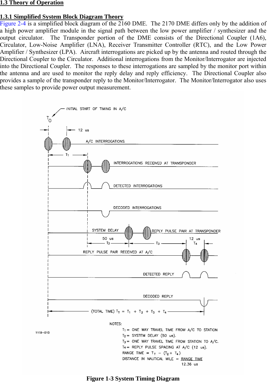
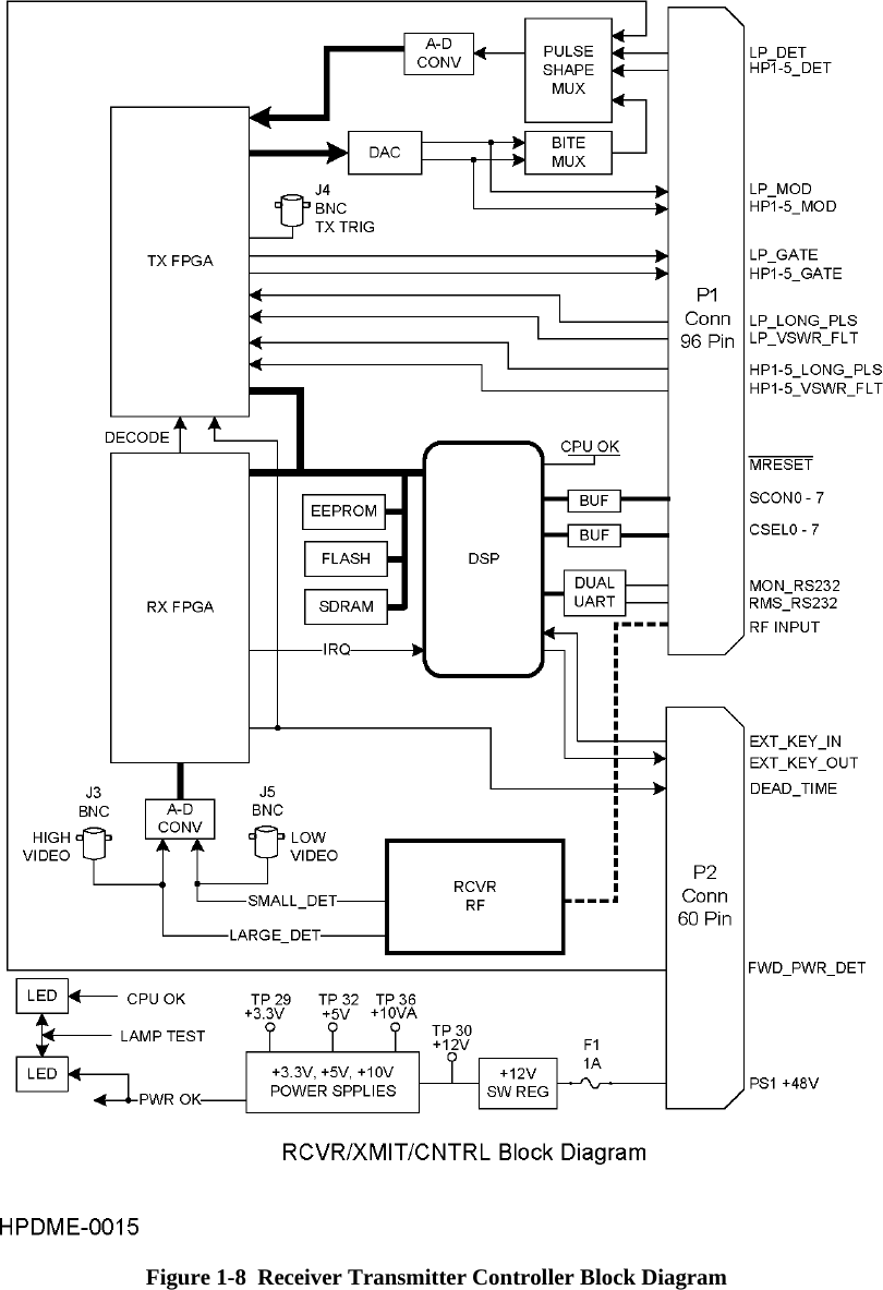
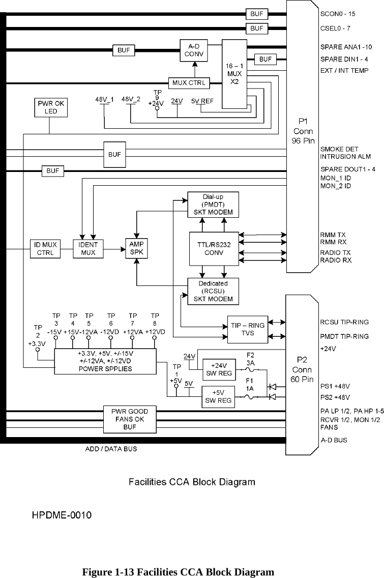
Selex Sistemi Integrati DMEH2 AVIATION SERVICES DME TRANSMITTER User Manual TECHNICAL DESCRIPTION Manual

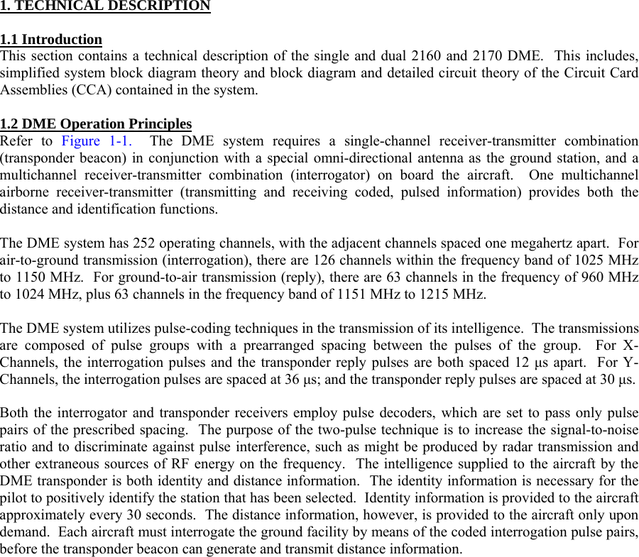
Selex Sistemi Integrati Inc. AVIATION SERVICES DME TRANSMITTER TECHNICAL DESCRIPTION Manual

Contents

USERS MANUAL 2

 1. TECHNICAL DESCRIPTION  1.1 Introduction This section contains a technical description of the single and dual 2160 and 2170 DME.  This includes, simplified system block diagram theory and block diagram and detailed circuit theory of the Circuit Card Assemblies (CCA) contained in the system.  1.2 DME Operation Principles Refer to Figure 1-1.  The DME system requires a single-channel receiver-transmitter combination (transponder beacon) in conjunction with a special omni-directional antenna as the ground station, and a multichannel receiver-transmitter combination (interrogator) on board the aircraft.  One multichannel airborne receiver-transmitter (transmitting and receiving coded, pulsed information) provides both the distance and identification functions.  The DME system has 252 operating channels, with the adjacent channels spaced one megahertz apart.  For air-to-ground transmission (interrogation), there are 126 channels within the frequency band of 1025 MHz to 1150 MHz.  For ground-to-air transmission (reply), there are 63 channels in the frequency of 960 MHz to 1024 MHz, plus 63 channels in the frequency band of 1151 MHz to 1215 MHz.  The DME system utilizes pulse-coding techniques in the transmission of its intelligence.  The transmissions are composed of pulse groups with a prearranged spacing between the pulses of the group.  For X-Channels, the interrogation pulses and the transponder reply pulses are both spaced 12 µs apart.  For Y-Channels, the interrogation pulses are spaced at 36 µs; and the transponder reply pulses are spaced at 30 µs.  Both the interrogator and transponder receivers employ pulse decoders, which are set to pass only pulse pairs of the prescribed spacing.  The purpose of the two-pulse technique is to increase the signal-to-noise ratio and to discriminate against pulse interference, such as might be produced by radar transmission and other extraneous sources of RF energy on the frequency.  The intelligence supplied to the aircraft by the DME transponder is both identity and distance information.  The identity information is necessary for the pilot to positively identify the station that has been selected.  Identity information is provided to the aircraft approximately every 30 seconds.  The distance information, however, is provided to the aircraft only upon demand.  Each aircraft must interrogate the ground facility by means of the coded interrogation pulse pairs, before the transponder beacon can generate and transmit distance information.
  Figure 1-1 Basic X-Channel DME System Block Diagram  Refer to Figure 2-2.  As stated, the transponder beacon must be interrogated by the aircraft before the ground facility can transmit usable distance information.  Assuming an aircraft has interrogated the ground facility; the interrogation signal is received at the beacon antenna, and then routed to the receiver through the Circulator and Preselector.  The signal is then amplified and fed to the Receiver Transmitter Controller (RTC) for verification of proper pulse spacing.  Once receive pulses are validated the RTC encodes a reply with the proper pulse spacing and delay.   The shaped pulses modulate the gated RF in the transmitter power amplifier (PA) to produce the RF output pulses.  The output pulses are then sent to the antenna and radiated to the aircraft as reply pulse pairs.
   Figure 1-2 DME Transponder Block Diagram  Three separate signals are transmitted by the beacon as a train of pulse pairs.  These signals, in order of priority, are: identification, replies to interrogations, and squitter pulse pairs (used as fill-in pulses).  This priority system prevents any interference between the three signals in the overall pulse train.  The identification of the ground facility is important to the using aircraft; therefore, it has been assigned first priority in the priority system.  The generation of identification intelligence is a function of the RTC.  Identification is transmitted periodically in International Morse Code with the characters of the code consisting of a periodic train of pulse pairs.  Identification keying occurs approximately every 30 seconds.  When keyed, the priority logic circuit input is disabled; and the circuits will not accept any decodes from the receiver.  The replies to an interrogation signal are second in the order of priority.  Their induction into the pulse train must be controlled (to prevent interference with the identity cycle and to establish priority over the squitter pulses).  This is accomplished by allowing them to enter the pulse train only during a time interval not occupied by the identity cycle.  This is a major portion of the time, since the identity cycle only occurs approximately every 30 seconds.  Once the receiver accepts an interrogation and decodes it, a blanking gate is generated (the so-called dead-time gate).  The dead-time gate is used to inhibit the transponder decoder for approximately 60 µs.  During this period, the decoded interrogation is delayed a predetermined amount of time and transmitted back as a reply.  The total delay from the time of a received interrogation to transmission of a reply is typically set for 50 µs for an X-Channel DME.
 The squitter pulses are third in the order of priority.  In the absence of interrogations or identity information, random squitter pulses are generated to maintain an average output pulse train of 800 Pulses Pairs Per Second (PPS).  The purpose of transmitting squitter pulses is to stabilize the Automatic Gain Control (AGC) circuits in the aircraft interrogator.  The process of distance measuring originates in the airborne unit with the generation and transmission of pulse signals called interrogations.  The airborne transmitter repeatedly initiates and transmits pulse signals consisting of pulse pairs having 12 µs spacing, a pulse width of 3.5 µs, and a gaussian or sine-squared shape.  These pulse pairs are recovered by the transponder beacon receiver, whose output triggers the associated transmitter into transmitting reply pulse pairs.  The reply pulse pairs are received by the airborne receiver and timing circuits, which automatically measure round-trip travel time (the time interval between interrogation and reply pulses) and convert this time into the electrical signals that operate the distance meter.  Using the block diagram of the system in Figure 2-2, the distance measurement function can be examined from the system stand point.  The range circuits of the airborne interrogator initiate the distance measuring process.  They formulate and transmit an interrogation pulse pair, which is received at a ground station antenna and sent to the RTC.  The RTC then triggers the encoded pulse generator where the shaped pulses are amplified and routed to the PA for modulation of the gated RF.  The output RF pulses are then radiated into space (as replies) via the antenna.  The reply pulses are received by the aircraft, decoded by the airborne receiver, and examined by the range circuits for synchronism with the airborne unit's own randomly generated interrogation pulses.  The airborne unit measures the elapsed time between the transmission of the interrogation pulse pair and the receipt of the reply pulse pair.  It then, converts this time into a distance indication.  In other words, the distance indication is a measurement of the range time of the pulse pairs.  This timing sequence is easily seen by means of the system timing diagram of Figure 2-3.  Timing starts (in the range circuits of the airborne unit) with the first pulse of the interrogation pulse pair.  After a time delay, depending upon the distance between the aircraft and the ground station, the interrogation pulses are received at the antenna of the ground transponder beacon.  The interrogation pulses are decoded, and the reply is encoded and transmitted after a preset time delay (the reply delay of the ground station).  This nominal reply delay duration is 50 µs, for which the airborne range circuits automatically account.  Thus, the total time lapse for any interrogation response cycle is the sum of reply pulse spacing, the two-way transit time (range time), and the reply delay.
 1.3 Theory of Operation  1.3.1 Simplified System Block Diagram Theory Figure 2-4 is a simplified block diagram of the 2160 DME.  The 2170 DME differs only by the addition of a high power amplifier module in the signal path between the low power amplifier / synthesizer and the output circulator.  The Transponder portion of the DME consists of the Directional Coupler (1A6), Circulator, Low-Noise Amplifier (LNA), Receiver Transmitter Controller (RTC), and the Low Power Amplifier / Synthesizer (LPA).  Aircraft interrogations are picked up by the antenna and routed through the Directional Coupler to the Circulator.  Additional interrogations from the Monitor/Interrogator are injected into the Directional Coupler.  The responses to these interrogations are sampled by the monitor port within the antenna and are used to monitor the reply delay and reply efficiency.  The Directional Coupler also provides a sample of the transponder reply to the Monitor/Interrogator.  The Monitor/Interrogator also uses these samples to provide power output measurement.  Figure 1-3 System Timing Diagram
 The Circulator provides isolation between the transmitted and received signals, since a common antenna is used for both.  Signals applied to any of the ports will experience the least insertion loss or minimum resistance when traveling to the adjacent port in a clockwise direction.  Signals traveling in a counterclockwise direction will be attenuated by at least 20 dB.  Aircraft interrogations and monitor interrogations arriving from the Directional Coupler are directed to the Preselector Assembly by the circulator.  The Preselector Assembly is a narrow-band, three-pole, mechanically-tuned filter that discriminates against undesired frequencies and provides additional attenuation of transmitter energy.  From the Preselector, the received interrogations are directed to the receiver input of the Receiver Transmitter Controller (RTC) after being amplified by the Low Noise Amplifier (LNA).  Within the receiver is a low-noise high stability local oscillator that is generated by an internal synthesizer.  This signal is mixed with the incoming RF to provide a 125 MHz first IF signal that is log detected and digitally processed for accurate interrogation time of arrival.  The 125MHz IF is further down converted to a 10.7 MHz IF signal.  This 10.7 MHz signal is narrow-band filtered and used to determine if the received interrogation was on-channel or from an adjacent channel.    The Low Power Amplifier Module delivers 125 watts peak Gaussian shaped pulses at the output connector when used in the Low Power DME.  This translates to a minimum 100 W output at the antenna connector of the station allowing for normal losses in the connecting cables, directional couplers, etc.  The output power is attainable on any DME channel from 960-MHz to 1215-MHz without requiring re-tuning of the amplifier.  The Low Power Amplifier module provides in nearly 200 watts shaped pulses when used as the driver amplifier in either the 2170 High Power DME system, or the TACAN system.  The Low Power Amplifier Assembly consists of three major circuits: the transmitter RF synthesizer, the Modulator and the RF Amplifier.  The RF synthesizer is programmed via a serial interface to the station transmit frequency.  A sample of the CW output of the synthesizer is available on the front panel of the Low Power Amplifier module to allow verification of transmitter frequency by external test equipment.  The CW output of the synthesizer is pulse modulated by an RF switch controlled by the gate pulses from the RTC, then amplified to 26.5 dBm at the output of the synthesizer CCA within the Low Power Amplifier module.  The synthesizer assembly also contains a DC/DC converter to provide the high voltage (~51 volt) supply used within the Low Power Amplifier module.  This DC/DC converter will operate over an input range in excess of 40 to 60 volts DC, providing a stable supply voltage for the RF amplifiers even when the DME system is operating on batteries and is nearing the end of the useful battery life.   The pulse modulated RF signal is then routed through a 4-stage RF amplifier to achieve the final output power of ≥200 watts peak.  The Modulator CCA within the Low Power Amplifier assembly performs the required pulse shape modulation and output power control.  The Gaussian shape desired when used as a stand-alone low power transmitter (2160 DME) is achieved by a linear modulator under control of the RTC module within the DME system.  Detected output pulses from the low power amplifier module are routed to the RTC, where they are compared to the desired pulse shape, and pre-distorted Gaussian shaped control pulses are sent from the RTC to the Low Power Amplifier assembly where they control the outputs of the Modulator CCA.  When the Low Power Amplifier module is used in either the 2170 High Power DME or the TACAN, the output is amplitude controlled by the RTC, and the pulse shaping is done in the low-power amplifier modulator.    The High Power Amplifier module (used only in the 2170 High Power DME and the TACAN, not shown in Figure 2-4) consists of three major circuits, the Modulator and the RF amplifier, and the DC/DC converter.  There is a slight difference in the TACAN version of the High Power Amplifier RF Amplifier and the DME version of the High Power Amplifier.  In the TACAN version, there is an additional driver amplifier stage to compensate for the reduction in input power because the output of the Low Power Amplifier is split 5-ways.  In the DME application, the full output of the Low Power amplifier is applied to the input of the High Power amplifier, hence this additional stage is not needed.  The DME version of the High Power Amplifier has two gain stages, a 500 watt amplifier followed by a 4-wide 2000 watt peak
amplifier (4 x 500).
 The modulator within the High Power Amplifier module operates in a similar fashion as the modulator in the low power amplifier above.  It receives square-pulse input signals from the RTC, and provides the collector voltage modulation to achieve the final RF output pulse shaping.  The High Power amplifier provides in excess of 2000 watts peak power across the full DME/TACAN transmitter band with no tuning required.   The DC/DC converter located within the High Power amplifier provides a constant high voltage power supply (approximately 53 volts) independent of the DME/TACAN system 48 volt power supply status.  This allows full power operation, even when the system is operating on battery backup and is nearing the end of the batteries’ useful life.  Energy storage capacitance to provide the large peak current requirements of the RF amplifier stages is also located on the DC/DC converter CCA.     The Monitor portion of the DME consists of two major sections: the Interrogator (for interrogating the transponder) and the Monitor (to evaluate the reply parameters). Both of these functions are located on the Monitor/Interrogator/Synthesizer module in the 2160/2170 DME system. The Monitor CCA is actually two separate printed wiring boards but they are plugged into the other; forming one module. The main board is dedicated mainly to digital circuitry and is the card-cage support of the module, going from the back plane to the front panel. The second board is dedicated to Interrogator (RF) circuitry.  Each monitor in the system is capable of monitoring all the critical parameters of two transponders on a dual DME, and is capable of performing monitor integrity. One monitor interrogator interrogates the transponders 50 times per second, therefore in a dual system the total rate is 100 interrogations on each transponder for monitor purposes. The interrogation signals are fed into the transponder via the directional coupler in the DME/TACAN system, and the transponder replies are routed to the monitor by the forward coupled transmitter RF signals from the system directional coupler. In dual-equipment stations, the Standby RF input is obtained from the output of the attenuator load connected to the transfer switch.  The monitor can vary the signal level, the pulse shape and timing and the frequency of the interrogations, so the monitor sends different interrogations to measure different parameters. In normal mode different interrogations are mixed together to measure all the critical parameters, if any of these parameters are out of range for an amount of time, the condition is reported to the LCU using the alarm signals. Upon request from the RMS other parameters can be measured and reported to the RMS. While a monitor is disabled to interrogate the transponders (which is half of the time), the monitor uses this time to send certification signals to itself and verifies that the circuitry and the software are working properly.     The Monitor(s) measure the signals and compare against the operator set limits. If parameters fall outside the preset limits the alarm indication to the Local Control Unit (LCU) is changed. The LCU examines the outputs from the Monitor(s) and determine whether to transfer or shutdown the transmitter based on the present settings such as station bypass, and/or voting logic and whether the equipment is single or dual transmitter equipment.  The standard PMDT consists of a laptop computer and is the input/output device for controlling and communicating with the TACAN system.  Station control, adjustment and monitoring functions are available through the computer, and are accessed via a Windows-based operator interface.  An external mouse is supplied with the laptop computer for ease in operation.  An optional desktop PC is available as a substitute for the standard laptop computer.  Also, an optional printer is available for use with either the laptop or desktop PC.     Station security control is provided through a four-level password system.  Complete access to the system for adjustments and measurements is provided at level 3.  Modification of non-critical parameters is available at level 2, and read-only access is available at level 1.  Password and account administration is accomplished at level 4.  All functions available on the local PMDT are available remotely via a modem and dial-up telephone line to an optional remote laptop or desktop PC running PMDT software.
  Figure 1-4 DME Simplified Block Diagram
 1.3.2 Detailed Theory of Operation  1.3.2.1 Low Power Backplane CCA Block Diagram Theory Refer to Figure 1-5.  The Low Power Backplane CCA provides interconnection and configuration for a Model 2160/2170 DME System. The Low Power Backplane is an 84HP (approximately 16.8”) wide, 9 slot card cage intended to fit in a standard 19” rack. The Low Power Backplane will accommodate both a single or dual controlled/monitored DME system. It’s referred to as a Low Power Backplane because only low power amplifiers may be inserted, while a high power DME or TACAN will have a separate, dedicated High Power Backplane.  Configuration of the DME system resides on the Low Power Backplane CCA in the form of DIP switches. Sixteen individual switches determine system configuration and eight switches set operating frequency.  System1 and System2 Low Power Amplifiers (LPA) connect to the backplane via J1 and J16 DB37 connectors with blind mate adapters (BMA). Each LPA also has an RF_OUT signal which eventually connects to couplers for further processing.  The remaining circuit cards that insert into slots of the Low Power Backplane utilize both 96 pin and 60 pin DIN41612 connectors. The 60 pin connectors have openings for RF connectors which carry RF signals to and from the Monitor CCAs and RTC CCAs. For circuit cards such as the RMS and Facilities CCAs that do no have RF signals, these RF connector positions are not populated.   System1 and System2 Receiver/Transmitter Controller (RTC) CCAs connect via J2/J3 and J14/J15 as well as their RF connectors.   System1 and System2 Monitor / Interrogator CCAs connect to the backplane via J4/J5 and J12/J13 as well as their RF connectors.  The RMS CCA connects to the backplane via J8/J9 and the Facilities CCA connects to the backplane via J10/J11.  Connections between the Low Power Backplane CCA and a High Power Backplane CCA are accomplished by 50 pin headers P5 and P6.  The J17 DB9 connector facilitates interface between the Low Power Backplane CCA and the Battery Charge Power Supply (BCPS) modules for System1 and System2.  Power for the backplane enters via terminals E1 through E4 block TB1.  The LCU CCA is attached via 60 pin header P4.  The Interface CCA has two possible connections; the 60 pin header P1 for general purpose signals and the 40 pin header P1 if a TACAN antenna system must be controlled.  The Fan Control CCA is connected by 14 pin header P7.
  Figure 1-5 Low Power Backplane CCA Block Diagram
 1.3.2.2 High Power Backplane CCA Block Diagram Theory  Refer to Figure 1-6.  The High Power Backplane CCA provides interconnection and configuration for a Model 2170 DME System. The High Power Backplane is an 84HP (approximately 16.8”) wide, 5 slot card cage intended to fit in a standard 19” rack. The High Power Backplane will accommodate up to five High Power Amplifier Assemblies.   Connections between the High Power Backplane CCA and the Low Power Backplane CCA are accomplished by 50 pin headers A2P1 and A2P2. These connectors are keyed to prevent incorrect installation.  The control signals of A2P1 and A2P2 are distributed to the five possible amplifier connectors A3P1 through A7P1. Connectors A3P1 through A7P1 are DB37 female connectors with blind-mate adapters (BMA).  +48 volts and ground power for each of the five possible amplifiers is routed via screw terminals A2E1 through A2E10. These terminals are each rated for 30 amps of continuous current.  Each amplifier has an RF_OUT signal, routed via connectors A3J2 through A7J2, which eventually connect to couplers for further processing.
  Figure 1-6 High Power Backplane CCA Block Diagram
 1.3.2.3 Low Power Amplifier Block Diagram Theory Refer to Figure 1-7 for a block diagram of the Low Power Amplifier module.  The 030802-0001 Low Power Module is used in the 2160 Low Power DME as the complete transmitter module, and in the 2170 High Power DME and the TACAN as the transmitter RF signal source/driver amplifier.  It is comprised of three major sections.  Within the module are the Synthesizer CCA which generates a pulsed RF signal for the DME/TACAN transmitters, the RF amplifier/transmitter assembly boards which provide the necessary amplification of the Synthesizer signal, and the Modulator CCA which processes the control signals from the RTC (Receiver Transmitter Controller) module to properly control the desired output RF pulse shape and amplitude.  The synthesizer CCA also contains the DC/DC power supply which regulates the various supply voltages used within the module.  Analog control signals from the RTC are routed via high speed differential analog paths through the low power backplane to the Low Power Amplifier.  Differential analog signals are used to suppress the effects of common mode noise on the signal paths and to maintain the integrity of the analog control signals.  Similarly, the detected video outputs of the Low Power Amplifier assembly are routed through similar high speed differential analog paths back to the RTC, for the same reasons.  1.3.2.3.1 Synthesizer CCA Block Diagram Theory Refer to Figure 2-7.  The Synthesizer Assembly contains only one CCA which generates a pulsed RF signal across the full DME/TACAN transmit band.   This CCA also provides a sample of the RF signal to the RTC for BITE considerations. The circuit card contains the Low Power Module’s temperature sensor and all of the input/output control signals for this module.    The Synthesizer CCA contains a DC/DC converter which accepts an input voltage range of  40Vdc – 60VDC and generates a nominal output voltage of 51VDC using the converters output “trim” pin to alter the output voltage.  This nominal voltage is passed to the Modulator CCA for modulation and power control of the RF transistors.  This nominal voltage is also DC/DC converted to 20VDC using an additional switching regulator. The other required DC voltages used within the module are linear regulated from the 20VDC voltage.   The DC/DC converter and switching regulator voltages are monitored for proper DC levels using a window comparator circuit. This output signal from this comparator is sent to the RTC for BITE monitoring with a logic level “0” indicating a “POWER GOOD” condition. A front panel status LED is also illuminated green to indicate this power good condition.  The LED can also be illuminated by the RMS for lamp test and troubleshooting purposes.    The RF synthesizer portion of this CCA generates a CW or pulsed RF output power of 26.5dBm ±0.5dB on any DME ground station transmit frequency from 960 MHz to 1215 MHz.  Synthesis of the transmit frequencies is accomplished by controlling the tuning voltage on a Voltage Controlled Oscillator (VCO).  A phase lock loop is used to control the tuning voltage.  The PLL uses an active gain loop filter and is frequency referenced to a 10 MHz standard provided by a temperature compensated crystal oscillator (TCXO). This TCXO reference provides the required transmitter frequency stability over all environmental conditions.  Programming of the desired frequency is done through serial control lines from the RTC.   The output RF signal from the VCO is buffered, amplified, and split three ways using a resistive divider.  One of these paths is used as feedback for the phase lock loop.  The second path routes the signal to a fixed frequency divider.  The output of this divider is monitored by the DME system for frequency integrity.  The final RF signal path is amplified to the proper signal level, pulse modulated and is fed to the power amplifier. The CW RF signal is pulse modulated using a non-reflective switch by the gate controls from the RTC, and is fed to the Pre-Driver CCA (012175) of the power amplifier.   Prior to the RF switch and the final gain block, a sample of the CW signal is provided for use by external test equipment via a resistive coupler.  This port is AC coupled and is properly terminated internally (50 ohm load) to provide sufficient isolation to avoid disruption of the transmitted signal by external influences, and made available on a front panel connector.  The low power amplifier temperature sensor is mounted on the back side of the final RF amplifier stage transistor.  It is in close proximity to the transistor in order to maximize heat transfer to the sensor.  The sensor is equipped with a serial programmable interface (SPI).   The temperature data from this sensor is processed by the RMS and used for amplifier protection in the event of over temperature.
 1.3.2.3.2 Low Power Modulator CCA Block Diagram Theory  The Modulator CCA sends and receives control signals to the RTC (Receiver Transmitter Controller) via the Synthesizer CCA. This board controls the voltage to the RF amplifying transistors to obtain the proper transmitter power and pulse shape. The transmitter gate signal, supplied by the RTC, is applied to the first two RF amplifier stages through a high side MOSFET switch. The modulating transistor switches are controlled at two different voltage levels for a 3 dB transmitter power level change. The final two amplifying stages are also voltage controlled by a high side MOSFET, but these transistors are linear modulated with the signal from the RTC that is Gaussian shaped. The energy storage capacitor used to provide the short term peak current requirements of the RF amplifier stages is contained on the Modulator CCA board. The forward and reverse detected RF video outputs signals from the Final CCA (012184) are routed to the Modulator CCA where the signals are used to determine the RF pulse shape and level. These detected signals are also monitored on the Modulator CCA for excessive pulse width and high VSWR conditions. The output of the high pulse width and high VSWR monitor circuits are stretched and sent to the RTC for monitoring.  In addition, in the event there is a detected pulse width fault or a high VSWR fault, the stretched outputs of these detectors will disable the Low Power Amplifier RF output for protection against damage.  The forward detected video signal is also routed to the RTC to complete the control loop that provides the proper power level and pulse shape.  The RTC compares this detected signal to the desired output pulse shape, calculates the necessary corrections, and pre-distorts the shaped pulse control signals used by the Low Power Amplifier module.   1.3.2.3.3 RF Amplifier / Transmitter Assembly Theory The RF Amplifier/Transmitter portion of the LPA Module provides amplification of the pulsed RF signal from the synthesizer CCA, and is comprised of three assemblies. The first assembly is the pre-driver amplifier stage, and the second assembly is the driver amplifier stage.  The last assembly contains the final RF amplifier stage along with an output low pass filter and a dual directional coupler.  The pre-driver and the driver stage are all square wave modulated by the modulator CCA, while the final amplification stage is square wave modulated for TACAN and High Power DME configurations or Gaussian shape modulated for Low Power DME configuration.  All the RF amplifying transistors are bi-polar junction transistors (BJT) and are operated in Class-C mode, common base configuration.  The module is capable of transmitting 225W peak at the output port of the module in either a Gaussian shape or square wave modulation.  The transmitter’s circuit cards are described in the following paragraphs.  1.3.2.3.4 Pre-Driver and Driver CCA Block Diagram Theory Refer to Figure 1-7. The pre-driver is a single stage RF amplifier which receives a pulsed RF signal from the Synthesizer CCA.  The RF signal is amplified and routed to the next stage, the “driver” CCA.  The driver CCA contains two stages of RF amplification and feeds into an attenuator pad on the Final CCA.  The voltage supplies of the transistors on the pre-driver and the driver stages are all square wave modulated in synchronization with the RF switch on the Synthesizer CCA, controlled by the gate pulses from the RTC.  The pulse width, gain, and output RF signal level are controlled via the Modulator CCA.    1.3.2.3.5 Final CCA Block Diagram Theory Refer to Figure 1-7. The final stage of the RF transmitter includes the final RF amplifier stage, a low pass filter, and a dual directional coupler. The final transistor receives a square wave modulation signal and maintains a square wave output shape for the High Power DME and TACAN system configurations, or transforms the input signal into a Gaussian shaped RF signal for the Low Power DME system configuration. This shape is controlled by modulating the supply voltage of the final transistor.  All modulation of the supply voltages are synchronized with the RF switch on the Synthesizer CCA.  The signal shape and output level are controlled by the RTC via the Modulator CCA.  An attenuator pad is used between the driver and the final RF amplifier stage in order to minimize voltage standing waves when modulating the input square wave into a Gaussian signal.  This attenuator also provides impedance stability between these two RF amplifier stages.   The low pass filter is a lumped element design and is optimized for minimal insertion loss across the DME/TACAN transmitter band, while providing a nominal 40dB or more of attenuation for unwanted high frequency spurious signals.  The filter is placed in a separate cavity for shielding purposes.
 The output directional coupler is a discrete component with a nominal coupling of -20 dB and a minimum directivity of 20dB.  The coupler is used to sample the transmitted RF signal and detect any reflected signals due to load mismatches.  Both the forward and reflected signals are further attenuated by 10dB attenuators and are converted to video signals by differential diode detectors before being passed to the Modulator CCA.  Both the forward and reflected detectors have 25dB of linearity. The coupler/detector section of this CCA is placed in a separate cavity for shielding purposes.   Figure 1-7 Low Power DME Amplifier Block Diagram
 1.3.2.4 Receiver Transmitter Controller Theory The Receiver Transmitter Controller (RTC) is an integral part of the DME dedicated to receiving aircraft interrogations and controlling the transmitter replies.  All of the receiver hardware is contained on the RTC assembly except for the pre-selector filter that is tuned to the station frequency.    The RTC Assembly (030805-0001) consists of two circuit card assemblies (CCA).  First is the RTC CCA (012168-1001) that slides into the card cage assembly and plugs into the motherboard for power and signal connections.  The Receiver RF CCA (012180-0001) is a second circuit card that plugs into the side of the RTC CCA.  Power and signal lines come from the stacked circuit card connectors while the receiver RF signal enters through a SMA connector.  The RF signal is routed from the backplane connector on the RTC CCA to the Receiver RF CCA using conformable RF cable.  The Receiver RF CCA is housed in a completely shielded enclosure consisting of a backing plate, fence, and cover.  1.3.2.4.1 CCA, Receiver Transmitter Controller Block Diagram Theory This section describes the details of the RTC CCA.  Throughout this section refer to Figure 1-8 and 012169-9001 schematic.    A Digital Signal Processor (DSP) and two Field Programmable Gate Arrays (FPGA) comprise the heart of the RTC CCA.  All of the timing critical functions of pulse reception and transmitter control are located in the FPGA hardware.  Non critical tasks such as identification control, squitter/transmitter rate control, and transmitter pulse shaping are handled by the RTC software in the DSP.  The DSP uses its speed to help the hardware handle tasks such as short and long distance echo suppression, decoder correlation, and CW desensitization.  Control of the transmitter is accomplished by the RTC CCA.  LVDS hardware on the board provides differential gate pulses that enable the RF modulators and apply the synthesizer RF output to the transistor amplifiers.  Additionally the RTC CCA provides differential Gaussian shaped pulses used to control the RF modulator amplitudes.  With each pulse transmitted the RTC CCA samples the detected RF output and determines what, if any, errors exist in the pulse shape parameters.  The RTC CCA then modifies the output waveform before transmission of the next pulse.  This N-1 pulse shaping algorithm is used to ensure the transmitter meets critical spectral requirements.  Pulse shaping is one of the transmitter control loops in the DME/TACAN equipment and does not require any user intervention.  Each RTC CCA has an associated low power amplifier and synthesizer.  For high power DME operation the LP amp is followed by a HP amplifier.  In this case the RTC CCA drives the LP amp with a trapezoidal shape pulse and performs the final pulse shaping in the high power amplifier.   When operating as a TACAN, up to five HP amps are summed together with a RF combiner.  In this case the RTC CCA shapes each HP amp individually and monitors the composite detected RF envelop for pulse corrections using the forward power detector input signal.  In addition to driving the RF modulators, the RTC CCA controls the transmitter pulse pair spacing and transmission rate.  The transmission rate is monitored in the FPGA hardware and randomly spaced pulse pairs are generated if necessary in order to meet a minimum transmission rate.  When overloaded by too many aircraft interrogations, the RTC CCA limits the transmitter rate by reducing the receiver sensitivity.  Functions also accomplished by the RTC CCA include the decoder that correlates each received pulse with previous pulses to find a pair that meets the decoder aperture for the DME operation mode.  Received pulse widths are monitored such that narrow radar pulses are rejected and wide out of tolerance pulses are rejected.  The receiver also provides continuous wave (CW) interference rejection and suppression of transmission due to interrogation echoes.  Communications between the RTC CCA and the RMS is accomplished with a serial data link.  Transmitter and receiver configurations are received from the RMS while operating data and maintenance alert signals are sent to the RMS for display on the PMDT.  A serial data link between the RTC CCA and the Monitor CCA is provided so the RTC software can control the transmitter delay as well as provide a transmitter soft
start feature that monitors the antenna VSWR while ramping up the output power.  This helps protect the high power amplifiers from damage in case the antenna port is not properly terminated.
  Figure 1-8  Receiver Transmitter Controller Block Diagram
 Multiple synthesizers are controlled by the RTC CCA.  First is the transmitter synthesizer located on the LP amplifier that is serially loaded based on the backplane frequency select switches.  Second is the receiver synthesizer that is loaded to provide an IF frequency of 125MHz.  Output frequencies of both these synthesizers are checked by the Monitor CCA.  When operating as a TACAN the North, Aux, and Ident trigger signals from the TACAN antenna controller are converted to TTL signals using comparators located on the RTC CCA.  These TTL signals are used by the FPGA hardware to transmit the North and Auxiliary burst sequences after a short delay.  This delay will be configurable in order to support remote shifting of the azimuth angle as required for flight check operations.  Both the trigger signals and the delayed triggers will be sent to the monitor for integrity alarm processing.  In addition to the LVDS gate and Gaussian modulation pulses, each power amplifier provides VSWR fault and long pulse fault signals to the RTC CCA.  For the LP amplifier connection a synthesizer lock signal is also sampled.  All of these signals are sent to the RMS where a maintenance alert is generated and detailed status can be displayed on the PMDT.  Morse code identification is controlled by the RTC CCA primarily by the RTC software.  Identification keying can be sourced into the RTC from external equipment such as a VOR, Localizer, or Glideslope.  Identification is fully configurable from the PMDT to allow such things as window keying, inverted input keying contacts, interlock-off upon external keying loss, etc.  The RTC can even operate in a master mode where keying is output to external equipment.  Front panel test points are provided for inspection of the large and small signal IF waveforms after the signals leave the Receiver RF CCA.  A BNC connector provides the transmitter trigger signal that can be used to trigger an external oscilloscope for inspection of the detected transmissions.  LEDs on the front of the RTC CCA shown that the power supplies and RTC software are operating properly as well as indicate whenever the receiver has reduced the sensitivity due to traffic overloading or detection of CW.  On the board test points are available to inspect the Gaussian modulation pulses for each power amplifier.  These modulation pulses are also multiplexed back into the sampling ADC for diagnostics purposes.
 1.3.2.4.2 CCA, Receiver RF Block Diagram Theory This section describes the details of the Receiver RF CCA.  Throughout this section refer to Figure 1-9 and 012181-9001 schematic.    Figure 1-9  Receiver RF Block Diagram  The Receiver RF CCA uses a dual heterodyne receiver with a first intermediate frequency (IF) of 125MHz and second IF of 10.7 MHz.  The receiver has a calculated noise figure of approximately 4dB which, when coupled with the external fixed-loss components such as the circulator, preselector, and power splitter provides a maximum receiver sensitivity of minus 94dBm.  The usable receiver sensitivity is configurable via the PMDT interface from -94dBm to -72dBm.  This allows the installation to match the receiver range to the transmitter range. By default the receiver sensitivity is set to -82dBm for 100W stations and -87dBm for 1000W stations.  These long-established settings ensure that the DME station only replies to aircraft within the working range of the transmitter operating power.  For instance a 100W DME transmitter reply can only reach aircraft within a 40NMI radius; therefore the receiver would be unnecessarily overloaded with aircraft interrogations within 200NMI if the receiver sensitivity was maximized to -94dBm.
 Frequency selection of the receiver is accomplished with an independent synthesizer.  Thus there are no RF cables interconnecting the interrogation synthesizer and transmitter synthesizer.  This also allows use of commonly available IF filter products.  The synthesizer output power is +17dBm in order to run a high IP3 mixer.  A sampled output is provided on the front panel of the RTC Assembly for use with a frequency counter.  A divided output clock signal is also provided for integrity monitoring by the Monitor CCA.  From the first mixer the 125MHz IF signal is bandpass filtered using a Surface Acoustic Wave (SAW) filter.  Each SAW filter has approximately 825MHz bandwidth and provides excellent group delay flatness.  When cascaded, they also provide more than 90dB image rejection of the final 10.7 MHz IF.  After the SAW filter the IF signal is amplified then resistively split into the large signal and small signal path.  Each 125MHz path terminates with a log detector that provides almost 70dB of linear dynamic detection range.  Operational amplifiers provide the final gain before conversion of the detected signals by the dual 12-bit ADC at a sampling rate of 25MHz.  The receiver dynamic range is greatly increased by using two paths separated by approximately 25dB of signal strength.  Internally the FPGA analyzes the two input signal and determines which signal is best for timing reception.  Inside the Receiver FPGA located on the RTC CCA, the two detected signals are resampled at 50MHz then low-pass filtered in order to reduce the noise bandwidth and eliminate the interpolated image.  All of the half amplitude detection, including a 2µs delay line, is accomplished digitally inside the Receiver FPGA.  This technique provides for superior receiver performance and stability.  For on-channel detection the large signal IF path is split before the log detector and down converted separately to 10.7 MHz using a second mixer driven from a 114.3MHz oscillator.  This final 10.7MHz IF is narrow band filtered using cascaded ceramic filters then log detected.  The resultant narrow-band signal is compared against the detected large signal and used by the Receiver FPGA to insure that received pulses are not from an adjacent DME channel.   1.3.2.5 Monitor Block Diagram Theory Refer to Figure 1-10. The Monitor CCA performs supervision of critical DME/TACAN system parameters and also performs self-monitoring. The Monitor CCA is actually two separate printed wiring boards but they are plugged into each other; forming one module. The main board is dedicated mainly to digital circuitry and is the card-cage support of the module, going from the back plane to the front panel. The second board is dedicated to Interrogator (RF) circuitry.  The Monitor CCA is powered by a single +48V power supply coming from the back plane. Regulated +1.2V, +2.5V, and +3.3V supplies are generated from the +48V by the Monitor CCA for the digital circuitry. +5V regulated power is used for analog circuitry and +17V is used to power the Interrogator board. The PS_OK LED is on while all the internal supplies are within limits. This LED can be also be lighted by the ~TEST signal coming from the LCU.   The DSP coordinates all subsystems to measure the parameters, sends the measurements to the RMS using RS232 communications, and notifies the LCU when a critical parameter is out of range using the primary and secondary alarms. The DSP utilizes an external flash ROM for storage of the program and synchronous dynamic RAM (SDRAM) as well as non-volatile RAM (NVRAM) for data storage. The DSP peripherals include a voltage supervisor / watchdog, a dual UART, a programmable logic device with complex control circuitry, and input / output latches.   The voltage supervisor / watchdog resets all the digital circuitry when the +3.3V power supply is too low, when the LCU asserts the ~MRESET line, or when the DSP does not refresh the watchdog timer. The dual UART is used to communicate with the RTC and the RMS through the back plane. The configuration switches of the backplane determine if the Monitor is part of a high or low power DME; or if it’s in TACAN mode. The ~LOCAL signal comes from the LCU and determines if the DME is being adjusted by a local operator. The ~OVERLOAD signal comes from the Receiver/Transmitter Controllers (RTCs) and is asserted when any RTC has reduced sensitivity because of the traffic load.
  Figure 1-10 Monitor CCA Block Diagram
 After a system reset, all the alarm latch outputs will are in the active state until updated by the DSP. The alarms are updated only when the DSP refreshes the voltage supervisor / watchdog. If there is a DSP failure, the alarms will remain in the last output state until watchdog time-out and the voltage supervisor / watchdog reset activates the alarms. During normal operation, the alarm outputs are read by the DSP using an input buffer to verify them. The LEDs are used to signal the alarms and pre-alarms conditions on the front panel and the external ~TEST signal coming from the LCU can light all LEDs to verify they have not failed.  The debug RS232 port is used only for factory purposes and will not be used by the customer in the field.  The 10MHz temperature-controlled crystal oscillator (TCXO) provides an accurate and reliable source of timing for the digital circuitry and the Interrogator sections.  The PLD is decoded into the DSP memory map. The PLD has complex circuitry for a programmable interrogator. The interrogator is enabled half of the time by the INT_EN_U signal coming from the LCU. When enabled, the interrogator uses a digital-to-analog converter (DAC) to generate interrogation pulses to the Interrogator board, which modulates and sends it to the RTCs. Simultaneously; the monitor interrogation is demodulated and sent to an analog-to-digital converter (ADC 1) via the MON_DET_INT signal. Once this sampling is finished, the interrogator controller switches to the ANT_DET_REPLY source or the STDBY_DET_REPLY source to complete the sampling with the reply from one RTC. The sampling is then shared with the DSP to measure the parameters.   The PLD uses the DONE signal to alert DSP once the sampled signal is ready. While the interrogator is disabled, the PLD sends a complete waveform with two interrogations pulses and two reply pulses through the DAC to ADC 1 by the CERT_SIGNAL to certify the alarm limits and the measurement circuitry. Also LOG_DET_MEAS is used to measure the antenna forward or reflected power while the interrogator is disabled, selecting with the FWD/~RFL~_CTRL signal. The digital attenuator in the ANT_DET_REPLY signal is used to verify the alarm limits in the output power.  Since interrogator controls the synthesizer frequency of the RF board, it has the ability to change the frequency in real time and mix normal interrogations with out-of-frequency interrogations. The Monitor uses this capability to measure the RTCs rejection of out-of-frequency interrogations. The attenuation of each sample from the DAC can be controlled through the INT_ATT_CTRL signal.  Two BNC connectors are on the front panel. The INT_TRIGGER signal is the trigger for an oscilloscope and the INT_TRIGGER_U signal is the source. The PMDT can select which interrogations to display and the PLD triggers the oscilloscope when the selected type is been sent.  The ANT_DET_REPLY and STDBY_DET_REPLY contain only the shape of the reply pulses. These signals along with the CERT_SIGNAL go through comparators to form square-waves. The square-waves are used by the PLD to measure the pulse-rate frequency and the efficiency. The TX1_ANT indicates which RTC is connected to the antenna. TX1_ID and TX2_ID signals are asserted when each RTC is emitting identification pulses. With these signals and both the antenna and standby reply’s, the PLD can monitor the identification code and frequency of both RTCs. An AUDIO_ID signal is also generated by the PLD to hear the Morse identification code of the DME.  The signal INT_F0 is the monitor’s synthesizer signal divided by 223. This signal is used by the DSP to measure the frequency of the synthesizer. The same types of signals come from the DME transmitters and receivers. All of these signals are multiplexed by the PLD to the DSP timer to be measured. The monitor’s synthesizer signal is also available on the monitor’s front panel to be measured externally.  When working in TACAN mode, North and Aux Burst signals are used in conjunction with the peak-hold circuit and ADC 2 to measure 15 / 135 Hz modulation depth and phase accuracy. The North and Aux Trigger and Delay are used to measure the North and Aux Burst delay and length. There are no hardware differences between the DME and TACAN monitors; only the DSP software and PLD firmware are
different.
  1.3.2.5.1 DME Interrogator CCA Block Diagram Theory Refer to Figure 1-11.  The Interrogator (RF board) has all the necessary circuitry to modulate the interrogations from the Monitor and demodulate the replies from the RTCs.   For DME systems, the ANTENNA_RF signal comes from the monitor port on the DME antenna.  For dual DME systems, the monitor signal is split and run to each Monitor.  For TACAN systems, this signal comes from a monitor antenna placed near the TACAN antenna. It is attenuated by a fixed 16dB attenuator and then by a digital attenuator controlled by the monitor DSP.   The digital attenuation stage setting depends on an initial calibration, which varies over antenna cable lengths and types. After the attenuators, the ANTENNA_RF signal is detected and the shapes of the pulses are sent as the ANT_DET_REPLY signal to be processed.  The STANDBY_RF signal only applies for dual equipment.  It is derived from a 20dB or 30dB attenuator that is split for each Monitor, then is attenuated by 16dB and demodulated similar to the ANTENNA_RF signal.   The ANT_REFLECTED signal comes from the transmitter 30dB reflected coupler.  For dual equipment it is split before routing to each Monitor. After an attenuation of 26dB, this signal is sent to a 45dB precision temperature-compensated logarithmic detector. It is used to shutdown the transmitter if the Monitor detects too much reverse power; which could be caused by an open or shorted antenna cable.   The signal FWD/~RFL~_CTRL is controlled by the PLD 1 to switch the source of the logarithmic detector between the reflected and the forward coupler. An additional 10dB attenuation to both signals is applied before the logarithmic detector for High Power DME and TACAN systems; therefore the measurements are equal for low and high power equipment. The ~10DB_CTRL signal activates this additional attenuation when the Monitor is in a high power configuration.  The ANT_FORWARD signal is a bi-directional signal that comes from the transmitter 30dB forward coupler. For dual equipment it is split/combined from each Monitor.  As an input, it is used to monitor the transmitter output power and calculate the antenna VSWR. To accomplish this, the signal runs through a circulator and then through a 6dB splitter. One of the split signals is attenuated by 20dB and then can be multiplexed to the 45dB logarithmic detector. The other split signal is attenuated by 10dB and then has an additional 10dB attenuation stage, which is only active in an HP DME or TACAN system. Finally, it is detected and the signal is sent in a differential pair to the RTC for feedback control of composite transmitted pulse shape for TACAN mode.  The Interrogator module has its own synthesizer for on and off-channel measurements. The reference frequency comes from the digital Monitor board and the accuracy of the synthesizer signal is ±5 parts-per-million (ppm). The synthesizer signal is buffered and sent to the Monitor’s front panel for external measurements. Also it is divided by 223 to be measured by the Monitor’s DSP.   The interrogation pulse shapes generated by the interrogator in the PLD 1 are modulated with the synthesizer signal and then run through three digital attenuation stages. The three attenuators are also controlled by the interrogator. These digital attenuators have a 95dB dynamic range. The resulting signal is multiplexed to the antenna after a low pass filter and the combiner or to the logarithmic detector after a 10dB attenuator; calibrating the power of the Monitor transmitter and consequently adjusting the interrogation attenuation to be equal over temperature.  This calibration is done periodically and is controlled by the PLD 1 interrogator using the INT_CAL signal. The monitor interrogation is demodulated again and sent to the digital board through the MON_INT signal to be used by the interrogator as previously explained.
    Figure 1-11 DME Interrogator (RF) Block Diagram
 1.3.2.6 RMS Processor Block Diagram Theory Refer to Figure 1-12.  The Remote Monitoring System (RMS) CCA performs communications via thirteen serial ports plus a parallel port, and facilitates monitoring/control in a single or dual DME system. The RMS CCA receives battery-backed DC power from the BCPS CCAs at connector J2, through OR’d diodes, and regulated to +5V and +3.3V supplies for use by the RMS CCA to power the microcontroller and all of its associated circuitry.  The U8 microcontroller utilizes external flash ROM, non-volatile RAM (NVRAM), synchronous dynamic RAM (SDRAM), a voltage supervisor/watchdog reset circuit, and an oscillator to form the core microcomputer. The U8 microcontroller also includes a direct memory access (DMA) controller, serial ports, and general purpose input/output (I/O). Microcomputer peripherals include a real-time clock (RTC), universal asynchronous receiver/transmitters (UARTs), a parallel port interface (PPI), a USB host port, a USB slave port, off-board bus buffers, and more general purpose I/O.  The U8 microcontroller’s flash ROM is factory programmed using the J4 SPI boot header while factory debug is accomplished using the J3 emulator header, the JP3 debug header, and the JP4 PMDT RS232 header. None of the aforementioned connectors and headers will be used by the customer in the field.  RMS communication to the LCU CCA occurs via the parallel port established by U29 through U32 and connector P1. The LCU also returns system control signals through P1 such as *TEST (lamp test) and *MRESET (master reset). Configuration switches on the Backplane CCA define the system set-up to the RMS when it reads them via the Facilities CCA through the external address/data bus on connector P2.  The U8 microcontroller communicates serially through one internal and twelve external UARTs. The internal UART is the debug port of JP3. The other twelve UARTs control communications to Monitors 1 and 2, Receiver/Transmitter Controllers 1 and 2, Remote Maintenance Monitor (RMM), ILS/VOR, Radio Modem, LCD, BCPS, TACAN Antenna, Ethernet, and the PMDT. Two options are possible for local PMDT communications. The PMDT may be connected to USB connector J1 with header JP2 strapped for USB operation. The second option (in factory only) has the PMDT connected to RS232 header JP4 and header JP2 strapped for RS232 operation.  These eleven external UARTs (not including the PMDT) route to connectors P1 and P2. The host USB port of connector J2 is available for possible future options such as connection to a printer.
   Figure 1-12 RMS CCA Block Diagram
 1.3.2.6.1 RMS CCA Detailed Theory Battery-backed DC power 1_+48V and 2_+48V enter via connector P2-25 and P2-26, diode-OR’D by diodes CR13 and CR14, and fused by F2. This voltage is further regulated to +5V by DC-DC converter U39, diode CR15, and inductor L3. Over-voltage protection for the +5V is provided by SCR Q5, zener diodes CR19 and CR20, capacitor C115, and resistor R65. The +5V supply is further regulated by linear regulator U40 to create DVCC (+3.3V). The +5V is measurable at TP14 while DVCC is available at TP7.  The DVCC and +5V supplies power the U8 microcontroller and its peripherals. The U8 microcontroller acts as a DC-DC converter to create +1.2V (measurable at TP3) for powering its core (VDDINT) by pulse-width-modulating U8-4/5 and using transistor Q1, diode CR2, and inductor L1. Diode CR1 insures proper power supply sequencing during power-up/down.  The U8 microcontroller utilizes 512Kx16 of flash ROM (U1 and U2) for non-volatile program storage as well as 32Kx8 non-volatile RAM (U3) for variable storage. Oscillator Y2 provides the system clock for U8 as well as UARTs U16, U22, and U28 after buffering by U17. The system clock can be measured at test point TP1.  Data buffers U33/U34 and address buffers U35/U36 are decoded by AND gates U47:B, U47:C, and U47:D to activate the buffers only during a valid asynchronous memory select cycle. Resistor networks RN5 through RN9 act as pull-ups on these buffered bus lines. Only the bus lines between U8 and the 16Mx16 SDRAM (U4) are not buffered in some form. The U4 SDRAM is used for program and variable storage and has very fast access/refresh times.  The U8 microcontroller has direct control of the CPU_OK LED (CR5) by utilizing output PF8 (U8-36) and transistor Q2. The ~TEST signal, from the LCU via connector P2-B8, also can light the CR5 LED when active. Zener diode CR17 limits the maximum voltage while resistor R11 limits the maximum current of the CR5 LED.  Buffer U37 is used to buffer address lines A17, A18, and A19, control signals ~AOE and ~AWE, as well as the serial peripheral interface (SPI). The SCK, MISO, and MOSI SPI signals (U8-53, U8-54, and U8-55) along with ~SPI_CS0 (U8-49) are used in conjunction with the SPI Boot header J4 for in-factory programming of flash ROM. Latch U7 and inverter U10 combine to create the SPI chip select signals ~SPI_CS1 through ~SPI_CS8 for communications to off-board serial SPI devices through connector P2-A8 through P2-A16.  Real-time clock (RTC) U15 is clocked by oscillator U9 and battery-backed up by battery B1 if header JP1 is strapped between JP1-2 and JP1-3. The 512 Hertz heartbeat of RTC U15 can be measured at test point TP13. Oscillator U9 is a highly accurate temperature-compensated crystal oscillator (TCXO) whose accuracy eliminates the need for a potentiometer or adjustable capacitor.  Emulator header J3 is used for in-factory testing and development only.  The ~MRESET signal from the LCU enters via connector P2-B16 and is filtered by inductor FL1 and capacitor C39 to create reset signal ~EXT_RES. Signal ~EXT_RES is bi-directional in that either the LCU or the RMS can cause the signal to be active and reset the entire DME system.   When the LCU pulls ~MRESET (and subsequently ~EXT_RES) low, voltage supervisor / watchdog input U6-1 is low; causing output U6-7 to go low which resets the U8 microcontroller and on-board latch U7 immediately. UARTs U16, U22, and U28 as well as USB host U38 will also be immediately reset by the RESET output of inverter U17:A. Latch U29 will be reset after being delayed by inverters U45:A, U45:B, resistor R13, capacitor C114, and diode CR16.  The RMS can initiate a system reset by activating ARM_SYS_RES (U29-9) and stopping the periodic strobing of voltage supervisor / watchdog input U6-6. A reset from U6-7 will occur approximately one second after the last watchdog strobe; causing inverter U17:A, transistors Q4/Q3 and ~EXT_RES to
become active. The reset will clear after ~DELAYED_RESET from U45:B clears latch U29-9 ARM_SYS_RES; which in turn shuts off transistor Q3 and releases ~EXT_RES.
 A reset can also be initiated by voltage supervisor / watchdog U6 when the power supply voltage on U6-2 drops too low; causing U6-7 to activate.   Latches U29 and U31, as well as buffer U32, establish an 8-bit parallel port for LCU communications. Latch U29 signals PWRITE, PADDR, ~PREAD_EN, and PIN/~POUT determine a read or write bus access. The PWRITE and PADDR signals are converted to RS422 by U30 before routing to connector P1.  Quad UART U16 provides four serial ports of the RMS CCA; the local PMDT, Monitor1, Monitor2, and ILS-VOR. The local PMDT has two possible connection means; either through USB connector J1 or RS232 header JP4. PMDT local select header JP2 must be strapped properly for either of them to operate. If the RS232 option is selected (normally only at the factory), U11 performs the RS232-TTL level conversions. If the USB option is selected, U20 performs the USB-TTL translations. U20 is clocked by crystal Y3 and serial EEPROM U5 may be used for USB ID storage. U20 also toggles LEDs CR6 and CR7 to indicate transmission and reception of USB data via the J1 USB-B connector. The ~TEST signal will also light these LEDs through CR8/CR11when active.  Header JP3 has debug communications that originate as TTL at U8-81/82 before being converted to RS232 by U11. This header is typically used for factory debug / development only.  The Monitor1, Monitor2, and ILS-VOR serial ports from U16 are converted to RS232 by U11 and U12 before connection to P1. The interrupt outputs of quad UART U16 are pulled down by resistors R37, R38, R39, and R41 before being combined by OR gates U13:B, U13:C, and U13:A to create UART1_INT. All twelve interrupt outputs of quad UARTs U16, U22, and U28 are logically combined to eventually create UART_INT which connects to microcontroller U8-48. The U8 microcontroller determines the source of the interrupt by polling.  LED_PWR, which originates between diode CR13 fuse F1, sources zener CR22 through current-limit resistors R66, R67, and R68 to create a precision +10V that can be measured at TP15. The precision +10V powers “window” comparators U46:A and U46:B; which compare the +5DIG voltage at U46-4 and U46-7 to the trip points established by resistors R70, R71, and R72 at U46-5 and U46-6. The precision +10V also powers “window” comparators U46:C and U46:D; which compare the DVCC (+3.3V) voltage at U46-8 and U46-11 to the trip points established by resistors R73, R74, and R75 at U46-9 and U46-10.  As long as both the +5DIG and DVCC are within the “window” trip points; the U46-2, U46-1, U46-14, and U46-13 comparator outputs will be pulled-up to +10V through resistor R69; turning on both transistors Q6 and Q7. Transistor Q6 being on lights the PWR_OK LED (CR25) through current-limit resistor R76 and voltage-limit zener CR24. Transistor Q7 being on pulls the ~PWR_OK signal low through resistor R77. The ~PWR_OK signal is read at microcontroller U8-32 (PF12).   If either +5DIG or DVCC go above or below the “window” trip points, both transistors Q6 and Q7 will shut off; darkening the PWR_OK LED (CR25) and causing the ~PWR_OK signal to go high. The ~TEST signal (when active low) is guaranteed to light the PWR_OK LED (CR25) through diode CR23.  Quad UART U22 provides four more serial ports of the RMS CCA; the RMM, Radio, Receiver1 (RTC1), and Receiver2 (RTC2). These ports are converted to RS232 by U12 and U25 before routing to connector P1.  Quad UART U28 provides the final four serial ports of the RMS CCA; the LCD, the BCPS, the DME/TACAN, and the Ethernet. These ports are converted to RS232 by U25 and U26 before routing to connector P1.  The U38 USB host controller connects to the U8 microcontroller via an 8-bit asynchronous bus. The J2 USB-A connector is powered by filtered (L2) and fused (F1) supply +5DIG. The U38 USB host is clocked by oscillator Y4 and has transient voltage suppression (TVS) protection provided by U41.
 Decoding of the address space used by the U8 microcontroller is provided by decoders U23, U24, U21, and U18. All decoder outputs are used for on-board devices except for U24-10, named ~EXT_CS. This output defines the address space that is used to decode the Facilities CCA devices. Buffers U43 and U44 establish an 8-bit asynchronous bus for communications to/from the Facilities CCA. The inputs and outputs of buffers U43 and U44 as well as ~EXT_CS route to connector P2.  The U8 microcontroller has a synchronous serial port controller (SPORT) that is used for communications to the off-board battery charge / power supply controller or controllers (Spare Slot). The SPORT signals are buffered by U42 before connection to P2.  1.3.2.7 Facilities CCA Theory Refer to Figure 1-13.  The Facilities CCA provides system I/O for the RMS CCA. Many of the inputs and outputs of the Facilities CCA eventually connect to the Interface CCA after routing through the Low Power Backplane CCA. System_1 and system_2 battery-backed power supplies (nominally 48VDC) enter connector P2 where they are diode-OR’D together and regulated down into several lower voltages; including +24V, ±15VDC, ±12VDC, +5VDC, and +3.3VDC.  U1 and U7 DC-DC converters regulate the +48V down to +24V and +5V respectively. The +24V supply is routed out connector P2 for powering the Interface CCA. The +5V supply powers several on-board digital and analog integrated circuits as well as powering DC-DC converter PS1 to create ±15VDC. Several linear regulators then create the ±12VDC supplies from the ±15VDC for powering RS232 integrated circuits and the analog signal processing system.   All power supplies, including the system_1 and system_2 supplies, can be monitored by the RMS CCA through the analog-digital converter. The RMS CCA will light on-board PWR_OK indicator CR24 if all supplies are within range. The ~TEST signal, which originates at the LCU CCA and enters on P2-B8, will light all on-board indicators when active. The ~TEST signal will also cause audio to be emitted from speaker SPK1 when active.  The ~MRESET signal, which originates at the LCU CCA and enters via P1-B16, resets U8 when active. U8 outputs ~RESET, which clears the outputs of all on-board latches. ~RESET is also asserted by U8 if the +3.3V supply drops too low.  An asynchronous data and address bus provided by the RMS CCA enters via DIN41612 connector P2. The address bus is decoded into 10 segments for input buffers and output latches. Input buffers are the U27 A-D converter bus, U28 and U29 system configuration switches, U31 amplifier powers status, U32 monitor powers status, U18 frequency configuration switches, and U37 TACAN antenna status. The output latches are U22 A-D converter control, U23 Ident tone multiplexer control, and U38 TACAN antenna control.  As mentioned previously, all power supplies can be monitored by the RMS CCA through on-board U26 A-D converter as well as the U30 voltage reference, exterior and interior temperatures, ten spare analog inputs, and four spare digital inputs. Exterior and interior temperatures originate at the Interface CCA and are conditioned by U19:A and U19:B operational amplifiers. The spare analog inputs and spare digital inputs also originate at the Interface CCA. All of these analog signals are switched through U20 and U21 multiplexers to the single channel A-D converter and read digitally via buffer U27.  The system configuration switch signals, SCON0 through SCON15, originate on the Low Power Backplane CCA and enter via DIN41612 connector P1. Two of these configuration switches, DIALUP/~EXT and DED/~RADIO, determine whether U12 and U14 on-board modems or external modems connected to the Interface CCA are active. If the U12 and U14 modems are selected, they communicate to the RMS CCA serially once their TTL signals are converted to RS232 by U11 and U13. The U12 and U14 modems each have a speaker output which is multiplexed through U16 to the U15 amplifier and SPK1 speaker. Both U12 and U14 modems have on-board tip and ring transient voltage suppression (TVS) before eventually routed to the Interface CCA and more TVS protection.
 U31 and U32 buffer the power OK signals of up to seven Amplifier CCAs, two Monitor CCAs, and two Receiver/Transmitter Controller CCAs as well as the A-D status signal, the INTERLOCK signal, the ~FANS_OK signal, the SMOKE_DETECTOR signal, and the INTRUSION_SENSOR signal. All of these signals originate at various cards in the Low Power and High Power Backplanes except the last four signals, which originate at the Interface CCA.  The U18 buffer reads the frequency select switches, which reside on the Low Power Backplane CCA and determine the operating frequency of the DME system.  The U37 buffer reads TTL signals which originate at the TACAN antenna system controller, routed through the Interface CCA, and converted from RS422 by U34. The U38 output latch allows the RMS CCA to direct activity of the TACAN antenna system controller after the latch TTL signals are converted to RS422 by U35 and U36. The U38 loop-back signal may be used for fault-isolation purposes to buffer U37.  The U22 latch controls the 32 channels of analog signals through multiplexers U20 and U21 as well as A-D convert/address and PWR_OK indicator. The U23 latch provides the spare digital outputs of the Interface CCA after buffering by U24 as well as the Ident tone multiplexer control and the fans on/off signal through transistor Q2.  Test header J1 is used for factory testing only.
 Figure 1-13 Facilities CCA Block Diagram
 1.3.2.7.1 Facilities CCA Detailed Theory System1 and System2 +48V power from connector P2-25 and P2-26 are scaled down by resistor networks RN1 and RN2 for input to the A-D converter as well as diode-OR’D by CR1 and CR2 to create the facilities +48V supply. This supply (also named LED_PWR) lights the CR24 PWR_OK LED when transistor Q1 is turned on under software control by U22-19; indicating all monitored power supplies are within range.  The facilities +48V is fused by F1 and regulated by regulator U1, L1, diode CR3, and C2 to create +5DIG. Zener CR36, R68, and SCR Q3 protect downstream circuitry in the event of an over-voltage event by opening fuse F1. Zener CR37 will short to ground and protect the downstream circuitry if the SCR/Fuse-blowing circuitry fails for any reason.  The +5DIG supply is further filtered and regulated by regulator U2 and capacitors C3 and C4 to create the +3.3V supply. The +5DIG supply is also input to DC-DC converter PS1 to create -15V and +15V supplies. The -15V is filtered and regulated by L2, C8, U3, and C9 to realize -12ANA and by C7, U4, and C10 for -12DIG. The +15V output is filtered and regulated by L3, C12, U5, and C13 to realize +12ANA and by C11, U6, and C14 for +12DIG.  The facilities +48V also feeds fuse F2 and regulator U7. Switching regulator U7, C15, L4, CR4, CR5, R10, C17, and R11 combine to convert 48 volts to +24V. Zener CR38, R69, and SCR Q4 protect downstream circuitry in the event of an over-voltage event by opening fuse F2. Zener CR39 will short to ground and protect the downstream circuitry if the SCR/Fuse-blowing circuitry fails for any reason.  The ~MRESET signal enters via P1-B16, is filtered by FL1/C19, diode-isolated by CR6, and resets U8 when active. U8 outputs ~RESET, which clears the outputs of on-board latches U22, U23, and U38. ~RESET is also asserted by U8 if the +3.3V supply drops too low after R14 and before U8-2.  The ~TEST signal enters on P2-B8 and will light on-board indicators CR13-CR21, and CR24 when active. The ~TEST signal will also cause audio to be emitted from speaker SPK1 when active. The ~TEST signal is transient-voltage-suppression (TVS) protected by CR40.  Asynchronous data and address busses provided by the RMS CCA enter via connector P2 and are pulled-up by resistor networks RN12 and RN13. The address bus is decoded into sixteen segments by U9 and U10; ten of which are used by the Facilities CCA.   The ten spare analog inputs (SPARE_ANA1 through SPARE_ANA10) and four spare digital inputs (SPARE_DIN1 through SPARE_DIN4) enter via connector P1 and are terminated to ground by resistor network RN3 before connection to analog multiplexers U20 and U21.  The DIALUP/~EXT control signal enters via P1-C26. When this signal is high, buffer/converter U11 is enabled and RMM_TX_232, RMM_RX_232, RMM_DTR_232, and RMM_DCD_232 signals will pass through U11 to Dial-up modem U12 to become ~DU_TXDD, ~DU_RXDD, ~DU_DTRD, and ~DU_DCDD.  Components R19, R18, CR9, R20, R17, and CR10 convert +5V signal levels to +3.3V between U11 and U12. Dial-up modem U12 lights indicator CR13 when a RING is received. Dial-up modem U12 also lights indicators CR14 through CR17 when serial data and control signals are active.  The tip and ring signals from Dial-up modem U12 are TVS-protected and filtered by CR7, FL2 and FL3 before exiting connector P2-B14 and P2-B15. Audio from U12-64 is scaled by R29 and R31 before audio header JP1-1.  The DED/~RADIO control signal enters via P1-C25. When this signal is high, buffer/converter U13 is enabled and RADIO_TX_232, RADIO _RX_232, RADIO _DTR_232, and RADIO _DCD_232 signals will pass through U13 to Dedicated modem U14 to become ~DED_TXDD, ~DED_RXD, ~DED_DTRD, and ~DED_DCD.  Components R22, R24, CR11, R23, R25, and CR12 convert +5V signal levels to +3.3V between U13 and U14. Dedicated modem U14 lights indicators CR18 through CR21 when serial data and
control signals are active.
 The tip and ring signals from dedicated modem U14 are isolated, TVS-protected, and filtered by T1, CR8, FL4, and FL5 before exiting connector P2-A14 and P2-A15. Audio from U14-64 is scaled by R28 and R30 before audio header JP1-3.  Three more sources of audio (other than the modems) are controlled by analog multiplexer U16. MON1_AUDIO_ID and MON2_AUDIO_ID from P1-C1 and P1-C2 (originally from the Monitor CCAs) connect to multiplexer U16-15 and U16-12. The third audio source is generated by 1KHz oscillator CR34, U17:A, C65, and R62 when the ~TEST signal is active. ID_MUX0 and ID_MUX1 (U16-11 and U16-10) select monitor audio through U16 except when ~TEST is active.  Resistors R39 and R38 scale the monitor or test audio output of U16-3 and feed it to AC-coupling capacitor C30. Amplifier U15 amplifies the sum of audio presented through R32, R33, and R34 and drives speaker SPK1 as determined by gain resistor R37. Amplifier U15 (and therefore all audio) is disabled if no jumper is present between audio header JP1-5 and JP1-6. Each modem’s audio output can be disabled by either removing jumpers between audio header JP1-1 and JP1-2 or JP1-3 and JP1-4.  The exterior and interior temperature circuitry operate identically.  Therefore only the exterior shall be discussed. The exterior temperature sensor signal (EXTERIOR_TEMP) from P1-A21 is converted from current to voltage by R41 and R43 before routing to buffer U19-3. The U19-1 buffered output (EXT_TEMP) is scaled by resistor network RN14-5/12 and RN14-6/11 before connection to the J1 test header and analog multiplexer U21-26 as ETMP_SCALED.  Test header J1 is used for factory testing only.  All on-board power supplies are scaled and presented to both the J1 test header and analog multiplexers U20 and U21. These supplies are DVCC (+3.3V), +5DIG, +12DIG, +12ANA, -12DIG, -12ANA, +15V, -15V, +24V, 1_+48V, and 2_+48V and are scaled by resistor networks RN14, RN4, RN5, RN1, and RN2. Other signals routed to the analog multiplexers are SPARE_ANA1 through SPARE_ANA10, SPARE_DIN1 through SPARE_DIN4, +5Vref created by U30, digital ground, and analog ground.   An individual channel of the 32 possible channels for the U20/U21 analog multiplexer pair is selected by MUX0 through MUX4 from latch U22. Inverter U17:B insures MUX4 enables only U20 or U21. The enabled U20 or U21 multiplexer passes its signal to buffer U25-3. Buffer output U25-6 passes the signal to A-D converter U26-14.   The U26 A-D converts the analog input signal to digital data outputs when commanded by latch U22-15. The end-of-conversion is signaled by U26-28; which is read through buffer U31-9. The digital data outputs of the A-D are pulled-up by RN6 and buffered through U27 to the data bus.  The system configuration switch signals (SCON0 through SCON15) enter via connector P1, are pulled-up by resistor networks RN7 and RN8, and then connect to buffers U28 and U29. Channel select inputs CSEL0 through CSEL7 enter via connector P1, are pulled-up by resistor network RN11, and are buffered to the data bus by U18.  Power OK signals from the Low Power Amplifiers, High Power Amplifiers, Monitor CCAs, and Receiver/Transmitter Controllers as well as status signals INTERLOCK and ~FANS_OK connect to buffers U31 and U32 and resistor networks RN9 and RN10. Resistors R16 and R26 provide a high current pull-up for SMOKE_DETECTOR and INTRUSION_SENSOR signals before buffer U32.  Latch U23 drives SPARE_DOU1 through SPARE_DOUT4 through buffer U24 to connector P1. Latch U23-12 drives the FANS_ON signal through inverter U17:C and transistor Q2 to connector P2-B16 while CR42 provides transient protection. Finally, latch U23 controls audio multiplexer U16 via ID_MUX0 and ID_MUX1 (discussed previously).  The U37 buffer reads TACAN antenna controller signals which enter through connector P1 and are
converted to TTL by U34. The U38 output latch directs activity of the TACAN antenna controller after the U38 latch signals are converted to RS422 by U35 and U36. The U38-19 loop-back signal may be used for fault-isolation purposes to buffer U37-9. Latch U38-16 also controls ~TACAN_RESET though transistor Q5 and TVS diode CR42 before routing to P1-C8.
 1.3.2.8 Interface CCA Theory Refer to Figure 1-14.  The Interface CCA provides interface connections between the RMS/Facilities/Low Power Backplane CCAs and the outside world. Examples include spare analog and digital inputs, spare digital outputs, temperature sensors, smoke detector, intrusion sensor, and a TACAN antenna controller. RS232 communications are provided to RCSU and PMDT terminals as well as an optional Ethernet module. All signals are protected by transient voltage suppression (TVS) devices on the Interface CCA before exiting.  All connections between the Interface CCA and the RMS/Facilities/Low Power Backplane CCAs are accomplished via headers J1 and J2. The J2 and J3 connections will not be used in a DME system since there will not be a TACAN antenna system controller.  Connectors J5 and J6 are DB9-types which provide interface to the RCSU and PMDT terminals mentioned previously.  Connector J7 is an RJ11 phone jack provided for exterior temperature sensing.  Connector J8 is a header provided for in-factory test purposes.  Connector J9 is an RJ45 jack intended for use as an Ethernet port. The port will be powered by a +3.3V DC-DC converter (PS1).  Terminal block TB1 facilitates connection of up to ten spare analog inputs, four digital inputs, and four digital outputs.   Terminal block TB2 allows connection of the RCSU and Dial-Up modem tip and ring signals. These signals are transient protected by common-mode chokes as well as spark-gaps, Sidactors, and power resistors. INTERLOCK and EXT_KEY_IN signals are TVS-protected and optically isolated. True isolation for these signals may be enabled or disabled depending on the strapping of JP1 and JP2. EXT_KEY_OUT signals are optically isolated and TVS-protected before exiting via TB2.  SMOKE_DETECTOR, INTRUSION_SENSOR, ILS-VOR_RX_232, and ILS-VOR_TX_232 signals are TVS-protected before further routing. DET_IDENT1 and DET_IDENT2 signals are scaled as well as TVS-protected before exiting via TB2.   Earth ground lug E1 provides a return path for all transient voltage protection devices on the Interface CCA.
   Figure 1-14 Interface CCA Block Diagram
 1.3.2.8.1 Interface CCA Detailed Theory The Interface CCA provides interface connections between the Backplane CCA and the outside world. All signals are protected by transient voltage suppression (TVS) devices. All connections between the Interface CCA and the Backplane CCA are accomplished via headers J1 and J2. The J2 and J3 connections will not be used in a DME system since there will not be a TACAN antenna system controller.  On-board sensor U1 provides interior (cabinet) temperature while an exterior sensor can be interfaced via RJ11 connector J7. Interior temperature sensor U1 is TVS-protected by diode CR68 while the exterior temperature signal is protected by diode CR29. Earth or chassis ground is connected by lug E1 and inductor L1. Circuit or analog ground is accessible at test points TP4 and TP5.  The +24VDC power, which originates at the Facilities CCA, is indicated present by LED CR71 and resistor R30. The +24VDC is TVS-protected by diode CR44 and available to be measured through resistor R28 and test point TP3. The +24VDC powers the INTERLOCK and EXT_KEY_IN opto-isolators, the optional Ethernet module J9, and an off-board radio/RF modem via terminal block TB2-9.  Optional Ethernet module J9 has an RJ45 connector, is TVS-protected by U4 through U6, is powered by DC-DC converter PS1, and has its TTL signals converted to RS232 by U7 before routing eventually to the RMS CCA. Diodes CR41 through CR43 insure the proper voltage level before entry into PS1. PS1 converts +24VDC to +3.3VDC and diode CR72 provide TVS protection.  All TACAN antenna system controller signals are TVS-protected by diodes CR45 through CR67 before routed to DB37 connector J3.  Test header J8 is used for factory testing.  The RCSU has two possible paths for communications; either tip-n-ring to terminal block TB2-1 and TB2-2 or RS232 to DB9 connector J5. The active path is configured by a system configuration DIP switch on the Low Power Backplane CCA. Diodes CR21 through CR24 provide TVS protection for the RS232 signals while resistors R21 through R24, spark-gap V2, sidactor Q3, and balun L2 provide the TVS protection for the tip and ring signals.  The PMDT also has two possible paths for communications; either tip-n-ring to terminal block TB2-3 and TB2-4 or RS232 to DB9 connector J6. The active path is configured by a system configuration DIP switch on the Low Power Backplane CCA. Diodes CR25 through CR28 provide TVS protection for the RS232 signals while resistors R17 through R20, spark-gap V1, sidactor Q2, and balun L3 provide the TVS protection for the tip and ring signals.  Spare I/O terminal block TB1 provides connection to ten spare analog inputs, four spare digital outputs, and four spare digital inputs. All of these signals are TVS-protected by diodes CR1 through CR18. All of these signals eventually route to the Facilities CCA.  External interconnect terminal block TB2 provides connection for the remainder of the signals of the Interface CCA. The SMOKE_DETECTOR and INTRUSION_SENSOR signals are TVS-protected by diodes CR37 and CR38. The ILS-VOR RS-232 signals are TVS-protected by diodes CR19 and CR20.  The INTERLOCK+ and INTERLOCK- signals are connected to opto-coupler U3:A. Full power supply isolation can be achieved by removing jumpers JP1A and JP1B from header JP1 if the customer is willing to provide an external supply. Current is set and steered through the LED of U3:A by resistors R14 through R15 and diodes CR36 and CR69. The transistor output of U3:A is TVS-protected by diode CR39.  The EXT_KEY_IN+ and EXT_KEY_IN- signals are connected to opto-coupler U3:B. Full power supply isolation can be achieved by removing jumpers JP2A and JP2B from header JP2 if the customer is willing to provide an external supply. Current is set and steered through the LED of U3:B by resistors R5 through R7 and diodes CR32 and CR70. The transistor output of U3:B is TVS-protected by diode CR40.
 The EXT_KEY_OUT signal is TVS-protected by diode CR35 before routing to pull-down resistor R9 and transistor Q1. Resistors R10 and R11 bias the LED of opto-coupler U2 while diodes CR33 and CR34 transient protect the transistor outputs of opto-coupler U2. The transistor outputs are labeled EXT_KEY_OUT+ and EXT_KEY_OUT- before routed to terminal block TB1.  The MON1_AUDIO_ID and MON2_AUDIO_ID are transient protected by diodes CR30 and CR31 before being voltage-divided by resistors R1/R3 and R2/R4. The lower voltage level signals are called DET_IDENT1 and DET_IDENT2 before being routed to terminal block TB2.  1.3.2.9 AC Monitor CCA Theory Refer to Figure 1-15.  The AC Power Monitor CCA provides a means for the DME system to measure the AC current and voltage levels of the obstruction lights and of the DME system itself. A photo switch bypass is also incorporated for the obstruction lights in the event manual operation is desired.  T1 is a current-sense transformer in series with the obstruction lights line supply from TB1-4 and TB1-5. AC current through the primary of T1 induces a current in the secondary. The secondary is connected to J1-3 and J1-4. A resistor on the BCPS CCA converts this current to voltage for measurement.   T3 is a voltage step-down transformer connected in parallel to the obstruction lights supply at TB1-4 and TB1-6. The transformer primary is strapped to accept a nominal 220 VAC. AC voltage on the primary is stepped-down on the secondary and current-limited by R1 and R2 in the unlikely event of an accidental short-circuit. The secondary is center-tapped and is routed to J1-1, J1-2, and J1-13.  T2 is a current-sense transformer in series with the DME’s line supply from TB1-10 and TB1-11. AC current through the primary of T2 induces a current in the secondary. The secondary is connected to J1-7 and J1-8. A resistor on the BCPS CCA converts this current to voltage for measurement.  T4 is a voltage step-down transformer connected in parallel to the DME’s supply at TB1-9 and TB1-10. The transformer primary is strapped to accept up to 220 VAC. AC voltage on the primary is stepped-down on the secondary and current-limited by R3 and R4 in the unlikely event of an accidental short-circuit. The secondary is center-tapped and routed to J1-5, J1-6, and J1-14.  An external SPDT switch is connected at TB1-1, TB1-2, and TB1-3. This switch in the OFF position allows an external photo switch to control the application of power to the obstruction lights. When in the ON position the obstruction lights are turned ON continuously.  Earth ground is also connected to the AC Monitor CCA via the board’s mechanical mounting holes and TB1-12.
  Figure 1-15 AC Power Monitor Block Diagram
 1.3.2.10 Local Control Unit Simplified Theory Refer to Figure 1-16.  The Local Control Unit (LCU) controls the normal operation of the DME/TACAN.  All operational functions are performed by the LCU and are controlled by either front panel keyboard when in the local mode or by the Remote Maintenance Subsystem (RMS) through the parallel interface.  The LCU is controlled by the Portable Maintenance Data Terminal (PMDT), Remote Control Status Unit (RCSU) or Remote Status Unit (RSU) through the RMS for all remote operator intervention or by the RMS for automatic restart.  The LCU receives the alarm outputs from the installed Monitor circuit card(s) and depending on the configuration of the system, uses the results of these signals to determine alarm status.  If an alarm is detected, the LCU shuts down the system currently radiating and transfers to the standby system in accordance with the system configuration.  The LCU also provides the ability to disable monitors and bypass alarms as required by the operator.  The LCU provides +24V to the two possible synthesizer VCO circuits, the +24V to activate the transfer switch, and the transmit enable clock to the installed RTCs.  Status is reported by LED's visible to operator standing in front of the DME/TACAN, or through the RMS to the PMDT/RCSU/RSU.  An alarm shutdown is reported to the RMS as well as indicated by an audible alarm.   Figure 1-16 LCU Simplified Block Diagram  1.3.2.11 Local Control Unit Block Diagram Theory Refer to Figure 1-17.  1.3.2.11.1.1 DC to DC Converter The LCU receives +48V from the two independent system power supplies and diode OR's the two sources to provide input power to a DC to DC converter which supplies all required voltages for the LCU.  1.3.2.11.1.2 Power Fail Detectors Each of the two independent +48V sources is monitored by a voltage comparator to monitor the health and availability of power from each of the sources.  These signals are used to determine voting logic for the alarm registers and are reported back to the RMS via the parallel interface.
 1.3.2.11.1.3 Key Switch Registers Front panel switches are de-bounced and held in the Key Switch Registers pending processing by the LCU transfer state machines.  Commands received from the RMS via the parallel interface also control the contents of the Key Switch Registers.  The registers will hold the last command received until the LCU transfer state machine processes the command.  1.3.2.11.1.4 Parallel Interface The interface to the RMS is via a parallel data bus consisting of eight (8) data bits, an Address Command line, a Write Command line, and a Read Command line.  The sequence to access internal registers within the LCU consist of the address being placed on the data bus followed by the strobing of the Address Command line to latch the address into the internal address register.  This is followed by the Read Command line driven true to facilitate a read from the latched address.  For a write command, the address is followed by the data to be written to the LCU followed by strobing the Write Command line. Alarm Configuration, Bypass Commands, Key Commands, and basic LCU configuration are some of the bits controlled by the RMS via the parallel interface.  State machine Status, Power-fail Status, System Configuration bits (SCON), and Local/Remote status are some of the status bits that are readable by the RMS via the parallel interface.  1.3.2.11.1.5 1.8432MHz Oscillator/Divider Chains The LCU employs a 1.8432MHz crystal oscillator to produce all frequencies required by the design.  The frequency is divided by 512 to produce 3600Hz used to produce the audible alarm tone and the Transmit On clocks driven back to the monitors.  The signal is further divided by 8 to produce 450Hz used as the system clock within the design.  This signal is divided by 45 to produce 10Hz used in the 20 second delay counter and the Key De-bounce circuits.   Figure 1-17 LCU Block Diagram
 1.3.2.11.2 Positive Alarm Register This register receives the positive (high True) alarms from the two potential monitors within a system.  Depending on the configuration of the alarm voting and bypass logic, the Alarm Register will report an alarm to the transfer state machines if reported by the enabled monitors.  1.3.2.11.3 Negative Alarm Register This register receives the negative (low True) alarms from the two potential monitors within a system.  Depending on the configuration of the alarm voting and bypass logic, the Alarm Register will report an alarm to the transfer state machines if reported by the enabled monitors.  1.3.2.11.4 20 Second Delay Counter The 20 second delay counter is activated whenever the system initially powers up or a transmitter has been shut down without transferring to a standby system to ensure that the system will not radiate any signal for a period of 20 seconds following the shutdown.  1.3.2.11.5 LCU Transfer Control State Machine #1 and #2 and Discrete Controls The heart of the LCU is the two redundant transfer control state machines.  These are configured by the RMS; receive key commands from the front panel or from the RMS, and process alarms reported by the monitors after being filtered by the Positive and Negative Alarm Registers.  Once configured for on air, the state machines will drive out the required signals to enable the transmit on clocks (1_TX_ON_CLK, 2_TX_ON_CLK), enable the +24V power to the synthesizer VCO's (1_24VCO, 2_24VCO), and select the required system to be placed on the antenna (1_+24ANT_SW, 2_+24ANT_SW).    With the redundant state machines, detection of an error assures that the system generating the error will be removed from the air.  The LCU transfers to the standby system if configured to do so either immediately for a Hot Standby system or after a 20 second delay for a Cold Standby system.  If further alarms are detected, the LCU transfer state machines will shut the standby transmitter down and block any further transmission for a minimum of 20 seconds.  Restarts are under the control of the RMS.  The LCU transfer control state machines report status back to the RMS indicating the state of the state machines, and any shutdowns that have occurred.  The LEDs on the front panel reflect the current state of the state machines.    1.3.2.11.6 LED Control Status is fed back to a local operator via the LED's on the front panel of the LCU.  These reflect the state of the transmitters and the various alarms as reported by the monitors.  1.3.2.11.7 Audible Alarm If an alarm as reported by the monitors is detected that is not bypassed, the audible alarm is generated.  The audible alarm can be reset by pressing the Alarm Silence button on the front panel.  In local mode, the audible alarm is disabled.  1.3.2.11.8 Monitor Alarm Interface In order to insure that a monitor alarm signal is communicated to the control logic, redundancy is incorporated into the monitor alarm signals.  Each alarm signal is sent as two signals, one active high and the other active low.  In the LCU, resistors are used to pull each of their signals to their active (alarm) state.  This insures that an alarm condition will be sensed if there is an open in either alarm line.  If an alarm line is shorted to its inactive (non-alarm) state, the other line will communicate an alarm condition.  If the 1_INT_ALARM+ signal is disconnected, a resistor  will pull the input high resulting in an alarm condition being sent to the control logic in the EPLD U3.  If the 1_INT_ALARM- signal is disconnected, a resistor will pull the input to a low logic level.
 1.3.2.11.9 Station Control Logic The station control logic is duplicated in both U1 and U3.  The logic responds to local operator control through the pushbutton switch inputs as well as remote control through the parallel interface.  The local operator can perform the following functions:  a. Specify which DME/TACAN transmitter is to be designated as main. b. Turn either transmitter ON and connect it to the antenna. c. Turn either transmitter ON and connect it to the load. d. Turn either transmitter OFF. e. Toggle the bypass state of either of the monitored signal sources (Integral, Standby). f. Silence the aural alarm (until the next event causes it to sound). g. Toggle the state of local control.  When local control is set, input from the keypad is enabled.  The following functions can be performed by the RMS through the parallel interface:  a. Functions a-g listed above. b. Enable or disable the alarm signals from either one of the monitors.  When a monitor's alarm signals are disabled, it is functionally equivalent to the monitor producing constant alarms. c. Set the "AND/OR" state of the alarm logic when it combines the alarm signals from Monitor 1 with the alarm signals from Monitor 2.  When set to "AND", both monitors must provide an alarm from the same source to cause the station to transfer. When set to "OR", Monitor 1 signaling an alarm or Monitor 2 signaling an alarm will cause the station to transfer. d. Set the "Maintenance Alert" state.  This lights the corresponding LED on the panel and sounds the aural alarm. e. Set the "Remote Control Fault" state.  This lights the corresponding LED on the panel and sounds the aural alarm.  In the alarm logic circuitry, the alarms from Monitor 1 alarm status are displayed on the panel.  Similarly, the alarms from Monitor 2 alarm status are displayed on the panel.  If a given monitor’s alarm signals are disabled by the RMS, it is equivalent to all of that monitor's alarm signals being asserted.  The state of the AND/OR setting determines whether both or either of the Monitor 1 or Monitor 2 signals are required to produce a transfer condition.  If one of the two +48V power fail logic signals goes active, the alarm logic will force an alarm condition for the monitor pair that is powered from the corresponding +48V supply.  In order to avoid shutting the DME/TACAN station down, the alarm logic is forced to the AND state.  This allows the other monitor to monitor the system.  The alarm signals from the monitors have already been given the appropriate transfer delay times within the monitors.  This results in an immediate transfer when the combinatorial requirements of the alarm signals are met.  When a transfer condition occurs, the present transmitter that is connected to the antenna system is taken off the air.  The other transmitter is connected to the antenna system, and turned on (if it is not already on).  If the transmitter, not designated as main connected to the antenna system when the transfer condition occurs, the control logic will enter the shutdown state and both transmitters are turned off.  Once the control logic enters the shutdown state, no further transfer operations will take  place until a local operator or the RMS turns one of the transmitters on and specifies that it is connected to the antenna system.  The Station Control Logic controls which transmitter is connected to the antenna system by the status of the +24V ANT outputs.
 1.3.2.11.10 System Configuration Inputs In order to reduce the amount of effort required to program various modules within the DME/TACAN for the proper configuration, there are eight logic signals that are sent from the RMS to each module to specify the system configuration.   1.3.2.12 High Power Amplifier Theory Refer to Figure 1-18 for a block diagram of the High Power Amplifier module.  The 030804-0001 High Power Module has three major assemblies.  The Modulator CCA, which is also the module’s input/output path, processes the control signals from the RTC (Receiver Transmitter Controller) to properly control the desired output RF pulse shape and amplitude.  The Power Supply CCA contains the DC/DC converters and transmitter energy storage capacitors.  The third assembly is the RF amplifier/transmitter portion of the module.  It receives a square wave pulsed RF signal from the Low Power Amplifier Module and provides the necessary amplification and pulse shaping to obtain the desired output performance.  Analog control signals from the RTC are routed via high speed differential analog paths through the high power backplane to the High Power Amplifier.  Differential analog signals are used to suppress the effects of common mode noise on the signal paths and to maintain the integrity of the analog control signals.  Similarly, the detected video outputs of the High Power Amplifier assembly are routed through similar high speed differential analog paths back to the RTC, for the same reasons.  The High Power Module is used in both the 2170 High Power DME systems and TACAN systems with the differences between the DME and TACAN versions noted below.  Only minor changes are required for it to be able to be used in either system.  1.3.2.12.1 High Power Modulator CCA Block Diagram Theory  The Modulator CCA sends and receives control signals to the RTC (Receiver Transmitter Controller) in the DME/TACAN systems.  In a dual equipment configuration, both the system 1 RTC and the system 2 RTC provide control signals to the High Power Amplifier module via the Modulator CCA.  These input signals are routed through analog switches on the Modulator CCA.  These switches are controlled by a main/secondary switch control input from the DME system, which tells the High Power Amplifier which set of input signals to respond to.  In the single equipment configuration DME / TACAN stations, this main/secondary switch is always configured to the “main” state, and the amplifiers will respond to signals from the only RTC.  In a dual 2170 High Power DME configuration station, with two separate high power amplifier modules, these input signals are configured to the “main” selection for system 1, and the “secondary” selection for system 2.  The high power amplifier associated with system 1 will respond to signals from RTC1, while the high power amplifier associated with system 2 will respond to signals only from RTC2.  In the dual TACAN configuration, where there is a common bank of 5 high power amplifier modules combined to make the final high power output, this main/secondary select input will be set to “main” when system 1 is on the antenna, and to “secondary” when system 2 is on the antenna.  The detected forward RF video from the output directional coupler within the High Power Amplifier assembly is routed via two high-speed differential analog buffers to RTC1 and RTC2 simultaneously.  The modulator CCA controls the voltage to the RF amplifying transistors to obtain the proper transmitter power and shape. The transmitter gate signal, supplied by the RTC, is applied to the first one (two in the DME configuration of the amplifier) RF amplifier stage(s) through a high side MOSFET switch.  Each transistor has an individual modulation MOSFET. The modulating transistor switches are controlled at two different voltage levels for a 6 dB transmitter power level change. The final amplifying stage consists of four transistor operating in parallel and each is controlled by a high side MOSFET. Each one of the transistors is linear modulated with the signal from the RTC that is Gaussian shaped. This determines the output pulse modulation shape and amplitude. The forward and reverse detected RF video outputs signals are sent from the Output CCA (012189) to the Modulator CCA where the signals are used to determine the RF pulse shape and level. These detected signals are also monitored on the Modulator CCA for excessive pulse width and high VSWR conditions. The output of the high pulse width and high VSWR monitor circuits are stretched and sent to the RTC for monitoring.  In addition, in the event there is a detected pulse width fault or a high VSWR fault, the stretched outputs of these detectors will disable the High Power Amplifier RF output for protection against damage.  The forward detected video signal is also routed to the
RTC to complete the control loop that provides the proper power level and pulse shape.  The RTC compares this detected signal to the desired output pulse shape, calculates the necessary corrections, and pre-distorts the shaped pulse control signals used by the High Power Amplifier module.    1.3.2.12.2 Power Supply CCA Block Diagram Theory  The Power Supply CCA within the High Power Amplifier assembly contains two of the same DC/DC converters used on the Low Power Amplifier Module running in parallel with the input voltages range of 36VDC to 60VDC. The nominal output voltage is 53.7VDC set by the Master converter with the second converter set as a Slave to share the load current. This nominal voltage is passed to the Modulator CCA (012178) for modulation and power control of the RF transistors.  This nominal output voltage is also DC/DC converted to 12VDC using a switching regulator. The other required DC voltages used within the module are linear regulated from the 12VDC voltage.   The DC/DC converter and switching regulator voltages are monitored for proper DC levels using a window comparator. This signal is sent to the RTC for “bite” monitoring with a logic level “0” indicating a “POWER GOOD” condition. A front panel status LED is provided, and is illuminated green to indicate this “power good” condition. The transmitter’s energy storage capacitors are contained on this circuit assembly.  1.3.2.12.3 RF Amplifier / Transmitter Assembly Theory The transmitter portion of the HPA Module provides amplification of the RF signal and is comprised of three assemblies. The first assembly contains an attenuator pad, and one amplification stage for HP DME configuration or two amplification stages for TACAN use.  The second assembly is comprised of four transistors in parallel.   The last assembly board contains a low pass filter and a coupler.  The transistors on the first assembly board all “square wave” modulated while the final transistors in parallel are “Gaussian pulsed” modulated regardless of High Power DME or TACAN configuration.  All transistors are bi-polar junction transistors (BJT) and are operated in Class-C mode, common base.  This module is capable of transmitting in excess of 1000W peak at the output port of the module in order to insure 1000 watt output power at the antenna connector at the top of the system cabinet.  The transmitter is described in the following paragraphs.  1.3.2.12.4 HP Driver CCA Block Diagram Theory Refer to Figure 1-18. The input to the driver board receives a “square wave” input signal from the low power module.  The signal is attenuated and then amplified by one or two stages depending upon configuration.  The attenuator pad serves two purposes.  The first is that it prevents the amplifier from being over-driven by the low power module, and the second is that it maintains impedance stability between modules.  Depending upon the configuration, the “square wave” signal is then amplified by one stage in the DME configuration or by two stages in the TACAN configuration.  The voltage supplies of the transistors are “square wave” modulated in synchronization with the Low Power Module.  The pulse width, gain, and output signal level are controlled by its own modulator.    NOTE:  The printed circuit board used is the same for both DME and TACAN; parts are simply added or removed during assembly of the DME and TACAN versions of the high power amplifier.      1.3.2.12.5 HP Final CCA Block Diagram Theory Refer to Figure 1-18. The final driver receives the “square wave” input signal and splits the signal into four transistors using multi-stages of 3dB hybrid couplers.  At this point, the signal is amplified and converted into a “Gaussian pulse” by modulating the transistor’s voltage supplies.  The hybrid couplers provide sufficient isolation among the four transistors and the driver to avoid instability when transforming the signal.  The proper pulse shaping and output signal level is controlled by its own modulator circuit.  The signals are recombined using multi-stage hybrid couplers.  Once again the couplers provide adequate isolation among the transistors in case of a transistor malfunction or voltage standing waves.    1.3.2.12.6 HP Output CCA Block Diagram Theory Refer to Figure 1-18.  The Output CCA contains a low pass filter and a coupler.  The low pass filter is designed for minimal insertion loss through the transmitter band and provides a nominal 40dB of attenuation for unwanted high frequency spurious signals.  The filter is shielded and uses both printed
circuit and lumped elements in the design.    The coupler is a printed circuit “micro-strip” component with a nominal coupling of 30 dB and a minimum directivity of 15dB.  The coupler is used to sample the transmitted signal and detect any reflected signals due to load mismatches.  Both the forward and reflected signals are further attenuated by 10dB and are converted to video signals before being passed to the Modulator CCA.  Both the forward and reflected detectors have about 25dB of linearity.
 Figure 1-18 High Power Amplifier Block Diagram
1.3.2.13 Fan Control CCA Block Diagram Theory Refer to Figure 1-19.  The Fan Control CCA provides control and monitoring of up to two fans in a Model 2170 High Power DME System. The Facilities CCA has an open-drain FANS_ON signal which turns the fans on when high. The Facilities CCA monitors the active-low ~FANS_OK signal to verify both fans are operating properly. If ~FANS_OK is high, one or both of the fans need servicing.  The Fan Control CCA has three connectors. Power signals 1_+48V, 2_+48V, and ground from the Low Power Backplane CCA enter via header P1. The +48VDC signals are diode-OR’D, fused and filtered before routing to voltage regulator diodes and the fans power+ connections.   Two voltage regulator diodes create +10.2V and +5.1V supplies from the diode-OR’D +48V. The +10.2V regulator provides bias to the power transistor that is the on/off switch for the fans. The +5.1V regulator provides power to the watchdog circuitry for fan speed monitoring.  The Fan1 and Fan2 watchdog circuitry watch for tachometer pulses. If either fan’s speed dips too low or stops entirely, the diode-AND output of the watchdog circuitry will go low; causing the ~FANS_OK transistor switch output to go high.   Terminal blocks TB1 and TB2 provide connections to the fans. Each fan has a power+, a power-, and a tachometer output. The power+ of both fans connects to the fused and filtered +48VDC supply while the power- of both fans are switched to ground by the power transistor switch whenever the FANS_ON signal is active. The tachometer outputs are connected to their individual fan watchdog circuitry.    Figure 1-19 Fan Control CCA Block Diagram
 1.3.2.14 BCPS Block Diagram Theory  Refer to Figure 1-20.  The Battery Charger Power Supply (BCPS) monitors various system power levels and switches the sourced power between the commercial power and batteries to assure continued service.  There are three basic blocks used to illustrate the functions within the BCPS; the Analog Multiplexer, PIC processor with A/D converter and the DC to DC converter.     48 VDCInput48 to 54.2V DC-DCConverter54.2 VDCBattery Input /Charge OutputAnalog MuxBattery CurrentBattery VoltageAC VoltsAC CurrentOB Light VoltageOB Light Current+12-12VCCPS VoltsPS CurrentHP VoltsLP VoltsPICProcessorWith A/DREFERENCE AC Fail SwitchBattery Backup EnableBatt Current SensePS Current SenseRS232 In ~Charger EnableLow Power (LP) Rack VoltageLoadResistorFuseHigh Power (HP) Rack VoltageFuseFuseBattery TestJ4 Connector ~Lamp Test ~ResetSynch InSynch OutRS232 OutJ1 ConnectorBCPS Display OutputsCharger ResetLEDsSoft-Start Current-Limiting Resistor Figure 1-20 BCPS Block Diagram
 1.3.2.15 Extender Board Block Diagram Theory  Refer to Figure 1-21.  The Extender (Logic) CCA provides the means for a service technician to extend an RMS, Facilities, Monitor/Interrogator, or RTC CCA outside of the Low Power Backplane card cage so that measurements can be taken.  The Extender (Logic) CCA extends a 96 pin DIN41612, a 60 pin hybrid DIN41612, and four RF signals through conformable conductors. The Extender (Logic) CCA can only extend the RMS, Facilities, Monitor/Interrogator, or RTC CCAs.  The 96 pin (P1 and P3) and 60 pin hybrid (P2 and P4) connectors are bussed straight across the CCA. The RF connectors (P2 and P4: D, E, F, and G) route straight across the CCA via conformable conductors.  Test points TP1 and TP2 allow test equipment connection to circuit ground.    Figure 1-21 Extender Board  1.3.2.16 Low Noise Amplifier (LNA) Theory  Refer to Figure  Error! Reference source not found..  The low noise amplifier assembly consists of a single MMIC amplifier that is performance maximized for the RF band from 1025 to 1150 MHz.  In the system it is located on the preselector filter output and helps to greatly reduce the receiver noise figure by amplifying the received interrogations before they are split and sent to the receivers.  The module uses 5Vdc that is fed from either RTC down the RF coax cables.

Navigation menu