Axell Wireless 50-0253SERIES UHF Signal Extender User Manual RECEIVER MULTICOUPLER
Axell Wireless UHF Signal Extender RECEIVER MULTICOUPLER
manual

9 Way Channelised UHF Cell Enhancer
Maintenance Handbook
H/book Number:-50-025301HBKM Issue No:-1Date:-04/07/2003 Page:-1 of 69
9 Channel, Channelised
UHF Cell Enhancer
Maintenance Handbook
For
Terry Consulting
AFL Works Order N.: Q10965
AFL product part N.: 50-025301

9 Way Channelised UHF Cell Enhancer
Maintenance Handbook
H/book Number:-50-025301HBKM Issue No:-1Date:-04/07/2003 Page:-2 of 69
Table of Contents
AMENDMENT LIST RECORD SHEET ................................................................................................. 5
INTRODUCTION ....................................................................................................................................... 6
Scope...........................................................................................................................................................................6
Purpose.......................................................................................................................................................................6
Glossary of Terms .....................................................................................................................................................7
Key to AFL RF Module Drawing Symbols.............................................................................................................8
1. SAFETY CONSIDERATIONS ....................................................................................................... 9
1.1 Earthing of Equipment................................................................................................................................9
1.2 Electric Shock Hazard .................................................................................................................................9
1.3 RF Radiation Hazard...................................................................................................................................9
1.4 Chemical Hazard........................................................................................................................................10
1.5 Emergency Contact Numbers ...................................................................................................................10
2. OVERVIEW/SYSTEM DESCRIPTION ..................................................................................... 11
3. SPECIFICATION .......................................................................................................................... 12
3.1 9 Channel Channelised Cell Enhancer 50-025301 Parts Lists ...............................................................12
3.1.1 VTA-Downlink Duplexer Shelf 50-025302 Parts List ............................................................................12
3.1.2 VTA Downlink Amplifier Shelf 50-025303 Parts List............................................................................13
3.1.3 VTA Downlink Channel Shelf 50-025304 Parts List ..............................................................................14
3.1.4 VTA Uplink Duplexer Shelf 50-025305 Parts List..................................................................................14
3.1.5 VTA Uplink Amplifier Shelf 50-025306 Parts List.................................................................................15
3.2 Technical Specification ..............................................................................................................................16
3.3 Mechanical Specification ...........................................................................................................................17
4. SYSTEM DRAWINGS .................................................................................................................. 18
4.1 Drg. Nō. 50-025381, Channelised CE System Diagram..........................................................................18
5. SUB-UNIT MODULES .................................................................................................................. 19
5.1 VTA Downlink Duplexer Shelf 60-025302 (4U chassis)..........................................................................19
5.1.1 Bandpass Filters (02-011204 & 02-013401)............................................................................................19
5.1.1.1 Description.......................................................................................................................................19
5.1.1.2 Technical Specification (02-011204) ...............................................................................................19
5.1.1.3 Technical Specification (02-013401) ...............................................................................................19
5.2 VTA Downlink Amplifier Shelf (50-025303, 8U Chassis).......................................................................20
5.2.1 UHF 3dB Splitter (05-002603) ................................................................................................................20
5.2.1.1 Description.......................................................................................................................................20
5.2.1.2 Technical Specification ....................................................................................................................20
5.2.2 ¼Watt 0- -30dB Switched Attenuator (10-000701).................................................................................20
5.2.2.1 General Application .........................................................................................................................20
5.2.2.2 Switched Attenuators........................................................................................................................20
5.2.3 Low Noise Amplifier (11-006102) ..........................................................................................................21
5.2.3.1 Description.......................................................................................................................................21
5.2.3.2 Technical Specification ....................................................................................................................21
5.2.3.3 Drg. Nō. 11-006170, LNA Circuit Diagram (RF)............................................................................22
5.2.3.4 Drg. Nō. 11-006171, LNA Schematic Diagram (DC) ......................................................................23
5.2.4 Low Noise Amplifiers (11-007302 & 11-007402) ..................................................................................24
5.2.4.1 Description.......................................................................................................................................24
5.2.4.2 Technical Specification, (11-007302) ..............................................................................................24
5.2.4.3 Technical Specification (11-007402) ...............................................................................................24
5.2.4.4 Drg. Nō. 11-007302, LNA Assembly With Alarm Relay ..................................................................25
5.2.4.5 Drg. Nō. 11-007370, LNA RF Circuit Diagram...............................................................................26
5.2.4.6 Drg. Nō. 11-007371, LNA DC Wiring Diagram ..............................................................................27
5.2.5.7 Drg. Nō. 11-003971, LNA DC Circuit Diagram..............................................................................28
5.2.6 3 Stage Amplifier Alarm Boards (12-002201).........................................................................................29
5.2.6.1 Description.......................................................................................................................................29

9 Way Channelised UHF Cell Enhancer
Maintenance Handbook
H/book Number:-50-025301HBKM Issue No:-1Date:-04/07/2003 Page:-3 of 69
5.2.6.2 Technical Specification ....................................................................................................................30
5.2.6.3 Drg. Nō. 12-002201, 3 Stage Alarm Board Assembly Drawing & Parts List..................................31
5.2.6.4 Drg. Nō. 12-002270, 3 Stage Alarm Board Circuit Diagram..........................................................32
5.2.6.5 Generic Rack Shelf Enclosure Alarm Wiring Sketch .......................................................................33
5.2.7 450MHz 20W Power Amplifier (12-004201)..........................................................................................35
5.2.7.1 Description.......................................................................................................................................35
5.2.7.2 Technical Specification ....................................................................................................................35
5.2.7.3 Drg. Nō. 12-004201, PA General Assembly ....................................................................................36
5.2.7.4 Drg. Nō. 12-004270, PA Circuit Diagram.......................................................................................37
5.2.7.5 Drg. Nō. 12-004270C1, PA Parts List(1).........................................................................................38
5.2.7.6 Drg. Nō. 12-004270C2, PA Parts List(2).........................................................................................39
5.2.7.7 Drg. Nō. 12-003670, PA to Alarm Wiring Details...........................................................................40
5.2.8 Single DC/DC Converter (13-001702) ....................................................................................................41
5.2.8.1 Description.......................................................................................................................................41
5.2.8.2 Technical Specification ....................................................................................................................41
5.2.8.3 Drg. Nō. 13-001702, 12.8V Regulator Assembly Drawing & Parts List .........................................42
5.2.8.4 Drg. Nō. 13-001771, 12.8V Single Regulator Circuit Diagram ......................................................43
5.2.9 24V Single Relay Board (80-008902)......................................................................................................44
5.2.9.1 Description.......................................................................................................................................44
5.2.9.2 Drg. Nō. 80-008970, Single Relay Board Circuit Diagram.............................................................45
5.2.10 24V 410W Power Supply (96-300054)................................................................................................46
5.2.10.1 Description ...................................................................................................................................46
5.2.10.2 Technical Specification ................................................................................................................46
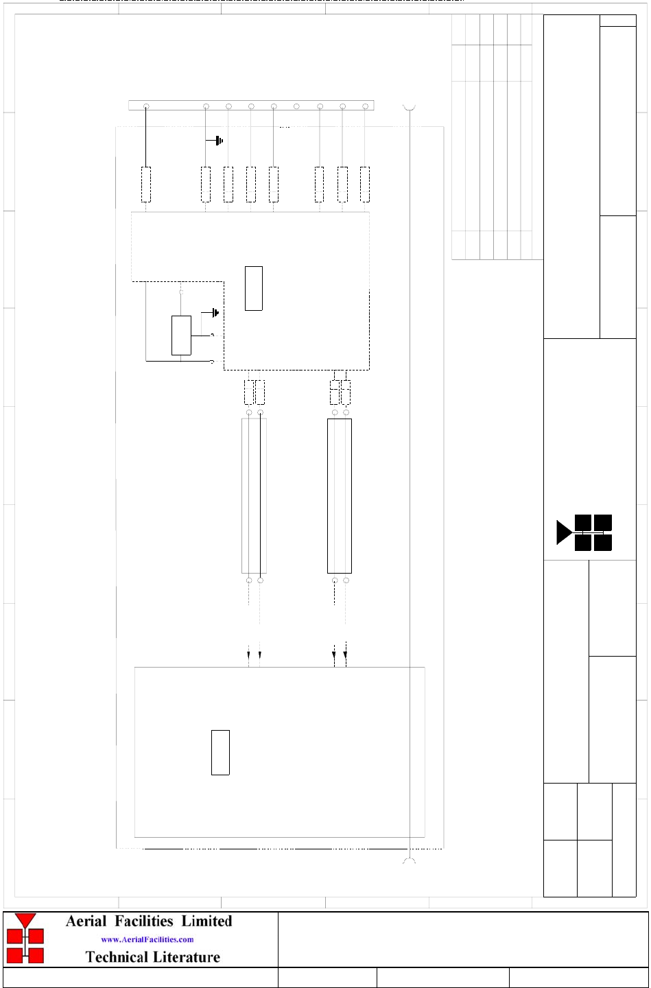
5.3 VTA Downlink Channel Shelf (50-025304)..............................................................................................47
5.3.1 UHF 3dB Splitter (05-002603) See section 5.2.1 ....................................................................................47
5.3.2 4-Way Splitter (05-003401) .....................................................................................................................47
5.3.2.1 Description.......................................................................................................................................47
5.3.2.2 Technical Specification ....................................................................................................................47
5.3.3 Channel Control Module (17-002101).....................................................................................................48
5.3.3.1 Description.......................................................................................................................................48
5.3.3.2 Technical Specification ....................................................................................................................48
5.3.3.3 VHF/ UHF Programming Procedure ..............................................................................................49
5.3.3.4 VHF/ UHF Programming Example .................................................................................................50
5.3.4 Channel Selectivity Module (17-010601) ................................................................................................51
5.3.4.1 Description.......................................................................................................................................51
5.3.4.2 Drg. Nō. 17-003080, Generic Channel Module Block Diagram .....................................................52
5.4 VTA Uplink Duplexer Shelf (50-025305, 4U Chassis) ............................................................................53
5.4.1 Bandpass Filters (02-011204 & 02-013401) See section 5.1.1................................................................53
5.5 VTA Uplink Amplifier Shelf (50-025306, 8U Chassis)............................................................................53
5.5.1 20Watt Class A Power Amplifier (12-016301)........................................................................................53
5.5.1.1 Description.......................................................................................................................................53
5.5.1.2 Technical Specification ....................................................................................................................53
5.5.1.3 Drg. Nō. 12-016370, 20W PA Circuit Diagram ..............................................................................54
5.5.2 Automatic Gain Control (17-001101, Det. & 17-001201, Atten.)...........................................................55
5.5.2.1 Description.......................................................................................................................................55
5.5.2.2 Technical Specification ....................................................................................................................56
5.5.2.3 Drg. Nō. 17-001101, ACG Detector Assembly ................................................................................57
5.5.2.4 Drg. Nō. 17-001171, AGC Detector Circuit Diagram.....................................................................58
5.5.2.5 Drg. Nō. 17-001171C, AGC Detector Parts List .............................................................................59
5.5.2.6 Drg. Nō. 17-001201, AGC Attenuator Assembly Drawing ..............................................................60
5.5.2.7 Drg. Nō. 17-001270, AGC Attenuator Circuit Diagram..................................................................61
5.5.2.8 Drg. Nō. 17-001270C, AGC Attenuator Parts List ..........................................................................62
6. INSTALLATION............................................................................................................................ 63
6.1 Initial Installation Record .........................................................................................................................63
7. MAINTENANCE............................................................................................................................ 64
7.1 General Procedures....................................................................................................................................64
7.1.1 Basic Fault Finding ..................................................................................................................................64
9 Way Channelised UHF Cell Enhancer
Maintenance Handbook
H/book Number:-50-025301HBKM Issue No:-1Date:-04/07/2003 Page:-4 of 69
7.1.2 Downlink..................................................................................................................................................65
7.1.3 Uplink.......................................................................................................................................................65
7.1.4 Fault repair ...............................................................................................................................................65
7.1.5 Checking service ......................................................................................................................................66
7.1.6 Service Support ........................................................................................................................................66
7.2 Tools & Test Equipment............................................................................................................................66
7.3 Care of Modules .........................................................................................................................................67
7.3.1 General Comments...................................................................................................................................67
7.3.2 Module Removal (LNA’s, general procedure): .......................................................................................67
7.3.3 Module Replacement (general): ...............................................................................................................67
7.3.4 Power Amplifiers .....................................................................................................................................67
7.3.5 Low Power Amplifier Replacement.........................................................................................................68
7.3.6 Module Transportation:............................................................................................................................68
APPENDIX A INITIAL EQUIPMENT SET-UP CALCULATIONS............................................... 69
9 Way Channelised UHF Cell Enhancer
Maintenance Handbook
H/book Number:-50-025301HBKM Issue No:-1Date:-04/07/2003 Page:-5 of 69
AMENDMENT LIST RECORD SHEET
Issue
Nō.
Date Incorporated
by
Page No.’s
Amended
Reason for new issue
1 04/08/2003 CMH 1st Issue
Document Ref:-50-025301HBKM

9 Way Channelised UHF Cell Enhancer
Maintenance Handbook
H/book Number:-50-025301HBKM Issue No:-1Date:-04/07/2003 Page:-6 of 69
INTRODUCTION
Scope
This handbook is for use solely with the equipment identified by the AFL Part Number
shown on the front cover. It is not to be used with any other equipment unless specifically
authorised by Aerial Facilities Limited. This is a controlled release document and, as such,
becomes a part of Aerial Facilities’ Total Quality Management System. Alterations and
modification may therefore only be performed by Aerial Facilities Ltd.
Purpose
The purpose of this handbook is to provide the user/maintainer with sufficient information
to service and repair the equipment to the level agreed. Maintenance and adjustments to any
deeper level must be performed by AFL, normally at the company’s repair facility in
Chesham, England.
This handbook has been prepared in accordance with BS 4884, and AFL’s Quality
procedures, which maintain the company’s registration to ISO 9001: 1994 and to the
R&TTE Directive of the European Parliament. Copies of the relevant certificates and the
company Quality Manual can be supplied on application to the Quality Manager.
This document fulfils the relevant requirements of Article 6 of the R&TTE Directive.
Limitation of Information Notice
This manual is written for the use of technically competent operators/service persons. No
liability is accepted by AFL for use or misuse of this manual, the information contained
therein, or the consequences of any actions resulting from the use of the said information,
including, but not limited to, descriptive, procedural, typographical, arithmetical, or listing
errors.
Furthermore, AFL does not warrant the absolute accuracy of the information contained
within this manual, or it’s completeness, fitness for purpose, or scope.
AFL has a policy of continuous product development and enhancement, and as such,
reserves the right to amend, alter, update and generally change the contents, appearance and
pertinence of this document without notice.
All AFL products carry a twelve month warranty from date of shipment. The warranty is
expressly on a return to base repair or exchange basis and the warranty cover does not
extend to on-site repair or complete unit exchange.

9 Way Channelised UHF Cell Enhancer
Maintenance Handbook
H/book Number:-50-025301HBKM Issue No:-1Date:-04/07/2003 Page:-7 of 69
Glossary of Terms
Repeater or
Cell Enhancer A Radio Frequency (RF) amplifier which can simultaneously
amplify and re-broadcast Mobile Station (MS) and Base
Transceiver Station (BTS) signals.
Band Selective Repeater A Cell Enhancer designed for operation on a range of channels
within a specified frequency band.
Channel Selective
Repeater A Cell Enhancer, designed for operation on specified channel(s)
within a specified frequency band. Channel frequencies may be
factory set, remotely set by computer, or on-site programmable.
BTS Base Transceiver Station
C/NR Carrier-to-Noise Ratio
Downlink (D.L.) RF signals transmitted from the BTS and to the MS
Uplink (U.L.) RF signals transmitted from the MS to the BTS
EMC Electromagnetic Compatibility
GND Ground
DC Direct Current
AC Alternating Current
ID Identification Number
OIP3 Output Third Order Intercept Point = RFout +(C/I)/2
LED Light Emitting Diode
M.S. Mobile Station
N/A Not Applicable
N/C No Connection
NF Noise Figure
RF Radio Frequency
Rx Receiver
Tx Transmitter
S/N Serial Number
9 Way Channelised UHF Cell Enhancer
Maintenance Handbook
H/book Number:-50-025301HBKM Issue No:-1Date:-04/07/2003 Page:-8 of 69
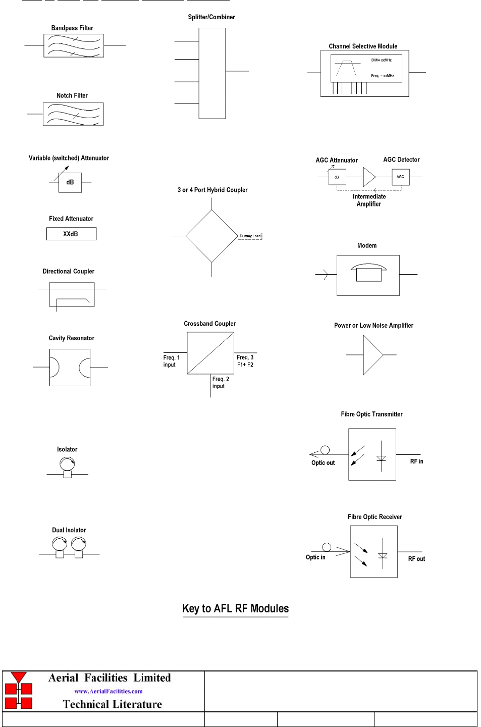
Key to AFL RF Module Drawing Symbols
9 Way Channelised UHF Cell Enhancer
Maintenance Handbook
H/book Number:-50-025301HBKM Issue No:-1Date:-04/07/2003 Page:-9 of 69
1. SAFETY CONSIDERATIONS
1.1 Earthing of Equipment
Cell Enhancers supplied from the mains must be connected to grounded outlets and earthed in
conformity with appropriate local, national and international electricity supply and safety
regulations.
1.2 Electric Shock Hazard
Electrical shocks due to faulty mains driven power supplies.
Whilst ever potentially present in any electrical equipment, such a condition would be
minimised by quality installation practice and thorough testing at:
a) Original assembly.
b) Commissioning.
c) Regular intervals, thereafter.
All test equipment to be in good working order prior to its use. High current power supplies
can be dangerous because of the possibility of substantial arcing. Always switch off during
disconnection and reconnection.
1.3 RF Radiation Hazard
RF radiation, (especially at UHF frequencies) arising from transmitter outputs connected to
AFL’s equipment, must be considered a safety hazard.
This condition might only occur in the event of cable disconnection, or because a ‘spare’
output has been left unterminated. Either of these conditions would impair the system’s
efficiency. No investigation should be carried out until all RF power sources have been
removed. This would always be a wise precaution, despite the severe mismatch between the
impedance of an N type connector at 50, and that of free space at 377, which would
severely mitigate against the efficient radiation of RF power. Radio frequency burns could
also be a hazard, if any RF power carrying components were to be carelessly touched!
Antenna positions should be chosen to comply with requirements (both local & statutory)
regarding exposure of personnel to RF radiation. When connected to an antenna, the unit is
capable of producing RF field strengths, which may exceed guideline safe values especially if
used with antennas having appreciable gain. In this regard the use of directional antennas
with backscreens and a strict site rule that personnel must remain behind the screen while the
RF power is on, is strongly recommended.
Where the equipment is used near power lines, or in association with temporary masts not
having lightning protection, the use of a safety earth connected to the case-earthing bolt is
strongly advised.
9 Way Channelised UHF Cell Enhancer
Maintenance Handbook
H/book Number:-50-025301HBKM Issue No:-1Date:-04/07/2003 Page:-10 of 69
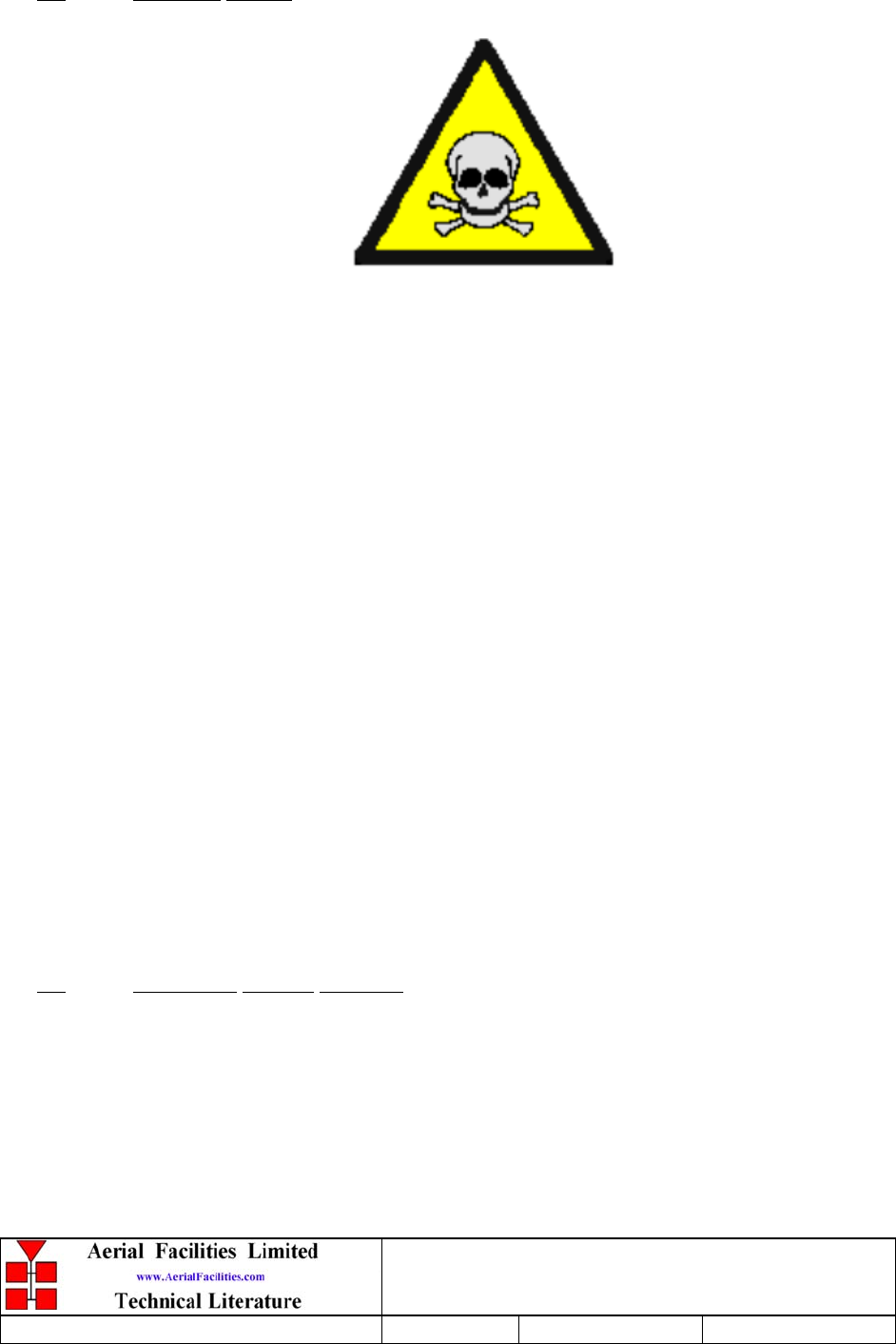
1.4 Chemical Hazard
Beryllium Oxide, also known as Beryllium Monoxide, or Thermalox™, is sometimes used
in devices within equipment produced by Aerial Facilities Ltd. Beryllium oxide dust can be
toxic if inhaled, leading to chronic respiratory problems. It is harmless if ingested or by
contact.
Products that contain beryllium are load terminations (dummy loads) and some power
amplifiers. These products can be identified by a yellow and black “skull and crossbones”
danger symbol (shown above). They are marked as hazardous in line with international
regulations, but pose no threat under normal circumstances. Only if a component containing
beryllium oxide has suffered catastrophic failure, or exploded, will there be any danger of the
formation of dust. Any dust that has been created will be contained within the equipment
module as long as the module remains sealed. For this reason, any module carrying the
yellow and black danger sign should not be opened. If the equipment is suspected of failure,
or is at the end of its life-cycle, it must be returned to Aerial Facilities Ltd for disposal.
To return such equipment, please contact the Quality Department, who will give you a
Returned Materials Authorisation (RMA) number. Please quote this number on the packing
documents, and on all correspondence relating to the shipment.
PolyTetraFluoroEthylene, (P.T.F.E.) and P.T.F.E. Composite Materials
Many modules/components in AFL equipment contain P.T.F.E. as part of the RF insulation
barrier.
This material should never be heated to the point where smoke or fumes are evolved. Any
person feeling drowsy after coming into contact with P.T.F.E. especially dust or fumes
should seek medical attention.
1.5 Emergency Contact Numbers
The AFL Quality Department can be contacted on:
Telephone +44 (0)1494 777000
Fax +44 (0)1494 777002
e-mail qa@aerial.co.uk
9 Way Channelised UHF Cell Enhancer
Maintenance Handbook
H/book Number:-50-025301HBKM Issue No:-1Date:-04/07/2003 Page:-11 of 69
2. OVERVIEW/SYSTEM DESCRIPTION
The AFL Channel Selective Cell Enhancer is a 2-way on-band repeater. Various models are
available to cover frequency bands from 50MHz to 3000MHz. Its main sphere of
applications is in urban areas where the topology is such that shadows occur in the
propagation pattern (for example within large buildings, conference centres and tunnels,
etc.,)
The Channel Selective Cell Enhancer is a 4-port device with direct connection to two
antennas, a highly directional Yagi or similar aligned towards the base site (for the nine
downlink channels) and a dedicated uplink antenna for the mobiles. The frequency bands
that are passed by the Cell Enhancer are set as per the specific customer requirements.
AFL manufacture a wide range of Cell Enhancers, configured for each customer's specific
requirements. Two basic physical variants are available, a rack mounted version to fit in a
standard 19" rack and an environmentally sealed wall mounted version which requires no
further enclosure.
The rack-mounted version is supplied in this instance in 5 shelf units. Each shelf/tray unit
containing active modules has a ‘D.C. on’ indicator on the front panel and the PSU (in the
downlink amplifier shelf) also has an ‘A.C. on’ indicator.
9 Way Channelised UHF Cell Enhancer
Maintenance Handbook
H/book Number:-50-025301HBKM Issue No:-1Date:-04/07/2003 Page:-12 of 69
3. SPECIFICATION
3.1 9 Channel Channelised Cell Enhancer 50-025301 Parts Lists
AFL Part N.Description Qty.
50-025302 VTA-Downlink Duplexer Shelf 1
50-025303 VTA-Downlink Amplifier Shelf 1
50-025304 VTA-Downlink Channel Shelf 1
50-025305 VTA-Uplink Duplexer Shelf 1
50-025306 VTA-Uplink Amplifier Shelf 1
3.1.1 VTA-Downlink Duplexer Shelf 50-025302 Parts List
02-011204 6P TETRA C/L FILT (NARROW) SMA 2
02-013401 6P CL FLTR(0.5 min BW)LARGE SMA ASSY 2
19-001021 4U 19" UNIT 400 DEEP CHASSIS + BKT 1
19-001024 4U 19" UNIT FRONT PANEL FAB 1
91-020004 N JACK PANEL UT-141 6
9 Way Channelised UHF Cell Enhancer
Maintenance Handbook
H/book Number:-50-025301HBKM Issue No:-1Date:-04/07/2003 Page:-13 of 69
3.1.2 VTA Downlink Amplifier Shelf 50-025303 Parts List
AFL Part N.Description Qty.
05-002603 UHF 3dB SPLITTER SMA 2
10-000701 1/4W0-30dB SWITCHED ATTENUATOR 2
11-006102 LNA 380-500MHz 1W WITH RELAY 2
11-007302 LNA. 380-500MHz 20dB (C/W RELAY) GA 1
11-007402 LNA. 380-500MHz 30dB (C/W RELAY) GA 3
12-002201 3 STAGE AMPLIFIER ALARM BOARD 2
12-002220 3 STAGE ALARM PCB COVER 2
12-004201 PWR AMP.450MHz 20W version CLASS A 2
13-001702 VOLTAGE REGULATOR Board 12V 2
50-012820 CCE RACK MOUNTED 8U CHASSIS 1
50-012822 CCE RACK MOUNTED LID 1
50-012825 CCE RACK MOUNTED HEATSINK BRACKET 4
50-027720 RACK MTD CHAN C.E. MODIFIED HEATSIN 2
80-008902 24V RELAY PCB ASSEMBLY 1
80-032320 10W PA HEATSINK (NEEDS 17-000526) 1
80-090822 C/E 8U FRONT PANEL, AFL (RAL7035) 1
91-030002 N ADAPTOR PANEL FEMALE:FEMALE 8
91-100003 SMA PLUG ELBOW UT-141 4
91-130001 SMA ADAPT 'T' ALL FEMALE 3 GHZ 1
91-520003 POWER SWITCHD/FUSED MAINS INL. 1
91-600014 'D' 9 WAY SOCKET S/B (NON FILTERED) 2
91-600015 'D' 9 WAY PLUG S/B (NON FILTERED) 1
91-700017 ICD 15 WAY 0.1' CONNECTOR 5
93-540035 1K3 0.25W 1% RES MRS25 M:F 2
96-300054 24V 17A PSU 400W (XP BCC) 1
96-500005 DC INPUT FILTERS 1
96-700002 LED.GREEN 5mm SEALED IP66 1
96-700005 LED.RED 5mm SEALED IP66 1
97-400002 HANDLE TYPE H6803 4U.[ALLOY] 2
9 Way Channelised UHF Cell Enhancer
Maintenance Handbook
H/book Number:-50-025301HBKM Issue No:-1Date:-04/07/2003 Page:-14 of 69
3.1.3 VTA Downlink Channel Shelf 50-025304 Parts List
05-002603 UHF 3dB SPLITTER SMA 2
05-003302 4 WAY SPLITTER GSM 900MHz 4
05-003401 4 WAY SPLITTER LOW POWER 4
17-002101 CHANNEL CONTROL MODULE 3
17-003022 MODULE PATTERNED LEAVE 8
17-003023 SUBRACK SIDE PANEL 4
17-003024 SUBRACK REAR BRACKET 8
17-003025 BOTTOM MODULE GUIDE 8
17-003028 MODULE SQUARE LEAVE 8
17-003029 TOP MODULE GUIDE 8
17-010601 CHAN MOD 480MHz, 15kHz B/W 9
97-000002 BLACK MODULE CAGE RUNNER 16
97-600001 SUBRACK FRONT HORIZ 4
97-600002 SUBRACK M2.5 STD TAP 4
3.1.4 VTA Uplink Duplexer Shelf 50-025305 Parts List
02-011204 6P TETRA C/L FILT (NARROW) SMA 2
02-013401 6P CL FLTR(0.5 min BW)LARGE SMA ASSY 2
19-001021 4U 19" UNIT 400 DEEP CHASSIS + BKT 1
19-001024 4U 19" UNIT FRONT PANEL FAB 1
91-020004 N JACK PANEL UT-141 6
9 Way Channelised UHF Cell Enhancer
Maintenance Handbook
H/book Number:-50-025301HBKM Issue No:-1Date:-04/07/2003 Page:-15 of 69
3.1.5 VTA Uplink Amplifier Shelf 50-025306 Parts List
02-011204 6P TETRA C/L FILT (NARROW) SMA 1
02-013401 6P CL FLTR(0.5 min BW)LARGE SMA ASSY 1
10-000701 1/4W0-30dB SWITCHED ATTENUATOR 2
11-006102 LNA 380-500MHz 1W WITH RELAY 1
11-007302 LNA. 380-500MHz 20dB (C/W RELAY) GA 3
11-007402 LNA. 380-500MHz 30dB (C/W RELAY) GA 3
12-016301 PA 380-470MHz 20W CLASS A 1
13-001702 VOLTAGE REGULATOR Board 12V 2
13-003011 DC/DC CONVERTER 24-12V 8A PCB ASSY 1
17-001101 CELL ENHANCER AGC DETECTOR/AMP ASS 2
17-001201 C/E AGC UNIT ATTENUATOR ASSY 2
50-012820 CCE RACK MOUNTED 8U CHASSIS 1
50-012822 CCE RACK MOUNTED LID 1
50-012825 CCE RACK MOUNTED HEATSINK BRACKET 4
50-027720 RACK MTD CHAN C.E. MODIFIED HEATSIN 2
80-008902 24V RELAY PCB ASSEMBLY 1
80-032320 10W PA HEATSINK (NEEDS 17-000526) 1
80-090822 C/E 8U FRONT PANEL, AFL (RAL7035) 1
91-030002 N ADAPTOR PANEL FEMALE:FEMALE 4
91-100003 SMA PLUG ELBOW UT-141 4
91-130001 SMA ADAPT 'T' ALL FEMALE 3 GHZ 1
91-520003 POWER SWITCHD/FUSED MAINS INL. 1
91-600014 'D' 9 WAY SOCKET S/B (NON FILTERED) 2
91-600015 'D' 9 WAY PLUG S/B (NON FILTERED) 1
93-540035 1K3 0.25W 1% RES MRS25 M:F 2
96-300054 24V 17A PSU 400W (XP BCC) 1
96-500005 DC INPUT FILTERS 1
96-700002 LED.GREEN 5mm SEALED IP66 1
96-700005 LED.RED 5mm SEALED IP66 1
97-400002 HANDLE TYPE H6803 4U.[ALLOY] 2
9 Way Channelised UHF Cell Enhancer
Maintenance Handbook
H/book Number:-50-025301HBKM Issue No:-1Date:-04/07/2003 Page:-16 of 69
3.2 Technical Specification
PARAMETER SPECIFICATION
Downlink Frequency Range: 491.4-492.2MHz
Single Downlink Channel Frequency: 485.5875MHz
Uplink Frequency Range: 488.4-489.6MHz
Single Uplink Frequency: 485.5875MHz
12.5kHz adjacent channel >20dBChannel Bandwidth selectivity:
25kHz adjacent channel >80dB
Number of Channels: 9
Number of ports: 4
RF Connectors: N type, female
Impedance: 50
VSWR: Better than 1.5:1
Sensitivity: 0.35 microvolts @ 12dB SINAD
Downlink Output Power: 40 Watts
Uplink Output Power: 20Watts
Uplink TOI: 50dBm
Downlink TOI: 50dBm
RF level per carrier: >+23dBm
Passband ripple: <±1.5dB
Noise figure: <6dB (@max gain)
Gain: 96dB
Gain adjustment: 0-30dB (in 2dB steps)
In band spurious: Better than –36dBm
Spurious up to 3GHz: Better than –90dBc
Input AC Supply: 120V AC
Consumption: 300 Watts
Amplifiers
Channel phase unlock
Alarms:
(Volt-free relay contacts) PSU Failure
MTBF: 80,000 Hrs.
Housing: 19” Rack mounted
9 Way Channelised UHF Cell Enhancer
Maintenance Handbook
H/book Number:-50-025301HBKM Issue No:-1Date:-04/07/2003 Page:-17 of 69
3.3 Mechanical Specification
PARAMETER SPECIFICATION
Height: Eurorack Shelves(1U=44.5mm)
Width: 19"Case Size:
Depth: <500mm
(excluding heatsinks, connectors, handles and feet)
operational: -10°C to +55°C
Temperature Range: storage: -40°C to +70°C
Weight: <15kg*
Humidity: 5 – 95% non-condensing
RF Connectors: N type female
Environmental Protection: IP54
Case: Alocrom
Heatsinks: Matt blackFinish:
Handles: Alocrom
Supply Cable:
Unit supplied with suitable supply input
leads with connector and specified length
of cable (where appropriate)
* Note: Individual shelf weights unspecified.
9 Way Channelised UHF Cell Enhancer
Maintenance Handbook
H/book Number:-50-025301HBKM Issue No:-1Date:-04/07/2003 Page:-18 of 69
4. SYSTEM DRAWINGS
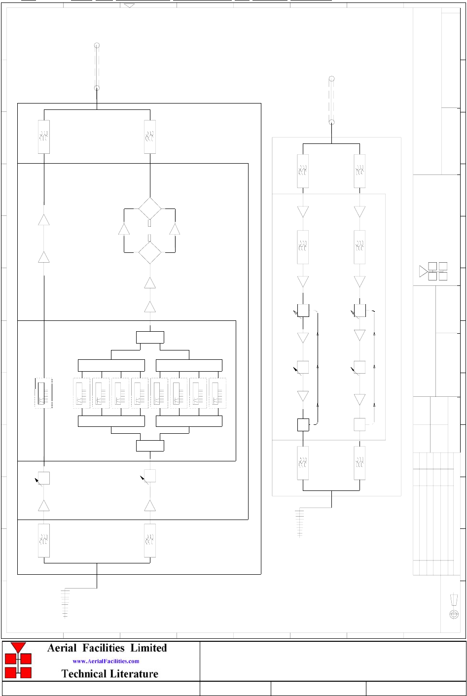
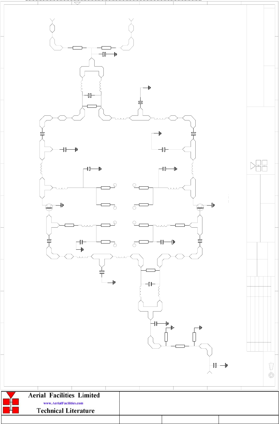
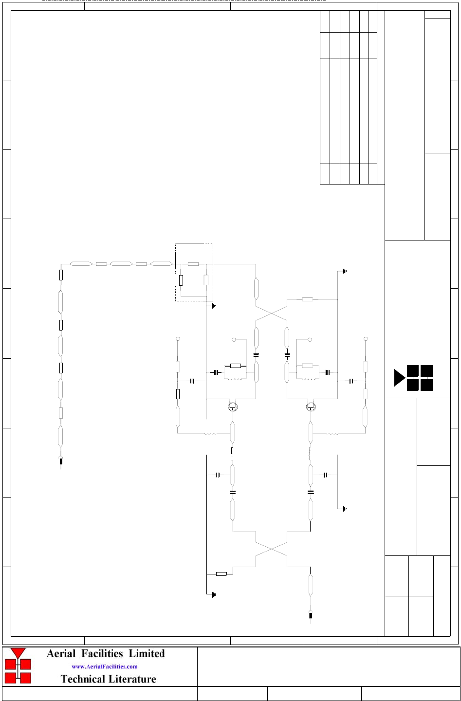
4.1 Drg. N. 50-025381, Channelised CE System Diagram
11 CHANNEL CHANNELISED CE (CSIC)
SYSTEM DIAGRAM
50-025381
1A
1:1
MNR 30/07/03
dB
dB
AGC dBdB
dBAGC dB
BANDPASS FILT ER
485.5875MHz
02-013401
LNA
11-007402
ATTENUATOR
10-000701
CHANNEL MO DUL E
17-010601 11-007402
LNA LNA
11-006102
485.5875MHz
02-013401
BANDPASS FIL TER
17-010601
8 x CHANNEL MODULE
491.4-492.2MHz
02-011204
BANDPASS FILT ER
LNA
11-007402 10-000701
ATTENUATOR
05-003401
SPLITTER
05-002603
SPL ITT ER
05-003401
CO M BINER
05-002603
CO M BINE R
11-007302
LNA
11-006102
LNA
SPLITTER
05-002603 05-002603
CO MBINER
12-004201
PA
12-004201
PA
BANDPASS FIL TER
491.4-492.2MHz
02-011204
485.5875MHz
02-013401
BANDPASS FIL TER
AGC DET.
17-001101 17-001201
AGC ATT.
11-006102
LNA AT TENUATOR
10-000701 11-007302
LNA
11-007402
LNA
BANDPASS FIL TER
02-013401
485.5875MHz
02-013401
BANDPASS FIL TER
485.5875MHz
11-007402
LNA
BANDPASS FIL TER
17-001101
AGC DET.
BANDPASS FIL TER
02-013401
488.4-489.6MHz
11-00730212-016301
PA
10-000701
ATTENUATOR
17-001201
AGC ATT.
LNA
11-007302
LNA 488.4-489.6MHz
BANDPASS FIL TER
02-01340111-007402
488.4-489.6MHz
02-013401
LNA
50-025305
50-025306
50-025304
50-025303
50-025302
DATEDES CRIPTIONNo
ISSUE
THIRD ANGLE PROJECTION
1 23 45 6 78 9101112
A
B
C
D
E
F
G
H
1 23 45 6 78 9101112
A
B
C
D
E
F
G
H
PERMISSIBLE ONLY IF EXPRESSLY AUTHORISED IN WRITING
RE P ROD UC TI ON OR USE OF THI S DE SIGN BY OTHERS IS
THIS IS A PROPRIETARY DESIGN OF AERIAL FACILITIES LTD.
UNLESS OTHERWISE STATED
ALL DIMENSIONS ARE IN mm
DATEDRAWN
CHKD APPD
TWO DECIMAL PLACES ± 0.1mm
NO DECIMAL PLACE ± 1mm
ONE DECIMAL PLACE ± 0.3mm
BY AERIAL FACILITIE S LTD.
TOLE RANCE S SCA LE
CUSTOMER DRAWING No
Fax : 01494 777002
Tel : 01494 777000
Aerial Facilities Limited
England
TI TLE
2
A
PRO DUCTIO N ISSUE MNR
30/ 07/ 03
FRE QUENCY PROGRAMMING DATA
B/W=15kHz
FRE QUENCY PROGRAMMING DATA
B/W=15kHz
FRE QUENCY PROGRAMMING DATA
B/W=15kHz
FRE QUENCY PROGRAMMING DATA
B/W=15kHz
FRE QUENCY PROGRAMMING DATA
B/W=15kHz
FRE QUENCY PROGRAMMING DATA
B/W=15kHz
FRE QUENCY PROGRAMMING DATA
B/W=15kHz
FRE QUENCY PROGRAMMING DATA
B/W=15kHz
FRE QUENCY PROGRAMMING DATA
B/W=15kHz
485. 58 75M H z
491. 63 75M H z
491. 83 75M H z
492. 03 75M H z
491. 61 75M H z
492. 17 50M H z
491. 66 25M H z
492. 01 25M H z
491. 41 25M H z
0-30dB
0-30dB
0-30dB
0-30dB
ANTENNA
DO WNL INK
ANTENNA
UPL INK
DO WNL INK
LCX
UPL INK
LCX
PB GD
9 Way Channelised UHF Cell Enhancer
Maintenance Handbook
H/book Number:-50-025301HBKM Issue No:-1Date:-04/07/2003 Page:-19 of 69
5. SUB-UNIT MODULES
5.1 VTA Downlink Duplexer Shelf 60-025302 (4U chassis)
5.1.1 Bandpass Filters (02-011204 & 02-013401)
5.1.1.1 Description
The bandpass filters are multi-section designs with a bandwidth dependent upon the
passband frequencies, (both tuned to customer requirements). The response shape is
basically Chebyshev with a passband design ripple of 0.1dB. The filters are of combline
design, and are carefully aligned during manufacture in order to optimise the insertion loss,
VSWR and intermodulation characteristics of the unit. The tuned elements are silver-plated
to reduce surface ohmic losses and maintain a good VSWR figure and 50 load at the input
and output ports.
Being passive devices, the bandpass filters should have an extremely long operational life
and require no maintenance. Should a filter be suspect, it is usually most time efficient to
replace the module rather than attempt repair or re-tuning.
No adjustments should be attempted without full network sweep analysis facilities to
monitor both insertion loss and VSWR simultaneously.
5.1.1.2 Technical Specification (02-011204)
PARAMETER SPECIFICATION
Passband 491.4-492.2 MHz
Insertion Loss 1.9 dB typical
> 485 MHz > 55 dB
Rejection > 458-459 MHz > 60 dB
Power Rating 50 Watt
Impedance 50 ohm
VSWR Better than 1.2:1
5.1.1.3 Technical Specification (02-013401)
Passband 485.5875MHz
Insertion Loss 1.9 dB typical
> 492 MHz > 60 dB
Rejection > 488-489 MHz > 55 dB
Power Rating 50 Watt
Impedance 50 ohm
VSWR Better than 1.2:1
9 Way Channelised UHF Cell Enhancer
Maintenance Handbook
H/book Number:-50-025301HBKM Issue No:-1Date:-04/07/2003 Page:-20 of 69
5.2 VTA Downlink Amplifier Shelf (50-025303, 8U Chassis)
5.2.1 UHF 3dB Splitter (05-002603)
5.2.1.1 Description
The 3dB Splitter/Combiner used is a device for accurately matching two or more RF
signals to single or multiple ports, whilst maintaining an accurate 50Ω load to all
inputs/outputs and ensuring that the VSWR and insertion losses are kept to a minimum.
Any unused ports will be terminated with an appropriate 50Ω load.
5.2.1.2 Technical Specification
PARAMETER SPECIFICATION
Frequency Range: 400-500 MHz
Power Rating: 5 Watts
Insertion Loss: 5.2dB Typical
VSWR: 1.2:1
Impedance: 50 Ohms
Connectors: SMA
Weight: <0.5Kgs
Mechanical: Drawing No. 07-003890
5.2.2 ¼Watt 0- -30dB Switched Attenuator (10-000701)
5.2.2.1 General Application
In many practical applications for Cell Enhancers etc., the gain in each path is found to be
excessive. Therefore, provision is made within the unit for the setting of attenuation in
each path, to reduce the gain.
5.2.2.2 Switched Attenuators
The AFL switched attenuators are available in two different types; 0 – 30dB in 2 dB steps
(as in this case), or 0 – 15dB in 1 dB steps. The attenuation is simply set using the four
miniature toggle switches on the top of each unit. Each switch is clearly marked with the
attenuation it provides, and the total attenuation in line is the sum of the values switched
in. They are designed to maintain an accurate 50 impedance over their operating
frequency at both input and output.
9 Way Channelised UHF Cell Enhancer
Maintenance Handbook
H/book Number:-50-025301HBKM Issue No:-1Date:-04/07/2003 Page:-21 of 69
5.2.3 Low Noise Amplifier (11-006102)
5.2.3.1 Description
The 15dB gain low noise amplifier used in the unit is a double stage solid-state low noise
amplifier. Class A circuitry is used throughout the units to ensure excellent linearity over
a very wide dynamic range. The active devices are very moderately rated to provide a
long trouble-free working life. There are no adjustments on these amplifiers, and in the
unlikely event of a failure, then the complete amplifier should be replaced.
5.2.3.2 Technical Specification
PARAMETER SPECIFICATION
Frequency range: 380-500MHz
Bandwidth: <150MHz
Gain: 15.5dB ±0.5dB
1dB compression point: 31dBm
IP3: 46dBm
I/O return loss: >18dB
Noise figure: <1.3dB
Supply requirement: 10 – 24V, DC
Consumption: 510-540mA @ (10 – 24V)
storage: -20°C to +55°CTemperature
range operation: -40°C to +70°
9 Way Channelised UHF Cell Enhancer
Maintenance Handbook
H/book Number:-50-025301HBKM Issue No:-1Date:-04/07/2003 Page:-22 of 69
5.2.3.3 Drg. N. 11-006170, LNA Circuit Diagram (RF)
C1
C2
C3
C7
R6
C8
R1 1 R1 2
R5
C5
C6
R7 R8
R1
R2
R3
R4
C4
R1 3 R1 4
R9 R1 0
C1 0
C1 4
C1 3
R1 5
C1 6
C1 7
380-500MHz 1W AMPLIFIER
(RF) CIRCUIT DIAGRAM
11-006170
1A
N.T.S
MNR 23/01/02
C9
C1 1 C1 2
R1 6
R1 7
C1 5
DATEDESCRIPTIONNo
ISSUE
THIRD ANGL E PRO JECTION
123456789101112
A
B
C
D
E
F
G
H
123456789101112
A
B
C
D
E
F
G
H
PERMISSIBLE ONLY IF EXPRESSLY AUTHORISED IN WRITING
RE PRODUCTI ON OR US E OF TH IS DES IGN BY OTHE RS I S
THIS IS A PROPRIETARY DESIGN OF AERIAL FACILITIES LTD.
UNLESS OTHERWISE STATED
ALL DIMENSIONS ARE IN mm
DATEDRAWN
CHKD APPD
TWO DECIMAL PLACES ± 0.1mm
NO DECIMAL PLACE ± 1mm
ONE DECIMAL PLACE ± 0.3mm
BY AERIAL FACILITIES LTD.
TOLERANCES SCALE
CUSTOME R DRAWING No
Fax : 01494 777002
Tel : 01494 777000
Aerial Facilities Limited
England
TI TLE
2
A
910R
5R6
910R
8.2pF
L1
L2
3.3pF 100R
18nH
L3
18nH
18nH
18nH
L4
6.8pF
220pF
1nF
56R
56R
1nF
220pF
220pF
220pF
220pF
220pF
10K 0R0
10K 0R0
6.8nH
L5
6.8nH
L6
T1
CYL 5
G
D
S
G
D
S
CYL 5
T2
L7
180nH
180nH
L9
7.5nH
L8
7.5nH
L10
18nH
L11
L12
18nH
18nH
L13
18nH
L14
6.8pF
6.8pF
100R 3.3pF
8.2pF
RF O UT
RF IN
ANY CO MPO NENTS IN ARE NO T USED IN THIS BUIL D
PRODUCTION ISSUE
23/ 01/ 02
MNR
0R0
RF O UT
(OPTIONAL)
6.8pF
CB IB
9 Way Channelised UHF Cell Enhancer
Maintenance Handbook
H/book Number:-50-025301HBKM Issue No:-1Date:-04/07/2003 Page:-23 of 69
5.2.3.4 Drg. N. 11-006171, LNA Schematic Diagram (DC)
BYDAT EDES CRIP TIO NNo
ISSUE
12
3456789
A
B
C
D
E
F
1 23456789
A
B
C
D
E
F
Fax : 01494 777002
Tel : 01494 777000
Aerial Facilities Limited
THIS IS A PROPRIETARY DESIGN OF AERIAL FACIL ITIES L TD.
REP RO DUCT IO N O R USE O F THIS DESIG N BY O THERS IS
PERMISSIBLE O NL Y IF EXPRESSLY AUTHORISED IN WRITING
BY AERIAL FACIL ITIES L TD.
NO DECIM AL PL ACE ± 1 mm
ONE DECIMAL PL ACE ± 0.3mm
TWO DECIMAL PL ACES ± 0.1mm
AL L DIMENSIO NS ARE IN m m
UNL ESS OTHERWISE STATED
CHKD
DRAWN
APPD
DATE
T O L ERANCES SCALE
England
CUST O MER DRAWING .No
TITLE
3
A
380-500MHz 1W AMPLIFIER
SCHEMATIC DIAGRAM
11-006171
1A
MNR 23/01/02
LM7808CT
REG 3
G
IO
+6V 220mA
-ve
+6V 220mA
-ve
J4 1
CO N2 - J5
CO N2 - J4
J4 2
J5 1
J5 2
DC INPUT DC O UT PUT
RF PCB
FOR CIRCUIT DIAGRAM
SEE 11-006170
SEE 11-003971
FOR CIRCUIT DIAGRAM
DC PCB
+8V C
BA
RF
IN
PRODUCTION ISSUE
23/01/02
MNR
OUT
RF
OC GOOD/0v BAD9 CON1
9
REL AY CO NTACT G O O D
REL AY COM MO N
RELAY CONTACT BAD
PIN OUTS
9 WAY 'D'
TTL VO LTAG E SET
TTL AL ARM/0v GOOD
GROUND
+12V DC I/P
7 CON1
8 CON1
5 CON1
4 CON1
6
8
7
5
4
A
3 CON1
2 CON1
3
2
CO N1
1
*
*
*
= ONLY APPLIES TO 11-006802
*
CB IB
9 Way Channelised UHF Cell Enhancer
Maintenance Handbook
H/book Number:-50-025301HBKM Issue No:-1Date:-04/07/2003 Page:-24 of 69
5.2.4 Low Noise Amplifiers (11-007302 & 11-007402)
5.2.4.1 Description
The low noise amplifiers used are double stage solid-state low-noise amplifiers. Class A
circuitry is used in the units to ensure excellent linearity over a very wide dynamic range.
The active devices are very moderately rated to provide a long trouble-free working life.
There are no adjustments on these amplifiers, and in the unlikely event of failure then the
entire amplifier should be replaced. The two amplifiers are very similar in construction,
the only difference is the biasing, which changes the gain figure, see tables below.
5.2.4.2 Technical Specification, (11-007302)
PARAMETER SPECIFICATION
Frequency range: 380-500MHz
Bandwidth: <140MHz
Gain: 20-22dB
1dB Compression Point: +23.5dB (typical)
3rd order intercept: +36dB (typical)
Input/Output return loss: >20dB
Noise figure: <1.3dB
Connectors: SMA female
Supply: 200-230mA @ 24V DC
operational: -10°C to +55°C
Temperature range: storage: -30°C to +70°C
Weight: <300gms
Size: 90 x 55 x 30.2 (case only)
5.2.4.3 Technical Specification (11-007402)
PARAMETER SPECIFICATION
Frequency range: 380-500MHz
Bandwidth: <140MHz
Gain: 30-32dB
1dB Compression Point: +22dBm (typical)
3rd order intercept: +34-35dBm (typical)
Input/Output return loss: >20dB
Noise figure: <1.3dB
Connectors: SMA female
Supply: 300-330mA @ 24V DC
operational: -10°C to +55°C
Temperature range: storage: -30°C to +70°C
Weight: <300gms
Size: 90 x 55 x 30.2 (case only)
9 Way Channelised UHF Cell Enhancer
Maintenance Handbook
H/book Number:-50-025301HBKM Issue No:-1Date:-04/07/2003 Page:-25 of 69
5.2.4.4 Drg. N. 11-007302, LNA Assembly With Alarm Relay
BYDAT EDES CRIPTIO NNo
ISSUE
1 23 456 78 9
A
B
C
D
E
F
1
2
3
4
5
6
7
8
9
F
E
D
A
B
C
Fax : 01494 777002
Tel : 01494 777000
Aerial Facilities Ltd
TWO DECIMAL PLACES ± 0.1mm
ONE DECIMAL PL ACE ± 0.3mm
NO DECIMAL PL ACE ± 1 mm
BY AERIAL F ACIL IT IES L TD.
PERMISSIBLE ONLY IF EXPRESSL Y AUTHORISED IN WRITING
REPRO DUCTION OR USE OF THIS DESIG N BY O THERS IS
THIS IS A PRO PRIETARY DESIG N OF AERIAL FACILITIES LTD.
DRAWN
CHKD
AL L DIM ENSIO NS ARE IN mm
UNL ESS O THERWISE STAT ED
APPD
DAT E
T O L ERANCES SCALE
England
CUSTO MER DRG.No
TITLE
A
3
LOW NOISE AMPLIFIER 380-500MHz
(20dB) ASSEMBLY DRAWING (WITH RELAY)
11-007302
1A
1.5:1
DBS 9/7/02
PRODUCTION ISSUE
9/7/02
DBS
COMPONENTS TO BE ADDED TO 11-003912,ITEM 15,DC PCB SUB-ASSEMBLY
AFL
SENSITIV E
DEVICES
E LE C TR O S TA TI C
OBSERVE PRECAUTIONS
ATTENTION
FOR HAND LING
AFL
AFL
********
11-007302
380-500MHz
20dB 10-24V DC
**/**/20**
REF .
FREQ.
GAIN
S/N
DAT E
0086
IN
34
see note 2
LABEL DETAILS - SCALE 1:1
35
see note 2
see note 2
31
IN 4 PLACES
2. LIDS,ITEMS 2 & 3 AND LABELS,ITEMS 31,34 & 35,TO BE FITTED ON TEST
1. SOLDER JOINTS TO BE MADE USING OR
2819
OUT
6
IN 3 PLACES
3
DC PCB
25
4
732
RF PCB
15
W6
21
2
C2
1
22
2
CPL 1
R1
C1
RF O UT
R1 9
W7
C2 1
5
C9
R2
R1 6
C5
L1
L3
C4 C8
+
R4
TR1
L5 C1 2
J31 J32
W5
W2 W1
225
10
17 24
2
33
2
27
5
27
2
20
2
16 23
5
24
2
IN 2 PLACES
4
26830
R3 9
REG 3
J3 J1J2
R5 0 R4 9
R4 4R4 3
RL 1
CO N1
CB IB
9 Way Channelised UHF Cell Enhancer
Maintenance Handbook
H/book Number:-50-025301HBKM Issue No:-1Date:-04/07/2003 Page:-26 of 69
5.2.4.5 Drg. N. 11-007370, LNA RF Circuit Diagram
BYDAT EDES CRIP TIO NNo
ISSUE
12
3456789
A
B
C
D
E
1 23456789
A
B
C
D
E
F
Fax : 01494 777002
Tel : 01494 777000
Aerial Facilities Limited
THIS IS A PROPRIETARY DESIGN OF AERIAL FACIL ITIES L TD.
REP RO DUCT IO N O R USE O F THIS DESIG N BY O THERS IS
PERMISSIBLE O NL Y IF EXPRESSLY AUTHORISED IN WRITING
BY AERIAL FACIL ITIES L TD.
NO DECIM AL PL ACE ± 1 mm
ONE DECIMAL PL ACE ± 0.3mm
TWO DECIMAL PL ACES ± 0.1mm
AL L DIMENSIO NS ARE IN m m
UNL ESS OTHERWISE STATED
CHKD
DRAWN
F
APPD
DAT E
T O L ERANCES SCALE
England
CUST O MER DRAWING .No
TITLE
3
A
LOW NOISE AMPLIFIER 380-500MHz
(20dB) RF PCB CIRCUIT DIAGRAM
11-007370
1A
-
DBS 5/7/02
CLY2
TR 2
RF INPUT
R1
51R
11303- 3
CPL1
1nF
C3
Ø1.6x6 turns
L2
3. 3pF
C7
L4
330nH
R3
100R 10K
R6
1nF
C6
1nF
C1
C4
3. 3pF
Ø1.6x6 turns
L1
330nH
L3
100R
R2 R5
10K
J31
C5
1nF
TR 1
CLY2
560R
R7
100nH
L6
C10
1nF
C9
1nF
R4
560R
100nH
L5
1nF
C13
1nF
C12
51R
R8
11303- 3
CPL2
R9
R11
0R 0
R10
0R 0
W1
W5
0R 0
RF OUTPUT
0R 0
W6
0R 0
R19
HEADER PIN
HEADER PIN
J32
HEADER PIN
J12
HEADER PIN
J11
PRODUCTION ISSUE
5/7/02
DBS
0R 0
W2
0R 0
W7
ATTENUATOR GROUP
(Select values on Test)
D
G S
D
GS
ECN2718 DBS
19/9/02
2A
CB IB
9 Way Channelised UHF Cell Enhancer
Maintenance Handbook
H/book Number:-50-025301HBKM Issue No:-1Date:-04/07/2003 Page:-27 of 69
5.2.4.6 Drg. N. 11-007371, LNA DC Wiring Diagram
BYDA T EDES CRIP TIO NNo
ISSUE
12
3456789
A
B
C
D
E
F
1 23456789
A
B
C
D
E
F
Fax : 01494 777002
Tel : 01494 777000
Aerial Facilities Limited
THIS IS A PROPRIETARY DESIGN OF AERIAL FACILITIES LTD.
REP RO DUCT IO N O R USE O F THIS DESIG N BY O THERS IS
PERMISSIBLE O NL Y IF EXPRESSLY AUTHORISED IN WRITING
BY AERIAL FACIL ITIES LTD.
NO DECIM AL PL ACE ± 1 mm
ONE DECIMAL PL ACE ± 0.3mm
TWO DECIMAL PL ACES ± 0.1mm
AL L DIMENSIO NS ARE IN m m
UNL ESS OTHERWISE STATED
CHKD
DRAWN
APPD
DATE
T O L ERANCES SCALE
England
CUST O MER DRAWING .No
TITLE
3
A
LOW NOISE AMPLIFIER. 380-500MHz
(20dB) RF SCHEMATIC DIAGRAM
11-007371
1A
-
DBS 8/7/02
LM7808CT
REG 3
G
IO
-ve
J11 - J12
DC INPUT DC O UT PUT
RF PCB
FOR CIRCUIT DIAGRAM
SEE 11-007370
SEE 11-003971
FOR CIRCUIT DIAGRAM
DC PCB
+8V C
BA
RF
IN
PRODUCTION ISSUE
8/7/02
DBS
OUT
RF
OC GOOD/0v BAD9 CON1
9
REL AY CO NTACT G O O D
REL AY COM MO N
RELAY CONTACT BAD
PIN OUTS
9 WAY 'D'
TTL VO LTAG E SET
TTL AL ARM/0v GOOD
GROUND
10-24V DC I/P
7 CON1
8 CON1
5 CON1
4 CON1
6
8
7
5
4
A
3 CON1
2 CON1
3
2
CO N1
1
5V 75mA
-ve
J31 - J32
J31 1
J32 2
J12 2
J11 15V 75mA
CB IB
9 Way Channelised UHF Cell Enhancer
Maintenance Handbook
H/book Number:-50-025301HBKM Issue No:-1Date:-04/07/2003 Page:-28 of 69
5.2.5.7 Drg. N. 11-003971, LNA DC Circuit Diagram
BYDA T EDES CRIP TIO NNo
ISSUE
12
3456789
A
B
C
D
E
F
1 23456789
A
B
C
D
E
F
Chesham(01494)778301
Fax (01494)778910
Aerial Facilities Limited
TWO DECIMAL PL ACES ± 0.1mm
ONE DECIMAL PL ACE ± 0.3mm
NO DECIM AL PL ACE ± 1 mm
BY AERIAL FACIL ITIES LTD.
PERMISSIBLE O NL Y IF EXPRESSLY AUTHORISED IN WRITING
REP RO DUCT IO N O R USE O F THIS DESIG N BY O THERS IS
THIS IS A PROPRIETARY DESIGN OF AERIAL FACILITIES LTD.
DRAWN
CHKD
UNL ESS OTHERWISE STATED
AL L DIMENSIO NS ARE IN m m
APPD
DATE
T O L ERANCES SCALE
England
CUST O MER DRAWING .No
TITLE
A
3
DC PCB FOR LNA's AND LPA's,
CIRCUIT DIAGRAM
11-003971
DJL 24/09/01
PROTOTYPE ISSUEAA
2 4 /9 /0 1
DJL
THIRD ANGL E PROJECTION
R33
4K 7
TR 7
BCW71
R32
10K
BCW71
R31
4K 7
TR 8
R34
10K
R21
4K 7
R20
10K
TR 1
R24
BCW71
TR 2
R23
4K 7
R22
10K
TR 3
R25
4K 7
10K
BCW71
R11
120R
R12
3K 6
270K
R10
R9
1K
C2
100n
R6
100K
R4
100K
R8
270K
1K
R7
2
+C8
REG1
IO
A
1K
R47
+C4 +C5
R43 R44 R45
+C10
100n
C11
IC2
8
5
3
4
C15
10u
C17 +C16
100n
R52
+C14
3
4
IC3
28
5
R49
1K REG2
IO
A
R51 R50
+C13
R46
1K
R48
1K
R39 R40
R38
100R
R42
VR1
R41
+
-
1
2
3
-
+
5
6
7
-
2
+
3
1
R53
R54
R55
RL1
1
R35
1K
TR 4
TR 6
R16
1K
R17
2K 2
22K
R18
R19
560R
R15
2K 4
+
C3
R14
3K
R3
100K
R2
120R
100K
R5
R29
0R
1K 8
R1
4K 7
R36
56R
R27
R13
4K 7
TR 5
FZT751
BCW71
1U
BCW71
3V 3
D3
9-
+
10
8
12
+
-
13
14
6-
+
5
7
IC1:C
IC1:B
IC1:D
11
4
LM 324M
LM 324M
LM 324M
IC1:A
LM324M
ZD 1
1. 23V
LL4148
D2 LE D 1
IC4:B
IC4:A
+
C12
1u
10u
+
C9
10u
1u 1u
>12V DC I/P
10u
ZD 3
5. 1V 10u
470R
R56
R57
D1
LL4148
CON 1 1
J2 2
9CON 1
CON 18
4CON 1
5CON 1
CON 13
RL1/1
ZD 2
C19
100n
4
8
LM 337LM
10u
10u
LL4148
1. * IF APPLICABLE, VALUES WILL BE DETERMINED AT A HIGHER LEVEL BOM
I C L7660C
I C L7660C
LM 337LM
2
J2 1
1J1
2J5
2J1
1J5
1J3
2J4
2J3
1J4
CON 1
+
C1
1u
C7
470p
+
C6
10u
+
C18
1u
2. CONNECTORS J1-5 TO BE FITTED AS NECESSARY
PRODUCTION ISSUE(ECN2359)
26/11/01
TAS1A
V_OUT
V_IN
B
C
A
*
**
***
***
*
P3
*
R58
7CON 1
R59
1K
CB IB
2A ECN2518
1 7 /4 /0 2
DJL
P5
P4
RL1/2 P8
P6
P7
P1
P2
R28
0R
*
*
*
*
*
*
*
*
3A ECN2686
2 5 /7 /0 2
DJL
9 Way Channelised UHF Cell Enhancer
Maintenance Handbook
H/book Number:-50-025301HBKM Issue No:-1Date:-04/07/2003 Page:-29 of 69
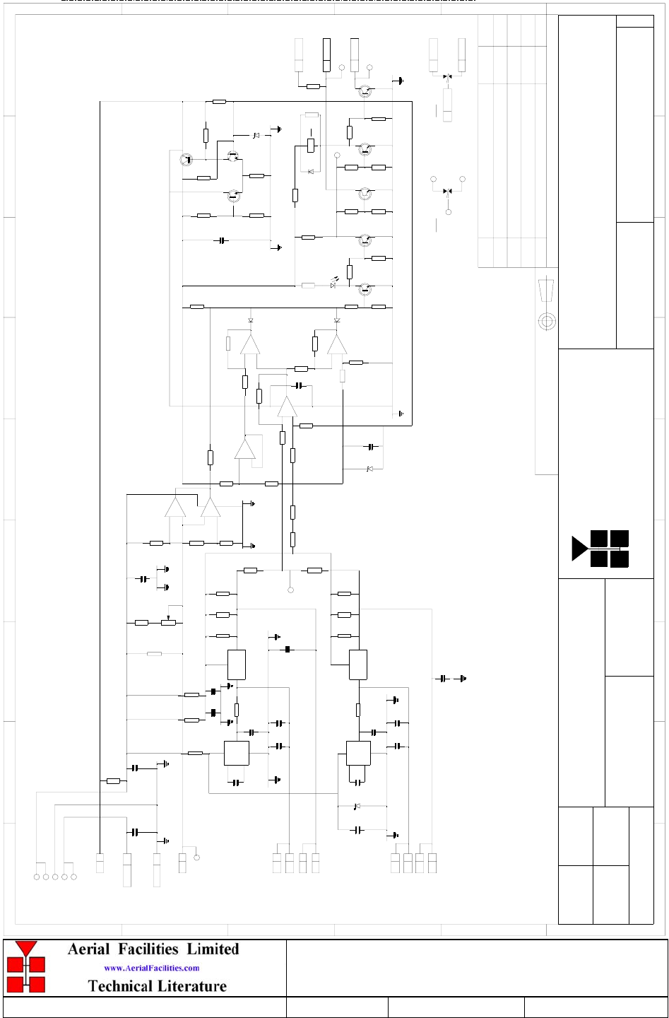
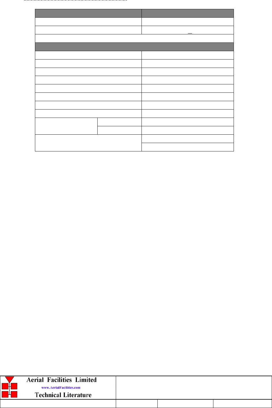
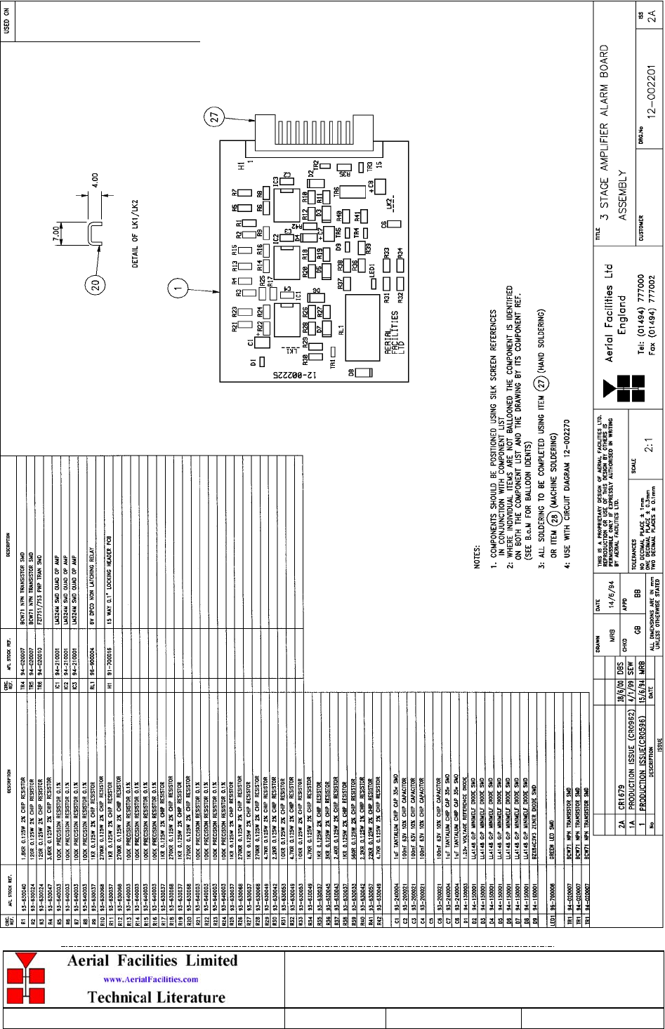
5.2.6 3 Stage Amplifier Alarm Boards (12-002201)
5.2.6.1 Description
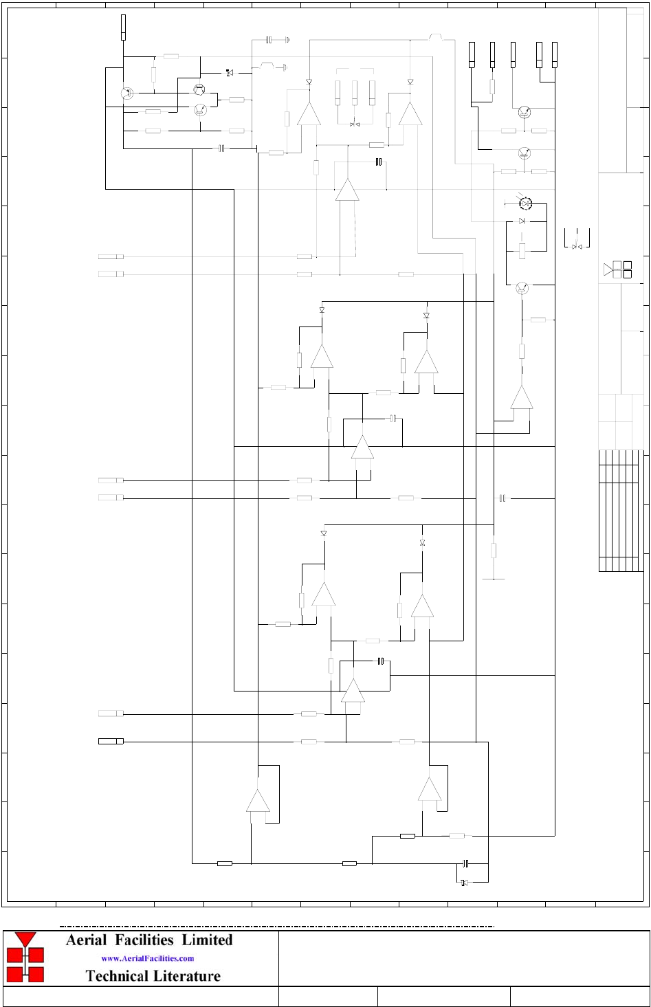
Amplifier Alarm Boards are fitted to monitor the bias conditions of AFL Class A
amplifiers which remain constant in normal operation. Any departure from normal bias
conditions is a result of device failure, excess temperature, over-driving or oscillation
(excessive power).
In normal operation, the Class A bias circuit of the amplifier develops a constant voltage
of 1.20V across the collector current setting resistor. The Amplifier Alarm Board is a
window comparator device, which is adjusted to sense a departure from this condition.
Several different alarm outputs are provided to simplify interfacing, (Relay Contact, Open
Collector, and TTL Logic Levels)
The basic version of the Alarm Board (12-002801) monitors a single amplifier stage. A
three-stage version (12-002201) is used on complex amplifiers where three separate
comparators have their outputs logically combined to a common output stage. Failure of
any one stage will activate the alarms.
Note that the alarm board has a green Light Emitting Diode located near to the centre of
the printed circuit board, which is illuminated on ‘Good’, and extinguished on ‘Alarm’. It
is therefore a simple matter to identify an active module failure, by searching for an
Alarm Board which has its green LED extinguished. A simple test of the alarm board is
possible by shorting across the monitor inputs, pins 1 and 2, 3 and 4 or across pins 5 and
6. This last monitor input is inactive if the board has been converted to a two way alarm
board. (Refer to relevant amplifier alarm wiring diagram.)
1) Volt-free change over relay contacts.
2) Open collector NPN transistor pulls low on alarm.
3) TTL driver.
The use of precision voltage sources and resistors has eliminated the need for initial
adjustment or calibration, and the board will function correctly with a wide variation in
power supply voltage (8 to 30 volts, nominal supply is 12 or 24Volts).
There are two selectable link options on the three-way board:
LINK1 - Removed to convert to two-way alarm board.
LINK2 - Removed to isolate 0V from chassis earth.
The one way alarm board only has the 0V isolation link (LINK2) fitted.
9 Way Channelised UHF Cell Enhancer
Maintenance Handbook
H/book Number:-50-025301HBKM Issue No:-1Date:-04/07/2003 Page:-30 of 69
5.2.6.2 Technical Specification
PARAMETER SPECIFICATION
Operating voltage: 8 to 30V (floating earth)
Alarm Threshold: Vcc - 1.20 volt +15%
Alarm output relay contacts:
Max. switch current: 1.0Amp
Max. switch volts: 120Vdc/60VA
Max. switch power: 24W/60VA
Min. switch load: 10.0µA/10.0mV
Relay isolation: 1.5kV
Mechanical life: >2x10⁷ operations
Relay approval: BT type 56
Connector details: 15-way 0.1" pitch
operational: -10°C to +55°C
Temperature range: storage: -40°C to +70°C
74 x 56mm (3 stage)
PCB Size: 54 x 56mm (1 stage)

9 Way Channelised UHF Cell Enhancer
Maintenance Handbook
H/book Number:-50-025301HBKM Issue No:-1Date:-04/07/2003 Page:-31 of 69
5.2.6.3 Drg. N. 12-002201, 3 Stage Alarm Board Assembly Drawing & Parts
List
9 Way Channelised UHF Cell Enhancer
Maintenance Handbook
H/book Number:-50-025301HBKM Issue No:-1Date:-04/07/2003 Page:-32 of 69
5.2.6.4 Drg. N. 12-002270, 3 Stage Alarm Board Circuit Diagram
9 Way Channelised UHF Cell Enhancer
Maintenance Handbook
H/book Number:-50-025301HBKM Issue No:-1Date:-04/07/2003 Page:-33 of 69
3 STAGE AMPLIFIER ALARM BO ARD
CIRCUIT DIAG RAM
12-002270
1
N.T .S
M R B 11/ 8/ 93
BYDATEDESCRIP TIONNo
ISSUE
1234 5 678 9
10 11 12 13 14 15 16 17 18
A
B
C
D
E
F
G
H
I
J
K
L
M
A
B
C
D
E
F
G
H
I
J
K
L
1 2 3 4 5 6 7 8 9 101112 13 1415 16
17 18
M
UNLESS OTHERWISE STATED
ALL DIMENSIONS A RE IN mm
DRAWN
CHKD
CUSTOMER DRAWING No
PERMISSIBLE ONLY IF EXPRESSLY AUTHORISED IN WRITING
THIS IS A PROPRIETARY DESIGN OF AERIAL FACILITIES LTD.
NO DECIMAL P LA CE ± 1mm
TWO DECIMAL PLACES ± 0.1mm
ONE DECIMAL P LACE ± 0.3mm
BY AERIAL FACILITIES LTD.
REPRODUCTI ON OR USE OF THIS DESIGN BY OTHERS IS
APPD
DATE
TOLERANCES SCA LE
Tel : 01494 777000
Fax : 01494 777002
Ae ria l Fa cilitie s Lim ite d
Eng land
TI TLE
1
A
+
-
IC1
+
-
IC1
+
-
IC1
+
-
IC1
CONN11
TTL ALARM
CONN
+5v TTL I N
12
CONN
0V
15
CONN
ALARM 0v
14
CONN
O/C ALARM
13
7
+8v TO +30v
CONN
1CONN
CONN2
CONN3
CONN4
CONN5
CONN6
MONITOR 1
INPUT
HI LOW HI
MONITOR 2
INPUT
LO W HI
MON I TO R 3
INPUT
LO W
9CONN
CONN10
CONN8
CONTACTS
ALARM
R1
1K 8
+
-
IC3
5
6
7
R2
120R
R3
120R
R4
3K 6
R6
100K
R5
100K
R7
100K
R9
1K
2
3
1
+
-
IC3
4
11
R11
1K
100K
R15
1K
R17
100K
R23
100K
R22
1K
R19
100K
R14
100K
R13
100K
R21
R25
1K
R27
1K
R37
2K 4
R39
560R
R26
270K
270K
R18
R24
100K
R28
270K
R20
270K
R16
100K
R10
270K
R8
100K
R12
270K
R42
4K 7
R29
4K 7
R35
1K
R40
2K 2
R41
22K
R38
1K
R36
3K
2K 2
R30
4K 7
R32
4K 7
R34
10K
R33
10K
R31
TR 3
BCW71BCW71
TR 2
BCW71
TR 1
6
5
7
+
-
IC2
10
9
8
+
-
IC3
3
2
4
11
1
12
13
14
+
-
IC3
+
-
IC2
12
13
14
10
9
8
3
2
4
1
11
+
-
IC2
+
-
IC2
5
6
7
10
9
8
12
13
14
D1
1. 23v
SR12D
+
C1
1uF
C2
100n
1u
C7
100n
C3
100n
C4
1. 0
C8
3v3
D9
TR 6
FZT7 51
TR 4
BCW71 BCW71
TR 4
100n
C6
LK 2
D7
D6
LK 1
D4
D5
D2
D3
D8
LE D 1
REL
-
RL1
+
OP AMP
6
7
RL1/2
8
+7. 5v
+7. 5v
2
+7. 5v +7. 5 v
VCC VCC
0v 0v
CR0508 14/1/94 MRB
IC1 , IC2 & IC3 = LM324A M
ALL DIODES = LL4148 UNLESS MARKED OTHERWISE
4
RL2/2 3
2
NOT USE D
VCC
PRODUCTION ISSUE 11/9/93 MRB
PRODUCTION ISSUE 29/8/00 MNR
2
2A
0v
RB RB
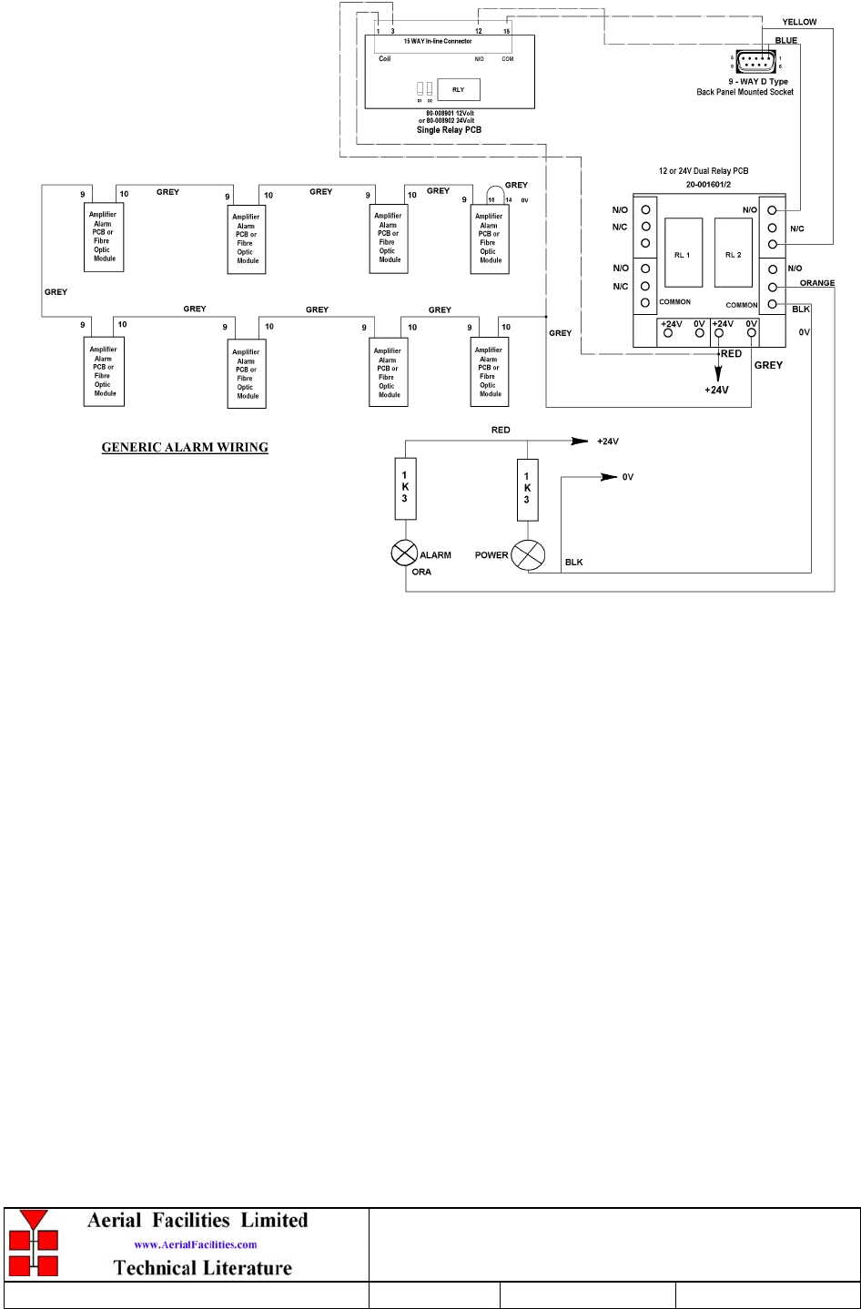
5.2.6.5 Generic Rack Shelf Enclosure Alarm Wiring Sketch
9 Way Channelised UHF Cell Enhancer
Maintenance Handbook
H/book Number:-50-025301HBKM Issue No:-1Date:-04/07/2003 Page:-34 of 69
9 Way Channelised UHF Cell Enhancer
Maintenance Handbook
H/book Number:-50-025301HBKM Issue No:-1Date:-04/07/2003 Page:-35 of 69
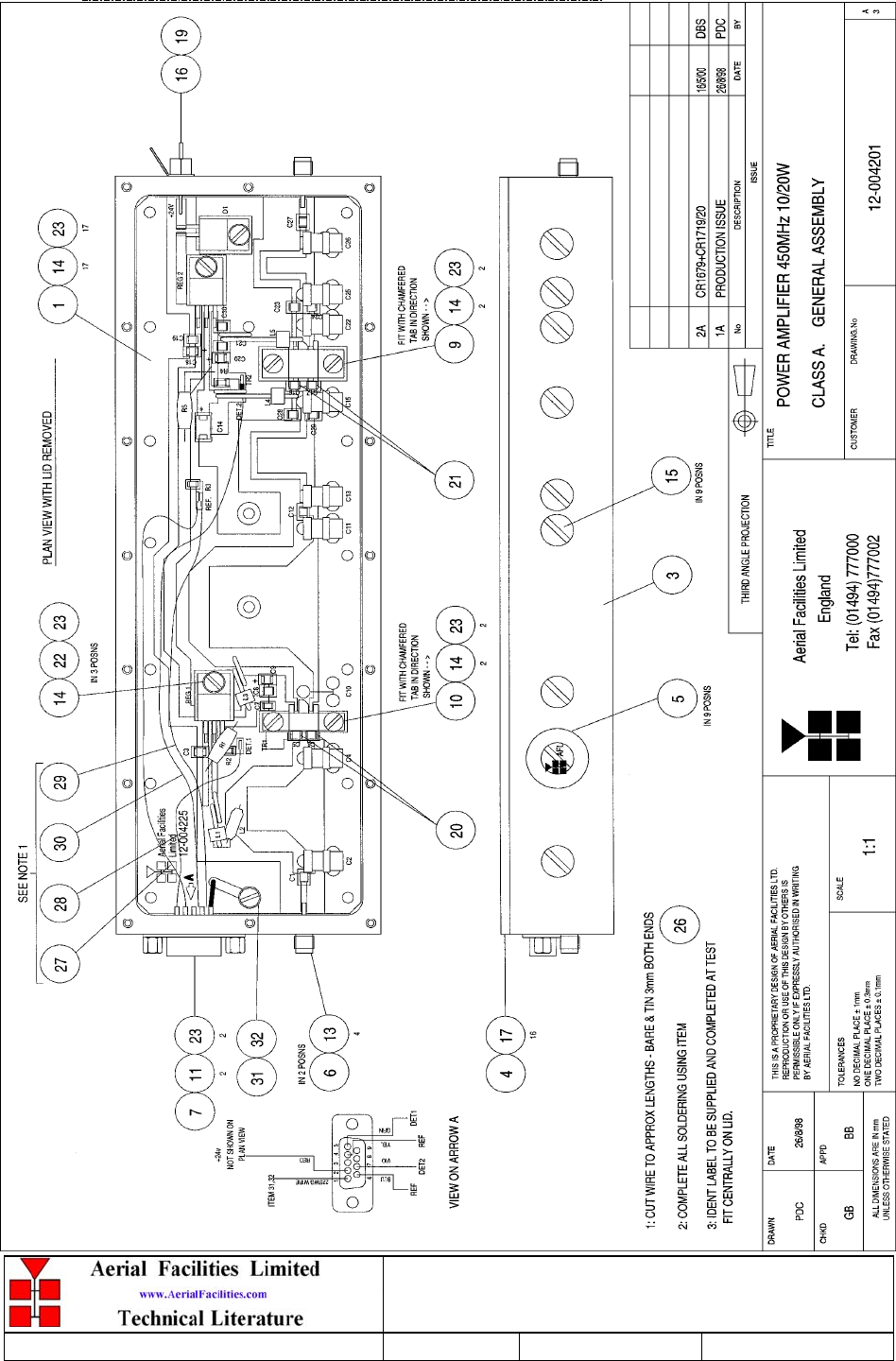
5.2.7 450MHz 20W Power Amplifier (12-004201)
5.2.7.1 Description
The power amplifiers fitted to this unit are multi-stage, solid state power amplifiers. Class
A circuitry is employed throughout the units to ensure excellent linearity over a wide
dynamic frequency range. All the semi-conductor devices are very conservatively rated to
ensure low device junction temperatures and a long, trouble free working lifetime.
The power amplifiers should require no maintenance over their operating lives. Under no
circumstances should the cover be removed or the side adjustments disturbed unless it is
certain that an amplifier has failed; since they are critically aligned during manufacture
and any re-alignment will require extensive test equipment.
5.2.7.2 Technical Specification
PARAMETER SPECIFICATION
Frequency Range: 350 – 550MHz (tuned to spec.)
Bandwidth: 20MHz (tuned to spec.)
Maximum Output Power: >20W (each)
Gain: 30dB
1dB Compression Point: <+43dBm
3rd Order Intercept Point: <+54dBm
VSWR: better than 1.45:1
Connectors: SMA female
Supply: 3.50A @ 24V DC
Size: 276 x 78 x 40mm (ex. Cons. & h’sink)
Weight: 1.5 kg (approx., excl. h’sink)
operational: -10°C to +55°CTemperature
range: storage: -40°C to +70°C
9 Way Channelised UHF Cell Enhancer
Maintenance Handbook
H/book Number:-50-025301HBKM Issue No:-1Date:-04/07/2003 Page:-36 of 69
5.2.7.3 Drg. N. 12-004201, PA General Assembly
9 Way Channelised UHF Cell Enhancer
Maintenance Handbook
H/book Number:-50-025301HBKM Issue No:-1Date:-04/07/2003 Page:-37 of 69
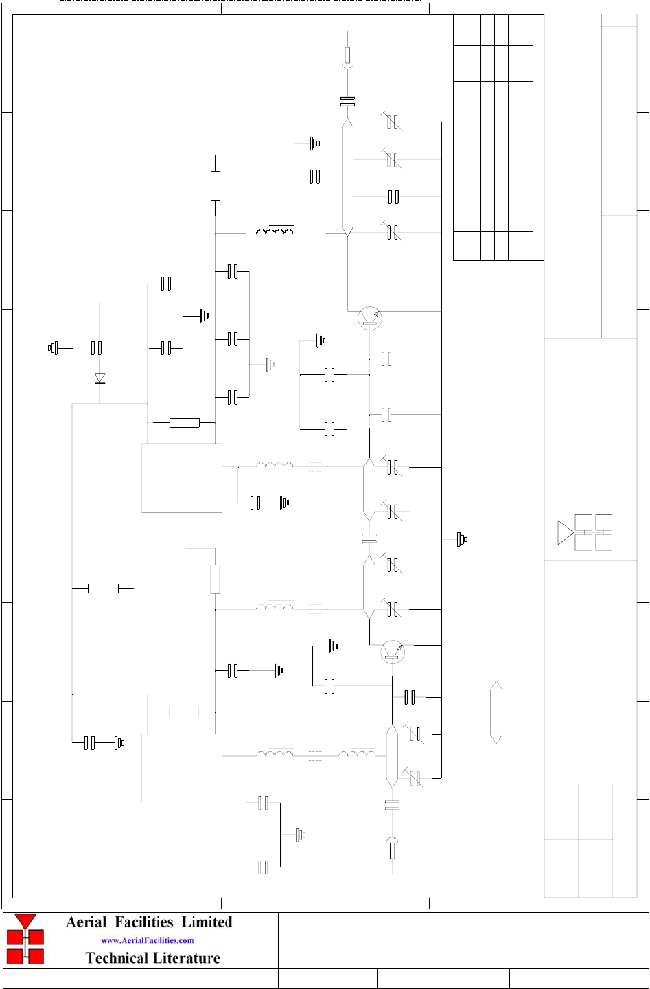
5.2.7.4 Drg. N. 12-004270, PA Circuit Diagram
1A
12-004270
POWER AMPLIFIER 450MHz 10/20W CLASS A
CIRCUIT DIAGRAM
-
3/8/98DBS
BYDATEDE SCRIP T IO NNo
ISSUE
123456789
A
B
C
D
E
F
123456789
A
B
C
D
E
F
PRODUCTION ISSUE PDC
3/8/98
+
RF INPUT
+
+
+
+
RF OUTPUT
+24v
ALARM
REF
ALARM
DET.1
ALARM
DET.2
R1
1R2
1KR
R2
R3
470R
REG .1
ADJ
OUT
IN
ADJ
REG .2
OUT
IN
C3
1uF
1nF
C7
1uF
C9
220pF
C8
L1 L3 L4 L5
FB4FB3FB2FB1
L2
47pF
C5
47pF
C6
1-14pF
C4
1-14pF
C2
C1 0
1-14pF
C1 1
1-14pF
TR1
TP5012
PT B2 00 3 1
TR2
C1 3
1-14pF
C1 5
1-14pF 1-14pF
C2 5 C2 6
1-14pF
C2 2
1-14pF
18pF
C2 8
27pF
C1 6
C1 7
27pF
C2 9
18pF
56pF
C1 2
4.7uF
C1 4
R5
R4 7
C1 9
56pF 1uF
C1 8
C2 0
1uF 56pF
C2 1
1000pF
C3 0
1KR
R4
1uH
D1
2OCTQ45
C2 4
15pF
C2 3
15pF
56pF
C2 7
C1
56pF
LM337T LM337T
CONDUCTORS SHOWN THUS: ARE 50 ohm STRIPLINES
REFER TO 12-004211 FOR COMPONENT POSITIONS EXCEPT FOR THOSE MARKED
(THEY ARE SPECIFIED ON 12-004201)
*
*
*
*
**
*
*
CR1679
16/5/00
DBS1B
Fax (01494)777002
Tel: (01494) 777000
Aerial Facilities Limited
THIS IS A PROPRIETARY DESIGN O F AERIAL FACILITIES LTD.
REPRODUCTION OR USE OF THIS DESIGN BY OTHERS IS
PERMISSIBLE O NLY IF EXPRESSLY AUTHORISED IN WRITING
BY AERIAL FACILITIES LTD.
NO DECIMAL P L ACE ± 1 mm
ONE DECIMAL PL ACE ± 0.3mm
TWO DECIMAL PLACES ± 0.1mm
AL L DIMENSIO NS ARE IN mm
UNLESS OTHERWISE STATED
CHKD
DRAWN
APPD
DATE
T O L ERANCES SCALE
England
CUSTOMER DRAWING.No
TITLE
3
A
C3 1
1nF
*
GB BB
9 Way Channelised UHF Cell Enhancer
Maintenance Handbook
H/book Number:-50-025301HBKM Issue No:-1Date:-04/07/2003 Page:-38 of 69
5.2.7.5 Drg. N. 12-004270C1, PA Parts List(1)
CIRC. DESCRIPT ION
AFL STOCK REF.
REF.
CHANGE NoCHANGE NoCHANGE NoCHANGE No DATEDATE
DAT E
DAT E ISSUEISSUEISSUE
ISSUE
1234
5
5
4
3
2
1
A
B
C
D
E
F
G
A
B
C
D
E
F
G
Aerial Facilities Limited
DRAWN DAT E APPD
CHKD CUST OM ER
TITLE
COMPONENT LIST FOR
POWER AMPLIFIER,450MHz,10/20W
CIRCUIT COMPONENT LIST
12-004270C1
1A
PDC
5/8/98
5/8/98
PROD. ISS.
C1
C2
C3
C4
C5
C6
C7
C8
C9
C10
C11
C12
C13
C14
C15
C16
C17
C18
C19
C20
C21
C22
C23
C24
C25
C26
C27
C28
C29
C30
93-200006 56pF CHIP CAP 10% TOL.(MIN)
56pF CHIP CAP 10% TOL.(MIN)93-200006
93-200006 56pF CHIP CAP 10% TOL.(MIN)
93-200006 56pF CHIP CAP 10% TOL.(MIN)
93-200006 56pF CHIP CAP 10% TOL.(MIN)
93-130023 PCB MOUNT AIR TRIMMER 1-14pF
93-130023 PCB MOUNT AIR TRIMMER 1-14pF
93-130023 PCB MOUNT AIR TRIMMER 1-14pF
93-130023 PCB MOUNT AIR TRIMMER 1-14pF
93-130023 PCB MOUNT AIR TRIMMER 1-14pF
93-130023 PCB MOUNT AIR TRIMMER 1-14pF
93-130023 PCB MOUNT AIR TRIMMER 1-14pF
93-240003 1uF TANTALUM CHIP CAP 35V
93-240004 1uF TANTALUM CHIP CAP 35V
93-240003 1uF TANTALUM CHIP CAP 35V
93-240004 1uF TANTALUM CHIP CAP 35V
REFER TO GA 12-004201 FOR DETAILS
93-200020 1nF CHIP CAP 63V 10%
93-200014 220pF CHIP CAP 10% TOL (MIN)
NOT FITTEDNOT FITTED
4.7uF TANTALUM CHIP CAP 35V93-240006
REFER TO GA 12-004201 FOR DETAILS
15pF CHIP CAP 10% TOL.(MIN)93-200005
93-200005 15pF CHIP CAP 10% TOL.(MIN)
93-200004 18pF CHIP CAP 10% TOL.(MIN)
18pF CHIP CAP 10% TOL.(MIN)93-200004
93-200016 1000pF (1nF) CHIP CAP 10% TOL.(MIN)
REFER TO GA 12-004201 FOR DETAILS
93-130023
5/5/00
CR1679
2A
PCB MOUNT AIR TRIMMER 1-14pF
REFER TO GA 12-004201 FOR DETAILS
C31 REFER TO GA 12-004201 FOR DETAILS
GB BB
9 Way Channelised UHF Cell Enhancer
Maintenance Handbook
H/book Number:-50-025301HBKM Issue No:-1Date:-04/07/2003 Page:-39 of 69
5.2.7.6 Drg. N. 12-004270C2, PA Parts List(2)
CIRC. DESCRIPT ION
AFL STOCK REF.
REF.
CHANGE NoCHANGE NoCHANGE NoCHANGE No DATEDATE
DAT E
DAT E ISSUEISSUEISSUE
ISSUE
1234
5
5
4
3
2
1
A
B
C
D
E
F
G
A
B
C
D
E
F
G
Aerial Facilities Limited
DRAWN DAT E APPD
CHKD CUST OM ER
TITLE
COMPONENT LIST FOR
POWER AMPLIFIER,450MHz,10\20W
CIRCUIT COMPONENT LIST
12-004270C2
PDC
5/8/98
5/8/98
PROD. ISS.
REG1
REG2
94-300002 LM337T, VOLTAGE REGULATOR
LM337T, VOLTAGE REGULATOR94-300002
D1 94-120006 2OTQ45 45V DUAL SCHOTTKY DIODE
R1
R2
R4
R3
R5
93-540075 1R2 2.5W RESISTOR
1KR CHIP RESISTOR93-630037
47R 6W RESISTOR93-540083
1KR CHIP RESISTOR93-630037
470R CHIP RESISTOR93-630032
L2 93-400004 1.0uH CHOKE SIGMA SC10 SERIES
93-910001 FERRITE BEAD
FERRITE BEAD93-910001
FERRITE BEAD93-910001
FERRITE BEAD93-910001
L1
L4
L5
90-500012 1.25 ENAMELLED COPPER WIRE
1.25 ENAMELLED COPPER WIRE90-500012
1.25 ENAMELLED COPPER WIRE90-500012
1.25 ENAMELLED COPPER WIRE90-500012
5/5/002A CR1679
1A
L3
TR1
TR2
REFER TO GA 12-004201 FOR DETAILS
REFER TO GA 12-004201 FOR DETAILS
GB BB
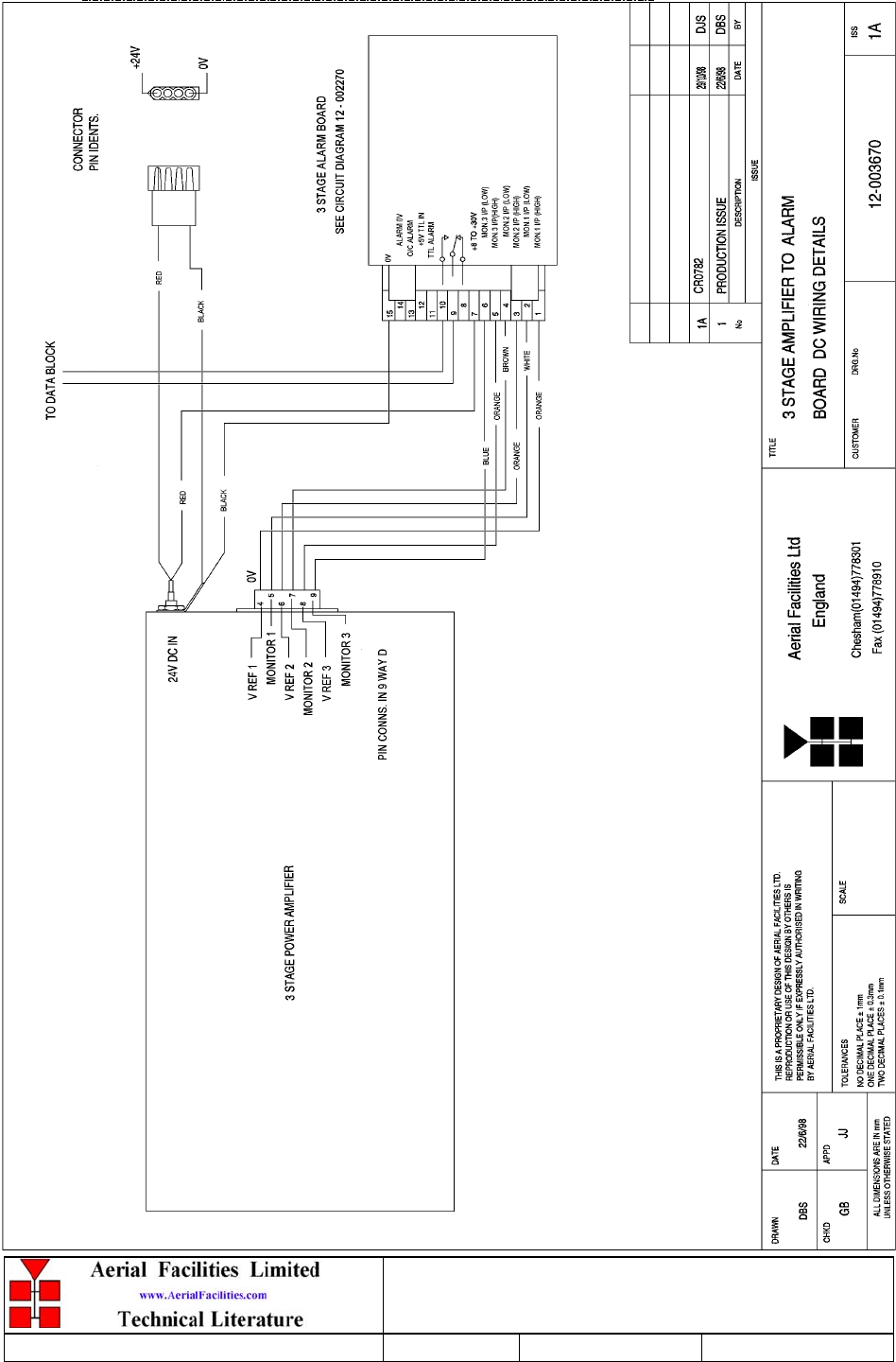
9 Way Channelised UHF Cell Enhancer
Maintenance Handbook
H/book Number:-50-025301HBKM Issue No:-1Date:-04/07/2003 Page:-40 of 69
5.2.7.7 Drg. N. 12-003670, PA to Alarm Wiring Details
9 Way Channelised UHF Cell Enhancer
Maintenance Handbook
H/book Number:-50-025301HBKM Issue No:-1Date:-04/07/2003 Page:-41 of 69
5.2.8 Single DC/DC Converter (13-001702)
5.2.8.1 Description
This unit it is used to derive a fixed voltage power supply rail from some higher voltage.
Typically, it is used to derive 5V, 8V, 12V or 15V from a 24V input. This particular
regulator is dedicated to supply 12.8V DC.
The circuit is based upon an LM317 variable voltage regulator, which is capable of
supplying a maximum of 1.5A output current. Note that at full output current the
dissipation of the device must remain in limits, bearing in mind the voltage which is
being dropped across it. The maximum allowable dissipation will also depend on the
efficiency of the heatsink on which the device is mounted.
The output voltage of the unit is programmed by the resistive divider which is fitted
between the output terminal, the reference terminal and ground. R1 is the reference
programming resistor and is fixed in all versions. R2 is fitted on 12V versions while R3,
(which is in parallel with R2) is fitted on 8V and 5V versions.
5.2.8.2 Technical Specification
PARAMETER SPECIFICATION
Operating Voltage: 21 – 27V DC
Output Voltages: 12.4V (typical)
Output Current: 1.0A (maximum per o/p)
Connections: Screw Terminal Block
operational: -10ΒC to +55ΒC
Temperature
range: storage: -40ΒC to +70ΒC
PCB Size: 47 x 30mm
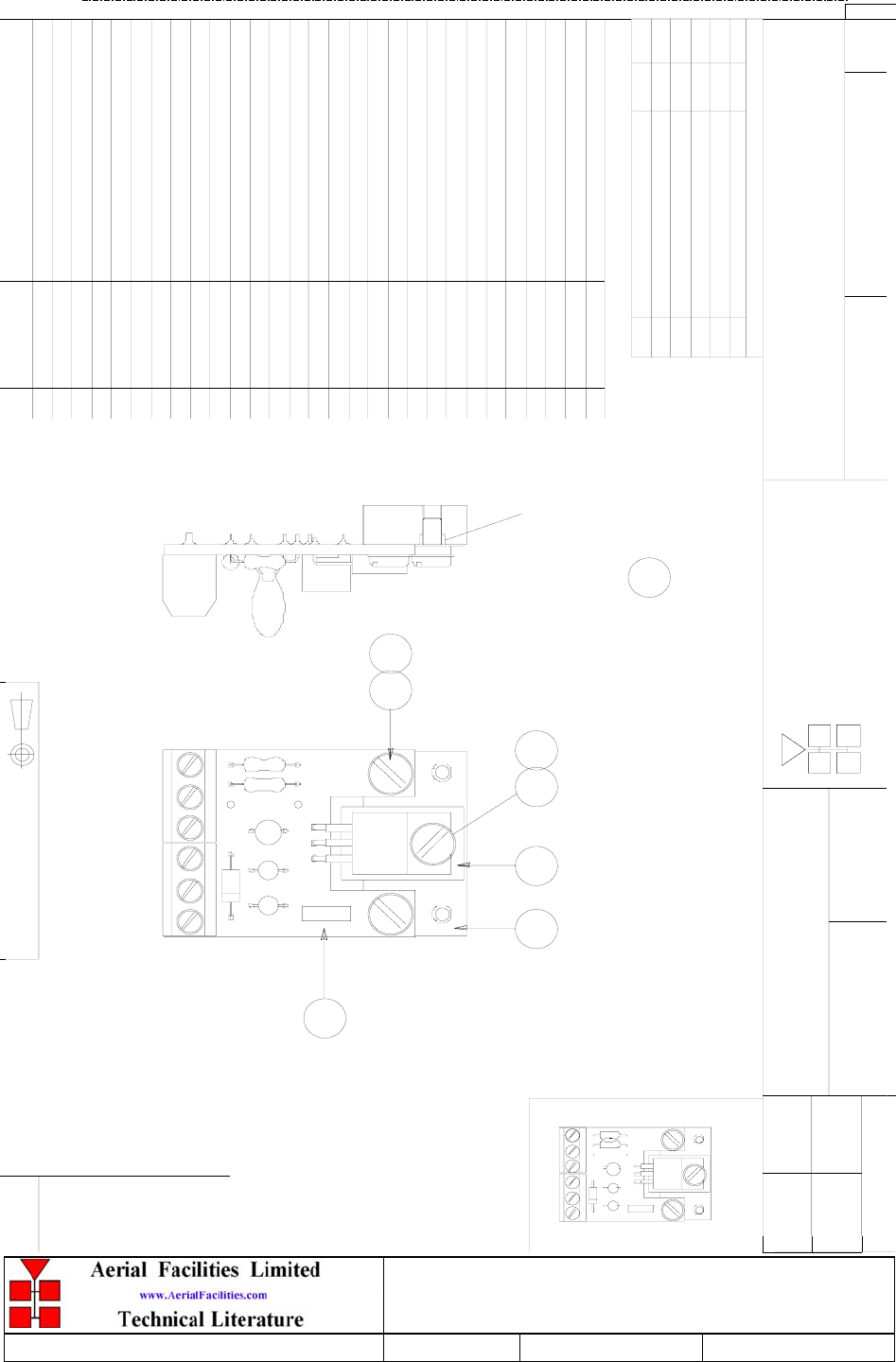
9 Way Channelised UHF Cell Enhancer
Maintenance Handbook
H/book Number:-50-025301HBKM Issue No:-1Date:-04/07/2003 Page:-42 of 69
5.2.8.3 Drg. N. 13-001702, 12.8V Regulator Assembly Drawing & Parts List
1
2 3
23
25
1
IN 2 PLACES
26
1
2624
12.8v REGULATOR,ASSEMBLY
13-001702 1A
2:1
MNR 12/7/00
BYDATEDESCRIPTIONNo
ISSUE
THIRD ANG LE PROJECTION
USED O N
++
+
TB1
D1
C1
C3 C2 R3 R2 R1
C4
REG1
13-001725
AFL Ltd
CO MP.
REF . AFL STO CK REF. DESCRIPTION
1A PRODUCTION ISSUE
1 2 /7 /0 0
MNR
1: ALL SOLDERED CONNECTIONS TO BE MADE USING ITEM
REG 1
13- 001725
TB1
D1
C4
+
C1
C2C3 R3 R2
A FL Lt d
++
R1
ACTUAL SIZE
123 456
PART SECTION SHOWING
Fax : (01494)777002
Tel : (01494)777000
Aerial Facilities Ltd
THIS IS A PRO PRIETARY DESIGN OF AERIAL FACIL ITIES L TD.
REPRODUCTIO N O R USE OF THIS DESIG N BY O THERS IS
PERMISSIBLE O NLY IF EXPRESSLY AUTHORISED IN WRITING
BY AERIAL F ACIL ITIES L TD.
NO DECIMAL PL ACE ± 1 mm
ONE DECIMAL PLACE ± 0.3mm
TWO DECIMAL PLACES ± 0 .1 mm
AL L DIM ENSIO NS ARE IN mm
UNL ESS OTHERWISE STAT ED
CHKD
DRAWN
APPD
DAT E
T OL ERANCES SCAL E
England
CUSTO MER DRG.No
TITLE
A
3
ISS
TB1 9 1- 7 00 0 0 3 3 WAY PRINTED CIRCUIT CO N
C1 93-140002 2.2uF 35V TANTALUM CAP
C2 9 3- 1 40 0 0 4 1 0 u F 3 5V T ANT AL UM CAP
C3 9 3- 1 4 0 0 0 2 2 .2 u F 3 5 V TANT AL UM CAP
C4 93-120003 1 00n F 6 3V POL YESTER CAP FIL M
D1 94-100006 DIODE 1N4003 [1N4000
R1 93-540024 240R 0.25W 1% RES MRS25 M:F
R2 93-540039 2K2 0.25W 1% RES MRS25 M:F
94-300001REG1 L M3 1 7 T N.S.C/MO T VO L TAG E REG
POSITION OF C/BORE
2: WHERE INDIVIDUAL ITEMS ARE NOT BALLOONED THE COMPONENT IS IDENTIFIED
ON BOTH THE COMPONENT LIST AND THE DRAWING BY ITS COMPONENT REF.
(SEE B.o.M FOR BALLOON IDENTS)
NOTE
GB BB
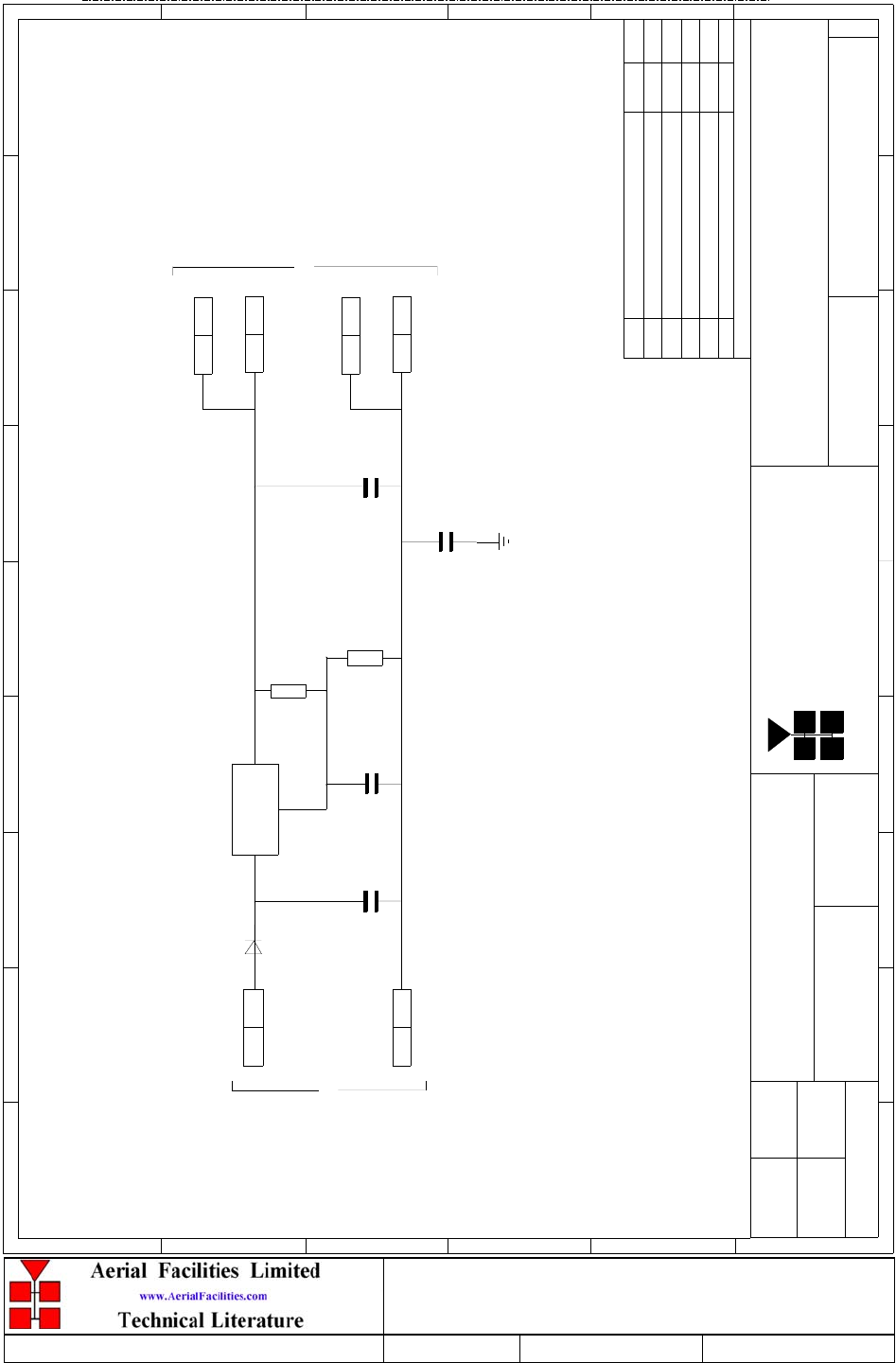
9 Way Channelised UHF Cell Enhancer
Maintenance Handbook
H/book Number:-50-025301HBKM Issue No:-1Date:-04/07/2003 Page:-43 of 69
5.2.8.4 Drg. N. 13-001771, 12.8V Single Regulator Circuit Diagram
BYDATEDESCRIPTIONNo
ISSUE
1 234 5678 9
A
B
C
D
E
A
B
C
D
E
18-30V INPUT
TB1 1
TB1 2
1N4003
D1
VIN REG1
LM317T
VOUT
ADJ R1
240R
C1 C2 R2
2K2 C3
C4
5 TB1
6 TB1
3 TB1
4 TB1
12.8v OUTPUT
++
+
2u2 10u 2u2
100n
Fax : (01494)777002
Tel : (01494)777000
Aerial Facilities Limited
THIS IS A PROPRIETARY DESIGN OF AERIAL FACILITIES LTD.
REPRODUCTIO N O R USE O F THIS DESIGN BY O THERS IS
PERMISSIBLE ONLY IF EXPRESSLY AUTHORISED IN WRITING
BY AERIAL FACIL IT IES L TD.
NO DECIMAL PL ACE ± 1 m m
ONE DECIMAL PLACE ± 0.3mm
TWO DECIMAL PL ACES ± 0 .1 m m
AL L DIMENSIO NS ARE IN mm
UNL ESS O THERWISE STATED
CHKD
DRAWN
F
12
APPD
DAT E
T O L ERANCES
3
SCALE
45
England
CUSTO MER DRAWING.No
67
TITLE
8 9
3
A
F
12.8v REGULATOR, CIRCUIT DIAGRAM
13-001771
1A
MNR 13/7/00
CR1679
13/7/00
MNR
GB BB

9 Way Channelised UHF Cell Enhancer
Maintenance Handbook
H/book Number:-50-025301HBKM Issue No:-1Date:-04/07/2003 Page:-44 of 69
5.2.9 24V Single Relay Board (80-008902)
5.2.9.1 Description
The General Purpose Relay Board allows the inversion of signals and the isolation of
circuits. It is equipped with a single dual pole change-over relay RL1, with completely
isolated wiring, accessed via a 15 way in-line connector.
The relay is provided with polarity protection diodes and diodes for suppressing the
transients caused by "flywheel effect" which can destroy switching transistors or induce
spikes on neighbouring circuits. It’s common use is to amalgamate all the alarm signals
into one, volts-free relay contact pair for the main alarm system.
Note that the board is available for different voltages (12 or 24V) depending on the type
of relay fitted at RL1.
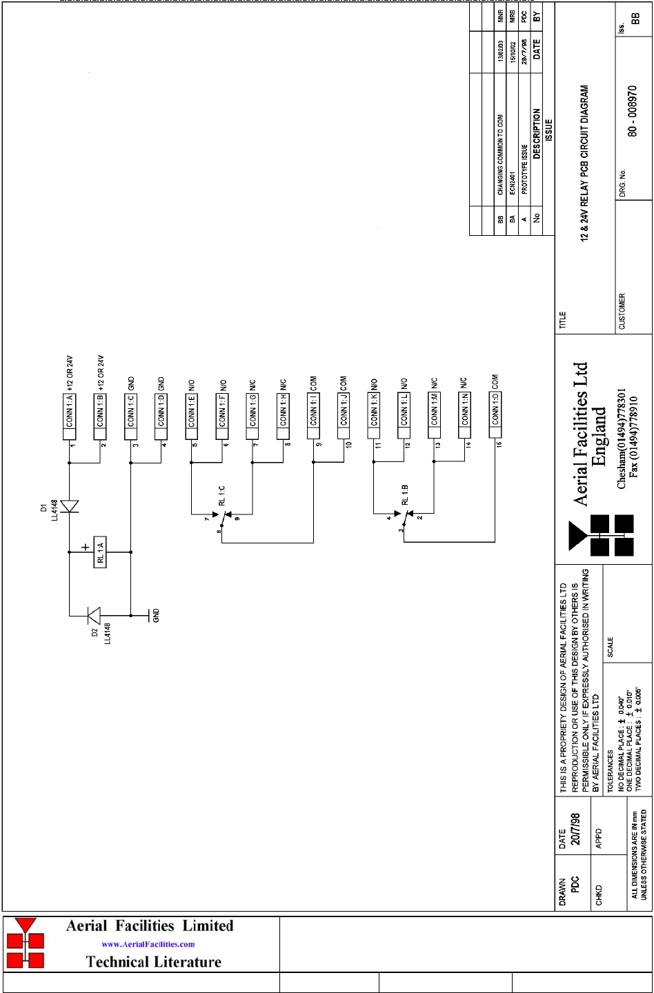
9 Way Channelised UHF Cell Enhancer
Maintenance Handbook
H/book Number:-50-025301HBKM Issue No:-1Date:-04/07/2003 Page:-45 of 69
5.2.9.2 Drg. N. 80-008970, Single Relay Board Circuit Diagram
9 Way Channelised UHF Cell Enhancer
Maintenance Handbook
H/book Number:-50-025301HBKM Issue No:-1Date:-04/07/2003 Page:-46 of 69
5.2.10 24V 410W Power Supply (96-300054)
5.2.10.1 Description
The power supply unit is a switched-mode type capable of supplying 24V DC at 17.0Amps
continuously. Equipment of this type typically requires approximately 8.0 Amps at 24V DC,
so the PSU will be used conservatively ensuring a long operational lifetime.
No routine maintenance of the PSU is required. If a fault is suspected, then the output
voltage from the power supply may be measured on its output terminals. This is typically set
to 24.5V.
All the PSU’s used in AFL Cell Enhancers are capable of operation from either 110 or 220V
nominal AC supplies. The line voltage is sensed automatically, so no adjustment or link
setting is needed by the operator. No drawings of the PSU are available.
5.2.10.2 Technical Specification
AC Input Supply:
Voltage: 110 or 220V nominal - 90 to 132 or 180 to
264V (single phase, absolute limits)
Frequency: 47 to 63Hz
DC Output Supply:
Voltage: 24V DC (nominal), 22 to 26V
(absolute limits)
Current: 17.0A
operational: -10ΒC to +55ΒC
Temperature
range: storage: -40ΒC to +70ΒC
9 Way Channelised UHF Cell Enhancer
Maintenance Handbook
H/book Number:-50-025301HBKM Issue No:-1Date:-04/07/2003 Page:-47 of 69
5.3 VTA Downlink Channel Shelf (50-025304)
5.3.1 UHF 3dB Splitter (05-002603) See section 5.2.1
5.3.2 4-Way Splitter (05-003401)
5.3.2.1 Description
The Splitter/Combiners used are devices for accurately matching two or more RF signals
to single or multiple ports, whilst maintaining an accurate 50Ω load to all inputs/outputs
and ensuring that the VSWR and insertion losses are kept to a minimum. Any unused
ports will be terminated with an appropriate 50Ω load.
5.3.2.2 Technical Specification
PARAMETER SPECIFICATION
Frequency range: 170 – 550MHz
Bandwidth: 280MHz
Rejection: >14dB
Insertion loss: 6.5dB (in band, typical)
Connectors: SMA
Weight: <1.5Kgm
operational
:
-10ΒC to +55ΒC
Temperature
range: storage -40ΒC to +70ΒC
9 Way Channelised UHF Cell Enhancer
Maintenance Handbook
H/book Number:-50-025301HBKM Issue No:-1Date:-04/07/2003 Page:-48 of 69
5.3.3 Channel Control Module (17-002101)
5.3.3.1 Description
The purpose of the channel control modules is to change the channel selective module
frequencies by means of a series of D.I.P switch banks, each switch corresponding to a
different ‘frequency bit’.
5.3.3.2 Technical Specification
Below shows the pin assignments for each switch on a channel control module.
IDC PIN 25-way Connector Function
1 13 Freq. bit 1 (12.5kHz)
2 25 Freq. bit 2 (25kHz)
3 12 Freq. bit 3 (50kHz)
4 24 Freq. bit 4 (100kHz)
5 11 Freq. bit 5 (200kHz)
6 23 Freq. bit 6 (400kHz)
7 10 Freq. bit 7 (800kHz)
8 22 Freq. bit 8 (1.6MHz)
9 9 Freq. bit 9 (3.2MHz)
10 21 Freq. bit 10 (6.4MHz)
11 8 Freq. bit 11 (12.8MHz)
12 20 Freq. bit 12 (25.6MHz)
13 7 Freq. bit 13 (51.2MHz)
14 19 Freq. bit 14 (102.4MHz)
15 6 Freq. bit 15 (204.8MHz)
16 18 Freq. bit 16 (409.6MHz)
17 5 Module alarm
18 17
19 4
20 16
21 3
N/C
22 15 +5V
23 2 0V
24 14 Switched 12V
25 1 0V
26 --- ---
9 Way Channelised UHF Cell Enhancer
Maintenance Handbook
H/book Number:-50-025301HBKM Issue No:-1Date:-04/07/2003 Page:-49 of 69
5.3.3.3 VHF/ UHF Programming Procedure
Check that the required frequency falls within the operational frequency limits of the Cell
Enhancer.
For each channel required, subtract the synthesiser offset from the required operating
frequency and record the resulting local oscillator frequency.
Divide each local oscillator frequency by the channel spacing and check that the result is an
integer (i.e.: no remainder).
If the synthesiser division ratio is not an integer value, check the required operational
frequency and repeat the calculation checking for mistakes.
Convert the required local oscillator frequency to synthesiser programming switch state
patterns according to the following table.
Switch number Synthesiser offset added when switch in UP position
1 +12.5kHz
2 +25kHz
3 +50kHz
4 +100kHz
5 +200kHz
6 +400kHz
7 +800kHz
8 +1.6MHz
9 +3.2MHz
10 +6.4MHz
11 +12.8MHz
12 +25.6MHz
13 +51.2MHz
14 +102.4MHz
15 +204.8MHz
16 +409.6MHz
9 Way Channelised UHF Cell Enhancer
Maintenance Handbook
H/book Number:-50-025301HBKM Issue No:-1Date:-04/07/2003 Page:-50 of 69
5.3.3.4 VHF/ UHF Programming Example
Frequency required: 465.5MHz
Channel spacing: 12.5 kHz
Synthesiser offset: 21.4MHz
The Local Oscillator frequency is therefore:
465.4 – 21.4 = 444.0MHz
Dividing the LO frequency by the channel spacing of 0.0125MHz:
444.0 = 35520
0.0125
This is an integer value, therefore it is OK to proceed.
Switch settings
16 15 14 13 12 11 10 9 8 7 6 5 4 3 2 1
Local Oscillator
Frequency of
444.0MHz 1 0 0 0 1 0 1 0 1 1 0 0 0 0 0 0
Switch setting: 0 = switch DOWN (on, frequency ignored)
1 = switch UP (off, frequency added)

9 Way Channelised UHF Cell Enhancer
Maintenance Handbook
H/book Number:-50-025301HBKM Issue No:-1Date:-04/07/2003 Page:-51 of 69
5.3.4 Channel Selectivity Module (17-010601)
5.3.4.1 Description
The channel selectivity module is employed when the Cell Enhancer requirement dictates
that very narrow bandwidths (single operating channels), must be selected from within
the operating passband. One channel selectivity module is required for each channel.
The Channel Selectivity Module is an Up/Down frequency converter that mixes the
incoming channel frequency with a synthesised local oscillator, so that it is down-
converted to an Intermediate Frequency (IF) in the upper HF range. An eight pole crystal
filter in the IF amplifier provides the required selectivity to define the operating passband
of the Cell Enhancer to a single PMR channel. The same local oscillator then converts the
selected IF signal back to the channel frequency.
Selectivity is obtained from a fixed bandwidth block filter operating at an intermediate
frequency (IF) in the low VHF range. This filter may be internal to the channel selectivity
module (Crystal or SAW filter) or an externally mounted bandpass filter, (LC or Helical
Resonator). Various IF bandwidths can therefore be accommodated. A synthesized Local
Oscillator is employed in conjunction with high performance frequency mixers, to
translate between the signal frequency and IF.
The operating frequency of each channel selectivity module is set by the programming of
channel selectivity module frequencies and is achieved digitally, via hard wired links,
banks of DIP switches (see section 5.3.3), or via an onboard RS232 control module,
providing the ability to remotely set channel frequencies.
Automatic Level Control (ALC) is provided within each channel selectivity module such
that the output level is held constant for high level input signals. This feature prevents
saturation of the output mixer and of the associated amplifiers.
Alarms within the module inhibit the channel if the synthesised frequency is not locked.
The synthesiser will not usually go out of lock unless a frequency far out of band is
programmed.
The channel selectivity module is extremely complex and, with the exception of channel
frequency programming within the design bandwidth, it cannot be adjusted or repaired
without extensive laboratory facilities and the necessary specialised personnel. If a fault
is suspected with any channel selectivity module it should be tested by substitution and
the complete, suspect module should then be returned to AFL for investigation.
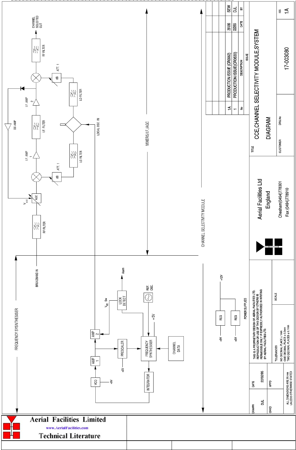
9 Way Channelised UHF Cell Enhancer
Maintenance Handbook
H/book Number:-50-025301HBKM Issue No:-1Date:-04/07/2003 Page:-52 of 69
5.3.4.2 Drg. N. 17-003080, Generic Channel Module Block Diagram
9 Way Channelised UHF Cell Enhancer
Maintenance Handbook
H/book Number:-50-025301HBKM Issue No:-1Date:-04/07/2003 Page:-53 of 69
5.4 VTA Uplink Duplexer Shelf (50-025305, 4U Chassis)
5.4.1 Bandpass Filters (02-011204 & 02-013401) See section 5.1.1
5.5 VTA Uplink Amplifier Shelf (50-025306, 8U Chassis)
5.5.1 20Watt Class A Power Amplifier (12-016301)
5.5.1.1 Description
This amplifier is a Class A 20W power amplifier with a frequency range from 380MHz to
470MHz in a 1 stage balanced configuration. It demonstrates a very high linearity and a very
good input/output return loss (RL). It has built in a Current Fault Alarm Function.
Its housing is an aluminium case (Alocrom 1200 finish) with SMA connectors for the RF
input/output and a D-Type connector for the power supply and the Current Fault Alarm
Function.
5.5.1.2 Technical Specification
Parameters Guaranteed Guaranteed Units
Temperature +25 -10 to +60 °C
Frequency Range 380 - 470 MHz
Small Signal Gain ≥23.0 dB
Gain Flatness 1.5 1.7 dB p-p Max
∆Gain vs. Temperature 1.0 dB Max
In/Out RL 18 18 dB Min
Output Power @ 1dB
Compression Point 43.2 43.0 dBm Min
Output 3rd Order IP 55.3 55.0 dBm Min
DC Supply Voltage 24 ± 0.5 Vdc
DC Supply Current 3700 typical 3800 mA Max
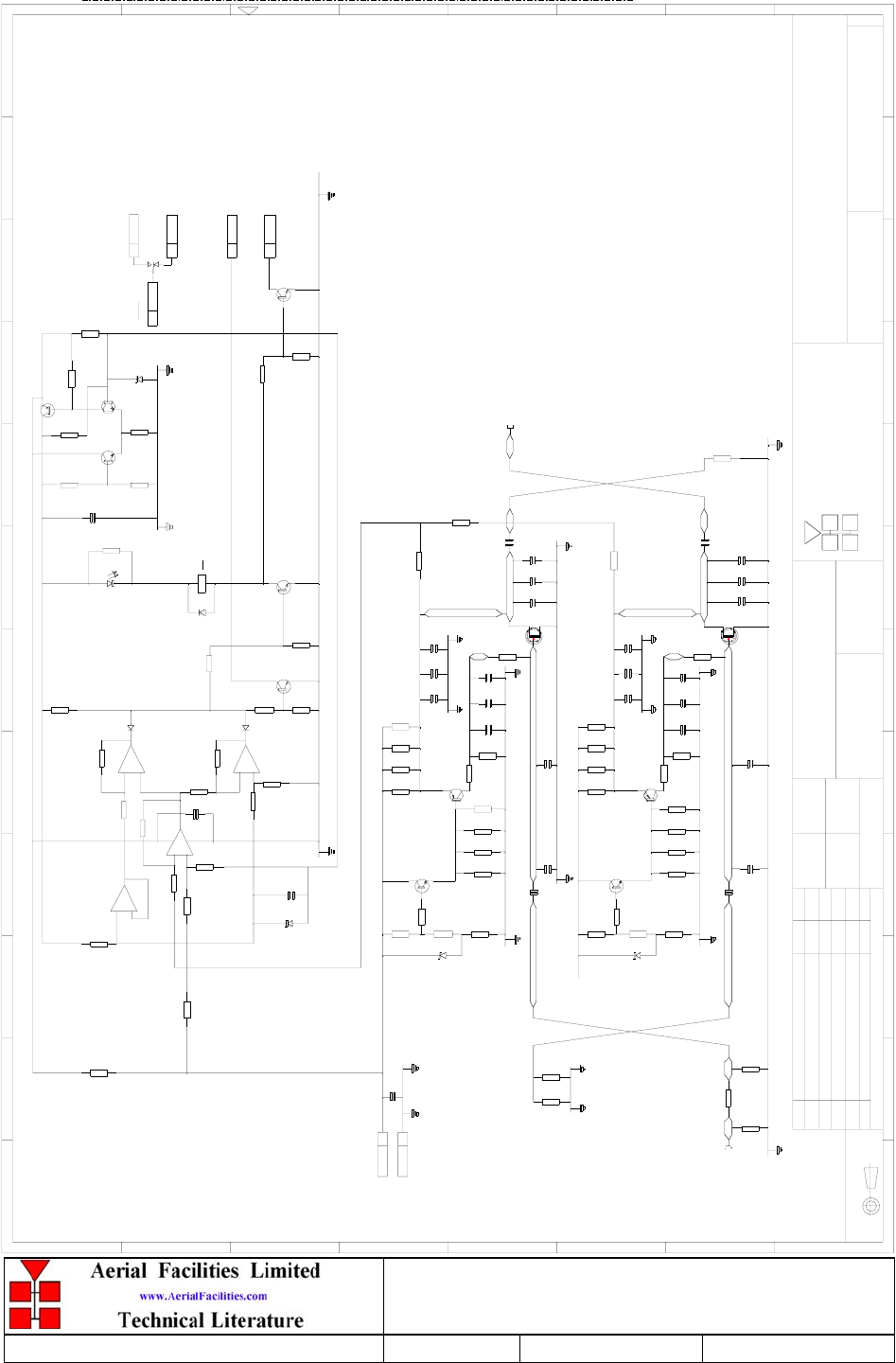
9 Way Channelised UHF Cell Enhancer
Maintenance Handbook
H/book Number:-50-025301HBKM Issue No:-1Date:-04/07/2003 Page:-54 of 69
5.5.1.3 Drg. N. 12-016370, 20W PA Circuit Diagram
POWER AMPLIFIER,380-470MHz,20W,CLASS A,
CIRCUIT DIAGRAM
12-016370
DJL 06/08/02
R26
R9
R32
R3
R2
R1
C1
C2
R4R5
R13
R15
R16
R14
R11R12 R10
C16
R33
C17
R28R29 R27
R30
R31
R40
R6
C3
C5 C6 C7
R22R20R19 R21
R8
R7 C9C10
C13 C12
C18
R25
R24
R23
C24C25
R41
C8
C23
C22C20 C21
R39R38R37R36
C28 C27
R42
R46
R65
C36
R67
C35
R55R44
R59
R56
TR 12
R48R53
R54
R69
R76
R68
R47
R64
R58
R57
R66
R50 R49
TR 8
RL1
1
TR 11
R74
R73
TR 7
C34
R61 R60
TR 10
R43
R62
R45
DATEDESCRIPTIONNo
ISSUE
THIRD ANGL E PRO JECTION
123456789101112
A
B
C
D
E
F
G
H
123456789101112
A
B
C
D
E
F
G
H
PERMISSIBLE ONLY IF EXPRESSLY AUTHORISED IN WRITING
RE PRODUCTI ON OR US E OF TH IS DES IGN BY OTHE RS I S
THIS IS A PROPRIETARY DESIGN OF AERIAL FACILITIES LTD.
UNLESS OTHERWISE STATED
ALL DIMENSIONS ARE IN mm
DATEDRAWN
CHKD APPD
TWO DECIMAL PLACES ± 0.1mm
NO DECIMAL PLACE ± 1mm
ONE DECIMAL PLACE ± 0.3mm
BY AERIAL FACILITIES LTD.
TOLERANCES SCALE
CUSTOME R DRAWING No
Fax : 01494 777002
Tel : 01494 777000
Aerial Facilities Limited
England
TI TLE
2
A
RF INPUT
SAT
0R 0
SAT
15p
4. 7p
CPL1
100R100R
+24V
3K 3
ZD 1
5. 1v
0R 0
1K 8
330R
6K 8 6K 8 6K 8
TR 2
FZT651
15p
3K 3
4. 7p
6K 8 6K 86K 8
CON 1
CON 1
+
A2
100u
A1
+24V
C15
ZD 2
5. 1v
0R 0
1K 8
330R TR 5
FZT651
27R
G S
D
MRF9045
18p
TR 1
470p
10p 7. 5p 2. 2p
G S
D
MRF9045
100u
C11
FZT751
6K 8
680R
+
270R
TR 3
2R 2 2R 2 1R 5
1n 100p
+
100u
C14
1R 5
100p 47p
C26
100u
18p
6K 8
680R
+
270R
TR 4
1n 100p
27R
1K
CPL2
470p
10p 7.5p 2.2p
50R
RF OUTPUT
FZT751
TR 6
2R 2 2R 2 1R 5
+
C29
100u
1R 5
100p 47p
1K
HY45B
HY45B
MI IB
AA PROT O TYPE ISSUE 6 /8 /02 DJL
0R 0
ZD 3 +
1. 23V 1u
470R
13
LM 324M
12
100K
100K
14
IC1:D
11
82K
+
-4
82K
BCW71
4K 7 4K 7
270K
LM 324M
IC1:B
8K 2
3K 6
6-
5+
LL4148
7
D2
LM 324M
1K
100n
10K
10K
LL4148
D3
1K
1K 8
2
3
IC1:A
-
LM 324M
+1
270K
IC1:C
+
9-
10
LL4148
8
D1
4K 7
oc good/ 0v bad
TTL al ar m
bad
good
BCW71
2K 4 560R
4K 7
BCW71
common
CON 1
10K
3V 3
1
5
2
CON 1
CON 1
3CON 1
FZT751
+
LE D 1 R63
150R
1U
3K
BCW71BCW71 TR 9
1K
ZD 4
2K 2
RL1/1
22K
4CON 1
1 A PRO DUCTIO N ISSUE( ECN2 7 3 7 )
17/ 10/ 02
DJL
0R 0
2A ECN2882
28/4/03
DJL

9 Way Channelised UHF Cell Enhancer
Maintenance Handbook
H/book Number:-50-025301HBKM Issue No:-1Date:-04/07/2003 Page:-55 of 69
5.5.2 Automatic Gain Control (17-001101, Det. & 17-001201, Atten.)
5.5.2.1 Description
The equipment is fitted with an Automatic Gain Control (AGC) system. This is generally
fitted in the Uplink path (not usually needed in the downlink path, as the signal here is at an
almost constant level), to avoid overloading the amplifiers (with the associated performance
degradation) should a mobile be operated very close to the unit.
Normally the attenuator is at minimum attenuation. The detector/amplifier unit monitors the
RF level being delivered by the power amplifier, and when a certain threshold is reached it
begins to increase the value of the attenuator to limit the RF output to the (factory set)
threshold. Therefore overloading of the power amplifier is avoided.
The factory set threshold is 1dB below the Enhancer 1dB compression point. Some
adjustment of this AGC threshold level is possible, a 10dB range is mostly achieved. It is
not recommended under any circumstances to adjust the AGC threshold to a level greater
than the 1dB compression point as system degradation will occur.
The detector comprises of a 50 transmission line with a resistive tap which samples a
small portion of the mainline power. The sampled signal is amplified and fed to a
conventional half wave diode rectifier, the output of which is a DC voltage proportional to
the RF input signal.
This DC voltage is passed via an inverting DC amplifier with integrating characteristics, to
the output, which drives the attenuation control line of the corresponding AGC attenuator.
This unit is fitted at some earlier point in the RF circuit.
The unit contains a 12V DC regulator in the detector module, which supplies stabilised
voltage to the DC amplifier and via an external cableform to the AGC attenuator.
For small signals, below AGC onset, the output control line will be close to 12V and the
AGC attenuator will have minimum attenuation. As the signal level increases the control
line voltage will fall, increasing the attenuator value and keeping the system output level at a
constant value.
The AGC onset level is adjusted by the choice of sampler resistor R1 and by the setting of
potentiometer VR1.
The attenuator comprises a 50 P.I.N diode, voltage-variable attenuator with a range of 3 to
30dB. The attenuation is controlled by a DC voltage which is derived from the associated
AGC detector unit.
9 Way Channelised UHF Cell Enhancer
Maintenance Handbook
H/book Number:-50-025301HBKM Issue No:-1Date:-04/07/2003 Page:-56 of 69
5.5.2.2 Technical Specification
PARAMETER SPECIFICATION
Frequency Range: up to 1000MHz
Attenuation Range: 3 to 30dB
Attenuation Steps: continuously variable
VSWR: better than 1.2:1
RF Connectors: SMA female
attenuator: 1WPower Handling:
detector/amp: >30W (or as required)
operation: -10°C to +55°CTemperature Range:
storage: -40°C to +70°C
attenuator pcb 50 x 42 x 21mm
Size: detector/amp pcb 54 x 42 x 21mm
attenuator: 90g
Weight: detector/amp: 100g
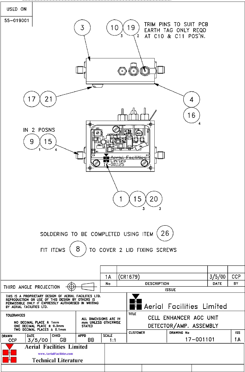
9 Way Channelised UHF Cell Enhancer
Maintenance Handbook
H/book Number:-50-025301HBKM Issue No:-1Date:-04/07/2003 Page:-57 of 69
5.5.2.3 Drg. N. 17-001101, ACG Detector Assembly
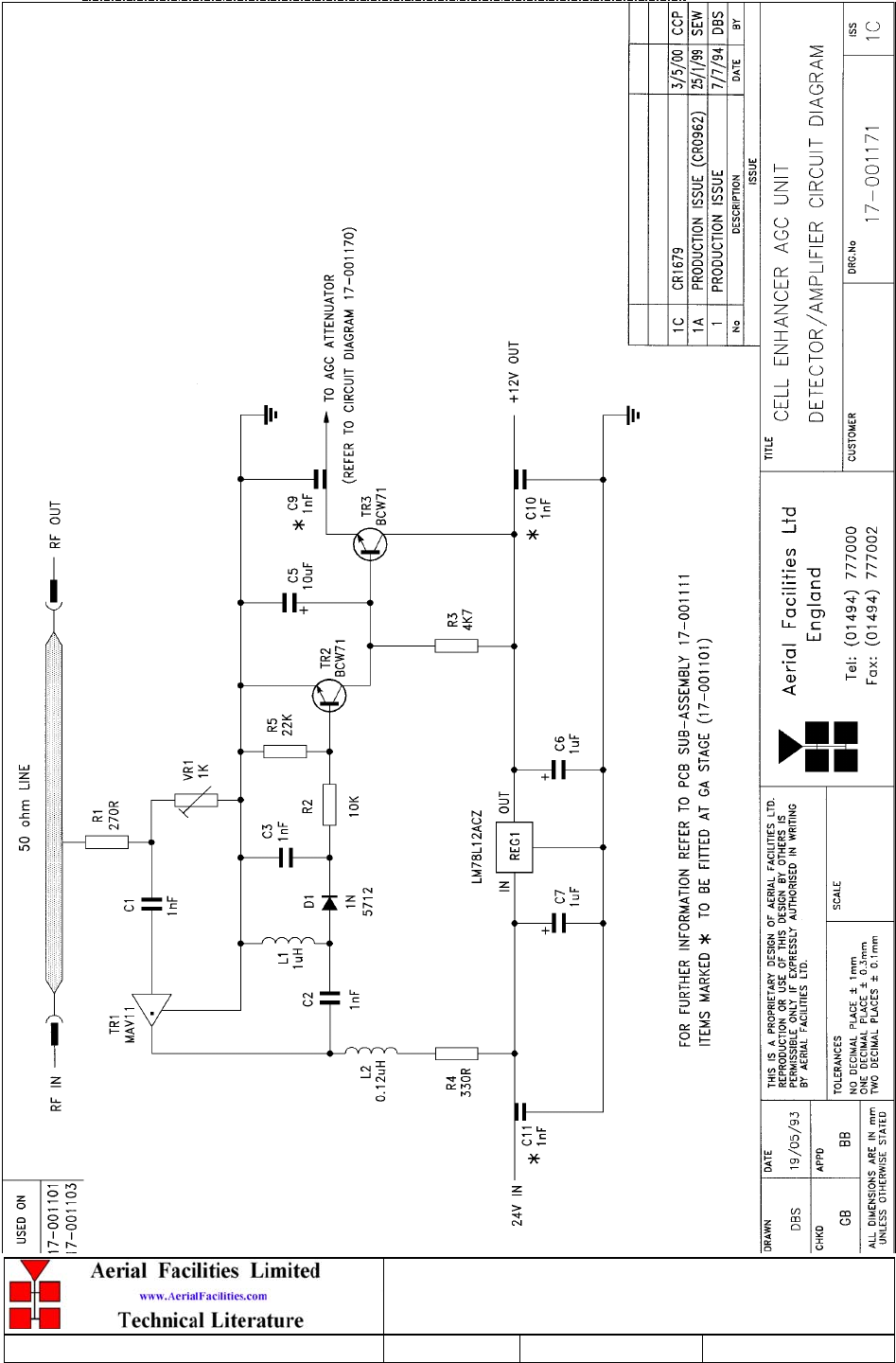
9 Way Channelised UHF Cell Enhancer
Maintenance Handbook
H/book Number:-50-025301HBKM Issue No:-1Date:-04/07/2003 Page:-58 of 69
5.5.2.4 Drg. N. 17-001171, AGC Detector Circuit Diagram
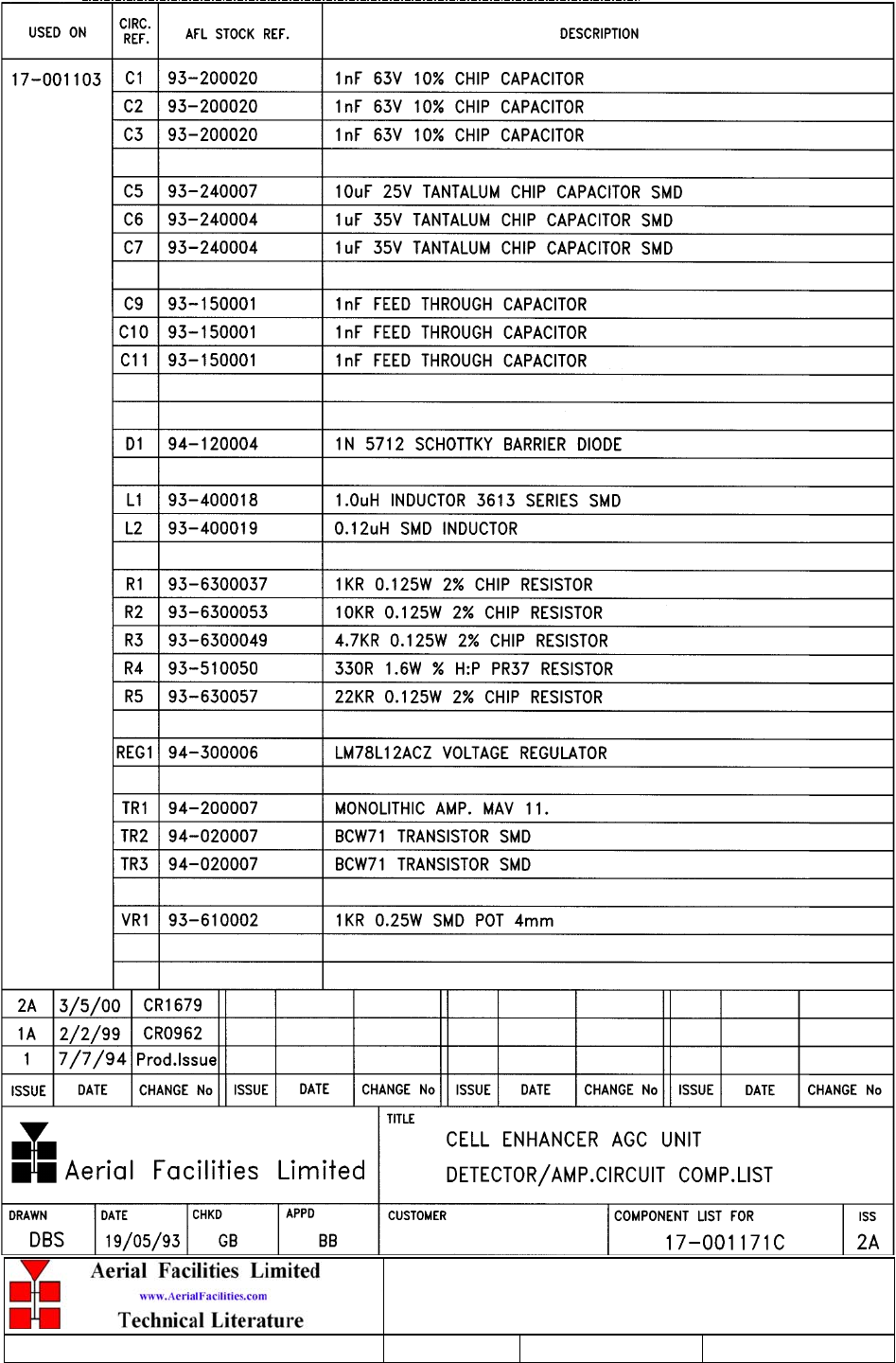
9 Way Channelised UHF Cell Enhancer
Maintenance Handbook
H/book Number:-50-025301HBKM Issue No:-1Date:-04/07/2003 Page:-59 of 69
5.5.2.5 Drg. N. 17-001171C, AGC Detector Parts List
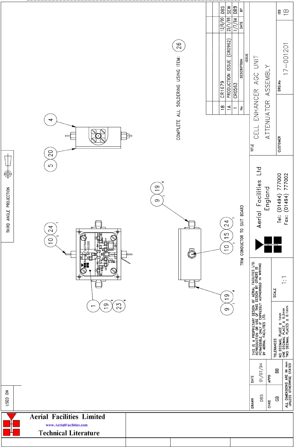
9 Way Channelised UHF Cell Enhancer
Maintenance Handbook
H/book Number:-50-025301HBKM Issue No:-1Date:-04/07/2003 Page:-60 of 69
5.5.2.6 Drg. N. 17-001201, AGC Attenuator Assembly Drawing
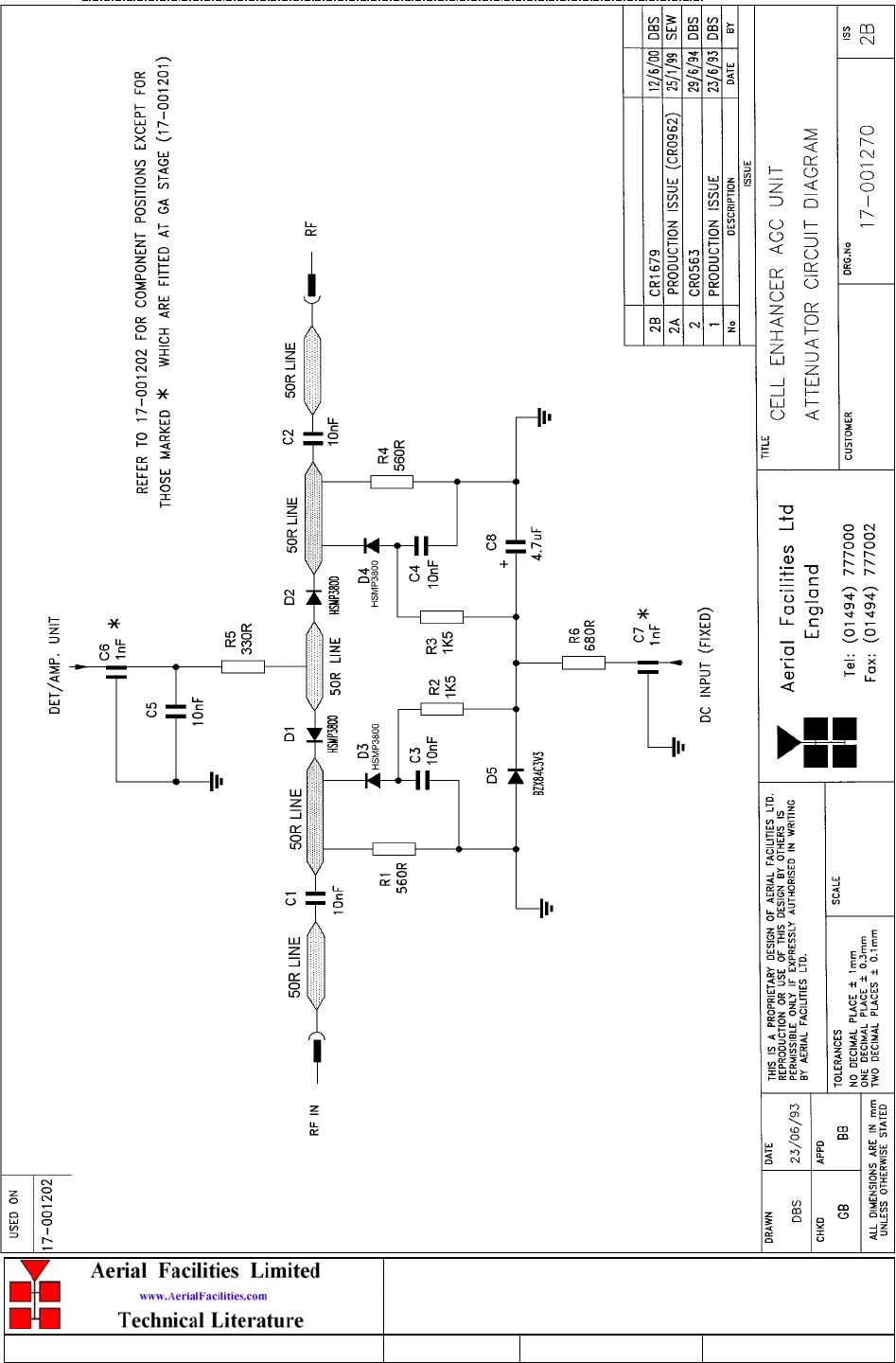
9 Way Channelised UHF Cell Enhancer
Maintenance Handbook
H/book Number:-50-025301HBKM Issue No:-1Date:-04/07/2003 Page:-61 of 69
5.5.2.7 Drg. N. 17-001270, AGC Attenuator Circuit Diagram
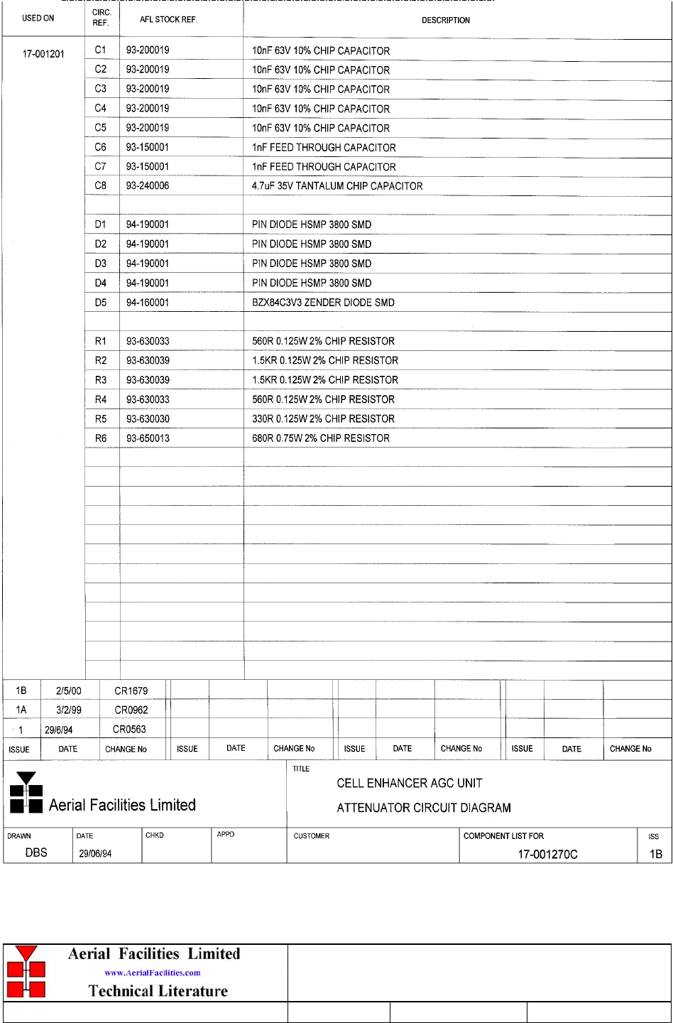
9 Way Channelised UHF Cell Enhancer
Maintenance Handbook
H/book Number:-50-025301HBKM Issue No:-1Date:-04/07/2003 Page:-62 of 69
5.5.2.8 Drg. N. 17-001270C, AGC Attenuator Parts List
All other modules in this shelf are described elsewhere in this document.

9 Way Channelised UHF Cell Enhancer
Maintenance Handbook
H/book Number:-50-025301HBKM Issue No:-1Date:-04/07/2003 Page:-63 of 69
6. INSTALLATION
6.1 Initial Installation Record
When this equipment is initially commissioned, please use the equipment set-up record sheet
in Appendix A. This will help both the installation personnel and AFL should these figures
be needed for future reference or diagnosis.
Installation will be a matter of securing each shelf into its appropriate place in the rack
cabinet, connecting all the cables (RF, Antennas, DC and alarm ) to their correct
ports/connectors and system testing (at the customer’s discretion) to prove the original
specification. Power should not be applied until all connections have been double-checked
and verified.
Refer to the system drawing(s) in section 4. for cabling details.

9 Way Channelised UHF Cell Enhancer
Maintenance Handbook
H/book Number:-50-025301HBKM Issue No:-1Date:-04/07/2003 Page:-64 of 69
7. MAINTENANCE
7.1 General Procedures
7.1.1 Basic Fault Finding
In the event that the performance of the system is suspect, a methodical and logical approach
to the problem will reveal the cause of the difficulty. The System consists of modules fitted
within shelves or trays and all housed within a standard 19” rack type cabinet.
Transmissions from the main base stations are passed though the system (via air interface
antennas) to the mobile radio equipment; this could be a handheld radio or a transceiver in a
vehicle. This path is referred to as the downlink. The return signal path from the mobile
radio equipment to the base station is referred to as the uplink.
The first operation is to check the alarms of each of the active units and determine that the
power supplies to the equipment are connected and active.
This can be achieved remotely (via CEMS, the RS232 Cell Enhancer Management System,
if fitted), or locally with the front panel LED’s. The green LED on the front panels of
shelves containing active components should be illuminated, while the red alarm indicator
should be off.
If an Alarm is on, then that individual shelf must be individually tested against the original
test specification.
The individual amplifier units within the shelf have a green LED showing through a hole in
their piggy-back alarm board, which is illuminated if the unit is working correctly.
If an amplifier is suspect, check the DC power supply to the unit. If no other fault is
apparent use a spectrum analyser to measure the incoming signal level at the input and then
after reconnecting the amplifier input, measure the output level. Consult with the system
diagram to determine the expected gain and compare result.
In the event that there are no alarms on and all units appear to be functioning it will be
necessary to test the system in a systematic manner to confirm correct operation.

9 Way Channelised UHF Cell Enhancer
Maintenance Handbook
H/book Number:-50-025301HBKM Issue No:-1Date:-04/07/2003 Page:-65 of 69
7.1.2 Downlink
Confirm that there is a signal at the expected frequency and strength from the base station. If
this is not present then the fault may lay outside the system. To confirm this, inject a
downlink frequency signal from a known source at the master site BTS input and check for
output at the remote site feeder output.
If a signal is not received at the output it will be necessary to follow the downlink path
through the system to find a point at which the signal is lost. The expected downlink output
for the given input can be found in the end-to-end test specification.
7.1.3 Uplink
Testing the uplink involves a similar procedure to the downlink except that the frequencies
used are those transmitted by the mobile equipment.
7.1.4 Fault repair
Once a faulty component has been identified, a decision must be made on the appropriate
course to carry out a repair. A competent engineer can quickly remedy typical faults such as
faulty connections or cables. The exceptions to this are cable assemblies connecting
bandpass filter assemblies that are manufactured to critical lengths to maintain a 50-ohm
system. Care should be taken when replacing cables or connectors to ensure that items are of
the correct specification. The repair of component modules such as amplifiers and bandpass
filters will not usually be possible in the field, as they frequently require specialist
knowledge and test equipment to ensure correct operation. It is recommended that items of
this type are replaced with a spare unit and the faulty unit returned to AFL for repair.

9 Way Channelised UHF Cell Enhancer
Maintenance Handbook
H/book Number:-50-025301HBKM Issue No:-1Date:-04/07/2003 Page:-66 of 69
7.1.5 Checking service
Following the repair of any part of the system it is recommended that a full end-to-end test is
carried out in accordance with the test specification and that the coverage is checked by
survey.
It is important to bear in mind that the system includes a radiating cable network and base
stations that may be faulty or may have been damaged.
7.1.6 Service Support
Advice and assistance with maintaining and servicing this system are available by contacting
Aerial Facilities Ltd.
7.2 Tools & Test Equipment
The minimum tools and test equipment needed to successfully service this AFL product are
as follows:-
Spectrum analyser: 100kHz to 2GHz (Dynamic range = 90dB).
Signal Generator: 30MHz to 2GHz (-120dBm to 0dBm o/p level).
Attenuator: 20dB, 10W, DC-2GHz, (N male – N female).
Test Antenna: Yagi or dipole for operating frequency.
Digital multi-meter: Universal Volt-Ohm-Amp meter.
Test cable x 2: N male – N male, 2M long RG214.
Test cable x 2: SMA male – N male, 1m long RG223.
Hand tools: Philips #1&2 tip screwdriver.
3mm flat bladed screwdriver.
SMA spanner and torque setter.
9 Way Channelised UHF Cell Enhancer
Maintenance Handbook
H/book Number:-50-025301HBKM Issue No:-1Date:-04/07/2003 Page:-67 of 69
7.3 Care of Modules
7.3.1 General Comments
Many of the active modules contain semiconductor devices utilising MOS technology, which
can be damaged by electrostatic discharge. Correct handling of such modules is mandatory to
ensure their long-term reliability.
To prevent damage to a module, it must be withdrawn/inserted with care. The module may
have connectors on its underside, which might not be visible to the service operative.
7.3.2 Module Removal (LNA’s, general procedure):
The following general rules should be followed to remove a module:
1 Remove power to the unit
2 Remove all visible connectors (RF, DC & alarm)
3 Release module retaining screws.
4 Slowly but firmly, pull the module straight out of its position. Take care not to twist/turn
the module during withdrawal. (When the module is loose, care may be needed, as there
may be concealed connections underneath).
7.3.3 Module Replacement (general):
1 Carefully align the module into its location then slowly push the module directly straight
into its position, taking care not to twist/turn it during insertion.
2 Reconnect all connectors, RF, alarm, power etc.,(concealed connectors may have to be
connected first).
3 Replace retaining screws (if any).
4 Double-check all connections before applying power.
7.3.4 Power Amplifiers
1) Remove power to the unit. (Switch off @ mains/battery, or remove DC in connector)
2) Remove alarm wires from alarm screw terminal block or disconnect multi-way alarm
connector.
3) Carefully disconnect the RF input and output coaxial connectors (usually SMA)
If alarm board removal is not required, go to step 5.
4) There is (usually) a plate attached to the alarm board which fixes it to the amplifier,
remove its retaining screws and the alarm board can be withdrawn from the amplifier in
its entirety. On certain types of amplifier the alarm board is not mounted on a dedicated
mounting plate; in this case it will have to firstly be removed by unscrewing it from the
mounting pillars, in most cases, the pillars will not have not have to be removed before
lifting the amplifier.
9 Way Channelised UHF Cell Enhancer
Maintenance Handbook
H/book Number:-50-025301HBKM Issue No:-1Date:-04/07/2003 Page:-68 of 69
5) If the amplifier to be removed has a heatsink attached, there may be several different
ways it can have been assembled. The most commonly used method, is screws through
the front of the heatsink to threaded screw holes (or nuts and bolts), into the amplifier
within the main case. If the heatsink is mounted on the rear of the main case (e.g., against
a wall in the case of wall mounted enclosures), then the fixing method for the heatsink
will be from within the case, (otherwise the enclosure would have to be removed from the
wall in order to remove the heatsink).
When the heatsink has been removed, the amplifier may be unscrewed from the main
casing by its four corner fixings and gently withdrawn.
Fitting a new power amplifier module will be the exact reverse of the above.
Note: Do not forget to apply fresh heatsink compound to the heatsink/main case
joint and also between the amplifier and the main case.
7.3.5 Low Power Amplifier Replacement
1 Disconnect the mains power supply and disconnect the 24V dc supply connector for the
LPA.
2 Disconnect the RF input and output cables from the LPA.
3 Disconnect the alarm connector.
4 Remove the alarm monitoring wires from (D type connector) pins 9 and 10.
5 Remove the LPA module by removing the four retaining screws, replace with a new
LPA module and secure it with the screws.
6 Connect the RF cables to the LPA input and output connectors. Reconnect the wires to
the alarm board connector pins 9 and 10.
7 Reconnect the DC supply connector and turn the mains switch on.
Note: Tighten SMA connectors using only a dedicated SMA torque spanner. If
SMA connectors are over-tightened, irreparable damage will occur. . Do not use
adjustable pliers to loosen/tighten SMA connectors.
Also take care not to drop or knock the module as this can damage (or misalign in the
case of tuned passive modules) sensitive internal components. Always store the modules
in an environmentally friendly location
7.3.6 Module Transportation:
To maintain the operation, performance and reliability of any module it must be stored and
transported correctly. Any module not installed in a whole system must be kept in an anti-
static bag or container. These bags or containers are normally identified by being pink or
black, and are often marked with an ESD label. Any module sent back to AFL for
investigation/repair must be so protected. Please contact AFL’s quality department before
returning a module.
9 Way Channelised UHF Cell Enhancer
Maintenance Handbook
H/book Number:-50-025301HBKM Issue No:-1Date:-04/07/2003 Page:-69 of 69
APPENDIX A INITIAL EQUIPMENT SET-UP CALCULATIONS
GENERAL INFORMATION
Site Name: Client Name:
Date: AFL Equip. Model N.
ANTENNA SYSTEMS
Model Gain Azimuth Comments
A - Service Antenna
B – Donor Antenna
Type Loss Length Comments
C – Service Feeder
D – Donor Feeder
INITIAL PARAMETERS
E – CE Output Power dBm
F – Antenna Isolation dB
G – Input signal level from donor BTS dBm
Operating Voltage V
DOWNLINK CALCULATIONS
Parameter Comments Value
Input signal level (G)dBm
CE max. o/p power (E)dBm
Gain setting E - G dB
Isolation required (Gain + 10dB) dB
Service antenna gain (A)dB
Service antenna feeder loss (C)dB
Effective radiated power (ERP) E+A-C dBm
Attenuator setting CE gain-gain setting dB
If the input signal level in the uplink path is known and steady, use the following calculation
table to determine the gain setting. If the CE features Automatic Gain Control the attenuator
should be set to zero and if not, then the attenuation setting for both uplink and downlink
should be similar.
UPLINK CALCULATIONS
Parameter Comments Value
Input signal level dBm
CE max. o/p power (E)dBm
Gain setting dB
Required isolation dB
Donor antenna gain (B)dB
Donor antenna feeder loss (D)dB
Effective radiated power (ERP)E+B-D dBm
Attenuator setting (CE gain-gain setting) dB