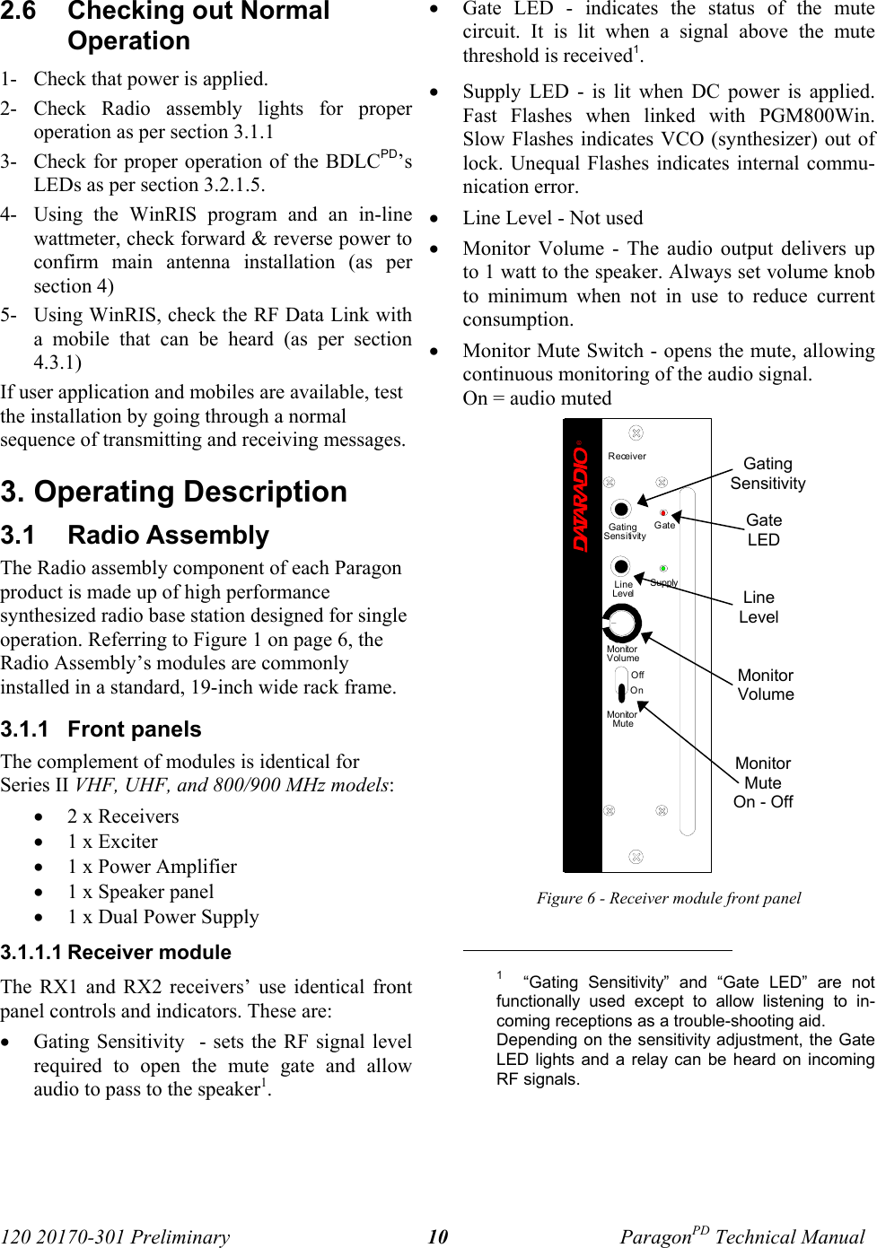
CalAmp Wireless Networks BDD4T881-3 Paragon/PD User Manual TITLE
CALAMP WIRELESS NETWORKS INC. Paragon/PD TITLE
UserManual.wiki
>
CalAmp Wireless Networks
>
BDD4T881-3 User Manual
>
updated user manual preliminary version 3 01
Contents
1.
updated user manual preliminary version 3 01
2.
preliminary version 100a
updated user manual preliminary version 3 01
Navigation menu
Upload a User Manual
Namespaces
Wiki Guide
HTML
PDF
Info
Views
User Manual
Discussion / Help
Navigation


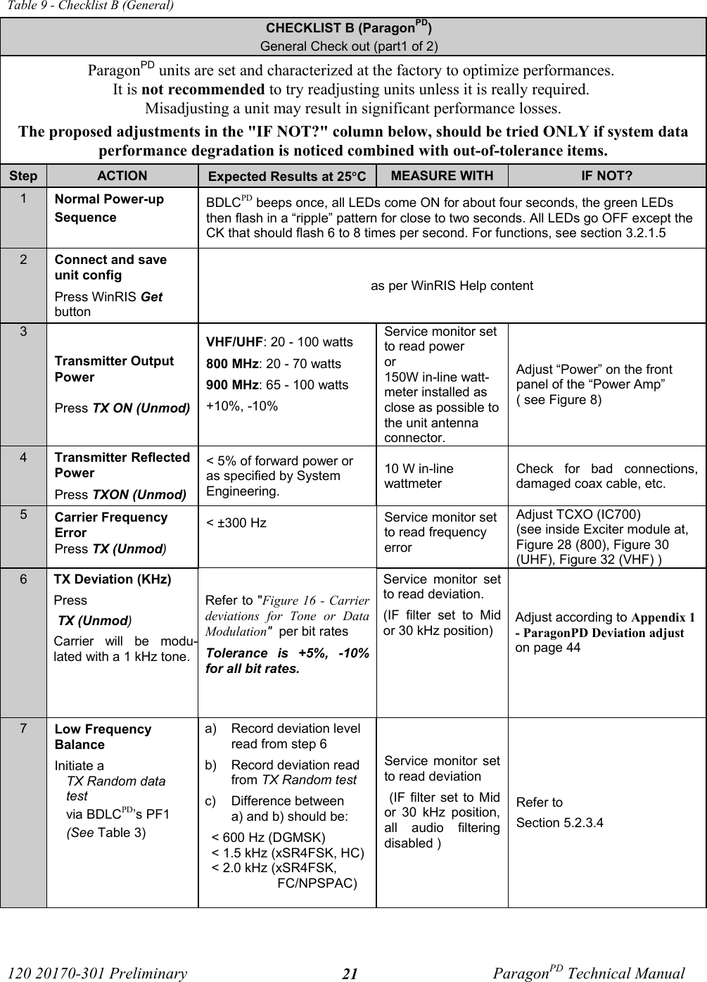
![120 20170-301 Preliminary ParagonPD Technical Manual44 Appendix 1 - ParagonPD Deviation adjust1. Using the WinRIS, press TX ON (Modulated) and record deviation level as read on the IFR.2. Using Windows Notepad, Edit the .bp2 file named with the corresponding BDLCPD serialnumber (e.g. abcd.bp2). “Save as” to another file name and keep it in case something goeswrong while changing a parameter.3. Locate the line labeled “Dev0 Par85=” and record the value beside the “=” sign. This is thecorresponding parameter value to the deviation read in step 1.4. Apply the following formula to determine the new parameter value to be set:(New Par85 value) = [(initial Par85 value) X (target deviation) / (deviation read)] + 25. Change the value in the file, “Save as” using the BDLCPD serial number file name.6. Run the WinRIS again and do a “Put From”. From the opened window, select the file thatyou just made the change to and then press “OK”7. Again, check deviation level while pressing TX ON (Modulated). • If the level is now correct, press StationReset to make the change permanent.• Otherwise do step 5 again, changing the value entered in the file by 1 or 2 digit(s) upor down, fine-tuning directly the Par85 (DSP deviation) parameter. Do steps 6 and 7again to confirm acceptance. This last step may have to be repeated once or twice while varying the entered valueup or down. If unable to obtain the correct level after editing up and/or down by nomore than 2, contact System Engineering.](https://usermanual.wiki/CalAmp-Wireless-Networks/BDD4T881-3.updated-user-manual-preliminary-version-3-01/User-Guide-264568-Page-49.png)