COMPUTIME CT-EM2531 Zigbee Module User Manual ZigBee Ready RF Transceiver Modules
Computime Limited Zigbee Module ZigBee Ready RF Transceiver Modules
UserManual.wiki
>
COMPUTIME
>
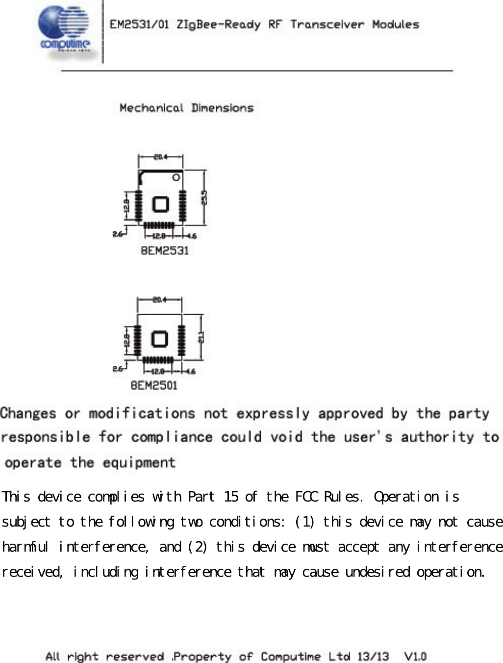
CT EM2531 User Manual
User Manual
Navigation menu
Upload a User Manual
Namespaces
Wiki Guide
HTML
PDF
Info
Views
User Manual
Discussion / Help
Navigation