COMPUTIME CTL3579A ZigBee Module User Manual
Computime Limited ZigBee Module
UserManual.wiki
>
COMPUTIME
>
CTL3579A User Manual
Users Manual
Navigation menu
Upload a User Manual
Namespaces
Wiki Guide
HTML
PDF
Info
Views
User Manual
Discussion / Help
Navigation
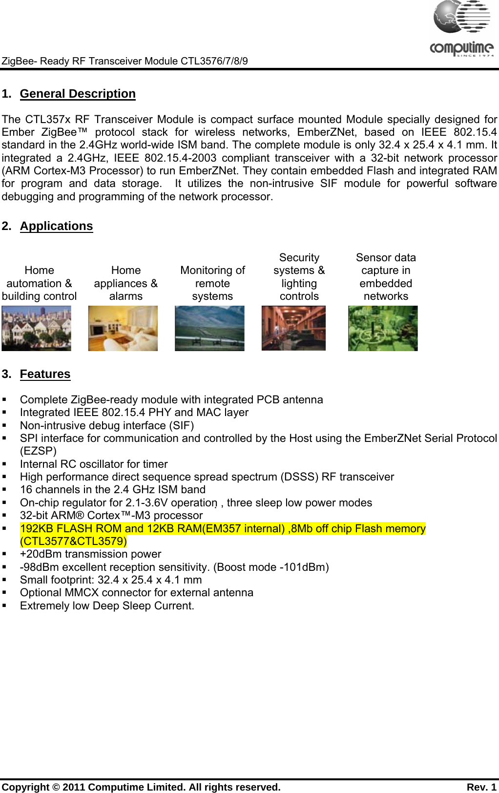
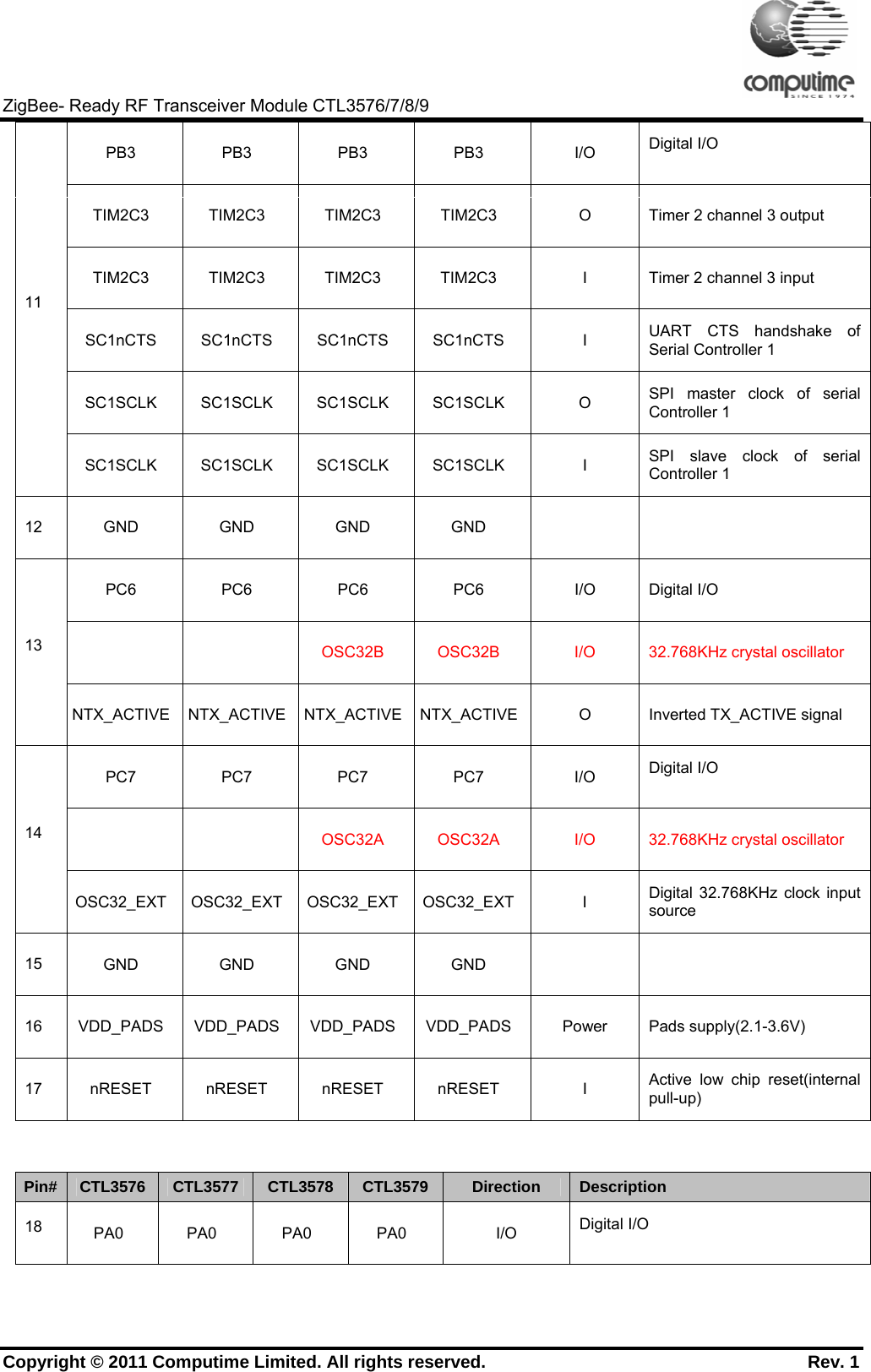
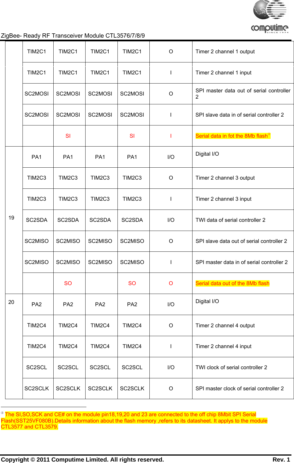
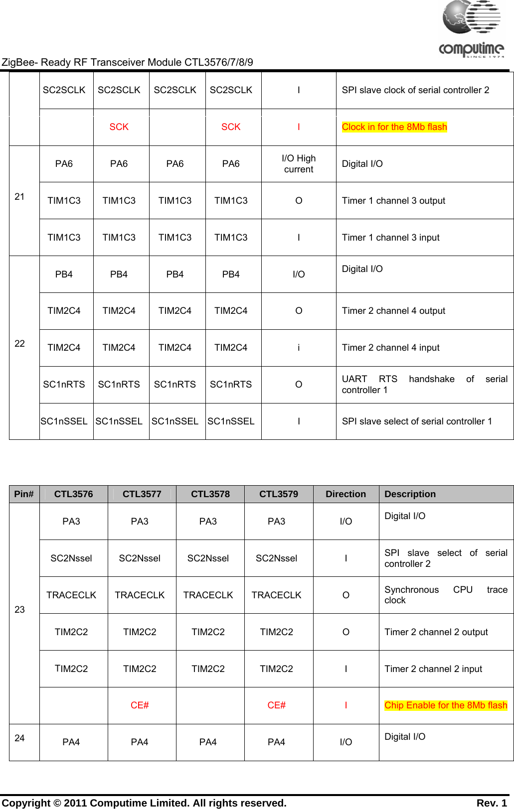
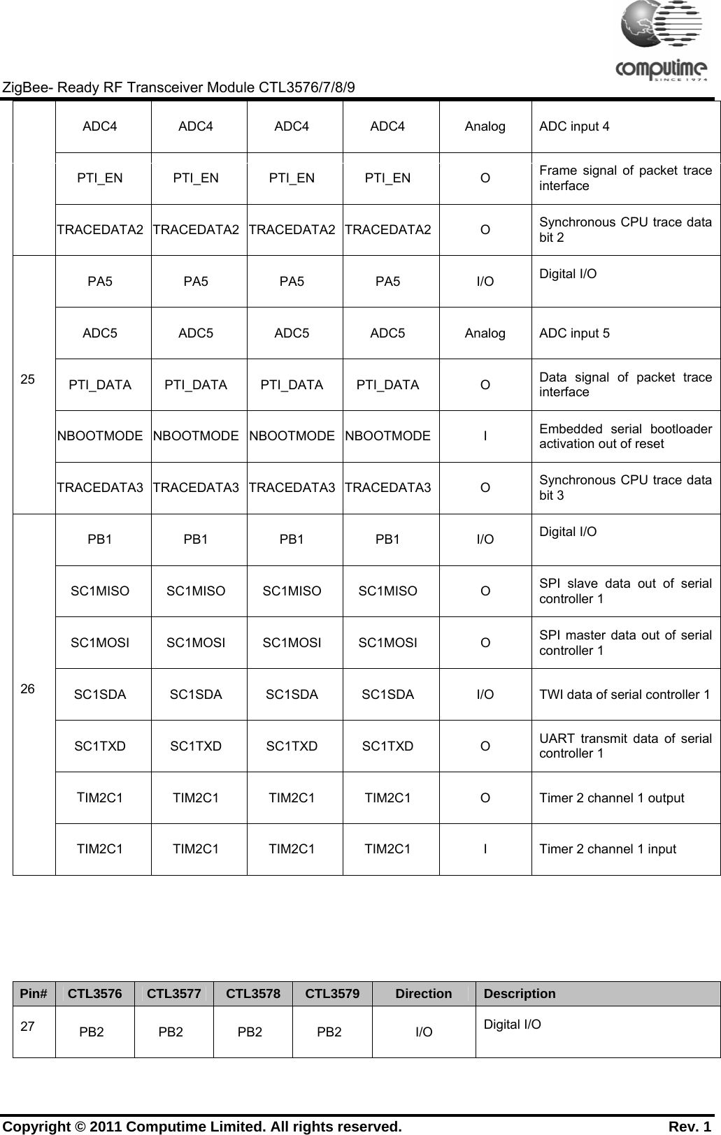
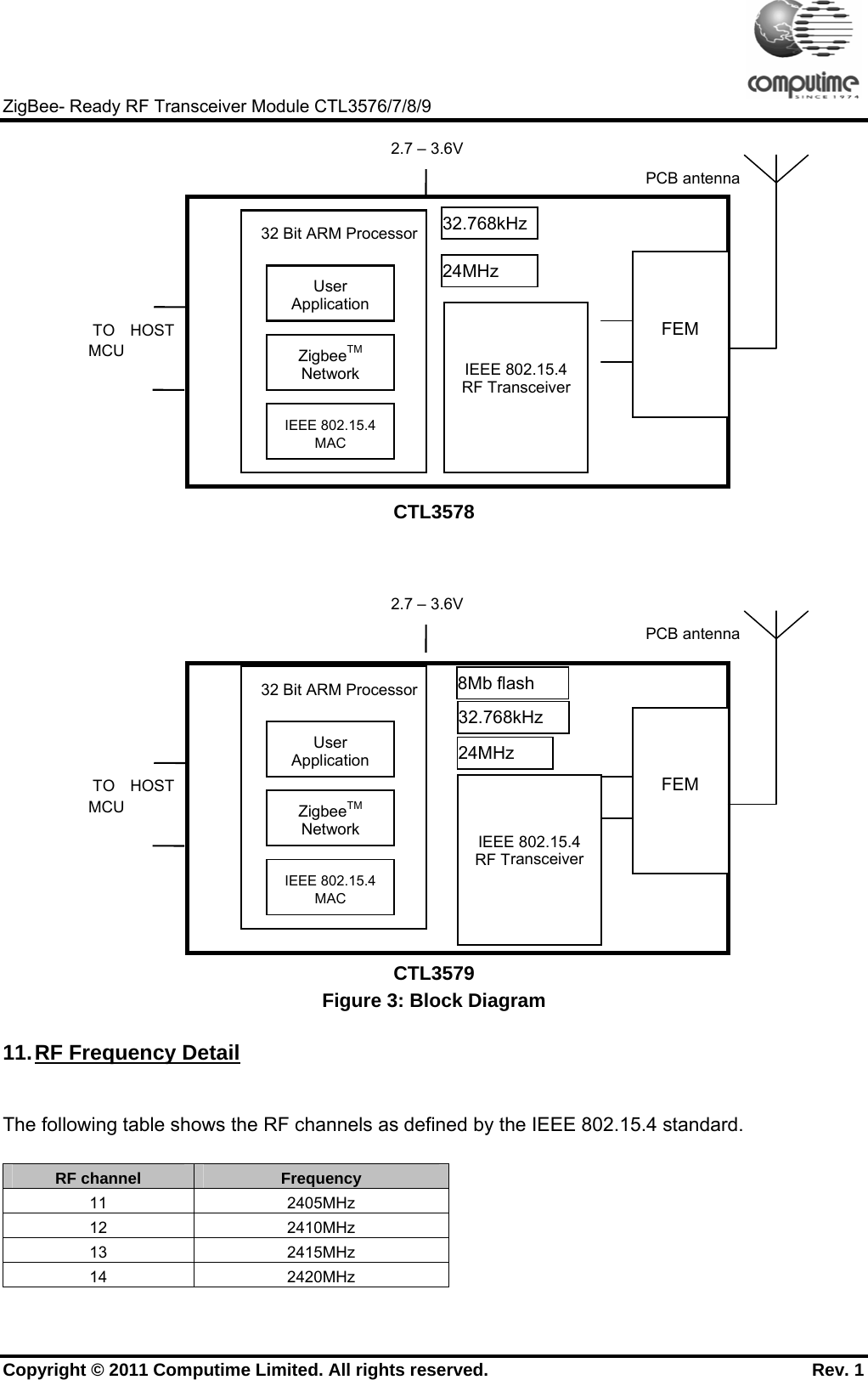
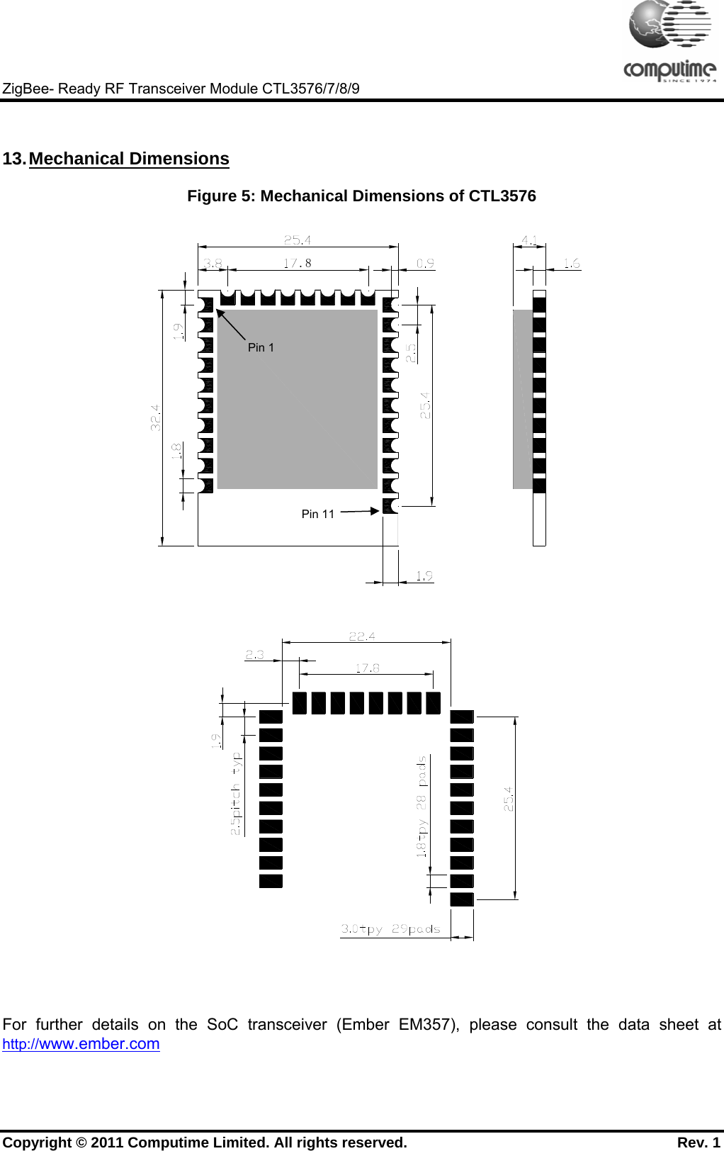
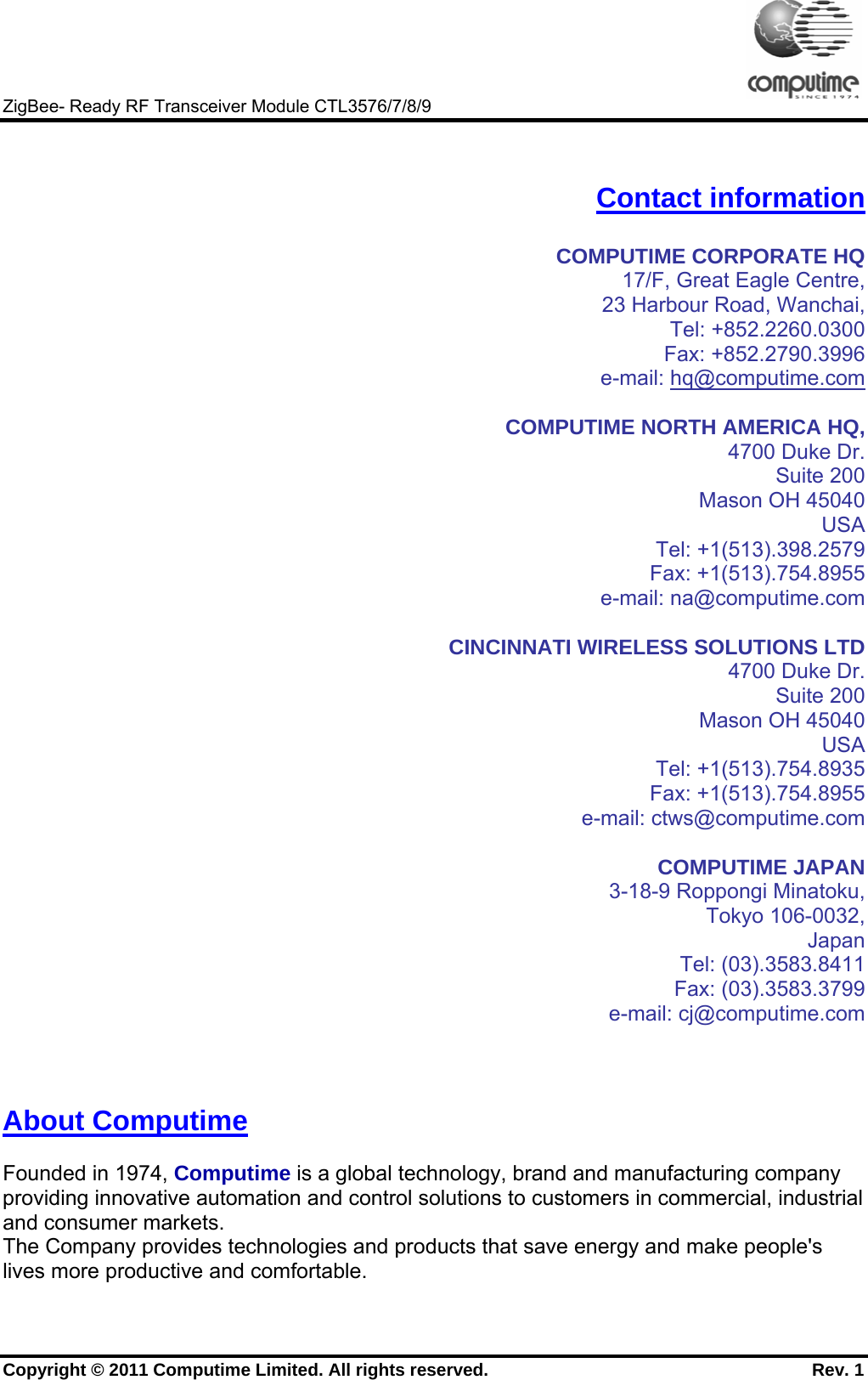
![ZigBee- Ready RF Transceiver Module CTL3576/7/8/9 Copyright © 2011 Computime Limited. All rights reserved. Rev. 1 4. Absolute Maximum Ratings Parameter Test Conditions Min. Max. UnitRegulator input voltage (VDD_PADS) -0.3 +3.6 V RF Input Power (for max level for correct packet reception) RX signal into a lossless balun +15 dBm Voltage on any GPIO (PA[7:0], PB[7:0], PC[7:0]), SWCLK, nRESET, VREG_OUT -0.3 VDD_PADS+0.3 V Voltage on any GPIO pin (PA4, PA5, PB5, PB6, PB7, PC1), when used as an input to the general purpose ADC with the low voltage range selected -0.3 2.0 V Voltage on OSCA, OSCB, NC -0.3 VDD_PADSA+0.3 V Storage temperature -40 +140 °C 5. Recommended Operating Conditions Parameter Test Conditions Min. Typ. Max. UnitRegulator input voltage (VDD_PADS) 2.7 3.6 V Operating temperature range 0 +70①°C 6. Electrical Specifications T=25℃, VCC = 3.0V, Fo =2450MHZ, if nothing else stated. Parameter Condition / Note Min Typ. Max UnitOperating frequency Programmable in 5MHz steps, 5 MHz steps for IEEE 802.15.4 compliance 2.4 2.5 GHzNumber of channels For IEEE 802.15.4 compliance 16 Channel spacing For IEEE 802.15.4 compliance 5 MHzInput/output impedance 50 OhmFrequency stability +/-40 ppmTransmit power Programmable from firmware -15 +20 dBm ① Operationg temperature range from -40 to 85°C for module CTL3576 and CTL3578.](https://usermanual.wiki/COMPUTIME/CTL3579A/User-Guide-1692807-Page-5.png)
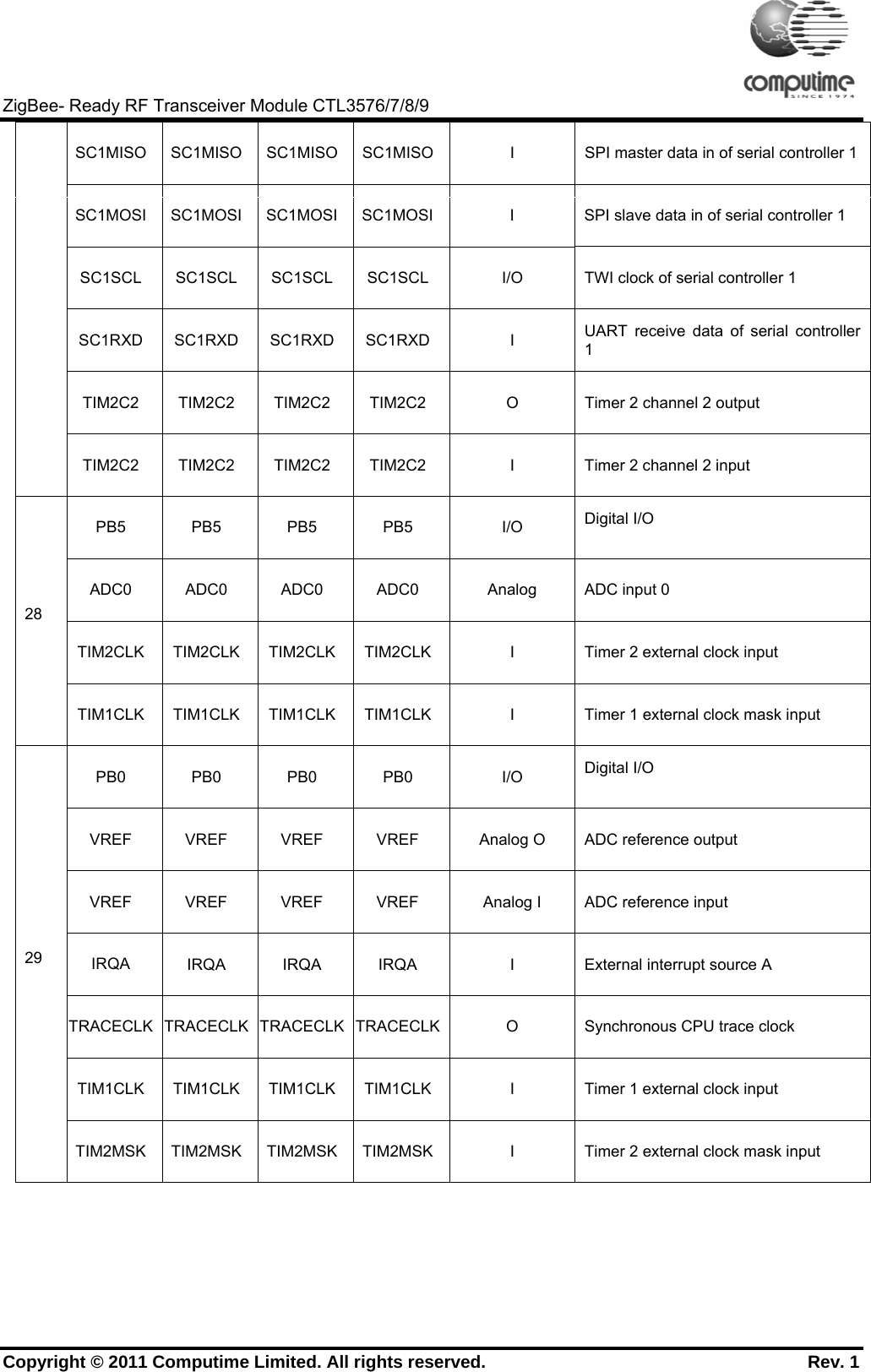
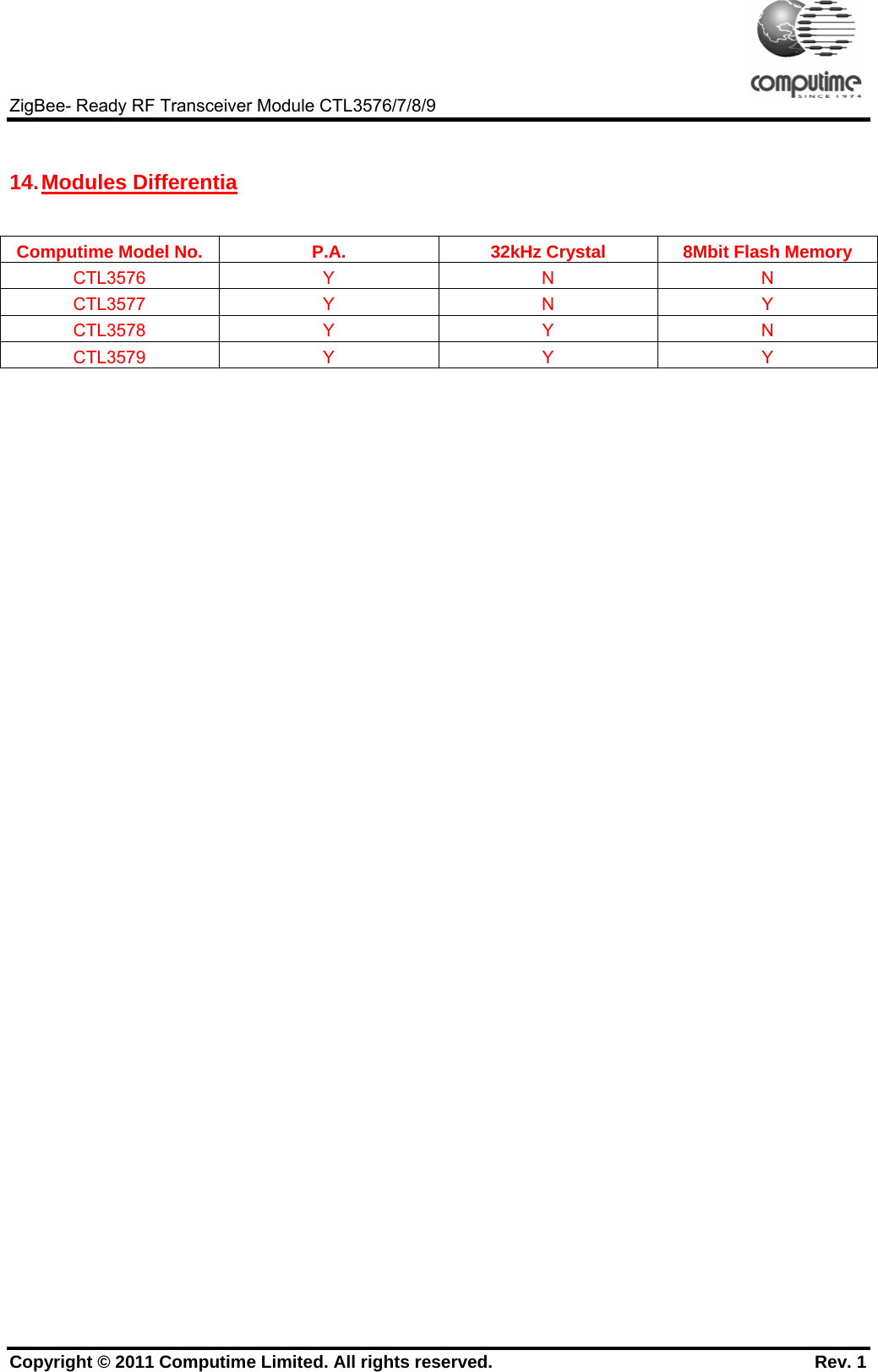
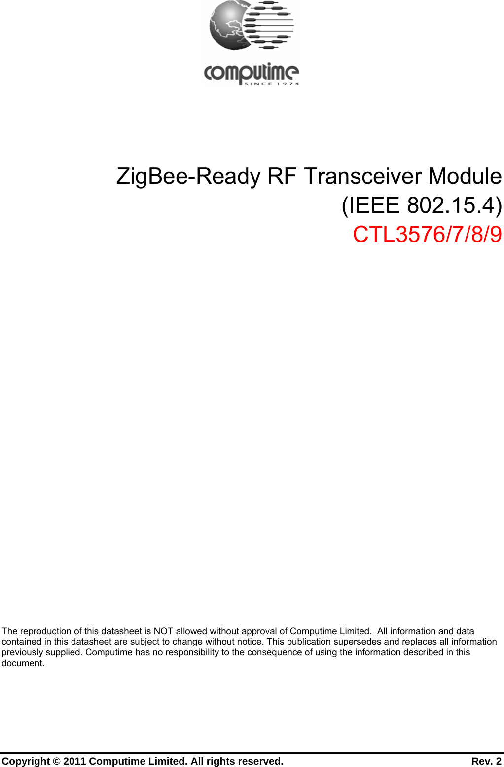
![ZigBee- Ready RF Transceiver Module CTL3576/7/8/9 Copyright © 2011 Computime Limited. All rights reserved. Rev. 1 9. Pin Description Pin# CTL3576 CTL3577 CTL3578 CTL3579 Direction Description JTCK JTCK JTCK JTCK I JTAG clock input from debugger 1 SWCLK SWCLK SWCLK SWCLK I/O Serial Wire Clock input/output with debugger PC2 PC2 PC2 PC2 I/O Digital I/O Enable with GPIO_DBGCFG[5] JTDO JTDO JTDO JTDO O JTAG data out to debugger 2 SWO SWO SWO SWO O Serial Wire Output asynchronous trace output to PC3 PC3 PC3 PC3 I/O Digital I/O Enable with GPIO_DBGCFG[5] 3 JTDI JTDI JTDI JTDI I JTAG data in from debugger PC4 PC4 PC4 PC4 I/O Digital I/O Either Enable with GPIO_DBGCFG[5] JTMS JTMS JTMS JTMS I JTAG mode select from debugger 4 SWDIO SWDIO SWDIO SWDIO I/O Serial Wire bidirectional data to/from debugger PC0 PC0 PC0 PC0 I/O High current Digital I/O Either Enable with GPIO_DBGCFG[5] JRST JRST JRST JRST I JTAG reset input from debugger IRQD IRQD IRQD IRQD I Default external interrupt source D 5 TRACEDATA1 TRACEDATA1 TRACEDATA1 TRACEDATA1 O Synchronous CPU trace data bit 1 PB7 PB7 PB7 PB7 I/OHigh current Digital I/O 6 ADC2 ADC2 ADC2 ADC2 Analog ADC input 2](https://usermanual.wiki/COMPUTIME/CTL3579A/User-Guide-1692807-Page-8.png)
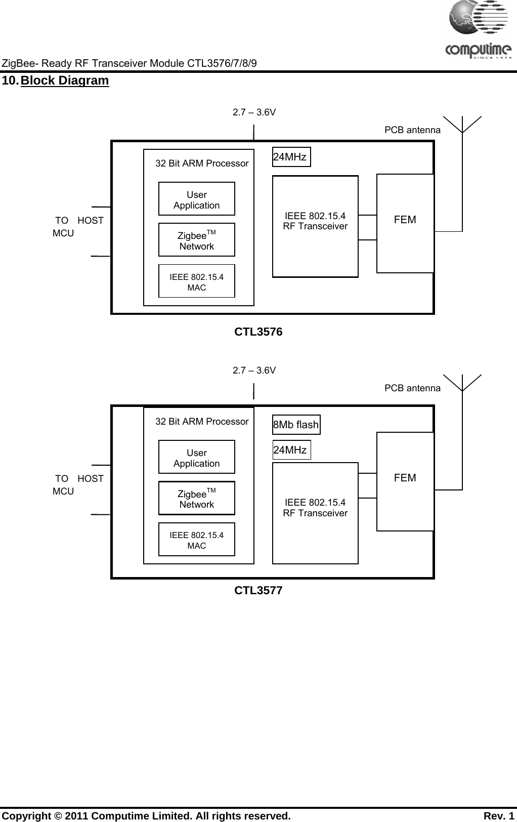
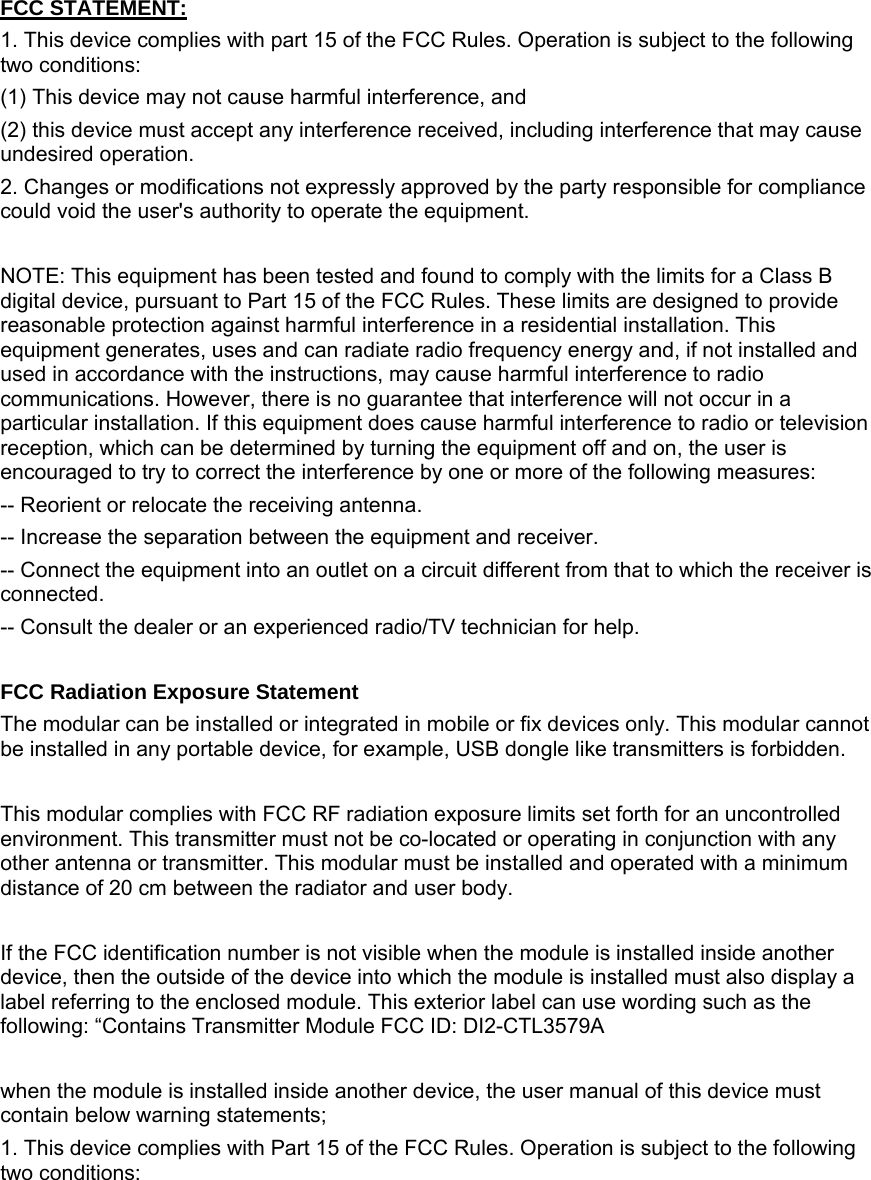
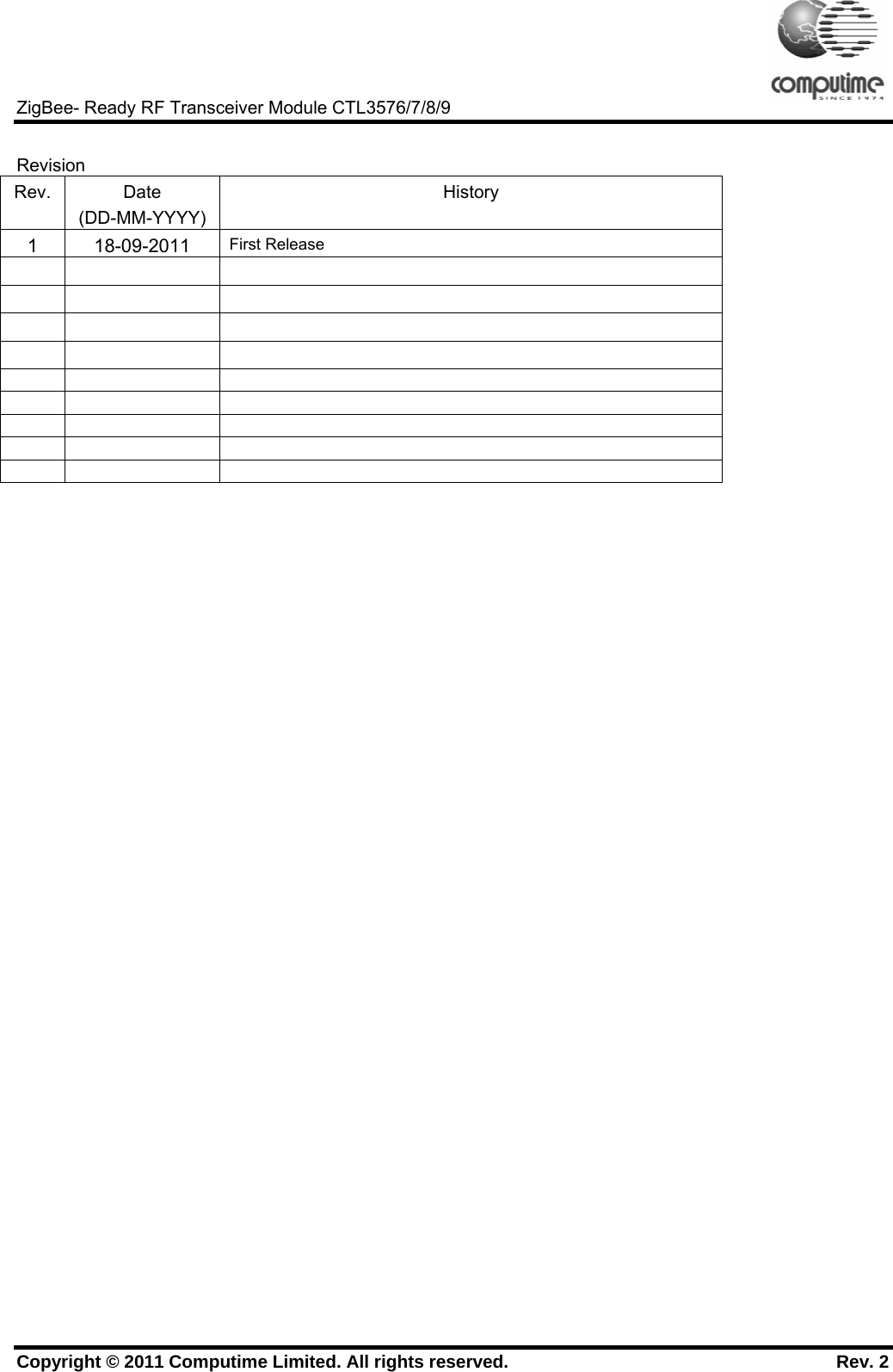
![ZigBee- Ready RF Transceiver Module CTL3576/7/8/9 Copyright © 2011 Computime Limited. All rights reserved. Rev. 1 IRQC IRQC IRQC IRQC I Default external interrupt source C TIM1C2 TIM1C2 TIM1C2 TIM1C2 O Timer 1 channel 2 output TIM1C2 TIM1C2 TIM1C2 TIM1C2 1 Timer 1 channel 2 input PB6 PB6 PB6 PB6 I/O High current Digital I/O ADC1 ADC1 ADC1 ADC1 Analog ADC input 1 IRQB IRQB IRQB IRQB I External interrupt source B TIM1C1 TIM1C1 TIM1C1 TIM1C1 O Timer 1 channel 1 output 7 TIM1C1 TIM1C1 TIM1C1 TIM1C1 I Timer 1 channel 1 input Pin# CTL3576 CTL3577 CTL3578 CTL3579 Direction Description PA7 PA7 PA7 PA7 I/O High current Digital I/O Disable REG_EN with GPIO_DBGCFG [4] TIM1C4 TIM1C4 TIM1C4 TIM1C4 O Timer 1 channel 4 output TIM1C4 TIM1C4 TIM1C4 TIM1C4 I Timer 1 channel 4 input 8 REG_EN REG_EN REG_EN REG_EN O External regulator open drain output PC1 PC1 PC1 PC1 I/O Digital I/O ADC3 ADC3 ADC3 ADC3 Analog ADC input 3 SWO SWO SWO SWO O Serial Wire Output asynchronous trace output to 9 TRACEDATA0 TRACEDATA0 TRACEDATA0 TRACEDATA0 O Synchronous CPU trace data bit 0 10 GND GND GND GND](https://usermanual.wiki/COMPUTIME/CTL3579A/User-Guide-1692807-Page-9.png)