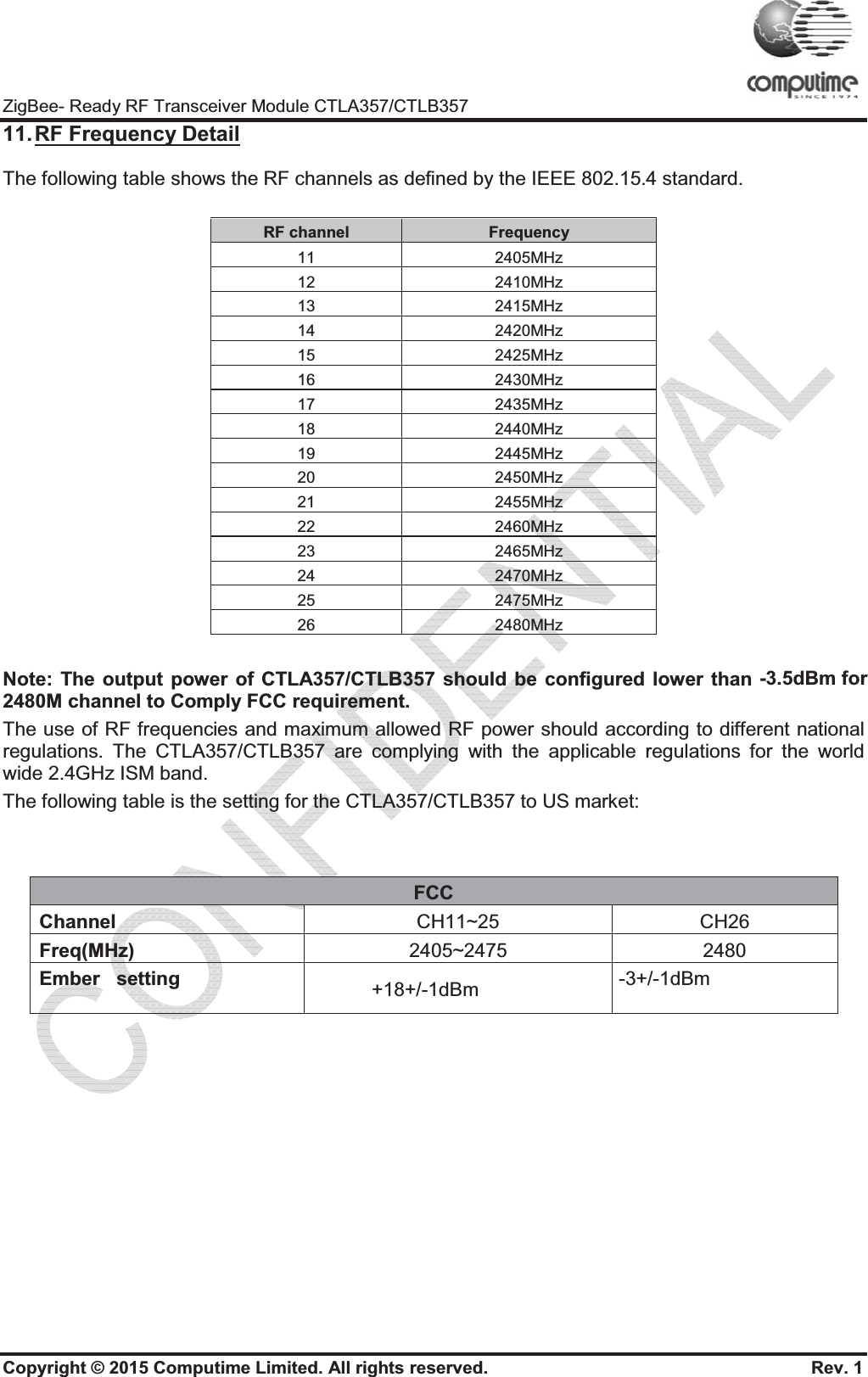
COMPUTIME CTLB357 ZigBee-Ready RF Transceiver User Manual CTLA357 CTLB357 General Product specifications R1
Computime Ltd. ZigBee-Ready RF Transceiver CTLA357 CTLB357 General Product specifications R1
UserManual.wiki
>
COMPUTIME
>
CTLB357 User Manual
User manual
Navigation menu
Upload a User Manual
Namespaces
Wiki Guide
HTML
PDF
Info
Views
User Manual
Discussion / Help
Navigation
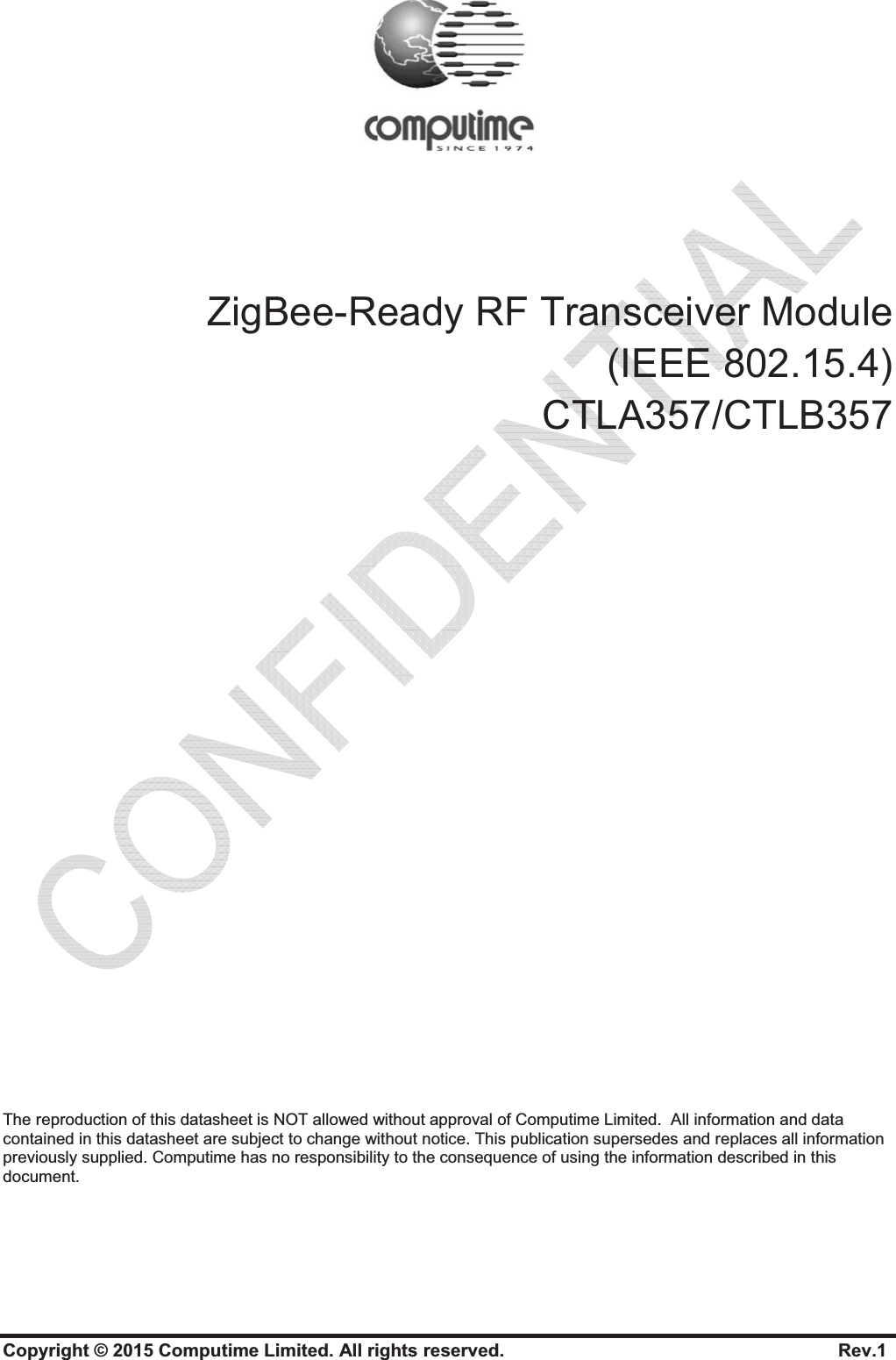
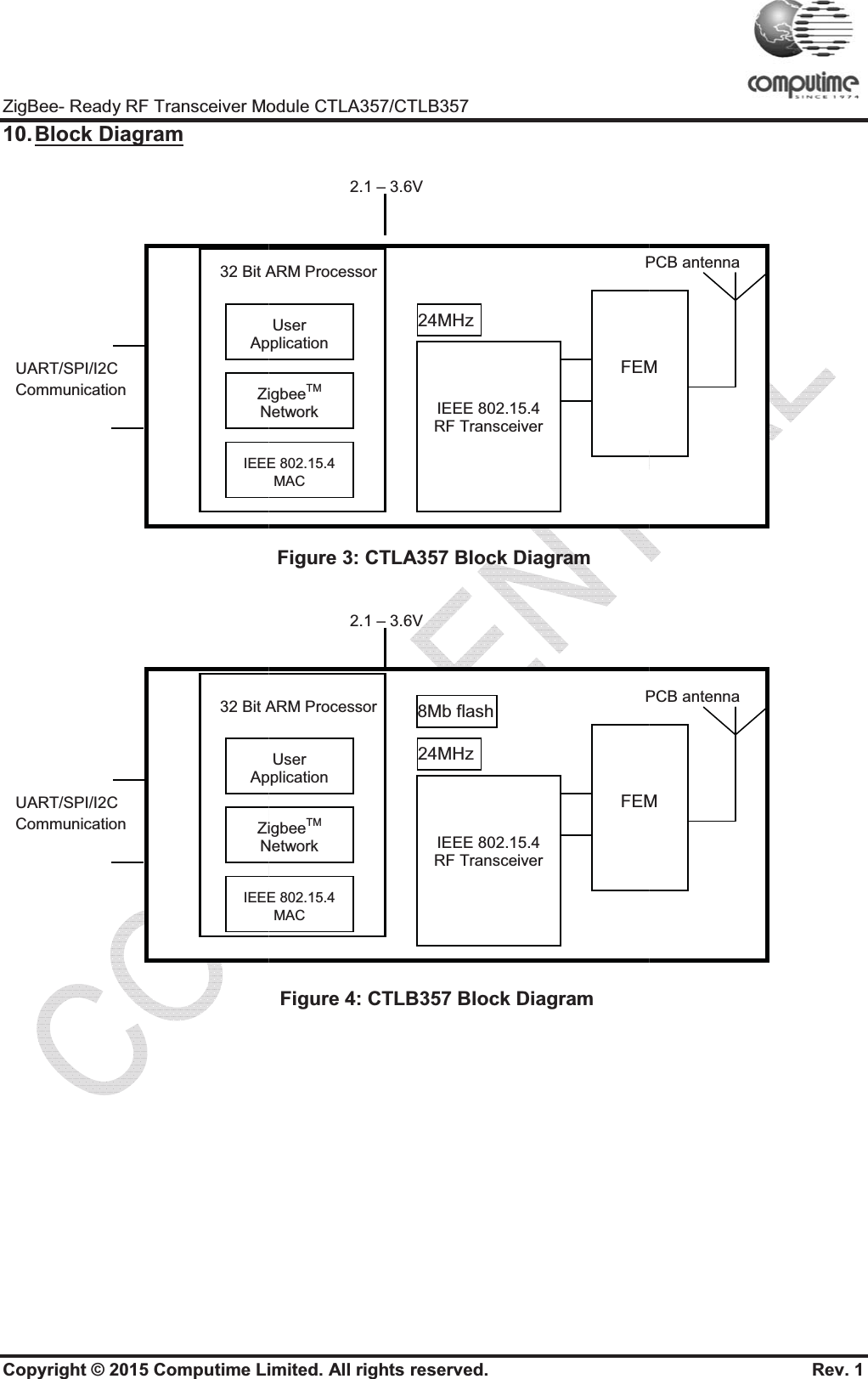
![ZigBee- Ready RF Transceiver MoCopyright © 2015 Computime Li4. Absolute Maximum RatParameter Regulator input voltage (VDD_PADS) Voltage on any GPIO (PA[7:0], PB[7:0], PC[7:0]), SWCLK, nRESET,VREG_OUT Voltage on any GPIO pin (PA4, PA5PB6, PB7, PC1), when used as an inputgeneral purpose ADC with the low vrange selected Voltage on OSCA, OSCB, NC Storage temperature 5. Recommended OperatinParameter Regulator input voltage (VDD_PADS) Operating temperature range Moisture Sensitivity Level(MSL) 6. Electrical SpecificationsT=25ć, VCC = 3.0V, Fo =2450MHz, iParameter RF Operating frequency Number of channels Channel spacing Frequency stability Transmit power Sensitivity Adjacent channel rejection +/-5 MHz Adjacent channel rejection +/-10 MHz odule CTLA357/CTLB357 imited. All rights reserved. tingsTest Conditions Min-0.3-0.3, PB5, t to the voltage -0.3-0.3-40ng Conditions Test Conditions Min.2.1-40sif nothing else stated.Condition / Note MinProgrammable in 5MHz steps, 5 MHz steps for IEEE 802.15.4 compliance 2.4For IEEE 802.15.4 compliance For IEEE 802.15.4 compliance Programmable from firmware PER = 1% PER, 20byte packet defined by IEEE 802.15.4 Boost mode IEEE 802.15.4 compliance at -82 dBm IEEE 802.15.4 compliance at -82 dBm Rev. 1 n.Max. Unit+3.6 V VDD_PADS+0.3 V2.0 V VDD_PADSA+0.3 V+85 °C .Typ. Max. Unit 3.6 V +85 °C MSL3 Typ. Max Unit 2.5 GHz16 5 MHz +/-40 ppm +20 dBm-100 dBm 35/35 dB 40/40 dB +18+/-12.4052.480](https://usermanual.wiki/COMPUTIME/CTLB357/User-Guide-2778044-Page-5.png)
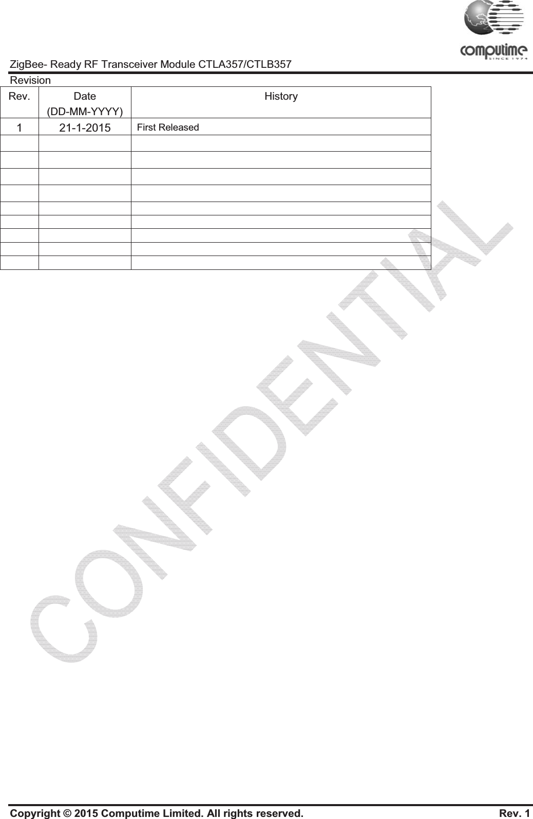
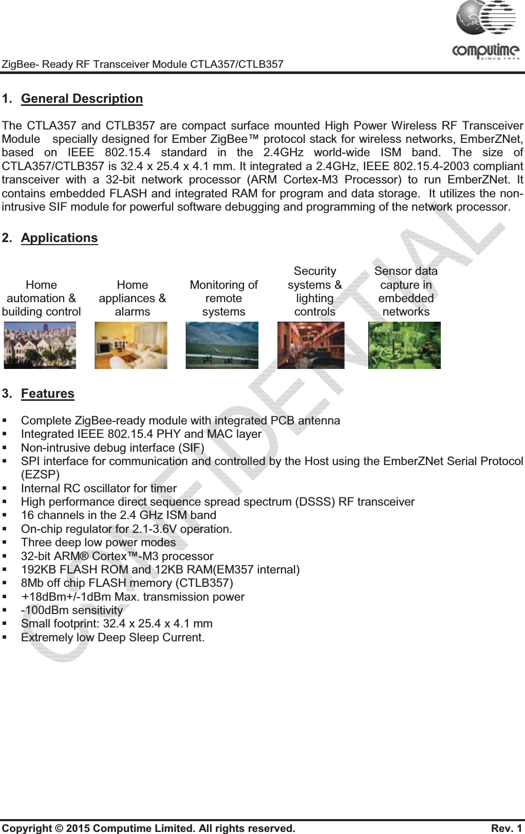
![ZigBee- Ready RF Transceiver MoCopyright © 2015 Computime LiParameter Supply voltage Current consumption, RX mode Current consumption, TX mode CTLA357, CTLBDeep sleep current CTLA357 CTLB357 Flash Memory CTLA357, CTLBCTLB357 RAM MCU clock frequency MCU Low Speed Clock 7. Typical application blocFiDebug and programminginterface HOST MCU NREPTI_PTI-DASIF_CSIF-MSIF-MNSIF_LSDBodule CTLA357/CTLB357 imited. All rights reserved. Condition / Note Min 2.1Max RX sensitivity (normal mode) Max RX sensitivity (boost mode) B357B357 FLASH memory in EM357 Off chip Serial FLASH Internal RAM in EM357 ckgure 1: Example of application circuitCTLA/B357 RF Module VDD_PADS=2.1- 3.6VLINK_ACTIVITYSTENATACLKMISOMOSILOADBG Rev. 1 Typ. Max Unit 3.6 V 28 mA 30 mA 150 mA 2.8 uA 8 12 uA 192 KB 8 Mb 12 KB 24 MHz32.768 KHz VN+]&/ S)](https://usermanual.wiki/COMPUTIME/CTLB357/User-Guide-2778044-Page-6.png)
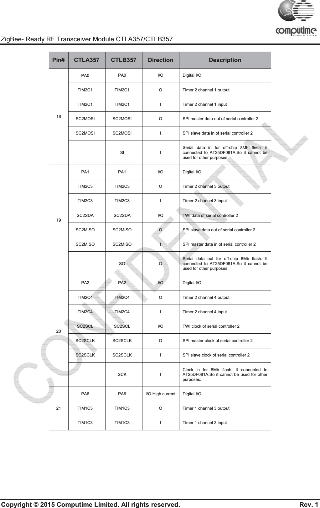
![ZigBee- Ready RF Transceiver MoCopyright © 2015 Computime Li9. Pin DescriptionPin# CTLA3571 JTCK SWCLK 2 PC2 JTDO SWO 3 PC3 JTDI 4 PC4 JTMS SWDIO 5 PC0 JRST IRQD TRACEDATA16 PB7 ADC2 IRQC TIM1C2 TIM1C2 7 PB6 ADC1 IRQB TIM1C1 TIM1C1 odule CTLA357/CTLB357 imited. All rights reserved. 7CTLB357 Direction DescriptionJTCK I JTAG clock input from debuggSWCLK I/O Serial Wire Clock input/output wPC2 I/O Digital I/O Enable with GPIO_DJTDO O JTAG data out to debugger SWO O Serial Wire Output asynchoutput to debugger PC3 I/O Digital I/O Enable with GPIO_DJTDI I JTAG data in from debuggerPC4 I/O Digital I/O Either EGPIO_DBGCFG[5] JTMS I JTAG mode select from debugSWDIO I/O Serial Wire bidirectional debugger PC0 I/O High current Digital I/O Either EGPIO_DBGCFG[5] JRST I JTAG reset input from debuggeIRQD I Default external interrupt sourc TRACEDATA1 O Synchronous CPU trace data bPB7 I/OHigh current Digital I/O ADC2 Analog ADC input 2 IRQC I Default external interrupt sourcTIM1C2 O Timer 1 channel 2 output TIM1C2 1 Timer 1 channel 2 input PB6 I/O High current Digital I/O ADC1 Analog ADC input 1 IRQB I External interrupt source B TIM1C1 O Timer 1 channel 1 output TIM1C1 I Timer 1 channel 1 input Rev. 1 nerwith debuggerDBGCFG[5]hronous trace DBGCFG[5]Enable with ggerdata to/from Enable with erce Dbit 1ce C](https://usermanual.wiki/COMPUTIME/CTLB357/User-Guide-2778044-Page-8.png)
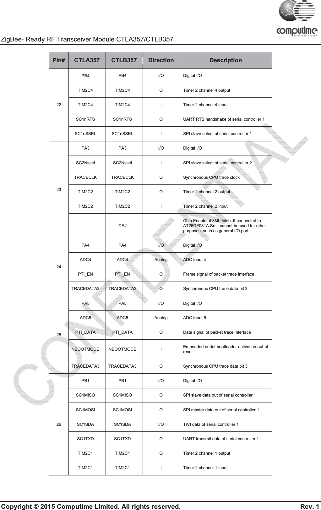
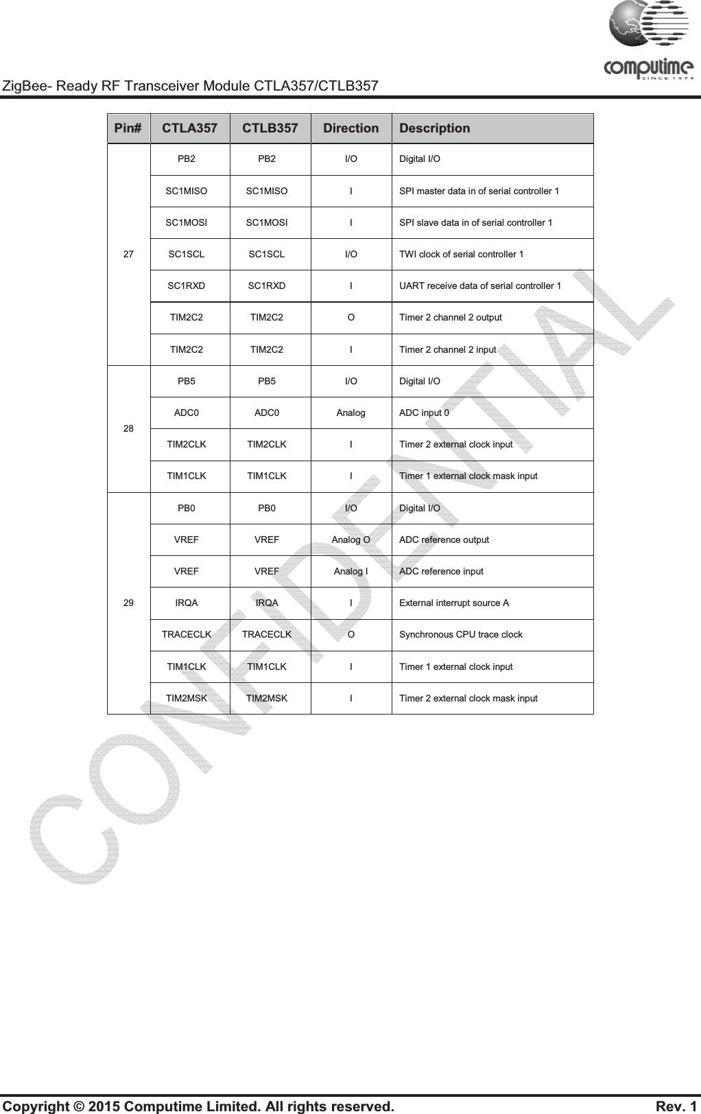
![ZigBee- Ready RF Transceiver MoCopyright © 2015 Computime LiPin# CTLA3578 PA7 TIM1C4 TIM1C4 REG_EN 9 PC1 10 GND 11 PB3 TIM2C3 TIM2C3 SC1nCTSSC1SCLKSC1SCLK12 GND 13 PC6 NTX_ACTIVE14 PC7 OSC32_EXT15 GND 16 VDD_PADS17 nRESET odule CTLA357/CTLB357 imited. All rights reserved. 7CTLB357 Direction DescriptionPA7 I/O High current Digital I/O Disable REGPIO_DBGCFG [4] TIM1C4 O Timer 1 channel 4 output TIM1C4 I Timer 1 channel 4 input REG_EN O External regulator open drain oPC1 O RX Enable: High RX DisabGND PB3 I/O Digital I/O TIM2C3 O Timer 2 channel 3 output TIM2C3 I Timer 2 channel 3 input SC1nCTS I UART CTS handshake of SeriaSC1SCLK O SPI master clock of serial ConSC1SCLK I SPI slave clock of serial ControGND PC6 I/O Digital I/O I/O 32.768KHz crystal oscillator.used for oscillation, then cannother purposes, such as generNTX_ACTIVE O Inverted TX_ACTIVE signal PC7 I/O Digital I/O I/O 32.768KHz crystal oscillator.used for oscillation, then cannother purposes, such as generOSC32_EXT I Digital 32.768KHz clock input sGND VDD_PADS Power Pads supply(2.1-3.6V) nRESET I Active low chip reset(internal p Rev. 1 nEG_EN with outputble: Lowal Controller 1troller 1oller 1If this pin is not be use for ral I/O port.If this pin is not be use for ral I/O port.sourcepull-up)](https://usermanual.wiki/COMPUTIME/CTLB357/User-Guide-2778044-Page-9.png)