Cypress Semiconductor 2011 Bluetooth Module User Manual
Cypress Semiconductor Bluetooth Module
Contents
- 1. User Manual
- 2. User Manual II
User Manual

PRELIMINARY CYBLE-01201x-x0
EZ-BLETM PRoCTM Module
CYBLE-012011-00/CYBLE-012012-10
Cypress Semiconductor Corporation 198 Champion Court San Jose,CA 95134-1709 408-943-2600
Document Number: 002-02521 Rev. ** Revised November 4, 2015
General Description
The CYBLE-01201x-x0 is a Bluetooth Low Energy (BLE)
wireless module solution. The CYBLE-01201x-x0 is a turnkey
solution and includes onboard crystal oscillators, trace antenna,
passive components, and the Cypress PRoC™ BLE. Refer to
the CYBL10X6X datasheet for additional details on the capabil-
ities of the PRoC BLE device used on this module.
The CYBLE-01201x-x0 supports a number of peripheral
functions (ADC, timers, counters, PWM) and serial
communication protocols (I2C, UART, SPI) through its
programmable architecture. The CYBLE-01201x-x0 includes a
royalty-free BLE stack compatible with Bluetooth 4.1 and
provides up to 23 GPIOs in a 14.52 × 19.20 × 2.00 mm package.
The CYBLE-01201x-x0 is available in a fully certified and
qualified version (CYBLE-012011-00), and an uncertified version
(CYBLE-012012-10). The CYBLE-012012-10 does not include
an RF shield and is not certied by Bluetooth SIG or refulatory
agencies.
The CYBLE-01201x-x0 is a complete solution targeted at appli-
cations requiring cost optimized BLE wireless connectivity.
Module Description
nModule size: 14.52 mm ×19.20 mm × 2.00 mm (with shield)
nCastelated solder pad connections for ease-of-use
nBluetooth 4.1 single-mode module
nIndustrial temperature range: –40 °C to +85 °C
n32-bit processor (0.9 DMIPS/MHz) with single-cycle 32-bit
multiply, operating at up to 48 MHz
n128-KB flash memory, 16-KB SRAM memory
nWatchdog timer with dedicated internal low-speed oscillator
(ILO)
nTwo-pin SWD for programming
nUp to 23 GPIOs configurable as open drain high/low,
pull-up/pull-down, HI-Z analog, HI-Z digial, or strong output
nCertified to FCC, IC, MIC, KC, and CE regulations
nBluetooth SIG 4.1 qualified
pQDID: TBD
pDeclaration ID: TBD
Power Consumption
nTX output power: –18 dbm to +3 dbm
nReceived signal strength indicator (RSSI) with 1-dB resolution
nTX current consumption of 15.6 mA (radio only, 0 dbm)
nRX current consumption of 16.4 mA (radio only)
nLow power mode support
pDeep Sleep: 1.3 µA with watch crystal oscillator (WCO) on
pHibernate: 150 nA with SRAM retention
pStop: 60 nA with XRES wakeup
Functional Capabilities
nUp to 22 capacitive sensors for buttons or sliders with
best-in-class signal-to-noise ration (SNR) and liquid tolerance
n12-bit, 1-Msps SAR ADC with internal reference,
sample-and-hold (S/H), and channel sequencer
nTwo serial communication blocks (SCBs) supporting I2C
(master/slave), SPI (master/slave), or UART
nFour dedicated 16-bit timer, counter, or PWM blocks
(TCPWMs)
nLCD drive supported on all GPIOs (common or segment)
nProgrammable low voltage detect (LVD) from 1.8 V to 4.5 V
nI2S master interface
nBluetooth Low Energy protocol stack supporting generic
access profile (GAP) Central, Peripheral, Observer, or
Broadcaster roles
nSwitches between Central and Peripheral roles on-the-go
nStandard Bluetooth Low Energy profiles and services for
interoperability
nCustom profile and service for specific use cases
Benefits
The CYBLE-01201x-x0 module is provided as a turnkey solution,
including all necessary hardware required to use BLE communi-
cation standards.
nProven hardware design ready to use
nCost optimized for applications without space constraint,
Footprint
p14.52 × 19.20 mm × 2.00 mm - CYBLE-012011-00
p14.52 × 19.20 mm × 1.55 mm - CYBLE-012012-10
nReprogrammable architecture
nFully certified module (CYBLE-012011-00) eliminates the time
needed for design, development and certification processes
nBluetooth SIG qualified with QDID and Declaration ID
(CYBLE-012011-00 Only)
nFlexible communication protocol support
nPSoC Creator™ provides an easy-to-use integrated design
environment (IDE) to configure, develop, program, and test a
BLE application

CYBLE-01201x-x0
Document Number: 002-02521 Rev. ** Page 2 of 31
Contents
Overview............................................................................ 3
Module Description...................................................... 3
Pad Connection Interface ................................................ 5
Recommended Host PCB Layout ................................... 6
Power Supply Connections and Recommended External
Components...................................................................... 9
Connection Options..................................................... 9
External Component Recommendation ...................... 9
Critical Components List ........................................... 11
Antenna Design......................................................... 11
Electrical Specification .................................................. 12
GPIO ......................................................................... 14
XRES......................................................................... 15
Digital Peripherals ..................................................... 18
Serial Communication ............................................... 20
Memory ..................................................................... 21
System Resources .................................................... 21
Environmental Specifications ....................................... 24
Environmental Compliance ....................................... 24
RF Certification.......................................................... 24
Environmental Conditions ......................................... 24
ESD and EMI Protection ........................................... 24
Regulatory Information .................................................. 25
FCC........................................................................... 25
Industry Canada (IC) Certification............................. 26
European R&TTE Declaration of Conformity ............ 26
MIC Japan................................................................. 27
KC Korea................................................................... 27
Ordering Information...................................................... 28
Part Numbering Convention...................................... 28
Document Conventions............................................. 29
Document History Page................................................. 30
Sales, Solutions, and Legal Information ...................... 31
Worldwide Sales and Design Support....................... 31
Products .................................................................... 31
PSoC® Solutions ...................................................... 31
Cypress Developer Community................................. 31
Technical Support ..................................................... 31
CYBLE-01201x-x0
Document Number: 002-02521 Rev. ** Page 3 of 31
Overview
Module Description
The CYBLE-01201x-x0 module is a complete module designed to be soldered to the applications main board.
Module Dimensions and Drawing
Cypress reserves the right to select components (including the appropriate BLE device) from various vendors to achieve the BLE
module functionality. Such selections will still guarantee that all height restrictions of the component area are maintained. Designs
should be held within the physical dimensions shown in the mechanical drawings in Figure 1. All dimensions are in millimeters (mm).
Table 1. Module Design Dimensions
See Figure 1 on page 4 for the mechanical reference drawing for CYBLE-01201x-x0.
Dimension Item Specification
Module dimensions Length (X) 14.52 ± 0.15 mm
Width (Y) 19.20 ± 0.15 mm
Antenna location dimensions Length (X) 11.00 ± 0.15 mm
Width (Y) 5.00 ± 0.15 mm
PCB thickness Height (H) 0.80 ± 0.10 mm
Shield height Height (H) 1.20 ± 0.10 mm
Maximum component height Height (H) 1.20 mm typical (shield) - CYBLE-012011-00
0.75 mm typical (crystal) - CYBLE-012012-10
Total module thickness (bottom of module to highest component) Height (H) 2.00 mm typical - CYBLE-012011-00
1.55 mm typical - CYBLE-012012-10
CYBLE-01201x-x0
Document Number: 002-02521 Rev. ** Page 4 of 31
Figure 1. Module Mechanical Drawing
Top View
Side View
Bottom View
Note
1. No metal should be located beneath or above the antenna area. Only bare PCB material should be located beneath the antenna area. For more information on
recommended host PCB layout, see Figure 3 and Figure 4 on page 6.
CYBLE-01201x-x0
Document Number: 002-02521 Rev. ** Page 5 of 31
Pad Connection Interface
As shown in the bottom view of Figure 1 on page 4, the CYBLE-01201x-x0 connects to the host board via solder pads on the backside
of the module. Table 2 and Figure 2 detail the solder pad length, width, and pitch dimensions of the CYBLE-01201x-x0 module.
Figure 2. Solder Pad Dimensions
Table 2. Solder Pad Connection Description
Name Connections Connection Type Pad Length Dimension Pad Width Dimension Pad Pitch
SP 31 Solder Pads 1.02 mm 0.71 mm 1.27 mm
CYBLE-01201x-x0
Document Number: 002-02521 Rev. ** Page 6 of 31
Recommended Host PCB Layout
Figure 3 details the recommended PCB layout pattern for the host PCB.
Figure 3. Recommended PCB Layout Pattern for CYBLE-01201x-x0 Module
To maximize RF performance, the host layout should follow these recommendations:
1. The ideal placement of the Cypress BLE module is in a corner of the host board with the trace antenna located at the far corner.
This placement minimizes the additional recommended keep out area stated in item 2.
2. It is recommended that the area around the Cypress BLE module trace antenna should contain an additional keep out area, where
no grounding or signal trace are contained. The keep out area applies to all layers of the host board. The recommended dimensions
of the host PCB keep out area are shown in Figure 4 (dimensions are in mm).
Figure 4. Recommended Host PCB Keep Out Area Around the CYBLE-01201x-x0 Antenna
Top View (On Host PCB)
Host PCB Keep Out Area Around Trace Antenna
CYBLE-01201x-x0
Document Number: 002-02521 Rev. ** Page 7 of 31
Tab le 3 details the solder pad pitch (center-to-center) for each of the neighboring connections.
Table 3. Module Solder Pad Connection Dimensions
Pad X Pad Y Pad Pitch (Pad X - Pad Y) Comments
Bottom Right Corner 1 4.88 mm Distance from Bottom Right Corner to Pad 1 center
1 2 1.27 mm Distance from Pad 1 center to Pad 2 center
2 3 1.27 mm Distance from Pad 2 center to Pad 3 center
3 4 1.27 mm Distance from Pad 3 center to Pad 4 center
4 5 1.27 mm Distance from Pad 4 center to Pad 5 center
5 6 1.27 mm Distance from Pad 5 center to Pad 6 center
6 7 1.27 mm Distance from Pad 6 center to Pad 7 center
7 8 1.27 mm Distance from Pad 7 center to Pad 8 center
8 9 1.27 mm Distance from Pad 8 center to Pad 9 center
9 10 1.27 mm Distance from Pad 9 center to Pad 10 center
10 11 1.27 mm Distance from Pad 10 center to Pad 11 center
Top Right Corner 12 2.04 mm Distance from Top Right Corner to Pad 12 center
12 13 1.27 mm Distance from Pad 12 center to Pad 13 center
13 14 1.27 mm Distance from Pad 13 center to Pad 14 center
14 15 1.27 mm Distance from Pad 14 center to Pad 15 center
15 16 1.27 mm Distance from Pad 15 center to Pad 16 center
16 17 1.27 mm Distance from Pad 16 center to Pad 17 center
17 18 1.27 mm Distance from Pad 17 center to Pad 18 center
18 19 1.27 mm Distance from Pad 18 center to Pad 19 center
19 20 1.27 mm Distance from Pad 19 center to Pad 20 center
20 21 1.27 mm Distance from Pad 20 center to Pad 21 center
Top Left Corner 22 2.90 mm Distance from Top Left Corner to Pad 22 center
22 23 1.27 mm Distance from Pad 22 center to Pad 23 center
23 24 1.27 mm Distance from Pad 23 center to Pad 24 center
24 25 1.27 mm Distance from Pad 24 center to Pad 25 center
25 26 1.27 mm Distance from Pad 25 center to Pad 26 center
26 27 1.27 mm Distance from Pad 26 center to Pad 27 center
27 28 1.27 mm Distance from Pad 27 center to Pad 28 center
28 29 1.27 mm Distance from Pad 28 center to Pad 29 center
29 30 1.27 mm Distance from Pad 29 center to Pad 30 center
30 31 1.27 mm Distance from Pad 30 center to Pad 31 center
31 Bottom Left Corner 4.88 mm Distance from Pad 31 center to Bottom Left Corner
CYBLE-01201x-x0
Document Number: 002-02521 Rev. ** Page 8 of 31
Tab le 4 details the solder pad connection definitions and available functions for each connection pad. Table 4 lists the solder pads on
CYBLE-01201x-x0, the BLE device port-pin, and denotes whether the function shown is available for each solder pad. Each
connection is configurable for a single option shown with a 3.
Table 4. Solder Pad Connection Definitions
Solder Pad
Number
Device
Port Pin UART SPI I2CTCPWM[2] CapSense WCO
Out ECO_OUT LCD SWD GPIO
1 XRES External Reset Hardware Connection Input
2P4.0
[3] 3(RTS) 3(MOSI) 33(CMOD)33
3P3.73(CTS) 33(Sensor) 33 3
4P3.63(RTS) 33(Sensor) 33
5P3.53(TX) 3(SCL) 33(Sensor) 33
6P3.43(RX) 3(SDA) 33(Sensor) 33
7P3.33(CTS) 33(Sensor) 33
8P3.23(RTS) 33(Sensor) 33
9P2.6 3(Sensor) 33
10 VREF Reference Voltage Input (Optional)
11 P2.4 3(Sensor) 33
12 P2.3 3(Sensor) 33 3
13 P2.2 3(SS) 3(Sensor) 33
14 P2.0 3(SS) 3(Sensor) 33
15 VDD Digital Power Supply Input (1.8 to 5.5V)
16 P1.7 3(CTS) 3(SCLK) 33(Sensor) 33
17 P1.6 3(RTS) 3(SS) 33(Sensor) 33
18 P1.5 3(TX) 3(MISO) 3(SCL) 33(Sensor) 33
19 P1.4 3(RX) 3(MOSI) 3(SDA) 33(Sensor) 33
20 P1.0 33(Sensor) 33
21 P0.4 3(RX) 3(MOSI) 3(SDA) 33(Sensor) 33 3
22 P0.5 3(TX) 3(MISO) 3(SCL) 33(Sensor) 33
23 P0.7 3(CTS) 3(SCLK) 33(Sensor) 33(SWDCLK) 3
24 P0.6 3(RTS) 3(SS) 33(Sensor) 33(SWDIO) 3
25 GND[4] Ground Connection
26 GND Ground Connection
27 GND Ground Connection
28 GND Ground Connection
29 VDDR Radio Power Supply (1.9V to 5.5V)
30 P5.03(RX) 3(SS) 3(SDA) 33(Sensor) 33
31 P5.1 3(TX) 3(SCLK) 3(SCL) 33(Sensor) 33 3
Notes
2. TCPWM: Timer, Counter, and Pulse Width Modulator. If supported, the pad can be configured to any of these peripheral functions.
3. When using the capacitive sensing functionality, Pad 2 (P4.0) must be connected to a CMOD capacitor (located off of Cypress BLE Module). The value of this
capacitor is 2.2 nF and should be placed as close to the module as possible.
4. The main board needs to connect all GND connections (Pad 25/26/27/28) on the module to the common ground of the system.
5. If the I2S feature is used in the design, the I2S pins shall be dynamically routed to the appropriate available GPIO by PSoC Creator
CYBLE-01201x-x0
Document Number: 002-02521 Rev. ** Page 9 of 31
Power Supply Connections and Recommended External Components
Power Connections
The CYBLE-01201x-x0 contains two power supply connections,
VDD and VDDR. The VDD connection supplies power for both
digital and analog device operation. The VDDR connection
supplies power for the device radio.
VDD accepts a supply range of 1.8 V to 5.5 V. VDDR accepts a
supply range of 1.9 V to 5.5 V. These specifications can be found
in Table 9. The maximum power supply ripple for both power
connections on the module is 100 mV, as shown in Tab le 7 .
The power supply ramp rate of VDD must be equal to or greater
than that of VDDR.
Connection Options
Two connection options are available for any application:
1. Single supply: Connect VDD and VDDR to the same supply.
2. Independent supply: Power VDD and VDDR separately.
External Component Recommendation
In either connection scenario, it is recommended to place an
external ferrite bead between the supply and the module
connection. The ferrite bead should be positioned as close as
possible to the module pin connection.
Figure 5 details the recommended host schematic options for a
single supply scenario. The use of one or two ferrite beads will
depend on the specific application and configuration of the
CYBLE-01201x-x0.
Figure 6 details the recommended host schematic for an
independent supply scenario.
The recommended ferrite bead value is 330 Ω, 100 MHz. (Murata
BLM21PG331SN1D).
Figure 5. Recommended Host Schematic Options for a Single Supply Option
Figure 6. Recommended Host Schematic for an Independent Supply Option
Two Ferrite Bead Option
Single Ferrite Bead Option
1.9V~5.5V Input 1.9V~5.5V Input
1.9V~5.5V Input
1.8V~5.5V Input
CYBLE-01201x-x0
Document Number: 002-02521 Rev. ** Page 11 of 31
Critical Components List
Tab le 5 details the critical components used in the CYBLE-01201x-x0 module.
Table 5. Critical Component List
Antenna Design
Tab le 6 details trace antenna used in the CYBLE-01201x-x0 module. For more information, see Ta ble 8 .
Table 6. Trace Antenna Specifications
Component Reference Designator Description
Silicon U1 56-pin QFN Programmable Radio-on-Chip (PRoC) with BLE
Crystal Y1 24.000 MHz, 10PF
Crystal Y2 32.768 kHz, 12.5PF
Item Description
Frequency Range 2400 – 2500 MHz
Peak Gain 0.5 dBi typical
Average Gain -0.5 dBi typical
Return Loss 10 dB minimum
CYBLE-01201x-x0
Document Number: 002-02521 Rev. ** Page 12 of 31
Electrical Specification
Tab le 7 details the absolute maximum electrical characteristics for the Cypress BLE module.
Table 7. CYBLE-01201x-x0 Absolute Maximum Ratings
Tab le 8 details the RF characteristics for the Cypress BLE module.
Table 8. CYBLE-01201x-x0 RF Performance Characteristics
Tab le 9 through Table 48 list the module level electrical characteristics for the CYBLE-01201x-x0. All specifications are valid for –40
°C ≤ TA ≤ 85 °C and TJ ≤ 100 °C, except where noted. Specifications are valid for 1.71 V to 5.5 V, except where noted.
Parameter Description Min Typ Max Units Details/Conditions
VDDD_ABS Analog, digital, or radio supply relative to VSS
(VSSD = VSSA)–0.5 – 6 V Absolute maximum
VCCD_ABS Direct digital core voltage input relative to VSSD –0.5 – 1.95 V Absolute maximum
VDD_RIPPLE Maximum power supply ripple for VDD and VDDR
input voltage – – 100 mV
3.0V supply
Ripple frequency of 100 kHz
to 750 kHz
VGPIO_ABS GPIO voltage –0.5 – VDD +0.5 V Absolute maximum
IGPIO_ABS Maximum current per GPIO –25 – 25 mA Absolute maximum
IGPIO_injection GPIO injection current: Maximum for VIH > VDD
and minimum for VIL < VSS –0.5 – 0.5 mA Absolute maximum current
injected per pin
LU Pin current for latch up –200 200 mA –
Parameter Description Min Typ Max Units Details/Conditions
RFO RF output power on ANT –18 0 3 dBm Configurable via register
settings
RXSRF receive sensitivity on ANT – –91 – dBm Guaranteed by design
simulation; High Gain Mode
FRModule frequency range 2400 – 2480 MHz –
GPPeak gain – 0.5 – dBi –
GAvg Average gain – –0.5 – dBi –
RL Return loss – –10.5 – dB –
Table 9. CYBLE-01201x-x0 DC Specifications
Parameter Description Min Typ Max Units Details/Conditions
VDD1 Power supply input voltage 1.8 – 5.5 V With regulator enabled
VDD2 Power supply input voltage unregulated 1.71 1.8 1.89 V Internally unregulated
supply
VDDR1 Radio supply voltage (radio on) 1.9 – 5.5 V –
VDDR2 Radio supply voltage (radio off) 1.71 – 5.5 V –
Active Mode, VDD = 1.71 V to 5.5 V
IDD3 Execute from flash; CPU at 3 MHz – 1.7 – mA T = 25 °C,
VDD = 3.3 V
IDD4 Execute from flash; CPU at 3 MHz – – – mA T = –40 °C to 85 °C
IDD5 Execute from flash; CPU at 6 MHz – 2.5 – mA T = 25 °C,
VDD = 3.3 V
IDD6 Execute from flash; CPU at 6 MHz – – – mA T = –40 °C to 85 °C
IDD7 Execute from flash; CPU at 12 MHz – 4 – mA T = 25 °C,
VDD = 3.3 V

CYBLE-01201x-x0
Document Number: 002-02521 Rev. ** Page 13 of 31
IDD8 Execute from flash; CPU at 12 MHz – – – mA T = –40 °C to 85 °C
IDD9 Execute from flash; CPU at 24 MHz – 7.1 – mA T = 25 °C,
VDD = 3.3 V
IDD10 Execute from flash; CPU at 24 MHz – – – mA T = –40 °C to 85 °C
IDD11 Execute from flash; CPU at 48 MHz – 13.4 – mA T = 25 °C,
VDD = 3.3 V
IDD12 Execute from flash; CPU at 48 MHz – – – mA T = –40 °C to 85 °C
Sleep Mode, VDD = 1.8 to 5.5 V
IDD13 IMO on – – – mA T = 25 °C, VDD = 3.3 V,
SYSCLK = 3 MHz
Sleep Mode, VDD and VDDR = 1.9 to 5.5 V
IDD14 ECO on – – – mA T = 25 °C, VDD = 3.3 V,
SYSCLK = 3 MHz
Deep-Sleep Mode, VDD = 1.8 to 3.6 V
IDD15 WDT with WCO on – 1.5 – µA T = 25 °C,
VDD = 3.3 V
IDD16 WDT with WCO on – – – µA T = –40 °C to 85 °C
IDD17 WDT with WCO on – – – µA T = 25 °C,
VDD = 5 V
IDD18 WDT with WCO on – – – µA T = –40 °C to 85 °C
Deep-Sleep Mode, VDD = 1.71 to 1.89 V (Regulator Bypassed)
IDD19 WDT with WCO on – – – µA T = 25 °C
IDD20 WDT with WCO on – – – µA T = –40 °C to 85 °C
Hibernate Mode, VDD = 1.8 to 3.6 V
IDD27 GPIO and reset active – 150 – nA T = 25 °C,
VDD = 3.3 V
IDD28 GPIO and reset active – – – nA T = –40 °C to 85 °C
Hibernate Mode, VDD = 3.6 to 5.5 V
IDD29 GPIO and reset active – – – nA T = 25 °C,
VDD = 5 V
IDD30 GPIO and reset active – – – nA T = –40 °C to 85 °C
Stop Mode, VDD = 1.8 to 3.6 V
IDD33 Stop-mode current (VDD)–20–nA
T = 25 °C,
VDD = 3.3 V
IDD34 Stop-mode current (VDDR)–40–- nA
T = 25 °C,
VDDR = 3.3 V
IDD35 Stop-mode current (VDD) – – – nA T = –40 °C to 85 °C
IDD36 Stop-mode current (VDDR)–––nA
T = –40 °C to 85 °C,
VDDR = 1.9 V to 3.6 V
Stop Mode, VDD = 3.6 to 5.5 V
IDD37 Stop-mode current (VDD)–––nA
T = 25 °C,
VDD = 5 V
IDD38 Stop-mode current (VDDR)–––nA
T = 25 °C,
VDDR = 5 V
IDD39 Stop-mode current (VDD) – – – nA T = –40 °C to 85 °C
IDD40 Stop-mode current (VDDR) – – – nA T = –40 °C to 85 °C
Table 9. CYBLE-01201x-x0 DC Specifications (continued)
Parameter Description Min Typ Max Units Details/Conditions

CYBLE-01201x-x0
Document Number: 002-02521 Rev. ** Page 14 of 31
Table 10. AC Specifications
GPIO
Parameter Description Min Typ Max Units Details/Conditions
FCPU CPU frequency DC – 48 MHz 1.71 V ≤ VDD ≤ 5.5 V
TSLEEP Wakeup from Sleep mode – 0 – µs Guaranteed by characterization
TDEEPSLEEP Wakeup from Deep-Sleep mode – – 25 µs 24-MHz IMO. Guaranteed by
characterization
THIBERNATE Wakeup from Hibernate mode – – 2 ms Guaranteed by characterization
TSTOP Wakeup from Stop mode – – 2 ms XRES wakeup
Table 11. GPIO DC Specifications
Parameter Description Min Typ Max Units Details/Conditions
VIH[6]
Input voltage HIGH threshold 0.7 × VDD – – V CMOS input
LVTTL input, VDD < 2.7 V 0.7 × VDD – – V –
LVTTL input, VDD >= 2.7 V 2.0 – – V –
VIL
Input voltage LOW threshold – – 0.3 × VDD VCMOS input
LVTTL input, VDD < 2.7 V – – 0.3× VDD V–
LVTTL input, VDD >= 2.7 V – – 0.8 V –
VOH
Output voltage HIGH level VDD –0.6 – – V IOH = 4 mA at 3.3-V VDD
Output voltage HIGH level VDD –0.5 – – V IOH = 1 mA at 1.8-V VDD
VOL
Output voltage LOW level – – 0.6 V IOL = 8 mA at 3.3-V VDD
Output voltage LOW level – – 0.6 V IOL = 4 mA at 1.8-V VDD
Output voltage LOW level – – 0.4 V IOL = 3 mA at 3.3-V VDD
RPULLUP Pull-up resistor 3.5 5.6 8.5 kΩ–
RPULLDOWN Pull-down resistor 3.5 5.6 8.5 kΩ–
IIL Input leakage current (absolute value) – – 2 nA 25 °C, VDD = 3.3 V
IIL_CTBM Input leakage on CTBm input pins – – 4 nA –
CIN Input capacitance – – 7 pF –
VHYSTTL Input hysteresis LVTTL 25 40 – mV VDD > 2.7 V
VHYSCMOS Input hysteresis CMOS 0.05 × VDD – – 1 –
IDIODE Current through protection diode to
VDD/VSS – – 100 µA –
ITOT_GPIO Maximum total source or sink chip
current – – 200 mA –
Note
6. VIH must not exceed VDD + 0.2 V.
CYBLE-01201x-x0
Document Number: 002-02521 Rev. ** Page 15 of 31
Table 12. GPIO AC Specifications
XRES
Parameter Description Min Typ Max Units Details/Conditions
TRISEF Rise time in Fast-Strong mode 2 – 12 ns 3.3-V VDDD, CLOAD = 25 pF
TFALLF Fall time in Fast-Strong mode 2 – 12 ns 3.3-V VDDD, CLOAD = 25 pF
TRISES Rise time in Slow-Strong mode 10 – 60 ns 3.3-V VDDD, CLOAD = 25 pF
TFALLS Fall time in Slow-Strong mode 10 – 60 ns 3.3-V VDDD, CLOAD = 25 pF
FGPIOUT1 GPIO Fout; 3.3 V ≤ VDD ≤ 5.5 V
Fast-Strong mode ––33MHz
90/10%, 25 pF load, 60/40 duty
cycle
FGPIOUT2 GPIO Fout; 1.7 V≤ VDD ≤ 3.3 V
Fast-Strong mode – – 16.7 MHz 90/10%, 25 pF load, 60/40 duty
cycle
FGPIOUT3 GPIO Fout; 3.3 V ≤ VDD ≤ 5.5 V
Slow-Strong mode –– 7 MHz
90/10%, 25 pF load, 60/40 duty
cycle
FGPIOUT4 GPIO Fout; 1.7 V ≤ VDD ≤ 3.3 V
Slow-Strong mode ––3.5MHz
90/10%, 25 pF load, 60/40 duty
cycle
FGPIOIN GPIO input operating frequency
1.71 V ≤ VDD ≤ 5.5 V – – 48 MHz 90/10% VIO
Table 13. OVT GPIO DC Specifications (P5_0 and P5_1 Only)
Parameter Description Min Typ Max Units Details/Conditions
IIL Input leakage (absolute value).
VIH > VDD – – 10 µA 25°C, VDD = 0 V, VIH = 3.0 V
VOL Output voltage LOW level – – 0.4 V IOL = 20 mA, VDD > 2.9 V
Table 14. OVT GPIO AC Specifications (P5_0 and P5_1 Only)
Parameter Description Min Typ Max Units Details/Conditions
TRISE_OVFS Output rise time in Fast-Strong mode 1.5 – 12 ns 25-pF load, 10%–90%, VDD=3.3 V
TFALL_OVFS Output fall time in Fast-Strong mode 1.5 – 12 ns 25-pF load, 10%–90%, VDD=3.3 V
TRISESS Output rise time in Slow-Strong mode 10 – 60 ns 25 pF load, 10%-90%,
VDD = 3.3 V
TFALLSS Output fall time in Slow-Strong mode 10 – 60 ns 25 pF load, 10%-90%,
VDD = 3.3 V
FGPIOUT1 GPIO FOUT
; 3.3 V ≤ VDD ≤ 5.5 V
Fast-Strong mode ––24MHz
90/10%, 25 pF load, 60/40 duty
cycle
FGPIOUT2 GPIO FOUT
; 1.71 V ≤ VDD ≤ 3.3 V
Fast-Strong mode ––16MHz
90/10%, 25 pF load, 60/40 duty
cycle
Table 15. XRES DC Specifications
Parameter Description Min Typ Max Units Details/Conditions
VIH Input voltage HIGH threshold 0.7 × VDDD – – V CMOS input
VIL Input voltage LOW threshold – – 0.3 × VDDD V CMOS input
RPULLUP Pull-up resistor 3.5 5.6 8.5 kΩ–
CIN Input capacitance – 3 – pF –
VHYSXRES Input voltage hysteresis – 100 – mV –
IDIODE Current through protection diode to
VDD/VSS – – 100 µA –
CYBLE-01201x-x0
Document Number: 002-02521 Rev. ** Page 16 of 31
Temperature Sensor
SAR ADC
Table 16. XRES AC Specifications
Parameter Description Min Typ Max Units Details/Conditions
TRESETWIDTH Reset pulse width 1 – – µs –
Table 17. Temperature Sensor Specifications
Parameter Description Min Typ Max Units Details/Conditions
TSENSACC Temperature-sensor accuracy –5 ±1 5 °C –40 to +85 °C
Table 18. SAR ADC DC Specifications
Parameter Description Min Typ Max Units Details/Conditions
A_RES Resolution – – 12 bits
A_CHNIS_S Number of channels - single-ended – – 8 8 full-speed
A-CHNKS_D Number of channels - differential – – 4 Diff inputs use
neighboring I/O
A-MONO Monotonicity – – – Yes
A_GAINERR Gain error – – ±0.1 % With external
reference
A_OFFSET Input offset voltage – – 2 mV Measured with 1-V
VREF
A_ISAR Current consumption – – 1 mA
A_VINS Input voltage range - single-ended VSS –V
DDA V
A_VIND Input voltage range - differential VSS – VDDA V
A_INRES Input resistance – – 2.2 kΩ
A_INCAP Input capacitance – – 10 pF
VREFSAR Trimmed internal reference to SAR –1 – 1 % Percentage of Vbg
(1.024 V)
Table 19. SAR ADC AC Specifications
Parameter Description Min Typ Max Units Details/
Conditions
A_PSRR Power-supply rejection ratio 70 – – dB Measured at 1-V
reference
A_CMRR Common-mode rejection ratio 66 – – dB
A_SAMP Sample rate – – 1 Msps 806 Ksps for
CYBLE-012011-00
devices
Fsarintref SAR operating speed without external ref.
bypass
– – 100 Ksps 12-bit resolution
A_SNR Signal-to-noise ratio (SNR) 65 – – dB FIN = 10 kHz
A_BW Input bandwidth without aliasing – – A_SAMP/2 kHz
A_INL Integral nonlinearity. VDD = 1.71 V to 5.5 V,
1 Msps
–1.7 – 2 LSB VREF = 1 V to VDD
A_INL Integral nonlinearity. VDDD = 1.71 V to 3.6 V,
1 Msps
–1.5 – 1.7 LSB VREF = 1.71 V to VDD
A_INL Integral nonlinearity. VDD = 1.71 V to 5.5 V,
500 Ksps
–1.5 – 1.7 LSB VREF = 1 V to VDD
CYBLE-01201x-x0
Document Number: 002-02521 Rev. ** Page 17 of 31
CSD
A_dnl Differential nonlinearity. VDD = 1.71 V to
5.5 V, 1 Msps
–1 – 2.2 LSB VREF = 1 V to VDD
A_DNL Differential nonlinearity. VDD = 1.71 V to
3.6 V, 1 Msps
–1 – 2 LSB VREF = 1.71 V to VDD
A_DNL Differential nonlinearity. VDD = 1.71 V to
5.5 V, 500 Ksps
–1 – 2.2 LSB VREF = 1 V to VDD
A_THD Total harmonic distortion – – –65 dB FIN = 10 kHz
Table 19. SAR ADC AC Specifications (continued)
Parameter Description Min Typ Max Units Details/
Conditions
CSD Block Specifications
Parameter Description Min Typ Max Units Details/
Conditions
VCSD Voltage range of operation 1.71 – 5.5 V
IDAC1 DNL for 8-bit resolution –1 – 1 LSB
IDAC1 INL for 8-bit resolution –3 – 3 LSB
IDAC2 DNL for 7-bit resolution –1 – 1 LSB
IDAC2 INL for 7-bit resolution –3 – 3 LSB
SNR Ratio of counts of finger to noise 5 – – Ratio Capacitance range of
9 pF to 35 pF, 0.1-pF
sensitivity. Radio is not
operating during the
scan
IDAC1_CRT1 Output current of IDAC1 (8 bits) in High
range
–612 – µA
IDAC1_CRT2 Output current of IDAC1 (8 bits) in Low
range
–306 – µA
IDAC2_CRT1 Output current of IDAC2 (7 bits) in High
range
–305 – µA
IDAC2_CRT2 Output current of IDAC2 (7 bits) in Low
range
–153 – µA
CYBLE-01201x-x0
Document Number: 002-02521 Rev. ** Page 18 of 31
Digital Peripherals
Timer
Counter
Table 20. Timer DC Specifications
Parameter Description Min Typ Max Units Details/Conditions
ITIM1 Block current consumption at 3 MHz – – 42 µA 16-bit timer
ITIM2 Block current consumption at 12 MHz – – 130 µA 16-bit timer
ITIM3 Block current consumption at 48 MHz – – 535 µA 16-bit timer
Table 21. Timer AC Specifications
Parameter Description Min Typ Max Units Details/Conditions
TTIMFREQ Operating frequency FCLK –48MHz
TCAPWINT Capture pulse width (internal) 2 × TCLK ––ns
TCAPWEXT Capture pulse width (external) 2 × TCLK ––ns
TTIMRES Timer resolution TCLK ––ns
TTENWIDINT Enable pulse width (internal) 2 × TCLK ––ns
TTENWIDEXT Enable pulse width (external) 2 × TCLK ––ns
TTIMRESWINT Reset pulse width (internal) 2 × TCLK ––ns
TTIMRESEXT Reset pulse width (external) 2 × TCLK ––ns
Table 22. Counter DC Specifications
Parameter Description Min Typ Max Units Details/Conditions
ICTR1 Block current consumption at 3 MHz – – 42 µA 16-bit counter
ICTR2 Block current consumption at 12 MHz – – 130 µA 16-bit counter
ICTR3 Block current consumption at 48 MHz – – 535 µA 16-bit counter
Table 23. Counter AC Specifications
Parameter Description Min Typ Max Units Details/Conditions
TCTRFREQ Operating frequency FCLK –48MHz
TCTRPWINT Capture pulse width (internal) 2 × TCLK ––ns
TCTRPWEXT Capture pulse width (external) 2 × TCLK ––ns
TCTRES Counter Resolution TCLK ––ns
TCENWIDINT Enable pulse width (internal) 2 × TCLK ––ns
TCENWIDEXT Enable pulse width (external) 2 × TCLK ––ns
TCTRRESWINT Reset pulse width (internal) 2 × TCLK ––ns
TCTRRESWEXT Reset pulse width (external) 2 × TCLK –– ns

CYBLE-01201x-x0
Document Number: 002-02521 Rev. ** Page 19 of 31
Pulse Width Modulation (PWM)
LCD Direct Drive
Table 24. PWM DC Specifications
Parameter Description Min Typ Max Units Details/Conditions
IPWM1 Block current consumption at 3 MHz – – 42 µA 16-bit PWM
IPWM2 Block current consumption at 12 MHz – – 130 µA 16-bit PWM
IPWM3 Block current consumption at 48 MHz – – 535 µA 16-bit PWM
Table 25. PWM AC Specifications
Parameter Description Min Typ Max Units Details/Conditions
TPWMFREQ Operating frequency FCLK –48MHz
TPWMPWINT Pulse width (internal) 2 × TCLK ––ns
TPWMEXT Pulse width (external) 2 × TCLK ––ns
TPWMKILLINT Kill pulse width (internal) 2 × TCLK ––ns
TPWMKILLEXT Kill pulse width (external) 2 × TCLK ––ns
TPWMEINT Enable pulse width (internal) 2 × TCLK ––ns
TPWMENEXT Enable pulse width (external) 2 × TCLK ––ns
TPWMRESWINT Reset pulse width (internal) 2 × TCLK ––ns
TPWMRESWEXT Reset pulse width (external) 2 × TCLK ––ns
Table 26. LCD Direct Drive DC Specifications
Parameter Description Min Typ Max Units Details/Conditions
ILCDLOW Operating current in low-power mode – 17.5 – µA 16 × 4 small segment
display at 50 Hz
CLCDCAP LCD capacitance per segment/common
driver
– 500 5000 pF
LCDOFFSET Long-term segment offset – 20 – mV
ILCDOP1 LCD system operating current
VBIAS = 5 V
– 2 – mA 32 × 4 segments. 50 Hz at
25 °C
ILCDOP2 LCD system operating current
VBIAS = 3.3 V
– 2 – mA 32 × 4 segments
50 Hz at 25 °C
Table 27. LCD Direct Drive AC Specifications
Parameter Description Min Typ Max Units Details/Conditions
FLCD LCD frame rate 10 50 150 Hz
CYBLE-01201x-x0
Document Number: 002-02521 Rev. ** Page 20 of 31
Serial Communication
Table 28. Fixed I2C DC Specifications
Table 30. Fixed UART DC Specifications
Table 31. Fixed UART AC Specifications
Parameter Description Min Typ Max Units Details/Conditions
II2C1 Block current consumption at 100 kHz – – 50 µA –
II2C2 Block current consumption at 400 kHz – – 155 µA –
II2C3 Block current consumption at 1 Mbps – – 390 µA –
II2C4 I2C enabled in Deep-Sleep mode – – 1.4 µA –
Table 29. Fixed I2C AC Specifications
Parameter Description Min Typ Max Units Details/Conditions
FI2C1 Bit rate – – 400 kHz
Parameter Description Min Typ Max Units Details/Conditions
IUART1 Block current consumption at 100 kbps – – 55 µA –
IUART2 Block current consumption at 1000 kbps – – 312 µA –
Parameter Description Min Typ Max Units Details/Conditions
FUART Bit rate – – 1 Mbps –
Table 32. Fixed SPI DC Specifications
Parameter Description Min Typ Max Units Details/Conditions
ISPI1 Block current consumption at 1 Mbps – – 360 µA –
ISPI2 Block current consumption at 4 Mbps – – 560 µA –
ISPI3 Block current consumption at 8 Mbps – – 600 µA –
Table 33. Fixed SPI AC Specifications
Parameter Description Min Typ Max Units Details/Conditions
FSPI SPI operating frequency (master; 6x over sampling) – – 8 MHz –
Table 34. Fixed SPI Master Mode AC Specifications
Parameter Description Min Typ Max Units Details/Conditions
TDMO MOSI valid after SCLK driving edge – – 18 ns –
TDSI MISO valid before SCLK capturing edge
Full clock, late MISO sampling used 20 – – ns Full clock, late MISO sampling
THMO Previous MOSI data hold time 0 – – ns Referred to Slave capturing edge
Table 35. Fixed SPI Slave Mode AC Specifications
Parameter Description Min Typ Max Units
TDMI MOSI valid before SCLK capturing edge 40 – – ns
TDSO MISO valid after SCLK driving edge – – 42 + 3 × TCPU ns
TDSO_ext MISO Valid after SCLK driving edge in
external clock mode. VDD < 3.0 V – – 50 ns
THSO Previous MISO data hold time 0 – – ns
TSSELSCK SSEL valid to first SCK valid edge 100 – – ns
CYBLE-01201x-x0
Document Number: 002-02521 Rev. ** Page 21 of 31
Memory
System Resources
Power-on-Reset (POR)
Table 36. Flash DC Specifications
Parameter Description Min Typ Max Units Details/Conditions
VPE Erase and program voltage 1.71 – 5.5 V –
TWS48 Number of Wait states at 32–48 MHz 2 – – CPU execution from flash
TWS32 Number of Wait states at 16–32 MHz 1 – – CPU execution from flash
TWS16 Number of Wait states for 0–16 MHz 0 – – CPU execution from flash
Table 37. Flash AC Specifications
Parameter Description Min Typ Max Units Details/Conditions
TROWWRITE[7] Row (block) write time (erase and program) – – 20 ms Row (block) = 128 bytes
TROWERASE[7] Row erase time – – 13 ms –
TROWPROGRAM[7] Row program time after erase – – 7 ms –
TBULKERASE[7] Bulk erase time (128 KB) – – 35 ms –
TDEVPROG[7] Total device program time – – 25 seconds –
FEND Flash endurance 100 K – – cycles –
FRET Flash retention. TA ≤ 55 °C, 100 K P/E cycles 20 – – years –
FRET2 Flash retention. TA ≤ 85 °C, 10 K P/E cycles 10 – – years –
Note
7. It can take as much as 20 ms to write to flash. During this time, the device should not be reset, or flash operations will be interrupted and cannot be relied on to have
completed. Reset sources include the XRES pin, software resets, CPU lockup states and privilege violations, improper power supply levels, and watchdogs. Make
certain that these are not inadvertently activated.
Table 38. POR DC Specifications
Parameter Description Min Typ Max Units Details/Conditions
VRISEIPOR Rising trip voltage 0.80 – 1.45 V –
VFALLIPOR Falling trip voltage 0.75 – 1.40 V –
VIPORHYST Hysteresis 15 – 200 mV –
Table 39. POR AC Specifications
Parameter Description Min Typ Max Units Details/Conditions
TPPOR_TR Precision power-on reset (PPOR) response
time in Active and Sleep modes ––1µs –
Table 40. Brown-Out Detect
Parameter Description Min Typ Max Units Details/Conditions
VFALLPPOR BOD trip voltage in Active and Sleep modes 1.64 – – V –
VFALLDPSLP BOD trip voltage in Deep Sleep 1.4 – – V –
Table 41. Hibernate Reset
Parameter Description Min Typ Max Units Details/Conditions
VHBRTRIP BOD trip voltage in Hibernate 1.1 – – V –
CYBLE-01201x-x0
Document Number: 002-02521 Rev. ** Page 22 of 31
Voltage Monitors (LVD)
SWD Interface
Table 42. Voltage Monitor DC Specifications
Parameter Description Min Typ Max Units Details/Conditions
VLVI1 LVI_A/D_SEL[3:0] = 0000b 1.71 1.75 1.79 V –
VLVI2 LVI_A/D_SEL[3:0] = 0001b 1.76 1.80 1.85 V –
VLVI3 LVI_A/D_SEL[3:0] = 0010b 1.85 1.90 1.95 V –
VLVI4 LVI_A/D_SEL[3:0] = 0011b 1.95 2.00 2.05 V –
VLVI5 LVI_A/D_SEL[3:0] = 0100b 2.05 2.10 2.15 V –
VLVI6 LVI_A/D_SEL[3:0] = 0101b 2.15 2.20 2.26 V –
VLVI7 LVI_A/D_SEL[3:0] = 0110b 2.24 2.30 2.36 V –
VLVI8 LVI_A/D_SEL[3:0] = 0111b 2.34 2.40 2.46 V –
VLVI9 LVI_A/D_SEL[3:0] = 1000b 2.44 2.50 2.56 V –
VLVI10 LVI_A/D_SEL[3:0] = 1001b 2.54 2.60 2.67 V –
VLVI11 LVI_A/D_SEL[3:0] = 1010b 2.63 2.70 2.77 V –
VLVI12 LVI_A/D_SEL[3:0] = 1011b 2.73 2.80 2.87 V –
VLVI13 LVI_A/D_SEL[3:0] = 1100b 2.83 2.90 2.97 V –
VLVI14 LVI_A/D_SEL[3:0] = 1101b 2.93 3.00 3.08 V –
VLVI15 LVI_A/D_SEL[3:0] = 1110b 3.12 3.20 3.28 V –
VLVI16 LVI_A/D_SEL[3:0] = 1111b 4.39 4.50 4.61 V –
LVI_IDD Block current – – 100 µA –
Table 43. Voltage Monitor AC Specifications
Parameter Description Min Typ Max Units Details/Conditions
TMONTRIP Voltage monitor trip time – – 1 µs –
Table 44. SWD Interface Specifications
Parameter Description Min Typ Max Units Details/Conditions
F_SWDCLK1 3.3 V ≤ VDD ≤ 5.5 V – – 14 MHz SWDCLK ≤ 1/3 CPU clock frequency
F_SWDCLK2 1.71 V ≤ VDD ≤ 3.3 V – – 7 MHz SWDCLK ≤ 1/3 CPU clock frequency
T_SWDI_SETUP T = 1/f SWDCLK 0.25 × T – – ns –
T_SWDI_HOLD T = 1/f SWDCLK 0.25 × T – – ns –
T_SWDO_VALID T = 1/f SWDCLK – – 0.5 × T ns –
T_SWDO_HOLD T = 1/f SWDCLK 1 – – ns –
CYBLE-01201x-x0
Document Number: 002-02521 Rev. ** Page 23 of 31
Internal Main Oscillator
Internal Low-Speed Oscillator
Table 49. ECO Trim Value Specification
Table 45. IMO DC Specifications
Parameter Description Min Typ Max Units Details/Conditions
IIMO1 IMO operating current at 48 MHz – – 1000 µA –
IIMO2 IMO operating current at 24 MHz – – 325 µA –
IIMO3 IMO operating current at 12 MHz – – 225 µA –
IIMO4 IMO operating current at 6 MHz – – 180 µA –
IIMO5 IMO operating current at 3 MHz – – 150 µA –
Table 46. IMO AC Specifications
Parameter Description Min Typ Max Units Details/Conditions
FIMOTOL3 Frequency variation from 3 to 48 MHz – – ±2 % With API-called calibration
FIMOTOL3 IMO startup time – 12 – µs –
Table 47. ILO DC Specifications
Parameter Description Min Typ Max Units Details/Conditions
IILO2 ILO operating current at 32 kHz – 0.3 1.05 µA –
Table 48. ILO AC Specifications
Parameter Description Min Typ Max Units Details/Conditions
TSTARTILO1 ILO startup time – – 2 ms –
FILOTRIM1 32-kHz trimmed frequency 15 32 50 kHz –
Parameter Description Value Details/Conditions
ECOTRIM 24-MHz trim value
(firmware configuration) 0x00003FFA Optimum trim value that needs to be loaded to register
CY_SYS_XTAL_BLERD_BB_XO_CAPTRIM_REG
CYBLE-01201x-x0
Document Number: 002-02521 Rev. ** Page 24 of 31
Environmental Specifications
Environmental Compliance
This Cypress BLE module is built in compliance with the Restriction of Hazardous Substances (RoHS) and Halogen Free (HF)
directives. The Cypress module and components used to produce this module are RoHS and HF compliant.
RF Certification
The CYBLE-012011-00 module will be certified under the following RF certification standards at production release.
nFCC: WAP2011
nCE
nIC: 7922A-2011
nMIC: TBD
nKC: MSIP-CRM-Cyp-2011
Environmental Conditions
Tab le 5 0 describes the operating and storage conditions for the Cypress BLE module.
Table 50. Environmental Conditions for CYBLE-01201x-x0
ESD and EMI Protection
Exposed components require special attention to ESD and electromagnetic interference (EMI).
A grounded conductive layer inside the device enclosure is suggested for EMI and ESD performance. Any openings in the enclosure
near the module should be surrounded by a grounded conductive layer to provide ESD protection and a low-impedance path to ground.
Device Handling: Proper ESD protocol must be followed in manufacturing to ensure component reliability.
Description Minimum Specification Maximum Specification
Operating temperature -40 °C 85 °C
Operating humidity (relative, non-condensation) 5% 85%
Thermal ramp rate – 3 °C/minute
Storage temperature –40 °C 85 °C
Storage temperature and humidity – 85 ° C at 85%
ESD: Module integrated into system
Components[8] –15 kV Air
2.2 kV Contact
Note
8. This does not apply to the RF pins (ANT, XTALI, and XTALO). RF pins (ANT, XTALI, and XTALO) are tested for 500-V HBM.

CYBLE-01201x-x0
Document Number: 002-02521 Rev. ** Page 25 of 31
Regulatory Information
FCC
FCC NOTICE:
The device CYBLE-012011-00 complies with Part 15 of the FCC Rules. The device meets the requirements for modular transmitter
approval as detailed in FCC public Notice DA00-1407.transmitter Operation is subject to the following two conditions: (1) This device
may not cause harmful interference, and (2) This device must accept any interference received, including interference that may cause
undesired operation.
CAUTION:
The FCC requires the user to be notified that any changes or modifications made to this device that are not expressly approved by
Cypress Semiconductor may void the user's authority to operate the equipment.
This equipment has been tested and found to comply with the limits for a Class B digital device, pursuant to Part 15 of the FCC Rules.
These limits are designed to provide reasonable protection against harmful interference in a residential installation. This equipment
generates uses and can radiate radio frequency energy and, if not installed and used in accordance with the instructions,ê may cause
harmful interference to radio communications. However, there is no guarantee that interference will not occur in a particular installation.
If this equipment does cause harmful interference to radio or television reception, which can be determined by turning the equipment
off and on, the user is encouraged to try to correct the interference by one or more of the following measures:
nReorient or relocate the receiving antenna.
nIncrease the separation between the equipment and receiver.
nConnect the equipment into an outlet on a circuit different from that to which the receiver is connected.
nConsult the dealer or an experienced radio/TV technician for help
LABELING REQUIREMENTS:
The Original Equipment Manufacturer (OEM) must ensure that FCC labelling requirements are met. This includes a clearly visible
label on the outside of the OEM enclosure specifying the appropriate Cypress Semiconductor FCC identifier for this product as well
as the FCC Notice above. The FCC identifier is FCC ID: WAP2011.
In any case the end product must be labeled exterior with "Contains FCC ID: WAP2011"
ANTENNA WARNING:
This device is tested with a standard SMA connector and with the antennas listed below. When integrated in the OEMs product, these
fixed antennas require installation preventing end-users from replacing them with non-approved antennas. Any antenna not in the
following table must be tested to comply with FCC Section 15.203 for unique antenna connectors and Section 15.247 for emissions.
RF EXPOSURE:
To comply with FCC RF Exposure requirements, the Original Equipment Manufacturer (OEM) must ensure to install the approved
antenna in the previous.
The preceding statement must be included as a CAUTION statement in manuals, for products operating with the approved antennas
in Table 6 on page 11, to alert users on FCC RF Exposure compliance. Any notification to the end user of installation or removal
instructions about the integrated radio module is not allowed.
The radiated output power of CYBLE-012011-00 with the trace antenna is far below the FCC radio frequency exposure limits. Never-
theless, use CYBLE-012011-00 in such a manner that minimizes the potential for human contact during normal operation.
End users may not be provided with the module installation instructions. OEM integrators and end users must be provided with
transmitter operating conditions for satisfying RF exposure compliance.

CYBLE-01201x-x0
Document Number: 002-02521 Rev. ** Page 26 of 31
Industry Canada (IC) Certification
CYBLE-012011-00 is licensed to meet the regulatory requirements of Industry Canada (IC),
License: IC: 7922A-2011
Manufacturers of mobile, fixed or portable devices incorporating this module are advised to clarify any regulatory questions and ensure
compliance for SAR and/or RF exposure limits. Users can obtain Canadian information on RF exposure and compliance from
www.ic.gc.ca.
This device has been designed to operate with the antennas listed in Tab le 6 on page 11, having a maximum gain of 0.5 dBi. Antennas
not included in this list or having a gain greater than 0.5 dBi are strictly prohibited for use with this device. The required antenna
impedance is 50 ohms. The antenna used for this transmitter must not be co-located or operating in conjunction with any other antenna
or transmitter.
IC NOTICE:
The device CYBLE-012011-00 including the built-in trace antenna complies with Canada RSS-GEN Rules. The device meets the
requirements for modular transmitter approval as detailed in RSS-GEN. Operation is subject to the following two conditions: (1) This
device may not cause harmful interference, and (2) This device must accept any interference received, including interference that
may cause undesired operation.
IC RADIATION EXPOSURE STATEMENT FOR CANADA
This device complies with Industry Canada licence-exempt RSS standard(s). Operation is subject to the following two conditions: (1)
this device may not cause interference, and (2) this device must accept any interference, including interference that may cause
undesired operation of the device.
Le présent appareil est conforme aux CNR d'Industrie Canada applicables aux appareils radio exempts de licence. L'exploitation est
autorisée aux deux conditions suivantes : (1) l'appareil ne doit pas produire de brouillage, et (2) l'utilisateur de l'appareil doit accepter
tout brouillage radioélectrique subi, même si le brouillage est susceptible d'en compromettre le fonctionnement.
LABELING REQUIREMENTS:
The Original Equipment Manufacturer (OEM) must ensure that IC labelling requirements are met. This includes a clearly visible label
on the outside of the OEM enclosure specifying the appropriate Cypress Semiconductor IC identifier for this product as well as the IC
Notice above. The IC identifier is 7922A-2011. In any case, the end product must be labeled in its exterior with "Contains IC:
7922A-2011"
European R&TTE Declaration of Conformity
Hereby, Cypress Semiconductor declares that the Bluetooth module CYBLE-012011-00 complies with the essential requirements and
other relevant provisions of Directive 1999/5/EC. As a result of the conformity assessment procedure described in Annex III of the
Directive 1999/5/EC, the end-customer equipment should be labeled as follows:
All versions of the CYBLE-012011-00 in the specified reference design can be used in the following countries: Austria, Belgium,
Cyprus, Czech Republic, Denmark, Estonia, Finland, France, Germany, Greece, Hungary, Ireland, Italy, Latvia, Lithuania, Luxem-
bourg, Malta, Poland, Portugal, Slovakia, Slovenia, Spain, Sweden, The Netherlands, the United Kingdom, Switzerland, and Norway.
CYBLE-01201x-x0
Document Number: 002-02521 Rev. ** Page 27 of 31
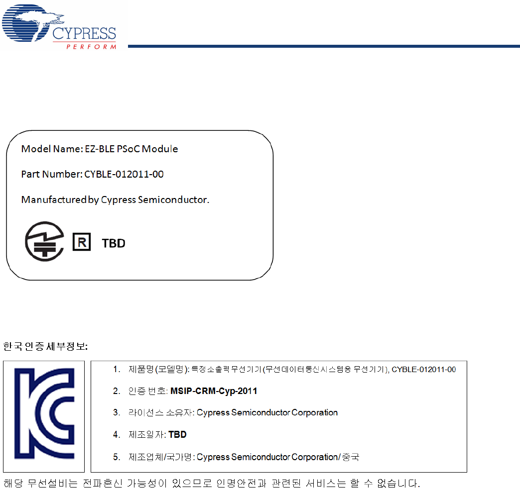
MIC Japan
CYBLE-012011-00 is certified as a module with type certification number TBD. End products that integrate CYBLE-012011-00 do not
need additional MIC Japan certification for the end product.
End product can display the certification label of the embedded module.
KC Korea
CYBLE-012011-00 is certified for use in Korea with certificate number MSIP-CRM-Cyp-2011.
CYBLE-01201x-x0
Document Number: 002-02521 Rev. ** Page 28 of 31
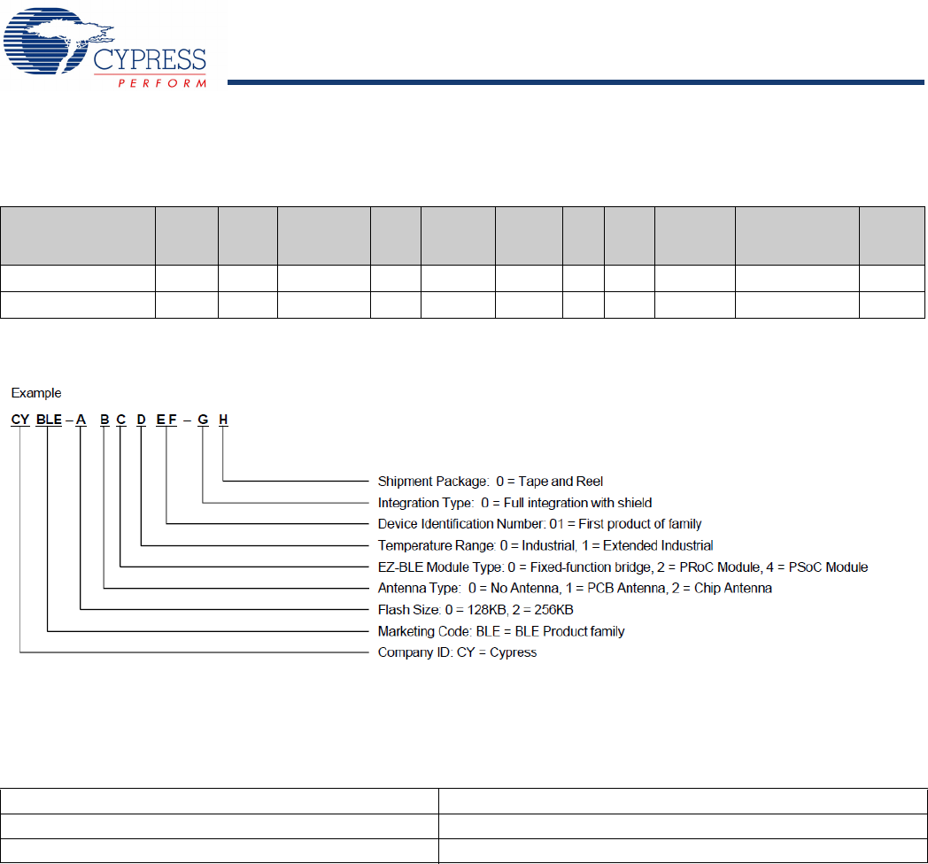
Ordering Information
The CYBLE-01201x-x0 is avialable in certified and uncertified options. The avialable part numbers and features are listed in the below
table.
Part Numbering Convention
The part numbers are of the form CYBLE-ABCDEF-GH where the fields are defined as follows.
For additional information and a complete list of Cypress Semiconductor BLE products, contact your local Cypress sales
representative. To locate the nearest Cypress office, visit our website.
Part Number
CPU
Speed
(MHz)
Flash
Size
(KB)
CapSense SCB TCPWM
12-Bit
SAR
ADC
I2SLCD Package Packing Shield
CYBLE-012011-00 48 128 Yes 2 4 1 Msps Yes Yes 31-SMT Tape and Reel Yes
CYBLE-012012-10 48 128 Yes 2 4 1 Msps Yes Yes 31-SMT Tape and Reel No
U.S. Cypress Headquarters Address 198 Champion Court, San Jose, CA 95134
U.S. Cypress Headquarter Contact Info (408) 943-2600
Cypress website address http://www.cypress.com

CYBLE-01201x-x0
Document Number: 002-02521 Rev. ** Page 29 of 31
Acronyms
Document Conventions
Units of Measure
Acronym Description
BLE Bluetooth Low Energy
Bluetooth SIG Bluetooth Special Interest Group
CE European Conformity
CSA Canadian Standards Association
EMI electromagnetic interference
ESD electrostatic discharge
FCC Federal Communications Commission
GPIO general-purpose input/output
IC Industry Canada
IDE integrated design environment
KC Korea Certification
MIC Ministry of Internal Affairs and Communications (Japan)
PCB printed circuit board
RX receive
QDID qualification design ID
SMT surface-mount technology; a method for producing electronic circuitry in which the components are placed
directly onto the surface of PCBs
TCPWM timer, counter, pulse width modulator (PWM)
TUV Germany: Technischer Überwachungs-Verein (Technical Inspection Association)
TX transmit
Symbol Unit of Measure
°C degree Celsius
kV kilovolt
mA milliamperes
mm millimeters
mV millivolt
µA microamperes
µm micrometers
MHz megahertz
GHz gigahertz
Vvolt

CYBLE-01201x-x0
Document Number: 002-02521 Rev. ** Page 30 of 31
Document History Page
Document Title: CYBLE-01201x-x0 Bluetooth® Low Energy (BLE) Module
Document Number: 002-02521
Revision ECN Orig. of
Change
Submission
Date Description of Change
** MINS 10/22/2015 Preliminary datasheet for CYBLE-01201x-x0 module.

Document Number: 002-02521 Rev. ** Revised November 4, 2015 Page 31 of 31
All products and company names mentioned in this document may be the trademarks of their respective holders.
CYBLE-01201x-x0
© Cypress Semiconductor Corporation, 2015. The information contained herein is subject to change without notice. Cypress Semiconductor Corporation assumes no responsibility for the use of any
circuitry other than circuitry embodied in a Cypress product. Nor does it convey or imply any license under patent or other rights. Cypress products are not warranted nor intended to be used for medical,
life support, life saving, critical control or safety applications, unless pursuant to an express written agreement with Cypress. Furthermore, Cypress does not authorize its products for use as critical
components in life-support systems where a malfunction or failure may reasonably be expected to result in significant injury to the user. The inclusion of Cypress products in life-support systems
application implies that the manufacturer assumes all risk of such use and in doing so indemnifies Cypress against all charges.
Any Source Code (software and/or firmware) is owned by Cypress Semiconductor Corporation (Cypress) and is protected by and subject to worldwide patent protection (United States and foreign),
United States copyright laws and international treaty provisions. Cypress hereby grants to licensee a personal, non-exclusive, non-transferable license to copy, use, modify, create derivative works of,
and compile the Cypress Source Code and derivative works for the sole purpose of creating custom software and or firmware in support of licensee product to be used only in conjunction with a Cypress
integrated circuit as specified in the applicable agreement. Any reproduction, modification, translation, compilation, or representation of this Source Code except as specified above is prohibited without
the express written permission of Cypress.
Disclaimer: CYPRESS MAKES NO WARRANTY OF ANY KIND, EXPRESS OR IMPLIED, WITH REGARD TO THIS MATERIAL, INCLUDING, BUT NOT LIMITED TO, THE IMPLIED WARRANTIES
OF MERCHANTABILITY AND FITNESS FOR A PARTICULAR PURPOSE. Cypress reserves the right to make changes without further notice to the materials described herein. Cypress does not
assume any liability arising out of the application or use of any product or circuit described herein. Cypress does not authorize its products for use as critical components in life-support systems where
a malfunction or failure may reasonably be expected to result in significant injury to the user. The inclusion of Cypress’ product in a life-support systems application implies that the manufacturer
assumes all risk of such use and in doing so indemnifies Cypress against all charges.
Use may be limited by and subject to the applicable Cypress software license agreement.
Sales, Solutions, and Legal Information
Worldwide Sales and Design Support
Cypress maintains a worldwide network of offices, solution centers, manufacturer’s representatives, and distributors. To find the office
closest to you, visit us at Cypress Locations.
Products
Automotive cypress.com/go/automotive
Clocks & Buffers cypress.com/go/clocks
Interface cypress.com/go/interface
Lighting & Power Control cypress.com/go/powerpsoc
Memory cypress.com/go/memory
PSoC cypress.com/go/psoc
Touch Sensing cypress.com/go/touch
USB Controllers cypress.com/go/USB
Wireless/RF cypress.com/go/wireless
PSoC® Solutions
psoc.cypress.com/solutions
PSoC 1 | PSoC 3 | PSoC 4 | PSoC 5LP
Cypress Developer Community
Community | Forums | Blogs | Video | Training
Technical Support
cypress.com/go/support