Unknown PMTHandbook
User Manual: PMTHandbook
Open the PDF directly: View PDF ![]() .
.
Page Count: 179 [warning: Documents this large are best viewed by clicking the View PDF Link!]

Contents
1. lntroduction............................................................... 3
Early development, photoemitter and secondary-emitter development, applications development,
photomultiplier
and
solid-state detectors compared
2. Photomultiplier Design . . . . . . . . . . . , . . . . . . . . . . . . . . . . . . . . . . . . . . . . . . . . . . . . . . . . .
10
Photoemission, practical photocathode materials, opaque and semitransparent photocathodes, glass
transmission and spectral response, thermionic emission, secondary emission, time tag in photoemission and
secondary emission
3. Electron Optics of Photomultipliers , . . . . . . . . . . . . . . . . . . . . . . . . . . . . . . . . . . . . . . . .
26
Electron-optical design considerations, design methods for photomultiplier electron optics, specific
photomultiplier electron-optical configurations, anode configurations
4. Photomultiplier Characteristics . . . . . . . . . . . . . . . . . . . . . . . . . . . . . . . . . . . . , . . 36
Photocathode-related characteristics, gain-related characteristics, dark current and noise, time effects, pulse
counting, scintillation counting, liquid scintillation counting, environmental effects
5. Photomultiplier Applications . . . . . . . . . . . . . . . . . . . . . . . . . . . . . . . . . . . . . . . . . . . . .
80
Summary of selection criteria, applied voltage considerations, mechanical considerations, optical
considera-
tions, specific photomultiplier applications
Appendix A. Typical Photomultiplier Applications and Selection Guide . . . . . . . . . . . 119
Appendix B.Glossary of Terms Related to Photomultiplier lubes and Their
Applica-
I
. . . . . . . . . . . . . . . . . . . . . . . . . . . . . . . . . . . . . . . . . . . . . . . . . . . . . . . . . .
125
Appendix C.
Spectral Response Designation Systems . . . . . . . . . . . . . . . . . . . . . . . . . . . . . . .
132
Appendix D. Photometric Units and Photometric-to-Radiant Conversion
.............
I
37
Appendix E.
Spectral Response and Source-Detector Matching
......... ..........I 43
Appendix F.
Radiant Energy and Sources
......................................
148
Appendix G. Statistical Theory of Noise in Photomultiplier Tubes. . . . . . . . . . . . . . .
I
60
Index........................................................................ 177
information furnished by BURLE INDUSTRIES, INC. is believed to be accurate and reliable. However, no responsibility of liability
is assumed by BURLE for its use, nor for any infringement of patents or other rights of third parties which may result from its use. No
license is granted by implication or otherwise under any patent or other rights of BURLE INDUSTRIES, INC.
BURLE ® and BURLE INDUSTRIES, INC.® are registered trademarks of BURLE TECHNOLOGIES, INC. Marca(s)
Registrada(s).
Copyright © 1980 by BURLE TECHNOLOGIES, INC. All rights reserved. No part of this book
may
be copied or reproduced in any
form or by any means -- graphic, electronic, or mechanical or incorporated into any information storage or retrieval system, without
the written permission of the copyright owner.
Supersedes PMT-62, 8-80 Printed in U.S.A./ 10-89
TP-136
2
Photomultiplier Handbook

1.
Introduction
The photomultiplier is a very versatile and
sensitive detector of radiant energy in the
ultraviolet, visible, and near infrared regions
of the electromagnetic spectrum. A schemat-
ic diagram of a typical photomultiplier tube
is given in Fig. 1. The basic radiation sensor
is the
photocathode
which is located inside a
vacuum envelope. Photoelectrons are emit-
ted and directed by an appropriate electric
field to an electrode or dynode within the
envelope. A number of secondary electrons
are emitted at this dynode for each imping-
ing primary photoelectron. These secondary
electrons in turn are directed to a second
dynode and so on until a final gain of
perhaps 106 is achieved. The electrons from
the last dynode are collected by an anode
which provides the signal current that is read
out.
PHOTOELECTRONS
92cs-32288
Fig.
1
-
Schematic representation of a photo-
multiplier tube and its operation
For a large number of applications, the
photomultiplier is the most practical or sen-
sitive detector available. The basic reason
for the superiority of the photomultiplier is
the secondary-emission amplification that
makes it possible for the tube to approach
“ideal” device performance limited only by
the statistics of photoemission. Amplifica-
tions ranging from 103 to as much as 108
provide output signal levels that are com-
patible with auxiliary electronic equipment
without need for additional signal amplifica-
tion. Extremely fast time response with rise
times as short as a fraction of a nanosecond
provides a measurement capability in special
applications that is unmatched by other
radiation detectors.
EARLY DEVELOPMENT
The development (history) of the photo-
multiplier is rooted in early studies of secon-
dary emission. In 1902, Austin and Starke1
reported that the metal surfaces impacted by
cathode rays emitted a larger number of elec-
trons than were incident. The use of secon-
dary emission as a means for signal
amplification was proposed as early as
1919.2 In 1935, Iams and Salzberg 3 of RCA
reported on a single-stage photomultiplier.
The device consisted of a semicylindrical
photocathode, a secondary emitter mounted
on the axis, and a collector grid surrounding
the secondary emitter. The tube had a gain
of about eight. Because of its better frequen-
cy response the single-stage photomultiplier
was intended for replacement of the
gas-
filled phototube as a sound pickup for
movies. But despite its advantages, it saw
only a brief developmental sales activity
before it became obsolete.
Multistage Devices
In 1936, Zworykin, Morton, and Malter,
all of
RCA4
reported on a multistage
photomultiplier. Again, the principal con-
templated application was sound-on-film
pickup. Their tube used a combination of
electrostatic and magnetic fields to direct
electrons from stage to stage. A photograph
of a developmental sample is given in Fig. 2.
Although the magnetic-type photomultiplier
provided high gain, it had several dif-
ficulties. The adjustment of the magnetic
field was very critical, and to change the gain
by reducing the applied voltage, the
magnetic field also had to be adjusted.
3

Photomultiplier Handbook
Another problem was that its rather wide
open structure resulted in high dark current
because of feedback from ions and light
developed near the output end of the device.
For these reasons, and because of the
development of electrostatically focused
photomultipliers, commercialization did not
follow.
Fig. 2
-
Magnetic-type multistage
photomul-
tiplier reported by Zworykin, Morton, and
Malter
in 1936.
The design of multistage electrostatically
focused photomultipliers required an
analysis of the equipotential surfaces be-
tween electrodes and of the electron trajec-
tories. Before the days of high-speed com-
puters, this problem was solved by a
mechanical analogue: a stretched rubber
membrane. By placing mechanical models of
the electrodes under the membrane, the
height of the membrane was controlled and
corresponded to the electrical potential of
the electrode. Small balls were then allowed
to roll from one electrode to the next. The
trajectories of the balls were shown to cor-
respond to those of the electrons in the cor-
responding electrostatic fields. Working
with the rubber-dam analogue, both J.R.
Pierce5
of Bell Laboratories and J.A.
Rajchman6
of RCA devices linear arrays of
electrodes that provided good focusing prop-
erties. Although commerical designs did not
result immediately from the linear dynode
array, The Rajchmann design with some
modifications eventually was, and still is,
used in photomultipliers-particularly for
high-gain wide-bandwidth requirements.
First Commercial Devices
The first commercially successful
photomultiplier was the type 931. This tube
had a compact circular array of nine
dynodes using electrostatic focusing. The
first such arrangement was described by
Zworykin and
Rajchman.7
Modifications
were later reported by Rajchmann and
4
Snyder8 and by Janes and
Gloverg,
all of
RCA. The basic electron-optics of the cir-
cular cage was thus well determined by 1941
and has not changed to the present time
although improvements have been made in
processing, construction, and performance
of the 931A product.
The success of the 931 type also resulted
from the development of a much improved
photocathode, Cs3Sb, reported by Gorlich 10
in 1936. The first experimental photo-
multipliers had used a Ag-O-Cs photocath-
ode having a typical peak quantum efficien-
cy of 0.4% at 800 nm. (The Ag-O-Cs layer
was also used for the dynodes.) The new
Cs3Sb
photocathode had a quantum effi-
ciency of 12% (higher today) at 400 nm. It
was used in the first 931’s, both as a
photocathode and as a secondary-emitting
material for the dynodes.
PHOTOEMITTER
AND
SECONDARY-
EMITTER DEVELOPMENT
Photocathode Materials
Much of the development work on
photomultiplier tubes has been concerned
with their physical configuration and the
related electron optics. But a very important
part of the development of photomultiplier
tubes was related to the photocathode and
secondary-emission surfaces and their pro-
cessing. RCA was very fortunate during the
1950’s and 60’s in having on its staff, prob-
ably the world’s foremost photocathode ex-
pert, Dr. A.H. Sommer. His treatise on
Photoemissive
Materials1
1
continues to pro-
vide a wealth of information to all
photocathode process engineers.
Sommer explored the properties of
numerous photocathode materials-par-
ticularly alkali-antimonides. Perhaps his
most noteworthy contribution was the
multialkali photocathode (S-20 spectral
response). This photocathode,
Na2KSb:Cs,
is important because of its high sensitivity in
the red and near infrared; the earlier Cs3Sb
photocathode spectral response barely ex-
tends through the visible, although it is very
sensitive in the blue where most scintillators
emit.
Bialkali photocathodes were also de-
veloped by Sommer and have proven to be

better in some applications than the
Cs3Sb
photocathode. Thus, the
Na2KSb
photo-
cathode has been found to be stable at higher
temperatures than
Cs3Sb
and, in addition,
has a very low dark (thermal) emission. It
has been particularly useful in
oil-well-
logging applications. Another bialkali
pho-
tocathode,
K2CsSb,
is more sensitive than
Cs3Sb
in the blue and is, therefore, used by
RCA to provide a better match to the
NaI:Tl crystals used in scintillation count-
ing.
Dynode Materials
The first secondary-emission material
used practically by RCA was the Ag-O-Cs
surface. But with the development of the
Cs3Sb
material for photocathodes, it was
found that this material was also an excellent
secondary emitter. Other practical secondary
emitters developed during the early years of
photomultiplier development were MgO:Cs
(often referred to as “silver-magnesium”)
and BeO:Cs (“copper-beryllium”).
In the early
1960’s,
R.E.
Simon12
while
working at the RCA Laboratories developed
his revolutionary concept of Negative Elec-
tron Affinity
(NEA).
Electron affinity is the
energy required for an electron at the
conduction-band level to escape to the
vacuum level. By suitably treating the sur-
face of a p-type semiconductor material, the
band levels at the surface can be bent
downward so that the effective electron af-
finity is actually negative. Thermalized elec-
trons in the conduction band are normally
repelled by the electron-affinity barrier; the
advantage of the NEA materials is that these
electrons can now escape into the vacuum as
they approach the surface. In the case of
secondary emission, secondary electrons can
be created at greater depths in the material
and still escape, thus providing a much
greater secondary-emission yield. In the case
of photoemission, it has been possible to
achieve extended-red and infrared sen-
sitivities greater than those obtainable with
any other known materials. The first prac-
tical application of the NEA concept was to
secondary emission.
Simon and Williams
l3
An early paper by
described the theory
and early experimental results of
secondary-
emission yields as high as 130 at 2.5
kV
for
GaP:Cs.
Introduction
APPLICATIONS DEVELOPMENT
Astronomy and Spectroscopy
Early applications of the photomultiplier
were in astronomy and spectroscopy.
Because the effective quantum efficiency of
the photomultiplier was at least ten times
that of photographic film, astronomers were
quick to realize the photomultiplier tube’s
advantage. Furthermore, because the output
current of the photomultiplier is linear with
incident radiation power, the tube could be
used directly in photometric and
spec-
trophotometric astronomy. The type 1P28, a
tube similar to the 931 but having an
ultraviolet-transmitting envelope was par-
ticularly useful in spectroscopy. The size and
shape of the photocathode were suitable for
the detection and measurement of line spec-
tra and the very wide range of available gain
proved very useful. 14
Radar Jammer
A totally unexpected application for the
new photomultiplier tube occurred during
World War II. The development of radar for
detecting and tracking aircraft led to the
simultaneous need for wideband
electronic-
noise sources as radar jammers. Although
other sources of noise were tried, the
photomultiplier proved to be most suc-
cessful. The advantage of the tube was its
high gain
(107)
and wide band width (several
hundred MHz). As a noise source the tube
was operated with a non-modulated input
light source and with high gain. The output
amplifier photoelectric shot noise was
“white” and thus indistinguishable from
natural noise sources. This application of
photomultiplier tubes resulted in production
of thousands per month compared with
previous production measured in only hun-
dreds per year.
Scintillation Counting
A proliferation of photomultiplier designs
followed the invention of the scintillation
counter shortly after World War II.15,16 The
photomultiplier tubes were designed with
semitransparent photocathodes deposited on
an end window which could be coupled
directly to the scintillator. The principal
scintillator used, NaI doped with thallium,
was discovered by
Hofstadter17.
Much of
the development work on photomultiplier
5

Photomultiplier Handbook
tubes during this period was reported by
RCA and its competitors in the biannual
meetings of the Scintillation Counter Sym-
posium.
These symposia were reported fully
in the IRE (and later the IEEE)
Transactions
on Nuclear Science beginning with the
meeting in Washington, January 1948. The
scintillation counter became the most impor-
tant measurement instrument in nuclear
physics, nuclear medicine, and radioactive
tracer applications of a wide variety.
Headlight Dimmer
During the
1950’s,
RCA collaborated with
the General Motors Company (Guide-Lamp
Division) on a successful headlight dimmer.
The photoelectric headlight dimmer-first
made available only on Cadillacs and
Oldsmobiles-basically used a tube similar
to the
931A,
but redesigned and tested to the
auto manufacturer’s particular require-
ments. The optical engineering problem was
to sense the oncoming headlights or tail-
lights being followed without responding to
street and house lights. Vertical and horizon-
tal angular sensitivity was designed to match
the spread of the high beams of the automo-
bile. A red filter was installed in the optical
path to provide a better balance between sen-
sitivity to oncoming headlights and to
tail-
lamps being followed. The device achieved a
remarkable success, probably because of the
novelty, and thousands of photomultiplier
tubes were used. But today, one rarely sees a
headlight dimmer.
Medical Diagnostic Equipment
In recent years two medical applications
have used large numbers of photomultiplier
tubes and have spurred further develop-
ments and improvements. The gamma
cam-
era18
is a sophisticated version of the scin-
tillation counter used medically for locating
tumors or other biological abnormalities. A
radioactive isotope combined in a suitable
compound is injected into the blood stream
or ingested orally by the patient. The
radioactive material disintegrates and gam-
ma rays are ejected from preferential loca-
tions such as tumors or specific organs. A
large crystal intercepts the gamma rays and
scintillates. Behind the crystal are photo-
multiplier tubes, perhaps 19, in hexagonal
array. The location of the point of scintilla-
tion origin is obtained by an algorithm
6
depending upon the individual signals from
each of the photomultipliers. Counting is
continued until several hundred thousand
counts are obtained and the organ in ques-
tion is satisfactorily delineated. The location
of each scintillation is represented by a point
on a cathode-ray-tube presentation.
The Computerized Axial Tomographic
(CAT) scanner was introduced to this coun-
try in 1973. The device uses a pencil or
fan-
beam of X-rays which rotates around the pa-
tient providing X-ray transmission data
from many directions. A scintillator coupled
to a photomultiplier detects the transmitted
beam-as an average photomultiplier cur-
rent-and a computer stores and computes
the cross-section density variation of the pa-
tient’s torso or skull. The photomultipliers
are1/ or 3/4-inch end-on tubes which
couple to the scintillator, commonly BGO
(bismuth germanate). Each unit is equipped
with as many as 600 photomultipliers.
PHOTOMULTIPLIERS AND
SOLID-
STATE DETECTORS COMPARED
In some applications either a photomulti-
plier or solid-state detector could be used.
The user may make his choice on the basis of
factors such as cost, size, or previous ex-
perience. In other applications, the choice
may be dictated by fundamental properties
of the photomultiplier or the solid-state
detector. A discussion follows of some of the
common applications favoring one or the
other detector with reasons for the choice. A
summary presents the principal considera-
tions the user must apply in making a choice
in an application for which he requires a
photodetector. This information should be
particularly useful to the designer who is not
well acquainted in this field.
Photomultiplier Features
The photomultiplier is unique in its ability
to interface with a scintillation crystal and
not only count the scintillations but measure
their magnitude and time their arrival. Most
scintillators emit in the blue and near ultra-
violet. This spectral output obviously favors
the photomultiplier having a photocathode
with high quantum efficiency in the short
wavelength range. On the other hand a sili-
con p-i-n diode is relatively poor in this part
of the spectrum but does best in the red and
near infrared. The most important factor,

probably, is the gain of the photomultiplier
which permits the measurement of the very
small signals from individual scintillations
with a good signal-to-noise ratio, limited
primarily by the statistics of the number of
photoelectrons per pulse. Finally, the short
rise time of the photomultiplier using fast
scintillators permits time-of-flight measure-
ments to be made in nuclear physics.
Although the CAT scanner equipment
also uses photomultipier tubes to detect the
scintillations in bismuth germanate (BGO)
crystals, the situation is somewhat different
from the scintillation counting applications
discussed above. In the CAT scanner the
X-rays produce a broad band of pulse
heights and no attempt is made to single out
and detect single scintillation events. The
photomultiplier is used in an analog mode to
detect the level of radiation incident on the
crystal. In the CAT scan operation the
typical machine scans the patient in a few
seconds and the level of irradiance from the
crystal onto the photomultiplier is relatively
high so that only a relatively low gain photo-
multiplier is required. Furthermore, the
speed of response requirement for the
photomultiplier is relatively modest-per-
haps a few hundred microseconds. Still, the
principal advantage of using a photomulti-
plier in this application for the detection of
the radiant signal is its good signal-to-noise
ratio. This ratio is very important to the pa-
tient because a reduction in its
signal-to-
noise ratio would have to be made up for
with an increased X-ray dose. Nevertheless,
there is interest and development activity
aimed at replacing the photomultiplier with
silicon p-i-n detectors. Two factors could
favor the alternate use of a silicon cell: (1) a
better scintillator (BGO is almost an order of
magnitude less sensitive than NaI:Tl; (2) a
faster scanning machine (a very desirable
technological advance because is would
minimize effects of body motions). Both of
these factors would result in a larger
photocurrent and could bring the signal level
for the silicon detector to the point where the
fundamental signal-to-noise ratio from the
X-ray source would not be degraded. Such
developments may be anticipated because
the silicon detector would also have the ad-
vantage of smaller size and perhaps lower
cost.
Introduction
As a result of increasing concern about en-
vironment, pollution monitoring is becom-
ing another important application for photo-
multiplier tubes. For example, in the moni-
toring of NOx the gas sample is mixed with
O3 in a reaction chamber. A
chemilum-
inescence results which is measured using a
near-infrared-pass filter and a photomulti-
plier having an S-20 spectral response. Al-
though the radiation level is very low, NO
can be detected down to a level of 0.1 ppm.
The advantage of the photomultiplier in this
application is again the high gain and good
signal-to-noise ratio (the photomultiplier is
cooled to 0°C to reduce dark-current noise)
even though the radiation spectrum is ob-
served near the threshold of the S-20 spectral
range.
In another pollution-monitoring applica-
tion,
SO2
is detected down to a level of 0.002
ppm. Here, the sample containing SO2 is ir-
radiated with ultraviolet and the excited SO2
molecules fluoresce with blue radiation that
is detected with a combination of a narrow-
band filter and photomultiplier. Very weak
signals are detected and again it is the high
gain, good signal-to-noise ratio and, in addi-
tion, good blue sensitivity which makes the
detection and measurement of small contam-
inations of SO
2
possible.
Spectroscopy is one of the very early ap-
plications for photomultipliers. The wide
range of radiation levels encountered is
readily handled by the approximately loga-
rithmic gain variation of the photomultiplier
with voltage. At very low signal levels, the
signal-to-noise capability of the photomulti-
plier is essential. Because photomultiplier
spectral response (with quartz or
ultraviolet-
transmitting-glass windows) covers the range
from ultraviolet to near infrared, the
photomultiplier is the logical choice for spec-
troscopic applications, except in the infrared
region of the spectrum.
Photocell* Features
Because of their small size and low cost,
CdSe and CdS type photocells are the logical
selection for applications such as automatic
exposure control in photographic cameras or
various inspection and counting require-
ments.
*“Photocell” is used here to indicate a photosensitive
device in which the charge transport takes place through
a solid as compared with “phototube” in which the
charge transport is through a vacuum.
7

Photomultiplier Handbook
Many p-i-n silicon cells are used in com-
bination with lasers or LED’s (light emitting
diodes). Here, one of the principal advantages
of the silicon cell is its good response in the
near infrared out to 1100 nm. In combina-
tion with the Nd:YAG laser emitting at 1060
nm, the silicon cell is used widely in laser
ranging and laser tracking. A similar ap-
plication utilizes an LED emitting near 900
nm with a silicon cell for automatic ranging
for special camera equipment. Size and in-
frared sensitivity are again the important
qualifications.
A rapidly growing application for photo-
cells is for fiber-optic communication
systems. LED’s are coupled to the fibers and
the detector may be a p-i-n diode or, for a
better signal-to-noise ratio, a silicon ava-
lanche diode. The qualifying attributes for
the choice of detector are size, near infrared
sensitivity, adequate speed of response, and
good signal-to-noise ratio.
Smoke detectors now use large numbers of
LED’s and p-i-n silicon cells. Again size,
cost, and infrared sensitivity are the impor-
tant qualifications.
Characteristics Comparison Summary
Spectral Response. Photomultipliers can
be obtained with good spectral sensitivity in
the range 200 to 900 nm. Silicon cells have
rather poor blue sensitivity, but are excellent
out to 1100 nm. In general, then, the photo-
multiplier is to be preferred for applications
involving the shorter wavelengths, although
other factors may override this considera-
tion.
Speed of Response.
If very fast response is
required, the photomultiplier is usually the
best choice of a detector. Photomultipliers
are available with rise times (10 to 90%) of 1
or 2 nanoseconds using a
50-ohm
load. The
inherent rise time of silicon cells may be in
the range 10 to 20 nanoseconds, depending
upon the area of the cell. However, because
of the cell’s capacitance, the effective rise
time is much longer depending upon the
choice of load resistance. For example, with
a
1-megohm
load resistance, the rise time
may be of the order of 20 microseconds. A
fairly large load resistance must be chosen to
maintain good signal-to-noise characteristics
for the silicon cell. Silicon avalanche photo-
diodes can have rise times as short as 2
nanoseconds. Gain for an avalanche photo-
8
diode can be of the order of 100, but the sen-
sitive area is small-about 0.5 square
millimeter.
Sensitive Area. Photomultiplier tubes are
made in a variety of sizes so that many dif-
ferent optical configurations can be accom-
modated. The largest photocathode area
available in commercial RCA photomulti-
plier tubes has a nominal diameter of 5 in-
ches and a minimum useful area of 97 square
centimeters. By way of contrast, the
1
/
2
-inch
side-on photomultiplier has a projected
pho-
tocathode area of 0.14 square centimeter.
Silicon p-i-n diodes are available with sen-
sitive areas generally not larger than 1 square
centimeter; and avalanche silicon cells, 0.005
square centimeter. In many applications, a
fairly large area is required, e.g., coupling to
a cathode-ray tube or a large scintillator.
This requirement generally indicates the use
of a photomultiplier tube. Silicon cells are at
an advantage when the source is small for
direct coupling or for lens imaging.
Temperature.
Photomultipliers are gener-
ally not rated for operation at temperatures
higher than 75° C. Exceptions are
photomul-
tipliers having a Na
2
KSb photocathode. This
bi-alkali photocathode can tolerate temper-
atures up to 150° C or even higher for short
cycles. In oil-well logging measurements this
consideration is important. Photocathode
sensitivities and gain change very little with
temperature, but dark current does increase
rapidly. Dark currents at room temperature
are of the order of 10
-
l5
ampere at the pho-
tocathode and double about every 10° C.
Silicon cells are rated from
-
50 to 80° C.
Sensitivities are also relatively independent
of temperature. But dark current which may
be 10-7ampere at room temperature, also
tends to double about every 10° C.
Signal-to-Noise Ratio. At very low light
levels, the limitation to detection and
measurement is generally the signal-to-noise
ratio. One way of describing the limit to
detection is to state the Equivalent Noise In-
put
(ENI)
or the Noise Equivalent Power
(NEP).
The NEP is the power level into the
device which provides a signal just equal to
the noise. Most often the bandwidth is
specified as 1 hertz and the wavelength of the
measurement is at the peak of the spectral
responsivity. ENI is the same type of specifi-
cation except the unit instead of power may

be luminous flux.
For a photomultiplier such as one used for
spectroscopy, the NEP at room temperature
at
400
nm is about 7 x 10-16
watts, or the
EN1 is about 7 x 10
-
l3
lumens. Both
specifications are for a l-hertz ban
dwidth.
For a p-i-n silicon photocell, the NEP at 900
nanometers may be of the order of 2 x
10- watts, or the EN1 of 1.5 x 10-
l1
lumens. Both values are for a l-hertz band-
width. Thus, the photomultiplier is clearly
superior in this category. Also it should be
pointed out that the silicon diode must be
coupled into a load resistance of about 5
megohms in order to avoid noise domination
from the coupling resistor. Unfortunately,
this large resistance then increases the effec-
tive rise time of the silicon device to about
100 microseconds. The NEP of a silicon ava-
lanche photodiode is about 10-14 watt at
900 nanometers or the ENI is 8 x 10
-
l3
lumens, both for a l-Hz bandwidth. The
lumen in these descriptions is that from a
tungsten source operating at 2856 K color
temperature.Peak emission for such a
source is near 1000 nm and thus closely
matches the spectral peak of the silicon
devices.
Gain. A photomultiplier can have a gain
factor, by which the fundamental photo-
cathode signal is multiplied, of from 103 to
108. Silicon avalanche photodiodes have a
gain of about 100. Silicon p-i-n diodes have
no gain. The high gain of the photomulti-
plier frequently eliminates the need of
special amplifiers, and its range of gain con-
trolled by the applied voltage provides flex-
ibility in operation.
Stability. Photomultiplier tubes are not
noted for great stability although for low
anode currents and careful operation they
are satisfactory. When the light level is
reasonably high, however, the very good
stability of the silicon p-i-n cell is a con-
siderable advantage. The silicon cell makes a
particularly good reference device for this
reason. In fact, the National Bureau of Stan-
dards has been conducting special calibra-
tion transfer studies using p-i-n silicon
diodes.
REFERENCES
1. H. Bruining, Physics and applications
of secondary electron emission,
(McGraw-
Hill Book Co., Inc.; 1954).
Introduction
2. J. Slepian, U.S. Patent 1, 450, 265,
April 3, 1923 (Filed 1919).
3. H. E. Iams and B. Salzberg, “The
secondary emission phototube,”
Proc.
IRE,
Vol. 23, pp. 55-64 (1935).
4.
V.K. Zworykin, G.A. Morton, and L.
Malter,
"The secondary-emission multipli
-
er-a new electronic device,” Proc. IRE,
Vol. 24, pp. 351-375 (1936).
5. J.R. Pierce, “Electron-multiplier
design,”Bell Lab. Record, Vol. 16, pp.
305-309 (1938).
6. J.A. Rajchman,“Le courant residue1
dans les multiplicateurs d’electrons
elec-
trostatiques,”These L’Ecole Polytechnique
Federale (Zurich, 1938).
7. V.K. Zworykin and J.A. Rajchman,
“The electrostatic electron multiplier,
Proc.
IRE,
Vol. 27, pp. 558-566 (1939).
8.
J.A. Rajchman and R.L. Snyder, “An
electrostatically focused multiplier
phototube,”Electronics, Vol. 13, p. 20
(1940).
9.
R.B. Janes, and A.M. Glover, “Recent
developments in phototubes,”
RCA Review,
Vol. 6, pp. 43-54 (1941). Also, A.M. Glover,
“A review of the development of sensitive
phototubes,”
Proc.
IRE, Vol. 29, pp.
413-423 (1941).
10. P. Gorlich, “Uber zusammengesetzte,
durchsichtige Photokathoden,” 2. Physik,
Vol. 101, p. 335 (1936).
11.
A.H. Sommer, Photoemissive
materials,
John Wiley and Sons; 1968.
12. R.E. Simon, Research in electron
emission from semiconductors, Quarterly
Report, Contract DA 36-039-AMC-02221
(E) (1963).
13. R.E. Simon and B.F. Williams,
“Secondary-electron emission,” IEEE
Trans.
Nucl.
Sci., Vol. NS-15, pp. 166-170
(1968).
14. M.H. Sweet,“Logarithmic photomul-
tiplier tube photometer,” JOSA, Vol. 37, p.
432 (1947).
15. H. Kallmann, Natur u
Technik
(July
1947).
16.
J.W. Coltman and F.H. Marshall, “A
photomultiplier radiation detector,”
Phys.
Rev.,
Vol. 72, p. 582 (1947).
17. R. Hofstadter,
“Alkali halide scintilla-
tion counters,”Phys. Rev., Vol. 74, p. 100
(1948).
18. H.O. Anger,“Scintillation camera”,
Rev. Sci. Instr.,
Vol. 29, pp. 27-33 (1958).
9

2.
Photomultiplier
Design
PHOTOEMISSION
The earliest observation of a photoelectric
effect was made by Becquerel in 1839. He
found that when one of a pair of electrodes
in an electrolyte was illuminated, a voltage
or current resulted. During the latter part of
the 19th century, the observation of a
photovoltaic effect in selenium led to the
development of selenium and cuprous oxide
photovoltaic cells.
The emission of electrons resulting from
the action of light on a photoemissive sur-
face was a later development. Hertz dis-
covered the photoemission phenomenon in
1887, and in 1888 Hallwachs measured the
photocurrent from a zinc plate subjected to
ultraviolet radiation. In 1890, Elster and
Geitel produced a forerunner of the vacuum
phototube which consisted of an evacuated
glass bulb containing an alkali metal and an
auxiliary electrode used to collect the
negative electrical carriers (photoelectrons)
emitted by the action of light on the alkali
metal.
Basic Photoelectric Theory
The modern concept of photoelectricity
stems from Einstein’s pioneer work for
which he received the Nobel Prize. The
essence of Einstein’s work is the following
equation for determining the maximum
kinetic energy E of an emitted photoelec-
tron:
(1)
Eq. (1) shows that the maximum energy of
the emitted photoelectron
mv2/2
is propor-
tional to the energy of the light quanta
hv
must be given to an electron to allow it to
escape the surface of a metal. For each
metal, the photoelectric effect is character-
ed in electron-volts.
10
In the energy diagram for a metal shown
in Fig. 3, the work function represents the
energy which must be given to an electron at
the top of the energy distribution to raise it
to the level of the potential barrier at the
metal-vacuum interface.
METAL
FERMI
ENERGY
92CS
-
32289
Fig. 3
-
Energy mode/ for a metal showing
the relationship of the work function and the
Fermi level.
According to the quantum theory, only
one electron can occupy a particular quan-
tum state of an atom. In a single atom, these
states are separated in distinct “shells”; nor-
mally only the lower energy states are filled.
In an agglomeration of atoms, these states
are modified by interaction with neighboring
atoms, particularly for the outermost elec-
trons of the atom. As a result, the outer
energy levels tend to overlap and produce a
continuous band of possible energy levels, as
shown in Fig. 3.
The diagram shown in Fig. 3 is for a
temperature of absolute zero; all lower
energy levels are filled. As the temperature is
increased, some of the electrons absorb ther-
mal energy which permits them to occupy

scattered states above the maximum level for
absolute zero. The energy distribution of
electrons in a particular metal is shown in
Fig. 4 for several different temperatures. At
absolute zero, all the lower states are oc-
cupied up to the Fermi level. At higher
temperatures, there is some excitation to up-
per levels. The electron density at a par-
ticular temperature is described by the
Fermi-Dirac energy-distribution function,
which indicates the probability of occupa-
tion f for a quantum state having energy E:
f = 1
(2)
When E is equal to E
f
, the value of f is 1/2.
It is customary to refer to the energy of level
Ef,
for which there is a
50-per-cent
prob-
ability of occupancy, as the Fermi level. At
absolute zero, the Fermi level corresponds to
the top of the filled energy distribution.
If the energy derived from the radiant
energy is just sufficient to eject an electron at
the Fermi level, the following relation exists:
(3)
radiation, is related to the long-wavelength
(4)
The relationship may be rewritten to relate
the long-wavelength limit to the work func-
tion, as follows:
(5)
Because some of the electrons occupy
states slightly higher than the Fermi level, as
shown in Fig. 4, excitation of these electrons
produces an extended response at the red
threshold of the spectral-response character-
istic. As a result, there is no abrupt red
threshold at normal temperatures, and the
true work function cannot be obtained in a
simple manner from the spectral-response
measurement. However, a universal func-
tion devised by Fowler can be used to predict
the shape of the spectral-response curve near
the threshold; the work function can then be
calculated from these data.
Photomultiplier Design
fig. 4
-
Energy distribution of conduction
electrons in potassium at temperatures of 0,
200, and 1033 degrees Kelvin based on
elementary Sommerfeld theory. (ref. 19)
Work Function and
Spectral
Response
Measurement of the work function and
spectral response for clean metal surfaces
has been of considerable importance in the
development of photoelectric theory.
Work functions for pure metals are in the
range 2 to 5 electron-volts. (See A.H.
Som-
mer, Ref. 11, Table 3.)
Fig. 5 shows spectral-response curves for
the alkali metals. The curves indicate a
regular progression of the wavelength for
maximum response with atomic number.
The most red-sensitive of these metals is
cesium, which is widely used in the activa-
tion of most commercial phototubes.
The energy distribution of emitted photo-
electrons has been measured for a number of
metals and photosurfaces. Typical results
are shown in Fig. 6 for a potassium film of
20 molecular layers on a base of
silver.20
The
maximum emission energy corresponds to
that predicted by the Einstein photoelectric
equation.
Quantum Efficiency
Because a quantum of radiation is neces-
sary to release an electron, the photoelectric
current is proportional to the intensity of the
radiation. This first law of photoelectricity
has been verified experimentally over a wide
range of light intensities. For most materials,
the quantum efficiency is very low; on the
best sensitized commercial photosurfaces,
the maximum yield reported is as high as one
electron for three light quanta.
11

Photomultiplier Handbook
WAVELENGTH-NANOMETERS
92CS-32291
Fig. 5
-
Spectral-response characteristics for the alkali metals showing
gression in the order of the periodic table. (ref. 19)
An ideal photocathode has a quantum ef-
ficiency of 100 per cent; i.e., every incident
photon releases one photoelectron from the
material into the vacuum. All practical
photoemitters have quantum efficiencies
below 100 per cent. To obtain a qualitative
understanding of the variations in quantum
efficiency for different materials and for dif-
ferent wavelengths or photon energies, it is
useful to consider photoemission as a pro-
cess involving three steps: (1) absorption of a
photon resulting in the transfer of energy
Fig. 6
-
Energy distribution of
photoelec-
trons from a potassium film. (ref.
20)
12
regular
pro-
from photon to electron, (2) motion of the
electron toward the material-vacuum inter-
face, and (3) escape of the electron over the
potential barrier at the surface into the
vacuum.
Energy losses occur in each of these steps.
In the first step, only the absorbed portion
of the incident light is effective and thus
losses by transmission and reflection reduce
the quantum efficiency. In the second step,
the photoelectrons may lose energy by col-
lision with other electrons (electron scat-
tering) or with the lattice (phonon
scattering). Finally, the potential barrier at
the surface prevents the escape of some elec-
trons.
Metallic and Semiconductor Materials
The energy losses described vary from
material to material, but a major difference
between metallic and semiconducting
materials makes separate consideration of
each of these two groups useful. In metals, a
large fraction of the incident visible light is
reflected and thus lost to the photoemission
process. Further losses occur as the photo-
electrons rapidly lose energy in collisions with
the large number of free electrons in the
metal through electron-electron scattering.
As a result, the escape depth, the distance
from the surface from which electrons can
reach the surface with sufficient energy to
overcome the surface barrier, is small, and is
typically a few nanometers. Finally, the

work function of most metals is greater than
three electron-volts, so that visible photons
which have energies less than three
electron-
volts are prevented from producing electron
emission. Only a few metals, particularly the
alkali ones, have work-function values low
enough to make them sensitive to visible
light. Because of the large energy losses in
absorption of the photon and in the motion
of the photoelectron toward the vacuum (the
first and second steps described above), even
the alkali metals exhibit very low quantum
efficiency in the visible region, usually below
0.1 per cent (one electron per 1000 incident
photons)l
As expected, higher quantum effi-
ciencies are obtained with higher photon
energies. For
12-electron-volt
photons,
quantum yields as high as 10 per cent have
been reported.
Fig. 7
-
Simplified semiconductor energy
band model.
The concept of the energy-band models
that describe semiconductor photoemitters is
illustrated in its simplest form in Fig. 7. Elec-
trons can have energy values only within well
defined energy bands which are separated by
forbidden-band gaps. At 0 K, the electrons
of highest energy are in the so-called valence
band and are separated from the empty con-
duction band by the bandgap energy
EG.
The probability that a given energy level may
be occupied by an electron is described by
Fermi-Dirac statistics and depends primarily
on the difference in energy between the level
under consideration and Fermi level. As a
first approximation, it may be said that any
energy levels which are below the Fermi level
will be filled with electrons, and any levels
which are above the Fermi level will be emp-
Photomultiplier Design
ty. At temperatures higher than 0 K, some
electrons in the valence band have sufficient
energy to be raised to the conduction band,
and these electrons, as well as the holes in the
valence band created by the loss of electrons,
produce electrical conductivity. Because the
number of electrons raised to the conduction
band increases with temperature, the con-
ductivity of semiconductors also increases
with temperature. Light can be absorbed by
valence-band electrons only if the energy of
the photon is at least equal to the band-gap
energy
EG.
If, as a result of light absorption,
electrons are raised from the valence band
into the conduction band, photoconductivity
is achieved. For photoemission, an electron
in the conduction band must have energy
greater than the electron affinity EA. The
additional energy
EA
is needed to overcome
the forces that bind the electron to the solid,
or, in other words, to convert a “free” elec-
tron within the material into a free electron
in the vacuum. Thus, in terms of the model
of Fig. 7, radiant energy can convert an elec-
tron into an internal photoelectron
(photo-
conductivity) if the photon energy exceeds
EG
and into an external photoelectron
(photoemission) if the photon energy ex-
ceeds (EG
+ EA
). As a result, photons with
total energies Ep
less than
(EG
+
EA)
cannot
produce photoemission.
The following statements can therefore be
made concerning photoemission in semicon-
ductors. First, light absorption is efficient if
the photon energy exceeds
EG.
Second,
energy loss by electron-electron scattering is
low because very few free electrons are pres-
ent; thus, energy loss by phonon scattering is
the predominant loss mechanism. The
escape depth in semiconductors is therefore
much greater than in metals, typically of the
order of tens of nanometers. Third, the
threshold wavelength, which is determined
by the work function in metals, is given by
the value of (EG + EA) in semiconductors.
Synthesis of materials with values of
EG + EA) below 2 electron-volts has
demonstrated that threshold wavelengths
longer than those of any metal can be ob-
tained in a semiconductor. Semiconductors,
therefore, are superior to metals in all three
steps of the photoemissive process: they ab-
sorb a much higher fraction of the incident
light, photoelectrons can escape from a
13

Photomultiplier Handbook
greater distance from the vacuum interface,
and the threshold wavelengths can be made
longer than those of a metal. Thus, it is not
surprising that all photoemitters of practical
importance are semiconducting materials.
Negative-Electron-Affinity Materials
20a
In recent years, remarkable improvements
in the photoemission from semiconductors
have been obtained through deliberate
modification of the energy-band structure.
The approach has been to reduce the elec-
tron affinity,
EA,
and thus to permit the
escape of electrons which have been excited
into the conduction band at greater depths
within the material. Indeed, if the electron
affinity is made less than zero (the vacuum
level lower than the bottom of the conduc-
tion band, a condition described as
“negative electron affinity” and illustrated
in Fig.
8),
the escape depth may be as much
92CS-32294
Fig. 8
-
Semiconductor energy-band model
showing
negative
electron affinity.
as 100 times greater than for the normal
material. The escape depth of a photoelec-
tron is limited by the energy loss suffered in
phonon scattering. Within a certain period
of time, of the order of 10-12
second, the
electron energy drops from a level above the
vacuum level to the bottom of the conduc-
tion band from which it is not able to escape
into the vacuum. On the other hand, the
electron can stay in the conduction band in
the order of 10-10 second without further
loss of energy, i.e.,without dropping into
the valence band. If the vacuum level is
below the bottom of the conduction band,
the electron will be in an energy state from
which it can escape into the vacuum for a
period of time that is approximately 100
times longer than if an energy above the bot-
tom of the conduction band is required for
escape, as in the materials represented by
Fig. 7. Therefore, a material conforming to
the conditions of Fig. 8 has greatly increased
escape depth. Under such circumstances, the
photosensitivity is significantly enhanced.
Substantial response is observed even for
photons with energies close to that of the
band gap where the absorption is weak. Effi-
cient photoemission in this case results only
because of the greater escape depth.
The reduction of the electron affinity is
accomplished through two steps. First, the
semiconductor is made strongly p-type by
the addition of the proper “doping” agent.
For example, if gallium arsenide is the host
material, zinc may be incorporated into the
crystal lattice to a concentration of perhaps
1,000 parts per million. The zinc produces
isolated energy states within the forbidden
gap, near the top of the valence band, which
are normally empty, but which will accept
electrons under the proper circumstances.
The p-doped material has its Fermi level just
above the top of the valence band. The se-
cond step is to apply to a semiconductor a
surface film of an electropositive material
such as cesium. Each cesium atom becomes
ionized through loss of an electron to a
p-type energy level near the surface of the
semiconductor, and is held to the surface by
electrostatic attraction.
The changes which result in the
energy-
band structure are two-fold. In the first
place, the acceptance of electrons by the
p-type impurity levels is accompanied by a
downward bending of the energy bands.
This bending can be understood by observ-
ing that a filled state must be, in general,
below the Fermi level; the whole structure
near the surface is bent downward to ac-
complish this result. In the second place, the
potential difference between the charged
electropositive layer (cesium) and the body
charge (filled zinc levels) results in a further
depression of the vacuum level as a result of
a dipole moment right at the surface.
Another way to describe the reduction of
the electron affinity is to consider the surface
of the semiconductor as a capacitor. The
charge on one side of the capacitor is
represented by the surface layer of cesium
ions; the other charge is represented by the
region of filled acceptor levels. The reduc-
tion in the electron affinity is exactly equal
to the potential difference developed across
the capacitor.
14

In a more rigorous analysis, the amount
by which the energy bands are bent is found
to be approximately equal to the band-gap,
and the vacuum level is lowered until the ab-
sorption level of the electropositive material
is essentially at the top of the valence band.
PRACTICAL PHOTOCATHODE
MATERIALS
Research on commercially useful photo-
emitters has been directed primarily toward
developing devices sensitive to visible radia-
tion. The first important commercial photo-
surface was silver-oxygen-cesium. This sur-
face, which provides a spectral response
designated S-l, is sensitive throughout the
entire visible spectrum and into the infrared.
Although it has rather low sensitivity and
high dark emission, the good response in the
red and near-infrared still recommends its
use in special applications although other
photocathodes are more generally used in
photomultipliers today.
200 400 600 800 1000
WAVELENGTH
-
NANOMETERS
92CM-32295
Fig. 9
-
Typical spectra/-response curves,
with 0080 lime-glass window for (a)
silver-
oxygen-cesium (Ag-O-Cs), (b) cesium-
antimony (Cs3Sb), (c) multialkali or trialkali
(Na2KSb:Cs
*The terminology
“:Cs”
indicates trace quantities of
the element.
Photomultiplier Design
The photocathodes most commonly used
in
photomultipliers are cesium-antimony
(Cs3Sb), multialkali or trialkali (Na2KSb:
Cs),*
and bialkali (K2CsSb). Another
bialkali photocathode
(Na2KSb)
is par-
ticularly useful at higher operating tempera-
tures because of its stability. Recently, the
rubidium-cesium-antimony (probably
Rb2
Cs Sb) photocathode has been introduced
because of its favorable blue sensitivity.
Typical spectral response curves for these
materials are shown in Figs. 9 and 10. Addi-
tional information about these and other
photocathodes of practical importance is
shown in Table I.
300 400 500 600 700
WAVELENGTH-NANOMETERS
92CM-32296
Fig.
10
-
Typical spectral-response curves
for various photocathodes useful in scintilla-
tion counting applications. The variation in
the cutoff at the low end is due to the use of
different envelope materials.
The long-wavelength response of the
mul-
tialkali photocathode has been extended by
processing changes including the use of an
increased photocathode-film thickness at the
expense of the short-wavelength response.
Fig. 11 shows two typical spectral-response
curves of the ERMA types (Extended Red
Multi-Alkali) II and III compared with the
S-20 response of the conventionally pro-
cessed multialkali photocathode.
15

Photomultiplier Handbook
Table I
Nominal Composition and Characteristics of
Various Photocathodes
Nominal
Composition
Cs
3
Sb
0
C
s
3
Sb
0
C
s
3Sb
S
Na
2
KSb
S
Na
2
KSb
S
K
2
CsSb
0
K
2
CsSb
0
K
2
CsSb
S
K
2
CsSb
S
K
2
CsSb
S
K
2
CsSb
S
Rb
2
CsSb
S
Na2KSb:Cs 0
Na
2
KSb:Cs
S
Na
2
KSb:Cs
S
Na
2
KSb:Cs
S
Na2KSb:Cs
Sd
Na2KSb:Cs
S
GaAs: Cs-0 Oe
Photo-
cathode
JEDEC
Envelope
MaterialaResponse
Designation
Conversion Luminous
Factorb Respon-
sivitv
(lumen/
watt)
(uA/lumen) Response (mA/watt) (percent)
Wave-
length of
Respon-
Maximum sivitv
Quantum
Efficiency
Dark
Emission
at 25° C
(fA/cm2)
0080 S-4
950 40
380
38 12
9741
S-5
1244 40
340
50
18
0080
S-11
857 70 400 60 19
7056
S-24
1250 40 380
50
16
Sapphire
1400 43 380 60 19
0080
938 60 380 56 18
7740 1083 60 400 65 20
B270
1111 90 380 100 33
0080 1120 80 380 90 29
7740 1140
71
420 82 24
9741 1240 56 380 70 23
0080 948 100 420 95 28
9741
510
75 380 38 12
7740
ERMA
IIIc
160 180 575 29
6
0080
ERMA
IIc
250 200 550 50
11
0080
S-20
480
135 390 65
21
0080 230 300 530 70 16
7056 432
117
420
51
15
9741
115
720 800 80
12
a
Numbers refer to the following glasses:
0080
-
Corning Lime Glass
9741
-
Corning Ultraviolet Transmitting Glass
7056
-
Coming Borosilicate Glass
7740
-
Corning Pyrex Glass
B270
-
Schott BK270
b
These conversion factors are the ratio of the radiant
responsivity at the peak of the spectral response char-
acteristic in amperes per watt to the luminous
respon-
sivity in amperes per lumen for a tungsten lamp oper-
ated at a color temperature of 2856 K.
0.2
0.3
3
.0003
.0003
.02
.02
.02
.02
.08
.3
0.4
1.2
92.
c A BURLE designation for “Extended-Red Multial-
kali.”
d Reflecting substrate.
e Single crystal.
0 = Opaque
S = Semitransparent
16

Photomultiplier Design
The negative-electron-affinity materials
described earlier are used in both opaque
and semitransparent photocathodes. Spec-
tral response curves for GaAs:Cs-O and
InGaAs:Cs-O are shown in Fig. 12. There
has been considerable interest in detectors
92CS-32298
Fig. 12
-
Spectra/ response characteristics Fig. 13
-
Spectral absorptance of the
Ag-O-
Cs and the
K2CsSb
semitransparent photo-
pared with the S-1 characteristic (Ag-O-Cs).
cathodes.
for 1060 nm, the wavelength of the Nd:YAG
laser. For comparison of sensitivities at this
wavelength, the spectral response of the
Ag-
0-Cs photocathode is also shown. The
InGaAs:Cs-O photocathode has the higher
responsivity at 1060 nm. The NEA photo-
cathodes are generally fairly small compared
with the large semitransparent photocath-
odes used for scintillation counting. Stabili-
ty, especially for the longer-wave-length
NEA photocathodes, is a problem unless the
photomultiplier output current are kept low.
OPAQUE AND SEMITRANSPARENT
PHOTOCATHODES
Photocathodes may be classified as
opaque or semitransparent. In the opaque
photocathode, the light is incident on a thick
photoemissive material and the electrons are
emitted from the same side as that struck by
the radiant energy. In the second type, the
semitransparent photocathode, the photo-
emissive material is deposited on a
transparent medium so that the electrons are
emitted from the side of the photocathode
opposite the incident radiation.
Because of the limited escape depth of
photoelectrons, the thickness of the
semitransparent photocathode film is
80
0 200 400 600 800 1000 1200
WAVELENGTH -NANOMETERS
92cs -32299
17

Photomultiplier Handbook
critical. If the film is too thick, much of the
incident radiant energy is absorbed at a
distance from the vacuum interface greater
than the escape depth; if the film is too thin,
much of the incident radiant energy is lost by
transmission.
0
200 300 400 500 600 700 800 900
WAVELENGTH- NANOMETERS
92CS-32300
Fig. 14 - Spectral absorption coefficient data
tocathodes.
The radiant spectral flux absorption of a
semitransparent photocathode varies with
wavelength as illustrated in Figs. 13 and 14.
The ordinate in Fig. 13 is
absorptance
which
is defined as the ratio of the radiant flux ab-
sorbed by the layer to that incident upon it.
(Absorptance
plus
reflectance
plus
transmit-
tance add to unity.) The data shown in Fig.
14 are spectral absorption coefficients. The
of the photocathode layer is given by
(6)
that the data in Fig. 14 are given in units of
micrometers - l so that in Eq. 6, d must be
given in micrometers. Typical thickness of a
Na2KSb:Cs
photocathode is about 0.030
Thus, at 400 nm the photocathode ab-
sorbs 87% of the flux which is not reflected.
The
spectral response of semitransparent
photocathodes can be controlled to some ex-
tent by thickness variation. With increasing
thickness in the case of alkali antimonides,
blue response decreases and red response in-
creases.
WAVELENGTH - NANOMETERS
92CS-32301
Fig. 15 - Ultraviolet transmittance cut off of various glasses and crystals used in
photomultiplier photocathode windows. Data are all for 1 mm thickness.
18

GLASS TRANSMISSION AND
SPECTRAL RESPONSE
Although photocathode spectral response
is determined primarily by the nature of the
photocathode surface, especially in the visi-
ble and long wavelength cut-off regions, the
short-wave length cut-off characteristic of
all photocathodes is determined by the
transmission of the window to the photo-
cathode.
Utraviolet
cut-off characteristics
of a number of glasses or crystals which have
been used in photomultiplier fabrication are
shown in Fig. 15.
tion. Photomultiplier tubes made with fused
quartz windows are useful in Cerenkov
counting applications where the spectral
energy distribution increases with decreasing
terval. Fused quartz is also a useful material
in liquid scintillation counting because of its
minimum contamination with
40
K which can
cause unwanted background counts.
The data presented in this figure are all for
1 mm thickness. The data also include losses
from reflection. For most glasses with an in-
dex of refraction of about 1.5, the reflection
loss is about 4% at each surface. The loss is
higher in high index-of-refraction material
such as sapphire. Although some photo-
multipliers, especially those of small size
may have window thickness of 1 mm or less,
larger face plates are generally thicker in
order to provide adequate strength. The
transmittance varies with thickness accord-
ing to the following relationship
Less expensive than synthetic fused quartz
is Corning 9741 glass, which is frequently
used in photomultipliers designed for the
near ultraviolet. It is a Kovar-sealing glass
but has the disadvantage of possible
weathering over long periods of exposure to
the atmosphere.
Another glass for the near ultraviolet is
Corning 9823, which seals to 0120 lead glass
and which can be used with Dumet metal
leads. This glass is somewhat inferior to 9741
at the shortest wavelengths, but is better for
wavelengths longer than 240 nm.
(7)
where k is a factor (approximately 0.92 for
most glasses) dependent upon the surface
tion, and t is the thickness.
Glass type 7056 is selected for its good op-
tical quality. It is a hard glass which seals to
7052 and Kovar. Pyrex type 7740 is selected
primarily for its low content of 40K and is
used in liquid scintillation-counting applica-
tions. Lime glass is the least expensive; it is a
soft glass which seals to lead glass, type
0120.
The window extending the furthest into
the ultraviolet is
LiF.
A few tubes are made
with this material but, because its fabrica-
tion is difficult, LiF face plates are only used
for special applications of spectroscopy.
Transmission extends to wavelengths shorter
than the Lyman-alpha limit of 121.5 nm.
Corning 9025 is a special non-browning
glass. It is doped with
cerium
and resists
darkening from exposure to ionizing radia-
tion. One application is in satellites which
must pass through space regions of
high-
intensity ionizing radiation.
THERMIONIC EMISSION
Sapphire windows (ultraviolet grade) are
good down to about 150 nm and are easier to
use than
LiF.
Sapphire can be sealed to
Kovar by a metalizing and brazing tech-
nique. Special photomultiplier tubes having
sapphire windows were used in the HEAO
program (High Energy Astronomical Obser-
vatory).
Current flows in the anode circuit of a
photomultiplier tube even when it is
operated in complete darkness. The dc com-
ponent of this current is called the anode
dark current, or simply the dark current.
This current and its resulting noise compo-
nent usually limit the lower level of
photomultiplier light detection. As a result,
the anode dark-current value is nearly
always given as part of the data for any tube.
Except for the extended short wavelength There are several sources of dark current
cutoff of sapphire, Suprasil, an ultraviolet in a photomultiplier tube: ohmic leakage,
grade of synthetic fused quartz, has a better thermionic emission, and regenerative ef-
transmission characteristic. Sapphire suffers fects. Ohmic leakage may result from con-
some loss in transmission by reflection taminations on the insulators within the
because of its relatively high index of refrac-
tube, on the outside of the tube envelope, or
19
Photomultiplier
Design

Photomultiplier Handbook
on the base.
Thermionic emission
generally
originates from the photocathode itself and
is amplified by the gain of the multiplier sec-
tion. Some emission may also come from the
secondary-emission dynode surfaces.
Regen-
erative effects can occur in the tube par-
ticularly if it is operated with high voltage
and high gain. (Regenerative effects are dis-
cussed in more detail in a later section on
Dark Current and
Noise.) The following dis-
cussion relates to the origin of thermionic
emission current and gives practical values
for this current in photomultiplier photo-
cathodes.
In a metal, the electrons which escape as
thermionic emission are generally from the
top of the conduction band (see Fig. 3).
Thus, the work functions for photoemission
and for thermionic emission are the same.
Thermionic emission as a function of work
ture T in degrees Kelvin is given by the
familiar Richardson equation:
where j is the thermionic current density; e,
the electron charge; m, the electron mass; k,
Boltzman’s constant; and h, Planck’s con-
stant.
If the constants before the exponential
expression are given in mks units, the equa-
tion (8) expressed in amperes per meter2
becomes
For semiconductor photocathodes, the
work functions of photoemission and
ther-
mionic emission may be quite different. The
work function for photoemission (see Fig. 7)
is the electron energy corresponding to the
height from the top of the valence band to
the vacuum level, or
EA
(the electron affini-
ty) plus
EG
(the forbidden gap, i.e., the
*An electron volt is the energy acquired by an electron
in being accelerated through a drop in potential of one
volt. In equations such as
(8),
the value of
kT
in the ex-
ponent must also be expressed in electron volts. It is the
in volts must be multiplied by the electron charge, e, in
coulombs (1.6 x 10
-
19)
to obtain the work function in
joules. The value of
kT
may then also be expressed in
joules.
separation of valence and conduction
bands). For an intrinsic semiconductor, ther-
mionic emission originates from the valence
band, as does photoemission, but the “work
function” is not the same as for
photoemis-
sion. In the case of an intrinsic semiconduc-
tor, thermionic-emission density can be ex-
pressed as
For an impurity semiconductor where
thermionic emission originates from the
im-
IO
I
Fig. 16
-
Variation of thermionic-emission
current density from various photocathodes
used in photomultiplier tubes as a function of
reciprocal temperature. Thermionic emission
multiplied by the gain of the photomultiplier
is a principal source of anode dark current.
20

purity centers, the equation for thermionic
emission may be written as
follows21:
where
EF
is the Fermi level energy referenced
from the top of the valence band, and
no
is
the impurity concentration.
Typical dark-emission current-density
characteristics for various photocathodes are
shown in Fig. 16 as a function of reciprocal
temperature. The current density is plotted
on a logarithmic scale to show the
exponential-like character of the emission.
Anode dark current of the photomultiplier
results from the cathode emission multiplied
by the gain of the tube. Thermionic dark
emission varies from tube to tube of the
same type, probably because of the variation
in
no.
Note that some of the curves show
substantial curvature at the low temperature
end. Some of this curvature is explained by
the variation of T in the T2/T3/4
= T5/4
term. But an explanation for the greater part
of the curvature may be the presence of
patches of different impurity level or con-
centration, or it may be that the impurity
concentration itself is a function of tempera-
ture. Exposure to temperatures above the
normal operating range sometimes results in
permanent reduction in dark current. Most
photocathodes are p-type semiconductors
one result of which is a lower dark emission
than for n-type semiconductors because of
the reduced Fermi-level energy.
SECONDARY EMISSION
When electrons having sufficient kinetic
energy strike the surface of a material,
secondary electrons are emitted. The
fined as follows:
(12)
where N
S
is the average number of secondary
electrons emitted for Ne primary electrons
incident upon the surface.
Photomultiplier Design
Fundamentals of Secondary
Emission
The physical processes involved in secon-
dary emission are in many respects similar to
those already described under
Photoemis-
sion.
The main difference is that the impact
of primary electrons rather than incident
photons causes the emission of electrons.
The steps involved in secondary emission can
be stated briefly as follows:
1. The incident electrons interact with
electrons in the material and excite them to
higher energy states.
2. Some of these excited electrons move
toward the vacuum-solid interface,
3. Those electrons which arrive at the sur-
face with energy greater than that repre-
sented by the surface barrier are emitted into
the vacuum.
When a primary beam of electrons im-
pacts a secondary-emitting material, the
primary-beam energy is dissipated within the
material and a number of excited electrons
are produced within the material. The
numbers of excited electrons produced are
indicated in Fig. 17 for primary energies
varying from 400 to 2200 electron-volts. The
total number of excited electrons produced
by a primary is indicated by the area of the
individual rectangles in the figure. These ap-
proximate data are based on experimental
data assuming that the range of primary
electrons varies as the 1.35 power of the
primary energy and that the number of elec-
trons excited is uniform throughout the
primary range.
0.5
Fig.
17
-
The
processes of secondary
sion.
See
textfor explanation.
-NANOMETERS
92cs-32303
emis-
21

Photomultiplier Handbook
As an excited electron in the bulk of the
material moves toward the vacuum-solid in-
terface, it loses energy as a result of colli-
sions with other electrons and optical
phonons. The energy of the electron is very
rapidly dissipated as a result of these
col-
lisons, and it is estimated that the energy of
such an electron will decay to within a few
times the mean thermal energy above the
bottom of the conduction band within
10-12 second. If the electron arrives at the
vacuum-solid interface with energy below
that required to traverse the potential bar-
rier, it cannot escape as a secondary elec-
tron. Therefore, only those electrons excited
near the surface of the material are likely to
escape as secondary electrons. The probabil-
ity of escape for an excited electron is as-
sumed to vary exponentially with the excita-
tion depth, as indicated in Fig. 17. If the pro-
duct of the escape function and the number
of excited electrons (which is a function of
primary energy and depth) is integrated, a
obtained, as indicated in the insert at the top
of Fig. 17. The model which has been as-
sumed thus explains the general
characteristics of secondary emission as a
function of primary energy.
Secondary-
emission yield increases with primary
energy, provided the excited electrons are
produced near the surface where the escape
probability is high. As the primary-electron
energy increases, the number of excited elec-
trons also increases, but the excitation oc-
curs at greater depths in the material where
escape is much less probable. Consequently,
the secondary-emission yield eventually
reaches a maximum and then decreases with
primary energy.
Secondary Emitter Materials
Experimental secondary-emission-yield
values are shown as a function of
primary-
electron energy in Fig. 18 for
MgO,
a tradi-
tional secondary-emission material, and for
GaP:Cs, a recently developed
negative-
electron-affinity material. Also shown is a
calculated curve from Simon and Williams13
based on their model of the GaP:Cs emitter.
Although both
MgO
and GaP:Cs display the
general characteristics of secondary emission
as a function of primary energy, as expected
from the model illustrated in Fig. 17, the
secondary-emission yield for GaP:Cs
in-
22
creases with voltage to much higher values.
Even though electrons are excited rather
deep in the negative-electron-affinity
material and lose most of their excess energy
as a result of collisions, many still escape in-
to the vacuum because of the nature of the
surface barrier.
PRIMARYENERGY
-
keV
92cs
-32304
Fig. 18
-
Typical experimental curve of sec-
ondary-emission yield as a function of .
primary-electron energy in GaP:Cs and
MgO.
Also shown in calculated curve for GaP:Cs
from Simon and Williams.
13
Because the GaP:Cs material is more dif-
ficult to handle than more conventional
secondary emitters, and, therefore, results in
higher cost, its use as a dynode has been
restricted to applications where the very high
secondary emission is particularly advan-
tageous. It is used as, for example, in
photomultiplier applications benefitting by
the reduction in statistical noise, or in the
design of photomultipliers having fewer
stages for a given amplification. The use of
fewer stages also reduces the variation of
gain with voltage changes.
In the development of photomultiplier
tubes it has been found that the photocath-
ode material may also be useful as a secon-
dary emitter
22.
Such was the case in some of
the first photomultipliers developed which
used a Ag-O-Cs photocathode and Ag-O-Cs
dynodes. Because of its high dark-emission
current and its instability, especially at
moderate current-density
material is no longer used. levels,this
Other photocathode materials which also
serve as secondary emitters are Cs3Sb,
Rb-
Cs-Sb, K2CsSb, and
Na2KSb:Cs.
Because
the processing of these secondary emitters is

Photomultiplier Design
not identical in most cases to that of the cor-
responding
photocathode, the particular
chemical
formulations specified here may
not be accurate. Secondary emission ratios
for these and other materials are shown in
Fig. 19.
Fig. 19
-
Secondary emission ratios for a
number of
materials
which have been used
as
dynodes in photomultipliers as a function of
accelerating voltage of the primary electrons.
Very high secondary-emission yields have
been reported23,24 for Na2KSb:Cs, the
multi-alkali photocathode (S-20 response).
Some photomultiplier with this
material as the secondary emitter although
its processing is complex. The very high
yields, particularly at high primary energies,
would suggest that the material has an effec-
tive negative electron affinity similar to that
of GaP:Cs. This explanation may also hold
true for K-Cs-Sb, which is used is some tubes
having this type of photocathode. A material
that has been very commonly used is
Cs3Sb
corresponding to the photocathodes with S-4
or S-l1 spectral responses. It has good
secondary emission in the practical working
range near 100 volts. Rb-Cs-Sb is a rather
new material which is just coming into use
because the corresponding photocathode has
good properties.All of the alkali
an-
timonides mentioned here have limitations.
They cannot tolerate exposure to air and
they are damaged by temperatures in excess
of 75 degrees C. In addition, stability suffers
cm-2.
A very practical secondary emitter can be
made from an oxidized silver-magnesium
alloy25,26 containing approximately 2 per
cent of magnesium. Although silver-
magnesium dynodes do not have as high a
secondary-emission ratio as some of the
materials mentioned above (see Fig.
18),
the
material is easily processed and is more
stable at relatively high currents. In addi-
tion, it can tolerate higher temperatures.
This surface has a low thermionic
background emission which is important in
applications requiring detection of low-level
light. When it is activated with cesium, gain
is somewhat higher. Without the cesium ac-
tivation,the oxygen-activated silver-
magnesium layer has been used effectively in
demountable systems for detecting ions and
other particles.
A material having characteristics very
similar to those of silver-magnesium is an
oxidized layerof copper-beryllium
alloy27,28,29in which the beryllium compo-
nent is about 2 per cent of the alloy. Secon-
dary emission is usually enhanced by the
bake-out in cesium vapor. A
secondary-
emission characteristic of the cesium-
activated copper-beryllium material is shown
in Fig, 19. Because of the advantages in
handling and the manufacturing cost, the
copper-beryllium is largely taking the place
of silver-magnesium in applications requir-
ing low dark emission and stability at
relatively high current densities. The lower
secondary-emission yield is usually compen-
sated for in photomultiplier design by ap-
plication of higher voltage or by an increase
in the number of dynode stages.
92CS
-
32306
Fig. 20
-
Typical secondary-electron energy
distribution; peak at right is caused by re-
flected primary electrons.
23

Photomultiplier Handbook
When secondary electrons are emitted into
the vacuum, the spread of emission energies
may be quite large, as illustrated in the curve
of Fig. 20 for a positive-electron-affinity
emitter. The peak at the right of the curve
does not represent a true secondary, but
rather a reflected primary. Data are not
available for the emission energies from a
negative-electron-affinity material, but they
are expected to be considerably less than for
positive-affinity materials.
TIME LAG IN PHOTOEMISSION AND
SECONDARY EMISSION
Because both photoemission and secon-
dary emission can be described in terms of
the excitation of electrons within the volume
of the solid and the subsequent diffusion of
these electrons to the surface, a finite time
interval occurs between the instant that a
primary (photon or electron) strikes a sur-
face and the emergence of electrons from the
surface. Furthermore, in the case of secon-
dary emission, the secondaries can be ex-
pected to reach the surface over a period of
time. Within the limitations of a mechanistic
approach to a quantum phenomenon, time
intervals for metals or insulators of the order
of 10-13 to 10-14
second may be estimated
from the known energy of the primaries,
their approximately known range, and the
approximately known diffusion velocities of
the internal electrons. In
negative-electron-
affinity semiconductors, it is known that the
lifetime of internal “free” electrons having
quasi-thermal energies (i.e., electrons near
the bottom of the conduction band) can be
of the order of 10-10 second.
Thus far, experiments have provided only
upper limits for the time lag of emission. In
the case of secondary emission, a variety of
experiments have established limits. Several
investigators
30,31,32
have deduced limits
from the measured performance of electron
tubes using secondary emitters. Others,
making direct measurements of these limits,
have determined the time dispersion of
secondary emission by letting short electron
bunches strike a target and comparing the
duration of the resulting secondary bunches
with the measured duration of the primary
bunch. Bythis means an upper limit of
6x10-l 2
second was determined for
platinum33
and an upper limit of 7 x 10⁻¹
1
1
24
second for an
MgO
layer34
formed on the
surface of an
AgMg
alloy.
The upper limit for the time lag in photo-
emission, however, is not well established.
From careful measurements of the time per-
formance of fast photomultipliers it can be
inferred that the limit must be less than
10
-
10
seconds.
While these limits are a useful guide to the
type of time performance to be expected in
present photomultipliers, they will probably
have less significance as photomultipliers us-
ing new semiconducting photoemitters and
secondary emitters are developed. Semicon-
ductors having minority-carrier lifetimes of
the order of microseconds are now available.
Probably, by combination of this character-
istic with negative electron affinity, higher
gains and quantum efficiencies can be
achieved, but at a sacrifice of time response
or band width. However, the first generation
of negative-electron-affinity emitters (e.g.,
Gap) has actually resulted in photomulti-
pliers having better time performance
because a smaller number of stages
operating at higher voltage can be used. At
this time it can only be concluded that in the
future photomultipliers will probably be
designed to match in more detail the re-
quirements of a particular use.
REFERENCES
19. V.K. Zworykin, and E.G.
Ramberg,
Photoelectricity and its Application, John
Wiley and Sons, Inc., New York, (1949).
20a. H. Rougeot and C. Baud, “Negative
Electron Affinity Photoemitters,” Advances
in Electronics and Electron Physics,
Vol. 48,
Edited by L.
Marton,
Academic Press, 1979.
20. J.J. Brady,“Energy Distribution of
Photoelectrons as a Function of the
Thickness of a Potassium Film,” Phys.
Rev.,
Vol. 46, (1934).
21. D.A. Wright, Semi-conductors,
Methuen and Co., New York (1955).
22. A.H. Sommer,“Relationship between
photoelectric and secondary electron emis-
sion, with special reference to the Ag-O-Cs
(S-l) photocathode,” J. Appl. Phys., Vol.
42,
pp. 567-569, (1971).
23.
A.A. Mostovskii, G.B. Vorobeva, and
G.B. Struchinskii,Soviet Physics-Solid
State,
Vol. 5, p. 2436, (1964).

24. C. Ghosh and B.P. Varma, “Secon-
dary emissionfrom multialkali photo-
cathodes,”J. Appl. Phys., Vol. 49, pp.
4554-4555, (1978).
25.
V.K. Zworykin, J.E. Ruedy, and E.W.
Pike,“Silver-magnesium alloy as a secon-
dary emitting material,” J. Appl.
Phys.;
Vol. 12, (1941).
26. P. Rappaport,
“Methods of processing
silver-magnesium secondary emitters for
electron tubes,”J. Appl. Phys., Vol. 25, pp
288-292, (1954).
27. J.S. Allen,“An improved electron
multiplier particle counter,”
Rev. Sci. Instr.,
Vol. 18, (1947).
28.
A.M. Tyutikov, “Structure and secon-
dary emission of emitters of activated
beryllium bronze, "
Radio Engineering and
Electronic Physics, (Translated from the
Russian and published by the IEEE), Vol. 8
No. 4, pp. 725-734, (1963).
Photomultiplier Design
29. A.H. Sommer,“Activation of
silver-
magnesium and copper-beryllium dynodes,”
J. Appl. Phys.,
Vol. 29, pp. 598-599, (1958).
30. G. Diemer and J.L.H. Jonker, “On
the time delay of secondary emission,”
Philips Research Repts., Vol. 5, p. 161
(1950).
3
1.
M.H. Greenblatt and P.A. Miller, Jr.,
“A microwave secondary-electron multi-
plier,” Phys. Rev., Vol. 72, p. 160 (1947).
32. C.G. Wang,
"Reflex Oscillators using.
secondary-emission current,” Phys. Rev.,
Vol. 68, p. 284 (1945).
33. I.A.D. Lewis and F.H. Wells,
Milli-
Microsecond Pulse Techniques, Pergamon
Press (1959).
34. K.C. Schmidt and C.F. Hendee,
“Continuous-channel electron multiplier
operated in the pulse saturated mode,”
IEEE Trans.
Nucl.
Sci.,
Vol. NS-13, No. 3,
p. loo (1966).
25

Photomultiplier Handbook
3.
Electron
Optics
of
Photomultipliers
ELECTRON-OPTICAL DESIGN
CONSIDERATIONS
One of the primary design considerations
in a photomultiplier tube is the shaping and
positioning of the dynodes (usually in a re-
current geometrical pattern) so that all the
stages are properly utilized and no electrons
are lost to support structures in the tube or
deflected in other ways. Although it is not
necessary that the electrons come to a sharp
focus on each succeeding stage, the shape of
the fields should be such that electrons tend
to return to a center location on the next
dynode, even though the emission point is
not at the optimum location of the preceding
dynode. If this requirement is not met, the
electrons increasingly diverge from the
center of the dynode in each successive
dynode stage. This effect in turn can lead to
the skipping of stages and loss of gain.
Magnetic fields may be combined with elec-
trostatic fields to provide the required elec-
tron optics, although today most photomul-
tipliers are electrostatically focused. In
addition to providing good collection of
secondary electrons from stage-to-stage, it is
important for some applications to minimize
the time spread of electron trajectories. For
this purpose is is useful to provide strong
electric fields at the surfaces of the dynodes
to assure high initial acceleration of the elec-
trons. Also important may be the design of
configurations which provide nearly equal
transit times between dynodes regardless of
the point of emission on the dynode.
In scintillation counting applications, fair-
ly large photocathode areas are required for
efficient scintillator coupling. Ideally, the
photocathode should be semitransparent
and located on the flat window of the tube.
This requirement poses a special problem in
design of efficient photocathode-to-first-
26
dynode electron optics. If all of the emitted
photoelectrons are not guided properly to
the first dynode, the signal-to-noise ratio of
the photomultiplier is degraded and poorer
pulse-height-resolution characteristics result.
The region between the last dynode and
the anode is also of special electron-optical
concern. The withdrawal field at the last
dynode should be large to minimize space
charge effects which limit the linearity and
magnitude of output current pulses. Another
consideration in high-speed photomultipliers
is to provide a structure which is matched to
appropriate transmission lines.
The complete electron-optical configura-
tion of the photomultiplier must also be such
as to avoid regenerative effects. For exam-
ple, there should not be an open path in the
tube through which occasional ions or light
could feed back from the output end to the
photocathode.
DESIGN
METHODS FOR
PHOTO-
MULTIPLIER ELECTRON OPTICS
Before the days of high-speed computers,
photomultiplier electron-optical problems
were often solved by means of mechanical
analogues such as a stretched rubber mem-
brane. When mechanical models of the elec-
trodes were placed under such a membrane
and their height adjusted to correspond to
the desired electrical potential, the height of
the membrane in the spaces between the elec-
trodes corresponded to the equivalent elec-
trical potential. Small balls were then al-
lowed to roll from one electrode to the next.
The trajectories of the balls corresponded to
those of the electrons in the photomultiplier
structure. With appropriate model design,
friction and depression of the membrane by

Electron Optics of Photomultipliers
the ball were made negligible. This model,
however, was only valid for geometries in
which the electrodes could be assumed to be
cylindrical surfaces (generated by a line
parallel to a fixed direction and moving
along a fixed curve) sufficiently long to be
considered infinite in extent. Application
was made to numerous dynode configura-
tions.
Another useful analogue was the resis-
tance network such as a two-dimensional
array of connectors having equal spacing
vertically and horizontally. This array repre-
sented a cross-section plane through cylin-
drical surfaces again assumed to be infinite
in length. Resistors of equal value were con-
nected between adjacent connectors both
vertically and horizontally. Points in the ar-
ray corresponding to an electrode were all
connected to the same potential. Equipoten-
tial lines between electrodes could then be
determined by observing the potential values
on the connectors between the electrodes.
When the equipotential lines had been deter-
mined, electron trajectories could be readily
calculated between closely spaced equipoten-
tial surfaces.
In another variation of the resistance net-
work, the vertical distribution of resistance
values was made logarithmic instead of uni-
form. This array then corresponded to an
axially symmetrical system with the axis ap-
proximated across the top of the board. An
example of a relevant problem is the region
between the photocathode and first dynode
for end-on-type photomultipliers where the
axis passes through the center of the photo-
cathode.
Only very simple electron-optical systems
can be solved in closed form, which requires
However, by using relaxation techniques
with a computer, the potential distribution
on a set of points confined within defined
boundary conditions can be determined.
Secondly, using the force equations, electron
paths can be traced. Computer programs
ex-
ist for solving various cases with or without
symmetry and with irregular potential boun-
daries.
An electron-optical design for a photo-
multiplier may be arrived at from computer-
developed equipotential lines and electron
trajectories plotted on a plan showing the
electrode configurations. Collection efficien-
cy and time response may be predicted from
an analysis of the electron trajectories. Col-
lection efficiency at the first dynode is de-
fined as the ratio of the number of photo-
electrons which land upon a useful area of
the dynode to the number of emitted photo-
electrons. If all the photoelectrons begin
their trajectories at the surface of the photo-
cathode with zero velocity,
100%
collection
would be possible. Because of the finite in-
itial velocities, however, some electrons
begin their trajectories with unfavorable
angles of launch and are not collected on a
useful area.
In modern photomultiplier structures,
first-dynode collection efficiencies range
from 85 to 98 per cent. Ideally, the emitted
photoelectrons should converge to a very
small area on the first dynode. In practice,
this electron-spot diameter is usually less
than 1/4 of the cathode diameter, depending
upon the tube type and focusing structure.
SPECIFIC PHOTOMULTIPLIER
ELECTRON-OPTICAL
CONFIGURATIONS
Circular-Cage Structure with
Side-On Photocathode
The first commercially successful photo-
multiplier design was based on a circular ar-
ray of photocathode and dynodes-as in the
931A. This design is depicted schematically
in Fig. 21. The photocathode is of the
“opaque” type; i.e., electrons are emitted
from the same side as the photocathode is il-
luminated. This particular type of tube is
relatively inexpensive and is useful for ap-
plications such as spectroscopy where high
sensitivity is required but the photocathode
area need not be large. In this case the best
collection is from the side of the photocath-
ode near the first dynode. In the part of the
photocathode near the apex formed by the
grill and the photocathode, the electrostatic
fields are small and collection efficiency is
poor. The time of response of the tube is
short because of its small size and high inter-
dynode field strengths, and there is relatively
small feedback from the anode end of the
tube back to the photocathode.
27

Photomultiplier Handbook
Circular-Cage Structure with
End-On Photocathode
Fig. 22 illustrates the use of a circular cage
coupled to a flat semi-transparent photo-
cathode. Such a configuration is useful in
scintillation counting where the flat photo-
cathode is coupled to the scintillating crystal.
In order to improve the collection efficiency
of photoelectrons by the first dynode, the
electrode which was the photocathode in
Fig. 21 has been modified to provide a larger
l-10: DYNODES
I I : ANODE
92CS-32308
fig. 22
-
An end-on photomultiplier structure
utilizing a circular dynode arrangement. This
type of tube would be useful as a detector for
scintillation counting.
28
useful first-dynode area in the end-on con-
struction. In addition, a skewed field is pro-
vided by the focusing electrode which results
in a more favorable pattern of impacting
photoelectrons on the first dynode. This
end-on construction still has a relatively
short time response because of the focused
dynode arrangement, although the transit-
time spread of electrons traversing the
photocathode-to-first-dynode space in-
creases the time of response as compared
with that of the simple circular side-on struc-
ture of Fig. 21.
Box-and-Grid Structure with
End-On Photocathode
The box and grid dynode structure shown
in Fig. 23 is also useful in scintillation count-
ing because of the relatively large flat semi-
transparent photocathode. This configura-
tion has the advantage of providing a rather
large entrance area to collect photoelectrons
so that collection efficiency is very nearly
100%. This feature is important in providing
good pulse-height resolution in scintillation
counting. The individual dynode boxes are
open at the exit end and have a grid at the en-
trance. The grid provides an electric field
which penetrates the preceding dynode re-
gion and aids in the withdrawal of secondary
electrons. The grid also eliminates a retard-
ing field that would be caused by the poten-
tial of the preceding dynode. Because the
field penetration is rather weak, the electron
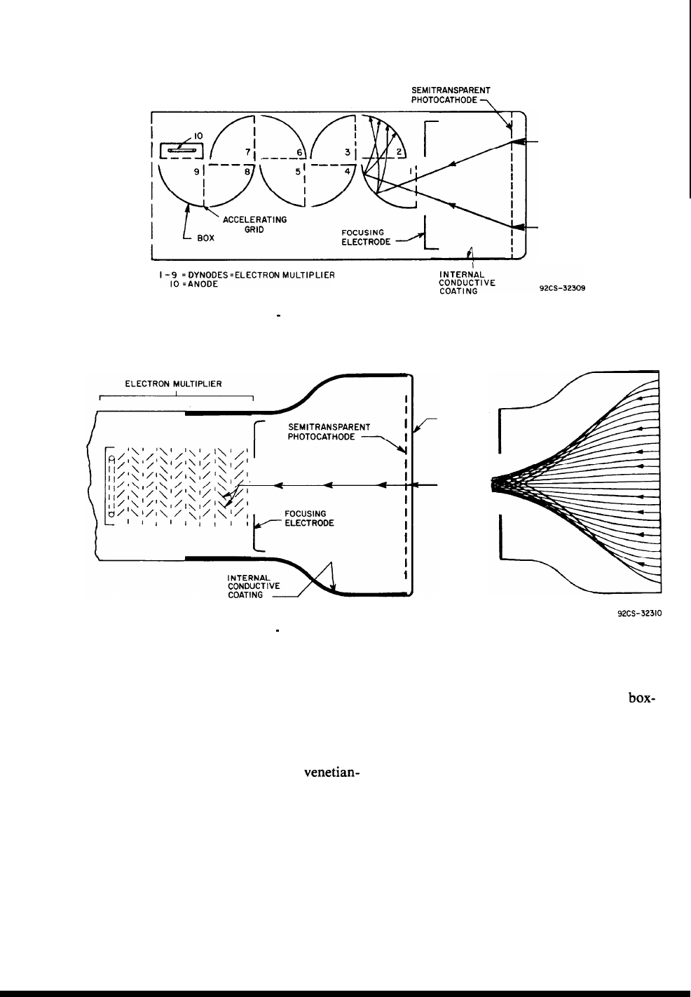
Electron Optics of Photomultipliers
INCIDENT
‘RADIATION
INCIDENT
RADIATION
Fig. 23
-
The box-and-grid multiplier structure.
FACEPLATE
INCIDENT
RADIATION
Fig. 24
-
The Venetian-blind multiplier structure.
transit time between dynodes is relatively
slow and has a rather large time spread.
Venetian-Blind Structure
Another structure which provides good
collection of photoelectrons, but again is
rather slow in response time, is the
venetian-
blind photomultiplier shown in Fig. 24.
Good collection of photoelectrons is aided
by the size of the photoelectron collecting
area which can be even larger than that of
the box-and-grid construction. The relatively
slow time response is the result of the weak
electric field at the surfaces of the dynode
vanes. The structure is very flexible as to the
number of stages. Some of the secondary
electrons are lost because of the interposition
of the grids between stages, as with the
box-
and-grid construction.
Tea-Cup Structure
A recent innovation in front-end design is
the so-called “tea-cup” photomultiplier,
named after its large first dynode. Secondary
electrons from the first dynode are directed
to an opening in the side of the tea-cup and
thence to the second dynode. Fields between
the photocathode region and the first
dynode region are separated by a very fine
grid structure. The particular advantage of
this design is that the collection efficiency of
the large first dynode is good not only for
29
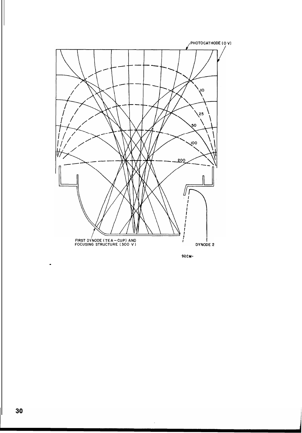
Photomultiplier Handbook
92CM-32311
Fig. 25
-
Tea-cup photomultiplier showing photoelectron paths directly from the
photocathode and those initiated by light transmitted through the photocathode
and striking the side wall which also has an active photoemissive layer. Also in-
dicated are equipotential lines in the region between photocathode and first
dynode.
photoelectrons emitted from the photocath-
ode but for photoelectrons emitted from the
activated side walls between the first dynode
and the photocathode as shown in Fig. 25.
The side-wall photoemission results from
light which passes through the front semi-
transparent photocathode. The increased
photoemission and collection efficiency im-
proves the pulse-height resolution in scin-
tillation counting applications. Indicated on
the diagram are equipotential lines and pho-
toelectron paths showing the collection of
electrons from the front surface and from
the side walls.
In-Line Dynode Structure with
Curved Photocathode
The planar-photocathode design, such as
that shown in Figs. 22-25, provides excellent
coupling to a scintillation crystal, but its
time response is not as good as that of a
spherical-section-photocathode design. The
spherical-section photocathode shown in
Fig. 26 when coupled to a high-speed elec-
tron multiplier provides a photomultiplier
having a very fast time response. Some tube
types utilize a spherical-section photocath-
ode on a plano-concave faceplate to facili-
tate scintillator coupling. This design is

Electron Optics of Photomultipliers
FRONT- END REGION
92CM-32312
Fig. 26
-
Photomultiplier design with curved faceplate and in-line dynode structure to
provide a minimum transit time and transit-time spread.
PHOTOCATHODE
DYNODE NO. I
TYPICAL
ELECTRON
TRAJECTORIES
TYPICAL
EQUIPOTENTIAL
LINES
92CM-32313
Fig. 27
-
Cross section of a photomultiplier showing equipotential lines and electron
trajectories that were plotted by computer.
31

Photomultiplier Handbook
usually limited to faceplate diameters of two
inches or less because of the excessive thick-
ness of the glass at the edge. The
plano-
concave faceplate may also contribute to
some loss in uniformity of sensitivity be-
cause of internal reflection effects near the
thick edge of the photocathode.
The performance of the front-end struc-
ture shown in Fig. 26 has been determined by
the use of a computer to trace equipotential
lines and electron trajectories which have
then been superimposed on a schematic dia-
gram of the tube structure as shown in Fig.
27.
A time parameter of interest is the photo-
cathode transit-time difference, the time dif-
ference between the peak current outputs for
simultaneous small-spot illumination of dif-
ferent parts of the photocathode. In a
planarcathode design, the transit time is
longer for edge illumination than for center
illumination because of the longer edge tra-
jectories and the weaker electric field near
the edge of the photocathode. The
center-to-
edge transit-time difference may be as much
as 10 nanoseconds. The spherical-section
photocathode affords more uniform time re-
sponse than the planar photocathode be-
cause all the electron paths are nearly equal
in length; however, the transit time is slightly
longer for edge trajectories than for axial
trajectories because of the weaker electric
field at the edge.
The photocathode transit-time difference
is ultimately limited by the initial-velocity
distribution of the photoelectrons; this
distribution causes time-broadening of the
electron packet during its flight from the
photocathode to the first dynode. The
broadening effect can be minimized by in-
creasing the strength of the electric field at
the surface of the photocathode.
Because the energy spread of secondary
electrons is even larger than that of photo-
electrons, initial-velocity effects are the ma-
jor limitation on the time response of the
electron multiplier. Multiplier time response
is usually improved by the use of high
electric-field strengths at the dynode surfaces
and compensated design geometries. In a
compensated design, such as that shown in
Fig. 28 and as used in the type of photomul-
tiplier shown in Fig. 26, longer electron
paths and weaker fields alternate with
32
shorter electron paths and stronger fields
from dynode to dynode to produce nearly
equal total transit time.
Certain materials have advantages over
other materials in providing good multiplier
time performance. For example, a standard
dynode material, copper beryllium, has a
maximum gain per stage of 8 at a 600-volt
in-
terstage potential difference. In contrast,
gallium phosphide exhibits a gain of 60 or
more at a
1200-volt
interstage potential dif-
ference. The advantage in time performance
of the
GaP
dynode over one of the
CuBe
type is that the number of stages, and thus
the total transit time may be reduced, and
that the energy spread of the secondary elec-
trons is less.
92cs-32314
Fig. 28
-
A compensated-design multiplier.
Continuous-Channel Multiplier Structure
The continuous-channel multiplier
struc-
ture35
shown in Fig. 29 is very compact and
utilizes a resistive emitter on the inside sur-
face of a cylinder rather than a discrete
number of dynodes. The lack of discrete
dynodes causes the electron-multiplication
statistics to be poor because of the variable
path lengths and the variable associated
voltages. The gain of a continuous-channel
multiplier is determined by the ratio of the

channel length to inside diameter; a typical
value of this ratio is
50
but it may range from
30
to 100.
92cs-32315
Fig. 29
-
The continuous-channel multiplier
structure.
Very high gain can be achieved with such a
single-channel multiplier, provided the chan-
nel is curved or bent to avoid line-of-sight
feed-back paths. Numerous special purpose
photomultiplier tubes have been built using
this concept.
Recently,36
very-high-speed photomulti-
plier tubes have been designed utilizing
microchannel plates in proximity with the
photocathode and anode. Such a device is il-
lustrated in Fig. 30. A microchannel plate is
an array of parallel channels, each perhaps
ray is mounted close to the photocathode
with the plane of the channel plate parallel to
the photocathode. A high voltage, 1 kilo-
volt, may be applied between photocathode
and microchannel plate, and similar voltages
applied across the microchannel sandwich
and between the plate and the anode. These
voltages assure short transit times. Time
resolution for pulses initiated by single
MICROCHANNEL
PLATE
\
Electron Optics of Photomultipliers
photoelectrons measured at full width at half
maximum
(FWHM)
is less than 300
pico-
seconds.37
Because of the construction and
high electric fields employed, the sensitivity
to external magnetic fields is much reduced,
a fact which is important in some nuclear
physics experimentation.
Crossed-Field Multiplier Structure
As mentioned earlier, a crossed-field
photomultiplier was first reported in earl
1936 by Zworykin, Morton and Malter.
3g
Their tube, shown schematically in Fig. 31,
used a combination of electrostatic and mag-
netic fields to direct electrons to repeated
stages of secondary emission. Above each
emitter was a field plate whose potential was
set to be equal to that of the next emitter
down the line. As a result of this configura-
tion, electrons emitted from the photocath-
ode or from one of the secondary emitters,
were caused to follow approximately cy-
cloidal paths to the next electrode. This early
development was not carried into large-scale
manufacture because of the critical
magnetic-field adjustments needed to change
the gain. Also, the rather wide open struc-
ture resulted in high dark current because of
feedback from ions and light developed near
the output end of the device.
Recently, however, similar, but improved
crossed-field photomultipliers39 have been
designed to provide perhaps the fastest rise
time of any photomultiplier. The electron
trajectories are essentially isochronous in the
crossed magnetic and electric fields so that a
very short rise time, 250
picoseconds40,
is
/
PHOTOCATHODE
/FACEPLATE
I
1
ANODE
92cs-32316
Fig. 30
-
Microchannel-plate photomultiplier.
33

Photomultiplier Handbook
achieved. Unfortunately, the photocathode
is rather small and inaccessible by the nature
of the design. A schematic drawing of the re-
cent crossed-field photomultiplier is shown
in Fig. 32. Note the single field electrode in
contrast to the multiple field the plates of the
Zworykin tube. The stepped arrangement is
required in order to provide uniform electric
field. A
50-ohm
coaxial output connector
provides coupling to the high-speed photo-
multiplier.
A
FIELD PLATES
CATHODE COLLECTOR
92CS
-
32317
Fig. 31
-
Schematic of the Zworykin
crossed-
field photomultiplier reported in 1936. A mag-
netic field, perpendicular to the plane of the
drawing,
and an electrostatic field, produced
by the upper fieldplates, combine to bend the
electron paths in the cycloidal trajectories il-
Iustrated.
FIRST
DYNODE
92CS-32318
Fig. 32
-
Schematic arrangement of a
modern static crossed-field photomultiplier.
ANODE CONFIGURATIONS
The primary function of the anode is to
collect secondary electrons from the last
dynode. The anode should exhibit a
constant-current characteristic of the type
shown in Fig. 33. The simplest anode struc-
ture, shown in Fig. 34, is a grid-like collector
used in some Venetian-blind structures. The
secondary electrons from the next-to-last
dynode pass through the grid to the last
dynode. Secondary electrons leaving the last
dynode are then collected on the grid-like
anode.
POTENTIAL BETWEEN LAST DYNODE AND ANODE-VOLTS
92cs -32319
Fig. 33
-
Constant-current characteristics of
a photomultiplier anode.
GRID-LIKE
TRAJECTORY
Fig. 34
-
The
simplest anode structure, a
grid-like collector.
In applications where large output pulse
currents are required it is important to pro-
vide a design having reasonably high with-
drawal fields to avoid space-charge develop-
ment which could limit the output current.
Space charge may actually limit the output at
the next to the last dynode, which is the case
in the circular-cage structure, Fig. 21,
because the withdrawal field at the last
dynode is significantly higher than at the
eighth dynode. In special applications a
tapered divider network may be used to pro-
vide higher inter-stage voltages in the last
several stages of the tube (see Chapter
5-Photomultiplier Applications).
Where fast time response is important, the
type of design shown in Fig. 34 may be at a
disadvantage because electrons from the last
dynode are not necessarily collected on the
first pass through the anode grid structure. It
is also important for fast time response that
the anodes be designed with
matched-
impedance transmission lines or with short
connecting support leads. Most high-speed
circuits are designed to utilize a
50-ohm
im-
34

Electron Optics of Photomultipliers
pedance, which requires a suitable connector
or lead geometry outside the tube to permit
proper impedance matching.
Anode configurations and internal trans-
mission lines may be analyzed by use of the
standard methods of cavity and transmis-
sion-line analysis. These methods yield ap-
proximate design
parameters41,
which are
optimized experimentally by means of
time-
domain reflectometry,
TDR42’43.
TDR pro-
vides information about the discontinuities
in the characteristic impedance of a system
as a function of electrical length and is an ex-
tremely useful approach in the design of
voltage-divider circuits and mating sockets
which do not readily lend themselves to
mathematical analysis.
Certain anode structures in fast-rise-time
photomultipliers exhibit a small-amplitude
pulse (prepulse) that can be observed a
nanosecond or two before the true signal
pulse. In grod-like anode structures this
prepulse is induced when electrons from the
next-to-last dynode pass through the anode
grid. In more sophisticated photomultiplier
designs this phenomenon may be suppressed
by auxiliary grids that shield the anode from
the effects of the impinging electron cloud.
REFERENCES
35. K.C. Schmidt and C.F. Hendee,
“Continuous-Channel Electron Multiplier
Operated in the Pulse-Saturated Mode,”
IEEE Trans.
Nucl.
Sci.,
Vol. NS-13, No. 3,
p. 100 (1966).
36. Ph. Chevalier, J.P. Boutot and G.
Pietri, “PM of new design for high speed
physics,” IEEE Trans.
Nucl.
Sci.,
Vol.
NS-17, No. 3, pp. 75-78 (June, 1970); G.
Pietri ,
“Contribution of the channel elec-
tron multiplier to the race of vacuum tubes
towards picosecond resolution time,” IEEE
Trans.
Nucl.
Sci. , Vol. NS-24, No. 1, pp.
228-232,
(Feb.
,
1977).
37.
C.C. Lo, P. Lecomte and B. Leskovar,
“Performance studies of prototype
micro-
channel plate photomultipliers," IEEE
Trans.
Nucl.
Sci., Vol. NS-24, No. 1 , pp.
302-311 , (Feb. , 1977).
38.
V.K. Zworykin, G.A. Morton, and L.
Malter ,
“The secondary emission multi-
plier-a new electronic device”’
Proc.
I.R.E.
Vol. 24 p. 351-375 (1936).
39. R.S. Enck and W.G. Abraham,
“Review of high speed communications
photomultiplier detectors,"
Proc.
Soc.
Photo Optical Instrumentation Engineers,
Vol. 150; Laser and Fiber Optics Communi-
cations’ San Diego CA; 28-29 Aug. , 1978
(Bellingham , WA; Soc. Photo-Optical In-
strumentation Engineers , 1978) , p 3 l-8.
40.
B. Leskovar and C.C. Lo, “Time Res-
olution Performance Studies of Contempo-
rary High Speed Photomultipliers,” IEEE
Trans.
Nucl.
Sci., Vol. NS-25, No. 1, pp.
582-590,
(Feb. 1978).
41.
I.A.D. Lewis and F.H. Wells,
Milli-
Microsecond Pulse Techniques, Pergamon
Press (1959).
42.
“Time-Domain Reflectometry,”
Hewlett Packard Application Note 62.
43.
“Time-Domain Reflectometry,”
Tektronix Publication 062-0703-00.
35

Photomultiplier Handbook
4.
Photomultiplier
Characteristics
PHOTOCATHODE-RELATED
CHARACTERISTICS
Current-Voltage Characteristics
Photomultiplier tubes may be operated as
photodiodes by utilizing the first dynode and
focusing electrode (if present) tied together
as an anode. In this mode of operation the
photocurrent is linear with light flux except
that, for semitransparent photocathodes, the
resistivity of the thin photocathode layer
limits the current which can be drawn. In the
case of a resistive photocathode, when the
light is directed to the center of the sensitive
area, there is a drop in potential between the
outer conductive ring and the illuminated
area. Because the illuminated area becomes
positively charged with respect to the photo-
cathode contact, only the more energetic
photoelectrons emitted will overcome the
slightly repelling electric field near the
photocathode surface.
Fig. 35 shows a pair of current-voltage
characteristics for
75-mm-diameter
photo-
multipliers operated as photodiodes. In both
cases the illuminated area is approximately 5
mm in diameter and located at the center of
the photocathode. The multialkali photo-
cathode (S-20 response) layer is fairly con-
ductive so that even for a photocurrent of
over 200 nanoamperes, good collection effi-
ciency is achieved for a collection voltage as
low as 50 volts. On the other hand, the
bialkali photocathode ,
K2CsSb
, is very
resistive causing poor collection efficiency
over a wide range of voltage even for photo-
emission currents as low as 10 nanoamperes.
For resistive photocathodes it is thus
necessary to limit the maximum photocath-
36
VOLTAGE-VOLTS
92CM-32321
Fig. 35
-
Current-voltage characteristics for
75-mm diameter photomultiplier tubes oper-
ated as photodiodes. The poor collection effi-
ciency shown for the tube with the resistive
photocathode is caused by the voltage drop
from the edge of the photocathode to the cen-
ter illuminated spot and the resulting electro-
static field distortion between the photocath-
ode and the first dynode and focus electrode
used together as an anode.
ode current to avoid non-linear operation.
Resistivity characteristics of several types of
photocathode are shown in Fig. 36. Here,
the resistance per square is shown as a func-
tion of temperature. The increase in resistivi-
ty with decreasing temperature is expected
because of the semiconductor nature of
photocathode materials. Resistance per
square is the resistance of a surface layer be-
tween conductors at opposite sides of a
square of the layer. Note that, if the resistivi-
square of side dimension d, and thickness t,

the resistance
R
is given by
where d l t is the cross-section area. Thus,
the resistance per square is independent of
the side dimension. On photocathode types
that are very resistive , it is advisable to main-
tain operating temperatures above -100° C
depending upon photocathode diameter , the
light-spot diameter, and the photocathode
current. The larger the photocathode diam-
eter and the smaller the light-spot diameter,
the more severe the effect.
2
Fig. 36 - Resistance per square as a function
of temperature for various semitransparent
photocathodes.
These data were ob-
tained with special
tubes
having connections
to parallel conducting lines or between con-
centric conducting circular rings on the Sur-
face of the photocathode.
Photomultiplier Characteristics
Photocathode resistive effects can be
avoided at manufacture by the use of nearly
transparent conductive undercoatings.
Opaque types of photocathode, such as
Cs3Sb on a solid substrate of nickel, do not
have a resistivity problem. Table II provides
guidance as to the maximum dc current that
can be utilized with various semitransparent
photocathodes at room temperature. It
should be realized that these data are only
typical; individual photocathodes may vary
considerably from the guideline provided in
their capability of delivering current without
resistive blocking.
Table II - Maximum Recommended Pboto-
cathode DC Currents for Various Semitrans-
parent Photocathode Types as Determined
by Surface Resistivity.
Photocathode Maximum Recommended
Current for T = 22°C
In the case of pulsed photocathode cur-
rents, the peak current values may be higher
than those shown in Table II. Average cur-
rents, however, are still limited, as shown,
by the resistance of the photocathode layer.
For a current pulse, the local surface poten-
tial of the cathode is sustained for a time by
the electrical charge associated with the pho-
tocathode capacitance. Thus, a square cen-
timeter of photocathode may have a capaci-
tance of about 0.5 picofarad. A 5-volt
change in potential is about the maximum
that could occur without blocking of the
photoemission current. The equivalent
charge is therefore 2.5 picocoulombs. For a
pulse duration of t seconds, a pulse current
of 2.5/t picoamperes could be maintained.
For t = 1 microsecond, the current maximum
could be 2.5 microamperes, as determined
by stored charge alone.
Pulse current maximum can be increased
by the capacitance of the photocathode
layer. For example, if a ground plane is pro-
vided in contact with the outside of the
37

Photomultiplier Handbook
photocathode faceplate, the capacitance of a
square centimeter of photocathode may be
increased to about 2 picofarads (assuming a
dielectric constant 6.75 and a glass thickness
of 3 mm). The ground plane must, of course,
be reasonably transparent to the light signal.
A conducting mesh is a suitable solution.
The ground plane should also be set at or
near photocathode potential, or noisy opera-
tion and deterioration of the photocathode
may result. See the section below under
“Dark Current and Noise.”
Variations in Spectral Response with
Temperature.
Minor variations in the spectral response
characteristics of photocathodes occur with
changes in temperature. Data are presented
here on the typical variations which can be
expected. Deviations from these data may be
expected on individual photocathodes be-
cause of variations in thickness and process-
ing.
When the temperature is decreased, the
response of photocathodes usually improves
in the shorter-wavelength region and
worsens in the longer-wavelength region
near the threshold. An illustration of this
trend is provided in Fig. 37 in which the
Fig. 37
-
Temperature coefficient of
cesium-
antimony cathodes as a function of wave-
length at 20 “C. Note the large positive effect
near the threshold.
temperature coefficient of responsivity of a
cesium-antimony photocathode is plotted as
a function of wavelength.46 The difference
in spectral response from room to liquid-air
temperature is illustrated in Fig. 38, also for
Cs3Sb.
According to Spicer and
Wooten47,
the increase in response in the blue at low
temperatures is the result of a decrease in
energy loss from lattice scattering; the de-
crease in the red at low temperatures results
from a decrease in occupied defect levels in
the forbidden energy band because of an in-
crease in band gap and possibly because of
an unfavorable change in band bending. It
may also be the case that, in photocathodes
having significant impurity levels, the ex-
tended red sensitivity at higher temperatures
is partly the result of thermally assisted
photoemission. The change of slope at the
elevated temperature in Fig. 38 is suggestive
of this mechanism.
0.1
1
I I
I
1
400 500 600
WAVELENGTH
-
NANOMETERS
92cs-32324
Fig. 38
-
Dependence of responsivity of a
Cs3Sb
photocathode on temperature; taken
from Spicer and
Wooten.
The data shown in Fig. 39 is of the same
type as that in Fig. 38, but for a GaAs:Cs
photocathode. Note, again, the increase in
sensitivity with decrease in temperature ex-
cept for the shift in the long wavelength
threshold. In GaAs:Cs the photoexcitation is
from the valence band; there is essentially no
excitation from the forbidden energy band.
Note the sharp long-wavelength cutoff.
38

Photomultiplier Characteristics
Fig. 39
-
Relative spectral responsivity shift
with temperature for a
GaAs:Cs
photocath-
ode.
48
Variation of Photocathode Response with
Angle of Incidence and Angle of Polariza-
tion.
In a theoretical paper49
Ramberg
has
evaluated the optical factors which deter-
mine the variation of photoresponse as a
function of polarization angle and angle of
incidence. One interesting conclusion of
Ramberg’s work is that for normal incidence
and for a certain regime of cathode thickness
and escape depth, the photoemission “may
be expected to be about 1.4 times as great for
illumination from the glass side as for il-
lumination from the vacuum side.” Photo-
multiplier tubes with semitransparent
photocathodes such as are used in typical
scintillation counting applications are all
designed for radiation incident on the glass
substrate which supports the photocathode.
The two curves of Fig. 40 are calculated
from Ramberg’s formulae for incidence
through the glass faceplate, and for polariza-
tion perpendicular and parallel to the plane
of incidence. (i.e. “parallel” implies that the
electric vector lies in the plane defined by the
incident ray and the normal to the glass sur-
face.) These curves assume an index of
refraction for the glass of 1.5, for the photo-
sensitive layer of 3.25, and the absorption in-
dex for the photosensitive layer, K, of 3.25.
The photocathode layer is assumed to be
thin with respect to the wavelength of
light-
taken as 550 nanometers for Fig. 40.
Note that Ramberg’s prediction is that
response should be greater for
perpendicular
polarization, especially at large angles of
in-
cidence.
This conclusion is at odds with
some reported measurements. Experimental
measurements for a semitransparent
Cs3Sb
92CM-32326
Fig. 40
-
Theoretical photoexcitation deter-
mined by optical factors for different polariza-
tion orientation as a function of angle of
incidence. Radiation is incident on a semi-
transparent photocathode such as Cs3Sb
through a glass substrate of index of refrac-
tion 1.5. Data are taken from
Ramberg.
0
2.0
(b)
92cs-32327
Fig. 41
-
(a) Photoresponse for a semitrans-
parent
Cs3Sb
photocathode as a function of
(0°) and perpendicular (90°) to the plane of in-
cidence. (b) Photoresponse ratio for polariza-
sured at an angle of incidence of 70°(from
Hoenig and
Cutler50).
39

Photomultiplier Handbook
photocathode on Corning 9741 glass are
reported by Hoenig and Cutler50
. Their
data, are shown in Fig. 41 a and b. Their
curve, a, shows the variation of photosen-
for two different angles of polarization. The
parallel to the plane of incidence. The curve,
b, shows the ratio of the photoresponse for
polarization angle 0° to the photoresponse
both measured at 70° angle of incidence.
Note that the response is greater for
polarization parallel to the plane of in-
cidence .
Measurements at RCA support the general
conclusion that the response is higher for
parallel
polarization for Cs
3
Sb,
K2CsSb
and
Na2KSb:Cs
semitransparent photocathodes
at large angles of incidence. On the other
hand, Hora51
finds the response for a
“trialkali antimonide” to be higher for
perpendicular polarization.
It is likely that the discrepancies noted
above are related to the differences in
photocathode substrates (between the glass
and the photocathode), photocathode thick-
ness, and photocathode processing which
may result in non-isotropic and structured
layers, in contrast, for example, to the
assumption by
Ramberg
of a very thin and
isotropic photocathode layer.
Optical Devices to Enhance Photoresponse
Numerous optical devices have been de-
vised to enhance photoresponse by utilizing
multiple paths in the faceplate and photo-
cathode. Experimental data and theoretical
analyses have been reported by a number of
different
authors.52-56
Fig. 42 shows a
typical arrangement permitting the light
beam to enter the glass substrate so that
reflected rays approach the glass-air inter-
face at an angle greater than the critical
angle and thus do not permit a refracted ray
to escape the glass. In this manner multiple
excitations of the photosensitive layer are
possible. Enhancement of the quantum effi-
ciency for an alkali-antimonide photocath-
ode may be something less than 2:1 in the
blue where the absorption of the photocath-
ode layer is high, but may be as high as 4: 1 in
the red where the absorption is low.
An interesting series of measurements and
theoretical predictions have been reported by
40
92CS-32328
Fig. 42
-
A glass quadrant in optical contact
with the photocathode window, permitting in-
coming radiation to approach the
glass-
photocathode interface at any angle of in-
critical angle for the glass-air interface (about
42°) all of the radiation is reflected,
permit-
ting multiple excitations of the photosen-
sitive surface.
D.P. Jones
56
on the behavior of a semitrans-
parent
Na2KSb:Cs
photocathode with angle
of incidence, wavelength, and polarization
angle. The optical arrangement is similar to
that shown in Fig. 42 except that a full 180°
cylindrical lens is cemented to the faceplate
and half of the surface is coated with
aluminum to reflect the rays back to the
photocathode. His data and theory favor
perpendicular polarization, particularly at
longer wavelengths.
Photocathode Uniformity
The uniformity of photocathode response
over its area may be of importance in some
applications. For example, in scintillation
counting, light pulses which excite different
areas of a non-uniform photocathode would
then result in variations in measured pulse
height. Such an effect would be more ap-
parent in the case where the scintillating
crystal is thin. In flying-spot scanners, non-
uniform photocathode sensitivity would
result in picture shading unless precaution is
taken to avoid even approximate imaging on
the photocathode surface.
Photocathode non-uniformity may result
from a variety of causes. Fig. 43 shows some
tests of photocathode uniformity. These
curves represent photoresponse for a small
focused (l/16-inch) spot as it is scanned
across the diameter of a semitransparent
photocathode. Curve (a) represents the

Photomultiplier Characteristics
uniformity ( ± 3%) typical of a well-pro-
cessed photocathode in a
2-inch
photomulti-
plier designed for scintillation counting. In
curve
(b),
the variation (1) across the photo-
cathode is the result of a non-uniform
evaporation of antimony during the process-
ing of the photocathode. Curve (c) shows
some peculiar non-uniformities in a 3-inch
photocathode. The peaks (2) are the result of
light entering the rounded corner of the tube
envelope and increasing emission by reflec-
tions in the glass faceplate. The peaks (3)
result when light,which is transmited
through the photocathode, strikes the re-
entry shoulder of the glass envelope. The in-
side shoulder of the envelope is aluminized
as part of the photocathode contact. Some
light striking the shoulder may be reflected
back to the photocathode and cause
in-
92cs-32329
Fig. 43
-
Photocathode uniformity patterns
observed by scanning a 1/16-inch spot
across
a diameter of a semitransparent photocath-
ode in
2-inch
and
3-inch
photomultiplier tubes
used in scintillation counting. (a), scan on a
typical well-processed
2-inch
tube;
(b),
scan
on a tube with non-uniform antimony evapora-
tion on the faceplate (1); (c), scan on a typical
3-inch
tube showing peaks (2) due to entry of
light on the edge of the faceplate and (3)
peaks due to reflection or photoemission
from transmitted radiation through the photo-
cathode onto the shoulder of the bulb.
creased emission, or there may actually be
some photosensitivity on the shoulder
because of the presence of processing
materials.
Anomalies in the photocathode uniformi-
ty such as shown in Fig. 43(c) can be largely
eliminated by a fabrication technique57
creating a diffusing layer on the photocath-
ode substrate. The fabrication of a diffusing
layer can be easily accomplished by sand-
blasting the inside surface of the photomulti-
plier faceplate. The effect of the diffusing
layer is to scatter the incoming light so that
light transmitted through the photocathode
is spread out in many directions, thus
avoiding direct correlation between the posi-
tion of the incoming light spot and any inter-
nal reflections. The diffusing layer also has a
desirable effect of enhancing the photocath-
ode sensitivity.
Uniformity of photocathode response,
however,
is not sufficient to assure a
uniform output response from the photo-
multiplier. All of the emitted photoelectrons
may not be properly directed to the first
dynode by the electron optics. In the case of
a Venetian-blind dynode structure, some of
the photoelectrons may strike parts of the
dynode which do not provide good collec-
tion fields to the second dynode. Fig. 44 is a
DISTANCE ACROSS PHOTOCATHODE-INCHES
92CS-32330
Fig. 44
-
Relative collection efficiency for
photoelectrons in
a
venetian-blind type photo-
multiplier tube.
58
plot of collection uniformity in a 3-inch
Venetian-blind photomultiplier tube. The
structure in the pattern for the scan perpen-
dicular to the length of the dynode is related
to the individual slats in the Venetian-blind
structure. By way of contrast, Fig. 45 shows
similar collection uniformity plots for a
3-inch “teacup”design where the large
41

Photomultiplier Handbook
open structure of the “tea-cup” first dynode
eliminates the electron-optical effects
observed in the Venetian-blind type tube.
DISTANCE ACROSS PHOTOCATHODE- INCHES
92CS-32331
Fig. 45
-
Relative collection efficiency for
photoelectrons in a “teacup” type RCA
pho-
tomultiplier tube.
58
Uniformity of response of a photomulti-
plier may also be affected by the voltage at
which the focusing electrode is operated.
Many photomultipliers are equipped with a
focusing electrode, between the photocath-
ode and the first dynode to provide optimum
collection of the photoelectrons emitted
from the photocathode. The focusing-
electrode voltage is usually set at the point at
which maximum anode output current is ob-
tained. In some applications, spatial unifor-
mity i.e., the variation of anode current with
position of photocathode illumination, may
be more important than maximizing output
current. In such cases, however, the final ad-
justment of the focusing-electrode potential
should not differ significantly from the ad-
justment that provides optimized collection
efficiency. Fig. 46 shows a typical focusing-
electrode characteristic.
Photocathode Stability
Stability and life of a photocathode is
usually related approximately inversely to
the current drawn from it. More stable and
reliable performance results if small areas of
concentrated illumination on the cathode
surface are avoided. In normal operation of
photomultipliers, of course, the photocath-
ode current is usually small and damage to
the tube is more likely to be caused by the
amplified secondary emission currents in the
latter dynode stages.
If a photomultiplier were to contain any
significant trace of gas, ionization of the gas
could occur , depending upon the applied
voltages and level of photocurrent. Ion bom-
bardment of the photocathode can readily
cause damage and loss of sensitivity in pro-
portion to the ion current. Photomultiplier
tubes, however, are generally so well evacu-
ated that ion damage is essentially only a
theoretical possibility.
Electrolytic effects can bring about serious
fatigue in
Cs3Sb
photocathodes (Ref. 11, p.
79) and presumably in other alkali-
antimonide photocathodes. An electrolytic
effect is caused when a potential gradient is
maintained across the cathode surface.
Photocathodes generally only have one
physical contact, but a gradient can be
developed because of the resistive nature of
the photocathode layer if a large photocur-
rent is drawn, for example, from a center
spot on the cathode. Actual electrolytic
decomposition takes place, which can be
recognized by a color change in the cathode
material.
92CS-32332
Fig.46
-
A
typicalfocusing-electrode
charac-
teristic.
It is also possible to damage a photocath-
ode by maintaining a difference in potential
through the faceplate supporting the photo-
cathode, particularly at elevated tempera-
tures. For example, if the photocathode in a
photomultiplier is maintained at
-
1000
42

Photomultiplier
Characteristics
volts and a ground plane at 0 volts is
established on the outside surface of the
glass, ionic conduction takes place through
the glass. Photocathode sensitivity will be
gradually deteriorated by the ionic
Photomultiplier tubes should be stored in
the dark when not in use. Blue and ultra-
violet radiation, especially, can cause photo-
chemical changes in the photocathode which
result in changes in sensitivity. It is especially
important to avoid exposure to intense il-
lumination such as sunlight even when no
voltage is applied to the tube. Permanent
damage may also result if the tube is exposed
to radiation so intense that it causes ex-
cessive heating of the photocathode. Tubes
should not be stored for long periods at
temperatures near the maximum rating of
the tube; high temperatures almost always
result in loss of sensitivity in the photocath-
ode.
A photomultiplier having a multialkali
photocathode (S-20 spectral response) tends
to lose sensitivity especially in the red por-
tion of its spectral response upon extended
exposure to high ambient room lighting; the
change is usually permanent. Contrary to
this behavior, photocathodes of the ex-
tended red multi-alkali
(ERMA)
type ap-
parently do not exhibit this loss.
The Ag-O-Cs photocathode (S-l) spectral
response) also suffers a decrease in sensitivi-
ty, particularly during operation, when ex-
posed to high radiant-energy levels normally
not harmful to other types of photocathode
materials. The decreased sensitivity occurs
primarily in the infrared portion of the spec-
trum. Loss of infrared sensitivity may also
occur following long periods of storage.
The
GaAs:Cs
photocathode is particularly
sensitive to responsivity loss even for
Another effect related to the exposure of
photocathodes to excessive blue or ultra-
violet radiation, as from fluorescent room
lighting, is a temporary increase in photo-
cathode dark emission current. The increase
may be as much as three orders of magnitude
even from relatively short exposure. This in-
crease in dark current occurs even though
voltage is not applied to the tube and may
persist for a period of from 6 to 24 hours
after such irradiation. Fig. 47 illustrates the
recovery after exposure to fluorescent-lamp
radiation for several photocathode types.
Some of this effect is the result of phosphor-
escence in the glass faceplate of the photo-
multiplier, but a larger part of the effect is
apparently an excitation phenomena in the
Fig.
47
-
Variation of dark current following
exposure of photocathode to cool white fluo-
rescent-lamp radiation. The various photo-
cathodes are identified by their spectral-
response symbols.
When semitransparent photocathodes
such as
Cs3Sb
and Ag-Bi-O-Cs (and prob-
ably others) are kept in the dark for many
hours, they become very
resistive59,
especial-
ly at reduced temperatures. The effect may
be so great that the photomultiplier may ap-
pear to have lost sensitivity. Apparently,
passage of current through the photosen-
sitive layer as a result of normal operation
restores the photocathode conductivity. At
reduced temperatures, the process may re-
quire minutes or hours of operation to re-
turn the photocathode to a reasonable con-
ductivity.
Photomultiplier tubes have been exposed
to gamma and X-radiation to an intensity of
1010
roentgens per hour by the Naval
photocathode damage was noted except that
faceplate discoloration was observed for ex-
posure in excess of
104
roentgens. Glass
fluorescent effects were also noted during
the tests. For applications where excessive
radiation may be present, it may be noted
that Corning has developed a non-browning
glass, Ce-doped No. 9025, which has been
used for special photomultipliers.
As a result of enhanced dark count rates
observed in photomultiplier tubes used in
various earth-orbiting satellites, an in-
43

Photomultiplier Handbook
vestigation was made by Viehmann et al61
on fluorescent and phosphorescent effects in
windows used in photomultiplier tubes when
bombarded by beta rays. Source of the beta
rays was an 0.8 millicurie beta emitter,
to 2.23
MeV
(megaelectron volts). A number
of special windows were tested. For Coming
9741 glass, two decay constants were ob-
served in the
phosphorescense:
4.2 and 57
minutes. For an exposure of 9.5 x
1010
elec-
trons per square centimeter in 30 minutes, an
steradian)-
1
was observed in a
photomulti-
plier with an S-20 response, closely coupled
to the glass plate.
GAIN-RELATED CHARACTERISTICS
Gain vs. Voltage
When several secondary-emission stages
are coupled together, so that the secondary
electrons from one become the primary elec-
multiplier phototube is given by
In practice, some of the electrons may skip
stages, or become lost to
the
amplification
process by impinging upon nonproductive
secondary-emission areas.
It is customary to describe the gain of the
multiplier phototube as a function of the ap-
plied voltage. Fig. 48 shows two such curves
on a
semilog
scale. These curves illustrate the
wide range of amplification in a multiplier
phototube. They also indicate the necessity
of providing a well regulated voltage supply
for the dynode stages.
It is possible to operate a four-to-six stage
photomultiplier so that each stage is at the
voltage required for maximum secondary
emission, as shown in Fig. 19. In such cases,
the gain could be made practically indepen-
dent of voltage over a small range. However,
such a condition would require approximate-
ly 500 volts per stage; thus the total voltage
required would be very high for the amount
of gain achieved.
44
In the design or operation of a multiplier
phototube having a fixed supply voltage, the
number of stages can be chosen so that the
gain of the tube is maximum. For this pur-
pose, the optimum voltage per stage is that
value at which a line through the origin (uni-
ty gain on the log-gain scale) is tangent to the
curve, as shown in Fig. 48. This point is
92cs-32334
Fig. 48
-
Log of gain as a function of volts
per stage for a tube (1P21) with Cs-Sb
dynodes and for a tube (6342A) with Cu-Be
dynodes.
identified on the graph as the point of max-
imum gain per volt. (Note that this argument
neglects the voltage used between the last
dynode and the anode and any discrepancy
resulting from nonuniform distribution of
voltage per stage). In most applications of
multiplier phototubes, the tubes are
operated above the point of maximum gain
per volt. When both the gain and the voltage
are presented on a logarithmic scale, the
resultant curve is then closely approximated
by a straight line. Fig. 49 describes the anode
sensitivity in amperes per lumen and the
typical amplification characteristics of a
photomultiplier as a function of the applied
voltage. Curves of minimum and maximum
sensitivity are also shown.

Photomultiplier Characteristics
SUPPLY VOLTS (E) BETWEEN ANODE AND CATHODE
92cs-32335
Fig. 49
-
Typical anode sensitivity and ampli-
fication
characteristics of a photomultiplier
tube as a function of applied voltage. Note
the log-log scaling.
External Magnetic and Electrostatic Fields
All photomultipliers are to some extent
sensitive to the presence of external magnetic
and electrostatic fields. These fields may
deflect electrons from their normal path be-
tween stages and cause a loss of gain. Tubes
designed for scintillation counting are
generally very sensitive to magnetic fields
because of the relatively long path from the
cathode to the first dynode; consequently,
such tubes ordinarily require electrostatic
and magnetic shielding. Magnetic fields may
easily reduce the anode current by a much as
50 per cent or more of the “no-field” value.
The three curves in Fig.
50
show the effect
on anode current of magnetic fields parallel
to the main tube axis and perpendicular to
the main axis in the directions parallel and
perpendicular to the dynodes. The curves are
I-
D-
92CS-32336
Fig. 50
-
Curves for
3/4-inch
diameter type
4516 photomultiplier showing the effect on
anode current of magnetic fields parallel to
the main axis of the tube and perpendicular
to the main axis in the directions parallel and
perpendicular to
the
dynodes. (Units for mag-
netic field intensity are shown in both Sl
units, ampere turns per meter, and conven-
tional cgs units, oersteds. Note that 1 oersted
45

Photomultiplier Handbook
plier tubes contain some parts which have
magnetic properties, but if they are
neglected, the magnetic induction-or mag-
netic flux density B-measured in units of
gauss would be numerically the same as the
oersted values. in the case of Sl units for
magnetic induction, 1 weber per square meter
=
1
tesla =
104
gausses.)
usually provided for one or more values of
over-all applied voltage and indicate the
relative anode current in per cent as a func-
tion of magnetic field intensity. Fig. 51
shows the variation of output current of
several photomultiplier tubes as a function
of magnetic-field intensity directly parallel
to the major axis of the tube. The magnitude
of the effect depends to a great extent upon
the structure of the tube, the orientation of
the field, and the operating voltage. In
general, the higher the operating voltage, the
less the effect of these fields.
High-mu material in the form of foils or
preformed shields is available commercially
for most photomultipliers. When such a
shield is used, it must be at cathode poten-
tial. The use of an external shield may pre-
sent a safety hazard because in many ap-
plications the photomultiplier is operated
with the anode at ground potential and the
cathode at a high negative potential. Ade-
quate safeguards are therefore required to
prevent personnel from coming in contact
with the high potential of the shield.
It is possible to modulate the output cur-
rent of a photomultiplier with a magnetic
field. The application of a magnetic field
generally causes no permanent damage to a
photomultiplier although it may magnetize
those internal parts of a tube that contain
ferromagnetic materials (tubes are available
which contain practically no ferromagnetic
materials). If tube parts do become magne-
tized, the performance of the tube may be
`-2400 -1600-800 0 8001600 24003200
MAGNETIC FIELD INTENSITY
-
AMPERE TURNS PER METER
I
1
II I I
I
1
-30-20-10 0
IO
203040
OERSTEDS
92CM
-
32337
Fig. 51- Variation of output current of several photomultiplier tubes as a function of
magnetic-field intensity directly parallel to the major axis of the tube. Positive
values of magnetic field are in the direction of the tube base. Operating voltages are
indicated. The 931A is a circular-cage, side-on type. The 4902, 8053 and 8575 are
2-inch
end-on types: teacup; Venetian-blind dynode; and in-line dynode structure,
respectively.
46

degraded somewhat; however, the condition
is easily corrected by degaussing, a process in
which a tube is placed in and then gradually
withdrawn from the center of a coil operated
at an alternating current of
60
Hz with a
maximum field strength of 8000 ampere
turns per meter (100 oersteds).
Linearity
Because the emission rate of photoelec-
trons is proportional to the incident radiant
flux, and the yield of secondary electrons for
a given primary electron energy is propor-
tional to the number of primary electrons,
the anode current of a photomultiplier is
proportional to the magnitude of the inci-
dent radiant flux. A linearity plot over a
wide range of light level is shown in Fig. 52
LIGHT FLUX -LUMENS
92CS-32338
Fig. 52
-
Range of anode-current linearity as
a function of light flux for a 931A photomulti-
plier.
for a type 931A. The limit of linearity occurs
when space charge begins to form.
Space-
charge-limiting effects usually occur in the
space between the last two dynodes. The
voltage gradient between anode and last
dynode is usually much higher than between
dynodes and, therefore, results in a limita-
tion at the previous stage, even though the
current is less. The maximum output cur-
rent, at the onset of space charge, is propor-
tional to the 3/2 power of the voltage gra-
dient in the critical dynode region. By use of
an unbalanced dynode-voltage distribution
increasing the interstage voltages near the
output end of the multiplier, it is possible to
increase the linear range of output current.
Photomultiplier Characteristics
Table III provides guidance as to the max-
imum pulse current which can be drawn
from the anode of various types of
photo-
multipliers before spacecharge effects limit
linearity. Note that the type 8575, which has
a focused dynode structure, provides the
highest withdrawal fields and highest linear
output current. On the other hand,
venetian-
blind or box-and-slot dynodes have relative-
ly low withdrawal fields. Higher currents can
be obtained from all types of photomulti-
pliers by unbalancing the voltage distribu-
tion to provide higher fields at the critical
last stages.
Some photomultipliers used in applica-
tions requiring high output pulse current use
an accelerating grid between the last dynode
and the anode to reduce the effects of
space-
charge limiting. The potential of such a grid
is usually between that of the last and the
next-to-last dynode and is adjusted by ob-
serving and maximizing the value of the
anode output current.
Another factor that may limit
anode-
output-current linearity is cathode
resistivi-
ty; cathode resistivity is a problem only in
tubes with semitransparent photocathodes,
particularly of the Cs-Sb or bialkali type.
Linear behavior is not always obtained
from photomultipliers even at low current
levels. For example, if the test light spot on a
931A is not directed close to the center of the
active area of the photocathode, disturbing
effects may arise from the proximity of the
ceramic end plates. Near the end plates, the
fields are not uniform and are affected by
charge patterns on the insulator spacers,
which change with the current level. An ex-
terior negative shield placed around the bulb
wall may improve tube linearity by elimi-
nating bulb charging effects. The passage of
excessive current may change the sensitivity
of the tube and cause an apparent non-
linearity.
Some photomultipliers exhibit a tem-
porary instability in anode current and
change in anode sensitivity for several
seconds after voltage and light are applied.
This instability, sometimes called
hysteresis
because of cyclic behavior, may be caused by
electrons striking and charging the dynode
support spacers and thus slightly changing
the electron optics within the tube. Sensitivi-
ty may overshoot or undershoot a few per
47

Tube Type
931A
(side-on, circular
cage)
4524
(3-inch, venetian-
blind dynodes)
4900
(3 -inch, Tea-cup
type)
8575
(2-inch, linear fo-
cused dynode struc-
ture)
8575
C-31059
(1 1/8-inch, box and
slot dynodes)
C-31059
Photomultiplier Handbook
cent before reaching a stable value. The time
to reach a stable value is related to the behavior may be a problem in applications
resistance of the insulator, its surface such as photometry where a photomultiplier
capacitance, and the local photomultiplier is used in a constant-anode-current mode by
current. This instability and non-linear varying the photomultiplier voltage as the
light input changes.
Table III
Maximum Anode Currents That Can be Utilized in Various Photomultiplier Types Without
Serious Loss of Linearity from Space-Charge Build-up.
Supply
Voltage Maximum
Volts Distribution*
Output Current
(mA)
with Linearity Loss Less
Than 10%
1000
1
1
1500
1200
1760
2100
1050
1150
5
5
30
120
4
12
*These number series represent the relative voltage applied between cathode and first dynode,
first dynode and second dynode,. . . . . ,
last dynode and anode. Note that in the case of the 8575
and the C-31059, a second voltage distribution is given with increased voltage drop in the last
stages providing higher output currents before the onset of space-charge-limiting conditions.
48

Photomultiplier Characteristics
Hysteresis has been eliminated in many
tubes by coating the dynode spacers with a
conductive material in the manufacturing
process and maintaining the coating at a
fixed potential. Tubes treated by this method
assume final sensitivity values almost im-
mediately upon application of light and
voltage.
Peak linear and saturation currents are
usually measured by pulsed methods. One
common method makes use of a cathode-ray
tube with a P15 or P16 phosphor. The grid is
double-pulsed with pulses of unequal ampli-
tudes but fixed amplitude ratio. As the
amplitude of the two pulses is increased, a
point is observed at which the amplitude of
the larger of the anode pulses does not in-
crease in the same proportion as the smaller
pulse. At this point the tube is assumed to
become non-linear. The current value at this
point is then measured by means of an
oscilloscope and load resistor. The max-
imum saturation current is found when a
further increase in radiation level yields no
further increase in output.
Although very high anode current can be
drawn from photomultiplier tubes, it
should be emphasized that stability cannot
be expected at such levels. These high cur-
rent levels are principally of interest in light-
pulse applications. In this case, the stability
of the tube is approximately that of the tube
operated at the integrated average current
level
t
Gain Variation with Temperature
It is often advisable to reduce the ambient
temperature of a photomultiplier in order to
reduce dark emission from the photocathode
and improve the signal-to-noise ratio of the
measurement. Variations of the spectral
characteristics of photocathodes with
temperature have been noted in the previous
section on
Photocathode Stability.
There are
numerous reports on the over-all variation
of the photomultiplier output current with
temperature including the effect of tempera-
ture on photocathode
sensitivity62-64.
Fig.
53 is a typical characteristic for type 8571
photomultiplier having Cs-Sb dynodes
showing the variation of gain with
temperature. These data do not include the
variation of photocathode response with
temperature which has been described in the
section on
Variations in Spectral Response
with Temperature. The gain data were ob-
tained by measuring both the anode response
variation and the photocathode response
variation with temperature and dividing out
the latter to obtain only the gain variation. It
is probable that the increase in gain at low
temperatures is the result of a decrease in
energy loss from lattice scattering. Although
the variation in over-all gain is fairly large, it
should be remembered that the variation
results from a small variation in each stage
compounded by the 9 stages. At room tem-
perature, the average gain per stage for the
8571 is 4.5 at 100 V per stage and the percen-
tage change in stage gain with temperature is
approximately
-0.06% per °C. Thus the
secondary emission temperature coefficient
is generally less that the photoresponse
temperature coefficient, both for Cs-Sb sur-
faces. See Fig. 37.
LOX
TEMPERATURE
-
°C
92cs-32341
Fig. 53
-
Typical variation of gain with tem-
perature for a
9-stage
photomultiplier tube
(type 8571) with Cs-Sb dynodes operating at
100 volts per stage.
A few words of caution regarding the am-
bient temperature of photomultipliers are
pertinent. A maximum ambient tempera-
ture, and in some instances a minimum tem-
perature, is specified for all photo-
49

Photomultiplier Handbook
multipliers. The specification of maximum
ambient temperatures reduces the possibility
of heat damage to the tube. Cesium, for ex-
ample, is very volatile and may be
redistributed within the tube causing loss of
secondary emission gain or loss of cathode
sensitivity.
It is recommended that photomultipliers
be operated at or below room temperature so
that the effects of dark current are mini-
mized. The variation of dark current, or
noise, is most important because of its effect
on ultimate low-light-level sensitivity.
Various cryostats and solid-state thermionic
coolers have been designed that reduce dark
current at low temperatures in low-light-level
applications. An important consideration in
the use of these devices is to prevent conden-
sation of moisture on the photomultiplier
window. A controlled low-humidity atmos-
phere or special equipment configuration
may be necessary to prevent such condensa-
tion.
Another reason for avoiding the operation
of photomultipliers at extremely low temper-
atures is the possible phase change that this
type of operation may cause in some of the
metal parts. These changes are particularly
probable when Kovar is used in
metal-to-
glass seals. Tubes utilizing Kovar in their
construction should not be operated at tem-
peratures below that of liquid nitrogen
(-196°C).
In some tubes, particularly those with
multialkali photocathodes, it is sometimes
observed that the noise actually increases as
the temperature of the photocathode is re-
duced below about -40°C. The reason for
this noise increase is not understood. How-
ever, most of the dark-current reduction has
already been achieved at temperatures above
-40°C.
In general, it is recommended that all
wires and connections to the tube be encap-
sulated for refrigerated operation. Encap-
sulation minimizes breakdown of insulation,
especially that caused by moisture condensa-
tion.
Stability and Gain
All photomultipliers have a maximum
anode current rating. The primary reason
for such a rating is to limit the anode power
dissipation to approximately one-half watt
or less. Consequently, the magnitude of the
50
maximum anode current is restricted to a
few milliamperes when the tube is operated
at 100 to
200
volts between the last dynode
and the anode. Many photomultipliers are
rated for only 0.1 mA or less.
Operating a photomultiplier at an ex-
cessively high anode current results in an in-
creased fatigue that occurs as the average
anode current increases. The loss in sensitiv-
ity occurs as a result of a reduction in the
secondary emission, particularly in the last
stages of the photomultiplier where the cur-
rents are the highest.
Tube fatigue or loss of anode sensitivity is
a function of output-current level, dynode
materials, and previous operating history.
The amount of average current that a given
photomultiplier can withstand varies widely,
even among tubes of the same type; conse-
quently, only typical patterns of fatigue may
be cited.
The sensitivity changes are thought to be
the result of erosion of the cesium from the
dynode surfaces during periods of heavy
electron bombardment, and the subsequent
deposition of the cesium on other areas
within the photomultiplier. Sensitivity losses
of this type, illustrated in Fig. 54 for a 1P21
TIME-MINUTES
92cs-32339
Fig. 54
-
Short-time fatigue and recovery
characteristics of a typical 1P21 operating at
100 volts per stage and with a light source
ad-
justed to give 100 microamperes initial anode
current. At the end of 100 minutes the light is
turned off and the tube allowed to recover
sensitivity. Tubes recover approximately as
shown, whether the voltage is on or off.

Photomultiplier Characteristics
operated at an output current of 100 micro-
amperes, may be reversed during periods of
non-operation when the cesium may again
return to the dynode surfaces. This process
of recovery may be accelerated by heating
the photomultiplier during periods of non-
operation to a temperature within the max-
imum temperature rating of the tube;
heating above the maximum rating may
cause a permanent loss of sensitivity.
Sensitivity losses for a given operating cur-
rent normally occur rather rapidly during in-
itial operation and at a much slower rate
after the tube has been in use for some time.
Fig. 55 shows this type of behavior for a
0100 200300400
5
2
TIME -HOURS
92cs-32340
Fig. 55
-
Typical sensitivity loss for a 1P21
operating
at
100 volts per stage for a period of
500 hours. Initial anode current is 100 micro-
amperes and is readjusted to this operating
value at 48, 168, and 360 hours.
1P21 having Cs-Sb dynodes, operating at an
output current of 100 microamperes. Tubes
operated at lower current levels, of the order
of 10 microamperes or less, experience less
fatigue than those operated at higher cur-
rents, and, in fact, may actually recover
from high-current operation during periods
of low-current operation.
Fatigue rates are also affected by the type
of dynode materials used in a tube. Copper
beryllium or silver magnesium dynodes are
generally more stable at high operating cur-
rents than the cesium antimony types. The
sensitivity for tubes utilizing these dynodes
very often increases during initial hours of
TIME -HOURS
Fig. 56
-
Typical responsivity variation on life
for a photomultiplier having silver-magne-
sium dynodes. Initial anode current was 2 mil-
liamperes and was readjusted to this operat-
ing value at 48, 168, and 360
hours.
operation, after which a very gradual de-
crease takes place, as illustrated in Fig. 56.
The operating stability of a photomulti-
plier depends on the magnitude of the
average anode current; when stability is of
prime importance, the use of average anode
currents of 1 microampere or less is recom-
mended.
In addition to the life characteristics,
which are probably the result of changes in
the dynode layer itself, other changes of a
temporary nature also occur. Not all these
changes are well understood; some are
charging of insulators in the tube.
Fig. 57 illustrates one of the peculiar in-
stabilities which are sometimes observed in
photomultiplier tubes. When the light is first
turned on, the current apparently overshoots
and then decays to a steady value. This par-
ticular phenomenon is probably the result of
the charging of the supporting insulator for
the dynodes. The effect is observed to occur
more rapidly at higher currents, presumably
51

Photomultiplier Handbook
because of the greater charging current.
Electrons striking the insulator probably
result
in secondary emission and a resultant
positive charge. The change in potential af-
fects the electron optics in the space between
dynodes. The effect is observed as an in-
crease in some tubes and as a decrease in
others. When the photomultiplier is designed
with metal shields or with conductive
coatings on the critical areas of the in-
sulators, this effect is eliminated.
TIME
-
SECONDS
92cs-32343
Fig. 57
-
Sudden shift in anode current prob-
ably as the result of insulator spacer charg-
ing. Observation was made using an experi-
mental photomultiplier in which the effect
was unusually large.
A related phenomenon is the variation of
pulse height with pulsecount rate in
scintillationcounting applications. Thus,
when a radio-active source is brought closer
to a scintillating crystal a greater rate of scin-
tillations should be produced, all having the
same magnitude. In a particular photomulti-
plier a few per cent change in amplitude may
result and cause problems in measurement.
Fig. 58 shows the typically minor variation
of pulse height with pulse-count rate for a
type 6342A multiplier phototube.
0.4 0.6
COUNTING
0.8
RATE
92cs-32344
Fig. 58
-
Typical variation of pulse
height
with pulsecount rate for a 6342A. 3
(13
Cs
source with a Nal:Tl source).
In order to investigate the phenomena of
pulse-height variation with pulsecount rate,
a purposely exaggerated experiment was
devised. Instead of a scintillating crystal, a
pulsed cathode-ray tube was used as a light
source. Two pulse rates were studied: 100
and 10,000 pulses per second. Pulse duration
was one microsecond; decay time to 0.1
maximum was 0.1 microsecond. The experi-
ment was devised to study the rate at which
the photomultiplier tube output response
changed when the pulse rate was suddenly
switched between the two rates. Tubes such
as the
6342A,
and especially the 8053 and
8054, showed practically no effect (of the
order of one per cent or less). Fig. 59 shows
Fig. 59
-
Variation of output pulse height as
the rate of pulsing is changed in a poorly
designed experimental tube. Light pulses
were provided from a cathode-ray tube. At the
left of the graph, which shows the pulse-
amplitude envelope with time for the output
of the photomultiplier tube, the pulses are at
100 per second. The pulse rate is increased
suddenly to 10,000 per second and again re-
duced as indicated. Changes in amplitude are
probably the result of insulator charging.
the pulses during the switching procedure for
an experimental tube. The phenomena were
completely reversible and were observed (to
a lesser extent) on many different tube types.
The time-decay period of several seconds
suggests the charging of an insulator spacer
to a new potential as the result of the in-
creased charge flow and the subsequent
modification of interdynode potential fields.
In scintillation counting it is particularly
important that the photomultiplier have very
good stability. There are two types of gain
stability tests which have been used to
evaluate photomultipliers for this
applica-
52

tion: (1) a test of long-term drift in pulse-
height amplitude measured at a constant
counting rate; and (2) a measure of
short-
term pulse-height amplitude shift with
change in counting rate.
In the time stability test, a pulse-height
analyzer, a
137Cs
source, and a NaI(T1)
crystal are employed to measure the pulse
height. The 137Cs source is located along the
major axis of the tube and crystal so that a
count-rate of 1000 counts per second is ob-
tained. The entire system is allowed to warm
up under operating conditions for a period
of one-half to one hour before readings are
recorded. Following this period of stabiliza-
tion, the pulse height is recorded at one-hour
intervals for a period of 16 hours. The drift
rate in per cent is then calculated as the mean
gain deviation
(MGD)
of the series of pulse-
height measurements, as follows:
where p is the mean pulse height, pi is the
pulse height at the
ith
reading, and n is the
total number of readings. Typical maximum
mean-gain-deviation values for photomulti-
pliers with high-stability Cu-Be dynodes are
usually less than 1 per cent when measured
under the conditions specified above. Gain
stability becomes particularly important
when photopeaks produced by nuclear
disintegrations of nearly equal energy are be-
ing differentiated.
In the
count-rate stability test,
the photo-
multiplier is first operated at 10,000 counts
per second. The photopeak counting rate is
then decreased to 1000 counts per second by
increasing the source-to-crystal distance.
The photopeak position is measured and
compared with the last measurement made
at a counting rate of 10,000 per second. The
count-rate stability is expressed as the
percentage gain shift for the count-rate
change. It should be noted that count-rate
stability is related to the hysteresis effect
discussed above. Photomultipliers designed
for counting stability may be expected to
have a value of no greater than 1 per cent
gain shift as measured by this count-rate
stability test.
Photomultiplier Characteristics
Life Expectancy
The life expectancy of a photomultiplier,
although related to fatigue, is very difficult
to predict. Most photomultipliers will func-
tion satisfactorily through several thousand
hours of conservative operation and propor-
tionally less as the severity of operation in-
creases.
Photomultipliers do not have
elements which “burn out” as in the case of
a filament in a vacuum tube. Furthermore,
loss of sensitivity which occurs with opera-
tion tends to recover during idle periods or
during conservative operation.
Factors which are known to affect life
adversely are high-current operation,
excessive-voltage operation, high photocath-
ode illumination, and high temperature.
Operation of photomultipliers in regions
of intense nuclear radiation or X-rays may
result in an increase in noise and dark cur-
rent as a result of fluorescence and scintilla-
tion within the glass portions of the tubes.
Continued exposure may cause darkening of
the glass and a resultant reduction in
transmission capability.
DARK CURRENT AND NOISE
The lower limit of light detection for a
photomultiplier tube is determined in many
cases by the electrical noise associated with
the anode dark current. There are several
sources of dark current in a photomultiplier.
These sources are described below,
Sources of Dark Current
Dark current in a photomultiplier tube
may be categorized by origin into three
types: ohmic leakage, dark or “thermionic”
emission of electrons from the cathode and
other elements of the tube, and regenerative
effects .
Ohmic leakage,
which results from the im-
perfect insulating properties of the glass
stem, the supporting members, or the plastic
base, is always present. This type of leakage
is usually negligible, but in some tubes it may
become excessive because of the presence of
residual metals used in the processing of the
photocathode or the dynodes. Condensation
of water vapor, dirt, or grease on the outside
of the tube may increase ohmic leakage
beyond reasonable limits. Simple precau-
tions are usually sufficient to eliminate this
sort of leakage. In unfavorable environmen-
tal conditions, however, it may be necessary
53

Photomultiplier Handbook
to coat the base of the tube with
moisture-
resisting materials, which may also prevent
external arc-overs resulting from high
voltage.
Ohmic leakage is the predominant source
of dark current at low-voltage operating
condition. It can be identified by its propor-
tionality with applied voltage. At higher
voltages, ohmic leakage is obscured by other
sources of dark current.
Fig. 60 shows the typical variation of dark
VOLTS PER STAGE
92CS-32346
Fig.
60
-
Typical variation of dark current
with voltage for a multiplier phototube.
current of a photomultiplier tube as a func-
tion of applied voltage. Note that in the mid-
range of voltage, the dark current follows
the gain characteristic of the tube. The
source of the gain-proportional, dark cur-
rent is the dark or thermionic emission of
electrons primarily from the photocathode.
Because each electron emitted from the
photocathode is multiplied by the secondary-
emission gain of the tube, the result is an
output pulse having a magnitude equal to the
charge of one electron multiplied by the gain
of the tube. (There are statistical amplitude
variations which will be discussed later.)
Because the emission of thermionic electrons
is random in time, the output dark current
consists of random unidirectional pulses.
The time average of these pulses, which may
54
be measured on a dc meter, is usually the
principal dc component of the dark current
at normal operating voltages. The limitation
to the measurement of very low light levels is
the variable character of the thermionic
dark-current component. It is not possible to
balance out this wide-band noise component
of the photomultiplier tube, as it might be to
balance out a steady ohmic-leakage current.
Nevertheless, it is usually advantageous to
operate the photomultiplier tube in the range
where the thermionic component is domi-
nant. In this range, the relationship between
sensitivity and noise is fairly constant as the
voltage is increased because both the photo-
electric emission and the thermionic emis-
sion are amplified by the same amount.
Typical dark emission current densities for
various photocathodes are given in Table I
(page 16). The resulting anode dark current
may be estimated by multiplying the dark
emission per unit area at the photocathode
by the photocathode area and by the gain of
the photomultiplier tube at the desired
operating voltage.
The thermionic component of the dark
current varies in a regular way with
temperature as illustrated in Fig. 16, and
because the thermionic component of the
dark current is a source of electronic noise in
the anode circuit, it is frequently advan-
tageous to cool the photomultiplier and take
advantage of the reduced dark current and
noise.
Various cryostats have been
de-
signed
62,66
providing low temperature
operation of photomultipliers. One practical
consideration is the prevention of condensa-
tion of moisture on the window. In a
Dewar-
type arrangement, condensation may not be
a problem; in simpler set-ups moisture con-
densation may be prevented by a controlled
low-humidity atmosphere at the external
window. On some types of photocathode,
too cool a temperature may result in the
photocathode becoming so resistive that the
photoemission is blocked by a drop in poten-
tial across the photocathode surface. See
earlier section on
Current-Voltage Charac-
teristics. Commercial cryostats or cooled
photomultiplier chambers are available
designed especially for photomultiplier
operation67.
At higher dynode voltages, a
regenerative
type of dark current develops, as shown in
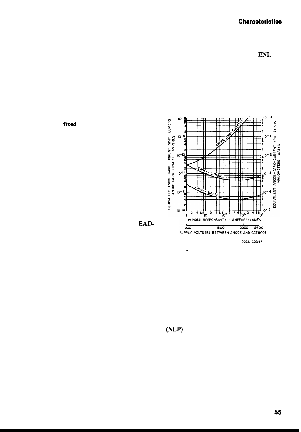
Fig. 60 . The dark current becomes very er-
ratic, and may at times increase to the prac-
tical limitations of the circuit. Continued
flow of large dark currents may cause
damage to the sensitized surfaces. Some
possible causes of the regenerative behavior
will be discussed in more detail later. All
photomultiplier tubes eventually become
unstable as the gain is increased.
Dark-Current Specification
Dark-current values are often specified at
a particular value of anode sensitivity rather
than at a
fixed
operating voltage. Specifica-
tions of dark current in this manner are more
closely related to the actual application of
the photomultiplier.
The best operating range for a given
photomultiplier can usually be predicted
from the quotient of the anode dark current
and the luminous sensitivity at which the
dark current is measured. This quotient is
identified as the Equivalent Anode Dark
Current Input (EADCI) in the Technical
Data for individual photomultiplier tubes;
and is the value of radiant flux incident on
the photocathode required to produce an
anode current equal to the dark current
observed. The units used in specifying EAD-
CI are either lumens or watts at the wave-
length of maximum cathode responsivity or
watts at a specified wavelength.
The curves in Fig. 61 shows both typical
anode dark current and equivalent anode
dark current input (EADCI) as functions of
luminous sensitivity. The optimum operat-
ing range occurs in the region of the
minimum on the EADCI curve, the region in
which the signal-to-noise ratio is also near its
maximum. The increase in the EADCI curve
at higher values of sensitivity indicates the
onset of a region of unstable and erratic
operation. Many curves of this type also in-
clude a scale of anode-to-cathode supply
voltage corresponding to the sensitivity
scale.
Equivalent Noise Input-The
dark current
in a photomultiplier is the average current
value of the output pulses occurring at ran-
dom intervals plus the dc leakage current.
Fluctuations or noise associated with these
pulses limit precision of measurement,
rather than the particular dark current value.
Noise from a photomultiplier may be
evaluated in terms of a signal-to-noise-ratio
Photomultiplier
Characteristics
measurement. If the type of modulation and
bandwidth used in the measurement is
known, an equivalent noise input, ENI, can
be calculated from the signal-to-noise ratio,
Equivalent noise input is defined as the value
of incident luminous or radiant flux which,
when modulated in a stated manner, pro-
duces an rms output current equal to the rms
noise current within a specified bandwidth,
usually 1 Hz.
92c3-32347
Fig. 61
-
Illustrative data showing the varia-
tion of anode dark current and the equivalent
anode-dark current input (EADCI) as a func-
tion of luminous sensitivity for a type 8575.
Operation of the tube at voltages higher than
that for the minimum of the EADCI character-
istic does not provide the best signal-to-noise
ratio.
Noise Equivalent Power-Another way to
categorize the limit of detection of a
photomultiplier is by noise equivalent power
(NEP)
which is essentially the same as EN1
except the units are always in watts. NEP is
the radiant flux in watts at a specified wave-
length incident on the detector which gives a
signal-to-noise ratio of unity. The frequency
bandwidth (usually 1 Hz) and the frequency
at which the radiation is chopped must be
specified as well as the spectral content of
the radiation (most often, monochromatic
radiation at the peak of the detector
response). It should be noted that NEP is
55

Photomultiplier Handbook
frequently specified in units of watts
HZ-1/2. The numerical value of this for-
mulation of NEP is the same as that given in
units of watts but with a specified bandwidth
of 1 Hz.
Detectivity-Detectivity
(D)
is the recipro-
cal of NEP; it is expressed in W
-
1.
Detectiv-
ity is a figure of merit providing the same in-
formation as NEP but in the reverse sense so
that the lower the radiation level to which
the photodetector responds, the higher the
detectivity.
Regenerative Effects
Dynode
Glow. Although photomultipliers
are designed to minimize regenerative ef-
fects, at some high voltage and gain almost
all photomultipliers exhibit breakdown
phenomena. One source of regeneration in
photomultipliers is the glowing of the
dynodes under electron bombardment.68
The glow has a blue spectral emission and of
course is most prominent in the latter stages
where the current is highest. The regenera-
tive effect occurs when the light from the
dynode glow is scattered and reflected back
to the photocathode. Dynode cage shields
and opaque support wafers minimize this ef-
fect .
Glass Charging Effects.
Regenerative
pho-
tomultiplier currents may also be triggered
by the electrostatic potential of the bulb
walls surrounding the dynode or photocath-
ode structure. Particularly when the poten-
tial of the bulb is near anode potential, stray
electrons may be attracted to the bulb and
cause the emission of light on impact, de-
pending upon the nature of the glass surface
and the presence of contamination. Secon-
dary electrons resulting from the impact of
stray electrons on the glass surface are col-
lected by the most positive elements in the
tube and help maintain the positive potential
of the inner surface of the glass. Under these
circumstances, it is possible to observe the
formation of glowing spots on the inside of
the glass bulb, provided the eye is dark
adapted and the applied voltage is sufficient-
ly high. Some of this fluorescent light may
be reflected back to the photocathode and
result in an increase in the photocathode
dark (or light) emission.
Shielding.
The effect just described can be
minimized by controlling the external poten-
tial of the glass envelope. Fig. 62 shows the
56
effect of various voltages applied to an exter-
nal shield around the tube envelope of a
1P21 photomultiplier. The graph shows the
equivalent noise input decreasing as the
shield is made negative toward the-potential
of the photocathode. It should be noted also
that an actual contact is not always required
to produce the effects noted in Fig. 62. The
proximity of a positive potential near the
glass bulb can cause a noisy operation.
4
Fig. 62
-
Effect of external-shield potential
on the noise of a 1P21 photomultiplier. Note
the desirability of maintaining a negative bulb
potential.
Operation of a photomultiplier tube with
an improper external shield may not only
cause an increase in noise or lead to an elec-
trical breakdown of the tube, but can result
in damage to the photocathode and reduced
tube life. In order to prevent these effects,
the envelope wall should be maintained near
photocathode potential by wrapping or
painting it with conductive material and con-
necting this material to cathode potential.
The connection is usually made through a
high impedance to reduce the shock hazard.
If a cathode potential shield is not provided,
the glass surface in the vicinity of the photo-
cathode must be insulated from any source
of potential difference so that leakage cur-
rents to the bulb are less than 10
-12
ampere.
In photomultiplier tubes in which the
pho-
tocathode is of a transmission type, on the
inside surface of the glass bulb, it is par-
ticularly important to avoid a positive
voltage contact on the external surface of the
photocathode window. In this case, ionic
currents can flow through the glass and pro-
duce a
fluoresence
and an accompanying
noisy photocathode current.

It should also be noted that continued
operation of a photomultiplier tube with a
positive voltage contact to the glass in the
photocathode area can cause a permanent
damage to the photocathode. The damage is
reported to be the result of ionic conduction
through the glass and poisoning of the
pho-
tocathode by sodium ions.69
Afterpulsing.
Afterpulses,
which may
be observed when photomultipliers are used
to detect very short light flashes as in scin-
tillation counting or in detecting short laser
pulses, are identified as minor secondary
pulses that follow a main anode-current
pulse. There are two general types of after-
pulses; both are characterized by their time
of occurrence in relation to the main pulse.
The first type results from light feedback
from the area of the anode, or possibly cer-
tain dynodes, to the photocathode; the in-
tensity of the light is proportional to the tube
currents. When this light feedback reaches
the cathode, the afterpulse is produced.
Afterpulses of this type, characterized by a
delay in the order of 40 to
50
nanoseconds,
may be a problem in many older
photomulti-
pliers having open dynode structures. The
time delay experienced with this type of
afterpulse is equal to the total transit time of
the signal through the photomultiplier plus
the transit time of the light that is fed back.
The second type of afterpulse has been
shown to be the result of ionization of gas in
the region between the cathode and first
dynode. The time of occurrence of the after-
pulse depends upon the tube dimensions, the
type of residual gas involved and the mass of
the gas ion, but usually ranges from 200
nanoseconds to well over 1 microsecond
after the main pulse. When the ion strikes
the photocathode, several secondary elec-
trons may be emitted; thus, the resulting
afterpulse has an amplitude equal to several
electron pulse-height equivalents. These
pulses appear to be identical to the larger
dark-current pulses, and it is suspected that
many of the dark-current pulses are the re-
sult of photocathode bombardment by gas
ions.
Several gases, including
N2
+ and
H2
+ ,
are known to produce afterpulses. Each gas
produces its own characteristic delay follow-
ing the main pulse. The most troublesome,
perhaps, is the afterpulse caused by the
H2
+
Photomultiplier Characteristics
ion; this afterpulse occurs approximately 300
nanoseconds after the main pulse in a tube
of type 7850 construction. One source of
hydrogen in the tube is water vapor absorbed
by the multiplier section before it is sealed to
the exhaust system. Other gases which may
cause afterpulsing may be present as a result
of outgassing of the photomultiplier parts
during processing or operation. Present
pho-
tomultiplier processing techniques are
designed to eliminate or at least to minimize
the problem of afterpulsing.
Helium Penetration71,72
Another effect
must be considered in relation to the sources
of dark current-the penetration of helium
through the glass of photomultiplier tubes.
When the photomultiplier is operated or
stored in an environment where helium is
present, helium will gradually permeate
through the glass envelope. Because helium
is inert, it does not react with the photocath-
ode or dynode surfaces. But tubes subjected
to such an environment will exhibit a noise
increase and an increase in afterpulsing
because of the ionization of the helium by
electron impact. Depending upon the degree
of permeation, a point will be reached at
which complete ionization and electrical
breakdown occurs making the tube unus-
able.
Other Noise Sources
Excess noise or dark current can also re-
sult from field emission occurring within the
tube and from scintillations in the glass
envelope of the tube caused by radioactive
elements within glass (most glasses contain
some radioactive 40K). Fused silica is
sometimes utilized in photomultiplier face-
plates to minimize these effects.
Noise in photomultiplier tubes can
also
result from the proximity of nuclear sources
or from cosmic rays which result in glass
scintillations. Andrew T.
Young73,
* has
identified large pulses which originate from
Cerenkov light flashes produced by cosmic
rays traversing the window of end-on photo-
multipliers. The flashes correspond to
*Andrew T. Young also has written a chapter, “Photo-
multipliers: Their Cause and Cure,” in Volume 12 of
Methods of Experimental Physics: Astrophysics,
L.
Marton, Editor, Academic Press, 1974. As well as
being
a good general reference on photomultipliers, this chap-
ter contains a further discussion of the
Cerenkov-light-
flash effect.
57

PhotomultIplier
Handbook
photoemission pulses of
50
electrons and
larger. The number of pulses is greater when
the face of the photomultiplier is upward
rather than downward because the Cerenkov
radiation is emitted in a conical pattern away
from the direction of entry. Young reports
the total number of pulses from this source
to be about 1.2 min
-
1
cm
-2.
Another phenomenon which deserves
mention in connection with dark current is
the effect of previous exposure to light,
especially blue or near ultraviolet. Large in-
creases in photocathode dark emission may
occur as discussed in section on
Photocath-
ode Stability
with rather slow recovery, as il-
lustrated in Fig. 47. It is advisable, there-
fore, that photomultipliers be kept in the
dark at all times, or at least for many hours
before they are used for making low-level
measurements.
Noise Output of a Photomultiplier
The output current of a photomultiplier
consists of a train of unidirectional electrical
pulses whether the tube is in the dark or with
illumination on its photocathode. Each pulse
is the result of an electron emitted from the
photocathode and amplified by the secon-
dary emission of the tube. (Some pulses may
originate also from light striking the first
dynode or from thermionic emission from
the first or other dynodes.) In a system hav-
ing a wide bandwith, the individual pulses
may be measured and counted. Their spac-
ing in time will have a statistical variation as
will their height. There variations constitute
noise and limit the precision of measure-
ments.
If the bandwidth is not sufficient to
resolve the individual pulses, particularly
when the light level is relatively high, the
output will exhibit noise or rapid variation in
signal level about an average value. The
noise level relative to the signal level will
decrease with increasing signal level or with
decreasing bandwidth. The noise may be de-
scribed by giving the rms value of the current
variation in a specified bandwidth.
Dark-Current and Noise Reduction
Dark-Current Reduction.
If care is taken
to avoid damage to the photomultiplier by
operation with excessive current, the dark
current can often be reduced by a process of
operating the photomultiplier in the dark at
or near the maximum operating voltage.
This process, called
dark aging,
may require
several hours to several days. After such a
process of aging, it is recommended that a
photomultiplier be operated for several
minutes at the reduced voltage before mea-
surements are attempted.
Dark Noise Reduction with Cooling.
Because the dark emission is reduced as the
temperature of the photocathode is reduced,
the dark noise output of the photomultiplier
may also be reduced by cooling. Fig. 63
TUBE
Fig. 63
-
Equivalent noise input in lumens for
a 1P21 photomultiplier as a function of tem-
perature.
shows the variation of equivalent noise in-
puts, ENI, for a 1P21 (opaque
Cs3Sb
photo-
cathode) over a wide range of temperature.
The implication of these data is that by cool-
ing from room temperature to
-
150 °C the
low light level limit of detection can be
reduced by two orders of magnitude.
Photomultiplier Noise Characteristics
The following paragraphs describe the
noise and signal levels from both a pulse and
a dc point of view. The noise frequency spec-
trum is also described and data are presented
showing the dark noise spectrum.
At very low signal levels, the detection
limit will be shown to be determined by the
dark current of the photomultiplier and its
associated noise. At high levels, the precision
of measurement is limited by the statistical
variation in the signal pulses-or the noise
which is always present to some degree in the
dc signal level. The signal-to-noise ratio can

Photomultiplier Characteristics
be improved by decreasing the bandwidth in
dc measurements or by the equivalent of in-
creasing the time in pulse-counting applica-
tions.
Noise Spectrum. The width of an output
current pulse initiated by an electron from
the photocathode is determined by the varia-
tions in transit time through the tube. The
noise associated with these pulses of electron
current is flat with frequency out to frequen-
cies corresponding to the width of the in-
dividual pulses. (The frequency spectrum of
a delta function is flat.) A power spectrum
of the noise from type 931 has been calcu-
lated by R. D.
Sard74
and is shown in Fig. 64.
Sard’s calculation was done by considering
FREQUENCY
-
MHz
92cs-32349
Fig. 65
-
Typical Dark-Pulse Spectrum
Fig. 64
-
Spectral energy distribution of the
noise from type
931A
operated at 100 volts per
stage, as calculated by R.
D.
Sard.74
the anode current from a single electron
traversing the space between the last two
dynodes and anode and the distribution
of electron arrival times due to differences in
transit time between stages; then, the Fourier
transform of the pulse shape was taken to
obtain the frequency spectrum.
The bandwidth of the noise spectrum dif-
fers in different tube designs, depending
upon transit-time variations. Usually,
high-
speed photomultipliers are characterized by
rise and fall times of the output pulses rather
than by bandwidth. This subject is discussed
in more detail in a later section.
Dark Noise Pulse Spectrum. Because of
the statistical nature of the secondary emis-
sion gain at each stage of the photomulti-
plier, the output pulses have a fairly wide
distribution of heights even though each
pulse is initiated by a single electron. Fig. 65
2
PULSE HEIGHT- PHOTOELECTRON EQUIVALENTS
92CM-32350
shows a differential dark-noise pulse spec-
trum-the number of pulses counted per
unit of time as a function of their height.
A differential dark-noise spectrum is ob-
tained with a multichannel pulse-height
analyzer. The calibration of the
single-
photoelectron pulse height is determined by
illuminating the photocathode with a light
level so low that there is a very low probabili-
ty of coincident photoelectron emission. The
dark-pulse distribution is then subtracted
from the subsequent combination of dark
pulses and single-photoelectron pulses, so
that the remainder represents only that
distribution resulting from single-photoelec-
tron events. By adjusting the gain of the
pulse-height analyzer, the single-electron
photopeak can be placed in the desired chan-
nel to provide a normalized distribution.
The dark-pulse spectrum of Fig. 65 is
characteristic of photomultipliers intended
for use in scintillation counting and other
59

Photomultiplier Handbook
low-light-level pulse applications. The curve
shown is idealized and represents an average
or typical spectrum. An actual spectrum
shows statistical variations depending upon
the length of the count.
The slope of the curve for the pulse-height
region between 1 and 4 photoelectrons is as
expected for single-electron emission, when
the statistical nature of secondary-emission
multiplication is considered. The number of
pulses in this region may be reduced by cool-
ing the photomultiplier. Below a pulse height
of one photoelectron equivalent, the curve is
determined partly by the statistical spread
due to the multiplication process and partly
from emission from some of the dynode
surfaces.
The slope of the curve for the pulse-height
region greater than 4 photoelectrons is
presumed to be caused by
multiple-electron-
emission events. These multiple pulses are
caused by processes such as ionic bombard-
ment of the photocathode. Other mecha-
nisms contributing to the noise spectrum in-
clude cosmic rays,field emission, and
radioactive contaminants that produce scin-
tillations within the glass envelope. Cooling
has little effect upon reduction of the
number of these multiple electron pulses, but
extended operation of the tube may improve
performance. Operation of the tube may
result in erosion of sharp points and reduce
the possible contribution of field effects. In
addition, improvement occurs because
residual gases are absorbed within the tube,
ion bombardment of the photocathode is
reduced, and the resulting multiple electron
emission is lessened.
For many applications it is useful to have
a summation of the total number of dark
pulses. In Fig. 65, for example, the sum of
dark-pulse counts from 1/8th electron
equivalent height to 16 electron equivalent
heights is 4 x
104
counts per minute.
Analytical Model of Noise and Signal-to-
Noise Ratio-Consider the lower
limit
of
light detection capability of a photomulti-
plier as determined by the fluctuation in the
thermionic dark emission. If the dark emis-
sion current from the photocathode is id, the
rms shot noise associated with this current is
given by
60
.
(16)
where e is the charge on the electron and
B
is
the bandwidth of the observation,
The photocathode dark emission and its
associated noise are both amplified by the
for the moment that the amplification pro-
cess is noise free, and that all of the current
emitted from the photocathode is collected
by the first dynode, the anode dark current is
given by
(17)
and the anode rms noise current is given by
(18)
Actually, noise is introduced by the secon-
dary emission process. (This subject is dis-
cussed at length in Appendix G.) If one as-
sumes Poisson statistics for the secondary
emission process, the anode noise current
shown in Eq. 18 should be increased by a
dary emission ratio per stage, assumed to be
the same for all stages. If a typical value of
factor of 1.15. Actual measurements indi-
cate a somewhat higher figure. On the other
hand, higher voltage on the first stage, or the
use of a GaP:Cs first dynode having a very
high secondary-emission ratio would reduce
this factor. For the purpose of the present
discussion, this increased noise from secon-
dary emission will be neglected and the
photomultiplier anode noise will be taken as
the amplified photocathode shot noise as
given by Eq. 18.
A fundamental advantage of a photomul-
tiplier as compared with a photodiode, is the
high gain and the fact that the secondary
emission process contributes very little to the
relative noise output of the tube. The high .
gain of the photomultiplier permits the use
of a relatively small load resistance
(R)
without deterioration of the photomultiplier
signal-to-noise ratio by the Johnson thermal
noise of the load resistance. The small load
resistance permits an operation of the
photo-
multiplier with the very high bandwidths in-
herent in the photomultiplier design. A large
load resistance shunted by the finite tube and
lead capacitance would otherwise seriously
limit the effective bandwidth of the system.

Photomultiplier Characteristics
In order to maintain the fundamental tion and cable used in pulse applica-
signal-to-noise capability of the photomulti- tions-the two noise sources are about
plier, the Johnson noise of the load resis- equal. Therefore, at this point in the exam-
tance must be less than the photomultiplier ple chosen there is some, but not a serious,
output noise. Johnson noise (rms) is given by
reduction of signal-to-noise ratio.
where
k
is Boltzmann’s constant and T is the
temperature in Kelvin units. In order to com-
pare this noise with the photomultiplier out-
put noise we may convert it to an equivalent
current noise by dividing by the load resis-
tance:
I(20)
Fig. 66 illustrates the relative magnitudes
Fig. 66
-
Comparison of the magnitudes of
Johnson noise in the load resistance and of
the output photomultiplier dark noise, both in
units of rms amperes per square root hertz.
For the case illustrated, both sources of
noise are equal for a load resistance of 50
ohms.
Noise in Signal. When the photocathode
current representing the signal is larger than
the photocathode dark emission, the domi-
nant noise is the noise in the signal. For a
photocathode signal current,
is,
the anode
signal current
Is,
is given by
.
(21)
and, paralleling equation 18, the anode rms
noise current associated with the signal cur-
rent is given by
I
rms
(22)
But, one must consider both the dark emis-
sion noise and the noise in the signal current.
Because there is no correlation between the
two sources, the noises may be added by
summing their squares, or for
total
rms noise
current:
(23)
An expression for the signal-to-noise ratio
may now be written:*
SNR = iS
Fig. 67 illustrates the variation of
signal-
to-noise according to equation 24 as a func-
tion of bandwidth and photocathode signal
current. The cathode dark emission is as-
sumed to be 10
-
15 ampere. For signal cur-
rents less than the dark emission, the dark
noise is the limit to the signal-to-noise ratio.
In this case, a narrow bandwidth is a require-
ment for detection. When dark noise is the
limit to detection, it is useful to reduce dark
emission by cooling. At wider bandwidths
and higher photocathode signal levels, the
limit to the signal-to-noise ratio is in the
*In this discussion, the signal is treated as though it were
dc. In an actual application, the signal may be
modulated and signal-to-noise figures would involve the
rms value of the modulated signal. Note also that the
noise calculation neglects the factor by which the noise
is increased by the secondary emission statistics.
61

Photomultiplier Handbook
noise of the signal so that cooling would not
be advantageous. In Fig. 67, it has been as-
sumed that the load resistance is sufficient
(greater than 50 ohms) so that Johnson noise
is not a factor.
In applying these signal-to-noise concepts
to an actual case, the photocathode dark
current may differ greatly from the 10- 15
ampere figure assumed. (See the data, Fig.
16.) The photocathode signal currents may
be calculated from a knowledge of the pho-
tocathode responsivity as published in a tube
data sheet. For example, a photocathode
may have a responsivity of 160
micro-
amperes per lumen for tungsten irradiation,
or 70 milliamperes per watt at the wave-
length of maximum responsivity (i.e., 420
nanometers). A photocathode current of 1
femtoampere would then correspond to
10-15/70x 10-3= 1.43x 10⁻¹⁴ watt flux
incident on the photocathode.
TIME EFFECTS
Terminology
Photomultiplier tubes may be character-
ized for time response in various ways. The
*These definitions follow the standards appearing in
“IEEE Standard Test Procedures for Photomultipliers
for Scintillation Counting and Glossary for Scintillation
Counting Field.”ANSI N 42.9
-
1972; IEEE Std 398
-1972. Published by The Institute of Electrical and Elec-
tronics Engineers, Inc., 345 East 47 St., New York,
N.Y. 10017.
62
terms used in these time characterizations
are defined below. In these definitions it is
assumed that the photomultiplier is activated
with a delta-function light pulse. Fig. 68 il-
lustrates the definitions of some of the more
common terms.
*
Fig. 68
-
The various time relationships in a
photomultiplier output pulse, assuming a
delta
excitation
function. Illustrated are tran-
sit time, rise time, fall time, and full width at
half maximum (FWHM).
Transit time†
“is the mean time difference
between the incidence of the light upon the
photocathode (full illumination) and the oc-
currence of the half-amplitude point on the
output-pulse leading edge.”
Rise
time “is the mean time difference be-
tween the 10- and
90-percent
amplitude
points on the output waveform for full
cathode illumination and delta-function ex-
citation.”
Fall time “is the mean time difference be-
tween the
90-
and 10-percent amplitude
points on the trailing edge of the output-
pulse waveform for full cathode illumination
and delta-function excitation.”
†This definition differs from the definition appearing in
the IEEE Standard Dictionary of Electrical and Elec-
tronics Terms (ANSI/IEEE Std. 100-1977: “The time
interval between the arrival of a delta-function light
pulse at the entrance window of the
tube
and the time at
which the output pulse at the anode terminal reaches
peak amplitude.”). This latter definition is closer to the
actual transit time which might be defined to the
average time of arrival of the electrons at the output.
However, the definition given to the half-amplitude
point may be more useful in an application where the
half-amplitude point is used for timing purposes.

Full-width-at-half-maximum
(FWHM)
is
the mean elapsed time between the
half-
amplitude points on the output waveform
for full cathode illumination and
delta-
function excitation.
Delta-function light pulses.
In tests related
to time characterization of photomultiplier
tubes it is useful to have light pulse sources
available which approach characterization as
a delta-function pulse. A delta-function
pulse is one whose duration is significantly
shorter than that of the output pulse to be
measured. It approaches the mathematical
concept of a function whose area is finite but
whose width approaches zero.
Various light sources have been used to
generate delta-function pulses for
time-
testing of photomultipliers.
A reverse-biased light-emitting diode
(Fer-
ranti type XP-23) has been used by
Leskovar75
to obtain light pulse widths of as
short as 200 ps. Mercury-wetted relay spark
sources have also been used and have pro-
vided pulses having rise times of 500 ps.
Pulses of radiation having a duration of 50
ps or less can be obtained with a
mode-
locked Nd:YAG laser. The laser wavelength
radiation at 532 nm by means of a nonlinear
crystal. Random pulses can be produced
with fast scintillators. A rise time of 400 ps
can be obtained for Naton 136 and a 60 Co
source.
81
Transit Time
Transit Time
is expected to increase as the
inverse half power of the applied voltage,
provided the effects of initial velocities and
secondary-emission delay are negligible. Fig.
69 shows the transit time measurements for
an 8053 photomultiplier plotted so as to
display the reciprocal square root voltage
relationship. The intercept of the line on the
time axis is probably due to the distortion of
the simple relationship by the magnitude of
the initial secondary emission velocities.
Fig. 70 shows the transit times for a
number of photomultiplier tubes plotted
over a range of operating voltages. The
larger part of the transit time is just the ac-
cumulation of times for electrons to traverse
from stage to stage. Usually, the time for the
photocathode-to-first-dynode transit is the
largest component, especially for photomul-
Photomultiplier Characteristics
tipliers with large photocathode areas. The
large photocathode necessitates a fairly long
path to the first dynode to provide good
photoelectron collection from the entire
photocathode.
SUPPLY KILOVOLTS BETWEEN
ANODE AND CATHODE
92CS-32406
Fig. 69
-
Transit time as a function of the
square foot of reciprocal applied voltage for a
type 8053 photomultiplier tube.
Fig, 70
-
Transit time as a function of supply
voltage (log scales) for a number of photomul-
tiplier tubes.
Photo- and secondary-emission times may
be as short as 10 ps, although for
negative-
electron-affinity
(NEA)
materials, the times
may be as long as 100 ps. One reason for the
63

PhotomultiplIer
Handbook
high performance of NEA materials is that
long diffusion paths for electrons are ob-
tained. Although this increase in diffusion
path length also increases the emission time,
emission time is not a significant part of the
transit time in most commercial photomulti-
pliers. In general, the transit time of a photo-
multiplier is not as important as its rise time
or as variations in the transit time which
would cause uncertainty in time measure-
ments made with the photomultiplier. A
fixed delay time is easily compensated for by
circuit design.
Rise Time
Fig. 71 shows the rise time-from the 10
Fig. 71
-
Anode-pulse rise times as a func-
tion of anode-to-cathode applied
voltage (log
scales) for a number of photomultipliers.
to
90%
amplitude points-for a number of
photomultipliers plotted over a range of
typical operating voltages. No correction
was made for the finite rise time of the light
pulse and measuring equipment, which is
estimated to be of the order of 0.8 ns. In us-
ing photomultipliers for
high-resolution-
time spectroscopy, the ideal point on the
output pulse to use as an indicator would be
at the half maximum of the rising character-
istic. The rising characteristic is generally
faster than the fall and thus provides the
highest precision in timing. However,
because output pulse heights vary, a fixed
discriminator level results in a loss of preci-
sion. When a fixed discriminator level is
used, the highest precision is obtained by use
of a discriminator level between 10 and 20%
of maximum. A superior method is the use
of a constant fraction of the pulse height as a
trigger
.76
Pulse Width
The width of the output pulse is deter-
mined by the variation in transit time
through the secondary emission chain of the
photomultiplier.The variations arise be-
cause of variations in emission energies and
directions of the secondary electrons as
related to the tube structure. The measure-
ment of pulse width is generally the full
width at half maximum. The output pulse
width follows the inverse half power of the
applied voltage as does the average transit
time. Fig. 72 illustrates the pulse width
(FWHM)
for an 8053. For timing experi-
ments, it is generally desirable to have a nar-
row pulse width for good timing precision
capability.
KILOVOLTS
92CS-32409
Fig. 72
-
Pulse width (full width at half max-
imum) for a type 8053 as a function of the in-
verse half power of the applied
voltage.
Pulse Jitter (Time Resolution)
Although pulse timing is done on the ris-
ing characteristic of the output pulse and is
more precise for a fast rise time, the ultimate
limit to time measurement is the variation in
pulse timing, or pulse jitter. Suppose single
photoelectrons initiate pulses. Variations in
transit time of photoelectrons to the first
dynode will occur because of variations in
the initial velocity and electric field resulting
from the electrode geometry. The same con-
siderations apply to the secondary electrons.
If a number of pulses initiated by single elec-
trons are observed, a histogram can be devel-
oped showing the number of pulses having a
64

Photomultiplier Characteristics
given transit-time difference. Such a histo-
gram, measured by Birk, Kerns, and
Tusting,77
is shown in Fig. 73. The time of
each pulse was measured by using the
leading-edge half-height point. The full
width at half maximum of this distribution is
about
360
ps and is a measure of the time
resolution capability of this particular tube.
TRANSITTIMEDIFFERENCE
-
ns
92CS-32410
Fig. 73
-
Histogram of transit-time difference
for single-photoelectron pulses from an
RCA
developmental type photomultiplier. (From
Birk,
Kerns, and Tusting
77
.)
If a number, N, of simultaneous photo-
electrons is emitted, the pulse jitter is re-
duced by the square root of N, simply by the
statistical averaging process. This relation-
ship has been demonstrated by Leskovar and
Lo75
for a microchannel-plate photomulti-
plier as shown in Fig. 74.
Data on time resolution for single photo-
electrons for a variety of photomultipliers
are given in Table IV. Values are given for
full photocathode illumination as well as for
illumination at the center point. The time
spread for full photocathode illumination is
larger than for a single point because it in-
cludes the difference in transit time from the
photocathode to the first dynode for dif-
ferent photocathode locations.
92CS-32411
Fig. 74
-
Time resolution of a
microchannel-
plate photomultiplier as a function of the
number of photoelectrons per pulse, mea-
sured with light pulse width of 2.6 ns, for full
photocathode illumination. Data are from
Leskovar and L
O
75
The dashed
line
showing
the inverse square root relationship has been
added.
Table IV
-
Time Resolution
(FWHM)*
for Single Photoelectrons for Various Photomultipliers
65

Photomultiplier Handbook
The improvement of the 8852 over the
8575 is the result of the use of the high-gain
first dynode. The difference between the
8850 and the 8852 may be due to the larger
photoelectron emission energies of the multi-
alkali photocathode. The poorer time resolu-
tion of the 8854 is caused by the very large
cathode area and the consequent reduced
electric field strengths and increased path
lengths.
A general treatment of single photoelec-
tron detection and timing has been provided
tion for a photomultiplier is very similar to
that for noise in a photomultiplier as given in
Appendix G. Variations in transit time in the
early stages of the photomultiplier are most
important to the over-all time resolution.
The large number of electrons in the latter
stages bring about an averaging process
which reduces the time variation.
Summary of Time-Resolution Statistics
The summary of time resolution statistics
below follows the work of Gatti and
If the secondary emission of each stage is
electron flight times including all of n stages
is given by
variance of the flight time from the
ith
dynode to the (i +
1)th
dynode. The last
term represents the variance in flight time
from the last dynode to the anode. This ex-
pression is actually a simplification because
of the induction effect of the electrons in
flight between the last stage and anode.
is negligible. If n is large and the variances of
flight times for each stage are assumed to be
follows:
(26)
When variations in secondary emission are
taken into account, assuming all stages have
a Poisson distribution, the total variance in
time of flight for the over-all tube is given by
(27)
Eq. 27 refers to the variance of the centroid
of the output pulse from a single photoelec-
tron input. If timing is done by a point on
the rising characteristic, an additional time
variance might be included, that for the
variation in pulse width. Gatti and
Svelto81
have shown that this term would add a
negligible amount to the variance as given by
Eq. 27.
PULSE COUNTING
One effective way to use a photomultiplier
for measuring very weak signals is to detect
and count pulses resulting from single
photoelectrons-sometimes referred to as
“photon counting”. (Actually, the highest
quantum efficiencies for photocathodes are
such that at best one in every three photons
would be detected, assuming a spectral
match to the peak quantumefficiency
wavelength.) Counting of single electrons
assumes that the rate of arrival of photons is
such that it would be unusual for more than
one photoelectron to be emitted in a time
equivalent to the output pulse width for a
single electron input to the multiplier.
Single-electron pulse counting is an impor-
tant technique in applications such as
Raman
spectroscopy, astronomical photom-
etry, and bio-luminescent measurements.
counting has an advantage equivalent to a
factor of 1.2 in quantum efficiency over
current-measurement techniques.
Output Pulse Height Distribution
An important consideration in photon
counting is the distribution of pulse heights
at the output of the photomultiplier. Statis-
tics of the variation in pulse heights for
single electron inputs is discussed in Appen-
dix G. (See Fig. G-6). Pulse height distribu-
tions are obtained with a multichannel
pulse-
height analyzer. Fig. 75 shows (1) a differen-
tial pulse-height distribution in which the
number of pulses in a given time interval and
in a given channel (between height, h and
h
an integral pulse-height distribution in which
the total number of pulses occurring in the
given time interval with a height of
h
or
66

greater is plotted.83 Also shown on the
graph is a rectangle whose intercept on the
abscissa is the equivalent of the output pulse
associated with one photoelectron and an
average photomultiplier gain of G. The rec-
tangle is determined by setting its height
equal to the intercept of the integral-pulse-
height distribution curve on the ordinate
axis, and by setting the area of the rectangle
equal to the area under the integral-pulse-
height curve. This area is equal to the total
charge of all the pulses counted: the total
number of pulses multiplied by the average
multiplier gain and the charge of one elec-
tron. This equality may be demonstrated by
integrating the integral-pulse-height curve
along the ordinate axis and comparing the
result with the integral of the product of the
differential pulse-height-distribution or-
dinate (number of pulses) and the abscissa
value (pulse height or charge associated).
The pulse-height resolution for single elec-
trons in this case is FWHM = 1.6 electron
equivalents. Note that the data of Fig. 75
FOR
92CS-32412
Fig. 75
-
Single electron (1) differential and (2)
integral pulse-height distribution curves. Type
4501, photocathode K2CsSb, counting time 10
minutes (from G. A. MortonB3). Different scales
for (1) and (2).
were taken on a tube, 4501, that has
copper-
beryllium dynodes and a modest
secondary-
emission gain. The pulse-height resolution
for single electrons in the case of
gallium-
phosphide dynodes is much better, as will be
discussed below.
When a very low light flux is measured by
the pulse-counting technique, it is also
Photomultiplier Characteristics
necessary to measure the count in the dark
and to subtract the rates to obtain that due
to the light alone. The optimum time which
should be spent on each measurement is
discussed in Appendix G-see for example,
Eq. G-103. If the signal count is much less
than the dark count, however, about equal
times should be spent on both measure-
ments. At higher signal levels, more time
should be spent on the signal count.
Copper-Beryllium Dynodes
Differential pulse-height distributions are
shown in Fig. 76 on a developmental photo-
-LIGHT
PULSE HEIGHT -ARBITRARY UNITS
92cs-32413
Fig. 76
-
Differential pulse-height distributions
obtained with type
Dev.
No.
C-70101B.
(Simi-
lar to type 8575, but having an S-20 response.
From R. M. Matheson84
.)
multiplier having copper-beryllium dynodes.
Note that the dark pulse-height distribution
does not show a peak representing single
electrons. The probable explanation is that
dark emission originates not only from the
photocathode, but from the dynodes as well.
Electrons originating from the first dynode
would show a distribution similar to that of
the photoelectrons, but with a pulse height
lower by the secondary-emission ratio of the
first dynode. Pulse-height distributions also
usually show an extended foot, as in Fig. 76,
for heights greater than 7 on the figure’s ar-
bitrary scale. These counts represent pulses
67

Photomultiplier Handbook
of more than one electron per pulse and are
probably caused by secondary mechanisms
such as ion feedback, scintillations in the
glass envelope initiated by cosmic rays or by
radioactive traces in the glass or in the tube
environment. Note that the numbers of these
large pulses are usually several orders of
magnitude less than the numbers in the
single-electron distribution. When a
single-
electron integral count is made, the upper
discriminator level could be set to exclude
these larger pulses.
In setting the lower level of the
discriminator, an optimum level is deter-
mined by the different character of the light
shown that the minimum error in deter-
mining the signal pulse count is obtained by
adjusting the lower-level discriminator set-
ting so that for an integral count distribution
are much improved. Consequently, such
tubes are particularly advantageous for
single-electron pulse counting. The improve-
ment in multiplication is demonstrated by
the differential pulse-height distribution for
single electrons shown in Fig. 78. Note the
(28)
where
Ns
represents the number of signal
pulses counted and
Nd
represents the
number of dark pulses counted. In Fig. 77,
the value of the pulse height that satisfies the
relation shown in Eq. 28, is given by
hl.
PULSE HEIGHT-PHOTOELECTRON EQUIVALENTS
92CS-32415
Fig. 78
-
Resolution of a single electron peak
having a measured FWHM of 63%. The first
dynode is GaP:Cs. (Data from Morton, Smith,
3
Fig. 77
-
Single electron response (I) and dark
pulse distribution (2) of tube type 4501 for
counting time of 10 minutes; integral distribu-
tion curves. h1 and h2
are
discriminator set-
tings (From G. A.
MortonB3).
Gallium-Phosphide Dynodes
For tubes having the high-gain GaP:Cs
first dynodes, the statistics of multiplication
improvement in resolution as compared with
that of Figs. 75 or 76. When the intensity of
the light flashes is increased, a pulse-height
spectrum such as illustrated in Fig. 79
results, again for a GaP:Cs first dynode. In
this case the light level has been adjusted so
that the peak counts are nearly equal for
one, two, and three electron pulses. The
small pulse distribution to the left of the
single-electron peak distribution is probably
an artifact caused by equipment noise at the
lower channel settings.
Peak-to-Valley Ratio
Another important consideration for a
photomultiplier used in pulse counting is the
peak-to-valley ratio. Referring to Fig. 79,
68

for single electrons, the peak-to-valley ratio
is the value of the peak of the single-electron
distribution divided by the minimum value
of the count distribution between the first
and second peaks-in this case a ratio of
about 2.3.
Photomultiplier Characteristics
Fig. 79 - Pulse-height spectrum showing
peaks corresponding to one, two, and up to
five electrons. The first dynode is GaP:Cs.
SCINTILLATION COUNTING
Pulse Magnitude
In scintillation counting, the problems are
similar to those of counting single photoelec-
trons but the numbers of equivalent photo-
electrons per pulse can vary from a few to a
fairly large number. For example, in the case
of a soft-beta emitter, using a coincidence
liquid scintillation counter (for an un-
quenched standard, PPO and POPOP in
toluene), the total number of photoelectrons
developed in the pair of photomultipliers
imately 2.5 per keV of beta-ray energy.
Because dark noise from single electrons can
be effectively discriminated against by using
coincidence techniques, a relatively efficient
count of low-energy beta emission can be
made. On the other hand, in the case of a
NaI:Tl crystal coupled to a photomultiplier
having a K2CsSb photocathode, the number
of photoelectrons developed is approximate-
ly 8 per keV of gamma-ray energy. Thus, for
the isotope
energy is 662 keV, the pulse height would be
the equivalent of 5300 photoelectrons.
Isotope 137Cs Sources
Fig. 80 shows the pulse-height distribution
92CS-32417
taken with a NaI:Tl crystal and a two-inch
“teacup” photomultiplier (type 4902).
Pulse-height resolution is illustrated for full
width at half maximum. The peak at the ex-
treme left is the barium K X-ray peak at 32
keV. The region between the two peaks is the
result of Compton scattering.
From Appendix G, Eq. G-111, the pulse-
height resolution is given by
The following values may be assumed:
mc = number of photons corresponding to
= variance in the number of photons
per photopeak pulse
For the case illustrated in Fig. 80, the
FWHM = 7.17%. Substituting the above
325,000. The FWHM related to the crystal
statistics alone is 6.33%. The FWHM related
to the photomultiplier alone is 3.37%.
Fig. 81 shows a pulse-height distribution
energy of 5.9 keV. Note that for this spec-
trum, the FWHM is approximately 40%.
Following the same type of analysis as used
above to evaluate the relative contributions
for the photomultiplier alone is 36% and for
the scintillator, 18%.
69

Photomultiplier Handbook
Narayan and
Prescott86
have presented
data illustrating a trend in which the photo-
multiplier statistics dominate the pulse-
height resolution at low gamma-ray energies
and the scintillator statistics dominate at
high gamma-ray energies. This trend is il-
lustrated in the above analysis of the data in
Figs. 80 and 81.
II
I
I
Fig. 81
-
Pulse-height distribution for
5sFe
taken with type 8850 photomultiplier and
Nal:TI
crystal.
As the gamma ray energy is increased, of
course, the relative pulse-height resolution
attributable to the photomultiplier decreases
as the square root of the number of photo-
electrons per pulse or as the square root of
the gamma ray energy. The relative pulse-
height resolution attributable to the crystal
also decreases with gamma ray energy, but
not as rapidly. The light-pulse statistics of
the crystal also varies from crystal to crystal.
Key Photomultiplier Characteristics for
Good Pulse-Height Resolution
Several characteristics of a photomulti-
plier tube determine its suitability for obtain-
ing good pulse-height resolution. Of prime
importance is the
quantum efficiency
of the
photocathode, especially as it matches the
generally blue spectrum of scintillators.
Secondly, of course, the photomultiplier
must have a suitable electron-optical con-
figuration so that all or nearly all of the
emitted photoelectrons effectively impact
the first dynode. The statistics of secondary
emission, especially in the first stage, also af-
fect the ultimate resolution. It is desirable,
therefore, to provide a fairly
high
secondary-
emission yield either by the nature of the
dynode surface material or by applying a
rather high voltage between the photocath-
ode and the first dynode. Finally, it is
generally advantageous that the
photoemis-
sion be uniform across the photocathode
and that a uniform collection of all the
photoelectrons be provided. This latter
characteristic is particularly important in the
case of thin scintillators where the light from
a scintillation is more localized on the
photocathode than it would be for thicker
scintillators. Light pipes may be used to im-
prove the uniformity of light on the
photocathode and therefore improve the
pulse-height resolution in the case of thin
scintillators. For a crystal whose length is
comparable to its diameter, the output
light-
flux distribution is generally uniform so that
photocathode uniformity becomes statisti-
cally less significant.
Peak-to-Valley Ratio
As in pulse-counting applications, another
way of classifying the performance of photo-
multipliers in scintillation counters is by the
peak-to-valley ratio of the distribution. This
way is illustrated in Fig. 81. The peak will be
higher, of course, if the resolution of the
tube is better. Good resolution also results in
a lower valley point before the pulse-height
distribution increases on the low energy side
as a result of photomultiplier dark current.
The peak-to-valley ratio is a particularly
valuable parameter for measurements with
sources characterized by low emission
energy.
Plateau Concept
A plateau curve for a scintillation counter
is illustrated in Fig. 82. The curve is devel-
oped by using a source such as
137Cs
and
counting all pulses higher than a fixed
discriminator level. The total counts are then
plotted as a function of the photomultiplier
voltage. The development of the curve in
Fig. 82 may be understood by referring to
the pulse-height distribution curve of Fig.
80. At the lowest value of photomultiplier
70

Photomultiplier Characteristics
voltage, the pulse heights are less than the
equivalent of the discriminator setting. As
the voltage is increased, the discriminator
setting moves in effect from right to left on
Fig. 80. The rising portion of Fig. 82 then
corresponds to the discriminator moving
through the photopeak, through the
Comp-
ton scattering region of the distribution, and
through the barium X-ray peak. The plateau
corresponds to the dark background87 of the
photomultiplier which would appear at the
extreme left of Fig. 80 except for the
scale-the barium X-ray peak at 32
keV
cor-
responds to about 250 photoelectrons. The
dark background pulse distribution of a
photomultiplier is shown in Fig. 76. As the
voltage on the photomultiplier is increased,
the dark current of the tube increases be-
cause various regenerative effects increase,
and the plateau is terminated at the upper
end of Fig. 82.
PHOTOMULTlPLlER VOLTAGE-VOLTS
92CS-32419
Fig. 82
-
Typical plateau is defined as por-
tion of integral-bias characteristic in which
change of counting rate per 100-volt interval
is less than a selected value (Engstrom and
Weaver
87
).
The concept of utilizing a plateau charac-
teristic probably stemmed from the plateau
of Geiger-Muller tubes. In the case of photo-
multipliers, the length of the plateau is deter-
mined by the stability of the tube at high
gain (a minimum of regenerative effects) and
by the characteristic variation of gain with
voltage. That is, a tube having Cs-Sb
dynodes would generally have a shorter
plateau than one having Cu-Be dynodes
simply
because of the more rapid increase in
gain with voltage for the Cs-Sb dynodes. The
plateau would also be shorter as the number
of stages is increased.
Photomultiplier plateau is of particular in-
terest in the application to oil-well logging.
A rather intense gamma-ray source such as
137Cs
is mounted in the sonde near the
photomultiplier and crystal assembly, but
shielded from it. The gamma-rays result in
Compton scattering in the materials near the
probe. The scattered radiation is detected
and measured with an integral count with the
discriminator set to correspond to a point on
the plateau so that essentially all of the in-
tercepted radiation is counted. As the depth
of the measurement in the drill hole in-
creases, the temperature does also. It is,
therefore, important that the counting char-
acteristic of the scintillation detector be
essentially independent of temperature. But,
as the temperature increases, both the dark
background count and the instability of the
photomultiplier increases and, as a result,
the length of the plateau decreases. Fig. 83
il-
92cs-32420
Fig. 83
-
Plateau characteristics at room
temperature and at 150 °C for a
photomulti-
plier having a Na2KSb photocathode. The
photomultiplier’s principal application is in
oil-well-logging.
lustrates plateau characteristics taken at
22°C and 150°C for a photomultiplier
having a Na2KSb photocathode. The curves
indicate a range of photomultiplier voltage
that would be satisfactory for this range of
temperature.
In scintillation counting applications
where gamma-ray energy resolution is im-
portant, the plateau concept is not par-
ticularly applicable. Direct measurement of
pulse-height resolution would be more
use-
71

Photomultiplier Handbook
ful. But in special applications such as the
oil-well logging, the plateau characterizes the
useful range of operating voltage.
LIQUID SCINTILLATION COUNTING
Liquid scintillators are most commonly
used for the evaluation of low-energy beta
emitters because of the generally short range
of beta particles and the need to provide an
intimate contact between the source and the
scintillator
.88,89
There are numerous fluors
or solutes which may be used, such as PPO
(2,5 diphenyloxazole). A common solvent is
toluene which must be miscible with the li-
quid radioactive sample. The emission of the
typical liquid scintillator is in the near ultra-
violet and blue spectrum so that a photomul-
tiplier having a“bialkali” photocathode
(K2CsSb)
provides a good spectral match.
Counting Techniques
When liquid-scintillation counting was
first introduced, the technique involved the
use of a single photomultiplier to observe the
liquid scintillator .Because of the low
energies involved and the need to measure
samples of relatively low activity, the
background count of the photomultiplier
was a severe limitation. An improved ap-
proach is the use of a pair of photomultiplier
tubes facing a common scintillator chamber.
Because of the number of photons involved
when a scintillation occurs in the sample, it is
quite likely that both photomultipliers will
sense the flash, thus permitting the use of
coincidence circuitry. Events that initiate
background counts in one photomultiplier
are only infrequently coincident with those
in the second tube and so a high degree of
discrimination against background counts is
possible.
The three most commonly used radioiso-
topes in liquid-scintillation counting are
tritium,
3H;
carbon, 14C; and phosphorus,
32P.
The beta-ray energies from these radio-
isotopes may vary over a fairly broad range;
for example,
3H
emits betas having energies
varying from zero to a maximum of 18.6
keV.
Maximum beta-ray energies for 14C
and
32P
are 156
keV
and 1.71
MeV
respec-
tively. Fig. 84 illustrates the distribution of
pulse heights (which are proportional to
energy) for tritium. (The average energy is
about 6
keV.)
72
A block diagram of a liquid-scintillation
spectrometer is shown in Fig. 85. If a photo-
multiplier having a fast time characteristic is
used in the spectrometer, the coincidence
resolving time may be as small as 10 nano-
seconds.
Fig. 84
-
Pulse-height spectrum representing
the beta energy for tritium (18.6
keV
max-
imum) from a liquid-scintillation counter.
Maximum and minimum discriminator levels
are indicated (From
E.D.
Bransome
88)
.
92cs-32422
Fig. 85
-
Block diagram of a liquid-scintilla-
tion spectrometer.

Photomultiplier
Characteristics
Counter Efficiency
A conventional figure of merit for a liquid
scintillation coincidence counter is the ratio,
E2/B, where E is the counting efficiency ex-
pressed in per cent, and B is the number of
background coincident counts per minute.
The efficiency, E, is measured utilizing a
standard sample whose disintegration rate is
known. The recorded count rate is compared
with that of the standard, taking into ac-
count the exponential decay in the disinte-
gration rate. The background count value,
B, is measured by utilizing a blank sample of
the scintillator .
Note that E2/B is proportional to the
square of a signal-to-noise figure for the
system. Thus, the efficiency E is propor-
tional to the signal; and the square root of B
is the expected standard deviation in the
statistical count.
Efficiencies of the scintillators and the
photomultipliers in
liquid-scintillation-
counting equipment (using the most efficient
liquid scintillator and photocathodes) are
such that about 2.5 photoelectrons are emit-
ted per
keV
of energy of the beta ray. The
best counting efficiency for a given radioiso-
tope is obtained when a highly efficient
scin-
tillator and a photomultiplier having a high
quantum efficiency in the spectral emissivity
range of the scintillator are used. The optical
system containing the two photomultipliers
and the counting vial is also of major impor-
tance. The system should be designed so
that, as far as possible, the photons pro-
duced in a scintillation are equally divided
between the photomultipliers. This division
assures that a coincidence pulse results from
as many scintillations as possible. In some
cases two or more different isotopes may be
counted simultaneously. It is desirable,
therefore, that the photomultipliers have
matched gains and good energy
(pulse-
height) resolution capability to provide best
isotope separation. A typical value for E is
about 60%. Quantum efficiency of the
bialkali photocathode for the scintillation
radiation is approximately 25 %.
Sources of Background Counts
There are various sources of the coin-
cident background counts. One source is the
random dark-noise pulses in each of the two
photomultipliers which are occasionally
coincident. The coincident rate may be
predicted by the following equation:
(29)
where C is the chance coincidence rate per
minute,
N1
is the dark-noise count rate in
counts per minute from tube No. 1,
N2
is the
dark-noise count rate in counts per minute
of the coincidence circuit in seconds. In a
liquid-scintillation spectrometer employing
two tubes each having dark-noise rates of
30,000 counts per minute each and a coin-
cidence circuit having a resolving time of 10
nanoseconds, the number of accidental coin-
cidences is approximately 0.3 count per
minute.
Another source of background count is
cross talk between the two photomultipliers
as a result of light flashes in one tube which
are sensed by the other.
Cosmic rays and other natural radiation
can result in flashes in the scintillator or
possibly in the photomultiplier envelope.
Shielding the equipment with lead can
reduce the background from these sources.
However, the photomultipliers themselves
also contain radioactive isotopes. A com-
mon contaminant is 40K, a naturally oc-
curring isotope of potassium (0.1 %), that is
present in many glasses. Photomultipliers
designed for use in liquid-scintillation
counters may utilize quartz face plates or
thin face plates of a glass having a minimum
potassium content and with a low yield of
scintillations from gamma rays.
When a vial filled only with a scintillator is
placed between the photomultipliers, and the
output from the coincidence circuit is ex-
amined by use of a multichannel analyzer, a
pulse-height distribution such as that shown
in Fig. 86 is obtained. Clearly, not many of
the background pulses shown are caused by
the accidental coincidences of dark-noise
pulses from the photomultipliers, but are
caused by cosmic rays of scintillations in the
material of the vial and photomultiplier
envelope resulting from the presence of
radioisotopes in the materials of which they
are constructed.
Typical values for B, the number of
background counts,in coincidence
liquid-
73

Photomultlpller
Handbook
scintillation counters are in the range 15 to
20 counts per minute, and
E2/B
values are
typically in the range 150 to 250 for tritium.
92CS
-
32423
Fig. 86
-
Background distribution obtained
from a liquid scintillator using a coincidence
system.
Photomultiplier Selection for
Liquid Scintillators
The
E2/B
figure of merit is, however, not
necessarily the best way of evaluating all
systems. It is valid at very low counting rates
where the background count is the dominant
factor, but is not of great help at
high-
counting rates where the background count
of the system becomes less important than
the efficiency in determining the merit of the
system.
In selecting a photomultiplier tube for a
liquid-scintillation application, the following
items are of major importance: high photo-
cathode quantum efficiency, low dark-noise
count rate, minimum internal-light
genera-
tion, low scintillation-efficiency envelope,
fast time response, and good energy resolu-
tion. The 4501V3 photomultiplier has been
specifically designed to meet these require-
ments.
ENVIRONMENTAL EFFECTS
Although photomultiplier tubes are not
overly sensitive to their environment and can
be handled without exercising undue cau-
tion, there are various considerations the
user should be aware of in order to maximize
tube life, avoid permanent damage, and pro-
vide the optimum performance. This section
provides guidance relating to specific
envi-
74
ronmental limitations
timizing performance
tions.
Temperature
or to means for
op-
under adverse
condi-
The maximum temperature to which a
photomultiplier should be exposed during
either operation or storage is determined
primarily by the characteristics
of
the photo-
cathode. Temperature ratings vary with tube
type depending upon the particular photo-
cathode. For a specific type, its published
data should be consulted. In general, how-
ever, a temperature of 75 °C should not be
exceeded. Excessive exposure to higher
temperatures will alter the delicate balance
of chemicals of the photocathode and result
in a loss of responsivity and/or a shift in
spectral response.Another reason for
avoiding operation of photomultipliers at
elevated temperatures is that it causes an in-
crease in the dark current. (See Fig. 16.)
There are also hazards in cooling photo-
multiplier tubes to reduce the dark emission
from the photocathode. Rapid cooling
should be avoided to minimize thermal
shock which could result in cracking of the
bulb or stem. Temperatures below
-
50°C
should be avoided because the difference in
expansion between the glass and the base
material could result in cracking of the glass.
This hazard is also present for photomulti-
plier tubes having metal envelopes or for
tubes having stiff lead glass stems when
socketed in a material of different expansion
coefficient.
In the cooling of photomultiplier tubes
care must also be taken to avoid moisture
condensation. One method is to provide a
dry atmosphere for the tube and, especially,
its base and socket. Another method is to
cover the critical areas of the tube with a
silicone rubber such as General Electric
RTV-11. The tube should first be cleaned
and then primed (4004 primer for RTV-11)
before the silicone rubber coating is applied.
Differential cooling in which only the pho-
tocathode end of the tube is cooled is not
recommended. This practice may result in
loss of photocathode sensitivity because of
the vapor transport of alkali metals from the
dynodes to the photocathode.
Voltage
The published data for photomultiplier

tubes contain information on the maximum
supply voltage as well as information on the
specific maxima for voltages between adja-
cent electrodes such as between dynode No.
1 and the photocathode. Too high a voltage
between closely spaced electrodes can result
in electrical breakdown, particularly across
insulator surfaces. The over-all tube voltage
maximum is determined by considerations of
the maximum gain which a tube can tolerate.
Depending upon the construction of the
photomultiplier, at some gain in excess of
107 or 10 8, there may be sufficient feed-
back-perhaps by light generated in the out-
put section of the tube-to result in a sus-
tained electrical current. This current
breakdown, if sufficiently large, can per-
manently damage the tube by causing an in-
crease in the dark current and a decrease in
responsivity .
Ground potential and shielding of the
photomultiplier can also be a problem. In
order to minimize regenerative effects it is
generally recommended that the wall of the
photomultiplier envelope be maintained at a
potential at or near cathode potential. This
recommendation offers no problem in a cir-
cuit in which the cathode is at ground poten-
tial. But when the anode is at ground poten-
tial, it may be advisable for safety reasons to
provide a double shield: the inner shield at
cathode potential, surrounded by an in-
sulator, and an outer shield at ground poten-
tial. The inner shield should be maintained
at cathode potential through a high resis-
tance (usually 5 to 10 megohms) to avoid
hazard through accidental contact or
breakdown of the insulation.
It is strongly recommended that no dif-
ference of potential be maintained between
the semitransparent photocathode layer of a
photomultiplier and its outer glass faceplate.
A potential on the outside of the glass that is
positive with respect to that of the photo-
cathode can result in damage to the photo-
cathode by ionic transport through the glass
faceplate.69 (See section on “Shielding”
earlier in this Chapter.)
In supplying the tube voltage by means of
a resistive voltage divider, care must be
taken to avoid physical contact between any
of the resistors. Such contact can cause
miniature electrostatic discharges resulting
in noise spikes in the photomultiplier output.
Photomultlpller
Characteristics
Light Level
It is generally advisable to store photomul-
tiplier tubes in the dark and to avoid ex-
cessive exposure of the tubes to any light rich
in blue or ultraviolet such as that from fluor-
escent lamps or sunlight. Exposure of the
photocathode to such radiation will general-
ly cause a very substantial increase in the
dark current originating from the photocath-
ode. Complete recovery from this effect may
take as long as several days. See Fig. 47. Ex-
posure of the photocathode to sunlight
even
though no voltage is being applied may also
result in photocathode response changes
such as loss of infrared response in a tube
having a multialkali photocathode.
Before a photomultiplier tube is used for
critical low-light-level measurements, it is
recommended that it be aged for a period of
24 hours in the dark with voltage applied.
This precaution is particularly recommended
after a long period of idleness even if the
tube has not been exposed to ambient
lighting.
When the photomultiplier has the ap-
propriate voltage applied, it is of course pru-
dent to avoid any excessive light exposure.
Particularly, if the voltage divider has a
substantial current flow, an excessive current
may flow in the photomultiplier which could
result in loss of gain and an increase in dark
current. Photomultiplier data sheets gener-
ally contain ratings of the maximum anode
current which may be drawn.
Some semitransparent photocathodes are
very resistive. See Fig. 36. Even though the
light flux on the photocathode may be
relatively small, it is possible that the drop in
voltage across the photocathode between the
electrical contact and the light spot may in-
hibit the photoelectron current flow and
cause a non-linear behavior that could upset
careful measurements.
When measurements are made at very low
light levels, it is important that the tube be
totally shielded from unwanted stray light to
avoid an increase in background noise out-
put. A person’s photopic vision is not a good
judge of the presence of light leakage that
the photomultiplier might sense readily. For
example, light may leak through an
open-
ended coaxial cable connector such as BNC
or through certain bases or sockets. It may
be noted that light-tight caps are generally
75

Photomultlpller
Handbook
commercially available to terminate unusual
coaxial connectors.
Magnetic Fields
Care should be exercised to keep the
magnetic field environment of a photomulti-
plier to a minimum. The electron optical
operation of a photomultiplier can be con-
siderably altered by magnetic fields, as
shown in Fig. 51. It is also possible to induce
a permanent magnetization of some photo-
multiplier parts such as dynodes or dynode
side rods constructed of nickel. If
magnetization occurs, degaussing may readi-
ly be accomplished by placing the tube at the
center of a coil operated at an alternating
current of 60 Hz with a maximum field
strength of 8000 ampere turns per meter and
then gradually withdrawing the tube from
the coil.
Magnetic shields are generally available
commercially for photomultiplier tubes of
various constructions. In providing such
protection, it may be important to use a
shield which extends beyond the semitrans-
parent photocathode a distance of at least
half the diameter of the photocathode.
Atmosphere
In some applications it may be necessary
to operate the photomultiplier in other than
normal atmospheric pressure. Most photo-
multipliers will tolerate pressures to three at-
mospheres. For the larger tubes, however,
this pressure may present an implosion
hazard. In these special cases, it would be
well to check with the tube manufacturer.
Pressures less than one atmosphere also pre-
sent a problem in that electrical breakdown
can more readily occur. In such cases it may
be necessary to coat all exposed connections
and wiring with an insulator such as silicone
rubber.
Corrosive atmospheres must be avoided,
especially on photomultipliers having metal
envelopes. Corrosion could destroy the
glass-to-metal seal and result in loss of
vacuum.
High-humidity conditions should be
avoided if possible because condensation on
the base and socket can result in additional
electrical leakage or even breakdown. If the
moisture situation is unavoidable, it may
again be advisable to coat exposed connec-
tions with an insulator such as silicone
rub-
76
ber as described earlier under “Tempera-
ture.”
Again, a word of caution about the prob-
lem of helium penetration of glass. Even at
room temperature, if there is a significant
helium content in the ambient photomulti-
plier atmosphere, some helium will penetrate
the glass envelope. The result is an increase
in dark current and after pulsing because of
ionization of the helium gas. Eventually,
with sufficient helium pressure a complete
electrical breakdown can occur with voltage
applied to the photomultiplier tube.
If helium cannot be avoided, it may be
desirable to use a separate enclosure for the
photomultiplier through which a small flow
of purging gas such as dry nitrogen is pro-
vided. It is also
reported90
that helium
penetration can be blocked by a thin layer of
an epoxy-Epon 828 resin (registered trade-
mark of Shell Chemical Company) and
Belsamid 125 hardening agent (registered
trademark of General Mills Incorporated).
Shock and Vibration
Most photomultipliers will survive only a
reasonable amount of shock or vibration
(less than 10-g shock, depending on shock
duration and direction). Although special
photomultipliers have been designed to sur-
vive in extreme environments (shock values
from 30 to 1500 g), the user should make
every effort to avoid excessive shock or vi-
bration, possibly by the use of special
vibration-isolation fixtures. The photomulti-
plier tube should be handled as the delicate
instrument that it is. Excessive shock or
vibration can actually cause physical damage
to the tube to the point of shorting out some
of the elements or even resulting in breakage
of the envelope and loss of vacuum. A lesser
degree of shock may cause deformation of
the tube elements and can result in loss of
gain or deterioration of other performance
parameters. If measurements are being made
while a tube is vibrated, it is likely that the
output will be modulated by the vibration
not only because the light spot may be
deflected to different positions on the
photocathode but also because some of the
dynodes may actually vibrate and cause
modulation of the secondary-emission gain.
Many photomultipliers have been de-
signed for use under severe conditions of
shock and vibration and, in many cases,
spe-

cifically for use in missile and rocket applica-
tions. Such tubes, however, find uses in
many other applications including oil-well
logging or other industrial control applica-
tions where the tube may be subjected to
rough usage. These tubes are available with
most of the electrical and spectral character-
istics typical of the more general-purpose
types. These types differ primarily in
mechanical construction in that additional
supporting members may be employed and
an improved cathode connection may be
used to assure positive contact when the tube
is subjected to these environments.
Rug-
gedization of tubes using the glass envelope
has also been accomplished by moving the
dynode cage close to the stem (thereby
drastically shortening the lead lengths and
raising their mechanical resonant frequen-
cy), by using heavier leads and extra spacers
to hold the dynode cage in place, and by a
special heavy-duty welding process on the
metal-to-metal joints.
Tubes recommended for use under severe
environmental conditions are usually de-
signed to withstand environmental tests
equivalent to those specified in the ap-
plicable portions of MIL-E-5272C or
MIL-
STD-810B
in which the specified accelera-
tions are applied directly to the tubes.
Sinusoidal vibration tests are performed on
apparatus that applies a variable sinusoidal
vibration to the tube. The sinusoidal fre-
quency is varied logarithmically with time
from a minimum to a maximum to a mini-
mum value. Each tube is vibrated in each of
the three orthogonal axes.
Random vibration tests are performed by
subjecting the tube to a specified spectral
density (g2/Hz) in a specified frequency
band.
Shock tests are performed on an apparat-
us that applies a half-wave sinusoidal shock
pulse to the photomultiplier tube. The tube
is subjected to the shock in each of the three
orthogonal axes. The shock pulse is ex-
pressed in terms of the peak acceleration of
the pulse and the time duration of the pulse.
The tubes may receive more than one shock
pulse in each of the orthogonal axes.
Nuclear Radiation
In specialized applications such as the use
of photomultiplier tubes in satellites, the
Photomultiplier Characteristics
tubes may be subjected to high levels of
radiation such as occur in the Van Allen
belts. A summary of the effects of radiation
on photomultiplier tubes may be found in a
paper by S.M. Johnson, Jr.90a. Temporary
effects of intense radiation are principally an
increase in background current and noise.
Continued exposure, however, will also
cause permanent damage to the face-plate
glass, and to a much lesser extent the photo-
cathode, and the dynodes.
The origin of the increased background
current in photomultipliers exposed to
nuclear radiation is a fluorescence or scin-
tillation in the glass faceplate that causes
electron emission from the photocathode.
For example, irradiation with 60Co gamma
rays produces the equivalent of 10-12
W/cm2 of 420-nm flux for an input of 10
-
3
rad/s.
The major damage to a photomultiplier is
the browning of the faceplate glass. Signifi-
cant changes in transmission are observed
for 9741 and 7056 glass with an exposure of
105
rads of 60Co gamma radiation. Fused
silica shows much less change for the same
irradiation. Lime glass is reported to be very
susceptible to browning. Sapphire is the least
degraded by gamma radiation of windows
used in photomultipliers. Of the far-ultra-
violet windows,
LiF
is reported to be very
susceptible to radiation damage.
MgF2
is
recommended down to the Lyman-alpha
wavelength level in the presence of high
radiation exposures.
Although most of the damage to photo-
multipliers from nuclear radiation is in the
faceplate, some change may be expected in
the photocathode. The damage is not great
compared with that to the glass, probably
because of the very small absorption of the
very thin photocathodes. The same may be
said for dynode material where, again, the
surface layer is most important.
REFERENCES
44. W.J. Harper and W.J. Choyke, “The
resistance of semitransparent photo-
cathodes,”Jour. Appl. Phys., Vol. 27, p.
1358 (1956).
45. R.W. Engstrom, R.G. Stoudenheimer,
H.L. Palmer, and D.A. Bly, “Recent Work
on photoemission and dark emission pro-
blems,”IRE Trans.
Nucl.
Sci., Vol. NS 5,
77
Photomultiplier Handbook
No. 3,
p.
120-124, (Dec. 1958).
46. M. Lontie-Bailliez and A.
Messen,
“L’influence de la temperature
sur
les
photomultiplicateurs,”
Annales
de la
Scoiete Scientifique de Bruxelles, Vol. 73,
Series 1, p. 390 (1959).
47. W.E.
Spicer
and F. Wooten, “Photo-
emission and photomultipliers,”
Proc.
IEEE,
Vol. 51, p. 1119-1126, (Aug. 1963).
48.
H. Martin, Cooling photomultipliers
with III-V photocathodes,” Electro-Optical
Systems Design, Vol. 8, No. 11, p. 16-20
(Nov. 1976).
49. E.G.
Ramberg,
“Optical factors in the
photoemission of thin films,” Appl. Opt.,
Vol. 6, No. 12, p. 2163-2170 (Dec. 1967).
50. S.A. Hoenig and A. Cutler III,
“Polarization sensitivity of the RCA 6903
photocathode tube,” Appl. Opt., Vol. 5,
No. 6,
p.
1091-2 (June 1966).
51. H. Hora,“Experimental evidence of
angular dependence of electron excitation in
photoemission”, Phys. Stat. Sol., Vol. (a)
5, p. 159-166 (1971).
52. W.D. Gunter, Jr., E.F. Erickson, and
G.R. Grant, “Enhancement of photomulti-
plier sensitivity by total internal reflection,”
Appl. Opt., Vol. 4, No. 4,
p.
512 (April
1965).
53. J.R.
Sizelove
and J.A. Love, III,
“Analysis of a multiple reflective translucent
photocathode,”Appl. Opt., Vol. 6, No. 3,
p.
443-446,
(March 1967).
54.
J.B. Oke and R.E.
Schild,
“A practical
multiple reflection technique for improving
the quantum efficiency of photomultiplier
tubes,”Appl. Opt.,Vol. 7, No. 4, p.
617-622 (Apil 1968).
55. W. D. Gunter, Jr., G.R. Grant, and
S.A. Shaw,“Optical devices to increase
photocathode quantum efficiency,” Appl.
Opt.,
Vol. 9, No. 2, p. 25 l-257 (Feb. 1970).
56. D.P. Jones,“Photomultiplier sensitiv-
ity variation with angle of incidence on the
photocathode,”
Appl. Opt.,
Vol. 15, No. 4,
p. 910-914 (April 1976).
57. F.A. Helvy and R.M. Matheson,
“Photosensitive cathode with closely adja-
cent light-diffusing layer,” U.S. Patent
3 242,626, (Mar. 29, 1966).
58. R.W. Engstrom, “Improvement in
photomultiplier and TV camera tubes for
nuclear medicine,”
IEEE Trans.
Nucl.
Sci.,
Vol. NS-24, No. 2, p. 900-903 (Apil 1977).
78
59. W. Widmaier and R.W. Engstrom,
“Variation of the conductivity of the semi-
transparent cesium-antimony photo-
cathode,”RCA Rev., Vol. 16, No. 1, p.
109-115 (March 1955).
60.
H.A. Zagorites and D.Y. Less, “Gam-
ma and X-ray effects in multiplier photo-
tubes,” Naval Radiological Defense
Laboratory, USNRDL-TR-763, (7 July
1964).
61. W. Viehmann, A.G. Eubanks, G.F.
Pieper,
and J.H. Bredekamp, “Photomulti-
plier window materials under electron ir-
radiation: fluorescence and phosphores-
cence”Appl. Opt., Vol. 14, No. 9, p.
2104-2115 (Sept. 1975).
62. R.B. Murray and J.J. Manning,
“Response of end-window photomultiplier
tubes as a function of temperature,” IRE
Trans.
Nucl.
Sci., Vol. NS-7, No. 2-3, p.
80-86 (June-Sept . 1960).
63. A.T. Young,“Temperature effects in
photomultipliers and astronomical photo-
metry,”Appl. Opt., Vol. 2, No. 1, p.
5 l-60-(Jan. 1963).
64.
R.E. Rohde, “Gain vs. temperature ef-
fects in
NaI(T1)
photomultiplier scintillation
detectors using 10 and 14 stage tubes,” Nucl.
Intr. and Methods, Vol. 34, p. 109-115
(1965).
65. D.F. Cove11 and B.A. Euler, “Gain
shift versus counting rate in certain
multiplier phototubes,” USNRDL-TR-521,
U.S. Naval Radiological Defense
Laboratory, San Francisco (1961).
66. C.S. Wiggins and K. Earley,
“Photomultiplier refrigerator,” Rev. Sci.
Instr., Vol. 33, p.
1057-8
(1962).
67. For example, among others: Products
for Research, Inc., 78 Holten Street,
Danvers, Massachusetts 01923
(617-774-3250).
Pacific Precision Instruments, 1040
Shary Court, Concord, California 945 18
(415-827-9010).
68.
H.R.
Krall,
“Extraneous light emission
from photomultipliers,” IEEE Trans.
Nucl.
Sci. Vol. NS-14, No. 1, p. 455-9 (Feb.
1967).
69.
Louis Lavoie, “Photomultiplier cath-
ode poisoning,”Rev. Sci. Instr., Vol. 38,
No. 6, pp 833-4, (1967).
70. G.A. Morton, H.M. Smith and R.
Wasserman,
“Afterpulses in photomulti-

Photomultlpller
Characteristics
pliers,” IEEE
Trans.
Nucl. Sci.,
Vol. NS-14,
No. 1, pp 443-448,
(1967).
71. V.O. Altemose, “Helium diffusion
through glass,
”
J. Appl. Phys., Vol. 32, No.
7, pp 1309-1316,
(1961).
72. W.C. Paske,“He + afterpulses in
photomultipliers: Their effect on atomic and
molecular lifetime determinations,” Rev.
Sci.
Instr., Vol. 45, No. 8, p.
1001-3
(1974).
73. A.T. Young,“Cosmic ray induced
dark current in photomultipliers,” Rev. Sci.
Instr., Vol. 37, No. 11, pp 1472-1481 (1966).
74. D. Sard, “Calculated frequency spec-
trum of the shot noise from a
photo-
multiplier tube,”J. Appl. Phys., Vol. 17, p.
768-777 (1946).
75. B. Leskovar and C.C. Lo, “Transit time
spread measurements of microchannel-plate
photomultipliers,”
European Conference on
Precise Electrical Measurements,
Brighton,
Sussex, England, 5-9 Sept. 1977 (London,
England: IEEE
(1977),
pp 41-3.)
76. D.A. Gedcke and W.J. McDonald,
“Design of the constant fraction of pulse
height trigger for optimum time resolution, ”
Nucl.
Instr. and Meth., Vol. 58, No. 2, pp
253-60
(1968).
77. M. Birk, Q.A. Kerns, and R.F. Tusting,
“Evaluation of the
C-70045A
high-speed
photomultiplier,”IEEE Trans.
Nucl.
Sci.
Vol. NS-11, No. 3, pp 129-138
(1964)
78. F. de la Barre,
“Influence of transit time
differences on photomultiplier time resolu-
tion,” IEEE Trans.
Nucl
Sci., Vol. NS-19,
No. 3, pp 119-121 (1972).
79. B. Leskovar, C.C. Lo, “Performance
studies of photomultipliers having dynodes
with
GaP(Cs)
secondary emitting surface,”
IEEE Trans.
Nucl.
Sci., Vol. NS-19, No. 3,
pp 50-62 (1972).
80. S.K. Poultney,“Single Photon Detec-
tion and Timing: Experiments and Techni-
ques,”
Advances in Electronics and Electron
Physics,
Vol. 31, Academic Press, Inc., New
York, (1972).
81. E. Gatti and V. Svelto, “Review of
theories and experiments of resolving time
with scintillation counters,”
Nucl.
Instr. and
Methods,
Vol. 43, pp 248-268, (1966).
82. W.A. Baum,“The detection and mea-
surement of faint astronomical sources,”
Astronomical Techniques,
Edited by W .A.
Hiltner, The University of Chicago Press,
(1962).
83. G.A. Morton,“Photon Counting,”
Appl. Opt., Vol. 7, No. 1, pp l-10, (1968).
84. R.M. Matheson, “Recent photomulti-
plier developments at RCA,” IEEE Trans.
Nucl.
Sci. Vol. NS-11, No. 3, pp 64-7 1,
(1964).
85. G.A. Morton, H.M. Smith, and H.R.
Krall, “Pulse-height resolution of high gain
first dynode photomultipliers,” Appl. Phys.
Lett.,
Vol. 13, No. 10, pp 356-7, (1968).
86. G.H. Narayan and J.R. Prescott,
“Line-widths in
NaI(Tl)
scintillation count-
ers for low energy gamma-rays,” IEEE
Trans.
Nucl.
Sci.,Vol. NS-13, No. 3, pp
132-7, (1966).
87. R.W. Engstrom and J.L. Weaver, “Are
plateaus significant in scintillation count-
ing?” Nucleonics, Vol. 17, No. 2, pp 70-74,
(1959).
88. The Current Status of Liquid-
Scintillation Counting,
Edited by Edwin D.
Bransome, Grune and Stratton, New York
and London, (1970).
89. Liquid-Scintillation Counting, Recent
Developments, Edited by Philip E. Stanley
and Bruce A. Scoggins, Academic Press
(1974).
90. Yasunori Nikaido et al, “Electron tube
for photoelectric conversion,” Patent
Publication No. SHO 42-16002 (Shimizu Pa-
tent Office, Fukiai-Ku, Kobe, Japan).
90a. S.M. Johnson, Jr., “Radiation effects
on multiplier phototubes,” IEEE Trans.
Nucl.
Sci., Vol. NS-20, No. 1, pp 113-124,
Feb. 1973.
79

Photomultiplier Handbook
5.
Photomultiplier
Applications
SUMMARY OF SELECTION
CRITERIA
A comparison of the relative advantages
of photomultipliers and solid-state detectors
is given in the introductory chapter of this
manual. The following is a summary of the
application requirements that indicate when,
in general, a photomultiplier is the most
suitable detector.
The most important consideration is the
light or radiation level to be detected. The
use of photomultipliers is recommended
when the level of light flux is very low. If
levels are relatively high, it may be simpler to
use a solid-state detector. Furthermore, a
high level of light flux could overload and
damage the photomultiplier. A photomulti-
plier may be used if the light flux is 100
microlumens or less or of the order of 0.1
microwatt or less at the peak of the spectral
response.
When a fairly large detector area is re-
quired, a photomultiplier is also recom-
mended, as is the case in scintillation count-
ing where a crystal scintillator may be several
centimeters in diameter. Silicon avalanche
photodiodes have good low-light-level
capability but their area is generally limited
to a few square millimeters.
Spectral response of the photomultiplier,
of course, must be a reasonable match to
that of the source of radiation. Photomulti-
pliers are useful in the range 120 nanometers
to 1100 nanometers, depending upon the
type of photocathode and window material.
Responses further in the infrared than
1100
nanometers require an infrared photocon-
ductive
detector or some other infrared-
sensitive device.
When a fast response time is an important
requirement, the photomultiplier is usually
the most suitable detector. Photomultiplier
tubes have response-time capability down to
the nanosecond range and even better in the
case of specially designed tubes.
80
APPLIED VOLTAGE
CONSIDERATIONS
Proper operation of a photomultiplier
depends critically upon the applied voltage
and the voltage distribution to the dynode
stages. A small variation in voltage can
result in a much larger percentage change in
the tube gain. For example, see Fig. 49 which
shows the log of the gain as a function of the
log of the voltage. For a 9-stage tube the
slope of the log-gain vs log-voltage curve is
approximately 7; for a 14-stage tube the
slope is about 12. (If the secondary emission
ratio were linear with voltage, see Fig. 19,
one would expect the slope of the log-gain vs
log-voltage curves to be equal to the number
of stages.) For a 12-stage tube, a 1% change
in voltage results in a 10% change in gain.
Thus, there is need for more than ordinary
precaution to provide a well-regulated power
supply
l
Power Supply, Regulation, Polarity, and
Shielding
Commercial power supplies are generally
available that have a line-regulation of
0.005% with some available at 0.001% for a
10% change in line voltage when working in-
to a fixed divider network. Voltage variation
with temperature might be of similar magni-
tude for a 1 °C change in temperature. It
would not be too difficult, therefore, to pro-
vide voltage supplies that would result in
gain stability of the photomultiplier tube due
to line voltage and temperature changes of
better than 0.1%. For requirements not this
critical, BURLE manufactures a simplified
compact power supply that includes a socket
and voltage-divider network for 1-l/8inch
diameter, 9-stage, side-on photomultipliers.
Also manufactured by BURLE are Inte-
grated Photodetection Assemblies
(IPA’s)
that package a photomultiplier tube, optical
filter, power supply, signal-conditioning

amplifier, and electrostatic/magnetic
shielding. The IPA operates from a
12-volt
dc supply.
The recommended polarity of the photo-
multiplier power-supply voltage with respect
to ground depends largely on the application
intended. Of course, the cathode is always
negative with respect to the anode. In some
pulsed application, however, such as scin-
tillation counting, the cathode should be
grounded and the anode operated at a high
positive potential with a capacitance-coupled
output. In this case the scintillator and any
magnetic or electrostatic shields should also
be connected to ground potential.
In applications in which the signal cannot
be passed through a coupling capacitor, the
positive side of the power supply should be
grounded. The cathode is then at a high
negative potential with respect to ground.
When this arrangement is used, extra pre-
cautions must be taken in the mounting and
shielding of the photomultiplier. If there is a
potential gradient across the tube wall, scin-
tillations occurring in the glass will increase
dark noise. If this condition continues for a
sufficiently long period of time, the photo-
cathode will be permanently damaged by the
ionic conduction through the glass. To pre-
vent this situation when a shield is used, the
shield is connected to photocathode poten-
tial. Light-shielding or supporting materials
used in photomultipliers must limit leakage
currents to 10-
12
ampere or less. Fig. 62
shows a curve of the effect of external-shield
potential on photomultiplier noise.
To reduce the shock hazard to personnel,
a very high resistance should be connected
between the shield and the negative high
voltage.
Voltage Divider Design
The interstage voltage gradients for the
photomultiplier elements may be supplied by
individual voltage sources. The usual source,
however, is a resistive voltage divider placed
across a high-voltage source, as shown in
Fig. 87.
A resistive voltage divider must be de-
signed to divide the applied voltage equally
or unequally among the various stages as re-
quired by the electrostatic system of the
tube. The most common voltage between
stages is usually referred to as the stage vol-
tage and the voltage between other stages as
Photomultiplier Applications
-
92CS
-
32424
Fig. 87
-
Schematic diagram of a resistive
voltage divider.
The following formula may be used to
calculate the voltage between stages:
The voltage-divider resistor values re-
quired for each stage can be determined
from the value of the total resistance re-
quired of the voltage divider and the voltage-
divider ratios of the particular tube type.
81

Photomultiplier Handbook
The interstage resistance values are in pro-
portion to the voltage-divider ratios as
follows:
where
Rj
is the resistance between elements
Dyj
-
1
and
Dyj.
The recommended resis-
tance values for a photomultiplier voltage
divider range from 20,000 ohms per stage to
5
megohms per stage; the exact values are
usually the result of a compromise. If low
values of resistance per stage are utilized, the
power drawn from the regulated power sup-
ply may be excessively large. The resistor
power rating should be at least twice the
calculated power dissipation to provide a
safety margin and to prevent a shift in
resistance values as a result of overheating.
The highest suitable value of stage resistance
(after consideration has been given to
average anode current as described below) is
dictated by leakage currents in the photo-
multiplier and socket wiring.
One criterion for the selection of a suitable
range of voltage-divider resistance values is
the expected maximum anode current that
may be drawn from the photomultiplier.
When the anode current is of the same order
of magnitude as the divider current, non-
linear response results. This non-linearity is
illustrated in Fig.88 which shows the
response of a 931A photomultiplier as a
function of light level using a conventional
voltage divider such as shown in Fig. 87 with
equal voltage per stage.91 (The value of
RL
was essentially zero for this measurement.)
The anode current is shown relative to the
divider current at zero light level. The
superlinearity region is explained by a
change which takes place in the voltage
distribution between stages from uniform to
non-uniform as the light level is increased.
Thus, the electron current flow from the last
dynode to the anode causes less current to
flow through the voltagedivider resistor,
voltage between dynodes and a decrease in
the collection voltage between the last
dynode and the anode. The reduced collec-
tion voltage tends to reduce the output cur-
rent slightly, but the increased dynode
voltages more than compensate for this
reduction by an increased gain.
82
Fig. 88
-
The relative response of a 931A
pho-
tomultiplier as a function of the light flux us-
ing the circuit of Fig. 87 with equal stage
voltage (at zero light level). (From Engstrom
and
Fischer91)
The decrease in sensitivity that occurs
beyond region A of Fig. 88 results from the
extension of voltage losses to the last two or
three dynode resistors causing defocusing
and skipping in the associated dynode
stages. In order to prevent this loss and
assure a high degree of linearity, the current
through the voltage-divider network should
be at least ten times the maximum average
anode current required. In calculating the
voltage-divider current, the average anode
current must first be estimated; this estimate
requires knowledge of the value of the input
(light) signal and the required output (elec-
trical) signal.
Photo-multiplier noise or a shift in gain
may result from heat emanating from the
voltage-divider resistors. The divider net-
work and other heat-producing components,
therefore, should be located so that they will
not increase the tube temperature. Resis-
tance values in excess of five megohms
should be avoided because current leakage
between the photomultiplier terminals could
cause a variation of the interstage voltage.
The type of resistor used in a divider
depends on the dynode structure with which
the divider will be used. Close-tolerance
resistors, such as the laser-trimmed
metal-
film types, are normally required with the
focused structures. On the other hand, inter-
dynode voltages in the Venetian-blind struc-
tures can vary widely with but little effect on

the photomultiplier. For this reason, the
resistors used with a Venetian-blind structure
can be of a less stable variety, such as com-
position.
The over-all performance of a tube that
has a cathode-to-first-dynode region essen-
tially electrostatically isolated from the re-
maining dynode region can be improved by
maintaining a high electric field, in the
cathode-to-first-dynode region to reduce the
transit-time spread of photoelectrons arriv-
ing at the first dynode and minimize the ef-
fect of magnetic fields. A high first-dynode
gain, which implies a high
have the disadvantage of reducing the gain in
Intermediate Stages
In applications in which it is desirable to
control the anode sensitivity without
changing the over-all voltage, the voltage of
a single dynode may be varied. Fig. 89 shows
the variation of anode current for a 931A
photomultiplier when one of the dynode
voltages is varied while the total supply
voltage is held constant. The dynode should
be selected from the middle of the dynode
string because a variation of dynode poten-
tials near the cathode or anode would have a
detrimental effect on photomultiplier opera-
tion.
Operation with Fewer Stages
A photomultiplier need not be operated
with all dynode stages, although the design
of the tube has been optimized for this con-
dition. In some situations where the light
level being detected is so high that it would
Photomultiplier Applications
overload the output stages of the photomul-
tiplier, it is possible to eliminate these stages
from the circuit. For example, the last
several stages of the tube and the anode may
be tied together electrically to form an
anode. The tube is then operated with the
reduced gain of the remaining stages. In an
extreme case, the photomultiplier may be
operated just as a photodiode using only the
photocathode and several or all of the re-
maining elements together as an anode. It
must be realized in operating the photomul-
tiplier in such a manner that many photo-
cathode types are very resistive (see Figs. 35
and 36) and, therefore, the photocurrent will
not be linear with light at the high level
which may be available. Photocathodes of
the opaque type with a conductive substrate,
or the semitransparent type with a conduc-
tive undercoating will tolerate a much higher
light level without loss of linearity.
700800
92CS-32426
Fig. 89
-
The output-current variation of a
931A
when the voltage on one dynode (No. 6)
is varied while the total supply voltage re-
mains fixed.
Voltage Dividers for Pulsed Operation
In applications in which the input signal is
in the form of pulses, the average anode cur-
rent can be determined from the peak pulse
current and the duty factor. The total
resis-
83

Photomultiplier Handbook
tance of the voltage-divider network is
calculated for the average anode current.
In cases in which the average anode cur-
rent is much less than a peak pulse current,
dynode potentials can be maintained at a
nearly constant value during the pulse dura-
tion by use of charge-storage capacitors at
the tube socket. The voltage-divider current
need only be sufficient to provide the
average anode current for the photomulti-
plier. The high peak currents required during
the large-amplitude light pulses are supplied
by the capacitors.
The capacitor values depend upon the
value of the output charge associated with
the pulse or train of pulses. The value of the
final-dynode-to-anode capacitor C is given
by
where C is in farads, q is the total anode
charge per pulse in coulombs, and V is the
voltage across the capacitor. The factor 100
is used to limit the voltage change across the
capacitor to a l-per-cent maximum during a
pulse. Capacitor values for preceding stages
should take into account the smaller values
of dynode currents in these stages. Conser-
vatively, a factor of approximately 2 per
stage is used. Capacitors are not required
across those dynode stages at which the peak
dynode current is less than 1/10 of the
average current through the voltage-divider
network. For pulse durations in the 1 to 100
ns range, consideration should be given to
the inherent stage-to-stage capacitances
which are in the order of 1 to 3
pF.
Medium-Speed Pulse Applications
In applications in which the output cur-
rent consists of pulses of short duration, the
capacitance
CL
of the anode circuit to
ground becomes very important. The capaci-
tance
CL
is the sum of all capacitances from
the anode to ground: photomultiplier-anode
capacitance, cable capacitance, and the in-
put capacitance of the measuring device. For
pulses having a duration much shorter than
the anode time constant
RLCL,
the output
voltage is equal to the product of the charge
and 1/CL because the anode current is simp-
ly charging a capacitor. The capacitor charge
84
then decays exponentially through the anode
load resistor with a time constant of
RLCL.
To prevent pulses from piling up on each
other, the maximum value of
RLCL
should
be much less than the reciprocal of the
repetition rate.
An important example of this type of
operation is scintillation counting, for exam-
ple with NaI:Tl. The time constant of the
scintillations is 0.25 microsecond and, be-
cause the integral of the output current pulse
is a measure of the energy of the incident
radiation, the current pulse is integrated on
the anode-circuit capacitance for a period of
about 10 microseconds. Because the scin-
tillations occur at random, the maximum
average counting rate is limited to about 10
kHz.
If circumstances require a higher
counting rate, the integration time must be
reduced accordingly.
Fast-Pulse Applications
In fast-pulse light applications, it is
recommended that the photomultiplier be
operated at negative high voltage with the
anode at ground potential. A typical
voltage-
divider circuit with series-connected capaci-
tors is shown in Fig. 90. The parallel con-
figuration of capacitors may also be used, as
shown in Fig. 91. The parallel arrangement
requires capacitors of higher voltage ratings.
Regardless of the configuration, the
capacitors must be located at the socket. The
capacitor arrangements just described may
also be applied to negative-ground applica-
tions.
Fig. 90
-
Series-connected
voltage-divider circuit using
for pulse-light applications.
capacitors in
positive ground
The wiring of the anode or dynode
“pick-
off” circuit is very critical in pulse applica-
tions if pulse shape is to be preserved. Most
pulse circuitry uses
50-ohm
characteristic im-
pedance cables and connectors because of

Photomultiplier Applications
92cs-32428
Fig. 91
-
Parallel-connected capacitors in voltage-divider circuit for pulsed-light
ap-
plication.
their ready availability, although 75- and
92-ohm
components are also used. Careful
wiring is required. Figs 92 and 95 illustrate
schematically and pictorially the best loca-
tion of pulse bypass capacitors that return
the anode pulse current to
Dyn
and Dyn
_
1
by paths of minimum residual inductance. It
should be noted that these bypass capacitors
also serve the function of charge-storage
capacitors, as shown in Fig. 91.
92cs-32429
Fig. 92
-
Bypass capacitors used to make
the last two dynodes appear as a ground
plane to a fast-pulsed signal.
Wiring Techniques
Good high-frequency wiring techniques
must be employed in wiring photomultiplier
sockets and associated voltage dividers if
pulse-shape distortion is to be minimized.
Fig. 93 illustrates the pulse shape obtained
from an 8575 photomultiplier excited by a
0.5-nanosecond
rise-time light pulse. The
pulse shape is most easily seen with the aid of
a repetitive light pulser and a high-speed
real-time oscilloscope. Fig. 94 indicates the
general type of distortion encountered with
the use of improperly wired or excessively in-
ductive capacitors.The output pulse il-
lustrates the ringing that may occur in an im-
properly wired socket.
Fig. 93
-
Pulse shape obtained from
photo-
multiplier excited by a light pulse having an
0.5-nanosecond rise time.
92cs-32430
Fig. 94
-
Pulse shape distortion (ringing) en-
countered with improperly wired or excessive-
ly inductive capacitors.
85

Photomultiplier Handbook
Fig. 95 shows a socket wired for a negative
high-voltage application. The disk-type
bypass capacitors are mounted in series with
minimum lead length because the
self-
inductance of the lead wires becomes critical
in nanosecond-pulse work. Care should also
be taken in dressing the bypass capacitors
and coaxial cable.
-
The resistors for the
voltage divider are shown mounted on the
socket. In applications requiring minimum
dark current, the resistors should be remote
from the photomultiplier to minimize
heating effects.
92cs-32432
Fig. 95
-
Anode detail of socket wired for a
negative high-voltage application showing
location of charge-storage capacitors.
Checking Socket and Tube Performance
Some photomultipliers typically display a
reflected-pulse rise time of the order of 1.5
nanoseconds for an initiating pulse of the
order of 50
picoseconds
when the tube and
socket are tested with a time-domain
reflec-
tometer, the instrument used to test the
anode-pin region of the socket.
During tube operation, the output pulse
can be viewed with a real-time high-speed
oscilloscope. The pulse shape can be in-
spected for signs of clipping or ringing.
The effectiveness of the charge-storage
capacitors can be verified with a simple
linearity test. The output of a photomulti-
plot of pulse amplitude as a function of the
logarithm of the voltage value should yield a
straight line.
A two-pulse technique may be employed
to test linearity at constant operating
voltage. Consider two sequential pulses hav-
ing amplitude ratios in the range from 2:1 to
10:1. The ratio of the amplitude of the two
86
photomultiplier current pulses is established
at low pulse amplitudes where linear opera-
tion is assured. Next, the light flux is in-
creased in a series of increments. A constant-
current pulse amplitude ratio indicates linear
operation. A pair of light-emitting diodes
may be used to provide the two light pulses.
The over-all control of the light levels may
be done with a series of neutral-density
filters. Exact filter calibration is not required
because the system is self-calibrating in the
pulse current measurements.
Tapered Dividers
Some applications require that photomul-
tipliers sustain high signal currents for short
time intervals, tens of nanoseconds or less.
In general, photomultipliers are capable of
supplying 0.2 ampere or more into a
50-ohm
load for short durations. However, the vol-
tage divider must be tailored to the applica-
tion to allow a photomultiplier to deliver
these high currents.
The principal limitation on current output
(into a
50-ohm
system) is space charge at the
last few stages. This space charge can be
overcome if the potential difference across
the last few stages is increased by use of a
tapered divider rather than an
equal-volts-
per-stage divider. The tapered divider places
3 to 4 times the normal interstage potential
difference across the last stage. The pro-
gression leading to the 4-times potential dif-
ference should be gradual to maintain prop-
er electrostatic focus between stages; a pro-
gression of 1, 1 . . .1, 1, 1.5, 2.0, 3, 4.2 is
recommended.
Another application of the tapered divider
is to provide a large signal voltage across a
high-impedance load. Voltage excursions of
400 to 500 volts can be obtained from photo-
multipliers. A possible application is in driv-
ing an electro-optical modulator. Because
the photomultiplier is nearly an ideal con-
stant current source, its output voltage signal
is limited only by the potential difference
between the last dynode and the anode. If
the potential difference is 100 volts, the
anode cannot swing through more than a
100-volt excursion. By impressing a much
higher potential difference between the
anode and last dynode by means of a tapered
divider, greater voltage swings can be ob-
tained. Tube data sheets should be consulted
for maximum voltage ratings.

Dynamic Compression of Output Signal
Most photomultipliers operate linearly
over a dynamic range of six or seven
orders
of magnitude, a range few monitor devices
can accommodate without requiring range
changes. When compression of the dynamic
range is desired, a logarithmic amplifier is
sometimes used. The photomultiplier may
also be operated in a compressed-output
mode, however, without the need for addi-
tional compression circuitry.
For example,in liquidscintillation
counting where several different isotopes
may be present, the output pulse height
might normally vary by as much as 100: 1. By
limiting the potential difference between the
last dynode and anode to, for example,
10
volts, space charge will limit the maximum
current that can be drawn. The anode pulse
can then be used for the coincidence timing
with a more convenient range of pulse
heights. Energy measurements can then be
made using the current at an earlier dynode
where space-charge saturation is not present.
Current Protection of Photomultiplier
If a photomultiplier is accidentally ex-
posed to an excessive amount of light, it may
be permanently damaged by the resultant
high currents. To reduce this possibility, the
resistive voltage-divider network may be
designed to limit the anode current. The
average anode current of a photomultiplier
cannot much exceed the voltage-divider cur-
rent; therefore, the zero-light level
voltage-
divider network serves as an overload
pro-
ANODE
Photomultiplier
Applications
tection for the tube. If overexposure is ex-
pected frequently,interdynode currents,
which can be quite excessive, may cause loss
of gain. In some applications it may be
worthwhile to protect against dynode
damage by using resistors in series with each
dynode lead
.91
Active
Divider Network
Although normally, the divider network
current should exceed the maximum photo-
multiplier output current by a factor of 10 or
more, it is possible by using the
emitter-
follower characteristics of transistors to pro-
vide a power supply requiring much less
divider current. Fig. 96 is an example of such
an active divider network devised by C. R.
Kerns92 As the dynode current increases,
the added current is diverted from the
high-
beta transistors rather than from the
divider-
resistor string, thus improving the voltage
regulation by a large factor. The capacitors
shown are the usual ones for high-frequency
bypassing. The circuit also retains a current-
limiting action that prevents damage to the
photomultiplier.
MECHANICAL CONSIDERATIONS
Handling
Because most photomultipliers have glass
envelopes, they should be handled with care
to avoid damage to the tube seals and other
parts. This caution is especially important
for tube types having graded-seal envelope
construction. The pins or leads of the tube
should also be treated with care.
Fig. 96
-
An active divider network for an 8575 photomultiplier designed to minimize
voltage changes at the dynodes. (From C.R.
Kerns92)
87

Photomultiplier Handbook
Basing
Photomultiplier tubes may have either a
temporary or a permanently attached base.
Dimensional outline diagrams such as those
shown in Fig. 97 are provided in the pub-
lished technical data for individual tubes. In-
dicated on the diagrams are the type of base
employed, maximum mechanical dimen-
sions, radii of curvature where applicable,
pin/lead details, location and dimensions of
magnetic parts used (in tubes utilizing mini-
mum number of magnetic materials), and
notes regarding restricted mounting areas,
again where applicable.
Photomultiplier tubes intended to be
soldered directly to circuit boards or hous-
ings are supplied with semiflexible or “fly-
ing” leads and a temporary base, intended
for testing purposes only, that should be re-
moved prior to permanent installation.
A lead-terminal diagram that shows
photomultiplier-tube lead orientation with
the temporary base removed, shown in Fig.
98, provides a lead indexing reference. A
lead-connection diagram, such as the one
shown in Fig.
99,
relates terminal to elec-
trode. Care must be exercised in interpreting
basing and lead-terminal diagrams to insure
against possible damage to the photomulti-
plier resulting from incorrect connections.
Terminal Connections
BURLE photomultipliers are supplied with
either semiflexible leads, semiflexible leads
attached to temporary bases, permanently
PHOTOCATHODE
B
attached bases, or stiff leads. Semiflexible
leads may be soldered, resistance (spot)
welded, or crimp connected into the
associated circuitry. When soldering or
welding is employed for such connections,
care should be taken to prevent tube destruc-
tion due to thermal stress of the seals at the
stem. A heat sink, such as locking forceps,
should be placed in contact with the
semi-
flexible leads between the point being
soldered or welded and the tube seals. If
soldering is employed, only a soft solder
(e.g., 60% Sn, 40% Pb) should be used.
Heat should be applied only long enough to
permit the solder to flow freely. By the term
semiflexible, it is implied that excessive
bending may break the leads, most common-
ly at the stem surface. Some photomulti-
pliers are supplied with insulating wafers at-
tached to the stem to prevent such an occur-
rence. The semiflexible leads are normally
made of dumet or Kovar and are usually
plated to facilitate soldering.
Photomultipliers supplied with perma-
nently attached bases or stiff leads should
use only high-grade, low-leakage sockets to
minimize leakage currents between adjacent
electrode terminals. Teflon and mica-filled
sockets should be used.
Mounting and Support
Photomultipliers having permanently at-
tached bases normally require no special
mounting arrangements. When special
mounting arrangements are used, however,
92CM - 32434
Fig. 97
-
Typical dimensional-outline drawings showing the type of base supplied
with each tube and pertinent notes.
88

INDEX
Fig. 98
-
Lead-orientation diagram.
BOTTOM VIEWS
PIN I
-
DYNODE NO. I
PIN 2
-
DYNODE NO. 3
PIN 3
-
DYNODE NO.5
PIN 4
-
DYNODE NO.7
PIN 5
-
DYNODE NO. 9
PIN 6
-
ANODE
PIN 7
-
DYNODE NO.10
PIN 8
-
DYNODE NO. B
PIN 9
-
DYNODE NO. 6
PIN IO
-
DYNODE NO 4
PIN II
-
DYNODE NO. 2
PIN 12
-
PHOTOCATHODE
LEAD I
-
DYNODE NO. I
LEAD 2
-
DYNODE NO. 3
LEAD3
-
DYNODE
NO.
5
LEAD4
-
DYNODENO.
7
LEAD
5
-
DYNODE
NO.
9
LEAD6
-
ANODE
LEAD7
-
DYNODE NO.10
LEAD 8
-
DYNODE NO. 8
LEAD9
-
DYNODE NO.6
LEAD 10
-
DYNODE NO.4
LEAD II
-
DYNODE NO.2
LEAD 12
-
PHOTOCATHODE
92CS-32436
Fig. 99
-
Lead-connection diagram: (a) with
base connected, (b) with temporary base
removed.
the envelope, especially that region near the
photocathode, must be maintained at
cathode potential. Care should also be taken
so that tube performance is not affected by
extraneous electrostatic or magnetic fields.
Side-on photomultipliers should be mounted
to allow rotation of the tube about its major
axis to obtain maximum anode current for a
given direction of incident radiation. An
angular tolerance with respect to incident
light direction is normally specified in tube
data sheets.
Direct clamping with non-resilient
materials to the envelope of tubes not having
permanently attached bases is not recom-
mended nor should clamping be made to any
Photomultiplier Applications
metal flanges employed in the construction
of a tube. Such flanges, when present, are
part of the tube’s vacuum enclosure and any
undue force or stress applied to them can
damage the seals and destroy the tube.
The use of resilient potting compounds or
rubber washers is recommended when
pho-
tomultipliers are clamp-mounted. If a pot-
ting compound is used, its characteris-
tics-over the temperature range in which
the tube is to be operated-must be such that
its resilience is maintained at low
temperature and its expansion, in confined
space, is not excessive at high temperature.
The electrical insulation properties of any
materials supporting or shielding the photo-
multiplier should be considered. If such
materials come into contact with high
voltage with respect to photocathode,
minute leakage currents can flow through
the material and the tube envelope to the
photocathode. Not only does this condition
introduce excessive noise at the tube output
but it can also permanently damage the
photocathode sensitivity of the tube through
electrolysis of the glass envelope. This cau-
tion is only true when the tube is operated at
high negative potential with respect to
ground. Under this operating condition, a
decrease in sensitivity can occur if the
faceplate of the tube comes into contact with
ground. Cathode sensitivity does not recover
after such an occurrence. Photocathode
“poisoning” due to envelope electrolysis can
destroy the usefulness of a photomultiplier
in a very short time. Therefore, the in-
sulating property of materials supporting the
tube should be such that leakage current to
the tube envelope is limited to 1 x 10 -
12
ampere, or less.
Shielding
Electrostatic and/or magnetic shielding of
most photomultipliers is usually required.
When such shields are used and are in con-
tact with the tube envelope, they must
always be connected to photocathode poten-
tial.
In applications where the dc component of
the signal output is of importance, the
cathode is normally operated at high nega-
tive voltage with respect to ground. As a
result, the shield is at high negative voltage
and precautions must be taken to avoid
shorts to ground and to prevent shock
89

Photomultiplier Handbook
hazard to personnel. A 10-megohm resistor
should be placed between the negative high
voltage and shields to avoid such hazards.
In scintillation counting applications, it is
recommended that the photocathode be
operated at ground potential. In this case,
the shields should be operated at ground
potential.
Magnetic shielding of most photomulti-
pliers is highly desirable. Characteristic
curves showing the effects of magnetic fields
on anode current are provided in many data
sheets.
Storage
Photomultipliers should be stored in the
dark. Storage of tubes in areas where light is
incident on the tube results temporarily in a
higher than normal dark-current level when
the tubes are placed in operation. This in-
crease in dark current is primarily due to
phosphorescence of the glass and can persist
for about 24 hours. Additionally, storage of
tubes designed for operation in the near IR
region of the spectrum (above 700 nano-
meters) in illuminated areas may decrease
the “red” sensitivity of the tube.
The phototube should never be stored or
operated in areas where there are concentra-
tions of helium because helium readily
permeates glass. The composition of the
envelope material is a major factor govern-
ing the rate of helium permeation. As the
silica content in the glass is reduced, the rate
of permeation decreases. Accordingly, the
rate of permeation is greatest for fused silica
and decreases to a minimum in lime glass. It
is also to be noted that the rate of permea-
tion is proportional to temperature and
varies directly with
pressure.691
92a 92b
Moisture Condensation
A very small anode current is observed
when voltage is applied to the electrodes of a
photomultiplier in darkness. Among the
components contributing to this dark cur-
rent are pulses produced by thermionic emis-
sion, ohmic leakage between the anode and
adjacent elements,secondary electrons
released by ionic bombardment of the
pho-
tocathode, cold emission from the elec-
trodes, and light feedback to the photocath-
ode. Other conditions contributing to anode
*Distributed by Arthur H. Thomas Company,
Vine Street and
3rd,
Philadelphia, PA 19105.
90
dark current include external leakage caused
by condensation on the tube base and/or
socket when conditions of high humidity ex-
ist and contamination of the tube base
and/or socket by handling.
Moisture condensation can be minimized
by potting the tube socket assembly in
silicone rubber compounds such as RTV-11,
or equivalent. If a tube is suspected of
having high ohmic leakage as a result of
handling, it is recommended that it and its
socket be washed with a solution of alkaline
cleaner such as Alconox*, or equivalent, and
de-ionized or distilled water having a tem-
perature not exceeding 60 °C. The base or the
socket should then be thoroughly rinsed in
de-ionized or distilled water (60 °C) and then
air-blown dry.
OPTICAL CONSIDERATIONS
Incident Light Flux
Photomultiplier tubes are capable of
operating usefully over a very wide range of
incident light flux. At the very lowest levels,
the limit is determined by the
useable
signal-
to-noise ratio. Upper range of usefulness is
determined by the saturation of the photo-
cathode or by the magnitude of the output
current levels which either result in
space-
charge limitations or cause damage to the
secondary emission dynodes.
The lower limit of detection is discussed in
detail in Chapter
4, Photomultiplier Charac-
teristics, in the section “Dark Current and
Noise.”See in particular Fig. 67. The lower
limit in a current-measurement mode is de-
termined by dark emission and bandwidth.
Photocurrent levels as low as 10
-
16
ampere
(625 photoelectrons per second) can be
measured. This photocurrent level cor-
responds to
5
x 10
-
13
lumens for a
200-microampere/lumen photocathode. In a
photoelectron-counting mode (see Appendix
G), the limit is determined by the statistics of
discriminating between photoelectrons and
thermally emitted electrons. For a
Na2KSb
photocathode, the dark emission from the
photocathode at room temperature may be
of the order of 10
-
17
ampere or 62 electrons
per second. Counting for one minute in the
dark and one minute in the light, one should
be able to detect a photocurrent of only a
few photoelectrons per second.
For resistive photocathodes (See Table II

Photomultiplier Applications
in Chapter IV,
Photomultiplier Characteris-
tics, in the section “Photocathode-Related
Characteristics.“) such as K
2
CsSb, the max-
imum recommended photocurrent is only of
the order of 10
-9
ampere which cor-
responds to a flux of the order of 10
-5
lumen.
When the photocathode resistivity does
not limit the input light flux, the maximum
light flux is determined by output currents in
the photomultiplier. For example, the 931A
maximum average anode current is 1.0
milliampere which corresponds to an input
light flux of about 10
-5
lumen with a total
applied voltage of 1000 volts. If the over-all
voltage were reduced to 500 volts, the tube
could tolerate an input flux of 10
-
3
lumen.
At times it may be useful to reduce the
light level on the photomultiplier by a
calibrated amount. Neutral-density filters
can be useful for this purpose. It should be
appreciated, however, that such filters are
frequently not neutral and their stated
density may be only an approximation. A
comparison of the spectral transmittance of
a metalized filter and a gelatin type is shown
in Fig. 100. Wratten filters are reasonably
Fig.
100
-
Comparison of spectral transmit-
tance
of metalized- and organic-type
neutral-
density filters (ND 1.0).
neutral in the visible range but become
transparent in the infrared, which could
cause a problem when they are used with a
photomultiplier having a near-infrared
response. This effect is much more pro-
nounced for the more dense neutral-density
filters.
Another method for reducing light level is
by the use of a mesh or screen. This method
l
*670 E. Arques St., Sunnyvale, Calif. 94086
has the advantage of providing a reduction
factor that is essentially independent of
wavelength. Such neutral density screens can
be obtained from the Varian Instrument Di-
vision. **
Large reduction factors can be achieved
by the use of opal glass, which scatters trans-
mitted light in an approximate Lambertian
(cosine) distribution (although a bit more
concentrated near the normal angles than the
cosine prediction). Unfortunately, the scat-
tered flux is not neutral, providing more red
than blue. See Fig. 101.
WWAVELENGTH
-
NANOMETERS
92cs-32430
Fig. 101
-
The effective spectral transmit-
tance (for scattered light) of an opal-glass
filter,
3-mm
thickness, into a solid angle of
approximately 0.01 steradian.
Convex front-surface spherical aluminum
mirrors can also be used to provide a
calibrated light-reduction factor. Aluminum
mirrors have the advantage of having a
reasonably flat spectral reflectance-from
92.3% at 300 nanometers to 86.7% at 800
nanometers.93 If a lamp of CP
candelas
is
located at a distance a from the surface of
the mirror having a reflectivity
e
and a
radius
r,
the flux (L) in lumens through a test
aperture of area A located at a distance b
from the mirror surface is given
by94

Photomultlpller
Handbook
nent rays on the mirror.
Calibration
For some purposes it may be useful to pro-
vide a calibration of the photomultiplier
anode or photocathode responsivity. A con-
venient test source is the tungsten lamp (see
Appendix F). Lamps with candle power and
color temperature (2856 K) traceable to the
National Bureau of Standards can be ob-
tained from BURLE, Lancaster, PA (Type
AJ2239). Some method of reducing the light
flux such as discussed above would normally
be required.
Spectral response measurements generally
require a sophisticated monochromator set-
up. Reasonably good results, however, can
be obtained by use of calibrated narrow-
band-pass color filters and a calibrated
tungsten lamp. The power through a par-
ticular filter may be obtained by integrating
the product of the filter transmission and the
tungsten irradiance over the wavelength
band of the filter. Spectral irradiance for a
tungsten lamp calibrated to a color tempera-
ture of 2856 K may be obtained from Appen-
dix F, Table F-I, with a multiplying factor
appropriate to the particular total luminous
flux. Details are given in the footnote ac-
companying Table F-I.
Spot Size
It is generally advisable to utilize a large
part of the photocathode area rather than to
focus a small spot of the light flux on the
photocathode. If the light flux is fairly high,
concentrating it on a small area could cause
damage to the photocathode or result in
non-linearity effects because of the
resistiv-
ity of the photocathode layer. Furthermore,
variations in photocathode sensitivity across
the surface area could cause some uncer-
tainty in the measurement if the light spot is
too small. In scintillation-counting applica-
tions, spot size is not generally a problem
because of the diffuse nature of the flux and
the size of the crystal. But, in
flying-spot-
scanner applications it is particularly impor-
tant that the image being scanned should not
be in focus on the surface of the photomulti-
plier because any non-uniformities of
photocathode sensitivity would cause fixed
pattern modulation.
92
Angle of Incidence
Photocathode response varies somewhat
with the angle of incidence (see Fig. 41). It is
also possible to increase the effective quan-
tum efficiency of a photocathode by the use
of a specially constructed optical coupling to
the photocathode window that utilizes at the
glass-air interface angles of incidence greater
than the critical angle. (See Fig. 42).
Light Modulation
For some purposes, it may be advan-
tageous to modulate the light signal with a
light chopper. A synchronous motor may be
used to rotate a chopper disk which could
then provide an approximate square-wave
modulation. The output signal could then be
analyzed with a narrow-band-pass amplifier
tuned to the chopper frequency. When the
modulated signal is in the presence of an un-
modulated background whether from the
dark current of the tube itself or from an ex-
ternal source of light, a significant improve-
ment in signal-to-noise may be achieved.
Regarding the testing of photomultiplier
tubes with delta-function light pulses, see the
section on “Time Effects” in Chapter 4,
Photomultiplier Characteristics.
Cerenkov
radiation also provides very short pulses of
light.
SPECIFIC PHOTOMULTIPLIER
APPLICATIONS
This section discusses various applications
of photomultipliers and some of the special
considerations for each application. This
catalogue of applications is not complete
even for presently known applications, and
new ones are being continually devised. The
applications discussed, however, are some of
the major ones and the information given
can be readily adapted to other applications
or to new ones.
Scintillation Counting
A scintillation counter is a device used to
detect and register individual light flashes
caused by ionizing radiation, usually in the
form of an alpha particle, beta particle,
gamma ray, or neutron, whose energy may
be in the range from just a few thousand
electron-volts to many million
electron-
volts. The most common use of scintillation
counters is in gamma-ray detection and spec-
troscopy.

The gas, liquid, or solid in which a scin-
tillation or light flash occurs is called the
scintillator. A photomultiplier mounted in
contact with the scintillator provides the
means for detecting and measuring the scin-
tillation. Fig. 102 is a diagram of a basic
Fig. 102
-
Diagram of a scintillation counter.
scintillation counter. The three most prob-
able ways in which incident gamma radiation
can cause a scintillation are by the photoelec-
tric effect, Compton scattering, or pair pro-
duction. The reaction probabilities associ-
ated with each of these-types of interaction
are a function of the energy of the incident
radiation as well as the physical size and
atomic number of the scintillator material.
In general, for a given scintillator, the
photoelectric effect predominates at small
quantum energies, the Compton effect at
medium energies, and pair production at
energies above 1.02
MeV.
Scintillation Processes. In the photoelectric
effect, a gamma-ray photon collides with a
bound electron in the scintillator and im-
parts virtually all its energy to the electron.
In the Compton effect a gamma-ray photon
tron in the scintillator and transmits only
part of its energy to the electron, as shown in
Fig. 103. A scattered photon of lower energy
92CS-32440
Fig. 103
-
Compton-effect mechanism.
Photomultiplier Applications
also results. To satisfy the conditions of con-
servation of energy and momentum, there is
a maximum energy that can be transferred to
the electron. This maximum energy, known
as the Compton edge, occurs when
e
in Fig.
given by
the speed of light. The resultant energy im-
parted to the electron can then range from
zero to a maximum of
TCM.
In pair production, the energy of a gamma
ray is converted to an electron-positron pair
in the field of a nucleus. The gamma ray
must have energy at least equal to two times
the rest-mass-energy equivalent of an elec-
energy is transferred as kinetic energy. When
the positron is annihilated, two photons are
produced 180 degrees apart, each with an
energy of 0.51
MeV.
The photons are then
subject to the normal probabilities of in-
teraction with the scintillator .
In neutron detection, unlike alpha- or
beta-particle or gamma-ray detection, the
primary interaction is with the nuclei of the
scintillator atoms rather than its atomic elec-
trons. The interaction may consist of scatter-
ing or absorption; in either case, some or all
of the energy of the neutron is transferred to
the recoil nucleus which then behaves
similarly to an alpha particle.
In each interaction between a form of
ionizing radiation and a scintillator, an elec-
tron having some kinetic energy is produced.
A secondary process follows which is in-
dependent of both the kind of ionizing radia-
tion incident on the scintillator and the type
of interaction which occurred. In this secon-
dary process, the kinetic energy of the ex-
cited electron is dissipated by exciting other
electrons from the valence band in the
scin-
tillator material into the conduction band.
When these excited electrons return to the
valence band, some of them generate light or
scintillation photons. The number of pho-
tons produced is essentially proportional to
the energy of the incident radiation. In the
photoelectric interaction described above, all
93

Photomultiplier Handbook
of the incident photon energy is transferred
to the excited electrons; therefore, the
number of photons produced in this secon-
dary process, and hence the brightness of the
scintillation, is proportional to the energy of
the incident photon.
Scintillation Mechanism.
The exact mecha-
nism of the scintillation or light-producing
process is not completely understood in all
types of materials; however, in an inorganic
scintillator, the phenomenon is known to be
caused by the absorption of energy by a
valence electron in the crystal lattice and its
subsequent return to the valence band. Fig.
104 shows a simplified energy-band diagram
IMPURITY
-
_
-
LEVELS
92CS-32441
Fig. 104
-
A simplified energy diagram of a
scintillation crystal: ionized electron-hole
pairs; an exciton; an activator center through
which an electron may return to the ground
state causing fluorescence; or through which
an electron may return to the ground state by
a thermal, non-radiative process; impurity
levels that can trap an electron for a time
causing phosphorescence.
of a scintillation crystal. The presence of
energy levels or centers between the valence
and conduction bands is the result of im-
perfections or impurities in the crystal lat-
tice. Three types are important: (1) fluor-
escence centers in which an electron, after
excitation, quickly returns to the valence
band with the emission of a photon; (2)
quenching centers in which the excited elec-
tron returns to the valence band with the
dissipation of heat without emission of light;
and (3)
phosphorescence
centers in which the
excited electron can be trapped in a
metastable state until it can absorb some ad-
ditional energy and return to the valence
band with the emission of a photon. An im-
portant process in the transfer of energy to
the fluorescence, or activator, centers in the
generation of
excitons
or bound
hole-
electron pairs. These pairs behave much like
hydrogen atoms and, being electrically
neutral, can wander freely through the
crystal until captured by fluorescence
centers. The emission of a photon from a
phosphorescence center is a relatively slow
or delayed process. Of the three types of
centers through which an excited electron
can return to the valence band, the first,
fluorescence, is that sought for in the
preparation of scintillators. The second
type, quenching, tends to lessen the effi-
ciency of the scintillator because it does not
cause the emission of photons, and the third,
phosphorescence, produces an undesirable
background glow.
Scintillator
Materials. The most popular
scintillator material for gamma-ray energy
spectrometry is thallium-activated sodium
iodide, NaI:Tl. This material is particularly
good because its response spectrum contains
a well-defined photoelectric peak; i.e., the
material has a high efficiency or probability
of photoelectric interaction. In addition, the
light emitted by the material covers a spec-
tral range from approximately 350 to 500
nanometers with a maximum at about 410
nanometers, a range particularly well
matched to the spectral response of conven-
tional photomultipliers, NaI:Tl does not,
however, have a fast decay time in com-
parison to other scintillators, and, therefore,
is generally not used for fast-time resolution.
As a comparison, the decay time constant
for NaI:Tl is approximately 250 nano-
seconds, while for a fast plastic scintillator
the dominant decay time constant is in the 1
to 4 nanosecond range.
The decay time of a scintillator involves
the time required for all the light-emitting
luminescence centers to return excited elec-
trons to the valence band. In some of the
better scintillators the decay is essentially ex-
ponential, with one dominant decay time
constant. Unfortunately, most scintillators
have a number of components each with dif-
ferent decay time.
Collection Considerations. Because scin-
tillations can occur anywhere in the bulk of
the scintillator material and emit photons in
all directions, there exists the problem of col-
lecting as many of these photons as possible
94

on the faceplate of the photomultiplier. If it
is assumed that the fluctuation in the
number of photons resulting from a single
ionizing event follows simple Poisson statis-
tics*, the relative standard deviation in the
number arriving at the face plate is given by
(32)
where
Np
is the average number of photons
arriving at the faceplate of the photo-
multiplier per incident ionizing event.
Np
is
ber of photons per unit energy for the scin-
tillation, E is the energy of the incident
radiation, and
t
is the fraction of the total
number of photons produced which arrive at
the faceplate of the photomultiplier.
Eq. (32) implies that it is highly desirable
that all emitted photons be collected at the
photomultiplier faceplate. This collection
problem can be simplified by careful selec-
tion of the shape and dimensions of the
scin-
tillator to match the photomultiplier photo-
cathode dimensions. The coating of all sides
of the scintillator except that which is to be
exposed to the photomultiplier faceplate
with a material that is highly reflective for
the wavelengths of the photons emitted by
the scintillator also proves helpful. Because
NaI:Tl is damaged by exposure to moist air,
it is usually packaged in an aluminum case
lined with highly reflective
MgO
or Al2O3
powder; the NaI:Tl scintillator is provided
with an exit window of glass or quartz. To
avoid total internal reflection, it is important
that the indices of refraction of the
scin-
tillator material, its window, any light guide,
and the photomultiplier faceplate match as
closely as possible.
If it is not convenient for the photomulti-
plier to be directly coupled to the scintillator,
as when the photomultiplier entrance win-
dow is not flat, light guides can be used.
Again, care should be taken in the design of
the light guide to assure maximum light
transmission. The outer side or surface of
the light guide should be polished and coated
with a highly reflective material. In some
*Actually, the variance in the number of photons ex-
iting from the crystal per event is much higher than ex-
pected from the simple expression of Eq. (32).
See
the
discussion in Chapter 4 on “Scintillation Counting”
related to
Eq.
G-l 11.
Photomultiplier Applications
cases, a flexible fiber-optics bundle can be
used. An optically transparent silicone-oil
coupling fluid should be applied at the
scin-
tillator (-light guide, if used)-photomultiplier
interface regardless of the light-conduction
method used.
The next important consideration in scin-
tillation counting is the conversion of the
photons to photoelectrons from the photo-
cathode. The photocathode should have the
greatest quantum efficiency possible over the
spectral range defined by the spectral
emissivity curve of the scintillator. The
method of determining the quantum effi-
ciency of a photocathode as a function of
wavelength is explained in Appendix E. Of
the various photocathodes available, bialkali
types,
K2CsSb
and Rb2CsSb, having peak
quantum efficiencies in excess of 25%, pro-
vide the best spectral match to the emission
from most
scintillators.
The uniformity of the photocathode, i.e.,
the variation in quantum efficiency at a
given wavelength as a function of position
on the photocathode, is also important.
Because the number of photoelectrons
emitted for a constant number of photons
incident on the photocathode is proportional
to the quantum efficiency any variation in
quantum efficiency as a function of position
results in an undesirable variation in the
number of photoelectrons emitted as a func-
tion of position.
When the scintillation is fairly bright, i.e.,
when a large number of photons are pro-
duced per scintillation, and when the
scin-
tillator is thick in comparison to its
diameter, as shown in Fig. 105(a), the
photocathode is approximately uniformly il-
luminated during each scintillation. How-
ever, if the scintillator is thin in comparison
to its diameter, as shown in Fig.
105(b),
or if
the scintillation is very weak, the illumina-
tion of the photocathode as a function of
position is closely related to the position of
origin of the scintillation; therefore, photo-
cathode uniformity is much more important
when a thin scintillator is used. In this case,
the use of a light guide may be advan-
tageous. Photocathode uniformity also be-
comes more important as the energy of the
incident radiation becomes less and the
number of photons per disintegration is
reduced.
95

Photomultiplier Handbook
REFLECTIVE
,-COATING
REFLECTIVE
/-COATING
COUPLING
FLUID
(b)
92CS -32442
Fig. 105
-
Scintillator geometries: (a) thick in
comparison to diameter;
(6)
thin in com-
parison to diameter.
In some photomultipliers, the collection
efficiency for photoelectrons decreases near
the outer edges of the photocathode;
therefore, best results are obtained when the
scintillator is slightly smaller in diameter
than the photocathode.
Significant Photomultiplier Characteristics.
In scintillation-counting applications (See
also the section on “Pulse Counting” in
Chapter
4, Photomultiplier Characteristics),
a photomultiplier should be selected to pro-
vide a photocathode diameter matching that
of the crystal to be used. The most important
characteristic of the tube to be used in scin-
tillation counting is then the effective photo-
cathode sensitivity to blue and near-ultra-
violet wavelengths. The effective photocath-
ode sensitivity includes the basic quantum
efficiency and the collection efficiency of the
electron-optical system. Tubes having
Venetian-blind dynodes provide a fairly large
opening to the first dynode area and thus
frequently have better collection efficiency
than tubes having a focused-dynode struc-
ture, although the focused structure is much
better for time resolution. Photomultipliers
having the recent “tea-cup” type of first
dynode generally have very good collection
efficiency and, in addition, are designed to
provide increased photocathode emission
96
either by reflected light or by excitation of
photoelectrons from photocathode
deposited on the side walls of the envelope.
At high count rates, tubes having
copper-
beryllium dynodes generally provide greater
stability than tubes having cesium-antimony
dynodes, although for low count rates the
latter prove to be satisfactory. A tube having
good stability may be expected to shift in
gain by no more than 7% in several months
of continuous operation at a count rate of
10,000 per second. Variation of pulse height
or gain with count rate is also of importance.
Well-designed tubes should show a variation
in pulse height of less than 1% between
count rates of 1000 per second and of 10,000
per second, related to the photopeak, using
137Cs
and a NaI:Tl crystal.
Photomultiplier dark noise is of particular
importance in scintillation-counting applica-
tions when the energy of the ionizing radia-
tion is small, or when very little energy is
transferred to the scintillation medium; in
short, when the flash per event represents
only a few photons. If a photomultiplier is
coupled to a scintillator and voltage is ap-
plied, the composite of all noise pulses
coming from the photomultiplier is referred
to as the background of the system. The plot
of a frequency distribution of these pulses as
a function of energy is shown in Fig. 106.
PULSE HEIGHT
92CS-32443
Fig. 106
-
Distribution of radiation back-
ground pulses as a function of energy.
A
cali-
bration spectrum showing the
137CS
photo-
peak is included for reference.
The well-defined peaks seen in the figure are
caused by external radiations and can be
reduced by placing the photomultiplier and
scintillator in a lead or iron vault to reduce
background radiation.

Photomultiplier Applications
It is desirable that the background count
of the scintillation counter be as low as
possible. Photomultipliers have been devel-
oped in which the background count is kept
low by the use of radioactively clean metal
cans instead of glass-bulb enclosures and
faceplates of either
Lucalox*
or sapphire in-
stead of glass. As an additional aid in reduc-
ing background, the scintillation counter can
be surrounded by another scintillator, such
as a plastic sheet equipped with its own
photomultipliers. The output from this scin-
tillation shield is then fed into an anticoin-
cidence
gate with the output from the scin-
tillation counter. The gating helps to reduce
the background contributions from both in-
ternal and external radioactive con-
taminants.
Liquid Scintillation Counting
In liquid scintillation counting, the scin-
tillation medium is a liquid and the ionizing
radiations to be detected are usually
low-
energy beta rays. Because low-energy beta
rays cannot penetrate a scintillation con-
tainer, the radioactive material is dissolved
in a solution containing the scintillator. The
scintillator is generally one or more fluores-
cent solutes in an organic solvent. The
beta-
ray energy is transferred by ionization and
by excitation that in turn results in the emis-
sion of photons in the near ultraviolet. In
some cases, a wavelength shifter is also used
to provide radiation at somewhat longer
wavelengths more compatible with the spec-
tral responsivity of the photomultiplier.
Important characteristics of the photo-
multiplier in this application are again high
responsivity in the spectral region of the
scintillation and low background count rate.
A useful figure of merit is the square of the
counting efficiency divided by the back-
ground coincident count rate in a paired
photomultiplier arrangement. Further
details of liquid scintillation counting ap-
plications are discussed in the section “Pulse
Counting” in Chapter 4, Photomultiplier
Characteristics.
Cerenkov Radiation Detection
Cerenkov radiation is generated when a
charged particle passes through a dielectric
*Registered Trade Name for General Electric Co.
material.
with a velocity greater than the velocity of
light in the dielectric (i.e., v greater than c/n,
where n is the index of refraction of the
dielectric). Polarization of the dielectric by
the particle results in the development of an
electromagnetic wave as the dielectric
relaxes. If the velocity of the particle is
greater than the velocity of light, construc-
tive interference occurs and a conical
wave-
front develops, as illustrated in Fig. 107.
with respect to the direction of the particle is
given by the expression
(33)
where
n
is the index of refraction of the
velocity to the velocity of light. The spectral
energy distribution of the radiation increases
limited by the absorption of the medium.
Cerenkov radiation is the electromagnetic
counterpart of the shock wave produced in a
gas by an object traveling faster than sound.
It is highly directional and occurs mostly in
the near-ultraviolet part of the elec-
tromagnetic spectrum. Because the radiation
is propagated in the forward direction of
motion of the charged particle, as shown in
Fig. 107, Cerenkov detectors can be made to
detect only those particles that enter the
system from a restricted solid angle.
Cerenkov radiation produced in an
aqueous solution by beta emitters can be
useful in radioassay techniques because it is
unaffected by chemical quenching and
because it offers the advantages, over
liquid-
scintillation counting techniques, of simpli-
fied sample preparation and the ability to ac-
commodate large-volume samples. Because
a fast particle is required to produce
Cerenkov radiation, rather high-energy beta
rays are required; e.g., the threshold for
Cerenkov radiation is 261
keV
for electrons
in water. Because the photon yield for
Cerenkov light is usually very low, the same
considerations concerning photomultiplier
selection apply for the Cerenkov detection as
for liquid-scintillation counting. The tube
selected should also be equipped with a
faceplate capable of good ultraviolet trans-
mission. In some experiments it may be
im-
97

Photomultiplier Handbook
portant to select photomultipliers for their
speed of response. Depending upon the
dispersion of the medium, the duration of
the Cerenkov flash can be very short.
Time Spectroscopy
In addition to the energy spectroscopy
described above, there are occasions when it
is of advantage to measure time differences
such as between a pair of gamma rays or a
combination of gamma rays and particles in
cascade de-exciting some level in a nucleus.
In time spectroscopy, some special con-
siderations must be made in selecting the
scintillator, photomultipliers, and technique
of analyzing the signals from the photomul-
tipliers.
In a photomultiplier, time resolution is
proportional to (n)
-
1/2, where n is the
average number of photoelectrons per event.
It is therefore important to choose a
scin-
tillator material that provides a high light
yield for a given energy of detected radia-
tion. It is also important that the variation of
the time of interaction of the radiation with
the scintillator be as small as possible. This
minimum variation is assured by attention to
scintillator thickness and source-to-detector
geometry. The decay time constant of the
light-emitting states in the scintillator should
be as short as possible, and the geometry and
reflective coatings of the scintillator should
be selected so that variations in path lengths
of photons from the scintillator to the
photocathode of the photomultiplier are
minimized. The photocathode of the photo-
multiplier selected should have a high quan-
tum efficiency. In addition, the transit-time
dispersion or jitter (variations in the time re-
quired for electrons leaving the photocath-
ode to arrive at the anode of the tube) should
be small over the entire photocathode area.
The major contribution to transit-time
spread occurs in the photocathode-to-first-
dynode region and may be a result of the in-
itial kinetic energies of the emitted photo-
electrons and their angle of emission. Focus-
ing aberrations,and the single-electron
response or rise time, i.e., the output-pulse
shape at the anode for a single photoelectron
impinging on the first dynode, may also be
of some importance. Although the
single-
electron response theoretically does not have
much effect on time resolution, it does
change the triggering threshold at which the
best time resolution can be obtained.
The most commonly used time-spectro-
scopy techniques include leading-edge tim-
ing, zero-crossover timing, and
constant-
fraction-of-pulse-height-trigger timing.
The
technique used depends on the time resolu-
tion and counting efficiency required and the
range of the pulse heights encountered. A
block diagram of a basic time spectrometer
is shown in Fig. 108.
Leading-edge timing
makes use of a fixed
threshold on the anode-current pulse and
provides good time resolution over a narrow
range of pulse heights. The fractional pulse
height F at which the triggering threshold is
set is defined as follows:
(34)
where
Vt
is the discriminator threshold, and
Va
is the peak amplitude of the anode-
current pulse. The fractional pulse height
has a considerable effect on the time resolu-
tion obtained; best results are usually ob-
tained with F equal to 0.2.
In fast zero-crossover timing, the anode
pulse is differentiated. This differentiation
produces a bipolar output pulse that triggers
98

Photomultiplier Applications
DETECTOR I
TIMING
PULSE
NUMBER
TIME
OF EVENTS
SPECTRUM
SOURCE OF
COINCIDENT
RADIATION
t
DETECTOR 2 MULTICHANNEL
(PULSE HEIGHT)
ANALYZER
Fig. 108
-
Generalized block diagram of a time spectrometer.
the timing discriminator at the zero
crossover, the time required to collect ap-
proximately 50 per cent of the total charge in
the photomultiplier pulse. Zero-crossover
timing is second to leadingedge timing for
time-resolution work with narrow
pulse-
height ranges, but is better than the
leading-
edge method for large pulse-height ranges.
In
constant-fraction triggering,
the point
on the leading edge of the anode-current
pulse at which leading-edge timing data in-
dicate that the best time resolution can be
obtained is used regardless of the pulse
height. For this reason, constant-fraction-
of-pulse-height timing is the best method for
obtaining optimum time resolution no
matter what the pulse-height range.
Oil-Well Logging
Logging is the term given to the method of
determination of the mineral composition
and structure a few miles under the earth’s
surface. Oil-well logging companies gather
data by means of probes, or sondes, that ex-
amine the geological media along very deep
bore holes. The probes determine various
physical and chemical characteristics of the
material in their vicinity. Measurements
made by the probes comprise the log.
A variety of sondes are used in selected
combinations to determine various aspects
of the lithology (the character of a rock for-
mation), including density, of the media
along the bore hole. The combinations of
sondes used depend very much on the
bore-
hole media. For example, when a formation-
density sonde is used in combination with a
neutron sonde in liquid-filled bore holes,
both lithology and porosity can be deter-
mined. The same pair of sondes allows the
measurement of gas and liquid saturation in
bore holes drilled through reservoirs of
low-
pressure gas. The use of the formation-
density sonde, along with either an induction
or a sonic sonde, permits a similar type of
determination. The final result of the
logging activity is information concerning
the existence of hydrocarbons and other
geological media of interest in establishing
an oil field.
The formation-density sonde is one of the
more sophisticated logging devices. Its
operational elements are encased in a rugged
cylindrical housing, as shown in Fig. 109. It
is designed to withstand the high tempera-
ture and shock encountered in probing bore
holes miles deep under the earth’s surface.
The sonde contains a gamma-ray source,
such as radioactive cesium 137, a detector
consisting of a sodium iodide crystal and a
photomultiplier tube, a gamma-ray shield
99

Photomultiplier Handbook
ELECTRONICS
PRESSURE FOOT
GAMMA SHIELD
Fig. 109
-
Formation-density sonde sends gamma rays into rock formation and then detects
returns with photomultiplier.
for the detector, a pressure foot that presses
the sonde against the bore-hole wall, and
operating electronics. The objective of this
sonde is to determine the bulk density of the
material in the region of the probe.
Gamma rays from the source interact with
the atoms in the geological medium.
Compton-scattered gamma rays are detected
by the crystal and photomultiplier in the
sonde. A knowledge of gamma-ray penetra-
tion of bulk media, mass absorption data,
and the special effects resulting from the
chemical nature of various geological media
allows the information imparted by the
pulses to be deciphered by the electronics
into bulk-density data, which becomes the
substance of the geological
formation-
density log.
lustrated in Fig. 110. Most of the decrease is
the result of photocathode sensitivity loss,
but some is associated with the crystal. Be-
cause of the loss in photocathode response
and the increase in thermionic emission with
temperature, the desired signal is finally lost
in the background noise at a temperature
near 200°C. Permanent damage to the
pho-
tocathode may also be expected after many
cycles of operation at 200°C.
Because of the increase in temperature
with the depth of the bore hole-to perhaps
150°C at 15,000 feet-a most important
characteristic of the photomultiplier is its
resistance to high temperature. Of the
numerous photocathodes which have been
developed, the
Na2KSb
“bialkali” photo-
cathode is the most stable at elevated
tem-
peratures.95 (See Fig. 83 and related text.)
92cs
-
32447
Fig. 110
-
Pulse-height resolution and pulse
height as a function of temperature for a
pho-
tomultiplier having a
Na2KSb
photocathode
and used with a
Nal:TI
crystal and a 137Cs
source.
As the temperature is increased on a
pho-
tomultiplier with a
Na2KSb
photocathode
coupled to a NaI:Tl crystal, the pulse height
(137Cs source) gradually decreases, as
il-
Gamma-Ray Camera
The gamma-ray camera originally de-
scribed by Anger96is a more sophisticated
100

version of the scintillation counter, and is
used for locating tumors or other biological
abnormalities. The general principle of the
gamma camera is illustrated in Fig. 111. A
92CS-32448
Fig.
111
-
Structure of gamma-ray camera.
radioactive isotope combined in a suitable
compound is injected into the blood stream
of the patient or is ingested orally. Certain
compounds or elements are taken up prefer-
entially by tumors or by specific organs of
the body, such as iodine in the thyroid gland.
As the radioactive isotope disintegrates,
gamma rays are ejected from the location of
the concentration.
A lead collimator permits gamma rays to
pass through it only when they are parallel to
the holes in the lead; gamma rays at other
angles are absorbed in the lead. In this way,
the location of the gamma-ray source may be
determined because gamma rays originating
Photomultiplier Applications
on the left side of the organ are caused to im-
pact the left side of the scintillation crystal,
etc. The crystal covers an area about 10
inches or more in diameter.
Behind the crystal are, perhaps, 19 photo-
multiplier tubes in a hexagonal array. The
light of the individual scintillation is not col-
limated but spreads out to all of the 19 tubes.
The location of the point of scintillation
origin is obtained by an algorithm depending
upon the individual signals from each of the
photomultipliers. Resolution is obtained in
this manner to about 1/4 inch. Each scintilla-
tion is then correspondingly located by a
single spot on a cathode-ray tube. Counting
is continued until several hundred thousand
counts are obtained and the organ in ques-
tion is satisfactorily delineated. Fig. 112 is a
reproduction of such a scintigram. The par-
ticular advantage of the gamma camera over
other techniques such as the CT scanner
(described below) is that the gamma camera
provides functional information. For exam-
ple: Tc-99m polyphosphate is used to reveal
bone diseases;
123
I is used in thyroid studies;
127Xe is inhaled to provide information on
lung ventilation.
Of great concern to the designer of gamma
cameras and, of course, to the ultimate
customer is the inherent resolution capability
of the device. Generally, with more photo-
multiplier tubes sampling the scintillation
distribution, the delineation becomes more
precise. Most of the original cameras utilized
Fig. 172
-
Scintigrams obtained by Lancaster General HospitaI with a gamma camera. The
scin-
tiphoto on the left shows multiple emboli in the right lung; photo on right shows lungs after
clearing. The isotope
technitium-99m
was used to tag albumin microspheres-a colloidal form
of the albumin protein, with particles ranging in size from 2 to 50 microns. These particles are
injected into the bloodstream and are filtered and trapped in the lung capillary bed; the scan
can then determine those areas where the capillary bed is intact. Areas of diminished blood
flow show as “cold spots.”
101

Photomultiplier Handbook
a hexagonal array of 19 tubes. By adding
another circumferential row, an array of 37
provided better resolution. In the same man-
ner cameras are now available with 61 tubes
and even 91. (Note the numerical progres-
sion of these hexagonal arrays: 1 + 6 + 12 +
18 + 24 + 30.) Different photomultiplier
dimensions also are used to provide in-
struments with appropriate portability or
coverage. Most common has been the 3-inch
photomultiplier,but a large number of
2-inch
tubes are also used and there is con-
sideration of the use of 1 1/2-inch tubes. Hex-
agonal
2-
and 3-inch tubes have been
developed to provide better space utilization,
and a photomultiplier with a square
faceplate is now available.
Resolution of the gamma-ray camera de-
pends fundamentally upon the pulse-height
resolution of the photomultiplier and,
hence, the quantum efficiency of the photo-
cathode. The most common photocathode
selected for gamma-ray-camera application
is the bialkali (K2CsSb). Also important in
the determination of good pulse-height
resolution is collection efficiency of the
photoelectrons. Large first dynodes are ap-
propriate and the “tea-cup” configuration is
used to advantage.
Because each scintillation is sensed by a
number of the photomultipliers in the array,
the spatial uniformity of the photomultiplier
response and its angular response become
important especially as related to the
algorithm of the gamma-ray-camera design.
The camera design may also incorporate
modifications in the light pipe such as
grooves or etched patterns to provide im-
proved spatial location of the scintillations.
Finally, the stability of the photomulti-
plier is important in maintaining the resolu-
tion and spatial integrity of the display.
Although the photomultiplier currents are
generally small in this application, changes
can occur in the photomultiplier gain which
would then result in positional errors in the
CRT display.Some gamma-ray-camera
designs include a means of recalibrating the
array of photomultipliers so that the
pulse-
height “window” is the same for each tube.
"For a more detailed discussion, see the article in
Scientific American, October, 1975, p 56, “Image
Reconstruction from Projections,” R. Gordon, G.T.
Herman, and S.A. Johnson.
102
This recalibration could be done periodically
(once a day) and would contribute signifi-
cantly to consistent, distortion-free opera-
tion.
Computerized Tomographic
X-Ray Scanners
The computerized tomographic (CT) scan-
ner produces an X-ray image in an entirely
different manner from that of conventional
radiography.* The standard X-ray picture is
a shadowgraph. Thus, a chest X-ray pro-
duces an overlay of shadows from the rib
cage and internal body structure. Interpreta-
tion is frequently difficult because of the in-
terfering images. The CT scanner, on the
other hand, provides a density image that
represents a cross section of the patient-a
tomograph. Thus, a CT scan of the head
would show the outer bone structure, the
folds of the brain, and possibly a tumor in-
side the skull as though a complete thin slice
had been taken through the middle of the
head. This tomographic image is produced
by exposing the head to X-rays at many dif-
ferent angles of entrance. The multiplicity of
shadow-type images thus formed are ana-
lyzed by a computer, which produces a
reconstructed cross-section density image.
A diagram of a typical CT scanner is
shown in Fig. 113. An X-ray source pro-
ducing a fan beam rotates around the patient
in a few seconds. (Short periods are desirable
to minimize artifacts in the final recon-
structed image of the patient’s cross section
caused by unavoidable motions.) An array
of several hundred detectors in an outer cir-
cle surrounding the patient provides the data
from which a computer derives a tomo-
graphic view of the patient’s body or head.
A typical tomograph is shown in Fig. 114.
Three different X-ray detector systems
have been developed for use in CT scanners.
All are in use at present by the various
CT-
scanner manufacturers. Each detector
system has its problems, but all seem com-
parable in ultimate performance.
The original CT-scanner development
utilized a crystal and photomultiplier. A
subsequent development used a tube con-
taining xenon gas at several atmospheres.
The density of the gas and the high atomic
weight of xenon provide sufficient absorp-
tion so that a large fraction of the X-rays are
detected by the resulting ion current. More

Photomultiplier
Applications
ARRAY OF STATIONARY
DETECTORS ENCIRCLING
PATIENT
92cS-32662
Fig-
113
-
Diagram of a typical CT scanner. X-ray source producing
a
fan beam
rotates around the patient. Array of several hundred detectors in outer circle pro
vides
the data from which a computer derives a tomographic
(cross-section)
view
of
the patient’s body or head.
recently, detector packages have been
developed using silicon photocells and a
CdWO
4
crystal. This latter detector package
appears to have cost advantages. Detection
with the silicon photocell was not feasible in
the early development of CT scanners, but a
combination of higher-speed machines and
the improved light output of the CdWO4
crystal, relative to the Bi3Ge4O12 (BGO)
crystal, has made this combination an
economic possibility.
Fig. 114
-
Tomograph showing a “slice” of
the thoracic cavity. Lung tissue, blood ves-
sels, air passages, ribs, and spine may be ob-
served. (Courtesy Pfizer Medical Systems,
Inc.).
The photomultiplier system uses a BGO
(bismuth germanate) crystal usually coupled
to the photomultiplier by means of a light
pipe. Spectral emission from the crystal is il-
lustrated in Fig. 115. It is rich in the
blue-
I I
I
I
I
300 400 500 600
WAVELENGTH-NANOMETERS
92CS-32452
Fig. 115
-
Fluorescence spectrum of
Bi4Ge3O12 (Data from Weber and
Mon-
champ
97
)
.
green region and thus is a good match for
bialkali photocathodes. Recently, it has been
found that the Rb2CsSb photocathode is
more suitable for use with the BGO crystal
than the
K2CsSb
photocathode because of
103

Photomultiplier Handbook
the somewhat higher response and better
spectral match. See Fig. 10. The Rb2CsSb
photocathode is also more suitable because it
has a lower surface resistance than the
K2CsSb
photocathode. See Fig. 36.
In the CT-scanner systems, pulse-height
discrimination is not used nor are individual
scintillations counted. The photomultiplier
is used as an integrator of the light flux in
each density measurement. It is important
that the photomultiplier provide a linear
translation of the light flux into output cur-
rent and also that there be no overshoot or
undershoot in photocurrents as the X-ray
beam path changes from outside to through
the patient resulting in a signal variation of
1000:1 or more. Typical maximum photo-
cathode current (X-ray path through air
only) is of the order of 2 nanoamperes de-
pending on operation conditions. The pho-
tomultiplier is usually operated at a modest
gain figure of the order of 60,000. High
photocathode sensitivity is important in pro-
viding minimum noise in the signal so that
the inherent signal-to-noise ratio in the
transmitted X-ray beam is retained and the
X-ray dose to the patient in minimized. The
photomultiplier tubes used are either
1
/
2
inch
or 3/4 inch in diameter, depending upon the
configuration of the particular CT scanner.
Positron Camera
vides tomographic presentations based on
coincident gamma-ray emission accompany-
ing annihilation of a positron and an elec-
tron. Tracer radionuclides such as
11
C,
13
N,
or 15O emit a positron upon disintegration.
In the presence of matter such as the brain,
the positron interacts almost instantly with
an electron resulting in the simultaneous
emission of two gamma rays each having an
energy of 511 keV, but moving in nearly op-
posite directions. When a pair of detectors,
one on either side of the patient, observes
coincident events, the point of radionuclide
disintegration lies on a line joining the two
detectors. See Fig. 116.
A number of positron cameras have been
designed and built, some commercially.
Various geometries and reconstruction tech-
niques have been utilized. Complications in
design arise when each detector can be in
coincidence with any of several detectors on
the opposite side of the patient. More than
104
92CS -32453
fig. 116
-
Principle of positron coincidence
detection. A disintegration at “a
”
results in
oppositely directed gamma rays which are
detected in coincidence
by
the pair of scintil-
lator-photomultiplier
detectors. An event at
"b” results in a count in only one of the detec-
tors. (From G.L.
Brownell
and C.A. Burn-
ham
98
)
one plane may be utilized to provide
three-
dimensional data.
Reponse time of the photomultiplier is of
particular importance in positron
cameras
because the discrimination against
spurious
coincidences improves as the resolution time
of the system decreases. Photomultiplier
transit time spreads of the order of 2
nanoseconds or less are advantageous in
these systems
although other time- factors,
related to thecrystal scintillator
(CsF
has a
time constant of 5 nanoseconds) and cir-
cuitry may limit the system discrimination
time to perhaps 10-20 nanoseconds. Photo-
multiplier tubes of
3/4-inch
and 1 1/2-inch
diameter have been the sizes preferred. Of
course, high quantum efficiency matching
the spectral emission of the scintillators
(NaI:Tl,
CsF,
Bi
4
Ge
3
O
12
) is
also
important.
Photometric and Spectrometric Applications
The side-on photomultiplier has in gener-
al, been the most widely used tube in photo-
metric and spectrometric applications. The
side-on tube is relatively small and has a
rectangularly shaped photocathode that
matches the shape of the light beam from an
exit slit. Spectrometric applications require
tubes with good stability, high anode sen-
sitivity, low dark current, and broad spectral
sensitivity. A high signal-to-noise ratio is im-
portant because of the generally small signal
levels.

Before the development of the new
negative-electron-affinity type photoemit-
ters,
such as gallium arsenide, it was
necessary to use more than one detector in
the measurement of radiant energy from the
near-ultraviolet to the near-infrared part of
the spectrum. A photomultiplier having a
gallium arsenide photoemitter can now be
used to detect radiant energy from the cutoff
point of the photomultiplier window in the
near-ultraviolet to 910 nanometers.
Spectrophotometry.
Spectrophotometers
measure the optical density of materials as a
function of wavelength and require photo-
multipliers having a broad spectral range.
The results of measurements of the absorp-
tion characteristics of substances are fre-
quently expressed in terms of optical density.
This logarithmic method correlates with the
way the human eye discriminates differences
in brightness.
The transmission density D is defined by
where
PO
is the radiant flux incident upon a
sample,
Pt
is the radiant flux transmitted by
a sample, and T is the transmission figure
equal to
Pt/Po.
Density measurements are
useful in various applications to films and
other transparencies in addition to chemical
analysis where concentration of a solution is
studied as a function of wavelength.
Color-Balancing Photometry. A color-
balancing photometer is used to determine
color balance and exposure times necessary
to produce photographic color prints from
color negatives. Such a device is shown in
block diagram form in Fig. 117. It allows the
matching of the relative proportions of red,
blue, and green light transmitted by a pro-
duction negative to those of a master color
negative. As the first step in the matching
process, the master negative is used to make
an acceptable print. This first print is pro-
duced through trial and error by measure-
ment of the relative proportions of red, blue,
and green light transmitted through a key
area of the master negative; the key area
usually consists of a flesh tone or a gray
area. The amount of light transmitted is a
Photomultiplier Applications
measure of the density. The exposure time
using white light and the lens opening used
to obtain the satisfactory print are noted.
Next, an area of the production negative
similar to that on the master negative is
chosen and the relative proportions of the
red, blue, and green light transmitted are
measured again. By use of magenta and
yellow correcting filters, the color trans-
mitted by the production negative can be
balanced with that of the master negative.
When the production negative is used, the
lens opening is adjusted so that the exposure
time with white light is the same as it was for
exposure of the master negative. When the
values of color-correcting filters and ex-
posure times thus determined are used,
prints from the production negative can be
obtained which are very nearly as good as
those obtained with the master color
negative.
Most color-balancing photometers employ
steady light sources and handle
small-
amplitude signals. Consequently, the photo-
multiplier used must have low values of dark
current and good stability. The life expectan-
cy of tubes used in this application is long
because the small signal levels reduce the ef-
fects of fatigue which might otherwise
adversely affect measurement accuracy and
repeatability. Low-current operation also
provides for linear operation where the
anode current is proportional to the input
flux over the range of transmission values
measured. The intensity range of a color-
balancing photometer, given in terms of the
ratio of the radiant flux incident upon a
sample to the radiant flux transmitted by a
sample, is usually of the order of 1000 to 1 or
more. It must be remembered that as in most
photomultiplier applications, the power sup-
plies used must be capable of providing
voltages sufficiently regulated and free from
ripple to assure minimum variation in sen-
sitivity with possible line-voltage variation.
Densitometry. Although techniques such
as those employed in the color-balancing
photometer may be used successfully to
measure density over an intensity range of 10
or 100 to 1 (density 1 to density
2),
their use
becomes increasingly difficult as the range is
increased to 1000 to 10,000 to 1 (density 3 to
density 4) or more. The large dynamic ranges
encountered in color-film processing place
105

Photomultiplier Handbook
92CS-32454
Fig. 117
-
Block diagram of a color-balancing photometer.
severe requirements upon the photomulti-
plier because it must be operated in a
constant-voltage mode. Problems develop in
this mode at high-density values at which the
dark current may become a significant pro-
portion of the signal current. The random
nature of this dark current, which precludes
its being “zeroed out”, may lead to output-
signal instability. As a result of the type of
operation needed to produce the dynamic
range required in density measurements, the
photomultiplier anode current is high at low
density values. These high currents may
result in excessive fatigue, and, depending
upon the operating point, perhaps non-
linear operation. As with the color-balancing
photometer,a well regulated low-ripple
power supply is needed to assure accurate
measurements.
Logarithmic Photometry.
In the measure-
ment of absorption characteristics, the
changes in brightness levels vary over such a
large range that it is advantageous to use a
photometer whose response is approximately
logarithmic. This response enables the
pho-
106
tometer to be equipped with a meter or read-
out scale that is linear and provides precise
readings even at high optical densities.
A simplified circuit of a logarithmic
photometer capable of measuring film
density with high sensitivity and stability and
of providing an appropriate logarithmic
electrical response and linear meter indica-
tion of density over three or four density
ranges is shown in Fig. 118.
The circuit of Fig. 118, in which the
photomultiplier operates at a constant cur-
rent, minimizes photomultiplier fatigue and
eliminates the need for a regulated
high-
voltage supply. The feedback circuit il-
lustrated develops a signal across
Rl
propor-
tional to the anode current. This signal con-
trols the bias applied to the control device
and automatically adjusts the current in the
voltage-divider network. By this means, the
dynode voltage is maintained at a level such
that the anode current is held constant at a
value
selected to minimize the effects of
fatigue. At optical densities of 3, the dynode
supply voltage may be 1000 volts; at optical
densities of less than 1, the dynode voltage

Photomultiplier Applications
COLOR FILTERS
92CM-32455
Fig.
118
-
Block diagram of a logarithmic photometer.
may be as low as
300
volts. Dynode voltage
is translated into density by means of the
scale on voltmeter V1 .
Because there is an approximately ex-
ponential variation of sensitivity of a
photomultiplier with applied voltage (see
Fig,
48),
in a constant-current mode, the
voltage varies almost linearly with the
logarithm of the input light flux. The voltage
is thus close to a linear measure of the
density. A compensating circuit for the lack
of linearity is indicated in Fig. 118 in the
form of a variable and automatic shunt
across the voltmeter V1 . As the density
values increase, the effective value of the
shunt resistance is reduced. This circuit not
only compensates for photomultiplier non-
linearity, but also for the non-linearity of the
optical system employed.
Spectrometry
Spectrometry, the science of spectrum
analysis, applies the methods of physics and
physical chemistry to chemical analysis.
Spectrometric applications include absorp-
tion, emission, Raman, solar, and vacuum
spectrometry, and fluorometry.
Absorption Spectrometry. Absorption
spectrometry, used to detect radiant energy
in the visible, ultraviolet, and infrared
ranges, is one of the most important of the
instrumental methods of chemical analysis.
It has gained this importance largely as a
result of the development of equipment
employing photomultipliers as detectors.
The principle underlying absorption
spec-
trometry is the spectrally selective absorp-
tion of radiant energy by a substance. The
measurement of the amount of absorption
aids the scientist in determining the amount
of various substances contained in a sample.
The essential components of an absorp-
tion spectrometer are a source of radiant
energy, a monochromator for isolating the
desired spectral band, a sample chamber, a
detector for converting the radiant energy to
electrical energy, and a meter to measure the
electrical energy. The spectral ranges of the
107

Photomultiplier Handbook
source and detector must be appropriate to
the range in which measurements are to be
made. In some cases this range may include
one wavelength. In others, it may scan all
wavelengths between the near-ultraviolet
and the near-infrared.
Raman
Spectroscopy.
There are two types
of molecular scattering of light,
Rayleigh
and Raman. Rayleigh scattering is the elastic
collision of photons with the molecules of a
homogeneous medium. Because the scat-
tered photons do not gain energy from or
lose energy to the molecule, they have the
classic example of
Rayleigh
scattering of
light from gas molecules is the scattering of
the sun’s light rays as they pass through the
earth’s atmosphere. This scattering accounts
for the brightness and blueness of the sky.
Raman
scattering is the inelastic collision
of photons with molecules that produces
scattered photons of higher or lower energy
than the initial photons. During the collision
there is a quantized exchange of energy that,
depending on the state of the molecules,
determines whether the initial photon gains
or loses energy. The differences in energy
levels are characteristic of the molecule. If
emitted after the interaction has a frequency
from the molecule that was in the excited
state. In the reverse case, the initial photon
has given up energy to the molecule in the
unexcited state.
Early
Raman
instruments had a number
of disadvantages and were difficult to use. It
was difficult to find a stable high-intensity
light source and to discriminate against
Rayleigh scattering of the exciting line. With
the recent development of high-quality
monochromators and the advent of the laser
light source, a renewed interest in the Raman
effect as an analytical method of chemical
analysis has taken place. Raman
spec-
trophotometers are generally used to in-
vestigate the structure of molecules and to
supplement other methods of chemical
analysis, particularly infrared-absorption
spectrometry.
The scattered photons from a Raman
in-
108
teraction are so few in number that only the
highest-quality photomultipliers can be used
as detectors. The tube should have high col-
lection efficiency, high gain, good multipli-
cation statistics, low noise, and high quan-
tum efficiency over the spectral range of in-
terest. Fig. 119 shows a Raman spectrum. To
reduce the effects of
Rayleigh
scattering, a
source of noise in Raman spectroscopy, the
photomultiplier is placed at right angles to
the light beam, whose wavelength has been
chosen as long as possible within the range
of interest.
92CS-32456
Fig. 119
-
Typical
Raman
spectrum.
Fluorometry. The fluorometer is another
instrument which utilizes the photomulti-
plier’s capability for low-light-level detec-
tion, its high gain, and its good
signal-to-
noise ratio. There are numerous applications
of this instrument in the fields of
biochemistry,
medical research, and in-
dustrial toxicology. Typical applications in-
clude the detection and measurement of
minute quantities of air pollutants and of
components of the blood or urine. Some
materials are detected by their own
fluorescence; others by their quenching ef-
fects on the fluorescence of other materials.
Illustrative of fluorometer operation is the
optical design of a model designed by G. K.
Turner
associates103
shown in Fig. 120. The
sample is irradiated by an ultraviolet source
filtered to eliminate longer wavelength com-
ponents of the lamp irradiation. Fluorescent
spectra at a longer wavelength pass through
a second filter which eliminates scattered
ultraviolet radiation.
A second
beam fromthe ultraviolet source
provides acalibratedreference flux. Both
the fluorescent beam and the reference beam

Photomultiplier Applications
are directed to the photomultiplier and alter-
nately sampled by means of the light inter-
rupter. The output ac signal from the
photomultiplier is processed to provide a
null signal by means of the light cam and the
attached dial records the fluorescence level.
The null feature of the device eliminates er-
rors from changes in the photomultiplier or
from the ultraviolet source. A third flux in-
dicated by the FORWARD LIGHT PATH is
provided so that even for an absence of
fluorescence a balance is always possible.
The BLANK KNOB provides an adjustment
so that the calibration can be adjusted to the
zero fluorescence point.
Low-Light-Level Detection
Systems for the detection of low light
levels make use of two basic techniques:
charge integration, in which the output
photocurrent is considered as an integration
of the anode pulses which originate from the
individual photoelectrons, and the digital
technique in which individual pulses are
counted.
Charge-Integration Method. In the
charge-integration method, either the
transit-time spread of the photomultiplier or
the time characteristics of the anode circuit
cause the anode pulses to overlap and pro-
duce a continuous, though perhaps noisy,
anode current. The current is modulated by
turning the light off and on by means of
some mechanical device such as a shutter or
light “chopper”.
The signal becomes the dif-
ference between the current in the light-on
and light-off conditions.
Detection is limited by noise in the anode
current. At low light levels the noise is
caused primarily by the fluctuations in dark
current of the photomultiplier (as discussed
in the section, “Dark Current and Noise” in
Chapter
4 Photomultiplier Characteristics
and in Appendix G, “Statistical Theory of
Noise in Photomultiplier Tubes. ") The noise
may be minimized by reducing the band-
width of the measuring system. For example,
a dc system may be used with a bandwidth of
only a few hertz if an appropriate low-level
current meter is selected. Bandwidth can also
be reduced by some technique of averaging
the current fluctuations over a period of
time.
Another technique of charge integration is
to chop the light signal with a motor-driven
chopper disk having uniformly spaced holes
or slots. The output current is then fed
through an amplifier having a narrow band-
width tuned to the frequency of chop. Band-
widths of the order of 1 Hz are typical.
Digital Method. In the digital method for
the detection of low light levels a series of
output pulses, each corresponding to a pho-
toelectron leaving the photocathode of a
photomultiplier, appears at the anode. All of
the output pulses from the tube are shaped
by a preamplifier before they enter a
pulse-
amplitude discrimination circuit. Only those
pulses having amplitudes greater than some
predetermined value and having the proper
rise-time characteristics pass through to the
signal-processing circuits. The digital tech-
nique is superior to charge integration at
109

Photomultlpller
Handbook
very low light levels because it eliminates the
dc leakage component of the dark current as
well as dark-current components originating
at places other than the photocathode. Fig.
121 shows a digital system in block form.
In the special case in which the digital
technique is used to count single photons in-
cident upon the photocathode of a photo-
multiplier, signal pulses appear at the anode
with an average pulse amplitude PH equal to
em, where e is the electron charge and
m
is
the photomultiplier gain. The number of
signal pulses
Na
arriving at the anode is
given by
(36)
where N
is the number of photons incident
on the ph
quantum efficiency of the photocathode at
the photon wavelength including a factor for
the loss of light by reflection and absorption,
and a factor for the loss resulting from im-
perfect electron-collection efficiency of the
front end of the photomultiplier.
The dark-noise pulses present in addition
to the signal pulses originate mainly from
single electrons and have a pulse-height
distribution as shown in the simplified dark-
noise pulse-height-distribution spectrum of
Fig. 122. Region A of Fig. 122 includes
circuit-originated noise, some single-electron
pulses, and pulses caused by electrons
originating at the dynodes in the multiplier
section. Pulses originating at the dynodes ex-
hibit less gain than the single-electron pulses
from the cathode. Region B represents the
single-electron pulse-height distribution and
is the region in which the single-photon
signal pulses appear. Region C is caused by
cosmic-ray muons, after-pulsing, and radio-
active contaminants in the tube materials
and in the vicinity of the tube. To maximize
the ratio of signal pulses to noise pulses in
single-photon counting, lower- and
upper-
level discriminators should be located as
shown in the figure. For a discussion of
signal-to-noise ratio and the statistics related
to pulse counting, see “Pulse Counting Sta-
tistics” in Appendix G.
The signal-to-noise ratio may be improved
by the square root of the total count time.
Increasing the time of count is analogous to
decreasing the bandwidth in the
charge-
integration method. The signal-to-noise
110
ratio can also be improved by decreasing the
number of dark-noise pulses. Because these
pulses originate at the photocathode surface,
the number can be reduced by reducing the
area of the photocathode or by reducing the
effective photocathode area by using elec-
tron optics to image only a small part of the
photocathode on the first dynode. It may
also be desirable to cool the photomultiplier
and thereby reduce the thermionic emission
from the photocathode.
In some applications not requiring the use
of the full area of the semitransparent
photocathode, it may be useful to restrict the
active area of the photocathode by specially
arranged magnetic
fields104
and thus reduce
the collection of thermally emitted electrons
from non-utilized areas of the photocath-
ode. Fig. 123 illustrates the design of such
a magnetic defocusing system type
PF-
1011 which includes an 8852
photomulti-
plier (2-inch diameter, ERMA photocath-
ode, and
GaP
first dynode). The basic ele-
ment is a permanent magnet in the form of
an annular ring (1) polarized so that the
S-pole or N-pole is toward the photocath-
ode. Pole pieces, spacers, and a magnetic-
shield cylinder complete the arrangement.
The resulting magnetic field is such that only
electrons emitted from the central portion of
the photocathode arrive at the first dynode.
Typical variation of photocathode response
as a function of the position of the incident
light is shown in Fig. 124. Note that the ef-
fective diameter of the photocathode has
been reduced to about one eighth of an inch.
Total dark emission at room temperature
from the magnetically controlled photo-
cathode is reduced by approximately 80:1. If
the tube is then cooled to
-
20°C,
the dark
count is still further reduced to about two
electrons per second.
Very-Low-Light-Level Photon-Counting
Technique.
Before beginning very-low-light-
level photon counting, the following special
precautions must be taken:
1. The power supply and interconnecting
circuits must have low-noise characteristics.
2. The optical system must be carefully
designed to minimize photon loss and to pre-
vent movement of the image of the object on
the photocathode, a possible cause of error
if the cathode is non-uniform. It is generally
good practice to defocus the image on the

Photomultiplier Applications
PHOTOMULTIPLIER
-
ADJUSTABLE
-
PULSE AMPLITUDE
DISCRIMINATOR
92cs-32458
Fig.
121-
Block diagram illustrating a digital system for detection of low light levels.
photocathode, especially in the case of a
point source, to minimize problems which
may result from a non-uniform photocath-
ode.
3. The photomultiplier must be allowed
to stabilize before photon counting is begun.
The tube should not be exposed to
ultraviolet radiation before use and should,
if possible, be operated for 24 hours at the
desired voltage before the data are taken.
4. The photomultiplier should be
operated with the cathode at ground poten-
tial if possible. If the tube is operated with
the photocathode at negative high voltage,
care must be taken to prevent the glass
envelope of the tube from coming into con-
tact with conductors at ground potential or
noisy insulators such as bakelite or felt.
Without this precaution, a very high dark
noise may result as well as permanent
damage to the photocathode.
5. Large thermal gradients must not be
permitted across the tube as it is cooling. In
addition, care must be taken to avoid ex-
cessive condensation across the leads of the
tube or on the faceplate.
PULSE HEIGHT 92cs-32459
Fig. 122
-
Dark-noise pulse-height-distribu-
tion spectrum.
92CS-32460
Fig. 123
-
Magnetic defocusing system
(PF1011) which includes type 8852 photomul-
tiplier.
This system permits collection of elec-
trons only from the central part of the pho-
tocathode and thus substantially reduces dark
emission. Shown are (7) ceramic magnet, (2)
spacer-insulator, (3) magnet pole piece of
black iron, and (4) magnetic shield cylinder.
The assembly is designed to fit over the 8852
envelope.
Photomultiplier Selection for Photon
Counting. In the selection of a photomulti-
plier for use in photon counting, several
im-
portant parameters must be considered.
First, and most important, the quantum effi-
ciency of the photocathode should be as high
as possible at the desired wavelength. To
minimize the thermionic dark-noise emis-
sion, the photocathode area should be no
larger than necessary for signal collection;
the multiplier structure should utilize as
large a fraction as possible of the electrons
from the photocathode. The over-all tube
should have as low a dark noise as possible.
In some applications, the rise time and
time-
resolution capabilities of the tube may also
be important.
111

PhotomultIplier
Handbook
DISTANCE FROM CENTER OF PHOTOCATHODE
-
INCHES
92CS-32461
Fig. 124
-
Typical variation of photocathode sensitivity as a function of incident-light
spot position for an 8852 photomultiplier with the magnetic defocusing system of
Fig. 123 affixed to the tube.
A number of more recent developments in
photomultiplier design are of considerable
significance in photon counting. These
developments fall into two major categories,
secondary-emission materials and photo-
cathodes. Because of the superior statistics
of gallium phosphide (one of the more
recently developed secondary-emission
materials discussed in the section “Secon-
dary Emission”in Chapter 2
Photomulti-
plier
Design),
a tight single-electron distribu-
tion curve can be obtained, as shown in Fig.
79. The tight distribution permits easy loca-
tion of the pulse-height discriminator, as is
particularly evident when some of the signal
pulses are originated by two or more photo-
electrons leaving the cathode simultane-
ously. If the average number of photoelec-
trons leaving the photocathode per pulse
were three,a pulse-height distribution
similar to that shown in Fig. 125 would be
obtained. Gallium phosphide provides a
higher signal-to-noise ratio than would con-
ventional secondary-emitting materials such
as Be0 or
Cs3Sb
when used in the same tube.
Photocathode developments include
ERMA (Extended Red Multi-Alkali), a
semitransparent photocathode having a
response to 940 nanometers, and several
negative-electron-affinity materials. Perhaps
the most significant of these materials is
indium gallium arsenide, whose threshold
wavelength increases with increasing indium
content. Spectral-response curves for some
of the more recent photocathodes are shown
in the section “Photoemission” in Chapter 2
Photomultiplier Design.
A
92CS-32462
Fig. 125
-
Pulse-height distribution obtained
with a photomultiplier having a gallium
phosphide first dynode. Light level is such
that three photoelectrons per pulse time is
the most probable number.
Astronomy
105
.
Astronomers were among
the first users of photomultiplier tubes. The
high quantum efficiency, low background
noise, and high gain recommend the use of
photomultipliers in various astronomical ap-
plications. Requirements are often similar to
112

those for low-level photometry or
spec-
trometry as discussed above. Applications
include the guidance of telescopes, intensity
measurements,
stellar spectrophotometry,
Doppler measurement of radial velocities,
and the measurement of stellar magnetic
fields by measuring Zeeman displacements.
Side-on photomultipliers such as the 1P21
are frequently used in these applications.
Refrigeration may be utilized to reduce
background. Photon counting may be
adopted for very low signal measurement.
For applications requiring a wide spectral
range, tubes with the GaAs:Cs photocathode
are very useful.
Pulsed Photomultipliers
Some years ago,
Post106
demonstrated
improved characteristics of photomultiplier
tubes by operating them with a pulsed
voltage supply. He used side-on photomulti-
pliers types 931A and 1P21 with an applied
voltage of between 4 and 5 kilovolts pulsed
for 2.5 microseconds or less. At these
voltages, 400 to 500 volts per stage, the
secondary emission for Cs-Sb dynodes is at a
maximum (see Fig. 19) so that the gain
becomes relatively insensitive to the varia-
tion of the maximum voltage applied. Nor-
mally, these tubes could not be operated at
such high voltages without incurring destruc-
Photomultiplier Applications
tive run-away dark currents. But, by pulsing
the applied voltage, regenerative effects that
depend upon transit time of ions are
eliminated. Post’s circuit is shown in Fig.
126. Not all tubes he tried could tolerate this
high voltage without field emission and
break-down effects, but on those tubes
which were satisfactory initially or which he
was able to stabilize by application of
repeated high-voltage pulses, he found some
very interesting advantages. Peak pulse
amplitudes of 0.7 ampere were possible and
provided a 70-volt pulse to drive an
oscilloscope directly. Thus, a single
photoelectron resulted in a 10-to-15-volt out-
put pulse; the tubes were operated at gains in
the neighborhood of 109
The measured rise
time he found to be slightly more than one
nanosecond. Refer to Fig. 71. Note in Fig.
126 the termination of the coaxial output
line at the photomultiplier end which re-
duced the output RC time constant. It is
pointed out by Post “the loss of a factor of
two in voltage by terminating at the multi-
plier is compensated by voltage doubling at
the unterminated end.”
Laser Range Finding
A simplified block diagram of a laser
range finder is shown in Fig. 127. Such a
device may be utilized by the military for
-4
kV
PULSE
Fig. 126
-
Post’s voltage divider and bypass capacitor connections of photomulti-
plier to output coaxial line for pulsed high-voltage operation.
105
113

Photomultiplier Handbook
92CS
-
32464
Fig. 127
-
Simplified block diagram of a laser range finder.
tank fire control or in various industrial
surveying type applications. Typically, a
laser is pulsed in a time range of 25
nanoseconds. Measurements are made of
beam travel time with a photomultiplier pick
may be used with a 3/4-inch diameter photo-
multiplier having an S-20 spectral response.
and solid-state junction lasers such as
of the longer wavelengths, the detectors are
more often silicon avalanche diodes. An in-
terference filter is used to pass the
wavelength of radiant energy of the laser
with a minimum of background radiation.
Photomultipliers used in laser range finding
may have a relatively small photocathode,
but they must exhibit high quantum efficien-
cy, low dark noise, and fast rise time or an
equivalent large bandwidth. Most
photomul-
tipliers can provide bandwidths exceeding
100 MHz and at the same time maintain
relatively large output signals. The band-
width of a photomultiplier can be limited by
the RC time constant of the anode circuit.
The range of a laser-range-finding system
depends on system parameters and opera-
tional environment. The maximum range of
a given system may be signal-photon limited
or background limited. The photon-limited
case exists when the background and de-
tector noise can be considered negligible.
The maximum range in this case is deter-
mined by the signal-to-noise ratio in the
photoelectron pulse corresponding to the
114
scattered laser return beam. The
signal-to-
noise ratio of such a pulse is proportional to
the square root of the product of the number
of incident photons on the photomultiplier
and the quantum efficiency of the photoelec-
tric conversion. If the atmospheric attenua-
tion is neglected and it is assumed that the
laser spot falls entirely within the target, the
maximum range in this case would be in-
creased as the square root of the quantum ef-
ficiency of the photocathode. This increase
follows because the number of photons col-
lected by the aperture of the receiving system
varies inversely as the square of the distance
from the target.
In cases where the laser pulse must be
detected against the background of a
daylight scene, it is said to be background
limited. If atmospheric attenuation again is
neglected, the signal is proportional to the
number of incident photons times the quan-
tum efficiency of the photocathode. The
number of incident photons from the return
beam is inversely proportional to the square
of the range, again assuming that the target
is larger than the laser spot. The noise,
however, is independent of the range and is
determined by the square root of the product
of the incident background radiation and the
quantum efficiency. Thus, to a first approx-
imation the range is increased in the
background-limited case only by the fourth
root of the quantum efficiency. Because the
photomultiplier current caused by the
background radiation is proportional to the
solid angle of the scene from which the

photomultiplier collects radiation, the
background current in the photomultiplier
may be minimized by the use of a
photocath-
ode having a small area or by the use of a
limiting aperture on the faceplate of the
photomultiplier. No loss in collected laser
light need result because the return beam
may generally be considered as originating
from a point source. The system aperture, of
course, must be large enough to avoid op-
tical alignment problems.
Scanning Applications
A number of photoelectrically sensed
scanning systems have been devised such as
facsimile scanners in which the material to
be transmitted-a photograph or printed
message-is mounted on a drum that is
rotated to provide scan in one dimension. A
scanning head moves parallel to the drum
axis to provide the other dimension. The pic-
ture element is illuminated with a focused
light spot and the scattered light is picked up
by a photomultiplier, providing high-speed
transmission utilizing the modulated output
electrical signal.
Two more recently developed scanning
systems are the flying-spot scanner for the
development of television signals and the
supermarket checkout system which recog-
nizes a coded symbol on each product.
Flying-Spot Scanning. The elements of a
flying-spot scanning system are shown in
Fig. 128. A cathode-ray tube, in conjunction
with its power supplies and deflection cir-
cuits, provides a small rapidly moving light
source which forms a raster on its face. This
raster is focused by the objective lens in the
optical system onto the object being
scanned, a slide transparency or a motion-
picture
film.
The amount of light passing
through the film varies with the film density.
This modulated light signal is focused upon
the photomultiplier by means of the
condensing-lens system. The photomultiplier
converts the radiant-energy signal into an
electrical video signal. The amplifier and its
associated equalization circuits increase the
amplitude of the video signal as required.
The flying-spot scanning system is capable
of providing high-resolution monochromatic
performance. With the addition of (a) ap-
propriate dichroic mirrors which selectively
reflect and transmit the red, blue, and green
wavelengths,
(b)
two additional photomulti-
Photomultiplier Applications
pliers with video amplifiers, and (c) ap-
propriate filters, color operation is possible.
In color operation, the primary wavelengths
are filtered after separation by the
light-
absorbing filters before being focused upon
each of three photomultipliers, one for each
color channel. The output of each photo-
multiplier is then fed to a separate video
amplifier.
Flying-spot video-signal generators are
used in the television industry primarily for
viewing slides, test patterns, motion-picture
film, and other
fixed
images. Systems have
been developed for the home-entertainment
industry that allow slides and motion-picture
film to be shown on the picture tube of any
type of commercial television receiver.
A similar system is utilized by the
photographic industry to provide accurate
exposure control for film copying. By means
of the three color controls, the operator may
produce a color television display represent-
ing the film and can adjust and measure each
color component to produce a visually satis-
fying balance.
Several important considerations must be
taken into account if the cathode-ray tube in
the system is to produce a light spot capable
of providing good resolution. The cathode-
ray tube should be operated with as small a
light spot as possible. The cathode-ray-tube
faceplate should be as blemish-free as
possible and the tube should employ a
fine-
grain phosphor. Blemishes adversely affect
signal-to-noise performance and contribute
to a loss of resolution.
The spectral output of the cathode-ray-
tube phosphor should match the spectral
characteristic of the photomultiplier. This
match can be rather loose in a monochro-
matic flying-spot generator. The spectral
output of the phosphor of the cathode-ray
tube used in a three-color version, however,
must include most of the visible spectrum.
Phosphors used in monochromatic systems
may provide outputs in the ultraviolet region
of the spectrum and still perform satisfac-
torily. Phosphors such as P16 and P15,
when used with an appropriate ultraviolet
filter, display the necessary short persistence
required in a monochromatic system.
The visible portion of the P15 or P24
phosphor is used in color systems. The P15
and P24 phosphors are, however, much
115

VERTICAL
SCANNING
HORIZONTAL
SCANNING
92CM
-32465
Fig.
128
-
Elements of a flying-spot scanning system.
slower than the P16 phosphor and cause a
lag in buildup and decay of output from the
screen.
The phosphor lag results in trailing, a con-
dition in which the persistence of energy
output from the cathode-ray tube causes a
continued and spurious input to the photo-
multiplier as the flying spot moves across the
picture being scanned. The result is that a
light area may trail into the dark area in the
reproduced picture.
Similarly, the lag in buildup of screen out-
put causes a dark area to trail over into the
light area. The result of these effects on the
reproduced picture is an appearance similar
to that produced by a video signal deficient
in high frequencies. Consequently,
high-
frequency equalization is necessary in the
video amplifier.
The objective lens used in a flying-spot
generator should be of a high-quality
enlarger type designed for low magnification
and, depending upon the cathode-ray-tube
light output,should be corrected for
ultraviolet radiation. The diameter of the
objective lens should be adequate to cover
the slide to be scanned. An enlarging f/4.5
lens with a focal length of 100 millimeters is
suitable for use with
35-millimeter
slides.
The optics should not image the film on the
photomultiplier because shading effects
would result from non-uniformities of the
photomultiplier response. In some cases it
may be useful to employ a beam splitter
116
between the cathode-ray tube and the lens
and to use a second photomultiplier to sense
any non-uniformities in the cathode-ray tube
raster display. This sensed signal may then
be used to eliminate this source of signal
distortion in the primary photomultiplier
pickup.
The spectral characteristics of the
photomultiplier (or photomultipliers in the
case of the three-color system) and the
cathode-ray-tube phosphor should match.
Usually, a photomultiplier having an S-4 or
S-l1
(Cs3Sb)
spectral response is suitable for
use in a monochromatic system or as the
detector for the blue and green channels. An
S-20 (Na2KSb:Cs) response is very often
utilized for the red channel. The bialkali
cathode (K-CS-Sb) is also well suited for the
blue channel. The speed of the detector must
be sufficient to provide the desired video
bandwidth. Most requirements do not ex-
ceed 6 to 8 MHz, a figure well within photo-
multiplier capabilities.
The anode dark current of the photomulti-
plier should be small compared to the useful
signal current. The signal-to-noise ratio will
be maximized by operation of the
photomul-
tiplier at the highest light levels possible. If
necessary, the over-all photomultiplier gain
should be reduced to prevent excessive anode
current and fatigue.
The amplitude of the light input is usually
a compromise between an optimum
signal-
to-noise ratio and maximum
cathode-ray-

Photomultiplier Applications
tube life. Tube life may be reduced because
of loss of phosphor efficiency at high
beam-
current levels. The signal-to-noise ratio can
also be improved by the selection of photo-
multipliers having the highest photocathode
sensitivities possible. However, because the
spread of photocathode sensitivities is
seldom greater than two or three to one, the
improvement afforded by such selection is
limited to two or three
dB,
an improvement
difficult to detect during observations of a
television display but desirable and necessary
in some critical applications.
Photomultiplier gain need only be suffi-
cient to provide a signal of the required level
to the succeeding video-amplifier stages.
These stages, in addition to providing the
necessary amplification and bandwidth to
assure good picture quality, incorporate
equalization circuits composed of networks
having different time constants. The
relatively long decay time of these circuits
generally results in appreciable reduction of
the useful signal-to-noise ratio. Therefore,
the use of short-persistence phosphors is
recommended to reduce the required amount
of equalization.
In addition to the video amplifier, a
gamma-correction amplifier is required in
each channel. The gammacorrection ampli-
fier assures maximum color fidelity by mak-
ing the linearity or gamma of the system uni-
ty.
Supermarket Checkout Systems.
Fig. 129
shows the elements of a supermarket check-
out system. The Universal Product Code
(UPC), which is to be marked on all prod-
ucts, is scanned by laser beam by means of
an oscillating mirror and a rotating mirror
system. The pattern of the scan is a network
of overlapping sine waves. The reflected pat-
tern contains the modulation of the UPC
symbol and is converted by the photomulti-
plier to an electronic signal that is then
analyzed for the content of the code.
The laser used in the supermarket
checkout system is usually a low-power
He-
Ne type with the principal emission line at
633 nanometers. A suitable photomultiplier
for this application is a two-inch end-on type
having an S-20 (Na2KSb:Cs) spectral
response or an extended-red multialkali
type. Stability and good signal-to-noise ratio
are important characteristics of the photo-
multiplier tube.
ROTATING MIRROR
POLYGON
92CM
-
32466
Fig. 129
-
Point-of-sale supermarket checkout system. At left is Universal Product
Code (UPC) symbol that provides 10-digit product identification. At right is sche
matic
of optical system for scanning the product symbol and detecting the modula-
tion with a photomultiplier.
117

Photomultiplier Handbook
REFERENCES
91. R.W. Engstrom and E. Fischer, “Ef-
fects of voltage-divider characteristics on
multiplier phototube response,” Rev. Sci.
Instr.,
Vol. 28, pp 525-527, July, 1957.
92. C.R. Kerns, “A high-rate phototube
base,”
IEEE Trans. Nucl. Sci.,
Vol. NS-24,
No. 1, pp 353-355, Feb. 1977.
92a. V.O. Altemose, “Helium diffusion
through glass,”
J. Appl. Phys.,
Vol. 32, No.
7, pp 1309-1316, 1961.
92b. F.J. Norton, “Permeation of gases
through solids,” J. Appl. Phys., Vol. 28,
No. 1, pp 34-39, 1957.
93. American Institute of Physics Hand-
book, Third Edition, McGraw-Hill, 1972.
94. R.W. Engstrom, “Luminous
Micro-
flux standard,” Rev. Sci.
Instrum.
Vol. 26,
No. 6, pp 622-623, June, 1955.
95. D.G. Fisher, A.F.
McDonie,
and A.H.
Sommer, “Bandbending effects in
Na2K
Sb
and
K2Cs
Sb photocathodes,” J.
Appl.
Phys., Vol. 45, No. 1, pp 487-8, Jan. 1974.
96. H.O. Anger, “Scintillation camera,”
Rev. Sci. Instrum.,
Vol. 29, pp 27-33, 1958.
97. M.J. Weber and R.R. Monchamp,
“Luminescence of Bi4Ge3O12: spectral and
decay properties,” J.
Appl.
Phys., Vol. 44,
No. 12, pp 5495-99, 1973.
98. G.L.
Brownell
and C.A.
Burnham,
“Recent developments in positron
scin-
tigraphy,” Instrumentation in Nuclear
Medicine, Vol. 2, Ed: G.J. Hine and J.A.
Sorenson, Chapter 4, pp 135-159, Academic
Press, 1974.
99. M.E. Phelps, E. J. Hoffman, N.A.
Mullani and M.M. Ter-Pogossian, “Ap-
plication
of annihilation coincidence detec-
tion to transaxial reconstruction tomogra-
phy,” J.
Nucl.
Medicine, Vol. 16, No. 3, pp
210-224, 1975.
100. S.E. Derenzo, H. Zaklad, and T.F.
Budinger ,
“Analytical study of a
high-
resolution positron ring detector system for
transaxial reconstruction tomography,” J.
Nucl.
Med., Vol. 16, No. 12, pp
1166-73,
Dec. 1975.
101. M.E. Phelps, E.J. Hoffman,
Sung-
Cheng Huang, and D.E. Kuhl, “ECAT: a
computerized tomographic imaging system
for positron-emitting radiopharmaceuti-
cals,” J.
Nucl.
Med., Vol. 19, No. 6, pp
635-647, June 1978.
102. G.L. Brownell, C. Burnham, B.
Ahluwalia, N.
Alpert,
D. Chester,
S.
Cahavi, J. Correia, L. Deveau, “Positron
imaging instrumentation,” IEEE Trans.
Nucl. Sci.,
Vol. 24, No. 2, pp 914-916, Apr.
1977.
103.
Operating and Service Manual, Model
111 Fluorometer,”
G.K. Turner Associates,
2524 Pulgas Ave., Palo Alto,
Calif.
94303.
104. G.Y. Farkas and P. Varga, “Reduc-
tion of dark current in transparent cathode
photomultipliers for use in optical measure-
ments,” J. Sci. Instrum., Vol. 41, pp.
704-705,
1964.
105. Astronomical Techniques, Edited by
W.A. Hiltner, The University of Chicago
Press, 1962.
106. R.F. Post, “Performance of Pulsed
Photomultipliers,”
Nucleonics,
Vol. 10, No.
5,
pp 46-50, May 1952.
118

Typical Photomultiplier Applications and Selection
Guide
Appendix
A-
Typical Photomultiplier Applications and Selection Guide
The many and varied requirements of
equipment designers and experimenters
preclude the recommendation of a single
photomultiplier as the optimum device for
any given application category. In most ap-
plications, some trade-offs must be made in
electrical characteristics; tube size must be
considered; the environment in which the
device is to be operated can be an influential
factor; and of course, over-all cost is impor-
tant. Each of these constraints can be best
evaluated by the individual designer for the
specific application.
This Appendix defines a number of the
more common applications of photomulti-
pliers and lists tube types which are suitable
or are frequently used for the particular ap-
plication. The listing is not all-inclusive and
is intended to serve only as a general guide
for initial type selection. Other photomulti-
pliers may be satisfactory for the specified
applications when all system requirements
are considered.
CATALOGUE OF PHOTOMULTIPLIER
APPLICATION CATEGORIES
Astronomy:
The guidance of telescopes, in-
tensity measurements, stellar
spectropho-
tometry, and the like.
Colorimetry: The quantitative color com-
parison of surfaces (reflectance) and solu-
tions (transmission).
C-T Scanners: A medical X-ray equipment
that provides a cross section density map
(tomograph) of a patient. A photomultiplier
is used to detect and measure the light flux
from a scintillating crystal.
Densitometry: The measurement of optical
density of photographic negatives, neutral
density filters, and similar materials.
Gamma-Ray Cameras: A scintillation
counter having a single large crystal and a
number of photomultiplier tubes used in
medical applications to map the location of
isotope disintegrations.
High-Temperature Environments:
Applica-
tions such as the logging of deep oil wells, or
geological exploration, and steel-mill process
controls.
Imaging Devices: Acathode-ray tube or
moving mirrors can be used as a light source
to sequentially illuminate a film positive or
negative or a printed page. This system is
used in (1) optical character recognition, (2)
scanning or printed or written material for
transmission by telephone, (3) parts inspec-
tion, and (4) reproduction of motion pic-
tures, slides, and educational material on a
television receiver (color or black and white).
Inspection, High-Speed:
Small objects such
as fruits, vegetables, seeds, candy, toys,
paper products and even glass, metal, and
other industrial parts can be examined for
color and defects as they move at high speed
past one or more photomultiplier tubes.
Laser Detection: Lasers provide unique
light sources; they are spectrally pure and
produce very narrow collimated beams.
They can be very intense and can be made to
produce light pulses of extremely short dura-
tion. The photomultiplier provides time
resolution in the nanosecond and
subnano-
second ranges and is capable of detecting
very low light levels such as those received
from weak reflected laser light pulses.
Photometry: The measurement of illumina-
tion or luminance. Levels of light flux vary
over a wide range in photography,
astronomy, television, and other applica-
tions.
Photon Counting: A method of detecting
photons by counting single photoelectrons
released from the photocathode.
Pollution Monitoring: The analysis of the
level and the nature of contaminants in solu-
tions, gases, and other waste materials.
119
Typical Photomultiplier Applications and Selection Guide
120
Positron Camera: A scintillation-counter-
type device providing tomographic presenta-
tions based on coincident gamma-ray emis-
sion accompanying annihilation of a
positron and an electron . Medical applica-
tions utilize tracer radio nuclides such as
11C, 13N, and 15O.
Process Control: The measurement of
transmitted or reflected light in continuous
flow processes using solids, liquids, or gases.
Detects flaws, improper marking, and
changes in color and optical density. By
using radioactive sources and scintillators,
photomultipliers can be used for the control
of the weight and thickness of opaque
materials.
Radioimmunoassay (RIA): A technique
that enables the measurement of minute
quantities of substances in biological fluids
as small as 10-12 gram. Compounds are
tagged with radioactive isotopes and are
measured with a liquid scintillation counter
for beta-emitting isotopes or a solid crystal
scintillation counter for gamma-emitting
isotopes.
Radiometry: The measurement of irra-
diance or radiance.
Raman Spectrometry: Measurement of the
wavelength shift of scattered photons from a
highly monochromatic source such as a laser
provides information on molecular structure
and bonding energy.
Scintillation Counting: The measurement of
nuclear radiation by detecting light or single
scintillations emitted from a scintillation
material receiving nuclear radiation.
Severe Physical Environments: Applica-
tions such as oil-well logging, satellites, and
military vehicles subject to severe shock and
vibration.
Thermoluminescent Dosimetry (TLD): Cer
tain phosphors emit light when they are
heated after having been exposed to ionizing
radiation. Devices using this principle afford
personnel protection by determining dosage
levels in medical and biological treatments
and studies. Energy stored in TLD’s is pro
portional to dosage over a very wide range.
Time Measurement: In nuclear experiments
the “time of flight” of nuclear particles is
important. Photomultipliers permit time
measurements down to a fraction of a
nonosecond.
Spectrophotometry
BURLE
Type Photo-
cathode
Material
Window
Material1No.
of
Stages
Dia
meter2
1P21 Cs3Sb 0080 9 1-1/8"s
1P28 Cs3Sb 8337 9 1-1/8"s
1P28A Cs3Sb 8337 9 1-1/8"s
1P28B K2CsSb 8337 9 1-1/8"s
931A GaAs 0080 9 1-1/8"s
931B GaAs 0080 9 1-1/8"s
4526A Na2KCsSb 0080 10 1-1/2"d
C31034 GaAs 8337 11 2"e
C31034A GaAs 8337 11 2"e
S83063E Na2KCsSb 7056 10 1-1/8"e
S83068E Rb2CsSb 7056 10 1-1/8"e
83089-600 Na2KCsSb 7056 10 1-1/8"e
83101-600 Rb2CsSb B270 10 3/4"e
1 0080, B270 – lime glass; 8337 - Schott, 7056 – borosilicate
2 e – end-window; s – side-window; d – dormer window
TLD
BURLE
Type Photo-
cathode
Material
Window
Material1No.
of
Stages
Dia
meter2
8575 K2CsSb 7740 12 2"e
8850 K2CsSb 7740 12 2"e
S83062E Rb2CsSb 7056 10 1"e
83087-100 Rb2CsSb B270 10 3/4"e
83101-600 Rb2CsSb B270 10 3/4"e
1 B270 – lime glass; 7740 – Pyrex ; 7056 - borosilicate
2 e – end-window
Gamma -Ray Cameras
BURLE
Type Photo-
cathode
Material
Window
Material1No.
of
Stages
Dia
meter2
4900 K2CsSb B270 10 3" e
6199 Cs3Sb 0080 10 1-1/2" e
S83010E Rb2CsSb 0080 10 1-1/2" e
S83013F K2CsSb 0080 10 3-1/2" e
S83019F K2CsSb B270 10 2" e
S83020F K2CsSb B270 10 60mm h,e
S83021E K2CsSb B270 10 3" e
S83022F K2CsSb B270 10 2" h,e
S83025F K2CsSb B270 10 3" h,e
S83049F K2CsSb B270 83" e
S83053F K2CsSb B270 860mm h,e
S83054F K2CsSb B270 82" e
S83056F K2CsSb B270 83" h,e
S83069E K2CsSb B270 835x46.5mm, mh
S83079E K2CsSb B270 83" sq
1 0080, B270 – lime glass
2 e – end-window; h – hexagonal; mh – modified hexagonal;
sq - square
Typical Photomultiplier Applications and Selection Guide
121
High Temperature Environments
BURLE
Type Photo-
cathode
Material
Window
Material1No.
of
Stages
Dia
meter2
C31000AP Na2KSb 7056 12 2"e
C31016G Na2KSb 7056 10 1"e
C83051 Na2KSb sa 10 1"e
C83060 Na2KSb sa 10 1-1/4"e
C83065 Na2KSb 7056 10 1"e
83103 100 Na2KSb 7056 10 3/4"e
1 sa – sapphire, 7056 – borosilicate
2 e – end-window
Flying-Spot Scanners
BURLE
Type Photo-
cathode
Material
Window
Material1No.
of
Stages
Dia
meter2
4552 K2CsSb 0080 9 1-1/8"s
1P21 Cs3Sb 0080 9 1-1/8"s
931A Cs3Sb 0080 9 1-1/8"s
931B K2CsSb 0080 9 1-1/8"s
6199 Cs3Sb 0080 10 1-1/2"e
83087-100 Rb2CsSb B270 10 3/4"e
83090-600 Rb2CsSb B270 93/4"e
83101-600 Rb2CsSb B270 10 3/4"e
S83010E Rb2CsSb 0080 10 1-1/2"e
1 0080 – lime glass; 8337 - Schott
2 e – end-window; s – side-window
Inspection, High Speed
BURLE
Type Photo-
cathode
Material
Window
Material1No.
of
Stages
Dia
meter2
1P21 Cs3Sb 0080 9 1-1/8" s
4552 K2CsSb 0080 9 1-1/8" s
6199 Cs3Sb 0080 10 1-1/2" e
931A Cs3Sb 0080 9 1-1/8" s
931B K2CsSb 0080 9 1-1/8" s
S83062E Rb2CsSb 7056 10 1" e
S83010E Rb2CsSb 0080 10 1-1/2" e
83087-100 Rb2CsSb B270 10 3/4"e
83090-600 Rb2CsSb B270 93/4" e
83101-600 Rb2CsSb B270 10 3/4" e
1 0080, B270 – lime glass, 7056 – borosilicate
2 e – end-window; s – side-window
Raman Spectroscopy
BURLE
Type Photo-
cathode
Material
Window
Material1No.
of
Stages
Dia
meter2
8850 K2CsSb 7740 12 2”e
8852 Na2KCsSb 7740 12 2”e
C31034 GaAs 8337 11 2”e
C31034A GaAs 8337 11 2”e
1 8337 - Schott; 7740 – Pyrex
2 e – end-window
Laser Detection
BURLE
Type Photo-
cathode
Material
Window
Material1No.
of
Stages
Dia
meter2
4526A Na2KCsSb 0080 10 1-1/2"d
8575 K2CsSb 7740 12 2"e
8850 K2CsSb 7740 12 2"e
8852 Na2KCsSb 7740 12 2"e
S83063E Na2KCsSb 7056 10 1-1/8"e
83087-100 Rb2CsSb B270 93/4"e
83101-600 Rb2CsSb B270 10 3/4"e
C31034 GaAs 8337 11 2"e
C31034A GaAs 8337 11 2"e
1 0080, B270 – lime glass; 8337 - Schott; 7740 – Pyrex
7056 – borosilicate
2 e – end-window; d – dormer window
Photometry
BURLE
Type Photo-
cathode
Material
Window
Material1No.
of
Stages
Dia
meter2
1P21 Cs3Sb 0080 9 1-1/8”s
931A Cs3Sb 0080 9 1-1/8”s
931B K2CsSb 0080 9 1-1/8”s
4552 K2CsSb 0080 9 1-1/8”s
1 0080 – lime glass
2 s – side-window
Photon Counting
BURLE
Type Photo-
cathode
Material
Window
Material1No.
of
Stages
Dia
meter2
8575 K2CsSb 7740 12 2"e
8850 K2CsSb 7740 12 2"e
8852 Na2KCsSb 7740 12 2"e
8854 K2CsSb 8337 14 5"e
C31034 GaAs 8337 11 2"e
C31034A GaAs 8337 11 2"e
S83062E Rb2CsSb 7056 10 1-1/2"e
83089-600 Na2KCsSb 7056 10 1-1/8"e
83090-600 Rb2CsSb B270 93/4"e
83101-600 Rb2CsSb B270 10 3/4"e
1 0080, B270 – lime glass; 8337 - Schott; 7740 – Pyrex
7056 – borosilicate
2 e – end-window
Positron Cameras
BURLE
Type Photo-
cathode
Material
Window
Material1No.
of
Stages
Dia
meter2
83087-100 Rb2CsSb B270 10 3/4"e
83090-600 Rb2CsSb B270 93/4"e
83101-600 Rb2CsSb B270 10 3/4"e
83102 100 Rb2CsSb 0080 9 1"e
S83062E Rb2CsSb 7056 10 1"e
1 0080, B270 – lime glass, 7056 – borosilicate
2 e – end-window
Typical Photomultiplier Applications and Selection Guide
122
Process Control
BURLE
Type Photo-
cathode
Material
Window
Material1No.
of
Stages
Dia
meter2
1P21 Cs3Sb 0080 9 1-1/8"s
1P28 Cs3Sb 8337 9 1-1/8"s
1P28A Cs3Sb 8337 9 1-1/8"s
1P28B K2CsSb 8337 9 1-1/8"s
931A Cs3Sb 0080 9 1-1/8"s
931B K2CsSb 0080 9 1-1/8"s
2060 Cs3Sb 0080 10 1-1/2"e
4856 K2CsSb 0080 10 2"e
4900 K2CsSb 0080 10 3"e
6199 Cs3Sb 0080 10 1-1/2"e
S83010E Rb2CsSb 0080 10 1-1/2"e
S83019F K2CsSb B270 10 2"e
S83021E K2CsSb B270 10 3"e
S83049F K2CsSb B270 83"e
S83054F K2CsSb B270 82"e
S83079E K2CsSb B270 83"sq,e
1 0080, B270 – lime glass; 8337 - Schott
2 e – end-window; s – side-window
Severe Physical Environments
BURLE
Type Photo-
cathode
Material
Window
Material1No.
of
Stages
Dia
meter2
83101 100 Rb2CsSb B270 10 3/4"e
C31016G Na2KSb 0080 10 1"e
C83051 Na2KSb sa 10 1"e
C83060 Na2KSb sa 10 1-1/4"e
1 0080, B270 – lime glass; sa - sapphire
2 e – end-window
Radiometry
BURLE
Type Photo-
cathode
Material
Window
Material1No.
of
Stages
Dia
meter2
1P21 Cs3Sb 0080 9 1-1/8"s
1P28 Cs3Sb 8337 9 1-1/8"s
1P28A Cs3Sb 8337 9 1-1/8"s
1P28B K2CsSb 8337 9 1-1/8"s
931A Cs3Sb 0080 9 1-1/8"s
931B K2CsSb 0080 9 1-1/8"s
4526A Na2KCsSb 0080 9 1-1.2"d
2060 Cs3Sb 0080 10 1-1/2"e
6199 Cs3Sb 0080 10 1-1/2"e
8575 K2CsSb 7740 12 2"e
8850 K2CsSb 7740 12 2"e
8852 Na2KCsSb 7740 12 2"e
S83010E Rb2CsSb 0080 10 1-1/2"e
S83062E Rb2CsSb 7056 10 1"e
83087-100 Rb2CsSb B270 10 3/4"e
83101-600 Rb2CsSb B270 10 3/4"e
1 0080, B270 – lime glass; 8337 - Schott; 7740 - Pyrex
7056 – borosilicate
2 e – end-window; s – side-window; d – dormer window
Time Measurement
BURLE
Type Photo-
cathode
Material
Window
Material1No.
of
Stages
Dia
meter2
8575 K2CsSb 7740 12 2"e
8850 K2CsSb 7740 12 2"e
8852 Na2KSb 7740 12 2"e
8854 K2CsSb 8337 14 5"e
S83062E Rb2CsSb 7056 10 1"e
S83068E Rb2CsSb 7056 10 1-1/8"e
83087-100 Rb2CsSb B270 10 3/4"e
83101-600 Rb2CsSb B270 10 3/4"e
1 0080, B270 – lime glass; 8337 - Schott; 7740 – Pyrex,
7056 – borosilicate
2 e – end-window
Scintillation Counting
BURLE
Type Photo-
cathode
Material
Window
Material1No.
of
Stages
Dia
meter2
2060 Cs3Sb 0080 10 1-1/2"e
4900 K2CsSb 0080 10 3"e
6199 Cs3Sb 0080 10 1-1/2"e
83103 100 Na2KSb 7056 10 3/4"e
8575 K2CsSb 7740 12 2"e
8850 K2CsSb 7740 12 2"e
8852 Na2KCsSb 7740 12 2"e
8854 K2CsSb 8337 14 5"e
C31000AP Na2KSb 7056 12 2"e
C31016G Na2KSb 0080 10 1"e
C31016H Na2KSb 0080 10 1"e
C31034 GaAs 8337 11 2"e
C31034A GaAs 8337 11 2"e
S83006F K2CsSb 0080 10 5"e
S83062E Rb2CsSb 7056 10 1"e
S83010E Rb2CsSb 0080 10 1-1/2"e
83087-100 Rb2CsSb B270 10 3/4"e
83092-500 Na2KSb 0080 10 1"e
83101-600 Rb2CsSb B270 10 3/4"e
1 0080, B270 – lime glass; 8337 - Schott; 7740 – Pyrex
7056 – borosilicate
2 e – end-window
Radioimmunoassay
BURLE
Type Photo-
cathode
Material
Window
Material1No.
of
Stages
Dia
meter2
4856 K2CsSb 0080 10 2"e
4900 K2CsSb 0080 10 3"e
6199 Cs3Sb 0080 10 1-1/2"e
S83068E Rb2CsSb 7056 10 1-1/8"e
S83010E Rb2CsSb 0080 10 1-1/2"e
S83019F K2CsSb B270 10 2"e
S83054F K2CsSb B270 82"e
1 0080, B270 – lime glass; 7056 – borosilicate
2 e – end-window
Typical Photomultiplier Applications and Selection Guide
123
Densitometry
BURLE
Type Photo-
cathode
Material
Window
Material1No.
of
Stages
Dia
meter2
1P21 Cs3Sb 0080 9 1-1/8"s
1P28 Cs3Sb 8337 9 1-1/8"s
931A GaAs 0080 9 1-1/8"s
931B GaAs 0080 9 1-1/8"s
4552 K2CsSb 0080 9 1-1/8"s
1 0080 – lime glass; 8337 - Schott
2 s – side-window
Colorimetry
BURLE
Type Photo-
cathode
Material
Window
Material1No.
of
Stages
Dia
meter2
1P21 Cs3Sb 0080 9 1-1/8"s
1P28 Cs3Sb 8337 9 1-1/8"s
931A GaAs 0080 9 1-1/8"s
931B GaAs 0080 9 1-1/8"s
83089-600 Na2KCsSb 7056 10 1-1/8”e
4552 K2CsSb 0080 9 1-1/8"s
1 0080 – lime glass; 8337 – Schott; 7056 – borosilicate
2 s – side-window; e – end-window
Astronomy
BURLE
Type Photo-
cathode
Material
Window
Material1No.
of
Stages
Dia
meter2
1P21 Cs3Sb 0080 9 1-1/8"s
1P28 Cs3Sb 8337 9 1-1/8"s
1P28B K2CsSb 8337 9 1-1/8"s
8575 K2CsSb 7740 12 2"e
8850 K2CsSb 7740 12 2"e
8852 Na2KCsSb 7740 12 2"e
C31034 GaAs 8337 11 2"e
C31034A GaAs 8337 11 2"e
1 0080 – lime glass; 8337 - Schott; 7740 - Pyrex
2 e – end-window; s – side-window
Pollution Monitoring
BURLE
Type Photo-
cathode
Material
Window
Material1No.
of
Stages
Dia
meter2
4526A Na2KCsSb 0080 9 1-1/2"d
S83063E Rb2CsSb 7056 10 1-1/8"e
8850 K2CsSb 7740 12 2"e
8852 Na2KCsSb 7740 12 2"e
83089-600 Na2KCsSb 7056 10 1-1/8"e
1 0080 – lime glass; 7740 – Pyrex, 7056 – borosilicate
2 e – end-window; d – dormer window
Cerenkov Radiation
BURLE
Type Photo-
cathode
Material
Window
Material1No.
of
Stages
Dia
meter2
8850 K2CsSb 7740 12 2"e
8854 K2CsSb 8337 14 5"e
S83062E Rb2CsSb 7056 10 1"e
83090-600 Rb2CsSb B270 93/4"e
83101-600 Rb2CsSb B270 10 3/4"e
1 0080, B270 – lime glass; 7740 – Pyrex, 8337 - Schott
7056 – borosilicate
2 e – end-window
Typical Photomultiplier Applications and Selection Guide
124
This page is blank.

Glossary of Terms
Glossary of Terms
and
Appendix
B-
Related to Photomultiplier Tubes
Their Applications
This Appendix contains a glossary of
terms frequently used in connection with
photomultiplier tubes and their applications.
Where suitable definitions were available
from established standards or other reliable
sources, they were used, possibly with minor
modifications. For these cases, the sources
of the definitions are indicated by the
reference number at the end of the defini-
tion. In many cases, however, the definitions
were prepared by the writers of this Manual.
In these latter cases, no source reference is
indicated after the definition.
Absorptance: The ratio of the radiant flux
absorbed in a body of material to that inci-
dent upon it. If the absorptance is a, the
Acceptor: An impurity element in a p-type
semiconductor that may become ionized by
taking an electron from the valence band
and induce conduction by holes. For exam-
ple, boron with a valence of three is a possi-
ble acceptor impurity in silicon (valence,
four).
Afterpulse: A spurious pulse induced in a
photomultiplier by a previous pulse. (112)
Angle of incidence:
The angle between a ray
of light striking a surface and the normal to
that surface.
Angstrom unit,
Å:10-10 meter, or 0.1
nanometer. In the International System of
Units (SI units), the nanometer or microm-
eter is the preferred unit for use in specifica-
tion of wavelengths of light.
Anode: An electrode through which a prin-
cipal stream of electrons leaves the inter-
electrode space. In a photomultiplier, the
anode is operated at a voltage positive with
respect to that of the last dynode and collects
the secondary electrons emitted from the last
dynode. (112)
Anticoincidence circuit: A circuit that pro-
duces a specified output signal when one
(frequently predesignated) of two inputs
receives a signal and the other receives no
signal within an assigned time interval. (112)
Background counts (in radiation counters):
Counts caused by ionizing radiation coming
from sources other than that to be measured.
(112)
Bandwidth: In electrical measurements, the
difference between limiting frequencies in a
frequency band, expressed in hertz (cycles
per second). The noise equivalent bandwidth
is the bandwidth of a rectangular equivalent
spectrum and may be defined as
circuit, A is the maximum absolute value of
angular frequency. (110)
Bleeder:
Resistive voltage divider.
Cage: Part of a photomultiplier including
the dynodes, focusing structure, anode, and
support members.
Candela, cd: The SI unit of luminous in-
tensity .
Cathode: See Photocathode.
CAT-Scanner or CT-Scanner: Computer-
ized Axial Tomography
-
scanner; a medical
X-ray equipment which provides a
cross-
sectional density map of a patient. In a
typical device, an X-ray fan beam incident
125

Photomultiplier Handbook
on and rotating around the patient is
detected by a large array of scintillation
crystals and photomultiplier tubes.
Cerenkov
radiation:
Radiation generated by
a high-energy charged particle moving
through a dielectric with a velocity greater
than the velocity of light in the dielectric
(i.e., greater than c/n where n is the index of
refraction of the dielectric).
Channel, channel number: In scintillation
counting, a number proportional to pulse
height specifying a generally narrow range of
pulse heights.
Channel multiplier: A tubular
electron-
multiplier having a continuous interior sur-
face of secondary-electron emissive material.
(107)
Coincidence circuit: A
circuit that produces
a specified output signal when and only
when a specified number (two or more) or a
specified combination of input terminals
receives signals within an assigned time inter-
val. (112)
-- --
Collection efficiency: The fraction of elec-
trons emitted by the photocathode of a
photomultiplier that lands on the first
dynode. Or more generally, the fraction of
electrons emitted by one electrode that lands
on the next electrode (dynode or anode).
Color temperature: The temperature of a
black body radiator such that its chromati-
city is the same as that of the light under con-
sideration. (109)
Conduction band: A partially filled energy
band in which the electrons can move freely,
allowing the material to carry an electric cur-
rent. The term is usually restricted to
semiconductors and insulators, where the
conduction band is normally empty and is
separated by an energy-gap from the full
bands below it.
(109)
Count (in radiation counters): A single
response of the counting system. (112)
Counting efficiency (scintillation counters):
The ratio of (1) the average number of
photons or particles of ionizing radiation
that produce counts to (2) the average
number incident on the sensitive area. (112)
Crosstalk: As applied to photomultipliers
used in liquid scintillation counting, light
originating internally in one photomultiplier
and transmitted to another, causing coinci-
dent background pulses.
Crystal: See Scintillator.
Curie,
Ci:
A unit of radioactivity defined as
the quantity of an radioactive nuclide in
which the number of disintegrations per
second is 3.7 x
1010.
(B4)
Current amplification (photomultipliers):
The ratio of (1) the output signal current to
(2) the photoelectric signal current from the
photocathode. (112)
Dark current: That current flowing in the
cathode circuit (cathode dark current) or in
the anode circuit (anode dark current) in the
absence of light or radiation in the spectrum
to which the photomultiplier is sensitive.
Delay line: A transmission line for intro-
ducing signal time delay. (112)
Delta function
(Dirac
Delta Function): A
1, when the integration is
carried out over the full range of the
variable. Pulsed light sources are sometimes
referred to as delta light sources when the
length of the pulse is short with respect to the
response time of the photomultiplier or
detecting instrument.
Detectivity, D: Reciprocal noise equivalent
power, NEP; it is expressed in W -1
.
Detec-
tivity is a figure of merit providing the same
information as NEP but describes the
characteristic such that the
lower
the radia-
tion level to which the photodetector can
respond, the higher the detectivity. See
Noise
Equivalent Power. (108)
Discriminator,
constant-fraction
pulse-
height: A pulse-height discriminator in
which the threshold changes with input
amplitude in such a way that the triggering
point corresponds to a constant fraction of
the input pulse height. (112)
Discriminator, pulse-height: A circuit that
produces a specified output signal if and
only if it receives an input pulse whose
amplitude exceeds in one case or is less than
an assigned value in another case. (112)
Donor: An impurity element in an n-type
semiconductor that may become ionized by
losing an electron to the conduction band
and induce conduction by electrons. For ex-
ample, phosphorus with a valence of five is a
possible donor impurity in silicon (valence,
four).
126

Dynode: An electrode that performs a
useful function, such as current amplifica-
tion, by means of secondary emission. (107)
EADCI, Equivalent Anode Dark Current
Input:
The input flux in lumens or watts at a
specific wavelength which results in an in-
crease in the anode current of a photomulti-
plier tube just equal to the anode dark cur-
rent.
E2/B: A figure of merit used to evaluate
performance of liquid scintillation counters.
E is the counting efficiency in per cent. B is
the number of background coincident counts
per minute.
Electron affinity,
EA:
The energy, usually
expressed in electron volts, required to move
an electron from the bottom of the conduc-
tion band to the vacuum level.
Electron multiplier: That portion of the
photomultiplier consisting of dynodes that
produce current amplification by secondary
electron emission. (112)
Electron resolution:
The ability of the elec-
tron multiplier section of the photomulti-
plier to resolve inputs consisting of n and
n + 1 electrons. This ability may be expressed
as a fractional FWHM of the
nth
peak, or as
the peak-to-valley ratio of the
nth
peak to the
valley between the nth and the (n+
1)th
peaks. (112)
Electron volt: The energy received by an
electron in falling through a potential dif-
ference of one volt. (108)
Equivalent Noise Input,
ENI:
That value of
input radiant or luminous flux that produces
an rms signal current that is just equal to the
rms value of the noise current in a specified
bandwidth (Usually 1 Hz). See Noise
Equivalent Power. (108)
Exitance: The density of radiant flux emit-
ted from a surface. Radiant exitance is the
integral of radiant flux over all wavelengths
with units of watt per square meter. Lumi-
nous exitance
is the total of all luminous flux
from a surface with units of lumen per
square meter.
Spectral radiant exitance
is the
exitance at a particular wavelength for a
specified wavelength interval; units are watt
per square meter and micrometer. The term
emittance
(now deprecated) is synonomous
with exitance. Sometimes the term exitance
is used to indicate the density of radiant flux
Glossary of Terms
incident upon a surface. It is recommended,
however, that the use of the term exitance be
restricted to emission
from
a surface because
terms such
as irradiance, spectral irradiance,
and illuminance are commonly used to in-
dicate flux density incident on a surface.
Extended Red Multi-Alkali, ERMA: A
designation of a Na2K Sb:Cs photocathode
processed to obtain increased
red-near-
infrared response.
Fall time: The mean time difference of the
trailing edge of a pulse between the 90- and
10-per cent amplitude points.
Fatigue: The tendency of a photomultiplier
responsivity to decrease during operation.
Most commonly, responsivity loss is the
result of a lowering of secondary emission,
particularly in the latter stages of a photo-
multiplier. Recovery may or may not occur
during a period of idleness.
Fermi level:
The value of the electron energy
at which the Fermi distribution function has
the value one-half. (107)
Focusing electrode: An electrode whose
potential is adjusted to control the
cross-
sectional area of the electron beam. (112)
Flying-Spot Scanner:
A
system for generat-
ing video signals for a television display. In a
typical conception, the scanned raster of a
cathode-ray tube is focused onto a photo-
graphic transparency. The modulated trans-
mitted light signal is directed onto the photo-
cathode of a photomultiplier tube which
provides the electrical video signal.
Footcandle: A unit of illuminance equal to
one lumen per square foot. The SI unit of
il-
uminance, the lux (lumen per square meter),
is preferred. (108)
Footlambert: A unit of luminance equal to
the candela per square meter (nit), is pre-
ferred. (108)
Forbidden band: In the band theory of
solids, a range of energies in which there are
no electronic levels. (109)
Full Width at Half Maximum, FWHM: The
full width of a distribution measured at half
the maximum ordinate. For a normal distri-
bution it is equal to
2(2
ln 2)
1/2
times the stan-
Gain (photomultipliers). See Current Ampli-
fication.
127

Photomultiplier Handbook
Gamma-ray camera: A device used in
nuclear medicine to image distributions of
gamma-ray emitters. In a typical instrument,
gamma rays emanating from tracer elements
introduced into the patient are collimated
and cause scintillations in a single large, thin
sodium iodide crystal. An array of photo-
multiplier tubes views the crystal and pro-
vides addressing information with which an
output image of dots is constructed on a
cathode-ray tube.
Hertz: Hz, the SI unit of frequency
equivalent to cycle per second. (108)
Hysteresis: A borrowed term to describe a
cyclic gain variation in photomultipliers
sometimes observed as a result of insulator
charging and discharging.
Illuminance: The density of the luminous
flux on a surface; it is the quotient of the
flux by the area of the surface when the lat-
ter is uniformly illuminated. The SI unit is
the lux, lumen per square meter. (109)
Irradiance: The density of radiant flux on a
surface; it is the quotient of the flux by the
area of the surface when the latter is
uniformly irradiated. The SI unit is the watt
per square meter.
Lambert’s cosine law: A
law stating that the
flux per solid angle in any direction from a
plane surface varies as the cosine of the angle
between that direction and the perpendicular
to the surface. (107)
Light
pipe: An optical transmission element
that utilizes unfocused transmission and
reflection to reduce photon losses. (112)
Liquid scintillation counter: The combina-
tion of a liquid scintillator and one or more
(usually two) photomultiplier tubes used to
measure or count radioactive disintegra-
tions. The most common application is the
counting of beta rays emanating from a
sample mixed with the liquid scintillator.
Lumen, lm: The SI unit of luminous flux. It
is equal to the flux through a unit solid angle
(steradian) from a uniform point source of
one candela. (107, 108)
Luminance:
The luminous intensity per pro-
jected area normal to the line of observation.
Formerly called photometric brightness or
brightness. (108)
Luminous efficacy: The quotient of the
total luminous flux by the total radiant flux.
It is expressed in lumens per watt. For exam-
ple, the maximum luminous efficacy of a
black body (which occurs at about 6600 K) is
95 lumens per watt. (108)
Luminous efficiency: The ratio of the
luminous efficacy of a given source to the
maximum spectral luminous efficacy. For
example, the maximum luminous efficiency
of a black body (which occurs at about 6600
K) is 95 lumens per watt/680 lumens per watt
= 0.14.
Luminous intensity: The luminous flux per
unit solid angle in the direction in question.
It is expressed in
candelas
(lumens per
stera-
dian). (107)
Lux, lx: The SI unit of illuminance equal to
the flux of one lumen uniformly distributed
over an area of one square meter.
Microchannel plate: An array of small
aligned channel multipliers usually used for
intensification. (107)
Multichannel Analyzer, MCA: See
Pulse-
height analyzer.
Negative Electron Affinity, NEA: A term
referring to an electron emitter whose sur-
face has been treated with an electropositive
material in such a way that the conduction
band minimum lies above the vacuum level.
Nit: The name recommended by the Inter-
national Commission on Illumination for
the unit of luminance equal to one candela
per square meter. Note: Candela per square
meter is the unit of luminance in the Interna-
tional System of Units (SI). (107)
Noise (photomultiplier tubes):
The random
output that limits the minimum observable
signal from the photomultiplier tube. (112)
Noise Equivalent Power, NEP:
The radiant
flux in watts incident on a detector which
gives a signal-to-noise ratio of unity. The
bandwidth and the manner in which the
radiation is chopped must be specified as
well as the spectral content of the radiation.
The most common spectral specification is
for monochromatic radiation at the peak of
the detector response. (Some detector
manufacturers rate their detectors in terms
of an NEP having units of watts Hz
-
1/2
.
Assuming that the noise spectrum is flat
within the range of the specification and that
NEP is normally specified for a bandwidth
of one hertz, the two forms of NEP are
numerically equal.) (108)

Glossary of Terms
Noise&signal, (photomultiplier tubes):
The
noise output resulting from the statistical
variation in the signal current itself as con-
trasted with that which may be present when
the detector is in the dark.
Opaque photocathode: A photocathode
wherein photoelectrons are emitted from the
same surface as that on which the photons
are incident. (Also called reflective
photo-
cathode.)
(112)
Peak-to-valley ratio: In a pulse-height-
distribution characteristic, the ratio of the
counting rate at the maximum to that at the
minimum-usually preceding the maximum.
Photocathode: An electrode used for ob-
taining photoelectric emission when ir-
radiated. (112)
Photocell:
A solid-state photosensitive elec-
tron device in which use is made of the varia-
tion of the current-voltage characteristic as a
function of incident radiation. (112)
Photomultiplier, PMT: A phototube with
one or more dynodes between its photocath-
ode and output electrode. (112)
Photon counting: The technique, using a
photomultiplier, of counting output pulses
originating from single photoelectrons.
Photopic vision: Vision mediated essential-
ly or exclusively by the cones. It is generally
associated with adaptation to luminance of
at least 3
candelas
per square meter. (107)
Phototube: An electron tube that contains a
photocathode and has an output depending
at every instant on the total photoelectric
emission from the irradiated area of the
photocathode. (112)
Plateau: (counter): The portion of the
counting-rate-versus-voltage characteristic
curve in which the counting rate is substan-
tially independent of the applied voltage.
(109)
Pulse-height analyzer, PHA:
An instrument
capable of indicating the number or rate of
occurrence of pulses falling within each of
one or more specified amplitude ranges.
(112)
Pulse-height distribution:
A histogram dis-
playing the pulse count versus channel num-
ber as obtained with a multichannel ana-
lyzer, particularly as applied to scintillation
counting.
Pulse-height resolution, PHR: The ratio of
the full width at half maximum of the
pulse-
height-distribution curve to the pulse height
corresponding to the maximum of the distri-
bution curve. In scintillation spectroscopy, it
is customary to state pulse-height resolution
as a percentage. (112)
Pulse jitter: A relatively small variation of
the pulse spacing in a pulse train. In
photomultipliers, pulse jitter is the result of
electron transit time variations. (109)
Pulse width: The time interval between the
first and last instants at which the instan-
taneous amplitude reaches a stated fraction
of peak pulse amplitude. (109)
Quantum efficiency (photocathodes): The
average number of electrons photoelectric-
ally emitted from the photocathode per inci-
dent photon of a given wavelength. (107)
Rad: A unit of absorbed radiation equal to
100 ergs per gram-O.01 J/kg in SI units.
(109)
Radiance: The radiant flux per unit solid
angle per unit of projected area of the
source. The SI unit is the watt per steradian
and square meter, Wsr
-
1
m
-
2.
(109)
Radiant intensity: The radiant flux pro-
ceeding from the source per unit solid angle
in the direction considered. The SI unit is
watt per steradian. (107)
Reflectance: The ratio of the radiant flux
reflected from a body of material to that in-
cident upon it.
(See Absorptance.)
Reflective photocathode: A photocathode
wherein photoelectrons are emitted from the
same surface as that on which the photons
are incident.
(Also
called
opaque photocath-
ode.)
Rem: Abbreviation for roentgen equivalent
man. (1) In older usage, the dose (absorbed)
of any ionizing radiation that will produce
the same biological effect as that produced
by one roentgen of high voltage x-radiation.
(2) The unit of the RBE (relative biological
effectiveness) dose that is equal to the ab-
sorbed dose in rads times the RBE. (109)
Resistance per square: The resistance of a
square of a thin conductive coating mea-
sured between opposite sides of the square.
The value is independent of the size of the
square.
129

Photomultiplier Handbook
Responsivity: The ratio of the output cur-
rent or voltage to the input flux in watts or
lumens. For example, as applied to photo-
multipliers: radiant responsivity expressed in
mA W
-
1
at a specific wavelength or
lm
-
1.
(108)
Rise time: The mean time difference of the
leading edge of a pulse between the 10- and
90-percent
amplitude points.
Roentgen: A unit of X- or gamma-radiation
exposure such that the associated secondary
ionizing particles produce, in air, ions carry-
ing one electrostatic unit of charge of either
sign per 0.001293 gram of air. This quantity
is the equivalent of 2.58 x 10
-4
coulomb per
kilogram of air.
(109)
Scintillation counter: The combination of
scintillator , photomultiplier, and associated
circuitry for detection and measurement of
ionizing radiation. (112)
Scintillator: The body of scintillator
material together with its container. (107)
Scotopic
vision:
Vision mediated essentially
or exclusively by the rods. It is generally
associated with adaptation to luminance
below about 0.03 candela per square meter.
(107)
Secondary emission: Electron emission
from solids or liquids due directly to bom-
bardment of their surfaces by electrons or
ions. (107)
Secondary emission ratio (electrons): The
average number of electrons emitted from a
surface per incident primary electron.
Note: The result of a sufficiently large
number of events should be averaged to en-
sure that statistical fluctuations are negli-
gible. (107)
Semitransparent photocathode: A photo-
cathode in which radiant flux incident on
one side produces photoelectric emission
from the opposite side. Synonymous with
Transmission-mode photocathode.
(112)
Sensitivity: See Responsivity,
the preferred
term.
Spectral luminous efficacy (radiant flux):
The quotient of the luminous flux at a given
wavelength by the radiant flux at that
wavelength. It is expressed in lumens per
watt. The maximum spectral luminous ef-
is 680 lumens per watt at a
wavelength of 555 nm. (107)
Spectral luminous efficiency (radiant flux):
The ratio of the spectral luminous efficacy
for a given wavelength to the maximum
spectral luminous efficacy. Accordingly, the
spectral luminous efficiency, V(X), is the
ratio V(X)
= K(X)/680 and is identical to the
standard visibility factor of the photopic
human eye and to the y-tristimulus value
tristimulus system. (107, 111)
Spectral radiant intensity:
Radiant intensity
per unit wavelength interval; for example,
watts per (steradian-nanometer). (107)
Stage: One step of a multiplier, as one
dynode stage.
,
Stem: The portion of a photomultiplier
envelope containing the leads to electrodes.
Steradian: The unit of solid angle which
subtends an area equal to the square of the
radius. (107)
Tea-cup: Descriptive term for an RCA
photomultiplier type having a large
cup-
shaped first dynode.
Time jitter: See Transit-time spread.
Time-to-amplitude converter, TAC: An
in-
strument producing an output pulse whose
amplitude is proportional to the time dif-
ference between start and stop pulses. (112)
Traceability:
Process by which the assigned
value of a measurement is compared, di-
rectly or indirectly, through a series of
calibrations to the value established by the
U.S. national standard. (107)
Transit time:
For a discussion of the several
definitions of this term, refer to the section
“Time Effects” in Chapter 4. Photomulti-
plier Characteristics.
Transit-time spread: The FWHM (full-
width-at-half maximum) of the time distri-
bution of a set of pulses each of which cor-
responds to the photomultiplier transit time
for that individual event. (112)
Transmission-mode photocathode:
A pho-
tocathode in which radiant flux incident on
one side produces photoelectric emission
from the opposite side. Synonymous with
Semitransparent photocathode.
(112)
Transmittance:
The ratio of the radiant flux
transmitted through a body of material to

Glossary of Terms
that incident upon it.
See Absorptance.
Vacuum level:
The minimum potential ener-
gy level an electron must reach to escape en-
tirely from the attraction of a solid or an
atom.
Valence band:
The range of energy states in
the spectrum of a solid crystal in which lie
the energies of the valence electrons that
bind the crystal together. (107)
Venetian-blind dynode:
A descriptive term
for a photomultiplier dynode structure. The
dynode is constructed with a number of
parallel slats with space between permitting
secondary electrons to be directed to the next
stage.
Voltage divider (photomultiplier):
A series
string of resistors across which a voltage is
applied providing an appropriate voltage
drop per stage.
Work function: The minimum energy re-
quired to remove an electron from the Fermi
level of a material into field-free space. (107)
REFERENCES
107. IEEE Standard Dictionary of Electrical
and Electronics Terms,
Wiley-Interscience.
108. RCA Electro-Optics Handbook,
EOH-11.
109. The International Dictionary of
Physics and Electronics,
D. Van Nostrand.
110. Information Transmission, Modula-
tion, and Noise,
Mischa Schwartz, McGraw-
Hill, 1959.
111. Leo Levi,
Applied Optics, Vol. 1,
John
Wiley and Sons, Inc., 1968.
112. An American National Standard,
IEEE Standard Test Procedures for Photo-
multipliers for Scintillation Counting and
Glossary for Scintillation Counting Field.
ANSI
N42.9-1972;
IEEE Std 398-1972.
131

Photomultiplier Handbook
Appendix
C-
Spectral Response Designation Systems
The spectral response of a photomultiplier
tube depends primarily on the chemical com-
ponents of the photocathodes. Differences
in spectral response, however, can result
from variations in the processing of
photocathodes even for the same chemicals.
Some photocathodes are of the “opaque” or
“reflective” type where the photoemission is
from the same side as the excitation. Others,
having essentially the same chemistry but of
the
“semitransparent” type where the
photoemission is from the side opposite
from that of the excitation, may have a
somewhat different spectral response. The
short-wavelength-cutoff characteristic of the
spectral response is the result of the
transmission characteristic of the particular
glass used for the photocathode window.
S-Designation System
In the early
1940’s,
the JEDEC (Joint
Electron Devices Engineering Council) in-
dustry committee on photosensitive devices
developed the “W-system of designating
spectral responses. The philosophy included
the idea that the product user need only be
concerned about the response of the device,
not by how it might be fabricated. And, in
fact, the chemical compositions of some of
the photocathodes and dynodes were con-
sidered proprietary by various manufac-
turers. S-numbers were registered from S-l
through S-40. See Table C-I. Subsequently,
the lack of activity of the industry committee
on photosensitive devices resulted in in-
dependent assignment of codes for spectral
responses. In other cases, the spectral
response was described by a curve and an ac-
tual description of the photocathode com-
position and of the window material.
The following material is a brief account
of the different designation systems and
their relationship and meaning. This infor-
132
mation is of value to the photomultiplier
user because it will help in the interpretation
of the published spectral characteristics data
for a specific tube type regardless of which
response designation system is used.
Numerical System
In 1971 RCA/BURLE introduced a
numerical system of spectral response des-
ignations supplementing and overlapping
the JEDEC S-designation system. The rea-
son for this extended system was the prolif-
eration of spectral responses resulting from
the combinations of different glasses, new
photocathode types, and processing varia-
tions. Table C-II is a catalogue of this 1971
numbering system providing an identifica-
tion and description of each number.
Alphanumeric Coded System
In 1976, RCA/BURLE changed its number
system for spectral-response characteristics to
an alphanumeric combination coded system.
The new designations were combinations of
alphanumerics based on (1) the photocath-
ode material, (2) the window material, and
(3) the photocathode operating mode. Table
C-III provides the code for the spectral
response designation in four columns. The
first two digits in the designation number
(Column I) indicate the photocathode
material; the following alphabetic character
(Column II) indicates the window material;
the next alphabetic character (Column III)
indicates the photocathode operating mode.
Where required, the letter “X” is used as a
suffix to the designation to indicate an ex-
tended response in the red or near infrared.
As an example of the usage of this system,
tube type 931A has a spectral response that
was previously designated as 102 (S-4) in
Table C-II. This tube type has a
Cs3Sb
photocathode, a 0080 lime glass window,

Spectral Response Designation Systems
and a reflection-type photocathode. Its
designation according to the 1976 code
system is 20AR.
Similarly, a tube type having a
Cs3Sb
photocathode, a 0080 glass window, and a
transmission-type photocathode is desig-
nated 20AT. This response was previously
designated 107 (S-l 1).
Current Practices
When the coded spectral response designa-
tion system was devised in 1976, it was an-
ticipated that all the information provided
by the code would be useful to customers in
specifying the type of photomultiplier
needed. Experience has indicated that very
few are sufficiently acquainted with the code
to make good use of it. Instead, most
knowledgeable customers prefer to be in-
formed directly of the nature of the
photocathode and the window. As a result,
therefore, BURLE has discontinued the use of
coded spectral response designations except
for occasional reference to some of the more
common JEDEC S-numbers, which have
become well established. Instead, reference
is made to the photocathode material, the
window material, and any special processing
information. In addition, typical spectral
response and other related data are pro-
vided .
133

Photomultiplier Handbook
Table C-I Spectral Response Designations as Specified by JEDEC
S-Designation
S-l
S-2
S-3
S-4
S-5
S-6
S-7
S-8
S-9
S-10
S-11
S-12
S-13
S-14
S-15
S-16
S-17
Photocathode
Composition Window*
Ag-O-Cs
lime glass
(Obsolete; formerly similar to S-l)
Ag-O-Rb lime glass
Cs3Sb
lime glass
Cs3Sb
Corning 9741
Na
uv transmitting
Ag-O-Rb-Cs borosilicate
Cs3Bi
lime glass
(Obsolete; formerly similar to S-l1)
Ag-Bi-O-Cs
lime glass
Cs3Sb
lime glass
(CdS
-
a photoconductive crystal)
Cs3Sb
fused silica
(Ge
-
photovoltaic)
(CdS-CdSe
-
a photoconductor)
(CdSe
-
a photoconductor)
Cs3Sb
lime glass
S-18
(Sb-S
-
photoconductor, camera tubes)
S-19
Cs
3Sb
fused silica
S-20 Na2KSb:Cs lime glass
S-21 Cs3Sb
Corning 9741
S-22 (Not used)
S-23
Rb-Te fused silica
S-24
(Not used)
S-25
Na2KSb:Cs lime glass
S-26
S-27
S-28
S-29
S-30
S-31
S-32
S-33
S-34
S-35
S-36
S-37
S-38
S-39
S-40
(InSb
-
photovoltaic)
(Ge:Au
-
photoconductive)
(InAs
-
photovoltaic)
(PbSe
-
photoconductive)
(Ge:Cu
-
photoconductive)
(PbS
-
photoconductive)
(PbS
-
photoconductive)
(PbS
-
photoconductive)
(InAs
-
photovoltaic)
(InSb
-
photoconductive)
(GaAs
-
photovoltaic)
(Si
-
photovoltaic)
(PbSe
-
photoconductive)
(PbSe
-
photoconductive)
(Ge:Hg
-
photoconductive)
*Window may be of material other than that
specified, but it will have equivalent spectral
characteristics.
References: 113, 114
134
Notes
semitransparent or
opaque
opaque
opaque
opaque
opaque
opaque
opaque
semitransparent
semitransparent
semitransparent
opaque with
reflecting substrate
opaque
semitransparent
semitransparent
semitransparent
semitransparent,
processed for ex-
tended red response

Number
101
102
103
104
105
106
107
108
109
110
111
112
113
114
115
116
K
2
CsSb
117
K2CsSb
118
K2CsSb
119
Na2KSb:Cs
120
K
2
CsSb
121
Cs-Te
122
K2CsSb
123
Cs3Sb
124
Cs3Sb
125
Cs-Te
126
K2CsSb
127
Ag-Bi-O-Cs
128
Ga-As
129
Ga-As-P
130
Na2KSb:Cs
131
Na2KSb:Cs
132
Na2KSb:Cs
133
K2CsSb
134
Ga-As
135
Ga-As-P
136
K2CsSb
Spectral Response Designation Systems
Table C-II
RCA/BURLE
1971 Spectral Response Numbering Code
JEDEC
S-Designation
S-l
S-4
S-5
S-8
S-10
S-l 1
S-13
S-19
S-20
Photocathode
Composition
Ag-o-cs
Cs3Sb
Cs3Sb
Cs3Sb
Cs-Bi
Ag-Bi-O-Cs
Cs3Sb
Cs3Sb
Cs3Sb
Na2KSb:Cs
Na2KSb:Cs
Na2KSb:Cs
Na2KSb:Cs
Na2KSb:Cs
K2CsSb
Window
lime glass
lime glass
Corning 9741 glass
Corning 9741 glass
lime glass
lime glass
lime glass
SiO2
SiO2
Borosilicate glass
lime glass
Corning 9823 glass
Pyrex
SiO2
Lime or boro-
silicate glass
Pyrex
Corning 9823 glass
Corning 9741 glass
Pyrex
Sapphire, uv grade
SiO2
Al
2
0
3
Sapphire, uv grade
Corning 9741 glass
LiF
Borosilicate or lime
glass
Corning 9741 glass
Corning 9741 glass
Corning 9741 glass
Borosilicate or lime
glass
Borosilicate glass
Lime or
borosilicate glass
SiO2
Sapphire, uv grade
Sapphire, uv grade
Lime glass
uv
uv
Notes
transmitting
transmitting
uv transmitting
uv transmitting
uv transmitting
extended red:
ERMA III
extended red:
ERMA III
extended red:
ERMA II
135

Photomultiplier Handbook
Table C-II
RCA/BURLE
1971 Spectral Response Numbering Code (cont’d)
Number JEDEC Photocathode
S-Designation Composition Window Notes
137
138
139
140
141
142
Na2KSb:Cs Corning 9741 glass
extended red:
ERMA II
Na2KSb:Cs
Corning 9741 glass
extended red:
ERMA I
Na2KSb
Borosilicate glass high temperature
In.06-Ga.94-As Corning 9741 glass Type I
In.12-Ga-.88-As
Corning 9741 glass
Type II
In.18-Ga.82-As
Corning 9741 glass
Type III
Table C-III RCA/BURLE 1976 Coded System for Spectral Response Designation
Column I
10 = AgOCs
15 =
AgBiOCs
20 =
CsSb
25
=
CsBi
30 =
CsTe
35
=
KCsSb
(Bialkali)
40 =
NaKSb
(High
temperature bialkali)
45
=
RbCsSb
50 = NaKCsSb (Multialkali)
51
= NaKCsSb
(ERMA
I)
52
= NaKCsSb
(ERMA
II)
53
= NaKCsSb
(ERMA
III)
60 = GaAs
71
= InGaAs (Type I)
72
= InGaAs (Type II)
73
= InGaAs (Type III)
Column
II
Column III
A
= 0080 (lime glass) or
D = Dormer-window type
7056 (Borosilicate glass) R = Reflection Type
C
= 7740 (Pyrex)
T
= Transmission Type
E
= 9741
(UV
transmitting
glass)
G
= 9823
(UV
transmitting
glass)
J
=
SiO2
(Fused silica)
M
= UV-grade Sapphire
P
=
LiF
Column IV
X= Extended Response
REFERENCES
113. “Relative spectral response data for
photosensitive devices
(“S”
curves)“,
JEDEC Publication No. 50, Electronic In-
dustries Association, Engineering
Depart-
ment, 2001 Eye Street, N.W., Washington,
D.C. 20006 (1964)
114. “Typical characteristics of
photosen-
sitive surfaces,”
JEDEC Publication No. 61,
Electronic Industries Association,
Engineer-
ing Department, 2001 Eye Street, N. W.,
Washington, D.C. 20006. (1966)
136

Spectral Response Designation Systems
Appendix
D-
Photometric Units and Photometric-to-Radiometric Conversion
Photometry is concerned with the mea-
surement of light. Because the origins of the
photoelectric industry were associated with
the visible spectrum, the units first used for
evaluating photosensitive devices were pho-
tometric. Today, however, even though
many of the applications of photosensitive
devices are for radiation outside the visible
spectrum, the photometric units are still re-
tained for many purposes. Because these
units are based on the characteristics of the
eye, this discussion begins with a considera-
tion of some of these characteristics.
CHARACTERISTICS OF
THE EYE
The sensors in the retina of the human eye
are of two kinds: “cones” which predomi-
nate the central (or foveal) vision and
“rods” which provide peripheral vision. The
cones are responsible for our color vision;
rods provide no color information but in the
dark-adapted state are more sensitive than
the cones and thus provide the basis of dark-
adapted vision. Because there are no rods in
the fovea1 region, faint objects can more
readily be observed at night when the eye is
not exactly directed toward the faint object.
The response of the light-adapted eye (cone
vision) is referred to as the Photopic eye
response; the response of the dark-adapted
eye (rod vision) is referred to as Scotopic eye
response.
Although characteristics of the human eye
vary from person to person, standard
luminosity coefficients for the eye were
defined by the Commission Internationale
d’Eclairage (International Commission on
Illumination) in 193 1. These standard C . I. E.
luminosity coefficients for photopic vision
are given in Table D-I. They represent the
relative luminous equivalents of an
equal-
energy spectrum for each wavelength in the
visible range, assuming foveal vision. An ab-
solute
“sensitivity” figure established for
the standard eye relates photometric units
and radiant power units. At 555 nanometers,
the wavelength of maximum sensitivity of
the eye, one watt of radiant power cor-
responds to approximately 680 lumens. The
quotient of the luminous flux at a given
wavelength by the radiant flux at that
wavelength is referred to as the Spectral
Luminous Efficacy ,
D-l
Various determinations of the maximum
value, K (555 nanometers), have varied
somewhat from the nominal value of 680
lumens per watt.
For the dark-adapted eye, the peak sen-
sitivity increases and is shifted toward the
violet end of the spectrum. A tabulation of
the relative scotopic vision is also given in
Table D-I. The peak luminosity for scotopic
vision occurs at 511 nanometers and is the
equivalent of 1746 lumens/watt. Fig. D-l
shows the comparison of the absolute
luminosity curves for scotopic and photopic
vision as a function of wavelength.
The sensitivity of the eye outside the
wavelength limits shown in Table D-I is very
low, but not actually zero. Studies with in-
tense infrared sources have shown that the
eye is sensitive to radiation of wavelength at
least as long as 1050 nanometers. Fig. D-2
shows a composite curve given by Griffin,
Hubbard, and
Wald115
for the sensitivity of
the eye for both foveal and peripheral vision
from 360 to 1050 nanometers. According to
Goodeve116 the ultraviolet sensitivity of the
eye extends to between 302.3 and 312.5
nanometers. Below this level the absorption
137

Photomultiplier Handbook
Table D-I
Relative Luminosity Values for Photopic and Scotopic Vision
Wavelength
(nm)
410
420
430
450
460
470
480
490
500
510
520
530
540
550
560
570
580
590
610
620
630
640
650
660
670
680
690
700
710
720
730
740
750
760
770
(B>3 cd m-2)(B<3
x
10-5cdm-2)
-
-
-
0.00004
0.00012
0.0004
0.0012
0.0040
0.0116
0.023
0.038
0.060
0.091
0.139
0.208
0.323
0.503
0.710
0.862
0.954
0.995
0.995
0.952
0.870
0.757
0.631
0.503
0.381
0.265
0.175
0.107
0.061
0.032
0.017
0.0082
0.0041
0.0021
0.00105
0.00052
0.00025
0.00012
0.00006
0.00003
0.0003
0.0008
0.0022
0.0055
0.0127
0.0270
0.0530
0.0950
0.157
0.239
0.339
0.456
0.576
0.713
0.842
0.948
0.999
0.953
0.849
0.697
0.531
0.365
0.243
0.155
0.0942
0.0561
0.0324
0.0188
0.0105
0.0058
0.0032
0.0017
0.0009
0.0005
0.0002
0.0001
-
-
-
-
-
-
-
138

Photometric Units and Photometric-to-Radiometric Conversion
of radiation by the proteins of the eye lens
apparently limits further extension of vision
into the ultraviolet. Light having a wave-
length of 302 nanometers is detected by its
fluorescent effect in the front part of the eye.
WAVELENGTH-NANOMETERS
92CS-
32467
Fig. D-7
-
Absolute luminosity curves for
scotopic and photopic eye response.
PHOTOMETRIC UNITS
Luminous intensity (or candlepower) de-
scribes luminous flux per unit solid angle in a
particular direction from a light source. The
measure of luminous intensity is the fun-
damental standard from which all other pho-
tometric units are derived. The standard of
luminous intensity is the candela; the older
term candle is sometimes still used, but
refers to the new candle or candela.
The candela is defined by the radiation
from a black body at the temperature of
solidification of platinum. A candela is
one-
sixtieth of the luminous intensity of one
square centimeter of such a radiator.
2
I
-PERIPHERY
-8
-10
.
300 500 700 900
1100
WAVELENGTH
-
NANOMETERS
92CS-
32468
Fig.
D-2
-
Relative spectral sensitivity of the
dark-adapted foveal and peripheral retina.
A suitable standard for practical photo-
electric measurements is the AJ2239 cali-
brated lamp, which operates at a current
of about 4.5 amperes and a voltage of 7 to 10
volts. A typical lamp calibrated at a color
temperature of 2856
K
provides a luminous
intensity of 55 candelas. The luminous inten-
sity of a tungsten lamp measured in candelas
is usually numerically somewhat greater than
the power delivered to the lamp in watts.
A color temperature of 2870 K served as
the basic test standard in this country for
about 30 years. A change had been made to
agree with C.I.E. illuminant A, a more wide-
spread standard that at first required a color
temperature of 2854 K, but has more recent-
ly been adjusted to 2856
K
to accommodate
to the international practical temperature
scale of
1968.
See also Appendix F. The dif-
ference between the old lamp standard at
2870
K
and at the new temperature is
generally negligible.
117
Luminous flux is the rate of flow of light
energy, the characteristic of radiant energy
that produces visual sensation. The unit of
luminous flux is the
lumen,
which is the flux
emitted per unit solid angle by a uniform
point source of one candela. Such a source
A radiant source may be evaluated in
terms of luminous flux if the radiant-energy
139

Photomultiplier Handbook
is the total radiant power in watts per unit
wavelength, total radiant power over
all
as follows:
D-2
efficiency. The lumen is the most widely
used unit in the rating of photoemissive
devices. For photomultipliers, the typical
test levels of luminous flux range from 10
-7
to 10-5 lumen (0.1 to 10 microlumens).
Illuminance
(or
illumination)
is the density
of luminous flux incident on a surface. A
common unit of illuminance is the
footcan-
dle, the illumination produced by one lumen
uniformly distributed over an area of one
square foot. It follows that one candela pro-
duces an illuminance of one footcandle at a
distance of one foot. The preferred SI unit
(International System of Units) of
illumi-
nance
is the lux, which is the illumination
produced by one lumen uniformly distri-
buted over an area of one square meter. (1 lx
= 1 lm m -2) It also follows that one
candela produces an illuminance of one lux
at a distance of one meter.
1 lux = 0.0929 footcandle
Table D-II lists some common values of
il-
luminance. Further information concerning
natural radiation is shown in Fig. D-3 which
indicates the change in natural illumination
at ground level during, before, and after
sunset for a condition of clear sky and no
Photometric luminance (or brightness)
is a
measure of the luminous flux per unit solid
angle leaving a surface at a given point in a
given direction, per unit of projected area.
The term photometric luminance is used to
distinguish a physically measured luminance
from a subjective brightness. The latter
varies with illuminance because of the shift
in spectral response of the eye toward the
blue region at lower levels of illuminance.
The term luminance describes the light emis-
sion from a surface, whether the surface is
self-luminous or receives its light from some
external luminous body.
Table D-II
Typical Values of Natural Scene Illuminance
Sky Condition
Approx. Levels of
Illuminance-
lux
(lm
m-2)
Direct sunlight
...............l-l.3 x
105
Full daylight (not direct sunlight) . l-2 x 10⁴
Overcast day
........................103
Very dark day . . . . . . . . . . . . . . . . . . . . . . . 10
2
Twilight
............................
10
Deep twilight
........................
1
Full moon
....................... . 10-1
Quarter moon
.....................
10
-2
Moonless, clear night sky.
...........
10
-3
Moonless, overcast night sky
.........
10
-4
92CS-32469
Fig.
D-3
-
Natural
illuminance
on
the
earth
for
the
hours
immediately
before
and
after
sunset
with
a
clear
sky
and
no
moon.
For a surface that is uniformly diffusing,
luminance is the same regardless of the angle
from which the surface is viewed. This con-
dition results from the fact that a uniformly
diffusing surface obeys Lambert’s Law (the
cosine law) of emission. Thus, both the emis-
sion per unit solid angle and the projected
area are proportional to the cosine of the
angle between the direction of observation
and the surface normal.
140

Photometric Units and Photometric-to-Radiometric Conversion
The SI unit of luminance is the
candela per
square meter or a lumen per steradian and
square meter. This unit is called the nit. A
commonly used unit of luminance is the
per square foot.
1 nit = 0.2919 footlambert
The relationship between luminance and
total luminous flux from a uniform diffuser
is illustrated by the use of Fig. D-4.
Fig.
D-4
-
Diagram
illustrating
Lambert’s
and
the
calculation
of total
luminous
from
a
diffuse
radiator.
law
flux
Consider an elementary portion of the dif-
fusing surface having an area, A, and a
luminance of L. The projected area at the
sented by the differential area on the surface
luminance, L, represents the luminous flux
per unit solid angle leaving the surface per
unit of projected area. Therefore, the flux
and the total flux from the area, A, is given
by
On the other hand if a perfectly diffusing
and reflecting surface is illuminated with 1
square meter (nits).
Table D-III provides data on luminance
values of various sources. Table D-IV is a
conversion table for various photometric
units.
Table D-III
Luminance Values for Various Sources
Source Luminance
(Footlamberts)
Sun, as observed from Earth’s surface at meridian . . . . . 4.7 x 10
8
. . . . .
Moon, bright spot, as observed from Earth’s surface. . . 730 . . . . . . . . . .
Clear blue sky . . . . . . . . . . . . . . . . . . . . . . . . . . . . . . . .2300. . . . . . . . .
Lightning flash . . . . . . . . . . . . . . . . . . . . . . . . . . . . . . . . 2 x 10
10 . . . . . .
Atomic fission bomb, 0.1 millisecond after firing,
90-feet diameter ball . . . . . . . . . . . . . . . . . . . . . . . . . . 6 x 10
11
. . . . . .
Tungsten filament lamp, gas-filled, 16 lumen/watt . . . . 6 x 10 6 . . . . .
Plain carbon arc, positive crater . . . . . . . . . . . . . . . . . . . . 4.7 x 10
6
. . . . .
Fluorescent lamp, T-12 bulb, cool white, 430 mA,
medium loading
...........................
2000 . . . . . . . . . .
Color television screen, average brightness . . . . . . . . . . . 50 . . . . . . . . . . . .
Luminance
(Candelas m
-2
)
1.6 x 10⁹
2500
7900
7 x 10¹⁰
2 x 10¹²
9 x 10⁶
1.6 x 10⁷
7000
170
141

Photomultiplier Handbook
CALCULATION OF RADIANT
RESPONSIVITY FROM
LUMINOUS RESPONSITIVITY
Specification of photocathode
responsi-
vity is most frequently given in terms of
lumens from a tungsten source at a color
temperature of 2856 K. If a relative spectral
response is known, it is possible to calculate
the absolute radiant responsivity of the
Table F-I in Appendix F. The integrations
indicated in Eq. D-7 have been performed
for most photocathode spectral responses.
A
watt, is provided in Table I. This factor
represents the ratio of the peak radiant
responsitivity in amperes per watt to the
luminous responsivity in amperes per lumen.
photocathode as follows.
Let the relative spectral response (with a
maximum
value
of unity) of the photocath-
Table D-IV
Conversion Table for
absolute radiant response at the peak of the
Various Photometric Units
response characteristic is then given by
SI Units Other Units
lamp radiation striking the photocathode be Luminous Intensity (I)
1 candela (cd) = 1
lumen/steradian
The response of the photocathode (in am-
(lm
sr
-
1)
peres) to the total radiation is then given by
D-4
uniform point source of 1 candela
The integration is done over the complete
range of wavelengths either as limited by
The light flux (in lumens) represented by
the total radiant flux is given by
Illuminance
(E)
1 lux (lx) = 1 lumen/ 1 footcandle (fc) =
1 lux = 0.0929 footcandle
D-5
Luminance (L)
1 nit (nt) = 1 candela/ 1 footlambert
(fL)
=
0.ciency as given in Table D-I and 680 lumens
per watt is taken as the maximum spectral
1 nit = 0.2919 footlambert
luminous efficacy.
The luminous responsivity of the photo-
cathode in amperes per lumen is then given
by the ratio of expressions D-4 and D-5:
REFERENCES
D-6
From Eq. D-6, the maximum radiant
amperes per watt:
Note that the absolute magnitude of the
lamp operated at a color temperature of
115. D.R. Griffin, R. Hubbard, and G.
Wald, “The sensitivity of the human eye to
infrared radiation,” JOSA, Vol. 37, No. 7,
pp
546,
(1947).
116. C.F.
Goodeve,
“Vision in the ultra-
violet,”
Nature
(1934)
117. R.W. Engstrom and A.L. Morehead,
“Standard test lamp temperature for
photosensitive devices-relationship of ab-
solute and luminous sensitivities,” RCA
Review,
Vol. 28, pp 419-423
(1967)
118. I.E.S. Lighting Handbook, Illuminat-
ing Engineering Society, New York, New
York (1959).
142

Spectral Response and Source-Detector Matching
Appendix
E-
Spectral
Response
and
Source-Detector
Matching
This appendix covers the significance of
the spectral response of photomultiplier
tubes; describes some of the methods used
for measuring this response; and discusses in
some detail the calculations and other con-
siderations useful for matching the radiation
source and the photomultiplier tube type for
a specific application.
SPECTRAL-RESPONSE
CHARACTERISTICS
A spectral-response characteristic is a
display of the response of a photosensitive
device as a function of the wavelength of the
exciting radiation. Such curves may be on an
absolute or a relative basis. In the latter case
the curves are usually normalized to unity at
the peak of the spectral-response curve. For
a photocathode the absolute radiant sen-
sitivity is expressed in amperes per watt.
Curves of absolute spectral response may
also be expressed in terms of the quantum ef-
ficiency at the particular wavelength. If the
curve is presented in terms of amperes per
watt, lines of equal quantum efficiency may
be indicated for convenient reference.
Typical curves are usually included in the
published tube data. It should be understood
that because of variations in processing,
deviations from these typical curves may be
expected. It would not be unusual for the
wavelength for peak response to vary by 30
nanometers from the typical value. The same
variation may be expected in the
long-
wavelength cutoff as judged by the wave-
length for which the response is 10% of the
maximum. On the other hand, the
short-
wavelength cutoff is more closely held by the
glass transmission characteristic of the
envelope.
The relationship between the spectral
of a photon is
E-l
quency of the incident radiation, c is the
the incident radiation. If the quantum effi-
of emitted photoelectrons to the number of
incident photons), the responsivity is given
by
=--
hcE-2
in units of coulombs per joule or amperes
per watt where e is the charge on the elec-
tron. Solving for the quantum efficiency:
E-3
MEASUREMENT TECHNIQUES
In order to determine a spectral-response
characteristic, (1) a source of essentially
monochromatic radiation, (2) a current-
sensitive instrument to measure the output
of the photocathode, and (3) a method of
calibrating the monochromatic radiation for
its magnitude in units of power are required.
Monochromatic radiation is often pro-
vided by a prism or a grating type of mono-
chromator. Interference filters may also be
used to isolate narrow spectral bands.
143
Photomultiplier Handbook
Although interference filters do not provide
the flexibility of a monochromator, they
may be indicated in situations in which
repeated measurements are required in a par-
ticular region of the spectrum.
The width of the spectral transmission
band in these measurements must be narrow
enough to delineate the spectral-response
characteristic in the required detail. How-
ever, for the most part, spectral-response
characteristics do not require fine detail and
generally have broad peaks with exponential
cutoff characteristics at the long-wavelength
limit and rather sharp cutoffs at the short-
wavelength end. For spectral measurements,
therefore, a reasonably wide band is used.
Such a band has the following important ad-
vantages: (1) because the level of radiation is
higher, measurements are easier and more
precise; and (2) spectral leakage in other
parts of the spectrum is relatively less impor-
tant. Spectral leakage is a problem in any
monochromator because of scattered radia-
tion, and in any filter because there is some
transmission outside the desired pass band.
A double monochromator may be used and
will greatly reduce the spectral leakage out-
side the pass band. The double monochro-
mator is at a disadvantage in cost and com-
plexity. If a pass band of 10 nanometers is
used, spectral leakage can be insignificant
for most of the spectral measurements. At
the same time, this pass band is narrow
enough to avoid distortion in the measured
spectral-response characteristic. It is often
advisable to vary the pass band depending
upon what part of the curve is being
measured. For example, at the long-
wavelength cutoff where the response of the
photocathode may be very small, the leakage
spectrum may play an important part; thus it
is advisable to increase the spectral bandpass
of the measurement. Wide pass-band color
filters that exclude the wavelength of the
measurement and include the suspected spec-
tral leakage region, or vice versa, are used in
checking the magnitude of the possible
leakage spectrum.
ENERGY SOURCES
Various radiant-energy sources are used to
advantage in spectral-response measure-
ments. A tungsten halogen lamp is useful
from 350 nanometers to wavelengths much
greater than 1000 nanometers because of its
uniform and stable spectral-emission charac-
teristic. A mercury vapor discharge lamp
provides a high concentration in specific
radiation lines and thus minimizes the
background scattered-radiation problem.
The mercury lamp is particularly useful in
the ultraviolet end of the spectrum where the
tungsten lamp fails. Another useful source
for the ultraviolet is the deuterium lamp.
(See the discussion on radiant energy sources
in Appendix F.)
MEASUREMENT OF
RADIANT POWER OUTPUT
A radiation thermocouple or thermopile
having a black absorbing surface is com-
monly used to measure the radiation power
output at a specific wavelength. Although
these devices are relatively low in sensitivity,
they do provide a reasonably reliable means
of measuring radiation independent of the
wavelength. The limitation to their accuracy
is the flatness of the spectral absorption
characteristic of the black coating on the
detector. Throughout the visible and near-
infrared regions there is usually no problem.
There is some question, however, as to the
flatness of the response in the ultraviolet
part of the spectrum.
The output of the thermocouple or
thermopile is a voltage proportional to the
input radiation power. This voltage is con-
verted by means of a suitable sensitive
voltmeter to a calibrated measure of power
in watts. The calibration may be accom-
plished by means of standard radiation
lamps obtained from the National Bureau of
Standards. It is theoretically possible to
calculate the monochromatic power from a
knowledge of the emission characteristic of
the source, the dispersion characteristic of
the monochromator or the transmission
characteristic of the filter, and from the
transmission characteristic of the various
lenses. This procedure is difficult, subject to
error, and is not recommended except
perhaps in the case of a tungsten lamp source
combined with a narrow-band filter system.
Another useful reference standard is the
pyroelectric detector. In this case, the radia-
tion to be measured must be interrupted by
means of a light chopper at about 15 hertz.
Absolute calibration might proceed in a
144

Spectral Response and Source-Detector Matching
manner similar to that of the thermopile.
Special pyroelectric detectors have been
fabricated that can be self-calibrated by
means of electric power input. 119
MEASUREMENT OF
PHOTOCATHODE OUTPUT
For measuring the spectral characteristic
of a photocathode, a very sensitive ammeter
is required. When the output of the photo-
cathode of a photomultiplier is measured,
the tube is usually operated as a photodiode
by connecting all elements other than the
photocathode together to serve as the anode.
When the photomultiplier is operated as a
conventional photomultiplier, the output is
very easy to measure. It is necessary, how-
ever, to be careful to avoid fatigue effects
which could distort the spectral-response
measurement. It should be noted that the
spectral response of a photomultiplier may
be somewhat different from that of the
photocathode alone because of the effect of
initial velocities on collection efficiency at
the first dynode and because of the possibili-
ty of a photoeffect on the first dynode by
light transmitted through the photocathode,
especially if the first dynode is a photosen-
sitive material such as cesium-antimony.
SOURCE AND DETECTOR
MATCHING
One of the most important parameters to
be considered in the selection of a photo-
multiplier type for a specific application is
the photocathode spectral response. The
spectral response of BURLE photomultiplier
tubes covers the spectrum from the ultra-
violet to the near-infrared region. In this
range there are a large variety of spectral
responses to choose from. Some cover nar-
row ranges of the spectrum while others
cover a very broad range. The published
data for each photomultiplier type show the
relative and absolute spectral-response
curves for a typical tube of that particular
type. The relative typical spectral-response
curves published may be used for matching
the detector to a light source for all but the
most exacting applications. The matching of
detector to source consists of choosing the
photomultiplier tube type that has a spectral
response providing maximum overlap of the
spectral distributions of detector and light
source.
MATCHING CALCULATIONS
The average power radiating from a light
source may be expressed as follows:
E-4
where
PO
is the incident power in watts per
unit wavelength at the peak of the relative
which is normalized to unity.
If the absolute spectral distribution for the
light source and the absolute spectral
response of the photomultiplier tube are
known, the resulting photocathode current
Ik when the light is incident on the detector
can be expressed as follows:
E-5
photocathode in amperes per watt at the
sents the relative photocathode spectral
response as a function of wavelength nor-
malized to unity at the peak. When Eq. E-4
is solved for the peak power per unit wave-
length,
PO,
and this solution is substituted in-
to Eq. E-5, the cathode current is expressed
as follows:
The ratio of the dimensionless integrals can
be defined as the matching factor, M. The
matching factor is the ratio of the area under
the curve defined by the product of the
relative source and detector spectral curves
to the area under the relative spectral source
curve.
Fig. E-l shows an example of the data in-
volved in the evaluation of the matching fac-
tor, M, as given in Eq. E-7.
If the input light distribution incident on
the detector is modified with a filter or any
other optical device, the matching-factor
formulas must be changed accordingly. If
the transmission of the filter or optical
145

Photomultiplier Handbook
WAVELENGTH-NANOMETERS
92cs-32470
Fig.
E-l
-
Graphic
example
of
factors
used
in
evaluation
of
matching
factor,
M.
Table E-I shows a number of matching fac-
tors calculated for various light sources and
spectral response characteristics. When the
spectral range of a source exceeded 1200
nanometers, the integration was terminated
at this wavelength. Because none of the
photoresponses exceed 1200 nanometers,
conclusions as to the relative merit of
various combinations are still valid.
It should also be noted that since these
data were originally published there has been
a proliferation of photocathode develop-
ment. Many of the new photocathodes, how-
ever, have spectral responses similar to those
listed in Table E-l. As a result, the spectral
matching factors given could also be used
for many of the new photocathodes. For
example, the data on S-l 1 could well be sub-
stituted for photocathodes such as Rb
2
CsSb,
K2CsSb or Na2KSb, with only moderate
error.
When M is substituted for the integral
ratio in Eq. E-6, the photocathode current
becomes
E-10
In any photomultiplier application it is
desirable to choose a detector having a
photocathode spectral response that will
maximize the photocathode current, Ik, for
a given light source. Maximizing the cathode
current is important to maximize the signal-
to-noise ratio. From Eq. E-9, it can be seen
that the product of the matching factor M
and the peak absolute photocathode sensitiv-
cathode current.
The importance of taking into account the
absolute photocathode sensitivity, as well as
the matching factor, is illustrated by a com-
parison of the S-l and S-20 photocathodes
with a tungsten light source operating at a
color temperature of 2856 K. The S-l and
the S-20 matching factors are 0.516 and
0.112, respectively. From the matching fac-
tors alone it appears that the S-l is the best
choice of photocathode spectral response.
The S-l has a peak absolute sensitivity of 2.3
milliamperes per watt and the S-20 has a
peak absolute sensitivity of 64 milliamperes
per watt. Then, from Eq. E-9 the expected
photocathode currents are
Ik(S-1)=0.0023 x 0.516 P=0.00119 P
Ik(S-20)=0.064 x 0.112 P=0.00717 P
These calculations show that the S-20
photocathode will provide a response to the
tungsten lamp six times that of the S-l
photocathode.
REFERENCES
119. W.M. Doyle and B.C. McIntosh (Laser
Precision Corp., Irvine, California) and Jon
Geist (National Bureau of Standards, Wash-
ington, D.C.), “Implementation of a system
of optical calibration based on pyroelectric
radiometry,” Optical Engineering, Vol. 15,
No. 6, pp 541-548, (Nov.-Dec. 1976)
120. E.H. Eberhardt, “Source-detector
spectral matching factors,” Applied Optics,
Vol. 7, p 2037 (1968)
146

Spectral Response and Source-Detector Matching
Light
Source
Phosphors
P1
P4
P7
P11
P15
P16
P20
P22B
P22G
P22R
P24
P31
NaI
Lamps
2870/2856
std
Fluorescent
Sun
In space
+2 air
masses
Day sky
Blackbodies
6000K
3000K
2870 K
2856 K
2810 K
2042 K
Notes
a
0.278 0.498 0.807 0.687 0.892 0.700 0.853 0.768 0.743
a,b
0.310 0.549 0.767
0.661
0.734 0.724
0.861
0.402 0.452
a
0.312 0.611 0.805 0.709 0.773
0.771
0.882 0.411 0.388
a
0.217 0.816 0.949 0.914 0.954 0.877 0.953
0.201 0.601
a
0.385 0.701 0.855 0.787
0.871
0.802 0.904 0.376 0.495
a
0.830 0.970 0.853 0.880 0.855 0.902 0.922 0.003 0.042
a
0.395 0.284 0.612 0.427 0.563 0.583 0.782 0.707 0.354
C
0.217 0.893 0.974 0.960 0.948 0.927 0.979 0.808 0.477
C
0.278 0.495 0.807 0.686 0.896 0.699 0.855 0.784 0.747
C
0.632 0.036 0.264 0.055 0.077 0.368 0.623 0.225 0.008
a
0.279 0.545 0.806 0.696 0.827 0.725 0.869 0.540
0.621
a,d
0.276 0.533
0.811
0.698 0.853 0.722 0.868 0.626
0.65 1
e
0.534 0.923 0.885 0.889 0.889 0.900 0.933 0.046 0.224
f
g
h
-
-
-
-
-
-
Table E-1
Spectral Matching Factors**
Other
Detectors
Photocathodes
Pho- Sco-
topic topic
S1 S4
S1O
S11
S17 S20
S25
eye eye
k k k
k k k
k
1
m
0.516* 0.046* 0.095* 0.060* 0.072* 0.112* 0.227* 0.071†* 0.040*
0.395 0.390 0.650 0.496 0.575 0.635 0.805 0.502 0.314
0.535* 0.308* 0.388* 0.328* 0.380* 0.406* 0.547* 0.179* 0.172*
0.536* 0.236* 0.348* 0.277* 0.315* 0.360* 0.513* 0.197* 0.175*
0.537* 0.520* 0.556* 0.508* 0.589* 0.581* 0.700* 0.170* 0.218*
0.533* 0.308* 0.376* 0.320* 0.375* 0.397* 0.521* 0.167* 0.159*
0.512* 0.053* 0.102* 0.067* 0.080* 0.120* 0.232* 0.075* 0.044*
0.504* 0.044* 0.090* 0.057* 0.069* 0.106* 0.216* 0.067* 0.038*
0.500* 0.042* 0.088* 0.055* 0.068* 0.103* 0.211* 0.065* 0.037*
0.493* 0.039* 0.081* 0.051* 0.062* 0.097* 0.150* 0.061* 0.034*
0.401* 0.008* 0.023* 0.011* 0.014* 0.033* 0.090* 0.018* 0.007*
*Entry valid only for 300-1200-nm wavelength
interval.
†For the total wavelength spectrum this entry
would be 0.0294.
Notes: a Registered spectral distribution.
Data extrapolated as required.
b Sulfide type.
c BURLE data.
d Low brightness type.
e Harshaw Chemical Co. data.
f
Standard test lamp distribution.
g General Electric Co. data.
h From
Handbook of Geophysics.
i
Approximately noon sea level flux at
60° latitude.
j
From Gates
(Science, Vol.
151, p 523
(1966)) between 300 nm and 530 nm. bet-
ween 300 nm and 530 nm.
A
12,000 K blackbody spectra) dis-
tribution was assumed between 530 nm
and 1200 nm.
k Registered spectral distribution. Data
extrapolated as required.
l Standard tabulated
photopic visibility
distribution.
m Standard tabulated
scotopic visibility
distribution.
** Data from E.H. Eberhardt, 120.
147

Photomultiplier Handbook
Appendix
F-
Radiant
Energy
and
Sources
Radiant energy is energy traveling in the
form of electromagnetic waves. It is mea-
sured in joules, ergs, or calories. The rate of
flow of radiant energy is called radiant flux,
and it is expressed in watts (joules per
second).
Planck’s equation for the spectral radiant
exitance of a black body in a vacuum is
F-l
(in W m-2m-1)
,
where
h = Planck’s constant (J s)
c = velocity of light (m s -1)
k = Boltzmann’s constant (J K-1)
T = absolute temperature (K)
BLACK-BODY RADIATION
As a body is raised in temperature, it first
emits radiation primarily in the invisible in-
frared region. Then, as the temperature is in-
creased, the radiation shifts toward the
shorter wavelengths. A certain type of radia-
tion called black-body radiation is used as a
standard for the infrared region. Other
sources may be described in terms of the
black body.
A black body is one which absorbs all inci-
dent radiation; none is transmitted and none
is reflected. Because, in thermal equilibrium,
thermal radiation balances absorption, it
follows that a black body is the most effi-
cient thermal radiator possible. A black
body radiates more total power and more
power at a particular wavelength than any
other thermally radiating source at the same
temperature. Although no material is ideally
black, the equivalent of a theoretical black
body can be achieved in the laboratory by
providing a hollow radiator with a small exit
hole. The radiation from the hole ap-
proaches that from a theoretical black
radiator if the cross-sectional area of the
cavity is large compared with the area of the
exit hole. The characteristic of 100-per-cent
absorption is achieved because any radiation
entering the hole is reflected many times in-
side the cavity.
The radiation distribution for a source
which is not black may be calculated from
the black-body radiation laws provided the
emissivity as a function of wavelength is
known. Spectral emissivity is defined as the
ratio of the output of a radiator at a specific
wavelength to that of a black body at the
same temperature. Tungsten sources, for
which tables of emissivity data are
available,
121
are widely used as practical
standards, particularly for the visible range.
Tungsten radiation standards for the visible
range are frequently given in terms of color
temperature, instead of true temperature.
The color temperature of a selective radiator
is determined by comparison with a black
body. When the outputs of the selective
radiator and a black body are the closest
possible approximation to a perfect color
match in the range of visual sensitivity, the
color temperature of the selective radiator is
numerically the same as the black-body true
temperature. For a tungsten source, the rela-
tive distribution of radiant energy in the visi-
ble spectral range is very close to that of a
black body, although the absolute tempera-
tures differ. However, the match of energy
distribution becomes progressively worse in
the ultraviolet and infrared spectral regions.
TUNGSTEN SOURCES
Tungsten Lamps
Tungsten lamps are probably the most im-
portant type of radiation source because of

their availability, reliability, and constancy
of operating characteristics. Commercial
photomultiplier design has been consider-
ably influenced by the characteristics of the
tungsten lamp. A relative spectral-emission
characteristic for a tungsten lamp at 2856 K
color temperature is shown in Fig. F-l.
WAVELENGTH-NANOMETERS
92cs-32471
Fig.
F-l -
Relative
spectra/emission
charac-
teristic for a
tungsten
lamp
at
a
color
temper-
ature
of
2856
K.
As a result of the work of industry com-
mittees, virtually the entire photosensitive-
device industry in the United States uses the
tungsten lamp at 2856 K color temperature*
as a general test source. The lamp is cali-
brated in lumens and is utilized in the infra-
red spectrum as well as the visible. Typical as
well as maximum and minimum photosensi-
tivities are quoted in microamperes per
lumen.
The principal disadvantages of using the
tungsten lamp as an industry standard test
are that it does not provide a direct measure
of radiant sensitivity as a function of wave-
length and that it is a somewhat misleading
term when the response of the photomulti-
plier lies outside the visible range. To assist
the scientist in using photomultipliers,
technical specifications for BURLE photomul-
tiplier types include photocathode spectral-
response curves which give the sensitivity in
absolute terms such as amperes per watt and
quantum efficiency as a function of wave-
*Formerly 2870
K,
but changed to agree with C.I.E.
designated Illuminant A at 2854 K, and again more
recently to 2856
K
because of the adoption of the inter-
national practical temperature scale of 1968.122
Radiant Energy and Sources
length. Methods of computing the response
of a given photodetector to a particular
radiation source are outlined in
Appendix E,
Spectral Response and Source-Detector
Matching.
The relative spectral irradiance from a
standard tungsten test lamp operated at 2870
K or 2854 K color temperature has been cal-
culated by Engstrom and Morehead.123
Their data utilized the black body character-
istic, the tungsten spectral emissivity, and
the transmission of the lamp envelope.
Tabulated data (ST-3340) are available from
BURLE Application Engineering. Their
data in the wavelength range 300 to 1200
nanometers has been adjusted to a tempera-
ture of 2856 K color temperature and are
shown in Table F-I. The data are normalized
to unity at the maximum. The conversion
was made by multiplying by the appropriate
Planckian functions with a value for the se-
cond radiation constant, C2 = 14,387.86 µm
K 124
.
Tungsten-Halogen Lamps
A variation of the tungsten lamp is the
tungsten-halogen lamp which is remarkable
in that it can be operated at relatively high
temperatures with increased life and with
practically constant light output until the
end of life. 125 Darkening of the envelope is
virtually prevented in these lamps by a reac-
tion of the halogen gas and the evaporated
tungsten. In a typical application the lamp
may contain between 0.2 and 0.3 micro-
moles/per cubic centimeter of I2 which is
broken down to atomic iodine by the heat of
the filament. The atomic iodine reacts with
the evaporated tungsten on the envelope wall
to form WI,. The volatile WI2 diffuses to the
filament where it is decomposed, depositing
W on the filament and freeing I to repeat the
cycle.
The temperature of the envelope wall must
be in the range 250 to 1200°C for the iodine
cycle to operate successfully. It is common,
therefore, for the envelopes to be made of
quartz. Because the envelopes are small,
even for high power lamps, the wall attains
the proper temperature. If the envelope wall
is at too low a temperature, the WI2 will not
be desorbed and a brown deposit of WI2 will
be formed. At too high a wall temperature,
the reaction, WI2- W + 2I will occur and
149

Photomultiplier Handbook
Wavelength,
nm
300
310
320
330
340
350
360
370
380
390
410
420
430
440
450
460
470
480
490
500
510
520
530
540
550
560
570
580
590
600
Table F-I
Relative Spectral Irradiance from a
Tungsten Test Lamp Operated at a
Color Temperature of 2856 K
Relative
spectral Wavelength,
Irradiance
nm
.0004
610
.0017 620
.0044
630
.0078 640
.0117 650
.0164
660
.0221 670
.0285 680
.0361 690
.0450
700
.0551 710
.0663 720
.0789 730
.0928 740
.1082 750
.1249 760
.1428 770
.1623 780
.1830
790
.2048 800
.2278 810
.2517 820
.2766
830
.3025 840
.3286
850
.
.3826
870
.4097 880
.4368 890
.4636 900
.4906
Relative
spectral Wavelength,
Irradiance
nm
.5179
910
.5449
920
.5717 930
.5984
940
.6249
950
.6500
960
.6747 970
.6988 980
.7219
990
.7438 1000
.7649 1010
.7860
1020
.8054
1030
.8233 1040
.8402
1050
.8557 1060
.8719
1070
.8861 1080
.8993 1090
.9114
1100
.9228 1110
.9346
1120
.9444
1130
.9545
1140
.9624
1150
.9692
1160
.9751 1170
.9809 1180
.9862 1190
.9893 1200
= 680 lumens per watt, the luminous flux repre-
sented by the tabular values is 2797 lumens. (There is
some uncertainty about the value 680 lumens per watt;
relative spectral luminous efficiency values. If the max-
various slightly differing values have been reported in
imum luminous efficacy at 555 nanometers is
recent years.)
Relative
spectral
Irradiance
.9916
.9945
.9965
.9977
.9990
1.0000
.9985
.9963
.9961
.9934
.9909
.9865
.9823
.9787
.9747
.9692
.9647
.9582
.9529
9457
.9412
.9321
.9257
.9174
.9111
.9037
.8948
.8868
.8796
.8704
150

Radiant Energy and Sources
the W will not be removed from the wall.
Because of the higher operating tempera-
tures and the long life with minimum
envelope darkening, the tungsten-halogen
lamps are useful as standard test lamps.
126
Robert Saunders, Jr., of the Optical
Radiation Section of the National Bureau of
Standards has developed an empirical for-
mula* representing the spectral irradiance of
1000-watt quartz-halogen type DXW lamps.
Saunders formula is
The fit of this formula to the actual data is
of the order of 0.1% at each wavelength in
the range of 350 to 900 nanometers for each
of four lamps tested. Rounded-off averages
of the constants in Eq. F-2 are A=0.867;
pressed in nanometers. Ts is the apparent
black-body temperature. The term
ea
repre-
sents a magnitude. Saunder’s data were
taken at a temperature, Ts , of approximate-
ly 3025 K.
For various purposes it is useful to have a
tabulation of the relative radiant spectral
flux from a tungsten-halogen lamp operating
at 3200
K
color temperature. Saunder’s data
were used to extrapolate to this temperature.
A value of Ts
= 3184 K was found to provide
a spectral distribution most closely fitting a
black body at 3200 K and thus providing a
color temperature of 3200 K. Using a value
of 1.4388 x 10⁷ nm K for the second radia-
tion constant,
C2,
the relative spectral ra-
diant flux values from such a lamp were
determined from Eq. F-2 and are tabulated
in Table F-II.
ARC AND GAS-DISCHARGE SOURCES.
Mercury Lamps
Of the various types of electrical discharge
that have been used as radiation sources, the
mercury arc is one of the most useful. The
*Private Communication
@More detailed information on arc and gas-discharge
sources may be found in Handbook of Optics,
sponsored by the Optical Society of America, W. G.
Driscoll and W. Vaughan, editors, McGraw-Hill,
1978.
0’400500600700
WAVELENGTH-NANOMETERS
92CS-32472
Fig.
F-2
-
Typical
spectra/emission
curve
for
a
water-cooled
mercury-arc
lamp
at
a
pressure
of
130
atmospheres.
character of the light emitted from a mer-
cury arc varies with pressure and operation
conditions. At low pressure, the spectral out-
put consists of sharp lines, which are very
useful as reference spectra. Table F-III pro-
vides a list of some of the mercury lines in
the visible and near-visible spectral range. In
the case of germicidal lamps, most of the
energy radiated is in one spectral line, 253.7
nanometers.
At increasing pressures, the
spectral-
energy distribution from the arc changes
from the typical mercury-line spectral char-
acteristic to an almost continuous spectrum
of high intensity in the near-infrared, visible,
and ultraviolet regions. Fig. F-2 shows the
spectral-energy distribution from a water-
cooled mercury arc at a pressure of 130 at-
mospheres.
Deuterium Lamps
These lamps provide a continuous,
line-
free spectrum in the ultraviolet range. The
lamps are useful in spectrophotometry and
related applications. A typical relative spec-
tral energy distribution from a deuterium
lamp is shown in Fig. F-3. Deuterium lamps
may also be obtained with calibrated spectral
irradiance over the wavelength range of 180
to 400 nanometers.
Zirconium Concentrated-Arc Lamps
A very useful point source is the
zir-
conium concentrated-arc lamp. Concen-
trated-arc lamps are available with ratings
These lamps may be obtained from Cenco Company.
151

Photomultiplier Handbook
Table F-II
Relative Spectral Irradiance from a Tungsten-Halogen Lamp in a
Quartz Envelope Operated at
a
Color Temperature of 3200 K
Wavelength,
nm
300
310
320
330
350
360
370
380
390
410
420
430
440
450
460
470
480
490
500
510
520
530
540
550
570
580
590
600
Relative
Spectral
Irradiance
.0109
.0151
.0204
.0269
.0347
.0440
.0548
.O671
.0811
.0967
.1139
.1327
.1531
.1749
.1981
.2224
.2480
.2745
.3018
.3299
.3585
.3875
.4169
.4463
.4757
.5048 860
.5338
.5625
.5908
.6183
.6450
Wavelength,
nm
610
620
630
650
660
670
680
690
700
710
720
730
740
750
760
770
780
790
800
810
820
830
840
850
870
880
890
900
sent watts per 10-nanometer interval, the sum,
relative spectral luminous efficiency values. If the max-
imum luminous efficacy at 555 nanometers is
Relative
Spectral
Irradiance
Wavelength,
nm
Relative
Spectral
Irradiance
.6714
.6966
.7211
.7444
.7669
.7883
.8086
.8280
.8464
.8636
.8796
.8945
.9083
.9213
.9327
.9434
.9530
.9618
.9694
.9763
.9820
.9870
.9912
.9943
.9969
.9985
.9996
1.0000
.9996
.9985
910
920
930
940
950
960
970
980
990
1000
1010
1020
1030
1040
1050
1060
1070
1080
1090
1100
1110
1120
1130
1140
1150
1160
1170
1180
1190
1200
.9969
.9950
.9924
.9893
.9859
.9820
.9778
.9733
.9683
.9629
.9572
.9515
.9454
.9392
.9327
.9259
.9194
.9125
.9052
.8984
.8911
.8838
.8766
.8693
.8621
.8544
.8472
.8399
8326
.8254
=680 lumens per watt, the luminous flux
represented by the tabular values is 3861 lumens. (There
is some uncertainty about the value 680 lumens per
watt; various slightly differing values have been
reported in recent years.)
152

Radiant Energy and Sources
Table F-III
Some of the Principal Spectral Lines
Characteristic of a Low-Pressure
Mercury Discharge (in nanometers)
237.8 365.0
253.7
404.7
265.3 435.8
296.7
546.1
302.1
577.0
313.2 579.0
334.1
(A more complete table may be found in
American Institute of Physics Handbook,
Third edition, 1972, McGraw-Hill, pp 7-92
-7-96.)
from 2 to 300 watts, and in point diameters
from 0.08 mm to 2.9 mm. These lamps re-
quire one special circuit to provide a high
starting voltage and another well-filtered
and ballasted circuit for operation.
Arc Lamps
The carbon arc is a source of great inten-
sity and high color temperature. A typical
energy-distribution spectrum of a dc
high-
intensity arc is shown in Fig. F-4. Figs. F-5
and F-6 show relative spectral-emission
characteristic curves for xenon and argon
DEUTERIUM
LAMP
WAVELENGTH -NANOMETERS
92cs-32473
Fig.
F-3
-
Typical
relative
spectral
energy
distribution
from
a
deuterium
lamp.
(From
Op-
tronic
Laboratories,
Inc.,
Silver
Spring,
Md.)
CARBON-ARC LAMP
8
92cs-32474
Fig.
F-4
-
Typical
spectra/emission
curve
for
a
dc
high-intensity
carbon-arc
lamp.
I
10001200
WAVELENGTH -NANOMETERS
92cs-32475
Fig.
F-5
-
Typical
spectralemission
curve
for
a
xenon-arc
lamp.
n
WAVELENGTH-NANOMETERS
92CS-32476
Fig.
F-6
-
Typical
spectral-emission
curve
for
an
argon-arc
lamp.
153

Photomultiplier Handbook
Fluorescent Lamps
The common
fluorescent
lamp,
a very ef-
ficient light source, consists of an argon-
mercury glow discharge in a glass envelope
internally coated with a phosphor that con-
verts ultraviolet radiation from the discharge
into useful light o
utput. There are
numerous
types of fluorescent lamps, each with a dif-
ferent output spectral distribution depending
upon the phosphor and gas filling. The spec-
tral response shown in Fig. F-7 is a typical
curve for a fluorescent lamp of the daylight
type.
WAVELENGTH-NANOMETERS
92cs-32477
Fig.
F-7
-
Typical
spectra/emission
curve
for
a
daylight-type
fluorescent
lamp.
SUMMARY OF TYPICAL SOURCES
Table F-IV provides typical parameters
for the most commonly used radiant energy
sources.
LASERS AND LIGHT-
EMITTING DIODES
In recent years the development of various
types of lasers and
p-n light-emitting diodes
with very high modulation frequencies and
short rise times has increased the types of
sources that photomultipliers are called
upon to detect. Although many of these in-
teresting devices have their principal wave-
lengths of emission in the infrared beyond
the sensitivity range of photomultiplier
tubes, some do not. Because of the growing
importance of laser applications and the use
of photomultipliers for detecting their radia-
tion, Tables F-V through F-IX are provided
as reference data on crystalline, gas, and li-
quid lasers,and on p-n junction light-
emitting diodes.
Table F-IV
Summary of Typical Sources/Parameters for the Most Commonly Used
Radiant Energy
Sources
Lamp Type
Mercury Short Arc
(high pressure)
Xenon Short Arc
Xenon Short Arc
Zirconium Arc
100
Vortex-Stabilized
Argon Arc
Tungsten
Light
Bulbs
Fluorescent Lamp
Standard Warm White
Carbon Arc
Non-Rotating
40
2,000
Rotating
15,800
Deuterium Lamp
40
DC
Input
Power
(watts)
Arc
Luminous Luminous
Average
Dimensions
Flux Efficiency Luminance
(mm) (lm)
(lm W-1) (cd mm-2)
200
2.5 x 1.8
9500
150
1.3 x 1.0
3200
20,000
12.5 x6
1,150,000
1.5
(diam.)
250
3x10
-
-
-
422,000
79
1630
21,500
-
2,560
=5x5
36,800
=8x8
350,000
1.0
(Nominal irradiance at 250 nm at
(diam.)
47.5
250
21
300
57
3000 (in
3
mmx6mm)
2.5
100
17
1400
7.9
10
16.3
21.5
25
64
-
18.4
175
22.2
800
154

Radiant Energy and Sources
Table F-V
Typical Characteristics of a Number of
Useful Crystal Laser Systems
Dopant Wavelength
of Laser
0.05%
0.6934
Cr
3
+
0.6929
0.5%
0.7009
Cr
3
+
0.7041
0.7670
1%
1.6220
Ni
2
+
1% 1.7500
Co
2
+
1.8030
1% 2.6113
Co
2
+
1% 1.0580
Nd
3
+
0.9145
1.3392
1% 1.0460
Nd
3
+
1.8%
1.0610
Nd
3
+
Nd
3
+ 1.0648
1%
Nd
3
+
1%
Pr
3
+
0.5%
Pr
3
+
5%
Eu
3
+
Ho
3
+
0.5%
Ho
3
+
Ho
3
+
1.0633
0.5985
1.0468
0.6113
0.5512
2.0460
2.0975
1%
Er
3
+
Er
3
+
Er
3
+
Tm3+
Tm3+
Tm
3
+
Yb
3
+
P = Pulse
1.6120
1.6100
1.6602
1.9110
2.0132
1.9340
1.0296
Host
Al2O3
Al2O3
MgF2
MgF2
ZnF
2
CaWO
4
CaF
2
CaMoO4
Y3Al5O12
LaF3
LaF
3
CaWO
4
Y20
3
3
CaF
2
CaWO
4
Y
3
Al
5
O
12
CaWO4
Ca(NbO3)2
Y3Al5O12
CaWO
4
Y3Al5O12
CW = Continuous
Mode and Highest
Temperature of .
Operation (K)
CW,P 350
P 300
P 77
P 77
P 300
P 77
P 77
P 77
P 77
CW 300
P 77
P 300
P 77
CW 300
CW 360
P 440
P 300
P 77
P 77
P 220
P 77
P 77
CW 77
P 300
P 77
P 77
P 77
P 77
CW 77
P 300
CW 77
P 77
155

Photomultiplier Handbook
Host
CaF
2
SrF
2
CaF
2
SrF
2
CaF
2
CaF
2
CW = Continuous
Material
Active System
Nd3+Y Al 0
3 5 12
Nd3+Y Al 0
3 5 12
Nd3+Y Al 0
3 5 12
-
W 2.36
-
0.06
-
Hg
0.69
0.1
-
W
1.06
0.2
1.06
0.6
- Plasma Arc
1.06
0.2
Cr
3
+
Na Doped Hg
Hg
1.06 0.4
1.2
77
1.0
300
2
300
15
300
200 300
0.5
300
10
300
Table F-V
Typical Characteristics of a Number of
Useful Crystal Laser Systems (Cont’d)
Dopant Wavelength Mode and Highest
of Laser Temperature of
Operation (K)
0.05 %
2.6130
P 300
U
3
+
CW 77
U
3
+ 2.4070
P 90
0.01 %
0.7083
P 20
Sm
2
+
0.01%
0.6969
P 4.2
Sm
2
+
0.01%
2.3588
CW 77
Dy
2
+
P 145
0.01%
1.1160
P 27
Tm
2
+
CW 4.2
P = Pulse
Table F-VI
Comparison of Characteristics of Continuous
Crystalline Lasers
Sensitizer Optical Pump Wave-
Length Eff.(%)
Power Operating
(Watts) Temp.(K)
Table F-VII
Typical Characteristics for Two
Liquid Lasers
Liquid Principal Pulse Energy(J)
Wavelength (Pulse Width)
Eu(O-ClBTFA)4 DMA*
0.61175
0.1 J
Nd +
3
:SeOCl
** * 3
2
1.056
+dimethylammonium salt of tetrakis europium-ortho-chloro-benzoyltrifluoracetonate.
**trivalent neodymium in selenium oxychloride.
156

Gas
Ne
(ionized)
Ne
(unionized)
He-Ne
(unionized)
Xe
(ionized)
Xe
(unionized)
A
(ionized)
N2
(ionized
Kr
(ionized)
CO2
(molecular
excitation)
CF
3
I
H2O
(molecular
excitation)
CN
(molecular
excitation)
Radiant Energy and Sources
Table F-VIII
Typical Characteristics of a Number of Useful Gas Lasers
Principal
Wavelengths
0.3324
Output
Power
0.5401
0.5944-0.6143
0.6328
1.1523
3.3913
0.4603-0.6271
0.5419-0.6271
0.4965 - 0.5971
2.026
3.507
5.575
9.007
0.4880
0.5145
0.4545 to
0.5287
0.33
0.3507
0.5208-0.6871
0.5682
10.552
10.572
10.592
1.315
27.9
118
118
337
Typical
-
-
1 mW
l-5 mW
<1 mW
5 mW
10 mW
1 mW
1 mW
-
0.5 mW
0.5 mW
0.5 W
0.5 W
1.5 W
-
-
-
-
-
50 W
-
-
-
-
-
Maximum
10 mW
10 mW
1 kW
Pulsed or
Continuous
Pulsed
CW
Pulsed
-
150 mW
25 mW
10 mW
-
1 W
1 W
10 mW
1 mW
5 mW
5 mW
5W
5 W
40 W
Pulsed
CW
CW
Pulsed
CW
Pulsed
CW
CW
CW
CW
CW
CW
CW
200 kW Pulsed
100 mW
CW
300 mW
CW
3 W CW
100 mW
CW
3.2 kW
CW
10 kW
Pulsed
1.2 W
Pulsed
1 mW Pulsed
CW
50 mW Pulsed
157

Photomultiplier Handbook
Table F-IX
Typical Characteristics of p-n Junction
Light-Emitting Diodes
crystal
PbSe
PbTe
InSb
PbS
In PxAs1-x)
GaSb
InP
GaAs
CdTe
(ZnxCd l-x)Te
CdTe-ZnTe
BP
Cu
2
Se-ZnSe
Zn(SexTe
1-x
)
ZnTe
GaP
GaP
SiC
LIGHT SOURCES FOR TESTING
Monochromatic sources of many wave-
lengths may be produced by narrow-band
filters or monochromators. Narrow-band
filters are more practical for production
testing, but, at best, such tests are time-
consuming and subject to error. Monochro-
matic sources are not used in general-
purpose testing because most applications
involve broader-band light sources; a
monochromatic test might grossly misrepre-
sent the situation because of spectral-
response variations.
A broad-band source is probably more
useful as a single test because it tends to in-
tegrate out irregularities in the spectral-
response characteristic and more nearly rep-
resents the typical application. The tungsten
lamp has been used for many years because
Wavelength
Laser
Action
8.5
Yes
6.5
Yes
5.2
Yes
4.3
Yes
3.15
Yes
0.85-3.15
Yes
0.91-3.15
Yes
1.6
No
0.91
Yes
0.90
Yes
0.80-0.90
Yes
0.55-0.90
Yes
0.855
No
0.59-0.83
No
0.56-0.66
No
0.64
No
0.40-0.63
No
0.627
No
0.62
No
0.565
No
0.68
No
0.456
?
it is relatively simple, stable, and inexpen-
sive, and maintains its calibration. The
tungsten lamp emits a broad band of energy
with relatively smooth transitions from one
end of the spectrum to the other. Its prin-
cipal disadvantage as a general source is its
lack of ultraviolet output and relatively low
blue output.
Sources such as arcs and glow discharges
are difficult to calibrate and show serious
time variations.
Filters are frequently used to narrow the
spectral range for specific purposes; how-
ever, they sometimes contribute to errors
because of significant transmission outside
the band of interest. Filters are also subject
to change in transmission with time and are
very difficult to reproduce with identical
characteristics.
158

Radiant Energy and Sources
In many applications it is appropriate to
test photomultipliers in the same manner in
which they are to be utilized in the final ap-
plication. For example, photomultipliers to
be used in scintillation counting may be
tested by means of an NaI:Tl crystal and a
137Cs source or a simulated NaI light source
utilizing a tungsten lamp whose light passes
through a one-half stock-thickness Corning
CS5-58 filter (5113 glass). Interference-type
filters are becoming increasingly important
in isolating specific wavelengths for testing
photomultiplier tubes for laser applications.
When a photomultiplier is manufactured
for a variety of purposes, including scientific
applications, it would be highly desirable if
sensitivity were specified by a complete spec-
tral response in terms of quantum efficiency
or radiant sensitivity. This information
could then be utilized with the known spec-
tral emission of any source to compute the
response of the photomultiplier to that
source. Complete spectral sensitivity data,
however, are rarely provided because it is
unnecessary for most practical situations
and would considerably increase device
costs.
REFERENCES
121. J.C. DeVos, “A new determination of
the emissivity of tungsten ribbon,” Physica,
Vol. 20, pp 107-131, (1954).
122. “Color temperature, luminous efficacy
and the international practical temperature
scale of 1968,”National Bureau of Stan-
dards Technical News Bulletin,
Vol. 54, No.
9,
pp 206-7, Sept. 1970.
123. R.W. Engstrom and A.L. Morehead,
“Standard test-lamp temperature for
photosensitive devices-relationship of ab-
solute and luminous sensitivities,” RCA
Rev.,
Vol. 28, pp 419-423 (1967).
124. E.R. Cohen, CODATA Bulletin 11,
Dec. 1973. See also D.G. Fink and H.W.
Beaty, Standard Handbook for Electrical
Engineers, 11th Edition, McGraw-Hill,
1978.
125. E.G. Zubler and F.A. Mosby, “An
iodine incandescent lamp with virtually 100
per cent lumen maintenance,” Illuminating
Engineering, Vol. 54, No. 12, pp 734-740,
Dec. 1959.
126. R. Stair, W.E. Schneider and J.K.
Jackson, “A new standard of spectral irra-
diance,”
Appl. Opt.,
Vol. 2, p 1151, (1963).
159

Photomultiplier Handbook
Appendix
G
-
Statistical
Theory
of
Noise in
Photomultiplier
Tubes
Generating Functions
In this treatment of noise and signal-to-
noise ratio in photomultiplier operation,
generating functions
127
will be used to devel-
op the statistics of the different processes
and their combinations. This approach has
been selected because it provides a general,
straightforward, and relatively simple
method of solving problems of this nature.
Those not acquainted with the use of
generating functions may find it worthwhile
to investigate some of the sources in
reference127. A short summary of generating
functions and their use is provided in this
section. Others may use this Appendix for
the summarized expressions relating to
photomultiplier statistics.
A generating function may be defined as
and
160
The
variance
is defined as
Substituting G-3 and G-8 in G-6 establishes
the identity of G-6 and G-7, and thus of G-6
and G-5.
Additive Events
Now, suppose there are two independent
events whose scores are to be added. An ex-
ample is the roll of two dice, or in the case of
a photomultiplier, the photocathode current
generated thermally and photoelectrically.
Assume two corresponding generating func-
tions: QA(s) and QB(s). It may be shown that
the generating function for the sum is

Statistical Theory of Noise in Photomultiplier Tubes
The case of
subtraction
is just a modifica-
tion of the addition. In this case
G-13
and, as before,
G-13a
Cascade Events
Consider a pair of independent sequential
events such as the emission of photoelec-
trons and the multiplication that occurs at
the first dynode of a photomultiplier. Each
photoelectron is multiplied by a secondary
emission factor that has an average value
and a variance. Assume two generating func-
tions: A(s) for the primary event, and B(s)
for the secondary or multiplying event. It
may then be shown that the generating func-
tion for the cascaded event is
QAB(s) = A[B(s)]
G-14
In the case of the cascaded event relating
to the photomultiplier, each electron from
the preceding stage is acted on independently
by the secondary emission gain. In contrast,
consider the case of multiplication of two in-
dependent scores: i.e., a die is rolled and the
score noted, then rolled again and scores
multiplied. The order of the events is not
significant. The generating function for one
event may be
G-17
G-18
PHOTON NOISE
.
G-22
G-25
Thus;the signal-to-noise ratio of the photon
There are a few cases in which the fluctua-
tion in the photon flux has an additional
term.
128
In broad-band thermal sources,
however, Eq. G-24 yields the proper expres-
sion for the noise in the input photon flux.
PHOTOEMISSION NOISE
The physics of photoemission and
photocathodes is discussed in Chapter 2 on
Photomultiplier Design. In the following
discussion it is assumed that the time be-
tween the absorption of a photon and the
subsequent emission of an electron, when
emission occurs, is short (about 10-12
second). In addition, it is assumed that all
the statistical processes of absorption, elec-
tron transport within the photocathode, and
photoemission can be described and
characterized by one number, the quantum
function of the photon wavelength.
161

Photomultiplier Handbook
A simple model of photoemission will aid
in understanding the noise contributions of
the photocathode. For each photon that
strikes the photocathode, an electron is
reflection effects at the various cathode in-
The chance that no electron is emitted is
162
G-30
Thus, for quantum efficiencies less than
unity, the statistics of the photoemission
process result in a finite signal-to-noise ratio
for the photoelectron number even though
there is no assumed noise in the photon
stream.
In practice, the signal-to-noise ratio of the
input photon flux is never infinite; the flux
always contains some noise. In most sources,
the signal-to-noise ratio of the photon flux is
given by Eq. G-25.
The photoelectron signal-to-noise ratio is
G-33
A quantum efficiency of 40 per cent reduces
the signal-to-noise ratio of the photoelectron
flux to about 63 per cent of that of the
photon flux.
It is important to realize that the degrada-
being less than unity is irreversible in that no
amount of noise-free amplification can im-
prove the photoelectron signal-to-noise
ratio.
In some applications, multiphoton pulses
form the input signal. In these applications,
integral numbers of photoelectrons are
emitted from the photocathode within a time

Statistical Theory of Noise In Photomultiplier Tubes
that is short with respect to the resolution
time of the photomultiplier. Examples of
this type of input can be found in radioactive
tracer scintillations, such as those observed
in tritium and carbon spectroscopy.
or
Eq. G-39 is just the coefficient of sr in the ex-
the chance of (m-r) failures to photoemit
and the binomial coeffi-
ber of ways such an output can occur among
the m-photon inputs.
92cs-32483
G-l
-
Photoelectron
output
pulse
spec-
trum
resulting
from
a flux of I-photon
input
A
Fig.
G-2
-
Photoelectron
output pulses
resulting from
a
flux
of
4-photon input pulses
is no photoemission only 13 per cent of the
time; most of the photoemission is divided
between 1- and (2-, 3-, of 4-) photoelectron
pulses in the ratio of 13 to 20. In sharp con-
occur 96 per cent of the time. Of the times
when photoelectrons are emitted, single-
electron pulses occur 70 times more often
than any others; 3- and 4-photoelectron
pulses almost never occur. It should be clear
that in multiphoton-pulse spectroscopy it is
163

Photomultiplier Handbook
The signal-to-noise ratio expected in the
photoelectron pulse distribution generated
from an m-photon input depends upon the
quantum efficiency. From Eqs. G-34 and
G-35, the relation
G-40
THERMAL EMISSION ADDED TO
PHOTOEMISSION NOISE
Another source of photocathode noise is
the thermionic emission of single electrons.
The strength of the emission varies with
photocathode type. In the bialkali cathode,
for example, thermionic emission is virtually
absent; on the other hand, Ag-O-Cs
photocathodes exhibit relatively large dark
currents as a result of thermionic emission.
These currents can be eliminated to some ex-
tent by cooling the tube.
Randomly emitted thermionic electrons
add a term to the fluctuation in the
photoelectron current proportional to their
number. Because of their independence with
respect to any usual signal current, the term
adds to that of the signal noise in
quadrature. (See Eq. G-l1.) That is,
STATISTICS RELATED TO
SECONDARY EMISSION
Although the amplification (multiplica-
tion) of the photoelectron current in the
dynode chain of a photomultiplier is often
referred to as noise-free, careful examina-
tion of the statistics of the gain mechanisms
involved shows that this statement is not en-
tirely correct. Approximate noise-free opera-
tion can be attained, however, with the use
of proper electronoptics and newly
developed dynode materials. In the fol-
lowing discussion the statistical gain pro-
cesses in the individual dynodes are ex-
amined and then combined to yield the
statistical properties of the entire multiplier
chain. Much of the work presented was ac-
complished at a very early stage in
photomultiplier history. 129
164
For a given primary energy, it is possible
to obtain any number of secondaries ns from
zero to a maximum ns(max). The maximum
number is given by the quotient of the
primary energy E
P
and the energy required to
produce a hole-electron pair within the
G-42
Over many repeated measurements using
primary electrons of the same energy, a trun-
cated distribution is obtained for nS. A
model that describes the observed distribu-
tions from most practical dynodes follows.
The observed number distributions for
secondary electrons vary among the dif-
ferent types of dynodes used commercially.
Nearly all the distributions fall within the
class limited by a Poisson distribution130 at
one extreme and an exponential distribution
at the other.131 To describe this wide variety
of distributions the Polya, or compound
Poisson, distribution is employed.132
Through the adjustment of one parameter,
the distribution runs from purely Poisson to
exponential. Therefore, this one distribution
can be used to describe and to interpret the
bulk of the observed secondary-emission
statistics.
The distribution has the following form:
where P(n,b) is the probability of observing
distribution, and b is the parameter con-
trolling the shape of the distribution. With
b = 0, the distribution is Poisson, as follows:
G-44
1 distribution
G-45
Fig. G.3 shows a family of distributions for
various values of b.
The generating function for P(n,b) is
given by
G-47

Statistical Theory of Noise In Photomultiplier Tubes
Fig.
G-3
-
Single-particle
output distribution
for
a
dynode
displaying
Polya
statistics.
A
value
of
b
=
gives
an
exponential
distribu-
tion;
b
=
0
gives
a
Poisson
distribution;
b
=
0.2
is
intermediate
between
the
two
extreme
values.
Fig. G-4 shows a log-log plot of the signal-
parameter. The signal-to-noise ratio im-
distribution, but approaches unity with large
any non-zero value of b, the signal-to-noise
in Fig. G-4, even small departures from
Fig.
G-4
-
A
comparison
of
the
SNR
as
a
Polya
distributions.
For
Poisson
statistics
(b
=
0),
the
SNR
increases
as
the
square
root
square
root
of
b
- for
large
mean
gains.
Poisson statistics significantly reduce the
signal-to-noise ratio at moderately high
gains of 10 to 20. It can be anticipated that
departures from Poisson statistics degrade
the single-electron pulse-height resolution.
The Polya distribution has an interesting
interpretation with respect to secondary-
emission statistics.
132
For non-zero values of
b, the distributions described by Eq. G-43
can be shown to be composed of a number
of different Poisson processes, each with a
different mean value. The mean values are,
in turn, distributed according to the Laplace
distribution. When b equals 0, the distribu-
tion of the mean values collapses to a delta
Poisson distribution. For b equals 1, the
distribution of the mean values is exponen-
tial. The physical interpretation for a dynode
displaying non-Poisson statistics is that
physical non-uniformities on the dynode sur-
face cause each element of the surface to
have a different mean value for emission.
Although each small element exhibits
Poisson statistics with respect to emission,
the total emission from the entire dynode is
non-Poisson because it comprises a distribu-
tion of Poisson distributions. It is possible
that the basic emission process from a given
dynode is not a Poisson process. However,
165

high-gain GaP dynodes exhibit nearly
Poisson statistics130 and at present it is
believed that departures from this norm are
caused, to a large extent, by dynode non-
uniformities.
The departure from Poisson statistics af-
fects the single-particle pulse-height resolu-
tion. Fig. G-5 shows the output-pulse
distribution from a single dynode for a
number of multiple-particle inputs. The
resolution is clearly degraded in passing
from a Poisson distribution to an exponen-
tial one. With the exponential distribution
shown in Fig. G-5, it would be difficult to
distinguish among one-, three-, and five-
particle input pulses, whereas the problem
virtually disappears for a Poisson distribu-
0
92CS-32478
Fig.
G-5
-
A
comparison
of
multiple-particle
distributions
from
a
single
dynode
having
Poisson
and
exponential
distribution.
Clearly,
the
particle
resolution
characteristics
of
the
exponential
distribution
are
much
poorer.
Statistics for a Series of Dynodes
Assume that one primary electron im-
pinging on the first dynode releases, on the
The output of the first dynode striking the
second dynode produces an average gain at
events, the average gain and its variance may
be related to the individual dynode statistics
as follows:
G-50
and
2
G-51
emission and variance for the second dynode
for a single-input electron. Continuing in
this manner, the gain and fluctuation from
the third stage are given by
G-52
and
2
G-53
Eq. G-53 can be rearranged to read
Eq. G-55 states the expected results: that
the total average gain for a series of k
dynodes is the product of the secondary-
emission yields of the individual dynodes in
the series. Eq. G-56 shows that the relative
contribution of any state to the total fluctua-
tion decreases with the proximity of the
dynodes to the output end of the chain. The
first stage contributes most to the total
variance. The higher the first-stage gain, the
less each subsequent stage contributes to the
total variance. This property is an important
feature of the high-gain GaP first-dynode
photomultipliers.
166

Statistical Theory of Noise in Photomultiplier Tubes
The signal-to-noise ratio for the multiplier
chain is given by
For large first-stage gains, the multiplier
signal-to-noise ratio is high. Most of the
noise contribution is from the first stage. If,
in addition to a large gain, the first stage ex-
hibits Poisson statistics, as explained above,
the signal-to-noise ratio becomes
G-58
The noise added to the input signal is very
small. It is in this sense that the multipli-
cation chain is said to provide noise-free
gain.
Multiple-Particle Inputs
The output-pulse distribution for
multiple-particle inputs is obtained from the
generating function for the multiplier chain.
By an extension of Eq. G-14 for the
generating function for a cascaded event, the
generating functions for a chain of k dy-
nodes may be obtained:
G-59
The probability Pk(n) of observing n elec-
trons (for a one-electron input) at the output
of a k-stage chain is derived from Eq. G-4 as
follows:
The generating function for a k-stage
multiplier chain for multiple-particle inputs
is given by extension of Eq. G-9 as follows:
Qk(s,m)=[Qk(s)]m
G-61
The probability of observing n output elec-
trons from m input particles is therefore
given by
92CS-32480
When identical dynodes are used, the output
Fig.
G-7
-
Theoretical
pulse-height
distribu-
distribution for single-electron input pulses
tion,
evolves toward a steady-state distribution
after four or five stages, and exhibits little
change thereafter. Fig. G-6 shows some
single-electron distribution132 computed by
use of the Polya statistics for each stage in
the chain as explained above. As b ap-
proaches 1, the distribution becomes more
sharply peaked.
0I2 3 4
PULSE HEIGHT
92CS-32479
Fig.
G-6
-
Computed
singleelectron
distribu-
tion
for
a
range
of
values
of
parameter
b.
Parameter
b
is
defined
in
Appendix
B.
Computer values of multiple-particle out-
puts for a two-stage structure are shown in
Fig. G-7.
131
The two curves relate to two dif-
ferent structures that have the same dynode
as a first stage. The solid-line curve shows
the output when the first stage is followed by
nearly pure Poisson statistics (b = 0.01). The
output peaks are sharply defined, and pulses
up to a ten-electron input pulse are clearly
resolvable. The dashed line describes the
final output distribution when the first stage
NUMBER OF SECONDARY ELECTRONS IN A
PULSE FROM DYNODE SURFACE
167

Photomultiplier Handbook
having an exponential output distribution.
Individual peaks are no longer discernible;
the large variance associated with the ex-
ponential statistics of the second stage
eliminates all the structure in the output of
the first stage.
BURLE has developed a high-gain gallium
phosphide dynode which, when used as the
first stage in a conventional copper
beryllium multiplier chain, greatly increases
the pulse-height resolution of the
photomultiplier. The high-gain first stage in
a photomultiplier having multiple photoelec-
tron events originating from the photo-
cathode is similar to the case illustrated in
Fig. G-7 for a multiplier where the high-gain
second dynode amplifies the multiple pulses
originating from the first dynode which in
turn are initiated by single electrons. Typi-
cal gains for the gallium phosphide dyn-
odes are 30 to 45, and their statistics are
nearly Poisson. Fig. G-8 shows the multiple-
particle pulse-height distribution for the
tube, and Fig. G-9 shows the pulse-height
curves for a tritium scintillation input for a
conventional tube using the standard
copper-beryllium first dynode along with
that for a tube with a gallium phosphide first
dynode. The increased resolution of the
gallium phosphide dynode is clearly shown.
Note: The first photoelectron peak of the
8850 spectra includes dark noise from
the photomultiplier,
chemilumi-
nescence
and phosphorescence from
the vial and cocktail, as well as
H3
disintegration.
RESOLUTION
=
40%
0
I
2 3 4 5 6
PULSE HEIGHT-PHOTOELECTRON EQUIVALENTS
92cs-32481
Fig.
G-8
-
Typical
photoelectron
pulse-height
spectrum
for
a
photomultiplier
having
a
GaP
first
dynode.
92CS-32482
Fig.
G-Q
-
A
comparison
of
the
tritium
scin-
tillation
pulse-height
spectra
obtained
using
a
conventional
photomultiplier
having
ail
CuBe
dynodes
and
a
photomultiplier
having
a
GaP
first
stage.
Note:
The
first
photoelectron
peak
of
the
8850
spectra
includes
dark
noise
from
the
photomultiplier,
chemiluminescence
and
phosphorescence
from
the
vial
and
cocktail,
as
well
as
3H
disintegration.
FLUCTUATIONS IN THE TUBE
AS A WHOLE
In the previous sections the noise con-
tributions from the photocathode and the
multiplier chain were considered. These
results can be combined to obtain the
signal-
to-noise ratio for the photomultiplier as a
whole.
The average number of photoelectrons
G-63
The variance is given by
2
G-64
flux of photons displays Poisson statistics. If
process, Eq. G-l6 must be used to obtain
2
Using these expressions to describe the in-
put to the photomultiplier chain, the average
number of electrons collected at the anode
can be stated as follows:
G-65
average gain of a k-stage multiplier. The
variance for the output electron stream is
given by
168

Statistical Theory of Noise in Photomultiplier Tubes
variance in the average gain of a k-stage
multiplier chain.
Eq. G-66 can be rearranged as follows:
G-67
For equal-gain stages described by Poisson
statistics in the multiplier chain, Eq. G-56
becomes
G-68
In this case
G-69
G-70
much less than 1 and hence that
G-7
1
The signal-to-noise ratio at the anode is
given by
G-72
For high-gain dynodes exhibiting Poisson
statistics, therefore,
SNRa
is essentially that
of the photoelectrons, SNRp.e., as given in
Eq. G-33.
In a photomultiplier in which the dynode
gain is not high but still exhibits Poisson
statistics,
SNRa
is given by
G-73
decreased by a factor of 0.87 from its value
changes the degradation factor to 0.94. Fur-
very much.
In the case of fully exponential dynode
statistics, the variance for each dynode in a
chain of identical dynodes is given by Eq.
G-48;
i.e.,
G-74
total anode fluctuation then becomes
For large dynode gains,
G-76
Even for large dynode gains, exponential
drop in SNR, is accompanied by a severe loss
in single- and multiple-electron pulse-height
resolution, as shown in Fig. G-7. To resolve
single-photoelectron pulses, the multiplier
chain must exhibit both high gain and good
(i.e., Poisson) statistics.
A
significant improvement in SNR, results
when the photocathode quantum efficiency
0.7 would improve
SNRa
by a factor of 1.4.
would have an SNR, equal to the square root
the ideal
SNRa
by a factor of 0.59. Con-
siderable improvement can be expected with
the development of photocathode materials
of increased sensitivity.
The application of these equations to pre-
sent photomultipliers indicates that the
available photocathode quantum efficiency
is the principal degrading influence on
the multiple-photon input-pulse resolution
greater than 6) do not significantly degrade
the input signal-to-noise ratio of photoelec-
trons provided the dynode statistics are
nearly Poisson.
OTHER SOURCES OF NOISE
IN PHOTOMULTIPLIER TUBES
Within a photomultiplier there are sources
of noise that are not associated directly with
the processes of photoelectric conversion
and electron multiplication. These sources
can, in general, be separated into two
groups:
(1) those that are not correlated
with and (2) those that are correlated with
the signal pulse.
Non-Correlated Noise Sources
The materials used to fabricate the in-
ternal structure and the glass envelope of a
169

Photomultiplier Handbook
photomultiplier may contain amounts of
certain radioactive elements that decay and
give off gamma rays or other high-energy
particles. If one of these emitted particles
strikes the photocathode or one of the first
few dynodes, it will produce an anode dark
pulse. The size of the anode pulse may be
equivalent to one or more photoelectrons
emitted at the photocathode. These pulses
are randomly emitted. In tube manufacture
this type of emission is minimized through
the careful selection of materials.
Analytically, the fluctuations resulting
from non-correlated random sources add in
quadrature to those of the signal. Because
they are random, the dark-pulse variances
-
The total anode variances are given by:
are the average single-
photoelectron and the average single-dark-
emitted electron numbers observed in a time
anode signal-to-noise ratio. Again, in those
instances where the incoming radiation
signal comprises more than one photon,
coincidence techniques can be employed to
reduce the effect of randomly emitted elec-
trons originating at the cathode.
Electrons may originate at dynodes well
along in the multiplier chain. At the anode,
these electrons appear as fractional-
photoelectron pulses. Such pulses also result
from interstage skipping, generally near the
beginning of the chain. With good statistics
in the chain, the fractional pulses may be
discriminated against because the single-
electron peak in the pulse-height spectrum
stands out sharply.
Correlated Noise Sources
A gas atom or molecule within the
photomultiplier may be ionized by a
photoelectron pulse, This ionization may
occur at the first-dynode surface or in the
vacuum between the photocathode and the
170
first dynode. The positive ion thus created
travels backward to the cathode where it
may release one or more electrons from the
photocathode. Because there is a time delay
in the ion-emitted electron pulse equal to the
time of flight of the ion to the photocathode,
the resulting pulse, usually referred to as an
afterpulse, occurs after the true signal pulse
at the anode. Afterpulses are caused mainly
by hydrogen ions and their occurrence can
be minimized in tube processing.
Primary electrons produce photons as well
as secondary electrons within the dynodes of
the multiplier chain. Despite the low effi-
ciency of this process, some of the emitted
photons may eventually reach the photo-
cathode and release additional electrons. A
time delay is observed corresponding to the
transit time for the regenerated electron
pulse to reach the point of origin of the light.
Depending upon the type of dynode
multiplier cage, this time may be of the order
of 20 nanoseconds. Most of the photons
comprising the light feedback originate in
the region of the last few dynodes or of the
anode.
If the voltage across the tube is increased,
the dark-pulse rate also increases and usually
produces some observable light near the
anode region, a fraction of which is fed back
to the photocathode. The result of this
positive feedback. is that, at a certain
voltage,the photomultiplier becomes
unstable and allows the output dark-pulse
rate to increase to an intolerably high level.
The voltage at which this increase occurs is
generally above the recommended maximum
operating voltage.
Not every signal pulse initiates an after-
pulse. Therefore,coincidence techniques,
using more than one photomultiplier, can be
employed in some instances to eliminate this
source of noise as well as the uncorrelated
sources discussed above.
If correlated noise sources cannot be
eliminated by time discrimination or other
means, an analytical treatment for the total
variance would follow the form given by Eq.
G-12.
NOISE AND THE BANDWIDTH
OF THE OBSERVATION
At high counting rates, noise calculations
are performed with the average and variance

Statistical Theory of
Noise
in Photomultiplier Tubes
of the photoelectron current rather than with
individual photoelectron pulses. The expres-
sions which have been developed for
signal-
to-noise ratio by consideration of the
variance from average may be converted to
expressions of signal-to-noise ratio involving
currents and bandwidth, B, by considering
the reciprocal nature of the observation time
and the bandwidth.
Noise equivalent bandwidth B may be
defined133 as follows:
G-79
transfer response of the circuit, and
Am
is
"circuit” in this case counts pulses in a time
Laplace
transform of the impulse response.
The impulse response is a rectangular pulse
case,
and
Am
is found to be equal to
7.
The noise
equivalent bandwidth is then readily found
to be
G-81
It is of interest to compare this relation with
the equivalent noise bandwidth for exponen-
tial impulse response as in an RC circuit; in
this case
B=1/4RC
G-82
From Eq. G-25, the SNR for a random
photon flux is given by
G-83
where I, is the average photon arrival rate
and
7
is the time interval of the count. When
In the case of the photocathode electron cur-
rent,
where i is the photocathode emission current
in amperes and e is the charge of the elec-
tron. If the signal current is considered as i,
the noise in the bandwidth B for the
photocurrent is the familiar shot noise
formula (2eiB)1/2.
The equation for the photon noise squared
is given by
G-86
The photocurrent noise squared is given by
Both these equations involve the photon
“current” I,.
If the photons are not randomly emitted,
Eq. G-86 must be modified. In the case in
which the variance in the photon current is
For a randomly emitted photon, the noise
current squared at the anode is given by
where the multiplier chain is assumed to be
composed of k high-gain dynodes exhibiting
Poisson statistics, each with an average gain
At the anode, the input resistance and ca-
pacitance of a preamplifier generate a noise
current squared given by
where g = l/R is the shunt conductance in
the anode lead, C is the shunt capacitance, B
is the bandwidth, k is Boltzmann’s constant,
T is the absolute temperature, and Rn is the
equivalent noise resistance of the preamplifi-
er input. The total noise current squared

Photomultiplier Handbook
The value of I, shown in Eq. G-92 is the
lower limit for the average photon current
and makes the squared anode-current fluc-
tuation greater than the squared noise cur-
rent in the photomultiplier preamplifier in-
put by a factor of ten. The resulting value of
the average photon current corresponds to a
photoelectric current of about 10-14 am-
pere, or about 6 x 10⁴ photoelectrons per
second. In cases in which the dark current is
effectively higher than 6 x 10⁴ photoelec-
trons per second, the photomultiplier sen-
sitivity limit is set by the dark current and
not by the preamplifier noise. It is the noise-
free gain of the multiplier chain which in-
creases the rms photocurrent shot noise by a
operation. See also Fig. 65 in Chapter 4,
Photomultiplier Characteristics.
PULSE COUNTING STATISTICS*
In utilizing a photomultiplier in a
“photon” counting mode, individual anode
pulses initiated by electrons from the
photocathode are counted. Because the
count at very low light levels originates from
both photoemission and thermionic emis-
sion, two separate counts are required:
one
in the light and one in the dark. In deter-
mining the photoelectron count rate, the
*Measured signal-to-noise ratios are similar for pulse-
counting or for current -measurement techniques.134
Baum
135
has shown that in some cases, pulse counting
can have an advantage of the equivalent of a factor of
1.2 in quantum efficiency.
statistics of the measurement are improved
by increasing the count time. The present
discussion recommends the optimum time
division between the dark and the light
counts.
G-93
G-94
The variances for the light and dark mea-
surements are given by
G-95
G-96
The final “signal” which is a measure of I,
is given by
G-97
Assume that the times of the counts are ac-
curately determined so that the respective
use of Eq. G-21 for multiplication (by the
reciprocal of the count times), the variance
of each term in G-97 is then
G-98
G-99
For the variance of a difference, using Eq.
G-11,
G-100
The signal-to-noise ratio in the determina-
tion of I, is then given by
G-101
172

Statistical Theory of Noise in Photomultiplier Tubes
to be minimized with respect to the division
nd from G-93 and G-94:
G-102
sidering the other quantities as invariant.
imum SNR condition:
G-103
The implication of Eq. G-103 is as
follows: For example, if the signal count is
much less than the dark count, about equal
times should be spent for both readings. If
the signal count and dark count are about
PULSE-HEIGHT RESOLUTION IN
SCINTILLATION COUNTING
In scintillation counting, for the case of a
K2CsSb photocathode and a NaI:Tl scin-
tillator, the typical photoemission yield is
approximately 8 photoelectrons per keV of
gamma-ray energy absorbed in the crystal-
or 125 eV per photoelectron. The peak of the
emission spectrum for NaI:Tl is approx-
imately at 415 nm which corresponds to a
photon energy of 3 eV. The quantum effi-
ciency of the bialkali photocathode for the
blue spectrum of the scintillator is approx-
imately 25 per cent. If the crystal were 100
per cent efficient in converting gamma-ray
energy to light energy, one would expect a
photoelectron for every 12 eV. Thus, the
conversion efficiency of the crystal is about
10 per cent.
The statistics of the pulse-height distribu-
tion, therefore, involve both the crystal and
the photomultiplier processes. On the other
hand, if the conversion efficiency of the
crystal were 100 per cent, the photoelectric
conversion of the gamma-ray would yield
essentially a constant number of photons per
conversion and the crystal would then not
contribute to the statistical process.
Let the average number of photons exiting
from the scintillator onto the photocathode
per photoelectrically converted gamma-ray
average quantum efficiency of the photo-
emission process is as before (Eq. G-28):
G-104
Now, using G-15 and G-16 for a cascaded
event, the average number of photoelectrons
per pulse is
G-105
and the variance in the
trons per pulse is numberof
photoelec-
It is instructive to consider the signal-to-
noise ratio at each stage of the photo-
multiplier. For the photocurrent in the pulse,
using G-105 and G-106:
For the current pulse leaving the first
dynode, assuming a secondary emission
statistics), again using G-15 and G-16:
Variance in this number =
SNR (pulse out of first dynode) =
G-108
Similarly, for the pulse out of the second
dynode:
Variance in this number =

Photomultiplier Handbook
SNR (pulse out of second dynode) =
If a tube having k stages of equal secon-
G-l10
In pulse-height resolution measurements it
is common to refer to the
Full-Width-Half-
Maximum (FWHM) which may be related to
the SR as follows:
FWHM
=2.355/SNR
G-111
The first term in the brackets represents the
relative variance of the photomultiplier con-
tribution and the second term is the relative
variance of the crystal contribution.
the number of photons
per pulse. In this case,
Actually, the crystal statistics are worse than
the above assumption. This question is
discussed in more detail in Chapter 4,
Photomultiplier Characteristics
in the sec-
tion on “Pulse Counting.”
SUMMARY
The more important expressions relating
to signal and noise discussed in this Appen-
dix are summarized below. Beginning at the
input to the photomultiplier, the signal is
followed through the tube, and the variance
and the SNR associated with the signal are
noted.
Photon flux: Conditions: random emis-
sion, Poisson statistics. Terminology: av-
Dark emission from a photocathode:
Ter-
minology:
average number of thermionic
Combined dark and photoemission from
the photocathode: Terminology: average
Photoemission determined from total
emission: Conditions: dark emission de-
so that the variance in the measurement is
negligible; dark emission to be subtracted
from total emission to determine
photoemis-
sion .
174

Statistical Theory of Noise In Photomultiplier Tubes
(Also, see section above on Pulse Counting
Statistics for cases in which the dark emis-
sion count is not determined over a long time
interval.)
Multiplier chain with single electron input:
2
Photomultiplier tube: Terminology: av-
erage number of electrons collected at the
Photomultiplier tube: Conditions: Each
stage is identical and has Poisson statistics.
Photomultiplier tube: Conditions: Each
stage identical with exponential statistics.
gain dynodes assumed, high
photon-
counting rates, output circuit noise contribu-
tions included. Terminology: charge on the
electron, e; bandwidth, B; Boltzmann’s con-
stant, k; temperature, T, (degrees Kelvin);
equivalent noise resistance of the input of
the preamplifier that processes the anode
signal, Rn; shunt conductance in the anode
lead, g; shunt capacitance in the anode lead,
C.
Photomultiplier tube: Conditions:
high-
gain dynodes assumed, gain and output cur-
rent sufficient so that circuit noise com-
ponents can be neglected. Terminology:
photocathode emission current, i.
Photomultiplier tube and scintillator:
Conditions: scintillations resulting from
gamma-ray photoelectric excitation in the
crystal; equal gain per stage assumed. Ter-
minology: full width half maximum,
FWHM; photocathode quantum efficiency,
average number of photons incident on the
variance in the number of photons in each
FWHM = 2.355/SNR
The first term inside the brackets is the
relative variance associated with the photo-
multiplier; the second term is the relative
variance associated with the scintillator.

Photomultiplier Handbook
REFERENCES
127. T. Jorgensen,“On Probability Gener-
ating Functions,”Am. J. Phys., Vol. 16, p
285 (1948); E. Breitenberger , “Scintillation
Spectrometer Statistics,” Prog. Nuc. Phys.,
Vol. 4, (Ed. O.R. Frisch, Pergamon Press,
London, p. 56 (1955); William Feller, An In-
troduction to Probability Theory and Its Ap-
plications, Vol. 1, John Wiley and Sons,
Third Edition (1968).
128. R.H. Brown and R.Q. Twiss, “Inter-
ferometry of the intensity fluctuations in
light,”Proc. Royal Soc. London, Vol.
243A, p 291 (1958).
129. W. Shockley and J.R. Pierce, “A
theory of noise for electron multipliers,”
Proc. IRE, Vol. 26, p 321 (1938); V.K.
Zworkykin, G.A. Morton, L. Malter, “The
secondary emission multiplier-a new elec-
tron device,”Proc. IRE, Vol. 24, p 351
(1936).
130. G.A. Morton, H.M. Smith, and H.R.
Krall, “Pulse height resolution of high gain
first dynode photomultipliers,” Appl. Phys.
Lett., Vol. 13, p 356 (1968).
131. L.A. Dietz, L.R. Hanrahan and A.B.
Hance,“Single-electron response of a
porous KCl transmission dynode and appli-
cation of Polya statistics to particle counting
in an electron multiplier,” Rev. Sci. Inst.,
Vol. 38, p 176 (1967).
132. J.R. Prescott, Nuc. Instr. Methods,
“A statistical model for photomultiplier
single-electron statistics,” Vol. 39, p 173
(1966).
133. M. Schwartz, Information Transmis-
sion, Modulation, and Noise,
McGraw-Hill,
p. 207 (1959).
134. F. Robben,“Noise in the measure-
ment of light with photomultipliers,” Appl.
Opt.,
Vol. 10, No. 4, pp 776-796, (1971).
135. W.A. Baum,“The detection and
measurement of faint astronomical sources,”
Astronomical Techniques,
Edited by W.A.
Hiltner, The University of Chicago Press,
(1962).
176

Index
Index
Ab
sorptance
.........................
18,125
Absorption coefficient ....................
. 18
Acceptor. . . . . . . . . . . . . . . . . . . . . . . . . . . . . . . . 125
Acceptor levels
.......
. .
.................
. 14
After pulse
..........................
. 57, 125
Aging . . . . . . . . . . . . . . . . . . . . . . . . . . . . . .... 58, 75
Air pressure and photomultiplier operation
...
. 76
Angle of incidence and photoemission
....
. 39,92
Angle of polarization and photoemission
..
. 39,40
Angstrom unit
..........................
. 125
Anode
............................
. 3,34,125
Anode current maximum
..................
. 50
Anode pulse current maximum
.............
.47
Anticoincidence circuit. ..................
.125
Applications list. ................. Appendix A
Argon arc lamp.
.........................
.153
Astronomy, application to
..............
.5,112
Avalanche photodiodes
....................
.8
B
ackground counts
....................
..12 5
Band bending
............................
.14
Bandwidth and noise spectrum . .59,125,170,171
Basing
................................ ...88
Beta radiation, effect on photomultiplier
.....
.44
Black-body radiation
.....................
.148
Bleeder.................................125
Box-andgrid dynode structure
.............
.28
C
age...................................125
Calibration, standard lamp. ................
.92
Candela ............................. 125,139
Capacitors, by pass.
......................
.84
Carbon-arc lamp
........................
.153
CAT scanner
..................
See CT-scanner
Cerencov radiation
...........
.19,57,92,97,126
Channel multiplier ....................
.32,126
Channel number
........................
.126
Circular cage
.......................... .4,27
Coincidence counter., ....................
.72
Collection efficiency .......................
27
Collection uniformity .....................
.41
Color temperature
...................
.126,139
Color-temperature standard.
..............
.149
Compton effect
..........................
.93
Conduction band
.........................
126
Connections, terminal
.....................
.88
Constant-fraction triggering
...............
.99
Cooling photomultipliers ..................
.74
Count
................................
..12 6
Counting efficiency
......................
.126
Count-rate stability ....................
.52,96
Crossed-field photomultiplier ..............
.33
Crosstalk...............................12 6
Cross talk in liquid scintillation counting .....
.73
Cryostats for photomultipliers. .............
.54
CT-scanner
.....................
.6,7,102,125
Curie...................................12 6
Current-voltage characteristic
..............
.36
D
arkcurrent ..................... .4,8,16,126
Dark current and noise
....................
.54
Dark current and temperature
...............
.8
Dark current, increase following exposure
to fluorescent lamps
...............
.43,58
Dark current, sources of
................
.19,53
Dark noise pulse spectrum
.................
.59
Dark noise reduction with cooling
.....
.50,54,58
Degaussing
............................ ..46
Delayline .............................
..12 6
Delta function
.....................
.59,63,126
Densitometry
...........................
.105
Detectivity ........................
.56,90, 126
Deuterium lamp
.........................
.151
Differential cooling .....................
.
.74
Discriminator, pulse height
............... 126
Discriminator setting .......................
68
Donor
..................................
126
Dynamic compression of output signal
......
.87
Dynode.. ................................. .
Dynode, Cs-Sb
...........................
.96
Dynode, Cu-Be
......................... ...98
Dynode, GaP:Cs
.......................
.68,83
Dynode glow.
............................
.56
Dynode voltage control
....................
.83
EADCI (Equivalent Anode Dark
Current Input). ...................
E
2
B
.
.55, 127
.................................
Einstein
..................................
10
Electron affinity ......................
.13,127
Electron multiplier. ......................
.127
Electron optics
........................
.26-35
Electron resolution (See also Pulse-height
resolution, single electron)
............
.127
Electron volt
.........................
.2O, 127
Electrostatic focus ........................
.4
Energy diagram
.................
.10, 13,14,94
Energy distribution, photoelectrons
.........
.12
ENI (Equivalent Noise Input)
........ .8,9,55,127
Environmental effects
.....................
.74
Environment, high humidity
................
.76
Environment, pressure
....................
.76
ERMA
.............................
15,16,127
Escape depth
..........................
13,18
F
all time. ............................
62,127
Fatigue
...........................
50,51,127
Fatigue and dynode materials
..............
.51
Feed back.
................................
4
Fermi-Dirac energy distribution function . . 11,13
Fermilevel .....................
.10,11,13,127
Fiber-optic communication systems.
.........
.8
Field emission
............................
60
Filters, narrow bandpass color
.........
.92,158
Filters, neutral density ....................
.91
Fluorescent lamp
........................
.154
177

Photomultiplier Handbook
Fluorometry
.............................
106
Flying-spot
scanner.
.................
.115,127
Focussing electrode
.....................
.127
Focussing-electrode voltage
...............
.42
Foot candle
.............................
127
Foot Lambert
............................
127
Forbidden band
......................
.13,127
FWHM (Full Width at Half Maximum) . .63,64,127
G
ain
...............................
3,9,127
Gain control
..............................
83
Gain, maximum
...........................
75
Gain, variation with temperature
............
.49
Gain, variation with voltage
................
.44
Gamma radiation and glass discoloration
....
.43
Gamma-ray camera
................
.6,100,128
Generating functions
....................
.160
Glass, browning of
.....................
.19,77
Glass charging effects
....................
.56
Glass, properties of.......................
.19
Glass transmission
.......................
.19
Ground potential
..........................
75
H
eadlight dimmer
.........................
6
Helium penetration
.................
.57,76,90
Hertz (Hz)
...............................
128
History of photomultiplier development
......3-6
Hofstadter................................
5
“Hysteresis” (cyclic instability)......
.47,52,127
Illuminance........................
.128,140
Illuminated area, photocathode.
............
.92
Insulator charging
.....................
.47,52
IPA’s (Integrated Photodetection Assemblies) .80
Irradiance
...............................
126
.............................
..13 2
Johnson noise
............................
61
L
ambert’s cosine law
................
.128,141
Laplace’s equation
.......................
.27
Laser range finding
....................
.8,113
Lasers .............................. 155-157
Lasers, Nd:YAG
...........................
.8
Leading edge timing
.....................
..9 6
Leakage, ohmic
..........................
.53
Life expectancy........................... 3
Light chopper.
...........................
.92
Light emitting diodes, (LED’s)
...........
.8,158
Light level for photomultiplier use........
.89,90
Light level reduction methods
...........
.90,91
Light pipe
............................
95,128
Light shielding
...........................
.75
Light sources for testing..................
.158
Linearity.................................4 7
Linearity and photocathode resistivity.......
.47
Linearity and voltage divider current.
........
.82
Linearity measurement.
...................
.49
Linearity, pulse measurement of
............
.86
Liquid scintillation counting...
.69,72,87,97,128
Lithium fluoride..........................
.19
Lumen(lm)..............................128
Luminance........................
..128.14 0
Luminous efficacy
.......................
.128
Luminous Intensity
..................
.128,129
Lux..................................... 128
178

Index
179

Photomultiplier Handbook
180
