Gemalto M2M ELS61-USA LTE/WCDMA Module ELS61-USA User Manual els61 usa hid
Gemalto M2M GmbH LTE/WCDMA Module ELS61-USA els61 usa hid
user manual_els61-usa_hd_v01040a
M2M.GEMALTO.COM
Cinterion® ELS61-USA
Hardware Interface Description
Version: 01.040a
DocId: els61-usa_hid_v01.040a

GENERAL NOTE
THE USE OF THE PRODUCT INCLUDING THE SOFTWARE AND DOCUMENTATION (THE "PROD-
UCT") IS SUBJECT TO THE RELEASE NOTE PROVIDED TOGETHER WITH PRODUCT. IN ANY
EVENT THE PROVISIONS OF THE RELEASE NOTE SHALL PREVAIL. THIS DOCUMENT CONTAINS
INFORMATION ON GEMALTO M2M PRODUCTS. THE SPECIFICATIONS IN THIS DOCUMENT ARE
SUBJECT TO CHANGE AT GEMALTO M2M'S DISCRETION. GEMALTO M2M GMBH GRANTS A NON-
EXCLUSIVE RIGHT TO USE THE PRODUCT. THE RECIPIENT SHALL NOT TRANSFER, COPY,
MODIFY, TRANSLATE, REVERSE ENGINEER, CREATE DERIVATIVE WORKS; DISASSEMBLE OR
DECOMPILE THE PRODUCT OR OTHERWISE USE THE PRODUCT EXCEPT AS SPECIFICALLY
AUTHORIZED. THE PRODUCT AND THIS DOCUMENT ARE PROVIDED ON AN "AS IS" BASIS ONLY
AND MAY CONTAIN DEFICIENCIES OR INADEQUACIES. TO THE MAXIMUM EXTENT PERMITTED
BY APPLICABLE LAW, GEMALTO M2M GMBH DISCLAIMS ALL WARRANTIES AND LIABILITIES.
THE RECIPIENT UNDERTAKES FOR AN UNLIMITED PERIOD OF TIME TO OBSERVE SECRECY
REGARDING ANY INFORMATION AND DATA PROVIDED TO HIM IN THE CONTEXT OF THE DELIV-
ERY OF THE PRODUCT. THIS GENERAL NOTE SHALL BE GOVERNED AND CONSTRUED
ACCORDING TO GERMAN LAW.
Copyright
Transmittal, reproduction, dissemination and/or editing of this document as well as utilization of its con-
tents and communication thereof to others without express authorization are prohibited. Offenders will be
held liable for payment of damages. All rights created by patent grant or registration of a utility model or
design patent are reserved.
Copyright © 2017, Gemalto M2M GmbH, a Gemalto Company
Trademark Notice
Gemalto, the Gemalto logo, are trademarks and service marks of Gemalto and are registered in certain
countries. Microsoft and Windows are either registered trademarks or trademarks of Microsoft Corpora-
tion in the United States and/or other countries. All other registered trademarks or trademarks mentioned
in this document are property of their respective owners.
els61-usa_hid_v01.040a 2017-08-31
Confidential / Preliminary
Cinterion® ELS61-USA Hardware Interface Description
2
Page 2 of 113
Document Name: Cinterion® ELS61-USA Hardware Interface Description
Version: 01.040a
Date: 2017-08-31
DocId: els61-usa_hid_v01.040a
Status Confidential / Preliminary

Cinterion® ELS61-USA Hardware Interface Description
Contents
113
els61-usa_hid_v01.040a 2017-08-31
Confidential / Preliminary
Page 3 of 113
Contents
1 Introduction ................................................................................................................. 9
1.1 Key Features at a Glance .................................................................................. 9
1.2 ELS61-USA System Overview......................................................................... 12
1.3 Circuit Concept ................................................................................................ 13
2 Interface Characteristics .......................................................................................... 15
2.1 Application Interface ........................................................................................ 15
2.1.1 Pad Assignment.................................................................................. 15
2.1.2 Signal Properties................................................................................. 17
2.1.2.1 Absolute Maximum Ratings ................................................ 23
2.1.3 USB Interface...................................................................................... 24
2.1.3.1 Reducing Power Consumption............................................ 25
2.1.4 Serial Interface ASC0 ......................................................................... 26
2.1.5 Serial Interface ASC1 ......................................................................... 28
2.1.6 UICC/SIM/USIM Interface................................................................... 30
2.1.6.1 Enhanced ESD Protection for SIM Interface....................... 32
2.1.7 Digital Audio Interface (DAI) ............................................................... 33
2.1.7.1 Pulse Code Modulation Interface (PCM)............................. 33
2.1.7.2 Inter IC Sound Interface ...................................................... 35
2.1.7.3 Solutions for the Digital Audio Interface .............................. 36
2.1.7.4 Electrical Characteristics of the Voiceband Part ................. 37
2.1.8 RTC Backup........................................................................................ 39
2.1.9 GPIO Interface .................................................................................... 40
2.1.10 I2C Interface ........................................................................................ 42
2.1.11 SPI Interface ....................................................................................... 44
2.1.12 PWM Interfaces .................................................................................. 45
2.1.13 Pulse Counter ..................................................................................... 45
2.1.14 Control Signals.................................................................................... 45
2.1.14.1 Status LED .......................................................................... 45
2.1.14.2 Power Indication Circuit ...................................................... 46
2.1.14.3 Host Wakeup....................................................................... 46
2.1.14.4 Fast Shutdown .................................................................... 47
2.2 RF Antenna Interface....................................................................................... 48
2.2.1 Antenna Interface Specifications ........................................................ 48
2.2.2 Antenna Installation ............................................................................ 50
2.2.3 RF Line Routing Design...................................................................... 51
2.2.3.1 Line Arrangement Examples ............................................... 51
2.2.3.2 Routing Example................................................................. 56
2.3 Sample Application .......................................................................................... 57
2.3.1 Sample Level Conversion Circuit........................................................ 59
3 Operating Characteristics ........................................................................................ 60
3.1 Operating Modes ............................................................................................. 60
3.2 Power Up/Power Down Scenarios................................................................... 61

Cinterion® ELS61-USA Hardware Interface Description
Contents
113
els61-usa_hid_v01.040a 2017-08-31
Confidential / Preliminary
Page 4 of 113
3.2.1 Turn on ELS61-USA ........................................................................... 61
3.2.1.1 Connecting ELS61-USA BATT+ Lines ................................ 61
3.2.1.2 Switch on ELS61-USA Using ON Signal............................. 63
3.2.1.3 Automatic Power On ........................................................... 64
3.2.2 Restart ELS61-USA ............................................................................ 65
3.2.2.1 Restart ELS61-USA via AT+CFUN Command .................... 65
3.2.2.2 Restart ELS61-USA Using EMERG_RST ........................... 66
3.2.3 Signal States after Startup .................................................................. 67
3.2.4 Turn off ELS61-USA ........................................................................... 68
3.2.4.1 Switch off ELS61-USA Using AT Command........................ 68
3.2.5 Automatic Shutdown ........................................................................... 70
3.2.5.1 Thermal Shutdown .............................................................. 70
3.2.5.2 Undervoltage Shutdown...................................................... 71
3.2.5.3 Overvoltage Shutdown........................................................ 71
3.3 Power Saving................................................................................................... 72
3.3.1 Power Saving while Attached to WCDMA Networks .......................... 72
3.3.2 Power Saving while Attached to LTE Networks.................................. 73
3.3.3 Wake-up via RTS0.............................................................................. 74
3.4 Power Supply................................................................................................... 75
3.4.1 Power Supply Ratings......................................................................... 75
3.4.2 Measuring the Supply Voltage (VBATT+)........................................... 78
3.4.3 Monitoring Power Supply by AT Command ........................................ 78
3.5 Operating Temperatures.................................................................................. 79
3.6 Electrostatic Discharge .................................................................................... 80
3.6.1 ESD Protection for Antenna Interfaces ............................................... 80
3.7 Blocking against RF on Interface Lines ........................................................... 81
3.8 Reliability Characteristics................................................................................. 83
4 Mechanical Dimensions, Mounting and Packaging............................................... 84
4.1 Mechanical Dimensions of ELS61-USA........................................................... 84
4.2 Mounting ELS61-USA onto the Application Platform....................................... 86
4.2.1 SMT PCB Assembly ........................................................................... 86
4.2.1.1 Land Pattern and Stencil..................................................... 86
4.2.1.2 Board Level Characterization.............................................. 88
4.2.2 Moisture Sensitivity Level ................................................................... 88
4.2.3 Soldering Conditions and Temperature .............................................. 89
4.2.3.1 Reflow Profile ...................................................................... 89
4.2.3.2 Maximum Temperature and Duration.................................. 90
4.2.4 Durability and Mechanical Handling.................................................... 91
4.2.4.1 Storage Conditions.............................................................. 91
4.2.4.2 Processing Life.................................................................... 92
4.2.4.3 Baking ................................................................................. 92
4.2.4.4 Electrostatic Discharge ....................................................... 92

Cinterion® ELS61-USA Hardware Interface Description
Contents
113
els61-usa_hid_v01.040a 2017-08-31
Confidential / Preliminary
Page 5 of 113
4.3 Packaging ........................................................................................................ 93
4.3.1 Tape and Reel .................................................................................... 93
4.3.1.1 Orientation........................................................................... 93
4.3.1.2 Barcode Label ..................................................................... 94
4.3.2 Shipping Materials .............................................................................. 95
4.3.2.1 Moisture Barrier Bag ........................................................... 95
4.3.2.2 Transportation Box .............................................................. 97
4.3.3 Trays ................................................................................................... 98
5 Regulatory and Type Approval Information ........................................................... 99
5.1 Directives and Standards................................................................................. 99
5.2 SAR requirements specific to portable mobiles ............................................. 102
5.3 Reference Equipment for Type Approval....................................................... 103
5.4 Compliance with FCC and IC Rules and Regulations ................................... 104
6 Document Information............................................................................................ 106
6.1 Revision History ............................................................................................. 106
6.2 Related Documents ....................................................................................... 106
6.3 Terms and Abbreviations ............................................................................... 106
6.4 Safety Precaution Notes ................................................................................ 110
7 Appendix.................................................................................................................. 111
7.1 List of Parts and Accessories......................................................................... 111

Cinterion® ELS61-USA Hardware Interface Description
Tables
118
els61-usa_hid_v01.040a 2017-08-31
Confidential / Preliminary
Page 6 of 113
Tables
Table 1: Pad assignments............................................................................................ 16
Table 2: Signal properties ............................................................................................ 17
Table 3: Absolute maximum ratings............................................................................. 23
Table 4: Signals of the SIM interface (SMT application interface) ............................... 30
Table 5: Overview of DAI/PCM lines............................................................................ 33
Table 6: Overview of DAI/I2S lines ............................................................................... 35
Table 7: Audio parameters adjustable by AT command .............................................. 37
Table 8: GPIO lines and possible alternative assignment............................................ 40
Table 9: Host wakeup lines.......................................................................................... 46
Table 10: Return loss in the active band........................................................................ 48
Table 11: RF Antenna interface UMTS/LTE (at operating temperature range) ............. 48
Table 12: Overview of operating modes ........................................................................ 60
Table 13: Signal states................................................................................................... 67
Table 14: Temperature dependent behavior.................................................................. 70
Table 15: Voltage supply ratings.................................................................................... 75
Table 16: Current consumption ratings.......................................................................... 76
Table 17: Board temperature ......................................................................................... 79
Table 18: Electrostatic values ........................................................................................ 80
Table 19: EMI measures on the application interface.................................................... 82
Table 20: Summary of reliability test conditions............................................................. 83
Table 21: Reflow temperature ratings............................................................................ 90
Table 22: Storage conditions ......................................................................................... 91
Table 23: Directives ....................................................................................................... 99
Table 24: Standards of North American type approval .................................................. 99
Table 25: Standards of European type approval............................................................ 99
Table 26: Requirements of quality ............................................................................... 100
Table 27: Standards of the Ministry of Information Industry of the
People’s Republic of China.......................................................................... 100
Table 28: Toxic or hazardous substances or elements with defined
concentration limits ...................................................................................... 101
Table 29: List of parts and accessories........................................................................ 111
Table 30: Molex sales contacts (subject to change) .................................................... 112

Cinterion® ELS61-USA Hardware Interface Description
Figures
118
els61-usa_hid_v01.040a 2017-08-31
Confidential / Preliminary
Page 7 of 113
Figures
Figure 1: ELS61-USA system overview ........................................................................ 12
Figure 2: ELS61-USA block diagram ............................................................................ 13
Figure 3: ELS61-USA RF section block diagram .......................................................... 14
Figure 4: Numbering plan for connecting pads (bottom view)....................................... 15
Figure 5: USB circuit ..................................................................................................... 24
Figure 6: Serial interface ASC0..................................................................................... 26
Figure 7: ASC0 startup behavior................................................................................... 27
Figure 8: Serial interface ASC1..................................................................................... 28
Figure 9: ASC1 startup behavior................................................................................... 29
Figure 10: External UICC/SIM/USIM card holder circuit ................................................. 31
Figure 11: SIM interface - enhanced ESD protection...................................................... 32
Figure 12: Long frame PCM timing, 256kHz ................................................................... 34
Figure 13: DAI startup timing........................................................................................... 34
Figure 14: I2S timing, 8kHz sample rate.......................................................................... 35
Figure 15: Block circuit for DAI to analog converter........................................................ 36
Figure 16: Sample circuit for analog to DAI box.............................................................. 36
Figure 17: Audio programming model............................................................................. 37
Figure 18: RTC supply variants....................................................................................... 39
Figure 19: GPIO startup behavior ................................................................................... 41
Figure 20: I2C interface connected to V180 .................................................................... 42
Figure 21: I2C startup behavior ....................................................................................... 43
Figure 22: Characteristics of SPI modes......................................................................... 44
Figure 23: Status signaling with LED driver .................................................................... 45
Figure 24: Power indication circuit .................................................................................. 46
Figure 25: Fast shutdown timing ..................................................................................... 47
Figure 26: Antenna pads (bottom view) .......................................................................... 50
Figure 27: Embedded Stripline with 65µm prepreg (1080) and 710µm core .................. 51
Figure 28: Micro-Stripline on 1.0mm standard FR4 2-layer PCB - example 1 ................ 52
Figure 29: Micro-Stripline on 1.0mm Standard FR4 PCB - example 2............................ 53
Figure 30: Micro-Stripline on 1.5mm Standard FR4 PCB - example 1............................ 54
Figure 31: Micro-Stripline on 1.5mm Standard FR4 PCB - example 2............................ 55
Figure 32: Routing to application‘s RF connector - top view........................................... 56
Figure 33: Schematic diagram of ELS61-USA sample application ................................. 58
Figure 34: Sample level conversion circuit...................................................................... 59
Figure 35: Sample circuit for applying power using an external µC ................................ 62
Figure 36: ON circuit options........................................................................................... 63
Figure 37: ON timing ....................................................................................................... 64
Figure 38: Automatic ON circuit based on voltage detector - option 1............................ 64
Figure 39: Automatic ON circuit based on voltage detector - option 2............................ 65
Figure 40: Emergency restart timing ............................................................................... 66
Figure 41: Switch off behavior......................................................................................... 69
Figure 42: Power saving and paging in WCDMA networks............................................. 72
Figure 43: Power saving and paging in LTE networks.................................................... 73
Figure 44: Wake-up via RTS0......................................................................................... 74
Figure 45: Position of reference points BATT+ and GND ............................................... 78
Figure 46: ESD protection for RF antenna interface ....................................................... 80
Figure 47: EMI circuits..................................................................................................... 81
Figure 48: ELS61-USA– top and bottom view................................................................. 84
Figure 49: Dimensions of ELS61-USA (all dimensions in mm) ....................................... 85
Figure 50: Land pattern (top view) .................................................................................. 86

Cinterion® ELS61-USA Hardware Interface Description
Figures
118
els61-usa_hid_v01.040a 2017-08-31
Confidential / Preliminary
Page 8 of 113
Figure 51: Recommended design for 110µm thick stencil (top view).............................. 87
Figure 52: Recommended design for 150µm thick stencil (top view).............................. 87
Figure 53: Reflow Profile................................................................................................. 89
Figure 54: Carrier tape .................................................................................................... 93
Figure 55: Reel direction ................................................................................................. 93
Figure 56: Barcode label on tape reel ............................................................................. 94
Figure 57: Moisture barrier bag (MBB) with imprint......................................................... 95
Figure 58: Moisture Sensitivity Label .............................................................................. 96
Figure 59: Humidity Indicator Card - HIC ........................................................................ 97
Figure 60: Tray dimensions............................................................................................. 98
Figure 61: Reference equipment for Type Approval ..................................................... 103

Cinterion® ELS61-USA Hardware Interface Description
1 Introduction
14
els61-usa_hid_v01.040a 2017-08-31
Confidential / Preliminary
Page 9 of 113
1 Introduction
This document1 describes the hardware of the Cinterion® ELS61-USA module. It helps you
quickly retrieve interface specifications, electrical and mechanical details and information on
the requirements to be considered for integrating further components.
1.1 Key Features at a Glance
1. The document is effective only if listed in the appropriate Release Notes as part of the technical docu-
mentation delivered with your Gemalto M2M product.
Feature Implementation
General
Frequency bands UMTS/HSPA+: Triple band, 850 (BdV) / AWS (BdIV) / 1900MHz (BdII)
LTE: Quad band, 700 (Bd12) / 850 (Bd5) / AWS (Bd4) / 1900MHz (Bd2)
Output power (according
to Release 99)
Class 3 (+24dBm +1/-3dB) for UMTS 1900,WCDMA FDD BdII
Class 3 (+24dBm +1/-3dB) for UMTS AWS, WCDMA FDD BdIV
Class 3 (+24dBm +1/-3dB) for UMTS 850, WCDMA FDD BdV
Output power (according
to Release 8)
Class 3 (+23dBm ±2dB) for LTE 1900,LTE FDD Bd2
Class 3 (+23dBm ±2dB) for LTE AWS, LTE FDD Bd4
Class 3 (+23dBm ±2dB) for LTE 850, LTE FDD Bd5
Class 3 (+23dBm ±2dB) for LTE 700, LTE FDD Bd12
Power supply 3.0V to 4.5V
Operating temperature
(board temperature)
Normal operation: -30°C to +85°C
Extended operation: -40°C to +90°C
Physical Dimensions: 27.6mm x 25.4mm x 2.2mm
Weight: approx. 3.5g
RoHS All hardware components fully compliant with EU RoHS Directive
LTE features
3GPP Release 9 UE CAT 1 supported
DL 10.2Mbps, UL 5.2Mbps
HSPA features
3GPP Release 8 DL 7.2Mbps, UL 5.7Mbps
HSDPA Cat.8 / HSUPA Cat.6 data rates
Compressed mode (CM) supported according to 3GPP TS25.212
UMTS features
3GPP Release 4 PS data rate – 384 kbps DL / 384 kbps UL
CS data rate – 64 kbps DL / 64 kbps UL

Cinterion® ELS61-USA Hardware Interface Description
1.1 Key Features at a Glance
14
els61-usa_hid_v01.040a 2017-08-31
Confidential / Preliminary
Page 10 of 113
SMS Point-to-point MT and MO
Cell broadcast
Text and PDU mode
Storage: SIM card plus SMS locations in mobile equipment
Software
AT commands Hayes 3GPP TS 27.007, TS 27.005, Gemalto M2M
AT commands for RIL compatibility
Java™ Open Platform Java™ Open Platform with
• Java™ profile IMP-NG & CLDC 1.1 HI
• Secure data transmission via HTTPS/SSL1
• Multi-threading programming and multi-application execution
Major benefits: seamless integration into Java applications, ease of pro-
gramming, no need for application microcontroller, extremely cost-efficient
hardware and software design – ideal platform for industrial applications.
The memory space available for Java programs is 30MB in the flash file
system and 18MB RAM. Application code and data share the space in the
flash file system and in RAM.
Microsoft™ compatibility RIL for Pocket PC and Smartphone
SIM Application Toolkit SAT letter classes b, c, e; with BIP
Audio Support for Voice over LTE (VoLTE), i.e. Voice Service via IMS (IP-based
Multimedia Subsystem) with CSFB
Firmware update Generic update from host application over ASC0 or USB modem.
Interfaces
Module interface Surface mount device with solderable connection pads (SMT application
interface). Land grid array (LGA) technology ensures high solder joint reli-
ability and allows the use of an optional module mounting socket.
For more information on how to integrate SMT modules see also [3]. This
application note comprises chapters on module mounting and application
layout issues as well as on additional SMT application development equip-
ment.
USB USB 2.0 High Speed (480Mbit/s) device interface, Full Speed (12Mbit/s)
compliant
2 serial interfaces ASC0 (shared with GPIO lines):
• 8-wire modem interface with status and control lines, unbalanced, asyn-
chronous
• Adjustable baud rates: 1,200bps to 921,600bps
• Autobauding: 1,200bps to 230,400bps
• Supports RTS0/CTS0 hardware flow control.
ASC1 (shared with GPIO lines):
• 4-wire, unbalanced asynchronous interface
• Adjustable baud rates: 1,200bps to 921,60bps
• Autobauding: 1,200bps to 230,400bps
• Supports RTS1/CTS1 hardware flow control
Feature Implementation

Cinterion® ELS61-USA Hardware Interface Description
1.1 Key Features at a Glance
14
els61-usa_hid_v01.040a 2017-08-31
Confidential / Preliminary
Page 11 of 113
Audio 1 digital audio interface (DAI), shared with GPIO lines
UICC interface Supported SIM/USIM cards: 3V, 1.8V
GPIO interface 22 GPIO lines comprising:
13 lines shared with ASC0, ASC1 and SPI lines, with network status indica-
tion, PWM functionality, fast shutdown and pulse counter
4 GPIO lines shared with DAI interface
5 GPIO lines not shared
I2C interface Supports I2C serial interface
SPI interface Serial peripheral interface, shared with GPIO lines
Antenna interface pads 50. UMTS/LTE main antenna, UMTS/LTE Rx Diversity antenna
Power on/off, Reset
Power on/off Switch-on by hardware signal ON
Switch-off by AT command
Switch off by hardware signal FST_SHDN instead of AT command
Automatic switch-off in case of critical temperature or voltage conditions
Reset Orderly shutdown and reset by AT command
Emergency reset by hardware signal EMERG_RST
Special features
Real time clock Timer functions via AT commands
TTY/CTM support Integrated CTM modem
Evaluation kit
Evaluation module ELS61-USA module soldered onto a dedicated PCB that can be connected
to an adapter in order to be mounted onto the DSB75.
DSB75 DSB75 Development Support Board designed to test and type approve
Gemalto M2M modules and provide a sample configuration for application
engineering. A special adapter is required to connect the ELS61-USA eval-
uation module to the DSB75.
1. HTTP/SecureConnection over SSL version 3.0 and TLS versions 1.0, 1.1, and 1.2 are supported. For
details please refer to Java User’s Guide for Cinterion ® ELS61-USUSA.
Feature Implementation
Cinterion® ELS61-USA Hardware Interface Description
1.2 ELS61-USA System Overview
14
els61-usa_hid_v01.040a 2017-08-31
Confidential / Preliminary
Page 12 of 113
1.2 ELS61-USA System Overview
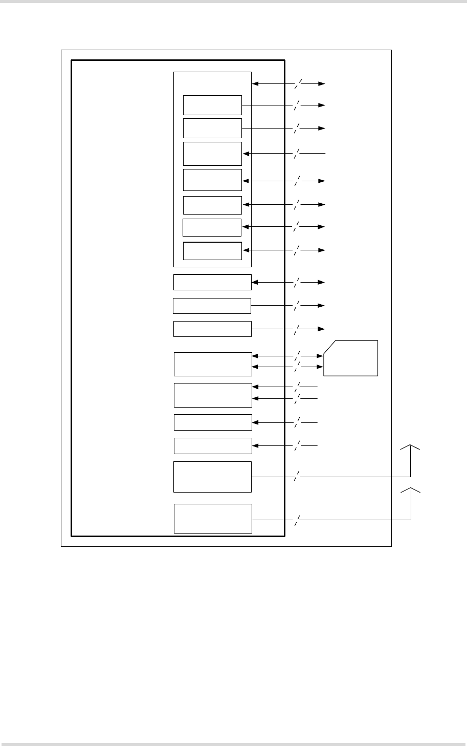
Figure 1: ELS61-USA system overview
GPIO
interface
I2C
USB
ASC0 lines
ASC1/SPI
CONTROL
RTC
POWER
Rx diversity
antenna
(UMTS/LTE)
Module
SIM interface
(with SIM detection)
SIM card
Application
Power supply
Backup supply
Emergency reset
ON
Serial interface/
SPI interface
Serial modem
interface lines
I2C
GPIO
3
4
4
5
2
5
1
1
1
2
USB
Rx diversity
1
Status LED
1
DAC (PWM) PWM
2
Fast
shutdown Fast shutdown
1
1
COUNTER Pulse counter
1
ASC0 lines
Serial modem
interface lines/
SPI interface
4
Main antenna
(UMTS/LTE)
Main antenna
1
DAI lines
4
PCM/I2S
Cinterion® ELS61-USA Hardware Interface Description
1.3 Circuit Concept
14
els61-usa_hid_v01.040a 2017-08-31
Confidential / Preliminary
Page 13 of 113
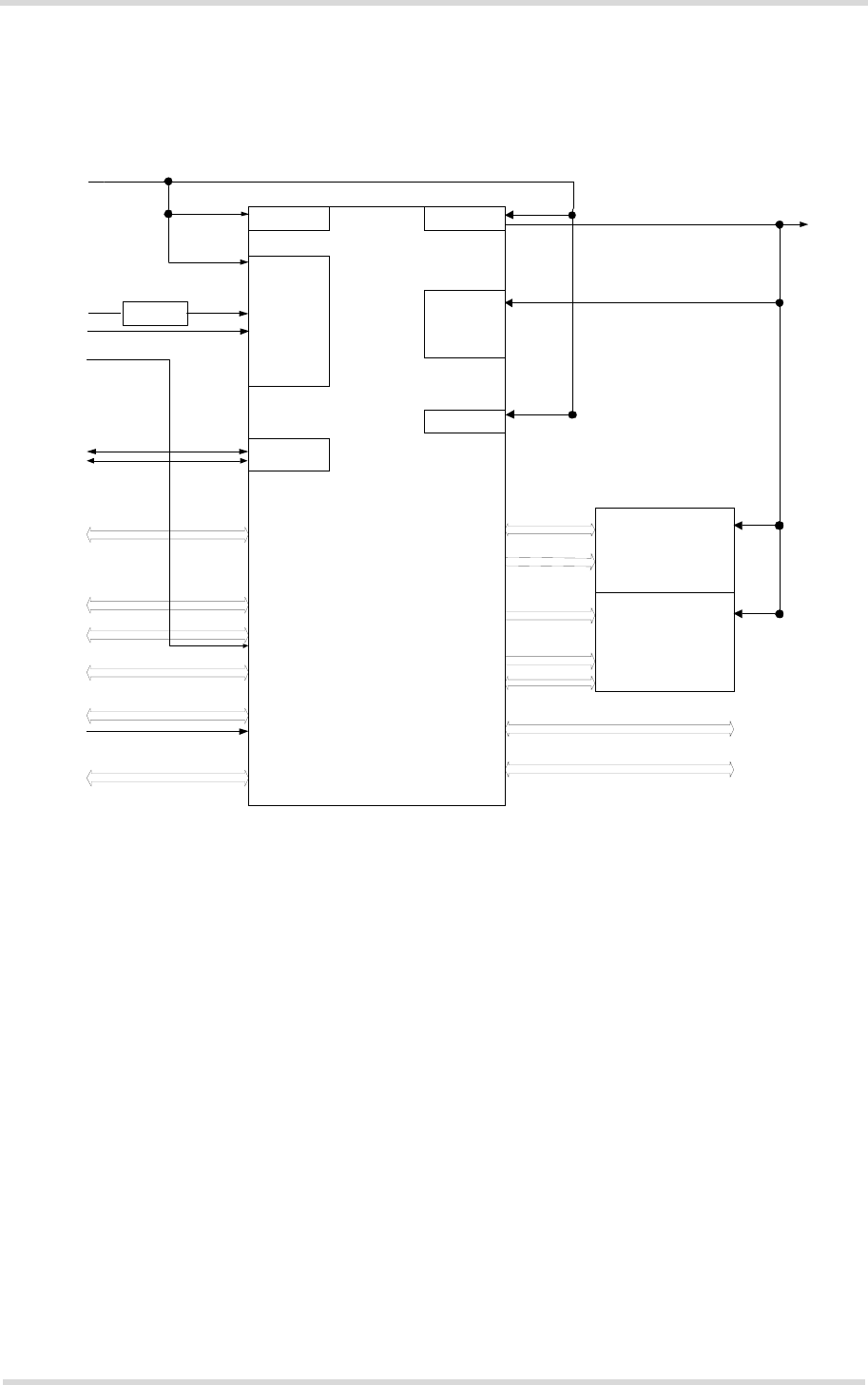
1.3 Circuit Concept
Figure 2 and Figure 3 show block diagrams of the ELS61-USA module and illustrate the major
functional components:
Figure 2: ELS61-USA block diagram
SD1 SD2
SD2
LDOs
PMU
LDOs
ON
Reset_BB
SD3
I2CDAT
I2CCLK
USB
GPIO
SIM
CCIN
LPDDR2
SDRAM
FLASH
VDD
VDD
ADQ0 ~ ADQ15
DDR_CA _0~DDR _CA _9
DDR _DQ_0~DDR_DQ_15
Control
Control
CCIN
SIM
GPIO
ASC0
USB
I2C
ON circuit
ON
EMERG _RST
BATT+BB
RX/TX
RF control
V180
Baseband
controller
and
Power
management
DAI
PCM/I2S/
GPIO
USIF1/
GPIO
FST_SHDWN
ASC1/GPIO/
SPI USIF3
Cinterion® ELS61-USA Hardware Interface Description
1.3 Circuit Concept
14
els61-usa_hid_v01.040a 2017-08-31
Confidential / Preliminary
Page 14 of 113
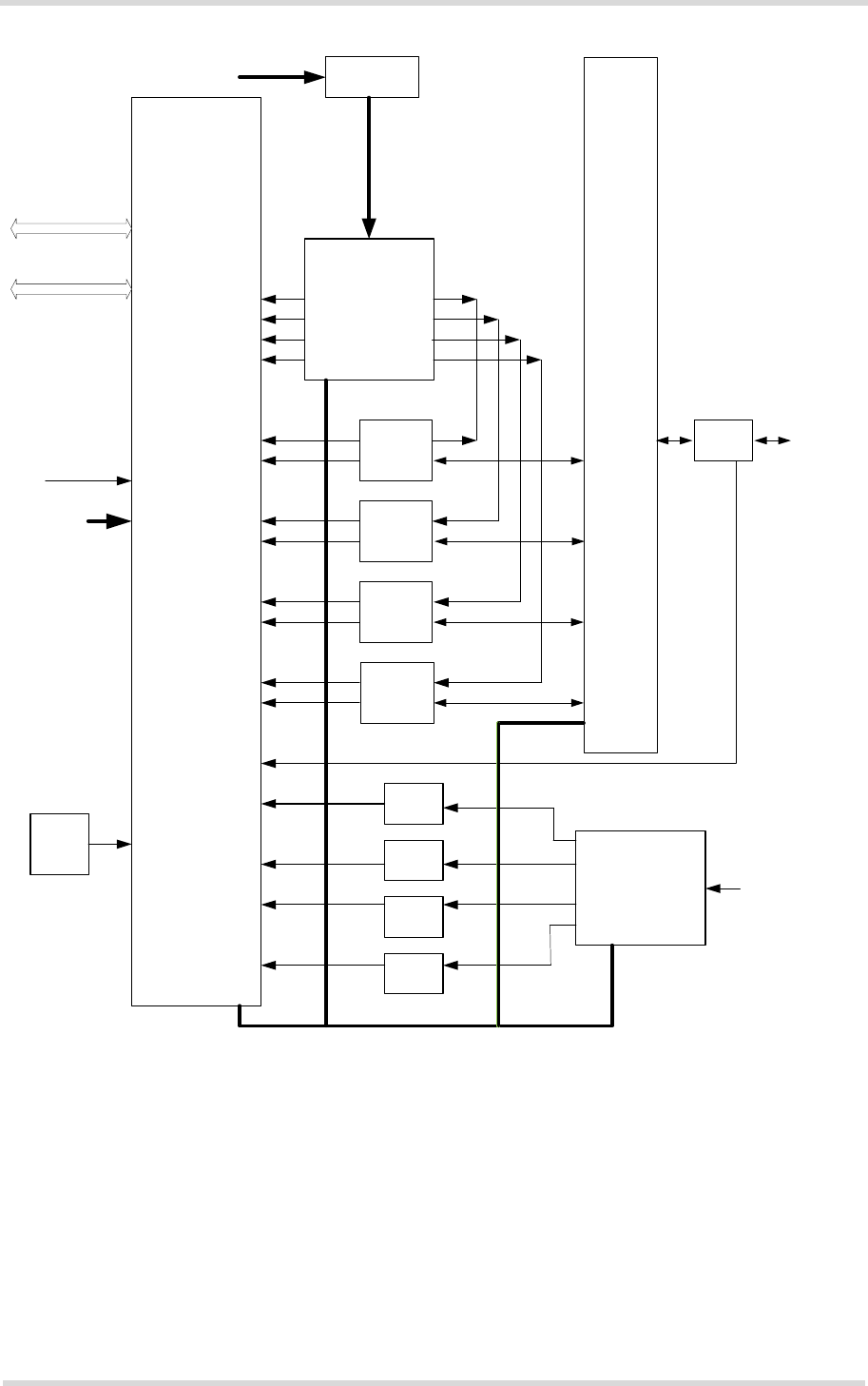
Figure 3: ELS61-USA RF section block diagram
LTE / UMTS
RF transceiver
SKY77622
SKY13525
SKY13525
Band2
SAW
Filter
Band4
SAW
Filter
Band5
SAW
Filter
Band12
SAW
Filter
Diversity Antenna
Band2
Duplexer
Band4
Duplexer
Band5
Duplexer
Band12
Duplexer
Antenna
Coupler
B2_OUT
B4_OUT
B5_OUT
B12_OUT
4G_HB_IN
2G/3G_HB_IN
4G_LB_IN
2G/3G_LB_IN
TQ_H
TP_H
TQ_L
TP_L
RX_M1
RX_M1X
RX_H4
RX_H4X
RX_L1
RX_L1X
RX_L3
RX_L3X
4G_HB_IN
4G_HB_IN
4G_HB_IN
4G_HB_IN
TRX4
TRX6
TRX5
TRX2
TRX2
TRX1
TRX3
TRX5
PA DCDC
SKY87000
BATT+RF
FBR_RF2
MAIN_FWD
MIPI
26MHz
RX/TX
BATT+BB
V180
RF control
Cinterion® ELS61-USA Hardware Interface Description
2 Interface Characteristics
59
els61-usa_hid_v01.040a 2017-08-31
Confidential / Preliminary
Page 15 of 113
2 Interface Characteristics
ELS61-USA is equipped with an SMT application interface that connects to the external appli-
cation. The SMT application interface incorporates the various application interfaces as well as
the RF antenna interface.
2.1 Application Interface
2.1.1 Pad Assignment
The SMT application interface on the ELS61-USA provides connecting pads to integrate the
module into external applications. Figure 4 shows the connecting pads’ numbering plan, the
following Table 1 lists the pads’ assignments.
Figure 4: Numbering plan for connecting pads (bottom view)
Supply pads: BATT+
Control pads
GND pads
ASC0 pads Combined GPIO/ASC1/SPI pads
SIM pads
I2C pads
Supply pads: Other
Combined GPIO/Control pads
(LED, PWM, COUNTER, FST_SHDN)
USB pads
GPIO pads
218217216215214213212211210209208207
206
205204203202201
33
32
31
30
29
28
27
26
25
24
23
22
21
20
53
54
55
56
57
58
59
60
61
62
63
64
65
66
223224225226227228229230231232233234235236237238239240
67 68 69 70 71 72 73
74 75 76 77 78 79 80
93 94 95 96 97 98 99
100 101 102 103 104 105 106
85 86
89 90
81 82
87 88
91 92
83 84
243
244
241
242
222
221
220
219
252
245
250
251
249
248
247
246
RF antenna pads
Do not use
Not connected
Reserved
Combined GPIO/
ASC0/SPI pads
ADC pad
Combined GPIO/DAI pads

Cinterion® ELS61-USA Hardware Interface Description
2.1 Application Interface
59
els61-usa_hid_v01.040a 2017-08-31
Confidential / Preliminary
Page 16 of 113
Signal pads that are not used should not be connected to an external application.
Please note that the reference voltages listed in Table 2 are the values measured directly on
the ELS61-USA module. They do not apply to the accessories connected.
Table 1: Pad assignments
Pad no. Signal name Pad no. Signal name Pad no. Signal name
201 Not connected 24 GPIO22/FSC 235 USB_DN
202 Not connected 25 GPIO21/DIN 236 Not connected
203 GND 26 GPIO23/BCLK 237 Not connected
204 BATT+BB 27 I2CDAT 238 GND
205 GND 28 I2CCLK 239 GPIO5/LED
206 ADC1 29 GPIO17/TXD1/MISO 240 GPIO6/PWM2
207 ON 30 GPIO16/RXD1/MOSI 241 GPIO7/PWM1
208 GND 31 GPIO18/RTS1 242 GPIO8/COUNTER
209 V180 32 GPIO19/CTS1/SPI_CS 53 BATT+RF
210 RXD0 33 EMERG_RST 54 GND
211 CTS0 221 GPIO12 55 GND
212 TXD0 222 GPIO11 56 ANT_DRX
213 GPIO24/RING0 223 GND 57 GND
214 RTS0 224 Not connected 58 GND
215 VDDLP 225 GND 59 ANT_MAIN
216 CCRST 226 Not connected 60 GND
217 CCIN 227 GND 61 GND
218 CCIO 228 Not connected 62 GND
219 GPIO14 229 GPIO4/FST_SHDN 63 GND
220 GPIO13 230 GPIO3/DSR0/SPI_CLK 64 Not connected
20 CCVCC 231 GPIO2/DCD0 65 Not connected
21 CCCLK 232 GPIO1/DTR0 66 Not connected
22 VCORE 233 VUSB 243 Not connected
23 GPIO20/DOUT 234 USB_DP 244 GPIO15
Centrally located pads
67 Not connected 83 GND 99 GND
68 Not connected 84 GND 100 GND
69 Not connected 85 GND 101 GND
70 Not connected 86 GND 102 GND
71 Not connected 87 Not connected 103 GND
72 Not connected 88 GND 104 Not connected
73 Not connected 89 GND 105 Not connected
74 Do not use 90 GND 106 Not connected
75 Do not use 91 Not connected 245 GND
76 Not connected 92 GND 246 Not connected
77 Not connected 93 GND 247 Not connected
78 Not connected 94 GND 248 Not connected
79 Not connected 95 GND 249 Not connected
80 Not connected 96 GND 250 GND
81 GND 97 GND 251 GND
82 GND 98 GND 252 GND
Cinterion® ELS61-USA Hardware Interface Description
2.1 Application Interface
59
els61-usa_hid_v01.040a 2017-08-31
Confidential / Preliminary
Page 17 of 113
2.1.2 Signal Properties
Table 2: Signal properties
Function Signal name IO Signal form and level Comment
Power
supply
BATT+BB
BATT+RF
IWCDMA activated:
VImax = 4.5V
VInorm = 3.8V
VImin = 3.0V during Transmit active.
Imax = 900mA during Tx
LTE activated:
VImax = 4.5V
VInorm = 3.8V
VImin = 3.0V during Transmit active.
Lines of BATT+ and GND
must be connected in
parallel for supply pur-
poses because higher
peak currents may occur.
Minimum voltage must
not fall below 3.0V includ-
ing drop, ripple, spikes
and not rise above 4.5V.
BATT+BB and BATT+RF
require an ultra low ESR
capacitor:
BATT+BB --> 150µF
BATT+RF --> 150µF
If using Multilayer
Ceramic Chip Capacitors
(MLCC) please take DC-
bias into account.
Note that minimum ESR
value is advised at
<70m.
Power
supply
GND Ground Application Ground
External
supply
voltage
V180 O Normal operation:
VOnorm = 1.80V ±3%
IOmax = -10mA
SLEEP mode Operation:
VOSleep = 1.80V ±5%
IOmax = -10mA
CLmax = 100µF
V180 should be used to
supply level shifters at
the interfaces or to supply
external application cir-
cuits.
VCORE and V180 may
be used for the power
indication circuit.
Vcore and V180 are
sensitive against back-
powering by other sig-
nals. While switched off
these voltage domains
must have <0.2V.
If unused keep lines
open.
VCORE O VOnorm = 1.2V ±2.5%
IOmax = -10mA
CLmax = 100nF
SLEEP mode Operation:
VOSleep = 0.90V...1.2V ±4%
IOmax = -10mA
Ignition ON1IV
IHmax = 5V tolerant
VIHmin = 1.3V
VILmax = 0.5V
Slew rate < 1ms
ON ___|~~~~
This signal switches the
module on, and is rising
edge sensitive triggered.
Internal pull down value
for this signal is 100k.
Cinterion® ELS61-USA Hardware Interface Description
2.1 Application Interface
59
els61-usa_hid_v01.040a 2017-08-31
Confidential / Preliminary
Page 18 of 113
Emer-
gency
restart
EMERG_RST I RI 1k, CI 1nF
VOHmax = VDDLP max
VIHmin = 1.35V
VILmax = 0.3V at ~200µA
~~|___|~~ low impulse width > 10ms
This line must be driven
low by an open drain or
open collector driver con-
nected to GND.
If unused keep line open.
RTC
backup
VDDLP I/O VOnorm = 1.8V ±5%
IOmax = -25mA
VImax = 1.9V
VImin = 1.0V
IItyp < 1µA
It is recommended to use
a serial resistor between
VDDLP and a possible
capacitor (bigger than
1µF).
If unused keep line open.
USB VUSB_IN I VImin = 3V
VImax = 5.25V
Active and suspend current:
Imax < 100µA
All electrical characteris-
tics according to USB
Implementers' Forum,
USB 2.0 Specification.
If unused keep lines
open.
USB_DN I/O Full and high speed signal characteris-
tics according USB 2.0 Specification.
USB_DP
Serial
Interface
ASC0
RXD0 O VOLmax = 0.25V at I = 1mA
VOHmin = 1.55V at I = -1mA
VOHmax = 1.85V
If unused keep lines
open.
Note that some ASC0
lines are originally avail-
able as GPIO lines. If
configured as ASC0
lines, the GPIO lines are
assigned as follows:
GPIO1 --> DTR0
GPIO2 --> DCD0
GPIO3 --> DSR0
GPIO24 --> RING0
The DSR0 line is also
shared with the SPI inter-
face‘s SPI_CLK signal.
Note that DCD0/GPIO2
must not be driven low
during startup
CTS0 O
DSR0 O
DCD0 O
RING0 O
TXD0 I VILmax = 0.35V
VIHmin = 1.30V
VIHmax = 1.85V
RTS0 I Pull down resistor active
VILmax = 0.35V at > 50µA
VIHmin = 1.30V at < 240µA
VIHmax = 1.85V at < 240µA
DTR0 I Pull up resistor active
VILmax = 0.35V at < -200µA
VIHmin = 1.30V at > -50µA
VIHmax = 1.85V
Table 2: Signal properties
Function Signal name IO Signal form and level Comment

Cinterion® ELS61-USA Hardware Interface Description
2.1 Application Interface
59
els61-usa_hid_v01.040a 2017-08-31
Confidential / Preliminary
Page 19 of 113
Serial
Interface
ASC1
RXD1 O VOLmax = 0.25V at I = 1mA
VOHmin = 1.55V at I = -1mA
VOHmax = 1.85V
VILmax = 0.35V
VIHmin = 1.30V
VIHmax = 1.85V
If unused keep line open.
Note that the ASC1 inter-
face lines are originally
available as GPIO lines.
If configured as ASC1
lines, the GPIO lines are
assigned as follows:
GPIO16 --> RXD1
GPIO17 --> TXD1
GPIO18 --> RTS1
GPIO19 --> CTS1
TXD1 I
RTS1 I
CTS1 O
SIM card
detection
CCIN I RI 110k
VIHmin = 1.45V at I = 15µA,
VIHmax= 1.9V
VILmax = 0.3V
CCIN = High, SIM card
inserted.
For details please refer to
Section 2.1.6.
If unused keep line open.
3V SIM
Card Inter-
face
CCRST O VOLmax = 0.30V at I = 1mA
VOHmin = 2.45V at I = -1mA
VOHmax = 2.90V
Maximum cable length or
copper track to SIM card
holder should not exceed
100mm.
CCIO I/O VILmax = 0.50V
VIHmin = 2.05V
VIHmax = 2.90V
VOLmax = 0.25V at I = 1mA
VOHmin = 2.50V at I = -1mA
VOHmax = 2.90V
CCCLK O VOLmax = 0.25V at I = 1mA
VOHmin = 2.40V at I = -1mA
VOHmax = 2.90V
CCVCC O VOmin= 2.70V
VOtyp = 2.90V
VOmax = 3.30V
IOmax = -30mA
Table 2: Signal properties
Function Signal name IO Signal form and level Comment

Cinterion® ELS61-USA Hardware Interface Description
2.1 Application Interface
59
els61-usa_hid_v01.040a 2017-08-31
Confidential / Preliminary
Page 20 of 113
1.8V SIM
Card Inter-
face
CCRST O VOLmax = 0.25V at I = 1mA
VOHmin = 1.45V at I = -1mA
VOHmax = 1.90V
Maximum cable length or
copper track to SIM card
holder should not exceed
100mm.
CCIO I/O VILmax = 0.35V
VIHmin = 1.25V
VIHmax = 1.85V
VOLmax = 0.25V at I = 1mA
VOHmin = 1.50V at I = -1mA
VOHmax = 1.85V
CCCLK O VOLmax = 0.25V at I = 1mA
VOHmin = 1.50V at I = -1mA
VOHmax = 1.85V
CCVCC O VOmin = 1.75V
VOtyp = 1.80V
VOmax = 1.85V
IOmax = -30mA
I2C I2CCLK IO Open drain IO
VOLmin = 0.35V at Imax = 4mA (Imax
= Imax external + I pull-up)
VOHmax = 1.85V
R external pull up min = 560
VILmax = 0.35V
VIHmin = 1.3V
VIHmax = 1.85V
According to the I2C Bus
Specification Version 2.1
for the fast mode a rise
time of max. 300ns is per-
mitted. There is also a
maximum VOL=0.4V at
3mA specified.
The value of the pull-up
depends on the capaci-
tive load of the whole sys-
tem (I2C Slave + lines).
The maximum sink cur-
rent of I2CDAT and
I2CCLK is 4mA.
I2C interface of the mod-
ule already has internal
1KOhm pull up resistor to
V180 inside the module.
Please take this into con-
sideration during applica-
tion design.
If lines are unused keep
lines open.
I2CDAT IO
Table 2: Signal properties
Function Signal name IO Signal form and level Comment
Cinterion® ELS61-USA Hardware Interface Description
2.1 Application Interface
59
els61-usa_hid_v01.040a 2017-08-31
Confidential / Preliminary
Page 21 of 113
SPI SPI_CLK O VOLmax = 0.25V at I = 1mA
VOHmin = 1.55V at I = -1mA
VOHmax = 1.85V
VILmax = 0.35V
VIHmin = 1.30V
VIHmax = 1.85V
If lines are unused keep
lines open.
Note that the SPI inter-
face lines are originally
available as GPIO lines.
If configured as SPI lines,
the GPIO lines are
assigned as follows:
GPIO3 --> SPI_CLK
GPIO16 --> MOSI
GPIO17 --> MISO
GPIO19 --> SPI_CS
MOSI O
MISO I
SPI_CS O
GPIO
interface
GPIO1-GPIO3 IO VOLmax = 0.25V at I = 1mA
VOHmin = 1.55V at I = -1mA
VOHmax = 1.85V
VILmax = 0.35V
VIHmin = 1.30V
VIHmax = 1.85V
Imax = ±5mA
If unused keep line open.
Please note that most
GPIO lines can be config-
ured by AT command for
alternative functions:
GPIO1-GPIO3: ASC0
control lines DTR0,
DCD0 and DSR0
GPIO4: Fast shutdown
GPIO5: Status LED line
GPIO6/GPIO7: PWM
GPIO8: Pulse Counter
GPIO16-GPIO19: ASC1
or SPI
GPIO20-GPIO23: DAI
GPIO24: ASC0 control
line RING0
GPIO4 IO
GPIO5 IO
GPIO6 IO
GPIO7 IO
GPIO8 IO
GPIO11-
GPIO15
IO
GPIO16-
GPIO19
IO
GPIO20-
GPIO23
IO
GPIO24 IO
Fast
shutdown
FST_SHDN I VILmax = 0.35V
VIHmin = 1.30V
VIHmax = 1.85V
~~|___|~~ low impulse width > 1ms
This line must be driven
low.
If unused keep line open.
Note that the fast shut-
down line is originally
available as GPIO line. If
configured as fast shut-
down, the GPIO line is
assigned as follows:
GPIO4 --> FST_SHDN
Status LED LED O VOLmax = 0.25V at I = 1mA
VOHmin = 1.55V at I = -1mA
VOHmax = 1.85V
If unused keep line open.
Note that the LED line is
originally available as
GPIO line. If configured
as LED line, the GPIO
line is assigned as fol-
lows:
GPIO5 --> LED
Table 2: Signal properties
Function Signal name IO Signal form and level Comment
Cinterion® ELS61-USA Hardware Interface Description
2.1 Application Interface
59
els61-usa_hid_v01.040a 2017-08-31
Confidential / Preliminary
Page 22 of 113
PWM PWM1 O VOLmax = 0.25V at I = 1mA
VOHmin = 1.55V at I = -1mA
VOHmax = 1.85V
If unused keep lines
open.
Note that the PWM lines
are originally available as
GPIO lines. If configured
as PWM lines, the GPIO
lines are assigned as fol-
lows:
GPIO7 --> PWM1
GPIO6 --> PWM2
PWM2 O
Pulse
counter
COUNTER I Internal up resistor active
VILmax = 0.35V at < -200µA
VIHmin = 1.30V at > -50µA
VIHmax = 1.85V
If unused keep line open.
Note that the COUNTER
line is originally available
as GPIO line. If config-
ured as COUNTER line,
the GPIO line is assigned
as follows:
GPIO8 --> COUNTER
Digital
audio inter-
face (DAI)
FSC O VOLmax = 0.25V at I = 1mA
VOHmin = 1.55V at I = -1mA
VOHmax = 1.85V
If unused keep line open.
Note that the DAI inter-
face lines are originally
available as GPIO lines.
If configured as DAI lines,
the GPIO lines are
assigned as follows:
GPIO22 --> FSC
GPIO23 --> BCLK
GPIO20 --> DOUT
GPIO21 --> DIN
BCLK O
DOUT O
DIN I VILmax = 0.35V
VIHmin = 1.30V
VIHmax = 1.85V
ADC
(Analog-to-
Digital Con-
verter)
ADC1 I RI = 1M
VI = 0V ... 1.2V (valid range)
VIH max = 1.2V
Resolution 1024 steps
Tolerance 0.3%
ADC can be used as
input for external mea-
surements.
If unused keep line open.
1. After the operating voltage is applied, it is required to wait at least 1 second to trigger the ON signal.
Table 2: Signal properties
Function Signal name IO Signal form and level Comment

Cinterion® ELS61-USA Hardware Interface Description
2.1 Application Interface
59
els61-usa_hid_v01.040a 2017-08-31
Confidential / Preliminary
Page 23 of 113
2.1.2.1 Absolute Maximum Ratings
The absolute maximum ratings stated in Table 3 are stress ratings under any conditions.
Stresses beyond any of these limits will cause permanent damage to ELS61-USA.
Table 3: Absolute maximum ratings1
1. Positive noted current means current sourcing from ELS61-USA. Negative noted current means current
sourcing towards ELS61-USA.
Parameter Min Max Unit
Supply voltage BATT+BB, BATT+RF -0.5 +5.5 V
Voltage at all signal lines in Power Down mode -0.3 +0.3 V
Voltage at digital lines in normal operation -0.2 V180 + 0.2 V
Voltage at SIM/USIM interface, CCVCC in normal operation -0.5 +3.3 V
VDDLP input voltage -0.15 2.0 V
Voltage at ADC line in normal operation 0 1.2 V
V180 in normal operation +1.7 +1.9 V
Current at V180 in normal operation -0 +50 mA
VCORE in normal operation +0.85 +1.25 V
Current at VCORE in normal operation -0 +50 mA
Voltage at ON signal -0.5 +6.5 V
Current at single GPIO -5 +5 mA
Current at all GPIO -50 +50 mA
Voltage at VCORE, V180 in power down mode -0.2 +0.2 V
Cinterion® ELS61-USA Hardware Interface Description
2.1 Application Interface
59
els61-usa_hid_v01.040a 2017-08-31
Confidential / Preliminary
Page 24 of 113
2.1.3 USB Interface
ELS61-USA supports a USB 2.0 High Speed (480Mbit/s) device interface that is Full Speed
(12Mbit/s) compliant. The USB interface is primarily intended for use as command and data in-
terface and for downloading firmware.
The external application is responsible for supplying the VUSB_IN line. This line is used for ca-
ble detection only. The USB part (driver and transceiver) is supplied by means of BATT+. This
is because ELS61-USA is designed as a self-powered device compliant with the “Universal Se-
rial Bus Specification Revision 2.0”1.
Figure 5: USB circuit
To properly connect the module's USB interface to the external application, a USB 2.0 compat-
ible connector and cable or hardware design is required. For more information on the USB re-
lated signals see Table 2. Furthermore, the USB modem driver distributed with ELS61-USA
needs to be installed.
1. The specification is ready for download on http://www.usb.org/developers/docs/
VBUS
DP
DN
VREG (3V075)
BATT+
USB_DP2)
lin. reg.
GND
Module
Detection only VUSB_IN
USB part1)
RING0
Host wakeup
1) All serial (including RS) and pull-up resistors for data lines are implemented.
USB_DN2)
2) If the USB interface is operated in High Speed mode (480MHz), it is recommended to take
special care routing the data lines USB_DP and USB_DN. Application layout should in this
case implement a differential impedance of 90 ohms for proper signal integrity.
RS
RS
SMT

Cinterion® ELS61-USA Hardware Interface Description
2.1 Application Interface
59
els61-usa_hid_v01.040a 2017-08-31
Confidential / Preliminary
Page 25 of 113
2.1.3.1 Reducing Power Consumption
While a USB connection is active, the module will never switch into SLEEP mode. Only if the
USB interface is in Suspended state or Detached (i.e., VUSB_IN = 0) is the module able to
switch into SLEEP mode thereby saving power. There are two possibilities to enable power re-
duction mechanisms:
• Recommended implementation of USB Suspend/Resume/Remote Wakeup:
The USB host should be able to bring its USB interface into the Suspended state as
described in the “Universal Serial Bus Specification Revision 2.0“1. For this functionality to
work, the VUSB_IN line should always be kept enabled. On incoming calls and other events
ELS61-USA will then generate a Remote Wakeup request to resume the USB host control-
ler.
See also [5] (USB Specification Revision 2.0, Section 10.2.7, p.282):
"If USB System wishes to place the bus in the Suspended state, it commands the Host Con-
troller to stop all bus traffic, including SOFs. This causes all USB devices to enter the Sus-
pended state. In this state, the USB System may enable the Host Controller to respond to
bus wakeup events. This allows the Host Controller to respond to bus wakeup signaling to
restart the host system."
• Implementation for legacy USB applications not supporting USB Suspend/Resume:
As an alternative to the regular USB suspend and resume mechanism it is possible to
employ the RING0 line to wake up the host application in case of incoming calls or events
signalized by URCs while the USB interface is in Detached state (i.e., VUSB_IN = 0). Every
wakeup event will force a new USB enumeration. Therefore, the external application has to
carefully consider the enumeration timings to avoid loosing any signalled events. For details
on this host wakeup functionality see Section 2.1.14.3. To prevent existing data call con-
nections from being disconnected while the USB interface is in detached state (i.e., VUS-
B_IN=0) it is possible to call AT&D0, thus ignoring the status of the DTR line (see also [1]).
1. The specification is ready for download on http://www.usb.org/developers/docs/
Cinterion® ELS61-USA Hardware Interface Description
2.1 Application Interface
59
els61-usa_hid_v01.040a 2017-08-31
Confidential / Preliminary
Page 26 of 113
2.1.4 Serial Interface ASC0
ELS61-USA offers an 8-wire unbalanced, asynchronous modem interface ASC0 conforming to
ITU-T V.24 protocol DCE signalling. The electrical characteristics do not comply with ITU-T
V.28. The significant levels are 0V (for low data bit or active state) and 1.8V (for high data bit
or inactive state). For electrical characteristics please refer to Table 2. For an illustration of the
interface line’s startup behavior see Figure 7.
ELS61-USA is designed for use as a DCE. Based on the conventions for DCE-DTE connec-
tions it communicates with the customer application (DTE) using the following signals:
• Port TXD @ application sends data to the module’s TXD0 signal line
• Port RXD @ application receives data from the module’s RXD0 signal line
Figure 6: Serial interface ASC0
Features:
• Includes the data lines TXD0 and RXD0, the status lines RTS0 and CTS0 and, in addition,
the modem control lines DTR0, DSR0, DCD0 and RING0.
• The RING0 signal serves to indicate incoming calls and other types of URCs (Unsolicited
Result Code). It can also be used to send pulses to the host application, for example to
wake up the application from power saving state.
• Configured for 8 data bits, no parity and 1 stop bit.
• ASC0 can be operated at fixed bit rates from 1,200bps up to 921,600bps.
• Autobauding supports bit rates from 1,200bps up to 230,400bps.
• Supports RTS0/CTS0 hardware flow control. The hardware hand shake line RTS0 has an
internal pull down resistor causing a low level signal, if the line is not used and open.
Although hardware flow control is recommended, this allows communication by using only
RXD and TXD lines.
• Wake up from SLEEP mode by RTS0 activation (high to low transition; see Section 3.3.2).
Note: The ASC0 modem control lines DTR0, DCD0, DSR0 and RING0 are originally available
as GPIO lines. If configured as ASC0 lines, these GPIO lines are assigned as follows:
GPIO1 --> DTR0, GPIO2 --> DCD0, GPIO3 --> DSR0 and GPIO24 --> RING0. Also, DSR0 is
shared with the SPI_CLK line of the SPI interface and may be configured as such. Configura-
tion is done by AT command (see [1]). The configuration is non-volatile and becomes active
after a module restart.
Cinterion® ELS61-USA Hardware Interface Description
2.1 Application Interface
59
els61-usa_hid_v01.040a 2017-08-31
Confidential / Preliminary
Page 27 of 113
The following figure shows the startup behavior of the asynchronous serial interface ASC0.
For pull-up and pull-down values see Table 13.
Figure 7: ASC0 startup behavior
Notes:
During startup the DTR0 signal is driven active low for 500µs. It is recommended to provide a
470 serial resistor for the DTR0 line to prevent shorts (high current flow).
No data must be sent over the ASC0 interface before the interface is active and ready to re-
ceive data (see Section 3.2.1).
An external pull down to ground on the DCD0 line during the startup phase activates a special
mode for ELS61-USA. In this special mode the AT command interface is not available and the
module may therefore no longer behave as expected.
TXD0
RXD0
RTS0
CTS0
DTR0/GPIO1
DSR0/GPIO3
DCD0/GPIO2
RING0/GPIO24
ON
EMERG_RST
PU
PD
PD
PD
PD
PU
PD
PU
Power supply active
Start up
Firmware
initialization
Command interface
initialization
Interface
active
Reset
state
V180
VCORE
PD
PU
PU
PU
PD
PD
PD
Cinterion® ELS61-USA Hardware Interface Description
2.1 Application Interface
59
els61-usa_hid_v01.040a 2017-08-31
Confidential / Preliminary
Page 28 of 113
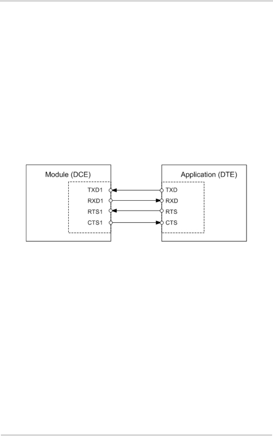
2.1.5 Serial Interface ASC1
Four ELS61-USA GPIO lines can be configured as ASC1 interface signals to provide a 4-wire
unbalanced, asynchronous modem interface ASC1 conforming to ITU-T V.24 protocol DCE
signalling. The electrical characteristics do not comply with ITU-T V.28. The significant levels
are 0V (for low data bit or active state) and 1.8V (for high data bit or inactive state). For electrical
characteristics please refer to Table 2. For an illustration of the interface line’s startup behavior
see Figure 9.
The ASC1 interface lines are originally available as GPIO lines. If configured as ASC1 lines,
the GPIO lines are assigned as follows: GPIO16 --> RXD1, GPIO17 --> TXD1, GPIO18 -->
RTS1 and GPIO19 --> CTS1. Configuration is done by AT command (see [1]: AT^SCFG). The
configuration is non-volatile and becomes active after a module restart.
ELS61-USA is designed for use as a DCE. Based on the conventions for DCE-DTE connec-
tions it communicates with the customer application (DTE) using the following signals:
• Port TXD @ application sends data to module’s TXD1 signal line
• Port RXD @ application receives data from the module’s RXD1 signal line
Figure 8: Serial interface ASC1
Features
• Includes only the data lines TXD1 and RXD1 plus RTS1 and CTS1 for hardware hand-
shake.
• On ASC1 no RING line is available.
• Configured for 8 data bits, no parity and 1 or 2 stop bits.
• ASC1 can be operated at fixed bit rates from 1,200 bps to 921,600 bps.
• Autobauding supports bit rates from 1,200bps up to 230,400bps.
• Supports RTS1/CTS1 hardware flow. The hardware hand shake line RTS0 has an internal
pull down resistor causing a low level signal, if the line is not used and open. Although hard-
ware flow control is recommended, this allows communication by using only RXD and TXD
lines.
Cinterion® ELS61-USA Hardware Interface Description
2.1 Application Interface
59
els61-usa_hid_v01.040a 2017-08-31
Confidential / Preliminary
Page 29 of 113
The following figure shows the startup behavior of the asynchronous serial interface ASC1.
*) For pull-down values see Table 13.
Figure 9: ASC1 startup behavior
TXD1/GPIO17
RXD1/GPIO16
RTS1/GPIO18
CTS1/GPIO19
ON
EMERG_RST
PD
PD
PD
PD
Power supply active
Start up
Firmware
initialization
Command interface
initialization
Interface
active
Reset
state
V180
VCORE
PD

Cinterion® ELS61-USA Hardware Interface Description
2.1 Application Interface
59
els61-usa_hid_v01.040a 2017-08-31
Confidential / Preliminary
Page 30 of 113
2.1.6 UICC/SIM/USIM Interface
ELS61-USA has an integrated UICC/SIM/USIM interface compatible with the 3GPP 31.102
and ETSI 102 221. This is wired to the host interface in order to be connected to an external
SIM card holder. Five pads on the SMT application interface are reserved for the SIM interface.
The UICC/SIM/USIM interface supports 3V and 1.8V SIM cards. Please refer to Table 2 for
electrical specifications of the UICC/SIM/USIM interface lines depending on whether a 3V or
1.8V SIM card is used.
The CCIN signal serves to detect whether a tray (with SIM card) is present in the card holder.
To take advantage of this feature, an appropriate SIM card detect switch is required on the card
holder. For example, this is true for the model supplied by Molex, which has been tested to op-
erate with ELS61-USA and is part of the Gemalto M2M reference equipment submitted for type
approval. See Section 7.1 for Molex ordering numbers.
Note [1]: No guarantee can be given, nor any liability accepted, if loss of data is encountered after removing
the SIM card during operation. Also, no guarantee can be given for properly initializing any SIM card that
the user inserts after having removed the SIM card during operation. In this case, the application must
restart ELS61-USA.
Note [2]: On the evaluation board, the CCIN signal is inverted, thus the CCIN signal is by default high and
will change to a low level if a SIM card is inserted.
Table 4: Signals of the SIM interface (SMT application interface)
Signal Description
GND Separate ground connection for SIM card to improve EMC.
CCCLK Chipcard clock
CCVCC SIM supply voltage.
CCIO Serial data line, input and output.
CCRST Chipcard reset
CCIN Input on the baseband processor for detecting a SIM card tray in the holder. If the SIM is
removed during operation the SIM interface is shut down immediately to prevent destruc-
tion of the SIM. The CCIN signal is by default low and will change to high level if a SIM card
is inserted.
The CCIN signal is mandatory for applications that allow the user to remove the SIM card
during operation.
The CCIN signal is solely intended for use with a SIM card. It must not be used for any other
purposes. Failure to comply with this requirement may invalidate the type approval of
ELS61-USA.
Cinterion® ELS61-USA Hardware Interface Description
2.1 Application Interface
59
els61-usa_hid_v01.040a 2017-08-31
Confidential / Preliminary
Page 31 of 113
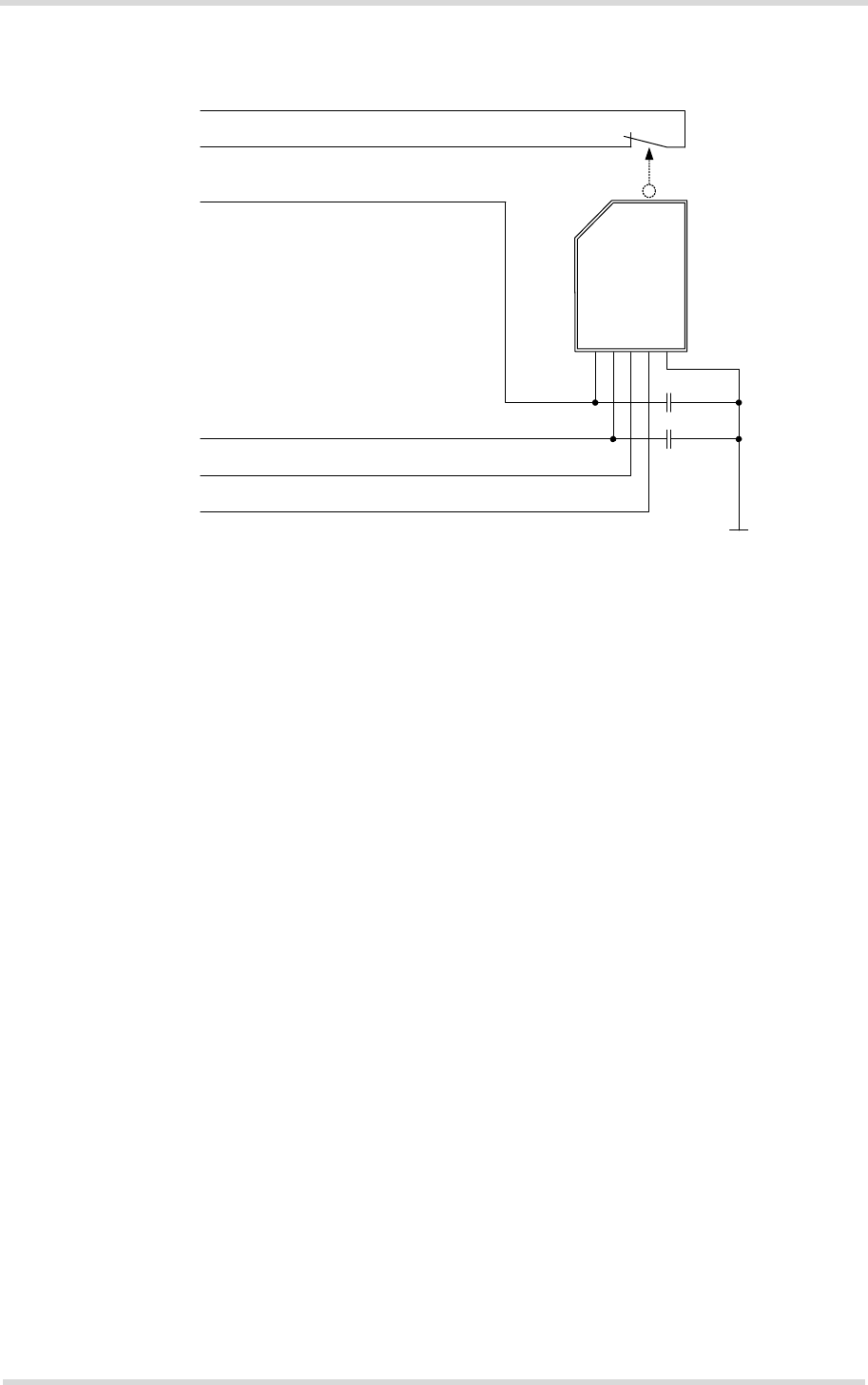
The figure below shows a circuit to connect an external SIM card holder.
Figure 10: External UICC/SIM/USIM card holder circuit
The total cable length between the SMT application interface pads on ELS61-USA and the
pads of the external SIM card holder must not exceed 100mm in order to meet the specifica-
tions of 3GPP TS 51.010-1 and to satisfy the requirements of EMC compliance.
To avoid possible cross-talk from the CCCLK signal to the CCIO signal be careful that both
lines are not placed closely next to each other. A useful approach is using a GND line to shield
the CCIO line from the CCCLK line.
An example for an optimized ESD protection for the SIM interface is shown in Section 2.1.6.1.
SIM
CCVCC
CCRST
CCIO
CCCLK
220nF
1nF
CCIN
V180
Cinterion® ELS61-USA Hardware Interface Description
2.1 Application Interface
59
els61-usa_hid_v01.040a 2017-08-31
Confidential / Preliminary
Page 32 of 113
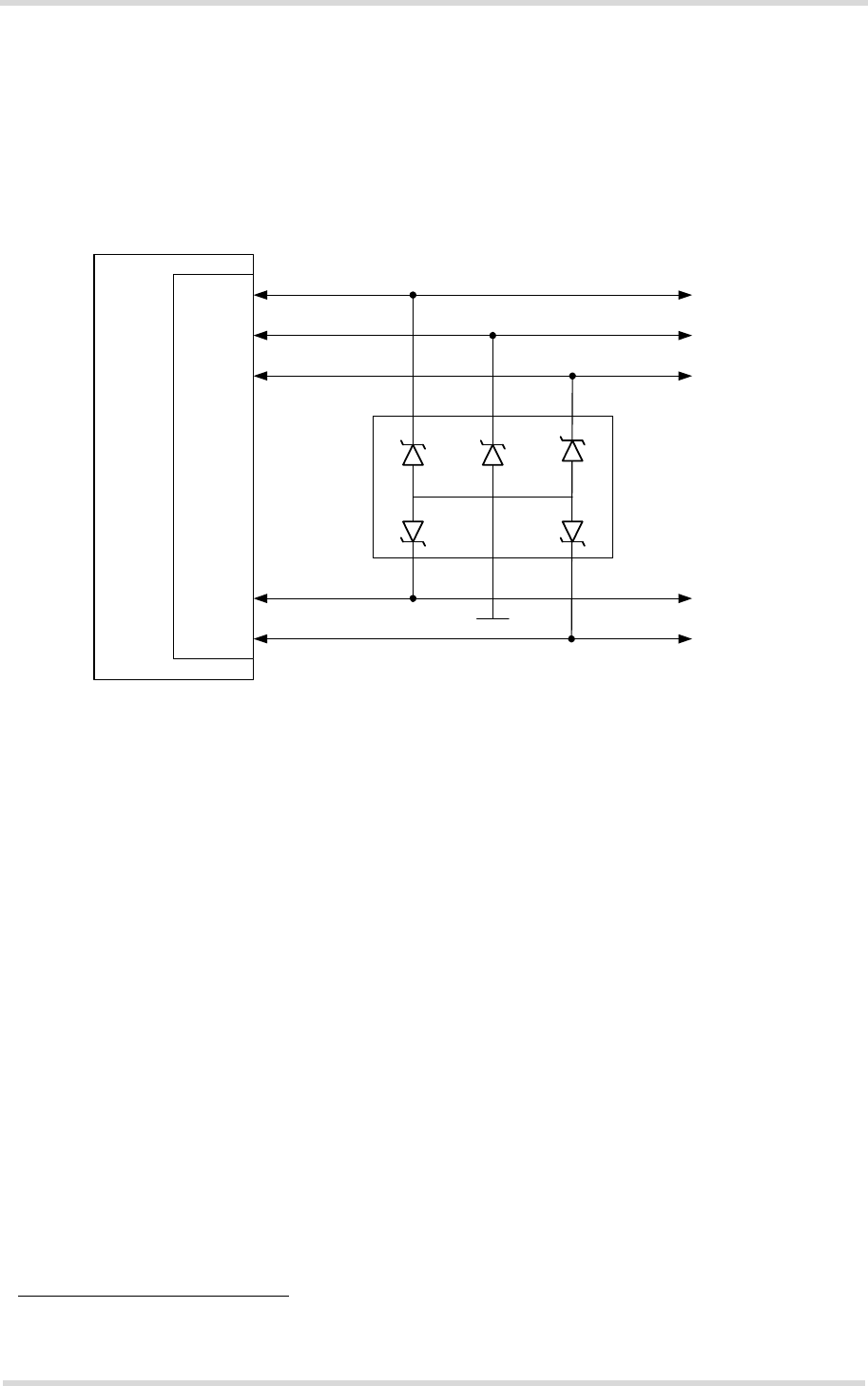
2.1.6.1 Enhanced ESD Protection for SIM Interface
To optimize ESD protection for the SIM interface it is possible to add ESD diodes to the SIM
interface lines as shown in the example given in Figure 11.1
The example was designed to meet ESD protection according ETSI EN 301 489-1/7: Contact
discharge: ± 4kV, air discharge: ± 8kV.
Figure 11: SIM interface - enhanced ESD protection
1. Note that the protection diode shall have low internal capacitance less than 5pF for IO and CLK.
CCRST
CCCLK
CCIO
CCVCC
CCIN GND
123
654
SIM_RST
SIM_CLK
SIM_IO
SIM_VCC
SIM_DET
Module

Cinterion® ELS61-USA Hardware Interface Description
2.1 Application Interface
59
els61-usa_hid_v01.040a 2017-08-31
Confidential / Preliminary
Page 33 of 113
2.1.7 Digital Audio Interface (DAI)
ELS61-USA supports a digital audio interface that can be employed either as pulse code mod-
ulation interface (see Section 2.1.7.1) or as inter IC sound interface (see Section 2.1.7.2). Op-
eration of these interface variants is mutually exclusive, and can be configured by AT command
(AT^SAIC; see [1]).
2.1.7.1 Pulse Code Modulation Interface (PCM)
Four ELS61-USA GPIO lines can be configured as pule code modulation interface (PCM). The
PCM functionality allows for the use of an external codec like the W681360 (see Section
2.1.7.3).
The PCM interface supports the following features:
• Master and Slave mode
• Long frame and short frame
• 8kHz sample rate / 125µs frame duration (narrow band), 16kHz sample rate / 62.5µs frame
duration (wide band)
• Bit clock: 256kHz (sample rate of 8kHz), 264kHz (short frame), 520kHz (sample rate of
8kHz), 528kHz (short frame), 1040kHz (sample rate of 16kHz)
• The most significant bit MSB is transferred first
• Data write at rising edge / data read at falling edge
• Common frame sync signal for transmit and receive
The four GPIO lines can be configured as DAI/PCM interface signals as follows: GPIO20 -->
DOUT, GPIO21--> DIN, GPIO22 --> FSC and GPIO23 --> BCLK. The configuration is done by
AT command (see [1]). It is non-volatile and becomes active after a module restart. Table 5 de-
scribes the available DAI/PCM lines at the digital audio interface. For electrical details see Sec-
tion 2.1.2.
Table 5: Overview of DAI/PCM lines
Signal name Input/Output Description
DOUT O PCM data from ELS61-USA to external codec.
DIN I PCM data from external codec to ELS61-USA.
FSC O Frame synchronization signal to external codec:
Long frame (8kHz)
BCLK O Bit clock to external codec.
Cinterion® ELS61-USA Hardware Interface Description
2.1 Application Interface
59
els61-usa_hid_v01.040a 2017-08-31
Confidential / Preliminary
Page 34 of 113
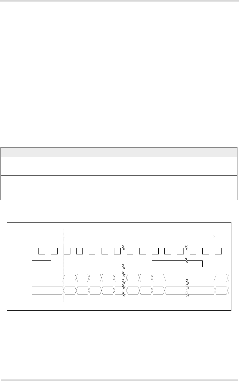
Figure 12 shows the PCM timing for the master mode available with ELS61-USA.
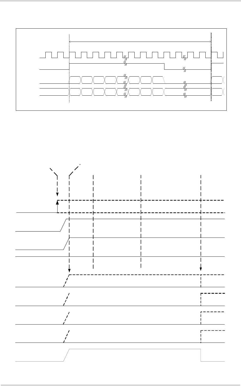
Figure 12: Long frame PCM timing, 256kHz
The following figure shows the start up behavior of the DAI interface. The start up configuration
of functions will be activated after the software initialization of the command interface. With an
active state of CTS0 (low level) the initialization of the DAI interface is finished.
Figure 13: DAI startup timing
BCLK
DOUT
DIN
FSC
MSB
MSB
LSB
LSB
14 13
14 13
1
1
12
12
2
2
MSB
MSB
125 µs
DIN/GPIO21
FSC/GPIO22
BCLK/GPIO23
DOUT/GPIO20
PD
PD
PD
PD
CTS0
ON
EMERG_RST
Power supply active
Start up
Firmware
initialization
Command interface
initialization
Interface
active
Reset
state
V180
VCORE
Cinterion® ELS61-USA Hardware Interface Description
2.1 Application Interface
59
els61-usa_hid_v01.040a 2017-08-31
Confidential / Preliminary
Page 35 of 113
2.1.7.2 Inter IC Sound Interface
The Inter IC Sound interface (I2S) is enabled using the AT command AT^SAIC (see [1]). An
activation is possible only out of call and out of tone presentation. The I2S properties and
capabilities comply with the requirements laid out in the Phillips I2S Bus Specifications,
revised June 5, 1996.
The I2S interface has the following characteristics:
• Clock Modes: Master with permanent clock option
• Sampling Rate: 8kHz (narrow band), 16kHz (wide band)
• Bit clock: 512kHz
The digital audio interface pads available for the PCM interface are also available for the I2S
interface. In I2S mode they have the same electrical characteristics (for more information on the
DOUT, DIN, FSC and BCLK pads please refer to Section 2.1.2 and Section 2.1.7.1).
The table below lists the available pads at the module’s digital audio interface.
The following figure shows the I2S timing for the master mode available with the module.
Figure 14: I2S timing, 8kHz sample rate
Table 6: Overview of DAI/I2S lines
Signal name Input/Output Description
DOUT O I2S data from module to external codec.
DIN I I2S data from external codec to module.
FSC O Frame synchronization signal to external codec:
Word alignment (WS)
BCLK O Bit clock to external codec: 512kHz
BCLK
DOUT
DIN
FSC
MSB
MSB
LSB
LSB
14 13
14 13
1
1
12
12
2
2
MSB
MSB
125 µs
Cinterion® ELS61-USA Hardware Interface Description
2.1 Application Interface
59
els61-usa_hid_v01.040a 2017-08-31
Confidential / Preliminary
Page 36 of 113
2.1.7.3 Solutions for the Digital Audio Interface
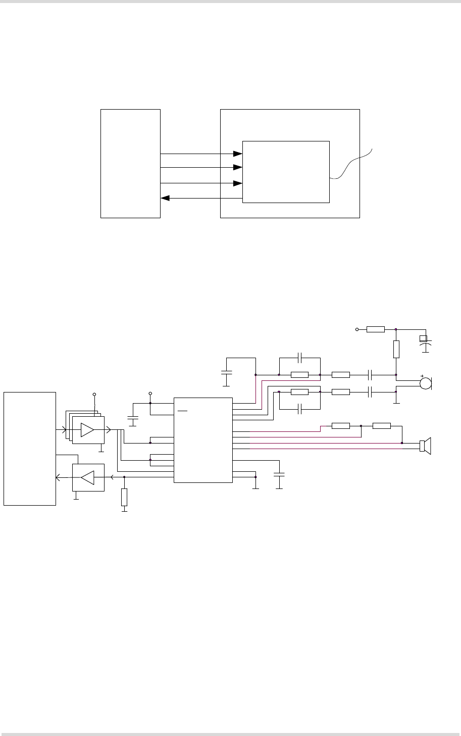
Figure 15 and Figure 16 show an example of using the digital audio interface of the module.
The below mentioned sample Nuvoton codec W681360 can be replaced with a DSP. In the ex-
ample, framesync and clock master is the module (FSC line) and thus the RF network.
Figure 15: Block circuit for DAI to analog converter
This DAI analog converter is well suited for evaluating and testing a telephone handset and can
be used instead of the headset interface of the DSB75.
Figure 16: Sample circuit for analog to DAI box
On the module side, the DAI interface has to be enabled. This can be done by using the follow-
ing AT command: AT^SCFG="GPIO/mode/DAI","std".
Please note that level converters are required between the module‘s 1.8V digital audio lines
and the 3.0V audio codec interface lines. Possible level converters are for example
74VHC1GT50 (up) and 74LVC1G34 (down). See Figure 16 and refer to Section 2.3.1 for more
information on a possible sample level conversion circuit.
W681360
13-Bit-Linear-
CODEC
PCM to Analog Converter
Module
DIN
DOUT
FSC
BCLK
+3.0 V
+3.0V
BCLK
DOUT
FSC
DIN
R5
1k
R6
1k
R9
100k
Mic1
MICROPHONE
1
2
+C6
100uF
C3
10nF
C2
100nF
R8 100kR7 20k
C1
100nF
U1
W681360
15
6
5
8
1
4
9
10
2
3
19
18
17
16
14
13
12
11
7
20
VSS
VDD
PO+
DR
VAGREF
PO-
BCLKR
PDI
RO-
PI
TI+
TI-
TG
HB
FST
DT
BCLKT
MCLK
FSR
VAG
R1 75k
R2 75k
C7 420pF
C8 420pF
R4 1k
R3 1k
C4 100nF
C5 100nF
LS1
SPEAKER
Speaker gain
Low lev el input
+3.0V
Module
Output lines:
FSC
BCLK
DOUT
Input line:
DIN
5V tolerant
V180
VCC
VCC
74VHC 1GT50
74LVC 1G34
Cinterion® ELS61-USA Hardware Interface Description
2.1 Application Interface
59
els61-usa_hid_v01.040a 2017-08-31
Confidential / Preliminary
Page 37 of 113
2.1.7.4 Electrical Characteristics of the Voiceband Part
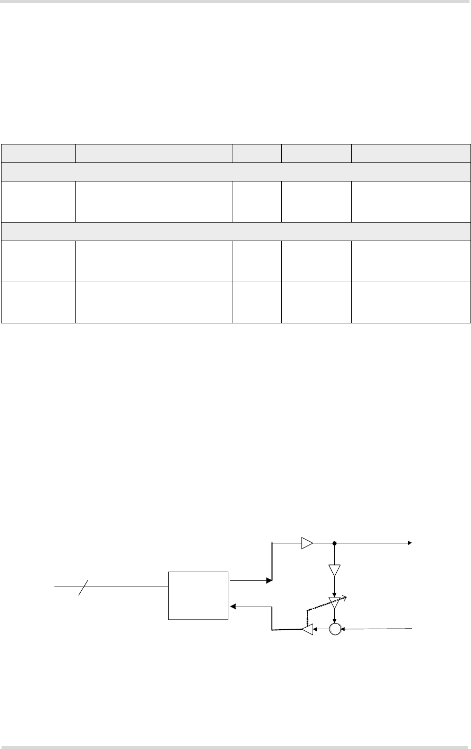
Setting Audio Parameters by AT Commands
The audio modes 2 to 10 can be temporarily adjusted according to the AT command parameter
listed in the table below. The audio parameter is set with the AT commandAT^SNFO and the
audio mode is changed by AT^SNFS (see [1]). For a model of how the parameters influence
the audio signal path see Section .
Audio Programming Model
The audio programming model shows how the signal path can be influenced by varying AT
command parameters: . For more information on the AT commands and parameters see Sec-
tion and [1].
Figure 17: Audio programming model
Table 7: Audio parameters adjustable by AT command
Parameter Influence to Range Gain range Calculation
AT^SNFI
inVolStep Digital TX volume 0
1...100
Mute
-43.5…+6dB
0.5dB steps
(inVolStep-88)*0.5dB
88 = 0dB (default)
AT^SNFO
outVolStep Digital RX volume 0
1…100
Mute
-43.5…+6dB
0.5dB steps
(outVolStep-88)*0.5dB
88 = 0dB (default)
sideToneStep Sidetone gain1
1. The sidetone path contains two logically gain cells in series as shown in Figure 17. The first one can be
controlled by the parameter sideToneGain while the second one will be controlled by outVolStep to keep
the resulting sidetone gain constant independently of the RX Volume. The second cell introduces an off-
set of -37.5dB to the sidetone path. The resulting sidetone gain can be calculated according the following
formula:
Resulting sidetone gain = 0.5 * (sideToneStep - outVolStep) -37.5 [dB]
If sideToneStep = 0 the sidetone path is completely muted - independent of outVolStep.
0
0...175
Mute
-43.5...
43.5dB
0.5dB steps
SideToneStep*0.5dB
88 = 0dB
Signal Processing /
Speech coder
+
AT parameters are given in brackets <...>
and marked red and italic .
<outVolStep>
<inVolStep>
Speech decoder /
Signal Processing
DAI
4
PCM/I2S
<sideToneGain>

Cinterion® ELS61-USA Hardware Interface Description
2.1 Application Interface
59
els61-usa_hid_v01.040a 2017-08-31
Confidential / Preliminary
Page 38 of 113
Characteristics of Audio Modes
The electrical characteristics of the voiceband part depend on the current audio mode set with
AT command. All values are noted for default gains, e.g. the default parameters are left
unchanged.
Note: With regard to acoustic shock, the cellular application must be designed to avoid sending
false AT commands that might increase amplification, e.g. for a highly sensitive earpiece. A
protection circuit should be implemented in the cellular application.
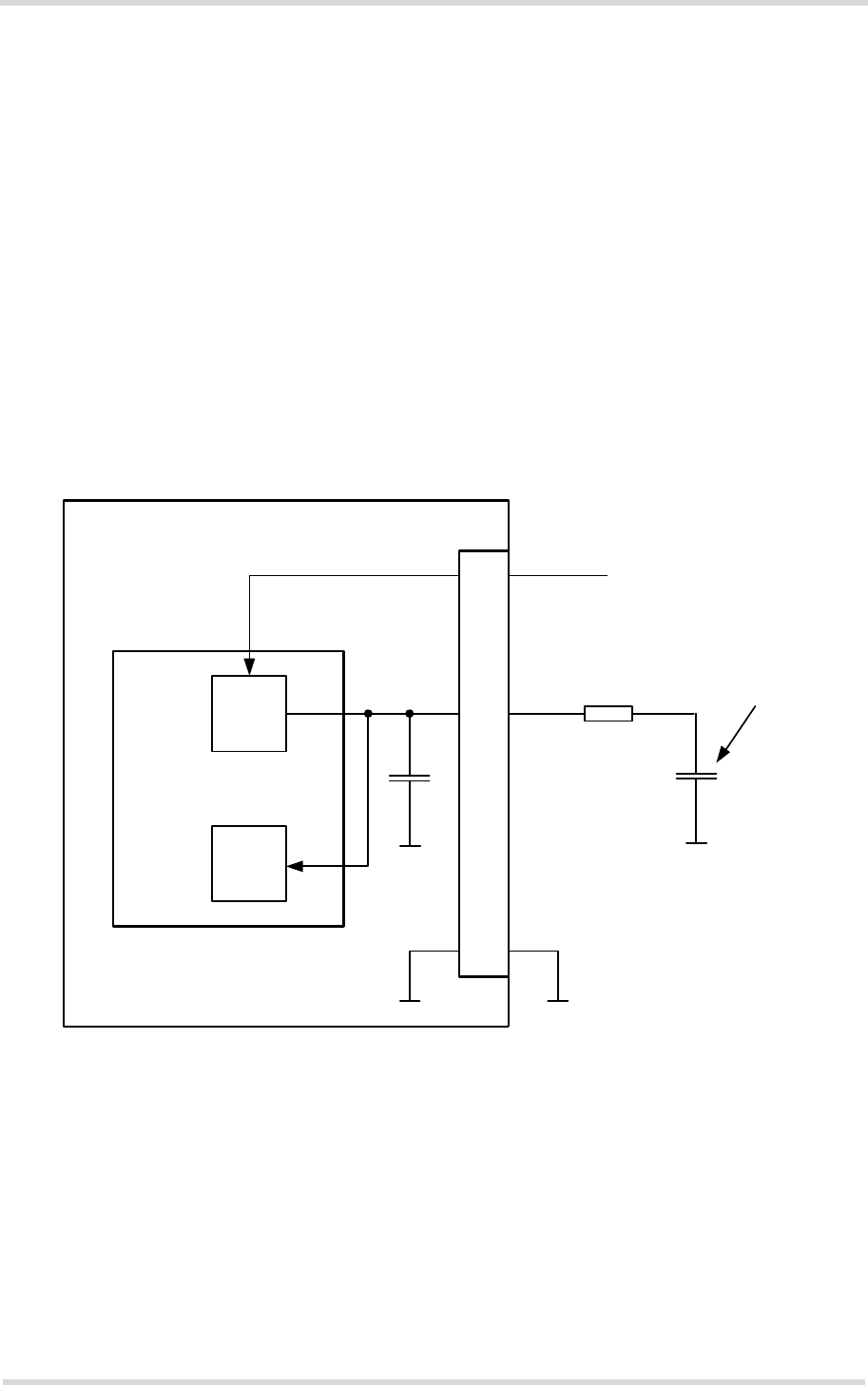
Cinterion® ELS61-USA Hardware Interface Description
2.1 Application Interface
59
els61-usa_hid_v01.040a 2017-08-31
Confidential / Preliminary
Page 39 of 113
2.1.8 RTC Backup
The internal Real Time Clock of ELS61-USA is supplied from a separate voltage regulator in
the power supply component which is also active when ELS61-USA is in Power Down mode
and BATT+ is available. An alarm function is provided that allows to wake up ELS61-USA with-
out logging on to the RF network.
In addition, you can use the VDDLP pad to backup the RTC from an external capacitor. The
capacitor is charged from the internal LDO of ELS61-USA. If the voltage supply at BATT+ is
disconnected the RTC can be powered by the capacitor. The size of the capacitor determines
the duration of buffering when no voltage is applied to ELS61-USA, i.e. the greater the capac-
itor the longer ELS61-USA will save the date and time. The RTC can also be supplied from an
external battery (rechargeable or non-chargeable). In this case the electrical specification of
the VDDLP pad (see Section 2.1.2) has to be taken in to account.
Figure 18 shows an RTC backup configuration. A serial 1k resistor has to be placed on the
application next to VDDLP. It limits the input current of an empty capacitor or battery.
Figure 18: RTC supply variants
Capacitor
VDDLP
Processor and power
management
LRTC
RTC
Application interface
BATT+
Module
1k
GND

Cinterion® ELS61-USA Hardware Interface Description
2.1 Application Interface
59
els61-usa_hid_v01.040a 2017-08-31
Confidential / Preliminary
Page 40 of 113
2.1.9 GPIO Interface
ELS61-USA offers a GPIO interface with 22 GPIO lines. The GPIO lines are shared with other
interfaces or functions: Fast shutdown (see Section 2.1.14.4), status LED (see Section
2.1.14.1), the PWM functionality (see Section 2.1.12), an pulse counter (see Section 2.1.13),
ASC0 (see Section 2.1.4), ASC1 (see Section 2.1.5), an SPI interface (see Section 2.1.11), and
a DAI interface (see Section 2.1.7).
The following table shows the configuration variants for the GPIO pads. All variants are mutu-
ally exclusive, i.e. a pad configured for instance as Status LED is locked for alternative usage.
After startup, the above mentioned alternative GPIO line assignments can be configured using
AT commands (see [1]). The configuration is non-volatile and available after module restart.
Table 8: GPIO lines and possible alternative assignment
GPIO Fast
Shutdown Status LED PWM Pulse
Counter ASC0 ASC1 SPI DAI
GPIO1 DTR0
GPIO2 DCD0
GPIO3 DSR0 SPI_CLK
GPIO4 FST_SHDN
GPIO5 Status LED
GPIO6 PWM2
GPIO7 PWM1
GPIO8 COUNTER
GPIO11
GPIO12
GPIO13
GPIO14
GPIO15
GPIO16 RXD1 MOSI
GPIO17 TXD1 MISO
GPIO18 RTS1
GPIO19 CTS1 SPI_CS
GPIO20 DOUT
GPIO21 DIN
GPIO22 FSC
GPIO23 BCLK
GPIO24 RING0
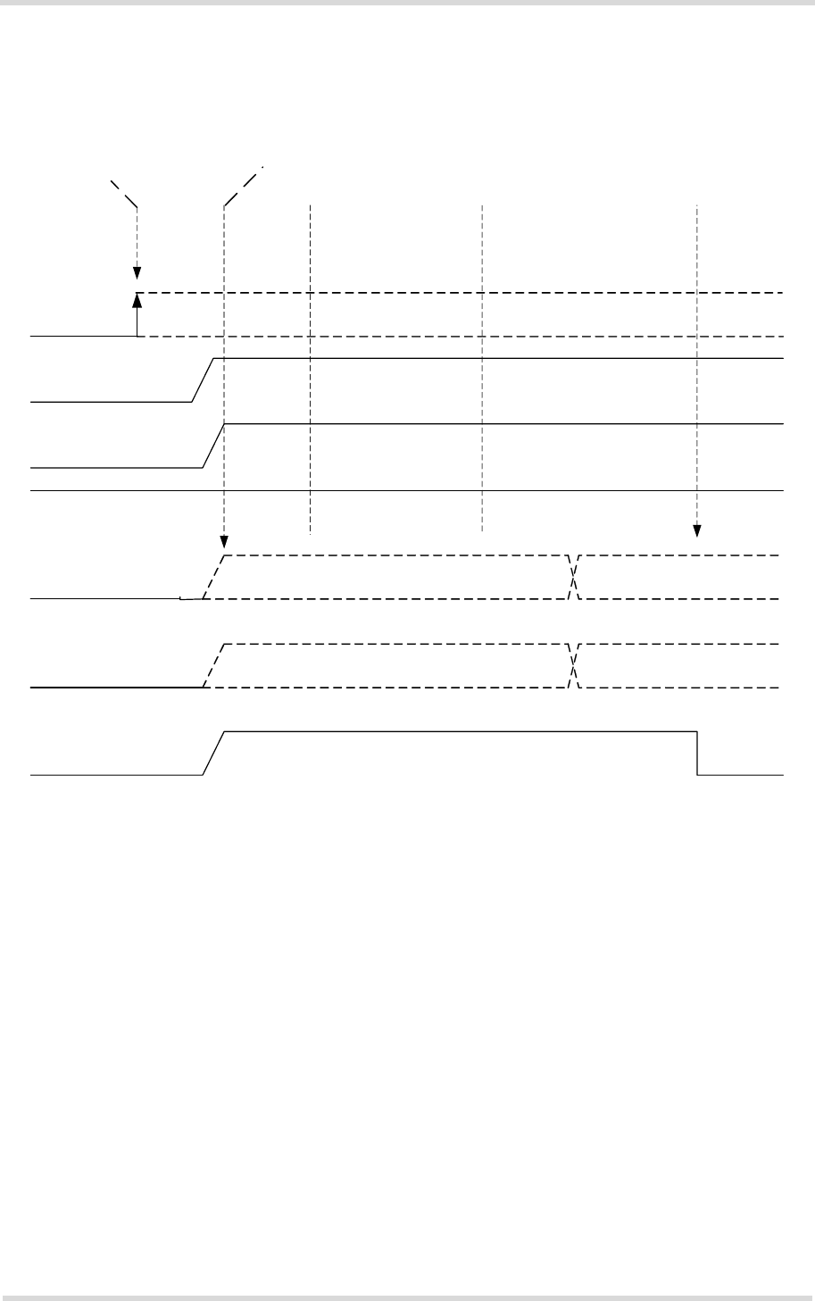
Cinterion® ELS61-USA Hardware Interface Description
2.1 Application Interface
59
els61-usa_hid_v01.040a 2017-08-31
Confidential / Preliminary
Page 41 of 113
The following figure shows the startup behavior of the GPIO interface. With an active state of
the ASC0 interface (i.e. CTS0 is at low level) the initialization of the GPIO interface lines is also
finished.
*) For pull down values see Table 13.
Figure 19: GPIO startup behavior
GPIO 1-8 PD
CTS0
ON
EMERG_RST
Power supply active
Start up
Firmware
initialization
Command interface
initialization
Interface
active
Reset
state
V180
VCORE
GPIO 11 - 24 PD
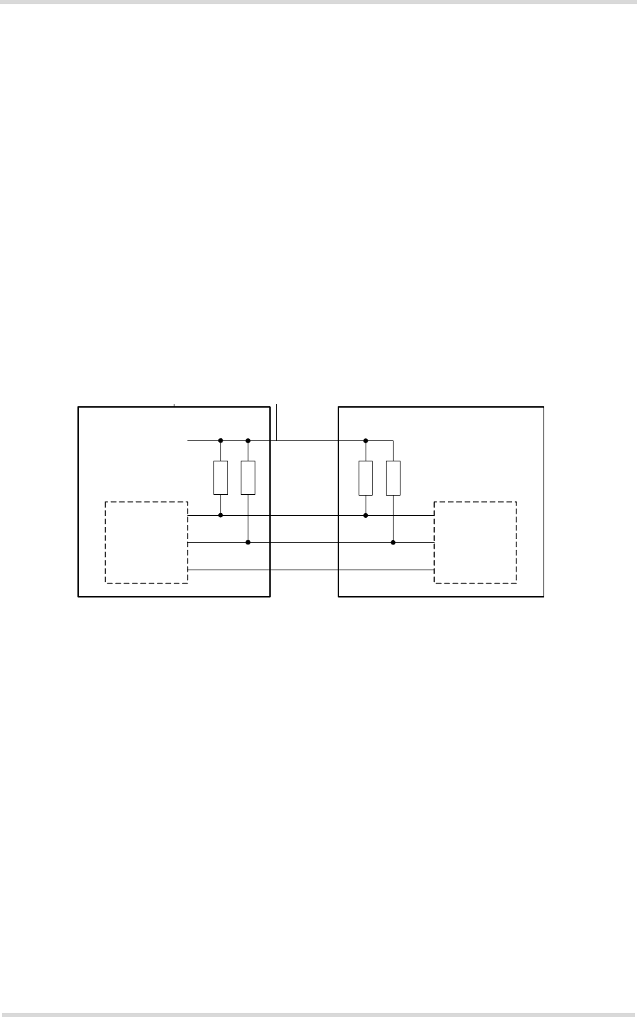
Cinterion® ELS61-USA Hardware Interface Description
2.1 Application Interface
59
els61-usa_hid_v01.040a 2017-08-31
Confidential / Preliminary
Page 42 of 113
2.1.10 I2C Interface
I2C is a serial, 8-bit oriented data transfer bus for bit rates up to 400kbps in Fast mode. It con-
sists of two lines, the serial data line I2CDAT and the serial clock line I2CCLK. The module acts
as a single master device, e.g. the clock I2CCLK is driven by the module. I2CDAT is a bi-direc-
tional line. Each device connected to the bus is software addressable by a unique 7-bit ad-
dress, and simple master/slave relationships exist at all times. The module operates as master-
transmitter or as master-receiver. The customer application transmits or receives data only on
request of the module.
To configure and activate the I2C bus use the AT^SSPI command. Detailed information on the
AT^SSPI command as well explanations on the protocol and syntax required for data transmis-
sion can be found in [1].
The I2C interface can be powered via the V180 line of ELS61-USA. If connected to the V180
line, the I2C interface will properly shut down when the module enters the Power Down mode.
In the application I2CDAT and I2CCLK lines need to be connected to a positive supply voltage
via a pull-up resistor. For electrical characteristics please refer to Table 2.
Figure 20: I2C interface connected to V180
Note: Good care should be taken when creating the PCB layout of the host application: The
traces of I2CCLK and I2CDAT should be equal in length and as short as possible.
I2CCLK
I2CDAT
GND
I2CCLK
I2CDAT
GND
Module Application
V180
R pull up
R pull up
R pull up
R pull up
1KOhm
1KOhm
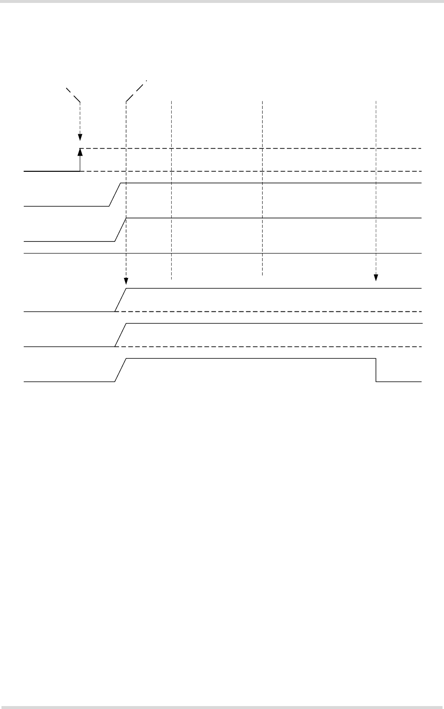
Cinterion® ELS61-USA Hardware Interface Description
2.1 Application Interface
59
els61-usa_hid_v01.040a 2017-08-31
Confidential / Preliminary
Page 43 of 113
The following figure shows the startup behavior of the I2C interface. With an active state of the
ASC0 interface (i.e. CTS0 is at low level) the initialization of the I2C interface is also finished.
Figure 21: I2C startup behavior
I2CCLK
I2CDAT
Open Drain
Open Drain
(external pull up)
(external pull up)
CTSx
ON
EMERG_RST
Power supply active
Start up
Firmware
initialization
Command interface
initialization
Interface
active
Reset
state
V180
VCORE
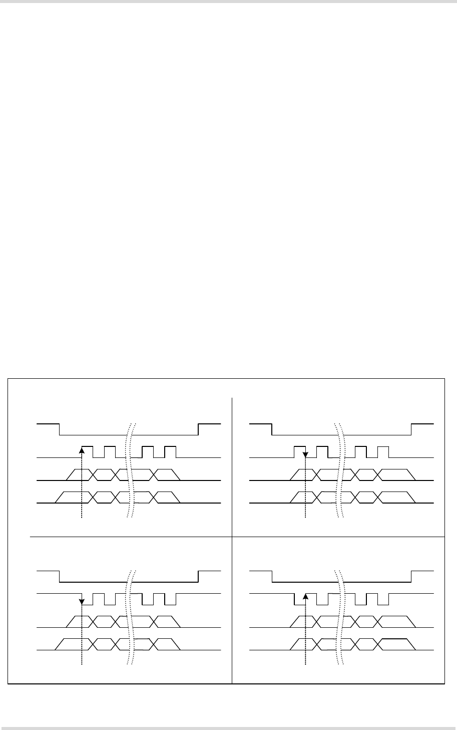
Cinterion® ELS61-USA Hardware Interface Description
2.1 Application Interface
59
els61-usa_hid_v01.040a 2017-08-31
Confidential / Preliminary
Page 44 of 113
2.1.11 SPI Interface
Four ELS61-USA GPIO interface lines can be configured as Serial Peripheral Interface (SPI).
The SPI is a synchronous serial interface for control and data transfer between ELS61-USA
and the external application. Only one application can be connected to the SPI and the inter-
face supports only master mode. The transmission rates are up to 6.5Mbit/s. The SPI interface
comprises the two data lines MOSI and MISO, the clock line SPI_CLK a well as the chip select
line SPI_CS.
The four GPIO lines can be configured as SPI interface signals as follows: GPIO3 --> SPI_CLK,
GPIO16 --> MOSI, GPIO17 --> MISO and GPIO19 --> SPI_CS. The configuration is done by
AT command (see [1]). It is non-volatile and becomes active after a module restart.
The GPIO lines are also shared with the ASC1 signal lines and the ASC0 modem status signal
line DSR0.
To configure and activate the SPI interface use the AT^SSPI command. Detailed information
on the AT^SSPI command as well explanations on the SPI modes required for data transmis-
sion can be found in [1].
In general, SPI supports four operation modes. The modes are different in clock phase and
clock polarity. The module’s SPI mode can be configured by using the AT command AT^SSPI.
Make sure the module and the connected slave device works with the same SPI mode.
Figure 22 shows the characteristics of the four SPI modes. The SPI modes 0 and 3 are the most
common used modes. For electrical characteristics please refer to Table 2.
Figure 22: Characteristics of SPI modes
SPI MODE 0 SPI MODE 1
SPI MODE 2 SPI MODE 3
Clock phase
Clock polarity
SPI_CS
MOSI
SPI_CLK
MISO
SPI_CS
MOSI
SPI_CLK
MISO
SPI_CS
MOSI
SPI_CLK
MISO
SPI_CS
MOSI
SPI_CLK
MISO
Sample Sample
Sample Sample
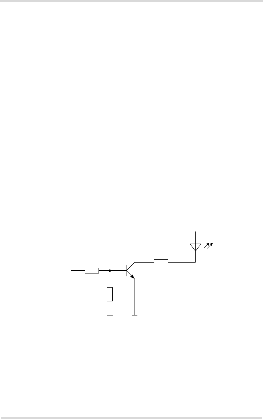
Cinterion® ELS61-USA Hardware Interface Description
2.1 Application Interface
59
els61-usa_hid_v01.040a 2017-08-31
Confidential / Preliminary
Page 45 of 113
2.1.12 PWM Interfaces
The GPIO6 and GPIO7 interface lines can be configured as Pulse Width Modulation interface
lines PWM1 and PWM2. The PWM interface lines can be used, for example, to connect buzz-
ers. The PWM1 line is shared with GPIO7 and the PWM2 line is shared with GPIO6 (for GPIOs
see Section 2.1.9). GPIO and PWM functionality are mutually exclusive.
The startup behavior of the lines is shown in Figure 19.
2.1.13 Pulse Counter
The GPIO8 line can be configured as pulse counter line COUNTER. The pulse counter inter-
face can be used, for example, as a clock (for GPIOs see Section 2.1.9).
2.1.14 Control Signals
2.1.14.1 Status LED
The GPIO5 interface line can be configured to drive a status LED that indicates different oper-
ating modes of the module (for GPIOs see Section 2.1.9). GPIO and LED functionality are mu-
tually exclusive.
To take advantage of this function connect an LED to the GPIO5/LED line as shown in Figure
23.
Figure 23: Status signaling with LED driver
VCC
GPIO5/
LED
LED
GNDGND
R1
R2
R3
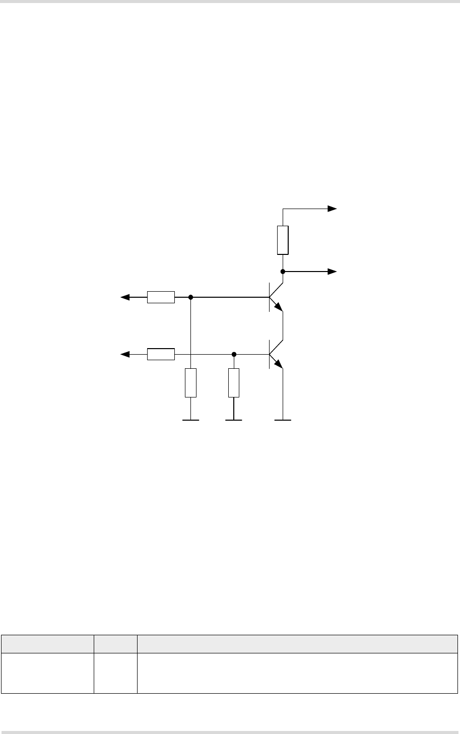
Cinterion® ELS61-USA Hardware Interface Description
2.1 Application Interface
59
els61-usa_hid_v01.040a 2017-08-31
Confidential / Preliminary
Page 46 of 113
2.1.14.2 Power Indication Circuit
In Power Down mode the maximum voltage at any digital or analog interface line must not ex-
ceed +0.3V (see also Section 2.1.2.1). Exceeding this limit for any length of time might cause
permanent damage to the module.
It is therefore recommended to implement a power indication signal that reports the module’s
power state and shows whether it is active or in Power Down mode. While the module is in
Power Down mode all signals with a high level from an external application need to be set to
low state or high impedance state. The sample power indication circuit illustrated in Figure 24
denotes the module’s active state with a low signal and the module’s Power Down mode with
a high signal or high impedance state.
Figure 24: Power indication circuit
2.1.14.3 Host Wakeup
If no call, data or message transfer is in progress, the host may shut down its own USB inter-
face to save power. If a call or other request (URC’s, messages) arrives, the host can be noti-
fied of these events and be woken up again by a state transition of the ASC0 interface‘s RING0
line. This functionality should only be used with legacy USB applications not supporting the rec-
ommended USB suspend and resume mechanism as described in [5] (see also Section 2.1.3.1).
For more information on how to configure the RING0 line by AT^SCFG command see [1].
Possible RING0 line states are listed in Table 9.
Table 9: Host wakeup lines
Signal I/O Description
RING0 O Inactive to active low transition:
0 = The host shall wake up
1 = No wake up request
22k
10k
100k
100k
4.7k
V180
VCORE
Power
indication
External
power supply
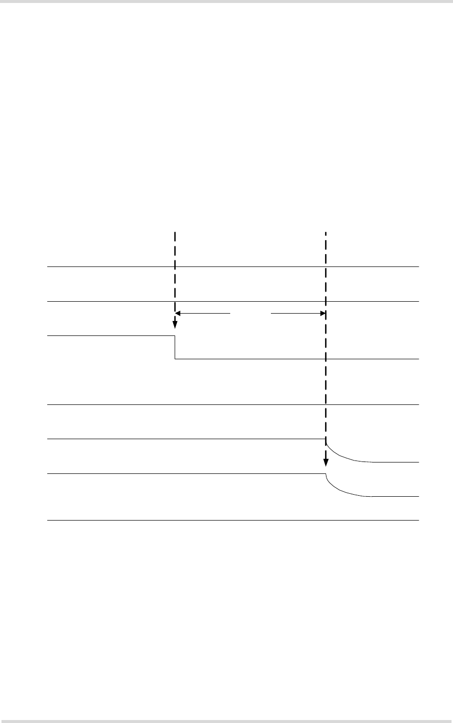
Cinterion® ELS61-USA Hardware Interface Description
2.1 Application Interface
59
els61-usa_hid_v01.040a 2017-08-31
Confidential / Preliminary
Page 47 of 113
2.1.14.4 Fast Shutdown
The GPIO4 interface line can be configured as fast shutdown signal line FST_SHDN. The con-
figured FST_SHDN line is an active low control signal and must be applied for at least 1 milli-
seconds. If unused this line can be left open because of a configured internal pull-up resistor.
Before setting the FST_SHDN line to low, the ON signal should be set to low (see Figure 25).
Otherwise there might be back powering at the ON line in Power Down mode.
The fast shutdown feature can be triggered using the AT command AT^SMSO=<fso>. For de-
tails see [1].
If triggered, a low impulse >1 milliseconds on the FST_SHDN line starts the fast shutdown. The
fast shutdown procedure still finishes any data activities on the module's flash file system, thus
ensuring data integrity, but will no longer deregister gracefully from the network, thus saving
the time required for network deregistration.
Figure 25: Fast shutdown timing
Please note that the normal software controlled shutdown using AT^SMSO will allow option for
a fast shutdown by parameter <fso>, i.e., without network deregistration. However, in this case
no URCs including shutdown URCs will be provided by the AT^SMSO command.
Please also note that the fast shutdown operation does not allow the module deregister from
the network, therefore, this practice is not recommended, and should not be conducted on reg-
ular basis. If it is used for energy saving reason, for instance, used in battery-driven solutions
that require prompt system shutdown before battery depletion, discretion is advised in such
case.
BATT+
VCORE
V180
VDDLP
Fast shut down procedure Power down
EMERG_RST
ON
GPIO4/FST_SHDN
<15ms_
Cinterion® ELS61-USA Hardware Interface Description
2.2 RF Antenna Interface
59
els61-usa_hid_v01.040a 2017-08-31
Confidential / Preliminary
Page 48 of 113
2.2 RF Antenna Interface
The ELS61-USA UMTS/LTE antenna interface comprises a UMTS/LTE main antenna as well
as a UMTS/LTE Rx diversity antenna to improve signal reliability and quality1. The RF interface
has an impedance of 50. ELS61-USA is capable of sustaining a total mismatch at the antenna
line without any damage, even when transmitting at maximum RF power.
The external antenna must be matched properly to achieve best performance regarding radi-
ated power, modulation accuracy and harmonic suppression. Antenna matching networks are
not included on the ELS61-USA module and should be placed in the host application if the an-
tenna does not have an impedance of 50.
Regarding the return loss ELS61-USA provides the following values in the active band:
2.2.1 Antenna Interface Specifications
For approval reasons it is mandatory to connect/apply the Rx diversity antenna to an existing
antenna. Not connecting/applying the Rx diversity antenna does not necessarily impact the
performance, but may result in approval failures. The minimum antenna efficiency should be
better than 50%.
1. By delivery default the UMTS/LTE Rx diversity antenna is configured as available for the module since
its usage is mandatory for LTE. Please refer to [1] for details on how to configure antenna settings.
Table 10: Return loss in the active band
State of module Return loss of module Recommended return loss of application
Receive > 8dB > 12dB
Transmit not applicable > 12dB
Table 11: RF Antenna interface UMTS/LTE (at operating temperature range1)
Parameter Conditions Min. Typical Max. Unit
LTE connectivity2Band 2, 4, 5,12
Receiver Input Sensitivity @
ARP (Dual Antenna; ch.
bandwidth 5MHz)
LTE 700 Band 12 (ch. band-
width 5MHz)
-97 -103.5 dBm
LTE 850 Band 5 (ch. band-
width 10MHz)
-98 -104.5 dBm
LTE AWS Band 4 (ch. band-
width 10MHz)
-100 -103 dBm
LTE 1900 Band 2 (ch. band-
width 10MHz)
-98 -102.5 dBm
Cinterion® ELS61-USA Hardware Interface Description
2.2 RF Antenna Interface
59
els61-usa_hid_v01.040a 2017-08-31
Confidential / Preliminary
Page 49 of 113
RF Power @ ARP with 50
Load
(Board temperature < 85°C,
BW:5MHz RB:25 (DL),
1 (UL) QPSK)
LTE 700 Band 12 (ch. band-
width 5MHz; 1RB, position
low)
+21 +23 dBm
LTE 850 Band 5 (ch. band-
width 5MHz; 1RB, position
low)
+21 +23 dBm
LTE AWS Band 4 (ch. band-
width 5MHz; 1RB, position
low)
+21 +23 dBm
LTE 1900 Band 2 (ch. band-
width 5MHz; 1RB, position
low)
+21 +23 dBm
UMTS/HSPA connectivity2Band II, IV, V
Receiver Input Sensitivity @
ARP
UMTS 850 Band V -104.7 -110 dBm
UMTS AWS Band IV -106.7 -108.5 dBm
UMTS 1900 Band II -104.7 -110 dBm
RF Power @ ARP with 50
Load
(Board temperature < 85°C)
UMTS 850 Band V +21 +23.5 dBm
UMTS AWS Band IV +21 +23.5 dBm
UMTS 1900 Band II +21 +23.5 dBm
1. No active power reduction is implemented - any deviations are hardware related.
2. Applies also to UMTS/LTE Rx diversity antenna.
Table 11: RF Antenna interface UMTS/LTE (at operating temperature range1)
Parameter Conditions Min. Typical Max. Unit
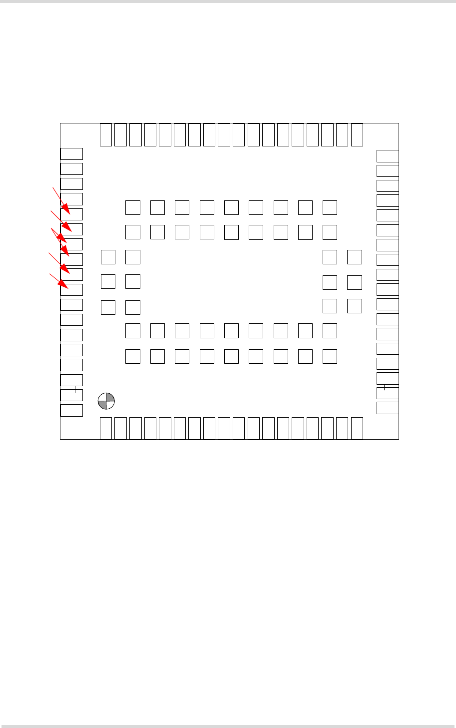
Cinterion® ELS61-USA Hardware Interface Description
2.2 RF Antenna Interface
59
els61-usa_hid_v01.040a 2017-08-31
Confidential / Preliminary
Page 50 of 113
2.2.2 Antenna Installation
The antenna is connected by soldering the antenna pad (ANT_MAIN or ANT_DRX) and its
neighboring ground pads (GND) directly to the application’s PCB. The antenna pads are the
antenna reference points (ARP) for ELS61-USA. All RF data specified throughout this docu-
ment is related to the ARP.
Figure 26: Antenna pads (bottom view)
The distance between the antenna pad and its neighboring GND pads has been optimized for
best possible impedance. To prevent mismatch, special attention should be paid to these pads
on the application‘s PCB.
The wiring of the antenna connection, starting from the antenna pad to the application‘s anten-
na should result in a 50 line impedance. Line width and distance to the GND plane needs to
be optimized with regard to the PCB’s layer stack. Some examples are given in Section 2.2.3.
To prevent receiver desensitization due to interferences generated by fast transients like high
speed clocks on the external application PCB, it is recommended to realize the antenna con-
nection line using embedded Stripline rather than Micro-Stripline technology. Please see Sec-
tion 2.2.3.1 for examples of how to design the antenna connection in order to achieve the
required 50 line impedance.
For type approval purposes, the use of a 50 coaxial antenna connector (U.FL-R-SMT) might
be necessary. In this case the U.FL-R-SMT connector should be placed as close as possible
to ELS61-USA‘s antenna pad.
218217216215214213212211210209208
207
206
205204203202201
33
32
31
30
29
28
27
26
25
24
23
22
21
20
53
54
55
56
57
58
59
60
61
62
63
64
65
66
223224225226227228229230231232233234235236237238239240
67 68 69 70 71 72 73
74 75 76 77 78 79 80
93 94 95 96 97 98 99
100 101 102 103 104 105 106
85 86
89 90
81 82
87 88
91 92
83 84
243
244
241
242
222
221
220
219
252
245
250
251
249
248
247
246
27
28
236237
GND
GND
ANT_MAIN
GND
ANT_DRX
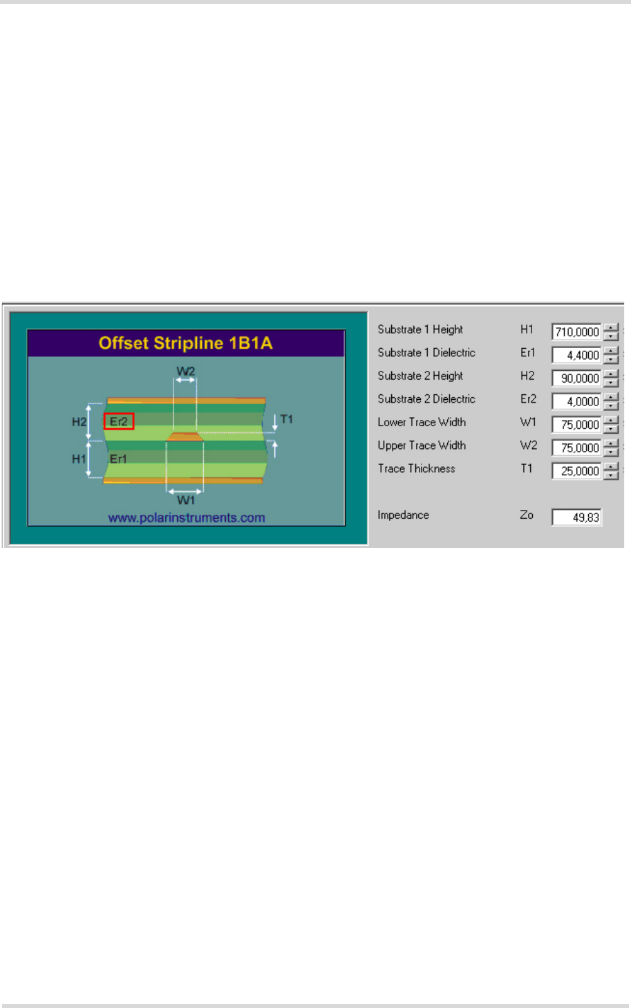
Cinterion® ELS61-USA Hardware Interface Description
2.2 RF Antenna Interface
59
els61-usa_hid_v01.040a 2017-08-31
Confidential / Preliminary
Page 51 of 113
2.2.3 RF Line Routing Design
2.2.3.1 Line Arrangement Examples
Several dedicated tools are available to calculate line arrangements for specific applications
and PCB materials - for example from http://www.polarinstruments.com/ (commercial software)
or from http://web.awrcorp.com/Usa/Products/Optional-Products/TX-Line/ (free software).
Embedded Stripline
This figure below shows a line arrangement example for embedded stripline with 65µm FR4
prepreg (type: 1080) and 710µm FR4 core (4-layer PCB).
Figure 27: Embedded Stripline with 65µm prepreg (1080) and 710µm core
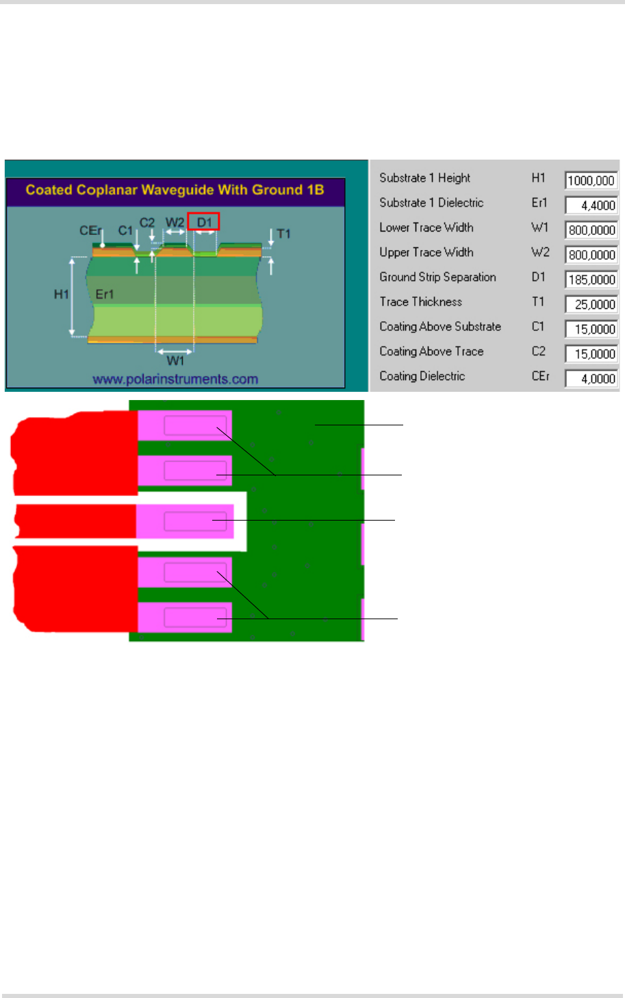
Cinterion® ELS61-USA Hardware Interface Description
2.2 RF Antenna Interface
59
els61-usa_hid_v01.040a 2017-08-31
Confidential / Preliminary
Page 52 of 113
Micro-Stripline
This section gives two line arrangement examples for micro-stripline.
• Micro-Stripline on 1.0mm Standard FR4 2-Layer PCB
The following two figures show examples with different values for D1 (ground strip separa-
tion).
Figure 28: Micro-Stripline on 1.0mm standard FR4 2-layer PCB - example 1
Antenna line
Ground line
Ground line
Application board
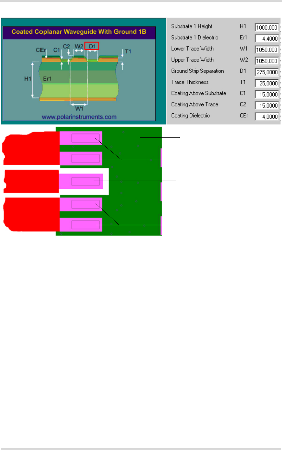
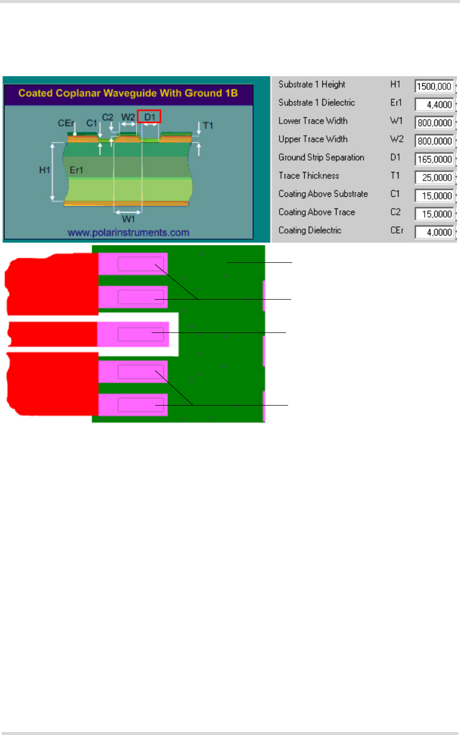
Cinterion® ELS61-USA Hardware Interface Description
2.2 RF Antenna Interface
59
els61-usa_hid_v01.040a 2017-08-31
Confidential / Preliminary
Page 54 of 113
• Micro-Stripline on 1.5mm Standard FR4 2-Layer PCB
The following two figures show examples with different values for D1 (ground strip separa-
tion).
Figure 30: Micro-Stripline on 1.5mm Standard FR4 PCB - example 1
Antenna line
Ground line
Ground line
Application board
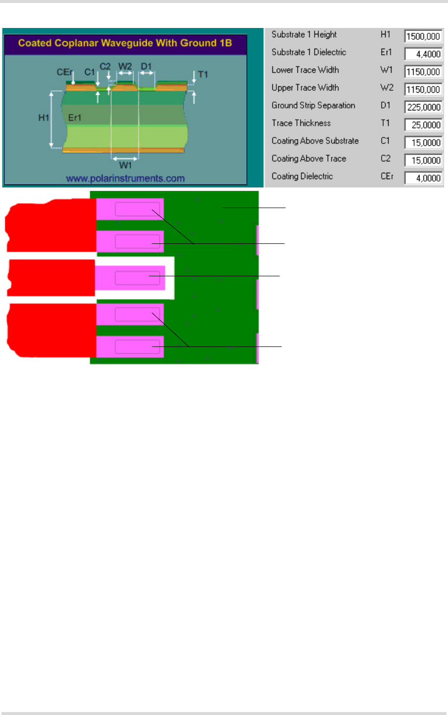
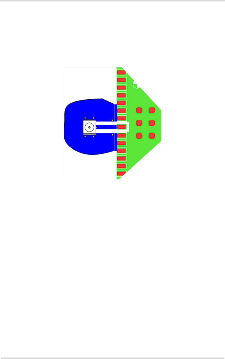
Cinterion® ELS61-USA Hardware Interface Description
2.2 RF Antenna Interface
59
els61-usa_hid_v01.040a 2017-08-31
Confidential / Preliminary
Page 56 of 113
2.2.3.2 Routing Example
Interface to RF Connector
Figure 32 shows the connection of the module‘s antenna pad with an application PCB‘s coaxial
antenna connector. Please note that the ELS61-USA bottom plane appears mirrored, since it
is viewed from ELS61-USA top side. By definition the top of customer's board shall mate with
the bottom of the ELS61-USA module.
Figure 32: Routing to application‘s RF connector - top view

Cinterion® ELS61-USA Hardware Interface Description
2.3 Sample Application
59
els61-usa_hid_v01.040a 2017-08-31
Confidential / Preliminary
Page 57 of 113
2.3 Sample Application
Figure 33 shows a typical example of how to integrate a ELS61-USA module with an applica-
tion. Usage of the various host interfaces depends on the desired features of the application.
Because of the very low power consumption design, current flowing from any other source into
the module circuit must be avoided, for example reverse current from high state external control
lines. Therefore, the controlling application must be designed to prevent reverse current flow.
Otherwise there is the risk of undefined states of the module during startup and shutdown or
even of damaging the module.
Because of the high RF field density inside the module, it cannot be guaranteed that no self
interference might occur, depending on frequency and the applications grounding concept. The
potential interferers may be minimized by placing small capacitors (47pF) at suspected lines
(e.g. RXD0, VDDLP, and ON).
While developing SMT applications it is strongly recommended to provide test points
for certain signals, i.e., lines to and from the module - for debug and/or test purposes.
The SMT application should allow for an easy access to these signals. For details on
how to implement test points see [3].
The EMC measures are best practice recommendations. In fact, an adequate EMC strategy for
an individual application is very much determined by the overall layout and, especially, the po-
sition of components.
Depending on the micro controller used by an external application ELS61-USA‘s digital input
and output lines may require level conversion. Section 2.3.1 shows a possible sample level
conversion circuit.
Note: ELS61-USA is not intended for use with cables longer than 3m.
Disclaimer
No warranty, either stated or implied, is provided on the sample schematic diagram shown in
Figure 33 and the information detailed in this section. As functionality and compliance with na-
tional regulations depend to a great amount on the used electronic components and the indi-
vidual application layout manufacturers are required to ensure adequate design and operating
safeguards for their products using ELS61-USA modules.
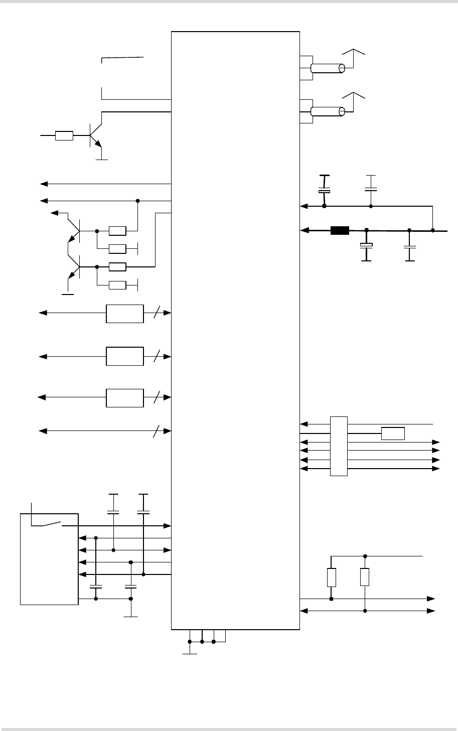
Cinterion® ELS61-USA Hardware Interface Description
2.3 Sample Application
59
els61-usa_hid_v01.040a 2017-08-31
Confidential / Preliminary
Page 58 of 113
Figure 33: Schematic diagram of ELS61-USA sample application
VCORE
V180
ASC0 (including GPIO1...GPIO3 for
DSR0, DTR0, DCD0 and GPIO24 for
RING0)/ SPI_CLK (for DSR0)
GPIO16...GPIO19/
ASC1/
SPI
8
4
CCVCC
CCIO
CCCLK
CCIN
CCRST
SIM
V180
220nF 1nF
I2CCLK
I2CDAT
2.2k***
V180
GPIO4 (FST_SHDN)
GPIO5 (Status LED)
GPIO6 (PWM)
GPIO7 (PWM)
GPIO8 (COUNTER)
GPIO11...GPIO15
LED
GND
GND
GND
ANT_MAIN
BATT+RF
Power suppl
y
Main antenna
ELS6x
All SIM components should be
close to card holder. Keep SIM
wires low capacitive.
*10pF *10pF
* add optional 10pF for SIM protection
against RF (internal Antenna)
150µF,
Low ESR! 33pF
Blocking**
Blocking**
Blocking**
PWR_IND
BATT+BB
53
204
GPIO20...GPIO23/
DAI
4
Blocking**
100k
4.7k
100k
22k
2.2k***
3USB
150µF,
Low ESR!
33pF
GND
GND
ANT_DRX
Diversity antenna
ON
EMERG_RST
RESET
VDDLP
100k
VDDLP
BEAD*
BEAD*: It is recommended to
add the BEAD as shown to the
BATT+BB line. The purpose of
this is to mitigate noise from
baseband power supply.
Note 1: BLM15PD121SN1D
MURATA Ind Chip Bead
(120Ohm 25% 100MHz Ferrite
1.3A) is recommended in this
case. For details please visit
www.murata.com.
Note 2: The Bead should be
placed as close as possible to
the module.
*** I2
C interface of the module already
has internal 1KOhm pull up resistor to
V180 inside the module. Please take
this into consideration during
application design.
Blocking** = For more details see Section 3.7
For switch on circuit see Section 3.2.1
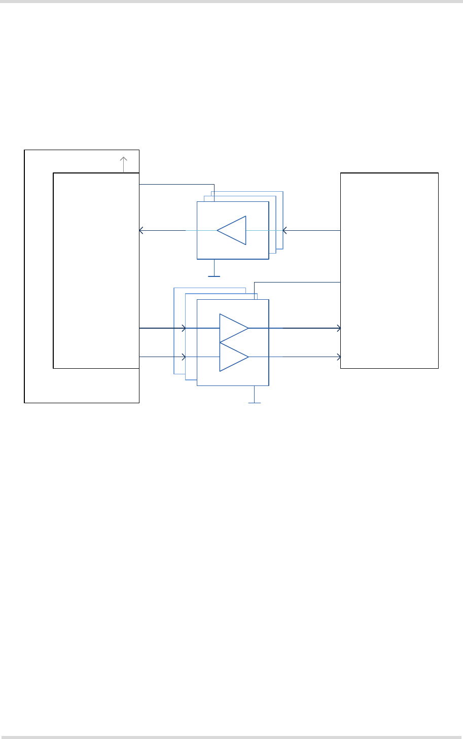
Cinterion® ELS61-USA Hardware Interface Description
2.3 Sample Application
59
els61-usa_hid_v01.040a 2017-08-31
Confidential / Preliminary
Page 59 of 113
2.3.1 Sample Level Conversion Circuit
Depending on the micro controller used by an external application ELS61-USA‘s digital input
and output lines (i.e., ASC0, ASC1 and GPIO lines) may require level conversion. The following
Figure 34 shows a sample circuit with recommended level shifters for an external application‘s
micro controller (with VLOGIC between 3.0V...3.6V). The level shifters can be used for digital
input and output lines with VOHmax=1.85V or VIHmax =1.85V.
Figure 34: Sample level conversion circuit
5V tolerarant
5V tolerarant
Low level input
Low level input
Low level input
VCC
5V tolerant
VCC
E.g.,
74VHC1GT50
E.g.,
NC7WZ16
74LVC2G34
External application
Micro controller
VLOGIC
(3.0V...3.6V)
Input lines,
e.g., µRXD, µCTS
Output lines,
e.g., µTXD, µRTS
V180 (1.8V)
Digital output lines,
e.g., RXDx, CTSx
Wireless module
Digital input lines,
e.g., TXDx, RTSx
Cinterion® ELS61-USA Hardware Interface Description
3 Operating Characteristics
83
els61-usa_hid_v01.040a 2017-08-31
Confidential / Preliminary
Page 60 of 113
3 Operating Characteristics
3.1 Operating Modes
The table below briefly summarizes the various operating modes referred to throughout the
document.
Table 12: Overview of operating modes
Mode Function
Normal
operation
UMTS / HSPA /
LTE SLEEP
Power saving set automatically when no call is in progress and the USB
connection is suspended by host or not present and no active commu-
nication via ASC0.
UMTS / HSPA /
LTE IDLE
Power saving disabled or an USB connection not suspended, but no
call in progress.
UMTS TALK/
UMTS DATA
UMTS data transfer in progress. Power consumption depends on net-
work settings (e.g. TPC Pattern) and data transfer rate.
HSPA DATA HSPA data transfer in progress. Power consumption depends on net-
work settings (e.g. TPC Pattern) and data transfer rate.
LTE DATA LTE data transfer in progress. Power consumption depends on network
settings (e.g. TPC Pattern) and data transfer rate.
Power
Down
Normal shutdown after sending the power down command. Only a voltage regulator is
active for powering the RTC. Software is not active. Interfaces are not accessible. Operat-
ing voltage remains applied.
Airplane
mode
Airplane mode shuts down the radio part of the module, causes the module to log off from
the network and disables all AT commands whose execution requires a radio connection.
Airplane mode can be controlled by AT command (see [1]).
Alarm
mode
Restricted operation launched by RTC alert function when the module is in Power Down
mode. In Alarm mode, the module remains deregistered from the network. Limited number
of AT commands is accessible.

Cinterion® ELS61-USA Hardware Interface Description
3.2 Power Up/Power Down Scenarios
83
els61-usa_hid_v01.040a 2017-08-31
Confidential / Preliminary
Page 61 of 113
3.2 Power Up/Power Down Scenarios
In general, be sure not to turn on ELS61-USA while it is beyond the safety limits of voltage and
temperature stated in Section 2.1.2.1. ELS61-USA immediately switches off after having start-
ed and detected these inappropriate conditions. In extreme cases this can cause permanent
damage to the module.
3.2.1 Turn on ELS61-USA
ELS61-USA can be turned on as described in the following sections:
• Connecting the operating voltage BATT+ (see Section 3.2.1.1).
• Hardware driven switch on by ON line: Starts Normal mode (see Section 3.2.1.2).
After startup or restart, the module will send the URC ^SYSSTART that notifies the host appli-
cation that the first AT command can be sent to the module (see also [1]).
3.2.1.1 Connecting ELS61-USA BATT+ Lines
Figure 35 shows sample external application circuits that allow to connect (and also to tempo-
rarily disconnect) the module‘s BATT+ lines from the external application‘s power supply.
Figure 35 illustrates the application of power employing an externally controlled microcontrol-
ler. The voltage supervisory circuit ensures that the power is disconnected and applied again
depending on given thresholds.
The transistor T2 mentioned in Figure 35 should have an RDS_ON value < 50m in order to min-
imize voltage drops.
Such circuits could be useful to maximize power savings for battery driven applications or to
completely switch off and restart the module after a firmware update.
After connecting the BATT+ lines the module can then be (re-)started as described in Section
3.2.1.2 and Section 3.2.2.
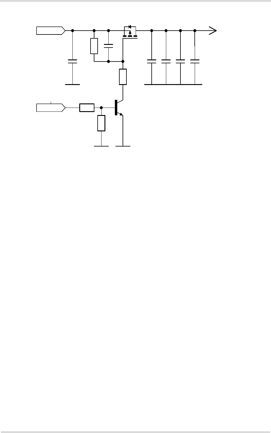
Cinterion® ELS61-USA Hardware Interface Description
3.2 Power Up/Power Down Scenarios
83
els61-usa_hid_v01.040a 2017-08-31
Confidential / Preliminary
Page 62 of 113
Figure 35: Sample circuit for applying power using an external µC
3.8V
Module
Place C2-C5 close to module
µcontroller
ENABLE
VBATT
VBATT_IN
C1
100nF
C2 47µF,X5R
C3 47µF,X5R
C4 47µF,X5R
C5 47µF,X5R
C6 47µF,X5R
R1
100k
R2
100k
R3
100k
R6
10k
T1
T2
IRML6401
BC847
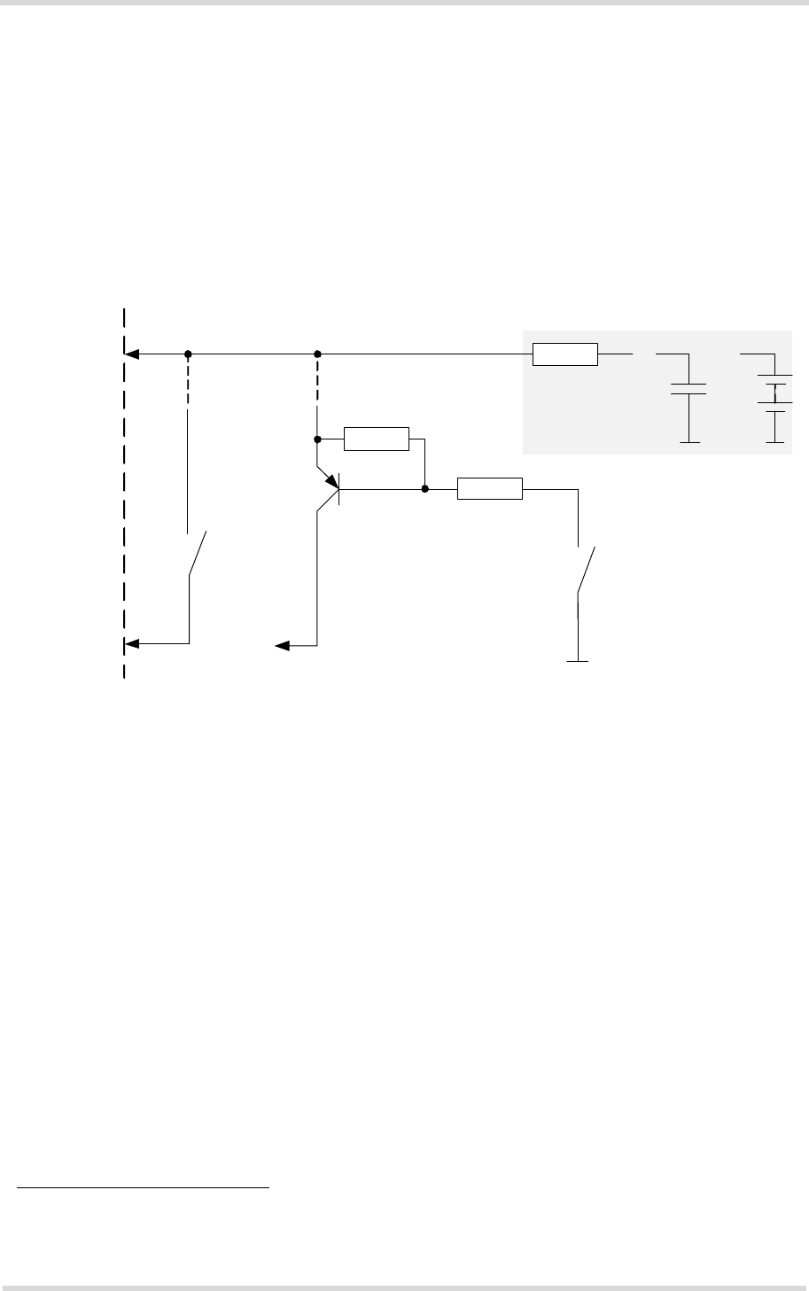
Cinterion® ELS61-USA Hardware Interface Description
3.2 Power Up/Power Down Scenarios
83
els61-usa_hid_v01.040a 2017-08-31
Confidential / Preliminary
Page 63 of 113
3.2.1.2 Switch on ELS61-USA Using ON Signal
After the operating voltage BATT+ is applied, ELS61-USA can be switched on by means of the
ON signal.
The ON signal is an edge triggered signal and allows the input voltage level up to 5V. The mod-
ule starts into normal mode on detecting the rising edge of the ON signal. The rising edge of
ON signal must be applied at least 100 milliseconds later than BATT+. See Figure 37.
The following Figure 36 shows recommendations for possible switch-on circuits.
Figure 36: ON circuit options
It is recommended to set a serial 1kOhm resistor between the ON circuit and the external ca-
pacitor or battery at the VDDLP power supply (i.e., RTC backup circuit). This serial resistor pro-
tection is necessary in case the capacitor or battery has low power (is empty).With Option 2 the
typical resistor values are: R1 = 150k and R2 = 3k. But the resistor values depend on the cur-
rent gain from the employed PNP resistor.
Please note that the ON signal is an edge triggered signal. This implies that a micro-second
high pulse on the signal line suffices to almost immediately switch on the module, as shown in
Figure 37. After module startup the ON signal should always be set to low to prevent possible
back powering at this pad.1
1. Please take due discretion when designing the filtering circuit, especially ESD, which may cause unin-
tended switch on.
VDDLP
ON
1k
+
R1
R2
Option 1 Option 2
RTC backup
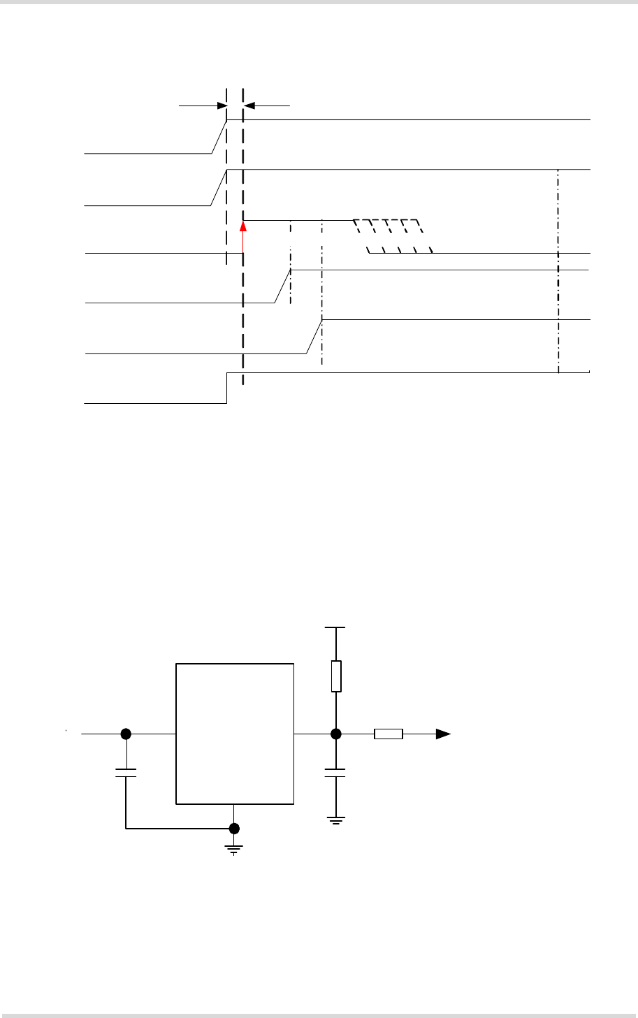
Cinterion® ELS61-USA Hardware Interface Description
3.2 Power Up/Power Down Scenarios
83
els61-usa_hid_v01.040a 2017-08-31
Confidential / Preliminary
Page 64 of 113
Figure 37: ON timing
3.2.1.3 Automatic Power On
If an automatic power on function is required for module application, circuit shown in either
Figure 38 or Figure 39 is recommended.
Figure 38: Automatic ON circuit based on voltage detector - option 1
BATT+
ON
EMERG_RST
V180
VCORE
VDDLP
Rising edge only starts up the module
>100ms
Voltage Detector*
BATT+BB
GND
ON
VDDLP
GND
* It is recommended to
apply the 3-pin microprocessor reset
monitor MAX803SQ293T1G or MAX803SQ293D3T1G
manufactured by ON Semiconductor.
Details please refer to www.onsemi.com
VCC RESET
GND
100nF Not Assembled
R1
10KOhm
R2
0Ohm
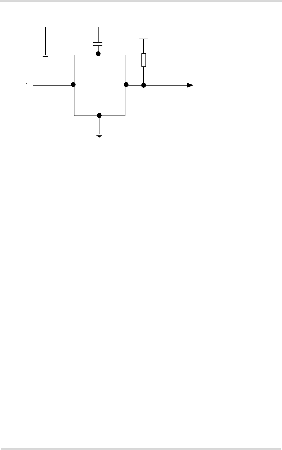
Cinterion® ELS61-USA Hardware Interface Description
3.2 Power Up/Power Down Scenarios
83
els61-usa_hid_v01.040a 2017-08-31
Confidential / Preliminary
Page 65 of 113
Figure 39: Automatic ON circuit based on voltage detector - option 2
3.2.2 Restart ELS61-USA
After startup ELS61-USA can be re-started as described in the following sections:
• Software controlled reset by AT+CFUN command: Starts Normal mode (see Section
3.2.2.1).
• Hardware controlled reset by EMERG_RST line: Starts Normal mode (see Section 3.2.2.2).
3.2.2.1 Restart ELS61-USA via AT+CFUN Command
To reset and restart the ELS61-USA module use the command AT+CFUN. See [1] for details.
Voltage Detector*
BATT+BB
GND
ON
VDDLP
* It is recommended to apply the ultra-low current voltage
detector NCP303LSN28T1 manufactured by ON Semiconductor.
Details please refer to www.onsemi.com
Input RESET
Output
GND
R1
10KOhm
21
3
0.1μF
GND 5 CD
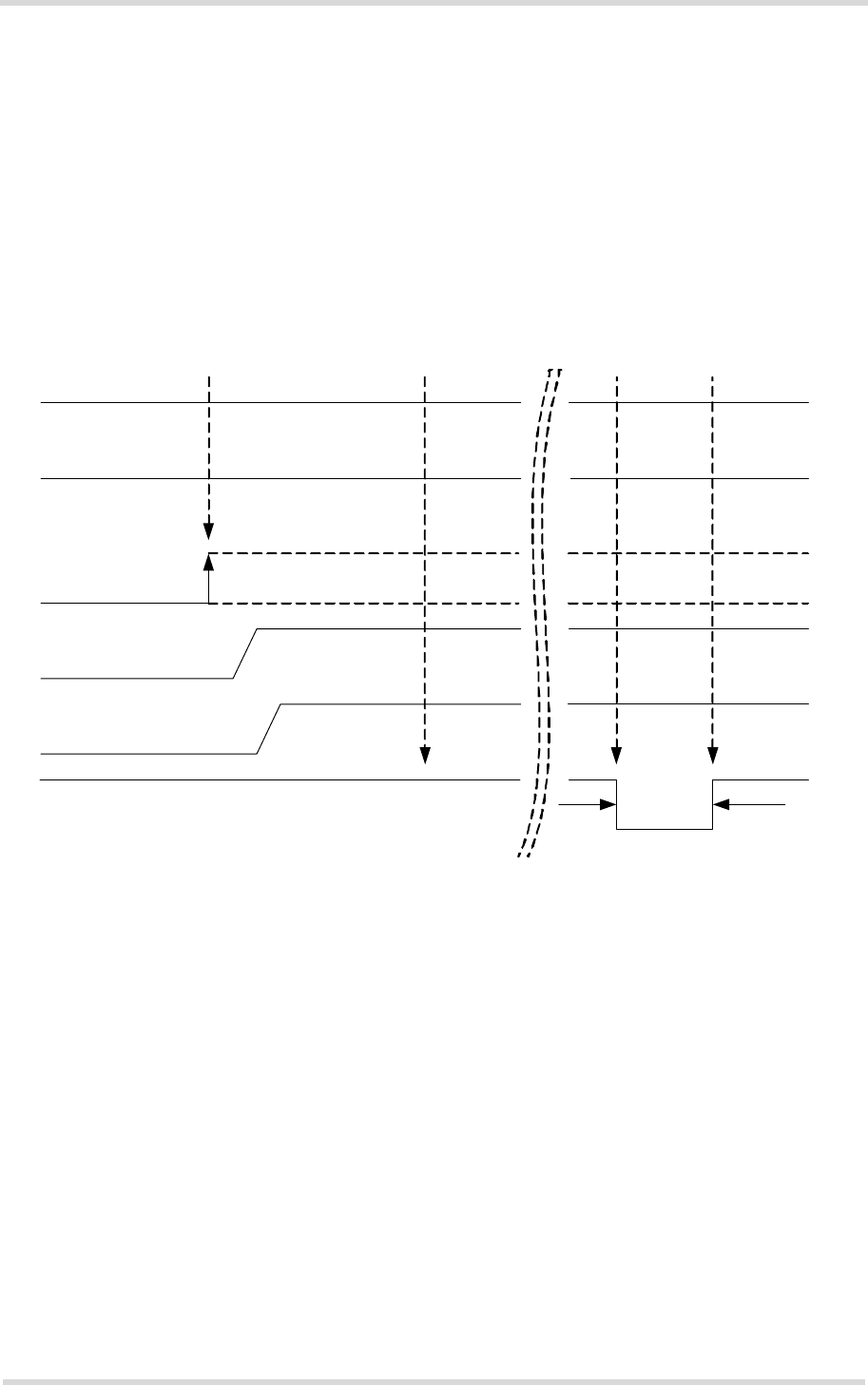
Cinterion® ELS61-USA Hardware Interface Description
3.2 Power Up/Power Down Scenarios
83
els61-usa_hid_v01.040a 2017-08-31
Confidential / Preliminary
Page 66 of 113
3.2.2.2 Restart ELS61-USA Using EMERG_RST
The EMERG_RST signal is internally connected to the main module processor. A low level for
more than 10ms sets the processor and with it all the other signal pads to their respective reset
state. The reset state is described in Section 3.2.3 as well as in the figures showing the startup
behavior of an interface.
After releasing the EMERG-RST line, i.e., with a change of the signal level from low to high,
the module restarts. The other signals continue from their reset state as if the module was
switched on by the ON signal.
Figure 40: Emergency restart timing
It is recommended to control this EMERG_RST line with an open collector transistor or an open
drain field-effect transistor.
Caution: Use the EMERG_RST line only when, due to serious problems, the software is not
responding for more than 5 seconds. Pulling the EMERG_RST line causes the loss of all infor-
mation stored in the volatile memory. Therefore, this procedure is intended only for use in case
of emergency, e.g. if ELS61-USA does not respond, if reset or shutdown via AT command fails.
BATT+
ON
EMERG_RST
VCORE
V180
VDDLP
>10ms
System
started
System
started again
Reset
state
Ignition
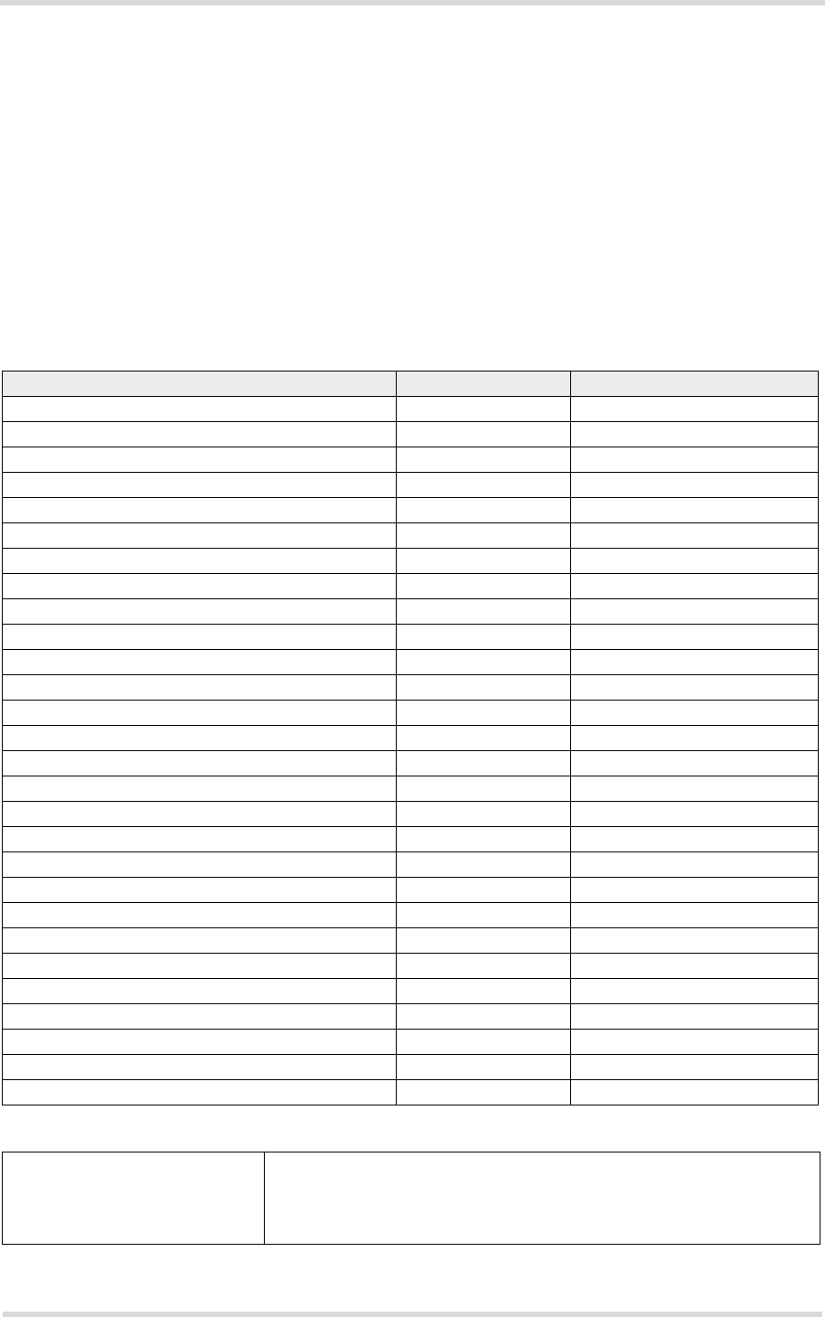
Cinterion® ELS61-USA Hardware Interface Description
3.2 Power Up/Power Down Scenarios
83
els61-usa_hid_v01.040a 2017-08-31
Confidential / Preliminary
Page 67 of 113
3.2.3 Signal States after Startup
Table 13 lists the states each interface signal passes through during reset phase and the first
firmware initialization. For further firmware startup initializations the values may differ because
of different GPIO line configurations.
The reset state is reached with the rising edge of the EMERG_RST signal - either after a normal
module startup (see Section 3.2.1.2) or after a reset (see Section 3.2.2.2). After the reset state
has been reached the firmware initialization state begins. The firmware initialization is complet-
ed as soon as the ASC0 interface lines CTS0, DSR0 and RING0 as well as the ASC1 interface
line CTS1 have turned low (see Section 2.1.4 and Section 2.1.5). Now, the module is ready to
receive and transmit data.
Abbreviations used in above Table 13:
Table 13: Signal states
Signal name Reset state First start up configuration
CCIO L O / L
CCRST L O / L
CCCLK L O / L
CCIN T / 100k PD I / PD
RXD0 T / PU O / H
TXD0 T / PD I
CTS0 T / PU O / H
RTS0 T / PU I / PD
GPIO1 T / PD T / PD
GPIO2 T / PD T / PD
GPIO3 T / PD T / PD
GPIO4 T / PD T / PD
GPIO5 T / PD T / PD
GPIO6 T / PD T / PD
GPIO7 T / PD T / PD
GPIO8 T / PD T / PD
GPIO11-GPIO15 T / PD T / PD
GPIO16 T / PD T / PD
GPIO17 T / PD T / PD
GPIO18 T / PD T / PD
GPIO19 T / PD T / PD
GPIO20 T / PD T / PD
GPIO21 T / PD T / PD
GPIO22 T / PD T / PD
GPIO23 T / PD T / PD
GPIO24 T / PD T / PD
I2CCLK T / PU OD / PU
I2CDAT T / PU OD / PU
L = Low level
H = High level
T = Tristate
I = Input
O = Output
OD = Open Drain
PD = Pull down, 200µA at 1.9V
PU = Pull up, -240µA at 0V

Cinterion® ELS61-USA Hardware Interface Description
3.2 Power Up/Power Down Scenarios
83
els61-usa_hid_v01.040a 2017-08-31
Confidential / Preliminary
Page 68 of 113
3.2.4 Turn off ELS61-USA
To switch the module off the following procedures may be used:
•Software controlled shutdown procedure: Software controlled by sending an AT command
over the serial application interface. See Section 3.2.4.1.
•Hardware controlled shutdown procedure: Hardware controlled by disconnecting the mod-
ule‘s power supply lines BATT+ (see Section 3.2.1.1).
•Automatic shutdown (software controlled): See Section 3.2.5
- Takes effect if ELS61-USA board temperature or voltage levels exceed a critical limit.
3.2.4.1 Switch off ELS61-USA Using AT Command
The best and safest approach to powering down ELS61-USA is to issue the appropriate AT
command. This procedure lets ELS61-USA log off from the network and allows the software to
enter into a secure state and safe data before disconnecting the power supply. The mode is
referred to as Power Down mode. In this mode, only the RTC stays active. After sending the
switch off command AT^SMSO, be sure not to enter any further AT commands until the module
was restarted.
CAUTION: Be sure not to disconnect the operating voltage VBATT+ before V180 pad has gone
low. Otherwise you run the risk of losing data, or in some rare cases even to render the module
inoperable.
To monitor the V180 line, it is recommended to implement a power indication circuit as de-
scribed in Section 2.1.14.2.
While ELS61-USA is in Power Down mode the application interface is switched off and must
not be fed from any other voltage source. Therefore, your application must be designed to
avoid any current flow into any digital pads of the application interface.

Cinterion® ELS61-USA Hardware Interface Description
3.2 Power Up/Power Down Scenarios
83
els61-usa_hid_v01.040a 2017-08-31
Confidential / Preliminary
Page 70 of 113
3.2.5 Automatic Shutdown
Automatic shutdown takes effect if the following event occurs:
• ELS61-USA board is exceeding the critical limits of overtemperature or undertemperature
(see Section 3.2.5.1)
• Undervoltage or overvoltage is detected (see Section 3.2.5.2 and Section 3.2.5.3)
The automatic shutdown procedure is equivalent to the power-down initiated with an AT com-
mand, i.e. ELS61-USA logs off from the network and the software enters a secure state avoid-
ing loss of data.
3.2.5.1 Thermal Shutdown
The board temperature is constantly monitored by an internal NTC resistor located on the PCB.
The values detected by the NTC resistor are measured directly on the board and therefore, are
not fully identical with the ambient temperature.
Each time the board temperature goes out of range or back to normal, ELS61-USA instantly
displays an alert (if enabled).
• URCs indicating the level "1" or "-1" allow the user to take appropriate precautions, such as
protecting the module from exposure to extreme conditions. The presentation of the URCs
depends on the settings selected with the AT^SCTM write command (for details see [1]):
AT^SCTM=1: Presentation of URCs is always enabled.
AT^SCTM=0 (default): Presentation of URCs is enabled during the 2 minute guard period
after start-up of ELS61-USA. After expiry of the 2 minute guard period, the presentation of
URCs will be disabled, i.e. no URCs with alert levels "1" or ''-1" will be generated.
• URCs indicating the level "2" or "-2" are instantly followed by an orderly shutdown. The pre-
sentation of these URCs is always enabled, i.e. they will be output even though the factory
setting AT^SCTM=0 was never changed.
The maximum temperature ratings are stated in Section 3.5. Refer to Table 14 for the associ-
ated URCs.
Table 14: Temperature dependent behavior
Sending temperature alert (2min after ELS61-USA start-up, otherwise only if URC presentation
enabled)
^SCTM_B: 1 Board close to overtemperature limit.
^SCTM_B: -1 Board close to undertemperature limit.
^SCTM_B: 0 Board back to non-critical temperature range.
Automatic shutdown (URC appears no matter whether or not presentation was enabled)
^SCTM_B: 2 Alert: Board equal or beyond overtemperature limit. ELS61-USA switches off.
^SCTM_B: -2 Alert: Board equal or below undertemperature limit. ELS61-USA switches off.

Cinterion® ELS61-USA Hardware Interface Description
3.2 Power Up/Power Down Scenarios
83
els61-usa_hid_v01.040a 2017-08-31
Confidential / Preliminary
Page 71 of 113
3.2.5.2 Undervoltage Shutdown
The undervoltage shutdown threshold is the specified minimum supply voltage VBATT+ given in
Table 2. When the average supply voltage measured by ELS61-USA approaches the under-
voltage shutdown threshold (i.e., 0.05V offset) the module will send the following URC:
^SBC: Undervoltage Warning
The undervoltage warning is sent only once - until the next time the module is close to the un-
dervoltage shutdown threshold.
If the voltage continues to drop below the specified undervoltage shutdown threshold, the mod-
ule will send the following URC:
^SBC: Undervoltage Shutdown
This alert is sent only once before the module shuts down cleanly without sending any further
messages.
This type of URC does not need to be activated by the user. It will be output automatically when
fault conditions occur.
Note: For battery powered applications it is strongly recommended to implement a BATT+ con-
necting circuit as described in Section 3.2.1.1 in order to not only be able save power, but also
to restart the module after an undervoltage shutdown where the battery is deeply discharged.
Also note that the undervoltage threshold is calculated for max. 400mV voltage drops during
transmit burst. Power supply sources for external applications should be designed to tolerate
400mV voltage drops without crossing the lower limit of 3.0 V. For external applications oper-
ating at the limit of the allowed tolerance the default undervoltage threshold may be adapted
by subtracting an offset. For details see [1]: AT^SCFG= "MEShutdown/sVsup/threshold".
3.2.5.3 Overvoltage Shutdown
The overvoltage shutdown threshold is the specified maximum supply voltage VBATT+ given in
Table 2. When the average supply voltage measured by ELS61-USA approaches the overvolt-
age shutdown threshold (i.e., 0.05V offset) the module will send the following URC:
^SBC: Overvoltage Warning
The overvoltage warning is sent only once - until the next time the module is close to the over-
voltage shutdown threshold.
If the voltage continues to rise above the specified overvoltage shutdown threshold, the module
will send the following URC:
^SBC: Overvoltage Shutdown
This alert is sent only once before the module shuts down cleanly without sending any further
messages.
This type of URC does not need to be activated by the user. It will be output automatically when
fault conditions occur.
Keep in mind that several ELS61-USA components are directly linked to BATT+ and, therefore,
the supply voltage remains applied at major parts of ELS61-USA. Especially the power ampli-
fier linked to BATT+RF is very sensitive to high voltage and might even be destroyed.
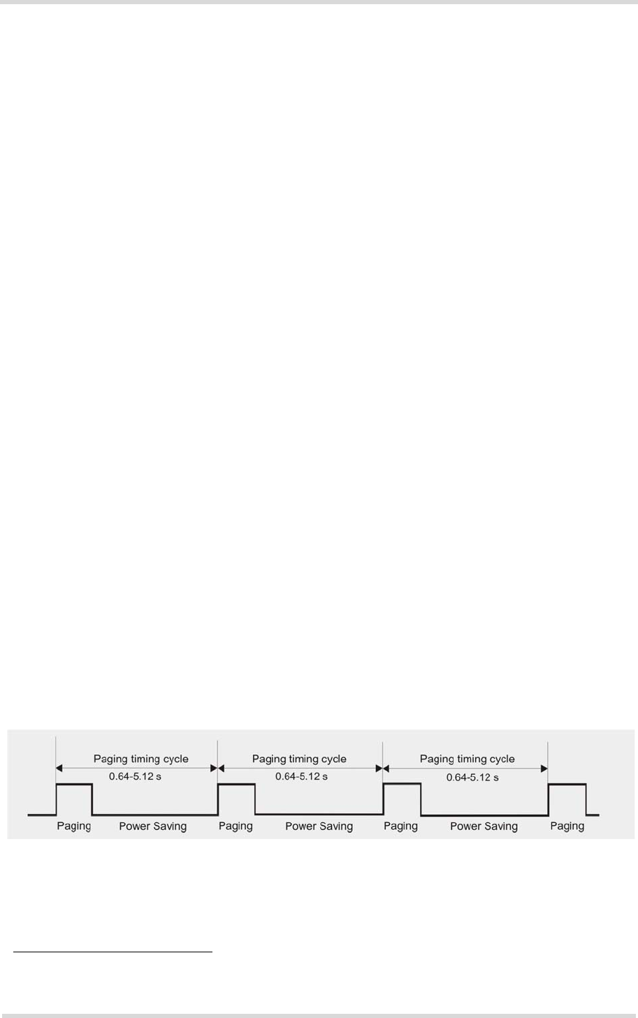
Cinterion® ELS61-USA Hardware Interface Description
3.3 Power Saving
83
els61-usa_hid_v01.040a 2017-08-31
Confidential / Preliminary
Page 72 of 113
3.3 Power Saving
ELS61-USA can be configured to control power consumption:
• Using the AT command AT^SPOW it is possible to specify a so-called power saving mode
for the module (<mode> = 2; for details on the command see [1]). The module‘s UART inter-
faces (ASC0 and ASC1) are then deactivated and will only periodically be activated to be
able to listen to network paging messages as described in Section 3.3.1 and Section 3.3.2.
See Section 3.3.3 for a description on how to immediately wake up ELS61-USA again using
RTS0.
Please note that the AT^SPOW setting has no effect on the USB interface. As long as the
USB connection is active, the module will not change into its SLEEP state to reduce its func-
tionality to a minimum and thus minimizing its current consumption. To enable switching
into SLEEP mode, the USB connection must therefore either not be present at all or the
USB host must bring its USB interface into Suspend state. Also, VUSB_IN should always
be kept enabled for this functionality. See “Universal Serial Bus Specification Revision 2.0”1
for a description of the Suspend state.
3.3.1 Power Saving while Attached to WCDMA Networks
The power saving possibilities while attached to a WCDMA network depend on the paging tim-
ing cycle of the base station.
During normal WCDMA operation, i.e., the module is connected to a WCDMA network, the
duration of a power saving period varies. It may be calculated using the following formula:
t = 2DRX value * 10 ms (WCDMA frame duration).
DRX (Discontinuous Reception) in WCDMA networks is a value between 6 and 9, thus result-
ing in power saving intervals between 0.64 and 5.12 seconds. The DRX value of the base sta-
tion is assigned by the WCDMA network operator.
In the pauses between listening to paging messages, the module resumes power saving, as
shown in Figure 42.
Figure 42: Power saving and paging in WCDMA networks
The varying pauses explain the different potential for power saving. The longer the pause the
less power is consumed.
1. The specification is ready for download on http://www.usb.org/developers/docs/
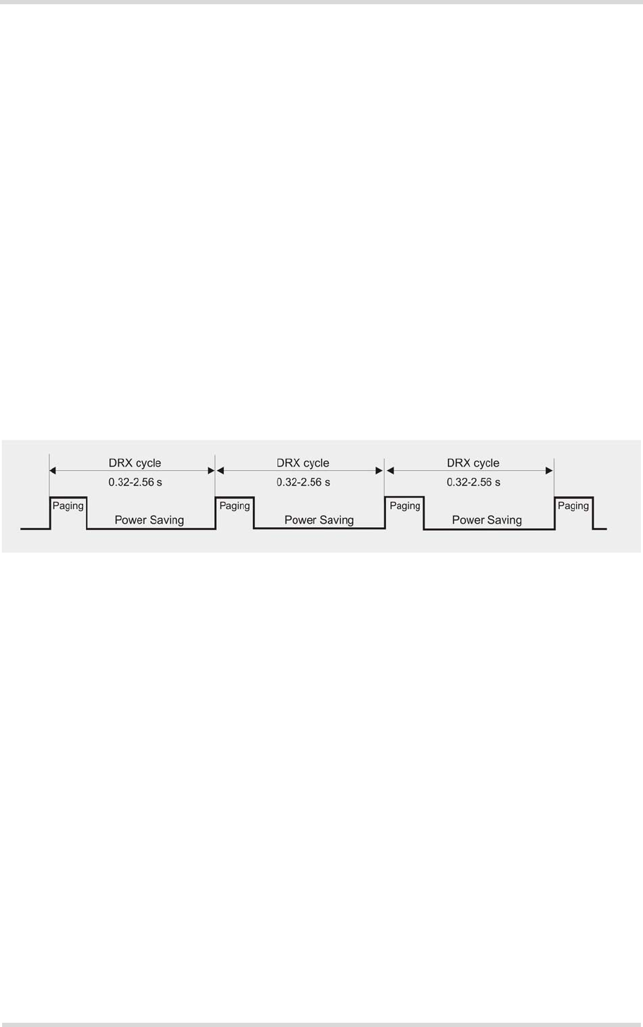
Cinterion® ELS61-USA Hardware Interface Description
3.3 Power Saving
83
els61-usa_hid_v01.040a 2017-08-31
Confidential / Preliminary
Page 73 of 113
Generally, power saving depends on the module’s application scenario and may differ from the
above mentioned normal operation. The power saving interval may be shorter than 0.64 sec-
onds or longer than 5.12 seconds.
3.3.2 Power Saving while Attached to LTE Networks
The power saving possibilities while attached to an LTE network depend on the paging timing
cycle of the base station.
During normal LTE operation, i.e., the module is connected to an LTE network, the duration of
a power saving period varies. It may be calculated using the following formula:
t = DRX Cycle Value * 10 ms
DRX cycle value in LTE networks is any of the four values: 32, 64, 128 and 256, thus resulting
in power saving intervals between 0.32 and 2.56 seconds. The DRX cycle value of the base
station is assigned by the LTE network operator.
In the pauses between listening to paging messages, the module resumes power saving, as
shown in Figure 43.
Figure 43: Power saving and paging in LTE networks
The varying pauses explain the different potential for power saving. The longer the pause the
less power is consumed.
Generally, power saving depends on the module’s application scenario and may differ from the
above mentioned normal operation. The power saving interval may be shorter than 0.32 sec-
onds or longer than 2.56 seconds.
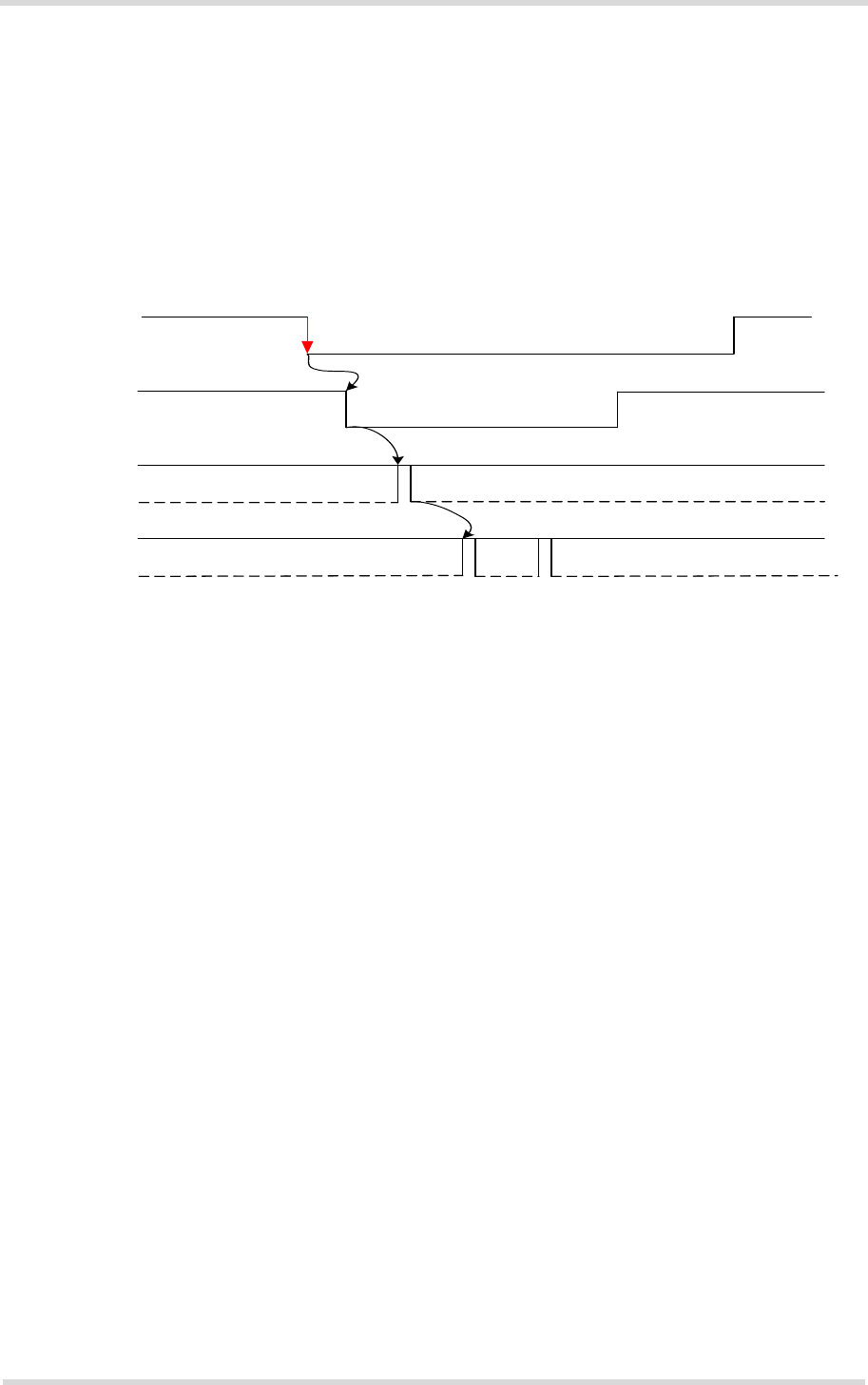
Cinterion® ELS61-USA Hardware Interface Description
3.3 Power Saving
83
els61-usa_hid_v01.040a 2017-08-31
Confidential / Preliminary
Page 74 of 113
3.3.3 Wake-up via RTS0
RTS0 can be used to wake up ELS61-USA from SLEEP mode configured with AT^SPOW.
Assertion of RTS0 (i.e., toggle from inactive high to active low) serves as wake up event, thus
allowing an external application to almost immediately terminate power saving. After RTS0
assertion, the CTS0 line signals module wake up, i.e., readiness of the AT command interface.
It is therefore recommended to enable RTS/CTS flow control (default setting).
Figure 44 shows the described RTS0 wake up mechanism.
Figure 44: Wake-up via RTS0
RTS0
CTS0
TXD0
RXD0
AT command
Reply URC
RTS assertion (falling edge)
Wake up from SLEEP mode Return to SLEEP mode
RTS back

Cinterion® ELS61-USA Hardware Interface Description
3.4 Power Supply
83
els61-usa_hid_v01.040a 2017-08-31
Confidential / Preliminary
Page 75 of 113
3.4 Power Supply
ELS61-USA needs to be connected to a power supply at the SMT application interface - 2 lines
BATT+, and GND. There are two separate voltage domains for BATT+:
•BATT+
BB with a line mainly for the baseband power supply.
•BATT+
RF with a line for the UMTS/LTE power amplifier supply.
Please note that throughout the document BATT+ refers to both voltage domains and power
supply lines - BATT+BB and BATT+RF.
The power supply of ELS61-USA has to be a single voltage source at BATT+BB and BATT+RF.
It must be able to provide the peak current during the uplink transmission.
All the key functions for supplying power to the device are handled by the power management
section of the analog controller. This IC provides the following features:
• Stabilizes the supply voltages for the baseband using low drop linear voltage regulators and
a DC-DC step down switching regulator.
• Switches the module's power voltages for the power-up and -down procedures.
• SIM switch to provide SIM power supply.
3.4.1 Power Supply Ratings
Table 15 and Table 16 assemble various voltage supply and current consumption ratings of the
module.
Table 15: Voltage supply ratings
Description Conditions Min Typ Max Unit
BATT+ Supply voltage Directly measured at Module. Voltage
must stay within the min/max values,
including voltage drop, ripple, spikes.
3.0 4.5 V
Maximum allowed
voltage drop
during transmit
burst
Normal condition, power control level
for Pout max
400 mV
Voltage ripple Normal condition, power control level
for Pout max
@ f <= 250 kHz
@ f > 250 kHz
120
90
mVpp
mVpp
Cinterion® ELS61-USA Hardware Interface Description
3.4 Power Supply
83
els61-usa_hid_v01.040a 2017-08-31
Confidential / Preliminary
Page 76 of 113
Table 16: Current consumption ratings
Description Conditions Typical rating Unit
IVDDLP @ 1.8V OFF State supply
current
RTC backup @ BATT+ = 0V 0.1 µA
IBATT+
1
(i.e., sum of
BATT+BB and
BATT+RF)
OFF State supply
current
Power Down 84 µA
Average UMTS
supply current
Data transfer @
maximum Pout
SLEEP2 @ DRX=9
(UART deactivated) USB disconnected 1.9 mA
USB suspended 1.9 mA
SLEEP2 @ DRX=8
(UART deactivated) USB disconnected 1.9 mA
USB suspended 1.9. mA
SLEEP2 @ DRX=6
(UART deactivated) USB disconnected 2.6 mA
USB suspended 2.5 mA
IDLE3 @ DRX=6
(UART active, but no
communication)
USB disconnected 14 mA
USB active 33 mA
UMTS Data transfer Band II 640 mA
UMTS Data transfer Band IV 650 mA
UMTS Data transfer Band V 405 mA
HSPA Data transfer Band II 640 mA
HSPA Data transfer Band IV 650 mA
HSPA Data transfer Band V 405 mA
Voice call Band II 615 mA
Voice call Band IV 615 mA
Voice call Band V 385 mA
Cinterion® ELS61-USA Hardware Interface Description
3.4 Power Supply
83
els61-usa_hid_v01.040a 2017-08-31
Confidential / Preliminary
Page 77 of 113
IBATT+
1
(i.e., sum of
BATT+BB and
BATT+RF)
Average LTE sup-
ply current
Data transfer @
maximum Pout
SLEEP2 @ “Paging
Occasions“ = 256 USB disconnected TBD. mA
USB suspended TBD. mA
SLEEP2 @ “Paging
Occasions“ = 128 USB disconnected TBD. mA
USB suspended TBD. mA
SLEEP2 @ “Paging
Occasions“ = 64 USB disconnected TBD. mA
USB suspended TBD. mA
SLEEP2 @ “Paging
Occasions“ = 32 USB disconnected TBD. mA
USB suspended TBD. mA
IDLE3 @ DRX=6
(UART active, but no
communication)
USB disconnected 17 mA
USB active 36 mA
LTE4 Data transfer Band 2 705 mA
LTE4 Data transfer Band 4 725 mA
LTE4 Data transfer Band 5 540 mA
LTE4 Data transfer Band 12 670 mA
LTE4 Voice call Band 2 TBD. mA
LTE4 Voice call Band 4 TBD. mA
LTE4 Voice call Band 5 TBD. mA
LTE4 Voice call Band 12 TBD. mA
1. With an impedance of ZLOAD=50 at the antenna connector.Measured at 25°C at 3.8V - except for Power
Down ratings that were measured at 3.0V.
2. Measurements start 6 minutes after switching ON the module,
Averaging times:
SLEEP mode - 3 minutes, transfer modes - 1.5 minutes
Communication tester settings: no neighbour cells, no cell reselection etc., RMC (reference measurement
channel). Note that SLEEP mode is enabled via AT command AT^SPOW=2, 1000, 3
3. The power save mode is disabled via AT command AT^SCFG=”MEopMode/PwrSave”, “disabled”.
4. Communication tester settings:
Channel Bandwidth: 5MHz
Number of Resource Blocks: 25 (DL), 1 (UL)
Modulation: QPSK
Table 16: Current consumption ratings
Description Conditions Typical rating Unit
Cinterion® ELS61-USA Hardware Interface Description
3.4 Power Supply
83
els61-usa_hid_v01.040a 2017-08-31
Confidential / Preliminary
Page 78 of 113
3.4.2 Measuring the Supply Voltage (VBATT+)
To measure the supply voltage VBATT+ it is possible to define two reference points GND and
BATT+. GND should be the module’s shielding, while BATT+ should be a test pad on the ex-
ternal application the module is mounted on. The external BATT+ reference point has to be
connected to and positioned close to the SMT application interface’s BATT+ pads 53
(BATT+RF) or 204 (BATT+BB) as shown in Figure 45.
Figure 45: Position of reference points BATT+ and GND
3.4.3 Monitoring Power Supply by AT Command
To monitor the supply voltage you can also use the AT^SBV command which returns the value
related to the reference points BATT+ and GND.
The module continuously measures the voltage at intervals depending on the operating mode
of the RF interface. The duration of measuring ranges from 0.5 seconds in TALK/DATA mode
to 50 seconds when ELS61-USA is in IDLE mode or Limited Service (deregistered). The dis-
played voltage (in mV) is averaged over the last measuring period before the AT^SBV com-
mand was executed.
If the measured voltage drops below or rises above the voltage shutdown thresholds, the mod-
ule will send an "^SBC" URC and shut down (for details see Section 3.2.5).
Reference point GND:
Module shielding
Reference point BATT+:
External test pad connected to
and positioned closely to BATT+
pad 53 or 204. External application

Cinterion® ELS61-USA Hardware Interface Description
3.5 Operating Temperatures
83
els61-usa_hid_v01.040a 2017-08-31
Confidential / Preliminary
Page 79 of 113
3.5 Operating Temperatures
Please note that the module’s lifetime, i.e., the MTTF (mean time to failure) may be reduced, if
operated outside the extended temperature range.
See also Section 3.2.5 for information about the NTC for on-board temperature measurement,
automatic thermal shutdown and alert messages.
Note: Within the specified operating temperature ranges the board temperature may vary to a
great extent depending on operating mode, used frequency band, radio output power and cur-
rent supply voltage.
For more information regarding the module’s thermal behavior please refer to [4].
Table 17: Board temperature
Parameter Min Typ Max Unit
Normal operation -30 +25 +85 °C
Extended operation1
1. Extended operation allows normal mode speech calls or data transmission for limited time until automatic
thermal shutdown takes effect. Within the extended temperature range (outside the normal operating
temperature range) the specified electrical characteristics may be in- or decreased.
-40 +90 °C
Automatic shutdown2
Temperature measured on ELS61-USA
board
2. Due to temperature measurement uncertainty, a tolerance of ±3°C on the thresholds may occur.
<-40 --- >+90 °C
Cinterion® ELS61-USA Hardware Interface Description
3.6 Electrostatic Discharge
83
els61-usa_hid_v01.040a 2017-08-31
Confidential / Preliminary
Page 80 of 113
3.6 Electrostatic Discharge
The module is not protected against Electrostatic Discharge (ESD) in general. Consequently,
it is subject to ESD handling precautions that typically apply to ESD sensitive components.
Proper ESD handling and packaging procedures must be applied throughout the processing,
handling and operation of any application that incorporates a ELS61-USA module.
An example for an enhanced ESD protection for the SIM interface is given in Section 2.1.6.1.
ELS61-USA has been tested according to group standard ETSI EN 301 489-1 (see Table 25) and
test standard EN 61000-4-2. Electrostatic values can be gathered from the following table.
Note: The values may vary with the individual application design. For example, it matters
whether or not the application platform is grounded over external devices like a computer or
other equipment, such as the Gemalto reference application described in Chapter 5.
3.6.1 ESD Protection for Antenna Interfaces
The following Figure 46 shows how to implement an external ESD protection for the RF anten-
na interfaces (ANT_MAIN and ANT_DRX) with either a T pad or PI pad attenuator circuit (for
RF line routing design see also Section 2.2.3).
Figure 46: ESD protection for RF antenna interface
Recommended inductor types for the above sample circuits: Size 0402 SMD from Panasonic
ELJRF series (22nH and 18nH inductors) or Murata LQW15AN18NJ00 (18nH inductors only).
Table 18: Electrostatic values
Specification/Requirements Contact discharge Air discharge
EN 61000-4-2
Antenna interfaces ±1kV n.a.
Antenna interfaces with ESD pro-
tection (see Section 3.6.1)
±4kV ±8kV
BATT+ ±4kV ±8kV
JEDEC JESD22-A114D (Human Body Model, Test conditions: 1.5 k, 100 pF)
All other interfaces ±1kV n.a.
Main/Diversity
Antenna
18pF
22nH
ANT_MAIN/
ANT_DRX
(Pad 59/56)
18pF
T pad attenuator circuit
Main/Diversity
Antenna
18nH
ANT_MAIN/
ANT_DRX
(Pad 59/56)
4.7pF
PI pad attenuator circuit
18nH
Cinterion® ELS61-USA Hardware Interface Description
3.7 Blocking against RF on Interface Lines
83
els61-usa_hid_v01.040a 2017-08-31
Confidential / Preliminary
Page 81 of 113
3.7 Blocking against RF on Interface Lines
To reduce EMI issues there are serial resistors, or capacitors to GND, implemented on the
module for the ignition, emergency restart, and SIM interface lines (cp. Section 2.3). However,
all other signal lines have no EMI measures on the module and there are no blocking measures
at the module’s interface to an external application.
Dependent on the specific application design, it might be useful to implement further EMI mea-
sures on some signal lines at the interface between module and application. These measures
are described below.
There are five possible variants of EMI measures (A-E) that may be implemented between
module and external application depending on the signal line (see Figure 47 and Table 19). Pay
attention not to exceed the maximum input voltages and prevent voltage overshots if using in-
ductive EMC measures.
The maximum value of the serial resistor should be lower than 1k on the signal line. The max-
imum value of the capacitor should be lower than 50pF on the signal line. Please observe the
electrical specification of the module‘s SMT application interface and the external application‘s
interface.
Figure 47: EMI circuits
Note: In case the application uses an internal RF antenna that is implemented close to the
ELS61-USA module, Gemalto strongly recommends sufficient EMI measures, e.g. of type B or
C, for each digital input or output.
C
GND
SMT
R
Application
EMI measures A
SMT
R
Application
EMI measures C
C
GND
SMT
L
Application
EMI measures E
C
GND
SMT Application
EMI measures B
SMT
L
Application
EMI measures D
Cinterion® ELS61-USA Hardware Interface Description
3.7 Blocking against RF on Interface Lines
83
els61-usa_hid_v01.040a 2017-08-31
Confidential / Preliminary
Page 82 of 113
The following table lists for each signal line at the module‘s SMT application interface the EMI
measures that may be implemented.
Table 19: EMI measures on the application interface
Signal name EMI measures Remark
ABCDE
CCIN x x
CCRST x The external capacitor should be not higher
than 30pF. The value of the capacitor
depends on the external application.
CCIO x
CCCLK x
RXD0 xxxxx
TXD0 xxxxx
CTS0 xxxxx
RTS0 xxxxx
GPIO1/DTR0 xxxxx
GPIO2/DCD0 xxxxx
GPIO3/DSR0/SPI_CLKxxxxx
GPIO4/FST_SHDN xxxxx
GPIO5/LED xxxxx
GPIO6/PWM2 xxxxx
GPIO7/PWM1 xxxxx
GPIO8/COUNTER xxxxx
GPIO11-GPIO15 xxxxx
GPIO16/RXD1/MOSIxxxxx
GPIO17/TXD1/MISOxxxxx
GPIO18/RTS1 xxxxx
GPIO19/CTS1/SPI_CSxxxxx
GPIO20/DOUT xxxxx
GPIO21/DIN xxxxx
GPIO22/FSC xxxxx
GPIO23/BCLK xxxxx
GPIO24/RING0 xxxxx
I2CDAT x x The rising signal edge is reduced with an
additional capacitor.
I2CCLK x x
V180 x x x
VCORE x x x
BATT+RF (pad 53) x x Measures required if BATT+RF is close to
internal RF antenna -
e.g., 39pF blocking capacitor to ground
BATT+BB (pad 204) x x
VUSB x x x
USB_DP It is not allowed to use any external ESD or
EMI components at this interface signal
lines.
USB_DN

Cinterion® ELS61-USA Hardware Interface Description
3.8 Reliability Characteristics
83
els61-usa_hid_v01.040a 2017-08-31
Confidential / Preliminary
Page 83 of 113
3.8 Reliability Characteristics
The test conditions stated below are an extract of the complete test specifications.
Table 20: Summary of reliability test conditions
Type of test Conditions Standard
Vibration Frequency range: 10-20Hz; acceleration: 5g
Frequency range: 20-500Hz; acceleration: 20g
Duration: 20h per axis; 3 axes
DIN IEC 60068-2-61
1. For reliability tests in the frequency range 20-500Hz the Standard’s acceleration reference value was
increased to 20g.
Shock half-sinus Acceleration: 500g
Shock duration: 1ms
1 shock per axis
6 positions (± x, y and z)
DIN IEC 60068-2-27
Dry heat Temperature: +70 ±2°C
Test duration: 16h
Humidity in the test chamber: < 50%
EN 60068-2-2 Bb
ETS 300 019-2-7
Temperature
change (shock)
Low temperature: -40°C ±2°C
High temperature: +85°C ±2°C
Changeover time: < 30s (dual chamber system)
Test duration: 1h
Number of repetitions: 100
DIN IEC 60068-2-14 Na
ETS 300 019-2-7
Damp heat cyclic High temperature: +55°C ±2°C
Low temperature: +25°C ±2°C
Humidity: 93% ±3%
Number of repetitions: 6
Test duration: 12h + 12h
DIN IEC 60068-2-30 Db
ETS 300 019-2-5
Cold (constant
exposure)
Temperature: -40 ±2°C
Test duration: 16h
DIN IEC 60068-2-1
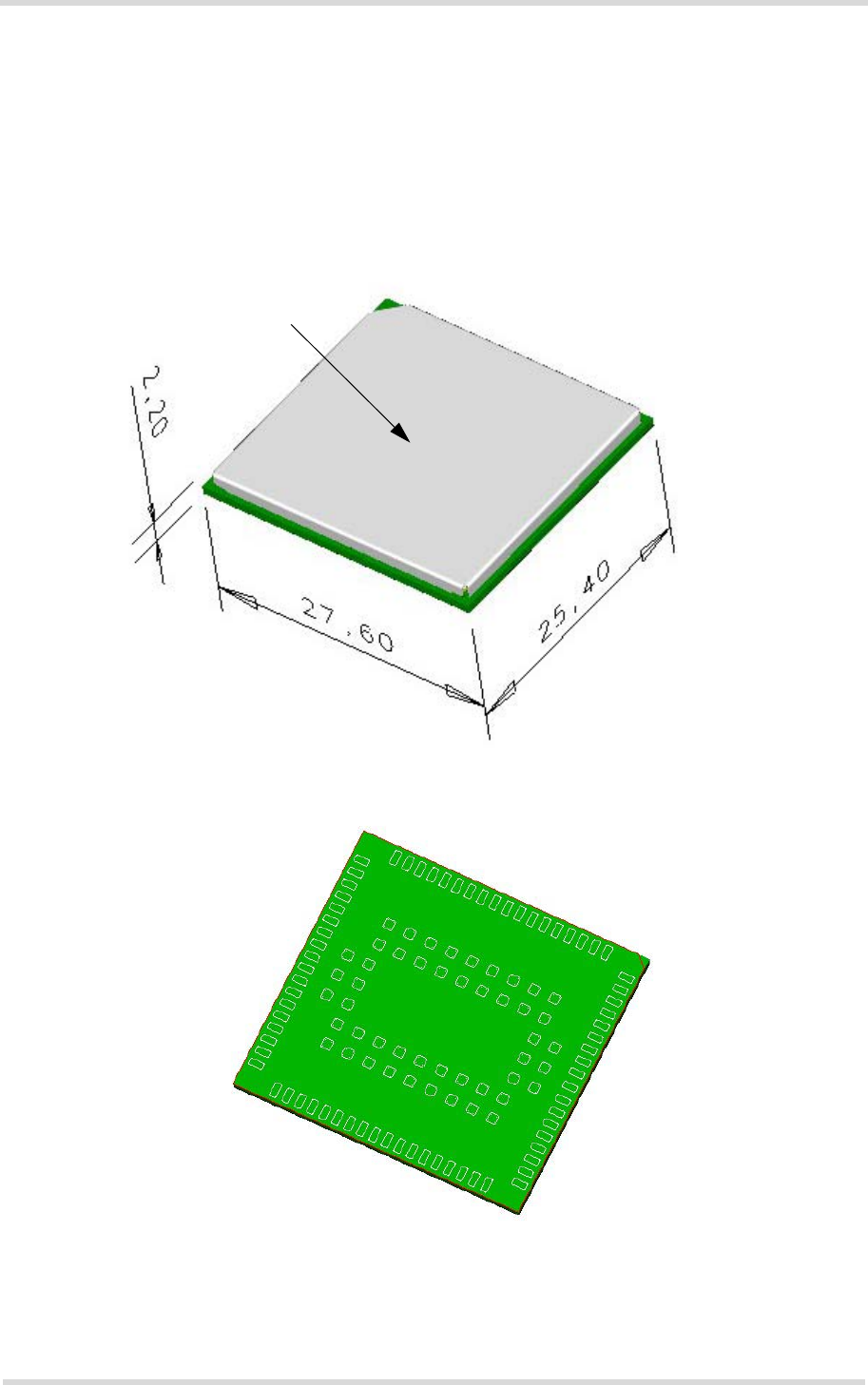
Cinterion® ELS61-USA Hardware Interface Description
4 Mechanical Dimensions, Mounting and Packaging
98
els61-usa_hid_v01.040a 2017-08-31
Confidential / Preliminary
Page 84 of 113
4 Mechanical Dimensions, Mounting and Packaging
4.1 Mechanical Dimensions of ELS61-USA
Figure 48 shows the top and bottom view of ELS61-USA and provides an overview of the
board's mechanical dimensions. For further details see Figure 49.
Figure 48: ELS61-USA– top and bottom view
Product label
Top view
Bottom view
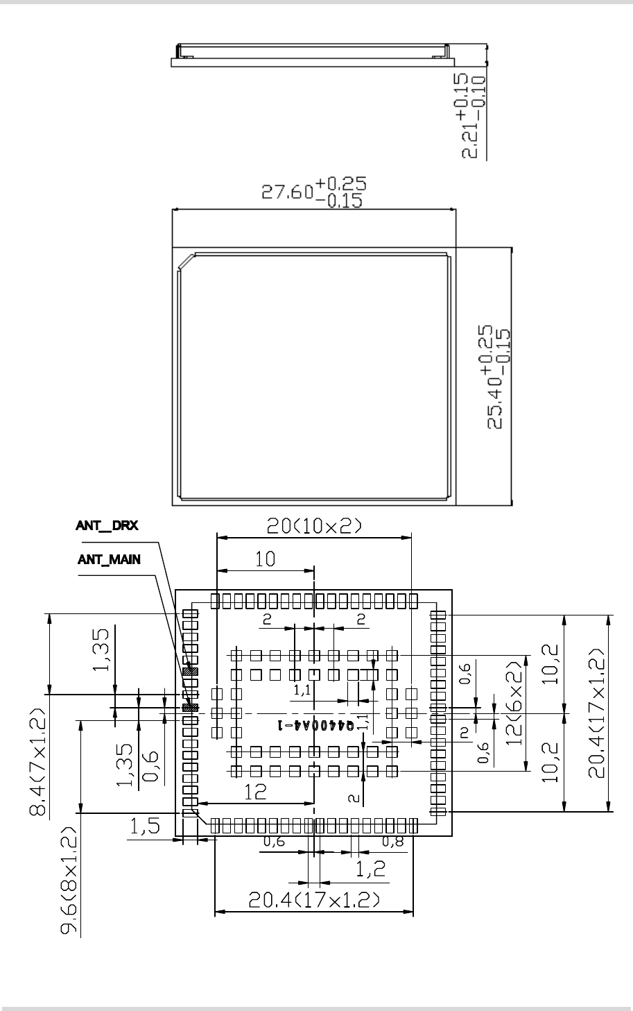
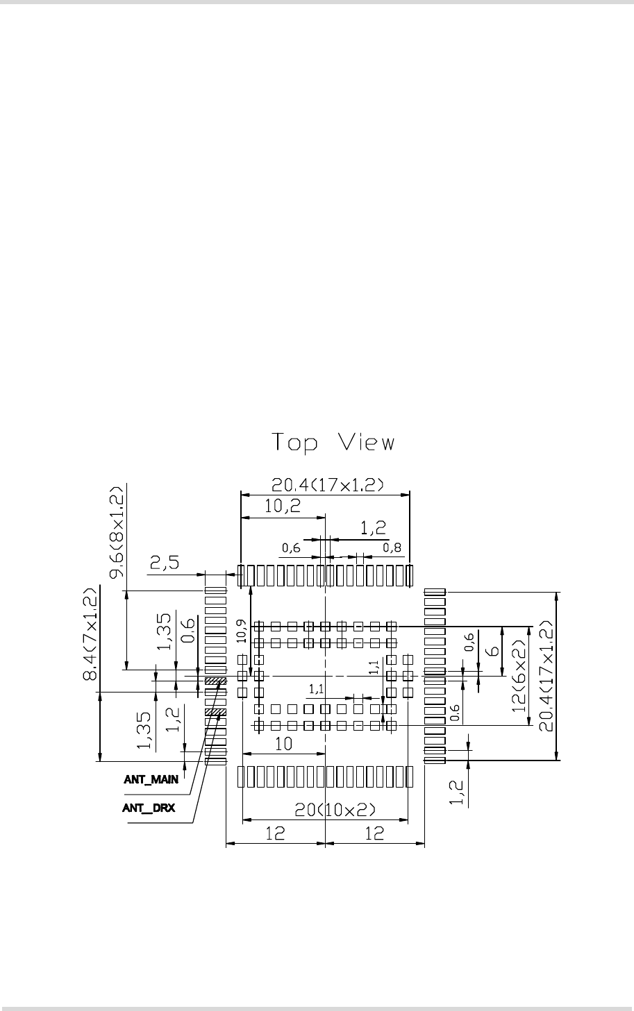
Cinterion® ELS61-USA Hardware Interface Description
4.2 Mounting ELS61-USA onto the Application Platform
98
els61-usa_hid_v01.040a 2017-08-31
Confidential / Preliminary
Page 86 of 113
4.2 Mounting ELS61-USA onto the Application Platform
This section describes how to mount ELS61-USA onto the PCBs, including land pattern and
stencil design, board-level characterization, soldering conditions, durability and mechanical
handling. For more information on issues related to SMT module integration see also [3].
Note: To avoid short circuits between signal tracks on an external application's PCB and vari-
ous markings at the bottom side of the module, it is recommended not to route the signal tracks
on the top layer of an external PCB directly under the module, or at least to ensure that signal
track routes are sufficiently covered with solder resist.
4.2.1 SMT PCB Assembly
4.2.1.1 Land Pattern and Stencil
The land pattern and stencil design as shown below is based on Gemalto characterizations for
lead-free solder paste on a four-layer test PCB and a respectively 110 µm and 150 µm thick
stencil.
The land pattern given in Figure 50 reflects the module‘s pad layout, including signal pads and
ground pads (for pad assignment see Section 2.1.1).
Figure 50: Land pattern (top view)
The stencil design illustrated in Figure 51 and Figure 52 is recommended by Gemalto M2M as
a result of extensive tests with Gemalto M2M Daisy Chain modules.
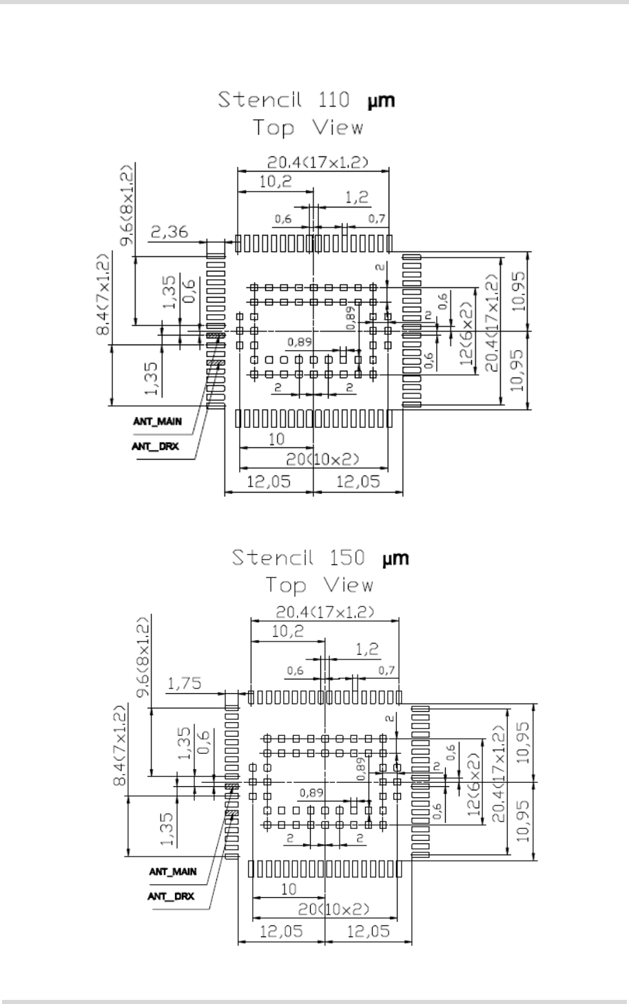
Cinterion® ELS61-USA Hardware Interface Description
4.2 Mounting ELS61-USA onto the Application Platform
98
els61-usa_hid_v01.040a 2017-08-31
Confidential / Preliminary
Page 87 of 113
The central ground pads are primarily intended for stabilizing purposes, and may show some
more voids than the application interface pads at the module's rim. This is acceptable, since
they are electrically irrelevant.
Figure 51: Recommended design for 110µm thick stencil (top view)
Figure 52: Recommended design for 150µm thick stencil (top view)

Cinterion® ELS61-USA Hardware Interface Description
4.2 Mounting ELS61-USA onto the Application Platform
98
els61-usa_hid_v01.040a 2017-08-31
Confidential / Preliminary
Page 88 of 113
4.2.1.2 Board Level Characterization
Board level characterization issues should also be taken into account if devising an SMT pro-
cess.
Characterization tests should attempt to optimize the SMT process with regard to board level
reliability. This can be done by performing the following physical tests on sample boards: Peel
test, bend test, tensile pull test, drop shock test and temperature cycling. Sample surface
mount checks are described in [3].
It is recommended to characterize land patterns before an actual PCB production, taking indi-
vidual processes, materials, equipment, stencil design, and reflow profile into account. For land
and stencil pattern design recommendations see also Section 4.2.1.1. Optimizing the solder
stencil pattern design and print process is necessary to ensure print uniformity, to decrease sol-
der voids, and to increase board level reliability.
Daisy chain modules for SMT characterization are available on request. For details refer to [3].
Generally, solder paste manufacturer recommendations for screen printing process parame-
ters and reflow profile conditions should be followed. Maximum ratings are described in Section
4.2.3.
4.2.2 Moisture Sensitivity Level
ELS61-USA comprises components that are susceptible to damage induced by absorbed
moisture.
Gemalto M2M’s ELS61-USA module complies with the latest revision of the IPC/JEDEC J-
STD-020 Standard for moisture sensitive surface mount devices and is classified as MSL 4.
For additional moisture sensitivity level (MSL) related information see Section 4.2.4 and Sec-
tion 4.3.2.
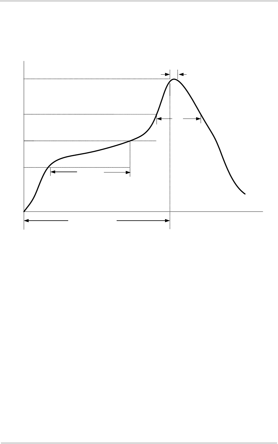
Cinterion® ELS61-USA Hardware Interface Description
4.2 Mounting ELS61-USA onto the Application Platform
98
els61-usa_hid_v01.040a 2017-08-31
Confidential / Preliminary
Page 89 of 113
4.2.3 Soldering Conditions and Temperature
4.2.3.1 Reflow Profile
Figure 53: Reflow Profile
TL
TP
tP
tL
tS
Preheat
t to maximum Time
Temperature
TSmin
TSmax
Cinterion® ELS61-USA Hardware Interface Description
4.2 Mounting ELS61-USA onto the Application Platform
98
els61-usa_hid_v01.040a 2017-08-31
Confidential / Preliminary
Page 90 of 113
4.2.3.2 Maximum Temperature and Duration
The following limits are recommended for the SMT board-level soldering process to attach the
module:
• A maximum module temperature of 245°C. This specifies the temperature as measured at
the module’s top side.
• A maximum duration of 30 seconds at this temperature.
Please note that while the solder paste manufacturers' recommendations for best temperature
and duration for solder reflow should generally be followed, the limits listed above must not be
exceeded.
ELS61-USA is specified for one soldering cycle only. Once ELS61-USA is removed from the
application, the module will very likely be destroyed and cannot be soldered onto another ap-
plication.
Table 21: Reflow temperature ratings1
1. Please note that the reflow profile features and ratings listed above are based on the joint industry standard
IPC/JEDEC J-STD-020D.1, and are as such meant as a general guideline. For more information on reflow
profiles and their optimization please refer to [3].
Profile Feature Pb-Free Assembly
Preheat & Soak
Temperature Minimum (TSmin)
Temperature Maximum (TSmax)
Time (tSmin to tSmax) (tS)
150°C
200°C
60-120 seconds
Average ramp up rate (TL to TP) 3K/second max. 2
2. Temperatures measured on shielding at each corner. See also [3].
Liquidous temperature (TL)
Time at liquidous (tL)217°C
50-90 seconds
Peak package body temperature (TP)245°C +0/-5°C
Time (tP) within 5 °C of the peak package body tem-
perature (TP)
30 seconds max.
Average ramp-down rate 3 K/second max. 2
Time 25°C to maximum temperature 8 minutes max.
1
4
2
3
Module
Temperature sensors (1-4)

Cinterion® ELS61-USA Hardware Interface Description
4.2 Mounting ELS61-USA onto the Application Platform
98
els61-usa_hid_v01.040a 2017-08-31
Confidential / Preliminary
Page 91 of 113
4.2.4 Durability and Mechanical Handling
4.2.4.1 Storage Conditions
ELS61-USA modules, as delivered in tape and reel carriers, must be stored in sealed, moisture
barrier anti-static bags. The conditions stated below are only valid for modules in their original
packed state in weather protected, non-temperature-controlled storage locations. Normal stor-
age time under these conditions is 12 months maximum.
Table 22: Storage conditions
Type Condition Unit Reference
Air temperature: Low
High
-25
+40
°C IPC/JEDEC J-STD-033A
Humidity relative: Low
High
10
90 at 40°C
%
IPC/JEDEC J-STD-033A
Air pressure: Low
High
70
106
kPa IEC TR 60271-3-1: 1K4
IEC TR 60271-3-1: 1K4
Movement of surrounding air 1.0 m/s IEC TR 60271-3-1: 1K4
Water: rain, dripping, icing and
frosting
Not allowed --- ---
Radiation: Solar
Heat
1120
600
W/m2ETS 300 019-2-1: T1.2, IEC 60068-2-2 Bb
ETS 300 019-2-1: T1.2, IEC 60068-2-2 Bb
Chemically active substances Not
recommended
IEC TR 60271-3-1: 1C1L
Mechanically active substances Not
recommended
IEC TR 60271-3-1: 1S1
Vibration sinusoidal:
Displacement
Acceleration
Frequency range
1.5
5
2-9 9-200
mm
m/s2
Hz
IEC TR 60271-3-1: 1M2
Shocks:
Shock spectrum
Duration
Acceleration
semi-sinusoidal
1
50
ms
m/s2
IEC 60068-2-27 Ea

Cinterion® ELS61-USA Hardware Interface Description
4.2 Mounting ELS61-USA onto the Application Platform
98
els61-usa_hid_v01.040a 2017-08-31
Confidential / Preliminary
Page 92 of 113
4.2.4.2 Processing Life
ELS61-USA must be soldered to an application within 72 hours after opening the moisture bar-
rier bag (MBB) it was stored in.
As specified in the IPC/JEDEC J-STD-033 Standard, the manufacturing site processing the
modules should have ambient temperatures below 30°C and a relative humidity below 60%.
4.2.4.3 Baking
Baking conditions are specified on the moisture sensitivity label attached to each MBB (see
Figure 58 for details):
• It is not necessary to bake ELS61-USA, if the conditions specified in Section 4.2.4.1 and
Section 4.2.4.2 were not exceeded.
• It is necessary to bake ELS61-USA, if any condition specified in Section 4.2.4.1 and Section
4.2.4.2 was exceeded.
If baking is necessary, the modules must be put into trays that can be baked to at least 125°C.
Devices should not be baked in tape and reel carriers at any temperature.
4.2.4.4 Electrostatic Discharge
Electrostatic discharge (ESD) may lead to irreversable damage for the module. It is therefore
advisable to develop measures and methods to counter ESD and to use these to control the
electrostatic environment at manufacturing sites.
Please refer to Section 3.6 for further information on electrostatic discharge.
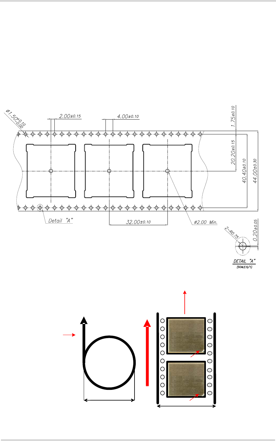
Cinterion® ELS61-USA Hardware Interface Description
4.3 Packaging
98
els61-usa_hid_v01.040a 2017-08-31
Confidential / Preliminary
Page 93 of 113
4.3 Packaging
4.3.1 Tape and Reel
The single-feed tape carrier for ELS61-USA is illustrated in Figure 54. The figure also shows
the proper part orientation. The tape width is 44mm and the ELS61-USA modules are placed
on the tape with a 32-mm pitch. The reels are 330mm in diameter with a core diameter of
100mm. Each reel contains 500 modules.
4.3.1.1 Orientation
Figure 54: Carrier tape
Figure 55: Reel direction
44mm
330mm
Reel direction of the
completely equipped tape
Direction into
SMD machine
View
direction
Pad 1
Pad 1
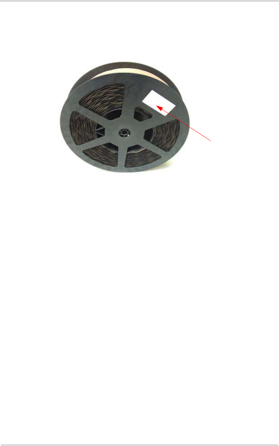
Cinterion® ELS61-USA Hardware Interface Description
4.3 Packaging
98
els61-usa_hid_v01.040a 2017-08-31
Confidential / Preliminary
Page 94 of 113
4.3.1.2 Barcode Label
A barcode label provides detailed information on the tape and its contents. It is attached to the
reel.
Figure 56: Barcode label on tape reel
Barcode label
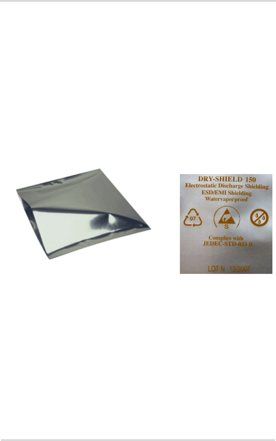
Cinterion® ELS61-USA Hardware Interface Description
4.3 Packaging
98
els61-usa_hid_v01.040a 2017-08-31
Confidential / Preliminary
Page 95 of 113
4.3.2 Shipping Materials
ELS61-USA is distributed in tape and reel carriers. The tape and reel carriers used to distribute
ELS61-USA are packed as described below, including the following required shipping materi-
als:
• Moisture barrier bag, including desiccant and humidity indicator card
• Transportation box
4.3.2.1 Moisture Barrier Bag
The tape reels are stored inside a moisture barrier bag (MBB), together with a humidity indica-
tor card and desiccant pouches - see Figure 57. The bag is ESD protected and delimits mois-
ture transmission. It is vacuum-sealed and should be handled carefully to avoid puncturing or
tearing. The bag protects the ELS61-USA modules from moisture exposure. It should not be
opened until the devices are ready to be soldered onto the application.
Figure 57: Moisture barrier bag (MBB) with imprint
The label shown in Figure 58 summarizes requirements regarding moisture sensitivity, includ-
ing shelf life and baking requirements. It is attached to the outside of the moisture barrier bag.
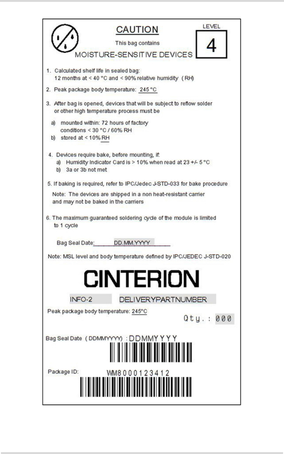
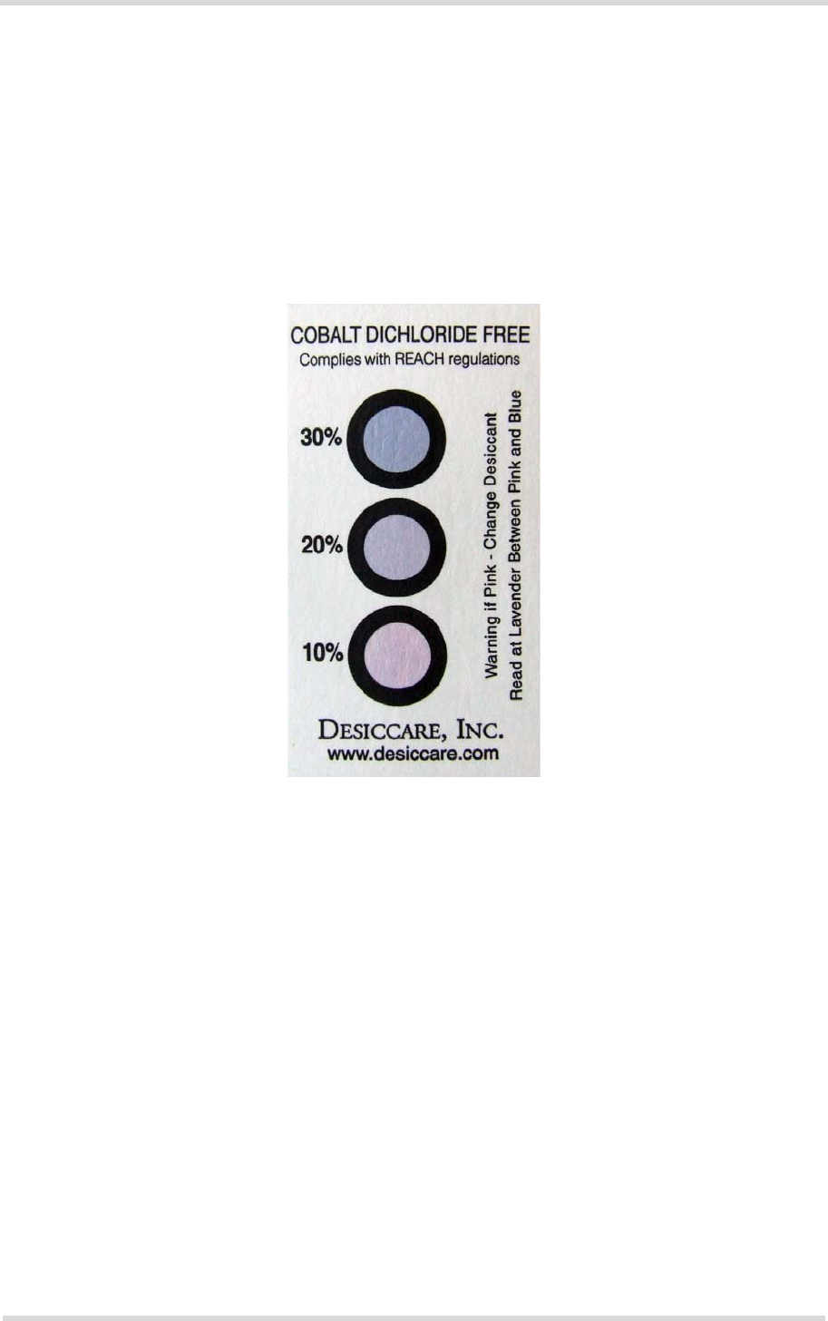
Cinterion® ELS61-USA Hardware Interface Description
4.3 Packaging
98
els61-usa_hid_v01.040a 2017-08-31
Confidential / Preliminary
Page 97 of 113
MBBs contain one or more desiccant pouches to absorb moisture that may be in the bag. The
humidity indicator card described below should be used to determine whether the enclosed
components have absorbed an excessive amount of moisture.
The desiccant pouches should not be baked or reused once removed from the MBB.
The humidity indicator card is a moisture indicator and is included in the MBB to show the ap-
proximate relative humidity level within the bag. Sample humidity cards are shown in Figure 59.
If the components have been exposed to moisture above the recommended limits, the units will
have to be rebaked.
Figure 59: Humidity Indicator Card - HIC
A baking is required if the humidity indicator inside the bag indicates 10% RH or more.
4.3.2.2 Transportation Box
Tape and reel carriers are distributed in a box, marked with a barcode label for identification
purposes. A box contains two reels with 500 modules each.
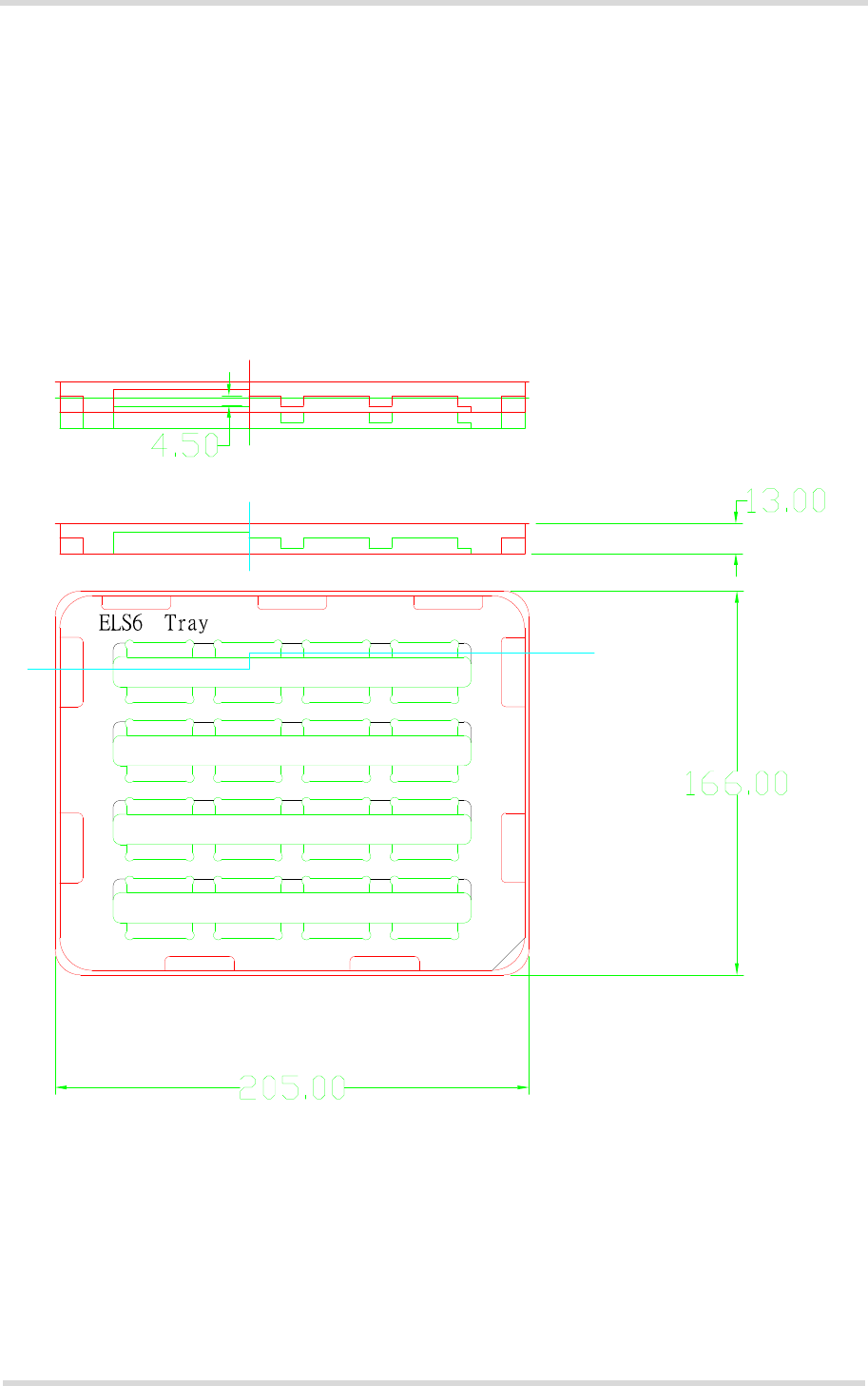
Cinterion® ELS61-USA Hardware Interface Description
4.3 Packaging
98
els61-usa_hid_v01.040a 2017-08-31
Confidential / Preliminary
Page 98 of 113
4.3.3 Trays
If small module quantities are required, e.g., for test and evaluation purposes, ELS61-USA may
be distributed in trays (for dimensions see Figure 60). The small quantity trays are an alterna-
tive to the single-feed tape carriers normally used. However, the trays are not designed for ma-
chine processing. They contain modules to be (hand) soldered onto an external application (for
information on hand soldering see [3]).
Trays are packed and shipped in the same way as tape carriers, including a moisture barrier
bag with desiccant and humidity indicator card as well as a transportation box (see also Section
4.3.2).
Figure 60: Tray dimensions
Cinterion® ELS61-USA Hardware Interface Description
5 Regulatory and Type Approval Information
105
els61-usa_hid_v01.040a 2017-08-31
Confidential / Preliminary
Page 99 of 113
5 Regulatory and Type Approval Information
5.1 Directives and Standards
ELS61-USA is designed to comply with the directives and standards listed below.
It is the responsibility of the application manufacturer to ensure compliance of the final product
with all provisions of the applicable directives and standards as well as with the technical spec-
ifications provided in the "ELS61-USA Hardware Interface Description”.1
1. Manufacturers of applications which can be used in the US shall ensure that their applications have a
PTCRB approval. For this purpose they can refer to the PTCRB approval of the respective module.
Table 23: Directives
2014/53/EU Directive of the European Parliament and of the council of 16 April 2014 on
the harmonization of the laws of the Member States relating to the making
available on the market of radio equipment and repealing Directive 1999/
05/EC.
The product is labeled with the CE conformity mark.
2002/95/EC (RoHS 1)
2011/65/EC (RoHS 2)
Directive of the European Parliament and of the Council of
27 January 2003 (and revised on 8 June 2011) on the
restriction of the use of certain hazardous substances in
electrical and electronic equipment (RoHS)
Table 24: Standards of North American type approval
CFR Title 47 Code of Federal Regulations, Part 22 and Part 24 (Telecommunications,
PCS); US Equipment Authorization FCC
OET Bulletin 65
(Edition 97-01)
Evaluating Compliance with FCC Guidelines for Human Exposure to
Radiofrequency Electromagnetic Fields
UL 60 950-1 Product Safety Certification (Safety requirements)
NAPRD.03 V5.15 Overview of PCS Type certification review board Mobile Equipment Type
Certification and IMEI control
PCS Type Certification Review board (PTCRB)
RSS132 (Issue2)
RSS133 (Issue5)
Canadian Standard
Table 25: Standards of European type approval
3GPP TS 51.010-1 Digital cellular telecommunications system (Release 9); Mobile Station
(MS) conformance specification;
GCF-CC V3.61.2 Global Certification Forum - Certification Criteria
ETSI EN 301 511
V12.5.1
Global System for Mobile communications (GSM); Mobile Stations (MS)
equipment; Harmonized Standard covering the essential requirements of
article 3.2 of Directive 2014/53/EU
Cinterion® ELS61-USA Hardware Interface Description
5.1 Directives and Standards
105
els61-usa_hid_v01.040a 2017-08-31
Confidential / Preliminary
Page 100 of 113
Draft ETSI EN 301 489-
01 V2.2.0
Electromagnetic Compatibility (EMC) standard for radio equipment and ser-
vices; Part 1: Common technical requirements; Harmonized Standard cov-
ering the essential requirements of article 3.1(b) of Directive 2014/53/EU
and the essential requirements of article 6 of Directive 2014/30/EU
Draft ETSI EN 301 489-52
V1.1.0
Electromagnetic Compatibility (EMC) standard for radio equipment and ser-
vices; Part 52: Specific conditions for Cellular Communication Mobile and
portable (UE) radio and ancillary equipment; Harmonized Standard cover-
ing the essential requirements of article 3.1(b) of Directive 2014/53/EU
ETSI EN 301 908-1
V11.1.1
IMT cellular networks; Harmonized Standard covering the essential require-
ments of article 3.2 of the Directive 2014/53/EU; Part 1: Introduction and
common requirements
ETSI EN 301 908-13
V11.1.1 IMT cellular networks; Harmonized Standard covering the essential
requirements of article 3.2 of the Directive 2014/53/EU; Part 13: Evolved
Universal Terrestrial Radio Access (E-UTRA) User Equipment (UE)
EN 60950-1: 2006
+A11:2009+A1:2010+A
12:2011+A2:2013
Safety of information technology equipment
Table 26: Requirements of quality
IEC 60068 Environmental testing
DIN EN 60529 IP codes
Table 27: Standards of the Ministry of Information Industry of the People’s Republic of China
SJ/T 11363-2006 “Requirements for Concentration Limits for Certain Hazardous Sub-
stances in Electronic Information Products” (2006-06).
SJ/T 11364-2006 “Marking for Control of Pollution Caused by Electronic
Information Products” (2006-06).
According to the “Chinese Administration on the Control
of Pollution caused by Electronic Information Products”
(ACPEIP) the EPUP, i.e., Environmental Protection Use
Period, of this product is 20 years as per the symbol
shown here, unless otherwise marked. The EPUP is valid only as long as
the product is operated within the operating limits described in the
Gemalto M2M Hardware Interface Description.
Please see Table 28 for an overview of toxic or hazardous substances or
elements that might be contained in product parts in concentrations
above the limits defined by SJ/T 11363-2006.
Table 25: Standards of European type approval

Cinterion® ELS61-USA Hardware Interface Description
5.2 SAR requirements specific to portable mobiles
105
els61-usa_hid_v01.040a 2017-08-31
Confidential / Preliminary
Page 102 of 113
5.2 SAR requirements specific to portable mobiles
Mobile phones, PDAs or other portable transmitters and receivers incorporating a UMTS mod-
ule must be in accordance with the guidelines for human exposure to radio frequency energy.
This requires the Specific Absorption Rate (SAR) of portable ELS61-USA based applications
to be evaluated and approved for compliance with national and/or international regulations.
Since the SAR value varies significantly with the individual product design manufacturers are
advised to submit their product for approval if designed for portable use. For US-markets the
relevant directives are mentioned below. It is the responsibility of the manufacturer of the final
product to verify whether or not further standards, recommendations or directives are in force
outside these areas.
Products intended for sale on US markets
ES 59005/ANSI C95.1 Considerations for evaluation of human exposure to Electromagnetic
Fields (EMFs) from Mobile Telecommunication Equipment (MTE) in the
frequency range 30MHz - 6GHz
Please note that SAR requirements are specific only for portable devices and not for mobile
devices as defined below:
• Portable device:
A portable device is defined as a transmitting device designed to be used so that the radi-
ating structure(s) of the device is/are within 20 centimeters of the body of the user.
• Mobile device:
A mobile device is defined as a transmitting device designed to be used in other than fixed
locations and to generally be used in such a way that a separation distance of at least 20
centimeters is normally maintained between the transmitter's radiating structure(s) and the
body of the user or nearby persons. In this context, the term ''fixed location'' means that the
device is physically secured at one location and is not able to be easily moved to another
location.
Cinterion® ELS61-USA Hardware Interface Description
5.3 Reference Equipment for Type Approval
105
els61-usa_hid_v01.040a 2017-08-31
Confidential / Preliminary
Page 103 of 113
5.3 Reference Equipment for Type Approval
The Gemalto M2M reference setup submitted to type approve ELS61-USA (including a special
approval adapter for the DSB75) is shown in the following figure1:
Figure 61: Reference equipment for Type Approval
1. For RF performance tests a mini-SMT/U.FL to SMA adapter with attached 6dB coaxial attenuator is cho-
sen to connect the evaluation module directly to the UMTS test equipment instead of employing the SMA
antenna connectors on the ELS61-USA-DSB75 adapter as shown in Figure 61. The following products
are recommended:
Hirose SMA-Jack/U.FL-Plug conversion adapter HRMJ-U.FLP(40)
(for details see http://www.hirose-connectors.com/ or http://www.farnell.com/
Aeroflex Weinschel Fixed Coaxial Attenuator Model 3T/4T
(for details see http://www.aeroflex.com/ams/weinschel/pdfiles/wmod3&4T.pdf)
DSB75
AH6‐Adapter
SIMCard
Audio
SMA
SMA
SMA
USB
PC
Power
Supply
LTE/GPRS/UMTS
BaseStation
AutoTestSystem
Diversity
Antenna
USB
ASC0
Main
Antenna
Eval_Board
ELS61
Eval_Board
ELS61
ASC1

Cinterion® ELS61-USA Hardware Interface Description
5.4 Compliance with FCC and IC Rules and Regulations
105
els61-usa_hid_v01.040a 2017-08-31
Confidential / Preliminary
Page 104 of 113
5.4 Compliance with FCC and IC Rules and Regulations
The Equipment Authorization Certification for the Gemalto M2M reference application de-
scribed in Section 5.3 will be registered under the following identifiers:
FCC Identifier: QIPELS61-USA
Industry Canada Certification Number: 7830A-ELS61USA
Granted to Gemalto M2M GmbH
Manufacturers of mobile or fixed devices incorporating ELS61-USA modules are authorized to
use the FCC Grants and Industry Canada Certificates of the ELS61-USA modules for their own
final products according to the conditions referenced in these documents. In this case, an FCC/ IC
label of the module shall be visible from the outside, or the host device shall bear a second label
stating "Contains FCC ID: QIPELS61-USA", and accordingly “Contains IC: 7830A-ELS61USA“.
The integration is limited to fixed or mobile categorized host devices, where a separation distance
between the antenna and any person of min. 20cm can be assured during normal operating
conditions. For mobile and fixed operation configurations the antenna gain, including cable
loss, must not exceed the limit 2.15 dBi for 700MHz, 850MHz, 1700MHz and 1900MHz.
IMPORTANT:
Manufacturers of portable applications incorporating ELS61-USA modules are required to have
their final product certified and apply for their own FCC Grant and Industry Canada Certificate
related to the specific portable mobile. This is mandatory to meet the SAR requirements for por-
table mobiles (see Section 5.2 for detail).
Changes or modifications not expressly approved by the party responsible for compliance
could void the user's authority to operate the equipment.
Note: This equipment has been tested and found to comply with the limits for a Class B digital
device, pursuant to part 15 of the FCC Rules and with Industry Canada license-exempt RSS
standard(s). These limits are designed to provide reasonable protection against harmful inter-
ference in a residential installation. This equipment generates, uses and can radiate radio fre-
quency energy and, if not installed and used in accordance with the instructions, may cause
harmful interference to radio communications. However, there is no guarantee that interference
will not occur in a particular installation. If this equipment does cause harmful interference to
radio or television reception, which can be determined by turning the equipment off and on, the
user is encouraged to try to correct the interference by one or more of the following measures:
• Reorient or relocate the receiving antenna.
• Increase the separation between the equipment and receiver.
• Connect the equipment into an outlet on a circuit different from that to which the receiver is
connected.
• Consult the dealer or an experienced radio/TV technician for help.
This Class B digital apparatus complies with Canadian ICES-003.

Cinterion® ELS61-USA Hardware Interface Description
5.4 Compliance with FCC and IC Rules and Regulations
105
els61-usa_hid_v01.040a 2017-08-31
Confidential / Preliminary
Page 105 of 113
If Canadian approval is requested for devices incorporating ELS61-USA modules the below
notes will have to be provided in the English and French language in the final user documen-
tation. Manufacturers/OEM Integrators must ensure that the final user documentation does not
contain any information on how to install or remove the module from the final product.
Notes (IC):
(EN) This Class B digital apparatus complies with Canadian ICES-003 and RSS-210. Opera-
tion is subject to the following two conditions: (1) this device may not cause interference, and
(2) this device must accept any interference, including interference that may cause undesired
operation of the device.
(FR) Cet appareil numérique de classe B est conforme aux normes canadiennes ICES-003 et
RSS-210. Son fonctionnement est soumis aux deux conditions suivantes: (1) cet appareil ne
doit pas causer d'interférence et (2) cet appareil doit accepter toute interférence, notamment
les interférences qui peuvent affecter son fonctionnement.
(EN) Radio frequency (RF) Exposure Information
The radiated output power of the Wireless Device is below the Industry Canada (IC) radio fre-
quency exposure limits. The Wireless Device should be used in such a manner such that the
potential for human contact during normal operation is minimized.
This device has also been evaluated and shown compliant with the IC RF Exposure limits un-
der mobile exposure conditions. (antennas at least 20cm from a person‘s body).
(FR) Informations concernant l'exposltion aux fréquences radio (RF)
La puissance de sortie émise par l'appareil de sans fiI est inférieure à la limite d'exposition aux
fréquences radio d‘Industry Canada (IC). Utilisez l'appareil de sans fil de façon à minimiser les
contacts humains lors du fonctionnement normal.
Ce périphérique a également été évalué et démontré conforme aux limites d'exposition aux RF
d'IC dans des conditions d'exposition à des appareils mobiles (les antennes se situent à moins
de 20cm du corps d'une personne).
Cinterion® ELS61-USA Hardware Interface Description
6 Document Information
110
els61-usa_hid_v01.040a 2017-08-31
Confidential / Preliminary
Page 106 of 113
6 Document Information
6.1 Revision History
Preceding document: "Cinterion® ELS61-USA Hardware Interface Description" Version 01.040
New document: "Cinterion® ELS61-USA Hardware Interface Description" Version 01.040a
New document: "Cinterion® ELS61-USA Hardware Interface Description" Version 01.040
6.2 Related Documents
[1] ELS61-USA AT Command Set
[2] ELS61-USA Release Note
[3] Application Note 48: SMT Module Integration
[4] Application Note 40: Thermal Solutions
[5] Universal Serial Bus Specification Revision 2.0, April 27, 2000
6.3 Terms and Abbreviations
Chapter What is new
3.2.1.3 Updated chapter’s description.
3.2.1.2 Updated Figure 37 regarding EMERG_RST.
3.2.2.2 Updated Figure 40 regarding EMERG_RST.
Chapter What is new
-- Initial document setup.
Abbreviation Description
ADC Analog-to-digital converter
AGC Automatic Gain Control
ANSI American National Standards Institute
ARFCN Absolute Radio Frequency Channel Number
ARP Antenna Reference Point
ASC0/ASC1 Asynchronous Controller. Abbreviations used for first and second serial interface of
ELS61-USA
B Thermistor Constant
BER Bit Error Rate
BIP Bearer Independent Protocol
BTS Base Transceiver Station
CB or CBM Cell Broadcast Message

Cinterion® ELS61-USA Hardware Interface Description
6.3 Terms and Abbreviations
110
els61-usa_hid_v01.040a 2017-08-31
Confidential / Preliminary
Page 107 of 113
CE Conformité Européene (European Conformity)
CHAP Challenge Handshake Authentication Protocol
CPU Central Processing Unit
CS Coding Scheme
CSD Circuit Switched Data
CTS Clear to Send
DAC Digital-to-Analog Converter
dBm0 Digital level, 3.14dBm0 corresponds to full scale, see ITU G.711, A-law
DCE Data Communication Equipment (typically modems, e.g. Gemalto M2M module)
DRX Discontinuous Reception
DSB Development Support Box
DSP Digital Signal Processor
DSR Data Set Ready
DTE Data Terminal Equipment (typically computer, terminal, printer or, for example, UMTS
application)
DTR Data Terminal Ready
DTX Discontinuous Transmission
EFR Enhanced Full Rate
EIRP Equivalent Isotropic Radiated Power
EMC Electromagnetic Compatibility
ERP Effective Radiated Power
ESD Electrostatic Discharge
ETS European Telecommunication Standard
ETSI European Telecommunication Standards Institute
FCC Federal Communications Commission (U.S.)
FDMA Frequency Division Multiple Access
FR Full Rate
GMSK Gaussian Minimum Shift Keying
GPIO General Purpose Input/Output
HiZ High Impedance
HR Half Rate
I/O Input/Output
IC Integrated Circuit
IMEI International Mobile Equipment Identity
ISO International Standards Organization
ITU International Telecommunications Union
kbps kbits per second
LED Light Emitting Diode
Abbreviation Description

Cinterion® ELS61-USA Hardware Interface Description
6.3 Terms and Abbreviations
110
els61-usa_hid_v01.040a 2017-08-31
Confidential / Preliminary
Page 108 of 113
Li-Ion/Li+ Lithium-Ion
Li battery Rechargeable Lithium Ion or Lithium Polymer battery
LPM Link Power Management
Mbps Mbits per second
MMI Man Machine Interface
MO Mobile Originated
MS Mobile Station (UMTS module), also referred to as TE
MSISDN Mobile Station International ISDN number
MT Mobile Terminated
NTC Negative Temperature Coefficient
OEM Original Equipment Manufacturer
PA Power Amplifier
PAP Password Authentication Protocol
PBCCH Packet Switched Broadcast Control Channel
PCB Printed Circuit Board
PCL Power Control Level
PCM Pulse Code Modulation
PDU Protocol Data Unit
PLL Phase Locked Loop
PPP Point-to-point protocol
PSK Phase Shift Keying
PSU Power Supply Unit
PWM Pulse Width Modulation
R&TTE Radio and Telecommunication Terminal Equipment
RAM Random Access Memory
RF Radio Frequency
RLS Radio Link Stability
RMS Root Mean Square (value)
RoHS Restriction of the use of certain hazardous substances in electrical and electronic
equipment.
ROM Read-only Memory
RTC Real Time Clock
RTS Request to Send
Rx Receive Direction
SAR Specific Absorption Rate
SAW Surface Accoustic Wave
SELV Safety Extra Low Voltage
SIM Subscriber Identification Module
Abbreviation Description

Cinterion® ELS61-USA Hardware Interface Description
6.3 Terms and Abbreviations
110
els61-usa_hid_v01.040a 2017-08-31
Confidential / Preliminary
Page 109 of 113
SMD Surface Mount Device
SMS Short Message Service
SMT Surface Mount Technology
SPI Serial Peripheral Interface
SRAM Static Random Access Memory
TA Terminal adapter (e.g. UMTS module)
TDMA Time Division Multiple Access
TE Terminal Equipment, also referred to as DTE
TLS Transport Layer Security
Tx Transmit Direction
UART Universal asynchronous receiver-transmitter
URC Unsolicited Result Code
USSD Unstructured Supplementary Service Data
VSWR Voltage Standing Wave Ratio
Abbreviation Description
Cinterion® ELS61-USA Hardware Interface Description
6.4 Safety Precaution Notes
110
els61-usa_hid_v01.040a 2017-08-31
Confidential / Preliminary
Page 110 of 113
6.4 Safety Precaution Notes
The following safety precautions must be observed during all phases of the operation, usage,
service or repair of any cellular terminal or mobile incorporating ELS61-USA. Manufacturers of
the cellular terminal are advised to convey the following safety information to users and oper-
ating personnel and to incorporate these guidelines into all manuals supplied with the product.
Failure to comply with these precautions violates safety standards of design, manufacture and
intended use of the product. Gemalto M2M assumes no liability for customer’s failure to comply
with these precautions.
When in a hospital or other health care facility, observe the restrictions on the use of
mobiles. Switch the cellular terminal or mobile off, if instructed to do so by the guide-
lines posted in sensitive areas. Medical equipment may be sensitive to RF energy.
The operation of cardiac pacemakers, other implanted medical equipment and hear-
ing aids can be affected by interference from cellular terminals or mobiles placed close
to the device. If in doubt about potential danger, contact the physician or the manufac-
turer of the device to verify that the equipment is properly shielded. Pacemaker
patients are advised to keep their hand-held mobile away from the pacemaker, while
it is on.
Switch off the cellular terminal or mobile before boarding an aircraft. Make sure it can-
not be switched on inadvertently. The operation of wireless appliances in an aircraft is
forbidden to prevent interference with communications systems. Failure to observe
these instructions may lead to the suspension or denial of cellular services to the
offender, legal action, or both.
Do not operate the cellular terminal or mobile in the presence of flammable gases or
fumes. Switch off the cellular terminal when you are near petrol stations, fuel depots,
chemical plants or where blasting operations are in progress. Operation of any elec-
trical equipment in potentially explosive atmospheres can constitute a safety hazard.
Your cellular terminal or mobile receives and transmits radio frequency energy while
switched on. Remember that interference can occur if it is used close to TV sets,
radios, computers or inadequately shielded equipment. Follow any special regulations
and always switch off the cellular terminal or mobile wherever forbidden, or when you
suspect that it may cause interference or danger.
Road safety comes first! Do not use a hand-held cellular terminal or mobile when driv-
ing a vehicle, unless it is securely mounted in a holder for speakerphone operation.
Before making a call with a hand-held terminal or mobile, park the vehicle.
Speakerphones must be installed by qualified personnel. Faulty installation or opera-
tion can constitute a safety hazard.
IMPORTANT!
Cellular terminals or mobiles operate using radio signals and cellular networks.
Because of this, connection cannot be guaranteed at all times under all conditions.
Therefore, you should never rely solely upon any wireless device for essential com-
munications, for example emergency calls.
Remember, in order to make or receive calls, the cellular terminal or mobile must be
switched on and in a service area with adequate cellular signal strength.
Some networks do not allow for emergency calls if certain network services or phone
features are in use (e.g. lock functions, fixed dialing etc.). You may need to deactivate
those features before you can make an emergency call.
Some networks require that a valid SIM card be properly inserted in the cellular termi-
nal or mobile.

Cinterion® ELS61-USA Hardware Interface Description
7 Appendix
112
els61-usa_hid_v01.040a 2017-08-31
Confidential / Preliminary
Page 111 of 113
7 Appendix
7.1 List of Parts and Accessories
Table 29: List of parts and accessories
Description Supplier Ordering information
ELS61-USA Gemalto M2M Standard module
Gemalto M2M IMEI:
Packaging unit (ordering) number: TBD.
Module label number: TBD.1
Customer IMEI mode:
Packaging unit (ordering) number: TBD.
Module label number: TBD.1
1. Note: At the discretion of Gemalto M2M, module label information can either be laser engraved on the
module’s shielding or be printed on a label adhered to the module’s shielding.
ELS61-USA Evaluation
Module
Gemalto M2M Ordering number: TBD.
DSB75 Evaluation Kit Gemalto M2M Ordering number: L36880-N8811-A100
DSB Mini
Compact Evaluation Board
Gemalto M2M Ordering number: L30960-N0030-A100
Starter Kit B80 Gemalto M2M Ordering Number L30960-N0040-A100
Multi-Adapter R1 for mount-
ing ELS61-USA evaluation
modules onto DSB75
Gemalto M2M Ordering number: L30960-N0010-A100
Approval adapter for mount-
ing ELS61-USA evaluation
modules onto DSB75
Gemalto M2M Ordering number: L30960-N2301-A100
SIM card holder incl. push
button ejector and slide-in
tray
Molex Ordering numbers: 91228
91236
Sales contacts are listed in Table 30.

Cinterion® ELS61-USA Hardware Interface Description
7.1 List of Parts and Accessories
112
els61-usa_hid_v01.040a 2017-08-31
Confidential / Preliminary
Page 112 of 113
Table 30: Molex sales contacts (subject to change)
Molex
For further information please click:
http://www.molex.com
Molex Deutschland GmbH
Otto-Hahn-Str. 1b
69190 Walldorf
Germany
Phone: +49-6227-3091-0
Fax: +49-6227-3091-8100
Email: mxgermany@molex.com
American Headquarters
Lisle, Illinois 60532
U.S.A.
Phone: +1-800-78MOLEX
Fax: +1-630-969-1352
Molex China Distributors
Beijing,
Room 1311, Tower B, COFCO Plaza
No. 8, Jian Guo Men Nei Street, 100005
Beijing
P.R. China
Phone: +86-10-6526-9628
Fax: +86-10-6526-9730
Molex Singapore Pte. Ltd.
110, International Road
Jurong Town,
Singapore 629174
Phone: +65-6-268-6868
Fax: +65-6-265-6044
Molex Japan Co. Ltd.
1-5-4 Fukami-Higashi,
Yamato-City,
Kanagawa, 242-8585
Japan
Phone: +81-46-265-2325
Fax: +81-46-265-2365

113
GEMALTO.COM/M2M
About Gemalto
Since 1996, Gemalto has been pioneering groundbreaking M2M and IoT products that keep our
customers on the leading edge of innovation.
We work closely with global mobile network operators to ensure that Cinterion® modules evolve
in sync with wireless networks, providing a seamless migration path to protect your IoT technology
investment.
Cinterion products integrate seamlessly with Gemalto identity modules, security solutions and licensing
and monetization solutions, to streamline development timelines and provide cost efficiencies that
improve the bottom line.
As an experienced software provider, we help customers manage connectivity, security and
quality of service for the long lifecycle of IoT solutions.
For more information please visit
www.gemalto.com/m2m, www.facebook.com/gemalto, or Follow@gemaltoIoT on Twitter.
Gemalto M2M GmbH
Werinherstrasse 81
81541 Munich
Germany
© Gemalto 2017. All rights reserved. Gemalto, the Gemalto logo, are trademarks and service marks of Gemalto and are registered in certain countries.