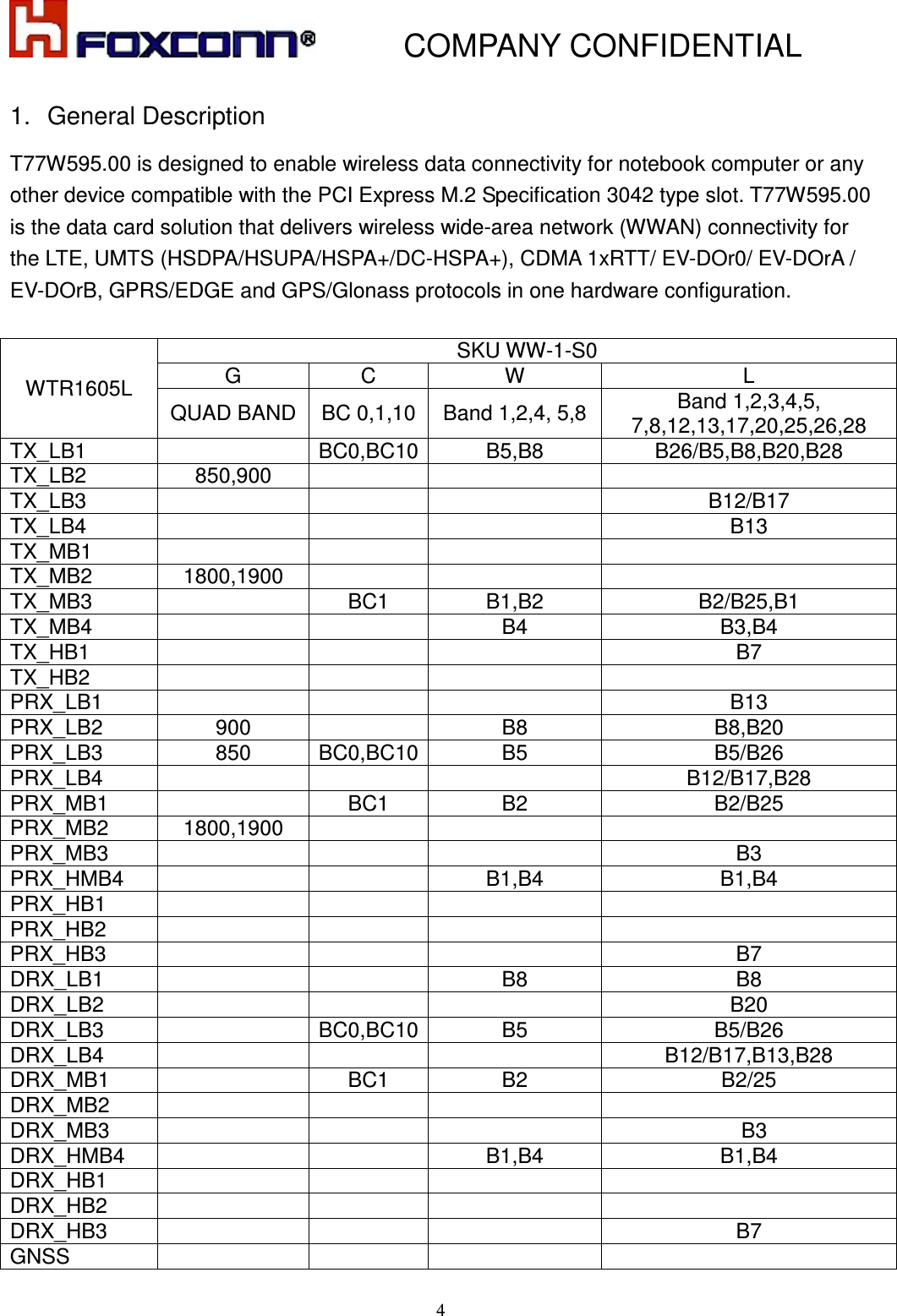
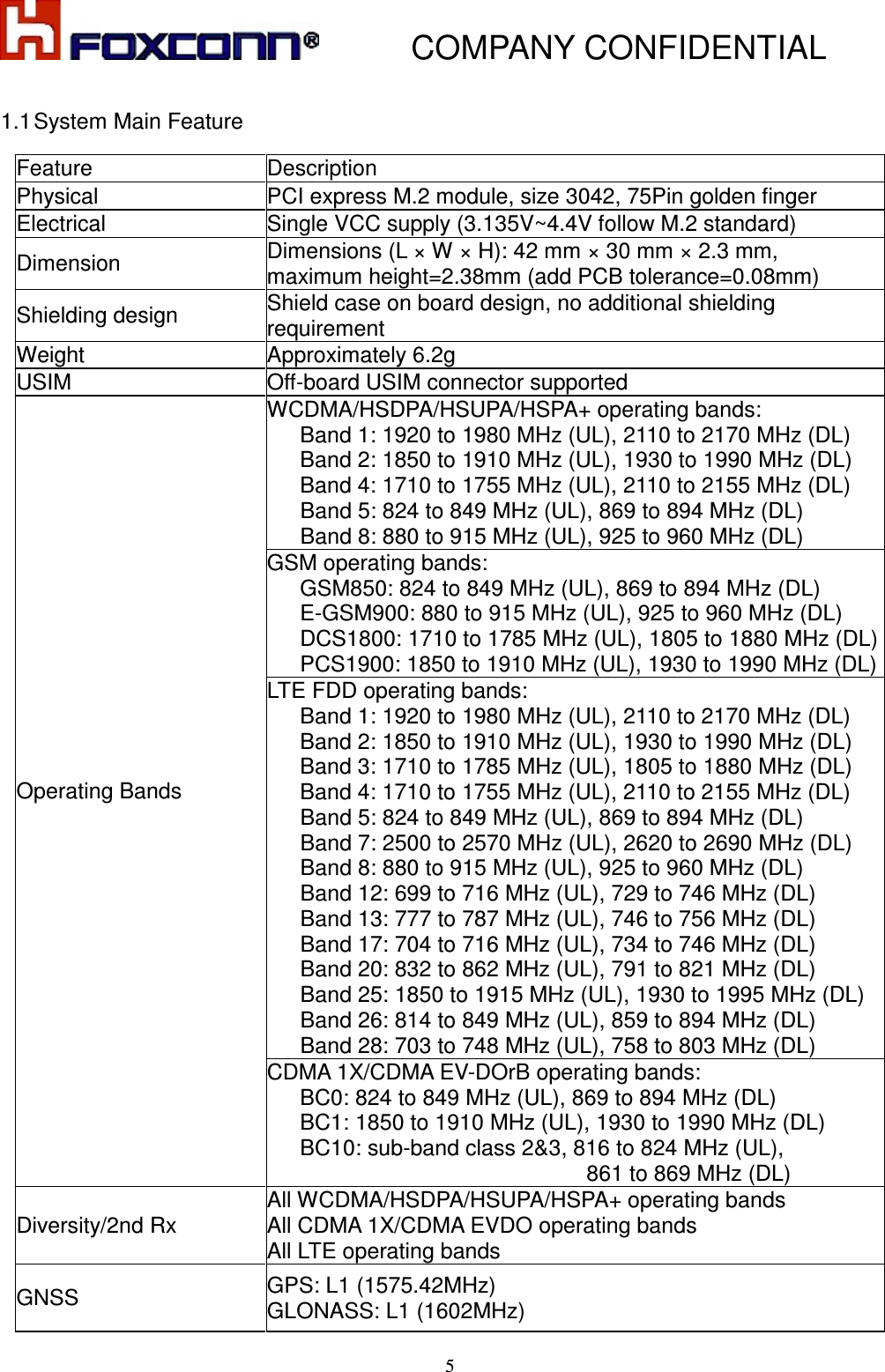
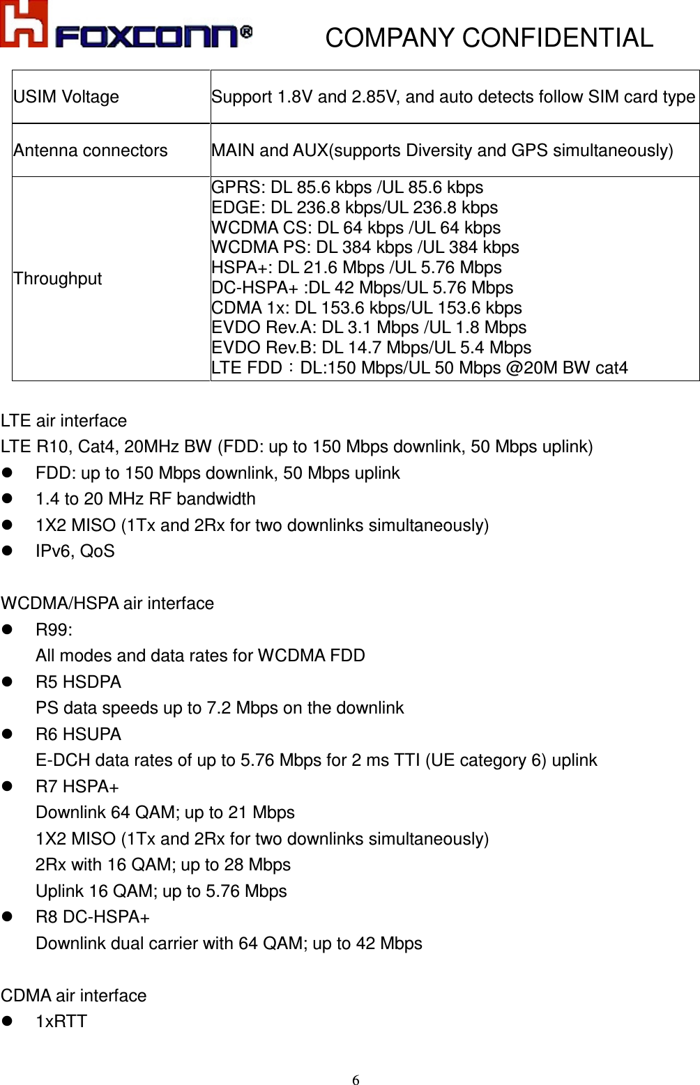
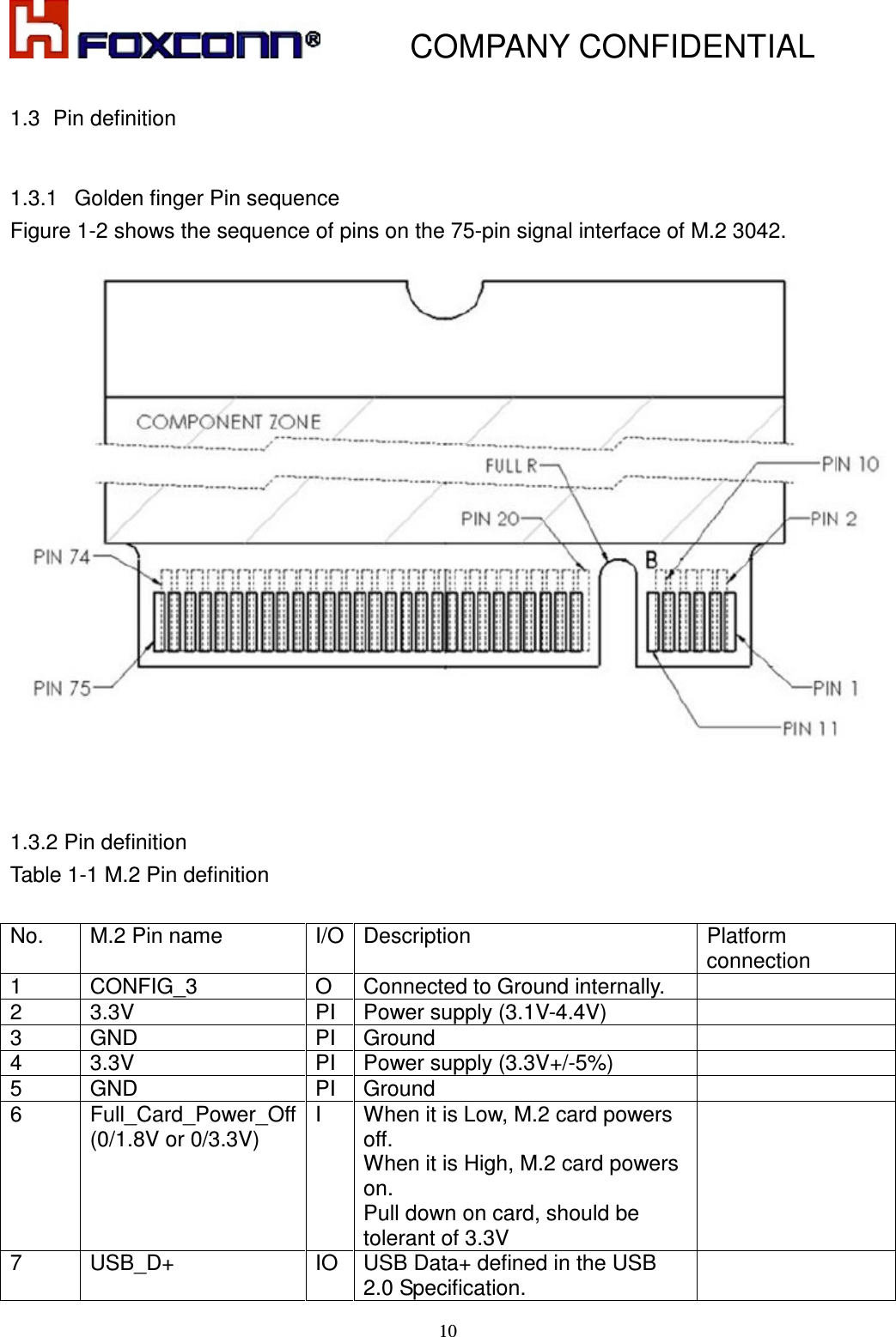
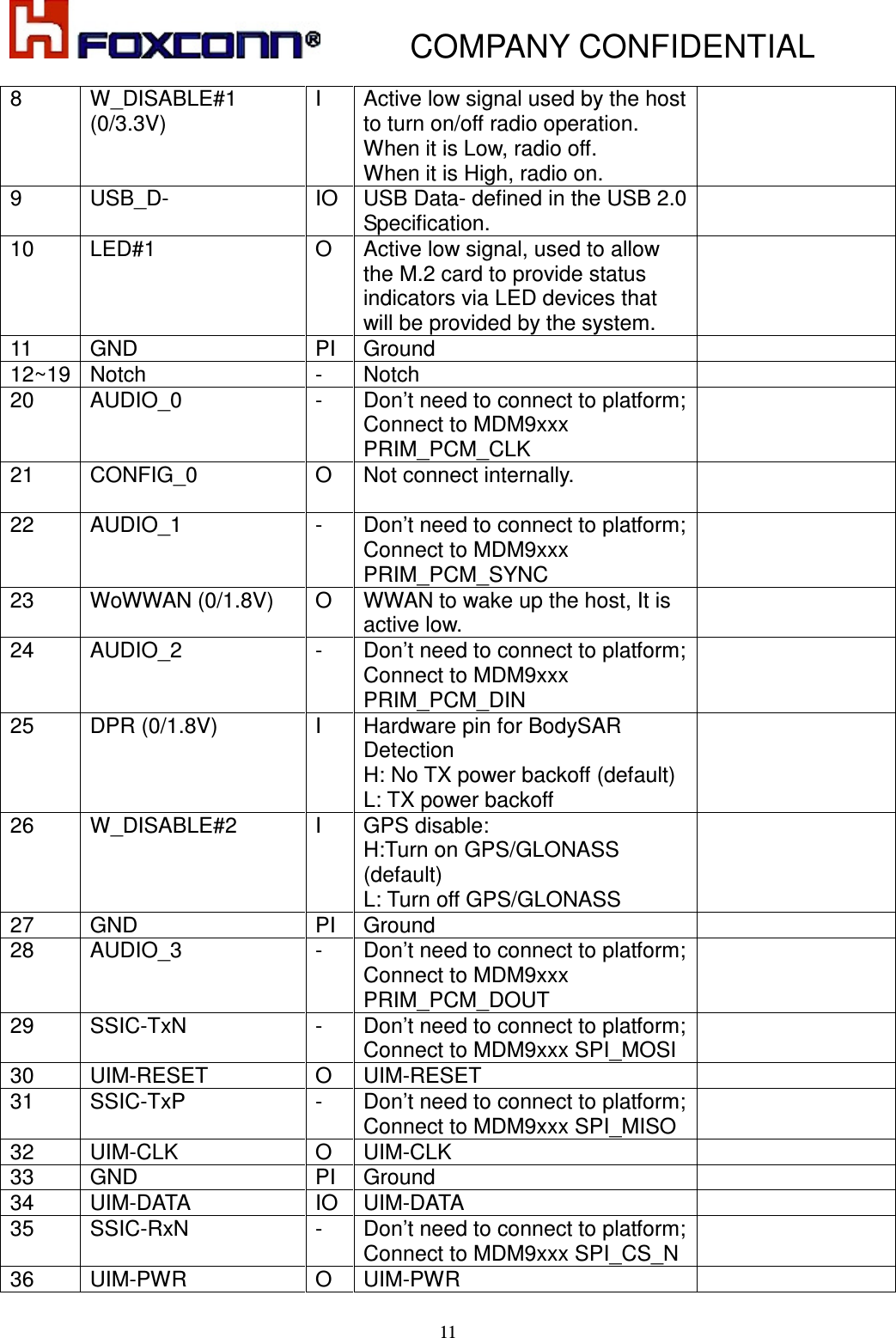
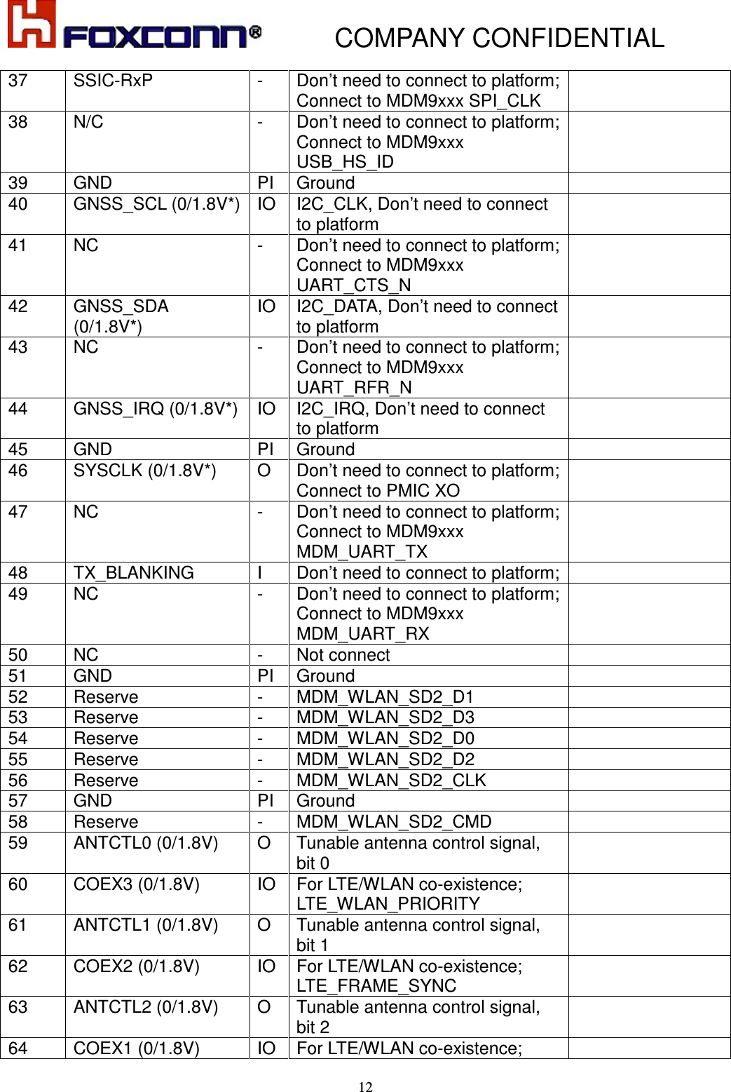
HON HAI PRECISION IND T77W595 LTE Cat4 PCI Express M.2 Module User Manual rev

HON HAI Precision Ind. Co., Ltd. LTE Cat4 PCI Express M.2 Module rev

User Manual_rev.pdf

   COMPANY CONFIDENTIAL - 1 -  3GPP Long Term Evolution Cat4 PCI Express M.2 Module   Engineering Requirements Specification        Project code:    T77W595.00 Solution:    MDM9625+WTR1625L SKU:                  WW-1-S3   Copyright © 2014. Foxconn Communications Inc. All rights reserved.
   COMPANY CONFIDENTIAL - 2 - Reviewers Department Name  Signature  Review Dates * Plan ** Results   Project Manager  Choro.Chung         Project Leader  Ai-ning Song         Hardware Engineer    Shao-you Lin           Modification History Rev Date  Originator  Comment D0.1  2014/07/26  Ai-ning  Initial release for carrier engagement, will update it after fix hardware design D0.2  2014/09/11  Henry Tang Add  SW  section  of  “USB  Enumeration”  and  “Windows Morphing”
   COMPANY CONFIDENTIAL - 3 - CONTENTS 1. GENERAL DESCRIPTION ...................................................................... 4 1.1 SYSTEM MAIN FEATURE ...................................................................... 5 1.2 SYSTEM BLOCK DIAGRAM .................................................................. 9 1.3 PIN DEFINITION ..................................................................................... 10 1.4 PLATFORM CONNECTION DESIGN ................................................. 14 2. HARDWARE FEATURES ..................................................................... 22 2.1 MOBILE DATA MODEM ............................................................................... 22 2.2 RF TRANSCEIVER ........................................................................................ 23 2.3 POWER MANAGEMENT IC ........................................................................ 23 2.4 ANTENNA DESIGN ....................................................................................... 24 3. MECHANICAL SPECIFICATIONS ...................................................... 27 3.1 OVERVIEW ..................................................................................................... 27 3.2 MECHANICAL CONSTRAINTS .................................................................. 27 3.3 M.2 CARD ASSEMBLY ................................................................................ 28 4. ELECTRICAL SPECIFICATIONS ........................................................ 30 4.1 RECOMMENDED OPERATING CONDITIONS ....................................... 30 4.2 POWER CONSUMPTION ............................................................................. 30 5. RF PERFORMANCE SPECIFICATIONS ........................................... 31 5.1 RF MAXIMUM TX POWER SPECIFICATIONS........................................ 31 5.2 RF MIN. RX SENSITIVITY SPECIFICATIONS ......................................... 32
          COMPANY CONFIDENTIAL    41.  General Description   T77W595.00 is designed to enable wireless data connectivity for notebook computer or any other device compatible with the PCI Express M.2 Specification 3042 type slot. T77W595.00 is the data card solution that delivers wireless wide-area network (WWAN) connectivity for the LTE, UMTS (HSDPA/HSUPA/HSPA+/DC-HSPA+), CDMA 1xRTT/ EV-DOr0/ EV-DOrA / EV-DOrB, GPRS/EDGE and GPS/Glonass protocols in one hardware configuration.    WTR1605L SKU WW-1-S0 G  C  W  L QUAD BAND BC 0,1,10 Band 1,2,4, 5,8 Band 1,2,3,4,5, 7,8,12,13,17,20,25,26,28 TX_LB1    BC0,BC10 B5,B8  B26/B5,B8,B20,B28 TX_LB2  850,900       TX_LB3        B12/B17 TX_LB4        B13 TX_MB1         TX_MB2  1800,1900       TX_MB3    BC1  B1,B2  B2/B25,B1 TX_MB4      B4  B3,B4 TX_HB1        B7 TX_HB2         PRX_LB1        B13 PRX_LB2  900    B8  B8,B20 PRX_LB3  850  BC0,BC10 B5  B5/B26 PRX_LB4        B12/B17,B28 PRX_MB1    BC1  B2  B2/B25 PRX_MB2  1800,1900       PRX_MB3        B3 PRX_HMB4      B1,B4  B1,B4 PRX_HB1         PRX_HB2         PRX_HB3        B7 DRX_LB1      B8  B8 DRX_LB2        B20 DRX_LB3    BC0,BC10 B5  B5/B26 DRX_LB4        B12/B17,B13,B28 DRX_MB1    BC1  B2  B2/25 DRX_MB2         DRX_MB3          B3 DRX_HMB4      B1,B4  B1,B4 DRX_HB1         DRX_HB2         DRX_HB3        B7 GNSS
          COMPANY CONFIDENTIAL    51.1 System Main Feature Feature  Description Physical  PCI express M.2 module, size 3042, 75Pin golden finger Electrical    Single VCC supply (3.135V~4.4V follow M.2 standard) Dimension  Dimensions (L × W × H): 42 mm × 30 mm × 2.3 mm,   maximum height=2.38mm (add PCB tolerance=0.08mm) Shielding design  Shield case on board design, no additional shielding requirement Weight   Approximately 6.2g USIM    Off-board USIM connector supported Operating Bands WCDMA/HSDPA/HSUPA/HSPA+ operating bands: Band 1: 1920 to 1980 MHz (UL), 2110 to 2170 MHz (DL) Band 2: 1850 to 1910 MHz (UL), 1930 to 1990 MHz (DL) Band 4: 1710 to 1755 MHz (UL), 2110 to 2155 MHz (DL)       Band 5: 824 to 849 MHz (UL), 869 to 894 MHz (DL)       Band 8: 880 to 915 MHz (UL), 925 to 960 MHz (DL) GSM operating bands: GSM850: 824 to 849 MHz (UL), 869 to 894 MHz (DL) E-GSM900: 880 to 915 MHz (UL), 925 to 960 MHz (DL) DCS1800: 1710 to 1785 MHz (UL), 1805 to 1880 MHz (DL) PCS1900: 1850 to 1910 MHz (UL), 1930 to 1990 MHz (DL) LTE FDD operating bands:       Band 1: 1920 to 1980 MHz (UL), 2110 to 2170 MHz (DL)       Band 2: 1850 to 1910 MHz (UL), 1930 to 1990 MHz (DL)       Band 3: 1710 to 1785 MHz (UL), 1805 to 1880 MHz (DL)       Band 4: 1710 to 1755 MHz (UL), 2110 to 2155 MHz (DL) Band 5: 824 to 849 MHz (UL), 869 to 894 MHz (DL) Band 7: 2500 to 2570 MHz (UL), 2620 to 2690 MHz (DL) Band 8: 880 to 915 MHz (UL), 925 to 960 MHz (DL) Band 12: 699 to 716 MHz (UL), 729 to 746 MHz (DL) Band 13: 777 to 787 MHz (UL), 746 to 756 MHz (DL) Band 17: 704 to 716 MHz (UL), 734 to 746 MHz (DL) Band 20: 832 to 862 MHz (UL), 791 to 821 MHz (DL) Band 25: 1850 to 1915 MHz (UL), 1930 to 1995 MHz (DL) Band 26: 814 to 849 MHz (UL), 859 to 894 MHz (DL) Band 28: 703 to 748 MHz (UL), 758 to 803 MHz (DL) CDMA 1X/CDMA EV-DOrB operating bands: BC0: 824 to 849 MHz (UL), 869 to 894 MHz (DL) BC1: 1850 to 1910 MHz (UL), 1930 to 1990 MHz (DL) BC10: sub-band class 2&3, 816 to 824 MHz (UL),                                                       861 to 869 MHz (DL) Diversity/2nd Rx All WCDMA/HSDPA/HSUPA/HSPA+ operating bands All CDMA 1X/CDMA EVDO operating bands All LTE operating bands GNSS  GPS: L1 (1575.42MHz) GLONASS: L1 (1602MHz)
          COMPANY CONFIDENTIAL    6USIM Voltage  Support 1.8V and 2.85V, and auto detects follow SIM card type Antenna connectors  MAIN and AUX(supports Diversity and GPS simultaneously) Throughput GPRS: DL 85.6 kbps /UL 85.6 kbps EDGE: DL 236.8 kbps/UL 236.8 kbps WCDMA CS: DL 64 kbps /UL 64 kbps WCDMA PS: DL 384 kbps /UL 384 kbps HSPA+: DL 21.6 Mbps /UL 5.76 Mbps DC-HSPA+ :DL 42 Mbps/UL 5.76 Mbps CDMA 1x: DL 153.6 kbps/UL 153.6 kbps EVDO Rev.A: DL 3.1 Mbps /UL 1.8 Mbps EVDO Rev.B: DL 14.7 Mbps/UL 5.4 Mbps LTE FDD:DL:150 Mbps/UL 50 Mbps @20M BW cat4  LTE air interface LTE R10, Cat4, 20MHz BW (FDD: up to 150 Mbps downlink, 50 Mbps uplink)   FDD: up to 150 Mbps downlink, 50 Mbps uplink   1.4 to 20 MHz RF bandwidth   1X2 MISO (1Tx and 2Rx for two downlinks simultaneously)   IPv6, QoS  WCDMA/HSPA air interface   R99:   All modes and data rates for WCDMA FDD   R5 HSDPA PS data speeds up to 7.2 Mbps on the downlink   R6 HSUPA E-DCH data rates of up to 5.76 Mbps for 2 ms TTI (UE category 6) uplink   R7 HSPA+ Downlink 64 QAM; up to 21 Mbps 1X2 MISO (1Tx and 2Rx for two downlinks simultaneously) 2Rx with 16 QAM; up to 28 Mbps Uplink 16 QAM; up to 5.76 Mbps   R8 DC-HSPA+ Downlink dual carrier with 64 QAM; up to 42 Mbps  CDMA air interface   1xRTT
          COMPANY CONFIDENTIAL    7153.6 kbps forward link, 153.6 kbps reverse link   1xEV-DOr0 High-speed peak data rates – 2.4 Mbps forward link; 153 kbps reverse link   1xEV-DOrA High-speed peak data rates – 3.1 Mbps forward link; 1.8 Mbps reverse link   1xEV-DOrB High-speed peak data rates – 14.7 Mbps forward link; 5.4 Mbps reverse link  GSM / GPRS / EDGE air interface   R99 Circuit-switched data: 9.6 k; 14.4 k   GPRS Packet-switched data: DTM (simple class A) operation Multi-slot class 12 data services CS schemes – CS1, CS2, CS3, and CS4 GEA1, GEA2, and GEA3 ciphering Maximum of four Rx timeslots per frame   EDGE  E2 power class for 8 PSK DTM (simple class A), multislot class 12   Downlink coding schemes – CS 1-4, MCS 1-9   Uplink coding schemes – CS 1-4, MCS 1-9   BEP reporting   SRB loopback and test mode B   8-bit and 11-bit RACH   PBCCH support   One-phase/two-phase access procedures   Link adaptation and IR   NACC, extended UL TBF  GNSS   GPS Standalone, MS-A, MS-B, and XTRA GPS   Glonass GLONASS standalone mode GLONASS capability increases the number of satellites available to the positioning
          COMPANY CONFIDENTIAL    8engine, resulting in an expanded area of coverage over traditional GPS receivers
          COMPANY CONFIDENTIAL    91.2   System Block Diagram Figure 1-1 System block diagram Chipsets: MDM9625+WTR1625L+PM8019+QFE1101
          COMPANY CONFIDENTIAL    10 1.3   Pin definition    1.3.1  Golden finger Pin sequence Figure 1-2 shows the sequence of pins on the 75-pin signal interface of M.2 3042.      1.3.2 Pin definition Table 1-1 M.2 Pin definition  No.  M.2 Pin name  I/O Description  Platform connection 1  CONFIG_3  O  Connected to Ground internally.   2  3.3V  PI  Power supply (3.1V-4.4V)   3  GND  PI  Ground   4  3.3V  PI  Power supply (3.3V+/-5%)   5  GND  PI  Ground   6  Full_Card_Power_Off (0/1.8V or 0/3.3V) I  When it is Low, M.2 card powers off. When it is High, M.2 card powers on. Pull down on card, should be tolerant of 3.3V  7  USB_D+  IO USB Data+ defined in the USB 2.0 Specification.
          COMPANY CONFIDENTIAL    118  W_DISABLE#1 (0/3.3V) I  Active low signal used by the host to turn on/off radio operation. When it is Low, radio off. When it is High, radio on.  9  USB_D-  IO USB Data- defined in the USB 2.0 Specification.  10  LED#1  O  Active low signal, used to allow the M.2 card to provide status indicators via LED devices that will be provided by the system.  11  GND  PI  Ground   12~19 Notch  -  Notch   20  AUDIO_0  -  Don’t need to connect to platform; Connect to MDM9xxx PRIM_PCM_CLK  21  CONFIG_0    O  Not connect internally.   22  AUDIO_1  -  Don’t need to connect to platform; Connect to MDM9xxx PRIM_PCM_SYNC  23  WoWWAN (0/1.8V)  O  WWAN to wake up the host, It is active low.  24  AUDIO_2  -  Don’t need to connect to platform; Connect to MDM9xxx PRIM_PCM_DIN  25  DPR (0/1.8V)  I  Hardware pin for BodySAR Detection H: No TX power backoff (default) L: TX power backoff  26  W_DISABLE#2  I  GPS disable: H:Turn on GPS/GLONASS (default) L: Turn off GPS/GLONASS  27  GND  PI  Ground   28  AUDIO_3  -  Don’t need to connect to platform; Connect to MDM9xxx PRIM_PCM_DOUT  29  SSIC-TxN  -  Don’t need to connect to platform; Connect to MDM9xxx SPI_MOSI  30  UIM-RESET  O  UIM-RESET   31  SSIC-TxP  -  Don’t need to connect to platform; Connect to MDM9xxx SPI_MISO  32  UIM-CLK  O  UIM-CLK   33  GND  PI  Ground   34  UIM-DATA  IO UIM-DATA   35  SSIC-RxN  -  Don’t need to connect to platform; Connect to MDM9xxx SPI_CS_N  36  UIM-PWR  O  UIM-PWR
          COMPANY CONFIDENTIAL    12 37  SSIC-RxP  -  Don’t need to connect to platform; Connect to MDM9xxx SPI_CLK  38  N/C  -  Don’t need to connect to platform; Connect to MDM9xxx USB_HS_ID  39  GND  PI  Ground   40  GNSS_SCL (0/1.8V*) IO I2C_CLK, Don’t need to connect to platform  41  NC  -  Don’t need to connect to platform; Connect to MDM9xxx UART_CTS_N  42  GNSS_SDA (0/1.8V*) IO I2C_DATA, Don’t need to connect to platform  43  NC  -  Don’t need to connect to platform; Connect to MDM9xxx UART_RFR_N  44  GNSS_IRQ (0/1.8V*) IO I2C_IRQ, Don’t need to connect to platform  45  GND  PI  Ground   46  SYSCLK (0/1.8V*)  O  Don’t need to connect to platform; Connect to PMIC XO  47  NC  -  Don’t need to connect to platform; Connect to MDM9xxx MDM_UART_TX  48  TX_BLANKING  I  Don’t need to connect to platform;  49  NC  -  Don’t need to connect to platform; Connect to MDM9xxx MDM_UART_RX  50  NC  -  Not connect   51  GND  PI  Ground   52  Reserve  -  MDM_WLAN_SD2_D1   53  Reserve  -  MDM_WLAN_SD2_D3   54  Reserve  -  MDM_WLAN_SD2_D0   55  Reserve  -  MDM_WLAN_SD2_D2   56  Reserve  -  MDM_WLAN_SD2_CLK   57  GND  PI  Ground   58  Reserve  -  MDM_WLAN_SD2_CMD   59  ANTCTL0 (0/1.8V)  O  Tunable antenna control signal, bit 0  60  COEX3 (0/1.8V)  IO For LTE/WLAN co-existence; LTE_WLAN_PRIORITY  61  ANTCTL1 (0/1.8V)  O  Tunable antenna control signal, bit 1  62  COEX2 (0/1.8V)  IO For LTE/WLAN co-existence; LTE_FRAME_SYNC  63  ANTCTL2 (0/1.8V)  O  Tunable antenna control signal, bit 2  64  COEX1 (0/1.8V)  IO For LTE/WLAN co-existence;
          COMPANY CONFIDENTIAL    13 LTE_ACTIVE 65  ANTCTL3 (0/1.8V)  O  Tunable antenna control signal, bit 3  66  SIM Detect  I  SIM_SWP   67  Reset# (0/1.8V)  I  System reset   68  SUSCLK(32kHz) (0/3.3V) -  Reserve     69  CONFIG_1  O  Connected to Ground internally.   70  3.3Vaux  PI  Power supply (3.3V+/-5%)   71  GND  PI  Ground   72  3.3Vaux  PI  Power supply (3.3V+/-5%)   73  GND  PI  Ground   74  3.3Vaux  PI  Power supply (3.3V+/-5%)   75  CONFIG_2  O  Connected to Ground internally.
          COMPANY CONFIDENTIAL    14 1.4 Platform connection design 1.4.1 Configuration Pins   The M.2 module provides 4 configuration pins. T77W595 is configured as WWAN-SSIC 0, refer to PCIe M.2_Rev 1.0. Item  Module configuration decodes  Module type  Port configuration Config  Config_0 Config_1 Config_2 Config_3 WWAN-SSIC 0 Pin No. 21  69  75  1 State  NC  GND  GND  GND  1.4.2 Power and ground (1) Power Rail Parameters Parameter  Min  Type  Max  Units Operating voltage  3.135 3.3  4.4  Vdc The operating voltage was defined in PCIe M.2_Rev 1.0 standard as 3.135V~4.4V. (2) 3.135 V is the minimum voltage supplied to LTE M.2 card by the host platform, and VCC must never be under 3.135 V in any case. As our experiment, if we set the VCC=3.0V, the M.2 card will power off when M.2 card working at +23dBm continue mode. (3) Whenever the M.2 module works at 2G mode, the module transmits at the maximum power (like +33dBm), the transient peak current may reach to 2.5 A.   We recommended design the VCC supply of host as below:  Remark: When the system power restarts, reserve R1 to discharge power.    (4) The LTE M.2 module provides 5 power pins and 11 Ground pins. To ensure that the LTE module works normally, all the pins must be connected.
          COMPANY CONFIDENTIAL    15 1.4.3 Full_Card_Power_Off   The M.2 LTE module can be controlled to power on/off by the Full_Card_Power_Of pin.   Item  State  M.2 card state 1  Low    Powers off, It’s internally pulled down by 100K ohm resistor 2  High  Powers on, it is 3.3V tolerant but can be driven by either 1.8V or 3.3V GPIO.   The recommended connections as below     1.4.4 USB interface T77W595 module is compliant with USB2.0 in all three modes (Low speed, Full speed, and high speed). When two devices are connected via a USB interface, one of the devices must act as a host, and the other device must act as a peripheral. The host is responsible for initiating and controlling traffic on the bus.   Figure 1-4-4 USB2.0 interface
          COMPANY CONFIDENTIAL    16 1.4.5 W_DISABLE# This control setting is implementation-specific and represents the collective intention of the host software to manage radio operation. T77W595 provides a hardware pin (W_DISABLE#) to disable or enable the radio. Besides, the radio can also be enabled or disabled through software AT commands.    Item  State  Function (WWAN state) W_DISABLE#1 Low    WWAN Disabled (no RF operation allowed) High  WWAN Enabled (RF operation allowed), internally pull up W_DISABLE#2 Low    GPS Disabled (no RF operation allowed) High  GPS Enabled (RF operation allowed), internally pull up  1.4.6 LED Indication The LED signal is provided to enable wireless communication add-in cards to provide status indications to users via system provided indicators (1) State of the LED# pin   Item  State  Definition  Interpretation 1  Low  The LED is emitting light.  Radio is capable of transmitting. 2  High  The LED is emitting no light.  Radio is incapable of transmitting.  (2) Typical LED Connection in Platform/System .
          COMPANY CONFIDENTIAL    17 1.4.7 WoWWAN The WAKE_ON_WWAN# signal is for power saving.   •LTE module always listening at very low power in idle mode •LTE module will wake up mother board via ‘WoWWAN’ signal. •The platform will power on when triggered by the LTE module.   The WAKE_ON_WWAN# signal is used to wake up the host. It is open drain and should be pulled up at the host side. When the WWAN needs to wake up the host, it will output a one second low pulse, shown in Figure 1-4-6.  Typical Connection in Platform/System
          COMPANY CONFIDENTIAL    18 1.4.8 DPR (Dynamic Power Reduction) The optional DPR signal is used by wireless devices to assist in meeting regulatory SAR (Specific Absorption Rate) requirements for RF exposure. The signal is provided by a host system proximity sensor to the wireless device to provide an input trigger causing a reduction in the radio transmit output power. The required value of the power reduction will vary between different host systems and is left to the host platform OEM and card vendor to determine, along with the specific implementation details. The assertion and de-assertion of DPR is asynchronous to any system clock. All transients resulting from the proximity sensor need to be de-bounced by system circuitry. (1) State of the DPR   Item  State  Definition  Interpretation 1  Low Enable the SAR power back off. Radio is capable of transmitting. 2  High Disable the SAR power back off, internally pull up Radio is incapable of transmitting. (2) Typical Connection in Platform/System  Remark:   a. The proximity sensor was controlled by the platform side.   b. After DPR pin becomes low level, you can set the MAX TX power by AT commands..
          COMPANY CONFIDENTIAL    19 1.4.9 USIM The UIM contains parameters necessary for the WWAN device’s operation in a wireless wide area network radio environment. The UIM signals are described in the following paragraphs for M.2 add-in cards that support the off-card UIM interface. (1) USIM card socket It is recommended to take electrostatic discharge (ESD) protection measures near the USIM card socket. The USIM socket should be placed near the NGFF interface (<100 mm), because a long circuit may impact signal quality.   (2) UIM-PWR UIM_PWR power supply can supply 1.8 V and 2.85 V power to UIM card and auto detects follow SIM card type (3) SIM Detect This signal is used to detect the insertion and removal of a SIM device in the SIM socket. With a Normal Short SIM Card connector, PUSH-PUSH type, the detect switch is normally shorted to ground when no SIM card is inserted. When the SIM is inserted, the SIM_DETECT will transition from logic 0 to logic 1 state. The rising edge will indicate insertion of the SIM card. When the SIM is pulled out, the SIM_DETECT will transition from logic1 to logic 0. This falling edge will indicates the pulling out of the SIM card. The M.2 module monitoring this signal will treat the rising/falling edge or the actual logic state as an interrupt, that when triggered, the module will act accordingly.
          COMPANY CONFIDENTIAL    20 1.4.10 Antenna Control   T77W595 provides GPIO control signals for external antenna tuner application. The function is under development for customization. ANTCTRL (0-3) are provided to allow for the implementation of antenna tuning solutions. The number antenna control lines required will depend on the application and antenna/band requirements. Foxconn general design for WWAN module with two control signals.  ANTCTL0 ANTCTL1 Frequency (MHz) Band support 0  0  880 ~ 960  Band8 (WCDMA) + GSM900 + High Bands 0  1  791 ~ 894  Band5 (WCDMA, LTE) + GSM850 + High Bands 1  0  746 ~787  Band13 (LTE) + High Bands 1  1  704 ~746  Band17 (LTE) + High Bands    1.4.11 Coexistence COEX1, COEX2 and COEX3 are provided to allow for the implementation of wireless coexistence solutions between the radio(s) on the M.2 Card and other off-card radio(s). These other radios can be located on another M.2 Card located in the same host platform or as alternate radio implementations (for example, using a PCI Express M.2 CEM or a proprietary form-factor add-in solution).  Reserve for future extension, please contact with us if need to use these Pins. Item  Signal name  GPIO from MDM9x15  Description COEX1  LTE_ACTIVE GPIO_51 TBD COEX2  LTE_FRAME_SYNC GPIO_52 TBD COEX3  LTE_WLAN_PRIORITY GPIO_53 TBD
          COMPANY CONFIDENTIAL    21 1.4.12 RESET# Asynchronous RESET# pin, active low. Whenever this pin is active, the modem will immediately be placed in a Power On reset condition. Care should be taken not to activate this pin unless there is a critical failure and all other methods of regaining control and/or communication with the WWAN sub-system have failed. The Reset# signal is relatively sensitive, it is recommended to install one capacitor (10~100pF) near to the M.2 card pin.
          COMPANY CONFIDENTIAL    22 2.  Hardware features  T77W595.00 consists of the following key engine components, in addition to the required front-end RF and other discrete components. Modem engine ■ Soft Baseband: MDM-9625 ■ RF: WTR1625L ■ Power: PM8019  Connectivity engine ■ USB: USB2.0 high-speed ■ USIM: located off board   ■ Antenna: connectors for the off board antennas 2.1 Mobile Data Modem The MDM9625 chipset solution integrates powerful digital signal processors (DXPs) into any market-proven wireless modem, offering increased processing capacity and lower power consumption. They are complete system solutions that operate on networks worldwide. The major functions of MDM9625 used on T77W595.00 are listed below: ❒ Processor:   - Manufactured in 28nm CMOS process - System uP (Cortex-A5 + L2 cache at up to 1 GHz) ❒ Memory: - External memory (16KB for security) EBI1: 1Gb LPDDR1 - External memory     EBI2: 2Gb NAND flash ❒ Air interface: - WCDMA (R99, HSDPA, HSUPA, HSPA+, DC-HSPA+) - CDMA (1x, EV-DOr0, EV-DOrA, EV-DOrB) - LTE (R10 Cat4, FDD/TDD) - GSM (GSM R99, GPRS, EDGE) - GPS/Glonass ❒ Advance RX operation: - Mobile receive diversity (WCDMA, CDMA and LTE)
          COMPANY CONFIDENTIAL    23 ❒ Connectivity: - USB 2.0 HS with built-in USB PHY - UART interface - UIM support (dual voltage)    2.2 RF transceiver The WTR1625L device is a highly integrated and versatile RF CMOS transceiver IC that can be used in multimode, multiband applications – including Rx diversity. The WTR1605 IC is the RF transceiver IC within compatible Qualcomm MDM9625 chipsets. The WTR1625 IC integrates advanced receive and transmit features into a 5.47 × 5.47 × 0.63 mm package to simplify handset design, minimize parts count, and reduce DC power consumption. These advanced Rx/Tx features include:   Multimode, multiband RF transceiver functions:   GNSS receiver functions   Fully integrated LO generation and distribution circuits to support all the RF operating band and mode combinations   Primary, diversity, and GNSS receivers that can operate simultaneously   Tx power detector for monitoring the transmit power levels   The GSM receiver can share the secondary paths with CDMA, WCDMA, and LTE diversity receivers   Qualcomm’s intelligent receiver technology for CDMA modes:   Low operating voltages that help save battery current and allows the WTR IC power to be supplied by the PMIC’s switching mode power supply (SMPS) circuits for even greater power savings  2.3 Power management IC T77W595.00 system uses the Qualcomm PM8019. Qualcomm has worked with Maxim Integrated Products Inc. to develop a custom PMIC solution for use with the T77W595.00 platform.
          COMPANY CONFIDENTIAL    24 2.4 Antenna Design 2.4.1 Antenna specification T77W595.00 also provides connectivity for off board antennas. The antennas and their connection interface for this device satisfy the requirements specified in the PCI Express M.2 Specification Revision Version 1.0 standard. The antenna elements are typically integrated into the notebook/ultrabook /tablet and connected to T77W595.00 module via flexible RF coaxial cables. T77W595.00 provides two RF connectors (MHF type), one for the primary transmitter/receiver port and the other for the diversity receiver and GNSS.   To ensure stable RF performance, customer must assemble adequate antenna according to the antenna specification.  Table 2-1 Main antenna specifications Parameter  Min. Typ.  Max.  Units  Notes Cable loss  /  /  0.5  dB  Maximum loss to antenna Impedance  /  50  /  Ohm  Antenna load impedance VSWR  /  /  3:1  /  Maximum allowed VSWR of antenna  Table 2-2 Aux antenna specifications Parameter   Gain  Maximum gain and uniform converge in high angle elevation and zenith. Gain in the azimuth is not desired. Average 3D gain  >-5dBi VSWR  Typical value <3:1 Isolation(diversity to Main) >10dB in all related bands Polarization  Any  2.4.2 Antenna location and mechanical design.   To ensure customer has a clear knowledge of the two antennas, check below product picture. Figure 2-1 Antenna connector location and type
          COMPANY CONFIDENTIAL    25 Figure 2-2 RF connectors
          COMPANY CONFIDENTIAL    26 Figure 2-3 RF receptacles
          COMPANY CONFIDENTIAL    27 3.  Mechanical Specifications 3.1 Overview T77W595.00 is compatible with the PCI Express M.2 Specification 3042 type 75-pin card edge-type connector. Refer to Electromechanical Specification Revision 0.7a, Version 1.0 with Input Power and Voltage Tolerance ECN for more details.  3.2 Mechanical constraints Figure 3-1 shows the mechanical constraints of T77W595.00 (3042-S3-B)
          COMPANY CONFIDENTIAL    28 3.3 M.2 card assembly Figure 3-2 shows Stack-up Mid-Line (In-line) Single Sided Module for 1.5 Maximum Component Height, refer to section 2.4.8.3.1 of PCIe M.2_Rev 1.0 standard.    Remark:   a.  2.4mm maximum above mother board b.  Cut area of main board under M.2 module c.  Need to add thermal pad between M.2 module and mechanical component (like material shielding) for thermal dissipation.
          COMPANY CONFIDENTIAL    29 3.4 Connector assembly      a. Mate the connector vertically as much as possible. Adjusting the mating axis of plug and receptacle. Do not slant mate.        .     b. Unmating: In case of unmating by pulling tool. Use the pulling tool as the following drawing, and pull plug to vertical direction as directly as possible             c. Pulling tool(Unit:mm)
          COMPANY CONFIDENTIAL    30 4.  Electrical Specifications  4.1 Recommended operating conditions Table 4-1 Recommended operating conditions Parameter  Min  Type  Max  Units Storage temperature  -30  +25  +85  °C Recommend operating temperature   (3GPP compliant) -10  +25  +60  °C Extend operating temperature   (operational, non-3GPP compliant) -20  +25  +70  °C Operating voltage  3.135 3.3  4.4  Vdc  Operating T77W595.00 device under conditions beyond its absolute maximum ratings (Table 4-1) may damage the device. Absolute maximum ratings are limiting values to be considered individually when all other parameters are within their specified operating ranges. Functional operation and specification compliance under any absolute maximum condition, or after exposure to any of these conditions, is not guaranteed or implied. Exposure may affect device reliability  4.2 Power consumption Table 4-2 Radio system power consumption  Test condition  Sample Test Estimated power range goal (Typical) Estimated power range goal (Max.) GSM in suspend mode  TBD  <5mA   GSM (Tx=33dBm single slot)  TBD <500mA  <2800mA WCDMA in suspend mode  TBD <5mA   WCDMA (Tx=24dBm)  TBD <800mA  <1100mA CDMA in suspend mode  TBD <4mA   CDMA (Tx=24dBm)  TBD <700mA  <1000mA LTE in suspend mode  TBD <5mA   LTE (16QAM) Tx=23 dBm  TBD <900mA  <1200mA GPS/GNSS tracking  TBD <150mA  <300mA Connected standby  TBD <3mA
          COMPANY CONFIDENTIAL    31 5.  RF performance specifications Radio performance for T77W595.00 is given in the following sections, including RF receiver, RF transmitter.  5.1 RF maximum Tx power specifications Table 5-1 Maximum transmit power                 Remark:   Above table is for general application, please inform us if you have any further requirement.   Mode  Band  Class 3GPP Standard   Design Spec.  MFG Spec. LTE  1,2/25,3,4,5/26, 7,8,13,12/17,20,28 3    23+/-2  23+/-1  23+2/-1 WCDMA  1,2,4,5,8  3    24+1.7/-3.7  23.5+/-1  23.5+1/-2 CDMA  BC0,BC1,BC10  3  23~30  24+0.5/-1  24+1/-1 GPRS  1800,1900  1  30+/-3  30+/-1  30+/-2 850,900  4  33+/-3  32 +/-1  33+/-2 E-GPRS  1800,1900  E2  26+/-3  25.5+/-1  26+/-2 850,900  E2  27+/-3  26.5+/-1  27+/-2
          COMPANY CONFIDENTIAL    32 5.2 RF min. Rx sensitivity specifications Table 5-2 Conducted min. receiver sensitivity LTE Band (10MHz BW) 3GPP (Combined)  Design Target  MFG Spec 1  -97dBm  -101 dBm  -100 dBm 2  -95dBm  -101 dBm  -98 dBm 3  -94dBm  -101 dBm  -99 dBm 4  -97dBm  -102 dBm  -100 dBm 5  -95dBm  -101 dBm  -99 dBm 7  -95dBm  -99 dBm  -98 dBm 8  -94dBm  -102 dBm  -99 dBm 12  -94dBm  -100 dBm  -98 dBm 13  -94dBm  -100 dBm  -98 dBm 17  -94dBm  -101 dBm  -98 dBm 20  -94dBm  -101 dBm  -99 dBm 25  -93.5dBm  -101 dBm  -98 dBm 26  -94.5dBm  -102 dBm  -99 dBm 28  -95.5dBm  -101 dBm  -100 dBm WCDMA  3GPP (Combined)  Design Target  MFG Spec 1  -106.7dBm  -113 dBm  -111 dBm 2  -104.7dBm  -113 dBm  -110 dBm 4  -106.7dBm  -113 dBm  -111 dBm 5  -104.7dBm  -113 dBm  -110 dBm 8  -103.7dBm  -113 dBm  -109 dBm GPRS / E-GPRS  3GPP  Design Target  MFG Spec GPRS 1800,1900  -102 dBm @ CS1  -109 dBm    -107 dBm @ CS1 GPRS 850,900  -100 dBm @ CS1  -109.5 dBm    -107 dBm @ CS1 EDGE 1800,1900  -98 dBm @ MCS5  -102 dBm    -100 dBm @ MCS5 EDGE 850,900  -98 dBm @ MCS5  -102 dBm    -100 dBm @ MCS5 CDMA  3GPP2 (Combined)  Design Target  MFG Spec BC0  -104dBm  -112dBm  -109dBm BC1  -104dBm  -111dBm  -109dBm BC10  -104dBm  -112dBm  -109dBm GPS/GLONASS tracking sensitivity  -152dBm  -161dBm  -155dBm  Remark:   a. It has 3dB margin at least refer to 3GPP standard or CDMA standard. b. The typical value of LTE was measured as combine Rx sensitivity which was follow test setup of 3GPP standard (TS36.521 charter 7.2 and charter 7.3.5), the test setup is follow TS36.508 Annex A Figure A.3.     SS RX/TX RX  UE under Test RX/TX Ior Îor Splitter/ combiner
          COMPANY CONFIDENTIAL    33 6.  Software Features 6.1 USB Enumeration When a USB device is attached to or removed from the USB, the host uses a process known as bus enumeration to identify and manage the device state changes necessary. When a USB device is attached to a powered port, the following actions are taken: 1.  The hub to which the USB device is now attached informs the host of the event via a reply on its status change pipe. At this point, the USB device is in the Powered state and the port to which it is attached is disabled. 2.  The host determines the exact nature of the change by querying the hub. 3.  Now that the host knows the port to which the new device has been attached, the host then waits for at least 100 ms to allow completion of an insertion process and for power at the device to become stable. The host then issues a port enable and reset command to that port.   4.  The hub performs the required reset processing for that port. When the reset signal is released, the port has been enabled. The USB device is now in the Default state and can draw no more than 100 mA from VBUS. All of its registers and state have been reset and it answers to the default address. 5.  The host assigns a unique address to the USB device, moving the device to the Address state. 6.  Before the USB device receives a unique address, its Default Control Pipe is still accessible via the default address. The host reads the device descriptor to determine what actual maximum data payload size this USB device’s default pipe can use. 7.  The host reads the configuration information from the device by reading each configuration zero to n-1, where n is the number of configurations. This process may take several milliseconds to complete. 8.  Based on the configuration information and how the USB device will be used, the host assigns a configuration value to the device. The device is now in the Configured state and all of the endpoints in this configuration have taken on their described characteristics. The USB device may now draw the amount of VBUS power described in its descriptor for the selected configuration. From the device’s point of view, it is now ready for use. When the USB device is removed, the hub again sends a notification to the host. Detaching a device disables the port to which it had been attached. Upon receiving the detach notification, the host will update its local topological information. The following diagram and table describe USB device states. Some of these states are
          COMPANY CONFIDENTIAL    34 visible to the USB and the host, while others are internal to the USB device.  Figure 6-1. Device State Diagram
          COMPANY CONFIDENTIAL    35 Table 6-1.    Visible Device States Attached Powered Default Address Configured Suspended State No  --  --  --  --  --  Device is not attached to the USB.    Other attributes are not significant. Yes  No  --  --  --  --  Device is attached to the USB, but is not powered. Other attributes are not significant. Yes  Yes  No  --  --  --  Device is attached to the USB and powered, but has not been reset. Yes  Yes  Yes  No  --  --  Device is attached to the USB and powered and has been reset, but has not been assigned a unique address. Device responds at the default address. Yes  Yes  Yes  Yes  No  --  Device is attached to the USB, powered, has been reset, and a unique device address has been assigned. Device is not configured. Yes  Yes  Yes  Yes  Yes  No  Device is attached to the USB, powered, has been reset, has a unique address, is configured, and is not suspended. The host may now use the function provided by the device. Yes  Yes  --  --  --  Yes  Device is, at minimum, attached to the USB and is powered and has not seen bus
          COMPANY CONFIDENTIAL    36 activity for 3 ms. It may also have a unique address and be configured for use. However, because the device is suspended, the host may not use the device's function.  6.2 Windows Morphing The device presents itself as different functions on different Windows OS. On windows 7, its functions include Diag, RmNet, Modem, Application Interface and NEMA after the user installs the driver package. On windows 8.1, its functions are MBIM and GPS after the user installs the driver package. The devices that exhibit morphing behavior are referred to as morphing devices. On Linux, its functions include Diag, ECM, Application Interface, Modem and NMEA. Windows morphing solution maps the morphing device’s USB configuration to a set of USB functions. At any point in time, a single set of functions (by way of a configuration) are exposed to the host. The solution achieves morphing by switching between these configurations. Logical configurations The functions present in the device are grouped into the following logical sets. Table 6-2.    Logical Set of Functions Logical Set of Functions Description Windows-7-Configuration Configuration selected by Windows 7 and older versions of Windows when the morphing device is inserted into the host. Linux-Configuration  Configuration selected by Linux when the morphing device is inserted into the host. Windows-8-Configuration Configuration selected by Windows 8 when the morphing device is inserted into the host. The following table shows the USB configurations listed in the previous table along with possible interfaces and functions. Additional requirements for each configuration are described in the remaining subtopics. Table 6-2.    Logical Set of Functions Configuration 1 (Windows-7-Configuration) Configuration 2 (Linux-Configuration) Configuration 3 (Windows-8-Configuration) Diag RmNet Modem Application Interface Diag ECM Application Interface Modem MBIM GPS
          COMPANY CONFIDENTIAL    37 NMEA  NMEA Goals of the solution   In Windows 7, host sends SET_CONFIGURATION request with value 1 to MDM9625 device. The functions defined in Configuration 1 will be exposed to the host.   In Linux, host sends SET_CONFIGURATION request with value 2 to MDM9625 device. The functions defined in Configuration 2 will be exposed to the host   In Windows 8, host sends SET_CONFIGURATION request with value 3 to MDM9625 device. The functions defined in Configuration 3 will be exposed to the host. Configuration requirements The Windows-7-Configuration should be the first configuration in the morphing device. Windows 8 and Linux will not select this configuration. In Windows 7 and earlier versions of Windows, the Windows-7-Configuration is the default configuration selected. The Windows-8-Configuration exposes the MBIM function as one of the functions on which MBCD (Mobile Broadband Class Driver) is loaded. In Windows 8, the value of this configuration is used in the subCompatibleID value returned to USBCCGP. USBCCGP selects this configuration when it is loaded. The Windows-8-Configuration should be either Configuration 2, 3, or 4. No other configuration is supported as the Windows-8-Configuration.
Federal Communication Commission Interference Statement  This device complies with Part 15 of the FCC Rules. Operation is subject to the following two conditions: (1) This device may not cause harmful interference, and (2) this device must accept any interference received, including interference that may cause undesired operation.  This equipment has been tested and found to comply with the limits for a Class B digital device, pursuant to Part 15 of the FCC Rules.  These limits are designed to provide reasonable protection against harmful interference in a residential installation. This equipment generates, uses and can radiate radio frequency energy and, if not installed and used in accordance with the instructions, may cause harmful interference to radio communications.   However, there is no guarantee that interference will not occur in a particular installation.   If this equipment does cause harmful interference to radio or television reception, which can be determined by turning the equipment off and on, the user is encouraged to try to correct the interference by one of the following measures:  -  Reorient or relocate the receiving antenna. -  Increase the separation between the equipment and receiver. -  Connect the equipment into an outlet on a circuit different from that to which the receiver is connected. -  Consult the dealer or an experienced radio/TV technician for help.  FCC Caution: Any changes or modifications not expressly approved by the party responsible for compliance could void the user's authority to operate this equipment.  This transmitter must not be co-located or operating in conjunction with any other antenna or transmitter.
Radiation Exposure Statement: The product comply with the FCC portable RF exposure limit set forth for an uncontrolled environment and are safe for intended operation as described in this manual. The further RF exposure reduction can be achieved if the product can be kept as far as possible from the user body or set the device to lower output power if such function is available.  This device is intended only for OEM integrators under the following conditions:  1. Antennas must be installed at least 2.5cm away from the user with no any metal part surrounding the radiating elements to affect the SAR pattern. OEM manufacture need to confirm SAR compliance if in doubt. 2. Only the identical antennas tested (including the excessive ground plane as shown in the certification filing) must be sued for portable product. Other antenna(s) even with the same antenna type and gain will need a class II permissive to verify the SAR compliance. 3. No co-transmission with other transmitter.  As long as 3 conditions above are met, further transmitter test will not be required. However, the OEM integrator is still responsible for testing their end-product for any additional compliance requirements required with this module installed  IMPORTANT NOTE: In the event that these conditions can not be met (for example certain laptop configurations or co-location with another transmitter), then the FCC authorization is no longer considered valid and the FCC ID can not be used on the final product. In these circumstances, the OEM integrator will be responsible for re-evaluating the end product (including the transmitter) and obtaining a separate FCC authorization.  End Product Labeling  The product can be kept as far as possible from the user body or set the device to lower output power if such function is available. The final end product must be labeled in a visible area with the following: “Contains FCC ID: MCLT77W595”. The grantee's FCC ID can be used only when all FCC compliance requirements are met.  Manual Information To the End User The OEM integrator has to be aware not to provide information to the end user regarding how to install or remove this RF module in the user’s manual of the end
product which integrates this module. The end user manual shall include all required regulatory information/warning as show in this manual.    Industry Canada statement: This device complies with RSS-210 of the Industry Canada Rules. Operation is subject to the following two conditions: (1) This device may not cause harmful interference, and (2) this device must accept any interference received, including interference that may cause undesired operation.  Ce dispositif est conforme à la norme CNR-210 d'Industrie Canada applicable aux appareils radio exempts de licence. Son fonctionnement est sujet aux deux conditions suivantes: (1) le dispositif ne doit pas produire de brouillage préjudiciable, et (2) ce dispositif doit accepter tout brouillage reçu, y compris un brouillage susceptible de provoquer un fonctionnement indésirable.  Radiation Exposure Statement: The product comply with the Canada portable RF exposure limit set forth for an uncontrolled environment and are safe for intended operation as described in this manual. The further RF exposure reduction can be achieved if the product can be kept as far as possible from the user body or set the device to lower output power if such function is available.  Déclaration d'exposition aux radiations: Le produit est conforme aux limites d'exposition pour les appareils portables RF pour les Etats-Unis et le Canada établies pour un environnement non contrôlé. Le produit est sûr pour un fonctionnement tel que décrit dans ce manuel. La réduction aux expositions RF peut être augmentée si l'appareil peut être conservé aussi loin que possible du corps de l'utilisateur ou que le dispositif est réglé sur la puissance de sortie la plus faible si une telle fonction est disponible.  This device is intended only for OEM integrators under the following conditions:   1. Antennas must be installed at least 2.5cm away from the user with no any metal part surrounding the radiating elements to affect the SAR pattern. OEM manufacture need to confirm SAR compliance if in doubt. 2. Only the identical antennas tested (including the excessive ground plane as shown
in the certification filing) must be sued for portable product. Other antenna(s) even with the same antenna type and gain will need a class II permissive to verify the SAR compliance. 3. No co-transmission with other transmitter.  As long as 3 conditions above are met, further transmitter test will not be required. However, the OEM integrator is still responsible for testing their end-product for any additional compliance requirements required with this module installed  Cet appareil est conçu uniquement pour les intégrateurs OEM dans les conditions suivantes:   1. Une. Les antennes doivent etre installes a au moins 2,5 cm loin de l'utilisateur, sans aucune partie metallique entourant les elements rayonnants a affecter le modele SAR. Fabrication OEM besoin pour confirmer la conformite SAR en cas de doute. 2. Seules les antennes identiques testes (y compris le plan excessive du sol, comme indique dans le depot de certification) doivent etre poursuivis pour produit portable. Autre antenne (s) meme avec le meme type et le gain d'antenne aura besoin d'un permissive classe II de verifier la conformite SAR. 3. Aucune co-transmission avec un autre emetteur.    Tant que les 3 conditions ci-dessus sont remplies, des essais supplémentaires sur l'émetteur ne seront pas nécessaires. Toutefois, l'intégrateur OEM est toujours responsable des essais sur son produit final pour toutes exigences de conformité supplémentaires requis pour ce module installé.  IMPORTANT NOTE: In the event that these conditions can not be met (for example certain laptop configurations or co-location with another transmitter), then the Canada authorization is no longer considered valid and the IC ID can not be used on the final product. In these circumstances, the OEM integrator will be responsible for re-evaluating the end product (including the transmitter) and obtaining a separate Canada authorization. NOTE IMPORTANTE: Dans le cas où ces conditions ne peuvent être satisfaites (par exemple pour certaines configurations d'ordinateur portable ou de certaines co-localisation avec un autre émetteur), l'autorisation du Canada n'est plus considéré comme valide et l'ID IC ne peut pas être utilisé sur le produit final. Dans ces circonstances, l'intégrateur OEM
sera chargé de réévaluer le produit final (y compris l'émetteur) et l'obtention d'une autorisation distincte au Canada. End Product Labeling  The product can be kept as far as possible from the user body or set the device to lower output power if such function is available. The final end product must be labeled in a visible area with the following: “Contains IC: 2878D-T77W595”.  Plaque signalétique du produit final L'appareil peut être conservé aussi loin que possible du corps de l'utilisateur ou que le dispositif est réglé sur la puissance de sortie la plus faible si une telle fonction est disponible. Le produit final doit être étiqueté dans un endroit visible avec l'inscription suivante: "Contient des IC: 2878D-T77W595". Manual Information To the End User The OEM integrator has to be aware not to provide information to the end user regarding how to install or remove this RF module in the user’s manual of the end product which integrates this module. The end user manual shall include all required regulatory information/warning as show in this manual. Manuel d'information à l'utilisateur final L'intégrateur OEM doit être conscient de ne pas fournir des informations à l'utilisateur final quant à la façon d'installer ou de supprimer ce module RF dans le manuel de l'utilisateur du produit final qui intègre ce module. Le manuel de l'utilisateur final doit inclure toutes les informations réglementaires requises et avertissements comme indiqué dans ce manuel.  DETACHABLE ANTENNA USAGE This device has been designed to operate with a PIFA antenna have a maximum gain of [6.14] dBi. Antenna having a higher gain is strictly prohibited per regulations of Industry Canada. The required antenna impedance is 50 ohms.  Under Industry Canada regulations, this radio transmitter may only operate using an antenna of a type and maximum (or lesser) gain approved for the transmitter by Industry Canada. To reduce potential radio interference to other users, the antenna type and its gain should be so chosen that the equivalent isotropically radiated
power (e.i.r.p.) is not more than that necessary for successful communication.  This radio transmitter (IC: 2878D-T77W595/ Model: T77W595) has been approved by Industry Canada to operate with the antenna type, maximum permissible gain and required antenna impedance for each antenna type indicated. Antenna types not included in this user's manual, having a gain greater than the maximum gain indicated for that type, are strictly prohibited for use with this device.  Ce dispositif a été conçu pour fonctionner avec une antenne ayant un gain maximal de PIFA   antenne avec dBi [6.33]. Une antenne à gain plus élevé est strictement interdite par les règlements d'Industrie Canada. L'impédance d'antenne requise est de 50 ohms.  Conformément à la réglementation d'Industrie Canada, le présent émetteur radio peutfonctionner avec une antenne d'un type et d'un gain maximal (ou inférieur) approuvé pourl'émetteur par Industrie Canada. Dans le but de réduire les risques de brouillage radioélectriqueà l'intention des autres utilisateurs, il faut choisir le type d'antenne et son gain de sorte que lapuissance isotrope rayonnée équivalente (p.i.r.e.) ne dépasse pas l'intensité nécessaire àl'établissement d'une communication satisfaisante.  Le présent émetteur radio (IC: 2878D-T77W595/ Modèle: T77W595) a été approuvé par Industrie Canada pour fonctionner avec les types d'antenne énumérés ci-dessous et ayant un gain admissible maximal et l'impédance requise pour chaque type d'antenne. Les types d'antenne non inclus dans cette liste, ou dont le gain est supérieur au gain maximal indiqué, sont strictement interdits pour l'exploitation de l'émetteur.

Navigation menu