Intelligent Distributed Controls ZB100 ZB100 ZigBee Module User Manual ZigBee Ready OEM Modules
Intelligent Distributed Controls Limited ZB100 ZigBee Module ZigBee Ready OEM Modules
Contents
- 1. Manual
- 2. Voltage regulator Datasheet
Manual
ZB100 Datasheet V1.0 www.idc.gb.com Page 1 of 28
ZigBee Ready OEM Modules
ZB100 - *
Compact 2.4GHz 802.15.4 / ZigBee Ready
Modules for Wireless Networking Applications in
Industry
Product Datasheet
Intelligent Distributed
Controls Limited
MOD: ZB100-1-J-S
001B0A0000000002
FCC ID: V7OZB100
MOD: ZB100-0-
A
001B0A0000000005
FCC ID: V7OZB100
ZB100 OEM Modules Product Datasheet
ZB100 Datasheet V1.0 www.idc.gb.com Page 2 of 28
Document Revision
Version Date Checked Date Approved Date Client Date
1.0 11/07/08
Document History
Version Date Author Description of Changes
1.0 11/07/08 S.Barnett Draft

ZB100 OEM Modules Product Datasheet
ZB100 Datasheet V1.0 www.idc.gb.com Page 3 of 28
Contents
Introduction ...................................................................................................................................... 4
Applications ..................................................................................................................................... 4
Key Features .................................................................................................................................... 4
Module Description.......................................................................................................................... 5
System-on-Chip (SoC) .............................................................................................................................. 5
Block Diagram ........................................................................................................................................... 5
CC2431 – Location Engine ....................................................................................................................... 6
Voltage Regulators.................................................................................................................................... 6
MCU Core................................................................................................................................................... 6
Memory ...................................................................................................................................................... 6
FLASH ................................................................................................................................................... 6
SRAM .................................................................................................................................................... 6
ROM....................................................................................................................................................... 6
Off-board Memory ................................................................................................................................ 7
DMA Controller.......................................................................................................................................... 7
GPIO ........................................................................................................................................................... 7
ADC ............................................................................................................................................................ 8
Temperature Sensor ............................................................................................................................ 8
Battery Monitor..................................................................................................................................... 8
Timers ........................................................................................................................................................ 8
Timer 1 (16-bit) ..................................................................................................................................... 8
Timer 2 (MAC)....................................................................................................................................... 9
Timers 3 and 4 (8-bit) ........................................................................................................................... 9
Watchdog Timer ................................................................................................................................... 9
Sleep Timer........................................................................................................................................... 9
USARTs...................................................................................................................................................... 9
UART ................................................................................................................................................... 10
SPI ....................................................................................................................................................... 10
Random Number Generator / CRC......................................................................................................... 10
AES Coprocessor.................................................................................................................................... 10
2-wire Debug Interface............................................................................................................................ 11
MAC Address ................................................................................................................................. 11
Radio Section ................................................................................................................................. 12
Block Diagram ......................................................................................................................................... 12
Receiver ................................................................................................................................................... 12
Transmitter .............................................................................................................................................. 13
Frequency Sythesiser ............................................................................................................................. 13
Specifications................................................................................................................................. 14
DC Characteristics .................................................................................................................................. 14
Memory .................................................................................................................................................... 16
RF Frequency, Output Power Levels and Data Rates .......................................................................... 16
Absolute Maximum Ratings.......................................................................................................... 17
Physical Dimension and Environmental Conditions.................................................................. 17
Module Coding ........................................................................................................................................ 18
Module Dimensional Detail..................................................................................................................... 19
PCB Mounting Information ..................................................................................................................... 20
Pin Configuration .................................................................................................................................... 21
Agency Certifications .................................................................................................................... 24
EUROPEAN UNION (ETSI) ...................................................................................................................... 24
UNITED STATES (FCC) ........................................................................................................................... 24
Approved Antenna List ................................................................................................................. 25
Glossary.......................................................................................................................................... 26
Related Documents ....................................................................................................................... 28
Disclaimer....................................................................................................................................... 28
Contact Information....................................................................................................................... 28

ZB100 OEM Modules Product Datasheet
ZB100 Datasheet V1.0 www.idc.gb.com Page 4 of 28
Introduction
The ZB100 range of OEM Modules from Intelligent Distributed Controls Limited, have been designed around
the CC2430/CC2431 System on Chip (SoC) single chip solutions fromTexas Instruments. The range of RF
transceiver modules are available with various RP-SMA, SMA and chip antenna configurations, and are
supplied in a pin header footprint common to all variants.
All modules are capable of supporting the industry leading ZigBee protocol stack (Z-Stack™) from Texas
Instruments, for wireless point-to-point, star, tree and mesh networks based on the IEEE 802.15.4 compliant
PHY and MAC layers, and providing 16 channels in the 2.45GHz licence-free ISM band. The shielded
module is only 21.6 x 35 mm in board area, 3.5mm thick excluding the pin headers and SMA or RP-SMA RF
connector. The module footprint also includes a MAC address chip (each device being unique). In addition
to the nominal 3.3V chip level supply (2.0 to 3.6V) for battery applications, the modules also contain an
isolated regulator allowing the device to be powered from industrial power supply voltages anywhere
between 4 and 30V, making the device ideal for industrial sensor applications.
Applications
• Home control and industrial automation
• Industrial monitoring
o Machinery condition monitoring –
vibration, temperature etc.
o Environmental monitoring –
temperature, humidity, pressure,
vibration, flow
• OEM wireless devices
• Asset tracking and inventory management
• Building automation / management
o Lighting
o Temperature
o Smoke/CO detectors
• Wireless barcode and tag reading
• Remote metering
• Security –
o Access control
o Role calling
Key Features
• Compact Design – all shielded modules
have the same 21.6 x 35 mm board area
footprint, antenna ready
• 2.0 – 3.6V supply voltage extending to
30V when using the on board isolated
regulator
• On board unique MAC address chip
• Optional CC2431 SoC which includes a
location detection hardware module
• Industry leading CC2420 RF transceiver
core, IEEE 802.15.4 compliant
• FCC CFR 47 Part 15 (US) and ETSI EN
300 440 (EU) Certified for Unlicensed
Operation
• 128kB FLASH, 8kB SRAM (4kB with data
retention in all power modes) Memory
space for Full-Funtion Device (FFD)
• Certified for use with up to 9dBi dipole
omnidirectional antenna (FCC restricted
on channel 26 – see FCC Restrictions)
• AES security coprocessor
• Hardware programming and debug
support using the Texas Instruments
development kit
• Digital RSSI and optional harware location
engine (CC2431)
• Over-the-air (OTA) programming capability
• 32.768kHz crystal controlled RTC
• 32MHz high speed 8051 core MCU with wide
range of configurable IO interfaces
o Powerfull DMA
o Watchdog Timer
o 802.15.4 MAC timer, 16 bit timer and
two 8 bit timers, random number gen.
o Battery monitor and temperature
sensor
o 20 general purpose IO lines available
on pin header with 20mA sink/source
on two pins
o 12-bit ADC with up to 8 inputs and
configurable resolution
o 2 configurable UART / SPI interfaces
• Very low power –
o With 8051 core running at 32MHz and
radio enabled, RX = 27mA, TX =
27mA
o
0.5 µA in powerdown mode, where external
interrupts or the RTC can wake up the
system
o
0.3 µA in stand-by mode, where external
interrupts can wake up the system
o
Very fast wake-up from low power modes
to active mode
ZB100 OEM Modules Product Datasheet
ZB100 Datasheet V1.0 www.idc.gb.com Page 5 of 28
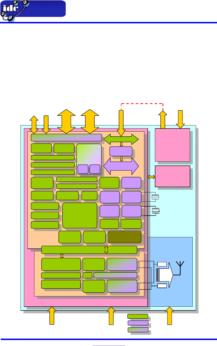
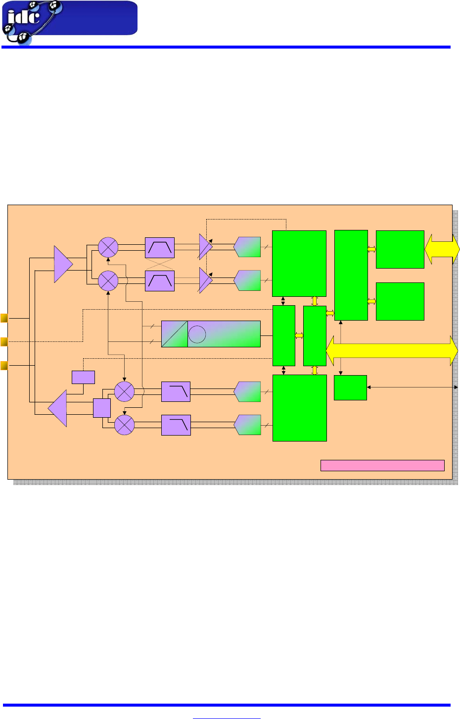
Module Description
System-on-Chip (SoC)
The CC2430 System-on-Chip is provided by Texas Instruments, and combines the market leading CC2420
RF transceiver (Chipcon / Ti), with an industry standard high-performance and peripheral enhanced 8051
micro-controller unit (MCU). With the memory arrangement provided on the ZB100, and the ability to support
the industry leading ZigBee protocol stack (Z-Stack™) from Texas Instruments, this module range forms the
basis for design solutions from the bottom “end-device”, right through to the most complex “full-function
device” requirements. Below provides a detailed view of the SoC complete with all peripherals, and
additional components forming the ZB100.
Block Diagram
Input
4 – 30V DC
Isolated
Regulator
Output
3.3V DC
Vunreg
Vreg = 3.3V
CC2430 / 31 SoC
MAC address
serial chip
32.000 MHz
32.768 kHz
CC2420 RF Transceiver
8051 Hi-speed
Enhanced core
Radio data interface
Receive Chain RF_P
RF_N
Balun
Chip Antenna
or
SMA Jack
or
RP-SMA Jack
RF Ground Plane
0V DC
0V DC
0V DC
Demodulator
Frequency Synthesiser
~
Transmit Chain
Modulator
AGC
CSMA / CA Strobe
Processor
Radio Registers
FIFO and Frame Control
V
DD
= 2.0 – 3.6V
Vunreg = 4.0 – 30V
3.3V
On-chip 1.8V
Regulator
Di
g
ital Su
pp
lies
Analogue and
Radio Su
pp
lies
CC2431 ONLY
Location Engine
AES
Encryption
Decr
yp
tion
IO Controller
32 MHz
Crystal
Osc
32.768 kHz
Crystal
Osc
Hi-Speed
RC
Osc
32 kHz
RC
Osc
Power-On
Reset
Brown
-
out
Connect
Pin 21 to Pin 22
when powering
from 4.0 – 30V
su
pp
l
y
RESETn
Debug
Interface
8051
Core
MCU
P2_1 / P2_2
Debu
g
**
**Debug Interface is shared with GPIO Port pins 2_1 and 2_2
P0_1………P0_7
P1_1………P1_7
------------- See Pin Confi
g
uration Table ------------
Clock Mux &
Calibration
Watchdog
Timer
IRQ
Controller
Memory Arbitrator
128kByte FLASH
8kByte SRAM
FLASH
Write
ADC
Audio / DC
8 Channels
12-bit
resolution
DMA
Sleep Mode Controller
Sleep Timer
USART
(
0
)
USART
(
1
)
Timer 2
MAC
802.15.4
Timer 1 (16-bit)
Timer 3 (8-bit)
Timer 4 (8-bit)
Digital
Analogue
Mixed
Batt
Mon.
Temp
Mon.
Random #
Gen. CRC

ZB100 OEM Modules Product Datasheet
ZB100 Datasheet V1.0 www.idc.gb.com Page 6 of 28
CC2431 – Location Engine
The CC2431 System-on-Chip is identical to the CC2430 in respect of MCU, memory, peripherals and radio
operation, with the addition of a hardware location detection module – microcode in silicon. This can be
used in applications requiring location management e.g. asset tracking. Mobile devices (blind nodes –
unknown position) receive signals from nodes with known locations. Based on the varying signal strengths
from received from these fixed nodes, the location engine calculates an estimate of its own position.
Accuracy of 3 to 5 metres in typical applications can be achieved. Coverage is approximately 64 x 64
metres, with a location estimate resolution of 0.5m. The time to perform the calculation takes less than 40µs,
and requires minimal CPU loading, as the calculations are performed in microcode. Once the result has
been calculated, this can then be reported as an X/Y coordinate back through the network to say a PC for
visual representation.
Voltage Regulators
The ZB100 module can be powered from two sources, both referenced to the modules 0V ground
connections.
1) Battery / 3.3V DC source (V
DD
). This is the SoC digital chip supply and can be anywhere between
2.0 and 3.6V, and is primarily intended for battery powered applications. This provides power to all
digital elements of the SoC, and also the Serial / MAC integrated circuit.
2) Higher voltage DC source (Vunreg). This connects to an isolated linear 3.3V regulator, which
accepts DC input in the range of 4.0 to 30V, making it ideally suited to industrial applications. The
output of the isolated regulator is then linked (on the OEM board) into the Battery / 3.3V DC source,
providing the required 3.3V for the SoC.
In addition, there is a 1.8V analogue regulator internal to the SoC powered from the, which provides power to
the analogue sections and RF radio sections of the device. This is self-contained, and the 1.8V regulated
output is not made available for any external devices.
MCU Core
The CC2430/31 SoC contains an enhanced 8051 micro-controller with the core CPU running at 32MHz. This
operates the standard 8051 instruction set on 1 cycle per instruction as opposed to the standard 12 cycles
per instruction.
Memory
The onboard memory of the ZB100 consists of the following:
FLASH
128kByte of FLASH memory divided into 64 pages of 2kbyte each. This is the smallest erasable unit
in memory, whilst the smallest writable element is 32 bytes. The worst case FLASH memory
endurance is 1000 erase/write cycles. Programming can be performed from within resident
firmware, or over the 2-wire debug interface. Over-the-air programming is possible and available on
the ZB100. FLASH sectors can be locked for security and auto powers down during low frequency
CPU read access.
SRAM
A total of 8192 bytes of data memory is provided on chip, divided into two 4096 byte sectors, with the
upper sector having data retention in all power modes, and the lower sector with retention in active
and power mode 1 only.
ROM
The ROM is a 64bit 1-wire serial device that communicates over a single IO pin of the SoC. This
provides a unique identity for the ZB100 module, with the option for this to be a complete UID-64 bit
MAC address, which contains the IEEE assigned 24-bit company identifier (Intelligent Distributed
Controls Ltd. = 001B0AH), and a 40-bit node address.

ZB100 OEM Modules Product Datasheet
ZB100 Datasheet V1.0 www.idc.gb.com Page 7 of 28
Off-board Memory
Additional memory may be connected to the ZB100 via a serial port configured in SPI mode. Up to
2Mbyte of extra FLASH may be added in this way.
DMA Controller
A powerful DMA controller is provided which can be used to relieve the processor from data movement
thereby improving the overall processing efficiency. The DMA controller can move data from/to a peripheral
unit to/from memory with minimal CPU intervention. The DMA controller controls data exchange over the
entire range of the XDATA memory space, and since most of the SFRs are mapped into the XDATA memory
space, data transfers to/from peripherals can be manipulated. Use of the DMA can also reduce power
consumption by keeping the CPU in a low power mode, whilst moving data to or from a peripheral unit. The
main features of the DMA controller are given below:
• Five independent DMA channels
• Three configurable levels of DMA channel priority
• 31 configurable transfer trigger events
• Independent control of source and destination address
• Single block and repeated transfer modes
• Supports length field in transfer data setting variable transfer length
• Can operate in word or byte size modes
GPIO
The CC2430/31 provides three 8-bit ports of general purpose IO – Ports 0, 1 and 2. Ports 0 and 1 are
complete 8-bit wide ports (P0_0 …. P0_7; P1_0 …. P1_7), and are available on the ZB100 header. Port 2
has only 5 usable elements, two of which are taken by the 32.768 kHz crystal for RTC applications, and
P2_0 is directly interfaced to the serial number integrated circuit (MAC address). This leaves P2_1 and
P2_2 brought out to the ZB100 header as two further general purpose IO pins. P2_1 and P2_2 are also
used for the debug interface – see later.
All ports are both bit and byte addressable, and each port pin can be configured to operate as either a
general purpose IO or as a peripheral IO.
Each port pin has the following configurable features:
• Output drive current of ±4mA (Sink/Source), with the exception of P1_0 and P1_1 which are high
current drives providing ±20mA capability
• Configurable 20kΩ pull-up or pull-down or tri-state when configured as an input with the exception
of P1_0 and P1_1
• Retention of IO mode and output value when in lowest power modes
• GPIOs configured as inputs can be used to generate inputs
• GPIOs (Port0 and Port1) configured as inputs can each be associated with one DMA trigger for
immediate transfer to a mapped XDATA location on input transition changes
• Four radio test signals can be output on port pins P1_4 to P1_7
• Peripheral units have two alternative port locations to maximise port utilisation and minimise pin
selection conflicts
Unused IO pins should either be configured as outputs or as inputs with the pull-up resistor configured. In
both cases unused pins should not be connected to V
DD
or 0V to avoid excessive current consumption.

ZB100 OEM Modules Product Datasheet
ZB100 Datasheet V1.0 www.idc.gb.com Page 8 of 28
ADC
The ADC supports uo to 12-bit analogue to digital conversion via a multiplexer which accepts up to eight
single-ended channels through the GPIO interface. Two further internal channels are provided – on chip
temperature sensor, and a battery monitor input which is essentially the V
DD
supply divided by 3, for an early
warning detection of battery failure. In addition a positive reference voltage multiplexer / selector can be
programmed to choose between an on-chip reference voltage, the analogue voltage supply, a single ended
external reference via AIN7, or a differential external reference via AIN6-ANI7. The ADC features are as
follows:
• Selectable decimation rates (7, 9, 10 and 12 bits)
• Eight individual single-ended input channels, which may be paired for differential signals
• Reference voltage, selectable between internal, single-ended external, differential external or
AVDD_SOC (V
DD
)
• Interrupt request generation
• DMA triggers at end of conversions
• Temperature Sensor input
• Battery Monitor Input
Temperature Sensor
The temperature sensor provides a further additional channel to the ADC. This provides a voltage
measurement relative to temperature over the temperature range of -40º to +80ºC. This provides an
on-chip temperature reading accuracy of ±2 ºC over the temperature range of -20º to +80ºC once a
calibration has been performed at room temperature. The actual voltage reading for a given
temperature is based on the temperature coefficient of 2.45mV/ºC calculated from the room
calibration point.
Battery Monitor
The battery monitor AVDD_SOC/3 provides a further additional channel to the ADC. This provides a
linear relationship to the SoC supply (V
DD
), thereby providing the ability (using a threshold value) to
detect early warning of low-supply/battery status.
Timers
A total of six timers are provided by the SoC with varying configurable atributes as follows:
Timer 1 (16-bit)
Timer 1 may be used for a wide variety of control and measurement applications (input capture,
output compare and PWM) with the ability to perform motor control functionality. The main features
of Timer 1 are as follows:
• Three capture/compare channels
• Rising, falling or any edge capture
• Set, clear or toggle output compare
• Free-running, modulo or up/down counter operation
• Clock pre-scaler for divide by 1, 8, 32 or 128
• Interrupt request generated on each capture/compare and terminal count
• DMA trigger function

ZB100 OEM Modules Product Datasheet
ZB100 Datasheet V1.0 www.idc.gb.com Page 9 of 28
Timer 2 (MAC)
The MAC timer is mainly used for general time keeping in the 802.15.4 MAC layer, providing timing
for the CSMA-CA algorithms. The main features of the MAC timer are as follows:
• 16-bit up-counter providing symbol/frame periods of 16µs/320µs
• Adjustable period with accuracy of 31.25ns
• 8-bit timer compare function
• 20-bit overflow count
• 20-bit overflow count compare function
• Start of Frame Delimiter capture function
• Timer start/stop synchronous with 32.768 kHz clock and time keeping maintained by Sleep Timer
• Interrupts generated on compare and overflow
• DMA trigger capability
Timers 3 and 4 (8-bit)
Timers 3 and 4 support typical requirements such as output compare and PWM functions, or basic
software timing requirements. The main features of Timer 1 are as follows:
• Two compare channels
• Free-running, modulo or up/down counter operation
• Clock pre-scaler for divide by 1, 2, 4, 8, 16, 32, 64 or 128
• Interrupts generated on compare and terminal count
• DMA trigger capability
Watchdog Timer
The watchdog timer consists of a 15-bit counter clocked by the 32.768 kHz crystal oscillator. This
provides a means of resetting the processor if it fails to reset the watchdog within the selected period
through software. This may happen where the application is subject to an electrically noisy
environment, power glitches etc. or where high reliabilty of the software is required. The watchdog
timer provides the following features:
• Four selectable time intervals – 1.9 ms, 15.625 ms, 0.25 s, 1 s.
• Watchdog Mode (Generates CPU reset if timed out)
• Timer Mode (Generates Interrupt only if timed out)
• Independent from system clock
Sleep Timer
The sleep timer is used to set the interval from entering the low power sleep state and returning to
active mode.
• 24-bit up counter driven from the 32.768 kHz oscillator.
• 24-bit compare for waking through interrupt
• Low power mode operation in PM2
• Maximum period = 512 seconds (approx.8.5minutes)
USARTs
Two serial communication USARTs are provided on the SoC – USART(0) and USART(1). These can be
operated and configured separately into either UART (asynchronous) or SPI (synchronoue) modes. Both
USARTs have identical functionality, but are configured on separate port pins. A second “alternative”
configuration is also possible providing more efficient use of the port pins for peripheral use.

ZB100 OEM Modules Product Datasheet
ZB100 Datasheet V1.0 www.idc.gb.com Page 10 of 28
UART
UART mode provides an asynchronous serial communications interface consisting of two or four
wire (TxD, RxD and optionally CTS and RTS). In addition standard GPIO pins can be configured to
provide further modem functions e.g. DSR, DTR and CD, as these can be interrupt configured.
Each UART provides the following features:
• 8 or 9 data bits
• Odd, even or no parity
• Configurable Start and Stop bit level
• Configurable LSB or MSB first transfer
• Independent receive and transmit interrupts
• Independent receive and transmit DMA triggers
• Parity and framing error status
• Up to 230,400 bps data speed, configurable via an internal baud rate generator derived from the
system clock
SPI
SPI mode provides a synchronous serial communication interface through either a 3-wire or 4-wire
interface. The full 4-wire interface consists of the following pin functions:
• MOSI – Master Out Slave In
• MISO – Master In Slave Out
• SCK – Serial Clock
• SSN – Slave Select
The SPI mode provides the following features:
• Selectable 3-wire or 4-wire interface
• Master or Slave presentation
• Configurable SCK polarity and phase, SCK speed is configured via an internal baud rate
generator derived from the system clock
• Configurable LSB or MSB first transfer
When selected for Slave presentation (4-wire mode), the SSN pin is used as an edge triggered chip-
select input.
Random Number Generator / CRC
The Random Number Generator is a 16-bit linear feedback shift register (Polynomial X
16
+X
15
+ X
2
+ 1) and
provides the following features:
• Generates psuedo-random bytes for either use by the firmware, or by the Command Strobe
Processor CSMA / CA
• Calculate CRC16 of bytes written to the upper Random Number Generator register
• Seeded by value written to the lower Random Number Generator register twice – Usually for
standard CRC16 calculations, the seed vakue is either 0x0000 or 0xFFFF.
AES Coprocessor
The data encryption is performed by a dedicated co-processor contained in the SoC silicon which supports
the Advanced Encryption standard, AES. This allows encryption/decryption to be performed with minimal
CPU intervention. This coprocessor provides the following features:
• Supports all security suites in the IEEE 802.15.4 standard
• ECB, CBC, CFB, OFB, CTR and CBC-MAC modes with hardware support for CCM mode
• 128-bits key and IV/Nonce, and DMA transfer trigger capability
ZB100 OEM Modules Product Datasheet
ZB100 Datasheet V1.0 www.idc.gb.com Page 11 of 28
The AES coprocessor can add security to wired links (UART / SPI) but primarily is intended for the wireless
link. AES encryption is performed on blocks of data (128-bit wide), prior to transmitting a packet payload
over the radio, and AES decryption after receiving a payload packet.
Ref [4] for further detail on AES operation.
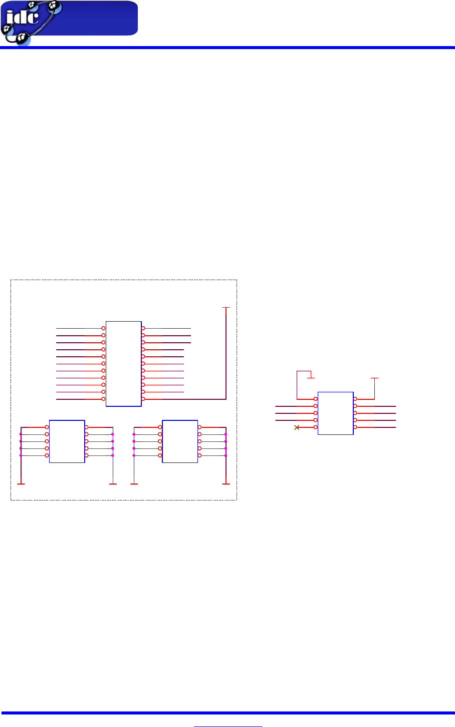
2-wire Debug Interface
The Debug Interface operates a proprietry 2-wire serial interface used for in-circuit debugging. Through this
interface it is possible to erase and write (program) the FLASH memory, and debug by controlled program
execution (stop/start, single stepping, breakpoints etc.).
The 2-wire debug interface shares with two GPIO port pins, and the debug mode is entered by a specific
operation of the debug clock in conjunction with the precessor RESETn pin. When not in debug mode, the
port pins revert back to standard general purpose IO pins.
The following details are for providing a programming interface for use with the Texas Instruments CC2430
Development Kit – CC2430DK. This uses a 10-way ribbon interface for programming and debugging the
SoC. In addition, this example interface can also provide a single SPI port. Alternatively Radio Test signals
can be configured to be outputs on the Port Pins P1_4 to P1_7 as given below.
MAC Address
The MAC address can be either hard-coded into FLASH, or take the address from the on-board 1-wire serial
device connected to the CC2430/31 Port P2_0. This device can be either a generic 24-bit serial number, or
a user specific EUI-64 global identifier whereby the first 24-bits provide the OUI, and the remaining 40-bits
provide the serialisation. The IEEE assigned OUI for Intelligent Distributed Controls Limited is 00-1B-0A.
OEMs may hardcode their own UID and serialisation or take the Intelligent Distributed Controls OUI as
appropriate
See Reference [6] for implimenting the 1-wire interface in software.
MISO
P1_7
0V
RESETn
SCLK
P1_3
+3.3V
RESETn
SoC PROGRAMMING DEBUG / FLASH
SCLK
0V
P2_1
P1_6
P1_6
SOC
Box Header 2x5
12
34
56
78
910
P0_1
P1_4
0V
P0_3
P2_1
P1_4
P2_2
P0_2
M1
12
34
56
78
910
11 12
13 14
15 16
17 18
19 20
21 22
RESETn
P0_4
P2_2
HD2
12
34
56
78
910
P1_5
P1_7
P1_2
Debug DC Debug DD
P0_6
MOSI
P0_7
P0_0
Footprint of IDC00008S Module
RESETn
0V
P1_1
Vreg
P0_5
Debug DC
0V
MISO
P1_5
+3.3V
3V3
CSn
Vunreg Debug DD
P1_0
HD3
12
34
56
78
910
MOSI
INTERFACE
ZB100 Module
Radio Test Signals
P1_4 – FIFO (One or more bytes in receive FIFO)
P1_5 – FIFOP (Unread receive FIFO bytes overflow)
P1_6 – SFD (Start of Frame Delimiter)
P1_7 – CCA (Clear Channel Assessment)
ZB100 OEM Modules Product Datasheet
ZB100 Datasheet V1.0 www.idc.gb.com Page 12 of 28
Radio Section
The radio core is based on the industry standard Chipcon/TI CC2420 transceiver. The IEEE 802.15.4
compliant radio is shown below in a simplified block diagram. Operation of the radio is configured through a
set of RF registers and controlled through a set of command strobes (single byte instructions) which control
the functionality of the radio. E.g. enable frequency synthesiser, enable receive mode, enable transmit mode
etc. The RF registers also provide status information from the radio. All command strobes from the CPU to
the radio pass through the CSMA/CA Strobe Processor
Refer to [1] for more detailed description of the radio operation.
Block Diagram
Receiver
The CC2430/31 SoC contains a low-IF receiver. The received RF signal is amplifier by a low-noise amplifer
(LNA) and down-converted in quadrature to the 2MHz intermediate frequency. The complex I/Q signal is
then bandpass filtered and amplified with a variable gain amplifier. The gain of the amplifier is digitally
controlled, and the AGC feedback loop ensures that the ADC operates inside its dynamic range. The signal
is digitised by the ADCs. The AGC, final channel filtering, demodulation, de-spreading, symbol-correlation
and byte synchronisation are performed digitally.
IRQ handling presents an interrupt when a start of frame delimiter has been detected. A 128 byte receive
FIFO is provided to buffer the received data. The firmware may read the receive FIFO through the SFR
interface, ideally by DMA transfer into CPU memory. The receive FIFO is provided with overflow detection,
informing the CPU via interrupt.
The CRC is verified in hardware, and the RSSI and correlation values are appended to the received frame.
The clear channel assessment, CCA, is available through an interrupt in receive mode. AES decryption (if
adopted) is then handled by the CPU and AES coprocessor independent from the radio.
LNA
PA
Σ
TX/RX SWITCH
Power
Control
TX POWER CONTROL
AUTOMATIC GAIN CONTROL
ADC
ADC
DAC
DAC
0
90
FREQUENCY
SYNTHESISER
~
DIGITAL
DEMODULATOR
-Digital RSSI
-Gain Control
-Image Suppression
-Channel Filtering
-Demodulation
-Frame synchronisation
DIGITAL
MODULATOR
-Data spreading
-Modulation
CONTROL
LOGIC
RADIO DATA
INTERFACE
FFCTRL
IRQ
HANDLING
SFR bus
RADIO
REGISTER
BANK
CSMA/CA
STROBE
PROCESSOR
Register
Bus
≡ CC2420 Transceiver

ZB100 OEM Modules Product Datasheet
ZB100 Datasheet V1.0 www.idc.gb.com Page 13 of 28
Transmitter
The CC2430/31 SoC transmitter is based on direct up-conversion. AES encryption (if adopted) is applied
prior to transferring the data to the 128 byte transmit FIFO buffer. Preamble and start of frame delimiters are
generated in hardware. The IEEE 802.15.4 direct sequence spread spectrum modulation format is then
applied by taking each byte and slitting it into two symbols (4-bits each). The least significant symbol is
transmitted first and for multi-byte fields, the least significant byte is transmitted first. Each symbol is
mapped to one-of-sixteen pseudo-random sequences of 32 “chips” each. The chip sequence is then
transmitted at 2MChip/s with the least significant chip first for each symbol. The modulation format is Offset
– Quadrature Phase Shift Keying (O-QPSK), with half-sine chip shaping. This is equivalent to Minimum Shift
Keying (MSK), whereby each “chip” is transmitted as a half sine alternatively between the I and Q channels
with one half period offset. The result for the I and Q channels are then output to the DACs, and then via low
pass filtering to the up-conversion mixers.
The resulting RF signal is then amplified in the programmable power amplifier (PA), and fed to the antenna
via the differential connection. Output power is programmed through the TXCTRLL Register. The maximum
power attainable is 0.6dBm. Internal TX/RX switching simplifies the antenna interface matching. The
biasing of the PA and LNA is done by connecting the TX/RX switch to the two differential RF connections
through a DC path. The signal then pass through a discrete microstrip balun to either the board mounted
chip antenna, or SMA / RP-SMA RF connector.
Frequency Sythesiser
Frequency synthesis is provided by a completely integrated VCO and 90º phase splitter for the I and Q local
oscillator (LO) signals to the up/down conversion mixers. The VCO operates in the frequency range 4800 –
4967 MHz, divided by two for the I and Q signals (2400 – 2483.5MHz). The VCO charateristics will change
with temperature and/or voltage supply and the desired operating frequency. To compensate for this the
PLL self-calibrates (bias current and tuning range) every time the RX mode or TX mode are enabled.
The on-chip voltage regulator delivers the regulated 1.8 V supply voltage for the radio circuitry.

ZB100 OEM Modules Product Datasheet
ZB100 Datasheet V1.0 www.idc.gb.com Page 14 of 28
Specifications
DC Characteristics
Parameter Min Typ Max Unit Condition/Note
Supply Inputs
Operating Supply
Voltage VDD 2.0 3.3 3.6 V
SoC power supply (Header Pin 22) referenced to
signal/RF ground plane (0V).
External Supply
Vunreg 4.0 --- 30.0 V
Header Pin 19 – Isolated Regulator output 3.3V -
Pin 21 requires linking to Pin 22 to power SoC.
Isolated section therefore draws no leakage
current when operating module from Pin 22 only
(E.g. battery).
Minimum input voltage to guarantee 3.3V output.
Isolated Regulator
Output Voltage 3.234 3.3 3.366 V Header Pin 21 – referenced to 0V.
Isolated Regulator
Output Current 50 100** mA
Nominally 50mA continuous (4-30V input),
** 100mA peak for short periods, dependent on
input voltage. Regulator has current and
thermal limiting.
Isolated Regulator
Drop-out voltage 380 450 mV Full load 100mA output.
Isolated Regulator
quiescent current 75 µA Up to 8mA typical on full 100mA load.
SoC Current Consumption – CC2430 & CC2431
MCU Active Mode, 32
MHz,
low MCU activity
9.5 mA
32 MHz XOSC running. No radio or peripherals
active. Low MCU activity : no flash access (i.e.
only cache hit), no RAM access.
MCU Active Mode, 32
MHz,
medium MCU activity
10.5 mA
32 MHz XOSC running. No radio or peripherals
active. Medium MCU activity: normal flash
access1, minor RAM access.
MCU Active Mode, 32
MHz,
high MCU activity
12.3 mA
32 MHz XOSC running. No radio or peripherals
active. High MCU activity: normal flash access1,
extensive RAM access and heavy CPU load.
MCU Active and RX
Mode 26.7 mA
MCU running at full speed (32MHz), 32MHz
XOSC running, radio in RX mode, -50 dBm input
power. No peripherals active. Low MCU activity.
MCU Active and TX
Mode, 0dBm 26.9 mA
MCU running at full speed (32MHz), 32MHz
XOSC running, radio in TX mode, 0dBm output
power. No peripherals active. Low MCU activity.
Power mode 1 (PM1) 190 µA
Digital regulator on, 16 MHz RCOSC and 32
MHz crystal oscillator off. 32.768 kHz XOSC,
POR and ST active. RAM retention.
Power mode 2 (PM2) 0.5 µA
Digital regulator off, 16 MHz RCOSC and 32
MHz crystal oscillator off. 32.768 kHz XOSC,
POR and ST active. RAM retention.
Power mode 3 (PM3) 0.3 µA No clocks. RAM retention. POR active.

ZB100 OEM Modules Product Datasheet
ZB100 Datasheet V1.0 www.idc.gb.com Page 15 of 28
Parameter Min Typ Max Unit Condition/Note
MAC address Chip Current Consumption (Active for initial read only on power up / reset)
Active Power 5 µA Powered via data pin of SoC, power, control
address and data all via a single pin.
Standby Power 0 µA No serial chip communication.
IO Parameters
General purpose Input
programmable pull-up /
pull-down
20 kΩ
P1_0 (Header Pin 12) and P1_1 (Header Pin 9)
do not have this feature. All are configurable for
external interrupt.
General purpose output
drive current sink /
source
±4 mA
P1_0 (Header Pin 12) and P1_1 (Header Pin 9)
have ±20mA drive capability.
ADC Resolution 7 12 bit Programmable conversion resolution /
decimation rate.
Analogue Input
Resistance 197 kΩ Simulated usung converstion 4MHz clock speed.
Internal reference 1.25 V
External reference can be selected on AIN7 /
P0_7 (Header Pin 2) or AIN6-AIN7 for
differential input conversation.
Input Voltage including
External reference
AIN6/AIN7
V
DD V
20 µs 7-bit setting (64 decimation rate).
36 µs 9-bit setting (128 decimation rate).
68 µs 10-bit setting (256 decimation rate.
Conversion Time
132 µs 12-bit setting (512 decimation rate).
ADC Current
Consumption 1.2 mA
Temperature Sensor
Temp. Coeffidient 2.45 mV/ºC Fitted from -20 ºC to +80 ºC.
Temp. Sensor
Accuracy -2 0 2 ºC
Over range -20 ºC to +80 ºC when using
2.45mV/ºC after 1-point calibration at room
temperature.
Temp. Sensor Current
Consumtion 280 µA When enabled.
Battery Monitor VDD/3 V
Additional analogue input channel which
measures the Analogue VDD divided by 3 for use
as a battery monitor.
UART Mode maximum
Baud Rate 230,400 bps For system clock set to 32MHz.
SPI Maximum Clock
Rate 4 MHz For system clock set to 32MHz.
Timer Input Capture 31.25 ns With Sysclk = 32MHz.
1.9 ms Clock source 32.768kHz (count = 64)
15.625 ms Clock source 32.768kHz (count = 512)
0.25 s Clock source 32.768kHz (count = 8192)
Watchdog Timer
1 s Clock source 32.768kHz (count = 32768)
ZB100 OEM Modules Product Datasheet
ZB100 Datasheet V1.0 www.idc.gb.com Page 16 of 28
Memory
Parameter Min Typ Max Unit Condition/Note
FLASH Memory 128 kbyte
64 pages of 2kbyte each
Page erase time 20 ms
Chip mass erase
time 200 ms
Write time 20 µs Per 4 bytes
Data Retention 100 years At room temperature
Program erase/write 1000 cycles endurance
SRAM 4096 bytes
Data retention in all power modes
SRAM 4096 bytes Data retention in power modes 0 (active) and 1.
MAC / Serial Chip 64 bit ROM accessed through 1-wire interface
RF Frequency, Output Power Levels and Data Rates
Parameter Min Typ Max Unit Condition/Note
RF Frequency Range 2400 2483.5 MHz Programmable in 1 MHz steps, 5 MHz between
channels for compliance with [1].
No. of channels 16 ** – See RF channel table.
Channel Spacing 5 Mhz **
Radio bit rate 250 kbps **
Radio Chip Rate 2.0 MChip/s **
Receiver Sensitivity -92 dBm PER = 1%, as specified by [1].
Nominal Output power 0 dBm
Delivered to a single ended 50 Ω load through a
balun and output power control set to 0x5F
(TXCTRLL register).
Programmable output
power range 26 dBm
The output power is programmable in 16 steps
from typically -25.2 to +0.6 dBm.
Antenna nominal RX /
TX impedance 50 Ω
The RF channels and associated frequencies defined by the IEEE 802.15.4 standard are as follows:
[1] IEEE std. 802.15.4 - 2003: Wireless Medium Access Control (MAC) and Physical Layer (PHY)
specifications for Low Rate Wireless Personal Area Networks (LR-WPANs).
RF Channel Frequency RF Channel Frequency RF Channel Frequency
11 2405 MHz 17 2435 MHz 23 2465 MHz
12 2410 MHz 18 2440 MHz 24 2470 MHz
13 2415 MHz 19 2445 MHz 25 2475 MHz
14 2420 MHz 20 2450 MHz 26 2480 MHz
15 2425 MHz 21 2455 MHz
16 2430 MHz 22 2460 MHz
ZB100 OEM Modules Product Datasheet
ZB100 Datasheet V1.0 www.idc.gb.com Page 17 of 28
Absolute Maximum Ratings
Parameter Min Typ Max Unit Condition/Note
Supply Voltage VDD -0.3 3.9 V Header Pin 22 – referenced to 0V.
Supply Voltage Vunreg V Header Pin 19 – referenced to 0V.
Voltage on any digital
IO pin -0.3
VDD+0.3
max 3.9 V
Input RF Level 10 dBm
Storage temp -50 +150 ºC Device not programmed.
Caution!! ZB100 Modules are ESD sensitive devices.
Precautions should be taken when handling the device in order to prevent permanent
damage.
Physical Dimension and Environmental Conditions
All modules are RoHS Compliant in construction.
Parameter Value Notes / Module Codes
Size – board profile 21.6 x 35 mm
Excludes over-hang of SMA or RP-SMA RF connectors.
See dimensional drawings for RF connector positions
and board overhang etc.
Module height 3.5 mm Board and RF shield combined - excluding pin headers.
4.8 mm ZB100-0-A; ZB100-1-A
12.3 mm ZB100-0-B; ZB100-0-D; ZB100-1-B; ZB100-1-D
16.3 mm ZB100-0-C; ZB100-0-E; ZB100-1-C; ZB100-1-E
12.3 mm ZB100-0-F-z; ZB100-0-H-z; ZB100-1-F-z; ZB100-1-H-z
Total height above OEM
daughter board
(See Dimensional
drawings)
12.3 mm ZB100-0-G-z; ZB100-0-J-z; ZB100-1-G-z; ZB100-1-J-z
6 g ZB100-0-A; ZB100-1-A
8 g ZB100-0-B; ZB100-0-D; ZB100-1-B; ZB100-1-D
10 g ZB100-0-C; ZB100-0-E; ZB100-1-C; ZB100-1-E
8 g ZB100-0-F-z; ZB100-0-H-z; ZB100-1-F-z; ZB100-1-H-z
Weight (approx.)
10 g ZB100-0-G-z; ZB100-0-J-z; ZB100-1-G-z; ZB100-1-J-z
Operating Temperature -20ºC to +70ºC -40ºC to +85ºC Storage and Operational with minor
degradation of clock stability / accuracy.
Operating Relative
Humidity 80% RH
For in-depth specifications please refer to the Related Documents - [1].
ZB100 OEM Modules Product Datasheet
ZB100 Datasheet V1.0 www.idc.gb.com Page 18 of 28
Module Coding
ZB100-x-y-z
(x) = System-on-Chip
0 = CC2430
1 = CC2431
(
c/w location en
g
ine
)
(y) = Antenna Style
A = Chip Antenna
B = Vertical SMA Jack
C = Vertical SMA Bulkhead Jack
D = Vertical RP-SMA Jack
E = Vertical RP-SMA Bulkhead Jack
F = R/A SMA Jack
G = R/A SMA Bulkhead Jack
H = R/A RP-SMA Jack
J = R/A RP-SMA Bulkhead Jack
R/A = Right-angled
RP-SMA = Reverse Polarity SMA
(z) = R/A RF Connector Orientation
S = Straight
R = Rotated
Examples
ZB100-0-A
CC2430 with Chip Antenna
ZB100-1-B
CC2431 with vertical SMA Jack
ZB100-0-J-R
CC2430 with R/A RP-SMA bulkhead
mounted in the rotated position

ZB100 OEM Modules Product Datasheet
ZB100 Datasheet V1.0 www.idc.gb.com Page 19 of 28
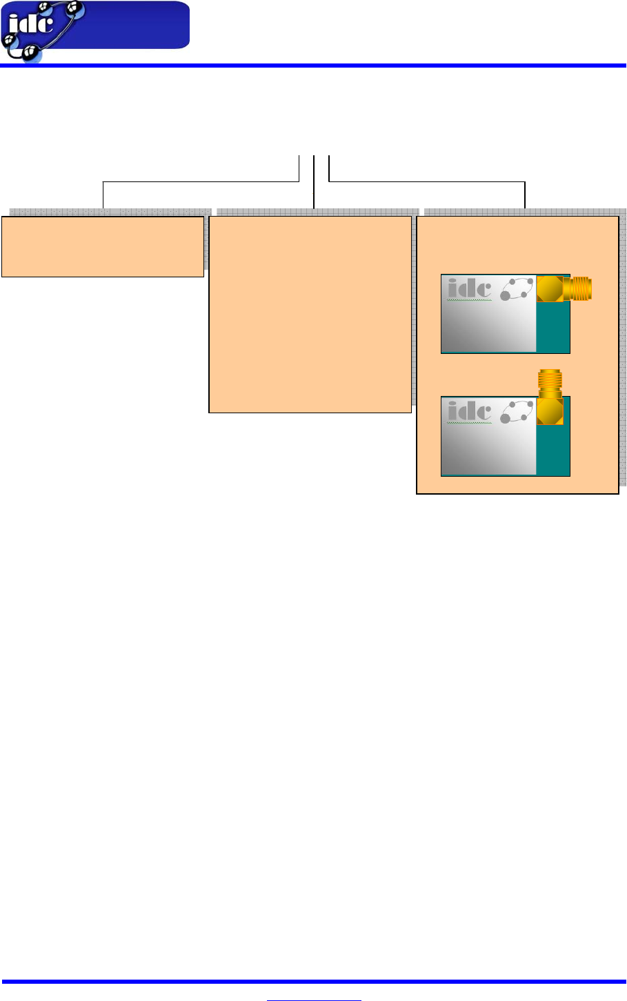
Module Dimensional Detail
Chip Antenna Versions Vertical SMA and RP-SMA Versions
ZB100-0-A, ZB100-1-A ZB100-0-B; ZB100-0-D; ZB100-1-B; ZB100-1-D
R/A SMA and RP-SMA Versions Vertical SMA and RP-SMA Bulkhead Versions
ZB100-0-F-z; ZB100-0-H-z; ZB100-0-C; ZB100-0-E; ZB100-1-C; ZB100-1-E
ZB100-1-F-z; ZB100-1-H-z
R/A SMA and RP-SMA Bulkhead Versions
ZB100-0-G-z; ZB100-0-J-z;
ZB100-1-G-z; ZB100-1-J-z
21.6mm
35.0mm
Daughter
board top
surface
1.3mm
4.1mm
5.33mm
12.3mm
21.6mm
35.0mm
Daughter
board top
surface
1.3mm
4.1mm
5.33mm
16.3mm
21.6mm
35.0mm
Daughter
board top
surface
1.3mm
4.1mm
5.33mm
12.3mm
Optional
Rotated
position
6.1mm
7.1mm
8.9mm
21.6mm
35.0mm
Daughter
board top
surface
1.3mm
4.1mm
5.33mm
12.3mm
Optional
Rotated
position
10.8mm
11.75mm
8.9mm
3.5mm
21.6mm
35.0mm
Daughter
board top
surface
1.3mm
Antenova
Rufa Chip
Antenna
ZB100 OEM Modules Product Datasheet
ZB100 Datasheet V1.0 www.idc.gb.com Page 20 of 28
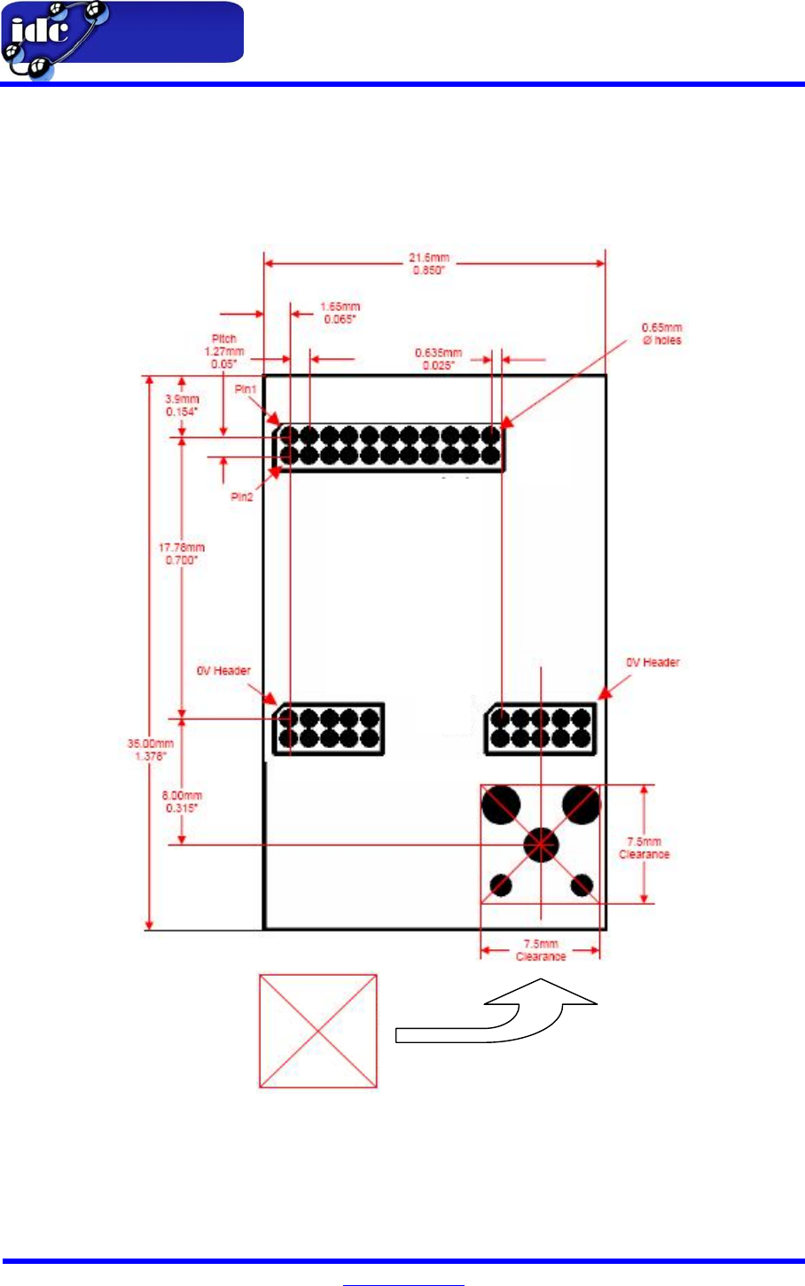
PCB Mounting Information
Daughter board PCB Layout and connector pads
–
top view:
22 way header (See table)
2 off 10 way headers for 0V grounding
The module requires a clearance hole
on the daughter board. This area will
need removing to allow for the SMA and
RP-SMA RF connector legs and signal
pin.
Not applicable if using the chip antenna

ZB100 OEM Modules Product Datasheet
ZB100 Datasheet V1.0 www.idc.gb.com Page 21 of 28
Pin Configuration
Connections of the 22-way header are as follows: 0V/Signal ground is provided by the two 10-way headers.
Pin # Pin
Ref. Use
Description
GPIO
Configurable Pull Up / Pull Down in Input mode, interrupt source, ±4mA drive
strength in output mode
1 P0_6
ADC - AIN6
Analogue Input 6 – single ended (Differential with AIN7) 8 – 12 bit resolution
GPIO
Configurable Pull Up / Pull Down in Input mode, interrupt source ±4mA drive
strength in output mode
2 P0_7
ADC – AIN7
Analogue Input 7 – single ended (Differential with AIN6) 8 – 12 bit resolution
GPIO
Configurable Pull Up / Pull Down in Input mode, interrupt source, ±4mA drive
strength in output mode
ADC – AIN4
Analogue Input 4 – single ended (Differential with AIN5) 8 – 12 bit resolution
USART0 / SPI
(SSN)
SPI0-SSN Data – Slave Select (Input)
USART0 / UART
(CTS)
UART0 – Clear-to-Send (Input)
USART1 / SPI
(MOSI)
SPI1-MISO – Data - Master Input / Slave Output
USART1 / UART
(TxD) UART1 – Transmit Data (Output)
3 P0_4
TIMER1
(CC2) TIMER1 – Channel 2 - Capture (Input) / Compare (Output)
GPIO
Configurable Pull Up / Pull Down in Input mode, interrupt source, ±4mA drive
strength in output mode
ADC – AIN5
Analogue Input 5 – single ended (Differential with AIN4) 8 – 12 bit resolution
USART0 / SPI
(SCK)
SPI0-SCK – Clock (Output)
USART0 / UART
(RTS)
UART0 – Ready-to-Send (Output)
USART1 / SPI
(MISO)
SPI1-MISO – Data - Master Input / Slave Outpu
4 P0_5
USART1 / UART
(RxD)
UART1 – Receive Data (Input)
GPIO
Configurable Pull Up / Pull Down in Input mode, interrupt source, ±4mA drive
strength in output mode
ADC – AIN2
Analogue Input 2 – single ended (Differential with AIN3) 8 – 12 bit resolution
USART0 / SPI
(MISO)
SPI0-MISO – Data - Master Input / Slave Output
USART0 / UART
(RxD)
UART0 – Receive Data (Input)
USART1 / SPI
(SSN)
SPI1-SSN – Slave Select (Input)
USART1 / UART
(CTS)
UART1 – Clear-to-Send (Input)
5 P0_2
TIMER1
(CC0)
TIMER1 – Channel 0 - Capture (Input) / Compare (Output)

ZB100 OEM Modules Product Datasheet
ZB100 Datasheet V1.0 www.idc.gb.com Page 22 of 28
Pin # Pin
Ref. Use
Description
GPIO
Configurable Pull Up / Pull Down in Input mode, interrupt source, ±4mA drive
strength in output mode
ADC – AIN3
Analogue Input 3 – single ended (Differential with AIN2) 8 – 12 bit resolution
USART0 / SPI
(MOSI)
SPI0-MOSI – Data - Master Output / Slave Input
USART0 / UART
(TxD)
UART0 – Transmit Data (Output)
USART1 / SPI
(SCK)
SPI1-SCK – Clock (Output)
USART1 / UART
(RTS)
UART1 – Ready-to-Send (Output)
6 P0_3
TIMER1
(CC1)
TIMER1 – Channel 1 - Capture (Input) / Compare (Output)
GPIO
Configurable Pull Up / Pull Down in Input mode, interrupt source, ±4mA drive
strength in output mode
7 P0_0
ADC – AIN0
Analogue Input 0 – single ended (Differential with AIN1) 8 – 12 bit resolution
GPIO
Configurable Pull Up / Pull Down in Input mode, interrupt source, ±4mA drive
strength in output mode
8 P0_1
ADC – AIN1
Analogue Input 1 – single ended (Differential with AIN0) 8 – 12 bit resolution
GPIO
NO configurable Pull Up / Pull Down in Input Mode, interrupt source, ±20mA drive
strength in output mode
TIMER1
(CC1) (Alt2)
TIMER1 – Channel 1 - Capture (Input) / Compare (Output) – Alternative Pin
9 P1_1
TIMER4
(CC1)
TIMER4 – Channel 1 - Capture (Input) / Compare (Output)
10 RESETn
SoC RESET
Used as SoC reset, or in conjunction with the two Debug pins DD and DC in order
to enter the debug / programming mode
GPIO
Configurable Pull Up / Pull Down in Input mode, interrupt source, ±4mA drive
strength in output mode
USART0 / SPI
(SCK) (Alt2)
SPI0-SCK – Clock (Output) – Alternative Pin
USART0 / UART
(RTS) (Alt2)
UART0 – Ready-to-Send (Output) – Alternative Pin
11 P1_3
TIMER3
(CC0)
TIMER3 – Channel 0 - Capture (Input) / Compare (Output)
GPIO
NO configurable Pull Up / Pull Down in Input Mode, interrupt source, ±20mA drive
strength in output mode
TIMER1
(CC2) (Alt2)
TIMER1 – Channel 2 - Capture (Input) / Compare (Output) – Alternative Pin
12 P1_0
TIMER4
(CC0)
TIMER4 – Channel 0 - Capture (Input) / Compare (Output)
GPIO
Configurable Pull Up / Pull Down in Input mode, interrupt source, ±4mA drive
strength in output mode
USART0 / SPI
(MOSI) (Alt2)
SPI0-MOSI – Data - Master Output / Slave Input – Alternative Pin
USART0 / UART
(TxD) (Alt2)
UART0 – Transmit Data (Output) – Alternative Pin
USART1 / SPI
(SCK) (Alt2)
SPI1-SCK – Clock (Output) – Alternative Pin
13 P1_5
USART1 / UART
(RTS) (Alt2)
UART1 – Ready-to-Send (Output) – Alternative Pin

ZB100 OEM Modules Product Datasheet
ZB100 Datasheet V1.0 www.idc.gb.com Page 23 of 28
Pin # Pin
Ref. Use
Description
GPIO
Configurable Pull Up / Pull Down in Input mode, interrupt source, ±4mA drive
strength in output mode
USART0 / SPI)
(SSN) (Alt2)
SPI0-SSN Data – Slave Select (Input) – Alternative Pin
USART0 / UART
(CTS) (Alt2)
UART0 – Clear-to-Send (Input) – Alternative Pin
14 P1_2
TIMER1
(CC0) (Alt2)
TIMER1 – Channel 0 - Capture (Input) / Compare (Output) – Alternative Pin
GPIO
Configurable Pull Up / Pull Down in Input mode, interrupt source, ±4mA drive
strength in output mode
USART1 / SPI
(MISO) (Alt2)
SPI1-MISO – Data - Master Input / Slave Output – Alternative Pin
USART1 / UART
(RxD) (Alt2)
UART1 – Receive Data (Input) – Alternative Pin
15 P1_7
TIMER3
(CC1) (Alt2)
TIMER3 – Channel 1 - Capture (Input) / Compare (Output) – Alternative Pin
GPIO
Configurable Pull Up / Pull Down in Input mode, interrupt source, ±4mA drive
strength in output mode
USART0 / SPI
(MISO) (Alt2)
SPI0-MISO – Data - Master Input / Slave Output – Alternative Pin
USART0 / UART
(RxD) (Alt2)
UART0 – Receive Data (Input) – Alternative Pin
USART1 / SPI
(SSN) (Alt2)
SPI1-SSN – Slave Select (Input) – Alternative Pin
USART1 / UART
(CTS) (Alt2)
UART1 – Clear-to-Send (Input) – Alternative Pin
16 P1_4
TIMER3
(CC1)
TIMER3 – Channel 1 - Capture (Input) / Compare (Output)
GPIO
Configurable Pull Up / Pull Down in Input mode, interrupt source, ±4mA drive
strength in output mode
17 P2_2
DC
Debug Clock – used in conjunction with RESETn and DD
GPIO
Configurable Pull Up / Pull Down in Input mode, interrupt source, ±4mA drive
strength in output mode
USART1 / SPI
(MOSI) (Alt2)
SPI1-MOSI – Data – Master Output / Slave Input – Alternative Pin
USART1 / UART
(TxD) (Alt2)
UART1 – Transmit Data (Output) – Alternative Pin
18 P1_6
TIMER3
(CC0) (Alt2)
TIMER3 – Channel 0 - Capture (Input) / Compare (Output) – Alternative Pin
19 Vunreg
Reg. Input
On-board regulator (4 to 30V). The regulator can provide 100mA max.
GPIO
Configurable Pull Up / Pull Down in Input mode, interrupt source, ±4mA drive
strength in output mode
20 P2_1
DD
Debug Data – used in conjunction with RESETn and DC
21 Vreg
Reg. Output
Vout from the Regulator Section. Link to Pin 22 when powering the SoC using the
on-board regulator.
22 3.3V
SoC V
DD
SoC Supply Voltage (2.0 to 3.6V) – 3V battery powered connection point.
NOTE: Refer to CC2430.pdf and/or CC2431.pdf Datasheets from the Texas Instruments Website for in-
depth detail for configuring and programming the SoC device.

ZB100 OEM Modules Product Datasheet
ZB100 Datasheet V1.0 www.idc.gb.com Page 24 of 28
Agency Certifications
EUROPEAN UNION (ETSI)
The ZB100 Module has been certified for use in European Union countries.
If the ZB100 Modules are incorporated into a product, the manufacturer must ensure compliance of the final
product to the European harmonised EMC and low-voltage/safety standards. A Declaration of Conformity
must be issued for each of these standards and kept on file as described in Annex II of the R&TTE Directive.
Furthermore, the manufacturer must maintain a copy of the ZB100 Modules documentation and ensure the
final product does not exceed the specified power ratings, antenna specifications, and/or installation
requirements as specified in the user manual. If any of these specifications are exceeded in the final
product, a submission must be made to a notidied body for compliance testing to all required standards.
IMPORTANT: The ‘CE’ markin must be affixed to a visible location on the OEM product. The ‘CE’ mark shall consist of the initials
‘CE’ taking the form shown above.
o If the CE marking is reduced or enlarged, the proportions given in the above example must be respected.
o The CE marking must have a height of at least 5mm except where this is not possible on account of the nature of the
apparatus.
o The CE marking must be affixed visibly, legibly, and indelibly.
UNITED STATES (FCC)
This equipment complies with Part 15 of the FCC rules and regulations.
To fulfill the FCC Certification requirements, an OEM manufacturer must comply with the following
regulations:
1. The modular transmitter must be labelled with its own FCC ID number, and, if the FCC ID is not
visible when the module is installed inside another device, then the outside of the device into which
the module is installed must also display a label referring to the enclosed module. This exterior label
can use wording such as the following:
Example of Label required for OEM products containing the following Model codes:
ZB100-x-A Chip Antenna
ZB100-x-D RF connector – Vertical RP-SMA
ZB100-x-E RF connector – Vertical RP-SMA bulkhead
ZB100-x-H-y RF connector – Right-angled RP-SMA
ZB100-x-J-y RF connectot – Right-angled RP-SMA bulkhead
Note: x refers to the System-on-Chip variant – either CC2430 or CC2431.
y refers to mountng position for right angled connectors – See Model Coding Section.
Any similar wording that expresses the same meaning may be used.
Contains FCC ID: VO7ZB100
The enclosed device complies with Part 15 of the FCC Rules. Operation is subject to the
following two conditions: (i) this device may not cause harmful interference and (ii) this device
must accept any interference received, including interference that may cause undesired operation.

ZB100 OEM Modules Product Datasheet
ZB100 Datasheet V1.0 www.idc.gb.com Page 25 of 28
2. For RF Connector models, the external antennas have been tested and approved specified below.
The ZB100 (D, E, H or J) models may be integrated with other types or custom designed antennas
which the OEM installer must authorize following the FCC 15.21 requirements.
WARNING: The Original Equipment Manufacturer (OEM) must ensure that the OEM modular transmitter must be labeled with
its own FCC ID number. This includes a clearly visible label on the outside of the final product enclosure that
displays the contents shown below. If the FCC ID is not visible when the equipment is installed inside another
device, then the outside of the device into which the equipment is installed must also display a label referring to the
enclosed equipment.
IMPORTANT: This equipemtn complies with Part 15 of the FCC Rules. Operation is subject to the following two conditions: (i) this
device may not cause harmful interference and (ii) this device must accept any interference received, including
interference that may cause undesired operation (FCC 15.19)
The internal / external antenna(s) used for this mobile transmitter must provide a separation distance of at least
20cm from all persons and must not be co-located or operating in conjunction with any other antenna or transmitter.
IMPORTANT: Modifications not expressly approved by this company could void the user’s authority to operate this equipment
(FCC section 15.21)
IMPORTANT: This equipment has been tested and found to comply with the limits for a Class A digital device, pursuant to Part 15
of the FCC Rules. These limits are designed to provide reasonable protection against harmful interference when
the equipment is operated in a commercial environment. This equipment generates, uses and can radiate radio
frequency energy and, if not installed and used in accordance with the instruction manual, may cause harmful
interference to radio communications. Operation of this equipment in residential areas is likely to cause harmful
interference in which case the user will be required to correct the interference at his/her own expense (FCC section
15.105).
Approved Antenna List
Part Number Manufacturer / Description Gain, dBI ETSI FCC
3030A5839-01
Antenova Rufa chip antenna
(Left-hand), frequency range 2400
– 2500MHz
2.1dBi Peak
9 9
2010B4844-01 (SMA)
9
³
2010B6090-01 (RP-SMA)
Antenova Titanis, swivel antenna
(1/2 wave), frequency range 2400
– 2500MHz
2.2dBi Peak
9
9
NET-WL-ANT009OSC
Solwise omni-directional dipole
with RP-SMA connector,
frequency range 2400 – 2500MHz
See Notes **
8.5±0.5dBi
9
9
NOTES:
All testing has been carried out with the CC2430 / CC2431 programmed for maximum RF output power of
0.6 dBm (Register TXCTRLL = 0xFF).
Any omni-directional dipole (articulated or straight) may be used providing the gain is less than that tested
using the
NET-WL-ANT009OSC (9dBi)
** Channel 26 - restriction for use under FCC Part 15 Rules.
The output power for channel 26 (2480MHz) is restricted as follows:
1. Use an omni-directional dipole antenna with gain no greater than 3 dBi.
2. Reduce the radio power accordingly within the software. E.g. for the 9dBi antenna, the power
outputs needs reducing by ≥ 6dB from maximum.

ZB100 OEM Modules Product Datasheet
ZB100 Datasheet V1.0 www.idc.gb.com Page 26 of 28
Glossary
ADC Analogue to Digital Converter
AES Advanced Encryption Standard
AIN# Analogue Input Channel #number
bps Bits per Second
CBC Cipher Block Chaining
CBC-MAC Cipher Block Chaining Message
Authentication Code
CC# Capture Compare #number
CCA Clear Channel Assessment, Radio
CCM Counter Mode + CBC-MAC
CD Carrier Detect
CE European marking to indicate
conformity
CFB Cipher Feedback
CPU Central Processing Unit
CSMA/CA Carrier Sense Multiple Access with
Collision Avoidanced
CTR Counter Mode (encryption)
CTS Clear to Send, UART Interface
DC
(1)
Direct Current
DC
(2
) Debug Clock
DD Debug Data
DMA Direct Memory Access
DSR Data Set Ready
DSSS Direct Sequence Spread Spectrum
DTR Data Terminal Ready
ECB Electronic Codebook (encryption)
ESD Electro Static Discharge
ETSI European Telecommunications
Standards Institute
EUI Extended Unique Identifier
FCC Federal Communications Commission
FFCTRL FIFO and Frame Control
FFD Full-Function Device
FIFO First In First Out
FIFOP FIFO receive buffer overflowed
threshold, Radio Interface
FLASH Non-volatile memory which can be
electrically erased and re-programmed
GPIO General Purpose Input/Output
HW Hardware
IEEE Institute of Electrical and Electronic
Engineers
IF Intermediate Frequency
IRQ Interrupt Request
ISM Industrial, Scientific and Medical
frequency band - a part of the radio
spectrum that can be used by
anybody without a license in most
countries
IV Initialisation Vector (AES)
kByte 1024 bytes
LC Inductor-Capacitor
LNA Low Noise Amplifer
LR-WPAN Low Rate Wireless Personal Area
Network
LSB Least Significant Bit
MAC Medium Access Control layer
MCU Microcontroller Unit - For the ZB100,
this refers to the 8051 core processor
in either the CC2430 or CC2431
MISO Master In / Slave Out, SPI Interface
MOSI Master Out / Slave In, SPI Interface
MSB Most Significant Bit
MSK Minimum Shift Keying
NONCE Not Once (AES)
OEM Original Equipment Manufacturer
OFB Output Feedback (encryption)
O-QPSK Offset-Quadrature Phase Shift
Keying
OTA Over-the-Air – upgrade/programming
OUI Organisationally Unique Identifier
(24-bit)
PA Power Amplifier
PC Personal Computer
PCB Printed Circuit Board
PER Packet Error Rate
PHY Physical Layer
PLL Phase Locked Loop
POR Power on Reset
PWM Pulse Width Modulator
R&TTE Radio and Telecommunications
Terminal Equipment
RAM Random Access Memory

ZB100 OEM Modules Product Datasheet
ZB100 Datasheet V1.0 www.idc.gb.com Page 27 of 28
R/A Right Angled
RC Resistor / Capacitor
RCOSC RC Oscillator
RF Radio Frequency
RP-SMA Reverse Polarity Sub-miniature Version
A – coaxial RF connector with reversed
gender (Required for FCC compliance)
RSSI Received Signal Strength Indicator
RTS Ready to Send, UART Interface
ROM Read only memory
RoHS Restriction on Hazardous Substances
RTC Real Time Clock
RxD Receive Data, UART Interface
SCK Serial Clock, SPI Interface
SFR Special Function Register
SMA Sub-miniature Version A – coaxial RF
connector
SoC System-on-Chip
SPI Serial Peripheral Interface bus
SRAM Static Random Access Memory
SSN Slave Select Number, SPI Interface
ST Sleep Timer
SW Software
TI Texas Instruments
TxD Transmit Data, UART Interface
TX Transmit, Radio
UART Universal Asynchrouns
Receiver/Transmitter
UID Unique Identifier
USART Universal Synchronous/Asynchrouns
Receiver/Transmitter
VCO Voltage Controlled Oscillator
XOSC Crystal Oscillator
802.15.4
The IEEE 802.15.4-2003 standard
applicable to low-rate wireless
Personal Area Networks

ZB100 OEM Modules Product Datasheet
ZB100 Datasheet V1.0 www.idc.gb.com Page 28 of 28
Related Documents
[1] Chipcon Products fromTexas Instruments CC2430 – A True System-on-Chip solution for 2.4GHz
IEEE 802.15.4 / ZigBee CC2430 Data Sheet (Rev. 2.1) SWRS036F
[2] Chipcon Products fromTexas Instruments CC2431 – System-on-Chip for 2.4 GHz ZigBee®/ IEEE
802.15.4 with Location Engine CC2431 Data Sheet (Rev. 2.01) SWRS034B
[3] Chipcon Products fromTexas Instruments – Application Note AN042 – CC2431 Location Engine
Application Note AN042 (Rev. 1.0) SWRA095
[4] Design Note DN108 – Using AES Encryption in CC111xFx, CC243x, and CC251xFx SWRA172A
[5] CC1110DK/ CC2430DK/CC2510DK Development Kit - User Manual - Rev. 1.5 SWRU039
[6] Dallas/Maxim – 1-wire Communication Through Software – App Note 126
Disclaimer
Intelligent Distributed Controls Limited believes that at the time of issue, all information contained herein to
be accurate. Intelligent Distributed Controls Limited reserves the right to make changes to this product or
documentation without prior notice. Latest available revisions shall be provided on the Website.
Contact Information
Intelligent Distributed Controls Limited
Suite 6
Keynes House
Chester Park
Alfreton Road
Derby
DE21 4AS
United Kingdom
Tel: +44(0)1332 604030
Fax: +44(0)1332 604031
E-mail: sales @idc.gb.com
Website: www.idc.gb.com
Office Hours: 9:00am - 5:00pm GMT