LG ELECTRONICS LGP2300W SINGLE-BAND PCS CDMA PHONE User Manual ServiceManual
LG Electronics, Inc. SINGLE-BAND PCS CDMA PHONE ServiceManual
UserManual.wiki
>
LG ELECTRONICS
>
LGP2300W User Manual
>
Service Manual
Contents
1.
Users Manual
2.
Service Manual
Service Manual
Navigation menu
Upload a User Manual
Namespaces
Wiki Guide
HTML
PDF
Info
Views
User Manual
Discussion / Help
Navigation
![LGP-2300/2310W LG Information & Communications, Ltd. - 15 -1. Telephone Number Inputting MethodTelephone numbers can be inputted as follows in LGP2300W.− − Press MENU+4+0 and then, press the password made up of six digits(Default:000000). 1) You can see ESN number : Press [ ok ]2) You can see “ NAM1 PHONE NUMBER” : types proper phone number and press [ ok ]3) Press [ok] ; press [ok]2. NAM Program MethodThe NAM inputting method of LGP2300W is as follows.- Press MENU+4+0.- Press the password made up of six digits (Default:000000).1) You can see ESN number : Press [ ok ] : If you press [akey] then you can insert akey with CRC checksum2) You can see “ NAM1 PHONE NUMBER” : types proper phone number and press [ ok ]3) You can see “ NAM1 HOME SID ” : types proper SID number and press [ ok ]4) You can see “ NAM1 NAME “: types proper NAM name and press [ EXIT] or [MORE]If you choose [MORE] then following procedures are added5) You can see “SERVICE SEC. CODE” : type security code number of just [ ok ]6) You can see “NAM 1 MOBILE COUNTRY CODE” : types proper country codes number and press[ ok ]7) You can see “NAM 1 NMSID” : press[ ok ]- If you changed your phone number then you can see NMSID is changed to your 0000+phonenumber.8) You can see “PHONE MODEL “: press [ ok ]9) You can see “SLOT CYCLE INDEX” :types proper Slot cycle index and press [ ok ]10) You can see “EXIT service programming” and phone will be rested. CHAPTER 2. NAM Input Method (Inputting of telephone numbersincluded)](https://usermanual.wiki/LG-ELECTRONICS/LGP2300W.Service-Manual/User-Guide-41362-Page-16.png)
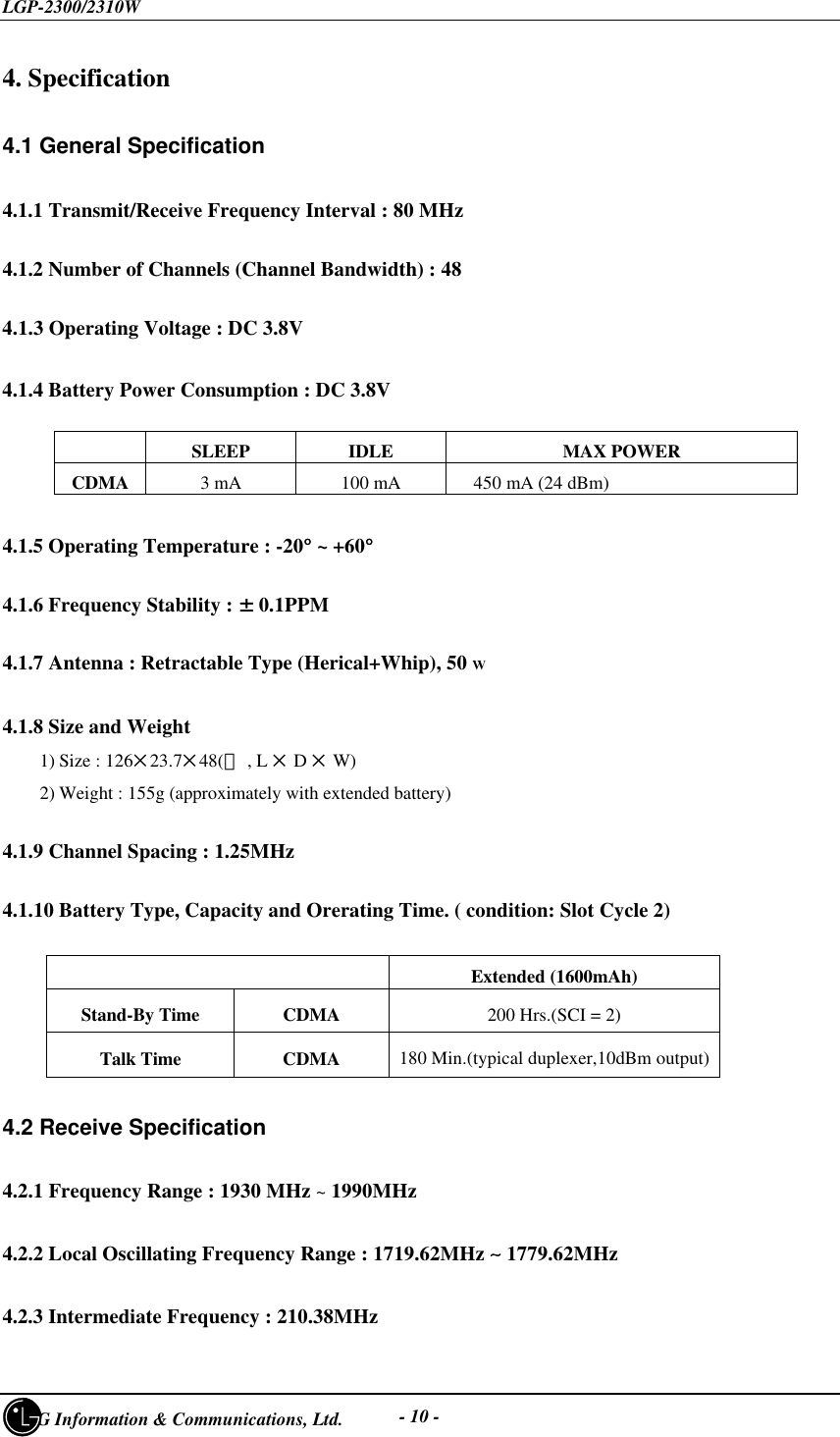
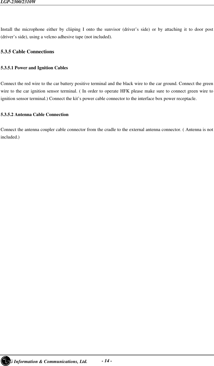
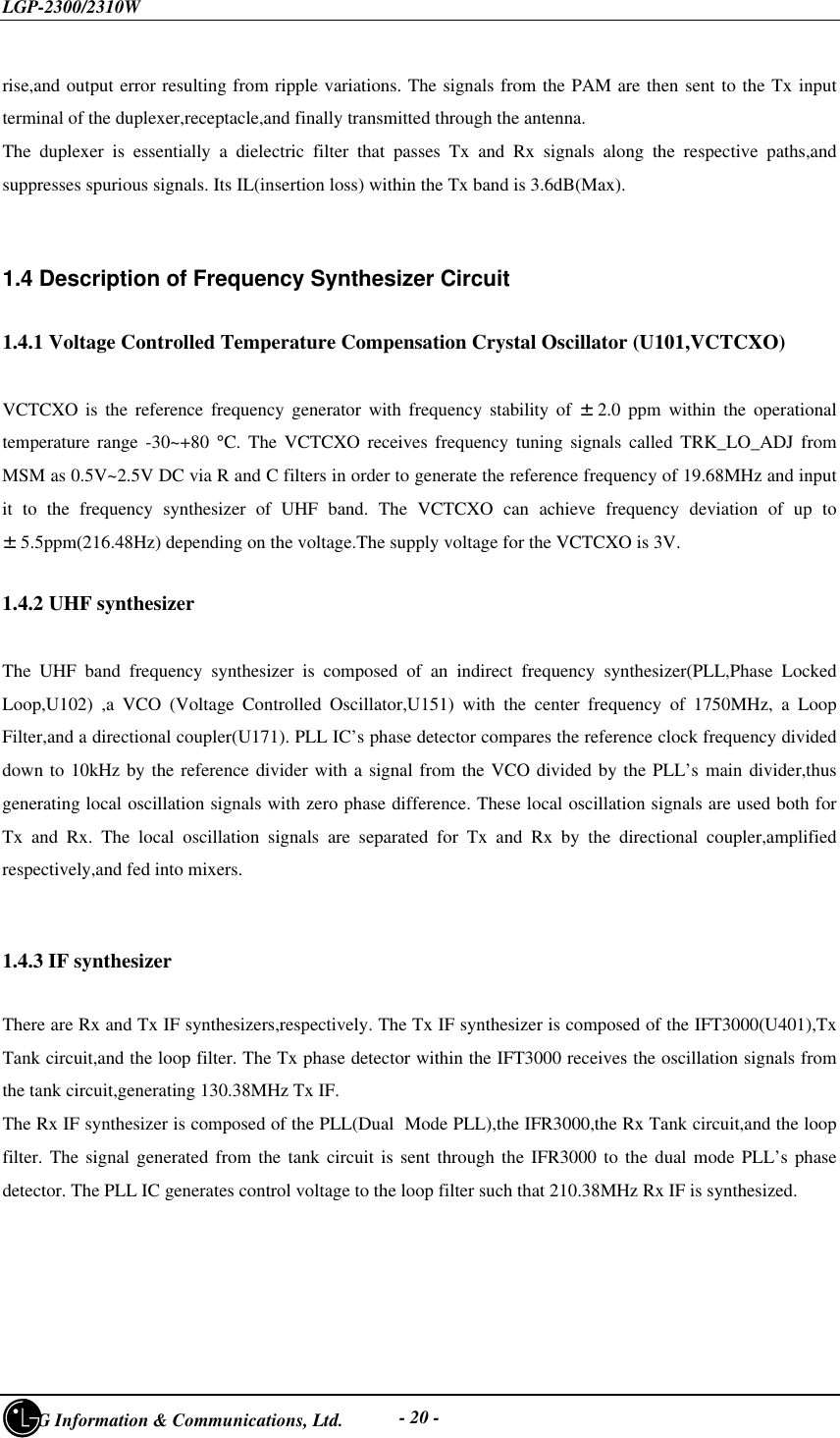
![LGP-2300/2310W LG Information & Communications, Ltd. - 17 - [Figure 1-1] Block Diagram of RF Transmit/Receive Part1.2 Description of Receive Part Circuit1.2.1 Duplexer (DP1)The duplexer(DP1) consists of a receive part bandpass filter (BPF) and a transmit part bandpass filter(BPF). Itsfunction is separating transmit/receive signals in the full duplex system using the transmit/receive commonantenna. The transmit part BPF is used to suppress noises and spurious waves entering the receive band amongtransmit signals in order to prevent the drop in receive sensitivity characteristics. The receive part BPF blocksthe signals sent out from entering the receive end in order to improve sensitivity characteristics.In addition, it suppresses video signals on IF signals. Insertion loss (IL) in the transmit band is 3.6dB (Max),whereas IL in the receive band is 4.5dB (Max). The receive band attenuation amount of transmit filter is 37dB(Min) and the transmit band attenuation amount of receive filter is 47dB or more (Min).1.2.2 Receive End RF circuitryThe RF signals from the duplexer are first fed into the LNA(U201) ,and the maximally amplified signals (withnoise figure of 1.8dB) from the LNA is then filtered by a BPF (U202) and amplified again by an RF](https://usermanual.wiki/LG-ELECTRONICS/LGP2300W.Service-Manual/User-Guide-41362-Page-18.png)
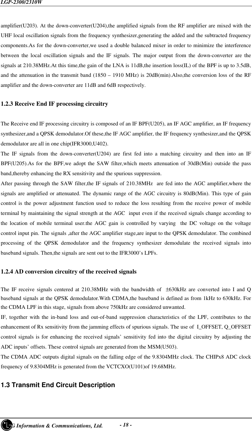
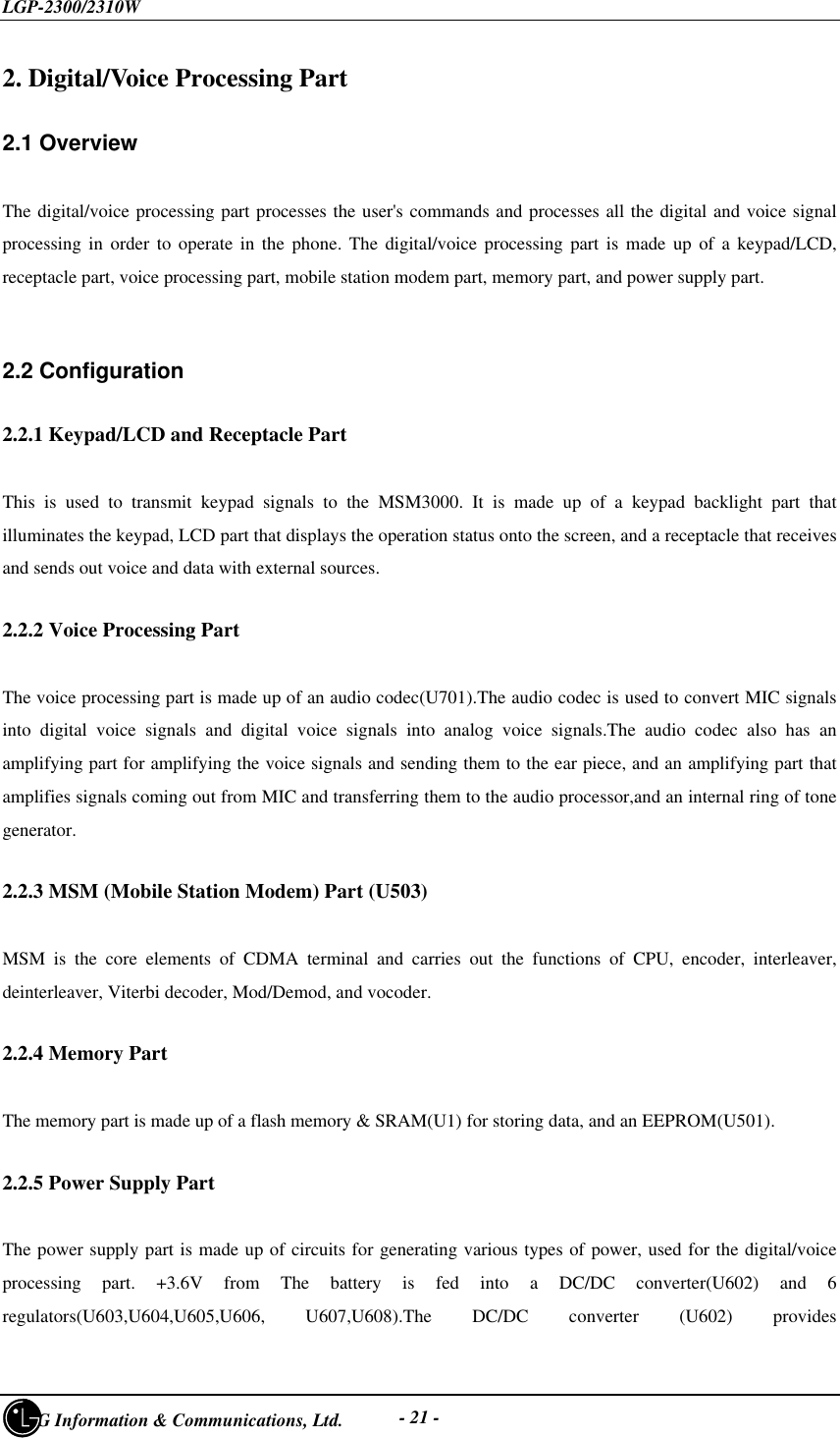
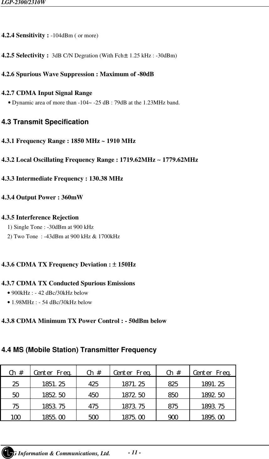
![LGP-2300/2310W LG Information & Communications, Ltd. - 22 -+5V.U603,U604,U606,U607,U608 produce +3.0V for the logic part,the RX circuitry,IFT&IFR3000,theCodec,and the UI part, respectively.The regulator U605 provides +3.6 U603, for the Tx circuitry.2.3 Circuit Description [Figure 2-1] Block Diagram of Digital/Voice Processing Part2.3.1 Keypad/LCD and Receptacle PartOnce the keypad is pressed, the key signals are sent out to the MSM3000 for processing. In addition, when thekey is pressed, the keypad lights up through the use of 8 LEDs. The terminal status and operation are displayedon the screen for the user with the characters and icons on the LCD(4 Line 512 Characters and 18 Icons [1Line])Moreover, it exchanges audio signals and data with external sources through the receptacle and then, receivespower from the battery or external batteries.2.3.2 Audio Processing PartMIC signals fed into the codec(U701). First, the signals are amplified through the mic preamp part and the micamp part of the codec.Then the signals are filtered, digitally converted and fed into the MSM3000. Also,thedigital audio signals outputted from the MSM3000 are converted into analog signals through the codec. First,thesignals are digital-to-analog converted by the PCM DAC part,bandpass filtered,and then amplified by theamplifier part.Also,the signals of the codec’s ringer, together with the MSM 3000’s ringer,activates the buzzerby activating Q703 and Q704.](https://usermanual.wiki/LG-ELECTRONICS/LGP2300W.Service-Manual/User-Guide-41362-Page-23.png)