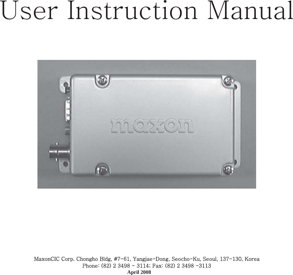
Maxon CIC SD-125EU1 RF Link Module User Manual SD125 User Instruction Manual

Maxon CIC Corp. RF Link Module SD125 User Instruction Manual

User Manual

 User Instruction Manual   MaxonCIC Corp. Chongho Bldg, #7-61, Yangjae-Dong, Seocho-Ku, Seoul, 137-130, Korea  Phone: (82) 2 3498 - 3114; Fax: (82) 2 3498 -3113   April 2008
FCC RF Exposure Compliance Requirements – The Federal Communications Commission (FCC), with its action in General Docket 93-62, November 7, 1997, has adopted a safety standard for human exposure to Radio Frequency (RF) electromagnetic energy emitted by FCC regulated equipment. Maxon subscribes to the same safety standard for the use of its products. Proper operation of this radio will result in user exposure far below the Occupational Safety and Health Act (OSHA) and Federal Communications Commission limits. Antennas used for this transmitter must not exceed an antenna gain of 6 dBi. The radio must be used in config-urations with a maximum operating duty factor not exceeding 50%, in typical push-to-talk configurations.  This radio is approved for use by the general population in an uncontrolled environment.  The antenna(s) used for this transmitter must be installed to provide a separation distance of at least 57cm(SD-125E U1), 54cm(SD-125E U2), 52cm(SD-125E U3), 66cm(SD-125E V2) from all persons, must not be co-located or operating in conjunction with asny other antenna or transmitter.      CAUTION -DO NOT transmit for more than 50% of total radio use time (50% duty cycle). Transmitting more than 50% of the time can cause FCC RF exposure compliance requirements to be exceeded.   Users must be provided with antenna installation instructions and transmitter operating conditions for satisfying RF exposure compliance. NOTE: This radio operates in FCC regulated frequency bands. All radios must be licensed by the FCC before use. Because this radio contains a transmitter, Federal law prohibits unauthorized use or adjustments of this radio. This device complies with Part 15 of the FCC Rules. Operation is subject to the condition that this device does not cause harmful interference. Safety CAUTION - DO NOT operate the transmitter of any radio unless all RF connectors are secure and any open connectors are properly terminated. CAUTION - DO NOT operate the radio near electrical blasting caps or in an explosive atmosphere. CAUTION - All equipment must be properly grounded for safe operation. WARNING - DO NOT allow children to operate transmitter -    equipped radio equipment. WARNING - All equipment should be serviced by a qualified technician. WARNING - It is mandatory that radio installations in vehicles fueled by liquefied petroleum gas conform to the following standard: National Fire Protection Association Standard NFPA 58 applies to radio installations in vehicles fueled by liquefied petroleum (LP) gas with LP gas container in the trunk or other sealed-off space within the interior of the vehicle. This standard requires that: 1. Any space containing radio equipment shall be isolated by a seal from the space in which the LP gas container and its fittings are located.   2. Remote (outside) filling connections shall be vented to the outside.
About your SD125E Series Data Radio The Maxon SD-125E Series of RF Link Modules from Maxon utilize the latest technology in their designs and manufacturing. Both the UHF and VHF models are Phase Lock Loop Synthesizer(PLL) / microprocessor controlled and offer 1/5 Watt(Low/High) programmable output power per channel with 16 channel capability. Multiple functions including 1200 to 9600 baud rates. AC and/or DC audio coupling, GMSK and FSK modulation are standard in these fully programmable wide bandwidth RF Link Module units.  Should you have questions regarding the operation of the radio, please consult your Dealer.
Specifications  GENERAL  Equipment Type ……………………………………………………… Data radio  Performance Specifications…………………………………………      TIA/EIA -603 / IC, RSS212  Band ……………………………………………………………………  VHF(SD125VE_V2) / UHF(SD125VE_U)  Channel Spacings ……………………………………………………  25 kHz, 12.5 kHz programmable  RF Output Power ……………………………………………………  1 watt, 5 watt programmable  Modulation Type …………………………………………………… F1D, F3E  Intermediate Frequency ……………………………………………  45.1 MHz & 455 kHz  Number of Channels ………………………………………………… 16  Frequency Source …………………………………………………… Synthesizer  Operation Rating …………………………………………………… Intermittent 90 : 5 : 5 (Standby: RX: TX)  Power Supply …………………………………………………………  Ext. Power Supply(12 VDC Nominal) 9.0V - 15.0V DC EXTREME  Temperature Range Storage ………………………………………………………………… from - 40°C to + 80°C Operating ……………………………………………………………… from - 30°C to + 60°C  Current Consumption Standby (Muted) ………………………………………………………  < 65 mA Transmit 5 Watt RF power …………………………………………  < 2.0 A Transmit 1 Watt RF power …………………………………………  < 1.0 A  Frequency Bands:  RX                                      TX VHF :    V2 148.000 - 174.000 MHz                148.000 - 174.000 MHz UHF :    U1 400.000 - 430.000 MHz                400.000 - 430.000 MHz   U2 440.000 - 470.000 MHz                440.000 - 470.000 MHz   U3 470.000 - 490.000 MHz                470.000 - 490.000 MHz  Lock Time ………………………………………………………………  < 10 mS  TX to RX attack time …………………………………………………  < 20 mS (No Power Saving) RX to TX attack time …………………………………………………  < 20 mS  Dimensions…………………………………………………………… (mm)H x (mm)W x (mm)D  Weight ………………………………………………………………… grams
TRANSMITTER Specification  Carrier Power: …………………………………………………………  Nom.  Max.  Min. Hi ………………………………………………………………………5W  <  6W   > 4.5W Low ……………………………………………………………………1W  <  1.5W  > 0.8W  Sustained Transmission …………………………………………… Nominal conditions Time :  5   10   30 Sec. Power: >90% >85% >80%  Frequency Error ………………………………………………………  < 0.75 kHz Nominal condition for UHF ±5.0 ppm Extreme condition for UHF  Frequency Deviation: 25 kHz Channel Spacing……………………………………………  Peak ±5.0, Min. ±3.8 12.5 kHz Channel Spacing…………………………………………  Peak ±2.5, Min. ±1.9  Audio Frequency Response…………………………………………  Within +1/-3dB of 6dB octave @ 300 Hz to 2.55 kHz for 12.5 kHz C.S. @ 300 Hz to 3.0 kHz for 25 kHz C.S.  Adjacent Channel Power 25 kHz …………………………………………………………………  < 70 dBc @ Nominal Condition < 65 dBc @ Extreme Condition  12.5 kHz ……………………………………………………………… < 60 dBc @ Nominal Condition < 55 dBc @ Extreme Condition  Conducted Spurious Emission …………………………………… < -57dBc   Modulation Sensitivity ………………………………………………  100mV RMS @ 60 % Peak Dev.  Hum & Noise: 25 kHz Channel Spacing ……………………………………………  > 40 dB (with no PSOPH) 12.5 kHz Channel Spacing …………………………………………  > 40 dB (with PSOPH)  Modulation Symmetry ………………………………………………  < 10 % Peak Dev @ 1 kHz input   for nominal dev +20dB    Load Stability ………………………………………………………… No osc at  ≥  10:1 VSWR all phase angles and suitable antenna No destroy at  ≥  20:1 all phase angle  Peak Deviation Range Adjustment @ 1 kHz, Nom. Dev +20dB: 25 kHz Channel Spacing ……………………………………………  Min. 3.5, Max. 6.0 12.5 kHz Channel Spacing …………………………………………  Min. 1.5, Max. 4.0
RECEIVER Specification  Sensitivity (12dB Sinad) ……………………………………………  Standard B.W < -118 dBm, Narrow B.W <-117 dBm @ Nom. Condition  Standard B.W < -115 dBm, Narrow B.W <-114 dBm @ Extreme Condition  Amplitude Characteristic. . . . . . . . . . . . . . . . . . . . . . . . . . . . . . . . < ±3 dB  Adjacent Channel Selectivity: 25 kHz Channel Spacing ……………………………………………  > 70 dB @ Nom., > 60 dB @ Extreme Condition 12.5 kHz Channel Spacing …………………………………………  > 60 dB @ Nom., > 50 dB @ Extreme Condition  Spurious Response Rejection ……………………………………  > 70 dB (100 kHz - 4 GHz)  Image Response ………………………………………………………  > 70 dB  IF Response……………………………………………………………  > 70 dB  Others. …………………………………………………………………  > 70 dB  Intermodulation Response Rejection: ±25 kHz/ 50 kHz ……………………………………………………… 65 dB ±50 kHz/ 100 kHz …………………………………………………… 65 dB  Conducted Spurious Emission @ Nominal Conditions: 9 kHz - 1 GHz …………………………………………………………  < -57 dBm 1 GHz - 4 GHz. …………………………………………………………  < -47 dBm  RX Spurious Emissions (Radiated) @ Nominal Conditions 9 kHz - 1 GHz …………………………………………………………  < -57 dBm 1 GHz - 12.75 GHz ……………………………………………………  < -47 dBm  AF Distortion. …………………………………………………………  < 5% @ Nom., < 10 % @ Extreme condition  RX Hum & Noise: 25.0 kHz CP ……………………………………………………………  < 40 dB No PSOPH 12.5 kHz CP ……………………………………………………………  < 40 dB with PSOPH  Receiver Response Time ……………………………………………  < 16 mS  Squelch Opening Range: ……………………………………………  RF level for 6 to 14 dB Sinad  Squelch Closing Range (Hysteresis): ……………………………  0 - 6 dB Sinad @ Nominal Condition  Squelch Attack Time: RF Level at Threshold ………………………………………………  < 40 mS RF Level at Threshold + 20 dB ……………………………………  < 30 mS  Squelch Decay Time …………………………………………………  5 mS Min., 20 mS Max.  Antenna Socket Input Match ………………………………………  > 10 dB Return Loss  L.O. Frequency Temperature Stability ……………………………  1st < 5 ppm, 2nd < 15 ppm from -30° to + 60° C  L.O. Frequency Aging Rate …………………………………………  ±2 ppm/ year
Environmental (performance without degradation unless stated) Temperature…………………………………………………………deg C Operating ……………………………………………………………-30℃ to +60℃  Degradation Specified @Extreme Storage……………………………………………………………….-40℃ to +80℃ Recharging …………………………………………………………..-10℃ to+55 ℃ ESD ………………………………………………………………….. 20kV (C-MIC≥15KV) Vibration ………………………………………………………………MIL STD 810 C Procedures  Ⅰ,Ⅱ,Ⅴand IEC68 26
MAXON SD-125 RF LINK MODULE   Intentionally Left Blank  PAGE-6 October 98
MAXON SD-125 RF LINK MODULE    The SD125E RF Link Module is the only item included in the shipping container.
MAXON SD-125 RF LINK MODULE    The MaxonCIC SD125E Series of RF Link Modules from MaxonCIC utilizes the latest technology in its design and manufacturing. Both the UHF and VHF models are PLL (Phase Lock Loop Synthesizer) / microprocessor controlled, and offer one to five watts of power with 16 channel capability. Multiple functions including 1200 to  9600  baud  rates,  AC  and/or  DC  audio  coupling,  GMSK  and  FSK  modulation  are  standard  in  these  fully programmable wide bandwidth RF Link Module units.    The radio is programmed using a IBM Personal Computer,    DOSbased  software,  an  interface  module  and  a  programming  cable. This allows the radio to be tailored to meet the requirements of the individual user and of the System(s) it is operating within.
  Busy Channel Lockout    16 Channels    TX Time-out    Power Save    1 / 5 Watt Programmable Output    12.5 / 25 kHz Programmable Channel Spacing    Busy Channel Lockout   The  Busy  Channel  Lockout  feature,  when  enabled,  disables  the  transmitter  when  the  receiving  channel  is busy and the user attempts to transmit.   16 Channels   The SD-125 Series radio can store up to 16 channels within the same band.   TX Time-out   The TX  Time-out feature, when enabled, limits the amount of time that the user can continuously transmit. This time can be set in increments of 10 seconds from 10 seconds to 990 seconds.   Power Save   The Power Save feature is used when an external battery is used as the power source. When Power Save is enabled, the receiver “ON” and “OFF” time can be programmed into the radio and allows the operator to set the length of time the receiver is asleep.   .           MAXON SD-125 RF LINK MODULE
MAXON SD-125 RF LINK MODULE    The SD125E Series radio requires the ACC-900E Programming Software, 9-15 VDC 200mA Power Supply and ACC2125 Programmer Interface Cable. Refer to the ACC-900E Programming for detailed information on programming the SD125E Series radio.    The SD-125 UHF/VHF Receiver is by design, broad band covering UHF(400-430 MHz & 440-470 MHz & 470-490MHz) and VHF(148-174 MHz) and should require no special alignment, unless repairs are performed on the receiver portion.   Should repairs be necessary, use the "Test Equipment Diagram" on page 17 & the "Alignment Points Diagram" on page 18, in conjunction with the following procedures:   • An Extender Board is required in order to separate the Digital and RF PCB’s to allow access to the alignment points. Installation instructions are provided with the Extender Board Assembly.   RECEIVER   1 Apply a standard test signal to the receiver antenna terminals.  2 Adjust T1 for maximum sensitivity and audio output with minimum audio distortion.   3 Adjust RV403 for the specific audio output level.    RX VCO   1 Set the unit to the highest receive frequency, 470MHz(UHF), 174MHz(VHF) and adjust the VCO L303 to 8 volts.   2 Set the unit to the lowest receive frequency 440MHz(UHF), 148(VHF) and check that the VCO voltage is above 2.0 volts. If voltage is below 2.0 volts, adjust L303 for 2.0 volts or more.    • Note: Use TP1 to measure the voltage.   TRANSMITTER   Connect the unit to a Service Monitor with the power meter setting to the 10 W scale (or autorange)   TCXO   Set the channel selector to the mid-range frequency 460 MHz, adjust TCX01 for a reading of 460 MHz ±200Hz (155 MHz VHF models).    TX VCO   1 Set the unit to the highest transmit frequency, 470MHz(UHF), 174MHz(VHF) key the transmitter and adjust the VCO L203 to 8 volts.   2 Set the unit to the lowest transmit frequency 440 MHz(UHF), 148(VHF) key the transmitter and check that the VCO voltage is above 2.0 volts. If voltage is below 2.0 volts, adjust L203 for 2.0 volts or more.    • Note: use TP1 to measure the voltage.
TX Deviation and Balance Adjustment   1 Set the unit to a mid-frequency and input the TX data with 400 Hz standard audio level.   2 Increase the signal level to 20 dB from standard level.   3 Monitor the demodulated signal from service monitor. Adjust RV3 to make the monitored signal to be a balanced square wave.   4 Reduce input signal to the standard level and adjust RV2 for the standard deviation.    APC   1 Adjust RV1 for High Power (5W)   2 Adjust RV6 for Low Power (1W)   3 This completes the transmitter alignment procedures.
MAXON SD-125 RF LINK MODULE MAXON SD-125 RF LINK MODULE         Surface Mount Components   Surface mount components should always be replaced using a temperature controlled soldering system. The soldering tools may be either a temperature controlled soldering iron or a temperature controlled hot-air soldering station. A hot-air system is recommended for the removal of components on these boards. With either soldering system, a temperature of 700°  F (371°  C) should be maintained.   The following procedures outline the removal and replacement of surface mount components. If a hot-air soldering system is employed, see the manufacturer’s operating instructions for detailed information on the use of your system.    CAUTION: Avoid applying heat to the body of any surface mount component using standard soldering methods. Heat should be applied only to the metalized terminals of the components. Hot-air systems do not damage the components since the heat is quickly and evenly distributed to the external surface of the component.    CAUTION: The CMOS Integrated Circuit devices used in this equipment can be destroyed by static discharges. Before handling one of these devices, service technicians should discharge themselves by touching the case of a bench test instrument that has a 3-prong power cord connected to an outlet with a known good earth ground. When soldering or desoldering a CMOS device, the soldering equipment should have a known good earth ground.    Surface Mount Removal
1 Grip the component with tweezers or small needle nose pliers.   2 Alternately heat the metalized terminal ends of the surface mount component with the soldering iron. If a hot-air system is used, direct the heat to the terminals of the component. Use extreme care with the soldering equipment to prevent damage to the printed circuit board (PCB) and the surrounding components.   3 When the solder on all terminals is liquefied, gently remove the component. Excessive force may cause the PCB pads to separate from the board if all solder is not completely liquefied.   4 It may be necessary to remove excess solder using a vacuum de-soldering tool or Solder wick . Again, use great care when de-soldering or soldering on the printed circuit boards. It may also be necessary to remove the epoxy adhesive that was under the    surface mount component and any flux on the printed circuit board.   Surface Mount Component Replacement   1 “Tin” one terminal end of the new component and the corresponding pad of the PCB. Use as little solder as possible.   2 Place the component on the PCB pads, observing proper polarity for capacitors, diodes, transistors, etc.   3 Simultaneously touch the “tinned” terminal end and the “tinned” pad with the soldering iron. Slightly press the component down on the board as the solder liquefies. Solder all terminals, allowing the component time to cool between each application of heat. Do not apply heat for an excessive length of time and do not use excessive solder.    With a hot-air system, apply hot air until all “tinned” areas are melted and the component is seated in place. It may be necessary to slightly press the component down on the board. Touch up the soldered connections with a standard soldering iron if needed. Do not use excessive solder.   • CAUTION: Some chemicals may damage the internal and external plastic parts of the radio.   4.  Allow the component and the board to cool and then remove all flux from the area using alcohol or another approved flux remover.   Surface Mounted Integrated Circuit Replacement   Soldering and de-soldering techniques of the surface mounted IC’s are similar to the above outlined procedures for the surface mounted chip components. Use extreme care and observe static precautions when removing or replacing the defective (or suspect) IC’s. This will prevent any damage to the printed circuit board or the surrounding circuitry. The hot-air soldering system is the best method of replacing surface mount IC’s. The IC’s can easily be removed and installed using the hot-air system. See the manufacturer’s instructions for complete details on tip selection and other operating instructions unique to your system. If a hot-air system is not available, the service technician may wish to clip the pins near the body of the defective IC and remove it. The pins can then be removed from the PCB with a standard soldering iron and tweezers, and the new IC installed following the Surface Mount Component Replacement procedures. it may not be necessary to “tin” all (or any) of the IC pins before the installation process.
 Pin1..... Audio In (Data RX) Pin2..... Audio Out (Data TX) Pin3.....PTT Pin4.....GND (Ground) Pin5.....B+ (8-18 Volts DC) Pin6..... Carrier Detect (Squelch) Pin7.....N/C No Connect Pin8..... Switch

Navigation menu