Maxon Electronics Australia MM-5500U CDMA EVDO USB Voice/Data Modem User Manual MM 5500U FCC
Maxon Electronics Australia Pty. Ltd. CDMA EVDO USB Voice/Data Modem MM 5500U FCC
UserManual.wiki
>
Maxon Electronics Australia
>
MM 5500U User Manual
users manual
Navigation menu
Upload a User Manual
Namespaces
Wiki Guide
HTML
PDF
Info
Views
User Manual
Discussion / Help
Navigation
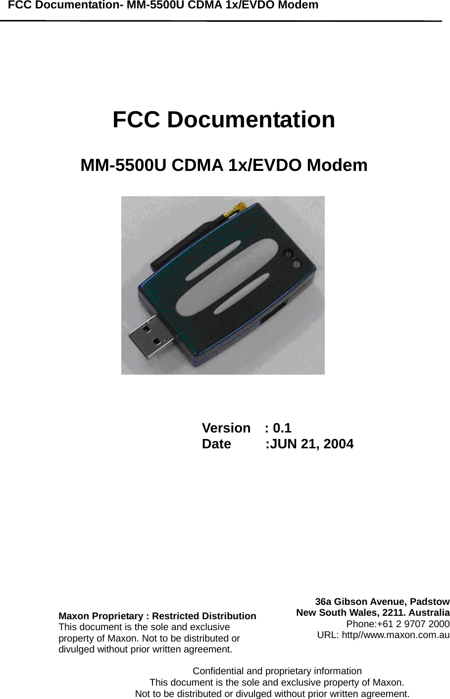
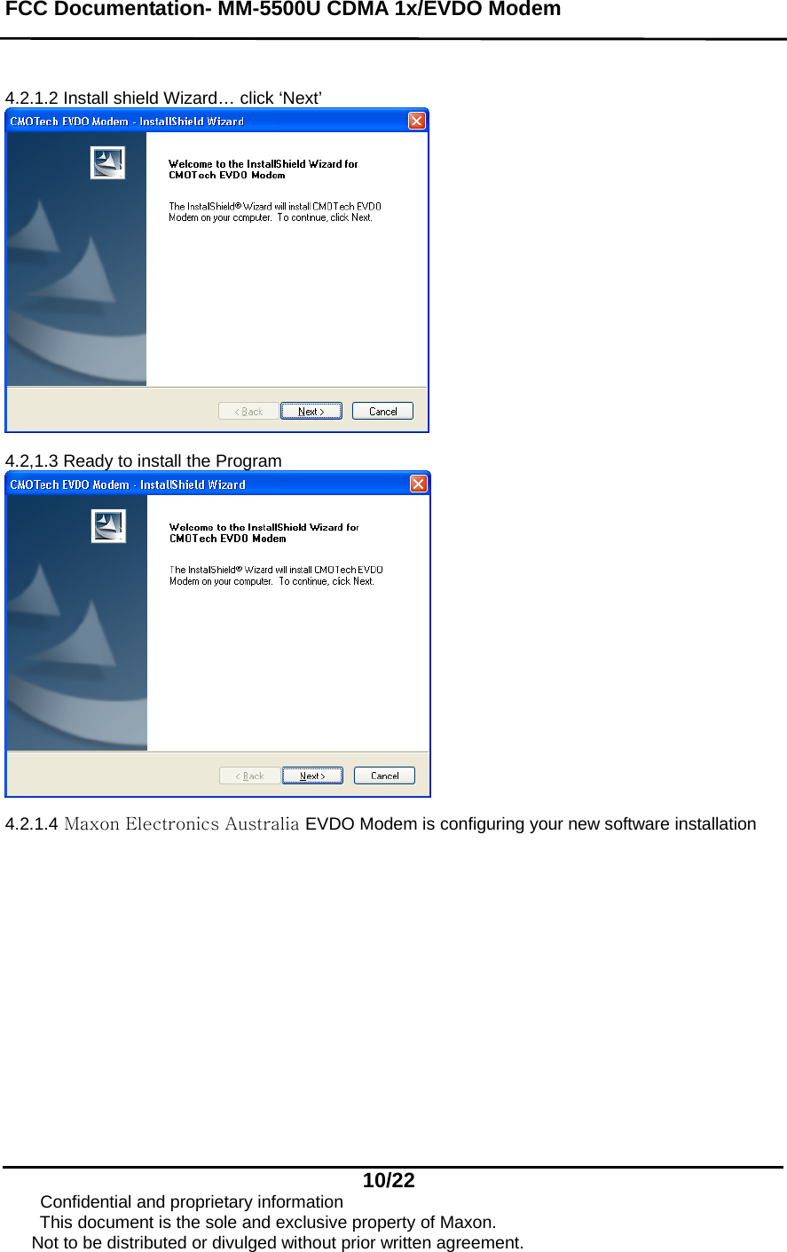
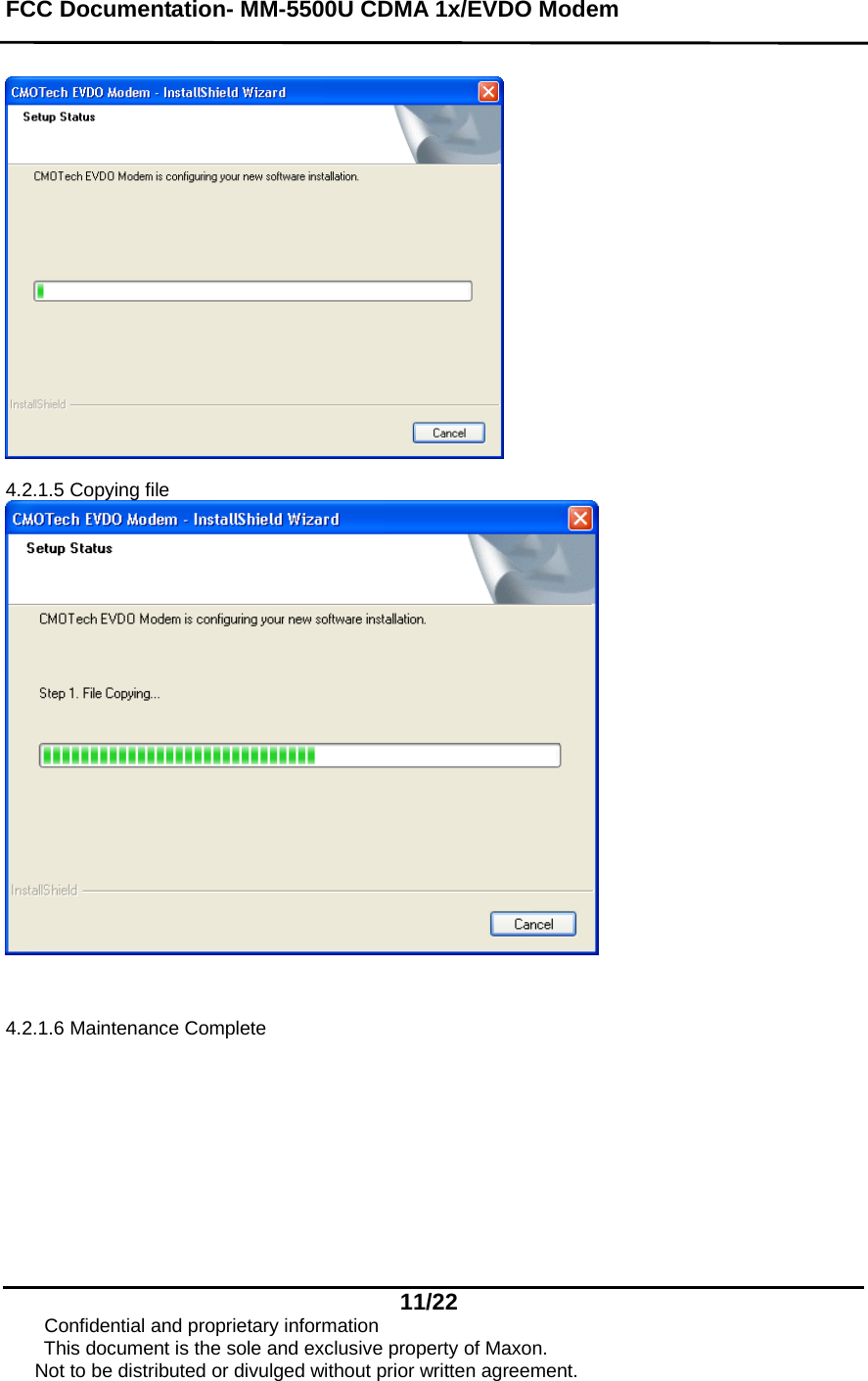
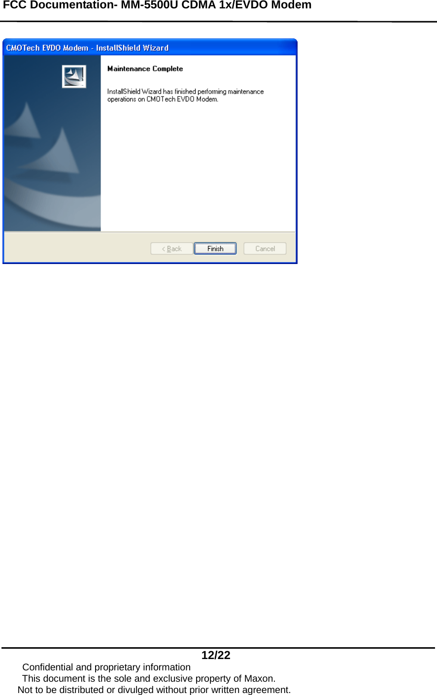
![FCC Documentation- MM-5500U CDMA 1x/EVDO Modem 5/22 Confidential and proprietary information This document is the sole and exclusive property of Maxon. Not to be distributed or divulged without prior written agreement. 2. Product Overview 2.1 Overview The MM-5500U CDMA 1x/EVDO Modem is designed to merge the capabilities of 3G 1x EV standard with the high value feature sets supported by 3G 1x MC IS-2000. The MM-5500U is capable of 2.4Mbps peak data rate on the forward link and 153Kbps peak data rate on the reverse link. The MM-5500U solution enables up to a doubling of overall IS-95-A/B voice capacity and new, higher-data-rate services. 2.2 What is the MM-5500U CDMA 1x/EVDO Modem - IS-95A/B, cdma2000-1X and EVDO CDMA Protocol Support - Remote controlled by AT commands - Data transmission up to 2.4Mbps [forward link], 153Kbps [reverse link] - LED indicating of the modem status 2.3 Supplied accessories - MM-5500U CDMA 1x/EVDO Modem (1) - Ear-piece assembly (1) - USB interface cable assembly (1) - Deriver CD (1)](https://usermanual.wiki/Maxon-Electronics-Australia/MM-5500U/User-Guide-459792-Page-5.png)