Meru Networks AP822E Dual Radio Access Point User Manual Hardware Specification
Meru Networks Inc. Dual Radio Access Point Hardware Specification
Contents
- 1. Hardware Specification
- 2. User Manual
- 3. HW specification
Hardware Specification
Source Organization:
::
:
USI CVS2/RD2/NS DOC NO.:
Original Effective Date:
::
:
01-09-2014
AP832e / AP832i /AP822e /AP822i
Hardware
Specification
PAGE 1 OF 10
機密等級: 機密
Confidential Level:
Confidential USI Controlled Document
Document Title(文件名稱
文件名稱文件名稱
文件名稱) :
AP832e /AP832i & AP822e /AP822i
Hardware Specification
Document Number(文件編號
文件編號文件編號
文件編號):
Revision(文件版本
文件版本文件版本
文件版本): A1.0
Revise Date: 01-09-2014
Prepared by(撰寫者
撰寫者撰寫者
撰寫者):
Create by which Unit(制定單位
制定單位制定單位
制定單位) : USI CVS2/RD2/NS

Source Organization:
::
:
USI CVS2/RD2/NS DOC NO.:
Original Effective Date:
::
:
01-09-2014
AP832e / AP832i /AP822e /AP822i
Hardware
Specification
PAGE 2 OF 10
Amendment Records
Item:
Date: Revision:
Page: Change Description: Changed by:
1
01/09/2014
A1.0 ALL Initial Release Paul

Source Organization:
::
:
USI CVS2/RD2/NS DOC NO.:
Original Effective Date:
::
:
01-09-2014
AP832e / AP832i /AP822e /AP822i
Hardware
Specification
PAGE 3 OF 10
TABLE OF CONTENTS
1 PURPOSE...................................................................................................................................... 4
2 OVERVIEW.................................................................................................................................... 4
3 HARDWARE DESIGN ................................................................................................................. 4
3.3.1
CPU................................................................................................................................5
3.3.2
SDRAM...........................................................................................................................5
3.3.3
FLASH............................................................................................................................5
3.3.4
GIGA PHY ......................................................................................................................5
3.3.5
CLOCK AND RESET......................................................................................................5
3.3.6
WATCHDOG TIMER ......................................................................................................6
3.3.7
LED FUNCTION .............................................................................................................6
3.3.8
GPIO DEFINE.................................................................................................................6
3.3.9
IRQ DEFINITIONS..........................................................................................................7
3.3.10
UART..............................................................................................................................7
3.3.11
JTAG ..............................................................................................................................7
3.3.12
PCIE INTERFACE..........................................................................................................7
3.3.13
USB INTERFACE...........................................................................................................7
3.3.14
POWER SUPPLY...........................................................................................................7
3.3.15
POWER REQUIREMENT...............................................................................................7
3.3.16
PHYSICAL DIMENSIONS...............................................................................................8
3.3.17
ENVIRONMENTAL REQUIREMENTS............................................................................8
3.3.18
RELIABILITY REQUIREMENTS.....................................................................................9
4 REGULATORY COMPLIANCE REQUIREMENTS ................................................................ 9
4.1.1
ETHERNET STANDARDS..............................................................................................9
4.1.2
SAFETY..........................................................................................................................9
4.1.3
UNINTENTIONAL RADIATION STANDARD ..................................................................9
4.1.4 INTENTIONAL RADIATION STANDARD..............................................................................9
4.1.5
DYNAMIC FREQUENCY SELECTION(DFS)................................................................10
4.1.6
ENVIRONMENTAL COMPLIANCE REQUIREMENTS .................................................10
4.1.7
TIER 1 COUNTRIES.....................................................................................................10
4.1.8
TIER 2 COUNTRIES.....................................................................................................10
Source Organization:
::
:
USI CVS2/RD2/NS DOC NO.:
Original Effective Date:
::
:
01-09-2014
AP832e / AP832i /AP822e /AP822i
Hardware
Specification
PAGE 4 OF 10
1 PURPOSE
The AP832e/AP832i & AP822e/AP822i is designed to serve the following purposes:
• WiFi 802.11a/b/g/n AP solution
• 802.11ac high data rate solution
• Indoor AP
2 Overview
The AP832e/AP832i & AP822e/AP822i is designed with the following features:
• Freescale P1020NSE2HFB 800MHz
• IEEE802.3at POE compliance
• 12V DC power adaptor ( <15.5W with 1.65mm DC jack)
• 2x Giga LAN port.
• One console port supported by phone jack.
• Flash: 1pcs 32Mbytes x 16 ( optional 64MB x 16)
• DDRIII: 2 pcs 64Mx16x2 bit => 256Mbytes/ 32bits
• Comply with ROHS
3 Hardware Design
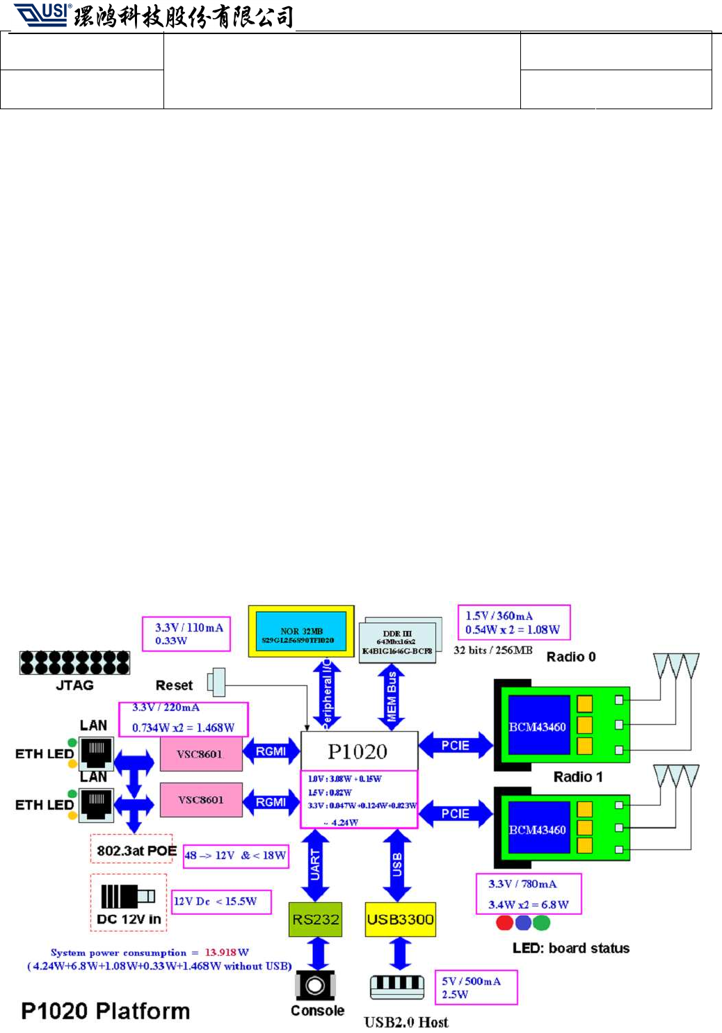
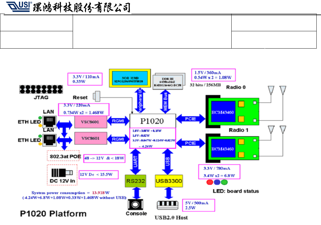
3.1 System Block Diagram for AP832e/AP832i
Source Organization:
::
:
USI CVS2/RD2/NS DOC NO.:
Original Effective Date:
::
:
01-09-2014
AP832e / AP832i /AP822e /AP822i
Hardware
Specification
PAGE 5 OF 10
3.2 System Block Diagram for AP822e/AP822i
3.3 Design Features
3.3.1 CPU
• Freescale CPU, P1020NSE2HFB (including the security engine) must be used and
configured to operate its core at 800 MHz and DDR3 memory at 667MT/s.
3.3.2 SDRAM
• 256MB DDR3 Memory with two 64x16x8 memory devices and configured in 32 bit
wide with optional ability to increase to 512MB at a future time without PCB re-spin
required.
3.3.3 FLASH
• 32MB parallel NOR Flash in one physical device with optional ability to increase to
64MB at a future time without PCB re-spin required. The device must be Spansion
S29GL256S90TFI020 or compatible and configured in 16 bit wide..
3.3.4 Giga PHY
• The hardware design must be equipped with two Gigabit Ethernet interfaces with
shielded RJ-45 connectors, each designed with one Vitesse VSC8601 (1GbE PHY).
Only one provides PoE. The PHY must support software to control LED functions (link,
activity, etc…) and support software to disable LEDs completely.
3.3.5 CLOCK AND RESET
• A 66.66MHz oscillator will be used to provide the clock for P1020NSE2HFB
• A reset chip will be used to provide the power on reset.
Source Organization:
::
:
USI CVS2/RD2/NS DOC NO.:
Original Effective Date:
::
:
01-09-2014
AP832e / AP832i /AP822e /AP822i
Hardware
Specification
PAGE 6 OF 10
• A push button is connected to a GPIO line of the processor to restore to defaults
configurations.
3.3.6 Watchdog Timer
• The hardware design must provide a watchdog circuit, either internal to CPU or by
external logic that should generate a board-wide hardware reset if not ticked in 10 to
20 seconds, provide CPU the status indicating either power-on reset or waterdog reset,
and allow CPU reset this status back to default, power-on reset.
3.3.7 LED function
• The hardware design must support one Board Status LED in Red Green Blue tri-color
to show the status of the AP and each individual color is turned ON/OFF by software
through a GPIO.
• On each Ethernet RJ45, the hardware design should provide two integrated LEDs,
one Green and one Amber and connect Green and Amber LED to LED1 and LED2 of
VSC8601 respectively. Green LED on the left is ON when the link is established and is
Blinking when the link is up and transmitting and receiving and the right Amber LED is
OFF for half duplex or no link and is ON for full-duplex and the link is up. Both LEDs
should be directly controlled by Ethernet PHY and should allow software override to
turn both LEDs OFF either indirectly through PHY registers or directly through GPIOs.
3.3.8 GPIO define
GPIOs Description Direction
Default
State Active
GPIO_0 Detect 802.3at POE source Input High Low
GPIO_1 Press restore to default
configuration button Input High Low
GPIO_2 Enable USB power Output Low High
GPIO_3 USB_FLAG status Input High Low
GPIO_4 Power on miniPCIE P2 interface Output High High
GPIO_5 reserved
GPIO_6 Status Blue LED Output High Low
GPIO_7 Status Red LED Output High Low
GPIO_8 Status Green LED Output High Low
GPIO_9 Hard reset miniPCIE P1 Output High Low
GPIO_10 Hard reset miniPCIE P2 Output High Low
GPIO_11 Detect DC adaptor Input High Low
GPIO_12 Hard reset Ethernet PHY1 only,
connecting to PHY1’s Hardware
Reset pin after ORing with
Power-On-Reset#, PHY1 is
connected to CPU’s SGMII1 and
not support PoE
Output High Low
Source Organization:
::
:
USI CVS2/RD2/NS DOC NO.:
Original Effective Date:
::
:
01-09-2014
AP832e / AP832i /AP822e /AP822i
Hardware
Specification
PAGE 7 OF 10
GPIO_13 Hard reset Ethernet PHY2 and
PHY1, connecting to PHY2’s
Hardware Reset pin after ORing
with Power-On-Reset#, PHY2 is
connected to CPU’s SGMII2 and
support PoE
Output High Low
3.3.9 IRQ Definitions
IRQs Description
IRQ00 reserved
IRQ01 IRQ for TSEC3’s PHY
IRQ02 IRQ for TSEC1’s PHY
IRQ03 reserved
IRQ04 reserved
IRQ05 reserved
IRQ06 reserved
3.3.10 UART
• One UART RS-232 console port support phone jack and pin header link. A 3.3V
RS-232 transceiver will be used.
3.3.11 JTAG
• To connect ICE debuggers, a JTAG connector must be provided internal to the
enclosure and should be a stuff option when in MP production.
3.3.12 PCIE INTERFACE
• The hardware design must provide two miniPCIe interfaces which capable of
supporting full size miniPCIe card.
3.3.13 USB INTERFACE
• The hardware design must provide one USB Host port with shielded vertical-mount
standard type-A USB receptacle connector. The port should supply current up to
500mA at 5V nominal as per USB2.0 specification
3.3.14 POWER SUPPLY
• Support POE/DC adapter supply, internal DC/DC generates 12V, 5V, 3.3V, 1.0V, 1.5V
and 0.75V voltage for chip used.
3.3.15 POWER REQUIREMENT
• The PoE must comply with 802.3at and electrically isolate from the AP chassis. The
maximum load on PoE input must be no more than 18W for the full system in the

Source Organization:
::
:
USI CVS2/RD2/NS DOC NO.:
Original Effective Date:
::
:
01-09-2014
AP832e / AP832i /AP822e /AP822i
Hardware
Specification
PAGE 8 OF 10
maximum configuration.
• Support for 12V DC power supplied externally via optional country specific AC to DC
adapter kits. The maximum load on DC input must be no more than 15.5W. The 12V
DC adaptors must be compatible with 1.65mm DC jack.
• The design must allow PoE and DC co-existent, but providing power redundancy is
not required.
• The design must provide a GPIO indicating the power source, either DC or PoE and
another GPIO indicating the PoE power source, either 802.3at or 802.3af.
• Within the power budget, 12.95W of 802.3af, the design must be able to power up the
full system in the configuration of two 3x3 3-stream Radios (both in 5GHz with 80MHz
channel bandwidth), the USB with 500mA-disabled, the LAN w/ PoE ( G1)port served
as the uplink port and the other LAN port (G2)with traffic in worst case, CPU operated
at 800MHz, and DDR3 operated at 667MT/s.
• Within the power budget, 25.5W of 802.3at, the design must be able to power up the
full system for all the interfaces in the configuration of two 3x3 3-stream Radios (both
in 5GHz with 80MHz channel bandwidth), the USB with 500mA enabled, the “G1” port
served as the uplink port and the “G2” port with traffic in worst case, CPU operated at
800MHz, and DDR3 operated at 667MT/s.
• The design and the DC adaptor must be able to power up the full system for all the
interfaces in the configuration of two 3x3 3-stream Radios (both in 5GHz with 80MHz
channel bandwidth), the USB with 500mA-enabled, the “G1” port served as the uplink
port and the “G2” port with traffic in worst case, CPU operated at 800MHz, and DDR3
operated at 667MT/s.
3.3.16 Physical Dimensions
• The Main Board must be exactly the same as AP332’s in dimension, all mounting hole
locations, all IO port’s locations, both radio card locations, and the locations of CPU,
both Ethernet PHYs, and DDR3 memory to leverage the enclosure design of AP332
completely.
• AP332 dimension: Can’t be larger than 5.75” x 5.75”, and must fully enclose both
miniPCIe radio cards. Both Ethernet RJ45 connectors, USB type-A connector, DC jack,
and Configuration Restored-to-Defaults Button, all should be top-entry type to allow
access from the bottom enclosure for either non-metallic enclosure for internal
antennas or metallic enclosure for external antennas.
3.3.17 Environmental Requirements
• Operating temperature: 0 to +50°C for indoor

Source Organization:
::
:
USI CVS2/RD2/NS DOC NO.:
Original Effective Date:
::
:
01-09-2014
AP832e / AP832i /AP822e /AP822i
Hardware
Specification
PAGE 9 OF 10
• Operating humidity: 5 to 95 percent (non-condensing)
• Non-operating (storage) temperature: -40 to +70°C
• Non-operating (storage) humidity: 5 to 95 percent (non-condensing)
3.3.18 Reliability Requirements
• MTBF must be at least 43,800 hours at 50C for the AP calculated using the Telcordia
SR-332 method and provide MTBF at 25C, too.
4 Regulatory Compliance Requirements
4.1.1 Ethernet Standards
• Ethernet IEEE 802.3
• Power Over Ethernet IEEE 802.3at
• Wireless IEEE 802.11a/b/g /n/ac
4.1.2 Safety
• UL 60950-1, 2nd Edition, 2007-03-27
• CSA C22.2 No. 60950-1-07, 2nd Edition, 2007-03
• EN 60950-1:2006+A12:2011
• IEC 60950-1:2005 Second Edition
4.1.3 Unintentional radiation Standard
• FCC Part 15.107 - 47CFR15.107 October 1, 2008 Class B
• FCC Part 15.109 - 47CFR15.109 October 1, 2008 Class B
• ICES-003 Class B – issue 4, February 2004
• EN 301 489-1
• EN 301 489-17
• EN55022 Class B – 2006
• EN55024 / AS/NZS CISPR 24 / Immunity
• EN61000-4-2 Electrostatic Discharge (ESD): Performance Criterion B.
• EN61000-4-3 Radiated Electromagnetic Fields (RS): Performance Criterion A.
• EN61000-4-4 Electrical Fast Transient / Burst (EFT): Performance Criterion B.
• EN61000-4-5 Lightning Surge Attachment: Performance Criterion B.
• EN61000-4-6 Conducted Radio Frequency Disturbances (CS): Performance Criterion
A.
• Japan VCCI Class B
4.1.4 intentional radiation Standard
• FCC Part 15.247 - 47 CFR Ch. I (10–1–00 Edition) (2400 – 2483.5 MHz and 5725 -

Source Organization:
::
:
USI CVS2/RD2/NS DOC NO.:
Original Effective Date:
::
:
01-09-2014
AP832e / AP832i /AP822e /AP822i
Hardware
Specification
PAGE 10 OF 10
5850 MHz)
• FCC Part 15.407 - 47 CFR15.407 October 1, 2008
• UNII-1: 5.15–5.25 GHz
• UNII-2: 5.25–5.35 GHz
• UNII-Worldwide: 5.47–5.725 GHz
• UNII-3: 5.725–5.825 GHz
• RSS-210
• EN 300 328 v1.7.1 (2006-05) Electromagnetic compatibility and Radio Spectrum
Matters (ERM)
• EN 301 893 V1.5.1 (2008-12) Broadband Radio Access Networks (BRAN)
• Japan Radio Law 38-24-1 (Ninsho)
•
4.1.5 DYNAMIC FREQUENCY SELECTION(DFS)
• Meru Engineering is responsible for DFS testing and certification. The contract
manufacturer is responsible for testing the Intentional and Unintentional radiation
testing and certification for the following standards
• FCC Part 15.407 DFS bands (5.25 – 5.35 GHz and 5.47 – 5.725 GHz)
• CE (ESTI) standard EN 301 893 v 1.5.1 testing in the5.25 – 5.35 GHz and 5.47 –
5.725 GHz bands.
4.1.6
Environmental Compliance Requirements
• ROHS, Directive 2002/95/EC on the restriction of the use of certain hazardous
substances in electrical and electronic equipment
• WEEE, Directive 2002/96/EC on waste electrical and electronic equipment
• REACH, Regulation (EC) No 1907/2006 concerning the Registration, Evaluation,
Authorization and Restriction of Chemicals
4.1.7 Tier 1 countries
• US
• Canada
• EU
• Japan
4.1.8 Tier 2 countries
• Australia
• China

Source Organization:
::
:
USI CVS2/RD2/NS DOC NO.:
Original Effective Date:
::
:
01-09-2014
AP832e / AP832i /AP822e /AP822i
Hardware
Specification
PAGE 11 OF 10
• Egypt
• Hong Kong
• India
• Indonesia
• Jordan
• Kuwait
• Lebanon
• Malaysia
• Mexico
• New Zealand
• Oman
• Philippines
• Qatar
• Russia
• Saudi Arabia
• Singapore
• South Africa
• South Korea
• Taiwan
• Thailand
• UAE
• Vietnam