MICROCHIP TECHNOLOGY A090665 ATZB-24-B0 2.4GHz B0, 802.15.4/Zigbee OEM- Module User Manual ZigBit 2 4 GHz Wireless Modules ATZB 24 A2 B0
Atmel Norway AS ATZB-24-B0 2.4GHz B0, 802.15.4/Zigbee OEM- Module ZigBit 2 4 GHz Wireless Modules ATZB 24 A2 B0
Contents
- 1. User Manual techn
- 2. User Manual Cert guide
User Manual techn
![IntroductionZigBit™ 2.4 GHz Wireless Modules 1-48226C–MCU Wireless–09/101.6 Related Documents[1] Atmel 8-bit AVR Microcontroller with 64K/128K/256K Bytes In-System Programmable Flash. 2549FAVR 04/06[2] Atmel Low-Power Transceiver for ZigBee Applications. AT86RF230 datasheet. doc5131.pdf[3] IEEE Std 802.15.4-2003 IEEE Standard for Information technology - Part 15.4 Wireless MediumAccess Control (MAC) and Physical Layer (PHY) Specifications for Low-Rate Wireless Personal AreaNetworks (LR-WPANs)[4] ZigBee Specification. ZigBee Document 053474r17, October 19, 2007[5] BitCloud™ IEEE 802.15.4/ZigBee Software. AVR2050: BitCloud User Guide. Atmels doc8199.pdf[6] ZigBit™ Development Kit. User's Guide. MeshNetics Doc. S-ZDK-451 - TBD](https://usermanual.wiki/MICROCHIP-TECHNOLOGY/A090665.User-Manual-techn/User-Guide-1460895-Page-7.png)
![ZigBit™ 2.4 GHz Wireless Modules 2-58226C–MCU Wireless–09/10Section 2Zigbit™ Module Overview2.1 OverviewZigBit is a low-power, high-sensitivity IEEE 802.15.4/ ZigBee-compliant OEM module. This multi-func-tional device occupies less than a square inch of space, which is comparable to a typical size of a singlechip. Based on a solid combination of Atmel’s latest MCU Wireless hardware platform [1], the ZigBitoffers superior radio performance, ultra-low power consumption, and exceptional ease of integration.Figure 2-1. ATZB-24-B0 Block DiagramFigure 2-2. ATZB-24-A2 Block DiagramATmega1281AT86RF230RFTransceiverVCC (1.8 - 3.6V)RF I/OGPIO SPI BusIRQUARTUSART/SPII2CJTAGANALOGATmega1281AT86RF230RFTransceiverVCC (1.8 - 3.6V)GPIO SPI BusIRQUARTUSART/SPII2CJTAGANALOGChipAntenna](https://usermanual.wiki/MICROCHIP-TECHNOLOGY/A090665.User-Manual-techn/User-Guide-1460895-Page-8.png)
![Zigbit™ Module OverviewZigBit™ 2.4 GHz Wireless Modules 2-68226C–MCU Wireless–09/10ZigBit modules comply with the FCC (Part 15), IC and ETSI (CE) rules applicable to the devices radiat-ing in uncontrolled environment. For details, see “Agency Certifications” on page 4-22.ZigBit fully satisfies the requirements of the “Directive 2002/95/EC of the European Parliament and theCouncil of 27January 2003 on the restriction of the use of certain hazardous substances in electrical andelectronic equipment” (RoHS). Atmel provides fully compliant product in all regions where the directive isenforced since July 1, 2006.ZigBit contains Atmel’s ATmega1281V Microcontroller [1] and AT86RF230 RF Transceiver [2]. The mod-ule features 128 Kbytes flash memory and 8 Kbytes RAM.The ZigBit already contains a complete RF/MCU-related design with all the necessary passive compo-nents included. The module can be easily mounted on a simple 2-layer PCB. Compared to a customRF/MCU design, a module-based solution offers considerable savings in development time and NREcost per unit during the design, prototyping, and mass production phases of product development.Innovative (patent-pending) dual chip antenna design in ATZB-24-A2 module eliminates the balun andachieves good performance over 2.4 GHz frequency band.To jumpstart evaluation and development, Atmel also offers a complete set of evaluation and develop-ment tools. The ZigBit Development Kit [6] (ATZB-DK-24) comes with everything you need to createcustom applications featuring ZigBit module.The kit features MeshBean development boards with an easy-to-access extension connector for attach-ing third party sensors and other peripherals, and a JTAG connector for easy application uploading anddebugging.The kit also includes reference applications to speed up application development, source code for hard-ware interface layer and reference drivers for the all the module interfaces, intuitive developmentenvironment from Atmel, and comprehensive set of application notes and product documentation.ZigBit modules comes bundled with BitCloud, a 2nd generation embedded software stack from Atmel.BitCloud is fully compliant with ZigBee PRO and ZigBee standards for wireless sensing and control [3],[4], [5] and it provides an augmented set of APIs which, while maintaining 100% compliance with thestandard, offer extended functionality designed with developer's convenience and ease-of-use in mind.Depending on end-user design requirements, ZigBit can operate as a self-contained sensor node, whereit would function as a single MCU, or it can be paired with a host processor driving the module over aserial interface. In the former case, a user application may be used with the BitCloud software allowingcustomization of embedded applications through BitCloud’s C API.In the latter case, the host processor controls data transmission and manages module peripherals via anextensive set of SerialNet AT commands. Thus, no firmware customization is required for a successfulmodule design-in. Additionally, third-party sensors can be connected directly to the module, thusexpanding the existing set of peripheral interfaces.](https://usermanual.wiki/MICROCHIP-TECHNOLOGY/A090665.User-Manual-techn/User-Guide-1460895-Page-9.png)

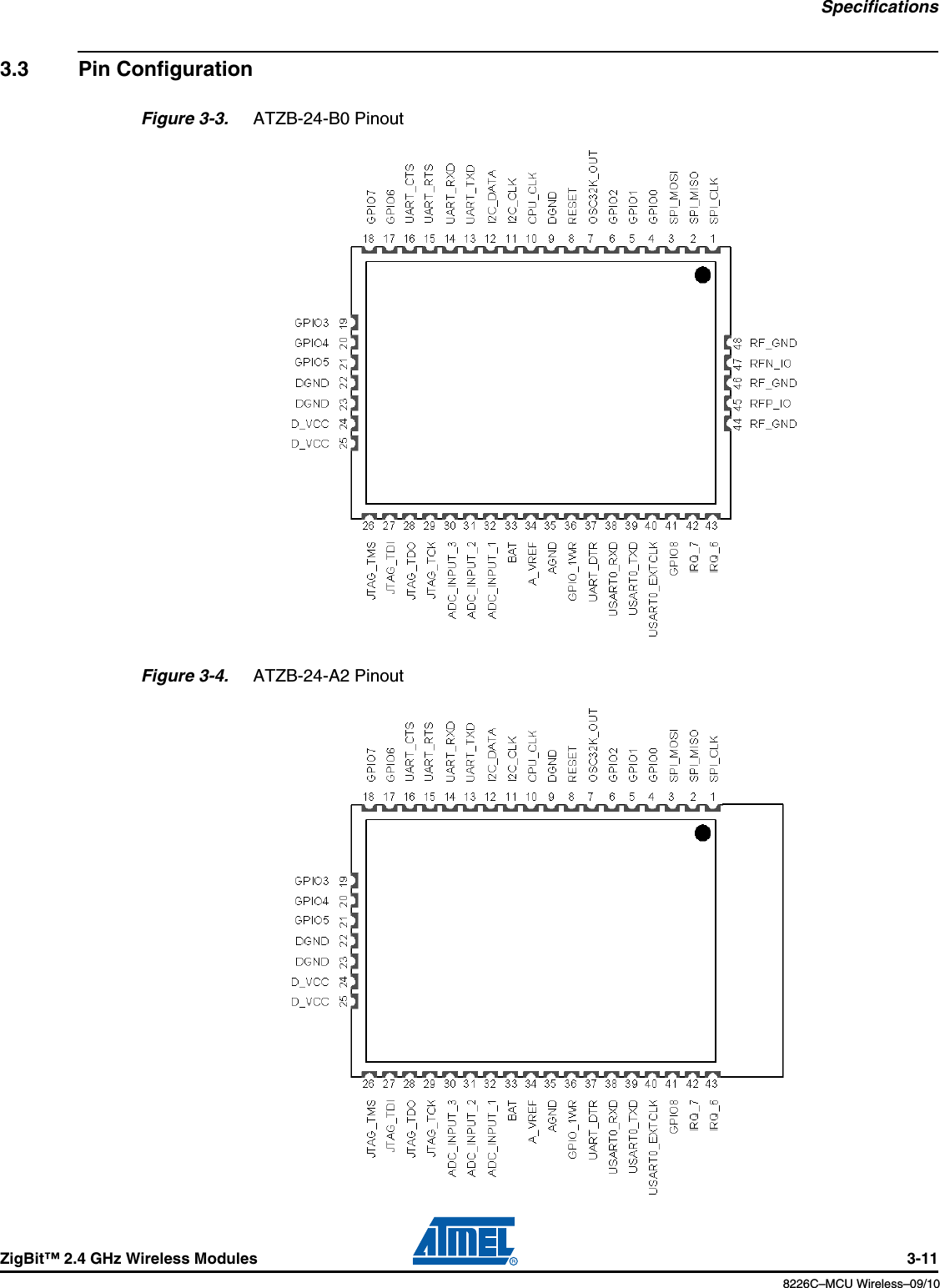
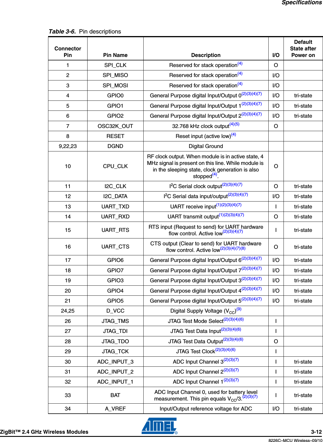
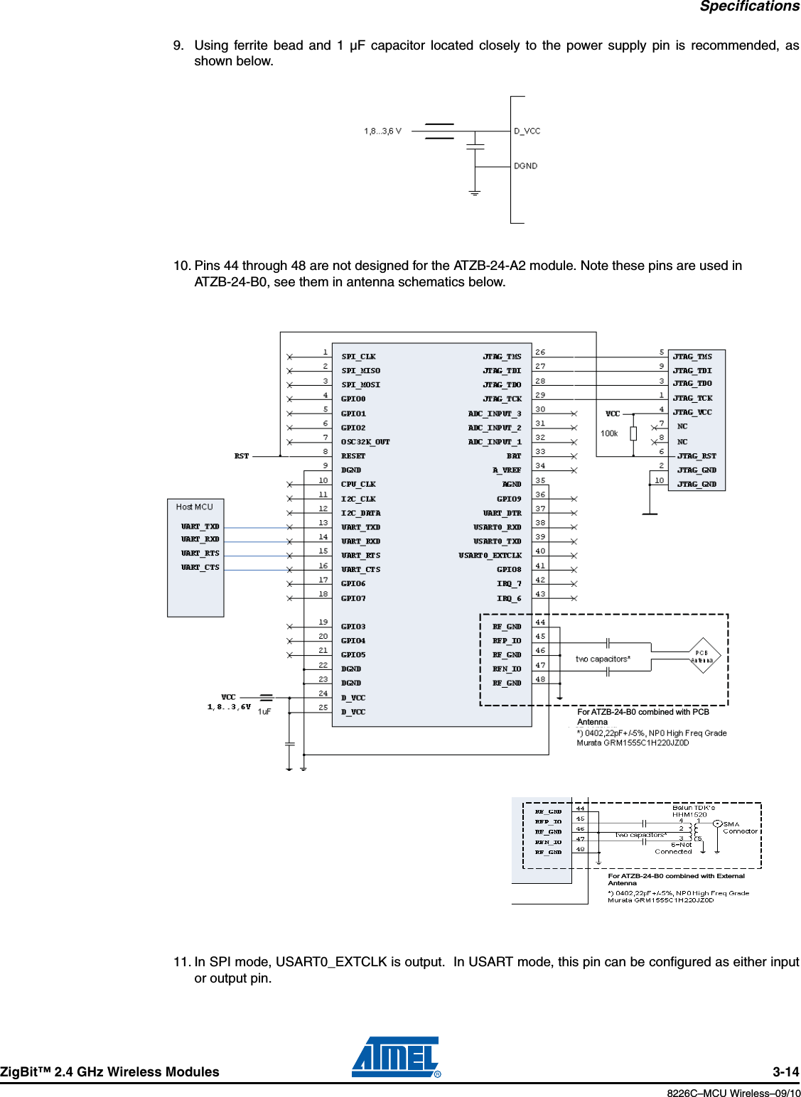
![SpecificationsZigBit™ 2.4 GHz Wireless Modules 3-138226C–MCU Wireless–09/10Notes: 1. The UART_TXD pin is intended for input (i.e. its designation as "TXD" implies some complex systemcontaining ZigBit as its RF terminal unit), while UART_RXD pin, vice versa, is for output.2. Most of pins can be configured for general purpose I/O or for some alternate functions as described indetails in the ATmega1281V Datasheet [1].3. GPIO pins can be programmed either for output, or for input with/without pull-up resistors. Output pindrivers are strong enough to drive LED displays directly (refer to figures on pages 387-388, [1]).4. All digital pins are provided with protection diodes to D_VCC and DGND5. It is strongly recommended to avoid assigning an alternate function for OSC32K_OUT pin because it isused by BitCloud. However, this signal can be used if another peripheral or host processor requires32.768 kHz clock, otherwise this pin can be disconnected.6. Normally, JTAG_TMS, JTAG_TDI, JTAG_TDO, JTAG_TCK pins are used for on-chip debugging andflash burning. They can be used for A/D conversion if JTAGEN fuse is disabled.7. The following pins can be configured with the BitCloud software to be general-purpose I/O lines:GPIO0, GPIO1, GPIO2, GPIO3, GPIO4, GPIO5, GPIO6, GPIO7, GPIO8, GPIO_1WR, I2C_CLK,I2C_DATA, UART_TXD, UART_RXD, UART_RTS, UART_CTS, ADC_INPUT_3, ADC_INPUT_2,ADC_INPUT_1, BAT, UART_DTR, USART0_RXD, USART0_TXD, USART0_EXTCLK, IRQ_7, IRQ_6.Additionally, four JTAG lines can be programmed with software as GPIO as well, but this requireschanging the fuse bits and will disable JTAG debugging.8. With BitCloud, CTS pin can be configured to indicate sleep/active condition of the module thus provid-ing mechanism for power management of host processor. If this function is necessary, connection ofthis pin to external pull-down resistor is recommended to prevent the undesirable transients duringmodule reset process.35 AGND Analog ground36 GPIO_1WR 1-wire interface(2)(3)(4)(7) I/O37 UART_DTR DTR input (Data Terminal Ready) for UART. Active low(2)(3)(4)(7) I tri-state38 USART0_RXD USART/SPI Receive pin(2)(3)(4)(7) I tri-state39 USART0_TXD USART /SPI Transmit pin(2)(3)(4)(7) O tri-state40 USART0_EXTCLK USART/SPI External Clock(2)(3)(4)(7)(11) I/O tri-state41 GPIO8 General Purpose Digital Input/Output I/O tri-state42 IRQ_7 Digital Input Interrupt request 7(2)(3)(4)(7) I tri-state43 IRQ_6 Digital Input Interrupt request 6(2)(3)(4)(7) I tri-state44,46,48 RF GND RF Analog Ground(2)(3)(4)(7)45 RFP_IO Differential RF Input/Output(10) I/O47 RFN_IO Differential RF Input/Output(10) I/OTable 3-6. Pin descriptionsConnector Pin Pin Name Description I/ODefault State after Power on](https://usermanual.wiki/MICROCHIP-TECHNOLOGY/A090665.User-Manual-techn/User-Guide-1460895-Page-16.png)


![Agency CertificationsZigBit™ 2.4 GHz Wireless Modules 4-248226C–MCU Wireless–09/104.3 Approved Antenna ListATZB-24-A2 Module works with integrated dual chip antenna. The design of the antenna is fully compli-ant with all the aforementioned regulation.ATZB-24-B0 Module has been tested and approved for use with the antennas listed in the table below.ATZB-24-0B Module may be integrated with other custom design antennas which OEM installer mustauthorize with respective regulatory agencies.Table 4-1. Approved Antenna specificationsPart Number Manufacture and description Gain [dBi] Minimum separation [cm]2010B48-01Antenova Titanis, swivel antenna (1/4 wave antenna) with SMA connector, frequency range 2.4 - 2.5 GHz2.2 2017010.10 WiMo, swivel antenna (1/2 wave antenna) with SMA connector, frequency range 2.35 - 2.5 GHz 2.1 20](https://usermanual.wiki/MICROCHIP-TECHNOLOGY/A090665.User-Manual-techn/User-Guide-1460895-Page-27.png)