MICROCHIP TECHNOLOGY A090667 Zigbit Amp 2.4GHz, Unbalanced Output User Manual 8228
Atmel Norway AS Zigbit Amp 2.4GHz, Unbalanced Output 8228
UserManual.wiki
>
MICROCHIP TECHNOLOGY
>
A090667 User Manual
>
Manual
Contents
1.
Manual
2.
Manual-Cert Guide
Manual
Navigation menu
Upload a User Manual
Namespaces
Wiki Guide
HTML
PDF
Info
Views
User Manual
Discussion / Help
Navigation
![ZigBit™ 2.4 GHz Amplified Wireless Modules 1-18228B–MCU Wireless–06/09Section 1Introduction1.1 SummaryZigBit™ Amp is an ultra-compact, extended range, low-power, high-sensitivity 2.4GHzIEEE 802.15.4/ZigBee® OEM module from Atmel. Based on the innovative Atmel's mixed-signal hard-ware platform, this module is enhanced by an output power amplifier and an input low-noise amplifier,and is designed for wireless sensing, monitoring & control and data acquisition applications. ZigBit Ampmodules eliminate the need for costly and time-consuming RF development, and shortens time to mar-ket for wireless applications with extended range requirements.Two different versions of ZigBit 2.4 GHz Amplified modules are available: ATZB-A24-UFL with built-inU.FL antenna connector and the ATZB-A24-U0 with unbalanced RF output. These modules are an addi-tion to the ZigBit family represented by ATZB-24-A2 and ATZB-24-B0. In addition Atmel offer the ZigBit900 MHz Wireless Module ATZB-900-B0 [2].1.2 ApplicationsZigBit module is compatible with robust IEEE 802.15.4/ZigBee stack that supports a self-healing, self-organizing mesh network, while optimizing network traffic and minimizing power consumption. Atmeloffers two stack configurations: BitCloud and SerialNet. BitCloud is a ZigBee PRO certified softwaredevelopment platform supporting reliable, scalable, and secure wireless applications running on Atmel’sZigBit modules. SerialNet allows programming of the module via serial AT-command interface.The applications include, but are not limited to:•Building automation & monitoring– Lighting controls– Wireless smoke and CO detectors– Structural integrity monitoring•HVAC monitoring & control•Inventory management•Environmental monitoring•Security•Water metering•Industrial monitoring– Machinery condition and performance monitoring– Monitoring of plant system parameters such as temperature, pressure, flow, tank level, humidity, vibration, etc.•Automated meter reading (AMR)01/12D](https://usermanual.wiki/MICROCHIP-TECHNOLOGY/A090667.Manual/User-Guide-1616296-Page-4.png)
![IntroductionZigBit™ 2.4 GHz Amplified Wireless Modules 1-48228B–MCU Wireless–06/091.6 Related Documents[1] ZigBit™ 2.4 GHz Wireless Modules ATZB-24-B0/A2. Product datasheet. Atmel’s doc8226.pdf[2]. ZigBit™ 700/800/900 MHz Wireless Modules ATZB-900-B. Product datasheet. Atmel’s doc8227.pdf[3] ZigBit™ Development Kit. User's Guide. MeshNetics Doc. S-ZDK-451~01[4] Atmel 8-bit AVR Microcontroller with 64K/128K/256K Bytes In-System Programmable Flash. 2549FAVR 04/06[5] Atmel Low-Power Transceiver for ZigBee Applications. AT86RF230 datasheet. doc5131.pdf[6] Ultra Small Surface Mount Coaxial Connectors - Low Profile 1.9mm or 2.4mm Mated Height.http://www.hirose.co.jp/cataloge_hp/e32119372.pdf [7] ZigBit™ Amp Development Kit. User's Guide. MeshNetics Doc. S-ZDK-451~02[8] IEEE Std 802.15.4-2003 IEEE Standard for Information technology - Part 15.4 Wireless MediumAccess Control (MAC) and Physical Layer (PHY) Specifications for Low-Rate Wireless Personal AreaNetworks (LR-WPANs)[9] ZigBee Specification. ZigBee Document 053474r17, October 19, 2007[10] BitCloud™ IEEE 802.15.4/ZigBee Software. Product User Guide. Atmel’s doc8199.pdf01/12D](https://usermanual.wiki/MICROCHIP-TECHNOLOGY/A090667.Manual/User-Guide-1616296-Page-7.png)
![ZigBit™ 2.4 GHz Amplified Wireless Modules 2-58228B–MCU Wireless–06/09Section 2Zigbit™ Module Overview2.1 OverviewZigBit™ Amp is an extended-range, low-power, high sensitivity IEEE 802.15.4/ZigBee OEM module,which occupies less than a square inch of space. Based on a solid combination of Atmel's latest MCUWireless hardware platform, power amplifier and low-noise amplifier, the ZigBit Amp offers anunmatched combination of superior radio performance, ultra-low power consumption and exceptionalease of integration.Figure 2-1. ATZB-A24-UFL/UN Block DiagramZigBit Amp modules contains Atmel's ATmega1281V Microcontroller [4] and AT86RF230 RF Trans-ceiver [5]. The module features 128K bytes flash memory and 8K bytes RAM.The compact all-in-one-chip integration of output Power Amplifier and input Low-Noise Amplifier, alongwith RF switches enables digital control of an external RF front-end to dramatically improve ZigBit'srange performance on signal transmission and increase its sensitivity. This ensures stable connectivitywith larger coverage area without significant increase in module size. The HF U.FL coaxial connector [6]used in the ATZB-A24-UFL module enables the user to choose appropriate external antenna for everytype of application.ZigBit Amp already contains a complete RF/MCU design with all the necessary passive componentsincluded. The module can be easily mounted on a simple 2-layer PCB with a minimum of required exter-nal connection. Compared to a custom RF/MCUsolution, a module-based solution offers considerablesavings in development time and NRE cost per unit during the design, prototyping, and mass productionphases of product development.ATmega1281AT86RF230RFTransceiverVCC (1.8 - 3.6V)GPIO SPI BusIRQUARTUSART/SPII2CJTAGANALOGSW SWLNAPARFI/OAntenna001/12D](https://usermanual.wiki/MICROCHIP-TECHNOLOGY/A090667.Manual/User-Guide-1616296-Page-8.png)
![Zigbit™ Module OverviewZigBit™ 2.4 GHz Amplified Wireless Modules 2-68228B–MCU Wireless–06/09To jumpstart evaluation and development, Atmel also offers a complete set of evaluation and develop-ment tools. The new ZigBit Amp Development Kit [7] (ATZB-DK-A24) comes with everything you need tocreate custom applications featuring ZigBit Amp module.The kit features MeshBean development boards with an easy-to-access extension connector for attach-ing third party sensors and other peripherals, and a JTAG connector for easy application uploading anddebugging.The kit also includes reference applications to speed up application development, source code for hard-ware interface layer and reference drivers for the all the module interfaces, intuitive developmentenvironment from Atmel, and comprehensive set of application notes and product tutorials.ZigBit Amp modules comes bundled with BitCloud, a 2nd generation embedded software stack fromAtmel. BitCloud is fully compliant with ZigBee PRO and ZigBee standards for wireless sensing and con-trol [7], [8], [9], and it provides an augmented set of APIs which, while maintaining 100% compliance withthe standard, offer extended functionality designed with developer's convenience and ease-of-use inmind. Depending on end-user design requirements, ZigBit Amp can operate as a self-contained sensor node,where it would function as a single MCU, or it can be paired with a host processor driving the moduleover a serial interface. In the former case, a user application may be used with the BitCloud softwareallowing customization of embedded applications through BitCloud's C API.In the latter case, the host processor controls data transmission and manages module peripherals via anextensive set of SerialNet AT commands. Thus, no firmware customization is required for a successfulmodule design-in. Additionally, third-party sensors can be connected directly to the module, thusexpanding the existing set of peripheral interfaces.01/12D](https://usermanual.wiki/MICROCHIP-TECHNOLOGY/A090667.Manual/User-Guide-1616296-Page-9.png)
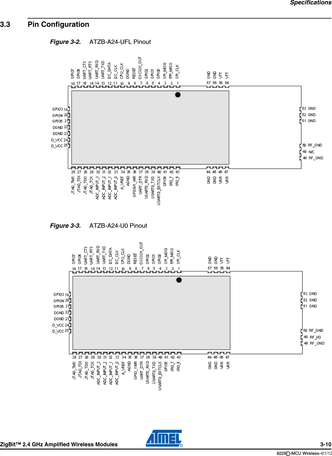
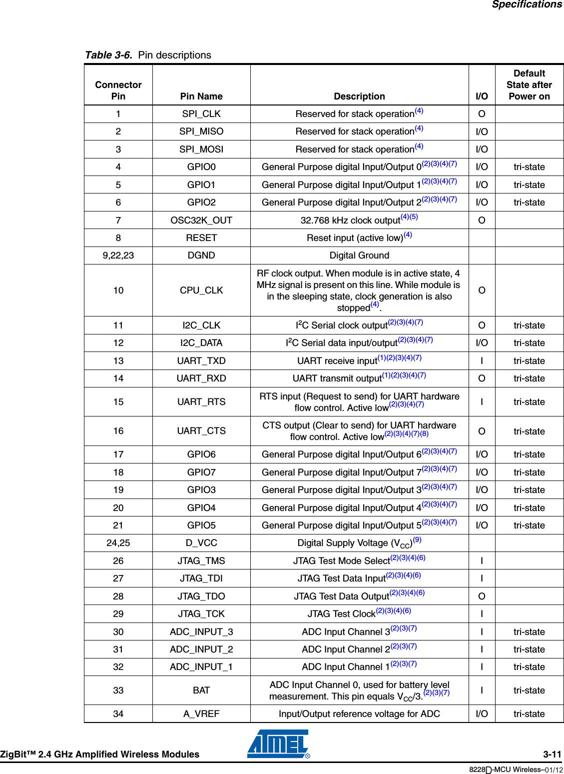
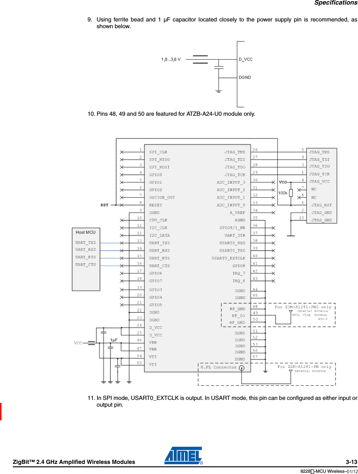
![SpecificationsZigBit™ 2.4 GHz Amplified Wireless Modules 3-128228B–MCU Wireless–06/09Notes: 1. The UART_TXD pin is intended for input (i.e. its designation as "TXD" implies some complex systemcontaining ZigBit Amp as its RF terminal unit), while UART_RXD pin, vice versa is for output.2. Most of pins can be configured for general purpose I/O or for some alternate functions as described indetails in the ATmega1281V Datasheet [3].3. GPIO pins can be programmed either for output, or for input with/without pull-up resistors. Output pindrivers are strong enough to drive LED displays directly (refer to figures on pages 387-388, [3]).4. All digital pins are provided with protection diodes to D_VCC and DGND5. It is strongly recommended to avoid assigning an alternate function for OSC32K_OUT pin because it isused by BitCloud. However, this signal can be used if another peripheral or host processor requires32.768 kHz clock, otherwise this pin can be disconnected.6. Normally, JTAG_TMS, JTAG_TDI, JTAG_TDO, JTAG_TCK pins are used for on-chip debugging andflash burning. They can be used for A/D conversion if JTAGEN fuse is disabled.7. The following pins can be configured with the BitCloud software to be general-purpose I/O lines:GPIO1, GPIO2, GPIO3, GPIO4, GPIO5, GPIO6, GPIO7, GPIO8, GPIO_1WR, I2C_CLK, I2C_DATA,UART_TXD, UART_RXD, UART_RTS, UART_CTS, ADC_INPUT_3, ADC_INPUT_2, ADC_INPUT_1,BAT, UART_DTR, USART0_RXD, USART0_TXD, USART0_EXTCLK, IRQ_7, IRQ_6. Additionally, fourJTAG lines can be programmed with software as GPIO as well, but this requires changing the fuse bitsand will disable JTAG debugging.8. With BitCloud, CTS pin can be configured to indicate sleep/active condition of the module thus provid-ing mechanism for power management of host processor. If this function is necessary, connection ofthis pin to external pull-down resistor is recommended to prevent the undesirable transients duringmodule reset process.35 AGND Analog ground36 GPIO9/1_WR General Purpose digital input/output 9 /1-wire interface(2)(3)(4)(7) I/O37 UART_DTR DTR input (Data Terminal Ready) for UART. Active low(2)(3)(4)(7) I tri-state38 USART0_RXD USART/SPI Receive pin(2)(3)(4)(7) I tri-state39 USART0_TXD USART /SPI Transmit pin(2)(3)(4)(7) O tri-state40 USART0_EXTCLK USART/SPI External Clock(2)(3)(4)(7)(11) I/O tri-state41 GPIO8 General Purpose Digital Input/Output I/O tri-state42 IRQ_7 Digital Input Interrupt request 7(2)(3)(4)(7) I tri-state43 IRQ_6 Digital Input Interrupt request 6(2)(3)(4)(7) I tri-state44,45,51,52,53,56,57 DGND Digital ground46,47 VRR Receiver supply voltage(9)48,50 RF GND RF Analog Ground(2)(3)(4)(7)49 RFP_IO Differential RF Input/Output(10) I/O54,55 VTT Transmitter supply voltage(9)Table 3-6. Pin descriptionsConnector Pin Pin Name Description I/ODefault State after Power on01/12D](https://usermanual.wiki/MICROCHIP-TECHNOLOGY/A090667.Manual/User-Guide-1616296-Page-15.png)