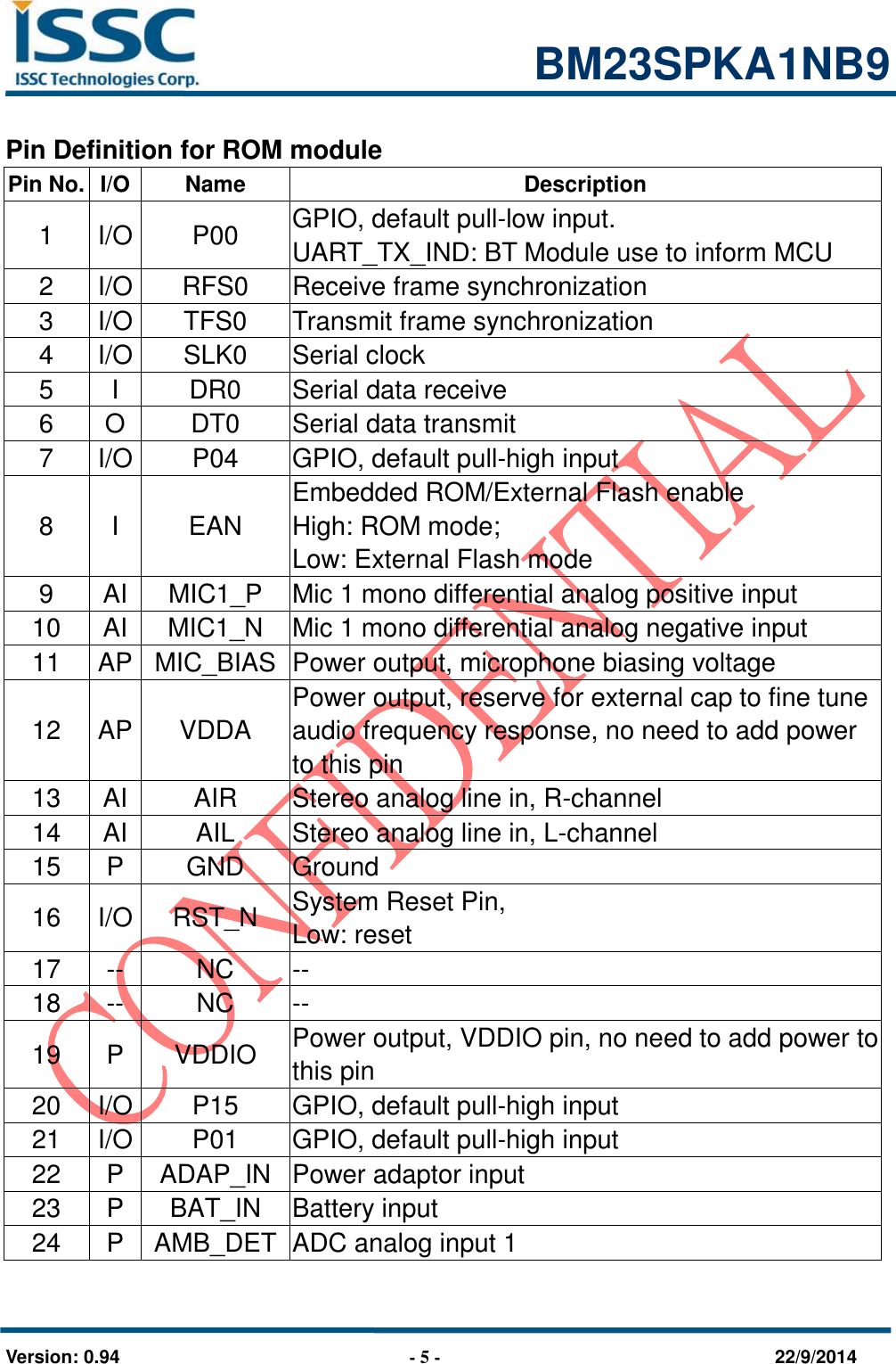
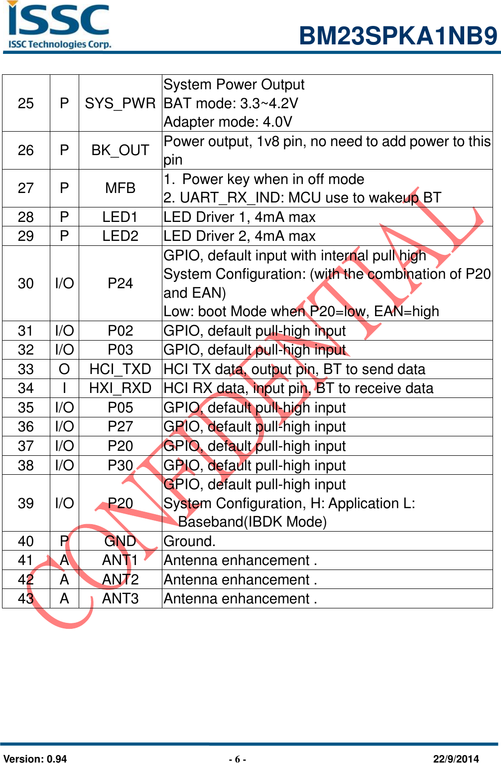
Microchip Technology BM23SPKXYC2A Bluetooth Modulel User Manual Manual

Microchip Technology Inc. Bluetooth Modulel Manual

Manual

                                                                          BM23SPKA1NB9     5F, No.5, Industry E. Rd. VII, Hsinchu Science Park, Hsinchu city 30077, Taiwan, R.O.C                                                  Version:0.94                                    Phone: 886-3-577-8385                                                                                   10/27/2014                                                                                            Fax: 886-3-577-8501        BM23SPKA1NB9  Bluetooth 4.1 Digital Audio Interface Module
                                                           BM23SPKA1NB9   Version: 0.94                              - 2 -                                    22/9/2014 Product Description The ISSC BM23SPKA1NB9 is a highly integrated Bluetooth 4.1 digital audio output  module,  designed  for  high  data  rate,  short-range  wireless communication in the 2.4 GHz ISM band. With the build-in ISSC Bluetooth stack,  profile  and  digital  audio  interface,  the  ISSC  BM23SPKA1NB9  can combine the external DSP and codec to provide high performance Bluetooth audio.    Features   Main Chip: ISSC IS2023S(ROM version)   Bluetooth 4.1 EDR compliant   Max. +4dBm Class 2 output power   Receiver  Sensitivity:  GFSK  typical  -90dBm,  π/4  PSK  typical  -91dBm, 8DPSK typical    -84dBm     Piconet and Scatter net support   CVSD, A-law, -law, mSBC CODEC algorithms for voice applications  SBC/AAC decode for Bluetooth audio streaming   Microphone input and audio line-in support  Built-in four language voice prompt (Chinese/English/Spanish/French)   Support PCM and I2S digital audio interface    Built-in 350mAH Li-ion battery charger   HSP, HFP, A2DP, AVRCP,SPP    profiles supported   3.3V operating voltage  Built-in program ROM and 64Kb EEPROM   43 pins for SMT module Size: 15mmx29mm2  Built-in PCB Antenna   RoHS compliant   FCC certification
                                                           BM23SPKA1NB9   Version: 0.94                              - 3 -                                    22/9/2014 Module Pin Out Diagram  BM23SPKA1NB9
                                                           BM23SPKA1NB9   Version: 0.94                              - 4 -                                    22/9/2014
                                                           BM23SPKA1NB9   Version: 0.94                              - 5 -                                    22/9/2014 Pin Definition for ROM module Pin No.   I/O Name Description 1 I/O P00 GPIO, default pull-low input. UART_TX_IND: BT Module use to inform MCU 2 I/O RFS0 Receive frame synchronization 3 I/O TFS0 Transmit frame synchronization 4 I/O SLK0 Serial clock 5 I DR0 Serial data receive 6 O DT0 Serial data transmit 7 I/O P04 GPIO, default pull-high input 8 I EAN Embedded ROM/External Flash enable High: ROM mode; Low: External Flash mode 9 AI MIC1_P Mic 1 mono differential analog positive input 10 AI MIC1_N Mic 1 mono differential analog negative input 11 AP MIC_BIAS Power output, microphone biasing voltage 12 AP VDDA Power output, reserve for external cap to fine tune audio frequency response, no need to add power to this pin 13 AI AIR Stereo analog line in, R-channel 14 AI AIL Stereo analog line in, L-channel 15 P GND Ground 16 I/O RST_N System Reset Pin, Low: reset 17 -- NC -- 18 -- NC -- 19 P VDDIO Power output, VDDIO pin, no need to add power to this pin 20 I/O P15 GPIO, default pull-high input 21 I/O P01 GPIO, default pull-high input 22 P ADAP_IN Power adaptor input 23 P BAT_IN Battery input 24 P AMB_DET ADC analog input 1
                                                           BM23SPKA1NB9   Version: 0.94                              - 6 -                                    22/9/2014 25 P SYS_PWR System Power Output BAT mode: 3.3~4.2V Adapter mode: 4.0V 26 P BK_OUT Power output, 1v8 pin, no need to add power to this pin 27 P MFB 1.  Power key when in off mode 2. UART_RX_IND: MCU use to wakeup BT 28 P LED1 LED Driver 1, 4mA max 29 P LED2 LED Driver 2, 4mA max 30 I/O P24 GPIO, default input with internal pull high System Configuration: (with the combination of P20 and EAN) Low: boot Mode when P20=low, EAN=high 31 I/O P02 GPIO, default pull-high input 32 I/O P03 GPIO, default pull-high input 33 O HCI_TXD HCI TX data, output pin, BT to send data 34 I HXI_RXD HCI RX data, input pin, BT to receive data 35 I/O P05 GPIO, default pull-high input 36 I/O P27 GPIO, default pull-high input 37 I/O P20 GPIO, default pull-high input 38 I/O P30 GPIO, default pull-high input 39 I/O P20 GPIO, default pull-high input System Configuration, H: Application L: Baseband(IBDK Mode) 40 P GND Ground. 41 A ANT1 Antenna enhancement . 42 A ANT2 Antenna enhancement . 43 A ANT3 Antenna enhancement .
                                                           BM23SPKA1NB9   Version: 0.94                              - 7 -                                    22/9/2014 Digital Audio Interface   Support I2S and PCM interface   Sampling Rate : 8K, 44.1K, 48K   Word Length: 16 bits, 24 bits   4 application modes
                                                           BM23SPKA1NB9   Version: 0.94                              - 8 -                                    22/9/2014 Mode 1: I2S Master BCLKADCLRCDACLRCADCDATDACDATSlaveSCLKnRFSnTFSnDRnDTnMasterExternal CODEC/DSP BM23DACADCADC Bn-1RFSn/TFSnSCLKnDRn/DTn Bn-2 B1B0Bn-1 Bn-2 B1B0Left Channel Right Channel1/fsWord Length Or   Solutions with mic and line-in analog input with I2S audio output   Mic for Bluetooth SCO link   Line-in for external audio playback(for high SNR requirement)  BCLKADCLRCDACLRCADCDATDACDATSlaveSCLKnRFSnTFSnDRnDTnMasterExternal CODEC/DSP BM23Application 1DACLineIn
                                                           BM23SPKA1NB9   Version: 0.94                              - 9 -                                    22/9/2014 Mode 2: I2S Slave BCLKADCLRCDACLRCADCDATDACDATMasterSCLKnRFSnTFSnDRnDTnSlaveExternal CODEC/DSP BM23DACADCADC Bn-1RFSn/TFSnSCLKnDRn/DTn Bn-2 B1B0Bn-1 Bn-2 B1B0Left Channel Right Channel1/fsWord Length Or   Solutions with mic and line-in analog input with I2S audio output   Mic for Bluetooth SCO link   Line-in for external audio playback(for high SNR requirement) BCLKADCLRCDACLRCADCDATDACDATMasterSCLKnRFSnTFSnDRnDTnSlaveExternal CODEC/DSP BM23Application 1DACLineIn
                                                           BM23SPKA1NB9   Version: 0.94                              - 10 -                                    22/9/2014 Mode 3: PCM master BCLKADCLRCDACLRCADCDATDACDATSlaveSCLKnRFSnTFSnDRnDTnMasterExternal CODEC/DSP BM23DACADCADC  Bn-1RFS0/TFS0SCLK0DR0/DT0 Bn-2 B1B0Bn-1 Bn-2 B1B0Left Channel1/fsWord LengthRight Channel
                                                           BM23SPKA1NB9   Version: 0.94                              - 11 -                                    22/9/2014 Mode 4: PCM slave BCLKADCLRCDACLRCADCDATDACDATMasterSCLKnRFSnTFSnDRnDTnSlaveExternal CODEC/DSP BM23DACADCADC  Bn-1RFS0/TFS0SCLK0DR0/DT0 Bn-2 B1B0Bn-1 Bn-2 B1B0Left Channel1/fsWord LengthRight Channel
                                                           BM23SPKA1NB9   Version: 0.94                              - 12 -                                    22/9/2014  Outline Dimension (Module Foot print)
                                                           BM23SPKA1NB9   Version: 0.94                              - 13 -                                    22/9/2014 Electrical Characteristics Table 1: Absolute Maximum Voltages Rating   Min Max Storage Temperature -40ºC +85ºC ESD: Human Body Mode ±2KV  ESD: Machine Mode ±200V  ESD: Charge Device Mode ±400V  Core supply voltage VDD_CORE, AVDD_PLL 1.14V 1.26V RF supply voltage VCC_RF 1.28V  SAR supply voltage AVDD_SAR 1.62V 1.98V Codec supply voltage VDD_AUDIO 2.7V 3.0V I/O voltage VDD_IO  3.6V Supply voltage BK_VDD  4.3V 3V1_VIN  4.3V BAT_IN 3.0 4.3V ADAP_IN 4.5 7.0V LED  5.1V Power switch  7.0V  Table 2: Recommended operate condition Rating   Min Typ Max Storage Temperature -10ºC +25ºC +60ºC Core supply voltage VDD_CORE, AVDD_PLL 1.14V 1.2V 1.26V RF supply voltage VCC_RF  1.28V  SAR supply voltage AVDD_SAR 1.62V 1.8V 1.98V Codec supply voltage VDD_AUDIO 2.7V  3.0V I/O voltage   VDD_IO 2.7V 3.0V 3.3V Supply voltage BK_VDD 3V  4.3V 3V1_VIN 3V  4.3V BAT_IN 3V  4.3V
                                                           BM23SPKA1NB9   Version: 0.94                              - 14 -                                    22/9/2014 ADAP_IN 4.5V  7.0V LED  4.3V  Power switch 1.8V  7.0V  Table 3: BUCK switching regulator Normal Operation Min Typ Max Unit Operation Temperature -40  85 ℃ Input Voltage (VIN) 3.0 3.8 4.5 V Output Voltage (VOUT) (ILOAD=70mA, VIN=4V) 1.7 1.80 2.05 V Output Voltage Accuracy    ±5  % Output Voltage Adjustable Step  50  mV/Step Output Adjustment Range -0.1  +0.25 V Output Ripple  10 15 mV RMS Average Load Current (ILOAD) 120   mA Settling Time (start-up time) EN or VIN to VOUT  1.2 2 ms Conversion efficiency @BAT=3.8V ILOAD = 50mA  88  % ILOAD ≥ 10mA (PWM)  70  ILOAD ≥ 10mA (PFM)  80  ILOAD ≥ 250μA (PFM)  65 70 Switching Frequency  800  KHz PWM/PFM Switching Point  by F/W  mA Start-up Current Limit 0 50 210 mA Start-up Inrush Current ILOAD = 10mA   400 mA Quiescent Current   PWM   1000 μA PFM  30 40 Output Current (Peak) 200   mA Load Regulation (ILOAD = 10 ~ 100mA)  1  mV/mA Line Regulation (3.2V < VIN < 4.2V)  0.03  %/V
                                                           BM23SPKA1NB9   Version: 0.94                              - 15 -                                    22/9/2014 (30) (mV/V) EN threshold Logic Low Voltage (VIL)   0.4 V Logic High Voltage (VIH) 1.62   V EN current   10 nA Shutdown Current *1   <1 μA  Table 4: Low Drop Regulation Normal Operation Min Typ Max Unit Operation Temperature -40  85 ℃ Input Voltage (VIN) 3.0  4.5 V Output Voltage (VOUT) (1) VOUT_CODEC (2) VOUT_IO     VOUT = 2.9V (2.4~3.4V)  2.9         V VOUT = 1.8V (1.3~2.3V)  1.8  Accuracy (VIN=3.7V, ILOAD=100mA, 27’C)  ±5  % Output Voltage Adjustable Step 67 100  mV/Step Output Adjustment Range  ±0.5  V Start-up Inrush Current ILOAD=10mA  200 400 mA Settling Time   (start-up time) EN or VIN to VOUT  250 500 μs Output Current (Average) VOUT   100 mA Output Current (Peak) VOUT   150 mA Drop-Out Voltage (ILOAD = maximum output current)   300 mV Quiescent Current (excluding load, ILOAD < 1mA)  45  μA Quiescent Current (excluding load, ILOAD < 100μA)   N/A μA Load Regulation (Iload = 0mA to 100mA), ΔVOUT   40 (0.4) mV (mV/mA)
                                                           BM23SPKA1NB9   Version: 0.94                              - 16 -                                    22/9/2014 Note: 0.4(mV/mA) * (100mA-0mA)=40mV Line Regulation (VOUT+0.3V<VIN<4.5V  7 10 mV/V EN threshold Logic Low Voltage (VIL)   0.4 V Logic High Voltage (VIH) 1.62   V EN current   10 nA Shutdown Current (*1)   <1 μA  Table 5: Battery Charger Charging Mode (BAT_IN rising to 4.2V) Min Typ Max Unit Operation Temperature -40  85 ℃ Input Voltage (VIN) Note: It needs more time to get battery fully charged when VIN=4.5V 4.5 5.0 7.0 V Supply current to charger only  3 4.5 mA Battery trickle charge current (BAT_IN < trickle charge voltage threshold)  0.1C  mA Maximum Battery   Fast Charge Current   Note: ENX2=0 Headroom > 0.7V   (ADAP_IN=5V) 170 200 240 mA Headroom = 0.3V (ADAP_IN=4.5V) 160 180 240 mA Maximum Battery   Fast Charge Current   Note: ENX2=1 Headroom > 0.7V (ADAP_IN=5V) 330 370 420 mA Headroom = 0.3V (ADAP_IN=4.5V) 180 220 270 mA Minimum Step     1  mA Trickle Charge Voltage Threshold  3  V Float Voltage   4.158 4.2 4.242 V Battery Charge Termination Current,   % of Fast Charge Current  10  % Standby Mode (BAT_IN falling from 4.2V)  Supply current to charger only  2 4 mA
                                                           BM23SPKA1NB9   Version: 0.94                              - 17 -                                    22/9/2014 Battery Current  -1  μA Battery Recharge Current Note: C  Battery Capacity (*1)  0.25C  mA
                                                           BM23SPKA1NB9   Version: 0.94                              - 18 -                                    22/9/2014 Table 6: Audio codec ADC    Conditions Min Typ Max Unit Temperature  -40 25 85 ℃ Resolution    16 Bits Input sample rate, Fsample 8KHz for MIC 44.1KHz for Line-in 8  44.1 KHz Signal to Noise Ratio (SNR @MIC or Line-in mode) fin=1KHz B/W=20~20KHz A-weighted THD+N < 1% 150mVpp input  8KHz  90  dB 44.1KHz  90  Digital Gain  -54  4.85 dB Digital Gain Resolution   2~6  dB MIC Boost Gain   20   Analog Gain    60 dB Analog Gain Resolution   2.0  dB Input full-scale at maximum gain (differential)   4  mV rms Input full-scale at minimum gain (differential)   800  mV rms 3dB bandwidth   20  KHz Microphone mode input impedance Input impedance  6 10 KΩ Input capacitance   20 pF THD+N (microphone input) @30mVrms input   0.02  % THD+N (line input)   0.04  % ADC channels   2   Analog supply voltage    2.6 2.8 3.0 V Digital supply voltage    1.08 1.2 1.32 V
                                                           BM23SPKA1NB9   Version: 0.94                              - 19 -                                    22/9/2014 Table 7: Transmitter section for BDR (25℃)  Min Typ Max Bluetooth specification Unit Maximum RF transmit power  4.0 5.0 -6 to 4 dBm RF power variation over temperature range with compensation enabled  ±1.0   dB RF power variation over temperature range with compensation disabled  ±2.0   dB RF power control range  18  ≥16 dB RF power range control resolution  ±0.5   dB 20dB bandwidth for modulated carrier  925  ≤1000 KHz ACP  Note: F0=2441MHz F = F0±2MHz  -42 -40 ≤-20 dBm F = F0±3MHz  -49 -48 ≤-40 dBm F = F0±>3MHz  -57 -53 ≤-40 dBm ∆f1avg maximum modulation 145  175 140<∆f1avg<175 KHz ∆f2max maximum modulation 120 135 140 ≥115 KHz ∆f2avg/∆f1avg 0.9 0.95  ≥0.80  ICFT 4.5 8 10.5 ±75 KHz Drift rate 3.3 5 7.0 ≤20 KHz/50us Drift (single slot packet)  12  ≤40 KHz 2nd harmonic content  -42  ≤-30 dBm 3rd harmonic content  -45  ≤-30 dBm
                                                           BM23SPKA1NB9   Version: 0.94                              - 20 -                                    22/9/2014 Table 8 Transmitter section for EDR (25℃)  Min Typ Max Bluetooth specification Unit Relative transmit power   -1.2  -4 to 1 dB π/4 DQPSK max carrier frequency stability   |ωo| freq. error  2.5 5 ≤10 for all blocks KHz |ωi| initial freq. error  2.5 5 ≤75 for all blocks KHz |ωo+ωi| block freq. error   5 10 ≤75 for all blocks KHz 8DPSK max carrier frequency stability   |ωo| freq. error  2.5 5 ≤10 for all blocks KHz |ωi| initial freq. error  2.5 5 ≤75 for all blocks KHz |ωo+ωi| block freq. error  5 10 ≤75 for all blocks KHz π/4 DQPSK modulation accuracy RMS DEVM  7 12.2 ≤20 % 99% DEVM  PASS  ≤30 % Peak DEVM   25 ≤35 % 8DQPSK modulation accuracy RMS DEVM  7  ≤13 % 99% DEVM  PASS  ≤20 % Peak DEVM   20 ≤25 % In-band spurious emissions  Note: F0=2441MHz F > F0+3MHz  <-52  ≤-40 dBm F < F0-3MHz  <-53  ≤-40 dBm F = F0-3MHz  -46  ≤-40 dBm F = F0-2MHz  -34  ≤-20 dBm F = F0-1MHz  -34  ≤-26 dBm F = F0+1MHz  -37  ≤-26 dBm F = F0+2MHz  -34  ≤-20 dBm
                                                           BM23SPKA1NB9   Version: 0.94                              - 21 -                                    22/9/2014 F = F0+3MHz  -46  ≤-40 dBm EDR differential phase encoding  100  ≥99 %  Table 9 Receiver section for BDR (25℃)  Frequency (GHz) Min Typ Max Bluetooth specification Unit Sensitivity at 0.1% BER for all basic rate packet types 2.402  -90  ≤-70 dBm 2.441  -90  2.480  -90  Maximum received signal at 0.1% BER  0  ≥-20 dBm Continuous power required to block Bluetooth reception (for input power of -67dBm with 0.1% BER) measured at the unbalanced port of the balun 0.030–2.000  -7  -10 dBm 2.000-2.400  -10  -27 2.500-3.000  -11  -27 3.000-12.75  -7  -10 C/I co-channel  6  ≤11 dB Adjacent channel selectivity C/I  Note: F0=2441MHz F = F0+1MHz  -6  ≤0 dB F = F0-1MHz  -6.5  ≤0 dB F = F0+2MHz  -36  ≤-30 dB F = F0-2MHz  -28  ≤-9 dB F = F0-3MHz  -31  ≤-20 dB F = F0+5MHz  -48  ≤-40 dB F = Fimage  -28  ≤-9 dB Maximum level of intermodulation  -37  ≥-39 dBm
                                                           BM23SPKA1NB9   Version: 0.94                              - 22 -                                    22/9/2014 interferers Spurious output level  N/A   dBm/Hz
                                                           BM23SPKA1NB9   Version: 0.94                              - 23 -                                    22/9/2014 Table 10: Receiver section for EDR (25℃)  Frequency (GHz) Modulation Min Typ Max Bluetooth specification Unit Sensitivity at 0.01% BER 2.402 π/4 DQPSK  -91  ≤-70 dBm 2.441 π/4 DQPSK  -91  2.480 π/4 DQPSK  -91  2.402 8DPSK  -85  ≤-70 dBm 2.441 8DPSK  -84  2.480 8DPSK  -85  Maximum received signal at 0.1% BER π/4 DQPSK  -10  ≥-20 dBm 8DPSK  -10  ≥-20 C/I co-channel at 0.1% BER π/4 DQPSK  10  ≤13 dB 8DPSK  16  ≤21 dB Adjacent channel selectivity C/I  Note: F0=2441MHz F = F0+1MHz π/4 DQPSK  -11  ≤0 dB 8DPSK  -5  ≤5 dB F = F0-1MHz π/4 DQPSK  -8  ≤0 dB 8DPSK  -4  ≤5 dB F = F0+2MHz π/4 DQPSK  -38.5  ≤-30 dB 8DPSK  -33.5  ≤-25 dB F = F0-2MHz π/4 DQPSK  -29  ≤-7 dB 8DPSK  -25  ≤0 dB F = F0-3MHz π/4 DQPSK  -32.5  ≤-20 dB 8DPSK  -27  ≤-13 dB F = F0+5MHz π/4  -49.5  ≤-40 dB
                                                           BM23SPKA1NB9   Version: 0.94                              - 24 -                                    22/9/2014 DQPSK 8DPSK  -43.5  ≤-33 dB F = Fimage π/4 DQPSK  -29  ≤-7 dB 8DPSK  -25  ≤0 dB
                                                           BM23SPKA1NB9   Version: 0.94                              - 25 -                                    22/9/2014 FCC Label Instructions The outside of final products that contains this module device must display a label referring to the enclosed module. This exterior label can use wording such as the following: “Contains Transmitter Module FCC ID: A8TBM23SPKXYC2A” or “Contains FCC ID: A8TBM23SPKXYC2A.” Any similar wording that expresses the same meaning may be used. If the final product is to be sold in Canada, then this exterior label should use wording such as the following: “Contains Transmitter Module IC: 12246A-BM23SPKXYC2”
                                                           BM23SPKA1NB9   Version: 0.94                              - 26 -                                    22/9/2014 Reflow profile
                                                           BM23SPKA1NB9   Version: 0.94                              - 27 -                                    22/9/2014 QR code label information  Label Size:15±1.5 *6±1.5 mm Device Name: BM23SPKA1NB9 MAC ID: xxxxxxxxxx Customer ID Name: Cxxxxx Date Code: 13xx                                       Module Weight (Test condition: module with QR label)     TBD
                                                           BM23SPKA1NB9   Version: 0.94                              - 28 -                                    22/9/2014 Storage standard 1.  Calculated shelf life in sealed bag: 12 months at < 40  ℃  and <90% relative humidity (RH) 2.  After bag is opened, devices that will be subjected to reflow solder or other high temperature process must be Mounted within 168 hours of factory conditions <30℃/60% RH
                                                           BM23SPKA1NB9   Version: 0.94                              - 29 -                                    22/9/2014 Ordering Information Device Module Order Number Size Shipment Method BM23SPKA1NB9 Bluetooth 4.1   digital audio Module 29*15 mm2 Tray  Note: Minimum Order Quantity is 630pcs Tray.
                                                           BM23SPKA1NB9   Version: 0.94                              - 30 -                                    22/9/2014  Packing Information Tray Dimensions
                                                           BM23SPKA1NB9   Version: 0.94                              - 31 -                                    22/9/2014  Packing Method                                                              Inner box: Q’ty (630 Pcs)                                             Dimensions: 36*16*9.5 cm        Bar Code Label P/N: Device name C/N: Customer name Lot No: Lot ID Q’ty: Box or Carton Module’s Q’ty                                                     Carton: Q’ty (3780 Pcs)                                                Dimensions: 38*35*30 cm

Navigation menu