MICROCHIP TECHNOLOGY RN42 RN-42 User Manual Device Features
Microchip Technology Inc. RN-42 Device Features
(RN-42) User Manual_20100415

RN-42 Specification
CONTENTS
RN-42 Specification...............................................................................................................................1
Type: Release.........................................................................................................................1
Document: RN-42-001................................................................................................................... 1
Version: 1.0.................................................................................................................................1
Release Date: Jan 08, 2010................................................................................................................ 1
Release Record ...................................................................................................................................... 1
Device Features .....................................................................................................................................2
Description.............................................................................................................................................2
Application.............................................................................................................................................3
1Ordering Information ...................................................................................................................5
2Key Features ..................................................................................................................................5
3Block Diagram ...............................................................................................................................5
4Electrical Characteristic ...............................................................................................................6
4.1 Absolute Maximum ratings ......................................................................................................6
4.2 Recommend operation conditions ...........................................................................................6
4.3 Electrica Characteristics ..........................................................................................................6
4.4 Radio characteristics .................................................................................................................7
4.5 Digital I/O characteristics .........................................................................................................7
5Mechanical Dimensions ................................................................................................................8
6Pin Definition Descriptions ...........................................................................................................9
7Design Concerns ..........................................................................................................................12
7.1 Reset circuit .............................................................................................................................12
7.2 Factory reset PIO4 ..................................................................................................................12
7.3 Connection status ....................................................................................................................12
7.4 HCI mode .................................................................................................................................12
7.5 Using SPI bus for flash upgrade ............................................................................................12
7.6 Minimizing radio interface .....................................................................................................13
7.7 Soldering reflow profile ..........................................................................................................13
8Reference Application Schematic ..............................................................................................14
9SMT Reflow Profile .....................................................................................................................15
9.1 Reliability solder temperature chart: ....................................................................................15
9.2 Reflow temperature chart: .....................................................................................................15
Flaircomm Technologies Confidential 4
RN-42 Specification
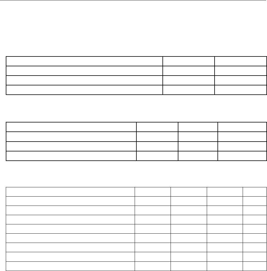
4 Electrical Characteristic
4.1 Absolute Maximum ratings
Rating Minimum Maximum
Store temperature -40℃ +120℃
Operation temperature -40℃ +85℃
Power Supply -0.4 Volt DC 3.6Volt
4.2 Recommend operation conditions
Rating Minimum Type Maximum
Store temperature -40℃ +25℃ +85℃
Operation temperature -20℃ +25℃ +70℃
Power Supply - DC 3.3Volt DC 3.6Volt
4.3 Electrica Characteristics
Parameter Min Typ. Max Unit
Supply Voltage (DC) 3.0 3.3 3.6 V
RX Supply Current 35 60 mA
TX Supply Current 65 100 mA
Average power consumption
Standby/Idle (default settings) 25 mA
Connected (normal mode) 30 mA
Connected (low power Sniff) 8 mA
Standby/Idle (Deep sleep enabled) 250uA 2.5 mA
Flaircomm Technologies Confidential 6
RN-42 Specification
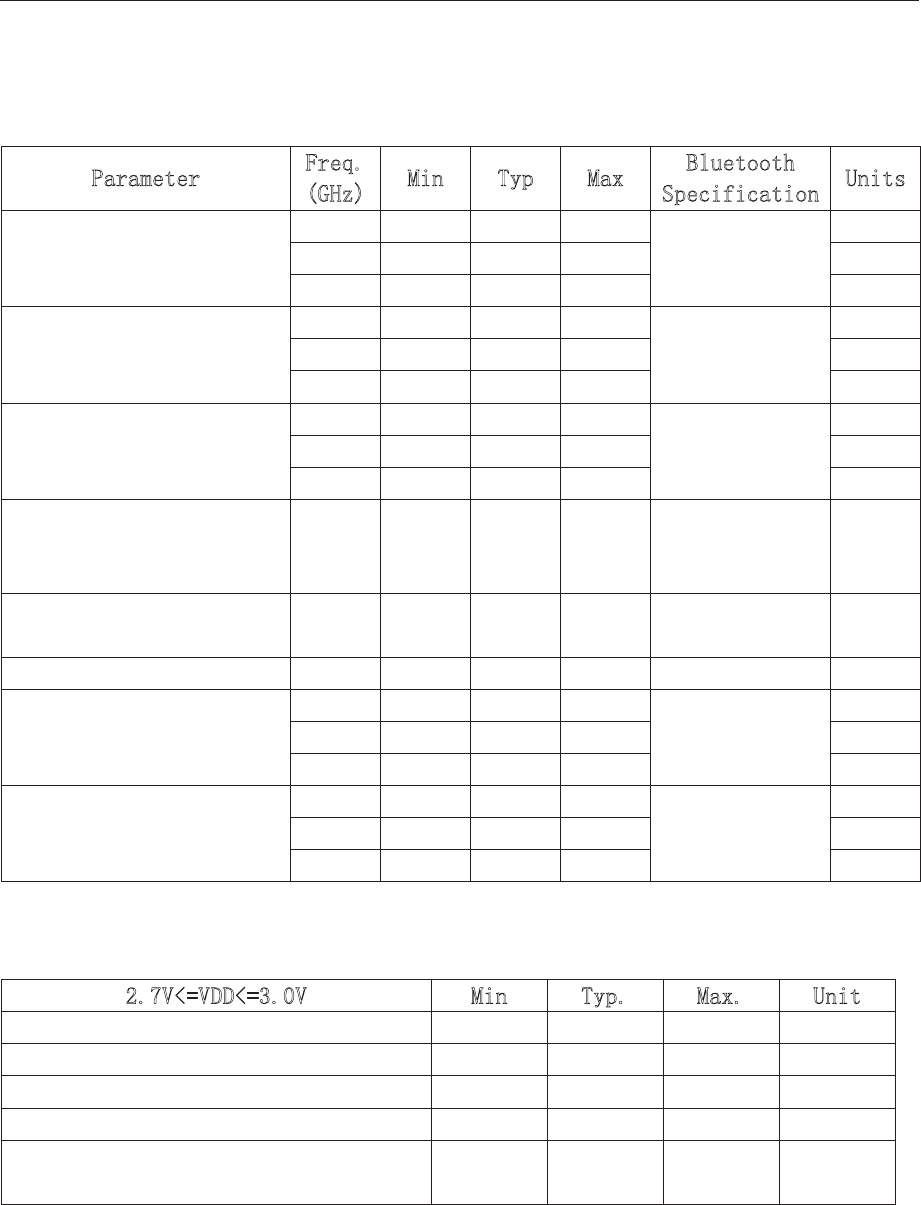
4.4 Radio characteristics
Freq.
(GHz)
Bluetooth
Specification
Parameter Min Typ Max Units
2.402 - -80 -86 dBm
2.442 - -80 -86 dBm
Sensitivity @ 0.1%BER <=-70
2.480 - -80 -86 dBm
2.402 5.0 6.0 dBm
2.442 5.0 6.0 dBm
RF Transmit Power <=6
2.480 5.0 6.0 dBm
2.402 - 5 75 kHz
2.442 - 5 75 kHz
Initial Carrier
Frequency
Tolerance
75
2.480 - 5 75 kHz
20dB bandwidth for
modulated
carrier
- 900 1000 <=1000 kHz
Drift (Five slots
packet) - 15 - 40 kHz
Drift Rate - 13 - 20 kHz
2.402 140 165 175 kHz
2.442 140 165 175 kHz
△f1avg Max Modulation >140
2.480 140 165 175 kHz
2.402 140 190 - kHz
2.442 140 190 - kHz
△f2avg Min Modulation 115
2.480 140 190 - kHz
4.5 Digital I/O characteristics
2.7V<=VDD<=3.0V Min Typ. Max. Unit
Input logic level LOW -0.4 - +0.8 V
Input logic level HIGH 0.7VDD - VDD+0.4 V
Output logic level LOW - - 0.2 V
Output logic level HIGH VDD-0.2 - - V
All I/O’s (except reset) default to
weak pull down +0.2 +1.0 +5.0 uA
Flaircomm Technologies Confidential 7
RN-42 Specification
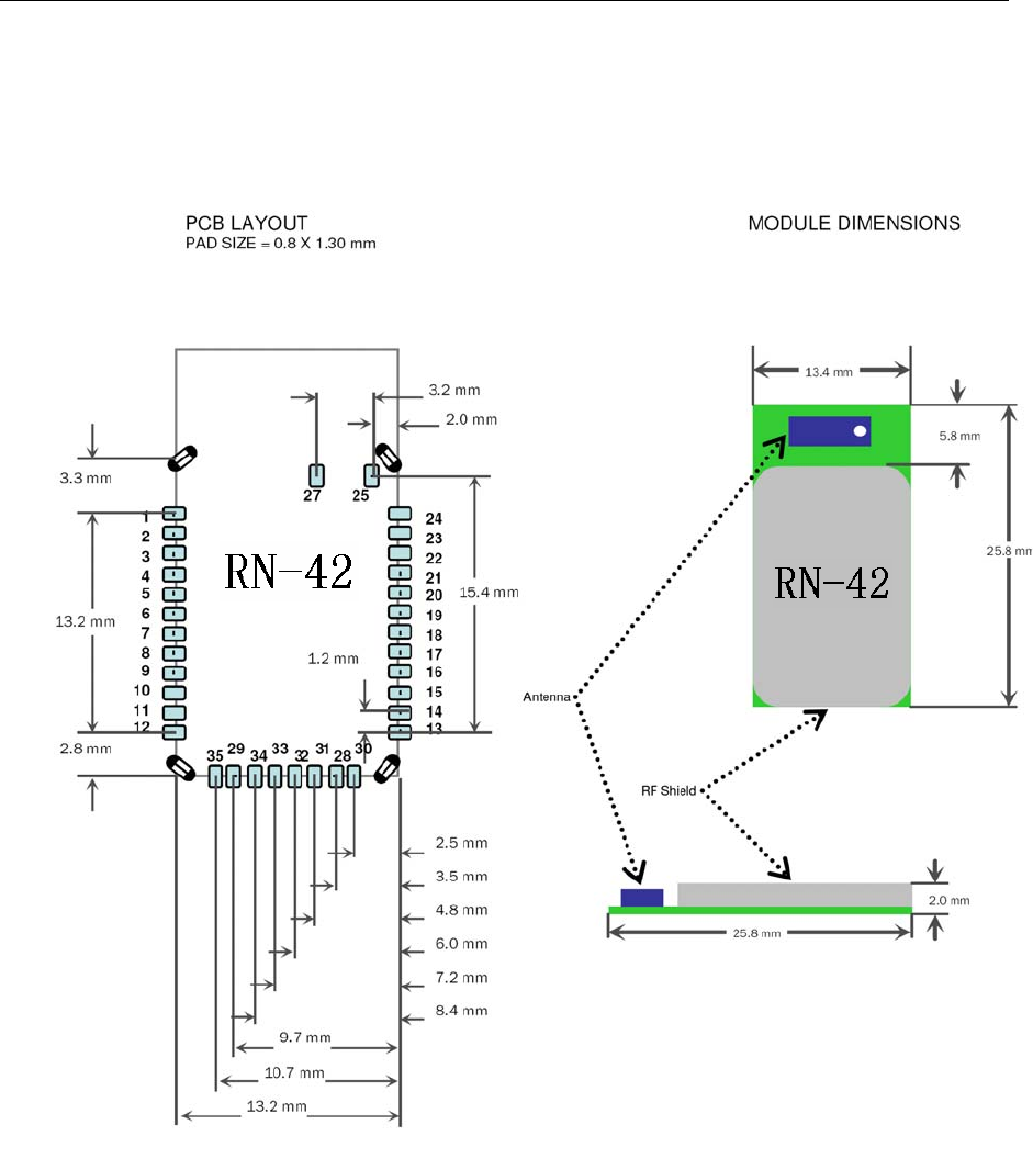
5 Mechanical Dimensions
Flaircomm Technologies Confidential 8
RN-42 Specification
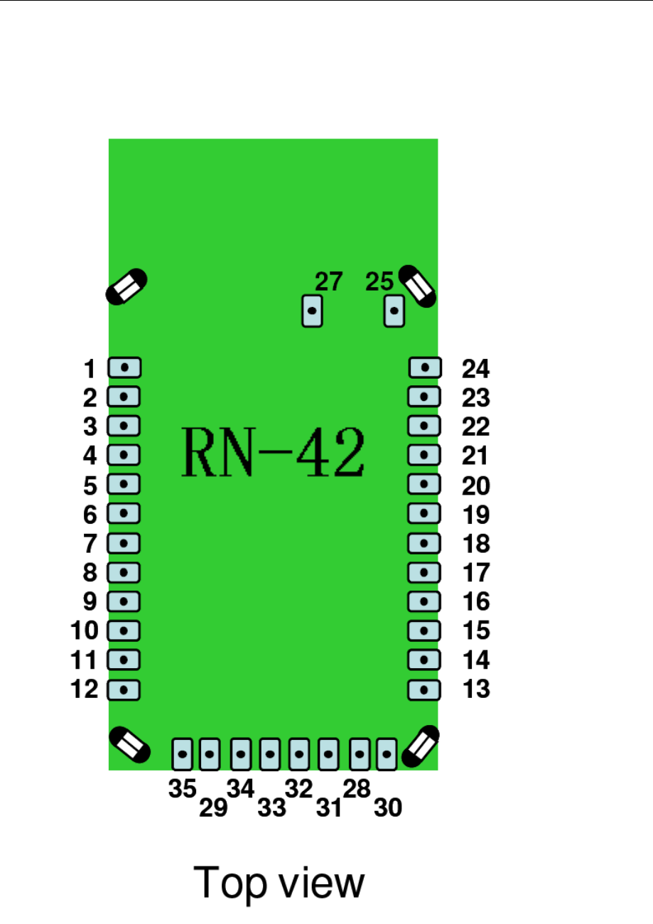
6 Pin Definition Descriptions
Flaircomm Technologies Confidential 9

RN-42 Specification
Pin Name Description Default
1 GND
2 SPI MOSI Programming only No Connect
Input to RN42with weak pull
down
3 PIO6 Set BT master (HIGH=auto-master mode)
Set Baud rate (HIGH = force 9600, LOW = 115K
or firmware setting) Input to RN42 with weak
pull down 4 PIO7
Input to RN42 with 1K pull
up 5 RESET Active LOW reset
6 SPI_CLK Programming only No Connect
7 PCM_CLK PCM interface No Connect
8 PCM_SYNC PCM interface No Connect
9 PCM_IN PCM interface No Connect
10 PCM_OUT PCM interface No Connect
11 VDD 3.3V regulated power input
12 GND
13 UART_RX UART receive Input Input to RN42
High level output from
RN42 14 UART_TX UART transmit output
UART RTS, goes HIGH to disable host
transmitter 15 UART_RTS Low level output from RN42
16 UART_CTS UART CTS, if set HIGH, disables transmitter Low level input to RN42
17 USB_D+ USB port Pull up 1.5K when active
18 USB_D- USB port
19 PIO2 Status, HIGH when connected, LOW otherwise Output from RN42
Input to RN42 with weak
pull down 20 PIO3 Auto discovery = HIGH
21 PIO5 Status, toggles based on state, LOW on connect Output from RN42
Input to RN42 with weak
pull down 22 PIO4 Set factory defaults
23 SPI_CSB Programming only No Connect
24 SPI_MISO Programming only No Connect
25 GND
26 NC RF pad keep all traces and planes clear.
27 GND
28 GND
29 GND
30 AIO0 Optional analog input Not Used
31 PIO8 Status (RF data rx/tx) Output from RN42
Flaircomm Technologies Confidential 10

RN-42 Specification
Input to RN42 with weak
pull down 32 PIO9 IO
Input to RN42 with weak
pull down 33 PIO10 IO (remote DTR signal)
Input to RN42 with weak
pull down
34 PIO11 IO (remote RTS signal )
35 AIO1 Optional analog input Not Used
Flaircomm Technologies Confidential 11

RN-42 Specification
7 Design Concerns
7.1 Reset circuit
RN-42 contains a 1k pull up to VCC, the polarity of reset on the RN42 is ACTIVE LOW.
A power on reset circuit with delay is OPTIONAL on the reset pin of the module. It should
only be required if the input power supply has a very slow ramp, or tends to bounce or
have instability on power up. Often a microcontroller or embedded CPU IO is available to
generate reset once power is stable. If not, there are many low cost power supervisor
chips available, such as MCP809, MCP102/121, and Torex XC61F.
7.2 Factory reset PIO4
It is a good idea to connect this pin to a switch, or jumper, or resistor, so it can be
accessed. This pin can be used to reset the module to FACTORY DEFAULTS and is
often critical in situations where the module has been mis-configured. To set Factory
defaults start HIGH, then toggle times.
7.3 Connection status
PIO5 is available to drive an LED, and blinks at various speeds to indicate status.
PIO2 is an output which directly reflects the connection state, it goes HIGH when
connected, and LOW otherwise.
7.4 HCI mode
The RN42 module must be loaded with special firmware to run in HCI mode. When in
HCI mode the standard SPP/DUN applications are disabled.
7.5 Using SPI bus for flash upgrade
While not required, this bus is very useful for configuring advanced
parameters of the Bluetooth modules, and is required for upgrading the firmware on
modules. The suggested ref-design shows a 6pin header which can be implemented to
gain access to this bus. A minimum-mode version could just use the SPI signals (4pins)
and pickup ground and VCC from elsewhere on the design.
Flaircomm Technologies Confidential 12
RN-42 Specification
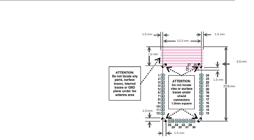
7.6 Minimizing radio interface
When laying out the carrier board
for the RN42 module the areas
under the antenna and shielding
connections should not have
surface traces, GND planes, or
exposed vias. (See diagram to right)
For optimal radio performance the
antenna end of RN42 module
should protrude 5mm past any
metal enclosure.
7.7 Soldering reflow profile
z Lead-Free Solder Reflow
z Temp: 230 degree C, 30-40 seconds, Peak 250 degree C maximum.
z Preheat temp: 165 +- 15 degree C, 90 to 120 seconds.
z Time: Single Pass, One Time
Flaircomm Technologies Confidential 13
RN-42 Specification
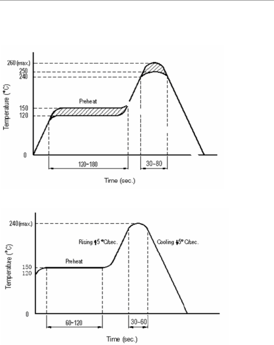
9 SMT Reflow Profile
9.1 Reliability solder temperature chart:
9.2 Reflow temperature chart:
Flaircomm Technologies Confidential 15
Compliance Information
FCC Compliance Statement:
This device complies with Part 15 of the FCC Rules . Operation is subject to
the following two conditions:
1. This device may not cause harmful interference, and
2. This device must accept any interference received, including
interference that may cause undesired operation. This device must
accept any interference received, including interference that may cause
undesired operation. Product that is a radio transmitter is labeled with FCC
ID.
FCC Caution:
(1) Exposure to Radio Frequency Radiation. This equipment must be
installed and operated in accordance with provided instructions and the
antenna(s) used for this transmitter must be installed to provide a
separation distance of at least 20 cm from all persons and must not be
collocated or operating in conjunction with any other antenna or
transmitter.
End-users and installers must be provided with antenna installation
instructions and transmitter operating conditions for satisfying RF exposure
compliance.
(2) Any changes or modifications not expressly approved by the grantee
of this device could void the user's authority to operate the equipment.
(3) This Transmitter must not be co-located or operating in conjunction with
any other antenna or transmitter.
(4) Changes or modifications to this unit not expressly approved by the
party responsible for compliance could void the user authority to operate
the equipment.
(5) Outdoor Operations in the 5.15~5.25GHz band is prohibited.
NOTE:
(1) This device is approved for OEM installation with specified antennas as
listed in this Manual. It is the responsibility of the Installer to comply with the
separation distance for satisfying RF exposure compliance.
(2) This device only could work when being installed into “client devices”
which could not transmit automatically, such as Notebook P.C. , with the
software driver limit.
IMPORTANT NOTE: In the event that these conditions can not be met (for
example certain laptop configurations or co-location with another
transmitter), then the FCC authorization is no longer considered valid and
the FCC ID can not be used on the final product. In these circumstances,
the OEM integrator will be responsible for re-evaluating the end product
(including the transmitter) and obtaining a separate FCC authorization.
IC Radiation Exposure Statement for Canada
This equipment complies with IC radiation exposure limits set forth for an
uncontrolled enviroment. To maintain compliance with IC RF exposure
compliance requirements, Please avoid direct contact to the transmitting.
End users must follow the specific operating instructions for satisfying RF
Exposure compliance.
Caution: The device is incapable of transmitting in the band 5600-5650 MHz
band in Canada.