PBE Europe as Axell Wireless 55-165704 55-165704 Cell Enhancer User Manual 80 330501HBKM
Axell Wireless 55-165704 Cell Enhancer 80 330501HBKM
Contents
- 1. manual 1 of 5
- 2. manual 2 of 5
- 3. manual 3 of 5
- 4. manual 4 of 5
- 5. manual 5 of 5
manual 5 of 5
STTRS DOCUMENTATION
Document Number 80-330501HBKM – Issue A - Draft Page 424 of 500
POWER ON
ALARM
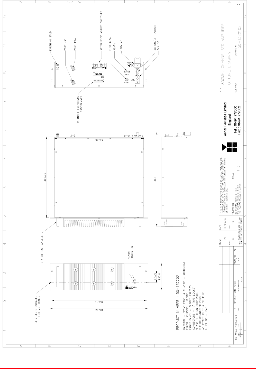
23.3.1.1. 800MHz Channelised Amplifier (50-132202) Outline Drawing
Drawing number 50-1322102
STTRS DOCUMENTATION
Document Number 80-330501HBKM – Issue A - Draft Page 425 of 500
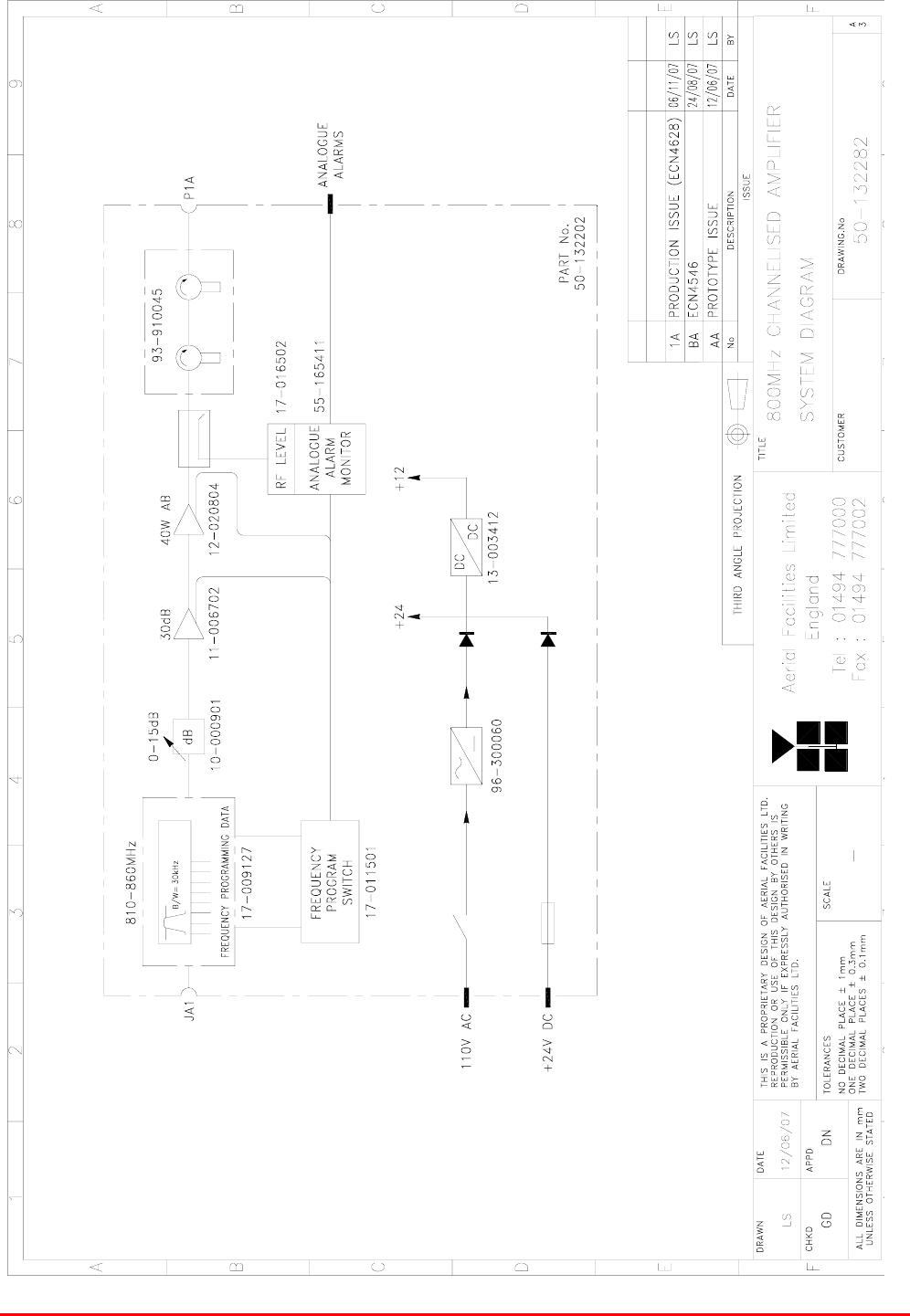
23.3.1.2. 800MHz Channelised Amplifier (50-132202) System Diagram
Drawing number 50-132282

STTRS DOCUMENTATION
Document Number 80-330501HBKM – Issue A - Draft Page 426 of 500
23.3.1.3. Dummy load 09-000902
Dual Isolator (850-870MHz) (93-910045) has one of its ports terminated with Dummy load 09-000902
in order to achieve the correct power rating to absorb the reflected power levels that can be
reasonably expected within the system.
09-000902 specification
PARAMETER SPECIFICATION
Frequency Range 0 - 2500 MHz
Power Rating 25 Watts continuous
VSWR Better than 1.1:1
Impedance 50 Ohms
Temperature Range -20 to +60°C
RF Connectors N Type female
Dimension 110.3mm x 38.1mm x
Weight 485 grams
Finish Black Anodised
RF Connector N Type male
Environmental IP66
MTBF >180,000 hours
23.3.1.4. Switched Attenuator 0.25W, 0 - 15dB (10-000901)
In many practical applications for Cell Enhancers etc., the gain in each path is found to be excessive.
Therefore, provision is made within the unit for the setting of attenuation in each path, to reduce the
gain.
10-000901 provides attenuation from 0 - 15dB in 2 dB steps The attenuation is simply set using the
four miniature toggle switches on the top of each unit. Each switch is clearly marked with the
attenuation it provides, and the total attenuation in line is the sum of the values switched in. They are
designed to maintain an accurate 50Ω impedance over their operating frequency at both input and
output.
10-000901 Specification
PARAMETER SPECIFICATION
Attenuation Values 0-15dB
Attenuation Steps 1, 2, 4 and 8dB
Power Handling 0.25 Watt
Attenuation Accuracy ± 1.0 dB
Frequency Range DC to 1GHz
Impedance 50Ω
Connectors SMA
VSWR 1.3:1
Weigh 0.2kg
operation -20°C to +60°C Temperature
range storage -40°C to +70°C
STTRS DOCUMENTATION
Document Number 80-330501HBKM – Issue A - Draft Page 427 of 500
7 8 96
1 2 3 4 5
9-Way Pin-Out Graphical Representation
23.3.1.5. Low Noise Amplifier (11-006702)
The Gallium-Arsenide low noise amplifiers used in 800MHz Line Amplifier (55-165703) are double
stage, solid-state low noise amplifiers. Class A circuitry is used throughout the units to ensure
excellent linearity and extremely low noise over a very wide dynamic range. The active devices are
very moderately rated to provide a long trouble-free working life. There are no adjustments on these
amplifiers, and in the unlikely event of a failure, then the complete amplifier should be replaced. This
amplifier features its own in-built alarm system which gives a volt-free relay contact type alarm that is
easily integrated into the main alarm system.
11-006702 Specification
PARAMETER SPECIFICATION
Frequency range 800 – 1000MHz
Bandwidth <200MHz
Gain 29dB (typical)
1dB Compression point 20dBm
OIP3 33dBm
Input/Output return loss >18dB
Noise figure 1.3dB (typical)
Power consumption 180mA @ 24V DC
Supply voltage 10-24V DC
Connectors SMA female
operational -10°C to +60°C Temperature
range storage -20°C to +70°C
Size 90 x 55 x 30.2mm
Weight 290gms (approximately)
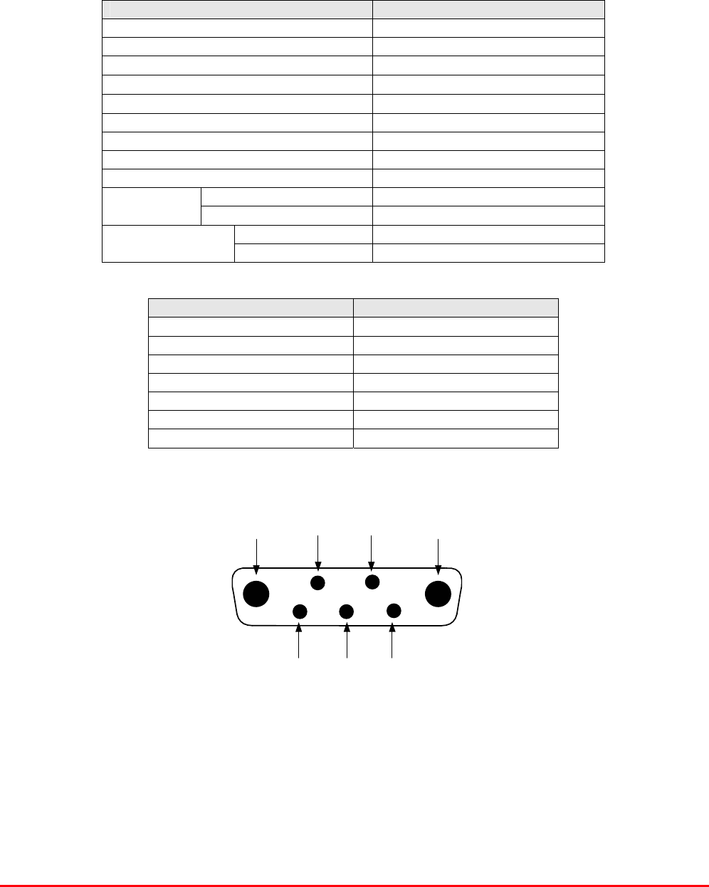
Low Noise Amplifier (11-006702) ‘D’ Connector Pin-out details
Connector pin Signal
1 +Ve input (10-24V)
2 GND
3 Alarm RelayO/P bad
4 Alarm Relay common
5 Alarm Relay good
6 No connection
7 TTL voltage set
8 TTL alarm/0V (good)
9 O/C good/0V bad
STTRS DOCUMENTATION
Document Number 80-330501HBKM – Issue A - Draft Page 428 of 500
23.3.1.6. Power Amplifier (12-020804)
This amplifier is a Class AB 40W power amplifier from 860MHz to 960MHz in balanced configuration.
The amplifier demonstrates a very good input/output return loss (RL) and it has a built-in Current Fault
Alarm Function.
The unit housing is an aluminium case (Iridite NCP finish) with SMA connectors for the RF
input/output and a D-Type connector for the power supply and the Current Fault Alarm Function.
12-020804 specification
Specification Parameter
Frequency Range 860 - 960MHz
Gain ≥28.0 dB
Gain Flatness 1.0dB p-p Max
∆Gain vs. Temperature 2.5dB Max
Input RL 15dB Min
Output RL 15dB Min
Output Power @ P1dB 46.0dBm Min
DC Supply Voltage 24 ± 0.5Vdc
RF Input Power 25dBm
At P1dB 6000mA Max DC Supply
Current With no RF input (Iqc) 1700mA Max
operational -40°C to +70°C Temperature
range storage -40°C to +100°C
7-Way Connector Pin-outs Connector Pin Signal
A1 +24V DC
A2 GND
1 Alarm relay common
2 TTL alarm/0V good
3 Alarm relay contact (bad)
4 Alarm relay contact (good)
5 O/C good/0V bad (TTL)

STTRS DOCUMENTATION
Document Number 80-330501HBKM – Issue A - Draft Page 429 of 500
23.3.1.7. DC/DC Converter 13-003412
13-003412 is based upon an O.E.M. DC/DC Converter module with a wide input range and and is
used to derive a 12V fixed voltage power supply rail from a higher voltage supply, in this case 24V. In
the event of failure this unit should not be repaired, only replaced.
13-003412 Specification
PARAMETER SPECIFICATION
Operating voltage 18 – 75V DC
Output voltages 12V (typical)
Output current 5.0A (Max)
operational -10%C to +60%C Temperature
range storage -20%C to +70%C
23.3.1.8. Channel Selectivity Module (17-009127)
Channel Selectivity Module (17-009127) is employed when requirement dictates that very narrow
bandwidths (single operating channels), must be selected from within the operating passband. One
channel selectivity module is required for each channel.
The Channel Selectivity Module is an Up/Down frequency converter that mixes the incoming channel
frequency with a synthesised local oscillator, so that it is down-converted to an Intermediate
Frequency (IF) in the upper HF range. An eight pole crystal filter in the IF amplifier provides the
required selectivity to define the operating passband of the Cell Enhancer to a single PMR channel.
The same local oscillator then converts the selected IF signal back to the channel frequency.
Selectivity is obtained from a fixed bandwidth block filter operating at an intermediate frequency (IF) in
the low VHF range. This filter may be internal to the channel selectivity module (Crystal or SAW filter)
or an externally mounted bandpass filter, (LC or Helical Resonator). Various IF bandwidths can
therefore be accommodated. A synthesized Local Oscillator is employed in conjunction with high
performance frequency mixers, to translate between the signal frequency and IF.
The operating frequency of each channel selectivity module is set by the programming of channel
selectivity module frequencies and is achieved digitally, via hard wired links, banks of DIP switches, or
via an onboard RS232 control module, providing the ability to remotely set channel frequencies.
Automatic Level Control (ALC) is provided within each channel selectivity module such that the output
level is held constant for high level input signals. This feature prevents saturation of the output mixer
and of the associated amplifiers.
Alarms within the module inhibit the channel if the synthesised frequency is not locked. The
synthesiser will not usually go out of lock unless a frequency far out of band is programmed.
The channel selectivity module is extremely complex and, with the exception of channel frequency
programming within the design bandwidth, it cannot be adjusted or repaired without extensive
laboratory facilities and the necessary specialised personnel. If a fault is suspected with any channel
selectivity module it should be tested by substitution and the complete, suspect module should then
be returned to AFL for investigation.

STTRS DOCUMENTATION
Document Number 80-330501HBKM – Issue A - Draft Page 430 of 500
23.3.1.9. Channel Control Module (17-011501)
The operating frequency for each channel in each repeater is programmed by 16 DIL (Dual In Line)
switches. The programming switches are mounted in the Channel Control Module. The Channel
Selectivity Modules are connected to the Channel Control Module via multi-way ribbon cables.
Adjacent to the DIL switches for each channel is a toggle switch to turn on and off individual channels
as required. A green LED indicates the power status of each channel.
A red LED shows the alarm condition for each channel. An illuminated alarm LED indicates that the
synthesiser has not achieved phase lock and that the module is disabled. There is a problem which
requires investigation, often a frequency programmed outside the operating frequency range.
The following information is necessary before attempting the programming procedure.
4. operating frequency
5. synthesiser channel spacing (step size)
6. synthesiser offset (IF)
Programming Procedure
Check that the required frequency falls within the operational frequency limits of the Cell Enhancer.
For each channel required, subtract the synthesiser offset from the required operating frequency and
record the resulting local oscillator frequency.
Divide each local oscillator frequency by the channel spacing and check that the result is an integer
(i.e: no remainder).
If the synthesiser division ratio is not an integer value, check the required operational frequency and
repeat the calculation checking for mistakes.
Convert the required local oscillator frequency to synthesiser programming switch state patterns
according to the following table. Note: the frequency of the passband will dictate the switch steps
used.
Switch Functions
Switch Number Synthesiser offset added when switch in UP position
12.5kHz step size 25kHz step size
1 +12.5kHz +25kHz
2 +25kHz +50kHz
3 +50kHz +100kHz
4 +100kHz +200kHz
5 +200kHz +400kHz
6 +400kHz +800kHz
7 +800kHz +1.6MHz
8 +1.6MHz +3.2MHz
9 +3.2MHz +6.4MHz
10 +6.4MHz +12.8MHz
11 +12.8MHz +25.6MHz
12 +25.6MHz +51.2MHz
13 +51.2MHz +102.4MHz
14 +102.4MHz +204.8MHz
15 +204.8MHz +409.6MHz
16 +409.6MHz +819.2MHz

STTRS DOCUMENTATION
Document Number 80-330501HBKM – Issue A - Draft Page 431 of 500
Programming Example
Frequency required: 454.000MHz
Channel spacing: 12.5kHz
Synthesiser offset: -21.4MHz
The Local Oscillator frequency is therefore:
454.000 – 21.4 = 432.600MHz
Dividing the Local Oscillator frequency by the channel spacing of 0.0125MHz:
432.600 = 34608
0.0125
This is an integer value, therefore it is OK to proceed.
Switch settings
Local Oscillator
Frequency 16 15 14 13 12 11 10 9 8 7 6 5 4 3 2 1
432.600 MHz 1 0 0 0 0 1 1 1 0 0 1 1 0 0 0 0
Switch setting: 0 = switch DOWN (ON, frequency ignored )
1 = switch UP (OFF, frequency added )
17-011501 Controller Module DIP Switch Connector Data
17-011501 Controller Module DIP Switch Connector Data
IDC PIN 25-way
Connector Function
(12.5kHz steps) Function
(25kHz steps)
1 13 Freq. bit 1 (12.5kHz) Freq. bit 1 (25kHz)
2 25 Freq. bit 2 (25kHz) Freq. bit 2 (50kHz)
3 12 Freq. bit 3 (50kHz) Freq. bit 3 (100kHz)
4 24 Freq. bit 4 (100kHz) Freq. bit 4 (200kHz)
5 11 Freq. bit 5 (200kHz) Freq. bit 5 (400kHz)
6 23 Freq. bit 6 (400kHz) Freq. bit 6 (800kHz)
7 10 Freq. bit 7 (800kHz) Freq. bit 7 (1.6MHz)
8 22 Freq. bit 8 (1.6MHz) Freq. bit 8 (3.2MHz)
9 9 Freq. bit 9 (3.2MHz) Freq. bit 9 (6.4MHz)
10 21 Freq. bit 10 (6.4MHz) Freq. bit 10 (12.8MHz)
11 8 Freq. bit 11 (12.8MHz) Freq. bit 11 (25.6MHz)
12 20 Freq. bit 12 (25.6MHz) Freq. bit 12 (51.2MHz)
13 7 Freq. bit 13 (51.2MHz) Freq. bit 13 (102.4MHz)
14 19 Freq. bit 14 (102.4MHz) Freq. bit 14 (204.8MHz)
15 6 Freq. bit 15 (204.8MHz) Freq. bit 15 (409.6MHz)
16 18 Freq. bit 16 (409.6MHz) Freq. bit 16 (819.2MHz)
17 5 Module alarm Module alarm
18 17 Gain bit 1 Gain bit 1
19 4 Gain bit 2 Gain bit 2
20 16 Gain bit 3 Gain bit 3
21 3 Gain bit 4 Gain bit 4
22 15 (5V (5V
23 2 0V 0V
24 14 Switched 12V Switched 12V
25 1 0V 0V
26 --- --- ---

STTRS DOCUMENTATION
Document Number 80-330501HBKM – Issue A - Draft Page 432 of 500
23.3.1.10. 24V Relay Board (80-008902)
The General Purpose Relay Board allows the inversion of signals and the isolation of circuits. It is
equipped with a single, dual pole, change-over relay RL1 with completely isolated wiring, accessed
via screw terminals.
The relay is provided with a polarity protection diode and diodes for suppressing the transients
caused by "flywheel effect" which can destroy switching transistors or induce spikes on neighbouring
circuits. It’s common use is to amalgamate all the alarm signals into one, volts-free relay contact pair
for the main alarm system.
80-008902 Technical Specification
Parameter Specification
Max. switch current 1.0Amp
Max. switch volts 120Vdc/60VA
Max. switch power 24W/60VA
Min. switch load 10.0µA/10.0mV
Relay isolation 1.5kV
Mechanical life >2x10⁷ operations
Relay approval BT type 56
Connector details 15-way 0.1" pitch
operational -10°C to +55°C Temperature
range storage -40°C to +70°C
23.3.1.11 Dual Isolator (850-870MHz) (93-910045)
The purpose of fitting an isolator to the output of a transmitter in a multi-transmitter environment is so
that each output is afforded a degree of isolation from every other. Without the addition of Isolators,
simultaneous transmissions could interfere to create intermodulation products and spurious
transmissions would be created which would cause interference.
Dual Isolator (93-910045) is a ferro-magnetic RF device, which has directional properties. In the
forward direction, RF arriving at the input is passed to the output with minimal attenuation. In the
reverse direction, RF arriving at the output due to reflected power from a badly matched load, or due
to coupling with another transmitter, is routed into an RF load where it is absorbed. The isolator
therefore functions to prevent reflected RF energy reaching the output port of an amplifier where it
could cause intermodulation products or premature device failure.
Dual Isolator (93-910045) is as its name suggests a two stage device, essentially two isolators in one
casing. One isolator stage has an internal 10W load fitted, the second stage needs an external load
fitted of sufficient rating to absorb the reflected power levels that can be reasonably expected within
the system. In this instance Dual Isolator (93-910045) is fitted with external load 09-000902.
93-910045 Specification
Parameter Specification
Frequency Range 850-870MHz
Insertion Loss 0.4 dB max.
Isolation 50 dB min.
Return Loss 23 dB min.
Power Handling 10W (internally fitted load)
RF Connectors N female

STTRS DOCUMENTATION
Document Number 80-330501HBKM – Issue A - Draft Page 433 of 500
23.3.1.12 Dual Diode Assembly (94-100004)
The purpose of these dual diode assemblies is to allow two DC voltage sources to be combined, so
that the main DC rail within the equipment can be sourced from either a mains driven PSU, or
externally through an XLR connector or from dual mains driven PSUs . They are very heavy-duty
diodes and they prevent any reverse current from flowing back to their source or the alternative
supply rail. Combining diodes such as these will also be used if the equipment is to be powered from
external back-up batteries.
23.3.1.13 PSU 24V (96-300060)
The power supply unit is a switched-mode type capable of supplying 24V DC at 6.25Amps
continuously. Equipment of this type typically requires approximately 2-2.5Amps at 24V DC, so the
PSU will be used conservatively ensuring a long operational lifetime.
No routine maintenance of the PSU is required. If a fault is suspected, then the output voltage from
the power supply may be measured on its output terminals. This is typically set to 24.5V. The output
voltage may be varied using a multi-turn adjustment potentiometer mounted close to the DC output
terminals.
The line input voltage is sensed automatically, so no adjustment or link setting is needed by the
operator.
96-300060 Specification
AC Input Supply
110 or 220V nominal
Voltage 90 to 132 or 180 to 264V
(absolute limits)
Frequency 47 to 63Hz
DC Output Supply:
24V DC (nominal)
Voltage 22 to 26V (absolute limits)
Current 6.25A

STTRS DOCUMENTATION
Document Number 80-330501HBKM – Issue A - Draft Page 434 of 500
23.3.2. 800MHz Uplink Amplifier/ Quadplexer (50-132204)
4U rack mount tray
800MHz Uplink Amplifier/ Quadplexer (50-132204) List of Major Components
Section Component
Part Component Part Description Qty Per
Assembly
23.3.2.3. 02-007206 Bandpass Filter 4
23.3.2.4. 05-003302 Four Way Splitter/Combiner 5
23.3.2.5. 07-015105 Wideband Asymmetric Coupler 1
23.3.2.6. 10-000701 Switched Attenuator 0.25Watt, 0 - 30dB 1
23.3.2.7. 10-000901 Switched Attenuator 0.25W, 0 - 15dB 1
23.3.2.8. 11-006702 Low Noise Amplifier 1
23.3.2.9. 12-021901 Low Power Amplifier 1
23.3.2.10. 13-003412 DC/DC Converter 1
17-001109 AGC Detector Unit 1 23.3.2.11. 17-001201 AGC Attenuator Unit 1
23.3.2.12. 80-007401 Dummy Load 6
23.3.2.13. 80-008901 12V (Single) Relay Board 1
23.3.2.14. 94-100004 Dual Diode Assembly 1
23.3.2.15. 96-300052 12V Switch-Mode PSU 1
STTRS DOCUMENTATION
Document Number 80-330501HBKM – Issue A - Draft Page 435 of 500
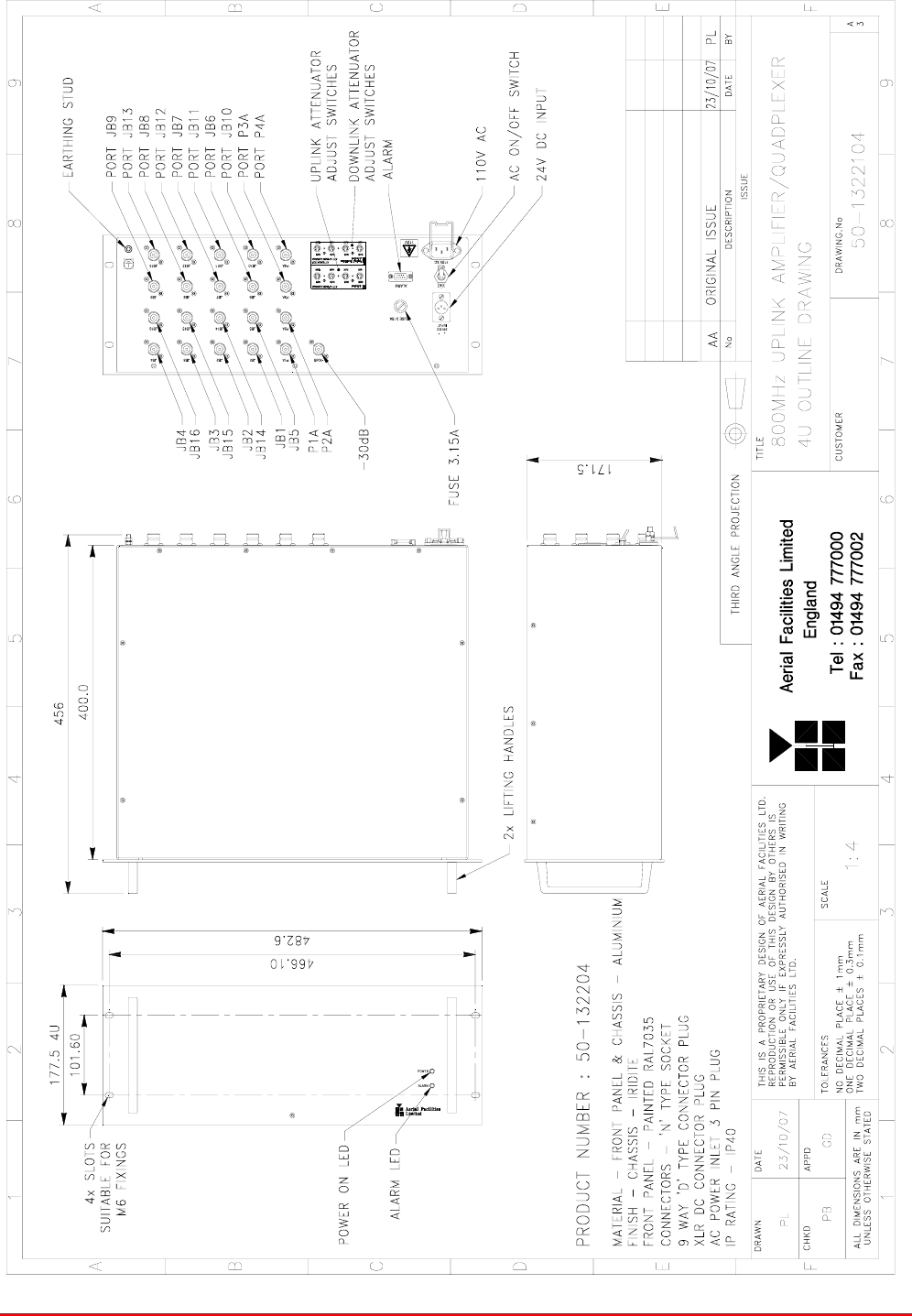
23.3.2.1. 800MHz Uplink Amplifier/ Quadplexer (50-132204) Outline Drawing
Drawing number 50-1322104
STTRS DOCUMENTATION
Document Number 80-330501HBKM – Issue A - Draft Page 436 of 500
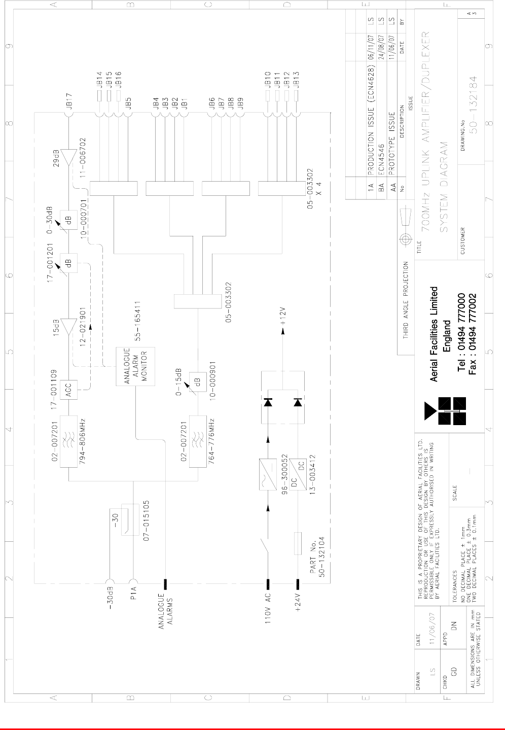
23.3.2.2. 800MHz Uplink Amplifier/ Quadplexer (50-132204) System Diagram
Drawing number 50-132284

STTRS DOCUMENTATION
Document Number 80-330501HBKM – Issue A - Draft Page 437 of 500
23.3.2.3. Bandpass Filter (02-007206)
The bandpass filters are multi-section designs with a bandwidth dependent upon the passband
frequencies, (both tuned to customer requirements). The response shape is basically Chebyshev with
a passband design ripple of 0.1dB. The filters are of slot coupled, folded combline design, and are
carefully aligned during manufacture in order to optimise the insertion loss, VSWR and
intermodulation characteristics of the unit. The tuned elements are silver-plated to reduce surface
ohmic losses and maintain a good VSWR figure and 50Ω load at the input and output ports.
Being passive devices, the bandpass filters should have an extremely long operational life and require
no maintenance. Should a filter be suspect, it is usually most time efficient to replace the module
rather than attempt repair or re-tuning.
No adjustments should be attempted without full network sweep analysis facilities to monitor both
insertion loss and VSWR simultaneously.
02-007206 Specification
PARAMETER SPECIFICATION
Response type Chebyshev
Frequency range 800 - 950MHz *
Bandwidth 25MHz *
Number of sections 8
Insertion loss 1.2 dB
VSWR better than 1.2:1
Connectors SMA female
Power handling 100W max
operation -20°C to +60°C Temperature
range storage -40°C to +70°C
Weight 3 kg (typical) *tuned to Customer's specification
23.3.2.4. Four Way Splitter/Combiner (05-003302)
The Splitter/Combiner used is a device for accurately matching two or more RF signals to single or
multiple ports, whilst maintaining an accurate 50Ω load to all inputs/outputs and ensuring that the
VSWR and insertion losses are kept to a minimum. Any unused ports should be terminated with an
appropriate 50Ω load.
Four Way Splitter (05-003302) Specification
PARAMETER SPECIFICATION
Frequency range 700-980MHz
Bandwidth 180MHz
Rejection >14dB
Insertion loss <7.0dB (in band)
Connectors N type, female
Weight <1.5kg
operational -20%C to +60%C Temperature
range storage -40%C to +70%C

STTRS DOCUMENTATION
Document Number 80-330501HBKM – Issue A - Draft Page 438 of 500
23.3.2.5. Wideband Asymmetric Coupler (07-015105)
The purpose of Wideband Asymmetric Coupler (07-015105) is to tap off a known portion (in this case
30dB) of RF signal from transmission lines and to combine them, for example through splitter units for
different purposes (alarms/monitoring etc.), whilst maintaining an accurate 50Ω load to all
ports/interfaces throughout the specified frequency range. They are known formally as directional
couplers as they couple power from the RF mainline in one direction only.
07-015105 Specification
PARAMETER SPECIFICATION
Construction Inductive air gap
Frequency 800-2500MHz
Through loss 0.4dB (typical)
Coupling level -30dB ±0.5dB
Isolation N/A
Weight <1.0kg
Connectors SMA, female
operation -20°C to +60°C
Temperature
range storage -40°C to +70°C
23.3.2.6. Switched Attenuator 0.25Watt, 0 - 30dB (10-000701)
In many practical applications for Cell Enhancers etc., the gain in each path is found to be excessive.
Therefore, provision is made within the unit for the setting of attenuation in each path, to reduce the
gain.
Switched Attenuator 10-000701 provides attenuation from 0 to 30dB in 2 dB steps The attenuation is
simply set using the four miniature toggle switches on the top of each unit. Each switch is clearly
marked with the attenuation it provides, and the total attenuation in line is the sum of the values
switched in. They are designed to maintain an accurate 50Ω impedance over their operating
frequency at both input and output.
10-000701 Specification
PARAMETER SPECIFICATION
Attenuation Values 0-30dB
Attenuation Steps 2, 4, 8 and 16dB
Power Handling 0.25 Watt
Attenuation Accuracy ± 1.0 dB
Frequency Range DC to 1GHz
Impedance 50Ω
Connectors SMA
VSWR 1.3:1
Weight 0.2kg
operation -20°C to +60°C Temperature
range storage -40°C to +70°C

STTRS DOCUMENTATION
Document Number 80-330501HBKM – Issue A - Draft Page 439 of 500
23.3.2.7. Switched Attenuator 0.25W, 0 - 15dB (10-000901)
In many practical applications for Cell Enhancers etc., the gain in each path is found to be excessive.
Therefore, provision is made within the unit for the setting of attenuation in each path, to reduce the
gain.
10-000901 provides attenuation from 0 - 15dB in 2 dB steps The attenuation is simply set using the
four miniature toggle switches on the top of each unit. Each switch is clearly marked with the
attenuation it provides, and the total attenuation in line is the sum of the values switched in. They are
designed to maintain an accurate 50Ω impedance over their operating frequency at both input and
output.
10-000901 Specification
PARAMETER SPECIFICATION
Attenuation Values 0-15dB
Attenuation Steps 1, 2, 4 and 8dB
Power Handling 0.25 Watt
Attenuation Accuracy ± 1.0 dB
Frequency Range DC to 1GHz
Impedance 50Ω
Connectors SMA
VSWR 1.3:1
Weigh 0.2kg
operation -20°C to +60°C Temperature
range storage -40°C to +70°C
23.3.2.8. Low Noise Amplifier (11-006702)
The Gallium-Arsenide low noise amplifiers used in 800MHz Line Amplifier (55-165703) are double
stage, solid-state low noise amplifiers. Class A circuitry is used throughout the units to ensure
excellent linearity and extremely low noise over a very wide dynamic range. The active devices are
very moderately rated to provide a long trouble-free working life. There are no adjustments on these
amplifiers, and in the unlikely event of a failure, then the complete amplifier should be replaced. This
amplifier features its own in-built alarm system which gives a volt-free relay contact type alarm that is
easily integrated into the main alarm system.
11-006702 Specification
PARAMETER SPECIFICATION
Frequency range 800 – 1000MHz
Bandwidth <200MHz
Gain 29dB (typical)
1dB Compression point 20dBm
OIP3 33dBm
Input/Output return loss >18dB
Noise figure 1.3dB (typical)
Power consumption 180mA @ 24V DC
Supply voltage 10-24V DC
Connectors SMA female
operational -10°C to +60°C Temperature
range storage -20°C to +70°C
Size 90 x 55 x 30.2mm
Weight 290gms (approximately)
STTRS DOCUMENTATION
Document Number 80-330501HBKM – Issue A - Draft Page 440 of 500
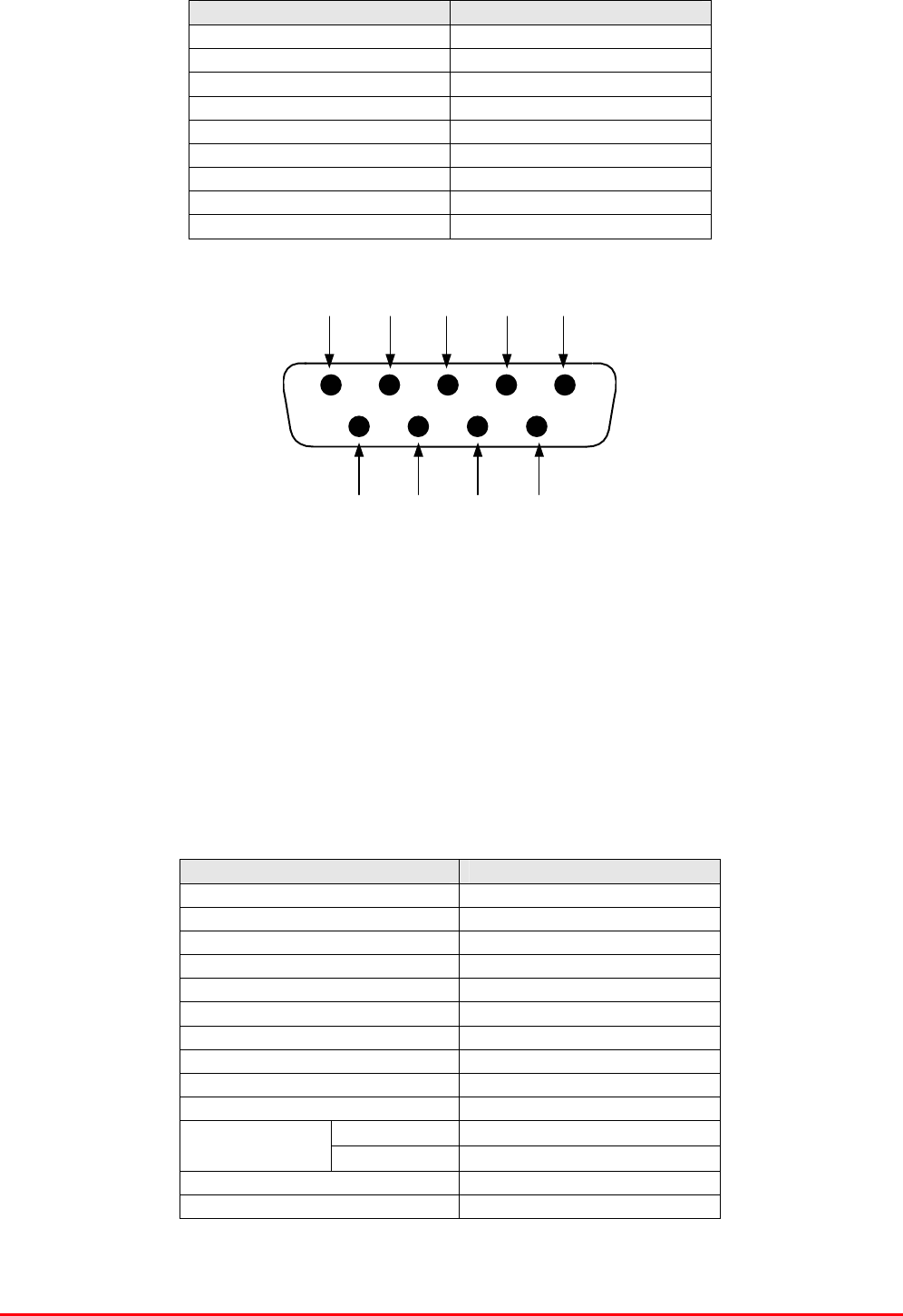
7 8 96
1 2 3 4 5
9-Way Pin-Out Graphical Representation
Low Noise Amplifier (11-006702) ‘D’ Connector Pin-out details
Connector pin Signal
1 +Ve input (10-24V)
2 GND
3 Alarm RelayO/P bad
4 Alarm Relay common
5 Alarm Relay good
6 No connection
7 TTL voltage set
8 TTL alarm/0V (good)
9 O/C good/0V bad
23.3.2.9. Low Power Amplifier (12-021901)
The low power amplifier used is a triple stage solid-state low-noise amplifier. Class A circuitry is used
in the unit to ensure excellent linearity over a very wide dynamic range. The three active devices are
very moderately rated to provide a long trouble-free working life.
Its housing is an aluminium case (Iridite NCP finish) with SMA connectors for the RF input/output and
a D-Type connector for the power supply and the Current Fault Alarm Function.
There are no adjustments on this amplifier, and in the unlikely event of failure then the entire amplifier
should be replaced.
Low Power Amplifier (12-021901) Specification
PARAMETER SPECIFICATION
Frequency range 800-960MHz*
Bandwidth 20MHz *
Maximum RF output >1.0 Watt
Gain 15dB
1dB compression point +30.5dBm
3rd order intercept point +43dBm
Noise Figure <6dB
VSWR better than 1.5:1
Connectors SMA female
Supply 500mA @ 10-15V DC
operational -10°C to +60°C
Temperature
range storage -20°C to +70°C
Weight 0.5 kg
Size 167x52x25mm
* Tuned to Customer’s specification
STTRS DOCUMENTATION
Document Number 80-330501HBKM – Issue A - Draft Page 441 of 500
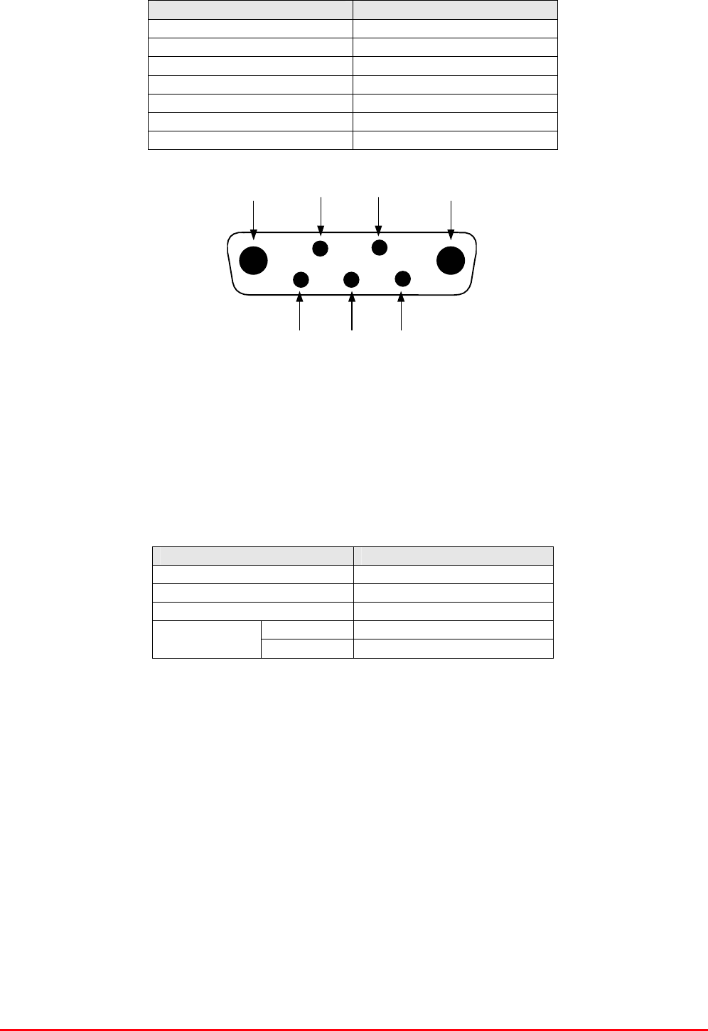
A1 A2
1 2
3 4 5
7-Way Connector Graphical Representation
Low Power Amplifier (12-021901) 7-Way Connector Pin-outs
Connector Pin Signal
A1 (large pin) +24V DC
A2 (large pin) GND
1 Alarm relay common
2 TTL alarm/0V good
3 Alarm relay contact (bad)
4 Alarm relay contact (good)
5 O/C good/0V bad (TTL)
23.3.2.10. DC/DC Converter 13-003412
13-003412 is based upon an O.E.M. DC/DC Converter module with a wide input range and and is
used to derive a 12V fixed voltage power supply rail from a higher voltage supply, in this case 24V. In
the event of failure this unit should not be repaired, only replaced.
13-003412 Specification
PARAMETER SPECIFICATION
Operating voltage 18 – 75V DC
Output voltages 12V (typical)
Output current 5.0A (Max)
operational -10%C to +60%C Temperature
range storage -20%C to +70%C
23.3.2.11. AGC System
AGC Detector Unit (17-001109)
AGC Attenuator Unit (17-001201)
Equipment 800MHz Uplink Amplifier/ Quadplexer (50-132204) is fitted with a wide dynamic range
Automatic Gain Control (AGC) system. This is fitted in the Uplink path to avoid overloading the
amplifiers (with the associated performance degradation) should a mobile be operated very close to
the unit.
The AFL wide dynamic range Automatic Gain Control system consists of two units, a
detector/amplifier and an attenuator. The logarithmic detector/amplifier unit is inserted in the RF path
on the output of the power amplifier, and the attenuator is situated in the RF path between the 1st and
2nd stages of amplification.

STTRS DOCUMENTATION
Document Number 80-330501HBKM – Issue A - Draft Page 442 of 500
Normally the attenuator is at minimum attenuation. The detector/amplifier unit monitors the RF level
being delivered by the power amplifier, and when a certain threshold is reached it begins to increase
the value of the attenuator to limit the RF output to the (factory set) threshold. Therefore overloading
of the power amplifier is avoided.
The factory set threshold is 1dB below the Enhancer 1dB compression point. Some adjustment of this
AGC threshold level is possible, a 10dB range is mostly achieved. It is not recommended under any
circumstances to adjust the AGC threshold to a level greater than the 1dB compression point as
system degradation will occur.
The detector comprises of a 50Ω transmission line with a resistive tap which samples a small portion
of the mainline power. The sampled signal is amplified and fed to a conventional half wave diode
rectifier, the output of which is a DC voltage proportional to the RF input signal.
This DC voltage is passed via an inverting DC amplifier with integrating characteristics, to the output,
which drives the attenuation control line of the corresponding AGC attenuator. This unit is fitted at
some earlier point in the RF circuit.
For small signals, below AGC onset, the output control line will be close to 12V and the AGC
attenuator will have minimum attenuation. As the signal level increases the control line voltage will
fall, increasing the attenuator value and keeping the system output level at a constant value.
The AGC onset level is adjusted by the choice of sampler resistor R1 and by the setting of
potentiometer VR1, (factory set at the time of system test) do not adjust unless able to monitor
subsequent RF levels. The attenuator comprises a 50Ω P.I.N diode, voltage-variable attenuator with a
range of 3 to 30dB. The attenuation is controlled by a DC voltage which is derived from the
associated AGC detector unit.
Wide Dynamic Range AGC Specification
PARAMETER SPECIFICATION
Frequency Range up to 1000MHz
Attenuation Range 3 to 30dB
Attenuation Steps continuously variable
VSWR better than 1.2:1
RF Connectors SMA female
attenuator 1W Power
Handling detector/amp >30W (or as required)
operation -10°C to +60°C Temperature
Range storage -20°C to +70°C
attenuator pcb 50 x 42 x 21mm
Size detector/amp pcb 54 x 42 x 21mm
attenuator 90gm
Weight detector/amp 100gm
23.3.2.12. Dummy Load (80-007401)
When a combiner system is used to split or combine RF signals, in many cases it is most cost
effective to use a standard stock item 4, 6 or 8 port device where, in fact, only a 3 or 6 port device is
needed. In this case the Four Way Splitters (05-003302) each have their unused ports terminated with
Dummy Load (80-007401) in order to preserve the correct impedance of the devices over the
specified frequency range. This also has the advantage of allowing future expansion capability should
extra channels or other functions become necessary.

STTRS DOCUMENTATION
Document Number 80-330501HBKM – Issue A - Draft Page 443 of 500
Dummy Load (80-007401) Specification
Parameter Specification
Frequency Range 0 to 1000MHz
Power Rating 1.6 Watts
0-500MHz 1.2:1 VSWR
(Max) 500-1000MHz 1.3:1
Temperature -20 to +55°C
Connector ‘N’ type Male
Nominal Impedance 50 Ohms
23.3.2.13. 12V (Single) Relay Board (80-008901)
The General Purpose Relay Board allows the inversion of signals and the isolation of circuits. It is
equipped with a single dual pole change-over relay RL1, with completely isolated wiring, accessed
via a 15 way in-line connector. The relay is provided with polarity protection diodes and diodes for
suppressing the transients caused by "flywheel effect" which can destroy switching transistors or
induce spikes on neighbouring circuits. It’s common use is to amalgamate all the alarm signals into
one, volts-free relay contact pair for the main alarm system.
80-008901 Specification
PARAMETER SPECIFICATION
Operating voltage 8 to 30V (floating earth)
Alarm threshold Vcc - 1.20 volt +15%
Alarm output relay contacts:
Max. switch current 1.0Amp
Max. switch volts 120Vdc/60VA
Max. switch power 24W/60VA
Min. switch load 10.0µA/10.0mV
Relay isolation 1.5kV
Mechanical life >2x10⁷ operations
Relay approval BT type 56
Connector details Screw terminals
operational -10°C to +60°C Temperature
range storage -20°C to +70°C
23.3.2.14. Dual Diode Assembly (94-100004)
The purpose of these dual diode assemblies is to allow two DC voltage sources to be combined, so
that the main DC rail within the equipment can be sourced from either a mains driven PSU, or
externally through an XLR connector or from dual mains driven PSUs . They are very heavy-duty
diodes and they prevent any reverse current from flowing back to their source or the alternative
supply rail. Combining diodes such as these will also be used if the equipment is to be powered from
external back-up batteries.

STTRS DOCUMENTATION
Document Number 80-330501HBKM – Issue A - Draft Page 444 of 500
23.3.2.15. 12V Switch-Mode PSU (96-300052)
No routine maintenance of the PSU is required. If a fault is suspected, then the output voltage from
the power supply may be measured on its output terminals. This is typically set to 12.2V. The
adjustment potentiometer will be found close to the DC output terminals.
All the PSUs used in AFL Cell Enhancers are capable of operation from either 110 or 220V nominal
AC supplies. The line voltage is sensed automatically, so no adjustment or link setting is needed by
the operator.
96-300052 Specification
AC Input Supply 110 or 220V nominal
Voltage 85 - 265V AC (absolute limits)
Frequency 47 to 63Hz
DC Output Supply 12V DC (nominal)
Voltage 10.5-13.8V (absolute limits)
Current 12.5A

STTRS DOCUMENTATION
Document Number 80-330501HBKM – Issue A - Draft Page 445 of 500
24. INTERNATIONAL STATION 700MHZ BDA (80-330558-1)
Rack number C09-CR-09
International Station 700MHz BDA (80-330558-1) List of Major Components
Section Component
Part Component Part Description Qty Per
Assembly
24.3.1. 05-003007 4 Port Hybrid Coupler 1
24.3.2. 09-000401 Dummy Load 1
24.3.3. 50-132105 700MHz 5 Cavity Combiner System 1
24.3.4. 50-132106 700MHz 4 Cavity Combiner System 1
STTRS DOCUMENTATION
Document Number 80-330501HBKM – Issue A - Draft Page 446 of 500
24.1. International Station 700MHz BDA (80-330558-1) Rack Drawing
Drawing number 80-330558
STTRS DOCUMENTATION
Document Number 80-330501HBKM – Issue A - Draft Page 447 of 500
24.2. International Station 700MHz BDA (80-330558-1) System Diagram
Drawing number 80-330588-1

STTRS DOCUMENTATION
Document Number 80-330501HBKM – Issue A - Draft Page 448 of 500
24.3. International Station 700MHz BDA (80-330558-1) Major Components
24.3.1. 4 Port Hybrid Coupler (05-003007)
This transmitter hybrid coupler is a device for accurately matching two or more RF signals to single or
multiple ports, whilst maintaining an accurate 50Ω load to all inputs/outputs and ensuring that the
insertion losses are kept to a minimum. Any unused ports should be terminated with an appropriate
50Ω load. In this specific instance one port of 4 Port Hybrid Coupler (05-003007) is terminated with
Dummy load 09-000401 (see below).
05-003007 Specification
PARAMETER SPECIFICATION
Frequency range 700-900MHz
Bandwidth 200MHz
Rejection >14dB
Insertion loss 6.5dB (in band, typical)
Connectors SMA
Weight <1.0kg
operational -10%C to +60%C Temperature
range storage -20%C to +70%C
24.3.2. Dummy Load (09-000401)
When a combiner system is used to split or combine RF signals, in many cases it is most cost
effective to use a standard stock item 4, 6 or 8 port device where, in fact, only a 3 - 6 port device is
needed. In this case the splitter/combiner module has one of its ports terminated (both uplink &
downlink) with an appropriate load in order to preserve the correct impedance of the device over the
specified frequency range. This has the advantage of allowing future expansion capability should
extra channels or other functions become necessary.
09-000401 Specification
PARAMETER SPECIFICATION
Frequency Range 10 - 1000 MHz
Power Rating 60 watts continuous
VSWR Better than 1.1:1
Impedance 50 Ohms
Temperature Range -20 to +60°C
RF Connectors N Type female
Dimension 119mm x 51mm x 51mm
Weight 485grams
Finish Black Anodised
MTBF >180,000 hours

STTRS DOCUMENTATION
Document Number 80-330501HBKM – Issue A - Draft Page 449 of 500
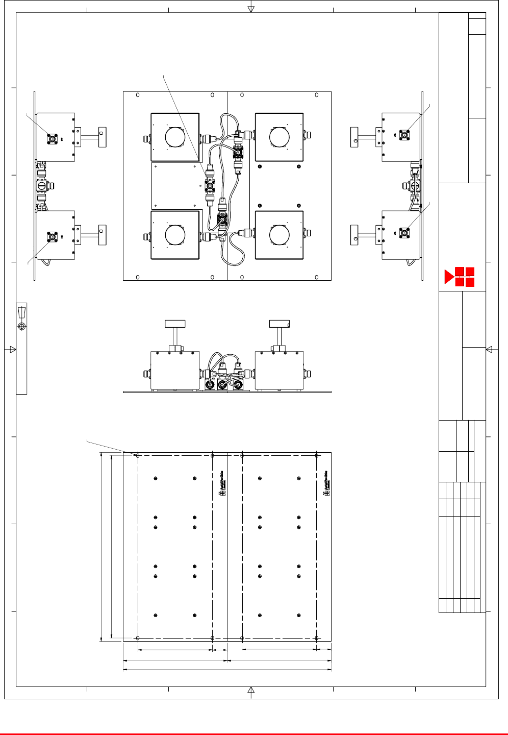
24.3.3. 700MHz 5 Cavity Combiner System (50-132105)
700MHz 5 Cavity Combiner System (50-132105) consists of 5 Dielectric Cavity Resonators mounted
on two 3U rack mount panels, three on one panel and two on the other
700MHz 5 Cavity Combiner System (50-132105) List of Major Components
section Component
Part Component Part Description Qty Per
Assembly
20.3.2.3. 04-003402 Dielectric Cavity Resonator 5
STTRS DOCUMENTATION
Document Number 80-330501HBKM – Issue A - Draft Page 450 of 500
700MHz 5CH CAVITY COMBINER OUTLINE DRAWING
1:3 50-1321105
PB
18/10/2007
GD
18/10/2007 AA
02/10/07
PL
PORT JA3
PORT JA2
PORT JA1
PORT JA4 PORT JA5
8x SLOTS SUITABLE FOR M6 FIXINGS
532.2 12U
265.9 6U 265.9 6U
I1
466.00
482.5
37.7 190.50 37.7 190.50
PRODUCT NUMBER : 50-132105
MATERIAL - FRONT PANEL & CHASSIS - ALUMINIUM
FINISH - FRONT PANEL - IRIDITE
FRONT PANEL - PAINTED RAL7035 (FRONT FACE & EDGES)
CONNECTORS - `N' TYPE SOCKET
AA ORIGINAL ISSUE PL
390
374
24.3.3.1. 700MHz 5 Cavity Combiner System (50-132105) Outline Drawing
Drawing number 50-1321105
STTRS DOCUMENTATION
Document Number 80-330501HBKM – Issue A - Draft Page 451 of 500
24.3.3.2. 700MHz 5 Cavity Combiner System (50-132105) System Diagram
Drawing number 50-132185

STTRS DOCUMENTATION
Document Number 80-330501HBKM – Issue A - Draft Page 452 of 500
24.3.3.3. Dielectric Cavity Resonator (04-003402)
Cavity resonators are used in this system for their high Q factor response and power handling
characteristics. Being finely tuned items, they can be prone to being de-tuned by mechanical shock or
vibration therefore these units should be handled, stored and installed with care.
Note that the cavities are coupled together using critical length harnesses. If any cable is to be
changed the exact same length and type of cable should be used for replacement.
04-003402 Specification
Specification Parameter
Frequency Range 764 to 776 MHz *
Bandwidth 25 kHz
Insertion Loss < 1.0 dB
Return Loss > 15 dB (at both ports)
Attenuation > 10 dB at Fc ± 1 MHz
Power Handling (CW) 20W
Environmental IP54
Size 124mm x 158mm x 157mm**
Weight 1.5 kg
Connectors N female
operation -20°C to +60°C
Temperature
range storage -40°C to +70°C
*Tuned to Customer’s specification
**Height is dependant upon position of tuning plunger

STTRS DOCUMENTATION
Document Number 80-330501HBKM – Issue A - Draft Page 453 of 500
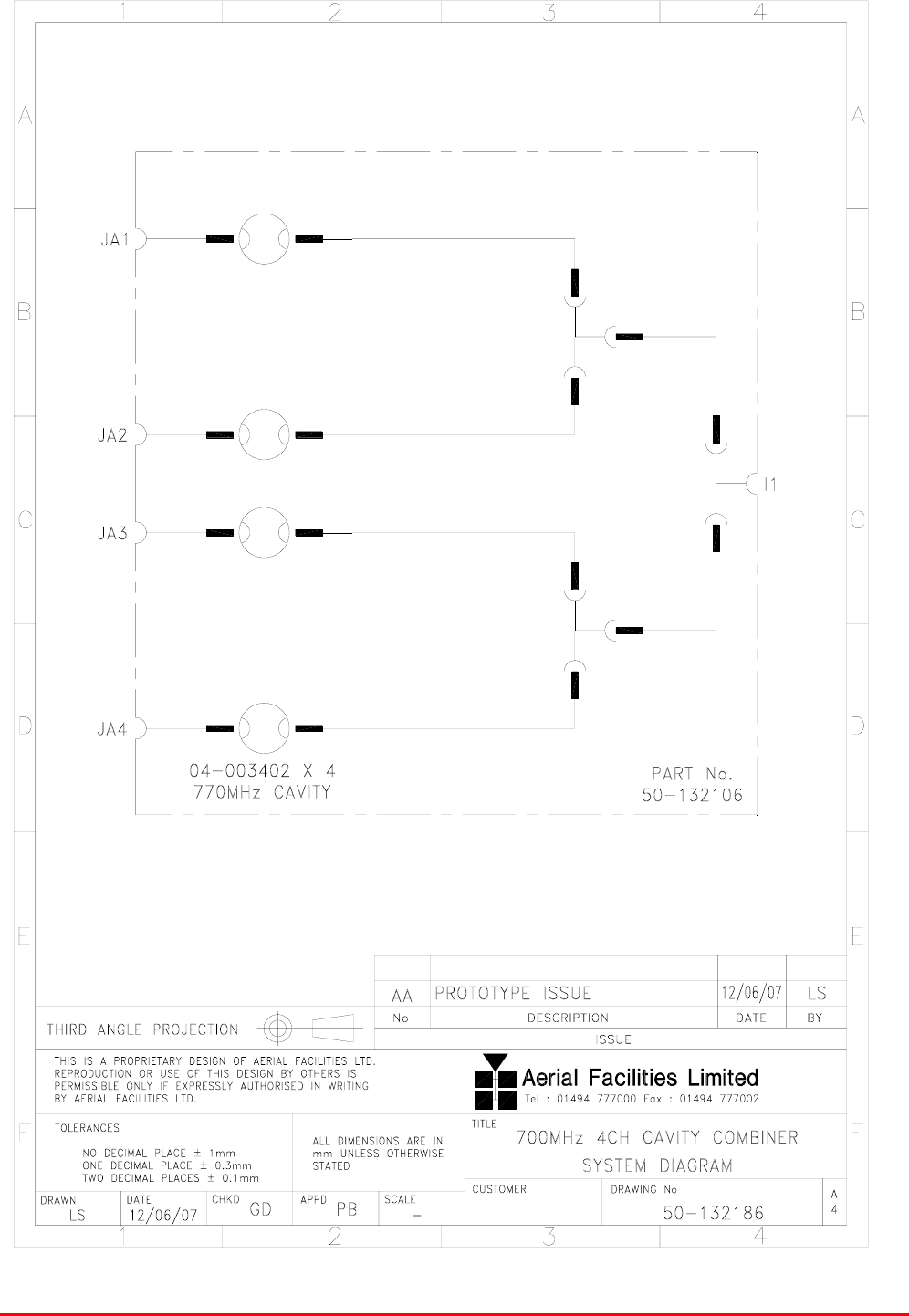
24.3.4. 700MHz 4 Cavity Combiner System (50-132106)
700MHz 4 Cavity Combiner System (50-132106) consists of 4 Dielectric Cavity Resonators mounted
on two 3U rack mount panels, three on one panel and two on the other
700MHz 4 Cavity Combiner System (50-132106) List of Major Components
section Component
Part Component Part Description Qty Per
Assembly
20.3.3.3. 04-003402 Dielectric Cavity Resonator 4
STTRS DOCUMENTATION
Document Number 80-330501HBKM – Issue A - Draft Page 454 of 500
1
1
2
2
3
3
4
4
5
5
6
6
7
7
8
8
A A
B B
C C
D D
E E
F F
A
2
Drawing No
Title
Customer
Drawn Date
Checked Approved
THIS IS A PROPRIE TARY DESIGN OF AERIA L FACILITIES LTD
REPRODUCTION OR USE OF THIS DESIGN B Y OTHER IS
PERMISSABLE ON LY IF EXPRESS LY AUTHORISED IN WRITING
BY AERIA L FACILITIES LTD
SCALE
Aerial Facilities Limited
England
Tel : 01494 777000
Fax : 01494 777002
ALL DIMENSIONS ARE IN mm
UNLESS OTHE RWISE S TATED
REVISION
No DESCRIPTION DATE BY
TWO DECIMA L PLACESG1mm
ONE DECIMA L PLACEG 0.3mm
NO DECIMA L PLACEG 1mm
TOLERANCES
700MHZ 4 C AVITY COMBINER OUTLINE DR AWING
1:3 50-1321106
PB
26/10/2007
GD
26/10/2007
AA
16/10/07
PL
PORT JA2
PORT JA1
PORT JA4 PORT JA3
8x SLOTS SUI TABLE FOR M6 FIXINGS
532.2 12U
265.9 6U 265.9 6U
I1
466.00
482.50
37.7 190.50 37.7 190.50
PRODUC T NUMBER : 50-132106
MATERIAL - FRON T PANEL & CHASSIS - ALUMINIUM
FINISH - FRON T PANEL - IRIDITE
FRON T PANEL - PAINTED RAL7035 (FRON T FACE & EDGES)
CONNEC TORS - `N' TYPE SOCKE T
AA ORIGINAL ISSUE
15/10/07
PL
THIRD ANGLE PROJECTION
24.3.4.1. 700MHz 4 Cavity Combiner System (50-132106) Outline Drawing
Drawing number 50-1321106
STTRS DOCUMENTATION
Document Number 80-330501HBKM – Issue A - Draft Page 455 of 500
24.3.4.2. 700MHz 4 Cavity Combiner System (50-132106) System Diagram
Drawing number 50-132186

STTRS DOCUMENTATION
Document Number 80-330501HBKM – Issue A - Draft Page 456 of 500
24.3.4.3. Dielectric Cavity Resonator (04-003402
Cavity resonators are used in this system for their high Q factor response and power handling
characteristics. Being finely tuned items, they can be prone to being de-tuned by mechanical shock or
vibration therefore these units should be handled, stored and installed with care.
Note that the cavities are coupled together using critical length harnesses. If any cable is to be
changed the exact same length and type of cable should be used for replacement.
04-003402 Specification
Specification Parameter
Frequency Range 764 to 776 MHz*
Bandwidth 25 kHz
Insertion Loss < 1.0 dB
Return Loss > 15 dB (at both ports)
Attenuation > 10 dB at Fc ± 1 MHz
Power Handling (CW) 20W
Environmental IP54
Size 124mm x 158mm x 157mm**
Weight 1.5 kg
Connectors N female
operation -20°C to +60°C
Temperature
range storage -40°C to +70°C
*Tuned to Customer’s specification
**Height is dependant upon position of tuning plunger

STTRS DOCUMENTATION
Document Number 80-330501HBKM – Issue A - Draft Page 457 of 500
25. INTERNATIONAL STATION 700MHz BDA (80-330558-2)
Rack number C09-CR-10
International Station 700MHz BDA (80-330558-2) List of Major Components
Section Component
Part Component Part Description Qty Per
Assembly
25.3.1. 50-132102 700MHz Channelised Amplifier 9
25.3.2. 50-132107 700MHz Uplink Amplifier 1
25.3.3. 50-132108 700MHz Downlink Splitter 1

STTRS DOCUMENTATION
Document Number 80-330501HBKM – Issue A - Draft Page 458 of 500
25.1. International Station 700MHz BDA (80-330558-2) Rack Drawing
Drawing number 80-330558
STTRS DOCUMENTATION
Document Number 80-330501HBKM – Issue A - Draft Page 459 of 500
25.2. International Station 700MHz BDA (80-330558-2) System Diagram
Drawing number 80-330588-2

STTRS DOCUMENTATION
Document Number 80-330501HBKM – Issue A - Draft Page 460 of 500
25.3. International Station 700MHz BDA (80-330558-2) Major Components
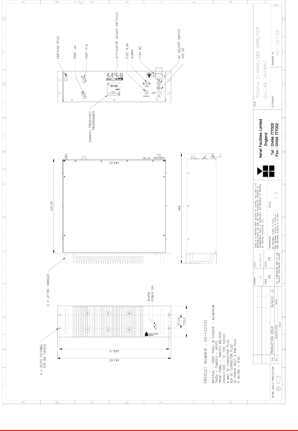
25.3.1. 700MHz Channelised Amplifier (50-132102)
3U rack mount shelf
700MHz Channelised Amplifier (50-132102) List of major Components
Section Component
Part Component Part Description Qty Per
Assembly
25.3.1.3. 09-000902 Dummy Load 1
25.3.1.4. 10-000901 Switched Attenuator 0.25W, 0 - 15dB 1
25.3.1.5. 11-006702 Low Noise Amplifier 1
25.3.1.6. 12-020804 Power Amplifier 1
25.3.1.7. 13-003412 DC/DC Converter 1
25.3.1.8. 17-009127 Channel Selectivity Module 1
25.3.1.9. 17-011501 Channel Control Module 1
25.3.1.10. 80-008902 24V Relay Board 1
25.3.1.11. 93-910048 Dual Isolator 1
25.3.1.12. 94-100004 Dual Diode Assembly 1
25.3.1.13. 96-300060 PSU 24V 1
STTRS DOCUMENTATION
Document Number 80-330501HBKM – Issue A - Draft Page 461 of 500
POWER ON
ALARM
25.3.1.1. 700MHz Channelised Amplifier (50-132102) Outline Drawing
Drawing number 50-1321102
STTRS DOCUMENTATION
Document Number 80-330501HBKM – Issue A - Draft Page 462 of 500
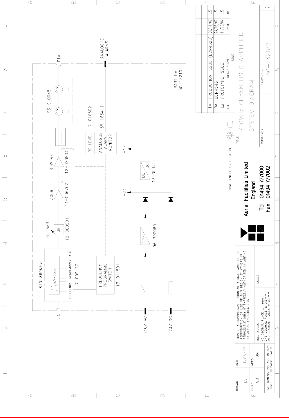
25.3.1.2. 700MHz Channelised Amplifier (50-132102) System diagram
Drawing number 50-132182

STTRS DOCUMENTATION
Document Number 80-330501HBKM – Issue A - Draft Page 463 of 500
25.3.1.3. Dummy load 09-000902
Dual Isolator (770MHz) (93-910048) has one of its ports terminated with Dummy load 09-000902 in
order to achieve the correct power rating to absorb the reflected power levels that can be reasonably
expected within the system.
09-000902 specification
PARAMETER SPECIFICATION
Frequency Range 0 - 2500 MHz
Power Rating 25 Watts continuous
VSWR Better than 1.1:1
Impedance 50 Ohms
Temperature Range -20 to +60°C
RF Connectors N Type female
Dimension 110.3mm x 38.1mm x
Weight 485 grams
Finish Black Anodised
RF Connector N Type male
Environmental IP66
MTBF >180,000 hours
25.3.1.4. Switched Attenuator 0.25W, 0 - 15dB (10-000901)
In many practical applications for Cell Enhancers etc., the gain in each path is found to be excessive.
Therefore, provision is made within the unit for the setting of attenuation in each path, to reduce the
gain.
10-000901 provides attenuation from 0 - 15dB in 2 dB steps The attenuation is simply set using the
four miniature toggle switches on the top of each unit. Each switch is clearly marked with the
attenuation it provides, and the total attenuation in line is the sum of the values switched in. They are
designed to maintain an accurate 50Ω impedance over their operating frequency at both input and
output.
10-000901 Specification
PARAMETER SPECIFICATION
Attenuation Values 0-15dB
Attenuation Steps 1, 2, 4 and 8dB
Power Handling 0.25 Watt
Attenuation Accuracy ± 1.0 dB
Frequency Range DC to 1GHz
Impedance 50Ω
Connectors SMA
VSWR 1.3:1
Weight 0.2kg
operation -20°C to +60°C Temperature
range: storage -40°C to +70°C
STTRS DOCUMENTATION
Document Number 80-330501HBKM – Issue A - Draft Page 464 of 500
7 8 96
1 2 3 4 5
9-Way Pin-Out Graphical Representation
25.3.1.5. Low Noise Amplifier (11-006702)
The Gallium-Arsenide low noise amplifiers used in 800MHz Line Amplifier (55-165703) are double
stage, solid-state low noise amplifiers. Class A circuitry is used throughout the units to ensure
excellent linearity and extremely low noise over a very wide dynamic range. The active devices are
very moderately rated to provide a long trouble-free working life. There are no adjustments on these
amplifiers, and in the unlikely event of a failure, then the complete amplifier should be replaced. This
amplifier features its own in-built alarm system which gives a volt-free relay contact type alarm that is
easily integrated into the main alarm system.
11-006702 Specification
PARAMETER SPECIFICATION
Frequency range 800 – 1000MHz
Bandwidth <200MHz
Gain 29dB (typical)
1dB Compression point 20dBm
OIP3 33dBm
Input/Output return loss >18dB
Noise figure 1.3dB (typical)
Power consumption 180mA @ 24V DC
Supply voltage 10-24V DC
Connectors SMA female
operational -10°C to +60°C Temperature
range storage -20°C to +70°C
Size 90 x 55 x 30.2mm
Weight 290gms (approximately)
Low Noise Amplifier (11-006702) ‘D’ Connector Pin-out details
Connector pin Signal
1 +Ve input (10-24V)
2 GND
3 Alarm RelayO/P bad
4 Alarm Relay common
5 Alarm Relay good
6 No connection
7 TTL voltage set
8 TTL alarm/0V (good)
9 O/C good/0V bad

STTRS DOCUMENTATION
Document Number 80-330501HBKM – Issue A - Draft Page 465 of 500
25.3.1.6 Power Amplifier (12-020804)
This amplifier is a Class AB 40W power amplifier from 860MHz to 960MHz in balanced configuration.
The amplifier demonstrates a very good input/output return loss (RL) and it has a built-in Current Fault
Alarm Function.
The unit housing is an aluminium case (Iridite NCP finish) with SMA connectors for the RF
input/output and a D-Type connector for the power supply and the Current Fault Alarm Function.
12-020804 specification
Specification Parameter
Frequency Range 860 - 960MHz
Gain ≥28.0 dB
Gain Flatness 1.0dB p-p Max
∆Gain vs. Temperature 2.5dB Max
Input RL 15dB Min
Output RL 15dB Min
Output Power @ P1dB 46.0dBm Min
DC Supply Voltage 24 ± 0.5Vdc
RF Input Power 25dBm
At P1dB 6000mA Max DC Supply
Current With no RF input (Iqc) 1700mA Max
operational -40°C to +70°C Temperature
range storage -40°C to +100°C
7-Way Connector Pin-outs Connector Pin Signal
A1 +24V DC
A2 GND
1 Alarm relay common
2 TTL alarm/0V good
3 Alarm relay contact (bad)
4 Alarm relay contact (good)
5 O/C good/0V bad (TTL)

STTRS DOCUMENTATION
Document Number 80-330501HBKM – Issue A - Draft Page 466 of 500
25.3.1.7. DC/DC Converter 13-003412
13-003412 is based upon an O.E.M. DC/DC Converter module with a wide input range and and is
used to derive a 12V fixed voltage power supply rail from a higher voltage supply, in this case 24V. In
the event of failure this unit should not be repaired, only replaced.
13-003412 Specification
PARAMETER SPECIFICATION
Operating voltage 18 – 75V DC
Output voltages 12V (typical)
Output current 5.0A (Max)
operational -10%C to +60%C Temperature
range storage -20%C to +70%C
25.3.1.8. Channel Selectivity Module (17-009127)
Channel Selectivity Module (17-009127) is employed when requirement dictates that very narrow
bandwidths (single operating channels), must be selected from within the operating passband. One
channel selectivity module is required for each channel.
The Channel Selectivity Module is an Up/Down frequency converter that mixes the incoming channel
frequency with a synthesised local oscillator, so that it is down-converted to an Intermediate
Frequency (IF) in the upper HF range. An eight pole crystal filter in the IF amplifier provides the
required selectivity to define the operating passband of the Cell Enhancer to a single PMR channel.
The same local oscillator then converts the selected IF signal back to the channel frequency.
Selectivity is obtained from a fixed bandwidth block filter operating at an intermediate frequency (IF) in
the low VHF range. This filter may be internal to the channel selectivity module (Crystal or SAW filter)
or an externally mounted bandpass filter, (LC or Helical Resonator). Various IF bandwidths can
therefore be accommodated. A synthesized Local Oscillator is employed in conjunction with high
performance frequency mixers, to translate between the signal frequency and IF.
The operating frequency of each channel selectivity module is set by the programming of channel
selectivity module frequencies and is achieved digitally, via hard wired links, banks of DIP switches, or
via an onboard RS232 control module, providing the ability to remotely set channel frequencies.
Automatic Level Control (ALC) is provided within each channel selectivity module such that the output
level is held constant for high level input signals. This feature prevents saturation of the output mixer
and of the associated amplifiers.
Alarms within the module inhibit the channel if the synthesised frequency is not locked. The
synthesiser will not usually go out of lock unless a frequency far out of band is programmed.
The channel selectivity module is extremely complex and, with the exception of channel frequency
programming within the design bandwidth, it cannot be adjusted or repaired without extensive
laboratory facilities and the necessary specialised personnel. If a fault is suspected with any channel
selectivity module it should be tested by substitution and the complete, suspect module should then
be returned to AFL for investigation.

STTRS DOCUMENTATION
Document Number 80-330501HBKM – Issue A - Draft Page 467 of 500
25.3.1.9. Channel Control Module (17-011501)
The operating frequency for each channel in each repeater is programmed by 16 DIL (Dual In Line)
switches. The programming switches are mounted in the Channel Control Module. The Channel
Selectivity Modules are connected to the Channel Control Module via multi-way ribbon cables.
Adjacent to the DIL switches for each channel is a toggle switch to turn on and off individual channels
as required. A green LED indicates the power status of each channel.
A red LED shows the alarm condition for each channel. An illuminated alarm LED indicates that the
synthesiser has not achieved phase lock and that the module is disabled. There is a problem which
requires investigation, often a frequency programmed outside the operating frequency range.
The following information is necessary before attempting the programming procedure.
7. operating frequency
8. synthesiser channel spacing (step size)
9. synthesiser offset (IF)
Programming Procedure
Check that the required frequency falls within the operational frequency limits of the Cell Enhancer.
For each channel required, subtract the synthesiser offset from the required operating frequency and
record the resulting local oscillator frequency.
Divide each local oscillator frequency by the channel spacing and check that the result is an integer
(i.e: no remainder).
If the synthesiser division ratio is not an integer value, check the required operational frequency and
repeat the calculation checking for mistakes.
Convert the required local oscillator frequency to synthesiser programming switch state patterns
according to the following table. Note: the frequency of the passband will dictate the switch steps
used.
Switch Functions
Switch Number Synthesiser offset added when switch in UP position
12.5kHz step size 25kHz step size
1 +12.5kHz +25kHz
2 +25kHz +50kHz
3 +50kHz +100kHz
4 +100kHz +200kHz
5 +200kHz +400kHz
6 +400kHz +800kHz
7 +800kHz +1.6MHz
8 +1.6MHz +3.2MHz
9 +3.2MHz +6.4MHz
10 +6.4MHz +12.8MHz
11 +12.8MHz +25.6MHz
12 +25.6MHz +51.2MHz
13 +51.2MHz +102.4MHz
14 +102.4MHz +204.8MHz
15 +204.8MHz +409.6MHz
16 +409.6MHz +819.2MHz

STTRS DOCUMENTATION
Document Number 80-330501HBKM – Issue A - Draft Page 468 of 500
Programming Example
Frequency required: 454.000MHz
Channel spacing: 12.5kHz
Synthesiser offset: -21.4MHz
The Local Oscillator frequency is therefore:
454.000 – 21.4 = 432.600MHz
Dividing the Local Oscillator frequency by the channel spacing of 0.0125MHz:
432.600 = 34608
0.0125
This is an integer value, therefore it is OK to proceed.
Switch settings
Local Oscillator
Frequency 16 15 14 13 12 11 10 9 8 7 6 5 4 3 2 1
432.600 MHz 1 0 0 0 0 1 1 1 0 0 1 1 0 0 0 0
Switch setting: 0 = switch DOWN (ON, frequency ignored )
1 = switch UP (OFF, frequency added )
17-011501 Controller Module DIP Switch Connector Data
17-011501 Controller Module DIP Switch Connector Data
IDC PIN 25-way
Connector Function
(12.5kHz steps) Function
(25kHz steps)
1 13 Freq. bit 1 (12.5kHz) Freq. bit 1 (25kHz)
2 25 Freq. bit 2 (25kHz) Freq. bit 2 (50kHz)
3 12 Freq. bit 3 (50kHz) Freq. bit 3 (100kHz)
4 24 Freq. bit 4 (100kHz) Freq. bit 4 (200kHz)
5 11 Freq. bit 5 (200kHz) Freq. bit 5 (400kHz)
6 23 Freq. bit 6 (400kHz) Freq. bit 6 (800kHz)
7 10 Freq. bit 7 (800kHz) Freq. bit 7 (1.6MHz)
8 22 Freq. bit 8 (1.6MHz) Freq. bit 8 (3.2MHz)
9 9 Freq. bit 9 (3.2MHz) Freq. bit 9 (6.4MHz)
10 21 Freq. bit 10 (6.4MHz) Freq. bit 10 (12.8MHz)
11 8 Freq. bit 11 (12.8MHz) Freq. bit 11 (25.6MHz)
12 20 Freq. bit 12 (25.6MHz) Freq. bit 12 (51.2MHz)
13 7 Freq. bit 13 (51.2MHz) Freq. bit 13 (102.4MHz)
14 19 Freq. bit 14 (102.4MHz) Freq. bit 14 (204.8MHz)
15 6 Freq. bit 15 (204.8MHz) Freq. bit 15 (409.6MHz)
16 18 Freq. bit 16 (409.6MHz) Freq. bit 16 (819.2MHz)
17 5 Module alarm Module alarm
18 17 Gain bit 1 Gain bit 1
19 4 Gain bit 2 Gain bit 2
20 16 Gain bit 3 Gain bit 3
21 3 Gain bit 4 Gain bit 4
22 15 (5V (5V
23 2 0V 0V
24 14 Switched 12V Switched 12V
25 1 0V 0V
26 --- --- ---
STTRS DOCUMENTATION
Document Number 80-330501HBKM – Issue A - Draft Page 469 of 500
25.3.1.10. 24V Relay Board (80-008902)
The General Purpose Relay Board allows the inversion of signals and the isolation of circuits. It is
equipped with a single, dual pole, change-over relay RL1 with completely isolated wiring, accessed
via screw terminals.
The relay is provided with a polarity protection diode and diodes for suppressing the transients
caused by "flywheel effect" which can destroy switching transistors or induce spikes on neighbouring
circuits. It’s common use is to amalgamate all the alarm signals into one, volts-free relay contact pair
for the main alarm system.
80-008902 Technical Specification
Parameter Specification
Max. switch current 1.0Amp
Max. switch volts 120Vdc/60VA
Max. switch power 24W/60VA
Min. switch load 10.0µA/10.0mV
Relay isolation 1.5kV
Mechanical life >2x10⁷ operations
Relay approval BT type 56
Connector details 15-way 0.1" pitch
operational -10°C to +55°C Temperature
range storage -40°C to +70°C
25.3.1.11. Dual Isolator (770MHz) (93-910048)
The purpose of fitting an isolator to the output of a transmitter in a multi-transmitter environment is so
that each output is afforded a degree of isolation from every other. Without the addition of Isolators,
simultaneous transmissions could interfere to create intermodulation products and spurious
transmissions would be created which would cause interference.
Dual Isolator (93-910048) is a ferro-magnetic RF device, which has directional properties. In the
forward direction, RF arriving at the input is passed to the output with minimal attenuation. In the
reverse direction, RF arriving at the output due to reflected power from a badly matched load, or due
to coupling with another transmitter, is routed into an RF load where it is absorbed. The isolator
therefore functions to prevent reflected RF energy reaching the output port of an amplifier where it
could cause intermodulation products or premature device failure.
Dual Isolator (93-910048) is as its name suggests a two stage device, essentially two isolators in one
casing. One isolator stage has an internal 10W load fitted, the second stage needs an external load
fitted of sufficient rating to absorb the reflected power levels that can be reasonably expected within
the system. In this instance Dual Isolator (93-910048) is fitted with external load 09-000902.
93-910048 Specification
Parameter Specification
Frequency Range 760-780 MHz
Insertion Loss 0.4 dB max.
Isolation 50 dB min.
Return Loss 23 dB min.
Power Handling 10W (internally fitted load)
RF Connectors N female

STTRS DOCUMENTATION
Document Number 80-330501HBKM – Issue A - Draft Page 470 of 500
25.3.1.12. Dual Diode Assembly (94-100004)
The purpose of these dual diode assemblies is to allow two DC voltage sources to be combined, so
that the main DC rail within the equipment can be sourced from either a mains driven PSU, or
externally through an XLR connector or from dual mains driven PSUs . They are very heavy-duty
diodes and they prevent any reverse current from flowing back to their source or the alternative
supply rail. Combining diodes such as these will also be used if the equipment is to be powered from
external back-up batteries.
25.3.1.13. PSU 24V (96-300060)
The power supply unit is a switched-mode type capable of supplying 24V DC at 6.25Amps
continuously. Equipment of this type typically requires approximately 2-2.5Amps at 24V DC, so the
PSU will be used conservatively ensuring a long operational lifetime.
No routine maintenance of the PSU is required. If a fault is suspected, then the output voltage from
the power supply may be measured on its output terminals. This is typically set to 24.5V. The output
voltage may be varied using a multi-turn adjustment potentiometer mounted close to the DC output
terminals.
The line input voltage is sensed automatically, so no adjustment or link setting is needed by the
operator.
96-300060 Specification
AC Input Supply
110 or 220V nominal
Voltage 90 to 132 or 180 to 264V
(absolute limits)
Frequency 47 to 63Hz
DC Output Supply:
24V DC (nominal)
Voltage 22 to 26V (absolute limits)
Current 6.25A

STTRS DOCUMENTATION
Document Number 80-330501HBKM – Issue A - Draft Page 471 of 500
25.3.2. 700MHz Uplink Amplifier (50-132107)
2U rack mount tray
700MHz Uplink Amplifier (50-132107) List of major Components
Section Component
Part Component Part Description Qty Per
Assembly
25.3.2.3. 10-000701 Switched Attenuator 0.25Watt, 0 - 30dB 1
25.3.2.4. 11-006702 Low Noise Amplifier 1
25.3.2.5. 12-021901 Low Power Amplifier 1
25.3.2.6. 13-003412 DC/DC Converter 1
17-001109 AGC Detector Assembly (Logarithmic) 1 25.3.2.7. 17-001201 AGC Detector Assembly 1
25.3.2.8. 80-008901 12V (Single) Relay Board 1
25.3.2.9. 94-100004 Dual Diode Assembly 1
25.3.2.10. 96-300052 12V Switch-Mode PSU 1
STTRS DOCUMENTATION
Document Number 80-330501HBKM – Issue A - Draft Page 472 of 500
POWER ON
ALARM
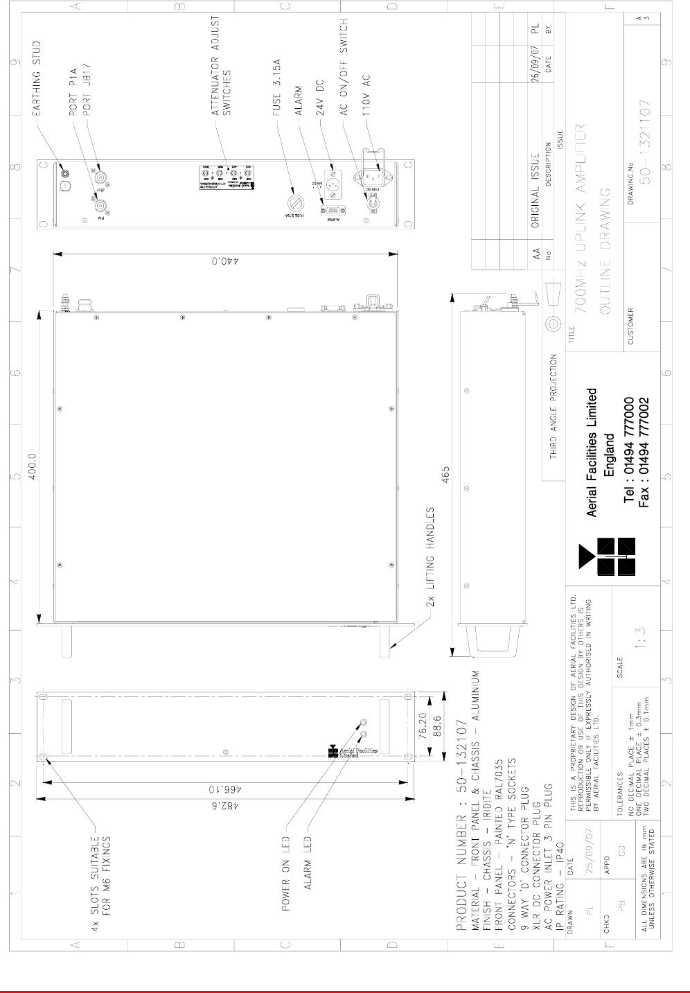
25.3.2.1. 700MHz Uplink Amplifier (50-132107) Outline Drawing
Drawing number 50-1321107
STTRS DOCUMENTATION
Document Number 80-330501HBKM – Issue A - Draft Page 473 of 500
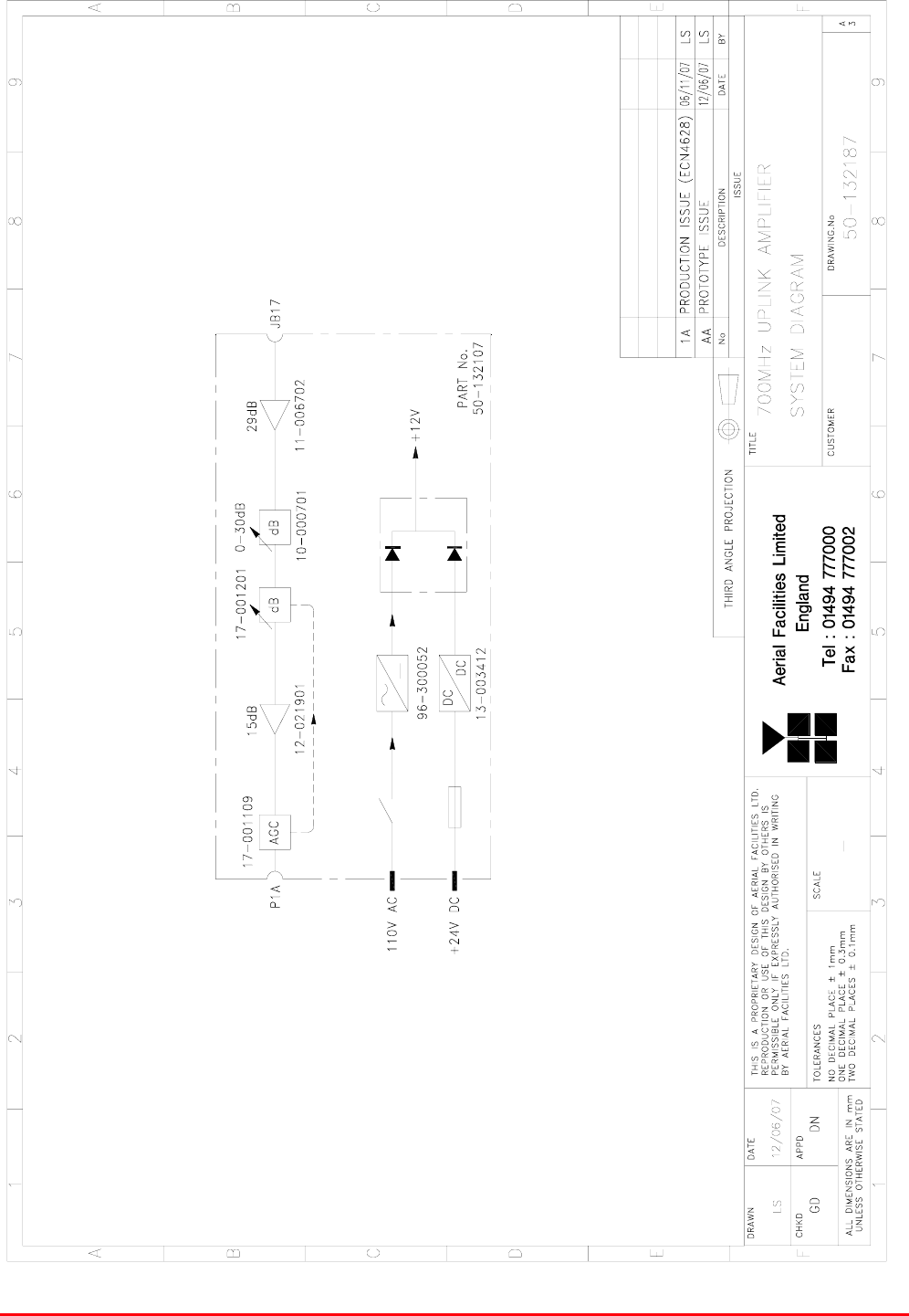
25.3.2.2. 700MHz Uplink Amplifier (50-132107) System Diagram
Drawing number 50-132187

STTRS DOCUMENTATION
Document Number 80-330501HBKM – Issue A - Draft Page 474 of 500
25.3.2.3. Switched Attenuator 0.25Watt, 0 - 30dB (10-000701)
In many practical applications for Cell Enhancers etc., the gain in each path is found to be excessive.
Therefore, provision is made within the unit for the setting of attenuation in each path, to reduce the
gain.
Switched Attenuator 10-000701 provides attenuation from 0 to 30dB in 2 dB steps The attenuation is
simply set using the four miniature toggle switches on the top of each unit. Each switch is clearly
marked with the attenuation it provides, and the total attenuation in line is the sum of the values
switched in. They are designed to maintain an accurate 50Ω impedance over their operating
frequency at both input and output.
10-000701 Specification
PARAMETER SPECIFICATION
Attenuation Values 0-30dB
Attenuation Steps 2, 4, 8 and 16dB
Power Handling 0.25 Watt
Attenuation Accuracy ± 1.0 dB
Frequency Range DC to 1GHz
Impedance 50Ω
Connectors SMA
VSWR 1.3:1
Weight 0.2kg
operation -20°C to +60°C Temperature
range storage -40°C to +70°C
25.3.2.4. Low Noise Amplifier (11-006702)
The Gallium-Arsenide low noise amplifiers used in 700MHz Line Amplifier (55-165704) are double
stage, solid-state low noise amplifiers. Class A circuitry is used throughout the units to ensure
excellent linearity and extremely low noise over a very wide dynamic range. The active devices are
very moderately rated to provide a long trouble-free working life. There are no adjustments on these
amplifiers, and in the unlikely event of a failure, then the complete amplifier should be replaced. This
amplifier features its own in-built alarm system which gives a volt-free relay contact type alarm that is
easily integrated into the main alarm system.
11-006702 Specification
PARAMETER SPECIFICATION
Frequency range 800 - 1000MHz
Bandwidth <200MHz
Gain 29dB (typical)
1dB Compression point 20dBm
OIP3 33dBm
Input/Output return loss >18dB
Noise figure 1.3dB (typical)
Power consumption 180mA @ 24V DC
Supply voltage 10-24V DC
Connectors SMA female
operational -10°C to +60°C Temperature
range storage -20°C to +70°C
Size 90 x 55 x 30.2mm
Weight 290gms (approximately)
STTRS DOCUMENTATION
Document Number 80-330501HBKM – Issue A - Draft Page 475 of 500
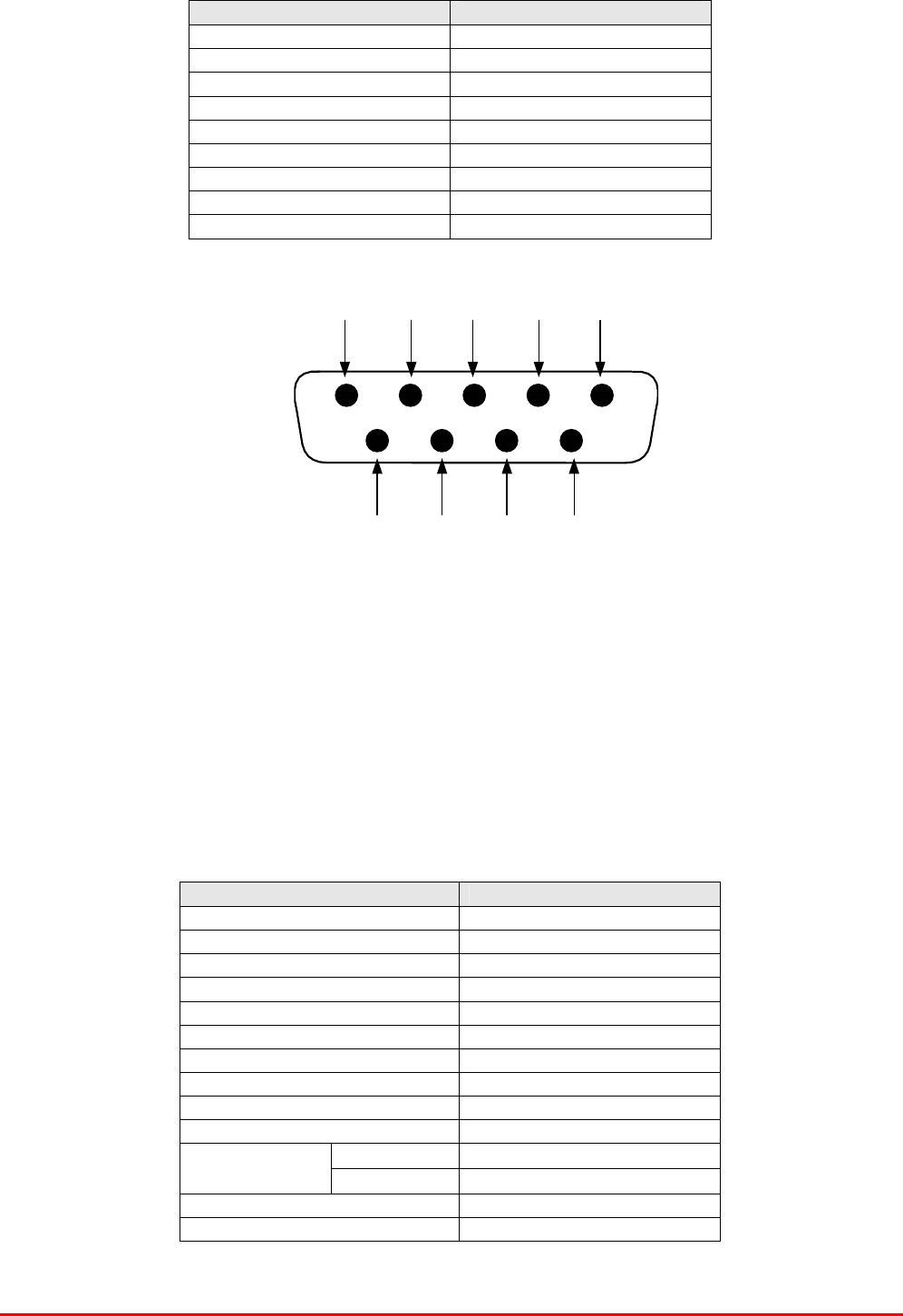
7 8 96
1 2 3 4 5
9-Way Pin-Out Graphical Representation
Low Noise Amplifier (11-006702) ‘D’ Connector Pin-out details
Connector pin Signal
1 +Ve input (10-24V)
2 GND
3 Alarm RelayO/P bad
4 Alarm Relay common
5 Alarm Relay good
6 No connection
7 TTL voltage set
8 TTL alarm/0V (good)
9 O/C good/0V bad
25.3.2.5. Low Power Amplifier (12-021901)
The low power amplifier used is a triple stage solid-state low-noise amplifier. Class A circuitry is used
in the unit to ensure excellent linearity over a very wide dynamic range. The three active devices are
very moderately rated to provide a long trouble-free working life.
Its housing is an aluminium case (Iridite NCP finish) with SMA connectors for the RF input/output and
a D-Type connector for the power supply and the Current Fault Alarm Function.
There are no adjustments on this amplifier, and in the unlikely event of failure then the entire amplifier
should be replaced.
Low Power Amplifier (12-021901) Specification
PARAMETER SPECIFICATION
Frequency range 800-960MHz*
Bandwidth 20MHz *
Maximum RF output >1.0 Watt
Gain 15dB
1dB compression point +30.5dBm
3rd order intercept point +43dBm
Noise Figure <6dB
VSWR better than 1.5:1
Connectors SMA female
Supply 500mA @ 10-15V DC
operational -10°C to +60°C
Temperature
range storage -20°C to +70°C
Weight 0.5 kg
Size 167x52x25mm
* Tuned to Customer’s specification
STTRS DOCUMENTATION
Document Number 80-330501HBKM – Issue A - Draft Page 476 of 500
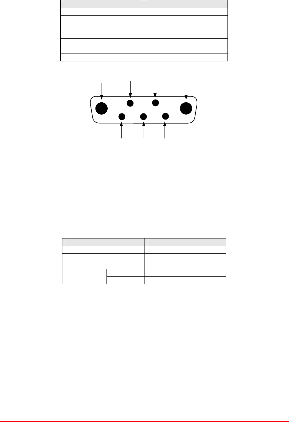
Low Power Amplifier (12-021901) 7-Way Connector Pin-outs
Connector Pin Signal
A1 (large pin) +24V DC
A2 (large pin) GND
1 Alarm relay common
2 TTL alarm/0V good
3 Alarm relay contact (bad)
4 Alarm relay contact (good)
5 O/C good/0V bad (TTL)
25.3.2.6. DC/DC Converter 13-003412
13-003412 is based upon an O.E.M. DC/DC Converter module with a wide input range and and is
used to derive a 12V fixed voltage power supply rail from a higher voltage supply, in this case 24V. In
the event of failure this unit should not be repaired, only replaced.
13-003412 Specification
PARAMETER SPECIFICATION
Operating voltage 18 – 75V DC
Output voltages 12V (typical)
Output current 5.0A (Max)
operational -10%C to +60%C Temperature
range storage -20%C to +70%C
25.3.2.7. AGC System
AGC Detector Unit (17-001109)
AGC Attenuator Unit (17-001201)
Equipment 700MHz Uplink Amplifier (50-132107) is fitted with a wide dynamic range Automatic Gain
Control (AGC) system. This is fitted in the Uplink path to avoid overloading the amplifiers (with the
associated performance degradation) should a mobile be operated very close to the unit.
The AFL wide dynamic range Automatic Gain Control system consists of two units, a
detector/amplifier and an attenuator. The logarithmic detector/amplifier unit is inserted in the RF path
on the output of the power amplifier, and the attenuator is situated in the RF path between the 1st and
2nd stages of amplification.

STTRS DOCUMENTATION
Document Number 80-330501HBKM – Issue A - Draft Page 477 of 500
Normally the attenuator is at minimum attenuation. The detector/amplifier unit monitors the RF level
being delivered by the power amplifier, and when a certain threshold is reached it begins to increase
the value of the attenuator to limit the RF output to the (factory set) threshold. Therefore overloading
of the power amplifier is avoided.
The factory set threshold is 1dB below the Enhancer 1dB compression point. Some adjustment of this
AGC threshold level is possible, a 10dB range is mostly achieved. It is not recommended under any
circumstances to adjust the AGC threshold to a level greater than the 1dB compression point as
system degradation will occur.
The detector comprises of a 50Ω transmission line with a resistive tap which samples a small portion
of the mainline power. The sampled signal is amplified and fed to a conventional half wave diode
rectifier, the output of which is a DC voltage proportional to the RF input signal.
This DC voltage is passed via an inverting DC amplifier with integrating characteristics, to the output,
which drives the attenuation control line of the corresponding AGC attenuator. This unit is fitted at
some earlier point in the RF circuit.
For small signals, below AGC onset, the output control line will be close to 12V and the AGC
attenuator will have minimum attenuation. As the signal level increases the control line voltage will
fall, increasing the attenuator value and keeping the system output level at a constant value.
The AGC onset level is adjusted by the choice of sampler resistor R1 and by the setting of
potentiometer VR1, (factory set at the time of system test) do not adjust unless able to monitor
subsequent RF levels. The attenuator comprises a 50Ω P.I.N diode, voltage-variable attenuator with a
range of 3 to 30dB. The attenuation is controlled by a DC voltage which is derived from the
associated AGC detector unit.
Wide Dynamic Range AGC Specification
PARAMETER SPECIFICATION
Frequency Range up to 1000MHz
Attenuation Range 3 to 30dB
Attenuation Steps continuously variable
VSWR better than 1.2:1
RF Connectors SMA female
attenuator 1W Power
Handling detector/amp >30W (or as required)
operation -10°C to +60°C Temperature
Range storage -20°C to +70°C
attenuator pcb 50 x 42 x 21mm
Size detector/amp pcb 54 x 42 x 21mm
attenuator 90gm
Weight detector/amp 100gm
25.3.2.8. 12V (Single) Relay Board (80-008901)
The General Purpose Relay Board allows the inversion of signals and the isolation of circuits. It is
equipped with a single dual pole change-over relay RL1, with completely isolated wiring, accessed
via a 15 way in-line connector.
The relay is provided with polarity protection diodes and diodes for suppressing the transients caused
by "flywheel effect" which can destroy switching transistors or induce spikes on neighbouring circuits.
It’s common use is to amalgamate all the alarm signals into one, volts-free relay contact pair for the
main alarm system.

STTRS DOCUMENTATION
Document Number 80-330501HBKM – Issue A - Draft Page 478 of 500
80-008901 Specification
PARAMETER SPECIFICATION
Operating voltage 8 to 30V (floating earth)
Alarm threshold Vcc - 1.20 volt +15%
Alarm output relay contacts:
Max. switch current 1.0Amp
Max. switch volts 120Vdc/60VA
Max. switch power 24W/60VA
Min. switch load 10.0µA/10.0mV
Relay isolation 1.5kV
Mechanical life >2x10⁷ operations
Relay approval BT type 56
Connector details Screw terminals
operational -10°C to +60°C Temperature
range storage -20°C to +70°C
25.3.2.9. Dual Diode Assembly (94-100004)
The purpose of these dual diode assemblies is to allow two DC voltage sources to be combined, so
that the main DC rail within the equipment can be sourced from either a mains driven PSU, or
externally through an XLR connector or from dual mains driven PSUs . They are very heavy-duty
diodes and they prevent any reverse current from flowing back to their source or the alternative
supply rail. Combining diodes such as these will also be used if the equipment is to be powered from
external back-up batteries.
25.3.2.10. 12V Switch-Mode PSU (96-300052)
No routine maintenance of the PSU is required. If a fault is suspected, then the output voltage from
the power supply may be measured on its output terminals. This is typically set to 12.2V. The
adjustment potentiometer will be found close to the DC output terminals.
All the PSUs used in AFL Cell Enhancers are capable of operation from either 110 or 220V nominal
AC supplies. The line voltage is sensed automatically, so no adjustment or link setting is needed by
the operator.
96-300052 Specification
AC Input Supply 110 or 220V nominal
Voltage 85 - 265V AC
(absolute limits)
Frequency 47 to 63Hz
DC Output Supply 12V DC (nominal)
Voltage 10.5-13.8V (absolute limits)
Current 12.5A

STTRS DOCUMENTATION
Document Number 80-330501HBKM – Issue A - Draft Page 479 of 500
25.3.3. 700MHz Downlink Splitter (50-132108)
2U rack mount tray
700MHz Downlink Splitter (50-132108) List of Major Components
Section Component
Part Component Part Description Qty Per
Assembly
25.3.3.3. 05-003302 Four Way Splitter/Combiner 5
25.3.3.4. 10-000901 Switched Attenuator 0.25W, 0 - 15dB 1
25.3.3.5. 80-007401 Dummy Load 7
STTRS DOCUMENTATION
Document Number 80-330501HBKM – Issue A - Draft Page 480 of 500
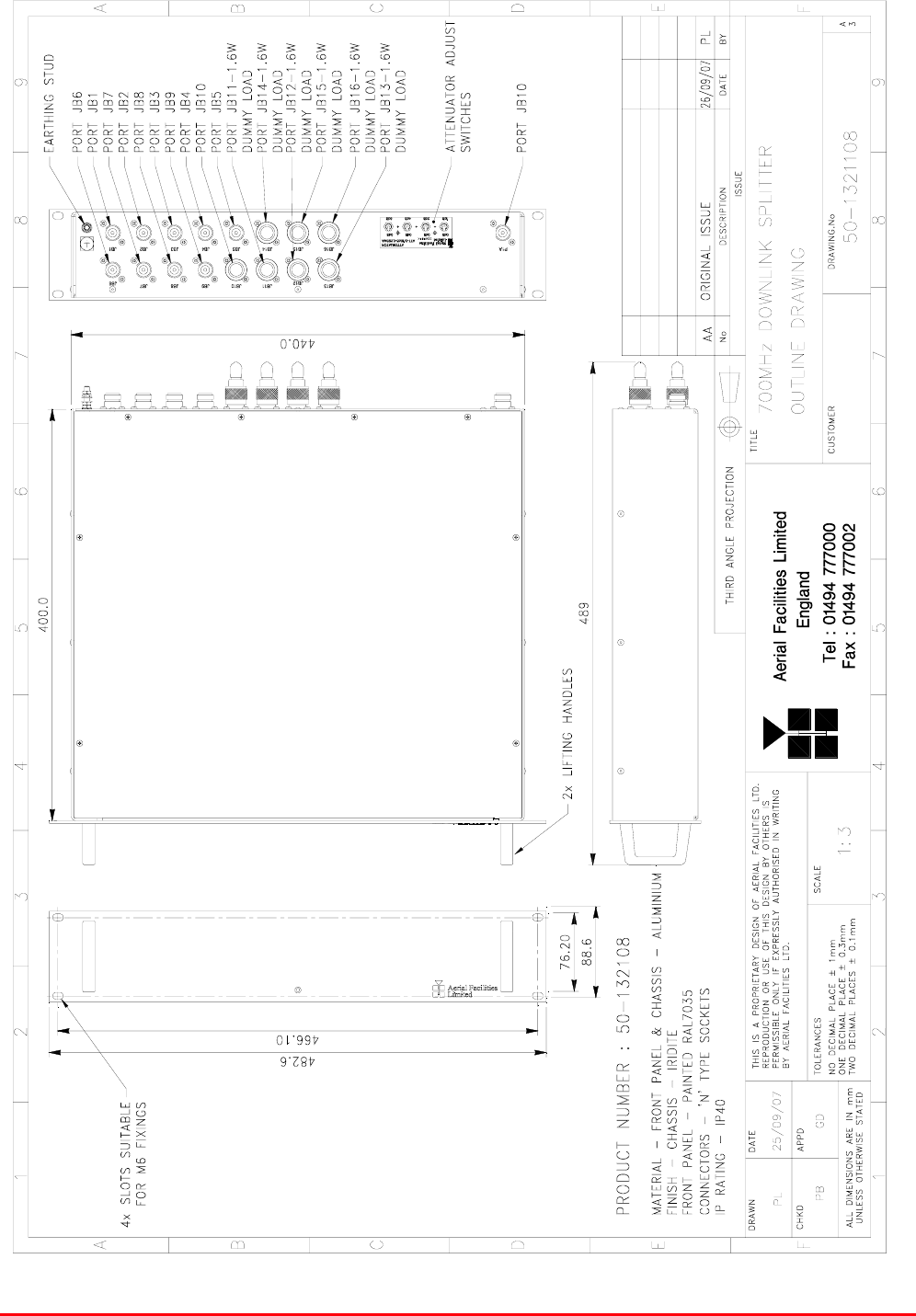
25.3.3.1. 700MHz Downlink Splitter (50-132108) Outline Drawing
Drawing number 50-1321108
STTRS DOCUMENTATION
Document Number 80-330501HBKM – Issue A - Draft Page 481 of 500
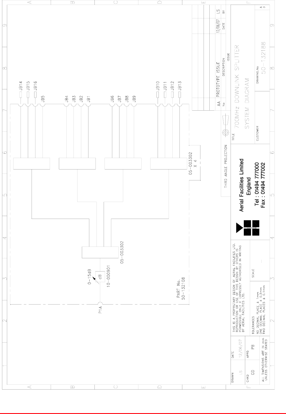
25.3.3.2. 700MHz Downlink Splitter (50-132108) System Diagram
Drawing number 50-132188

STTRS DOCUMENTATION
Document Number 80-330501HBKM – Issue A - Draft Page 482 of 500
25.3.3.3. Four Way Splitter/Combiner (05-003302)
The Splitter/Combiner used is a device for accurately matching two or more RF signals to single or
multiple ports, whilst maintaining an accurate 50Ω load to all inputs/outputs and ensuring that the
VSWR and insertion losses are kept to a minimum. Any unused ports should be terminated with an
appropriate 50Ω load.
Four Way Splitter (05-003302) Specification
PARAMETER SPECIFICATION
Frequency range: 700-980MHz
Bandwidth: 180MHz
Rejection: >14dB
Insertion loss: <7.0dB (in band)
Connectors: N type, female
Weight: <1.5kg
operational
:-20%C to +60%C
Temperature
range: storage -40%C to +70%C
25.3.3.4. Switched Attenuator 0.25W, 0 - 15dB (10-000901)
In many practical applications for Cell Enhancers etc., the gain in each path is found to be excessive.
Therefore, provision is made within the unit for the setting of attenuation in each path, to reduce the
gain.
10-000901 provides attenuation from 0 - 15dB in 2 dB steps The attenuation is simply set using the
four miniature toggle switches on the top of each unit. Each switch is clearly marked with the
attenuation it provides, and the total attenuation in line is the sum of the values switched in. They are
designed to maintain an accurate 50Ω impedance over their operating frequency at both input and
output.
10-000901 Specification
PARAMETER SPECIFICATION
Attenuation Values 0-15dB
Attenuation Steps 1, 2, 4 and 8dB
Power Handling 0.25 Watt
Attenuation Accuracy ± 1.0 dB
Frequency Range DC to 1GHz
Impedance 50Ω
Connectors SMA
VSWR 1.3:1
Weigh 0.2kg
operation -20°C to +60°C Temperature
range storage -40°C to +70°C

STTRS DOCUMENTATION
Document Number 80-330501HBKM – Issue A - Draft Page 483 of 500
25.3.3.5. Dummy Load (80-007401)
When a combiner system is used to split or combine RF signals, in many cases it is most cost
effective to use a standard stock item 4, 6 or 8 port device where, in fact, only a 3 or 6 port device is
needed. In this case seven of the outputs from the Four Way Splitter/Combiner (05-003302) have
their ports terminated with Dummy Load (80-007401) in order to preserve the correct impedance of
the devices over the specified frequency range. This also has the advantage of allowing future
expansion capability should extra channels or other functions become necessary.
Dummy Load (80-007401) Specification
Parameter Specification
Frequency Range 0 to 1000MHz
Power Rating 1.6 Watts
0-500MHz 1.2:1 VSWR
(Max) 500-1000MHz 1.3:1
Temperature -20 to +55°C
Connector ‘N’ type Male
Nominal Impedance 50 Ohms
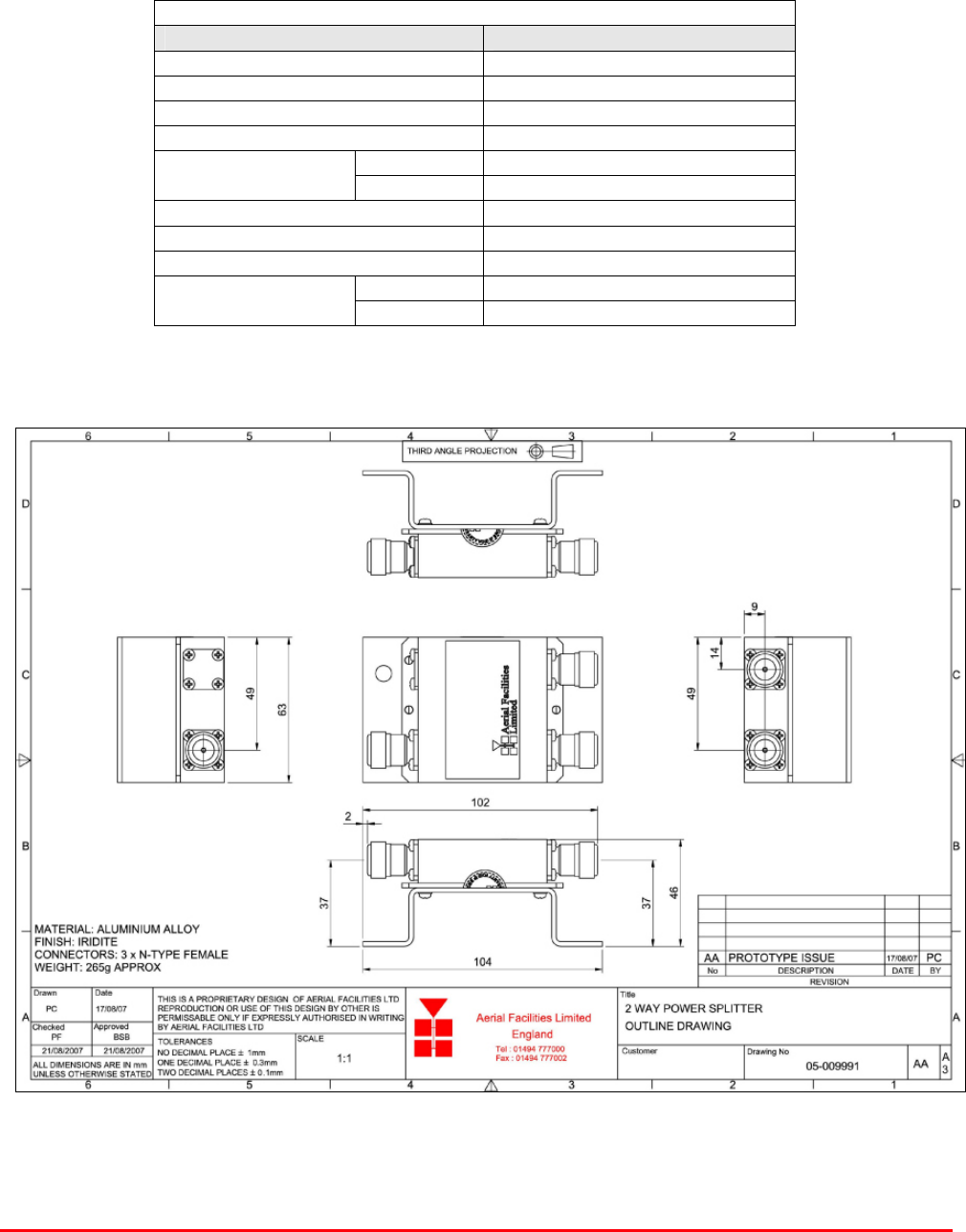
STTRS DOCUMENTATION
Document Number 80-330501HBKM – Issue A - Draft Page 484 of 500
26 2 WAY POWER SPLITTER 50/50 (05-009901)
The power Splitter is a device for accurately matching two or more RF signals to single or multiple
ports, whilst maintaining an accurate 50Ω load to all inputs/outputs and ensuring that the VSWR,
return and insertion losses are kept to a minimum. Any unused ports should be terminated with an
appropriate 50Ω load. Power devices such as these, typically give 10dB better output isolation than
low power equivalents – (important for splitters that feed antenna systems).
2 Way Power Splitter 05-009901
Specification Parameter
Frequency Range 764 – 860MHz
Impedence 50Ω
Insertion Loss ≤ ± 0.3dB
VSWR 1.25:1
Splitter 100Watts Maximum
input power Combiner 5Watts
Power splitting/combining ratio 50% - 50%
RF Connectors N Female
Dimensions 104mm x 63mm x 46mm
operation -20°C to +60°C Temperature
range storage -40°C to +70°C
2 WAY POWER SPLITTER 50/50 (05-009901) Outline Drawing
Drawing number 05-009991

STTRS DOCUMENTATION
Document Number 80-330501HBKM – Issue A - Draft Page 485 of 500
27 2 WAY POWER SPLITTER 90/10 (05-009902)
The power Splitter is a device for accurately matching two or more RF signals to single or multiple
ports, whilst maintaining an accurate 50Ω load to all inputs/outputs and ensuring that the VSWR,
return and insertion losses are kept to a minimum. Any unused ports should be terminated with an
appropriate 50Ω load. Power devices such as these, typically give 10dB better output isolation than
low power equivalents – (important for splitters that feed antenna systems).
2 way power splitter 05-009902
Specification Parameter
Frequency Range 764 – 860MHz
Impedence 50Ω
Insertion Loss ≤ ± 0.3dB
VSWR 1.25:1
Splitter 100Watts Maximum
input power Combiner 5Watts
Power splitting/combining ratio 90% - 10%
RF Connectors N Female
Dimensions 104mm x 63mm x 46mm
operation -20°C to +60°C Temperature
range storage -40°C to +70°C
2 WAY POWER SPLITTER 90/10 (05-009902) Outline Drawing
Drawing number 05-009991
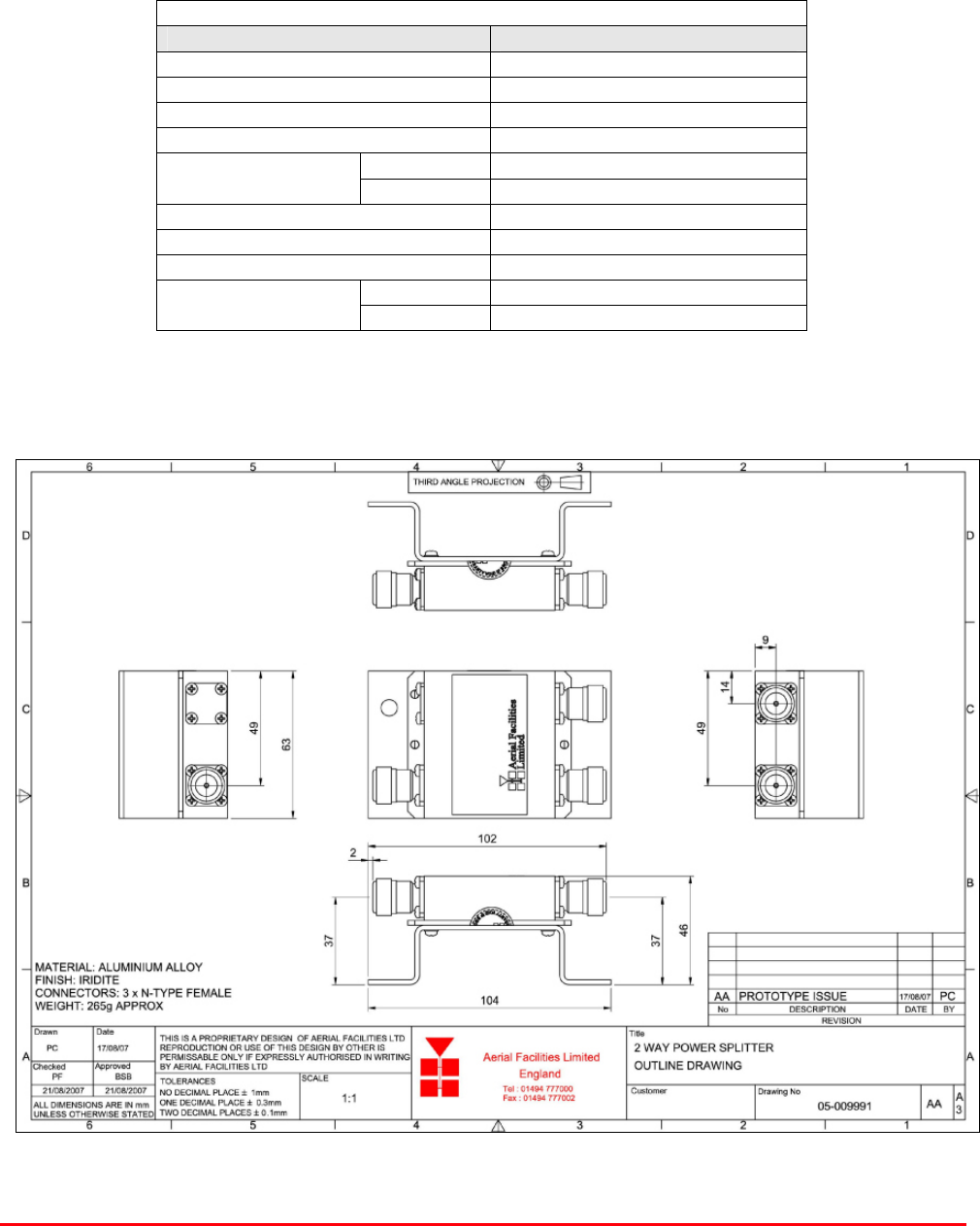
STTRS DOCUMENTATION
Document Number 80-330501HBKM – Issue A - Draft Page 486 of 500
28 2 WAY POWER SPLITTER 80/20 (05-009903)
The power Splitter is a device for accurately matching two or more RF signals to single or multiple
ports, whilst maintaining an accurate 50Ω load to all inputs/outputs and ensuring that the VSWR,
return and insertion losses are kept to a minimum. Any unused ports should be terminated with an
appropriate 50Ω load. Power devices such as these, typically give 10dB better output isolation than
low power equivalents – (important for splitters that feed antenna systems).
2 way power splitter 05-009903
Specification Parameter
Frequency Range 764 – 860MHz
Impedence 50Ω
Insertion Loss ≤ ± 0.3dB
VSWR 1.25:1
Splitter 100Watts Maximum
input power Combiner 5Watts
Power splitting/combining ratio 80% - 20%
RF Connectors N Female
Dimensions 104mm x 63mm x 46mm
operation -20°C to +60°C Temperature
range storage -40°C to +70°C
2 WAY POWER SPLITTER 80/20 (05-009903) Outline Drawing
Drawing number 05-009991

STTRS DOCUMENTATION
Document Number 80-330501HBKM – Issue A - Draft Page 487 of 500
29 2 WAY POWER SPLITTER 60/40 (05-009904)
The power Splitter is a device for accurately matching two or more RF signals to single or multiple
ports, whilst maintaining an accurate 50Ω load to all inputs/outputs and ensuring that the VSWR,
return and insertion losses are kept to a minimum. Any unused ports should be terminated with an
appropriate 50Ω load. Power devices such as these, typically give 10dB better output isolation than
low power equivalents – (important for splitters that feed antenna systems).
2 way power splitter 05-009904
Specification Parameter
Frequency Range 764 – 860MHz
Impedence 50Ω
Insertion Loss ≤ ± 0.3dB
VSWR 1.25:1
Splitter 100Watts Maximum
input power Combiner 5Watts
Power splitting/combining ratio 60% - 40%
RF Connectors N Female
Dimensions 104mm x 63mm x 46mm
operation -20°C to +60°C Temperature
range storage -40°C to +70°C
2 WAY POWER SPLITTER 60/40 (05-009904) Outline Drawing
Drawing number 05-009991

STTRS DOCUMENTATION
Document Number 80-330501HBKM – Issue A - Draft Page 488 of 500
30 2 WAY POWER SPLITTER 70/30 (05-009905)
The power Splitter is a device for accurately matching two or more RF signals to single or multiple
ports, whilst maintaining an accurate 50Ω load to all inputs/outputs and ensuring that the VSWR,
return and insertion losses are kept to a minimum. Any unused ports should be terminated with an
appropriate 50Ω load. Power devices such as these, typically give 10dB better output isolation than
low power equivalents – (important for splitters that feed antenna systems).
2 way power splitter 05-009905
Specification Parameter
Frequency Range 764 – 860MHz
Impedence 50Ω
Insertion Loss ≤ ± 0.3dB
VSWR 1.25:1
Splitter 100Watts Maximum
input power Combiner 5Watts
Power splitting/combining ratio 70% - 30%
RF Connectors N Female
Dimensions 104mm x 63mm x 46mm
operation -20°C to +60°C Temperature
range storage -40°C to +70°C
2 WAY POWER SPLITTER 70/30 (05-009905) Outline Drawing
Drawing number 05-009991

STTRS DOCUMENTATION
Document Number 80-330501HBKM – Issue A - Draft Page 489 of 500
Section Description Qty
26 05-009901 9 2 WAY SPLITTER 50/50 separate 5
27 05-009902 9 2 W SPLITTER 90/10 separate 14
28 05-009903 9 2 W SPLITTER 80/20 separate 6
29 05-009904 9 2 W SPLITTER 60/40 4
30 05-009905 9 2 W SPLITTER 70/30 separate 3
31 ***///***05-009906 3 W SPLITTER 33/33/33 separate 1
32 ***///***05-009907 3 W SPLITTER 40/20/40 separate 1
33 ***///***05-009908 3 W SPLITTER 80/10/10 separate 3
34 ***///***05-009909 4 W SPLITTER 70/10/10/10 separate 1
35 ***///***05-009910 4 W SPLITTER 25/25/25/25 separate 3
36 ***///***05-009911 5 WAY POWER SPLITTER 1
37 ***///***05-009912 3 W SPLITTER 60/40/10 separate 1
38 ***///***80-237501 2W SPLITTER 50/50 built into racks 11
39 ***///***80-237501 2 W SPLITTER 90/10 built into racks 12
40 ***///***80-237501 2 W SPLITTER 70/30 built into racks 5
41 ***///***80-237501 3 W SPLIT 33/33/33 built into racks 1
42 ***///***80-237501 3 W SPLIT 40/20/40 built into racks 1
43 ***///***80-237501
not “real” numbers
4W SPLIT25/25/25/25 built into rack 7
44. SPARES PACKAGE (80-330520)
Not yet defined...

STTRS DOCUMENTATION
Document Number 80-330501HBKM – Issue A - Draft Page 490 of 500

STTRS DOCUMENTATION
Document Number 80-330501HBKM – Issue A - Draft Page 491 of 500

STTRS DOCUMENTATION
Document Number 80-330501HBKM – Issue A - Draft Page 492 of 500

STTRS DOCUMENTATION
Document Number 80-330501HBKM – Issue A - Draft Page 493 of 500

STTRS DOCUMENTATION
Document Number 80-330501HBKM – Issue A - Draft Page 494 of 500

STTRS DOCUMENTATION
Document Number 80-330501HBKM – Issue A - Draft Page 495 of 500

STTRS DOCUMENTATION
Document Number 80-330501HBKM – Issue A - Draft Page 496 of 500

STTRS DOCUMENTATION
Document Number 80-330501HBKM – Issue A - Draft Page 497 of 500
APPENDIX A
A.1. Glossary of Terms used in this document
Repeater or
Cell Enhancer A Radio Frequency amplifier which can simultaneously amplify and re-
broadcast Mobile Station and Base Transceiver Station signals.
Band Selective
Repeater A Cell Enhancer designed for operation on a range of channels within a
specified frequency band.
Channel Selective
Repeater A Cell Enhancer, designed for operation on specified channel(s) within a
specified frequency band. Channel frequencies may be factory set or on-
site programmable.
AC Alternating Current
AGC Automatic Gain Control
BBU Battery Backup Unit
BTS Base Transceiver Station
CEMS Coverage Enhancement Management System
C/NR Carrier-to-Noise Ratio
DAB Digital Audio Broadcasting
DC Direct Current
Downlink (D/L) RF signals Tx from the BTS to the Master Site
FO Fibre Optic
GND Ground
ID Identification Number
LED Light Emitting Diode
LCX Coaxial Leaky Feeder
LNA Low Noise Amplifier
LPA Low Power Amplifier
MOU Master Optical Unit
MS Master Site
MST Mobile Station
MTBF Mean Time Between Failures
N/A Not Applicable
N/C No Connection
OFR On Frequency Repeater
OIP3 Output Third Order Intercept Point = RFout +(C/I)/2
PA Power Amplifier
RF Radio Frequency
RSA Receiver/Splitter Amplifier
Rx Receiver
S/N Serial Number
TTL Transistor-Transistor Logic, a common type of digital circuit.
Tx Transmitter
Uplink (U/L) RF signals transmitted from the MS to the BTS
VSWR Voltage Standing Wave Ratio
WDM Wave division multiplex
STTRS DOCUMENTATION
Document Number 80-330501HBKM – Issue A - Draft Page 498 of 500
C0- AX CABLE
C0- AX CABLE
CAT 5 CABLE
CABLES
24/ FIBRE OPTIC CABLE/LINK
CABLE 1/ 2"
RADIATING CABLE
TAPPER/ COUPLER
STATION
BASE TRANSCEIVER
MISC
HUBS
FIBRE MAIN HUB
EXPANSION HUB
BI- DIRECTIONAL AMPLIFIER
E
BTS
FMH
EH
7/8 " DIA
1/2 " DIA
6 dB DIRECTIONAL COUPLER
10 dB COUPLER
C10
CROSS BAND COUPLER
COUPLERS
J JUMPER
C6
C10 10 dB DIRECTIONAL COUPLER
6 dB DIRECTIONAL COUPLER
DIRECTIONAL COUPLER
PANEL ANTENNA
( MOUNTED AT HIGH LEVEL)
DIRECTIONAL ANTENNA
FLAT PLATE ANTENNA
YAGI ANTENNA
ANTENNAS
REMOTE ANTENNA UNIT
OMNI ANTENNA
SPLITTERS
ANTENNA
RAU
BAND PASS FILTER
CAVITY RESONATOR
NOTCH FILTER
ISOLATOR
HYBRID COMBINER
EARTH STUD
LEEKY FEEDER
Outputs to receivers
R.S. A
AMPLIFIER
MISC
dB ATTENUATOR ( VARIABLE)
A. G.C
AGC dB
CONTROLLER
MONITORING
MODEM
MONITORING CONTROLLER
MODEM
( CELL ENHANCER)
FREQUENCY PROGRAMMING
DATA
B/W=30 to 200kHz CHANNEL MODULE
FIBRE- OPTIC
MODULATOR
FIBRE- OPTIC
DEMODULATOR
LOCAL OSCILLATOR
( up to
16 way)
Outputs
DUMMY LOAD
LOCAL OSCILLATOR
SPLITTER
MISC
8/ FIBRE OPTIC CABLE/LINK
STANDARD FOR LEVEL (dBm)
- 73 = BELOW ACCEPTABLE
SIGNAL LEVEL(dBm)
ALL AIRPORTS
BCCH ( BROADCAST
IDENTITY CODE)
BSIC ( BASIC SITE
LEVEL (dBm)
- 83 = BELOW ACCEPTABLE
SIGNAL LEVEL(dBm)
- 82 = ACCEPTABLE SIGNAL
- 72 = ACCEPTABLE SIGNAL
CONTROL CHANNEL)
= READING POSITION
22 =
602 =
SIGNAL KEY
STANDARD EXCEPT
FOR AIRPORTS
( SEE BELOW)
BLADE ANTENNA
ATTENUATOR ( FIXED)
dB
OUTIN
COUPLED
HI COM
LOW
HYBRID SPLITTER
IN
IN
OUT
OUT
IN
OUT
BYDATEDESCRIPTIONNo
ISSUE
THIRD ANGLE PROJECTION
1234 5 6 7 8 9
A
B
C
D
E
F
123456789
A
B
C
D
E
F
Fax : 01494 777002
Tel : 01494 777000
Aerial Facilities Limited
THIS IS A PROPRIETARY DESIGN OF AERIAL FACILITIES LTD.
REPRODUCTION OR USE OF THIS DESIGN BY OTHERS IS
PERMISSIBLE ONLY IF EXPRESSLY AUTHORISED IN WRITING
BY AERIAL FACILITIES LTD.
NO DECIMAL PLACE ± 1mm
ONE DECIMAL PLACE ± 0. 3 m m
TWO DECIMAL PLACES ± 0.1mm
ALL DIMENSIONS ARE IN mm
UNLESS OTHERWISE STATED
CHKD
DRAWN
APPD
DATE
TOLERANCES SCALE
England
CUSTOMER DRAWING.No
TITLE
3
A
AFL - STANDARD SYMBOLS
90- 000001
AA
NTS
PL 10/05/00
ORIGINAL
ISSUE
PL23/05/ 00
21/06/ 00 PLBLADE ANTENNA ADDED1A
2A ECN3165
RF
RF
PLUG & SOCKET
FIBRE OPTIC
CONNECTOR
FC/ APC
SOCKET
PLUG
MISC
DC
DC
AC TO DC PSU
DC TO DC
CONVERTER
FUSE
RELAY
N.O. ( CLEAR CONTACT)
N.C. ( FILLED CONTACT)
COM
MB GD
26/01/ 04 PL
2B TEXT CORRECTION 28/07/ 04 PL
A.2. Key to Drawing Symbols used in this document

STTRS DOCUMENTATION
Document Number 80-330501HBKM – Issue A - Draft Page 499 of 500
Aerial Facilities Limited
A.3. EC Declaration of Conformity
In accordance with BS EN ISO/IEC 17050-1&-2:2004
Aerial Facilities Limited
Aerial House
Asheridge Road
Chesham
Buckinghamshire HP5 2QD
United Kingdom
DECLARES, UNDER OUR SOLE RESPONSIBILITY THAT THE FOLLOWING PRODUCT:
PRODUCT PART NO[S] **************
PRODUCT DESCRIPTION **************
IN ACCORDANCE WITH THE FOLLOWING DIRECTIVES:
1999/5/EC The Radio & Telecommunications Terminal Equipment Directive Annex V
and its amending directives
HAS BEEN DESIGNED AND MANUFACTURED TO THE FOLLOWING STANDARD[S] OR
OTHER NORMATIVE DOCUMENT[S]:
BS EN 60950 Information technology equipment.
Safety. General requirements
ETS EN 301 489-1 EMC standard for radio equipment and services.
Part 1. Common technical requirements
I hereby declare that the equipment named above has been designed to comply with the relevant
sections of the above referenced specifications. The unit complies with all essential requirements
of the Directives.
SIGNED
B S BARTON
TECHNICAL DIRECTOR DATE: dd/mm/yyyy
Registered Office: Aerial House, Asheridge Road, Chesham, Buckinghamshire, HP5 2QD England Registered No. 4042808 (England)
www.aerialfacilities.com

STTRS DOCUMENTATION
Document Number 80-330501HBKM – Issue A - Draft Page 500 of 500
A.4. Amendment List Record Sheet
Document Ref. 80-330501HBKM
Issue
No. Date Incorporated
by Page Nos.
Amended Reason for new issue
A 28-08-2007 AJS Draft