TM8100 Service Manual TM8000/TM8100 Mobile Radio Manual/MM8100 02 00 812_TM8100 MM8100 812
User Manual: Pdf TM8000/TM8100 Mobile Radio Service Manual/MM8100-02-00-812_TM8100 Mobile Radio Service Manual
Open the PDF directly: View PDF ![]() .
.
Page Count: 244 [warning: Documents this large are best viewed by clicking the View PDF Link!]
- Contents
- Preface
- Chapter 1. Description of Radio
- Chapter 2. Servicing of Radio

TM8000 mobiles
TM8100 Mobile Radio
Service Manual
MM8100-02-00-812 Version 3.00
May 2004 © Tait Electronics Limited

2TM8100 Mobile Radio Service Manual
May 2004 © Tait Electronics Limited
Contact Information
Tait Radio Communications http://www.taitworld.com
Corporate Head Office
New Zealand
Tait Electronics Ltd
P.O. Box 1645
Christchurch
New Zealand
E-mail (Sales): sales@taitworld.com
Technical Support:
E-mail: support@taitworld.com
Website: http://support.taitworld.com
Tait Oceania
New Zealand
Tait Communications Ltd
E-mail: headoffice@tcl.tait.co.nz
Australia
Tait Electronics (Aust) Pty Ltd
E-mail: australia@taitworld.com
Tait Europe
Regional Head Office: United Kingdom
Tait Mo b i l e Radio L t d
E-mail: teusales@tait.co.uk
Latin America
Tait La t i n A m er ica
E-mail: latinamerica@taitworld.com
Tait North America
Regional Head Office:
United States of America
Tait North America Inc
E-mail: usa@taitworld.com
Canada
Tait North America Inc
E-mail: canada@taitworld.com
Tait North Asia
Regional Head Office: Hong Kong
Tait Mobile Radio (Hong Kong) Ltd
E-mail: hongkong@taitworld.com
Beijing
Tait Mobile Radio (Hong Kong) Ltd
E-mail: beijing@taitworld.com
Tait South Asia
Regional Head Office: Singapore
Tait Electronics (Far East) Pte Ltd
E-mail: singapore@taitworld.com
Thailand
Ta i t M o b il e Ra d i o L t d
E-mail: thailand@taitworld.com
Note
For the addresses and telephone numbers of
the above regional offices refer to the
TaitWorld website.

TM8100 Mobile Radio Service Manual 3
May 2004 © Tait Electronics Limited
Tait General Software Licence Agreement
This legal document is an Agreement between
you (the “Licensee”) and Tait Electronics
Limited (“Tait”). By using any of the Software
or Firmware items prior-installed in the
related Tait product, included on this CD or
downloaded from the Tait website,
(hereinafter referred to as “the Software or
Firmware”) you agree to be bound by the
terms of this Agreement. If you do not agree
to the terms of this Agreement, do not install
and use any of the Software or Firmware.
If you install and use any of the Software or
Firmware that will be deemed to be
acceptance of the terms of this licence
agreement.
The terms of this agreement shall apply
subject only to any express written terms of
agreement to the contrary between Tait and
the Licensee.
Licence
TAIT GRANTS TO YOU AS LICENSEE THE NON-
EXCLUSIVE RIGHT TO USE THE SOFTWARE OR
FIRMWARE ON A SINGLE MACHINE PROVIDED
YOU MAY ONLY:
1. COPY THE SOFTWARE OR FIRMWARE INTO
ANY MACHINE READABLE OR PRINTED FORM
FOR BACKUP PURPOSES IN SUPPORT OF YOUR
USE OF THE PROGRAM ON THE SINGLE MACHINE
(CERTAIN PROGRAMS, HOWEVER, MAY INCLUDE
MECHANISMS TO LIMIT OR INHIBIT COPYING,
THEY ARE MARKED “COPY PROTECTED”),
PROVIDED THE COPYRIGHT NOTICE MUST BE
REPRODUCED AND INCLUDED ON ANY SUCH
COPY OF THE SOFTWARE OR FIRMWARE;
AND / OR
2. MERGE IT INTO ANOTHER PROGRAM FOR
YOUR USE ON THE SINGLE MACHINE (ANY
PORTION OF ANY SOFTWARE OR FIRMWARE
MERGED INTO ANOTHER PROGRAM WILL
CONTINUE TO BE SUBJECT TO THE TERMS AND
CONDITIONS OF THIS AGREEMENT).
THE LICENSEE MAY NOT DUPLICATE, MODIFY,
REVERSE COMPILE OR REVERSE ASSEMBLE ANY
SOFTWARE OR FIRMWARE IN WHOLE OR PART.
Title to Software
THIS AGREEMENT DOES NOT CONSTITUTE A
CONTRACT OF SALE IN RELATION TO THE
SOFTWARE OR FIRMWARE SUPPLIED TO THE
LICENSEE. NOT WITHSTANDING THE LICENSEE
MAY OWN THE MAGNETIC OR OTHER PHYSICAL
MEDIA ON WHICH THE SOFTWARE OR
FIRMWARE WAS ORIGINALLY SUPPLIED, OR HAS
SUBSEQUENTLY BEEN RECORDED OR FIXED, IT IS
A FUNDAMENTAL TERM OF THIS AGREEMENT
THAT AT ALL TIMES TITLE AND OWNERSHIP OF
THE SOFTWARE OR FIRMWARE, WHETHER ON
THE ORIGINAL MEDIA OR OTHERWISE, SHALL
REMAIN VESTED IN TAIT OR THIRD PARTIES
WHO HAVE GRANTED LICENCES TO TAIT.
Term and Termination
THIS LICENCE SHALL BE EFFECTIVE UNTIL
TERMINATED IN ACCORDANCE WITH THE
PROVISIONS OF THIS AGREEMENT. THE LICENSEE
MAY TERMINATE THIS LICENCE AT ANY TIME BY
DESTROYING ALL COPIES OF THE SOFTWARE OR
FIRMWARE AND ASSOCIATED WRITTEN
MATERIALS. THIS LICENCE WILL BE TERMINATED
AUTOMATICALLY AND WITHOUT NOTICE FROM
TAIT IN THE EVENT THAT THE LICENSEE FAILS TO
COMPLY WITH ANY TERM OR CONDITION OF
THIS AGREEMENT. THE LICENSEE AGREES TO
DESTROY ALL COPIES OF THE SOFTWARE OR
FIRMWARE AND ASSOCIATED WRITTEN
MATERIALS IN THE EVENT OF SUCH
TERMINATION.
Limited Warranty
THE SOFTWARE OR FIRMWARE IS SUPPLIED BY
TAIT AND ACCEPTED BY THE LICENSEE “AS IS”
WITHOUT WARRANTY OF ANY KIND EITHER
EXPRESSED OR IMPLIED, INCLUDING BUT NOT
BEING LIMITED TO ANY IMPLIED WARRANTIES AS
TO MERCHANTABILITY OR FITNESS FOR ANY
PARTICULAR PURPOSE. THE LICENSEE
ACKNOWLEDGES THAT THE SOFTWARE OR
FIRMWARE IS USED BY IT IN BUSINESS AND
ACCORDINGLY TO THE MAXIMUM EXTENT
PERMITTED BY LAW NO TERMS OR WARRANTIES
WHICH ARE IMPLIED BY LEGISLATION SHALL
APPLY TO THIS AGREEMENT. TAIT DOES NOT
WARRANT THAT THE FUNCTIONS CONTAINED
IN THE SOFTWARE OR FIRMWARE WILL MEET
THE LICENSEE’S REQUIREMENTS OR THAT THE
OPERATION OF THE SOFTWARE OR FIRMWARE
WILL BE UNINTERRUPTED OR ERROR-FREE.
4TM8100 Mobile Radio Service Manual
May 2004 © Tait Electronics Limited
Exclusion of Liability
TAIT’S ENTIRE LIABILITY AND THE LICENSEE’S
EXCLUSIVE REMEDY SHALL BE THE FOLLOWING:
1. IN NO CIRCUMSTANCES SHALL TAIT BE
UNDER ANY LIABILITY TO THE LICENSEE, OR
ANY OTHER PERSON WHATSOEVER, FOR ANY
DIRECT OR CONSEQUENTIAL DAMAGE ARISING
OUT OF OR IN CONNECTION WITH ANY USE OR
INABILITY OF USING THE SOFTWARE OR
FIRMWARE.
2. TAIT WARRANTS THE OPERATION OF THE
SOFTWARE OR FIRMWARE ONLY WITH THE
OPERATING SYSTEM FOR WHICH IT WAS
DESIGNED. USE OF THE SOFTWARE OR
FIRMWARE WITH AN OPERATING SYSTEM
OTHER THAN THAT FOR WHICH IT WAS
DESIGNED MAY NOT BE SUPPORTED BY TAIT,
UNLESS OTHERWISE EXPRESSLY AGREED BY
TAIT.
General
THE LICENSEE CONFIRMS THAT IT SHALL
COMPLY WITH THE PROVISIONS OF LAW IN
RELATION TO THE SOFTWARE OR FIRMWARE.
Law and Jurisdiction
THIS AGREEMENT SHALL BE SUBJECT TO AND
CONSTRUED IN ACCORDANCE WITH
NEW ZEALAND LAW AND DISPUTES BETWEEN
THE PARTIES CONCERNING THE PROVISIONS
HEREOF SHALL BE DETERMINED BY THE NEW
ZEALAND COURTS OF LAW. PROVIDED HOWEVER
TAIT MAY AT ITS ELECTION BRING PROCEEDINGS
FOR BREACH OF THE TERMS HEREOF OR FOR
THE ENFORCEMENT OF ANY JUDGEMENT IN
RELATION TO A BREACH OF THE TERMS HEREOF
IN ANY JURISDICTION TAIT CONSIDERS FIT FOR
THE PURPOSE OF ENSURING COMPLIANCE WITH
THE TERMS HEREOF OR OBTAINING RELIEF FOR
BREACH OF THE TERMS HEREOF.
No Dealings
THE LICENSEE MAY NOT SUBLICENSE, ASSIGN OR
TRANSFER THE LICENCE OR THE PROGRAM
EXCEPT AS EXPRESSLY PROVIDED IN THIS
AGREEMENT. ANY ATTEMPT OTHERWISE TO
SUBLICENSE, ASSIGN OR TRANSFER ANY OF THE
RIGHTS, DUTIES OR OBLIGATIONS HEREUNDER
IS VOID.
No Other Terms
THE LICENSEE ACKNOWLEDGES THAT IT HAS
READ THIS AGREEMENT, UNDERSTANDS IT AND
AGREES TO BE BOUND BY ITS TERMS AND
CONDITIONS. THE LICENSEE FURTHER AGREES
THAT SUBJECT ONLY TO ANY EXPRESS WRITTEN
TERMS OF AGREEMENT TO THE CONTRARY
BETWEEN TAIT AND THE LICENSEE THIS IS THE
COMPLETE AND EXCLUSIVE STATEMENT OF THE
AGREEMENT BETWEEN IT AND TAIT IN
RELATION TO THE SOFTWARE OR FIRMWARE
WHICH SUPERSEDES ANY PROPOSAL OR PRIOR
AGREEMENT, ORAL OR WRITTEN AND ANY
OTHER COMMUNICATIONS BETWEEN THE
LICENSEE AND TAIT RELATING TO THE
SOFTWARE OR FIRMWARE.

TM8100 Mobile Radio Service Manual 5
May 2004 © Tait Electronics Limited
Contents
Preface . . . . . . . . . . . . . . . . . . . . . . . . . . . . . . . . . . . . . . . . . . . . . . . . . 6
Scope of Service Manual . . . . . . . . . . . . . . . . . . . . . . . . . . . . . . . . . . . . . . 6
Summary of Service Manual . . . . . . . . . . . . . . . . . . . . . . . . . . . . . . . . . . . 6
Enquiries and Comments . . . . . . . . . . . . . . . . . . . . . . . . . . . . . . . . . . . . . 7
Updates of Manual and Equipment . . . . . . . . . . . . . . . . . . . . . . . . . . . . . . 7
Copyright. . . . . . . . . . . . . . . . . . . . . . . . . . . . . . . . . . . . . . . . . . . . . . . . . 7
Disclaimer. . . . . . . . . . . . . . . . . . . . . . . . . . . . . . . . . . . . . . . . . . . . . . . . . 7
Typographical Conventions . . . . . . . . . . . . . . . . . . . . . . . . . . . . . . . . . . . . 8
Associated Documentation. . . . . . . . . . . . . . . . . . . . . . . . . . . . . . . . . . . . 10
Publication Record . . . . . . . . . . . . . . . . . . . . . . . . . . . . . . . . . . . . . . . . . 11
List of Acronyms . . . . . . . . . . . . . . . . . . . . . . . . . . . . . . . . . . . . . . . . . . . 12
Chapter 1 Description of Radio . . . . . . . . . . . . . . . . . . . . . . . . . . . . . . . 13
1 Introduction. . . . . . . . . . . . . . . . . . . . . . . . . . . . . . . . . . . . . . . . . . . 15
2 General Description . . . . . . . . . . . . . . . . . . . . . . . . . . . . . . . . . . . . . 33
3 Circuit Descriptions . . . . . . . . . . . . . . . . . . . . . . . . . . . . . . . . . . . . . 63
Chapter 2 Servicing of Radio . . . . . . . . . . . . . . . . . . . . . . . . . . . . . . . . 79
4 General Information . . . . . . . . . . . . . . . . . . . . . . . . . . . . . . . . . . . . . 81
5 Servicing Procedure . . . . . . . . . . . . . . . . . . . . . . . . . . . . . . . . . . . . 107
6 Disassembly and Re-assembly of Radio . . . . . . . . . . . . . . . . . . . . . . 125
7 Servicing of Control Head . . . . . . . . . . . . . . . . . . . . . . . . . . . . . . . 151
8 Servicing of Main Board . . . . . . . . . . . . . . . . . . . . . . . . . . . . . . . . . 165
9 Diagnosis of Faults on Main Board . . . . . . . . . . . . . . . . . . . . . . . . . 171

6TM8100 Mobile Radio Service Manual
May 2004 © Tait Electronics Limited
Preface
Scope of Service Manual
This manual provides information to service technicians for carrying out
level-1 and level-2 repairs of TM8100 mobile radios. Level-1 repairs
entail the replacement of faulty parts and circuit boards; level-2 repairs
entail the repair of circuit boards, with the exception of certain special
items on the boards. The manual does not cover level-3 repairs, which
entail the repair of the special items. The servicing procedures are
moreover limited to the control head and radio body of TM8100 mobile
radios. Servicing of all accessories associated with the radio is covered in
the accessories manual.
Summary of Service Manual
The service manual is divided into two chapters. A description of the
radio is given in Chapter 1. After an introductory section, an illustrated
parts breakdown is given for the radio. This is followed by a description
of the principles of operation of the radio and the functioning of the
circuitry.
The servicing procedures are given in Chapter 2. General information
is given first, followed by the full sequence of tasks required to service a
particular radio. The chapter concludes with additional details for
certain tasks, namely, disassembly and re-assembly of the radio, servicing
of the control head, general information on the servicing of the main
circuit board, and the diagnosis of faults on the main circuit board.

TM8100 Mobile Radio Service Manual 7
May 2004 © Tait Electronics Limited
Enquiries and Comments
Any enquiries regarding this manual or the equipment that it describes,
as well as any comments, suggestions and notifications of errors, should
be addressed by e-mail to Technical Support (support@taitworld.com)
or to the Technical Support Manager, Tait Electronics Limited, PO Box
1645, Christchurch, New Zealand. Orders for this manual can be placed
with your Tait Dealer.
Updates of Manual and Equipment
In the interests of improving the performance, reliability or servicing of
the equipment, Tait Eletcronics Limited reserves the right to upgrade the
equipment or update this manual or both without prior notice.
Copyright
All information contained in this manual is the property of Tait
Electronics Limited. All rights are reserved. This manual may not, in
whole or in part, be copied, photocopied, reproduced, translated, stored,
or reduced to any electronic medium or machine-readable form,
without prior written permission from Tait Electronics Limited. All
trade names referenced are the service mark, trade mark, or registered
trade mark of the respective manufacturers.
Disclaimer
There are no warranties extended or granted by this manual. Tait
Electronics Limited accepts no responsibility for damage arising from use
of the information contained in the manual or of the equipment and
software it describes. It is the responsibility of the user to ensure that use
of such information, equipment and software complies with the laws,
rules and regulations of the applicable jurisdictions.

8TM8100 Mobile Radio Service Manual
May 2004 © Tait Electronics Limited
Typographical Conventions
Conventions In this manual a special font is used for the names of certain hardware-
related and software-related elements. Details of these elements are given
in the tables below. The font used is Helvetica Narrow, with small
capitals for hardware-related and italics for software-related elements. In
essence this typographical convention is used to distinguish long or
cryptic names of elements from the ordinary text of the document.
Sequences of GUI
elements For indicating the selection of a sequence of GUI (graphical user
interface) elements, the convention illustrated by the following example
is applied: Select “Start” > “Programs” > “Tait Programming Applications” >
“TM8100 Programming Application” means: Select the “Start” menu, then
select the “Programs” option from the list that appears, then the “Tait
Programming Applications” option from the second list, and finally the
“TM8100 Programming Application” option from the third list that appears.
Hardware-related elements
Convention Usage Examples
“SMALL CAPS QUOTES”Labelled hardware
items and settings
Connect the cable to the “NODE” port.
Set the switch to the “TX/PTT” position.
SMALL CAPS Electrical signals Check the signal DIG CDC2 LRCK at pin 10 of
IC205.
Unlabelled hardware
items and settings
Remove the VCO TOP and SYN TOP cans.
Press the ON/OFF key.
Software-related elements
Convention Usage Examples
“Italics Quotes” Labelled GUI elements Note the values listed in the “AGC Delta Gain
Values” field.
Italics Unlabelled GUI elements
and displayed or typed text
Click the Close button.
The message node is not running is displayed.
Bold italics Variables in displayed or
typed text or GUI items
Enter the CCTM command 304 ccc, where
ccc is the DAC value of the clamp current.

TM8100 Mobile Radio Service Manual 9
May 2004 © Tait Electronics Limited
Alert notices Alert notices that appear in the manual are selected from whichever of
the following are appropriate. These alert notices are in accordance with
the ANSI definitions.
Warning!! This alert notice is used when there is a
potential risk of death or serious injury.
Caution This alert notice is used when there is a risk of
minor to moderate injury to people.
Important This alert notice is used to warn about the risk of
equipment damage or malfunction.
Note This alert notice is used to highlight information that is
required to ensure that procedures are performed correctly.
10 TM8100 Mobile Radio Service Manual
May 2004 © Tait Electronics Limited
Associated Documentation
Basic manuals Together with this service manual, the following manuals are of concern
to service technicians. The pair of digits in the third field of the
document product code indicates the language of the document — 00
indicates an English and 03 a multi-lingual document.
MM8100-00-03-804
TM8100 mobile radio — User’s guide
MMAA00-00-00-812
TM8100 mobile radio — Accessories manual
PCB information
packages Information on the circuit boards is supplied in the following separate
documents. The information consists of the BOMs (bills of materials),
grid reference indexes, PCB layouts, and circuit diagrams.
MMAB12-B1-00-814
Main board (B1) — PCB information package
MMAB12-D1-00-814
Main board (D1) — PCB information package
MMAB12-H5-00-814
Main board (H5/H6) — PCB information package
MMAC20-00-00-814
Control-head board (two-digit display) — PCB information package
MMAC50-00-00-814
Control-head board (one-digit display) — PCB information package
3DK manuals The following manuals are mainly of concern to third-party developers.
The manuals are supplied in soft-copy form on a 3DK (third-party
developer’s kit) resource CD.
MMAA30-01-00-807
TM8000 3DK hardware developer’s kit — Application manual
MMAA30-02-00-429
TM8000 3DK application board — Software programmer’s manual
MMAA30-02-00-812
TM8000 3DK application board — Service manual
MM8100-00-00-441
TM8100 Computer-controlled data interface — Protocol definition

TM8100 Mobile Radio Service Manual 11
May 2004 © Tait Electronics Limited
Publication Record
Version Publication date Amended sections and pages
1.00 September 2003 First release — includes information for level-1
repairs only
2.00 March 2004 Second release — information for level-2 repairs
added
3.00 May 2004 Third release — information for TM8110 radio
and D1 band added
12 TM8100 Mobile Radio Service Manual
May 2004 © Tait Electronics Limited
List of Acronyms
3DK Third-party Developer’s Kit
ACP Adjacent Channel Power
ADC Analogue-to-digital Converter
AGC Automatic Gain Control
ALC Automatic Level Control
ASC Accredited Service Centre
BOM Bill of Materials
CCTM Computer-controlled Test Mode
CODEC Coder-decoder
CSO Customer Service Organisation
CTCSS Continuous-tone-controlled Subaudible Signalling
DAC Digital-to-analogue Converter
DSP Digital Signal Processor
DTMF Dual-tone Multi-frequency
ESD Electrostatic Discharge
FCL Frequency Control Loop
FE Front-end
FPGA Field-programmable Gate Array
GPS Global Positioning System
GUI Graphical User Interface
IPN Internal Part Number
IF Intermediate Frequency
IQ In-phase and Quadrature
ISC International Service Centre
LCD Liguid-crystal Display
LED Light-emitting Diode
LNA Low-noise Amplifier
LO Local Oscillator
LPF Low-pass Filter
PA Power Amplifier
PLL Phase-locked Loop
PTT Press-to-talk
RSSI Received Signal Strength Indication
SFE Software Feature Enabler
SMD Surface-mount Device
SMT Surface-mount Technology
SMPS Switch-mode Power Supply
SPI Serial Peripheral Interface
TCXO Temperature-compensated Crystal Oscillator
TEL Tait Electronics Limited
UI User Interface
VCO Voltage-controlled Oscillator
VCXO Voltage-controlled Crystal Oscillator

TM8100 Mobile Radio Service Manual Description of Radio 13
May 2004 © Tait Electronics Limited
TM8000 mobiles
Chapter 1
Description of Radio

14 Description of Radio TM8100 Mobile Radio Service Manual
May 2004 © Tait Electronics Limited
Chapter 1 Contents
1 Introduction . . . . . . . . . . . . . . . . . . . . . . . . . . . . . . . . . . . . . . . . . . 15
1.1 TM8100 Mobile Radio System . . . . . . . . . . . . . . . . . . . . . . . . . . . . . . . . 15
1.2 Radio Body . . . . . . . . . . . . . . . . . . . . . . . . . . . . . . . . . . . . . . . . . . . . . . 21
1.3 Control Head . . . . . . . . . . . . . . . . . . . . . . . . . . . . . . . . . . . . . . . . . . . . . 23
1.4 Repair Levels . . . . . . . . . . . . . . . . . . . . . . . . . . . . . . . . . . . . . . . . . . . . . 25
1.5 Product Codes . . . . . . . . . . . . . . . . . . . . . . . . . . . . . . . . . . . . . . . . . . . . 26
1.6 Specifications . . . . . . . . . . . . . . . . . . . . . . . . . . . . . . . . . . . . . . . . . . . . . 29
2 General Description . . . . . . . . . . . . . . . . . . . . . . . . . . . . . . . . . . . . . 33
2.1 Illustrated Parts Breakdown . . . . . . . . . . . . . . . . . . . . . . . . . . . . . . . . . . . 33
2.2 Architecture of Radio . . . . . . . . . . . . . . . . . . . . . . . . . . . . . . . . . . . . . . . 51
2.3 Operation of Control-head Circuitry . . . . . . . . . . . . . . . . . . . . . . . . . . . . 53
2.4 Operation in Receive Mode . . . . . . . . . . . . . . . . . . . . . . . . . . . . . . . . . . 54
2.5 Operation in Transmit Mode. . . . . . . . . . . . . . . . . . . . . . . . . . . . . . . . . . 57
3 Circuit Descriptions . . . . . . . . . . . . . . . . . . . . . . . . . . . . . . . . . . . . . 63
3.1 Control-head board . . . . . . . . . . . . . . . . . . . . . . . . . . . . . . . . . . . . . . . . 63
3.2 Transmitter. . . . . . . . . . . . . . . . . . . . . . . . . . . . . . . . . . . . . . . . . . . . . . . 64
3.3 Receiver. . . . . . . . . . . . . . . . . . . . . . . . . . . . . . . . . . . . . . . . . . . . . . . . . 65
3.4 Frequency Synthesizer. . . . . . . . . . . . . . . . . . . . . . . . . . . . . . . . . . . . . . . 67
3.5 Frequency Control Loop. . . . . . . . . . . . . . . . . . . . . . . . . . . . . . . . . . . . . 70
3.6 CODEC and Audio Circuitry . . . . . . . . . . . . . . . . . . . . . . . . . . . . . . . . . 71
3.7 Power Supply . . . . . . . . . . . . . . . . . . . . . . . . . . . . . . . . . . . . . . . . . . . . . 73
3.8 Interface Circuitry . . . . . . . . . . . . . . . . . . . . . . . . . . . . . . . . . . . . . . . . . 76

TM8100 Mobile Radio Service Manual Introduction 15
May 2004 © Tait Electronics Limited
1 Introduction
Scope of Section This section introduces the TM8100 mobile radio system. There are six
subsections covering the following aspects:
■introduction to items that make up system
■additional information on radio body
■additional information on control head
■repair levels that govern servicing of radio
■explanation of product codes for radio body and control head
■general specification for TM8100 radios
The radio body and control head are the principal items of the system
and are the prime concern of this service manual.
1.1 TM8100 Mobile Radio System
Main Items of System The TM8100 mobile radio system is a high-performance
microprocessor-controlled transceiver with a comprehensive range of
accessories. The system is designed primarily for installation in vehicles
but can also be used in desktop, remote-monitoring and similar
applications. The system consists of the following items:
■radio body
■control head
■audio accessories
■mounting for radio
■desktop power supply (optional)
Separate calibration and programming applications are used to calibrate
and program the radio. The service manual covers the servicing of the
radio body and control head only. The accessories manual covers
servicing of all the remaining items.
Radio Body The radio body contains the transmitter, receiver and microprocessor
circuitry. The radio body also allows for the fitting of an internal options
board to provide additional functions. There are three standard external
connectors on the radio body: an RF connector, power connector, and
auxiliary connector. If an internal options board is fitted, there might or
might not be an associated external options connector. The auxiliary
and external options connectors allow for the connection of various
external devices.

16 Introduction TM8100 Mobile Radio Service Manual
May 2004 © Tait Electronics Limited
Figure 1.1 Illustrations of the TM8115 radio showing both the front and rear
TM8100 Mobile Radio Service Manual Introduction 17
May 2004 © Tait Electronics Limited
Control Head The control head is attached to the radio body. There is a choice of three
control heads:
■two-digit-display control head
■one-digit-display control head
■blank control head
The control heads with a display provide an interface with the radio user
and include a socket for the connection of a microphone. (Aside from
the number of characters displayed, there are no other differences
between these two control heads.) The blank control head has no UI
(user interface) but has a single external connector called the
programming connector; this is typically used for monitoring purposes.
For calibrating and programming the radio, the control head is connected
(via the microphone or programming connector as appropriate) to the
PC on which the calibration and programming applications are installed.
Designations The designation of the radio depends on which control head is attached
to the radio body:
■TM8115 : two-digit-display control head
■TM8110 : one-digit-display control head
■TM8105 : blank control head
Illustrations of the TM8115 radio are given in Figure 1.1 and illustrations
of the TM8110 and TM8105 in Figure 1.2.
Audio Accessories One or more audio accessories may be connected to the control head
and radio body. A microphone is the accessory usually required; other
accessories that are available are a handset, high-power remote speaker,
and hands-free kit. Various external devices may also be connected. The
user’s guide and accessories manual describe the audio accessories.
Installation Kits and
Desktop Power Supply The mounting hardware for the radio is in the form of a U-cradle. It is
supplied in an installation kit and provides for the installation of the radio
in a vehicle. Alternatively, the radio might be needed for desktop use, in
which case a desktop power supply is required. Tait desktop power
supplies include the parts needed to mount the radio. The user’s guide
and accessories manual describe the installation kit.
Block Diagrams
of System The block diagrams of Figure 1.3 to Figure 1.5 illustrate possible
configurations of the radio system. Figure 1.3 and Figure 1.4 show
example installations of the TM8110 or TM8115 radio in a vehicle and
on a desktop. Figure 1.5 shows an example of the TM8105 radio (with
blank control head) installed in a vehicle. Different audio accessories are
shown connected to the radio. The hands-free kit is connected to the
auxiliary connector, and the remote speaker to the power connector.
The accessories that may be connected to the microphone connector
include the rugged microphone, as well as a DTMF (dual-tone multi-
frequency) microphone, desktop microphone, and handset.

18 Introduction TM8100 Mobile Radio Service Manual
May 2004 © Tait Electronics Limited
Figure 1.2 Illustration of the front of the TM8105 and TM8110 radios

TM8100 Mobile Radio Service Manual Introduction 19
May 2004 © Tait Electronics Limited
Figure 1.3 Block diagram of an example installation in a vehicle of a radio with a user interface
MICROPHONE
CONNECTOR
MICRO-
PHONE
HANGER
PLATE MOUNTING
CONTROL
HEAD RADIO BODY
RADIO SYSTEM
HANDS-
FREE
KIT
HIGH-
POWER
REMOTE
SPEAKER
POWER
CONNECTOR
AUXILIARY
CONNECTOR
EXTERNAL OPTIONS
CONNECTOR
RF
CONNECTOR
EXTERNAL
DEVICE
VEHICLE
BATTERY
FUSES
RF ANTENNA

20 Introduction TM8100 Mobile Radio Service Manual
May 2004 © Tait Electronics Limited
Figure 1.4 Block diagram of an example desktop installation of a radio with a user interface
MICROPHONE
CONNECTOR
HANDSET
OR
DESKTOP
MICRO-
PHONE
RADIO SYSTEM
DESKTOP POWER SUPPLY
CONTROL
HEAD RADIO BODY
POWER
CONNECTOR
AUXILIARY
CONNECTOR
EXTERNAL OPTIONS
CONNECTOR
RF
CONNECTOR RF ANTENNA
EXTERNAL
DEVICE
BACK-UP
BATTERY
AC MAINS
TM8100 Mobile Radio Service Manual Introduction 21
May 2004 © Tait Electronics Limited
1.2 Radio Body
Main, Digital and
Internal Options Boards The radio body consists of a rectangular case — or chassis — with a lid.
The chassis houses a main board with the receiver and transmitter
circuitry, and a digital board with the microprocessor that controls the
radio. There are different main boards available covering different
frequency bands and with different RF performances; refer to the
product codes in Figure 1.8. The digital board is reflow-soldered to the
main board. There is space in the lid for an optional internal options
board. The essentials of the arrangement are illustrated in the block
diagram of Figure 1.6.
Main-board Assembly The rear edge of the main board is attached to a heat-transfer block. The
block is in thermal contact with the rear of the case, where there are
cooling fins for heat dissipation. Heat from the output stage of the
transmitter is conducted via the heat-transfer block to the rear and
radiated from the cooling fins. (The lower surface of the case is ridged
to augment the dissipation of heat.) The RF, auxiliary and power
connectors are fixed to the rear of the main board. They project through
apertures in the heat-transfer block and the rear of the case. The main
board, digital board, and heat-transfer block constitute a separate unit
called the main-board assembly.
Internal Options Boards Either Tait-designed or custom internal options boards may be fitted in
the radio body. Full details of the boards are given in the accessories
and 3DK manuals. Any internal options board that is fitted might or
might not include an external options connector. If included, the
connector will project through an aperture in the rear of the lid. If there
is no connector, the aperture is sealed with a bung.
Internal Connections There are three sets of internal connections to the main board; these use
the following connectors:
■factory connector
■control-head connector
■internal options connector
The factory connector is for Factory use only. The control-head
connector is on the front edge of the main board; it is used to connect a
control-head loom from the control head to the main board. The
internal options connector is required when an internal options board is
fitted; it is used to connect an options loom between the two boards.

22 Introduction TM8100 Mobile Radio Service Manual
May 2004 © Tait Electronics Limited
Figure 1.5 Block diagram of an example installation in a vehicle of a radio with a blank control
head
EXTERNAL
DEVICE
PROGRAMMING
CONNECTOR
MOUNTING
BLANK
CONTROL
HEAD RADIO BODY
RADIO SYSTEM
VEHICLE
BATTERY
POWER
CONNECTOR
AUXILIARY
CONNECTOR
EXTERNAL OPTIONS
CONNECTOR
RF
CONNECTOR
EXTERNAL
DEVICE
EXTERNAL
DEVICE
FUSES
RF ANTENNA
TM8100 Mobile Radio Service Manual Introduction 23
May 2004 © Tait Electronics Limited
1.3 Control Head
Introduction The control head clips securely to the front of the radio body. The
control-head loom between the two is enclosed in the space between
them. For badging and branding purposes there are both a logo and a
label for the product model code on the front panel. The control head
may also be left unbadged. For the control heads with UI, the essential
features are shown in the block diagram of Figure 1.6.
Control Heads with UI The front panel of the control heads with UI is fitted with the controls
and indicators needed by the radio user; these comprise:
■LCD (liquid-crystal display) screen
■indicator LEDs (light-emitting diodes)
■volume control
■ON/OFF key
■function keys
■channel-selection keys
In addition, there are the microphone connector and an internal speaker.
The necessary circuitry for the above items is mounted on a control-head
board fitted behind the front panel. The volume-control potentiometer
is fixed to the board; so is a control-head connector, which is used for
the control-head loom between the control head and radio body.
Options for Control
Heads with UI The control heads with UI allow for an optional concealed microphone
or the use of a dynamic microphone. (A concealed microphone is fitted
behind the front panel next to the speaker.) With either option a separate
circuit board is required for the microphone. This board is connected to
the control-head board by means of two connectors; the plugs of the
connectors are mounted on the latter board and the sockets on the
former. Full details of the optional microphones and circuit board are
given in the accessories manual.
Blank Control Head The blank control head has none of the features of the control heads with
UI. The front panel of the blank control head is fitted only with the
single programming connector. The control-head loom is permanently
fixed to the rear of the programming connector. The space inside the
control head can be used for the fitting of an optional third-party circuit
board, but is otherwise empty.

24 Introduction TM8100 Mobile Radio Service Manual
May 2004 © Tait Electronics Limited
Figure 1.6 Block diagram of the radio body and control head of a radio with a user interface
MICROPHONE
CONNECTOR
DISPLAY
AND LEDs
FUNCTION KEYS
AND CHANNEL-
SELECTION KEYS
VOLUME
CONTROL
ON/OFF KEY
SPEAKER
CONCEALED
MICROPHONE
(OPTIONAL)
CONTROL HEAD
CONTROL-HEAD
BOARD
CIRCUIT
BOARD FOR
OPTIONAL
MICROPHONES
SPEAKER
LEADS
MICROPHONE
LEADS
CONNECTORS
FOR OPTIONAL
BOARD
PADS
SPEAKER
CONNECTOR
CONTROL-HEAD
CONNECTOR
FACTORY
CONNECTOR
(FACTORY ONLY)
CONTROL-HEAD
CONNECTOR
CONTROL-
HEAD
LOOM
RADIO BODY
MAIN BOARD
DIGITAL BOARD
(MOUNTED ON
MAIN BOARD)
OPTIONS
BOARD
(OPTIONAL)
EXTERNAL OPTIONS
CONNECTOR
POWER
CONNECTOR
AUXILIARY
CONNECTOR
RF CONNECTOR
INTERNAL
OPTIONS
CONNECTOR
OPTIONS
LOOM
TM8100 Mobile Radio Service Manual Introduction 25
May 2004 © Tait Electronics Limited
1.4 Repair Levels
Introduction The repairs that can be carried out on the radio are grouped into
categories — or levels — of increasing complexity. This manual covers
two repair levels:
■level-1 repairs
■level-2 repairs
The repairs included at each level are defined below. The specific repair
skills and resources needed for each repair level are discussed in Chapter
2. By resources is meant tools and equipment, spares kits, and the type
of access to the TaitWorld website.
Level-1 Repairs There are three types of level-1 repair:
■replacement of control-head board
■replacement of main-board assembly
■replacement of other parts
The last-named parts include the connectors and volume-control
potentiometer on the control-head board, but not the connectors on the
main board.
Level-2 Repairs There are two types of level-2 repair:
■repair of control-head board
■repair of main-board assembly, excluding special items
These repairs entail the replacement of faulty SMT (surface-mount
technology) components on the boards, as well as the connectors on the
main board. The special items are the digital board and certain
components on the main board; the details are given in Chapter 2.
(Repairs of the special items are level-3 repairs.)
Service Centres The service centres that carry out repairs of the radios can be divided into
three categories:
■Dealers and Customers with appropriate facilities
■ASCs, including CSOs (Customer Service Organisations)
■TEL and ISC
ASCs (accredited service centres), the ISC (International Service Centre)
and TEL (Tait Electronics Limited) may carry out both level-1 and
level-2 repairs. These are moreover the only service centres that may
repair a radio that is still under warranty — any repair by a non-
accredited service centre will void the warranty. After the expiry of the
warranty, Dealers and Customers with appropriate facilities may also
carry out level-1 repairs, but are strongly advised not to attempt level-2
repairs. Details of the process by which service centres may achieve
accreditation are given in Chapter 2.

26 Introduction TM8100 Mobile Radio Service Manual
May 2004 © Tait Electronics Limited
Restrictions Regarding
Level-3 Repairs Only TEL and the ISC should carry out level-3 repairs. The level of
technology employed in the TM8100 generation of radios is an order of
magnitude greater than in earlier generations. This greater sophistication
demands special equipment and techniques for level-3 repairs. Although
other service centres are strongly advised not to attempt such repairs,
those with sufficient resources and skilled technicians may wish to do so.
These service centres should contact Technical Support for assistance and
for the necessary documentation. TEL does not offer accreditation for
level-3 repairs to any service centres other than the ISC.
1.5 Product Codes
Introduction This subsection describes the product codes used to identify different
products of the mobile radio product line. The product-code scheme in
general is first explained, and then the product codes for the radio body
and control head in particular. The purpose is solely to enable service
technicians to identify the radio body and control head of a radio that has
been delivered for repair.
Figure 1.7 Scheme for the product codes assigned to products of the mobile radio product line
TMabcc ddee PRODUCT IN MOBILE RADIO PRODUCT LINE
Product identifiers
Options (radio body only) (digits and letters)
Part 2 of product identifier (digits and letters)
Part 1 of product identifier (digits only)
Category of product
A = accessory
B = radio body
C = control head
Product family
A = TM8105, TM8110 and TM8115
Product line
M = mobile radios

TM8100 Mobile Radio Service Manual Introduction 27
May 2004 © Tait Electronics Limited
Limitations on Use
of Product Codes The product codes discussed in this subsection are those in use at the time
of publication. For up-to-date information refer to the TaitWorld
website. The explanations of the product codes are to aid identification
only, and are not to be used as the basis for sales orders. There are two
reasons for this: Firstly, an arbitrarily-constructed product code might
apply to a product that, for compliance reasons, is restricted to certain
markets. Secondly, a product with such a product code might not even
exist.
General Scheme for
Product Codes Individual products of the mobile radio product line are identified by
product codes with the format:
TMabcc–ddee
where a and b are uppercase letters representing the product family and
category of product respectively, and cc, dd and ee are characters that
identify the specific product. The characters ee are applicable to the
radio body only and identify different options. The product code
scheme is summarised in Figure 1.7.
Figure 1.8 Scheme for the product codes currently in use for the radio body
TMABab ccdd
D1 = 220 to 270 MHz
RADIO BODY
Radio options
00 = no options
Frequency band
B1 = 136 to 174 MHz
H5 = 400 to 470 MHz
H6 = 450 to 530 MHz
RF performance
2 = 25 W
Architecture of digital board
3 = 25 W (trigger-base)
1 = conventional analogue

28 Introduction TM8100 Mobile Radio Service Manual
May 2004 © Tait Electronics Limited
Product Families
and Categories Examples of different product families within the mobile radio product
line are the T700, T2000 and TM8100 radios. The TM8100 family is
however the first to which the above product-code scheme applies.
Examples of different product categories are radio bodies, control heads,
and accessories. These are the only categories identified to date. The
product codes for the radio body and control head are discussed below;
those for the accessory items are described in the accessories manual.
Product Codes
for Radio Body The product codes for the radio body have the format:
TMABab–ccdd
where a identifies the architecture of the digital board, b identifies the
RF performance, cc is the letter-digit combination identifying the
frequency band, and dd identifies any options selected. The characters
dd are set to 00 for the default radio with no options added. For
universal options available to all Customers, the digits 01 to 99 are used
for dd. For custom options implemented for particular Customers, the
letters AA to ZZ are used. The digits and letters identifying the universal
and custom options are assigned sequentially. Figure 1.8 illustrates the
product codes in use at the time of publication.
Figure 1.9 Scheme for the product codes currently in use for the control head
TMACab cc
CONTROL HEAD
Badge and branding options
0T = Tait
0U = unbadged
Options for control head
0 = no options
Type of control head
1 = blank control head
2 = two-digit-display control head
5 = one-digit-display control head
TM8100 Mobile Radio Service Manual Introduction 29
May 2004 © Tait Electronics Limited
Product Codes
for Control Head The product codes for the control head have the format:
TMACab–cc
where a identifies the type of control head, b identifies any options
selected, and cc identifies badging and branding options. By type is
meant whether the control head is blank or has a user interface with a
one- or two-digit display; allowance is made for additional types in the
future. Only the digits 1 to 9 are allowed for a (0 is not used), and the
digits 0 to 9 for b; the latter is set to 0 when no options are added. Both
letters and digits may be used for cc. The default for cc is 0T; on one-
and two-digit-display control heads the Tait logo is then displayed next
to the LCD screen; the product model code TM8110 and TM8115
respectively is displayed above the speaker grille. Figure 1.9 illustrates the
product codes in use at the time of publication.
1.6 Specifications
Introduction General specifications for TM8100 radios are given in Table 1.1 and
Table 1.2. The parameter values quoted in the tables are minimum
values. These specifications are valid for the date of publication only.
The specifications will also be found on the TaitWorld website in the area
reserved for TM8000 products. The latter specifications are updated
whenever changes occur.

30 Introduction TM8100 Mobile Radio Service Manual
May 2004 © Tait Electronics Limited
Table 1.1 General specification for TM8100 radios — Basic, physical and environmental aspects
Parameter Values
Basic characteristics
Frequency bands:
• B1 band
• D1 band
• H5 band
• H6 band
136 to 174 MHz
216 to 266 MHz
400 to 470 MHz
450 to 530 MHz
Frequency stability ±1.5 ppm
Channel capacity (simplex or semi-duplex):
• TM8110 radio
• TM8115 radio
10
24
Channel spacing:
• Narrow
• Medium
• Wide
12.5 kHz
20 kHz
25 kHz
Power supply Between 10.8 and 16 V DC
RF connector 50 Ω BNC or miniature UHF
Interface connectors:
• Microphone connector
• Auxiliary connector
• Internal options connector
Ports:
1 serial, 1 I/O
1 serial, 3 input, 4 I/O, 1 audio tap in, 1 audio tap out
1 serial, 7 I/O, 1 audio tap in, 1 audio tap out
Physcial characteristics
Weight 1.43 kg (50.44 ounces)
Dimensions:
• Length
• Width
• Height
175 mm (6.88 inches)
160 mm (6.29 inches)
50 mm (1.97 inches)
Environmental conditions
Operating temperatures −30°C to +60°C (−22°F to +140°F)
Standards
• IP54
• MIL-STD 810C, D, E and F
(for details contact Technical Support)
Meets the requirements for sealing against:
• Dust
• Rain
Meets the requirements regarding the following aspects:
• Low pressure
• High temperature
• Low temperature
• Temperature shock
• Solar radiation
• Vibration
• Shock
• Dust
• Rain
• Humidity
• Salt fog

TM8100 Mobile Radio Service Manual Introduction 31
May 2004 © Tait Electronics Limited
Table 1.2 General specification for TM8100 radios — Transmitter and receiver
Parameter Values
Transmitter
Output power:
• Level 1 — very low
• Level 2 — low
• Level 3 — medium
• Level 4 — high
1 W
5 W
10 W
25 W
Modulation limiting:
• Narrow channel spacing
• Medium channel spacing
• Wide channel spacing
< ±2.5 kHz
< ±4 kHz
< ±5 kHz
FM hum and noise:
• Narrow channel spacing
• Medium channel spacing
• Wide channel spacing
> 33 dB
> 41 dB
> 43 dB
Conducted and radiated emissions:
• Up to 1 GHz
• Between 1 and 4 GHz
(for radio operating frequencies below 500 MHz)
• Between 1 and 12.75 GHz
(for radio operating frequencies above 500 MHz)
< −36 dBm
< −30 dBm
< −30 dBm
Audio response 300 Hz to 3 kHz (flat or with pre-emphasis)
Audio distortion < 3% at 1 kHz 60% modulation
Transmit rise time
(From the time the external PTT line is asserted to the time
when the RF output power reaches 90% of its final value)
< 10 ms
Receiver
Sensitivity < −118 dBm for 12 dB SINAD
Intermodulation > 66 dB
Spurious responses > 72 dB
Selectivity:
• Narrow channel spacing
• Medium channel spacing
• Wide channel spacing
> 65 dB
> 70 dB
> 75 dB
Hum and noise:
• Narrow channel spacing
• Medium channel spacing
• Wide channel spacing
> 40 dBm
> 41 dBm
> 43 dBm
Audio response 300 Hz to 3 kHz (flat or with de-emphasis)
Audio distortion < 3%
Receive detect time
(From the time an RF signal is first present at the antenna to
the time when the BUSY DETECT line changes state)
< 3 ms
32 Introduction TM8100 Mobile Radio Service Manual
May 2004 © Tait Electronics Limited

TM8100 Mobile Radio Service Manual General Description 33
May 2004 © Tait Electronics Limited
2 General Description
Scope of Section This section comprises a general description of the radio body and
control head of TM8100 radios. Firstly, the mechanical parts,
miscellaneous parts, and circuit boards that make up the radio are
identified and discussed. Secondly, the basic modules of the circuitry are
identified and their essential functions described. Thirdly, the operation
of the control-head circuitry is summarised. Finally, the principles of
operation of the radio are given in three separate subsections.
2.1 Illustrated Parts Breakdown
Introduction This subsection identifies all the mechanical parts, miscellaneous parts,
and circuit boards that make up the radio. The parts and circuit boards
are illustrated in three sets of figures covering respectively the control
heads with UI, the blank control head, and the radio body. The figures
are exploded-view illustrations showing how the parts and circuit boards
are assembled to build the complete radio. Accompanying the figures are
tables in which the parts identified in the figures are listed and their
details given.
Labels on Radio Before the different parts of the radio are considered, however, some
important external features are described. These are illustrated in
Figure 2.1, which shows the underside of the radio. The first feature is
the set of four labels with the following information:
■compliance information
■serial number and product code
■safety label — hot surface
■safety label — RF exposure
The two safety labels concern the high temperatures that the body of the
radio can attain in operation and exposure to RF radiation during
transmissions. Regarding the former, the figure clearly shows the
cooling fins at the rear and the ridges on the underside, which are
provided for heat dissipation.

34 General Description TM8100 Mobile Radio Service Manual
May 2004 © Tait Electronics Limited
Figure 2.1 Underside of the radio showing the labels and connectors on the radio body
SERIAL NUMBER AND
PRODUCT CODE
CONTROL HEAD
POWER
CONNECTOR
BUNG FOR
AUXILIARY CONNECTOR
COMPLIANCE INFORMATION
RF CONNECTOR
RADIO BODY
SAFETY LABEL
(HOT SURFACE)
SAFETY LABEL
(RF EXPOSURE)
CONTROL-HEAD SEALLEVER POINT
MOUNTING
POINTS
COVER SEAL FOR
EXTERNAL OPTIONS CONNECTOR
(BUNG IS FITTED IF THERE IS NO CONNECTOR)
TM8100 Mobile Radio Service Manual General Description 35
May 2004 © Tait Electronics Limited
Mounting Points, Seals
and Connectors Other features illustrated in Figure 2.1 are the mounting points for the
radio, the seal between the control head and radio body, and the
connectors at the rear. The last-named are:
■RF connector
■power connector
■auxiliary connector
■external options connector (optional)
A bung seals the access to the auxiliary connector when this connector
is not used. A second bung seals the aperture provided for the external
options connector when there is no internal options board with such a
connector. If an options board with a connector is installed, a cover seal
is supplied instead. Whenever the connector is not in use, the cover seal
is fitted over the connector as shown in the figure. The bungs and seals
ensure that the radio is sealed to IP54 standards.
Separation of Control
Head and Radio Body Figure 2.2 shows the control head detached from the radio body, the
control-head loom between them, and the control-head seal. The seal is
fitted to the front face of the radio body. The loom is shown still
connected to the control-head connector on the radio body. The two
points where the control head is levered off the radio body are indicated
by dot-dash-dot marks on the underside. These lever points are shown
in Figure 2.1. The control head may be attached to the radio body with
the underside of the radio body facing either up or down. Which
orientation is appropriate depends on the installation.

36 General Description TM8100 Mobile Radio Service Manual
May 2004 © Tait Electronics Limited
Parts of Control
Head with UI Figure 2.3 to Figure 2.5 illustrate the parts of a control head with UI. In
the figures each relevant part is identified by an index number. In
Table 2.1 all the index numbers are listed and the corresponding details
of these parts are given. The parts of accessory items are also identified
in the figures but are not assigned index numbers. Details of such parts
are given in the accessories manual.
Exterior of
Control Head Figure 2.3 shows the exterior of the control head. Illustrated are the
front panel with the various keys and indicator LEDs, and the lens
covering the display. There is a rectangular aperture in the lens through
which the display is viewed. Depending on the type of control head, the
aperture is sized to fit either the one or the two characters displayed. An
identifying label distinguishes the control heads. Externally the control
heads differ only in this label and the lens. Also shown in Figure 2.3 are
the knob for the volume-control potentiometer and the access to the
microphone connector. The potentiometer and connector are mounted
on the control-head board inside the front panel.
Figure 2.2 Illustration showing the control head detached from the radio body
CONTROL-HEAD LOOM
RADIO BODY
CONTROL HEAD CONTROL-HEAD SEAL

TM8100 Mobile Radio Service Manual General Description 37
May 2004 © Tait Electronics Limited
Control-head Board Figure 2.4 and Figure 2.5 show the interior of the control head. The
control-head board is screwed to a space-frame that is fitted inside the
front panel. (Different boards are required for the one- and two-digit-
display control heads.) The control-head loom connected to the board
requires a female-to-female adaptor to allow connection to the radio
body. Figure 2.4 also shows the separate circuit board mounted on the
control-head board when a dynamic or concealed microphone is used.
Space-frame, Keypad
and Display The space-frame fits over the speaker, a keypad, and the LCD for the
display. The keypad is designed so that pressing any key results in contact
being made with the control-head board. There are four light pipes in
the keypad for the LEDs associated with the function keys. Light pipes
for the three STATUS LEDs, however, are moulded into the front panel.
The LCD fits in a recess in the front panel. Electrical contact between
the LCD and the control-head board is ensured by two elastomeric strips
held in place by the space-frame.
Figure 2.3 Exterior of a control head with UI
2
3
4
1
ACCESS TO
MICROPHONE
CONNECTOR
SPEAKER GRILLE

38 General Description TM8100 Mobile Radio Service Manual
May 2004 © Tait Electronics Limited
Figure 2.4 Interior of a control head with UI showing the space-frame and associated parts
5
7
7
6
8
9
9
10
1
CIRCUIT BOARD
FOR CONCEALED
AND DYNAMIC
MICROPHONES
(OPTIONAL)

TM8100 Mobile Radio Service Manual General Description 39
May 2004 © Tait Electronics Limited
Speaker and
Microphones A speaker is always fitted, although in certain installations it is not used
and therefore not connected to the control-head board. (The
connecting wires are not shown in the figures.) A cloth membrane for
the speaker is fixed to the speaker grille on the inside of the front panel.
Figure 2.5 also shows the two parts of a concealed microphone — the
microphone capsule and a rubber seal. These are fitted in a recess in the
front panel next to the speaker. The leads from the capsule are soldered
to pads on the control-head board. Before the microphone is fitted a
small hole is drilled in the recess to provide an acoustic path to the
microphone. The hole is covered by the rubber seal to ensure that the
control head remains sealed to IP54 standards. The concealed
microphone is an optional accessory like the dynamic microphone; both
are described in the accessories manual.
Table 2.1 Parts of the control heads with UI
Index Reference IPN Description Quantity
1 Figure 2.3 316-06786-xx Front panel 1
2 Figure 2.3 311-01054-xx Knob for volume-control potentiometer 1
3 Figure 2.3 312-01095-xx Lens with Tait logo (two-digit display) 1
312-01106-xx Lens with Tait logo (one-digit display)
4 Figure 2.3 365-01717-xx Label for TM8115 1
365-01745-xx Label for TM8110
5 Figure 2.4 219-02882-xx Control-head loom 1
6 Figure 2.4 240-00021-41 Female-female adaptor for control-head connector 1
7 Figure 2.4 346-10030-08 3 x 8 PT screw for control-head board 3
8 Figure 2.4 XMAC20 Control-head board (two-digit display) 1
XMAC50 Control-head board (one-digit display)
9 Figure 2.4 209-00011-xx Elastomeric strip 2
10 Figure 2.4 319-30073-xx Space-frame 1
11 Figure 2.5 252-00011-xx Speaker 1
12 Figure 2.5 307-01024-xx Speaker membrane 1
13 Figure 2.5 311-03114-xx Keypad 1
14 Figure 2.5 262-00003-xx Short light pipe 2
15 Figure 2.5 262-00004-xx Long light pipe 2
16 Figure 2.5 008-00031-xx LCD 1
Note
The characters xx in an IPN (internal part number) stand for the issue number. Items in the control head will
always be the latest issue at the time the control head is manufactured.

40 General Description TM8100 Mobile Radio Service Manual
May 2004 © Tait Electronics Limited
Figure 2.5 Interior of a control head with UI showing the parts remaining after the removal of the
space-frame
1
16
13
11
12
14
15
CAPSULE OF CONCEALED
MICROPHONE (OPTIONAL)
RUBBER SEAL FOR CONCEALED
MICROPHONE (OPTIONAL)
LIGHT PIPES
FOR STATUS LEDs

TM8100 Mobile Radio Service Manual General Description 41
May 2004 © Tait Electronics Limited
Parts of Blank
Control Head Figure 2.6 and Figure 2.7 illustrate the parts of the blank control head.
Details of the parts are summarised in Table 2.2. Figure 2.6 shows the
exterior of the control head. Illustrated are the front panel and the cover
seal for the programming connector. When the connector is not in use,
the seal is fitted to ensure that the control head is sealed to IP54 standards.
Figure 2.7 shows the interior of the control head. There is provision in
the blank control head for the fitting of a custom circuit board.
Otherwise, as shown in the figure, only the control-head loom is fitted.
The programming connector at one end of the loom is screwed to the
front panel. The female-to-female adaptor needed for connection of the
other end to the radio body is supplied as part of the loom.
Figure 2.6 Exterior of the blank control head
2
5
4
3
1
PROGRAMMING CONNECTOR

42 General Description TM8100 Mobile Radio Service Manual
May 2004 © Tait Electronics Limited
Figure 2.7 Interior of the blank control head
7
6
1

TM8100 Mobile Radio Service Manual General Description 43
May 2004 © Tait Electronics Limited
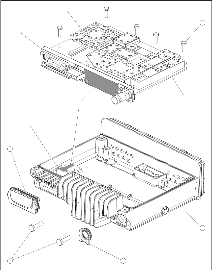
Parts of Radio Body Figure 2.8 to Figure 2.12 illustrate the parts of the radio body. Details of
the parts are summarised in Table 2.3. Figure 2.8 shows the two main
assemblies that make up the radio body — the lid assembly and the
chassis assembly. Also shown are the cover for the radio body and the
control-head seal detached from the chassis. The cover label shown in
the figure is permanently fixed to the cover. The screws secure the lid to
the chassis. The parts of the lid assembly and chassis assembly are shown
in the remaining figures.
Lid Assembly Figure 2.9 and Figure 2.10 show the parts of the lid assembly. Any
internal options board is mounted inside the lid, and this case is illustrated
in Figure 2.10. The main seal shown in both figures is an O-ring that
fits in a groove in the wall of the lid. This seal ensures that the lid is
properly sealed to the chassis. Figure 2.9 also shows the bung that seals
the aperture provided in the lid for an external options connector.
Figure 2.10 shows a typical large options board. A cover seal is supplied
for the board’s external options connector. The options loom connects
the options board to the internal options connector on the main board.
The latter connector is indicated in Figure 2.12.
Chassis Assembly Figure 2.11 and Figure 2.12 show the parts of the chassis assembly.
Illustrated in Figure 2.11 are the chassis and the main board, digital
board, and heat-transfer block of the main-board assembly. Also shown
are the bung for the auxiliary connector and the seal needed for the RF
connector. The screws secure the main-board assembly in the chassis.
Figure 2.12 shows the heat-transfer block detached from the main board.
All the parts associated with the block are illustrated; the principal parts
are inner and outer foam seals needed for the auxiliary connector, and a
rubber seal for the power connector. The lock washer and hexagonal nut
are supplied as integral parts of the RF connector. The screws secure the
heat-transfer block to the main board.
Table 2.2 Parts of the blank control head
Index Reference IPN Description Quantity
1 Figure 2.6 316-06786-xx Front panel of blank control head 1
2 Figure 2.6 312-01095-xx Label with Tait logo 1
3 Figure 2.6 354-01043-xx Lock-nut for programming connector 1 pair
4 Figure 2.6 362-01108-xx Cover seal for programming connector 1
5 Figure 2.6 347-00011-xx UNC 4-40 x 3/16-inch pan Pozi screw for cover seal 2
6 Figure 2.7 219-02902-xx Control-head loom for blank control head 1
7 Figure 2.7 362-01111-xx Foam seal for programming connector 1
Note
The characters xx in an IPN stand for the issue number. Items in the control head will always be the latest
issue at the time the control head is manufactured.

44 General Description TM8100 Mobile Radio Service Manual
May 2004 © Tait Electronics Limited
Figure 2.8 Cover, control-head seal, lid assembly, and chassis assembly of the radio body
CHASSIS ASSEMBLY
LID ASSEMBLY
4
1
2
3
3

TM8100 Mobile Radio Service Manual General Description 45
May 2004 © Tait Electronics Limited
Dissipation of Heat Heat needs to be dissipated from the interior of the radio body and, in
particular, from the following components on the main board:
■9V regulator
■audio PA (power amplifier)
■two RF PAs
■driver for RF PAs
These components are discussed in Section 3. The mechanisms by
which the heat is conducted away in each case are described below.
Dissipation of Heat
from Radio Interior Heat from the radio interior is conducted via the heat-transfer block to
the cooling fins at the rear, where it is radiated away. The ridged
underside of the chassis augments the dissipation of heat. The rear face
of the block is in contact with the chassis where the fins are situated. A
coating of thermal paste on the rear face ensures the necessary thermal
contact between the two surfaces. The coated area is shown in both
Figure 2.11 and Figure 2.12.
Figure 2.9 Parts of the lid assembly
5
6
7

46 General Description TM8100 Mobile Radio Service Manual
May 2004 © Tait Electronics Limited
Figure 2.10 Parts of the lid assembly with an internal options board
6
TYPICAL LARGE
INTERNAL OPTIONS BOARD
5
SCREWS FOR SECURING
INTERNAL OPTIONS BOARD OPTIONS LOOM
FOAM SEAL
COVER SEAL
LOCK-NUTSSCREWS
EXTERNAL
OPTIONS
CONNECTOR

TM8100 Mobile Radio Service Manual General Description 47
May 2004 © Tait Electronics Limited
Dissipation of Heat
from Regulator and
Audio PA
Heat from the regulator and audio PA is conducted to the underside of
the chassis via a screw boss on the floor of the chassis. The boss is in
contact with the underside of the PCB where the components are
mounted. A coating of thermal paste on the screw boss ensures the
necessary thermal contact between the boss and the PCB. The coated
area is shown in Figure 2.11.
Dissipation of Heat
from RF PAs and Driver Heat from the RF PAs and driver is conducted to the cooling fins via a
copper plate and the heat-transfer block. The copper plate is fixed to the
underside of the PCB beneath these components. It is in contact with a
large metal block projecting from the front of the heat-transfer block. A
coating of thermal paste on the plate ensures the necessary thermal
contact between the surfaces. The contact area on the heat-transfer
block is shown in Figure 2.12.
Table 2.3 Parts of the radio body
Index Reference IPN Description Quantity
1 Figure 2.8 303-23166-xx Cover 1
2 Figure 2.8 365-01712-xx Label for cover 1
3 Figure 2.8 349-02067-xx M4 x 16 screw for lid of radio body 4
4 Figure 2.8 362-01115-xx Control-head seal 1
5 Figure 2.9 312-01091-xx Lid of radio body 1
6 Figure 2.9 362-01109-xx Main seal in lid 1
7 Figure 2.9 302-50000-xx Bung for aperture for external options connector 1
8 Figure 2.11 303-11225-xx Chassis of radio body 1
9 Figure 2.11 349-02066-xx Internal M3 x 10 screw for main-board assembly 5
10 Figure 2.11 362-01113-xx Seal for RF connector 1
11 Figure 2.11 349-02067-xx External M4 x 16 screw for main-board assembly 2
12 Figure 2.11 302-50001-xx Bung for auxiliary connector 1
13 Figure 2.12 349-02066-xx M3 x 10 screw for heat-transfer block 3
14 Figure 2.12 308-13147-xx Heat-transfer block 1
15 Figure 2.12 362-01114-xx Rubber seal for power connector 1
16 Figure 2.12 354-01043-xx Lock-nut for auxiliary connector 1 pair
17 Figure 2.12 362-01112-xx Outer foam seal for auxiliary connector 1
18 Figure 2.12 362-01110-xx Inner foam seal for auxiliary connector 1
Note
The characters xx in an IPN stand for the issue number. Items in the radio body will always be the latest issue
at the time the radio body is manufactured.
48 General Description TM8100 Mobile Radio Service Manual
May 2004 © Tait Electronics Limited
Figure 2.11 Parts of the chassis assembly
10
11
8
12
9
DIGITAL BOARD
HEAT-TRANSFER
BLOCK
MAIN BOARD
MAIN-BOARD
ASSEMBLY
THERMAL PASTE
SCREW BOSS

TM8100 Mobile Radio Service Manual General Description 49
May 2004 © Tait Electronics Limited
Figure 2.12 Parts of the main-board assembly
13
17
14
18
16 15 THERMAL PASTE THERMAL PASTE
DIGITAL BOARD
LOCK WASHER OF
RF CONNECTOR
HEXAGONAL NUT OF
RF CONNECTOR
RF CONNECTOR
POWER
CONNECTOR
MAIN BOARD
INTERNAL OPTIONS CONNECTOR
AUXILIARY CONNECTOR

50 General Description TM8100 Mobile Radio Service Manual
May 2004 © Tait Electronics Limited
Figure 2.13 Block diagram of the main board of the radio body
POWER SUPPLY
MAIN
BOARD
DIGITAL BOARD
RECEIVER
FRE-
QUENCY
SYNTHE-
SIZER
TRANS-
MITTER
CODEC
AND AUDIO
CIRCUITRY
INTERFACE
CIRCUITRY
CONTROL-
HEAD
CONNECTOR
POWER
CONNECTOR
AUXILIARY
CONNECTOR
INTERNAL
OPTIONS
CONNECTOR
FACTORY
CONNECTOR
(FACTORY
ONLY)
RF CONNECTOR
DIG TX INH
SYN TX LO
SYN LOCK
SYN RX OSC
SYN RX LO1
TX RX RF
DIG RX EN
DIG SYN SPI
DIG SYN SPI
TX RX RF
DIG SYN EN
DIG RX EN
DIG RX EN
DIG RX EN
PSU SYS RST
+3V3
TM8100 Mobile Radio Service Manual General Description 51
May 2004 © Tait Electronics Limited
2.2 Architecture of Radio
Introduction In this subsection the architecture of the radio is described. The different
circuit modules of the control-head, main and digital boards introduced
in Subsection 2.1 (on page 33) are identified and their essential functions
are summarised. The optional circuit boards mentioned in
Subsection 2.1 are covered in other manuals.
Control Head The control heads with UI house a control-head board with the circuitry
needed for the controls and indicators on the front panel. There is
provision for an optional circuit board for use with dynamic
microphones or with a concealed microphone inside the control head.
There is also provision for the fitting of an optional third-party circuit
board in the blank control head.
Circuit Boards in
Control Head The operation of the control-head board is summarised in
Subsection 2.3 (on page 53). The circuit board for concealed and
dynamic microphones is described in the accessories manual. The fitting
of third-party circuit boards in the blank control head is discussed in the
application manual for 3DK hardware developers.
Radio Body The radio body houses a main board with the transmitter, receiver and
associated circuitry, and a digital board with the microprocessor and
associated circuitry. The digital board is reflow-soldered to the main
board. There is also provision for an internal options board to be
connected to the main board.
Circuit Boards and
Modules in Radio Body The different circuit modules of the main board are discussed below and
the operation of the circuitry is described in Subsection 2.4 (on page 54)
and Subsection 2.5 (on page 57). The different internal options boards
are discussed in the accessories manual and the 3DK manuals.
Modules of Main Board The control-head, main and digital boards, and the connectors on the
boards, are illustrated in Figure 1.6 of the previous section. Figure 2.13
is a block diagram showing the main and digital boards and the circuit
modules of the main board. These modules are:
■transmitter
■receiver
■frequency synthesizer
■CODEC (coder-decoder) and audio circuitry
■power supply
■interface circuitry
Software plays a prominent role in the functioning of the radio. For
describing the operation of the radio the software must be included with
the above modules. This is considered further below.

52 General Description TM8100 Mobile Radio Service Manual
May 2004 © Tait Electronics Limited
Figure 2.14 Architecture of the TM8100 transceiver
IF:
UHF: 45.1 MHz
VHF: 21.4 MHz
Digital
down-
converter
Squelch
Front
end
1st
IF
Channel
LPF
Channel
LPF
RSSI
Second LO
UHF: 90.328 MHz
VHF: 42.928 MHz
FM
Demod
Quad
Demod
RX
AGC
Analogue-to-digital conversion
2nd IF:
64 kHz
Audio
filtering
De-
emphasis
Optional
processing
Data and signalling
decoders
Side
tones
Volume
control
Audio
PA
Phase
locked to
TCXO
LPF
ANT
Control
Head
PWR
Mag.
PLL
Loop
filter
Loop
filter
Frequency
control
Triple-point
Equalisation
Audio
filtering
Pre-
emphasis
Optional
processing
Data and signalling
encoders
ALC Mic
PGA
Mic
FGA
Dir.
Coup. Fin Drv
/Ex
Pwr
Crtl
Ramp
control
TCXO:
13.000 MHz
VCO*
Control
Auxiliary
Head
VCXO
Bias
CUSTOM-
LOGIC
BLOCK HARDWARE
BLOCK
HARDWARE BLOCK Digital-to-analogue conversion
System interface
KEY
NOTES
(1) Noise blanker not shown
(2) VHF configuration shown*
For UHF there are separate VCOs for RX and TX
DSP
BLOCK
TM8100 Mobile Radio Service Manual General Description 53
May 2004 © Tait Electronics Limited
Operation of Radio Figure 2.14 is a simplified block diagram of the transceiver architecture
showing the hardware modules integrated with the software modules.
The same DSP (digital signal processor) device includes the software that
controls the transceiver and the software constituting the digital-signal-
processing blocks in Figure 2.14. The operation of the radio is then best
described with reference to Figure 2.14 and with a division into the
following two parts:
■operation in receive mode
■operation in transmit mode
Operational descriptions of these two parts are given in Subsection 2.4
(on page 54) and Subsection 2.5 (on page 57) respectively.
2.3 Operation of Control-head Circuitry
User Interface In this subsection the operation of the control-head circuitry is
summarised. A detailed description of the circuitry is given in Section 3
(on page 63). Control heads with UI provide a user interface consisting
of:
■seven-segment LCD
■up and down channel-selection keys
■four programmable function keys
■ON/OFF push-button key
■LED indicators
■volume control
■internal speaker
■microphone connector
The LCD displays one or two characters depending on the type of
control head. The microphone connector may also be used for the
connection of a handset or programming lead. If required, a concealed
microphone may be fitted inside the control head.
Connectors and
Circuit Boards There is an 18-way electrical interface between the control head and
radio body. The physical connection is via an 18-way loom. The control
head normally contains a single PCB assembly called the control-head
board. The differences between the boards for the one- and two-digit-
display control heads are discussed in Section 3 (on page 63). If a
dynamic microphone is used or a concealed microphone fitted, a small
circuit board must be mounted on the control-head board. The added
board has the necessary amplification, filtering and switching functions.
The internal speaker is connected to the control-head board via a lead
with a mating connector so that it can be easily disconnected.
54 General Description TM8100 Mobile Radio Service Manual
May 2004 © Tait Electronics Limited
Control-head Board The control-head board does not include a microprocessor. A
synchronous bi-directional serial interface provides communication of
key status, LCD and LED-indicator data between the radio body and the
control head. On the control-head board the serial data are converted to
or from parallel form by a number of shift registers for the keys and
indicators. For the LCD, the serial data are fed to a driver IC that
converts the serial data to a form suitable for the LCD itself. The keys
are scanned and the LCD and LED indicators updated approximately
every 50 ms.
2.4 Operation in Receive Mode
Receive Path This subsection describes the functioning of the radio in receive mode.
Detailed descriptions of the circuitry involved are given in Section 3
(on page 63). As shown in Figure 2.14, the receive path exists in the
hardware, custom-logic and DSP domains. From a functional point of
view there are three major parts:
■RF hardware
■digital base-band processing
■audio processing and signalling
These functional parts are described in detail below.
RF Hardware
Front-end Circuitry
and First IF The front-end hardware amplifies and image-filters the received RF
spectrum, then down-converts the desired channel frequency to a first
intermediate frequency IF1 of 45.1 MHz (UHF) or 21.4 MHz (VHF)
where coarse channel filtering is performed. The first LO (local
oscillator) signal is obtained from the frequency synthesizer and is
injected on the low side of the desired channel frequency for all bands.
In receive mode the modulation to the frequency synthesizer is muted.
See Subsection 2.5 (on page 57) for a description of the synthesizer. The
output of the first IF (intermediate frequency) stage is then down-
converted using an image-reject mixer to a low IF of 64 kHz.
Quadrature
Demodulator The LO for the image-reject mixer (quadrature demodulator) is
synthesized and uses the TCXO (temperature-compensated crystal
oscillator) as a reference. This ensures good centring of the IF filters and
more consistent group-delay performance. The quadrature demodulator
device has an internal frequency division of 2 so the second LO operates
at 2 x(IF1 + 64 kHz). The quadrature output from this mixer is fed to
a pair of ADCs (analogue-to-digital converters) with high dynamic range
where it is oversampled at 256 kHz and fed to the custom logic device.
TM8100 Mobile Radio Service Manual General Description 55
May 2004 © Tait Electronics Limited
Automatic Gain Control The AGC (automatic gain control) is used to limit the maximum signal
level applied to the image-reject mixer and ADCs in order to meet the
requirements for intermodulation and selectivity performance.
Hardware gain control is performed by a variable-gain amplifier within
the quadrature demodulator device driven by a 10-bit DAC (digital-to-
analogue converter). Information about the signal level is obtained from
the IQ (in-phase and quadrature) data output stream from the ADCs.
The control loop is completed within custom logic. The AGC will
begin to reduce gain when the combined signal power of the wanted
signal and first adjacent channels is greater than about –70 dBm. In the
presence of a strong adjacent-channel signal it is therefore possible that
the AGC may start acting when the wanted signal is well below
–70 dBm.
Noise Blanking
(B1 band only) For the B1 band only, noise-blanking circuitry is included. The noise
blanker removes common sources of electrical interference such as
vehicle ignition noise. The programming application allows for disabling
the noise blanker if it is not required. The noise blanker functions by
sampling the RF input to the receiver for impulse noise and momentarily
disconnecting the first LO for the duration of the impulse. The response
time of the noise blanker is very fast (tens of nanoseconds) and is shorter
than the time taken for the RF signal to pass through the front-end
hardware, so that the LO is disabled before the impulse reaches the IF
stage where it could cause crystal filter ring.
Digital Base-band Processing
Custom Logic The remainder of the receiver processing up to demodulation is
performed by custom logic. The digitised quadrature signal from the RF
hardware is digitally down-converted to a zero IF, and channel filtering
is performed at base-band. Different filter shapes are possible to
accommodate the various channel spacings and data requirements.
These filters provide the bulk of adjacent channel selectivity for narrow-
band operation. The filters have linear phase response so that good
group-delay performance for data is achieved. The filters also decimate
the sample rate down to 48 kHz. Custom logic also performs
demodulation, which is multiplexed along with AGC and amplitude
data, and fed via a single synchronous serial port to the DSP. The stream
is demultiplexed and the demodulation data used as an input for further
audio processing.
Noise Squelch The noise squelch process resides in the DSP. The noise content above
and adjacent to the voice band is measured and compared with a preset
threshold. When a wanted signal is present, out-of-band noise content
is reduced and, if below the preset threshold, is indicated as a valid
wanted signal.
56 General Description TM8100 Mobile Radio Service Manual
May 2004 © Tait Electronics Limited
Received Signal
Strength Indication Received signal strength is measured by a process resident in the DSP.
This process obtains its input from the demodulator (value of RF signal
magnitude) and from the AGC (value of present gain). With these two
inputs and a calibration factor, the RF signal strength at the antenna can
be accurately calculated.
Calibration The following items within the receiver path are calibrated in the
Factory:
■front-end tuning
■AGC
■noise squelch
■RSSI (received signal strength indication)
Information on the calibration of these items is given in the on-line help
facility of the calibration application.
Audio Processing and Signalling
Audio Processing Raw demodulated data from the receiver is processed within the DSP.
The sample rate at this point is 48 kHz with signal bandwidth limited
only by the IF filter ing. Scaling (dependent on the bandwidth of the RF
channel) is then applied to normalise the signal level for the remaining
audio processing. The sample rate is decimated to 8 kHz and bandpass
audio filtering (0.3 to 3 kHz) is applied. De-emphasis is then applied to
cancel out the receive signals pre-emphasised response and improve
signal-to-noise performance. Optional processing such as decryption or
companding is then applied if applicable.
Data and Signalling
Decoders The data and signalling decoders obtain their signals from various points
within the audio processing chain. The point used depends on the
bandwidth of the decoders and whether de-emphasis is required. Several
decoders may be active simultaneously.
Side Tones Side tones are summed in at the end of the audio-processing chain.
These are tones that provide some form of alert or give the user
confidence an action has been performed. The confidence tones may be
generated in receive or transmit mode. The side-tone level is a fixed
proportion (in the order of –10 dB) relative to full scale in the receive
path.
CODEC The combined audio and side-tone signal is converted to analogue form
by a 16-bit DAC with integral anti-alias filtering. This is followed by a
programmable-gain amplifier with a range of 45 dB in 1.5 dB steps. The
amplifier performs volume control and muting. The DAC and volume
control are part of the same CODEC device (AD6521).
TM8100 Mobile Radio Service Manual General Description 57
May 2004 © Tait Electronics Limited
Output to Speakers The output of the CODEC is fed to an audio power amplifier and to the
control head via a buffer amplifier. The output configuration of the
audio power amplifier is balanced and drives an internal speaker and,
optionally, an external speaker. The speaker loads are connected in
parallel rather than being switched. The power delivered to each speaker
is limited by its impedance. The internal speaker has 16 Ω impedance
whereas the external speaker can be as low as 4 Ω.
2.5 Operation in Transmit Mode
Transmit Path This subsection describes the functioning of the radio in transmit mode.
Detailed descriptions of the circuitry involved are given in Section 3
(on page 63). As shown in Figure 2.14, the transmit path exists in the
hardware, custom-logic and DSP domains. From a functional point of
view there are three major parts:
■audio processing and signalling
■frequency synthesizer
■RF transmitter
These functional parts are described in detail below.
Audio Processing and Signalling
Microphone Input The input to the transmitter path begins at the microphone input. There
are two microphone sources: a fist microphone connected to the control
head and an auxiliary microphone connected via the auxiliary or external
options connector. Only electret-type microphones are supported.
Support for optional dynamic fist microphones is facilitated by a
hardware amplifier and filter; this circuitry is mounted on a separate
board that needs to be installed in the control head.
Analogue Processing
of Microphone Signal The CODEC (AD6521) performs microphone selection and
amplification. The microphone amplifier consists of an amplifier with a
fixed gain of 16 dB followed by a programmable-gain amplifier with 0 to
22 dB gain. The amplified microphone signal is converted to a digital
stream by a 16-bit ADC with integral anti-alias filtering (0.1 to 3.2 kHz).
The digital stream is transported to the DSP for further audio processing.
Automatic Level
Control The ALC (automatic level control) follows, and is used to effectively
increase dynamic range by boosting the gain of the microphone pre-
amplifier under quiet conditions and reducing the gain under noisy
acoustic conditions. The ALC function resides in the DSP and controls
the microphone programmable-gain amplifier in the CODEC. The
ALC has a fast-attack (about 10 ms) and slow-decay (up to 2 s)
characteristic. This characteristic ensures that the peak signal level is
regulated near full scale to maximise dynamic range.
58 General Description TM8100 Mobile Radio Service Manual
May 2004 © Tait Electronics Limited
DSP Audio Processing The output of the automatic level control provides the input to the DSP
audio-processing chain at a sample rate of 8 kHz. Optional processing
such as encryption or companding is done first if applicable. Pre-
emphasis, if required, is then applied. The pre-emphasised signal is hard-
limited to prevent over-deviation, and filtered to remove high-frequency
components. The sample rate is then interpolated up to 48 kHz and
scaled to be suitable for the frequency synthesizer.
Data and Signalling
Encoders The data and signalling encoders inject their signals into various points
within the audio-processing chain. The injection point depends on the
bandwidth of the encoders and whether pre-emphasis is required.
Frequency Synthesizer
Main Parts of
Synthesizer As shown in Figure 2.14, the frequency synthesizer consists of two main
parts:
■FCL (frequency control loop)
■RF PLL (phase-locked loop)
The FCL and RF PLL are described briefly below. Detailed descriptions
of the circuitry are given in Section 3 (on page 63). Note that patents
are pending for several aspects of the synthesizer design.
Frequency Control
Loop The FCL consists of the following:
■TCXO
■mixer
■loop filter
■VCXO (voltage-controlled crystal oscillator)
■frequency control block
The FCL provides the reference frequency for the RF PLL. It generates
a high-stability reference frequency that can be both modulated and
offset in fine resolution steps.
RF PLL The RF PLL consists of the following:
■RF PLL device
■loop filter
■VCO (voltage-controlled oscillator)
■VCO output switch
The RF PLL has fast-locking capability but coarse frequency resolution.
The above combination of control loops creates improved frequency
generation and acquisition capabilities.
TM8100 Mobile Radio Service Manual General Description 59
May 2004 © Tait Electronics Limited
Operation of
Control Loop The RF PLL is a conventional integer-N design with frequency
resolution of 25 Hz. In transmit mode the loop locks to the transmit
frequency, whereas in receive mode it locks to the receive frequency
minus the first IF frequency.
Initially, the VCO generates an unregulated frequency in the required
range. This is fed to the PLL device (ADF4111) and divided down by a
programmed ratio to approximately 25 kHz. The reference frequency
input from the FCL is also divided down to approximately 25 kHz. The
phase of the two signals is compared and the error translated into a DC
voltage by a programmable charge pump and dual-bandwidth loop filter.
This DC signal is used to control the VCO frequency and reduce the
initial error. The loop eventually settles to a point that minimises the
phase error between divided-down reference and VCO frequencies.
The net result is that the loop “locks” to a programmed multiple of the
reference frequency.
The FCL generates an output of 13.012 ± 0.004 MHz. Initially a
VCXO produces a quasi-regulated frequency in the required range. The
VCXO output is fed to a mixer where it is mixed with the 13.000 MHz
TCXO frequency. The mixer, after low-pass filtering to remove
unwanted products, produces a nominal frequency of 12 kHz. This is
converted to digital form and transported to the frequency-control block
in custom logic.
The frequency-control block compares the mixer output frequency with
a reference generated by the digital clock, and creates a DC error signal.
A programmed offset is also added. This error signal is converted to
analogue form and used to control the VCXO frequency and reduce the
initial error. Once settled, the loop “locks” to the TCXO frequency
with a programmed offset frequency. The FCL output therefore acquires
the TCXO’s frequency stability.
Modulation The full bandwidth modulation signal is obtained from the DSP in digital
form at a sample rate of 48 kHz. In traditional dual-point modulation
systems the modulation is applied, in analogue form, to both the
frequency reference and the VCO in the RF PLL, combining to produce
a flat modulation response down to DC. Reference modulation is
usually applied directly to the TCXO.
In the system employed in the TM8100 radio, the frequency reference is
generated by the FCL, which itself requires dual-point modulation
injection to allow modulation down to DC. With another modulation
point required in the RF PLL, this system therefore requires triple-point
modulation. The modulation signals applied to the FCL are in digital
form, whereas for the RF PLL (VCO) the modulation signal is applied
in analogue form. The modulation cross-over points occur at
approximately 30 and 300 Hz as determined by the closed loop
bandwidths of the FCL and RF PLL respectively.
60 General Description TM8100 Mobile Radio Service Manual
May 2004 © Tait Electronics Limited
Frequency Generation The RF PLL has a frequency resolution of 25 kHz. Higher resolution
cannot be achieved owing to acquisition-time requirements and so for
any given frequency the error could be as high as ±12.5 kHz. This error
is corrected by altering the reference frequency to the RF PLL. The
FCL supplies the reference frequency and is able to adjust it up to
±300 ppm with better than 0.1 ppm resolution (equivalent to better
than 50 Hz resolution at the RF frequency). The FCL offset will usually
be different for receive and transmit modes.
Fast Frequency Settling Both the FCL and RF PLL employ frequency-acquisition speed-up
techniques to achieve fast frequency settling. The frequency-acquisition
process of the FCL and RF PLL is able to occur concurrently with
minimal loop interaction owing to the very large difference in frequency
step size between the loops.
Frequency Acquisition
of RF PLL In the RF PLL the loop bandwidth is initially set high by increasing the
charge pump current and reducing time constants in the loop filter. As
a result settling to within 1 kHz of the final value occurs in under 4 ms.
In order to meet noise performance requirements the loop parameters
are then switched to reduce the loop bandwidth. There is a small
frequency kick as the loop bandwidth is reduced. Total settling time is
under 4.5 ms.
Frequency Acquisition
of FCL The FCL utilises self-calibration techniques that enable it to rapidly settle
close to the final value while the loop is open. The loop is then closed
and settling to the final value occurs with an associated reduction in
noise. The total settling time is typically less than 4 ms.
Calibration The following items are calibrated in the frequency synthesizer:
■nominal frequency
■KVCO
■KVCXO
■VCO deviation
Calibration of the nominal frequency is achieved by adding a fixed offset
to the FCL nominal frequency; the TCXO frequency itself is not
adjusted. The items KVCO and KVCXO are the control sensitivities of
the RF VCO (in MHz/V) and VCXO (in kHz/V) respectively. The
latter has temperature compensation.

TM8100 Mobile Radio Service Manual General Description 61
May 2004 © Tait Electronics Limited
RF transmitter
RF Power Amplifier
and Switching The RF PA (power amplifier) is a four-stage line-up with approximately
42 dB of power gain. The output of the frequency synthesizer is first
buffered to reduce kick during power ramping. The buffer output goes
to a broad-band exciter IC that produces approximately 200 mW output.
This is followed by an LDMOS driver producing up to 2 W output that
is power-controlled. The final stage consists of two parallel LDMOS
devices producing enough power to provide 25 W at the RF connector.
Output of RF
Power Amplifier The output of the RF PA passes through a dual-directional coupler, used
for power control and monitoring, to the PIN switch. The PIN switch
toggles the antenna path between the receiver and transmitter in receive
and transmit modes respectively. Finally, the output is low-pass-filtered
to bring harmonic levels within specification.
Power Control The steady-state power output of the transmitter is regulated using a
hardware control loop. The forward power output from the RF PA is
sensed by the directional coupler and fed back to the power control loop.
The PA output power is controlled by varying driver gate bias voltage
that has a calibrated maximum limit to prevent overdrive. The power
control signal is supplied by a 13-bit DAC driven by custom logic.
Figure 2.15 Typical ramping waveform
Bias
ramp
Power
ramp
Bias
ramp
Power
ramp
Hi power
Lo power
Power
Time
62 General Description TM8100 Mobile Radio Service Manual
May 2004 © Tait Electronics Limited
Ramping Power ramp-up consists of two stages:
■bias
■power ramping
The timing between these two stages is carefully controlled in order to
achieve the correct overall wave shape and meet the specification for
transient ACP (adjacent channel power). A typical ramping waveform is
shown in Figure 2.15.
Bias Ramp-up The steady-state final-stage bias level is supplied by an 8-bit DAC
programmed prior to ramp-up but held to zero by a switch on the DAC
output under the control of a TX INHIBIT signal. Bias ramp-up begins upon
release by the TX INHIBIT signal with the ramping shape being determined
by a low-pass filter. Owing to power leakage through the PA chain,
ramping the bias takes the PA output power from less than –10 dBm to
approximately 25 dB below steady-state power.
Power Ramp-up The power ramp signal is supplied by a 13-bit DAC that is controlled by
custom logic. The ramp is generated using a look-up table in custom
logic memory that is played back at the correct rate to the DAC to
produce the desired waveform. The ramp-up and ramp-down
waveforms are produced by playing back the look-up table in forward
and reverse order respectively. For a given power level the look-up table
values are scaled by a steady-state power constant so that the ramp
waveform shape remains the same for all power levels.

TM8100 Mobile Radio Service Manual Circuit Descriptions 63
May 2004 © Tait Electronics Limited
3 Circuit Descriptions
Scope of Section This section contains descriptions of the circuitry of the control-head
board and each of the modules of the main board. The latter are the
transmitter, receiver, frequency synthesizer and FCL, CODEC and audio
circuitry, power supply, and interface circuitry. Since the digital board is
not serviceable at level-2, no description of the digital circuitry is given.
3.1 Control-head Board
Introduction This subsection describes the circuitry of the control-head boards for the
one- and two-digit-display control heads. The boards differ only in their
layouts; the components are identical. The circuit description given
below is sufficiently general to be applicable to both boards.
Connectors and
UI Devices The control-head board includes the circuitry for the seven keys, 18
LEDs, and the LCD device of the control head. Also mounted on the
board are the volume-control potentiometer and the following five
connectors:
■control-head connector
■microphone connector
■speaker connector
■two connectors for optional circuit board
Protection circuitry is provided for the microphone connector. The
optional circuit board is installed when a dynamic microphone is used or
a concealed microphone is fitted.
Basic Circuitry The LCD driver is based on IC2, IC5 and IC7. Electrical contact
between the control head and the LCD itself is via two elastomeric strips
as described in Subsection 2.1 (on page 33). There are pads on the board
for the seven keys — four function keys, two channel-selection keys, and
an ON/OFF key. The device IC4 reads the status of the function and
channel-selection keys. Of the 18 LEDs, there are red, orange and green
STATUS LEDs, and four green LEDs for the function keys, as well as 11
green LEDs for back-lighting — one for each key and four for the LCD.
The four dual switching transistors Q1 to Q4 control the switching of
the LEDs; the transistors are driven by IC3.
64 Circuit Descriptions TM8100 Mobile Radio Service Manual
May 2004 © Tait Electronics Limited
Serial Peripheral
Interface The control-head board uses an SPI (serial peripheral interface) to
control the display on the LCD, turn back-lighting on and off, control
the STATUS LEDs, and read the status of the keys. The interface consists
of the following four lines at the control-head connector:
■pin 11: data out CH SPI DO
■pin 12: latch line CH LE
■pin 15: data in CH SPI DI
■pin 16: clock CH SPI CLK
The handling of the data is described below.
Data Input and Output Data that are input to the control head are clocked through the LCD
driver and daisy-chained to a shift register. Once all the data have been
clocked in, the latch line is driven low. On this falling edge all the
outputs (LEDs and LCD segments) are driven to their new state. When
the latch line is driven high, the state of each key is latched into another
shift register. The data are then clocked out back to the radio body so
that the radio can respond accordingly.
LCD Driver An oscillator is used to run the LCD. It oscillates at about 60 Hz and
employs a Schmitt trigger and D flip-flop to ensure a 50% duty cycle to
the LCD. A reset circuit is required because the reset from the main
board is not routed to the control head. The reset circuit also employs a
Schmitt trigger.
Volume Control The volume-control potentiometer is linear and passes the DC voltage
signal VOL WIP DC to the radio body. The signal is read by an ADC on the
main board, and the volume is adjusted accordingly.
3.2 Transmitter
Broadband Exciter The transmitter circuitry is given on sheet 3 of the circuit diagram for
the main board. The broadband exciter is a common element in all the
variants of the TM8100 mobile radio, as it operates across all frequencies
from 66 MHz to 940 MHz. It is made up of Q300 and Q303, which
amplify the signal provided by the frequency synthesizer from its level of
7 to 9 dBm up to 24.5 dBm for the frequency band from 66 to 530 MHz
and slightly less than this for the bands covering 530 MHz to 940 MHz.
The exciter operates in full saturation, thereby maintaining a constant
output power independent of the varying input power level supplied by
the synthesizer (7 to 9 dBm).
TM8100 Mobile Radio Service Manual Circuit Descriptions 65
May 2004 © Tait Electronics Limited
Power Amplifier The power amplifier comprises the driver amplifier Q306 and two
paralleled final devices Q309 and Q310. The 24.5 dBm signal from the
broadband exciter is reduced by a band-dependent pi-attenuator and is
amplified by Q306. The resulting signal is then amplified a second time
by Q309 and Q310 to produce a typical output power of 42 W when
measured after the series capacitors at the start of the directional coupler
(C348, C349, C350). The high-level RF signal passes via the directional
coupler, the transmit-receive PIN switch, and the low pass filter, through
to the antenna. The low-pass filter is used to attenuate unwanted
harmonic frequencies.
Power Control Loop Calibration is used to adjust the power control loop, thus setting the
output of the transmitter to one of four preferred power levels (1, 5, 12
and 25 watts). The loop maintains these power settings under changing
environmental conditions. The control mechanism for this loop is via
the DAC IC204 and one of the operational amplifiers making up IC301.
The power control loop will be inhibited if for any reason an out-of-lock
signal is detected from the synthesizer. This ensures that no erroneous
signals are transmitted at any time. The power control loop senses the
forward power by means of the diode D304. This signal is fed to the
buffer and a band-limited operational amplifier back to the gate of Q306.
A voltage clamp (one of the operational amplifiers of IC301) for Q306
limits the maximum current that this device can draw.
Directional Coupler The directional coupler actively senses the forward power and feeds it
back to the power-control circuit. If the directional coupler detects too
much reverse power, indicating a badly matched antenna, the transmitter
will be reduced to the lowest power setting.
Temperature Sensor For added protection, a temperature sensor ensures that the transmitter
power is reduced to very low levels should a temperature threshold be
exceeded. If the temperature does not decrease, the transmitter is
switched off.
3.3 Receiver
Introduction The receiver circuitry is given on sheet 4 of the circuit diagram for the
main board. The receiver is of the triple-conversion superheterodyne
type. The first two IF stages are implemented in hardware; the third stage
is implemented in the FPGA (field-programmable gate array) of the
digital board. The FPGA also carries out the demodulation of the
received signals.
66 Circuit Descriptions TM8100 Mobile Radio Service Manual
May 2004 © Tait Electronics Limited
Front-end Circuitry The front-end circuitry is a standard varicap-tuned singlet (band-pass
filter), followed by an LNA (low-noise amplifier), and then a varicap-
tuned doublet (image filter). The varicap tuning voltage CDC RX FE TUNE
is provided by a DAC, with voltages calculated from a calibration table
stored in non-volatile memory. The two varicap-tuned filters need to be
calibrated to ensure that maximum sensitivity is achieved.
First Mixer The first mixer is a standard diode-ring mixer with SMD (surface-mount
device) baluns and a quadruple SMD diode. For the VHF band the
receiver includes a circuit for suppressing ignition noise. This circuit
momentarily removes the LO signal from the mixer when an ignition
noise pulse is detected. The ignition-noise suppressor is selectable on a
per-channel basis when the radio is programmed.
First IF Stage and
Second Mixer The first IF stage consists of a crystal channel filter (BPF1), followed by
an IF amplifier, and then another crystal filter (BPF2). The second mixer
is an IC quadrature mixer with an internal AGC amplifier. This IC has
a divide-by-two function on the LO input in order to provide the
quadrature LO frequencies required internally. The second LO
frequency is synthesized by an integer PLL (IC403), which uses the
TCXO frequency SYN RX OSC (13.0000 MHz) as its reference.
Frequencies
of IF Stages The frequency of the first IF stage depends as follows on the frequency
band of the radio:
■B1 band: 21.400 029 MHz
■D1 band: 21.400 029 MHz
■H5 band: 45.100 134 MHz
■H6 band: 45.100 134 MHz
The above are nominal values; the actual frequency will differ by a small
amount depending on the exact initial frequency of the TCXO. The
frequency of the second IF stage will always be precisely 64.000 kHz
once the TCXO calibration has been completed. (The TCXO
calibration does not adjust the TCXO frequency, but instead adjusts the
VCXO frequency, which in turn adjusts the VCO or first LO frequency
as well as the frequency of the first IF stage. The second LO frequency
remains fixed.) The third IF stage is completely within the FPGA and is
not accessible.
Demodulation Demodulation takes place within the FPGA. Demodulated audio is
passed to the DSP of the digital board for processing of the receiver audio
signal. Raw demodulated audio can be tapped out from the DSP for use
with an external modem. The modem may be connected to the
auxiliary connector or to the external options connector when an
internal options board is fitted.
TM8100 Mobile Radio Service Manual Circuit Descriptions 67
May 2004 © Tait Electronics Limited
Automatic Gain Control The receiver has an AGC circuit to enable it to cover a large signal range.
Most of the circuit functions are implemented in the FPGA. The FPGA
passes the AGC signal to the CODEC IC204 for output from pin 14
(IDACOUT) and thence via IC201 as the signal CDC RX AGC to pin 23 of the
quadrature mixer IC400. As the antenna signal increases, the AGC
voltage decreases.
Channel Filtering The channel filtering is split between the first and third IF stages. The
channel filtering circuit in the first IF stage comprises a pair of two-pole
crystal filters. The first filter has a 3 dB bandwidth of 12 kHz, and the
second a 3 dB bandwidth of 15 kHz. Most of the channel filtering,
however, is implemented in the FPGA. When the radio is programmed,
the different filters are selected as assigned by the channel programming.
The selectable filters plus the fixed crystal filters result in the following
total IF 3 dB bandwidths:
■wide channel spacing : 12.6 kHz
■medium channel spacing: 12.0 kHz
■narrow channel spacing : 7.8 kHz
(The FPGA runs from the DIG SYS CLK signal, which has a frequency of
12.288 MHz.) The receiver requires the TCXO calibration to be
completed to ensure that the channel filtering is centred, thereby
minimising distortion.
Received Signal
Strength Indication The RSSI is calculated in the FPGA and DSP, and can be passed as an
analogue voltage to the internal options interface and the external
auxiliary interface. To obtain an accurate estimate of the RSSI (over the
signal level and frequency), it is necessary to calibrate the AGC
characteristic of the receiver and the front-end gain versus the receive
frequency.
3.4 Frequency Synthesizer
Introduction The frequency synthesizer includes an active loop filter, one or two
VCOs and buffer amplifiers, and a PLL IC. The last-named uses
conventional integer-N frequency division and includes a built-in charge
pump. Speed-up techniques ensure a transmit-receive settling time of
less than 4.5 ms while retaining low noise characteristics in static
operation. In the following description of the circuitry, first the
necessary power supplies and then the synthesizer itself are discussed. The
circuitry is given on sheet 5 of the circuit diagram for the main board.
68 Circuit Descriptions TM8100 Mobile Radio Service Manual
May 2004 © Tait Electronics Limited
Power Supplies Several power supplies are used by the frequency synthesizer owing to a
combination of performance requirements and the availability of suitable
components. The PLL IC includes analogue and digital circuitry and
uses separate power supplies for each section. The digital section is run
on 3 V, while the analogue section is run on approximately 5 V. The
VCOs and buffer amplifiers run off a supply of about 5.3 V. The active
loop filter requires a supply of 14 to 15 V, and a reference voltage of
approximately 2.5 V.
Performance
Requirements Low noise and good regulation of the power supply are essential to the
performance of the synthesizer. A 6 V regulator IC provides good line
regulation of the 9 V supply and good load regulation. Good regulation
of the power-supply line and load is essential for meeting the transient
ACP requirements. The regulator output voltage is electrically noisy,
however, and filtering is essential. Filtering of the power supply is
achieved with two capacitance multipliers (Q508 and C585 for the VCO
supply, and Q512 and C579 for the PLL and loop-filter supply). The
VCO (or VCOs) use a separate capacitance multiplier because these
multipliers have poor load regulation and the VCOs impart sufficient
load transients to warrant a separate supply.
Effect of Tuning Range For reasons of noise performance, the VCOs are designed to be tuned
within a range of 2 to 12 V. Active tuning circuitr y is required. An active
loop filter incorporating an IC operational amplifier achieves this range
with a suitable power supply voltage. Normal synthesizer switching
behaviour involves overshoot, which dictates that the tuning voltage
range must extend above and below the range of 2 to 12 V. The 14 V
limit is a result of limits on the working supply voltage of the IC
operational amplifier.
Switch-mode Power
Supply The power supply VCL SUPPLY for the active loop filter is provided by a
SMPS (switch-mode power supply), which is in turn powered by 9 V.
The SMPS consists of an oscillator (switching circuit) and a detector.
The output voltage is monitored by a feedback circuit that controls the
DC bias of the switching circuit to maintain a constant output voltage.
Synthesizer Circuitry The essential function of the PLL frequency synthesizer is to multiply a
25 kHz reference frequency to give any desired frequency that is an
integer multiple of 25 kHz. There are some constraints imposed by the
capabilities of the synthesizer hardware, especially the tuning range of the
VCOs.
Reference Frequency The 25 kHz (approximate) reference is obtained by dividing the 13 MHz
(approximate) output of the FCL. Any error in the FCL output
frequency will be multiplied by the synthesizer. Therefore, if the
synthesizer is locked but not the FCL, then the synthesizer output
frequency will be wrong. The FCL frequency division is performed by
a digital counter inside the PLL IC. The divider setting is constant.
TM8100 Mobile Radio Service Manual Circuit Descriptions 69
May 2004 © Tait Electronics Limited
VCO Frequency and
Output Power The output frequency from the synthesizer is generated by a VCO. The
VCO frequency is tuned across the frequency range of the radio by
means of a DC control voltage, typically between 2 V and 12 V. The
VCO output power is amplified by a buffer amplifier. The power is low
and varies from band to band. The buffer output power depends on
which mode — receive or transmit — is used. In receive mode the
output power should be about 7 dBm, whereas in transmit mode it
should be about 9 dBm.
Dual VCOs Some variants of the synthesizer use two VCOs: one for receive and one
for transmit. Synthesizers with two VCOs share the same tuning signal.
Only one VCO is switched on at a time, and so the PLL IC will see only
one output frequency to tune. A portion of the RF output from the
VCOs is fed to the RF input of the PLL IC. The RF signal is divided
by an integer that would give 25 kHz if the output frequency were
correct.
Phase-locked Loop The PLL IC compares the 25 kHz reference and the divided VCO
signal, and the error is used to control the internal charge pump. The
charge pump is a current source that can sink or source current in
proportion to the frequency or phase error. The output is a series of
25 kHz pulses with a width that is dependent on the phase error. When
the output frequency of the synthesizer is correct, there is no error and
the charge pump output will become open circuit.
Active Loop Filter The loop filter continuously integrates the current pulses from the charge
pump and produces a steady DC output voltage that tunes the VCO (or
VCOs). When the VCO frequency is correct, there is no frequency
error and therefore no charge-pump output, and so the loop filter’s
output voltage remains constant. If the frequency is too high or too low,
the error will result in the output of charge-pump current pulses
(negative or positive depending on the sign of the error). The loop filter’s
output voltage will change accordingly, causing the VCO frequency to
change in proportion. The synthesizer design is such that normally the
VCO frequency will be automatically corrected.
Re-tuning of VCO
Frequency When the radio changes channels or switches between receive and
transmit, the VCO frequency must be changed. The rate at which the
VCO is re-tuned is dependent on many factors, of which the loop filter
is the main factor. The loop filter is an integrator built around an
operational amplifier. The resistors and capacitors of the filter affect both
the switching time and the stability of the synthesizer; the values of these
components have been carefully selected to give optimum control
characteristics.
70 Circuit Descriptions TM8100 Mobile Radio Service Manual
May 2004 © Tait Electronics Limited
Speed-up Techniques To reduce the change-over time between transmit and receive, part-time
speed-up techniques have been implemented. Speed-up involves
changing some resistor values while simultaneously changing the PLL IC
settings. This process is implemented in hardware under software control
in conjunction with use of the synthesized reference input. The result is
a transmit-receive settling time of less than 4.5 ms. (The switching time
is measured for a frequency change equal to the first IF plus 10 MHz or
1 MHz, depending on the repeater offsets used for the band. This
implies a synthesizer transmit-receive change-over plus an offset of
1 MHz or 10 MHz in less than 4.5 ms. The ramp-up and ramp-down
of the transmitter, which totals 1 ms, extends this change-over time to
5.5 ms.)
3.5 Frequency Control Loop
Introduction The FCL forms part of the frequency-synthesizer module. The basis of
the FCL is a VCXO, which generates the reference frequency required
by the main PLL of the synthesizer. The FCL circuitry is given on sheet
5 of the circuit diagram for the main board, and is described below.
Elements of
FCL Circuitry The FCL is a simple frequency-locked loop. The circuitry consists of the
following elements:
■VCXO (XL501, Q501, Q503)
■TCXO (XL500)
■buffer amplifier (IC500)
■mixer (IC501)
■low-pass filter (IC502, pins 5 to 7)
■modulator buffer amplifier (IC502, pins 1 to 3)
The TCXO supplies a reference frequency of 13.0000 MHz, which is
extremely stable, regardless of the temperature. The VCXO runs at a
nominal frequency of 13.0000 MHz, and is frequency-locked to the
TCXO reference frequency.
Circuit Operation The VCXO output is mixed with the TCXO output to create a nominal
difference (or offset) frequency SYN CDC FCL of 12.0 kHz. The signal
SYN CDC FCL is fed via the CODEC IC502 in the CODEC circuitry to
the FPGA on the digital board. The FPGA detects the offset frequency,
compares it with the programmed offset frequency, and outputs a
corresponding feedback signal CDC VCXO MOD via IC205. The feedback
signal is amplified and inverted by the modulator buffer amplifier and
output as the loop voltage for the VCXO. With this design the VCXO
frequency can be adjusted by very small precise amounts, and because the
loop is locked, the VCXO inherits the temperature stability of the
TCXO.
TM8100 Mobile Radio Service Manual Circuit Descriptions 71
May 2004 © Tait Electronics Limited
Modulation The FCL modulation is implemented within the FPGA and appears at
the output of IC205, and therefore on the VCXO loop voltage.
Consequently, the VCXO is frequency modulated directly by the
relevant modulation information. The latter may be the microphone
audio, an audio tap-in signal, internal modem signals, or any
combination of these.
3.6 CODEC and Audio Circuitry
CODEC Circuitry The CODEC circuitry and audio circuitry are given on sheet 2 of the
circuit diagram for the main board. Regarding the former, analogue-to-
digital conversion and digital-to-analogue conversion is performed by
the devices IC203, IC204 and IC205.
Device IC203 IC203 is an eight-channel DAC that provides control of transmitter
biasing, front-end tuning, and the output of analogue RSSI signals. The
digital input data are fed to IC203 in synchronous serial form. Three of
the DAC channels are not used.
Device IC205 IC205 contains two CODECs. One is used by the FCL. The second is
used for auxiliary audio (input) and VCO modulation (output). The
digital section communicates with this device via a four-wire
synchronous serial interface.
Device IC204 IC204 contains base-band, voice-band and auxiliary CODECs and some
analogue signal conditioning. The reference voltage (nominally 1.2 V)
for these CODECs is provided internally by IC204 but is decoupled
externally by C228.
Base-band CODEC The base-band CODEC handles the I and Q outputs (IRXP, IRXN, QRXP
and QRXN balls) of the receiver’s second IF stage. The analogue signals are
differential and biased at 1.2 V nominally. The digital section
communicates with this CODEC via a two-wire synchronous serial
interface (BSDO and BSOFS balls). The digital-to-analogue conversion
section of the base-band CODEC is not used.
Voice-band CODEC The voice-band CODEC handles the microphone and speaker signals.
The digital section communicates with this CODEC via a three-wire
synchronous serial interface (VSFS, VSDO and VSDI balls). IC204 also
contains voice-band filtering, pre-amplification and volume control.
72 Circuit Descriptions TM8100 Mobile Radio Service Manual
May 2004 © Tait Electronics Limited
Auxiliary CODEC The auxiliary CODEC handles transmitter power control, receiver gain
control, auxiliary audio output and general analogue monitoring
functions. The digital section communicates with this CODEC via a
three-wire synchronous serial interface (ASFS, ASDI and ASDO balls). The
DAC used for receiver gain control (IDACOUT ball) is a current output type.
Current-to-voltage conversion is performed by R238. The full-scale
output of 1.2 V is amplified by IC201 to approximately 3 V as required
by the receiver.
Audio Circuitry The audio circuitry performs four functions:
■output of audio signal for speaker
■input of microphone audio signal
■input of auxiliary audio signal
■output of auxiliary audio signal
The sections of the circuitry concerned with these functions are
described below.
Audio Signal
for Speaker The audio signal for the speaker is generated by IC204 (VOUTAUXP ball).
This signal is post-volume-control and has a pre-emphasised frequency
response. The signal is then processed by R218, R217 and C205 to
restore a flat frequency response and reduce the signal level to that
required by the audio power amplifier.
Summing Circuit The top of C205 is where side tones are summed in and the CDC RX AUD
signal is obtained. C201 and R211 pre-emphasize and attenuate the
side-tone signal to give a flat side-tone frequency response and reduce the
input to an appropriate level.
Buffer Amplifier IC201 (pins 8 to 10) amplifies the signal at the top of C205 by 19 dB and
drives the CDC RX AUD system interface line via C212 and R225. The
capacitor C212 provides AC output coupling and R225 ensures stability.
The DC bias for this amplifier is derived from IC204.
Audio Power Amplifier The signal at the top of C205 is fed via C204 to the audio power
amplifier IC202. IC202 has 46 dB of gain and a differential output
configuration. C209, C211, R252 and R253 ensure stability of the
amplifier at high frequencies. When operational, the output bias voltage
for IC202 is approximately half the radio supply voltage. When not
operational, the output becomes high impedance.
Control of Audio
Power Amplifier Power up, power down, and muting of IC202 is controlled by two signals
from the digital section, DIG AUD PA EN1 and DIG AUD PA EN2. The network
consisting of Q200, Q201, R200 to R206, R210 and R250 converts the
two digital signals to the single three-level analogue signal required by
IC202.
TM8100 Mobile Radio Service Manual Circuit Descriptions 73
May 2004 © Tait Electronics Limited
Microphone Signals There are two microphone source signals:
■ITF AUX MIC AUD from auxiliary or internal options connector
■ITF CH MIC AUD from control head
The biasing for electret microphones is provided by a filtered 3.0 V
supply via R226 and R227. The components R209 and C202 provide
the supply filtering. The microphone inputs to IC204 (VINAUXP, VINAUXN,
VINNORP and VINNORN balls) are differential. The negative inputs are
decoupled to the filtered 3.0 V supply by C215 and C216. The positive
inputs are biased to approximately 1.5 V by R229, R232, R230 and
R233. AC coupling and DC input protection is provided by C213 and
C214.
Auxiliary Audio Input The auxiliary audio input signal ITF AUD TAP IN is DC-coupled to the ADC
input of IC205. R241 combined with internal clamping diodes in
IC205 provide DC protection for the ADC input. IC205 provides the
input biasing of approximately 1.5 V.
Auxiliary Audio Output The source for the auxiliary audio output signal CDC AUD TAP OUT is
provided by IC204 (RAMPDAC ball). The DAC output of IC204 is low-
pass filtered to remove high-frequency artefacts. The low-pass filter,
formed by IC201 (pins 1 to 3), R219, R220, R221, R224, C206, C208
and C210, is a third-order Butterworth type with a cut frequency of
approximately 12 kHz. The output of the low-pass filter is amplified by
6 dB by a buffer amplifier, IC201 (pins 5 to 7), and fed via R207 and
R208 to drive the CDC AUD TAP OUT interface line. The DC bias for this
signal path is provided by IC204 and is approximately 1.2 V when
operational. The offset at CDC AUD TAP OUT is approximately 2.4 V owing
to the gain of the buffer amplifier.
3.7 Power Supply
Introduction The power-supply circuitry consists of the following main sections:
■supply protection
■supervisory circuit
■internal power supplies
■control of internal power supplies
The power-supply circuitry is given on sheet 6 of the circuit diagram for
the main board, and is described below.
74 Circuit Descriptions TM8100 Mobile Radio Service Manual
May 2004 © Tait Electronics Limited
Supply Protection Electrical protection to the radio is provided by the clamping diode
D600 and 10 A fuses in the positive and negative leads of the power
cable. This provides protection from reverse voltages, positive transients
greater than 30 V, and all negative transients. An ADC monitors the
supply and is responsible for the protection of internal devices, which
have an operating voltage of less than 30 V. The ADC also ensures
protection if the radio operates outside its specified voltage range of
10.6 V to 16 V.
Supervisory Circuit The supervisory circuit comprises a reset and watchdog timer. The
circuit provides the reset signal PSU SYS RST to the digital section, which
in turn provides the watchdog signal DIG WD KICK required by the
supervisory circuit.
Internal Power
Supplies There are nine internal power supplies:
■one SMPS
■five linear regulators (+9V0, +6V0, +3V3, +3V0 AN, +2V5 CDC)
■three switched supplies (+9V0 TX, +3V0 RX, +13V8 SW)
The SMPS is used to regulate to 3.3 V from the external supply
+13V8BATT. The four lower voltages required are then further stepped
down with linear regulators. These all take advantage of the efficiency
gain of the SMPS. The 9 V regulator and the 13.8 V switched supply
are connected to +13V8 BATT. The two remaining switched supplies (9 V
and 3 V) use P-channel MOSFETs.
Control of Internal
Power Supplies The radio can be turned on using the ON/OFF key on the control head or
by means of external signals. For the latter case hardware links are
required and there are several power-sense options; these are discussed
below. Some internal power supplies can be controlled by means of
digital lines depending on the mode in which the radio is operating.
Power-sense Options There are five power-sense options for powering up and powering down
the radio:
■battery power sense
■auxiliary power sense
■internal-options power sense
■no power sense
■emergency power sense
The emergency power-sense option can be used in conjunction with any
of the other four options. The ON/OFF key can be used with any of the
options, although the behaviour of the radio will depend on the option
selected. The links LK1 to LK4 on the main board are used to
implement the desired option. The power-sense options and the link
settings are described below.
TM8100 Mobile Radio Service Manual Circuit Descriptions 75
May 2004 © Tait Electronics Limited
Battery Power Sense For the battery-power-sense option the link LK1 is required to connect
+13V8BATT of the power connector to the power-up circuitry. With this
option, when a 13.8 V supply is connected to the radio, the radio enters
the programmed power-on mode. The ON/OFF key can then be used to
turn the radio on and off. This option has the disadvantage that the radio
still draws about 28 mA after being switched off using the ON/OFF key.
The reason is that the radio enters the stand-by mode and does not shut
down completely.
Auxiliary Power Sense With the auxiliary power-sense option the digital input line AUX GPI3 of
the auxiliary connector is used to power up and power down the radio.
The link LK2 is required to connect the line to the power-up circuitry.
The line is active high; it is on when the level exceeds 2.6 V and off
when the level falls below 0.7 V; the line tolerates maximum inputs equal
to the radio supply voltage. When the line becomes active, the radio
enters the programmed power-on mode. The ON/OFF key can then be
used to switch the radio on and off. With the radio off and the line
active, the radio draws about 28 mA. When the line becomes inactive,
the radio is shut down completely regardless of whether it was on or in
stand-by mode. With the line inactive the radio draws less than 1 mA.
In a vehicle installation this avoids flattening the battery when the
ignition key is off.
Internal-options
Power Sense The internal-options power-sense option is similar to the auxiliary
power-sense option, except that the IOP GPIO7 line of the internal options
connector is used. The link LK4 is required to connect the line to the
power-up circuitry. This line is also active high; it is on when the level
exceeds 2.6 V and off when the level falls below 0.7 V; the line tolerates
maximum inputs of 5 V. The behaviour of the ON/OFF key is the same as
with the auxiliary power-sense option.
No Power Sense If no power-sense option is selected, the radio can only be powered up
and powered down by means of the ON/OFF key. For this option the links
LK1, LK2 and LK4 must be removed. The advantage of this option over
the battery power-sense option is that the radio draws less than 1 mA
when it is switched off.
Emergency
Power Sense For the emergency power-sense option the AUX GPI2 line of the auxiliary
connector is used. Externally, this line is typically connected to a hidden
switch. Internally, the link LK3 is required to connect the line to the
power-up circuitry. The line is active low and has an internal pull-up
resistor to the external supply voltage. The line is on when the level falls
below 0.7 V. When the line becomes active, as when the hidden switch
is pressed for two seconds, the radio enters the emergency mode. This
mode can also be activated by making an emergency call or by pressing
a key that has been programmed appropriately. The concealed
microphone is typically fitted when the emergency power-sense option
is selected.
76 Circuit Descriptions TM8100 Mobile Radio Service Manual
May 2004 © Tait Electronics Limited
Operation in
Emergency Mode If the radio is off when the emergency mode is activated, the radio is
powered up but the display on the control head is not switched on. If
the radio is on when the mode is activated, the display is frozen. In the
latter case, if the ON/OFF key is pressed, the display is switched off but the
radio remains in the emergency mode. While in this mode the radio
cycles between transmit and receive. To exit the emergency mode the
ON/OFF key needs to be pressed again.
3.8 Interface Circuitry
Bi-directional Lines Bi-directional lines are provided on four pins of the auxiliary connector,
(AUX GPIO4 to AUX GPIO7) one on the control-head connector (CH GPIO1),
and seven on the internal options connector (IOP GPIO1 to IOP GPIO7).
Those on the auxiliary and control-head connectors are formed by
combining two uni-directional lines. For example, the line AUX GPIO4 at
pin 10 of the auxiliary connector is formed from ITF AUX GPI4 and DIG AUX
GPO4. The circuitry is the same in all five cases and is explained below
for the case of AUX GPIO4.
Output Signals An output on the line AUX GPIO4 originates as the 3.3 V signal
DIG AUX GPO4 from the digital section. The signal is first inverted by Q703
(pins 3 to 5) and the output divided down to 1.6 V by R746 and R753
to drive the base of Q703 (pins 1, 2 and 6). When the latter’s collector
current is low, the base current is a maximum and creates a small voltage
drop across R761, causing the collector emitter to saturate. As the
collector current increases, the base current decreases proportionally
until the voltage across R761 reaches 1 V. At this point the base-emitter
begins to turn off and the base current diminishes rapidly. The net effect
is a current-limiting action. The current limit value is approximately
18 mA (the inverse of the value of R761). The output configuration is
open-collector with a pull-up to 3.3 V by default. Pull-up options to
5 V and 13.8 V are also available.
Five-volt Regulator The 5 V supply mentioned above is provided by a simple buffered zener
regulator formed by Q702, D721, R721 and R722. The resistor R722
limits the current to about 25 mA under short-circuit conditions.
Input Signals
(AUX GPIO4)An input signal applied to AUX GPIO4 is coupled via R757 to ITF AUX GPI4
and fed to the digital section. As the input signal may exceed the
maximum allowed by the digital section, it is clamped by D711 and a
shunt regulator. The shunt regulator consists of Q708, R719 and R720
and begins to turn on at approximately 2.7 V. In combination with
D711, the input to ITF AUX GPI4 is therefore clamped to 3.3 V nominally.
The value of R757 is made large to minimise the loading effect on the
output pull-up resistors. On AUX GPIO4 only, the optional MOSFET
Q707, which has a high current drive, may be fitted.
TM8100 Mobile Radio Service Manual Circuit Descriptions 77
May 2004 © Tait Electronics Limited
Input Signals
(AUX GPI1 to AUX GPI3)Dedicated inputs are provided on three pins of the auxiliary connector
(AUX GPI1 to AUX GPI3). AUX GPI1 is a general-purpose input with strong
protection of the same type used for AUX GPIO4. AUX GPI2 is normally a
dedicated emergency input but can be made a general-purpose input like
AUX GPI1 by removing the link LK3 in the power supply area. AUX GPI3 is
normally a dedicated ignition-sense input but can be made a general-
purpose input like AUX GPI1 by removing the link LK2 in the power
supply area and fitting the 33 kΩ resistor R775.
ESD Protection On exposed inputs of the auxiliary and control-head connectors ESD
(electrostatic discharge) protection is provided by a 470 pF capacitor and
by clamping diodes to ground and to 13.8 V. For example, on AUX GPIO4
this would consist of D713 and C725. The lines IOP GPIO1 to IOP GPIO7
are intended for connection to internal digital devices and so these have
relatively light protection.
Hookswitch Detection Hookswitch detection is performed by Q700, R709, R706 and R712.
When the resistance to ground on the PTT line is less than 13.2 kΩ,
Q700 will turn on and drive the ITF CH HOOK line high; this indicates
either that the microphone is on hook or that the PTT (press-to-talk)
switch is pressed.
78 Circuit Descriptions TM8100 Mobile Radio Service Manual
May 2004 © Tait Electronics Limited

TM8100 Mobile Radio Service Manual Servicing of Radio 79
May 2004 © Tait Electronics Limited
TM8000 mobiles
Chapter 2
Servicing of Radio

80 Servicing of Radio TM8100 Mobile Radio Service Manual
May 2004 © Tait Electronics Limited
Chapter 2 Contents
4 General Information . . . . . . . . . . . . . . . . . . . . . . . . . . . . . . . . . . . . 81
4.1 Repair Levels and Website Access . . . . . . . . . . . . . . . . . . . . . . . . . . . . . . 81
4.2 Tools, Equipment and Spares . . . . . . . . . . . . . . . . . . . . . . . . . . . . . . . . . . 84
4.3 Servicing Precautions . . . . . . . . . . . . . . . . . . . . . . . . . . . . . . . . . . . . . . . 87
4.4 SMT Repair Techniques . . . . . . . . . . . . . . . . . . . . . . . . . . . . . . . . . . . . . 91
4.5 Equipment Set-up . . . . . . . . . . . . . . . . . . . . . . . . . . . . . . . . . . . . . . . . . 93
5 Servicing Procedure . . . . . . . . . . . . . . . . . . . . . . . . . . . . . . . . . . . . .107
5.1 Initial Inspection. . . . . . . . . . . . . . . . . . . . . . . . . . . . . . . . . . . . . . . . . . 107
5.2 Fault Diagnosis and Repair . . . . . . . . . . . . . . . . . . . . . . . . . . . . . . . . . . 109
5.3 Final Inspection, Test and Administration . . . . . . . . . . . . . . . . . . . . . . . . 121
6 Disassembly and Re-assembly of Radio . . . . . . . . . . . . . . . . . . . . . . .125
6.1 Detachment of Control Head . . . . . . . . . . . . . . . . . . . . . . . . . . . . . . . . 127
6.2 Disassembly of Control Head. . . . . . . . . . . . . . . . . . . . . . . . . . . . . . . . . 131
6.3 Disassembly of Radio Body. . . . . . . . . . . . . . . . . . . . . . . . . . . . . . . . . . 137
6.4 Re-assembly of Radio Body . . . . . . . . . . . . . . . . . . . . . . . . . . . . . . . . . 144
6.5 Re-assembly and Attachment of Control Head. . . . . . . . . . . . . . . . . . . . 148
7 Servicing of Control Head . . . . . . . . . . . . . . . . . . . . . . . . . . . . . . . .151
7.1 Faults not Involving Control-head Board . . . . . . . . . . . . . . . . . . . . . . . . 151
7.2 Faults Involving Control-head Board . . . . . . . . . . . . . . . . . . . . . . . . . . . 157
7.3 Replacement of Faulty Component . . . . . . . . . . . . . . . . . . . . . . . . . . . . 160
7.4 Replacement of Faulty Control-head Board . . . . . . . . . . . . . . . . . . . . . 163
8 Servicing of Main Board. . . . . . . . . . . . . . . . . . . . . . . . . . . . . . . . . .165
8.1 Fault Diagnosis and Repair . . . . . . . . . . . . . . . . . . . . . . . . . . . . . . . . . . 165
8.2 Replacement of Faulty Component . . . . . . . . . . . . . . . . . . . . . . . . . . . . 166
8.3 Replacement of Faulty Main-board Assembly. . . . . . . . . . . . . . . . . . . . . 169
9 Diagnosis of Faults on Main Board. . . . . . . . . . . . . . . . . . . . . . . . . . .171
9.1 Power-supply Circuitry . . . . . . . . . . . . . . . . . . . . . . . . . . . . . . . . . . . . . 171
9.2 Interface Circuitry . . . . . . . . . . . . . . . . . . . . . . . . . . . . . . . . . . . . . . . . 178
9.3 Frequency Synthesizer. . . . . . . . . . . . . . . . . . . . . . . . . . . . . . . . . . . . . . 183
9.4 Frequency Control Loop. . . . . . . . . . . . . . . . . . . . . . . . . . . . . . . . . . . . 191
9.5 Receiver. . . . . . . . . . . . . . . . . . . . . . . . . . . . . . . . . . . . . . . . . . . . . . . . 197
9.6 Transmitter. . . . . . . . . . . . . . . . . . . . . . . . . . . . . . . . . . . . . . . . . . . . . . 208
9.7 CODEC and Audio Circuitry . . . . . . . . . . . . . . . . . . . . . . . . . . . . . . . . 236

TM8100 Mobile Radio Service Manual General Information 81
May 2004 © Tait Electronics Limited
4 General Information
Scope of Section This section discusses the two repair levels covered by the service manual,
details concerning website access, the tools, equipment and spares
required, and the setting up of the necessary test equipment. General
servicing precautions are also given, as well as details of certain non-
standard SMT techniques required for level-2 repairs.
4.1 Repair Levels and Website Access
Repair Levels As described in Section 1, this manual covers level-1 and level-2 repairs
of TM8100 radios. To summarise, level-1 repairs comprise the
replacement of control-head boards, main-board assemblies, and other
parts of the radio; level-2 repairs comprise repairs of control-head boards
and, except for special items, main-board assemblies. The special items
are:
■digital board
■RF PAs (Q309 and Q310)
■CODEC 1 (IC204)
■copper plate
Replacements of the connectors and volume-control potentiometer on
the control-head board are level-1 repairs. Replacements of the
connectors on the main-board assembly, however, are level-2 repairs
because these repairs entail the disassembly of the main-board assembly.
Important The circuit boards in the TM8100 radio are complex.
They should be serviced only by accredited service
centres. Repairs attempted without the necessary
equipment and tools or by untrained personnel might
result in permanent damage to the radio.
Accreditation of
Service Centres Service centres that wish to achieve ASC status should contact Technical
Support. They will need to provide evidence that they meet the criteria
required for accreditation; Technical Support will supply details of these
criteria. These centres must then make available suitable staff for training
by TEL personnel, allow their service facilities to be assessed, and provide
adequate documentation of their processes. They will be accorded ASC
status and endorsed for repairs of TM8100 radios after their staff have
been trained and their facilities confirmed as suitable. Existing ASCs
need to apply for and be granted an endorsement for repairs of TM8100
radios. All ASCs with the necessary endorsements may carry out level-
1 and level-2 repairs of these radios, whether under warranty or not.
82 General Information TM8100 Mobile Radio Service Manual
May 2004 © Tait Electronics Limited
Skills and Resources
for Level-1 Repairs For level-1 repairs basic electronic repair skills are sufficient. Apart from
the standard tools and equipment of any service centre, certain torque
drivers are required as well as a service kit and, for diagnostic purposes,
a spare control head. Replacement control-head boards and main-board
assemblies are supplied by TEL in separate spares kits. The other
replacement parts are supplied in four spares kits: parts for the one-digit-
display control head, parts for the two-digit-display control head, parts
for the radio body, and spare control-head seals. Further details are given
in Subsection 4.2 (on page 84).
Skills and Resources
for Level-2 Repairs For level-2 repairs expertise is required in SMT repairs of circuit boards
with a very high complexity and extreme component density. Apart
from the tools and equipment needed for level-1 repairs, the standard
SMT repair tools are required. A can-removal tool is strongly
recommended but not mandatory. Replacement SMT components are
supplied by TEL in two separate spares kits, one for the control-head
boards and one for the main board. Spare special items are not supplied.
Further details are given in Subsection 4.2.
Website Access To carry out level-1 and level-2 repairs, service centres need access to the
secured portion of the Technical Support website. There are different
access levels; those required for level-1 and level-2 repairs are:
■level-1 repairs: associate access
■level-2 repairs: Tait-only access
Log-in passwords are needed for associate and Tait-only access; Technical
Support supplies service centres with the necessary log-in information.
(The unsecured portion of the Technical Support website is accessible to
the general public. This type of access is called public access, and no log-
in password is required.)
Items Available
on Website The information available at the different access levels is summarised in
Table 4.1. The technical notes mentioned are of different types.
Associate technical notes relate to the repair of the radio but not the
downloading of firmware; Tait-only technical notes relate to the
firmware. The PCB information packs are discussed in more detail
below.

TM8100 Mobile Radio Service Manual General Information 83
May 2004 © Tait Electronics Limited
PCB Information Packs A PCB information pack for a particular circuit board consists of the
relevant BOMs, grid reference indexes, PCB layouts, and circuit
diagrams. (The grid reference indexes give the locations of components
on the PCB layouts and circuit diagrams.) A PCB information pack is
compiled whenever there is a major change in the layout of the board.
All PCB information packs are published on the Technical Support
website. In the service documentation, however, the PCB information
pack for only the current release of the board is included.
Tait FOCUS Database An additional source of information to service centres is the Tait FOCUS
call-logging database. (This is accessible on the Technical Support
website also.) All Customer-related technical issues regarding the radios
are recorded on this database. These issues may be raised by both
Customers and service centres. Technical Support resolves the issues and
informs the Customer or service centre concerned of the outcome. All
issues and their solutions are available for review by all service centres.
Table 4.1 Items relating to TM8100 radios that are available on the Technical Support website
Item Public access Associate access Tait-only access
Operator’s manuals
User’s guides
Installation guides
Public technical notes
•
•
•
•
•
•
•
•
•
•
•
•
Product release notes
Specifications
Calibration software
Programming software
Programming user manuals
Fitting instructions
Service manuals
Associate technical notes
•
•
•
•
•
•
•
•
•
•
•
•
•
•
•
•
Software release information
Firmware
Tait-only technical notes
PCB information packs
•
•
•
•

84 General Information TM8100 Mobile Radio Service Manual
May 2004 © Tait Electronics Limited
4.2 Tools, Equipment and Spares
Torque-dr iv er s For level-1 and level-2 repairs, excluding SMT repairs of the circuit
boards, the torque-drivers listed in Table 4.2 are required. These are the
only special tools required over and above the standard workshop tools.
For level-1 repairs only the Torx T10 and Torx T20 driver bits are
necessary. The sockets are needed for disassembling and re-assembling
the main-board assembly, which is a level-2 task.
Tools for SMT Repairs In general only the standard tools for SMT work are required for level-2
repairs of the circuit boards. In addition, a can-removal tool is
recommended but if none is available, a hot-air tool may be used instead.
However, it should be borne in mind that a hot-air tool affords little
control. Even in skilled hands, use of a hot-air tool to remove cans will
result in rapid uncontrolled rises in the temperature of components
under the can being removed as well as under any adjacent cans. The
circuit board might suffer damage as a result.
Table 4.2 Torque-drivers
Drive type Torque (N.m) Torque (lbf.in) Repair level
Torx T20 2.5 22 1
Torx T10 1.9 17 1
1.7 15 2
0.56 5 1
0.34 3 1
3/16-inch socket 0.90 8 2
14 mm long-reach socket 1.7 15 2

TM8100 Mobile Radio Service Manual General Information 85
May 2004 © Tait Electronics Limited
Test Equipment The following test equipment is required for servicing the radio:
■test PC (with programming and calibration applications loaded)
■RF communications test set (audio bandwidth of at least 10 kHz)
■oscilloscope
■digital current meter (capable of measuring up to 3 A)
■multimeter
■DC power supply (capable of 13.8 V and 10 A)
■spare TM8115 control head
■spare TM8110 control head
■TMAA21-00 service kit
Separate instruments may be used in place of the RF communications
test set. These are an RF signal generator, audio signal generator, audio
analyzer, RF power meter, and modulation meter. Details of the service
kit are given below.
Service Kit The TMAA21-00 service kit contains all the items needed for
connecting the radio to the test equipment. The setting up of the
equipment is described in Subsection 4.5 (on page 93). The service kit
also includes a product support CD and a folder with the necessary
service documentation, including this manual. The CD contains the
programming application, calibration application, and soft-copies of the
service and related documentation. The contents of the service kit are
listed in Table 4.3. Note that the TMAA20-04 cable listed is required
only if the test PC is to be connected directly to the radio for
programming purposes.
Table 4.3 Contents of TMAA21-00 service kit
Product code Item
TMAA21-01 Cable (DB14 socket to RJ45 plug plus in-line connector)
TMAA20-01 Product support CD
TMAA20-02 Adaptor (RJ45 socket to DB9 socket)
TMAA20-03 Cable (power connector to banana plugs plus in-line connector)
TMAA20-04 Cable (RJ12 socket to RJ45 plug)
T2000-A19 Cable (DB9 socket to RJ12 plug)
TOPA-SV-024 Test unit
MM8100-01-00-812 Service and accessories manuals

86 General Information TM8100 Mobile Radio Service Manual
May 2004 © Tait Electronics Limited
Spares Kits The spares kits required for the servicing of the radio are listed in
Table 4.4. The corresponding repair levels are also indicated. A spares
kit (Spares kit 6) for the repair of the rugged microphone is also supplied
but is not discussed in this manual; refer to the accessories manual for the
details. The contents of Spares kits 1, 2 and 10 are given in Section 6
(on page 125). Contents lists for Spares kits 4 and 5 are supplied with
the kits.
Table 4.4 Spares kits
Kit number Product code Description Repair level
1 TMAA22-01 Parts of two-digit-display control head
— excluding control-head board
1
2 TMAA22-02 Mechanical parts of radio body 1
3 TMAA22-03 Control-head boards (two-digit display) 1
4 TMAA22-04 Selected components of control-head boards 2
5 TMAA22-05 Selected components of main board 2
7 TMAA22-07 Control-head seals 1
10 TMAA22-90 Parts of one-digit-display control head
— excluding control-head board
1
11 TMAA22-91 Control-head boards (one-digit display) 1
TMAA22-12B1 Main-board assembly (B1 band) 1
TMAA22-12H5 Main-board assembly (H5 band) 1
TMAA22-12H6 Main-board assembly (H6 band) 1

TM8100 Mobile Radio Service Manual General Information 87
May 2004 © Tait Electronics Limited
4.3 Servicing Precautions
Introduction This subsection discusses the precautions that need to be taken when
servicing the radios. These precautions fall into the following categories:
■mechanical issues
■compliance issues
■anti-static precautions
■transmitter issues
Service technicians should familiarise themselves with these precautions
before attempting repairs of the radios.
Use of Torque-drivers Apply the correct torque when using a torque-driver to tighten a screw
or nut in the radio. Under-torquing can cause problems with
microphonics and heat transfer. Over-torquing can damage the radio.
Table 6.3 in Section 6 (on page 125) lists the correct torque values for
the different screws and nuts.
Non-scratch Bench Tops Use workbenches with non-scratch bench tops so that the mechanical
parts of the radio are not damaged during disassembly and re-assembly.
(The workbench must also satisfy the anti-static requirements specified
below.) In addition, use a clear area of the bench when disassembling and
re-assembling the radio.
Note The radio is designed to satisfy the applicable compliance
regulations. Do not make modifications or changes to the
radio not expressly approved by TEL. Failure to do so could
invalidate compliance requirements and void the Customer’s
authority to operate the radio.
Sealing of Radio To maintain the sealing of the radio to IP54 standards, ensure that all
bungs and seals are fitted after servicing the radio. These are for the
auxiliary, RF, external options, and programming connectors:
■bung for auxiliary connector
■rubber seal for RF connector
■bung for aperture for options connector (connector not fitted)
■cover seal for options connector (connector fitted)
■cover seal for programming connector (blank control head only)
In addition, ensure that the grommet sealing the aperture to the
microphone connector of two-digit-display control heads is properly
fitted.

88 General Information TM8100 Mobile Radio Service Manual
May 2004 © Tait Electronics Limited
Important The components of the circuit boards in the radios are
susceptible to damage from electrostatic discharges.
Observe anti-static precautions when handling the
boards or their components. Follow the procedures
given in the manufacturers’ data books.
Storage and Transport
of Items Always observe anti-static precautions when storing, shipping or
carrying the circuit boards and their components. Use anti-static bags
for circuit boards and anti-static bags or tubes for components that are to
be stored or shipped. Use anti-static bags or trays for carrying circuit
boards, and foil or anti-static bags, trays, or tubes for carrying
components.
Anti-static
Workbenches Use an anti-static workbench installed and tested according to the
manufacturer’s instructions. A typical installation is shown in Figure 4.1.
These benches have a dissipative rubber bench top, a conductive wrist
strap, and a connection to the building earth. The material of the bench
top must satisfy not only anti-static requirements but also the non-scratch
requirements mentioned above.
Figure 4.1 Typical installation of an anti-static workbench
TO BUILDING
EARTH
METAL FRAME
DISSIPATIVE RUBBER
BENCH MAT
CONDUCTIVE WRIST STRAP

TM8100 Mobile Radio Service Manual General Information 89
May 2004 © Tait Electronics Limited
Transmitter Issues The following issues relate to the operation of the transmitter:
■RF and thermal burns
■antenna loading
■test transmissions
■accidental transmissions
■distress beacons
The precautions required in each case are given below.
Caution Avoid thermal burns. Do not touch the cooling
fins or underside of the radio body when the
transmitter is or has been operating. Avoid RF
burns. Do not touch the antenna while the trans-
mitter is operating.
Important The radio has been designed to operate with a 50 Ω
termination impedance, but will tolerate a wide range of
antenna loading conditions. Nevertheless, do not
operate the transmitter without a suitable load. Failure
to do so might result in damage to the power output
stage of the transmitter.
Important While servicing the main board, avoid overheating the
radio during test transmissions. The following is good
practice: Secure the main-board assembly in the chassis
with the two external screws and one of the internal
screws. The screws are labelled 9 and 11 in Figure 2.11.
The heat-transfer block must be secured to the main
board. The lid of the radio body may be left off. After
completing any measurement or test requiring
activation of the transmitter, immediately return the
radio to the receive mode.
Important Under certain circumstances the microprocessor can key
on the transmitter. Ensure that all instruments are
protected at all times from such accidental transmissions.
Note The frequency ranges 156.8 MHz ± 375 kHz,
243 MHz ± 5 kHz, and 406.0 to 406.1 MHz are reserved
worldwide for use by distress beacons. Do not program
transmitters to operate in any of these frequency bands.

90 General Information TM8100 Mobile Radio Service Manual
May 2004 © Tait Electronics Limited
Figure 4.2 Locations of the capacitors C548 and C565 and the inductors L601 and L602 on the main
board
VHF BOARD
(UHF BOARD SIMILAR)
UHF BOARD
(VHF BOARD SIMILAR)
TM8100 Mobile Radio Service Manual General Information 91
May 2004 © Tait Electronics Limited
4.4 SMT Repair Techniques
Standard Procedures Service centres carrying out level-2 repairs are expected to be familiar
with the standard techniques for the replacement of SMT components.
However, certain components on the main board require non-standard
techniques and these are discussed below. Another issue of concern is
the procedure for removing and installing cans. A discussion of the issue
concludes this subsection.
Non-standard
Procedures Do not use the standard SMT repair techniques when replacing the
capacitors C548 and C565 and the inductors L601 and L602. The
standard techniques tend to produce excessive heat, which will damage
these components. Do not use a hot-air tool or heat gun. Instead use
solder paste and a standard soldering iron with a number-6 iron tip. The
capacitors are part of the frequency-synthesizer circuitry under the
SYN TOP can. The inductors are part of the SMPS of the power-supply
circuitry on the bottom-side of the board. Figure 4.2 shows the
locations of the components.
Can Removal
and Installation Cans are best removed and installed using a can-removal tool. If this tool
is available, technicians should refer to the documentation supplied with
the tool for the correct procedures. If the tool is not available, a hot-air
tool may be used instead. However, technicians require training in the
best techniques to employ in the absence of a can-removal tool. Such
training is part of the accreditation process for service centres.
Spare Cans It is good practice to discard any can that has been removed and replace
it with a spare can from Spares kit 5. If this is not done, special
precautions are needed when re-installing the original can. These
precautions are discussed as part of the training for accreditation.

92 General Information TM8100 Mobile Radio Service Manual
May 2004 © Tait Electronics Limited
Figure 4.3 Test equipment for servicing radios
RADIO BODY
BLANK
CONTROL HEAD
POWER CONNECTOR
TEST PC
SERIAL PORT
DB9 SOCKET
RJ12 PLUG
COMPUTER
CONNECTOR
RADIO CONNECTOR
DB15 SOCKET
RJ45 PLUG
MICROPHONE
CONNECTOR
IN-LINE
CONNECTOR
AUXILIARY CONNECTOR
BANANA
PLUGS
BNC PLUGTEST UNIT
OSCILLOSCOPE
RX AUDIO/SINAD
CONNECTOR
AUDIO IN HI
RF COMMUNI-
CATIONS
TEST SET
AUDIO OUT
TX AUDIO
CONNECTOR
RADIO BODY
CONTROL HEAD
RF CONNECTOR
BNC PLUG
BNC PLUG
BNC PLUG
AUDIO MONITOR
OUTPUT
RF IN/OUT
N-TYPE
CONNECTOR
DC POWER SUPPLY
PROGRAMMING
CONNECTOR
RJ45
PLUG
DB9
SOCKET
ADAPTOR
(SEE INSET FOR CONNECTION
TO BLANK CONTROL HEAD)
AC INPUT
TM8100 Mobile Radio Service Manual General Information 93
May 2004 © Tait Electronics Limited
4.5 Equipment Set-up
Introduction This subsection covers the setting up of the test equipment for servicing
the radios, as well as related aspects:
■setting up of test equipment, including test unit
■use of test unit
■installing programming and calibration applications
■basic programming and calibration tasks
■invoking CCTM (computer-controlled test mode)
■summary tables of CCTM commands and error codes
■visual and aural indications provided by radio
The last-named aspect applies to control heads with UI, and concerns
the STATUS LEDs and LCD screen, and the various alerts and confidence
tones emitted from the speaker.
Connect Equipment Connect the test equipment to the radio as shown in Figure 4.3. Use the
test unit, cables and adaptor of the service kit. Refer to Subsection 4.2
(on page 84) for details of the test equipment and service kit. The face
of the test unit is fitted with a speaker, five switches, and the following
connectors:
■“RADIO” connector (DB15 plug)
■“COMPUTER” connector (RJ12 socket)
■“TX AUDIO” connector (BNC socket)
■“RX AUDIO/SINAD” connector (BNC socket)
These connectors are all required for connecting the test equipment and
radio. Figure 4.4 illustrates the face of the test unit.
Use of Test Unit The test unit facilitates the testing of the receive and transmit functions
of radios. When the switches are set for the required mode, the test unit
automatically routes all signals to the appropriate destinations. The unit
may be used with both mobile and portable radios. A full description is
given in the accessories manual. As shown in Figure 4.4, the switches
are:
■SELECTOR switch
■HOOK switch
■MODE switch
■AUDIO IN switch
■AUDIO OUT switch
For servicing TM8100 radios set the SELECTOR switch to “TM8100”. For
testing receive and transmit functions respectively, the remaining switches
must be set as described below. (When programming or calibrating
radios the switches have no effect, although it is good practice to set the
MODE switch to “RX”.)

94 General Information TM8100 Mobile Radio Service Manual
May 2004 © Tait Electronics Limited
Figure 4.4 Illustration of the face of the test unit
Radio
Rx
Tx / PTT
Speaker
Radio
Load
TOP Mod Audio
Mic Audio Rx Audio /
SINAD
Tx Audio
Computer
TOP
Off
Hook On
Hook Off
TM8000 only
TM8000
AUDIO OUT
SWITCH
AUDIO IN
SWITCH
SPEAKER
SELECTOR
SWITCH
HOOK
SWITCH
MODE
SWITCH
TM8100 Mobile Radio Service Manual General Information 95
May 2004 © Tait Electronics Limited
Settings for
Receive Tests For receive tests set the switches on the test unit as follows:
■HOOK switch : “HOOK OFF”
■MODE switch : “RX”
■AUDIO IN switch : “OFF”
■AUDIO OUT switch: “SPEAKER” or “LOAD”
In the last-named case, with the switch in the “SPEAKER” position, the
received audio is output from the test unit’s speaker. In the “LOAD”
position a 16 Ω load is switched into the circuit in place of the test unit’s
speaker. Note, however, that the AUDIO OUT switch has no effect on the
radio’s speaker.
Settings for
Transmit Tests For transmit tests set the switches on the test unit as follows:
■HOOK switch : “HOOK OFF”
■MODE switch : “RX” initially
■AUDIO IN switch : “MIC AUDIO”
■AUDIO OUT switch: (immaterial)
When ready to transmit, set the MODE switch to the “TX/PTT” position.
This switch functions in the same way as the PTT switch on the
microphone.
Product Support CD After setting up the test equipment for the first time, install the
programming and calibration applications on the test PC. These
applications are included on the product support CD supplied with the
service kit. Access the contents of the CD as follows:
1. Insert the product support CD in the CD-ROM drive of the test
PC.
2. The Contents window of the CD should appear; the window is
illustrated in Figure 4.5. If the Contents window fails to appear,
proceed as follows:
3. Click “Start” > “Run”. The “Run” dialogue box appears.
4. Type d:\menu.exe, where d is the letter designating the CD-ROM
drive.
5. Click the “OK” button. The “Run” dialogue box is closed and the
Contents window appears.

96 General Information TM8100 Mobile Radio Service Manual
May 2004 © Tait Electronics Limited
Install Applications The upper two buttons in the Contents window of the product support
CD allow for the installation of the programming and calibration
applications:
1. Click the “Programming” button. Installation of the programming
application begins automatically. Follow the instructions on the
screen to complete the installation.
2. Click the “Calibration” button. Installation of the calibration
application begins automatically. Follow the instructions on the
screen to complete the installation.
3. The Contents window remains open following installation of the
above applications. Investigate the remaining features of the
product support CD as described below, or click the Close button
to remove the window.
4. Remove and store the product support CD.
Figure 4.5 The Contents window of the product support CD
TM8100 Mobile Radio Service Manual General Information 97
May 2004 © Tait Electronics Limited
View Documents The middle six buttons in the Contents window of the product support
CD give access to the documents stored on the CD:
■user’s guide
■service manual
■operator’s manual
■PCB information packs
■accessories manual
■licence agreement
To view any document click the corresponding button. The Adobe
Acrobat Reader application needs to be installed on the test PC.
Access TaitWorld
Website Of the two lower and remaining buttons in the Contents window of the
product support CD, the “Miscellaneous” button is currently unused.
Clicking the “TaitWorld” button opens the default browser installed on the
test PC and accesses the TaitWorld website.
Programming
Application The programming application is typically used to read the programming
file of a radio, change settings in the various forms constituting the file,
and reprogram the radio. Alternatively, the application can be used to
open a new file, select the required settings, and program one or more
radios. To run the application and become familiar with its features,
proceed as follows:
1. Click “Start” > “Programs” > “Tait Programming Applications” >
“TM8100 Programming Application”. The programming application
is opened.
2. On the menu bar, click “Help” > “Contents and Index”. The on-line
help facility is opened.
3. Read the information provided by the on-line help facility.
4. Close the on-line help facility and close the programming
application.
98 General Information TM8100 Mobile Radio Service Manual
May 2004 © Tait Electronics Limited
Calibration Application The calibration application is used to read radio calibration files, perform
diagnostic functions, change certain settings, perform calibration tests,
view and check calculated calibration data, and program radios with
calibration files. To run the application and become familiar with its
features, proceed as follows:
1. Click “Start” > “Programs” > “Tait Programming Applications” >
“TM8100 Calibration Application”. The calibration application is
opened.
2. On the menu bar, click “Help” > “Contents and Index”. The on-line
help facility is opened.
3. Read the information provided by the on-line help facility.
4. Close the on-line help facility and close the calibration
application.
Computer-controlled
Test M od e The servicing procedures require a radio to be placed in the computer-
controlled test mode. In this mode CCTM commands can be entered at
the test PC. These commands are then relayed via the test unit to the
radio. Certain CCTM commands cause the radio to carry out particular
functions; others read particular settings and parameter values in the
radio. The CCTM commands of use in servicing radios are listed in
Table 4.5 to Table 4.9, grouped according to category.
Terminal Program
for CCTM To place a radio in CCTM requires the use of a terminal program on the
test PC. An example is HyperTerminal, which is supplied with
Microsoft Windows. As a preliminary, first select the settings for the
communications port as follows:
1. Open the terminal program. (In the case of HyperTerminal, click
“Start” > “Programs” > “Accessories” > “Communications” >
“HyperTerminal”.)
2. In the terminal program first select the COM port to which the
radio is connected. Then select the following settings for the port:
■bits per second : 19 200
■data bits : 8
■parity : none
■stop bits : 1
■flow control : none
3. Click the “OK” button (or equivalent).
4. Save the file with the port settings under a suitable name. For
subsequent sessions requiring the terminal program, open this file.

TM8100 Mobile Radio Service Manual General Information 99
May 2004 © Tait Electronics Limited
Table 4.5 CCTM commands in the audio category
Command
Usage
Entry at keyboard Response on screen
Audio category
20 – Mute received audio
Forces muting of the received
audio signal
20 None
21 – Unmute received audio
Forces unmuting of the received
audio signal
21 None
22 – Mute microphone
Mutes transmit modulation
(effectively mutes microphone
audio)
22 None
23 – Unmute microphone
Unmutes transmit modulation
(effectively unmutes microphone
audio)
23 None
74 – Audio PA
Controls the state of the audio PA
(and hence enables or disables the
speaker)
74 x
where x is the required state
(0=stand-by, 1=on, 2=mute)
None
110 – Audio volume
Sets the level of the audio volume
110 x
where x defines the required level
(any integer from 0 to 255)
None
138 – Select microphone
Selects the microphone required
138 x
where x is the required microphone
(0=control-head microphone;
1=auxiliary microphone)
None
323 – Audio tap in
Generates the audio tone AUD TAP IN
at the specified tap point
323 x y
where x specifies the tap point
(r2, r5, t1 or t5) and y the tap type
(A=bypass in, B=combine, E=splice)
(the default is A when y is omitted)
None
324 – Audio tap out
Outputs the audio signal at the
specified tap point to AUD TAP OUT
324 x y
where x specifies the tap point
(r1, r2, r3, r4, r5, t1, t2, t3 or t7)
and y the tap type
(C=bypass out, D=split, E=splice)
(the default is D when y is omitted)
None

100 General Information TM8100 Mobile Radio Service Manual
May 2004 © Tait Electronics Limited
Table 4.6 CCTM commands in the radio-information, radio-control and system categories
Command
Usage
Entry at keyboard Response on screen
Radio-information category
94 – Radio serial number
Reads the serial number of the
radio
94 x
where x is the serial number
(an eight-digit number)
96 – Firmware version
Reads the version number of the
radio firmware
96 QMA1F_x_y
where x is a three-character
identifier and y is an eight-digit
version number
97 – Boot-code version
Reads the version number of the
boot code
97 QMA1B_x_y
where x is a three-character
identifier and y is an eight-digit
version number
98 – FPGA version
Reads the version number of the
FPGA
98 QMA1G_x_y
where x is a three-character
identifier and y is an eight-digit
version number
133 – Hardware version
Reads the product code of the
radio body and the hardware
version number
133 x
y
where x is the product code
and y is the version number
(a four-digit number)
134 – FLASH serial number
Reads the serial number of the
FLASH memory
134 x
where x is the serial number
(a 16-digit hexadecimal number)
Radio-control category
400 – Select channel
Changes the current channel to
that specified
400 x (alternatively *x)
where x is a valid channel number
None
System category
46 – Supply voltage
Reads the supply voltage
46 x
where x is the supply voltage in
millivolts
203 – Clear system error
Clears the last recorded system
error
203 None
204 – Read system error
Reads the last recorded system
error and the associated data
204 SysErr: x
y
where x is the error number and
y represents the associated data

TM8100 Mobile Radio Service Manual General Information 101
May 2004 © Tait Electronics Limited
Table 4.7 CCTM commands in the frequency-synthesizer and receiver categories
Command
Usage
Entry at keyboard Response on screen
Frequency-synthesizer category
72 – Lock status
Reads the lock status of the RF PLL,
FCL and LO2 respectively
72 x y z
where x is the RF PLL, y the FCL,
and z the LO2 lock status
(0=not in lock, 1=in lock)
101 – Radio frequencies
Sets the transmit and receive
frequencies to specified values
101 x y 0
where x is the transmit and y the
receive frequency in hertz
(any integer from 50 000 000 to
1000 000 000)
None
334 – Synthesizer power
Switches the frequency synthesizer
on or off via the DIG SYN EN line
334 x
where x is the required state
(0=off, 1=on)
None
335 – Synthesizer switch
Switches the transmit-receive
switch of the frequency synthesizer
on or off via the DIG SYN TR SW line
335 x
where x is the required state
(0=off, 1=on)
None
Receiver category
32 – Receive mode
Sets the radio in the receive mode
32 None
63 – RSSI level
Reads the averaged RSSI level
63 x
where x is the averaged level in
multiples of 0.1 dBm
376 – Front-end tuning
Sets or reads the tuning voltage for
the front-end circuitry of the
receiver
376 (to read voltage) x
where x is the front-end tuning
voltage in millivolts
376 x (to set voltage)
where x is the front-end tuning
voltage in millivolts
(any integer from 0 to 3000)
None
378 – Receiver output level
Reads the signal power at the
output of the channel filter
(the square of the amplitude)
378 x
where x is the signal power

102 General Information TM8100 Mobile Radio Service Manual
May 2004 © Tait Electronics Limited
Table 4.8 CCTM commands in the transmitter category (part 1)
Command
Usage
Entry at keyboard Response on screen
Transmitter category
33 – Transmit mode
Sets the radio in the transmit mode
33 None
47 – Temperature
Reads the temperature in the
vicinity of the PAs
47 x
y
where x is the ADC value of the
tem-perature (an integer from 0 to
1023) and y is the corresponding
voltage in millivolts (a value from 0
to 1200 mV)
114 – Transmitter power
Sets or reads the transmitter power
setting (compare command 326)
114 (to read value) x
where x is the current power
setting (an integer from 0 to 1023)
114 x (to set value)
where x is the required power
setting (an integer from 0 to 1023)
None
304 – Driver bias
Sets or reads the clamp current at
the gate of the PA driver
304 (to read value) x
where x is the DAC value of the
clamp current (an integer from 0 to
255)
304 x (to set value)
where x is the required DAC value
of the clamp current
(an integer from 0 to 255)
None
318 – Forward power
Reads the forward-power level
318 x
where x is the voltage in millivolts
corresponding to the power level
(a value from 0 to 1100 mV)
319 – Reverse power
Reads the reverse-power level
319 x
where x is the voltage in millivolts
corresponding to the power level
(a value from 0 to 1100 mV)
326 – Transmitter power
Sets the power level of the
transmitter
326 x
where x specifies the level
(0=off, 1=very low, 2=low,
3=medium, 4=high, 5=maximum)
None

TM8100 Mobile Radio Service Manual General Information 103
May 2004 © Tait Electronics Limited
Invoking CCTM Using the terminal program, place the radio in CCTM as follows:
1. Enter the character ^ to reset the radio.
2. As soon as the radio is reset, the letter v is displayed. (If an
uppercase letter V appears, this implies a fault.)
3. Immediately the letter v is displayed, enter the character %. (The
character % must be entered within half a second of the letter v
appearing.)
4. If the character % is accepted, the character – is displayed in
response, and the message CL (two-digit display) or C (one-digit
display) appears on the radio’s LCD screen. This implies that the
radio has entered CCTM. If the attempt fails, repeat Steps 1 to 3.
CCTM Error Codes Once the radio is in CCTM, the CCTM commands may be entered as
shown in Table 4.5 to Table 4.9. Depending on the command, a
response might or might not be displayed. If an error occurs, an error
code will be displayed. Possible error codes are listed in Table 4.10.
Table 4.9 CCTM commands in the transmitter category (part 2)
Command
Usage
Entry at keyboard Response on screen
Transmitter category
331 – Final bias 1
Sets or reads the bias voltage for
the first PA
331 (to read value) x
where x is the DAC value of the
bias voltage (an integer from 0 to
255)
331 x (to set value)
where x is the DAC value of the
required bias voltage
(any integer from 0 to 255)
None
332 – Final bias 2
Sets or reads the bias voltage for
the second PA
332 (to read value) x
where x is the DAC value of the
bias voltage (an integer from 0 to
255)
332 x (to set value)
where x is the DAC value of the
required bias voltage
(any integer from 0 to 255)
None

104 General Information TM8100 Mobile Radio Service Manual
May 2004 © Tait Electronics Limited
Visual and Aural
Indications In radios that have a control head with UI, visual and aural indicators give
information about the state of the radio. Visual indications are provided
by the STATUS LEDs, function-key LEDs, and LCD screen on the front
panel. The information conveyed by the STATUS LEDs is listed in
Table 4.11. The behaviour of the function-key LEDs depends on the
way the function keys are programmed; further information is not
appropriate in this manual. The LCD screen normally displays only the
number of the channel to which the radio is tuned. Other displays will
be mentioned where necessary but are not summarised here. Aural
indications are provided in the form of different tones emitted from the
speaker. The information conveyed by the tones is given in Table 4.12.
Not all of the tones listed are relevant to the servicing of radios but they
are included for the sake of completeness.
Table 4.10 CCTM error codes
Error code Description
C01 An invalid CCTM command has been received. Enter a valid CCTM command.
C02 A valid CCTM command with invalid parameters has been received. Re-enter the CCTM
command with valid parameters.
C03 A valid CCTM command has been received but cannot be processed at this time. Enter the
CCTM command again. If the error persists, power the radio down and up again, and re-enter
the CCTM command.
C04 An error occurred on entry into CCTM. Power the radio down and up again, and place the
radio in CCTM again.
C05 The radio has not responded within the specified time. Re-enter the CCTM command.
X04 The DSP is not responding. Check the DSP pin connections. If the error persists, replace the
DSP.
X05 The version of the DSP is incompatible with the version of the radio firmware. Replace the DSP
with a later version.
X06 The internal configuration of the MCU is incorrect. Adjust the configuration.
X31 There is an error in the checksum for the model configuration.
X32 There is an error in the checksum for the radio’s database.
X35 The radio temperature is above the T1 threshold and a reduction in the transmit power is
impending. To avoid damaging the radio, stop transmitting until the radio has cooled down
sufficiently.
X36 The radio temperature is above the T2 threshold and the inhibiting of transmissions is
imminent.
X37 The supply voltage is less than the V1 threshold.
X38 The supply voltage is less than the V2 threshold and the radio has powered itself down. The
radio will not respond to the reset command character ^.

TM8100 Mobile Radio Service Manual General Information 105
May 2004 © Tait Electronics Limited
Table 4.11 Visual indications provided by the STATUS LEDs of control heads with UI
LED colour LED name Indications Meanings
Red Transmit LED is on The radio is transmitting
LED flashes (1) The transmit timer is about to expire
(2) The radio has been stunned
Green Receive and
monitor
LED is on There is activity on the current channel, although it might
not be audible
LED flashes (1) The radio has received a call with valid special signalling
(2) The monitor has been activated
(3) The squelch override has been activated
Amber Scanning LED is on The radio is scanning a group of channels for activity
LED flashes The radio has detected activity on a certain channel and
scanning has halted on this channel
Table 4.12 Aural indications emitted from the speaker of control heads with UI
Type of tone Meanings
One short beep (1) After power-up — Radio is locked; PIN is required
(2) On power-down — Radio is off
(3) On pressing key — Key-press is valid
(4) On pressing function key — Function has been initiated
One short low-pitched beep On pressing function key again — Function has been terminated
One short high-pitched beep While powered up — Radio has been stunned
One long low-pitched beep (1) On pressing key — Key-press is invalid
(2) On entry of PIN — PIN is invalid
(3) On pressing PTT switch — Transmission is inhibited
Two short beeps (1) On power-up — Radio is ready to use
(2) On entry of PIN — PIN has been accepted and radio is ready to use
(3) After radio has been stunned — Radio has been revived and is ready to use
Two low-pitched beeps While powered up — Temperature of radio is high
Two high-pitched beeps While powered up — Temperature of radio is very high and all transmissions
will be at low power; if temperature rises further, transmissions will be inhibited
Three short beeps While powered up — Previously busy channel is now free
Three beeps During transmission — Transmit time-out is imminent; transmission will be
terminated in 10 seconds
Warble While powered up — Frequency synthesizer is out of lock on current channel;
LCD will usually be flashing OL (two-digit display) or L (one-digit display)
Continuous low-pitched
tone
While powered up — System error has occurred and radio might be inoperable;
LCD usually displays E1 or E2 (two-digit display) or E (one-digit display)
106 General Information TM8100 Mobile Radio Service Manual
May 2004 © Tait Electronics Limited

TM8100 Mobile Radio Service Manual Servicing Procedure 107
May 2004 © Tait Electronics Limited
5 Servicing Procedure
Scope of Section This section gives the full sequence of tasks required when servicing a
particular radio. These tasks are:
■initial inspection
■fault diagnosis and repair
■final inspection, test and administration
The tasks are described in Subsection 5.1 to Subsection 5.3 respectively.
Where more details are required regarding disassembly and re-assembly
procedures, references are given to Section 6 (on page 125). For the
servicing of the control head and main board, references are given to
Section 7 (on page 151) and Section 8 (on page 165) respectively.
5.1 Initial Inspection
Introduction When a radio is received for repair, details of the Customer and the fault
will be recorded in a fault database. The fault reported by the Customer
might concern damage to or loss of a mechanical part, or the failure of a
function of the radio, or both. Whatever the case, first check the radio
for mechanical loss or damage. This is advisable even if the fault
concerns a function failure only. Inspect the radio as follows:
Check for Minor
Damage or Loss Check for damage or loss of parts that can be replaced without
disassembling the radio. These parts are:
■knob for volume-control potentiometer
■microphone grommet
■rubber seal for RF connector
■bung for auxiliary connector
■bung for aperture for external options connector
The last-named part should be replaced by a cover seal if an external
options connector is present. All the parts are illustrated in
Subsection 2.1 (on page 33). Except for the microphone grommet, if
any of these parts is missing or damaged, replace it as described below.
In the case of the microphone grommet, refer to the accessories manual
for the repair procedure.
Replace Damaged
or Missing Knob Remove the volume-control knob if it is damaged. Obtain a
replacement knob from Spares kit 1 or 10. The contents of the kit are
listed in Table 6.1 of Section 6 (on page 125). Push the replacement
knob onto the shaft of the volume-control potentiometer. Ensure that
the knob turns freely.
108 Servicing Procedure TM8100 Mobile Radio Service Manual
May 2004 © Tait Electronics Limited
Replace Damaged
or Missing Seals
and Bungs
Remove any damaged seal or bung. Obtain a replacement seal for the
RF connector or a replacement bung from Spares kit 2. The contents of
the kit are listed in Table 6.2 of Section 6 (on page 125). Order a
replacement cover seal (and screws) from TEL; the IPNs of the parts are
listed in Table 2.2. In fitting a replacement bung, ensure that it is not
upside down and that it is properly seated. To fit the seal for the RF
connector, first fit the upper part of the seal and then press down around
the sides of the seal to the bottom. Ensure that the seal is properly seated
around its entire periphery.
Check for
Additional Damage Also check for damage to exterior parts that can be replaced only by
partly disassembling the radio. These parts are:
■cover assembly for radio body
■keys, lens and LCD of control head
■front panel of control head
In the case of the front panel, inspect particularly the light pipes for the
STATUS LEDs and the membrane behind the speaker grille. If the radio
is reported to have a functional fault, continue with the tasks given in
Subsection 5.2 (on page 109) — any additional mechanical damage will
be repaired during the course of rectifying the functional fault. If the
radio has no functional fault, repair any additional damage as described
below; conclude with the tasks of Subsection 5.3 (on page 121).
Replace Damaged
Cover Assembly Remove a damaged cover assembly as described in Subsection 6.3
(on page 137). Obtain a replacement assembly from Spares kit 2. The
cover assembly comprises a cover and a label, as shown in Figure 2.8; the
label is permanently fixed to the cover. The IPNs of both items are given
in Table 6.2. If a spares kit is not available, order both items from TEL.
Fit the replacement cover assembly to the radio body.
Repair Damaged
Control Head If the control head is damaged, detach it from the radio body as described
in Subsection 6.1 (on page 127). The procedure includes inspecting the
interior of the control head for evidence of other damage. Disassemble
the control head and repair all damage as described in Subsection 6.2
(on page 131). Obtain replacement parts from Spares kit 1 (two-digit-
display control head) or Spares kit 10 (one-digit-display control head).
Then re-assemble the control head and re-attach it to the radio body as
described in Subsection 6.5 (on page 148).

TM8100 Mobile Radio Service Manual Servicing Procedure 109
May 2004 © Tait Electronics Limited
5.2 Fault Diagnosis and Repair
List of Tasks When the radio is reported to have a functional fault, carry out the tasks
described in this section. There are seven possible tasks in all:
■Task 1 — power up radio
■Task 2 — read programming file
■Task 3 — obtain SFE (software feature enabler) details
■Task 4 — read calibration file
■Task 5 — check user interface
■Task 6 — check receive and receive-audio functions
■Task 7 — check transmit and transmit-audio functions
Only the task relevant to the reported fault needs to be carried out,
except that the first four tasks must always be done. If the report of the
fault is not sufficiently specific, all the tasks must be done. If the fault is
not confirmed when the relevant task is done, obtain more information
from the Customer; in particular, determine whether the radio is
properly configured for the Customer’s system.
Tas k 1 —
Power up Radio With the radio connected to the test equipment as described in
Subsection 4.5 (on page 93), attempt to power up the radio:
1. Apply power to the radio. If the radio doesn’t power up
automatically, press the ON/OFF switch.
2. If the radio powers up successfully, proceed to Task 2. If it does
not, attempt to rectify the fault as described in the chart of
Figure 5.1.
3. If the repair succeeded — without the need for replacing the
main-board assembly — proceed to Task 2. Otherwise continue
with Step 4.
4. If the main-board assembly was replaced or if the repair failed, re-
assemble the radio as described in Subsection 6.4 (on page 144)
and Subsection 6.5 (on page 148). Conclude with the tasks of
Subsection 5.3 (on page 121).

110 Servicing Procedure TM8100 Mobile Radio Service Manual
May 2004 © Tait Electronics Limited
POWER-UP FAULTS
1. Initial checks
(1) If the radio fails to power up properly, check the fuses, cables, connectors, mains plug,
and DC power supply. Rectify any fault. (If a fuse has blown, replace it with exactly
the same type of fast-blow fuse.)
(2) Check if the radio powers up.
(3) If the radio powers up, return to Step 3 of Task 1. If it does not, go to (4) below.
(4) Detach the control head as in Subsection 6.1 (on page 127), and exchange it for a
serviceable spare control head.
(5) Check if the radio powers up.
(6) If the radio powers up, the original control head is faulty; disconnect the spare control
head, and go to Part 2 below. If the radio still fails to power up, the radio body is
faulty; reconnect the original control head, and go to Part 3.
2. Control head faulty
(1) Exchange the control-head loom for a serviceable spare loom.
(2) Check if the radio powers up.
(3) If the radio powers up, the original loom is faulty; go to (4). If the radio still fails to
power up, reconnect the original loom, and go to (5).
(4) Replace the faulty control-head loom, and return to Step 3 of Task 1.
(5) Check the control-head connector on the control-head board.
(6) If the connector is faulty, remove the control-head board as in Subsection 6.2
(on page 131), and replace the connector. If the connector is not faulty, replace the
control-head board as in Subsection 7.4 (on page 163).
(7) Check if the radio powers up.
(8) If the radio powers up, return to Step 3 of Task 1. If the radio does not power up, the
repair has failed; re-assemble the control head with the original control-head board as
in Subsection 6.5 (on page 148), and return to Step 3 of Task 1.
3. Radio body faulty
(1) Remove the lid of the radio body as in Subsection 6.3 (on page 137), and check the
power connector.
(2) If the connector is not faulty, go to (5). If it is, go to (3).
(3) At level-1 service centres, go to (5) and replace the main-board assembly. At level-2
service centres, remove and disassemble the main-board assembly as in Subsection 6.3,
replace the connector, and re-assemble the main-board assembly as in Subsection 6.4
(on page 144).
(4) Check if the radio powers up. If it does, return to Step 3 of Task 1. If it does not, go to
(5).
(5) Repair or replace the main-board assembly as in Section 8 (on page 165).
(6) The final test in Section 8 will indicate whether the repair succeeded or failed. Return
to Step 3 of Task 1.
Figure 5.1 Chart for locating and rectifying faults that affect power up
TM8100 Mobile Radio Service Manual Servicing Procedure 111
May 2004 © Tait Electronics Limited
Tas k 2 —
Read Programming File Given that the radio powers up, the next task is to read the radio’s
programming file or upload a default file.
1. Run the programming application on the test PC as described in
Subsection 4.5 (on page 93).
2. Attempt to read the radio’s programming file. If it seems that the
file cannot be read, cycle the power to the radio and again attempt
to read the file. First cycling the power is essential if the radio is
programmed to power up in transparent-data mode (both
1200 baud FFSK and Tait high-speed data) and if the selected data
port is the microphone connector (control head with UI) or
programming connector (blank control head).
3. If the file can be read, store a copy on the test PC and proceed to
Task 3. If the file cannot be read, attempt to rectify the fault as
described in the chart of Figure 5.2.
4. If the repair succeeded — without the need for replacing the
main-board assembly — continue with Step 5. Otherwise
continue with Step 8.
5. If the programming file can be read now, store a copy on the test
PC and proceed to Task 3. If the file still cannot be read, set up a
default programming file.
6. Attempt to upload the default programming file to the radio.
7. If the upload succeeds, proceed to Task 4. If the upload fails,
continue with Step 8.
8. If the main-board assembly was replaced or if the repair failed, re-
assemble the radio as described in Subsection 6.4 (on page 144)
and Subsection 6.5 (on page 148). Conclude with the tasks of
Subsection 5.3 (on page 121).
Tas k 3 —
Obtain SFE Details Determine if any software features have been enabled for the radio under
repair.
1. Use the programming application to obtain details of software
features. On the menu bar click “Tools” > “Optional Features”. The
“Software Feature Enabler” dialogue box appears.
2. In the dialogue box all available features are listed in the “Feature
Set” field. The corresponding product codes are given in the
“Feature Code” field.
3. Click the “Read Radio” button.
4. The status of each feature listed — whether enabled or disabled —
is shown in the “Status” field. Note if any features are enabled.

112 Servicing Procedure TM8100 Mobile Radio Service Manual
May 2004 © Tait Electronics Limited
PROGRAMMING FAULTS
1. Initial checks
(1) If the radio’s programming file cannot be read, check the connections between the test
PC and the radio, the cables, the test unit, and that the serial port of the test PC is
correct. (It is good practice to set the MODE switch on the test unit to “RX”.) Rectify any
fault.
(2) Check if the programming file can be read.
(3) If the file can be read, return to Step 4 of Task 2. If it cannot be read, go to (4) below.
(4) Detach the control head as in Subsection 6.1 (on page 127), and exchange it for a
serviceable spare control head.
(5) Check if the programming file can be read.
(6) If the file can be read, the original control head is faulty; disconnect the spare control
head, and go to Part 2 below. If the file still cannot be read, the radio body is faulty;
reconnect the original control head, and go to Part 3.
2. Control head faulty
(1) If the control-head loom has already been checked, go to (5). If it has not, exchange
the loom for a serviceable spare loom.
(2) Check if the programming file can be read.
(3) If the file can be read, the original loom is faulty; go to (4). If the file still cannot be
read, reconnect the original loom, and go to (5).
(4) Replace the faulty control-head loom, and return to Step 4 of Task 2.
(5) Check the control-head connector and microphone connector on the control-head
board and the path between them.
(6) If either connector is faulty, remove the control-head board as in Subsection 6.2
(on page 131), and replace the connector. If there is an obvious fault causing a break
in the path between the connectors, repair it. If no fault can be found, replace the
control-head board as in Subsection 7.4 (on page 163).
(7) Check if the programming file can be read.
(8) If the file can be read, return to Step 4 of Task 2. If the file cannot be read, re-assemble
the control head with the original control-head board, and return to Step 4 of Task 2.
3. Radio body faulty
(1) Remove the lid of the radio body as in Subsection 6.3 (on page 137).
(2) Repair or replace the main-board assembly as in Section 8 (on page 165).
(3) The final test in Section 8 will indicate whether the repair succeeded or failed. Return
to Step 4 of Task 2.
Figure 5.2 Chart for locating and rectifying faults that affect the reading of the programming file

TM8100 Mobile Radio Service Manual Servicing Procedure 113
May 2004 © Tait Electronics Limited
Tas k 4 —
Read Calibration File Given that the programming file can be read, or a default programming
file uploaded, the next task is to read the calibration file.
1. Run the calibration application on the test PC as described in
Subsection 4.5 (on page 93).
2. Attempt to read the radio’s calibration file. (If the radio is
programmed to power up in transparent-data mode as discussed in
Task 2, first cycle the power to the radio.)
3. If the file can be read, store a copy on the test PC and proceed to
the next paragraph. If the file cannot be read, set up a suitable
default calibration file.
4. Upload the default calibration file. This should be successful
because any faults affecting this task should have been rectified in
Ta s k 2.
Remaining Tasks Further action depends on the nature of the reported fault. There are
five possibilities:
1. If the reported fault concerns powering up the radio — and this
has now been addressed — servicing of the radio is complete. Re-
assemble the radio, if necessary, and conclude with the tasks of
Subsection 5.3 (on page 121).
2. If the reported fault concerns reading the programming file — and
this has now been addressed — servicing of the radio is complete.
Re-assemble the radio, if necessary, and conclude with the tasks of
Subsection 5.3.
3. If the reported fault concerns the user interface or a receive or
transmit function, carry out only the relevant task below.
4. If the reported fault is unspecific, carry out each of the remaining
tasks in sequence.
5. If the reported fault concerns powering up the radio or reading
the programming file, and this has not been confirmed, obtain
more information from the Customer.

114 Servicing Procedure TM8100 Mobile Radio Service Manual
May 2004 © Tait Electronics Limited
Task 5 —
Check User Interface This task does not apply to the blank control head. Check the user
interface of one- and two-digit-display control heads as follows:
1. Check for any of the following faults:
■LCD faulty
■some or all LEDs faulty
■some or all keys faulty
■speaker faulty
■volume control faulty
In the case of the function-key LEDs, note from the programming
file whether the back-lighting option is on or off.
2. If there is no fault, continue with Step 6. If there is a fault,
continue with Step 3.
3. Attempt to rectify the fault as described in Section 7
(on page 151). The final test in Section 7 will indicate whether
the repair succeeded or failed.
4. If the repair succeeded, continue with Step 5. If the repair failed,
conclude with the tasks of Subsection 5.3 (on page 121).
5. If the reported fault is unspecific, proceed to Task 6. If the
reported fault concerns the user interface — and this has now
been rectified — re-assemble the radio, if necessary, and conclude
with the tasks of Subsection 5.3.
6. If the reported fault concerns the user interface — and this has not
been confirmed — obtain more information from the Customer.
If the reported fault is unspecific, proceed to Task 6.

TM8100 Mobile Radio Service Manual Servicing Procedure 115
May 2004 © Tait Electronics Limited
Tas k 6 —
Check Receive and
Receive-audio
Functions
Check the receive and receive-audio functions of the radio as follows:
1. Check whether the radio receives.
2. If the radio receives, continue with Step 7. If it does not, continue
with Step 3.
3. Attempt to rectify the fault as described in the charts of Figure 5.3
and Figure 5.4.
4. If the repair succeeded — without the need for replacing the
main-board assembly — continue with Step 6. Otherwise
continue with Step 5.
5. If the main-board assembly was replaced or if the repair failed, re-
assemble the radio as described in Subsection 6.4 (on page 144)
and Subsection 6.5 (on page 148). Conclude with the tasks of
Subsection 5.3 (on page 121).
6. If the reported fault concerns the receive function — and this has
now been rectified — re-assemble the radio, if necessary, and
conclude with the tasks of Subsection 5.3. If the reported fault is
unspecific, proceed to Task 7.
7. If the reported fault concerns the receive function — and this has
not been confirmed — obtain more information from the
Customer. If the reported fault is unspecific, proceed to Task 7.

116 Servicing Procedure TM8100 Mobile Radio Service Manual
May 2004 © Tait Electronics Limited
RECEIVE AND RECEIVE-AUDIO FAULTS — PARTS 1 AND 2
1. Initial checks
(1) If the radio fails to receive, detach the control head as in Subsection 6.1 (on page 127),
and exchange it for a serviceable spare control head.
(2) Check if the radio receives.
(3) If the radio receives, the original control head is faulty; disconnect the spare control
head, and go to Part 2 below. If the radio still fails to receive, the radio body is faulty;
reconnect the original control head, and go to Part 3 in Figure 5.4.
2. Control head faulty
(1) If the control-head loom has already been checked, go to (5). If it has not, exchange
the loom for a serviceable spare loom.
(2) Check if the radio receives.
(3) If the radio receives, the original loom is faulty; go to (4). If the radio still fails to
receive, reconnect the original loom, and go to (5).
(4) Replace the faulty control-head loom, and return to Step 4 of Task 6.
(5) If the speaker and volume control have already been checked, go to (8). If they have
not, check if either is faulty. If there is no fault, go to (8). If there is a fault, repair it as
in Subsection 7.1 (on page 151).
(6) If the repair succeeded, go to (7). If the repair failed, return to Step 4 of Task 6.
(7) Check if the radio receives. If it does, return to Step 4 of Task 6. If it does not, go to
(8).
(8) Check the control-head connector and microphone connector on the control-head
board and the path between them.
(9) If either connector is faulty, remove the control-head board as in Subsection 6.2
(on page 131), and replace the connector. If there is an obvious fault causing a break
in the path between the connectors, repair it. If no fault can be found, replace the
control-head board as in Subsection 7.4 (on page 163).
(10) Check if the radio receives.
(11) If the radio receives, return to Step 4 of Task 6. If the radio still fails to receive, re-
assemble the control head with the original control-head board, and return to Step 4
of Task 6.
Figure 5.3 Chart for locating and rectifying faults that affect the receive function — control head is
faulty

TM8100 Mobile Radio Service Manual Servicing Procedure 117
May 2004 © Tait Electronics Limited
RECEIVE AND RECEIVE-AUDIO FAULTS — PART 3
3. Radio body faulty
(1) Enter the CCTM command 72 to check if the radio is in lock.
(2) If the radio is in lock, go to (6). If it is not, check the programming file, and in
particular the frequency band and channel frequencies.
(3) If the programming file is OK, go to (13). If it is not, reprogram the radio.
(4) Check if the radio is in lock. If it is, go to (5). If it is not, go to (13).
(5) Check if the radio receives. If it does, return to Step 4 of Task 6. If it does not, go to
(6).
(6) Check the receiver sensitivity. If the sensitivity is OK, go to (7). If it is not, go to (9).
(7) Check the squelch function. If it is OK, go to (9). If it is not, recalibrate the radio.
(8) Check if the radio receives. If it does, return to Step 4 of Task 6. If it does not, go to
(9).
(9) Remove the lid of the radio body as in Subsection 6.3 (on page 137), and check the RF
connector.
(10) If the connector is OK, go to (13). If it is faulty, go to (11).
(11) At level-1 service centres, go to (13) and replace the main-board assembly. At level-2
service centres, remove and disassemble the main-board assembly as in Subsection 6.3,
replace the connector, and re-assemble the main-board assembly as in Subsection 6.4
(on page 144).
(12) Check if the radio receives. If it does, return to Step 4 of Task 6. If it does not, go to
(13).
(13) Repair or replace the main-board assembly as in Section 8 (on page 165).
(14) The final test in Section 8 will indicate whether the repair succeeded or failed. Return
to Step 4 of Task 6.
Figure 5.4 Chart for locating and rectifying faults that affect the receive function — radio body is
faulty

118 Servicing Procedure TM8100 Mobile Radio Service Manual
May 2004 © Tait Electronics Limited
Task 7 —
Check Transmit and
Transmit-audio
Functions
Check the transmit and transmit-audio functions of the radio as follows:
1. Check whether the radio transmits.
2. If the radio transmits, continue with Step 5. If it does not,
continue with Step 3.
3. Attempt to rectify the fault as described in the charts of Figure 5.5
and Figure 5.6.
4. Re-assemble the radio, if necessary. Conclude with the tasks of
Subsection 5.3 (on page 121).
5. If the reported fault concerns the transmit function — and this has
not been confirmed — obtain more information from the
Customer. If the reported fault is unspecific, and no fault could
be found with the radio, also obtain more information. Otherwise
re-assemble the radio, if necessary, and conclude with the tasks of
Subsection 5.3.

TM8100 Mobile Radio Service Manual Servicing Procedure 119
May 2004 © Tait Electronics Limited
TRANSMIT AND TRANSMIT-AUDIO FAULTS — PARTS 1 AND 2
1. Initial checks
(1) If the radio fails to transmit, exchange the microphone for a serviceable spare
microphone.
(2) Check if the radio transmits.
(3) If the radio transmits, the original microphone is faulty; go to (4). If the radio still fails
to transmit, reconnect the original microphone, and go to (5).
(4) Repair the faulty microphone as described in the accessories manual, and return to
Step 4 of Task 7.
(5) Detach the control head as in Subsection 6.1 (on page 127), and exchange it for a
serviceable spare control head.
(6) Check if the radio transmits.
(7) If the radio transmits, the original control head is faulty; disconnect the spare control
head, and go to Part 2 below. If the radio still fails to transmit, the radio body is faulty;
reconnect the original control head, and go to Part 3 in Figure 5.6.
2. Control head faulty
(1) If the control-head loom has already been checked, go to (5). If it has not, exchange
the loom for a serviceable spare loom.
(2) Check if the radio transmits.
(3) If the radio transmits, the original loom is faulty; go to (4). If the radio still fails to
transmit, reconnect the original loom, and go to (5).
(4) Replace the faulty control-head loom, and return to Step 4 of Task 7.
(5) Check the control-head connector and microphone connector on the control-head
board and the path between them.
(6) If either connector is faulty, remove the control-head board as in Subsection 6.2
(on page 131), and replace the connector. If there is an obvious fault causing a break
in the path between the connectors, repair it. If no fault can be found, replace the
control-head board as in Subsection 7.4 (on page 163).
(7) Check if the radio transmits.
(8) If the radio transmits, return to Step 4 of Task 7. If the radio still fails to transmit, re-
assemble the control head with the original control-head board, and return to Step 4
of Task 7.
Figure 5.5 Chart for locating and rectifying faults that affect the transmit function — control head
is faulty

120 Servicing Procedure TM8100 Mobile Radio Service Manual
May 2004 © Tait Electronics Limited
TRANSMIT AND TRANSMIT-AUDIO FAULTS — PART 3
3. Radio body faulty
(1) If the radio transmits a carrier but not audio, go to (7).
(2) Enter the CCTM command 72 to check if the radio is in lock.
(3) If the radio is in lock, go to (7). If it is not, check the programming file, and in
particular the frequency band and channel frequencies.
(4) If the programming file is OK, go to (7). If it is not, reprogram the radio.
(5) Check if the radio is in lock. If it is, go to (6). If it is not, go to (7).
(6) Check if the radio transmits. If it does, return to Step 4 of Task 7. If it does not, go to
(7).
(7) Remove the lid of the radio body as in Subsection 6.3 (on page 137), and check the RF
connector.
(8) If the connector is OK, go to (11). If it is faulty, go to (9).
(9) At level-1 service centres, go to (11) and replace the main-board assembly. At level-2
service centres, remove and disassemble the main-board assembly as in Subsection 6.3,
replace the connector, and re-assemble the main-board assembly as in Subsection 6.4
(on page 144).
(10) Check if the radio transmits. If it does, return to Step 4 of Task 7. If it does not, go to
(11).
(11) Repair or replace the main-board assembly as in Section 8 (on page 165).
(12) The final test in Section 8 will indicate whether the repair succeeded or failed. Return
to Step 4 of Task 7.
Figure 5.6 Chart for locating and rectifying faults that affect the transmit function — radio body is
faulty
TM8100 Mobile Radio Service Manual Servicing Procedure 121
May 2004 © Tait Electronics Limited
5.3 Final Inspection, Test and Administration
Remaining Tasks This subsection discusses the servicing tasks remaining after the repair, or
attempted repair, of the radio:
■final inspection
■final test
■final administration
If the radio could not be repaired, omit the first two tasks.
Final Inspection After repairing and re-assembling the radio, make a final inspection of the
exterior to check that no mechanical parts were damaged during the
repair. Repeat the inspection given in Subsection 5.1 (on page 107).
Rectify any damage.
Final Test Reconnect the radio to the test equipment. Test the radio to confirm
that it is fully functional again. The recommended tests are listed in
Table 5.1 to Table 5.3. (The calibration application can be used for
many of these tests.) It is good practice to record the test results on a
separate test sheet. A copy of the test sheet can be supplied to the
Customer as confirmation of the repair.
Final Administration The administration tasks following a successful repair of the radio are
discussed in the next paragraph. There will be cases, on the other hand,
where the radio could not be repaired for one of the following reasons:
■fault not located
■repair of fault failed
■required repair is level-3 repair
In these cases level-1 service centres should return the faulty radio to the
nearest ASC, and level-2 service centres should return the radio to the
ISC. Supply details of the Customer, the fault and, if applicable, the
attempted repair.
Administration Tasks The final administration tasks are the standard workshop procedures for
updating the fault database and returning the repaired radio to the
Customer with confirmation of the repair. With TM8100 radios,
however, additional tasks are necessary if:
■faulty control-head board or main-board assembly is replaced
■default programming file is used
These additional tasks are discussed further below.

122 Servicing Procedure TM8100 Mobile Radio Service Manual
May 2004 © Tait Electronics Limited
Replacement of
Board or Assembly In some cases the repair of the radio will require the replacement of a
complete control-head board or a complete main-board assembly. In
these cases level-1 service centres should return the faulty board or
assembly to the nearest ASC, and level-2 service centres should return
the board or assembly to the ISC. Supply details of the fault and, if
applicable, the attempted repair.
New Programming File If the radio had to be reprogrammed with a default programming file, the
following additional actions are required: If the radio is to be returned
direct to a Customer who has no programming facilities, the appropriate
programming file needs to be obtained and uploaded (or the data
obtained to create the file). If the radio is to be returned to a Dealer or
direct to a Customer who does have programming facilities, the Dealer
or Customer respectively need to be informed so that they can program
the radio appropriately.
Table 5.1 Final tests of transmitter function
Test Limits
Error in transmit frequency +100 Hz to –100 Hz
Transmit power:
• High
• Medium
• Low
• Very low
23.2 W to 29.2 W
11.1 W to 14.0 W
4.6 W to 5.8 W
0.9 W to 1.2 W
Current at high power:
• B1-band radios
• D1-band radios
• H5-band radios
• H6-band radios
< 5.5 A
< 5.5 A
< 6.5 A
< 6.5 A
Peak deviation (sweep tone of 300 Hz to 3 kHz):
• Narrow-band
• Medium-band
• Wide-band
< 2.5 kHz
< 4.0 kHz
< 5.0 kHz
Distortion:
• 1 kHz at 1.5 kHz deviation (narrow-band)
• 1 kHz at 3.0 kHz deviation (wide-band)
< 3%
< 3%
CTCSS (continuous-tone-controlled subaudible signalling) deviation:
• Narrow-band
• Medium-band
• Wide-band
250 to 350 Hz
500 to 560 Hz
580 to 680 Hz

TM8100 Mobile Radio Service Manual Servicing Procedure 123
May 2004 © Tait Electronics Limited
Table 5.2 Final tests of receiver functions
Test Limits
Receive sensitivity <118 dBm for 12 dB SINAD
Mute opening:
• Country
• City
• Hard
>6 dB and <10 dB SINAD
>8 dB and <14 dB SINAD
>18 dB and <22 dB SINAD
Audio power (maximum volume at –47 dBm):
• At “RX AUDIO/SINAD” connector on test unit
• At pins 3 (SPK–) and 4 (SPK+) of power connector on radio
>500 mVrms
>5.00 Vrms
Distortion (at –47 dBm, 60% rated system deviation at 1 kHz,
with volume set to give 3 W into 16 Ω load) <3.00%
Table 5.3 Final tests of general radio functions
Test Description
PTT switch Check that PTT switch functions
Microphone Check operation of microphone
Check operation of hook-switch
Data communications Test 1200 baud data transmission (standard)
Test Tait high-speed data transmission (if feature is enabled)
Direct-connect GPS
(global positioning system)
Check that GPS poll returns correct position (if feature is enabled)
Selcall Check that radio encodes selcall
Check that radio decodes selcall
Audio tap points and digital I/O Check configuration of programmed options and test operation of
these lines to confirm that Customer requirements are satisfied
124 Servicing Procedure TM8100 Mobile Radio Service Manual
May 2004 © Tait Electronics Limited

TM8100 Mobile Radio Service Manual Disassembly and Re-assembly of Radio 125
May 2004 © Tait Electronics Limited
6 Disassembly and Re-assembly of Radio
Introduction This section covers the procedures for disassembling and re-assembling
the radio:
■detachment of control head
■disassembly of control head
■disassembly of radio body
■re-assembly of radio body
■re-assembly and attachment of control head
The procedures are detailed in Subsection 6.1 to Subsection 6.5
respectively.
References to
Disassembly and Re-
assembly Procedures
The full sequence of tasks entailed in servicing the radio is given in
Subsection 5.2 (on page 109). During the course of servicing a
particular radio, some or all of the above disassembly and re-assembly
procedures will be required. In Subsection 5.2 there are instructions at
the appropriate points regarding which disassembly or re-assembly
procedure needs to be carried out. However, these procedures can also
be followed independently to disassemble and re-assemble the radio.

126 Disassembly and Re-assembly of Radio TM8100 Mobile Radio Service Manual
May 2004 © Tait Electronics Limited
Figure 6.1 Lever points for detaching the control head from the radio body
LEVER
POINT
DETAILS OF
LEVER POINT
INDICATION OF
LEVER POINT
UNDERSIDE OF CHASSIS CONTROL HEAD
RADIO
BODY
TM8100 Mobile Radio Service Manual Disassembly and Re-assembly of Radio 127
May 2004 © Tait Electronics Limited
6.1 Detachment of Control Head
Detach Control Head Whether the control head or the radio body is faulty, the control head
needs to be detached from the radio body. Do so as follows:
1. Note which way up the control head is attached to the radio body.
The control head may be oriented with the underside of the radio
body either facing up or facing down. The configuration depends
on the Customer’s installation, and the radio will need to be
returned to the Customer with the same configuration.
2. Disconnect the radio from any test equipment or power supply.
3. Note the two points where the control head should be levered off
the radio body. As shown in Figure 6.1, these points are indicated
by dot-dash-dot marks on the underside of the radio body. The
lever point is between the rubber control-head seal and the front
panel of the control head.
4. At each of the above lever points, insert the blade of a medium-
sized (about 5 mm) flat-bladed screwdriver and lever off the
control head.
5. After detaching the control head, disconnect the control-head
loom at the connector on the radio body. Refer to Figure 6.2.
6. Inspect the control head and loom as described below.

128 Disassembly and Re-assembly of Radio TM8100 Mobile Radio Service Manual
May 2004 © Tait Electronics Limited
Figure 6.2 Details of the control-head seal between the radio body and control head
CONTROL-HEAD LOOM
CONTROL HEAD
CONTROL-HEAD
SEAL
RADIO BODY
SEAL
SEAL LIPS
FRONT FACE OF RADIO BODY
DETAILS OF
CONTROL-HEAD SEAL
TM8100 Mobile Radio Service Manual Disassembly and Re-assembly of Radio 129
May 2004 © Tait Electronics Limited
Inspect Mechanical
Parts Regardless of the reason for detaching the control head, it is advisable to
inspect the mechanical parts for damage. Any exterior damage will have
been identified already in Subsection 5.1 (on page 107). Check for and
rectify any interior damage as follows:
1. Inspect the control-head loom. If the loom has obvious physical
damage, replace it with a spare loom from Spares kit 1 (two-digit
display) or Spares kit 10 (one-dig it display). The product code and
contents of the kit are listed in Subsection 6.2 (on page 131).
2. Inspect the control-head seal. Refer to Figure 6.2, which shows
a cross-section of the seal. Check for any sign of deformation, cuts
or tears. Pay particular attention to the two lips of the seal.
3. If the seal is damaged, replace it with a spare seal from Spares kit
7. This kit contains a set of these seals.
4. Inspect the interior of the control head for signs of damage.
Check for cracked, broken or burnt parts. In a control head with
UI the parts to inspect are the space-frame, speaker and, if fitted,
concealed microphone. In a blank control head inspect the
programming connector and attached loom.
5. If the inspection in Step 4 reveals no damage, continue with the
repair of the radio as described in Subsection 5.2 (on page 109).
If there is damage in a control head with UI, disassemble the
control head and replace the damaged part or assembly as
described in the next subsection. If there is damage in a blank
control head, replace the complete control head; for the relevant
product code refer to Subsection 1.5 (on page 26).

130 Disassembly and Re-assembly of Radio TM8100 Mobile Radio Service Manual
May 2004 © Tait Electronics Limited
Figure 6.3 Plan view of the control head showing the control-head board
CONCEALED MICROPHONE
(IF FITTED)
GUIDE 3
CLIP 3
SCREW 1 CLIP 1 CLIP 2
PADS FOR LEADS TO
CONCEALED MICROPHONE
SPEAKER
CONNECTOR
CONTROL-HEAD
BOARD
SPEAKER
CONTROL-HEAD
CONNECTOR
SCREW 3 GUIDE 4SCREW 2GUIDE 1GUIDE 2
POSITION OF CIRCUIT
BOARD FOR OPTIONAL
MICROPHONES
CONNECTORS FOR
OPTIONAL BOARD
TM8100 Mobile Radio Service Manual Disassembly and Re-assembly of Radio 131
May 2004 © Tait Electronics Limited
6.2 Disassembly of Control Head
Introduction This subsection covers the disassembly of control heads with UI and the
replacement of a damaged part or assembly. There are two stages in the
disassembly procedure:
■remove control-head board
■replace damaged part or assembly
For the latter task the control-head board must be removed. To repair
the board, removal is unnecessary unless there is a need to gain access to
components on the underside or to replace the complete board. A
separate circuit board for a concealed or dynamic microphone might or
might not be mounted on the control-head board.
Remove Control-head
Board The procedure for removing the control-head board is as follows. Refer
to Figure 6.3.
1. Pull off the knob from the volume-control potentiometer. Do not
use any tools to do so as this might cause damage.
2. If a circuit board for a concealed or dynamic microphone is fitted,
unplug it from the control-head board.
3. If a concealed microphone is fitted, unsolder the microphone leads
from the control-head board. The leads are soldered to pads on
the board as shown in Figure 6.3.
4. Note whether the speaker leads are connected to the control-head
board. If so, disconnect the leads. The radio will need to be
returned to the Customer in its original state.
5. Use a Torx T10 screwdriver to remove the screws securing the
control-head board. The order of removal is immaterial. The
screws are labelled screw 1 to screw 3 in Figure 6.3; these numbers
are also inscribed on the PCB. The control-head board is now
held down only by the clips labelled clip 1 to clip 3 in Figure 6.3.
6. Pull upwards on the edge of the control-head board adjacent to
the speaker. At the same time push clip 1 and clip 2 by hand away
from the board. The board will lift up slightly.
7. Push clip 3 away from the control-head board while
simultaneously pressing on the shaft of the volume-control
potentiometer. The board will be freed from the space-frame.
Remove the board.
8. If the earlier inspections have not revealed any damaged parts,
continue with the repair of the radio as described in
Subsection 5.2 (on page 109). If there is damage, continue with
the disassembly of the control head and rectify the damage as
described below.

132 Disassembly and Re-assembly of Radio TM8100 Mobile Radio Service Manual
May 2004 © Tait Electronics Limited
Table 6.1 Contents of TMAA22-01 Spares kit 1 and TMAA22-10 Spares kit 10 — parts of the two-
and one-digit-display control heads less the control-head board
IPN Description Quantity Reference
—Front-panel assembly (see below for constituent parts) 1 Figure 2.3
311-01054-xx Knob for volume-control potentiometer 1 Figure 2.3
— Control-head-loom assembly (see below for constituent parts) 1 Figure 2.4
346-10030-08 3 x 8 PT screw for control-head board 3 Figure 2.4
Parts of front-panel assembly
316-06786-xx Front panel 1 Figure 2.3
312-01095-xx Lens with Tait logo (two-digit display) 1 Figure 2.3
312-01106-xx Lens with Tait logo (one-digit display)
365-01717-xx Label for TM8115 1 Figure 2.3
365-01745-xx Label for TM8110
209-00011-xx Elastomeric strip 2 Figure 2.4
319-30073-xx Space-frame 1 Figure 2.4
008-00031-xx LCD 1 Figure 2.5
252-00011-xx Speaker 1 Figure 2.5
307-01024-xx Speaker membrane 1 Figure 2.5
311-03114-xx Keypad 1 Figure 2.5
262-00003-xx Short light pipe 2 Figure 2.5
262-00004-xx Long light pipe 2 Figure 2.5
Parts of control-head-loom assembly
219-02882-xx Control-head loom 1 Figure 2.4
240-00021-41 Female-female adaptor for control-head connector 1 Figure 2.4
Note
The characters xx in an IPN stand for the issue number. Items in the spares kit will always be the latest issue at
the time the spares kit is produced.

TM8100 Mobile Radio Service Manual Disassembly and Re-assembly of Radio 133
May 2004 © Tait Electronics Limited
Front-panel Assembly
and Spares kits 1 and 10 The assembly remaining after the removal of the control-head board is
called the front-panel assembly. A complete front-panel assembly is
included in Spares kit 1 (two-digit display) and Spares kit 10 (one-digit
display). The other parts in these kits are a control-head loom, screws
for the control-head board, and a volume-control knob. The contents
of the kits, including the parts of the front-panel assembly, are listed in
Table 6.1. The IPN of each spare part is given but, if applicable, not the
issue number within the IPN. The latest issue of a particular part is
always supplied.
Repair of Front-
panel Assembly There are two methods of repairing a damaged front-panel assembly:
■replace complete front-panel assembly
■replace damaged parts of front-panel assembly
Generally either method may be used. However, the latter method must
be used if a concealed microphone is fitted or custom labels have been
added to the front panel. The two methods are described separately
below:
Replace Front-panel
Assembly To replace the complete front-panel assembly, discard the damaged
assembly and obtain a replacement assembly from the appropriate spares
kit:
■Spares kit 1 : two-digit-display control head
■Spares kit 10: one-digit-display control head
Leave the spare control-head loom, the screws, and the volume-control
knob in the kit. Continue with the repair of the radio as described in
Subsection 5.2 (on page 109). Later in the repair procedure the control
head board will be fitted to the new front-panel assembly and the
complete control head will be assembled.

134 Disassembly and Re-assembly of Radio TM8100 Mobile Radio Service Manual
May 2004 © Tait Electronics Limited
Figure 6.4 Plan view of the control head with the control-head board removed
CLIP 6 CLIP 4 CLIP 2
CLIP 5 CLIP 3 CLIP 1
SPEAKER
LCD
ELASTOMERIC STRIPS
SPACE-FRAME
APERTURE FOR
MICROPHONE
CONNECTOR
KEYPAD
CONCEALED MICROPHONE
(IF FITTED)
APERTURE FOR SHAFT
OF VOLUME-CONTROL
POTENTIOMETER
LIGHT PIPES FOR
STATUS LEDs
TM8100 Mobile Radio Service Manual Disassembly and Re-assembly of Radio 135
May 2004 © Tait Electronics Limited
Replace Damaged Parts
— Disassembly Task To replace a damaged part, first disassemble the damaged front-panel
assembly as well as a spare assembly from the appropriate spares kit.
Proceed as follows. Refer to Figure 6.4.
1. Note the clips on the space-frame labelled clip 1 to clip 6 in
Figure 6.4. These clips need to be released to remove the space-
frame.
2. While pulling upwards on the space-frame at the corner where the
microphone connector is situated, release the clips in the order:
clips 1 and 2, 3 and 4, and then 5 and 6. To release each clip use
a medium-sized (about 5 mm) flat-bladed screwdriver to lever the
clip out of its recess. Pulling on the space-frame helps release the
clips.
3. Pull the space-frame out when all six clips have been released.
4. Remove the elastomeric strips, speaker, LCD, keypad and, if
fitted, concealed microphone.
Replace Damaged Parts
— Replacement Task Replace any of the following parts that external and internal inspection
have shown to be damaged. Refer to the accessories manual regarding
the replacement of a concealed microphone that has been damaged.
■elastomeric strips
■space-frame
■speaker
■keypad
■LCD
■front panel
Obtain replacement parts from the disassembled spare front-panel
assembly. Discard the damaged parts and return unused spare parts to the
spares kit. Note that spare front panels include the speaker membrane,
lens and branding label; the LED light pipes are moulded into the panel.
If any part of the front panel is damaged, including the membrane, lens
and light pipes, replace the complete panel.

136 Disassembly and Re-assembly of Radio TM8100 Mobile Radio Service Manual
May 2004 © Tait Electronics Limited
Figure 6.5 Lever points for removing the cover of the radio body
LEVER POINT
UPPER
SCREW
BOSS
DETAILS OF
LEVER POINT
LOWER
SCREW
BOSS

TM8100 Mobile Radio Service Manual Disassembly and Re-assembly of Radio 137
May 2004 © Tait Electronics Limited
6.3 Disassembly of Radio Body
Introduction This subsection covers the disassembly of the radio body. There are three
stages in the disassembly procedure:
■open radio body
■remove main-board assembly
■disassemble main-board assembly
The control head need not be detached before the radio body is opened,
but it must be detached before the main-board assembly can be removed.
Remove the main-board assembly only if it requires repair or
replacement. Disassemble the main-board assembly only if a connector
on the board requires replacement.
Open Radio Body The first stage in disassembling the radio body is to remove the cover and
lid. In the process it is advisable to inspect and, if necessary, replace the
main seal in the lid. The procedure is included in the disassembly
instructions:
1. Note the two screw bosses on each side of the chassis. The cover
clips to the underside of each upper boss. Also note the two points
where the cover should be levered off the radio body. As shown
in Figure 6.5, each lever point is a slot above the lower screw boss.
2. Insert the blade of a small (about 3 mm) flat-bladed screwdriver in
each of the above slots in turn. In each case push the screwdriver
under the cover towards the upper screw boss. This will release
the cover from the upper boss. Remove the cover.
3. Use a Torx T20 screwdriver to remove the four screws securing
the lid of the radio body. The screws are shown in Figure 6.6.
4. Carefully remove the lid. If an options board is fitted, there will
be an options loom connecting the main board in the chassis and
the options board in the lid. If this is the case, place the lid next
to the chassis as shown in Figure 6.7 and disconnect the loom.
5. Inspect the main seal in the lid for any sign of deformation, cuts
or tears. Refer to Figure 6.7. If the seal is damaged, replace it
with a spare seal from Spares kit 2. The contents of the kit are
listed in Table 6.2. The IPN of each spare part is given but, if
applicable, not the issue number within the IPN. The latest issue
of a particular part is always supplied.
6. Continue with the servicing procedure detailed in Subsection 5.2
(on page 109).

138 Disassembly and Re-assembly of Radio TM8100 Mobile Radio Service Manual
May 2004 © Tait Electronics Limited
Figure 6.6 The four screws that secure the lid to the chassis of the radio body
CHASSIS
LID
BUNG FOR
AUXILIARY
CONNECTOR
COVER SEAL FOR EXTERNAL
OPTIONS CONNECTOR

TM8100 Mobile Radio Service Manual Disassembly and Re-assembly of Radio 139
May 2004 © Tait Electronics Limited
Figure 6.7 Illustration of the lid removed from the chassis of the radio body, with an options board
installed in the lid
SLOT IN HEAT-TRANSFER
BLOCK FOR SCREWDRIVER
MAIN SEAL
CHASSIS
LID
MAIN BOARD
INTERNAL
OPTIONS
BOARD
MAIN SEAL
OPTIONS LOOM
INTERNAL OPTIONS CONNECTOR

140 Disassembly and Re-assembly of Radio TM8100 Mobile Radio Service Manual
May 2004 © Tait Electronics Limited
Figure 6.8 Illustration of the chassis showing the screws that secure the main-board assembly
BUNG FOR
AUXILIARY CONNECTOR
SCREW 2 SCREW 3 SCREW 4 SCREW 5
SCREW 1
SCREW 6 SCREW 7
PLAN VIEW
REAR VIEW
PAD TOP
CAN
DIGITAL BOARD
SEAL FOR
RF CONNECTOR
HEAT-TRANSFER BLOCK
MAIN
BOARD
PAF TOP CAN
TM8100 Mobile Radio Service Manual Disassembly and Re-assembly of Radio 141
May 2004 © Tait Electronics Limited
Remove Main-board
Assembly The second stage, if necessary, in disassembling the radio body is to
remove the main-board assembly.
1. Remove the bung (if fitted) covering the auxiliary connector.
2. Remove the rubber seal around the RF connector — preferably
by hand. If necessary, however, lever up the seal by inserting the
blade of a small (about 3 mm) flat-bladed screwdriver in the gap
beneath the seal. See Figure 6.8. Do not damage the seal with
the screwdriver.
3. Note the five interior screws securing the main-board assembly;
these are labelled screw 1 to screw 5 in Figure 6.8. Use a Torx
T10 screwdriver to remove the screws. The order of removal is
immaterial, but good practice would be to follow the order from
screw 1 to screw 5.
4. Note the two exterior screws securing the main-board assembly;
these are labelled screw 6 and screw 7 in Figure 6.8. Use a Torx
T20 screwdriver to remove the screws.
5. The main-board assembly is now free of the chassis. Note the slot
in the heat-transfer block shown in Figure 6.7. Insert the blade of
a small (about 3 to 5 mm) flat-bladed screwdriver in the slot. Tilt
the screwdriver to lever up the front edge of the circuit board.
Grip the edge of the board and pull out the assembly, but avoid the
thermal paste on the heat-transfer block and PCB underside. The
areas coated with thermal paste are shown in Figure 2.11 and
Figure 6.9.

142 Disassembly and Re-assembly of Radio TM8100 Mobile Radio Service Manual
May 2004 © Tait Electronics Limited
Disassemble
Main-board Assembly The third stage, if necessary, in disassembling the radio body is to
disassemble the main-board assembly.
1. Remove the rubber seal for the power connector.
2. Use a torque-driver with a 3/16-inch socket to remove the lock-
nuts for the auxiliary connector.
3. Use a torque-driver with a 14 mm long-reach socket to remove
the hexagonal nut of the RF connector. Also remove the lock
washer.
4. Use a Torx T10 screwdriver to remove the three screws securing
the copper plate on the main board to the heat-transfer block.
Access to the screws is via the holes in the PAD TOP and PAF TOP cans
shown in Figure 6.8.
Figure 6.9 Features of the main-board assembly
AUXILIARY
CONNECTOR
AND SEAL
POWER
CONNECTOR
AND SEAL
HEAT-TRANSFER BLOCK
MAIN BOARD
DIGITAL BOARD
RF CONNECTORTHERMAL PASTE
INTERNAL OPTIONS
CONNECTOR

TM8100 Mobile Radio Service Manual Disassembly and Re-assembly of Radio 143
May 2004 © Tait Electronics Limited
5. Separate the main board from the heat-transfer block. Avoid
touching or fouling the thermal paste on the copper plate and
heat-transfer block.
6. Replace any faulty connector. In the case of the power connector
note that, as well as the pins being soldered to the PCB, there are
two screws securing the connector. Use a Torx T10 screwdriver
to remove the screws. After replacing the connector, use a torque-
driver to tighten the screws to 0.34 N·m (3 lbf·in).
Table 6.2 Contents of TMAA22-02 Spares kit 2 — mechanical parts of radio body
IPN Description Quantity Reference
—Cover assembly (see below for constituent parts) 1 Figure 2.8
349-02067-xx M4 x 16 screw for lid of radio body 4 Figure 2.8
362-01115-xx Control-head seal 1 Figure 2.8
362-01109-xx Main seal in lid 1 Figure 2.9
302-50000-xx Bung for external options connector 1 Figure 2.9
302-50001-xx Bung for auxiliary connector 1 Figure 2.11
362-01113-xx Seal for RF connector 1 Figure 2.11
349-02067-xx External M4 x 16 screw for main-board assembly 2 Figure 2.11
349-02066-xx Internal M3 x 10 screw for main-board assembly 5 Figure 2.11
362-01114-xx Rubber seal for power connector 1 Figure 2.12
354-01043-xx Lock-nut for auxiliary connector 1 pair Figure 2.12
362-01112-xx Outer foam seal for auxiliary connector 1 Figure 2.12
362-01110-xx Inner foam seal for auxiliary connector 1 Figure 2.12
Parts of cover assembly
303-23166-xx Cover 1 Figure 2.8
365-01712-xx Label for cover 1 Figure 2.8
Note
The characters xx in an IPN stand for the issue number. Items in the spares kit will always be the latest issue at
the time the spares kit is produced.
144 Disassembly and Re-assembly of Radio TM8100 Mobile Radio Service Manual
May 2004 © Tait Electronics Limited
6.4 Re-assembly of Radio Body
Introduction There are three stages in the re-assembly of the radio body:
■re-assemble main-board assembly
■install main-board assembly
■close radio body
The first stage is necessary only if the main-board assembly has been
disassembled, and the second only if it has been removed from the chassis.
The procedures for the three stages are given separately below. The
torque values for the fasteners involved are summarised in Table 6.3.
Re-assemble Main-
board Assembly —
Apply Thermal Paste
If the main-board assembly needs to be re-assembled, first replenish the
thermal paste on the copper plate:
1. Thermal paste is required over the complete surface of the copper
plate. The corresponding area of the heat-transfer block is shown
in Figure 2.12. This area constitutes the contact area between the
copper plate and the heat-transfer block.
2. Inspect the area on the copper plate requiring thermal paste, as
well as the corresponding area on the heat-transfer block. If the
residual paste has been contaminated with dirt, clean off the paste.
3. Obtain 0.1 cm3 of thermal paste. Use Dow Corning 340 silicone
heat-sink compound (IPN 937-00000-55) or the equivalent.
4. Use a stiff brush to apply the paste in a thin film to the required
area on the copper plate. Ensure that no bristles from the brush
come loose and remain embedded in the paste. The paste needs
to be completely free of contaminants.
Re-assemble Main-
board Assembly —
Fasten Parts of
Assembly
Complete the assembly of the main-board assembly by securing the main
board to the heat-transfer block.
1. Fit the main board to the heat-transfer block, and screw in the
three screws that secure the copper plate to the heat-transfer block.
Use a Torx T10 torque-driver to tighten the screws to 1.7 N·m
(15 lbf·in).
2. Clean off any excess thermal paste on the heat-transfer block.
3. Secure the two lock-nuts for the auxiliary connector. Use a
torque-driver with a 3/16-inch socket to tighten each lock-nut to
0.90 N·m (8 lbf·in).
4. Fit the lock washer and hexagonal nut of the RF connector. Use
a torque-driver with a 14 mm long-reach socket to tighten the nut
to 1.7 N·m (15 lbf·in).
5. Fit the rubber seal for the power connector. There is only one
correct orientation. Ensure that the seal is properly seated.

TM8100 Mobile Radio Service Manual Disassembly and Re-assembly of Radio 145
May 2004 © Tait Electronics Limited
Install Main-board
Assembly —
Apply Thermal Paste
If the main-board assembly needs to be installed, first replenish the
thermal paste on the heat-transfer block and on the screw boss on the
floor of the chassis:
1. Thermal paste is required on the area of the heat-transfer block
shown in Figure 6.9. This area constitutes the contact area
between the main-board assembly and the chassis.
2. Inspect the area on the heat-transfer block requiring thermal paste,
as well as the corresponding area on the chassis. If the residual
paste has been contaminated with dirt, clean off the paste.
3. Obtain 0.1 cm3 of thermal paste. Use Dow Corning 340 silicone
heat-sink compound (IPN 937-00000-55) or the equivalent.
4. Use a stiff brush to apply the paste in a thin film to the required
area on the heat-transfer block. Ensure that no bristles from the
brush come loose and remain embedded in the paste. The paste
needs to be completely free of contaminants.
5. Thermal paste is also required on the screw boss in contact with
the PCB. The area is shown in Figure 2.11. Inspect the area, as
well as the corresponding area on the PCB. If the residual paste
has been contaminated with dirt, clean off the paste.
6. Replenish the paste on the screw boss as described in Steps 3 and
4. The amount of paste required is about one-tenth of that used
for the heat-transfer block.
Table 6.3 Summary of the torque values for the fasteners used in TM8100 mobile radios
Description of screws Drive type Quantity To rq ue
(N·m)
Torq ue
(lbf·in)
Screws for control-head board Torx T10 3 0.56 5
Screws for lid of radio body Torx T20 4 2.5 22
External screws for main-board assembly Torx T20 2 2.5 22
Internal screws for main-board assembly Torx T10 5 1.9 17
Screws for copper plate Torx T10 3 1.7 15
Screws for power connector Torx T10 2 0.34 3
Lock-nuts for auxiliary connector 3/16-inch socket 2 0.90 8
Hexagonal nut of RF connector Long-reach socket 1 1.7 15

146 Disassembly and Re-assembly of Radio TM8100 Mobile Radio Service Manual
May 2004 © Tait Electronics Limited
Important Ensure that the two external screws securing the main-
board assembly are properly tightened; otherwise the
radio will overheat and might be damaged.
Install Main-board
Assembly — Secure
Assembly in Chassis
Complete the installation of the main-board assembly by securing the
assembly in the chassis:
1. Place the main-board assembly in position in the chassis.
2. Screw in the two external screws by hand as far as possible. The
screws are labelled screw 6 and screw 7 in Figure 6.8. Ensure that
the screws start easily and are not cross-threaded.
3. Identify the diagonal edge of the PAD TOP can. The can is shown
in Figure 6.8.
4. While pressing down firmly on the diagonal edge of the PAD TOP
can, use a Torx T20 torque-driver to tighten the screws to
2.5 N·m (22 lbf·in). (If the screws are not tightened properly, the
radio will overheat.) The reason for pressing down on the can is
to ensure that the circuit board is seated correctly on the bosses for
the five internal screws.
5. Clean off any excess thermal paste on the heat-transfer block.
6. Screw in the five internal screws by hand as far as possible. The
screws are labelled screw 1 to screw 5 in Figure 6.8. Ensure that
the screws start easily and are not cross-threaded. Then use a Torx
T10 torque-driver to tighten the screws to 1.9 N·m (17 lbf·in).
7. Fit the rubber seal for the RF connector; first fit the upper part of
the seal and then press down around the sides of the seal to the
bottom. Ensure that the seal is properly seated around its entire
periphery.
8. In most radios a bung will have been supplied for the auxiliary
connector. In such cases the bung must be fitted again on re-
assembly to ensure that the radio is sealed. In fitting the bung,
ensure that it is not upside down and that it is properly seated.
TM8100 Mobile Radio Service Manual Disassembly and Re-assembly of Radio 147
May 2004 © Tait Electronics Limited
Close Radio Body Secure the lid and cover of the radio body as follows:
1. If an options board is installed in the lid of the radio body,
reconnect the options loom to the internal options connector on
the main board. This is best done with the lid placed next to the
chassis as shown in Figure 6.7.
2. Place the lid in position on the chassis. Ensure that the main seal
in the lid is properly seated.
3. Screw in by hand the four screws that secure the lid. Ensure that
the screws start easily and are not cross-threaded. Then use a Torx
T20 torque-driver to tighten the screws to 2.5 N·m (22 lbf·in).
4. Fit the cover of the radio body.
5. Continue with the servicing procedure detailed in Subsection 5.2
(on page 109).
148 Disassembly and Re-assembly of Radio TM8100 Mobile Radio Service Manual
May 2004 © Tait Electronics Limited
6.5 Re-assembly and Attachment of Control Head
Introduction There are at most three stages in the re-assembly and attachment of the
control head. The first two stages concern only control heads with UI,
not the blank control head. The three stages are:
■re-assemble front-panel assembly
■re-install control-head board
■re-attach control head
The procedures for the three stages are given separately below. The first
stage is required only if the control head has been completely
disassembled. The second stage is required if the control-head board has
been removed; this stage includes the fitting, if applicable, of the circuit
board for optional concealed and dynamic microphones. The torque
values for the screws involved are included in Table 6.3.
Re-assemble
Front-panel Assembly If the control head has been completely disassembled, re-assemble the
mechanical parts as follows:
1. If the LCD is a spare delivered by TEL and not obtained from
Spares kit 1 or 10, it will have a protective film covering the screen.
Peel off the film before continuing.
2. Ensure that the LCD is free of dirt and fingerprints. Use isopropyl
alcohol and a soft lens-cleaning cloth to clean the LCD, including
the electrical contact points. Take care not to scratch the soft
polariser material on both sides of the LCD.
3. Place the LCD in its recess in the cover as shown in Figure 6.4.
There is only one correct orientation: the small protrusion on the
edge of the LCD must be adjacent to the wall of the front panel.
4. Place the keypad in position on the floor of the front panel.
5. Place the speaker in position and, if included, the concealed
microphone.
6. Place the space-frame in position. Ensure that the leads from the
speaker and, if fitted, the concealed microphone do not foul the
frame. The leads will need to be connected to the top of the
control-head board when the board is installed.
7. Press down on the space-frame until all six clips on the frame snap
into place in their recesses.
8. Ensure that the conductors along the edges of the two elastomeric
strips are clean. Wipe the strips with a soft lens-cleaning cloth. If
necessary, clean the strips using isopropyl alcohol.
9. Insert the two elastomeric strips in their slots in the space-frame.

TM8100 Mobile Radio Service Manual Disassembly and Re-assembly of Radio 149
May 2004 © Tait Electronics Limited
Re-install Control-head
Board Re-install the control-head board and, if included, the optional
microphone board as follows. The torque values for the screws securing
the control-head board are included in Table 6.3.
1. Place the control-head board in position on the space-frame.
Ensure that the board fits inside the four guides on the frame. The
guides are labelled guide 1 to guide 4 in Figure 6.3.
2. Press straight down on the control-head board until the three clips
on the space-frame snap into position against the board. The clips
are labelled clip 1 to clip 3 in Figure 6.3. It is important not to
press down on the circuit board at an angle. To do so might distor t
the elastomeric strips, causing failure in the operation of the LCD.
3. Screw in by hand the three screws that secure the control-head
board. The screws are labelled screw 1 to screw 3 in Figure 6.3.
Ensure that the screws start easily and are not cross-threaded.
Then, beginning with screw 1, use a Torx T10 torque-driver to
tighten the screws to 0.6 N·m (5 lbf·in).
4. If an optional microphone board is included, attach the board to
the control-head board. Two sockets on the former connect to
corresponding plugs on the latter.
5. If a concealed microphone is fitted, solder the leads from the
microphone to the relevant pads on the control-head board. The
pads are shown in Figure 6.3.
6. If the speaker leads were originally connected to the control-head
board, as noted in Subsection 6.2 (on page 131), then reconnect
the leads. Orient the plug on the leads so that the ridge on one
side of the plug is uppermost.
7. Push the knob onto the shaft of the volume-control
potentiometer. Ensure that the knob turns freely.
150 Disassembly and Re-assembly of Radio TM8100 Mobile Radio Service Manual
May 2004 © Tait Electronics Limited
Re-attach Control Head Re-attach the control head to the radio body as follows. The procedure
applies both to the blank control head and to control heads with UI.
1. Orient the control head with respect to the radio body as noted in
Subsection 6.1 (on page 127).
2. Reconnect the control-head loom to the connector on the radio
body. Refer to Figure 6.2.
3. Align the control head with the inner face of the radio body.
Ensure that the control-head loom folds properly into the space
between the control head and the radio body.
4. Press the control head against the radio body until it clips into
position. Ensure that the seal is not damaged in the process.
5. Continue with the servicing procedure detailed in Subsection 5.2
(on page 109).

TM8100 Mobile Radio Service Manual Servicing of Control Head 151
May 2004 © Tait Electronics Limited
7 Servicing of Control Head
Scope of Section This section covers servicing of the control head following the initial
investigation described in Subsection 5.2 (on page 109). The
investigation will have revealed either of the following:
■user interface is faulty
■control-head board needs to be replaced
The former includes faults with the two-digit display, LEDs, keys,
speaker, and volume control. Subsection 7.1 to Subsection 7.3 describe
repairs of the user interface. Subsection 7.4 describes the replacement of
the control-head board. Throughout this section data in square brackets
are grid references giving the locations of the components concerned on
the circuit diagram.
Repair of User Interface Faults in the user interface can be divided into two categories:
■faults not involving control-head board
■faults involving control-head board
Subsection 7.1 below and Subsection 7.2 (on page 157) cover the repair
procedures for these two cases respectively. Repair of the control-head
board, however, is a level-2 repair. Level-1 service centres should instead
replace the board as described in Subsection 7.4 (on page 163). For
level-2 service centres, Subsection 7.3 (on page 160) describes how to
find the correct replacement for a faulty component on the board. For
a discussion of SMT repair techniques, refer to Subsection 4.4
(on page 91).
7.1 Faults not Involving Control-head Board
Types of Faults This subsection gives the procedures for rectifying the following faults in
the user interface:
■display is faulty but not LEDs
■some but not all keys are faulty
■speaker is faulty
■volume control is faulty
The repair procedures are given in Tasks 1 to 5 below. A faulty display
might or might not be caused by a faulty control-head board — Tasks 1
and 2 deal with the case where the board is not the cause. The remaining
three faults also do not involve the board, and these are dealt with in
Tasks 3 to 5 respectively.

152 Servicing of Control Head TM8100 Mobile Radio Service Manual
May 2004 © Tait Electronics Limited
Figure 7.1 Primary side of the control-head board
PADS FOR LCDPADS FOR LCD
PADS FOR LCD
PAD FOR KEY
TM8100 Mobile Radio Service Manual Servicing of Control Head 153
May 2004 © Tait Electronics Limited
Tas k 1 —
Display Faulty but not
LEDs — Check
Elastomeric Strips
If all the LEDs function correctly but the display functions only partially
or not at all, first check the elastomeric strips as follows:
1. Disconnect the control-head loom from the control head.
Remove the control-head board as described in Subsection 6.2
(on page 131).
2. Remove the elastomeric strips and check the conductors in the
strips for continuity. Replace the strips if they are faulty. (Obtain
spare strips by disassembling the spare control head of Spares kit 1
or 10 as described in Subsection 6.2.)
3. Ensure that the conductors along the edges of the strips are clean.
Use isopropyl alcohol and a soft lens-cleaning cloth to clean the
edges.
4. Use isopropyl alcohol and a soft lens-cleaning cloth to clean the
pads for the LCD on the control-head board. See Figure 7.1.
5. Insert the elastomeric strips in their slots in the space-frame.
6. Install the control-head board as described in Subsection 6.5
(on page 148).
7. Reconnect the control-head loom to the control head and test the
user interface. If the fault has been removed, return to
Subsection 5.2 (on page 109). If it has not, go to Task 2.
Tas k 2 —
Display Faulty but not
LEDs — Replace LCD
If the elastomeric strips are not the cause of the fault, replace the LCD
as follows:
1. Disconnect the control-head loom. Remove the control-head
board and disassemble the control head as described in
Subsection 6.2.
2. Remove the LCD. Obtain a spare LCD by disassembling the spare
control head of Spares kit 1 or 10 as described in Subsection 6.2.
3. Use isopropyl alcohol and a soft lens-cleaning cloth to clean the
electrical contact points on the spare LCD. Take care not to
scratch the soft polariser material on both sides of the LCD.
4. Re-assemble the control head as described in Subsection 6.5.
5. Reconnect the control-head loom and test the user interface. If
the fault has been removed, return to Subsection 5.2. If it has not,
go to Step 6.
6. The control-head board is suspect. Level-1 service centres should
replace the board as described in Subsection 7.4 (on page 163).
Level-2 service centres should attempt to repair the board as
described in Subsection 7.2 (on page 157).

154 Servicing of Control Head TM8100 Mobile Radio Service Manual
May 2004 © Tait Electronics Limited
Figure 7.2 Secondary side of the control-head board with the LCD driver circuitry and other
components indicated
1
2
3
PINS OF RV1
TM8100 Mobile Radio Service Manual Servicing of Control Head 155
May 2004 © Tait Electronics Limited
Tas k 3 —
Some but not All Keys
Faulty
If one or more (but not all) of the keys are faulty, repair the control head
as follows:
1. Disconnect the control-head loom and remove the control-head
board as described in Subsection 6.2 (on page 131).
2. Use isopropyl alcohol and a soft lens-cleaning cloth to clean the
pads on the control-head board for those keys that are faulty.
Figure 7.1.
3. Re-install the control-head board as described in Subsection 6.5
(on page 148).
4. Reconnect the control-head loom and test the keys. If the fault
has been removed, return to Subsection 5.2 (on page 109). If it
has not, go to Step 5.
5. Disassemble the control head completely as described in
Subsection 6.2. Replace the keypad with a spare. Obtain the
spare keypad by disassembling the spare control head of Spares kit
1 or 10 as described in Subsection 6.2.
6. Re-assemble the control head as described in Subsection 6.5.
Reconnect the control-head loom, test the keys to confirm the
removal of the fault, and return to Subsection 5.2.
Tas k 4 —
Speaker Faulty If the speaker functions only intermittently or the audio level is low,
repair the control head as follows:
1. Disconnect the control-head loom and disassemble the control
head completely as described in Subsection 6.2.
2. Replace the speaker with a spare. Obtain a spare speaker by
disassembling the spare control head of Spares kit 1 or 10 as
described in Subsection 6.2.
3. Re-assemble the control head as described in Subsection 6.5.
4. Check the continuity from the speaker connector SK2 to pin 17
(SPK–) and pin 18 (SPK+) [at 1E1] of the control-head connector
SK1 (see Figure 7.2). If there is no fault, go to Step 5. If there is
still a fault, go to Task 5.
5. Reconnect the control-head loom, test the speaker to confirm the
removal of the fault, and return to Subsection 5.2.

156 Servicing of Control Head TM8100 Mobile Radio Service Manual
May 2004 © Tait Electronics Limited
Figure 7.3 Secondary side of the control-head board with IC3, IC5, IC7 and the switching
transistors for the LEDs indicated
TM8100 Mobile Radio Service Manual Servicing of Control Head 157
May 2004 © Tait Electronics Limited
Tas k 5 —
Volume Control Faulty If the volume control works only intermittently, works only at full
volume, or does not work at all, repair the control head as follows:
1. Disconnect the control-head loom.
2. Check that the resistance between pins 1 and 2 of the volume-
control potentiometer RV1 [at 1D3] varies linearly between about
0Ω and 10 kΩ. (see Figure 7.2). If it does, go to Step 3. If it does
not, go to Step 6.
3. Disassemble the control head completely as described in
Subsection 6.2 (on page 131).
4. Replace the speaker with a spare. Obtain a spare speaker by
disassembling the spare control head of Spares kit 1 or 10 as
described in Subsection 6.2.
5. Re-assemble the control head as described in Subsection 6.5
(on page 148). Reconnect the control-head loom. Confirm the
removal of the fault, and return to Subsection 5.2 (on page 109).
6. Remove the control-head board as described in Subsection 6.2.
7. Replace the potentiometer RV1. See Figure 7.1.
8. Re-install the control-head board as described in Subsection 6.5.
Reconnect the control-head loom. Confirm the removal of the
fault, and return to Subsection 5.2.
7.2 Faults Involving Control-head Board
Types of Faults This subsection gives the procedure for repairing a faulty control-head
board. (Level-1 service centres should replace the board as described in
Subsection 7.4 (on page 163), rather than attempt to repair it.) A faulty
board can have the following effects:
■display faulty but not LEDs
■some LEDs faulty
■all LEDs faulty
■display and all LEDs faulty
■all keys faulty
In the case of a faulty display, the cause will have been narrowed to the
board following the checks in Subsection 7.1 (on page 151). The repair
procedures are given below in Tasks 1 to 5 respectively. For obtaining
replacement components, refer to Subsection 7.3 (on page 160).
158 Servicing of Control Head TM8100 Mobile Radio Service Manual
May 2004 © Tait Electronics Limited
Task 1 —
Display Faulty but not
LEDs
If the checks in Subsection 7.1 (on page 151) show that neither the LCD
nor the elastomeric strips are faulty, check the relevant components on
the control-head board as follows:
1. Use an oscilloscope to display the signal at pin 5 [at 1H10] of IC5
(see Figure 7.3). The signal should be a square wave with a
frequency of about 60 Hz and an amplitude that alternates
between 0.0 and 3.3 V. If the signal is correct, go to Step 3. If it
is not, go to Step 2.
2. Replace IC2 [at 1G12] (see Figure 7.3). Test the user interface.
If the fault has been removed, return to Subsection 5.2
(on page 109). If it has not, go to Step 3.
3. Use the oscilloscope to display the signal at pin 12 [at 1H9] of IC7
(see Figure 7.3). The signal should be a square wave with a
frequency of about 120 Hz and an amplitude that alternates
between 0.0 and 3.3 V. If the signal is correct, replace IC5 and go
to Step 4. If it is not, replace IC7 and go to Step 4.
4. Test the user interface. If the fault has been removed, return to
Subsection 5.2. If it has not, the repair failed; replace the control-
head board as described in Subsection 7.4 (on page 163).
Task 2 —
Some LEDs Faulty If the display functions correctly but one or more (but not all) of the
LEDs D1 to D18 are faulty, check the control-head board as follows:
1. Disconnect the control-head loom. Remove the control-head
board as described in Subsection 6.2 (on page 131). Reconnect
the loom to the board.
2. Use a multimeter to measure the forward voltage across each faulty
LED. See Figure 7.1. The voltage should be 2.0 ± 0.4 V DC. If
it is, go to Step 3. If it is not, replace the LED and go to Step 4.
3. If the forward voltage is correct, the LED is functional but the
associated switching transistor is suspect. Replace the transistor
corresponding to the LED in question. The switching transistors
associated with the LEDs D1 to D18 are Q1 to Q4. See
Figure 7.3. Continue with Step 4.
4. Test the user interface. If the fault has been removed, re-install the
control-head board as described in Subsection 6.5 (on page 148),
and return to Subsection 5.2. If it has not, the repair failed;
replace the control-head board as described in Subsection 7.4.
TM8100 Mobile Radio Service Manual Servicing of Control Head 159
May 2004 © Tait Electronics Limited
Tas k 3 —
All LEDs Faulty If the display functions correctly but all the LEDs are faulty, repair the
control head as follows:
1. Disconnect the control-head loom.
2. Replace IC3 [at 1D5] which drives the switching transistors for
the LEDs. See Figure 7.3.
3. Reconnect the loom and test the user interface. If the fault has
been removed, return to Subsection 5.2 (on page 109). If it has
not, the repair failed; replace the control-head board as described
in Subsection 7.4 (on page 163).
Tas k 4 —
Display and All LEDs
Faulty
If the display is faulty as well as all the LEDs, repair the control head as
follows:
1. Use a multimeter to measure the 3.3 V DC supply voltage across
C1 [at 1D2] (see Figure 7.2). If it is correct, go to Step 3. If it is
not, go to Step 2.
2. Check for shorts to ground of the 3.3 V supply. Repair any fault
and go to Step 8.
3. Use the multimeter to check that the RST line at pin 6 [at 1E10] of
IC7 is high. The level should be 3.3 V. If it is, go to Step 5. If it
is not, go to Step 4.
4. Check for continuity in the LCD driver circuitry (D22, C12,
R27) [at 1E9 and 1E10] (see Figure 7.2). Repair any fault and go
to Step 8. If there is no continuity fault, replace IC7 and go to
Step 8.
5. Use the multimeter to check that the OE line at pin 8 [at 1F10] of
IC5 is low. The level should be less than 0.6 V. If it is, replace IC7
and go to Step 8. If it is not, go to Step 6.
6. Check that the voltage at pins 4, 10 and 14 of IC5 is 3.3 V DC.
Also check that pin 7 [at 1J8] of IC5 is at ground. If the voltages
are correct, replace IC7 and go to Step 8. If they are not, go to
Step 7.
7. Check for continuity between IC5 and the control-head
connector SK1. Also check for shorts to ground between IC5 and
SK1. Repair any fault and go to Step 8.
8. Confirm the removal of the fault, and return to Subsection 5.2. If
the repair failed or no fault could be found, replace the control-
head board as described in Subsection 7.4.
160 Servicing of Control Head TM8100 Mobile Radio Service Manual
May 2004 © Tait Electronics Limited
Task 5 —
All Keys Faulty If all the keys, with the exception of the ON/OFF key, are faulty, repair the
control head as follows:
1. Disconnect the control-head loom. Replace IC4 [at 1C2], which
reads the status of the keys. See Figure 7.2.
2. Reconnect the control-head loom and test the keys to confirm the
removal of the fault. If the fault has been removed, return to
Subsection 5.2 (on page 109). If it has not, replace the control-
head board as described in Subsection 7.4 (on page 163).
7.3 Replacement of Faulty Component
Introduction This subsection gives the procedure for obtaining the correct
replacement for any faulty component on the control-head board. There
are four steps:
■identify version of PCB information pack applicable to board
■identify replacement component in BOM of PCB information pack
■consult technical notes
■obtain replacement component
The technical notes will indicate whether there have been any changes
affecting the component in question.
Identify PCB
Information Pack First identify which version of PCB information pack applies to the
control-head board under repair:
1. Note the IPN of the PCB. The IPN is printed at one corner of
the board as shown in Figure 7.1 to Figure 7.3. The last two digits
in the IPN comprise the issue number of the PCB.
2. Compare the issue number in the IPN with that in the PCB
information pack supplied with the service documentation.
3. If the issue numbers match, consult the BOM as described in the
paragraph following the next. If the issue number indicates that
the board is either an earlier or a later version, continue with
Step 4.
4. Obtain the PCB information pack for the board under repair. If
a copy is not available, refer to the Technical Support website as
described in the next paragraph.
TM8100 Mobile Radio Service Manual Servicing of Control Head 161
May 2004 © Tait Electronics Limited
Access Website To locate the correct version of PCB information pack, follow the
procedure given below. It is advisable to print and store a copy of every
PCB information pack published on the Technical Support website.
1. Access the Technical Support website at support.taitworld.com.
2. Click the “Login” button. The Log-in dialogue box appears.
3. Enter the required log-in information in the “Username” and
“Password” fields. (Tait-only access is required.) Click the “Login”
button.
4. Click the “Mobile Radios — TM8000” option. A list of facilities for
this product family appears.
5. Click the “PCB Information” facility. A list of all PCB information
packs for TM8100 radios appears.
6. Navigate to the required PCB information pack and click the
adjacent “view/download” command. The document is displayed.
View the document, print a copy, or save a copy in the test PC.
Alternatively, right-click the “view/download” command and select
the save or print option from the menu that appears.
Identify Replacement
Component After locating the correct PCB information pack for the board, consult
the BOM for the board. Identify the component in question in the
BOM. Note, however, that a new PCB information pack is published
only whenever there is a major change in the design of the board. A
major change normally involves a change in the layout of the PCB,
which requires that the issue number in the IPN be incremented. Any
minor changes following a major change (and preceding the next major
change) normally involve only changes in the components on the board.
Such minor changes might affect the component in question. To
determine if this is the case, consult any technical notes that might apply
to the board; the procedure is given in the next paragraph.
162 Servicing of Control Head TM8100 Mobile Radio Service Manual
May 2004 © Tait Electronics Limited
Consult Technical Notes A technical note about each major change is published on the Technical
Support website. Technical notes giving details of any intervening minor
but important changes are also published. To access these technical
notes, follow the procedure below. It is advisable to print and store a
copy of every technical note published.
1. If not already logged on to the Technical Support website, do so
as described above. (Associate access is sufficient.)
2. Click the “Mobile Radios — TM8000” option. A list of facilities for
this product family appears.
3. Click the “Technical Notes” facility. A list of all technical notes
appears.
4. From the publication dates of the technical notes identify those
that follow publication of the PCB information pack in question.
5. Identify any of the above technical notes that apply to the control-
head board.
6. For each technical note identified in Step 5, click the adjacent
“view/download” command. The technical note is displayed. View
the document, print a copy, or save a copy in the test PC.
Alternatively, right-click the “view/download” command and select
the save or print option from the menu that appears.
7. Determine from the technical notes if any changes apply to the
required replacement component.
Obtain Replacement
Component Determine if the required replacement component is included in Spares
kit 4; a contents list is supplied with the kit. (Check with TEL regarding
the availability of the kit.) If the required component is not included in
the kit, order the component from a CSO or, in the case of a CSO, from
TEL. Always ensure that the replacement component has the identical
specification to that given in the BOM. It is particularly important for
the tolerances to be the same.
TM8100 Mobile Radio Service Manual Servicing of Control Head 163
May 2004 © Tait Electronics Limited
7.4 Replacement of Faulty Control-head Board
Replace Board A faulty control-head board requires replacement in any of these
situations:
■only level-1 repairs permitted
■fault on board not located
■repair of fault failed
If not already done, remove the faulty board as described in
Subsection 6.2 (on page 131). Obtain a spare board from Spares kit 3 or
Spares kit 11. These kits contain replacement control-head boards for
two- and one-digit-display control heads respectively. (Check with TEL
regarding the availability of the kits.)
Re-assemble and
Test Control Head Re-assemble the control head with the replacement control-head board
as described in Subsection 6.5 (on page 148). Reconnect the control-
head loom to the radio body, and test the user interface as described in
Task 5 o f Subsection 5.2 (on page 109). If there is no fault, return to
Subsection 5.2 and continue with the servicing of the radio. If there is
still a fault, the repair failed; remove the spare board, re-assemble the
control head with the original board, and return to Subsection 5.2.
164 Servicing of Control Head TM8100 Mobile Radio Service Manual
May 2004 © Tait Electronics Limited

TM8100 Mobile Radio Service Manual Servicing of Main Board 165
May 2004 © Tait Electronics Limited
8 Servicing of Main Board
Scope of Section This section covers servicing of the main board following the initial
investigation described in Subsection 5.2 (on page 109). There are three
aspects:
■fault diagnosis and repair of main board
■replacement of faulty component
■replacement of faulty main-board assembly
These aspects are described in Subsection 8.1 to Subsection 8.3
respectively. The initial investigation will have determined that the main
board is faulty. Subsection 8.1 below gives the subsequent repair
procedure. Repair of the main board, however, is a level-2 repair. Level-
1 service centres should instead replace the complete main-board
assembly as described in Subsection 8.3 (on page 169). For level-2
service centres, Subsection 8.2 (on page 166) describes how to find the
correct replacement for a faulty component on the board.
8.1 Fault Diagnosis and Repair
Identify Suspect
Circuit Module With the information gained from the initial investigation, identify
which module of the circuitry on the main board is faulty:
■power-supply circuitry
■interface circuitry
■frequency synthesizer
■frequency control loop
■receiver
■transmitter
■CODEC and audio circuitry
Depending on which module is suspect, refer to Subsection 9.1 to
Subsection 9.7 respectively for the further fault diagnosis and repair of
the circuit.
Recalibration and
Reprogramming During the above fault-diagnosis procedure, if the calibration is found to
be faulty at any time, recalibrate the radio before continuing. (Certain
restrictions might apply.) Similarly, if there is a problem with the radio
firmware, reprogram the radio before continuing. (Use a default
programming file if necessary.)
166 Servicing of Main Board TM8100 Mobile Radio Service Manual
May 2004 © Tait Electronics Limited
Action Following
Fault Diagnosis There are several outcomes following the fault-diagnosis and repair
procedures given in Section 9 (on page 171). If the main board was
successfully repaired, conclude the servicing task as described below. If
the repair failed, if the fault could not be found, or if the repair required
is a level-3 repair, replace the complete main-board assembly as described
in Subsection 8.3 (on page 169).
Test M ai n-boa rd
Assembly After repairing the main board, confirm the removal of the fault by
carrying out the basic tests given in Subsection 5.2 (on page 109).
Recalibration or reprogramming of the radio, as mentioned above, might
also be necessary. If the tests confirm the removal of the fault, continue
as described in the next paragraph. If they do not, replace the complete
main-board assembly as described in Subsection 8.3.
Re-install Cans
and Retest Finally, re-install all cans on the main board that have been removed; refer
to Subsection 4.4 (on page 91) for information on can replacement.
Repeat the above basic tests following the re-installation of the cans. The
tests should again confirm the removal of the fault. Re-assemble the
radio body as described in Subsection 6.4 (on page 144). Return to
Subsection 5.2 to continue with the servicing of the radio. If the tests
do not confirm the repair, replace the complete main-board assembly as
described in Subsection 8.3.
8.2 Replacement of Faulty Component
Introduction This subsection gives the procedure for obtaining the correct
replacement for any faulty component on the main board. There are
four steps:
■identify version of PCB information pack applicable to board
■identify replacement component in BOM of PCB information pack
■consult technical notes
■obtain replacement component
The technical notes will indicate whether there have been any changes
affecting the component in question.
TM8100 Mobile Radio Service Manual Servicing of Main Board 167
May 2004 © Tait Electronics Limited
Identify PCB
Information Pack First identify which version of PCB information pack applies to the main
board under repair:
1. Note the IPN of the PCB. The IPN is the ten-digit number
printed at one corner of the board. The last two digits in the IPN
comprise the issue number of the PCB.
2. Compare the issue number in the IPN with that in the PCB
information pack supplied with the service documentation.
3. If the issue numbers match, consult the BOM as described in the
paragraph following the next. If the issue number indicates that
the board is either an earlier or a later version, continue with
Step 4.
4. Obtain the PCB information pack for the board under repair. If
a copy is not available, refer to the Technical Support website as
described in the next paragraph.
Access Website To locate the correct version of PCB information pack, follow the
procedure given below. It is advisable to print and store a copy of every
PCB information pack published on the Technical Support website.
1. Access the Technical Support website at support.taitworld.com.
2. Click the “Login” button. The Log-in dialogue box appears.
3. Enter the required log-in information in the “Username” and
“Password” fields. (Tait-only access is required.) Click the “Login”
button.
4. Click the “Mobile Radios — TM8000” option. A list of facilities for
this product family appears.
5. Click the “PCB Information” facility. A list of all PCB information
packs for TM8100 radios appears.
6. Navigate to the required PCB information pack and click the
adjacent “view/download” command. The document is displayed.
View the document, print a copy, or save a copy in the test PC.
Alternatively, right-click the “view/download” command and select
the save or print option from the menu that appears.
168 Servicing of Main Board TM8100 Mobile Radio Service Manual
May 2004 © Tait Electronics Limited
Identify Replacement
Component After locating the correct PCB information pack for the board, consult
the BOM for the board. Identify the component in question in the
BOM. Note, however, that a new PCB information pack is published
only whenever there is a major change in the design of the board. A
major change normally involves a change in the layout of the PCB,
which requires that the issue number in the IPN be incremented. Any
minor changes following a major change (and preceding the next major
change) normally involve only changes in the components on the board.
Such minor changes might affect the component in question. To
determine if this is the case, consult any technical notes that might apply
to the board; the procedure is given in the next paragraph.
Consult Technical Notes A technical note about each major change is published on the Technical
Support website. Technical notes giving details of any intervening minor
but important changes are also published. To access these technical
notes, follow the procedure below. It is advisable to print and store a
copy of every technical note published.
1. If not already logged on to the Technical Support website, do so
as described above. (Associate access is sufficient.)
2. Click the “Mobile Radios — TM8000” option. A list of facilities for
this product family appears.
3. Click the “Technical Notes” facility. A list of all technical notes
appears.
4. From the publication dates of the technical notes identify those
that follow publication of the PCB information pack in question.
5. Identify any of the above technical notes that apply to the main
board.
6. For each technical note identified in Step 5, click the adjacent
“view/download” command. The technical note is displayed. View
the document, print a copy, or save a copy in the test PC.
Alternatively, right-click the “view/download” command and select
the save or print option from the menu that appears.
7. Determine from the technical notes if any changes apply to the
required replacement component.
Obtain Replacement
Component Determine if the required replacement component is included in Spares
kit 5; a contents list is supplied with the kit. (Check with TEL regarding
the availability of the kit.) If the required component is not included in
the kit, order the component from a CSO or, in the case of a CSO, from
TEL. Always ensure that the replacement component has the identical
specification to that given in the BOM. It is particularly important for
the tolerances to be the same.
TM8100 Mobile Radio Service Manual Servicing of Main Board 169
May 2004 © Tait Electronics Limited
8.3 Replacement of Faulty Main-board Assembly
Replace Assembly A faulty main-board assembly requires replacement in any of these
situations:
■only level-1 repairs permitted
■fault on board not located
■repair of fault failed
■required repair is level-3 repair
If not already done, remove the faulty main-board assembly from the
chassis as described in Subsection 6.3 (on page 137). Obtain a
replacement assembly. The product codes for spare main-board
assemblies are listed in Table 4.4 of Subsection 4.2 (on page 84). Install
the replacement assembly in the chassis as described in Subsection 6.4
(on page 144).
Calibrate and
Program Radio Connect the radio to the test equipment. Calibrate and program the
replacement main-board assembly in the same way as the faulty assembly.
Use the files downloaded as described in Tasks 2 and 4 of Subsection 5.2
(on page 109). If a file could not be downloaded, use the default file.
Test Main-board
Assembly Carry out the basic tests given in Subsection 5.2 to confirm that the
replacement main-board assembly functions as required. If there is no
fault, re-assemble the radio as described in Subsection 6.4 and
Subsection 6.5 (on page 148), and conclude with the task discussed
below. If the tests do not confirm the proper functioning of the radio,
the repair failed; remove the spare assembly, re-assemble the radio with
the original assembly, and return to Subsection 5.2.

170 Servicing of Main Board TM8100 Mobile Radio Service Manual
May 2004 © Tait Electronics Limited
Enable Software
Features If the main-board assembly is successfully replaced, ensure that the
correct software features, if any, are enabled for the Customer. If software
features need to be enabled, a special licence file is required for the
replacement main-board assembly. The file must allow for the enabling
of the same software features as in the original assembly. Proceed as
follows:
1. If it was possible to carry out Task 3 of Subsection 5.2
(on page 109), go to Step 2. If it was not possible, go to Step 3.
2. Task 3 will have revealed if any software features were enabled for
the radio under repair. If there were, go to Step 3. If there were
none, return to Subsection 5.2 to continue with the servicing of
the radio.
3. Technicians not at a CSO should contact their CSO regarding the
radio’s software features. Technicians at CSOs should contact
Logistics at TEL.
4. Supply the serial number of the radio under repair, and the serial
number of the replacement main-board assembly.
5. If it is known from Task 3 above that the radio had software
features enabled, go to Step 6. Otherwise go to Step 7.
6. Ask the CSO (or TEL) for a licence file for the replacement main-
board assembly. The CSO will supply the required file. Go to
Step 8.
7. Ask the CSO (or TEL) if the radio under repair had any software
features enabled, and if so, to send a licence file for the
replacement main-board assembly. The CSO (or TEL) will either
indicate that the radio had no software features enabled or supply
the required file. In the former case return to Subsection 5.2 to
continue with the servicing of the radio. In the latter case go to
Step 8.
8. On receiving the licence file, run the programming application on
the test PC. On the menu bar click “Tools” > “Optional Features”.
The “Software Feature Enabler” dialogue box appears.
9. Use the licence file to enable the appropriate software features.
The procedure is given in the on-line help facility under the
heading “Enabling a feature”. Then return to Subsection 5.2 to
continue with the servicing of the radio.

TM8100 Mobile Radio Service Manual Diagnosis of Faults on Main Board 171
May 2004 © Tait Electronics Limited
9 Diagnosis of Faults on Main Board
Introduction The previous section describes how to determine which module of
circuitry on the main board is faulty. This section provides guidelines for
locating and rectifying faults within a suspect module. The section is
divided into seven subsections which cover the seven modules
concerned:
■power-supply circuitry
■interface circuitry
■frequency synthesizer
■frequency control loop
■receiver
■transmitter
■CODEC and audio circuitry
For obtaining replacements for faulty components, refer to
Subsection 8.2 (on page 166). For a discussion of SMT repair
techniques, refer to Subsection 4.4 (on page 91); refer to this subsection
also regarding the replacement of the capacitors C548 and C565 and the
inductors L601 and L602.
Grid References Throughout this section data in square brackets are grid references giving
the locations of the components concerned on the circuit diagram. The
first reference in square brackets is for the B1, H5 and H6 bands, and the
second is for the D1 band. Using the first reference in the next
subsection as an example, the format is thus: [at 6F7/6E6].
9.1 Power-supply Circuitry
Two Types of Fault Fault diagnosis of the power-supply circuitry is divided into four tasks.
Which tasks are applicable depends on the nature of the power-up fault.
There are two cases: Firstly, either the radio fails to power up
immediately when power is applied, or it fails to power up when power
is applied and the ON/OFF key is pressed. Secondly, the radio powers up
when the ON/OFF key is pressed, but not for a power-up option for which
it is configured. With the first type of fault, carry out Tasks 1 to 3. With
the second type of fault, carry out Task 4.

172 Diagnosis of Faults on Main Board TM8100 Mobile Radio Service Manual
May 2004 © Tait Electronics Limited
Figure 9.1 Important components of the power-supply circuitry on the bottom-side of the main
board
PIN 5
PIN 7
CAN FOR DIGITAL BOARD
TM8100 Mobile Radio Service Manual Diagnosis of Faults on Main Board 173
May 2004 © Tait Electronics Limited
Tas k 1 —
Check Inputs to SMPS The test equipment and radio should be set up as described in
Subsection 4.5 (on page 93). If not already done, remove the main-
board assembly from the chassis. Connect the control head to the
assembly. Then check the SMPS as follows:
1. Use a multimeter to check the supply voltage at pin 7 [at
6F7/6E6] of IC602 (see Figure 9.1) in the SMPS circuitry; the
voltage should be 13.8 V DC. If it is, go to Step 5. If it is not, go
to Step 2.
2. Disconnect the 13.8 V supply at the power connector PL100.
Check for continuity and shorts to ground in the path between
the power connector and pin 7 of IC602 (see Figure 9.1). Locate
and repair the fault.
3. Reconnect the 13.8 V supply. Confirm the removal of the fault
by measuring the voltage at pin 7 of IC602. If the voltage is
correct, continue with Step 4. If it is not, the repair failed; return
to Subsection 8.1 and replace the complete main-board assembly.
4. Press the ON/OFF key. If the radio powers up, return to
Subsection 8.1. If it does not, go to Step 5.
5. Check the digital power-up signal at pin 5 [at 6G6/6E6] of IC602
(see Figure 9.1); the signal is active high, namely, when the voltage
exceeds 2.0 V DC. Measure the voltage at pin 5. If it exceeds
2.0 V, go to Task 2. If it does not, go to Step 6.
6. Keep the probe of the multimeter on pin 5 of IC602 and press the
ON/OFF key. The voltage should exceed 2.0 V DC while the key is
depressed. If it does, go to Task 2. If it does not, go to Step 7.
7. Disconnect the 13.8 V supply at the power connector PL100.
Check for continuity and shorts to ground in the path from pin 5
of IC602, via R600 [at 6B4/6D2] and via Q709 [at 7C2/7D2] in
the interface circuitry (see Figure 2.6.1), to pin 9 of the control-
head connector SK100 (ITF PSU ON OFF line). Locate and repair the
fault. Go to Step 8.
8. Reconnect the 13.8 V supply. Press the ON/OFF key. If the radio
powers up, return to Subsection 2.5.1. If it does not, go to Step 9.
9. With the probe of the multimeter on pin 5 of IC602 (see
Figure 9.1), press the ON/OFF key again. The voltage should exceed
2.0 V DC while the key is depressed. If it does, go to Task 2. If
it does not, the repair failed; return to Subsection 8.1 and replace
the complete main-board assembly.

174 Diagnosis of Faults on Main Board TM8100 Mobile Radio Service Manual
May 2004 © Tait Electronics Limited
Task 2 —
Check 3.3 V Supply If the inputs at pin 5 and pin 7 of IC602 in the SMPS circuitry are
correct, but the radio fails to power up, then the 3.3 V DC supply needs
to be investigated.
1. First determine as follows if a fault on the digital board is affecting
the supply or preventing the radio from powering up: While
keeping the ON/OFF key depressed, measure the supply at the 3V3
test point [at 1N0/1B11] near the corner of the digital board (see
Figure 9.2). The voltage is 3.3 ± 0.1 V when there is no fault. If
the voltage is correct, the digital board is faulty; return to
Subsection 8.1 and replace the complete main-board assembly. If
the voltage is not correct, go to Step 2.
Figure 9.2 Important components of the power-supply circuitry on the top side of the main board
SPARES FOR LINKS LK1 TO LK6
CAN FOR DIGITAL BOARD
TM8100 Mobile Radio Service Manual Diagnosis of Faults on Main Board 175
May 2004 © Tait Electronics Limited
2. Disconnect the 13.8 V supply at the power connector. Remove
R199 [at 1J6/1H8] (see Figure 9.1). Reconnect the 13.8 V
supply.
3. With the probe of the multimeter on the 3V3 test point, press the
ON/OFF key. If the voltage is now 3.3 ± 0.1 V, the digital board is
faulty; return to Subsection 2.5.1 and replace the complete main-
board assembly. If the voltage is still not correct, go to Step 4.
4. If the digital board is functional, the fault is on the main board.
Replace R199. Disconnect the 13.8 V supply. Use the
multimeter to measure the resistance between the 3V3 test point
and ground. If there is a short circuit, continue with Step 5. If
there is no short circuit (but the voltage is wrong), go to Step 7.
5. Search for shorts to ground in the components C603, C612,
C613, C618, D606 [at 6G6 to 6J6/6E6 to 6E8] of the SMPS
circuitry (see Figure 9.1) as well as in the CODEC and interface
circuitry. Repair any fault and repeat the resistance measurement
of Step 4 to confirm the removal of the fault. If there is no fault,
go to Step 6. If the fault remains, the repair failed; return to
Subsection 8.1 and replace the complete main-board assembly.
6. Reconnect the 13.8 V supply. Press the ON/OFF key. If the radio
powers up, return to Subsection 8.1. If the radio fails to power up,
disconnect the 13.8 V supply and go to Step 7.
7. Measure the resistance of L601 [at 6H6/6E7] (see Figure 9.1).
The resistance should be virtually zero. If it is, go to Step 8. If it
is not, replace L601. Reconnect the 13.8 V supply and press the
ON/OFF key. If the radio powers up, return to Subsection 8.1. If
the radio fails to power up, disconnect the 13.8 V supply and go
to Step 8.
8. Remove the CDC BOT can. Remove IC603 (3.0 V regulator) [at
6H5/6D7] and IC604 (2.5 V regulator) [at 6H3/6C7] (see
Figure 9.3). Reconnect the 13.8 V supply and press the ON/OFF
key. If the 3.3 V supply is restored, go to Task 3 to check each
regulator (3.0 V and 2.5 V) in turn. If the 3.3 V supply is not
restored, continue with Step 9.
9. Suspect IC602 [at 6G7/6E6]. Disconnect the 13.8 V supply.
Replace IC602 with a spare (see Figure 9.1). Resolder IC603 and
IC604 in position (see Figure 9.3). Reconnect the 13.8 V supply
and press the ON/OFF key. If the radio powers up, return to
Subsection 8.1. If the radio fails to power up, the repair failed;
return to Subsection 8.1 and replace the complete main-board
assembly.

176 Diagnosis of Faults on Main Board TM8100 Mobile Radio Service Manual
May 2004 © Tait Electronics Limited
Task 3 —
Check Linear
Regulators
This section gives the general procedure for checking any linear
regulator. There are two possible faults: either the regulator has failed
and prevents the radio from powering up, or the regulator voltage is
incorrect. (The regulator IC might or might not have been removed
during earlier checks.)
1. Disconnect the 13.8 V supply. Check for continuity and shorts to
ground (if not already done) on the input, output and control line
of the relevant regulator IC. Repair any fault.
2. If the regulator IC has been removed, resolder it in position.
3. Reconnect the 13.8 V supply and press the ON/OFF key. If the radio
powers up or the correct regulator voltage is restored, return to
Subsection 8.1. If the repair failed, go to Step 4.
4. Disconnect the 13.8 V supply. Replace the regulator IC with a
spare. Reconnect the 13.8 V supply and press the ON/OFF key. If
the radio powers up or the correct regulator voltage is restored,
return to Subsection 8.1. If the repair failed, return to
Subsection 8.1 and replace the complete main-board assembly.
Figure 9.3 Regulator ICs under the CDC BOT can
LO2 BOT CAN
CAN FOR
DIGITAL
BOARD
TM8100 Mobile Radio Service Manual Diagnosis of Faults on Main Board 177
May 2004 © Tait Electronics Limited
Tas k 4 —
Check Digital Power-up
Signals
The radio may be configured for one or more of the power-up options
listed in Table 9.1. A particular option is implemented by inserting the
link mentioned in the table. The activation mechanism is the condition
that results in the digital power-up signal at pin 5 [at 6F6/6E6] of IC602
(see Figure 9.1) becoming active.
The functioning of the power-up options may be checked as described
in Steps 1 to 4 below; information on rectifying faults is also given. If
there is a fault with a particular power-up option for which the radio is
configured, carry out the procedure described in the relevant step.
1. For the 13V8-power-sense option the link LK1 [at 6C6/6E3]
should be inserted (see Figure 9.2). Check the power-up signal
while first disconnecting and then reconnecting the 13.8 V DC
supply at the power connector. The signal should go high when
the power is reconnected. If it does, return to Subsection 8.1. If
it does not, check for continuity and shorts to ground between the
link LK1 and the +13V8 BATT input at the power connector PL100.
Repair any fault and return to Subsection 8.1.
2. For the auxiliary-power-sense option the link LK2 [at 6B6/6E2]
should be inserted (see Figure 9.2). Connect +3.3 V DC (more
than 2.6 V to be precise) from the power supply to the AUX GPI3
line (pin 4 of the auxiliary connector SK101). Check that the
power-up signal is high. Remove the +3.3 V supply and ground
the AUX GPI3 line (to be precise the voltage on the line should be
less than 0.6 V). If the signal is correct, return to Subsection 8.1.
If it is not, check for continuity and shorts to ground between
D601 [at 6C6/6E3] (see Figure 9.1) and pin 4 of the auxiliary
connector. Repair any fault and return to Subsection 8.1.
3. For the emergency option the link LK3 [at 6B5/6D2] should be
inserted (see Figure 9.2). Connect the AUX GPI2 line (pin 5 of the
auxiliary connector SK101) to ground. Check that the power-up
signal is high. Remove the connection to ground. If the signal is
correct, return to Subsection 8.1. If it is not, check for continuity
and shorts to ground in the path from D601 [at 6C5/6D3] (see
Figure 9.1), via Q600 [at 6C5/6D2] (see Figure 9.2), to pin 5 of
the auxiliary connector. Repair any fault and return to
Subsection 8.1.
4. For the internal-options-power-sense option the link LK4 [at
6B4/6C2] should be inserted (see Figure 9.2). Connect +3.3 V
DC (more than 2.6 V to be precise) from the power supply to the
IOP GPIO7 line (pin 15 of the internal options connector SK102).
Check that the power-up signal is high. Remove the +3.3 V
supply and ground the IOP GPIO7 line (to be precise the voltage on
the line should be less than 0.6 V). If the signal is correct, return
to Subsection 8.1. If it is not, check for continuity and shorts to
ground between D604 [at 6C4/6C3] (see Figure 9.1) and pin 15
of the internal options connector. Repair any fault and return to
Subsection 8.1.

178 Diagnosis of Faults on Main Board TM8100 Mobile Radio Service Manual
May 2004 © Tait Electronics Limited
9.2 Interface Circuitry
Introduction This subsection covers the diagnosis of faults involving signals output
from or input to the radio’s internal circuitry via the control-head,
internal options, power, or auxiliary connectors. For most inputs and
outputs, filtering or basic processing is applied between the internal
circuitry and the connectors.
Internal and
Connector Signals The signals at the internal circuitry and those at the connectors are
distinguished as internal signals and connector signals respectively. On
the circuit diagram for the internal circuitry, dashed lines enclose
connector signals. Internal signals are all named signals outside these
enclosures. In Figure 9.4, which shows part of the internal options
connector as an example, IOP GPIO7 is a connector signal and ITF IOP GPIO7
is an internal signal.
Table 9.1 Implementation of the power-up options
Power-up
option
Link to
insert
Factory
default Activation mechanism Connector
13V8
power sense
LK1 Link in Connection of 13.8 V supply Power connector
Auxiliary
power sense
LK2 Link in AUX GPI3 line goes high
(If LK1 is in, line floats high;
if LK1 is out, line floats low)
Pin 4 of
auxiliary connector
Emergency LK3 Link in AUX GPI2 line goes low Pin 5 of
auxiliary connector
Internal-options
power sense
LK4 Link out IOP GPIO7 line goes high Pin 15 of
internal options connector

TM8100 Mobile Radio Service Manual Diagnosis of Faults on Main Board 179
May 2004 © Tait Electronics Limited
Types of Signals The connector and internal signals can be of three types:
■output lines
■input lines
■bi-directional lines
For diagnosing faults in these three cases, c ar r y out Tas k 1 , Ta sk 2 or Ta s k
3 respectively. Where components need to be replaced to rectify faults,
refer to Figure 9.5 to Figure 9.7 for the locations of the components.
These figures show the three areas of the main board where the
components of the interface circuitry are situated.
Figure 9.4 Example illustrating the convention for internal and connector signals
+3V3_CL +3V3
D705
BAV70W
2
3 R723
33K R731
1K0
IOP_GPIO7
1B2
6B4
ITF_IOP_GPO7
+3V3_CL +3V3
D706
BAV70W
1
3 R724
33K R732
1K0
IOP_GPIO6
1B2
ITF_IOP_GPO6
+3V3_CL +3V3
D706
BAV70W
2
3 R725
33K R733
1K0
IOP_GPIO5
1B2
ITF_IOP_GPO5
TO
INTERNAL
OPTIONS
CONNECTOR

180 Diagnosis of Faults on Main Board TM8100 Mobile Radio Service Manual
May 2004 © Tait Electronics Limited
Task 1 —
Check Output Lines For an output line suspected or reported to be faulty, compare actual and
expected signals as described below. If necessary, determine what an
expected signal should be by copying the faulty radio’s programming file
into a serviceable radio and measuring the relevant points on the latter.
1. Check the electrical signal at the appropriate pin of a connector
mated to the radio connector in question. If the expected
connector signal is not present, go to Step 3. If it is, go to Step 2.
2. If the expected signal is present, there might be no fault on that
line or there could be an intermittent fault. Subject the radio to
mild mechanical shock or vibration, or to a temperature change.
This might expose any intermittent contact, in which case go to
Step 3.
3. If the expected signal is not present, check whether the expected
internal signal is present. If it is, go to Step 5. If it is not, go to
Step 4.
4. The fault lies with the radio’s internal circuitry. If the power-
supply circuitry or the CODEC and audio circuitry is suspect,
continue with the fault diagnosis as in Subsection 9.1 and
Subsection 9.7 respectively. If the digital board is suspect, return
to Subsection 8.1 and replace the complete main-board assembly.
5. The fault lies in the filtering, basic processing, or connector for the
line under test. Re-solder components or replace damaged or
faulty components as necessary. Confirm the removal of the fault
and return to Subsection 8.1. If the fault could not be found,
return to Subsection 8.1 and replace the complete main-board
assembly.
Figure 9.5 Components of the interface circuitry on the top-side of the main board at the corner

TM8100 Mobile Radio Service Manual Diagnosis of Faults on Main Board 181
May 2004 © Tait Electronics Limited
Tas k 2 —
Check Input Lines For an input line suspected or reported to be faulty, proceed as follows:
1. For a suspect CH ON OFF line, go to Step 4. For all other input lines
go to Step 2.
2. For the suspect line, apply a 3.3 V DC test signal to a connector
mated to the radio connector in question.
3. Check the internal signal for the line under test. If 3.3 V DC is
present, go to Step 7. If it is not, go to Step 8.
4. For the CH ON OFF line, apply a short to ground on pin 5 of a
connector mated to the control-head connector. Check that there
is 3.9 V DC present on the ITF ON OFF line, and that PSU ON OFF is
approximately equal to the radio’s primary supply voltage,
nominally 13.8 V DC.
5. Remove the short on the connector. Check that, with CH ON OFF
open-circuit, both ITF ON OFF and ITF PSU ON OFF are close to 0.0 V.
6. If the voltages given in Steps 4 and 5 are observed, go to Step 7.
If they are not, go to Step 8.
Figure 9.6 Components of the interface circuitry on the top-side of the main board near the CDC TOP
and IF TOP cans
CDC TOP CANIF TOP CAN

182 Diagnosis of Faults on Main Board TM8100 Mobile Radio Service Manual
May 2004 © Tait Electronics Limited
Figure 9.7 Components of the interface circuitry on the bottom-side of the main board
CAN FOR DIGITAL BOARD
TM8100 Mobile Radio Service Manual Diagnosis of Faults on Main Board 183
May 2004 © Tait Electronics Limited
7. The fault lies with the radio’s internal circuitry. If the power-
supply circuitry or the CODEC and audio circuitry is suspect,
continue with the fault diagnosis as in Subsection 9.1 and
Subsection 9.7 respectively. If the digital board is suspect, return
to Subsection 8.1 and replace the complete main-board assembly.
8. The fault lies in the filtering, basic processing, or connector for the
line under test. Re-solder components or replace faulty com-
ponents as necessary. Confirm the removal of the fault and return
to Subsection 8.1. If the fault could not be found, return to
Subsection 8.1 and replace the complete main-board assembly.
Tas k 3 —
Bi-directional Lines For a bi-directional line suspected or reported to be faulty, proceed as
described below. In the procedure the direction of the line will need to
be configured. For information on this topic consult the on-line help
facility on the programming application’s “Programmable I/O” page.
1. Configure the suspect line as an output, and then carry out the
procedure given in Task 1.
2. Configure the suspect line as an input, and then carry out the
procedure given in Task 2.
9.3 Frequency Synthesizer
Introduction This subsection covers the diagnosis of faults in the frequency
synthesizer. The synthesizer is a closed-loop control system. A fault in
one area can cause symptoms to appear elsewhere. Locating the fault can
therefore be difficult. The fault-diagnosis procedure is divided into four
tasks. First discussed, however, is the lock status of the radio, which will
indicate whether or not the synthesizer is suspect.
Lock Status The lock status of the radio might already have been determined as part
of the preliminary fault diagnosis. The following is a summary:
1. Enter the CCTM command 33 to place the radio in transmit
mode. Enter the command 72 to determine the lock status in this
mode. Note the response. The normal status is 110.
2. Enter the CCTM command 32 to place the radio in receive mode.
Enter the command 72 to determine the lock status in this mode.
Note the response. The normal status is 111.
3. If the lock status in either or both receive and transmit mode is
a0a, where a is 0 or 1, the FCL is suspect; go to Subsection 9.4.
4. If the lock status is 011 or 010 in receive mode or 010 in transmit
mode, the synthesizer is suspect; proceed to Task 1. (If the status
is 010 in receive mode, investigate the receiver later also.)

184 Diagnosis of Faults on Main Board TM8100 Mobile Radio Service Manual
May 2004 © Tait Electronics Limited
Figure 9.8 Synthesizer circuitry under the FCL TOP can on the top-side of the main board
SYN TOP CAN

TM8100 Mobile Radio Service Manual Diagnosis of Faults on Main Board 185
May 2004 © Tait Electronics Limited
Tas k 1 —
Initial Checks First check that the digital board or a power supply is not the cause of
the fault:
1. Check the lock-detect signal on each side of L102 [at 1J2/1D7].
(See Figure 9.8.) When the circuit is functioning properly, the
lock-detect signal is active (about 3 V) to match the lock status 111
or 110. When there is a fault and the lock status is 011 or 010, the
lock-detect signal should be inactive (about 0 V). If it is, go to
Step 3. If it is not, go to Step 2.
2. Check L102, check for shorts and other faults near L102, and
check the signal SYN LOCK at pin 14 of IC503 [at 5H7] (see
Figure 9.8 and Figure 9.9). If no fault is found, the digital board
is faulty; return to Subsection 8.1 and replace the complete main-
board assembly. If there is a fault, repair it, confirm the removal
of the fault, and return to Subsection 8.1. If the repair failed,
return to Subsection 8.1 and replace the complete main-board
assembly.
3. Check the 6 V output from IC606 [at 6E3/6C4] (see Figure 9.9).
If the voltages are correct, go to Step 4. If they are not, check that
the logic setting at pin 1 of IC606 is 9 V, check the 9 V output
from the regulator, and check IC606 itself. If a fault is found,
repair it and confirm the removal of the fault; then enter the
CCTM command 72 again and take the action indicated. If the
repair failed or no fault could be found, return to Subsection 8.1
and replace the complete main-board assembly.
4. Check for 3 V DC on pins 7, 15 and 16 of IC503 [at 5H7] (see
Figure 9.9). If there is, go to Step 5. If there is not, check for
faults in the +3V0 AN supply to IC503 from IC603 [at 6H5/6D7].
If a fault is found, repair it and confirm the removal of the fault;
then enter the CCTM command 72 again and take the action
indicated. If the repair failed or no fault could be found, return to
Subsection 8.1 and replace the complete main-board assembly.
5. Check the VCL supply at C531 [at 5F0/5B5] (see Figure 9.9). It
should be about 14 V DC. If it is, go to Step 6. If it is not, check
the SMPS circuit based on Q500 [at 5A1/5C1] and Q502 [at
5D1/5B3] (see Figure 9.8). If a fault is found, repair it and
confirm the removal of the fault; then enter the CCTM command
72 again and take the action indicated. If the repair failed or the
fault could not be found, return to Subsection 8.1 and replace the
complete main-board assembly.
6. Check that the DIG SYN EN line at R104 [at 1J2/1D7] is active (see
Figure 9.8). If it is, go to Task 2. If it is not, check R104, and
check for shorts and other faults near R104. If no fault is found,
the digital board is faulty; return to Subsection 8.1 and replace the
complete main-board assembly. If there is a fault, repair it,
confirm the removal of the fault, and return to Subsection 8.1. If
the repair failed, return to Subsection 8.1 and replace the
complete main-board assembly.

186 Diagnosis of Faults on Main Board TM8100 Mobile Radio Service Manual
May 2004 © Tait Electronics Limited
Figure 9.9 Synthesizer circuitry under the SYN TOP and VCO TOP cans on the top-side of the main
board
VHF BOARD
UHF BOARD
TM8100 Mobile Radio Service Manual Diagnosis of Faults on Main Board 187
May 2004 © Tait Electronics Limited
Tas k 2 —
VCO Checks If there is no fault with the digital board or power supplies, check the
VCO. The following procedure applies to the UHF board (bands H5
and H6); the procedure for the VHF board (bands B1 and D1) is similar.
1. Remove the VCO TOP and SYN TOP cans.
2. Enter the CCTM command 32 to place the radio in receive mode.
Measure the voltage on the collector of Q504 [at 5K3] (see
Figure 9.9). It should be about 5 V. If it is, go to Step 3. If it is
not, check the circuit between Q504 and pin 3 of Q508 [at 5Q6].
If a fault is found, repair it and confirm that the voltage is now
correct; then enter the CCTM command 72 again and take the
action indicated; if the lock status is still 011 or 010, go to Step 3.
If the repair failed or the fault could not be found, return to
Subsection 8.1 and replace the complete main-board assembly.
3. Use the CCTM command 101 to program the radio with the
centre frequency of the frequency band. The format of the
command is 101 aa0, where a is the transmit frequency in hertz.
Enter the CCTM command 335 1 to switch on the transmit-
receive switch in the synthesizer. Carry out the checks in Step 4.
After these checks enter the CCTM command 335 0 to switch off
the transmit-receive switch.
4. Measure the voltage on the collector of Q510 [at 5Q3] (see
Figure 9.9). It should be about 5 V. If it is, go to Step 5. If it is
not, check the circuit between Q510 and pin 3 of Q508 [at 5Q6].
If a fault is found, repair it and confirm that the voltage is now
correct; then enter the CCTM command 72 again and take the
action indicated; if the lock status is still 010, go to Step 5. If the
repair failed or the fault could not be found, return to
Subsection 8.1 and replace the complete main-board assembly.
5. Use the CCTM command 101 to program the radio with the
lowest frequency of the frequency band. Enter the CCTM
command 33 (transmit mode) and then the command 32 (receive
mode), and in each case carry out the checks in Step 7. (If the
radio fails to enter transmit mode, go to Task 4.)
6. Repeat Step 5 with the radio programmed with the highest
frequency of the frequency band.
7. Measure the VCO tuning voltage at C565 [at 5M5] (see
Figure 9.9). The tuning voltage should be steady DC with no
modulation or noise. The DC values listed in Table 9.2 should be
obtained. (The corresponding values for VHF radios are also
given in the table.) If the voltages are correct, return to
Subsection 8.1 and replace the complete main-board assembly. If
there is unexpected modulation or noise, go to Task 3. If the
voltages are not correct, go to Task 4.

188 Diagnosis of Faults on Main Board TM8100 Mobile Radio Service Manual
May 2004 © Tait Electronics Limited
Figure 9.10 Synthesizer circuitry under the SYN BOT and VCO BOT cans on the bottom-side of the main
board
VHF BOARD
UHF BOARD

TM8100 Mobile Radio Service Manual Diagnosis of Faults on Main Board 189
May 2004 © Tait Electronics Limited
Tas k 3 —
Modulation or Noise
on VCO Tuning
Voltages
Noise or modulation can result in the frequency synthesizer providing a
tuning voltage that is approximately correct on average, but without
locking. Rectify the fault as follows:
1. Remove R570 [at 5M4/5F11] and R566 [at 5L4/5F10], which
provide a modulation path to the VCO(s) (see Figure 9.9).
2. Use the CCTM command 72 again to determine if the fault has
been removed. If it has, the CODEC and audio circuitry requires
investigation; go to Subsection 9.7. If the fault has not been
removed, replace R570 and R566, and go to Step 3.
3. The PLL is probably receiving insufficient RF power from the
VCO(s). Check for faults in the circuitry of the VCO(s) and
related buffer amplifier(s). If a fault is found, repair it, confirm the
removal of the fault, and return to Subsection 8.1. If the repair
failed or the fault could not be found, return to Subsection 8.1
and replace the complete main-board assembly.
Table 9.2 Nominal VCO tuning voltages
Frequency band Mode Frequency Nominal VCO tuning voltage
B1 Receive Lowest 3 to 4 V
Highest 7 to 8 V
Transmit Lowest 5.5 to 6.5 V
Highest 9.5 to 10.5 V
D1 Receive Lowest 2.5 to 3.5
Highest 7.5 to 8.5
Transmit Lowest 5 to 6
Highest 10 to 11
H5 Receive Lowest 3 to 4 V
Highest 11 to 12 V
Transmit Lowest 3 to 4 V
Highest 10.5 to 11.5 V
H6 Receive Lowest 2.5 to 3.5 V
Highest 11 to 12.5 V
Transmit Lowest 2 to 3 V
Highest 10 to 11 V
190 Diagnosis of Faults on Main Board TM8100 Mobile Radio Service Manual
May 2004 © Tait Electronics Limited
Task 4 —
Incorrect VCO Tuning
Voltages
If the VCO tuning voltages are incorrect, rectify the fault as follows:
1. Remove the SYN TOP and SYN BOT cans.
2. There are two basic faults: Firstly, the VCO tuning voltage at
C565 is low, whereas the voltage at pin 7 of IC505 is much higher;
in this case go to Step 3. Secondly, the tuning voltage is either
near 0 V or near the VCL supply voltage measured in Step 3 of
Task 1; in this case go to Step 4.
3. Check for damage, shorts, open circuits, and dry solder joints in
the circuitry along the path between pin 7 of IC505 [at 5J5/5F8]
and C565 [at 5M5/5F11] (see Figure 9.9 and Figure 9.10). If a
fault is found, repair it, confirm the removal of the fault, and
return to Subsection 8.1. If the repair failed or the fault could not
be found, return to Subsection 8.1 and replace the complete
main-board assembly.
4. Check for open circuits, short circuits, and faulty components in
the circuitry in the feedback path for the operational amplifier
IC505 [at 5J5/5F8] (Q511, IC504, R554, R556, C548, C555)
(see Figure 9.9 and Figure 9.10). If no fault is found, go to Step
5. If a fault is found, repair it, confirm the removal of the fault,
and return to Subsection 8.1. If the repair failed, return to
Subsection 8.1 and replace the complete main-board assembly.
5. Check the reference input signal at pin 8 of IC503 [at 5H7] of the
PLL (see Figure 9.9). The signal should be about 13 MHz and
1V
pp. If it is, return to Subsection 8.1 and replace the complete
main-board assembly. If it is not, go to Step 6.
6. Remove IC503. Repeat the above check of the reference input
signal. It should now be about 1.5 to 2.0 Vpp. If it is not, the FCL
requires investigation; go to Subsection 9.4. If it is, replace IC503,
confirm the removal of the fault, and return to Subsection 8.1. If
the repair failed, return to Subsection 8.1 and replace the
complete main-board assembly.
TM8100 Mobile Radio Service Manual Diagnosis of Faults on Main Board 191
May 2004 © Tait Electronics Limited
9.4 Frequency Control Loop
Lock Status Fault diagnosis of the FCL is divided into four tasks. First discussed,
however, is the lock status of the radio, which will indicate whether or
not the FCL is suspect. The lock status might already have been
determined as part of the preliminary fault diagnosis. The following is a
summary:
1. Enter the CCTM command 33 to place the radio in transmit
mode.
2. Enter the CCTM command 72 to determine the lock status in
transmit mode. Note the response. The normal status is 110.
3. Enter the CCTM command 32 to place the radio in receive mode.
4. Enter the CCTM command 72 to determine the lock status in
receive mode. Note the response. The normal status is 111.
5. If the lock status in either or both receive and transmit mode is
a0a, where a is 0 or 1, the FCL is suspect; proceed to Task 1.
Tas k 1 —
Check VCXO and
TCXO Outputs
First check the VCXO output and the TCXO output as follows:
1. Use an oscilloscope probe to check the VCXO output at C536 [at
5G8/5H6] — probe the via situated between C536 and R537 (see
Figure 9.11). The signal should be a sine wave of about 1.1 Vpp
on 1.45 V DC. If it is, go to Step 3. If it is not, go to Step 2.
2. The VCXO circuitry (Q501, Q503, XL501 and associated
components) under the VCXO BOT can is faulty. If not already done,
remove the main-board assembly from the chassis, and remove the
VCXO BOT can. Locate and repair the fault in the VCXO (see
Figure 9.12). Confirm the removal of the fault and go to Step 3.
If the repair failed, return to Subsection 8.1 and replace the
complete main-board assembly.
3. Use the oscilloscope probe to check the TCXO output at the
TP504 test point [at 5B8/5J2] (see Figure 9.11). (The test point is
at the junction of C510 and R513.) The signal is SYN RX OSC and
should be a clipped sine wave of about 1.0 Vpp. If it is, go to Task
2. If it is not, go to Step 4.
4. The TCXO circuitry (XL500 [at 5B8/5J2] and associated
components) under the CDC TOP can is faulty. Remove the CDC TOP
can. Locate and repair the fault in the TCXO (see Figure 9.16 in
Subsection 9.5). Confirm the removal of the fault and go to Task
2. If the repair failed, return to Subsection 8.1 and replace the
complete main-board assembly.

192 Diagnosis of Faults on Main Board TM8100 Mobile Radio Service Manual
May 2004 © Tait Electronics Limited
Figure 9.11 FCL circuitry under and adjacent the FCL TOP can
VIA BETWEEN C536 AND R357
POSITION IN WHICH TO PLACE R527
FOR FAULT-DIAGNOSIS PURPOSES
WHEN LOOP OSCILLATES
TM8100 Mobile Radio Service Manual Diagnosis of Faults on Main Board 193
May 2004 © Tait Electronics Limited
Tas k 2 —
Check Signals at
TP501 and TP502
If the VCXO and TCXO outputs are correct, or any related faults were
rectified, check the signals at the TP501 and TP502 test points:
1. Use the oscilloscope probe to check the difference frequency at
the TP502 test point [at 5F8/5J6] (see Figure 9.11). The signal is
SYN CDC FCL and should be a sine wave of about 1.3 Vpp on 1.5 V
DC. If it is, go to Step 4. If it is not, go to Step 2.
2. The mixer circuitry (IC501 [at 5D7/5H4] and associated
components) or the LPF (low-pass filter) circuitry (IC502 pins 5
to 7 [at 5F7/5H5] and associated components) under the FCL TOP
can is faulty. Remove the FCL TOP can.
3. Locate the fault in the mixer or LPF circuitry (see Figure 9.11).
Note that the TCXO input to the mixer at R521 [at 5D7/5H3]
(pin 4 of IC501) should be a square wave with a frequency of
13000 000 Hz and an amplitude of 3 Vpp. Also, the VCXO input
to the mixer at R522 [at 5D6/5G3] (pin 1 of IC501) should be a
sine wave of 20 mVpp (but the signal is noisy and difficult to
measure). Repair the circuitry, confirm the removal of the fault,
and go to Step 4. If the repair failed, return to Subsection 8.1 and
replace the complete main-board assembly.
4. With the oscilloscope probe at the TP501 test point [at 5F5/5G5]
(see Figure 9.11), check the DAC output CDC VCXO MOD. If a
triangular wave is present, the loop is oscillating; go to Task 4.
Otherwise go to Task 3.

194 Diagnosis of Faults on Main Board TM8100 Mobile Radio Service Manual
May 2004 © Tait Electronics Limited
Task 3 —
CCTM Checks If the signals at the TP501 and TP502 test points are correct, or any related
faults were rectified, perform the following CCTM checks:
1. Enter the CCTM command 393 1 1900. Note the voltage level;
this should be about 1.3 V DC. Then enter the CCTM command
72 and note the lock status.
2. Enter the CCTM command 393 1 –1900. Note the voltage level;
this should be about 2.1 V DC. Then enter the CCTM command
72 and note the lock status.
3. If the above voltage levels are not correct or if the FCL is out of
lock in either or both of the above cases, go to Step 4. If the
voltage level remains fixed at about 1.5 V DC, go to Step 5. If the
voltage levels are all correct (following earlier repairs), the fault has
been removed; return to Subsection 8.1.
Figure 9.12 FCL circuitry under the VCXO BOT can
SYN BOT CAN
CDC BOT CAN
CAN FOR
DIGITAL
BOARD
TM8100 Mobile Radio Service Manual Diagnosis of Faults on Main Board 195
May 2004 © Tait Electronics Limited
4. The VCXO tank circuit (Q501, D501, D502, XL501 and
associated components) or the crystal XL501 [at 5D3/5E4] is
faulty (see Figure 9.12). If not already done, remove the main-
board assembly from the chassis, and remove the VCXO BOT can.
Locate and repair the fault, confirm the removal of the fault, and go
to Step 9. If the repair failed, return to Subsection 8.1 and replace
the complete main-board assembly.
5. There is a fault in the CODEC 2 circuitry or with the digital
signals to and from IC205 [at 2P2/2D12]. The CODEC 2
circuitry comprises IC205 and associated components under the
CDC TOP can (see Figure 9.16 in Subsection 9.5) as well as R246 [at
2Q1/2C13] under the CDC BOT can (see Figure 9.3 of
Subsection 9.1). If not already done, remove the CDC TOP can.
6. Check the signals DIG CDC2 LRCK at pin 10 of IC205, DIG CDC2 SCLK
at pin 12, CDC2 DIG SDTO at pin 8, and DIG CDC2 SDTI at pin 9 [at
2Q2]. The signals should be active 3.3 V digital signals to and
from the digital board. If the signals are correct, go to Step 8. If
they are not, go to Step 7.
7. If any or all digital signals are missing, check the connections
between IC205 and the digital board. Repair any faults such as
open circuits, and return to Step 1. If the connections are not
faulty, then the digital board is faulty. Return to Subsection 8.1
and replace the complete main-board assembly.
8. The CODEC 2 circuitry identified in Step 5 is faulty. Locate and
repair the fault, confirm the removal of the fault, and go to Step
9. Note that, if the circuitry is functioning properly, probing the
TP501 test point [at 5F5/5G5] (see Figure 9.11) during power-up
will show a five-step staircase signal followed by a random nine-
step staircase signal — this is the expected power-up auto-
calibration sequence. If the repair failed, return to Subsection 8.1
and replace the complete main-board assembly.
9. Replace all cans. Repeat Steps 1 to 3 to confirm the removal of
the fault. If the repair failed, return to Subsection 8.1 and replace
the complete main-board assembly.
196 Diagnosis of Faults on Main Board TM8100 Mobile Radio Service Manual
May 2004 © Tait Electronics Limited
Task 4 —
Loop is Oscillating If a check of the signal at the TP501 test point shows that the loop is
oscillating, proceed as follows:
1. If not already done, remove the FCL TOP can. Connect the TP501
test point [at 5F5/5G5] to ground by resoldering R527 [at
5E5/5F4] in the position shown in Figure 9.11. This forces the
VCXO loop voltage high.
2. Use the oscilloscope probe to check the VCXO output at C536
[at 5G8/5H6] — probe the via situated between C536 and R537
(see Figure 9.11). The signal should be a sine wave with a
frequency of 13.017 MHz and an amplitude of about 1.1 Vpp on
1.45 V DC. If the signal is correct, go to Step 4. If it is not, go
to Step 3.
3. The VCXO (Q501, Q503, XL501 and associated components) is
faulty. If not already done, remove the main-board assembly from
the chassis, and remove the VCXO BOT can. Locate and repair the
fault in the VCXO (see Figure 9.12), confirm the removal of the
fault, and go to Step 4. If the repair failed, return to
Subsection 8.1 and replace the complete main-board assembly.
4. Use the oscilloscope probe to check the difference frequency at
the TP502 test point [at 5F8/5J6] (see Figure 9.11). The signal is
SYN CDC FCL and should be a sine wave with a frequency of about
17 kHz and an amplitude of about 1.3 Vpp on 1.5 V DC. If the
signal is correct, go to Step 6. If it is not, go to Step 5.
5. The mixer circuitry (IC501 [at 5D7/5H4] and associated
components) or the LPF circuitry (IC502 pins 5 to 7 [at 5F7/5H5]
and associated components) under the FCL TOP can is faulty. Locate
the fault in the mixer or LPF (see Figure 9.11). Note that the
TCXO input to the mixer at R521 [at 5D7/5H3] (pin 4 of
IC501) should be a square wave with a frequency of
13000 000 Hz and an amplitude of 3 Vpp. Also, the VCXO input
to the mixer at R522 [at 5D6/5G3] (pin 1 of IC501) should be a
sine wave of 20 mVpp (but the signal is noisy and difficult to
measure). Repair the circuitry, confirm the removal of the fault,
and go to Step 6. If the repair failed, return to Subsection 8.1 and
replace the complete main-board assembly.
6. Resolder R527 [at 5E5/5F4] in its original position as shown in
Figure 9.11. Replace all cans. Repeat Steps 1 to 3 of Task 3 to
confirm the removal of the fault. If the repair failed, return to
Subsection 8.1 and replace the complete main-board assembly.
TM8100 Mobile Radio Service Manual Diagnosis of Faults on Main Board 197
May 2004 © Tait Electronics Limited
9.5 Receiver
Fault Conditions Fault diagnosis of the receiver is divided into seven tasks. The symptoms
of the fault in the receiver circuitry determine which tasks need to be
carried out. There are four cases:
■receiver sensitivity is too low
■RSSI readings are incorrect
■radio mute is faulty
■receiver distortion is too high
For the case of low sensitivity proceed to Task 1. Depending on the
extent of the sensitivity loss, Task 2, Task 3 or Task 4 will also need to be
carried out. For the remaining three cases proceed to Task 5, Task 6 and
Task 7 respective l y.
Tas k 1 —
Low Receiver
Sensitivity
Depending on the nature of the fault, a reduction in receiver sensitivity
of 1 dB is often due to a reduction in receiver gain of many decibels. It
is therefore easier to measure gain loss rather than sensitivity loss.
Consequently, if the receiver sensitivity is too low, first check the receiver
gain as follows:
1. Input an RF signal (not necessarily modulated) of –90 dBm (or
–84 dBm with a trigger-base radio) at the RF connector.
2. Enter the CCTM command 378 to measure the receiver output
level. Note the value x returned. (A change in the input level of
10 dB should result in a tenfold change in x.)
3. Normally x should be between 500 000 and 6000 000, depending
on the frequency band in which the radio operates. The
corresponding RF voltages at the QN test point [at 4P1/4C12] (see
Figure 9.13) are 12 mVpp and 120 mVpp respectively. (These can
be measured through a hole in the IF TOP can.) With an
unmodulated RF signal the frequency should be 64.000 kHz,
provided that the LO1, FCL and LO2 are locked and on the
correct frequency.
4. Given the value of x, go to the relevant task as follows:
■x < 500, go to Task 2 (sensitivity is more than 40 dB too low)
■x < 40 000, go to Task 3 (sensitivity is about 15 dB too low)
■x < 500 000, go to Task 4 (sensitivity is a few decibels too low)

198 Diagnosis of Faults on Main Board TM8100 Mobile Radio Service Manual
May 2004 © Tait Electronics Limited
Figure 9.13 Receiver circuitry under the IF TOP can
FCL TOP CAN
DIRC TOP CAN SYN TOP CAN
FE TOP CAN CDC TOP CAN
MEASUREMENT POINT
TM8100 Mobile Radio Service Manual Diagnosis of Faults on Main Board 199
May 2004 © Tait Electronics Limited
Tas k 2 —
Receiver Sensitivity Is
More Than 40 dB Too
Low
If the receiver sensitivity is more than 40 dB too low, the fault is probably
in the power-supply, control, LO, IF1 or IF2 circuitry.
1. Remove the main-board assembly from the chassis. Check for
3.0 V DC (3V0 AN) at the TP601 test point [at 6K5/6D8] near the
LO2 BOT can (see Figure 9.14). If the voltage is correct, go to Step
2. If it is not, go to Task 3 of Subsection 9.1 on the power-supply
circuitry.
2. Remove the LO2 BOT can. Check for 3.0 V DC (3V0 RX) around
the collector feed to Q402 [at 4G3/4E6] or Q403 [at 4G2/4D6]
of LO2 (see Figure 9.14). If the voltage is correct, go to Step 3.
If it is not, go to Task 3 of Subsection 9.1 on the power-supply
circuitry.
Alternative measurement points are the collector feed to Q401 [at
4F6/4G5] of the RF LNA under the FE TOP can (see Figure 9.15)
or Q404 [at 4R6/4G14] of the IF amplifier under the IF TOP can
(see Figure 9.13).
3. Check the logic signal DIG SYN EN at pin 8 [at 4D1/4C3] of IC403
(see Figure 9.14). The signal is active high. The required status is
active — about 3.0 V. If it is, go to Step 4. If it is not, check the
signal continuity from the digital board to the receiver. Repair
any fault and go to Step 7. If the digital board itself appears faulty,
return to Subsection 8.1 and replace the complete main-board
assembly.
An alternative measurement point to the above is pin 24 [at
4L2/4D10] of IC400 under the IF TOP can (see Figure 9.13).
4. Enter the CCTM command 72 to determine the lock status. The
result should be 111 (LO1, FCL, LO2). If it is, go to Step 5. If
the LO1 is not in lock, go to Subsection 9.3 on the frequency
synthesizer. If the FCL is not in lock, go to Subsection 9.4 on the
FCL. If the LO2 is not in lock, check the components around
IC403, Q402 and Q403 (see Figure 9.14). Repair any fault and
go to Step 7.
5. Remove the IF TOP can. Check all components around Q404 [at
4R6/4G14] of the IF amplifier (see Figure 9.13). Check the
supply voltage at L419 [at 4R8/4H14]. Also check the amplifier
bias conditions: Vc should be 1.5 ± 0.2 V and Ic should be
1.8 ± 0.5 mA. Measure Vc between the collector of Q404 and
the point shown in Figure 9.13. To check Ic, unsolder and raise
one terminal of L419 (tombstone position), connect a multimeter
between this terminal and the pad for the terminal, and measure
the current. If there is no fault, go to Step 6. If there is, repair the
fault and go to Step 7.

200 Diagnosis of Faults on Main Board TM8100 Mobile Radio Service Manual
May 2004 © Tait Electronics Limited
Figure 9.14 Receiver circuitry under the LO2 BOT can
CDC BOT CAN
VCXO BOT CAN SYN BOT CAN VCO BOT CAN
TM8100 Mobile Radio Service Manual Diagnosis of Faults on Main Board 201
May 2004 © Tait Electronics Limited
6. Having excluded the IF amplifier, check all remaining
components between T401 [at 4L6/4G10] and IC400 [at
4M1/4C10] — these form the matching circuitry for the crystal
filters XF400 [at 4N6/4G12] and XF401 [at 4Q2/4D13] (see
Figure 9.13). If there is no fault, go to Task 3. If there is, repair
the fault and go to Step 7.
7. Recalibrate the receiver using the calibration application.
Confirm the removal of the fault and return to Subsection 8.1. If
the repair failed, go to Task 3.
Tas k 3 —
Receiver Sensitivity Is
About 15 dB Too Low
If the receiver sensitivity is about 15 dB too low, the fault is probably in
the front-end tuning circuitry.
1. Using the calibration application, check the calibration of the
front-end tuning circuitry: Open the “Raw Data” page and click
the “Receiver” tab. Record the values listed in the “Rx FE Tune BPF
Settings” field — these are the DAC values of the FE (front-end)
tuning voltages for the five frequencies FE TUNE0 to FE TUNE4.
(FE TUNE0 is the lowest frequency and FE TUNE4 the highest
frequency in the radio’s frequency band.)
2. For each of the frequencies FE TUNE0 to FE TUNE4 in turn, carry
out the following procedure: Enter the CCTM command
101 aa0, where a is the frequency in hertz. Enter the CCTM
command 376 and record the value returned — this is the front-
end tuning voltage in millivolts.
3. Compare the values measured in Steps 1 and 2 with the nominal
DAC and voltage values listed in Table 9.3. If the values are
correct, go to Step 4. If they are not, recalibrate the receiver using
the calibration application, and check the DAC and voltage values
again. If the values are now correct, the fault has been rectified;
return to Subsection 8.1. If they are not, go to Step 4.
4. Remove the FE TOP and IF TOP cans. Check the soldering of all the
components of the front-end tuning circuitry from C400 [at
4B6/4G1] to T401 [at 4L6/4G10] (see Figure 9.13 and
Figure 9.15). Check the supply voltage at L404 [at 4E7/4H5].
Also check the LNA bias conditions: Vc should be 2.7 ± 0.1 V
and Ic should be 10 ± 1 mA. Measure Vc between the collector
of Q401 [at 4F6/4G5] and the point shown in Figure 9.15. To
check Ic, unsolder and raise one terminal of L404 (tombstone
position), connect a multimeter between this terminal and the pad
for the terminal, and measure the current. If there is no fault, go
to Step 5. If there is, repair the fault and go to Step 6.
5. Check the signal level at the output of LO1 and continue the fault
diagnosis as in Subsection 9.3 on the frequency synthesizer.
6. Recalibrate the receiver using the calibration application.
Confirm the removal of the fault and return to Subsection 8.1. If
the repair failed, go to Task 4.

202 Diagnosis of Faults on Main Board TM8100 Mobile Radio Service Manual
May 2004 © Tait Electronics Limited
Figure 9.15 Receiver circuitry under the FE TOP can
Table 9.3 Front-end tuning voltages and corresponding DAC values
Frequency band
Tuning voltages at five different frequencies
FE TUNE0 FE TUNE1 FE TUNE2 FE TUNE3 FE TUNE4
B1 band
Frequency (MHz)
DAC value
Voltage (V)
135.9
37 ± 20
0.44 ± 0.24
145.1
88 ± 15
1.04 ± 0.18
155.1
136 ± 15
1.60 ± 0.18
164.1
174 ± 15
2.04 ± 0.18
174.1
210 ± 15
2.57 ± 0.18
D1 band
Frequency (MHz)
DAC value
Voltage (V)
215.9
42 ± 20
0.5 ± 0.2
228.1
103 ± 15
1.2 ± 0.18
241.1
151 ± 15
1.7 ± 0.18
253.1
187 ± 15
2.2 ± 0.18
266.1
224 ± 10
2.6 ± 0.12
H5 band
Frequency (MHz)
DAC value
Voltage (V)
399.9
0 to 36
0 to 0.43
417.1
94 ± 15
1.11 ± 0.18
435.1
106 ± 15
1.25 ± 0.18
452.1
156 ± 15
1.84 ± 0.18
470.1
191 ± 15
2.25 ± 0.18
H6 band
Frequency (MHz)
DAC value
Voltage (V)
449.9
41 ± 20
0.48 ± 0.24
470.1
91 ± 15
1.07 ± 0.18
490.1
134 ± 15
1.58 ± 0.18
510.1
176 ± 15
2.07 ± 0.18
530.1
210 ± 15
2.47 ± 0.18
PIN TOP CAN MEASUREMENT POINT

TM8100 Mobile Radio Service Manual Diagnosis of Faults on Main Board 203
May 2004 © Tait Electronics Limited
Tas k 4 —
Receiver Sensitivity Is
Few Decibels Too Low
If the receiver sensitivity is just a few decibels too low, the fault-diagnosis
procedure is similar to that of Task 3.
1. Using the calibration application, check the calibration of the
front-end tuning circuitry: Open the “Raw Data” page and click
the “Receiver” tab. Record the values listed in the “Rx FE Tune BPF
Settings” field — these are the DAC values of the FE tuning
voltages for the five frequencies FE TUNE0 to FE TUNE4.
(FE TUNE0 is the lowest frequency and FE TUNE4 the highest
frequency in the radio’s frequency band.)
2. For each of the frequencies FE TUNE0 to FE TUNE4 in turn, carry
out the following procedure: Enter the CCTM command
101 aa0, where a is the frequency in hertz. Enter the CCTM
command 376 and record the value returned — this is the front-
end tuning voltage in millivolts.
3. Compare the values measured in Steps 1 and 2 with the nominal
DAC and voltage values listed in Table 9.3. If the values are
correct, go to Step 4. If they are not, recalibrate the receiver using
the calibration application, and check the DAC and voltage values
again. If the values are now correct, the fault has been rectified;
return to Subsection 8.1. If they are not, go to Step 4.
4. Remove the FE TOP and IF TOP cans. Check the soldering of all the
components of the front-end tuning circuitry from C400 [at
4B6/4G1] to T401 [at 4L6/4G10] (see Figure 9.13 and
Figure 9.15). Also check the LNA and IF-amplifier bias
conditions as in Step 4 of Task 3 and Step 5 of Task 2 respectively.
If there is no fault, go to Step 5. If there is, repair the fault and go
to Step 6.
5. Check the PIN switch and LPF as in Task 9 and Task 10 of
Subsection 9.6 on the transmitter.
6. Recalibrate the receiver using the calibration application.
Confirm the removal of the fault and return to Subsection 8.1. If
the repair failed, return to Subsection 8.1 and replace the
complete main-board assembly.
Table 9.4 Nominal AGC data
Parameter
AGC voltages and receiver input powers
AGC0 AGC1 AGC2
AGC voltage (mV)
B1 frequency band
D1 frequency band
H5 frequency band
H6 frequency band
2110 ± 50
2050 ± 50
2200 ± 50
2220 ± 50
1960 ± 40
1900 ± 40
2040 ± 40
2050 ± 40
1790 ± 40
1750 ± 40
1860 ± 40
1870 ± 40
Receiver input power (dBm)
Standard radio
Trigger-base radio
–68
–62
–60
–54
–50
–44
204 Diagnosis of Faults on Main Board TM8100 Mobile Radio Service Manual
May 2004 © Tait Electronics Limited
Task 5 —
Incorrect RSSI Readings If the RSSI readings are incorrect, use the calibration application to
check the receiver calibration as follows:
1. Open the “Raw Data” page and click the “Receiver” tab. Note the
settings listed in the “AGC Voltage Cal Pts” field. The nominal
settings should be as listed in Table 9.4. If the settings are correct,
go to Step 3. If they are not, recalibrate the receiver and check the
settings again. If they are now correct, go to Step 2. If they are
not, go to Task 1 and check the receiver sensitivity.
2. Check if the RSSI fault has been removed. If it has, return to
Subsection 8.1. If it has not, go to Step 3.
3. Note the settings listed in the “FE Tune BPF Settings” field. The
nominal settings should be as listed in Table 9.3. If the settings are
correct, go to Step 5. If they are not, recalibrate the receiver and
check the settings again. If they are now correct, go to Step 4. If
they are not, go to Task 1 and check the receiver sensitivity.
4. Check if the RSSI fault has been removed. If it has, return to
Subsection 8.1. If it has not, go to Step 5.
5. Note the values listed in the “RSSI Delta Gain Values” field. The
values should run gradually from 0 dB to about –3 dB. If they do,
go to Step 7. If they do not, recalibrate the receiver and check the
values again. If they are now correct, go to Step 6. If they are not,
go to Task 1 and check the receiver sensitivity.
6. Check if the RSSI fault has been removed. If it has, return to
Subsection 8.1. If it has not, go to Step 7.
7. Note the values listed in the “AGC Delta Gain Values” field. The
values should be between 0 dB and about 35 dB. If they are, go
to Step 9. If they are not, recalibrate the receiver and check the
values again. If they are now correct, go to Step 8. If they are not,
go to Task 1 and check the receiver sensitivity.
8. Check if the RSSI fault has been removed. If it has, return to
Subsection 8.1. If it has not, go to Step 9.
9. In this case all the RSSI calibration settings are correct, but there
is still an RSSI fault; go to Task 1 and check the receiver sensitivity.
TM8100 Mobile Radio Service Manual Diagnosis of Faults on Main Board 205
May 2004 © Tait Electronics Limited
Tas k 6 —
Radio Mute Faulty If the radio mute is faulty, use the programming and calibration
applications to check the relevant settings.
1. Check the programming of the mute. In the programming
application click the “Basic Settings” page under the “Networks”
heading. Click the “Basic Network Settings” tab.
2. Check the setting in the “Squelch Detect Type” field. Ensure that
the setting is what the Customer expects. If the setting is “Noise
Level”, implying that noise muting is selected, go to Step 3. If the
setting is “Signal Strength”, implying that RSSI muting is selected,
go to Step 7.
3. With noise muting selected, check the noise mute settings: In the
calibration application open the “Variable Parameters” page and
click the “Squelch and Signal Strength” tab.
4. Ensure that, under the “Squelch Threshold” label, the settings in the
“Country”, “City” and “Hard” fields are what the Customer expects.
5. Open the “Raw Data” page and click the “Mute” tab. Compare the
values in the “Mute Noise Readings” field with the required
minimum and maximum values listed in Table 9.5. If the values
are correct, go to Task 1 and check the receiver sensitivity. If they
are not, go to Step 6.
6. Recalibrate the mute and then check if the mute fault has been
removed. If it has, return to Subsection 8.1. If it has not, go to
Task 1 and check the receiver sensitivity.
7. With RSSI muting selected, check the RSSI mute settings: In the
calibration application open the “Variable Parameters” page and
click the “Squelch and Signal Strength” tab.
8. Check that the values in the “Busy Opening Pt” fields and the “Busy
Hysteresis” fields are what the Customer expects. If they are, go
to Task 5 and check the RSSI calibration. If they are not, go to
Step 9.
9. Adjust the values in the “Busy Opening Pt” and “Busy Hysteresis”
fields. Program the radio with the new values. Check if the mute
fault has been removed. If it has, return to Subsection 8.1. If it
has not, go to Task 5 and check the RSSI calibration.

206 Diagnosis of Faults on Main Board TM8100 Mobile Radio Service Manual
May 2004 © Tait Electronics Limited
Figure 9.16 TCXO circuitry under the CDC TOP can
Table 9.5 Mute data
Channel spacing SINAD (dB) Minimum noise value Maximum noise value
Narrow (12.5 kHz) 8 1900 2300
20 250 500
Medium (20 kHz) 8 3700 4200
20 1000 1500
Wide (25 kHz) 8 5500 7300
20 2200 3700
IF TOP CAN
TM8100 Mobile Radio Service Manual Diagnosis of Faults on Main Board 207
May 2004 © Tait Electronics Limited
Tas k 7 —
High Receiver
Distortion
If there is high receiver distortion, the TCXO is suspect.
1. Use the calibration application to check the TCXO calibration:
Open the “Raw Data” page and click the “Voltage Ref, TCXO and
VCXO” tab. Note the values listed in the “Tx TCXO” and “Rx TCXO”
fields of the “TCXO” group box. The values should be between
+20 Hz and –20 Hz. If they are, go to Step 3. If they are not, go
to Step 2.
2. Remove the CDC TOP can. Check the TCXO components and
repair any fault (see Figure 9.16). Recalibrate the TCXO and
check the TCXO calibration values again as in Step 1. If the
values are now correct, go to Step 3. If they are not, go to Step 4.
3. Check if the distortion fault has been removed. If it has, return to
Subsection 8.1. If it has not, go to Step 4.
4. Input a large unmodulated RF input signal exceeding –90 dBm at
the RF connector. Use a needle probe to measure the frequency
of the signal at the QN test point [at 4P1/4C12] — access is through
the hole in the IF TOP can (see Figure 9.13). The frequency is the
second IF and should be 64.000 kHz. If it is, go to Step 6. If it is
not, go to Step 5.
5. Recalibrate the TCXO and check if the distortion fault has been
removed. If it has, return to Subsection 8.1. If it has not, go to
Step 6.
6. Remove the IF TOP can. Check the components between T401 [at
4L6/4G10] and IC400 [at 4M1/4C10] — these form the
matching circuitry for the crystal filters XF400 [at 4N6/4G12]
and XF401 [at 4Q2/4D13] (see Figure 9.13). Repair any fault,
confirm the removal of the fault, and return to Subsection 8.1. If
the repair failed or the fault could not be found, return to
Subsection 8.1 and replace the complete main-board assembly.
208 Diagnosis of Faults on Main Board TM8100 Mobile Radio Service Manual
May 2004 © Tait Electronics Limited
9.6 Transmitter
Introduction This subsection covers the diagnosis of faults in the transmitter circuitry.
The main indication of a fault in the transmitter is a reduction in range.
This implies that the power output is wrong or too low. Another type
of fault is manifested when the radio always transmits at full power, even
if set otherwise. Regardless of the fault, the lock status should be normal.
The procedure for diagnosing transmitter faults is divided into 16 tasks.
Before beginning the fault diagnosis with Task 1, note the following
concerning can removal and transmit tests.
Can Removal and
Replacement There are five cans shielding the bulk of the transmitter circuitry:
■PAD TOP
■PAF TOP
■DIRC TOP
■PIN TOP
■LPF TOP
To remove any can, first remove the main-board assembly from the
chassis. In the case of the PAD TOP and PAF TOP cans, also remove the
screws securing the heat-transfer block to the PCB; then separate the
block slightly from the PCB (the RF connector limits the amount of
movement). Secure the block again before any transmit tests. Replace
all cans that have been removed only after repairing the board. (This
applies to the B1, D1, H5 and H6 bands. For certain other bands the
transmitter will not operate correctly unless all the cans are fitted.)
Transmit Tests Observe the precautions listed in Subsection 8.1 regarding transmit tests.
In particular, always place the main-board assembly in the chassis before
a transmit test. Also ensure that the assembly is secured by at least the
two external screws and one of the internal screws. There is no need,
however, to secure the lid of the radio body. To prevent overheating,
place the radio in receive mode as soon as possible after a transmit test.
The reason for this is that the transmit timers do not function in CCTM
mode.
TM8100 Mobile Radio Service Manual Diagnosis of Faults on Main Board 209
May 2004 © Tait Electronics Limited
Tas k 1 —
Check Power Supply First check the power supplies for the transmitter circuitry.
1. Set the DC power supply to 13.8 V, with a current limit of 9 A.
2. Enter the CCTM command 326 5 to set the radio to maximum
power.
3. Enter the CCTM command 33 to place the radio in transmit
mode.
4. Check for more than 13 V DC at the drain of Q306 [at 3C3/3E3]
by measuring the voltage at the point on L306 [at 3D5/3F3]
shown in Figure 9.20 and Figure 9.21. Also check for more than
13 V at the common drain of Q309 [at 3F3/3E5] and Q310 [at
3F2/3D5] by measuring the voltage at the point on L310 [at
3F5/3F5] shown in Figure 9.18 and Figure 9.19. Use a needle
probe or else remove the PAF TOP and PAD TOP cans. If the supply
is correct, go to Step 5. If it is not, go to Subsection 9.1 on the
power-supply circuitry.
5. Check for 9.0 ± 0.5 V DC between the 9V0_TX and GND test points
[at 3A9/3J1] (see Figure 9.17). If the supply is correct, go to Task
2. If it is not, go to Subsection 9.1.
Tas k 2 —
Check Forward and
Reverse Powers
Next check the forward and reverse power for an indication of which
part of the circuitry is suspect.
1. Enter the CCTM command 318 to check the forward power.
The value returned is the voltage in millivolts corresponding to
the power level, and should be as shown in Table 9.6.
2. Confirm the above result by checking the level at the FWD PWR test
point (see Figure 9.17) using an oscilloscope.
3. Enter the CCTM command 319 to check the reverse power. The
values returned is the voltage in millivolts corresponding to the
power level, and should be as shown in Table 9.6.
4. Confirm the above result by checking the level at the REV PWR test
point (see Figure 9.17) using an oscilloscope. If the oscilloscope
momentarily indicates a very high reverse power, then the most
likely scenario is that the antenna VSWR threshold has been
exceeded and the PA has shut down to very low power. Check
the 50 W antenna load.
5. If the reverse power is momentarily too high, the directional
coupler, PIN switch or LPF is suspect; go to Task 11. Otherwise
go to Task 3.

210 Diagnosis of Faults on Main Board TM8100 Mobile Radio Service Manual
May 2004 © Tait Electronics Limited
Figure 9.17 Test points and components of the shaping filter
Table 9.6 Voltages in millivolts corresponding to nominal forward and reverse powers
Frequency band Forward power (318 command) Reverse power (319 command)
B1 1200 to 1900 < 500
D1 1700 to 2400 < 700
H5 2600 to 3400 < 1000
H6 2900 to 3800 < 1000
DIRC TOP CAN
IF TOP CAN
VCO TOP CAN (UHF ONLY)
D_TX_INH TEST POINT
TX_INH TEST POINT
REV_PWR
TEST POINT
FWD_PWR
TEST POINT
TM8100 Mobile Radio Service Manual Diagnosis of Faults on Main Board 211
May 2004 © Tait Electronics Limited
Tas k 3 —
Check RF Output Power If the power supplies are correct, check the RF output power of the
transmitter. This check assumes that the test probe from the test set is
connected to the RF connector.
1. With the radio in transmit mode, note the RF output power
measured by the test set, and note the current reading on the DC
power supply. The power should exceed 32 W. The current
should exceed 5 A (UHF) or 4 A (VHF).
2. If the RF output power measured in Step 1 is correct, go to Step
3. If there is no power at all, go to Step 5. If the power is wrong
or too low, go to Task 14.
3. If the current measured in Step 1 is correct, go to Step 4. If it is
not, go to Task 11.
4. Enter the following CCTM commands in turn and measure the
RF output power in each case:
■326 4
■326 3
■326 2
■326 1
If the power remains unchanged at all settings, go to Task 5 and
then Task 8.
5. If the radio draws some current but there is no power output at
the antenna, go to Task 11. If no current is drawn, go to Task 4.
212 Diagnosis of Faults on Main Board TM8100 Mobile Radio Service Manual
May 2004 © Tait Electronics Limited
Task 4 —
Check for Inhibiting
of Transmitter
If the transmitter is drawing no current or the wrong current, check
whether it is being inhibited.
1. With the radio in transmit mode, check the logic signal at the
TX INH test point [at 3J0/3A8] (see Figure 9.17). The signal is
active high. The required status is inactive — about 0 V. If it is,
go to Task 5. If the signal is active — about 1.1 V — go to Step 2.
2. Check the logic signal at the DTXINH test point [at 3L0/3B9] (see
Figure 9.17). The signal is active low. The required status is
inactive — about 3.2 V. If it is, go to Step 3. If the signal is active
— about 0 V — go to Step 5.
3. The lock status is possibily no longer normal. With the
transmitter in transmit mode, enter the CCTM command 72 to
check the lock status. The normal status is 110. If it is not,
proceed to the relevant subsection. If it is, go to Step 4.
4. Check for short circuits on the DIG TX INH line from the DTXINH test
point. Repair any fault, confirm the removal of the fault, and
return to Subsection 8.1. If the repair failed or no fault could be
found, return to Subsection 8.1 and replace the complete main-
board assembly.
5. Suspect the temperature sensor. Enter the CCTM command 47
to check the temperature reading. Of the two numbers returned,
the first should be in the range 380 to 420, corresponding to a
temperature of around 25°C. If it is, go to Task 5. If it is not (the
value will be typically less than 200), go to Step 6.
6. If not already done, remove the PAF TOP can.
7. Check D301 and the surrounding components (see Figure 9.18
and Figure 9.19). If there is no fault, go to Subsection 9.7 on the
CODEC and audio circuitry. If a fault is found, repair it, confirm
the removal of the fault, and return to Subsection 8.1. If the repair
failed, return to Subsection 8.1 and replace the complete main-
board assembly.
TM8100 Mobile Radio Service Manual Diagnosis of Faults on Main Board 213
May 2004 © Tait Electronics Limited
Tas k 5 —
Prepare to Check
Biasing
If the transmitter is not being inhibited, check the biasing of the two PAs
and the PA driver. First make the following preparations:
1. Set the current limit on the DC power supply to 2 A.
2. Use the calibration application to determine the bias offset current
for the first PA: Open the “Final Gate Bias 1” page, click the “Set”
button and, under the “Target Current” label, note the offset current
(in mA) in the “High Power” field.
3. Repeat Step 2 to find the offset current for the second PA on the
“Final Gate Bias 2” page.
4. Also find the offset current for the PA driver: Open the “Tx Driver
Bias Limit” page, click the “Set” button, and note the offset current
(in mA) in the “Target Current” field.
5. Enter the CCTM command 331 to check the DAC value of final
bias 1 (CDC TX FIN BIAS 1) at maximum power. Record the value a
returned.
6. Enter the CCTM command 332 to check the DAC value of final
bias 2 (CDC TX FIN BIAS 2) at maximum power. Record the value b
returned.
7. Enter the CCTM command 304 to check the DAC value of the
clamp current at the driver gate. Record the value c returned.
8. Enter the CCTM command 33 to place the radio in transmit
mode.
9. Turn off all biases by entering the following CCTM commands in
sequence:
■331 1
■332 1
■304 1
■114 1023
■334 0
■335 0
10. Note the current reading on the DC power supply. This will be
about 300 mA.

214 Diagnosis of Faults on Main Board TM8100 Mobile Radio Service Manual
May 2004 © Tait Electronics Limited
Figure 9.18 PA circuitry under the PAF TOP can (B1, H5 and H6 bands)
H5, H6 BANDS
B1 BAND
MEASUREMENT POINT ON L310
(B1 BAND SIMILAR)
TM8100 Mobile Radio Service Manual Diagnosis of Faults on Main Board 215
May 2004 © Tait Electronics Limited
Tas k 6 —
Check Biasing
of First PA
Check the biasing of the first PA (Q310).
1. Use a multimeter to measure the voltage at pin 14 of IC301 [at
3G1/3C6] (see Figure 9.17). The voltage will be 40 ± 5 mV.
Enter the CCTM command 331 a (where a was recorded in Task
5) and check that the voltage is between 2 and 5 V. Also note the
current reading; this should increase by an amount equal to the
offset noted in Step 2 of Task 5.
2. If the voltage and current are both correct, enter the CCTM
command 331 1 to turn off final bias 1, and go to Task 7. If the
voltage is correct but not the current, go to Step 3. If neither the
current nor the voltage is correct, go to Step 5.
3. If not already done, remove the PAF TOP can. Enter the CCTM
command 331 a (where a was recorded in Task 5) and check that
the voltage at the gate of Q310 [at 3F2/3D5] is between 2 and 5
V. If it is, Q310 is faulty; return to Subsection 8.1 and replace the
complete main-board assembly. If it is not, go to Step 4.
4. Check the circuitry between pin 14 of IC301 and the gate of
Q310 (see Figure 9.17 to Figure 9.21). If a fault is found, repair
it, confirm the removal of the fault, and return to Subsection 8.1.
If the repair failed or Q310 itself is faulty, return to Subsection 8.1
and replace the complete main-board assembly.
5. Use the multimeter to measure the voltage at the FIN1 test point [at
3J1/3C8] (see Figure 9.17). The voltage will be 18 ± 2 mV.
Enter the CCTM command 331 a (where a was recorded in Task
5) and check that the voltage is between 1.1 and 2.7 V. If it is, go
to Step 6. If it is not, go to Subsection 9.7 on the CODEC and
audio circuitry.
6. Check IC301 and the surrounding shaping-filter circuitry (see
Figure 9.17). If a fault is found, repair it, confirm the removal of
the fault, and return to Subsection 8.1. If the repair failed, return
to Subsection 8.1 and replace the complete main-board assembly.

216 Diagnosis of Faults on Main Board TM8100 Mobile Radio Service Manual
May 2004 © Tait Electronics Limited
Figure 9.19 PA circuitry under the PAF TOP can (D1 band)
PAF TOP
D301
MEASUREMENT POINT ON L310
Q310
Q309
D1 BAND

TM8100 Mobile Radio Service Manual Diagnosis of Faults on Main Board 217
May 2004 © Tait Electronics Limited
Figure 9.20 PA driver circuitry under the PAD TOP can (B1, H5 and H6 bands)
H5, H6 BANDS
SYNTHESIZER OUTPUT AT C300
BUFFER OUTPUT AT C313
SYNTHESIZER OUTPUT AT C300
BUFFER OUTPUT AT C313
EXCITER OUTPUT AT C301
EXCITER OUTPUT AT C301
B1 BAND
DRIVER OUTPUT
DRIVER OUTPUT
COMPONENTS
C310, R324, R327
COMPONENTS
C310, R324, R327
MEASUREMENT
POINT ON L306
MEASUREMENT
POINT ON L306

218 Diagnosis of Faults on Main Board TM8100 Mobile Radio Service Manual
May 2004 © Tait Electronics Limited
Figure 9.21 PA driver circuitry under the PAD TOP can (D1 band)
R308
R324
C310
R327
C301
Q303
C313
Q300
C300
C317
C389
Q306
PAD TOP
SYNTHESIZER OUTPUT AT C300
BUFFER OUTPUT AT C313
MEASUREMENT POINT ON L306 DRIVER OUTPUT
EXCITER OUTPUT AT C301
D1 BAND
COMPONENTS
C310, R324, R327
TM8100 Mobile Radio Service Manual Diagnosis of Faults on Main Board 219
May 2004 © Tait Electronics Limited
Tas k 7 —
Check Biasing
of Second PA
If there is no fault in the biasing of the first PA, check that of the second
PA (Q309).
1. Use the multimeter to measure the voltage at pin 8 of IC301 [at
3G0/3B6] (see Figure 9.17). The voltage should be 40 ± 5 mV.
Enter the CCTM command 332 b (where b was recorded in Task
5) and check that the voltage is between 2 and 5 V. Also note the
current reading; this should increase by an amount equal to the
offset noted in Step 3 of Task 5.
2. If the voltage and current are both correct, enter the CCTM
command 332 1 to turn off final bias 2, and go to Task 8. If the
voltage is correct but not the current, go to Step 3. If neither the
current nor the voltage is correct, go to Step 5.
3. If not already done, remove the PAF TOP can. Enter the CCTM
command 332 b (where b was recorded in Task 5) and check that
the voltage at the gate of Q309 [at 3F3/3E5] is between 2 and 5 V.
If it is, Q309 is faulty; return to Subsection 8.1 and replace the
complete main-board assembly. If it is not, go to Step 4.
4. Check the circuitry between pin 8 of IC301 and the gate of Q309
(see Figure 9.17 to Figure 9.21). If a fault is found, repair it,
confirm the removal of the fault, and return to Subsection 8.1. If
the repair failed or Q309 itself is faulty, return to Subsection 8.1
and replace the complete main-board assembly.
5. Use the multimeter to measure the voltage at the FIN2 test point [at
3K0/3B9] (see Figure 9.17). The voltage will be 18 ± 2 mV.
Enter the CCTM command 332 b (where b was recorded in Task
5) and check that the voltage is between 1.1 and 2.7 V. If it is, go
to Step 6. If it is not, go to Subsection 9.7 on the CODEC and
audio circuitry.
6. Check IC301 and the surrounding shaping-filter circuitry (see
Figure 9.17). If a fault is found, repair it, confirm the removal of
the fault, and return to Subsection 8.1. If the repair failed, return
to Subsection 8.1 and replace the complete main-board assembly.

220 Diagnosis of Faults on Main Board TM8100 Mobile Radio Service Manual
May 2004 © Tait Electronics Limited
Figure 9.22 Test points and components of the power-control circuitry
Table 9.7 Voltages at IC303 at maximum power (40 W)
Frequency band Frequency (MHz)
Voltage (V)
Pin 9 Pin 5 (FWD PWR)
B1 136
155
174
2.2 ± 0.1
2.3 ± 0.1
2.5 ± 0.1
1.9 ± 0.1
2.1 ± 0.1
2.3 ± 0.1
D1 216
241
266
2.2 ± 0.1
2.2 ± 0.1
2.3 ± 0.1
4.3 ± 0.1
4.3 ± 0.1
4.7 ± 0.1
H5 400
435
470
3.4 ± 0.1
3.8 ± 0.1
4.0 ± 0.1
3.3 ± 0.1
3.7 ± 0.1
3.9 ± 0.1
H6 450
490
530
3.9 ± 0.1
4.2 ± 0.1
4.7 ± 0.1
3.8 ± 0.1
4.1 ± 0.1
4.6 ± 0.1
DIRC TOP CAN
IF TOP CAN
VCO TOP CAN (UHF ONLY)
SET_PWR
TEST POINT

TM8100 Mobile Radio Service Manual Diagnosis of Faults on Main Board 221
May 2004 © Tait Electronics Limited
Tas k 8 —
Check Biasing
of PA Driver
If there is no fault in the biasing of the PAs, check that of the PA driver
(Q306).
1. Note the current reading on the DC power supply. Enter the
CCTM command 304 c (where c was recorded in Task 5) to turn
on the clamp current; do not specify a value higher than c.
Compare the current reading with that noted in Task 5. If the
current is correct, go to Step 5. If it is not, go to Step 2.
2. Check that the voltage from the DAC is changing by measuring
the voltage at the DRV test point [at 3A7/3H1] (CDC TX DRV BIAS)
(see Figure 9.22). Enter the CCTM command 304 1 to turn off
the bias. The voltage should be 0.0 V. Enter the CCTM
command 304 c (where c was recorded in Task 5) to change the
DAC value of the clamp current; do not specify a value higher
than c. The voltage should increase to between 0.8 and 2.5 V. If
it does, go to Step 3. If it does not, go to Subsection 9.7 on the
CODEC and audio circuitry.
3. Check that the voltage at the SET PWR test point [at 3B5/3G2] (see
Figure 9.22) is between 2 and 5 V. If it is, go to Step 4. If it is
not, go to Step 5.
4. Remove the PAD TOP can. Check that the voltage on the gate of
Q306 [at 3C3/3E3] is between 2 and 5 V. If it is, replace Q306;
confirm the removal of the fault and return to Subsection 8.1. If
it is not, go to Step 6 of Task 9.
5. Check that the power control is functional: Enter the CCTM
command 304 c (where c was recorded in Task 5). Note the
current reading on the DC power supply. Enter the CCTM
command 114 0 to switch off the power. Compare the current
reading with that noted in Step 1. If the currents in both cases are
correct, go to Task 10. If they are not, go to Step 6.
6. Check that the voltage from the DAC is changing: Measure the
voltage at the PWR test point [at 3A9/3K1] (CDC TX PWR CTL) (see
Figure 9.22). Enter the CCTM command 114 1023. The voltage
should increase to 2.4 ± 0.1 V. If it does, go to Task 9. If it does
not, go to Subsection 9.7 on the CODEC and audio circuitry.

222 Diagnosis of Faults on Main Board TM8100 Mobile Radio Service Manual
May 2004 © Tait Electronics Limited
Figure 9.23 Components of concern on the bottom-side of the main board (B1, H5 and H6 bands)
B1 BAND
COPPER BLOCK
VCO BOT CAN
NB BOT CAN
COPPER BLOCK
VCO BOT CAN
H5, H6 BANDS
TM8100 Mobile Radio Service Manual Diagnosis of Faults on Main Board 223
May 2004 © Tait Electronics Limited
Tas k 9 —
Repair Circuitry Following the checks in Task 8, locate and repair the fault in the circuitry
as follows:
1. Cycle the power. Enter the CCTM command 326 5 to set the
transmitter to maximum power. Enter the CCTM command 33
to place the radio in transmit mode. Measure the voltage at pin 9
of IC303 [at 3E7/3H4] in the power-control circuit (see
Figure 9.22). The voltage should be as given in Table 9.7. If it is,
go to Step 3. If it is not, go to Step 2.
2. Check the voltage at pin 5 of IC303 [at 3J7/3H8] (or use the
FWD PWR test point). The voltage should be as given in Table 9.7.
If it is, check the components between pins 6 and 7 of IC303 (see
Figure 9.23 and Figure 9.24) [R340, C3090, R3090 (B1 band) or
R340, C345, R3009 (D1, H5, H6)]. If it is not, check the
components of the directional coupler (see Figure 9.27). In either
case repair any fault. Replace IC303 if necessary. Confirm the
removal of the fault and return to Subsection 8.1. If the repair
failed, return to Subsection 8.1 and replace the complete main-
board assembly.
3. Measure the voltage at pin 8 of IC303 [at 3D7/3H4] in the power-
control circuit. The voltage should be 7.4 ± 0.5 V. If it is not, go
to Step 5. If it is, measure the voltage at pin 10 of IC303. The
voltage should be 4.8 ± 0.5 V. If it is, go to Step 4. If it is not, go
to Step 5.
4. Check C322, C324, R342, R347 (see Figure 9.22) and R396 (see
Figure 9.23 and Figure 9.24) in the power-control circuit. Repair
any fault. If these components are not faulty, replace IC303.
Confirm the removal of the fault and return to Subsection 8.1. If
the repair failed, return to Subsection 8.1 and replace the
complete main-board assembly.
5. Measure the voltage at pin 1 of IC301 [at 3C8/3J3] in the power-
control circuit. The voltage should be 4.8 ± 0.5 V. If it is, check
the components R334 (see Figure 9.22) and C319 (see
Figure 9.23 and Figure 9.24) [at 3D8/3J4]. If it is not, check the
components between the PWR test point [at 3A9/3K1] and pin 1
of IC301 (see Figure 9.22). Repair any fault. Replace IC301 if
necessary. Confirm the removal of the fault and return to
Subsection 8.1. If the repair failed, return to Subsection 8.1 and
replace the complete main-board assembly.
6. Check for short circuits at the gate of the PA driver Q306 [at
3C3/3E3]. Check R333, R336 [at 3D7/3H3] (see Figure 9.22),
C310, R324 and R327 [at 3C4/3F2] (see Figure 9.20 and
Figure 9.21) between the power-control circuit and Q306.
Repair any fault. If these components are not faulty, replace
Q306. Confirm the removal of the fault and return to
Subsection 8.1. If the repair failed, return to Subsection 8.1 and
replace the complete main-board assembly.

224 Diagnosis of Faults on Main Board TM8100 Mobile Radio Service Manual
May 2004 © Tait Electronics Limited
Figure 9.24 Components of concern on the bottom-side of the main board (D1 band)
R390
R389
R3000
C319
R340
C345
R396
R3009
COPPER BLOCK
VCO BOT CAN

TM8100 Mobile Radio Service Manual Diagnosis of Faults on Main Board 225
May 2004 © Tait Electronics Limited
Figure 9.25 Components of the interstage matching circuitry between the PA driver Q306 and the
PAs Q309 and Q310 (B1, H5 and H6 bands)
B1 BAND
H5, H6 BANDS
PAF TOP CAN PAD TOP CAN

226 Diagnosis of Faults on Main Board TM8100 Mobile Radio Service Manual
May 2004 © Tait Electronics Limited
Figure 9.26 Components of the interstage matching circuitry between the PA driver Q306 and the
PAs Q309 and Q310 (D1 band)
Table 9.8 RF voltages along the initial RF signal path of the VHF radio (B1 band)
Power level
(W)
Frequency
(MHz)
RF voltages (V)
Synthesizer
output
Buffer
output
Exciter
output
Driver
output
1136
155
174
0.3 ± 0.1
0.3 ± 0.1
0.2 ± 0.1
0.2 ± 0.1
0.3 ± 0.1
0.2 ± 0.1
2.4 ± 0.5
2.5 ± 0.5
2.6 ± 0.5
1.8 ± 0.5
1.0 ± 0.5
1.5 ± 0.5
5136
155
174
0.3 ± 0.1
0.2 ± 0.1
0.2 ± 0.1
0.2 ± 0.1
0.3 ± 0.1
0.2 ± 0.1
2.5 ± 0.5
2.6 ± 0.5
2.6 ± 0.5
3.0 ± 0.5
1.5 ± 0.5
2.6 ± 0.5
12 136
155
174
0.3 ± 0.1
0.2 ± 0.1
0.2 ± 0.1
0.2 ± 0.1
0.3 ± 0.1
0.3 ± 0.1
2.5 ± 0.5
2.6 ± 0.5
2.7 ± 0.5
4.2 ± 0.5
2.0 ± 0.5
3.8 ± 0.5
26 136
155
174
0.3 ± 0.1
0.2 ± 0.1
0.2 ± 0.1
0.2 ± 0.1
0.3 ± 0.1
0.3 ± 0.1
2.4 ± 0.5
2.4 ± 0.5
2.5 ± 0.5
3.3 ± 0.5
1.7 ± 0.5
4.5 ± 0.5
40 136
155
174
0.3 ± 0.1
0.2 ± 0.1
0.3 ± 0.1
0.4 ± 0.1
0.4 ± 0.1
0.3 ± 0.1
2.5 ± 0.5
2.5 ± 0.5
2.5 ± 0.5
8.2 ± 0.5
5.5 ± 0.5
7.7 ± 0.5
Q306
Q309
Q310
D1 BAND
PAD TOP CANPAF TOP CAN

TM8100 Mobile Radio Service Manual Diagnosis of Faults on Main Board 227
May 2004 © Tait Electronics Limited
Table 9.9 RF voltages along the initial RF signal path of the VHF radio (D1 band)
Power level
(W)
Frequency
(MHz)
RF voltages (V)
Synthesizer
output
Buffer
output
Exciter
output
Driver
output
1 216
241
266
0.3 ± 0.1
0.4 ± 0.1
0.3 ± 0.1
0.3 ± 0.1
0.3 ± 0.1
0.3 ± 0.1
3.8 ± 0.5
3.7 ± 0.5
3.5 ± 0.5
1.3 ± 0.5
1.0 ± 0.4
2.3 ± 0.9
5216
241
266
0.3 ± 0.1
0.3 ± 0.1
0.3 ± 0.1
0.3 ± 0.1
0.3 ± 0.1
0.3 ± 0.1
3.3 ± 0.5
3.2 ± 0.5
3.6 ± 0.5
3 ± 1
3 ± 1
6 ± 2
12 216
241
266
0.4 ± 0.1
0.3 ± 0.1
0.3 ± 0.1
0.2 ± 0.1
0.3 ± 0.1
0.3 ± 0.1
3.3 ± 0.5
3.6 ± 0.5
3.2 ± 0.5
4 ± 2
4 ± 2
9 ± 4
26 216
241
266
0.3 ± 0.1
0.3 ± 0.1
0.3 ± 0.1
0.3 ± 0.1
0.3 ± 0.1
0.3 ± 0.1
3.8 ± 0.5
3.5 ± 0.5
3.4 ± 0.5
4 ± 2
5 ± 2
12 ± 5
40 216
241
266
0.3 ± 0.1
0.3 ± 0.1
0.3 ± 0.1
0.3 ± 0.1
0.3 ± 0.1
0.2 ± 0.1
3.3 ± 0.5
3.3 ± 0.5
3.6 ± 0.5
12 ± 5
9 ± 4
20 ± 8
Table 9.10 RF voltages along the initial RF signal path of the UHF radio (H5 and H6 bands)
Power level
(W)
Frequency
(MHz)
RF voltages (V)
Synthesizer
output
Buffer
output
Exciter
output
Driver
output
1 450
490
530
0.2 ± 0.1
0.2 ± 0.1
0.2 ± 0.1
0.3 ± 0.1
0.3 ± 0.1
0.4 ± 0.1
4.5 ± 0.5
4.6 ± 0.5
3.9 ± 0.5
2.3 ± 0.5
1.5 ± 0.5
0.8 ± 0.5
5450
490
530
0.2 ± 0.1
0.2 ± 0.1
0.2 ± 0.1
0.3 ± 0.1
0.4 ± 0.1
0.4 ± 0.1
4.6 ± 0.5
4.6 ± 0.5
3.6 ± 0.5
3.6 ± 0.5
2.6 ± 0.5
1.2 ± 0.5
12 450
490
530
0.2 ± 0.1
0.2 ± 0.1
0.2 ± 0.1
0.2 ± 0.1
0.3 ± 0.1
0.3 ± 0.1
3.9 ± 0.5
4.0 ± 0.5
3.4 ± 0.5
4.5 ± 0.5
3.9 ± 0.5
1.7 ± 0.5
26 450
490
530
0.2 ± 0.1
0.1 ± 0.1
0.1 ± 0.1
0.2 ± 0.1
0.2 ± 0.1
0.2 ± 0.1
3.8 ± 0.5
3.6 ± 0.5
3.0 ± 0.5
4.6 ± 0.5
4.5 ± 0.5
1.8 ± 0.5
40 450
490
530
0.2 ± 0.1
0.2 ± 0.1
0.2 ± 0.1
0.3 ± 0.1
0.3 ± 0.1
0.3 ± 0.1
4.2 ± 0.5
3.6 ± 0.5
3.2 ± 0.5
8.6 ± 0.5
8.2 ± 0.5
2.5 ± 0.5
228 Diagnosis of Faults on Main Board TM8100 Mobile Radio Service Manual
May 2004 © Tait Electronics Limited
Task 1 0 —
Trace Initial RF Signal
Path
If the biasing of the PA driver and the PAs is correct, investigate the initial
RF signal path in the transmitter circuitry.
1. Use an RF probe to measure the RF voltage after C300 [at
3A1/3C1] (see Figure 9.20 and Figure 9.21). This is the output
SYN TX LO from the frequency synthesizer. The required voltage
should be as given in Table 9.8 (B1 band), Table 9.9 (D1) or
Table 9.10 (H5, H6). If it is, go to Step 3. If it is not, go to Step 2.
2. Check C300. If C300 is not faulty, go to Subsection 9.3 on the
frequency synthesizer. If C300 is faulty, replace it and return to
Step 1.
3. If not already done, remove the PAD TOP can. Measure the RF
voltage after C313 [at 3B0/3B2] (see Figure 9.20 and
Figure 9.21). This is the output of the buffer amplifier in the
exciter circuit. The required voltage should be as given Table 9.8
(B1 band), Table 9.9 (D1) or Table 9.10 (H5, H6). If it is, go to
Step 5. If it is not, go to Step 4.
4. Check the components around Q300 [at 3B0/3B2] (see
Figure 9.20 and Figure 9.21). Repair any fault. If these
components are not faulty, replace Q300. Confirm the removal
of the fault and return to Subsection 8.1. If the repair failed,
return to Subsection 8.1 and replace the complete main-board
assembly.
5. Measure the RF voltage after C301 [at 3A3/3E1] (see Figure 9.20
and Figure 9.21). This is the output of the exciter. The required
voltage should be as given in Table 9.8 (B1 band), Table 9.9 (D1)
or Table 9.10 (H5, H6). If it is, go to Step 7. If it is not, go to
Step 6.
6. Check the components between C313 and Q303 [at 3D0/3B3],
and between Q303 and R308 [3A3/3E1] (see Figure 9.20 and
Figure 9.21). Repair any f ault. If these components are not faulty,
replace Q303. Confirm the removal of the fault and return to
Subsection 8.1. If the repair failed, return to Subsection 8.1 and
replace the complete main-board assembly.
7. Measure the RF voltage at the drain of Q306 (B1 band) [at 3E3]
or after C317 and C389 (D1, H5, H6) [at 3D3/3E3] (see
Figure 9.20 and Figure 9.21). This is the output of the PA driver.
The required voltage should be as given in Table 9.8 (B1 band),
Table 9.9 (D1) or Table 9.10 (H5, H6). If it is, go to Step 9. If
it is not, go to Step 8.
8. Check the components between C301 [at 3A3/3E1] and Q306
(see Figure 9.20 and Figure 9.21). Repair any fault. If these
components are not faulty, replace Q306. Confirm the removal
of the fault and return to Subsection 8.1. If the repair failed,
return to Subsection 8.1 and replace the complete main-board
assembly.
TM8100 Mobile Radio Service Manual Diagnosis of Faults on Main Board 229
May 2004 © Tait Electronics Limited
9. Measure the RF voltage at the gates of the PAs Q309 [at 3F3/3E5]
and Q310 [at 3F2/3D5] (see Figure 9.18 and Figure 9.19). If an
RF voltage is present, go to Task 11. If there is no RF voltage,
check the components of the interstage matching circuitry
between the PA driver Q306 and the gates of the PAs (see
Figure 9.25 and Figure 9.26). If a fault is found, repair it, confirm
the removal of the fault, and return to Subsection 8.1. If the repair
failed or the fault could not be found, return to Subsection 8.1
and replace the complete main-board assembly.
Task 11 —
Check Power at
Directional Coupler
If, as determined in Task 10, there is no fault in the initial RF signal path,
investigate the remainder of the circuitry: the directional coupler, PIN
switch, and LPF. Check the directional coupler as follows:
1. Remove the DIRC TOP can.
2. Remove the coupling capacitors C348, C349, C350 [at 3K3/3E9]
(see Figure 9.27 and Figure 9.28).
3. Solder one terminal of an 82 pF (B1 band) or 680 pF (D1, H5,
H6) test capacitor to the PCB at the point shown in Figure 9.27
and Figure 9.28. Mount the capacitor vertically. Use a test
capacitor of the type GRM111, DLI C17, Murata 1210, or the
equivalent.
4. Solder a 50 Ω test lead to the PCB. Solder the outer sheath to the
test pad shown in Figure 9.27 and Figure 9.28, and solder the
central wire to the other terminal of the test capacitor.
5. Connect the test lead to the test set and measure the RF output
power. This should exceed 35 W. If it does, remove the test lead
and test capacitor, resolder the coupling capacitors in position, and
go to Task 12. If it does not, go to Step 7.
6. Check for an open circuit between the test capacitor and the
common drain of Q309 [at 3F3/3E5] and Q310 [at 3F2/3D5] (see
Figure 9.18 and Figure 9.19 as well as Figure 9.27 and
Figure 9.28). Also check for faulty, shorted or misplaced
components in this part of the circuit. Repair any fault.
7. Again measure the RF output power. If it is correct, the fault has
been rectified; if it is not, the repair failed. Remove the test lead
and test capacitor, resolder the coupling capacitors in position, and
return to Subsection 8.1. If the repair had failed, replace the
complete main-board assembly.

230 Diagnosis of Faults on Main Board TM8100 Mobile Radio Service Manual
May 2004 © Tait Electronics Limited
Figure 9.27 Circuitry under the DIRC TOP can, the measurement point on L315, and the points for
attaching the test lead and test capacitor (B1, H5 and H6 bands)
MEASUREMENT POINT ON L315
H5, H6 BANDS B1 BAND
MOUNTING POINT FOR
TEST CAPACITOR
TEST PAD
TEST PAD

TM8100 Mobile Radio Service Manual Diagnosis of Faults on Main Board 231
May 2004 © Tait Electronics Limited
Figure 9.28 Circuitry under the DIRC TOP can, the measurement point on L315, and the points for
attaching the test lead and test capacitor (D1 band)
DIRC
TOP
C350
C349
C348
L315
D1 BAND
MEASUREMENT POINT ON L315
MOUNTING POINT FOR TEST CAPACITOR
TEST PAD

232 Diagnosis of Faults on Main Board TM8100 Mobile Radio Service Manual
May 2004 © Tait Electronics Limited
Figure 9.29 Circuitry under the PIN TOP can, and points for attaching the test lead and test capacitor
H5, H6 BANDS B1 BAND
MOUNTING POINT FOR
TEST CAPACITOR
TEST PAD TEST PAD
D307
PIN TOP
C361
C362
C363
TEST PAD MOUNTING POINT FOR
TEST CAPACITOR
D1 BAND
TM8100 Mobile Radio Service Manual Diagnosis of Faults on Main Board 233
May 2004 © Tait Electronics Limited
Task 12 —
Check PIN Switch If there is no fault in the directional coupler, check the PIN switch as
follows:
1. Remove the PIN TOP can.
2. Remove the three blocking capacitors C361, C362 and C363 [at
3N3/3E11] (see Figure 9.29).
3. Solder one terminal of a 33 pF (D1 band) or 22 pF (B1, H5, H6)
test capacitor to the PCB at the point shown in Figure 9.29.
Mount the capacitor vertically. Use a test capacitor of the type
GRM111, DLI C17, Murata 1210, or the equivalent.
4. Solder a 50 Ω test lead to the PCB. Solder the outer sheath to the
test pad shown in Figure 9.29, and solder the central wire to the
other terminal of the test capacitor.
5. Connect the test lead to the test set and measure the RF output
power. This should exceed 35 W. If it does, remove the test lead
and test capacitor, resolder the blocking capacitors in position, and
go to Task 13. If it does not, go to Step 6.
6. The PIN switch is not drawing the expected current. Check
D307 [at 3M3/3E10] (see Figure 9.29). If it is not faulty, go to
Step 7. If D307 is faulty, replace it, confirm the removal of the
fault, and return to Subsection 8.1. If the repair failed, return to
Subsection 8.1 and replace the complete main-board assembly.
7. Check the +9V0_TX supply to the PIN switch via R3000 [at
3M5/3J10], and R389 and R390 [at 3M5/3F10] on the bottom-
side of the PCB (see Figure 9.23 and Figure 9.24). Replace any
faulty component and again measure the RF output power. If it
is correct, the fault has been rectified; if it is not, the repair failed.
Remove the test lead and test capacitor, resolder the blocking
capacitors in position, and return to Subsection 8.1. If the repair
had failed, replace the complete main-board assembly.
Task 13 —
Check Components
of LPF
If there is no fault in the directional coupler or PIN switch, the fault
should lie in the LPF. Check the LPF as follows:
1. Remove the LPF TOP can.
2. Connect the RF connector to the test set.
3. Check the capacitors and inductors of the LPF between the PIN
switch and the RF connector. Check for shorts, open circuits, and
faulty components.
4. Repair any fault and measure the RF output power. This should
exceed 35 W. If it does, the fault has been rectified; return to
Subsection 8.1. If it does not, the repair failed; return to
Subsection 8.1 and replace the complete main-board assembly.
234 Diagnosis of Faults on Main Board TM8100 Mobile Radio Service Manual
May 2004 © Tait Electronics Limited
Task 1 4 —
Transmitter Power
Is Incorrect
If the check of the transmitter power in Task 3 shows that the power is
wrong or too low, proceed as follows:
1. If not already done, enter the CCTM command 326 5.
2. Use the CCTM command 101 to program the radio with the
highest frequency of the frequency band. The format is 101 aa0,
where a is the frequency in hertz. Enter the command 33.
Record the RF output power measured by the test set and the
supply current measured by the DC power supply. Enter the
command 32.
3. Use the command 101 to program the radio with the middle
frequency of the frequency band. Enter the command 33.
Measure and record the RF output power and the supply current.
Enter the command 32.
4. Use the command 101 to program the radio with the lowest
frequency of the frequency band. Enter the command 33.
Measure and record the RF output power and the supply current.
Enter the command 32.
5. The RF output power should exceed 32 W and the supply current
should be less than 5.2 A (VHF) or 6.0 A (UHF). If the power
and current are skewed (low at one part of the frequency band and
high elsewhere), go to Task 15. If the power and current are low
at all three frequencies, go to Task 16.
Task 1 5 —
Power and Current
Are Skewed
If the RF output power and the supply current are skewed, the output
matching is suspect.
1. Remove the DIRC TOP can.
2. Remove the coupling capacitors C348, C349, C350 [at 3K3/3E9]
(see Figure 9.27 and Figure 9.28).
3. Solder one terminal of an 82 pF (B1 band) or 680 pF (D1, H5,
H6) test capacitor to the PCB at the point shown in Figure 9.27
and Figure 9.28. Mount the capacitor vertically. Use a test
capacitor of the type GRM111, DLI C17, Murata 1210, or the
equivalent.
4. Solder a 50 Ω test lead to the PCB. Solder the outer sheath to the
test pad shown in Figure 9.27 and Figure 9.28, and solder the
central wire to the other terminal of the test capacitor.
5. Connect the test lead to the test set and repeat Steps 1 to 4 of
Task 13.
6. If the power and current are still skewed, go to Step 7. If the
power and current are correct, remove the test lead and test
capacitor, resolder the coupling capacitors in position, and go to
Task 12.

TM8100 Mobile Radio Service Manual Diagnosis of Faults on Main Board 235
May 2004 © Tait Electronics Limited
7. If not already done, remove the PAF TOP can. Check for an open
circuit between the test capacitor and the common drain of Q309
[at 3F3/3E5] and Q310 [at 3F2/3D5] (see Figure 9.18 and
Figure 9.19 as well as Figure 9.27 and Figure 9.28). Also check
for faulty, shorted or misplaced components in this part of the
circuit. Repair any fault.
8. Repeat Steps 1 to 4 of Task 14. Remove the test lead and test
capacitor, and resolder the coupling capacitors in position. If the
power and current are now correct at all three frequencies, the
fault has been rectified; return to Subsection 8.1. If they are not,
go to Task 10.
Task 16 —
Power and Current
Are Low
If the RF output power and the supply current are uniformly low at all
frequencies, one of the PAs is suspect or the input to the PAs is reduced.
Check each PA in turn:
1. For the first PA (Q310), enter the CCTM command 331 to check
the DAC value of final bias 1 (CDC TX FIN BIAS 1). Record the value
a returned.
2. Note the current reading on the DC power supply. Enter the
CCTM command 331 1 to turn off final bias 1.
3. Enter the CCTM command 33 to place the radio in transmit
mode. Note the RF output power measured at the test set. This
should be as shown in Table 9.10. If it is, go to Step 4 to repeat
the check with the second PA. If it is not, carry out Task 5 and
then Task 6.
4. For the second PA (Q309), enter the CCTM command 332 to
check the DAC value of final bias 2 (CDC TX FIN BIAS 2). Record the
value b returned.
5. Note the current reading on the DC power supply. Enter the
CCTM command 332 1 to turn off final bias 2.
6. With the radio still in transmit mode, note the RF output power
measured at the test set. This should be as shown in Table 9.10.
If it is, go to Task 10. If it is not, carry out Task 5 and then Task 7.
Table 9.11 RF output power of individual RF power amplifiers at different frequencies
Frequency band
Frequency within band
Lowest frequency Centre frequency Highest frequency
B1 29 ± 5 W 34 ± 5 W 29 ± 5 W
D1 33 ± 5 W 28 ± 5 W 29 ± 5 W
H5 5 ± 5 W 12 ± 5 W 27 ± 5 W
H6 13 ± 5 W 19 ± 5 W 28 ± 5 W
236 Diagnosis of Faults on Main Board TM8100 Mobile Radio Service Manual
May 2004 © Tait Electronics Limited
9.7 CODEC and Audio Circuitry
Fault Conditions This subsection covers the diagnosis of faults in the CODEC and audio
circuitry. There are four conditions that indicate a possible fault in the
circuitry:
■no speaker audio or speaker audio is distorted
■receiver does not operate
■no transmit modulation or modulation is distorted
■no receive audio at auxiliary connector
■no transmit modulation despite modulation at auxiliary connector
In the first case regarding the speaker audio, the green STATUS LED will
be operating correctly and all unmute criteria will be satisfied. In the
third case regarding the transmit modulation, the radio will be
transmitting the correct amount of RF power. In the fourth case the
receiver will be operating normally and in the fifth case the transmitter
will be.
Fault-diagnosis
Procedures The procedures for diagnosing the above faults are given below in Tasks
2 to 6 respectively. In each case, however, first carry out Task 1. Also
note that the fourth and fifth conditions mentioned above can both
occur at the same time. In this case car r y out b o t h Ta s k 5 an d Ta s k 6 .
Task 1 —
Check Power Supply Before searching for faults in the CODEC and audio circuitry, first check
the 2.5 V DC supply. The procedure is given in Task 3 of Subsection 9.1
on the power-supply circuitry.
Task 2 —
Faulty Speaker Audio If the green STATUS LED is operating correctly and all unmute criteria are
satisfied, but there is either no speaker audio or the speaker audio is
distorted, proceed as follows:
1. In user mode apply an on-channel RF signal of –47 dBm with
60%, 1 kHz deviation. (Use the programming application to find
the frequency selected for channel 1.) The channel must not have
signalling enabled. Set the volume to maximum. Use an
oscilloscope probe to check the output of the voice-band
CODEC at the TP200 test point [at 2D2/2D4] (see Figure 9.30).
The signal should be a sine wave of 100 mVpp with an offset of
0.6 V DC. If it is, go to Step 2. If it is not, go to Step 9.
2. Vary the volume control. This should cause the signal level at the
TP200 test point to vary. If it does, go to Step 3. If it does not, go
to Step 7.
TM8100 Mobile Radio Service Manual Diagnosis of Faults on Main Board 237
May 2004 © Tait Electronics Limited
3. Check that the voltage at pin 11 of IC202 [at 2D2/2D4] (see
Figure 9.30) is at least 8 V DC. If it is, go to Step 4. If it is not,
check for and repair any faults in the level-translation circuits
incorporating Q200 [at 2D1/2D2] and Q201 [at 2D2/2D3] (see
Figure 9.30). Confirm the removal of the fault and return to
Subsection 8.1. If the repair failed, return to Subsection 8.1 and
replace the complete main-board assembly.
4. Check that the digital signal DIG AUD PA EN1 at R200 [at 2B2/2D2]
is 3.3 V DC, and that the digital signal DIG AUD PA EN2 at R202 [at
2C1/2C2] is 0.0 V DC (see Figure 9.30). If they are, go to Step
5. If they are not, check the programming and test set-up;
otherwise the digital board is faulty; return to Subsection 8.1 and
replace the complete main-board assembly.
5. Check the positive and negative speaker outputs AUD ITF SPK+ [at
2F2/2D5] and AUD ITF SPK– [at 2F1/2C5] at pins 3 and 8
respectively of IC202 (see Figure 9.30). The outputs should have
approximately half-rail bias. If they do, go to Step 6. If they do
not, check for and repair any soldering faults around IC202, or
else replace IC202. Confirm the removal of the fault and return
to Subsection 8.1. If the repair failed, return to Subsection 8.1
and replace the complete main-board assembly.
6. Check that there is approximately 9.5 Vpp AC on each speaker
output at maximum volume. If there is, the fault is unknown (it
could be intermittent); return to Subsection 8.1 and replace the
complete main-board assembly. If there is no AC, check that
C204 [at 2D2/2D4] and R214 [at 2D3/2E4] (see Figure 9.30) are
not faulty and are correctly soldered. Repair any fault. Confirm
the removal of the fault and return to Subsection 8.1. If the repair
failed or the fault could not be found, return to Subsection 8.1
and replace the complete main-board assembly.
7. Check the voltage on the VOL WIP DC line at the junction of R708
and C706 [at 7C4/7E3] (see Figure 9.31). As the volume varies,
the voltage should vary between 0.0 and 1.2 V. If it does, go to
Step 8. If it does not, check the control-head connector SK100.
Repair or replace the connector if necessary. Confirm the
removal of the fault and return to Subsection 8.1. If the repair
failed or the fault could not be found, return to Subsection 8.1
and replace the complete main-board assembly.
8. Remove the CDC TOP can. Check that the voltage at the junction
of R234 and R235 [at 2J5/2G8] (see Figure 9.31) varies between
0.0 and 0.6 V. If it does, IC204 is suspect; return to
Subsection 8.1 and replace the complete main-board assembly. If
it does not, check for continuity across R234, and check that
R235 is properly soldered. Repair any fault. Confirm the
removal of the fault and return to Subsection 8.1. If the repair
failed or the fault could not be found, return to Subsection 8.1
and replace the complete main-board assembly.

238 Diagnosis of Faults on Main Board TM8100 Mobile Radio Service Manual
May 2004 © Tait Electronics Limited
9. Remove the CDC BOT can. Check the signal at the junction of
R218 and IC204 [at 2E4/2G10] (see Figure 9.32). The signal
should be a sine wave of approximately 1 Vpp with an offset of
1.2 V DC. If it is, go to Step 10. If it is not, IC204 or the digital
board is faulty; return to Subsection 8.1 and replace the complete
main-board assembly.
10. Check for continuity between the TP200 test point [at 2D2/2D4]
(see Figure 9.30) and the junction between R218 and IC204 [at
2E4/2G10] (see Figure 9.32). Repair any fault; if necessary,
replace R214, R215 [at 2D3/2E4] (see Figure 9.29) or R218.
Confirm the removal of the fault and return to Subsection 8.1. If
the repair failed or the fault could not be found, return to
Subsection 8.1 and replace the complete main-board assembly.
Figure 9.30 Circuitry in the vicinity of IC202
CAN FOR DIGITAL BOARD
TM8100 Mobile Radio Service Manual Diagnosis of Faults on Main Board 239
May 2004 © Tait Electronics Limited
Tas k 3 —
Faulty Receiver If the receiver does not operate, check the operation of the base-band
CODEC and receiver AGC as described below. It is assumed that the
receiver and power-supply circuitry were checked and no faults were
found.
1. Remove the CDC BOT can. With no RF signal applied, check that
the voltage at pin 14 [at 2N4/2F12] of IC201 exceeds 2.5 V DC
(see Figure 9.32). If it does, go to Step 4. If it does not, go to
Step 2.
2. Check that the voltage at pin 12 [at 2N5/2F11] of IC201 exceeds
1 V DC. If it does, go to Step 3. If it does not, check for and
repair any shorts to ground at the junction of R238 [at 2N5/2F11]
and pin 12 (see Figure 9.32). Confirm the removal of the fault
and return to Subsection 8.1. If the repair failed or the fault could
not be found, return to Subsection 8.1 and replace the complete
main-board assembly.
3. Check the circuitry (R238, R239, R240) [at 2N4/2F11] around
pins 12, 13 and 14 of IC201 (see Figure 9.32). Repair any fault.
Confirm the removal of the fault and return to Subsection 8.1. If
the repair failed or the fault could not be found, return to
Subsection 8.1 and replace the complete main-board assembly.
4. Apply a strong on-channel signal. (Use the programming
application to find the frequency selected for channel 1.) Check
that a sine wave is present at the QN test point [at 4P1/4C12] (there
is access through a hole in the IF TOP can — see Figure 9.31). If
there is, the digital board or IC204 is faulty; return to
Subsection 8.1 and replace the complete main-board assembly. If
a sine wave is not present, go to Subsection 9.5 on the receiver.

240 Diagnosis of Faults on Main Board TM8100 Mobile Radio Service Manual
May 2004 © Tait Electronics Limited
Figure 9.31 Circuitry under the CDC TOP can, adjacent interface circuitry, and the QN and TP503 test
points
SYN TOP CAN FCL TOP CAN
IF TOP CAN
JUNCTION OF
R234 AND R235
QN TEST POINT
JUNCTION OF R708 AND C706 ITF AUD TAP IN
JUNCTION OF R237 AND R241
JUNCTION OF
R229 AND R232
TP503 TEST POINT
JUNCTION OF C708 AND C732
TM8100 Mobile Radio Service Manual Diagnosis of Faults on Main Board 241
May 2004 © Tait Electronics Limited
Tas k 4 —
Faulty Modulation If the radio transmits the correct amount of RF power, but there is either
no modulation or the modulation is distorted, proceed as follows:
1. Apply a 1 kHz audio signal of 20 mVpp at the microphone input
on the control head. Enter the CCTM command 33 to place the
radio in transmit mode. (The frequency is that of channel 1.)
Check that the 1 kHz signal appears at the TP503 test point [at
5N9/5J12] (see Figure 9.31). If it does, go to Subsection 9.3 on
the frequency synthesizer. If it does not, go to Step 2.
2. With no microphone connected, check that the voltage at the
junction of C708 and C732 [at 7C0/7B3] (CH MIC AUD) is
approximately 3 V (see Figure 9.31). If it is, go to Step 4. If it is
not, go to Step 3.
3. Remove the CDC BOT can. Check that the voltage across C202 [at
2D7/2H3] is 3 V (see Figure 9.32). If it is, go to Step 4. If it is
not, check the soldering of R209 [at 2D8/2J3] (see Figure 9.32),
and check for shorts to ground at C202. Repair any fault.
Confirm the removal of the fault and return to Subsection 8.1. If
the repair failed or the fault could not be found, return to
Subsection 8.1 and replace the complete main-board assembly.
4. Remove the CDC TOP can. Check that the voltage at the junction
of R229 and R232 [at 2J5/2G8] is 1.5 V DC (see Figure 9.31). If
it is, then IC204 is suspect; return to Subsection 8.1 and replace
the complete main-board assembly. If it is not, go to Step 5.
5. Check the soldering of R229 and R232 [at 2J5/2G8], and check
for shorts across R232 (see Figure 9.31). Repair any fault.
Confirm the removal of the fault and return to Subsection 8.1. If
the repair failed or the fault could not be found, return to
Subsection 8.1 and replace the complete main-board assembly.

242 Diagnosis of Faults on Main Board TM8100 Mobile Radio Service Manual
May 2004 © Tait Electronics Limited
Figure 9.32 Circuitry under the CDC BOT can
LO2 BOT CAN
CAN FOR
DIGITAL
BOARD
JUNCTION OF R218 AND IC204CDC AUD TAP OUT
TM8100 Mobile Radio Service Manual Diagnosis of Faults on Main Board 243
May 2004 © Tait Electronics Limited
Tas k 5 —
Faulty Speaker Audio
at Auxiliary Connector
If the receiver operates normally but there is no speaker audio at the
auxiliary connector, proceed as follows:
1. Enter the CCTM command 400 x, where x is a valid channel
number. (A suitable channel will depend on the programming of
the radio.)
2. Enter the CCTM command 21 to force unmuting of the received
audio signal.
3. Enter the CCTM command 110 128 to set the audio level at its
midpoint.
4. At the test set apply 60%, 1 kHz modulation to the RF signal.
Reduce the volume to a minimum.
5. Enter the CCTM command 324 r5. Check that the received
signal is present with an offset of 2.4 V DC at pin 13 (AUD TAP OUT)
of the auxiliary connector (alternatively, as CDC AUD TAP OUT [at
2B6/2G3] at the junction of R207 and R208 — see Figure 9.32).
If it is, go to Step 6. If it is not, return to Subsection 8.1 and
replace the complete main-board assembly.
6. Remove the CDC BOT can. Check that the voltage at pin 1 [at
2E6/2H4] of IC201 is 1.2 V, and that the voltage at pin 7 [at
2D6/2G3] is 2.4 V (see Figure 9.32). If they are, return to
Subsection 8.1 and replace the complete main-board assembly. If
they are not, go to Step 7.
7. Check the circuits involving IC201 (pins 1 to 3 and 5 to 7).
Repair any fault. Confirm the removal of the fault and return to
Subsection 8.1. If the repair failed or the fault could not be found,
return to Subsection 8.1 and replace the complete main-board
assembly.
244 Diagnosis of Faults on Main Board TM8100 Mobile Radio Service Manual
May 2004 © Tait Electronics Limited
Task 6 —
Faulty Modulation
Using Auxiliary
Connector
If the transmitter operates normally but there is no modulation (although
there is modulation at the auxiliary connector), proceed as follows:
1. Enter the CCTM command 33 to place the radio in transmit
mode. (The frequency is that of channel 1.) Check the
modulation via the microphone input. If it is correct, go to Step
2. If it is not, go to Task 4.
2. Apply a 1 kHz AC-coupled signal of 0.7 Vpp at pin 7 (AUD TAP IN)
of the auxiliary connector (alternatively, as ITF AUD TAP IN [at
2M2/2D11] at the junction of R237 and R241 — see
Figure 9.31). Enter the CCTM command 323 t5. Check that the
DC offset voltage at pin 7 is approximately 1.5 V DC. If it is, go
to Step 3. If it is not, go to Step 4.
3. Remove the CDC TOP can. Check for and repair any soldering
faults around IC205 [at 2P2/2D12], or else replace IC205 (see
Figure 9.31). Confirm the removal of the fault and return to
Subsection 8.1. If the repair failed, return to Subsection 8.1 and
replace the complete main-board assembly.
4. Check that there are no shorts at pin 7 of the auxiliary connector.
If there are none, go to Step 5. If there are, repair the fault.
Confirm the removal of the fault and return to Subsection 8.1. If
the repair failed, return to Subsection 8.1 and replace the
complete main-board assembly.
5. Remove the CDC TOP can. Check that the voltage at both ends of
R241 [at 2P2/2D12] is 1.5 V DC (see Figure 9.31). If it is, go to
Step 6. If it is not OK, go to Step 7.
6. Check for and repair any soldering faults around IC205 [at
2P2/2D12], or else replace IC205 (see Figure 9.31). Confirm the
removal of the fault and return to Subsection 8.1. If the repair
failed, return to Subsection 8.1 and replace the complete main-
board assembly.
7. Remove R241 and check that the voltage at pin 3 of IC205 is
1.5 V DC (see Figure 9.31). If it is, go to Step 8. If it is not,
return to Subsection 8.1 and replace the complete main-board
assembly.
8. Check for and repair any soldering faults around R241 and IC205
[at 2P2/2D12] (see Figure 9.31). Confirm the removal of the
fault and return to Subsection 8.1. If the repair failed, return to
Subsection 8.1 and replace the complete main-board assembly.
