M830 00 202 A4 Pages T800/T800 SERIES 2 MANUALS/M830 202/Pages B4.1 B4.8
T800/T800 SERIES 2 MANUALS/M830-00-202/Pages B4.1-B4.8 Pages B4.1-B4.8
T800/T800 SERIES 2 MANUALS/M830-00-202/Pages B4.1-B4.8 Pages B4.1-B4.8
User Manual: Pdf T800/T800 SERIES 2 MANUALS/M830-00-202/Pages B4.1-B4.8
Open the PDF directly: View PDF ![]() .
.
Page Count: 8
M830-00 T835 Functional Testing B4.1
Copyright TEL 31/03/01
4 T835 Functional Testing
Caution: This equipment contains CMOS devices which are susceptible to dam-
age from static charges. Refer to Section 1.2 in Part A for more infor-
mation on anti-static procedures when handling these devices.
The following test procedures will confirm that the T835 has been tuned and adjusted
correctly and is fully operational.
Note 1: In this and following sections deviation settings are given first for wide
bandwidth sets, followed by settings in brackets for mid bandwidth sets ( )
and narrow bandwidth sets [ ].
Note 2: Unless otherwise specified, the term “PGM800Win” used in this and follow-
ing sections refers to version 3.00 and later of the software.
Refer to Figure 4.3 for the location of the main tuning and adjustment controls, and to
Section 3.3 for the test equipment set-up. Refer also to Section 6 where the parts lists,
grid reference index and diagrams will provide detailed information on identifying and
locating components and test points on the main PCB. The parts list and diagrams for
the VCO PCB are in Part E.
The following topics are covered in this section.
Section Title Page
4.1 Current Consumption 4.3
4.2 Sensitivity 4.3
4.3 Switching Range 4.3
4.4 Audio Distortion 4.4
4.5 Ultimate Signal-To-Noise Ratio 4.4
4.6 De-emphasised Audio Frequency Response 4.5
4.7 Noise Mute (If Linked In) 4.6
4.8 RSSI 4.6
4.9 Carrier Level Mute (Carrier Mute Linked In) 4.7
Editor’s Note: The CTCSS adjustment procedures described in Section 4.10 have
been moved to a more appropriate location in Section 3 as part of
the Initial Tuning & Adjustment procedure (refer to Section 3.4.6
and Section 3.12).

B4.2 T835 Functional Testing M830-00
23/07/99 Copyright TEL
Figure Title Page
4.1
4.2
4.3
T835 De-emphasised Audio Frequency Response
T835 RSSI Voltage vs Signal Strength
T835 Main Tuning & Adjustment Controls
4.5
4.6
4.9

M830-00 T835 Functional Testing B4.3
Copyright TEL 23/07/99
4.1 Current Consumption
Connect the T835 to a 13.8V power supply.
Rotate RV230 (front panel gating sensitivity) anticlockwise until the “Gate” LED is
extinguished.
Set switch SW201 (front panel monitor mute) to the on position.
Check that the current in the 13.8V power cable is less than 350mA.
Rotate the RV230 clockwise until the “Gate” LED is lit.
Rotate RV210 (front panel line level) and RV205 (front panel monitor volume) to
give maximum outputs.
Check that the current is less than 800mA.
Reset the front panel controls to the required settings.
4.2 Sensitivity
If CTCSS is enabled, disable the CTCSS tone by either programming the T835 for
“No Tone” on the set channel, or by pulling pin 10 of D-range 2 (CTCSS ENABLE)
low.
Apply an on-channel signal from the RF generator with ±3kHz deviation
(±2.4kHz) [±1.5kHz] at 1kHz.
Adjust the RF level to give 12dB audio sinad.
Check that the sensitivity is -117dBm or better.
4.3 Switching Range
Apply an on-channel signal from the RF generator at various frequencies within
the 3MHz switching range (front end bandwidth), corresponding to pre-
programmed channels.
Measure the sensitivity at each frequency as described in Section 4.2.
Ensure that the sensitivity is -115dBm or better across the whole switching range.

B4.4 T835 Functional Testing M830-00
23/07/99 Copyright TEL
4.4 Audio Distortion
The level of distortion measured at the line output (refer to Figure 1.3 in Part F) gives an
indication of the accuracy of the IF alignment.
Apply an accurate on-channel signal from the RF generator at a level of -70dBm
with ±3kHz deviation (±2.4kHz) [±1.5kHz] at 1kHz.
Adjust RV210 (front panel line level) to give +10dBm into 600 ohms.
Check that the distortion is approximately 1% THD.
Note: For a flat response, the distortion should always be better than 2% for wide
bandwidth sets or 4% for mid and narrow bandwidth sets.
Adjust RV205 (front panel monitor volume) to give 2V rms into a 4 ohm resistive
load.
Check that the distortion at the monitor output is better than 2% THD.
Reset the controls before proceeding to the next set of tests.
4.5 Ultimate Signal-To-Noise Ratio
Apply a signal from the RF generator at a level of -57dBm with ±3kHz deviation
(±2.4kHz) [±1.5kHz] at 1kHz.
Select de-emphasis on the links provided in the audio processor (refer to Section
3.5), and link pins 2 & 3 of PL240 to include the 300Hz filter.
Adjust RV210 (front panel line level) to provide +10dBm output.
Switch off the modulation, checking that the residual noise is lower than -45dBm
(-43dBm) [-39dBm] at the line output (this corresponds to S/N of 55dB (53dB)
[49dB] and is in accordance with EIA measurement conditions).
Note: You can make the measurement without the 300Hz high pass filter, but the
result will be 10dB worse.
M830-00 T835 Functional Testing B4.5
Copyright TEL 30/04/98
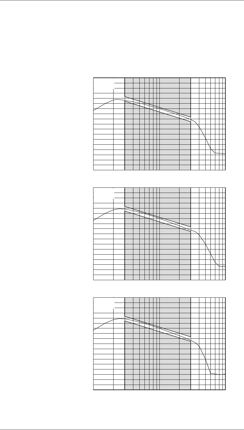
4.6 De-emphasised Audio Frequency Response
Set RV210 (front panel line level) to provide 0dBm output at 1kHz modulating fre-
quency.
Sweep the modulating frequency, checking that the line audio response closely
follows that shown in Figure 4.1 - the limits should not be exceeded.
Figure 4.1 T835 De-emphasised Audio Frequency Response
Wide Bandwidth
Narrow Bandwidth
+25
+20
Audio Level (dB ref. to O/P @ 1kHz)
+15
+10
+5
+0
-5
-10
-15
-20
-25
-30
-35
-40
-45
-50
-55
100 200 300 500 1k 2k 3k 5k 10k
Frequency (Hz)
25°C 13.8V
Ref. audio power:
+0.0dBm @ 1kHz
+25
+20
Audio Level (dB ref. to O/P @ 1kHz)
+15
+10
+5
+0
-5
-10
-15
-20
-25
-30
-35
-40
-45
-50
-55
100 200 300 500 1k 2k 3k 5k 10k
Frequency (Hz)
25°C 13.8V
Ref. audio power:
-2.2dBm @ 1kHz
Mid Bandwidth
+25
+20
Audio Level (dB ref. to O/P @ 1kHz)
+15
+10
+5
+0
-5
-10
-15
-20
-25
-30
-35
-40
-45
-50
-55
100 200 300 500 1k 2k 3k 5k 10k
Frequency (Hz)
25°C 13.8V
Ref. audio power:
-2.5dBm @ 1kHz

B4.6 T835 Functional Testing M830-00
23/07/99 Copyright TEL
4.7 Noise Mute (If Linked In)
Rotate RV230 (front panel gating sensitivity) fully anticlockwise.
Apply an on-channel signal from the RF generator at a level of -110dBm with
±3kHz deviation (±2.4kHz) [±1.5kHz] at 1kHz.
Increase the RF level in 1dB steps, checking that the mute opens for an RF input
level of approximately -105dBm.
Turn the RF off and check that the mute closes.
Rotate RV230 clockwise and check that the mute opens.
Reset RV230 to give the required opening sinad.
Note: False opening of the mute can occur if the RF generator’s attenuator is noisy
when the level is being changed.
4.8 RSSI
Apply an on-channel signal from the RF generator at a level of -100dBm with
±3kHz deviation (±2.4kHz) [±1.5kHz] at 1kHz.
Using a high impedance DMM, check that the RSSI output voltage on pin 5 of
D-range 1 (PL100) is 4.5V (nominal).
Vary the RF level in 5dB steps and check that the RSSI output voltage changes at a
rate of approximately 15dB/V over the range of -115dBm to -70dBm (refer to Fig-
ure 4.2 for RSSI voltage vs signal strength).
Figure 4.2 T835 RSSI Voltage vs Signal Strength
RF Level (dBm)
-130 -120 -110 -100 -90 -80 -70 -60
1
2
3
4
5
6
7
8
RSSI Voltage

M830-00 T835 Functional Testing B4.7
Copyright TEL 23/07/99
4.9 Carrier Level Mute (Carrier Mute Linked In)
Apply an on-channel signal from the RF generator at a level of -120dBm with
±3kHz deviation (±2.4kHz) [±1.5kHz] at 1kHz.
Increase the RF level in 2dB steps and check that the mute opens at an RF level
which corresponds with the preset level on RV235 (carrier mute), i.e. between
-115dBm and -70dBm.
Editor’s Note: The CTCSS adjustment procedures described in Section 4.10 have
been moved to a more appropriate location in Section 3 as part of
the Initial Tuning & Adjustment procedure (refer to Section 3.4.6
and Section 3.12).

B4.8 T835 Functional Testing M830-00
23/07/99 Copyright TEL
