RELM Communications RPV516A VHF FM Transceiver User Manual
RELM Communications Inc VHF FM Transceiver Users Manual
UserManual.wiki
>
RELM Communications
>
RPV516A User Manual
>
Users Manual
Contents
1.
Users Manual
2.
Revised Manual 121901
3.
Revised Manual 010402
Users Manual
Navigation menu
Upload a User Manual
Namespaces
Wiki Guide
HTML
PDF
Info
Views
User Manual
Discussion / Help
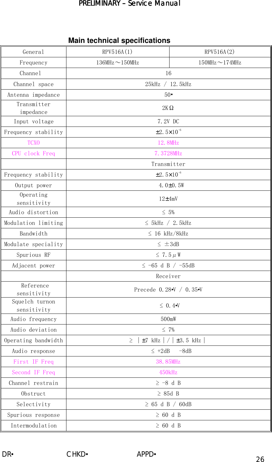
Navigation
![PRELIMINARY PRELIMINARY PRELIMINARY PRELIMINARY –––– ServiceServiceServiceService Manual Manual Manual Manual DR• CHKD• APPD• 34 turns on Q110 to protect transmitting final amplifier (Q107). 5•Power supply A 5V reference power supply [5M] for the control circuit is derived from an internal battery. This reference is used to provide a 5V supply in transmit mode [5T] ,a 5V supply in receive mode [5R] , and a 5V•supply common in both modes [5C] based on the control signal sent from the microprocessor. 6•Control system The IC403 CPU operates at 7.37MHZ. This oscillator has a circuit that shifts the frequency according to the EEPROM data.](https://usermanual.wiki/RELM-Communications/RPV516A.Users-Manual/User-Guide-175629-Page-16.png)
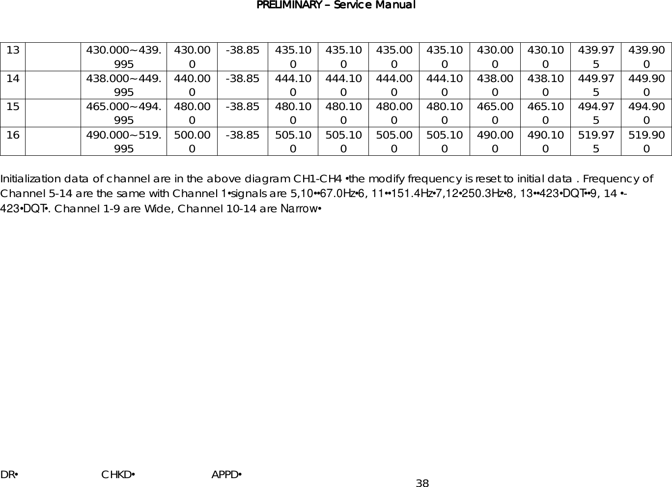
![PRELIMINARY PRELIMINARY PRELIMINARY PRELIMINARY –––– ServiceServiceServiceService Manual Manual Manual Manual DR• CHKD• APPD• 36 (12) Reset scan mode (13) Scan priority 3. PC modify mode• Make settings through external programmer or PC program software: (1) Frequency stability (2) RF power (3) Low power alarm (4) Squelch•level 9&3• (5) CTCSS deviation•Wide/Narrow•• (6) DQT deviation•Wide/Narrow•• (7) Receive sensitivity•low•medium•high• 4. Wire Clone: Press MONI to turn on the power , enter wire clone mode 2 seconds later, press PTT, Begin cloning while red lights, finish while light goes out. 5. Mode setting: • Short cut the SELF on PCB, and turn on the power till “BEEP”. • Set channel selector knob to corresponding place according to the model•1-16• • Press [MONI]•then press [PTT], to set the channel, channel data and initial data. • Turn off the power, disconnect SELF on PCB to end mode settings. Eg. RPV516A•2•, its serial number is 2, to initialize: short cut SELF on PCB to turn on The power, set channel selector knob at CH2, press MONI, then press PTT, the initial data of 1-4 channel can be found in the diagram, serial number 2. Reset data to initial data. The receive and transmit frequency of channel 5-14 are the same with channel 1, signals are channel5, 10•67.0Hz•6,11•151.4Hz•7,12•250.3Hz•8,13•423•DQT••9,14•-423•DQT•, Channel 1-9 are Wide , Channel 10-14 are Narrow•Turn off the power after reset, disconnecting SELF and restart the power to use the transceiver. • Remarks: The old data(frequency, CTCSS/DQT, channel function) will be deleted once set the new mode by pressing MONI AND PTT , part of the function also would be changed. Therefore, do not set this operation unless change the EEPROM, etc.](https://usermanual.wiki/RELM-Communications/RPV516A.Users-Manual/User-Guide-175629-Page-18.png)
![PRELIMINARY PRELIMINARY PRELIMINARY PRELIMINARY –––– Service ManualService ManualService ManualService Manual DR• CHKD• APPD• 39 6. Manual Modify Mode• Press PTT and MONI simultaneously to turn on the power•enter manual modify mode out 3 seconds later. Choose the settings by turning the channel selector knob 1-12CH, use PTT•upward•or MONI•downward•to modify•Notice: MIC shouldn’t be connected with external cable while modifying•,1~12CH are defined as follows: (1) Frequency stability (2) RF power (3) Low power alarm (4) Receiver sensitivity•IF point modify) (5) Receiver sensitivity•low point modify) (6) Receiver sensitivity (high point modify) (7) Squelch• level 9• (8) Squelch•level 3• (9) CTCSS deviation•Wide• (10) CTCSS deviation•Narrow• (11) DQT deviation•Wide• (12) DQT deviation•Narrow• 13~16CH are used for adjusting transmitter and receiver. Press PTT to transmit; Press MONI to choose: Wide/Narrow•one Beep sound is Narrow•two Beep sound is Wide. 13~16CH are defined as follows: (13) IF frequency (discrepancy of transmission and receive frequency is 0.1MHz). (14) Lowest frequency (discrepancy of transmission and receive frequency is 0.1MHz). (15) Highest frequency (discrepancy of transmission and receive frequency is -0.075MHz)• (16) IF frequency•sends 250.3Hz CTCSS signals (discrepancy of transmission and receive frequency is 0.1MHz). Notice:To enter and shut off manual modify mode by short cut the SELF. Turn on the power, and enter settings mode, the manual function is automatically on. Press [PTT] to disable manual modify. Once this function is disabled, this mode is not accessible, kindly suggest disable this mode after modifying. ••CPU• CPU control M38034M4](https://usermanual.wiki/RELM-Communications/RPV516A.Users-Manual/User-Guide-175629-Page-21.png)
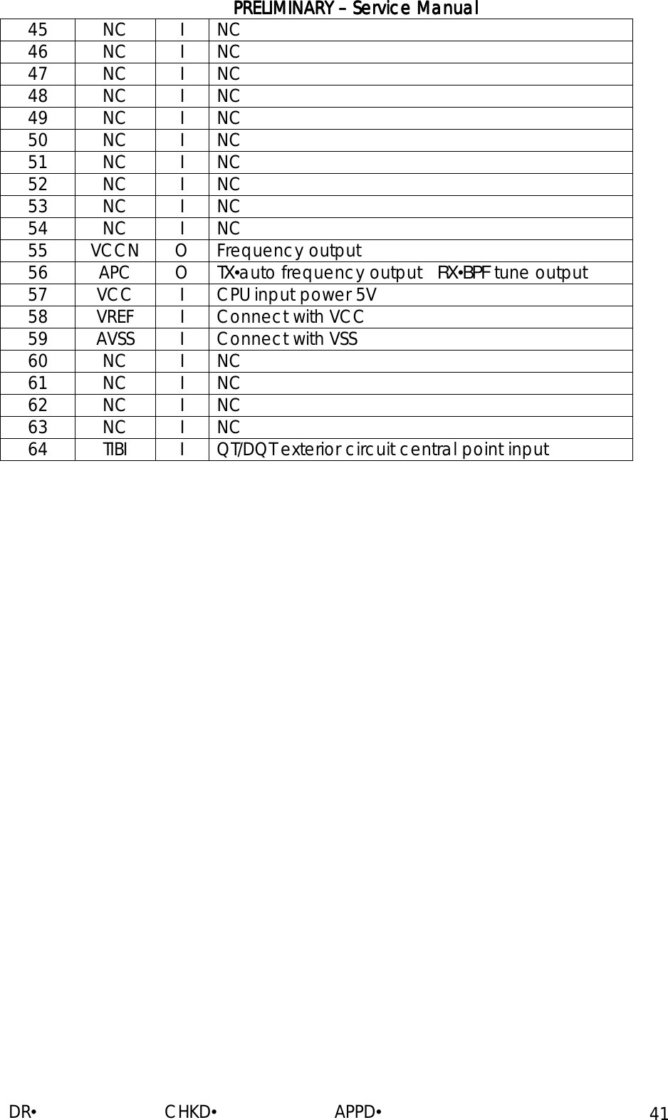
![PRELIMINARY PRELIMINARY PRELIMINARY PRELIMINARY –––– Service ManualService ManualService ManualService Manual DR• CHKD• APPD• 40 Pin No. Port name I/O Function 1 TI I Input QT/DQT signal 2 BUSY I Input busy signal 3 BATT I Detect battery voltage 4 NC I NC 5 TO O Output QT/DQT 6 BEEP O Beep output 7 NC I NC 8 ENC0 I Input encode 9 ENC1 I Input encode 10 ENC2 I Input encode 11 ENC3 I Input encode 12 NC I NC 13 PTT I [PTT] input •connect RXD 14 TXD O RS-232C output 15 RXD I RS-232C input 16 MONI I [MONI] input 17 SELF I program L•set up mode 18 CNVSS I Connect VSS 19 RST I Reset 20 INT0 I Power detection 21 NC I NC 22 XIN I Oscillator•7.3728MHz• 23 XOUT O Oscillator 24 VSS I Grounding 25 SHIFT O Clock frequency deviation H•unlock 26 PABC O MOS FET power H•unlock 27 WNRC O Audio referential sensitivity L•narrow 28 WNTC O Max deviation H•narrow 29 NC I NC 30 SDA I/O EEPROM data cable 31 SCL O EEPROM clock cable 32 UL I Lock circuit detector L•unlock 33 DT O Common data output 34 CK O Common clock output 35 LE O PLL IC H•lock up 36 5MC O Power control except CPU and EEPROM L•unlock 37 AFCO O AF amplifier H•unlock 38 RX O TX/RX VCO H•receive 39 GLED O Green light control H•light 40 RLED O Red light control H•light 41 SAVE O Power saving control H•power saving OFF 42 MUTE O Squelch control H•Mic squelch L•AF squelch 43 5RC O Receiver power control L•unlock 44 5TC O Transmitter power control H•unlock](https://usermanual.wiki/RELM-Communications/RPV516A.Users-Manual/User-Guide-175629-Page-22.png)
![PRELIMINARY PRELIMINARY PRELIMINARY PRELIMINARY –––– Service ManualService ManualService ManualService Manual DR• CHKD• APPD• 42 RPV516RPV516RPV516RPV516 adjust description adjust description adjust description adjust description Use programmer or PC software to program RPV516, or by manual program , eg . To program RPV516A( refer to“RPV516/TC368 software description”for the manual program and mode settings•. 一. Instrument• 1• Synthesized test instrument 1 set 2• Scanner 1 set 3• 3A/10V power 1 set 4• Digital Voltmeter 1 set 5• 3A DC Ammeter 1 set •• Adjust• 1. Initialization:It is necessary to initialize the transceiver because there is useless data in EEPROM. Short cut the SELF on PCB, turn on the power till there comes the sound ”BEEP”•place the channel selector knob at CH1[RPV516B•1•] or CH2[RPV516A(2)]• press [MONI]• then press [ PTT] • to begin initializing the channel and other data. Please refer to the outcome of initialization at“RPV516/TC368 software description”. 2. Adjust:The adjustment of RPV516, some are conducted in normal mode, some are in manual program mode. Turn on the power and enter the normal mode., at the same time, press the PTT and MONI to turn on the transceiver•enter the manual program mode 3seconds later.•refer to“RPV516/TC368 software description”manual program mode•. VCO SECTION:VCO SECTION:VCO SECTION:VCO SECTION: measurementmeasurementmeasurementmeasurement AdjustmentAdjustmentAdjustmentAdjustment ITEMITEMITEMITEM CONDITIONCONDITIONCONDITIONCONDITION Test equipTest equipTest equipTest equip term term term terminalinalinalinal partpartpartpart MethodMethodMethodMethod Specifications/Specifications/Specifications/Specifications/RemarksRemarksRemarksRemarks 1.Setting 1.power 7.5V 1.CH: TX HIGH 3.7V±0.1V 2.Transmit VCO lock voltage 2.CH: TX LOW check •0.7V 1.CH: RX HIGH 3.7V±0.1V 3.Receive VCO lock voltage 2.CH: RX LOW Digital Voltmeter CV TC1 check Notice:if unlock VCO, check adjustment is enabled in manual mode.(signal could be transmitted regardless of the lock of VCO in manual mode).](https://usermanual.wiki/RELM-Communications/RPV516A.Users-Manual/User-Guide-175629-Page-24.png)