Telit Communications S p A OM12030-200 2G/3.5G wireless module User Manual User guide
Telit Communications S.p.A. 2G/3.5G wireless module User guide
User guide

ATOP3.5G Product Description
(OM12030)
80447ST10636A rev.10 - 2015-03-03

ATOP3.5G Product Description
80447ST10636A rev.10 – 2015-03-03
Reproduction forbidden without written authorization from Telit Communications S.p.A. - All Rights
Reserved. Page 2 of 66
Mod. 0808 2011-07 Rev.2
APPLICABILITY TABLE
PRODUCT
REGIONS
W
(orld)
U
(SA)
A
(PAC)
ATOP 3.5G
√
√
√
+ SMX
√
√
√
+ SMX + NFC
√
√
√

ATOP3.5G Product Description
80447ST10636A rev.10 – 2015-03-03
Reproduction forbidden without written authorization from Telit Communications S.p.A. - All Rights
Reserved. Page 3 of 66
Mod. 0808 2011-07 Rev.2
SPECIFICATIONS SUBJECT TO CHANGE WITHOUT NOTICE
Notice
While reasonable efforts have been made to assure the accuracy of this document, Telit assumes
no liability resulting from any inaccuracies or omissions in this document, or from use of the
information obtained herein. The information in this document has been carefully checked and is
believed to be entirely reliable. However, no responsibility is assumed for inaccuracies or
omissions. Telit reserves the right to make changes to any products described herein and
reserves the right to revise this document and to make changes from time to time in content
hereof with no obligation to notify any person of revisions or changes. Telit does not assume any
liability arising out of the application or use of any product, software, or circuit described herein;
neither does it convey license under its patent rights or the rights of others.
It is possible that this publication may contain references to, or information about Telit products
(machines and programs), programming, or services that are not announced in your country.
Such references or information must not be construed to mean that Telit intends to announce
such Telit products, programming, or services in your country.
Copyrights
This instruction manual and the Telit products described in this instruction manual may be, include
or describe copyrighted Telit material, such as computer programs stored in semiconductor
memories or other media. Laws in the Italy and other countries preserve for Telit and its licensors
certain exclusive rights for copyrighted material, including the exclusive right to copy, reproduce in
any form, distribute and make derivative works of the copyrighted material. Accordingly, any
copyrighted material of Telit and its licensors contained herein or in the Telit products described in
this instruction manual may not be copied, reproduced, distributed, merged or modified in any
manner without the express written permission of Telit. Furthermore, the purchase of Telit
products shall not be deemed to grant either directly or by implication, estoppel, or otherwise, any
license under the copyrights, patents or patent applications of Telit, as arises by operation of law
in the sale of a product.
Computer Software Copyrights
The Telit and 3rd Party supplied Software (SW) products described in this instruction manual may
include copyrighted Telit and other 3rd Party supplied computer programs stored in semiconductor
memories or other media. Laws in the Italy and other countries preserve for Telit and other 3rd
Party supplied SW certain exclusive rights for copyrighted computer programs, including the
exclusive right to copy or reproduce in any form the copyrighted computer program. Accordingly,
any copyrighted Telit or other 3rd Party supplied SW computer programs contained in the Telit
products described in this instruction manual may not be copied (reverse engineered) or
reproduced in any manner without the express written permission of Telit or the 3rd Party SW
supplier. Furthermore, the purchase of Telit products shall not be deemed to grant either directly
or by implication, estoppel or otherwise, any license under the copyrights, patents or patent
applications of Telit or other 3rd Party supplied SW, except for the normal non-exclusive, royalty
free license to use that arises by operation of law in the sale of a product.

ATOP3.5G Product Description
80447ST10636A rev.10 – 2015-03-03
Reproduction forbidden without written authorization from Telit Communications S.p.A. - All Rights
Reserved. Page 4 of 66
Mod. 0808 2011-07 Rev.2
Usage and Disclosure Restrictions
License Agreements
The software described in this document is the property of Telit and its licensors. It is furnished by
express license agreement only and may be used only in accordance with the terms of such an
agreement.
Copyrighted Materials
Software and documentation are copyrighted materials. Making unauthorized copies is prohibited
by law. No part of the software or documentation may be reproduced, transmitted, transcribed,
stored in a retrieval system, or translated into any language or computer language, in any form or
by any means, without prior written permission of Telit.
High Risk Materials
Components, units, or third-party products used in the product described herein are NOT fault-
tolerant and are NOT designed, manufactured, or intended for use as on-line control equipment in
the following hazardous environments requiring fail-safe controls: the operation of Nuclear
Facilities, Aircraft Navigation or Aircraft Communication Systems, Air Traffic Control, Life Support,
or Weapons Systems (“High Risk Activities”). Telit and its supplier(s) specifically disclaim any
expressed or implied warranty of fitness for such High Risk Activities.
Trademarks
TELIT and the Stylized T Logo are registered in Trademark Office. All other product or service
names are the property of their respective owners.
Copyright © Telit Communications S.p.A.

ATOP3.5G Product Description
80447ST10636A rev.10 – 2015-03-03
Reproduction forbidden without written authorization from Telit Communications S.p.A. - All Rights
Reserved. Page 5 of 66
Mod. 0808 2011-07 Rev.2
ATOP 3.5G (OM12030)
Automotive telematics on-board unit platform 3.5G
1 Introduction
ATOP 3.5G (OM12030) is Telit’s platform for automotive telematics on-board units (OBU's) for
applications such as road pricing and eCall, based on the following technologies:
3G cellular for voice and data communication
GPS/GLONASS for positioning service
NFC for short range communication, e.g. configuration and law enforcement
SmartMX smartcard with Java card JCOP OS for security
J9 Virtual Machine for application portability and easy creation
Dedicated processor for Real-Time and connection to system via ADC, CAN, UART,
Ethernet, USB
Backward hardware compatibility with ATOP 2.5G EVO (OM12001)
Designed for automotive markets1
Thanks to on-board ATOP 3.5G security resources, product developers and manufacturers can
offer products which guarantee fraud prevention and tamper evidence without extra effort for
additional security precautions. These products can be used in end-to-end transaction systems
requiring Common Criteria level 5+.
ATOP 3.5G can be used by itself as a complete solution for GNSS-3G based road pricing and
eCall applications. In this case, ATOP 3.5G just needs to be complemented with a power supply,
speaker, microphone, some knobs and an optional display. ATOP 3.5G provides the processing
power and software application environment resources on board to complement road pricing and
eCall with some other added value telematics services.
ATOP 3.5G can also be applied as a front end for more elaborate telematics products, by making
its resources, i.e. GNSS, mobile communication, security (ID authentication) available for use by
other resources in the OBU.
Three different 3G band configuration variants are defined for OM12030:
World market configuration
American market configuration
Pacific market configuration
For applications where security is not paramount, such as eCall, variants without NFC short
range communication and/or the SmartMX security processor are available.
1 In accordance with Telit’s Robustness Validation, using AEC-Q100-defined qualification tests.
ATOP3.5G Product Description
80447ST10636A rev.10 – 2015-03-03
Reproduction forbidden without written authorization from Telit Communications S.p.A. - All Rights
Reserved. Page 6 of 66
Mod. 0808 2011-07 Rev.2
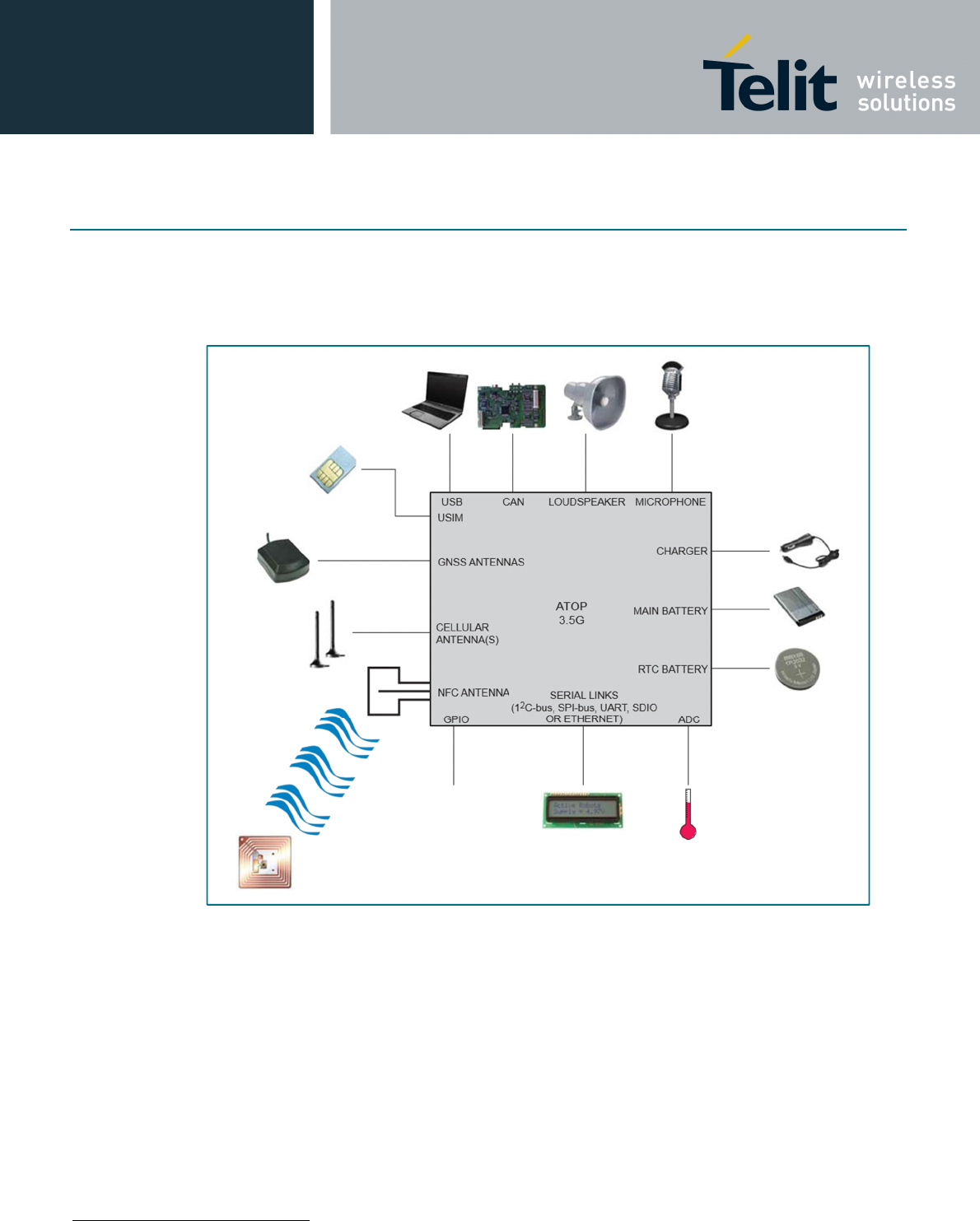
2 General description
Figure 1 represents ATOP 3.5G connections in a typical application, with its connection to
batteries, antennas and USIM. For communication with the external world, serial link, GPIOs, and
ADCs will connect to screen, keys, and sensors. UART, CAN, SDIO, Ethernet or USB can be used
to connect to an on-board computer.
Figure 1 ATOP 3.5G module connections
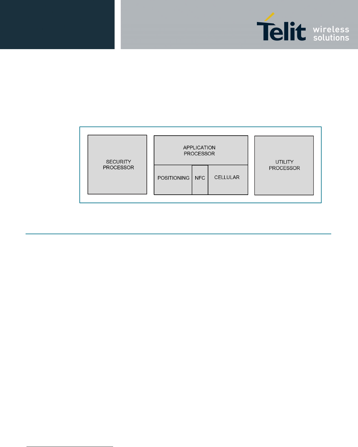
Figure 2 represents a more conceptual view of ATOP from a system point of view, showing three
main components:
Application processor: This processor will run code specific to the application (road
tolling, insurance ...) which is portable from one platform to another one in order to avoid
recertification. The application drives the three following conceptual co-processors:
o A Positioning processor provides accurate location information to the
application;
o An NFC processor2 provides connection to an external bignette, card reader, or
other NFC enabled device to increase application security;
o A Communication processor allows the application to connect to servers and
receive update and notifications, receive or generate voice call or SMS.
2 Only for OM12030/1X0, with X as defined in Section 5.
ATOP3.5G Product Description
80447ST10636A rev.10 – 2015-03-03
Reproduction forbidden without written authorization from Telit Communications S.p.A. - All Rights
Reserved. Page 7 of 66
Mod. 0808 2011-07 Rev.2
Security processor3: This processor provides a root of trust for signing messages to
servers; authenticates the presence of an external vignette; and/or runs multiple security
applications.
Utility processor: This processor takes care of all housekeeping tasks such as
connecting to external interfaces, displays, etc. but also handles power management,
waking-up and booting-up the system, i.e. all support tasks which are not part of the
high-level applications but are required to make the system work.
Figure 2 ATOP conceptual view
3 Features and benefits
Utility processor for interfacing with external world and house-keeping
o ARM Cortex M3 microcontroller with Ethernet, CAN, USB Host, Device and
OTG, UART, SPI-bus, I2C-bus, ADCs, DAC, GPIOs, and PWMs
o Internal temperature sensor
Application processor to run customer application code
o Virtual Machine for customer application
o Communication coprocessor with Quad-band 3.5G/EDGE/GPRS/GSM terminal
o GPS/GLONASS receiver
Near Field Communication (NFC) coprocessor to connect to external vignette, smart
card, mobile phone2
Security processor for providing a source of trust3
o SmartMX smartcard running JCOP 2.4.2
Mandatory and voluntary certification
o R&TTE and FCC passed for safety, EMC, and RF
o Certification for GCF, including field test
o Certification for PTCRB
o Certification for AT&T
Designed and qualified for use in automotive applications1
-40 °C to +85 °C / limited operating range as defined in Table 11
3 Only for OM12030/1X0 and OM12030/2X0, with X as defined in Section 5.

ATOP3.5G Product Description
80447ST10636A rev.10 – 2015-03-03
Reproduction forbidden without written authorization from Telit Communications S.p.A. - All Rights
Reserved. Page 8 of 66
Mod. 0808 2011-07 Rev.2
4 Applications
ATOP 3.5G can be used for telematics applications where tamper-resistance, confidentiality,
integrity and authenticity of end-user information are required, e.g.:
Road pricing
Pay as you drive insurance
Stolen vehicles tracking
Emergency call
Internet connectivity
5 Ordering information
ATOP 3.5G is defined in multiple variants:
Table 1 Type names
Type number Package
Name
Description
OM12030/X00 [1] LGA350 Worldwide Quad-band UMTS 2100 (I), 1900 (II), 850 (V) including 800
(VI), 900 (VIII)
OM12030/X10 [1] North American Quad-band UMTS 2100 (I), 1900 (II), 1700 (IV), 850 (V)
including 800 (VI)
OM12030/X20 [1] Pacific Quad-band UMTS 2100 (I), 1800 (III) including 1700 (IX), 850 (V)
including 800 (VI), 900 (VIII)
[1] X = 1 Includes NFC short range communication and the SmartMX security element.
Feature combination nicknamed “Full”.
X = 0 Omits NFC short range communication and the SmartMX security element.
Feature combination nicknamed “Minus”.
X = 2 Omits NFC short range communication but retains the SmartMX security element.
Feature combination nicknamed “Auth”.
All variants support 2G bands 850, 900, 1800, and 1900.
ATOP3.5G Product Description
80447ST10636A rev.10 – 2015-03-03
Reproduction forbidden without written authorization from Telit Communications S.p.A. - All Rights
Reserved. Page 9 of 66
Mod. 0808 2011-07 Rev.2
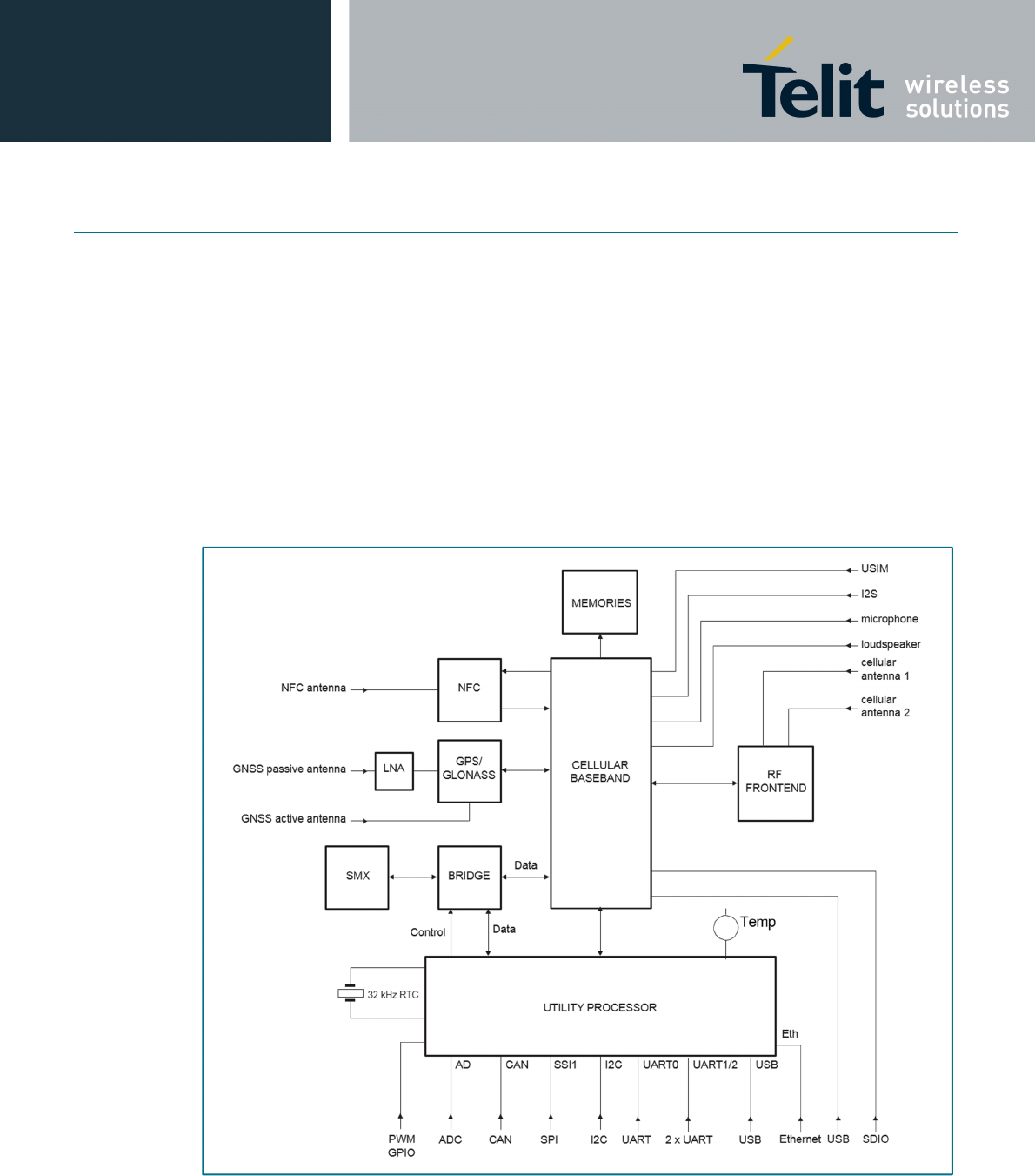
6 Block diagram
Figure 3 represents the data connections within the ATOP 3.5G module.
Two main groups of components can be distinguished:
The first group includes the cellular baseband, GPS/GLONASS and secure element
(SMX). They offer to the application running on a Virtual Machine all services required
for telematics applications.
The second group includes the microcontroller which takes care of interfacing with the
external world via its interfaces: Ethernet, USB, CAN, UARTs, SPIs, GPIOs, PWMs, and
ADCs.
Depending on which ATOP software features are used in the customer application, some of its
interfaces that are exported due to multiplexing may be used internally and thus may not be
usable by the application.
Figure 3 ATOP 3.5G internal connections
ATOP3.5G Product Description
80447ST10636A rev.10 – 2015-03-03
Reproduction forbidden without written authorization from Telit Communications S.p.A. - All Rights
Reserved. Page 10 of 66
Mod. 0808 2011-07 Rev.2
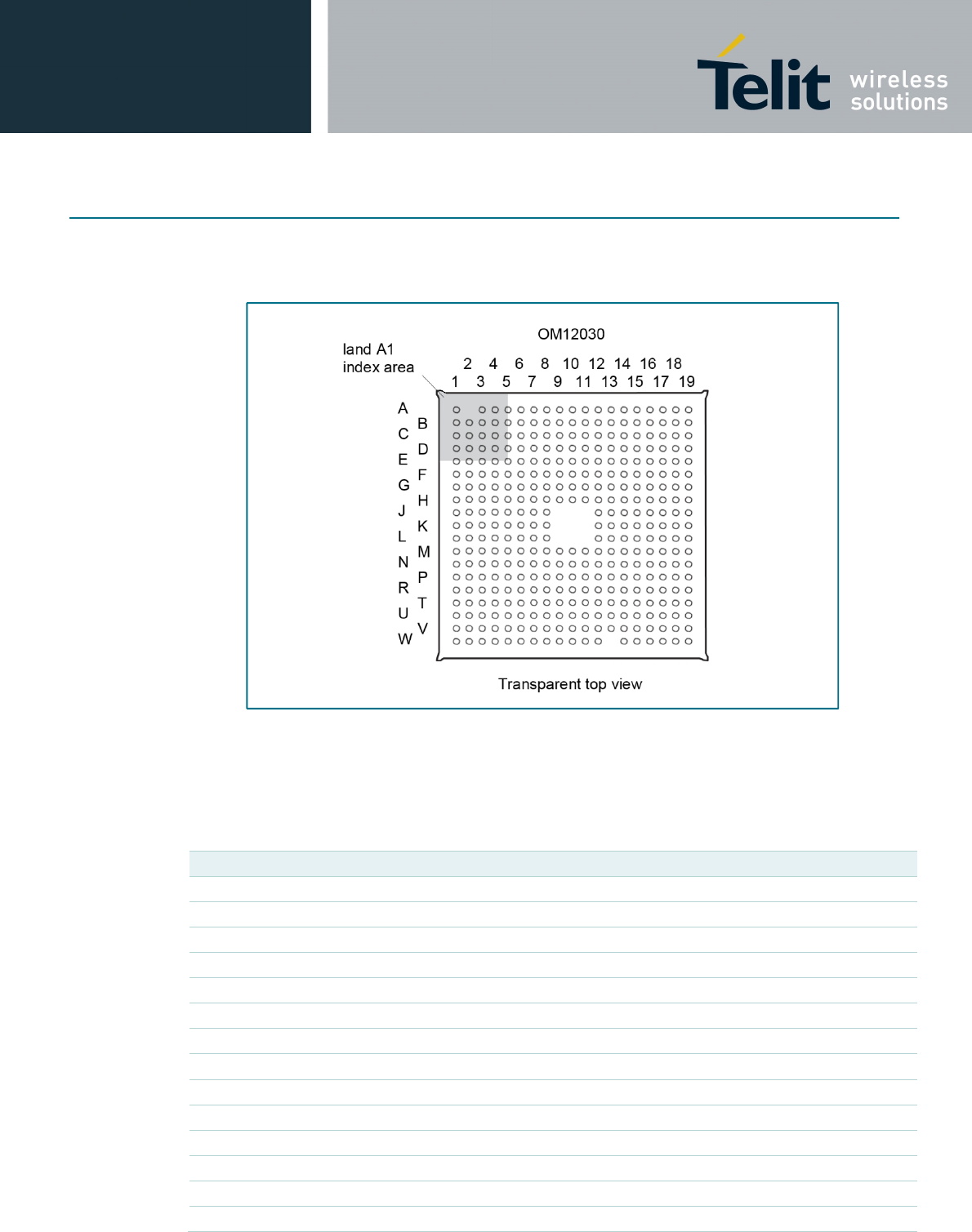
7 Pinning information
7.1 Pinning
Figure 4 shows a transparent top view of ATOP 3.5G to identify all pins.
Figure 4 ATOP 3.5G pin configuration
7.2 Pin description
7.2.1 Module pinning list
Table 2 ATOP 3.5G pinning list
Symbol[1] Pin Level
Description[2]
Utility processor
UART0
MC_P002_TXD0_AD07 M15 3.0 transmitter output for UART0 [3]
MC_P003_RXD0_AD06 M19 3.0 receiver input for UART0 [3]
UART1
MC_P015_TXD1_SCK0_SCK V15 3.0 transmitter output for UART1 [4][5]
MC_P016_RXD1_SSEL0_SSEL T7 3.0 receiver input for UART1 [4][5]
MC_P022_RTS1_TD1 T9 3.0 ready to send [5]
MC_P017_CTS1_MISO0_MISO V13 3.0 clear to send [4][5]
MC_P021_RI1_RD1 R10 3.0 ring indicator [5]
MC_P018_DCD1_MOSI0_MOSI R11 3.0 data carrier detect [4][5]
UART2
MC_P010_TXD2_SDA2_MAT30 R13 3.0 transmitter output for UART2 [5]
MC_P011_RXD2_SCL2_MAT31 U10 3.0 receiver input for UART2 [5]

ATOP3.5G Product Description
80447ST10636A rev.10 – 2015-03-03
Reproduction forbidden without written authorization from Telit Communications S.p.A. - All Rights
Reserved. Page 11 of 66
Mod. 0808 2011-07 Rev.2
Symbol[1] Pin Level
Description[2]
UART3
MC_P428_RXMCLK_MAT20_TXD3 V14 3.0 transmitter output for UART3 [5][6]
MC_P429_TXMCLK_MAT21_RXD3 N11 3.0 receiver input for UART3 [5][6]
I2C-bus 0
MC_P028_SCL0_USBSCL T12 3.0 I2C-bus clock input/output [7]
MC_P027_SDA0_USBSDA T11 3.0 I2C-bus data input/output [7]
SSI
MC_P007_I2STXCLK_SCK1_MAT21 T18 3.0 serial clock [5]
MC_P009_I2STXSDA_MOSI1_MAT23 V18 3.0 master out/slave in [5]
MC_P008_I2STXWS_MISO1_MAT22 V17 3.0 master in/slave out [5]
MC_P006_I2SRXSDA_SSEL1_MAT20 R18 3.0 slave select [5]
I2S-bus
MC_P023_AD00_I2SRXCLK_CAP30 P16 3.0 receive serial clock [3]
MC_P024_AD01_I2SRXWS_CAP31 M16 3.0 receive word select [3]
MC_P025_AD02_I2SRXSDA_TXD3 N16 3.0 receive data [3]
MC_P211_EINT1_I2STXCLK T13 3.0 transmit serial clock [8]
MC_P212_EINT2_I2STXWS R9 3.0 transmit word select [8]
MC_P213_EINT3_I2STXSDA T10 3.0 transmit data [8]
CAN1
MC_P000_RD1_TXD3_SDA1 T14 3.0 receive data
[5]
MC_P001_TD1_RXD3_SCL1 R12 3.0 transmit data
[5]
CAN2
MC_P004_I2SRXCLK_RD2_CAP20 P19 3.0 receive data [5]
MC_P005_I2SRXWS_TD2_CAP21 P15 3.0 transmit data [5]
Universal Serial Bus (USB)
MC_P029_USBDP N12 USB data P [9]
MC_P030_USBDN L13 USB data N [9]
MC_P130_VBUS_AD04 L12 USB Vbus detect [3]
MC_P209_USBCNT_RXD2 R14 USB device connect [5]
Ethernet
MC_P115_ENETREFCLK T19 3.0 [5]
MC_P116_ENETMDC U18 3.0 [5]
MC_P100_ENETTXD0 R16 3.0 [5]
MC_P101_ENETTXD1 R15 3.0 [5]
MC_P104_ENETTXEN V19 3.0 [5]
MC_P109_ENETRXD0 T15 3.0 [5]
MC_P110_ENETRXD1 T16 3.0 [5]
MC_P114_ENETRXER T8 3.0 [5]
MC_P108_ENETCRS P14 3.0 [5]

ATOP3.5G Product Description
80447ST10636A rev.10 – 2015-03-03
Reproduction forbidden without written authorization from Telit Communications S.p.A. - All Rights
Reserved. Page 12 of 66
Mod. 0808 2011-07 Rev.2
Symbol[1] Pin Level
Description[2]
MC_P117_ENETMDIO V16 3.0 [5]
Control
Analog IOs
MC_P026_AD03_AOUT_RXD3 N18 3.0 digital analog converter output [10]
GPIO/PWM
MC_P210_EINT0_NMI W14 3.0 external interrupt; pull up in ATOP
2.5G EVO (OM120001) not in
LPC1768 [8]
MC_P119_MCOA0_CAP11 N13 3.0 PWM, event capture input, ... [5]
MC_P118_USBLD_PWM11_CAP10 N15 3.0
MC_P122_MCOB0_USBPWRD_MAT10 M10 3.0
MC_P129_MCOB2_PCAP11_MAT01 M11 3.0
Debug Interfaces
Microcontroller JTAG
MC_JTAG_TCK_SWDCLK K16 3.0 [11]
MC_JTAG_TDO_SWO K19 3.0 [5]
MC_JTAG_TDI L16 3.0 [12]
MC_JTAG_TMS_SWDIO L18 3.0 [12]
MC_JTAG_RTCK M18 3.0 [11]
MC_JTAG_TRST K18 3.0 [12]
Microcontroller PC trace 3.0
MC_P206_TRCLK_PCAP10_RI1 N10 3.0 [5]
MC_P205_TRDATA0_PWM16_DTR1 N9 3.0 [5]
MC_P204_TRDATA1_PWM15_DSR1 P18 3.0 [5]
MC_P203_TRDATA2_PWM14_DCD1 M12 3.0 [5]
MC_P202_TRDATA3_PWM13_CTS1 N8 3.0 [5]
Audio interfaces
Analog in
BB_AUDIO_IN1_N G12 microphone 1 (optionally digital)
BB_AUDIO_IN1_P H13
BB_AUDIO_IN1_BIAS G13
BB_AUDIO_IN2_N G16 microphone 2
BB_AUDIO_IN2_P F16
BB_AUDIO_IN2_BIAS G15
BB_AUDIO_IN_L H14 line in left
BB_AUDIO_IN_R J14 line in right
Analog out
BB_AUDIO_OUT1_LP J15 positive left out
BB_AUDIO_OUT1_LN H15 negative left out
BB_AUDIO_OUT1_2_RP K13 positive right out

ATOP3.5G Product Description
80447ST10636A rev.10 – 2015-03-03
Reproduction forbidden without written authorization from Telit Communications S.p.A. - All Rights
Reserved. Page 13 of 66
Mod. 0808 2011-07 Rev.2
Symbol[1] Pin Level
Description[2]
BB_AUDIO_OUT1_2_RN K15 negative right out
BB_AUDIO_SPKL_P D17 positive speaker left out
BB_AUDIO_SPKL_N E17 negative speaker left out
BB_AUDIO_SPKR_P F17 positive speaker right out
BB_AUDIO_SPKR_N G17 negative speaker right out
Digital
BB_I2S_SCLK_PCM_CLK E14 1.8
BB_I2S_WS_PCM_SYNC D15 1.8
BB_I2S_DOUT_PCM_DATA_IN E12 1.8
BB_I2S_MCLK_PCM_DATA_OUT E13 1.8
BB_I2S_DIN G14 1.8
System interfaces
USB interface
BB_USBDN U12 USB data N
BB_USBDP U11 USB data P
BB_USBID U13 USB device connect
BB_USBVBUS U14 USB Vbus detect
SDIO interface
BB_SDIOCMD P7 2.85
BB_SDIOCLK P8 2.85
BB_SDIO_PWR_EN_N P9 2.85
BB_SDIO_DET P11 1.8 active low, no pull up needed
BB_SDIOD0 U6 2.85
BB_SDIOD1 U7 2.85
BB_SDIOD2 U8 2.85
BB_SDIOD3 U9 2.85
USIM interface ISO7316-3 class B/C I/O levels
BB_SIM_DATA E16
BB_SIM_CLK D14
BB_SIM_RST D13
BB_USIM_DETEC_N L14 active low, no pull up needed
Battery and power management
VBAT_RTC_SNK J18 power supply for microcontroller
RTC battery
VBAT_SNK J2; J4 power supply for whole system
except RF power amplifier and
utility processor [13]
VBAT_PA_SNK J1; K1; K2 power supply for RF power
amplifier [13]
VBAT_MC_SNK K4 main power supply for utility
processor

ATOP3.5G Product Description
80447ST10636A rev.10 – 2015-03-03
Reproduction forbidden without written authorization from Telit Communications S.p.A. - All Rights
Reserved. Page 14 of 66
Mod. 0808 2011-07 Rev.2
Symbol[1] Pin Level
Description[2]
VDD_SPKR H17 power supply for class D amplifier
VCHG_SNK G10; H10 charger supply connection
VBAT_SENSE E10 battery voltage sense
BB_ICHG H11 charger output
BB_BATT_FET_N E11 external charge FET control
BB_BATT_THERM H18 battery thermistor
VIO_REF P5 voltage (1.8 V) reference for
baseband digital interface
VADC_REF W16 voltage reference for MC_ADC
VADC_GND W17 ground reference for MC_ADC
VUSIM_SRC J13 USIM power supply
VDD_3V0_SRC N19 microcontroller current source and
voltage reference
VDD_3V0_SRC_ENA W18 enables VDD_3V0_SRC (active
HIGH, internal pull up)
Clock generation
BB_EXT_CLK D10 2.6 clock source
MC_XTAL1 M13 optional quartz for microcontroller
MC_XTAL2 N7
GPS_1PPS R4 1.8 one pulse per second (output)
System reset
MC_RESET L15 3.0 reset ATOP module [14]
Antennas
NFC antenna
NFC_ANT1 W10 TX1
NFC_ANT2 W11 TX2
NFC_ANT3 V12 RX
Cellular antenna
CELL_ANT1 C1 [15]
CELL_ANT2 A3 [15]
GPS antenna
GPS_PAS_ANT V1 passive GPS antenna input
GPS_ACT_ANT W3 active antenna input
GPS_ACT_ANT_BIAS T4 active antenna bias (1 V PIN diode
drop inside ATOP 3.5G) [16]
GPS_PAS_ANT_DIS T2 passive antenna disable:
3-state: internal LNA enabled;
active LOW: internal LNA disabled
Industrial test
Baseband JTAG
BB_JTAG_NTRST E9 1.8

ATOP3.5G Product Description
80447ST10636A rev.10 – 2015-03-03
Reproduction forbidden without written authorization from Telit Communications S.p.A. - All Rights
Reserved. Page 15 of 66
Mod. 0808 2011-07 Rev.2
Symbol[1] Pin Level
Description[2]
BB_JTAG_TCK G7 1.8
BB_JTAG_TDI G8 1.8
BB_JTAG_RTCK G9 1.8
BB_JTAG_TDO H7 1.8
BB_JTAG_TMS J7 1.8
Other baseband debug
BB_BOOTMODE J8 1.8 internal pull up; high = normal boot;
low = flash mode
BB_BOOT_SCUR P12 1.8 used for debug of Secure Boot
BB_PS_HOLD H8
used for JTAG debug of application
processor
BB_PON_RESETN D12
Reserved for future use – Do not connect
F15; H9; H12; H16; J16;
J17; K12; L17; M2; M4; M5;
M14; M17; N2; N4; N17;
P2; P4; P13; P17; R5; R7;
R8;
R17; T17; U4; U5; U15;
U16; V5;V7; V8
Ground
GND A1; A4; A5; A6; A7; A8; A9;
A10; A11; A12; A13; A14;
A15; A16; A17; A18; A19;
B1; B2; B3; B4; B5; B6; B7;
B8; B9; B10; B11; B12;
B13; B14; B15; B16; B17;
B18; B19; C2; C3; C4; C5;
C6; C7; C8; C9; C10; C11;
C12; C13; C14; C15; C16;
C17; C18; C19; D1; D2;
D3; D4; D5; D6; D7; D8;
D9; D11; D16; D18; D19;
E1; E2; E3; E4; E5; E6; E7;
E8; E15; E18; E19; F1; F2;
F3; F4; F5; F6; F7; F8; F9;
F10; F11; F12; F13; F14;
F18; F19; G1; G2; G3; G4;
G5; G6; G11; G18; G19;
H1; H2; H3; H4; H5; H6;
H19; J3; J5; J6; J12; J19;
K3; K5; K6; K7; K8; K14;
K17; L1; L2; L3; L4; L5; L6;
L7; L8; L19; M1; M3; M6;
M7; M8; M9; N1; N3; N5;
N6; N14; P1; P3; P6; P10;
R1; R2; R3; R6; R19; T1;
T3; T5; T6; U1; U2; U3;
U17; U19; V2; V3; V4; V6;
V9; V10; V11; W1; W2;
W4; W5; W6; W7; W8; W9;
W12; W15; W19

ATOP3.5G Product Description
80447ST10636A rev.10 – 2015-03-03
Reproduction forbidden without written authorization from Telit Communications S.p.A. - All Rights
Reserved. Page 16 of 66
Mod. 0808 2011-07 Rev.2
Symbol[1] Pin Level
Description[2]
Unused
A2; W13
[1] Pin names aree encoded as follows: MC_Pxyy_iii_jjj_kkk indicates a microcontroller pin. Each pin can
be configured between several functions (typically 4), all mentioned in the pin name:
Pxyy: GPIO yy of GPIO port x;
AD0x: ADC input x;
EINTx: external interrupt x;
MATxy: match output for timer x, channel y;
PCAPxy: capture input for PWM x, channel y;
PWMxy: PWM x, channel y;
RDx/TDx: CAN port x;
SDx/SCLx: I2C-bus x;
TXx/RXy: UART x;
BB_xxx indicates a pin connected respectively to baseband;
GPS_xxx indicates a pin connected respectively to GPS/GLONASS;
NFC_xxx: indicates a pin connected respectively to NFC;
Vxxx_REF indicates a voltage reference – no current should be drawn from this pin;
Vxxx_SNK indicates a voltage sink – current is drawn by this pin;
Vxxx_SRC indicates a current source – current can be drawn from this pin.
[2] Only the main function is described for microcontroller pins, but all functions available for a given pin
can be found in its name.
[3] 5 V tolerant pad providing digital I/O functions (with TTL levels and hysteresis) and analog input.
When configured as an ADC input, digital section of the pad is disabled and the pin is not 5 V tolerant.
[4] SSP0 is used internally and therefore is not available for customer application.
[5] 5 V tolerant pad providing digital I/O functions with TTL levels and hysteresis.
[6] V14 and N11 optionally connected to BB_UART_RX/BB_UART_TX for debugging.
[7] Open-drain 5 V tolerant digital I/O pad, compatible with I2C-bus 400 kHz specification. This pad
requires an external pull up to provide output functionality. When power is switched off, this pin is
connected to the I2C-bus and does not disturb the I2C-bus lines. Open-drain configuration applies to
all functions on this pin.
[8] 5 V tolerant pad with 5 ns glitch filter providing digital I/O functions with TTL levels and hysteresis.
[9] Pad provides digital I/O and USB functions. It is designed in accordance with the USB specification,
revision 2.0 (Full-speed and Low-speed mode only). This pad is not 5 V tolerant.
[10] 5 V tolerant pad providing digital I/O with TTL levels and hysteresis and analog output function. When
configured as the DAC output, digital section of the pad is disabled.
[11] 5 V tolerant pad providing digital I/O functions with TTL levels and hysteresis. Internal pull up and pull
down resistors disabled.
[12] 5 V tolerant pad providing digital I/O functions with TTL levels and hysteresis and internal pull up
resistor.
[13] The VBAT_SNK and VBAT_PA_SNK pins should be supplied only whenever VBAT_MC_SNK is
supplied.
[14] 5 V tolerant pad with 20 ns glitch filter providing digital I/O function with TTL levels and hysteresis.
[15] Cellular antennas switchable under control of the utility processor.
[16] A minimum current of 1 mA is required to minimize insertion loss. Maximum rating pin diode 100 mA.
ATOP3.5G Product Description
80447ST10636A rev.10 – 2015-03-03
Reproduction forbidden without written authorization from Telit Communications S.p.A. - All Rights
Reserved. Page 17 of 66
Mod. 0808 2011-07 Rev.2
7.2.2 Internal pins list
Table 3 lists a number of internal pins controlled by the Utility Processor that are of interest to
ATOP 3.5G application programmers. Most of these pins are controlled by low-level software
drivers provided by TELIT and so should not be controlled directly. They are there described only
for reference.
Table 3 Internal microcontroller pins, controlled by TELIT-provided libraries
All these pins are controlled via TELIT-provided libraries and should not be used/controlled directly in any
way.
Pin name GPIO number Description
BB_RESETN P1.25 0 = reset application processor, otherwise should be left floating
BB_POK P1.28 0 = enable application processor
BB_SSI[3:0] P1.20 serial communication channel
P1.21
P1.23
P1.24
BB_SDB[4:0] P2.0 internal communication channel
P2.1
P2.7
P2.8
P3.26
ANT_SW P3.25 antenna switch
BB_UART_RX P4.28 BB UART internally connected to MC UART3 by means of level
shifter
BB_UART_TX P4.29
INT_TEMP P1.31 ADC input to internal temperature sensor. A TELIT-provided
function call converts value to °C. For more information see
section 12.1.
I2C_SDA P0.19 [1] I2C bus to SmartMX security processor bridge
I2C_SCL P0.20 [1]
I2C_GATE P2.1 [1] SmartMX security processor bridge control line. This is used to
switch the SmartMX data communication channel between the
base band and the Utility Processor (see Figure 3). This is shared
with one of the BB_SDB pins. For detailed usage instructions, see
Ref 12.
SMX_NRESET P1.26 [1] SmartMX security processor reset line
RFU P1.27 32KHz tree distribution
[1] Only for OM1230/1X0 and OM12030/2X0, with X as defined in Section 5. On all other ATOP 3.5G
variants this pin is RFU.

ATOP3.5G Product Description
80447ST10636A rev.10 – 2015-03-03
Reproduction forbidden without written authorization from Telit Communications S.p.A. - All Rights
Reserved. Page 18 of 66
Mod. 0808 2011-07 Rev.2
8 Functional description
8.1 Utility Processor
The LPC1768 Utility Processor is responsible for tasks such as:
booting the system
handling RTC and regular wake-up
interfacing with external sensors, display, buttons via I2C-bus, SPI-bus, UART, ...
communicating with others car’s units via CAN, UART, Ethernet, ...
controlling operator access for firmware upgrade, data retrieval via USB, UART, ...
managing eCall access through the lower layers of the application processor. Due to
license restrictions, only service calls are allowed from the J9 VM, no eCalls.
monitoring internal thermal sensor
Except for a few services provided by TELIT to handle communication between the
applications running on the Virtual Machine and virtualized external devices, the Utility
Processor is completely available to the application developer.
8.1.1 General features
ARM Cortex-M3 microcontroller, running up to 100 MHz
512 KB on-chip Flash Program Memory with In-System Programming (ISP) and In-
Application Programming (IAP) capabilities. Single Flash sector or full-chip erase in 100
ms and 256 bytes programming in 1 ms. Flash program memory is on the ARM local bus
for high performance CPU access
o 10000 erase cycles4
o 10 years retention powered on; 20 years powered off
o First 16 erase block are 4 KB large, others are 32 KB large
64 KB RAM memory:
o 32 KB Static RAM with local code/data bus for high-performance CPU access
o 2 * 16 KB Static RAM blocks with separate access paths for higher throughput,
for Ethernet, USB, DMA memory as well as for CPU code and data
o These SRAM blocks may be used for Ethernet, USB, and DMA memory, as well
as for general-purpose CPU instruction and data storage for general-purpose
SRAM
Multilayer AHB matrix interconnect with separate bus for each AHB master, providing
simultaneous DMA and program execution from on-chip flash with no contention
between these functions
Nested Vectored Interrupt Controller (NVIC), supporting up to 33 vectored interrupts
8 channel General Purpose DMA controller (GPDMA) on the AHB multilayer matrix that
can be used with the SSP, serial interfaces, the I2S-bus port, as well as for memory-to-
memory transfers
4 If data needs to be saved regularly by utility processor, it is advised to use an external EEPROM connected to I2C-bus or
SPI-bus.

ATOP3.5G Product Description
80447ST10636A rev.10 – 2015-03-03
Reproduction forbidden without written authorization from Telit Communications S.p.A. - All Rights
Reserved. Page 19 of 66
Mod. 0808 2011-07 Rev.2
Serial interfaces available externally:
o 3 UARTs with fractional baud rate generation, one with modem control I/O, one
with IrDA support, all with FIFO. These reside on the APB-bus
o 1 SSP controller with FIFO and multi-protocol capabilities, as well as a SPI port,
sharing its interrupt. The SSP controller can be used with the GPDMA controller
and reside on the APB-bus
o 2 I2C-bus interfaces reside on the APB-bus. The I2C-bus interfaces are
expansion I2C-bus interfaces with standard port pins
o I2S-bus (Inter-IC Sound) interface for digital audio input or output, residing on the
APB bus. The I2S-bus interface can be used with the GPDMA
o 2 channels with Acceptance Filter/FullCAN mode residing on the APB-bus
High-speed serial interfaces
o USB 2.0 Full-speed Device/Host/OTG controller with on-chip PHY and
associated DMA controller
o Ethernet MAC with RMII interface and dedicated DMA controller
o 2 CAN channels
Other APB peripherals
o 12-bit A/D converter with input multiplexing among 7 external pins
o 10-bit D/A converter with DMA support
o 4 general-purpose timers with a total of 8 capture inputs and ten compare output
pins each. Each timer block has an external count input
o 1 PWM/Timer block with support for three-phase motor control
o Real-Time Clock (RTC) with separate power pin; clock source can be the RTC
oscillator or the APB clock oscillator
o Watchdog Timer: the watchdog timer can be clocked from the internal RC
oscillator, the RTC oscillator or the APB clock
Standard ARM Test/Debug interface for compatibility with existing tools
4 reduced power modes: Sleep mode, Deep-sleep mode, Power-down mode and Deep
Power-down mode
4 external interrupt inputs. In addition every PORT0/2 pin can be configured as an edge
sensing interrupt
Processor wake-up from Power-down mode via any interrupt able to operate during
Power-down mode (includes external interrupts, RTC interrupt)
Brownout detection with separate thresholds for interrupt and forced reset
On-chip Power-On Reset
On-chip crystal oscillator with an operating range of 1 MHz to 25 MHz
o For CAN and USB, a clock generated internally to ATOP 3.5G is provided or an
external crystal can be used
On-chip PLL allows CPU operation up to the maximum CPU rate without the need for a
high-frequency crystal. May be run from the main oscillator, the internal RC oscillator or
the RTC oscillator
Versatile pin function selections allow more possibilities for using on-chip peripheral
functions
ATOP3.5G Product Description
80447ST10636A rev.10 – 2015-03-03
Reproduction forbidden without written authorization from Telit Communications S.p.A. - All Rights
Reserved. Page 20 of 66
Mod. 0808 2011-07 Rev.2
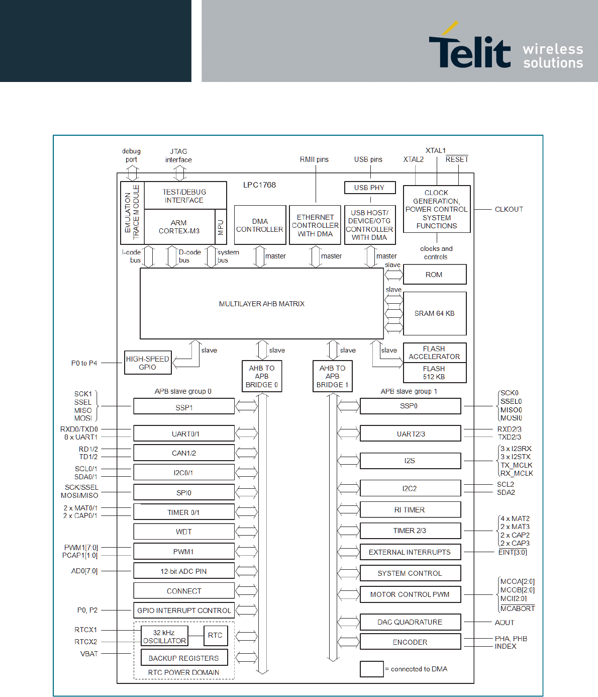
8.1.2 Utility Processor block diagram
Figure 5 LPC1768 block diagram
Remark: Some interfaces, such as 1 UART, 1 I2C-bus, 1 SSP are not available externally, as they
are used within ATOP 3.5G. For more details, refer to Section 7.2.2.

ATOP3.5G Product Description
80447ST10636A rev.10 – 2015-03-03
Reproduction forbidden without written authorization from Telit Communications S.p.A. - All Rights
Reserved. Page 21 of 66
Mod. 0808 2011-07 Rev.2
8.1.3 Ethernet
The Ethernet block supports bus clock rates of up to 100 MHz. It contains a full featured 10
Mbit/s or 100 Mbit/s Ethernet MAC designed to provide optimized performance by using DMA
hardware acceleration. Features include a generous suite of control registers, half or full-duplex
operation, flow control, control frames, hardware acceleration for transmit retry, receive packet
filtering and wake-up on LAN activity. Automatic frame transmission and reception with scatter-
gather DMA off-loads many operations from the CPU.
The Ethernet block and the CPU share the ARM Cortex M3 D-CODE and system bus through
the AHB-multilayer matrix to access the various on-chip SRAM blocks for Ethernet data, control
and status information.
The Ethernet block interfaces between an off-chip Ethernet PHY using the Reduced MII (RMII)
protocol and the on-chip Media Independent Interface Management (MIIM) serial bus.
8.1.4 USB
Device and host controller with on-chip PHY.
8.1.4.1 USB device controller
This controller enables Full-speed (12 Mbit/s) data exchange with a USB Host controller. It
consists of a register interface, serial interface engine, endpoint buffer memory and a DMA
controller. The serial interface engine decodes the USB data stream and writes data to the
appropriate endpoint buffer. The status of a completed USB transfer or error condition is
indicated via status registers. If enabled, an interrupt is also generated. When enabled, the DMA
controller transfers data between the endpoint buffer and the on-chip SRAM.
8.1.4.2 USB host controller
This controller enables full- and low-speed data exchange with USB devices attached to the bus.
It consists of a register interface, a serial interface engine and a DMA controller. The register
interface complies with the OHCI specification.
8.1.5 CAN
8.1.5.1 Description
The Controller Area Network (CAN) is a serial communications protocol which efficiently supports
distributed real-time control with a very high level of security. Its application domain ranges from
high-speed networks to low-cost multiplex wiring. The CAN block is intended to support multiple
CAN buses simultaneously, allowing the device to be used as a gateway, switch or router among
a number of CAN buses in industrial or automotive applications.
8.1.5.2 Features
2 CAN controllers and buses
Data rates to 1 Mbit/s on each bus
32-bit register and RAM access
Compatible with CAN specification 2.0B, ISO 11898-1
Global Acceptance Filter recognizes 11- and 29-bit receive identifiers for all CAN buses
Acceptance Filter can provide FullCAN-style automatic reception for selected Standard
Identifiers
FullCAN messages can generate interrupts
ATOP3.5G Product Description
80447ST10636A rev.10 – 2015-03-03
Reproduction forbidden without written authorization from Telit Communications S.p.A. - All Rights
Reserved. Page 22 of 66
Mod. 0808 2011-07 Rev.2
8.1.6 Power-saving modes
8.1.6.1 Peripheral and clock control
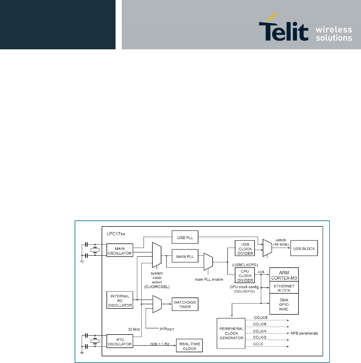
As shown in Figure 6, the CPU clock rate can also be controlled as needed by changing clock
sources, reconfiguring PLL values and/or altering the CPU clock divider value. This allows a trade-
off of power versus processing speed based on application requirements. In addition, Peripheral
Power Control allows shutting down the clocks to individual on-chip peripherals, allowing fine-
tuning of power consumption by eliminating all dynamic power use in any peripherals that are not
required for the application.
The LPC1768 includes three independent oscillators. These are the main oscillator, the IRC
oscillator and the RTC oscillator. Each oscillator can be used for more than one purpose as
required in a particular application. Any of the 3-clock sources can be chosen by software to
drive the main PLL and ultimately the CPU.
Following reset, the LPC1768 operates from the Internal RC oscillator until switched by software.
This allows systems to operate without any external crystal and the boot loader code to operate
at a known frequency. Main oscillator is driven by an optional external crystal on customer board.
Its presence might be required if an accurate clock is necessary, for instance for USB or HS CAN
compliancy.
Figure 6 LPC1768 clock generation
8.1.6.2 Power modes
The LPC1768 supports various power control features. There are 4 special modes of processor
power reduction:
Sleep mode
Deep sleep mode
Power-down mode
Deep power-down mode

ATOP3.5G Product Description
80447ST10636A rev.10 – 2015-03-03
Reproduction forbidden without written authorization from Telit Communications S.p.A. - All Rights
Reserved. Page 23 of 66
Mod. 0808 2011-07 Rev.2
The CPU clock rate may also be controlled as needed by changing clock sources, reconfiguring
PLL values and/or altering the CPU clock divider value. This allows a trade-off of power versus
processing speed based on application requirements. In addition, Peripheral Power Control
allows shutting down the clocks to individual on-chip peripherals, allowing fine-tuning of power
consumption by eliminating all dynamic power use in any peripherals that are not required for the
application. Each of the peripherals has its own clock divider which provides even better power
control.
An integrated PMU (Power Management Unit) automatically adjusts internal regulators to
minimize power consumption during Sleep mode, Deep sleep mode, Power-down mode and
Deep power-down mode.
The LPC1768 also implements a separate power domain to allow turning off power to the bulk of
the device while maintaining operation of the RTC and a small set of registers for storing data
during any of the Power-down modes.
Sleep mode: When Sleep mode is entered, the clock to the core is stopped. Resumption from the
Sleep mode does not need any special sequence but re-enabling the clock to the ARM core.
In Sleep mode, execution of instructions is suspended until either a Reset or interrupt occurs.
Peripheral functions continue operation during Sleep mode and may generate interrupts to cause
the processor to resume execution. Sleep mode eliminates dynamic power used by the
processor itself, memory systems and related controllers and internal buses.
Deep sleep mode: In Deep sleep mode, the oscillator is shut down and the chip receives no
internal clocks. The processor state and registers, peripheral registers and internal SRAM values
are preserved throughout Deep sleep mode and the logic levels of chip pins remain static. The
output of the IRC is disabled but the IRC is not powered down for a fast wake-up later.
The RTC oscillator is not stopped because the RTC interrupts may be used as the wake-up
source. The PLL is automatically turned off and disconnected.
The Deep sleep mode can be terminated and normal operation resumed by either a reset or
certain specific interrupts that are able to function without clocks. Since all dynamic operation of
the chip is suspended, this mode reduces chip power consumption to a very low value. Power to
the flash memory is left on in Deep sleep mode, allowing a very quick wake-up.
Power-down mode: Power-down mode does everything that Deep sleep mode does, but also
turns off the power to the IRC oscillator and flash memory. This saves more power but requires
waiting for resumption of flash operation before code execution or data access can resume.
Deep power-down mode: The Deep power-down mode can only be entered from the RTC block.
In Deep power-down mode, power is shut off to the entire chip except for the RTC module and the
RESET pin. The LPC1768 can wake up from Deep power-down mode via the RESET pin or an
alarm time match event of the RTC.
Wake-up interrupt controller: The wake-up Interrupt Controller (WIC) allows the CPU to wake up
automatically from any enabled priority interrupt that can occur while the clocks are stopped in
Deep sleep mode, Power-down mode and Deep power-down mode.
The WIC works with the Nested Vectored Interrupt Controller (NVIC). When the CPU enters
Deep sleep mode, Power-down mode or Deep power-down mode, the NVIC sends a mask of the
current interrupt situation to the WIC. This mask includes all of the interrupts that are both
enabled and of sufficient priority to be serviced immediately. With this information, the WIC
notices when one of the interrupts has occurred and then it wakes up the CPU. The WIC
eliminates the need to periodically wake up the CPU and poll the interrupts.

ATOP3.5G Product Description
80447ST10636A rev.10 – 2015-03-03
Reproduction forbidden without written authorization from Telit Communications S.p.A. - All Rights
Reserved. Page 24 of 66
Mod. 0808 2011-07 Rev.2
8.1.7 RTC
The RTC is designed to have low-power consumption: less than 1 μA. The RTC typically runs
from the main chip power supply, conserving battery power while the rest of the device is
powered up. When operating from a battery, the RTC is operational down to 2.1 V. Battery power
can be provided from a standard 3 V Lithium button cell.
An ultra-low power 32 kHz oscillator provides a 1 Hz clock to the time counting portion of the
RTC, moving most of the power consumption out of the time counting function.
The RTC contains a small set of backup registers (20 bytes) for holding data while the main part
of the LPC1768 is powered off.
The RTC includes an alarm function that can wake up the LPC1768 from all reduced power
modes with a time resolution of 1 s.
8.2 Application processor
The application processor is running a Virtual Machine (VM) able to interpret Java applications. It
is running on the main CPU of the UMTS/EDGE/GPRS/GSM baseband and offers:
portability to numerous platforms
maintainability via secure download and update mechanisms
large virtualized feature set, such as:
o secure network access (https)
o cryptography
o Near Field Communication (NFC)2
Java VM with the following features:
o High performance J2ME Virtual Machine
o based on IBM J9
o Connected Device Configuration 1.1.2
CDC Foundation Profile 1.1.2, extended with the following Telit API's
o Wireless Messaging
o Location
o Audio playback
o Telephony
o Contactless communication - including secure element access
o Power management
o Service calls
o Firmware Update over The Air
Connection to microcontroller via message passing
As for memory, the application processor features:
256 MB of NAND flash memory available to store application data and code
128 MB of volatile memory for application data (LPDDR)

ATOP3.5G Product Description
80447ST10636A rev.10 – 2015-03-03
Reproduction forbidden without written authorization from Telit Communications S.p.A. - All Rights
Reserved. Page 25 of 66
Mod. 0808 2011-07 Rev.2
8.3 Position processing
8.3.1 Key features
ATOP 3.5 G features GNSS reception used for positioning services. This support is provided in
software integrated on the application processor with the following key features:
Supports both GPS and GLONASS
“All in view” tracking capability
Dual antenna support with internal switching:
o passive antenna input with internal separate LNA
o active antenna input with internal LNA bypass
Supports following Satellite Based Augmentation Systems: WAAS, EGNOS, MSAS
Receiver Autonomous Integrity Monitoring (RAIM) & Fault Detection and Exclusion
(FDE) support
Support of assistance data (Ephemerides, location, time...) provided by customer
application to ensure faster Time To First Fix (TTFF)
1 Pulse Per Second (1PPS) output for synchronization with GPS system clock
Software upgradable
CEP50 < 2 m
8.3.2 Sensitivity
Table 4 shows acquisition and tracking sensitivity measurements for a passive antenna.
Table 4 Sensitivity
Symbol Parameter Conditions Min Typ Max Unit
t
TTFF
time to first fix time open sky, hot start, 130 dBm signal - 1.5 - s
open sky,warm start, 130 dBm signal - < 27 - s
open sky, cold start, 130 dBm signal - < 36 - s
P
i(acq)
minimum acquisition
input power
ephemeris decode, cold start - 145 - dBm
hot start - 152 - dBm
P
i(trck)
minimum tracking
input power - 160 - dBm
Pi(reacq) minimum
reacquisition input
power
- 159 - dBm
An active antenna should have an integrated LNA with a noise figure of 1.6dB, or lower, and a
gain of 17dB, or higher, to achieve the same sensitivity as measured on the passive antenna
input. A higher (or lower) noise figure results in a one to one worse (or better) sensitivity.

ATOP3.5G Product Description
80447ST10636A rev.10 – 2015-03-03
Reproduction forbidden without written authorization from Telit Communications S.p.A. - All Rights
Reserved. Page 26 of 66
Mod. 0808 2011-07 Rev.2
8.4 UMTS/EDGE/GSM/GPRS coprocessor
Connection to mobile networks is provided by a certified communications protocol stack that is
field tested worldwide, with best-in-class RF performance and power consumption.
32-bit ARM1136EJ-S control processor, up to 390 MHz
Communication engine
o Support for 2 antennas allowing backup of primary antenna for 2G and 3G as
well as receive diversity for high bit rate
o UMTS/HSDPA/HSUPA Quad-band support for worldwide coverage: 2100 (I),
1900 (II), 1700 (IV/IX), 850 (V) (including 800 (VI)) and 900 (VIII), power class 3
o 2.75G Quad-band support: GSM 850, PCS 1900, E-GSM 900, and DCS 1800
with EDGE/GPRS multi-slot class 12, class B, power class E2
Audio subsystem
o W-AMR/HR/FR/EFR/AMR Vocoders
o Noise suppression and echo cancelation
o 2 microphone inputs
o 1 stereo or 2 mono outputs
o 1 stereo class D up to 1 W @ 5 V / 8
o Digital IO
USIM card interface
o class B and C
o SIM toolkit R99 support for all provisioning functions that do not need a UI
High performance interfacing
o High-speed OTG USB
o SDIO interface
The following maximum theoretical transfer speed can be reached for the different standards:
HSUPA mode: 5.76 Mbps (Cat 6) uplink speed
HSDPA mode: 14.4 Mbps (Cat 10) downlink speed
UMTS mode: 384 Kbps DL/384 Kbps UL
EDGE: 236.8 Kbps DL/236.8 Kbps UL (class 12)
GPRS: 85.6 Kbps DL/85.6 Kbps UL (class 12)
GSM: 14.4 Kbps DL/14.4 Kbps UL
8.5 Near Field Communication coprocessor
Remark: This paragraph applies only to OM12030/1X0 (with X as defined in Section 5).
To connect to an external device, such as vignette, mobile phone, or personalization station for car
sharing scheme, an NFC communication link is present with the following features:
Reader/writer and card interface modes
o Baud rate up to 424 kbps
o Complete NFC framing and error detection
o Support for ISO14443 A, ISO14443 B, and MIFARE
This interface can also be used to exchange data with ISO14443/MIFARE cards.

ATOP3.5G Product Description
80447ST10636A rev.10 – 2015-03-03
Reproduction forbidden without written authorization from Telit Communications S.p.A. - All Rights
Reserved. Page 27 of 66
Mod. 0808 2011-07 Rev.2
8.6 Smartcard and JCOP operating system
Remark: This paragraph applies only to OM12030/1X0 (with X as defined in Section 5).
For telematics and other high value applications, it is paramount to protect against data tampering,
loading of unauthorized applications, ID stealing, as well as to protect end-user privacy. For this, a
secured component such as a smartcard is required as a root of trust.
In ATOP 3.5G this is achieved by a SmartMX co-processor with the following features:
Latest built-in security features to avoid power (SPA/DPA), timing and fault attacks
20 KB EEPROM
o Typical 500000 cycles endurance and minimum 20 years retention time
6144 Bytes RAM
Secure cryptographic processor
o High-performance secured Public Key Infrastructure (PKI) with RSA up to 2048,
ECC GF(p) up to 320 bits
o AES up to 256 bits and triple-DES
For portability and to allow multiple secure application cardlets to run in complete isolation, ATOP
3.5G offers a Java Card Open Platform operating system (JCOP) v2.4.2 based on independent,
third-party specifications, that is, by Sun Microsystems, the Global Platform consortium, the
International Organization for Standards (ISO), EMV (Europay, MasterCard and VISA) and others.
The SmartMX family was designed to service high volume, single-application and multi-application
markets such as eGovernment, Smart Passport, banking/finance, mobile communications, public
transportation, pay TV, conditional access, network access and digital rights management, thus
ensuring applications running on ATOP 3.5G can rely on the highest level of security available.
For more information, contact the Telit Technical Support Center (TTSC).
8.7 Debugging versus software security
While debug capabilities are a must, the observability, test, and control capabilities they provide
can also be used for device tampering. ATOP 3.5G offers debug capabilities and security features
that ensure that only signed software is executed. It is up to the customer to enable this.
Unlocking is not possible.
For debug, the following features are present:
LPC1768 MCU
o CPU debug via JTAG or Serial Wire Debug interface;
o Unique Serial Number;
o Core Read Protection with multiple levels.
For security, the following features are present and can protect against unauthorized debug, code
tampering and insertion:
Observability
o JTAG access locked down until authentication is performed;
o Secure debug with authentication.
Code authentication and integrity
o Code is signed with Public Key cryptography to ensure authentication and
checked at boot.

ATOP3.5G Product Description
80447ST10636A rev.10 – 2015-03-03
Reproduction forbidden without written authorization from Telit Communications S.p.A. - All Rights
Reserved. Page 28 of 66
Mod. 0808 2011-07 Rev.2
8.8 Firmware update Over The Air (FOTA)
Considering the long lifetime of Telematics applications, it is mandatory to be able to update the
different software elements of an application over the air. To this purpose, ATOP 3.5G provides
multiple mechanisms:
2 partitions of 27 MB for storing communication stack and virtual machine
o Dual boot mechanism, to switch between newer or older stack
o API to access to firmware versions
Utility processor microcode update mechanism
Update mechanism embedded in virtual machine for applications
8.9 Battery and power management
All voltage conversion and battery charging management are handled by ATOP 3.5G.
Direct connection to mobile phone type battery
o Optional connection to coin cells for RTC
Battery charging management
o Full hardware and software support of single cell Li-Ion, Li-Ion polymer battery
with voltage and charge current monitoring
Support large voltage range: See Table 11
Integration of all required LDO and DC-to-DC converters
Separate power supply pins are provided for microcontroller, RTC and the rest of the system, so
that each part can be separately disabled.
The utility microcontroller can be programmed to wake up ATOP 3.5G on external (CAN, GPIO ...)
or RTC events.
1 A are drawn by RTC standalone via an optional separate power supply.
8.10 OTP content
Storage in One Time Programmable memory (OTP) of critical parameters:
IMEI
Serial Number
Assemly data, including week code, etc.
ATOP 3.5G type description
RF calibration parameters
Essential NV items for proper 3GPP behavior
ATOP3.5G Product Description
80447ST10636A rev.10 – 2015-03-03
Reproduction forbidden without written authorization from Telit Communications S.p.A. - All Rights
Reserved. Page 29 of 66
Mod. 0808 2011-07 Rev.2
9 Application design-in information
9.1 Battery charging
ATOP 3.5G natively handles Lithium Ion battery technology.
The charging algorithm supports three charging techniques: trickle charge, constant-current and
constant voltage. The charging state machine is mostly automated, with a minimum of software
intervention.
The first step in the automated charging process determines if trickle charging is needed.
Charging of a severely depleted battery must begin with trickle charging to limit the current
and protect the battery from more charging current than it can handle.
Once a minimum battery voltage is established using trickle charging, constant-current
charging is enabled to charge the battery quickly – this mode is sometimes called fast
charging.
Once the battery approaches its target voltage, the charge is completed using constant-
voltage charging.
A battery thermistor sensor allows controlling the temperature window within which the charger is
active.
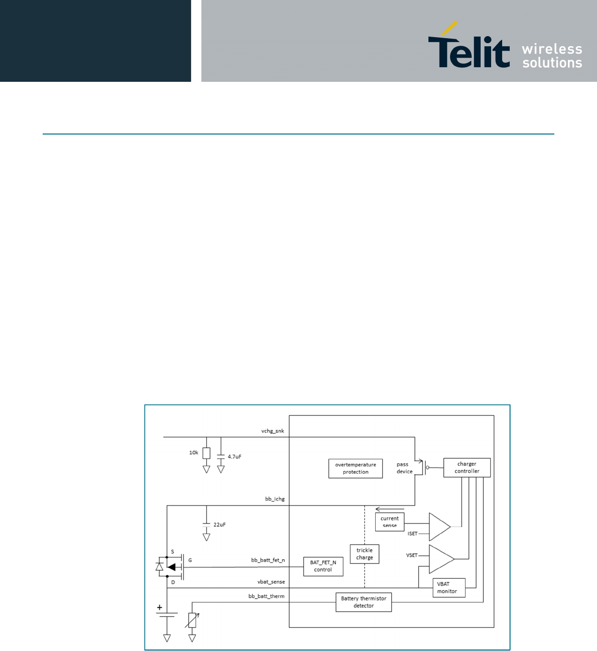
For characteristics of the charging process, refer to Sections 12.2 and 13.5.
Figure 7 shows the internal and external components involved in battery charging.
Figure 7 ATOP 3.5G battery charging
If no rechargeable battery is used in the application, the charging control pins must be connected
as follows:
VCHG_SNK, BB_BATT_FET_N, BB_ICHG, and BB_BATT_THERM must be left unconnected
VBAT_SENSE must be connect to VBAT_PA_SNK
ATOP3.5G Product Description
80447ST10636A rev.10 – 2015-03-03
Reproduction forbidden without written authorization from Telit Communications S.p.A. - All Rights
Reserved. Page 30 of 66
Mod. 0808 2011-07 Rev.2
9.2 Current source
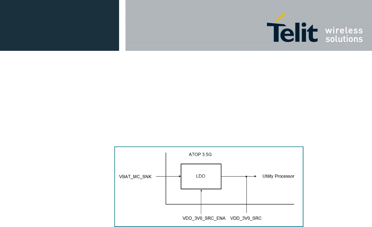
ATOP 3.5G handles all its voltage conversion internally.
For the Utility Processor, a separate input, VBAT_MC_SNK, is used. Internally, an LDO,
controlled by VDD_3V0_SRC_ENA (active HIGH, with internal pull up), converts it to the 3 V
required by the utility processor. As described in Figure 8, the output of the LDO is also available
externally to power external component, up to a maximum of 50 mA can be drawn, depending on
the operating temperature range and the VBAT_MC_SNK value. Other limiting values can be
found in Table 14.
Figure 8 ATOP 3.5G VDD_3V0_SRC current source
9.3 RTC
The MCU RTC is internally supplied by the output of the LDO described in Figure 8. It can also be
supplied by a separate battery such as a coin cell via VBAT_RTC_SNK such that the RTC is kept
alive in case of power loss.
9.4 ESD protection
All pins are tested against ESD according to HBM. Pins that have direct a connection to external world in the
application, such as antennas and battery charging, are tested against ESD following HMM models.
Human Body Model (HBM): 2000 V requirements are fulfilled
Human Metal Model (HMM), detailed list is as follows:
o CELL_ANT1 and CELL_ANT2 up to 4 kV
o VBAT_SNK, VBAT_MC_SNK, and VBAT_VCC_PA_SNK up to 4 kV
o For GPS_PAS _ANT and GPS_ACT_ANT up to 4 kV. For GPS_ACT_ANT an
external ESD protection diode is recommended if used externally
Charged Device Model (CDM) is considered not applicable for metal-shielded modules, such as OM12030.
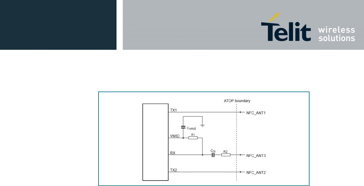
9.5 NFC antenna design
Remark: This paragraph applies only to OM12030/1X0 (with X as defined in Section 5).
For NFC antenna design, refer to Ref [6] for antenna design and Ref [7] in case the application
requires to boost the NFC signal.
ATOP3.5G Product Description
80447ST10636A rev.10 – 2015-03-03
Reproduction forbidden without written authorization from Telit Communications S.p.A. - All Rights
Reserved. Page 31 of 66
Mod. 0808 2011-07 Rev.2
Figure 9 describes the internal setup of NFC_ANT pins, with R1 = 1 k, R2 = 2.7 k, Crx = 1 nF,
Cvmid = 100 nF.
Figure 9 ATOP 3.5G internal setup of NFC antenna
9.6 Antenna placement
Care must be taken to introduce sufficient distance between the various antennas in the system.
In particular, if an active GNSS antenna is positioned too close to a 3G cellular antenna, the LNA
of the active GNSS antenna will amplify any spurious that the 3G antenna may radiate in the
GNSS frequency bands. For more information, refer to section 15.
9.7 Electrical safety
ATOP 3.5G is intended only for installation in a restricted area location.
It shall be supplied by a limited power source complying with clause 2.5 of EN 60950-1 and
mounted on a V1 flammability class material or better.
it shall be supplied by a power supply which next features:
If you do not use overcurrent protection devices: Current of short-circuit of power supply
< 8 A. / Apparent power < 100 VA;
If you use overcurrent protection devices: Current of short-circuit < 333 A. / Apparent
power < 250 VA. (The rated current of overprotection device shall be < 5A).
9.8 Software package
For customer production and end-of-line testing, the following software tools are provided to
interface to the module:
ATOP test software example in source
Parameters settings in OTP (IMEI, RF parameters)
Flashing tool for the application processor
A flashing tool for the utility processor can be downloaded from a third party web site.
ATOP3.5G Product Description
80447ST10636A rev.10 – 2015-03-03
Reproduction forbidden without written authorization from Telit Communications S.p.A. - All Rights
Reserved. Page 32 of 66
Mod. 0808 2011-07 Rev.2
10 Limiting values
Table 5 Power supply
Parameters mentioned in this table are indicative and taken from supplier data sheets.
Symbol Parameter Conditions Min Max Unit
V
BAT(VBAT_PA_SNK)
battery supply voltage on
pin VBAT_PA_SNK battery voltage for RF amplifier 3.2 4.6 V
V
BAT(VBAT_SNK)
battery supply voltage on
pin VBAT_SNK battery voltage for application processor 3.2 4.4 V
V
BAT(VBAT_MC_SNK)
battery supply voltage on
pin VBAT_MC_SNK battery voltage for utility processor 3.1 5.5 V
V
BAT(VBAT_RTC_SNK)
battery supply voltage on
pin VBAT_RTC_SNK
battery voltage for utility processor RTC 2.1 3.25 V
V
BAT(VBAT_CHG)
battery supply voltage on
pin VBAT_CHG
charger supply voltage - 5.0 V
V
BAT(VBAT_SPKR)
battery supply voltage on
pin VBAT_SPKR
amplifier supply voltage - 5.0 V
Table 6 Microcontroller pins
Parameters mentioned in this table are indicative and taken from supplier data sheets.
Symbol Parameter Conditions Min Max Unit
V
I(a)
analog input voltage on ADC-related pins 0.5 +5.1 V
V
i
input voltage 5 V tolerant I/O pins [1][2] 0.5 +5.5 V
other I/O pins [1] 0.5 +3.6 V
input voltage for MC_XTAL1; internal
oscillator input 0 1.95 V
[1] VBAT(VBAT_MC_SNK) (battery voltage for utility processor) must be present.
[2] 3-state outputs go into 3-state mode when VBAT(VBAT_MC_SNK) (battery voltage for utility processor) is grounded.
Table 7 Cellular baseband digital interfaces
Parameters mentioned in this table are indicative and taken from supplier data sheets.
Symbol Parameter Conditions Min Max Unit
V
i
input voltage 0.5 +2.3 V
I
I
input current 100 +100 mA

ATOP3.5G Product Description
80447ST10636A rev.10 – 2015-03-03
Reproduction forbidden without written authorization from Telit Communications S.p.A. - All Rights
Reserved. Page 33 of 66
Mod. 0808 2011-07 Rev.2
Table 8 Cellular antennas
Due to their ESD protection implementation the antennas are DC grounded. Parameters mentioned in this table are indicative
and taken from supplier data sheets.
Symbol Parameter Conditions Min Max Unit
R
I
input resistance DC voltage - 1 Ω
VSWR
load
load voltage standing wave
ratio
all phase angles - 20:1 -
P
o(sp)
spurious output power LOW bands; for all phase angles, load VSWR
= 12:1, all phase angles - 30 dBm
HIGH bands; for all phase angles,
load VSWR
= 8:1, all phase angles - 30 dBm
Table 9 GPS passive antenna input
Due to its ESD protection implementation, the GPS antenna is DC grounded. Parameters mentioned in this table are
indicative and taken from supplier data sheets.
Symbol Parameter Conditions Min Max Unit
R
I
input resistance DC voltage - 1 Ω
Table 10 GPS active antenna input and antenna bias
Parameters mentioned in this table are indicative and taken from supplier data sheets.
Symbol Parameter Conditions Min Max Unit
V
I(max)
maximum input voltage DC voltage 25 +25 V
I
I
input current DC current - 70 mA

ATOP3.5G Product Description
80447ST10636A rev.10 – 2015-03-03
Reproduction forbidden without written authorization from Telit Communications S.p.A. - All Rights
Reserved. Page 34 of 66
Mod. 0808 2011-07 Rev.2
11 Recommended operating conditions
ATOP 3.5G is qualified for automotive use, in accordance with TELIT's
"Knowledge-Based
Qualification" ("KBQ", based on ZVEI's Robustness Validation, Ref. [1]), using AEC-Q100-defined
qualification tests, targeting 15 years lifetime.
Table 11 Recommended operating conditions
Allowed temperature ranges.
Symbol Parameter Conditions Min Max Unit
Tstg storage temperature module storage temperature range before
final reflow, stored in dry pack 40 +125 °C
Tamb ambient temperature
module limited ambient temperature range for
utility processor (LPC1768) 40 +85 °C
module ambient temperature range all
functions (the limiting factor is NFC) 30 +85 °C
Vch(VCHG_SNK) charge voltage on pin
VCHG_SNK
- 5.0 V
VBAT(VBAT_PA_SNK) battery supply voltage on
pin VBAT_PA_SNK
battery voltage for RF amplifier 3.4 4.4 V
VBAT(VBAT_SNK) battery supply voltage on
pin VBAT_SNK
battery voltage for application processor 3.2 4.4 V
VBAT(VBAT_MC_SNK) battery supply voltage on
pin VBAT_MC_SNK
battery voltage for utility processor 3.1 5.5 V
IBAT(m) peak current to be used to
dimension decoupling
capacitors on pin
VBAT_PA_SNK
- 2200 mA
12 Thermal characteristics
12.1 Internal temperature sensor
ATOP 3.5G includes an internal temperature sensor. The LPC1768 has access to this sensor to
adapt its behavior to conditions.
12.2 Battery charging
To improve battery lifetime, it is recommended to avoid charging batteries outside of the
temperature range specified by their manufacturers, typically 0 °C to 50 °C.

ATOP3.5G Product Description
80447ST10636A rev.10 – 2015-03-03
Reproduction forbidden without written authorization from Telit Communications S.p.A. - All Rights
Reserved. Page 35 of 66
Mod. 0808 2011-07 Rev.2
13 Static characteristics
13.1 Pins
Table 12 Characteristics for microcontroller pins
Parameters mentioned in this table are indicative and taken from supplier data sheets.
Symbol Parameter Conditions Min Typ Max Unit
V
o
output voltage 0 - 3.0 V
V
IH
HIGH-level input voltage 2.0 - - V
V
IL
LOW-level input voltage - - 0.8 V
I
IL
LOW-level input current VI = 0 V; no pull up - - 10 nA
I
IH
HIGH-level input current VI = 3.0 V; no pull-down - - 10 nA
V
OH
HIGH-level output voltage
IOH = 4 mA 2.6 - - V
V
OL
LOW-level output voltage
IOL = 4 mA - - 0.4 V
I
OL
LOW-level output current
VOL = 0.4 V 4 - - mA
I
OH
HIGH-level output current
VOH = 2.6 V 4 - - mA
I
OSL
LOW-level short-circuit
output current VI = 3.0 V [1] - - 50 mA
I
OSH
HIGH-level short-circuit
output current VI = 0 V [1] - - 45 mA
I
OZ
OFF-state output current VO = 3.0 V or 0 V; no pull up/pull-down - - 10 A
I
pd
pull-down current V
I
= 5 V 10 50 150 A
I
pu
pull up current V
I
= 0 V 15 50 85 A
3.0 V < V
I
< 5 V 0 0 0 A
I
lu(IO)
input/output latch-up
current 1.5 V < VI < 4.5 V; Tamb < 125 °C - - 100 mA
[1] Only allowed for a short time period.
Table 13 Characteristic for baseband digital interface
Parameters mentioned in this table are indicative and taken from supplier data sheets.
Symbol Parameter Conditions Min Typ Max Unit
V
IH
HIGH-level input voltage 1.2 - 2.1 V
V
IL
LOW-level input voltage 0.3 - 0.6 V
I
IL
LOW-level input current 1 - - A
I
IH
HIGH-level input current - - 1 A
V
OH
HIGH-level output voltage
1.35 - 1.8 V
V
OL
LOW-level output voltage
- - 0.1 V
R
pu
pull up resistance - 100 - k
R
pd
pull-down resistance - 100 - k
C
i
input capacitance - - 10 pF

ATOP3.5G Product Description
80447ST10636A rev.10 – 2015-03-03
Reproduction forbidden without written authorization from Telit Communications S.p.A. - All Rights
Reserved. Page 36 of 66
Mod. 0808 2011-07 Rev.2
13.2 Current sources
Table 14 VDD_3V0_SRC current source
Can be used to supply external components.
Symbol Parameter Conditions Min Typ Max Unit
Pin: VDD_3V0_SRC
V
o
output voltage for T
a
m
b
= 40 °C to +85 °C 2.9 3.0 3.1 V
I
o
output current - - 50 mA
ton turn-on time measured from the moment
VDD_3V0_SRC_ENA exceeds 1.4 V [1] - 240 - μs
Load regulation
∆VO/(VOx∆IO)
relative output voltage
variation with output
current
[1] - 0.002 0.004 %/mA
Line regulation
∆VO/(VOx∆VI)
relative output voltage
variation with input
for VBAT(VBAT_MC_SNK) variation [1] 0.1 0.02 0.1 %/V
[1] Parameter is indicative and taken from supplier data sheet.
Table 15 VSIM_SRC current source
To be only used to supply SIM cards[1]. Parameters mentioned in this table are indicative and taken from supplier data
sheets.
Symbol Parameter Conditions Min Typ Max Unit
Pin: VSIM_SRC
Vo output voltage for ISO7816-3 class B SIMs 2.80 - 3.00 V
for ISO7816-3 class C SIMs 1.7 - 1.80 V
Io output current full power mode - - 150 mA
sleep mode - - 3 mA
[1] Voltage is dynamically controlled to reduce power consumption when SIM card is not accessed.

ATOP3.5G Product Description
80447ST10636A rev.10 – 2015-03-03
Reproduction forbidden without written authorization from Telit Communications S.p.A. - All Rights
Reserved. Page 37 of 66
Mod. 0808 2011-07 Rev.2
13.3 Voltage references
Table 16 VIO_REF voltage reference
To be used as a reference for connecting BB digital interfaces. Parameters mentioned in this table are indicative and taken
from supplier data sheets.
Symbol Parameter Conditions Min Typ Max Unit
Pin: VIO_REF
Vo output voltage 1.74 1.80 1.86 V
∆Vo/Vo relative output voltage
variation for VBAT (VBAT_SNK) variation - - 3 %/V
Table 17 VADC_REF voltage reference
Used as power supply reference for internal ADCs.
Symbol Parameter Conditions Min Typ Max Unit
Pin: VADC_REF
Vo output voltage for Tamb = 40 °C to +85 °C 2.9 3.0 3.1 V
Io output current for Tamb = 40 °C to +85 °C [1] - - 1 mA
∆Vo/(Vox∆Vi)
relative output voltage
variation with input
voltage
for VBAT (VBAT_MC_SNK) variation [2] 0.1 - 0.1 %/V
[1] To be used only as a reference voltage.
[2] Parameter is indicative and taken from supplier data sheet.
13.4 Clocks
Table 18 1PPS
This pulse is synchronized with GPS system clock.
Symbol Parameter Conditions Min Typ Max Unit
t
w
pulse width - 100 - s
t
jit
jitter time RMS stationary and receiving 4 or more satellites - 4.1 - ms
V
OH
HIGH-level output voltage
1.35 - 1.80 V
V
OL
LOW-level output voltage
- - 0.1 V
Table 19 BB_EXT_CLK
Symbol Parameter Conditions Min Typ Max Unit
f
xtal
reference oscillator
frequency - 19.2 - MHz
f
xtal
/f
xtal
reference oscillator
frequency accuracy
(40°C to +85°C)
- 2 5 ppm
V
OH
HIGH-level output voltage
at 6 mA 2.15 2.60 - V
V
OL
LOW-level output voltage
at 6 mA - - 0.45 V

ATOP3.5G Product Description
80447ST10636A rev.10 – 2015-03-03
Reproduction forbidden without written authorization from Telit Communications S.p.A. - All Rights
Reserved. Page 38 of 66
Mod. 0808 2011-07 Rev.2
Table 20 Microcontroller clock
External crystal required for high-speed CAN, for all other purposes, internal RC oscillator is sufficient. Parameters mentioned
in this table are indicative and taken from supplier data sheets.
Symbol Parameter Conditions Min Typ Max Unit
f
xtal
crystal frequency in case of externally oscillator, connected to
MC_XTAL_1 and MC_XTAL_2
1 - 25 MHz
V
i(clk)RMS
RMS clock input voltage 0.2 - - V
t
cy(clk)
clock cycle time 40 - 1000 ns
t
clk(H)
clock HIGH time 0.4 ×
t
cy(clk)
- - ns
t
clk(L)
clock LOW time 0.4 ×
t
cy(clk)
- - ns
t
r(clk)
clock rise time - - 5 ns
t
f(clk)
clock fall time - - 5 ns
f
osc
oscillator frequency frequency of internal RC oscillator 3.96 4 4.04 MHz
Table 21 Internal Real-Time Clock
An internal crystal generates RTC. Parameters mentioned in this table are indicative and taken from supplier data sheets.
Symbol Parameter Conditions Min Typ Max Unit
f
xtal
crystal frequency in case of externally generated clock - 32.768
- KHz
fxtal/fxtal relative crystal frequency
variation
20 - 20 10-6
first year of aging 3 - 3 10-6
TC temperature coefficient 0.028
0.034
0.04 10
-6
/C°²
T
turnp
turning point temperature
20 25 30 C°
t
d
delay time time to reach stability; at 25 °C, starting from
VDD_3V0 > 2 V - 300 - ms
Figure 10 32KHz deviation in ppm dependng on temperature

ATOP3.5G Product Description
80447ST10636A rev.10 – 2015-03-03
Reproduction forbidden without written authorization from Telit Communications S.p.A. - All Rights
Reserved. Page 39 of 66
Mod. 0808 2011-07 Rev.2
13.5 Battery charging
Table 22 Battery charging
Handled by integrated battery charging unit. Parameters mentioned in this table are indicative and taken from supplier data
sheets.
Symbol Parameter Conditions Min Typ Max Unit
V
DD(chg)
charger supply voltage - - 5 V
T
en(ch)
charge enable
temperature charger only enabled within this window 0 - 40 deg
V
ch(trickle)
trickle charge voltage battery level at which fast charge mode starts - [1] - V
I
ch(trickle)
trickle charge current 10 [1] 160 mA
V
ch(fast)
fast charge voltage constant voltage phase - [1] - V
I
ch(fast)
fast charge current constant current phase I
EOC
[1] 1000 mA
I
eoc
end of charge current auto charge ends when battery current
reaches this level
- [1] Ich(fast) mA
V
th(ch)
charge threshold voltage auto charge resumes when battery level drops
below this level - [1] - V
[1] Settings are software programmable, depending on battery technology (LiIon, LiFePO4…) and need to be set
accordingly.

ATOP3.5G Product Description
80447ST10636A rev.10 – 2015-03-03
Reproduction forbidden without written authorization from Telit Communications S.p.A. - All Rights
Reserved. Page 40 of 66
Mod. 0808 2011-07 Rev.2
14 Dynamic characteristics
14.1 Power consumption
Table 23 Utility processor power consumption
Measured at Tamb = 25 °C with a power supply at 3.7 V. Covers LPC1768 and LDO.
Symbol Parameter Conditions Min Typ Max
Unit
II input current Cortex M3 at 12 MHz [1] - 7 - mA
Cortex M3 at 100 MHz [1] - 45 - mA
Cortex M3 in Power-down mode [2] - 100 - A
RTC active [3] - 1 - A
[1] No peripherals enabled.
[2] Wake-up can be initiated by event on RTC, CAN, USB and most GPIOs.
[3] In case a separate power source such as a coin cell is connected to VBAT_RTC_SNK and no power is supplied via
VBAT_MC_SNK.
Table 24 Application processor power consumption
Baseband ARM and memories power consumption additionally to cellular function.
Symbol Parameter Conditions Min Typ Max Unit
II input current application processor - [1] - mA
[1] Application dependent.
Table 25 Security processor power consumption
Measured at Tamb = 25 °C with a power supply at 3.7 V. Only for OM12030/1X0 and OM12030/2X0 (with X as defined in
Section 5).
Symbol Parameter Conditions Min Typ Max Unit
I
I
input current function switched OFF; included in NFC
coprocessor
- - 0 A
function active - 6 - mA
Table 26 NFC coprocessor power consumption
Measured at Tamb = 25 °C with a power supply at 3.7 V. Covers NFC. Only for OM12030/1X0 (with X as defined in Section 5).
Symbol Parameter Conditions Min Typ Max Unit
I
I
input current function switched OFF - 2 - A
Power-down mode; RF field detection ON - 35 - A
NFC and SMX active - 30 - mA
NFC and SMX active with RF transmission
ongoing
- 90 130 mA

ATOP3.5G Product Description
80447ST10636A rev.10 – 2015-03-03
Reproduction forbidden without written authorization from Telit Communications S.p.A. - All Rights
Reserved. Page 41 of 66
Mod. 0808 2011-07 Rev.2
Table 27 Communication processor power consumption
Measured at Tamb = 25 °C with a power supply at 3.7 V.
Symbol Parameter Conditions Min Typ Max Unit
DC1800I
I
input current (combined
VBAT_SNK and
VBAT_PA_SNK)
Data transfer
WCDMA 2100 (Band I) - 220 630 [2]
mA
WCDMA 1900 (Band II) - - 630 [2]
mA
WCDMA 1800 (Band III) - - <tbd> mA
WCDMA 1700 (Band IV) - - 630 [2]
mA
WCDMA 850 (Band V) -
- 600 [2]
mA
WCDMA 900 (Band VIII) - - 600 [2]
mA
EDGE class 12 (high bands) 4Tx - 1 Rx slots
- - 550 [3]
mA
EDGE class 12 (low bands) - - 600 [3]
mA
GPRS class 12 (high bands) - - 800 [4]
mA
GPRS class 12 (low bands) - - 900 [4]
mA
Voice
GSM - - 200 [5]
mA
WCDMA - - 250 [6]
mA
Stand-by
GSM900 - - 2.3 mA
DCS800 - - 2.1 mA
WCDMA - - 1.7 mA
[1] Average current. Measurements are performed according to 3GPP 4.14 subclause 5.4 for 2G, 34.121 app C2 for 3G.
[2] 24 dBm transmit power.
[3] 27 dBm for low bands, 26 dBm for high bands.
[4] 33 dBm for low bands, 30 dBm for high bands.
[5] 33 dBm for low bands, 30 dBm for high bands.
[6] Weighted current consumption. Reference document DG.09, WCDMA 2100

ATOP3.5G Product Description
80447ST10636A rev.10 – 2015-03-03
Reproduction forbidden without written authorization from Telit Communications S.p.A. - All Rights
Reserved. Page 42 of 66
Mod. 0808 2011-07 Rev.2
14.2 Cellular RF parameters
Table 28 Operating frequencies
The operating frequencies in GSM850, EGSM900, CDS1800, PCS1900, and WCDMA conform to 3GPP specifications.
Mode Freq.TX (MHz) Freq RX (MHz) Channels TX – RX offset
GSM850 824.2 ~ 848.8 869.2 ~ 893.8 128 ~ 251 45 MHz
EGSM900 890.0 ~ 914.8 935.0 ~ 959.8 0 ~ 124 45 MHz
880.2 ~ 889.8 925.2 ~ 934.8 975 ~ 1023 45 MHz
DCS1800 1710.2 ~ 1784.8 1805.2 ~ 1879.8 512 ~ 885 95 MHz
PCS1900 1850.2 ~ 1909.8 1930.2 ~ 1989.8 512 ~ 810 80 MHz
WCDMA850 (CLR) 826.4 ~ 846.6 871.4 ~ 891.6 TX: 4132 ~ 4233 45 MHz
RX: 4357 ~ 4458
WCDMA900 882.4 ~ 912.6 927.4 ~ 957.6 TX: 2712 ~ 2863 45 MHz
RX: 2937 ~ 3088
WCDMA1700 (AWS) 1712.4 ~ 1752.6 2112.4 ~ 2152.6 TX: 1312 ~ 1513 400 MHz
RX: 1537 ~ 1738
WCDMA1800 (DCS) 1710.4 ~ 1785.6 1805.4 ~ 1180.6 RX: 937 ~ 1288 95 MHz
TX: 1162 ~ 1513
WCDMA1900 (PCS) 1852.4 ~ 1907.6 1932.4 ~ 1097.6 TX: 9262 ~ 9538 80 MHz
RX: 9662 ~ 9938
WCDMA2100 (IMT) 1922.4 ~ 1977.6 2112.4 ~ 2167.6 TX: 9512 ~ 9888 190 MHz
RX: 10562 ~ 10838
Not all ATOP 35G variants support all of the above bands. The band combinations per variant are defined in section 5.

ATOP3.5G Product Description
80447ST10636A rev.10 – 2015-03-03
Reproduction forbidden without written authorization from Telit Communications S.p.A. - All Rights
Reserved. Page 43 of 66
Mod. 0808 2011-07 Rev.2
Table 29 Receiver sensitivity in GSM
Typical values measured on TELIT reference board at 3.8 V and for Tamb = 25 °C for all channels; 3GPP requirement is 102
dBm; for Tamb = 25 °C and all voltage conditions (3.4 V VBAT(VBAT_PA_SNK) 4.4 V).
Symbol Parameter Conditions Min Typ Max Unit
S
RX
receiver sensitivity GSM850 band - 110.3
- dBm
GSM900 band - 111.3
- dBm
DCS1800 band - 108.6
- dBm
PCS1900 band - 108.9
- dBm
Table 30 Receiver sensitivity in UMTS
Typical values measured on TELIT reference board at 3.8 V and for Tamb = 25 °C for all channels; 3GPP requirement is band
specific; for Tamb = 25 °C and all voltage conditions (3.4 V VBAT(VBAT_PA_SNK) 4.4 V).
Symbol Parameter Conditions Min Typ Max Unit
S
RX
receiver sensitivity band I 3GPP requirement is 106.0 - 109.5
- dBm
band II 3GPP requirement is 104.0 - 110.3
- dBm
band III (IX) 3GPP requirement is 103.3 - <tbd>
- dBm
band IV 3GPP requirement is 106.0 - 110.1
- dBm
band V (VI) 3GPP requirement is 104.0 - 111.2
- dBm
band VIII 3GPP requirement is 103.0 - 111.0
- dBm

ATOP3.5G Product Description
80447ST10636A rev.10 – 2015-03-03
Reproduction forbidden without written authorization from Telit Communications S.p.A. - All Rights
Reserved. Page 44 of 66
Mod. 0808 2011-07 Rev.2
Table 31 Transmit GSM output power
Typical values at 3.8 V and for Tamb = 25 °C; 3GPP requirement is 33 / 27 dBm +/- 2.5dB for GSM / EDGE 850 + 900 MHz
and 30 / 26 dBm +/- 2.5dB for GSM / EDGE 1800 + 1900 MHz for all temperature conditions (-40 to + 85 C) and all voltage
conditions (3.4 V VBAT(VBAT_PA_SNK) 4.4 V).
Symbol Parameter Conditions Min Typ Max Unit
P
TX
GSM / GPRS mode
(up to 4 TX slots) GSM850 band / PCL 5 30.5 32.8 35.5 dBm
GSM900 band / PCL 5 30.5 32.5 35.5 dBm
DCS1800 band / PCL 0 27.5 29.6 32.5 dBm
PCS1900 band / PCL 0 27.5 29.7 32.5 dBm
EDGE mode GSM850 band / PCL 8 24.5 26.8 29.5 dBm
GSM900 band / PCL 8 24.5 26.5 29.5 dBm
DCS1800 band / PCL 2 23.5 25.7 28.5 dBm
PCS1900 band / PCL 2 23.5 25.6 28.5 dBm
Table 32 Transmit UMTS maximum RMS power
Typical values at 3.8 V and for Tamb = 25 °C; 3GPP requirement is 24 dBm +1/-3 for all temperature conditions (40° C Tamb
+85 °C) and all voltage conditions (3.4 V VBAT(VBAT_SNK) 4.4 V).
Symbol Parameter Conditions Min Typ Max Unit
PMAX maximum RMS power band I 21 22.9 25 dBm
band II 21 22.9 25 dBm
band III (IX) 21 22.9 25 dBm
band IV 21 22.9 25 dBm
band V (VI) 21 22.9 25 dBm
band VIII 21 22.9 25 dBm

ATOP3.5G Product Description
80447ST10636A rev.10 – 2015-03-03
Reproduction forbidden without written authorization from Telit Communications S.p.A. - All Rights
Reserved. Page 45 of 66
Mod. 0808 2011-07 Rev.2
15 Test and qualification information
ATOP 3.5G is a class A digital device for use in a commercial, industrial or business environment.
It is tested to conform to FCC and AT&T as well as to R&TTE articles 3.1(a) and (b), safety and
EMC respectively and relevant article 3.2 requirements using the TELIT reference board. The
manufacturer of the final product integrating ATOP 3.5G must assess its equipment against the
essential requirements of the R&TTE, FCC and AT&T directives.
ATOP 3.5G is targeted to be compliant with the following standards:
Mandatory European standards
o R&TTE Article 3.1a: Electrical safety (EN60950)
o R&TTE Article 3.1a: SAR (EN62209-1): MPE calculation as distance > 20 cm
o R&TTE Article 3.1b: EMC (EN62311:2008, EN301489-1, and EN301489-7 for
GSM, EN301489-24 for UMTS)
o R&TTE Article 3.2: Radiated RF (EN301511 for GSM, EN301908-1/-2 for UMTS,
EN300440-1/-2 for GPS, EN300291-1/-2 for NFC)
o Notified Body opinion according to Annex IV: Evaluation of compliance with
essential requirements
Mandatory US and Canadian standards
o FCC EMC: part 15B
o FCC RF: part 24 for PCS1900, part 22 for GSM850, part 15.225 for NFC
o FCC certificate from Telecom Certification body
Voluntary certification
o Global Certification Forum (GCF), including Field Tests
o PCS-1900 Type Certification Review Board (PTCRB)
o AT&T certificate
o Certification for Japanese Radio and Telecommunication law (TELEC)
Certification reports are available upon request.
SAR according to EN 62209-1 has not been checked and replaced by MPE calculation. Hence
the antenna(s) used in the final application must be installed to provide a separation distance of
at least 20 centimeters from all persons and must not be co-located or operating with any other
antenna or transmitter. Additionally, for FCC compliance, the system antenna(s) gain must not
exceed 3 dBi for mobile and fixed or mobile operating configurations.
The manufacturer of the final product using ATOP 3.5G will have to provide instructions for
antenna installation and transmitter operating conditions to satisfy to RF exposure compliance.
The manufacturer of the final product using ATOP 3.5G should take care that ATOP 3.5G is
always within the operating limits (temperature, power supply, …) described in the present
document. In particular it must be supplied by a limited power source according to EN 60950-1.
Physically, the clearance and creepage distances required by the end product must be upheld
when the module is installed. The cooling of the end product shall not negatively be influenced by
the installation of the module.
Manufacturers of devices incorporating this module are advised to clarify any regulatory
questions and to have their complete product tested and approved for R&TTE, FCC, AT&T
compliance and all relevant regulations.
ATOP3.5G Product Description
80447ST10636A rev.10 – 2015-03-03
Reproduction forbidden without written authorization from Telit Communications S.p.A. - All Rights
Reserved. Page 46 of 66
Mod. 0808 2011-07 Rev.2
15.1 FCC and IC Cautions
Modification statement
“Telit Communications S.P.A.” has not approved any changes or modifications to this device by
the user. Any changes or modifications could void the user’s authority to operate the equipment.
“Telit Communications S.P.A.”
n’approuve aucune modification apportée à l’appareil par
l’utilisateur, quelle qu’en soit la nature. Tout changement ou modification peuvent annuler le droit
d’utilisation de l’appareil par l’utilisateur.
Interference statement
This device complies with Part 15 of the FCC Rules and Industry Canada licence-
exempt RSS
standard(s). Operation is subject to the following two conditions: (1) this device may not cause
interference, and (2) this device must accept any interference, including interference that may
cause undesired operation of the device.
Le
présent appareil est conforme aux CNR d'Industrie Canada applicables aux appareils radio
exempts de licence. L'exploitation est autorisée aux deux conditions suivantes : (1) l'appareil ne
doit pas produire de brouillage, et (2) l'utilisateur de l'appareil
doit accepter tout brouillage
radioélectrique subi, même si le brouillage est susceptible d'en compromettre le fonctionnement.
Wireless notice
This equipment complies with FCC and IC radiation exposure limits set forth for an uncontrolled
environment. The antenna should be installed and operated with minimum distance of 20 cm
between the radiator and your body. Antenna gain must be below:
Frequency band
Maximum antenna gain
GSM 850/FDD V 1.92
PCS 1900/FDD II 0.51
FDD IV 5.00
This transmitter must not be co-
located or operating in conjunction with any other antenna or
transmitter.
Cet appareil est conforme aux limites d'exposition aux rayonnements de la IC pour un
environnement non contrôlé. L'antenne doit être installé de façon à g
arder une distance minimale
de 20 centimètres entre la source de rayonnements et votre corps. Gain de l'antenne doit être ci-
dessous:
Bande de fréquence
Gain de l'antenne maximum
GSM 850/FDD V 1.92
PCS 1900/FDD II 0.51
FDD IV 5.00
L'émetteur ne doit
pas être colocalisé ni fonctionner conjointement avec à autre antenne ou autre
émetteur.
ATOP3.5G Product Description
80447ST10636A rev.10 – 2015-03-03
Reproduction forbidden without written authorization from Telit Communications S.p.A. - All Rights
Reserved. Page 47 of 66
Mod. 0808 2011-07 Rev.2
FCC Class B digital device notice
This equipment has been tested and found to comply with the limits for a Class B digital device,
pursuant to part 15 of the
FCC Rules. These limits are designed to provide reasonable protection
against harmful interference in a residential installation. This equipment generates, uses and can
radiate radio frequency energy and, if not installed and used in accordance with the in
structions,
may cause harmful interference to radio communications. However, there is no guarantee that
interference will not occur in a particular installation. If this equipment does cause harmful
interference to radio or television reception, which can
be determined by turning the equipment off
and on, the user is encouraged to try to correct the interference by one or more of the following
measures:
- Reorient or relocate the receiving antenna.
- Increase the separation between the equipment and receiver.
-
Connect the equipment into an outlet on a circuit different from that to which the receiver
is connected.
- Consult the dealer or an experienced radio/TV technician for help..
Labelling Requirements for the Host device
T
he host device shall be properly labelled to identify the modules within the host device. The
certification label of the module shall be clearly visible at all times when installed in the host
device, otherwise the host device must be labelled to display t
he FCC ID and IC of the module,
preceded by the words "Contains transmitter module", or the word "Contains", or similar wording
expressing the same meaning, as follows:
For OM12030/XY0 (with X and Y as defined in section 5):
Contains FCC ID: RI7OM12030-XY0
Contains IC: 5131A-OM12030XY0
L'appareil hôte doit être étiqueté comme il faut pour permettre l'identification des modules qui s'y
trouvent. L'étiquette de certification du module donné doit être posée sur l'appareil hôte à un
endroit bien en vue en tout temps. En l'absence d'étiquette, l'appareil hôte doit porter une
étiquette donnant le FCC ID et le IC du module, précédé des mots « Contient un module
d'émission », du mot « Contient » ou d'une formulation similaire exprimant le même sens, comme
suit:
Pour OM12030/XY0 (avec X et Y comme definit par la section 5):
Contains FCC ID: RI7OM12030-XY0
Contient IC: 5131A-OM12030XY0.
CAN ICES-3 (B) / NMB-3 (B)
This Class B digital apparatus complies with Canadian ICES-003.
Cet appareil numérique de classe B est conforme à la norme canadienne NMB-003..

ATOP3.5G Product Description
80447ST10636A rev.10 – 2015-03-03
Reproduction forbidden without written authorization from Telit Communications S.p.A. - All Rights
Reserved. Page 48 of 66
Mod. 0808 2011-07 Rev.2
15.2 1999/5/EC Directive regulatory notices
This device has been evaluated against the essential requirements of the 1999/5/EC Directive.
Bulgarian С настоящето “Telit Communications S.P.A.” декларира, че “OM12030/X00”
(*)
отговаря на съществените
изисквания и другите приложими изисквания на Директива 1999/5/ЕС.
Croatian Ovime “Telit Communications S.P.A.”, izjavljuje da je ovaj “OM12030/X00”
(*)
je u skladu s osnovnim zahtjevima i
drugim relevantnim odredbama Direktive 1999/5/EC.
Czech “Telit Communications S.P.A.” tímto prohlašuje, že tento “OM12030/X00”
(*)
je ve shodě se základními požadavky
a dalšími příslušnými ustanoveními směrnice 1999/5/ES.
Danish Undertegnede “Telit Communications S.P.A.” erklærer herved, at følgende udstyr “OM12030/X00”
(*)
overholder
de væsentlige krav og øvrige relevante krav i direktiv 1999/5/EF.
Dutch Hierbij verklaart “Telit Communications S.P.A.” dat het toestel “OM12030/X00”
(*)
in overeenstemming is met de
essentiële eisen en de andere relevante bepalingen van richtlijn 1999/5/EG.
English Hereby, “Telit Communications S.P.A.”, declares that this “OM12030/X00”
(*)
is in compliance with the essential
requirements and other relevant provisions of Directive 1999/5/EC.
Estonian Käesolevaga kinnitab “Telit Communications S.P.A.” seadme “OM12030/X00”
(*)
vastavust direktiivi 1999/5/EÜ
põhinõuetele ja nimetatud direktiivist tulenevatele teistele asjakohastele sätetele.
German Hiermit erklärt “Telit Communications S.P.A.”, dass sich das Gerät “OM12030/X00”
(*)
in Übereinstimmung mit den
grundlegenden Anforderungen und den übrigen einschlägigen Bestimmungen der Richtlinie 1999/5/EG befindet.
Greek ΜΕ ΤΗΝ ΠΑΡΟΥΣΑ “Telit Communications S.P.A.” ΔΗΛΩΝΕΙ ΟΤΙ “OM12030/X00”
(*)
ΣΥΜΜΟΡΦΩΝΕΤΑΙ ΠΡΟΣ
ΤΙΣ ΟΥΣΙΩΔΕΙΣ ΑΠΑΙΤΗΣΕΙΣ ΚΑΙ ΤΙΣ ΛΟΙΠΕΣ ΣΧΕΤΙΚΕΣ ΔΙΑΤΑΞΕΙΣ ΤΗΣ ΟΔΗΓΙΑΣ 1999/5/ΕΚ.
Hungarian Alulírott, “Telit Communications S.P.A.” nyilatkozom, hogy a “OM12030/X00”
(*)
megfelel a vonatkozó alapvetõ
követelményeknek és az 1999/5/EC irányelv egyéb elõírásainak.
Finnish “Telit Communications S.P.A.” vakuuttaa täten että “OM12030/X00”
(*)
tyyppinen laite on direktiivin 1999/5/EY
oleellisten vaatimusten ja sitä koskevien direktiivin muiden ehtojen mukainen.
French Par la présente “Telit Communications S.P.A.” déclare que l'appareil “OM12030/X00”
(*)
est conforme aux
exigences essentielles et aux autres dispositions pertinentes de la directive 1999/5/CE.
Icelandic Hér með lýsir “Telit Communications S.P.A.” yfir því að “OM12030/X00”
(*)
er í samræmi við grunnkröfur og aðrar
kröfur, sem gerðar eru í tilskipun 1999/5/EC
Italian Con la presente “Telit Communications S.P.A.” dichiara che questo “OM12030/X00”
(*)
è conforme ai requisiti
essenziali ed alle altre disposizioni pertinenti stabilite dalla direttiva 1999/5/CE.
Latvian Ar šo “Telit Communications S.P.A.” deklarē, ka “OM12030/X00”
(*)
atbilst Direktīvas 1999/5/EK būtiskajām
prasībām un citiem ar to saistītajiem noteikumiem.
Lithuanian Šiuo “Telit Communications S.P.A.” deklaruoja, kad šis “OM12030/X00”
(*)
atitinka esminius reikalavimus ir kitas
1999/5/EB Direktyvos nuostatas.
Maltese Hawnhekk, “Telit Communications S.P.A.”, jiddikjara li dan “OM12030/X00”
(*)
jikkonforma mal-ħtiġijiet essenzjali u
ma provvedimenti oħrajn relevanti li hemm fid-Dirrettiva 1999/5/EC.
Norwegian “Telit Communications S.P.A.” erklærer herved at utstyret “OM12030/X00”
(*)
er i samsvar med de grunnleggende
krav og øvrige relevante krav i direktiv 1999/5/EF.
Polish Niniejszym “Telit Communications S.P.A.” oświadcza, że “OM12030/X00”
(*)
jest zgodny z zasadniczymi
wymogami oraz pozostałymi stosownymi postanowieniami Dyrektywy 1999/5/EC
Portuguese
“Telit Communications S.P.A.” declara que este “OM12030/X00”
(*)
está conforme com os requisitos essenciais e
outras disposições da Directiva 1999/5/CE.
Slovak “Telit Communications S.P.A.” týmto vyhlasuje, že “OM12030/X00”
(*)
spĺňa základné požiadavky a všetky
príslušné ustanovenia Smernice 1999/5/ES.
Slovenian “Telit Communications S.P.A.” izjavlja, da je ta “OM12030/X00”
(*)
v skladu z bistvenimi zahtevami in ostalimi
relevantnimi določili direktive 1999/5/ES.
Spanish Por medio de la presente “Telit Communications S.P.A.” declara que “OM12030/X00”
(*)
cumple con los requisitos
esenciales y cualesquiera otras disposiciones aplicables o exigibles de la Directiva 1999/5/CE.
Swedish Härmed intygar “Telit Communications S.P.A.” att denna “OM12030/X00”
(*)
står I överensstämmelse med de
väsentliga egenskapskrav och övriga relevanta bestämmelser som framgår av direktiv 1999/5/EG.
(*) Valid for OM12030/000, OM12030/100 and OM12030/200.
ATOP3.5G Product Description
80447ST10636A rev.10 – 2015-03-03
Reproduction forbidden without written authorization from Telit Communications S.p.A. - All Rights
Reserved. Page 49 of 66
Mod. 0808 2011-07 Rev.2
In order to satisfy the essential requirements of 1999/5/EC Directive, the product is compliant with the following
standards:
RF spectrum use (R&TTE art. 3.2)
EN 301 511 V9.0.2
EN 301 908-1 V5.2.1
EN 301 908-2 V5.2.1
EN 300 440-1 v 1.6.1
EN 300 440-2 v1.4.1
EN 302 291-1 v 1.1.1(1)
EN 302 291-2 v 1.1.1(1)
EMC (R&TTE art. 3.1b)
EN 301 489
-
1 V1.9.2
EN 301 489-3 V1.4.1
EN 301 489-7 V1.3.1
EN 301 489-24 V1.5.1
Health & Safety (R&TTE art. 3.1a)
EN 60950
-
1:2006 + A11:2009 + A1:2010 + A12:2011 + AC:2011
EN 62311:2008
(1) Only applicable to the product OM12030/1X0 with X as defined in section 5.
The conformity assessment procedure referred to in Article 10 and detailed in Annex IV of Directive 1999/5/EC has
been followed with the involvement of the following Notified Body:
AT4 wireless, S.A.
Parque Tecnologico de Andalucía
C/ Severo Ochoa 2
29590 Campanillas – Málaga
SPAIN
Notified Body No: 1909
Thus, the following marking is included in the product:
There is no restriction for the commercialization of this device in all the countries of the European Union.
Final product integrating this module must be assessed against essential requirements of the 1999/5/EC (R&TTE)
Directive. It should be noted that assessment does not necessarily lead to testing. Telit Communications S.p.A.
recommends carrying out the following assessments:
RF spectrum use (R&TTE art. 3.2) It will depend on the antenna used on the final product.
EMC (R&TTE art. 3.1b) Testing
Health & Safety (R&TTE art. 3.1a) Testing

ATOP3.5G Product Description
80447ST10636A rev.10 – 2015-03-03
Reproduction forbidden without written authorization from Telit Communications S.p.A. - All Rights
Reserved. Page 50 of 66
Mod. 0808 2011-07 Rev.2
15.3 Reliability qualification
ATOP is qualified according to AEC-Q100 Grade 3. The qualification is done in accordance with
the concept of "Robustness Validation". Reliability tests used are compliant with those as
described in AEC-Q100.
The basis for Robustness Validation is the “Mission Profile”, reflecting the specific use case of a
device (application, location, and environment) and the associated stress factors. The Mission
Profile used for ATOP is “Dashboard application” in a car. The qualification strategy, based on the
Mission Profile includes so-called extended read points, meaning that the reliability stress tests
are not stopped after the required read point needed to determine fit for use, but in some cases
are extended up to twice the required read point, in order to determine the reliability margin.
Table 33 presents in more details the tests performed to guarantee module lifetime.
Table 33 Electrical and environmental qualification
Test Abbreviation
Conditions Description
Characterization and performance-related test methods
Electrical
characterization CHAR Tamb = 40 °C to +85 °C
Electromagnetic
compatibility
EMC according to IEC 62132-
4,
IEC 61967-4, LIN EMC
test specification
Operational and environmental test methods
High temperature
operational life (HTOL)
ERF based on worst case Stress test accelerating the operational intrinsic
lifetime of semiconductor devices. Also in this case
operation means that the device is in an application
like environment: supply voltage, supply and output
current, input signals, output loads. The acceleration
is achieved by temperature (normally at maximal
junction temperature inside the packaged device),
but supply voltage and sometimes current can be
used too. Failure modes are typically wear out
related: electro migration, gate oxide breakdown,
transistor threshold voltage shifting or transistor
characteristic degradation due to hot carriers or
negative bias instability, mobile ions.
IFR applicative case, biased,
Tja = 85 °C
High temperature
storage life HTSL Tamb = 125 °C Environment stress simulating storage and
accelerating intermetallic bonding fracture failures at
high temperatures (without supply).
Moisture sensitive level
assessment MSLA 2 reflows Methodology to determine the moisture sensitivity for
Surface Mount Devices (SMD) in relation to PCB
assembly by Hot Convection reflow.
Unbiased HAST (Highly
Accelerated Steam Test)
UHST Tamb = 110 °C / 85 % RH Preferred
unbiased humidity stress test to investigate
endurance of the product regarding internal corrosion
and leakage formation by transport of ions/water.
Typical for standoff without voltage supply.
Temperature humidity
test THB Tamb = 85 °C / 85 % RH /
V biased
Preferred biased humidity stress to investigate
endurance of the product regarding internal corrosion
and leakage formation by transport of ions/water.
Typical for standoff with voltage supply on.

ATOP3.5G Product Description
80447ST10636A rev.10 – 2015-03-03
Reproduction forbidden without written authorization from Telit Communications S.p.A. - All Rights
Reserved. Page 51 of 66
Mod. 0808 2011-07 Rev.2
Test Abbreviation
Conditions Description
Temperature cycling TMCL Tamb = 40 °C to +105 °C
Acceleration test to investigate thermo-mechanical
failure modes (like delamination, die lift, wire break,
bond ball lift, die crack, pattern shift, and passivation
crack) due to both ambient and internal temperature
changes during device or application power-up and
switching OFF as well as ambient storage.
Vibration VIBR ISO 17650, Random
RMS
2.78G, Tamb = 40 °C to
+85 °C
Test used to determine the ability of the device to
withstand repetitive vibration as a result of motion
produced by transportation or field operation.
Board level test methods
Board level temperature
cycling BL-TMCL Tamb = 40 °C to +125 °C
Acceleration test to investigate thermo-mechanical
failure modes (like solder fatigue) at the interconnect
between the device and the printed circuit board due
to both ambient and internal temperature changes
during device and application power-up and
switching OFF as well as ambient storage.
System level ESD ESDS IEC61000-4-2, ESD gun
ATOP3.5G Product Description
80447ST10636A rev.10 – 2015-03-03
Reproduction forbidden without written authorization from Telit Communications S.p.A. - All Rights
Reserved. Page 52 of 66
Mod. 0808 2011-07 Rev.2
16 Marking
Figure 11 outlines the label information for ATOP 3.5G as template.
Figure 11 ATOP label informaton
The label contains the following information:
1. Black solid O: pin A1 indicator
2. Telit logo
3. Commercial name
4. (empty by default)
5. Type of sample (marketing, released, …)
6. IMEI
7. Barcode type 2D matrix: ECC200 of the IMEI, followed a semicolon, and a 42 character
string for Telit EMS internal use
8. Model number designator
9. FCC ID
10. IC ID
11. (empty by default)
12. Certifcation logo(s)
13. Production country
The maximum barcode size is 8x8 +/0.5mm. The offset between the reference point (0) and
barcode upper left corner is x = 1,5mm y = 9.6mm, both values +/ 0.5mm
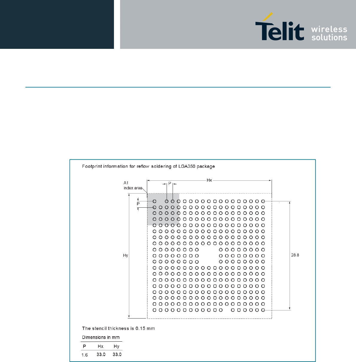
ATOP3.5G Product Description
80447ST10636A rev.10 – 2015-03-03
Reproduction forbidden without written authorization from Telit Communications S.p.A. - All Rights
Reserved. Page 53 of 66
Mod. 0808 2011-07 Rev.2
17 Packing information
ATOP 3.5G modules are packed in trays or as tape & reel. Before packing and shipping, trays and reels are
dry baked for 16 hours at 125 °C, according to IPC/JEDEC J-STD-033B.1.
ATOP 3.5G has been tested according to IPC/JEDEC J-STD 020D and is classified as Moisture Sensitivity
Level 3 (MSL3).
17.1 Footprint information for reflow soldering
The PCB footprint design is a copy of the metal LGA pattern at the bottom side of the ATOP package.
Figure 12 ATOP 3.5G footprint
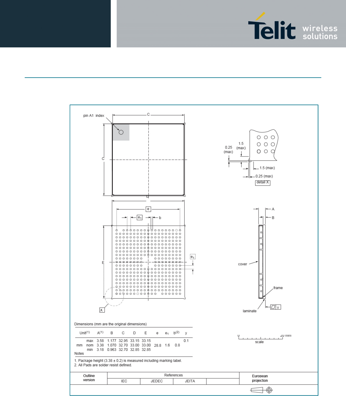
ATOP3.5G Product Description
80447ST10636A rev.10 – 2015-03-03
Reproduction forbidden without written authorization from Telit Communications S.p.A. - All Rights
Reserved. Page 54 of 66
Mod. 0808 2011-07 Rev.2
18 Package outline
ATOP 3.5G is a 33 33 3.35 mm laminate based module with a metal cover and a Land Grid
Array (LGA) at the bottom side of the product. The pad size is 0.8 mm with a 1.6 mm pitch.
Figure 13 ATOP 3.5G package outline
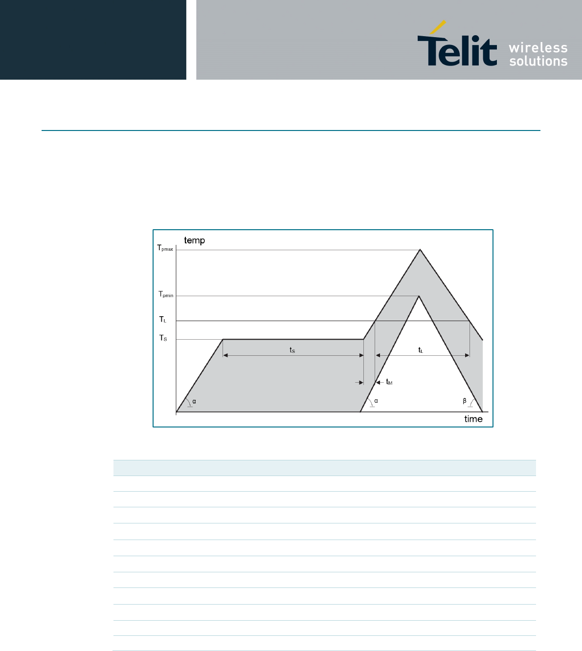
ATOP3.5G Product Description
80447ST10636A rev.10 – 2015-03-03
Reproduction forbidden without written authorization from Telit Communications S.p.A. - All Rights
Reserved. Page 55 of 66
Mod. 0808 2011-07 Rev.2
19 Soldering
The ATOP 3.5G (OM12030) can be assembled using a standard Surface Mount Technology
(SMT) reflow process in a convection oven. Figure 14 and Table 34 indicate the maximum and
minimum limits of the solder profile. The applied profile has to fit within these limits. This
temperature profile is based on the IPC/JEDEC joint industry standard J-STD-020C.
It is recommended to use a standard no-clean SAC solder paste for a lead free assembly process.
No cleaning should be applied during or after module soldering process.
Figure 14 Reflow profile
Table 34 Reflow profile parameters
Reflow condition Value Unit
ramp-up rate () 3 °C/s
ramp-down rate () 6 °C/s
preheat temperature (T
S
) 150 to 200 °C
preheat time (t
S
) 60 to 180 s
time to melting (t
M
) 6 to 35 s
time maintained above temperature (T
L
) > 217 °C
time maintained above time (t
L
) 60 to 150 s
peak/classification temperature minimum (T
pmin
) 235 °C
peak/classification temperature maximum (T
pmax
) 250 °C
maximum time above 250 °C 10 s
maximum time from 25 °C to peak temperature 8 mn

ATOP3.5G Product Description
80447ST10636A rev.10 – 2015-03-03
Reproduction forbidden without written authorization from Telit Communications S.p.A. - All Rights
Reserved. Page 56 of 66
Mod. 0808 2011-07 Rev.2
20 Abbreviations
Table 35 Abbreviations
Acronym Description
1PPS 1 Pulse Per Second
3GPP Third-Generation Partnership Project
A/D Analog to Digital interface
ACLR Adjacent Channel Leakage Ratio (out-of-band power ratio falling in the adjacent
channel)
ADC Analog to Digital Converter
AEC Automotive Electronics Council
AES Advanced Encryption Standard
AHR Advanced High-Performance Bus
APB Advanced Peripheral Bus
API Application Programming Interface
ATOP Automotive Telematics On-board unit Platform
CAN Controller Area Network
CDC Connected Device Configuration
CDM ESD Charged Device Model ESD
CEP50 Circular Error Probable 50%
CLK Clock
CPU Central Processing Unit
D/A Digital to Analog interface
DAC Digital to Analog Converter
DCS Digital Cellular System
DDR Double Data Rate (memory)
DES Data Encryption Standard
DL DownLink
DMA Direct Memory Access
DPA Differential Power Analysis
DSP Digital Signal Processor
ECC Error Correcting Code
EDGE Enhanced Data Rates for GSM Evolution
EEPROM Electrically Erasable Programmable Read-Only Memory
EGNOS European Geostationary Navigation Overlay Service
EJTAG Extended Joint Test Action Group
EMC ElectroMagnetic Compatibility
EMV Eurocard MasterCard Visa
EN European Norm
ESD ElectroStatic Discharge
EVM Error Vector Magnitude

ATOP3.5G Product Description
80447ST10636A rev.10 – 2015-03-03
Reproduction forbidden without written authorization from Telit Communications S.p.A. - All Rights
Reserved. Page 57 of 66
Mod. 0808 2011-07 Rev.2
Acronym Description
FCC Federal Communication Commission
FDE Fault Detection and Exclusion
FIFO First In First Out
FOTA Firmware upgrade Over The Air
GCF Global Certification Forum
GLONASS GLObalnaïa NAvigatsionnaïa Spoutnikovaïa Sistéma
GND GrounND
GNSS Global Navigation Satellite System
GP General Purpose
GPDMA General Purpise Direct Memory Access
GPIO General-Purpose Input Output
GPRS General Packet Radio Service
GSM Global System Mobile
GPS Global Positioning System
HBM ESD Human Body Model ESD
HMM ESD Human Metal Model ESD
HR/FR/EFR/AMR
Half Rate / Full Rate / Enhanced Full Rate / Adaptive Multi-Rate vocoder
HS CAN High-Speed Controller Area Network
HSDPA High-Speed Downlink Packet Access
HSUPA High-Speed Uplink Packet Access
HW HardWare
I2C Inter-Integrated Cicuit
I2S Inter-IC Sound
ID Identification
IF Intermediate Frequency
IMEI International Mobile Equipment Identity
IO Input Output
IRC Internal RC
IrDA Infrared Data Association
IRQ Interrupt ReQuest
ISO International Organization for Standardization
J2ME Java 2 Micro Edition
J2SE Java 2 Standard Edition
J9 VM Java Virtual Machine
JCOP Java Card Open Platform
JEDEC Joint Electron Device Engineering Council
JTAG Joint Test Action Group
LBS Location Based Services
LGA Land Grid Array
LDO Low DropOut

ATOP3.5G Product Description
80447ST10636A rev.10 – 2015-03-03
Reproduction forbidden without written authorization from Telit Communications S.p.A. - All Rights
Reserved. Page 58 of 66
Mod. 0808 2011-07 Rev.2
Acronym Description
LNA Low Noise Amplifier
LPDDR Low Power DDR (memory)
MAC Media Access Control
MCE Master Controller Element
MCU MicroController Unit
MIDP Mobile Information Device Profile
MIIM Media Independent Interface Management
MSAS MTSAT Satellite-based Augmentation System
NGC Near Field Communication
NIMH Nickel Metal Hydride
NV item Non Volatile (data) item
NVIC Nested Vectored Interrupt Controller
OBU On-Board Unit
OHCI Open Host Controller Interface
OS Operating System
OTG On The Go
OTP One Time Programmable
PA Power Amplifier
PCB Printed-Circuit Board
PCM Pulse Code Modulation
PCS Personal Communication Service
PHY PHYsical layer
PKI Public Key Infrastructure
PLL Phase-Locked Loop
PMU Power Management Unit
PPS Pulse Per Second
PTCRB PCS Type Certification Review Board
PWM Pulse Width Modulation
R&TTE Radio and Telecommunication Terminal Equipment
RAIM Receiver Autonomous Integrity Monitoring
RAM Random Access Memory
RF Radio Frequency
RFU Reserved for Future Use
RMII Reduced Media Independent Interface
RMS Root Mean Square
ROM Read-Only Memory
RSA A public-key encryption technology developed by RSA Data Security, Inc. The acronym
stands for Rivest, Shamir and Adelman, the inventors of the technique
RTC Real-Time Clock
RTOS Real-Time Operating System

ATOP3.5G Product Description
80447ST10636A rev.10 – 2015-03-03
Reproduction forbidden without written authorization from Telit Communications S.p.A. - All Rights
Reserved. Page 59 of 66
Mod. 0808 2011-07 Rev.2
Acronym Description
SAW Surface Acoustic Wave
SBAS Satellite Based Augmentation System
SDIO Secure Digital Input Output
SIM Subscriber Identification Module
SMD Surface Mounted Device
SMS Short Message Service
SNR Signal to Noise Ratio
SPA Simple Power Analysis
SPI Serial Peripheral Interface
SRAM Static Random Access Memory
SSP Synchronous Serial Port
TCXO Temperature Controlled Crystal Oscillator
THD Total Harmonic Distortion
TTFF Time To First Fix
TTL Transistor-Transistor Logic
TTSC Telit Technical Support Center
UART Universal Asynchronous Receiver Transmitter
UL UpLink
UMTS Universal Mobile Telecommunications Service
USB Universal Serial Bus
USIM Universal Subscriber Identity Module
VM Virtual Machine
VSWR Voltage Standing Wave Ratio
WAAS Wide Area Augmentation System
W-AMR Wide band - Adaptive Multi-Rate
WIC Wake-up Interrupt Controller

ATOP3.5G Product Description
80447ST10636A rev.10 – 2015-03-03
Reproduction forbidden without written authorization from Telit Communications S.p.A. - All Rights
Reserved. Page 60 of 66
Mod. 0808 2011-07 Rev.2
21 References
[1] ZVEI - Zentralverband Elektrotechnik- und Elektronikindustrie e.V. —
http://www.zvei.org/Verband/Publikationen/Seiten/default.aspx?k=robustness%u020validation
[2] LPC1768 data sheet —
http://www.nxp.com/documents/data_sheet/LPC1769_68_67_66_65_64_63.pdf
[3] LPC1768 user manual — http://www.nxp.com/documents/user_manual/UM10360.pdf
[4] LPC1768 errata sheet — http://www.nxp.com/documents/errata_sheet/ES_LPC176X.pdf
[5] LPC1768 web page —
http://www.nxp.com/products/microcontrollers/cortex_m3/lpc1700/LPC1768FET100html#overview
[6] AN1445 Antenna design guide for MFRC52x, PN51x, PN53x AN1444 RF Design Guideplus Excel
Calculation — http://www.nxp.com/documents/application_note/AN1445_An1444.zip
[7] AN1425 RF Amplifier for NFC Reader IC's AN166510 Amplifier antenna matching calculation (Excel)
— http://www.nxp.com/documents/application_note/AN1425_AN166510.zip
[8] Global Certification Forum — http://www.globalcertificationforum.org
[9] R&TTE Radio and Telecommunications Terminal Equipment —
http://ec.europa.eu/enterprise/policies/european-standards/harmonised-standards/rtte/
[10] PCS Type Certification Review Board — http://www.ptcrb.org
[11] Third-Generation Partnership Project — http://www.3gpp.org
[12] Applicable ATOP 3.5G software documentation.

ATOP3.5G Product Description
80447ST10636A rev.10 – 2015-03-03
Reproduction forbidden without written authorization from Telit Communications S.p.A. - All Rights
Reserved. Page 61 of 66
Mod. 0808 2011-07 Rev.2
22 Legal information
22.1 Definitions
Draft — The document is a draft version only. The content is still under
internal review and subject to formal approval, which may result in
modifications or additions. Telit does not give any representations or
warranties as to the accuracy or completeness of information included herein
and shall have no liability for the consequences of use of such information.
Short data sheet — A short data sheet is an extract from a full data sheet
with the same product type number(s) and title. A short data sheet is intended
for quick reference only and should not be relied upon to contain detailed and
full information. For detailed and full information see the relevant full data
sheet, which is available on request via the local Telit sales office. In case of
any inconsistency or conflict with the short data sheet, the full data sheet
shall prevail.
Product specification — The information and data provided in a Product
data sheet shall define the specification of the product as agreed between
Telit and its customer, unless Telit and customer have explicitly agreed
otherwise in writing. In no event however, shall an agreement be valid in
which Telit’s product is deemed to offer functions and qualities beyond those
described in the Product data sheet.
22.2 Disclaimers
Limited warranty and liability — Information in this document is believed
to be accurate and reliable. However, Telit does not give any
representations or warranties, expressed or implied, as to the accuracy or
completeness of such information and shall have no liability for the
consequences of use of such information. Telit takes no responsibility for the
content in this document if provided by an information source outside of
Telit.
In no event shall Telit be liable for any indirect, incidental, punitive, special or
consequential damages (including - without limitation - lost profits, lost
savings, business interruption, costs related to the removal or replacement
of any products or rework charges) whether or not such damages are based
on tort (including negligence), warranty, breach of contract or any other
legal theory.
Notwithstanding any damages that customer might incur for any reason
whatsoever, Telit’ aggregate and cumulative liability towards customer for
the products described herein shall be limited in accordance with the Terms
and conditions of commercial sale of Telit.
Right to make changes — Telit reserves the right to make changes to
information published in this document, including
without limitation
specifications and product descriptions, at any time and without notice. This
document supersedes and replaces all information supplied prior to the
publication hereof.
Applications — Applications that are described herein for any of these
products are for illustrative purposes only. Telit makes no representation or
warranty that such applications will be suitable for the specified use without
further testing or modification.
Customers are responsible for the design and operation of their applications
and products using Telit products, and Telit accepts no liability for any
assistance with applications or customer product design. It is customer’s
sole responsibility to determine whether Telit’s product is suitable and fit for
the customer’s applications and products planned, as well as for the
planned application and use of customer’s third party customer(s).
Customers should provide appropriate design and operating safeguards to
minimize the risks associated with their applications and products.
Telit does not accept any liability related to any default, damage, costs or
problem which is based on any weakness or default in the customer’s
applications or products, or the application or use by customer’s third party
customer(s). Customer is responsible for doing all necessary testing for the
customer’s applications and products using Telit products in order to avoid a
default of the applications and the products or of the application or use by
customer’s third party customer(s). Telit does not accept any liability in this
respect.
Limiting values — Stress above one or more limiting values (as defined in
the Absolute Maximum Ratings System of IEC 60134) will cause permanent
damage to the device. Limiting values are stress ratings only and (proper)
operation of the device at these or any other conditions above those given in
the Recommended operating conditions section (if present) or the
Characteristics sections of this document is not warranted. Constant or
repeated exposure to limiting values will permanently and irreversibly affect
the quality and reliability of the device.
Terms and conditions of commercial sale — Telit products are sold
subject to the general terms and conditions of commercial sale, as published
at
http://www.telit.com/profile/terms,
unless otherwise agreed in a valid
written individual agreement. In case an individual agreement is concluded
only the terms and conditions of the respective agreement shall apply. Telit
hereby expressly objects to applying the customer’s general terms and
conditions with regard to the purchase of Telit products by customer.
No offer to sell or license — Nothing in this document may be interpreted or
construed as an offer to sell products that is open for acceptance or the grant,
conveyance or implication of any license under any copyrights, patents or
other industrial or intellectual property rights.
Export control — This document as well as the item(s) described herein
may be subject to export control regulations. Export might require a prior
authorization from competent authorities.
ATOP product — Any offer of Telit’s ATOP to customers (“CUSTOMER”) is
subject to the following conditions:
CUSTOMER recognizes that since the parts were not originally designed for
automotive use, it will not be possible to achieve the levels of quality and
failure analysis that are normally associated with parts explicitly designed for
automotive use.
CUSTOMER further recognizes that Telit is not obligated to qualify the
ATOP Product to the AEC-Q100 automotive quality standard or indeed to
any other such existing or future automotive industry standards. Note that
the AEC-Q100 applies to Integrated Circuits and was not designed for
modules such as ATOP.
Subject to the foregoing, in the event that CUSTOMER designs-in and uses
the ATOP OM120xx beyond Telit’ then existing ATOP OM120xx Product
specification (latest version of the ATOP OM120xx Datasheet), CUSTOMER
understands and agrees:
(a) that CUSTOMER shall use ATOP OM120xx Product without Telit’s
warranty;
(b) that such use shall be solely at the CUSTOMER’s own risk;
(c) to fully indemnify Telit for any liability, damages or failed
ATOP OM120xx Product claims resulting from such use.
Translations — A non-English (translated) version of a document is for
reference only. The English version shall prevail in case of any discrepancy
between the translated and English versions.
ATOP3.5G Product Description
80447ST10636A rev.10 – 2015-03-03
Reproduction forbidden without written authorization from Telit Communications S.p.A. - All Rights
Reserved. Page 62 of 66
Mod. 0808 2011-07 Rev.2
22.3 Licenses
Modules with GSM or 3G functionality
Purchase of a Telit module with GSM functionality does not convey an
implied license under any patent right on the GSM or 3G Standard. A license
for the portfolio of GSM and 3G patents of Koninklijke Philips Electronics
N.V. needs to be obtained via Philips Intellectual Property and Standards
(www.ip.philips.com), e-mail: info.licensing@philips.com
Modules with DPA Countermeasures functionality
TELIT Modules containing functionality
implementing countermeasures to Differential
Power Analysis and Simple Power Analysis
are produced and sold under applicable
license from Cryptography Research, Inc.
Telit Modules with ISO/IEC 14443 type B functionality
RATP/Innovation
Tecgnology
This Telit module is ISO/IEC 14443 Type B software
enabled and is licensed under Innovatron’s Contactless
Card patents license for ISO/IEC 14443 B.
The license includes the right to use the module in
systems and/or end-user equipment.
Modules with NFC functionality
Purchase of a Telit module that complies with one of the Near Field
Communication (NFC) standards ISO/IEC 18092 and ISO/IEC 21481 does
not convey an implied license under any patent right infringed by
implementation of any of those standards
22.4 Trademarks
All referenced brands, product names, service names and trademarks are the property of their respective owners.
I2C-bus — logo is a trademark of NXP B.V.
MIFARE — is a trademark of NXP B.V.
SmartMX — is a trademark of NXP B.V.
23 Contact information
For general contact, technical support, to report documentation errors and to order manuals,
contact Telit Technical Support Center (TTSC) at:
TS-Automotive@telit.com
TS-EMEA@telit.com
TS-NORTHAMERICA@telit.com
TS-LATINAMERICA@telit.com
TS-APAC@telit.com
Alternatively, use:
http://www.telit.com/en/products/technical-support-center/contact.php
For detailed information about where you can buy the Telit modules or for recommendations on
accessories and components visit:
http://www.telit.com
To register for product news and announcements or for product questions contact Telit Technical
Support Center (TTSC). Our aim is to make this guide as helpful as possible. Keep us informed of
your comments and suggestions for improvements.
Telit appreciates feedback from the users of our information.

ATOP3.5G Product Description
80447ST10636A rev.10 – 2015-03-03
Reproduction forbidden without written authorization from Telit Communications S.p.A. - All Rights
Reserved. Page 63 of 66
Mod. 0808 2011-07 Rev.2
24 Tables
Table 1 Type names........................................................................................ 8
Table 2 ATOP 3.5G pinning list .......................................................................10
Table 3 Internal microcontroller pins, controlled by TELIT-provided libraries .....17
Table 4 Sensitivity ..........................................................................................25
Table 5 Power supply .....................................................................................32
Table 6 Microcontroller pins ............................................................................32
Table 7 Cellular baseband digital interfaces ....................................................32
Table 8 Cellular antennas ...............................................................................33
Table 9 GPS passive antenna input ................................................................33
Table 10 GPS active antenna input and antenna bias........................................33
Table 11 Recommended operating conditions ...................................................34
Table 12 Characteristics for microcontroller pins ...............................................35
Table 13 Characteristic for baseband digital interface ........................................35
Table 14 VDD_3V0_SRC current source ..........................................................36
Table 15 VSIM_SRC current source .................................................................36
Table 16 VIO_REF voltage reference ...............................................................37
Table 17 VADC_REF voltage reference ............................................................37
Table 18 1PPS.................................................................................................37
Table 19 BB_EXT_CLK ....................................................................................37
Table 20 Microcontroller clock ..........................................................................38
Table 21 Internal Real-Time Clock ....................................................................38
Table 22 Battery charging ................................................................................39
Table 23 Utility processor power consumption...................................................40
Table 24 Application processor power consumption ..........................................40
Table 25 Security processor power consumption...............................................40
Table 26 NFC coprocessor power consumption ................................................40
Table 27 Communication processor power consumption ...................................41
Table 28 Operating frequencies ........................................................................42
Table 29 Receiver sensitivity in GSM ................................................................43
Table 30 Receiver sensitivity in UMTS ..............................................................43
Table 31 Transmit GSM output power ...............................................................44
Table 32 Transmit UMTS maximum RMS power ...............................................44
Table 33 Electrical and environmental qualification............................................50
Table 34 Reflow profile parameters ..................................................................55
Table 35 Abbreviations .....................................................................................56
Table 36 Revision history .................................................................................66

ATOP3.5G Product Description
80447ST10636A rev.10 – 2015-03-03
Reproduction forbidden without written authorization from Telit Communications S.p.A. - All Rights
Reserved. Page 64 of 66
Mod. 0808 2011-07 Rev.2
25 Figures
Figure 1 ATOP 3.5G module connections ......................................................... 6
Figure 2 ATOP conceptual view ........................................................................ 7
Figure 3 ATOP 3.5G internal connections ......................................................... 9
Figure 4 ATOP 3.5G pin configuration ..............................................................10
Figure 5 LPC1768 block diagram .....................................................................20
Figure 6 LPC1768 clock generation .................................................................22
Figure 7 ATOP 3.5G battery charging ..............................................................29
Figure 8 ATOP 3.5G VDD_3V0_SRC current source ........................................30
Figure 9 ATOP 3.5G internal setup of NFC antenna .........................................31
Figure 10 32KHz deviation in ppm dependng on temperature .............................38
Figure 11 ATOP label informaton .......................................................................52
Figure 12 ATOP 3.5G footprint ..........................................................................53
Figure 13 ATOP 3.5G package outline ...............................................................54
Figure 14 Reflow profile ....................................................................................55

ATOP3.5G Product Description
80447ST10636A rev.10 – 2015-03-03
Reproduction forbidden without written authorization from Telit Communications S.p.A. - All Rights
Reserved. Page 65 of 66
Mod. 0808 2011-07 Rev.2
26 Contents
1 Introduction ..................................................... 5
2 General description ......................................... 6
3 Features and benefits ..................................... 7
4 Applications .................................................... 8
5 Ordering information ....................................... 8
6 Block diagram ................................................. 9
7 Pinning information ....................................... 10
7.1 Pinning ..................................................... 10
7.2 Pin description .......................................... 10
7.2.1 Module pinning list ............................. 10
7.2.2 Internal pins list.................................. 17
8 Functional description ................................... 18
8.1 Utility Processor ........................................ 18
8.1.1 General features ................................ 18
8.1.2 Utility Processor block diagram .......... 20
8.1.3 Ethernet ............................................ 21
8.1.4 USB .................................................. 21
8.1.5 CAN .................................................. 21
8.1.6 Power-saving modes ......................... 22
8.1.7 RTC .................................................. 24
8.2 Application processor ................................ 24
8.3 Position processing ................................... 25
8.3.1 Key features ...................................... 25
8.3.2 Sensitivity .......................................... 25
8.4 UMTS/EDGE/GSM/GPRS coprocessor ..... 26
8.5 Near Field Communication coprocessor .... 26
8.6 Smartcard and JCOP operating system ..... 27
8.7 Debugging versus software security .......... 27
8.8 Firmware update Over The Air (FOTA) ...... 28
8.9 Battery and power management ................ 28
8.10 OTP content.............................................. 28
9 Application design-in information ................... 29
9.1 Battery charging ........................................ 29
9.2 Current source .......................................... 30
9.3 RTC .......................................................... 30
9.4 ESD protection .......................................... 30
9.5 NFC antenna design ................................. 30
9.6 Antenna placement ................................... 31
9.7 Electrical safety ......................................... 31
9.8 Software package...................................... 31
10 Limiting values .............................................. 32
11 Recommended operating conditions ............. 34
12 Thermal characteristics ................................. 34
12.1 Internal temperature sensor ....................... 34
12.2 Battery charging ........................................ 34
13 Static characteristics ..................................... 35
13.1 Pins........................................................... 35
13.2 Current sources ......................................... 36
13.3 Voltage references .................................... 37
13.4 Clocks ....................................................... 37
13.5 Battery charging ........................................ 39
14 Dynamic characteristics ................................ 40
14.1 Power consumption ................................... 40
14.2 Cellular RF parameters ............................. 42
15 Test and qualification information .................. 45
15.1 FCC and IC Cautions ................................ 46
15.2 1999/5/EC Directive regulatory notices ...... 48
15.3 Reliability qualification ............................... 50
16 Marking ......................................................... 52
17 Packing information....................................... 53
17.1 Footprint information for reflow soldering ... 53
18 Package outline ............................................ 54
19 Soldering ...................................................... 55
20 Abbreviations ................................................ 56
21 References ................................................... 60
22 Legal information .......................................... 61
22.1 Definitions ................................................. 61
22.2 Disclaimers ............................................... 61
22.3 Licenses .................................................... 62
22.4 Trademarks ............................................... 62
23 Contact information ....................................... 62
24 Tables ........................................................... 63
25 Figures ......................................................... 64
26 Contents ....................................................... 65
27 Revision history............................................. 66

ATOP3.5G Product Description
80447ST10636A rev.10 – 2015-03-03
Reproduction forbidden without written authorization from Telit Communications S.p.A. - All Rights
Reserved. Page 66 of 66
Mod. 0808 2011-07 Rev.2
27 Revision history
Table 36 Revision history
Revision Date Changes
10 20150303 Final maximum antenna gain calculation results added.
9 20150225 Removed 3 non-existing pins from pin configuration figure in Section 7.1
Corrected audio pin descriptions in Table 2
Added statement about active GNSS antenna sensitivity
Corrected erroneous maximum supply charger voltage; VSIM_SRC
output current for full power mode; 1PPS signal jutter information.
Removed RF performance tables not helpful for application designers
and added oreviourly missing GSM/GPRS output power table
Refined module height information to match measured values form
production in Figure 13
Updated OTP content description and label information
Final FCC/IC and EC cautions.
8 20141008 Editorial corrections and update of missing characterization values.
7 20140928 Editorial corrections.
6 20140921 Review of all characterization values. Major clean up of the formatting.
5 20140917 Corrected more known issues pending since the last pre-Telit version
and filled out most characterization values.
4 20140727 Corrected most known issues pending since the last pre-Telit version
3 20140703 Recomposed for Telit. style only. No content updated
Document ID Date Data sheet status Changes
OM12030 v2 - NXP Objective data sheet (Never released)
OM12030 v1 20131010 NXP Objective data sheet -
OM12030 v0.x multiple NXP Objective data sheet drafts -
Please be aware that important notices concerning this document and the product(s)
described herein, have been included in section ‘Legal information’.
© TEIT S.p.A. 2015. All rights reserved.
For more information, please visit: http://www.Telit.com
For sales office addresses, please send an email to cs-automotive@Telit.com
Date of release: dd.mmmm.2014
Document identifier: OM12030