UBS Axcera 835-3 UHF television transmitter User Manual Chapter 4
UBS-Axcera UHF television transmitter Chapter 4
Contents
Chapter 4

3-kW UHF Transmitter Chapter 4, Detailed Alignment Procedures
835-3, Rev. 0 4-1
Chapter 4
Detailed Alignment Procedures
Before beginning the alignment procedures, make sure that the RF output at J2 of (A11)
the output coupler assembly of the transmitter is terminated into a dummy load of at
least 3000 watts. While performing the alignment, refer to the test data sheet for the
transmitter and compare the final readings from the factory with the readings on each
of the trays. The readings should be very similar. If one of the readings is off by a
significant degree, the problem is likely to be in that tray.
Switch on the UHF exciter tray circuit breaker on the AC distribution panel in the UHF
exciter cabinet and the circuit breaker on the rear of the UHF exciter tray for the 3-kW
transmitter. Also switch on the main and the individual amplifier circuit breakers on the
AC distribution panel in the amplifier array cabinet.
4.1 (A1) UHF Exciter Tray (1227-1200; Appendix A)
The (A1) UHF exciter tray has been factory tuned and should need no alignment to
achieve normal operation. Apply the baseband video and audio inputs of the test signals,
as needed, to the A/V input and remote interface panel on the rear of the transmitter.
4.1.1 (Optional) (A6) Delay Equalizer Board (1227-1204; Appendix B)
This board may not be present in the tray.
This board has been factory tuned and should not be re-tuned without the proper
equipment. To align this board:
• Connect a sinX/X test signal into jack J1-2 on the delay equalizer board.
• Monitor the video output of the board at video sample jack J2 with a video
measuring set VM700 adjusted to measure group delay.
• Tune the four stages of the board using the variable inductors (L1-L4) and
potentiometers (R7, R12, R17, and R22) until the signal attains the FCC group delay
curve. The stages are arranged in order of increasing frequency. Adjust R29, if
needed, for the desired video gain.
4.1.2 (A7) IF Carrier Oven Oscillator Board (1191-1404; Appendix B)
While monitoring J3 with a spectrum analyzer, observe the 45.75 MHz visual IF (+5
dBm).
Connect a frequency counter to J3 and adjust C17 for 45.750000 MHz.
Connect a frequency counter to J1 and check for 50 kHz; this is the aural phase lock
loop reference.
4.1.3 (A5) Clamp/Modulator Board (1227-1208; Appendix B)
Determine if jumper W1 on jack J3 is present. Jumper W1 terminates the video input
into 75 ohms. Remove jumper W1 if video loop-through is required on the rear chassis
jacks J1 and J2.
3-kW UHF Transmitter Chapter 4, Detailed Alignment Procedures
835-3, Rev. 0 4-2
Set the controls R28, the white clip; R31, the sync clip; and R43, the sync stretch, to
their fully counter-clockwise (CCW) position.
Note: On Revision 6 or later boards, controls R43, sync stretch cut-in, and
R176, sync stretch magnitude, should be set fully CCW.
Place jumper W5 on jack J11 to the clamp disable position (towards the top of the
board) and jumper W2 on jack J4 to the AGC disable (out) position.
Connect a 5-step staircase video test signal to the input of the transmitter.
Monitor TP5 (on Revision 1 or later boards) with an oscilloscope. Adjust R15, the video
gain pot, for 1 Vpk-pk. Alternately, pin 2 on video sample jack J7 can be monitored for 1
Vpk-pk when terminated into 75 ohms (2 Vpk-pk when unterminated).
Change the video input test signal to a multiburst test pattern. While monitoring TP5 or
video sample jack J7, pin 2, adjust C8 and R35 for a flat-frequency response. Change
the input video test signal back to the 5-step staircase.
Decrease the amplitude of the input video test signal (the 5-step staircase) to 0.5 Vpk-
pk. (Double terminating the input will accomplish the required level reduction or R15
can be adjusted as needed.) Monitor pin 2 of IC U8B (or TP6 on Revision 1 or later
boards) with an oscilloscope. Adjust R76, the sync separator, to obtain a steady
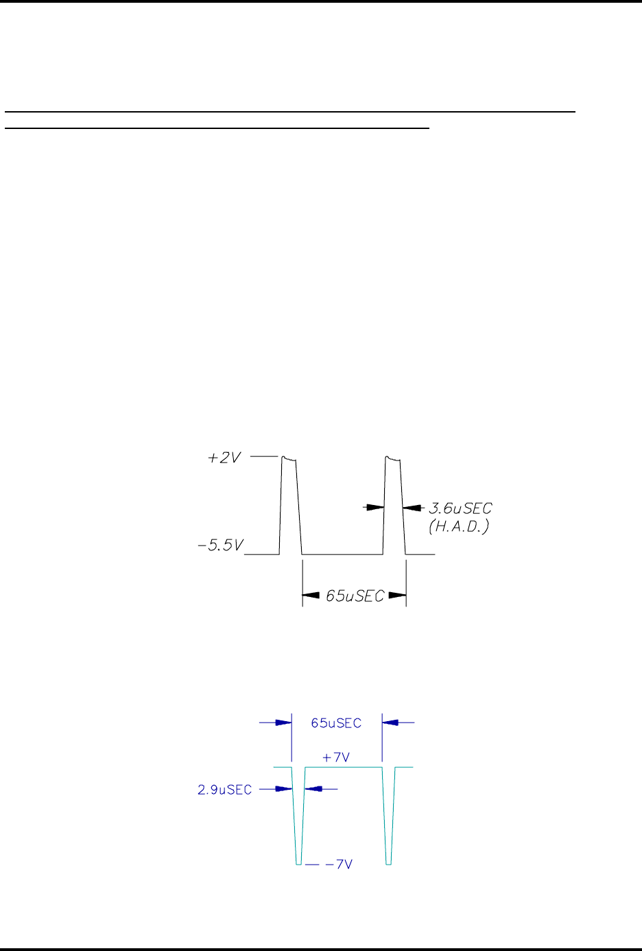
waveform as shown in Figure 4-1.
Figure 4-1. Steady Waveform Obtained When R76 is Adjusted
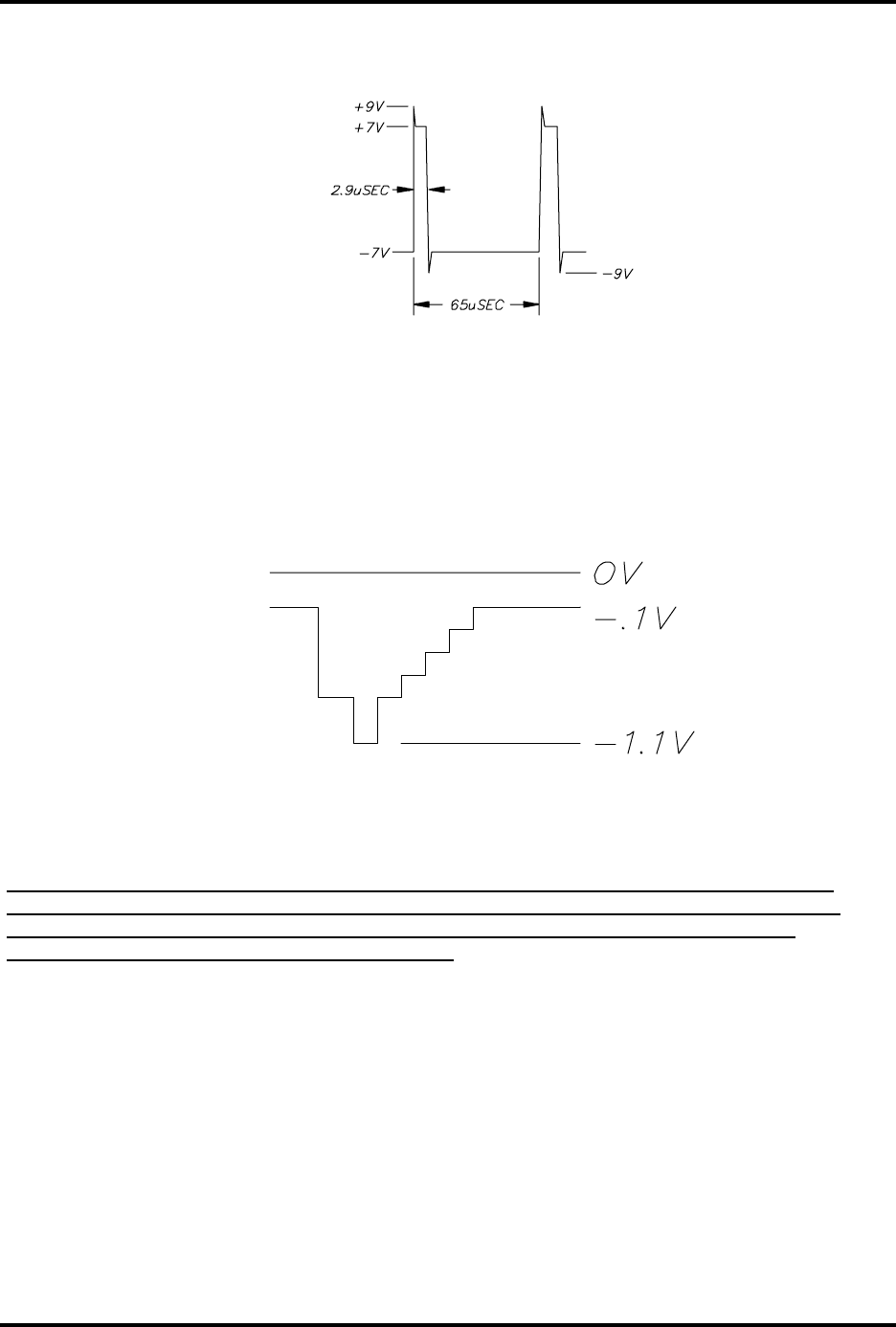
Monitor pin 9 of IC U9 with an oscilloscope. The waveform shown in Figure 4-2 should
be observed.
Figure 4-2. Waveform Observed When Pin 9 of IC U9 is Monitored
3-kW UHF Transmitter Chapter 4, Detailed Alignment Procedures
835-3, Rev. 0 4-3
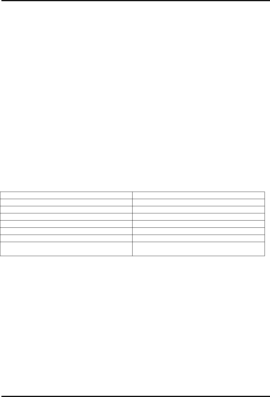
Monitor pin 13 of IC U6 (or TP7 on Revision 1 or later boards) with an oscilloscope. The
waveform shown in Figure 4-3 should be observed.
Figure 4-3. Waveform Observed When Pin 13 of IC U6 is Monitored
Restore the input video level to 1 Vpk-pk.
Monitor TP5 (on Revision 1 or later boards) or pin 2 of J7 (terminated into 75 ohms)
with an oscilloscope. Adjust pot R105, manual bias, for a blanking level of -0.8 VDC. The
waveform shown in Figure 4-4 should be observed. Move jumper W5 on J11 to the
clamp enable position (towards the bottom of the board). Adjust pot R95, clamp bias, for
a blanking level of -0.8 VDC. Again, the waveform in Figure 4-4 should be observed.
Figure 4-4. Waveform Observed When An Adjustment is Made
for a Blanking Level of –0.8 VDC
Note: The waveform in Figure 4-4 represents the theoretical level for proper
modulation depth. The second step below explains how to set the modulation
depth by the use of a television demodulator or a zero-spanned spectrum
analyzer tuned to the visual IF frequency.
Connect the oscilloscope to the lead of L4 that is closest to C32 and adjust the color
notch subcarrier trap, C32, until the 3.58-MHz color burst is nulled.
Check the ratio of sync to video (0.286 volts of sync for a 1 Vpk-pk total video signal). If
necessary, adjust R43, the sync stretch cut-in (on Revision 6 or later boards, also adjust
R176, the sync stretch magnitude) for the proper sync ratio. Re-adjust R15, the video
gain pot, as described above, to maintain a 1 Vpk-pk video signal.
To construct the test setup for the adjustment of the depth of modulation and ICPM at
IF:
• Remove the cable on J18 and connect the double sideband 45.75-MHz visual IF
signal from J18 to a 10-dB splitter/coupler. Connect the coupled port of the

3-kW UHF Transmitter Chapter 4, Detailed Alignment Procedures
835-3, Rev. 0 4-4
splitter/coupler to the RF input of a television demodulator. Connect the direct port
to a spectrum analyzer.
• Connect the 75-ohm video output of the demodulator to the video input of a
waveform monitor. For ICPM measurements, also connect the quadrature output of
the demodulator to the horizontal input of the waveform monitor using a 250-kHz
low pass filter (an oscilloscope can be used in place of a waveform monitor).
• Set the controls of the demodulator to the following:
Detector mode – Cont
Sound Trap – In
Zero Carrier – On
Auto – Sync
Audio Source – Split
De-emphasis – In
Move jumper W5 on J11 to the clamp disable position. Re-adjust pot R105, manual bias,
for the correct depth of modulation by observing the demodulated waveform on the
waveform monitor or on the spectrum analyzer set to zero span.
Move jumper W5 on J11 to the clamp enable position. Re-adjust pot R95, the clamp
bias, for the correct depth of modulation.
Set the waveform monitor to display ICPM. Preset R143 fully clockwise (CW) and adjust
C65 for the greatest effect at white on the ICPM display. Adjust R143 for minimum
ICPM.
Recheck the depth of modulation and adjust R95, clamp bias, if necessary.
Remove the video input signal. Alternately, turn the front panel meter switch between
the video and sync positions and adjust blanking pot R49 for a reading of zero on both
positions on the front panel meter.
Replace the input video test signal (the 5-step staircase). While monitoring the front
panel meter in the sync position, adjust R19 on the transmitter control board (1227-
1209) for a reading of 40 (4 on the 0 to 10 scale). Turn the front panel meter to the
video position and adjust R20 on the transmitter control board for a reading of 100 (10
on the 0 to 10 scale).
Place jumper W2 on jack J4 to the AGC enable position. Adjust R60, the sync level, for
the proper depth of modulation in the AGC mode. Return jumper W2 on jack J4 to the
AGC disable position.
Note: Use the AGC mode only if the incoming program video level cannot be
properly maintained.
Reconnect the plug to J18 and move the spectrum analyzer test cable to 41.25 IF output
jack J16. Tune C56 and L10 to L13 to maximize the 41.25-MHz aural IF signal and
minimize the out-of-band products.
Reconnect the plug to J16 and move the spectrum analyzer test cable to IF output jack
J20. Preset R150, the visual IF gain pot, to the middle of the range. Insert a multiburst
test signal into the transmitter and observe the visual frequency response with the

3-kW UHF Transmitter Chapter 4, Detailed Alignment Procedures
835-3, Rev. 0 4-5
spectrum analyzer set at 1 dB/division. Tune R153 and C77, the IF frequency response
adjustments, for a flat-frequency response (±0.5 dB).
While still monitoring J20 with a spectrum analyzer, re-adjust R150, visual IF gain, for a
0-dbm visual output level. Adjust R127, A/V ratio, for a –13-dB aural-to-visual ratio or
to the required A/V ratio. Reconnect the plug to J20.
Using an input video test signal (the 5-step staircase) with 100-IRE white level, monitor
TP5 or video sample jack J7, pin 2, with an oscilloscope. Set control R31, the sync clip,
just below the point where sync clipping begins to occur. Similarly, set R28, the white
clip, to the point just below where the white video begins to clip.
Note: This procedure should be checked after system setup or if linearity problems
occur.
4.1.4 (A4) Aural IF Synthesizer Board (1227-1205; Appendix B)
To set up the test equipment for this board, begin by connecting the 600-ohm balanced
audio output from an audio oscillator to the balanced audio input jack of the transmitter,
J4-2 (+), J4-3 (-), and J4-1 (ground), on the A/V input and remote interface assembly
of the transmitter.
Connect the aural IF output at J16 on the clamp modulator board to the input of an IF
splitter. Connect one output of the splitter to the video demodulator and the other
output to the spectrum analyzer.
Connect a short cable at the front of the demodulator from the RF out jack to the IF in
jack.
Connect a cable from the 600-ohm audio output jack of the demodulator to the input of
an audio distortion analyzer.
Set the output frequency of the audio oscillator to 400 Hz and the output level to +10
dBm.
Center the aural carrier on the spectrum analyzer with the spectrum analyzer set to the
following:
Frequency/Division – 10 kHz
Resolution bandwidth – 3 kHz
Time/Division – 50 msec
Trigger – Free run
Adjust L5 for approximately +3.5 VDC on the cathode of CR17. The green LED DS1
should be illuminated, indicating a locked condition. If not, re-tune L5 for a locked
condition.
Adjust R13 on the aural IF synthesizer board for ±25-kHz deviation.
Check the distortion on the aural distortion analyzer (S/B =< 0.5%).
Disconnect the 600-ohm balanced audio input to the tray. Connect a 75-ohm stereo
audio input (400 Hz at 1 Vpk-pk) to composite audio input jack J6 on the A/V input and
interface assembly. Follow the procedure in the stereo generator instruction manual for

3-kW UHF Transmitter Chapter 4, Detailed Alignment Procedures
835-3, Rev. 0 4-6
matching the level of the generator to the exciter. R17 adjusts the composite audio
gain.
Check the distortion level on the distortion analyzer (S/B =< 0.5%).
4.1.5 (A8) ALC Board (1227-1207; Appendix B) (Part 1 of 2)
The following explains the meaning of each LED on (A8) the ALC Board when they are
illuminated:
• DS1 - Indicates that an abnormally low IF signal level is present at IF input
connector J1
• DS2 - Indicates that the ALC circuit is unable to maintain the signal level requested
by the ALC reference; this is usually due to excessive attenuation in the linearity or
the IF phase corrector signal path, or switch S1 is in the Manual Gain mode
• DS3 - Indicates a video fault
• DS4 - Indicates that a Mute command is present
To align the ALC board, preset the following controls in the UHF exciter tray:
• ALC Board – To disable linearity correctors: jumper W1 on J4 to Disable mode
(towards the bottom of the board); for manual gain control: jumper W3 on J6 to
Manual mode (towards the top of the board); R87, the manual gain pot, adjusted to
mid-range
• IF Phase Corrector Board – W2 on J9 in phase correction enable; W3 on J10 in
amplitude correction disable
The combined IF output of the clamp modulator board is cabled to jack J1 of the ALC
board. Remove J1 from the board, and look to see that DS1, the Input Fault LED, is
illuminated. Reconnect J1 and check to see that DS1 is extinguished.
Jumper W3 on J6 should be in the Manual position (towards the top of the board).
Monitor jack J3, IF output, with a spectrum analyzer and adjust R87 for approximately a
–20-dBm level.
With a multiburst video signal present, tune C4 for a flat-frequency response of
±0.5 dB.
Before proceeding with the second part of the ALC board alignment, check the IF phase
corrector board to make sure that it is functioning properly.
4.1.6 (A9) IF Phase Corrector Board (1227-1250; Appendix B)
Refer to the alignment procedure for the setup of the IF phase corrector board.
The IF input jack of the IF phase corrector board is fed from J3, the IF output jack of
(A8) the ALC board. The IF output jack is fed to J7, the IF input jack of the ALC board.
4.1.7 (A8) ALC Board (1227-1207; Appendix B) (Part 2 of 2)

3-kW UHF Transmitter Chapter 4, Detailed Alignment Procedures
835-3, Rev. 0 4-7
Input a multiburst video test signal. Remove the plug from J8 and connect a spectrum
analyzer. Tune C63 for a flat-frequency response of ±0.5 dB. Reconnect the plug to J8.
Move the Operate/Standby switch on the front panel to the Operate position.
Place jumper W3 on jack J6 in the Manual mode (towards the top of the board) and
adjust R87 for 0.8 volts at J19, pin 2, or at TP4.
Place jumper W3 on J6 in the Auto mode (towards the bottom of the board) and adjust
front panel power adjust control A20 fully CW. If the optional remote power raise/lower
kit is present, adjust switch S1 on the board to maximum voltage at J19, pin 2, or at
TP4. Adjust R74, the range adjust, for 1 volt at TP4.
Adjust front panel power adjust control A20 for 0.8 VDC at J19, pin 2, or at TP4. If the
optional remote power raise/lower kit is present, adjust switch S1 on the board to the
mid-range of its travel. Adjust front panel power adjust control A20 for 0.8 VDC at TP4.
Disconnect the plug that is now on J12 (IF output) and monitor it with a spectrum
analyzer. Verify an output of approximately 0 dBm. Adjust R99, if needed, to increase
the output level. Reconnect the plug on J12.
Move W2 on J5 to the cutback enable position (towards the bottom of the board).
Remove the input video signal and verify that the transmitter output drops to 25%.
Adjust R71, the cutback level, if necessary. Restore the input video.
Note: The following step affects the response of the entire transmitter.
Connect a video sweep signal to the input of the transmitter. Monitor the output of the
system with a spectrum analyzer. Adjust C71 with R103 and C72 with R106, as needed,
to flatten the response. C71 and C72 adjust for the frequency of the correction notch
being applied to the visual response of the transmitter. R103 and R106 are used to
adjust the depth and width of the correction notch.
Refer to the alignment procedures for the setup of the linearity correctors. Controls
R13, R18, and R23, the magnitude controls, should be set fully CW. Controls R34, R37,
and R40 are the linearity cut-in adjustments.
4.1.8 (A11-A1) UHF Upconverter Board (1227-1237; Appendix B)
This board is mounted in (A11) a UHF upconverter enclosure assembly (1227-1238).
R10 is a gain control that is adjusted to give an approximately +17-dBm output at J5 of
the board.
4.1.9 (A14-A1) Channel Oscillator Board (1145-1201; Appendix B)
This board is mounted in (A14) the channel oscillator assembly (1145-1202).
To align this board, begin by connecting the main output of the channel oscillator, J1, to
a spectrum analyzer, tuned to the crystal frequency, and peak the tuning capacitors C6
and C18 for maximum output. Tune L2 and L4 for maximum output. The output level
should be about +5 dBm. The channel oscillator should maintain an oven temperature of
50° C.

3-kW UHF Transmitter Chapter 4, Detailed Alignment Procedures
835-3, Rev. 0 4-8
If a spectrum analyzer is not available, connect a digital voltmeter (DVM) to TP1 on the
x8 multiplier board. Tune capacitors C6 and C18 for maximum voltage and then also
tune L2 and L4 for maximum voltage output at TP1.
Connect the sample output of the channel oscillator, J2 to a suitable counter and tune
C11, coarse adjust, and C9, fine adjust, to the crystal frequency.
Note: Do not re-peak C6, C18, L2, or L4 because this may change the output
level.
Note: While adjusting C9 and C11 to the crystal frequency, the peak voltage
monitored at TP1 of the x8 multiplier board should not decrease. If a decrease
does occur, there may be a problem with the crystal. Contact ADC Field Support
for further instructions.
Note: If the VCXO board (1145-1204) in the VCXO assembly (1145-1206) is
used, C9, the fine-frequency adjust, is not located on the VCXO board, but on
the FSK identifier board by using R18.
Reconnect the main output, J1, of the channel oscillator to the input, J1, of the x8
multiplier board.
4.1.10 (A15-A1) x8 Multiplier Board (1227-1002; Appendix B)
This board is mounted in a x8 multiplier enclosure assembly (1227-1240).
During normal operation, the green LED DS1, which can be seen through the access
hole in the enclosure assembly, will be lit to indicate that the LO is present at the output
of the x8 multiplier board.
To align this board, connect a spectrum analyzer to the output jack, J2, of the board.
Tune C4, C6, C10, C12, C18, and C20 for maximum output. Readjust all of the
capacitors to minimize the seventh and the ninth harmonics; they should be at least -30
dB down
without affecting the x8 multiplier output.
If a spectrum analyzer is not available, a DC voltmeter can be used, but the harmonic
frequencies must be minimized to prevent interference with other channels.
While monitoring each test point with a DC voltmeter, maximize each test point by
tuning the broadband multipliers in the following sequence:
• Monitor TP1 with a DVM and tune C4 for maximum (typically 0.6 VDC)
• Monitor TP2 and tune C6 and C10 for maximum (typically 1.2 VDC)
• Monitor TP3 and tune C12 and C18 for maximum (typically 2.0 VDC)
• Monitor TP4 and tune C20 for maximum
• Re-peak C12 and C10 while monitoring TP4 (typically 3.5 VDC)
• The typical output level is +15 dBm.
4.1.11 (A19-A1) Visual/Aural Metering Board (1227-1202; Appendix B)
This board is mounted in a visual/aural metering enclosure assembly (1227-1212).

3-kW UHF Transmitter Chapter 4, Detailed Alignment Procedures
835-3, Rev. 0 4-9
The board is adjusted to give a peak-detected output indication to the front panel meter
for combined output, visual-only output, aural-only output, and reflected output. The
board should need no adjustments to achieve normal operation.
4.1.12 (A3-A2) +12-VDC(4A)/-12-VDC(1A) Power Supply Board (1227-1203;
Appendix B)
This board is mounted in (A3) the +12V(4A)/-12V(1A) power supply assembly (1227-
1210).
The board has no adjustments.
DS1 will be lit if a +12-VDC output is connected to J2. DS2 will be lit if a +12-VDC
output is connected to J3. DS3 will be lit if a +12-VDC output is connected to J4. DS4
will be lit if a +12-VDC output is connected to J5. DS5 will be lit if a –12-VDC output is
connected to J6.
4.2 (A1, A2, A3, A4, A5, and A6) 600-Watt UHF Amplifier Trays (1227-1300;
Appendix A)
The trays have been adjusted at the factory to meet all specifications, including phase
adjustment with other 600-watt amplifier trays, and should not need to be adjusted to
attain normal operation. During adjustments of the amplifier boards, switch S1 on the
amplifier control board should be in the Manual Gain position. The output voltage from
(A12) the switching power supply should be adjusted for +29.5 VDC.
4.2.1 (A1) UHF Filter (1007-1101; Appendix B)
Apply a multiburst test signal to the transmitter. Monitor J2 with a spectrum analyzer
and tune C1 and C3 for peak output with a flat-frequency response.
4.2.2 (A2-A1) Variable Gain/Phase Board (1227-1330; Appendix B)
This board is mounted in the variable gain/phase enclosure (1227-1331).
There are no adjustments to this board; it has an adjustable gain of 0 to 20 dB.
4.2.3 (A3-A1) 1-WatT UHF Amplifier Board (1227-1303; Appendix B)
This board is mounted in the 1-watt amplifier enclosure (1227-1319).
The board has approximately 10 dB of gain and has no adjustments.
4.2.4 (A4-A1) Dual Stage Amplifier Board, Class A (1227-1305; Appendix B)
This board is part of the dual stage amplifier assembly, class A (1227-1340). The board
operates class A and has a gain of approximately 11 dB.
The biases of the transistors are set by the on-board biasing circuits. Adjust R106 and
R206 for 3 amps of idle current, no RF drive applied. Connect a voltage meter across E1
and E2 on the amplifier protection board. Move switch S1 to the I2 position and adjust
R106 for a reading of 30 mV. Move switch S1 to the I1 position and adjust R206 for a
reading of 30 mV.

3-kW UHF Transmitter Chapter 4, Detailed Alignment Procedures
835-3, Rev. 0 4-10
Connect a sweep test signal to J1, the RF input jack of the 600-watt amplifier tray and
monitor the output of the board at J2 with a padded-input spectrum analyzer. Tune
capacitors C104 and C204 for peak output and then tune C106 and C206 for peak
output power with a flat-frequency response at J2.
4.2.5 (A4-A2) Coupler Board Assembly (1227-1316; Appendix B)
There are no adjustments to this board.
4.2.6 (A4-A3) Dual Stage Amplifier Board, Class AB (1227-1301; Appendix B)
This board is part of the dual stage amplifier assembly, class AB (1227-1339).
This board operates class AB and has a gain of approximately 9 dB. The biases of the
transistors are set by the on-board biasing circuits. Adjust R106 and R206 for 100
milliamps of idle current per side, no RF drive applied. Connect a voltage meter across
E1 and E2 on the amplifier protection board. Move switch S1 to the I4 position and
adjust R106 for a reading of 1.0 mV. Move switch S1 to the I3 position and adjust R206
for a reading of 1.0 mV.
Connect a sweep test signal to J1, the RF input jack of the 600-watt amplifier tray, and
monitor the output of the board at J2 with a padded-input spectrum analyzer. Tune
capacitors C104 and C204 for peak output and then tune C106 and C206 for peak
output with a flat-frequency response and minimum current at J2.
4.2.7 (A5-A1) 4-Way Splitter Board (1227-1312; Appendix B)
There are no adjustments to this board.
Monitor the output of the tray at J2 with a padded-input spectrum analyzer.
4.2.8 (A5-A2, A5-A3, A5-A4, and A5-A5) Dual Stage Amplifier Boards, Class AB
(1227-1301; Appendix B)
Each of these boards is part of a dual stage amplifier assembly, class AB (1227-1339).
These boards operate class AB and have a gain of approximately 9 dB. The idling
currents for each of the transistors are set to 250 mA.
To adjust the idling currents, no RF applied to the tray, of the devices on the (A5-A2)
amplifier board, connect a voltage meter across E1 and E2 on the amplifier protection
board and switch S1 to the I6 position. Adjust R106 for a reading of 2.5 mV. Move
switch S1 to the I5 position and adjust R206 for a reading of 2.5 mV.
Connect a sweep test signal to J1, the RF input jack of the 600-watt amplifier tray. On
the (A5-A2) amplifier board, tune capacitors C104 and C204 for peak output power.
Tune C106 and C206 for peak output power with a flat-frequency response and
minimum current.
To adjust the idling currents, no RF applied to the tray, of the devices on the (A5-A3)
amplifier board, connect a voltage meter across E1 and E2 on the amplifier protection
board. Move switch S1 to the I8 position and adjust R106 for a reading of 2.5 mV. Move
switch S1 to the I7 position and adjust R206 for a reading of 2.5 mV.
Connect a sweep test signal to J1, the RF input jack of the 600-watt amplifier tray. On

3-kW UHF Transmitter Chapter 4, Detailed Alignment Procedures
835-3, Rev. 0 4-11
the (A5-A3) amplifier board, tune capacitors C104 and C204 for peak output power.
Tune C106 and C206 for peak output power with a flat-frequency response and
minimum current.
To adjust the idling currents, no RF applied to the tray, of the devices on the (A5-A4)
amplifier board, connect a voltage meter across E1 and E2 on the amplifier protection
board. Move switch S1 to the I10 position and adjust R106 for a reading of 2.5 mV.
Move switch S1 to the I9 position and adjust R206 for a reading of 2.5 mV.
Connect a sweep test signal to J1, the RF input jack of the 600-watt amplifier tray. On
the (A5-A4) amplifier board, tune capacitors C104 and C204 for peak output power.
Tune C106 and C206 for peak output power with a flat-frequency response and
minimum current.
To adjust the idling currents, no RF applied to the tray, of the devices on the (A5-A5)
amplifier board, connect a voltage meter across E1 and E2 on the amplifier protection
board. Move switch S1 to the I12 position and adjust R106 for a reading of 2.5 mV.
Move switch S1 to the I11 position and adjust R206 for a reading of 2.5 mV.
Connect a sweep test signal to J1, the RF input jack of the 600-watt amplifier tray. On
the (A5-A5) amplifier board, tune capacitors C104 and C204 for peak output power.
Tune C106 and C206 for peak output power with a flat-frequency response and
minimum current.
4.2.9 (A5-A6) 4-Way Combiner Board (1227-1311; Appendix B)
There are no adjustments to this board.
4.2.10 (A5-A7) Circulator
The circulator contains no adjustments.
4.2.11 (A6-A1) Dual Peak Detector Board, Single Supply (1227-1333; Appendix
B)
There are no adjustments to this board.
4.2.12 (A7) Amplifier Protection Board (1227-1306; Appendix B)
There are no adjustments to this board. One of the red LEDs, DS1 to DS13, will light if
the fuse associated with it is opened.
4.2.13 (A8) Amplifier Control Board (1227-1308; Appendix B)
To check the operation of the overdrive circuit, increase the gain pot of the 600-watt
amplifier tray to approximately 110%. The Overdrive LED DS2 should light and the
output power should not increase above the 110% level.
4.2.14 Calibration of Output Power and VSWR Cutback
To calibrate the output power and VSWR cutback of the 600-watt amplifier trays, place a
wattmeter and dummy load of at least 600 watts at the output of the tray that is to be
calibrated and switch the front panel meter to the % Output Power position. Preset R16,
manual gain, on (A8) the amplifier control board (1227-1308) fully CCW.

3-kW UHF Transmitter Chapter 4, Detailed Alignment Procedures
835-3, Rev. 0 4-12
Move switch S1 on the amplifier control board to the Manual position. Insert a visual-
only with sync-only test signal to the system and verify 40 IRE units of sync. Adjust R16
for 360 watts on the wattmeter. Monitor a sample of the output with a spectrum
analyzer set to the zero-span position and adjust the spectrum analyzer so that the
level of the output is at the top line of the gaticule. Insert -13 dB of aural to the visual
sync-only test signal and adjust R16 for the same visual-only input reference level on
the spectrum analyzer. The output power on the wattmeter should be approximately
450-watts visual +/-13-dB aural. Calibrate the front panel output power meter to 100%
with R2, forward calibration, on the amplifier control board.
Reduce manual gain pot R16 to a 50% reading on the front panel meter in the %
Output Power position. Turn the tray off. Remove the load from the output of the tray
and switch the front panel meter to the Reflected Output Power position. Switch the tray
on. Adjust reflected power adjust pot R22, on the amplifier control board, for a 50%
reading. Then adjust R29, the VSWR threshold cutback pot on the amplifier control
board, until the VSWR Cutback LED DS1 on the front panel just lights. This sets up the
VSWR cutback circuitry.
After the setup is completed, move switch S1 on the amplifier control board to the
Automatic Gain Control position; this is the normal operating position for the switch.
This completes the alignment procedures for the 600-watt UHF amplifier tray. The tray
is now aligned, calibrated, and ready for normal operation.
4.3 Alignment of (A9) the Bandpass Filter and (A10) the Output Trap Filter
The (A9) bandpass filter (A9) and (A10) the output trap filter are tuned to reject
unwanted distortion products generated when the signals are diplexed and also during
the amplification process. The bandpass filter is factory tuned to the proper bandwidth
and should not need to be re-tuned. Please consult the ADC Field Support Department
before tuning the filters.
The traps on the output trap filter are labeled with their center frequency relative to the
frequency of the carrier (for example, the traps labeled -4.5 MHz are tuned for a center
frequency of 4.5 MHz lower than the frequency of the visual carrier).
The trap sections are reflective notches that can be adjusted across the entire UHF
frequency band. The electrical length of the outer sleeve and the center rod of the notch
can be adjusted to tune the notch frequency. The depth of the notch is set by the gap
between the center conductor of the trap section and the center conductor of the main
line. Tight coupling makes a deep notch, while loose coupling makes a shallow notch.
The trap sections have been factory tuned and should not need major adjustments. The
frequency, relative to the visual carrier, that the trap is tuned to is marked on that trap
section.
Fine tuning of the center frequency of the notches can be accomplished with the tuning
bolts on the side of the filter section. Loosen the nut locking the bolt in place and adjust
the bolt to change the frequency of the notch. Monitor the output of the transmitter
with a spectrum analyzer and null the distortion product with the bolt. Red field is a
good video test signal to use to see the +8.08-MHz product. Tighten the nut when the
tuning is completed. Hold the bolt in place with a screwdriver as the nut is tightened to
prevent it from slipping.
3-kW UHF Transmitter Chapter 4, Detailed Alignment Procedures
835-3, Rev. 0 4-13
For major tuning, such as changing the notch depth or moving the notch frequency
more than 1 MHz, the outer conductor and the center conductor of the trap section must
both be moved. This requires an RF sweep generator to accomplish. Apply the sweep
signal to the input of the trap filter and monitor the output. Loosen the clamp holding
the outer conductor in place and make the length longer to lower the frequency of the
notch or shorter to raise the frequency of the notch. Loosen the center conductor with
an Allen wrench and move it deeper for a lower-frequency notch or out for a higher-
frequency notch.
These adjustments must both be made in order to change the notch frequency; the
effects of these adjustments are shown in Table 4-1. Moving only the center conductor
or the outer conductor will effect the notch depth in addition to the center frequency.
The variable that is being adjusted with this procedure is the length of the center
conductor inside the trap filter. The gap between the trap and the main line should not
be changed. Moving only the inner or the outer conductors by themselves will affect
both the gap and the notch depth.
To effect the notch depth only, both sections will have to be moved. The notch depth is
controlled by the gap between the center conductor and the trap section. This gap also
has an effect on the center frequency. To deepen the notch, shorten the outer conductor
and pull the center conductor out until the notch is back in the same place. Move the
sections in the opposite direction to make a shallow notch.
Table 4-1. Effects of Tuning the Output Trap Filter
ADJUSTMENT EFFECT
Lengthening outer conductor only Notch frequency up, shallower notch
Shortening outer conductor only Notch frequency down, deeper notch
Inserting inner conductor deeper Notch frequency down, deeper notch
Inserting less inner conductor Notch frequency up, shallower notch
Tuning bolt in Notch frequency down
Tuning bolt out Notch frequency up
Moving both inner and outer conductors
to keep the same gap inside Center frequency moves notch stays the
same
After tuning has been completed, tighten the clamp and the Allen screws that hold the
conductors. Use the fine-tuning bolts to bring in the frequency. The final tuning
adjustments should be completed with the transmitter driving the output trap filter for
at least one hour to allow for drift during the warming-up period.
This completes the alignment procedures for the bandpass filter and output trap filter
assembly.