Yuge information technology CLM920 4G LTE Wireless Module User Manual
Shanghai Yuge Information Technology Co., Ltd 4G LTE Wireless Module
User Manual
CLM920
Hardware user guide
1 Introduction
This document is CLM920 Mini PCIE module hardware interface manual, designed to
describe the hardware of CLM920 , component and function characteristics, application
interface definition and user instructions, electrical and mechanical characteristics, etc.,
provide hardware user guide for user application development based on this product.
Abbreviation
ADC Analog-Digital Converter
AFC Automatic Frequency Control
AGC Automatic Gain Control
ARFCN Absolute Radio Frequency Channel Number
B2B Board to Board Connector
BER Bit Error Rate
CDMA Code Division Multiple Access
DAI Digital Audio interface
DAC Digital-to-Analog Converter
DSP Digital Signal Processor
DTR Data Terminal Ready
EFR Enhanced Full Rate
EMC Electromagnetic Compatibility
EMI Electro Magnetic Interference
ESD Electronic Static Discharge
EVDO Evolution Data Only
FR Full Rate
GPRS General Packet Radio Service
HR Half Rate
IMEI International Mobile Equipment Identity
ISO International Standards Organization
PLL Phase Locked Loop
PPP Point-to-point protocol
RAM Random Access Memory
ROM Read-only Memory
RTC Real Time Clock
SMS Short Message Service
UART Universal asynchronous receiver-transmitter
UIM User Identifier Management
USB Universal Serial Bus
VSWR Voltage Standing Wave Ratio

2 Product Summary
2.1
CLM920 is a wireless communication module with PCI Express Mini Card 1.2 standard
interface, support FDD/TDD/UMTS/EDGE/GSM network and Windows 7/Windows8/Windows
10/Android 4.0 or above OS. It can be used for the following scenes:
Vehicle equipment
Wireless POS machine
Wireless advertising/media
Remote monitoring
Intelligent metering
Mobile Broadband
Industrial automation
Other wireless terminal
2.2 Module characteristics
MODEL: CLM920
Chipset:MDM9607
Package type
Mini PCIE
Dimension (mm)
51*30*3.8
FDD-LTE
150M DL
50M UL
@Cat.4
B2
B4
B5
B7
WCDMA
42M DL
5.76M UL
B2
B5
GSM
236Kbps DL/UL
B2
B5
GPS
Analog audio
Optional
Digital audio
USB(2.0 High Speed)/UART/USIM
NDIS/ECM/Gobinet
2.3 Module function
CLM920 includes following circuit units:
Baseband processing unit
Power management unit
Memory unit
RF transceiver unit
RF front-end unit
GPS RF receiving unit
3 Application interface
3.1 Summary
This chapter mainly describes the interface definition and application of this module.
Including the following:
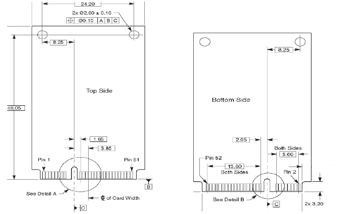
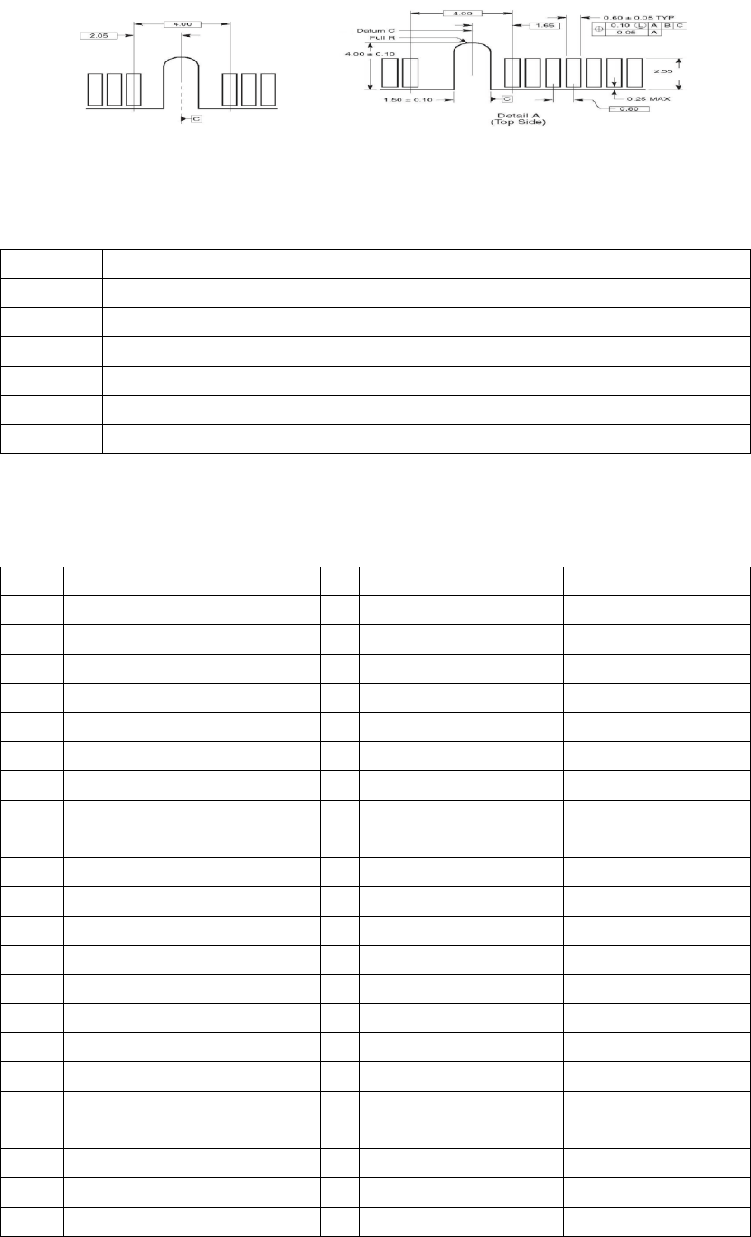
52 PIN gold finger
Interface definition
Power interface
USB interface
USIM interface
UART interface
WWAN interface
PCM/Analog audio interface
RF antenna interface
3.2 Module interface
3.2.1 52 PIN gold finger
3.2.2 Interface definition
Input and output parameter definition
IO
Bidirectional input and output
PI
Power input
PO
Power output
AI
Analog input
AO
Analog output
DI
Digital input
DO
Digital output
PIN definition
PIN
Standard PIN definition
Module PIN definition
IO Function Remarks
1
WAKE#
MIC+
AI
Audio input+
2
3.3Vaux
VBAT
PI Power input
3
COEX1
MIC-
AI Audio input-
4
GND
GND
GND
5
COEX2
SPK+/REC+
AO Audio output+ AT set headset and speaker mode
6
1.5V
UIM_DET
DI SIM Hot plug detection
7
CLKREQ#
SPK-/REC-
AO Audio output- AT set headset and speaker mode
8
UIM_PWR
UIM_PWR
PO SIM power
9
GND
GND
GND
10
UIM_DATA
UIM_DATA
IO SIM data signal
11
REFCLK-
UART_RX
DI UART receiving
12
UIM_CLK
UIM_CLK
DO SIM clock signal
13
REFCLK+
UART_TX
DO UART sending
14
UIM_RESET
UIM_RESET
DO SIM reset signal
15
GND
GND
GND
16
UIM_VPP
NC
17
RESERVED
VDD_EXT
PO 1.8V power output
18
GND
GND
GND
19
RESERVED
WAKEUP_IN
DI Sleep mode controlling
20
W_DISABLE#
RESERVED
RESERVED
21
GND
GND
GND
22
PERST#
RESET
DI Reset controlling Low level effective

23
PERn0
UART_CTS
DI UART sending clear
24
3.3Vaux
VBAT
PI Power input
25
PERp0
UART_RTS
DO UART requests sending
26
GND
GND
GND
27
GND
GND
GND
28
1.5V
ONOFF
AI Power on Low level effective
29
GND
GND
GND
30
SMB_CLK
NC
31
PETn0
NC
32
SMB_DATA
WAKEUP_OUT
DO Module wakeup host
33
PETp0
NC
34
GND
GND
GND
35
GND
GND
GND
36
USB_D-
USB_DM
IO USB differential signal-
37
GND
GND
GND
38
USB_D+
USB_DP
IO USB differential signal+
39
3.3Vaux
VBAT
PI Power input
40
GND
GND
GND
41
3.3Vaux
VBAT
PI Power input
42
LED_WWAN#
LED_WWAN
OC LED indicator
43
GND
GND
GND
44
LED_WLAN#
UIM_DET
DI
SIM Hot plug detection
45
RESERVED
PCM_CLK
DO PCM Clock pulse
46
LED_WPAN#
LED
OC LED indicator
47
RESERVED
PCM_DOUT
DO PCM sending data
48
1.5V
NC
49
RESERVED
PCM_DIN
DI PCM receiving data
50
GND
GND
GND
51
RESERVED
PCM_SYNC
DO PCM Frame synchronization signal
52
3.3Vaux
VBAT
PI Power input
NOTE:
The IO interface level of module is 1.8V (SIM interface level supports 1.8V and 3.3V)
The RESEVERED and NC PIN is suspended
3.3 Power interface
The power interface includes two parts:
VBAT for module power supply
USIM_PWR for SIM power supply
Power PIN definition
PIN
Name
I/0
Definition Min Voltage Typical Voltage Max Voltage
2/24/39/41/52
VBAT
PI
Module power 3.3 3.7 4.2
8
UIM_PWR
PO
SIM power 0 1.8/2.85 1.98/3.3
4/9/15/18/21/26/27/29/34
/35/37/40/43/50
GND
PI
GND 0
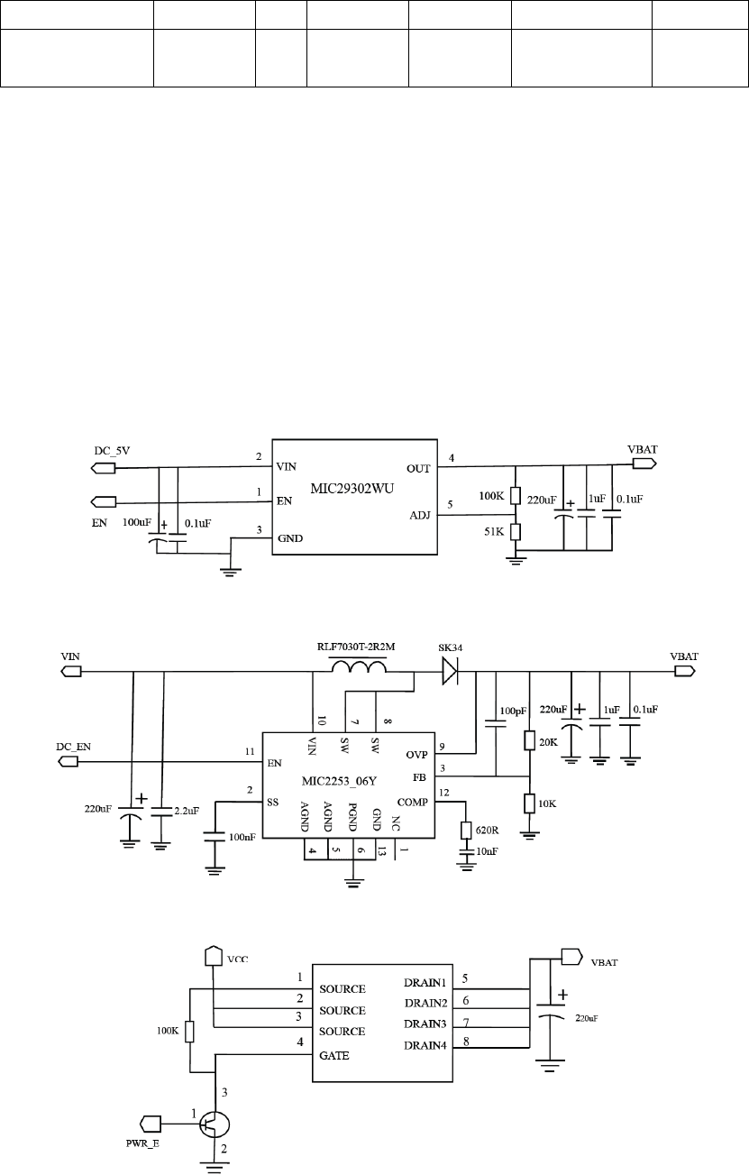
The module uses a single power supply mode, the module provides 5-way power supply pin,
14-way ground pin to ensure the module’s normal operation, all power and ground pins should
be connected and get in use. The module power supply range is 3.3 - 4.2V, and it is
recommended to use 3.7V/2A power supply. Module in the transmission of data or instant call
will produce more than 2A peak current and it’s resulting in a larger power supply ripple, so the
customer’s circuit design of power line should be as short as possible and wide enough. It is
recommended to reserve a 220uF capacitors near the power input. It is recommended that
customers can use DCDC or LDO
to provide enough current. Then the VBAT is controlled by the MOS tube so that the module
can be completely switched off.
LDO Reference power circuit
DCDC Reference power circuit
MOS tube control power switch reference circuit
NOTE:
In order to prevent the damage of the module caused by surge and overvoltage, it is
suggested that a 5.1V/500mW zener diode to be connected on the module VBAT pin.
It is suggested that 3 ceramic capacitors (33pF, 10pF, 100nF) to be added to the VBAT pin
and to be placed close to the VBAT pin.
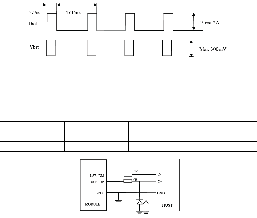
The minimum operating voltage of the module is 3.3V, because the transmission data or
GSM call will produce more than 2A current, resulting in the power supply voltage ripple
voltage drop, so the power supply voltage shall not be less than 3.3V.
GSM TDMA burst current supply voltage drop
3.4 USB port
The module USB port supports USB2.0 high-speed protocol, supports slave device mode, and
does not support USB charging mode. The USB input / output routing needs to follow the
USB2.0 characteristic, and the USB interface is defined as follows:
PIN
Signal IO Description
36
USB_D-
IO
USB differential signal-
38
USB_D+ IO USB differential signal+
Circuit diagram of USB connection
NOTE:
USB routing design needs to strictly comply with the requirements of the USB2.0 protocol,
note the protection of the data line, differential line, controlling impedance for the line is 90
ohm. The ESD protection device should be added on the data line, and the equivalent
capacitance value of the ESD protection device is less than 1pF.
The power supply voltage of the USB bus is provided inside the module without external
supply. At the same time, the USB bus is not provided power. Because of the power of
module can only be used as slave device of USB bus.
USB port supports following functions:
Software download and update
Data communication
AT command
3.5 UART port
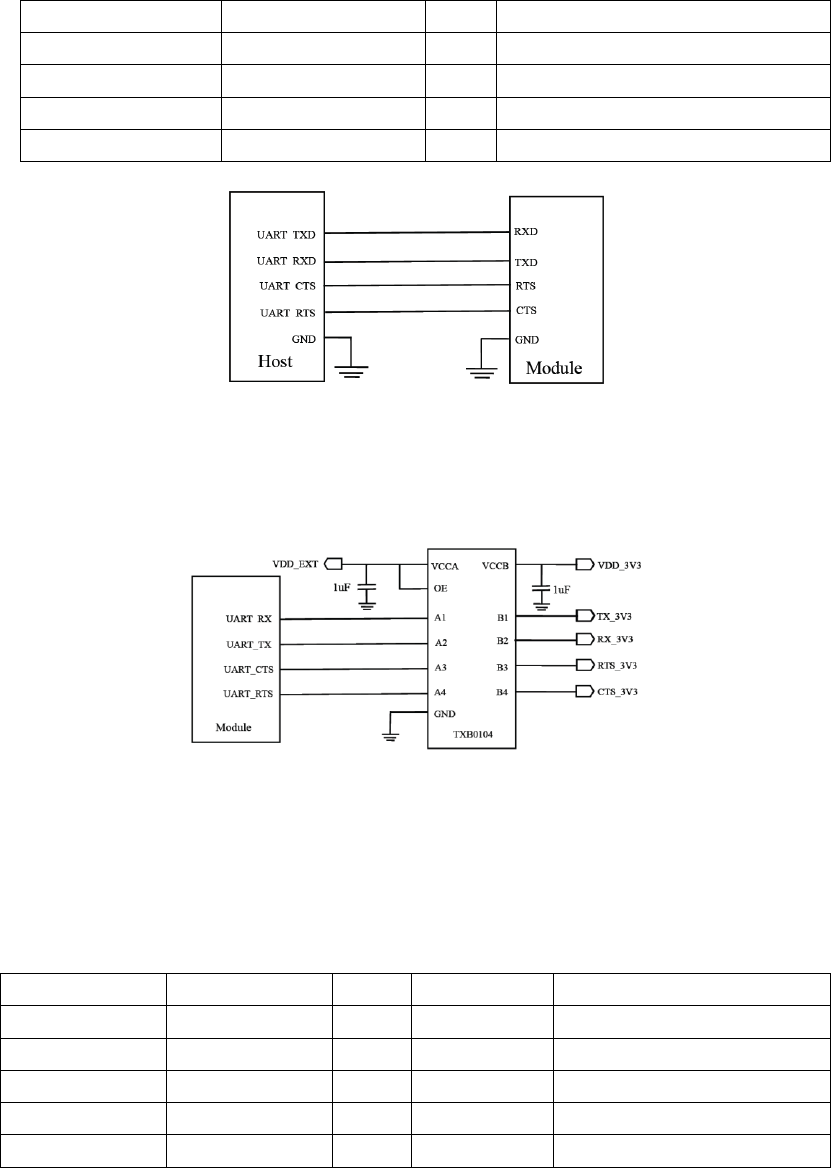
The module provides a UART port, the serial port level is 1.8V. The AT command can be sent
through the serial port, print program log information, etc. The module serial port supports
9600/19200/38400/57600/115200/230400bps baud rate and defaults is 115200bps.
PIN
Signal
I/O Definition
11
UART_RX
DI Sending data
13
UART_TX
DO Receiving data
23
UART_CTS
DI User enable module sending
25
UART_RTS
DO Module requests the user to send
UART port design
Module serial port level is 1.8V, if the serial port needs to be connected with the MCU of 3.3V
level, it is necessary to add a level conversion chip to realize the matching, chip connection can
refer to the following design:
Level conversion circuit
3.6 USIM interface
The module provides a USIM card interface compatible with the ISO 7816-3 standard, and the
USIM card power supply is internally powered by the module. The source regulator provides
the voltage of 1.8V and 3.0V.
PIN
Signal
I/O High level Definition
6
USIM_DET
DI 1.8V USIM hot plug detection
8
UIM_PWR
PO 1.8V/2.95V USIM power
10
UIM_DATA
IO 1.8V/2.95V USIM data
12
UIM_CLK
DO 1.8V/2.95V USIM clock
14
UIM_RESET
DO 1.8V/2.95V USIM reset
3.6.1 USIM slot design
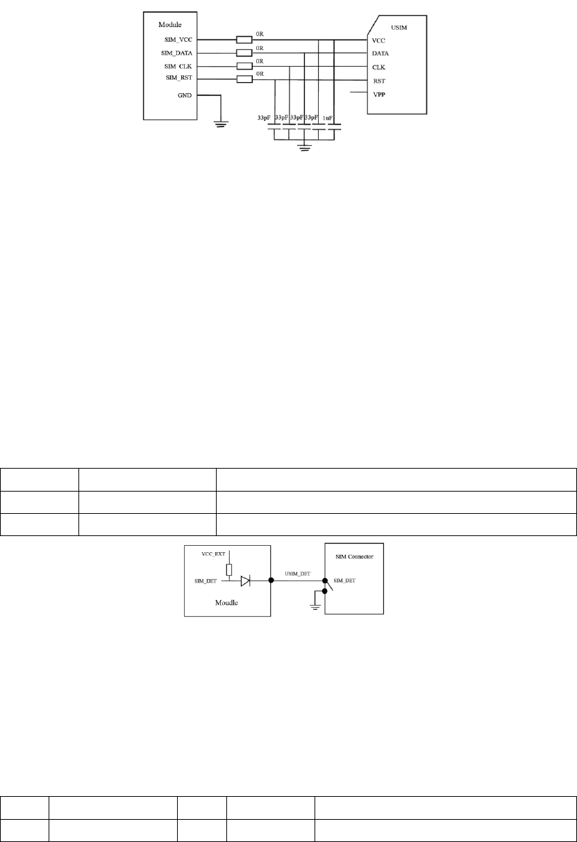
The module does not has USIM slot, users need to design USIM slot on their own interface
board.
USIM interface reference design diagram is as follow:
NOTE:
USIM interface line is recommended to choose ON SEMI SMF15C device to do ESD
protection, USIM card peripheral circuit devices should be close to USIM slot.
The SIM card circuit is susceptible and caused no card. The slot should be placed as far
away from the antenna's RF as possible and keep away from the RF line, VBAT and high
speed signal line.
The internal UIM_DATA has been pulled to the USIM_VCC through the 47K resistor, the
outside does not need to pull-up.
USIM_DET is the detection pins of USIM card to detect whether the USIM inserts or does
not insert, the default is high level. When hot plug, it needs this pin to detect the USIM status.
The USIM card and the module’s GND needs to maintain good connectivity, UIM_CLK
GND should be protected independently.
3.6.2 USIM_DET Hot plug reference design
NO.
USIM_DET status
Definition
1
HIGH
SIM inserted
2
LOW
SIM does not inserted
NOTE:
It is recommended to add a diode protection beside the UIM _DET pin.
When a normally closed SIM or a normally open SIM card is used, the detection function
can be set by the AT command. AT+HOSCFG=1,1 (High level when SIM card is insert)/
AT+HOSCFG=1,0(Low level when SIM card is insert)/ AT+HOSCFG=0.0(Hot plug is
disabled)
3.7 GPIO interface
PIN
Signal
I/O
High level Definition
19
WAKEUP_IN
DI
1.8V Module sleep control
22
RESET
DI
1.8V
Module reset control, low level effective
28
ONOFF
PI
VBAT-0.3V
Low level to power on
32
WAKEUP_OUT
DO
1.8V
Module wakeup host
The module supports sleep wake up function. WAKEUP_IN is the host wakeup module,
WAKEUP_OUT is module wakeup host.
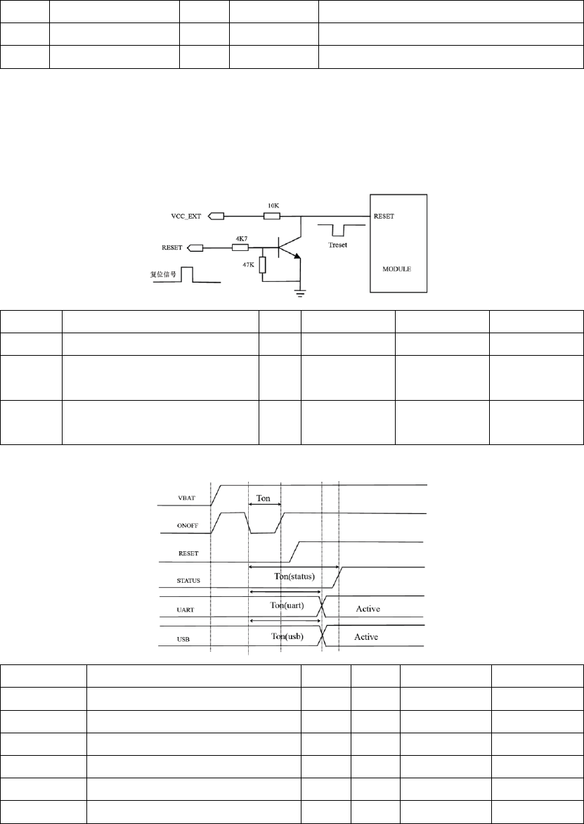
Reset: pull this pin down 150-450ms can reset the module, outside the proposed pull-up resistor
10K to VCC_EXT. in module use of an unusual condition or emergency. RESET pin is sensitive
to interference and should be paid attention to it when design.
Symbol
Description
Min
Type
Max
Unit
Treset
Low level pulse width
50
100
500
ms
VIH
RESET input high level
voltage
1.17
1.8
2.1
V
VIL
RESET input low level
voltage
-0.3
0
0.8
V
ONOFF: Pulling down this pin can power on the module.
Symbol
Description
Min
Type
Max
Unit
Ton
Booting low level wide
100
500
-
ms
Ton(status)
Boot time (judged by status)
22
-
-
ms
Ton(usb)
Boot time (judged by usb)
-
20
-
ms
Ton(uart)
Boot time (judged by uart)
-
20
-
ms
VIH
RESET input high level voltage
0.6
0.8
1.8
V
VIL
RESET input low level voltage
-0.3
0
0.5
V
3.8 Network instruction interface
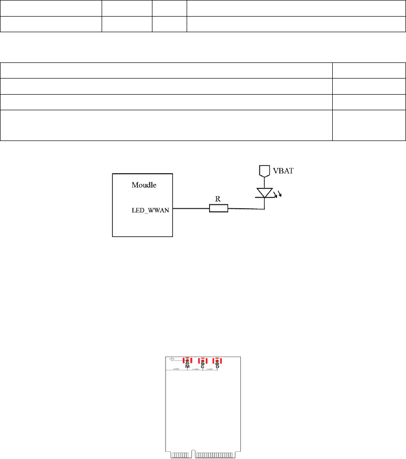
The module provides an open GPIO signal to indicate the radio frequency communication
state.
PIN
PIN NO.
I/O
Description
LED_WWAN
42
PI
Network status indicator
Status
LED display
No service
Always light
Module registration is not 4G network
Double flash
Module registration is 4G network or module registration is not 4G network
into voice, SMS and other services
Flash quickly
NOTE: The brightness of the LED lamp can be adjusted by adjusting the current limiting
resistance, and the maximum current is 40mA.
3.9 RF antenna connector
3.9.1 RF antenna connector position
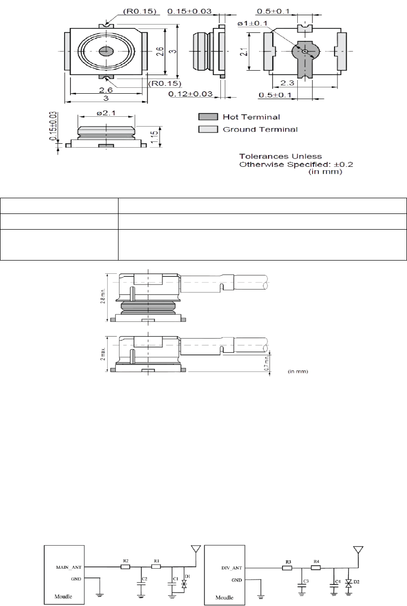
3.9.2 RF antenna connector size
The antenna connector must use a coaxial connector with 50 ohm characteristic
impedance
Murata's MM9329-2700 connector is recommended
Rated condition
environment condition
Frequency range
DC to 6GHZ –40°C to +85°C
Characteristic
impedance
50 Ω –40°C to +85°C
NOTE:
The module provides three channel RF antenna interfaces: main antenna, the diversity
antenna and the GPS antenna (optional). The connection with the antenna must be the line of
50 ohm characteristic impedance.
In practical use, according to the user's circuit board line, the antenna factory can optimize
the matching device parameter value, the motherboard R1/R2/R3/R4 default is stickered 0
Ohm, C1/C2/C3/C4 default is blank stickers, in order to prevent damage to the internal
module of the electrostatic, it is recommended to choose a two-way TVS at the antenna
connection D1/D2.
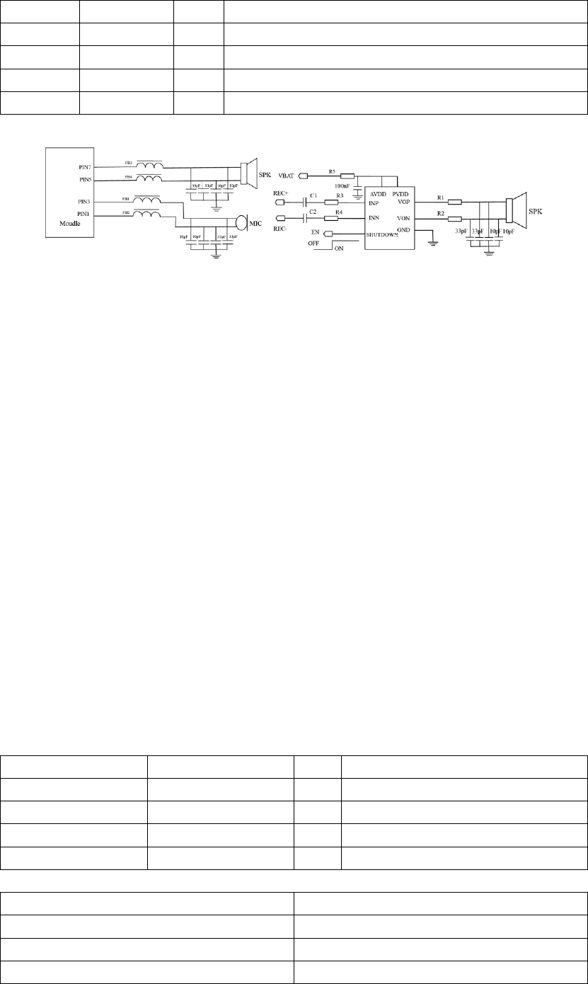
3.10 Analog audio interface
The module provides a set of analog voice interfaces, which consist of one differential input
signal (MIC+/MIC-), one way differential output signal SPK+ (REC+) /SPK- (REC-).
PIN
Signal
I/O
Description
1
MIC+
AI
Audio input+
3
MIC-
AI
Audio input-
5
SPK+/REC+
AO
Audio output+
7
SPK-/REC-
AO
Audio output-
NOTE:
The MIC+/MIC- channel is used as a microphone differential input, and the Mike signal
has the bias voltage needed inside the module without external need. Mike usually uses
electret microphone.
SPK+/SPK- channels are usually used for handles, headphones, or external power
amplifiers. If customers need external audio power amplifiers, they are passed
AT+CSDVC=4 switch to the headphone channel output signal, and then external audio
amplifier amplification signal.
Audio signal is a sensitive signal, it should be far away from the radiation source and
power interface, line as short as possible, and protect sensitive signals.
In order to prevent the TDD noise, the filter capacitor 10pF and 33pF are reserved to
design the audio circuit to remove the RFI signal.
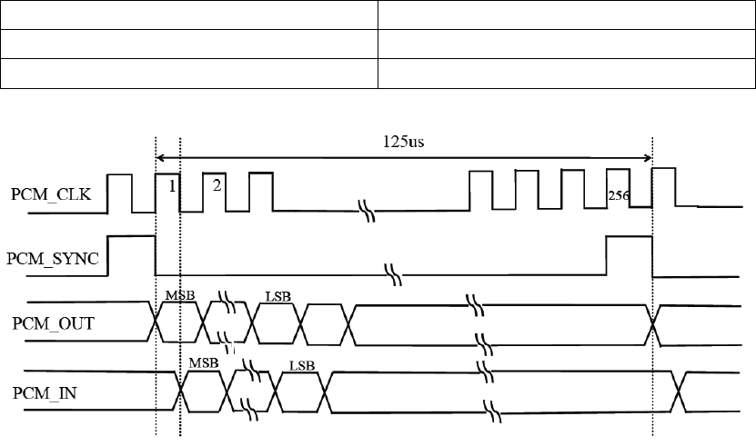
3.11 PCM digital audio
The module provides a set of PCM audio interfaces to support 8 bit A rates, U rates, and
16 bit linear short frame coded lattices. The formula is PCM_SYNC, 8kHZ, PCM_CLK is
2048kHZ.
PIN
Signal
I/O
Description
45
PCM_CLK D0
DO
PCM Clock pulse
47
PCM_DOUT
DO
PCM data output
49
PCM_DIN
DI
PCM data input
51
PCM_SYNC
DO
PCM Frame synchronization signal
Features
Description
Code format
linear
Data bits
16bits
Master-slave mode
Master/slave mode
PCM clock
2048kHz
PCM Frame synchronization signal
Short frame
Data format
MSB
FCC Radiation Exposure Statement:
This equipment complies with FCC radiation exposure limits set forth for an uncontrolled
environment .This equipment should be installed and operated with minimum distance 20cm
between the radiator& your body.
FCC Label Instructions
The outside of final products that contains this module device must display a label referring to the enclosed
module. This exterior label can use wording such as: “Contains Transmitter Module
FCC ID:2AN95-CLM920" or “Contains FCC ID:2AN95-CLM920” Any similar wording that expresses the
same meaning may be used.
Single Modular Approval. Output power is conducted. This device is to be used in mobile or fixed
applications only. Antenna gain including cable loss must not exceed 5.41dBi in GSM850,11.41dBi in
EGPRS850, 2.5dBi in GSM1900, 8.0dBi in EGPRS1900, 10.43dBi in WCDMA Band V, 10.5dBi WCDMA
Band II, 11.0dBi in LTE Band 2, 7.0dBi in LTE Band 4, 11.42dBi in LTE Band 5,10.50dBi in LTE Band 7
for the purpose of satisfying the requirements of CFR 47 2.1043 & 2.1091. The antenna(s) used for this
transmitter must be installed to provide a separation distance of at least 20 cm from all persons and must
not be co-located or operated in conjunction with any antenna or transmitter, except in accordance with
FCC multi-transmitter evaluation procedure. Compliance of this device in all final product configurations is
the responsibility of the Grantee. Installation of this device into specific final products may require the
submission of a Class II permissive change application containing data pertinent to RF Exposure,
spurious emissions, ERP/EIRP, and host/module authentication, or new application if appropriate.