Zebra Technologies 211486030B 21-148603-0B User Manual
Zebra Technologies Corporation 21-148603-0B
Contents
- 1. User Manual
- 2. Host User Guide
- 3. Host User Guide Regulatory
User Manual
148603 Project Document
Copyright 2012 Motorola Solutions, Inc. 20110610-i i
Confidential Material – Disclosure Strictly Prohibited. "Ni ckel Leucochroic Puffin"
Motorola Solutions Inc.
Title:
148603 Specification and Integration Guide
Description/Abstract/Synopsis:
The purpose of this document is to provide an integration guide targeted for
module integrators who have an NDA with Motorola Solutions.
Document Status:
In Progress
A
[ ] – Released Version
MPA Document Number:
[ ] – Next Release In Process
NA
Division:
Sub-team:
[ ] – Document Obsolete
Working Revision:
20110610-i
MCD
RF-SYS
Obsolete Document Replaced By:
Last Updated: 01/18/2012
Document Type:
SPEC / IG
N/A
Confidentiality Statement:
Classification: N/A
[] - Contains Motorola Solutions partner NDA related material (Disclosure requires a three-way
NDA.)
Partner Name
Agreement Number
USI
Under NDA and Motorola Corporate
Supply Agreement between Motorola
Solutions and USI
[] - For Motorola Solutions Internal Use Only
[ x] - Disclosure allowed under Motorola Solutions NDA Only
[x] - Does or may contain Motorola Solutions patentable property
*** Direct this document‟s disclosure inquires to (Job Title):
TNT Archive Location/Path: Agile
Current Owner:
Authors / Contributors:
Revision History

148603 Project Document
Copyright 2012 Motorola Solutions, Inc. 20110610-i ii
Confidential Material – Disclosure Strictly Prohibited. "Ni ckel Leucochroic Puffin"
Rev #
Author
Date
Notes
Supporting or Reference Documentation
MPA or Motorola Solutions
Document Number
Title
Release Signatures Required
Divisional Role
Motorola Solutions Associate
Copyright Information
No part of this document may be reproduced, stored in or introduced into a retrieval system, or
transmitted in any form or by any means (electronic, mechanical, photocopying, recording, or
otherwise) for any purposes, without the express written permission of Motorola Solutions, Inc.
Motorola Solutions, Inc. may have patents, patent applications, trademarks, copyrights, or other
intellectual property rights covering subject matter in this document. Except as expressly
provided in any written license agreement from Motorola Solutions, Inc., the furnishing of this
document does not give you any express or implied rights to these patents, trademarks,
copyrights, or other intellectual property.
© 2011 Motorola Solutions, Incorporated. All rights reserved.

MPA Project Document
Copyright 2012 Motorola Solutions, Inc. 20110610-i 3
Confidential Material – Disclosure Strictly Prohibited. "Ni ckel Leucochroic Puffin"
Table of Contents
1. INTRODUCTION 6
1.1. BACKGROUND 6
1.2. GENERAL NOTE 6
1.3. PURPOSE 6
1.4. PART NUMBERS 6
2. ARCHITECTURE 7
2.1. WLAN 7
2.1.1. HOST COMMUNICATIONS 7
2.2. BLUETOOTH 7
2.3. GPS 9
2.4. POWER SUB-SYSTEM 9
3. SIGNAL DESCRIPTIONS 10
3.1. SIGNAL DESCRIPTIONS 10
3.1. PIN LAYOUT 13
4. DESIGN GUIDELINES AND RECOMMENDATIONS 14
4.1. TYPICAL APPLICATION SCHEMATIC 14
4.2. HOST PCB LAYOUT RECOMMENDATIONS 17
5. HOST REQUIREMENTS 18
5.1. ELECTRICAL POWER 18
5.2. ENVIRONMENTAL 18
5.2.1. ABSOLUTE MAXIMUM RATINGS 18
5.2.2. NORMAL OPERATING CONDITIONS 19
5.4. TIMING REQUIREMENTS 21
5.4.1. POWER UP TIMING 21
5.4.1.1. WLAN 21
5.4.1.2. BT/GPS/FM 21
5.4.2. SDIO TIMING REQUIREMENTS 22
5.4.2.1. SDIO DATA SWITCHING CHARACTERISTICS 22
5.4.2.2. SDIO DATA SWITCHING CHARACTERISTICS 22
5.4.2.3. SDIO SWITCHING CHARACTERISTICS 23
5.5. ANTENNA REQUIREMENTS 24

MPA Project Document
Copyright 2012 Motorola Solutions, Inc. 20110610-i 4
Confidential Material – Disclosure Strictly Prohibited. "Ni ckel Leucochroic Puffin"
5.5.1. WLAN 24
5.5.2. BT 24
5.5.3. GPS 25
6. MODULE SPECIFICATIONS 26
6.1. POWER CONSUMPTION 26
6.1.1. WLAN POWER CONSUMPTION 27
6.1.2. BT POWER CONSUMPTION 28
6.1.3. GPS POWER CONSUMPTION 28
7. APPENDIX 29
7.1. RECOMMENDED HOST PCB PASTEMASK 29
7.2. MECHANICAL INTERFACE DRAWING 30
7.3. REGULATORY 30
7.3.1. CE REGULATIONS 30
7.3.2. FCC REGULATIONS 31
7.3.3. IC REGULATIONS 33
Table of Figures
Figure 1 - Pin Map 13
Figure 2 – TOP VIEW Recommended Option 3) Solid ground beneath the specific
module areas 17
Figure 3 - Recommended host PCB PasteMask 29
Table of Tables
Table 1 - Module Part Numbers and Description ............................................................ 6
Table 2 – Signal Descriptions ........................................................................................ 10
Table 3 - Typical Application Schematic BOM .............................................................. 15
Table 4 - Absolute Maximum Ratings ............................................................................ 18
Table 5 - Normal Operating Conditions ......................................................................... 19
Table 6 - Slow Clock Requirements .............................................................................. 20
Table 7 - SDIO Single Block Read ................................................................................ 22
Table 8 - SDIO Interface Read ...................................................................................... 22
Table 9 - SDIO Single Block Write ................................................................................ 22
Table 10 -SDIO Interface Write ..................................................................................... 22
Table 11 – SDIO Timing ................................................................................................ 23
Table 12 - SDIO Timing ................................................................................................. 23

MPA Project Document
Copyright 2012 Motorola Solutions, Inc. 20110610-i 5
Confidential Material – Disclosure Strictly Prohibited. "Ni ckel Leucochroic Puffin"
Table 13 - WLAN Antenna Requirements ..................................................................... 24
Table 14 - Bluetooth Antenna Requirements ................................................................ 24
Table 15 - GPS Antenna Requirements ........................................................................ 25
Table 16 - Hardware Low Power Mode - Module Shutdown (SDWN) Current Draw ..... 26
Table 17 - BT Power Consumption ............................................................................... 28
Table 18 - GPS Power Consumption ............................................................................ 28

148603 Project Document
148603 Specification and Integration Guide
Copyright 2012 Motorola Solutions, Inc. 20110610-i 6 of 36
Confidential Material – Disclosure Strictly Prohibited. "Ni ckel Leucochroic Puffin"
1. Introduction
1.1. Background
148603 is a radio module that will provide Wireless Local Area Network (WLAN)
Bluetooth, GPS and FM features to Motorola Solutions‟ EMS products.
NOTE: FM is DISABLED in all revisions, and WLAN RF0 Path is not populated in
the -01 and -02 versions.
1.2. General Note
This is a living document. Some descriptions are based on the current phase of the
148603 module design program. Changes to this document will occur without direct
notification to its users. Users who wish to have the latest information should co-
ordinate with the module team leader. The terms “preferred” and “recommend” are
used throughout this document. Preferred can be thought of as a “nice-to-have” or “in-
good practice”. The term “recommendation” should be taken as a stronger
implementation guideline where if not implemented performance degradation may
occur.
1.3. Purpose
The purpose of this document is to provide a guide targeted for module integrators who
have an NDA with Motorola Solutions.
1.4. Part Numbers
Part Number
SKU
21-148603-01
Diversity version with WLAN and BT
on SHARED RF paths
21-148603-02
Diversity version with WLAN and BT
on SEPARETE RF paths
21-148603-03
NON-Diversity version with WLAN and
BT on a SHARED RF path
21-148603-04
NON-Diversity version with WLAN and
BT on SEPARETE RF paths
Table 1 - Module Part Numbers and Description

148603 Project Document
148603 Specification and Integration Guide
Copyright 2012 Motorola Solutions, Inc. 20110610-i 7 of 36
Confidential Material – Disclosure Strictly Prohibited. "Ni ckel Leucochroic Puffin"
2. Architecture
2.1. WLAN
2.1.1. Host Communications
The WLAN core requires a total of eight (8) dedicated signals in order to communicate
to the host processor. The WLAN core is enabled via the WL_EN signal (1) and
communicates to the host processor via SDIO (6) with an additional interrupt signal
WL_IRQ(1).
2.1.1.1. Hardware Interface
The interface between the host and the 148603 Module is a standard SDIO interface
(see SDIO spec version 2.0), supporting maximum clock rate of 52MHz.
The WL1281/3 SDIO also supports the following features:
• Both 1 and 4 bit data bus
• Abort command
• Multi-Block data transfer
• The SDIO interface is used for WLAN IP only.
• The SDIO interface supports High Speed protocol.
2.2. Bluetooth
2.2.1. Host Communications
The Bluetooth subsystem requires nine (9) connections to the host in order for full
operation, including PCM (4), High-Speed UART (4) and BT_GPS_FM_EN (1) , which
shall be connected to the host to enable the Bluetooth IP. It should also be noted that
an additional line from the WL1283 can be used for debug purposes, namely
BT_UART_DBG.
2.2.1.1. Hardware Interface
2.2.1.1.1. HCI UART Transport layers
The HCI UART Supports 4-wire UART interface to host. Supports most baud rates for
all fast clock frequencies, up to a maximum of 4Mbps. Default baud rate after power up
is 115.kkbps with a deviation of +1.5%, -2.5%, until baud is changed via a vendor
specific command.

148603 Project Document
148603 Specification and Integration Guide
Copyright 2012 Motorola Solutions, Inc. 20110610-i 8 of 36
Confidential Material – Disclosure Strictly Prohibited. "Ni ckel Leucochroic Puffin"
o BT_GPS_FM_TX
o BT_GPS_FM_RX
o BT_GPS_FM_RTS
o BT_GPS_FM_CTS
2.2.1.1.2. PCM Audio
PCM audio interface to the host uses the following signals:
In Slave mode, input frequencies up to 16MHz supported. In master mode, the TI1283
can generate any clock frequency between 64KHz and 4.096MHz.
o BT_PCM_OUT
o BT_PCM_IN
o BT_PCM_SYNC
o BT_PCM_CLK
The BT Audio Codec has a fully dedicated programmable serial port
o Two voice channels
o Supports Master/slave modes
o u-law, a-law, linear and transparent coding schemes
o Long and short frames
o Different data sizes, order and positions
o UDI profile
o High rate PCM
2.2.2. Power Class
148603 supports up to Power Class 1.5 Operation.
2.2.3. 148603 BT RF Paths
The 148603 design will be the first internal module to integrate a PTA and selection
diversity antenna structure over the same RF paths. Due to the development cycle and
schedule, at the time of the release of the module‟s engineering design, this timing was
not fully understood. Consequently, the 148603 team designed in a provision that
would allow the BT RF to be available through a separate RF port. Should this
population option need to be used, external matching and filtering would be required
and support from the 148603 module team should be sought when implementing this
option.
IMPORTANT NOTE: A tradeoff performance evaluation is currently being
conducted to demonstrate the ability to break-out the BT RF from the WL1283 to
the 148603 Module pins, bypassing the FEM and disabling PTA.

148603 Project Document
148603 Specification and Integration Guide
Copyright 2012 Motorola Solutions, Inc. 20110610-i 9 of 36
Confidential Material – Disclosure Strictly Prohibited. "Ni ckel Leucochroic Puffin"
2.3. GPS
The GPS hardware interface shares the BT UART hardware interface as described in
Section Error! Reference source not found.. On power up, the core is disabled by
default and will remain in this state until host enables it by setting BT_GPS_FM_EN and
writing Vendor Specific commands to turn on GPS via the shared transport.
2.4. Power Sub-System
The 148603 requires two external voltage sources a VBAT=3.3V nominal and a
VIO=1.8V nominal. The VBAT is used to supply voltage to the SoC, FEM, and antenna
selection control logic. The VIO is used to supply voltage to the SoC and provide level
detection to the antenna switch control logic. The SoC incorporates an internal 1.8V
that is used to supply the internal Soc 1.8V rail as well as power to the 26MHz TCXO.
2.5. Internal Clock Frequencies
The 148603 has on-module TCXO operating at 26MHz
2.5.1. WLAN
WLAN has an Zero-IF architecture and thus the LO operates at ~10GHz that is divided
by 2 for 5G Band operation and divided by 4 for 2.4GHz Band operation.
2.5.2. BT
The TCXO is used to produce the relevant BT channel, between 2.402G to 2.480GHz.
The ADPLL produces the frequencies between 4.804GHz to 4.96GHz, which divided by
2 to provide the BT frequencies.
2.5.3. GPS
The LO frequency for GPS is 1579.5MHz.
2.5.4. FM
The FM IP generates the FM station frequency from the divided FREF clock or by the
32K clock. It is generated by the Synthesizer and ADPLL. The FM channel frequency
band is between 76-108MHz (Europe and Japan).
NOTE: FM is DISABLED.
148603 Project Document
148603 Specification and Integration Guide
Copyright 2012 Motorola Solutions, Inc. 20110610-i 10 of 36
Confidential Material – Disclosure Strictly Prohibited. "Ni ckel Leucochroic Puffin"
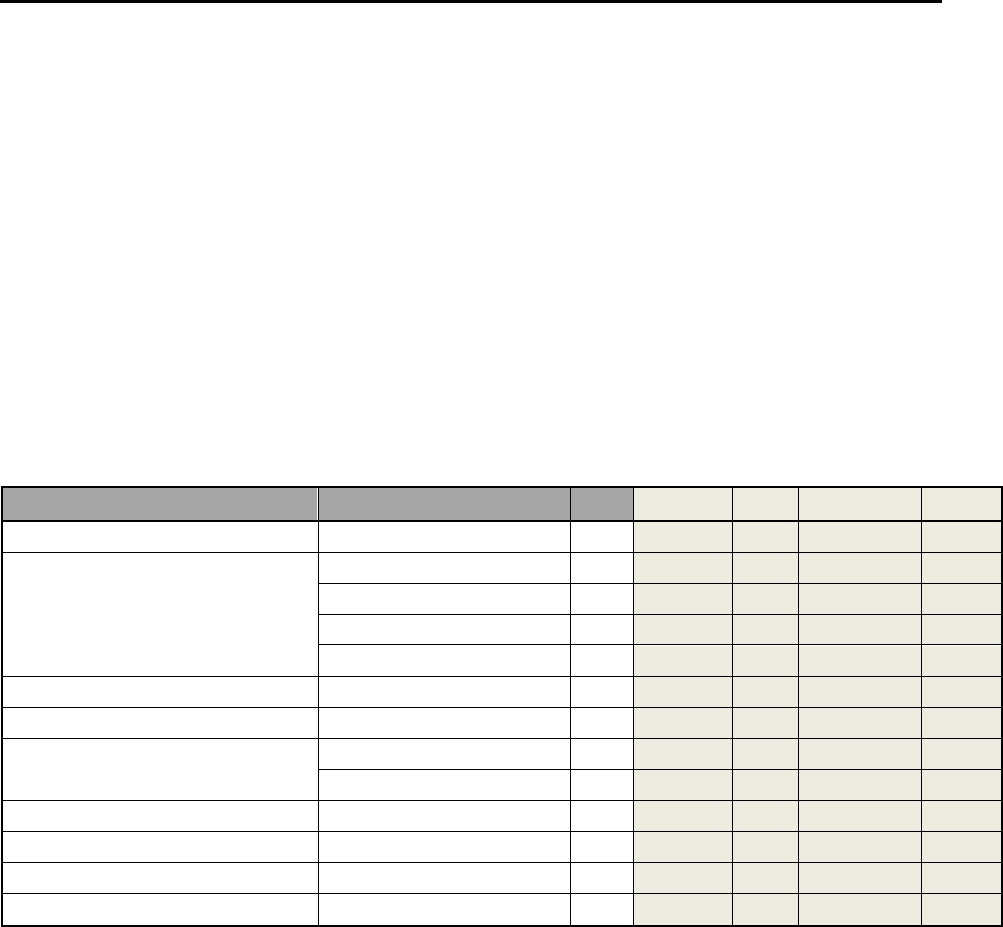
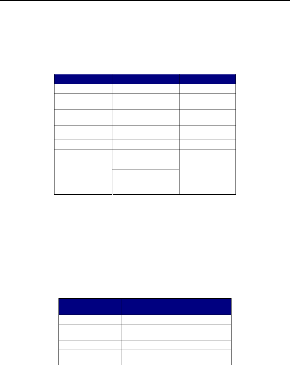
3. Signal Descriptions
3.1. Signal Descriptions
Listed below are the pin numbers and signals on the 148603 module.
GEN = General (No specific function), PWR= Power Supply, ANA= Analog
NOTE: FM is DISABLED in all revisions, and WLAN RF0 Path is not populated in
the -01 and -02 versions.
Table 2 – Signal Descriptions
PIN DEFINE REV
0.02
Module
Pin Name
Pin
#
I/O
Type
Function
Connects
to
SD
State
Default
State
(after
POR)
Buffer
[mA]
Description
VBAT1
68
PWR
GEN
PWR
VBAT 3.3V Input
VBAT2
69
PWR
GEN
PWR
VBAT 3.3V Input
VBAT3
70
PWR
GEN
PWR
VBAT 3.3V Input
VBAT4
71
PWR
GEN
PWR
VBAT 3.3V Input
VIO1
16
PWR
GEN
PWR
VIO 1.8V Digital Voltage
VIO2
17
PWR
GEN
PWR
VIO 1.8V Digital Voltage
GND1
6
GND
GEN
GND
Ground Pin
GND3
8
GND
GEN
GND
Ground Pin
GND4
10
GND
GEN
GND
Ground Pin
GND5
11
GND
GEN
GND
Ground Pin
GND6
13
GND
GEN
GND
Ground Pin
GND7
14
GND
GEN
GND
Ground Pin
GND8
15
GND
GEN
GND
Ground Pin
GND9
18
GND
GEN
GND
Ground Pin
GND10
23
GND
GEN
GND
Ground Pin
GND11
30
GND
GEN
GND
Ground Pin
GND12
33
GND
GEN
GND
Ground Pin
GND13
36
GND
GEN
GND
Ground Pin
GND14
38
GND
GEN
GND
Ground Pin
GND15
41
GND
GEN
GND
Ground Pin
GND16
43
GND
GEN
GND
Ground Pin
GND17
46
GND
GEN
GND
Ground Pin
GND18
48
GND
GEN
GND
Ground Pin
GND19
50
GND
GEN
GND
Ground Pin
GND20
54
GND
GEN
GND
Ground Pin
GND21
60
GND
GEN
GND
Ground Pin
GND22
67
GND
GEN
GND
Ground Pin

148603 Project Document
148603 Specification and Integration Guide
Copyright 2012 Motorola Solutions, Inc. 20110610-i 11 of 36
Confidential Material – Disclosure Strictly Prohibited. "Ni ckel Leucochroic Puffin"
GND23
72
GND
GEN
GND
Ground Pin
GND_H
73
GND
GEN
GND
Ground Pin Heat Sink Pad
WL_EN
32
IN
WLAN
HOST
PD
PD
N/A
WLAN IP enable
(0=not active, 1=host enable WLAN IP)
SDIO_CLK
25
IN
WLAN
HOST
HiZ
HiZ
4
WLAN SDIO clock. Place signal
conditioning resistor on SDIO_CLK close
to host processor
SDIO_CMD
24
I/O
WLAN
HOST
HiZ
HiZ
8/6/4/2
SDIO command in. SDIO lines must be
pulled up by the host.
SDIO_D0
26
I/O
WLAN
HOST
HiZ
HiZ
8/6/4/2
SDIO data bit 0. SDIO lines must be
pulled up by the host.
SDIO_D3
28
I/O
WLAN
HOST
PD
HiZ
8/6/4/2
SDIO data bit 3. SDIO lines must be
pulled up by the host.
SDIO_D1
29
I/O
WLAN
HOST
HiZ
HiZ
8/6/4/2
WLAN SDIO data bit 1. SDIO lines must
be pulled up by the host.
SDIO_D2
27
I/O
WLAN
HOST
HiZ
HiZ
8/6/4/2
WLAN SDIO data bit 2 . SDIO lines must
be pulled up by the host.
WLAN_IRQ
58
OUT
WLAN
HOST
PD
Drive 0
4
WLAN Interrupt out. Active low.
WL_RS232_TX
66
OUT
WLAN
DEBUG
PU
Drive 1
4
RTT tool UART output
WL_RS232_RX
65
IN
WLAN
DEBUG
PU
PU
4
RTT tool UART input
WL_UART_DBG
57
OUT
WLAN
DEBUG
PU
Drive 1
4
WLAN Logger output UART output
JTAG_TMS
62
IN
WLAN
DEBUG
PU
PU
4
JTAG Test Mode State Input
JTAG_TDO
61
OUT
WLAN
DEBUG
PU
Drive 1
4
JTAG Test Data Out Output
JTAG_TDI
64
IN
WLAN
DEBUG
PU
PU
4
JTAG Test Data In Input
JTAG_TCK
63
IN
WLAN
DEBUG
PD
PD
4
JTAG Test Clock Input
RF2
9
RF
WLAN/BT
ANT
RF
Default WLAN RF Port
(Shared with BT using -01 Module
Configuration)
50Ω Termination if not used.
RF1
12
RF
WLAN/BT
ANT
RF
Auxiliary WLAN RF Port
(Shared with BT using -01 Module
Configuration)
50Ω Termination if not used.
RF0
7
RF
GEN
GND
RF
Diversity Bypass Path. WLAN RF Port
(Shared with BT using -03 Module
Configuration) This path is mutually
exclusive with RF1 and RF2. RF0 Path
is not populated in the -01 and -02
versions.
50Ω Termination if not used.
BT_GPS_FM_EN
53
IN
BT/GPS/FM
HOST
PD*
PD*
N/A
Bluetooth IP enable
(0=not active, 1= host enable Bluetooth
IP
(GPS and FM active through VS
commands)
BT_GPS_FM_TX
19
OUT
BT/GPS/FM
HOST
PU
Drive 1
4
HCI UART transmit output
BT_GPS_FM_RX
20
IN
BT/GPS/FM
HOST
PU
PU
4
HCI UART receive input
BT_GPS_FM_CTS
21
IN
BT/GPS/FM
HOST
PU
PU
4
HCI UART clear to send input (active
low)
BT_GPS_FM_RTS
22
OUT
BT/GPS/FM
HOST
PU
Drive 1
4
HCI UART request to send (active low).
Signal IRQ asserted until cleared by host.

148603 Project Document
148603 Specification and Integration Guide
Copyright 2012 Motorola Solutions, Inc. 20110610-i 12 of 36
Confidential Material – Disclosure Strictly Prohibited. "Ni ckel Leucochroic Puffin"
BT_PCM_CLK
2
I/O
BT
HOST
PD
PD
8/6/4/2
Bluetooth PCM clock in or out.
Data can be driven out on rising edge or
falling edge.
Data can be sampled on rising edge or
falling edge.
BT_PCM_SYNC
3
I/O
BT
HOST
PD
PD
8/6/4/2
Bluetooth PCM frame sync in or out.
BT_PCM_IN
4
IN
BT
HOST
PD
PD
8/6/4/2
Bluetooth PCM data.
BT_PCM_OUT
1
OUT
BT
HOST
PD
PD
8/6/4/2
Bluetooth PCM Data out.
BT_RF
49
RF
BT
ANT
RF
BT RF Port (Using -02 Module
Configuration)
50Ω Termination if not used
BT_UART_DBG
5
OUT
BT
DEBUG
PU
PU
4
BT Logger output UART output
GPS_TIMESTAMP
56
IN
GPS
WWAN/
HOST
PD
PD
4
Time stamp from cellular clock or any
reference clock used to calibrate TCXO
GPS_PA_EN
55
IN
GPS
WWAN
PD
PD
4
GPS PA enable can be used for possible
WWAN coexistence. This input will
"blank-out" GPS signal in the case where
there is known jamming from WWAN
module.
GPS_PPS_OUT
52
OUT
GPS
HOST
PD
PD
4
GPS Pulse per second strobe output
GPS_EXT_LNA_EN
51
OUT
GPS
GPS
PD
PD
4
GPS External LNA Enable output
GPS_RF
42
RF
GPS
ANT
RF
GPS RF input port
50Ω Termination if not used.
FM_RF_IN_P
37
RF
FM
ANT
RF
FM 50Ω Receive RF Input Port.
180nH external serial inductor required.
50Ω Termination if not used.
FM_RF_OUT_P
34
RF
FM
ANT
RF
FM Transmit RF Plus Differential Output
Port. No Connect if not used
FM_RF_OUT_M
35
RF
FM
ANT
RF
FM Transmit RF Minus Differential
Output Port. No Connect if not used
FM_AUD_IN_L
40
ANA
FM
HOST
ANA
FM Audio Left Input
Requires external serial 0.22uF cap if
used.
GND if not used.
FM_AUD_IN_R
39
ANA
FM
HOST
ANA
FM Audio Right Input
Requires external serial 0.22uF cap if
used.
GND if not used.
FM_AUD_OUT_L
44
ANA
FM
HOST
ANA
FM Audio Left Output
Requires external serial 0.22uF cap if
used.
No Connect if not used
FM_AUD_OUT_R
45
ANA
FM
HOST
ANA
FM Audio Right Output
Requires external serial 0.22uF cap if
used.
No Connect if not used
SLOW_CLK
47
ANA
GEN
HOST
ANA
32.768KHz Slow CLK input. See Sec. 0
GPIO_WL_BT_N7
31
I/O
GEN
TP
PD
PD
4
Spare GPIO.
Can be used by the WL and BT IP's
GPIO_WL_BT_GPS_M8
59
I/O
GEN
TP
PU
PU
4
Spare GPIO.
Can be used by the WL, BT, and GPS IP's
148603 Project Document
148603 Specification and Integration Guide
Copyright 2012 Motorola Solutions, Inc. 20110610-i 13 of 36
Confidential Material – Disclosure Strictly Prohibited. "Ni ckel Leucochroic Puffin"
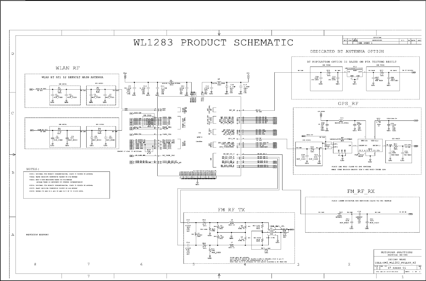
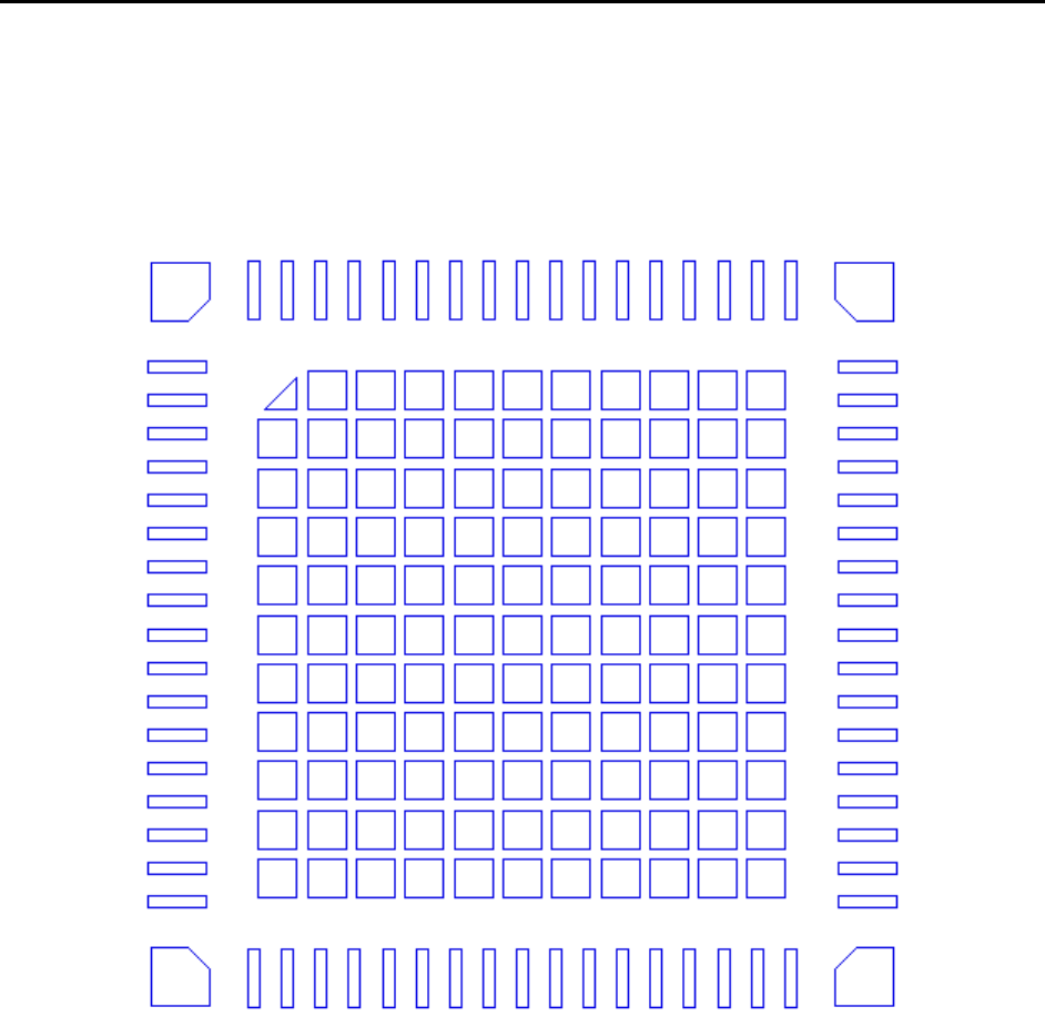
3.1. Pin Layout
Pin layout has been optimized for RF performance, heat dissipation, Voltage drop,
signal route, host signal connections, module size, and manufacturability.
Figure 1 - Pin Map

148603 Project Document
148603 Specification and Integration Guide
Copyright 2012 Motorola Solutions, Inc. 20110610-i 14 of 36
Confidential Material – Disclosure Strictly Prohibited. "Ni ckel Leucochroic Puffin"
4. Design Guidelines and Recommendations
4.1. Typical Application Schematic
General Note: This typical application schematic and BOM has not been updated to reflect the addition of
RF0 and the associated part numbers in the Section 1.4. As such, please use the latest MPA3 platform
schematics. This section(4.1) is superseded by Section 1.4 and the MPA3 controlled schematics.
NOTE: FM is DISABLED in all revisions, and WLAN RF0 Path is not populated in
the -01 and -02 versions.
An application schematic has been created for the MPA3 platform and is controlled
outside of this document. Schematic-function-blocks have been created for each sub-
function such as optional BT and FM.
Shown on page 16 is a typical application schematic for the 148603 module with all
schematic blocks for both the -01 and -02 module versions. Listed below Table 3 is the
bill of materials (BOM) for the Application Schematic.
IMPORTANT NOTE: SDIO lines must be pulled up by the host.
Place signal conditioning resistor on SDIO_CLK close to host processor.
148603 Project Document
148603 Specification and Integration Guide
Copyright 2012 Motorola Solutions, Inc. 20110610-i 15 of 36
Confidential Material – Disclosure Strictly Prohibited. "Ni ckel Leucochroic Puffin"
Table 3 - Typical Application Schematic BOM
Motorola Part Number Qty Ref Designator
21-144290-02 1U2
50-11500-458 2 C10,C17
50-11500-471 1C9
50-11568-25K102 1 C25
50-11568-25K471 2 C13,C14
50-11573-10K104 3 C11,C16,C21
50-11578-25J100 1 C29
50-11578-25J470 3 C12,C15,C24
50-11800-542 2 L3,L4
50-11800-563 1L2
50-11800-715 1L1
50-11800-717 2 L5,L11
50-11824-2R7 2 L8,L9
50-11828-510 2 L6,L7
50-12700-167 1 FL1
50-12700-168 1U3
50-13130-3981 1U1
50-14714-1000 1 R20
50-14725-2701 1 R22
50-14726-000 18 R1-R12, R17-R19,R21,R23,R24
50-15600-072 1T1
50-21815-181 1 L10
NOT_USED 22 C1-C8,C18-C20,C22,C23,C26-C28,C30,C31,R13-R16
148603 Project Document
148603 Specification and Integration Guide
Copyright 2012 Motorola Solutions, Inc. 20110610-i 16 of 36
Confidential Material – Disclosure Strictly Prohibited. "N ickel Leucochroic Puffin"
148603
148603-02
148603 Project Document
148603 Specification and Integration Guide
Copyright 2012 Motorola Solutions, Inc. 20110610-i 17 of 36
Confidential Material – Disclosure Strictly Prohibited. "Ni ckel Leucochroic Puffin"
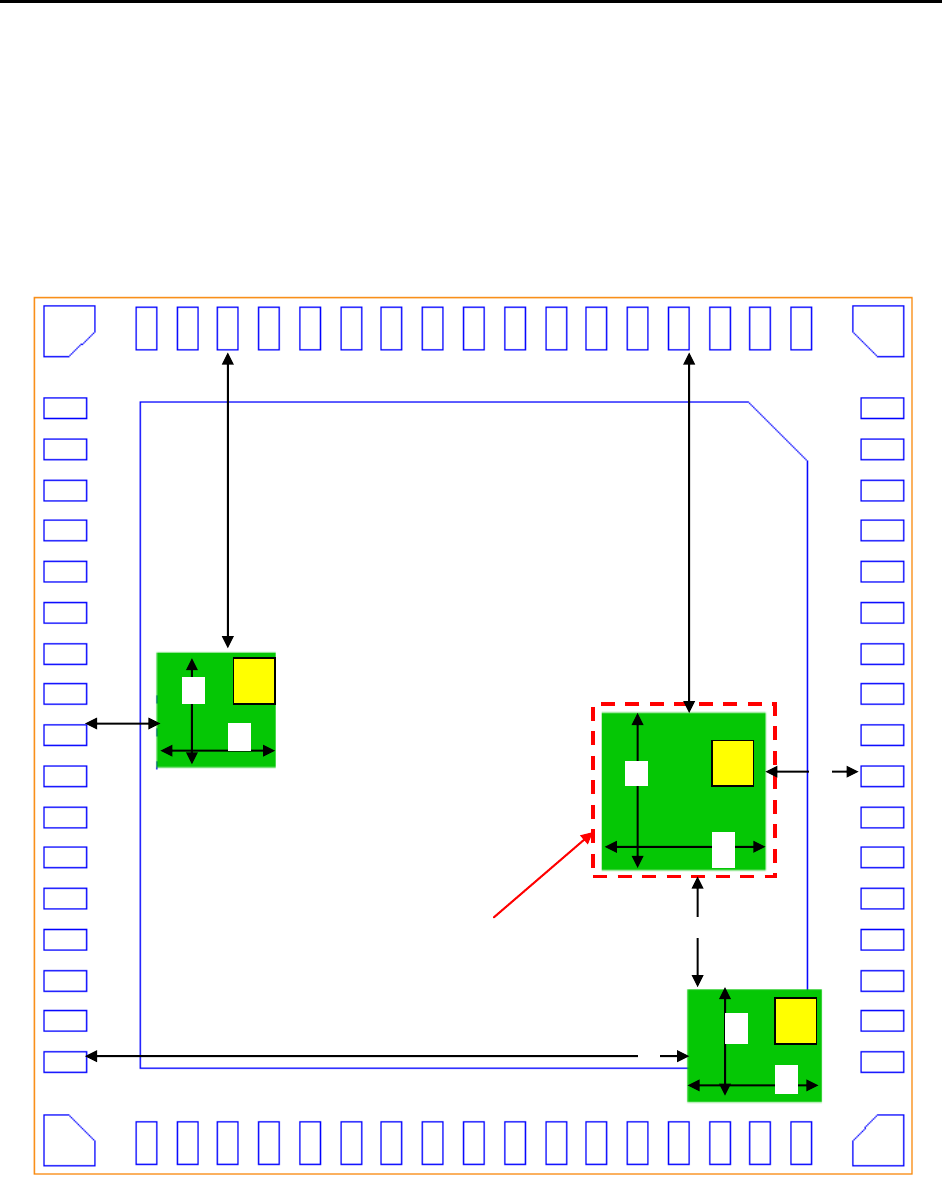
4.2. Host PCB Layout Recommendations
4.2.1. Recommended Footprint and Solder Paste
The latest part symbol should be always be refreshed from the Motorola Solution part
libraries. See Appendix
for the Recommended Host PCB Footprint/Pastemask.
The Allegro Footprint (.dra) is also available.
Figure 2 – TOP VIEW Recommended Option 3) Solid ground beneath the specific module areas
No traces under this
green shaded area.
See Section Error!
Reference source
not found.
a
b
c
d
e
f
g
h
1
2
3
i
j
k
l
148603 Project Document
148603 Specification and Integration Guide
Copyright 2012 Motorola Solutions, Inc. 20110610-i 18 of 36
Confidential Material – Disclosure Strictly Prohibited. "Ni ckel Leucochroic Puffin"
5. Host Requirements
5.1. Electrical Power
VBAT = 3.3V ±10%, with a ripple of 25mVRMS (Sine wave 10 Hz to 5 MHz)
VIO = 1.8V ±5%, with a ripple of 25mVRMS (Sine wave 10 Hz to 5 MHz)
5.2. Environmental
5.2.1. Absolute Maximum Ratings
Stresses beyond those listed in Table 4 below may cause permanent damage to the
device. These are stress ratings only and the functional operation of the device at these
or any other conditions beyond those indicated under Table 5 - Normal Operating
Conditions” is not implied. Exposure to absolute-maximum-rated conditions for
extended periods may affect device reliability.
Rating
Condition
Min
Max
Unit
VBAT power supply voltage
Absolute Max Voltage up to 6 hours cumulative in
7 years.
-0.5
5.5
V
VIO power supply voltage
-0.5
2.1
V
Input voltage to Analog pins
FM_RF_IN_P, FM_AUD_IN_L, FM_AUD_IN_R
FM_AUD_OUT_L, FM_AUD_OUT_R
-0.5
2.1
V
Input voltage to all other pins
-0.5
VIO+0.5V
V
Operating ambient temperature
range
Absolute Minimum driven by TCXO
-30
85
°C
Storage temperature range
Absolute Max driven by TCXO
-40
85
°C
Table 4 - Absolute Maximum Ratings
148603 Project Document
148603 Specification and Integration Guide
Copyright 2012 Motorola Solutions, Inc. 20110610-i 19 of 36
Confidential Material – Disclosure Strictly Prohibited. "Ni ckel Leucochroic Puffin"
5.2.2. Normal Operating Conditions
Rating
Condition
Sym
Min
Typ
Max
Unit
VBAT power supply voltage
3
3.3
3.6
V
VIO power supply voltage
1.71
1.8
1.89
V
VBAT Maximum ripple
Sine wave 10 Hz to 5 MHz
25
mVrms
VIO Maximum ripple
Sine wave 10 Hz to 5 MHz
25
mVrms
VIO High-level input voltage
Default
VIH
0.65 x
VIO
VIO
V
VIO Low-level input voltage
Default
VIL
0
0.35 x
VIO
V
High-level output voltage
@ 4 mA
VOH
VIO -
0.45
VIO
V
@ 1 mA
VIO -
0.112
VIO
V
@ 0.3 mA
VIO -
0.033
VIO
V
Low-level output voltage
@ 4 mA
VOL
0
0.45
V
@ 1 mA
0
0.112
V
@ 0.09 mA
0
0.01
V
Input transitions time Tr/Tf from 10% to 90%
(Digital IO) (1)
Tr/Tf
1
10
nS
Output rise time from 10% to 90% (Digital pins)
(1)
CL < 25 pF
Tr
5.3
ns
Output fall time from 10% to 90% (Digital pins)
(1)
CL < 25 pF
Tf
4.9
ns
Ambient operating temperature (installed
environment)
-20
+70
ºC
Storage temperature (installed environment)
-40
+85
ºC
Pull currents All except WL_EN,
BT_GPS_FM_EN, (For these typ = 6uA)
110
190
uA
(1) Applies to all Digital lines except SDIO, UART, and SLW_CLK lines
Table 5 - Normal Operating Conditions
148603 Project Document
148603 Specification and Integration Guide
Copyright 2012 Motorola Solutions, Inc. 20110610-i 20 of 36
Confidential Material – Disclosure Strictly Prohibited. "Ni ckel Leucochroic Puffin"
5.3. External Slow Clock (32K) Requirement
The supported digital slow clock is a free-running clock of 32.768 KHz which is supplied
from an external clock source. It shall be connected to the SLOW_CLK pin and is a
digital square-wave signal in the range of 0-1.8V Nom. See Table 2 above on page 10
for module pin number. All four core functions share a single input. Refer to * If the
available slow clock source does not meet the 40 ppm requirement, there are two options;
• Use the fast clock for the FM_TX functionality. This is configured using a vendor-specific command to switch to Fref
operation after enabling the FM core with the slow clock source.
• Enable clock error calibration in the FM core to compensate for the clock source error. The calibration can be done using a
known vendor-input clock error or intrinsically to the core (self-calibration).
Table 6 - Slow Clock Requirements below for slow clock specifications. SLOW_CLK is
a "fail-safe" input and can support an external clock voltage on the module pin even
when no power is supplied to the module. See Error! Reference source not found.
Error! Reference source not found. for the SLOW_CLK input requirements.
Characteristics
Condition
Sym
Min.
Typ.
Max.
Unit
Input slow clock frequency
32768
Hz
Input slow clock accuracy
(Initial + temp + aging)
WLAN, BT
±250
ppm
GPS
±200
FM_RX
±150
FM_TX *
±40
Input transition time Tr/Tf -10% to 90%
Tr/Tf
100
ns
Frequency input duty cycle
15
50
85
%
Input voltage limits
Square wave, DC-coupled
Vih
0.65 x VIO
VIO
Vpeak
Vil
0
0.35 x VIO
Input impedance
1
MΩ
Input capacitance
5
pF
Phase noise
1 kHz , 10 kHz
-125
dBc/Hz
Jitter
Integrated over 300 - 15000 Hz
1Hz / 0.5nS
* If the available slow clock source does not meet the 40 ppm requirement, there are two options;
• Use the fast clock for the FM_TX functionality. This is configured using a vendor-specific command to switch to Fref
operation after enabling the FM core with the slow clock source.
• Enable clock error calibration in the FM core to compensate for the clock source error. The calibration can be done using a
known vendor-input clock error or intrinsically to the core (self-calibration).
Table 6 - Slow Clock Requirements
148603 Project Document
148603 Specification and Integration Guide
Copyright 2012 Motorola Solutions, Inc. 20110610-i 21 of 36
Confidential Material – Disclosure Strictly Prohibited. "Ni ckel Leucochroic Puffin"
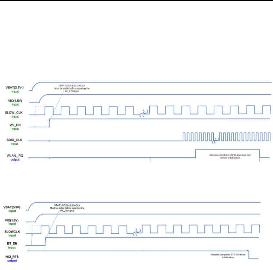
5.4. Timing Requirements
5.4.1. Power Up Timing
5.4.1.1. WLAN
TBD
5.4.1.2. BT/GPS/FM
TBD
148603 Project Document
148603 Specification and Integration Guide
Copyright 2012 Motorola Solutions, Inc. 20110610-i 22 of 36
Confidential Material – Disclosure Strictly Prohibited. "Ni ckel Leucochroic Puffin"
5.4.2. SDIO Timing Requirements
5.4.2.1. SDIO Data Switching Characteristics
Table 7 - SDIO Single Block Read
Parameter
Sym
Min.
Max.
Unit
Delay time, assign relative address or data transfer mode /
Read-command CMD valid to card-response CMD valid
tCR
2
64
Clock
cycles
Delay time, CMD command valid to CMD command valid
tCC
58
Clock
cycles
Delay time, CMD response valid to CMD command valid
tRC
8
Clock
cycles
Access time, CMD command valid to SD3-SD0 read data valid
tAC
2
Clock
cycles
Table 8 - SDIO Interface Read
5.4.2.2. SDIO Data Switching Characteristics
NOTE: CRC status and busy waveforms are only for data line 0. Data lines 1-3 are N/A. The busy waveform is optional, and
may not be present.
Table 9 - SDIO Single Block Write
Parameter
Sym
Min.
Max.
Unit
Delay time, CMD card response invalid to SD3-SD0 write data
valid
td1
2
Clock
cycles
Delay time, SD3-SD0 write data invalid end to CRC status valid
td2
2
2
Clock
cycles
Table 10 -SDIO Interface Write
148603 Project Document
148603 Specification and Integration Guide
Copyright 2012 Motorola Solutions, Inc. 20110610-i 23 of 36
Confidential Material – Disclosure Strictly Prohibited. "Ni ckel Leucochroic Puffin"
5.4.2.3. SDIO Switching Characteristics
Over Recommended operating conditions
Parameters for maximum clock frequency
Table 11 – SDIO Timing
Parameter
Sym
Min.
Max.
Unit
Clock frequency, CLK Default Rate
fclock
0
26
MHz
Clock frequency, CLK High Rate
fclock
0
52
MHz
Low/high duty cycle
DC
40
60
%
Rise time, CLK
tTLH
1
3
ns
Fall time, CLK
tTHL
1
3
ns
Setup time, input valid before CLK
↑
tISU
2
ns
Hold time, input valid after CLK ↑
tIH
2
ns
Delay time, CLK ↓ to output valid
tODLY
2.5
14.8
ns
Capacitive load on outputs
Cl
15
pF
Table 12 - SDIO Timing
148603 Project Document
148603 Specification and Integration Guide
Copyright 2012 Motorola Solutions, Inc. 20110610-i 24 of 36
Confidential Material – Disclosure Strictly Prohibited. "Ni ckel Leucochroic Puffin"
5.5. Antenna Requirements
The following table summarizes the guidelines for the Antenna design:
5.5.1. WLAN
Description
Requirement
Comments
Frequency Bands
Lower band
2.4 GHz to 2.5 GHz
Required for
802.11g support
Upper band
4.920 GHz to 5.825
GHz
Required for
802.11a support
Nominal
Impedance
50 ohms
VSWR
Less than 2.0:1
Across bands
Gain (Peak)
3dBi for the lower
band
Does not include
RF losses
between 148603
radio and
Antenna
connector
4dBi for the upper
band
Table 13 - WLAN Antenna Requirements
Regulatory Note: Many country regulations require special testing and reporting of
antenna performance or of the system with the antenna attached. Please check the
appropriate regulatory authority or contact Motorola Solutions for more information.
5.5.2. BT
If the BT antenna is being shared with WLAN, then the WLAN antenna requirements in
Table 13 above supersede the requirements in this section.
If a standalone antenna for BT is being used then the requirements in Table 14 apply.
Description
Requirement
Comments
Frequency Band
Bluetooth
2.4 GHz to
2.5 GHz
Nominal Impedance
50 ohms
VSWR
Less than
2.0:1
Across the Band
Table 14 - Bluetooth Antenna Requirements

148603 Project Document
148603 Specification and Integration Guide
Copyright 2012 Motorola Solutions, Inc. 20110610-i 25 of 36
Confidential Material – Disclosure Strictly Prohibited. "Ni ckel Leucochroic Puffin"
5.5.3. GPS
Description
Requirement
Comments
Frequency Bands
GPS
1575.42MHz
± 2MHz
GLONASS*
1565MHz-
1606MHz
Although the 148603
does not support GLONASS it
is recommended that the
antenna is ready for future
proofing
Nominal
Impedance
50 ohms
VSWR
Less than 2.0:1
Table 15 - GPS Antenna Requirements
148603 Project Document
148603 Specification and Integration Guide
Copyright 2012 Motorola Solutions, Inc. 20110610-i 26 of 36
Confidential Material – Disclosure Strictly Prohibited. "Ni ckel Leucochroic Puffin"
6. Module Specifications
6.1. Power Consumption
Hardware Low Power Mode - Module Shutdown (SDWN)
Description: After VBAT and VIO are supplied to the module and while
WLAN_EN and BT_GPS_FM_EN are de-asserted (LOW), the module is in
Shutdown state. Open connections will be lost. Upon resume downloading
firmware is necessary.
Requirements:
o SDIO lines should be held high by the host to prevent leakage.
o Host clears all enables WL_EN & BT_GPS_FM_EN.
o Host ensures all other IOs are in the correct state to prevent back-
powering.
State
Comments
VBAT current
(uA)
VIO current (uA)
Supply Voltage
VBAT= 3.3V, VIO =
1.8V
Min.
Typ.
Max.
Min.
Typ.
Max.
Shutdown
See Section
6.1
40
10
Table 16 - Hardware Low Power Mode - Module Shutdown (SDWN) Current Draw

148603 Project Document
148603 Specification and Integration Guide
Copyright 2012 Motorola Solutions, Inc. 20110610-i 27 of 36
Confidential Material – Disclosure Strictly Prohibited. "Ni ckel Leucochroic Puffin"
6.1.1. WLAN Power Consumption
System Draws for MPA3 Guidance:
o Software Low Power Mode – Extended Low Power Mode (ELP,
RTTT=Sleep Mode)
Description: In this mode, MAC, PHY, and DRPw are in shutdown
mode. The WL1283 SoC will not be able to receive packets. While
in ELP mode, the WL1283 WLAN IP operates on slow clock only.
Requirements: Processor sends SDIO (or RTTT UART) commands
to the WLAN core.
In case of critical suspend need to disable wake on WL_IRQ.
See Error! Reference source not found. on page Error!
Bookmark not defined.
o Highest Current Mode
VBAT :Transmitting CW 22dBm on 2.4GHz (This will change
based on EV2 /DV results and the limitation in output power)
VIO: Loading FW
o Worst Case Suspend Mode - Wake on LAN (WOWL)
Description: WAKE ON LAN is designed to block packets from
going up from the firmware layer into the driver layer.
Requirements: The enabling of this feature requested two separate
different commands.1. Enable the feature. 2. Configure the filter
different variants. If the filter is activated and the user didn't define
the filter variants, then all packets will be blocked from arriving to
the driver layer.
Current draws are approximate based and are solely based on TI
solution specification: Dynamic mode with Beacon (DTIM = 1 ;
TBTT = 100 ms; Beacon duration ~1.6 ms ; Rate=1 Mbps) Beacon
in Listen mode This mode reflects results with software drivers and
not the RTTT tool.
Other WLAN Core Discrete Power Modes:
Together with ELP there are 4 discrete power modes for the WLAN Core. The other
three are:
o Awake mode
In this mode MAC, PHY, and DRPw are fully active and various
RT3 functions are all active. While in this mode, power
consumption is not optimized.
o Listen mode
In Listen mode, MAC and Phy are awake, but DRPw shuts down
one of the RF channels. While in this mode, the WL1283 SoC will
accept only 11b packets; OFDM packets are not supported. This
mode saves power while the WL1283 SoC is active and ready to
receive a new packet.
o StandBy (Power Down Mode)
148603 Project Document
148603 Specification and Integration Guide
Copyright 2012 Motorola Solutions, Inc. 20110610-i 28 of 36
Confidential Material – Disclosure Strictly Prohibited. "Ni ckel Leucochroic Puffin"
In this mode, PHY and DRPw are in shutdown mode. The WL1271
SOC will not be able to receive packets.
6.1.2. BT Power Consumption
Software Low Power Mode - Deep Sleep
Send Vendor specific command to radio during download of patch BT connections will
be maintained. No need to download patch. In case of critical suspend need to disable
wake on data.
Highest Current Mode
Transferring data using BT Serial port profile. Transmitting EDR data.
*Specification is at 4 dBm and needs to be measured at class1.5 power levels.
Worst Case Suspend Mode
Depends on if either Hardware or Software Low Power Mode is implemented WC
numbers here are represented of Software low power mode
State
Comments
VBAT
current (mA)
VIO
current (mA)
Supply Voltage VBAT= 3.3V, VIO = 1.8V
Min.
Typ.
Max.
Min.
Typ.
Max.
System (MPA3 Guidance)
Software Low Power Mode - Deep Sleep
See Section
0.2
0.03
Highest Current Mode
See Section
29
TBD
Table 17 - BT Power Consumption
6.1.3. GPS Power consumption
GPS sub-section shall not exceed current draw indicted below.
Characteristics
DC Spec
Current (mA)
Average
Typical
Peak
Full Power Tracking Mode
LNA 1.8V
5
7.5
VIO 1.8V
0.5
0.6
Vbat 3.3V
22
27
Acquisition Mode @-130dBm Power Level
LNA 1.8V
5
7.5
VIO 1.8V
0.5
0.6
Vbat 3.3V
36.5
42
Sleep current
LNA 1.8V
-
-
VIO 1.8V
0.5
0.6
Vbat 3.3V
0.1
1.1
Table 18 - GPS Power Consumption
148603 Project Document
148603 Specification and Integration Guide
Copyright 2012 Motorola Solutions, Inc. 20110610-i 29 of 36
Confidential Material – Disclosure Strictly Prohibited. "Ni ckel Leucochroic Puffin"
7. Appendix
7.1. Recommended Host PCB Pastemask
Figure 3 - Recommended host PCB PasteMask
148603 Project Document
148603 Specification and Integration Guide
Copyright 2012 Motorola Solutions, Inc. 20110610-i 30 of 36
Confidential Material – Disclosure Strictly Prohibited. "Ni ckel Leucochroic Puffin"
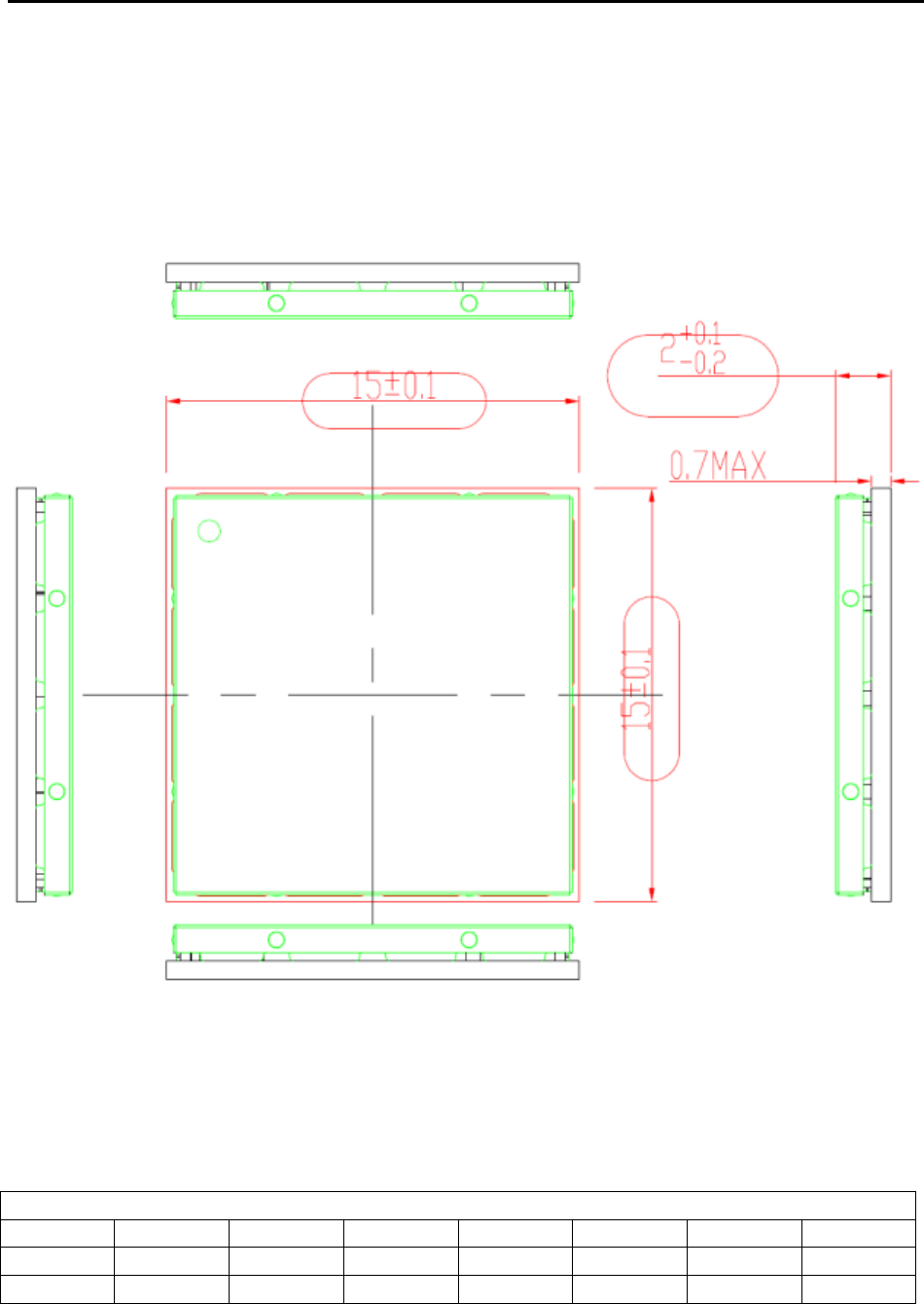
7.2. Mechanical Interface Drawing
7.3. Regulatory
7.3.1. CE Regulations
This equipment may be operated in:
AT
BE
BG
CH
CY
CZ
DE
DK
EE
ES
FI
FR
GB
GR
HU
IE
IT
IS
LI
LT
LU
LV
MT
NL
148603 Project Document
148603 Specification and Integration Guide
Copyright 2012 Motorola Solutions, Inc. 20110610-i 31 of 36
Confidential Material – Disclosure Strictly Prohibited. "Ni ckel Leucochroic Puffin"
NO
PL
PT
RO
SE
SI
SK
TR
Products with 2.4–GHz Wireless LAN Devices France
L'utilisation de cet equipement (2.4GHz wireless LAN) est soumise à certaines
restrictions: cet equipement peut être utilisé à l'interieur d'un batiment en utilisant toutes
les frequences de 2400 a 2483.5MHz (Chaine 1–13). Pour une utilisation en
environement exterieur, les frequences comprises entre 2400-2454 MHz (Chaîne 1-9)
peuvent être utilisé. Pour les dernières restrictions, voir http://www.art-telecom.fr.
For 2.4–GHz wireless LAN operation of this product, certain restrictions apply. This
equipment may use the entire–2400–MHz to 2483.5–MHz frequency band (channels 1
through 13) for indoor applications. For outdoor use, only 2400-2454 MHz frequency
band (channels 1-9) may be used. For the latest requirements, see http://www.art-
telecom.fr.
7.3.2. FCC Regulations
This mobile phone complies with part 15 of the FCC Rules. Operation is subject to the
following two conditions: (1) This device may not cause harmful interference, and (2)
this device must accept any interference received, including interference that may
cause undesired operation.
This mobile phone has been tested and found to comply with the limits for a Class B
digital device, pursuant to Part 15 of the FCC Rules. These limits are designed to
provide reasonable protection against harmful interference in a residential installation.
This equipment generates uses and can radiated radio frequency energy and, if not
installed and used in accordance with the instructions, may cause harmful interference
to radio communications. However, there is no guarantee that interference will not occur
in a particular installation If this equipment does cause harmful interference to radio or
television reception, which can be determined by turning the equipment off and on, the
user is encouraged to try to correct the interference by one or more of the following
measures:
-Reorient or relocate the receiving antenna.
-Increase the separation between the equipment and receiver.
-Connect the equipment into an outlet on a circuit different from that to which the
receiver is connected.
-Consult the dealer or an experienced radio/TV technician for help.

148603 Project Document
148603 Specification and Integration Guide
Copyright 2012 Motorola Solutions, Inc. 20110610-i 32 of 36
Confidential Material – Disclosure Strictly Prohibited. "Ni ckel Leucochroic Puffin"
FCC Caution:
Any Changes or modifications not expressly approved by the party responsible for
compliance could void the user„s authority to operate the equipment.
The antenna(s) used for this transmitter must not be co-located or operating in
conjunction with any other antenna or transmitter.
Operation on the 5.15-5.25 GHz frequency band is restricted to indoor use only.
Note: The country code selection is for non-US model only and is not available to all US
model. Per FCC regulation, all WiFi product marketed in US must fixed to US operation
channels only.
Radiation Exposure Statement:
Radiation Exposure Statement:
This equipment complies with FCC radiation exposure limits set forth for an uncontrolled
environment. This equipment should be installed and operated with minimum distance
20cm between the radiator & your body.
Note: The country code selection is for non-US model only and is not available to all US
model. Per FCC regulation, all WiFi product marketed in US must fixed to US operation
channels only.
This device is intended only for OEM integrators under the following conditions:
The antenna must be installed such that 20 cm is maintained between the antenna and
users, and
The transmitter module may not be co-located with any other transmitter or antenna.
As long as 2 conditions above are met, further transmitter test will not be required.
However, the OEM integrator is still responsible for testing their end-product for any
additional compliance requirements required with this module installed
IMPORTANT NOTE: In the event that these conditions can not be met (for example
certain laptop configurations or co-location with another transmitter), then the FCC
authorization is no longer considered valid and the FCC ID can not be used on the final
product. In these circumstances, the OEM integrator will be responsible for re-
evaluating the end product (including the transmitter) and obtaining a separate FCC
authorization.
End Product Labeling

148603 Project Document
148603 Specification and Integration Guide
Copyright 2012 Motorola Solutions, Inc. 20110610-i 33 of 36
Confidential Material – Disclosure Strictly Prohibited. "Ni ckel Leucochroic Puffin"
This transmitter module is authorized only for use in device where the antenna may be
installed such that 20 cm may be maintained between the antenna and users. The final
end product must be labeled in a visible area with the following:“Contains FCC ID:
XXXXXXXX”, where XXXXXXXX is the approved FCC ID for the device being installed.
The grantee's FCC ID can be used only when all FCC compliance requirements are
met.
Manual Information To the End User
The OEM integrator has to be aware not to provide information to the end user
regarding how to install or remove this RF module in the user‟s manual of the end
product which integrates this module.
The end user manual shall include all required regulatory information/warning as show
in this manual.
7.3.3. IC Regulations
Industry Canada statement:
This device complies with RSS-210 of the Industry Canada Rules. Operation is subject
to the following two conditions: (1) This device may not cause harmful interference, and
(2) this device must accept any interference received, including interference that may
cause undesired operation.
Ce dispositif est conforme à la norme CNR-210 d'Industrie Canada applicable aux
appareils radio exempts de licence. Son fonctionnement est sujet aux deux conditions
suivantes: (1) le dispositif ne doit pas produire de brouillage préjudiciable, et (2) ce
dispositif doit accepter tout brouillage reçu, y compris un brouillage susceptible de
provoquer un fonctionnement indésirable.
Radiation Exposure Statement:
This equipment complies with IC radiation exposure limits set forth for an uncontrolled
environment. This equipment should be installed and operated with minimum distance
20cm between the radiator & your body.
Déclaration d'exposition aux radiations:
Cet équipement est conforme aux limites d'exposition aux rayonnements IC établies
pour un environnement non contrôlé. Cet équipement doit être installé et utilisé avec un
minimum de 20 cm de distance entre la source de rayonnement et votre corps.
This device is intended only for OEM integrators under the following conditions: (For
module device use)
1) The antenna must be installed such that 20 cm is maintained between the antenna
and users, and
2) The transmitter module may not be co-located with any other transmitter or antenna.

148603 Project Document
148603 Specification and Integration Guide
Copyright 2012 Motorola Solutions, Inc. 20110610-i 34 of 36
Confidential Material – Disclosure Strictly Prohibited. "Ni ckel Leucochroic Puffin"
As long as 2 conditions above are met, further transmitter test will not be required.
However, the OEM integrator is still responsible for testing their end-product for any
additional compliance requirements required with this module installed.
Cet appareil est conçu uniquement pour les intégrateurs OEM dans les conditions
suivantes: (Pour utilisation de dispositif module)
1) L'antenne doit être installée de telle sorte qu'une distance de 20 cm est respectée
entre l'antenne et les utilisateurs, et
2) Le module émetteur peut ne pas être coïmplanté avec un autre émetteur ou antenne.
Tant que les 2 conditions ci-dessus sont remplies, des essais supplémentaires sur
l'émetteur ne seront pas nécessaires. Toutefois, l'intégrateur OEM est toujours
responsable des essais sur son produit final pour toutes exigences de conformité
supplémentaires requis pour ce module installé.
IMPORTANT NOTE:
In the event that these conditions can not be met (for example certain laptop
configurations or co-location with another transmitter), then the Canada authorization is
no longer considered valid and the IC ID can not be used on the final product. In these
circumstances, the OEM integrator will be responsible for re-evaluating the end product
(including the transmitter) and obtaining a separate Canada authorization.
NOTE IMPORTANTE:
Dans le cas où ces conditions ne peuvent être satisfaites (par exemple pour certaines
configurations d'ordinateur portable ou de certaines co-localisation avec un autre
émetteur), l'autorisation du Canada n'est plus considéré comme valide et l'ID IC ne peut
pas être utilisé sur le produit final. Dans ces circonstances, l'intégrateur OEM sera
chargé de réévaluer le produit final (y compris l'émetteur) et l'obtention d'une
autorisation distincte au Canada.
End Product Labeling
This transmitter module is authorized only for use in device where the antenna may be
installed such that 20 cm may be maintained between the antenna and users. The final
end product must be labeled in a visible area with the following: “Contains
IC:XXXXXXXX”, where XXXXXXXX is the approved IC ID for the device being
installed.
Plaque signalétique du produit final
Ce module émetteur est autorisé uniquement pour une utilisation dans un dispositif où
l'antenne peut être installée de telle sorte qu'une distance de 20cm peut être maintenue
entre l'antenne et les utilisateurs. "Contient des IC: IC: XXXXXXXX", où
XXXXXXXX est l'ID approuvée IC pour le périphérique en cours d'installation.
Manual Information To the End User
The OEM integrator has to be aware not to provide information to the end user
regarding how to install or remove this RF module in the user‟s manual of the end
product which integrates this module.
The end user manual shall include all required regulatory information/warning as show
in this manual.

148603 Project Document
148603 Specification and Integration Guide
Copyright 2012 Motorola Solutions, Inc. 20110610-i 35 of 36
Confidential Material – Disclosure Strictly Prohibited. "Ni ckel Leucochroic Puffin"

148603 Project Document
148603 Specification and Integration Guide
Copyright 2012 Motorola Solutions, Inc. 20110610-i 36 of 36
Confidential Material – Disclosure Strictly Prohibited. "Ni ckel Leucochroic Puffin"
Manuel d'information à l'utilisateur final
L'intégrateur OEM doit être conscient de ne pas fournir des informations à l'utilisateur
final quant à la façon d'installer ou de supprimer ce module RF dans le manuel de
l'utilisateur du produit final qui intègre ce module.
Le manuel de l'utilisateur final doit inclure toutes les informations réglementaires
requises et avertissements comme indiqué dans ce manuel.
Caution :
(i) the device for operation in the band 5150-5250 MHz is only for indoor use to reduce
the potential for harmful interference to co-channel mobile satellite systems;
(ii) the maximum antenna gain permitted for devices in the bands 5250-5350 MHz and
5470-5725 MHz shall comply with the e.i.r.p. limit; and
(iii) the maximum antenna gain permitted for devices in the band 5725-5825 MHz shall
comply with the e.i.r.p. limits specified for point-to-point and non point-to-point operation
as appropriate.
(iv) Users should also be advised that high-power radars are allocated as primary users
(i.e. priority users) of the bands 5250-5350 MHz and 5650-5850 MHz and that these
radars could cause interference and/or damage to LE-LAN devices.
Avertissement:
Le guide d‟utilisation des dispositifs pour réseaux locaux doit inclure des instructions
précises sur les restrictions susmentionnées, notamment :
(i) les dispositifs fonctionnant dans la bande 5 150-5 250 MHz sont réservés
uniquement pour une utilisation à l‟intérieur afin de réduire les risques de brouillage
préjudiciable aux systèmes de satellites mobiles utilisant les mêmes canaux;
(ii) le gain maximal d‟antenne permis pour les dispositifs utilisant les bandes 5 250-5
350 MHz et 5 470-5 725 MHz doit se conformer à la limite de p.i.r.e.;
(iii) le gain maximal d‟antenne permis (pour les dispositifs utilisant la bande 5 725-5 825
MHz) doit se conformer à la limite de p.i.r.e. spécifiée pour l‟exploitation point à point et
non point à point, selon le cas.
(iv) De plus, les utilisateurs devraient aussi être avisés que les utilisateurs de radars de
haute puissance sont désignés utilisateurs principaux (c.-à-d., qu‟ils ont la priorité) pour
les bandes 5 250-5 350 MHz et 5 650-5 850 MHz et que ces radars pourraient causer
du brouillage et/ou des dommages aux dispositifs LAN-EL.