File info: application/pdf · 19 pages · 1.95MB
Onkyo-R-805-TX-Service-Manual - vintage hifi
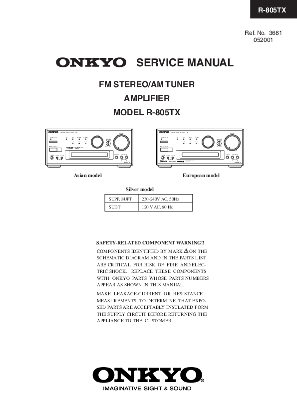
THE SUPPLY CIRCUIT BEFORE RETURNING THE. APPLIANCE TO THE CUSTOMER. Ref. No. 3681. 052001. R-805TX. SERVICE MANUAL. STANDBY/ON.
Extracted Text
R-805TX

Ref. No. 3681 052001
SERVICE MANUAL
FM STEREO/AM TUNER AMPLIFIER
MODEL R-805TX

FM STEREO / AM TUNER AMPLIFIER

ENERGY SAVE STANDBY / ON

CD

MD

CDR/PC

LINE/DVD

FM

AM

TAPE

WIDE RANGE AMPLIFIER TECHNOLOGY

PHONES MEMORY FM MODE CLEAR

INPUT

ACOUSTIC PRESENCE
OFF / 1 / 2 / 3

VOLUME

DISPLAY

PRESET

TUNING
R-805TX

Asian model

FM STEREO / AM TUNER AMPLIFIER

ENERGY SAVE STANDBY / ON

CD

MD

CDR

LINE/DVD

FM

AM

TAPE

PHONES MEMORY FM MODE
CLEAR ACCUCLOCK

WIDE RANGE AMPLIFIER TECHNOLOGY

INPUT

ACOUSTIC PRESENCE
OFF / 1 / 2 / 3

VOLUME

DISPLAY

PRESET

TUNING
R-805TX

European model

Silver model

SUPP, SUPT SUDT

230-240V AC, 50Hz 120 V AC, 60 Hz

SAFETY-RELATED COMPONENT WARNING!!
COMPONENTS IDENTIFIED BY MARK ON THE SCHEMATIC DIAGRAM AND IN THE PARTS LIST ARE CRITICAL FOR RISK OF FIRE AND ELECTRIC SHOCK. REPLACE THESE COMPONENTS WITH ONKYO PARTS WHOSE PARTS NUMBERS APPEAR AS SHOWN IN THIS MANUAL.
MAKE LEAKAGE-CURRENT OR RESISTANCE MEASUREMENTS TO DETERMINE THAT EXPOSED PARTS ARE ACCEPTABLY INSULATED FORM THE SUPPLY CIRCUIT BEFORE RETURNING THE APPLIANCE TO THE CUSTOMER.

SPECIFICATIONS
Amplier Section
Power output 20 watts per channel, min RMS, at 4 ohms, both channels driven 1 kHz, with no mor e than 0.6% THD 15 watt per channel, min RMS, at 8 ohms, both channels driven 1 kHz, with no mor e than 0.6% THD 2 X 20 watts at 4 ohms, 1 kHz, DIN 2 X 17 watts at 6 ohms, 1 kHz, DIN 2 X 15 watts at 8 ohms, 1 kHz, DIN 2 X 29 watts at 4 ohms, 1 kHz, EIAJ
Dynamic power output 2 X 24 watts at 4 ohms 2 X 17 watts at 8 ohms
otal harmonic distortion 0.6% at rated power
IM distortion 0.6% at rated power
Damping factor 30 at 8 ohms
Input Sensitivity and Impedance TAPE/MD PLAY: 150 mV, 50 kohms LINE IN: 150 mV, 50 kohms
Frequency and r esponse 10 to 50,000 Hz +0 / �3 dB
Tone contr ol ACOUSTIC PRESENCE 1 +4 dB at 82 Hz ACOUSTIC PRESENCE 2 +3 dB at 20.5 Hz, + 3 dB at 82 Hz ACOUSTIC PRESENCE 3 +3 dB at 20.5 Hz, + 6 dB at 82 Hz BASS �8 dB at 100 Hz TREBLE �8 dB at 10 kHz
Signal to noise ratio TAPE: 100 dB (IHF-A)
Muting � dB
Tuner Section
Tuning range FM: 87.9 to 107.9 MHz (200 kHz steps) (U.S. & Canadian models) 87.5 to 108.00 MHz (50 kHz steps) (Other area models) AM: 530 to 1710 kHz (10 kHz steps) (U.S. & Canadian models) 522 to 1611 kHz (9 kHz steps) (Other area models)
Usable sensitivity FM: Mono 11.2 dBf, 1.0 �V (75 ohms IHF) 0.9 �V (75 ohms DIN) Stereo 17.2 dBf, 2.0 �V (75 ohms IHF) 23.0 �V (75 ohms DIN) AM: 30 �V

R-805TX
50 dB Quieting sensitivity FM: Mono 17.2 dBf, 2.0 �V (75 ohms) Stereo 37.2 dBf, 20.0 �V (75 ohms)
Captur e ratio FM: 2.0 dB
Image r ejection ratio FM: 40 dB (U.S. & Canadian models) 85 dB (Other area models) AM: 40 dB
IF rejection ratio FM: 90 dB AM: 40 dB
Signal to noise ratio FM: Mono 73 dB, IHF Stereo 67 dB, IHF AM: 40 dB
Selectivity FM: 50 dB DIN (�300 kHz at 40 kHz Devi.)
AM Suppr ession Ratio 50 dB
Harmonic distortion FM: Mono 0.2% Stereo 0.3% AM: 0.7 %
Frequency r esponse FM: 30 to 15,000 Hz (�1.5 dB)
Stereo separation FM: 45 dB at 1,000 Hz 30 dB at 100 to 10,000 Hz
Stereo thr eshold FM: 17.2 dBf, 2.0 �V (75 ohms)
General Clock precision
monthly error: +/-30 seconds (at 25 degrees Celsius)
Power supply AC 120 V, 60 Hz AC 230 V, 50 Hz
Power consumption 61 W (120 V, 50 Hz) 54 W (230 V, 60 Hz)
Dimensions (W X H X D) 205 X 91 X 302 mm 8-1/16" X 3-9/16" X 11-7/8"
Weight 3.4 kg, 7.5 lbs
Specications and external appearance are subject to change without notice as a result of product improvement.

R-805TX

SERVICE PROCEDURES
1. Replacing the fuses

This symbol located near the fuses indicates that the fuse used is fast operating type. For continued protection against fire hazard, replace with same type fuse. For fuse rating refer to the marking adjacent to the symbol.

Ce symbole indique que le fusible utlise est a rapide. Pour une protection permanente, n'untiliser que fusibles de meme type. Ce darnier est la qu le present symbol est appse.

CIRCUIT NO. F901
F902

PART NO. DESCRIPTION 252158 1.6A-UL/T237, Primary <D> 252083 0.4A-SE-EAWK, Primary
<P/T> 252069 0.8A-SE-EAK,AC outlet
<P/T> Note: <D>: 120V model only
<P/T>: 230V model only

5. Changing the AM band step The tuning step selector switch is not provided in this model. When you change the band step, change the parts as shown below.

R715 R716

To 10kHz 3.3k 5.6k

To 9kHz 10k Open

6. Adjustment of clock frequency 1. Connect the frequency counter to the terminal TP701. 2. Press and hold down the MEMORY button, then press the
DISPLAY button.(All segments on FL tube light on) 3. Adjust the trimmer capacitor C707 so that the reading of
frequency counter becomes 524.288 kHz+/-1Hz.

2. To initialize the unit This device employs a microprocessor to perform various functions and operations. If interference generated by an external power supply, radio wave, or other electrical source results in accident which causes the specified operations and functions to operate abnormally. To perform a result, please follow the procedure below.

1. Press and hold down the MEMORY button, then press the DISPLAY button. 2. Press the STANDBY/ON button. After "clear" is displayed, the preset memory and each mode stored in the memory, such as surround, are initialized and will return to the factory setting.

3. Safety-check out (120V model only) After correcting the original service problem, perform the following safety check before releasing the set to the customer. Connect the insulating-resistance tester between the plug of power supply cord and screw on the back panel. Specifications: 3.3Mohm+/-10% at 500V.

4. Memory Preservation
This unit does not require memory preservation batteries. A built-in memory power back-up system preserves the contents of the memory during po wer f ailures and even when the unit is unplugged.The unit must be plugged in order to char ge the back-up system. The memory preservation period after the unit has been unplugged varies depending on climate and placement of the unit. On the a v erage, memory contents are protected over a period of a few weeks after the last time the unit has been unplugged. This period is shorter when the unit is exposed to a highly humid climate.

PANEL VIEWS
FRONT PANEL

STANDBY/ON button ENERGY SA VE indicator ENERGY SA VE button
Remote control sensor

Input source indicators INPUT selector ACOUSTIC PRESENCE button VOLUME control

FM STEREO / AM TUNER AMPLIFIER

ENERGY SAVE STANDBY / ON

CD

MD

CDR

LINE/DVD

FM

AM

TAPE

INPUT

ACOUSTIC PRESENCE
OFF / 1 / 2 / 3

VOLUME

PHONES MEMORY FM MODE
CLEAR ACCUCLOCK

WIDE RANGE AMPLIFIER TECHNOLOGY

DISPLAY

PRESET

TUNING
R-805TX

CLEAR or FM MODE button MEMORY button
PHONES jack

DISPLAY button
PRESET TUNING

buttons buttons

European models front panel shown.

Display

RDS indicator (non-U.S., non-Canadian models only)

AM/PM indicator

Tuning indicator

MEMORY indicator AUTO/MONO indicator

STEREO indicator

TIMER W.DAY
W.END MEMORY REC SLEEP

AUTO MONO AM PM RDS

STEREO
MIN MUTING kHz MHz

Timer setting indicators

Multi display

Frequency indicators

MUTING indicator Sleep time indicator

REAR PANEL

CD recorder

REC INPUT

PLAY OUTPUT

R-805TX

Stereo cassette tape deck

REC INPUT

PLAY OUTPUT

For the Asian model: In addition to a CD recorder , you can connect a digital audio processor to this connector .
: Signal flow

CDR

TAPE

OUT

IN

OUT

IN

L

L

R
(REC) CD
L

R

(PLAY) (REC) (PLAY)

REMOTE CONTROL

OUT MD IN LINE/DVD PROCESSOR

L

R (REC) (PLAY)

R

OUT

IN

This unit (R-805TX)

ANTENNA

CDR

OUT

IN

L

TAPE

OUT

IN

L

AM R
CD L
FM 75
R

OUT MD IN

R

LINE/DVD

REMOTE CONTROL
PROCESSOR

L

R

OUT

IN

L
R SPEAKERS

CAUTION: SPEAKER IMPEDANCE 4 OHMS MIN. /SPEAKER
AC OUTLET AC 230-240V 50Hz
SWITCHED 100W MAX.

(illustration is European model)

OUTPUT CD player

REC INPUT

PLAY OUTPUT

MD recorder

AUDIO OUTPUT
DVD, LD or Video equipment

Connecting a sound processor (other than U.S. & Canadian models)

Connections

1 Remove the jumper plugs.

PROCESSOR

IN OUT
2 Connect the sound processor to the unit.

Jumper plug

This unit (R-805TX)

ANTENNA

CDR

OUT

IN

L

TAPE

OUT

IN

L

AM R
CD L
FM 75
R

OUT MD IN

R

LINE/DVD

REMOTE CONTROL
PROCESSOR

L

R

OUT

IN

L
R SPEAKERS

CAUTION:

SPEAKER

IMPEDANCE 4 OHMS MIN. /SPEAKER

.

AC OUTLET
AC 230-240V 50Hz
SWITCHED 100W MAX.

PROCESSOR L

R

OUT

IN

Sound processor INPUT
OUTPUT -
: Signal flow

REMOTE CONTROLLER
� You can control the other -connected components with the supplied remote controller. � The remote controller buttons operate in the same way as the buttons on each component
with the same indication. � For actual operations, please refer to the Instruction Manual for each component.

STANDBY/ON button Toggles between STANDBY and ON.
Tuner control PRESET : Tuner preset select buttons
FM : FM band select button AM : AM band select button
TONE button Enables you to set the tone.
Mode Select buttons Pressing this button
TIMER : repeatedly to select one of the following eight settings. WEEKDAY: Timer playback on the specified day(s) of the week. WEEKEND:Timer playback on the specied day(s) of the week. REC:Timer record setting DAYSET:Sets the day of the week (WEEKDAY & WEEKEND). ADJUST:Sets the current time and the day of the week. 24H/12H: Enables you to select 24-hour display or 12-hour display by pressing the ENTER button and using the UP /DOWN buttons.
UP /DOWN : Enables you to select a parameter after you press the TIMER or TONE button. Press the ENTER button to confirm the selection.
ENTER:Press this button to confirm the selection made via the TIMER, TONE, UP , or DOWN button.

STANDBY/ ON CLOCK

GRAPHIC EQ SLEEP EFFECT MODE

PRESET

TUNER INPUT

F M

A M

TAPE

PAUSE/STEP DVD

REPEAT SCROLL

M D

PLAY MODE CLEAR

REC

REPEAT RANDOM

C D

MEMORY CLEAR

DISC

REPEAT PLAY MODE

CDR

TONE CLEAR

REC

MUTING

TIMER

1

2

3

4 UP/DOWN
7
ENTER --/---

5

6

8 10 / 0

9

VOLUME

ACOUSTIC PRESENCE

REMOTE CONTROLLER RC-456S

CLOCK button Press this button to display the current time.
SLEEP button Enables you to make the Sleep time setting.
INPUT button Enables you to select a listening source.
MUTING button Mutes the sound temporarily .
VOLUME / buttons Enables you to increase or decrease the volume level.
ACOUSTIC PRESENCE button Switches acoustic presence of f and types.
Number buttons Used to set the time/day and select the PRESET stations.

R-805TX

� Use the following buttons to control components that are connected to the - system.

Stereo cassette tape deck control
: Reverse play button : Stop button : Play button : Rewind button
: Fast-forward button

DVD player control : Chapter/track down button : Chapter/track up button : Stop button
PAUSE/STEP : Pause/Step forward button
: Play button
CD player (or changer) contr ol REPEAT : Repeat mode button RANDOM :Random play
button : Stop button : Pause button : Play button MEMORY:Memory button CLEAR : Clear button DISC : Disc button for CD
changer : Track down button : Track up button

STANDBY/ ON CLOCK

GRAPHIC EQ SLEEP EFFECT MODE

PRESET

TUNER INPUT

F M

A M

TAPE

PAUSE/STEP DVD

REPEAT SCROLL

M D

PLAY MODE CLEAR

REC

REPEAT RANDOM

C D

MEMORY CLEAR

DISC

REPEAT PLAY MODE

CDR

TONE CLEAR

REC

MUTING

TIMER

1

2

3

4 UP/DOWN
7
ENTER --/---

5

6

8 10 / 0

9

VOLUME

ACOUSTIC PRESENCE

REMOTE CONTROLLER RC-456S

Graphic equalizer contr ol EFFECT: Ef fect select button MODE: Mode select button
MD recorder control REPEAT : Repeat mode
button SCROLL : Scroll button
: Stop button : Pause button : Play button PLAY MODE:Play mode
selection button CLEAR:Clear button
REC:Recording button : Track down button : Track up button
CD recorder contr ol REPEAT : Repeat mode
button PLAY MODE : Play mode
selection button : Stop button : Pause button : Play button CLEAR:Clear button REC:Recording button : Track down button : Track up button
CD player (or changer) / MD r ecorder / CD recorder control 1~9, 10/0 : Number buttons --/--- : Ten's hold button

EXPLODED VIEW
P901(P/PT)

P901 (D)

21

10

14

10
41 P851 P801 3

P966

P965

12 U8

U2
U10 P953 23 U3

F902 F901
E901
11

U5 8

U6 T901
4

Q527 Q525 Q526 15 6
3

Q528 3
U1

3 5
3

24

1 U4
3
2

17
20 19 32

ONKYO

3

R-805TX
31 26
25

PARTS LIST

REF.NO. PART NO. 1 27111147A

DESCRIPTION Front bracket

2 28325755

Knob, Acoustic

3 838130088

3TTB+8B,Self-tapping screw

4 27100375D

Chassis

5 27175323

Leg

6 27141530A

Retainer HS

8 801433

3SMS8W.SW+14B(BC),Special screw

10 27300750 ! #2271,Bushing cord

11 830440089

4TTC+8C(BC),Self-tapping screw

12 27122840

Rear panel <P>

27122841

Rear panel <D>

27122856

Rear panel <T>

14 838430068

3TTB+6B(BC),Self-tapping screw

15 27160451B

Heat sink

17 28198901

Facet

19 28191798

Clear plate RE

20 28191873A

Clear plate

21 28184759-1

Top cover

22 28141409A

Cushion

24 838930088

3TTB+8B(UN), Self-tapping screw

25 28325716

Knob INP

26 28325717

Knob VOL

31 27212304

Front panel <P>

27212317

Front panel <T/D>

32 28135247Y

Badge

41 29362630

Label, processor

42 29110083

Tape, cloth

43 838430088

3TTB+8B(BC),Self-tapping screw

44 29362571

Label, warning

E901 260208

Wire tie

F901 252083

! 0.4A-SE-EAWK,Fuse <P/T>

F901 252158

! 1.6A-UL/T-237,Fuse <D>

F902 252069

! 0.8A-SE-EAK,Fuse <P/T>

P801 25055436

NPLG-2P418,Plug

P851 880009

NRP-345,Plastic rivet <P/T>

P901 253277MIL ! AS-UC-2#18,Power supply cord <D>

253193HIT ! AS-CEE,Power supply cord <P/T>

P953 2047150512

NCFC7-150512,Flexible flat cable

R-805TX

REF.NO. P965 P966 P967
Q525,Q526
Q527,Q528
T901 U1
U2
U3
U4
U5
U6
U8
U10

PART NO. 27150448A 880009 27301779 2202064, 2202063 or 2202066 2202054, 2202053 or 2202056 2301443 2301444 1A911501-2C 1A911501-2D 1A911501-2E 1A911502-2C 1A911502-2D 1A911502-2E 1A911503-2C 1A911503-2D 1A911503-2E 1A911504-2C 1A911504-2D 1A911504-2E 1A911505-2C 1A911505-2D 1A911505-2E 1A911506-2C 1A911506-2D 1A911506-2E 1A911507-2C 1A911507-2D 1A911507-2E 240135

CAUTION: Replacement for transistor of mark *, if necessary must be made from the same bata group (HFE) as the original type.
DESCRIPTION Shield plate NRP-345,Plastic rivet HL-38-0,Clamp * 2SC4511-Y, * 2SC4511-O or * 2SC4511-P,Transistor * 2SA1725-Y, * 2SA1725-O or * 2SA1725-P,Transistor ! NPT-1385D,Power transformer <D> ! NPT-1385P,Power transformer <P/T> NAAF-6801-2C,Main circuit PC board ass'y <P> NAAF-6801-2D,Main circuit PC board ass'y <T> NAAF-6801-2E,Main circuit PC board ass'y <D> NAETC-6802-2C,Input/output terminal PC board ass'y <P> NAETC-6802-2D,Input/output terminal PC board ass'y <T> NAETC-6802-2E,Input/output terminal PC board ass'y <D> NAPS-6803-2C,Secondary circuit PC board ass'y <P> NAPS-6803-2D,Secondary circuit PC board ass'y <T> NAPS-6803-2E,Secondary circuit PC board ass'y <D> NADG-6804-2C,Display circuit PC board ass'y <P> NADG-6804-2D,Display circuit PC board ass'y <T> NADG-6804-2E,Display circuit PC board ass'y <D> NAAF-6805-2C,Tone circuit PC board ass'y <P> NAAF-6805-2D,Tone circuit PC board ass'y <T> NAAF-6805-2E,Tone circuit PC board ass'y <D> NAPS-6806-2C,Primary circuit PC board ass'y <P> NAPS-6806-2D,Primary circuit PC board ass'y <T> NAPS-6806-2E,Primary circuit PC board ass'y <D> NAETC-6807-2C,Speaker terminal PC board ass'y <P> NAETC-6807-2D,Speaker terminal PC board ass'y <T> NAETC-6807-2E,Speaker terminal PC board ass'y <D>
TFCE1E512A, Tuner unit

NOTE: THE COMPONENTS IDENTIFIED BY MARK ! ARE CRITICAL FOR RISK OF FIRE AND ELECTRIC SHOCK. REPLACE ONLY WITH PART NUMBER SPECIFIED.

NOTE:<P>:European model only <T>: 230V model only for Asia <D>: 120V model only for Asia

IC BLOCK DIAGRAMS AND DESCRIPTIONS

TC9184AP(ELECTRONIC TONE CONTROL)

VSS

VDD

1

16

GND 7

CK DATA STB 8 9 10

BASS+ 2

LEVEL SHIFT

15 BASS+

R-805TX

ANALOG SWITCH LADDER RESISTOR

CODE DETECTING 20bit SHIFT REGISTER CIRCUIT CIRCUIT

13bit LATCH CIRCUIT

LADDER RESISTOR ANALOG SWITCH

BASS- 3 COM 4 TREBLE- 5

14 BASS13 COM 12 TREBLE-

ANALOG SWITCH LADDER RESISTOR

13bit LATCH CIRCUIT

LADDER RESISTOR ANALOG SWITCH

TREBLE+ 6

11 TREBLE+

Pin No. 1 16 2/15 3/14 5/12 6/11 4/13 7 8
9
10

Symbol VSS VDD BASS+ BASSTREBLETREBLE+ COM GND CK
DATA
STB

Function Power supply voltage terminals (Analog section) Volume terminal
Ground terminal (Digital section) Clock input terminal. Clock input receiving data from DATA terminal Data input terminal. Input 20bit tone control data by synchronizing to the rise of CK signals. Strobe input terminal. The tone control data received from DATA and CK terminals are transferred into IC buy turning this terminal to "H" level. Previous data are kept stored so long as "H" level in not applied to this terminal.

TC9273N-10 (Analog Switch Array)

S1 2 S2 3 S3 4 S4 5 S5 6 S6 7 S7 8 S8 9 S9 10 S10 11 S11 12

VSS

VDD

1

28

(L-ch) 10bit Latch Circuit

(R-ch) 10bit Latch Circuit (Same as L-ch Circuit)

27 S1 26 S2 25 S3 24 S4 23 S5 22 S6 21 S7 20 S8 19 S9 18 S10 17 S11

LEVEL SHIFTER+SHIFT REGISTER CIRCUIT

13

14

15

16

GND

CK

DATA

STB

Pin No. 1 13 28
2/27 3/26 4/25 5/24 6/23 7/22 8/21 9/20 10/19 11/18 12/17 14 15 16

Symbol Vss GND VDD S1 S2 S3 S4 S5 S6 S7 S8 S9 S10 S11 CK DATA STB

Description Negative power supply pin Digital ground pin Positive power supply pin
Input/Output pins
Clock input pin for data transfer. Serial data input pin for setting switches. Strobe input pin for data writing.

TA7291S(VOLUME MOTOR DRIVER) Vcc Vref 28
REGULATOR
PROTECTOR

R-805TX

6 Vss 7 OUT1

INPUT

IN1 IN2

0

0

1

0

0

1

1

1

OUTPUT OUT1 OUT2

H

L

L

H

L

L

MODE
STOP CW/CCW CCW/CW BRAKE

CCW: Counter-clockwise direction CW: Clockwise direction

3 OUT2

91 IN1 IN2

5 GND

10-BT-167GK(FL TUBE)

10G

TIMER W.DAY

CD

W.END MEMORY

REC REPEAT

SLEEP RANDOM

9G

8G

7G

6G

5G

4G

TRACK AUTO MONO AM PM

3G RDS

2G

1G

S T

MIN kHz MHz

STEREO
MUTING S.BASS DIRECT

:This model is not used.

a

f

hj

kb

g

m

e

n

rp

c

d

10G

9G

8G

7G

6G

5G 4G

3G

2G

1G

P1

-

a

a

a

a

a

a

a

a

-

P2

W.DAY

j

j

j

j

j

j

j

j MUTING

P3

W.END

h

h

h

h

h

h

h

h

MIN

P4

MEMORY k

k

k

k

k

k

k

k S.BASS

P5

-

b

b

b

b

b

b

b

b

-

P6

-

f

f

f

f

f

f

f

f

-

P7

-

g

g

g

g

g

g

g

g

-

P8

REC

m

m

m

m

m

m

m

m

MHz

P9

-

c

c

c

c

c

c

c

c

-

P10

-

e

e

e

e

e

e

e

e

-

P11

REPEAT

n

n

n

n

n

n

n

n

kHz

P12

RANDOM

r

r

r

r

r

r

r

r

DIRECT

P13

-

p

p

p

p

p

p

p

p

-

P14

-

d

d

d

d

d

d

d

d

-

P15

TIMER

TRACK AUTO MONO AM PM RDS

S

P16

CD

-

-

-

-

Col

-

T STEREO

P17

SLEEP

-

-

-

-

-

Dp

-

-

MICROPROCESSOR-CONNECTION DIAGRAM

POWER AMP. SW CIRCUIT

Q405

VOLUME

M

MOTOR

DRIVER

TA7291S

Q781 RDS DECODER
BU1923
Q705 BUFFER

POWERSTOPPAGE DETECTOR
TERMINAL RI
S709 INPUT SW
+B

Q704 REMOTE SENSOR

R-805TX

CDR

42 LINE/DVD

ENERGY 43

45 ~POFF 44 RDSSCK

46 SYSIN

47 REMIN

IC

49 SYSOUT

50 RDSSIG

51 RDSDATA

+5V

53 ROTB

54 ROTA

55 POWER2

56 SBASS A

57 SBASS B

58 VOLDOWN

59 VOL UP

61 P2
P1
60

62 P3

63 P4

64 P5

41

48

52

4G 1 5G
2 6G 3 7G 4 8G 5 9G 6 10G 7 +5V 8 POWER1 9 SBASS-3 10 SBASS-2 11 SBASS-1 12 FCE/VCE 13 INPMUT 14 DATA 15 PLLCE 16 ~RESET 17 CLK 18 TUMUT 19 GND 20 NC 21 STEREO 22 SD 23 NC 24

Q703 FL TUBE

P6

65

P7

66

P8

67

P9

68

P10

69

P11

70

Vload

71

P12 72

P13

73

P14

74

P15

75

P16

76

P17

77

1G

78

2G

79

3G

80

AUDIO MUTE

Q301 SOURCE SELECTOR SWITCH TC9273N

Q915 AC OUTLET
SWITCH

SWITCH CIRCUIT

Q702 SYSTEM RESET

CD 40
MD 39
TAPE 38
AM 37
FM 36
X2 35
X1 34
GND 33
XT2 32
XT1 31
+5V 30
+5V 29
K0 28
K1 27
AREA 26
SIGNAL 25

X701 X'TAL

DISPLAY P-UP

ECO

MEMORY

INITIALIZING FM MODE P.DOWN ACOUSTIC

POWER

TUNER UNIT
Q471 TONE CONTROL
TC9184AP

MICROPROCESSOR-TERMINAL DESCRIPTION

Pin No. Function

1~7 4G~10G

8 +5V

9 POWER1

10 SBASS-3

11 SBASS-2

12 SBASS-1

13

FCE/VCE

14 INPMUT 15 DATA 16 PLLCE 17 ~RESET 18 CLK 19 TUMUT 20 GND 21 NC 22 STEREO 23 SD 24 NC 25 SIGNAL 26 AREA 27 K1 28 K0 29 +5V 30 +5V 31 XT1 32 XT2 33 GND 34 X1 35 X2 36 FM 37 AM 38 TAPE

I/O Description

Pin No. Function

O Grid output pins for FL tube.

39 CD

Positive power supply pin

40 MD

O Power supply control pin for AC outlet and FL tube.

41 CDR

O Acoustic presence control output pin

42 LINE/DVD

O Acoustic presence control output pin

43 ENERGY

O Acoustic presence control output pin

44 RDSSCK

O Latch output pin of the function switch and

45 ~POFF

strobe output pin of the tone control

46 SYSIN

O Audio muting control output pin

47 REMIN

O Data output pin for function switch, tone control and PLL ICs.

48 IC

O Chip enable output pin for PLL IC.

49 SYSOUT

I System reset input pin.

50 RDSSIG

O Clock signal output pin for function switch, tone control and PLL ICs. 51 RDSDATA

O Muting output pin for tuner section.

52 +5V

Ground pin for A/D converter.

53 ROTB

Not used.

54 ROTA

I Stereo broadcast detection pin.

55 POWER2

I Broadcast detection input pin

56 SBASS A

Not used.

57 SBASS B

I Signal strength input pin

58 VOLDOWN

I Initializing input pin for region

59 VOL UP

I Operation key connection pin

60~70 P1~P11

I Operation key connection pin

71 Vload

Analog power supply for A/D converter

72~77 P12~P17

Reference voltage input pin for A/D converter

78~80 1G~3G

Oscillator connection pin for sub system. Not used.

Oscillator connection pin for sub system. Not used.

Ground pin

Crystal oscillator connection pin for main system clock

Crystal oscillator connection pin for main system clock

O FM indicator output pin

O AM indicator output pin

O TAPE indicator output pin

I/O Description O CD indicator output pin O MD indicator output pin O CDR indicator output pin O LINE/DVD indicator output pin O ENERGY SAVE indicator output pin I Clock input pin from RDS decoder I Power failure detection pin I System code input pin I Signal input from remote controller
Inner connection pin O System code output pin I Quality check signal from RDS decoder. I Data input pin from RDS decoder.
Positive power supply pin I Rotary encoder connection pin for Input selector I Rotary encoder connection pin for Input selector O Power supply control pin for Power amplifier O Acoustic presence indicator output pin O Acoustic presence indicator output pin O DOWN signal output pin for Master volume O UP signal output pin for Master volume O Segment output pin for FL tube
Pull down resistor connection pin for FL tube O Segment output pins for FL tube O Grid output pins for FL tube.

R-805TX

WIRING VIEW

NAETC6802

P903
NAPS6805
JL901A
P902 JL903A JL902A
JL502C P853
NAETC6807

P301B

P302B

P301A

P302A

JL703B

JL901B

JL903B

JL702B

JL902B
P501

P952A P951A
TP701 P403A

JL701B

JL502B P402A JL501B
P401A

P502

NAAF-

6801

JL702A

JL501A

JL703A

R-805TX

TUNER PACK

NADG-6804

NAPS6803

P952B P951B

JL953

P403B
NAAF6805
P402B
P401B

JL701A

R-805TX

PRINTED CIRCUIT BOARD-PARTS LIST

MAIN CIRCUIT PC BOARD (NAAF-6801-2C/2D/2E)

CIRCUIT NO. PART NO.

DESCRIPTION

ICs

Q301

22240881

TC9273N-010

Q405

22240239

TA7291S

Q913

222780565JRC NJM78M56FA

Transistors

Q501-Q504 2211733

2SC1845-E

Q505-Q508 2213284

2SC1740S-R

Q509-Q514 2211455

2SA1015-GR

Q515-Q518 2211255

2SC1815-GR

Q519,Q520 2213284

2SC1740S-R

Q521,Q522 2211654 or 2SC2235-Y or

2211653

2SC2235-O

Q523,Q524 2211644 or 2SA965-Y or

2211643

2SA965-O

Q525,Q526 2202064, * 2SC4511-Y,

2202063 or * 2SC4511-O or

2202066 * 2SC4511-P

Q527,Q528 2202054, * 2SA1725-Y,

2202053 or * 2SA1725-O or

2202056 * 2SA1725-P

Q540

2213284

2SC1740S-R

Q541

2213354

2SA933S-R

Q545

2213510 or DTA114ES or

2214350

RN2202

Q546

2213290

DTC114ES

Q911

2211644

2SA965-Y

Q914

2211256

2SC1815-BL

Q915

2213640

DTC123JS

Q916

2213510

DTA114ES

Q917,Q918 2211164

2SC2120-Y

Diodes

D501,D502 223163 or

1SS133 or

D570

223205

1SS270A

D576

22380035 or GP104003E or

D914-D917 22380046

AM01Z

D901

223163 or

1SS133 or

223205

1SS270A

D911

22380022F RBV402

D912,D913 224471203 MTZJ12C

D918

224471203 MTZJ12C

D919-D922 22380035 or GP104003E or

D933,D934 22380046

AM01Z

D923

224473004 MTZJ30D

D924

224470683 MTZJ6.8C

D931,D932 223163 or

1SS133 or

D935

223205

1SS270A

Coils

L501,L502 231176S

S-1.3C

Capacitors

C301,C302 374721015 100pF+/-10%,50V,Plastic <P>

C305,C306 374721015 100pF+/-10%,50V,Plastic <P>

C307,C308 374721015 100pF+/-10%,50V,Plastic <P>

C311,C312 374722215 220pF+/-10%,50V,Plastic <P>

C325,C326 393341007 10 u F,16V, Elect.

C405

393321017 100 u F,6.3V, Elect.

C501,C502 393341007 10 u F,16V, Elect.

C503,C504 374721015 100pF+/-10%,50V,Plastic

C515,C516 393322217 220 u F,6.3V, Elect.

C529,C530 393344707 47 u F,16V, Elect.

C531-C534 393341007 10 u F,16V, Elect.

C535,C536 374724734 0.047 u F+/-5%,50V,Plastic

C538,C540 393361017 100 u F,35V, Elect.

C550

393361017 100 u F,35V, Elect.

C575

393380107 1 u F,50V, Elect.

C576

353744709 47 u F,16V, Elect.

C911

374722244 0.22 u F+/-5%,50V,Plastic

C912,C913 374721044 0.1 u F+/-5%,50V,Plastic

C914,C915 393363327S 3300 u F,35V, Elect.

C916,C917 393343317 330 u F,16V, Elect.

C918

374721034 0.01 u F+/-5%,50V,Plastic

C919

393384707 47 u F,50V, Elect.

C920,C922 393381017 100 u F,50V, Elect.

C921

354771019 100 u F,63V, Elect.

C923

393380337 3.3 u F,50V, Elect.

CIRCUIT NO. PART NO.

Capacitors

C925

393352227

C929

393361017

C930

393341007

C932

393380107

C933,C940 374722234

Resistors

R515-R518 443523904

R519,R520 443523304

R521,R522 443523904

R559,R560 443521014

R561,R562 4500027

R563,R564 453530824

R565,R566 453530564

R569,R572 443522204

R911

443525604

R912,R915 441623914F

R916

453534794

R918

443721024U

R919

443522704

R923

453530274

R924,R925 443622204HT

R928

443722714U

R945

443622714HT

Relay

RL911

25065537

Terminals

P303.P304 25045300

Sockets

JL501B

25050269

JL502B

25050268

JL701B

25055629

JL702B

25051095

JL703B

25051093

JL901B

25051087

JL902B

25051107

JL903B

25051108

Plugs

P301A

25055704

P302A

25055701

P401A,P402A 25055708

P403A

25055703

P501,P502 25055038

P951A,P952A 25055703

TP701

25055038

Heat sink

Q913A

27160145-1

Screw

Q913B

838430107

DESCRIPTION
2200 u F,25V, Elect. 100 u F,35V, Elect. 10 u F,16V, Elect. 1 u F,50V, Elect. 0.022 u F+/-5%,50V,Plastic
39ohm+/-5%,1/2W,Metal oxide 33ohm+/-5%,1/2W,Metal oxide 39ohm+/-5%,1/2W,Metal oxide 100ohm+/-5%,1/2W,Metal oxide MPC708-2WK-0.22,Metal plate 8.2ohm+/-5%,1/2W,Metal 5.6ohm+/-5%,1/2W,Metal 22ohm+/-5%,1/2W,Metal oxide 56ohm+/-5%,1/2W,Metal oxide 390ohm+/-5%,1W,Metal oxide 0.47ohm+/-5%,1/2W,Metal 1kohm+/-5%,2W,Metal oxide 27ohm+/-5%,1/2W,Metal oxide 2.7ohm+/-5%,1/2W,Metal 22ohm+/-5%,1W,Metal oxide 270ohm+/-5%,2W,Metal oxide 270ohm+/-5%,1W,Metal oxide
NRL-2P5A-DC12-107
NPJ-6PDBL159
NSCT-5P97 NSCT-4P96 NPLG-8P591 NSCT-11P882 NSCT-9P880 NSCT-3P874 NSCT-3P894 NSCT-4P895
NPLG-8P660 NPLG-5P657 NPLG-12P664 NPLG-7P659 NPLG-2P29 NPLG-7P659 NPLG-2P29
RAD-51
3TTB+10S(BC),Self-tapping

INPUT/OUTPUT TERMINAL PC BOARD (NAETC-6802-2C/2D/2E)

CIRCUIT NO. PART NO.

DESCRIPTION

Capacitors

C315,C316 374721015 100pF+/-10%,50V,Plastic <P>

C319,C320 374721015 100pF+/-10%,50V,Plastic <P>

Terminals

P306,P307 25045303

NPJ-4PDBL162

P308

25045330

NPJ-2PDBL184

Sockets

P301B

25051233

NSCT-8P1023

P302B

25051230

NSCT-5P1020

POWER SUPPLY PC BOARD (NAPS-6803-2C/2D/2E)

CIRCUIT NO. PART NO.

DESCRIPTION

IC

Q951

222780125 78M12HF

Transistors

Q952

2213284

2SC1740S-R <P>

Q953

2213510

DTA114ES

Q955,Q956 2215024

2SD1468S-R

Diode

D951

223163 or

1SS133 or

223205

1SS270A

CAUTION:Replacement for transistor of mark * , if necessary must be made from the same beta group (HFE) as the original type.

CIRCUIT NO. PART NO.

Capacitors

C951,C962 354780339

C952

393384797

C965

393361017

C966

393341007

Resistors

R965

453530824

R966

443621204

Sockets

P951B,P952B 25051232

P953A

25052248

Heat sink

Q951A

27160145-1

Screw

Q951B

838430107

DESCRIPTION
3.3 u F,50V, Elect. 0.47 u F,50V, Elect. 100 u F,35V, Elect. 10 u F,16V, Elect.
8.2ohm+/-5%,1/2W,Metal 12ohm+/-5%,1W,Metal oxide
NSCT-7P1022 NSCT-15P2145
RAD-51
3TTB+10S(BC),Self-tapping

DISPLAY CIRCUIT PC BOARD (NADIS-6804-2C/2D/2E)

CIRCUIT NO. PART NO.

DESCRIPTION

FL tube

Q703

212141

10BT-167GK

Remote sensor

Q704

241329

PIC-26043TH2

ICs

Q701

22241625NEC MPD78044FGF-192-3B9

Q781

22241302

BU1923 <P>

Transistors

Q702

221282 or

DTC144ES or

2213560

RN1204

Q705

2212600 or DTA124ES or

2213580

RN2203

Diodes

D701-D706 223163 or

1SS133 or

223205

1SS270A

D707

224470562 MTZJ5.6B

D709

225339

SPR-39MVWF

D710

225338

SLR-332VR

D711-D717 225340

SLR-332DU

D781

223163 or

1SS133 or

223205

1SS270A <P>

Crystals

X701

3010224

XTL-4.19M

X781

3010321 or HC-49/U034.332MHz or

3010203

AF6146CG <P>

Capacitors

C701

3000078

DX-5R5L104,Super

C703

353780229 2.2 u F,50V, Elect.

C705

353741009 10 u F,16V, Elect.

C707

3060011

NTC-45P10,Trimmer

C708,C710 393384707 47 u F,50V, Elect.

C711

353721019 100 u F,6.3V, Elect.

C713

353741009 10 u F,16V, Elect.

C783

353721019 100 u F,6.3V, Elect. <P>

C786

353780229 2.2 u F,50V, Elect. <P>

Terminal

P701

25045396

LGT1516-0101

Resistors

R801,R802 443523914 390ohm+/-5%,1/2W,Metal oxide

Switches

S701-S708 25035699

NPS-111-S662

S709

25065534

REB161PVB

Sockets

JL501A

25051109

NSCT-5P896

JL701A

25051092

NSCT-8P879

JL702A

25051095

NSCT-11P882

JL703A

25051093

NSCT-9P880

Holder

Q703A

27191093A (FL)

TONE CIRCUIT PC BOARD (NAAF-6805-2C/2D/2E)

CIRCUIT NO. PART NO.

DESCRIPTION

ICs

Q411

22240191

NJM4565D-D

Q413,Q414 22240250

NJM2068L-D

Q471

22241253

TC9184AP

NOTE:<P>: European model only <T>: Asian model only for 230V <D>: Asian model only for 120V

R-805TX

CIRCUIT NO. PART NO.

Transistors

Q415-Q422 2211945

Q423-Q426 2213631 or

2213632

Q431-Q433 2212600

Diodes

D411-D416 223163 or

D419,D420 223205

Capacitors

C401

374722234

C413,C414 393381007

C415,C416 374721024

C417,C418 374721044

C419,C420 353780229

C421,C422 374722244

C423,C424 374723934

C425,C426 374721044

C427,C428 374724744

C429,C430 374728224

C431,C432 393381007

C433-C437 393341007

C471,C472 393380477

C473,C474 374721844

C475,C476 374723334

C477,C478 393380107

C479,C480 374725624

C481,C482 374723334

C483,C484 393341007

Resistor

R401

5104383

Sockets

P403B

25051232

P401B

25051237

P402B

25051237

Shield plate

R401A

27150449

DESCRIPTION
2SK246-GR RN1241-A or RN1241-B DTA124ES
1SS133 or 1SS270A
0.022 u F+/-5%,50V,Plastic 10 u F,50V, Elect. 1000pF+/-5%,50V,Plastic 0.1 u F+/-5%,50V,Plastic 2.2 u F,50V, Elect. 0.22 u F+/-5%,50V,Plastic 0.039 u F+/-5%,50V,Plastic 0.1 u F+/-5%,50V,Plastic 0.47 u F+/-5%,50V,Plastic 8200pF+/-5%,50V,Plastic 10 u F,50V, Elect. 10 u F,16V, Elect. 4.7 u F,50V, Elect. 0.18 u F+/-5%,50V,Plastic 0.033 u F+/-5%,50V,Plastic 1 u F,50V, Elect. 5600pF+/-5%,50V,Plastic 0.033 u F+/-5%,50V,Plastic 10 u F,16V, Elect.
N16RGL100KBT20F,Variable
NSCT-7P1022 NSCT-12P1027 NSCT-12P1027
(M)

PRIMARY CIRCUIT PC BOARD (NAPS-6806-2C/2D/2E)

CIRCUIT NO. PART NO.

DESCRIPTION

Capacitor

C906

3300055 ! DE1610F103M-KH,IS

Resistor

R901

431533355 ! 3.3Mohm,1/2W,Solid <D>

AC outlet

P903

25051637 ! NSCT-2P1424 <P/T>

25051990 ! NSCT-2P1777 <D>

Relay

RL901

25065594 ! NRL-1P10A-DC12-146

Fuse holders

F901A

25050065 ! YSH403T

F902A

25050065 ! YSH403T <P/T>

Sockets

JL901A

25051087

NSCT-3P874

JL902A

25051107

NSCT-3P894

JL903A

25051108

NSCT-4P895

Plug

P902

25055676

NPLG-2P632

Cover

C906A

27301216 ! SB1925A <P/T>

Fuse label

F901B

29361919

T400MAL250V <P/T>

SPEAKER TERMINAL PC BOARD (NAETC-6807-2C/2D/2E)

CIRCUIT NO. PART NO.

DESCRIPTION

Capacitors

C585,C586 374722224 2200pF+/-5%,50V,Plastic <P>

C585,C586 374721024 1000pF+/-5%,50V,Plastic <T/D>

C587,C588 374721024 1000pF+/-5%,50V,Plastic

Terminal

P853

25060295

NTM-4PDMN226

Socket

JL502C

25051108

NSCT-4P895

NOTE:THE COMPONENTS IDENTIFIED BY MARK ! ARE CRITICAL FOR RISK OF FIRE AND ELECTRIC SHOCK. REPLACE ONLY WITH PART NUMBER SPECIFIED.

SCHEMATIC DIAGRAM
MOTHER BOARD

R-805TX

P303
LEFT CD
RIGHT
LEFT REC
RIGHT MD
LEFT PLAY
RIGHT
P304 LEFT LINE /DVD RIGHT
LEFT OUT
RIGHT PROCESSOR
LEFT IN
RIGHT

R301 330
R302 330
R305 330
R306 330
R309 2.2K
R310 2.2K

C301 R303 101K *1
1M

R304
1M C302 *1 101K
R307
1M

R308

1M

R311 1M

*1 C305
101K

R312

*1 C306

1M *1 101K

R313 330
R314 330
R317 2.2K
R318 2.2K
R321 330
R322 330

R315 1M

*1 C307 101K

R316

C308

1M

101K

*1

*1:European model only R319

1M

R320 1M

R323 1M R324 1M

*1 C311
221K C312 *1 221K

Q301 1 VEE

TC9273N-010 VDD 28

2

MD-PLAY 27

3

MD-REC 26

4

LINE/DVD 25

5

CD

24

6

CDR-R

23

7

CDR-P

22

8

TAPE-PLAY 21

9

TAPE-REC 20

10

19

11

TUNER

18

12

17

13 GND 14 CLK

STB 16 DATA 15

*1 R351
10K

*1
R352 10K

P401A

NAAF-6801

P306 LEFT REC RIGHT CD-R/PC LEFT PLAY RIGHT
P307 LEFT REC RIGHT TAPE LEFT PLAY RIGHT
P308

R325 2.2K
R326 2.2K
R329 330
R330 330

R327 1M R328 1M
R331 1M R332 1M

R333 2.2K
R334 2.2K
R337 330
R338 330

R335 1M R336 1M
R339 1M R340 1M

*1 *1 C315 101K C316 *1 101K
*1 C319 101K *1
*1 C320 101K

P953A

RI
R-IN GND L-IN RDS +12V +5.0V SIGNAL D-GND CLK DATA PLLCE

C951

18K

3.3/50

101 C963 100K R962

R952 39K

3.3 C962

R951 Q953

DTA114ES C952
0.47/50 2.2K R967

NAETC-6802

R953 1K

R956 2.2K

R955 12V 2.2K

D951

*1

R961 *1

C961 680K

223Z Q952 *1 2SC1740S-R

C967 223Z C966 10/16

100K R957

100K R958

Q956 2SD1468R

STEREO SD
TUMUTE R-CH GND
L-CH

78M12HF Q951
O GI

Q955 2SD1468R
22.6V R966 R965 12 8.2 (1W) (1/2W)

C965 100/35

C959 *1 R959 *1 223Z 1K
R960*1 3.3K

SIGNAL +5.6V RDS-M D-GND
CLK DATA PLLCE

NAPS-6803

P302B P302A

P301B P301A

VDD P951B

P952B

TUNER UNIT
SN UJ 240133 UD 240134 UP UPT 240135 UDT
JL701B TO NADG-6804
*1:UP Only

FCE/VCE INPMUTE SBASS1 SBASS2 SBASS3 VOLUP VOLDOWN FLA FLB GND GND GND +5.6V -VP POFF POWER2 RDS-M
RI FCE/VCE DATA PLLCE CLK TUMUTE STEREO SD POWER1 SIGNAL STEREO SD TUMUTE R-CH GND L-CH VDD SIGNAL +5.6V RDS-M

D576 GP104003E or AM01Z
Q545 DTA114ES

VOL-R GND VOL-L GND MAIN-L GND MAIN-R GND GND VOL-DOWN VOL-UP MUTE GND VSS VDD SBASS1 SBASS2 SBASS3 MUTE

C326 10/16
C325 10/16

TO NAAF-6805
C405 100/6.3
R576 3.3K

TO NADG-6804

JL702B

Q546 DTC114ES

TO NAAF-6805 P403A

R573 470

C501 10/16

R574 C502 470 10/16
Q405 TA7291S VOLUP 1 VOLUP 2 5V 3 VOL+ 4 5 DGND 6 5V 7 VOL8 5V VOLDOWN 9 VOLDOWN

1/50
C575 R579 R575 220K 2.2K

R578 22K 2SA933S-R

Q541

Q540 2SC1740S-R
R577 82K
C550 100/35

R571 12K

D570 68K R570

C576 47/16

R504 62K C504 101J

R572 22

23.1V

R507 820

22.2V

22.2V

C505

R509 820

22.9V

R515
39 (1/2W)

2SA1015-GR Q509

R517 39 (1/2W) 27.9V Q513 2SA1015-GR
1.10V

0.12V
R503 62K

Q501 R505
470 2SC1845-E
C503 101J

101J Q503
2SC1845-E

R511 D501 12K 21.9V

0.69V

0.59V C509 2P(C)

R525 18K C513 22P

1.08V

Q511 2SA1015-GR

1.08V Q517 2SC1815-GR

(1/2W) C529 22/16 R549 22K

Q505 2SC1740S-R
Q507 2SC1740S-R

Q515 22.5V 2SC1815-GR

R513 270
23.1V

R527 1.5K
R529 47K

22.9V R519
33 (1/2W) R531
47K

22.9V
R521 39 (1/2W)

C538 100/35

C515 220/6.3

R535 180

R491 10K

R492 10K

22/16 C530 R550 22K

Q508 2SC1740S-R
R512 Q506 D502 12K 2SC1740S-R
Q502 2SC1845-E R506 470
C506 101J

C516 220/6.3 R536 180

R530

R532

R514 270

47K
R528 1.5K

47K
R520 33 (1/2W)

R534 2.7K
R522 39 (1/2W)

Q516 2SC1815-GR

Q518 2SC1815-GR

Q512 2SA1015-GR

R526 18K C514 22P

2SC1845-E Q504

C510 2P(C)

Q510 2SA1015-GR

Q514 2SA1015-GR

C540 100/35

R569 22
(1/2W)

R508 820

R510 820

R516 39 (1/2W)

R518 39 (1/2W)

R524 18K C512 22P 10/16
C532 R558 680

R533 2.7K
P402A

R523 18K C511
22P C531
10/16

Q521

2SC2235

R555 1.5K

0.41V

R559
100 Q519 (1/2W)
2SC1740S-R

R557 680

1.08V

Q523 2SA965

NF-1L NF-2L L-E CLK DATA FCE/VCE VSS GND VDD R-E NF-2R NF-1R
Q524
2SA965 2SC1740S-R
Q520 R560 100
(1/2W)
Q522 2SC2235

R556 1.5K

TO NAAF-6805

Q525 0.55V
2SC4511 0.01V
C533 10/16
0.01V Q527 0.55V
2SA1725

R561 0.22 (2W)

R565 5.6
(1/2W) L501 S-1.3C

R563 C535 8.2 473 (1/2W)

*2
UP UPT UDT UD

C585 C586 C587 C588 222J 222J 102J 102J 102J 102J 102J 102J

C536 R564 473 8.2 (1/2W)

Q528 2SA1725

Q526 2SC4511

R562 0.22 (2W)

L502 S-1.3C
R566 5.6 (1/2W)

10/16 C534

12.8V VDD 23.9V
VSS

C917 C916 330/16 330/16

D912 MTZJ12C
D913 MTZJ12C

R912 390
(1W)
R915 390
(1W)

D934

DTA114ES Q916

R936

R938 10K

D931 R937 10K

Q917 2SC2120Y

D932

10K

D933

R939 10K

Q918 2SC2120Y

Q915 DTC123JC

23.9V D911 C914 3300/35

C915 3300/35

23.9V

R923 2.7 (1/2W)

RBV402

C912 104J

C911 224J

RL911

C913 104J

R911 56

(1/2W)

R968 22K Q914
2SC1815-BL

R928 270 (2W)

R945 270 (1W)

D935
C940 223J

C933 223

D919 GP104003E

22.9V D915 D914

R916
0.47 (1/2W)

C918 103J

C921 100/63

C925 2200/25
C919 47/50
R918 1K (2W)
R917 D918 2.2K
MTZJ12C

C931 223Z C930 10/16

5.6V

Q913

78M56HF

OG I

R925

22(1W)

R924 22(1W)

C929 100/35

C932

1/50

R926 100 R927 100

D924 MTZJ6.8C

31.2V Q911

D917 D916

2SA965Y

R919
27 (1/2W)

D922

2.2K 100/50

CLK GND PLLCE

C923 R920

3.3/50 C922

TO NADG6804

JL703B

P951A

P952A

TO NAPS-6803

TO NAPS-6803

C924 103 R921 33KOR100K D923 MTZJ30D

D921 D920 C920
100/50

JL501B

JL502B

JL902B

JL903B

JL901B

NCETC-6807
P853

C588 C586 C587 C585

*2

JL502C

*2

*2

*2

JL902A JL901A

C901

D901 RL901

223Z

F901 FUSE C906
103M

F901 1.25A/125V
AC-H P902 P901

P903

AC-G

JL903A

R901 3.3M

T901 NPT-1385D
UD NAETC-6806

JL901A

C901

D901 RL901

223Z

F901 FUSE

C906 103M

F901 0.4A/250V
AC-H P902 P901

FUSE F902

JL902A

P903

JL903A

T901 NPT-1385P

AC-G F902 0.8A/250V

UP
D914-917,919-922, 933,934 GP104003E or AM01Z

NAETC-6806

SCHEMATIC DIAGRAM
DISPLAY/TONE SECTIONS(European model only)

R-805TX

T2 9

8 CMP

NADG-6804

R748 1K

R747 820

R746 470

R745 390

S705 ACOUSTIC
S704 P-UP S703 P-DOWN S702 DISPLAY S701 FM MODE

R750 470

R749 390

S708 MEMORY
S707 POWER S706
ECO

D710

ECO
R737
FM
R738
AM

SLR-332VR

10K D711
10K

R735 560
R736 270

D712

R739
TAPE

10K D713

R740
CD

10K D714

R741
MD

10K D715

Q704 REMSENS

C712 223Z

C713 10/16
R730 10K

S709 INPUT SELECTER

R742
CDR

10K D716

R743
DVD

10K D717

R744 10K

D711-D717 SLR-332DU

R732 10K

RED

R731 330

D709 SPR-39MUWF

GREEN
R734 10K

R733 390

R729 10K

R721 R719 22K 22K

TP701

X701

XTL-4.19M

C707

NTC-45P27

R718 2.7K

R720 VOLDOWN 1K

C706 CH220J

VOLUP

R722 1K

41 CDR

RDSCLK

42 DVD 43 ECO 44 RDSCLK

SYSIN

45 POFF 46 SYSIN

SYSOUT RDSSIG RDSDATA
POWER2

47 REMIN
48 IC
49 SYSOUT
50 RDSSIG
51 RDSDATA
52 VDD3 R726 10K
53 ROTB R727 10K
54 ROTA R728 1K
55 POWER2
56 SBASSLEDA

Q701 MPD78044FGF-192-389

57 SBASSLEDB

58 VOLDOWN

59 VOLUP P1 60 P1 P2 61 P2 P3 62 P3 P4 63 P4 P5 64 P5

P6 65 P6
P7 66 P7 P8 67 P8 P9 68 P9 P10 69 P10 P11 70 P11
71 -VP P12 72 P12 P13 73 P13 P14 74 P14 P15 75 P15 P16 76 P16 P17 77 P17 1G 78 1G 2G 79 2G 3G 80 3G

MD 40 CD 39 TAPE 38 AM 37 FM 36 X2 35 X1 34 VSS 33
32 31 AVREF 30 AVDD 29 K0 28 K1 27 AREA26 SIGNAL 25

R717 2.7K

SIG POFF

1 F2
2

3

4

5 10G

6 9G

SYSIN SYSOUT

7 8G

8 7G

9 6G

10 5G

11 4G

12 3G

13 2G

D705

10K R715

R752 10K

C705 10/16

24 SD23 STEREO22
21 AVSS20 T U M U T1 9
CLK 18

R714 100K SD
STEREO R713 100K
TUMUT CLK

RESET17 R709
PLLCE 16 R708
DATA15 R707
INPMUT 14 R706
FCE/VCE 13 R705
SBASS3 12 R704
SBASS2 11 R703
SBASS1 10 R702
POWER1 9

RLLCE DATA INPMUT FCE/VCE SBASS3 SBASS2 SBASS1 POWER1

VDD 8 10G 7 10G
9G 6 9G 8G 5 8G 7G 4 7G 6G 3 6G 5G 2 5G 4G 1 4G

C704 223Z D701 D704

R751 47K

D707 MTZJ5.6B

D706

RI
R723 220K

Q705 DTA124ES

R756 10K
Q702 DTC144ES

R711 1K

C702 223Z

D702

C703 2.2/50
C701 0.1F/5.5
D703

C710 47/50

R709 1K R708 1K R707 1K R706 470 R705 10K R704 10K R703 10K R702 1K
C711 100/6.3
C708 47/50

C781 CH220J
X781 AF6146CG

C782 CH220J

VDD2 12

X1 13

X0 14

Q781

BU1923

2RDSDATA T57 15

1RDSSIG RDSCLK 16

5 VDD1

4 INPUT

3 VREF

C786 2.2/50

C785 223Z

5.6 -31

Q703

10-BT-167GK

6 VSS1

VSS2 11

7 VSS3

T1 10

C784 561K

14 1G

15

16

17

18

19

20 SLEEP

21

22

R781 1K RDSDATA R782 1K RDSSIG R783 1K RDSSCK

23

24

25

26

27

28

29

30

31 CD,T,STEREO,

32 TIMER,TRACK,ETC

33 d

34 p

35 RANDOM,DIRECT, r

36 REPEAT,kHz,n

37 e

39 REC,MHz,m

38 c

P7

P8

P9

P10

P11

P12

P13

P14

P15

P16

P17

1G

2G

3G

4G

5G

6G

7G

8G

9G

10G

NAAF-6805

VOL-R
VOL-L GND MAIN-R GND MAIN-L

GND

GND VOLDOWN VOLUP MUTE-R

R401

C401 223Z

R401 (1/2) R403 8.2K
R401 (2/2) R404 8.2K

P403B

Q431

Q432

Q433

-12

DTA124ES

DTA124ES

DTA124ES

12 GND
-B3 +B3 SBASS3 SBASS2 SBASS1 MUTE-L

R455 R456 R457

100K 100K 100K

R753 100K*11

R411 330

C413 47/50

* C411

NJM4565D-D

3

Q411

1

R413 2 (1/2) 100K

R417 1K

R419 220K

* C415 102J

R415 3.3K

R421 4.7K

R423 1M

NJM2068L-D

D411

4

R427 C417

Q415

Q413 2

680 104

2SK246

1 (1/2)

C421

C419

8

3

224

2.2/50

R429 180K

C435

R425 1M

R412 330

C414 47/50
R414 100K C412

5

8 NJM4565D-D

Q411

7

6 (2/2)

4

R418 1K
R420 220K

* C416 102J

R416 3.3K

R422 4.7K

C434 10/16
C433 10/16

4

Q414 2 1 (1/2)

8

3

NJM2068L-D

R430 180K

R424 1M
R428 C418
680 104 C422
224

D412 Q416 2SK246
C420 2.2/50

C436

R426 1M

D413

Q419 2SK246

R437 1.8K

R435 1M D415 Q417 2SK246
R441 1M

R431 220K

D419

C431 47/50
Q421 2SK246

R439 R433 1M 4.7K

R443 680

NJM2068L-D

R451 1K

C423 393
C427 474

C425 104
C429 822

6 Q413 (2/2)
5
R445 100K

7
R453 220K

D420

Q423 RN1241
Q425 RN1241

D414 Q420 2SK246
R438 1.8K

R432 220K

Q422 2SK246

C432 47/50

R434 4.7K

R440 1M

D416

R436 1M

R444 680

NJM2068L-D

Q418 2SK246
R442 1M

C424 474
C428 393

C426 822
C430 104

6 Q414 (2/2)
5
R446 100K

7
R454 220K

R452 1K

Q424 RN1241

Q426 RN1241

10G

9G

TIMER CD W.DAY W.END MEMORY REC REPEAT SLEEP RANDOM

8G

7G

6G

TRACK AUTO MONO

5G

4G

AM PM

TO NAAF-6801

10/16 C472

C478 2.2/50 12K R474 330
R476

220K R480

2.2K 333 R472 C476
184 C474

562 C480

333 C482 12

2.2K 220 R478 R482

10/16 C484

VDD 16 15 14 13 12 11
STB 10 DATA 9

Q471

TC9184AP

1 VSS 2 3 4 5 6 7 GND 8 CK

-12
2.2K R471 10/16 C471

333 C475
12K R473
C477

184 2.2K 220
C473 R477 R481

562

330 R475

C479
220K R479

333 C481

2.2/50

C483 10/16

NF-1R NF-2R R-E VDD GND VSS FCE/VCE DATA CLK L-E NF-2L NF-1L
P402B

40 g

P6

41 f

D781
C783 100/6.3

TO NAAF-6801

FCE/VCE DATA PLLCE CLK
TUMUT STEREO
SD POWER1 SIGNAL

JL703A

FCE/VCE INPMUTE
SBASS3 SBASS2 SBASS1
VOLUP VOLDOWN
FCAL

TO NAAF-6801

JL701A

TO NAAF-6801

RI RDS POWER2 POFF -VP +5.6V GND GND GND

FLB FLA
JL702A

TO NAAF-6801

P5

45 W,DAY,MUTING, j

44 W,END,h,MIN

43 MEMORY,SBASS,k

49 F1
50

46 a

42 b

C709 223Z

P701

R801 390 (1/2)
R802 390 (1/2)

L-IN L-OUT
GND R-OUT R-IN
JL501B

48

47

P1

P2

P3

P4

3G RDS

2G ST

1G
STEREO MIN MUTING kHz S.BASS MHz DIRECT

a

j fh

kb

g er

m
nc p

d

(9G-2G)

NOTE

. THE COMPONENTS IDENTIFIED BY MARK ARE CRITICAL FOR SAFETY

REPLACE ONLY WITH PART NUMBER SPECIFIED.

. VOLTAGE(MEASURED WITH VOLTMETER)

IS DC VOLTAGE. (NO INPUT SIGNAL)

. ALL DIODES ARE EQUIVALENT TO 1SS133 UNLESS OTHERWISE NOTED.

. ELECTROLYTIC CAPACITORS (

) ARE IN Fu/WV.

. ALL CAPACITORS ARE IN pF/50WV UNLESS OTHERWISE NOTED.

EX) 030 3pF 330 33pF 331 330pF 333 0.033uF . ALL RESISTORS ARE IN OHMS 1/6 WATTS UNLESS OTHERWISE NOTED. . THE THICK LINES ON PC BOARD ARE THE PRINTING SIDE OF THE PARTS.

EX)

PRINTING SIDE

. CIRCUIT IS SUBJECT TO CHANGE FOR IMPROVEMENT.

P401B

TO NAAF-6801

TO NAAF-6801

SCHEMATIC DIAGRAM
DISPLAY/TONE SECTIONS (Other models)

R-805TX

NADG-6804

R748 1K

R747 820

R746 470

R745 390

S705 ACOUSTIC
S704 P-UP S703 P-DOWN S702 DISPLAY S701 FM MODE

R750 470

R749 390

S708 MEMORY
S707 POWER S706
ECO

ECO FM AM

D710 SLR-332VR

D711

R735 560
R736 270

D712

TAPE

D713

CD

D714

MD

D715

Q704 REMSENS

C712 223Z

C713 10/16
R730 10K

S709 INPUT SELECTER

R729 10K

CDR DVD

D716 D717

D711-D717 SLR-332DU

R732 10K

RED

R731 330

D709 SPR-39MUWF

GREEN
R734 10K

R733 390

R721 R719 22K 22K

TP701

X701

XTL-4.19M

C707

NTC-45P27

R718 2.7K

R720 V O L D O W1NK
VOLUP

C706 CH220J

R722 1K
RDSCLK SYSIN
SYSOUT RDSSIG RDSDATA
POWER2

41 CDR

42 DVD

43 ECO

44 RDSCLK

45 POFF

46 SYSIN

47 REMIN

48 IC

49 SYSOUT

50 RDSSIG

51 RDSDATA

52 VDD3

R726 10K 53 ROTB

R727 10K 54 ROTA

R728

55 POWER2

2.2K 56 SBASSLEDA

57 SBASSLEDB

58 VOLDOWN

59 VOLUP P1 60 P1 P2 61 P2 P3 62 P3 P4 63 P4 P5 64 P5

Q701
MPD78044FGF-192-3BQ OR MPD78P048(R-805TX)

P6 65 P6 P7 66 P7 P8 67 P8 P9 68 P9 P10 69 P10 P11 70 P11
71 -VP P12 72 P12 P13 73 P13 P14 74 P14 P15 75 P15 P16 76 P16 P17 77 P17 1G 78 1G 2G 79 2G 3G 80 3G

MD 40 CD 39 TAPE 38 AM 37 FM 36 X2 35 X1 34 VSS 33
32 31 AVREF 30 AVDD 29 K0 28 K1 27 AREA26 SIGNAL 25

R717 2.7K

SIG POFF

1 F2
2

3

4

5 10G

6 9G

SYSIN SYSOUT

7 8G

8 7G

9 6G

10 5G

11 4G

12 3G

13 2G

14 1G

15

R716 *

D705

* R715

R752 10K

C705 10/16

24 SD23 STEREO22
21 AVSS20 T U M U T1 9
CLK 18

R714 100K SD
STEREO R713 100K
TUMUT CLK

RESET17

R709 PLLCE 16

RLLCE

R708 DATA15

DATA

INPMUT 14 R707 INPMUT

FCE/VCE 13 R706 FCE/VCE

SBASS3 12 R705 SBASS3

R704 SBASS2 11

SBASS2

R703 SBASS1 10

SBASS1

POWER19 R702 POWER1

VDD 8 10G 7 10G
9G 6 9G 8G 5 8G 7G 4 7G 6G 3 6G 5G 2 5G 4G 1 4G

C704

223Z

R751 47K

D707 MTZJ5.6B

D706

RI
R723 220K

Q705 DTA124ES

R756 10K

R711

Q702

1K

DTC144ES

C702 223Z

D702

C703 2.2/50
C701 0.1F/5.5
D703

C710 47/50

D701 D704

R709 1K R708 1K R707 1K R706 470 R705 10K R704 10K R703 10K R702 1K
C711 100/6.3
C708 47/50

C785 223Z
5.6 -31

Q703

10-BT-167GK

R715 R716

J-TYPE NONE 10K

D-TYPE 3.3K 5.6K

OTHER 5.6K 3.3K

D781
C783 100/6.3

16

17

18

19

20 SLEEP

21

22

R781 1K RDSDATA R782 1K RDSSIG R783 1K RDSSCK

23

24

25

26

27

28

29

30

31 CD,T,STEREO,

32 TIMER,TRACK,ETC

33 d

34 p

35 RANDOM,DIRECT, r

36 REPEAT,kHz,n

37 e

38 c

39 REC,MHz,m

40 g

41 f

42 b

43 MEMORY,SBASS,k

44 W,END,h,MIN

45 W,DAY,MUTING, j

46 a

47

48

49 F1
50

TO NAAF-6801

FCE/VCE DATA PLLCE CLK TUMUT
STEREO SD
POWER1 SIGNAL

JL703A

FCE/VCE INPMUTE SBASS3 SBASS2 SBASS1
VOLUP VOLDOWN
FCAL

TO NAAF-6801

JL701A

TO NAAF-6801

RI RDS POWER2 POFF
-VP +5.6V GND GND GND
FLB FLA

JL702A

C709 223Z

P701

R801 390 (1/2)
R802 390 (1/2)

L-IN L-OUT GND
R-OUT R-IN

TO NAAF-6801

P1

P2

P3

P4

P5

P6

P7

P8

P9

P10

P11

P12

P13

P14

P15

P16

P17

1G

2G

3G

4G

5G

6G

7G

8G

9G

10G

NAAF-6805
VOL-R GND VOL-L GND MAIN-R GND MAIN-L
GND VOLDOWN VOLUP MUTE-R

R401 (1/2) R403 8.2K
R401 (2/2) R404 8.2K

R401

C401 223Z

Q431 DTA124ES

Q432 DTA124ES

Q433 DTA124ES

-12

10/16

10/16

10/16

12

GND

C435

C436

C437

-B3 +B3 SBASS3 SBASS2 SBASS1 MUTE-L

P403B

R455 100K C485 223Z R456 100K C486 223Z R457 100K C487 223Z

R753 100K*11

R411 330

C413 10/50
C411 101J

NJM4565D-D

3

Q411

1

R413 2 (1/2) 100K

* C415 102J

R417 1K
R415 3.3K

R419 220K
R421 4.7K

R423 1M

NJM2068L-D

D411

4

R427 C417

Q415

Q413 2

680 104

2SK246

1 (1/2)

C421

C419

8

3

224

2.2/50

R429 180K

C435

R425 1M

C433 10/16 C434 10/16

R412 330

C414 10/50 5

C412 101J

R414 6 100K

8 NJM4565D-D

Q411

7

(2/2)

4

R418 1K
R420 220K

* C416 102J

R416 3.3K

R422 4.7K

4

Q414 2 1 (1/2)

8

3

NJM2068L-D

R430 180K

R424 1M
R428 C418
680 104 C422
224

D412 Q416 2SK246
C420 2.2/50

C436

R426 1M

D413

Q419 2SK246

R437 1.8K

R435 1M D415 Q417 2SK246
R441 1M

R433 R439 6.8K
1M

R431 220K

D419

C431 10/50
Q421 2SK246

R443 1K

NJM2068L-D

R451 1K

C423 393
C427 474

C425 104
C429 822

6 Q413 (2/2)
5
R445 100K

7
R453 100K

D420

Q423 RN1241
Q425 RN1241

D414 Q420 2SK246
R438 1.8K

R432 220K

Q422 2SK246

C432 10/50

R434 6.8K

D416

R436 1M

R444 1K

NJM2068L-D

R440 1M

Q418 2SK246
R442 1M

C424 474
C428 393

C426 822
C430 104

6 Q414 (2/2)
5
R446 100K

7
R454 100K

R452 1K

Q424 RN1241

Q426 RN1241

10G

9G

TIMER CD W.DAY W.END MEMORY REC REPEAT SLEEP RANDOM

8G

7G

6G

TRACK AUTO MONO

5G

4G

AM PM

3G RDS

2G ST

1G
STEREO MIN MUTING kHz S.BASS MHz DIRECT

a

j fh

kb

g er

m
nc p
d

(9G-2G)

JL501B

1 VSS 2 3 4 5 6 7 GND 8 CK

VDD 16 15 14 13 12 11
STB 10 DATA 9

4.7/50 C472

C478 1/50 12K R474 330
R476

220K R480

2.2K 333 R472 C476
184 C474

562 C480

333 C482 12

2.2K 220 R478 R482

Q471

TC9184AP

-12
2.2K R471 4.7/50 C471

333 C475
12K R473
C477

184 C473

2.2K R477

220 R481

C488 22

562

330 R475

C479
220K R479

333 C481

1/50

10/16 C484
C483 10/16

NF-1R NF-2R
R-E VDD
GND VSS
FCE/VCE DATA CLK
L-E NF-2L NF-1L
P402B

TO NAAF-6801

NOTE

. THE COMPONENTS IDENTIFIED BY MARK ARE CRITICAL FOR SAFETY

REPLACE ONLY WITH PART NUMBER SPECIFIED.

. VOLTAGE(MEASURED WITH VOLTMETER)

IS DC VOLTAGE. (NO INPUT SIGNAL)

. ALL DIODES ARE EQUIVALENT TO 1SS133 UNLESS OTHERWISE NOTED.

. ELECTROLYTIC CAPACITORS (

) ARE IN Fu/WV.

. ALL CAPACITORS ARE IN pF/50WV UNLESS OTHERWISE NOTED.

EX) 030 3pF 330 33pF 331 330pF 333 0.033uF . ALL RESISTORS ARE IN OHMS 1/6 WATTS UNLESS OTHERWISE NOTED. . THE THICK LINES ON PC BOARD ARE THE PRINTING SIDE OF THE PARTS.

EX)

PRINTING SIDE

. CIRCUIT IS SUBJECT TO CHANGE FOR IMPROVEMENT.

P401B

TO NAAF-6801

TO NAAF-6801

PACKING VIEW

92

91
88

FM

UP/DOWN

PEPEAT

PLAY REPEAT

MODE

SCROLL CLEAR

MEMORY TIMER

RANDOM CLEAR

REC CD

1

DISC

4

C2D/MD

ENTER

7

5

3

- - / - -

8

6

10/0

9

REMOTE CONTROLLEMRURTCIN-G398S

VOLUME

POWER

CROCK CALL PRTEUSNEETR

SLEEP

AM

PRAECSOEUNTSCATEIPCEEFFEGC.ETQUAMILNOIPZDUEETRSELECTOR

DVD

MD

PAUSE/STEP

97 95

Other models
89

94 96

European model
96 99 87
95

98
84

92

91

FM

UP/DOWN

PEPEAT TIMERMEMORRYEPCELAETPALRARYAMNODDEOMCLEARCSDCROLRLEC

1

DISC

4

C2D/MD

ENTER

7

5

3

- - / - -

8

6

10/0

9

REMOTE CONTROLLEMRURTCIN-G398S

VOLUME

POWER

CROCK CALL PRTEUSNEETR

SLEEP

AM

PRAECSOEUNTSCATEIPCEEFFEGC.ETQUAMILNOIPZDUEETRSELECTOR

DVD

MD

PAUSE/STEP

94

European model
83
88

R-805TX

81

82 86

REF.NO. PART NO.

81

29053724

29053725

82

29362827

83

29091901B

84

29095835

86

282301

87

29110071

88

29091887

29091902

89

29091886

91

24140456

DESCRIPTION Carton box <T/D> Carton box <P> Label EAN Pad A, Front 0.515*650*550,Protection sheet Staple PP tape Pad B <T/D> Pad B <P> Pad A, Rear RC-456S, Remote controller

REF.NO. PART NO. DESCRIPTION

92

3010054 UM-3, Battery

94

29343070 Instruction manual E

29343071 Instruction manual FS <P>

29343072 Instruction manual DG <P>

29343074 Instruction manual CT <T/D>

95

292116

FM antenna

96

232140

NMA-3057, AM loop antenna

97

25065462 YAE21-0237, Antenna adapter <T/D>

98

29100097-1A 350*250, Polybag

99

29100180 D240*W250,Polybag <P>

NOTE: <P>: European model only <T>: Asian model only for 230V <D>: Asian model only for 120V

ONKYO CORPORATION Sales & Product Planning Div. : 2-1, Nisshin-cho, Neyagawa-shi, OSAKA 572-8540, JAPAN Tel: 072-831-8111 Fax: 072-833-5222

ONKYO U.S.A. CORPORATION 18 Park Way, Upper Saddle River, N.J. 07458, U.S.A. Tel: 201-785-2600 Fax: 201-785-2650 E-mail: onkyo@onkyousa.com
ONKYO EUROPE ELECTRONICS GmbH Industriestrasse 20, 82110 Germering, GERMANY Tel: 089-849-320 Fax: 089-849-3265 E-mail: info@onkyo.de
ONKYO CHINA LIMITED Units 2102-2107, Metroplaza Tower I, 223 Hing Fong Road, Kwai Chung, N.T., HONG KONG Tel: 852-2429-3118 Fax: 852-2428-9039

HOMEPAGE http://www.onkyo.co.jp/

Part No. 0M3681 NS0105

Printed in Japan

PACKING PROCEDURES
1. Pad A
Proceed the operation of step 1 to 6.

1

2

outside 6
3
54

R-805TX

Top view

: inside : outside

Turn up

6 outside

Bottom view

6 3
54

6
5 2

1

2. Pad B Proceed the operation of step 1 to 6.
2 5
1

1 2

2

5

6

6

6

4

3

3 4

4

2

1

6
: inside 3
4

1

4

2

4

2

3

Insert the pad A to pad B. A,B

A
Pad B
B

A
Pad A
B
A,B