PolarFire FPGA and PolarFire SoC FPGA Power-Up and Resets
File info: application/pdf · 49 pages · 2.36MB
PolarFire FPGA and PolarFire SoC FPGA Power-Up and Resets
Extracted Text
PolarFire� FPGA and PolarFire SoC FPGA Power-Up and Resets
Introduction
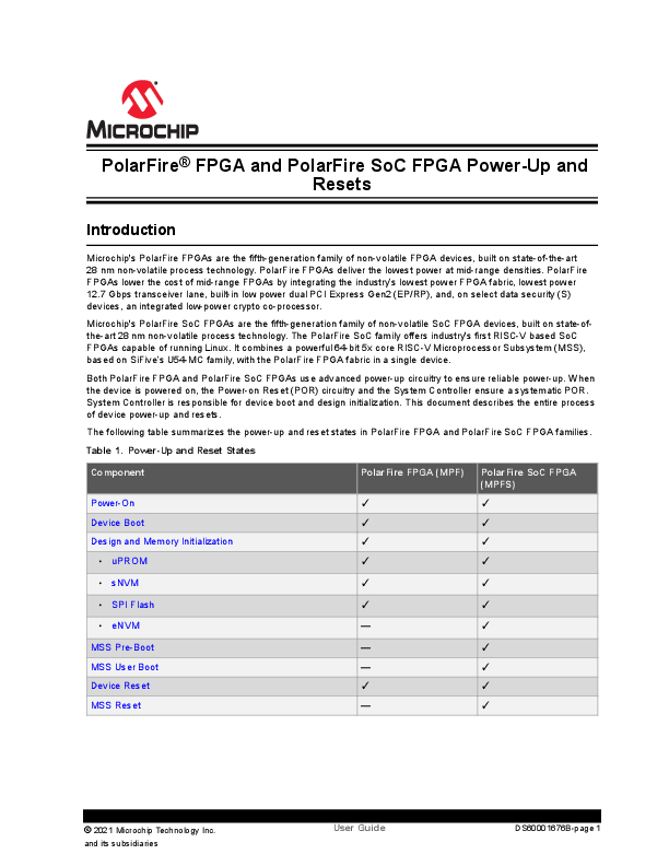
Microchip's PolarFire FPGAs are the fifth-generation family of non-volatile FPGA devices, built on state-of-the-art 28 nm non-volatile process technology. PolarFire FPGAs deliver the lowest power at mid-range densities. PolarFire FPGAs lower the cost of mid-range FPGAs by integrating the industry's lowest power FPGA fabric, lowest power 12.7 Gbps transceiver lane, built-in low power dual PCI Express Gen2 (EP/RP), and, on select data security (S) devices, an integrated low-power crypto co-processor.
Microchip's PolarFire SoC FPGAs are the fifth-generation family of non-volatile SoC FPGA devices, built on state-ofthe-art 28 nm non-volatile process technology. The PolarFire SoC family offers industry's first RISC-V based SoC FPGAs capable of running Linux. It combines a powerful 64-bit 5x core RISC-V Microprocessor Subsystem (MSS), based on SiFive's U54-MC family, with the PolarFire FPGA fabric in a single device.
Both PolarFire FPGA and PolarFire SoC FPGAs use advanced power-up circuitry to ensure reliable power-up. When the device is powered on, the Power-on Reset (POR) circuitry and the System Controller ensure a systematic POR. System Controller is responsible for device boot and design initialization. This document describes the entire process of device power-up and resets.
The following table summarizes the power-up and reset states in PolarFire FPGA and PolarFire SoC FPGA families.
Table 1.Power-Up and Reset States
Component
Power-On Device Boot Design and Memory Initialization
� uPROM
PolarFire FPGA (MPF)
PolarFire SoC FPGA (MPFS)
� sNVM
� SPI Flash
� eNVM
--
MSS Pre-Boot MSS User Boot Device Reset MSS Reset
--
--
--
� 2021 Microchip Technology Inc.
and its subsidiaries
User Guide
DS60001676B-page 1
References
� For more information about embedded memory blocks, see PolarFire FPGA and PolarFire SoC FPGA Fabric User Guide.
� For more information about MSS booting, see PolarFire SoC Software Development and Tool Flow User Guide.
� For more information about PCIe initialization process, see PolarFire FPGA and PolarFire SoC FPGA PCI Express User Guide.
� For more information about Power-Up to Functional Timing, see PolarFire FPGA Datasheet or PolarFire SoC FPGA Advance Datasheet.
� For more information about MSS, see PolarFire SoC FPGA MSS Technical Reference Manual.
� For more information on power supply sequencing requirements and recommendations, see UG0726: PolarFire FPGA Board Design User Guide or UG0901: PolarFire SoC Board Design Guidelines User Guide.
� 2021 Microchip Technology Inc.
and its subsidiaries
User Guide
DS60001676B-page 2
Table of Contents
Introduction.....................................................................................................................................................1 1. References................................................................................................................................... 2
1. Acronyms................................................................................................................................................ 4
2. Power-Up................................................................................................................................................ 5 2.1. Power-On..................................................................................................................................... 5 2.2. Device Boot.................................................................................................................................. 5 2.3. Design and Memory Initialization................................................................................................. 6 2.4. MSS Pre-Boot (For PolarFire SoC FPGA Only).........................................................................23 2.5. MSS User Boot (For PolarFire SoC FPGA Only)....................................................................... 29 2.6. HSIO/GPIO Bank Initialization....................................................................................................29 2.7. IO Recalibration..........................................................................................................................31 2.8. Transceiver Initialization............................................................................................................. 32 2.9. User PLLs and DLLs Initialization.............................................................................................. 33 2.10. PCIe Initialization........................................................................................................................33 2.11. State of Blocks During Power-Up...............................................................................................33
3. PolarFire FPGA Resets.........................................................................................................................35 3.1. Hard Resets............................................................................................................................... 35 3.2. User Reset Generation Scheme................................................................................................ 36
4. PolarFire SoC FPGA Resets.................................................................................................................38 4.1. User Resets................................................................................................................................38 4.2. MSS Resets............................................................................................................................... 39 4.3. User Reset Generation Scheme................................................................................................ 41
5. Appendix: Power Supplies.................................................................................................................... 44
6. Revision History.................................................................................................................................... 45
The Microchip Website.................................................................................................................................46
Product Change Notification Service............................................................................................................46
Customer Support........................................................................................................................................ 46
Microchip Devices Code Protection Feature................................................................................................ 46
Legal Notice................................................................................................................................................. 47
Trademarks.................................................................................................................................................. 47
Quality Management System....................................................................................................................... 48
Worldwide Sales and Service.......................................................................................................................49
� 2021 Microchip Technology Inc.
and its subsidiaries
User Guide
DS60001676B-page 3
1. Acronyms
The following table lists the acronyms used in this document.
Table 1-1.List of Acronyms
Acronym AMBA eNVM MSS POR SCB sNVM HSIO GPIO PLL DLL FIC PCIe
Expanded ARM Advanced Microcontroller Bus Architecture embedded Non-Volatile Memory Microprocessor Subsystem Power on Reset System Controller Bus Secure Non-volatile Memory High-speed IO General Purpose IO Phase-locked loop Delay-locked loop Fabric Interface Controller Peripheral Component Interconnect Express
Acronyms
� 2021 Microchip Technology Inc.
and its subsidiaries
User Guide
DS60001676B-page 4
Power-Up
2. Power-Up
The device power-up process includes the following sequential steps:
� 2.1 Power-On � 2.2 Device Boot � 2.3 Design and Memory Initialization � 2.4 MSS Pre-Boot (For PolarFire SoC FPGA Only) � 2.5 MSS User Boot (For PolarFire SoC FPGA Only) � 2.6 HSIO/GPIO Bank Initialization � 2.8 Transceiver Initialization � 2.9 User PLLs and DLLs Initialization � 2.10 PCIe Initialization � 2.11 State of Blocks During Power-Up
2.1 Power-On
When the device is powered on, the POR circuitry detects voltage ramp-up on the VDD, VDD18, and VDD25 power supply rails using voltage detectors. For a list of power supplies, see 5. Appendix: Power Supplies. The System Controller remains in the reset state until the required voltage threshold levels are reached. The System Controller is responsible enabling, or turning on the FPGA fabric and related IOs.
The voltage detectors in the devices are calibrated with a high-level of accuracy to ensure reliable monitoring of minimum threshold levels. For power-supply threshold voltage levels to release POR, see the "Power-on Reset Voltages" section in respective PolarFire FPGA Datasheet or PolarFire SoC FPGA Advance Datasheet. The device boot starts after a programmable delay of 20 �s to 50 ms and also after the voltage supply rails reach their respective threshold voltage levels.
In both the device families, there are separate voltage detectors to monitor IO bank supplies. During POR, the dedicated IO bank is powered-up, the serial transceivers and the fabric are powered down, and HSIO/GPIO banks are tri-stated. Separate detectors in the associated IO bank controller (for Bank 3) detect when the VDDI3 is at the level required to allow enabling the inputs and subsequently (after a delay of 200 ns) the outputs of the dedicated IO bank (including SPI configuration and JTAG IO).
For more information on power supply sequencing requirements and recommendations, see the "Core Power Supply Operations" section, in respective UG0726: PolarFire FPGA Board Design User Guide or UG0901: PolarFire SoC Board Design Guidelines User Guide.
2.2 Device Boot
After POR circuitry releases the System Controller from reset, the device boot-up procedure is executed by the System Controller to bring-up FPGA fabric and related IOs. The System Controller always executes the same device boot-up sequence irrespective of the user design.
The following events occur during device boot-up:
� sNVM is powered up and enabled for normal operation. � Transceiver IOs are enabled. � User voltage detectors are enabled. � FPGA fabric is powered-up and enabled. � HSIO and GPIO banks are configured based on the user configuration in the Libero� SoC
� Only GPIO can be used before calibration. � MSS is powered down and MSSIOs are tri-stated (for PolarFire SoC FPGA only).
The following illustration shows the boot-up sequence for a programmed PolarFire FPGA device.
� 2021 Microchip Technology Inc.
and its subsidiaries
User Guide
DS60001676B-page 5
Figure 2-1.Device Boot-Up for PolarFire FPGA
Power-Up
2.3 Design and Memory Initialization
When the device boot is completed, the state of the RAM blocks (LSRAMs and �SRAMs) zeros after power-up. In both the device families, the fabric RAM blocks can be initialized with known values, if desired. PCIe and XCVR blocks used in the design are initialized with the user configuration data at power-up. The System Controller performs the design and memory initialization during the power-up sequence. The memory initialization data can be stored in �PROM, sNVM, or an external SPI Flash. The storage location of the initialization data is selected during the Libero design flow. The initialization data can be encrypted for storing in external SPI Flash.
The following figure shows the sequence in which the fabric, PCIe, Transceiver, LSRAMs, and �SRAMs are automatically initialized. The sequence is customized depending on the resources instantiated in the user design. For example, the PCIE_INIT_DONE will not assert if the user design does not contain PCIe. As a result, the sequence skips the PCIe initialization and moves to the next step. At this stage in PolarFire SoC FPGA device, the MSS remains in reset.
In Libero SoC, memory initialization can be done using any of the following methods:
� Importing the content file using the fabric RAMs tab of the Configure Design Initialization Data and Memories option after Place and Route is performed. For more information, see 2.3.5 How To Set Up Design and Memory Initialization.
� Importing the content file using the LSRAM and �SRAM Configurator before Place and Route. For more information, see 2.3.7 RAM Initialization Before Place and Route.
The user can monitor the design initialization status using the Initialization Monitor.
� 2021 Microchip Technology Inc.
and its subsidiaries
User Guide
DS60001676B-page 6
Figure 2-2.Power-up To Functional Time
Power-Up
The typical PUFT takes about 100 clock cycles to assert SUSPEND_EN after Device Initialization (Device_Init_done) is done. For more information about typical PUFT, see respective PolarFire FPGA Datasheet or PolarFire SoC Advance Datasheet.
The total power-up to functional time is as shown in the following equation:
tPUFT = tFAB_READY(cold/warm) + max((tPCIE + tXCVR + tLSRAM + tUSRAM), tCALIB)
PUFT is variable depending on the design configuration.
Notes: � Both the device families have built-in tamper detection features to monitor voltage supplies and flags to detect minimum or maximum threshold values. These flags are valid only after design initialization, and not during POR. � Power-up To Functional Time is based on the case where VDDI/VDDAUX of IO banks are powered either before or after VDD/VDD18/VDD25. The IO bank enable time is measured from the assertion time of VDD/VDD18/ VDD25. If VDDI/VDDAUX of IO banks are powered sufficiently after VDD/VDD18/VDD25, then the IO bank enable time is measured from the assertion of VDDI/VDDAUX. In this case, IO operation is indicated by the assertion of BANK_#_VDDI_STATUS, rather than being measured relative to FABRIC_POR_N negation. � The assertion of AUTOCALIB_DONE can occur before or after the assertion of DEVICE_INIT_DONE. The time taken for the assertion of AUTOCALIB_DONE depends on: � The time when VDDI/VDDAUX is up after VDD/VDD18/VDD25 is powered on. � The ramp times of VDDI of each IO bank designated for auto-calibration. � How much auto-initialization is to be performed for the PCIe, SerDes transceivers and fabric LSRAMs. � If any of the IO banks specified for auto-calibration do not have their VDDI/VDDAUX powered on within the auto-calibration timeout window, then it auto-calibrates whenever VDDI/VDDAUX is subsequently powered on. To obtain an accurate calibration on such IO banks, it is necessary to initiate a re-calibration (using CALIB_START from fabric). � SUSPEND_EN asserts (if the suspend mode is enabled) when DEVICE_INIT_DONE or AUTOCALIB_DONE is asserted.
The following signals are asserted during the design initialization:
� DEVICE_INIT_DONE: asserted once the execution of design initialization is complete and remains high. If the PFSoC_INIT_MONITOR IP output DEVICE_INIT_DONE is used as INIT_DONE input to the CORERESET_PF IP, then MSS gets operational after DEVICE_INIT_DONE. Also, MSS can be configured without using DEVICE_INIT_DONE, which is independent of PFSoC_INIT_MONITOR IP. This signal is used as source for generating system-level reset and CORERESET_PF IP controls the MSS reset.
� 2021 Microchip Technology Inc.
and its subsidiaries
User Guide
DS60001676B-page 7
Power-Up
� FABRIC_POR_N: de-asserted when the fabric is operational. � PCIE_INIT_DONE: used by fabric logic to hold PCIe-related fabric logic in reset until the PCIe controller is
initialized. PCIE_INIT_DONE is asserted after initializing the PCIe lane instances placed in the PCIe quad. If only XCVR lanes are placed in the PCIe quad, only XCVR_INIT_DONE is asserted. � XCVR_INIT_DONE: asserted when the XCVR block is initialized. � SRAM_INIT_DONE: asserted when the LSRAM blocks are initialized. � USRAM_INIT_DONE: asserted when the �SRAM blocks are initialized. � BANK_#_CALIB_STATUS: This signal can be used by user logic to determine if the calibration completes for each IO banks. # denotes the bank number (0,1, 7, 8, and 9). � BANK_#_VDDI_STATUS: This signal can be used to monitor status of VDDI supply on specific IO banks. This signal is the output signal from the INIT_MONITOR IP if any of the corresponding bank is selected. # denotes the bank number (0,1, 7, 8, and 9). � SRAM_INIT_FROM_SNVM_DONE: asserted when SRAM is initialized from sNVM. � USRAM_INIT_FROM_SNVM_DONE: asserted when USRAM is initialized from sNVM. � SRAM_INIT_FROM_UPROM_DONE: asserted when SRAM is initialized from �PROM. � USRAM_INIT_FROM_UPROM_DONE: asserted when USRAM is initialized from �PROM. � SRAM_INIT_FROM_SPI_DONE: asserted when SRAM is initialized from SPI. � USRAM_INIT_FROM_SPI_DONE: asserted when USRAM is initialized from SPI.
PolarFire Initialization Monitor
PolarFire Initialization Monitor (PF_INIT_MONITOR) macro is available in the IP Catalog under Clock and Management as shown in the following figure.
� 2021 Microchip Technology Inc.
and its subsidiaries
User Guide
DS60001676B-page 8
Figure 2-3.PolarFire Initialization Monitor Configurator
Power-Up
The following figure shows the Dynamic Recalibration tab.
� 2021 Microchip Technology Inc.
and its subsidiaries
User Guide
DS60001676B-page 9
Figure 2-4.PolarFire Initialization Monitor Configurator - Dynamic Recalibration
Power-Up
PolarFire Initialization Monitor provides simulation support. Use the Simulation Options tab to specify the time of releasing the output signals from the zero time instance. The following figure shows the Simulation Options tab.
� 2021 Microchip Technology Inc.
and its subsidiaries
User Guide
DS60001676B-page 10
Figure 2-5.PolarFire Initialization Monitor Configurator - Simulation Options
Power-Up
Note: IOs must be calibrated before initiating the training logic of the DDR controller. This requires generating a reset signal by ANDing the DEVICE_INIT_DONE and BANK_#_CALIB_STATUS signals of the PFSOC_INIT_MONITOR IP. BANK_# refers to the BANK where DDR subsystem is placed.
PolarFire SoC Initialization Monitor
PolarFire SoC Initialization Monitor (PFSOC_INIT_MONITOR) macro is available in the IP Catalog under Clock and Management as shown in the following figure.
� 2021 Microchip Technology Inc.
and its subsidiaries
User Guide
DS60001676B-page 11
Figure 2-6.PolarFire SoC Initialization Monitor Configurator
Power-Up
The following figure shows the Dynamic Recalibration tab.
� 2021 Microchip Technology Inc.
and its subsidiaries
User Guide
DS60001676B-page 12
Figure 2-7.PolarFire SoC Initialization Monitor Configurator - Dynamic Recalibration
Power-Up
PolarFire SoC Initialization Monitor provides simulation support. Use the Simulation Options tab to specify the time of releasing the output signals from the zero time instance. The following figure shows the Simulation Options tab.
� 2021 Microchip Technology Inc.
and its subsidiaries
User Guide
DS60001676B-page 13
Figure 2-8.PolarFire SoC Initialization Monitor Configurator - Simulation Options
Power-Up
2.3.1
Note: IOs must be calibrated before initiating the training logic of the DDR controller. This requires generating a reset signal by ANDing the DEVICE_INIT_DONE and BANK_#_CALIB_STATUS signals of the PFSOC_INIT_MONITOR IP. BANK_# refers to the BANK where DDR subsystem is placed.
Secured Non-Volatile Memory (sNVM) Each device has 56 Kbytes of sNVM, organized into 221 pages of 236 or 252 bytes depending on whether the data is stored as plain text or encrypted/authenticated data. It can be accessed through system service calls to the System Controller. Pages within the sNVM can be marked as ROM during bit-stream programming. The sNVM content can be used to initialize LSRAMs and �SRAMs with secure data.
The following formulas applies where there is at least one LSRAM or USRAM to be auto-initialized in the user design, giving a duration in milliseconds.
tLSRAM_pt_SNVM = ((14.0875+(541.4125�L))/1000)�6%
tUSRAM_pt_SNVM = ((14.0875+(29.325�L))/1000)�6%
Where,
L = Number of LSRAMs to be auto-initialized
U = Number of small SRAMs to be auto-initialized
Note: pt in "tLSRAM_pt_SNVM" and "tUSRAM_pt_SNVM" refers to "plaintext" .
� 2021 Microchip Technology Inc.
and its subsidiaries
User Guide
DS60001676B-page 14
Power-Up
2.3.2
Embedded Non-Volatile Memory (eNVM) (For PolarFire SoC FPGA Only)
PolarFire SoC FPGA devices include one embedded non-volatile memory (eNVM) block size of 128 KB. eNVM supports Single error correction and dual error detection (SECDED) protected, High Data Retention Time. For more information, see PolarFire FPGA and PolarFire SoC FPGA Security User Guide.
2.3.3
�PROM Both the device families have a micro programmable read-only memory (PROM) row located at the bottom of the fabric, providing up to 513 Kbytes of non-volatile, read-only memory. The address bus is 16-bit wide and the read data bus is 9-bit wide. Fabric logic has access to the entire PROM data.
The following formulas apply where there is at least one LSRAM or USRAM to be auto-initialized in the user design, giving a duration in milliseconds.
tLSRAM_pt_UPROM = ((30.1325+(663.7125�L))/1000)�6%
tUSRAM_pt_UPROM = ((30.1325+(28.75�U))/1000)�6%
Where,
L = Number of LSRAMs to be auto-initialized
U = Number of small SRAMs to be auto-initialized
Note: pt in "tLSRAM_pt_UPROM" and "tUSRAM_pt_UPROM" refers to "plaintext" .
2.3.4 2.3.4.1
2.3.4.2 2.3.4.3
External SPI Flash The SPI Flash memory interfaces with the System Controller's SPI interface and can store the programming images. The System Controller supports devices from vendors like Micron, Winbond, and Spansion.
Fabric SRAM (tLSRAM and tUSRAM) in SPI Flash can be initialized using Plaintext Initialization Data, Authenticated Plaintext Initialization Data, and Authenticated Encrypted Initialization Data.
If user design does not require the auto-initialization of any large FPGA fabric SRAMs, the tLSRAM parameter is zero. If user design does not require the auto-initialization of any small FPGA fabric SRAMs (USRAMs), the tUSRAM parameter is zero.
Plaintext Initialization Data Without Authentication The following formulas apply where there is at least one LSRAM or USRAM to be auto-initialized in the user design from SPI Flash, giving a duration in milliseconds.
tLSRAM_pt = [[{(ROUNDUP(4.034�L)+1)�8192/f} + (130�L)]/1000]+1 �6%
tUSRAM_pt = [[{(ROUNDUP(0.144�U)+1)�8192/f} + (25�U)]/1000]+1 �6%
Where,
L = Number of LSRAMs to be auto-initialized
U = Number of small SRAMs to be auto-initialized
f = Frequency of the SPI clock in MHz
Note: pt in "tLSRAM_pt" and "tUSRAM_pt" refers to "plaintext" .
Authenticated Plaintext Initialization Data If authentication of the plaintext initialization data is selected, an additional 103 ms � 6% must be added to the tLSRAM_pt and tUSRAM_pt timing parameters.
Note: pt in "tLSRAM_pt" and "tUSRAM_pt" refers to "plaintext" .
Authenticated Encrypted Initialization Data The following formula calculates the additional time required for LSRAM to perform the encryption.
tLSRAM_enc = tLSRAM_pt+tLSRAM_auth+((ROUNDUP((L�2560)/1024,1)+1)�1024�8/Dlsram)/1000
Where, pt in "tLSRAM_pt" refers to "plaintext".
Note: Dlsram depends on the SPI SCK frequency.
� 2021 Microchip Technology Inc.
and its subsidiaries
User Guide
DS60001676B-page 15
Power-Up
2.3.5
The following table lists the LSRAM encrypted data divisor settings. Table 2-1.LSRAM Encrypted Data Divisor Settings SPI_SCK frequency (MHz) 13.33 20 40
Dlsram 180 30 15
The following formula calculates the additional time required for USRAM to perform the encryption.
tUSRAM_enc = tUSRAM_pt+tUSRAM_auth+((ROUNDUP((U�2560)/1024,1)+1)�1024�8/Dusram)/1000
Where,
� tLSRAM_pt = tLSRAM � tUSRAM_pt = tUSRAM � auth in "tLSRAM_auth" and "tUSRAM_auth" refers to "Authenticated Plaintext". � pt in "tUSRAM_pt" refers to "plaintext". � tLSRAM_auth = tUSRAM_auth = 103ms � 6%.
Note: Dusram depends on the SPI SCK frequency.
The following table lists the USRAM encrypted data divisor settings.
Table 2-2.USRAM Encrypted Data Divisor Settings
SPI_SCK frequency (MHz) 20 40
Dlsram 45 20
For SPI_SCK frequency of 13.3 MHz, the formula is as follows: tUSRAM_enc = tUSRAM_pt + tUSRAM_auth + 0.01
How To Set Up Design and Memory Initialization
This section describes how to initialize PCIe, transceivers, and fabric RAM blocks using the Configure Design Initialization Data and Memories option in Libero SoC. Design and Memory Initialization is divided into three stages of initialization as shown in the following figure.
� 2021 Microchip Technology Inc.
and its subsidiaries
User Guide
DS60001676B-page 16
Figure 2-9.Design and Memory Initialization
Power-Up
1. The first stage client is responsible for bring-up of FPGA fabric and related IOs, and then de-asserts the FABRIC_POR_N signal. This client is stored in the sNVM at the top of the address space.
2. The second stage client initializes the PCIe and XCVR blocks present in the design. The client is stored in the sNVM and the starting address of the client is configurable.
3. The third stage client initializes the fabric RAMs present in the design. Each logical RAM in the design can be initialized from a different Storage Type--sNVM, �PROM, or SPI Flash. The starting address of these storage types is configurable.
Note: The second stage client initializes the PCIe and XCVR blocks present in the design. Import a text file to change the default PCIe/XCVR register values (custom configuration). This will modify the Stage 2 generated assembly file (from default flow). The format in the text file to change the register content is as follows: Instance_Name, Register:Field_Name, and Hex value separated by spaces. For example: PF_PCIE_0/PCIESS_LANE0_Pipe_AXI0 SER_DRV_CTRL:TXDRVTRIM 0xFFFFFF
Note: When initializing the RAM from SPI Flash, ensure that the System Controller SPI interface is in the Master mode by setting the IO_CFG_INTF pin to 1.
Note: The SPI Clock divider value specifies the required SPI SCK frequency to read the initialization data from SPI Flash. The SPI Clock divider value must be selected based on the external SPI Flash operating frequency range.
Table 2-3.SPI Clock Divider Value
SPI Clock Divider Value 1 2 4 6
SCK Frequency 80 MHz 40 MHz 20 MHz 13.3 MHz
Follow these steps to initialize fabric RAMs at power-up:
1. Select the required logical RAM from the Fabric RAMs tab and click Edit. The Edit Fabric RAM Initialization Client window provides the following options to: � Initialize the client from an Intel-Hex (*.hex), Simple-Hex(*.shx), Motorola-S (*.s), or Microchip Binary (*.mem)
� 2021 Microchip Technology Inc.
and its subsidiaries
User Guide
DS60001676B-page 17
� Initialize the client with Zeros � Create the client as a placeholder with no content � Select Storage Type for the client
Figure 2-10.Fabric RAMs
Power-Up
2. After configuring the RAM initialization client, click Apply on the Fabric RAMs tab.
3. Select Generate Design Initialization Data under Design Flow tab. It automatically generates the first, second, and third stage initialization clients, which are automatically added to the non-volatile memory that the user chooses. The Generate Design Initialization Data is highlighted as shown in the following figure.
� 2021 Microchip Technology Inc.
and its subsidiaries
User Guide
DS60001676B-page 18
Figure 2-11.Generate Design Initialization Data
Power-Up
The initialization clients are added to the respective tab--�PROM, SNVM, SPI Flash, or eNVM (for PolarFire SoC FPGA only)--as shown in the following figure. Figure 2-12.Initialization Clients Generated in sNVM
Note: The second stage client is added to sNVM if the user design includes the PCIe or XCVR block. If SPI Flash is selected as the storage type, the initialization client is added to the SPI Flash tab as shown in the following figure.
� 2021 Microchip Technology Inc.
and its subsidiaries
User Guide
DS60001676B-page 19
Figure 2-13.Third Initialization Client on SPI Flash
Power-Up
4. If an external SPI Flash is chosen for stage 3, before completing the Run PROGRAM Action, you should generate Generate SPI Flash Image and Run PROGRAM_SPI_IMAGE Action from the Design Flow tab, as shown in the following figure.
Figure 2-14.Program SPI Flash Image
2.3.5.1 2.3.5.2
These steps ensure that PCIe, XCVR, and Fabric RAMs present in the design are initialized during power-up using initialization clients placed in the non-volatile memory based on the user selection.
SPI Flash Client Configuration Memory initialization data stored in SPI Flash can be encrypted and binded with the device. The Design Initialization tab provides the following encryption/binding options:
� SPI Flash � Binding Encrypted with Default Key In this case, KLK is used as the root key for authentication and encryption/decryption
� SPI Flash � Binding Encrypted with User Encryption Key 1 (UEK1) In this case, UEK1 is used as the root key for authentication and encryption/decryption
� SPI Flash � Binding Encrypted with User Encryption Key 2 (UEK2) In this case, UEK2 is used as the root key for authentication and encryption/decryption
eNVM Client Configuration (For PolarFire SoC FPGA Only) If eNVM is selected as the storage type, the initialization client is added to the eNVM tab as shown in the following figure. Once the initialization client is added to the eNVM, double-click Generate Bitstream from the Design Flow tab.
Figure 2-15.Fourth Stage Initialization Client in eNVM
� 2021 Microchip Technology Inc.
and its subsidiaries
User Guide
DS60001676B-page 20
Power-Up
2.3.6 2.3.7
Power-up To Functional (PUFT) Timing Data Report The information about PUFT timing data is available in the Design Initialization Data and Memories report of the Libero SoC. To indicate the completion of initialization of each block, such as PCIE, XCVR, RAMs, a signal is asserted as part of device initialization after power-up (this is done as part of UIC). For example, PCIE_INIT_DONE signal is asserted after all the PCIE related registers are configured. The last signal that is asserted is DEVICE_INIT_DONE.
In cases of PCIE and XCVR blocks, the number of instructions used to initialize the registers of that block are counted after FABRIC_POR is asserted in each case. Software implementation of PUF timing for any signal is a product of `number of instructions' and a constant (average time taken for one UIC instruction). This number is added to the report for every signal.
PUFTsignal = (Number_Of_Instructions � Constant ) ns
This constant is based on the run time (of UIC script) data collected. Based on the number of instructions in that design and the amount of time taken by UIC, the average time taken for one UIC instruction is calculated.
In case of SRAM and �SRAM blocks, the amount of time taken to initialize vary from number of blocks measured on a device. This average time to initialize one block is used to compute the PUF timing of that signal. There is a constant time taken by system controller to copy the data to initialize the first block (Constant_Copy_Time). When the first block is being initialized, the data for initializing the second block is copied in background.
PUFTsignal = Constant_Copy_Time + (Number_Of_Blocks � Average_Time_to_Init_One_Block ) ns
These signals are asserted in a sequence so the PUFT timing for each signal depends on:
� The previous block(s) in the sequence being instantiated in the user design (or not) � The configuration of the block (Some configurations may need a few additional registers.)
SRAMs and �SRAMs can be initialized from different storage locations (sNVM, UPROM, and SPI). In the case of SPI, additional data needs to be collected depending on the SPI clock divider value and the encryption type selected.
RAM Initialization Before Place and Route During Fabric RAM IP core creation, the content file can be imported for simulation. The path of the content file is stored and passed to the Design and Memory Initialization stage.
Follow these steps to initialize Fabric RAM using LSRAM and �SRAM configurator:
1. In the PF Two-Port Large SRAM Configurator window, select the Memory Initialization Settings tab. Then, select the Initialize RAM at Power-up check box as shown in the following figure.
� 2021 Microchip Technology Inc.
and its subsidiaries
User Guide
DS60001676B-page 21
Figure 2-16.PF Two-Port Large SRAM Configurator Window
Power-Up
2. Select the Import File option and import memory content file (Intel-Hex) from the Import Memory Content dialog box, as shown in the following figure. File extensions are set to *.hex for Intel-Hex files during import. The imported memory content is displayed in the RAM Content Editor pane.
� 2021 Microchip Technology Inc.
and its subsidiaries
User Guide
DS60001676B-page 22
Figure 2-17.Import Memory Content
Power-Up
3. After Place and Route, select the storage type for the content file and generate the initialization client using the procedure mentioned in 2.3.5 How To Set Up Design and Memory Initialization.
For more information about LSRAM and �SRAM Configurators and user options, see the "Embedded Memory Blocks" section in PolarFire FPGA and PolarFire SoC FPGA Fabric User Guide.
2.4 MSS Pre-Boot (For PolarFire SoC FPGA Only)
Upon successful completion of Design Initialization, MSS Pre-boot starts its execution. The MSS is released from a reset after completion of all normal startup procedures. The System Controller manages the programming, initialization, and configuration of the devices. For ES devices, MSS Pre-boot does not occur if the programmed device is configured for System Controller suspend mode.
The MSS pre-boot phase of initialization is coordinated by System Controller firmware, although it may make use of the E51 in the MSS Core Complex to perform certain parts of the pre-boot sequence.
The following events occur during the MSS pre-boot stage:
� Power-up of the MSS embedded Non-Volatile Memory (eNVM) � Initialization of the redundancy repair associated with the MSS Core Complex L2 cache � Authentication of User boot code (if User Secure boot option is enabled) � Handover operational MSS to User Boot code
The MSS Core Complex can be booted in one of four modes. The following table lists the MSS pre-boot options, which can be configured and programmed into the sNVM. The boot mode is defined by the user parameter U_MSS_BOOTMODE[1:0]. Additional boot configuration data is mode-dependent and is defined by the user parameter U_MSS_BOOTCFG (see Table 2-6 and Table 2-8 ).
� 2021 Microchip Technology Inc.
and its subsidiaries
User Guide
DS60001676B-page 23
Power-Up
Table 2-4.MSS Core Complex Boot Modes
U_MSS_BOOTMODE[1:0] 0
1
Mode Idle boot
Non-secure boot
Description
MSS Core Complex boots from boot ROM if MSS is not configured
MSS Core Complex boots directly from address defined by the U_MSS_BOOTADDR
2
User secure boot
MSS Core Complex boots from sNVM
3
Factory secure boot MSS Core Complex boots using the factory secure boot
protocol
The boot option is selected as part of the Libero design flow. Changing the mode can only be achieved through the generation of a new FPGA programming file.
Figure 2-18.MSS Pre-boot Flow
Power-on Reset
IO Initialization and RAM Redundancy
Power-up and Configure eNVM
U_MSS_ BOOTMODE =0
U_MSS_ BOOTMODE =1
U_MSS_ BOOTMODE
U_MSS_ BOOTMODE =2
U_MSS_ BOOTMODE =3
Idle Boot
Non-Secure Boot
User Secure Boot
Factory Secure Boot
2.4.1
Idle Boot If the MSS is not configured (For example, blank device), then the MSS Core Complex executes a boot ROM program which holds all the processors in an infinite loop until a debugger connects to the target. The boot vector registers maintain their value until the device is reset or a new boot mode configuration is programmed. For configured devices, this mode can be implemented using the U_MSS_BOOTMODE=0 boot option in the Libero configurator.
Note: In this mode, U_MSS_BOOTCFG is not used.
The following figure shows the Idle boot flow.
� 2021 Microchip Technology Inc.
and its subsidiaries
User Guide
DS60001676B-page 24
Figure 2-19.Idle Boot Flow
Idle Mode U_MSS_BOOTMODE=0
Set BOOTVEC = BOOTROM
All processors execute infinite loop until debugger launch
All processors in Debug Mode
Power-Up
Application Execution
2.4.2
Non-Secure Boot In this mode, the MSS Core Complex executes from a specified eNVM address without authentication. It provides the fastest boot option, but there is no authentication of the code image. The address can be specified by setting U_MSS_BOOTADDR in the Libero Configurator. This mode can also be used to boot from any FPGA fabric memory resource through FIC. This mode is implemented using the U_MSS_BOOTMODE=1 boot option.
The MSS Core Complex is released from reset with boot vectors defined by U_MSS_BOOTCFG (as listed in the following table).
Table 2-5.U_MSS_BOOTCFG Usage in Non-Secure Boot Mode 1
Offset (bytes) 0
Size (bytes) 4
Name BOOTVEC0
Description Boot vector for E51
4
4
BOOTVEC1
Boot vector for U540
8
4
BOOTVEC2
Boot vector for U541
16
4
20
4
BOOTVEC3 BOOTVEC4
Boot vector for U542 Boot vector for U543
The following figure shows the Non-Secure boot flow.
� 2021 Microchip Technology Inc.
and its subsidiaries
User Guide
DS60001676B-page 25
Figure 2-20.Non-Secure Boot Flow
Non-Secure Boot U_MSS_BOOTMODE=1
Power-Up
Set BOOTVEC = eNVM or Fabric
All processors execute application
2.4.3
User Secure Boot This mode allows user to implement their own custom secure boot and the user secure boot code is placed in the sNVM. The sNVM is a 56 Kbytes non-volatile memory that can be protected by the built-in physically unclonable function (PUF). This boot method is considered secured because sNVM pages marked as ROM are immutable. On power up, the System Controller copies the user secure boot code from sNVM to Data Tightly Integrated Memory (DTIM) of the E51 Monitor core. E51 starts executing the user secure boot code.
If the size of the user secure boot code is more than the size of the DTIM then user needs to split the boot code into two stages. The sNVM may contain the next stage of the user boot sequence, which may perform authentication of the next boot stage using the user authentication/decryption algorithm.
If authenticated or encrypted pages are used, then the same USK key (that is, U_MSS_BOOT_SNVM_USK) must be used for all authenticated/encrypted pages.
If authentication fails, the MSS Core Complex can be placed in reset and the BOOT_FAIL tamper flag can be raised. This mode is implemented using the U_MSS_BOOTMODE=2 boot option.
Table 2-6.U_MSS_BOOTCFG Usage in User Secure Boot
Offset (bytes) Size (bytes) Name
Description
0
1
U_MSS_BOOT_SNVM_PAGE
Start page in SNVM
1
3
RESERVED
For alignment
4
12
U_MSS_BOOT_SNVM_USK
For authenticated/encrypted pages
The following figure shows the user secure boot flow.
� 2021 Microchip Technology Inc.
and its subsidiaries
User Guide
DS60001676B-page 26
Figure 2-21.Factory Secure Boot
User Secure Boot U_MSS_BOOTMODE=2
Set BOOTVEC = BOOTROM
System Controller copies the User Secure Boot
code from sNVM to E51 DTIM
E51 Executes User Secure Boot
No Error
Authentication of Next Stage
Boot Code
Error
Release Reset to MSS Core Complex
MSS Core Complex in Reset
Power-Up
All processors execute application
BOOT_FAIL Tamper Flag
Raised
Signal to Fabric
2.4.4
Factory Secure Boot
In this mode, the System Controller reads the Secure Boot Image Certificate (SBIC) from eNVM and validates the SBIC. On successful validation, System Controller copies the factory secure boot code from its private, secure memory area and loads it into the DTIM of the E51 Monitor core. The default secure boot performs a signature check on the eNVM image using SBIC which is stored in eNVM. If no errors are reported, reset is released to the MSS Core Complex. If errors are reported, the MSS Core Complex is placed in reset and the BOOT_FAIL tamper flag is raised. Then, the System Controller activates a tamper flag which asserts a signal to the FPGA fabric for user action. This mode is implemented using the U_MSS_BOOTMODE=3 boot option.
The SBIC contains the address, size, hash, and Elliptic Curve Digital Signature Algorithm (ECDSA) signature of the protected binary blob. ECDSA offers a variant of the DSA, which uses elliptic curve cryptography. It also contains the reset vector for each Hardware thread/core/processor core (Hart) in the system.
Table 2-7.Secure Boot Image Certificate (SBIC)
Offset 0
Size (bytes) 4
Value IMAGEADDR
Description Address of UBL in MSS memory map
� 2021 Microchip Technology Inc.
and its subsidiaries
User Guide
DS60001676B-page 27
Power-Up
...........continued
Offset
Size (bytes)
4
4
8
4
12
4
16
4
20
4
24
4
28
1
28
3
32
8
40
16
56
48
104
104
Total
208
Value IMAGELEN BOOTVEC0 BOOTVEC1 BOOTVEC2 BOOTVEC3 BOOTVEC4 OPTIONS[7:0] RESERVED
VERSION DSN H CODESIG Bytes
Description Size of UBL in bytes Boot vector in UBL for E51 Boot vector in UBL for U540 Boot vector in UBL for U541 Boot vector in UBL for U542 Boot vector in UBL for U543 SBIC options --
SBIC/Image version Optional DSN binding UBL image SHA-384 hash DER-encoded ECDSA signature --
DSN
If the DSN field is non-zero, it is compared against the device's own serial number. If the comparison fails, then the boot_fail tamper flag is set and authentication is aborted.
VERSION
If SBIC revocation is enabled by U_MSS_REVOCATION_ENABLE, the SBIC is rejected unless the value of VERSION is greater than or equal to the revocation threshold.
SBIC REVOCATION OPTION
If SBIC revocation is enabled by U_MSS_REVOCATION_ENABLE and OPTIONS[0] is `1', all the SBIC versions less than VERSION are revoked upon complete authentication of the SBIC. The revocation threshold remains at the new value until it increments again by a future SBIC with OPTIONS[0] = `1' and a higher VERSION field. The revocation threshold may only be incremented using this mechanism and can only be reset by a bit-stream.
When the revocation threshold is updated dynamically, the threshold is stored using the redundant storage scheme used for passcodes such that a power failure during device boot does not cause a subsequent device boot to fail. If the update of revocation threshold fails, it is guaranteed that the threshold value is either the new value or the previous one.
Table 2-8.U_MSS_BOOTCFG Usage in Factory Boot Loader Mode
Offset (bytes)
Size (bytes) Name
Description
0
4
U_MSS_SBIC_ADDR
Address of SBIC in MSS address space
4
4
U_MSS_REVOCATION_ENABLE Enable SBIC revocation if non-zero
The following figure shows the factory secure boot flow.
� 2021 Microchip Technology Inc.
and its subsidiaries
User Guide
DS60001676B-page 28
Figure 2-22.Factory Secure Boot Flow
Factory Secure Boot U_MSS_BOOTMODE=3
Set BOOTVEC = BOOTROM
System Controller reads the SBIC from eNVM
Power-Up
Yes Signature Valid
No
Copies Factory Secure Boot Loader from ROM to
E51 DTIM
MSS Core Complex in Reset
Set BOOTVEC = Factory Secure Boot Loader
Factory Secure Boot Loader calculates the hash `H' of the eNVM
image
BOOT_FAIL Tamper Flag
Raised
Signal to Fabric
Yes
Check SBIC .H = H
No
Set BOOTVEC = SBIC.BOOTVEC
Release Reset to MSS Core Complex
All processors execute application
2.5 MSS User Boot (For PolarFire SoC FPGA Only)
MSS user boot takes place when the control is given from System Controller to MSS Core Complex. Upon successful MSS pre-boot, System Controller releases the reset to the MSS Core Complex. MSS can be booted up in one of the following ways:
� Bare Metal Application � Linux Application � AMP Application
For more information about MSS booting, see PolarFire SoC Software Development and Tool Flow User Guide.
2.6 HSIO/GPIO Bank Initialization
Unused GPIO and HSIO banks can be left powered down or powered up. During the device power-up, the used GPIO and HSIO banks are simultaneously powered up along with all the other power supplies. All of the banks are initialized automatically with Flash configuration bits when fabric is powered up. All of the powered-up user IOs (HSIO/GPIO) go through an initial PVT calibration on power-up.
The time at which IOs are functional depends on a combination of the following:
� 2021 Microchip Technology Inc.
and its subsidiaries
User Guide
DS60001676B-page 29
Power-Up
� Device boot � Ramp-up time of the power applied to the IO banks � Calibration time of IOs (For example, DDR interfaces)
For low-speed operations below 100 MHz, IOs are functional after the power applied to IO banks exceeds the threshold levels. When GPIO is mapped to the OUTPUT PAD signals, the drive strength is weakened when initial calibration is complete. This occurs because the initial pre-calibrated drive strength is at maximum calibration code until IO calibration status/AUTOCALIB_DONE signal is asserted. It is recommended to monitor the IO calibration status/AUTOCALIB_DONE signal for both high-speed and low-speed signals because of the drive strength change.
If the user requires the IOs to be usable immediately upon completion of device boot, the IO power ramp time must be sufficiently short. The user can also apply slow or delayed IO power ramp times on IO banks to delay the time until which the IOs are usable. If the user is applying slow ramp rates to IO banks power supplies, the user logic in the fabric must monitor the state of the IO banks to know when they are usable as low-speed IOs.
Figure 2-23.Ramp-up Time
The high-speed IO calibration process occurs automatically. The user's design in the FPGA fabric must monitor the completion of IO calibration or AUTOCALIB_DONE to use the IOs for high-speed applications. The status of
� 2021 Microchip Technology Inc.
and its subsidiaries
User Guide
DS60001676B-page 30
Power-Up
the IO calibration and bank power supply can be monitored using the status signals of the PolarFire/PolarFire SoC Initialization Monitor IP. The following figure shows Auto calibration timeout settings. Configure the Timeout option based on selected GPIO or HSIO in the user design.
Figure 2-24.Auto Calibration Timeout
The PolarFire/PolarFire SoC Initialization Monitor asserts BANK_#_CALIB_STATUS and BANK_#_VDDI_STATUS signals to the fabric. BANK_#_CALIB_STATUS can be used by the user logic to determine if the calibration completes for each IO bank. BANK_#_VDDI_STATUS signal can be used to monitor VDDI supply on specific IO banks.
The DRI clock (DRI_CLK) must be gated off until the assertion of DEVICE_INIT_DONE, which asserts at the end of the complete device initialization.
2.7 IO Recalibration
The PF_INIT_MONITOR IP and PFSOC_INIT_MONITOR IP are used to control the IO recalibration or to monitor the initial IO calibration. The following figure shows the recalibration operation.
When IO recalibration is enabled, the following ports are exposed in PFSOC_INIT_MONITOR IP:
� BANK_#_CALIB_STATUS � BANK_#_CALIB_INTERRUPT � BANK_#_CALIB_LOCK � BANK_#_CALIB_LOAD � BANK_#_CALIB_START
The following figure shows the recalibration operation.
� 2021 Microchip Technology Inc.
and its subsidiaries
User Guide
DS60001676B-page 31
Power-Up
Figure 2-25.Recalibration Operation
calib_intrpt
calib_status calib_start
calibrated pvt code registered and buffered to IOA's
calibrated pvt code registered and buffered to IOA's
Start re-calibration
calib_lock
user initiated load
calib_load
Initial POR loads bank codes Automatically without user initiated load
bank code
default code
bank pvt code registered and buffered to IOA's initial code
The following steps describe the recalibration operation:
bank pvt code registered and buffered to IOA's new code
1. Start a new calibration. � user activation of "bank#_calib_start"=1. � This initiates the calibration sequence.
2. The calibration engine indicates it has a new code. � Calibration engine activates the signal "bank#_calib_interrupt"=1. � At this point the new calibration code is ready, but has not been released to the IOs. It is being held ready for when the user requires it.
3. The user indicated that the engine should send out the new code to the IOs. � User activates the "bank#_calib_lock"=1. � This latches the new codes and distributes to the IOs.
4. The calibration engine indicates the latching of the new codes is complete. � Calibration engine activates the "bank#_calib_status"=1. � This indicates the calibration is complete to the user and IOs.
Note: bank#_calib_load must be tied high.
2.8 Transceiver Initialization
Transceiver power-up depends on VDDA, VDDA25, and VDD_XCVR_CLK.
VDD_XCVR_CLK is applicable if an external reference clock is used for transceivers. For a list of power supplies, see 5. Appendix: Power Supplies. During power-up, glitches can occur in the reference clocks and the data bits. The transceiver is initialized by the Flash configuration bits and the design initialization client, which is executed from the sNVM.
When XCVR_INIT_DONE/DEVICE_INIT_DONE signal from PFSOC_INIT_MONITOR goes high, the transceiver is completely configured. The user logic using the XCVR clock must be held in reset until the XCVR_INIT_DONE signal is asserted.
The transceiver data pins are in hot-plug mode at power-up. Programming bits can be used to detect TX and/or RX termination early to enable fast Receiver Detection in standards such as PCI Express.
The time taken to complete initialization of the transceiver subsystem depends on the number of lanes to be configured and the number of different high-speed serial protocols to be configured. When QUAD0 with 1 Lane is initialized with Libero default values, the XCVR initialization time is 282 �s as listed in the following table. The worst case delay is calculated with all PCS and PMA register writes in stage 2 assembly file. For information about stage 2, see Design and Memory Initialization.
Table 2-9.XCVR Initialization Time
Flow Type
No. of Register Writes in Stage 2 Assembly File
XCVR Initialization Time
Default Flow (No modification to
61
generate files)
282 �s
� 2021 Microchip Technology Inc.
and its subsidiaries
User Guide
DS60001676B-page 32
...........continued Flow Type
Assembly File Modified Flow
Power-Up
No. of Register Writes in Stage 2 Assembly File
136
XCVR Initialization Time 594 �s
2.9 User PLLs and DLLs Initialization
Both PLLs and DLLs are initialized automatically with Flash configuration bits when fabric is powered up.
2.10
PCIe Initialization
To achieve the PCIe initialization requirement, the physical layer is configured using Flash configuration bits. The remaining configuration is done during design initialization with the user data stored in the non-volatile memory.
For resetting the PCIESS, use the PCIe_x_PERST_N sideband reset input.
For resetting PCIESS using drivers, use hot reset (in-band reset). A hot reset is propagated in-band from one link neighbor to another by sending several TS1 (training sequence 1 packets) with bit0 of symbol 5 asserted. These TS1 are sent on all lanes. Once sent, the Tx and Rx of hot reset end up in detect link training state machine (LTSSM) state. Hot reset is initiated by setting the secondary bus reset bit in the root ports bridge control configuration register.
The time taken to complete initialization depends on the number of lanes to be configured and the number of PCI controllers to be configured. When PCIE0 controller is initialized with Libero default values, the PCIE initialization time is 440 �s. When PCIE0 and PCIE1 are both enabled, the PCIE initialization time is 782 �s.
The worst case PCIE initialization time is calculated with all PCIe Controller and Bridge register writes in stage 2 assembly file as listed in the following table.
Table 2-10.PCIe Initialization Time
PCIE Controller Selection
PCIE0-Enabled PCIE1-Disabled
Default Flow (No Modification to Generated Files)
No. of Register Writes in Stage 2 Assembly File
PCIe Initialization Time
99
440 �s
Assembly File Modified Flow
No. of Register Writes in Stage 2 Assembly File
388
PCIe Initialization Time
937.5 �s
PCIE0-Enabled
185
PCIE1-Enabled
782 �s
745
1759 �s
For more information about PCIe initialization process, see PolarFire FPGA and PolarFire SoC FPGA PCI Express User Guide.
2.11
State of Blocks During Power-Up
The following table shows the state of different blocks during device power-up. Table 2-11.Default State During Device Power-Up
Block
POR
Device Boot
System Controller
Held in reset
Executing boot-up sequence
Design and Memory Initialization State
Performs design and memory initialization.
� 2021 Microchip Technology Inc.
and its subsidiaries
User Guide
DS60001676B-page 33
Power-Up
...........continued Block
POR
Device Boot
sNVM FPGA fabric array LSRAM
Held in reset Powered down Powered down
Power up sequence, then functional
Power up sequence, then functional
Powered up, uninitialized
�SRAM
Powered down
Powered up, uninitialized
�PROM
Powered down
Math block
Powered down
Transceiver and TX PLLs Powered down
Powered up
Powered up
Powered up but not functional Termination Optionally Enabled
GPIO/HSIO - Low Speed (if power is applied)
Input buffers are disabled and output buffers are tri-stated. GPIO buffers are in hot-plug mode.
Powered up but not usable GPIO buffers are in hot-plug mode.
HSIO buffers do not support hotplug capability
GPIO/HSIO - High-speed Input buffers are
(if power is applied)
disabled and output
buffers are tri-stated
GPIO buffers are in
hot-plug mode.
Powered up but not usable GPIO buffers are in hot-plug mode.
HSIO buffers do not support hotplug capability.
PCIe
Powered down
Powered up but not functional.
Transceiver IO
MSSIOs (for PolarFire SoC FPGA only) MSS (for PolarFire SoC FPGA only
Tri-stated and hotplug mode Tri-stated
Powered down
Tri-stated in hot-plug mode Termination optionally enabled. Tri-stated
Powered down
Design and Memory Initialization State Functional
Functional
Initialized with user data if configured. Initialized with user data if configured. Functional Functional Initialized with user data and functional.
Functional if IO and IO Auxiliary Supplies supply exceeds threshold.
Functional at high-speed after the completion of IO calibration if IO and IO Auxiliary Supplies are applied.
Initialized with user data and functional. Termination Enabled, operational.
Tri-stated
Powered down
Note: For more information about cold boot and warm boot power-up to functional time, see the "Power-Up to Functional Timing" section in respective PolarFire FPGA Datasheet or PolarFire SoC FPGA Advance Datasheet.
� 2021 Microchip Technology Inc.
and its subsidiaries
User Guide
DS60001676B-page 34
PolarFire FPGA Resets
3. PolarFire FPGA Resets
After a device power-up, the PolarFire FPGA system controller manages the device initialization. The following sections describe the PolarFire hard resets and user reset generation mechanism.
3.1 Hard Resets
PolarFire FPGA devices can be reset by any of the following sources: � DEVRST_N pin � Reset from POR circuitry
Figure 3-1.Simplified Block Diagram of Resets
Reset from POR Circuitry
POR Circuitry
System Controller Reset
PolarFire� System Controller
Initialization Signals to Fabric
PF_INIT_MONITOR
DEVICE_INIT_DONE FABRIC_POR_N PCIE_INIT_DONE
SRAM_INIT_DONE USRAM_INIT_DONE BANK_#_CALIB_STATUS BANK_#_VDDI_STATUS
Fabric
DEVRST_N
3.1.1
Device Reset Pad (DEVRST_N)
DEVRST_N or device reset, is powered through the dedicated IO bank. The DEVRST_N assertion results in full re-initialization of the device, including the loading of user configuration data to PCIe, transceivers, and the re-initialization of MSS, fabric LSRAMs, and �SRAMs.
For designing a robust system, users may use the dedicated DEVRST_N pin or a general purpose reset signal using any GPIO/HSIO as a global system reset. For the following cases, the users can use the DEVRST_N as a warm reset for the device:
� User design modifies auto-initialized fabric RAMs or PCIe configuration during operation. � User design is using transceivers or UserCrypto.
In case of PCIe, for resetting the PCIESS, use the PCIe_x_PERST_N input. The PCIe_x_PERST_N is a sideband reset input. For resetting PCIESS using drivers, use hot reset (in-band reset).
A hot reset is propagated in-band from one link neighbor to another by sending several TS1 (training sequence 1 packets) with bit0 of symbol 5 asserted. These TS1 are sent on all the lanes. When sent, the Tx and Rx of hot reset end up in detect LTSSM (link training state machine) state. Hot reset is initiated by software by setting the secondary bus reset bit in the Root Port's Bridge control configuration register.
For all other use cases, it is recommended to use a general purpose reset signal using any GPIO, HSIO, or IO because they take much shorter time for design to come out of reset.
If the dedicated DEVRST_N is not used for warm resets, the DEVRST_N pin must be configured using one of the following methods:
� Drive the signal with a POR chip or an external device and keep the DEVRST_N asserted till the system/clocks are stable and the chip is properly powered up.
� Connect DEVRST_N to VDDI3 through a 1 k ohm resistor per pin without sharing with any other pins.
� 2021 Microchip Technology Inc.
and its subsidiaries
User Guide
DS60001676B-page 35
PolarFire FPGA Resets
3.1.2
� In this case, the user needs to ensure that all clocks going to the device are stable before the user design is released from power-on reset. The details of the minimum time taken for the fabric design to be activated after power-on is specified in the Power-Up To Functional Timing section of PolarFire FPGA Datasheet.
Assertion of DEVRST_N or device reset initiated from the fabric (through PF_TAMPER macro) triggers the System Controller to power down the device in the following sequence:
1. The reset signal propagates as a non-maskable interrupt to the System Controller, which first disables all IOs. 2. The fabric gets powered down. 3. Resets are issued to all peripherals, such as transceivers, PCIe, PLLs, and DLLs.
Resets Initiated from POR Circuitry POR circuitry releases the System Controller from the Reset state when all voltage supplies (VDD, VDD18, and VDD25) reach their stable minimum threshold levels. If any of the supplies fall below the minimum requirement, the device reset is issued.
3.2 User Reset Generation Scheme
The User Reset Generation Scheme are as follows:
� If the design uses an external reset input, the reset input must be ignored until the input buffer of the reset signal is known to be operational. This is applicable for the following conditions: � FABRIC_POR_N negates � BANK_x_VDDI_STATUS asserts (where x is the number of the IO bank containing the input buffer)
� If the design uses a PLL with an external reference clock input, the PLL must be held in power-down state from the FPGA fabric until the input buffer of the external reference clock is known to be operational. This is when the later of the following two conditions occur: � FABRIC_POR_N negates � BANK_y_VDDI_STATUS asserts (where y is the number of the IO bank containing the input buffer)
� If the DRI_CLK is generated by a flip-flop in the FPGA fabric (e.g. a clock divider), this flip-flop must be asynchronously reset (e.g with FABRIC_POR_N).
� The flip-flop in the FPGA fabric that drives DRI_PSEL must be asynchronously reset (e.g with FABRIC_POR_N).
� A PLL lock signal should not be used directly as a reset signal if the PLL is configured not to emit clock pulses until after lock assertion because no clock edges occur during reset and any synchronous reset logic in the FGPA fabric is not correctly reset.
It is recommended to use CORERESET_PF as shown in Figure 3-3 to incorporate these requirements.
The CORERESET_PF IP core is included in the Libero IP catalog as shown in Figure 3-2. This IP core synchronously de-asserts the reset to the downstream logic in user-specified clock domain. As a result, the reset assertion is asynchronous but the negation is synchronous to the clock. This IP core ensures that the recovery time is met and that all of the flip-flops come out of reset in the same clock pulse.
The CORERESET_PF IP combines the resets from multiple sources like external GPIO, PLL lock, and PF_INIT_MONITOR blocks.
� 2021 Microchip Technology Inc.
and its subsidiaries
User Guide
DS60001676B-page 36
Figure 3-2.CORERESET_PF IP
PolarFire FPGA Resets
Note: For more information about the CORERESET_PF IP, see the CORERESET_PF handbook available in Libero catalog.
PolarFire Initialization Monitor (PF_INIT_MONITOR component) can be used for issuing reset to the user logic. The following figure shows an example use case of PF_INIT_MONITOR. In this example, the DEVICE_INIT_DONE signal is connected to the INIT_DONE signal of the RESET_GEN_0 block (CORERESET_PF IP) to give a synchronous reset signal to the user logic. The DEVICE_INIT_DONE signal gets asserted after the completion of device initialization.
In this example, EXT_RST_N and REF_CLK are connected to Bank 6. BANK_x_VDDI_STATUS and BANK_y_VDDI_STATUS are connected to Bank_6_VDDI_STATUS by enabling the Bank_6_VDDI_STATUS in PF_INIT MONITOR IP. Bank6_CALIB_STATUS can be used for monitoring the GPIO calibration status, if any of the GPIO is connected to Bank6.
Figure 3-3.Example of PolarFire Initialization
� 2021 Microchip Technology Inc.
and its subsidiaries
User Guide
DS60001676B-page 37
PolarFire SoC FPGA Resets
4. PolarFire SoC FPGA Resets
The fabric flip-flops powers-up in an intermediate state. The reset logic should be included in the design for proper functioning. A reset pulse is required to force the initial state of flip-flops to a known value.
4.1
4.1.1
4.1.2
User Resets
Device Reset Pad (DEVRST_N) DEVRST_N or device reset, is powered through the dedicated IO bank. The DEVRST_N assertion results in full re-initialization of the device, including the loading of user configuration data to PCIe, transceivers, and the re-initialization of MSS, fabric LSRAMs, and �SRAMs.
For designing a robust system, users may use the dedicated DEVRST_N pin or a general purpose reset signal using any GPIO/HSIO as a global system reset. For the following cases, the users can use the DEVRST_N as a warm reset for the device:
� User design modifies auto-initialized fabric RAMs or PCIe configuration during operation. � User design is using transceivers or UserCrypto.
In case of PCIe, for resetting the PCIESS, use the PCIe_x_PERST_N input. The PCIe_x_PERST_N is a sideband reset input. For resetting PCIESS using drivers, use hot reset (in-band reset).
A hot reset is propagated in-band from one link neighbor to another by sending several TS1 (training sequence 1 packets) with bit0 of symbol 5 asserted. These TS1 are sent on all the lanes. When sent, the Tx and Rx of hot reset end up in detect LTSSM (link training state machine) state. Hot reset is initiated by software by setting the secondary bus reset bit in the Root Port's Bridge control configuration register.
For all other use cases, it is recommended to use a general purpose reset signal using any GPIO, HSIO, or IO because they take much shorter time for design to come out of reset.
If the dedicated DEVRST_N is not used for warm resets, the DEVRST_N pin must be configured using one of the following methods:
� Drive the signal with a POR chip or an external device and keep the DEVRST_N asserted till the system/clocks are stable and the chip is properly powered up.
� Connect DEVRST_N to VDDI3 through a 1 k ohm resistor per pin without sharing with any other pins. � In this case, the user needs to ensure that all clocks going to the device are stable before the user design is released from power-on reset. The details of the minimum time taken for the fabric design to be activated after power-on is specified in the Power-Up To Functional Timing section of PolarFire SoC FPGA Advance Datasheet.
Device Reset from Fabric The TR_RESET_DEVICE signal from the fabric may be pulsed high by user logic in order to initiate a full device reset and re-boot. This TR_RESET_DEVICE signal is one of the tamper response control signal. The TR_RESET_DEVICE signal can be used as a tamper response to a detected tamper event in the fabric. In this case, the signal should be pulsed low for a short duration. For information about pulse duration, see PolarFire SoC FPGA Advance Datasheet.
Assertion of DEVRST_N or device reset initiated from the fabric triggers the System Controller to power down the device in the following sequence:
1. The reset signal propagates as a non-maskable interrupt to the System Controller, which first disables all IOs. 2. Starts the Watchdog timer to schedule an device reset 3. Powers down the fabric.
Resets are issued to all peripherals, such as MSS, fabric, transceivers, PCIe, PLLs, and DLLs. For information about peripherals, see PolarFire SoC FPGA MSS Technical Reference Manual.
� 2021 Microchip Technology Inc.
and its subsidiaries
User Guide
DS60001676B-page 38
PolarFire SoC FPGA Resets
4.2 MSS Resets
After device power-up, the PolarFire SoC System Controller manages the device initialization. After the MSS warm reset, the firmware sequences the MSS back out of reset. Following are the PolarFire SoC resets:
� Microprocessor subsystem (MSS) Cold Reset � MSS Warm Reset � MSS Peripheral Soft Resets � User Reset
For information about MSS, see PolarFire SoC FPGA MSS Technical Reference Manual.
Figure 4-1.Block Diagram of MSS Resets
PolarFire� SoC FPGA
DEVRST_N
POR Circuitry
System Controller
MSS MSS Cold Reset
PF_INIT_ MONITOR
tr_reset_device MSS Soft Reset
System Register MSS Peripheral Soft Resets
MSS Reset From Fabric
MSS E51 Watchdog Timer
Reset from MSS to Fabric
MSS Warm Reset
Fabric
4.2.1
MSS Cold Reset
MSS cold reset is initiated by the Power on Reset (POR) circuitry when the device is powered on. MSS cold reset results in resetting of all the functionality within the MSS except the eNVM. eNVM can be reset using SOFT_RESET_CR register.
4.2.2 4.2.2.1
MSS Warm Reset Any of the four MSS warm reset provides a method to reset the entire MSS and all the peripherals. This results in the asynchronous resetting of all functionality within the MSS (except the MSSIO configuration, IOMUXes and potentially MSS GPIO peripherals, if configured to be reset by fabric). The MSS internally remains in reset until the warm reset source is removed. When the warm reset signal is removed, an interrupt is generated to the System Controller, to indicate the MSS warm reset release event. After this, the System Controller firmware sequences the MSS back out of reset.
Following are the sources for initiating warm resets of the MSS.
MSS Soft Reset An MSS_RESET_CR soft reset register can be written with a specific value via the application code in order to fully reset the MSS. The following table lists the MSS Soft Reset register names and their description.
� 2021 Microchip Technology Inc.
and its subsidiaries
User Guide
DS60001676B-page 39
PolarFire SoC FPGA Resets
Table 4-1.MSS_RESET_CR Register Name Type
31:16 15:0
Reserved
RO
RESET_VALUE RW
Default Value
0x0000
0x0000
Field Description
Reserved When written, 16'hDEAD causes a full MSS reset. The reset clears this register. The register may be written to any value but only a value of 16'hDEAD causes the reset to happen.
4.2.2.2 MSS Reset from Fabric User logic in the fabric asserts a reset signal to asynchronously reset the MSS.
4.2.2.3
MSS E51 Processor Watchdog Timeout Reset The MSS can be configured such that the E51 processor's watchdog timer causes a reset of the MSS when the timer runs out.
MSS Reset Reasons
MSS can be reset in various ways as explained in the preceding sections. The user can access the 32-bit register RESET_SR to know which reset caused the MSS to be reset. The following table lists the reason for resetting the MSS.
Table 4-2.MSS Reset Reasons
Reason SCB_PERIPH_RESET SCB_MSS_RESET SCB_CPU_RESET
DEBUGER_RESET FABRIC_RESET WDOG_RESET GPIO_RESET SCB_BUS_RESET
Reset Reason Bit Asserted By
0
SCB
1
SCB, CPU, MSS
2
SCB, CPU, MSS
3
Debugger
4
Fabric
5
Watchdog
6
Fabric
7
Fabric
Notes
This is the power on reset. This fully resets the MSS including eNVM trim values. Additional bits in the SOFT-RESET register also allow the SCB registers to be reset.
This resets the MSS including the Core Complex, Peripherals and all AXI infrastructure. It does not reset the eNVM trim values and SCB registers.
This resets the Core Complex only. This reset should be used in most cases as the MSS will require reseting at the same time to clear outstanding AXI transactions and so on.
This is asserted by the Core Complex debugger and has the same effect as the SCB_MSS_RESET.
This is asserted by the fabric and has the same effect as the SCB_MSS_RESET. This reset is disabled by a system register bit at reset and does not function until enabled.
This indicates that the watchdog reset has been activated.
This indicates that the fabric GPIO reset was asserted. It resets the GPIO blocks if the GPIOs are configured to be reset by this signal. It does not reset the MSS.
Indicates that SCB bus reset has occurred.
� 2021 Microchip Technology Inc.
and its subsidiaries
User Guide
DS60001676B-page 40
PolarFire SoC FPGA Resets
...........continued Reason CPU_SOFT_RESET
Reserved
Reset Reason Bit Asserted By
8
CPU
31:9
Notes
Indicates that the CPU resets the MSS using the soft reset register.
Reserved
4.2.2.4
MSS Peripheral Soft Resets Each MSS peripheral has a soft reset register (SOFT_RESET_CR) bit associated with it in the MSS system registers and this bit must be written to "1" and then "0" to allow the peripheral to be used. When the MSS is reset, all these resets are asserted.
Table 4-3.MSS Peripheral Soft Resets
ADDR Register x88 SOFT_RESET_CR
Field ENVM
Bit
Type
Reset value
0
RW
0x0
4.2.3 4.2.4
Following is the exception for MSS peripheral soft resets:
MSS GPIO Soft Reset: Each of the three MSS GPIO blocks can be configured to be reset by MSS warm reset or by the MSS GPIO reset signal from the fabric (if the device is programmed).
If configured to use the MSS warm reset (the default configuration), then they are also reset by MSS GPIO soft reset registers in the MSS system registers.
If configured to use the GPIO fabric reset, the MSS GPIO registers state are unaffected by writes to the MSS GPIO soft reset registers. However, these MSS GPIO registers are reset during the handling of the MSS warm reset event by the System Controller firmware.
MSS eNVM Reset Reset of the eNVM is handled by the System Controller.
Resets from MSS to Fabric There is a status signal from the MSS to the fabric, which indicates the reset status of MSS. This signal can be used by the fabric logic to hold the data transfers between MSS and fabric.
4.3 User Reset Generation Scheme
The User Reset Generation Scheme are as follows:
� If the design uses an external reset input, the reset input must be ignored until the input buffer of the reset signal is known to be operational. This is applicable for the following conditions: � FABRIC_POR_N negates � BANK_x_VDDI_STATUS asserts (where x is the number of the IO bank containing the input buffer)
� If the design uses a PLL with an external reference clock input, the PLL must be held in power-down state from the FPGA fabric until the input buffer of the external reference clock is known to be operational. This is when the later of the following two conditions occur: � FABRIC_POR_N negates � BANK_y_VDDI_STATUS asserts (where y is the number of the IO bank containing the input buffer)
� If the DRI_CLK is generated by a flip-flop in the FPGA fabric (e.g. a clock divider), this flip-flop must be asynchronously reset (e.g with FABRIC_POR_N).
� The flip-flop in the FPGA fabric that drives DRI_PSEL must be asynchronously reset (e.g with FABRIC_POR_N).
� A PLL lock signal should not be used directly as a reset signal if the PLL is configured not to emit clock pulses until after lock assertion because no clock edges occur during reset and any synchronous reset logic in the FGPA fabric is not correctly reset.
It is recommended to use CORERESET_PF as shown in Figure 4-3 to incorporate these requirements.
� 2021 Microchip Technology Inc.
and its subsidiaries
User Guide
DS60001676B-page 41
PolarFire SoC FPGA Resets
The CORERESET_PF IP core is included in the Libero IP catalog as shown in Figure 4-2. This IP core synchronously de-asserts the reset to the downstream logic in user-specified clock domain. As a result, the reset assertion is asynchronous but the negation is synchronous to the clock. This IP core ensures that the recovery time is met and that all of the flip-flops come out of reset in the same clock pulse. The CORERESET_PF IP combines the resets from multiple sources like external GPIO, PLL lock, and PF_INIT_MONITOR blocks. The CORERESET_PF IP generates system-level synchronous reset (FABRIC_RESET_N) for MSS and fabric logic. Figure 4-2.CORERESET_PF IP
Note: For more information about the CORERESET_PF IP, see the CORERESET_PF handbook available in Libero catalog. PolarFire SoC Initialization Monitor (PFSOC_INIT_MONITOR component) can be used for issuing reset to the user logic. The following figure shows an example use case of PFSOC_INIT_MONITOR and PFSOC_MSS_C0_0. In this example, the DEVICE_INIT_DONE signal is connected to the INIT_DONE signal of the RESET_GEN_0 block (CORERESET_PF IP) to give a synchronous reset signal to the user logic. In this example, EXT_RST_N and REF_CLK are connected to Bank 0. BANK_x_VDDI_STATUS and BANK_y_VDDI_STATUS are connected to Bank_0_VDDI_STATUS by enabling the Bank_0_VDDI_STATUS in PFSOC_INIT MONITOR IP. Bank0_CALIB_STATUS can be used for monitoring the GPIO calibration status, if any of the GPIO is connected to Bank0. The FABRIC_RESET_N signal of the PFSOC_MSS_C0 IP is connected to MSS_RESET_N_F2M of PFSOC_MSS_C0_0 and MSS_RESET_N_M2F is connected to other fabric related peripherals to give a synchronous reset signal to the user logic. The DEVICE_INIT_DONE signal gets asserted after the completion of design initialization.
� 2021 Microchip Technology Inc.
and its subsidiaries
User Guide
DS60001676B-page 42
Figure 4-3.Example of PolarFire SoC Initialization
PolarFire SoC FPGA Resets
� 2021 Microchip Technology Inc.
and its subsidiaries
User Guide
DS60001676B-page 43
Appendix: Power Supplies
5. Appendix: Power Supplies
The following table lists the power supplies.
Table 5-1.Power Supplies in PolarFire SoC Devices
Power Supply VDD VDD18 VDD25 VDDIx VDDAUXx VDDA VDDA25 VDD_XCVR_CLK
Description For fabric core and transceiver/PCIe blocks. For fabric programming and RC oscillators. For corner phase-locked loop (PLLs) and on-chip non-volatile memory (sNVM). For IO banks. For GPIO and HSIO banks. For transceiver. For transceiver PLLs. For transceiver reference clock input buffers.
� 2021 Microchip Technology Inc.
and its subsidiaries
User Guide
DS60001676B-page 44
Revision History
6. Revision History
The revision history table describes the changes that were implemented in the document. The changes are listed by revision, starting with the most current publication.
Revision B
Date 08/2021
Description
The following documents are merged in this revision: � UG0725: PolarFire FPGA Device Power-up and Reset User Guide � PolarFire SoC FPGA Power-up and Reset User Guide
A
03/2021
The following is a summary of the changes made in this revision.
� Information about the transceiver initialization time was added. See Transceiver Initialization.
� Information about the PCIe initialization time was added. See PCIe Initialization.
� Information about IO re-calibration was added. See IO Recalibration.
� Document formatted to Microchip template. Document number is changed from 50200890 to DS60001676.
3.0
10/2020
The following is a summary of the changes made in this revision.
� Information about ramp-up time was added. See 2.6 HSIO/GPIO Bank Initialization.
� Information about low-speed IO calibration was added. See 2.6 HSIO/GPIO Bank Initialization.
� Information about 2.4 MSS Pre-Boot (For PolarFire SoC FPGA Only) and 2.5 MSS User Boot (For PolarFire SoC FPGA Only) was added.
� Information about 4.3 User Reset Generation Scheme was updated.
2.0
04/2020
The following is a summary of the changes made in this revision.
� Information about 2.3 Design and Memory Initialization was updated.
� Information about 2.3.5 How To Set Up Design and Memory Initialization was added.
� Information about 4.3 User Reset Generation Scheme was added.
1.0
--
The first publication of this document.
� 2021 Microchip Technology Inc.
and its subsidiaries
User Guide
DS60001676B-page 45
The Microchip Website
Microchip provides online support via our website at www.microchip.com/. This website is used to make files and information easily available to customers. Some of the content available includes:
� Product Support � Data sheets and errata, application notes and sample programs, design resources, user's guides and hardware support documents, latest software releases and archived software
� General Technical Support � Frequently Asked Questions (FAQs), technical support requests, online discussion groups, Microchip design partner program member listing
� Business of Microchip � Product selector and ordering guides, latest Microchip press releases, listing of seminars and events, listings of Microchip sales offices, distributors and factory representatives
Product Change Notification Service
Microchip's product change notification service helps keep customers current on Microchip products. Subscribers will receive email notification whenever there are changes, updates, revisions or errata related to a specified product family or development tool of interest. To register, go to www.microchip.com/pcn and follow the registration instructions.
Customer Support
Users of Microchip products can receive assistance through several channels: � Distributor or Representative � Local Sales Office � Embedded Solutions Engineer (ESE) � Technical Support
Customers should contact their distributor, representative or ESE for support. Local sales offices are also available to help customers. A listing of sales offices and locations is included in this document. Technical support is available through the website at: www.microchip.com/support
Microchip Devices Code Protection Feature
Note the following details of the code protection feature on Microchip devices: � Microchip products meet the specifications contained in their particular Microchip Data Sheet. � Microchip believes that its family of products is secure when used in the intended manner and under normal conditions. � There are dishonest and possibly illegal methods being used in attempts to breach the code protection features of the Microchip devices. We believe that these methods require using the Microchip products in a manner outside the operating specifications contained in Microchip's Data Sheets. Attempts to breach these code protection features, most likely, cannot be accomplished without violating Microchip's intellectual property rights. � Microchip is willing to work with any customer who is concerned about the integrity of its code. � Neither Microchip nor any other semiconductor manufacturer can guarantee the security of its code. Code protection does not mean that we are guaranteeing the product is "unbreakable." Code protection is constantly evolving. We at Microchip are committed to continuously improving the code protection features of our products. Attempts to break Microchip's code protection feature may be a violation of the Digital Millennium Copyright Act. If such acts allow unauthorized access to your software or other copyrighted work, you may have a right to sue for relief under that Act.
� 2021 Microchip Technology Inc.
and its subsidiaries
User Guide
DS60001676B-page 46
Legal Notice
Information contained in this publication is provided for the sole purpose of designing with and using Microchip products. Information regarding device applications and the like is provided only for your convenience and may be superseded by updates. It is your responsibility to ensure that your application meets with your specifications.
THIS INFORMATION IS PROVIDED BY MICROCHIP "AS IS". MICROCHIP MAKES NO REPRESENTATIONS OR WARRANTIES OF ANY KIND WHETHER EXPRESS OR IMPLIED, WRITTEN OR ORAL, STATUTORY OR OTHERWISE, RELATED TO THE INFORMATION INCLUDING BUT NOT LIMITED TO ANY IMPLIED WARRANTIES OF NON-INFRINGEMENT, MERCHANTABILITY, AND FITNESS FOR A PARTICULAR PURPOSE OR WARRANTIES RELATED TO ITS CONDITION, QUALITY, OR PERFORMANCE.
IN NO EVENT WILL MICROCHIP BE LIABLE FOR ANY INDIRECT, SPECIAL, PUNITIVE, INCIDENTAL OR CONSEQUENTIAL LOSS, DAMAGE, COST OR EXPENSE OF ANY KIND WHATSOEVER RELATED TO THE INFORMATION OR ITS USE, HOWEVER CAUSED, EVEN IF MICROCHIP HAS BEEN ADVISED OF THE POSSIBILITY OR THE DAMAGES ARE FORESEEABLE. TO THE FULLEST EXTENT ALLOWED BY LAW, MICROCHIP'S TOTAL LIABILITY ON ALL CLAIMS IN ANY WAY RELATED TO THE INFORMATION OR ITS USE WILL NOT EXCEED THE AMOUNT OF FEES, IF ANY, THAT YOU HAVE PAID DIRECTLY TO MICROCHIP FOR THE INFORMATION. Use of Microchip devices in life support and/or safety applications is entirely at the buyer's risk, and the buyer agrees to defend, indemnify and hold harmless Microchip from any and all damages, claims, suits, or expenses resulting from such use. No licenses are conveyed, implicitly or otherwise, under any Microchip intellectual property rights unless otherwise stated.
Trademarks
The Microchip name and logo, the Microchip logo, Adaptec, AnyRate, AVR, AVR logo, AVR Freaks, BesTime, BitCloud, chipKIT, chipKIT logo, CryptoMemory, CryptoRF, dsPIC, FlashFlex, flexPWR, HELDO, IGLOO, JukeBlox, KeeLoq, Kleer, LANCheck, LinkMD, maXStylus, maXTouch, MediaLB, megaAVR, Microsemi, Microsemi logo, MOST, MOST logo, MPLAB, OptoLyzer, PackeTime, PIC, picoPower, PICSTART, PIC32 logo, PolarFire, Prochip Designer, QTouch, SAM-BA, SenGenuity, SpyNIC, SST, SST Logo, SuperFlash, Symmetricom, SyncServer, Tachyon, TimeSource, tinyAVR, UNI/O, Vectron, and XMEGA are registered trademarks of Microchip Technology Incorporated in the U.S.A. and other countries.
AgileSwitch, APT, ClockWorks, The Embedded Control Solutions Company, EtherSynch, FlashTec, Hyper Speed Control, HyperLight Load, IntelliMOS, Libero, motorBench, mTouch, Powermite 3, Precision Edge, ProASIC, ProASIC Plus, ProASIC Plus logo, Quiet-Wire, SmartFusion, SyncWorld, Temux, TimeCesium, TimeHub, TimePictra, TimeProvider, WinPath, and ZL are registered trademarks of Microchip Technology Incorporated in the U.S.A.
Adjacent Key Suppression, AKS, Analog-for-the-Digital Age, Any Capacitor, AnyIn, AnyOut, Augmented Switching, BlueSky, BodyCom, CodeGuard, CryptoAuthentication, CryptoAutomotive, CryptoCompanion, CryptoController, dsPICDEM, dsPICDEM.net, Dynamic Average Matching, DAM, ECAN, Espresso T1S, EtherGREEN, IdealBridge, In-Circuit Serial Programming, ICSP, INICnet, Intelligent Paralleling, Inter-Chip Connectivity, JitterBlocker, maxCrypto, maxView, memBrain, Mindi, MiWi, MPASM, MPF, MPLAB Certified logo, MPLIB, MPLINK, MultiTRAK, NetDetach, Omniscient Code Generation, PICDEM, PICDEM.net, PICkit, PICtail, PowerSmart, PureSilicon, QMatrix, REAL ICE, Ripple Blocker, RTAX, RTG4, SAM-ICE, Serial Quad I/O, simpleMAP, SimpliPHY, SmartBuffer, SMART-I.S., storClad, SQI, SuperSwitcher, SuperSwitcher II, Switchtec, SynchroPHY, Total Endurance, TSHARC, USBCheck, VariSense, VectorBlox, VeriPHY, ViewSpan, WiperLock, XpressConnect, and ZENA are trademarks of Microchip Technology Incorporated in the U.S.A. and other countries.
SQTP is a service mark of Microchip Technology Incorporated in the U.S.A.
The Adaptec logo, Frequency on Demand, Silicon Storage Technology, and Symmcom are registered trademarks of Microchip Technology Inc. in other countries.
GestIC is a registered trademark of Microchip Technology Germany II GmbH & Co. KG, a subsidiary of Microchip Technology Inc., in other countries.
All other trademarks mentioned herein are property of their respective companies.
� 2021, Microchip Technology Incorporated, Printed in the U.S.A., All Rights Reserved.
ISBN: 978-1-5224-8752-4
� 2021 Microchip Technology Inc.
and its subsidiaries
User Guide
DS60001676B-page 47
Quality Management System
For information regarding Microchip's Quality Management Systems, please visit www.microchip.com/quality.
� 2021 Microchip Technology Inc.
and its subsidiaries
User Guide
DS60001676B-page 48
AMERICAS
Corporate Office 2355 West Chandler Blvd. Chandler, AZ 85224-6199 Tel: 480-792-7200 Fax: 480-792-7277 Technical Support: www.microchip.com/support Web Address: www.microchip.com Atlanta Duluth, GA Tel: 678-957-9614 Fax: 678-957-1455 Austin, TX Tel: 512-257-3370 Boston Westborough, MA Tel: 774-760-0087 Fax: 774-760-0088 Chicago Itasca, IL Tel: 630-285-0071 Fax: 630-285-0075 Dallas Addison, TX Tel: 972-818-7423 Fax: 972-818-2924 Detroit Novi, MI Tel: 248-848-4000 Houston, TX Tel: 281-894-5983 Indianapolis Noblesville, IN Tel: 317-773-8323 Fax: 317-773-5453 Tel: 317-536-2380 Los Angeles Mission Viejo, CA Tel: 949-462-9523 Fax: 949-462-9608 Tel: 951-273-7800 Raleigh, NC Tel: 919-844-7510 New York, NY Tel: 631-435-6000 San Jose, CA Tel: 408-735-9110 Tel: 408-436-4270 Canada - Toronto Tel: 905-695-1980 Fax: 905-695-2078
Worldwide Sales and Service
ASIA/PACIFIC
Australia - Sydney Tel: 61-2-9868-6733 China - Beijing Tel: 86-10-8569-7000 China - Chengdu Tel: 86-28-8665-5511 China - Chongqing Tel: 86-23-8980-9588 China - Dongguan Tel: 86-769-8702-9880 China - Guangzhou Tel: 86-20-8755-8029 China - Hangzhou Tel: 86-571-8792-8115 China - Hong Kong SAR Tel: 852-2943-5100 China - Nanjing Tel: 86-25-8473-2460 China - Qingdao Tel: 86-532-8502-7355 China - Shanghai Tel: 86-21-3326-8000 China - Shenyang Tel: 86-24-2334-2829 China - Shenzhen Tel: 86-755-8864-2200 China - Suzhou Tel: 86-186-6233-1526 China - Wuhan Tel: 86-27-5980-5300 China - Xian Tel: 86-29-8833-7252 China - Xiamen Tel: 86-592-2388138 China - Zhuhai Tel: 86-756-3210040
ASIA/PACIFIC
India - Bangalore Tel: 91-80-3090-4444 India - New Delhi Tel: 91-11-4160-8631 India - Pune Tel: 91-20-4121-0141 Japan - Osaka Tel: 81-6-6152-7160 Japan - Tokyo Tel: 81-3-6880- 3770 Korea - Daegu Tel: 82-53-744-4301 Korea - Seoul Tel: 82-2-554-7200 Malaysia - Kuala Lumpur Tel: 60-3-7651-7906 Malaysia - Penang Tel: 60-4-227-8870 Philippines - Manila Tel: 63-2-634-9065 Singapore Tel: 65-6334-8870 Taiwan - Hsin Chu Tel: 886-3-577-8366 Taiwan - Kaohsiung Tel: 886-7-213-7830 Taiwan - Taipei Tel: 886-2-2508-8600 Thailand - Bangkok Tel: 66-2-694-1351 Vietnam - Ho Chi Minh Tel: 84-28-5448-2100
EUROPE
Austria - Wels Tel: 43-7242-2244-39 Fax: 43-7242-2244-393 Denmark - Copenhagen Tel: 45-4485-5910 Fax: 45-4485-2829 Finland - Espoo Tel: 358-9-4520-820 France - Paris Tel: 33-1-69-53-63-20 Fax: 33-1-69-30-90-79 Germany - Garching Tel: 49-8931-9700 Germany - Haan Tel: 49-2129-3766400 Germany - Heilbronn Tel: 49-7131-72400 Germany - Karlsruhe Tel: 49-721-625370 Germany - Munich Tel: 49-89-627-144-0 Fax: 49-89-627-144-44 Germany - Rosenheim Tel: 49-8031-354-560 Israel - Ra'anana Tel: 972-9-744-7705 Italy - Milan Tel: 39-0331-742611 Fax: 39-0331-466781 Italy - Padova Tel: 39-049-7625286 Netherlands - Drunen Tel: 31-416-690399 Fax: 31-416-690340 Norway - Trondheim Tel: 47-72884388 Poland - Warsaw Tel: 48-22-3325737 Romania - Bucharest Tel: 40-21-407-87-50 Spain - Madrid Tel: 34-91-708-08-90 Fax: 34-91-708-08-91 Sweden - Gothenberg Tel: 46-31-704-60-40 Sweden - Stockholm Tel: 46-8-5090-4654 UK - Wokingham Tel: 44-118-921-5800 Fax: 44-118-921-5820
� 2021 Microchip Technology Inc.
and its subsidiaries
User Guide
DS60001676B-page 49