AN408: Termination Options for Any-Frequency, Any-Output Clock Generators and Clock Buffers
File info: application/pdf · 19 pages · 1.26MB
AN408: Termination Options for Any-Frequency, Any-Output Clock Generators and Clock Buffers
Clock Generator, Clock Buffer, Clock Buffer IC, Clock Synthesizer, Clock Processor
AN408 Termination Options for Any-Frequency, Any-Output ...
This application note provides termination recommendations for connecting input and output clock signals to the. Si533x and Si5356/55 family of timing ICs ...
Full PDF Document

If the inline viewer fails, it will open the original document in compatibility mode automatically. You can also open the file directly.
Extracted Text
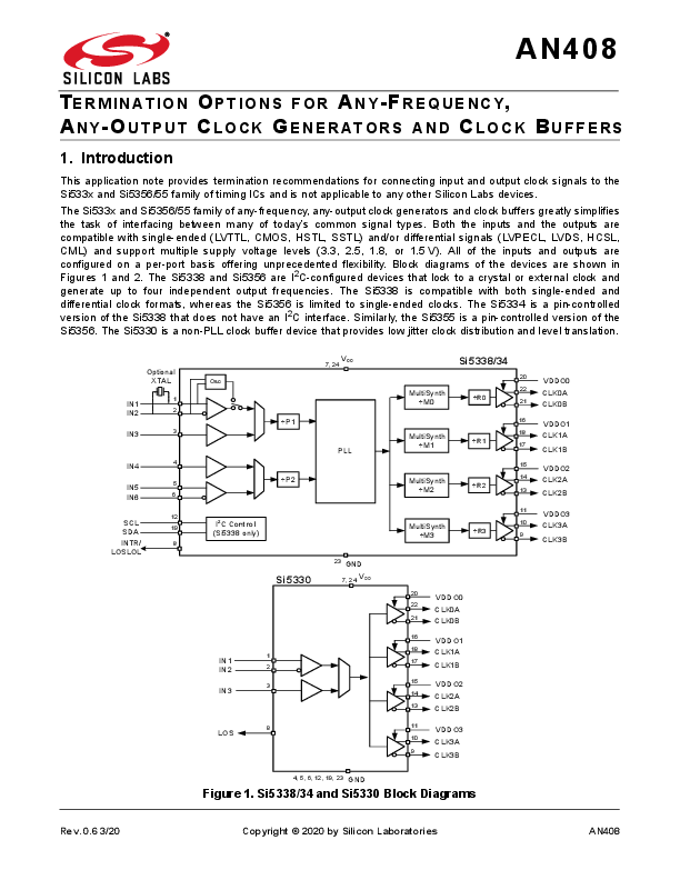
AN408

TERMINATION O PTIONS FOR A NY- F REQUENCY, ANY-OUTPUT CLOCK GENERATORS AND CLOCK BUFFERS
1. Introduction
This application note provides termination recommendations for connecting input and output clock signals to the Si533x and Si5356/55 family of timing ICs and is not applicable to any other Silicon Labs devices.
The Si533x and Si5356/55 family of any-frequency, any-output clock generators and clock buffers greatly simplifies the task of interfacing between many of today's common signal types. Both the inputs and the outputs are compatible with single-ended (LVTTL, CMOS, HSTL, SSTL) and/or differential signals (LVPECL, LVDS, HCSL, CML) and support multiple supply voltage levels (3.3, 2.5, 1.8, or 1.5 V). All of the inputs and outputs are configured on a per-port basis offering unprecedented flexibility. Block diagrams of the devices are shown in Figures 1 and 2. The Si5338 and Si5356 are I2C-configured devices that lock to a crystal or external clock and generate up to four independent output frequencies. The Si5338 is compatible with both single-ended and differential clock formats, whereas the Si5356 is limited to single-ended clocks. The Si5334 is a pin-controlled version of the Si5338 that does not have an I2C interface. Similarly, the Si5355 is a pin-controlled version of the Si5356. The Si5330 is a non-PLL clock buffer device that provides low jitter clock distribution and level translation.

Optional XTAL

IN1

1

IN2

2

IN3

3

IN4

4

IN5

5

IN6

6

SCL

12

SDA

19

INTR/

8

LOSLOL

7, 24 VDD
Osc
�P1 PLL
�P2
I2C Control (Si5338 only)

MultiSynth �M0

Si5338/34

20

22

�R0

21

16

MultiSynth �M1

�R1

18 17

15

MultiSynth �M2

�R2

14 13

11

MultiSynth �M3

�R3

10 9

VDDO0 CLK0A CLK0B
VDDO1 CLK1A CLK1B
VDDO2 CLK2A CLK2B
VDDO3 CLK3A CLK3B

Si5330

23 GND 7, 24 VDD

IN1

1

IN2

2

IN3

3

LOS

8

20

VDDO0

22

CLK0A

21

CLK0B

16

VDDO1

18

CLK1A

17

CLK1B

15

VDDO2

14

CLK2A

13

CLK2B

11

VDDO3

10

CLK3A

9

CLK3B

4, 5, 6, 12, 19, 23 GND
Figure 1. Si5338/34 and Si5330 Block Diagrams

Rev. 0.6 3/20

Copyright � 2020 by Silicon Laboratories

AN408

AN408

XTAL

1 2

CLKin

4

SCL

12

SDA

19

I2C_LSB

3

OEB

6

SSC_DIS

5

INTR

8

Osc
�P1
I2C and Pin Control

VDD
7, 24
PLL

23 GND

MultiSynth �M0
MultiSynth �M1
MultiSynth �M2
MultiSynth �M3

Si5356

20

22

�R0

21

16

18

�R1

17

15

14

�R2

13

11

10

�R3

9

VDDOA CLK0 CLK1
VDDOB CLK2 CLK3
VDDOC CLK4 CLK5
VDDOD CLK6 CLK7

XTAL

1 2

CLKin

4

P1

3

P2

12

P3

19

P4

5

P5

6

LOS

8

Osc
Control

VDD
7, 24
�P1 PLL

MultiSynth �M0
MultiSynth �M1
MultiSynth �M2
MultiSynth �M3

Si5355

20

22

�R0

21

16

18

�R1

17

15

14

�R2

13

11

10

�R3

9

VDDOA CLK0 CLK1
VDDOB CLK2 CLK3
VDDOC CLK4 CLK5
VDDOD CLK6 CLK7

23 GND
Figure 2. Si5356 and Si5355 Block Diagrams

2

Rev. 0.6

AN408
2. Inputs
The Si533x and Si5356/55 families support both single-ended and differential inputs. The device supports up to two single-ended inputs (Pins 3 and 4) and two differential inputs (Pins 1,2, and 5,6). On the Si5338/34 and Si5356/55 devices, a crystal can be connected to Pins 1 and 2 instead of an input clock. Refer to "AN360: Crystal Selection Guide for Any-Frequency Devices" for more information on using the crystal input option.
2.1. Single-Ended Inputs
The multi-format single-ended clock inputs of the Si533x and Si5356/55 are ac-coupled internally to remove any dc bias from the signal. This allows the device to trigger on a signal swing threshold instead of a specific voltage level (normally specified as VIH and VIL). The receiver accepts any signal with a minimum voltage swing of 800 mVPP and a maximum of 3.73 VPP regardless of the core VDD supply. For best performance, the slew rate at input Pins 3 and 4 must be greater than 1 V/ns. This makes the inputs 3.3 V-tolerant even when the core voltage is powered with 1.8 V. An Si5338/34/56/55 should have an input duty cycle no worse than 40/60%. An Si5330 should have an input duty cycle no worse than 45/55%. 2.1.1. LVTTL/CMOS Inputs The only termination necessary when interfacing a CMOS driver to the Si533x and Si5356/55 is a source resistor (Rs) placed near the driver to help match its output impedance to the transmission line impedance. In some cases, the value for this series resistor may be zero as it depends upon the CMOS driver characteristics. The CMOS drivers in the Si533x and Si5356/55 are designed to work optimally into a 50  transmission line without an external source resistor. A typical CMOS signal connection is illustrated in Figure 3. Using this configuration, the receiver is capable of interfacing to 3.3, 2.5, or 1.8 V CMOS clock signals.

VDD = 3.3 V, 2.5 V, 1.8 V
Rs 50

LVTTL/ CMOS

Figure 3. Interfacing to an LVTTL/CMOS Input Signal

Si533x/56/55

Rev. 0.6

3

AN408

2.1.2. Single-Ended SSTL and HSTL Inputs
HSTL and SSTL single-ended clock inputs should be input to the differential inputs, pins 1 and 2, of the Si533x with the circuit shown in Figure 4.
Some drivers may require a series 25  resistor. If the SSTL/HSTL input is being driven by another Si533x device, the 25  series resistor is not required as this is integrated on-chip. The maximum recommended input frequency in this case is 350 MHz.

Keep termination close to

input pin of the Si533x

VTT

0.4 to 1.2 V pk-pk

50 0.1 uF
50

VDD

Differential Input

Si533x 1 2

R1 0.1 uF
VTT

0.1 uF

R2
SSTL_2, SSTL_18, HSTL
R1 = 2 k R2 = 2 k

SSTL_3
R1 = 2.43 k R2 = 2 k
Figure 4. Single-Ended SSTL/HSTL Input to Pins 1 and 2

4

Rev. 0.6

AN408

2.1.3. Applying a Single-Ended Signal to a Differential Input
It is possible to interface any single-ended signal to the differential input pins (IN1/IN2 or IN5/IN6). The recommended interface for a signal that requires a 50  load is shown in Figure 5. On these inputs, it is important that the signal level be less than 1.2 VPP SE and greater than 0.4 VPP SE. The maximum recommended input frequency in this case is 350 MHz.

0.4 to 1.2V pk-pk

Keep termination close to input pin of the Si533x 0.1 uF 50

Si533x

50

0.1 uF

Figure 5. Single-Ended Input Signal with 50  Termination
2.2. Differential Inputs
The multi-format differential clock inputs of the Si533x will interface with today's most common differential signals, such as LVDS, LVPECL, CML, and HCSL. The differential inputs are internally self-biased and must be ac-coupled externally with a 0.1 �F capacitor. The receiver will accept a signal with a voltage swing between 400 mV and 2.4 VPP differential. Each half of the differential signal must not exceed 1.2 VPP at the input to the Si533x or else the 1.3 V dc voltage limit may be exceeded. 2.2.1. LVDS Inputs When interfacing the Si533x device to an LVDS signal, a 100  termination is required at the input along with the required dc blocking capacitors as shown in Figure 6.

Keep termination close to input pin of the Si533x
50

0.1 uF 100

Must be ac coupled
Si533x

LVDS

50 0.1 uF

Figure 6. LVDS Input Signal

2.2.2. LVPECL Inputs
Since the differential receiver of the Si533x is internally self biased, an LVPECL signal may not be dc-coupled to the device. Figure 7 shows some common LVPECL connections that should not be used because of the dc levels they present at the receiver's input.

Rev. 0.6

5

AN408

DC Coupled with Thevenin Termination
50
50 LVPECL

VDD VDD

R1

R1

R2

R2

LVPECL Rb

AC Coupled with Thevenin Re-Biasing

VDD VDD

R1

R1

50

50 Rb

R2

R2

Not Recommended
Figure 7. Common LVPECL Connections that May be Destructive to the Si533x Input
Recommended configurations for interfacing an LVPECL input signal to the Si533x are shown in Figure 8. Typical values for the bias resistors (Rb) range between 120 and 200  depending on the LVPECL driver. The 100  resistor provides line termination. Because the receiver is internally self-biased, no additional external bias is required. Another solution is to terminate the LVPECL driver with a Thevenin configuration as shown in Figure 8b. The values for R1 and R2 are calculated to provide a 50 termination to VDD-2V. Given this, the recommended resistor values are R1 = 127 and R2 = 82.5  for VDD = 3.3 V, and R1 = 250 andR2 = 62.5 for VDD = 2.5 V.

6

Rev. 0.6

3.3 V, 2.5 V
LVPECL Rb

Keep termination close to input pin of the Si533x
0.1 uF
50

100

0.1 uF Rb

50 Must be ac coupled

AN408
Si533x

VDD= 3.3 V, 2.5 V LVPECL

Figure 8a--LVPECL Input Signal with Source Biasing Option

Keep termination close to input pin of the Si533x

VDD VDD

Must be ac coupled

R1

R1

0.1 uF

Si533x

50

50
R2 VT = VDD � 2 V R1 // R2 = 50 Ohm

0.1 uF R2

Figure 8b--LVPECL Input Signal with Load Biasing Option Figure 8. Recommended Options for Interfacing to an LVPECL Signal

Rev. 0.6

7

AN408

2.2.3. CML Inputs
CML signals may be applied to the differential inputs of the Si533x. Since the Si533x differential inputs are internally self-biased, a CML signal may not be dc-coupled to the device.
The recommended configurations for interfacing a CML input signal to the Si533x are shown in Figure 9. The 100  resistor provides line termination, and, since the receiver is internally-biased, no additional external biasing components are required.

Keep termination close to input pin of the Si533x
0.1 uF 50

Si533x

100

CML

50

0.1 uF

Must be ac coupled
Figure 9. CML Input Signal
2.2.4. Applying CMOS Level Signal to Differential Inputs Note that the maximum voltage level on the differential input pins on all Si533x must not exceed 1.3 V. To apply a CMOS signal to any of these pins, use the circuit shown in Figure 10. For a CMOS signal applied to these differential inputs, the maximum recommended frequency is 200 MHz.

CMOS Input Signal
1.8 V CMOS Rse = 249  Rsh = 464
2.5 V CMOS Rse = 402  Rsh = 357

Keep Rse and Rsh close to the receiver

0.1 uF Rse
50

3.3 V CMOS

Rsh

Rse = 499  Rsh = 274

0.1 uF

Si533x

Figure 10. Applying a CMOS Level Signal to the Differential Inputs

8

Rev. 0.6

AN408

2.2.5. HCSL Inputs
A typical HCSL driver has an open source output, which requires an external series resistor and a resistor to ground. The values of these resistors depend on the driver but are typically equal to 33  (Rs) and 50  (Rt). Note that the HCSL driver in the Si533x requires neither Rs nor Rt resistors. Other than two ac-coupling capacitors, no additional external components are necessary when interfacing an HCSL signal to the Si533x.

3.3V, 2.5V, 1.8V Rs

Must be ac coupled

0.1 uF 50

Si533x

Rs

HCSL

50

Rt

Rt

0.1 uF

Figure 11. HCSL Input Signal to Si533x

Rev. 0.6

9

AN408

3. Outputs
The Si533x devices provide four outputs that can be differential or single-ended. The Si5356/55 devices only have CMOS outputs. When configured as single-ended, the driver generates two signals that can be configured as inphase or complimentary. Each of the outputs has its own output supply pin, allowing the device to be used in mixed supply applications without the need for external level translators. Each output driver is configurable to support the following signal types: CMOS/LVTTL, SSTL, HSTL, LVPECL, LVDS, and HCSL. The Si5338 also supports a CML output driver.
3.1. CMOS/LVTTL Outputs
The CMOS output driver has a controlled impedance of about 50 , which includes an internal series resistor of approximately 22 . For this reason, an external Rs series resistor is not recommended when driving 50  traces. If the trace impedance is higher than 50 , a series resistor, Rs, should be used. A typical configuration is shown in Figure 12. By default, the CMOS outputs of the driver are in-phase and can be used to drive two receivers. They can also be configured as complimentary outputs. The output supports 3.3, 2.5, and 1.8 V CMOS signal levels when the appropriate voltage is supplied to the external VDDO pin and the device is configured accordingly.

Si533x/56/55
CMOS

3.3, 2.5, or 1.8 V VDDOx
CLKxA CLKxB

LVTTL/ CMOS
50

50

Figure 12. Interfacing to a CMOS Receiver
3.1.1. 1.5 and 1.2 V CMOS Outputs
The Si533x/55/56 output drivers natively support 3.3, 2.5, and 1.8 V CMOS. However, 1.5 and 1.2 V CMOS signals can be obtained using a two-resistor network as shown in Figure 13 and Table 1 below. Place R1 and R2 as close to the device output as possible.

33..33VV,, 22..55VV,, oorr 11..88VV

VVDDDDOOxx

Si53333xx//56/5555

RR11 5500

CCMMOOSS

CCLLKKxxAA CCLLKKxxBB

RR22

RR11 5500

RR22

11..55 oorr 11..22 VV

Figure 13. Interfacing to a 1.5 or 1.2 V CMOS Receiver

10

Rev. 0.6

AN408

Table 1. Resistor Values for Interfacing to 1.5 and 1.2 V Receivers

VDDOx 1.8 V 2.5 V 3.3 V

1.2 V CMOS Output

R1

R2

25

150

55

100

90

80

1.5 V CMOS Output

R1

R2

10

300

33

125

60

90

The resistor values in Table 1 were selected to maintain signal integrity, specifically rise/fall time, at the cost of current consumption. The increase in current consumption is expected to be on the order of 2 to 8 mA per output depending on VDDOx, 4 mA max with VDDOx of 1.8 V.
3.2. SSTL and HSTL Outputs
The Si533x supports both SSTL and HSTL outputs, which can be single-ended or differential. The recommended termination scheme for SSTL is shown in Figure 14. The VTT supply can be generated using a simple voltage divider as shown below.

Si533x

SSTL (3.3, 2.5, or 1.8 V) HSTL (1.5 V)
VDDOx

VTT VTT

50

50

SSTL

CLKxA

50

or

CLKxB

HSTL

50

SSTL_3 SSTL_2 SSTL_18
HSTL

VDDO

R1

VTT

SSTL_2, SSTL_18, HSTL
R1 = 2k R2 = 2k

SSTL_3
R1 = 2.43k R2 = 2k

0.1 uF

R2

Figure 14. Interfacing the Si533x to an SSTL or HSTL Receiver

Rev. 0.6

11

AN408

3.3. LVPECL Outputs
The LVPECL driver is configurable in both 3.3 V or 2.5 V standard LVPECL modes. The output driver can be accoupled or dc-coupled to the receiver.
3.3.1. DC-Coupled LVPECL Outputs
The standard LVPECL driver supports two commonly used dc-coupled configurations. Both of these are shown in Figure 15. LVPECL drivers were designed to be terminated with 50  to VDD�2 V, which is illustrated in Figure 15a. VTT can be supplied with a simple voltage divider as shown in Figure 15. An alternative method of terminating LVPECL is shown in Figure 15b, which is the Thevenin equivalent to the termination in Figure 15a. It provides a 50  load terminated to VDD�2.0 V. For 3.3 V LVPECL, use R1 = 127 and R2 = 82.5 ; for 2.5 V LVPECL, use R1 = 250 and R2 = 62.5 The only disadvantage to this type of termination is that the Thevenin circuit consumes additional power from the VDDO supply.

Si533x

3.3 V, 2.5 V VDDOx

LVPECL

CLKxA CLKxB

Keep termination close to the receiver
50 50
VTT 50
50

3.3 V LVPECL 2.5 V LVPECL

VDDO � 2.0 V

Figure 14a--DC Coupled Termination of 50 Ohms to VDD � 2.0 V

Si533x

LVPECL

3.3 V, 2.5 V VDDOx
CLKxA CLKxB

VDDO VDDO

Keep termination close to the receiver

R1

R1

3.3 V LVPECL

2.5 V LVPECL 50

50

3.3 V LVPECL

R2

R2

VT = VDDO � 2.0 V R1 // R2 = 50 Ohm

R1 = 127 Ohm R2 = 82.5 Ohm

2.5 V LVPECL
R1 = 250 Ohm R2 = 62.5 Ohm

Figure 14b--DC Coupled with Thevenin Termination

Figure 15. Interfacing the Si533x to an LVPECL Receiver Using DC Coupling

12

Rev. 0.6

AN408

3.3.2. AC Coupled LVPECL Outputs
AC coupling is necessary when a receiver and a driver have compatible voltage swings but different commonmode voltages. AC coupling works well for dc-balanced signals, such as for 50% duty cycle clocks. Figure 16 describes two methods for ac coupling the standard LVPECL driver. The Thevenin termination shown in Figure 16a is a convenient and common approach when a VBB (VDD � 1.3 V) supply is not available; however, it does consume additional power. The termination method shown in Figure 16b consumes less power. A VBB supply can be generated from a simple voltage divider circuit as shown in Figure 16.

3.3 V, 2.5 V

Si533x

VDDOx

0.1 uF

CLKxA

50

LVPECL

CLKxB

50

Rb Rb

0.1 uF

VDDO VDDO

R1

R1

Keep termination close to the receiver
3.3 V LVPECL 2.5 V LVPECL

R2

R2

VDDO � 1.3 V

3.3 V LVPECL

R1 // R2 = 50 Ohm R1 = 82.5 Ohm

R2 = 127 Ohm

Rb = 130 Ohm (2.5 V LVPECL) Rb = 200 Ohm (3.3 V LVPECL)

Figure 15a--AC Coupled with Thevenin Termination

2.5 V LVPECL
R1 = 62.5 Ohm R2 = 250 Ohm

Si533x

LVPECL

3.3 V, 2.5 V VDDOx
CLKxA CLKxB

Rb Rb
Rb = 130 Ohm (2.5 V LVPECL) Rb = 200 Ohm (3.3 V LVPECL)

Keep termination close to the receiver
0.1 uF
50

0.1 uF

50 VBB
50

50 VDDO � 1.3 V

3.3 V LVPECL 2.5 V LVPECL

Figure 15b--AC Coupled with 100 Ohm Termination
Figure 16. Interfacing to an LVPECL Receiver Using AC Coupling

Rev. 0.6

13

AN408

3.4. LVDS Outputs
The LVDS output option provides a very simple and power-efficient interface that requires no external biasing when connected to an LVDS receiver. An ac-coupled LVDS driver is often useful as a CML driver. The LVDS driver may be dc-coupled or ac-coupled to the receiver in 3.3 V or 2.5 V output mode.
3.4.1. AC-Coupled LVDS Outputs
The Si5338/34 LVDS output can drive an ac-coupled load. The Si5330 LVDS output can only drive an ac-coupled load if the input to the Si5330 has a very well-controlled duty cycle like any Silicon Labs PLL clock products. The ac coupling capacitors may be placed at either the driver or receiver end, as long as they are placed prior to the 100  termination resistor. Keep the 100  termination resistor as close to the receiver as possible, as shown in Figure 17. When a 1.8 V output supply voltage is used, the LVDS output of the Si533x produces a common-mode voltage of ~0.875 V, which does not support the LVDS standard. In this case, it is best to ac-couple the output to the load.

Si533x

3.3 V or 2.5 V VDDOx

LVDS

CLKxA CLKxB

Keep termination close to the receiver
50 100
50

LVDS

Si533x

16a--DC-Coupled LVDS Output

3.3V, 2.5V, or 1.8V VDDOx

LVDS

CLKxA CLKxB

Keep termination close to the receiver
0.1 uF 50
100

50 0.1 uF

16b--AC-Coupled LVDS Output

Figure 17. Interfacing to an LVDS Receiver

14

Rev. 0.6

AN408

3.5. HCSL Outputs
Host clock signal level (HCSL) outputs are commonly used in PCI Express applications. A typical HCSL driver has an open source output that requires an external series resistor and a resistor to ground. The Si533x HCSL driver has integrated these resistors to simplify the interface to an HCSL receiver. No external components are necessary when connecting the Si533x HCSL driver to an HCSL receiver.

3.3, 2.5, or 1.8 V VDDOx

Rs

50

CLKxA

HCSL Rs

CLKxB

50 Rt Rt

HCSL

Si533x
Figure 18. Interfacing the Si533x to an HCSL Receiver
3.6. CML Outputs
The Si5338 has a CML driver option. This driver can be used to replace an LVPECL driver in ac-coupled applications and save ~15 mA for each output driver in the process. When using the CML driver, no external bias resistors from the CML outputs to ground or Vtt should be connected. The CML driver is compliant with LVPECL peak-peak output levels; however, the common-mode output voltage is not compliant to LVPECL specs. The CML driver is individually available for all four differential outputs. See Section 9 of the Si5338 Reference Manual for information on selecting the CML Driver option. The CML output driver option should only be used when the output clock signal comes from an internal MultiSynth. The Si5338 CML output driver can be used as long as the following conditions are met: 1. Both pins of the differential output pair are ac coupled to the load. 2. The load at the receiver is effectively 100  differential. 3. The Si5338 PLL is not bypassed. 4. The VDDOx supply for the CML driver voltage is 3.3 V or 2.5 V. The CML driver has the same specified output voltage swing as the LVPECL driver. 1. Max Vsepp = .95 V 2. Min Vsepp = .55 V 3. Typ Vsepp = .8 V Figure 19 shows the normal connection for the Si5338 CML Driver format. Figure 20 shows the expected termination for the Si5338 CML driver. This termination is most often within a CML receiver.

Rev. 0.6

15

AN408
Si5338 CML Driver

+

50

Do Not use external bias
resistors

Receiver

-

50

Do Not use external bias
resistors

Si5338 CML Driver

Figure 19. CML Driver Connection Effective Termination

+

50

50

Vbias

50

-

50

Vbias can be any voltage with any source impedance
Figure 20. Terminations for Si5338 CML Driver

16

Rev. 0.6

AN408
3.7. Interfacing the Si533x LVDS/LVPECL to a CML Receiver
Current mode logic (CML) is transmitted differentially and terminated to 50  to Vcc as shown in Figure 21. A CML receiver can be driven with either an LVPECL or an LVDS output depending on the signal swing required by the receiver. A single-ended output swing from 550 mV to 960 mV is achieved when driving a CML receiver with an LVPECL output. For a reduced output swing, LVDS mode is recommended for producing a single-ended swing between 250 mV and 450 mV.
Driving a CML Receiver Using the LVPECL Output

Si533x LVPECL

550 mV � 960 mV p-p 50
50 Rb Rb

0.1 uF 0.1 uF

CML Receiver
50 Vcc
50

Rb = 130 Ohms (2.5 V LVPECL) Rb = 200 Ohms (3.3 V LVPECL)

Driving a CML Receiver Using the LVDS Output

Si533x LVDS

250 mV - 450 mV p-p 50
50

0.1 uF 0.1 uF

CML Receiver
50 Vcc
50

Figure 21. Terminating an LVPECL or an LVDS Output to a CML Receiver

Rev. 0.6

17

AN408
REVISION HISTORY
Revision 0.6
March, 2020  Fixed R1 typo in "2.1.2. Single-Ended SSTL and HSTL Inputs" on page 4.  Updated reference to Si5338 reference manual in "3.6. CML Outputs" on page 15.
Revision 0.5
October, 2013  Updated Figure 10 on page 8.
Updated resistor values.
 Updated "2.2.4. Applying CMOS Level Signal to Differential Inputs" on page 8.
Added text to recommend max CMOS input frequency into a differential input.
 Updated "2.1.2. Single-Ended SSTL and HSTL Inputs" on page 4 and "2.1.3. Applying a Single-Ended Signal to a Differential Input" on page 5 to specify a max input frequency of 350 MHz.
 Removed R1 and R2 and 0.1 �f cap from Figures 15 and 16.  Added maximum input frequency of 350 MHz to "2.1.2. Single-Ended SSTL and HSTL Inputs" on page 4 and
"2.1.3. Applying a Single-Ended Signal to a Differential Input" on page 5.  Added "3.6. CML Outputs" on page 15.  Added "3.1.1. 1.5 and 1.2 V CMOS Outputs" on page 10.
Revision 0.4
November, 2010  Updated "3.5. HCSL Outputs" on page 15.
Revision 0.3
July, 2010  Moved Section "2.2.4 Applying a Single-Ended Signal to a Differential Input" to Section 2.1.3.  Modified LVPECL circuit in Figure 16.  Added "2.2.3. CML Inputs" on page 8.  Added "2.2.4. Applying CMOS Level Signal to Differential Inputs" on page 8.
Revision 0.2
January, 2010  Added "2.2.2. LVPECL Inputs" on page 5.  Removed "3.4. Low Power LVPECL Output Driver--AC Coupled".  Added "3.7. Interfacing the Si533x LVDS/LVPECL to a CML Receiver" on page 17.
Revision 0.1
October, 2008  Initial release.

18

Rev. 0.6

ClockBuilder Pro
One-click access to Timing tools, documentation, software, source code libraries & more. Available for Windows and iOS (CBGo only).
www.silabs.com/CBPro

Timing Portfolio www.silabs.com/timing

SW/HW www.silabs.com/CBPro

Quality www.silabs.com/quality

Support and Community community.silabs.com

Disclaimer Silicon Labs intends to provide customers with the latest, accurate, and in-depth documentation of all peripherals and modules available for system and software implementers using or intending to use the Silicon Labs products. Characterization data, available modules and peripherals, memory sizes and memory addresses refer to each specific device, and "Typical" parameters provided can and do vary in different applications. Application examples described herein are for illustrative purposes only. Silicon Labs reserves the right to make changes without further notice to the product information, specifications, and descriptions herein, and does not give warranties as to the accuracy or completeness of the included information. Without prior notification, Silicon Labs may update product firmware during the manufacturing process for security or reliability reasons. Such changes will not alter the specifications or the performance of the product. Silicon Labs shall have no liability for the consequences of use of the information supplied in this document. This document does not imply or expressly grant any license to design or fabricate any integrated circuits. The products are not designed or authorized to be used within any FDA Class III devices, applications for which FDA premarket approval is required, or Life Support Systems without the specific written consent of Silicon Labs. A "Life Support System" is any product or system intended to support or sustain life and/or health, which, if it fails, can be reasonably expected to result in significant personal injury or death. Silicon Labs products are not designed or authorized for military applications. Silicon Labs products shall under no circumstances be used in weapons of mass destruction including (but not limited to) nuclear, biological or chemical weapons, or missiles capable of delivering such weapons. Silicon Labs disclaims all express and implied warranties and shall not be responsible or liable for any injuries or damages related to use of a Silicon Labs product in such unauthorized applications.
Trademark Information Silicon Laboratories Inc.�, Silicon Laboratories�, Silicon Labs�, SiLabs� and the Silicon Labs logo�, Bluegiga�, Bluegiga Logo�, ClockBuilder�, CMEMS�, DSPLL�, EFM�, EFM32�, EFR, Ember�, Energy Micro, Energy Micro logo and combinations thereof, "the world's most energy friendly microcontrollers", Ember�, EZLink�, EZRadio�, EZRadioPRO�, Gecko�, Gecko OS, Gecko OS Studio, ISOmodem�, Precision32�, ProSLIC�, Simplicity Studio�, SiPHY�, Telegesis, the Telegesis Logo�, USBXpress� , Zentri, the Zentri logo and Zentri DMS, ZWave�, and others are trademarks or registered trademarks of Silicon Labs. ARM, CORTEX, Cortex-M3 and THUMB are trademarks or registered trademarks of ARM Holdings. Keil is a registered trademark of ARM Limited. Wi-Fi is a registered trademark of the Wi-Fi Alliance. All other products or brand names mentioned herein are trademarks of their respective holders.

Silicon Laboratories Inc. 400 West Cesar Chavez Austin, TX 78701 USA
http://www.silabs.com