Managing the Instruction Fetch Bank. ... Step-by-step instructions on how to configure a Silicon Labs IDE project and a mVision2 project for code bank-ing are included in...
the Keil linker manual for a description of the M51 file. Step by Step Instructions on Configuring a Code Banked Project Using Vision2. The following steps show how to configure the code banked example project using the Keil IDE, Vision2. 1. Start Vision2, create a new project and add the files listed in Table 2 to the project. Addition
AN130
CODE BANKING USING THE KEIL 8051 TOOLS
1. Relevant Devices
This application note applies to the following devices: C8051F120, C8051F121, C8051F122, C8051F123, C8051F124, C8051F125, C8051F126, and C8051F127.
Introduction
The 8051 architecture supports a 64KB linear program memory space. Devices that have more than 64KB of program memory implement a code banking scheme to surmount this 64KB limit. This application note discusses software project management techniques and provides example applications that use code banking.
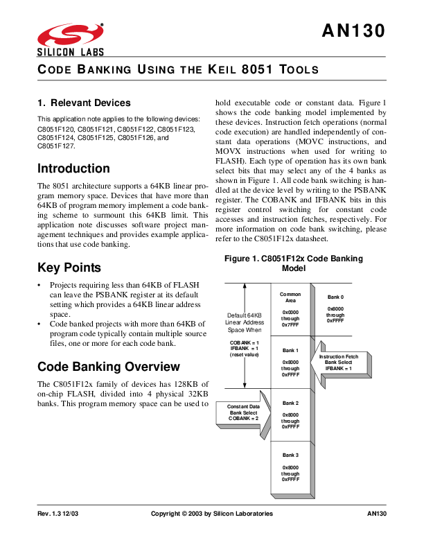
hold executable code or constant data. Figure 1 shows the code banking model implemented by these devices. Instruction fetch operations (normal code execution) are handled independently of constant data operations (MOVC instructions, and MOVX instructions when used for writing to FLASH). Each type of operation has its own bank select bits that may select any of the 4 banks as shown in Figure 1. All code bank switching is handled at the device level by writing to the PSBANK register. The COBANK and IFBANK bits in this register control switching for constant code accesses and instruction fetches, respectively. For more information on code bank switching, please refer to the C8051F12x datasheet.
Key Points
Figure 1. C8051F12x Code Banking Model
· Projects requiring less than 64KB of FLASH can leave the PSBANK register at its default setting which provides a 64KB linear address space.
· Code banked projects with more than 64KB of program code typically contain multiple source files, one or more for each code bank.
Code Banking Overview
The C8051F12x family of devices has 128KB of on-chip FLASH, divided into 4 physical 32KB banks. This program memory space can be used to
Default 64KB Linear Address Space When
COBANK = 1 IFBANK = 1 (reset value)
Common Area
0x0000 through 0x7FFF
Bank 1
0x8000 through 0xFFFF
Constant Data Bank Select COBANK = 2
Bank 2
0x8000 through 0xFFFF
Bank 0 0x8000 through 0xFFFF
Instruction Fetch Bank Select IFBANK = 1
Bank 3
0x8000 through 0xFFFF
Rev. 1.3 12/03
Copyright © 2003 by Silicon Laboratories
AN130
AN130
For projects that require more than 64KB of code ging at the beginning of log, erasing the FLASH
space or non-volatile data space, the user has the page with the oldest data as it progresses.
option of manually handling the bank switching in
software or setting up a code- banked project. Both Managing the Instruction Fetch Bank
methods are discussed in this note.
Select
User-Managed Bank
Since this application uses less than 32KB of
Switching for Data Intensive FLASH for program code, there will be no instruc-
Projects
tion fetches from the 0x8000 to 0xFFFF memory space. This makes the value of IFBANK a "don't
User-managed bank switching is useful for projects care". However, if an application uses between
that have less than 64KB of executable code but need to store large amounts of data in FLASH. In
32KB and 64KB of FLASH for program code, IFBANK should be left at its reset value, targeting
this situation, the Common area and Bank 1 are Bank 1.
used for program memory while Bank 2 and Bank 3 are used for data storage. The project does
Advancing Through the Code Banks
not need to be set up for code banking.
This application reserves the first 16KB of FLASH
The following data logging example shows how in the Common area for program code. The log
bank switching can be managed in application soft- starts at address 0x4000 in the Common area and
ware.
ends at location 0xF7FF in Bank 3 as shown in
Example 1: Data Logging Application
This application uses a 22.1184 MHz crystal oscillator to implement a software real-time clock (RTC). PCA0, configured to count Timer 0 overflows, generates an interrupt once every second. The interrupt handler records the current time and device temperature in a non-volatile log in FLASH.
The 112,640 byte log cycles through all 4 code banks recording time and temperature. Each data record has 6 fields as shown in Figure 2. The log is capable of storing 14080 records over a time period of 3.9 hours. Once the log is full, it continues log-
":" 0x3A
Figure 2. Log Record Structure
HOURS
MINUTES SECONDS
ADC READING
0xFF
2
Rev. 1.3
AN130
Figure 3.
Table 1 .
After storing a record in the log, the FLASH write Preserving the PSBANK Register in
pointer is advanced to the next record and checked Functions and Interrupt Service
for code bank boundaries. There are three possible boundary conditions to consider when adjusting the
Routines
FLASH write pointer. These cases are outlined in
A program must preserve and restore the value of
Figure 3. FLASH Memory Map for Example 1
the PSBANK register in every function and interrupt service routine that switches code banks.
0x0000 0x4000 0x7FFF 0x8000
0xFFFF 0x8000
0xFFFF 0x8000 0xF7FF 0xF800
Common Area
0x0000 through 0x7FFF
16KB reserved for program code
Bank 1 0x8000 through 0xFFFF
Bank 2 0x8000 through 0xFFFF
14080 x 8
Non-Volatile Time and
Temperature Log
112,640 bytes total
Bank 3
0x8000 through 0xFFFF
1KB FLASH, Lock Bits, and
Reserved Area
Choosing Log Record Size
Example 1 only writes entire records to FLASH. If the record size is a power of 2 and the log starts at the beginning of a FLASH page, then all records will be contained within one of the code banks. If a record can cross a bank boundary, then bounds checking must be performed after every byte write.
Keeping Accurate Time
This application keeps track of time by implementing an interrupt driven real-time clock. With SYSCLK at 49.7664 MHZ, Timer 0 in mode 2 overflows exactly 4050 times every second when clocked by SYSCLK/48. PCA Module 0 is configured in "Software Timer Mode" to count Timer 0 overflows and generate an interrupt every second.
Table 1. FLASH Write Pointer Boundary Conditions
Condition
How to Detect
Typical Action
FLASH write pointer reaches the end of the Common area.
FLASH write pointer reaches the end of Bank 1 or Bank 2.
FLASH write pointer reaches the end of the log.
FLASH write pointer will point to location 0x8000.
No action is necessary if COBANK is always set to Bank 1 whenever the pointer is moved to the beginning of the log.
FLASH write pointer will point to location 0x0000.
FLASH write pointer should be set to 0x8000 and COBANK should be incremented.
FLASH write pointer will point to location 0xF800 and Bank 3 will be selected by COBANK.
FLASH write pointer should be reset to the first location in the log (0x4000) and COBANK should select Bank 1.
Rev. 1.3
3
AN130
Project-Managed Bank Switching for CodeIntensive Applications
The Keil 8051 development tools support code banking by generating code that can automatically switch and preserve the PSBANK register. This allows the user to expand 64KB projects to 128KB without modifying existing modules. Using the code banking capability of the Silicon Labs IDE or the Keil Vision2 for projects containing more than 64KB of program code is recommended to take advantage of this feature.
To use the Keil 8051 tools for code banking, the project needs to be configured. The configuration required for code banking is supported in Version 1.7 and later of the Silicon Labs IDE and Version 2.00 and later of Vision2. Step-by-step instructions on how to configure a Silicon Labs IDE project and a Vision2 project for code banking are included in example 2.
Code banked projects typically contain multiple source files, one or more for each code bank. This greatly simplifies project configuration, as will be shown in example 2. In addition to source files, all projects configured for code banking must include a code banked version of STARTUP.A51 and L51_BANK.A51. These files can be found in the Silicon Labs IDE installation directory, `Cygnal\Examples\C8051F12x\Asm'
Example 2: Project-Managed Code Banking
This example shows how to set up a code banked project using the Keil development tools. It uses Timer 3 and Timer 4 interrupts to blink the LED and output a 1 kHz sine wave on DAC1, respectively. The code that blinks the LED is located in Bank 3 and the code that outputs a sine wave is located in Bank 2. Since interrupts must be located in the Common area, both interrupts call a function in one of the banks to perform the desired task.
This example contains three source files, one for each bank and the Common area, and two required project files, as listed in Table 2 .
Table 2. Files needed by Example 2
common.c
bank2.c
bank3.c
STARTUP.A51
L51_BANK.A51
Step by Step Instructions on Configuring a Code Banked Project Using the Silicon Labs IDE
The following steps show how to configure the code banked example project using the Silicon Labs IDE.
1. Start the Silicon Labs IDE and add the files listed in Table 2 to a new project. Additionally, an example project is included named `example2.wsp'.
2. Open the Tool Chain Integration window from the Project menu and select the Linker tab as shown in Figure 4. Click on the Customize button. A window similar to the one shown in Figure 5 should appear on the screen. Select the processor you are using from the pull down menu. This enables code banking by adding the BANKAREA directive to the linker command line parameters. For more information on the BANKAREA directive, please refer to Chapter 9 of the Keil Assembler/Linker manual,
4
Rev. 1.3
AN130
accessible in PDF format from the Help menu of the Silicon Labs IDE.
Figure 4. Tool Chain Integration Window
Select the Files to Link tab.
Figure 6. Target Build Configuration Window
Figure 5. Linker Customization Window
Figure 7. Project Build Definition Window
bank3.obj
4. For each file in the Files To Be Linked list box, select the desired bank from the Bank # pull down menu. The `L51_BANK.obj' and `STARTUP.obj' files should be located in the Common area in all projects. The remaining project files should be located in their respective code banks, as shown in Table 3 .
3. Open the Target Build Configuration window Table 3. Code Bank Selection for Example 2
from the Project menu and click the Customize button, as shown in Figure 6. The window
Filename
Code Bank
shown in Figure 7 should appear on the screen. common.obj
Common area
bank2.obj
Bank 2
bank3.obj
Bank 3
Rev. 1.3
5
AN130
Table 3. Code Bank Selection for Example 2
Filename
Code Bank
STARTUP.obj
Common area
L51_BANK.obj
Common area
5. Save the project by selecting Save Project from the Project menu.
6. Build the project by selecting Build/Make Project from the Project menu.
2. Open the Options for Target window from the Project menu and select the Target tab, as shown in Figure 8. Click on the Code Banking check box at the bottom on the window. Next, select the number 4 from the Banks: pull down menu. Finally, edit the Bank Area: text boxes with a value of 0x8000 for the Start: value and 0xFFFF for the End: value. When the selections match those shown in Figure 8, press the OK button to close the window.
Figure 8. Options for Target Window
7. If the project has been configured correctly, an `example2.M51' map file will be generated in the project folder. Inspect this file to verify that functions have been located in the proper bank. You should also notice that the sine table in `bank2.c' has been located in the Common area because it is a constant code variable. Refer to the Keil linker manual for a description of the M51 file.
Step by Step Instructions on Configuring a Code Banked Project Using Vision2.
The following steps show how to configure the 3. Each file now needs to be assigned to a code
code banked example project using the Keil IDE, Vision2.
bank or to the common area. Additionally, groups of files can be created and banking
1. Start Vision2, create a new project and add the files listed in Table 2 to the project. Additionally, an example project is included named `example2.Uv2'.
assignments made for the entire group. For each file/group in the Project Workspace window, right-click on the file-name/group-name and select Options for File/Options for Group, as shown in Figure 9. The window shown in
Figure 10 should appear on the screen. Select
the desired bank from the Code Bank: pull
down menu. The `L51_BANK.obj' and
`STARTUP.obj' files should be located in the
Common area in all projects. The remaining
project files should be located in their respec-
tive code banks, as shown in Table 4 .
4. Build the project by selecting Build target or Rebuild all target files from the Project menu.
6
Rev. 1.3
AN130
5. If the project has been configured correctly, an Table 4. Code Bank Selection for Example 2
`example2.M51' map file will be generated in the project folder. Inspect this file to verify that
Filename
Code Bank
functions have been located in the proper bank. You should also notice that the sine table in `bank2.c' has been located in the Common area
common.obj bank2.obj
Common area Bank 2
because it is a constant code variable. Refer to the Keil linker manual for a description of the
bank3.obj
Bank 3
M51 file.
STARTUP.obj
Common area
Figure 9. Select "Options for File"
L51_BANK.obj
Common area
Code Bank Assignment Considerations
Assigning files to code banks is a straightforward procedure. However, determining the best placement of functions in code banks is largely dependant on the nature of the project. This section outlines some guidelines to follow when assigning code banks.
Figure 10. Options for File Window
The Common area is accessible by all code banks at all times. It is important to keep all code that must always be accessible in the Common area. For example, reset and interrupt vectors, interrupt service routines, code constants, bank switch code, and library functions should always be located in the Common area.
Assigning Code Banks for Maximum Performance
Code bank switching does not significantly affect the performance of most systems. However, to achieve maximum performance in time critical applications, programs should be structured so that frequent bank switching is not necessary. Bank switch code is not generated when the function being called resides in the Common area or in the same bank as its calling function. Placing frequently accessed functions or functions called from different banks in the Common area is essential to achieve maximum performance in time critical applications.
Rev. 1.3
7
AN130
Code Constants
Code constants (strings, tables, etc.) are located in the Common area by default. This is the best location for code constants in most applications because they can be accessed using the MOVC instruction from any bank. If the Common area is not large enough to accommodate all code constants, they may be placed in one of the code banks but may only be accessed from code executing from the same bank in which they reside or the common area. They may not be accessed from code executing in another bank because the linker sets the constant code bank to the same bank as the instruction fetch bank. Constant data in a code bank may be accessed from the common area only if the bank in which they reside is the currently selected bank. Figure 11 shows how to invoke a linker-managed bank switch from C.
IFBANK always target the same code bank. This is why constant code tables must be located in the Common area or in the bank that accesses them.
The bank switch macros in `L51_BANK.A51' may be changed to keep COBANK fixed regardless of the value of IFBANK. This would allow the user to dedicate one bank for constant data operations while using the other two banks for instruction fetches only. This dedicated bank would be available to code executing in any bank or the Common area.
The Common area may always be used for both instruction fetches and data storage regardless of the PSBANK register settings. For more information on bank switch macros, please see Chapter 9 of the Keil Assembler/Linker manual accessible in PDF format from the help menu of the Silicon Labs IDE.
The BANKx linker control allows code constants to be located outside the Common area. For details on locating constant code variables in a code bank, please see the Keil Knowledge Base article at http:/ /www.keil.com/support/docs/1615.htm.
Bank Switch Macros
The Keil 8051 tools support 3 modes of bank switching defined in `L51_BANK.A51'. Bank switching on the C8051F12x uses Mode 4 (bank switching via user-provided code). This mode allows the user to specify a macro for each code bank that selects it in the PSBANK register.
The PSBANK register contains two bank selects, COBANK for constant data and IFBANK for instruction fetches. Using the `L51_BANK.A51' supplied by Silicon Labs, the COBANK and
Figure 11. Invoking a Linker-Managed Bank Switch From C
// declare the following function prototype
extern void switchbank (unsigned char bank_number);
...
switchbank(1);
// switch to code bank 1
8
Rev. 1.3
AN130
Software Examples
Example 1: User-Managed Code Banking (Data Logger with RealTime Clock)
//----------------------------------------------------------------------------// Data_Logger_RTC.c //----------------------------------------------------------------------------// Copyright 2002 Cygnal Integrated Products, Inc. // // AUTH: FB // DATE: 30 SEP 02 // // // This application uses a 22.1184 MHz crystal oscillator to implement a // software real-time clock (RTC). PCA Module 0, configured to count Timer 0 // overflows in software timer mode, generates an interrupt every second. // The interrupt handler records the current time and device temperature // in a non-volatile log in FLASH. // // With SYSCLK at 49.7664 MHZ, Timer 0 in mode 2 overflows exactly 4050 times // every second when clocked by SYSCLK/48. PCA0, clocked by Timer 0 overflows, // is programmed to generate an interrupt every 4050 Timer 0 overflows, // or once every second. // // The 112,640 byte log cycles through all 4 code banks recording time and // temperature. Each data record is 8 bytes long. The log is capable of storing // 14080 records over a time period of 3.9 hours. Once the log is full, it // continues logging at the beginning of log, erasing the FLASH page with // the oldest data as it progresses. // // When this code is built, the linker generates two multiple call to segments // warnings. These warnings are generated because the FLASH support routines // are called from the main routine and from interrupts. These warnings have // been accounted for in the code by disabling interrupts before calling any // FLASH support routines. // // // Target: C8051F12x // Tool chain: KEIL C51 6.03 / KEIL EVAL C51 //
//-----------------------------------------------------------------------------
// Includes
//-----------------------------------------------------------------------------
#include <c8051f120.h>
// SFR declarations
#include <stdio.h>
// printf() and getchar()
//----------------------------------------------------------------------------// 16-bit SFR Definitions for `F12x //-----------------------------------------------------------------------------
sfr16 DP sfr16 ADC0 sfr16 ADC0GT sfr16 ADC0LT sfr16 RCAP2
= 0x82; = 0xbe; = 0xc4; = 0xc6; = 0xca;
// data pointer // ADC0 data // ADC0 greater than window // ADC0 less than window // Timer2 capture/reload
Rev. 1.3
9
AN130
sfr16 RCAP3 sfr16 RCAP4 sfr16 TMR2 sfr16 TMR3 sfr16 TMR4 sfr16 DAC0 sfr16 DAC1 sfr16 PCA0CP5 sfr16 PCA0CP2 sfr16 PCA0CP3 sfr16 PCA0CP4 sfr16 PCA0 sfr16 PCA0CP0 sfr16 PCA0CP1
= 0xca; = 0xca; = 0xcc; = 0xcc; = 0xcc; = 0xd2; = 0xd2; = 0xe1; = 0xe9; = 0xeb; = 0xed; = 0xf9; = 0xfb; = 0xfd;
// Timer3 capture/reload // Timer4 capture/reload // Timer2 // Timer3 // Timer4 // DAC0 data // DAC1 data // PCA0 Module 5 capture // PCA0 Module 2 capture // PCA0 Module 3 capture // PCA0 Module 4 capture // PCA0 counter // PCA0 Module 0 capture // PCA0 Module 1 capture
//----------------------------------------------------------------------------// Type Definitions //-----------------------------------------------------------------------------
typedef union UInt { unsigned int Int; unsigned char Char[2];
} UInt;
// Byte addressable unsigned int
typedef union Long { long Long; unsigned int Int[2]; unsigned char Char[4];
} Long;
// Byte addressable long
typedef union ULong { unsigned long ULong; unsigned int Int[2]; unsigned char Char[4];
} ULong;
// Byte addressable unsigned long
typedef struct Record { char start; unsigned int hours; unsigned char minutes; unsigned char seconds; unsigned int ADC_result; char end;
} Record;
// LOG record structure
//-----------------------------------------------------------------------------
// Global CONSTANTS
//-----------------------------------------------------------------------------
#define TRUE
1
#define FALSE
0
#define EXTCLK #define SYSCLK
22118400 49766400
// External oscillator frequency in Hz // Output of PLL derived from // (EXTCLK*9/4)
#define BAUDRATE
115200
// Baud rate of UART in bps // Note: The minimum standard baud rate // supported by the UART0_Init routine // in this file is 19,200 bps when
10
Rev. 1.3
AN130
#define SAMPLERATE 2000
sbit LED = P1^6; sbit SW2 = P3^7;
#define LOG_START 0x04000L #define LOG_END 0x1F800L #define RECORD_LEN 8 #define START_OF_RECORD `:'
#define FLASH_PAGESIZE 1024
#define COBANK 0xF0
#define COBANK0 #define COBANK1 #define COBANK2 #define COBANK3
0x00 0x10 0x20 0x30
// SYSCLK = 49.76MHz.
// The ADC sampling rate in Hz
// LED='1' means ON // SW2='0' means switch pressed
// Starting address of LOG // Last address in LOG + 1 // Record length in bytes // Start of Record symbol
// Number of bytes in each FLASH page
// Bit mask for the high nibble of PSBANK
// These macros define the bit mask values // for the PSBANK register used for // selecting COBANK. COBANK should always // be cleared then OR-Equaled (|=) with // the proper bit mask to avoid changing // the other bits in the PSBANK register
//----------------------------------------------------------------------------// Global VARIABLES //-----------------------------------------------------------------------------
unsigned char SECONDS = 0; unsigned char MINUTES = 0; unsigned int HOURS = 0;
// global RTC seconds counter // global RTC minutes counter // global RTC hours counter
unsigned int ADC_RESULT = 0;
// holds the oversampled and averaged // result from ADC0
bit LOG_FLAG = 0;
// this flag is used to enable // and disable logging but does // not affect the real-time clock
bit LOG_ERASED = 0;
// this flag indicates that the
// LOG has been erased.
//-----------------------------------------------------------------------------
// Function PROTOTYPES
//-----------------------------------------------------------------------------
void main(void); void RTC_update(void); void print_menu(void);
// initialization routines void SYSCLK_Init(void); void PORT_Init(void); void UART0_Init (void); void ADC0_Init (void); void Timer3_Init(int counts); void RTC_Init (void); void PCA0_ISR (void);
Rev. 1.3
11
AN130
// FLASH support routines void FLASH_PageErase (unsigned long addr); void FLASH_Write (unsigned long dest, char* src, unsigned int numbytes); void FLASH_ByteWrite (unsigned long dest, char dat); void FLASH_Read ( char* dest, unsigned long src, unsigned int numbytes); unsigned char FLASH_ByteRead (unsigned long addr);
// LOG support routines
void print_time(void); void LOG_erase(void); unsigned long find_current_record(void); void LOG_print(char all_at_once); void LOG_update(void);
//----------------------------------------------------------------------------// MAIN Routine //-----------------------------------------------------------------------------
void main (void) {
#define input_str_len 4 char input_str[input_str_len];
// buffer to hold characters entered // at the command prompt
WDTCN = 0xde; WDTCN = 0xad;
// disable watchdog timer
PORT_Init (); SYSCLK_Init (); UART0_Init (); ADC0_Init(); RTC_Init (); Timer3_Init(SYSCLK/SAMPLERATE);
// initialize crossbar and GPIO // initialize oscillator // initialize UART0 // initialize ADC0 // initializes Timer0 and the PCA // initialize Timer3 to overflow // and generate interrupts at // <SAMPLERATE> Hz
// to implement a real-time clock
EA = 1;
// enable global interrupts
print_menu();
// print the command menu
while (1){
SFRPAGE = UART0_PAGE; printf("\nEnter a command > "); gets(input_str, input_str_len);
switch ( input_str[0] ){
case `1': LOG_FLAG = 1; SFRPAGE = UART0_PAGE; printf("\nLogging has now started.\n"); break;
case `2': LOG_FLAG = 0;
12
Rev. 1.3
AN130
SFRPAGE = UART0_PAGE; printf("\nLogging has now stopped.\n"); break;
case `3': LOG_FLAG = 0; LOG_erase(); SFRPAGE = UART0_PAGE; printf("\nThe log has been erased and logging is stopped.\n"); break;
case `4': LOG_print(FALSE); print_menu(); break;
case `5': LOG_print(TRUE); print_menu(); break;
case `6': print_time(); break;
case `?': print_menu(); break;
default: printf("\n*** Unknown Command.\n"); break;
}
} // end while
}
//----------------------------------------------------------------------------// RTC_update //----------------------------------------------------------------------------// // void RTC_update(void) {
SECONDS++; if (SECONDS == 60) {
SECONDS = 0; MINUTES++; if (MINUTES == 60) {
MINUTES = 0; HOURS++; } }
}
//----------------------------------------------------------------------------// FLASH Support Routines //-----------------------------------------------------------------------------
//----------------------------------------------------------------------------// FLASH_PageErase //-----------------------------------------------------------------------------
Rev. 1.3
13
AN130
//
// This function erases the FLASH page containing <addr>.
//
void FLASH_PageErase (unsigned long addr)
{
char SFRPAGE_SAVE = SFRPAGE;
// Preserve current SFR page
char PSBANK_SAVE = PSBANK;
// Preserve current code bank
bit EA_SAVE = EA;
// Preserve interrupt state
ULong temp_addr; char xdata * idata pwrite;
// Temporary ULong // FLASH write/erase pointer
temp_addr.ULong = addr;
// copy <addr> to a byte addressable // unsigned long
// Extract address information from <addr> pwrite = (char xdata *) temp_addr.Int[1];
// Extract code bank information from <addr>
PSBANK &= ~COBANK;
// Clear the COBANK bits
if( temp_addr.Char[1] == 0x00){ PSBANK |= COBANK1;
} else {
// If the address is less than // 0x10000, the Common area and // Bank1 provide a 64KB linear // address space // Else, Bank2 and Bank3 provide // a 64KB linear address space
if (temp_addr.Char[2] & 0x80){ PSBANK |= COBANK3;
// If bit 15 of the address is // a `1', then the operation should // target Bank3, else target Bank2
} else {
PSBANK |= COBANK2; temp_addr.Char[2] |= 0x80; pwrite = (char xdata *) temp_addr.Int[1]; } }
SFRPAGE = LEGACY_PAGE;
EA = 0; FLSCL |= 0x01; PSCTL = 0x03;
// Disable interrupts // Enable FLASH writes/erases // MOVX erases FLASH page
*pwrite = 0;
// Initiate FLASH page erase
FLSCL &= ~0x01; PSCTL = 0x00;
// Disable FLASH writes/erases // MOVX targets XRAM
EA = EA_SAVE; PSBANK = PSBANK_SAVE; SFRPAGE = SFRPAGE_SAVE; }
// Restore interrupt state // Restore current code bank // Restore SFR page
//----------------------------------------------------------------------------// FLASH_Write
14
Rev. 1.3
AN130
//----------------------------------------------------------------------------// // This routine copies <numbytes> from <src> to the FLASH addressed by <dest>. // void FLASH_Write (unsigned long dest, char* src, unsigned int numbytes) {
unsigned int i;
// Software Counter
for (i = 0; i < numbytes; i++) {
FLASH_ByteWrite( dest++, *src++); } }
//-----------------------------------------------------------------------------
// FLASH_ByteWrite
//-----------------------------------------------------------------------------
//
// This routine writes <dat> to the FLASH byte addressed by <dest>.
//
void FLASH_ByteWrite (unsigned long dest, char dat)
{
char SFRPAGE_SAVE = SFRPAGE;
// Preserve current SFR page
char PSBANK_SAVE = PSBANK;
// Preserve current code bank
bit EA_SAVE = EA;
// Preserve interrupt state
ULong temp_dest;
// Temporary ULong
char xdata * idata pwrite;
// FLASH write/erase pointer
temp_dest.ULong = dest;
// copy <dest> to a byte // addressable unsigned long
// Check if data byte being written is 0xFF // There is no need to write 0xFF to FLASH since erased // FLASH defaults to 0xFF. if(dat != 0xFF){
// Extract address information from <dest> pwrite = (char xdata *) temp_dest.Int[1];
// Extract code bank information from <addr>
PSBANK &= ~COBANK;
// Clear the COBANK bits
if( temp_dest.Char[1] == 0x00){ PSBANK |= COBANK1;
} else {
// If the address is less than // 0x10000, the Common area and // Bank1 provide a 64KB linear // address space // Else, Bank2 and Bank3 provide // a 64KB linear address space
if (temp_dest.Char[2] & 0x80){// If bit 15 of the address is
// a `1', then the operation should
PSBANK |= COBANK3;
// target Bank3, else target Bank2
} else {
Rev. 1.3
15
AN130
PSBANK |= COBANK2; temp_dest.Char[2] |= 0x80; pwrite = (char xdata *) temp_dest.Int[1]; } }
SFRPAGE = LEGACY_PAGE;
EA = 0; FLSCL |= 0x01; PSCTL = 0x01;
// Disable interrupts // Enable FLASH writes/erases // MOVX writes FLASH byte
*pwrite = dat;
// Write FLASH byte
FLSCL &= ~0x01; PSCTL = 0x00; }
// Disable FLASH writes/erases // MOVX targets XRAM
EA = EA_SAVE; PSBANK = PSBANK_SAVE; SFRPAGE = SFRPAGE_SAVE; }
// Restore interrupt state // Restore current code bank // Restore SFR page
//----------------------------------------------------------------------------// FLASH_Read //----------------------------------------------------------------------------// // This routine copies <numbytes> from FLASH addressed by <src> to <dest>. // void FLASH_Read ( char* dest, unsigned long src, unsigned int numbytes) {
unsigned int i;
// Software Counter
for (i = 0; i < numbytes; i++) {
*dest++ = FLASH_ByteRead(src++); } }
//-----------------------------------------------------------------------------
// FLASH_ByteRead
//-----------------------------------------------------------------------------
//
// This routine returns to the value of the FLASH byte addressed by <addr>.
//
unsigned char FLASH_ByteRead (unsigned long addr)
{
char SFRPAGE_SAVE = SFRPAGE;
// Preserve current SFR page
char PSBANK_SAVE = PSBANK;
// Preserve current code bank
ULong temp_addr; char temp_char;
// Temporary ULong // Temporary char
char code * idata pread;
// FLASH read pointer
temp_addr.ULong = addr;
// copy <addr> to a byte addressable // unsigned long
16
Rev. 1.3
AN130
// Extract address information from <addr> pread = (char code *) temp_addr.Int[1];
// Extract code bank information from <addr>
PSBANK &= ~COBANK;
// Clear the COBANK bits
if( temp_addr.Char[1] == 0x00){ PSBANK |= COBANK1;
} else {
// If the address is less than // 0x10000, the Common area and // Bank1 provide a 64KB linear // address space // Else, Bank2 and Bank3 provide // a 64KB linear address space
if (temp_addr.Char[2] & 0x80){ PSBANK |= COBANK3;
// If bit 15 of the address is // a `1', then the operation should // target Bank3, else target Bank2
} else {
PSBANK |= COBANK2; temp_addr.Char[2] |= 0x80; pread = (char code *) temp_addr.Int[1]; } }
temp_char = *pread;
// Read FLASH byte
PSBANK = PSBANK_SAVE; SFRPAGE = SFRPAGE_SAVE;
// Restore current code bank // Restore SFR page
return temp_char; }
//-----------------------------------------------------------------------------
// Support Routines
//-----------------------------------------------------------------------------
//-----------------------------------------------------------------------------
// print_menu
//-----------------------------------------------------------------------------
//
// This routine uses prints the command menu to the UART.
//
void print_menu(void)
{
char SFRPAGE_SAVE = SFRPAGE;
// Save Current SFR page
SFRPAGE = UART0_PAGE; printf("\n\nC8051F12x Data Logging Example\n"); printf("---------------------------------------\n"); printf("1. Start Logging\n"); printf("2. Stop Logging\n"); printf("3. Erase Log\n"); printf("4. Print Log (one page at a time - Press CTRL+C to stop)\n"); printf("5. Print Log (all at once - Press CTRL+C to stop)\n"); printf("6. Print Elapsed Time Since Last Reset\n"); printf("?. Print Command List\n");
Rev. 1.3
17
AN130
SFRPAGE = SFRPAGE_SAVE; }
// Restore SFR page
//-----------------------------------------------------------------------------
// print_time
//-----------------------------------------------------------------------------
//
// This routine uses prints the elapsed time since the last reset to the UART.
//
void print_time(void)
{
char SFRPAGE_SAVE = SFRPAGE;
// Save Current SFR page
bit EA_SAVE = EA;
// Preserve interrupt state
SFRPAGE = UART0_PAGE;
EA = 0;
printf ("%05u:%02bu:%02bu\n", HOURS, MINUTES, SECONDS);
EA = EA_SAVE;
SFRPAGE = SFRPAGE_SAVE;
// Restore SFR page
}
//----------------------------------------------------------------------------// find_current_record //----------------------------------------------------------------------------// // unsigned long find_current_record(void) {
char SFRPAGE_SAVE = SFRPAGE; bit EA_SAVE = EA;
// Save Current SFR page // Preserve interrupt state
unsigned long pRead = LOG_START;
// Pointer used to read from FLASH
unsigned int i; bit record_erased;
// Software counter // Temporary flag
// Keep skipping records until an uninitialized record is found or // until the end of the log is reached while( pRead < LOG_END ){
EA = 0; // Skip all records that have been initialized if(FLASH_ByteRead(pRead) == START_OF_RECORD ){
// increment pRead to the next record pRead += RECORD_LEN; EA = EA_SAVE; continue; }
// Verify that the Record is uninitialized, otherwise keep // searching for an uninitialized record record_erased = 1; for(i = 0; i < RECORD_LEN; i++){
if( FLASH_ByteRead(pRead+i) != 0xFF ){ record_erased = 0;
}
18
Rev. 1.3
AN130
} if(!record_erased){
// increment pRead to the next record pRead += RECORD_LEN; EA = EA_SAVE; continue; }
EA = EA_SAVE;
// When this code is reached, <pRead> should point to the beginning
// of an uninitialized (erased) record;
SFRPAGE = SFRPAGE_SAVE;
// Restore SFR page
return pRead;
}
// This code is reached only when there are no uninitialized records
// in the LOG. Erase the first FLASH page in the log and return
// a pointer to the first record in the log.
EA = 0;
FLASH_PageErase(LOG_START);
// Erase the first page of the LOG
EA = EA_SAVE;
SFRPAGE = SFRPAGE_SAVE;
// Restore SFR page
return LOG_START;
}
//-----------------------------------------------------------------------------
// LOG_erase
//-----------------------------------------------------------------------------
//
//
void LOG_erase(void)
{
unsigned long pWrite = LOG_START;
// pointer used to write to FLASH
bit EA_SAVE = EA;
// save interrupt status
// Keep erasing pages until <pWrite> reaches the end of the LOG. while( pWrite < LOG_END ){
EA = 0; FLASH_PageErase(pWrite); EA = EA_SAVE;
pWrite += FLASH_PAGESIZE;
}
LOG_ERASED = 1; }
// flag that LOG has been erased
//-----------------------------------------------------------------------------
// LOG_print
//-----------------------------------------------------------------------------
//
//
void LOG_print(char all_at_once)
{
char SFRPAGE_SAVE = SFRPAGE;
// Save Current SFR page
Rev. 1.3
19
AN130
bit EA_SAVE = EA;
// save interrupt status
unsigned long pRead = LOG_START;
// Pointer used to read from FLASH
Record temp_rec;
// Temporary record
// Keep printing records until the end of the log is reached while( pRead < LOG_END ){
// Copy a record from at <pRead> from the LOG into the local // Record structure <temp_rec> EA = 0; FLASH_Read( (char*) &temp_rec, pRead, RECORD_LEN); EA = EA_SAVE;
// Validate Record if(temp_rec.start != `:'){
SFRPAGE = SFRPAGE_SAVE; return; }
// Restore SFR page
// Print the Record SFRPAGE = UART0_PAGE;
RI0 = 0;
// Clear UART Receive flag // to later check for the // user pressing CTRL+C
EA = 0;
// disable interrupts
// print the time and ADC reading printf ("%05u:%02bu:%02bu ADC = 0x%04X\n",
temp_rec.hours, temp_rec.minutes, temp_rec.seconds, temp_rec.ADC_result);
EA = EA_SAVE; // check if we need to continue
// restore interrupts // any pending interrupts will // be handled immediatly
// if printing all data at once do not stop printing unless // the user presses CTRL+C, otherwise print 16 records and // then prompt user to press any key
if(all_at_once){
// Check if user has pressed CTRL+C
if(RI0 && SBUF0 == 0x03){
RI0 = 0;
SFRPAGE = SFRPAGE_SAVE;
// Restore SFR page
return;
}
// pause every 16 lines } else if( (pRead & ((RECORD_LEN*16)-1)) == 0 &&
pRead > (LOG_START + RECORD_LEN)) {
20
Rev. 1.3
AN130
// wait for a key to be pressed then check if user has
// pressed CTRL+C (0x03)
printf("\npress any key to continue\n");
if(_getkey() == 0x03) {
SFRPAGE = SFRPAGE_SAVE;
// Restore SFR page
return;
}
}
// increment pRead to the next record pRead += RECORD_LEN;
SFRPAGE = SFRPAGE_SAVE;
// Restore SFR page
}
}
//-----------------------------------------------------------------------------
// LOG_update
//-----------------------------------------------------------------------------
//
//
void LOG_update(void)
{
bit EA_SAVE = EA;
// Preserve interrupt state
Record temp_record;
// local LOG record structure
static unsigned long pWrite = LOG_START;
// pointer used to write to the LOG
bit record_erased;
// temporary flag
unsigned int i;
// temporary integer
// record the time and ADC reading in the LOG if logging is enabled if(LOG_FLAG){
if(LOG_ERASED){ pWrite = LOG_START; LOG_ERASED = 0;
} else {
// find the current record if the record at pWrite is not erased record_erased = 1; for(i = 0; i < RECORD_LEN; i++){
EA = 0; if( FLASH_ByteRead(pWrite+i) != 0xFF ){
record_erased = 0; } EA = EA_SAVE; } if(!record_erased){ pWrite = find_current_record(); }
// build the temporary record
Rev. 1.3
21
AN130
temp_record.start = START_OF_RECORD; temp_record.hours = HOURS; temp_record.minutes = MINUTES; temp_record.seconds = SECONDS; temp_record.ADC_result = ADC_RESULT;
// write the temporary record to FLASH EA = 0; FLASH_Write( pWrite, (char*) &temp_record, RECORD_LEN); EA = EA_SAVE;
// increment record pointer pWrite += RECORD_LEN;
// if <pWrite> is past the end of the LOG, reset to the top if(pWrite >= LOG_END){
pWrite = LOG_START; } } // end else } // end if(LOG_FLAG)
}
//----------------------------------------------------------------------------// Initialization Routines //-----------------------------------------------------------------------------
//-----------------------------------------------------------------------------
// SYSCLK_Init
//-----------------------------------------------------------------------------
//
// This routine initializes the system clock to use an external 22.1184 MHz
// crystal oscillator multiplied by a factor of 9/4 using the PLL as its
// clock source. The resulting frequency is 22.1184 MHz * 9/4 = 49.7664 MHz
//
void SYSCLK_Init (void)
{
int i;
// delay counter
char SFRPAGE_SAVE = SFRPAGE;
// Save Current SFR page
SFRPAGE = CONFIG_PAGE;
// set SFR page
OSCXCN = 0x67;
// start external oscillator with // 22.1184MHz crystal
for (i=0; i < 256; i++) ;
// Wait for osc. to start up
while (!(OSCXCN & 0x80)) ;
// Wait for crystal osc. to settle
CLKSEL = 0x01;
// Select the external osc. as // the SYSCLK source
OSCICN = 0x00;
// Disable the internal osc.
//Turn on the PLL and increase the system clock by a factor of M/N = 9/4
22
Rev. 1.3
SFRPAGE = CONFIG_PAGE;
PLL0CN = 0x04; SFRPAGE = LEGACY_PAGE; FLSCL = 0x10;
SFRPAGE = CONFIG_PAGE; PLL0CN |= 0x01; PLL0DIV = 0x04; PLL0FLT = 0x01;
PLL0MUL = 0x09;
for (i=0; i < 256; i++) ; PLL0CN |= 0x02; while(!(PLL0CN & 0x10)); CLKSEL = 0x02;
SFRPAGE = SFRPAGE_SAVE; }
AN130
// Set PLL source as external osc.
// Set FLASH read time for 50MHz clk // or less
// Enable Power to PLL // Set Pre-divide value to N (N = 4) // Set the PLL filter register for // a reference clock from 19 - 30 MHz // and an output clock from 45 - 80 MHz // Multiply SYSCLK by M (M = 9)
// Wait at least 5us // Enable the PLL // Wait until PLL frequency is locked // Select PLL as SYSCLK source
// Restore SFR page
//-----------------------------------------------------------------------------
// PORT_Init
//-----------------------------------------------------------------------------
//
// This routine configures the Crossbar and GPIO ports.
//
void PORT_Init (void)
{
char SFRPAGE_SAVE = SFRPAGE;
// Save Current SFR page
SFRPAGE = CONFIG_PAGE;
// set SFR page
XBR0 XBR1 XBR2
= 0x04; = 0x00; = 0x40;
// Enable UART0 // Enable crossbar and weak pull-up
P0MDOUT |= 0x01; P1MDOUT |= 0x40;
// Set TX0 pin to push-pull // Set P1.6(LED) to push-pull
SFRPAGE = SFRPAGE_SAVE; }
// Restore SFR page
//----------------------------------------------------------------------------// UART0_Init //----------------------------------------------------------------------------// // Configure the UART0 using Timer1, for <baudrate> and 8-N-1. In order to // increase the clocking flexibility of Timer0, Timer1 is configured to count // SYSCLKs. // // To use this routine SYSCLK/BAUDRATE/16 must be less than 256. For example, // if SYSCLK = 50 MHz, the lowest standard baud rate supported by this // routine is 19,200 bps. // void UART0_Init (void)
Rev. 1.3
23
AN130
{ char SFRPAGE_SAVE = SFRPAGE; SFRPAGE = UART0_PAGE; SCON0 = 0x50; SSTA0 = 0x10; SFRPAGE = TIMER01_PAGE; TMOD &= ~0xF0; TMOD |= 0x20; TH1 = -(SYSCLK/BAUDRATE/16);
CKCON |= 0x10;
// Save Current SFR page
// SCON0: mode 0, 8-bit UART, enable RX // Timer 1 generates UART0 baud rate and // UART0 baud rate divide by two disabled
// TMOD: timer 1, mode 2, 8-bit reload // Set the Timer1 reload value // When using a low baud rate, this equation // should be checked to ensure that the // reload value will fit in 8-bits. // T1M = 1; SCA1:0 = xx
TL1 = TH1; TR1 = 1;
// initialize Timer1 // start Timer1
SFRPAGE = UART0_PAGE; TI0 = 1;
// Indicate TX0 ready
SFRPAGE = SFRPAGE_SAVE; }
// Restore SFR page
//-----------------------------------------------------------------------------
// ADC0_Init
//-----------------------------------------------------------------------------
//
// Configure ADC0 to start conversions on Timer3 Overflows and to
// use left-justified output mode.
//
void ADC0_Init (void)
{
char SFRPAGE_SAVE = SFRPAGE;
// Save Current SFR page
SFRPAGE = ADC0_PAGE;
ADC0CN = 0x85;
// ADC0 enabled; normal tracking // mode; ADC0 conversions are initiated // on Timer3 overflows; ADC0 data is // left-justified
REF0CN = 0x07; AMX0SL = 0x0F;
// enable temp sensor, on-chip VREF, // and VREF output buffer // Select TEMP sens as ADC mux output
ADC0CF = ((SYSCLK/2500000) << 3);// ADC conversion clock = 2.5MHz
ADC0CF |= 0x01;
// PGA gain = 2
EIE2 |= 0x02;
// Enable ADC0 End-of-conversion // interrupts
SFRPAGE = SFRPAGE_SAVE;
// Restore SFR page
24
Rev. 1.3
AN130
}
//----------------------------------------------------------------------------// Timer3_Init //----------------------------------------------------------------------------// This routine initializes Timer3 in auto-reload mode to overflow // at intervals specified in <counts>. // void Timer3_Init (int counts) {
SFRPAGE = TMR3_PAGE;
TMR3CN = 0; TMR3CF = 0x08; RCAP3 = -counts; TMR3 = RCAP3; TR3 = 1;
// STOP timer; set to auto-reload mode // Timer3 counts SYSCLKs // set reload value
// start Timer3
}
//-----------------------------------------------------------------------------
// RTC_Init
//-----------------------------------------------------------------------------
//
// This Routine initializes Timer0 and PCA0 to implement a real-time clock.
// Assuming <SYSCLK> is generated from a 22.1184 crystal oscillator, Timer0
// overflows exactly 1800 times per second when configured as an 8-bit timer
// that uses <SYSCLK>/48 as its timebase. PCA0 is configured to count
// Timer0 overflows and interrupt every 1800 Timer0 overflows, or every second.
// The PCA0 ISR updates a set of global RTC counters for seconds, minutes, hours,
// and days.
//
void RTC_Init(void)
{
char SFRPAGE_SAVE = SFRPAGE;
// Save Current SFR page
SFRPAGE = TIMER01_PAGE;
// configure Timer0 in Mode2: 8-bit Timer with Auto-Reload
TMOD &= ~0x0F;
// Clear Timer0 bits
TMOD |= 0x02;
// Mode2 Auto-Reload
// configure Timer0 timebase to <SYSCLK>/48
CKCON &= ~0x0F;
// Clear bits
CKCON |= 0x02;
// Set Timer0 timebase
// configure PCA0 to count Timer0 overflows PCA0MD = 0x04;
// configure capture/compare module 0 to generate an interrupt when
// the value of PCA0 reaches 4050 (0x0FD2)
PCA0CP0 = 4050;
// Set the value to match
PCA0CPM0 &= ~0xFF; PCA0CPM0 |= 0x49;
// Clear bits // Generate an interrupt when the // PCA0 value matches PCA0CP0
EIE1 |= 0x08;
// Enable PCA0 interrupts
Rev. 1.3
25
AN130
TR0 = 1; PCA0CN |= 0x40;
// Start Timer0 // Enable PCA0
SFRPAGE = SFRPAGE_SAVE; }
// Restore SFR page
//----------------------------------------------------------------------------// PCA0_ISR //----------------------------------------------------------------------------// // void PCA0_ISR (void) interrupt 9 {
if (CCF0) { CCF0 = 0;
// clear Module0 capture/compare flag
PCA0 = 0x00; RTC_update(); LOG_update();
// clear the PCA counter // update RTC variables // update LOG if logging is enabled
} else
if (CCF1) { CCF1 = 0;
} else
// clear Module1 capture/compare flag
if (CCF2) { CCF2 = 0;
} else
// clear Module2 capture/compare flag
if (CCF3) { CCF3 = 0;
} else
// clear Module3 capture/compare flag
if (CCF4) { CCF4 = 0;
} else
// clear Module4 capture/compare flag
if (CCF5) { CCF5 = 0;
} else
// clear Module5 capture/compare flag
if (CF) { CF = 0;
}
// clear PCA counter overflow flag
}
//----------------------------------------------------------------------------// ADC0_ISR //----------------------------------------------------------------------------// // This ISR is called on the end of an ADC0 conversion. // void ADC0_ISR (void) interrupt 15 {
26
Rev. 1.3
static Long result = {0}; int i; bit EA_SAVE = EA; //accumulate 256 temperature samples result.Long += ADC0; i++;
// byte addressable long variable
if( i == 256 ) {
i = 0;
// take the average (Divide by 256 = shift right by 8) // Do this operation "result.Long >>= 8;" (170 SYSCLK cycles) using
// three MOV instructions (9 SYSCLK cycles) // Assume Most Significant Byte only contains sign information
result.Char[3] = result.Char[2]; result.Char[2] = result.Char[1]; result.Char[1] = result.Char[0];
// update global <ADC_RESULT> ADC_RESULT = result.Int[1]; }
}
AN130
Rev. 1.3
27
AN130
Example 2: Project-Managed Code Banking
//----------------------------------------------------------------------------// common.c //----------------------------------------------------------------------------// Copyright 2002 Cygnal Integrated Products, Inc. // // AUTH: FB // DATE: 18 SEP 02 // // This example shows how to set up a code banking project using the Cygnal // IDE and the KEIL development tools. It uses Timer3 and Timer4 interrupts // to blink the LED and output a 1 kHz sine wave on DAC1, respectively. The // code that blinks the LED is located in Bank 3 and the code that outputs a // sine wave based on a 256 entry sine table is located in Bank 2. Since // interrupts must be located in the Common area, both interrupts call // a function in one of the banks to perform the desired task. // // The project should be configured for code banking as shown in AN030 before // this project is built. // // This program uses the the 24.5 MHz internal oscillator multiplied by two // for an effective SYSCLK of 49 MHz. This program also initializes UART1 // at <BAUDRATE> bits per second. // // // Target: C8051F12x // Tool chain: KEIL C51 6.03 / KEIL EVAL C51 //
//-----------------------------------------------------------------------------
// Includes
//-----------------------------------------------------------------------------
#include <c8051f120.h>
// SFR declarations
#include <stdio.h>
// printf() and getchar()
//----------------------------------------------------------------------------// 16-bit SFR Definitions for `F12x //-----------------------------------------------------------------------------
sfr16 DP sfr16 ADC0 sfr16 ADC0GT sfr16 ADC0LT sfr16 RCAP2 sfr16 RCAP3 sfr16 RCAP4 sfr16 TMR2 sfr16 TMR3 sfr16 TMR4 sfr16 DAC0 sfr16 DAC1 sfr16 PCA0CP5 sfr16 PCA0CP2 sfr16 PCA0CP3 sfr16 PCA0CP4 sfr16 PCA0 sfr16 PCA0CP0 sfr16 PCA0CP1
= 0x82; = 0xbe; = 0xc4; = 0xc6; = 0xca; = 0xca; = 0xca; = 0xcc; = 0xcc; = 0xcc; = 0xd2; = 0xd2; = 0xe1; = 0xe9; = 0xeb; = 0xed; = 0xf9; = 0xfb; = 0xfd;
// data pointer // ADC0 data // ADC0 greater than window // ADC0 less than window // Timer2 capture/reload // Timer3 capture/reload // Timer4 capture/reload // Timer2 // Timer3 // Timer4 // DAC0 data // DAC1 data // PCA0 Module 5 capture // PCA0 Module 2 capture // PCA0 Module 3 capture // PCA0 Module 4 capture // PCA0 counter // PCA0 Module 0 capture // PCA0 Module 1 capture
28
Rev. 1.3
AN130
//-----------------------------------------------------------------------------
// Global CONSTANTS
//-----------------------------------------------------------------------------
#define TRUE
1
#define FALSE
0
#define INTCLK #define SYSCLK #define BAUDRATE
24500000 49000000 115200
// Internal oscillator frequency in Hz // Output of PLL derived from (INTCLK*2) // Baud rate of UART in bps
#define SAMPLE_RATE_DAC 100000L #define PHASE_PRECISION 65536
// DAC sampling rate in Hz // range of phase accumulator
sbit LED = P1^6; sbit SW2 = P3^7;
// LED='1' means ON // SW2='0' means switch pressed
#define FREQUENCY 1000
// frequency of output waveform in Hz
// <phase_add> is the change in phase // between DAC1 samples; It is used in // the set_DAC1 routine in bank2 unsigned int phase_add = FREQUENCY * PHASE_PRECISION / SAMPLE_RATE_DAC;
//----------------------------------------------------------------------------// Function PROTOTYPES //-----------------------------------------------------------------------------
// Common area functions void main(void); void SYSCLK_Init(void); void PORT_Init(void); void UART1_Init (void); void DAC1_Init (void); void Timer3_Init(int counts); void Timer4_Init(int counts);
// code bank 2 functions extern void set_DAC1(void);
// code bank 3 functions extern void toggle_LED(void); //----------------------------------------------------------------------------// MAIN Routine //-----------------------------------------------------------------------------
void main (void) {
WDTCN = 0xde; WDTCN = 0xad;
// disable watchdog timer
PORT_Init (); SYSCLK_Init (); UART1_Init (); DAC1_Init ();
// initialize crossbar and GPIO // initialize oscillator // initialize UART1 // initialize DAC1
Timer3_Init(SYSCLK/12/1000);
// initialize Timer3 to overflow
Rev. 1.3
29
AN130
// every millisecond
Timer4_Init(SYSCLK/SAMPLE_RATE_DAC);// initialize Timer4 to overflow // <SAMPLE_RATE_DAC> times per // second
EA = 1;
// enable global interrupts
while(1);
}
//-----------------------------------------------------------------------------
// Interrupt Service Routines
//-----------------------------------------------------------------------------
//-----------------------------------------------------------------------------
// Timer3_ISR
//-----------------------------------------------------------------------------
// This routine changes the state of the LED whenever Timer3 overflows 250 times.
//
// NOTE: The SFRPAGE register will automatically be switched to the Timer 3 Page
// When an interrupt occurs. SFRPAGE will return to its previous setting on exit
// from this routine.
//
void Timer3_ISR (void) interrupt 14
{
static int i;
// software interrupt counter
TF3 = 0; i++;
// clear Timer3 overflow flag // increment software counter
// toggle the LED every 250ms
if (i == 250) {
toggle_LED();
// toggle the green LED
i = 0;
// clear software counter
}
}
//-----------------------------------------------------------------------------
// Timer4_ISR -- Wave Generator
//-----------------------------------------------------------------------------
//
// This ISR is called on Timer4 overflows. Timer4 is set to auto-reload mode
// and is used to schedule the DAC output sample rate in this example.
// Note that the value that is written to DAC1 during this ISR call is
// actually transferred to DAC1 at the next Timer4 overflow.
//
void Timer4_ISR (void) interrupt 16
{
TF4 = 0;
// clear Timer4 overflow flag
set_DAC1();
}
//----------------------------------------------------------------------------// Initialization Routines //-----------------------------------------------------------------------------
//----------------------------------------------------------------------------// SYSCLK_Init
30
Rev. 1.3
AN130
//-----------------------------------------------------------------------------
//
// This routine initializes the system clock to use the internal oscillator
// at 24.5 MHz multiplied by two using the PLL.
//
void SYSCLK_Init (void)
{
int i;
// software timer
char SFRPAGE_SAVE = SFRPAGE;
// Save Current SFR page
SFRPAGE = CONFIG_PAGE;
// set SFR page
OSCICN = 0x83;
// set internal oscillator to run // at its maximum frequency
CLKSEL = 0x00;
// Select the internal osc. as // the SYSCLK source
//Turn on the PLL and increase the system clock by a factor of M/N = 2 SFRPAGE = CONFIG_PAGE;
PLL0CN = 0x00; SFRPAGE = LEGACY_PAGE; FLSCL = 0x10;
SFRPAGE = CONFIG_PAGE; PLL0CN |= 0x01; PLL0DIV = 0x01; PLL0FLT = 0x01;
PLL0MUL = 0x02;
// Set internal osc. as PLL source
// Set FLASH read time for 50MHz clk // or less
// Enable Power to PLL // Set Pre-divide value to N (N = 1) // Set the PLL filter register for // a reference clock from 19 - 30 MHz // and an output clock from 45 - 80 MHz // Multiply SYSCLK by M (M = 2)
for (i=0; i < 256; i++) ; PLL0CN |= 0x02; while(!(PLL0CN & 0x10)); CLKSEL = 0x02;
// Wait at least 5us // Enable the PLL // Wait until PLL frequency is locked // Select PLL as SYSCLK source
SFRPAGE = SFRPAGE_SAVE; }
// Restore SFR page
//-----------------------------------------------------------------------------
// PORT_Init
//-----------------------------------------------------------------------------
//
// This routine configures the crossbar and GPIO ports.
//
void PORT_Init (void)
{
char SFRPAGE_SAVE = SFRPAGE;
// Save Current SFR page
SFRPAGE = CONFIG_PAGE;
// set SFR page
XBR0 XBR1 XBR2
= 0x00; = 0x00; = 0x44;
// Enable crossbar and weak pull-up // Enable UART1
Rev. 1.3
31
AN130
P0MDOUT |= 0x01; P1MDOUT |= 0x40;
// Set TX1 pin to push-pull // Set P1.6(LED) to push-pull
SFRPAGE = SFRPAGE_SAVE; }
// Restore SFR page
//-----------------------------------------------------------------------------
// UART1_Init
//-----------------------------------------------------------------------------
//
// Configure the UART1 using Timer1, for <baudrate> and 8-N-1.
//
void UART1_Init (void)
{
char SFRPAGE_SAVE = SFRPAGE;
// Save Current SFR page
SFRPAGE = UART1_PAGE; SCON1 = 0x10;
// SCON1: mode 0, 8-bit UART, enable RX
SFRPAGE = TIMER01_PAGE; TMOD &= ~0xF0; TMOD |= 0x20;
// TMOD: timer 1, mode 2, 8-bit reload
if (SYSCLK/BAUDRATE/2/256 < 1) {
TH1 = -(SYSCLK/BAUDRATE/2);
CKCON |= 0x10;
// T1M = 1; SCA1:0 = xx
} else if (SYSCLK/BAUDRATE/2/256 < 4) {
TH1 = -(SYSCLK/BAUDRATE/2/4);
CKCON &= ~0x13;
// Clear all T1 related bits
CKCON |= 0x01;
// T1M = 0; SCA1:0 = 01
} else if (SYSCLK/BAUDRATE/2/256 < 12) {
TH1 = -(SYSCLK/BAUDRATE/2/12);
CKCON &= ~0x13;
// T1M = 0; SCA1:0 = 00
} else {
TH1 = -(SYSCLK/BAUDRATE/2/48);
CKCON &= ~0x13;
// Clear all T1 related bits
CKCON |= 0x02;
// T1M = 0; SCA1:0 = 10
}
TL1 = TH1; TR1 = 1;
// initialize Timer1 // start Timer1
SFRPAGE = UART1_PAGE; TI1 = 1;
// Indicate TX1 ready
SFRPAGE = SFRPAGE_SAVE;
// Restore SFR page
}
//----------------------------------------------------------------------------// DAC1_Init //----------------------------------------------------------------------------// // Configure DAC1 to update on Timer4 overflows and enable the the VREF buffer. // //
32
Rev. 1.3
AN130
void DAC1_Init(void){
char SFRPAGE_SAVE = SFRPAGE;
// Save Current SFR page
SFRPAGE = DAC1_PAGE;
DAC1CN = 0x94; SFRPAGE = LEGACY_PAGE;
// Enable DAC1 in left-justified mode // managed by Timer4 overflows
REF0CN |= 0x03;
// Enable the internal VREF (2.4v) and // the Bias Generator
SFRPAGE = SFRPAGE_SAVE;
// Restore SFR page
}
//-----------------------------------------------------------------------------
// Timer3_Init
//-----------------------------------------------------------------------------
//
// Configure Timer3 to auto-reload mode and to generate interrupts
// at intervals specified by <counts> using SYSCLK/12 as its time base.
//
//
void Timer3_Init (int counts)
{
char SFRPAGE_SAVE = SFRPAGE;
// Save Current SFR page
SFRPAGE = TMR3_PAGE;
TMR3CN = 0x00;
// Stop Timer; Clear overflow flag; // Set to Auto-Reload Mode
TMR3CF = 0x00;
// Configure Timer to increment; // Timer counts SYSCLKs/12
RCAP3 = -counts; TMR3 = RCAP3;
// Set reload value // Initialize Timer to reload value
EIE2 |= 0x01; TR3 = 1;
// enable Timer3 interrupts // start Timer
SFRPAGE = SFRPAGE_SAVE;
// Restore SFR page
}
//-----------------------------------------------------------------------------
// Timer4_Init
//-----------------------------------------------------------------------------
// Configure Timer4 to auto-reload mode and to generate interrupts
// at intervals specified in <counts> using SYSCLK as its time base.
//
void Timer4_Init (int counts)
{
char SFRPAGE_SAVE = SFRPAGE;
// Save Current SFR page
SFRPAGE = TMR4_PAGE;
Rev. 1.3
33
AN130
TMR4CN = 0x00;
TMR4CF = 0x08;
RCAP4 = -counts; TMR4 = RCAP4; EIE2 |= 0x04; TR4 = 1; SFRPAGE = SFRPAGE_SAVE; }
// Stop Timer4; Clear overflow flag (TF4); // Set to Auto-Reload Mode
// Configure Timer4 to increment; // Timer4 counts SYSCLKs
// Set reload value // Initialzie Timer4 to reload value
// enable Timer4 interrupts // start Timer4
// Restore SFR page
34
Rev. 1.3
AN130
//----------------------------------------------------------------------------// bank2.c //----------------------------------------------------------------------------// // AUTH: FB // DATE: 18 SEP 02 // // Target: C8051F12x // Tool chain: KEIL C51 // // This file contains routines used by the code banking example in AN030. // All routines in this file are located in Code Bank 2. //
//-----------------------------------------------------------------------------
// Includes
//-----------------------------------------------------------------------------
#include <c8051f120.h>
// SFR declarations
//----------------------------------------------------------------------------// 16-bit SFR Definitions for `F12x //-----------------------------------------------------------------------------
sfr16 DP sfr16 ADC0 sfr16 ADC0GT sfr16 ADC0LT sfr16 RCAP2 sfr16 RCAP3 sfr16 RCAP4 sfr16 TMR2 sfr16 TMR3 sfr16 TMR4 sfr16 DAC0 sfr16 DAC1 sfr16 PCA0CP5 sfr16 PCA0CP2 sfr16 PCA0CP3 sfr16 PCA0CP4 sfr16 PCA0 sfr16 PCA0CP0 sfr16 PCA0CP1
= 0x82; = 0xbe; = 0xc4; = 0xc6; = 0xca; = 0xca; = 0xca; = 0xcc; = 0xcc; = 0xcc; = 0xd2; = 0xd2; = 0xe1; = 0xe9; = 0xeb; = 0xed; = 0xf9; = 0xfb; = 0xfd;
// data pointer // ADC0 data // ADC0 greater than window // ADC0 less than window // Timer2 capture/reload // Timer3 capture/reload // Timer4 capture/reload // Timer2 // Timer3 // Timer4 // DAC0 data // DAC1 data // PCA0 Module 5 capture // PCA0 Module 2 capture // PCA0 Module 3 capture // PCA0 Module 4 capture // PCA0 counter // PCA0 Module 0 capture // PCA0 Module 1 capture
//----------------------------------------------------------------------------// Global VARIABLES //-----------------------------------------------------------------------------
extern int phase_add;
//----------------------------------------------------------------------------// Global CONSTANTS //-----------------------------------------------------------------------------
int code SINE_TABLE[256] = {
0x0000, 0x0324, 0x0647, 0x096a, 0x0c8b, 0x0fab, 0x12c8, 0x15e2, 0x18f8, 0x1c0b, 0x1f19, 0x2223, 0x2528, 0x2826, 0x2b1f, 0x2e11, 0x30fb, 0x33de, 0x36ba, 0x398c, 0x3c56, 0x3f17, 0x41ce, 0x447a, 0x471c, 0x49b4, 0x4c3f, 0x4ebf, 0x5133, 0x539b, 0x55f5, 0x5842, 0x5a82, 0x5cb4, 0x5ed7, 0x60ec, 0x62f2, 0x64e8, 0x66cf, 0x68a6,
Rev. 1.3
35
AN130
0x6a6d, 0x6c24, 0x6dca, 0x6f5f, 0x70e2, 0x7255, 0x73b5, 0x7504, 0x7641, 0x776c, 0x7884, 0x798a, 0x7a7d, 0x7b5d, 0x7c29, 0x7ce3, 0x7d8a, 0x7e1d, 0x7e9d, 0x7f09, 0x7f62, 0x7fa7, 0x7fd8, 0x7ff6, 0x7fff, 0x7ff6, 0x7fd8, 0x7fa7, 0x7f62, 0x7f09, 0x7e9d, 0x7e1d, 0x7d8a, 0x7ce3, 0x7c29, 0x7b5d, 0x7a7d, 0x798a, 0x7884, 0x776c, 0x7641, 0x7504, 0x73b5, 0x7255, 0x70e2, 0x6f5f, 0x6dca, 0x6c24, 0x6a6d, 0x68a6, 0x66cf, 0x64e8, 0x62f2, 0x60ec, 0x5ed7, 0x5cb4, 0x5a82, 0x5842, 0x55f5, 0x539b, 0x5133, 0x4ebf, 0x4c3f, 0x49b4, 0x471c, 0x447a, 0x41ce, 0x3f17, 0x3c56, 0x398c, 0x36ba, 0x33de, 0x30fb, 0x2e11, 0x2b1f, 0x2826, 0x2528, 0x2223, 0x1f19, 0x1c0b, 0x18f8, 0x15e2, 0x12c8, 0x0fab, 0x0c8b, 0x096a, 0x0647, 0x0324, 0x0000, 0xfcdc, 0xf9b9, 0xf696, 0xf375, 0xf055, 0xed38, 0xea1e, 0xe708, 0xe3f5, 0xe0e7, 0xdddd, 0xdad8, 0xd7da, 0xd4e1, 0xd1ef, 0xcf05, 0xcc22, 0xc946, 0xc674, 0xc3aa, 0xc0e9, 0xbe32, 0xbb86, 0xb8e4, 0xb64c, 0xb3c1, 0xb141, 0xaecd, 0xac65, 0xaa0b, 0xa7be, 0xa57e, 0xa34c, 0xa129, 0x9f14, 0x9d0e, 0x9b18, 0x9931, 0x975a, 0x9593, 0x93dc, 0x9236, 0x90a1, 0x8f1e, 0x8dab, 0x8c4b, 0x8afc, 0x89bf, 0x8894, 0x877c, 0x8676, 0x8583, 0x84a3, 0x83d7, 0x831d, 0x8276, 0x81e3, 0x8163, 0x80f7, 0x809e, 0x8059, 0x8028, 0x800a, 0x8000, 0x800a, 0x8028, 0x8059, 0x809e, 0x80f7, 0x8163, 0x81e3, 0x8276, 0x831d, 0x83d7, 0x84a3, 0x8583, 0x8676, 0x877c, 0x8894, 0x89bf, 0x8afc, 0x8c4b, 0x8dab, 0x8f1e, 0x90a1, 0x9236, 0x93dc, 0x9593, 0x975a, 0x9931, 0x9b18, 0x9d0e, 0x9f14, 0xa129, 0xa34c, 0xa57e, 0xa7be, 0xaa0b, 0xac65, 0xaecd, 0xb141, 0xb3c1, 0xb64c, 0xb8e4, 0xbb86, 0xbe32, 0xc0e9, 0xc3aa, 0xc674, 0xc946, 0xcc22, 0xcf05, 0xd1ef, 0xd4e1, 0xd7da, 0xdad8, 0xdddd, 0xe0e7, 0xe3f5, 0xe708, 0xea1e, 0xed38, 0xf055, 0xf375, 0xf696, 0xf9b9, 0xfcdc, };
//----------------------------------------------------------------------------// set_DAC1 //-----------------------------------------------------------------------------
void set_DAC1(void) {
char SFRPAGE_SAVE = SFRPAGE;
// Save Current SFR page
static unsigned phase_acc = 0;
// holds phase accumulator
int temp1;
// temporary 16-bit variable
// increment phase accumulator phase_acc += phase_add;
// read the table value temp1 = SINE_TABLE[phase_acc >> 8];
// Add a DC bias to change the the rails from a bipolar (-32768 to 32767) // to unipolar (0 to 65535) // Note: the XOR with 0x8000 translates the bipolar quantity into // a unipolar quantity.
SFRPAGE = DAC1_PAGE;
DAC1 = 0x8000 ^ temp1;
// write to DAC1
SFRPAGE = SFRPAGE_SAVE;
// restore SFR page
}
36
Rev. 1.3
AN130
//----------------------------------------------------------------------------// bank3.c //----------------------------------------------------------------------------// // AUTH: FB // DATE: 18 SEP 02 // // Target: C8051F12x // Tool chain: KEIL C51 // // This file contains routines used by the code banking example in AN030. // All routines in this file are located in Code Bank 3. //
//-----------------------------------------------------------------------------
// Includes
//-----------------------------------------------------------------------------
#include <c8051f120.h>
// SFR declarations
//----------------------------------------------------------------------------// Global CONSTANTS //-----------------------------------------------------------------------------
sbit LED = P1^6;
//----------------------------------------------------------------------------// toggle_led //-----------------------------------------------------------------------------
void toggle_led(void) {
LED = ~LED;
}
Rev. 1.3
37
Simplicity Studio
One-click access to MCU and wireless tools, documentation, software, source code libraries & more. Available for Windows, Mac and Linux!
IoT Portfolio www.silabs.com/IoT
SW/HW www.silabs.com/simplicity
Quality www.silabs.com/quality
Support and Community community.silabs.com
Disclaimer Silicon Labs intends to provide customers with the latest, accurate, and in-depth documentation of all peripherals and modules available for system and software implementers using or intending to use the Silicon Labs products. Characterization data, available modules and peripherals, memory sizes and memory addresses refer to each specific device, and "Typical" parameters provided can and do vary in different applications. Application examples described herein are for illustrative purposes only. Silicon Labs reserves the right to make changes without further notice and limitation to product information, specifications, and descriptions herein, and does not give warranties as to the accuracy or completeness of the included information. Silicon Labs shall have no liability for the consequences of use of the information supplied herein. This document does not imply or express copyright licenses granted hereunder to design or fabricate any integrated circuits. The products are not designed or authorized to be used within any Life Support System without the specific written consent of Silicon Labs. A "Life Support System" is any product or system intended to support or sustain life and/or health, which, if it fails, can be reasonably expected to result in significant personal injury or death. Silicon Labs products are not designed or authorized for military applications. Silicon Labs products shall under no circumstances be used in weapons of mass destruction including (but not limited to) nuclear, biological or chemical weapons, or missiles capable of delivering such weapons.
Trademark Information Silicon Laboratories Inc.® , Silicon Laboratories®, Silicon Labs®, SiLabs® and the Silicon Labs logo®, Bluegiga®, Bluegiga Logo®, Clockbuilder®, CMEMS®, DSPLL®, EFM®, EFM32®, EFR, Ember®, Energy Micro, Energy Micro logo and combinations thereof, "the world's most energy friendly microcontrollers", Ember®, EZLink®, EZRadio®, EZRadioPRO®, Gecko®, ISOmodem®, Precision32®, ProSLIC®, Simplicity Studio®, SiPHY®, Telegesis, the Telegesis Logo®, USBXpress® and others are trademarks or registered trademarks of Silicon Labs. ARM, CORTEX, Cortex-M3 and THUMB are trademarks or registered trademarks of ARM Holdings. Keil is a registered trademark of ARM Limited. All other products or brand names mentioned herein are trademarks of their respective holders.
Silicon Laboratories Inc. 400 West Cesar Chavez Austin, TX 78701 USA
http://www.silabs.com