ADA4945-1
File info: application/pdf · 44 pages · 1.18MB
ADA4945-1
adc driver, differential amplifier, diff amp, Fully Differential Amplifier
"adc driver, differential amplifier, diff amp, Fully Differential Amplifier"
High Speed, ±0.1 μV/˚C Offset Drift, Fully Differential ...
High Speed, ±0.1 μV/˚C Offset Drift, Fully Differential ADC Driver Data Sheet ADA4945-1 Rev. 0 Feedback Information furnished by Analog Devices is believed to be accurate and reliable.
Extracted Text
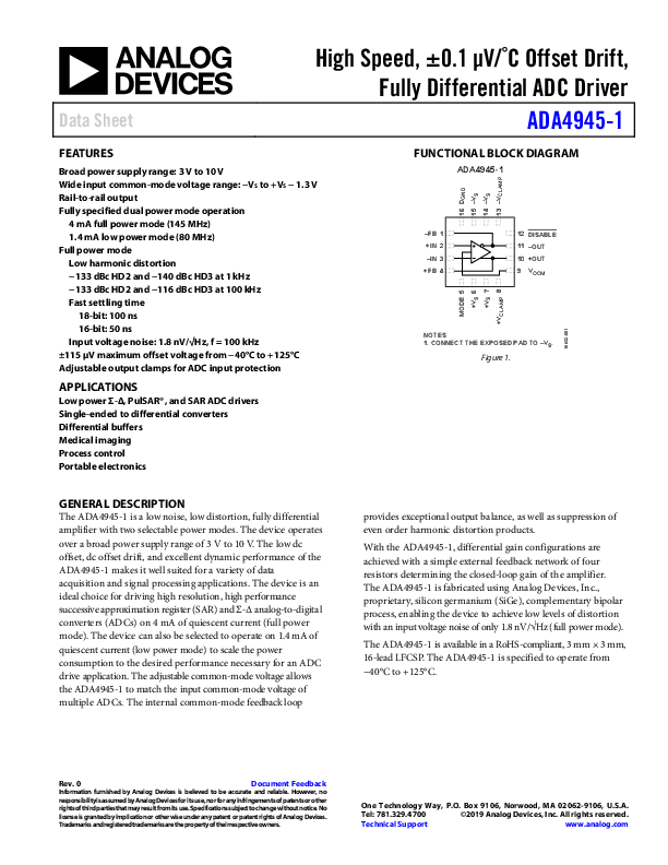
Data Sheet

High Speed, �0.1 V/�C Offset Drift, Fully Differential ADC Driver ADA4945-1

FEATURES
Broad power supply range: 3 V to 10 V Wide input common-mode voltage range: -VS to +VS - 1.3 V Rail-to-rail output Fully specified dual power mode operation
4 mA full power mode (145 MHz) 1.4 mA low power mode (80 MHz) Full power mode Low harmonic distortion -133 dBc HD2 and -140 dBc HD3 at 1 kHz -133 dBc HD2 and -116 dBc HD3 at 100 kHz Fast settling time
18-bit: 100 ns 16-bit: 50 ns Input voltage noise: 1.8 nV/Hz, f = 100 kHz �115 V maximum offset voltage from -40�C to +125�C Adjustable output clamps for ADC input protection
APPLICATIONS
Low power -, PulSAR�, and SAR ADC drivers Single-ended to differential converters Differential buffers Medical imaging Process control Portable electronics

FUNCTIONAL BLOCK DIAGRAM
ADA4945-1

16 DGND 15 �VS 14 �VS 13 �VCLAMP

MODE 5 +VS 6 +VS 7
+VCLAMP 8
16932-001

�FB 1 +IN 2 �IN 3 +FB 4

12 DISABLE 11 �OUT 10 +OUT 9 VOCM

NOTES 1. CONNECT THE EXPOSED PAD TO �VS.
Figure 1.

GENERAL DESCRIPTION
The ADA4945-1 is a low noise, low distortion, fully differential amplifier with two selectable power modes. The device operates over a broad power supply range of 3 V to 10 V. The low dc offset, dc offset drift, and excellent dynamic performance of the ADA4945-1 makes it well suited for a variety of data acquisition and signal processing applications. The device is an ideal choice for driving high resolution, high performance successive approximation register (SAR) and - analog-to-digital converters (ADCs) on 4 mA of quiescent current (full power mode). The device can also be selected to operate on 1.4 mA of quiescent current (low power mode) to scale the power consumption to the desired performance necessary for an ADC drive application. The adjustable common-mode voltage allows the ADA4945-1 to match the input common-mode voltage of multiple ADCs. The internal common-mode feedback loop

provides exceptional output balance, as well as suppression of even order harmonic distortion products.
With the ADA4945-1, differential gain configurations are achieved with a simple external feedback network of four resistors determining the closed-loop gain of the amplifier. The ADA4945-1 is fabricated using Analog Devices, Inc., proprietary, silicon germanium (SiGe), complementary bipolar process, enabling the device to achieve low levels of distortion with an input voltage noise of only 1.8 nV/Hz (full power mode).
The ADA4945-1 is available in a RoHS-compliant, 3 mm � 3 mm, 16-lead LFCSP. The ADA4945-1 is specified to operate from -40�C to +125�C.

Rev. 0

Document Feedback

Information furnished by Analog Devices is believed to be accurate and reliable. However, no

responsibility is assumed by Analog Devices for its use, nor for any infringements of patents or other

rights of third parties that may result from its use. Specifications subject to change without notice. No

license is granted by implication or otherwise under any patent or patent rights of Analog Devices.

Trademarks and registered trademarks are the property of their respective owners.

One Technology Way, P.O. Box 9106, Norwood, MA 02062-9106, U.S.A.

Tel: 781.329.4700

�2019 Analog Devices, Inc. All rights reserved.

Technical Support

www.analog.com

ADA4945-1
TABLE OF CONTENTS
Features .............................................................................................. 1 Applications....................................................................................... 1 Functional Block Diagram .............................................................. 1 General Description ......................................................................... 1 Revision History ............................................................................... 2 Specifications..................................................................................... 3
Supply Voltage (VS) = 10 V ......................................................... 3 VS = 5 V.......................................................................................... 7 VS = 3 V........................................................................................ 11 Absolute Maximum Ratings.......................................................... 15 Thermal Resistance .................................................................... 15 Maximum Power Dissipation ................................................... 15 ESD Caution................................................................................ 15 Pin Configuration and Function Descriptions........................... 16 Typical Performance Characteristics ........................................... 17 Full Power Mode .......................................................................... 17 Low Power Mode........................................................................ 25 Test Circuits..................................................................................... 33 Terminology .................................................................................... 34 Theory of Operation ...................................................................... 35
REVISION HISTORY
4/2019--Revision 0: Initial Version

Data Sheet
Fully Differential and Common-Mode Signal Paths............. 35 Output Voltage Clamp ............................................................... 36 Power Modes............................................................................... 36 Applications Information .............................................................. 37 Analyzing an Application Circuit ............................................ 37 Setting the Closed-Loop Gain .................................................. 37 Estimating the Output Noise Voltage ...................................... 37 Impact of Mismatches in the Feedback Networks ................. 38 Calculating the Input Impedance of an Application Circuit ..... 38 Input Common-Mode Voltage Range ..................................... 40 Input and Output Capacitive AC Coupling............................ 40 Setting the Output Common-Mode Voltage .......................... 40 Disable Pin .................................................................................. 40 Driving a Capacitive Load......................................................... 40 Output Clamps ........................................................................... 41 Driving a High Precision ADC ................................................ 42 Layout, Grounding, and Bypassing.............................................. 43 Outline Dimensions ....................................................................... 44 Ordering Guide .......................................................................... 44

Rev. 0 | Page 2 of 44

Data Sheet

ADA4945-1

SPECIFICATIONS

SUPPLY VOLTAGE (VS) = 10 V
Output common-mode voltage (VOCM) = midsupply, Gain (G) = 1, feedback resistance (RF) = gain resistance (RG) = 499 , differential load resistance (RL, dm) = 1 k, and TA = 25�C, unless otherwise noted. All specifications refer to single-ended input and differential outputs, unless otherwise noted. Refer to Figure 98 for circuit definitions.
Positive Input (+DIN) or Negative Input (�DIN) to Differential Output Voltage (VOUT, dm) Performance

Table 1.

Full Power Mode

Parameter

Test Conditions/Comments Min

Typ Max

DYNAMIC PERFORMANCE

-3 dB Small Signal

VOUT, dm = 20 mV p-p, G = 1

145

Bandwidth

VOUT, dm = 20 mV p-p, G = 2

95

VOUT, dm = 20 mV p-p, G = 5

40

-3 dB Large Signal

VOUT, dm = 2 V p-p, G = 1

60

Bandwidth

VOUT, dm = 2 V p-p, G = 2

54

VOUT, dm = 2 V p-p, G = 5

52

Bandwidth for 0.1 dB

VOUT, dm = 20 mV p-p, G = 1

28

Flatness

VOUT, dm = 20 mV p-p, G = 2

20

Slew Rate

VOUT, dm = 8 V step

600

Settling Time to 0.1% VOUT, dm = 8 V step

35

Settling Time

16-bit

50

18-bit

100

Input Overdrive

G = 1, differential input

500

Recovery

voltage (VIN, dm) = 10 V p-p,

triangular waveform

Output Overdrive

G = 10, VOUT, dm = 22 V p-p,

200

Recovery

triangular waveform

NOISE/HARMONIC PERFORMANCE

VOUT, dm = 8 V p-p

Second Harmonic Distortion (HD2)

Center frequency (fC) = 1 kHz

-133

fC = 100 kHz

-133

fC = 100 kHz, G = 2

-128

fC = 1 MHz

-95

Third Harmonic Distortion (HD3)

fC = 1 kHz

-140

fC = 100 kHz

-116

fC = 100 kHz, G = 2

-123

fC = 1 MHz

-88

Input Voltage Noise

Differential

Frequency under test

f = 10 Hz

5

f = 100 kHz

1.8

1/f corner frequency

100

Common Mode

f = 10 Hz

350

f = 100 kHz

30

1/f corner frequency

1000

Low Power Mode

Min

Typ Max

80
40 17 18
40 16 27
7 100 85 150 300 300

120

-133
-133 -128 -68 -138
-116 -122 -62
7 3 40 284 38 1000

Unit
MHz
MHz MHz MHz
MHz MHz MHz
MHz V/�s ns ns ns ns
ns
dBc
dBc dBc dBc dBc
dBc dBc dBc
nV/Hz nV/Hz Hz nV/Hz nV/Hz nV/Hz

Rev. 0 | Page 3 of 44

ADA4945-1

Data Sheet

Parameter Integrated Voltage Noise Input Current Noise
INPUT CHARACTERISTICS Input Offset Voltage
Input Offset Voltage Drift
Input Bias Current
Input Bias Current Drift
Input Offset Current
Input Offset Current Drift
Input Common-Mode Voltage (VCM) Range
Input Resistance
Input Capacitance Common-Mode
Rejection Ratio (CMRR) Open-Loop Gain
OUTPUT CHARACTERISTICS
Output Voltage Swing
Short-Circuit Current Output Balance Error

Test Conditions/Comments 0.1 Hz to 10 Hz
f = 10 Hz f = 100 kHz 1/f corner frequency
25�C TA = 20�C to 85�C TA = -40�C to +125�C TA = 20�C to 85�C
TA = -40�C to +125�C TA = 25�C TA = 20�C to 85�C TA = -40�C to +125�C TA = 20�C to 85�C TA = -40�C to +125�C TA = 25�C TA = 20�C to 85�C TA = -40�C to +125�C TA = 20�C to 85�C
TA = -40�C to +125�C
Differential Common mode
VCM = 0.5 V to 9 V
Output voltage (VOUT) = �4 V
Load resistance (RL) = 100  for each singleended output RL = 1 k
f = 100 kHz, VOUT, cm/VOUT, dm

Full Power Mode

Min

Typ Max

35

11 1.0 2000

�10 �50 �15 �80 �30 �115 �0.1 �0.5

�0.2 �1.0 -1.2 -2.5 -1.5 -3.0 -1.8 -3.4 -10 -50 -10 -50 �20 �200 �25 �250 �40 �300 �0.1 �0.6

�0.12 �0.7

-VS

+VS - 1.3

50 50 1 -110

120

-VS + 0.55

+VS - 0.55

-VS + 0.1

+VS - 0.1

170

100

Low Power Mode

Min

Typ Max

25

4 0.6 1000

�10 �50 �15 �80 �30 �115 �0.1 �0.5

�0.2 -0.5 -0.6 -0.7 -10 -10 �10 �20 �25 �0.06

�1.0 -0.8 -1.0 -1.2 -50 -50 �130 �150 �200 �0.38

�0.07 �0.4

-VS

+VS - 1.3

50 50 1 -110

115

-VS + 0.55

+VS - 0.55

-VS + 0.1

+VS - 0.1

140

100

Unit nV rms
pA/Hz pA/Hz Hz
�V �V �V �V/�C
�V/�C �A �A �A nA/�C nA/�C nA nA nA nA/�C
nA/�C V
k M pF dB
dB
V
V mA peak dB

Rev. 0 | Page 4 of 44

Data Sheet

ADA4945-1

VOCM to Common-Mode Output Voltage (VOUT, cm) Performance

Table 2.
Parameter VOCM DYNAMIC
PERFORMANCE -3 dB Small Signal
Bandwidth -3 dB Large Signal
Bandwidth Slew Rate Input Voltage Noise Gain VOCM CHARACTERISTICS Input Common-Mode
Voltage Range Input Resistance Offset Voltage
Input Offset Voltage Drift
Input Bias Current
Input Bias Current Drift
CMRR

Test Conditions/Comments
VOUT, cm = 20 mV p-p
VOUT, cm = 2 V p-p
VOUT, cm = 2 V p-p f = 100 kHz VOUT, cm/VOCM, VOCM = �1 V
Common mode offset (VOS,cm) = VOUT,cm - VOCM, positive input (VIP) = negative input (VIN) = VOCM = 0 V 25�C TA = 20�C to 85�C TA = -40�C to +125�C TA = 20�C to 85�C
TA = -40�C to +125�C TA = 25�C TA = 20�C to 85�C TA = -40�C to +125�C TA = 20�C to 85�C
TA = -40�C to +125�C VOS, dm/VOCM, VOCM = �1 V

Full Power Mode

Min

Typ

Max

35

3.8

26

35

0.99

1

-VS + 0.4 125

1.01 +VS - 1.4

�5

�60

�10

�20

�5

�10 -220 -300 -350 -1.3

-1.5 -130

Low Power Mode

Min

Typ Max

15

1.3

9

45

0.99

1

1.01

-VS + 0.4 125

+VS - 1.4

�5 �60 �10 �20 �5
�10 -160 -205 -230 -0.75
-1.0 -130

Unit
MHz
MHz
V/�s nV/Hz V/V
V
k
mV mV mV �V/�C
�V/�C �A �A �A �A/�C
�A/�C dB

Rev. 0 | Page 5 of 44

ADA4945-1

Data Sheet

General Performance

Table 3.
Parameter CLAMP
Clamp Output Voltage
Recovery Time

Full Power Mode

Low Power Mode

Test Conditions/Comments Min

Typ

Max

Min

Typ

Max

Unit

Differential Common mode

-VS - 0.5 -VS
100

+VS + 0.5 -VS - 0.5

+VS

-VS

100

+VS + 0.5 V

+VS

V

ns

Input Resistance

Resistance between +VCLAMP

480

and -VCLAMP

DISABLE (DISABLE PIN)

MODE

Input Voltage

Disabled

-VS � 0.3

Enabled

DGND + 1.4

Turn Off Time

Quiescent current <10% of

6

enabled quiescent current

Turn On Time

Turn on time (tO) >90% of final

1.2

VOUT

DISABLE Pin Bias Current

480
DGND + 1 -VS � 0.3 VS + 0.3 DGND + 1.4
6 2

k
DGND + 1 V VS + 0.3 V
�s �s

Enabled

DISABLE = 10 V

50

50

nA

Disabled

DISABLE = 0 V

50

50

nA

DGND PIN VOLTAGE RANGE

-VS

POWER SUPPLY

Operating Range

3

Quiescent Current

Enabled

Full power mode, MODE = +VS

Low power mode, MODE = -VS

Disabled

Full power mode, MODE = +VS

Low power mode, MODE = -VS

Positive Power Supply

VOS, dm/VS, VS = 1 V p-p

Rejection Ratio (+PSRR)

Negative Power Supply VOS, dm/VS, VS = 1 V p-p Rejection Ratio (-PSRR)

OPERATING TEMPERATURE

-40

RANGE

+VS � 2.5 �VS

10

3

4

4.2

60

70

-120 -120

+125

-40

+VS � 2.5 V

10

V

mA

1.4

1.6

mA

�A

60

70

�A

-120

dB

-120

dB

+125

�C

Rev. 0 | Page 6 of 44

Data Sheet

ADA4945-1

VS = 5 V
VOCM = midsupply, G = 1, RF = RG = 499 , RL, dm = 1 k, TA = 25�C, unless otherwise noted. All specifications refer to single-ended input and differential outputs, unless otherwise noted. Refer to Figure 98 for circuits definitions. +DIN or �DIN to VOUT, dm Performance

Table 4.
Parameter DYNAMIC PERFORMANCE
-3 dB Small Signal Bandwidth
-3 dB Large Signal Bandwidth
Bandwidth for 0.1 dB Flatness
Slew Rate Settling Time to 0.1% Settling Time
Input Overdrive Recovery
Output Overdrive Recovery
NOISE/HARMONIC PERFORMANCE HD2
HD3
Input Voltage Noise Differential
Common Mode
Integrated Voltage Noise
Input Current Noise

Test Conditions/Comments
VOUT, dm = 20 mV p-p, G = 1
VOUT, dm = 20 mV p-p, G = 2 VOUT, dm = 20 mV p-p, G = 5 VOUT, dm = 2 V p-p, G = 1
VOUT, dm = 2 V p-p, G = 2 VOUT, dm = 2 V p-p, G = 5 VOUT, dm = 20 mV p-p, G = 1
VOUT, dm = 20 mV p-p, G = 2 VOUT, dm = 8 V step VOUT, dm = 8 V step 16-bit 18-bit G = 1, VIN, dm = 10 V p-p, triangular waveform G = 2, VOUT, dm = 12 V p-p, triangular waveform VOUT, dm = 8 V p-p
Center frequency (fC) = 1 kHz fC = 100 kHz fC = 100 kHz, G = 2 fC = 1 MHz fC = 1 kHz fC = 100 kHz fC = 100 kHz, G = 2 fC = 1 MHz
f = 10 Hz f = 100 kHz 1/f corner frequency f = 10 Hz f = 100 kHz 1/f corner frequency 0.1 Hz to 10 Hz
f = 10 Hz f = 100 kHz 1/f corner frequency

Full Power Mode

Min

Typ Max

145
95 40 60
54 52 28
20 600 35 50 100 300
145

-133
-133 -128 -95 -140 -116 -123 -88
5 1.8 100 350 30 1000 35
11 1.0 2000

Low Power Mode

Min

Typ Max

80
40 17 18
40 16 27
7 100 85 150 300 500
80

-133
-133 -128 -68 -138 -116 -122 -62
7 3 40 284 38 1000 25
4 0.6 1000

Unit
MHz
MHz MHz MHz
MHz MHz MHz
MHz V/�s ns ns ns ns
ns
dBc
dBc dBc dBc dBc dBc dBc dBc
nV/Hz nV/Hz Hz nV/Hz nV/Hz nV/Hz nV rms
pA/Hz pA/Hz Hz

Rev. 0 | Page 7 of 44

ADA4945-1

Data Sheet

Parameter INPUT CHARACTERISTICS
Input Offset Voltage
Input Offset Voltage Drift
Input Bias Current
Input Bias Current Drift
Input Offset Current
Input Offset Current Drift
VCM Range Input Resistance
Input Capacitance CMRR Open-Loop Gain OUTPUT CHARACTERISTICS Output Voltage Swing
Short-Circuit Current Output Balance Error

Test Conditions/Comments
25�C TA = 20�C to 85�C TA = -40�C to +125�C TA = 20�C to 85�C
TA = -40�C to +125�C TA = 25�C TA = 20�C to 85�C TA = -40�C to +125�C TA = 20�C to 85�C TA = -40�C to +125�C TA = 25�C TA = 20�C to 85�C TA = -40�C to +125�C TA = 20�C to 85�C
TA = -40�C to +125�C
Differential Common mode
VCM = 0.5 V to 9 V VOUT = �4 V
RL = 100
RL = 1 k
f = 100 kHz, VOUT, cm/VOUT, dm

Full Power Mode

Min

Typ Max

�10 �50 �15 �80 �30 �115 �0.1 �0.5

�0.2 �1.0 -1.2 -2.5 -1.5 -3.0 -1.8 -3.4 -10 -50 -10 -50 �20 �200 �25 �250 �40 �300 �0.1 �0.6

�0.12 �0.7

-VS

+VS - 1.3

50

50

1

-110

120

-VS + 0.55 -VS + 0.1
170
100

+VS - 0.55 +VS - 0.1

Low Power Mode

Min

Typ Max

�10 �50 �15 �80 �30 �115 �0.1 �0.5

�0.2 -0.5 -0.6 -0.7 -10 -10 �10 �20 �25 �0.06

�1.0 -0.8 -1.0 -1.2 -50 -50 �130 �150 �200 �0.38

�0.07 �0.4

-VS

+VS - 1.3

50

50

1

-110

115

-VS + 0.55
-VS + 0.1 140
100

+VS - 0.55 +VS - 0.1

Unit
�V �V �V �V/�C
�V/�C �A �A �A nA/�C nA/�C nA nA nA nA/�C
nA/�C V k M pF dB dB
V
V mA peak dB

Rev. 0 | Page 8 of 44

Data Sheet

ADA4945-1

VOCM to VOUT, cm Performance Table 5.
Parameter VOCM DYNAMIC PERFORMANCE
-3 dB Small Signal Bandwidth -3 dB Large Signal Bandwidth Slew Rate Input Voltage Noise Gain VOCM CHARACTERISTICS Input Common-Mode Voltage
Range Input Resistance Offset Voltage
Input Offset Voltage Drift
Input Bias Current
Input Bias Current Drift
CMRR

Test Conditions/Comments
VOUT, cm = 20 mV p-p VOUT, cm = 2 V p-p VOUT, cm = 2 V p-p f = 100 kHz VOUT, cm/VOCM, VOCM = �1 V
VOS, cm = VOUT, cm - VOCM, VIP = VIN = VOCM = 0 V 25�C TA = 20�C to 85�C TA = -40�C to +125�C TA = 20�C to 85�C TA = -40�C to +125�C TA = 25�C TA = 20�C to 85�C TA = -40�C to +125�C TA = 20�C to 85�C TA = -40�C to +125�C VOS, dm/VOCM, VOCM = �1 V

Full Power Mode

Min

Typ Max

35

3.8

26

35

0.99

1

1.01

-VS + 0.4 125

+VS - 1.4

�10 �60 �10 �20 �5 �10 -220 -300 -350 -1.3 -1.5 -130

Low Power Mode

Min

Typ Max

15

1.3

9

45

0.99

1

1.01

Unit
MHz MHz V/�s nV/Hz V/V

-VS + 0.4 125

+VS - 1.4 V k

�10 �60 �10 �20 �5 �10 -160 -205 -230 -0.75 -1.0 -130

mV mV mV �V/�C �V/�C �A �A �A �A/�C �A/�C dB

Rev. 0 | Page 9 of 44

ADA4945-1

Data Sheet

General Performance
Table 6.
Parameter CLAMP
Clamp Output Voltage
Recovery Time Input Resistance
DISABLE (DISABLE PIN) MODE Input Voltage
Turn Off Time
Turn On Time DISABLE Pin Bias Current
Enabled Disabled DGND PIN VOLTAGE RANGE POWER SUPPLY Operating Range Quiescent Current
Enabled
Disabled
+PSRR -PSRR OPERATING TEMPERATURE RANGE

Full Power Mode

Low Power Mode

Test Conditions/Comments

Min

Typ Max

Min

Typ Max

Unit

Differential Common mode

-VS - 0.5 -VS
100

Resistance between +VCLAMP and

480

-VCLAMP

+VS + 0.5 -VS - 0.5

+VS

-VS

100

480

+VS + 0.5 V

+VS

V

ns

k

Disabled Enabled Quiescent current <10% of enabled quiescent current tO >90% of final VOUT

-VS � 0.3 DGND + 1.4
6
1.2

DGND + 1 -VS � 0.3 +VS + 0.3 DGND + 1.4
6
2

DGND + 1 V +VS + 0.3 V
�s
�s

DISABLE = 5 V DISABLE = 0 V

50

50

nA

50

50

nA

�VS

+VS � 2.5 �VS

+VS � 2.5 V

3

10

3

10

V

Full power mode, MODE = +VS Low power mode, MODE = -VS Full power mode, MODE = +VS Low power mode, MODE = -VS VOS, dm/VS, VS = 1 V p-p VOS, dm/VS, VS = 1 V p-p
-40

4

4.2

60 70

-120

-120

+125

-40

mA

1.4 1.6

mA

�A

60 70

�A

-120

dB

-120

dB

+125

�C

Rev. 0 | Page 10 of 44

Data Sheet

ADA4945-1

VS = 3 V
VOCM = midsupply, G = 1, RF = RG = 499 , RL, dm = 1 k, TA = 25�C, unless otherwise noted. All specifications refer to single-ended input and differential outputs, unless otherwise noted. Refer to Figure 98 for circuit definitions. +DIN or �DIN to VOUT, dm Performance

Table 7.
Parameter DYNAMIC PERFORMANCE
-3 dB Small Signal Bandwidth
-3 dB Large Signal Bandwidth
Bandwidth for 0.1 dB Flatness
Slew Rate Settling Time to 0.1% Settling Time
Input Overdrive Recovery
Output Overdrive Recovery
NOISE/HARMONIC PERFORMANCE
HD2
HD3
Input Voltage Noise Differential
Common Mode
Integrated Voltage Noise
Input Current Noise

Test Conditions/Comments
VOUT, dm = 20 mV p-p, G = 1
VOUT, dm = 20 mV p-p, G = 2 VOUT, dm = 20 mV p-p, G = 5 VOUT, dm = 2 V p-p, G = 1
VOUT, dm = 20 mV p-p, G = 1
VOUT, dm = 20 mV p-p, G = 2 VOUT, dm = 4 V step VOUT, dm = 4 V step 16-bit 18-bit G = -1, VIN, dm = 3 V p-p, triangular waveform G = 2, VOUT, dm = 6 V p-p, triangular waveform VOUT, dm = 4 V p-p
fC = 1 kHz fC = 100 kHz fC = 100 kHz, G = 2 fC = 1 MHz fC = 1 kHz fC = 100 kHz fC = 100 kHz, G = 2 fC = 1 MHz
f = 10 Hz f = 100 kHz 1/f corner frequency f = 10 Hz f = 100 kHz 1/f corner frequency 0.1 Hz to 10 Hz
f = 10 Hz f = 100 kHz 1/f corner frequency

Full Power Mode

Min

Typ Max

145
95 40 22
28
20 600 35 50 100 500
200

-133 -133 -128 -95 -140 -116 -123 -88
5 1.8 100 350 30 1000 35
11 1.0 2000

Low Power Mode

Min

Typ Max

80
40 17 11
27
7 100 85 150 300 300
120

-133 -133 -128 -68 -138 -116 -122 -62
7 3 40 284 38 1000 25
4 0.6 1000

Unit
MHz
MHz MHz MHz
MHz
MHz V/�s ns ns ns ns
ns
dBc dBc dBc dBc dBc dBc dBc dBc
nV/Hz nV/Hz Hz nV/Hz nV/Hz nV/Hz nV rms
pA/Hz pA/Hz Hz

Rev. 0 | Page 11 of 44

ADA4945-1

Data Sheet

Parameter INPUT CHARACTERISTICS
Input Offset Voltage
Input Offset Voltage Drift
Input Bias Current
Input Bias Current Drift
Input Offset Current
Input Offset Current Drift
VCM Range Input Resistance
Input Capacitance CMRR Open-Loop Gain OUTPUT
CHARACTERISTICS Output Voltage Swing
Short-Circuit Current Output Balance Error

Test Conditions/Comments
25�C TA = 20�C to 85�C TA = -40�C to +125�C TA = 20�C to 85�C
TA = -40�C to +125�C TA = 25�C TA = 20�C to 85�C TA = -40�C to +125�C TA = 20�C to 85�C TA = -40�C to +125�C TA = 25�C TA = 20�C to 85�C TA = -40�C to +125�C TA = 20�C to 85�C
TA = -40�C to +125�C
Differential Common mode
VCM = 0.5 V to 9 V VOUT = �4 V
RL = 100  RL = 1 k
f = 100 kHz, VOUT, cm/VOUT, dm

Full Power Mode

Min

Typ Max

Low Power Mode

Min

Typ Max

�10 �50 �15 �80 �30 �115 �0.1 �0.5

�10 �50 �15 �80 �30 �115 �0.1 �0.5

�0.2 �1.0 -1.2 -2.5 -1.5 -3.0 -1.8 -3.4 -10 -50 -10 -50 �20 �200 �25 �250 �40 �300 �0.1 �0.6

�0.2 -0.5 -0.6 -0.7 -10 -10 �10 �20 �25 �0.06

�1.0 -0.8 -1.0 -1.2 -50 -50 �130 �150 �200 �0.38

�0.12 �0.7

�0.07 �0.4

-VS

+VS - 1.3 -VS

+VS - 1.3

50

50

50

50

1

1

-110

-110

120

115

-VS + 0.55 -VS + 0.1
170 100

+VS - 0.55 -VS + 0.55 +VS - 0.1 -VS + 0.1
140 100

+VS - 0.55 +VS - 0.1

Unit
�V �V �V �V/�C
�V/�C �A �A �A nA/�C nA/�C nA nA nA nA/�C
nA/�C V k M pF dB dB
V V mA peak dB

Rev. 0 | Page 12 of 44

Data Sheet

ADA4945-1

VOCM to VOUT, cm Performance Table 8.
Parameter VOCM DYNAMIC PERFORMANCE
-3 dB Small Signal Bandwidth -3 dB Large Signal Bandwidth Slew Rate Input Voltage Noise Gain VOCM CHARACTERISTICS Input Common-Mode Voltage
Range Input Resistance Offset Voltage
Input Offset Voltage Drift
Input Bias Current
Input Bias Current Drift
CMRR

Test Conditions/Comments

Full Power Mode

Min

Typ Max

Low Power Mode

Min

Typ Max

VOUT, cm = 20 mV p-p

35

15

VOUT, cm = 2 V p-p

3.8

1.3

VOUT, cm = 2 V p-p

26

9

f = 100 kHz

35

45

VOUT, cm/VOCM, VOCM = �1 V

0.99

1

1.01

0.99

1

1.01

VOS, cm = VOUT, cm - VOCM, VIP = VIN = VOCM = 0 V 25�C TA = 20�C to 85�C TA = -40�C to +125�C TA = 20�C to 85�C TA = -40�C to +125�C TA = 25�C TA = 20�C to 85�C TA = -40�C to +125�C TA = 20�C to 85�C TA = -40�C to +125�C VOS, dm/VOCM, VOCM = �1 V

-VS + 0.4 125

+VS - 1.4 -VS + 0.4 125

+VS - 1.4

�10 �60 �10 �20 �5 �10 -220 -300 -350 -1.3 -1.5 -130

�10 �60 �10 �20 �5 �10 -160 -205 -230 -0.75 -1.0 -130

Unit
MHz MHz V/�s nV/Hz V/V
V
k
mV mV mV �V/�C �V/�C �A �A �A �A/�C �A/�C dB

Rev. 0 | Page 13 of 44

ADA4945-1

Data Sheet

General Performance

Table 9.
Parameter CLAMP
Clamp Output Voltage
Recovery Time

Test Conditions/Comments
Differential Common mode

Full Power Mode

Low Power Mode

Min

Typ Max

Min

Typ Max

Unit

-VS - 0.5

+VS + 0.5 -VS - 0.5

+VS + 0.5 V

-VS

+VS

-VS

+VS

V

100

100

ns

Input Resistance

Resistance between +VCLAMP and

480

-VCLAMP

DISABLE (DISABLE PIN) MODE

480

k

Input Voltage
Turn Off Time Turn On Time DISABLE Pin Bias Current

Disabled Enabled Quiescent current <10% of enabled quiescent current tO >90% of final VOUT

-VS � 0.3 DGND + 1.4
6
1.2

DGND + 1 �VS � 0.3 +VS + 0.3 DGND + 1.4
6
2

DGND + 1 V +VS + 0.3 V
�s
�s

Enabled

DISABLE = 3 V

50

50

nA

Disabled

DISABLE = 0 V

50

50

nA

DGND PIN VOLTAGE RANGE POWER SUPPLY
Operating Range Quiescent Current
Enabled
Disabled
+PSRR -PSRR OPERATING TEMPERATURE RANGE

-VS
3
Full power mode, MODE = +VS Low power mode, MODE = -VS Full power mode, MODE = +VS Low power mode, MODE = -VS VOS, dm/VS, VS = 1 V p-p VOS, dm/VS, VS = 1 V p-p
-40

+VS � 2.5 �VS

10

3

4

4.2

60 70

-120

-120

+125

-40

+VS � 2.5 V

10

V

mA

1.4 1.6

mA

�A

60 70

�A

-120

dB

-120

dB

+125

�C

Rev. 0 | Page 14 of 44

Data Sheet

ABSOLUTE MAXIMUM RATINGS

Table 10. Parameter Supply Voltage VOCM Differential Input Voltage Operating Temperature Range Storage Temperature Range Lead Temperature (Soldering, 10 sec) Junction Temperature Electrostatic Discharge (ESD)
Field Induced Charged Device Model (FICDM)
Human Body Model (HBM)

Rating 11 V �VS �1 V -40�C to +125�C -65�C to +150�C 300�C 150�C
1250 V
4000 V

Stresses at or above those listed under Absolute Maximum Ratings may cause permanent damage to the product. This is a stress rating only; functional operation of the product at these or any other conditions above those indicated in the operational section of this specification is not implied. Operation beyond the maximum operating conditions for extended periods may affect product reliability.

THERMAL RESISTANCE

Thermal performance is directly linked to printed circuit board (PCB) design and operating environment. Careful attention to PCB thermal design is required.

JA is the natural convection, junction to ambient, thermal resistance measured in a one cubic foot sealed enclosure. JC is the junction to case thermal resistance.

Table 11. Package Type CP-16-22

JA

JC

70 15

Unit �C/W

MAXIMUM POWER DISSIPATION
The maximum safe power dissipation in the ADA4945-1 package is limited by the associated rise in junction temperature (TJ) on the die. At approximately 150�C, which is the glass transition temperature, the properties of the plastic change. Even temporarily exceeding this temperature limit can change the stresses that the package exerts on the die, permanently shifting the parametric performance of ADA4945-1. Exceeding a junction temperature of 150�C for an extended period can result in changes in the silicon devices, potentially causing failure.

ADA4945-1

The power dissipated in the package (PD) is the sum of the quiescent power dissipation and the power dissipated in the package due to the load drive for all outputs. The quiescent power dissipation is the voltage between the supply pins (�VS) times the quiescent current (IS). The load current consists of the differential and common-mode currents flowing to the load, as well as currents flowing through the external feedback networks and internal common-mode feedback loop. The internal resistor tap used in the common-mode feedback loop places a negligible differential load on the output. Consider RMS voltages and currents when dealing with ac signals.
Airflow reduces JA. In addition, more metal directly in contact with the package leads from metal traces through holes, ground, and power planes reduces the JA.
Figure 2 shows the maximum safe power dissipation in the package vs. the ambient temperature for the 16-lead LFCSP (JA = 70�C/W) package on a JEDEC standard 4-layer board. JA values are approximations.
3.0

MAXIMUM SAFE POWER DISSIPATION (W)
16932-003

2.5

2.0

1.5

1.0

0.5

0 �40 �20

0

20

40

60

80 100 120

AMBIENT TEMPERATURE (�C)

Figure 2. Maximum Safe Power Dissipation vs. Ambient Temperature

ESD CAUTION

Rev. 0 | Page 15 of 44

ADA4945-1 PIN CONFIGURATION AND FUNCTION DESCRIPTIONS

16 DGND 15 �VS 14 �VS 13 �VCLAMP

�FB 1 +IN 2 �IN 3 +FB 4

ADA4945-1
TOP VIEW (Not to Scale)

12 DISABLE 11 �OUT 10 +OUT 9 VOCM

MODE 5 +VS 6 +VS 7
+VCLAMP 8

16932-005

Table 12. Pin Function Descriptions

Pin No. Mnemonic

1

-FB

2

+IN

3

-IN

4

+FB

5

MODE

6

+VS

7

+VS

8

+VCLAMP

9

VOCM

10

+OUT

11

-OUT

12

DISABLE

13

-VCLAMP

14

-VS

15

-VS

16

DGND

Exposed pad (EPAD)

NOTES 1. EXPOSED PAD. CONNECT THE EXPOSED PAD TO �VS.
Figure 3. Pin Configuration
Description Negative Output for Feedback Component Connection. Positive Input Summing Node. Negative Input Summing Node. Positive Output for Feedback Component Connection. Selects Between Full Power Mode and Low Power Mode. Positive Supply Voltage. Positive Supply Voltage. Positive Clamp Level. Output Common-Mode Voltage. Positive Output for Load Connection. Negative Output for Load Connection. Disable Pin. Negative Clamp Level. Negative Supply Voltage. Negative Supply Voltage. Digital Ground Level. Exposed Pad. Connect the exposed pad to -VS.

Data Sheet

Rev. 0 | Page 16 of 44

Data Sheet

ADA4945-1

TYPICAL PERFORMANCE CHARACTERISTICS

TA = +25�C, VS = �5 V, G = 1, RF = RG = 499 , RT = 53.6  (when used), and RL = 1 k, unless otherwise noted. See Figure 94, Figure 95, Figure 96, and Figure 97 for the test circuits.

FULL POWER MODE

NORMALIZED GAIN (dB)

3

2

G = 1, RL = 1k

1

G = 1, RL = 100

0

�1

�2

G = 2, RL = 1k

�3

�4

�5

�6

G = 2, RL = 100

�7

�8 VOUT, dm = 0.1V p-p

�9

0.1

1

10

100

FREQUENCY (MHz)

1000

Figure 4. Small Signal Frequency Response for Various Gains and Loads

16932-007
NORMALIZED GAIN (dB)

3

2

G = 1, RL = 1k

1

G = 1, RL = 100

0

�1

G = 2, RL = 1k

�2

G = 2, RL = 100

�3

�4

�5

�6

�7

16932-010

�8 VOUT, dm = 2V p-p

�9

0.1

1

10

100

FREQUENCY (MHz)

1000

Figure 7. Large Signal Frequency Response for Various Gains and Loads

GAIN (dB)

3

2

VS = �5V VS = �2.5V

1

VS = �1.5V

0

�1

�2

�3

�4

�5

�6

�7

�8 VOUT, dm = 0.1V p-p

�9

0.1

1

10

100

FREQUENCY (MHz)

1000

Figure 5. Small Signal Frequency Response for Various Supplies

16932-008
GAIN (dB)

3

2

VS = �5V VS = �2.5V

1

VS = �1.5V

0

�1

�2

�3

�4

�5

�6

�7

�8 VOUT, dm = 2V p-p

�9

0.1

1

10

100

FREQUENCY (MHz)

1000

Figure 8. Large Signal Frequency Response for Various Supplies

16932-011

GAIN (dB)

3

2

+25�C

1

�40�C

0 +125�C
�1

�2

�3

�4

�5

�6

�7

�8 VOUT, dm = 0.1V p-p

�9

0.1

1

10

100

FREQUENCY (MHz)

1000

Figure 6. Small Signal Frequency Response for Various Temperatures

16932-009

GAIN (dB)

3

2

+25�C

1 �40�C
0

�1

�2

+125�C

�3

�4

�5

�6

�7

�8 VOUT, dm = 2V p-p

�9

0.1

1

10

100

FREQUENCY (MHz)

1000

Figure 9. Large Signal Frequency Response for Various Temperatures

16932-012

Rev. 0 | Page 17 of 44

ADA4945-1

GAIN (dB)

3

2

1

0

�1

�2

VOCM = �1V

�3

�4

�5

�6

�7

�8 VOUT, dm = 0.1V p-p

�9

0.1

1

10

FREQUENCY (MHz)

VOCM = 0V

100

1000

Figure 10. Small Signal Frequency Response at Various VOCM Levels

GAIN (dB)

3 2 VOCM = 0V, �1V

1

0

�1

�2

�3

�4

�5

�6

�7

�8 VOUT, dm = 2V p-p

�9

0.1

1

10

100

FREQUENCY (MHz)

1000

Figure 11. Large Signal Frequency Response at Various VOCM Levels

GAIN (dB)

4

3

CCOM1 = CCOM2 = 20pF

2

1

0

�1

�2

CCOM1 = CCOM2 = 0pF

�3

CCOM1 = CCOM2 = 5pF

�4 CCOM1 = CCOM2 = 10pF
�5

�6

�7

�8

CDIFF = 0pF VOUT = 0.1V p-p

�9

1

10

100

FREQUENCY (MHz)

1000

Figure 12. Small Signal Frequency Response for Various Capacitive Loads

16932-015
GAIN (dB)

16932-014
GAIN (dB)

16932-013
NORMALIZED GAIN (dB)

Data Sheet

16932-016

0.25

0.20

G = 1, RL = 100

0.15

G = 1, RL = 1k

0.10

0.05

0

�0.05 �0.10 �0.15

G = 2, RL = 100 G = 2, RL = 1k

�0.20 VOUT, dm = 0.1V p-p

�0.25

0.1

1

10

100

FREQUENCY (MHz)

1000

Figure 13. 0.1 dB Flatness Small Signal Frequency Response for Various Gains and Loads

3

2

1

0

�1

�2

�3

�4

�5

�6

�7

�8 VOUT, dm = 0.1V p-p

�9

0.1

1

10

100

FREQUENCY (MHz)

1000

Figure 14. VOCM Small Signal Frequency Response

16932-017

4 3 2 1 0 �1 �2 �3 �4 �5 �6 �7 �8 CDIFF = 0pF �9 VOUT = 2V p-p
1

CCOM1 = CCOM2 = 0pF CCOM1 = CCOM2 = 5pF CCOM1 = CCOM2 = 10pF CCOM1 = CCOM2 = 20pF

10

100

FREQUENCY (MHz)

1000

16932-018

Figure 15. Large Signal Frequency Response for Various Capacitive Loads

Rev. 0 | Page 18 of 44

Data Sheet

NORMALIZED GAIN (dB)

0.25

0.20

G = 1, RL = 100

0.15

G = 1, RL = 1k

0.10

G = 2, RL = 1k

0.05

G = 2, RL = 100

0

�0.05

�0.10

�0.15

�0.20 VOUT, dm = 2V p-p

�0.25

0.1

1

10

100

FREQUENCY (MHz)

1000

Figure 16. 0.1 dB Flatness Large Signal Frequency Response for Various Gains and Loads

3

2

1

0

�1

�2

�3

�4

�5

�6

�7

�8 VOUT, dm = 2V p-p

�9

0.1

1

10

100

FREQUENCY (MHz)

1000

Figure 17. VOCM Large Signal Frequency Response

GAIN (dB)

INPUT OFFSET VOLTAGE (�V)

NORMALIZED AT TA = 25�C
TEMPERATURE (�C)
Figure 18. Input Offset Voltage vs. Temperature for 50 Devices

16932-022
HARMONIC DISTORTION (dBc)

16932-021
HARMONIC DISTORTION (dBc)

16932-019
INPUT OFFSET CURRENT (nA)

ADA4945-1

16932-023

16932-086

NORMALIZED AT TA = 25�C
TEMPERATURE (�C)
Figure 19. Input Offset Current vs. Temperature for 30 Devices

�20 VOUT, dm = 8V p-p
�40

�60

�80 �100 �120

HD2, HD2,

HD3,

�140
�160 100

HD3,

1k

10k

100k

1M

FREQUENCY (Hz)

Figure 20. Harmonic Distortion vs. Frequency for Various Loads

�20 VOUT, dm = 8V p-p
�40

�60

�80 �100 �120

HD2, VS = �5V HD2, VS = �2.5V

�140
�160 100

HD3, VS = �2.5V HD3, VS = �5V

1k

10k

100k

1M

FREQUENCY (Hz)

Figure 21. Harmonic Distortion vs. Frequency for Various Supplies

16932-024

Rev. 0 | Page 19 of 44

ADA4945-1

HARMONIC DISTORTION (dBc)

HARMONIC DISTORTION (dBc)

�20 VOUT, dm = 8V p-p
�40

�60

�80 �100 �120

HD2, G = 1 HD2, G = 2

�140
�160 100

HD3, G = 2 HD3, G = 1

1k

10k

100k

1M

FREQUENCY (Hz)

Figure 22. Harmonic Distortion vs. Frequency for Various Gains

�20 VOUT, dm = 2V p-p
�40

�60

�80

�100
HD2 �120

�140 HD3
�160 �5 �4 �3 �2 �1 0 1 2 3 4 5 VOCM (V)
Figure 23. Harmonic Distortion vs. VOCM, f = 1 kHz, �5 V Supplies
�20
�40

�60

�80

�100 �120

HD2

�140

VOUT, dm = 2V p-p

HD3

�160

�2.5 �2.0 �1.5 �1.0 �0.5 0 0.5 1.0 1.5 2.0 2.5

VOCM (V)

Figure 24. Harmonic Distortion vs. VOCM, f = 1 kHz, �2.5 V Supplies

HARMONIC DISTORTION (dBc)

16932-104
HARMONIC DISTORTION (dBc)

16932-103
HARMONIC DISTORTION (dBc)

16932-088
HARMONIC DISTORTION (dBc)

Data Sheet

�20

HD2 AT VOUT, dm = 8V p-p

HD3 AT VOUT, dm = 8V p-p

�40

HD2 AT VOUT, dm = 4V p-p

HD3 AT VOUT, dm = 4V p-p

HD2 AT VOUT, dm = 2V p-p

�60

HD3 AT VOUT, dm = 2V p-p

�80

�100

�120

�140

�160 100

1k

10k

100k

1M

FREQUENCY (Hz)

Figure 25. Harmonic Distortion vs. Frequency for Various VOUT, dm

16932-090

�20 f = 1kHz
�40 VS = +3V, 0V HD3
�60
�80
�100 VS = +3V, 0V HD2
�120

VS = �2.5V HD3 VS = �2.5V HD2
VS = �5V HD3
VS = �5V HD3

�140

16932-107

�160 0 2 4 6 8 10 12 14 16 18 20 VOUT, dm (V p-p)
Figure 26. Harmonic Distortion vs. VOUT, dm for Various Supplies, f = 1 kHz

�20 VOUT, dm = 8V p-p
�40

�60

�80 �100 �120

HD2, RF = RG = 499 HD3, RF = RG = 1k

�140
�160 100

HD3, RF = RG = 1k HD3, RF = RG = 499

1k

10k

100k

1M

FREQUENCY (Hz)

16932-109

Figure 27. Harmonic Distortion vs. Frequency for Various RF and RG Values

Rev. 0 | Page 20 of 44

Data Sheet

CMRR (dB)

OUTPUT BALANCE (dB)

110 100
90 80 70 60 50 40
0.1

1

10

100

FREQUENCY (MHz)

Figure 28. CMRR vs. Frequency

�10

�20

�30

�40

�50

�60

�70

�80 0.1

1

10

100

FREQUENCY (MHz)

Figure 29. Output Balance vs. Frequency

130

120

�PSRR

110 +PSRR
100

90

80

70

60

50

40 0.1

1

10

100

FREQUENCY (MHz)

Figure 30. PSRR vs. Frequency

PSRR (dB)

16932-026

16932-020

16932-025
OPEN-LOOP GAIN (dB)

INPUT VOLTAGE NOISE (nV/Hz)

OUTPUT VOLTAGE (V)

ADA4945-1

PHASE (Degrees)

16932-027

140 130 120 110 100
90 80 70 60 50 40 30 20 10
0 �10 �20 �30 �40
1

30

15 �015

�30

�45

GAIN

�60

�75

�90

PHASE

�105 �120

�135

�150

�165

�180

�195

�210

�225

�240 10 100 1k 10k 100k 1M 10M 100M 1G

Figure 31. Open-Loop Gain and Phase vs. Frequency

14 12 G = +10

10

8

VOUT, dm

6

4

2

10 � VIN

0

�2 �4

�6 �8
�10
�12
�14 0

100 200 300 400 500 600 700 800 900 1000 TIME (ns)

Figure 32. Output Overdrive Recovery, G = 2

100

16932-030

10

16932-099

1

1

10

100

1k

10k

100k

1M

10M

FREQUENCY (Hz)

Figure 33. Voltage Noise Spectral Density, Referred to Input

Rev. 0 | Page 21 of 44

ADA4945-1
100
10

INPUT CURRENT NOISE (pA/Hz)

1

SUPPLY CURRENT (mA)

0.1 1

10

100

1k

10k

100k

1M

10M

FREQUENCY (Hz)

Figure 34. Input Current Noise Spectral Density

4.5

8

4.0

6

3.5

4

3.0

2

2.5

0

2.0

�2

SUPPLY CURRENT

1.5

�4

1.0

�6

DISABLE

0.5

�8

0

�10

0 0.2 0.4 0.6 0.8 1.0 1.2 1.4 1.6 1.8 2.0

TIME (�s)

Figure 35. DISABLE Pin Turn-Off Time

8

0.4

6

0.3

INPUT

4

0.2

2

0.1

%ERROR

0

0

�2

�0.1

OUTPUT

�4

�0.2

�6 VOUT, dm = 8V p-p
�8 �10 0 10 20 30 40 50 60
TIME (ns)

70 80

�0.3
�0.4 90

Figure 36. 0.1% Settling Time

VOLTAGE (V)

DISABLE PIN VOLTAGE (V)

ERROR (%)

16932-115

16932-111

16932-101
CLOSED-LOOP OUTPUT IMPEDANCE MAGNITUDE ()

Data Sheet
100

10

1

0.1

16932-029

0.01 0.1

1

10

100

FREQUENCY (MHz)

Figure 37. Closed-Loop Output Impedance Magnitude vs. Frequency, G = 1

DISABLE PIN VOLTAGE (V)

OUTPUT VOLTAGE (V)

1.2 1.1 1.0 0.9 0.8 0.7 0.6 0.5 0.4 0.3 0.2 0.1
0 �0.1 �0.2 �0.3
0

8

7

6

5

4

3

2

DISABLE

1

0

�1

�OUT, VICM = 1V

�2

�3

�4

�5

+OUT, VICM = 1V

�6

�7 0.2 0.4 0.6 0.8 1.0 1.2 1.4 1.6 1.8 2.0

TIME (�s)

Figure 38. DISABLE Pin Turn-On Time

16932-112

100

G = 1, RL = 1k

80

G = 1, RL = 100

G = 2, RL = 1k

60

G = 2, RL = 100

OUTPUT VOLTAGE (mV)

40

20

0

�20

�40

�60

�80 VOUT, dm = 0.1V p-p
�100 0 100 200 300 400 500 600 700 800 900 1000 TIME (ns)
Figure 39. Small Signal Transient Response for Various Gains and Loads

16932-047

Rev. 0 | Page 22 of 44

Data Sheet

OUTPUT VOLTAGE (mV)

100

CCOM1 = CCOM2 = 0pF

80

CCOM1 = CCOM2 = 5pF

CCOM1 = CCOM2 = 10pF

60

CCOM1 = CCOM2 = 20pF

40

20

0

�20

�40

�60

�80 CDIFF = 0pF VOUT, dm = 0.1V p-p
�100 0 100 200 300 400 500 600 700 800 900 1000
TIME (ns)

Figure 40. Small Signal Transient Response for Various Capacitive Loads, VS = 10 V

100

CCOM1 = CCOM2 = 0pF

80

CCOM1 = CCOM2 = 5pF

CCOM1 = CCOM2 = 10pF

60

CCOM1 = CCOM2 = 20pF

OUTPUT VOLTAGE (mV)

40

20

0

�20

�40

�60

�80 CDIFF = 0pF VOUT, dm = 0.1V p-p
�100 0 100 200 300 400 500 600 700 800 900 1000 TIME (ns)
Figure 41. Small Signal Transient Response for Various Capacitive Loads, VS = 5 V

100

CCOM1 = CCOM2 = 0pF

80

CCOM1 = CCOM2 = 5pF

CCOM1 = CCOM2 = 10pF

60

CCOM1 = CCOM2 = 20pF

OUTPUT VOLTAGE (mV)

40

20

0

�20

�40

�60
�80 CDIFF = 0pF VOUT, dm = 0.1V p-p
�100 0 100 200 300 400 500 600 700 800 900 1000 TIME (ns)
Figure 42. Small Signal Transient Response for Various Capacitive Loads, VS = 3 V

16932-071
OUTPUT VOLTAGE (V)

16932-070
OUTPUT VOLTAGE (V)

16932-069
OUTPUT VOLTAGE (V)

ADA4945-1

7 6
5 4 3 2 1 0
�1 �2 �3
�4 �5 �6 VOUT, dm = 8V p-p �7
0 100 200 300

G G G G

= = = =

1, 1, 2, 2,

RRRRLLLL

= = = =

1k 100 1k 100

400 500 600 700 800 900 1000 TIME (ns)

16932-067

Figure 43. Large Signal Transient Response for Various Gains and Loads

7 6

5 4

3

2 1

0

�1 �2

�3

�4

�5

�6

CDIFF = 0pF VOUT, dm = 8V p-p

�7

0 100 200 300

CCOM1 = CCOM2 = 0pF CCOM1 = CCOM2 = 5pF CCOM1 = CCOM2 = 10pF CCOM1 = CCOM2 = 20pF
400 500 600 700 800 900 1000 TIME (ns)

16932-075

Figure 44. Large Signal Transient Response for Various Capacitive Loads, VS = 10 V

7 6

CCOM1 = CCOM2 = 0pF CCOM1 = CCOM2 = 5pF

5 4

CCOM1 = CCOM2 = 10pF CCOM1 = CCOM2 = 20pF

3

2 1

0

�1 �2 �3

�4

�5

�6

CDIFF = 0pF VOUT, dm = 8V p-p

�7

0 100 200 300 400 500 600 700 800 900 1000

TIME (ns)

16932-076

Figure 45. Large Signal Transient Response for Various Capacitive Loads, VS = 5 V

Rev. 0 | Page 23 of 44

ADA4945-1

4

CCOM1 = CCOM2 = 0pF

CCOM1 = CCOM2 = 5pF

3

CCOM1 = CCOM2 = 10pF

CCOM1 = CCOM2 = 20pF

2

OUTPUT VOLTAGE (V)

1

0

�1

�2

�3 CDIFF = 0pF VOUT, dm = 4V p-p
�4 0 100 200 300 400 500 600 700 800 900 1000
TIME (ns)

Figure 46. Large Signal Transient Response for Various Capacitive Loads, VS = 3 V

OUTPUT VOLTAGE (mV)

100

80

VS = �5V

60

VS = �2.5V

40

20

0

�20

�40

�60

�80 VOUT, dm = 0.1V p-p
�100 0 100 200 300 400 500 600 700 800 900 1000 TIME (ns)
Figure 47. VOCM Small Signal Transient Response

16932-081

16932-077
OUTPUT VOLTAGE (V)

Data Sheet

1.25

1.00

VS = �5V

0.75

0.50

VS = �2.5V

0.25

0

�0.25

�0.50

�0.75

�1.00 VOUT, dm = 2V p-p
�1.25 0 100 200 300 400 500 600 700 800 900 1000
TIME (ns)

Figure 48. VOCM Large Signal Transient Response

16932-082

Rev. 0 | Page 24 of 44

Data Sheet

LOW POWER MODE

3

2

G = 1, RL = 100

1

G = 1, RL = 1k

0

NORMALIZED GAIN (dB)

�1

�2

�3 G = 2, RL = 1k
�4

�5

G = 2, RL = 100

�6

�7

�8 VOUT, dm = 0.1V p-p

�9

0.1

1

10

100

FREQUENCY (MHz)

1000

Figure 49. Small Signal Frequency Response for Various Gains and Loads

GAIN (dB)

3

2

VS = �5V VS = �2.5V

1

VS = �1.5V

0

�1

�2

�3

�4

�5

�6

�7

�8 VOUT, dm = 0.1V p-p

�9

0.1

1

10

100

FREQUENCY (MHz)

1000

Figure 50. Small Signal Frequency Response for Various Supplies

GAIN (dB)

3

2

25�C 125�C

1

0

�1

�40�C

�2

�3

�4

�5

�6

�7

�8 VOUT, dm = 0.1V p-p

�9

0.1

1

10

100

FREQUENCY (MHz)

1000

Figure 51. Small Signal Frequency Response for Various Temperatures

16932-034
GAIN (dB)

16932-033
GAIN (dB)

16932-032
NORMALIZED GAIN (dB)

ADA4945-1

3

2

G = 1, RL = 1k

1

0

G = 1, RL = 100

�1

G = 2, RL = 1k

�2

�3

�4

G = 2, RL = 100

�5

�6

�7

�8 VOUT, dm = 2V p-p

�9

0.1

1

10

100

FREQUENCY (MHz)

1000

16932-035

Figure 52. Large Signal Frequency Response for Various Gains and Loads

3

2

VS = �5V VS = �2.5V

1

VS = �1.5V

0

�1

�2

�3

�4

�5

�6

�7

�8 VOUT, dm = 2V p-p

�9

0.1

1

10

100

FREQUENCY (MHz)

1000

Figure 53. Large Signal Frequency Response for Various Supplies

16932-036

3

2

�40�C

1

+25�C

0

�1 +125�C
�2

�3

�4

�5

�6

�7

�8 VOUT, dm = 2V p-p

�9

0.1

1

10

100

FREQUENCY (MHz)

1000

Figure 54. Large Signal Frequency Response for Various Temperatures

16932-037

Rev. 0 | Page 25 of 44

ADA4945-1

GAIN (dB)

3

2

1

VOCM = �1V

0

�1

�2 VOCM = +1V
�3

�4

VOCM = 0V

�5

�6

�7

�8 VOUT, dm = 0.1V p-p

�9

0.1

1

10

100

FREQUENCY (MHz)

1000

Figure 55. Small Signal Frequency Response at Various VOCM Levels

GAIN (dB)

3 2 VOCM = 0V, �1V

1

0

�1

�2

�3

�4

�5

�6

�7

�8 VOUT, dm = 2V p-p

�9

0.1

1

10

100

FREQUENCY (MHz)

1000

Figure 56. Large Signal Frequency Response at Various VOCM Levels

4

3

CCOM1 = CCOM2 = 20pF

2

1

GAIN (dB)

0

�1

�2

CCOM1 = CCOM2 = 0pF

�3

CCOM1 = CCOM2 = 5pF

�4

CCOM1 = CCOM2 = 10pF

�5

�6

�7

�8

CDIFF = 0pF VOUT = 0.1V p-p

�9

1

10

100

FREQUENCY (MHz)

1000

Figure 57. Small Signal Frequency Response for Various Capacitive Loads

16932-040
GAIN (dB)

16932-039
GAIN (dB)

16932-038
NORMALIZED GAIN (dB)

Data Sheet

16932-041

0.25

0.20

G = 1, RL = 100

0.15

0.10

0.05

0 �0.05 �0.10 �0.15

G = 2, RL = 100 G = 2, RL = 1k

G = 1, RL = 1k

�0.20 VOUT, dm = 0.1V p-p

�0.25

0.1

1

10

100

FREQUENCY (MHz)

1000

Figure 58. 0.1 dB Flatness Small Signal Frequency Response for Various Gains and Loads

3 2

1

0

�1

�2

�3

�4

�5

�6

�7

�8 VOUT, dm = 0.1V p-p

�9

0.1

1

10

100

FREQUENCY (MHz)

Figure 59. VOCM Small Signal Frequency

1000

16932-042

4

CCOM1 = CCOM2 = 0pF

3

CCOM1 = CCOM2 = 5pF

2

CCOM1 = CCOM2 = 10pF CCOM1 = CCOM2 = 20pF

1

0 �1 �2

�3 �4 �5

�6

�7

�8

CDIFF = 0pF VOUT = 2V p-p

�9

1

10

100

FREQUENCY (MHz)

1000

16932-043

Figure 60. Large Signal Frequency Response for Various Capacitive Loads

Rev. 0 | Page 26 of 44

Data Sheet

NORMALIZED GAIN (dB)

0.25

0.20

G = 1, RL = 100

0.15 G = 1, RL = 1k

0.10

G = 2, RL = 1k 0.05

0

�0.05 �0.10

G = 2, RL = 100

�0.15

�0.20 VOUT, dm = 2V p-p

�0.25

0.1

1

10

100

FREQUENCY (MHz)

1000

Figure 61. 0.1 dB Flatness Large Signal Frequency Response for Various Gains and Loads

3

2

1

0

�1

�2

�3

�4

�5

�6

�7

�8 VOUT, dm = 2V p-p

�9

0.1

1

10

100

FREQUENCY (MHz)

1000

Figure 62. VOCM Large Signal Frequency

GAIN (dB)

INPUT OFFSET VOLTAGE (�V)

NORMALIZED AT TA = 25�C
TEMPERATURE (�C)
Figure 63. Input Offset Voltage vs. Temperature for 50 Devices

16932-046
HARMONIC DISTORTION (dBc)

16932-045
HARMONIC DISTORTION (dBc)

16932-044
INPUT OFFSET CURRENT (nA)

ADA4945-1

16932-085

16932-087

NORMALIZED AT TA = 25�C
TEMPERATURE (�C)
Figure 64. Input Offset Current vs. Temperature for 30 Devices

�20 VOUT, dm = 8V p-p
�40

�60

�80 �100

HD2, HD2,

�120

HD3,

�140
�160 100

HD3,

1k

10k

100k

1M

FREQUENCY (Hz)

Figure 65. Harmonic Distortion vs. Frequency for Various Loads

�20 VOUT, dm = 8V p-p
�40

�60

�80
HD2, �100
HD2, �120

�140
� 160 100

HD3,

HD3,

1k

10k

100k

1M

FREQUENCY (Hz)

Figure 66. Harmonic Distortion vs. Frequency for Various Supplies

16932-048

Rev. 0 | Page 27 of 44

ADA4945-1

HARMONIC DISTORTION (dBc)

HARMONIC DISTORTION (dBc)

�20 VOUT, dm = 8V p-p
�40

�60

�80

HD2, �100

�120

HD2,

�140
�160 100

HD3,

HD3,

1k

10k

100k

1M

FREQUENCY (Hz)

Figure 67. Harmonic Distortion vs. Frequency for Various Gains

�20 VOUT, dm = 2V p-p
�40

�60

�80

�100 �120

HD2

�140
HD3 �160
�5 �4 �3 �2 �1 0 1 2 3 4 5 VOCM (V)
Figure 68. Harmonic Distortion vs. VOCM, f = 1 kHz, �5 V Supplies
�20

�40

�60

�80
�100 HD2
�120

�140
VOUT, dm = 2V p-p �160
�2.5 �2.0 �1.5 �1.0 �0.5 0

HD3 0.5 1.0 1.5 2.0 2.5

VOCM (V)

Figure 69. Harmonic Distortion vs. VOCM, f = 1 kHz, �2.5 V Supplies

HARMONIC DISTORTION (dBc)

16932-106
HARMONIC DISTORTION (dBc)

16932-105
HARMONIC DISTORTION (dBc)

16932-089
HARMONIC DISTORTION (dBc)

Data Sheet

�20

�40

HD2 HD3 HD2 HD3 HD2 HD3

AT AT AT AT AT AT

VVVVVVOOOOOOUUUUUUTTTTTT,,,,,,

dm dm dm dm dm dm

= = = = = =

8V 8V 4V 4V 2V 2V

p-p p-p p-p p-p p-p p-p

�60

�80

�100

�120

�140

�160 100

1k

10k

100k

1M

FREQUENCY (Hz)

Figure 70. Harmonic Distortion vs. Frequency for Various VOUT, dm

16932-091

�20 f = 1kHz
�40 VS = +3V, 0V HD3
�60
�80
�100 VS = +3V, 0V HD2
�120

VS = �2.5V HD3 VS = �2.5V HD2
VS = �5V HD3
VS = �5V HD3

�140

16932-108

�160 0 2 4 6 8 10 12 14 16 18 20 VOUT, dm (V p-p)
Figure 71. Harmonic Distortion vs. VOUT, dm for Various Supplies, f = 1 kHz

�20 VOUT, dm = 8V p-p
�40

�60

�80 �100 �120

HD2, RF = RG = 499 HD3, RF = RG = 1k

�140
�160 100

HD3, RF = RG = 1k HD3, RF = RG = 499

1k

10k

100k

1M

FREQUENCY (Hz)

16932-110

Figure 72. Harmonic Distortion vs. Frequency for Various RF and RG Values

Rev. 0 | Page 28 of 44

16932-051

Data Sheet

CMRR (dB)

OUTPUT BALANCE (dB)

110 100
90 80 70 60 50 40
0.1

1

10

100

FREQUENCY (MHz)

Figure 73. CMRR vs. Frequency

�10

�20

�30

�40

�50

�60

�70

�80 0.1

1

10

100

FREQUENCY (MHz)

Figure 74. Output Balance vs. Frequency

130

120

110 +PSRR
100

90

�PSRR

80

70

60

50

40 0.1

1

10

100

FREQUENCY (MHz)

Figure 75. PSRR vs. Frequency

PSRR (dB)

16932-050
INPUT VOLTAGE NOISE (nV/Hz)

16932-028
OUTPUT VOLTAGE (V)

16932-049
OPEN-LOOP GAIN (dB)

ADA4945-1

PHASE (Degrees)

140 130 120 110 100
90 80 70 60 50 40 30 20 10
0 �10 �20 �30 �40
1

GAIN PHASE
10 100 1k 10k 100k 1M FREQUENCY (Hz)

30 15
0 �15 �30 �45 �60 �75 �90 �105 �120 �135 �150 �165 �180 �195 �210 �225 �240 10M 100M 1G

Figure 76. Open-Loop Gain and Phase vs. Frequency

14 12 G = +10

10 � VIN

10

8

6

VOUT, dm

4 2

0

�2 �4

�6 �8
�10
�12
�14 0

0.2 0.4 0.6 0.8 1.0 1.2 1.4 1.6 1.8 2.0 TIME (�s)

Figure 77. Output Overdrive Recovery, G = 2

100

16932-031

10

16932-100

1

1

10

100

1k

10k 100k

1M

10M

FREQUENCY (Hz)

Figure 78. Voltage Noise Spectral Density, Referred to Input

Rev. 0 | Page 29 of 44

ADA4945-1
100
10

INPUT CURRENT NOISE (pA/Hz)

SUPPLY CURRENT (mA)

1

0.1 1

10

100

1k

10k 100k

1M

10M

FREQUENCY (Hz)

Figure 79. Current Noise Spectral Density

2.0 1.8 1.6 1.4 1.2 1.0 0.8 0.6 0.4 0.2
0 0

10

8

6

4

2

0

SUPPLY CURRENT

�2

�4

�6 DISABLE
�8

�10 0.2 0.4 0.6 0.8 1.0 1.2 1.4 1.6 1.8 2.0
TIME (�s)

Figure 80. DISABLE Pin Turn-Off Time

8

0.4

6

0.3

INPUT

4

0.2

2

0.1

%ERROR

0

0

�2

�0.1

OUTPUT

�4

�0.2

�6 VOUT, dm = 8V p-p
�8 �20 0 20 40

�0.3
�0.4 60 80 100 120 140 160 180
TIME (ns)

Figure 81. 0.1% Settling Time

VOLTAGE (V)

ERROR (%)

DISABLE PIN VOLTAGE (V)

16932-116

16932-113

16932-102
CLOSED-LOOP OUTPUT IMPEDANCE MAGNITUDE ()

Data Sheet
100

10

1

0.1

16932-052

0.01 0.1

1

10

100

FREQUENCY (MHz)

Figure 82. Closed-Loop Output Impedance Magnitude vs. Frequency, G = 1

DISABLE PIN VOLTAGE (V)

OUTPUT VOLTAGE (V)

1.2 1.1 1.0 0.9 0.8 0.7 0.6 0.5 0.4 0.3 0.2 0.1
0 �0.1 �0.2 �0.3
0

DISABLE
�OUT, VICM = 1V +OUT, VICM = 1V 0.5 1.0 1.5 2.0 2.5 3.0 3.5 TIME (�s)
Figure 83. DISABLE Pin Turn-On Time

8
7 6 5 4 3
2 1
0 �1
�2
�3 �4 �5
�6 �7 4.0

16932-114

100

G = 1, RL = 1k

80

G = 1, RL = 100

G = 2, RL = 1k

60

G = 2, RL = 100

OUTPUT VOLTAGE (mV)

40

20

0

�20

�40

�60

16932-066

�80 VOUT, dm = 0.1V p-p
�100 0 100 200 300 400 500 600 700 800 900 1000 TIME (ns)
Figure 84. Small Signal Transient Response for Various Gains and Loads

Rev. 0 | Page 30 of 44

Data Sheet

100

CCOM1 = CCOM2 = 0pF

80

CCOM1 = CCOM2 = 5pF

CCOM1 = CCOM2 = 10pF

60

CCOM1 = CCOM2 = 20pF

OUTPUT VOLTAGE (mV)

40

20

0

�20

�40

�60

�80 CDIFF = 0pF VOUT, dm = 0.1V p-p
�100 0 100 200 300 400 500 600 700 800 900 1000 TIME (ns)
Figure 85. Small Signal Transient Response for Various Capacitive Loads, VS = 10 V

100

CCOM1 = CCOM2 = 0pF

80

CCOM1 = CCOM2 = 5pF

CCOM1 = CCOM2 = 10pF

60

CCOM1 = CCOM2 = 20pF

OUTPUT VOLTAGE (mV)

40

20

0

�20

�40

�60

�80 CDIFF = 0pF VOUT, dm = 0.1V p-p
�100 0 100 200 300 400 500 600 700 800 900 1000
TIME (ns)
Figure 86. Small Signal Transient Response for Various Capacitive Loads, VS = 5 V

100

CCOM1 = CCOM2 = 0pF

80

CCOM1 = CCOM2 = 5pF

CCOM1 = CCOM2 = 10pF

60

CCOM1 = CCOM2 = 20pF

OUTPUT VOLTAGE (mV)

40

20

0

�20

�40

�60

�80 CDIFF = 0pF VOUT, dm = 0.1V p-p
�100 0 100 200 300 400 500 600 700 800 900 1000 TIME (ns)
Figure 87. Small Signal Transient Response for Various Capacitive Loads, VS = 3 V

16932-074
OUTPUT VOLTAGE (V)

16932-073
OUTPUT VOLTAGE (V)

16932-072
OUTPUT VOLTAGE (V)

ADA4945-1

7 6
5 4 3 2 1 0
�1 �2 �3
�4 �5 �6 VOUT, dm = 8V p-p �7
0 0.2 0.4 0.6

0.8 1.0 1.2 TIME (�s)

G G G G

= = = =

1, 1, 2, 2,

RRRRLLLL

= = = =

1k 100 1k 100

1.4 1.6 1.8 2.0

16932-068

Figure 88. Large Signal Transient Response for Various Gains and Loads

7 6

5 4

3

2 1

0

�1 �2

�3

�4

�5

�6 �7

CDIFF = 0pF VOUT, dm = 8V p-p

0 0.2 0.4 0.6

CCOM1 = CCOM2 = 0pF CCOM1 = CCOM2 = 5pF CCOM1 = CCOM2 = 10pF CCOM1 = CCOM2 = 20pF
0.8 1.0 1.2 1.4 1.6 1.8 2.0 TIME (�s)

16932-078

Figure 89. Large Signal Transient Response for Various Capacitive Loads, VS = 10 V

7 6

CCOM1 = CCOM2 = 0pF CCOM1 = CCOM2 = 5pF

5 4

CCOM1 = CCOM2 = 10pF CCOM1 = CCOM2 = 20pF

3

2 1

0

�1 �2 �3

�4

�5

�6 �7

CDIFF = 0pF VOUT, dm = 8V p-p

0 0.2 0.4 0.6 0.8 1.0 1.2 1.4 1.6 1.8 2.0

TIME (�s)

16932-079

Figure 90. Large Signal Transient Response for Various Capacitive Loads, VS = 5 V

Rev. 0 | Page 31 of 44

ADA4945-1

4

CCOM1 = CCOM2 = 0pF

CCOM1 = CCOM2 = 5pF

3

CCOM1 = CCOM2 = 10pF

CCOM1 = CCOM2 = 20pF

2

OUTPUT VOLTAGE (V)

1

0

�1

�2

�3 CDIFF = 0pF VOUT, dm = 4V p-p
�4 0 0.2 0.4 0.6 0.8 1.0 1.2 1.4 1.6 1.8 2.0
TIME (�s)

Figure 91. Large Signal Transient Response for Various Capacitive Loads, VS = 3 V

OUTPUT VOLTAGE (mV)

100

80

VS = �5V

60

VS = �2.5V

40

20

0

�20

�40

�60

�80 VOUT, dm = 0.1V p-p
�100 0 100 200 300 400 500 600 700 800 900 1000 TIME (ns)
Figure 92. VOCM Small Signal Transient Response

16932-083

16932-080
OUTPUT VOLTAGE (V)

Data Sheet

1.25 1.00

VS = �5V

0.75

0.50 0.25

VS = �2.5V

0

�0.25

�0.50

�0.75

�1.00
VOUT, dm = 2V p-p �1.25
0 0.2 0.4 0.6

0.8 1.0 1.2 TIME (�s)

1.4 1.6

1.8 2.0

Figure 93. VOCM Large Signal Transient Response

16932-084

Rev. 0 | Page 32 of 44

Data Sheet

TEST CIRCUITS

NETWORK ANALYZER
OUTPUT 50

VIN

53.6

25.5

499
VOCM 499

499 +5V
ADA4945-1
�5V 499

475 54.9 54.9 475

NETWORK ANALYZER
INPUT 50
50

16932-053

Figure 94. Equivalent Basic Test Circuit

DC-COUPLED GENERATOR
50 LOW-PASS FILTER

VIN

53.6

499
VOCM 499

499 +5V
ADA4945-1

475 54.9
475 54.9

100 2:1 50 DUAL

HP

FILTER LP

CT

25.5

-5V 499

Figure 95. Test Circuit for Distortion Measurements

+5V

IS

R1

R2

�FB DISABLE

+5V �5V

+IN

�OUT

VOCM

VIN

0.1�F

+OUT

�IN

+FB

R1

R2

�5V

16932-097

Figure 96. Test Circuit for DISABLE Pin Turn Off Time Measurement

R1

R2

+5V

�FB DISABLE

+IN

�OUT

+5V �5V

VOCM

VIN

0.1�F

+OUT

�IN

+FB

R1

R2

�5V

16932-098

Figure 97. Test Circuit for DISABLE Pin Turn On Time Measurement

16932-054

ADA4945-1

Rev. 0 | Page 33 of 44

ADA4945-1
TERMINOLOGY
Differential Voltage Differential voltage is the difference between two node voltages. For example, the differential output voltage (or equivalently, output differential mode voltage) is defined as
VOUT, dm = (V+OUT - V-OUT) where V+OUT and V-OUT refer to the voltages at the +OUT and -OUT terminals with respect to a common reference. Similarly, the differential input voltage is defined as
VIN, dm = (+DIN - (-DIN)) Common-Mode Voltage (CMV) CMV is the average of two node voltages. The output commonmode voltage is defined as
VOUT, cm = (V+OUT + V-OUT)/2 Similarly, the input common-mode voltage is defined as
VIN, cm = (+DIN + (-DIN))/2 Common-Mode Offset Voltage Common-mode offset voltage is the difference between the voltage applied to the VOCM terminal and the common mode of the output voltage.
VOS, cm = VOUT, cm - VOCM

Data Sheet

Differential VOS, Differential CMRR, and VOCM CMRR The differential mode and common-mode voltages each have their own error sources. The differential offset (VOS, dm) is the voltage error between the +IN and -IN terminals of the amplifier. Differential CMRR reflects the change of VOS, dm in response to changes to the common-mode voltage at +DIN and -DIN (see Figure 98).

CMRRDIFF

=

VIN, cm VOS, dm

VOCM CMRR reflects the change of VOS, dm in response to changes to the common-mode voltage at the output terminals.

CMRRVOCM

=

VOCM VOS, dm

Balance Balance is a measure of how well the differential signals are matched in amplitude. The differential signals are exactly 180� apart in phase. By this definition, the output balance is the magnitude of the output common-mode voltage divided by the magnitude of the output differential mode voltage.

Output Balance Error = VOUT, cm VOUT , dm

�FB
+DIN VOCM
�DIN
+FB

RG RF +IN

�OUT

ADA4945-1

RG RF �IN

+OUT

RL, dm VOUT, dm

Figure 98. Circuit Definitions

16932-004

Rev. 0 | Page 34 of 44

Data Sheet
THEORY OF OPERATION
RG +DIN

RF CC

�OUT

ADA4945-1

+IN GDIFF
�IN

GO OUTPUT CLAMP
GCM CC

+VCLAMP �VCLAMP VOCM

GO

16932-055

�DIN

RG

RF
Figure 99. ADA4945-1 Architectural Block Diagram

+OUT

The ADA4945-1 is a high speed, low power differential amplifier fabricated on Analog Devices advanced dielectrically isolated SiGe bipolar process. The device provides two closely balanced differential outputs in response to either differential or single-ended input signals. An external feedback network that is similar to a voltage feedback operational amplifier sets the differential gain. The output common-mode voltage is independent of the input common-mode voltage and is set by an external voltage at the VOCM terminal. The PNP input stage allows input common-mode voltages between the negative supply and 1.3 V less than the positive supply. A rail-to-rail output stage supplies a wide output voltage range. The DISABLE pin can reduce the supply current (IS) of the amplifier to 50 �A.
FULLY DIFFERENTIAL AND COMMON-MODE SIGNAL PATHS
Figure 99 shows a simplified diagram of the ADA4945-1 architecture. The differential feedback loop consists of the differential transconductance (GDIFF) working through the GO output buffers and the RF/RG feedback networks. The commonmode feedback loop is set up with a voltage divider across the two differential outputs to create an output voltage midpoint (VOUT(CM)) and a common-mode transconductance (GCM).

Subtracting the previous equations gives the relationship that shows RF and RG setting the differential gain.

(V+OUT - V-OUT) = (+DIN � (-DIN)) �

R F RG

The common-mode feedback loop drives the output commonmode voltage that is sampled at the midpoint of the output voltage divider to equal the voltage at VOCM. This voltage equalization results in the following relationships:

V = V + +OUT

OCM

VOUT, dm

2

V = V - -OUT

OCM

VOUT, dm

2

Note that the summing junction input voltages of the differential amplifier (+IN and -IN in Figure 99) are set by both the output voltages and the input voltages.

V+ IN

=

+DIN

RF RF + RG

 + V-OUT

RG RF + RG


V- IN

=

-DIN


RF

RF + RG


+

V+OUT


RG RF + RG


The differential feedback loop forces the voltages at +IN and -IN to equal each other. This voltage equalization sets the following relationships:

+DIN = - V-OUT

RG

RF

-DIN = - V+OUT

RG

RF

Rev. 0 | Page 35 of 44

ADA4945-1

OUTPUT VOLTAGE CLAMP
In addition to the differential and common-mode signal paths, the ADA4945-1 implements clamping circuits to protect the input devices of circuits being driven by the ADA4945-1, hereafter assumed to be an ADC, from being overdriven and potentially damaged. These clamping circuits use both differential and common-mode feedback to limit the output voltages to a range defined by the voltage applied to two reference pins, +VCLAMP and -VCLAMP. These high impedance pins are typically connected to potentials that define the allowable input range of the ADC, which are the ADC reference voltages (+VREF and -VREF) for most ADCs.
As shown in Figure 100, the common-mode clamping circuit senses the output voltage midpoint and applies a commonmode feedback signal to prevent VOUT, cm from exceeding +VCLAMP or going below -VCLAMP.

iCLAMP (CM)

UPPER COMMON-MODE
CLAMP

+VCLAMP �OUT

LOWER COMMON-MODE
CLAMP

+OUT �VCLAMP

Figure 100. Common-Mode Clamp Block Diagram
The differential clamping circuit, shown in Figure 101, senses each output (+OUT and -OUT) and applies a differential feedback signal to prevent either output from exceeding (+VCLAMP + 0.5 V) or going below (-VCLAMP - 0.5 V). The approximately 500 mV offset voltage is designed to allow the outputs to fully use the input range of the ADC without any clamp engagement, while providing input protection prior to the turn on of the ADC input protection diodes. This feature allows the ADA4945-1 to provide a full-scale signal to the ADC without incurring any clamp induced distortion, thus maximizing signal-to-noise ratio (SNR) and linearity while protecting the ADC inputs.

16932-056 16932-057

iCLAMP (DIFF)

Data Sheet

UPPER DIFFERENTIAL
CLAMP

500 mV +�

+VCLAMP �OUT

iCLAMP (DIFF)

LOWER DIFFERENTIAL
CLAMP

500 mV

+OUT �VCLAMP

Figure 101. Differential Clamp Block Diagram

By applying a differential feedback signal in response to one or both outputs exceeding the clamp reference voltages, both outputs are limited equally, even if only one output exceeds one of the clamp reference voltages. This feature allows the ADA49451 to maintain a constant output common-mode voltage even while clamping the differential outputs, which enables a faster system recovery from a clamped condition.
In systems where output clamping is not desired, the upper output clamp can be disabled by connecting +VCLAMP to +VS, and the lower output clamp can be disabled by connecting -VCLAMP to -VS. If one clamp is disabled (for example, -VS = -VCLAMP = 0 V), the other can be remain active, and the output is limited when either or both outputs reaches the active clamp reference.
An additional feature of the ADA4945-1 is the use of a resistor divider between the +VCLAMP and -VCLAMP pins, as shown in Figure 99, to set the default potential on the VOCM pin when the pin is not externally driven. Because the +VCLAMP and -VCLAMP pins are typically set to the maximum and minimum desired input voltage of the ADC (for example, +VREF and -VREF), respectively, this resistor divider sets the output common-mode voltage of the ADA4945-1 at the midpoint of the ADC input range by default. By contrast, most fully-differential amplifiers use a resistor divider between the amplifier supply voltages to set the default output common-mode voltage, which may not be optimal for maximizing ADC input range usage.

POWER MODES
The ADA4945-1 implements two fully characterized active power modes (full power, low power) and a disable mode to optimize system power and performance trade-offs. The transition time from disable mode to either of the active power modes is fast (<2 s), allowing additional power savings by dynamically placing the ADA4945-1 in disable mode when the output voltage is not needed (for example, between ADC samples in low data rate systems).

Rev. 0 | Page 36 of 44

Data Sheet

ADA4945-1

APPLICATIONS INFORMATION
ANALYZING AN APPLICATION CIRCUIT
The ADA4945-1 uses open-loop gain and negative feedback to force the differential and common-mode output voltages to minimize the differential and common-mode error voltages. The differential error voltage is the voltage between the differential inputs labeled +IN and -IN (see Figure 98). For most purposes, this voltage is 0 V. Similarly, the difference between the actual output common-mode voltage and the voltage applied to VOCM is also 0 V. Starting from these two assumptions, any application circuit can be analyzed.
SETTING THE CLOSED-LOOP GAIN
Determine the differential mode gain of the circuit in Figure 98 by using the following equation:

VOUT, dm = RF

VIN , dm

RG

This calculation assumes that the input resistors (RG) and feedback resistors (RF) on each side are equal.
ESTIMATING THE OUTPUT NOISE VOLTAGE
The differential output noise of the ADA4945-1 can be estimated by using the noise model in Figure 102. The input-referred noise voltage density, vnIN, is modeled as a differential input, and the noise currents, inIN- and inIN+, appear between each input and ground. The noise currents are assumed equal and produce a voltage across the parallel combination of the gain and feedback resistances. vnCM is the noise voltage density at the VOCM pin. Each of the four resistors contributes (4kTRx)1/2. Table 13 summarizes the input noise sources, the multiplication factors, and the output referred noise density terms. For more noise calculation information, go to the Analog Devices Differential Amplifier Calculator (DiffAmpCalcTM), click ADIDiffAmpCalculator.zip, and follow the on-screen prompts.

VnRG1 RG1
inIN+
inIN�

RF1

VnRF1

+
VnIN ADA4945-1

VnOD

16932-058

VOCM

VnRG2 RG2

RF2

VnRF2

VnCM

Figure 102. ADA4945-1 Noise Model

As with conventional op amps, the output noise voltage densities can be estimated by multiplying the input referred terms at +IN and -IN by the appropriate output factor, where:

GN

=

(1

2 +

2

)

is the circuit noise gain.

1

=

RG1 RF1 + RG1

and

2

=

RG2 RF2 + RG2

are

the

feedback factors.

When RF1/RG1 = RF2/RG2, then 1 = 2 = , and the noise gain becomes

GN

=

1

=1+

RF RG

Note that the output noise from VOCM goes to zero in this case. The total differential output noise density, vnOD, is the root-sumsquare of the individual output noise terms.

8

 vnOD =

vn2Oi

i =1

Table 13. Output Noise Voltage Density Calculations

Input Noise Voltage Input Noise Contribution Input Noise Term Density

Differential Input

vnIN

vnIN

Inverting Input

inIN-

inIN- � (RG2||RF2)

Noninverting Input

inIN+

inIN+ � (RG1||RF1)

VOCM Input Gain Resistor, RG1 Gain Resistor, RG2 Feedback Resistor, RF1 Feedback Resistor, RF2

vnCM vnRG1 vnRG2 vnRF1 vnRF2

vnCM (4kTRG1)1/2 (4kTRG2)1/2 (4kTRF1)1/2 (4kTRF2)1/2

Output Multiplication Factor GN GN GN GN (1 - 2) GN (1 - 2) GN (1 - 1) 1 1

Output-Referred Noise Voltage Density Term
vnO1 = GN (vnIN) vnO2 = GN [inIN- � (RG2||RF2)] vnO3 = GN [inIN+ � (RG1||RF1)] vnO4 = GN (1 - 2)(vnCM) vnO5 = GN (1 - 2)(4kTRG1)1/2 vnO6 = GN (1 - 1)(4kTRG2)1/2 vnO7 = (4kTRF1)1/2 vnO8 = (4kTRF2)1/2

Rev. 0 | Page 37 of 44

ADA4945-1

IMPACT OF MISMATCHES IN THE FEEDBACK NETWORKS

Even if the external feedback networks (RF/RG) are mismatched, the internal common-mode feedback loop still forces the outputs to remain balanced. The amplitudes of the signals at each output remain equal and 180� out of phase. The input-to-output, differential mode gain varies proportionately to the feedback mismatch, but the output balance is unaffected.

As well as causing a noise contribution from VOCM, ratio matching errors in the external resistors result in a degradation of the ability of the circuit to reject input common-mode signals, similar to a four resistors difference amplifier made from a conventional op amp.

In addition, if the dc levels of the input and output commonmode voltages are different, matching errors result in a small differential mode, output offset voltage. When G = 1, with a ground referenced input signal and the output common-mode level set to 2.5 V, an output offset of as much as 25 mV (1% of the difference in common-mode levels) can result if 1% tolerance resistors are used. Resistors of 1% tolerance result in a worst case input CMRR of about 40 dB, a worst case differential mode output offset of 25 mV due to the 2.5 V level shift, and no significant degradation in output balance error.

CALCULATING THE INPUT IMPEDANCE OF AN APPLICATION CIRCUIT

The effective input impedance depends on whether the signal source is single-ended or differential. For a balanced differential input signal, as shown in Figure 103, the input impedance (RIN, dm) between the inputs (+DIN and -DIN) is RIN, dm = 2 � RG.

RF

+DIN �DIN

ADA4945-1

+VS

RG

+IN

VOCM

RG

�IN

RF

VOUT, dm

Figure 103. ADA4945-1 Configured for Balanced (Differential) Inputs

16932-059 16932-060

Data Sheet

For an unbalanced single-ended input signal, as shown in Figure 104, the input impedance is
1 + 2 RIN,SE = RG1 1(2 + 1)
where: RG1
1 = RG1 + RF1 RG2
2 = RG2 + RF2
RF1

RIN, SE

RG1

+VS

VOCM RG2

ADA4945-1

RL VOUT, dm

�VS RF2

Figure 104. ADA4945-1 with Unbalanced (Single-Ended) Input

For a balanced system where RG1 = RG2 = RG and RF1 = RF2 = RF, the equations simplify to


1 =

2 =

RG RG + RF

and

R IN,SE

=


1

-

RG RF
2(RG +

R

F

)


The input impedance of the circuit is effectively higher than it would be for a conventional op amp connected as an inverter because a fraction of the differential output voltage appears at the inputs as a common-mode signal, partially bootstrapping the voltage across the RG1 input resistor.

Rev. 0 | Page 38 of 44

Data Sheet

Terminating a Single-Ended Input
This section describes how to properly terminate a single-ended input to the ADA4945-1. Assume a system gain of 1 where RF1 = RF2 = RG1 = RG2 = 499 , an input source with an open-circuit output voltage of 2 V p-p, and a source resistance of 50 . Figure 105 shows the circuit.
1. Calculate the input impedance.

1 = 2 = 499/998 = 0.5 and RIN = 665.33

RIN 665.333

RF1
499 +VS

RS
50 VS 2V p-p

RG1 499 VOCM
RG2 499

ADA4945-1

RL VOUT, dm

16932-061

�VS RF2 499
Figure 105. Single-Ended Input Impedance RIN

2. Add a termination resistor (RT) to match the 50  source resistance. Because RT||665.33  = 50 , RT = 54.06 .

VS 2V p-p

RIN 50

RS

50

RT

54.06

RG1 499 VOCM
RG2 499

RF1 499
+VS

ADA4945-1

RL VOUT, dm

16932-062

�VS RF2 499
Figure 106. Adding Termination Resistor, RT
3. Replace the source termination resistor combination with the Thevenin equivalent. The Thevenin equivalent of the source resistance, RS, and the termination resistance, RT, is RTH = RS||RT = 25.976 . The Thevenin equivalent of the source voltage is

VTH

=

VS

RT RS + RT

= 1.039 V p-p

RS
50 VS 2V p-p

RT 54.06

VTH 1.039V p-p

RTH 25.976

16932-063

Figure 107. Thevenin Equivalent Circuit

ADA4945-1

4. Set RF1 = RF2 = RF to maintain a balanced system. Compensate the imbalance caused by RTH. There are two methods available to compensate, as follows:

� Add RTH to RG2 to maintain balanced gain resistances

and increase RF1 and RF2 to RF =

VS VTH

Gain(RG + RTH) to

maintain the system gain.

�

Decrease RG2 to RG2 =

R F � VTH VS � Gain

to maintain system

gain and decrease RG1 to (RG2 - RTH) to maintain

balanced gain resistances.

The first compensation method is used in the Analog Devices DiffAmpCalcTM tool. Using the second compensation method, RG2 =259.241  and RG1 = 259.241 � 25.976 = 233.265 . The modified circuit is shown in Figure 108.

RF1
499 +VS

VTH 1.039V p-p

RTH 25.976

RG1 233.265
VOCM

RG2

259.241

ADA4945-1

RL VOUT, dm

16932-064

�VS RF2 499
Figure 108. Thevenin Equivalent with Matched Gain Resistors

Figure 108 shows an easily manageable circuit with matched feedback loops that can be easily evaluated. 5. The modified gain resistor, RG1, changes the input impedance. Repeat Step 1 through Step 4 several times using the modified value of RG1 from the previous iteration until the value of RT does not change from the previous iteration. After three additional iterations, the change in RG1 is less than 0.1%. The final circuit is shown in Figure 109 with the closest 1% resistor values.

0.998V p-p

RF1
499 +VS

RS

RG

VP

VS 2V p-p

50

RT 57.6

243 VOCM

ADA4945-1

RG2 VN

267

RL

VOUT, dm 1.990V p-p

16932-065

�VS RF2 499
Figure 109. Terminated Single-Ended-to-Differential System with G = 1

Rev. 0 | Page 39 of 44

ADA4945-1

Data Sheet

INPUT COMMON-MODE VOLTAGE RANGE
The input common-mode range at the summing nodes of the ADA4945-1 is specified as -VS to +VS - 1.3 V. By extending the input common-mode range down to -VS, the ADA4945-1 is especially well suited to dc-coupled, single-ended-to-differential, and single-supply applications, such as ADC driving.
INPUT AND OUTPUT CAPACITIVE AC COUPLING
Although the ADA4945-1 is best suited to dc-coupled applications, it is possible to use the device in ac-coupled circuits. Input ac coupling capacitors can be inserted between the source and RG. This ac coupling blocks the flow of the dc common-mode feedback current and causes the ADA4945-1 dc input commonmode voltage to equal the dc output common-mode voltage. These ac coupling capacitors must be placed in both loops to keep the feedback factors matched. Output ac coupling capacitors can be placed in series between each output and the respective load of each output.
SETTING THE OUTPUT COMMON-MODE VOLTAGE
The VOCM pin of the ADA4945-1 is internally biased at a voltage approximately equal to the midway between the output voltage clamps, ((+VCLAMP) + (-VCLAMP))/2. Relying on this internal bias results in an output common-mode voltage that is within approximately 100 mV of the expected value.
When more accurate control of the output common-mode level is required, it is recommended that an external source, or resistor divider (10 k or greater resistors), be used. The output common-mode offset listed in Table 2, Table 5, and Table 8 assumes that the VOCM input is driven by a low impedance voltage source.
It is also possible to connect the VOCM input to a common-mode level (CML) output of an ADC. However, care must be taken to ensure that the output has sufficient drive capability. The input impedance of the VOCM pin is approximately 125 k.
DISABLE PIN
The ADA4945-1 features a DISABLE pin that can be used to minimize the quiescent current consumed when the device is not being used. DISABLE is asserted by applying a low logic level to the DISABLE pin. The logic level for the DISABLE pin is referenced to DGND. See Table 3, Table 6, and Table 9 for the threshold limits.
The DISABLE pin features an internal pull-up network that enables the amplifier for normal operation. The ADA4945-1 DISABLE pin can be left floating (that is, no external connection is required) and does not require an external pullup resistor to ensure normal on operation (see Figure 110). When the ADA4945-1 is disabled, the output is high impedance. Note that the outputs are tied to the inputs through the feedback resistors and to the source using the gain resistors. In addition, there are back to back diodes on the input pins that limit the differential voltage to 1.2 V.

+VS

DISABLE

DGND

AMPLIFIER BIAS CURRENT

16932-095

�VS
Figure 110. DISABLE Pin Circuit
DRIVING A CAPACITIVE LOAD
A purely capacitive load reacts with the bond wire and pin inductance of the ADA4945-1, resulting in high frequency ringing in the transient response and loss of phase margin. One way to minimize this effect is to place a resistor in series with each output to buffer the load capacitance. The resistor and load capacitance form a first-order, low-pass filter. Therefore, the resistor value must be as small as possible. In some cases, the ADCs require small series resistors to be added on their inputs.
Figure 111 shows the capacitive load vs. the series resistance required to maintain a minimum 45� of phase margin. The test circuit is shown in Figure 112.
35

30

SERIES RESISTANCE ()

25

LOW POWER MODE

20

15 FULL POWER MODE
10

5

16932-117

0

10

100

1000

LOAD CAPACITANCE (pF)

Figure 111. Series Resistance vs. Load Capacitance

VIN

R3

R4

+5V

�FB

+IN

�OUT RS

CL

0.1�F

VOCM

+OUT

CL

�IN

RS

+FB

R1

R2

�5V

16932-094

Figure 112. Series Resistance with a Capacitive Load Test Circuit

Rev. 0 | Page 40 of 44

Data Sheet

OUTPUT CLAMPS
The ADA4945-1 implements output voltage clamps to effectively limit the differential and common-mode signal levels, thereby protecting circuitry following the ADA4945-1 from being overdriven. The operation of these clamps is discussed in the Theory of Operation section. Figure 113 shows an example where the output voltage clamp may be used while driving an ADC. In this example, the ADA4945-1 is operating from +7 V and -2 V supplies, and the ADC is using +5 V reference. In such a scenario, the ADC input can potentially be overdriven if no clamping were present. By connecting the clamps to the positive and negative references of the ADC, the differential and common-mode signal levels are limited as shown in Figure 114 and Figure 115. Note that the differential signals are clamped ~500 mV beyond the clamp set voltage to allow full swing to the references. The common-mode signal is clamped right at the clamp set voltages.

REF

RF

+7V

RG

+VCLAMP

R

C

+2.5V ADA4945-1

RG

C

�VCLAMP

R

�2V RF

+5V VREF
�IN
ADC
+IN

Figure 113. ADA4945-1 Output Voltage Clamp Usage

16932-096
VOLTAGE (V)

VOLTAGE (V)

+VS = +7V, �VS = �2V +VCLAMP = +5V, �VCLAMP = 0V VOCM = +2.5V

ADA4945-1
+DIN �DIN +OUT �OUT

16932-092

TIME (�s)
Figure 114. Clamped Differential Signal Levels

+VS = +7V, �VS = �2V +VCLAMP = +5V, �VCLAMP = 0V +DIN = �DIN = 0V

VOCM +OUT, �OUT

16932-093

TIME (�s)
Figure 115. Clamped Common-Mode Signal Levels

Rev. 0 | Page 41 of 44

ADA4945-1

Data Sheet

DRIVING A HIGH PRECISION ADC
The ADA4945-1 is ideally suited for broadband dc-coupled applications. The recommended list of precision converters is shown in Table 15. The circuit in Figure 116 shows an example of the ADA4945-1 driving a precision ADC such as the AD4003 (an 18-bit, 2 MSPS, successive approximation ADC), or the AD7768 (a 24-bit, 256 kSPS, sigma-delta ADC). The ADA4945-1 is dc-coupled on the input and the output, which eliminates the need for a transformer to drive the ADC. In this example, the ADA4945-1 is applied in a differential input to differential output configuration, with a gain of 1, and with dual supplies of +7 V and -2 V. The output of the ADA4945-1 is level shifted to match the input common mode of the ADC. The gain is set by the ratio of the feedback resistor to the gain resistor. In addition, the circuit can be used in a single-ended input to differential output configuration. If needed, a termination resistor in parallel with the source input can be used. When a single-ended input is used, the input impedance of the amplifier can be calculated as shown in the Terminating a Single-Ended Input section. If the feedback and gain resistors are all 1 k, as in Figure 116, the single-ended input impedance is approximately 1.33 k, which, in parallel with a 52.3  termination resistor, provides a 50
1k
+7V

termination for the source. An additional 25.5  (1025.5  total) at the inverting input balances the parallel impedance of the 50  source and the termination resistor driving the noninverting input. However, if a differential source input is used, the differential input impedance is 2 k. In this case, two 52.3  termination resistors are used to terminate the inputs.
When driving the AD7768 in this example, the ADA4945-1 is driven by a signal generator having an 8 V p-p symmetric, bipolar output. The VOCM input of the ADA4945-1 is bypassed for noise reduction and is driven via the common-mode source of the AD7768 to 2.5 V. With an output common-mode voltage of 2.5 V, each ADA4945-1 output swings between 0 V and 4 V, opposite in phase, providing a gain of 1 and a 8 V p-p differential signal to the ADC input. The differential RC section between the ADA4945-1 output and the ADC input provides a single-pole, low-pass filter to help reduce current spikes due to ADC input switching.
Table 14 shows the SNR and total harmonic distortion (THD) of the ADA4945-1 driving the AD7768 and AD4003 for various input frequencies at a near full-scale signal. The RC filter values in Figure 116 are also shown, as well as the reference voltage (REF) level.
REF

+DIN �DIN

1k
+2.5V 1k

+VCLAMP

R

C
ADA4945-1
C

�VCLAMP

R

CDIFF

VREF �IN
ADC
+IN

16932-118

�2V 1k
Figure 116. ADA4945-1 Driving Precision ADC

Table 14. SNR and THD for ADA4945-1 Driving AD7768 and AD4003

ADC

Frequency (kHz) Signal Level (V p-p)

REF (V) R ()

AD7768 1

8.0

4.096

10

2

8.0

4.096

10

10

8.0

4.096

10

20

7.98

4.096

10

AD4003 1

9.5

5.0

200

10

9.5

5.0

200

100

9.1

5.0

200

C (nF) 0.27 0.27 0.27 0.27 180.0 180.0 180.0

CDIFF (nF) 0.68 0.68 0.68 0.68 Not applicable Not applicable Not applicable

SNR (dB) 106.7 106.5 105.8 104.7 98.5 98.3 96.3

THD (dB) -115.9 -115.5 -116.9 -116.2 -123.5 -117.0 -100.3

Table 15. Recommended Converters

Product

Power (mW)

AD4001

16

AD4003

16

AD4005

8

AD4007

8

AD4011

4

AD4020

20

Throughput (MSPS) 2 2 1 1 0.5 2

Resolution (Bits) 16 18 16 18 18 20

SNR (dB) 96 100 96 100 100 100

Rev. 0 | Page 42 of 44

Data Sheet
LAYOUT, GROUNDING, AND BYPASSING
As a high speed device, the ADA4945-1 is sensitive to the PCB environment in which it operates. Using the superior performance of the ADA4945-1 requires attention to the details of high speed PCB design.
Ensure that signal routing is short and direct to avoid parasitic effects. Wherever complementary signals exist, provide a symmetrical layout to maximize balanced performance. When routing differential signals over a long distance, ensure that PCB traces are close together, and twist any differential wiring such that loop area is minimized. This configuration reduces radiated energy and makes the circuit less susceptible to interference.

ADA4945-1
Bypass the power supply pins as near to the device as possible and directly to a nearby ground plane. Use high frequency ceramic chip capacitors. Use two parallel bypass capacitors (0.1 �F and 10 �F) for each supply. Place the 0.1 �F capacitor as near to the device as possible. Further away, provide low frequency bypassing using 10 �F tantalum capacitors from each supply to ground. The ground plane must be as continuous and unbroken as possible to provide a low impedance path for return currents to the supply. As such, the ground plane should be kept free of any signal traces or other interruptions.

Rev. 0 | Page 43 of 44

ADA4945-1

Data Sheet

OUTLINE DIMENSIONS

PIN 1 INDICATOR
AREA

3.10 3.00 SQ 2.90

0.80 0.75 0.70
SEATING PLANE

TOP VIEW SIDE VIEW

0.50 BSC

0.30 0.23 0.18
13
12

16 1

EXPOSED PAD

DETAIL A (JEDEC 95)
PIN 1 IN D I C ATO R AR E A OP T IO N S (SEE DETAIL A)
1.75 1.60 SQ 1.45

9

4

0.50 0.40 0.30

8

5

BOTTOM VIEW

0.20 MIN

0.05 MAX 0.02 NOM COPLANARITY
0.08 0.20 REF

FOR PROPER CONNECTION OF THE EXPOSED PAD, REFER TO THE PIN CONFIGURATION AND FUNCTION DESCRIPTIONS SECTION OF THIS DATA SHEET.

COMPLIANT TO JEDEC STANDARDS MO-220-WEED-6
Figure 117. 16-Lead Lead Frame Chip Scale Package [LFCSP] 3 mm � 3 mm Body and 0.75 mm Package Height (CP-16-22) Dimensions shown in millimeters

PKG-005138
08-24-2018-E

ORDERING GUIDE

Model1

Temperature Range

ADA4945-1ACPZ-R2 -40�C to +125�C

ADA4945-1ACPZ-RL -40�C to +125�C

ADA4945-1ACPZ-R7 -40�C to +125�C

ADA4945-1CP-EBZ

AMC-ADA4945-1EBZ

1 Z = RoHS Compliant Part.

Package Description 16-Lead LFCSP 16-Lead LFCSP 16-Lead LFCSP Evaluation Board ADC Mezzanine Card

Package Option CP-16-22 CP-16-22 CP-16-22

Ordering Quantity 250 5,000 1,500

Marking Code C9D C9D C9D

�2019 Analog Devices, Inc. All rights reserved. Trademarks and registered trademarks are the property of their respective owners.
D16932-0-4/19(0)

Rev. 0 | Page 44 of 44