NCP1340 - High-Voltage, Quasi-Resonant, Controller featuring Valley Lock-Out Switching
File info: application/pdf · 43 pages · 1.30MB
NCP1340 - High-Voltage, Quasi-Resonant, Controller featuring Valley Lock-Out Switching
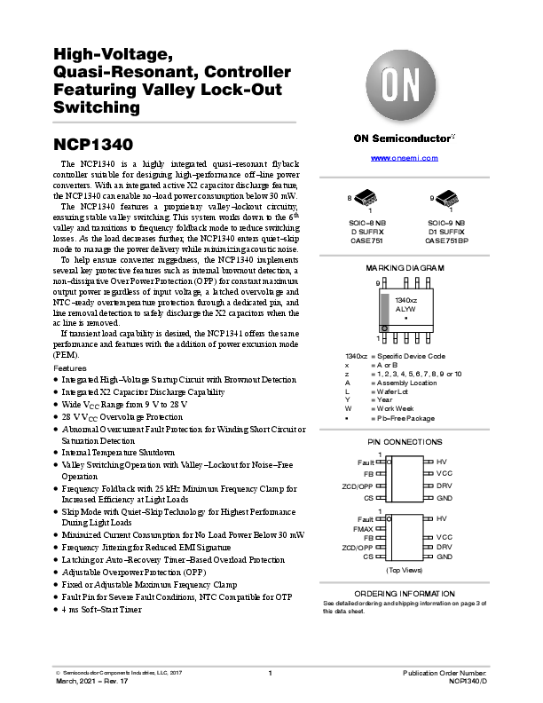
The NCP1340 is a highly integrated quasi−resonant flyback.controller suitable for designing high−performance off−line power.converters. With an integrated active X2 capacitor discharge feature,.the NCP1340 can enable no−load power consumption below 30 mW.
NCP1340 - High-Voltage, Quasi-Resonant, Controller ...
March, 2021 − Rev. 17. 1. Publication Order Number: ... Mounting Techniques Reference Manual, SOLDERRM/D. SOLDERING FOOTPRINT*. Discrete.
NCP1340 - High-Voltage, Quasi-Resonant ...
Full PDF Document

If the inline viewer fails, it will open the original document in compatibility mode automatically. You can also open the file directly.
Extracted Text
High-Voltage, Quasi-Resonant, Controller Featuring Valley Lock-Out Switching

NCP1340
The NCP1340 is a highly integrated quasi-resonant flyback controller suitable for designing high-performance off-line power converters. With an integrated active X2 capacitor discharge feature, the NCP1340 can enable no-load power consumption below 30 mW.
The NCP1340 features a proprietary valley-lockout circuitry, ensuring stable valley switching. This system works down to the 6th valley and transitions to frequency foldback mode to reduce switching losses. As the load decreases further, the NCP1340 enters quiet-skip mode to manage the power delivery while minimizing acoustic noise.
To help ensure converter ruggedness, the NCP1340 implements several key protective features such as internal brownout detection, a non-dissipative Over Power Protection (OPP) for constant maximum output power regardless of input voltage, a latched overvoltage and NTC-ready overtemperature protection through a dedicated pin, and line removal detection to safely discharge the X2 capacitors when the ac line is removed.
If transient load capability is desired, the NCP1341 offers the same performance and features with the addition of power excursion mode (PEM).
Features
� Integrated High-Voltage Startup Circuit with Brownout Detection � Integrated X2 Capacitor Discharge Capability � Wide VCC Range from 9 V to 28 V � 28 V VCC Overvoltage Protection � Abnormal Overcurrent Fault Protection for Winding Short Circuit or
Saturation Detection
� Internal Temperature Shutdown � Valley Switching Operation with Valley-Lockout for Noise-Free
Operation
� Frequency Foldback with 25 kHz Minimum Frequency Clamp for
Increased Efficiency at Light Loads
� Skip Mode with Quiet-Skip Technology for Highest Performance
During Light Loads
� Minimized Current Consumption for No Load Power Below 30 mW � Frequency Jittering for Reduced EMI Signature � Latching or Auto-Recovery Timer-Based Overload Protection � Adjustable Overpower Protection (OPP) � Fixed or Adjustable Maximum Frequency Clamp � Fault Pin for Severe Fault Conditions, NTC Compatible for OTP � 4 ms Soft-Start Timer

www.onsemi.com

8
1
SOIC-8 NB D SUFFIX CASE 751

9 1
SOIC-9 NB D1 SUFFIX CASE 751BP

MARKING DIAGRAM
9
1340xz ALYW
G

1

1340xz = Specific Device Code

x

= A or B

z

= 1, 2, 3, 4, 5, 6, 7, 8, 9 or 10

A

= Assembly Location

L

= Wafer Lot

Y

= Year

W

= Work Week

G

= Pb-Free Package

PIN CONNECTIONS

1 Fault
FB
ZCD/OPP

HV VCC DRV

CS

GND

1 Fault
FMAX FB
ZCD/OPP CS

HV
VCC DRV GND

(Top Views)

ORDERING INFORMATION
See detailed ordering and shipping information on page 3 of this data sheet.

� Semiconductor Components Industries, LLC, 2017

1

March, 2021 - Rev. 17

Publication Order Number: NCP1340/D

NCP1340
TYPICAL APPLICATION SCHEMATIC
Figure 1. NCP1340 8-Pin Typical Application Circuit
Figure 2. NCP1340 9-Pin Typical Application Circuit
www.onsemi.com 2

NCP1340

Table 1. ORDERING INFORMATION TABLE

Orderable Part Number

Device Marking

Package

Shipping

NCP1340A3D1R2G

1340A3

SOIC-9

2500 / Tape & Reel

NCP1340B1DR2G

1340B1

SOIC-8

2500 / Tape & Reel

NCP1340B3D1R2G

1340B3

SOIC-9

2500 / Tape & Reel

NCP1340B4D1R2G

1340B4

SOIC-9

2500 / Tape & Reel

NCP1340B5D1R2G

1340B5

SOIC-9

2500 / Tape & Reel

NCP1340A6DR2G

1340A6

SOIC-8

2500 / Tape & Reel

NCP1340B6DR2G

1340B6

SOIC-8

2500 / Tape & Reel

NCP1340B7D1R2G

1340B7

SOIC-9

2500 / Tape & Reel

NCP1340B8D1R2G

1340B8

SOIC-9

2500 / Tape & Reel

NCP1340B9D1R2G

1340B9

SOIC-9

2500 / Tape & Reel

NCP1340B10DR2G

1340B10

SOIC-8

2500 / Tape & Reel

For information on tape and reel specifications, including part orientation and tape sizes, please refer to our Tape and Reel Packaging Specifications Brochure, BRD8011/D.

Table 2. DEVICE DIFFERENTIATION TABLE

Ordering Code

Brownout

Start/Stop OVLD

Levels

Timer

X2

NCP1340A3D1R2G 112V/98V 160 ms Yes

NCP1340B1DR2G

112V/98V 160 ms Yes

NCP1340B3D1R2G 112V/98V 160 ms Yes

NCP1340B4D1R2G 112V/98V 160 ms Yes

NCP1340B5D1R2G 112V/98V 160 ms Yes

NCP1340A6DR2G

112V/98V 160 ms Yes

NCP1340B6DR2G

112V/98V 160 ms Yes

NCP1340B7D1R2G 112V/98V 160 ms No

NCP1340B8D1R2G

90V/80V

160 ms No

NCP1340B9D1R2G

90V/80V

40 ms

No

NCP1340B10DR2G

Disabled

160 ms No

OTP/Overload Protection Latched Auto-Restart Auto-Restart Auto-Restart Auto-Restart Latched Auto-Restart Auto-Restart Auto-Restart Auto-Restart Auto-Restart

Frequency Clamp
Adjustable None
Adjustable Adjustable Adjustable
None None Adjustable Adjustable Adjustable None

RFB Pullup 400 kW 400 kW 400 kW 20 kW 20 kW 20 kW 20 kW 20 kW 20 kW 20 kW 20 kW

VCC OVP Yes Yes Yes No Yes Yes Yes Yes Yes Yes Yes

IFB Pullup 100 mA 100 mA 100 mA None None None None None None None None

Jitter 1.3kHz 1.3kHz 1.3kHz 1.3kHz None None None None None None None

www.onsemi.com 3

NCP1340
FUNCTIONAL BLOCK DIAGRAM

Figure 3. NCP1340 Block Diagram

Table 3. PIN FUNCTIONAL DESCRIPTION 8-Pin 9-Pin Pin Name

Function

1

1

Fault

The controller enters fault mode if the voltage on this pin is pulled above or below the fault

thresholds. A precise pull up current source allows direct interface with an NTC thermistor.

-

2

FMAX

A resistor to ground sets the value for the maximum switching frequency clamp. If this pin is

pulled above 4 V, the maximum frequency clamp is disabled.

2

3

FB

Feedback input for the QR Flyback controller. Allows direct connection to an optocoupler.

3

4

ZCD/OPP A resistor divider from the auxiliary winding to this pin provides input to the demagnetization de-

tection comparator and sets the OPP compensation level.

4

5

CS

Input to the cycle-by-cycle current limit comparator.

5

6

GND

Ground reference.

6

7

DRV

This is the drive pin of the circuit. The DRV high-current capability (-0.5 /+0.8 A) makes it suit-

able to effectively drive high gate charge power MOSFETs.

7

8

VCC

This pin is the positive supply of the IC. The circuit starts to operate when VCC exceeds 17 V and

turns off when VCC goes below 9 V (typical values). After start-up, the operating range is 9 V up

to 28 V.

-

9

N/C

Removed for creepage distance.

8

10

HV

This pin is the input for the high voltage startup and brownout detection circuits. It also contains

the line removal detection circuit to safely discharge the X2 capacitors when the line is removed.

www.onsemi.com 4

NCP1340

Table 4. MAXIMUM RATINGS

Rating

Symbol

Value

Unit

High Voltage Startup Circuit Input Voltage High Voltage Startup Circuit Input Current Supply Input Voltage Supply Input Current (Note 1) Supply Input Voltage Slew Rate Fault Input Voltage Fault Input Current Zero Current Detection and OPP Input Voltage Zero Current Detection and OPP Input Current Maximum Input Voltage (Other Pins) Maximum Input Current (Other Pins) Driver Maximum Voltage (Note 2) Driver Maximum Current
Operating Junction Temperature Maximum Junction Temperature Storage Temperature Range Power Dissipation (TA = 25�C, 1 oz. Cu, 42 mm2 Copper Clad Printed Circuit) D Suffix, SOIC-8 D1 Suffix, SOIC-9

VHV(MAX) IHV(MAX) VCC(MAX) ICC(MAX) dVCC/dt VFault(MAX) IFault(MAX) VZCD(MAX) IZCD(MAX)
VMAX IMAX VDRV IDRV(SRC) IDRV(SNK)
TJ TJ(MAX)
TSTG PD(MAX)

-0.3 to 700 20
-0.3 to 30 30 1
-0.3 to VCC + 0.7 V 10
-0.3 to VCC + 0.7 V -2/+5
-0.3 to 5.5 10
-0.3 to VDRV(high) 500 800
-40 to 125 150
�60 to 150
450 330

V mA V mA V/ms V mA V mA V mA V mA
�C �C �C mW

Thermal Resistance (TA = 25�C, 1 oz. Cu, 42 mm2 Copper Clad Printed Circuit) D Suffix, SOIC-8 D1 Suffix, SOIC-9

RqJA

�C/W 225 300

ESD Capability Human Body Model per JEDEC Standard JESD22-A114F (All pins except HV) Human Body Model per JEDEC Standard JESD22-A114F (HV Pin) Charge Device Model per JEDEC Standard JESD22-C101F
Latch-Up Protection per JEDEC Standard JESD78E

2000

V

800

V

1000

V

�100

mA

Stresses exceeding those listed in the Maximum Ratings table may damage the device. If any of these limits are exceeded, device functionality should not be assumed, damage may occur and reliability may be affected. 1. The VCC pin is rated to handle the full transient current of the DRV pin. 2. Maximum driver voltage is limited by the driver clamp voltage, VDRV(high), when VCC exceeds the driver clamp voltage. Otherwise, the
maximum driver voltage is VCC.

www.onsemi.com 5

NCP1340

Table 5. ELECTRICAL CHARACTERISTICS: (VCC = 12 V, VHV = 120 V, VFault = open, VFB = 2.4 V, VCS = 0 V, VZCD = 0 V, VFMAX = 0 V, CVCC = 100 nF , CDRV = 100 pF, for typical values TJ = 25�C, for min/max values, TJ is � 40�C to 125�C, unless otherwise noted)

Characteristics

Conditions

Symbol

Min Typ Max Unit

START-UP AND SUPPLY CIRCUITS

Supply Voltage Startup Threshold (Other Versions) Startup Threshold (Version B10) Discharge Voltage During Line Removal Minimum Operating Voltage Operating Hysteresis (Other Versions) Operating Hysteresis (Version B10) Internal Latch / Logic Reset Level Transition from Istart1 to Istart2
VCC(off) Delay
Startup Delay
Minimum Voltage for Start-Up Current Source

dV/dt = 0.1 V/ms
VCC increasing VCC increasing VCC decreasing VCC decreasing VCC(on) - VCC(off) VCC(on) - VCC(off) VCC decreasing VCC increasing, IHV = 650 mA

V

VCC(on) VCC(on) VCC(X2_reg) VCC(off) VCC(HYS) VCC(HYS) VCC(reset) VCC(inhibit)

16.0 14.0 17.0 8.5 7.5 5.5 4.5 0.40

17.0 15.0 18.0 9.0
� � 6.5 0.70

18.0 16.0 19.0 9.5
� � 7.5 1.05

VCC decreasing

tdelay(VCC_off)

25

32

40

ms

Delay from VCC(on) to DRV Enable

tdelay(start)

�

�

500 ms

VHV(MIN)

�

�

30

V

Inhibit Current Sourced from VCC Pin Start-Up Current Sourced from VCC Pin

Vcc = 0 V
Vcc = Vcc(on) � 0.5 V �40�C to 105�C �40�C to 125�C

Istart1 Istart2

0.2

0.5 0.65 mA

mA 2.4 3.75 5.0 2.0 3.75 5.0

Start-Up Circuit Off-State Leakage Current

VHV = 162.5 V VHV = 325 V VHV = 700 V

Supply Current Fault or Latch Skip Mode (excluding FB current) Operating Current

VCC = VCC(on) � 0.5 V VFB = 0 V
fsw = 50 kHz, CDRV = open

VCC Overvoltage Protection Threshold

VCC Overvoltage Protection Delay

X2 CAPACITOR DISCHARGE (ALL VERSIONS EXCEPT B7/B8/B9/B10)

IHV(off1)

�

IHV(off2)

�

IHV(off3)

�

ICC1

-

ICC2

-

ICC3

-

VCC(OVP)

27

tdelay(VCC_OVP) 25

�

15

mA

�

20

�

50

mA

0.115 0.150

0.230 0.315

1.0

1.5

28

29

V

32

40

ms

Line Voltage Removal Detection Timer

Discharge Timer Duration

Line Detection Timer Duration

VCC Discharge Current HV Discharge Level

VCC = 20 V

BROWNOUT DETECTION (ALL VERSIONS EXCEPT B10)

tline(removal)

65

tline(discharge)

21

tline(detect)

21

ICC(discharge)

13

VHV(discharge)

�

100 135 ms

32

43

ms

32

43

ms

18

23

mA

�

30

V

System Start-Up Threshold Other Versions Versions B8, B9

VHV increasing

VBO(start)

V

107 112 116

85

90

95

Brownout Threshold Other Versions Versions B8, B9

VHV decreasing

VBO(stop)

V

93

98

102

75

80

85

Hysteresis Other Versions Versions B8, B9

VHV increasing

VBO(HYS)

V

9.0

14

�

6.0

10

�

Brownout Detection Blanking Time GATE DRIVE

VHV decreasing

tBO(stop)

40

70

100 ms

Rise Time Fall Time

VDRV from 10% to 90% VDRV from 90% to 10%

tDRV(rise) tDRV(fall)

�

20

40

ns

�

5

30

ns

www.onsemi.com 6

NCP1340

Table 5. ELECTRICAL CHARACTERISTICS: (VCC = 12 V, VHV = 120 V, VFault = open, VFB = 2.4 V, VCS = 0 V, VZCD = 0 V, VFMAX = 0 V, CVCC = 100 nF , CDRV = 100 pF, for typical values TJ = 25�C, for min/max values, TJ is � 40�C to 125�C, unless otherwise noted)

Characteristics

Conditions

Symbol

Min Typ Max Unit

GATE DRIVE

Current Capability Source Sink
High State Voltage
Low Stage Voltage FEEDBACK

IDRV(SRC) IDRV(SNK)

mA

�

500

�

�

800

�

VCC = VCC(off) + 0.2 V, RDRV = 10 kW VDRV(high1)

8.0

�

�

V

VCC = 30 V, RDRV = 10 kW

VDRV(high2)

10

12

14

VFault = 0 V

VDRV(low)

�

�

0.25

V

Open Pin Voltage Versions B5/B6/A6

VFB(open)

4.9

5.0

5.1

V

4.8

5.0

5.1

VFB to Internal Current Setpoint Division Ratio

KFB

-

4

-

�

Internal Pull-Up Resistor Versions A6, B4, B5, B6, B7, B8, B9, B10

VFB = 0.4 V

RFB

350 400 440 kW

17

20

23

Internal Pull-Up Current Versions A6, B4, B5, B6, B7, B8, B9, B10

IFB

90

100 108 mA

-

0

-

Valley Thresholds Transition from 1st to 2nd valley Transition from 2nd to 3rd valley Transition from 3rd to 4th valley Transition from 4th to 5th valley Transition from 5th to 6th valley Transition from 6th to 5th valley Transition from 5th to 4th valley Transition from 4th to 3rd valley Transition from 3rd to 2nd valley Transition from 2nd to 1st valley
Maximum Frequency Clamp Versions A2, B2 Versions A3, B3, B4, B5, B7, B8, B9 Versions A3, B3, B5, B7, B8, B9 Version B4
FMAX Secondary Mode Threshold
FMAX Pin Source Current
Maximum On Time
DEMAGNETIZATION INPUT

VFB decreasing VFB decreasing VFB decreasing VFB decreasing VFB decreasing VFB increasing VFB increasing VFB increasing VFB increasing VFB increasing
VFMAX = 0.7 V VFMAX = 3.5 V VFMAX = 3.5 V
9-Pin Versions Only

V1to2 V2to3 V3to4 V4to5 V5to6 V6to5 V5to4 V4to3 V3to2 V2to1

V 1.316 1.400 1.484 1.128 1.200 1.272 1.034 1.100 1.166 0.940 1.000 1.060 0.846 0.900 0.954 1.410 1.500 1.590 1.504 1.600 1.696 1.598 1.700 1.802 1.692 1.800 1.908 1.880 2.000 2.120

fMAX1 fMAX2 fMAX3 fMAX3

kHz

100 110 120

300 360 420

60

75

85

68

75

78

VFMAX(mode) 3.85 4.00 4.15

V

IFMAX

9.0

10

11

mA

ton(MAX)

28

32

40

ms

ZCD threshold voltage ZCD hysteresis Demagnetization Propagation Delay ZCD Clamp Voltage
Positive Clamp Negative Clamp
Blanking Delay After Turn-Off Timeout After Last Demagnetization Detection
CURRENT SENSE

VZCD decreasing VZCD increasing VZCD step from 4.0 V to -0.3 V
IQZCD = 5.0 mA IQZCD = -2.0 mA
While in soft-start After soft-start complete

VZCD(trig)

35

60

90

mV

VZCD(HYS)

15

25

55

mV

tdemag

�

80

250

ns

V

VZCD(MAX)

12.4 12.7

13

VZCD(MIN)

-0.9 -0.7

0

tZCD(blank)

600 700 800 ns

t(tout1) t(tout2)

80

100 120

ms

5.1

6.0

6.9

Current Limit Threshold Voltage Leading Edge Blanking Duration

VCS increasing
DRV minimum width minus tdelay(ILIM1)

VILIM1 tLEB1

0.760 0.800 0.840 V 220 265 330 ns

www.onsemi.com 7

NCP1340

Table 5. ELECTRICAL CHARACTERISTICS: (VCC = 12 V, VHV = 120 V, VFault = open, VFB = 2.4 V, VCS = 0 V, VZCD = 0 V, VFMAX = 0 V, CVCC = 100 nF , CDRV = 100 pF, for typical values TJ = 25�C, for min/max values, TJ is � 40�C to 125�C, unless otherwise noted)

Characteristics

Conditions

Symbol

Min Typ Max Unit

CURRENT SENSE

Current Limit Threshold Propagation Delay
PWM Comparator Propagation Delay Minimum Peak Current Freeze Setpoint Abnormal Overcurrent Fault Threshold Abnormal Overcurrent Fault Blanking Duration
Abnormal Overcurrent Fault Propagation Delay
Number of Consecutive Abnormal Overcurrent Faults to Enter Latch Mode

Step VCS 0 V to VILIM1 + 0.5 V, VFB = 4 V
Step VCS 0 V to 0.7 V, VFB = 2.4
VCS increasing, VFB = 4 V DRV minimum width minus
tdelay(ILIM2) Step VCS 0 V to VILIM2 + 0.5 V,
VFB = 4 V

tdelay(ILIM1)

�

95

175

ns

tdelay(PWM) Vfreeze VILIM2 tLEB2

�

125 175 ns

170 200 230 mV

1.125 1.200 1.275 V

80

110 140 ns

tdelay(ILIM2)

�

80

175

ns

nILIM2

�

4

�

Overpower Protection Delay

VCS dv/dt = 1 V/ms, measured from VOPP(MAX) to DRV falling edge

Overpower Signal Blanking Delay

Pull-Up Current Source

VCS = 1.5 V

JITTERING (All Except Version A6, B5, B6, B7, B8, B9, B10)

tOPP(delay)
tOPP(blank) ICS

�

95

175

ns

220 280 330 ns

0.7

1.0

1.5

mA

Jitter Frequency
Peak Jitter Voltage Added to PWM Comparator

fjitter Vjitter

1.0

1.3

1.6 kHz

90

100 115 mV

FAULT PROTECTION

Soft-Start Period
Flyback Overload Fault Timer Other Versions Version B9

Measured from 1st DRV pulse to VCS = VILIM1
VCS = VILIM1

tSSTART tOVLD

2.8

4.0

5.0 ms

ms

120 160 200

30

40

50

Overvoltage Protection (OVP) Threshold
OVP Detection Delay
Overtemperature Protection (OTP) Threshold (Note 3)

VFault increasing VFault increasing VFault decreasing

VFault(OVP)

2.79 3.00 3.21

V

tdelay(OVP)

22.5

30

37.5

ms

VFault(OTP_in)

380

400

420

mV

Overtemperature Protection (OTP) Exiting Threshold (Note 3)

VFault increasing Versions B Only

VFault(OTP_out) 874

910

966

mV

OTP Detection Delay OTP Pull-Up Current Source Fault Input Clamp Voltage Fault Input Clamp Series Resistor Autorecovery Timer LIGHT/NO LOAD MANAGEMENT

VFault decreasing VFault = VFault(OTP_in) + 0.2 V

tdelay(OTP)

22.5

30

37.5

ms

IOTP

42.5 45.0 48.5 mA

VFault(clamp)

1.15

1.7

2.25

V

RFault(clamp)

1.32

1.55

1.78

kW

trestart

1.8

2.0

2.2

s

Minimum Frequency Clamp
Dead-Time Added During Frequency Foldback

VFB = 400 mV

fMIN tDT(MAX)

21.5

25

27.0 kHz

34

-

-

ms

Quiet-Skip Timer Skip Threshold Skip Hysteresis

VFB decreasing VFB increasing

tquiet Vskip Vskip(HYS)

1.25

-

-

ms

350 400 450 mV

20

50

70

mV

www.onsemi.com 8

NCP1340

Table 5. ELECTRICAL CHARACTERISTICS: (VCC = 12 V, VHV = 120 V, VFault = open, VFB = 2.4 V, VCS = 0 V, VZCD = 0 V, VFMAX = 0 V, CVCC = 100 nF , CDRV = 100 pF, for typical values TJ = 25�C, for min/max values, TJ is � 40�C to 125�C, unless otherwise noted)

Characteristics

Conditions

Symbol

Min Typ Max Unit

THERMAL PROTECTION

Thermal Shutdown Thermal Shutdown Hysteresis 3. NTC with R110 = 8.8 kW

Temperature increasing Temperature decreasing

TSHDN

�

140

�

�C

TSHDN(HYS)

�

40

�

�C

www.onsemi.com 9

NCP1340

INTRODUCTION

The NCP1340 implements a quasi-resonant flyback converter utilizing current-mode architecture where the switch-off event is dictated by the peak current. This IC is an ideal candidate where low parts count and cost effectiveness are the key parameters, particularly in ac-dc adapters, open-frame power supplies, etc. The NCP1340 incorporates all the necessary components normally needed in modern power supply designs, bringing several enhancements such as non-dissipative overpower protection (OPP), brownout protection, and frequency reduction management for optimized efficiency over the entire power range. Accounting for the needs of extremely low standby power requirements, the controller features minimized current consumption and includes an automatic X2 capacitor discharge circuit that eliminates the need to install power-consuming resistors across the X2 input capacitors.
� High-Voltage Start-Up Circuit: Low standby power
consumption cannot be obtained with the classic resistive start-up circuit. The NCP1340 incorporates a high-voltage current source to provide the necessary current during start-up and then turns off during normal operation.
� Internal Brownout Protection: The ac input voltage is
sensed via the high-voltage pin. When this voltage is too low, the NCP1340 stops switching. No restart attempt is made until the ac input voltage is back within its normal range.
� X2-Capacitor Discharge Circuitry: Per the
IEC60950 standard, the time constant of the X2 input capacitors and their associated discharge resistors must be less than 1 s in order to avoid electrical shock when the user unplugs the power supply and inadvertently touches the ac input cord terminals. By providing an automatic means to discharge the X2 capacitors, the NCP1340 eliminates the need to install X2 discharge resistors, thus reducing power consumption.
� Quasi-Resonant, Current-Mode Operation:
Quasi-Resonant (QR) mode is a highly efficient mode of operation where the MOSFET turn-on is synchronized with the point where its drain-source voltage is at the minimum (valley). A drawback of this mode of operation is that the operating frequency is inversely proportional to the system load. The NCP1340 incorporates a valley lockout (VLO) and frequency foldback technique to eliminate this drawback, thus maximizing the efficiency over the entire power range.
� Valley Lockout: In order to limit the maximum
frequency while remaining in QR mode, one would traditionally use a frequency clamp. Unfortunately, this can cause the controller to jump back and forth between two different valleys, which is often undesirable. The

NCP1340 patented VLO circuitry solves this issue by determining the operating valley based on the system load, and locking out other valleys unless a significant change in load occurs.
� Frequency Foldback: As the load continues to
decrease, it becomes beneficial to reduce the switching frequency. When the load is light enough, the NCP1340 enters frequency foldback mode. During this mode, the peak current is frozen and dead-time is added to the switching cycle, thus reducing the frequency and switching operation to discontinuous conduction mode (DCM). Dead-time continues to be added until skip mode is reached, or the switching frequency reaches its minimum level of 25 kHz.
� Skip Mode: To further improve light or no-load power
consumption while avoiding audible noise, the NCP1340 enters skip mode when the operating frequency reaches its minimum value. foldback isavoid acoustic noise, the circuit prevents the switching frequency from decaying below 25 kHz. This allows regulation via burst of pulses at 25 kHz or greater instead of operating in the audible range.
� Quiet-Skip: To further reduce acoustic noise, the
NCP1340 incorporates a novel circuit to prevent the skip mode burst period from entering the audible range as well.
� Internal OPP: In order to limit power delivery at high
line, a scaled version of the negative voltage present on the auxiliary winding during the on-time is routed to the ZCD/OPP pin. This provides the designer with a simple and non-dissipative means to reduce the maximum power capability as the bulk voltage increases.
� Frequency Jittering: In order to reduce the EMI
signature, a low frequency triangular voltage waveform is added to the iniput of the PWM comparator. This helps by spreading out the energy peaks during noise analysis.
� Internal Soft-Start: The NCP1340 includes a 4 ms
soft-start to prevent the main power switch from being overly stressed during start-up. Soft-start is activated each time a new startup sequence occurs or during auto-recovery mode.
� Dedicated Fault Input: The NCP1340 includes a
dedicated fault input. It can be used to sense an overvoltage condition and latch off the controller by pulling the pin above the overvoltage protection (OVP) threshold. The controller is also disabled if the Fault pin is pulled below the overtemperature protection (OTP) threshold. The OTP threshold is configured for use with a NTC thermistor.

www.onsemi.com 10

NCP1340

� Overload/Short-Circuit Protection: The NCP1340
implements overload protection by limiting the maximum time duration for operation during overload conditions. The overload timer operates whenever the maximum peak current is reached. In addition to this, special circuitry is included to prevent operation in CCM during extreme overloads, such as an output short-circuit.
� Maximum Frequency Clamp: The NCP1340 includes
a maximum frequency clamp. In all versions, the clamp is available disabled or fixed at 110 kHz. In the 9-pin versions, the clamp can be adjusted via an external resistor from the FMAX Pin to ground. It can also be disabled by pulling the FMAX pin above 4 V.

HIGH VOLTAGE START-UP The NCP1340 contains a multi-functional high voltage
(HV) pin. While the primary purpose of this pin is to reduce standby power while maintaining a fast start-up time, it also incorporates brownout detection and line removal detection.
The HV pin must be connected directly to the ac line in order for the X2 discharge circuit to function correctly. Line and neutral should be diode "ORed" before connecting to the HV pin as shown in Figure 4. The diodes prevent the pin voltage from going below ground. A resistor in series with the pin should be used to protect the pin during EMC or surge testing. A low value resistor should be used (<5 kW) to reduce the voltage offset during start-up.

AC CON

EMI

HV Controller

Figure 4. High-Voltage Input Connection

Start-up and VCC Management During start-up, the current source turns on and charges
the VCC capacitor with Istart2 (typically 6 mA). When Vcc reaches VCC(on) (typically 16.0 V), the current source turns off. If the input voltage is not high enough to ensure a proper
start-up (i.e. VHV has not reached VBO(start)), the controller will not start. VCC then begins to fall because the controller bias current is at ICC2 (typically 1 mA) and the auxiliary supply voltage is not present. When VCC falls to VCC(off) (typically 10.5 V), the current source turns back on and
charges VCC. This cycle repeats indefinitely until VHV reaches VBO(start). Once this occurs, the current source immediately turns on and charges VCC to VCC(on), at which point the controller starts (see Figure 6).
When VCC is brought below VCC(inhibit), the start-up current is reduced to Istart1 (typically 0.5 mA). This limits power dissipation on the device in the event that the VCC pin is shorted to ground. Once VCC rises back above VCC(inhibit), the start-up current returns to Istart2.

Once VCC reaches VCC(on), the controller is enabled and the controller bias current increases to ICC3 (typically 2.0 mA). However, the total bias current is greater than this
due to the gate charge of the external switching MOSFET.
The increase in ICC due to the MOSFET is calculated using Equation 1.

DICC + fsw @ QG @ 10-3

(eq. 1)

where DICC is the increase in milliamps, fsw is the switching frequency in kilohertz and QG is the gate charge of the external MOSFET in nanocoulombs.
CVCC must be sized such that a VCC voltage greater than VCC(off) is maintained while the auxiliary supply voltage increases during start-up. If CVCC is too small, VCC will fall below VCC(off) and the controller will turn off before the auxiliary winding supplies the IC. The total ICC current after the controller is enabled (ICC3 plus DICC) must be considered to correctly size CVCC.

www.onsemi.com 11

NCP1340

VHV VBO (start )

Figure 5. Start-up Circuitry Block Diagram

VHV (MIN ) VCC
VCC(on) VCC(off)
VCC(inhibit )
DRV

Start-up Current = Istart1

Start-up Current = Istart2

Figure 6. Start-up Timing

tdelay (start )

www.onsemi.com 12

NCP1340

DRIVER The NCP1340 maximum supply voltage, VCC(MAX), is
28 V. Typical high-voltage MOSFETs have a maximum gate voltage rating of 20 V. The DRV pin incorporates an active voltage clamp to limit the gate voltage on the external MOSFETs. The DRV voltage clamp, VDRV(high) is typically 12 V with a maximum limit of 14 V.
REGULATION CONTROL
Peak Current Control The NCP1340 is a peak current-mode controller, thus the
FB voltage sets the peak current flowing in the transformer and the MOSFET. This is achieved by sensing the MOSFET current across a resistor and applying the resulting voltage ramp to the non-inverting input of the PWM comparator through the CS pin. The current limit threshold is set by applying the FB voltage divided by KFB (typically 4) to the inverting input of the PWM comparator. When the current sense voltage ramp exceeds this threshold, the output driver is turned off, however, the peak current is affected by several functions (see Figure 7):

The peak current level is clamped during the soft-start phase. The setpoint is actually limited by a clamp level ramping from 0 to 0.8 V within 4 ms.
In addition to the PWM comparator, a dedicated comparator monitors the current sense voltage, and if it reaches the maximum value, VILIM (typically 800 mV), the gate driver is turned off and the overload timer is enabled. This occurs even if the limit imposed by the feedback voltage is higher than VILIM1. Due to the parasitic capacitances of the MOSFET, a large voltage spike often appears on the CS Pin at turn-on. To prevent this spike from falsely triggering the current sense circuit, the current sense signal is blanked for a short period of time, tLEB1 (typically 275 ns), by a leading edge blanking (LEB) circuit. Figure 7 shows the schematic of the current sense circuit.
The peak current is also limitied to a minimum level, Vfreeze (0.2 V, typically). This results in higher efficiency at light loads by increasing the minimum energy delivered per switching cycle, while reducing the overall number of switching cycles during light load.

Figure 7. Current Sense Logic
www.onsemi.com 13

NCP1340

Zero Current Detection The NCP1340 is a quasi-resonant (QR) flyback
controller. While the power switch turn-off is determined by the peak current set by the feedback loop, the switch turn-on is determined by the transformer demagnetization. The demagnetization is detected by monitoring the transformer auxiliary winding voltage.
Turning on the power switch once the transformer is demagnetized has the benefit of reduced switching losses. Once the transformer is demagnetized, the drain voltage starts ringing at a frequency determined by the transformer magnetizing inductance and the drain lump capacitance, eventually settling at the input voltage. A QR flyback controller takes advantage of the drain voltage ringing and turns on the power switch at the drain voltage minimum or "valley" to reduce switching losses and electromagnetic interference (EMI).

As shown by Figure 13, a valley is detected once the ZCD pin voltage falls below the demagnetization threshold, VZCD(trig), typically 55 mV. The controller will either switch once the valley is detected or increment the valley counter, depending on the FB voltage.
Overpower Protection The average bulk capacitor voltage of the QR flyback
varies with the RMS line voltage. Thus, the maximum power capability at high line can be much higher than desired. An integrated overpower protection (OPP) circuit provides a relatively constant output power limit across the input voltage on the bulk capacitor, Vbulk. Since it is a high-voltage rail, directly measuring Vbulk will contribute losses in the sensing network that will greatly impact the standby power consumption. The NCP1340 OPP circuit achieves this without the need for a high-voltage sensing network, and is essentially lossless.

Figure 8. OPP Circuit Schematic

www.onsemi.com 14

NCP1340

VAUX (V)


-


NAUX NP

. VBULK

Figure 9. Auxiliary Winding Voltage

Since the auxiliary winding voltage during the power
switch on time is a reflection of the input voltage scaled by
the primary to auxiliary winding turns ratio, NP:AUX (see Figure 9), OPP is achieved by scaling down reflected
voltage during the on-time and applying it to the ZCD pin
as a negative voltage, VOPP. The voltage is scaled down by a resistor divider comprised of ROPPU and ROPPL. The maximum internal current setpoint (VCS(OPP)) is simply the sum of VOPP and the peak current sense threshold, VILIM1. Figure 8 shows the schematic for the OPP circuit.
The adjusted peak current limit is calculated using
Equation 2. For example, a VOPP of -150 mV results in a peak current limit of 650 mV in NCP1340.

VCS(OPP) + VOPP ) VILIM1

(eq. 2)

To ensure optimal zero-crossing detection, a diode is
needed to bypass ROPPU during the off-time. Equation 3 is used to calculate ROPPU and ROPPL.

RZCD ) ROPPU ROPPL

+

*

NP:AUX

@ Vbulk VOPP

*

VOPP

(eq. 3)

ROPPU is selected once a value is chosen for ROPPL. ROPPL is selected large enough such that enough voltage is available for the zero-crossing detection during the

off-time. It is recommended to have at least 8 V applied on

the ZCD pin for good detection. The maximum voltage is

internally clamped to VCC. The off-time voltage on the ZCD Pin is given by Equation 4.

VZCD

+

ROPPL RZCD ) ROPPL

@

VAUX

*

VF

(eq. 4)

Where VAUX is the voltage across the auxiliary winding and VF is the DOPP forward voltage drop.

The ratio between RZCD and ROPPL is given by Equation 5. It is obtained by combining Equations 3 and 4.

RZCD ROPPL

+

VAUX

* VF * VZCD

VZCD

A design example is shown below:

System Parameters:

(eq. 5)

VAUX + 18 V

VF + 0.6 V

NP:AUX + 0.18

The ratio between RZCD and ROPPL is calculated using Equation 5 for a minimum VZCD of 8 V.

RZCD ROPPL

+

18

V

*

0.6 V 8V

*

8

V

+

1.2

kW

RZCD is arbitrarily set to 1 kW. ROPPL is also set to 1 kW because the ratio between the resistors is close to 1.

The NCP1340 maximum overpower compensation or

peak current setpoint reduction is 31.25% for a VOPP of -250 mV. We will use this value for the following example:

Substituting values in Equation 3 and solving for ROPPU we obtain:

RZCD ) ROPPU ROPPL

+

0.18

@

370 V * (-0.25 -0.25 V

V)

+

271

ROPPU + 271 @ ROPPL * RZCD

ROPPU + 271 @ 1 kW * 1 kW + 270 kW

For optimum performance over temperature, it is recommended to keep ROPPL below 3 kW.

www.onsemi.com 15

NCP1340

Soft-Start Soft-start is achieved by ramping up an internal reference,
VSSTART, and comparing it to the current sense signal. VSSTART ramps up from 0 V once the controller initially powers up. The peak current setpoint is then limited by the VSSTART ramp resulting in a gradual increase of the switch current during start-up. The soft-start duration, tSSTART, is typically 4 ms.
During startup, demagnetization phases are long and difficult to detect since the auxiliary winding voltage is very small. In this condition, the 6 ms steady-state timeout is generally shorter than the inductor demagnetization period. If it is used to restart a switching cycle, it can cause operation

in CCM for several cycles until the voltage on the ZCD pin is high enough to prevent the timer from running. Therefore, a longer timeout period, ttout1 (typically 100 ms), is used during soft-start to prevent CCM operation.
Frequency Jittering In order to help meet stringent EMI requirements, the
NCP1340 features frequency jittering to average the energy peaks over the EMI frequency range. As shown in Figure 10, the function consists of summing a 0 to 100 mV, 1.3 kHz triangular wave (Vjitter) with the CS signal immediately before the PWM comparator. This current acts to modulate the on-time and hence the operation frequency.

Figure 10. Jitter Implementation

Since the jittering function modulates the peak current level, the FB signal will attempt to compensate for this effect in order to limit the output voltage ripple. Therefore, the bandwidth of the feedback loop must be well below the jitter frequency, or the jitter function will be filtered by the loop.
Due to the frozen peak current, the effect of the jittering circuit will not be seen during frequency foldback mode.

Maximum Frequency Clamp The NCP1340 includes a maximum frequency clamp. In
all versions, the clamp is available disabled or fixed at 110 kHz. In the 9-pin versions, the clamp can be adjusted via an external resistor from the FMAX Pin to ground. It can also be disabled by pulling the FMAX pin above 4 V. The maximum frequency can be programmed using Equation 6, and is shown in Figure 11.

261 kHz * 1 V FSW(MAX) + RFMAX * 10 mA

(eq. 6)

FSW(MAX) (kHz)

1000 900 800 700 600 500 400 300 200 100 0 0

50 100 150 200 250 300 350 250 RFMAX (kW)
Figure 11. FSW(MAX) vs. RFMAX

www.onsemi.com 16

NCP1340

LIGHT LOAD MANAGEMENT
Valley Lockout Operation The operating frequency of a traditional QR flyback
controller is inversely proportional to the system load. In other words, a load reduction increases the operating frequency. A maximum frequency clamp can be useful to limit the operating frequency range. However, when used by itself, such an approach often causes instabilities since when this clamp is active, the controller tends to jump (or hesitate) between two valleys, thus generating audible noise.
Instead, the NCP1340 also incorporates a patented valley lockout (VLO) circuitry to eliminate valley jumping. Once

1x10⁵

6th 5th 4th 3rd

2nd

VCO
8x10⁴ mode

a valley is selected, the controller stays locked in this valley until the output power changes significantly. This technique extends the QR mode operation over a wider output power range while maintaining good efficiency and limiting the maximum operating frequency.
The operating valley (1st, 2nd, 3rd, 4th, 5th or 6th) is determined by the FB voltage. An internal counter increments each time a valley is detected by the ZCD/OPP Pin. Figure 12 shows a typical frequency characteristic obtainable at low line in a 65 W application.
1st

Fsw (Hz)

6x10⁴

6th

5th 4th 3rd

2nd

1st

4x10⁴

2x10⁴

VCO mode

0

0

20

40

60

Pout (W)

Figure 12. Valley Lockout Frequency vs. Output Power

When an "n" valley is asserted by the valley selection circuitry, the controller is locked in this valley until the FB voltage decreases to the lower threshold ("n+1" valley activates) or increases to the "n valley threshold" + 600 mV ("n-1" valley activates). The regulation loop adjusts the

peak current to deliver the necessary output power. Each valley selection comparator features a 600 mV hysteresis that helps stabilize operation despite the FB voltage swing produced by the regulation loop.

Table 6. VALLEY FB THRESHOLDS (typical values)

FB Falling

1st to 2nd valley

1.400 V

2nd to 3rd valley

1.200 V

3rd to 4th valley

1.100 V

4th to 5th valley

1.000 V

5th to 6th valley

0.900 V

Valley Timeout In case of extremely damped oscillations, the ZCD
comparator may not be able to detect the valleys. In this condition, drive pulses will stop while the controller waits for the next valley or ZCD event. The NCP1340 ensures continued operation by incorporating a maximum timeout

2nd to 1st valley 3rd to 2nd valley 4th to 3rd valley 5th to 4th valley 6th to 5th valley

FB Rising

2.000 V 1.800 V 1.700 V 1.600 V 1.500 V

period after the last demagnetization detection. The timeout signal acts as a substitute for the ZCD signal to the valley counter. Figure 13 shows the valley timeout circuit schematic. The steady state timeout period, ttout2, is set at 6 ms (typical) to limit the frequency step.

www.onsemi.com 17

NCP1340

During startup, the voltage offset added by the OPP diode, DOPP, prevents the ZCD Comparator from accurately detecting the valleys. In this condition, the steady state timeout period will be shorter than the inductor demagnetization period causing CCM operation. CCM operation lasts for a few cycles until the voltage on the ZCD pin is high enough to detect the valleys. A longer timeout period, ttout1, (typically 100 ms) is set during soft-start to limit CCM operation.
In VLO operation, the number of timeout periods are counted instead of valleys when the drain-source voltage

oscillations are too damped to be detected. For example, if the FB voltage sets VLO mode to turn on at the fifth valley, and the ZCD ringing is damped such that the ZCD circuit is only able to detect:
� Valleys 1 to 4: the circuit generates a DRV pulse 6 ms
(steady-state timeout delay) after the 4th valley
detection.
� Valleys 1 to 3: the timeout delay must run twice, and
the circuit generates a DRV pulse 12 ms after the 3rd valley detection.

Figure 13. Valley Timeout Circuitry

Frequency Foldback As the output load decreases (FB voltage decreases), the
valleys are incremented from 1 to 6. When the sixth valley is reached, if the FB voltage further decreases to 0.8 V, the peak current setpoint becomes internally frozen to Vfreeze (0.2 V typically), and the controller enters frequency foldback mode (FF). During this mode, the controller regulates the power delivery by modulating the switching frequency.
In frequency foldback mode, the controller reduces the switching frequency by adding dead-time after the 6th valley is detected. This dead-time increases as the FB

voltage decreases. There is no discontinuity when the system transitions from VLO to FF and the frequency smoothly reduces as FB decreases.
The dead-time circuit is designed to add 0 ms dead-time when VFB = 0.8 V and linearly increases the total dead-time to tDT(MAX) (32 ms minimum) as VFB falls down to 0.4 V. The minimum frequency clamp prevents the switching frequency from dropping below 25 kHz to eliminate the risk of audible noise.
Figure 14 summarizes the VLO to FF operation with respect to the FB voltage.

www.onsemi.com 18

Operating Mode
FF Valley 6 Valley 5 Valley 4 Valley 3 Valley 2 Valley 1

NCP1340

0.8 0.9 1.0 1.1 1.2 1.4 1.5 1.6 1.7 1.8 2.0 Figure 14. Valley Lockout Thresholds

VVFF�����������BB idne�����������ccrFereaaau�����������ssletes!s����������������������

3.2

V (V) FB

www.onsemi.com 19

NCP1340

Minimum Frequency Clamp and Skip Mode As mentioned previously, the circuit prevents the
switching frequency from dropping below fMIN (25 kHz typical). When the switching cycle would be longer than 40 ms, the circuit forces a new switching cycle. However, the fMIN clamp cannot generate a DRV pulse until the demagnetization is completed. In other words, it will not cause operation in CCM.
Since the NCP1340 forces a minimum peak current and a minimum frequency, the power delivery cannot be continuously controlled down to zero. Instead, the circuit starts skipping pulses when the FB voltage drops below the skip level, Vskip, and recovers operation when VFB exceeds Vskip + Vskip(HYS). This skip-mode method provides an efficient method of control during light loads.
Quiet-Skip To further avoid acoustic noise, the circuit prevents the
burst frequency during skip mode from entering the audible range by limiting it to a maximum of 800 Hz. This is achieved via a timer (tquiet) that is activated during Quiet-Skip. The start of the next burst cycle is prevented until this timer has expired.
As the output power decreases, the switching frequency decreases. Once it hits 25 kHz, the skip-in threshold is reached and burst mode is entered - switching stops as soon

as the currnet drive pulses ends � it does not stop immediately.
Once switching stops, FB will rise. As soon as FB crosses the skip-exit threshold, drive pulses will resume, but the controller remains in burst mode. At this point, a 1250 ms (min) timer, tquiet, is started together with a count-to-3 counter. The next time the FB voltage drops below the skip-in threshold, drive pulses stop at the end of the current pulse as long as 3 drive pulses have been counted (if not, they do not stop until the end of the 3rd pulse). They are not allowed to start again until the timer expires, even if the skip-exit threshold is reached first. It is important to note that the timer will not force the next cycle to begin � i.e. if the natural skip frequency is such that skip-exit is reached after the timer expires, the drive pulses will wait for the skip-exit threshold.
This means that during no-load, there will be a minimum of 3 drive pulses, and the burst-cycle period will likely be much longer than 1250 ms. This operation helps to improve efficiency at no-load conditions.
In order to exit burst mode, the FB voltage must rise higher than 1 V. If this occurs before tquiet expires, the drive pulses will resume immediately � i.e. the controller won't wait for the timer to expire. Figure 15 provides an example of how Quiet-Skip works.

www.onsemi.com 20

NCP1340
Figure 15. Quiet-Skip Timing Diagram www.onsemi.com 21

NCP1340

FAULT MANAGEMENT

The NCP1340 contains three separate fault modes. Depending on the type of fault, the device will either latch off, restart when the fault is removed, or resume operation after the auto-recovery timer expires.
Latching Faults Some faults will cause the NCP1340 to latch off. These
include the abnormal OCP (AOCP), VCC OVP, and the

external latch input. When the NCP1340 detects a latching fault, the driver is immediately disabled. The operation during a latching fault is identical to that of a non-latching fault except the controller will not attempt to restart at the next VCC(on), even if the fault is removed. In order to clear the latch and resume normal operation, VCC must first be allowed to drop below VCC(reset) or a line removal event must be detected. This operation is shown in Figure 16.

Fault

Fault Applied

Fault Removed

VCC V CC ( on) V CC ( off)
FDRV

time time

IHV
Istart 2 Istart (off)

Figure 16. Operation During Latching Fault

time time

www.onsemi.com 22

NCP1340

Non-Latching Faults
When the NCP1340 detects a non-latching fault
(brownout or thermal shutdown), the drivers are disabled,
and VCC falls towards VCC(off) due to the IC internal current consumption. Once VCC reaches VCC(off), the HV current source turns on and CVCC begins to charge towards VCC(on). When VCC, reaches VCC(on), the cycle repeats until the fault is removed. Once the fault is removed, the NCP1340 is

re-enabled when VCC reaches VCC(on) according to the initial power-on sequence, provided VHV is above VBO(start). This operation is shown in Figure 17. When VHV is reaches VBO(start), VCC immediately charges to VCC(on). If VCC is already above VCC(on) when the fault is removed, the controller will start immediately as long as VHV is above VBO(start).

Fault

Fault Applied

Fault Removed

VCC V CC (on ) V CC (off )
FDRV

Waits for next VCC(on) before
starting

time time

IHV
Istart 2 Istart (off)

Figure 17. Operation During Non-Latching Fault

time time

www.onsemi.com 23

NCP1340

Auto-recovery Timer Faults Some faults faults cause the NCP1340 auto-recovery
timer to run. If an auto-recovery fault is detected, the gate drive is disabled and the auto-recovery timer, tautorec (typically 1.2 s), starts. While the auto-recovery timer is

running, the HV current source turns on and off to maintain
Vcc between Vcc(off) and Vcc(on). Once the auto-recovery timer expires, the controller will attempt to start normally at
the next VCC(on) provided VHV is above VBO(start). This operation is shown in Figure 18.

Fault

Fault Applied

Fault Removed

VCC VCC(on) VCC(off)
DRV
Autorecovery Timer 1.2 s

Controller stops

Restarts At V CC (on ) ( new burst cycle if Fault still present )

t restart Figure 18. Operation During Auto-Recovery Fault

time time time

www.onsemi.com 24

NCP1340

PROTECTION FEATURES

Brownout Protection
A timer is enabled once VHV drops below its disable threshold, VBO(stop) (typically 99 V). The controller is disabled if VHV doesn't exceed VBO(stop) before the brownout timer, tBO (typically 54 ms), expires. The timer is set long enough to ignore a two cycle dropout. The timer
starts counting once VHV drops below VBO(stop).

Figure 19 shows the brownout detector waveforms during a brownout.
When a brownout is detected, the controller stops switching and enters non-latching fault mode (see Figure 17). The HV current source alternatively turns on and off to maintain VCC between VCC(on) and VCC(off) until the input voltage is back above VBO(start).

VHV

VBO (start ) VBO (stop )

Brownout Timer
VCC
VCC (on)

Brownout detected
Starts Charging Immediately

Fault Cleared

time

Restarts at next V CC(on)

time

VCC (off ) DRV

tdelay (start ) time

Figure 19. Operation During Brownout

time

Line Removal Detection and X2 Capacitor Discharge Safety agency standards require the input filter capacitors
to be discharged once the ac line voltage is removed. A resistor network is the most common method to meet this requirement. Unfortunately, the resistor network consumes power across all operating modes and it is a major contributor of input power losses during light-load and no-load conditions.
The NCP1340 eliminates the need for external discharge resistors by integrating active input filter capacitor

discharge circuitry. A novel approach is used to reconfigure the high voltage startup circuit to discharge the input filter capacitors upon removal of the ac line voltage. The line removal detection circuitry is always active to ensure safety compliance.
The line removal is detected by digitally sampling the voltage present at the HV pin, and monitoring the slope.
A timer, tline(removal) (typically 100 ms), is used to detect when the slope of the input signal is negative or below the resolution level. The timer is reset any time a positive slope

www.onsemi.com 25

NCP1340

is detected. Once the timer expires, a line removal condition is acknowledged initiating an X2 capacitor discharge cycle, and the controller is disabled.
If VCC is above VCC(on), it is first discharged to VCC(on). A second timer, tline(discharge) (typically 32 ms), is used for the time limiting of the discharge phase to protect the device against overheating. Once the discharge phase is complete, tline(discharge) is reused while the device checks to see if the line voltage is reapplied. During the discharge phase, if VCC

drops to VCC(on), it is quickly recharged to VCC(X2_reg). The discharging process is cyclic and continues until the ac line is detected again or the voltage across the X2 capacitor is lower than VHV(discharge) (30 V maximum). This feature allows the device to discharge large X2 capacitors in the input line filter to a safe level.
It is important to note that the HV pin cannot be connected to any dc voltage due to this feature, i.e. directly to the bulk capacitor.

X2 Capacitor

VHV

Discharge

VBO (start ) VBO (stop )

AC Line Unplug

X2 Capacitor Discharge

VHV(discharge )
Timer tline(removal ) tline(discharge /detect )

AC Timer Starts

AC Timer Restarts

DRV

tline(removal )

AC Timer Expires

No AC Detection

tline(discharge )

tline(detect )

tline(discharge )

time

X2 Discharge Current Istart 2
ICC
ICC(discharge )
ICC3 Istart 2 VCC VCC (X2_reg ) VCC (on )

0

Device is stopped

X2 Discharge

X2 Discharge

time

Figure 20. Line Removal Timing
www.onsemi.com 26

VHV VBO(start ) VBO(stop )
VHV(discharge )
Timer tline (removal ) tline(discharge /detect )

NCP1340
X2 Capacitor Discharge

AC Line Unplug

AC Timer Starts

AC Timer Restarts

AC Timer Expires

DRV

tline (removal )

tline (discharge )

AC Detected

time

time

X2 Discharge Current Istart 2
ICC
ICC(discharge )
ICC 3 Istart 2
VCC VCC (X2_reg )
VCC (on )

0

Device is stopped

X2 Discharge

time tdelay (start )
time

time

Figure 21. Line Removal Timing with AC Reapplied

An over temperature protection block monitors the junction temperature during the discharge process to avoid thermal runaway, in particular during open/short pins safety tests. Please note that the X2 discharge capability is also active at all times, including off-mode and before the controller actually starts to pulse (e.g. if the user unplugs the converter during the start-up sequence).
Dedicated Fault Input The NCP1340 includes a dedicated fault input accessible
via the Fault pin (8-pin and 9-pin versions only). The controller can be latched by pulling up the pin above the upper fault threshold, VFault(OVP) (typically 3.0 V). The controller is disabled if the Fault pin voltage is pulled below

the lower fault threshold, VFault(OTP_in) (typically 0.4 V). The lower threshold is normally used for detecting an overtemperature fault. The controller operates normally while the Fault pin voltage is maintained within the upper and lower fault thresholds. Figure 22 shows the architecture of the Fault input.
The Fault input signal is filtered to prevent noise from triggering the fault detectors. Upper and lower fault detector blanking delays, tdelay(OVP) and tdelay(OTP),are both typically 30 ms. A fault is detected if the fault condition is asserted for a period longer than the blanking delay.

www.onsemi.com 27

NCP1340

OVP An active clamp prevents the Fault pin voltage from
reaching the upper latch threshold if the pin is open. To reach the upper threshold, the external pull-up current has to be higher than the pull-down capability of the clamp (set by RFault(clamp) at VFault(clamp)), i.e., approximately 1 mA.
The upper fault threshold is intended to be used for an overvoltage fault using a zener diode and a resistor in series from the auxiliary winding voltage. The controller is latched once VFault exceeds VFault(OVP).
Once the controller is latched, it follows the behavior of a latching fault according to Figure 16 and is only reset if VCC is reduced to VCC(reset), or X2 discharge is activated. In the typical application these conditions occur only if the ac voltage is removed from the system.
OTP The lower fault threshold is intended to be used to detect
an overtemperature fault using an NTC thermistor. A pull up current source, IFault(OTP) (typically 45.5 mA), generates a

voltage drop across the thermistor. The resistance of the NTC thermistor decreases at higher temperatures resulting in a lower voltage across the thermistor. The controller detects a fault once the thermistor voltage drops below VFault(OTP_in).
The controller bias current is reduced during power up by disabling most of the circuit blocks including IFault(OTP). This current source is enabled once VCC reaches VCC(on). A filter capacitor is typically connected between the Fault and GND pins. This will result in a delay before VFault reaches its steady state value once IFault(OTP) is enabled. Therefore, the lower fault comparator (i.e. overtemperature detection) is ignored during soft-start.
Version A latches off the controller after an overtemperature fault is detected according to Figure 16. In Version B, the controller is re-enabled once the fault is removed such that VFault increases above VFault(OTP_out), the auto-recovery timer expires, and VCC reaches VCC(on) as shown in Figure 18.

Figure 22. Fault Pin Internal Schematic

www.onsemi.com 28

NCP1340

Overload Protection The overload timer integrates the duration of the overload
fault. That is, the timer count increases while the fault is present and reduces its count once it is removed. The overload timer duration, tOVLD, is typically 160 ms. When the overload timer expires, the controller detects an overload condition does one of the following:

� The controller latches off (version A) or � Enters a safe, low duty-ratio auto-recovery mode
(version B).
Figure 23 shows the overload circuit schematic, while Figure 24 and Figure 25 show operating waveforms for latched and auto-recovery overload conditions.

Count 4 Figure 23. Overload Circuitry

www.onsemi.com 29

Fault Latch
V CC V CC(on) VCC(off)
DRV

Latch Event

NCP1340

IHV
Istart2 IHV(off)

Figure 24. Latched Overload Operation

time time time time

www.onsemi.com 30

Output Load

Overcurrent applied

Max Load

Fault Flag

V CC V CC(on) V CC(off)
DRV

Fault timer starts

Fault timer 160 ms

NCP1340

Fault disappears

Controller stops

Restarts

At V CC ( on ) ( new burst

cycle if Fault

still present

)

time time time time

t OVLD

t restart

Figure 25. Auto-Recovery Overload Operation

t delay ( start )

time

www.onsemi.com 31

NCP1340

Abnormal Overcurrent Protection (AOCP) Under some severe fault conditions, like a winding
short-circuit, the switch current can increase very rapidly during the on-time. The current sense signal significantly exceeds VILIM1, but because the current sense signal is blanked by the LEB circuit during the switch turn-on, the power switch current can become huge and cause severe system damage.
The NCP1340 protects against this fault by adding an additional comparator for Abnormal Overcurrent Fault detection. The current sense signal is blanked with a shorter LEB duration, tLEB2, typically 125 ns, before applying it to the Abnormal Overcurrent Fault Comparator. The voltage threshold of the comparator, VILIM2, typically 1.2 V, is set 50% higher than VILIM1, to avoid interference with normal operation. Four consecutive Abnormal Overcurrent faults cause the controller to enter latch mode. The count to 4 provides noise immunity during surge testing. The counter is reset each time a DRV pulse occurs without activating the Fault Overcurrent Comparator.
Current Sense Pin Failure Protection A 1 mA (typically) pull-up current source, ICS, pulls up the
CS pin to disable the controller if the pin is left open. Additionally, the maximum on-time, ton(MAX) (32 ms
typically), prevents the MOSFET from staying on permanently if the CS Pin is shorted to GND.
Output Short Circuit Protection During an output short-circuit, there is not enough
voltage across the secondary winding to demagnetize the

core. Due to the valley timeout feature of the controller, the flux level will quickly walk up until the core saturates. This can cause excessive stress on the primary MOSFET and secondary diode. This is not a problem for the NCP1340, however, because the valley timeout timer is disabled while the ZCD Pin voltage is above the arming threshold. Since the leakage energy is high enough to arm the ZCD trigger, the timeout timer is disabled and the next drive pulse is delayed until demagnetization occurs.
VCC Overvoltage Protection An additional comparator on the VCC pin monitors the
VCC voltage. If VCC exceeds VCC(OVP), the gate drive is disabled and the NCP1340 follows the operation of a latching fault (see Figure 16).
Thermal Shutdown An internal thermal shutdown circuit monitors the
junction temperature of the controller. The controller is disabled if the junction temperature exceeds the thermal shutdown threshold, TSHDN (typically 140�C). When a thermal shutdown fault is detected, the controller enters a non-latching fault mode as depicted in Figure 17. The controller restarts at the next VCC(on) once the junction temperature drops below below TSHDN by the thermal shutdown hysteresis, TSHDN(HYS), typically 40�C.
The thermal shutdown is also cleared if VCC drops below VCC(reset), or a line removal fault is detected. A new power up sequence commences at the next VCC(on) once all the faults are removed.

www.onsemi.com 32

VCC(on) (V)

Istart1 (mA)

NCP1340
TYPICAL CHARACTERISTICS

17.14 17.12
17.1 17.08 17.06 17.04 17.02
17 16.98 16.96 16.94
-40
0.6

-20 0 20 40 60 80 100 120 TJ, JUNCTION TEMPERATURE (�C)
Figure 26. VCC(on) vs. Temperature

0.5

0.4

0.3

0.2

0.1

0 -40 -20 0

20 40 60 80 100 120

TJ, JUNCTION TEMPERATURE (�C) Figure 28. Istart1 vs. Temperature

7

6

5

4

3

2

1

0 -40 -20 0

20 40 60 80 100 120

TJ, JUNCTION TEMPERATURE (�C) Figure 30. IHV(off1) vs. Temperature

VCC(off) (V)

IHV(off2) (mA)

Istart2 (mA)

9

8.99

8.98

8.97

8.96

8.95

8.94

8.93 -40
5 4.5
4 3.5
3 2.5
2 1.5
1 0.5
0 -40

-20 0 20 40 60 80 100 120 TJ, JUNCTION TEMPERATURE (�C)
Figure 27. VCC(off) vs. Temperature
-20 0 20 40 60 80 100 120 TJ, JUNCTION TEMPERATURE (�C) Figure 29. Istart2 vs. Temperature

9

8

7

6

5

4

3

2

1

0 -40 -20 0

20 40 60 80 100 120

TJ, JUNCTION TEMPERATURE (�C) Figure 31. IHV(off2) vs. Temperature

IHV(off1) (mA)

www.onsemi.com 33

ICC1 (mA)

ICC3 (mA)

NCP1340
TYPICAL CHARACTERISTICS

0.126 0.124 0.122 0.120 0.118 0.116 0.114 0.112 0.110 0.108 0.106
-40
1.075 1.070 1.065 1.060 1.055 1.050 1.045 1.040 1.035 1.030
-40

-20 0 20 40 60 80 100 120 TJ, JUNCTION TEMPERATURE (�C) Figure 32. ICC1 vs. Temperature
-20 0 20 40 60 80 100 120 TJ, JUNCTION TEMPERATURE (�C) Figure 34. ICC3 vs. Temperature

VCC(OVP) (V)

ICC2 (mA)

0.255 0.250 0.245 0.240 0.235 0.230 0.225 0.220
-40
28.35
28.3
28.25
28.2
28.15
28.1 -40

-20 0 20 40 60 80 100 120 TJ, JUNCTION TEMPERATURE (�C) Figure 33. ICC2 vs. Temperature
-20 0 20 40 60 80 100 120 TJ, JUNCTION TEMPERATURE (�C)
Figure 35. VCC(OVP) vs. Temperature

19.8 19.6 19.4 19.2
19 18.8 18.6 18.4 18.2
18 17.8 17.6
-40

112.6

112.4

112.2

112

VBO(start) (V)

111.8

111.6

111.4

111.2

110

-20 0 20 40 60 80 100 120 TJ, JUNCTION TEMPERATURE (�C)
Figure 36. ICC(discharge) vs. Temperature

110.8 -40

-20 0 20 40 60 80 100 120 TJ, JUNCTION TEMPERATURE (�C)
Figure 37. VBO(start) vs. Temperature

ICC(discharge) (mA)

www.onsemi.com 34

VBO(stop) (V)

tDRV(fall) (ns)

NCP1340
TYPICAL CHARACTERISTICS

98.2
98
97.8
97.6
97.4
97.2
97 -40
45 40 35 30 25 20 15 10
5 0 -40

-20 0 20 40 60 80 100 120 TJ, JUNCTION TEMPERATURE (�C)
Figure 38. VBO(stop) vs. Temperature CDRV = 1 nF
CDRV = 100 pF
-20 0 20 40 60 80 100 120 TJ, JUNCTION TEMPERATURE (�C)
Figure 40. tDRV(fall) vs. Temperature

fMAX1 (kHz)

tDRV(rise) (ns)

90 80 70 60 50 40 30 20 10
0 -40
111.8 111.6 111.4 111.2
111 110.8 110.6 110.4 110.2
-40

CDRV = 1 nF
CDRV = 100 pF -20 0 20 40 60 80 100 120
TJ, JUNCTION TEMPERATURE (�C) Figure 39. tDRV(rise) vs. Temperature
-20 0 20 40 60 80 100 120 TJ, JUNCTION TEMPERATURE (�C) Figure 41. fMAX1 vs. Temperature

367 366.5
366 365.5
365 364.5
364 363.5
363 362.5
-40

-20 0 20 40 60 80 100 120 TJ, JUNCTION TEMPERATURE (�C) Figure 42. fMAX2 vs. Temperature

fMAX3 (kHz)

73.45 73.4
73.35 73.3
73.25 73.2
73.15 73.1
73.05 73 -40

-20 0 20 40 60 80 100 120 TJ, JUNCTION TEMPERATURE (�C) Figure 43. fMAX3 vs. Temperature

fMAX2 (kHz)

www.onsemi.com 35

ton(MAX) (ms)

VZCD(HYS) (mV)

NCP1340
TYPICAL CHARACTERISTICS

32.5 32.4 32.3 32.2 32.1
32 31.9 31.8 31.7
-40
25.65

-20 0 20 40 60 80 100 120 TJ, JUNCTION TEMPERATURE (�C)
Figure 44. ton(MAX) vs. Temperature

VZCD(trig) (mV)

63.6 63.5 63.4 63.3 63.2 63.1
63 -40
12.95

-20 0 20 40 60 80 100 120 TJ, JUNCTION TEMPERATURE (�C)
Figure 45. VZCD(trig) vs. Temperature

25.6 25.55
25.5 25.45
25.4

VZCD(MAX) (V)

12.9 12.85
12.8 12.75

25.35 -40

-20 0 20 40 60 80 100 120 TJ, JUNCTION TEMPERATURE (�C)
Figure 46. VZCD(HYS) vs. Temperature

12.7 -40

-20 0 20 40 60 80 100 120 TJ, JUNCTION TEMPERATURE (�C)
Figure 47. VZCD(MAX) vs. Temperature

0 -0.1 -0.2 -0.3 -0.4 -0.5 -0.6 -0.7 -0.8 -0.9
-40

-20 0 20 40 60 80 100 120 TJ, JUNCTION TEMPERATURE (�C)
Figure 48. VZCD(MIN) vs. Temperature

Vfreeze (mV)

198.8 198.6 198.4 198.2
198 197.8 197.6
-40

-20 0 20 40 60 80 100 120 TJ, JUNCTION TEMPERATURE (�C)
Figure 49. Vfreeze vs. Temperature

VZCD(MIN) (V)

www.onsemi.com 36

fjitter (kHz)

VFault(OVP) (V)

NCP1340
TYPICAL CHARACTERISTICS

1.31 1.308 1.306 1.304 1.302
1.3 1.298 1.296 1.294
-40
3.1

-20 0 20 40 60 80 100 120 TJ, JUNCTION TEMPERATURE (�C) Figure 50. fjitter vs. Temperature

Vjitter (mV)

104.2 104
103.8 103.6 103.4 103.2
103 102.8
-40
402.5

-20 0 20 40 60 80 100 120 TJ, JUNCTION TEMPERATURE (�C) Figure 51. Vjitter vs. Temperature

3.09

402

VFault(OTP_in) (mV)

3.08

401.5

3.07

401

3.06

400.5

3.05

400

3.04

399.5

3.03 -40

-20 0 20 40 60 80 100 120 TJ, JUNCTION TEMPERATURE (�C)
Figure 52. VFault(OVP) vs. Temperature

399 -40

-20 0 20 40 60 80 100 120 TJ, JUNCTION TEMPERATURE (�C)
Figure 53. VFault(OTP_in) vs. Temperature

920

918

916

914

912

910

908

906 -40

-20 0 20 40 60 80 100 120 TJ, JUNCTION TEMPERATURE (�C)
Figure 54. VFault(OTP_out) vs. Temperature

IOTP (mA)

45.1 45
44.9 44.8 44.7 44.6 44.5 44.4 44.3
-40

-20 0 20 40 60 80 100 120 TJ, JUNCTION TEMPERATURE (�C) Figure 55. IOTP vs. Temperature

VFault(OTP_out) (mV)

www.onsemi.com 37

VFault(clamp) (V)

fMIN (kHz)

NCP1340
TYPICAL CHARACTERISTICS

1.731
1.73
1.729
1.728
1.727
1.726 -40
24.5 24.45
24.4 24.35
24.3 24.25
24.2 24.15
24.1 24.05
24 -40

-20 0 20 40 60 80 100 120 TJ, JUNCTION TEMPERATURE (�C)
Figure 56. VFault(clamp) vs. Temperature
-20 0 20 40 60 80 100 120 TJ, JUNCTION TEMPERATURE (�C) Figure 58. fMIN vs. Temperature

tquiet (ms)

RFault(clamp) (kW)

1.55 1.545
1.54 1.535
1.53 1.525
1.52 1.515
1.51 1.505
1.5 1.495
-40
1.39
1.385
1.38
1.375
1.37
1.365 -40

-20 0 20 40 60 80 100 120 TJ, JUNCTION TEMPERATURE (�C)
Figure 57. RFault(clamp) vs. Temperature
-20 0 20 40 60 80 100 120 TJ, JUNCTION TEMPERATURE (�C) Figure 59. tquiet vs. Temperature

840

0.8

830 820 810 800 790 780
-40

-20 0 20 40 60 80 100 120 TJ, JUNCTION TEMPERATURE (�C)
Figure 60. tZCD(blank) vs. Temperature

VILIM1 (V)

0.799 0.798 0.797 0.796 0.795 0.794 0.793
-40

-20 0 20 40 60 80 100 120 TJ, JUNCTION TEMPERATURE (�C)
Figure 61. VILIM1 vs. Temperature

tZCD(blank) (ns)

www.onsemi.com 38

VILIM2 (V) tDT(MAX) (ms)

NCP1340
TYPICAL CHARACTERISTICS

1.202 1.201
1.2 1.199 1.198 1.197 1.196 1.195 1.194 1.193
-40

-20 0 20 40 60 80 100 120 TJ, JUNCTION TEMPERATURE (�C)
Figure 62. VILIM2 vs. Temperature

40 39.9 39.8 39.7 39.6 39.5 39.4 39.3 39.2 39.1
-40

-20 0 20 40 60 80 100 120 TJ, JUNCTION TEMPERATURE (�C)
Figure 63. tDT(MAX) vs. Temperature

Vskip (mV)

399

398.5

398

397.5

397

396.5

396 -40

-20 0 20 40 60 80 100 120
TJ, JUNCTION TEMPERATURE (�C) Figure 64. Vskip vs. Temperature

www.onsemi.com 39

MECHANICAL CASE OUTLINE
PACKAGE DIMENSIONS

8 1
SCALE 1:1

SOIC-8 NB CASE 751-07
ISSUE AK

DATE 16 FEB 2011

-X- A

B -Y-
-Z- H

8

5

S

0.25 (0.010) M Y M

1 4
K

G D

C
SEATING PLANE

N X 45 _

0.10 (0.004) M

0.25 (0.010) M Z Y S X S

NOTES: 1. DIMENSIONING AND TOLERANCING PER ANSI Y14.5M, 1982. 2. CONTROLLING DIMENSION: MILLIMETER. 3. DIMENSION A AND B DO NOT INCLUDE MOLD PROTRUSION. 4. MAXIMUM MOLD PROTRUSION 0.15 (0.006) PER SIDE. 5. DIMENSION D DOES NOT INCLUDE DAMBAR PROTRUSION. ALLOWABLE DAMBAR PROTRUSION SHALL BE 0.127 (0.005) TOTAL IN EXCESS OF THE D DIMENSION AT MAXIMUM MATERIAL CONDITION. 6. 751-01 THRU 751-06 ARE OBSOLETE. NEW STANDARD IS 751-07.

MILLIMETERS

INCHES

DIM MIN MAX MIN MAX

A 4.80 5.00 0.189 0.197

B 3.80 4.00 0.150 0.157

C 1.35 1.75 0.053 0.069

D 0.33 0.51 0.013 0.020

G

1.27 BSC

0.050 BSC

H 0.10 0.25 0.004 0.010

J 0.19 0.25 0.007 0.010

J

K 0.40 1.27 0.016 0.050

M

0_ 8_ 0_ 8_

N 0.25 0.50 0.010 0.020

S 5.80 6.20 0.228 0.244

SOLDERING FOOTPRINT*
1.52 0.060

7.0 0.275

4.0 0.155

GENERIC MARKING DIAGRAM*

8 XXXXX ALYWX
1 IC

8
XXXXX ALYWX
G 1
IC (Pb-Free)

8
XXXXXX AYWW
1 Discrete

8
XXXXXX AYWW
G 1
Discrete (Pb-Free)

XXXXX = Specific Device Code

A

= Assembly Location

L

= Wafer Lot

Y

= Year

W

= Work Week

G

= Pb-Free Package

XXXXXX = Specific Device Code

A

= Assembly Location

Y

= Year

WW = Work Week

G

= Pb-Free Package

0.6 0.024

1.270 0.050

  SCALE 6:1

mm inches

*For additional information on our Pb-Free strategy and soldering details, please download the ON Semiconductor Soldering and Mounting Techniques Reference Manual, SOLDERRM/D.

*This information is generic. Please refer to device data sheet for actual part marking. Pb-Free indicator, "G" or microdot "G", may or may not be present. Some products may not follow the Generic Marking.

STYLES ON PAGE 2

DOCUMENT NUMBER: 98ASB42564B DESCRIPTION: SOIC-8 NB

Electronic versions are uncontrolled except when accessed directly from the Document Repository. Printed versions are uncontrolled except when stamped "CONTROLLED COPY" in red.
PAGE 1 OF 2

ON Semiconductor and

are trademarks of Semiconductor Components Industries, LLC dba ON Semiconductor or its subsidiaries in the United States and/or other countries.

ON Semiconductor reserves the right to make changes without further notice to any products herein. ON Semiconductor makes no warranty, representation or guarantee regarding

the suitability of its products for any particular purpose, nor does ON Semiconductor assume any liability arising out of the application or use of any product or circuit, and specifically

disclaims any and all liability, including without limitation special, consequential or incidental damages. ON Semiconductor does not convey any license under its patent rights nor the

rights of others.

� Semiconductor Components Industries, LLC, 2019

www.onsemi.com

STYLE 1: PIN 1. EMITTER 2. COLLECTOR 3. COLLECTOR 4. EMITTER 5. EMITTER 6. BASE 7. BASE 8. EMITTER
STYLE 5: PIN 1. DRAIN 2. DRAIN 3. DRAIN 4. DRAIN 5. GATE 6. GATE 7. SOURCE 8. SOURCE
STYLE 9: PIN 1. EMITTER, COMMON 2. COLLECTOR, DIE #1 3. COLLECTOR, DIE #2 4. EMITTER, COMMON 5. EMITTER, COMMON 6. BASE, DIE #2 7. BASE, DIE #1 8. EMITTER, COMMON
STYLE 13: PIN 1. N.C. 2. SOURCE 3. SOURCE 4. GATE 5. DRAIN 6. DRAIN 7. DRAIN 8. DRAIN
STYLE 17: PIN 1. VCC 2. V2OUT 3. V1OUT 4. TXE 5. RXE 6. VEE 7. GND 8. ACC
STYLE 21: PIN 1. CATHODE 1 2. CATHODE 2 3. CATHODE 3 4. CATHODE 4 5. CATHODE 5 6. COMMON ANODE 7. COMMON ANODE 8. CATHODE 6
STYLE 25: PIN 1. VIN 2. N/C 3. REXT 4. GND 5. IOUT 6. IOUT 7. IOUT 8. IOUT
STYLE 29: PIN 1. BASE, DIE #1 2. EMITTER, #1 3. BASE, #2 4. EMITTER, #2 5. COLLECTOR, #2 6. COLLECTOR, #2 7. COLLECTOR, #1 8. COLLECTOR, #1

SOIC-8 NB CASE 751-07
ISSUE AK

STYLE 2: PIN 1. COLLECTOR, DIE, #1 2. COLLECTOR, #1 3. COLLECTOR, #2 4. COLLECTOR, #2 5. BASE, #2 6. EMITTER, #2 7. BASE, #1 8. EMITTER, #1
STYLE 6: PIN 1. SOURCE 2. DRAIN 3. DRAIN 4. SOURCE 5. SOURCE 6. GATE 7. GATE 8. SOURCE
STYLE 10: PIN 1. GROUND 2. BIAS 1 3. OUTPUT 4. GROUND 5. GROUND 6. BIAS 2 7. INPUT 8. GROUND
STYLE 14: PIN 1. N-SOURCE 2. N-GATE 3. P-SOURCE 4. P-GATE 5. P-DRAIN 6. P-DRAIN 7. N-DRAIN 8. N-DRAIN
STYLE 18: PIN 1. ANODE 2. ANODE 3. SOURCE 4. GATE 5. DRAIN 6. DRAIN 7. CATHODE 8. CATHODE
STYLE 22: PIN 1. I/O LINE 1 2. COMMON CATHODE/VCC 3. COMMON CATHODE/VCC 4. I/O LINE 3 5. COMMON ANODE/GND 6. I/O LINE 4 7. I/O LINE 5 8. COMMON ANODE/GND
STYLE 26: PIN 1. GND 2. dv/dt 3. ENABLE 4. ILIMIT 5. SOURCE 6. SOURCE 7. SOURCE 8. VCC
STYLE 30: PIN 1. DRAIN 1 2. DRAIN 1 3. GATE 2 4. SOURCE 2 5. SOURCE 1/DRAIN 2 6. SOURCE 1/DRAIN 2 7. SOURCE 1/DRAIN 2 8. GATE 1

STYLE 3: PIN 1. DRAIN, DIE #1 2. DRAIN, #1 3. DRAIN, #2 4. DRAIN, #2 5. GATE, #2 6. SOURCE, #2 7. GATE, #1 8. SOURCE, #1
STYLE 7: PIN 1. INPUT 2. EXTERNAL BYPASS 3. THIRD STAGE SOURCE 4. GROUND 5. DRAIN 6. GATE 3 7. SECOND STAGE Vd 8. FIRST STAGE Vd
STYLE 11: PIN 1. SOURCE 1 2. GATE 1 3. SOURCE 2 4. GATE 2 5. DRAIN 2 6. DRAIN 2 7. DRAIN 1 8. DRAIN 1
STYLE 15: PIN 1. ANODE 1 2. ANODE 1 3. ANODE 1 4. ANODE 1 5. CATHODE, COMMON 6. CATHODE, COMMON 7. CATHODE, COMMON 8. CATHODE, COMMON
STYLE 19: PIN 1. SOURCE 1 2. GATE 1 3. SOURCE 2 4. GATE 2 5. DRAIN 2 6. MIRROR 2 7. DRAIN 1 8. MIRROR 1
STYLE 23: PIN 1. LINE 1 IN 2. COMMON ANODE/GND 3. COMMON ANODE/GND 4. LINE 2 IN 5. LINE 2 OUT 6. COMMON ANODE/GND 7. COMMON ANODE/GND 8. LINE 1 OUT
STYLE 27: PIN 1. ILIMIT 2. OVLO 3. UVLO 4. INPUT+ 5. SOURCE 6. SOURCE 7. SOURCE 8. DRAIN

DATE 16 FEB 2011
STYLE 4: PIN 1. ANODE 2. ANODE 3. ANODE 4. ANODE 5. ANODE 6. ANODE 7. ANODE 8. COMMON CATHODE
STYLE 8: PIN 1. COLLECTOR, DIE #1 2. BASE, #1 3. BASE, #2 4. COLLECTOR, #2 5. COLLECTOR, #2 6. EMITTER, #2 7. EMITTER, #1 8. COLLECTOR, #1
STYLE 12: PIN 1. SOURCE 2. SOURCE 3. SOURCE 4. GATE 5. DRAIN 6. DRAIN 7. DRAIN 8. DRAIN
STYLE 16: PIN 1. EMITTER, DIE #1 2. BASE, DIE #1 3. EMITTER, DIE #2 4. BASE, DIE #2 5. COLLECTOR, DIE #2 6. COLLECTOR, DIE #2 7. COLLECTOR, DIE #1 8. COLLECTOR, DIE #1
STYLE 20: PIN 1. SOURCE (N) 2. GATE (N) 3. SOURCE (P) 4. GATE (P) 5. DRAIN 6. DRAIN 7. DRAIN 8. DRAIN
STYLE 24: PIN 1. BASE 2. EMITTER 3. COLLECTOR/ANODE 4. COLLECTOR/ANODE 5. CATHODE 6. CATHODE 7. COLLECTOR/ANODE 8. COLLECTOR/ANODE
STYLE 28: PIN 1. SW_TO_GND 2. DASIC_OFF 3. DASIC_SW_DET 4. GND 5. V_MON 6. VBULK 7. VBULK 8. VIN

DOCUMENT NUMBER: 98ASB42564B DESCRIPTION: SOIC-8 NB

Electronic versions are uncontrolled except when accessed directly from the Document Repository. Printed versions are uncontrolled except when stamped "CONTROLLED COPY" in red.
PAGE 2 OF 2

ON Semiconductor and

are trademarks of Semiconductor Components Industries, LLC dba ON Semiconductor or its subsidiaries in the United States and/or other countries.

ON Semiconductor reserves the right to make changes without further notice to any products herein. ON Semiconductor makes no warranty, representation or guarantee regarding

the suitability of its products for any particular purpose, nor does ON Semiconductor assume any liability arising out of the application or use of any product or circuit, and specifically

disclaims any and all liability, including without limitation special, consequential or incidental damages. ON Semiconductor does not convey any license under its patent rights nor the

rights of others.

� Semiconductor Components Industries, LLC, 2019

www.onsemi.com

MECHANICAL CASE OUTLINE
PACKAGE DIMENSIONS

9 1
SCALE 1:1
D 0.20 C
4 TIPS 10

SOIC-9 NB CASE 751BP
ISSUE A

2X
0.10 C A-B

D

A
2X

0.10 C A-B

F

6

H
1 5

0.20 C
5 TIPS

B TOP VIEW

E

L2
9X b 0.25 M C A-B D

A3 L
DETAIL A

0.10 C

9X
0.10 C

h X 45 _

C

SEATING PLANE

M

A A1

e SIDE VIEW

C

SEATING PLANE

RECOMMENDED SOLDERING FOOTPRINT*

9X 0.58

1.00 PITCH

DETAIL A

END VIEW

DATE 21 NOV 2011

NOTES: 1. DIMENSIONING AND TOLERANCING PER ASME Y14.5M, 1994. 2. CONTROLLING DIMENSION: MILLIMETERS. 3. DIMENSION b DOES NOT INCLUDE DAMBAR PROTRUSION. ALLOWABLE PROTRUSION SHALL BE 0.10mm TOTAL IN EXCESS OF 'b' AT MAXIMUM MATERIAL CONDITION. 4. DIMENSIONS D AND E DO NOT INCLUDE MOLD FLASH, PROTRUSIONS, OR GATE BURRS. MOLD FLASH, PROTRUSIONS, OR GATE BURRS SHALL NOT EXCEED 0.15mm PER SIDE. DIMENSIONS D AND E ARE DETERMINED AT DATUM F. 5. DIMENSIONS A AND B ARE TO BE DETERMINED AT DATUM F. 6. A1 IS DEFINED AS THE VERTICAL DISTANCE FROM THE SEATING PLANE TO THE LOWEST POINT ON THE PACKAGE BODY.

MILLIMETERS

DIM MIN MAX

A 1.25 1.75

A1 0.10 0.25

A3 0.17 0.25

b 0.31 0.51

D 4.80 5.00

E 3.80 4.00

e

1.00 BSC

H 5.80 6.20

h

0.37 REF

L 0.40 1.27

L2

0.25 BSC

M

0_ 8_

GENERIC MARKING DIAGRAM*
9
XXXXX ALYWX
G 1

6.50

9X 1.18

1

DIMENSION: MILLIMETERS

*For additional information on our Pb-Free strategy and soldering details, please download the ON Semiconductor Soldering and Mounting Techniques Reference Manual, SOLDERRM/D.

XXXXX = Specific Device Code

A

= Assembly Location

L

= Wafer Lot

Y

= Year

W

= Work Week

G

= Pb-Free Package

*This information is generic. Please refer to device data sheet for actual part marking. Pb-Free indicator, "G", may or not be present.

DOCUMENT NUMBER: 98AON52301E DESCRIPTION: SOIC-9 NB

Electronic versions are uncontrolled except when accessed directly from the Document Repository. Printed versions are uncontrolled except when stamped "CONTROLLED COPY" in red.
PAGE 1 OF 1

ON Semiconductor and

are trademarks of Semiconductor Components Industries, LLC dba ON Semiconductor or its subsidiaries in the United States and/or other countries.

ON Semiconductor reserves the right to make changes without further notice to any products herein. ON Semiconductor makes no warranty, representation or guarantee regarding

the suitability of its products for any particular purpose, nor does ON Semiconductor assume any liability arising out of the application or use of any product or circuit, and specifically

disclaims any and all liability, including without limitation special, consequential or incidental damages. ON Semiconductor does not convey any license under its patent rights nor the

rights of others.

� Semiconductor Components Industries, LLC, 2019

www.onsemi.com

ON Semiconductor and are trademarks of Semiconductor Components Industries, LLC dba ON Semiconductor or its subsidiaries in the United States and/or other countries. ON Semiconductor owns the rights to a number of patents, trademarks, copyrights, trade secrets, and other intellectual property. A listing of ON Semiconductor's product/patent coverage may be accessed at www.onsemi.com/site/pdf/Patent-Marking.pdf. ON Semiconductor reserves the right to make changes without further notice to any products herein. ON Semiconductor makes no warranty, representation or guarantee regarding the suitability of its products for any particular purpose, nor does ON Semiconductor assume any liability arising out of the application or use of any product or circuit, and specifically disclaims any and all liability, including without limitation special, consequential or incidental damages. Buyer is responsible for its products and applications using ON Semiconductor products, including compliance with all laws, regulations and safety requirements or standards, regardless of any support or applications information provided by ON Semiconductor. "Typical" parameters which may be provided in ON Semiconductor data sheets and/or specifications can and do vary in different applications and actual performance may vary over time. All operating parameters, including "Typicals" must be validated for each customer application by customer's technical experts. ON Semiconductor does not convey any license under its patent rights nor the rights of others. ON Semiconductor products are not designed, intended, or authorized for use as a critical component in life support systems or any FDA Class 3 medical devices or medical devices with a same or similar classification in a foreign jurisdiction or any devices intended for implantation in the human body. Should Buyer purchase or use ON Semiconductor products for any such unintended or unauthorized application, Buyer shall indemnify and hold ON Semiconductor and its officers, employees, subsidiaries, affiliates, and distributors harmless against all claims, costs, damages, and expenses, and reasonable attorney fees arising out of, directly or indirectly, any claim of personal injury or death associated with such unintended or unauthorized use, even if such claim alleges that ON Semiconductor was negligent regarding the design or manufacture of the part. ON Semiconductor is an Equal Opportunity/Affirmative Action Employer. This literature is subject to all applicable copyright laws and is not for resale in any manner.

PUBLICATION ORDERING INFORMATION

LITERATURE FULFILLMENT: Email Requests to: orderlit@onsemi.com
ON Semiconductor Website: www.onsemi.com

TECHNICAL SUPPORT North American Technical Support: Voice Mail: 1 800-282-9855 Toll Free USA/Canada Phone: 011 421 33 790 2910

Europe, Middle East and Africa Technical Support: Phone: 00421 33 790 2910 For additional information, please contact your local Sales Representative


www.onsemi.com

1