Canon U.S.A., Inc. | FPA-5520iV HR Option Stepper
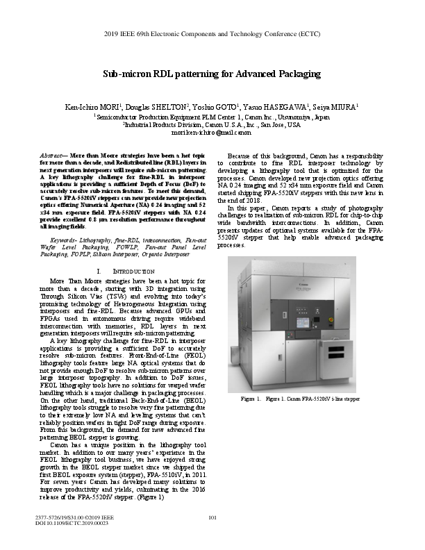
2019 IEEE 69th Electronic Components and Technology Conference (ECTC) Sub-micron RDL patterning for Advanced Packaging Ken-Ichiro MORI1, Douglas SHELTON2, Yoshio GOTO1, Yasuo HASEGAWA1, Seiya MIURA1 1Semiconductor Production Equipment PLM Center 1, Canon Inc., Utsunomiya, Japan 2Industrial Products Division, Canon U.S.A., Inc., San Jose, USA mori.ken-ichiro@mail.canon Abstract-- More than Moore strategies have been a hot topic for more than a decade, and Redistributed line (RDL) layers in next generation interposers will require sub-micron patterning. A key lithography challenge for fine-RDL in interposer applications is providing a sufficient Depth of Focus (DoF) to accurately resolve sub-micron features. To meet this demand, Canon's FPA-5520iV steppers can now provide new projection optics offering Numerical Aperture (NA) 0.24 imaging and 52 x34 mm exposure field. FPA-5520iV steppers with NA 0.24 provide excellent 0.8 m resolution performance throughout all imaging fields. Keywords- Lithography, fine-RDL, inteconnection, Fan-out Wafer Level Packaging, FOWLP, Fan-out Panel Level Packaging, FOPLP, Silicon Interposer, Organic Interposer Because of this background, Canon has a responsibility to contribute to fine RDL interposer technology by developing a lithography tool that is optimized for the processes. Canon developed new projection optics offering NA 0.24 imaging and 52 x34 mm exposure field and Canon started shipping FPA-5520iV steppers with this new lens in the end of 2018. In this paper, Canon reports a study of photography challenges to realization of sub-micron RDL for chip-to-chip wide bandwidth interconnections. In addition, Canon presents updates of optional systems available for the FPA5520iV stepper that help enable advanced packaging processes. I. INTRODUCTION More Than Moore strategies have been a hot topic for more than a decade, starting with 3D integration using Through Silicon Vias (TSVs) and evolving into today's promising technology of Heterogeneous Integration using interposers and fine-RDL. Because advanced GPUs and FPGAs used in autonomous driving require wideband interconnection with memories, RDL layers in next generation interposers will require sub-micron patterning. A key lithography challenge for fine-RDL in interposer applications is providing a sufficient DoF to accurately resolve sub-micron features. Front-End-of-Line (FEOL) lithography tools feature large NA optical systems that do not provide enough DoF to resolve sub-micron patterns over large interposer topography. In addition to DoF issues, FEOL lithography tools have no solutions for warped wafer handling which is a major challenge in packaging processes. On the other hand, traditional Back-End-of-Line (BEOL) lithography tools struggle to resolve very fine patterning due to their extremely low NA and leveling systems that can't reliably position wafers in tight DoF range during exposure. From this background, the demand for new advanced fine patterning BEOL stepper is growing. Canon has a unique position in the lithography tool market. In addition to our many years' experience in the FEOL lithography tool business, we have enjoyed strong growth in the BEOL stepper market since we shipped the first BEOL exposure system (stepper), FPA-5510iV, in 2011. For seven years Canon has developed many solutions to improve productivity and yields, culminating in the 2016 release of the FPA-5520iV stepper. (Figure 1) Figure 1. Figure 1. Canon FPA-5520iV i-line stepper 2377-5726/19/$31.00 ©2019 IEEE 101 DOI 10.1109/ECTC.2019.00023 II. CHALLENGES OF HIGH-RESOLUTION FOR ADVANCED PACKAGING Current advanced packaging processes mainly use design rules calling for 5 m L/S RDL patterns that connect a chip's pads and ball bumps. However, 5 m L/S RDL are not costeffective for multi-chip interconnections because these processes require multiple interconnect layers for highbandwidth, chip-to-chip connections. RDL line width reduction is a key challenge to expand the advanced packaging market to multi-chip interconnections by FOWLP or interposers, including interconnections between SoC and DRAM, split die connection of FPGA, and interconnections between image sensors and SoC. Next generation advanced packaging requires 1.0 m RDL and its future applications are targeting 0.8 m RDL. A. New projection optics for fine RDL To meet these requirements, Canon has developed a new projection optical system featuring a high NA and wide-field that is best suited for sub-micron RDL. These new projection optics are a new option for FPA-5520iV steppers, offering NA 0.24 imaging and a 52 x 34 mm exposure field. A summary of FPA-5520iV stepper standard and optional specifications are presented in Table 1 including the optional 0.8 m resolution option that requires the optional 0.24 NA. FPA-5520iV steppers with NA 0.24 optics provide excellent 0.8 m resolution performance throughout all imaging fields thanks to Canon's wave-front aberration based projection optics manufacturing methods, wave-front engineering, and on-axis optical tilt focus sensor. To show the importance of NA with respect to imaging results, Canon conducted an examination comparing the associated DoF with NA values varying from 0.18 to 0.57 when imaging 0.8 m features. Figure 2 shows that large NA values deliver the lowest ultimate resolution although for a 0.8 m process the usable DoF is less than 5 m for the highest NA examples. To provide a larger process window and maximize DoF, the Canon simulations show that NA 0.24 exposure conditions can deliver < 7 m of DoF for 0.8 m imaging which is suitable for fine RDL processes. TABLE I. FPA-5520IV I-LINE STEPPER SPECIFICATIONS Wafer size Resolution 300 mm 1.5 m / 0.8 m (option) NA Reduction ratio Exposure field Exposure wavelength Single machine overlay accuracy 0.15 0.18 / 0.15 0.24 (option) 2:1 52 x 34 mm 365 nm (i-line) Front 0.15m Backside 0.5m (option) Figure 2. NA 0.24 is an optimum condition for 0.8 m imaging B. Wave-front engineering in optics manufacturing To achieve sub-micron resolution, precision technology is required to design and fabricate low aberration lenses and the simulation results in Figure 3 shows the relationship between resist image profiles and coma aberration. The resist profile strongly depends on the lens aberration, especially in 0.8 m patterning, indicating the importance of strictly managing the lens aberration for sub-micron resolution. Canon employs manufacturing technology developed over many years of FEOL experience in wavefront engineering and manufacturing to produce a stable, supply of low-aberration lenses. Figure 4 explains a schematic diagram of Canon's Phase Measurement interferometer (PMi) lens aberration measurement system. The PMi system can quickly measure lens aberration by obtaining the interference image of the ideal light wave and the light wave passed through the lens. The PMi enables high precision lens aberration analysis and high quality lens assembly to realize and realizes stable lowaberration lens manufacturing. Figure 3. Simulation result of impact of Coma aberration 102 Figure 4. Schematic diagram of Phase Measurement interferometer C. Die-by-die tilt and focus compensation In FOWLP, an RDL layer is formed on wafers that are warped largely due to the molding process. Wafer warpage reduces focus margin and reduction of focus margin due to warpage is a big issue in submicron resolution since DOF is very small. FPA-5520iV steppers are equipped with die by die tilt & focus compensation systems as a solution for this issue. Figure 5 is a schematic diagram of the tilt focus system. Measurement light is projected obliquely incident from the side of the lens to each shot and the reflected light from the wafer is detected by sensor. Focus is calculated from the position information of the reflected light. The real-time focus system provides very accurate focus compensation as the focus position within each shot can be measured immediately before exposure. This system also does not need to measure wafer topography in advance, so high productivity is achieved. This system benefits from the Canon dioptric lens design that allows a large gap between the projection lens and wafer (> 20 mm), which is difficult to realize with mirror optical systems that are common in BEOL exposure applications. D. Photo resist patterning study Canon has collaborated with resist companies and materials makers to study 0.8 m resolution performance and Figure 6, Figure 7 and Figure 8 demonstrate the highresolution imaging performance of the FPA-5520iV steppers. Figure 6 displays a plot of printed feature sizes (Critical Dimension, CD) vs. Focus position for 0.8 m L/S patterns. Using 1.095 m thick PFi-38 A7 i-line photoresist, a DoF evaluation was conducted examining 15 images heights across a 52 x 34 mm field. This result showed that NA 0.24 was suited for 0.8 m L/S imaging, with an NA 0.24 condition yielding a DoF of about 8 m for 0.8 m L/S patterns that should provide sufficient focus margin for fine RDL processes. Figure 7 displays resist profile cross sections for 0.8 m L/S patterns with NA0.24 & NA0.18. Using 1.48 m thick TDMR®-AR1100 LB (TOKYO OHKA KOGYO CO.LTD.) i-line photoresist, NA0.24 condition provides a larger profile DoF than NA0.18 condition for 0.8 m L/S patterns. This resist profile cross-section result showed a DoF of about 8 m for 0.8 m L/S pattern, and NA0.24 is more preferable than NA 0.18 for 0.8 m L/S patterns. Figure 8 displays resist profile cross-section for 0.8 m L/S patterns on a Cu sputter wafer with NA0.24. Using 2.5 m thick JSR i-line photoresist, NA0.24 condition provides good resist profiles on Cu sputter wafers. Another advantage of the new projection optic system is the large 52 x 34 wide imaging field. The large-field and high-resolution imaging benefits of the FPA-5520iV can help speed the development of large size FOWLP and interposers manufacturing and performance improvements of FPGA and GPU devices. Figure 6. DoF evaluation for 0.8m Line & Space pattern Figure 5. Schematic diagram of the tilt focus system Figure 7. NA 0.24 & NA0.18 resolution comparison for 0.8 m Line/Space imaging 103 L R X span Figure 8. NA 0.24 resolution testing profile for 0.8 m Line/Space imaging on Cu sputter wafers (2.5 m thick resist) Figure 9. Schematic diagram of Grid PA III. UPDATE OF OPTIONAL SYSTEMS FOR FPA-5520IV STEPPERS SUPPORTING FOWLP A. Warped wafer handling system Warped wafer handling which is a key challenge for BEOL exposure tools and the FPA-5520iV is equipped with a new wafer handling system that offers a significant improvement over first generation FPA-5510iV steppers that were capable of handling up to 500 m of wafer warpage. The latest FPA-5520iV steppers are designed to handle more than 5 mm of wafer warpage in order to process FOWLP reconstituted wafers that typically exhibit more warpage than silicon wafers. B. Die rotation detection and compensation system In the chip first process, die shift and die rotation occur in the molding process. In addition, since the wafer notch as a reference in alignment is generally formed after molding, the positional accuracy of notch is poor. In a standard wafer handling sequence, steppers will execute a mechanical prealignment step which references a wafer notch. However, Fan-out wafers with poor notch accuracy are difficult to align to which can lower productivity. To solve this problem, FPA-5520iV steppers adopt a Grid Pre-alignment (Grid PA) function that aligns not only to a wafer notch, but also to the wafer chip image reference. An illustration of the Grid PA alignment system is provided in Figure 9. During the Grid PA sequence, a wafer image is acquired with cameras arranged symmetrically along the X axis with respect to the wafer. Left (L) and right (R) measurements of grid Y position are performed and the differences between the L/R Y values are calculated relative to the distance between the cameras, Grid PA estimates and compensates the globally for chip rotation relative to the notch reference. With this function it is possible to expose a fan-out wafer where die-rotation has occurred without lowering productivity. C. Through-Silicon Alignment The FPA-5520iV steppers can also be equipped with an optional Through-Silicon Alignment (TSA) System that can uses infrared light to view through full-thickness silicon wafers to measure the position of alignment marks on the backside of the wafer. The TSA system provides the FPA5520iV with a selection of infrared wavelength bands and center wavelengths that may be optimized to increase alignment accuracy. Principles of the TSA system are illustrated in Figure 10. Figure 10. Principles of Though Si Alignment 104 D. Panel handling (Under study) While maintaining 0.8 m pattern fidelity across a large exposure area is a key requirement of fine RDL processes, Fan-Out adopters seek to transition from wafer based to panel based processes to improve productivity and overall costs [1]. To support high-resolution FOPLP processes, Canon has studied a panel handling system for FPA-5520iV steppers. Although FPA-5520iV steppers cannot directly process Gen 4.5 panels that can be up to 730 x 920 mm in size, we developed a substrate handling system for R&D purpose to handle and process panels sizes up to 365 x 306.7 mm or approximately 1/6 of a Gen 4.5 panel. FPA-5520iV steppers can provide 0.8 m resolution on 365 x 306.7 mm rectangular substrates as illustrated in Figure 11, providing unique advantages supporting fine RDL & FOPLP processes. Canon is willing to do collaborative works with panel market players. Details of the allowable substrate range for the FPA5520iV panel handling system are included in Table 2. IV. CONCLUSION To meet the demands of sub-micron RDL and advanced packaging applications, Canon developed the FPA-5520iV stepper that can be equipped to deliver 0.8 m resolution on 300 mm wafers. In addition, Canon developed many original options for the packaging process. These could be realized by applying Canon's advanced FEOL and precision optical technology. Canon keeps meeting the challenging requirements for advanced packaging with Canon's extensive technology of exposure systems including the FPA-5520iV stepper. Canon remains committed to continued innovation enabling current and future FOWLP and interposer processes. REFERENCES [1] C. Chu, R. Rice, "FOPLP Standardization Survey Results", SEMI Standards, San Jose, CA, Nov. 2017 [2] Shin-Ichiro Hirai, Nobuyuki SAITO, Yoshio GOTO, Hiromi SUDA, Ken-Ichiro MORI, Seiya MIURA "A study of vertical lithography for high-density 3D structures" Proc. SPIE 8326, Optical Microlithography XXV, 83261E (13 March 2012) [3] Masaki MIZUTANI, Shin-Ichiro HIRAI, Ichiro KOIZUMI, KenIchiro MORI, Seiya MIURA "A STUDY OF VERTICAL LITHOGRAPHY FOR HIGH-DENSITY 3D STRUCTURES" Proc. SPIE 8683, Optical Microlithography XXVI, 86831F (12 April 2013) [4] Yoshio GOTO, Kosuke URUSHIHARA, Bunsuke TAKESHITA, Ken-Ichiro MORI "A study of Sub-micron Fan-out Wafer Level Packaging solutions" , THA2-103, iMAPS 2018 (11 Occtober 2018), unpublished. Figure 11. Example of panel exposure TABLE II. SUBSTRATE SPECIFICATION FOR PANEL HANDLING SYSTEM Item Material Maximum panel size Thickness Warpage Specification Glass X 306.7 mm / Y 365.0 mm 0.5 mm 1.0 mm 105OpenPDF 1.0.0-SNAPSHOT