i.MX RT1170 introduction i.MX RT1170 Crossover Processors Data Sheet for Consumer Products, Rev. 1, 05/2021 NXP Semiconductors 5 — Twelve universal asynchronous receiver/transmitter (UARTs) modules
i.MX RT1170 introduction i.MX RT1170 Crossover Processors Data Sheet for Consumer Products, Rev. 2, 11/2021 NXP Semiconductors 5 — Twelve universal asynchronous receiver/transmitter (UARTs) modules
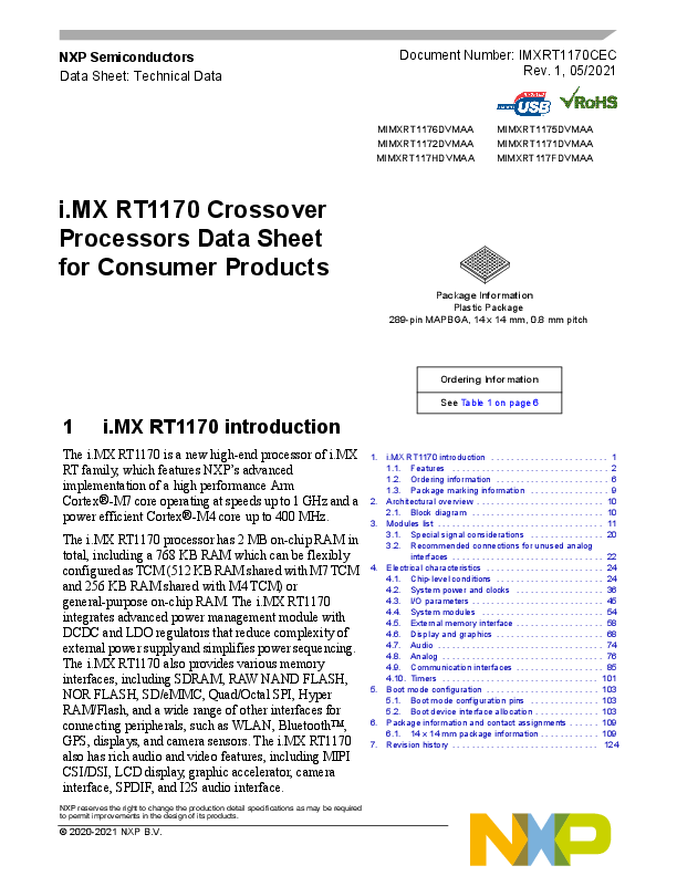
NXP Semiconductors Data Sheet: Technical Data
Document Number: IMXRT1170CEC Rev. 1, 05/2021
i.MX RT1170 Crossover Processors Data Sheet for Consumer Products
MIMXRT1176DVMAA MIMXRT1172DVMAA MIMXRT117HDVMAA
MIMXRT1175DVMAA MIMXRT1171DVMAA MIMXRT117FDVMAA
Package Information Plastic Package
289-pin MAPBGA, 14 x 14 mm, 0.8 mm pitch
Ordering Information
1 i.MX RT1170 introduction
See Table 1 on page 6
The i.MX RT1170 is a new high-end processor of i.MX RT family, which features NXP's advanced implementation of a high performance Arm Cortex®-M7 core operating at speeds up to 1 GHz and a power efficient Cortex®-M4 core up to 400 MHz.
The i.MX RT1170 processor has 2 MB on-chip RAM in total, including a 768 KB RAM which can be flexibly configured as TCM (512 KB RAM shared with M7 TCM and 256 KB RAM shared with M4 TCM) or general-purpose on-chip RAM. The i.MX RT1170 integrates advanced power management module with DCDC and LDO regulators that reduce complexity of external power supply and simplifies power sequencing. The i.MX RT1170 also provides various memory interfaces, including SDRAM, RAW NAND FLASH, NOR FLASH, SD/eMMC, Quad/Octal SPI, Hyper RAM/Flash, and a wide range of other interfaces for connecting peripherals, such as WLAN, BluetoothTM, GPS, displays, and camera sensors. The i.MX RT1170 also has rich audio and video features, including MIPI CSI/DSI, LCD display, graphic accelerator, camera interface, SPDIF, and I2S audio interface.
1. i.MX RT1170 introduction . . . . . . . . . . . . . . . . . . . . . . . . 1 1.1. Features . . . . . . . . . . . . . . . . . . . . . . . . . . . . . . . . 2 1.2. Ordering information . . . . . . . . . . . . . . . . . . . . . . . 6 1.3. Package marking information . . . . . . . . . . . . . . . . 9
2. Architectural overview . . . . . . . . . . . . . . . . . . . . . . . . . . 10 2.1. Block diagram . . . . . . . . . . . . . . . . . . . . . . . . . . . 10
3. Modules list . . . . . . . . . . . . . . . . . . . . . . . . . . . . . . . . . . 11 3.1. Special signal considerations . . . . . . . . . . . . . . . 20 3.2. Recommended connections for unused analog interfaces . . . . . . . . . . . . . . . . . . . . . . . . . . . . . . . 22
4. Electrical characteristics . . . . . . . . . . . . . . . . . . . . . . . . 24 4.1. Chip-level conditions . . . . . . . . . . . . . . . . . . . . . . 24 4.2. System power and clocks . . . . . . . . . . . . . . . . . . 36 4.3. I/O parameters . . . . . . . . . . . . . . . . . . . . . . . . . . . 45 4.4. System modules . . . . . . . . . . . . . . . . . . . . . . . . . 54 4.5. External memory interface . . . . . . . . . . . . . . . . . . 58 4.6. Display and graphics . . . . . . . . . . . . . . . . . . . . . . 68 4.7. Audio . . . . . . . . . . . . . . . . . . . . . . . . . . . . . . . . . . 74 4.8. Analog . . . . . . . . . . . . . . . . . . . . . . . . . . . . . . . . . 76 4.9. Communication interfaces . . . . . . . . . . . . . . . . . . 85 4.10. Timers . . . . . . . . . . . . . . . . . . . . . . . . . . . . . . . . 101
5. Boot mode configuration . . . . . . . . . . . . . . . . . . . . . . . 103 5.1. Boot mode configuration pins . . . . . . . . . . . . . . 103 5.2. Boot device interface allocation . . . . . . . . . . . . . 103
6. Package information and contact assignments . . . . . . 109 6.1. 14 x 14 mm package information . . . . . . . . . . . . 109
7. Revision history . . . . . . . . . . . . . . . . . . . . . . . . . . . . . . 124
NXP reserves the right to change the production detail specifications as may be required to permit improvements in the design of its products.
© 2020-2021 NXP B.V.
i.MX RT1170 introduction
The i.MX RT1170 is specifically useful for applications such as: · Industrial Human Machine Interfaces (HMI) · Motor Control · Home Appliance · High-end Audio Appliance · Low-end Instrument Cluster · Point-of-Sale (PoS)
1.1 Features
The i.MX RT1170 processors are based on Arm Cortex®-M7 CoreTM Platform, which has the following features:
· The Arm Cortex-M7 Core Platform: -- 32 KB L1 Instruction Cache and 32 KB L1 Data Cache -- Floating Point Unit (FPU) with single-precision and double-precision support of Armv7-M Architecture FPv5 -- Support the Arm®v7-M Thumb instruction set, defined in the Armv7-M architecture -- Integrated Memory Protection Unit (MPU), up to 16 individual protection regions -- Up to 512 KB I-TCM and D-TCM in total -- Frequency of 1 GHz with Forward Body Biasing (FBB) -- Frequency of the core, as per Table 11, "Operating ranges," on page 27.
· The Arm Cortex®-M4 Core platform: -- Cortex-M4 processor with single-precision FPU defined by Armv7-M architecture FPv4-SP -- Integrated MPU with 8 individual protection regions -- 16 KB Instruction Cache, 16 KB Data Cache, and 256 KB TCM -- Frequency of 400 MHz without body biasing
The SoC-level memory system consists of the following additional components: -- Boot ROM (256 KB) -- On-chip RAM (2 MB in total) Configurable 512 KB RAM shared with M7 TCM 256 KB RAM shared with M4 TCM Dedicated 1.25 MB OCRAM -- Secure always-on RAM (4 KB)
· External memory interfaces: -- 8/16/32-bit SDRAM, up to SDRAM-133/SDRAM-166/SDRAM-200 -- 8/16-bit SLC NAND FLASH -- SD/eMMC -- SPI NOR/NAND FLASH
i.MX RT1170 Crossover Processors Data Sheet for Consumer Products, Rev. 1, 05/2021
2
NXP Semiconductors
i.MX RT1170 introduction
-- Parallel NOR FLASH with XIP support -- Single/Dual channel Quad SPI FLASH with XIP support -- Hyper RAM/FLASH -- OCT FLASH -- Synchronization mode for all devices · Timers and PWMs: -- Six General Programmable Timer (GPT) modules
4-channel generic 32-bit resolution timer for each Each supports standard capture and compare operation -- Two Periodical Interrupt Timer (PIT) modules Four timers for each module Generic 32-bit resolution timer Periodical interrupt generation -- Four Quad Timer (QTimer) modules 4-channel generic 16-bit resolution timer for each Each supports standard capture and compare operation Quadrature decoder integrated -- Four FlexPWMs Up to 8 individual PWM channels for each 16-bit resolution PWM suitable for Motor Control applications -- Four Quadrature Decoders -- Four Watch Dog (WDOG) modules
Each i.MX RT1170 processor enables the following interfaces to external devices (some of them are muxed and not available simultaneously):
· Display Interface: -- Parallel RGB LCD interface (eLCDIF) Support 8/16/24-bit interface Support up to WXGA resolution @60fps Support Index color with 256 entry x 24-bit color LUT -- Parallel RGB LCD Interface Version 2 (LCDIFv2) Enhanced based on LCDIF version Support up to 8 layers of alpha blending -- MIPI Display Serial Interface (MIPI DSI) PHY integrated 2 data lanes interface with up to 1.5 GHz bit rate clock -- Smart LCD Display with 8080 interface through SEMC
· Audio:
i.MX RT1170 Crossover Processors Data Sheet for Consumer Products, Rev. 1, 05/2021
NXP Semiconductors
3
i.MX RT1170 introduction
-- SPDIF input and output -- Four Synchronous Audio Interface (SAI) modules supporting I2S, AC97, TDM, and
codec/DSP interfaces -- Medium Quality Sound (MQS) interface via GPIO pads -- PDM microphone interface with 4 pairs of inputs -- Asynchronous Sample Rate Converter (ASRC) · Graphics engine: -- Generic 2D (PXP)
BitBlit Flexible image composition options--alpha, chroma key Porter-duff blending Image rotation (90, 180, 270) Image resize Color space conversion Multiple pixel format support (RGB, YUV444, YUV422, YUV420, YUV400) Standard 2D-DMA operation -- Vector Graphics Processing Real-time hardware curve tessellation of lines, quadratic, and cubic Bezier curves 16x Line Anti-aliasing OpenVG 1.1 support Vector Drawing · Camera Interface: -- Parallel Camera Sensor Interface (CSI) Support 24-bit, 16-bit, and 8-bit input Barcode binarization and histogram statistics -- MIPI Camera Serial Interface (MIPI CSI) PHY integrated 2 data lanes interface with up to 1.5 GHz bit rate clock · Connectivity: -- Two USB 2.0 OTG controllers with integrated PHY interfaces -- Two Ultra Secure Digital Host Controller (uSDHC) interfaces eMMC 5.0 compliance with HS400 support up to 400 MB/sec SD/SDIO 3.0 compliance with 200 MHz SDR signaling to support up to 100 MB/sec Support for SDXC (extended capacity) -- One 10M/100M Ethernet controller with support for IEEE1588 -- One Gigabit Ethernet controller with support for AVB -- One Gigabit Ethernet controller with Time Sensitive Networking (TSN) Capability
i.MX RT1170 Crossover Processors Data Sheet for Consumer Products, Rev. 1, 05/2021
4
NXP Semiconductors
i.MX RT1170 introduction
-- Twelve universal asynchronous receiver/transmitter (UARTs) modules -- Six I2C modules -- Six SPI modules -- Three FlexCAN (with Flexible Data-rate supported) modules -- Two EMV SIM modules · Analog: -- Two Analog-Digital-Converters (ADC), which supports both differential and single-end inputs -- One Digital-Analog-Converter (DAC) -- Four Analog Comparators (ACMP) · GPIO and Pin Multiplexing: -- General-purpose input/output (GPIO) modules with interrupt capability -- Input/output multiplexing controller (IOMUXC) to provide centralized pad control -- Two FlexIO modules -- 8 x 8 keypad
The i.MX RT1170 processors integrate advanced power management unit and controllers: · Full PMIC integration, including on-chip DCDC and LDOs · Temperature sensor with programmable trim points · Hardware power management controller (GPC)
The i.MX RT1170 processors support the following system debug: · Arm CoreSight debug and trace architecture · Trace Port Interface Unit (TPIU) to support off-chip real-time trace · Cross Triggering Interface (CTI) · Support for 5-pin (JTAG) and SWD debug interfaces
Security functions are enabled and accelerated by the following hardware: · High Assurance Boot (HAB) · Cryptographic Acceleration and Assurance (CAAM) module: -- Public Key Cryptography Engine (PKHA) -- Symmetric Engines -- Cryptographic Hash Engine -- Random Number Generation (RNG4) -- Four Job Rings for use by processors -- Secure Hardware-Only Cryptographic Key Management -- Encrypted Boot -- Revision control check based on fuse values -- DEK includes IV -- Side channel attack countermeasures -- 64 KB secure RAM
i.MX RT1170 Crossover Processors Data Sheet for Consumer Products, Rev. 1, 05/2021
NXP Semiconductors
5
i.MX RT1170 introduction
· Inline Encryption Engine (IEE): -- External memory encryption/decryption -- I/O direct encrypted storage and retrieval (Stream Support) -- FlexSPI decryption only
· On-the-Fly AES Decryption (OTFAD): -- AES-128 Counter Mode On-the-Fly Decryption -- Hardware support for unwrapping "key blobs" -- Functionally acts as a slave sub-module to the FlexSPI
· Secure Non-Volatile Storage (SNVS): -- Secure real-time clock (SRTC) -- Zero Master Key (ZMK)
· Secure always-on RAM (4 KB) · Secure key management and protection
-- Physical Unclonable Function (PUF) -- UnDocumented Function (UDF) -- Built-in Manufacturing Protection Hardware · Secure and trusted access control
NOTE The actual feature set depends on the part numbers as described in Table 1. Functions such as display and camera interfaces, connectivity interfaces, and security features are not offered on all derivatives.
1.2 Ordering information
Table 1 provides examples of orderable part numbers covered by this Data Sheet.
Table 1. Order information
Qualification tier M7 core M4 core SRAM
Parallel LCD and CSI MIPI DSI and CSI GPU2D PXP CAN-FD
MIMXRT1176 MIMXRT1175 MIMXRT1172 MIMXRT1171 MIMXRT117H MIMXRT117F
DVMAA
DVMAA
DVMAA
DVMAA
DVMAA
DVMAA
Consumer 1 GHz
400 MHz 2 MB Yes Yes Yes Yes x3
Consumer 1 GHz
400 MHz 2 MB -- -- -- -- x3
Consumer 1 GHz -- 2 MB Yes Yes Yes Yes x3
Consumer 1 GHz -- 2 MB -- -- -- -- x3
Consumer 1 GHz
400 MHz 2 MB Yes Yes Yes Yes x3
Consumer 1 GHz -- 2 MB Yes Yes Yes Yes x3
i.MX RT1170 Crossover Processors Data Sheet for Consumer Products, Rev. 1, 05/2021
6
NXP Semiconductors
i.MX RT1170 introduction
Table 1. Order information (continued)
MIMXRT1176 MIMXRT1175 MIMXRT1172 MIMXRT1171 MIMXRT117H MIMXRT117F
DVMAA
DVMAA
DVMAA
DVMAA
DVMAA
DVMAA
ADC
x2
x2
x2
x2
x2
x2
12-bit DAC
x1
x1
x1
x1
x1
x1
ACMP
x4
x4
x4
x4
x4
x4
1 Gb ENET with AVB
x1
x1
x1
x1
x1
x1
1 Gb ENET with TSN
x1
--
--
--
x1
--
10/100 Mb ENET with
x1
x1
x1
x1
x1
x1
1588
USB 2.0 OTG
x2
x2
x2
x2
x2
x2
eMMC 5.0 / SD 3.0
x2
x2
x2
x2
x2
x2
EMV SIM
x2
x2
x2
x2
x2
x2
SAI
x4
x4
x4
x4
x4
x4
DMIC
x8
x8
x8
x8
x8
x8
FlexSPI
x2
x2
x2
x2
x2
x2
UART
x12
x12
x12
x12
x12
x12
I2C
x6
x6
x6
x6
x6
x6
SPI
x6
x6
x6
x6
x6
x6
GPT
x6
x6
x6
x6
x6
x6
PIT
x2
x2
x2
x2
x2
x2
QTimer
x4
x4
x4
x4
x4
x4
FlexPWM
x4
x4
x4
x4
x4
x4
Temp Monitor
x1
x1
x1
x1
x1
x1
Security
Yes
Yes
Yes
Yes
Yes
Yes
Package
289 MAPBGA, 14 mm x14 mm, 0.8 mm pitch
289 MAPBGA, 14 mm x14 mm, 0.8 mm pitch
289 MAPBGA, 14 mm x14 mm, 0.8 mm pitch
289 MAPBGA, 14 mm x14 mm, 0.8 mm pitch
289 MAPBGA, 14 mm x14 mm, 0.8 mm pitch
289 MAPBGA, 14 mm x14 mm, 0.8 mm pitch
Junction temperature Tj (C)
0 to 95
0 to 95
0 to 95
0 to 95
0 to 95
0 to 95
Figure 1 describes the part number nomenclature so that characteristics of a specific part number can be identified (for example, cores, frequency, temperature grade, fuse options, and silicon revision). The primary characteristic which describes which data sheet applies to a specific part is the temperature grade (junction) field.
· The i.MX RT1170 Crossover Processors for Consumer Products Data Sheet (IMXRT1170CEC) covers parts listed with a "D (Consumer temp)"
i.MX RT1170 Crossover Processors Data Sheet for Consumer Products, Rev. 1, 05/2021
NXP Semiconductors
7
i.MX RT1170 introduction
Ensure to have the proper data sheet for specific part by verifying the temperature grade (junction) field and matching it to the proper data sheet. If there are any questions, visit the web page nxp.com/IMXRT or contact an NXP representative for details.
M IMX X X @ ## % + VV $ A
Qualification Level
M
Prototype Samples
P
Mass Production
M
Special
S
Part # series
XX
i.MX RT
RT
Family
@
First Generation RT family
1
Reserved
2-8
Sub-Family
##
RT116x
16
RT117x
17
RT118x
18
Tie
%
Single Core Standard Feature
1
Single Core Enhanced Feature
2
Dual Core Enhanced Security
3
Dual Core Standard Feature
5
Dual Core Enhanced Feature
6
Dual Core Premium Feature
7
Dual Core Full Feature
9
Facial Recognition
F
Hybrid Solution with Vision & Voice
H
Local Voice Control (text input models)
S
Silicon Rev
A
A0
A
Main Core Frequency
$
2xx MHz
2
500 MHz
5
600 MHz
6
800 MHz
8
1 GHz
A
Package Type
VV
289MAPBGA, 14 x 14 mm, 0.8 mm pitch
VM
196MAPBGA, 12 x 12 mm, 0.8 mm pitch
VJ
144MAPBGA, 10 x 10 mm, 0.8 mm pitch
VP
Temperature (Tj)
+
Consumer: 0 to + 95 °C
D
Industrial: -40 to +105 °C
C
Extended Industrial: -40 to + 125 eC
X
Automotive: -40 to + 125 eC
A
Figure 1. Part number nomenclature--i.MX RT11XX family
i.MX RT1170 Crossover Processors Data Sheet for Consumer Products, Rev. 1, 05/2021
8
NXP Semiconductors
i.MX RT1170 introduction
1.3 Package marking information
Figure 2 describes the package marking format about the i.MX RT1170 Crossover Processors.
Figure 2. MAPBGA289 14 x 14 mm package marking format
The 14 x 14 mm of i.MX RT1170 MAPBGA289 package has the following top-side marking: · First line: aaaaaaaaaaaaaaa · Second line: mmmmm · Third line: xxxyywwx
Table 2 lists the identifier decoder.
Table 2. Identifier decoder
Identifier a m y w x
Description Part number code, refer to Section 1.2, Ordering information
Mask set Year
Work week NXP internal use
i.MX RT1170 Crossover Processors Data Sheet for Consumer Products, Rev. 1, 05/2021
NXP Semiconductors
9
Architectural overview
2 Architectural overview
The following subsections provide an architectural overview of the i.MX RT1170 processor system.
2.1 Block diagram
Figure 3 shows the functional modules in the i.MX RT1170 processor system1.
.
Figure 3. i.MX RT1170 system block diagram
1. Some modules shown in this block diagram are not offered on all derivatives. See Table 1 for details.
i.MX RT1170 Crossover Processors Data Sheet for Consumer Products, Rev. 1, 05/2021
10
NXP Semiconductors
Modules list
3 Modules list
The i.MX RT1170 processors contain a variety of digital and analog modules. Table 3 describes these modules in alphabetical order.
Table 3. i.MX RT1170 modules list
Block Mnemonic
Block Name
Subsystem
Brief Description
ACMP1 ACMP2 ACMP3 ACMP4 ADC_ETC ADC1 ADC2
AOI
Arm
ASRC CAAM
CANFD1 CANFD2 CANFD3
CCM GPC PGMC PMU SRC
Analog Comparator
Analog
The comparator (CMP) provides a circuit for comparing two analog input voltages. The comparator circuit is designed to operate across the full range of the supply voltage (rail-to-rail operation).
ADC External Trigger Control
Analog
ADC_ETC enables multiple users shares a ADC module in a Time-Division-Multiplexing (TDM).
Analog to Digital Converter
Analog
The ADC is a 12-bit general purpose analog to digital converter.
And-Or-Inverter
Cross Trigger
The AOI provides a universal boolean function generator using a four-term sum of products expression with each product term containing true or complement values of the four selected inputs (A, B, C, D).
Arm Platform
Arm
The Arm Core Platform includes one Cortex-M7 core. It
includes associated sub-blocks, such as Nested
Vectored Interrupt Controller (NVIC), Floating-Point Unit
(FPU), Memory Protection Unit (MPU), and CoreSight
debug modules.
The Cortex-M4 platform has following features:
· Cortex-M4 processor with FPU
· Local memory
16 KB instruction cache and 16 KB data cache
256 KB TCM
Asynchronous Sample Rate Converter
Multimedia Peripherals
The ASRC can process groups of audio channels with an independent time-based simultaneously.
Cryptographic Accelerator and Assurance Module
Security
CAAM supports a set of standard hardware accelerators, boot time acceleration of the hashing function, crypto key protection, HDCP 2.x authentication and protected video path support, manufacturing protection and public key cryptographic acceleration, and inter-operate with TrustZone, Resource Domain, and system virtualization access controls.
Flexible Controller Area Network
Connectivity Peripherals
The CAN with Flexible Data rate (CAN FD) module is a communication controller implementing the CAN protocol according to the ISO11898-1 and CAN 2.0B protocol specification.
Clock Control Module, General Power Controller,
Power Manage Unit, Power Gating and Memory Controller,
System Reset Controller
Clocks, Resets, and Power Control
These modules are responsible for clock and reset distribution in the system, and also for the system power management.
i.MX RT1170 Crossover Processors Data Sheet for Consumer Products, Rev. 1, 05/2021
NXP Semiconductors
11
Modules list
Table 3. i.MX RT1170 modules list (continued)
Block Mnemonic CSI
Block Name Parallel CSI
CWT DAC DAP
Code Watchdog Timer Digital-Analog-Converter
Debug Access Port
DCDC
DCDC Converter
eDMA eDMA_LPSR
enhanced Direct Memory Access
eLCDIF
LCD interface
EMV SIM1 EMV SIM2
Europay, Master and Visa Subscriber Identification
Module
Subsystem
Brief Description
Multimedia Peripherals
The CSI IP provides parallel CSI standard camera interface port. The CSI parallel data ports are up to 24 bits. It is designed to support 24-bit RGB888/YUV444, CCIR656 video interface, 8-bit YCbCr, YUV or RGB, and 8-bit/10-bit/16-bit/24-bit Bayer data input.
Timer peripherals
The CWT provides mechanisms for detecting side-channel attacks and the execution of unexpected instruction sequences.
Analog
The DAC is a 12-bit general purpose digital to analog converter.
System Control Peripherals
The DAP provides real-time access for the debugger without halting the core to: · System memory and peripheral registers · All debug configuration registers The DAP also provides debugger access to JTAG scan chains. The DAP module is internal to the Cortex-M7 Core Platform.
Analog
The DCDC module is used for generating power supply for core logic. Main features are: · Adjustable high efficiency regulator · Two outputs: 1.0 V and 1.8 V · Over current and over voltage detection
System Control Peripherals
There are two enhanced DMAs (eDMA). · The eDMA is a 32-channel DMA engine, which is
capable of performing complex data transfers with minimal intervention from a host processor. · The DMA_MUX is capable of multiplexing up to 128 DMA request sources to the 32 DMA channels of eDMA.
Multimedia Peripherals
The enhanced LCD controller provides flexible display options and to drive a wide range of display devices varying in size and capability. Major features are: · Up to WXGA 60 Hz · 8/16/18/24 bit LCD data bus support available
depending on I/O mux options. · Programmable timing and parameters for LCD
interfaces to support a wide variety of displays. · Index color with 256 entry x 24-bit color LUT
Connectivity Peripherals
EMV SIM is designed to facilitate communication to Smart Cards compatible to the EMV version 4.3 standard (Book 1) and Smart Cards compatible with ISO/IEC 7816-3 standard.
i.MX RT1170 Crossover Processors Data Sheet for Consumer Products, Rev. 1, 05/2021
12
NXP Semiconductors
Modules list
Table 3. i.MX RT1170 modules list (continued)
Block Mnemonic ENET
Block Name Ethernet Controller
ENET 1G
Ethernet Controller
ENET_QOS
Ethernet Quality-of-Service
EWM
External Watchdog Monitor
FlexIO1 FlexIO2
Flexible Input/output
FlexPWM1 FlexPWM2 FlexPWM3 FlexPWM4
Pulse Width Modulation
FlexRAM
RAM
Subsystem
Brief Description
Connectivity Peripherals
The Ethernet Media Access Controller (MAC) is designed to support 10/100 Mbit/s Ethernet/IEEE 802.3 networks. An external transceiver interface and transceiver function are required to complete the interface to the media. The module has dedicated hardware to support the IEEE 1588 standard. See the ENET chapter of the reference manual for details.
Connectivity Peripherals
One 1G Ethernet is also integrated, which has following features: · RGMII/RMII/MII operation · Support IEEE1588 · Support AVB
Connectivity Peripherals
The ENET_QOS is compliant with the IEEE 802.32015 specification and can be used in applications, such as AV bridges, AV nodes, switches, data center bridges and nodes, and network interface cards. It enables a host to transmit and receive data over Ethernet in compliance with the IEEE802.1AS and IEEE802.1-Qav for audio/video traffic.
Timer Peripherals
The EWM modules is designed to monitor external circuits, as well as the software flow. This provides a back-up mechanism to the internal WDOG that can reset the system. The EWM differs from the internal WDOG in that it does not reset the system. The EWM, if allowed to time-out, provides an independent trigger pin that when asserted resets or places an external circuit into a safe mode.
Connectivity and Communications
The FlexIO is capable of supporting a wide range of protocols including, but not limited to: UART, I2C, SPI, I2S, camera interface, display interface, PWM waveform generation, etc. The module can remain functional when the chip is in a low power mode provided the clock it is using remain active.
Timer Peripherals
The pulse-width modulator (PWM) contains four PWM sub-modules, each of which is set up to control a single half-bridge power stage. Fault channel support is provided. The PWM module can generate various switching patterns, including highly sophisticated waveforms.
Memories
The i.MX RT1170 has 512 KB of on-chip RAM which could be flexible allocated to I-TCM, D-TCM, and on-chip RAM (OCRAM) in a 32 KB granularity. The FlexRAM is the manager of the 512 KB on-chip RAM array. Major functions of this blocks are: interfacing to I-TCM and D-TCM of CM7 and OCRAM controller; dynamic RAM arrays allocation for I-TCM, D-TCM, and OCRAM.
i.MX RT1170 Crossover Processors Data Sheet for Consumer Products, Rev. 1, 05/2021
NXP Semiconductors
13
Modules list
Table 3. i.MX RT1170 modules list (continued)
Block Mnemonic
Block Name
Subsystem
Brief Description
FlexSPI1 FlexSPI2
GPIO1 GPIO2 GPIO3 GPIO4 GPIO5 GPIO6 GPIO7 GPIO8 GPIO9 GPIO10 GPIO11 GPIO12 GPIO13 GPT1 GPT2 GPT3 GPT4 GPT5 GPT6
GPU2D
IOMUXC
Flexible Serial Peripheral Interface
General Purpose I/O Modules
Connectivity and Communications
System Control Peripherals
FlexSPI acts as an interface to one or two external serial memory devices, FlexSPI2 has 8 bi-directional data lines.
Used for general purpose input/output to external ICs. Each GPIO module supports up to 32 bits of I/O. Note: GPIO13 register access takes a long time (about 50s due to clocked by 32 KHz clock source). During the period of registers access, the LPSR domain bus would be on hold.
General Purpose Timer
Graphics Processing IOMUX Control
Timer Peripherals
Each GPT is a 32-bit "free-running" or "set and forget" mode timer with programmable prescaler and compare and capture register. A timer counter value can be captured using an external event and can be configured to trigger a capture event on either the leading or trailing edges of an input pulse. When the timer is configured to operate in "set and forget" mode, it is capable of providing precise interrupts at regular intervals with minimal processor intervention. The counter has output compare logic to provide the status and interrupt at comparison. This timer can be configured to run either on an external clock or on an internal clock.
Multimedia Peripherals
The vector graphics processing supports following features: · Real-time hardware curve tessellation of lines,
quadratic, and cubic Bezier curves · 16x line anti-aliasing · OpenVG 1.1 support · Vector drawing
Mux control
This module enables flexible I/O multiplexing. Each IO pad has a default as well as several alternate functions. The alternate functions are software configurable.
i.MX RT1170 Crossover Processors Data Sheet for Consumer Products, Rev. 1, 05/2021
14
NXP Semiconductors
Modules list
Table 3. i.MX RT1170 modules list (continued)
Block Mnemonic JTAGC
Block Name JTAG Controller
KPP
Keypad Port
LCDIFv2
Parallel RGB LCD interface version 2
LPI2C1 LPI2C2 LPI2C3 LPI2C4 LPI2C5 LPI2C6
LPSPI1 LPSPI2 LPSPI3 LPSPI4 LPSPI5 LPSPI6
Low Power Inter-integrated Circuit
Low Power Serial Peripheral Interface
Subsystem
Brief Description
System Control Peripherals
Human Machine Interfaces
Multimedia Peripherals
Connectivity and Communications
Connectivity and Communications
The JTAG interface complies with JTAG TAP standards to internal logic. The i.MX RT1170 processors use JTAG port for production, testing, and system debugging. In addition, the JTAG provides BSR (Boundary Scan Register) standard support, which complies with IEEE 1149.1 and IEEE 1149.6 standards. The JTAG port must be accessible during platform initial laboratory bring-up, for manufacturing tests and troubleshooting, as well as for software debugging by authorized entities. The i.MX RT1170 JTAG incorporates two security modes for protecting against unauthorized accesses. Modes are selected through eFUSE configuration.
The KPP is a 16-bit peripheral that can be used as a keypad matrix interface or as general purpose input/output (I/O). It supports 8 x 8 external key pad matrix. Main features are: · Multiple-key detection · Long key-press detection · Standby key-press detection · Supports a 2-point and 3-point contact key matrix
The LCDIFv2 is an enhanced version of LCDIF. Main features are: · Eight layers of alpha blending · CRC check for configurable region on the final
display output after alpha blending · Write-back channel to save the final output into
memory
The LPI2C is a low power Inter-Integrated Circuit (I2C) module that supports an efficient interface to an I2C bus as a master. The I2C provides a method of communication between a number of external devices. More detailed information, see Section 4.9.2, LPI2C module timing parameters.
The LPSPI is a low power Serial Peripheral Interface (SPI) module that support an efficient interface to an SPI bus as a master and/or a slave. · It can continue operating while the chip is in stop
modes, if an appropriate clock is available · Designed for low CPU overhead, with DMA off
loading of FIFO register access
i.MX RT1170 Crossover Processors Data Sheet for Consumer Products, Rev. 1, 05/2021
NXP Semiconductors
15
Modules list
Table 3. i.MX RT1170 modules list (continued)
Block Mnemonic
Block Name
Subsystem
Brief Description
LPUART1 LPUART2 LPUART3 LPUART4 LPUART5 LPUART6 LPUART7 LPUART8 LPUART9 LPUART10 LPUART11 LPUART12 MECC64
MIPI-CSI
MIPI-DSI
MQS
MU
UART Interface
Connectivity Peripherals
Each of the UART modules support the following serial data transmit/receive protocols and configurations: · 7- or 8-bit data words, 1 or 2 stop bits, programmable
parity (even, odd or none) · Programmable baud rates up to 20 Mbps.
Error Correcting Code MIPI CSI Interface
MIPI DSI Interface
Medium Quality Sound Messaging Unit
Memories and MECC64 module supports Single Error Correction and Memory Controllers Double Error Detection (SECDED) ECC function to
provide reliability for 4 banks On-Chip RAM (OCRAM) access. When ECC function is disabled, ECC OCRAM can be also used to store data.
Multimedia Peripherals
Key features of MIPI CSI controller are listed as following: · Implements all three MIPI CSI-2 layers · Supports CSI-2 Unidirectional Master operation · Virtual Channel support · Flexible pixel-based user interface
Multimedia Peripherals
Key features of MIPI DSI controller are listed as following: · Implements all three DSI layers · Supports Command and Video Modes · Virtual Channel support · Flexible packet based user interface
Multimedia Peripherals
MQS is used to generate 2-channel medium quality PWM-like audio via two standard digital GPIO pins.
System Control
The Messaging Unit module enables two processors within the SoC to communicate and coordinate by passing messages (e.g. data, status, and control) through the MU interface. The MU also provides the ability for one processor to signal the other processor using interrupts.
i.MX RT1170 Crossover Processors Data Sheet for Consumer Products, Rev. 1, 05/2021
16
NXP Semiconductors
Modules list
Table 3. i.MX RT1170 modules list (continued)
Block Mnemonic
Block Name
Subsystem
Brief Description
OCOTP_CTRL
OTP Controller
Security
The On-Chip OTP controller (OCOTP_CTRL) provides an interface for reading, programming, and/or overriding identification and control information stored in on-chip fuse elements. The module supports electrically programmable poly fuses (eFUSEs). The OCOTP_CTRL also provides a set of volatile software-accessible signals that can be used for software control of hardware elements, not requiring non volatility. The OCOTP_CTRL provides the primary user-visible mechanism for interfacing with on-chip fuse elements. Among the uses for the fuses are unique chip identifiers, mask revision numbers, cryptographic keys, JTAG secure mode, boot characteristics, and various control signals requiring permanent non volatility.
OCRAM
On-Chip Memory controller
Memories and The On-Chip Memory controller (OCRAM) module is Memory Controllers designed as an interface between the system's AXI bus
and the internal (on-chip) SRAM memory module.
OSC
Oscillator
Clock Sources and Control
Two crystal oscillators: · 48 MHz crystal oscillator: it is used as primary clock
source for all the PLLs to generate the clock for CPU, BUS, and high-speed interfaces. · 32 kHz crystal oscillator: it is the primary clock source for RTC as well as low speed clock source for CCM/SRC/GPC.
PDM
Pulse Density Modulation
Multimedia Peripherals
The PDM supports up to 8-channels (4 lanes) digital MIC inputs.
PIT1 PIT2
Periodical Interrupt Timer
Timer Peripherals
The PIT features 32-bit counter timer, programmable count modules, clock division features, interrupt generation, and a slave mode to synchronize count enable for multiple PITs.
PXP
Pixel Processing Pipeline
Multimedia Peripherals
A high-performance pixel processor capable of 1 pixel/clock performance for combined operations, such as color-space conversion, alpha blending, and rotation. The PXP is enhanced with features specifically for gray scale applications. In addition, the PXP supports traditional pixel/frame processing paths for still-image and video processing applications.
Quadrature DEC1 Quadrature DEC2 Quadrature DEC3 Quadrature DEC4
Quadrature Decoder
Timer Peripherals
The enhanced quadrature decoder module provides interfacing capability to position/speed sensors. There are five input signals: PHASEA, PHASEB, INDEX, TRIGGER, and HOME. This module is used to decode shaft position, revolution count, and speed.
i.MX RT1170 Crossover Processors Data Sheet for Consumer Products, Rev. 1, 05/2021
NXP Semiconductors
17
Modules list
Table 3. i.MX RT1170 modules list (continued)
Block Mnemonic
Block Name
Subsystem
Brief Description
QuadTimer1 QuadTimer2 QuadTimer3 QuadTimer4
RDC
ROMCP
RTC OSC
SAI1 SAI2 SAI3 SAI4 SEMA4
SEMC
SNVS SPDIF
QuadTimer
Timer Peripherals
The quad-timer provides four time channels with a variety of controls affecting both individual and multi-channel features.Specific features include up/down count, cascading of counters, programmable module, count once/repeated, counter preload, compare registers with preload, shared use of input signals, prescaler controls, independent capture/compare, fault input control, programmable input filters, and multi-channel synchronization.
Resource Domain Controller
Security
The RDC provides robust support for the isolation of processing domain to prevent one core from accessing another's peripherals, to control access rights to common memory and provide hardware enforcement of semaphore based locking of shared peripherals. For single system use case, RDC can be disabled and AIPS-TZ/DEXSC can be bypassed. For dual system case, RDC can be configured and locked each core starts their own image.
ROM Controller with Patch
Memories and The ROMCP acts as an interface between the Arm Memory Controllers advanced high-performance bus and the ROM. The
on-chip ROM is only used by the Cortex-M7 core during boot up. Size of the ROM is 256 KB.
Real Time Clock Oscillator
Clock Sources and Control
The RTC OSC provides the clock source for the Real-Time Clock module. The RTC OSC module, in conjunction with an external crystal, generates a 32.768 kHz reference clock for the RTC.
Synchronous Audio Interface
Multimedia Peripherals
The SAI module provides a synchronous audio interface (SAI) that supports full duplex serial interfaces with frame synchronization, such as I2S, AC97, TDM, and codec/DSP interfaces.
Semaphores
System Control
The SEMA4 module implements hardware-enforced semaphores as an IPS-mapped slave peripheral device and provides 16 hardware-enforced gates in a dual-processor configuration.
Smart External Memory Controller
Memory and Memory Controller
The SEMC is a multi-standard memory controller optimized for both high-performance and low pin-count. It can support multiple external memories in the same application with shared address and data pins. The interface supported includes SDRAM, NOR Flash, SRAM, and NAND Flash, as well as 8080 display interface.
Secure Non-Volatile Storage
Security
Secure Non-Volatile Storage, including Secure Real Time Clock, Security State Machine, and Master Key Control.
Sony Philips Digital Interconnect Format
Multimedia Peripherals
A standard audio file transfer format, developed jointly by the Sony and Phillips corporations. Has Transmitter and Receiver functionality.
i.MX RT1170 Crossover Processors Data Sheet for Consumer Products, Rev. 1, 05/2021
18
NXP Semiconductors
Modules list
Table 3. i.MX RT1170 modules list (continued)
Block Mnemonic
Block Name
Subsystem
Brief Description
SSARC TEMP SENSE
USB1 USB2 uSDHC1 uSDHC2
VIDMUX
State Save and Restore Memories and The SSARC saves the registers of functional modules in
Controller
Memory Controllers memory before power down, and restores registers from
memory after the module is powered up.
Temperature Sensor
Analog
The temperature sensor implements a temperature sensor/conversion function based on a temperature-dependent voltage to time conversion.
Universal Serial Bus 2.0
Connectivity Peripherals
USB 2.0 OTG modules (USB OTG1 and USB OTG2) contains: · Two high-speed OTG 2.0 modules with integrated HS
USB PHYs · Support eight Transmit (TX) and eight Receive (Rx)
endpoints, including endpoint 0
SD/MMC and SDXC Enhanced Multi-Media Card / Secure Digital Host
Controller
Connectivity Peripherals
i.MX RT1170 specific SoC characteristics: All four MMC/SD/SDIO controllers are identical and are based on the uSDHC. They are: · Fully compliant with MMC command/response sets
and Physical Layer as defined in the Multimedia Card System Specification. · Fully compliant with SD command/response sets and Physical Layer as defined in the SD Memory Card Specifications, v3.0 including high-capacity SDXC cards up to 2 TB. · Fully compliant with SDIO command/response sets and interrupt/read-wait mode as defined in the SDIO Card Specification, Part E1, v3.0 Two ports support: · 1-bit or 4-bit transfer mode specifications for SD and SDIO cards up to UHS-I SDR104 mode (104 MB/s max) · 1-bit, 4-bit, or 8-bit transfer mode specifications for MMC cards up to 52 MHz in both SDR and DDR modes (104 MB/s max) · 4-bit or 8-bit transfer mode specifications for eMMC chips up to 200 MHz in HS200 mode (200 MB/s max)
Video mux
Mux control
Video mux are mux control for Parallel CSI (IO PADs), MIPI CSI-2, MIPI DSI, Parallel LCDIF (IO PADs) and CSI, LCDIF-V2, eLCDIF control. It also includes the DCIC of MIPI DSI and Parallel DSI.
i.MX RT1170 Crossover Processors Data Sheet for Consumer Products, Rev. 1, 05/2021
NXP Semiconductors
19
Modules list
Table 3. i.MX RT1170 modules list (continued)
Block Mnemonic
Block Name
Subsystem
Brief Description
WDOG1 WDOG2 WDOG3 WDOG4
XBARA XBARB
XECC XRDC
Watch Dog
Timer Peripherals
WDOG1 and WDOG2 Timer support two comparison points during each counting period. Each of the comparison points is configurable to evoke an interrupt to the Arm core, and a second point evokes an external event on the WDOG line. WDOG3 and WDOG4 modules are high reliability independent timers that are available for system to use. They provide a safety feature to ensure software is executing as planned and the CPU is not stuck in an infinite loop or executing unintended code. If the WDOG module is not serviced (refreshed) within a certain period, it resets the MCU. Windowed refresh mode is supported as well.
Cross BAR
Cross Trigger
Each crossbar switch is an array of muxes with shared inputs. Each mux output provides one output of the crossbar. The number of inputs and the number of muxes/outputs are user configurable and registers are provided to select which of the shared inputs are routed to each output.
External ECC Controller Memories and XECC can be used as a gasket module on AXI bus to Memory Controllers support ECC function for external memory.
Extended Resource Domain Controller
Security
The XRDC provides an integrated, scalable architectural framework for access control, system memory protection, and peripheral isolation. It allows software to assign chip resources including processor cores, non-core bus masters, memory regions, and slave peripherals to processing domains to support enforcement of robust operational environments.
3.1 Special signal considerations
Table 4 lists special signal considerations for the i.MX RT1170 processors. The signal names are listed in alphabetical order.
The package contact assignments can be found in Section 6, Package information and contact assignments." Signal descriptions are provided in the i.MX RT1170 Reference Manual (IMXRT1170RM).
Table 4. Special signal considerations
Signal Name CLK1_P/ CLK1_N
DCDC_PSWITCH
Remarks
This differential output is reserved for NXP internal use. For users, this output must be a no connect.
PAD is in DCDC_IN domain and connected to ground to bypass DCDC. To enable DCDC function, assert DCDC_PSWITCH with at least 1 ms delay after the DCDC_IN rising edge.
i.MX RT1170 Crossover Processors Data Sheet for Consumer Products, Rev. 1, 05/2021
20
NXP Semiconductors
Modules list
Table 4. Special signal considerations (continued)
Signal Name
Remarks
RTC_XTALI/RTC_XTALO
To hit the exact oscillation frequency, the board capacitors must be reduced to account for the board and chip parasitics. The integrated oscillation amplifier is self-biasing, but relatively weak. Care must be taken to limit the parasitic leakage from RTC_XTALI and RTC_XTALO to either the power or the ground (> 100 M). This de-biases the amplifier and reduces the start-up margin. If you want to feed an external low-frequency clock into RTC_XTALI, the RTC_XTALO pin must remain unconnected or driven by a complementary signal. The logic level of this forcing clock must not exceed the VDD_SNVS_DIG level and the frequency shall be < 100 kHz under the typical conditions. It is recommended to tie RTC_XTALI to GND if external crystal is not used. When a high-accuracy real-time clock is not required, the system may use the on-chip 32 kHz oscillator. The tolerance is ±10%. The ring oscillator starts faster than the external crystal and is used until the external crystal reaches a stable oscillation. The ring oscillator also starts automatically if no clock is detected at RTC_XTALI.
XTALI/XTALO
The SDK software requires 24 MHz on XTALI/XTALO. The crystal can be eliminated if an external 24 MHz oscillator is available in the system. In this case, refer to section of Bypass Configuration (24 MHz) from the reference manual. There are three configurations that can be utilized, but configuration 2 is recommended. The logic level of this forcing clock must not exceed the VDD_LPSR_ANA level. If this clock is used as a reference for USB, then there are strict frequency tolerance and jitter requirements. See Section 4.2.6, On-chip oscillators and relevant interface specifications chapters for details.
JTAG_nnnn
External resistors can be used with all JTAG signals except for JTAG_TDO, but they are not required. See Table 5 for a summary of the JTAG interface.
JTAG_TDO is configured with an on-chip keeper circuit, such that the floating condition is actively eliminated if an external pull resistor is not present. An external pull resistor on JTAG_TDO is detrimental. See Table 5 for a summary of the JTAG interface.
When JTAG_MOD is low, the JTAG interface is configured for a common software debug, adding all the system TAPs to the chain. When JTAG_MOD is high, the JTAG interface is configured to a mode compliant with the IEEE 1149.1 standard.
NC
These signals are No Connect (NC) and should not be connected by the user.
POR_B
See the System Boot chapter in the reference manual for the correct boot configuration. Note that an incorrect setting may result from an improper boot sequence. POR_B signal has internal 100 k pull up to SNVS domain, should pull up to VDD_SNVS_ANA if need to add external pull up resistor, otherwise it will cause additional leakage during SNVS mode. It is recommended to add the external reset IC to the circuit to guarantee POR_B is properly processed during power up/down, please refer to the EVK design for details. Note: · As the Low DCDC_IN detection threshold is 2.6 V, the reset IC's reset threshold must be higher
than 2.6 V, then the whole chip is reset before the internal DCDC module reset to guarantee the chip safety during power down. · For power on reset, on any conditions ones need to make sure the voltage on DCDC_PSWITCH pin is below 0.5 V before power up.
ONOFF
A brief connection to GND in the OFF mode causes the internal power management state machine to change the state to ON. In the ON mode, a brief connection to GND generates an interrupt (intended to be a software-controllable power-down). Approximately five seconds (or more) to GND causes a forced OFF. Both boot mode inputs can be disconnected.
TEST_MODE
This input is reserved for NXP manufacturing use. The user must tie this pin directly to GND.
i.MX RT1170 Crossover Processors Data Sheet for Consumer Products, Rev. 1, 05/2021
NXP Semiconductors
21
Modules list
Signal Name WAKEUP
Table 4. Special signal considerations (continued)
Remarks
A GPIO powered by SNVS domain power supply which can be configured as wakeup source in SNVS mode.
JTAG JTAG_TCK JTAG_TMS JTAG_TDI JTAG_TDO JTAG_TRSTB JTAG_MOD
Table 5. JTAG controller interface summary
I/O Type Input Input Input
3-state output Input Input
On-chip Termination
2050 kpull-down 2050 kpull-up 2050 kpull-up
High-impedance
2050 kpull-up 2050 kpull-down
3.2 Recommended connections for unused analog interfaces
Table 6 shows the recommended connections for unused analog interfaces.
hi
Table 6. Recommended connections for unused analog interfaces
Module
32 kHz RTC_XTALI, RTC_XTALO OSC
Pad Name
ADC CCM DAC MIPI
DCDC
ADC_VREFH VDDA_ADC_1P8 VDDA_ADC_3P3 CLK1_N, CLK1_P DAC_OUT VDD_MIPI_1P0 VDD_MIPI_1P8 MIPI_DSI_CKN, MIPI_DSI_CKP, MIPI_DSI_DN0, MIPI_DSI_DP0, MIPI_DSI_DN1, MIPI_DSI_DP1 MIPI_CSI_CKN, MIPI_CSI_CKP, MIPI_CSI_DN0, MIPI_CSI_DP0, MIPI_CSI_DN1, MIPI_CSI_DP1 DCDC_IN, DCDC_IN_Q, DCDC_DIG, DCDC_ANA DCDC_DIG_SENSE, DCDC_ANA_SENSE, DCDC_LP, DCDC_LN DCDC_PSWITCH, DCDC_MODE
Recommendations if Unused
Not connected It is recommended that RTC_XTALI ties to GND if external crystal is not
connected. 10 K resistor to ground 10 K resistor to ground 10 K resistor to ground
Not connected Not connected 10 K resistor to ground 10 K resistor to ground Not connected
Not connected
Not connected Not connected
To ground
i.MX RT1170 Crossover Processors Data Sheet for Consumer Products, Rev. 1, 05/2021
22
NXP Semiconductors
Modules list
Table 6. Recommended connections for unused analog interfaces (continued)
Module
Pad Name
USB USB1_DN, USB1_DP, USB1_VBUS, USB2_DN, USB2_DP, USB2_VBUS VDD_USB_1P8 VDD_USB_3P3
SYS OSC XTALI, XTALO
Recommendations if Unused
Not connected Powered with 1.8 V Powered with 3.3 V
Not connected
i.MX RT1170 Crossover Processors Data Sheet for Consumer Products, Rev. 1, 05/2021
NXP Semiconductors
23
Electrical characteristics
4 Electrical characteristics
This section provides the device and module-level electrical characteristics for the i.MX RT1170 processors.
4.1 Chip-level conditions
This section provides the device-level electrical characteristics for the IC. See Table 7 for a quick reference to the individual tables and sections.
Table 7. i.MX RT1170 chip-Level conditions
For these characteristics Absolute maximum ratings Thermal characteristics Operating ranges Maximum supply currents Typical power mode supply currents System power and clocks
Topic appears on page 24 on page 26 on page 26 on page 29 on page 30 on page 36
4.1.1 Absolute maximum ratings
CAUTION
Stress beyond those listed under Table 8 may cause permanent damage to the device. These are stress ratings only. Functional operation of the device at these or any other conditions beyond those indicated under "recommended operating conditions" is not implied. Exposure to absolute-maximum-rated conditions for extended periods may affect device reliability.
Table 8 shows the absolute maximum operating ratings.
Table 8. Absolute maximum ratings
Parameter Description
Core supplies input voltage Power for LPSR domain Power for DCDC Power for PLL, OSC, and LDOs Supply input voltage to Secure Non-Volatile Storage and Real Time Clock USB VBUS supply
Symbol VDD_SOC_IN VDD_LPSR_IN
DCDC_IN VDDA_1P8_IN VDD_SNVS_IN
USB1_VBUS USB2_VBUS
Min
Max
Unit
-0.3
1.2
V
-0.3
3.96
V
-0.3
3.96
V
-0.3
1.98
V
-0.3
3.96
V
-0.3
5.6
V
i.MX RT1170 Crossover Processors Data Sheet for Consumer Products, Rev. 1, 05/2021
24
NXP Semiconductors
Table 8. Absolute maximum ratings (continued)
Power for USB OTG PHYs
VDD_USB_1P8
-0.3
VDD_USB_3P3
-0.3
Power for ADC, DAC, and ACMP
VDDA_ADC_1P8
-0.3
VDDA_ADC_3P3
-0.3
Power for MIPI CSI/DSI PHY
VDD_MIPI_1P8
-0.3
VDD_MIPI_1P0
-0.3
IO supply for GPIO in SDIO1 bank (3.3 V mode)
NVCC_SD1
-0.3
IO supply for GPIO in SDIO1 bank (1.8 V mode)
-0.3
IO supply for GPIO in SDIO2 bank (3.3 V mode)
NVCC_SD2
-0.3
IO supply for GPIO in SDIO2 bank (1.8 V mode)
-0.3
IO supply for GPIO in EMC bank1 (3.3 V mode)
NVCC_EMC1
-0.3
IO supply for GPIO in EMC bank1 (1.8 V mode)
-0.3
IO supply for GPIO in EMC bank2 (3.3 V mode)
NVCC_EMC2
-0.3
IO supply for GPIO in EMC bank2 (1.8 V mode)
-0.3
IO power for GPIO in GPIO AD bank (3.3 V mode)
NVCC_GPIO
-0.3
IO power for GPIO in GPIO AD bank (1.8 V mode)
-0.3
IO supply for GPIO in DISP1 bank (3.3 V mode)
NVCC_DISP1
-0.3
IO supply for GPIO in DISP1 bank1 (1.8 V mode)
-0.3
IO supply for GPIO in DISP2 bank (3.3 V mode)
NVCC_DISP2
-0.3
IO supply for GPIO in DISP2 bank1 (1.8 V mode)
-0.3
IO power for GPIO in LPSR bank (3.3 V mode)
NVCC_LPSR
-0.3
IO power for GPIO in LPSR bank (1.8 V mode)
-0.3
IO power for GPIO in SNVS bank (1.8 V mode)
NVCC_SNVS
-0.3
Input/Output Voltage range Storage Temperature range 1 NVCC is the I/O supply voltage.
Vin/Vout
-0.5
TSTORAGE
-40
Electrical characteristics
1.98
V
3.96
V
1.98
V
3.96
V
1.98
V
1.2
V
3.96
V
1.98
V
3.96
V
1.98
V
3.96
V
1.98
V
3.96
V
1.98
V
3.96
V
1.98
V
3.96
V
1.98
V
3.96
V
1.98
V
3.96
V
1.98
V
1.98
V
NVCC + 0.31
V
150
o C
Table 9. Electrostatic discharge and latch-up characteristics
Symbol
Description
Min
Max
Unit
VHBM VESD
ILAT
Electrostatic discharge voltage, human body model
-2000
+2000
V
Electrostatic discharge voltage, charged-device model
All pins except the corner pins
-500
+500
V
Immunity level: · Class II @95 oC ambient temperature
-100
+100
mA
i.MX RT1170 Crossover Processors Data Sheet for Consumer Products, Rev. 1, 05/2021 NXP Semiconductors
Notes
1 2 3
25
Electrical characteristics
1 Determined according to JEDEC Standard JS001, Electrostatic Discharge (ESD) Sensitivity Testing Human Body Model (HBM).
2 Determined according to JEDEC Standard JS002, Field-Induced Charged-Device Model Test Method for Electrostatic-Discharge-Withstand Thresholds of Microelectronic Components.
3 Determined according to JEDEC Standard JESD78, IC Latch-up Test.
4.1.2 Thermal characteristics
Table 10 displays the 14 x 14 mm package thermal characteristics.
Table 10. 14 x 14 mm thermal characteristics
Rating
Board Type1
Symbol
Value
Unit
Junction to Ambient Thermal Resistance2 Junction to Top of Package Thermal Characterization Parameter2
JESD51-9, 2s2p JESD51-9, 2s2p
RJA3 JT4
31.6 1.4
oC/W oC/W
Junction to Case Thermal Resistance5
JESD51-9, 1s
RJC6
10
oC/W
1 Thermal test board meets JEDEC specification for this package (JESD51-9). 2 Determined in accordance to JEDEC JESD51-2A natural convection environment. Thermal resistance data in this report is
solely for a thermal performance comparison of one package to another in a standardized specified environment. It is not
meant to predict the performance of a package in an application-specific environment. 3 RJA = (Tj - Ta)/P [unit: oC/W], where Tj = junction temperature, Ta = ambient temperature, P = device power. 4 JT = (Tj - Tt)/P [unit: oC/W], where Tj = junction temperature, Tt = temperature at top of package, P = device power. 5 Junction-to-Case thermal resistance determined using an isothermal cold plate. Case temperature is taken at the package top
side centre surface temperature. 6 RJC = (Tj - Tc)/P [unit: oC/W], where Tj = junction temperature, Tc = case temperature, P = device power.
4.1.3 Operating ranges
Table 11 provides the operating ranges of the i.MX RT1170 processors. For details on the chip's power structure, see the "Power Management Unit (PMU)" chapter of the i.MX RT1170 Reference Manual (IMXRT1170RM).
i.MX RT1170 Crossover Processors Data Sheet for Consumer Products, Rev. 1, 05/2021
26
NXP Semiconductors
Electrical characteristics
Parameter Description Run Mode
STANDBY Mode
Power for DCDC Power for PLL, OSC, and LDOs Power for LPSR domain Power for SNVS and RTC Power for USB OTG PHYs Power for ADC, DAC, and ACMP
Power for MIPI CSI/DSI PHY
Table 11. Operating ranges
Symbol
Operating Conditions
VDD_SOC_IN Overdrive M7 core at 1 GHz
M7 core at 700 MHz
M7 core at 240 MHz
VDD_LPSR_DIG M4 core at 400 MHz
M4 core at 240 MHz
M4 core at 120 MHz
VDD_SOC_IN
M7 core
VDD_LPSR_DIG
M4 core
DCDC_IN
--
VDDA_1P8_IN
--
Min 1.1
1.0 0.9 1.1 1.0 0.9 0.8 0.8 3.0 1.71
Max1 Unit
Comment
1.15 V The FBB_DISABLE fuse bit must be checked on each device to determine if FBB must be enabled along with overdrive to operate the M7 core at frequencies above 700 MHz. If FBB_DISABLE = 0, then FBB must be enabled when the SOC domain is in overdrive mode. If FBB_DISABLE = 1, then FBB should not be enabled when the SOC domain is in overdrive mode.
1.15 V ----
1.15 V --
1.15 V --
1.15 V --
1.15 V --
1.15 V --
1.15 V --
3.6 V --
1.89 V --
VDD_LPSR_IN
--
3.0 3.6 V --
VDD_SNVS_IN
--
2.4 3.6 V --
VDD_USB_1P8
--
VDD_USB_3P3
--
VDDA_ADC_1P8
--
VDDA_ADC_3P3
--
ADC_VREFH
--
VDD_MIPI_1P8
--
VDD_MIPI_1P0
--
1.65 1.95 3.0 3.6 1.65 1.95 3.0 3.6 1.0 1.89 1.65 1.95 0.9 1.1
V-- V-- V-- V-- V-- V-- V--
i.MX RT1170 Crossover Processors Data Sheet for Consumer Products, Rev. 1, 05/2021
NXP Semiconductors
27
Electrical characteristics
Table 11. Operating ranges (continued)
GPIO supplies
NVCC_SD1
--
3.0 3.6 V IO power for GPIO in SDIO1 bank
(3.3 V mode)
--
1.65 1.95 V IO power for GPIO in SDIO1 bank
(1.8 V mode)
NVCC_SD2
--
3.0 3.6 V IO power for GPIO in SDIO2 bank
(3.3 V mode)
--
1.65 1.95 V IO power for GPIO in SDIO2 bank
(1.8 V mode)
NVCC_EMC1
--
3.0 3.6 V IO power for GPIO in EMC bank1 (3.3
V mode)
--
1.65 1.95 V IO power for GPIO in EMC bank1 (1.8
V mode)
NVCC_EMC2
--
3.0 3.6 V IO power for GPIO in EMC bank2 (3.3
V mode)
--
1.65 1.95 V IO power for GPIO in EMC bank2 (1.8
V mode)
NVCC_GPIO
--
3.0 3.6 V IO power for GPIO in GPIO AD bank
(3.3 V mode)
--
1.65 1.95 V IO power for GPIO in GPIO AD bank
(1.8 V mode)
NVCC_DISP1
--
3.0 3.6 V IO power for GPIO in DISP1 bank
(3.3 V mode)
--
1.65 1.95 V IO power for GPIO in DISP1 bank
(1.8 V mode)
NVCC_DISP2
--
3.0 3.6 V IO power for GPIO in DISP2 bank
(3.3 V mode)
--
1.65 1.95 V IO power for GPIO in DISP2 bank
(1.8 V mode)
NVCC_LPSR
--
3.0 3.6 V IO power for GPIO in LPSR bank (3.3
V mode)
--
1.65 1.95 V IO power for GPIO in LPSR bank (1.8
V mode)
NVCC_SNVS
--
1.65 1.95 V IO power for GPIO in SNVS bank (1.8
V mode)
Temperature Operating Ranges
Junction temperature
Tj
Standard Commercial 0
95 oC See the application note, i.MX
RT1170 Product Lifetime Usage
Estimates for information on product
lifetime (power-on years) for this
processor.
1 Applying the maximum voltage results in maximum power consumption and heat generation. NXP recommends a voltage set point = (Vmin + the supply tolerance). This results in an optimized power/speed ratio.
i.MX RT1170 Crossover Processors Data Sheet for Consumer Products, Rev. 1, 05/2021
28
NXP Semiconductors
Electrical characteristics
4.1.4 Maximum supply currents
The data shown in Table 12 represent a use case designed specifically to show the maximum current consumption possible. All cores are running at the defined maximum frequency and are limited to L1 cache accesses only to ensure no pipeline stalls. Although a valid condition, it would have a very limited practical use case, if at all, and be limited to an extremely low duty cycle unless the intention were to specifically show the worst case power consumption.
Table 12. Maximum supply currents
Power Rail
DCDC_IN
VDDA_1P8_IN
VDD_SOC_IN
VDD_LPSR_IN
VDD_SNVS_IN
VDD_USB_1P8
VDD_USB_3P3
VDDA_ADC_1P8
VDDA_ADC_3P3 ADC_VREFH
VDD_MIPI_1P8
VDD_MIPI_1P0
NVCC_SD1 NVCC_SD2 NVCC_EMC1 NVCC_EMC2 NVCC_GPIO NVCC_DISP1 NVCC_DISP2 NVCC_LPSR NVCC_SNVS
Comments
Max Current
Unit
Max power for chip at 125 oC
500
mA
1.8 V power supply for PLL, OSC, and
100
mA
LDOs
Power supply for digital logic
850
mA
3.3 V power supply for LPSR domain
75
mA
Power supply for SNVS domain
1
mA
1.8 V power supply for USB OTG PHYs
50
mA
3.3 V power supply for USB OTG PHYs
60
mA
1.8 V power supply for ADC, DAC, and
10
mA
ACMP
3.3 V power supply for ADC, DAC, and
2
mA
ACMP
1.8 V power supply for MIPI CSI/DSI PHY
100
mA
1.0 V power supply for MIPI CSI/DSI PHY
30
mA
Imax = N x C x V x (0.5 x F) Where: N--Number of IO pins supplied by the power line C--Equivalent external capacitive load V--IO voltage (0.5 x F)--Data change rate. Up to 0.5 of the clock rate (F) In this equation, Imax is in Amps, C in Farads, V in Volts, and F in Hertz.
i.MX RT1170 Crossover Processors Data Sheet for Consumer Products, Rev. 1, 05/2021
NXP Semiconductors
29
Electrical characteristics
4.1.5 Typical power mode supply currents
Table 13 and Table 14 show the current and power consumption (not including I/O) of i.MX RT1170 processors in selected power modes.
Table 13. Typical power modes current and power consumption (Dual core)
Modes
Test conditions
Set Point #1 Active
Set Point #0 Active
Set Point #5 Active
· CM7 runs at 1 GHz, overdrive voltage to 1.1 V with FBB mode; CM4 runs at 400 MHz, overdrive voltage to 1.1 V
· CM7 domain bus frequency at 240 MHz; CM4 domain bus frequency at 160 MHz
· LDO_LPSR_ANA and LDO_LPSR_DIG are bypassed
· 16 MHz, 400 MHz, external 24 MHz crystal, and external 32 kHz crystal are enabled
· All PLLs are enabled · All peripherals are enabled and run at their
maximum clock root frequency under overdrive mode
· CM7 runs at 700 MHz, drive voltage to 1.0 V; CM4 runs at 240 MHz, drive voltage to 1.0 V
· CM7 domain bus frequency at 200 MHz; CM4 domain bus frequency at 120 MHz
· LDO_LPSR_ANA and LDO_LPSR_DIG are bypassed
· 16 MHz, 400 MHz, external 24 MHz crystal, and external 32 kHz crystal are enabled
· All PLLs are enabled · All peripherals are enabled and run at their
maximum clock root frequency under normal drive mode
· CM7 runs at 240 MHz, lower voltage to 0.9 V; CM4 runs at 120 MHz, lower voltage to 0.9 V
· CM7 domain bus frequency at 100 MHz; CM4 domain bus frequency at 60 MHz
· LDO_LPSR_ANA and LDO_LPSR_DIG are bypassed
· 16 MHz, 400 MHz, external 24 MHz crystal, and external 32 kHz crystal are enabled
· All PLLs are enabled · All peripherals are enabled and run at their
maximum clock root frequency under underdrive mode
Power supplies at 3.3 V (Typical)1
25 oC Tj 95 oC Tj
DCDC_IN VDD_LPSR_IN VDD_SNVS_IN
Total
132.4 28.1 3.8 437.025
186.2 31.5
9 614.594
Units
mA A A mW
DCDC_IN VDD_LPSR_IN VDD_SNVS_IN
Total
79.3
95.1
mA
28.5
31
A
3.7
8.2
A
261.796 313.959 mW
DCDC_IN VDD_LPSR_IN VDD_SNVS_IN
Total
42.2
60.9
mA
28.1
30.9
A
3.7
8
A
139.365 201.098 mW
i.MX RT1170 Crossover Processors Data Sheet for Consumer Products, Rev. 1, 05/2021
30
NXP Semiconductors
Electrical characteristics
Table 13. Typical power modes current and power consumption (Dual core) (continued)
Set Point #7 Active
· CM7 runs at 200 MHz, lower voltage to 0.9 V; CM4 is clock gated, lower voltage to 0.9 V
· CM7 domain bus frequency at 100 MHz · LDO_LPSR_ANA and LDO_LPSR_DIG are
bypassed · 16 MHz, 400 MHz, and external 32 kHz crystal are
enabled · All PLLs are power gated · All peripherals controlled by CM4 core are clock
gated, but remain powered
Set Point #9 Active
· CM7 is clock gated, lower voltage to 0.9 V; CM4 runs at 100 MHz, lower voltage to 0.9 V
· CM4 domain bus frequency at 50 MHz · LDO_LPSR_ANA and LDO_LPSR_DIG are
bypassed · 16 MHz, 400 MHz, and external 32 kHz crystal are
enabled · All PLLs are power gated · All peripherals controlled by CM7 core are clock
gated, but remain powered
Set Point #11 Active
· CM7 is power off; CM4 runs at 200 MHz, drive voltage to 1.0 V
· CM4 domain bus frequency at 100 MHz · DCDC is off, LDO_LPSR_ANA and
LDO_LPSR_DIG are active · 16 MHz, 400 MHz, and external 32 kHz crystal are
enabled · All PLLs are power gated · The WAKEUPMIX domain, MEGAMIX domain,
and DISPLAYMIX domain are power gated · All peripherals in LPSRMIX domain are clocked
Set Point #12 Active
· CM7 is power off; CM4 runs at 100 MHz, lower voltage to 0.9 V
· CM4 domain bus frequency at 50 MHz · DCDC is off, LDO_LPSR_ANA and
LDO_LPSR_DIG are active · 16 MHz, 400 MHz, and external 32 kHz crystal are
enabled · All PLLs are power gated · The WAKEUPMIX domain, MEGAMIX domain,
and DISPLAYMIX domain are power gated · All peripherals in LPSRMIX domain are clocked
Set Point #1 Standby Suspend
· System is on STANDBY mode · Both CM7 and CM4 are on SUSPEND mode · TCM is on retention · LDO_LPSR_ANA and LDO_LPSR_DIG are
bypassed · All clock sources are turned off except for 32 kHz
RTC · All PLLs are power gated · All peripherals are clock gated, but remain
powered
DCDC_IN VDD_LPSR_IN VDD_SNVS_IN
Total
DCDC_IN VDD_LPSR_IN VDD_SNVS_IN
Total
DCDC_IN VDD_LPSR_IN VDD_SNVS_IN
Total
DCDC_IN VDD_LPSR_IN VDD_SNVS_IN
Total
DCDC_IN VDD_LPSR_IN VDD_SNVS_IN
Total
19.7 28.1 3.7 65.115
36.3
mA
30.7
A
7.8
A
119.917 mW
11.8
27.2
mA
28.3
30.7
A
3.7
7.7
A
39.046 89.887 mW
24.2
33.4
A
28.2
31.4
mA
3.7
7.8
A
93.152 103.756 mW
24.3
33.1
A
12.3
13.6
mA
3.7
7.6
A
40.682 45.014 mW
2.4 22.3 3.7 8.006
9
mA
38.7
A
7.6
A
29.853 mW
i.MX RT1170 Crossover Processors Data Sheet for Consumer Products, Rev. 1, 05/2021
NXP Semiconductors
31
Electrical characteristics
Table 13. Typical power modes current and power consumption (Dual core) (continued)
Set Point #0 Standby Suspend
· System is on STANDBY mode · Both CM7 and CM4 are on SUSPEND mode · TCM is on retention · LDO_LPSR_ANA and LDO_LPSR_DIG are
bypassed · All clock sources are turned off except for 32 kHz
RTC · All PLLs are power gated · All peripherals clock gated, but remain powered
Set Point #5 Standby Suspend
· System is on STANDBY mode · Both CM7 and CM4 are on SUSPEND mode · TCM is on retention · LDO_LPSR_ANA and LDO_LPSR_DIG are
bypassed · All clock sources are turned off except for 32 kHz
RTC · All PLLs are power gated · All peripherals are clock gated, but remain
powered
Set Point #7 Standby Suspend
· System is on STANDBY mode · Both CM7 and CM4 are on SUSPEND mode · TCM is on retention · LDO_LPSR_ANA and LDO_LPSR_DIG are
bypassed · All clock sources are turned off except for 32 kHz
RTC · All PLLs are power gated · All peripherals are clock gated, but remain
powered
Set Point #10 Standby Suspend
· Lower voltage to 0.8 V with RBB mode for both SOC and LPSR domains
· System is on STANDBY mode · Both CM7 and CM4 are on SUSPEND mode · TCM is on retention · LDO_LPSR_ANA and LDO_LPSR_DIG are
bypassed · All clock sources are turned off except for 32 kHz
RTC · All PLLs are power gated · All peripherals are clock gated, but remain
powered
Set Point #11 Standby Suspend
· System is on STANDBY mode · CM7 is power off, CM4 is on SUSPEND mode · CM4 TCM is on retention · DCDC is off, LDO_LPSR_ANA and
LDO_LPSR_DIG are active · All clock sources are turned off except for 32 kHz
RTC · All PLLs are power gated · The WAKEUPMIX domain, MEGAMIX domain,
and DISPLAYMIX domain are power gated · All peripherals in LPSRMIX domain are clock
gated, but remain powered
DCDC_IN VDD_LPSR_IN VDD_SNVS_IN
Total
DCDC_IN VDD_LPSR_IN VDD_SNVS_IN
Total
DCDC_IN VDD_LPSR_IN VDD_SNVS_IN
Total
DCDC_IN VDD_LPSR_IN VDD_SNVS_IN
Total
DCDC_IN VDD_LPSR_IN VDD_SNVS_IN
Total
1.8 22.2 3.7 6.025
7
mA
38.6
A
7.6
A
23.252 mW
1.4 22.2 3.7 4.705
5.5
mA
38.6
A
7.6
A
18.302 mW
1.4 22.1 3.7 4.705
5.5
mA
38.6
A
7.6
A
18.302 mW
1.2 22.3 3.7 4.046
4.4
mA
38.7
A
7.6
A
14.673 mW
24.2 0.364
3.7 1.293
32.7
A
2.2
mA
7.5
A
7.393
mW
i.MX RT1170 Crossover Processors Data Sheet for Consumer Products, Rev. 1, 05/2021
32
NXP Semiconductors
Electrical characteristics
Table 13. Typical power modes current and power consumption (Dual core) (continued)
Set Point #15 Standby Suspend
· Lower voltage to 0.8 V with RBB mode for LPSR domain
· System is on STANDBY mode · CM7 is power off, CM4 is on SUSPEND mode · CM4 TCM is on retention · DCDC is off, LDO_LPSR_ANA and
LDO_LPSR_DIG are active · All clock sources are turned off except for 32 kHz
RTC · All PLLs are power gated · The WAKEUPMIX domain, MEGAMIX domain,
and DISPLAYMIX domain are power gated · All peripherals in LPSRMIX domain are clock
gated, but remain powered
DCDC_IN VDD_LPSR_IN VDD_SNVS_IN
Total
SNVS
· Only SNVS domain is powered · 32 kHz RTC is alive · DCDC_IN and VDD_LPSR_IN are power gated
DCDC_IN VDD_LPSR_IN VDD_SNVS_IN
Total 1 Code runs in the ITCM; typical values are the average values on typical process wafers.
24.5 0.234
3.7 0.865
0 0 3.7 12.21
33
A
1.5
mA
7.5
A
5.084
mW
0
A
0
A
7.6
A
25.08
W
Table 14. Typical power modes current and power consumption (Single core)
Modes
Test conditions
Power supplies at 3.3 V (Typical)1 25 oC Tj 95 oC Tj
Set Point #1 Active
Set Point #0 Active
· CM7 runs at 1 GHz, overdrive voltage to 1.1 V with FBB mode
· CM7 domain bus frequency at 240 MHz · LDO_LPSR_ANA and LDO_LPSR_DIG are
bypassed · 16 MHz, 400 MHz, external 24 MHz crystal, and
external 32 kHz crystal are enabled · All PLLs are enabled · All peripherals are enabled and run at their
maximum clock root frequency under overdrive mode
· CM7 runs at 700 MHz, drive voltage to 1.0 V · CM7 domain bus frequency at 200 MHz · LDO_LPSR_ANA and LDO_LPSR_DIG are
bypassed · 16 MHz, 400 MHz, external 24 MHz crystal, and
external 32 kHz crystal are enabled · All PLLs are enabled · All peripherals are enabled and run at their
maximum clock root frequency under normal drive mode
DCDC_IN VDD_LPSR_IN VDD_SNVS_IN
Total
DCDC_IN VDD_LPSR_IN VDD_SNVS_IN
Total
110.9 28.1 3.8 366.075
149.3 30.6 7.5 492.816
69.4 28.5 3.8 229.127
81.4 30.5 7.3 268.745
Units
mA A A mW
mA A A mW
i.MX RT1170 Crossover Processors Data Sheet for Consumer Products, Rev. 1, 05/2021
NXP Semiconductors
33
Electrical characteristics
Table 14. Typical power modes current and power consumption (Single core) (continued)
Set Point #5 Active
Set Point #7 Active
Set Point #1 Standby Suspend
Set Point #0 Standby Suspend
Set Point #5 Standby Suspend
· CM7 runs at 240 MHz, lower voltage to 0.9 V · CM7 domain bus frequency at 100 MHz · LDO_LPSR_ANA and LDO_LPSR_DIG are
bypassed · 16 MHz, 400 MHz, external 24 MHz crystal, and
external 32 kHz crystal are enabled · All PLLs are enabled · All peripherals are enabled and run at their
maximum clock root frequency under underdrive mode
· CM7 runs at 200 MHz, lower voltage to 0.9 V · CM7 domain bus frequency at 100 MHz · LDO_LPSR_ANA and LDO_LPSR_DIG are
bypassed · 16 MHz, 400 MHz, and external 32 kHz crystal are
enabled · All PLLs are power gated · All peripherals are clocked
· System is on STANDBY mode · CM7 is on SUSPEND mode · TCM is on retention · LDO_LPSR_ANA and LDO_LPSR_DIG are
bypassed · All clock sources are turned off except for 32 kHz
RTC · All PLLs are power gated · All peripherals are clock gated, but remain
powered
· System is on STANDBY mode · CM7 is on SUSPEND mode · TCM is on retention · LDO_LPSR_ANA and LDO_LPSR_DIG are
bypassed · All clock sources are turned off except for 32 kHz
RTC · All PLLs are power gated · All peripherals are clock gated, but remain
powered
· System is on STANDBY mode · CM7 is on SUSPEND mode · TCM is on retention · LDO_LPSR_ANA and LDO_LPSR_DIG are
bypassed · All clock sources are turned off except for 32 kHz
RTC · All PLLs are power gated · All peripherals are clock gated, but remain
powered
DCDC_IN VDD_LPSR_IN VDD_SNVS_IN
Total
DCDC_IN VDD_LPSR_IN VDD_SNVS_IN
Total
DCDC_IN VDD_LPSR_IN VDD_SNVS_IN
Total
DCDC_IN VDD_LPSR_IN VDD_SNVS_IN
Total
DCDC_IN VDD_LPSR_IN VDD_SNVS_IN
Total
38.6
54.3
mA
28.2
30.6
A
3.7
7.3
A
127.485 179.315 mW
19.4
34.1
mA
28.1
30.4
A
3.7
7.2
A
64.125 112.654 mW
2.4 22.6 3.7 8.007
9
mA
38.2
A
7.2
A
29.850 mW
1.8 22.5 3.7 6.026
7
mA
38.3
A
7.3
A
23.250 mW
1.4 22.3 3.7 4.706
5.5
mA
38.2
A
7.3
A
18.300 mW
i.MX RT1170 Crossover Processors Data Sheet for Consumer Products, Rev. 1, 05/2021
34
NXP Semiconductors
Electrical characteristics
Table 14. Typical power modes current and power consumption (Single core) (continued)
Set Point #10 Standby Suspend
· Lower voltage to 0.8 V with RBB mode for both SOC and LPSR domains
· System is on STANDBY mode · CM7 is on SUSPEND mode · TCM is on retention · LDO_LPSR_ANA and LDO_LPSR_DIG are
bypassed · All clock sources are turned off except for 32 kHz
RTC · All PLLs are power gated · All peripherals are clock gated, but remain
powered
DCDC_IN VDD_LPSR_IN VDD_SNVS_IN
Total
Set Point #15 Standby Suspend
· Lower voltage to 0.8 V with RBB mode for LPSR domain
· System is on STANDBY mode · CM7 is power off · LMEM is on retention · DCDC is off, LDO_LPSR_ANA and
LDO_LPSR_DIG are active · All clock sources are turned off except for 32 kHz
RTC · All PLLs are power gated · The WAKEUPMIX domain, MEGAMIX domain,
and DISPLAYMIX domain are power gated · All peripherals in LPSRMIX domain are clock
gated, but remain powered
DCDC_IN VDD_LPSR_IN VDD_SNVS_IN
Total
SNVS
· Only SNVS domain is powered · 32 kHz RTC is alive · DCDC_IN and VDD_LPSR_IN are power gated
DCDC_IN VDD_LPSR_IN VDD_SNVS_IN
Total 1 Code runs in the ITCM; typical values are the average values on typical process wafers.
1.2 22.3 3.7 4.046
24.5 0.234
3.7 0.865
0 0 3.7 12.21
4.4
mA
38.3
A
7.3
A
14.670 mW
33
A
1.5
mA
7.2
A
5.083
mW
0
A
0
A
7.3
A
24.09
W
Table 15 shows the typical wakeup time.
Table 15. Typical wakeup time1
Description
Typical wakeup time
Unit
From Set Point #1 Standby Suspend to Set Point #1 Overdrive RUN
4.76
ms
From Set Point #0 Standby Suspend to Set Point #1 Overdrive RUN
6.4
ms
From Set Point #5 Standby Suspend to Set Point #1 Overdrive RUN
6.96
ms
From Set Point #10 Standby Suspend to Set Point #1 Overdrive RUN
6.74
ms
From Set Point #15 Standby Stop to Set Point #1 Overdrive RUN
8.07
ms
From SNVS mode to ROM exit
8.54
ms
1 Please refer to Table 13 and Table 14 for Set Point modes definition, and the only difference between Set Point #15 Standby Suspend mode and Set Point #15 Standby Stop mode is the Suspend mode versus Stop mode on CM4 core.
i.MX RT1170 Crossover Processors Data Sheet for Consumer Products, Rev. 1, 05/2021
NXP Semiconductors
35
Electrical characteristics
4.2 System power and clocks
This section provides the information about the system power and clocks.
4.2.1 Power supplies requirements and restrictions
The system design must comply with power-up sequence, power-down sequence, and steady state guidelines as described in this section to guarantee the reliable operation of the device. Any deviation from these sequences may result in the following situations:
· Excessive current during power-up phase · Prevention of the device from booting · Irreversible damage to the processor (worst-case scenario) Figure 4 shows the power sequence.
VDD_SNVS_IN VDD_SNVS_ANA VDD_SNVS_DIG
VDD_LPSR_IN VDD_LPSR_ANA VDD_LPSR_DIG
DCDC_IN
1ms
DCDC_PSWITCH
VDDA_1P8 VDD_SOC_IN
ONOFF POR_B
Figure 4. Power sequence
4.2.1.1 Power-up sequence The below restrictions must be followed:
· VDD_SNVS_IN supply must be turned on before any other power supply or be connected (shorted) with VDD_LPSR_IN and DCDC_IN supply.
· If a coin cell is used to power VDD_SNVS_IN, then ensure that it is connected before any other supply is switched on.
· When internal DCDC is enabled, external delay circuit is required to delay the "DCDC_PSWITCH" signal at least 1 ms after DCDC_IN is stable.
i.MX RT1170 Crossover Processors Data Sheet for Consumer Products, Rev. 1, 05/2021
36
NXP Semiconductors
Electrical characteristics
· Need to ensure DCDC_IN ramps to 3.0 V within 0.2 x RC, RC is from external delay circuit used for DCDC_PSWITCH and must be longer than 1 ms.
· POR_B (if used) must be held low during the entire power up sequence.
NOTE The POR_B input (if used) must be immediately asserted at power-up and remain asserted until after the last power rail reaches its working voltage. In the absence of an external reset feeding the POR_B input, the internal POR module takes control. See the i.MX RT1170 Reference Manual (IMXRT1170RM) for further details and to ensure that all necessary requirements are being met.
NOTE The voltage on DCDC_PSWITCH pin should be below 0.5 V before ramping up the voltage on DCDC_PSWITCH.
NOTE The power rail VDD_SNVS_DIG is controlled by software.
NOTE Need to ensure that there is no back voltage (leakage) from any supply on the board towards the 3.3 V supply (for example, from the external components that use both the 1.8 V and 3.3 V supplies).
NOTE USB1_VBUS, USB2_VBUS, and VDDA_ADC_3P3 are not part of the power supply sequence and may be powered at any time.
4.2.1.2 Power-down sequence
The following restrictions must be followed: · VDD_SNVS_IN supply must be turned off after any other power supply or be connected (shorted) with VDD_LPSR_IN and DCDC_IN supply. · If a coin cell is used to power VDD_SNVS_IN, then ensure that it is removed after any other supply is switched off.
4.2.1.3 Power supplies usage
I/O pins should not be externally driven while the I/O power supply for the pin (NVCC_XXXX) is OFF. This can cause internal latch-up and malfunctions due to reverse current flows. For information about I/O power supply of each pin, see "Power Rail" columns in pin list tables of Section 6, Package information and contact assignments."
i.MX RT1170 Crossover Processors Data Sheet for Consumer Products, Rev. 1, 05/2021
NXP Semiconductors
37
Electrical characteristics
4.2.2 Internal POR and power detect
Internal detector monitors VDD_SOC_IN and VDD_LPSR_DIG. Internal POR will be asserted whenever VDD_SOC_IN or VDD_LPSR_DIG are lower than the valid voltage values shown in the Table 16.
Table 16. Internal POR and power detect
Symbol
Vdetlpsr1p0_H Vdetsoc1p0_H Hystdet1p0
Description
Value
Unit
1.0 V supply valid
0.75
V
1.0 V supply valid
0.75
V
The detector hysteresis
100
mV
4.2.3 Integrated LDO voltage regulator parameters
Various internal supplies can be powered ON from internal LDO voltage regulators. The on-chip LDOs are intended for internal use only and should not be used to power any external circuitry. See the i.MX RT1170 Reference Manual (IMXRT1170RM) for details on the power tree scheme.
4.2.3.1 LDO_SNVS_ANA Table 17 shows the parameters of LDO_SNVS_ANA.
Table 17. LDO_SNVS_ANA specification
Specification VDD_SNVS_IN VDD_SNVS_ANA I_out External decoupling capacitor
Min
Typ
Max
Unit
2.4
3
3.6
V
1.65
1.75
1.95
V
--
--
1
mA
--
2.2
--
F
4.2.3.2 LDO_SNVS_DIG Table 18 shows the parameters of LDO_SNVS_DIG.
Table 18. LDO_SNVS_DIG specification
Specification VDD_SNVS_ANA VDD_SNVS_DIG I_out External decoupling capacitor
Min
Typ
Max
Unit
1.65
1.75
1.95
V
0.65
0.85
0.95
V
--
--
1
mA
--
0.22
--
F
i.MX RT1170 Crossover Processors Data Sheet for Consumer Products, Rev. 1, 05/2021
38
NXP Semiconductors
4.2.3.3 LDO_PLL Table 19 shows the parameters of LDO_PLL.
Table 19. LDO_PLL specification
Specification VDDA_1P8_IN VDDA_1P0 I_out External decoupling capacitor
Min
Typ
1.71
1.8
0.9
1
--
--
--
2.2
Electrical characteristics
Max
Unit
1.89
V
1.2
V
70
mA
--
F
4.2.3.4 LPSR_LDO_DIG
LPSR_LDO_DIG provides 1.0 V power source (VDD_LPSR_DIG) from 1.8V power domain (VDD_LPSR_ANA). The trim voltage range of LDO output is from 0.7 V to 1.15 V. There are two work modes: Low Power mode and High Power mode. In typical PVT case, the static current consumption is less than 3 A in Low Power mode. The maximum drive strength of this LDO regulator is 50 mA in High Power mode.
Table 20. LPSR_LDO_DIG specification
Specification VDD_LPSR_ANA VDD_LPSR_DIG I_out External decoupling capacitor
Min
Typ
Max
Unit
1.71
1.8
1.89
V
0.7
1
1.15
V
--
--
50
mA
--
2.2
--
F
4.2.3.5 LPSR_LDO_ANA
LPSR_LDO_ANA provides 1.8 V power source (VDD_LPSR_ANA) from 3.3 V power domain (VDD_LPSR_IN). Its default output value is 1.8 V. Two work modes are supported by this LDO: Low Power mode and High Power mode. In Low Power mode, the LDO provides 2 mA (maximum value) by consuming only 4 A current. In High Power mode, the LDO provides 75 mA current capacity with 40 A static power dissipation.
Table 21. LPSR_LDO_ANA specification
Specification VDD_LPSR_IN VDD_LPSR_ANA I_out External decoupling capacitor
Min
Typ
Max
Unit
3
3.3
3.6
V
--
1.8
--
V
--
--
75
mA
--
4.7
--
F
i.MX RT1170 Crossover Processors Data Sheet for Consumer Products, Rev. 1, 05/2021
NXP Semiconductors
39
Electrical characteristics
4.2.4 DCDC
DCDC can be configured to operate on power-save mode when the load current is less than 50 mA. During the power-save mode, the converter operates with reduced switching frequency in PFM mode and with a minimum quiescent current to maintain high efficiency.
DCDC can detect the peak current in the P-channel switch. When the peak current exceeds the threshold, DCDC will give an alert signal, and the threshold can be configured. By this way, DCDC can roughly detect the current loading.
DCDC also includes the following protection functions: · Over current protection. In run mode, DCDC shuts down when detecting abnormal large current in the P-type power switch. · Over voltage protection. DCDC shuts down when detecting the output voltage is too high. · Low voltage detection. DCDC shuts down when detecting the input voltage is too low.
Table 22 shows DCDC characteristics.
Table 22. DCDC characteristics
Description Input voltage Output voltage · 1.0 V output · 1.8 V output Loading · 1.0 V output · 1.8 V output Efficiency · DCDC run mode
· DCDC low power mode
Output voltage accuracy · DCDC Run mode
· DCDC Low power mode Over current detection
Over voltage detection · Output 1.8 V · Output 1.0 V
Min 3
Typ 3.3
Max 3.6
Unit V
Comments --
0.6
1
1.375
V
25 mV per step
1.5
1.8
2.275
V
25 mV per step
--
150
850
mA
--
--
80
150
mA
----
--
80%
--
--
150 mA@vdd1p0
80 mA@vdd1p8
--
80%
--
--
300 A@vdd1p0
300 A@vdd1p8
-2.5%
--
-6%
--
--
1.5
2.5%
--
6%
--
--
A
Maximum 50 mV Vp-p@vdd1p0
--
The typical value can be configured as 1.5 A and 2 A by register.
--
2.5
2.75
V
--
--
1.5
1.65
V
--
i.MX RT1170 Crossover Processors Data Sheet for Consumer Products, Rev. 1, 05/2021
40
NXP Semiconductors
Electrical characteristics
Table 22. DCDC characteristics
Description · Low DCDC_IN detection Leakage current Quiescent current · DCDC Run mode · DCDC Low power mode Capacitor value
Inductor value · Saturation current
Min -- --
Typ 2.6 3
Max 2.8 --
Unit V A
Comments -- DCDC off
--
150
--
A
--
--
5
--
A
--
--
33
--
F
High frequency
(DCDC_ANA)
capacitor are also
66
required.
(DCDC_DIG)
--
4.7
--
H
--
--
1
--
A
--
For additional information, see the i.MX RT1170 Reference Manual (IMXRT1170RM).
4.2.5 PLL's electrical characteristics
This section provides PLL electrical characteristics.
4.2.5.1 Audio/Video PLL's electrical parameters
Parameter Clock output range Reference clock Lock time Period jitter (p2p) Duty cycle
Table 23. Audio/Video PLL's electrical parameters
Min
Typ
Max
650
--
1300
--
24
--
--
--
11250
--
50
--
48.5
--
51.5
4.2.5.2 528 MHz PLL
Parameter Clock output range Reference clock
Table 24. 528 MHz PLL's electrical parameters
Min
Typ
Max
--
--
528
--
24
--
Unit MHz MHz reference cycles ps
%
Unit MHz MHz
i.MX RT1170 Crossover Processors Data Sheet for Consumer Products, Rev. 1, 05/2021
NXP Semiconductors
41
Electrical characteristics
Table 24. 528 MHz PLL's electrical parameters (continued)
Parameter
Min
Lock time
--
Period jitter (p2p)
--
PFD period jitter (p2p)
--
Duty cycle
45
Typ
Max
--
11250
50
--
100
--
--
55
4.2.5.3 Ethernet PLL
Parameter Clock output range Reference clock Lock time Period jitter (p2p) Duty cycle
Table 25. Ethernet PLL's electrical parameters
Min
Typ
Max
--
--
1000
--
24
--
--
--
11250
--
50
--
47.5
--
52.5
4.2.5.4 480 MHz PLL
Parameter Clock output range Reference clock Lock time Period jitter (p2p) PFD period jitter (p2p) Duty cycle
4.2.5.5 Arm PLL
Table 26. 480 MHz PLL's electrical parameters
Min
Typ
Max
--
--
480
--
24
--
--
--
383
--
40
--
--
125
--
45
--
55
Parameter Clock output range Reference clock Lock time
Table 27. Arm PLL's electrical parameters
Min
Typ
Max
624
--
1248
--
24
--
--
--
2250
Unit reference cycles
ps ps %
Unit MHz MHz reference cycles ps
%
Unit MHz MHz reference cycles
ps ps %
Unit MHz MHz reference cycles
i.MX RT1170 Crossover Processors Data Sheet for Consumer Products, Rev. 1, 05/2021
42
NXP Semiconductors
Parameter Period jitter (p2p) Duty cycle
Table 27. Arm PLL's electrical parameters (continued)
Min
Typ
Max
--
15
--
45
--
55
Electrical characteristics
Unit ps %
4.2.6 On-chip oscillators
The system oscillator (SYS OSC) is a crystal oscillator. The SYS OSC, in conjunction with an external crystal or resonator, generates a reference clock for this chip. It also provides the option for an external input clock to XTALI signal directly.
Table 28. System oscillator frequency specifications
Symbol
Parameter
Conditions
Min
Typ
Max
Unit
IVDDA (Low power mode) Analog supply current
IVDDA (High gain mode) Analog supply current
RF
Feedback resistor
RS CXCY Cpara
Series resistor1
XTALI/XTALO load capacitance
Parasitically capacitance of XTALI and XTALO
24 MHz
--
0.5
--
mA
24 MHz
--
1.3
--
mA
Low-power mode
No need
High-gain mode
--
1
--
M
--
--
0
--
k
See crystal or resonator manufacture's recommendation
--
--
1.5
2.0
pF
Clock output
FOSC
Oscillator crystal or resonator
--
--
24
--
MHz
frequency
tdcy
Duty-cycle of the output clock
--
Dynamic parameters
40
50
60
%
VPP
Peak-peak amplitude of
Low-power mode
--
0.8
--
V
oscillation
High gain mode 0.75x 0.8 x
--
V
VDDA_ VDDA_
1P8_IN 1P8_IN
tstart
Start-up time
24 MHz low-power --
250
--
s
mode
1 Depends on the drive level of external crystal device
24 MHz high-gain
--
250
--
s
mode
Each i.MX RT1170 processor has two external input system clocks: a low frequency (RTC_XTALI) and a high frequency (XTALI).
The RTC_XTALI is used for low-frequency functions. It supplies the clock for wake-up circuit, power-down real time clock operation, and slow system and watch-dog counters. The clock input can be
i.MX RT1170 Crossover Processors Data Sheet for Consumer Products, Rev. 1, 05/2021
NXP Semiconductors
43
Electrical characteristics
connected to either external oscillator or a crystal using internal oscillator amplifier. Additionally, there is an internal ring oscillator, which can be used instead of the RTC_XTALI if accuracy is not important.
The system clock input XTALI is used to generate the main system clock. It supplies the PLLs and other peripherals. The system clock input can be connected to either external oscillator or a crystal using internal oscillator amplifier.
Table 29. 32 kHz oscillator DC electrical specifications
Symbol
Description
Min
Typ
Max
Unit Note
Cpara
Parasitically capacitance of RTC_XTALI
--
and RTC_XTALO
1.5
2.0
pF
--
Vpp
Peak-to-peak amplitude of oscillator
--
0.6
--
V
1
fosc_lo
Oscillator crystal
--
tstart
Crystal startup time
--
Vec_extal32 Externally provided input clock amplitude
0.7
32.768
--
kHz
--
500
--
ms
1
--
VDD_SNVS
V
2,3
_ANA
1 Proper PCB layout procedures must be followed to achieve specifications. 2 This specification is for an externally supplied clock driven to EXTAL32 and does not apply to any other clock input. The
oscillator remains enabled and XTAL32 must be left unconnected. 3 The parameter specified is a peak-to-peak value and VIH and VIL specifications do not apply. The voltage of the applied clock
must be within the range of VSS to VDD_SNVS_ANA.
The RTC OSC module provides the clock source for the Real-Time Clock module. The RTC OSC module, in conjunction with an external crystal, generates a 32.768 kHz reference clock for the RTC.
Table 30. RC oscillator with 16 MHz internal reference frequency
Symbol
Parameter
Clock output
Fclkout_16M
Clock frequency
Dynamic parameters
Tstart_16M
Start-up time
Power-down mode
IVDDA
Supply current in power-down
Condition
Min
Typ
Max
--
15.1
16
16.9
--
--
50
--
--
1
2
95
Unit MHz s nA
Symbol General
IVDDA Clock output
Fclkout
Table 31. RC oscillator with 48 MHz internal reference frequency
Parameter
Condition
Min
Typ
Max
Analog supply current
--
--
350
500
Clock frequency
--
--
48
--
Unit A MHz
i.MX RT1170 Crossover Processors Data Sheet for Consumer Products, Rev. 1, 05/2021
44
NXP Semiconductors
Electrical characteristics
Table 31. RC oscillator with 48 MHz internal reference frequency (continued)
Symbol
Parameter
Dynamic parameters
Tstart Accuracy
Start-up time
Ttarget
Trimmed
Condition
Min
Typ
Max
Unit
--
--
2.5
--
s
--
-2
--
2
%
Table 32. RC oscillator with 400 MHz internal reference frequency
Symbol
Parameter
General
IVDD_1P8V_ON IVDD_ON
Clock output
Analog supply current Digital supply current
F_tuned
Tuned clock frequency
F/F
Frequency error after tuning
Dynamic parameters
JPP-CC tstart ttune
Peak-peak, period jitter Start-up time Tuning time
Condition
Min
Typ
Max
--
--
60
--
--
--
80
--
--
--
400
--
--
--
0.1
--
--
--
50
--
--
--
1
--
--
1
--
256
Unit
A A
MHz %
ns s s
Symbol firc32k firc32k
Table 33. RC oscillator with 32 kHz internal reference frequency
Description Internal reference frequency Deviation of IRC32K frequency
Min
Typ
Max
Unit
--
32
--
kHz
-25%
--
25%
%firc32k
Note -- --
4.3 I/O parameters
This section provides parameters on I/O interfaces.
4.3.1 I/O DC parameters
This section includes the DC parameters of the following I/O types: · XTALI and RTC_XTALI (Clock Inputs) DC Parameters · General Purpose I/O (GPIO)
i.MX RT1170 Crossover Processors Data Sheet for Consumer Products, Rev. 1, 05/2021
NXP Semiconductors
45
Electrical characteristics
NOTE The term `NVCC_XXXX' in this section refers to the associated supply rail of an input or output.
NOTE When enable the open drain for I/O pad, the external pull-up voltage cannot exceed the associated supply rail.
Figure 5. Circuit for parameters Voh and Vol for I/O cells
4.3.1.1 XTALI and RTC_XTALI (clock inputs) DC parameters Table 34 shows the DC parameters for the clock inputs.
Table 34. XTALI and RTC_XTALI DC parameters1
Parameter
Symbol Test Conditions
Min
Max
Unit
XTALI high-level DC input voltage
Vih
--
XTALI low-level DC input voltage
Vil
--
RTC_XTALI high-level DC input voltage
Vih
--
RTC_XTALI low-level DC input voltage
Vil
--
1 The DC parameters are for external clock input only.
VDDA_1P8_IN - 0.5
VDDA_1P8_IN V
0
0.5
V
VDD_SNVS_ANA - 0.5 VDD_SNVS_ANA V
0
0.5
V
4.3.1.2 General purpose I/O (GPIO) DC parameters
Following section introduces the GPIO DC parameters, respectively, for GPIO pads. These parameters are guaranteed per the operating ranges in Table 11 unless otherwise noted.
Table 35. DC specification for GPIO_EMC_B1/GPIO_EMC_B2/GPIO_SD_B1/GPIO_SD_B2/GPIO_DISP_B1 bank
Parameter
Symbol Min
Value Typ
Unit
Condition
Max
Receiver 3.3 V
High level input voltage
VIH
0.625 x NVCC
--
NVCC + 0.3
V
--
i.MX RT1170 Crossover Processors Data Sheet for Consumer Products, Rev. 1, 05/2021
46
NXP Semiconductors
Electrical characteristics
Table 35. DC specification for GPIO_EMC_B1/GPIO_EMC_B2/GPIO_SD_B1/GPIO_SD_B2/GPIO_DISP_B1 bank (continued)
Value
Parameter
Symbol
Min
Typ
Max
Low level input voltage
High level input voltage Low level input voltage
Output high current Output low current Output low/high current total for each IO bank
Pull-up / pull-down resistance
VIL
-0.3
--
0.25 x NVCC
Receiver 1.8 V
VIH
0.65 x NVCC
--
NVCC + 0.3
VIL
-0.3
--
0.35 x NVCC
Driver 3.3 V and driver 1.8 V for PDRV = L and PDRV = H
IOH
-6
IOL
6
IOCT
--
--
--
--
--
--
100
RHigh
Weak pull-up and pull-down
10
--
100
Pull-up / pull-down resistance RLow
20
--
50
Unit
Condition
V
--
V
--
V
--
mA VOH = 0.8 x NVCC
mA VOL = 0.2 x NVCC
mA
--
k High voltage range (2.7 V - 3.6 V)
k Low voltage range (1.65 V - 1.95 V)
Table 36. DC specification for GPIO_SNVS bank
Parameter
Symbol
Min
Typ
Max
Unit
Condition
High level input voltage
VIH
0.7 x
--
NVCC_SNVS + V
--
NVCC_SNVS
0.1
Low level input voltage
VIL
-0.3
--
0.3 x
V
--
NVCC_SNVS
Output high current
IOH
170
--
--
A
VOH =
NVCC_SNVS - 0.3
Output low current
IOL
270
--
--
A
VOL = 0.3
Output low/high current total for IOCT
--
each IO bank
--
100
mA
--
Weak pull-up and pull-down
Pull-up resistance
RHigh
--
1000
3500
--
Pull-down resistance
RLow
--
850
3500
--
i.MX RT1170 Crossover Processors Data Sheet for Consumer Products, Rev. 1, 05/2021
NXP Semiconductors
47
Electrical characteristics
Table 37. DC specification for GPIO_AD/GPIO_LPSR/GPIO_DISP_B2 bank
NO.
Characteristics
1
Input high voltage (VIH)
2
Input low voltage (VIL)
3
Input Hysteresis (VHYSN)
4
Output high voltage (VOH)
DSE = 1
5
Output high voltage (VOH)
DSE = 0
Test Conditions
Normal voltage range
Derated voltage range
Derated2 voltage range
Low voltage range
High voltage range
Normal voltage range
Derated voltage range
Derated2 voltage range
Low voltage range
High voltage range
All voltage range
Normal voltage range IOH = -10 mA
Derated voltage range IOH = -6 mA
Derated2 voltage range IOH = -5 mA
Low voltage range IOH = -10 mA
High voltage range IOH = -10 mA
Normal voltage range IOH = -5 mA
Derated voltage range IOH = -3 mA
Derated2 voltage range IOH = -2.5 mA
Low voltage range IOH = -5 mA
High voltage range IOH = -5 mA
Min 0.7 x NVCC 0.75 x NVCC 0.75 x NVCC 0.7 x NVCC 0.7 x NVCC
- 0.3 - 0.3 - 0.3 - 0.3 - 0.3 0.06 x NVCC NVCC - 0.5
NVCC - 0.5
NVCC - 0.5
NVCC - 0.5
NVCC - 0.5
NVCC - 0.5
NVCC - 0.5
NVCC - 0.5
NVCC - 0.5
NVCC - 0.5
Max NVCC + 0.1 NVCC + 0.1 NVCC + 0.1 NVCC + 0.1 NVCC + 0.1 0.3 x NVCC 0.25 x NVCC 0.25 x NVCC 0.3 x NVCC 0.3 x NVCC
-- --
--
--
--
--
--
--
--
--
--
Units V V V V V V V V V V V V
V
V
V
V
V
V
V
V
V
i.MX RT1170 Crossover Processors Data Sheet for Consumer Products, Rev. 1, 05/2021
48
NXP Semiconductors
Electrical characteristics
Table 37. DC specification for GPIO_AD/GPIO_LPSR/GPIO_DISP_B2 bank (continued)
NO.
Characteristics
Test Conditions
Min
6
Output low voltage (VOL)
Normal voltage range
--
DSE = 1
IOL = 10 mA
Derated voltage range
--
IOL = 6 mA
Derated2 voltage range
--
IOL = 5 mA
Low voltage range
--
IOL = 10 mA
High voltage range
--
IOL = 10 mA
7
Output low voltage (VOL)
Normal voltage range
--
DSE = 0
IOL = 5 mA
Derated voltage range
--
IOL = 3 mA
Derated2 voltage range
--
IOL = 2.5 mA
Low voltage range
--
IOL = 5 mA
High voltage range
--
IOL = 5 mA
8
NVCC
Normal voltage range
2.7
Derated voltage range
1.98
Derated2 voltage range
1.71
Low voltage range
1.71
High voltage range
3
11
Pull-up resistor range (RPU)
All voltage range
25
Measure @VDD
12
Pull-down resistor range
All voltage range
25
(RPD) Measure @VSS
13
Input leakage current
All voltage range
--
14
Output capacitance (CL)
All voltage range
--
15
Input capacitance (Cin)
All voltage range
--
16
Output low/high current
All voltage range
--
total for each IO bank (IOCT)
Max
Units
0.5
V
0.5
V
0.5
V
0.5
V
0.5
V
0.5
V
0.5
V
0.5
V
0.5
V
0.5
V
3.6
V
2.7
V
1.98
V
1.98
V
3.6
V
50
k
50
k
400
nA
15
pF
5
pF
100
mA
i.MX RT1170 Crossover Processors Data Sheet for Consumer Products, Rev. 1, 05/2021
NXP Semiconductors
49
Electrical characteristics
4.3.2 I/O AC parameters
The GPIO and DDR I/O load circuit and output transition time waveform are shown in Figure 6 and Figure 7.
FUronmdeOr uTtepsutt
Test Point CL
CL includes package, probe and fixture capacitance Figure 6. Load circuit for output
Output (at pad)
80%
20%
tr
tf
Figure 7. Output transition time waveform
OVDD 80%
20%0 V
4.3.2.1 General purpose I/O (GPIO) AC parameters
The I/O AC parameters for GPIO are presented in the Table 38 and Table 39, respectively.
Table 38. AC specification for GPIO_EMC_B1/GPIO_EMC_B2/GPIO_SD_B1/GPIO_SD_B2/GPIO_DISP_B1 bank
Symbol
Parameter
fmax Maximum frequency
tr Rise time tf Fall time
fmax Maximum frequency tr Rise time tf Fall time
Test Condition
Min Typ
Max
Driver 1.8 V application
Load = 21 pF (PDRV = L, high drive,
208
33
--
--
Load = 15 pF (PDRV = H, low drive,
50
Measured between VOL and VOH
0.4
--
1.32
Measured between VOH and VOL
0.4
--
1.32
Driver 3.3 V application
Load = 20 pF
--
--
200
Measured between VOL and VOH
--
--
3
Measured between VOH and VOL
--
--
3
Unit
MHz
ns ns MHz ns ns
i.MX RT1170 Crossover Processors Data Sheet for Consumer Products, Rev. 1, 05/2021
50
NXP Semiconductors
Electrical characteristics
Table 39. Dynamic input characteristics for GPIO_EMC_B1/GPIO_EMC_B2/GPIO_SD_B1/GPIO_SD_B2/GPIO_DISP_B1 bank
Symbol
Parameter
Test Condition1, 2
Min
Max
Dynamic Input Characteristics for 3.3 V Application
fop Input frequency of operation
--
--
200
INPSL Slope of input signal at I/O
Measured between 10% to 90% of the I/O swing --
3.5
Dynamic Input Characteristics for 1.8 V Application
fop Input frequency of operation
--
--
208
INPSL Slope of input signal at I/O
Measured between 10% to 90% of the I/O swing --
1.5
1 For all supply ranges of operation. 2 The dynamic input characteristic specifications are applicable for the digital bidirectional cells.
Unit
MHz ns
MHz ns
Table 40. AC specifications for GPIO_AD/GPIO_LPSR/GPIO_DISP_B2 bank
NO.
Characteristic
1 Pad rise/fall time (DSE = 0, SRE = 0)
2 Pad rise/fall time (DSE = 0, SRE = 1)
Condition
Normal voltage range (Cload = 15 pF)
Derated voltage range (Cload = 15 pF)
Derated2 voltage range (Cload = 15 pF)
Low voltage range (Cload = 15 pF)
High voltage range (Cload = 15 pF)
Normal voltage range (Cload = 15 pF)
Derated voltage range (Cload = 15 pF)
Derated2 voltage range (Cload = 15 pF)
Low voltage range (Cload = 15 pF)
High voltage range (Cload = 15 pF)
Max
Unit
--
3
ns
--
5
ns
--
6
ns
--
3
ns
--
3
ns
--
6
ns
--
10
ns
--
12
ns
--
6
ns
--
6
ns
i.MX RT1170 Crossover Processors Data Sheet for Consumer Products, Rev. 1, 05/2021
NXP Semiconductors
51
Electrical characteristics
Table 40. AC specifications for GPIO_AD/GPIO_LPSR/GPIO_DISP_B2 bank (continued)
NO.
Characteristic
3 Pad rise/fall time (DSE = 1, SRE = 0)
4 Pad rise/fall time (DSE = 1, SRE = 1)
5 IPP_DO to pad propagation delay: (DSE = 0, SRE = 0)
6 IPP_DO to pad propagation delay: (DSE = 0, SRE = 1)
Condition
Normal voltage range (Cload = 15 pF)
Derated voltage range (Cload = 15 pF)
Derated2 voltage range (Cload = 15 pF)
Low voltage range (Cload = 15 pF)
High voltage range (Cload = 15 pF)
Normal voltage range (Cload = 15 pF)
Derated voltage range (Cload = 15 pF)
Derated2 voltage range (Cload = 15 pF)
Low voltage range (Cload = 15 pF)
High voltage range (Cload = 15 pF)
Normal voltage range (Cload = 15 pF)
Derated voltage range (Cload = 15 pF)
Derated2 voltage range (Cload = 15 pF)
Low voltage range (Cload = 15 pF)
High voltage range (Cload = 15 pF)
Normal voltage range (Cload = 15 pF)
Derated voltage range (Cload = 15 pF)
Derated2 voltage range (Cload = 15 pF)
Low voltage range (Cload = 15 pF)
High voltage range (Cload = 15 pF)
Max
Unit
--
2.5
ns
--
4.5
ns
--
5
ns
--
2.5
ns
--
2.5
ns
--
5
ns
--
9
ns
--
10
ns
--
5
ns
--
5
ns
--
2.5
ns
--
4.5
ns
--
5
ns
--
2.5
ns
--
4
ns
--
7
ns
--
12
ns
--
14
ns
--
7
ns
--
8.5
ns
i.MX RT1170 Crossover Processors Data Sheet for Consumer Products, Rev. 1, 05/2021
52
NXP Semiconductors
Electrical characteristics
Table 40. AC specifications for GPIO_AD/GPIO_LPSR/GPIO_DISP_B2 bank (continued)
NO.
Characteristic
7 IPP_DO to pad propagation delay: (DSE = 1, SRE = 0)
8 IPP_DO to pad propagation delay: (DSE = 1, SRE = 1)
9 Pad to IPP_IND propagation delay
10 IPP_IND rise/fall time
Condition
Normal voltage range (Cload = 15 pF)
Derated voltage range (Cload = 15 pF)
Derated2 voltage range (Cload = 15 pF)
Low voltage range (Cload = 15 pF)
High voltage range (Cload = 15 pF)
Normal voltage range (Cload = 15 pF)
Derated voltage range (Cload = 15 pF)
Derated2 voltage range (Cload = 15 pF)
Low voltage range (Cload = 15 pF)
High voltage range (Cload = 15 pF)
Normal voltage range (100 F load on IPP_IND)
Derated voltage range (100 F load on IPP_IND)
Derated2 voltage range (100 F load on IPP_IND)
Low voltage range (100 F load on IPP_IND)
High voltage range (100 F load on IPP_IND)
Normal voltage range (100 F load on IPP_IND)
Derated voltage range (100 F load on IPP_IND)
Derated2 voltage range (100 F load on IPP_IND)
Low voltage range (100 F load on IPP_IND)
High voltage range (100 F load on IPP_IND)
Max
Unit
--
2
ns
--
3.6
ns
--
4
ns
--
2
ns
--
4
ns
--
6
ns
--
11
ns
--
12
ns
--
6
ns
--
7.5
ns
--
2
ns
--
3.5
ns
--
4
ns
--
4
ns
--
2
ns
--
0.3
ns
--
0.4
ns
--
0.5
ns
--
0.3
ns
--
0.3
ns
i.MX RT1170 Crossover Processors Data Sheet for Consumer Products, Rev. 1, 05/2021
NXP Semiconductors
53
Electrical characteristics
Figure 8 is the GPIO block diagram.
IPP_OBE
OUTPUT DRIVER
IPP_DSE
IPP_DO
Pad
IPP_SRE
IPP_PUE IPP_PUS
IOMUX/IOMUXC
PU/PD logic
PU/PD device
IPP_IND
IPP_IBE
IPP_HYS
INPUT RECEIVER
Figure 8. GPIO block diagram
4.4 System modules
This section contains the timing and electrical parameters for the modules in the i.MX RT1170 processor.
4.4.1 Reset timing parameters
Figure 9 shows the POR reset timing and Table 41 lists the timing parameters.
POR_B (Input)
CC1
Figure 9. POR reset timing diagram
i.MX RT1170 Crossover Processors Data Sheet for Consumer Products, Rev. 1, 05/2021
54
NXP Semiconductors
Electrical characteristics
Table 41. POR reset timing parameters
ID
Parameter
CC1 Duration of POR_B to be qualified as valid.
Min Max 1--
Unit
RTC_XTALI cycle
4.4.2 WDOG reset timing parameters
Figure 10 shows the WDOG reset timing and Table 42 lists the timing parameters.
WDOGn_B (Output)
CC3
Figure 10. WDOGn_B timing diagram
Table 42. WDOGn_B timing parameters
ID
Parameter
Min Max
Unit
CC3 Duration of WDOGn_B Assertion
1
--
RTC_XTALI cycle
NOTE
RTC_XTALI is approximately 32 kHz. RTC_XTALI cycle is one period or approximately 30 s.
NOTE
WDOGn_B output signals (for each one of the Watchdog modules) do not have dedicated pins, but are muxed out through the IOMUX. See the IOMUX manual for detailed information.
i.MX RT1170 Crossover Processors Data Sheet for Consumer Products, Rev. 1, 05/2021
NXP Semiconductors
55
Electrical characteristics
4.4.3 JTAG Controller timing parameters
Figure 11 depicts the JTAG controller timing. Figure 12 depicts the JTAG TRST_B timing.
TCK (input)
J1
J2 J2
J3
J4
TDI / TMS (input) J5
TDO (output) J6
TDO (output)
Figure 11. JTAG controller timing
TCK (input) TRST_B (input) TRST_B (input)
J7
J8
J8
Figure 12. JTAG_TRST_B timing
i.MX RT1170 Crossover Processors Data Sheet for Consumer Products, Rev. 1, 05/2021
56
NXP Semiconductors
Electrical characteristics
Table 43. JTAG timing parameters
ID
Parameter
J0 TCK frequency J1 TCK cycle time J2 TCK pulse width J3 Input data setup time J4 Input data hold time J5 Output data valid time J6 Output high impedance time J7 TRST_B assert time J8 TRST_B setup time to TCK edge
Value
Min
Max
--
25
40
--
20
--
5
--
5
--
--
15.2
--
15.2
100
--
18
--
Unit
MHz ns ns ns ns ns ns ns ns
4.4.4 SWD timing parameters
Figure 13 depicts the SWD timing.
SWD_CLK (input) SWD_DIO SWD_DIO SWD_DIO
S1
S2 S2
S3
S4
S5 S6
Figure 13. SWD timing
i.MX RT1170 Crossover Processors Data Sheet for Consumer Products, Rev. 1, 05/2021
NXP Semiconductors
57
Electrical characteristics
Table 44. SWD timing parameters
Symbol
Description
Min
S0
SWD_CLK frequency
--
S1
SWD_CLK cycle time
20
S2
SWD_CLK pulse width
10
S3
Input data setup time
5
S4
Input data hold time
1
S5
Output data valid time
--
S6
Output high impedance time
--
4.4.5 Trace timing parameters
Figure 14 depicts the trace timing.
T1
T2
T2 TRACE_CLK (output)
T3 T4
T3 T4
TRACE0-3 (output)
Max
Unit
50
MHz
--
ns
--
ns
--
ns
--
ns
14.4
ns
14.4
ns
Figure 14. Trace timing
Table 45. Trace timing parameters
Symbol T0 T1 T2 T3 T4
Description TRACE_CLK frequency TRACE_CLK cycle time TRACE_CLK pulse width TRACE data setup time TRACE data hold time
Min -- 1/T0 6 2 0.7
4.5 External memory interface
The following sections provide information about external memory interfaces.
Max
Unit
70
MHz
--
ns
--
ns
--
ns
--
ns
i.MX RT1170 Crossover Processors Data Sheet for Consumer Products, Rev. 1, 05/2021
58
NXP Semiconductors
4.5.1 SEMC specifications
The following sections provide information on SEMC interface. Measurements are with a load of 15 pf and an input slew rate of 1 V/ns.
Electrical characteristics
4.5.1.1 SEMC output timing There are ASYNC and SYNC modes for SEMC output timing.
4.5.1.1.1 SEMC output timing in ASYNC mode Table 46 shows SEMC output timing in ASYNC mode.
Table 46. SEMC output timing in ASYNC mode
Symbol
Parameter
Min.
Max.
Unit
Comment
Frequency of operation
--
200
MHz
TCK
Internal clock period
5
--
ns
TAVO
Address output valid time
--
2
ns These timing parameters
TAHO
Address output hold time
(TCK - 2) 1
--
ns
apply to Address and ADV# for NOR/PSRAM in ASYNC
TADVL Active low time
(TCK - 1) 2
mode.
TDVO TDHO TWEL
Data output valid time Data output hold time WE# low time
--
2
ns These timing parameters
(TCK - 2) 3
--
ns
apply to Data/CLE/ALE and WE# for NAND, apply to
(TCK - 1) 4
ns Data/DM/CRE for NOR/PSRAM, apply to
Data/DCX and WRX for DBI
interface.
1 Address output hold time is configurable by SEMC_*CR0.AH. AH field setting value is 0x0 in above table. When AH is set with value N, TAHO min time should be ((N + 1) x TCK). See the i.MX RT1170 Reference Manual (IMXRT1170RM) for more detail about SEMC_*CR0.AH register field.
2 ADV# low time is configurable by SEMC_*CR0.AS. AS field setting value is 0x0 in above table. When AS is set with value N, TADL min time should be ((N + 1) x TCK - 1). See the i.MX RT1170 Reference Manual (IMXRT1170RM) for more detail about SEMC_*CR0.AS register field.
3 Data output hold time is configurable by SEMC_*CR0.WEH. WEH field setting value is 0x0 in above table. When WEH is set with value N, TDHO min time should be ((N + 1) x TCK). See the i.MX RT1170 Reference Manual (IMXRT1170RM) for more detail about SEMC_*CR0.WEH register field.
4 WE# low time is configurable by SEMC_*CR0.WEL. WEL field setting value is 0x0 in above table. When WEL is set with value N, TWEL min time should be ((N + 1) x TCK - 1). See the i.MX RT1170 Reference Manual (IMXRT1170RM) for more detail about SEMC_*CR0.WEL register field.
Figure 15 shows the output timing in ASYNC mode.
i.MX RT1170 Crossover Processors Data Sheet for Consumer Products, Rev. 1, 05/2021
NXP Semiconductors
59
Electrical characteristics
)NTERNALCLOCK !$$2 !$6
$!4! 7%
4#+ 4!6/ 4$6/
! 4!(/
$ 4$(/
Figure 15. SEMC output timing in ASYNC mode
4.5.1.1.2 SEMC output timing in SYNC mode Table 47 shows SEMC output timing in SYNC mode.
Table 47. SEMC output timing in SYNC mode
Symbol
TCK TDVO TDHO
Parameter Frequency of operation Internal clock period Data output valid time Data output hold time
Min. -- 5 -- -0.7
Max. 200 -- 0.6 --
Unit MHz ns ns ns
Comment
--
--
These timing parameters apply to Address/Data/DM/CKE/control signals with SEMC_CLK for SDRAM.
Figure 16 shows the output timing in SYNC mode.
i.MX RT1170 Crossover Processors Data Sheet for Consumer Products, Rev. 1, 05/2021
60
NXP Semiconductors
Electrical characteristics
3%-#?#,+ $!4!
4$6/
4$(/
$
Figure 16. SEMC output timing in SYNC mode
4.5.1.2 SEMC input timing There are ASYNC and SYNC modes for SEMC input timing.
4.5.1.2.1 SEMC input timing in ASYNC mode Table 48 shows SEMC input timing in ASYNC mode.
Table 48. SEMC input timing in ASYNC mode
Symbol TIS TIH
Parameter Data input setup Data input hold
Min.
Max.
Unit
Comment
7.1
--
ns For NAND/NOR/PSRAM/DBI,
0
--
ns
these timing parameters apply to RE# and Read Data.
Figure 17 shows the input timing in ASYNC mode.
i.MX RT1170 Crossover Processors Data Sheet for Consumer Products, Rev. 1, 05/2021
NXP Semiconductors
61
Electrical characteristics
.!.$NON
%$/MODEAND./2032!-TIMING
/%
$!4! /%
$
$
4)3 4)(
.!.$%$/MODETIMING
$!4!
$
$
4)3 4)(
Figure 17. SEMC input timing in ASYNC mode
4.5.1.2.2 SEMC input timing in SYNC mode Table 49 and Table 50 show SEMC input timing in SYNC mode.
Table 49. SEMC input timing in SYNC mode (SEMC_MCR.DQSMD = 0x0)
Symbol TIS TIH
Parameter Data input setup Data input hold
Min.
Max.
Unit
Comment
8.67
--
ns --
0
--
ns
Table 50. SEMC input timing in SYNC mode (SEMC_MCR.DQSMD = 0x1)
Symbol
Parameter
Min.
TIS
Data input setup
2
TIH
Data input hold
1
Figure 18 shows the input timing in SYNC mode.
Max. -- --
Unit ns -- ns
Comment
i.MX RT1170 Crossover Processors Data Sheet for Consumer Products, Rev. 1, 05/2021
62
NXP Semiconductors
Electrical characteristics
3%-#?#,+
$!4! 3%-#?$13
$ 4)3 4)(
Figure 18. SEMC input timing in SYNC mode
4.5.2 FlexSPI parameters
Measurements are with a load 15 pf and input slew rate of 1 V/ns.
4.5.2.1 FlexSPI input/read timing
There are three sources for the internal sample clock for FlexSPI read data:
· Dummy read strobe generated by FlexSPI controller and looped back internally
(FlexSPIn_MCR0[RXCLKSRC] = 0x0)
· Dummy read strobe generated by FlexSPI controller and looped back through the DQS pad (FlexSPIn_MCR0[RXCLKSRC] = 0x1)
· Read strobe provided by memory device and input from DQS pad
(FlexSPIn_MCR0[RXCLKSRC] = 0x3)
The following sections describe input signal timing for each of these three internal sample clock sources.
4.5.2.1.1 SDR mode with FlexSPIn_MCR0[RXCLKSRC] = 0x0, 0x1
Table 51. FlexSPI input timing in SDR mode where FlexSPIn_MCR0[RXCLKSRC] = 0X0
Symbol
TIS TIH
Parameter Frequency of operation Setup time for incoming data Hold time for incoming data
Min
Max
Unit
--
60
MHz
8.67
--
ns
0
--
ns
Table 52. FlexSPI input timing in SDR mode where FlexSPIn_MCR0[RXCLKSRC] = 0X1
Symbol
TIS TIH
Parameter Frequency of operation Setup time for incoming data Hold time for incoming data
Min
Max
Unit
--
133
MHz
2
--
ns
1
--
ns
i.MX RT1170 Crossover Processors Data Sheet for Consumer Products, Rev. 1, 05/2021
NXP Semiconductors
63
Electrical characteristics
SCK SIO[0:7]
TIS
TIH
TIS
TIH
Internal Sample Clock
Figure 19. FlexSPI input timing in SDR mode where FlexSPIn_MCR0[RXCLKSRC] = 0X0, 0X1
NOTE Timing shown is based on the memory generating read data on the SCK falling edge, and FlexSPI controller sampling read data on the falling edge.
4.5.2.1.2 SDR mode with FlexSPIn_MCR0[RXCLKSRC] = 0x3 There are two cases when the memory provides both read data and the read strobe in SDR mode:
· A1--Memory generates both read data and read strobe on SCK rising edge (or falling edge)
· A2--Memory generates read data on SCK falling edge and generates read strobe on SCK rising edge
Table 53. FlexSPI input timing in SDR mode where FlexSPIn_MCR0[RXCLKSRC] = 0x3 (case A1)
Symbol TSCKD - TSCKDQS
Parameter
Frequency of operation Time delta between TSCKD and TSCKDQS
Value
Min
Max
--
166
-2
2
Unit
MHz ns
SCK SIO[0:7]
DQS
TSCKD TSCKDQS
TSCKD TSCKDQS
Figure 20. FlexSPI input timing in SDR mode where FlexSPIn_MCR0[RXCLKSRC] = 0X3 (case A1)
i.MX RT1170 Crossover Processors Data Sheet for Consumer Products, Rev. 1, 05/2021
64
NXP Semiconductors
Electrical characteristics
NOTE Timing shown is based on the memory generating read data and read strobe on the SCK rising edge. The FlexSPI controller samples read data on the DQS falling edge.
Table 54. FlexSPI input timing in SDR mode where FlexSPIn_MCR0[RXCLKSRC] = 0x3 (case A2)
Symbol TSCKD - TSCKDQS
Parameter
Frequency of operation Time delta between TSCKD and TSCKDQS
Value
Min -- -2
Max 166 2
Unit
MHz ns
SCK SIO[0:7]
DQS
TSCKD
TSCKDQS
TSCKD
TSCKDQS
TSCKD
TSCKDQS
Internal Sample Clock
Figure 21. FlexSPI input timing in SDR mode where FlexSPIn_MCR0[RXCLKSRC] = 0X3 (case A2)
NOTE Timing shown is based on the memory generating read data on the SCK falling edge and read strobe on the SCK rising edge. The FlexSPI controller samples read data on a half cycle delayed DQS falling edge.
4.5.2.1.3 DDR mode with FlexSPIn_MCR0[RXCLKSRC] = 0x0, 0x1
Table 55. FlexSPI input timing in DDR mode where FlexSPIn_MCR0[RXCLKSRC] = 0x0
Symbol
TIS TIH
Parameter Frequency of operation Setup time for incoming data Hold time for incoming data
Min
Max
--
30
8.67
--
0
--
Unit MHz ns ns
i.MX RT1170 Crossover Processors Data Sheet for Consumer Products, Rev. 1, 05/2021
NXP Semiconductors
65
Electrical characteristics
Table 56. FlexSPI input timing in DDR mode where FlexSPIn_MCR0[RXCLKSRC] = 0x1
Symbol
TIS TIH
Parameter Frequency of operation Setup time for incoming data Hold time for incoming data
Min
Max
--
66
2
--
1
--
Unit MHz ns ns
SCLK SIO[0:7] Internal Sample Clock
TIS
TIH
TIS
TIH
Figure 22. FlexSPI input timing in DDR mode where FlexSPIn_MCR0[RXCLKSRC] = 0x0, 0x1
4.5.2.1.4 DDR mode with FlexSPIn_MCR0[RXCLKSRC] = 0x3 There are two cases when the memory provides both read data and the read strobe in DDR mode:
· B1--Memory generates both read data and read strobe on SCK edges · B2--Memory generates read data on SCK edges and generates read strobe on SCK2
edges
Table 57. FlexSPI input timing in DDR mode where FlexSPIn_MCR0[RXCLKSRC] = 0x3 (case B1)
Symbol TSCKD - TSCKDQS
Parameter Frequency of operation Time delta between TSCKD and TSCKDQS
Min -- -1
Max 166 1
Unit MHz ns
SCK SIO[0:7]
DQS
TSCKD TSCKDQS
Figure 23. FlexSPI input timing in DDR mode where FlexSPIn_MCR0[RXCLKSRC] = 0x3 (case B1)
i.MX RT1170 Crossover Processors Data Sheet for Consumer Products, Rev. 1, 05/2021
66
NXP Semiconductors
Electrical characteristics
Table 58. FlexSPI input timing in DDR mode where FlexSPIn_MCR0[RXCLKSRC] = 0x3 (case B2)
Symbol TSCKD - TSCKDQS
Parameter Frequency of operation Time delta between TSCKD and TSCKDQS
Min -- -1
Max 166 1
Unit MHz ns
SCK SIO[0:7]
TSCKD
SCK2 DQS
TSCK2DQS
Figure 24. FlexSPI input timing in DDR mode where FlexSPIn_MCR0[RXCLKSRC] = 0x3 (case B2)
4.5.2.2 FlexSPI output/write timing
The following sections describe output signal timing for the FlexSPI controller including control signals and data outputs.
4.5.2.2.1
SDR mode
Table 59. FlexSPI output timing in SDR mode
Symbol
Parameter
Min
Max
Unit
Frequency of operation
--
1661
MHz
Tck
SCK clock period
6.0
--
ns
TDVO
Output data valid time
--
1
ns
TDHO
Output data hold time
1
--
ns
TCSS
Chip select output setup time
3 x TCK - 1
--
ns
TCSH
Chip select output hold time
3 x TCK + 2
--
ns
1 The actual maximum frequency supported is limited by the FlexSPIn_MCR0[RXCLKSRC] configuration used. Please refer to the FlexSPI SDR input timing
specifications.
NOTE
TCSS and TCSH are configured by the FlexSPIn_FLSHAxCR1 register, the default values are shown above. Please refer to the i.MXRT1170 Reference Manual (IMXRT1170RM) for more details.
i.MX RT1170 Crossover Processors Data Sheet for Consumer Products, Rev. 1, 05/2021
NXP Semiconductors
67
Electrical characteristics
SCK
T CSS
T CK
TCSH
CS
TDVO
TDVO
SIO[0:7]
TDHO
TDHO
Figure 25. FlexSPI output timing in SDR mode
4.5.2.2.2
DDR mode
Table 60. FlexSPI output timing in DDR mode
Symbol
Parameter
Min
Max
Unit
Frequency of operation1
--
166
MHz
Tck
SCK clock period (FlexSPIn_MCR0[RXCLKSRC] = 0x0) 6.0
--
ns
TDVO
Output data valid time
--
2.2
ns
TDHO
Output data hold time
0.8
--
ns
TCSS
Chip select output setup time
3 x TCK / 2 - 0.7 --
ns
TCSH
Chip select output hold time
3 x TCK / 2 + 0.8 --
ns
1 The actual maximum frequency supported is limited by the FlexSPIn_MCR0[RXCLKSRC] configuration used. Please refer to the FlexSPI SDR input timing
specifications.
NOTE
TCSS and TCSH are configured by the FlexSPIn_FLSHAxCR1 register, the default values are shown above. Please refer to the i.MXRT1170 Reference Manual (IMXRT1170RM) for more details.
SCK
T CSS
CS
TDVO
T CK
TDVO
TCSH
SIO[0:7]
TDHO
TDHO
Figure 26. FlexSPI output timing in DDR mode
4.6 Display and graphics
The following sections provide information about display and graphic interfaces.
i.MX RT1170 Crossover Processors Data Sheet for Consumer Products, Rev. 1, 05/2021
68
NXP Semiconductors
Electrical characteristics
4.6.1 MIPI D-PHY electrical characteristics
The i.MX RT1170 conforms to the MIPI CSI-2 and D-PHY standards for protocol and electrical specifications.
Compliant with standards: · MIPI Alliance Specification for Display Serial Interface Version 1.1 (MIPI DSI controller) · MIPI Standard 1.1 for D-PHY (MIPI DSI D-PHY) · Compatible with MIPI Alliance Standard for Camera Serial Interface 2 (CSI-2) Version 1.1
4.6.1.1
MIPI HS-TX specifications
Table 61. MIPI high-speed transmitter DC specifications
Symbol
Parameter
Min
Typ
Max Unit
VCMTX1
High Speed Transmit Static Common Mode Voltage
150
200
250
mV
|VCMTX|(1,0)
|VOD|1
VCMTX mismatch when Output is Differential-1 or Differential-0 High Speed Transmit Differential Voltage
--
--
5
mV
140
200
270
mV
|VOD|
VOHHS1
VOD mismatch when Output is Differential-1 or Differential-0 High Speed Output High Voltage
--
--
14
mV
--
--
360
mV
ZOS
Single Ended Output Impedance
40
50
62.5
ZOS
Single Ended Output Impedance Mismatch
--
--
10
%
1 Value when driving into load impedance anywhere in the ZID (Differential input impedance) range.
Table 62. MIPI high-speed transmitter AC specifications
Symbol
Parameter
VCMTX(HF) Common-level variations above 450 MHz VCMTX(LF) Common-level variation between 50-450 MHz
tR and tF1 Rise Time and Fall Time (20% to 80%) 1 UI is the long-term average unit interval.
Min
Typ
Max
Unit
--
--
15
mVRMS
--
--
25
mVPEAK
150
-- 0.3 x UI ps
4.6.1.2 MIPI LP-TX specifications
Table 63. MIPI low-power transmitter DC specifications
Symbol
Parameter
Min
Typ
Max
Unit
VOH1
Thevenin Output High Level
1.1
1.2
1.3
V
VOL
Thevenin Output Low Level
-50
--
50
mV
ZOLP2
Output Impedance of Low Power Transmitter
110
--
--
1 This specification can only be met when limiting the core supply variation from 1.1 V to 1.3 V.
i.MX RT1170 Crossover Processors Data Sheet for Consumer Products, Rev. 1, 05/2021
NXP Semiconductors
69
Electrical characteristics
2 Though there is no specified maximum for ZOLP, the LP transmitter output impedance ensures the TRLP/TFLP specification is met.
Table 64. MIPI low-power transmitter AC specifications
Symbol
Parameter
Min
Typ
Max
Unit
TRLP /TFLP1 15% to 85% Rise Time and Fall Time
--
--
25
ns
TREOT1,2,3 30% to 85% Rise Time and Fall Time
--
--
35
ns
TLP-PULSE-TX4 Pulse width of the LP exclusive-OR clock: First LP exclusive-OR
40
--
--
ns
clock pulse after Stop state or last pulse before Stop state
Pulse width of the LP exclusive-OR clock: All other pulses
20
--
--
ns
TLP-PER-TX
V/tSR1,5,6,7
Period of the LP exclusive-OR clock Slew Rate @ CLOAD = 0 pF
90
--
--
ns
30
--
500 mV/ns
Slew Rate @ CLOAD = 5 pF
30
--
200 mV/ns
Slew Rate @ CLOAD = 20 pF
30
--
150 mV/ns
Slew Rate @ CLOAD = 70 pF
30
--
100 mV/ns
CLOAD1
Load Capacitance
0
--
70
pF
1 CLOAD includes the low equivalent transmission line capacitance. The capacitance of TX and RX are assumed to always be < 10 pF. The distributed line capacitance can be up to 50 pF for a transmission line with 2 ns delay.
2 The rise-time of TREOT starts from the HS common-level at the moment of the differential amplitude drops below 70 mV, due to stopping of the differential drive.
3 With an additional load capacitance CCM between 0 to 60 pF on the termination center tap at RX side of the lane. 4 This parameter value can be lower than TLPX (MIPI D-PHY low power states), due to differences in rise vs. fall signal slopes,
trip levels, and mismatches between Dp and Dn LP transmitters. Any LP exclusive-OR pulse observed during HS EoT
(transition from HS level to LP-11) is glitch behavior as described in Low-Power Receiver section.
5 When the output voltage is between 15% and 85% of the fully settled LP signal levels.
6 Measured as average across any 50 mV segment of the output signal transition.
7 This value represents a corner point in a piecewise linear curve.
4.6.1.3 MIPI LP-RX specifications
Table 65. MIPI low power receiver DC specifications
Symbol
Parameter
Min
VIH
Logic 1 input voltage
880
VIL
Logic 0 input voltage, not in ULP state
--
VIL-ULPS
Logic 0 input voltage, ULP state
--
VHYST
Input hysteresis
25
Table 66. MIPI low power receiver AC specifications
Symbol
Parameter
Min
eSPIKE1,2
Input pulse rejection
--
Typ Max Unit
--
1300 mV
--
550
mV
--
300
mV
--
--
mV
Typ Max Unit
--
300 V.ps
i.MX RT1170 Crossover Processors Data Sheet for Consumer Products, Rev. 1, 05/2021
70
NXP Semiconductors
Electrical characteristics
Table 66. MIPI low power receiver AC specifications (continued)
TMIN-RX3
Minimum pulse width response
20
--
--
VINT
Peak Interference amplitude
--
--
200
fINT
Interference frequency
450
--
--
1 Time-voltage integration of a spike above VIL when being in LP-0 state or below VIH when being in LP-1 state. 2 An impulse below this value will not change the receiver state.
3 An input pulse greater than this value will toggle the output.
ns mV MHz
4.6.1.4 MIPI LP-CD specifications
Table 67. MIPI contention detector DC specifications
Symbol
Parameter
Min
Typ
Max Unit
VIHCD VILCD
Logic 1 contention threshold Logic 0 contention threshold
450
--
--
mV
--
--
200
mV
4.6.1.5 MIPI DC specifications
Table 68. MIPI input characteristics DC specifications
Symbol
Parameter
Min
Typ
Max Unit
VPIN ILEAK1
Pad signal voltage range Pin leakage current
-50
--
1350 mV
-10
--
10
A
VGNDSH
Ground shift
-50
--
50
mV
VPIN(absmax)2 Maximum pin voltage level
-0.15
--
1.45
V
TVPIN(absmax)3 Maximum transient time above VPIN(max) or below VPIN(min)
--
--
20
ns
1 When the pad voltage is within the signal voltage range between VGNDSH(min) to VOH + VGNDSH(max) and the Lane Module is in LP receive mode.
2 This value includes ground shift.
3 The voltage overshoot and undershoot beyond the VPIN is only allowed during a single 20 ns window after any LP-0 to LP-1 transition or vice versa. For all other situations it must stay within the VPIN range.
4.6.2 CMOS Sensor Interface (CSI) timing parameters
The following sections describe the CSI timing in gated and ungated clock modes.
4.6.2.1 Gated clock mode timing
Figure 27 and Figure 28 shows the gated clock mode timings for CSI, and Table 69 describes the timing parameters (P1P7) shown in the figures. A frame starts with a rising/falling edge on CSI_VSYNC
i.MX RT1170 Crossover Processors Data Sheet for Consumer Products, Rev. 1, 05/2021
NXP Semiconductors
71
Electrical characteristics
(VSYNC), then CSI_HSYNC (HSYNC) is asserted and holds for the entire line. The pixel clock, CSI_PIXCLK (PIXCLK), is valid as long as HSYNC is asserted.
CSI_VSYNC CSI_HSYNC CSI_PIXCLK
P1 P2 P3 P4
P7 P5 P6
CSI_DATA[23:00]
Figure 27. CSI Gated clock mode--sensor data at falling edge, latch data at rising edge
CSI_VSYNC CSI_HSYNC CSI_PIXCLK
P1 P2
P7 P6 P5
P3 P4
CSI_DATA[23:00]
Figure 28. CSI Gated clock mode--sensor data at rising edge, latch data at falling edge
Table 69. CSI gated clock mode timing parameters
ID
Parameter
P1 CSI_VSYNC to CSI_HSYNC time P2 CSI_HSYNC setup time P3 CSI DATA setup time
Symbol tV2H tHsu tDsu
Min. 33.5 2.6 2.6
Max. -- -- --
Units ns ns ns
i.MX RT1170 Crossover Processors Data Sheet for Consumer Products, Rev. 1, 05/2021
72
NXP Semiconductors
Electrical characteristics
Table 69. CSI gated clock mode timing parameters (continued)
ID
Parameter
P4 CSI DATA hold time P5 CSI pixel clock high time P6 CSI pixel clock low time P7 CSI pixel clock frequency
Symbol tDh
tCLKh tCLKl fCLK
Min. 0
3.75 3.75 --
Max. -- -- -- 80
Units ns ns ns
MHz
4.6.2.2 Ungated clock mode timing
Figure 29 shows the ungated clock mode timings of CSI, and Table 70 describes the timing parameters (P1P6) that are shown in the figure. In ungated mode the CSI_VSYNC and CSI_PIXCLK signals are used, and the CSI_HSYNC signal is ignored.
CSI_VSYNC P1
CSI_PIXCLK
P2 P3
P6 P4 P5
CSI_DATA[23:00]
Figure 29. CSI ungated clock mode--sensor data at falling edge, latch data at rising edge
Table 70. CSI ungated clock mode timing parameters
ID
Parameter
P1 CSI_VSYNC to pixel clock time P2 CSI DATA setup time P3 CSI DATA hold time
P4 CSI pixel clock high time P5 CSI pixel clock low time P6 CSI pixel clock frequency
Symbol tVSYNC
tDsu tDh tCLKh tCLKl fCLK
Min. 33.5 2.6
0 3.75 3.75 --
Max. -- -- -- -- -- 80
Units ns ns ns ns ns MHz
The CSI enables the chip to connect directly to external CMOS image sensors, which are classified as dumb or smart as follows:
· Dumb sensors only support traditional sensor timing (vertical sync (VSYNC) and horizontal sync (HSYNC)) and output-only Bayer and statistics data.
· Smart sensors support CCIR656 video decoder formats and perform additional processing of the image (for example, image compression, image pre-filtering, and various data output formats).
i.MX RT1170 Crossover Processors Data Sheet for Consumer Products, Rev. 1, 05/2021
NXP Semiconductors
73
Electrical characteristics
4.6.3 LCD Controller timing parameters
Figure 30 shows the LCD timing and Table 71 lists the timing parameters.
LCDn_CLK (falling edge capture)
L1
L2
L3
LCDn_CLK (rising edge capture)
LCDn_DATA[23:00] LCDn Control Signals
L4 L5 L6 L7
Figure 30. LCD timing
Table 71. LCD timing parameters
ID
Parameter
Symbol
Min
Max Unit
L1 LCD pixel clock frequency
tCLK(LCD)
-- 75/1501 MHz
L2 LCD pixel clock high (falling edge capture)
tCLKH(LCD)
3
--
ns
L3 LCD pixel clock low (rising edge capture)
tCLKL(LCD)
3
--
ns
L4 LCD pixel clock high to data valid (falling edge capture)
td(CLKH-DV)
-1
1
ns
L5 LCD pixel clock low to data valid (rising edge capture)
td(CLKL-DV)
-1
1
ns
L6 LCD pixel clock high to control signal valid (falling edge capture) td(CLKH-CTRLV) -1
1
ns
L7 LCD pixel clock low to control signal valid (rising edge capture) td(CLKL-CTRLV)
-1
1
ns
1 For eLCDIF or LCDIFv2, the maximum pixel clock frequency of parallel IO interface is 75 MHz, while it is 150 MHz for MIPI DSI interface.
4.7 Audio
This section provides information about SAI/I2S.
4.7.1 SAI/I2S switching specifications
This section provides the AC timings for the SAI in master (clocks driven) and slave (clocks input) modes. All timings are given for non-inverted serial clock polarity (SAI_TCR[TSCKP] = 0, SAI_RCR[RSCKP] = 0) and non-inverted frame sync (SAI_TCR[TFSI] = 0, SAI_RCR[RFSI] = 0). If the polarity of the clock and/or the frame sync have been inverted, all the timings remain valid by inverting the clock signal (SAI_BCLK) and/or the frame sync (SAI_FS) shown in the figures below.
i.MX RT1170 Crossover Processors Data Sheet for Consumer Products, Rev. 1, 05/2021
74
NXP Semiconductors
Num S1 S2 S3 S4 S5 S6 S7 S8 S9 S10
Table 72. Master mode SAI timing
Characteristic SAI_MCLK cycle time SAI_MCLK pulse width high/low SAI_BCLK cycle time SAI_BCLK pulse width high/low SAI_BCLK to SAI_FS output valid SAI_BCLK to SAI_FS output invalid SAI_BCLK to SAI_TXD valid SAI_BCLK to SAI_TXD invalid SAI_RXD/SAI_FS input setup before SAI_BCLK SAI_RXD/SAI_FS input hold after SAI_BCLK
Min 15 40% 40 40% -- 0 -- 1 14 0
Electrical characteristics
Max -- 60% -- 60% 8.4 -- 10 -- -- --
Unit ns MCLK period ns BCLK period ns ns ns ns ns ns
Num S11 S12 S13 S14 S15 S16
Figure 31. SAI timing--Master modes
Table 73. Slave mode SAI timing
Characteristic SAI_BCLK cycle time (input) SAI_BCLK pulse width high/low (input) SAI_FS input setup before SAI_BCLK SAI_FA input hold after SAI_BCLK SAI_BCLK to SAI_TXD/SAI_FS output valid SAI_BCLK to SAI_TXD/SAI_FS output invalid
Min 40 40% 6 2 -- -1.5
Max -- 60% -- -- 20 --
Unit ns BCLK period ns ns ns ns
i.MX RT1170 Crossover Processors Data Sheet for Consumer Products, Rev. 1, 05/2021
NXP Semiconductors
75
Electrical characteristics
Table 73. Slave mode SAI timing
Num S17 S18
Characteristic SAI_RXD setup before SAI_BCLK SAI_RXD hold after SAI_BCLK
Min 6 2
Max -- --
Unit ns ns
Figure 32. SAI timing--Slave mode
4.8 Analog
The following sections provide information about analog interfaces.
4.8.1 12-bit ADC electrical specifications
All ADC channels meet the 12-bit single-ended accuracy specifications.
Table 74. ADC electrical specifications (VREFH = VDD_ANA_181 and VADINmax VREFH)
Symbol
Description
Min
Typ
Max
Unit
Notes
VADIN
Input voltage
VREFL
--
VREFH
V
--
VREFH
ADC high reference supply 1.0
1.8
1.89
V
--
input
CADIN RADIN RAS fADCK
Csample Ccompare Cconversion
Input capacitance Input resistance Analog source resistance ADC conversion clock frequency Sample cycles Fixed compare cycles Conversion cycles
--
4.5
--
--
500
--
--
--
5
8
--
88
3.5
--
131.5
--
17.5
--
Cconversion = Csample + Ccompare
pF
--
--
K
2
MHz
--
Cycles
3
Cycles
--
Cycles
--
i.MX RT1170 Crossover Processors Data Sheet for Consumer Products, Rev. 1, 05/2021
76
NXP Semiconductors
Electrical characteristics
Table 74. ADC electrical specifications (VREFH = VDD_ANA_181 and VADINmax VREFH) (continued)
Symbol
Description
Min
Typ
Max
Unit
Notes
TUE DNL INL ENOB
Total unadjusted Error
--
Differential nonlinearity
--
Integral nonlinearity
--
Effective number of bits
-14 to -2
--
±1.2
--
±1.2
--
LSB
4
LSB
4,5
LSB
4,5
6
Single-ended mode
Avg = 1
--
10.3
--
--
Avg = 2
--
10.6
--
--
Avg = 16
--
11.3
--
--
Differential mode
Avg = 1
--
11.2
--
--
Avg = 2
--
--
--
--
Avg = 16
--
--
--
--
SINAD EFS EZS
Signal to noise plus distortion SINAD = 6.02 x ENOB + 1.76
Full-scale error
--
-4
--
Zero-scale error
--
0.05
--
dB
--
LSB
4
LSB
4
lin_ext_leak External channel leakage
--
30
500
nA
--
current
EIL
Input leakage error
RAS * lin_ext_leak
mV
--
tADCSETUP
Setup time
--
5
--
s
--
1 The range is from 1.71 V to 1.89 V. 2 This resistance is external to the SoC. To achieve the best results, the analog source resistance must be kept as low as
possible. The results in this data sheet were derived from a system that had < 15 analog source resistance. The RAS and CAS time constant should be kept to < 1 ns. 3 See Figure 33, "Sample time VS. RAS". 4 1 LSB = (VREFH - VREFL) / 2^N, N = 12 5 ADC conversion clock at max frequency and using linear histogram. 6 Input data used for test is 1 kHz sine wave.
Table 75. ADC electrical specifications (VREFFH = 1.68 V and VADINmax NVCC_GPIOmax)
Symbol
Description
Min
Typ1
Max
Unit
Notes
VADIN
Input voltage
VREFL
--
NVCC_GPIOmax V
--
VREFH
ADC high reference supply 1.0
1.8
1.89
V
--
input
CADIN RADIN RAS
Input capacitance
--
Input resistance
--
Analog source resistance
--
4.5
--
1
--
--
5
pF
--
K
--
K
2
i.MX RT1170 Crossover Processors Data Sheet for Consumer Products, Rev. 1, 05/2021
NXP Semiconductors
77
Electrical characteristics
Table 75. ADC electrical specifications (VREFFH = 1.68 V and VADINmax NVCC_GPIOmax) (continued)
Symbol
Description
Min
Typ1
Max
Unit
Notes
fADCK
Csample Ccompare Cconversion TUE DNL INL ENOB
ADC conversion clock frequency Sample cycles Fixed compare cycles Conversion cycles Total unadjusted Error Differential nonlinearity Integral nonlinearity Effective number of bits
8
--
88
3.5
--
131.5
--
17.5
--
Cconversion = Csample + Ccompare
--
-14 to -2
--
--
±1.2
--
--
±1.2
--
MHz
--
Cycles
3
Cycles
--
Cycles
--
LSB
4
LSB
4,5
LSB
4,5
6
Single-ended mode
Avg = 1
--
10.3
--
--
Avg = 2
--
10.6
--
--
Avg = 16
--
11.3
--
--
Differential mode
Avg = 1
--
11.2
--
--
Avg = 2
--
--
--
--
Avg = 16
--
--
--
--
SINAD EFS EZS
Signal to noise plus distortion SINAD = 6.02 x ENOB + 1.76
Full-scale error
--
-4
--
Zero-scale error
--
0.05
--
dB
--
LSB
4
LSB
4
lin_ext_leak External channel leakage
--
30
500
current
nA
--
EIL
Input leakage error
RAS * lin_ext_leak
mV
--
tADCSETUP
Setup time
--
5
--
s
--
1 Typical values assume Temp = 25 °C and fACLK = Max, unless otherwise stated. Typical values are for reference only, and are not tested in production.
2 This resistance is external to the SoC. To achieve the best results, the analog source resistance must be kept as low as possible. The results in this data sheet were derived from a system that had < 15 analog source resistance. The RAS and CAS time constant should be kept to < 1 ns.
3 See Figure 33, "Sample time VS. RAS". 4 1 LSB = (VREFH - VREFL) / 2^N, N = 12 5 ADC conversion clock at max frequency and using linear histogram. 6 Input data used for test is 1 kHz sine wave.
i.MX RT1170 Crossover Processors Data Sheet for Consumer Products, Rev. 1, 05/2021
78
NXP Semiconductors
Electrical characteristics
Table 76. ADC electrical specifications (1 V VREFFH < VDD_ANA_18min1 and VADINmax VREFH)2
Symbol
Description
Min
Typ3
Max
Unit
Notes
VADIN
Input voltage
VREFL
--
VREFH
V
--
VREFH
ADC high reference supply 1.0
1.8
1.89
V
--
input
CADIN RADIN RAS fADCK
Csample Ccompare Cconversion TUE DNL INL ENOB
Input capacitance Input resistance Analog source resistance ADC conversion clock frequency Sample cycles Fixed compare cycles Conversion cycles Total unadjusted Error Differential nonlinearity Integral nonlinearity Effective number of bits
--
4.5
--
--
500
--
--
--
5
8
--
88
3.5
--
131.5
--
17.5
--
Cconversion = Csample + Ccompare
--
-14 to -2
--
--
±1.2
--
--
±1.2
--
pF
--
--
K
4
MHz
--
Cycles
5
Cycles
--
Cycles
--
LSB
6
LSB
6,7
LSB
6,7
8
Single-ended mode
Avg = 1
--
10.3
--
--
Avg = 2
--
10.6
--
--
Avg = 16
--
11.3
--
--
Differential mode
Avg = 1
--
11.2
--
--
Avg = 2
--
--
--
--
Avg = 16
--
--
--
--
SINAD EFS EZS
Signal to noise plus distortion SINAD = 6.02 x ENOB + 1.76
Full-scale error
--
-4
--
Zero-scale error
--
0.05
--
dB
--
LSB
6
LSB
6
lin_ext_leak External channel leakage
--
30
500
nA
--
current
EIL
Input leakage error
RAS * lin_ext_leak
mV
--
tADCSETUP
Setup time
--
5
--
s
--
1 VDD_ANA_18min = 1.71 V 2 Values in this table are based on design simulations.
3 Typical values assume Temp = 25 °C and fACLK = Max, unless otherwise stated. Typical values are for reference only, and are not tested in production.
i.MX RT1170 Crossover Processors Data Sheet for Consumer Products, Rev. 1, 05/2021
NXP Semiconductors
79
Electrical characteristics
4 This resistance is external to the SoC. To achieve the best results, the analog source resistance must be kept as low as possible. The results in this data sheet were derived from a system that had < 15 analog source resistance. The RAS and CAS time constant should be kept to < 1 ns.
5 See Figure 33, "Sample time VS. RAS". 6 1 LSB = (VREFH - VREFL) / 2^N, N = 12 7 ADC conversion clock at max frequency and using linear histogram. 8 Input data used for test is 1 kHz sine wave.
The following figure shows a plot of the ADC sample time versus RAS.
Figure 33. Sample time VS. RAS
4.8.1.1 12-bit ADC input impedance equivalent circuit diagram The following figure shows 12-bit ADC input impedance equivalent circuit diagram.
i.MX RT1170 Crossover Processors Data Sheet for Consumer Products, Rev. 1, 05/2021
80
NXP Semiconductors
Electrical characteristics
VAS
RAS
ZAS CAS
SIMPLIFIED INPUT PIN EQUIVALENT
CIRCUIT Pad leakage
VADIN
ZADIN
SIMPLIFIED CHANNEL SELECT
CIRCUIT
RADIN
ADC SAR ENGINE
INPUT PIN INPUT PIN INPUT PIN
RADIN RADIN RADIN
CADIN
Figure 34. ADC input impedance equivalent circuit diagram
4.8.2 12-bit DAC electrical characteristics
4.8.2.1 12-bit DAC operating requirements
Table 77. 12-bit DAC operating conditions
Symbol
Description
Min
Typ
Max
Unit
Notes
CL
Output load capacitance
--
50
100
pF
1
IL
Output load current
--
--
1
mA
2
1 The DAC output can drive R and C loading. The user should consider both DC and dynamic application requirements. 50 pF CL provides the best dynamic performance, while 100 pF provides the best DC performance.
2 Sink or source current ability.
Table 78. DAC characteristics
Symbol
Description
VDACOUTL DAC low level output voltage
VDACOUTH DAC high level output voltage
DNL
Differential nonlinearity error
Test Conditions
Min
Typ
ADC_VREFH selected, VSS
--
Rload = 18 k, Cload = 50
pF
VDDA_AD --
C_1P8 -
0.15
Code 100h -- F00h best fit --
±0.5
curve
Max 0.15
Unit V
Notes
1
VDDA_AD V C_1P8
±1
LSB
--
i.MX RT1170 Crossover Processors Data Sheet for Consumer Products, Rev. 1, 05/2021
NXP Semiconductors
81
Electrical characteristics
Table 78. DAC characteristics (continued)
Symbol INL
EO
Description
Test Conditions
Min
Integral nonlinearity error Code 100h -- F00h best fit --
curve
--
Offset error
Code 100h
--
Typ ±1 ±2 ±0.6
TEO
EG TEG
Offset error temperature Code 100h coefficient
Gain error
Code F00h
Gain error temperature Code F00h coefficient
--
±30
--
±0.4
--
±10
Max -- -- --
-- -- --
Unit Notes
LSB
2
LSB
3
%FSR -- (Full-sc ale range)
V/oC --
%FSR -- ppm of -- FSR/oC
i.MX RT1170 Crossover Processors Data Sheet for Consumer Products, Rev. 1, 05/2021
82
NXP Semiconductors
Symbol TFS_LS TFS_MS TFS_HS TCC_LS TCC_MS TCC_HS
Table 78. DAC characteristics (continued)
Description
Test Conditions
Full scale setting time in Code 100h -- F00h or
Low Speed mode
F00h -- 100h @ZTC
current
Code 100h -- F00h or F00h --100h @PTAT current
Full scale setting time in Code 100h -- F00h or
Middle Speed mode
F00h -- 100h @ZTC
current
Code 100h -- F00h or F00h -- 100h @PTAT current
Full scale setting time in Code 100h -- F00h or
High Speed mode
F00h -- 100h @ZTC
current
Code 100h -- F00h or F00h -- 100h @PTAT current
Code to code setting
Code 7F7h -- 807h or
time in Low Speed mode 807h -- 7F7h @ZTC
current
Code 7F7h -- 807h or 807h -- 7F7h @PTAT current
Code to code setting time in Middle Speed mode
Code 7F7h -- 807h or 807h -- 7F7h @ZTC current
Code 7F7h -- 807h or 807h -- 7F7h @PTAT current
Code to code setting time in Middle Speed mode
Code 7F7h -- 807h or 807h -- 7F7h @ZTC current
Code 7F7h -- 807h or 807h -- 7F7h @PTAT current
Min --
Typ 5
--
5
--
1
--
1
--
0.5
--
0.5
--
1
--
1
--
0.5
--
0.5
--
0.3
--
0.3
Electrical characteristics
Max --
Unit s
Notes
4
--
--
--
--
--
--
--
--
--
--
--
i.MX RT1170 Crossover Processors Data Sheet for Consumer Products, Rev. 1, 05/2021
NXP Semiconductors
83
Electrical characteristics
Table 78. DAC characteristics (continued)
Symbol
Description
Test Conditions
Min
Typ
Max
Unit Notes
SR_LS
Slew rate in Low Speed Code 100h -- F00h or
--
mode
F00h -- 100h @ZTC
current
0.24
--
V/s
5
Code 100h -- F00h or
--
F00h --100h @PTAT
current
0.24
--
SR_MS
Slew rate in Middle Speed mode
Code 100h -- F00h or
--
F00h -- 100h @ZTC
current
1.2
--
Code 100h -- F00h or
--
F00h --100h @PTAT
current
1.2
--
SR_HS
Slew rate in High Speed Code 100h -- F00h or
--
mode
F00h -- 100h @ZTC
current
2.4
--
PSRR
Power supply rejection ratio
Code 100h -- F00h or
--
F00h --100h @PTAT
current
Code 800h,
--
VDD_ANA18 = 100 mV,
VREFH_ANA12 selected
2.4
--
70
--
dB
6
Glitch
Glitch energy
Code 100h -- F00h -- --
30
--
100h
nV-s --
Code 7FFh -- 800h -- --
30
--
7FFh
CT
Channel to channel
--
crosstalk
--
--
-80
dB
7
ROP
Output resistance
Code 100h -- F00h and -- Rload = 18 k
200
--
8
1 It is recommended to operate the DAC in the output voltage range between 0.15 V and (VDDA_ADC_1P8 - 0.15 V) for best accuracy. Linearity of the output voltage outside this range will be affected as current load increases.
2 When ADC_VREFH is selected as the reference (DAC_CR[DACRFS] = 0b). 3 When the internal 1.2 V source is selected as the reference (DAC_CR[DACRFS] = 1b). 4 The DAC output remains within ±0.5 LSB of the final measured value for digital input code change. Noise on the power supply
can cause this performance to degrade to ±1 LSB. This parameter represents both rising edge and falling edge settling time. 5 Time for the DAC output to transition from 10% to 90% signal amplitude (rising edge or falling edge). 6 PSRR = 20 x log{VDD_ANA18 /VDAC_OUT} 7 If two DACs are used and sharing the same VREFH. 8 Based on design simulation.
i.MX RT1170 Crossover Processors Data Sheet for Consumer Products, Rev. 1, 05/2021
84
NXP Semiconductors
4.8.3 ACMP electrical specifications
Table 79. ACMP operating conditions
Symbol
Description
Min
VREFH_EXT External reference voltage
1
VREFH_INT1 Internal reference voltage
--
1 This is an internal reference voltage generated by PMC0.
Typ -- 1.3
Electrical characteristics
Max 1.98 --
Unit V V
Table 80. ACMP characteristics
Symbol
Description
Condition
Min
Typ
Max
Unit
VAIN
Analog input voltage
--
0
--
NVCC_GPIO1 V
VAIO
Analog input offset
--
voltage
--
--
20
mV
VH
Analog comparator
Hystrl[1:0] = 00
--
5
--
mV
hysteresis
Hystrl[1:0] = 01
--
10
--
mV
Hystrl[1:0] = 10
--
20
--
mV
Hystrl[1:0] = 11
--
30
--
mV
TDHS
Propagation delay,
Normal supply
--
--
50
ns
high-speed mode
TDHS
Propagation delay,
--
low-speed mode
--
--
5
s
--
Analog comparator
--
initialization delay
--
--
20
s
INL
8-bit DAC integral
--
non-linearity
-1
--
1
LSB
DNL
8-bit DAC differential -- non-linearity
-1
--
1
LSB
1 The maximum input voltage for CMP analog inputs associated with GPIO_AD bank is NVCC_GPIO.
4.8.4 Temperature sensor
Table 81 lists the parameters of temperature sensor.
Table 81. Temperature sensor parameters
Parameter
Min
Max
Unit
Temperature range1
-40
125
C
1 Accuracy of measurement: ± 5C for 25C and above, while ± 10C for below 25C.
4.9 Communication interfaces
The following sections provide the information about communication interfaces.
i.MX RT1170 Crossover Processors Data Sheet for Consumer Products, Rev. 1, 05/2021
NXP Semiconductors
85
Electrical characteristics
4.9.1 LPSPI timing parameters
The Low Power Serial Peripheral Interface (LPSPI) provides a synchronous serial bus with master and slave operations. Many of the transfer attributes are programmable. The following tables provide timing characteristics for classic LPSPI timing modes.
All timing is shown with respect to 20% VDD and 80% VDD thresholds, unless noted, as well as input signal transitions of 3 ns and a 30 pF maximum load on all LPSPI pins.
Table 82. LPSPI Master mode timing
Number Symbol
Description
Min.
Max.
Units
Note
1
fSCK
Frequency of operation
2
tSCK
SCK period
--
fperiph / 2
MHz
1
2 x tperiph
--
ns
2
3
tLead
Enable lead time
1
--
tperiph
--
4
tLag
Enable lag time
1
--
tperiph
--
5
tWSCK Clock (SCK) high or low time
tSCK / 2 - 3
--
ns
--
6
tSU
Data setup time (inputs)
10
--
ns
--
7
tHI
Data hold time (inputs)
2
--
ns
--
8
tV
Data valid (after SCK edge)
--
8
ns
--
9
tHO
Data hold time (outputs)
0
--
ns
--
1 Absolute maximum frequency of operation (fop) is 30 MHz. The clock driver in the LPSPI module for fperiph must guaranteed this limit is not exceeded.
2 tperiph = 1000 / fperiph
1 PCS (OUTPUT)
3
2
4
SCK (CPOL=0) (OUTPUT)
5 5
SCK (CPOL=1) (OUTPUT)
SIN (INPUT)
6
7
2 MSB IN
BIT 6 . . . 1
LSB IN
SOUT (OUTPUT)
2 MSB OUT
8 BIT 6 . . . 1
9 LSB OUT
1. If configured as an output. 2. LSBF = 0. For LSBF = 1, bit order is LSB, bit 1, ..., bit 6, MSB.
Figure 35. LPSPI Master mode timing (CPHA = 0)
i.MX RT1170 Crossover Processors Data Sheet for Consumer Products, Rev. 1, 05/2021
86
NXP Semiconductors
Electrical characteristics
1 PCS (OUTPUT)
3
2
4
SCK (CPOL=0) (OUTPUT)
SCK (CPOL=1) (OUTPUT)
SIN (INPUT)
5
5
6
7
MSB IN2
8
SOUT (OUTPUT)
PORT DATA
MASTER MSB OUT
BIT 6 . . . 1
9 BIT 6 . . . 1
LSB IN
MASTER LSB OUT
PORT DATA
1.If configured as output 2. LSBF = 0. For LSBF = 1, bit order is LSB, bit 1, ..., bit 6, MSB.
Figure 36. LPSPI Master mode timing (CPHA = 1)
s
Table 83. LPSPI Slave mode timing
Number Symbol
Description
Min.
Max.
Units
Note
1
fSCK
Frequency of operation
2
tSCK
SCK period
0
fperiph / 2
MHz
1
2 x tperiph
--
ns
2
3
tLead
Enable lead time
1
--
tperiph
--
4
tLag
Enable lag time
1
--
tperiph
--
5
tWSCK Clock (SCK) high or low time
tSCK / 2 - 5
--
ns
--
6
tSU
Data setup time (inputs)
2.7
--
ns
--
7
tHI
Data hold time (inputs)
8
ta
Slave access time
9
tdis
Slave MISO disable time
3.8
--
ns
--
--
tperiph
ns
3
--
tperiph
ns
4
10
tV
Data valid (after SCK edge)
--
14.5
ns
--
11
tHO
Data hold time (outputs)
0
--
ns
--
1 Absolute maximum frequency of operation (fop) is 30 MHz. The clock driver in the LPSPI module for fperiph must be guaranteed this limit is not exceeded.
2 tperiph = 1000 / fperiph 3 Time to data active from high-impedance state 4 Hold time to high-impedance state
i.MX RT1170 Crossover Processors Data Sheet for Consumer Products, Rev. 1, 05/2021
NXP Semiconductors
87
Electrical characteristics PCS
(INPUT)
SCK (CPOL=0) (INPUT)
SCK (CPOL=1)
(INPUT)
8
SIN (OUTPUT)
SOUT (INPUT)
2
4
3
5
5
see note
6
SLAVE MSB 7
10 BIT 6 . . . 1
9
11
11
SLAVE LSB OUT
SEE NOTE
MSB IN
BIT 6 . . . 1
LSB IN
NOTE: Not defined
Figure 37. LPSPI Slave mode timing (CPHA = 0)
PCS (INPUT)
SCK (CPOL=0) (INPUT)
SCK (CPOL=1)
(INPUT)
SIN (OUTPUT)
2 3
5
5
10 see note SLAVE MSB OUT
11 BIT 6 . . . 1
4
9 SLAVE LSB OUT
8
SOUT (INPUT) NOTE: Not defined
6
7
MSB IN
BIT 6 . . . 1
LSB IN
Figure 38. LPSPI Slave mode timing (CPHA = 1)
i.MX RT1170 Crossover Processors Data Sheet for Consumer Products, Rev. 1, 05/2021
88
NXP Semiconductors
4.9.2 LPI2C module timing parameters
This section describes the timing parameters of the LPI2C module.
Table 84. LPI2C module timing parameters
Symbol
Description
Min
fSCL
SCL clock frequency
Standard mode (Sm)
0
Fast mode (Fm)
0
Fast mode Plus (Fm+)
0
High speed mode (Hs-mode) 0
Ultra Fast mode (UFm)
0
1 Hs-mode and Ultra Fast mode are supported in slave mode.
Max 100 400 1000 3400 5000
Electrical characteristics
Unit kHz
Notes
1
4.9.3 Ultra High Speed SD/SDIO/MMC Host Interface (uSDHC) AC timing
This section describes the electrical information of the uSDHC, which includes SD3.0 (Single Data Rate) timing and eMMC5.0 (up to 200 MHz) timing.
4.9.3.1 SD3.0/eMMC4.3 (Single Data Rate) specifications
Figure 39 depicts the timing of SD3.0/eMMC4.3, and Table 85 lists the SD/eMMC4.3 timing characteristics.
SD4
SD2 SD1
SD5
SDx_CLK
SD3 SD6
Output from uSDHC to card SDx_DATA[7:0]
SD7 SD8
Input from card to uSDHC SDx_DATA[7:0]
Figure 39. SD/eMMC4.3 timing
i.MX RT1170 Crossover Processors Data Sheet for Consumer Products, Rev. 1, 05/2021
NXP Semiconductors
89
Electrical characteristics
Table 85. SD/eMMC4.3 interface timing specification
ID
Parameter
Symbols
Min
Max
Unit
SD1
SD2 SD3 SD4 SD5
Card Input Clock
Clock Frequency (Low Speed) Clock Frequency (SD/SDIO Full Speed/High Speed) Clock Frequency (MMC Full Speed/High Speed) Clock Frequency (Identification Mode) Clock Low Time Clock High Time Clock Rise Time Clock Fall Time
fPP1
0
fPP2
0
fPP3
0
fOD
100
tWL
7
tWH
7
tTLH
--
tTHL
--
uSDHC Output/Card Inputs SD_CMD, SDx_DATAx (Reference to CLK)
400 25/50 20/52 400
-- -- 3 3
kHz MHz MHz kHz
ns ns ns ns
SD6 uSDHC Output Delay
tOD
-6.6
3.6
ns
uSDHC Input/Card Outputs SD_CMD, SDx_DATAx (Reference to CLK)
SD7 uSDHC Input Setup Time
tISU
2.5
--
ns
SD8 uSDHC Input Hold Time4
tIH
1.5
--
ns
1 In low speed mode, card clock must be lower than 400 kHz, voltage ranges from 2.7 to 3.6 V.
2 In normal (full) speed mode for SD/SDIO card, clock frequency can be any value between 025 MHz. In high-speed mode, clock frequency can be any value between 050 MHz.
3 In normal (full) speed mode for MMC card, clock frequency can be any value between 020 MHz. In high-speed mode, clock frequency can be any value between 052 MHz.
4 To satisfy hold timing, the delay difference between clock input and cmd/data input must not exceed 2 ns.
4.9.3.2 eMMC4.4/4.41/SD3.0 (Dual Data Rate) AC timing)
Figure 40 depicts the timing of eMMC4.4/4.41/SD3.0. Table 86 lists the eMMC4.4/4.41/SD3.0 timing characteristics. Be aware that only DATA is sampled on both edges of the clock (not applicable to CMD).
i.MX RT1170 Crossover Processors Data Sheet for Consumer Products, Rev. 1, 05/2021
90
NXP Semiconductors
Electrical characteristics
SD1
SDx_CLK
SD2
SD2
Output from eSDHCv3 to card SDx_DATA[7:0]
......
SD3 SD4
Input from card to eSDHCv3
SDx_DATA[7:0]
......
Figure 40. eMMC4.4/4.41/SD3.0 timing Table 86. eMMC4.4/4.41/SD3.0 interface timing specification
ID
Parameter
Symbols
Min
Max
Card Input Clock
SD1 Clock Frequency (eMMC4.4/4.41 DDR) SD1 Clock Frequency (SD3.0 DDR)
fPP
0
52
fPP
0
50
uSDHC Output / Card Inputs SD_CMD, SDx_DATAx (Reference to CLK)
SD2 uSDHC Output Delay
tOD
2.8
6.8
uSDHC Input / Card Outputs SD_CMD, SDx_DATAx (Reference to CLK)
SD3 uSDHC Input Setup Time SD4 uSDHC Input Hold Time
tISU
2.4
--
tIH
1.2
--
Unit
MHz MHz
ns
ns ns
4.9.3.3 SDR50/SDR104 AC timing
Figure 41 depicts the timing of SDR50/SDR104, and Table 87 lists the SDR50/SDR104 timing characteristics.
SD1
SD2
SD3
SCK SD4/SD5
4-bit output from uSDHC to card 4-bit input from card to uSDHC
SD6
SD7
SD8
Figure 41. SDR50/SDR104 timing
i.MX RT1170 Crossover Processors Data Sheet for Consumer Products, Rev. 1, 05/2021
NXP Semiconductors
91
Electrical characteristics
Table 87. SDR50/SDR104 interface timing specification
ID
Parameter
Symbols
Min
Max
Unit
Card Input Clock
SD1 Clock Frequency Period SD2 Clock Low Time SD3 Clock High Time
tCLK
5.0
--
ns
tCL
0.46 x tCLK
0.54 x tCLK
ns
tCH
0.46 x tCLK
0.54 x tCLK
ns
uSDHC Output/Card Inputs SD_CMD, SDx_DATAx in SDR50 (Reference to CLK)
SD4 uSDHC Output Delay
tOD
3
1
ns
uSDHC Output/Card Inputs SD_CMD, SDx_DATAx in SDR104 (Reference to CLK)
SD5 uSDHC Output Delay
tOD
1.6
1
ns
uSDHC Input/Card Outputs SD_CMD, SDx_DATAx in SDR50 (Reference to CLK)
SD6 uSDHC Input Setup Time
tISU
2.5
--
ns
SD7 uSDHC Input Hold Time
tIH
1.5
--
ns
uSDHC Input/Card Outputs SD_CMD, SDx_DATAx in SDR104 (Reference to CLK)1
SD8 Card Output Data Window 1Data window in SDR104 mode is variable.
tODW
0.5 x tCLK
--
ns
4.9.3.4 HS200 mode timing Figure 42 depicts the timing of HS200 mode, and Table 88 lists the HS200 timing characteristics.
SCK
8-bit output from uSDHC to eMMC
8-bit input from eMMC to uSDHC
SD1
SD2
SD3
SD5
SD8
Figure 42. HS200 mode timing
i.MX RT1170 Crossover Processors Data Sheet for Consumer Products, Rev. 1, 05/2021
92
NXP Semiconductors
Electrical characteristics
Table 88. HS200 interface timing specification
ID
Parameter
Symbols
Min
Max
Unit
Card Input Clock
SD1 Clock Frequency Period SD2 Clock Low Time SD3 Clock High Time
tCLK
5.0
--
ns
tCL
0.46 x tCLK
0.54 x tCLK
ns
tCH
0.46 x tCLK
0.54 x tCLK
ns
uSDHC Output/Card Inputs SD_CMD, SDx_DATAx in HS200 (Reference to CLK)
SD5 uSDHC Output Delay
tOD
1.6
0.74
ns
uSDHC Input/Card Outputs SD_CMD, SDx_DATAx in HS200 (Reference to CLK)1
SD8 Card Output Data Window 1HS200 is for 8 bits while SDR104 is for 4 bits.
tODW
0.5 x tCLK
--
ns
4.9.3.5 HS400 specifications - eMMC 5.0 only
Be aware that only data are sampled on both edges of the clock (not applicable to CMD). The CMD input/output timing for HS400 mode is the same as CMD input/output timing for HS200 mode. Check SD5 and SD8 parameters in the HS200 interface timing specifications table for CMD input/output timing of HS400 mode.
Table 88 lists the HS400 timing characteristics.
Table 89. HS400 interface timing specification
Symbol
SD1 SD2 SD3
SD4 SD5
Operating voltage
Description
Min
Max
1.71
1.95
Card input clock
Clock frequency Clock period Clock Low time Clock High time
0 5.0 0.46 x SD1 0.46 x SD1
200 -- 0.54 x SD1 0.54 x SD1
SDHC output / card Inputs SDHC_CMD, SDHC_Dn (reference to SDHC_CLK)
Output skew from data to edge of SCK
0.45
--
Output skew from edge of SCK to data
0.45
--
Unit V
MHz ns ns ns
ns ns
SDHC input / card outputs (reference to strobe)
SD6
SDHC input skew
--
0.45
ns
SD7
SDHC hold skew
--
0.45
ns
i.MX RT1170 Crossover Processors Data Sheet for Consumer Products, Rev. 1, 05/2021
NXP Semiconductors
93
Electrical characteristics
Figure 42 depicts the timing of HS400.
SCK
DAT0
Output from
D.A..T1
uSDHC to eMMC DAT7
Strobe
DAT0
Input from eMMC to uSDHC
D.A..T1
DAT7
SD1
SD2
SD3
SD4 SD5 SD4 SD5
SD6
SD7
Figure 43. HS400 timing
4.9.3.6 Bus operation condition for 3.3 V and 1.8 V signaling Signaling level of SD/eMMC4.3 and eMMC4.4/4.41 modes is 3.3 V. Signaling level of SDR104/SDR50/HS200/HS400 mode is 1.8 V.
4.9.4 Ethernet controller (ENET) AC electrical specifications
4.9.4.1 ENET MII mode timing This subsection describes MII receive, transmit, asynchronous inputs, and serial management signal timings.
4.9.4.1.1 MII receive signal timing (ENET_RX_DATA3,2,1,0, ENET_RX_EN, ENET_RX_ER, and ENET_RX_CLK)
The receiver functions correctly up to an ENET_RX_CLK maximum frequency of 25 MHz + 1%. There is no minimum frequency requirement. Additionally, the processor clock frequency must exceed twice the ENET_RX_CLK frequency.
i.MX RT1170 Crossover Processors Data Sheet for Consumer Products, Rev. 1, 05/2021
94
NXP Semiconductors
Electrical characteristics
Figure 44 shows MII receive signal timings. Table 90 describes the timing parameters (M1M4) shown in the figure.
M3
ENET_RX_CLK (input)
M4
ENET_RX_DATA3,2,1,0 (inputs)
ENET_RX_EN ENET_RX_ER
M1
M2
Figure 44. MII receive signal timing diagram
ID M1
M2
M3 M4
Table 90. MII receive signal timing
Characteristic1
Min.
ENET_RX_DATA3,2,1,0, ENET_RX_EN, ENET_RX_ER to ENET_RX_CLK setup
ENET_RX_CLK to ENET_RX_DATA3,2,1,0, ENET_RX_EN, ENET_RX_ER hold
ENET_RX_CLK pulse width high
ENET_RX_CLK pulse width low
5
5
35% 35%
Max.
Unit
--
ns
--
ns
65% 65%
ENET_RX_CLK period ENET_RX_CLK period
1 ENET_RX_EN, ENET_RX_CLK, and ENET0_RXD0 have the same timing in 10 Mbps 7-wire interface mode.
4.9.4.1.2 MII transmit signal timing (ENET_TX_DATA3,2,1,0, ENET_TX_EN, ENET_TX_ER, and ENET_TX_CLK)
The transmitter functions correctly up to an ENET_TX_CLK maximum frequency of 25 MHz + 1%. There is no minimum frequency requirement. Additionally, the processor clock frequency must exceed twice the ENET_TX_CLK frequency.
i.MX RT1170 Crossover Processors Data Sheet for Consumer Products, Rev. 1, 05/2021
NXP Semiconductors
95
Electrical characteristics
Figure 45 shows MII transmit signal timings. Table 91 describes the timing parameters (M5M8) shown in the figure.
M7
ENET_TX_CLK (input)
ENET_TX_DATA3,2,1,0 (outputs)
ENET_TX_EN ENET_TX_ER
M5 M8
M6 Figure 45. MII transmit signal timing diagram
ID M5
M6
M7 M8
Table 91. MII transmit signal timing
Characteristic1
Min.
ENET_TX_CLK to ENET_TX_DATA3,2,1,0, ENET_TX_EN, ENET_TX_ER invalid
ENET_TX_CLK to ENET_TX_DATA3,2,1,0, ENET_TX_EN, ENET_TX_ER valid
ENET_TX_CLK pulse width high
ENET_TX_CLK pulse width low
5
--
35% 35%
Max. --
20
65% 65%
Unit ns
ns
ENET_TX_CLK period ENET_TX_CLK period
1 ENET_TX_EN, ENET_TX_CLK, and ENET0_TXD0 have the same timing in 10-Mbps 7-wire interface mode.
4.9.4.1.3 MII asynchronous inputs signal timing (ENET_CRS and ENET_COL)
Figure 46 shows MII asynchronous input timings. Table 92 describes the timing parameter (M9) shown in the figure.
ENET_CRS, ENET_COL
M9
Figure 46. MII asynchronous inputs timing diagram
Table 92. MII asynchronous inputs signal timing
ID M91
Characteristic ENET_CRS to ENET_COL minimum pulse width
Min. 1.5
Max. --
1 ENET_COL has the same timing in 10-Mbit 7-wire interface mode.
Unit ENET_TX_CLK period
i.MX RT1170 Crossover Processors Data Sheet for Consumer Products, Rev. 1, 05/2021
96
NXP Semiconductors
Electrical characteristics
4.9.4.1.4 MII serial management channel timing (ENET_MDIO and ENET_MDC)
The MDC frequency is designed to be equal to or less than 2.5 MHz to be compatible with the IEEE 802.3 MII specification. However the ENET can function correctly with a maximum MDC frequency of 15 MHz. Figure 47 shows MII asynchronous input timings. Table 93 describes the timing parameters (M10M15) shown in the figure.
ENET_MDC (output)
M14 M15
M10
ENET_MDIO (output)
M11
ENET_MDIO (input)
ID M10
M11
M12 M13 M14 M15
M12 M13 Figure 47. MII serial management channel timing diagram
Table 93. MII serial management channel timing
Characteristic
ENET_MDC falling edge to ENET_MDIO output invalid (min. propagation delay) ENET_MDC falling edge to ENET_MDIO output valid (max. propagation delay) ENET_MDIO (input) to ENET_MDC rising edge setup ENET_MDIO (input) to ENET_MDC rising edge hold ENET_MDC pulse width high ENET_MDC pulse width low
Min. 0
--
18 0 40% 40%
Max. --
5
-- -- 60% 60%
Unit ns
ns
ns ns ENET_MDC period ENET_MDC period
4.9.4.2 RMII mode timing
In RMII mode, ENET_CLK is used as the REF_CLK, which is a 50 MHz ± 50 ppm continuous reference clock.
Figure 48 shows RMII mode timings. Table 94 describes the timing parameters (M16M21) shown in the figure.
i.MX RT1170 Crossover Processors Data Sheet for Consumer Products, Rev. 1, 05/2021
NXP Semiconductors
97
Electrical characteristics
ENET_CLK (input)
M16 M17
M18
ENET_TX_DATA (output) ENET_TX_EN
ENET_RX_EN (input) ENET_RX_DATA[1:0] ENET_RX_ER
M19
M20 M21 Figure 48. RMII mode signal timing diagram
Table 94. RMII signal timing
ID M16 M17 M18 M19 M20
M21
Characteristic
ENET_CLK pulse width high ENET_CLK pulse width low ENET_CLK to ENET0_TXD[1:0], ENET_TX_DATA invalid ENET_CLK to ENET0_TXD[1:0], ENET_TX_DATA valid ENET_RX_DATAD[1:0], ENET_RX_EN(ENET_RX_EN), ENET_RX_ER to ENET_CLK setup ENET_CLK to ENET_RX_DATAD[1:0], ENET_RX_EN, ENET_RX_ER hold
Min. 35% 35%
4 -- 2
2
Max. 65% 65%
-- 13 --
Unit ENET_CLK period ENET_CLK period
ns ns ns
--
ns
4.9.4.3 RGMII signal switching specifications
The following timing specifications meet the requirements for RGMII interfaces for a range of transceiver devices.
Table 95. RGMII signal switching specifications1
Symbol
Tcyc2 TskewT3
Description Clock cycle duration Data to clock output skew at transmitter
Min. 7.2 -500
Max.
Unit
8.8
ns
500
ps
i.MX RT1170 Crossover Processors Data Sheet for Consumer Products, Rev. 1, 05/2021
98
NXP Semiconductors
Electrical characteristics
Table 95. RGMII signal switching specifications1 (continued)
Symbol
Description
Min.
Max.
Unit
TskewR3 Duty_G4 Duty_T4
Data to clock input skew at receiver Duty cycle for Gigabit Duty cycle for 10/100T
1
2.6
ns
45
85
%
40
90
%
Tr/Tf
Rise/fall time (2080%)
--
0.98
ns
1 The timings assume the following configuration: DDR_SEL = (11)b DSE (drive-strength) = (111)b
2 For 10 Mbps and 100 Mbps, Tcyc will scale to 400 ns ±40 ns and 40 ns ±4 ns respectively. 3 For all versions of RGMII prior to 2.0; this implies that PC board design will require clocks to be routed such that an additional
trace delay of greater than 1.5 ns and less than 2.0 ns will be added to the associated clock signal. For 10/100, the Max value is unspecified. 4 Duty cycle may be stretched/shrunk during speed changes or while transitioning to a received packet's clock domain as long as minimum duty cycle is not violated and stretching occurs for no more than three Tcyc of the lowest speed transitioned between.
2'-))?48#ATTRANSMITTER 2'-))?48$NNTO
4SKEW4
2'-))?48?#4,
48%.
48%22
4SKEW2
2'-))?48#ATRECEIVER
Figure 49. RGMII transmit signal timing diagram
2'-))?28#ATTRANSMITTER 2'-))?28$NNTO
4SKEW4
2'-))?28?#4,
28$6
28%22
4SKEW2
2'-))?28#ATRECEIVER
Figure 50. RGMII receive signal timing diagram
i.MX RT1170 Crossover Processors Data Sheet for Consumer Products, Rev. 1, 05/2021
NXP Semiconductors
99
Electrical characteristics
2'-))?28#SOURCEOFDATA )NTERNALDELAY 2'-))?28$NNTO
4SETUP4
4HOLD4
2'-))?28?#4, 2'-))?28#ATRECEIVER
28$6
28%22
4SETUP2
4HOLD2
Figure 51. RGMII receive signal timing diagram with internal delay
4.9.4.4 Ethernet Quality-of-Service (QOS) electrical specifications
The following timing specs are defined at the chip I/O pin and must be translated appropriately to arrive at timing specs/constraints for the physical interface.
It also supports the following Time Sensitive Networking (TSN) features: · 802.1Qbv Enhancements to Scheduling Traffic · 802.1Qbu Frame preemption · Time based Scheduling
Please refer to RGMII, RMII, and MII specifications in Section 4.9.4, Ethernet controller (ENET) AC electrical specifications
4.9.5 Controller Area Network (CAN) AC electrical specifications
The Controller Area Network (CAN) module is a communication controller implementing the CAN protocol according to the CAN with Flexible Data rate (CAN FD) protocol and the CAN 2.0B protocol specification. The processor has three CAN modules available. Tx and Rx ports are multiplexed with other I/O pins. See the IOMUXC chapter of the device reference manual to see which pins expose Tx and Rx pins; these ports are named CAN_TX and CAN_RX, respectively.
Please refer to Section 4.3.2.1, General purpose I/O (GPIO) AC parameters.
4.9.6 LPUART electrical specifications
Please refer to Section 4.3.2.1, General purpose I/O (GPIO) AC parameters.
4.9.7 USB PHY parameters
This section describes the USB-OTG PHY parameters.
The USB PHY meets the electrical compliance requirements defined in the Universal Serial Bus Revision 2.0 OTG with the following amendments.
i.MX RT1170 Crossover Processors Data Sheet for Consumer Products, Rev. 1, 05/2021
100
NXP Semiconductors
Electrical characteristics
· USB ENGINEERING CHANGE NOTICE -- Title: 5V Short Circuit Withstand Requirement Change -- Applies to: Universal Serial Bus Specification, Revision 2.0
· Errata for USB Revision 2.0 April 27, 2000 as of 12/7/2000 · USB ENGINEERING CHANGE NOTICE
-- Title: Pull-up/Pull-down resistors -- Applies to: Universal Serial Bus Specification, Revision 2.0 · USB ENGINEERING CHANGE NOTICE -- Title: Suspend Current Limit Changes -- Applies to: Universal Serial Bus Specification, Revision 2.0 · USB ENGINEERING CHANGE NOTICE -- Title: USB 2.0 Phase Locked SOFs -- Applies to: Universal Serial Bus Specification, Revision 2.0 · On-The-Go and Embedded Host Supplement to the USB Revision 2.0 Specification -- Revision 2.0 plus errata and ecn June 4, 2010 · Battery Charging Specification (available from USB-IF) -- Revision 1.2, December 7, 2010 -- Portable device only
4.10 Timers
This section provides information on timers.
4.10.1 Pulse Width Modulator (PWM) characteristics
This section describes the electrical information of the PWM.
Table 96. PWM timing parameters
Parameter PWM Clock Frequency Output skew
Symbol
Typ
--
--
--
--
Max
Unit
240
MHz
2
ns
4.10.2 Quad timer timing
Table 97 lists the quad timer parameters.
i.MX RT1170 Crossover Processors Data Sheet for Consumer Products, Rev. 1, 05/2021
NXP Semiconductors
101
Electrical characteristics
Table 97. Quad timer timing
Characteristic
Symbo
Min1
Max
Unit
Timer input period
TIN
2T + 6
--
ns
Timer input high/low period
TINHL
1T + 3
--
ns
Timer output period
TOUT
33
--
ns
Timer output high/low period
TOUTHL
16.7
--
ns
1 T = clock cycle. For 60 MHz operation, T = 16.7 ns.
4IMER)NPUTS 4 ).
4).(,
4).(,
See Figure
4IMER/UTPUTS
4 /54
4 /54(,
Figure 52. Quad timer timing
4 /54(,
i.MX RT1170 Crossover Processors Data Sheet for Consumer Products, Rev. 1, 05/2021
102
NXP Semiconductors
Boot mode configuration
5 Boot mode configuration
This section provides information on boot mode configuration pins allocation and boot devices interfaces allocation.
5.1 Boot mode configuration pins
Table 98 provides boot options, functionality, fuse values, and associated pins. Several input pins are also sampled at reset and can be used to override fuse values, depending on the value of BT_FUSE_SEL fuse. The boot option pins are in effect when BT_FUSE_SEL fuse is `0' (cleared, which is the case for an unblown fuse). For detailed boot mode options configured by the boot mode pins, see the i.MX RT1170 Fuse Map and the System Boot chapter in i.MX RT1170 Reference Manual (IMXRT1170RM).
Table 98. Fuses and associated pins used for boot
Pad GPIO_LPSR_02 GPIO_LPSR_03 GPIO_DISP_B1_06 GPIO_DISP_B1_07 GPIO_DISP_B1_08 GPIO_DISP_B1_09 GPIO_DISP_B1_10 GPIO_DISP_B1_11 GPIO_DISP_B2_00 GPIO_DISP_B2_01 GPIO_DISP_B2_02 GPIO_DISP_B2_03 GPIO_DISP_B2_04 GPIO_DISP_B2_05
Default setting on reset 35 K pull-down 35 K pull-down HighZ HighZ HighZ HighZ HighZ HighZ HighZ HighZ HighZ HighZ HighZ HighZ
eFuse name BOOT_MODE[0] BOOT_MODE[1] BT_CFG[0] BT_CFG[1] BT_CFG[2] BT_CFG[3] BT_CFG[4] BT_CFG[5] BT_CFG[6] BT_CFG[7] BT_CFG[8] BT_CFG[9] BT_CFG[10] BT_CFG[11]
Details
Boot Options, Pin value overrides fuse settings for BT_FUSE_SEL = `0'. Signal Configuration as Fuse Override Input at Power Up. These are special I/O lines that control the boot up configuration during product development. In production, the boot configuration can be controlled by fuses.
5.2 Boot device interface allocation
The following tables list the interfaces that can be used by the boot process in accordance with the specific boot mode configuration. The tables also describe the interface's specific modes and IOMUXC allocation, which are configured during boot when appropriate.
Table 99. Boot through NAND
PAD Name GPIO_EMC_B1_00 GPIO_EMC_B1_01 GPIO_EMC_B2_02
IO Function semc.DATA[0] semc.DATA[1] semc.DATA[2]
ALT ALT 0 ALT 0 ALT 0
Comments -- -- --
i.MX RT1170 Crossover Processors Data Sheet for Consumer Products, Rev. 1, 05/2021
NXP Semiconductors
103
Boot mode configuration
GPIO_EMC_B1_03 GPIO_EMC_B1_04 GPIO_EMC_B1_05 GPIO_EMC_B1_06 GPIO_EMC_B1_07 GPIO_EMC_B1_30 GPIO_EMC_B1_31 GPIO_EMC_B1_32 GPIO_EMC_B1_33 GPIO_EMC_B1_34 GPIO_EMC_B1_35 GPIO_EMC_B1_36 GPIO_EMC_B1_37 GPIO_EMC_B1_18 GPIO_EMC_B1_19 GPIO_EMC_B1_20 GPIO_EMC_B1_22 GPIO_EMC_B1_41
PAD Name GPIO_SD_B2_00 GPIO_SD_B2_01 GPIO_SD_B2_02 GPIO_SD_B2_03 GPIO_SD_B2_04 GPIO_SD_B1_05 GPIO_SD_B1_04 GPIO_SD_B1_03 GPIO_SD_B2_05 GPIO_EMC_B2_18
GPIO_SD_B2_06 GPIO_SD_B1_02
Table 99. Boot through NAND
semc.DATA[3] semc.DATA[4] semc.DATA[5] semc.DATA[6] semc.DATA[7] semc.DATA[8] semc.DATA[9] semc.DATA[10] semc.DATA[11] semc.DATA[12] semc.DATA[13] semc.DATA[14] semc.DATA[15] semc.ADDR[9] semc.ADDR[11] semc.ADDR[12]
semc.BA1 semc.CSX[0]
ALT 0 ALT 0 ALT 0 ALT 0 ALT 0 ALT 0 ALT 0 ALT 0 ALT 0 ALT 0 ALT 0 ALT 0 ALT 0 ALT 0 ALT 0 ALT 0 ALT 0 ALT 0
Table 100. Boot through FlexSPI1
IO Function flexspi1.B_DATA[3] flexspi1.B_DATA[2] flexspi1.B_DATA[1] flexspi1.B_DATA[0]
flexspi1.B_SCLK flexspi1.B_DQS flexspi1.B_SS0_B flexspi1.B_SS1_B flexspi1.A_DQS flexspi1.A_DQS
Mux Mode ALT 1 ALT 1 ALT 1 ALT 1 ALT 1 ALT 8 ALT 8 ALT 9 ALT 1 ALT 6
flexspi1.A_SS0_B flexspi1.A_SS1_B
ALT 1 ALT 9
-- -- -- -- -- -- -- -- -- -- -- -- -- -- -- -- -- --
Comments -- -- -- -- -- -- -- -- --
Secondary option for DQS
-- --
i.MX RT1170 Crossover Processors Data Sheet for Consumer Products, Rev. 1, 05/2021
104
NXP Semiconductors
PAD Name GPIO_SD_B2_07 GPIO_SD_B2_08 GPIO_SD_B2_09 GPIO_SD_B2_10 GPIO_SD_B2_11
Boot mode configuration
Table 100. Boot through FlexSPI1 (continued)
IO Function flexspi1.A_SCLK flexspi1.A_DATA[0] flexspi1.A_DATA[1] flexspi1.A_DATA[2] flexspi1.A_DATA[3]
Mux Mode ALT 1 ALT 1 ALT 1 ALT 1 ALT 1
Comments -- -- -- -- --
Table 101. Boot through FlexSPI2 (QSPI/HyperFLASH)
PAD Name GPIO_EMC_B1_41 GPIO_EMC_B2_00 GPIO_EMC_B2_01 GPIO_EMC_B2_02 GPIO_EMC_B2_03 GPIO_EMC_B2_04 GPIO_EMC_B2_05 GPIO_EMC_B2_06 GPIO_EMC_B2_07 GPIO_EMC_B2_08 GPIO_EMC_B2_09 GPIO_EMC_B2_10 GPIO_EMC_B2_11 GPIO_EMC_B2_12 GPIO_EMC_B2_13 GPIO_EMC_B2_14 GPIO_EMC_B2_15 GPIO_EMC_B2_16 GPIO_EMC_B2_17 GPIO_EMC_B2_18 GPIO_EMC_B2_19 GPIO_EMC_B2_20
IO Function flexspi2.B_DATA[7] flexspi2.B_DATA[6] flexspi2.B_DATA[5] flexspi2.B_DATA[4] flexspi2.B_DATA[3] flexspi2.B_DATA[2] flexspi2.B_DATA[1] flexspi2.B_DATA[0]
flexspi2.B_DQS flexspi2.B_SS0_B flexspi2.B_SCLK flexspi2.A_SCLK flexspi2.A_SS0_B flexspi2.A_DQS flexspi2.A_DATA[0] flexspi2.A_DATA[1] flexspi2.A_DATA[2] flexspi2.A_DATA[3] flexspi2.A_DATA[4] flexspi2.A_DATA[5] flexspi2.A_DATA[6] flexspi2.A_DATA[7]
ALT ALT 4 ALT 4 ALT 4 ALT 4 ALT 4 ALT 4 ALT 4 ALT 4 ALT 4 ALT 4 ALT 4 ALT 4 ALT 4 ALT 4 ALT 4 ALT 4 ALT 4 ALT 4 ALT 4 ALT 4 ALT 4 ALT 4
Comments -- -- -- -- -- -- -- -- -- -- -- -- -- -- -- -- -- -- -- -- -- --
i.MX RT1170 Crossover Processors Data Sheet for Consumer Products, Rev. 1, 05/2021
NXP Semiconductors
105
Boot mode configuration
PAD Name GPIO_SD_B1_00 GPIO_EMC_B1_40
PAD Name GPIO_AD_17 GPIO_AD_18 GPIO_AD_19 GPIO_AD_20 GPIO_AD_21 GPIO_AD_22 GPIO_AD_23
PAD Name GPIO_AD_32 GPIO_AD_33 GPIO_AD_34 GPIO_AD_35 GPIO_SD_B1_00 GPIO_SD_B1_01 GPIO_SD_B1_02 GPIO_SD_B1_03 GPIO_SD_B1_04 GPIO_SD_B1_05
PAD Name GPIO_AD_26 GPIO_AD_27 GPIO_AD_28 GPIO_SD_B2_00 GPIO_SD_B2_01
Table 102. FlexSPI reset IO Function
gpio_mux4.IO[3] gpio_mux2.IO[8]
Mux Mode ALT 5 ALT 5
Table 103. Boot through SAI1
IO Function sai1.MCLK sai1.RX_SYNC sai1.RX_BCLK sai1.RX_DATA[0] sai1.TX_DATA[0] sai1.TX_BCLK sai1.TX_SYNC
Table 104. Boot through SD1
IO Function usdhc1.CD_B
usdhc1.WP usdhc1.VSELECT usdhc1.RESET_B
usdhc1.CMD usdhc1.CLK usdhc1.DATA0 usdhc1.DATA1 usdhc1.DATA2 usdhc1.DATA3
Table 105. Boot through SD2
IO Function usdhc2.CD_B
usdhc2.WP usdhc2.VSELECT
usdhc2.DATA3 usdhc2.DATA2
Mux Mode ALT 0 ALT 0 ALT 0 ALT 0 ALT 0 ALT 0 ALT 0
Mux Mode ALT 4 ALT 4 ALT 4 ALT 4 ALT 0 ALT 0 ALT 0 ALT 0 ALT 0 ALT 0
Mux Mode ALT 11 ALT 11 ALT 11 ALT 0 ALT 0
Comments --
Secondary option
Comments -- -- -- -- -- -- --
Comments -- -- -- -- -- -- -- -- -- --
Comments -- -- -- -- --
i.MX RT1170 Crossover Processors Data Sheet for Consumer Products, Rev. 1, 05/2021
106
NXP Semiconductors
PAD Name GPIO_SD_B2_02 GPIO_SD_B2_03 GPIO_SD_B2_04 GPIO_SD_B2_05 GPIO_SD_B2_06 GPIO_SD_B2_08 GPIO_SD_B2_09 GPIO_SD_B2_10 GPIO_SD_B2_11
PAD Name GPIO_AD_28 GPIO_AD_29 GPIO_AD_30 GPIO_AD_31
PAD Name GPIO_SD_B2_07 GPIO_SD_B2_08 GPIO_SD_B2_09 GPIO_SD_B2_10
PAD Name GPIO_DISP_B1_04 GPIO_DISP_B1_07 GPIO_DISP_B1_06 GPIO_DISP_B1_05
Boot mode configuration
Table 105. Boot through SD2 (continued)
IO Function usdhc2.DATA1 usdhc2.DATA0
usdhc2.CLK usdhc2.CMD usdhc2.RESET_B usdhc2.DATA4 usdhc2.DATA5 usdhc2.DATA6 usdhc2.DATA7
Mux Mode ALT 0 ALT 0 ALT 0 ALT 0 ALT 0 ALT 0 ALT 0 ALT 0 ALT 0
Comments -- -- -- -- -- -- -- -- --
Table 106. Boot through SPI1
IO Function lpspi1.SCK lpspi1.PCS0 lpspi1.SDO lpspi1.SDI
Mux Mode ALT 0 ALT 0 ALT 0 ALT 0
Comments -- -- -- --
Table 107. Boot through SPI2
IO Function lpspi2.SCK lpspi2.PCS0 lpspi2.SDO lpspi2.SDI
Mux Mode ALT 6 ALT 6 ALT 6 ALT 6
Comments -- -- -- --
Table 108. Boot through SPI3
IO Function lpspi3.SCK lpspi3.PCS0 lpspi3.SDO lpspi3.SDI
Mux Mode ALT 9 ALT 9 ALT 9 ALT 9
Comments -- -- -- --
i.MX RT1170 Crossover Processors Data Sheet for Consumer Products, Rev. 1, 05/2021
NXP Semiconductors
107
Boot mode configuration
PAD Name GPIO_DISP_B2_12 GPIO_DISP_B2_15 GPIO_DISP_B2_14 GPIO_DISP_B2_13
PAD Name GPIO_AD_24 GPIO_AD_25 GPIO_AD_26 GPIO_AD_27
PAD Name GPIO_LPSR_04 GPIO_LPSR_05 GPIO_LPSR_06 GPIO_LPSR_07
Table 109. Boot through SPI4
IO Function lpspi4.SCK lpspi4.PCS0 lpspi4.SDO lpspi4.SDI
Mux Mode ALT 9 ALT 9 ALT 9 ALT 9
Table 110. Boot through UART1
IO Function lpuart1.TX lpuart1.RX lpuart1.CTS_B lpuart1.RTS_B
Mux Mode ALT 0 ALT 0 ALT 0 ALT 0
Table 111. Boot through UART12
IO Function lpuart12.RTS_B lpuart12.CTS_B
lpuart12.TX lpuart12.RX
Mux Mode ALT 3 ALT 3 ALT 3 ALT 3
Comments -- -- -- --
Comments -- -- -- --
Comments -- -- -- --
i.MX RT1170 Crossover Processors Data Sheet for Consumer Products, Rev. 1, 05/2021
108
NXP Semiconductors
Package information and contact assignments
6 Package information and contact assignments
This section includes the contact assignment information and mechanical package drawing.
6.1 14 x 14 mm package information
6.1.1 14 x 14 mm, 0.8 mm pitch, ball matrix
Figure 53 shows the top, bottom, and side views of the 14 x 14 mm MAPBGA package.
Figure 53. 14 x 14 mm BGA, case x package top, bottom, and side Views
i.MX RT1170 Crossover Processors Data Sheet for Consumer Products, Rev. 1, 05/2021
NXP Semiconductors
109
Package information and contact assignments
6.1.2 14 x 14 mm supplies contact assignments and functional contact assignments
Table 112 shows the device connection list for ground, sense, and reference contact signals.
Table 112. 14 x 14 mm supplies contact assignment
Supply Rail Name
ADC_VREFH DAC_OUT DCDC_ANA
DCDC_ANA_SENSE DCDC_DIG
DCDC_DIG_SENSE DCDC_GND DCDC_IN DCDC_IN_Q DCDC_LN DCDC_LP DCDC_MODE
DCDC_PSWITCH NVCC_DISP1 NVCC_DISP2 NVCC_EMC1 NVCC_EMC2 NVCC_GPIO NVCC_LPSR NVCC_SNVS NVCC_SD1 NVCC_SD2
VDD_LPSR_ANA VDD_LPSR_DIG VDD_LPSR_IN VDD_MIPI_1P0 VDD_MIPI_1P8 VDD_USB_1P8 VDD_USB_3P3
Ball(s) Position(s) G16 H16
M7, M8 M6
K8, K9, L8 L7
K6, K7, L6 M5, N5 L5 T4, U4 T3, U3 N4 P3 D12 E7
F6, F7, G6 H6, J6 M12 P7 U11 D14 G13 P12 P11 R12 F10 F9 H12 G12
Remark -- -- -- -- -- -- -- -- -- -- -- -- -- -- -- -- -- -- -- -- -- -- -- -- -- -- -- -- --
i.MX RT1170 Crossover Processors Data Sheet for Consumer Products, Rev. 1, 05/2021
110
NXP Semiconductors
Package information and contact assignments
Table 112. 14 x 14 mm supplies contact assignment (continued)
Supply Rail Name
VDD_SOC_IN VDD_SNVS_ANA VDD_SNVS_DIG
VDD_SNVS_IN VDDA_1P0
VDDA_1P8_IN VDDA_ADC_1P8 VDDA_ADC_3P3
VSS
Ball(s) Position(s)
H8, H9, H10, J8, J9, J10, K10 U14 T14 U12 N11 M11 K15 J13
A1, A17, B7, C8, C10, C12, C14, D4, F11, F12, F13, G3, G7, G8, G9, G10, G11, G15, H7, H11, J7, J11, K11, L3, L10, L11, L15, P4, P14, R4,
R7, T12, U1, U17
Remark
-- -- -- -- --
-- --
Table 113 shows an alpha-sorted list of functional contact assignments of the 14 x 14 mm package.
Table 113. 14 x 14 mm functional contact assignment
Ball name
CLK1_N CLK1_P GPIO_AD_00 GPIO_AD_01 GPIO_AD_02 GPIO_AD_03 GPIO_AD_04 GPIO_AD_05 GPIO_AD_06 GPIO_AD_07 GPIO_AD_08
14 x 14 ball
Power group
T15
--
U15
--
N12 NVCC_GPIO
R14 NVCC_GPIO
R13 NVCC_GPIO
P15 NVCC_GPIO
M13 NVCC_GPIO
P13 NVCC_GPIO
N13 NVCC_GPIO
T17 NVCC_GPIO
R15 NVCC_GPIO
Ball Types
Default modes
Default setting
Default function
Input/ output
Value
--
--
Digital GPIO
Digital GPIO
Digital GPIO
Digital GPIO
Digital GPIO
Digital GPIO
Digital GPIO
Digital GPIO
Digital GPIO
-- -- ALT 5
GPIO_MUX2_IO31
ALT 5 GPIO_MUX3_IO0
ALT 5 GPIO_MUX3_IO1
ALT 5 GPIO_MUX3_IO2
ALT 5 GPIO_MUX3_IO3
ALT 5 GPIO_MUX3_IO4
ALT 5 GPIO_MUX3_IO5
ALT 5 GPIO_MUX3_IO6
ALT 5 GPIO_MUX3_IO7
-- -- Input Input Input Input Input Input Input Input Input
-- -- 35K PU1 35K PU 35K PD2 35K PD 35K PD 35K PD 35K PD 35K PD 35K PD
i.MX RT1170 Crossover Processors Data Sheet for Consumer Products, Rev. 1, 05/2021
NXP Semiconductors
111
Package information and contact assignments
Table 113. 14 x 14 mm functional contact assignment (continued)
Ball name
GPIO_AD_09 GPIO_AD_10 GPIO_AD_11 GPIO_AD_12 GPIO_AD_13 GPIO_AD_14 GPIO_AD_15 GPIO_AD_16 GPIO_AD_17 GPIO_AD_18 GPIO_AD_19 GPIO_AD_20 GPIO_AD_21 GPIO_AD_22 GPIO_AD_23 GPIO_AD_24 GPIO_AD_25 GPIO_AD_26 GPIO_AD_27
14 x 14 ball
Power group
R16 NVCC_GPIO R17 NVCC_GPIO P16 NVCC_GPIO P17 NVCC_GPIO L12 NVCC_GPIO N14 NVCC_GPIO M14 NVCC_GPIO N17 NVCC_GPIO N15 NVCC_GPIO M16 NVCC_GPIO L16 NVCC_GPIO K13 NVCC_GPIO K14 NVCC_GPIO K12 NVCC_GPIO J12 NVCC_GPIO L13 NVCC_GPIO M15 NVCC_GPIO L14 NVCC_GPIO N16 NVCC_GPIO
Ball Types
Default modes
Default setting
Default function
Input/ output
Value
Digital GPIO
Digital GPIO
Digital GPIO
Digital GPIO
Digital GPIO
Digital GPIO
Digital GPIO
Digital GPIO
Digital GPIO
Digital GPIO
Digital GPIO
Digital GPIO
Digital GPIO
Digital GPIO
Digital GPIO
Digital GPIO
Digital GPIO
Digital GPIO
Digital GPIO
ALT 5 GPIO_MUX3_IO8 ALT 5 GPIO_MUX3_IO9 ALT 5 GPIO_MUX3_IO10 ALT 5 GPIO_MUX3_IO11 ALT 5 GPIO_MUX3_IO12 ALT 5 GPIO_MUX3_IO13 ALT 5 GPIO_MUX3_IO14 ALT 5 GPIO_MUX3_IO15 ALT 5 GPIO_MUX3_IO16 ALT 5 GPIO_MUX3_IO17 ALT 5 GPIO_MUX3_IO18 ALT 5 GPIO_MUX3_IO19 ALT 5 GPIO_MUX3_IO20 ALT 5 GPIO_MUX3_IO21 ALT 5 GPIO_MUX3_IO22 ALT 5 GPIO_MUX3_IO23 ALT 5 GPIO_MUX3_IO24 ALT 5 GPIO_MUX3_IO25 ALT 5 GPIO_MUX3_IO26
Input Input Input Input Input Input Input Input Input Input Input Input Input Input Input Input Input Input Input
35K PD 35K PD 35K PD 35K PD 35K PD 35K PD 35K PD 35K PD 35K PD 35K PU 35K PD 35K PD 35K PD 35K PD 35K PD 35K PD 35K PD 35K PU 35K PU
i.MX RT1170 Crossover Processors Data Sheet for Consumer Products, Rev. 1, 05/2021
112
NXP Semiconductors
Package information and contact assignments
Table 113. 14 x 14 mm functional contact assignment (continued)
Ball name
GPIO_AD_28 GPIO_AD_29 GPIO_AD_30 GPIO_AD_31 GPIO_AD_32 GPIO_AD_33 GPIO_AD_34 GPIO_AD_35 GPIO_DISP_B1_00 GPIO_DISP_B1_01 GPIO_DISP_B1_02 GPIO_DISP_B1_03 GPIO_DISP_B1_04 GPIO_DISP_B1_05 GPIO_DISP_B1_06 GPIO_DISP_B1_07 GPIO_DISP_B1_08 GPIO_DISP_B1_09 GPIO_DISP_B1_10
14 x 14 ball
Power group
L17 NVCC_GPIO M17 NVCC_GPIO K17 NVCC_GPIO J17 NVCC_GPIO K16 NVCC_GPIO H17 NVCC_GPIO J16 NVCC_GPIO G17 NVCC_GPIO E13 NVCC_DISP1 D13 NVCC_DISP1 D11 NVCC_DISP1 E11 NVCC_DISP1 E10 NVCC_DISP1 C11 NVCC_DISP1 D10 NVCC_DISP1 E12 NVCC_DISP1 A15 NVCC_DISP1 C13 NVCC_DISP1 B14 NVCC_DISP1
Ball Types
Default modes
Default setting
Default function
Input/ output
Value
Digital GPIO
Digital GPIO
Digital GPIO
Digital GPIO
Digital GPIO
Digital GPIO
Digital GPIO
Digital GPIO
Digital GPIO
Digital GPIO
Digital GPIO
Digital GPIO
Digital GPIO
Digital GPIO
Digital GPIO
Digital GPIO
Digital GPIO
Digital GPIO
Digital GPIO
ALT 5 GPIO_MUX3_IO27 ALT 5 GPIO_MUX3_IO28 ALT 5 GPIO_MUX3_IO29 ALT 5 GPIO_MUX3_IO30 ALT 5 GPIO_MUX3_IO31 ALT 5 GPIO_MUX4_IO0 ALT 5 GPIO_MUX4_IO1 ALT 5 GPIO_MUX4_IO2 ALT 5 GPIO_MUX4_IO21 ALT 5 GPIO_MUX4_IO22 ALT 5 GPIO_MUX4_IO23 ALT 5 GPIO_MUX4_IO24 ALT 5 GPIO_MUX4_IO25 ALT 5 GPIO_MUX4_IO26 ALT 5 GPIO_MUX4_IO27 ALT 5 GPIO_MUX4_IO28 ALT 5 GPIO_MUX4_IO29 ALT 5 GPIO_MUX4_IO30 ALT 5 GPIO_MUX4_IO31
Input Input Input Input Input Input Input Input Input Input Input Input Input Input Input Input Input Input Input
35K PD
35K PD
35K PD
35K PD
35K PD
35K PD
35K PD
35K PU
50/35K PD3 50/35K PD 50/35K PD 50/35K PD 50/35K PD 50/35K PD Highz
Highz
Highz
Highz
Highz
i.MX RT1170 Crossover Processors Data Sheet for Consumer Products, Rev. 1, 05/2021
NXP Semiconductors
113
Package information and contact assignments
Table 113. 14 x 14 mm functional contact assignment (continued)
Ball name
GPIO_DISP_B1_11 GPIO_DISP_B2_00 GPIO_DISP_B2_01 GPIO_DISP_B2_02 GPIO_DISP_B2_03 GPIO_DISP_B2_04 GPIO_DISP_B2_05 GPIO_DISP_B2_06 GPIO_DISP_B2_07 GPIO_DISP_B2_08 GPIO_DISP_B2_09 GPIO_DISP_B2_10 GPIO_DISP_B2_11 GPIO_DISP_B2_12 GPIO_DISP_B2_13 GPIO_DISP_B2_14 GPIO_DISP_B2_15 GPIO_EMC_B1_00 GPIO_EMC_B1_01
14 x 14 ball
Power group
A14 NVCC_DISP1
E8
NVCC_DISP2
F8
NVCC_DISP2
E9
NVCC_DISP2
D7
NVCC_DISP2
C7
NVCC_DISP2
C9
NVCC_DISP2
C6
NVCC_DISP2
D6
NVCC_DISP2
B5
NVCC_DISP2
D8
NVCC_DISP2
D9
NVCC_DISP2
A6
NVCC_DISP2
B6
NVCC_DISP2
A5
NVCC_DISP2
A7
NVCC_DISP2
A4
NVCC_DISP2
F3
NVCC_EMC1
F2
NVCC_EMC1
Ball Types
Default modes
Default setting
Default function
Input/ output
Value
Digital GPIO
Digital GPIO
Digital GPIO
Digital GPIO
Digital GPIO
Digital GPIO
Digital GPIO
Digital GPIO
Digital GPIO
Digital GPIO
Digital GPIO
Digital GPIO
Digital GPIO
Digital GPIO
Digital GPIO
Digital GPIO
Digital GPIO
Digital GPIO
Digital GPIO
ALT 5 GPIO_MUX5_IO0 ALT 5 GPIO_MUX5_IO1 ALT 5 GPIO_MUX5_IO2 ALT 5 GPIO_MUX5_IO3 ALT 5 GPIO_MUX5_IO4 ALT 5 GPIO_MUX5_IO5 ALT 5 GPIO_MUX5_IO6 ALT 5 GPIO_MUX5_IO7 ALT 5 GPIO_MUX5_IO8 ALT 5 GPIO_MUX5_IO9 ALT 5 GPIO_MUX5_IO10 ALT 5 GPIO_MUX5_IO11 ALT 5 GPIO_MUX5_IO12 ALT 5 GPIO_MUX5_IO13 ALT 5 GPIO_MUX5_IO14 ALT 5 GPIO_MUX5_IO15 ALT 5 GPIO_MUX5_IO16 ALT 5 GPIO_MUX1_IO0 ALT 5 GPIO_MUX1_IO1
Input Input Input Input Input Input Input Input Input Input Input Input Input Input Input Input Input Input Input
Highz Highz Highz Highz Highz Highz Highz 35K PD 35K PD 35K PD 35K PD 35K PD 35K PD 35K PD 35K PD 35K PD 35K PU 50/35K PD 50/35K PD
i.MX RT1170 Crossover Processors Data Sheet for Consumer Products, Rev. 1, 05/2021
114
NXP Semiconductors
Package information and contact assignments
Table 113. 14 x 14 mm functional contact assignment (continued)
Ball name
GPIO_EMC_B1_02 GPIO_EMC_B1_03 GPIO_EMC_B1_04 GPIO_EMC_B1_05 GPIO_EMC_B1_06 GPIO_EMC_B1_07 GPIO_EMC_B1_08 GPIO_EMC_B1_09 GPIO_EMC_B1_10 GPIO_EMC_B1_11 GPIO_EMC_B1_12 GPIO_EMC_B1_13 GPIO_EMC_B1_14 GPIO_EMC_B1_15 GPIO_EMC_B1_16 GPIO_EMC_B1_17 GPIO_EMC_B1_18 GPIO_EMC_B1_19 GPIO_EMC_B1_20
14 x 14 ball
Power group
G4
NVCC_EMC1
E4
NVCC_EMC1
H5
NVCC_EMC1
F4
NVCC_EMC1
H4
NVCC_EMC1
H3
NVCC_EMC1
F5
NVCC_EMC1
A3
NVCC_EMC1
A2
NVCC_EMC1
C2
NVCC_EMC1
C5
NVCC_EMC1
D5
NVCC_EMC1
B1
NVCC_EMC1
C1
NVCC_EMC1
D3
NVCC_EMC1
B3
NVCC_EMC1
B4
NVCC_EMC1
C4
NVCC_EMC1
C3
NVCC_EMC1
Ball Types
Default modes
Default setting
Default function
Input/ output
Value
Digital GPIO
Digital GPIO
Digital GPIO
Digital GPIO
Digital GPIO
Digital GPIO
Digital GPIO
Digital GPIO
Digital GPIO
Digital GPIO
Digital GPIO
Digital GPIO
Digital GPIO
Digital GPIO
Digital GPIO
Digital GPIO
Digital GPIO
Digital GPIO
Digital GPIO
ALT 5 GPIO_MUX1_IO2 ALT 5 GPIO_MUX1_IO3 ALT 5 GPIO_MUX1_IO4 ALT 5 GPIO_MUX1_IO5 ALT 5 GPIO_MUX1_IO6 ALT 5 GPIO_MUX1_IO7 ALT 5 GPIO_MUX1_IO8 ALT 5 GPIO_MUX1_IO9 ALT 5 GPIO_MUX1_IO10 ALT 5 GPIO_MUX1_IO11 ALT 5 GPIO_MUX1_IO12 ALT 5 GPIO_MUX1_IO13 ALT 5 GPIO_MUX1_IO14 ALT 5 GPIO_MUX1_IO15 ALT 5 GPIO_MUX1_IO16 ALT 5 GPIO_MUX1_IO17 ALT 5 GPIO_MUX1_IO18 ALT 5 GPIO_MUX1_IO19 ALT 5 GPIO_MUX1_IO20
Input Input Input Input Input Input Input Input Input Input Input Input Input Input Input Input Input Input Input
50/35K PD
50/35K PD
50/35K PD
50/35K PD
50/35K PD
50/35K PD
50/35K PD
50/35K PD
50/35K PD
50/35K PD
50/35K PD
50/35K PD
50/35K PD
50/35K PD
50/35K PD
50/35K PD
50/35K PD
50/35K PD
50/35K PD
i.MX RT1170 Crossover Processors Data Sheet for Consumer Products, Rev. 1, 05/2021
NXP Semiconductors
115
Package information and contact assignments
Table 113. 14 x 14 mm functional contact assignment (continued)
Ball name
GPIO_EMC_B1_21 GPIO_EMC_B1_22 GPIO_EMC_B1_23 GPIO_EMC_B1_24 GPIO_EMC_B1_25 GPIO_EMC_B1_26 GPIO_EMC_B1_27 GPIO_EMC_B1_28 GPIO_EMC_B1_29 GPIO_EMC_B1_30 GPIO_EMC_B1_31 GPIO_EMC_B1_32 GPIO_EMC_B1_33 GPIO_EMC_B1_34 GPIO_EMC_B1_35 GPIO_EMC_B1_36 GPIO_EMC_B1_37 GPIO_EMC_B1_38 GPIO_EMC_B1_39
14 x 14 ball
Power group
G2
NVCC_EMC1
H2
NVCC_EMC1
B2
NVCC_EMC1
J5
NVCC_EMC1
J4
NVCC_EMC1
J3
NVCC_EMC1
G5
NVCC_EMC1
E5
NVCC_EMC1
E6
NVCC_EMC1
E3
NVCC_EMC1
D2
NVCC_EMC1
D1
NVCC_EMC1
E2
NVCC_EMC1
E1
NVCC_EMC1
F1
NVCC_EMC1
G1
NVCC_EMC1
H1
NVCC_EMC1
J1
NVCC_EMC1
J2
NVCC_EMC1
Ball Types
Default modes
Default setting
Default function
Input/ output
Value
Digital GPIO
Digital GPIO
Digital GPIO
Digital GPIO
Digital GPIO
Digital GPIO
Digital GPIO
Digital GPIO
Digital GPIO
Digital GPIO
Digital GPIO
Digital GPIO
Digital GPIO
Digital GPIO
Digital GPIO
Digital GPIO
Digital GPIO
Digital GPIO
Digital GPIO
ALT 5 GPIO_MUX1_IO21 ALT 5 GPIO_MUX1_IO22 ALT 5 GPIO_MUX1_IO23 ALT 5 GPIO_MUX1_IO24 ALT 5 GPIO_MUX1_IO25 ALT 5 GPIO_MUX1_IO26 ALT 5 GPIO_MUX1_IO27 ALT 5 GPIO_MUX1_IO28 ALT 5 GPIO_MUX1_IO29 ALT 5 GPIO_MUX1_IO30 ALT 5 GPIO_MUX1_IO31 ALT 5 GPIO_MUX2_IO0 ALT 5 GPIO_MUX2_IO1 ALT 5 GPIO_MUX2_IO2 ALT 5 GPIO_MUX2_IO3 ALT 5 GPIO_MUX2_IO4 ALT 5 GPIO_MUX2_IO5 ALT 5 GPIO_MUX2_IO6 ALT 5 GPIO_MUX2_IO7
Input Input Input Input Input Input Input Input Input Input Input Input Input Input Input Input Input Input Input
50/35K PD
50/35K PD
50/35K PD
50/35K PD
50/35K PD
50/35K PD
50/35K PD
50/35K PD
50/35K PD
50/35K PD
50/35K PD
50/35K PD
50/35K PD
50/35K PD
50/35K PD
50/35K PD
50/35K PD
50/35K PD
50/35K PD
i.MX RT1170 Crossover Processors Data Sheet for Consumer Products, Rev. 1, 05/2021
116
NXP Semiconductors
Package information and contact assignments
Table 113. 14 x 14 mm functional contact assignment (continued)
Ball name
GPIO_EMC_B1_40 GPIO_EMC_B1_41 GPIO_EMC_B2_00 GPIO_EMC_B2_01 GPIO_EMC_B2_02 GPIO_EMC_B2_03 GPIO_EMC_B2_04 GPIO_EMC_B2_05 GPIO_EMC_B2_06 GPIO_EMC_B2_07 GPIO_EMC_B2_08 GPIO_EMC_B2_09 GPIO_EMC_B2_10 GPIO_EMC_B2_11 GPIO_EMC_B2_12 GPIO_EMC_B2_13 GPIO_EMC_B2_14 GPIO_EMC_B2_15 GPIO_EMC_B2_16
14 x 14 ball
Power group
K1
NVCC_EMC1
L1
NVCC_EMC1
K2
NVCC_EMC2
K4
NVCC_EMC2
K3
NVCC_EMC2
R1
NVCC_EMC2
M1
NVCC_EMC2
N1
NVCC_EMC2
T1
NVCC_EMC2
M3
NVCC_EMC2
P1
NVCC_EMC2
N2
NVCC_EMC2
R2
NVCC_EMC2
L4
NVCC_EMC2
M2
NVCC_EMC2
K5
NVCC_EMC2
M4
NVCC_EMC2
L2
NVCC_EMC2
P2
NVCC_EMC2
Ball Types
Default modes
Default setting
Default function
Input/ output
Value
Digital GPIO
Digital GPIO
Digital GPIO
Digital GPIO
Digital GPIO
Digital GPIO
Digital GPIO
Digital GPIO
Digital GPIO
Digital GPIO
Digital GPIO
Digital GPIO
Digital GPIO
Digital GPIO
Digital GPIO
Digital GPIO
Digital GPIO
Digital GPIO
Digital GPIO
ALT 5 GPIO_MUX2_IO8 ALT 5 GPIO_MUX2_IO9 ALT 5 GPIO_MUX2_IO10 ALT 5 GPIO_MUX2_IO11 ALT 5 GPIO_MUX2_IO12 ALT 5 GPIO_MUX2_IO13 ALT 5 GPIO_MUX2_IO14 ALT 5 GPIO_MUX2_IO15 ALT 5 GPIO_MUX2_IO16 ALT 5 GPIO_MUX2_IO17 ALT 5 GPIO_MUX2_IO18 ALT 5 GPIO_MUX2_IO19 ALT 5 GPIO_MUX2_IO20 ALT 5 GPIO_MUX2_IO21 ALT 5 GPIO_MUX2_IO22 ALT 5 GPIO_MUX2_IO23 ALT 5 GPIO_MUX2_IO24 ALT 5 GPIO_MUX2_IO25 ALT 5 GPIO_MUX2_IO26
Input Input Input Input Input Input Input Input Input Input Input Input Input Input Input Input Input Input Input
50/35K PD
50/35K PD
50/35K PD
50/35K PD
50/35K PD
50/35K PD
50/35K PD
50/35K PD
50/35K PD
50/35K PD
50/35K PU
50/35K PD
50/35K PD
50/35K PU
50/35K PD
50/35K PD
50/35K PD
50/35K PD
50/35K PD
i.MX RT1170 Crossover Processors Data Sheet for Consumer Products, Rev. 1, 05/2021
NXP Semiconductors
117
Package information and contact assignments
Table 113. 14 x 14 mm functional contact assignment (continued)
Ball name
GPIO_EMC_B2_17 GPIO_EMC_B2_18 GPIO_EMC_B2_19 GPIO_EMC_B2_20 GPIO_LPSR_00 GPIO_LPSR_01 GPIO_LPSR_02 GPIO_LPSR_03 GPIO_LPSR_04 GPIO_LPSR_05 GPIO_LPSR_06 GPIO_LPSR_07 GPIO_LPSR_08 GPIO_LPSR_09 GPIO_LPSR_10 GPIO_LPSR_11 GPIO_LPSR_12 GPIO_LPSR_13 GPIO_LPSR_14
14 x 14 ball
Power group
T2
NVCC_EMC2
N3
NVCC_EMC2
U2
NVCC_EMC2
R3
NVCC_EMC2
N6
NVCC_LPSR
R6
NVCC_LPSR
P6
NVCC_LPSR
T7
NVCC_LPSR
N7
NVCC_LPSR
N8
NVCC_LPSR
P8
NVCC_LPSR
R8
NVCC_LPSR
U8
NVCC_LPSR
P5
NVCC_LPSR
R5
NVCC_LPSR
T5
NVCC_LPSR
U5
NVCC_LPSR
U6
NVCC_LPSR
T6
NVCC_LPSR
Ball Types
Default modes
Default setting
Default function
Input/ output
Value
Digital GPIO
Digital GPIO
Digital GPIO
Digital GPIO
Digital GPIO
Digital GPIO
Digital GPIO
Digital GPIO
Digital GPIO
Digital GPIO
Digital GPIO
Digital GPIO
Digital GPIO
Digital GPIO
Digital GPIO
Digital GPIO
Digital GPIO
Digital GPIO
Digital GPIO
ALT 5 GPIO_MUX2_IO27 Input
ALT 5 GPIO_MUX2_IO28 Input
ALT 5 GPIO_MUX2_IO29 Input
ALT 5 GPIO_MUX2_IO30 Input
ALT 10 GPIO12_IO0
Input
ALT 10 GPIO12_IO1
Input
ALT 0 BOOT_MODE0
Input
ALT 0 BOOT_MODE1
Input
ALT 10 GPIO12_IO4
Input
ALT 10 GPIO12_IO5
Input
ALT 10 GPIO12_IO6
Input
ALT 10 GPIO12_IO7
Input
ALT 10 GPIO12_IO8
Input
ALT 10 GPIO12_IO9
Input
ALT 0 JTAG_MUX_TRSTB Input
ALT 0 JTAG_MUX_TDO
Input
ALT 0 JTAG_MUX_TDI
Input
ALT 0 JTAG_MUX_MOD
Input
ALT 0 JTAG_MUX_TCK
Input
50/35K PD 50/35K PD 50/35K PD 50/35K PD 35K PD
35K PD
35K PD
35K PD
35K PD
35K PD
35K PD
35K PD
35K PD
35K PD
35K PU
Highz
35K PU
35K PD
35K PD
i.MX RT1170 Crossover Processors Data Sheet for Consumer Products, Rev. 1, 05/2021
118
NXP Semiconductors
Ball name
GPIO_LPSR_15 GPIO_SD_B1_00 GPIO_SD_B1_01 GPIO_SD_B1_02 GPIO_SD_B1_03 GPIO_SD_B1_04 GPIO_SD_B1_05 GPIO_SD_B2_00 GPIO_SD_B2_01 GPIO_SD_B2_02 GPIO_SD_B2_03 GPIO_SD_B2_04 GPIO_SD_B2_05 GPIO_SD_B2_06 GPIO_SD_B2_07 GPIO_SD_B2_08 GPIO_SD_B2_09 GPIO_SD_B2_10 GPIO_SD_B2_11
Package information and contact assignments
Table 113. 14 x 14 mm functional contact assignment (continued)
14 x 14 ball
Power group
U7
NVCC_LPSR
B16 NVCC_SD1
D15 NVCC_SD1
C15 NVCC_SD1
B17 NVCC_SD1
B15 NVCC_SD1
A16 NVCC_SD1
J15 NVCC_SD2
J14 NVCC_SD2
H13 NVCC_SD2
E15 NVCC_SD2
F14 NVCC_SD2
E14 NVCC_SD2
F17 NVCC_SD2
G14 NVCC_SD2
F15 NVCC_SD2
H15 NVCC_SD2
H14 NVCC_SD2
F16 NVCC_SD2
Ball Types
Default modes
Default setting
Default function
Input/ output
Value
Digital GPIO
Digital GPIO
Digital GPIO
Digital GPIO
Digital GPIO
Digital GPIO
Digital GPIO
Digital GPIO
Digital GPIO
Digital GPIO
Digital GPIO
Digital GPIO
Digital GPIO
Digital GPIO
Digital GPIO
Digital GPIO
Digital GPIO
Digital GPIO
Digital GPIO
ALT 0 JTAG_MUX_TMS ALT 5 GPIO_MUX4_IO3 ALT 5 GPIO_MUX4_IO4 ALT 5 GPIO_MUX4_IO5 ALT 5 GPIO_MUX4_IO6 ALT 5 GPIO_MUX4_IO7 ALT 5 GPIO_MUX4_IO8 ALT 5 GPIO_MUX4_IO9 ALT 5 GPIO_MUX4_IO10 ALT 5 GPIO_MUX4_IO11 ALT 5 GPIO_MUX4_IO12 ALT 5 GPIO_MUX4_IO13 ALT 5 GPIO_MUX4_IO14 ALT 5 GPIO_MUX4_IO15 ALT 5 GPIO_MUX4_IO16 ALT 5 GPIO_MUX4_IO17 ALT 5 GPIO_MUX4_IO18 ALT 5 GPIO_MUX4_IO19 ALT 5 GPIO_MUX4_IO20
Input Input Input Input Input Input Input Input Input Input Input Input Input Input Input Input Input Input Input
35K PU
50/35K PU
50/35K PD
50/35K PU
50/35K PU
50/35K PU
50/35K PD
50/35K PD
50/35K PD
50/35K PD
50/35K PD
50/35K PU
50/35K PU
50/35K PU
50/35K PD
50/35K PD
50/35K PD
50/35K PD
50/35K PD
i.MX RT1170 Crossover Processors Data Sheet for Consumer Products, Rev. 1, 05/2021
NXP Semiconductors
119
Package information and contact assignments
Table 113. 14 x 14 mm functional contact assignment (continued)
Ball name
GPIO_SNVS_00
GPIO_SNVS_01
GPIO_SNVS_02
GPIO_SNVS_03
GPIO_SNVS_04
GPIO_SNVS_05
GPIO_SNVS_06
GPIO_SNVS_07
GPIO_SNVS_08
GPIO_SNVS_09
MIPI_CSI_CKP MIPI_CSI_CKN MIPI_CSI_DN0 MIPI_CSI_DN1 MIPI_CSI_DP0 MIPI_CSI_DP1 MIPI_DSI_CKP MIPI_DSI_CKN MIPI_DSI_DN0 MIPI_DSI_DN1 MIPI_DSI_DP0 MIPI_DSI_DP1 ONOFF
PMIC_ON_REQ
14 x 14 ball
Power group
Ball Types
Default modes
Default setting
Default function
Input/ output
Value
R10 NVCC_SNVS
ANALOG ALT 5 GPIO13_IO3 GPIO
Input
P10 NVCC_SNVS
ANALOG ALT 5 GPIO13_IO4 GPIO
Input
L9
NVCC_SNVS
ANALOG ALT 5 GPIO13_IO5
GPIO
Input
M10 NVCC_SNVS
ANALOG ALT 5 GPIO13_IO6 GPIO
Input
N10 NVCC_SNVS
ANALOG ALT 5 GPIO13_IO7 GPIO
Input
P9
NVCC_SNVS
ANALOG ALT 5 GPIO13_IO8
GPIO
Input
M9
NVCC_SNVS
ANALOG ALT 5 GPIO13_IO9 GPIO
Input
R9
NVCC_SNVS
ANALOG ALT 5 GPIO13_IO10
GPIO
Input
N9
NVCC_SNVS
ANALOG ALT 5 GPIO13_IO11
GPIO
Input
R11 NVCC_SNVS
ANALOG ALT 5 GPIO13_IO12 GPIO
Input
B12
VDD_MIPI_1P8
CSI
--
--
--
A12
VDD_MIPI_1P8
CSI
--
--
--
A11
VDD_MIPI_1P8
CSI
--
--
--
A13
VDD_MIPI_1P8
CSI
--
--
--
B11
VDD_MIPI_1P8
CSI
--
--
--
B13
VDD_MIPI_1P8
CSI
--
--
--
B9
VDD_MIPI_1P8
DSI
--
--
--
A9
VDD_MIPI_1P8
DSI
--
--
--
A8
VDD_MIPI_1P8
DSI
--
--
--
A10
VDD_MIPI_1P8
DSI
--
--
--
B8
VDD_MIPI_1P8
DSI
--
--
--
B10
VDD_MIPI_1P8
DSI
--
--
--
U10 NVCC_SNVS
ANALOG ALT 0 RESET_B GPIO
Input
U9
NVCC_SNVS
ANALOG ALT 0 SNVS_LP_PMIC_ON Output
GPIO
_REQ
PD
PD
PD
PD
PD
PD
PD
PD
PD
PD
-- -- -- -- -- -- -- -- -- -- -- -- PU
Output high
i.MX RT1170 Crossover Processors Data Sheet for Consumer Products, Rev. 1, 05/2021
120
NXP Semiconductors
Package information and contact assignments
Table 113. 14 x 14 mm functional contact assignment (continued)
Ball name
14 x 14 ball
Power group
Ball Types
Default modes
Default setting
Default function
Input/ output
Value
PMIC_STBY_REQ
T9
NVCC_SNVS
ANALOG ALT 0 CCM_PMIC_VSTBY_ Output Output
GPIO
REQ
low
POR_B
T10 NVCC_SNVS
ANALOG ALT 0 POR_B GPIO
--
PU
RTC_XTALI
T13
--
--
--
--
--
--
RTC_XTALO
U13
--
--
--
--
--
--
TEST_MODE
T11 NVCC_SNVS
ANALOG ALT 0 TEST_MODE GPIO
Input PD
USB1_DN
E16
--
--
--
--
--
--
USB1_DP
E17
--
--
--
--
--
--
USB2_DN
C16
--
--
--
--
--
--
USB2_DP
C17
--
--
--
--
--
--
USB1_VBUS
D17
--
--
--
--
--
--
USB2_VBUS
D16
--
--
--
--
--
--
XTALI
U16
--
--
--
--
--
--
XTALO
T16
--
--
--
--
--
--
WAKEUP
T8
NVCC_SNVS
ANALOG ALT 5 GPIO13_IO0
GPIO
Input PU
1 Pull-up 2 Pull-down 3 Typical resistance value is 50 k for 3.3 V and 35 k for 1.8 V. The range is from 10 k to 100 k (3.3 V) and 20 k to 50 k
(1.8 V).
i.MX RT1170 Crossover Processors Data Sheet for Consumer Products, Rev. 1, 05/2021
NXP Semiconductors
121
Package information and contact assignments
6.1.3 14 x 14 mm, 0.8 mm pitch, ball map
Table 114 shows the 14 x 14 mm, 0.8 mm pitch ball map for the i.MX RT1170.
Table 114. 14 x 14 mm, 0.8 mm pitch, ball map
1
VSS A
GPIO_ B EMC_
B1_14
GPIO_ C EMC_
B1_15
GPIO_ D EMC_
B1_32
GPIO_ E EMC_
B1_34
GPIO_ F EMC_
B1_35
GPIO_ G EMC_
B1_36
GPIO_ H EMC_
B1_37
GPIO_ J EMC_
B1_38
2
GPIO_ EMC_ B1_10
GPIO_ EMC_ B1_23
GPIO_ EMC_ B1_11
GPIO_ EMC_ B1_31
GPIO_ EMC_ B1_33
GPIO_ EMC_ B1_01
GPIO_ EMC_ B1_21
GPIO_ EMC_ B1_22
GPIO_ EMC_ B1_39
3
GPIO_ EMC_ B1_09
GPIO_ EMC_ B1_17
GPIO_ EMC_ B1_20
GPIO_ EMC_ B1_16
GPIO_ EMC_ B1_30
GPIO_ EMC_ B1_00
VSS
GPIO_ EMC_ B1_07
GPIO_ EMC_ B1_26
4
GPIO_ DISP_ B2_15
GPIO_ EMC_ B1_18
GPIO_ EMC_ B1_19
VSS
GPIO_ EMC_ B1_03
GPIO_ EMC_ B1_05
GPIO_ EMC_ B1_02
GPIO_ EMC_ B1_06
GPIO_ EMC_ B1_25
5
6
7
8
GPIO_ DISP_ B2_13
GPIO_ DISP_ B2_08
GPIO_ EMC_ B1_12
GPIO_ EMC_ B1_13
GPIO_ EMC_ B1_28
GPIO_ EMC_ B1_08
GPIO_ EMC_ B1_27
GPIO_ EMC_ B1_04
GPIO_ EMC_ B1_24
GPIO_ DISP_ B2_11
GPIO_ DISP_ B2_12
GPIO_ DISP_ B2_06
GPIO_ DISP_ B2_07
GPIO_ EMC_ B1_29
NVCC_ EMC1
NVCC_ EMC1
NVCC_ EMC2
NVCC_ EMC2
GPIO_ DISP_ B2_14 VSS
GPIO_ DISP_ B2_04 GPIO_ DISP_ B2_03 NVCC_ DISP2
NVCC_ EMC1
VSS
VSS
VSS
MIPI_ DSI_ DN0
MIPI_ DSI_ DP0
VSS
GPIO_ DISP_ B2_09
GPIO_ DISP_ B2_00
GPIO_ DISP_ B2_01
VSS
VDD_ SOC_
IN
VDD_ SOC_
IN
9
10
MIPI_ DSI_ CKN
MIPI_ DSI_ CKP
GPIO_ DISP_ B2_05
GPIO_ DISP_ B2_10
GPIO_ DISP_ B2_02
VDD_ MIPI_ 1P8
VSS
MIPI_ DSI_ DN1
MIPI_ DSI_ DP1
VSS
GPIO_ DISP_ B1_06
GPIO_ DISP_ B1_04
VDD_M IPI_ 1P0
VSS
VDD_ SOC_
IN
VDD_ SOC_
IN
VDD_ SOC_
IN
VDD_ SOC_
IN
11
12
13
14
15
16
17
MIPI_ CSI_ DN0 MIPI_ CSI_ DP0 GPIO_ DISP_ B1_05 GPIO_ DISP_ B1_02 GPIO_ DISP_ B1_03 VSS
VSS
VSS
VSS
MIPI_ CSI_ CKN
MIPI_ CSI_ CKP
VSS
NVCC_ DISP1
GPIO_ DISP_ B1_07
VSS
VDD_ USB_ 3P3
VDD_ USB_ 1P8
GPIO_ AD_23
MIPI_ CSI_ DN1
GPIO_ DISP_ B1_11
MIPI_ CSI_ DP1
GPIO_ DISP_ B1_10
GPIO_ DISP_ B1_09
VSS
GPIO_ DISP_ B1_01
NVCC_ SD1
GPIO_ DISP_ B1_00
GPIO_ SD_ B2_05
VSS
GPIO_ SD_ B2_04
NVCC_ SD2
GPIO_ SD_ B2_07
GPIO_ SD_ B2_02
GPIO_ SD_ B2_10
VDDA_ ADC_ 3P3
GPIO_ SD_ B2_01
GPIO_ DISP_ B1_08
GPIO_ SD_ B1_04
GPIO_ SD_ B1_02
GPIO_ SD_ B1_01
GPIO_ SD_ B2_03
GPIO_ SD_ B2_08
VSS
GPIO_ SD_ B2_09
GPIO_ SD_ B2_00
GPIO_ SD_ B1_05
GPIO_ SD_ B1_00
USB2_ DN
USB2_ VBUS
USB1_ DN
GPIO_ SD_ B2_11
ADC_ VREFH
DAC_ OUT
GPIO_ AD_34
VSS
GPIO_ SD_ B1_03
USB2_ DP
USB1_ VBUS
USB1_ DP
GPIO_ SD_ B2_06
GPIO_ AD_35
GPIO_ AD_33
GPIO_ AD_31
i.MX RT1170 Crossover Processors Data Sheet for Consumer Products, Rev. 1, 05/2021
122
NXP Semiconductors
Package information and contact assignments
Table 114. 14 x 14 mm, 0.8 mm pitch, ball map (continued)
GPIO_ K EMC_
B1_40
GPIO_ L EMC_
B1_41
GPIO_ M EMC_
B2_04
GPIO_ N EMC_
B2_05
GPIO_ P EMC_
B2_08
GPIO_ R EMC_
B2_03
GPIO_ T EMC_
B2_06
VSS U
GPIO_ EMC_ B2_00
GPIO_ EMC_ B2_15
GPIO_ EMC_ B2_12
GPIO_ EMC_ B2_09
GPIO_ EMC_ B2_16
GPIO_ EMC_ B2_10
GPIO_ EMC_ B2_17
GPIO_ EMC_ B2_19
GPIO_ EMC_ B2_02
VSS
GPIO_ EMC_ B2_07
GPIO_ EMC_ B2_18
DCDC _PSWI
TCH
GPIO_ EMC_ B2_20
DCDC _LP
DCDC _LP
GPIO_ EMC_ B2_01 GPIO_ EMC_ B2_11 GPIO_ EMC_ B2_14 DCDC_ MODE
VSS
VSS
DCDC_ LN
DCDC_ LN
GPIO_ EMC_ B2_13
DCDC _IN_Q
DCDC _IN
DCDC _IN
GPIO_ LPSR_
09
GPIO_ LPSR_
10
GPIO_ LPSR_
11
GPIO_ LPSR_
12
DCDC _GND
DCDC _GND
DCDC _ANA_ SENSE
GPIO_ LPSR_
00
GPIO_ LPSR_
02
GPIO_ LPSR_
01
GPIO_ LPSR_
14
GPIO_ LPSR_
13
DCDC _GND
DCDC _DIG_ SENSE
DCDC _ANA
GPIO_ LPSR_
04
NVCC_ LPSR
VSS
GPIO_ LPSR_
03
GPIO_ LPSR_
15
DCDC _DIG
DCDC _DIG
DCDC _ANA
GPIO_ LPSR_
05
GPIO_ LPSR_
06
GPIO_ LPSR_
07
WAKE UP
GPIO_ LPSR_
08
DCDC _DIG
GPIO_ SNVS_
02
GPIO_ SNVS_
06
GPIO_ SNVS_
08
GPIO_ SNVS_
05
GPIO_ SNVS_
07
PMIC_ STBY_ REQ
PMIC_ ON_ REQ
VDD_ SOC_
IN
VSS
GPIO_ SNVS_
03
GPIO_ SNVS_
04
GPIO_ SNVS_
01
GPIO_ SNVS_
00
POR_B
ONOFF
VSS
VSS
VDDA_ 1P8_IN
VDDA_ 1P0
VDD_ LPSR_
DIG GPIO_ SNVS_
09 TEST_ MODE
NVCC_ SNVS
GPIO_ AD_22
GPIO_ AD_13
NVCC_ GPIO
GPIO_ AD_00
VDD_ LPSR_
ANA VDD_ LPSR_
IN VSS
VDD_ SNVS_
IN
GPIO_ AD_20
GPIO_ AD_24
GPIO_ AD_04
GPIO_ AD_06
GPIO_ AD_05
GPIO_ AD_02
RTC_ XTALI
RTC_ XTALO
GPIO_ AD_21
GPIO_ AD_26
GPIO_ AD_15
GPIO_ AD_14
VSS
GPIO_ AD_01
VDD_ SNVS_
DIG VDD_ SNVS_ ANA
VDDA_ ADC_ 1P8 VSS
GPIO_ AD_25
GPIO_ AD_17
GPIO_ AD_03
GPIO_ AD_08
CLK1_ N
CLK1_ P
GPIO_ AD_32
GPIO_ AD_19
GPIO_ AD_18
GPIO_ AD_27
GPIO_ AD_11
GPIO_ AD_09
XTALO
XTALI
GPIO_ AD_30
GPIO_ AD_28
GPIO_ AD_29
GPIO_ AD_16
GPIO_ AD_12
GPIO_ AD_10
GPIO_ AD_07
VSS
1
2
3
4
5
6
7
8
9
10
11
12
13
14
15
16
17
i.MX RT1170 Crossover Processors Data Sheet for Consumer Products, Rev. 1, 05/2021
NXP Semiconductors
123
Revision history
7 Revision history
Table 115 provides a revision history for this data sheet.
Table 115. i.MX RT1170 Data Sheet document revision history (continued)
Rev. Number Rev. 1
Rev. 0
Date 05/2021
12/2020
Substantive Change(s)
· Added 64 KB RAM for CAAM and built-in Manufacturing Protection Hardware in the Section 1.1, Features; removed ECC, tamper protection, and DryICE from the Section 1.1, Features
· Updated the SD revision and two new part numbers in the Table 1. Order information · Updated the Figure 1, "Part number nomenclature--i.MX RT11XX family" · Updated the descriptions of Arm, OCRAM, RTC OSC, LPUART, uSHDC, and SNVS in the
Table 3. i.MX RT1170 modules list · Updated the CLK1_P/CLK1_N, DCDC_PSWITCH, RTC_XTALI/RTC_XTALO, NC, and
POR_B descriptions in the Table 4. Special signal considerations · Updated the Table 9. Electrostatic discharge and latch-up characteristics · Added a comment for VDD_SOC_IN in the Table 11. Operating ranges · Updated the test conditions of Set Point #7 in the Table 14. Typical power modes current
and power consumption (Single core) · Updated the Table 15. Typical wakeup time · Updated the DCDC_PSWITCH note in the Section 4.2.1.1, Power-up sequence · Updated the descriptions in the Section 4.2.2, Internal POR and power detect · Updated the comments of output voltage and maximum value of 1.0 V loading output in the
Table 22. DCDC characteristics · Updated the clock output range in the Table 27. Arm PLL's electrical parameters · Updated a typo for 32K frequency in the Section 4.2.6, On-chip oscillators · Added weak pull-up and pull-down parameters in the Table 36. DC specification for
GPIO_SNVS bank · Removed the leakage from pad VDD to VSS value and updated the maximum value of input
leakage current from Table 37. DC specification for GPIO_AD/GPIO_LPSR/GPIO_DISP_B2 bank · Updated the compliant standards in the Section 4.6.1, MIPI D-PHY electrical characteristics · Added tADCSETUP in the Table 75. ADC electrical specifications (VREFFH = 1.68 V and VADINmax NVCC_GPIOmax) and Table 76. ADC electrical specifications (1 V VREFFH < VDD_ANA_18min and VADINmax VREFH) · Updated the note in the Table 81. Temperature sensor parameters · Removed the Section, SNVS
· Initial version
i.MX RT1170 Crossover Processors Data Sheet for Consumer Products, Rev. 1, 05/2021
124
NXP Semiconductors
How To Reach Us Home Page: nxp.com Web Support: nxp.com/support
Limited warranty and liability -- Information in this document is believed to be accurate and reliable. However, NXP Semiconductors does not give any representations or warranties, expressed or implied, as to the accuracy or completeness of such information and shall have no liability for the consequences of use of such information. NXP Semiconductors takes no responsibility for the content in this document if provided by an information source outside of NXP Semiconductors. In no event shall NXP Semiconductors be liable for any indirect, incidental, punitive, special or consequential damages (including - without limitation - lost profits, lost savings, business interruption, costs related to the removal or replacement of any products or rework charges) whether or not such damages are based on tort (including negligence), warranty, breach of contract or any other legal theory.
Notwithstanding any damages that customer might incur for any reason whatsoever, NXP Semiconductors' aggregate and cumulative liability towards customer for the products described herein shall be limited in accordance with the Terms and conditions of commercial sale of NXP Semiconductors.
Right to make changes - NXP Semiconductors reserves the right to make changes to information published in this document, including without limitation specifications and product descriptions, at any time and without notice. This document supersedes and replaces all information supplied prior to the publication hereof.
Security -- Customer understands that all NXP products may be subject to unidentified or documented vulnerabilities. Customer is responsible for the design and operation of its applications and products throughout their lifecycles to reduce the effect of these vulnerabilities on customer's applications and products. Customer's responsibility also extends to other open and/or proprietary technologies supported by NXP products for use in customer's applications. NXP accepts no liability for any vulnerability. Customer should regularly check security updates from NXP and follow up appropriately.
Customer shall select products with security features that best meet rules, regulations, and standards of the intended application and make the ultimate design decisions regarding its products and is solely responsible for compliance with all legal, regulatory, and security related requirements concerning its products, regardless of any information or support that may be provided by NXP. NXP has a Product Security Incident Response Team (PSIRT) (reachable at PSIRT@nxp.com) that manages the investigation, reporting, and solution release to security vulnerabilities of NXP products.
Suitability for use in automotive applications -- This NXP Semiconductors product has been qualified for use in automotive applications. Unless otherwise agreed in writing, the product is not designed, authorized or warranted to be suitable for use in life support, life-critical or safety-critical systems or equipment, nor in applications where failure or malfunction of an NXP Semiconductors product can reasonably be expected to result in personal injury, death or severe property or environmental damage. NXP Semiconductors and its suppliers accept no liability for inclusion and/or use of NXP Semiconductors products in such equipment or applications and therefore such inclusion and/or use is at the customer's own risk.
Non-automotive qualified products -- Unless this data sheet expressly states that this specific NXP Semiconductors product is automotive qualified, the product is not suitable for automotive use. It is neither qualified nor tested in accordance with automotive testing or application requirements. NXP Semiconductors accepts no liability for inclusion and/or use of non-automotive qualified products in automotive equipment or applications.
In the event that customer uses the product for design-in and use in automotive applications to automotive specifications and standards, customer (a) shall use the product without NXP Semiconductors' warranty of the product for such automotive applications, use and specifications, and (b) whenever customer uses the product for automotive applications beyond NXP Semiconductors' specifications such use shall be solely at customer's own risk, and (c) customer fully indemnifies NXP Semiconductors for any liability, damages or failed product claims resulting from customer design and use of the product for automotive applications beyond NXP Semiconductors' standard warranty and NXP Semiconductors' product specifications.
Suitability for use Automotive Product (Functional Safety) Suitability for use in automotive applications --This NXP product has been qualified for use in automotive applications. It has been developed in accordance with ISO 26262, and has been ASIL-classified accordingly. If this product is used by customer in the development of, or for incorporation into, products or services (a) used in safety critical applications or (b) in which failure could lead to death, personal injury, or severe physical or environmental damage (such products and services hereinafter referred to as "Critical
Table continues on the next page...
Applications"), then customer makes the ultimate design decisions regarding its products and is solely responsible for compliance with all legal, regulatory, safety, and security related requirements concerning its products, regardless of any information or support that may be provided by NXP. As such, customer assumes all risk related to use of any products in Critical Applications and NXP and its suppliers shall not be liable for any such use by customer. Accordingly, customer will indemnify and hold NXP harmless from any claims, liabilities, damages and associated costs and expenses (including attorneys' fees) that NXP may incur related to customer's incorporation of any product in a Critical Application.
Non-automotive products for restricted use in automotive onlySuitability for use in automotive applications -- The use of this NXP Semiconductors product is restricted to automotive applications only. It has not been fully qualified for use in automotive applications. The customer of this NXP Semiconductors product therefore understands and accepts that:
· The Customer shall only use this NXP Semiconductors product for automotive applications.
· This product was not originally designed for automotive use. It will therefore, not be possible to achieve the levels of quality and failure analysis that are normally associated with products explicitly designed for automotive use.
· With respect to test-coverage, this product is not fully compliant to AEC-Q100.
· All product manufacturing locations are certified according to ISO/TS16949.
· Unless otherwise agreed in writing, the product is not designed, authorized or warranted to be suitable for use in life support, life-critical or safety-critical systems or equipment, nor in applications where failure or malfunction of an NXP Semiconductors product can reasonably be expected to result in personal injury, death or severe property or environmental damage. NXP Semiconductors and its suppliers accept no liability for inclusion and/or use of NXP Semiconductors products in such equipment or applications and therefore such inclusion and/or use is at the customer's own risk.
Applications -- Applications that are described herein for any of these products are for illustrative purposes only. NXP Semiconductors makes no representation or warranty that such applications will be suitable for the specified use without further testing or modification.
Customers are responsible for the design and operation of their applications and products using NXP Semiconductors products, and NXP Semiconductors accepts no liability for any assistance with applications or customer product design. It is customer's sole responsibility to determine whether the NXP Semiconductors product is suitable and fit for the customer's applications and products planned, as well as for the planned application and use of customer's third party customer(s). Customers should provide appropriate design and operating safeguards to minimize the risks associated with their applications and products.
NXP Semiconductors does not accept any liability related to any default, damage, costs or problem which is based on any weakness or default in the customer's applications or products, or the application or use by customer's third party customer(s). Customer is responsible for doing all necessary testing for the customer's applications and products using NXP Semiconductors products in order to avoid a default of the applications and the products or of the application or use by customer's third party customer(s). NXP does not accept any liability in this respect.
Limiting values -- Stress above one or more limiting values (as defined in the Absolute Maximum Ratings System of IEC 60134) will cause permanent damage to the device. Limiting values are stress ratings only and (proper) operation of the device at these or any other conditions above those given in the Recommended operating conditions section (if present) or the Characteristics sections of this document is not warranted. Constant or repeated exposure to limiting values will permanently and irreversibly affect the quality and reliability of the device.
Terms and conditions of commerical sale -- NXP Semiconductors products are sold subject to the general terms and conditions of commercial sale, as published at http://www.nxp.com/profile/terms, unless otherwise agreed in a valid written individual agreement. In case an individual agreement is concluded only the terms and conditions of the respective agreement shall apply. NXP Semiconductors hereby expressly objects to applying the customer's general terms and conditions with regard to the purchase of NXP Semiconductors products by customer.
Table continues on the next page...
No offer to sell or license -- Nothing in this document may be interpreted or construed as an offer to sell products that is open for acceptance or the grant, conveyance or implication of any license under any copyrights, patents or other industrial or intellectual property rights.
Hazardous voltage -- Although basic supply voltages of the product may be much lower, circuit voltages up to 60 V may appear when operating this product, depending on settings and application. Customers incorporating or otherwise using these products in applications where such high voltages may appear during operation, assembly, test etc. of such application, do so at their own risk. Customers agree to fully indemnify NXP Semiconductors for any damages resulting from or in connection with such high voltages. Furthermore, customers are drawn to safety standards (IEC 950, EN 60 950, CENELEC, ISO, etc.) and other (legal) requirements applying to such high voltages.
Bare die -- All die are tested on compliance with their related technical specifications as stated in this data sheet up to the point of wafer sawing and are handled in accordance with the NXP Semiconductors storage and transportation conditions. If there are data sheet limits not guaranteed, these will be separately indicated in the data sheet. There are no post-packing tests performed on individual die or wafers.
NXP Semiconductors has no control of third party procedures in the sawing, handling, packing or assembly of the die. Accordingly, NXP Semiconductors assumes no liability for device functionality or performance of the die or systems after third party sawing, handling, packing or assembly of the die. It is the responsibility of the customer to test and qualify their application in which the die is used. All die sales are conditioned upon and subject to the customer entering into a written die sale agreement with NXP Semiconductors through its legal department.
Quick reference data -- The Quick reference data is an extract of the product data given in the Limiting values and Characteristics sections of this document, and as such is not complete, exhaustive or legally binding.
Export control -- This document as well as the item(s) described herein may be subject to export control regulations. Export might require a prior authorization from competent authorities.
Evaluation products --This product is provided on an "as is" and "with all faults" basis for evaluation purposes only. NXP Semiconductors, its affiliates and their suppliers expressly disclaim all warranties, whether express, implied or statutory, including but not limited to the implied warranties of non-infringement, merchantability and fitness for a particular purpose. The entire risk as to the quality, or arising out of the use or performance, of this product remains with customer. In no event shall NXP Semiconductors, its affiliates or their suppliers be liable to customer for any special, indirect, consequential, punitive or incidental damages (including without limitation damages for loss of business, business interruption, loss of use, loss of data or information, and the like) arising out the use of or inability to use the product, whether or not based on tort (including negligence), strict liability, breach of contract, breach of warranty or any other theory, even if advised of the possibility of such damages.
Notwithstanding any damages that customer might incur for any reason whatsoever (including without limitation, all damages referenced above and all direct or general damages), the entire liability of NXP Semiconductors, its affiliates and their suppliers and customer's exclusive remedy for all of the foregoing shall be limited to actual damages incurred by customer based on reasonable reliance up to the greater of the amount actually paid by customer for the product or five dollars (US$5.00). The foregoing limitations, exclusions and disclaimers shall apply to the maximum extent permitted by applicable law, even if any remedy fails of its essential purpose.
Translations -- A non-English (translated) version of a document is for reference only. The English version shall prevail in case of any discrepancy between the translated and English versions.
NXP, the NXP logo, NXP SECURE CONNECTIONS FOR A SMARTER WORLD, COOLFLUX,EMBRACE, GREENCHIP, HITAG, ICODE, JCOP, LIFE, VIBES, MIFARE, MIFARE CLASSIC, MIFARE DESFire, MIFARE PLUS, MIFARE FLEX, MANTIS, MIFARE ULTRALIGHT, MIFARE4MOBILE, MIGLO, NTAG, ROADLINK, SMARTLX, SMARTMX, STARPLUG, TOPFET, TRENCHMOS, UCODE, Freescale, the Freescale logo, CodeWarrior, ColdFire, ColdFire+, the Energy Efficient Solutions logo, Kinetis, Layerscape, mobileGT, PEG, PowerQUICC, Processor Expert, QorIQ, QorIQ Qonverge, SafeAssure, the SafeAssure logo, StarCore, Symphony, VortiQa, Vybrid, Airfast, BeeKit, BeeStack, CoreNet, Flexis, MXC, Platform in a Package, QUICC Engine, Tower, TurboLink, EdgeScale, EdgeLock, eIQ, and Immersive3D are trademarks of NXP B.V. All other product or service names are the property of their respective owners. AMBA, Arm, Arm7, Arm7TDMI, Arm9, Arm11, Artisan, big.LITTLE, Cordio, CoreLink, CoreSight,
Table continues on the next page...
Cortex, DesignStart, DynamIQ, Jazelle, Keil, Mali, Mbed, Mbed Enabled, NEON, POP, RealView, SecurCore, Socrates, Thumb, TrustZone, ULINK, ULINK2, ULINK-ME, ULINK-PLUS, ULINKpro, µVision, Versatile are trademarks or registered trademarks of Arm Limited (or its subsidiaries) in the US and/or elsewhere. The related technology may be protected by any or all of patents, copyrights, designs and trade secrets. All rights reserved. Oracle and Java are registered trademarks of Oracle and/or its affiliates. M, M Mobileye and other Mobileye trademarks or logos appearing herein are trademarks of Mobileye Vision Technologies Ltd. in the United States, the EU and/or other jurisdictions.
© NXP B.V. 2021.
All rights reserved.
For more information, please visit: http://www.nxp.com For sales office addresses, please send an email to: salesaddresses@nxp.com
Date of release: 28 May 2021 Document identifier: IMXRT1170EC
Acrobat Distiller 20.0 (Windows)