GR716 Data Sheet and User’s Manual
File info: application/pdf · 552 pages · 4.21MB
GR716 Data Sheet and User’s Manual
GR716 Data Sheet and User's Manual - Cobham Gaisler
Features. • Fault-tolerant SPARC V8 processor with 31 register windows, 192KiB EDAC protected tightly coupled memory and support for ...
Full PDF Document

If the inline viewer fails, it will open the original document in compatibility mode automatically. You can also open the file directly.
Extracted Text
GR716
LEON3FT Microcontroller
2020 Advanced Data Sheet and User's Manual
The most important thing we build is trust
Features � Fault-tolerant SPARC V8 processor with 31 register
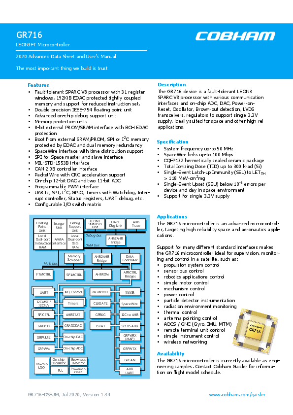
windows, 192KiB EDAC protected tightly coupled memory and support for reduced instruction set. � Double precision IEEE-754 floating point unit � Advanced on-chip debug support unit � Memory protection units � 8-bit external PROM/SRAM interface with BCH EDAC protection � Boot from external SRAM/PROM, SPI or I2C memory protected by EDAC and dual memory redundancy � SpaceWire interface with time distribution support � SPI for Space master and slave interface � MIL-STD-1553B interface � CAN 2.0B controller interface � PacketWire with CRC acceleration support � On-chip 12-bit DAC and two 11-bit ADC � Programmable PWM interface � UARTs, SPI, I2C, GPIO, Timers with Watchdog, Interrupt controller, Status registers, UART debug, etc. � Configurable I/O switch matrix
Description The GR716 device is a fault-tolerant LEON3 SPARC V8 processor with various communication interfaces and on-chip ADC, DAC, Power-onReset, Oscillator, Brown-out detection, LVDS transceivers, regulators to support single 3.3V supply, ideally suited for space and other high-rel applications.
Specification
� System frequency up-to 50 MHz
� SpaceWire links up-to 100 Mbps
� CQFP132 hermetically sealed ceramic package
� Total Ionizing Dose (TID) up to 300 krad (Si)
�
Single-Event Latch-up > 118 MeV-cm2mg
Immunity
(SEL)
to
LETTH
� Single-Event Upset (SEU) below 10-6 errors per
device and day in space environment
� Support for single 3.3V supply
Floating Point Unit
Integer Debug Unit Support Unit
Local
Local
Dual-port AMBA Dual-port
Instruction Interface Data
RAM
RAM
LEON3 Statistics
Unit Debug bus DMA bus
UART Dbg Link
AHB2AHB Bridge
AHB Trace
Main bus
Memory Scrubber
AHB2AHB Bridge
DMA Controller
FTMCTRL
SPIMCTRL
AHBROM
APBCTRL Bridges
UART
I2CMST / I2CSLV
SPICTRL
IRQ Control Timers
AHBSTAT
MEMPROT CLKGATE
GPREG
GRGPIO
GRADCDAC
LSTAT
GRPULSE
On-chip DAC
GRPWM
On-chip ADC
On-chip LDO
On-chip Oscillator
PLL
Brownout Detector Power-on
reset
1553B
SpaceWire
I2C to AHB
SPI to AHB GRPWRX
(MAP) GRPWTX
GRCAN AHB UART
Applications The GR716 microcontroller is an advanced microcontroller, targeting high reliability space and aeronautics applications.
Support for many different standard interfaces makes the GR716 microcontroller ideal for supervision, monitoring and control in a satellite, such as: � propulsion system control � sensor bus control � robotics applications control � simple motor control � mechanism control � power control � particle detector instrumentation � radiation environment monitoring � thermal control � antenna pointing control � AOCS / GNC (Gyro, IMU, MTM) � remote terminal unit control � simple instrument control � wireless networking
Availability The GR716 microcontroller is currently available as engineering samples. Contact Cobham Gaisler for information on flight model schedule.
GR716-DS-UM, Jul 2020, Version 1.34
www.cobham.com/gaisler
GR716
1
Introduction.............................................................................................................................. 9
1.1 Scope ....................................................................................................................................................... 9
1.2 Data sheet limitations .............................................................................................................................. 9
1.3 Updates and feedback.............................................................................................................................. 9
1.4 Software support...................................................................................................................................... 9
1.5 Development board ................................................................................................................................. 9
1.6 Reference documents .............................................................................................................................. 9
1.7 Document revision history .................................................................................................................... 10
1.8 Acronyms .............................................................................................................................................. 11
1.9 Definitions ............................................................................................................................................. 12
1.10 Register descriptions ............................................................................................................................. 13
2
Architecture............................................................................................................................ 14
2.1 Key features........................................................................................................................................... 15
2.2 Digital Architecture Overview .............................................................................................................. 18
2.3 Analog Architecture Overview.............................................................................................................. 26
2.4 Signal Overview .................................................................................................................................... 31
2.5 I/O switch matrix overview ................................................................................................................... 31
2.6 I/O switch default configurations for bootstraps ................................................................................... 34
2.7 I/O switch matrix options, considerations and limitations .................................................................... 37
2.8 I/O switch matrix pin validation script.................................................................................................. 38
2.9 I/O switch matrix scenario examples .................................................................................................... 41
2.10 Cores...................................................................................................................................................... 47
2.11 Memory map ......................................................................................................................................... 48
2.12 Atomic access........................................................................................................................................ 51
2.13 Interrupts ............................................................................................................................................... 53
3
Signals.................................................................................................................................... 55
3.1 Bootstrap signals ................................................................................................................................... 55
3.2 Configuration for flight ......................................................................................................................... 62
3.3 Complete signal list ............................................................................................................................... 63
4
Clocking ................................................................................................................................. 65
4.1 PLL Configuration and Status ............................................................................................................... 66
4.2 Clock Source and divisor ...................................................................................................................... 66
4.3 System clock.......................................................................................................................................... 67
4.4 SpaceWire clock .................................................................................................................................... 67
4.5 MIL-STD-1553B clock ......................................................................................................................... 67
4.6 PacketWire RX Clock ........................................................................................................................... 67
4.7 ADC Clock ............................................................................................................................................ 67
4.8 DAC Clock ............................................................................................................................................ 68
4.9 PWM Clock ........................................................................................................................................... 68
4.10 Clock gating unit ................................................................................................................................... 68
4.11 Debug AHB bus clocking...................................................................................................................... 68
4.12 Test mode clocking................................................................................................................................ 68
5
Reset....................................................................................................................................... 69
5.1 IO Reset ................................................................................................................................................. 69
6
Technical notes....................................................................................................................... 70
6.1 GRLIB AMBA plug&play scanning ..................................................................................................... 70
6.2 Software portability............................................................................................................................... 70
7
System Startup Status and General Configuration................................................................. 71
GR716-DS-UM, Jul 2020, Version 1.34
2
www.cobham.com/gaisler
GR716
7.1 Configuration Registers......................................................................................................................... 71 7.2 Boot Strap information register ............................................................................................................. 76 7.3 Special Configuration Registers ............................................................................................................ 77
8
Reset Generation and Brownout Detection............................................................................ 85
8.1 Overview ............................................................................................................................................... 85
8.2 Operation ............................................................................................................................................... 85
8.3 Registers ................................................................................................................................................ 86
9
Crystal (XO) Oscillator.......................................................................................................... 90
9.1 Overview ............................................................................................................................................... 90
9.2 Operation ............................................................................................................................................... 90
10 PLL......................................................................................................................................... 93
10.1 Overview ............................................................................................................................................... 93 10.2 Operation ............................................................................................................................................... 93 10.3 Registers ................................................................................................................................................ 94
11 Voltage and Current References........................................................................................... 100
11.1 Overview ............................................................................................................................................. 100 11.2 Operation ............................................................................................................................................. 100
12 Internal ADC, Pre-Amplifier and Analog MUX.................................................................. 101
12.1 Overview ............................................................................................................................................. 101 12.2 Operation ............................................................................................................................................. 102 12.3 Registers .............................................................................................................................................. 107
13 LDO ..................................................................................................................................... 112
13.1 Overview ............................................................................................................................................. 112 13.2 Operation ............................................................................................................................................. 112
14 Temperature Sensor.............................................................................................................. 113
14.1 Overview ............................................................................................................................................. 113 14.2 Operation ............................................................................................................................................. 113
15 Internal DAC........................................................................................................................ 114
15.1 Overview ............................................................................................................................................. 114 15.2 Operation ............................................................................................................................................. 115 15.3 Registers .............................................................................................................................................. 116
16 LEON3/FT - High-performance SPARC V8 32-bit Processor ............................................ 119
16.1 Overview ............................................................................................................................................. 119 16.2 LEON3 integer unit ............................................................................................................................. 120 16.3 Local instruction and data RAM ......................................................................................................... 128 16.4 Floating-point unit............................................................................................................................... 128 16.5 AMBA interface .................................................................................................................................. 129 16.6 Configuration registers ........................................................................................................................ 130 16.7 Software considerations ...................................................................................................................... 136
17 IEEE-754 Floating-Point Unit ............................................................................................. 137
17.1 Overview ............................................................................................................................................. 137 17.2 Functional Description ........................................................................................................................ 137
18 UART Serial Interface ......................................................................................................... 140
18.1 Overview ............................................................................................................................................. 141 18.2 Operation ............................................................................................................................................. 141 18.3 Baud-rate generation ........................................................................................................................... 142
GR716-DS-UM, Jul 2020, Version 1.34
3
www.cobham.com/gaisler
GR716
18.4 Loop back mode .................................................................................................................................. 143 18.5 FIFO debug mode................................................................................................................................ 143 18.6 Interrupt generation ............................................................................................................................. 143 18.7 Registers .............................................................................................................................................. 144
19 Hardware Debug Support Unit ............................................................................................ 147
19.1 Overview ............................................................................................................................................. 147 19.2 Operation ............................................................................................................................................. 147 19.3 AHB trace buffer ................................................................................................................................. 148 19.4 Instruction trace buffer ........................................................................................................................ 150 19.5 Using the DSU trace buffer ................................................................................................................. 151 19.6 DSU memory map............................................................................................................................... 151 19.7 DSU registers ...................................................................................................................................... 152
20 On-chip Dual-port Memory with EDAC Protection............................................................ 158
20.1 Overview ............................................................................................................................................. 158 20.2 Local Memory memory map and register ........................................................................................... 161
21 Fault Tolerant PROM/SRAM Memory Interface ................................................................ 165
21.1 Overview ............................................................................................................................................. 165 21.2 PROM access ...................................................................................................................................... 166 21.3 SRAM access ...................................................................................................................................... 168 21.4 Memory EDAC ................................................................................................................................... 168 21.5 Bus Ready signalling........................................................................................................................... 169 21.6 Access errors ....................................................................................................................................... 171 21.7 Registers .............................................................................................................................................. 172
22 Fault Tolerant NVRAM Memory Interface ......................................................................... 176
23 MIL-STD-1553B / AS15531 Interface ................................................................................ 177
23.1 Overview ............................................................................................................................................. 177 23.2 Electrical interface............................................................................................................................... 178 23.3 Operation ............................................................................................................................................. 178 23.4 Bus Controller Operation .................................................................................................................... 180 23.5 Remote Terminal Operation ................................................................................................................ 185 23.6 Bus Monitor Operation........................................................................................................................ 189 23.7 Registers .............................................................................................................................................. 190
24 ADC / DAC Interface .......................................................................................................... 202
24.1 Overview ............................................................................................................................................. 202 24.2 Operation ............................................................................................................................................. 204 24.3 Registers .............................................................................................................................................. 206
25 CAN 2.0 Controller.............................................................................................................. 211
25.1 Overview ............................................................................................................................................. 212 25.2 Interface............................................................................................................................................... 213 25.3 Protocol ............................................................................................................................................... 213 25.4 Status and monitoring.......................................................................................................................... 214 25.5 Transmission........................................................................................................................................ 214 25.6 Reception............................................................................................................................................. 217 25.7 Global reset and enable ....................................................................................................................... 220 25.8 Registers .............................................................................................................................................. 221 25.9 Memory mapping ................................................................................................................................ 230
26 Clock gating unit (Primary) ................................................................................................. 232
GR716-DS-UM, Jul 2020, Version 1.34
4
www.cobham.com/gaisler
GR716
26.1 Overview ............................................................................................................................................. 232 26.2 Operation ............................................................................................................................................. 232 26.3 Registers .............................................................................................................................................. 233
27 Clock gating unit (Secondary) ............................................................................................. 236
27.1 Overview ............................................................................................................................................. 236 27.2 Operation ............................................................................................................................................. 236 27.3 Registers .............................................................................................................................................. 237
28 DMA Controller with internal AHB/APB bridge ................................................................ 240
28.1 Overview ............................................................................................................................................. 240 28.2 Configuration....................................................................................................................................... 241 28.3 Operation ............................................................................................................................................. 250 28.4 AHB transfers...................................................................................................................................... 252 28.5 Interrupts ............................................................................................................................................. 252 28.6 Errors ................................................................................................................................................... 252 28.7 Internal Buffer Readout Interface........................................................................................................ 253 28.8 Registers .............................................................................................................................................. 253 28.9 DMA Transfer Example ...................................................................................................................... 259
29 General Purpose I/O Port ..................................................................................................... 263
29.1 Overview ............................................................................................................................................. 264 29.2 Operation ............................................................................................................................................. 264 29.3 Pulse command.................................................................................................................................... 264 29.4 Pulse sequencer ................................................................................................................................... 264 29.5 Pulse sampler...................................................................................................................................... 266 29.6 Registers .............................................................................................................................................. 266
30 Pulse Width Modulation Generator ..................................................................................... 277
30.1 Overview ............................................................................................................................................. 278 30.2 Operation ............................................................................................................................................. 278 30.3 Registers .............................................................................................................................................. 280
31 PacketWire Receiver............................................................................................................ 285
31.1 Overview ............................................................................................................................................. 285 31.2 PacketWire interface............................................................................................................................ 285 31.3 Operation ............................................................................................................................................. 286 31.4 Operation ............................................................................................................................................. 286 31.5 Registers .............................................................................................................................................. 288
32 PacketWire Transmitter........................................................................................................ 291
32.1 Overview ............................................................................................................................................. 291 32.2 PacketWire interface............................................................................................................................ 291 32.3 Operation ............................................................................................................................................. 292 32.4 Registers .............................................................................................................................................. 293
33 SpaceWire Interface and RMAP target ................................................................................ 296
33.1 Overview ............................................................................................................................................. 296 33.2 Operation ............................................................................................................................................. 297 33.3 Link interface ...................................................................................................................................... 298 33.4 Time-code distribution ........................................................................................................................ 301 33.5 Interrupt distribution............................................................................................................................ 301 33.6 Receiver DMA channels...................................................................................................................... 304 33.7 Transmitter DMA channels ................................................................................................................. 309
GR716-DS-UM, Jul 2020, Version 1.34
5
www.cobham.com/gaisler
GR716
33.8 33.9 33.10 33.11
RMAP.................................................................................................................................................. 312 AMBA interface .................................................................................................................................. 316 SpaceWire Plug-and-Play.................................................................................................................... 317 Registers .............................................................................................................................................. 323
34 SpaceWire - Time Distribution Protocol.............................................................................. 341
34.1 Overview ............................................................................................................................................. 341 34.2 Protocol ............................................................................................................................................... 341 34.3 Functionality........................................................................................................................................ 341 34.4 Data formats ........................................................................................................................................ 347 34.5 Registers .............................................................................................................................................. 348
35 General Purpose Timer Unit with Watchdog ....................................................................... 364
35.1 Overview ............................................................................................................................................. 364 35.2 Operation ............................................................................................................................................. 364 35.3 Registers .............................................................................................................................................. 366
36 General Purpose Timer Unit (Secondary)............................................................................ 370
36.1 Overview ............................................................................................................................................. 370 36.2 Operation ............................................................................................................................................. 370 36.3 Registers .............................................................................................................................................. 371
37 I2C to AHB bridge ............................................................................................................... 375
37.1 Overview ............................................................................................................................................. 375 37.2 Operation ............................................................................................................................................. 376 37.3 Registers .............................................................................................................................................. 380
38 I2C master ............................................................................................................................ 383
38.1 Overview ............................................................................................................................................. 383 38.2 Operation ............................................................................................................................................. 384 38.3 Registers .............................................................................................................................................. 387
39 I2C slave .............................................................................................................................. 390
39.1 Overview ............................................................................................................................................. 390 39.2 Operation ............................................................................................................................................. 391 39.3 Registers .............................................................................................................................................. 393
40 Interrupt Controller .............................................................................................................. 397
40.1 Overview ............................................................................................................................................. 397 40.2 Operation ............................................................................................................................................. 398 40.3 Registers .............................................................................................................................................. 402
41 LEON3 Statistics Unit ......................................................................................................... 414
41.1 Overview ............................................................................................................................................. 414 41.2 Using the LEON3 statistics unit .......................................................................................................... 416 41.3 Registers .............................................................................................................................................. 416
42 Memory Scrubber and Status Register ................................................................................ 419
42.1 Overview ............................................................................................................................................. 420 42.2 Operation ............................................................................................................................................. 420 42.3 Registers .............................................................................................................................................. 422
43 SPI to AHB bridge ............................................................................................................... 427
43.1 Overview ............................................................................................................................................. 427 43.2 Transmission protocol ......................................................................................................................... 428 43.3 System clock requirements and sampling ........................................................................................... 429
GR716-DS-UM, Jul 2020, Version 1.34
6
www.cobham.com/gaisler
GR716
43.4 SPI instructions.................................................................................................................................... 429 43.5 Registers .............................................................................................................................................. 431
44 SPI Controller ...................................................................................................................... 433
44.1 Overview ............................................................................................................................................. 433 44.2 Operation ............................................................................................................................................. 434 44.3 Registers .............................................................................................................................................. 437
45 SPI for Space Slave Controller ............................................................................................ 444
45.1 Overview ............................................................................................................................................. 444 45.2 Implementation of SPI protocols......................................................................................................... 445 45.3 Transmission........................................................................................................................................ 445 45.4 Operation ............................................................................................................................................. 446 45.5 SPI 2 Protocol Handler........................................................................................................................ 446 45.6 Message Header - Command Token.................................................................................................... 447 45.7 Redundancy ......................................................................................................................................... 453 45.8 Registers .............................................................................................................................................. 454
46 SPI Memory Controller........................................................................................................ 459
46.1 Overview ............................................................................................................................................. 460 46.2 Operation ............................................................................................................................................. 460 46.3 Registers .............................................................................................................................................. 463
47 AMBA Protection Unit ........................................................................................................ 466
47.1 Overview ............................................................................................................................................. 466 47.2 Operation ............................................................................................................................................. 467 47.3 Registers .............................................................................................................................................. 467 47.4 Example of configure and use the Memory protection ....................................................................... 483
48 Serial Debug and remote access Interface ........................................................................... 485
48.1 Overview ............................................................................................................................................. 486 48.2 Operation ............................................................................................................................................. 486 48.3 Registers .............................................................................................................................................. 487
49 AHB Status Registers .......................................................................................................... 489
49.1 Overview ............................................................................................................................................. 489 49.2 Operation ............................................................................................................................................. 489 49.3 Registers .............................................................................................................................................. 490
50 Trace buffer .......................................................................................................................... 492
50.1 Overview ............................................................................................................................................. 492 50.2 Operation ............................................................................................................................................. 493 50.3 Using the AHB trace buffer................................................................................................................. 494 50.4 Registers .............................................................................................................................................. 495
51 Boot ROM............................................................................................................................ 498
51.1 Overview ............................................................................................................................................. 498 51.2 ROM Architecture ............................................................................................................................... 499 51.3 Loader description ............................................................................................................................... 504 51.4 Standby description ............................................................................................................................. 504 51.5 State at handover to application software............................................................................................ 505 51.6 Boot source requirements.................................................................................................................... 506 51.7 Protection schemes .............................................................................................................................. 506
52 Electrical description ........................................................................................................... 509
52.1 Absolute maximum ratings ................................................................................................................. 509
GR716-DS-UM, Jul 2020, Version 1.34
7
www.cobham.com/gaisler
GR716
52.2 52.3 52.4 52.5 52.6 52.7 52.8 52.9 52.10 52.11
Recommended operating conditions ................................................................................................... 511 Power supplies characteristics............................................................................................................. 512 Input voltages, leakage currents and capacitances .............................................................................. 513 Output voltages, leakage currents and capacitances ........................................................................... 514 Simplified IO buffer schematics.......................................................................................................... 516 DAC Electrical Characteristics ........................................................................................................... 518 ADC Electrical Characteristics ........................................................................................................... 519 Reference Voltages and Currents Electrical Characteristics ............................................................... 522 Reset and Brownout-Detector Electrical Characteristics .................................................................... 522 AC characteristics................................................................................................................................ 524
53 Mechanical description ........................................................................................................ 538
53.1 Component and package ..................................................................................................................... 538 53.2 Pin assignment..................................................................................................................................... 538 53.3 Mechanical package drawings............................................................................................................. 542
54 Ordering information ........................................................................................................... 544
54.1 Silicon and mask information.............................................................................................................. 545
55 Errata.................................................................................................................................... 546
55.1 Overview ............................................................................................................................................. 546 55.2 Errata description ................................................................................................................................ 546
56 Planned Features .................................................................................................................. 550
56.1 Overview ............................................................................................................................................. 550 56.2 Feature description .............................................................................................................................. 550
GR716-DS-UM, Jul 2020, Version 1.34
8
www.cobham.com/gaisler
GR716
1 Introduction
1.1 Scope
This document is the advanced data sheet and user's manual for the GR716 LEON3FT microcontroller. The GR716 microcontroller has been developed in an activity initiated by the European Space Agency under ESTEC contract 40001117749/14/NL/AK.
1.2 Data sheet limitations
Note that this document is an advanced data sheet: � Advanced data sheet - Product in development � Preliminary data sheet - Shipping prototype � Data sheet - Shipping space-grade product
1.3 Updates and feedback
Updates are available at https://www.gaisler.com/gr716 Feedback can be sent to Cobham Gaisler AB support: support@gaisler.com For commercial questions please contact sales@gaisler.com
1.4 Software support
The GR716 LEON3FT microcontroller design is supported by standard toolchains provided by Cobham Gaisler. Toolchains can be downloaded from https://www.gaisler.com.
1.5 Development board
Development boards with GR716 device is available. Please see https://www.gaisler.com/gr716boards
1.6 Reference documents
[AMBA] [GRLIB] [GRIP] [SPARC] [LEON-REX] [GRMON3] [V8E]
[CCSDS] [SPW]
[RMAP]
AMBA Specification, Rev 2.0, ARM Limited
GRLIB IP Library User's Manual, Cobham Gaisler, www.cobham.com/gaisler
GRLIB IP Core User's Manual, Cobham Gaisler, www.cobham.com/gaisler
The SPARC Architecture Manual, Version 8, SPARC International Inc.
LEON-REX Instruction Set Extension, Cobham Gaisler
GRMON3 User's Manual, Cobham Gaisler
SPARC-V8 Supplement, SPARC-V8 Embedded (V8E) Architecture Specification, SPARC-V8E, Version 1.0, SPARC International Inc.
Time Code Formats, CCSDS 301.0-B-4, www.CCSDS.org
Space engineering: SpaceWire - Links, nodes, routers and networks, ECSS-E-ST-50-12C
Space engineering: SpaceWire - Remote memory access protocol, ECSS-E-ST-50-52C
GR716-DS-UM, Jul 2020, Version 1.34
9
www.cobham.com/gaisler
GR716
1.7 Document revision history
Change record information is provided in table 1.
Table 1. Change record
Version 1.29 1.30
1.31 1.32
1.33 1.34
Date May 2019 March 2020
April 2020 May 2020
Jun 2020 July 2020
Note First public release Updated reference documents in section 1.6 Crystal recommendations and examples added to section 9.2.3 and 9.2.5 Updated ordering section 54 Errata section 55.1 updated for XO and GRDMAC errata Ordering information section Errata section 55.1 workaround update for XO Errata section 55.1 added Errata for Lower ESD tolerance on supply pins Added note for analogue supply VDDA in section 52.2 Added note for Power On Reset release delay in section 52.10 Updated GR716 Crystal configuration examples Updated drawings in architecture section
GR716-DS-UM, Jul 2020, Version 1.34
10
www.cobham.com/gaisler
GR716
1.8 Acronyms
Table 2. Acronyms
Acronym AHB AMBA APB BCH CAN CPU DMA DSU EDAC FIFO FPU Gb
GB
GiB
I/O ISR JTAG kB
KiB
Mb, Mbit
MB, Mbyte
MiB
PROM RAM SEE SEL/SEU/ SET SPARC SW UART
Comment Advanced High-performance bus, part of [AMBA] Advanced Microcontroller Bus Architecture Advanced Peripheral Bus, part of [AMBA] Bose�Chaudhuri�Hocquenghem, class of error-correcting codes Controller Area Network, bus standard Central Processing Unit, used to refer to one LEON3FT processor core. Direct Memory Access Debug Support Unit Error Detection and Correction First-In-First-Out, refers to buffer type Floating Point Unit Gigabit, 109 bits Gigabyte, 109 bytes Gibibyte, gigabinary byte, 230 bytes, unit defined in IEEE 1541-200 Input/Output Interrupt Service Routine Joint Test Action Group (developer of IEEE Standard 1149.1-1990) Kilobyte, 103 bytes Kibibyte, 210 bytes, unit defined in IEEE 1541-2002 Megabit, 106 bits Megabyte, 106 bytes Mebibyte, 220 bytes, unit defined in IEEE 1541-2002 Programmable Read Only Memory Random Access Memory Single Event Effects Single Event Latchup/Upset/Transient
Scalable Processor ARChitecture Software Universal Asynchronous Receiver/Transmitter
GR716-DS-UM, Jul 2020, Version 1.34
11
www.cobham.com/gaisler
GR716
1.9 Definitions
This section and the following subsections define the typographic and naming conventions used throughout this document.
1.9.1 Bit numbering
The following conventions are used for bit numbering: � The most significant bit (MSb) of a data type has the leftmost position � The least significant bit of a data type has the rightmost position � Unless otherwise indicated, the MSb of a data type has the highest bit number and the LSb the
lowest bit number
1.9.2 Radix
The following conventions is used for writing numbers: � Binary numbers are indicated by the prefix "0b", e.g. 0b1010. � Hexadecimal numbers are indicated by the prefix "0x", e.g. 0xF00F � Unless a radix is explicitly declared, the number should be considered a decimal.
1.9.3 Data types
Byte (BYTE) Halfword (HWORD) Word (WORD)
8 bits of data 16 bits of data 32 bits of data
GR716-DS-UM, Jul 2020, Version 1.34
12
www.cobham.com/gaisler
GR716
1.10 Register descriptions
An example register, showing the register layout used throughout this document, can be seen in table 3. The values used for the reset value fields are described in table 4, and the values used for the field type fields are described in table 5. Fields that are named RESERVED, RES, or R are read-only fields. These fields can be written with zero or with the value read from the same register field.
Table 3. <Address> - <Register acronym> - <Register name>
31
24 23
16 15
87
0
EF3
EF2
EF1
EF0
<Reset value for EF3>
<Reset value for EF2>
<Reset value for EF1>
<Reset value for EF0>
<Field type for EF3>
<Field type for EF2>
<Field type for EF1>
<Field type for EF0>
31: 24 23: 16 15: 8 7: 0
Example field 3 (EF3) - <Field description> Example field 2 (EF2) - <Field description> Example field 1 (EF1) - <Field description> Example field 0 (EF0) - <Field description>
Table 4. Reset value definitions
Value 0 1 0xNN 0bNN NR *
-
Description Reset value 0. Reset value 1. Used for single-bit fields. Hexadecimal representation of reset value. Used for multi-bit fields. Binary representation of reset value. Used for multi-bit fields. Field not reset Special reset condition, described in textual description of the field. Used for example when reset value is taken from a pin. Don't care / Not applicable
Table 5. Field type definitions
Value r w rw rw* wc cas
Description Read-only. Writes have no effect. Write-only. Used for a writable field in a register where the field's read-value has no meaning. Readable and writable. Readable and writable. Special condition for write, described in textual description of field. Write-clear. Readable, and cleared when written with a 1 Readable, and writable through compare-and-swap. Only applies to SpaceWire Plug-and-Play registers.
GR716-DS-UM, Jul 2020, Version 1.34
13
www.cobham.com/gaisler
GR716
2 Architecture
5.11Kohm 4.7nF
C_3v3V C_1v8V
47nF 2.2uF
Ext Xtal 4Mhz � 25Mhz
SRAM Interface 1)
BandGap Ref
Temp Sensor
DMA Controller
VREF
LDO (Core)
System Power Supply
Core Voltage Sence
Brown Out
Detector
Power On Reset
Crystal Oscillator
PLL
Control &Status
Memory Protection
Scrub & ahbstat
Embeeded Boot ROM
WDT Logic
Reset Logic
Clock Logic
System Clock and Reset
AMBA System and peripheral bus
LDO (PLL)
Debug Interface
SPI Flash Interface
Internal SRAM Interface
LEON3FT SPARC V8
DSU
REX
FPU Trace
64kB D-ram
AMBA
128kB I-ram
SpaceWire with
TDP/RMAP Support
SPI Master -
SPI Slave
SPI For Space
2x
2x
2x
3x
SPI Master SPI Slave I2C Master I2C Slave
2x SPI Memory
7x UART
CAN 2.0
External ADC/DAC Interface
MIL-1553B PacketWire BC/RT/MT
SRAM Memory Controller
2xPWV
64x GPIO
2x 11-bit ADC
4x 12-bit DAC
GPIO
LVDS
Mixed Analog Digital GPIO
Figure 1. GR716 block diagram
The microcontroller is a single core LEON3FT SPARC V8 processor, with advanced interface protocols, that has been optimized for real-time systems and deterministic software execution. Features such as SPARC V8E Alternate Window Pointer, interrupt zero jitter latency, SPARC V8E multiply step instructions and the possibility to run software (including interrupt handlers) from local RAM are supported to increase the determinism and responsiveness in the system. The LEON-REX instruction set extension is also supported by the microcontroller and is further described in [LEON-REX].
The architecture is centered around multiple instances of the AMBA Advanced High-speed Bus (AHB), to which the LEON3FT processor and other high-bandwidth units are connected. Low bandwidth peripherals/functions are connected to the AMBA Advanced Peripheral Bus (APB) which is accessed through an AHB to APB bridge. The use of multiple processor buses also enables non-intrusive debugging and the possibility to have direct access to on-board memory without interrupting or involving the LEON3FT processor.
64 external CMOS pins and six LVDS transceivers are configurable from software via configuration registers. Pre-defined pin configurations are defined in the boot software and can be enabled by using pull-up/pull-down resistors on external pins during reset. Pre-defined configuration of external pins are useful in cases when the microcontroller should boot from external memories or remote controlled via SpaceWire, UART, SPI or I2C after reset. The program controlling the microcontroller needs to set appropriate direction and functionality on all pins after reset depending on the environment that the microcontroller is used in. On-chip LVDS transceivers for SpaceWire and SPI for Space and dedicated pins for external SPI boot ROM boot are available and can optionally be used.
The microcontroller has a high level of integrated analog functions. Analog function integrated onchip includes Analog to digital converters, Brown out detection, Crystal Oscillator, Digital to Analog Converters, Power-on and reset functionality and Linear Voltage Regulators for single 3.3V supply.
GR716-DS-UM, Jul 2020, Version 1.34
14
www.cobham.com/gaisler
GR716
2.1 Key features
� Core - Fault-tolerant SPARC V8 processor with 31 register windows and support for LEONREX. - Double precision IEEE-754 floating point unit. - Memory protection units with 8 zones and individual access control of APB peripherals for memory protection. - Advanced on-chip debug support unit with trace buffers and statistic unit for software profiling. - Single cycle instructions execution and data fetch from tightly coupled memory. - Deterministic instruction execution and interrupt latency. - Fast context switching (Partial write %PSR, AWP, Register file partitioning, interrupt mapping, MVT). - Single Vector Trap support. - Interrupt zero jitter delay.
� Memories - 192KiB EDAC protected tightly coupled memory with single cycle access from processor and ATOMIC bit operations. - Embedded ROM with boot loader for initializing and remote access. - Dedicated SPI memory interface with boot ROM capability. - I2C memory interface with boot ROM capability. - 8-bit SRAM/ROM (FTMCTRL) with support up to 16 MB ROM and 256 MB SRAM. - Support for package option with embedded SRAM/PROM (FTMCTRL). - Scrubber with programmable scrub rate for all embedded memories and external PROM/ SRAM and SPI memories.
� System - On-chip voltage regulators for single supply support. Capability to sense core voltage for trimming of the embedded voltage regulator for low power applications. - Power-on-reset, brownout detection and dual watchdogs for safe operation. External reset signal generation for reseting companion chips. - Crystal oscillator support. - PLL for System and SpaceWire clock generation. In-application programming of system clock and peripheral clocks. System and SpaceWire clocks switches glitch free. - Low power mode and individual clock gating of functions and peripherals. - Temperature and core voltage sensor. - External precision voltage reference for precision measurement. - Four programmable DMA controllers with up to 16 individual channels. DMA transfers can be triggered on events such as interrupts or bits/register changing value. - Timer units with seven 32-bit timers including watchdog. - Multiple bus structures for non-intrusive debug, DMA transfers and memory scrubbers. - Atomic access support for all APB registers (AND, OR, XOR, Set&Clear).
GR716-DS-UM, Jul 2020, Version 1.34
15
www.cobham.com/gaisler
GR716
- Support for NVRAM (SRAM and/or PROM) embedded in package. Support for software boot and execution from embedded RAM for future package options.
- Peripheral access control. - Embedded trace and statistics unit for profiling of the system. � Peripherals - SpaceWire with support for RMAP and Time Distribution Protocol. - Redundant MIL-STD-1553B BRM (BC/RT/BM) interface. - Two CAN 2.0B bus controllers. - Six UART ports, with 16-byte FIFO. - Two SPI master/slave serial ports. - SPI4SPACE - hardware support for SPI protocol 0,1 and 2 in HW for SPI for SPI4SPACE. - Two I2C master/slave serial ports. - PacketWire interface. - PWM with up to 16 channels. PWM clock support up to 200 MHz. - Up to 64 general purpose input and outputs (GPIO) with external interrupt capability,
pulse generation and sampling. - Four single ended Digital to Analog Converters (DAC), 12-bit at 3MS/s. - Four differential or eight single ended Analog to Digital Converters (ADC) 11-bit at
200KS/s with programmable pre-amplifier and support for oversampling. Dual sample and hold circuit integrated for simultaneously sampling. - External ADC and DAC support up to 16-bit at 1MS/s. � I/O - Configurable I/O selection matrix with support for mixed signals, internal pull-up/pulldown resistors. - LVDS transceivers for SpaceWire or SPI4SPACE. - Dedicated SPI boot ROM support for configuration. � Supply - Single 3.3V�0.3V supply or separate Core Voltage 1.8V�0.18V, I/O voltage 3.3V�0.3V. � Radiation tolerance - Technology: 180 nm process, UMC Taiwan - Library: DARE+ Library version 5.5, IMEC - TID: up to 300 Krad(Si) - SEL: > 118 MeV-cm2/mg - SEU: Proven tolerance with hardened flip-flops and error corrections on all on-chip and external memories � Package - 132-lead CQFP, 0.635 mm pitch, 24mm x 24mm, hermetically sealed with flat pins and insulating lead-frame for customer trim and form. � Software - Supported by standard tools-chains and debug tools provided by Cobham Gaisler. Toolchains, simulators and debug software is available at https://www.gaisler.com.
GR716-DS-UM, Jul 2020, Version 1.34
16
www.cobham.com/gaisler
GR716
� Boot ROM and boot options - Remote boot directly via SpaceWire, UART, SPI or I2C. - Direct software execution from onchip RAM, external SRAM, PROM or SPI memory. - Direct software execution from in package embedded memory. - Application Software Container (ASW) for boot software integrity check. - Boot via ASW from external SRAM, PROM, SPI memory or I2C memory. - Boot from redundant memory. - Fast boot option.
� System configuration - Reset and boot status. - Individual reset and clock control for digital and analog peripherals. - Remote reset and boot control. - Clock source and divide control for the system, SpaceWire, SPI4S, ADC, DAC, 1553 and PWM clock domain. - Support for external system reset. - Support for external clock source for the system, SpaceWire, SPI4S, 1553 and PWM. - Automatic oscillator shutdown if oscillator not used. - Individual programmable brown-out levels. - Protection for erroneous I/O configuration during power-up and power-down. - Programmable LDO output level for low power mode.
GR716-DS-UM, Jul 2020, Version 1.34
17
www.cobham.com/gaisler
GR716
2.2 Digital Architecture Overview
The system is built around three 32-bit AMBA AHB buses; one 32-bit Main AHB bus, one 32-bit DMA AHB buses and one 32-bit Debug AHB bus. The main bus connects the LEON3FT core with all other peripheral cores in the design as well as the external memory controllers. Several peripherals are connected through AMBA AHB/APB bridges where one of the bridges is integrated with the DMA controller.
The debug AMBA AHB bus connects a UART serial debug communications link to the debug support unit and also to the rest of the system through an AMBA AHB bridge.
Debug Control
RS232
1553 A/B
CAN
SPI
SPI-ForI2C PacketWire SpaceWire Space
Embeeded Boot ROM
FPU Mul REX
LEON3FT SPARC V8
Trace AMBA
64kB D-ram
128kB I-ram
Main AMBA AHB
Bridge
Bridge
Bridge
Bridge
SPI Memory Controller
Memory Controller
NVRAM Controller
Scrub & ahbstat
Memory Prot
Bridge
Debug Unit (DSU)
TRACE Unit
Serial Debug
Link
Mil-1553B BC/RT/MT
DBG AMBA
Bridge
AHBSTAT
CAN 2.0
DMA AMBA AHB AMBA APB 0 AMBA APB 1 AMBA APB 2 AMBA APB 3
IrqCtrl & Timers
I2C
GPIO
SPI2AHB
PacketWire
SPI4S
I2C2AHB
SpaceWire Router RMAP
Ext ADC
Config & Status
Bridge
SpacWire TDP
PLL
POR BO LDO
AHBUART
Onchip ADCDAC
SPI
PWM
UART
DMA Controller
Reset / Clock
SPI Memory
Ext PROM/SRAM
Memory
NVRAM
RS232 External Onchip
I2C
Sync ADC &
DAC
SPI
I/O Port PWM External RS232 Status
ADC &
and
DAC
Control
Figure 2. Simplified architecture and functional block diagram of the microcontroller
Reset / Clock Watchdog
2.2.1 Processor core and memory subsystem
The microcontroller implements a LEON3FT 32-bit processor core conforming to the IEEE-1754 (SPARC V8) architecture. The microcontroller is designed for embedded applications, combining high performance with low complexity and low power consumption. The LEON3FT core has the following main features: 7-stage pipeline with Harvard architecture, hardware multiplier and divider and on-chip debug support. The LEON3FT processor is enhanced with fault tolerance against SEU errors. The fault tolerance is focused on the protection of the on-chip RAM, processor register file and protection of external memory interfaces.
The LEON3FT integer pipeline is implemented with 31 register windows, SEU protection of register file with zero impact on software timing, and hardware multiply and divide units. The multiplier is a 16x16 hardware multiplier that is iterated four times. Floating-point operations are supported by integration of a hardware floating-point unit (GRFPU-lite).
Memory protection units are located on the AMBA system bus and on AMBA DMA bus. Each protection unit monitors access on the AHB bus. When an access is made to a protected area then the protection unit will assert a signal to the memory controller that will annul the operation and respond to the AMBA access with an AMBA ERROR response. Four areas can be protected on the system bus and four areas can be protected on the DMA bus.
Exclusive write permission can be enforced for individual APB peripherals to protect interfaces from erroneous writes during normal operations.
GR716-DS-UM, Jul 2020, Version 1.34
18
www.cobham.com/gaisler
GR716
To protect tightly coupled instruction and data memory directly connected to the processor core from software the LEON3FT hardware watchpoints (located within the processor integer unit) can function as memory protection registers for both the instruction and data RAM.
Several features are supported in the architecture in order to enhance it for embedded microcontroller applications:
� Support for SPARC V8E write partial %psr
� Support for SPARC V8E Alternative Window Pointer
� Support of the SPARC V8E Multiply step instructions
The microcontroller program execution is deterministic due to the microcontroller being cache-less, and AMBA accesses made by the processor being unaffected by other AMBA masters in the microcontroller. The processor uses separate EDAC protected instruction and data memories with fixed latencies. The instruction memory latency is 1 system clock and the delay for the data memory is 1 system clock. The local instruction and data memory in the system have the same latency and behaviour in the corrected as in the uncorrected case. This also applies to the CPU, so dynamic SEU handling schemes such as the LEON3FT pipeline restart on error options is not be used.
The microcontroller has 64 KiB of shared data RAM and 128 KiB of tightly coupled instruction memory connected to the processor. The tightly coupled instruction and data RAM can be accessed via the AMBA buses. This AMBA access can be used to upload new software into the instruction memory or read/write data to/from any AMBA master in the system. The access to the data memory will not affect or delay any access made by the processor on the AMBA bus.
The processor or any AMBA master can access the external PROM/SRAM or SPI memory controller for program execution or reading/writing data. The external SRAM memory can be protected by the scrubber located on the main system bus. The scrubber connected to the main system bus will block access for the processor to the external memories during scrub execution. The scrub rate can be configured and should be set to an acceptable rate for the mission. The scrubber access will not block the AMBA bus since masters and slaves on the main system bus support split transactions.
GR716-DS-UM, Jul 2020, Version 1.34
19
www.cobham.com/gaisler
GR716
2.2.2 DMA controller
The microcontroller has four parallel DMA controllers. The GRDMAC core provides a flexible direct memory access controller. The DMA controller can perform burst transfers of data between AHB and APB peripherals at aligned or unaligned memory addresses. The GRDMAC core has multiple AHB master interfaces for access to AHB peripheral bus and direct access to all APB slaves. The GRDMAC is able to perform programmable sequences of data transfers between any slaves in AMBA address space. The IP core is able to transfer data between peripherals and memory and between memory areas. If the accessed memory is internal or external does not matter, as long as the memory is mapped into AMBA address space reachable from the AHB bus where the DMA controller is mapped.
The DMA controller configuration registers are accessible through an APB interface. Each DMA controller can be flexibly configured by means of two descriptor chains residing in main memory: a Memory to Buffer (M2B) chain and a Buffer to Memory (B2M) chain. Each chain is composed of a linked list of descriptors, where each descriptor specifies an AHB address and the size of the data to read/write, supporting a scatter/gather behavior.
Once enabled, the DMA controller will proceed in reading the descriptor chains, then reading memory mapped addresses specified by the M2B chain and filling its internal buffer. It will then write the content of the buffer back to memory-mapped addresses by elaborating the B2M descriptor chain.
The DMA controller supports a simplified mode of operation, with only one channel. In this mode of operation only one descriptor is present for each of the M2B and B2M chains. These two descriptors are written directly in the core's register via APB.
The DMA controller will offload the CPU and provide DMA capabilities to IP cores in the microcontroller design that do not have an internal DMA engine. The DMA controller can be programmed to initiate DMA transfers on events, such as interrupts, to the GRDMAC core to achieve timely readouts of values. An example of use can be found the detailed description of the DMA controller in section 28.
2.2.3 Interrupt handling
The microcontroller supports interrupt time stamping and interrupt handling mechanism to ensure that a fixed number of clock cycles occurs between the assertion of an interrupt and the processor's jump to the trap table. Depending on the software application, several types of time stamping can be of interest:
� Timestamp when interrupt line is raised from peripheral IP core. This time is of particular importance when time needs to be synchronized with an external event.
� Timestamp when processor acknowledges the interrupt. This stamp is primarily of interest in system characterization where users may want to measure the time it takes for the processor to divert execution flow to the interrupt service routine after the processor has discovered the pending interrupt.
� Timestamp when software enters ISR. This timestamp is typically taken by software by reading a timer register when the ISR is entered.
Interrupt time stamping is controlled via the Interrupt Timestamp Control register(s) described in section 40. Each Interrupt Timestamp Control register contains a field (TSTAMP) that contains the number of timestamp register sets that the core implements. A timestamp register sets consist of one Interrupt Timestamp Counter register, one Interrupt Timestamp Control register, one Interrupt Assertion Timestamp register and one Interrupt Acknowledge Timestamp register.
Software enables time stamping for a specific interrupt via an Interrupt Timestamp Control Register. When the selected interrupt line is asserted, software will save the current value of the interrupt timestamp counter into the Interrupt Assertion Timestamp register. When the processor acknowledges the interrupt, the Interrupt Timestamp Control register will be set and the current value of the timestamp
GR716-DS-UM, Jul 2020, Version 1.34
20
www.cobham.com/gaisler
GR716
counter will be saved in the Interrupt Acknowledge Timestamp Register. The difference between the Interrupt Assertion timestamp and the Interrupt Acknowledge timestamp is the number of system clock cycles that was required for the processor to react to the interrupt and divert execution to the trap handler.
2.2.4 Reset and software boot
The reset default behavior for all included cores, except the LEON3FT processor, is to enter an idle state upon reset. The internal reset signal will be asserted as a result of power-on. In the idle state the cores do not initiate any transactions nor keep any output signals in an idle state. This is of particular concern for bidirectional signals to prevent contention.
The LEON3FT processor will normally start executing from a predefined start address 0x0000000 at reset. The start of execution can be prevented by assertion of an external break signal. If the break signal is asserted then the processor will enter power-down mode after reset. This will allow software upload from an external entity that can then start the processor at a dynamically specified address, by writing to the interrupt controller's register interface. Processor can optionally be forced via bootstraps to be forced to start from external PROM, SRAM, MRAM, SPI or I2C memory. This mode could be used if the application requires separate boot code than the one existing in the LEON3FT microcontroller boot ROM. Boot addresses for external PROM and SPI memory are defined in section 2.11.
A boot ROM application is placed at address 0x00000000 and is normally executed after reset. The boot application supports system functions controllability via external bootstrap registers. The application always starts executing after reset and checking the value of external bootstrap signals. Based on these signals the processor performs tasks such as load software to internal RAM from an external memory device, enable remote access via SpaceWire, SPI, UART or I2C. See section 3.1 for more information about bootstrap options for the boot ROM.
In the case of boot from I2C, the boot ROM application will copy the content of the I2C into the onboard memory and start to execute the software setup by application.
A protocol to guard against the system trying to boot using a corrupt boot image is implemented using a protected image format containing an image header, boot code, data checksum and header checksum, see section 51. Extra protection can be enabled via bootstraps by reading identical images from redundant memories but needs to be configured before booting via an external boot strap.
Self-test and diagnostic test of the CPU and internal RAMs can be enabled via bootstraps. The internal ROM will check for Stuck-At and Transition errors in local instruction and data ram. Stuck-At or Transition error(s) will result an error reported in the boot report, see 51.2.5.
2.2.5 Direct boot from external memory
Custom boot options are supported via bootstrap options to bypass the internal boot ROM code. The LEON3FT microcontroller can be configured to boot directly from external ROM, external SRAM, external SPI Memory or internal NVRAM in package (GR716 with internal NVRAM is currently not available).
2.2.6 Atomic access
The microcontroller supports atomic bit and bit field access for all APB peripherals and in internal data memory when accessed from the LEON3FT processor. The atomic access is supported via address mirrors of the peripheral and local data ram. The microcontroller supports the following atomic operations:
� Configuration register will 'or' data written from processor with contents of control register
� Configuration register will 'and' data written from processor with contents of control register
� Configuration register will 'xor' data written from processor with contents of control register
GR716-DS-UM, Jul 2020, Version 1.34
21
www.cobham.com/gaisler
GR716
� Configuration register will set and cleared using a double store from the processor written from the processor.
The actual bit field operation is performed in the APB bridge and in the local on-chip data RAM and will have no impact on the instruction execution or delay of data fetch. Atomic accesses are further described in section 2.12.
2.2.7 Remote access and control
The microcontroller can be accessed and controlled by an external control unit via SpaceWire (RMAP), UART, SPI or I2C without using processor support. Full access, except for debug features on the debug AMBA bus, will be granted to SpaceWire, UART, SPI or I2C if enabled at startup via bootstraps after reset:
� SpaceWire: Remote Memory Access Protocol (RMAP) provides full remote access to the entire AMBA address space of the microcontroller. See section for GRSPW2 for more information
� UART: Support for reading and writing to register via special protocol over UART provides full remote access to the entire AMBA address space of the microcontroller. See section for AHBUART for more information
� SPI: Support for reading and writing to register via special protocol over SPI provides full remote access to the entire AMBA address space of the microcontroller. See section for SPI2AHB for more information
� I2C: Support for reading and writing to register via special protocol over I2C provides full remote access to the entire AMBA address space of the microcontroller. See section for I2C2AHB for more information
All the communication interfaces above can be implemented to be functional directly after the microcontroller leaves reset, no initialisation from the processor is required. The communication links can also be disabled by the processor, a feature that can be required for safety.
When debugging the microcontroller, the DSU is used to load software and initiate the program counter. In the case when new software is remotely updated via SpaceWire, UART, SPI or I2C, a special feature in the interrupt handler is implemented to restart the system and to start execution of new software. For more information see section 40.2.7 to 40.2.9.
2.2.8 Pin sharing
A I/O switch matrix allows most of the GR716 microcontroller pins functionality to be configurable and to be shared between several peripherals. The I/O switch matrix provides a flexible solution where enabling one core changes the I/O switch matrix so that the current core gets connected to I/O pads.
The microcontroller comprises on-chip ADC/DAC. The on-chip ADC/DAC requires special mixed digital and analog I/Os. The mixed digital and analog I/O is controlled via configuration registers and needs to be set to analog mode when an ADC or DAC is going to be used.
SPI4SPACE supports on-chip LVDS transceivers and CMOS I/Os. The redundant SPI4SPACE channel can be accessed via CMOS pins and the primary SPI4SPACE channel is accessed via on-chip LVDS.
2.2.9 Integrated ADC and DAC
The ADC digital control logic supports functions to control the on-chip ADC and to offload the processor. Support for automatic oversampling on all channels, sample sequencer and digital level comparators are examples of features integrated to offload the processor. The integrated DMA controller can also be used to off-load the processor by automatic transfers of sample values to/from the integrated data and ADC/DAC.
GR716-DS-UM, Jul 2020, Version 1.34
22
www.cobham.com/gaisler
GR716
2.2.10 Debug and statistics
An external debug host can access the microcontroller Debug Support Unit (DSU) via UART (RS232). The DSU can be used to access instruction trace buffers and registers of the LEON3FT processor. The DSU has also support for tracing AHB accesses that can be used for performance monitoring. For more information about the functionality see section 19. Since the DSU is connected to an AMBA AHB bus and is accessed via debug communication links also connected to AMBA AHB, all debug accesses will generate traffic over AMBA AHB. In order for the debugging to be completely non-intrusive this debug traffic is separated from the non-debug AHB traffic.
The microcontroller includes a LEON3 statistics unit that allows the debugger to count a wide range of events without interrupting or controlling execution. See section 41 for more information about the LEON3 statistics unit.
The GR716 microcontroller have one dedicated Serial Debug interface. The Serial Debug unit is directly connected to the AMBA debug bus. The Serial Debug unit have a unique AMBA address described in chapter 2.11.
The debug interface is intended to be used during software development and have direct access to the internal state of the processor and trace buffers. This interface can be disabled during mission via external pin configuration i.e. tie DSU_EN to low.
The Serial Debug interface unit is fully described in section 48
2.2.11 AMBA Error detection
The microcontroller includes status registers to store information about AMBA AHB accesses triggering an error response on the Main and DMA AMBA bus. Error response on the AMBA main bus is stored in either the memory scrubber unit or AHB Status unit 2. Error response triggered on the DMA bus is stored in the AHB Status unit 1.
The Main AMBA bus can be configured to fetch all AMBA error responses in the memory scrubber, see chapter 7.3.3. The system default configuration is to only fetch AMBA errors from the external memory controllers in the memory scrubber. All other AMBA error responses on the Main bus will be fetched in the AHB Status unit 2.
GR716-DS-UM, Jul 2020, Version 1.34
23
www.cobham.com/gaisler
GR716
2.2.12 Internal communication
Triggers, events and synchronization signals that require immediate response are distributed outside the internal AMBA bus structure. This section explains the different connections next to the internal AMBA structure. Signal connections are visually shown in figure 3 and described in table 6 in this section.
Debug Control
RS232
1553 A/B
CAN
SPI
SPI-ForI2C PacketWire SpaceWire Space
Embeeded Boot ROM
FPU Mul REX
Interrupt (Part of AMBA Bus Structure)
LEON3FT SPARC V8
Trace AMBA
64kB D-ram
128kB I-ram
Debug Unit (DSU)
TRACE
Interrupt, Power-Down,
Restart
TRACE Unit
EDAC Errors
Serial Debug
Link
Mil-1553B BC/RT/MT
AHBSTAT
Memory Protection
SPI2AHB
PacketWire
SPI4S
CAN 2.0
I2C2AHB
1553 Reset Request
SpaceWire Router RMAP
TDP
SpacWire TDP
SPI Memory Controller
Memory Controller
EDAC Errors Scrubber
NVRAM Controller
Scrub & ahbstat
Memory Prot
IrqCtrl & Timers
PWM
I2C
Memory Protection
AHBUART
Onchip ADCDAC
WatchDog
GPIO
Ext ADC
Config & Status
UART
SPI
PWM
DMA Controller
PLL
POR BO LDO
Reset / Clock
SPI Memory
Ext PROM/SRAM
Memory
NVRAM
RS232 External Onchip
I2C
Sync ADC &
DAC
SPI
I/O Port PWM External RS232 Status
ADC &
and
DAC
Control
Figure 3. Internal communication paths outside AMBA bus structure
Reset / Clock Watchdog
Table 6. Internal communication paths outside the AMBA bus structure
Connecting functional Internal bus name blocks
EDAC Error
AMBA status, local instruction memory and local data memory
EDAC Error Scrub- AMBA status functionality
ber
in scrubber, external mem-
ory controller and NVRAM
controller
Interrupt Bus
All blocks connected to the internal AMBA structure
Memory protection
Protection unit, external memory controller, NVRAM controller, local instruction memory and local data memory
Description
Connection for monitoring of correctable errors signaled from the internal data and instruction memory.
Connection for monitoring of correctable errors signaled from the memory controller and NVRAM controller.
Connection for distributing events from/to all peripherals and digital functionality. The internal interrupt bus distributes all 64 unique interrupts IDs in table 29. The interrupt bus is used to program event driven functions e.g. the DMA channel 0 to respond to a specific Interrupt ID in table 29.
Connection for blocking write access to protected areas. Protection unit grants or denies the ongoing AMBA access via the memory protection bus.
GR716-DS-UM, Jul 2020, Version 1.34
24
www.cobham.com/gaisler
GR716
Table 6. Internal communication paths outside the AMBA bus structure
Internal bus name Processor Interrupt, Power Down and Restart
Watch Dog
1553 Reset Request TDP DSU PWM
L3STAT
TRACE
Connecting functional blocks LEON3FT, Interrupt controller and Primary Clock gating unit.
Timer unit 0 and reset request logic
MIL-1553 peripheral interfaces and reset request logic MIL-1553B and SpaceWire
DSU and LEON3FT PWM, GPIO, DAC and ADC
To LEON3 Statistical Unit
From AMBA infrastructure to Trace buffer
Description
The interrupts generated on the interrupt bus are all forwarded to the interrupt controller. The interrupt controller prioritizes, masks and propagates the interrupt with the highest priority to the processor. This bus is also used for request for Power-Down of the processor and restart of the processor. Power down request from the processor is described in section 16.2.16 and reboot is described in section 40.2.7.
Watch dog timer unit drives a watchdog signal on this bus to request restart of the system. Watch dog functionality is described in section 35. User can override reset request with control register described in section 7.3.
MIL-1553B codec request for reset of MIL1553B interface support.
Internal bus for communication between the SpaceWire Time Distribution Protocol core and the SpaceWire interface or the MIL-1553B interface. For more information see section 34.
Debug interface for direct access and control of the LEON3FT processor from debug interface.
PWM synchronization tick outputs. Ticks or events can be programmed individually for each PWM to be generated at PWM compare points, PWM period match, or not generated at all. PWM ticks are distributed in the system to synchronize events to the PWM output.
Connection for counting events in the system defined in table 558 under section "Implementation specific events" and in section "Events generated from REQ/GNT signals". Bus is only passively listening.
Main and DMA AMBA buses are routed to the trace buffer. Trace buffer is passively listening to signals.
GR716-DS-UM, Jul 2020, Version 1.34
25
www.cobham.com/gaisler
GR716
2.3 Analog Architecture Overview
The analog/mixed and power-supply IP blocks are presented here. In figure 4, a simplified block diagram shows these blocks and their analog and power interconnections in the GR716 microcontroller.
5.11Kohm 4.7nF
C_3v3V C_1v8V
47nF 2.2uF
Ext Xtal 4Mhz � 25Mhz
SRAM Interface 1)
BandGap Ref
Temp Sensor
DMA Controller
VREF
LDO (Core)
System Power Supply
Core Voltage Sence
Brown Out
Detector
Power On Reset
Crystal Oscillator
PLL
Control &Status
Memory Protection
Scrub & ahbstat
Embeeded Boot ROM
WDT Logic
Reset Logic
Clock Logic
System Clock and Reset
AMBA System and peripheral bus
LDO (PLL)
Debug Interface
SPI Flash Interface
Internal SRAM Interface
LEON3FT SPARC V8
DSU
REX
FPU Trace
64kB D-ram
AMBA
128kB I-ram
SpaceWire with
TDP/RMAP Support
SPI Master -
SPI Slave
SPI For Space
2x
2x
2x
3x
SPI Master SPI Slave I2C Master I2C Slave
2x SPI Memory
7x UART
CAN 2.0
External ADC/DAC Interface
MIL-1553B PacketWire BC/RT/MT
SRAM Memory Controller
2xPWV
64x GPIO
2x 11-bit ADC
4x 12-bit DAC
GPIO
LVDS
Mixed Analog Digital GPIO
Figure 4. Simplified block diagram of the analog/mixed and power-supply IPs in the GR716 microcontroller.
Generally, note that when the XO-oscillator and PLL are used to generate the GR716 microcontroller clocks, these two blocks must be correctly connected and configured to obtain correct digital functionality of the GR716 microcontroller. Moreover, to obtain correct analog functionality of the GR716 microcontroller, the voltage and current references, set by Vref and Rref, must be correctly connected and configured, since they provide the GR716 microcontroller with the internal references and bias currents required by several other IPs in Figure 4.
2.3.1 Reset and Brownout-detector
The RESET and Brownout-detector blocks supervise the supply voltages as shown in Figure 4. The RESET block provides reset of the internal GR716 microcontroller logic. The internal reset signal, IntRST_N, is available externally as a 3.3V CMOS output, RESET_OUT_N. The IntRST_N and RESET_OUT_N signals are low when VDD_CORE is too low. There is also a reset release delay at power up, starting to count when VDD_CORE goes above its reset threshold level. The Brownout detectors are intended to be used as pre-warnings to the GR716 microcontroller that some supply voltage(s) has started to go down, so the CPU can perform a well-controlled system shutdown before any reset detectors are activated. The Brownout detectors are implemented as one detector block on each supply to be supervised, and each of them has a programmable threshold level that can be set individually. Each Brownout-detector output signal can be programmed by an interrupt mask bit to generate an interrupt, and typically, the interrupt routine can be used to shut down the system in a controlled way.
GR716-DS-UM, Jul 2020, Version 1.34
26
www.cobham.com/gaisler
GR716
2.3.2 XO oscillator
The oscillator (XO) is supplied by the LEON3FT microcontroller core voltage, VDD_CORE (1.8V). The oscillator output is a 3.3V CMOS output and is available on an external pin.
2.3.3 PLL
The PLL is supplied by 1.8V from an internal LDO, which should have an external decoupling capacitor on the PLL supply pin (1.8V). This supply pin shall be left open, with exception of this decoupling capacitor. The PLL provides several internal clock outputs, typically used as clock for the SpaceWire interface, etc. The PLL reference-clock input is a 3.3V CMOS input, to which the XOoscillator clock output can be directly connected, or any other clock signal generated on PCB fulfilling the electrical specification of this input. The PLL reference-clock input is allowed to be asynchronous to any other clocks in the GR716 microcontroller.
2.3.4 Voltage reference
The reference blocks are supplied by VDDA_REF. This supply needs to have the best voltage integrity on the chip. Therefore, no fast load-current steps are present in any of the on-chip blocks using this supply. It is essential that especially this supply has good PCB decoupling/filtering (across VDDA_REF and VSSA_REF) in order to not feed external disturbances from PCB supplies into this supply. The analog internal references are generated in two steps. First, a reference voltage is generated by an on-chip band-gap reference, which should have an external decoupling capacitor on the VREF pin. Alternatively, the on-chip reference block can be turned off; then, an external reference voltage must be applied to this pin (including the right decoupling capacitance needed in that voltagereference implementation). Second, this reference voltage is buffered and put out on the VREFBUF pin. This reference voltage is also used by an internal current generator, which puts this voltage across an external reference resistor, RREF on PCB, to generate a precision reference current. Since this reference current is used to generate both the current reference to each DAC and the internal bias currents required by several other on-chip blocks, RREF can not be chosen arbitrarily to get any desired DAC full-scale value; it shall be 5.11kohm (or 4.64kohm + 464ohm).
GR716-DS-UM, Jul 2020, Version 1.34
27
www.cobham.com/gaisler
GR716
2.3.5 On-chip ADC
There are two independent ADC blocks. Each ADC is a 11bit/200kSps SAR converter, and has an analog MUX in-front of it, which means that one MUX channel at a time can be measured.
VREFBUF GPIO[37]
Analog Out
Digital Input Digital Output Analog In/Out
VREF
On-Chip analogue routing
Enable Output (Access from
Processor)
AMBA On-chip System
Bus
GPIO[38] GPIO[39] GPIO[40] GPIO[41] GPIO[42] GPIO[43]
Mixed GPIO
Mixed GPIO
Digital Input Digital Output Analog In/Out
Digital Input Digital Output Analog In/Out
Digital Input Digital Output Analog In/Out
Digital Input Digital Output Analog In/Out
Digital Input Digital Output Analog In/Out
Digital Input Digital Output Analog In/Out
ADC 1
AMAPMP
Core Voltage Sence
MUX
ACFG.AI PACFG.AG
ADC 0
AMAPMP
ACFG.AI
Temp Sensor
MUX
ACFG.AI PACFG.AG
ACFG.AI
LDO
Trim Input (Access from
Processor)
11-bit ADC
ACFG.AE
Enable Sensor (Access from
Processor)
ADC Data
Configuration and trigger event
On-Chip ADC
Controller 0-3
11-bit ADC
ACFG.AE
ADC DATA
Configuration and trigger event
On-Chip ADC
Controller 4-7
GPIO[44]
Digital Input Digital Output Analog In/Out
Figure 5. Shared external connections for ADC0 and ADC1
Each ADC can be programmed to single-ended 11-bit range (0 - VREF) using one input pin per channel, or to differential-input 11-bit range (-VREF to VREF) using two input pins per channel. Inbetween the ADC and MUX, there is a fully differential pre-amplifier, which has three programmable gain-settings (x1, x2, x4). It is to be used together with the fully-differential ADC setting. The input impedance is in the order of 5-20 kohm (TBC) when the pre-amplifier is in use. The pre-amplifier can be by-passed by programming; then, the DC input impedance is high (dominated by MUX leakage currents). These three blocks are supplied by VDDA_ADC and VSSA_ADC. This supply is not the analog reference for ADC measurements; however, it must still be really well decoupled/filtered at high frequencies (>~1MHz) to not degrade the ADC performance.
The ADC supply ground, VSSA_ADC, must always be hardwired to the same PCB ground point as VSSA_REF, directly outside the Microcontroller package. Otherwise, the ADC measurement range will be incorrect, since the reference voltage from the on-chip band-gap reference is a single-ended signal referred to VSSA_REF, whereas the reference input of the on-chip ADC is a single-ended input referred to VSSA_ADC.
GR716-DS-UM, Jul 2020, Version 1.34
28
www.cobham.com/gaisler
GR716
2.3.6 On-chip DAC There are four independent 12bit/3MSps DAC blocks.
GPIO[45] GPIO[46] GPIO[47] GPIO[48]
Mixed GPIO
Mixed GPIO
Digital Input Digital Output Analog In/Out
Digital Input Digital Output Analog In/Out
Digital Input Digital Output Analog In/Out
Digital Input Digital Output Analog In/Out
DAC 0
12-bit DAC
DCFG.DE
DAC 1
12-bit DAC
DCFG.DE
DAC 2
12-bit DAC
DCFG.DE
DAC 3
12-bit DAC
DCFG.DE
DAC Data
Configuration and trigger event
On-Chip DAC
Controller 0
AMBA On-chip System
Bus
DAC Data
Configuration and trigger event
On-Chip DAC
Controller 1
DAC Data
Configuration and trigger event
On-Chip DAC
Controller 2
DAC Data
Configuration and trigger event
On-Chip DAC
Controller 3
Figure 6. DAC connections to external pin
The DAC output is a sourcing-current single-ended output, typically to be loaded by virtual ground generated by an op-amp on PCB, or by a passive impedance connected to PCB ground providing the output voltage directly across this impedance. These four DAC blocks are supplied by VDDA_DAC and VSSA_DAC. In the same way as for the ADC, it is enough to provide really good decoupling/filtering at high frequencies (>~1MHz).
2.3.7 LDO
The LDO provides VDD_CORE with a regulated 1.8V, and needs a 3.3V input supply. The LDO can be by-passed and, then, the VDD_CORE pins are directly fed with 1.8V regulated supply voltage from PCB. In this case, the 3.3V LDO input pins must not be connected to any low-impedance node other than VDD_CORE; one other possibility is to leave the LDO input pins open (non-connected), but the recommendation is to connect them directly to VDD_CORE. In any case, all VDD_CORE pins must be decoupled on PCB with a small capacitor (in the order of 10nF) directly at each VDD_CORE/GND pin pair. When in use, the LDO is always capable of supplying the full maximum current consumption needed by VDD_CORE. However, the LDO will cause additional on-chip power dissipation - the core average current times the LDO voltage drop - which will further increase the junction temperature. Therefore, when running the core logic such that the core current is high, it is critical to carefully check that the maximum allowed junction temperature is never exceeded in the thermal situation at hand. This should of course be checked in all application implementations with the GR716 microcontroller, but is especially important to do carefully when the LDO is in use at the same time as core current can be high.
GR716-DS-UM, Jul 2020, Version 1.34
29
www.cobham.com/gaisler
GR716
2.3.8 Temperature Sensor
There is a temperature sensor implemented on the GR716 microcontroller chip. Its output signal is a monotonic voltage versus temperature, and is measured by the on-chip ADC in the same way as any other MUX channel. Its output is not threshold detected or used in any other on-chip block, so if a chip over-temperature protection is desired, the user needs to measure the sensor and take adequate actions in the system application at hand.
2.3.9 Core Voltage (VDD_CORE) Monitor
The core voltage level can be monitored via the on-chip ADC. The voltage measured can be used by the application to trim the core voltage when the on-chip LDO is active. Default Core voltage trim value is to have maximum core voltage to always guarantee functionality in worst case corners at maximum supported clock frequency. For low power applications the core voltage can be decreased to optimum level in order to minimize power consumption.
2.3.10 External precision voltage reference and monitor
A precession voltage reference can be enabled and used to facilitate applications such as thermistor measurements in a loop with the on-board ADC or reference for virtual ground amplifier in combination with the on-board DAC.
R0 TH0
VREFBUF
VSSA_REF GPIO[37]
GPIO[38]
C0
Analog Out
~2.4V
In Package feedback
Ground
Digital Input Digital Output Analog In/Out
Digital Input Digital Output Analog In/Out
VREF
R0
Enable Output Internal Ref ~1.0V
R0 + R1 =~2.4V R1
R1
ADC 0
AMAPMP
Temp Sensor
MUX
ACFG.AI PACFG.AG
ACFG.AI
BandGap Ref
Enable Sensor (Access from
Processor)
11-bit ADC
ACFG.AE
ADC Data
Configuration and trigger event
VSSA_ADC
Ground
GND
Figure 7. Schematic view of thermistor force sense implementation using on-board ADC and precision reference
GR716-DS-UM, Jul 2020, Version 1.34
30
www.cobham.com/gaisler
GR716
2.4 Signal Overview
The GR716 microcontroller has 64 external general purpose user input and outputs, 6 LVDS transceivers and dedicated SPI memory interface. Almost all 64 external inputs and outputs and LVDS transceivers have multiple functionality. Functionality is selected by the application software during startup and configuration. During startup i.e. after reset all user input and outputs are configured as inputs.
LVDS transmitters are disabled after reset and only enabled if SpaceWire or SPI for Space is enabled.
2.5 I/O switch matrix overview
This section provides a introduction to the I/O switch matrix and gives a presentation to the predefined set of pin configuration.
The I/O switch matrix provides access to several I/O units. When an interface is not activated, its pins automatically become general purpose I/O. After reset, all I/O switch matrix pins are defined as inputs until programmed otherwise. Configuration and assigning of functions to external I/O is flexible and is controlled by software via registers described in section 7.1.
Figure 8 shows an overview of how the various I/O units are connected to the I/O switch matrix.
Figure 8. Architectural block diagram showing connections to the I/O switch matrix
Power supply
Oscillator
Power Sense SpaceWire and clock and reset PLL status
External SPI Boot ROM
DSU enable, break and status
LVDS for SpaceWire or SPI-for-Space
LDO
XO
POR & BO
PLL
LEON3
192K RAM
SPI Boot ROM
IRQ
TIMERS
LSTAT
DSU
SPW
SPI For Space
MCTRL
SPI
UART
ADCDAC
I2C
GPIO
1553B
SPW
CAN
PW R X
PW TX
OnChip ADCDAC
GPREG
Mixed Signal General Puropse Inputs and outputs
Table 2.6 shows a listing of all external CMOS pins in the I/O switch matrix and what functions can be assign to external pins. Table 2.6 also shows configuration registers to assign specific function or pin to external I/O. To assign a specific function or pin to an external interface the "column" value should be written into the table 'row' I/O configuration register and bit field. E.g. n register SYS.CFG.GP0.GP5 described in section 7.1.
GR716-DS-UM, Jul 2020, Version 1.34
31
www.cobham.com/gaisler
Table 7. IO configuration option table 1
GR716
SYS.CFG.GP0
GR716-DS-UM, Jul 2020, Version 1.34
SYS.CFG.GP1
SYS.CFG.GP2
32
0x0
GPIO0 GPIO1 GPIO2 GPIO3 GPIO4 GPIO5 GPIO6 GPIO7 GPIO8 GPIO9 GPIO10 GPIO11 GPIO12 GPIO13 GPIO14 GPIO15 GPIO16 GPIO17 GPIO18 GPIO19 GPIO20 GPIO21 GPIO22 GPIO23 GPIO24 GPIO25 GPIO26 GPIO27 GPIO28 GPIO29 GPIO30 GPIO31 GPIO32 GPIO33 GPIO34 GPIO35 GPIO36 GPIO37 GPIO38 GPIO39
0x1
UART_RTSN0 UART_CTNS0 UART_TX0 UART_RX0 UART_CTSN1 UART_RTSN1 UART_TX1 UART_RX1 UART_CTSN2 UART_RTSN2 UART_TX2 UART_RX2
UART_CTSN3 UART_RTSN3 UART_TX3 UART_RX3 UART_RTSN4 UART_TX4 UART_RX4 UART_CTSN4 UART_CTSN5 UART_RTSN5 UART_TX5 UART_RX5
UART_CTSN3 UART_RTSN3 UART_TX3 UART_RX3 UART_RTSN4 UART_TX4 UART_RX4
0x2
0x3
MEM_ADDR0 MEM_ADDR1 MEM_ADDR2 MEM_ADDR3 MEM_ADDR4 MEM_ADDR5 MEM_ADDR6 MEM_ADDR7 MEM_ADDR8 MEM_ADDR9 MEM_ADDR10 MEM_ADDR11 MEM_ADDR12 MEM_ADDR13 MEM_ADDR14 MEM_ADDR15 MEM_ADDR16 MEM_ADDR17 MEM_ADDR18 RAM_CSN0 RAM_CSN1 RAM_CSN2 RAM_CSN3 ROM_CSN0 ROM_CSN1 MEM_DATA0 MEM_DATA1 MEM_DATA2 MEM_DATA3 MEM_DATA4 MEM_DATA5 MEM_DATA6 MEM_DATA7 MEM_OEN MEM_WRN ROM_CSN0 ROM_CSN1
1553_RXENA 1553_TXA 1553_RXA 1553_RXNA 1553_TXNA 1553_TXINHA 1553_RXB 1553_RXNB 1553_RXENB 1553_TXB 1553_CLK 1553_TXNB 1553_TXINHB
1553_RXENA 1553_TXA 1553_RXA
0x4
0x5
PWRX_BUSYN PWRX_CLK PWRX_DATA PWRX_ABORT PWRX_VALID PWRX_RDY PWTX_VALID PWTX_CLK PWTX_BUSYN PWTX_READY PWTX_DATA PWTX_ABORT
CAN_TX0 CAN_RX0 CAN_SEL0 CAN_RX1 CAN_TX1 CAN_SEL1
CAN_TX0 CAN_RX0 CAN_SEL0 CAN_RX1 CAN_TX1 CAN_SEL1
PWRX_VALID PWRX_CLK PWRX_DATA PWRX_ABORT PWRX_BUSYN PWRX_RDY PWTX_VALID PWTX_CLK PWTX_BUSYN PWTX_READY PWTX_DATA PWTX_ABORT PWRX_VALID PWRX_CLK PWRX_DATA
CAN_TX0 CAN_RX0 CAN_SEL0
0x6
I2CM_SDA0 I2CM_SCL0 I2CM_SDA1 I2CM_SCL1 I2CS_SDA0 I2CS_SCL0 I2CS_SDA1 I2CS_SCL1 I2CS_SDA2 I2CS_SCL2
0x7
SPIM_SLV1 SPIM_SCK1 SPIM_MOSI1 SPIM_MISO1 SPI_SCK0 SPI_MISO0 SPI_MOSI0 SPI_SEL0 SPI_SLV0_0 SPI_SLV0_1 SPI_SLV0_2 SPI_SLV0_3
SPI_SCK1 SPI_MISO1 SPI_MOSI1 SPI_SEL1 SPI_SLV1_0 SPI_SLV1_1
0x8
SPI_SLV1_2 SPI_SLV1_3
I2CM_SDA0 I2CM_SCL0 I2CM_SDA1 I2CM_SCL1 I2CS_SDA0 I2CS_SCL0 I2CS_SDA1 I2CS_SCL1 I2CM_SDA0 I2CM_SCL0 I2CS_SDA0 I2CS_SCL0
I2CS_SDA1
SPI_SCK0 SPI_MISO0 SPI_MOSI0 SPI_SEL0 SPI_SLV0_0 SPI_SLV0_1 SPI_SLV0_2 SPI_SLV0_3
SPI_SLV0_3 SPI_SLV0_2 SPI_SLV0_1
ADC0 ADC1 ADC2
0x9
ADC-DAC_A0 ADCDAC_A1 ADCDAC_A2 ADCDAC_A3 ADCDAC_A4 ADCDAC_A5 ADCDAC_A6 ADCDAC_A7
ADCDAC_D0 ADCDAC_D1 ADCDAC_D2 ADCDAC_D3 ADCDAC_A0 ADCDAC_A1 ADCDAC_D4 ADCDAC_D5 ADCDAC_D6 ADCDAC_D7 ADCDAC_D8 ADCDAC_D9 ADCDAC_D10 ADCDAC_D11 ADCDAC_D12 ADCDAC_D13 ADCDAC_D14 ADCDAC_D15 ADC_RC DAC_WR ADC_CS ADC_RDY ADC_TRIG ADCDAC_D6 ADCDAC_D7
0xA
PWM0 PWM1 PWM2 PWM3 PWM4 PWM5 PWM6 PWM7 PWM8 PWM9 PWM10 PWM11 PWM12 PWM13 PWM14 PWM15
PWM12 PWM13 PWM14 PWM15 PWM0 PWM1 PWM2 PWM3 PWM4 PWM5 PWM6 PWM7 PWM8 PWM9 PWM10 PWM11 PWM0 PWM1 PWM2
0xB
SPW_RXS SPW_RXD SPW_TXS SPW_TXD
MEM_BRDYN MEM_BEXCN
0xC
0xD
TDP_SETET TDP_E_ET_I
0xE
SYS.CFG.GP3
SYS.CFG.GP4
www.cobham.com/gaisler
www.cobham.com/gaisler
33
GR716-DS-UM, Jul 2020, Version 1.34
SYS.CFG.GP7
SYS.CFG.GP6
SYS.CFG.GP5
0x0
GPIO40 GPIO41 GPIO42 GPIO43 GPIO44 GPIO45 GPIO46 GPIO47 GPIO48 GPIO49 GPIO50 GPIO51 GPIO52 GPIO53 GPIO54 GPIO55 GPIO56 GPIO57 GPIO58 GPIO59 GPIO60 GPIO61 GPIO62 GPIO63
0x1
0x2
0x3
UART_CTSN4 UART_CTSN5 UART_RTSN5 UART_TX5 UART_RX5 UART_RX0 UART_TX0 UART_CTSN0 UART_RTSN0 UART_CTSN0 UART_TX0 UART_RX0 UART_CTSN1 UART_RTSN1 UART_TX1 UART_RX1 UART_CTSN2 UART_RTSN2 UART_TXN2 UART_RXN2 UART_CTSN3 UART_RXN3 UART_TX3 UART_RTSN3
RAM_CSN2 RAM_CSN3 ROM_CSN0 ROM_CSN1
MEM_ADDR19 MEM_ADDR20 MEM_ADDR21 MEM_ADDR22
ROM_CSN0 ROM_CSN1
1553_RXNA 1553_TXNA 1553_TXINHA 1553_RXB 1553_RXNB 1553_RXENB 1553_TXB 1553_CLK 1553_TXNB 1553_TXINHB
1553_RXENA 1553_TXA 1553_RXA 1553_RXNA 1553_TXNA 1553_TXINHA 1553_RXB 1553_RXNB 1553_RXENB 1553_TXB 1553_CLK 1553_TXNB 1553_TXINHB
0x4
0x5
PWRX_ABORT PWRX_BYN PWRX_RDY PWTX_VALID PWTX_CLK PWTX_BUSYN PWTX_RDY PWTX_DATA PWTX_ABORT
CAN_TX0 CAN_RX0 CAN_SEL0 CAN_RX1 CAN_RX1
CAN_TX1 CAN_SEL1
PWRX_VALID PWRX_CLK PWRX_DATA PWRX_ABORT PWRX_BSYN PWRX_RDY PWTX_VALID PWTX_CLK PWTX_BUSYN PWTX_RDY PWTX_DATA PWTX_ABORT
CAN_TX0 CAN_RX0 CAN_SEL0 CAN_RX1 CAN_TX1 CAN_SEL1
0x6
I2CS_SCL1 I2CM_SDA0 I2CM_SCL0 I2CS_SDA0 I2CS_SCL0
I2CM_SDA1 I2CM_SCL1 I2CS_SDA2 I2CS_SCL2
I2CM_SDA0 I2CM_SCL0 I2CM_SDA1 I2CM_SCL1 I2CS_SDA0 I2CS_SCL0 I2CS_SDA1 I2CS_SCL1 I2CS_SDA2 I2CS_SCL2
0x7
SPI_SLV0_0 SPI_SCK0 SPI_MISO0 SPI_MOSI0 SPI_SEL0 SPI_SLV1_1 SPI_SLV1_0 SPI_SCK1 SPI_MISO1 SPI_MOSI1 SPI_SEL1 SPI_MOSI1 SPI_SEL1 SPIS_SCK0 SPIS_MISO0 SPIS_MOSI0 SPIS_SLV0 SPI_SCK0 SPI_MISO0 SPI_MOSI0 SPI_SEL0 SPI_SLV0_0 SPI_SLV0_1 SPI_SLV0_2
0x8
ADC3 ADC4 ADC5 ADC6 ADC7 DAC0 DAC1 DAC2 DAC3
0x9
ADC_RC DAC_WR ADC_CS ADC_RDY ADC_TRIG
ADCDAC_D15 ADCDAC_D14 ADCDAC_D13 ADCDAC_D0 ADCDAC_D1 ADCDAC_D2 ADCDAC_D3 ADCDAC_D4 ADCDAC_D5 ADCDAC_D6 ADCDAC_D7 ADCDAC_D8 ADCDAC_D9 ADCDAC_D10 ADCDAC_D11 ADCDAC_D12 ADCDAC_A0 ADCDAC_A1
0xA
PWM3 PWM0 PWM1 PWM2 PWM3 PWM4 PWM5 PWM6 PWM15 PWM0 PWM1 PWM2 PWM3 PWM4 PWM5 PWM6 PWM7 PWM8 PWM9 PWM10 PWM11 PWM12 PWM13 PWM14
0xB
0xC
0xD
SPIM_SLV1 SPIM_SCK1 SPIM_MOSI1 SPIM_MISO1 SPI4S_SCK0 SPI4S_MISO0 SPI4S_MOSI0 SPI4S_SLV0
AHBUART_TX AHBUART_RX
TDP_SETET TDP_E_ET_I TDP_PULSE0 TDP_PULSE1
TDP_PULSE2 TDP_PULSE3 TDP_PULSE4 TDP_PULSE5
0xE
GR716
GR716
2.6 I/O switch default configurations for bootstraps
This chapter lists external pin connection for all valid boot strap options.
2.6.1 External pin configuration for SpaceWire remote access This section describes valid bootstrap configuration for SpaceWire remote access.
Table 8. Remote SpaceWire pin configurations
Pin Name LVDS_RX[0] LVDS_RX[1] LVDS_TX[0] LVDS_TX[1]
Note 1:
Interface Name Functional description
RXD
SpaceWire receiver data interface
RXS
SpaceWire receiver strobe interface
TXD
SpaceWire transmitter data interface
TXS
SpaceWire transmitter strobe interface
Remote SpaceWire interface uses LVDS type interface
2.6.2 External pin configuration for UART remote access This section describes valid bootstrap configuration for UART remote access.
Table 9. Remote UART access pin configurations
Pin Name GPIO[49] GPIO[50]
Note 1:
Interface Name Functional description
TX
UART transmitter interface
RX
UART receiver interface
Interface uses CMOS type interface
2.6.3 External pin configuration for I2C remote access This section describes valid bootstrap configuration for I2C remote access.
Table 10. Remote I2C access pin configurations
Pin Name GPIO[49] GPIO[50]
Note 1:
Interface Name Functional description
SDA
I2C Serial Data interface
SCL
I2C Serial Clock interface
Interface uses CMOS type interface
2.6.4 External pin configuration for SPI remote access This section describes valid bootstrap configuration for SPI remote access.
Table 11. Remote SPI access pin configurations
Pin Name GPIO[53] GPIO[54] GPIO[55] GPIO[56]
Note 1:
Interface Name Functional description
SCK
SPI Slave Clock interface
MISO
SPI Master input Slave output interface
MOSI
SPI Master output Slave input interface
SLV
SPI Slave Select interface
Interface uses CMOS type interface
GR716-DS-UM, Jul 2020, Version 1.34
34
www.cobham.com/gaisler
GR716
2.6.5 External pin configuration for external SPI boot memory This section describes valid bootstrap configuration for external SPI memory.
Table 12. SPI memory pin configurations
Pin Name SPIM_MOSI SPIM_SCK SPIM_SEL SPIM_MISO GPIO[2] GPIO[1] GPIO[0] GPIO[3]
Note 1:
Interface Name Functional description
MOSI
SPI Memory master output slave input
SCK
SPI Memory master clock output
SEL
SPI Memory slave select output
MISO
SPI Memory master input slave output
MOSI
Redundant SPI Memory master output slave input
SCK
Redundant SPI Memory master clock output
SEL
Redundant SPI Memory slave select output
MISO
Redundant SPI Memory master input slave output
Interface uses CMOS type interface
2.6.6 External pin configuration for external SRAM boot memory This section describes valid bootstrap configuration for external SRAM.
Table 13. SRAM memory pin configurations
Pin Name GPIO[0] GPIO[1] GPIO[2] GPIO[3] GPIO[4] GPIO[5] GPIO[6] GPIO[7] GPIO[8] GPIO[9] GPIO[10] GPIO[11] GPIO[12] GPIO[13] GPIO[14] GPIO[15] GPIO[16] GPIO[17] GPIO[18] GPIO[33] GPIO[34]
Interface Name ADDR[0] ADDR[1] ADDR[2] ADDR[3] ADDR[4] ADDR[5] ADDR[6] ADDR[7] ADDR[8] ADDR[9] ADDR[10] ADDR[11] ADDR[12] ADDR[13] ADDR[14] ADDR[15] ADDR[16] ADDR[17] ADDR[18] OEN WRN
Functional description Memory address interface
Output interface Writen enable interface
GR716-DS-UM, Jul 2020, Version 1.34
35
www.cobham.com/gaisler
GR716
Table 13. SRAM memory pin configurations
Pin Name GPIO[25] GPIO[26] GPIO[27] GPIO[28] GPIO[29] GPIO[30] GPIO[31] GPIO[32] GPIO[19] GPIO[20]
Note 1:
Interface Name Functional description
DATA[0]
Data interface
DATA[1]
DATA[2]
DATA[3]
DATA[4]
DATA[5]
DATA[6]
DATA[7]
CSN[0]
Chip Select
CSN[1]
Redundant Chip Select
Interface uses CMOS type interface
2.6.7 External pin configuration for external PROM/FLASH boot memory This section describes valid bootstrap configuration for external PROM/FLASH.
Table 14. PROM/FLASH memory pin configurations
Pin Name GPIO[0] GPIO[1] GPIO[2] GPIO[3] GPIO[4] GPIO[5] GPIO[6] GPIO[7] GPIO[8] GPIO[9] GPIO[10] GPIO[11] GPIO[12] GPIO[13] GPIO[14] GPIO[15] GPIO[16] GPIO[17] GPIO[18] 33 34
Interface Name ADDR[0] ADDR[1] ADDR[2] ADDR[3] ADDR[4] ADDR[5] ADDR[6] ADDR[7] ADDR[8] ADDR[9] ADDR[10] ADDR[11] ADDR[12] ADDR[13] ADDR[14] ADDR[15] ADDR[16] ADDR[17] ADDR[18] OEN WRN
Functional description Memory address interface
Output interface Writen enable interface
GR716-DS-UM, Jul 2020, Version 1.34
36
www.cobham.com/gaisler
GR716
Table 14. PROM/FLASH memory pin configurations
Pin Name GPIO[25] GPIO[26] GPIO[27] GPIO[28] GPIO[29] GPIO[30] GPIO[31] GPIO[32] GPIO[35] GPIO[36]
Note 1:
Interface Name Functional description
DATA[0]
Data interface
DATA[1]
DATA[2]
DATA[3]
DATA[4]
DATA[5]
DATA[6]
DATA[7]
CSN[0]
Chip Select
CSN[1]
Redundant Chip Select
Interface uses CMOS type interface
2.6.8 External pin configuration for external I2C boot memory This section describes valid bootstrap configuration for external I2C memory.
Table 15. I2C memory pin configurations
Pin Name GPIO[2] GPIO[3] GPIO[4] GPIO[5]
Note 1:
Interface Name Functional description
SDA
I2C Serial Data interface
SCL
I2C Serial Clock interface
SDA
Redundant I2C Serial Data interface
SCL
Redundant I2C Serial Clock interface
Interface uses CMOS type interface
2.7 I/O switch matrix options, considerations and limitations
This chapter lists options and limitations when using different interfaces in the IO switch.
2.7.1 SPI interfaces
The SPI interface can switch from being a Master to Slave interface and vice versa. In general this is not a problem and adds flexibility to the I/O mux concept except for the 'slave select' signal. The 'slave select' signal will change direction when switching from Slave i.e. slave select input signal to Master interface i.e. slave select output. In the worst scenario this can permanently damage the internal driver and receiver. To mitigate this problem the Master Slave select output and Slave Select input has been assigned to different I/Os.
In a situation where the application board only requires the SPI interface to either be Slave or Master the option is given to the designer to assign the extra pin to another system interface.
2.7.2 External Memory interface
The external PROM/SRAM interface occupies many external I/Os due parallel data and address buses. The system should only allocate the number of address and chip-select pins needed for the application. E.g. a system that only requires 256KiB of memory only need to allocate and use 18 external address lines and 1 chip-select i.e. the system can assign 4 pins to another system interface.
There is also a potential saving to make if the functionality 'bus ready' and 'bus exception' isn't used.
GR716-DS-UM, Jul 2020, Version 1.34
37
www.cobham.com/gaisler
GR716
2.7.3 External ADC and DAC interface
The number of pins used for the external ADC and DAC interface depends upon the number of external ADC and DAC channel the application shall support. The interface can use up to 8 address lines in order to address and control multiple ADC and DAC outside the GR716 microcontroller. On the other hand, if very few or only one ADC or DAC is used the 8 address lines can be assigned to another system interface.
2.8 I/O switch matrix pin validation script
This an introduction to the validation script provided upon request in order to validate pin configurations and to generate constants for the I/O switch configuration registers. The intention of the script is to help the user of the GR716 microcontroller to validate a configuration according to table 2.6 and to quickly setup a system for test. The script should not be used for any other purpose than test and debug of systems using the GR716 microcontroller.
2.8.1 Functional pin mapping sections
The I/O configuration script is written in TCL and contains lists for mapping functional pins to physical pins on the GR716 microcontroller as described in table 2.6. Each functional group maps individual functional pins to physical external pins. Example of UART0 configuration description are shown in table 16.
Table 16. UART0 functional pin mapping to external pins of the GR716 microcontroller
set uart0_cfg0 { {uart0_cfg0} { { 1 1 uart_ctsn(0) in} { 0 1 uart_rtsn(0) out} { 2 1 uart_tx(0) out} { 3 1 uart_rx(0) in}
} }
Table 16 specifies the following for the configuration UART0_CFG0: � functional pin UART_CTSN(0) of UART0 to mapped to external physical pin GPIO(0) � functional pin UART_RTSN(0) of UART0 to mapped to external physical pin GPIO(1) � functional pin UART_TX(0) of UART0 to mapped to external physical pin GPIO(2) � functional pin UART_RX(0) of UART0 to mapped to external physical pin GPIO(3) Functions can have multiple I/O configurations and are then differentiated by adding a consecutive number to the name of the configuration. All interface options described in table 2.6 are described in the I/O mux script.
2.8.2 I/O configuration sections
The I/O configuration section specifies all functional groups to be available on physical pins. The functions and configurations are listed and named in this section. Example of using UART0, UART1 and UART3 are listed in table 16.
Table 17. Example of mapping UART0, UART1 and UART2 to external pins of the GR716 microcontroller
set iomx_uart0_cfg [list \ $auart_cfg0 $uart2_cfg0 $uart3_cfg1 \ ]
GR716-DS-UM, Jul 2020, Version 1.34
38
www.cobham.com/gaisler
GR716
2.8.3 Usage of the pin validation script Script needs to be modified and loaded into GRMON. After script been loaded the TCL command gen_config can be run to generate the external I/O configuration register settings.
Table 18. Example of executing I/O configuration script
grmon2> source iomx.tcl grmon2> gen_config $iomx_uart0_cfg ... grmon2>
2.8.4 Output of the pin validation script The I/O script can be executed from within GRMON using the build-in TCL support. Here is an example of running the script for setting up the system using with SpaceWire, 1 UART and external SPI memory.
Table 19. Example of output from running the pin validation script when successful
grmon2> source iomx.tcl grmon2> gen_config $iomx_apw_uart0_spi0_cfg
# Pin list pin[0]: uart_ctsn(0) pin[1]: uart_rtsn(0) pin[2]: uart_tx(0) pin[3]: uart_rx(0) pin[12]: spim_sck(0) pin[13]: spim_miso(0) pin[14]: spim_mosi(0) pin[15]: spim_slv(0) pin[16]: spw_rxd pin[17]: spw_rxs pin[18]: spw_txs pin[19]: spw_txd
// C constant const int iomx[8] = { 0x00001111, 0x11110000, 0x00002222, 0x00000000, 0x00000000, 0x00000000, 0x00000000, 0x00000000};
grmon2>
GR716-DS-UM, Jul 2020, Version 1.34
39
www.cobham.com/gaisler
GR716
The script outputs: � A section specifying all pins that are dedicated to specific interface. (All other pins are consid-
ered as GPIOs) � A section that can be imported directly to standard 'C' program for configuration of I/O mux reg-
isters, see section 7.1.
2.8.5 Erroneous pin configuration Script checks for conflicting pins and a third section will be printed when running the scripts.
Table 20. Example of output from running the pin validation script when conflicting pins are detected grmon2> source iomx.tcl ... Error: conflicting pin config
Double-mapped signal: uart_ctsn(3) uart_rtsn(3) uart_tx(3) uart_rx(3)
grmon2>
The last printed section will print the pins violating the selected pins configuration.
2.8.6 Validation of custom pin configuration The supplied validation scripts contains variables for valid pin placement of each interface specified in table 2.6. See script for valid names.
2.8.7 Script limitations The script is provided "as-is" and only checks for valid configurations according to pre-defined pin allocations for specific interfaces defined in the script. The script will not check pins placement or direction selected is correct according to target system or PCB board.
GR716-DS-UM, Jul 2020, Version 1.34
40
www.cobham.com/gaisler
GR716
2.9 I/O switch matrix scenario examples
This chapter gives examples of how to configure the GR716 microcontroller and the I/O mux for following scenarios: � Sensor / Actuator Node using external SRAM to store data � Bus bridge using external SRAM to store data � Bus bridge booting from external serial ROM This chapter presents examples of I/O mux configuration tables. The configuration tables e.g. table 22 should be interpreted as follow: � Each row represent an external I/O on the GR716 microcontroller device � The first column states the register and bits used to control the external I/O � The columns marked with a hexadecimal number states the value the function are selected with.
For reference see table 2.6. � The columns marked with <namn>.<index> are a combined user scenarios and gives the fixed
functions and pins for the scenario � Empty entries in columns marked with <namn>.<index> indicates that the user can assign any
valid function to the external pin according to table 2.6.
2.9.1 Scenario #1 - Sensor / Actuator Node
This chapter describes how to configure the I/O mux to node bus either via SPW, CAN or MIL-1553B and at the same run internal or external ADC. The following assumptions are made for the system: � All on-chip ADCs and DACs is used (or external ADC / DAC). � External RAM needs to be greater than 128KiB. (If the application needs less than that the inter-
nal on-chip memory should be used in order to utilize the pins on the device more efficiently). For this example we assume 256KiB is needed. � Boot from external PROM is required. In table 21 options of I/O configuration for using SPW, MIL-1553B and CAN as node bus are depicted. Note that SpaceWire is connected on dedicated pins.
GR716-DS-UM, Jul 2020, Version 1.34
41
www.cobham.com/gaisler
GR716
Table 21. Examples of I/O configuration for using SPW, MIL-1553B and CAN as node bus
IO Config Register SYS.CFG.GP0.GP0 SYS.CFG.GP0.GP1 SYS.CFG.GP0.GP2 SYS.CFG.GP0.GP3 SYS.CFG.GP0.GP4 SYS.CFG.GP0.GP5 SYS.CFG.GP0.GP6 SYS.CFG.GP0.GP7 SYS.CFG.GP1.GP0 SYS.CFG.GP1.GP1 SYS.CFG.GP1.GP2 SYS.CFG.GP1.GP3 SYS.CFG.GP1.GP4 SYS.CFG.GP1.GP5 SYS.CFG.GP1.GP6 SYS.CFG.GP1.GP7 SYS.CFG.GP2.GP0 SYS.CFG.GP2.GP1 SYS.CFG.GP2.GP2 SYS.CFG.GP2.GP3 SYS.CFG.GP2.GP4 SYS.CFG.GP2.GP5 SYS.CFG.GP2.GP6 SYS.CFG.GP2.GP7 SYS.CFG.GP3.GP0 SYS.CFG.GP3.GP1 SYS.CFG.GP3.GP2 SYS.CFG.GP3.GP3 SYS.CFG.GP3.GP4 SYS.CFG.GP3.GP5 SYS.CFG.GP3.GP6 SYS.CFG.GP3.GP7 SYS.CFG.GP4.GP0 SYS.CFG.GP4.GP1 SYS.CFG.GP4.GP2 SYS.CFG.GP4.GP3 SYS.CFG.GP4.GP4 SYS.CFG.GP4.GP5 SYS.CFG.GP4.GP6 SYS.CFG.GP4.GP7 SYS.CFG.GP5.GP0 SYS.CFG.GP5.GP1 SYS.CFG.GP5.GP2 SYS.CFG.GP5.GP3 SYS.CFG.GP5.GP4 SYS.CFG.GP5.GP5 SYS.CFG.GP5.GP6 SYS.CFG.GP5.GP7 SYS.CFG.GP6.GP0 SYS.CFG.GP6.GP1 SYS.CFG.GP6.GP2 SYS.CFG.GP6.GP3 SYS.CFG.GP6.GP4 SYS.CFG.GP6.GP5 SYS.CFG.GP6.GP6 SYS.CFG.GP6.GP7 SYS.CFG.GP7.GP0 SYS.CFG.GP7.GP1 SYS.CFG.GP7.GP2 SYS.CFG.GP7.GP3 SYS.CFG.GP7.GP4 SYS.CFG.GP7.GP5 SYS.CFG.GP7.GP6 SYS.CFG.GP7.GP7
MIL1553
MIL.CFG1
MIL.CFG2
MEM_ADDR0
MEM_ADDR0
MEM_ADDR1
MEM_ADDR1
MEM_ADDR2
MEM_ADDR2
MEM_ADDR3
MEM_ADDR3
MEM_ADDR4
MEM_ADDR4
MEM_ADDR5
MEM_ADDR5
MEM_ADDR6
MEM_ADDR6
MEM_ADDR7
MEM_ADDR7
MEM_ADDR8
MEM_ADDR8
MEM_ADDR9
MEM_ADDR9
MEM_ADDR10
MEM_ADDR10
MEM_ADDR11
MEM_ADDR11
MEM_ADDR12
MEM_ADDR12
MEM_ADDR13
MEM_ADDR13
MEM_ADDR14
MEM_ADDR14
MEM_ADDR15
MEM_ADDR15
MEM_ADDR16
MEM_ADDR16
MEM_ADDR17
ADCDAC_A0
MEM_ADDR18
ADCDAC_A1
RAM_CSN0
RAM_CSN0
RAM_CSN1
ADCDAC_D5
RAM_CSN2
ADCDAC_D6
RAM_CSN3
ADCDAC_D7
ROM_CSN0
ADCDAC_D8
ROM_CSN1
ADCDAC_D9
MEM_DATA0
MEM_DATA0
MEM_DATA1
MEM_DATA1
MEM_DATA2
MEM_DATA2
MEM_DATA3
MEM_DATA3
MEM_DATA4
MEM_DATA4
MEM_DATA5
MEM_DATA5
MEM_DATA6
MEM_DATA6
MEM_DATA7
MEM_DATA7
MEM_OEN
MEM_OEN
MEM_WRN
MEM_WRN
ROM_CSN0
ROM_CSN1
ADC0
1553_RXENA
ADC1
1553_TXA
ADC2
1553_RXA
ADC3
ADC_RC
ADC4
DAC_WR
ADC5
ADC_CS
ADC6
ADC_RDY
ADC7
ADC_TRIG
DAC0
1553_RXENB
DAC1
1553_TXB
DAC2
1553_CLK
DAC3
ADCDAC_D13
ADCDAC_D0
ADCDAC_D1
1553_RXENA
ADCDAC_D2
1553_TXA
ADCDAC_D3
1553_RXA
ADCDAC_D4
1553_RXNA
1553_RXNA
1553_TXNA
1553_TXNA
1553_TXINHA 1553_TXINHA
1553_RXB
1553_RXB
1553_RXNB
1553_RXNB
1553_RXENB
ADCDAC_D10
1553_TXB
ADCDAC_D11
1553_CLK
ADCDAC_D12
1553_TXNB
1553_TXNB
1553_TXINHB 1553_TXINHB
CAN.CFG1 MEM_ADDR0 MEM_ADDR1 MEM_ADDR2 MEM_ADDR3 MEM_ADDR4 MEM_ADDR5 MEM_ADDR6 MEM_ADDR7 MEM_ADDR8 MEM_ADDR9 MEM_ADDR10 MEM_ADDR11 MEM_ADDR12 MEM_ADDR13 MEM_ADDR14 MEM_ADDR15 MEM_ADDR16 MEM_ADDR17 MEM_ADDR18 RAM_CSN0 RAM_CSN1 RAM_CSN2 RAM_CSN3 ROM_CSN0 ROM_CSN1 MEM_DATA0 MEM_DATA1 MEM_DATA2 MEM_DATA3 MEM_DATA4 MEM_DATA5 MEM_DATA6 MEM_DATA7 MEM_OEN MEM_WRN
ADC0 ADC1 ADC2 ADC3 ADC4 ADC5 ADC6 ADC7 DAC0 DAC1 DAC2 DAC3
CAN_TX0 CAN_RX0 CAN_SEL0 CAN_RX1 CAN_TX1 CAN_SEL1
CAN CAN.CFG2 MEM_ADDR0 MEM_ADDR1 MEM_ADDR2 MEM_ADDR3 MEM_ADDR4 MEM_ADDR5 MEM_ADDR6 MEM_ADDR7 MEM_ADDR8 MEM_ADDR9 MEM_ADDR10 MEM_ADDR11 MEM_ADDR12 MEM_ADDR13 MEM_ADDR14 MEM_ADDR15 MEM_ADDR16 ADCDAC_A0 ADCDAC_A1 RAM_CSN0 RAM_CSN1
MEM_DATA0 MEM_DATA1 MEM_DATA2 MEM_DATA3 MEM_DATA4 MEM_DATA5 MEM_DATA6 MEM_DATA7 MEM_OEN MEM_WRN ROM_CSN0 ROM_CSN1 CAN_TX0 CAN_RX0 CAN_SEL0 ADC_RC DAC_WR ADC_CS ADC_RDY ADC_TRIG CAN_RX1 ADCDAC_D15 ADCDAC_D14 ADCDAC_D13 ADCDAC_D0 ADCDAC_D1 ADCDAC_D2 ADCDAC_D3 ADCDAC_D4 ADCDAC_D5 ADCDAC_D6 ADCDAC_D7 ADCDAC_D8 ADCDAC_D9 ADCDAC_D10 ADCDAC_D11 ADCDAC_D12 CAN_TX1 CAN_SEL1
SpaceWire
SPW.CFG1
SPW.CFG2
MEM_ADDR0
MEM_ADDR0
MEM_ADDR1
MEM_ADDR1
MEM_ADDR2
MEM_ADDR2
MEM_ADDR3
MEM_ADDR3
MEM_ADDR4
MEM_ADDR4
MEM_ADDR5
MEM_ADDR5
MEM_ADDR6
MEM_ADDR6
MEM_ADDR7
MEM_ADDR7
MEM_ADDR8
MEM_ADDR8
MEM_ADDR9
MEM_ADDR9
MEM_ADDR10 MEM_ADDR10
MEM_ADDR11 MEM_ADDR11
MEM_ADDR12 MEM_ADDR12
MEM_ADDR13 MEM_ADDR13
MEM_ADDR14 MEM_ADDR14
MEM_ADDR15 MEM_ADDR15
MEM_ADDR16 MEM_ADDR16
MEM_ADDR17 ADCDAC_A0
MEM_ADDR18 ADCDAC_A1
RAM_CSN0
RAM_CSN0
RAM_CSN1
RAM_CSN1
RAM_CSN2
SPW_RXD
RAM_CSN3
SPW_RXS
ROM_CSN0
SPW_TXS
ROM_CSN1
SPW_TXD
MEM_DATA0
MEM_DATA0
MEM_DATA1
MEM_DATA1
MEM_DATA2
MEM_DATA2
MEM_DATA3
MEM_DATA3
MEM_DATA4
MEM_DATA4
MEM_DATA5
MEM_DATA5
MEM_DATA6
MEM_DATA6
MEM_DATA7
MEM_DATA7
MEM_OEN
MEM_OEN
MEM_WRN
MEM_WRN
ROM_CSN0
ROM_CSN1
ADC_RC DAC_WR ADC_CS ADC_RDY ADC_TRIG
ADCDAC_D15 ADCDAC_D14 ADCDAC_D13 ADCDAC_D0 ADCDAC_D1 ADCDAC_D2 ADCDAC_D3 ADCDAC_D4 ADCDAC_D5 ADCDAC_D6 ADCDAC_D7 ADCDAC_D8 ADCDAC_D9 ADCDAC_D10 ADCDAC_D11 ADCDAC_D12
GR716-DS-UM, Jul 2020, Version 1.34
42
www.cobham.com/gaisler
GR716
2.9.2 Scenario #2 - Bus bridge
This chapter describes how to configure the I/O mux for a node bus bridge. The following assumptions are made for the system: � External RAM needs to be greater than 128KiB. (If the application needs less than that the inter-
nal on-chip memory should be used in order to utilize the pins on the device more efficiently). For this example we assume at least 256KiB is needed. � Boot from external PROM is required. � Connects to spacecraft bus either via 1553B or SpaceWire, and on the other side to node bus via CAN. In table 22 two example of I/O configurations for Node bus bridge are shown. Note that SpaceWire is assumed to be connected on dedicated pins see BRIDGE.CFG1 in table 22. If SpaceWire redundancy is required configuration BRIDGE.CFG2 in table 22 should be used.
GR716-DS-UM, Jul 2020, Version 1.34
43
www.cobham.com/gaisler
GR716
Table 22. Examples of I/O MUX configurations for Node bus bridges when using the external parallel memory
IO Config Register SYS.CFG.GP0.GP0 SYS.CFG.GP0.GP1 SYS.CFG.GP0.GP2 SYS.CFG.GP0.GP3 SYS.CFG.GP0.GP4 SYS.CFG.GP0.GP5 SYS.CFG.GP0.GP6 SYS.CFG.GP0.GP7 SYS.CFG.GP1.GP0 SYS.CFG.GP1.GP1 SYS.CFG.GP1.GP2 SYS.CFG.GP1.GP3 SYS.CFG.GP1.GP4 SYS.CFG.GP1.GP5 SYS.CFG.GP1.GP6 SYS.CFG.GP1.GP7 SYS.CFG.GP2.GP0 SYS.CFG.GP2.GP1 SYS.CFG.GP2.GP2 SYS.CFG.GP2.GP3 SYS.CFG.GP2.GP4 SYS.CFG.GP2.GP5 SYS.CFG.GP2.GP6 SYS.CFG.GP2.GP7 SYS.CFG.GP3.GP0 SYS.CFG.GP3.GP1 SYS.CFG.GP3.GP2 SYS.CFG.GP3.GP3 SYS.CFG.GP3.GP4 SYS.CFG.GP3.GP5 SYS.CFG.GP3.GP6 SYS.CFG.GP3.GP7 SYS.CFG.GP4.GP0 SYS.CFG.GP4.GP1 SYS.CFG.GP4.GP2 SYS.CFG.GP4.GP3 SYS.CFG.GP4.GP4 SYS.CFG.GP4.GP5 SYS.CFG.GP4.GP6 SYS.CFG.GP4.GP7 SYS.CFG.GP5.GP0 SYS.CFG.GP5.GP1 SYS.CFG.GP5.GP2 SYS.CFG.GP5.GP3 SYS.CFG.GP5.GP4 SYS.CFG.GP5.GP5 SYS.CFG.GP5.GP6 SYS.CFG.GP5.GP7 SYS.CFG.GP6.GP0 SYS.CFG.GP6.GP1 SYS.CFG.GP6.GP2 SYS.CFG.GP6.GP3 SYS.CFG.GP6.GP4 SYS.CFG.GP6.GP5 SYS.CFG.GP6.GP6 SYS.CFG.GP6.GP7 SYS.CFG.GP7.GP0 SYS.CFG.GP7.GP1 SYS.CFG.GP7.GP2 SYS.CFG.GP7.GP3 SYS.CFG.GP7.GP4 SYS.CFG.GP7.GP5 SYS.CFG.GP7.GP6 SYS.CFG.GP7.GP7
Bridge
BRIDGE.CFG1
BRIDGE.CFG2
MEM_ADDR0
MEM_ADDR0
MEM_ADDR1
MEM_ADDR1
MEM_ADDR2
MEM_ADDR2
MEM_ADDR3
MEM_ADDR3
MEM_ADDR4
MEM_ADDR4
MEM_ADDR5
MEM_ADDR5
MEM_ADDR6
MEM_ADDR6
MEM_ADDR7
MEM_ADDR7
MEM_ADDR8
MEM_ADDR8
MEM_ADDR9
MEM_ADDR9
MEM_ADDR10
MEM_ADDR10
MEM_ADDR11
MEM_ADDR11
MEM_ADDR12
MEM_ADDR12
MEM_ADDR13
MEM_ADDR13
MEM_ADDR14
MEM_ADDR14
MEM_ADDR15
MEM_ADDR15
MEM_ADDR16
MEM_ADDR16
MEM_ADDR17
MEM_ADDR17
MEM_ADDR18
MEM_ADDR18
RAM_CSN0
RAM_CSN0
RAM_CSN1
RAM_CSN1
RAM_CSN2
SPW_RXD
RAM_CSN3
SPW_RXS
ROM_CSN0
SPW_TXS
ROM_CSN1
SPW_TXD
MEM_DATA0
MEM_DATA0
MEM_DATA1
MEM_DATA1
MEM_DATA2
MEM_DATA2
MEM_DATA3
MEM_DATA3
MEM_DATA4
MEM_DATA4
MEM_DATA5
MEM_DATA5
MEM_DATA6
MEM_DATA6
MEM_DATA7
MEM_DATA7
MEM_OEN
MEM_OEN
MEM_WRN
MEM_WRN
ROM_CSN0
ROM_CSN1
1553_RXENA
1553_RXENA
1553_TXA
1553_TXA
1553_RXA
1553_RXA
1553_RXNA
1553_RXNA
1553_TXNA
1553_TXNA
1553_TXINHA
1553_TXINHA
1553_RXB
1553_RXB
1553_RXNB
1553_RXNB
1553_RXENB
1553_RXENB
1553_TXB
1553_TXB
1553_CLK
1553_CLK
1553_TXNB
1553_TXNB
1553_TXINHB
1553_TXINHB
CAN_TX0 CAN_RX0 CAN_SEL0 CAN_RX1 CAN_TX1 CAN_SEL1
CAN_TX0 CAN_RX0 CAN_SEL0 CAN_RX1 CAN_TX1 CAN_SEL1
GR716-DS-UM, Jul 2020, Version 1.34
44
www.cobham.com/gaisler
GR716
2.9.3 Scenario #3 - Bus bridge booting from external serial ROM
This chapter shows how to make use of more I/O and describes how to configure the I/O mux for a node bus bridge. The following assumptions are made for the system: � System boots and runs software from external serial memory. (Software can also execute from
internal instruction memory). � Connects to spacecraft bus either via MIL-1553B or SpaceWire, and on the other side to node
bus via CAN. In table 23 two example of I/O configurations for Node bus bridge are depicted. Note that the external SPI configuration ROM and SpaceWire are connected on dedicated pins.
GR716-DS-UM, Jul 2020, Version 1.34
45
www.cobham.com/gaisler
GR716
Table 23. Examples of I/O MUX configurations for Node bus bridges when using the external serial memory
IO Config Register SYS.CFG.GP0.GP0 SYS.CFG.GP0.GP1 SYS.CFG.GP0.GP2 SYS.CFG.GP0.GP3 SYS.CFG.GP0.GP4 SYS.CFG.GP0.GP5 SYS.CFG.GP0.GP6 SYS.CFG.GP0.GP7 SYS.CFG.GP1.GP0 SYS.CFG.GP1.GP1 SYS.CFG.GP1.GP2 SYS.CFG.GP1.GP3 SYS.CFG.GP1.GP4 SYS.CFG.GP1.GP5 SYS.CFG.GP1.GP6 SYS.CFG.GP1.GP7 SYS.CFG.GP2.GP0 SYS.CFG.GP2.GP1 SYS.CFG.GP2.GP2 SYS.CFG.GP2.GP3 SYS.CFG.GP2.GP4 SYS.CFG.GP2.GP5 SYS.CFG.GP2.GP6 SYS.CFG.GP2.GP7 SYS.CFG.GP3.GP0 SYS.CFG.GP3.GP1 SYS.CFG.GP3.GP2 SYS.CFG.GP3.GP3 SYS.CFG.GP3.GP4 SYS.CFG.GP3.GP5 SYS.CFG.GP3.GP6 SYS.CFG.GP3.GP7 SYS.CFG.GP4.GP0 SYS.CFG.GP4.GP1 SYS.CFG.GP4.GP2 SYS.CFG.GP4.GP3 SYS.CFG.GP4.GP4 SYS.CFG.GP4.GP5 SYS.CFG.GP4.GP6 SYS.CFG.GP4.GP7 SYS.CFG.GP5.GP0 SYS.CFG.GP5.GP1 SYS.CFG.GP5.GP2 SYS.CFG.GP5.GP3 SYS.CFG.GP5.GP4 SYS.CFG.GP5.GP5 SYS.CFG.GP5.GP6 SYS.CFG.GP5.GP7 SYS.CFG.GP6.GP0 SYS.CFG.GP6.GP1 SYS.CFG.GP6.GP2 SYS.CFG.GP6.GP3 SYS.CFG.GP6.GP4 SYS.CFG.GP6.GP5 SYS.CFG.GP6.GP6 SYS.CFG.GP6.GP7 SYS.CFG.GP7.GP0 SYS.CFG.GP7.GP1 SYS.CFG.GP7.GP2 SYS.CFG.GP7.GP3 SYS.CFG.GP7.GP4 SYS.CFG.GP7.GP5 SYS.CFG.GP7.GP6 SYS.CFG.GP7.GP7
Bridge
BRIDGE.CFG1
BRIDGE.CFG2
SPW_RXD SPW_RXS SPW_TXS SPW_TXD
1553_RXENA 1553_TXA 1553_RXA 1553_RXNA 1553_TXNA 1553_TXINHA 1553_RXB 1553_RXNB 1553_RXENB 1553_TXB 1553_CLK 1553_TXNB 1553_TXINHB
1553_RXENA 1553_TXA 1553_RXA 1553_RXNA 1553_TXNA 1553_TXINHA 1553_RXB 1553_RXNB 1553_RXENB 1553_TXB 1553_CLK 1553_TXNB 1553_TXINHB
CAN_TX0 CAN_RX0 CAN_SEL0 CAN_RX1 CAN_TX1 CAN_SEL1
CAN_TX0 CAN_RX0 CAN_SEL0 CAN_RX1 CAN_TX1 CAN_SEL1
GR716-DS-UM, Jul 2020, Version 1.34
46
www.cobham.com/gaisler
GR716
2.10 Cores
The design is based on the following cores from the GRLIB IP Library:
Table 24. Used IP cores
Core AHB2AHB AHBROM AHBSTAT AHBTRACE AHBUART APBCTRL APBUART DSU3 LRAM FTMCTRL GPTIMER GR1553B GRADCDAC GRCAN GRCLKGATE GRDMAC GRGPIO GRGPIO_SEQ GRGPREG GRMEMPROT GRPWM GRPWRX GRPWTX GRSPW2 I2C2AHB I2CMST I2CSLV IRQ(A)MP L3STAT LEON3FT MEMSCRUB RSTGEN SPI2AHB SPICTRL SPIMCTRL SPISLAVE
Function Bi-directional AHB/AHB bridge Generic AHB ROM AHB Status Register AHB trace buffer Serial/AHB Debug interface AHB/APB bridge 8-bit UART with FIFO LEON3 Debug Support Unit Local on-chip SRAM with EDAC and AHB interface 8/16/32-bit memory controller with EDAC Modular timer unit with watchdog MIL-STD-1553B / AS15531 interface ADC/DAC Interface CAN 2.0 controller with DMA Clock gating unit DMA Controller with internal AHB/APB bridge General Purpose I/O Port General Purpose Sequencer General purpose register Memory protection PWM controller PacketWire receiver PacketWire transmitter SpaceWire codec with AHB host interface and RMAP I2C to AHB bridge I2C master I2C slave Multiprocessor interrupt controller with AMP extensions LEON3 statistical unit LEON3 SPARC V8 32-bit processor Memory scrubber Reset generator SPI to AHB bridge SPI controller SPI memory controller SPI for space slave
Vendor 0x01 0x01 0x01 0x01 0x01 0x01 0x01 0x01 0x01 0x01 0x01 0x01 0x01 0x01 0x01 0x01 0x01 0x01 0x01 0x01 0x01 0x01 0x01 0x01 0x01 0x01 0x01 0x01 0x01 0x01 0x01 N/A 0x01 0x01 0x01 0x01
Device 0x020 0x1B 0x052 0x017 0x007 0x006 0x00C 0x004 0x0A3 0x054 0x038 0x04D 0x036 0x03D 0x02C 0x095 0x01A 0x1F8 0x087 0x1F1 0x04A 0x08D 0x08E 0x029 0x00B 0x028 0x03E 0x00D 0x098 0x053 0x057 N/A 0x05C 0x02D 0x045 0x0A7
The information in the last two columns is available via plug'n'play information in the system and is used by software to detect peripherals and to initialize software drivers.
GR716-DS-UM, Jul 2020, Version 1.34
47
www.cobham.com/gaisler
GR716
2.11 Memory map
The memory map of the internal AHB and APB buses as seen from the processor cores can be seen below.
The column 'DMA Access' in the Memory map table indicates if the AMBA peripheral is accessible by a DMA controller.
Table 25. AMBA memory map, as seen from processors
Core AHBROM FTMCTRL SPIMCTRL SPIMCTRL DLRAM ILRAM FTMCTRL NVRAM
FTMCTRL DLRAM IRQAMP GPTIMER A GPTIMER P MEMPROT B GRCLKGATE B GRCLKGATE C GRGPREG T L3STAT R AHBSTAT L ILRAM 0 GRSPWTDP GRGPRBANK GRGPREG AHBUART
Address range 0x00000000 - 0x000FFFFF 0x01000000 - 0x01FFFFFF 0x02000000 - 0x03FFFFFF 0x04000000 - 0x05FFFFFF 0x30000000 - 0x300FFFFF 0x31000000 - 0x310FFFFF 0x40000000 - 0x4FFFFFFF 0x50000000 - 0x50FFFFFF 0x80000000 - 0x800000FF 0x80001000 - 0x800010FF 0x80002000 - 0x800023FF 0x80003000 - 0x800030FF 0x80004000 - 0x800040FF 0x80005000 - 0x800051FF 0x80006000 - 0x800060FF 0x80007000 - 0x800070FF 0x80008000 - 0x800080FF 0x80009000 - 0x800093FF 0x8000A000 - 0x8000A0FF 0x8000B000 - 0x8000B0FF 0x8000C000 - 0x8000C1FF 0x8000D000 - 0x8000D0FF 0x8000E000 - 0x8000E0FF 0x8000F000 - 0x8000F0FF
Area Internal Boot PROM External PROM SPI Memory 0 mapped area SPI Memory 1 mapped area Processor local data memory Processor local instruction memory External SRAM Memory Reserved space for internal NVRAM Memory controller with EDAC On-chip Data memory control registers Multi-processor Interrupt Ctrl. Modular Timer Unit 0 with Watchdog support Modular Timer Unit 1 Memory Protection Unit for system bus Clock gating configuration register unit 0 Clock gating configuration register unit 1 Configuration and test registers LEON3 Statistics Unit AHB Status Register for DMA AMBA bus On-chip Instruction memory control registers CCSDS TDP / SpaceWire I/F IO Mux configuration register Test register and system control register Slave UART configuration for remote access
DMA Access Yes Yes Yes Yes Yes Yes Yes Yes No No No No No No No No No No No No No No No No
GR716-DS-UM, Jul 2020, Version 1.34
48
www.cobham.com/gaisler
GR716
Table 25. AMBA memory map, as seen from processors
Core GRSPW2 GR1553B GRCAN
A GRCAN P SPI2AHB B I2C2AHB C GRDMAC T GRDMAC R GRDMAC L GRDMAC 1 MEMPROT
BANDGAP BO PLL PWRX PWTX APBUART 1) APBUART 1) APBUART 1) A P APBUART 1) B APBUART 1) C APBUART 1) T AHBSTAT 1) R NVRAM 1) L GRADCDAC 1) 2 SPICTRL 1) SPICTRL 1)
GRGPIO 1) GRGPIO 1) I2CMST 1) I2CMST 1) GRPWM0 1)
Address range 0x80100000 - 0x801000FF 0x80101000 - 0x801010FF 0x80102000 - 0x801023FF 0x80103000 - 0x801033FF 0x80104000 - 0x801040FF 0x80105000 - 0x801050FF 0x80106000 - 0x801061FF 0x80107000 - 0x801071FF 0x80108000 - 0x801081FF 0x80109000 - 0x801091FF 0x8010A000 - 0x8010A0FF 0x8010B000 - 0x8010B0FF 0x8010C000 - 0x8010C0FF 0x8010D000 - 0x8010D0FF 0x8010E000 - 0x8010E0FF 0x8010F000 - 0x8010F0FF 0x80300000 - 0x803000FF
Area GRSPW2 SpaceWire Serial Link MIL-STD-1553B Interface CAN Controller with DMA CAN Controller with DMA SPI to AHB Bridge I2C to AHB Bridge Stand alone DMA unit 0 Stand alone DMA unit 1 Stand alone DMA unit 2 Stand alone DMA unit 3 Memory protection for DMA bus Bandgap control registers Brown-Out detection control registers PLL control registers PacketWire Receiver with DMA PacketWire Transmitter with DMA Generic UART 0
0x80301000 - 0x803010FF Generic UART 1
0x80302000 - 0x803020FF Generic UART 2
0x80303000 - 0x803030FF Generic UART 3
0x80304000 - 0x803040FF Generic UART 4
0x80305000 - 0x803050FF Generic UART 5
0x80306000 - 0x803060FF AHB Status Register for MAIN AMBA bus
0x80307000 - 0x803070FF Memory controller with EDAC (NVRAM)
0x80308000 - 0x803080FF External ADC / DAC Interface
0x80309000 - 0x803090FF SPI Controller 0
0x8030A000 - 0x8030A0FF SPI Controller 1
0x8030B000 - 0x8030BFFF Unused 0x8030C000 - 0x8030CFFF General Purpose I/O port 0 to 31
0x8030D000 - 0x8030DFFF General Purpose I/O port 32 to 64
0x8030E000 - 0x8030E0FF I2C-master 0
0x8030F000 - 0x8030F0FF I2C-master 1
0x80310000 - 0x803100FF PWM generator 0
DMA Access No No No No No No No No No No No No No No No No Yes Yes Yes Yes Yes Yes Yes Yes Yes Yes Yes Yes Yes Yes Yes Yes
GR716-DS-UM, Jul 2020, Version 1.34
49
www.cobham.com/gaisler
GR716
Table 25. AMBA memory map, as seen from processors
Core
ADC 1)
ADC 1)
ADC 1) A P ADC 1) B ADC 1) C ADC 1) T ADC 1) R ADC 1) L DAC 1) 3
DAC 1)
DAC 1)
DAC 1)
I2CSLV 1)
I2CSLV 1)
GRSPI4 1)
GRPWM1 1)
Address range
Area
0x80400000 - 0x804000FF On-chip ADC interface 0
0x80401000 - 0x804010FF On-chip ADC interface 1
0x80402000 - 0x804020FF On-chip ADC interface 2
0x80403000 - 0x804030FF On-chip ADC interface 3
0x80404000 - 0x804040FF On-chip ADC interface 4
0x80405000 - 0x804050FF On-chip ADC interface 5
0x80406000 - 0x804060FF On-chip ADC interface 6
0x80407000 - 0x804070FF On-chip ADC interface 7
0x80408000 - 0x804080FF On-chip DAC interface 0
0x80409000 - 0x804090FF On-chip DAC interface 1
0x8040A000 - 0x8040A0FF On-chip DAC interface 2
0x8040B000 - 0x8040B0FF On-chip DAC interface 3
0x8040C000 - 0x8040C0FF I2C-slave 0
0x8040D000 - 0x8040D0FF I2C-slave 1
0x8040E000 - 0x8040E0FF SPI for Space Slave
0x80410000 - 0x804100FF PWM generator 1
DMA Access Yes Yes Yes Yes Yes Yes Yes Yes Yes Yes Yes Yes Yes Yes Yes Yes
GR716-DS-UM, Jul 2020, Version 1.34
50
www.cobham.com/gaisler
GR716
Table 25. AMBA memory map, as seen from processors
Core AHBUART L3STAT GRGPREG
A P B C T R L
D B G
DSU3 AHBTRACE1 MEMSCRUB SPIMCTRL SPIMCTRL -
Address range 0x94000000 - 0x940000FF 0x94001000 - 0x940013FF 0x94002000 - 0x940020FF 0x94003000 - 0x94003FFF 0x94004000 - 0x94004FFF 0x94005000 - 0x94005FFF 0x94006000 - 0x94006FFF 0x94007000 - 0x94007FFF 0x94008000 - 0x94008FFF 0x94009000 - 0x94009FFF 0x9400A000 - 0x9400AFFF 0x9400B000 - 0x9400BFFF 0x9400C000 - 0x9400CFFF 0x9400D000 - 0x9400DFFF 0x9400E000 - 0x9400EFFF 0x9400F000 - 0x9400FFFF 0x90000000 - 0x907FFFFF 0x94000000 - 0x940FFFFF 0x9ff20000 - 0x9ff3FFFF 0x9FFFF000 - 0x9FFFFFFF 0xFFF00000 - 0xFFF000FF 0xFFF00100 - 0xFFF001FF 0xFFF00200 - 0xFFF002FF 0xFFFFF000 - 0xFFFFFFFF
Area AHB Debug UART LEON3 Statistics Unit Analog test control Unused Unused Unused Unused Unused Unused Unused Unused Unused Unused Unused Unused Unused LEON3 Debug Support Unit APB bus DBG address space AHB Trace Buffer Configuration area for Debug bus Memory scrubber registers SPIMCTRL control registers 0 SPIMCTRL control registers 1 Configuration area for system main bus
DMA Access Yes Yes Yes -Yes Yes Yes Yes Yes Yes Yes Yes
Note 1:
CPU and DMA controller accesses specified memory areas using different APB interfaces. The CPU and DMA can access different APB peripherals at the same time without conflict
Accesses to unused AMBA AHB address space will result in an AMBA ERROR response, this applies to the memory areas that are marked as "Unused" in the table above. Accesses to unused areas located on one of the AHB/APB bridges will not have any effect, note that these unoccupied address ranges are not marked as "Unused" in the table above. No AMBA ERROR response will be given for memory allocated to one of the APB bridges.
2.12 Atomic access
This chapter describes how atomic read and modify operations are performed in the GR716 microcontroller. The GR716 microcontroller supports atomic read-modify-write operations in hardware by mirroring the address space of the peripheral and internal data memory for different atomic operations. Atomic operations supported are OR, AND, XOR and Set&Clear.
Atomic operations are performed by adding an atomic operation offset to the destination register address of the normal write operation of a atomic bit mask:
Table 26. For atomic operations in local processor data memory
*(DEST_ADDR + ATOMIC_OP_OFFSET) = ATOMIC_MASK;
GR716-DS-UM, Jul 2020, Version 1.34
51
www.cobham.com/gaisler
GR716
Local data memory use the following atomic offset:
� OR operation offset: 0x10000
� AND operation offset 0x20000
� XOR operation offset 0x30000
� Set and clear operation offset: 0x40000
APB peripheral registers use the following atomic offset:
� AND operation offset: 0x20000
� OR operation offset 0x40000
� XOR operation offset 0x60000
� Set and clear operation offset: 0x80000
When using the atomic set and clear function, some extra precautions have to be taken. In order to be able to both set and clear a 32 bit register two consecutive 32-bit writes need to be performed. The access will not be executed and an error response will be given if a non-related access appears in between the 2 writes to the same slave. To guarantee no non-related access in between the 2 atomic set and clear write accesses the LEON3FT processors ability to perform a double store should be used. [SPARC]
All addresses in the atomic set and clear address space have been aligned to 0x8 i.e. local write address in processor data memory or APB peripheral needs to be modified in order to avoid exception from the LEON3FT processor. The shifted address is automatically decoded in the local memory or the APB peripheral.
Table 27. Set and clear atomic operation address definition
(ADDR + OP) & 0xFFFFF000) + ((ADDR & 0x00000FFF) << 1)
For simplicity and to guarantee the use of a double store it is recommended to include a function that forces the usage of the double store operation. An example of such a function for using atomic set and clear function to register in APB peripherals is included in this chapter:
Table 28. Example of Atomic set and clear function using SPARC V8 double store operation
// Atomic set and clear for aliging write address and setting operation offset
// function need set and clear mask and address to peripheral
void SetAndClear (unsigned int _set, unsigned int _clr, unsigned int *addr)
{
unsigned long long a = ((unsigned long long int) _set << 32) | _clr;
// Concatenate set and clear // mask
unsigned int b = (unsigned int)addr & 0xFFFFF000;
// Keep base address
b += 0x80000;
// Add atomic offset for op.
b |= (((unsigned int) addr & 0x00000FFF) << 1);
// Align local address to 0x8
__asm__ volatile ("std %1, [%0]"::"r"(b),"r"(a));
// Insert double store op
}
GR716-DS-UM, Jul 2020, Version 1.34
52
www.cobham.com/gaisler
GR716
2.13 Interrupts
The table below indicates the interrupt default assignments. All interrupts are handled by the interrupt
controller and forwarded to the LEON3 processors. For more configuration and option see chapter 40
Table 29. Bus Interrupt line assignments
Interrupt ID
1 2 3 4 5 6 7 8 9 10 11 12 13 14 15
Interrupt Line 0 1 2 3 4 5 6 7 8 9 10 11 12 13 14 15
Core n/a Extended GRPWRX GRPWTX GR1553 GRSPW2 GRDMAC I2CS/2AHB/SPI2AHB GRPWM GPTIMER0 GPTIMER0 GPTIMER0 GPTIMER0 GPTIMER0 GPTIMER0 GPTIMER0
Comment not used Extended Interrupts for primary interrupt controller Interrupt from PacketWire RX controller Interrupt from PacketWire TX controller Interrupt from GR1553 controller Interrupt from SpaceWire controller DMA controller interrupt 0 - 3 Interrupt from I2C Slave 0 and 1 / I2C2AHB / SPI2AHB Interrupt from PWM controller Interrupt 1 from timer block 0 Interrupt 2 from timer block 0 Interrupt 3 from timer block 0 Interrupt 4 from timer block 0 Interrupt 5 from timer block 0 Interrupt 6 from timer block 0 Interrupt 7 from timer block 0 (WDOG)
16
16
GRADCDAC
17
17
GRGPIO
18
18
GRGPIO
19
19
GRGPIO
20
20
GRGPIO
21
21
GRCAN0&1
22
22
GRCAN0&1
23
23
GRCAN0&1
24
24
APBUART
25
25
APBUART
26
26
DAC
27
27
DAC
28
28
ADC0
29
29
ADC1
30
30
ADC2
31
31
ADC3
External ADC interface Interrupt from GPIO controller 0 / External DAC (Interrupt from GPIO controller 0) (Interrupt from GPIO controller 0) (Interrupt from GPIO controller 0) Interrupt from CAN controller Interrupt from CAN RX controller Interrupt from CAN TX controller APBUART interface interrupt 0 APBUART interface interrupt 1 on-chip DAC 0 interrupt on-chip DAC 1 interrupt on-chip ADC interrupt 0 on-chip ADC interrupt 1 on-chip ADC interrupt 2 on-chip ADC interrupt 3
28
32
ADC4
29
33
ADC5
30
34
ADC6
on-chip ADC interrupt 4 on-chip ADC interrupt 5 on-chip ADC interrupt 6
GR716-DS-UM, Jul 2020, Version 1.34
53
www.cobham.com/gaisler
GR716
Table 29. Bus Interrupt line assignments
Interrupt ID 31 26 27 16 17 18 19 3 4 5 6 7 8
Interrupt Line 35 36 37 38 39 40 41 42 43 44 45 46 47
Core ADC7 DAC DAC GRGPIO GRGPIO GRGPIO GRGPIO APBUART GRSPWTDP APBUART APBUART APBUART I2CSLV1 / I2C2AHB
Comment on-chip ADC interrupt 7 on-chip DAC 2 interrupt on-chip DAC 3 interrupt Interrupt from GPIO controller 1 (Interrupt from GPIO controller 1) (Interrupt from GPIO controller 1) (Interrupt from GPIO controller 1) APBUART interface interrupt 2 SpaceWire TDP APBUART interface interrupt 3 APBUART interface interrupt 4 APBUART interface interrupt 5 I2C Slave Interface 0 and/or I2C2AHB
11
48
SPICTRL
Interrupt from SPI controller 0
12
49
SPICTRL
Interrupt from SPI controller 1
13
50
I2CM
Interrupt from I2C master controller 0
14
51
I2CM
Interrupt from I2C master controller 1
2
52
SPIMCTRL
Interrupt from SPI memory controller 0 and 1
20
53
GPTIMER1
Interrupt 1 from timer block 1
21
54
GPTIMER1
Interrupt 2 from timer block 1
22
55
GPTIMER1
Interrupt 3 from timer block 1
23
56
GPTIMER1
Interrupt 4 from timer block 1
24
57
GPTIMER1
Interrupt 5 from timer block 1
25
58
GPTIMER1
Interrupt 6 from timer block 1
26
59
GPTIMER1
Interrupt 7 from timer block 1
16
60
GRGPIOSEQ0
GPIO sequencer 0
17
61
GRGPIOSEQ1
GPIO sequencer 1
18
62
PLL
PLL interrupt, Power On Reset and Brown Out interrupt
19
63
AHBSTAT/DLRAM,
AHB status, Scrubbers and I/O mux interrupt
ILRAM/GRGPRBANK/
MEMSCRUB
GR716-DS-UM, Jul 2020, Version 1.34
54
www.cobham.com/gaisler
GR716
3 Signals
3.1 Bootstrap signals
The power-up and initialisation state is affected by several external signals as shown in table 30.The bootstrap signals taken via GPIO, DUART and SPIM signals are saved when the on-chip system reset is released. This occurs after deassertion of the internal power-on-reset or RESET_IN_N input and valid input clock on the SYS_CLK pin. The state of the signals are sampled and stored in a bootstrap register. See section 7.2 for boot strap register description.
Note that some pins used for bootstrapping have dual purpose can be used for normal operations after reset has been released.
Table 30. Bootstrap signals
Pin DSU_EN DSU_BREAK GPIO[17] GPIO[0] GPIO[62] GPIO[63]
DUART_TXD
SPIM_MOSI
Functional description
Enables the Debug Support Unit (DSU) and other members connected to the Debug AHB bus. If DSU_EN is HIGH the DSU and the Debug AHB bus will be clocked. If DSU_EN is LOW the DSU and all members on the Debug AHB bus will be clock gated off
Puts processor in debug mode when asserted while DSU_EN is HIGH. When DSU_EN is LOW, BREAK is assigned to the timer enable bit of the watchdog timer and also controls if the processor starts executing after reset.
Enable bypass of internal boot ROM.
Boot strapping this signal 'high' will force the processor NOT to execute the internal boot software. Normally the processor starts executing from address 0x0. But if this bootstrap is 'high' the processor will start execute from software from address selected by bootstrap signals SPIM_MOSI & SPIM_SCK & SPIM_SEL.
Determines the use of EDAC for external boot RAM when the GR716 microcontroller shall boot from external memory. Set to low for enabling EDAC and to high for disabling EDAC.
Determine the use of PLL when the GR716 microcontroller shall boot via a remote source.
Enable test of internal memories at startup. The processor starts checking internal memory for bit errors during boot if this bootstrap is set to 'high'. Setting this to 'high' will slow down the boot processes since the check is software based.
Enables extra protection of external boot source or setting SpaceWire clock frequency
If boot from external RAM/ROM this pin enable the use of redundant memory if primary boot memory fails.
If remote access via SPW this pin together with DUART_TXD are used to set the SpaceWire default speed.
If boot from external SRAM/ROM/SPI-ROM this pin are used for selecting to copy ASW image from selected external boot RAM/ROM (If not set for this option. The GR716 microcontroller will start execute from the selected external memory)
If remote access via SPW is selected this pin together with GPIO[63] are used to set the SPW default speed. Set DUART_TXD & GPIO[63] accordingly depending on external SpaceWire frequency:
"00" - For 5Mhz external frequency source
"01" - For 10Mhz external frequency source
"10" - For 20Mhz external frequency source
"11" - For 25Mhz external frequency source
Enable remote access. When remote access is disabled processor will start from selected external boot memory.
GR716-DS-UM, Jul 2020, Version 1.34
55
www.cobham.com/gaisler
GR716
Table 30. Bootstrap signals
Pin
SPIM_SCK & SPIM_SEL
Functional description This pin together with the pin SPIM_MOSI selects which source the LEON3FT microcontroller should boot from: When copy ASW boot from external source is selected (SPIM_MOSI is low) "00" - Copy software image from SPI Memory "01" - Copy software image from external SRAM "10" - Copy software image from external ROM "11" - Copy software image from external I2C
When boot from external source is selected (SPIM_MOSI is low) "00" - Boot from SPI Memory "01" - Boot from external SRAM "10" - Boot from external ROM "11" - Unused
Note 1:
Note 2: Note 3: Note 4: Note 5:
Note 6: Note 7:
Enable for remote access interfaces (SPIM_MOSI is high) "00" - SPI remote access "01" - SpaceWire RMAP enable "10" - I2C remote access "11" - UART remote access User should use weak pull-up/pull-downs for configuration of the GR716 microcontroller. A weak resistor is defined as resistor which require low current from the drive circuitry. The resistance should be greater or equal to 10K ohm. Bootstrap signals determine state of GR716 microcontroller after reset has been released. The LEON3FT processor is always enabled after reset has been released. Remote access request will force the processor to power down according to 16.2.16 after initialization has been completed. Remote access will enable clocks according to table:
1. SpaceWire option will enable SpaceWire core and external SpaceWire interface 2. SPI option will enable SPI for Space Slave and external SPI for Space interface 3. I2C option will enable I2C2AHB bridge and external I2C interface 4. UART option will enable AHBUART1 and external UART interface Only requested memory interface will have clock and pins enabled. Watchdog timer will always be enabled and not controllable from bootstraps.
GR716-DS-UM, Jul 2020, Version 1.34
56
www.cobham.com/gaisler
GR716
3.1.1 Boot strap configuration for remote access This section describes valid bootstrap configuration for remote access:
Table 31. Remote bootstrap configurations
Pin
Remote Access Source
SPIM_MOSI
high
SPIM_SCK SPIM_SEL
low
high
SpaceWire Divisor
DUART_TXD GPIO[63]
low
low
high
low
high
low
low
high
low
high
low
high
high
low
high
low
high
high
low
high
high
low
high
low
high
high
low
high
low
high
high
low
high
low
high
high
low
high
low
high
x 2)
x 2)
PLL 4) 5)
GPIO[0]
low low
low low
low low
low low
high
Boot Bypass GPIO[17]
low low
low low
low low
low low
low
Memory test GPIO[62]
low high
low high
low high
low high
low
Functional description
Enable SpaceWire remote access using a 5 MHz input clock after initialization of the processor
Enable SpaceWire remote access using a 5 MHz input clock after initialization of the processor and internal memory test.
Enable SpaceWire remote access using a 10 MHz input clock after initialization of the processor
Enable SpaceWire remote access using a 10 MHz input clock after initialization of the processor and internal memory test.
Enable SpaceWire remote access using a 20 MHz input clock after initialization of the processor
Enable SpaceWire remote access using a 20 MHz input clock after initialization of the processor and internal memory test.
Enable SpaceWire remote access using a 25 MHz input clock after initialization of the processor
Enable SpaceWire remote access using a 25 MHz input clock after initialization of the processor and internal memory test.
Enable SpaceWire remote access using the clock direct from the SpaceWire input pin after initialization of the processor
GR716-DS-UM, Jul 2020, Version 1.34
57
www.cobham.com/gaisler
GR716
Table 31. Remote bootstrap configurations
Pin
Remote Access SPIM_MOSI
high
high high
high high
high high
Note 1: Note 2: Note 3: Note 4: Note 5:
Source
SpaceWire Divisor
PLL 4) 5)
Boot Bypass Memory test
SPIM_SCK SPIM_SEL
DUART_TXD GPIO[63]
GPIO[0]
GPIO[17]
GPIO[62]
Functional description
low
high
x 2)
x 2)
high
low
high Enable SpaceWire
remote access using the
clock direct from the
SpaceWire input pin after
initialization of the pro-
cessor and internal mem-
ory test.
low
low
x 2)
x 2)
x 2)
low
low Enable SPI remote
access after initialization
of the processor.
low
low
x 2)
x 2)
x 2)
low
high Enable SPI remote
access after initialization
of the processor and
internal memory test.
high
low
x 2)
x 2)
x 2)
low
low Enable I2C remote
access after initialization
of the processor.
high
low
x 2)
x 2)
x 2)
low
high Enable I2C remote
access after initialization
of the processor and
internal memory test.
high
high
x 2)
x 2)
x 2)
low
low Enable UART remote
access after initialization
of the processor.
high
high
x 2)
x 2)
x 2)
low
high Enable UART remote
access after initialization
of the processor and
internal memory test.
To enable remote access SPIM_MOSI must be bootstrapped to high.
Configuration pin has no effect or not used for bootstrap configuration. It recommend to tie the pin to either low or high.
Processor are forced into power down mode after processor and memory test has been completed.
Enable internal PLL by bootstrap signal to low. When using the internal PLL the link speed will be set to 10 Mbps after reset and maximum link speed after auto negotiation of link speed is 100 Mbps.
Disable internal PLL by bootstrap signal to high. When bypassing the internal PLL the speed will be set to input frequency of the SpaceWire clock. The PLL will be in power down mode.
GR716-DS-UM, Jul 2020, Version 1.34
58
www.cobham.com/gaisler
GR716
3.1.2 Boot strap configuration for external SPI memory This section describes valid bootstrap configuration for use of external memory options:
Table 32. External SPI memory bootstrap configurations
Pin
Remote Access SPIM_MOSI
low
low
low
low
Note 1: Note 2: Note 3: Note 4: Note 5: Note 6: Note 7:
Source
ASW 3)
Red 4)
EDAC 5)
Bypass 6)
Memory test
SPIM_SCK SPIM_SEL
DUART_TXD GPIO[63]
GPIO[0]
GPIO[17]
GPIO[62]
Functional description
low
low
low
low
5)
low
7)
Enable external SPI
memory boot. Processor
will start execute appli-
cation software direct
from memory after ini-
tialization of the proces-
sor.
low
low
low
low
5)
high
7)
Enable external SPI
memory boot. Processor
will start execute appli-
cation software direct
from memory.
low
low
high
low
5)
low
low Enable external ASW
SPI memory boot after
initialization of the pro-
cessor. Processor will
copy and extract ASW
container before execut-
ing application software.
low
low
high
high
5)
low
low Enable external ASW
SPI memory with DMR
protection boot after ini-
tialization of the proces-
sor. Processor will copy
and extract ASW con-
tainer before executing
application software.
To enable external memory access SPIM_MOSI must be bootstrapped to low.
Configuration pin has no effect or not used for bootstrap configuration. It recommend to tie the pin either to low or high.
Enable ASW protection. ASW protection usage is described in section 51.
Enable dual module redundancy protection. Option only valid in combination with ASW protection. Redundant memory is expected to located at 0x04000000.
Enable BCH EDAC protection. EDAC can be enabled and used in combination with all other options. When configuration is used external memory must included BCH check bits.
Enable bypass of the internal boot ROM. When enabled the processor will start execute code directly from the primary memory at 0x02000000. Processor or internal memory is initialized after reset when this option is used.
Enable memory test. Memory test configuration can be used in combination with all other options. Memory test have no affect when internal boot ROM is bypassed.
GR716-DS-UM, Jul 2020, Version 1.34
59
www.cobham.com/gaisler
GR716
3.1.3 Boot strap configuration for external SRAM memory This section describes valid bootstrap configuration for use of external memory options:
Table 33. External SRAM memory bootstrap configurations
Pin
Remote Access SPIM_MOSI
low
low
low
low
Note 1: Note 2: Note 3: Note 4: Note 5: Note 6: Note 7:
Source
ASW 3)
Red 4)
EDAC 5)
Bypass 6)
Memory test
SPIM_SCK SPIM_SEL
DUART_TXD GPIO[63]
GPIO[0]
GPIO[17]
GPIO[62]
Functional description
low
high
low
low
5)
low
7)
Enable external SRAM
memory boot. Processor
will start execute appli-
cation software direct
from memory after ini-
tialization of the proces-
sor.
low
high
low
low
5)
high
7)
Enable external SRAM
memory boot. Processor
will start execute appli-
cation software direct
from memory.
low
high
high
low
5)
low
low Enable external ASW
SRAM memory boot
after initialization of the
processor. Processor will
copy and extract ASW
container before execut-
ing application software.
low
high
high
high
5)
low
low Enable external ASW
SRAM memory with
DMR protection boot
after initialization of the
processor. Processor will
copy and extract ASW
container before execut-
ing application software.
To enable external memory access SPIM_MOSI must be bootstrapped to low.
Configuration pin has no effect or not used for bootstrap configuration. It recommend to tie the pin either to low or high.
Enable ASW protection. ASW protection usage is described in section 51.
Enable dual module redundancy protection. Option only valid in combination with ASW protection. Redundant memory is expected to be located at address allocated for external chip select signal 1.
Enable BCH EDAC protection. EDAC can be enabled and used in combination with all other options. When configuration is used external memory must included BCH check bits.
Enable bypass of the internal boot ROM. When enabled the processor will start execute code directly from the primary memory at 0x40000000. Processor or internal memory is initialized after reset when this option is used.
Enable memory test. Memory test configuration can be used in combination with all other options. Memory test have no affect when internal boot ROM is bypassed.
GR716-DS-UM, Jul 2020, Version 1.34
60
www.cobham.com/gaisler
GR716
3.1.4 Boot strap configuration for external PROM/FLASH memory This section describes valid bootstrap configuration for use of external memory options:
Table 34. External PROM/FLASH memory bootstrap configurations
Pin
Remote Access SPIM_MOSI
low
low
low
low
Note 1: Note 2: Note 3: Note 4: Note 5: Note 6: Note 7:
Source
ASW 3)
Red 4)
EDAC 5)
Bypass 6)
Memory test
SPIM_SCK SPIM_SEL
DUART_TXD GPIO[63]
GPIO[0]
GPIO[17]
GPIO[62]
Functional description
high
low
low
low
5)
low
7)
Enable external PROM/
FLASH memory boot.
Processor will start exe-
cute application soft-
ware direct from memory
after initialization of the
processor.
high
low
low
low
5)
high
7)
Enable external PROM/
FLASH memory boot.
Processor will start exe-
cute application soft-
ware direct from
memory.
high
low
high
low
5)
low
low Enable external ASW
PROM/FLASH memory
boot after initialization of
the processor. Processor
will copy and extract
ASW container before
executing application
software.
high
low
high
high
5)
low
low Enable external ASW
PROM/FLASH memory
with DMR protection
boot after initialization of
the processor. Processor
will copy and extract
ASW container before
executing application
software.
To enable external memory access SPIM_MOSI must be bootstrapped to low
Configuration pin has no effect or not used for bootstrap configuration. It recommend to tie the pin either to low or high.
Enable ASW protection. ASW protection usage is described in section 51.
Enable dual module redundancy protection. Option only valid in combination with ASW protection. Redundant memory is expected to be located at address allocated for external chip select signal 1.
Enable BCH EDAC protection. EDAC can be enabled and used in combination with all other options. When configuration is used external memory must included BCH check bits.
Enable bypass of the internal boot ROM. When enabled the processor will start execute code directly from the primary memory at 0x01000000. Processor or internal memory is initialized after reset when this option is used.
Enable memory test. Memory test configuration can be used in combination with all other options. Memory test have no affect when internal boot ROM is bypassed.
GR716-DS-UM, Jul 2020, Version 1.34
61
www.cobham.com/gaisler
GR716
3.1.5 Boot strap configuration for external I2C memory This section describes valid bootstrap configuration for use of external memory options:
Table 35. External SPI memory bootstrap configurations
Pin
Remote Access SPIM_MOSI
low
low
Note 1: Note 2: Note 3: Note 4: Note 5: Note 6: Note 7:
Source
ASW 3)
Red 4)
EDAC 5)
Bypass 6)
Memory test
SPIM_SCK SPIM_SEL
DUART_TXD GPIO[63]
GPIO[0]
GPIO[17]
GPIO[62]
Functional description
high
high
high
low
5)
low
7)
Enable external ASW
I2C memory boot after
initialization of the pro-
cessor. Processor will
copy and extract ASW
container before execut-
ing application software.
high
high
high
high
5)
low
7)
Enable external ASW
I2C memory with DMR
protection boot after ini-
tialization of the proces-
sor. Processor will copy
and extract ASW con-
tainer before executing
application software.
To enable external memory access SPIM_MOSI must be bootstrapped to low
Configuration pin has no effect or not used for bootstrap configuration. It recommend to tie the pin either to low or high.
Enable ASW protection. ASW protection usage is described in section 51.
Enable dual module redundancy protection. Option only valid in combination with ASW protection. Redundant memory is expected to located at I2C master unit 1.
Configuration pin has no effect or not used for bootstrap configuration. It recommend to tie the pin either to low or high.
Bypass boot ROM must always be strapped to low when I2C option is used.
Enable memory test. Memory test configuration can be used in combination with all other options.
3.2 Configuration for flight
To achieve the intended radiation tolerance in flight, certain bootstrap signals must be held at a fixed configuration: � DSU_EN must be held low (disabling debug interfaces)
GR716-DS-UM, Jul 2020, Version 1.34
62
www.cobham.com/gaisler
GR716
3.3 Complete signal list
The design has the external signals shown in table 36.
Table 36: Complete signal list for the design
Name RESET_OUT_N
RESET_IN_N C_RST XO_P XO_N XO_OUT SYS_CLK SPW_CLK DSU_EN DSU_BREAK DUART_TXD DUART_RXD SPIM_MOSI SPIM_SCK SPIM_SEL SPIM_MISO
LVDS_RX[0]p LVDS_RX[0]n LVDS_RX[1]p LVDS_RX[1]n LVDS_RX[2]p LVDS_RX[2]n LVDS_TX[0]p LVDS_TX[0]n LVDS_TX[1]p LVDS_TX[1]n LVDS_TX[2]p LVDS_TX[2]p GPIO[63:0]2) TESTEN VDDA_LVDS VDDA_ADC VSSA_ADC VDDA_DAC VSSA_DAC VDDA_PLL VSSA_PLL
Usage Reset signal generated from the Power On Reset or Software controlled reset. This signal will also indicate an error or watchdog event has occurred. System input reset Internal system release delay control Crystal oscillator positive input Crystal oscillator negative input Digital clock output System clock SpaceWire clock Debug Support Unit enable signal Debug Support Unit break signal Debug UART, transmit data Debug UART, receive data SPI Memory master output slave input SPI Memory master clock output SPI Memory slave select output SPI Memory master input slave output
SPI Slave
SPI4S Slave
SPI Master
SpaceWire
SCK
SCK
MISO
RXD
MOSI MOSI
-
RXS
SEL
SEL
-
-
-
-
SCK
TXD
-
-
SEL
TXS
MISO MISO MOSI
-
General Purpose I/O
Test enable signal Analog LVDS Supply Analog ADC supply Analog ADC ground Analog DAC supply Analog DAC ground Analog PLL supply Analog PLL ground
Pin sharing Direction
No
Out
No
In
No
-
No
-
No
-
No
Out
No
In
No
In
No
In
No
In
Yes
Out
Yes
In
Yes
Out
Yes
Out
Yes
Out
No
In
Yes
In
Yes
In
Yes
In
Yes
In
Yes
In
Yes
In
Yes
Out
Yes
Out
Yes
Out
Yes
Out
Yes
Out
Yes
Out
Yes
Bidir
No
-
No
-
No
-
No
-
No
-
No
-
No
-
No
-
Polarity Low
Low Analog Analog Analog High High -
High Low High Low High Low High Low High Low High Low High Analog Analog Analog Analog Analog Analog Analog
GR716-DS-UM, Jul 2020, Version 1.34
63
www.cobham.com/gaisler
GR716
Table 36: Complete signal list for the design
Name
Usage
Pin sharing
VDDA_REF
Analog BandGap supply
No
VSSA_REF
Analog BandGap ground
No
VREFBUF
External Precision Voltage reference
No
VREF
External BandGap reference
No
RREF
External BandGap reference. Connect to
No
ground via resistance of 5.11 Kohm.
LDO_IN
LDO voltage supply
No
VDDIO1)
Digital IO supply
No
VDD1)
Core supply
No
GND
Ground
No
Note 1: Connect to ground via decoupling capacitors when internal LDO is used
Note 2: See chapter 2.5 for IO definition selection
Direction -
-
Polarity Analog Analog Analog Analog Analog
Analog Analog Analog Analog
GR716-DS-UM, Jul 2020, Version 1.34
64
www.cobham.com/gaisler
GR716
4 Clocking
Up to six unique external clock sources connected on five external input pins: SYS_CLK, SPW_CLK, PWRX_CLK, GR1553_CLK, SPI4S_CLK, PWM_CLK sources can be used for generating different clocks in the GR716 Microcontroller. Internal ADC and DAC clock generation is also sup-
ported to control asynchronous interface for the ADC and DAC. Note that external PacketWire clock is only accessible via the IO switch matrix
Table 37. Clock inputs
Clock input ADC_CLK
DAC_CLK
SYS_CLK SPW_CLK GR1553_CLK SPI4S_CLK PWRX_CLK PWTX_CLK PWM_CLK
Description
Frequency Range
ADC clock generated from internal logic used for clocking and con- up to 2 MHz trol of internal ADC
DAC clock generated from internal logic used for clocking and con- up to 3 MHz trol of the internal DAC
System clock input
1 - 50 MHz 5)
SpaceWire clock
4 - 100 MHz 2)
MIL-STD-1553B interface clock (Only valid via PIN muxing)
20 MHz 3)
SPI for Space clock
up to 25 MHz 3)
PacketWire receive clock
up to 12.5 MHz 1)
PacketWire loop-back clock for test purpose
up to 12.5 MHz 1)
PWM clock
up to 100MHz
Note 1: Frequency shall be equal or lesser than system clock frequency divided by 4 Note 2: Duty cycle for SpaceWire clock shall be set to 50/50 for best jitter performance Note 3: Duty cycle for MIL-STD-1553B clock shall be at least 40% Note 4: Frequency shall be equal or lesser than system clock frequency divided by 2 Note 5: System clock must at all time be supplied to the system
The internal ADC_CLK is generated via control registers for the internal ADC, see chapter 12.
There are four internal DAC_CLK clocks. Each DAC_clock is generated individually via control registers, see chapter 15.
The SYS_CLK pin is used as the main system clock, and can be selected to directly drive the clock network without PLL. The SYS_CLK is selected by default as system clock. The system clocks shall always be running during reset and normal operation.
The SPW_CLK pin is the external SpaceWire clock, and it can be used to generate the internal clocks directly or multiplied with a PLL, depending on the value of the configuration registers in PLL configuration block, see chapter 10.
The GR1553_CLK pin is the external MIL-1553B 20 MHz clock and can be used if MIL-1553B interface requires external clock.
The PWRX_CLK pin is the external PacketWire Reciever clock and is used if PacketWirer receiver interface is enabled.
The microcontroller PLL can be used to generate frequencies required for SpaceWire, 1553B or the system. The lowest frequency to be used with the integrated PLL is 4 MHz to be able to meet jitter performance for SpaceWire (with ideal supply).
Clock distribution and configuration in the microcontroller is shown in figure 9. In figure 9 the 'blue', 'green' and 'grey' boxes represents logic. External pins are marked with 'names' for cross reference to the pin list in section 3.3. Control registers accessible via software or external boot-straps in order to setup and configure clocks in the system are named using the format <register name>.<bitfield>.
GR716-DS-UM, Jul 2020, Version 1.34
65
www.cobham.com/gaisler
GR716
External SPI4S Clock
SPISL_SCK, GPIO[53]
External System Clock
SYS_CLK
On-chip PLL
External SpaceWire
Clock
Sel
PLL
PLL.CFG PLLREF.SEL PLL.PD
System Clock Dividor
Sel
Clock
Sel
Divider
SYSREF.SEL
SYSREF.DUTY SYSREF.DIV
SpaceWire Clock Dividor
Sel
Clock
Divider
SYSSEL.S
Clock Div ACFG.AC Clock Div DCFG.DS
Internal SPI4S Clock
Internal System Clock On-chip ADC clock
On-chip DAC clock
Internal SpcaeWire
Clock
GPIO[10]
External GPIO[47]
MIL/1553B
Sel
Clock GPIO[61]
SYS.CFG.GPx GPIO[1]
External GPIO[26]
PacketWire GPIO[38]
Sel
Clock
GPIO[53]
SYS.CFG.GPx
External GPIO[17], GPIO[18] PWM Clock
SPWREF.SEL
SPWREF.DUTY SPWREF.DIV
MIL-1553B Clock Dividor
Sel
Clock
Divider
SYSREF.SEL SYSREF.DUTY SYSREF.DIV
PWMx Clock Dividor
Sel
Clock
Divider
Internal MIL-1553B
Clock
Internal PacketWire
Clock
Internal PWMx Clock
PWMxREF.SEL
PWMxREF.DUTY PWMxREF.DIV PWMxREF.200M
Figure 9. LEON3FT microcontroller clock distribution scheme and control register.
4.1 PLL Configuration and Status
The PLL is designed to mitigate radiation effects and to always output 400 MHz. In order to lock and generate a 400 MHz output clock the PLL needs to be programmed with the input clocks frequency. The input clock frequency is set via PLL control and status registers, see section 10.
When the GR716 Microcontroller is configured to be controlled via remote access the PLL is configured automatically after reset by the hardware. The setup used is determined by configuration bootstraps specified in chapter 3.1. The input frequency needs to be known by the hardware in order to properly setup and synchronize the remote access link.
4.2 Clock Source and divisor
The system clock, SpaceWire clock, PWM and GR1553B clock can be generated internally from internal or external sources, see figure 9 and section 10. Clock source and divisor is selected via configuration registers described in section 10.
The clock source and divisor needs to be chosen carefully depended upon the application requirements for clock frequency, clock jitter and clock duty cycle.
GR716-DS-UM, Jul 2020, Version 1.34
66
www.cobham.com/gaisler
GR716
4.3 System clock
The system clock is used to clock the processors, the AMBA buses, and all on-chip cores. The system clock can be derived directly from input pin SYS_CLK or from the external pins SPWCLK via the internal PLL. The microcontroller includes an on-chip oscillator able to provide a 5 - 25 MHz internal clock. This clock can optionally be used to generate other on-chip clocks for the processor system, SpaceWire and MIL-STD-1553B. To be able to provide a high-accuracy reference clock a crystal oscillator is implemented, where the active oscillator part is implemented on-chip and the crystal is to be connected externally. Alternatively, any arbitrary clock source can be applied as a logic-level clock signal on one of the crystal-interface input pins. The output from the on-chip oscillator needs to be connected outside the microcontroller device if to used.
4.3.1 System clock source selection
By selecting a system clock source and/or system clock divisor for the system. The core system can be configured to run slower or faster than the external system clock. Special care needs to be taken when switching system clock source in order to switch to a existing clock source. The device will automatically switch back to use the default system input clock during reset and if the system tries to switch to a disabled clock source.
4.4 SpaceWire clock
The clock used for the SpaceWire link receiver and transmitter logic is taken from the dedicated SpaceWire clock pin SPW_CLK either directly, or multiplied with a PLL, depending on the value of the configuration register for the SpaceWire clock mux and PLL. See chapter 10 for more information.
4.5 MIL-STD-1553B clock
The 20 MHz clock for the MIL-STD-1553B codec is taken from the dedicated pin gr1553b_clk or from the external SPWCLK signal configured via the internal register.
4.5.1 Using PLL clock as input clock for 1553B interface
The PLL output clock frequency can be used to generate a MIL-STD-1553B clock. The MIL-STD1553B clock can be generated by divide the PLL frequency by 20, see section 10 for details on the MIL-STD-1553B clock divisor registers.
4.6 PacketWire RX Clock
The external clock input for the PacketWire clock receiver is available via the IO mux, see table 2.6. For more information about the PacketWire see section 31. The PacketWire RX clock can also be generated from internal PacketWire TX clock. The PacketWire TX clock is selected as input to the PacketWire RX clock when the PacketWire is deselected in the IO mux.
4.7 ADC Clock
ADC clock shall match the sampling speed required by the application. Maximum sampling speed is 200 Ksps i.e. maximum ADC clock frequency is 2 MHz. The ADC clock is configured via registers, see 12.
GR716-DS-UM, Jul 2020, Version 1.34
67
www.cobham.com/gaisler
GR716
4.8 DAC Clock
DAC clock shall match the sampling speed required by the application. Maximum sampling speed is 3 Msps i.e. maximum DAC clock frequency is 3 MHz. The DAC clock is configured via registers, see 15.
4.9 PWM Clock
The PWM clock shall match the resolution required by the application. The PWM clock can be generated from the an external pin, from the system clock or from the PLL. The PWM frequency can be up to 200 MHz.
4.10 Clock gating unit
The design has a clock gating unit through which individual cores can have their clocks enabled/disabled and resets driven. The LEON3 processor core will automatically be clock gated when the processor enters power-down or halt state. The floating-point units (GRFPU) will be clock gated when the corresponding processor has disabled FPU operations by setting the %psr.ef bit to zero, or when the processor has entered power-down/halt mode. For more information see the chapter about the clock gating unit section 26.
4.11 Debug AHB bus clocking
All cores on the Debug AHB bus will be gated off when the DSU_EN signal is set to low.
4.12 Test mode clocking
When in test mode (TESTEN signal = 1) all clocks in the design are connected to the SYS_CLK test clock.
GR716-DS-UM, Jul 2020, Version 1.34
68
www.cobham.com/gaisler
GR716
5 Reset
The device has an on-chip reset generator that creates a reset signal that is fed to the rest of the system. The reset is asynchronously set and synchronously released after a delay. The delay can be controlled by connecting a external capacitance to the external pin C_RST input.
All peripherals can be reset independently while the processor continues execution. Thus giving the option to force the full device into a known state during reset mode or just applying a hard reset to selected peripherals. Peripherals are reset independently via register accessible from the processor in
the microcontroller or via remote accesses via UART, I2C, SPI, CAN, MIL-STD-1553B or SpaceWire interface. Remote access via CAN and MIL-STD-1553B requires external boot ram. For
more information about individual reset control see chapter 26.2.
The microcontroller includes a brown-out detector to supervise the external power supply for the system to shutdown in a controlled manor. A system shutdown is requested via an interrupt to the processor by the brown-out detector in case the supply voltage falls below a specific value. The voltage level is programmable and is always set to the lowest possible value by default after reset.
5.1 IO Reset
The 64 General purpose IO described in chapter 2.4 and 2.5 will set to high impedance mode during power-up/down, Brown detection or if a failure has been detected in the IO configuration registers described in chapter 7.1.
GR716-DS-UM, Jul 2020, Version 1.34
69
www.cobham.com/gaisler
GR716
6 Technical notes
6.1 GRLIB AMBA plug&play scanning
The bus structure in this design requires some special consideration with regard to plug&play scanning. The default behavior of GRLIB AMBA plug&play scanning routines is to start scanning at address 0xFFFF0000. If any AHB/AHB bridges or APB bridges are detected during the scan, the general scanning routine traverses the bridge and reads the plug&play information from the bus behind the bridge. In this design, the default 0xFFFF0000 address gives plug&play information only for the Processor AHB bus. For the plug&play scanning routine to get plug&play information from all AHB buses the start address 0x9FFF0000 need to be used.
6.2 Software portability
6.2.1 Instruction set architecture
The LEON3FT processor used in this design implements the SPARC V8 instruction set architecture. This means that any compiler that produces valid SPARC V8 executables can be used. Full instruction set compatibility is kept with LEON2FT and LEON3FT applications.
6.2.2 Peripherals
Standard GRLIB software drivers can be used. For software driver development, this document describes the capabilities offered by the LEON3FT microcontroller system. In order to write a generic driver for a GRLIB IP core, that can be used on all systems based on GRLIB, please also refer to the generic IP core documentation in GRLIB IP Core User's Manual [GRIP]. Note, however, that the generic documentation may describe functionality not present in this implementation and that this data sheet supersedes any documentation found in [GRIP] for this system.
6.2.3 Plug and play
Standard GRLIB AMBA plug&play layout is used. The same software routines used for typical LEON/GRLIB systems can be used.
GR716-DS-UM, Jul 2020, Version 1.34
70
www.cobham.com/gaisler
GR716
7 System Startup Status and General Configuration
This section describes general status register and control registers for LEON3FT microcontroller system. General status and configuration register described in this section are be used for IO function selection and peripheral configuration. GPIOs are sampled during RESET and stored in register for configuration of IO switch matrix and peripherals.
This section also describes how to get access to control signal to analog functions from external pins and how to enable memory build test and interrupt test.
7.1 Configuration Registers
The registers are mapped into AMBA address space. The register layout used for configuration of GPIO is explained in section 2.5.
Table 38. System IO configuration register
AMBA address 0x8000D000 0x8000D004 0x8000D008 0x8000D00C 0x8000D010 0x8000D014 0x8000D018 0x8000D01C 0x8000D020 0x8000D024 0x8000D028 0x8000D02C 0x8000D030 0x8000D040 0x8000D044 0x8000D048
Register System IO configuration for GPIO 0 to 7 System IO configuration for GPIO 8 to 15 System IO configuration for GPIO 16 to 23 System IO configuration for GPIO 24 to 31 System IO configuration for GPIO 32 to 39 System IO configuration for GPIO 40 to 47 System IO configuration for GPIO 48 to 55 System IO configuration for GPIO 56 to 63 System IO Pullup configuration for GPIO 0 to 31 System IO Pullup configuration for GPIO 32 to 64 System IO Pulldown configuration for GPIO 0 to 31 System IO Pulldown configuration for GPIO 32 to 64 LVDS configuration System IO configuration register protection System IO configuration register error interrupt System IO configuration register error status
Acronym SYS.CFG.GP0 SYS.CFG.GP1 SYS.CFG.GP2 SYS.CFG.GP3 SYS.CFG.GP4 SYS.CFG.GP5 SYS.CFG.GP6 SYS.CFG.GP7 SYS.CFG.PULLUP0 SYS.CFG.PULLUP1 SYS.CFG.PULLDOWN0 SYS.CFG.PULLDOWN1 SYS.CFG.LVDS SYS.CFG.PROT SYS.CFG.EIRQ SYS.CFG.ESTAT
Table 39. 0x8000D000 - SYS.CFG.GP0 - System GPIO configuration register0
31 30 29 28 27 26 25 24 23 22 21 20 19 18 17 16 15 14 13 12 11 10 9 8 7 6 5 4 3 2 1 0
GP7
GP6
GP5
GP4
GP3
GP2
GP1
GP0
0x0
0x0
0x0
0x0
0x0
0x0
0x0
0x0
rw
rw
rw
rw
rw
rw
rw
rw
31: 28 27: 24 23: 20 19: 16 15: 12 11: 8 7: 4 3: 0
GPIO7 functional select (GP7) - Select functionality for GPIO pin 7. For functionality see Table 2.6. GPIO6 functional select (GP6) - Select functionality for GPIO pin 6. For functionality see Table 2.6. GPIO5 functional select (GP5) - Select functionality for GPIO pin 5. For functionality see Table 2.6. GPIO4 functional select (GP4) - Select functionality for GPIO pin 4. For functionality see Table 2.6. GPIO3 functional select (GP3) - Select functionality for GPIO pin 3. For functionality see Table 2.6. GPIO2 functional select (GP2) - Select functionality for GPIO pin 2. For functionality see Table 2.6. GPIO1 functional select (GP1) - Select functionality for GPIO pin 1. For functionality see Table 2.6. GPIO0 functional select (GP0) - Select functionality for GPIO pin 0. For functionality see Table 2.6.
GR716-DS-UM, Jul 2020, Version 1.34
71
www.cobham.com/gaisler
GR716
Table 40. 0x8000D004 - SYS.CFG.GP1 - System GPIO configuration register1
31 30 29 28 27 26 25 24 23 22 21 20 19 18 17 16 15 14 13 12 11 10 9 8 7 6 5 4 3 2 1 0
GP7
GP6
GP5
GP4
GP3
GP2
GP1
GP0
0x0
0x0
0x0
0x0
0x0
0x0
0x0
0x0
rw
rw
rw
rw
rw
rw
rw
rw
31: 28 27: 24 23: 20 19: 16 15: 12 11: 8 7: 4 3: 0
GPIO15 functional select (GP7) - Select functionality for GPIO pin 15. For functionality see Table 2.6. GPIO14 functional select (GP6) - Select functionality for GPIO pin 14. For functionality see Table 2.6. GPIO13 functional select (GP5) - Select functionality for GPIO pin 13. For functionality see Table 2.6. GPIO12 functional select (GP4) - Select functionality for GPIO pin 12. For functionality see Table 2.6. GPIO11 functional select (GP3) - Select functionality for GPIO pin 11. For functionality see Table 2.6. GPIO10 functional select (GP2) - Select functionality for GPIO pin 10. For functionality see Table 2.6. GPIO9 functional select (GP1) - Select functionality for GPIO pin 9. For functionality see Table 2.6. GPIO8 functional select (GP0) - Select functionality for GPIO pin 8. For functionality see Table 2.6.
Table 41. 0x8000D008 - SYS.CFG.GP2 - System GPIO configuration register2
31 30 29 28 27 26 25 24 23 22 21 20 19 18 17 16 15 14 13 12 11 10 9 8 7 6 5 4 3 2 1 0
GP7
GP6
GP5
GP4
GP3
GP2
GP1
GP0
0x0
0x0
0x0
0x0
0x0
0x0
0x0
0x0
rw
rw
rw
rw
rw
rw
rw
rw
31: 28 27: 24 23: 20 19: 16 15: 12 11: 8 7: 4 3: 0
GPIO23 functional select (GP7) - Select functionality for GPIO pin 23. For functionality see Table 2.6. GPIO22 functional select (GP6) - Select functionality for GPIO pin 22. For functionality see Table 2.6. GPIO21 functional select (GP5) - Select functionality for GPIO pin 21. For functionality see Table 2.6. GPIO20 functional select (GP4) - Select functionality for GPIO pin 20. For functionality see Table 2.6. GPIO19 functional select (GP3) - Select functionality for GPIO pin 19. For functionality see Table 2.6. GPIO18 functional select (GP2) - Select functionality for GPIO pin 18. For functionality see Table 2.6. GPIO17 functional select (GP1) - Select functionality for GPIO pin 17. For functionality see Table 2.6. GPIO16 functional select (GP0) - Select functionality for GPIO pin 16. For functionality see Table 2.6.
Table 42. 0x8000D00C - SYS.CFG.GP3 - System GPIO configuration register 3
31 30 29 28 27 26 25 24 23 22 21 20 19 18 17 16 15 14 13 12 11 10 9 8 7 6 5 4 3 2 1 0
GP7
GP6
GP5
GP4
GP3
GP2
GP1
GP0
0x0
0x0
0x0
0x0
0x0
0x0
0x0
0x0
rw
rw
rw
rw
rw
rw
rw
rw
31: 28 27: 24 23: 20 19: 16 15: 12 11: 8 7: 4 3: 0
GPIO31 functional select (GP7) - Select functionality for GPIO pin 31. For functionality see Table 2.6. GPIO30 functional select (GP6) - Select functionality for GPIO pin 30. For functionality see Table 2.6. GPIO29 functional select (GP5) - Select functionality for GPIO pin 29. For functionality see Table 2.6. GPIO28 functional select (GP4) - Select functionality for GPIO pin 28. For functionality see Table 2.6. GPIO27 functional select (GP3) - Select functionality for GPIO pin 27. For functionality see Table 2.6. GPIO26 functional select (GP2) - Select functionality for GPIO pin 26. For functionality see Table 2.6. GPIO25 functional select (GP1) - Select functionality for GPIO pin 25. For functionality see Table 2.6. GPIO24 functional select (GP0) - Select functionality for GPIO pin 24. For functionality see Table 2.6.
GR716-DS-UM, Jul 2020, Version 1.34
72
www.cobham.com/gaisler
GR716
Table 43. 0x8000D010 - SYS.CFG.GP4 - System GPIO configuration register 4
31 30 29 28 27 26 25 24 23 22 21 20 19 18 17 16 15 14 13 12 11 10 9 8 7 6 5 4 3 2 1 0
GP7
GP6
GP5
GP4
GP3
GP2
GP1
GP0
0x0
0x0
0x0
0x0
0x0
0x0
0x0
0x0
rw
rw
rw
rw
rw
rw
rw
rw
31: 28 27: 24 23: 20 19: 16 15: 12 11: 8 7: 4 3: 0
GPIO39 functional select (GP7) - Select functionality for GPIO pin 39. For functionality see Table 2.6. GPIO38 functional select (GP6) - Select functionality for GPIO pin 38. For functionality see Table 2.6. GPIO37 functional select (GP5) - Select functionality for GPIO pin 37. For functionality see Table 2.6. GPIO36 functional select (GP4) - Select functionality for GPIO pin 36. For functionality see Table 2.6. GPIO35 functional select (GP3) - Select functionality for GPIO pin 35. For functionality see Table 2.6. GPIO34 functional select (GP2) - Select functionality for GPIO pin 34. For functionality see Table 2.6. GPIO33 functional select (GP1) - Select functionality for GPIO pin 33. For functionality see Table 2.6. GPIO32 functional select (GP0) - Select functionality for GPIO pin 32. For functionality see Table 2.6.
Table 44. 0x8000D014 - SYS.CFG.GP5 - System GPIO configuration register 5
31 30 29 28 27 26 25 24 23 22 21 20 19 18 17 16 15 14 13 12 11 10 9 8 7 6 5 4 3 2 1 0
GP7
GP6
GP5
GP4
GP3
GP2
GP1
GP0
0x0
0x0
0x0
0x0
0x0
0x0
0x0
0x0
rw
rw
rw
rw
rw
rw
rw
rw
31: 28 27: 24 23: 20 19: 16 15: 12 11: 8 7: 4 3: 0
GPIO47 functional select (GP7) - Select functionality for GPIO pin 47. For functionality see Table 2.6. GPIO46 functional select (GP6) - Select functionality for GPIO pin 46. For functionality see Table 2.6. GPIO45 functional select (GP5) - Select functionality for GPIO pin 45. For functionality see Table 2.6. GPIO44 functional select (GP4) - Select functionality for GPIO pin 44. For functionality see Table 2.6. GPIO43 functional select (GP3) - Select functionality for GPIO pin 43. For functionality see Table 2.6. GPIO42 functional select (GP2) - Select functionality for GPIO pin 42. For functionality see Table 2.6. GPIO41 functional select (GP1) - Select functionality for GPIO pin 41. For functionality see Table 2.6. GPIO40 functional select (GP0) - Select functionality for GPIO pin 40. For functionality see Table 2.6.
Table 45. 0x8000D018 - SYS.CFG.GP6 - System GPIO configuration register 6
31 30 29 28 27 26 25 24 23 22 21 20 19 18 17 16 15 14 13 12 11 10 9 8 7 6 5 4 3 2 1 0
GP7
GP6
GP5
GP4
GP3
GP2
GP1
GP0
0x0
0x0
0x0
0x0
0x0
0x0
0x0
0x0
rw
rw
rw
rw
rw
rw
rw
rw
31: 28 27: 24 23: 20 19: 16 15: 12 11: 8 7: 4 3: 0
GPIO55 functional select (GP7) - Select functionality for GPIO pin 55. For functionality see Table 2.6. GPIO54 functional select (GP6) - Select functionality for GPIO pin 54. For functionality see Table 2.6. GPIO53 functional select (GP5) - Select functionality for GPIO pin 53. For functionality see Table 2.6. GPIO52 functional select (GP4) - Select functionality for GPIO pin 52. For functionality see Table 2.6. GPIO51 functional select (GP3) - Select functionality for GPIO pin 51. For functionality see Table 2.6. GPIO50 functional select (GP2) - Select functionality for GPIO pin 50. For functionality see Table 2.6. GPIO49 functional select (GP1) - Select functionality for GPIO pin 49. For functionality see Table 2.6. GPIO48 functional select (GP0) - Select functionality for GPIO pin 48. For functionality see Table 2.6.
GR716-DS-UM, Jul 2020, Version 1.34
73
www.cobham.com/gaisler
GR716
Table 46. 0x8000D01C - SYS.CFG.GP7 - System GPIO configuration register 7
31 30 29 28 27 26 25 24 23 22 21 20 19 18 17 16 15 14 13 12 11 10 9 8 7 6 5 4 3 2 1 0
GP7
GP6
GP5
GP4
GP3
GP2
GP1
GP0
0x0
0x0
0x0
0x0
0x0
0x0
0x0
0x0
rw
rw
rw
rw
rw
rw
rw
rw
31: 28 27: 24 23: 20 19: 16 15: 12 11: 8 7: 4 3: 0
GPIO63 functional select (GP7) - Select functionality for GPIO pin 63. For functionality see Table 2.6. GPIO62 functional select (GP6) - Select functionality for GPIO pin 62. For functionality see Table 2.6. GPIO61 functional select (GP5) - Select functionality for GPIO pin 61. For functionality see Table 2.6. GPIO60 functional select (GP4) - Select functionality for GPIO pin 60. For functionality see Table 2.6. GPIO59 functional select (GP3) - Select functionality for GPIO pin 59. For functionality see Table 2.6. GPIO58 functional select (GP2) - Select functionality for GPIO pin 58. For functionality see Table 2.6. GPIO57 functional select (GP1) - Select functionality for GPIO pin 57. For functionality see Table 2.6. GPIO56 functional select (GP0) - Select functionality for GPIO pin 56. For functionality see Table 2.6.
Table 47. 0x8000D020 - SYS.CFG.PULLUP0 - System GPIO pullup configuration register for GPIO 0 to 31
31 30 29 28 27 26 25 24 23 22 21 20 19 18 17 16 15 14 13 12 11 10 9 8 7 6 5 4 3 2 1 0 UP
0x00000000 rw
31: 0
Select and configure inputs using internal pullup resistor (PULLUP) - Each bit in register bitfield corresponds to one input pin.
Table 48. 0x8000D024 - SYS.CFG.PULLUP1 - System GPIO pullup configuration register for GPIO 32 to 63
31 30 29 28 27 26 25 24 23 22 21 20 19 18 17 16 15 14 13 12 11 10 9 8 7 6 5 4 3 2 1 0 UP
0x00000000 rw
31: 0
Select and configure inputs using internal pullup resistor (PULLUP) - Each bit in register bitfield corresponds to one input pin.
Table 49. 0x8000D028 - SYS.CFG.PULLDOWN0 - System GPIO pulldown configuration register for GPIO 0 to 31
31 30 29 28 27 26 25 24 23 22 21 20 19 18 17 16 15 14 13 12 11 10 9 8 7 6 5 4 3 2 1 0 DOWN
0xFFFFFFFF rw
31: 0
Select and configure inputs using internal pulldown resistor (DOWN) - Each bit in register bitfield corresponds to one input pin.
Table 50. 0x8000D02C - SYS.CFG.PULLDOWN1 - System GPIO pulldown configuration register for GPIO 32 to 63
31 30 29 28 27 26 25 24 23 22 21 20 19 18 17 16 15 14 13 12 11 10 9 8 7 6 5 4 3 2 1 0 DOWN
0xFFFFFFFF rw
31: 0
Select and configure inputs using internal pulldown resistor (DOWN) - Each bit in register bitfield corresponds to one input pin.
GR716-DS-UM, Jul 2020, Version 1.34
74
www.cobham.com/gaisler
GR716
Table 51. 0x8000D030 - SYS.CFG.LVDS - System LVDS configuration register
31 30 29 28 27 26 25 24 23 22 21 20 19 18 17 16 15 14 13 12 11 10 9 8 7 6 5 4 3 2 1 0
R
RX2
RX1
RX0
TX2
TX1
TX0
0x0
0x0
0x0
0x0
0x0
0x0
0x0
r
rrw
rrw
rrw
rw
rw
rw
31: 16 23: 20 19: 16 15: 12 11: 8
7: 4
3: 0
Note 1:
Not used LVDS Reciever 2 (RX2) - Select functionality for LVDS receiver 0
0x8 - LVDS receiver disable LVDS Reciever 1 (RX1) - Select functionality for LVDS receiver 0
0x8 - LVDS receiver disable LVDS Reciever 0 (RX0) - Select functionality for LVDS receiver 0
0x8 - LVDS receiver disable LVDS Transmitter 2 (TX2) - Select functionality for LVDS transmitter 2
0x1 - SPI for Space Slave MISO 0x2 - SPI Master MOSI 0x3 - SPI Slave MISO 0x8 - LVDS transmitter disable LVDS Transmitter 1 (TX1) - Select functionality for LVDS transmitter 1
0x0 - SpaceWire Strobe Transmission 0x2 - SPI Master 0x8 - LVDS transmitter disable LVDS Transmitter 0 (TX0) - Select functionality for LVDS transmitter 0
0x0 - SpaceWire Data Transmission 0x2 - SPI Master SCLK 0x8 - LVDS transmitter disable Transmitter configuration not listed will force the transmitter to output a logic '0'
The connections listed below are always active: LVDS Receiver 0 -> SpaceWire Data Receiver LVDS Receiver 1 -> SpaceWire Strobe Receiver, SPI for Space Slave MOSI LVDS Receiver 2 -> SPI for Space Slave Select The connections listed below are active only if a GPIO is not employed for the relevant signal: LVDS Receiver 0 -> SPI Master MISO, SPI Slave SCLK LVDS Receiver 1 -> SPI Slave MOSI LVDS Receiver 2 -> SPI Slave SEL
Table 52. 0x8000D034 - SYS.CFG.PROT - System IO configuration protection register
31 30 29 28 27 26 25 24 23 22 21 20 19 18 17 16 15 14 13 12 11 10 9 8 7 6 5 4 R 0x0 r
3210 DI EC IR EN 0000 rw rw rw rw
31: 4 3
Not used Disable configuration (DI) - Disable configuration at multiple configuration error.
0x1 - Enable disable IO when multiple errors has been detected 0x0 - Disable disable IO when multiple errors has been detected
GR716-DS-UM, Jul 2020, Version 1.34
75
www.cobham.com/gaisler
GR716
2 1 0
Table 52. 0x8000D034 - SYS.CFG.PROT - System IO configuration protection register Enable Correction (EC) - Generate interrupt at error event
0x1 - Enable correction of single error 0x0 - Disable correction of single error
Enable Protection interrupt (IR) - Generate interrupt at error event
0x1 - Enable interrupt 0x0 - Disable interrupt
Enable System IO Register Protection (EN) - Enables BCH protection of all IO configuration registers
0x1 - Enable protection 0x0 - Disable protection
Table 53. 0x8000D03C - SYS.CFG.EIRQ- System IO configuration interrupt protection register
31 30 29 28 27 26 25 24 23 22 21 20 19 18 17 16 15 14 13 12 11 10 9 8 7 6 5 4 3 R 0x0 r
210 ME 00 wc wc
31: 2 1 0
Not used Multiple error interrupt (M) Single Error interrupt (E)
Table 54. 0x8000D03C - SYS.CFG.ESTAT - System IO configuration status protection register
31 30 29 28 27 26 25 24 23 22 21 20 19 18 17 16 15 14 13 12 11 10 9 8 7 6 5 4 3 2 1 0
R
ESTAT
0x0
0
r
r
31: 13 12: 0
Not used Error status (ESTAT) BCH error status for individual register banks
7.2 Boot Strap information register
The register shows the current status of the external boot strap configuration used. The register can be modified in order to trigger a reboot and re-configuration of the microcontroller using the internal onchip boot ROM
Table 55. Boot strap register
AMBA address 0x80008000
Register
Internal boot ROM configuration register. Register gets default value from external bootstrap pins after reset.
Acronym SYS.CFG.BOOT
Table 56. 0x80008000 - SYS.CFG.BOOT - Internal boot ROM configuration register
31 30 29 28 27
25 24
21 20
16 15 14 13
98
54
210
EM DE RE BY
-
SEL
DIV
NB NV
-
REM
SRC AS -
----
-
-
-
11
-
-
-1
rw rw rw rw
rw
rw
rw
rw rw
rw
rw
rw
rw r
31
Enable Memory test (Set to zero for fast re-boot). Default settings is determined by GPIO[62]. For more infor-
mation see table 30 in section 3.1
30
Disable EDAC for external memory. Default settings is determined by GPIO[0]. For more information see table
30 in section 3.1
GR716-DS-UM, Jul 2020, Version 1.34
76
www.cobham.com/gaisler
GR716
29 28 27: 25 24: 21
20: 16 15 14 13: 9 8: 5
4: 2
1: 0:
Table 56. 0x80008000 - SYS.CFG.BOOT - Internal boot ROM configuration register Redundant memory available. Default settings is determined by GPIO[63]. For more information see table 30 in section 3.1
Bypass of internal boot ROM. This will force the microcontroller to boot from external selected source. Default settings is determined by GPIO[17]. For more information see table 30 in section 3.1
Not used
PLL Divisor startup value
0 - Input frequency to PLL is 50 Mhz 1 - Input frequency to PLL is 25 Mhz 2 - Input frequency to PLL is 20 Mhz 3 - Input frequency to PLL is 12.5 Mhz 4 - Input frequency to PLL is 10 Mhz 5 - Input frequency to PLL is 5 Mhz
All other values assume input frequency is set to 50 MHz. Default settings is determined by GPIO[63] and DUART_TX. For more information see table 30 in section 3.1
SpaceWire clock divisor
The register field set the reset value of register CLKDIV.CLKDIVSTART in SpaceWire. The register CLKDIV.CLKDIVSTART determines the link-rate during initialization (all states up to and including the connectingstate). For more information see 33.3.5. Default settings is determined by GPIO[63] and DUART_TX. For more information see table 30 in section 3.1
Boot from NVRAM when bit is to '0'. Only available in package option with embedded NVRAM. Pin strapped to '1' by default in package without NVRAM in package.
Internal NVRAM exists in package when bit is to '0'. Pin strapped to '1' by default in package without NVRAM in package.
Not used
Enable remote access interface:
0x0 - None 0x1 - SpaceWire 0x2 - SPI2AHB 0x4 - I2C 0x8 - UART
All other values are reserved for future boot options. Default settings is determined by SPIM_MOSI, SPIM_SCK and SPIM_SEL. For more information see table 30 in section 3.1
Select external memory to boot from
0x0 - External SPI ROM 0x1 - External SRAM/MRAM 0x2 - External ROM/PROM/EEPROM 0x3 - External I2C ROM 0x4 - Reserved for future boot options 0x5 - Reserved for future boot options 0x6 - Reserved for future boot options 0x7 - Reserved for future boot options
Default settings is determined by SPIM_MOSI, SPIM_SCK and SPIM_SEL. For more information see table 30 in section 3.1
Configure boot ROM to check and use ASW container. Default settings is determined by DUART_TX. For more information see table 30 in section 3.1
Not used
7.3 Special Configuration Registers
The special registers are used for getting access to special functions in the LEON3FT microcontroller. Special functions accessible via special configuration registers:
GR716-DS-UM, Jul 2020, Version 1.34
77
www.cobham.com/gaisler
GR716
� Make digital control and status signals for on-chip analog functionality available on the external general inputs and outputs.
� Enable and run Production test on individual embedded memories � Trigger interrupt test � Enable external voltage reference
7.3.1 On-chip analog functions
Access to digital control and status signals for integrated analog functionality. Access to control and status for individual analog functions can be configured in the register SYS.CFG.ANA1 and SYS.CFG.ANA2. Register described in this section is only available in debug mode. Please contact Cobham Gaisler support if for more information is needed.
Table 57. Analog access configuration register
AMBA address 0x94002000
0x94002004
Register
Configuration register for access of analog digital control and status interface on external pins
Configuration register for access of analog digital control and status interface on external pins
Acronym SYS.CFG.ANA1
SYS.CFG.ANA2
Table 58. 0x94002000 - SYS.CFG.ANA1 - Analog access configuration register
31
0
ANA1
0x0
rw
31
Enable PLL_FB output on internal analog test bus 4
30
Enable PLL_LOCK output on internal analog test bus 4
29
Enable PLL_OUT output on internal analog test bus 5 output on internal analog test bus 4
28
Enable VMON33LVDS_BG33_OK output on internal analog test bus 4
27
Enable VMON33LVDS_SUPPLY33_OK output on internal analog test bus 4
26
Enable VMON33LVDS_COMPIN output on internal analog test bus 4
25
Enable VMON33DAC_BG33_OK output on internal analog test bus 4
24
Enable VMON33DAC_SUPPLY33_OK output on internal analog test bus 4
23
Enable VMON33DAC_COMPIN output on internal analog test bus 4
22
Enable VMON33BG_BG33_OK output on internal analog test bus 3
21
Enable VMON33BG_SUPPLY33_OK output on internal analog test bus 3
20
Enable VMON33BG_COMPIN output on internal analog test bus 3
19
Enable VMON33ADC_BG33_OK output on internal analog test bus 3
18
Enable VMON33ADC_SUPPLY33_OK output on internal analog test bus 3
17
Enable VMON33ADC_COMPIN output on internal analog test bus 3
16
Enable VMON33IO_BG33_OK output on internal analog test bus 3
15
Enable VMON33IO_SUPPLY33_OK output on internal analog test bus 3
14
Enable VMON33IO_COMPIN output on internal analog test bus 3
13
Enable ADC0_OUTN_CROSS output on internal analog test bus 2
12
Enable ADC0_OUTN output on internal analog test bus 2
11
Enable ADC0_VREFN output on internal analog test bus 2
10
Enable ADC0_AGND output on internal analog test bus 2
GR716-DS-UM, Jul 2020, Version 1.34
78
www.cobham.com/gaisler
GR716
9 8 7 6 5 4 3 2 1 0
Table 58. 0x94002000 - SYS.CFG.ANA1 - Analog access configuration register Enable Buffered VPTAT output on internal analog test bus 2 Enable ip_hipo_23u<7> output on internal analog test bus 2 Enable ip_ref_10u<42> output on internal analog test bus 2 Enable ADC0_OUTP_CROSS output on internal analog test bus 1 Enable ADC0_OUTP output on internal analog test bus 1 Enable ADC0_VREFP output on internal analog test bus 1 Enable CompOut33 output on internal analog test bus 1 Enable Buffered bandgap VREF output on internal analog test bus 1 Enable Unbuffered VPTAT output on internal analog test bus 1 Enable GND3V3_REF_C output on internal analog test bus 1
Table 59. 0x94002004 - SYS.CFG.ANA2 - Analog access configuration register
31 30 29
23 22
0
ADC
Reserved
ANA2
0x0
0x0
0x0
rw
rw
rw
31 30 29: 23 22 21 20 19 18 17 16 15 14 13 12 11 10 9 8 7 6 5 4 3 2 1 0
Enable control of ADC0 from external GPIO signals Enable observability of ADC0 output signals on external GPIO signals Reserved Select external resistor reference (sel_VMON18_INT_COMPIN) for VMON18 1 Select external resistor reference (sel_VMON33_INT_COMPIN5) for VMON33 5 Select external resistor reference (sel_VMON33_INT_COMPIN4) for VMON33 4 Select external resistor reference (sel_VMON33_INT_COMPIN3) for VMON33 3 Select external resistor reference (sel_VMON33_INT_COMPIN2) for VMON33 2 Select external resistor reference (sel_VMON33_INT_COMPIN1) for VMON33 1 Enable (ena_TEST) test buffer 5 Enable (ena_TEST) test buffer 4 Enable (ena_TEST) test buffer 3 Enable (ena_TEST) test buffer 2 Enable (ena_TEST) test buffer 1 Enable bypass (byp_TEST) measurement for test buffer 5 Enable bypass (byp_TEST) measurement for test buffer 4 Enable bypass (byp_TEST) measurement for test buffer 3 Enable bypass (byp_TEST) measurement for test buffer 2 Enable bypass (byp_TEST) measurement for test buffer 1 Enable offset (i_TEST) measurement for test buffer 5 Enable offset (i_TEST) measurement for test buffer 4 Enable offset (i_TEST) measurement for test buffer 3 Enable offset (i_TEST) measurement for test buffer 2 Enable offset (i_TEST) measurement for test buffer 1 Enable VMON18PLL_SUPPLY_OK output on internal analog test bus 5 Enable VMON18PLL_COMPIN output on internal analog test bus 5
Access to specific functionality are granted on the following general purpose input and output signals only if corresponding configuration bit is set in the register SYS.CFG.ANA1 and SYS.CFG.ANA2.
GR716-DS-UM, Jul 2020, Version 1.34
79
www.cobham.com/gaisler
GR716
Table 60. External access of integrated Analog digital configuration and status signals
Pin GPIO[0-36]
GPIO[37-48]
Mode Analog Mode
User Mode Analog Mode
Functional description
GPIO[0] GPIO[1] GPIO[2] GPIO[3] GPIO[4] GPIO[5] GPIO[7:6] GPIO[9:8] GPIO[10] GPIO[11] GPIO[22:12] GPIO[23]
- ADC Select internal reference (active high) input - ADC Start conversion (active high) input - ADC Clock input - ADC enable (active high) input - ADC Pre-AMP Bypass input - ADC Select single ended mode (active high) input - ADC Pre-AMP Pair select input - ADC Pre-AMP Gain select input - ADC Pre-AMP Cross - ADC Pre-AMP Select On Chip Temperature sensor
- ADC digital output - ADC End of conversion output
User IO
When external access to analog digital control and status signals are enabled the mixed GPIO signals are used as analog inputs and outputs to the integrated ADC and DAC. Analog values inserted should respect the limits specified in chapter 52. GPIO[37-44] are used as ADC inputs and GPIO[45-48] are used as DAC outputs.
Internal test buffers can be enabled on following pins in analog mode:
GPIO[39] GPIO[40] GPIO[42] GPIO[48]
- Test buffer 1 output (Internal test bus 1) - Test buffer 2 output (Internal test bus 2) - Test buffer 3 output (Internal test bus 3) - Test buffer 4 output (Internal test bus 4)
External test voltage references can be enabled on following pins in analog mode:
GPIO[44] GPIO[47]
- Analog test input reference voltage for ADC domain - Analog test input reference voltage for IO and Core domain
GPIO[49-63]
User Mode Analog Mode
User Mode
Mixed Analog Digital user GPIO.
Internal test buffer can be enabled on following pins in analog mode:
GPIO[49]
- Test buffer 5 output
External test voltage reference can be enabled on following pins in analog mode:
GPIO[50]
- Analog test input reference voltage for PLL domain
User GPIO pin 63. Note that the GPIO pin #63 can only be configured as output
7.3.2 Memory Test
All memory entities have a build-in test structure for automatic testing. The automatic testing is triggered from software and can only be enabled when the external DSU_EN signal is high. The test is destructive and all memory contents will be overwritten.
The memory test algorithm used is a March C- (evolved March C). The advantage of using the March C- test algorithm is that the algorithm covers many faults models without knowing the internal structure or the layout of the memory. The covered fault models includes Stuck-At, Transition, Coupling, Neighborhood Sensitivity and Address decoding fault.
The disadvantage of using the March C- algorithm is that it is very time consuming due to its nature of checking bit by bit multiple times.
March C- algorithm implemented {(w0);(r0,w1);(r1,w0);(r0,w1);(r1,w0);(r0)}
Notation of the algorithm:
GR716-DS-UM, Jul 2020, Version 1.34
80
www.cobham.com/gaisler
GR716
: address 0 bit 0 to address n-1 bit m : address n-1 bit m to address n bit 0
w0 : write 0 to bit (memory cell) location w1 : write 1 to bit (memory cell) location r0 : read a bit (memory cell) value should be 0 r1 : read a bit (memory cell) value should 1 The March C- test algorithm is enabled per memory instantiation by writing to the configuration register SYS.CFG:MEMTEST.
Table 61. Memory test configuration register
AMBA address 0x80008004
Register Configuration register for memory test
Acronym SYS.CFG.MEMTEST
Table 62. 0x80008004 - SYS.CFG.MEMTEST - Memory test configuration register
31 30 29 28 27 26 25 24 23 22 21 20 19 18 17 16 15 14 13 12 11 10 9 8 7 6 5 4
DM
IM DBG5 DBG4 DBG3 DBG2 DBG1 DBG0 DSU5 DSU4 DSU3 DSU2 DSU1 DSU0
0x0 0x0 0x0 0x0 0x0 0x0 0x0 0x0 0x0 0x0 0x0 0x0 0x0 0x0
rw
rw
rw
rw
rw
rw
rw
rw
rw
rw
rw
rw
rw
rw
32 RW1 0x0
rw
10 RW0 0x0
rw
31: 30
29: 28
27: 26 25: 24 23: 22 21: 20 19: 18 17: 16 15: 14 13: 12 11: 10 9: 8 7: 6 5: 4
On-chip data memory test control bits (DM):
0x0 - Not used (Memory bit for memory is kept in reset state) 0x1 - Enable March C- test algorithm 0x2 - Write 0x0 to all locations in memory 0x3 - Not used On-chip Instruction memory test control bits (IM):
0x0 - Not used (Memory bit for memory is kept in reset state) 0x1 - Enable March C- test algorithm 0x2 - Write 0x0 to all locations in memory 0x3 - Not used Trace Memory on MAIN AHB bus (DBG0 - DBG5):
0x0 - Not used (Memory bit for memory is kept in reset state) 0x1 - Enable March C- test algorithm 0x2 - Write 0x0 to all locations in memory 0x3 - Not used
Trace Memory on MAIN AHB bus (DSU0 - DSU5):
0x0 - Not used (Memory bit for memory is kept in reset state) 0x1 - Enable March C- test algorithm 0x2 - Write 0x0 to all locations in memory 0x3 - Not used
GR716-DS-UM, Jul 2020, Version 1.34
81
www.cobham.com/gaisler
GR716
3: 2 1: 0
Table 62. 0x80008004 - SYS.CFG.MEMTEST - Memory test configuration register LEON3FT register Window 1 memory (RW1):
0x0 - Not used (Memory bit for memory is kept in reset state) 0x1 - Enable March C- test algorithm 0x2 - Write 0x0 to all locations in memory 0x3 - Not used
LEON3FT register Window 0 memory (RW0):
0x0 - Not used (Memory bit for memory is kept in reset state) 0x1 - Enable March C- test algorithm 0x2 - Write 0x0 to all locations in memory 0x3 - Not used
To minimize the power consumption all memory tests should be executed in sequence. It is still possible to execute all tests in parallel to shorten the test time. The run time is depended upon the number of memory cells in the memory entity. The largest memory entity's are the data (64Kib) and instruction memory (128KiB).
The results and current status can be read in the status register SYS.STAT:MEMTEST. The status register indicates if test is running and if any error was detected during the memory test per memory entity in the LEON3FT microcontroller.
Table 63. Memory test status register
AMBA address 0x8000E004
Register Status register for memory test
Acronym SYS.STAT.MEMTEST
Table 64. 0x8000E004 - SYS.STAT.MEMTEST - Memory test status register
31 30 29 28 27 26 25 24 23 22 21 20 19 18 17 16 15 14 13 12 11 10 9 8 7 6 5 4
DM
IM DBG5 DBG4 DBG3 DBG2 DBG1 DBG0 DSU5 DSU4 DSU3 DSU2 DSU1 DSU0
0x0 0x0 0x0 0x0 0x0 0x0 0x0 0x0 0x0 0x0 0x0 0x0 0x0 0x0
rw
rw
rw
rw
rw
rw
rw
rw
rw
rw
rw
rw
rw
rw
32 RW1 0x0
rw
10 RW0 0x0
rw
31: 30
29: 28
27: 26 25: 24 23: 22 21: 20 19: 18 17: 16
On-chip data memory test control bits (DM):
0x0 - No error detected during last test (If test has been run) 0x1 - Enable March C- test algorithm 0x2 - Error during last scan 0x3 - Invalid state and test result
On-chip Instruction memory test control bits (IM):
0x0 - No error detected during last test (If test has been run) 0x1 - Enable March C- test algorithm 0x2 - Error during last scan 0x3 - Invalid state and test result
Trace Memory on MAIN AHB bus (DBG0 - DBG5):
0x0 - No error detected during last test (If test has been run) 0x1 - Enable March C- test algorithm 0x2 - Error during last scan 0x3 - Invalid state and test result
GR716-DS-UM, Jul 2020, Version 1.34
82
www.cobham.com/gaisler
GR716
15: 14 13: 12 11: 10 9: 8 7: 6 5: 4 3: 2
1: 0
Table 64. 0x8000E004 - SYS.STAT.MEMTEST - Memory test status register Trace Memory on MAIN AHB bus (DSU0 - DSU5):
0x0 - No error detected during last test (If test has been run) 0x1 - Enable March C- test algorithm 0x2 - Error during last scan 0x3 - Invalid state and test result
LEON3FT register Window 1 memory (RW1):
0x0 - No error detected during last test (If test has been run) 0x1 - Enable March C- test algorithm 0x2 - Error during last scan 0x3 - Invalid state and test result LEON3FT register Window 0 memory (RW0):
0x0 - No error detected during last test (If test has been run) 0x1 - Enable March C- test algorithm 0x2 - Error during last scan 0x3 - Invalid state and test result
7.3.3 System configuration register
This register can be used to test system, change system error behavior or enable special system functions e.g. interface loopback functionality or to enable external voltage refernce.
The interrupt test is accessible to the system in all functional modes. Protection scheme has been added to the interrupt test functionality in order to prevent erroneous accesses to the functionality. The generated interrupt event will be inserted into the interrupt controller and the intention is to test interrupt controller and interrupt software.
The interrupt test control register contains a interrupt number bit field and two protection bits. The two protection bits are used as protection and enable bits for the interrupt test. When the protection bits are toggled an interrupt event is asserted to the interrupt controller.
Table 65. Interrupt test configuration register
AMBA address 0x8000E000
Register
Configuration register for memory test, LVDS reference and Main bus configuration
Acronym SYS.CFG.SCFG
31
31: 18
Table 66. 0x8000E000 - SYS.CFG.SCFG - Interrupt test configuration register
21 20
18 17 16 15 14 13 12 11 10 9 8
R
VREF
SPW LL LS LE FS PR
IRQ
0x0
0x0
0x0 0x0 0x0 0x0 0x0 0x0
0x0
r
rw
rw rw rw rw rw rw
rw
Not used
3210 MR WE EE
0x0 0x0 0x0 rw rw rw
20: 18
Enable and control of external voltage reference
Bit #20 - Enable external voltage reference Bit #19 - Input external voltage reference (Only for test purpose during production) Bit #18 - Bypass buffer, this bit should normally be set to 0 in order to get a full scale ADC reference output.
To enable and output a reference for precision measurements using internal ADC set VREF bits to 100b.
GR716-DS-UM, Jul 2020, Version 1.34
83
www.cobham.com/gaisler
GR716
17: 16
15
14: 13
12 11 10: 9 8:3 2 1 0
Table 66. 0x8000E000 - SYS.CFG.SCFG - Interrupt test configuration register SpaceWire Loop-back control (SPW) - Control of SpaceWire loop-back production test.
Bit #17 - Enable internal loop-back for SpaceWire PHY 0 (LVDS) Bit #16 - Enable internal loop-back for SpaceWire PHY 1 (CMOS)
Internal loop-back means that the ports internal data and strobe signals are not mapped to the corresponding external SpaceWire I/O pins. They are instead routed back to the port internally (transmit data to receive data, transmit strobe to receive strobe).
LVDS External Loop (LL) - Enable LVDS external loop-back.
External loop-back means that the external LVDS I/O pins are not routed to the corresponding port. Instead they are routed back out on the external pins (LVDS_RXp/n to LVDS_TXp/n). Enable of external loop-back forces the LVDS receiver and transmitter to be enabled.
LVDS external loop-back mode enables external test of voltage input and low level detection.
SpaceWire External Loop (LS) - SpaceWire external loop-back
0x0 - Normal operation 0x1 - External loop-back mode routed back via rising edge clocked flip-flops 0x2 - External loop-back mode routed back via falling edge clocked flip-flops 0x3 - External loop-back mode routed back via rising or falling edge clocked flip-flops
SpaceWire External loop-back means that the external SpaceWire I/O pins are routed via SpaceWire-Phy to the corresponding port. Pins are routed back via SpaceWire-Phy out on the external pins (SPW_RXDp/n to SPW_TXDp/n and SPW_RXSp/n to SPW_TXSp/n).
Test option 0x1 and 0x2 are used for setup and hold measurements for respective clock edge. Test option 0x3 is used for minimum pulse width detection.
Locken (LE) - Support Locked transfers in SCRUBBER.
Force Scrubber (FS) - Force Scrubber to function as AHBSTAT unit on main AMBA bus.
Interrupt test protection bits (PROT) - Protection and generation of interrupt test for specified interrupt source.
The protection bits needs to be toggled in-order to generate a test interrupt i.e.both PROT bits needs to be read and bitwise inverted before written back to the PROT bit-field to generate a interrupt.
Interrupt source (IRQ) - An event will be generated on the interrupt source
MIL-1553B reset disable (MR) - Disable reset signal from MIL-1553B core
Override watchdog error generation (WE) - Disables reset request. To be used during debug of the system
Override error generation (EE) - Disables reset generation when processor error is detected. To be used during debug of the system
GR716-DS-UM, Jul 2020, Version 1.34
84
www.cobham.com/gaisler
GR716
8 Reset Generation and Brownout Detection
8.1 Overview
The Reset Generation and Brownout detection provides the system with a reset signal, deterministic startup behavior during power-on of the system and detection of power supply failure on board level.
The generated reset is output on a 3.3V IO to be used in the system.
8.2 Operation
8.2.1 System overview
The Reset generation and Brownout detection consists of two analog functions: The Power On Reset (POR) and the Brownout detection (BO).
The Brownout detectors will monitor the 1.8V and all 3.3V supplies. At the event of crossing a Brownout threshold, an interrupt will be generated. When such an interrupt is detected, the software needs to take action, typically shutting down critical parts of the system in a well controlled way. The time from detection of supply brownout to activation of system reset is determined by the external power supplies capability to maintain the supply voltages (the amount of decoupling capacitance on PCB).
8.2.2 Detailed description
An internal reset signal is generated from level detection of the core supply voltage, VDD_CORE. When this supply is below the detector threshold, the internal reset signal is low. When the supply goes above the threshold, the internal reset is still kept low until the reset release time has pasted; then, it goes high.
There is an external input reset signal, RESET_IN_N, which forces start of a reset cycle when it goes active (low). This reset cycle includes a full reset release time delay before the internal reset is released (before it goes high).
The internal reset signal and the external reset input signal RESET_IN_N input are asynchronous. However, note that the reset of all internal Microcontroller logic is synchronous with the system clock. Therefore, a positive edge on this clock is required after the internal reset is activated (after it goes low), for the reset to start taking effect on the internal Microcontroller logic, and to complete the internal Microcontroller reset state, 5 clock cycles are needed.
The RESET_OUT_N output is a buffered copy of the internal reset signal, and the output is a standard CMOS 3.3V driver.
The reset release time or pulse width is set by the combination of an internal capacitor (400pF) and an external capacitor C_RST.
The sum of power-on-reset capacitor must be large enough to keep the device in reset until power and system clock is stable. The external power-on-reset capacitor, connected to C_RST, is recommend to be at least 47nF and must be greater or equal to 5nF. The power-on-reset pulse width can be estimated using the formula: Tpw = 755000*Crst. For example Tpw_47nF = 755000*47nF=~35ms.
The internal reset detection threshold has a hysteresis of at least 100mV(TBC). This is to ensure that noise on VDD_CORE power-up/down ramp does not cause spurious toggling of the interal reset signal. The hysteresis also ensures that the delay circuitry, which generates the reset release time, functions properly (that the internal delay circuit is ensured to have enough time for proper discharge before VDD_CORE can cross the threshold again).
The Brownout detector on the supplies, VDD_CORE, VDD_IO, VDDA_PLL, VDDA_ADC, VDDA_DAC, VDD_LVDS, VDDA_REF, have individually programmable threshold levels. The threshold selected for each supply must, in worst case, be set below the guaranteed minimum supply
GR716-DS-UM, Jul 2020, Version 1.34
85
www.cobham.com/gaisler
GR716
voltage instant peak level provided on the package pins for each supply, respectively. Otherwise, undesired Brownout detections giving inadvertent system shutdowns can result. Note however that the Brownout detectors have a spurious-pulse rejection filter of about 5us.
Furthermore, for any supply voltage in the system that is equipped with a reset threshold detection, such as the on-chip VDD_CORE detector or any arbitrary supply detector on PCB, the Brownout level must be set with a certain margin higher than the reset level, such that there is enough time to ensure that the Brownout interrupt routine can be executed before the reset is activated. Therefore, the selection of the Brownout threshold levels should be extra carefully co-designed with the power-supply and reset designs on PCB, in Microcontroller applications that will utilize the Brownout detectors on supply voltages that are also reset detected (which the VDD_CORE always is).
The Brownout detection is latched in the interrupt handling logic, and the detected event can then be taken care of by the interrupt service routine.
After power-on reset, the Microcontroller starts with all Brownout interrupt mask bits set to enable.
8.2.3 Reset IO control
The 64 General purpose IO described in chapter 2.4 and 2.5 is forced to high impedance mode when core voltage supply is lower than the threshold for releasing the system reset.
8.2.4 Brownout IO control
The control register for the 64 General purpose IO described in chapter 2.4 and 2.5 described in chapter Configuration Registers can be forced by the system to keep its state when Brown Out has been detected for at least one of the external voltage supplies, VDD_CORE, VDD_IO, VDDA_PLL, VDDA_ADC, VDDA_DAC, VDD_LVDS, VDDA_REF.
The system can force all 64 General purpose IO by disabling clock source #23 described in section 26
8.2.5 Access control
The reset release time is programmable by an external capacitor, C_RST. Capacitor value and release time is specified in section 52.10 Brown Out detection level and interrupt generation can be controlled via registers.
8.3 Registers
The Reset Generation and Brownout Detection is programmed through registers mapped into APB address space.
Table 67. Reset Generation and Brownout Detection status and control registers
APB address offset 0x00 0x04 0x08 0x0C 0x10 0x14 0x18 0x1C 0x20 0x24
Register Configuration register Status register Interrupt register Interrupt mask register LDO trim register Voltage monitor delay register Voltage monitor powerdown register Unused Power control, XO and LVDS driver enable register Brown Out disable IO from local register
GR716-DS-UM, Jul 2020, Version 1.34
86
www.cobham.com/gaisler
GR716
Table 68. 0x00 - CFG - Reset Generation and Brownout Detection Configuration register
31
21 20
18 17
15 14
12 11
98
65
32
0
R
BLI
BLC
BLA
BLD
BLB
BLL
BLP
0
b000
b000
b000
b000
b000
b000
b000
rw
rw
rw
rw
rw
rw
rw
31: 21 20: 18 17: 15 14: 12 11: 9 8: 6 5: 3 2: 0
Reserved Brown Out Level for 3.3 V power supply (BLI) Brown Out Level for 1.8 V power supply (BLC) Brown Out Level for Analog ADC supply (BLA) Brown Out Level for Analog DAC supply (BLD) Brown Out Level for BandGap supply (BLB) Brown Out Level for LVDS power supply (BLL) Brown Out Level for PLL power supply (BLP)
000 sets the minimum value for the threshold, 111 the maximum
31
31: 7 6 5 4 3 2 1 0
Table 69. 0x04 - STS - Reset Generation and Brownout Detection status register
6543210
RESERVED
BI BC BA BD BB BL BP
0x00000000
0000000
r
rrrrrrr
RESERVED Brown Out Detected (BI) - Faulty 3.3 V power supply detected Brown Out Detected (BC) - Faulty 1.8 V power supply detected Brown Out Detected (BA) - Faulty ADC power supply Brown Out Detected (BD) - Faulty DAC power supply Brown Out Detected (BB) - Faulty BandGap power supply Brown Out Detected (BL) - Faulty LVDS power supply detected Brown Out Detected (BP) - Faulty PLL power supply detected
31
31: 7 6 5 4 3 2 1 0
Table 70. 0x08 - IRQ - Reset Generation and Brownout Detection Interrupt Flags
6543210
RESERVED
II IB ID IA IC IL IR
0x00000000
0000000
r
wc wc wc wc wc wc wc
RESERVED Interrupt Flag for Brown Out Detection (II) Interrupt Flag for Brown Out Detection (IC) Interrupt Flag for Brown Out Detection (IA) Interrupt Flag for Brown Out Detection (ID) Interrupt Flag for Brown Out Detection (IB) Interrupt Flag for Brown Out Detection (IL) Interrupt Flag for Brown Out Detection (IP)
GR716-DS-UM, Jul 2020, Version 1.34
87
www.cobham.com/gaisler
GR716
31
31: 7 6 5 4 3 2 1 0
Table 71. 0x0C - MSK - Reset Generation and Brownout Detection Interrupt Mask
6543210
RESERVED
MI MB MD MA MC ML MR
0x00000000
0000000
r
rw rw rw rw rw rw rw
RESERVED
Interrupt Mask for Brown Out Detection (MI) - Set to 0 to mask interrupt generation for 3.3V power supply detection interrupt from Brown Out detection
Interrupt Mask for Brown Out Detection (MC) - Set to 0 to mask interrupt generation for 1.8 V power supply detection interrupt from Brown Out detection
Interrupt Mask for Brown Out Detection (MA) - Set to 0 to mask interrupt generation for ADC power supply detection interrupt from Brown Out detection
Interrupt Mask for Brown Out Detection (MD) - Set to 0 to mask interrupt generation for DAC power supply detection interrupt from Brown Out detection
Interrupt Mask for Brown Out Detection (MB) - Set to 0 to mask interrupt generation for faulty BandGap power supply detection interrupt from Brown Out detection
Interrupt Mask for Brown Out Detection (ML) - Set to 0 to mask interrupt generation for faulty LVDS power supply detection interrupt from Brown Out detection
Interrupt Mask for Brown Out Detection (MP) - Set to 0 to mask interrupt generation for faulty PLL power supply detection interrupt from Brown Out detection
31
31: 3 0: 2
Table 72. 0x10 - LDOTRM - LDO Trimmer
RESERVED 0 r
RESERVED LDO trimmer value (TRM): b000 -> 0mV b001 -> +22mV b010 -> +44mV b011 -> +66mV (Default) b100 -> -88mV b101 -> -66mV b110 -> -44mV b111 -> -22mV
32
0
TRM
b011
rw
Table 73. 0x14 - VDEL - Voltage monitor delay register
31
14 13
12 11
10 9
87
65
43
21
0
R
BDI
BDC
BDA
BDD
BDB
BDL
BDP
0
b00
b00
b00
b00
b00
b00
b00
rw
rw
rw
rw
rw
rw
rw
31: 14 13: 12 11: 10 9: 8 7: 6
Reserved Brown Out Delay for 3.3 V power supply (BDI) Brown Out Delay for 1.8 V power supply (BDC) Brown Out Delay for Analog ADC supply (BDA) Brown Out Delay for Analog DAC supply (BDD)
GR716-DS-UM, Jul 2020, Version 1.34
88
www.cobham.com/gaisler
GR716
5: 4 3: 2 1: 0
Table 73. 0x14 - VDEL - Voltage monitor delay register Brown Out Delay for BandGap supply (BDB) Brown Out Delay for LVDS power supply (BDL) Brown Out Delay for PLL power supply (BDP)
31
31: 7 6 5 4 3 2 1 0
Table 74. 0x18 - VPD - Voltage monitor powerdown register
RESERVED 0x00000000
r
RESERVED Brown Out Powerdown (BI) - Powerdown 3.3 V power supply detected Brown Out Powerdown (BC) - Powerdown 1.8 V power supply detected Brown Out Powerdown (BA) - Powerdown ADC power supply Brown Out Powerdown (BD) - Powerdown DAC power supply Brown Out Powerdown (BB) - Powerdown BandGap power supply Brown Out Powerdown (BL) - Powerdown LVDS power supply detected Brown Out Powerdown (BP) - Powerdown PLL power supply detected
6543210 BI BC BA BD BB BL BP 0000000 rw rw rw rw rw rw rw
Table 75. 0x20 - XEN - Power control, XO and LVDS driver enable register
31 RESERVED 0x00000000 r
31: 3
RESERVED
2
Power down LVDS (LP) - Power down LVDS power supply
1
Power down POR (PP) - Power Down POR power supply
0
Power down XO (XP) - Power down XO power supply
Note: Register is protected by password. Contact supportgasiler.com
3210 LP PP XP 000 rw rw rw
Table 76. 0x24 - BDI - Brown Out disable IO from local register
31 RESERVED 0x00000000 r
31: 2
RESERVED
0
Disable IO (D) - Brown Out disable IO from local register
Note: Register is protected by password. Contact supportgasiler.com
10 D 0 rw
GR716-DS-UM, Jul 2020, Version 1.34
89
www.cobham.com/gaisler
GR716
9 Crystal (XO) Oscillator
9.1 Overview
The on-chip crystal oscillator (XO) contains all active oscillator parts, and a crystal (XTAL) is added on PCB. It provides a clock output signal as a 3.3V CMOS square-wave output.
9.2 Operation
9.2.1 System overview
The on-chip XO supports generation of an accurate XTAL-based oscillator clock signal, where its output signal can be directly connected to the system clock input on the LEON3FT microcontroller. This clock signal can also be arbitrarily used on PCB. If a precision XO on PCB is needed, the onchip XO can then be made to draw negligible power if desired.
9.2.2 Detailed description
The XO block is supplied by the Microcontroller core voltage, VDD_CORE (1.8V). The oscillator output is a 3.3V CMOS output and is available on an external pin. The XO block requires an external crystal on PCB (parallel-resonant fundamental-tone AC-cut XTAL). The XTAL two terminals are to be connected directly to XO pins (XO_X1, XO_X2), and a capacitor to ground on each of these XO pins are. The range of supported XTAL frequencies is 5 to 25 MHz, where 5MHz is recommended for low-power applications and up to 25MHz for high-performance applications. See chapter 9.2.3 for the details how to implement the XO interface in PCB design. In applications where an external high-precision oscillator on PCB needs to be used (TCXO, OCXO, etc), a 3.3V CMOS-compatible oscillator signal should be fed into the system clock input. To minimize the on-chip XO current consumption, a detector is build-in to disable the XO when the XO pins are connected according to the following figure.
Figure 11. Connection diagram to disable the XO, for minimum current consumption.
GR716-DS-UM, Jul 2020, Version 1.34
90
www.cobham.com/gaisler
GR716
9.2.3 Crystal recommendations and examples
This section specifies crystal recommendations for proper functionality and lists a number of typical crystal configurations for the GR716 device. The frequency of the crystal should be 5, 10, 12.5, 16, 20 or 25 MHz, optimum for different applications. The crystal type should be parallel-resonant fundamental-tone AC-cut XTAL. Recommended values on CX1 and CX2 range (ceramic NP0), at 20 MHz: � Minimum recommended value for CX1 and CX2 is 10 pF_nom. � Max recommended value for CX1 and CX2 is 22 pF_nom, for worst-case max ESR of 100 ohm. � Max recommended value for CX1 and CX2 is 33 pF_nom, for worst-case max ESR of 50 ohm. � Max recommended value for CX1 and CX2 is 47 pF_nom, for worst-case max ESR of 25 ohm. Lower frequencies than 20 MHz allow for higher crystal ESR values, e.g. half the frequency allows for at least double the ESR.
Figure 13. Connection diagram for CX1 and CX2 on PCB, where XO_X1 and XO_X2 are the XO connections on GR716. Table 77. GR716 Crystal configuration examples
Crystal
HC49US / U-Sxxx (Citizen)
ABMM2 (Abracon)
JXS32-WA (Jauch)
T1507 ESCC 3501/019
(Rakon)
T807 ESCC 3501/018
(Rakon)
Note 1:
Frequency [MHz]
5 25
10 25
20
Max ESR @ 25�C []
150 50
50 50
45
Load Cap 1) [pF]
20 15
18 18
10
Typical CX1, CX2 [pF]
33 22
33 22
15
5
20
50
100
10
15
50
100
16
15
30
47
25
10
30
47
The total crystal load capacitance should take into account the PCB stray capacitance and the input capacitance of the GR716 device on XO pins to ground. The XO input pins to ground are typically 4 pF. E.g. Assuming a crystal with load capacitance of 20pF and PCB stray capacitance of 3pF would require CX1 = CX2 = 33 pF
GR716-DS-UM, Jul 2020, Version 1.34
91
www.cobham.com/gaisler
GR716
9.2.4 PCB Design Considerations This section lists PCB considerations for use of external crystal: � Signal traces between GR716, the crystal (XTAL), the external capacitors must be as short as
possible to minimize the parasitic capacitive crosstalk and field disturbance. � Route XOUT with ground shield to X1 and X2 to minimize the crosstalk. � Route the whole signal path between the XTAL and the load capacitors as short as possible i.e.
XTAL to CX1 and CX2 to XTAL. Keep ground connection for CX1 and CX2 together. � Use a ground plan and ground guard ring to protect crystal traces. This ground must be clean i.e.
no current should be flowing through it. It should be connected to the GR716 ground of plane, close to the XO package pins.
Figure 15. Example of layout using a ground guard ring.
9.2.5 Access control N/A
GR716-DS-UM, Jul 2020, Version 1.34
92
www.cobham.com/gaisler
GR716
10 PLL
10.1 Overview
The Phase-Lock-Loop (PLL) is capable of generating an phase locked output clock of 400MHz to the system. The input reference clock is multiplied by 16, 20, 32, 40 or 80.
10.2 Operation
10.2.1 System overview The PLL provides a 400MHz internal clock, typically used as SpaceWire clock, etc. The PLL reference-clock input is a 3.3V CMOS input, to which the XO-oscillator clock output can be directly connected, or any other clock signal generated on PCB fulfilling the electrical specification of this input. The PLL reference-clock input is allowed to be asynchronous to any other clocks in the GR716 LEON3FT microcontroller.
10.2.2 Detailed description For more information about using the PLL in the system see section 4.
10.2.3 Access control PLL status and configuration can be accessed via registers
10.2.4 Configuration protection The PLL control registers are provided with an BCH EDAC that can correct and detect errors for the PLL and clock configuration. When an correctable or uncorrectable error is detected an interrupt can optionally be generated to the system. In case of a uncorrectable error was detected the default configuration will be selected i.e. system clock source is the external SYS_CLK pin The protection scheme needs to be enabled by system to be active.
GR716-DS-UM, Jul 2020, Version 1.34
93
www.cobham.com/gaisler
GR716
10.3 Registers
Table 78. PLL control and status registers
APB address offset 0x00 0x04 0x08 0x0C 0x10 0x14 0x18 0x1C 0x20 0x24 0x28 0x2C
Register Configuration register Status register PLL reference clock and divider Select SpaceWire clock source and divisor Select 1553B clock source and divisor Select SYS clock source and divisor Switch to selected system clock Control register Protection register Test clock enable Select PWM0 clock source and divisor Select PWM1 clock source and divisor
31 30 PD 0* rw
Table 79. 0x00 - CFG - PLL configuration registers
RESERVED 0x00000000
r
32
0
CFG
0*
rw
31
30: 3 2: 0
PLL power down (PD) - If this bit is written to 1, the PLL is powerdown. The PLL should always be in power down mode when not used, i.e.,when the PLL is bypassed.
RESERVED
PLL configuration (CFG) - Internal PLL multiplier depended upon the input frequency of the PLL
011b - when input frequency 25MHz (division by 16) 101b - when input frequency 20MHz(division by 20) 100b - when input frequency 12.5MHz(division by 32) 110b - when input frequency 10MHz (division by 40) 111b - when input frequency 5MHz (division by 80) 000b - not used 001b - not used
* This register can be changed after reset due to bootstrap pins
31
31: 2 1 0
Table 80. 0x04 - STS - PLL status register
RESERVED 0x00000000
r
210 LL CL wc rw r
RESERVED
Lost lock (LL) - This bit is a sticky bit that indicates if the lock bit from the SpaceWire clock PLL has gone low. This bit can be cleared by writing a 1 to the PLL clear lost lock bit.
PLL clock lock (CL) - Shows the current value of the PLL lock output.
GR716-DS-UM, Jul 2020, Version 1.34
94
www.cobham.com/gaisler
GR716
Table 81. 0x08 - PLLREF - Select reference for PLL clock
31
24 23
16 15
10 9 8 7
0
RESERVED
Not used
RESERVED
SEL
Not used
0x0
0x0
0x0
0*
0
r
rw
r
rw
r
31: 24 23: 16 15: 10 9: 8
7: 0
RESERVED Not used RESERVED PLL Reference Clock (SEL) - Select SpaceWire reference clock 0x0 - Clock source from external signal SYS_CLK 0x1 - Clock source from external signal SPW_CLK All other values will result in the external signal SYS_CLK to be used as reference * This register can be changed after reset due to bootstrap pins Not used
31
31: 24 23: 16 15: 10
Table 82. 0x0C - SPWREF - Select reference for SpaceWire clock
24 23
16 15
10 9 8 7
0
RESERVED
DUTY
RESERVED
SEL
DIV
0x0
0x0
0x0
0*
0
r
rw
r
rw
rw
RESERVED
DUTY cycle for generated clock frequency - The duty cycle bitfield specifies how many of the total clock cycles specified in the DIV bitfield the generated clock shall be high. IF this register is set to 0x0 the duty cycle will be set to clock cycles defined in DIV and the clock period to 2xDIV.
RESERVED
GR716-DS-UM, Jul 2020, Version 1.34
95
www.cobham.com/gaisler
GR716
9: 8 7: 0
Table 82. 0x0C - SPWREF - Select reference for SpaceWire clock SpaceWire Reference Clock (SEL) - Select SpaceWire reference clock
0x0 - Bypass when PLL is in power down mode (Clock source from external signal SYS_CLK or SPW_CLK)
0x1 - Clock generated from PLL
All other values will result in the clock generated from the PLL to be used.
The output from the PLL is always 400 MHz
* This registers default value can be changed after reset due to bootstrap pins
SpaceWire Reference Clock Divisor (DIV) - Set the divisor for input reference clock. Zero (default) bypass the divisor.
When bitfield DUTY period is set to 0x0 or 0x1. The input clock frequency will be divided by 2xDIV clock cycles with the duty cycle set to 50%. Valid configurations when DUTY period is set to 0 or 1:
0x00 - Bypass i.e. input frequency is divided by 1 0x02 - Divide input frequency by 4 0x04 - Divide input frequency by 8 0x06 - Divide input frequency by 12 0x08 - Divide input frequency by 16 0x0A - Divide input frequency by 20 0x0C - Divide input frequency by 24 0x0E - Divide input frequency by 28 0x10 - Divide input frequency by 32 0x14 - Divide input frequency by 40 0x16 - Divide input frequency by 44 0x18 - Divide input frequency by 48 0x1A - Divide input frequency by 52 0x1C - Divide input frequency by 56 0x1E - Divide input frequency by 60
All other combinations is not valid.
When bitfield DUTY period is equal or greater then 0x2.The DIV bifield will divide the input frequency by DIV clock cycles and with the duty cycle defined in the DUTY bitfield. 0x04 - Divide input frequency by 4 0x06 - Divide input frequency by 6 0x08 - Divide input frequency by 8 0x0A - Divide input frequency by 10 0x0C - Divide input frequency by 12 0x0E - Divide input frequency by 14 0x10 - Divide input frequency by 16 0x14 - Divide input frequency by 20 0x16 - Divide input frequency by 22 0x18 - Divide input frequency by 24 0x1A - Divide input frequency by 26 0x1C - Divide input frequency by 28 0x1E - Divide input frequency by 30 All other combinations is not valid
31
31: 24 23: 16
Table 83. 0x10 - MILREF - Select reference for 1553B clock
24 23
16 15
10 9 8 7
0
RESERVED
DUTY
RESERVED
SEL
DIV
0x0
0x0
0x0
0
0
r
rw
r
rw
rw
RESERVED
DUTY cycle for generated clock frequency - The duty cycle bitfield specifies how many of the total clock cycles specified in the DIV bitfield the generated clock shall be high. IF this register is set to 0x0 the duty cycle will be set to clock cycles defined in DIV and the clock period to 2xDIV.
GR716-DS-UM, Jul 2020, Version 1.34
96
www.cobham.com/gaisler
GR716
15: 10 9: 8
7: 0
RESERVED
Table 83. 0x10 - MILREF - Select reference for 1553B clock
1553B Reference Clock (SEL) - Select 1553B reference clock and source
0x0 - Clock source from external signal SYS_CLK
0x1 - External 1553B clock pin selected by the IO mux
0x2 - Clock source from external signal SPW_CLK
0x3 - Clock generated from PLL
External or active 1553B clock is selected via IO mux configuration
1553B reference Clock Divisor (DIV) - Set the divisor for input reference clock. Zero (default) bypass the divisor.
When bitfield DUTY period is set to 0x0. The input clock frequency will be divided by 2xDIV clock cycles with the duty cycle set to 50% When bitfield DUTY period is larger then 0x1.The DIV bifield will divide the input frequency by DIV clock cycles and with the duty cycle defined in the DUTY bitfield
Table 84. 0x14 - SYSREF - Select SYS clock source and divisor
31
24 23
16 15
10 9 8 7
0
RESERVED
DUTY
RESERVED
SEL
DIV
0x0
0x0
0x0
0
0
r
rw
r
rw
rw
31: 24 23: 16 15: 10 9: 8
7: 0
RESERVED
DUTY cycle for generated clock frequency - The duty cycle bitfield specifies how many of the total clock cycles specified in the DIV bitfield the generated clock shall be high. IF this register is set to 0x0 the duty cycle will be set to clock cycles defined in DIV and the clock period to 2xDIV.
RESERVED
System Reference Clock (SEL) - Select system clock frequency and source
0x0 - Clock source from external signal SYS_CLK input pin
0x1 - Clock source from external signal SPW_CLK input pin
0x2 - Clock generated from PLL
All other values will result in the clock generated from the external signal SYS_CLK to be used
System Reference Clock Divisor (DIV) - Set the divisor for input reference clock. Zero (default) bypass the divisor.
When bitfield DUTY period is set to 0x0. The input clock frequency will be divided by 2xDIV clock cycles with the duty cycle set to 50% When bitfield DUTY period is larger then 0x1.The DIV bifield will divide the input frequency by DIV clock cycles and with the duty cycle defined in the DUTY bitfield
31
31: 1 0
Table 85. 0x18 - SYSSEL - Select system clock source
RESERVED 0x0 r
10 S 0 rw
RESERVED
Select new system clock source (S) - Writing to this register will force the system clock selected in register SYSREF to be selected and used.as system clock.
GR716-DS-UM, Jul 2020, Version 1.34
97
www.cobham.com/gaisler
GR716
31
31: 1 0
Table 86. 0x1C - CTRL - Enable interrupt generation from PLL and clock logic
RESERVED 0x0 r
10 IE 0 rw
RESERVED Interrupt Enable (IE) - Writing to this register will enable interrupt generation from PLL and clock logic
Table 87. 0x20 - PROT - Clock configuration protection registers
31
28 27
24 23 22 21 20 19 18 17 16 15 14
876
0
RESERVED
ECTRL
R R ESTAT
EIRQ R
REGE1
R
REGE0
0x0
0x0
0 0 0x0
0x0 0
-
0
-
r
rw
r r wc
wc r
r
r
r
31: 28 27: 24
21: 20
17: 16
14: 8 6: 0
RESERVED
Error control (ECTRL) - Enable error detection and correction of clock control registers
b0000 - Disable all error detection and correction b1111 - Enable error detection and correction
Error status (ESTAT) -Error status register
bx1 - Error detected in bitfields for PD, ECTRL, TCTRL, CFG or system clock configuration register b1x - Error detected in bitfields for PLL, SPW or 1553B clock configuration registers
Enable error interrupt generation (EIRQ) - Register for enabling error interrupt generation
b00 - No interrupt generation b11 - Enable interrupt generation
Register debug register 1 (REGE1) - Debug register displaying the EDAC checksum for PLL, SPW or 1553B clock configuration registers
Register debug register 0 (REGE0) - Debug register displaying the EDAC checksum for PD, ECTRL, TCTRL, CFG or system clock configuration registers
31
31: 1 0
Table 88. 0x24 - TCTRL - Test Clock Enable
RESERVED 0x0 r
RESERVED Enable of output test clock Writing to this register will: 1. force the internal MIL-1553 clock to be available at GPIO 61. 2. force the internal SpaceWire clock to be available at GPIO 62 3. force the internal system clock to be available at GPIO 63 4. force the internal PWM0 clock to be available at GPIO 60 5. force the internal PWM1 clock to be available at GPIO 59
3210 EN 0 rw
Table 89. 0x28 - PWM0REF - Select reference for PWM0 clock
31
24 23
16 15
10 9 8 7
3
0
RESERVED
D2
DUTY
RESERVED
SEL
DIV
0x0
0x0
0x0
0
0
GR716-DS-UM, Jul 2020, Version 1.34
98
www.cobham.com/gaisler
GR716
31: 25 24 23: 16 15: 10 9: 8
7: 0
Table 89. 0x28 - PWM0REF - Select reference for PWM0 clock
r
rw
r
rw
rw
RESERVED
Divide reference clock by 2. To generate a 200 MHz clock the PWM0REF.SEL must be set to 0x3 i.e. the source of the PWM clock must be the output of the PLL.
DUTY cycle for generated clock frequency - The duty cycle bitfield specifies how many of the total clock cycles specified in the DIV bitfield the generated clock shall be high. IF this register is set to 0x0 the duty cycle will be set to clock cycles defined in DIV and the clock period to 2xDIV.
RESERVED
PWM Reference Clock (SEL) - Select 1553B reference clock and source
0x0 - Clock source from external signal SYS_CLK
0x1 - Clock source from external signal SPW_CLK
0x2 - External PWM0 clock pin GPIO[17]
0x3 - Clock generated from PLL
PWM reference Clock Divisor (DIV) - Set the divisor for input reference clock. Zero (default) bypass the divisor.
When bitfield DUTY period is set to 0x0. The input clock frequency will be divided by 2xDIV clock cycles with the duty cycle set to 50% When bitfield DUTY period is larger then 0x1.The DIV bifield will divide the input frequency by DIV clock cycles and with the duty cycle defined in the DUTY bitfield
Table 90. 0x2C - PWM1REF - Select reference for PWM1 clock
31
24 23
16 15
10 9 8 7
0
RESERVED
D2
DUTY
RESERVED
SEL
DIV
0x0
0x0
0x0
0
0
r
rw
r
rw
rw
31: 25 24 23: 16 15: 10 9: 8
7: 0
RESERVED
Divide reference clock by 2. To generate a 200 MHz clock the PWM1REF.SEL must be set to 0x3 i.e. the source of the PWM clock must be the output of the PLL.
DUTY cycle for generated clock frequency - The duty cycle bitfield specifies how many of the total clock cycles specified in the DIV bitfield the generated clock shall be high. IF this register is set to 0x0 the duty cycle will be set to clock cycles defined in DIV and the clock period to 2xDIV.
RESERVED
PWM Reference Clock (SEL) - Select 1553B reference clock and source
0x0 - Clock source from external signal SYS_CLK
0x1 - Clock source from external signal SPW_CLK
0x2 - External PWM0 clock pin GPIO[18]
0x3 - Clock generated from PLL
PWM reference Clock Divisor (DIV) - Set the divisor for input reference clock. Zero (default) bypass the divisor.
When bitfield DUTY period is set to 0x0. The input clock frequency will be divided by 2xDIV clock cycles with the duty cycle set to 50% When bitfield DUTY period is larger then 0x1.The DIV bifield will divide the input frequency by DIV clock cycles and with the duty cycle defined in the DUTY bitfield
GR716-DS-UM, Jul 2020, Version 1.34
99
www.cobham.com/gaisler
GR716
11 Voltage and Current References
11.1 Overview
The internal voltage and current reference block provides accurate reference voltage and currents in the system.
11.2 Operation
11.2.1 System overview
The internal voltage and current references consist of a bandgap reference providing a high-impedance unbuffered voltage of nominal 1V and a bias block generating accurate bias currents. The bias block includes a temperature sensor compatible with the ADC IP to enable digital temperature read out.
11.2.2 Detailed description
The reference blocks, internal voltage reference and current reference generator, are supplied by VDDA_REF and VSSA_REF. It is essential that there is good PCB decoupling on this supply, especially at high frequencies, since the on-chip disturbance suppression commonly is poor at high frequencies, which would result in high-frequency disturbance transferred directly onto the references used by analog blocks such as ADC and DACs.
Another decoupling capacitor, which is the most critical (sensitive) one for the whole Microcontroller, is on the internal voltage reference output pin, VREF. This decoupling capacitance should be 4.7nF located very close to the VREF pin, and grounded (very close) to the VSSA_REF pin. There should be no other components on PCB connected to the VREF pin, and its PCB layout connection should not extend beyond the decoupling capacitor, to avoid disturbance on this pin. Preferably, a VSSA_REF local ground plane and guard ring around this pin should be implemented in the PCB layout.
The reference buffer providing VREFBUF is a buffer amplifier with gain 2.4 of VREF. The maximum load current on VREFBUF, with full voltage performance maintained, is 2mA. It can be used, for example, to perform accurate bridge measurements with the ADC, such as thermistor measurements, or wherever a reference voltage (referred to VSSA_REF) is needed in application circuits on PCB. It is, however, critical that no fast current load steps are present on the VREFBUF output, since that can cause erroneous voltage transients.
The reference resistor, RREF, sets all the reference currents for internal bias currents and the fullscale current for the four DACs. Therefore, it is critical that RREF always is within 4.9-5.3 kohm over worst-case conditions. The DAC fullscale current is proportional to the current through RREF, where 5.11 Kohm gives a nominal fullscale current of 4.0mA.
GR716-DS-UM, Jul 2020, Version 1.34
100
www.cobham.com/gaisler
GR716
12 Internal ADC, Pre-Amplifier and Analog MUX
12.1 Overview
The GR716 has 2 separate 11 bit Analog-to-Digital Converters (ADC) converters and 8 separate ADC control units. Each 11 bit resolution Analog-to-Digital Converters (ADC) converts analog singleended or differential input signals to 11 bit digital outputs. An integrated analog multiplexer and preamplifier allow measuring both on- and off-chip analog signals. ADC control and status registers are accessible via 8 ADC control units from the processor. The 8 ADC control units supports CPU offloading, autonomously ADC measurements and level detection to off-load the processor. The ADC control units are located on APB bus in the address range from 0x80400000 to 0x80407FFF. See ADC converters and ADC control units connections in the next drawing. The figure shows memory locations and functions used for ADC configuration and control.
Main AHB (0x000000000xFFFFFFFF)
LEON3FT Processor
APB (0x800000000x800FFFFF)
Bridge
APB
Bridge
(0x80100000-
0x801FFFFF)
APB (0x804000000x804FFFFF)
Bridge
GRCLKGATE
GRGPREG
MEMPROT
ADC0 ADC1 ADC2 ADC3 ADC4 ADC5 ADC6 ADC7
Enable ADCx clocks (0x80006000 0x8000600F)
Memory Protection (0x8001A000 0x8001AFFF)
ADC MUX & ARBITER
ADC MUX & ARBITER
Select Outputs (0x8000D000 0x8000D03F)
Temp
ADC Conv
0
Core Voltage
ADC Conv
1
GPIO37 Figure 16. GR716 ADC bus and pin connection
GPIO44
The primary clock gating unit GRCLKGATE described in section 26 is used to enable/disable individual ADC converters and ADC control units. The unit GRCLKGATE can also be used to perform reset of individual ADC control units. Software must enable clock and release reset described in section 26 before ADC configuration and sampling can start.
External IO selection per ADC input pin is made in the system IO configuration register (GRGPREG) in the address range from 0x8000D000 to 0x8000D03F. See section 7.1 for further information.
GR716-DS-UM, Jul 2020, Version 1.34
101
www.cobham.com/gaisler
GR716
Each ADCx control unit has access to external ADC pins via ADC converters and has a unique AMBA address described in chapter 2.11. ADC control unit 0, 1, 2, 3, 4, 5, 6 and 7 have identical configuration and status registers. Configuration and status registers are described in section 12.3.
The system can be configured to protect and restrict access to individual ADC units in the MEMPROT unit. See section 47 for more information.
12.2 Operation
12.2.1 System overview
Each ADC converter is a 11bit/200kSps SAR converter, and has an analog MUX in-front of it, which means that one MUX channel at a time can be measured. The ADC can be programmed to singleended 11-bit range (0 V - 2.5 V) using one input pin per channel, or to differential-input 11-bit range (-2.0V- 2.0V) using two input pins per channel. In-between the ADC and MUX, there is a fully differential pre-amplifier, which has three programmable gain-settings (x1, x2, x4). It is to be used together with the fully-differential ADC setting. The amplifier input impedance is in the order of 5 to 20 kohm (TBC). The amplifier can be by-passed by programming; then, the DC input impedance is high (dominated by MUX leakage currents). These three blocks are supplied by VDDA_ADC and VSSA_ADC. This supply is not the analog reference for the ADC measurements. However, it must still be really well decoupled/filtered at high frequencies (>~1MHz) to not degrade the ADC performance.
The ADC supply ground, VSSA_ADC, should be hardwired to the same PCB ground point as VSSA_REF, directly outside the Microcontroller package.
12.2.2 Detailed description
The on-chip ADC and pre-amplifier has a digital control and status interface accessible via register on the APB bus. To support CPU offloading, autonomously ADC measurements and level detection a digital interface has been implemented in the digital core of the microcontroller to support different complex sampling modes over multiple ADC channels. The digital interface also supports sampling modes to suppress noise and to increase the resolution and ENOB. Increasing the resolution is supported via oversampling and increasing the ENOB by using higher gain-settings in the pre-amplifier. In order to make the oversampling effective the measured signal needs to be of AC signal type or a DC signal with dithering i.e. introduce random noise in the analog input signal to the ADC. AC signal is defined as a signal where the quantization error of 2 consequence samples are independent.
Single-ended or differential mode is selected per ADC channel but will only be valid for ADC channel 0,2,4 and 6, since multiple channel inputs will be used when differential mode is enabled. Differential mode have the capability to measure more accurately and the input gain can be adjusted using the on-chip amplifier. The on-chip amplifier gain can be configured individually for the differential channels to x1, x2 or x4. To use just a pin when single-ended mode is selected, bypass mode should be selected too. If bypass is not selected, the negative pin shall be grounded.
The digital control logic supports following Sampling modes and configuration:
� Read current value i.e. via the ADC status register see section12.3for register description.
� Oversampling and averaging to extend the number of effective bits. The sampling rate and number of samples accumulated is controlled via registers. The number of samples can be configured in the range of 1 to 65535 samples. No other manipulation of the results is performed in hardware. The accumulated samples can be consecutive or taken with a configurable distance inbetween. For each additional bit resolution, the signal must be oversampled by a factor of four. For simplicity the hardware do not perform any truncation or division of the accumulated samples. To get a correct average sampled value the accumulated sample value shall be rounded and divided by the number of samples used. For application where the truncation error is less import-
GR716-DS-UM, Jul 2020, Version 1.34
102
www.cobham.com/gaisler
GR716
ant the user should choose to oversample by a factor of 2^N. When a factor or 2^N is chosen and truncation error is less important the user can shift the accumulated result by N steps.
� Sequence sampling for autonomously collecting of data from single or multiple ADC input channels. The Digital ADC logic interface supports up to 4 contiguous samples. The Sequence sampler can be combined with the oversampler i.e. samples can be optionally accumulated or sampled with configurable distance between samples.
Triggers can set and used for sampling. When a trigger is selected and a trigger event occur the channels value will be recorded and stored and presented in the status register. Multiple event can be selected per channel.
Autonomously Level detection of internal and external voltage levels can enabled. The digital ADC will generate an interrupt to the processor if interrupts are enabled and measured voltage level is above or below configured thresholds. The level detection needs to be enabled in order to generate an event. In order to get the level detection working the ADC interface needs to be configured to sample the input. For autonomously level detection the ADC interface should be configured to sample the input periodically.
Amplifier Control can amplify the ADC input channel x1, x2 or x4. Amplifier control does only take affect if the ADC input channel is configured as differential input.
On-chip Temperature and Core Supply Voltage can be sampled and presented to the system.
Interrupts generation when ADC channel voltage level is outside specified voltage range or programmed sampling sequence is finished is supported.
For low noise measurements of external sources and DMA transfers to offload the processor interrupts needs to be setup and used by the system. To perform a low noise measurement on a ADC channel most of the internal clock network needs to be disabled and the IOs next to the ADC inputs pins needs to be silent. The system software needs to program the ADC to trigger and sample an input using an external or internal trigger while system is in sleep mode. The same trigger or timer can be used to wake the processor if needed. DMA transfers can be triggered by the interrupt generated by the ADC interface. Simple or multiple transfers of ADC samples to internal or external RAM can be setup and made by the DMA controller in the LEON3FT microcontroller.
Arbitration: The ADC control units can access the ADC channels through a multiplexing structure. When an ADC controller unit tries to start a conversion, it waits until the multiplexing structure grants access to the ADC. ADC control units with lower IDs have higher priority, although higher priority requests don't stop the ongoing conversion.
12.2.3 Increasing the resolution of an ADC measurement
Applications measuring a large dynamic range, yet require fine resolution to measure small changes in a parameter. E.g. the on-chip ADC measure a large temperature range where the system requires the microcontroller to respond to small temperature change. Such a system could require an ADC measurement resolution of 12-15 bits. Via oversampling and averaging, a 12-15 bit resolution measurement can be supported with the on-chip 11 bit ADC.
To increase the effective number of bits (ENOB) by 1, the signal must be oversampled by a factor of four. To support an ADC resolution of 12-15 bits the on-chip ADC needs to be configured to oversample the signal by 4, 16, 64 or 256, respectively.
Assume a system is using the on-chip 11-bit ADC to output a temperature value once every second (1 Hz). To increase the resolution of the measurement to 14-bits, we calculate the oversampling frequency as follows: Sample Frequency = 4^(14-11)x1 Hz = 64Hz.
Thus, if we oversample the temperature sensor at 64 Hz, we will collect enough samples within the required sampling period to average them and can now use 14-bits of the output data for a 14-bit measurement. To do so, we accumulate i.e. add 64 consecutive samples together. Once the results have
GR716-DS-UM, Jul 2020, Version 1.34
103
www.cobham.com/gaisler
GR716
been calculated we store the data in the status register of the ADC and begin to collect data for the next temperature measurement.
To further enhance the ENOB the system can make use of the pre-amplifier or/and use dithering i.e. introduce random noise to the external signal.
Example of setting up the ADC for oversampling of a temperature sensor:
This examples assume the system requires to sample a temperature sensor once every second with the accuracy of 14 bits and a system clock of 20Mhz.
Configuration and setup steps:
� Setup a timer to generate a tick/sync event with the frequency of 512Hz to oversample by a factor of 8. For this example we assume Timer unit 1 and counter 2 is used. See documentation for timer section.
� Register bit fields configuration for using ADC channel #0 (Single ended measurement is assumed i.e. pre-amplifier must be bypassed)
ACFG.AC = 8
// ADC clock should be set to maximum of 3Mhz. Here we use 2.5Mhz i.e. 20Mhz/8
ACFG.AE = 1
// Enable ADC
ACFG.AI = 0x0
// Channel #0
ACFG.AM = 0x1 // Single ended mode
ASAMPC.AO = 0x3F // Oversample by 63+1 i.e. add 3 extra ENOB
ASEQC.SQ = 0x1 // Enable synchronization to synchronization source
ASEQC.SE = 0x1 // Enable sequencer
ASEQC.SC = 0x1 // Enable continuously sampling i.e. Software needs to disable sampling manually
ASYNC.S10 = 0x1 // Synchronize i.e. sample value when counter 2 in timer unit 1 generates a 'tick
ACFG.AS = 0x1
// Start sampling i.e. listen for sync defined in sync register
This will generate a new interrupt and temperature reading from e.g. an external temperature sensor once every second with 14 bit resolution.
The correct sequence should be as the following address and data table:
TABLE 91. Example of using on-board ADC to oversample an external analog source
Address
Data
Description
---
---
0x80400018
0x00000009 ADC0 - Mask register (Enable events from ADC0)
0x8040000C
0x00000800 ADC0 - Select trigger (counter 2 in timer unit 1)
0x80400008
0xB0000000 ADC0 - Sequencer control (Enable synchronization to ext trigger, continuously enabled)
0x80400004
0x0000003F ADC0 - Sampling configuration (Oversampling, no consecutive)
0x80400000
0x0008C001 ADC0 - Configuration (Speed, Channel, Enable)
---
---
12.2.4 Using the DMA to sample long sequences
The build-in DMA controller can be used in order to support long autonomous sampling (or low noise sampling) with out processor intervention.
For this example we extend the previous example in chapter 12.2.3 by using the DMA to transfer 8 samples from the ADC to the local memory before interrupting the processor. The DMA can be programmed to transfer a pre-defined or infinite number samples. (The software needs to disable the DMA if infinite transfer mode is enabled and no interrupt). The DMA controller can be programmed to generate an interrupt after each transfer or at the end of the transfer. In this example we only generate an interrupt when all samples has been transfered in order to minimize the interrupt load.
In order to accomplish this we need to:
� Setup timer and ADC according to chapter 12.2.3
GR716-DS-UM, Jul 2020, Version 1.34
104
www.cobham.com/gaisler
GR716
� Setup the DMA controller channel to respond to interrupt from ADC controller � Program the DMA controller to read sample from fixed address when interrupt occur � Program the DMA controller to write sample using incremental address
The correct sequence should be as the following address and data table:
TABLE 92. Example of transferring data from ADC to local processor memory using DMA
Address
Data
Description
...
...
0x30000080
0x30001000 Channel Vector - Channel 0 M2B descriptor chain pointer
0x30000084
0x30001040 Channel Vector - Channel 0 B2M descriptor chain pointer
...
...
0x30001000
0x30001023 M2B conditional descriptor 0 - next descriptor pointer (lsb set to 1 for cond. desc.)
0x30001004
0x80400018 M2B conditional descriptor 0 - address (ADC0 Interrupt register address)
0x30001008
0x00040013 M2B conditional descriptor 0 - control (conditional trigger enable, get 4 Byte)
0x3000100C
0x00000009 M2B conditional descriptor 0 - mask (check "End of Conversion" and "End of sequence" )
0x30001010
0x00000009 M2B conditional descriptor 0 - data (check "End of Conversion" and "End of sequence")
0x30001014
0x0000001C M2B conditional descriptor 0 - ADC0 event to trigger GRDMAC0
0x30001018
0x00080008 M2B conditional descriptor 0 - Transfer 8 samples and configure retry to 8
0x3000101C
0x80005A5A M2B conditional descriptor 0 - Protection bits for checking DMA descriptor
0x30001020
0x00000002 M2B data descriptor 0 - next descriptor pointer (NULL, end of chain)
0x30001024
0x80400010 M2B data descriptor 0 - address (DMA status register address)
0x30001028
0x00040015 M2B data descriptor 0 - control (4 Bytes from fixed address)
0x3000102C
0x00000000 M2B data descriptor 0 - status (Clear area)
...
...
0x30001040
0x00000000 B2M data descriptor 0 - next descriptor pointer (NULL, end of chain)
0x30001044
0x30002000 B2M data descriptor 0 - address (DMA write address for ADC data)
0x30001048
0x00040001 B2M data descriptor 0 - control (4 Bytes, Increment address)
0x3000104C
0x00000000 B2M data descriptor 0 - status (Clear area)
...
...
0x30002000
0x00000000 ADC data written by the DMA controller (Clear area)
0x30002004
0x00000000 ..
0x30002008
0x00000000 ..
0x3000200C
0x00000000 ..
...
...
0x80106000
0x00000002 GRDMAC Control register (Reset i.e. re-start core)
0x80100008
0x0000FFFF GRDMAC interrupt mask register
0x80100010
0x31000080 GRDMAC channel vector pointer
0x80100000
0x0001004D GRDMAC Control register (Enable channel in extended mode)
---
---
0x80400018
0x00000009 ADC0 - Mask register (Enable events from ADC0)
0x8040000C
0x00000800 ADC0 - Select trigger (counter 2 in timer unit 1)
0x80400008
0xB0000000 ADC0 - Sequencer control (Enable synchronization to ext trigger, continuously enabled)
0x80400004
0x000000FF ADC0 - Sampling configuration (Oversampling, no consecutive)
0x80400000
0x0008C001 ADC0 - Configuration (Speed, Channel, Enable)
...
...
After completion 4 oversampled values should be located in the local processor data ram at 0x30002000.
GR716-DS-UM, Jul 2020, Version 1.34
105
www.cobham.com/gaisler
GR716
12.2.5 Low noise sampling
The LEON3FT microcontroller supports low noise sampling i.e. the LEON3FT microcontroller can disable the LEON3FT processor and peripherals not needed by the system to minimize jitter introduced into the ADC by the LEON3FT microcontroller itself. To be able to operate or be able to sample and wake-up the application shall: � Set the PSR.PIL register low enough for processor to wake-up from expected interrupt � Keep clocks enabled for peripherals generating the expected interrupt Failure to keep expected interrupt source enabled will most likely result in the watch-dog wake-up the processor. For low noise sampling the user application shall: � Enable ADC clock for channel to use � Disable all other interfaces or peripherals not needed in the clock gating unit � Enable interrupt generation in ADC or if the DMA is used the DMA controller can be set to gen-
erate the interrupt to wake-up the processor � Start sampling and set the LEON3FT microcontroller in power down mode. See 16.1.6
12.2.6 Level Detection
The ADC interface can be configured to monitor the input level. The application can get an event if the ADC input level is above specified value in register AHT or below the value specified in register AHL. See table 102 and 103 for register AHT and AHL for the ADC interface. To enable the level detection and interrupt generation the corresponding bit in the interrupt mask register needs to be set. See table 100.
12.2.7 Access control
ADC, Pre-Amplifier and Analog MUX status and configuration can be accessed via registers
GR716-DS-UM, Jul 2020, Version 1.34
106
www.cobham.com/gaisler
GR716
12.3 Registers
The set of configuration and status registers available for each ADC controller is reported in table 59. The GR716 has 8 input pins for the ADC. They can be grouped as single ended (up to 8 single ended channels) or differential ADC channels (up to 4), or in a mixed way. Another differential channel is internally available, connected to the temperature sensor described in chapter 14.
Table 93. ADC, Pre-Amplifier and Analog MUX status and control registers
APB address offset
Register
0x00
ADC control register
0x04
Sampling control Status register
0x08
Sequence control register
0x0C
Sequence synchronization register
0x10
Status register
0x14
Interrupt register
0x18
Interrupt mask register
0x1C
Amplifier control register
0x20
High range detection register
0x24
Low range detection register
0x2C - 0x38
Sequence Sampling memory register(s).
* Add offset n*0x100 to APB address offset in table for accessing ADC controller n.
31
31: 16
15 14 13: 9 8 7 6
Table 94. 0x00 - ACFG - ADC, Pre-Amplifier and Analog MUX Control register
16 15 14 13
98765
210
AC
AE AS
Reserved
AH AL R
AI
R AM
0x1F4
00
0
000
0000
00
rw
rw rw
r
rw rw r
rw
r rw
ADC Scaler (AC) - Scaler reload bits for setting the ADC data rate. The ADC scaler is clocked by the system clock and decrement on each clock cycle. When the ADC scaler underflows it is reloaded with the value of its reload register and a tick is generated. The ADC sample rate is equal to System Frequency / (ACFG.AC + 1). The ADC sample rate shall not violate the ADC maximum sampling frequency specified in section 52.
ADC Enable (AE) - Enable On-chip ADC.
ADC conversion start (AS) - Start conversion. This signal will stay high until ADC end of conversion gets high.
Reserved
ADC high range check enable (AH)
ADC Low Range check enable (AL)
Reserved
GR716-DS-UM, Jul 2020, Version 1.34
107
www.cobham.com/gaisler
GR716
5: 2
1 0
Table 94. 0x00 - ACFG - ADC, Pre-Amplifier and Analog MUX Control register ADC channel select Input (AI) b0000 - ADC0 if AM=1 and AB= 1; ADC0-ADC1 if AM=0 b0001 - ADC1 if AM=1 and AB= 1; ADC1-ADC0 if AM=0 b0010 - ADC2 if AM=1 and AB= 1; ADC2-ADC3 if AM=0 b0011 - ADC3 if AM=1 and AB= 1; ADC3-ADC2 if AM=0 b0100 - ADC4 if AM=1 and AB= 1; ADC4-ADC5 if AM=0 b0101 - ADC5 if AM=1 and AB= 1; ADC5-ADC4 if AM=0 b0110 - ADC6 if AM=1 and AB= 1; ADC6-ADC7 if AM=0 b0111 - ADC7 if AM=1 and AB= 1; ADC7-ADC6 if AM=0 b1000 - + TEMPERATURE / Core Voltage (valid only for AM= 0) b1001 - -TEMPERATURE / Core Voltage (valid only for AM= 0) Reserved ADC single ended mode (AM) - Select single ended mode by setting bit to 1, differential mode if 0
Table 95. 0x04 - ASAMPC - ADC Sampling Control register
31
18 17
16 15
0
Reserved
AE
AO
0x0
0x0
0x0
r
rw
rw
31: 18 17: 16
15: 0
Reserved
ADC Events (AE) - Number of consecutive events to sample and store. The maximum number of samples possible to store for each ADC channel is 4. When 4 events i.e. when 4 samples has been stored an interrupt.
b00 - Sample and store 1 sample b01 - Sample and store 2 samples b10 - Sample and store 3 samples b11 - Sample and store 4 samples
ADC Oversampling (AO) - Set the number of consecutive samples to be taken for ADC input channel. Number of samples taken and accumulated is AO + 1.
Note 1:
The ASAMPC.AE and ASAMPC.AO control bits can be combined in order to sample the ADC channel. E.g. setting the bit field ASAMPC.AE=4 and ASAMPC.AO=255 will store 4 samples with the oversampling ratio of 256 for the selected ADC channel.
Table 96. 0x08 - ASEQC - ADC Sequence Control register
31 30 29 28 27 26
16 15
0
SQ R SE SC AC
R
SD
00000
0x0
0
rw r rw rw rw
r
rw
31
SQ: Sequence synchronization enable. The sampling sequence for ADC will be synchronized to synchronization
source selected in register ASYNC
30
Reserved.
29
SE: Sequence enable. This bit will self-clear when sequence is complete. In case of bit SC is set to continuously
sequence the software needs to disable the sequence, setting AS and the this field to 0. When manual termination
of the current sequence will always finish. The ADC sequence will start immediately when no synchronization
source is selected.
28
SC: Sequence continuously enabled. Continuously sample from ADC input. When sequence interrupt is enabled
by bit SI an interrupt will be generated every-time the ADC sampling memory is full.
27
AC: Auto clear interrupt. This feature can be used to clear automatic clear pending interrupt.
GR716-DS-UM, Jul 2020, Version 1.34
108
www.cobham.com/gaisler
GR716
26: 16 15: 0
Reserved
Table 96. 0x08 - ASEQC - ADC Sequence Control register
SD: Sequence divisor determines the sequence-rate for the ADC.The sample rate is determined by the value (SD+1) / (System Frequency / (ACFG.AC + 1)) if no external synchronizer i selected.
31
31: 8 7: 6 5: 0
Table 97. 0x0C - ASYNC - ADC Sequence Synchronization register
8765
0
CSYNC
rr
SYNC
0x0
00
0
r/w
rr
r/w
Synchronization delay counter (ASYNC) - Number of system clock cycles to delay sampling from trigger. Reserved Synchronization trigger (SYNC) - Select the trigger
63: 48
47: 40
39: 32
31: 16 -
15 -
14 -
13 -
13 -
11 -
10 -
9
-
8
-
7
-
6
-
5
-
4
-
3
-
2
-
1
-
0
-
Not used Synchronize to PWM1 tick 7 downto 0 Synchronize to PWM0 tick 7 downto 0 Synchronize ADC to trigger on GPIO 63 to 56, 7 downto 0 Synchronize ADC to Timer unit 1 counter 6 Synchronize ADC to Timer unit 1 counter 5 Synchronize ADC to Timer unit 1 counter 4 Synchronize ADC to Timer unit 1 counter 3 Synchronize ADC to Timer unit 1 counter 2 Synchronize ADC to Timer unit 1 counter 1 Synchronize ADC to Timer unit 1 counter 0 Synchronize ADC to Timer unit 1 scaler tick Synchronize ADC to Timer unit 0 counter 6 Synchronize ADC to Timer unit 0 counter 5 Synchronize ADC to Timer unit 0 counter 4 Synchronize ADC to Timer unit 0 counter 3 Synchronize ADC to Timer unit 0 counter 2 Synchronize ADC to Timer unit 0 counter 1 Synchronize ADC to Timer unit 0 counter 0 Synchronize ADC to Timer unit 0 scaler tick
Note 1: When selecting external GPIO trigger special care must be taken to ensure external signal used as trigger change state within 1 system clock frequency.
Table 98. 0x10 - ASTS - ADC, Pre-Amplifier and Analog MUX status register
31 30
19 18
0
AE
Reserved
AD
0
0
-
r
r
r
31
ADC End of conversion (AE) - Digital conversion and sampled data is valid in the bit field ASTS.AO. The
ASTS.AE bit is set to valid when the number of samples has been taken specified in the bit field ASAMPC.AO.
I.e. if the value in the bitfield ASAMPC.AO is set to 2 the ADC End of conversion bit AE will be set to valid
when 2 consecutive samples has been accumulated and the result has been stored in the register bitfield
ASTS.AD.
GR716-DS-UM, Jul 2020, Version 1.34
109
www.cobham.com/gaisler
GR716
30: 19 18: 0
Table 98. 0x10 - ASTS - ADC, Pre-Amplifier and Analog MUX status register RESERVED
ADC digital output (AD) - Digital sampled value. The number of samples accumulated is determined by the number of samples defined in the ASAMPC register. If the field is filled with ones, overflow during oversample occurred.
31
31: 4 3 2 1 0
Table 99. 0x14 - AINT - ADC, Pre-Amplifier and Analog MUX Interrupt Register
RESERVED 0x00000000
r
43210 IS IH IL IE 0000 wc wc wc wc
RESERVED Interrupt for ADC End of Sequence (IS) Interrupt for ADC High level detection (IH) Interrupt for ADC Low level detection (IL) Interrupt for ADC End of conversion channel n (IE)
31
31: 4 3 2 1 0
31
31: 5 4 3 2 1:0
Table 100. 0x18 - AMASK - ADC, Pre-Amplifier and Analog MUX Interrupt Mask Register
43210
RESERVED
MS MH ML ME
0x00000000
0000
r
wc rw rw rw
RESERVED Interrupt Mask for ADC End of sequence (MS) Interrupt Mask for ADC High level detection (MH) Interrupt Mask for ADC Low level detection (ML) Interrupt Mask for ADC End of conversion channel n (ME)
Table 101. 0x1C - PACFG - Pre-Amplifier Control register
Reserved 0 r
Reserved Reserved Reserved Amplifier Bypass (AB) - Bypass amplifier for no gain or single mode Amplifier Gain (AG) - Select pre-amplifier gain (effective when AB = 0) b00 - 0 dB b01 - 6 dB b10 - 12 dB b11 - 12 dB
543210 R R AB AG 0 0 0 0x0 r r rw rw
GR716-DS-UM, Jul 2020, Version 1.34
110
www.cobham.com/gaisler
GR716
31
31:19 18:0
Table 102. 0x20 - AHT -ADC High Level detection register
19 18
0
Reserved
AHT
0
-
r
rw
RESERVED
ADC High Level detection threshold (AHT) - An interrupt shall be generated if the sampled value is above the specified value in this register
31
31:19 18:0
Table 103. 0x24 - ALT -ADC Low Level detection register
19 18
0
Reserved
ALT
0
-
r
rw
RESERVED
ADC Low Level detection threshold (ALT) - An interrupt shall be generated if the sampled value is below the specified value in this register
Note: To make use of this function the AD C must be enable the ACFG.AH bit must set
31
31:19 18:0
Table 104. 0x2C - 0x38 - ASQ - ADC Sequence status register 0,1,2 and 3
19 18
0
Reserved
AD
0
-
r
rw
RESERVED
ADC digital output (AD) - Digital sampled value. The number of samples accumulated is determined by the number of samples defined in the ASAMPC register. Reading a register with a higher index can cause the reading of an old value from previous sequences of events.
Note: Note2:
To make use of this function the AD C must be enable the ACFG.AL bit must set There are 4 individual status registers
GR716-DS-UM, Jul 2020, Version 1.34
111
www.cobham.com/gaisler
GR716
13 LDO
13.1 Overview
The on-chip LDO supports single 3.3V supply for the LEON3FT microcontroller. This LDO is intended to be used in applications with medium and low system clock frequencies, since the additional power dissipation can become high when the core-supply current becomes high at high clock frequencies.
13.2 Operation
13.2.1 System overview
The internal LDO provides the digital core with a regulated VDD_CORE of 1.8V, and needs a 3.3V input supply. The LDO can be by-passed by feeding 1.8V regulated supply voltage from PCB directly into the VDD_CORE supply pins. When enabled, the LDO is always capable of supplying the full maximum current consumption needed by VDD_CORE, but the LDO increases the on-chip power dissipation so the maximum junction temperature should be carefully checked in applications where the core current can be high.
13.2.2 Detailed description
When the internal LDO is in use, the core-supply current is drawn from a 3.3V supply on PCB, flowing through the LDO, and then internally to VDD_CORE. There must still be decoupling capacitors connected to the VDD_CORE supply pins on PCB, which typically are ceramic capacitors in the order of 10nF placed as close to each VDD_CORE / GND pin pair as possible. Also, one larger capacitor is needed for damping and decoupling of lower frequencies, which typically is a tantalum capacitor in the order of 100uF and ESR in the order of 0.1ohm.
The LDO will cause additional on-chip power dissipation, equal to the core average current times the LDO voltage drop, which will further increase the Microcontroller junction temperature. Therefore, when running the core logic such that the core current is high, it is critical to carefully check that the maximum allowed junction temperature is never exceeded in the thermal situation at hand. This should of course be checked in all application implementations with the Microcontroller, but it is especially important when the LDO is in use at the same time as core current can be high.
The LDO can be by-passed. Then, the VDD_CORE pins are directly fed with 1.8V regulated supply voltage from PCB. In this case, the 3.3V LDO input pins must not be connected to any low-impedance node other than VDD_CORE. Another possibility is to leave the LDO input pins open (non-connected), but the recommendation is to connect them directly to VDD_CORE.
In regard to decoupling on VDD_CORE, it should be done in the same way, see above, whether the LDO is in use or by-passed. When the LDO is in use, decoupling on the LDO input supply pins should be done in the same way as for VDD_CORE pins, i.e. in the order of 10nF per pin pair, and one larger capacitor (which can be common to other ICs on PCB, to be decided at convenience of the PCB designer).
GR716-DS-UM, Jul 2020, Version 1.34
112
www.cobham.com/gaisler
GR716
14 Temperature Sensor
14.1 Overview
There is an integrated temperature sensor on the GR716 microcontroller, which can be used to supervise the die temperature.
14.2 Operation
14.2.1 System overview The on-chip temperature sensor can be sampled via the internal ADC. It is not accessible externally.
14.2.2 Detailed description The temperature-sensor output signal is a monotonic voltage signal versus temperature. It is measured by the ADC in the same way as any other analog MUX channel. Its output is not threshold-detected or used in any other on-chip block, so if e.g. a chip over-temperature protection is desired the user needs to measure the sensor and take adequate actions in the system application at hand.
14.2.3 Access control The temperature sensor is always enabled and the output can be sampled with the ADC interface.
GR716-DS-UM, Jul 2020, Version 1.34
113
www.cobham.com/gaisler
GR716
15 Internal DAC
15.1 Overview
The GR716 has 4 separate 12 bit Digital-to-Analog Converter (DAC) converters and 4 separate DAC control units. Each Digital-to-Analog Converter (DAC) is a 12 bit resolution DAC. The digital core logic provides a register control and status interface via registers for each DAC. The digital interface also provides more complex control logic in order to synchronize the DAC output to e.g. timers in the LEON3FT microcontroller. The DAC control units are located on APB bus in the address range from 0x80408000 to 0x8040BFFF. See DAC converters and DAC control units connections in the next drawing. The figure shows the memory locations and functions used for DAC configuration and control.
Main AHB (0x000000000xFFFFFFFF)
LEON3FT Processor
APB (0x800000000x800FFFFF)
Bridge
APB (0x801000000x801FFFFF)
Bridge
GRCLKGATE
GRGPREG
MEMPROT
Enable DACx clocks (0x80006000 0x8000600F)
Memory Protection (0x8001A000 0x8001AFFF)
Select Outputs (0x8000D000 0x8000D03F)
APB (0x804000000x804FFFFF)
Bridge
DAC0 DAC1 DAC2 DAC3
IOMUX
GPIO45
GPIO48
Figure 17. GR716 DAC bus and pin connection
The primary clock gating unit GRCLKGATE described in section 26 is used to enable/disable individual DAC units. The unit GRCLKGATE can also be used to perform reset of individual DAC units. Software must enable clock and release reset described in section 26 before DAC configuration and transmission can start.
External IO selection per DAC unit is made in the system IO configuration register (GRGPREG) in the address range from 0x8000D000 to 0x8000D03F. See section 7.1 for further information.
Each DACx unit controls its own external pins and has a unique AMBA address described in chapter 2.11. DAC units 0, 1, 2 and 3 have identical configuration and status registers. Configuration and status registers are described in section 15.3.
The system can be configured to protect and restrict access to individual DAC units in the MEMPROT unit. See section 47 for more information.
GR716-DS-UM, Jul 2020, Version 1.34
114
www.cobham.com/gaisler
GR716
15.2 Operation
15.2.1 System overview
There are four independent 12bit/3MSps DAC blocks. They have sourcing-current single-ended outputs, typically to be loaded by virtual grounds generated by op-amps on PCB, or by passive impedances connected to PCB ground providing the output voltages directly across these impedances. These four blocks are supplied by VDDA_DAC and VSSA_DAC. In the same way as for the ADC, it is enough to provide really good decoupling at high frequencies (>~1MHz).
Note that the DAC fullscale current is proportional to the current through the external RREF, and 5.11kohm gives a fullscale current of 4.0mA nominally.
15.2.2 Detailed description
Each DAC will convert a 12 bit register to an analog output. The register is accessible via the APB register interface the digital DAC interface provides. The conversion from the 12 bit register can take affect immediately or when a selected trigger event occurs. The DSEQ.SQ bit determines the DAC mode. When DSEQ.SQ is set to '0' the conversion will take affect immediately and when DSEQ.SQ is set to '1' the conversion will take affect on the next trigger event selected in the DSYNC register.
Triggers can be set to synchronize outputs from the DAC. When triggers are used the DAC output level or value will not be updated or changed until an event has occurred on the selected trigger. The trigger event can be programmed to also generate an interrupt when a new value from the processor can be accepted. When the trigger event has occurred the status register is updated regardless of the interrupt generation.
In trigger mode the output value in register DOUT.DI can be updated at anytime without affecting the DAC output. The value in the 12 bit register is directly forwarded to the analog DAC when an trigger event occur.
The speed of the conversion can be in the range from 1Ksps to 3Msps. The conversion rate is set by the internal DAC scaler register field DCFG.DS. The register field is calculated by dividing the system clock frequency with sample rate.
Slew rate control can be enabled for system with sampling conversion rate up to 50Ksps. Enabling slew rate control will limit the DAC output current change and improve noise on the output. Slew rate control is enabled with register field DCFG.DD.
15.2.3 DAC output example
To enable DAC and direction conversation of the register use the following steps:
DCFG.DE = 8 DCFG.DS = 0x1F4 DOUT.DI = 1
// Enable DAC // Set DAC scaler // DAC digital input value
TABLE 105. Example of direction conversion of value 0xFF using DAC0
Address
Data
Description
---
---
0x80408004
0x000000FF DAC0 - Output Value
0x80408000
0x01FCC001 DAC0 - Configuration (Scaler, Mode, Enable)
---
---
15.2.4 Access control The integrated DAC is controlled via APB registers
GR716-DS-UM, Jul 2020, Version 1.34
115
www.cobham.com/gaisler
GR716
15.3 Registers
APB address offset 0x00 0x04 0x08 0x0C 0x10 0x14 0x18
Table 106. DAC control registers
Register Control register Output register Sequence control register Sequence synchronization register Status register Interrupt register Interrupt mask register
31
31: 16
15: 7 7: 4 3 2 1
0
DS 0x01F4
rw
Table 107. 0x00 - DCFG - DAC Control register
16 15 Reserved 0 r
87
43210
DC
R R DD DE
0xE
0000
rw
r r rw rw
DAC Scaler Divider (DS) - The DAC Scaler divider bits are sued for setting the DAC conversion rate. The system clock is used to create the DAC clock using the DAC scaler divider value. The scaler value shall be set to the system frequency divided by the conversion rate. E.g. if the system frequency is 50MHz and samples rate 1Msps the scaler should be set to 50.
Reserved
DAC Conversion interrupt delay (DC) - Number of DAC clock cycle for digital to analog conversion.
The register is used to delay the interrupt from the DAC to the system in-order to make sure the DAC output has been set before changing the DAC output register.
Reserved
Reserved
DAC DEM enable (DD) - The DAC support two operation modes:
� without DEM: data rate can change at maximum of 3Mhz data rate. An external filter at 1Mhz should be employed
� with DEM: data rate can change at division of 50Khz data rate. Other data rates will show drop
in performance. A first order or filtering at 58.6khz must be employed to suppress switching artifacts of the DEM.
DAC Enable (DE) - Enable DAC. To power down the DAC set this bit to '0'
31
31: 12 11: 0
Table 108. 0x04 - DOUT - DAC output register
12 11
0
R
DI
0x00
0x000
r
rw
Reserved
DAC Digital input (DI) - DAC Digital unsigned input. Conversion will start when a new value is written to this register.
GR716-DS-UM, Jul 2020, Version 1.34
116
www.cobham.com/gaisler
GR716
Table 109. 0x08 - DSEQC - DAC Sequence Control register
31 30
0
SQ
Reserved
0
0
rw
r
31 30: 0
SQ: Sequence synchronization enable. The output sequence for the DAC will be synchronized to synchronization source selected in register DSYNC
Reserved
31
31: 5 4: 0
Table 110. 0x0C - DSYNC - DAC Sequence Synchronization register
Reserved 0x0 r
Reserved Synchronization trigger (SYNC) - Select the trigger
54
0
SYNC
0
r/w
31: 24 -
23: 16 -
15 -
14 -
13 -
12 -
11 -
10 -
9
-
8
-
7
-
6
-
5
-
4
-
3
-
2
-
1
-
0
-
Synchronize GPIO n to trigger on GPIO 56 to 63 Synchronize GPIO n to trigger on GPIO 0 to 7 Synchronize GPIO n to Timer unit 1 counter 6 Synchronize GPIO n to Timer unit 1 counter 5 Synchronize GPIO n to Timer unit 1 counter 4 Synchronize GPIO n to Timer unit 1 counter 3 Synchronize GPIO n to Timer unit 1 counter 2 Synchronize GPIO n to Timer unit 1 counter 1 Synchronize GPIO n to Timer unit 1 counter 0 Synchronize GPIO n to Timer unit 1 scaler tick Synchronize GPIO n to Timer unit 0 counter 6 Synchronize GPIO n to Timer unit 0 counter 5 Synchronize GPIO n to Timer unit 0 counter 4 Synchronize GPIO n to Timer unit 0 counter 3 Synchronize GPIO n to Timer unit 0 counter 2 Synchronize GPIO n to Timer unit 0 counter 1 Synchronize GPIO n to Timer unit 0 counter 0 Synchronize GPIO n to Timer unit 0 scaler tick
Table 111. 0x10 - DSTAT - DAC status register
31
10
Reserved
WT
0
0
r
r
31:1
Reserved
0
DAC Waiting for Trigger (WT) - DAC is set to wait for trigger to start conversion. When '0' the DAC conver-
sion has been completed.
GR716-DS-UM, Jul 2020, Version 1.34
117
www.cobham.com/gaisler
GR716
31
31: 1 0
Table 112. 0x14 - DINT - DAC Interrupt Register
Reserved 0x00000000
r
Reserved
Interrupt for DAC End of conversion (EM)
31
31: 1 0
Table 113. 0x18 - DMASK - DAC Interrupt Mask Register
Reserved 0x00000000
r
Reserved
Interrupt Mask for DAC End of conversion (EM) -
10 EI 0 wc
10 EM 0 rw
GR716-DS-UM, Jul 2020, Version 1.34
118
www.cobham.com/gaisler
GR716
16 LEON3/FT - High-performance SPARC V8 32-bit Processor
16.1 Overview
LEON3 is a 32-bit processor core conforming to the IEEE-1754 (SPARC V8) architecture. It is designed for embedded applications, combining high performance with low complexity and low power consumption. The LEON3 core has the following main features: 7-stage pipeline with Harvard architecture, hardware multiplier and divider, on-chip debug support and multi-processor extensions.
3-Port Register File
IEEE-754 FPU Co-Processor HW MUL/DIV
7-Stage Integer pipeline
Trace Buffer Debug port Interrupt port
Local IRAM
AHB I/F
Local DRAM
Debug support unit Interrupt controller
AMBA AHB Master (32-bit)
Figure 18. LEON3 processor core block diagram
16.1.1 Integer unit
The LEON3 integer unit implements the full SPARC V8 manual, including hardware multiply and divide instructions. The number of register windows is 31. The pipeline consists of 7 stages with a separate local instruction and data interface (Harvard architecture).
16.1.2 Floating-point unit and co-processor
The LEON3 integer unit provides interfaces for a floating-point unit (FPU). The floating-point processors execute in parallel with the integer unit, and does not block the operation unless a data or resource dependency exists.
16.1.3 On-chip debug support
The LEON3 pipeline includes functionality to allow non-intrusive debugging on target hardware. To aid software debugging, 4 watchpoint registers can be enabled. Each register can cause a breakpoint trap on an arbitrary instruction or data address range. When the debug support unit is attached, the watchpoints can be used to enter debug mode. Through a debug support interface, full access to all processor registers is provided. The debug interfaces also allows single stepping, instruction tracing and hardware breakpoint/watchpoint control. An internal trace buffer can monitor and store executed instructions, which can later be read out via the debug interface.
GR716-DS-UM, Jul 2020, Version 1.34
119
www.cobham.com/gaisler
GR716
16.1.4 Interrupt interface
LEON3 supports the SPARC V8 interrupt model with a total of 15 asynchronous interrupts. The interrupt interface provides functionality to both generate and acknowledge interrupts.
16.1.5 AMBA interface
LEON3 implements an AMBA AHB master to load and store data. The interface is compliant with the AMBA-2.0 standard.
16.1.6 Power-down mode
The LEON3 processor core implements a power-down mode, which halts the pipeline until the next interrupt. The processor also supports clock gating during the power down period. A small part of the CPU is always awake and needs to run during power-down to check for wake-up conditions.
16.2 LEON3 integer unit
16.2.1 Overview
The LEON3 integer unit implements the integer part of the SPARC V8 instruction set. The implementation is focused on high performance and low complexity. The LEON3 integer unit has the following main features: � 7-stage instruction pipeline � 31 register windows � Hardware multiplier � Radix-2 divider (non-restoring) � Static branch prediction � Single-vector trapping for reduced code size
GR716-DS-UM, Jul 2020, Version 1.34
120
www.cobham.com/gaisler
GR716
Figure 19 shows a block diagram of the integer unit.
call/branch address
Fetch Decode
I-Memory
data address
d_inst
+1
Add
`0' jmpa tbr
f_pc
d_pc
r_inst
r_pc
Register Access
r_imm rd
register file
rs1
rs2
imm
y, tbr, wim, psr
e_inst
e_pc
e_op1
e_op2
Execute
Memory Exception Write-back
m_inst x_inst w_inst
m_pc x_pc w_pc
alu/shift e pc
result
mul/div
y
m_y
xres
x_y
wres
Y
30 tbr, wim, psr
30 jmpl address
D-Memory
32 address/dataout 32 datain
Figure 19. LEON3 integer unit datapath diagram
16.2.2 Instruction pipeline
The LEON3 integer unit uses a single instruction issue pipeline with 7 stages:
1.
FE (Instruction Fetch): The instruction is fetched from the local instruction memory or external memory located on
the AMBA bus. The instruction is valid at the end of this stage and is latched inside the IU.
2.
DE (Decode): The instruction is decoded and the CALL and Branch target addresses are generated.
3.
RA (Register access): Operands are read from the register file or from internal data bypasses.
4.
EX (Execute): ALU, logical, and shift operations are performed. For memory operations (e.g., LD) and for JMPL/
RETT, the address is generated.
5.
ME (Memory): Data memory is read or written at this time.
6.
XC (Exception) Traps and interrupts are resolved. For internal memory reads, the data is aligned as appropriate.
7.
WR (Write): The result of any ALU, logical, shift, or internal memory operations are written back to the register file.
GR716-DS-UM, Jul 2020, Version 1.34
121
www.cobham.com/gaisler
GR716
Table 114 lists the cycles per instruction (assuming local instruction and data memory are used):
Table 114.Instruction timing
Instruction
Cycles
JMPL
31
JMPL,RETT pair
4
Double load
2
Single store
2
Double store
3
SMUL/UMUL
4
SDIV/UDIV
35
Taken Trap
5
Atomic load/store
3
All other instructions
1
1 Assuming instruction in JMPL delay slot takes one cycle. Additional cycles spent in the delay slot will reduce the effective time of the JMPL to 2 or 1.
A number of conditions can extend an instruction's duration in the pipeline:
Branch interlock: When a conditional branch or trap is performed 1-2 cycles after an instruction which modifies the condition codes, 1-2 cycles of delay is added to allow the condition to be computed. If static branch prediction is enabled, this extra delay is incurred only if the branch is not taken.
Load delay: When using data resulting on a load shortly after the load, the instruction will be delayed to satisfy the pipeline's load delay. The processor pipeline is configured for one cycles load delay.
Hold cycles: When blocking on the store buffer, the pipeline will be held still until the data is ready, effectively extending the execution time of the instruction causing the miss by the corresponding number of cycles. Note that since the whole pipeline is held still, hold cycles will not mask load delay or interlock delays.
FPU/Coprocessor: The floating-point unit or coprocessor may need to hold the pipeline or extend a specific instruction. When this is done is specific to the FP/CP unit.
16.2.3 SPARC Implementor's ID
Cobham Gaisler is assigned number 15 (0xF) as SPARC implementor's identification. This value is hard-coded into bits 31:28 in the %psr register. The version number for LEON3 is 3, which is hardcoded in to bits 27:24 of the %psr.
16.2.4 Divide instructions
Full support for SPARC V8 divide instructions is provided (SDIV, UDIV, SDIVCC & UDIVCC). The divide instructions perform a 64-by-32 bit divide and produce a 32-bit result. Rounding and overflow detection is performed as defined in the SPARC V8 manual.
16.2.5 Multiply instructions
The LEON processor supports the SPARC integer multiply instructions UMUL, SMUL UMULCC and SMULCC. These instructions perform a 32x32-bit integer multiply, producing a 64-bit result. SMUL and SMULCC performs signed multiply while UMUL and UMULCC performs unsigned multiply. UMULCC and SMULCC also set the condition codes to reflect the result. The multiply instructions are performed using a 16x16 hardware multiplier which is iterated four times.
GR716-DS-UM, Jul 2020, Version 1.34
122
www.cobham.com/gaisler
GR716
16.2.6 Compare and Swap instruction (CASA)
LEON3 implements the SPARC V9 Compare and Swap Alternative (CASA) instruction. The CASA operates as described in the SPARC V9 manual. The instruction is privileged but setting ASI = 0xA (user data) will allow it to be used in user mode.
16.2.7 Hardware breakpoints
The integer unit is configured to include 4 hardware breakpoints. Each breakpoint consists of a pair of ancillary state registers (see section 16.6.5). Any binary aligned address range can be watched for instruction or data access, and on a breakpoint hit, trap 0x0B is generated.
16.2.8 Instruction trace buffer
The instruction trace buffer consists of a circular buffer that stores executed instructions. This is enabled and accessed only through the processor's debug port via the Debug Support Unit. When enabled, the following information is stored in real time, without affecting performance: � Instruction address and opcode � Instruction result � Load/store data and address � Trap information � 30-bit time tag
16.2.9 Processor configuration register
The ancillary state register 17 (%asr17) provides information on how various configuration options. This can be used to enhance the performance of software. See section 16.6.2 for layout.
GR716-DS-UM, Jul 2020, Version 1.34
123
www.cobham.com/gaisler
GR716
16.2.10 Exceptions
LEON3 adheres to the general SPARC trap model. The table below shows the implemented traps and their individual priority. When PSR (processor status register) bit ET=0, an exception trap causes the processor to halt execution and enter error mode, and the external error signal will then be asserted.
Table 115.Trap allocation and priority
Trap
TT
reset
0x00
data_store_error
0x2b
instruction_access_exception 0x01
privileged_instruction
0x03
illegal_instruction
0x02
fp_disabled
0x04
cp_disabled
0x24
watchpoint_detected
0x0B
window_overflow
0x05
window_underflow
0x06
r_register_access_error
0x20
mem_address_not_aligned 0x07
fp_exception
0x08
cp_exception
0x28
data_access_exception
0x09
tag_overflow
0x0A
division_by_zero
0x2A
trap_instruction
0x80 - 0xFF
interrupt_level_15
0x1F
interrupt_level_14
0x1E
interrupt_level_13
0x1D
interrupt_level_12
0x1C
interrupt_level_11
0x1B
interrupt_level_10
0x1A
interrupt_level_9
0x19
interrupt_level_8
0x18
interrupt_level_7
0x17
interrupt_level_6
0x16
interrupt_level_5
0x15
interrupt_level_4
0x14
interrupt_level_3
0x13
interrupt_level_2
0x12
interrupt_level_1
0x11
Pri Description 1 Power-on reset 2 write buffer error during data store 3 Error or MMU page fault during instruction fetch 4 Execution of privileged instruction in user mode 5 UNIMP or other un-implemented instruction 6 FP instruction while FPU disabled 6 CP instruction while Co-processor disabled 7 Hardware breakpoint match 8 SAVE into invalid window 8 RESTORE into invalid window 9 register file EDAC error (LEON3FT only) 10 Memory access to un-aligned address 11 FPU exception 11 Co-processor exception 13 Access error during data load, MMU page fault 14 Tagged arithmetic overflow 15 Divide by zero 16 Software trap instruction (TA) 17 Asynchronous interrupt 15 18 Asynchronous interrupt 14 19 Asynchronous interrupt 13 20 Asynchronous interrupt 12 21 Asynchronous interrupt 11 22 Asynchronous interrupt 10 23 Asynchronous interrupt 9 24 Asynchronous interrupt 8 25 Asynchronous interrupt 7 26 Asynchronous interrupt 6 27 Asynchronous interrupt 5 28 Asynchronous interrupt 4 29 Asynchronous interrupt 3 30 Asynchronous interrupt 2 31 Asynchronous interrupt 1
Class Interrupting Interrupting Precise Precise Precise Precise Precise Precise Precise Precise Interrupting Precise Deferred Deferred Precise Precise Precise Precise Interrupting Interrupting Interrupting Interrupting Interrupting Interrupting Interrupting Interrupting Interrupting Interrupting Interrupting Interrupting Interrupting Interrupting Interrupting
The prioritization follows the SPARC V8 manual except for a minor difference for r_register_access_error, which has lower priority than window_over/underflow because the window condition is detected before the register file is accessed.
The data_store_error is delivered as a deferred exception but is non-resumable and therefore classed as interrupting. Likewise, r_register_access_error is delivered as a precise trap but since it is nonresumable it is classed as an interrupting trap.
GR716-DS-UM, Jul 2020, Version 1.34
124
www.cobham.com/gaisler
GR716
16.2.11 Single vector trapping (SVT)
Single-vector trapping (SVT) is an SPARC V8e option to reduce code size for embedded applications. When enabled, any taken trap will always jump to the reset trap handler (%tbr.tba + 0). The trap type will be indicated in %tbr.tt, and must be decoded by the shared trap handler. SVT is enabled by setting bit 13 in %asr17.
16.2.12 Address space identifiers (ASI)
In addition to the address, a SPARC processor also generates an 8-bit address space identifier (ASI), providing up to 256 separate, 32-bit address spaces. During normal operation, the LEON3 processor accesses instructions and data using ASI 0x8 - 0xB as defined in the SPARC manual. Using the LDA/ STA instructions, alternative address spaces can be accessed. The different available ASIs are described in section 16.6.
16.2.13 Partial WRPSR
The processor has support for partial WRPSR. Partial write %PSR (WRPSR) is a SPARC V8e option that allows WRPSR instructions to only affect the %PSR.ET field.
16.2.14 Alternative window pointer
Alternative window pointer (AWP) is a SPARC V8e option intended to reduce interrupt latency by allowing code that manipulates the current window pointer, mainly window over and underflow handlers and context switching code, to run with traps enabled.
Two bits are added to the PSR register, AW (alternative window) and PAW (previous alternative window). Also an AWP (alternative window pointer) field is added in an ASR register.
When the AW bit is set, the current register window used for reading/writing non-global registers is taken from the AWP register field instead of the normal CWP register field, and SAVE and RESTORE operations modify the AWP field instead of the CWP. SAVE and RESTORE can do not trigger the window over/underflow traps while AW is set.
When both AW and PAW are zero, the AWP field is kept equal to the CWP field.
When a trap occurs, the value of AW is copied into the PAW field, and AW is cleared. When returning from a trap using the RETT instruction, the PAW field is copied back into AW. The RETT will not trigger the window underflow trap if PAW is set regardless of if CWP or AWP point to an invalid window.
16.2.15 Register file partitioning
Register file partitioning is an optional extension to allow a subrange of the register windows to be used as if it was the whole register file. The selected subset is connected in a ring so that the outs of the lowest register window is aliased to the ins of the highest register window in the range. Other register windows outside this range are not accessible and will be kept at their old values while the partitioning is enabled.
The partitioning is activated by setting the STWIN and CWPMAX fields of the %asr20 register. This selects the subset of windows between STWIN and STWIN+CWPMAX so that they map to CWP values 0 to CWPMAX. STWIN and CWPMAX must be set so they map to a valid range, CWPMAX+STWIN must not exceed the highest possible CWP value supported in the normal case. Also, for correct operation, CWP must be set to a value between 0 and CWPMAX before accessing any non-global register.
Writing CWPMAX to (otherwise illegal value) 0 in %asr20 will result in writing only AWP and keeping the values of STWIN and CWPMAX.
GR716-DS-UM, Jul 2020, Version 1.34
125
www.cobham.com/gaisler
GR716
A special write-only bit in the %asr20 register can be used to write CWP in the PSR at the same time as writing the STWIN,CWPMAX,AWP fields, this is intended to allow switching between two register file partitions without disabling interrupts.
The WIM register is not managed by the partitioning logic, therefore the lowest bits of the WIM will map to the partitioned windows. The highest bits of the WIM will be masked to 0 on read to simulate a smaller register file, however these bits are still writable.
16.2.16 Power-down
The processor can enter a power-down mode to minimize power consumption during idle periods. The power-down mode is entered by performing a WRASR instruction to %asr19:
wr %g0, %asr19
During power-down, the pipeline is halted until the next interrupt occurs. Signals inside the processor pipeline are then static, reducing power consumption from dynamic switching.
Note: %asr19 must always be written with the data value zero to ensure compatibility with future extensions.
Note: This instruction must be performed in supervisor mode with interrupts enabled.
When resuming from power-down, the pipeline will be re-filled from the point of power-down and the first instruction following the WRASR instruction will be executed prior to taking the interrupt trap. Up to six instructions after the WRASR instruction will be fetched prior to fetching the trap handler.
16.2.17 Processor reset operation
The processor is reset by asserting the RESET input for at least 4 clock cycles. The following table indicates the reset values of a subset of the registers which are affected by the reset..
Table 116.Processor reset values
Register Trap Base Register PC (program counter) nPC (next program counter) PSR (processor status register)
Reset value Trap Base Address field reset (value 0) 0x0 0x4 ET=0, S=1
By default, the execution will start from address 0 and is taken from the register processor boot address register in the interrupt controller. This allows processor to be dynamically restarted and the reset address to be changed dynamically and can e.g. when new software has been remotely uploaded and processor should restart.
16.2.18 LEON-REX extension
The processor supports the LEON-REX addition to the SPARC instruction set, allowing a more compact code representation than the regular SPARC machine code, see reference document [LEONREX]
Detection whether support is present can be done by checking the REXV field in the asr17 register (see section 16.6.2). The REX support can be set to enabled, illegal or transparent mode via the REXEN/REXILL bits in the asr17 register, after reset the default setting is illegal so any LEON-REX code will cause an illegal instruction trap.
16.2.19 Constant interrupt delay
The LEON3FT is enhanced with an interrupt zero jitter feature. When the interrupt zero jitter feature is enabled all sources of interrupt jitter introduced by the hardware can be eliminated. The latency is
GR716-DS-UM, Jul 2020, Version 1.34
126
www.cobham.com/gaisler
GR716
controlled via a 12 bit counter register which also determines the interrupt latency. If the 12 bit counter is set in the range 0 to 4, the LEON3FT will start the to process the interrupt request as soon as possible. If the counter is set to a specific value depending on the timing of the memory system, then it can enable the zero jitter behavior to force the interrupt latency to higher number of cycles, but it is guaranteed to have zero jitter.
The processor interrupt delay bit fields are found and in the ASI2 register. Example of setting the interrupt delay to 10 clock cycles:
asm volatile (" sta %0, [%1] 2" : : "r"(10), "r"(4) : "memory");
GR716-DS-UM, Jul 2020, Version 1.34
127
www.cobham.com/gaisler
GR716
16.3 Local instruction and data RAM
Local instruction and data ram is attached to the processor. The local instruction ram is 128KiB and the local data ram is 64KiB. Accesses performed to the local RAMs will not appear on the AHB bus. The address for the instruction ram is 0x31000000, and for the data ram 0x30000000.
The local instruction RAM is intended for executing instructions and will serve instructions without any wait states. Initializing the instruction local RAM is done from software via stores or remote via the local instruction memory AHB interface on the DMA bus.
The local data RAM will serve data accesses of any size without adding wait states. The local data ram can be accessed via AHB from any AMBA master with access to the DMA bus.
16.4 Floating-point unit
Cobham Gaisler's GRFPU-Lite is connected with the LEON3 pipeline. The characteristics of the FPU's are described in the next sections.
16.4.1 GRFPU-Lite
GRFPU-Lite is a smaller version of GRFPU, suitable for implementations with limited logic resources. The GRFPU-Lite is not pipelined and executes thus only one instruction at a time. To improve performance, the FPU controller (GRLFPC) allows GRFPU-Lite to execute in parallel with the processor pipeline as long as no new FPU instructions are pending. Below is a table of worst-case throughput of the GRFPU-Lite:
Table 117.GRFPU-Lite worst-case instruction timing with GRLFPC
Instruction FADDS, FADDD, FSUBS, FSUBD,FMULS, FMULD, FSMULD, FITOS, FITOD, FSTOI, FDTOI, FSTOD, FDTOS, FCMPS, FCMPD, FCMPES. FCMPED
FDIVS FDIVD FSQRTS FSQRTD
Throughput Latency
8
8
31
31
57
57
46
46
65
65
The GRLFPC controller implements the SPARC deferred trap model, but the FPU trap queue (FQ) can contain only one queued instructions when an FPU exception is taken.When the GRFPU-Lite is enabled in the model, the version field in %fsr has the value of 3.
GR716-DS-UM, Jul 2020, Version 1.34
128
www.cobham.com/gaisler
GR716
16.5 AMBA interface
16.5.1 Overview
The LEON3 processor uses one AHB master interface for all data and instruction accesses. Instructions and data are fetched with single READ cycles. Store data is performed using single accesses or a two-beat incremental burst in case of 64-bit store.
The HPROT signals of the AHB bus are driven to indicate if the accesses is instruction or data, and if it is a user or supervisor access.
Table 118.HPROT values
Type of access Instruction Instruction Data Data
User/Super User Super User Super
HPROT 1100 1110 1101 1111
In case of atomic accesses, a locked access will be made on the AMBA bus to guarantee atomicity as seen from other masters on the bus.
16.5.2 Error handling
An AHB ERROR response received while fetching instructions will normally cause an instruction access exception (tt=0x1).
An AHB ERROR response while fetching data will normally trigger a data_access_exception trap (tt=0x9).
GR716-DS-UM, Jul 2020, Version 1.34
129
www.cobham.com/gaisler
GR716
16.6 Configuration registers
16.6.1 PSR, WIM, TBR registers The %psr, %wim, %tbr registers are implemented as required by the SPARC V8 manual.
Table 119.LEON3 Processor state register (%psr)
31
28
27
IMPL
VER
0xF
0x3
r
r
15
14
13
12
11
RESERVED
EC
EF
PIL
0
0
0
0
r
r
rw
rw
24
23
20
19
16
ICC
RESERVED
0
0
r
r
8
7
6
5
4
0
S
PS
ET
CWP
1
1
0
0
rw
rw
rw
rw
31:28 27:24 23:20 19:14 13 12 11:8 7 6 5 4:0
Implementation ID (IMPL), read-only hardwired to "1111" (15) Implementation version (VER), read-only hardwired to "0011" (3) for LEON3. Integer condition codes (ICC), see sparcv8 for details Reserved Enable coprocessor (EC), always set to '0' to indicate no coprocessor available in microcontroller Enable floating-point (EF) Processor interrupt level (PIL) - controls the lowest IRQ number that can generate a trap Supervisor (S) Previous supervisor (PS), see sparcv8 for details Enable traps (ET) Current window pointer
Table 120.LEON3 Window invalid mask (%wim)
31
30
0
R
WIM
0
NR
r
rw
Table 121.LEON3 Trap base address register (%tbr)
31 TBA * rw
12
11
TT
0
r
31:12 11:4 3:0
Trap base address (TBA) - Top 20 bits used for trap table address Trap type (TT) - Last taken trap type. Read only. Always zero, read only
4
3
0
R
0
r
GR716-DS-UM, Jul 2020, Version 1.34
130
www.cobham.com/gaisler
GR716
16.6.2 ASR17, LEON3 configuration register
The ancillary state register 17 (%asr17) provides information on current LEON3FT configuration. This can be used to enhance the performance of software. There are also a few bits that are writable to configure certain aspects of the processor.
Table 122.LEON3 configuration register (%asr17)
31
28
27
26
25
24
23
22
21
20
18
17
16
INDEX
R NOTAG R
REXV
REXM
RESERVED
R
R
0
0
1
1
01b
00b
0
0
0
r
r
r
r
r
rw
r
r
r
15
14
13
12
11
10
9
8
7
5
4
0
R
DW
SV
LD
FPU
M
V8
NWP
NWIN
0
0
0
0
3
0
1
4
30
r
rw
rw
r
r
r
r
r
r
31:28 27 26
27 24:23 22:21
20:18 17 16:15 14
13 12 11:10 9
8
7:5 4:0
Processor index (INDEX) -Processor index is set to zero.
Reserved and not used Tagged arithmetic (NOTAG) - Then the processor supports tagged arithmetic.and compare-andswap (CASA) instruction.
Reserved and not used REX version (REXV) - REX version REX mode (REXM) - set to `00' for REX enabled, `01' for REX illegal and `10' for REX transparent mode. Writable with reset value `01' when REX support has been enabled Reserved for future implementations Reserved for future implementations
Reserved for future implementations Disable write error trap (DWT). When set, a write error trap (tt = 0x2b) will be ignored. Set to zero after reset.
Single-vector trapping (SVT) enable. If set, will enable single-vector trapping. Set to zero after reset. Load delay (LDDEL) - Indicates 1-cycle load delay is used. FPU Option (FPU) - Indicates system has a GRFPU-Lite
MAC instruction (M) - Set to zero to indicate multiply-accumulate (MAC) instruction is NOT available
MUL/DIV instructions available (V8) - Indicates SPARC V8 multiply and divide instructions are available Hardward watchpoints (NWP) - Number of watchpoints available is 4
Register windows (NWIM) - Number of implemented registers windows corresponds to NWIN+1 i.e. 31 for GR716.
GR716-DS-UM, Jul 2020, Version 1.34
131
www.cobham.com/gaisler
GR716
16.6.3 ASR20, Alternative window register This register allows access to the alternative window pointer.
Table 123.LEON3 alternative window register (%asr20)
31
26
25
21
20
16
RESERVED
STWIN
CWPMAX
0
0
30
r
rw
rw
15
5
4
0
RESERVED
WCWP
AWP
0
-
*
r
w
rw
31:26 25:21 20:16
15:5 5
4:0
Reserved for future implementations
Starting window (STWIN) - Starting window of partition.
Maximum value of current window pointer (CWPMAX) - Partition size minus 1. Reset value is number of windows minus 1, which with STWIN=0 maps whole register file into partition. If this field is written with value 0, STWIN and CWPMAX fields are unmodified.
Reserved for future implementations
Write CWP - If written with 1, then the CWP field in PSR will simultaneously be written with the value written to AWP.
Alternative Window Pointer (AWP). Continuously updated with the value of CWP when the alternative window feature is disabled.
GR716-DS-UM, Jul 2020, Version 1.34
132
www.cobham.com/gaisler
GR716
16.6.4 ASR22-23 - Up-counter
The ancillary state registers 22 and 23 (%asr22-23) contain an internal up-counter that can be read by software without causing any access on the on-chip AMBA bus. The number of available bits in the counter is 32 bits and is the same as the number of counter bits in the DSU time tag counter. %ASR23 contains the least significant part of the counter value and %ASR22 contains the most significant part.
The time tag value accessible in these registers is the same time tag value used for the system's trace buffers and for all processors connected to the same debug support unit. The time tag counter will increment when any of the trace buffers is enabled, or when the time tag counter is forced to be enabled via the DSU register interface, or when any processor has its %ASR22 Disable Up-counter (DUCNT) field set to zero.
The up-counter value will increment even if all processors have entered power-down mode.
Table 124.LEON3 up-counter MSbs (%ASR22)
31
30
0
DUCNT
Not Used
31
Disable Up-counter (DUCNT) - Disable upcounter. When set to `1' the up-counter may be disabled.
When cleared, the counter will increment each processor clock cycle. Default (reset) value is `1'.
30:0
Reserved and not used
Table 125.LEON3 up-counter LSbs (%ASR23)
31
0
UPCNT(31:0)
31:0
Counter value (UPCNT(31:0)) - Least significant bits of internal up-counter. Read-only.
GR716-DS-UM, Jul 2020, Version 1.34
133
www.cobham.com/gaisler
GR716
16.6.5 ASR24-31, Hardware watchpoint/breakpoint registers Each breakpoint consists of a pair of ancillary state registers (%asr24/25, %asr26/27, %asr28/29 and %asr30/31) registers; one with the break address and one with a mask:
31 %asr24, %asr26 %asr28, %asr30
WADDR[31:2] NR rw
2 10 IF
00 r rw
31 %asr25, %asr27 %asr29, %asr31
WMASK[31:2] NR rw
Figure 20. Watch-point registers
2
0
DL DS
00
r rw
WADDR - Address to compare against WMASK - Bit mask controlling which bits to check (1) or ignore (0) for match IF - break on instruction fetch from the specified address/mask combination DL - break on data load from the specified address/mask combination DS - break on data store to the specified address/mask comination Note: Setting IF=DL=DS=0 disables the breakpoint When there is a hardware watchpoint match and DL or DS is set then trap 0x0B will be generated. Hardware watchpoints can be used with or without the LEON3 debug support unit (DSU) enabled.
GR716-DS-UM, Jul 2020, Version 1.34
134
www.cobham.com/gaisler
GR716
16.6.6 Register protection control register
ASR register 16 (%asr16) is used to control the IU/FPU register file SEU protection. It is possible to disable the SEU protection by setting the IDI/FDI bits, and to inject errors using the ITE/FTE bits. Corrected errors in the register file are counted, and available in ICNT and FCNT fields. The counters saturate at their maximum value (7), and should be reset by software after read-out.
Table 126.LEON3FT Register protection control register (%asr16)
31
30
29
27
26
RESERVED
FCNT
RESERVED
0
0
0
r
rw
r
15
14
13
11
10
IUFT
ICNT
RFTB[7:0]
1
0
0
r
rw
rw
20
19
18
17
16
EIUFT
FTE FDI
1
0
0
r
rw
r
3
2
1
0
DP
ITE
IDI
0
0
0
rw
rw
rw
31:30 29:27 26: 20 19: 18 17
16 15:14 13:11 10:3
2
1
0
Reserved for future implementations FP RF error counter - Number of detected parity errors in the FP register file.
Reserved for future implementations Extended IU FT ID - Top bits of IUFT field to indicate FT values higher than 3 FPU RF Test Enable - Enables FPU register file test mode. Parity bits are xored with TB before written to the FPU register file. FP RF protection disable (FDI) - Disables FP RF parity protection when set. IU FT ID - SEU protection is available for IU
IU RF error counter - Number of detected parity errors in the IU register file. RF Test bits (RFTB) - In test mode, these bits are xored with correct parity bits before written to the register file.
DP ram select (DP) - Only applicable if the IU or FPU register files consists of two dual-port rams. See table 127 below. IU RF Test Enable - Enables register file test mode. Parity bits are xored with TB before written to the register file. IU RF protection disable (IDI) - Disables IU RF parity protection when set.
Table 127.DP ram select usage
ITE/FTE DP
1
0
1
1
0
X
Function Write to IU register (%i, %l, %o, %g) will only write location of %rs2 Write to FPU register (%f) will only write location of %rs2 Write to IU register (%i, %l, %o, %g) will only write location of %rs1 Write to FPU register (%f) will only write location of %rs1 IU and FPU registers written nominally
GR716-DS-UM, Jul 2020, Version 1.34
135
www.cobham.com/gaisler
GR716
16.7 Software considerations
16.7.1 Register file initialization on power up for LEON3FT
This section is only valid if internal boot ROM is bypassed. After power-on and internal boot ROM is bypassed, the check bits in the IU and FPU register files are not initialized. This means that access to an un-initialized (un-written) general-purpose register could cause a register access trap (tt = 0x20). Such behavior is considered as a software error, as the software should not read a register before it has been written. It is recommended that the boot code for the processor writes all registers in the IU and FPU register files before launching the main application. Initialization of IU and FPU register files is performed by the internal boot ROM before handover to application software.
GR716-DS-UM, Jul 2020, Version 1.34
136
www.cobham.com/gaisler
GR716
17 IEEE-754 Floating-Point Unit
17.1 Overview
The floating-point unit implements floating-point operations as defined in IEEE Standard for Binary Floating-Point Arithmetic (IEEE-754) and SPARC V8 standard (IEEE-1754). Supported formats are single and double precision floating-point numbers. The floating-point unit is not pipelined and executes one floating-point operation at a time.
clk reset
opcode operand1 operand2 round
ctrl_in
Unpack
Iteration unit (Add/Sub/Mul/Div)
GRFPU Lite
Pack
ctrl_out result except cc
Control unit
17.2 Functional Description
17.2.1 Floating-point number formats The floating-point unit handles floating-point numbers in single or double precision format as defined in IEEE-754 standard.
GR716-DS-UM, Jul 2020, Version 1.34
137
www.cobham.com/gaisler
GR716
17.2.2 FP operations
The floating-point unit supports four types of floating-point operations: arithmetic, compare, convert and move. The operations, summarized in the table below, implement all FP instructions specified by the SPARC V8 instruction set except FSMULD and instructions with quadruple precision.
Table 128.:Floating-point operations
Operation
Op1 Op2 Result Exceptions
Description
Arithmetic operations
FADDS FADDD
SP SP SP DP DP DP
NV, OF, UF, NX Addition
FSUBS FSUBD
SP SP SP DP DP DP
NV, OF, UF, NX Subtraction
FMULS FMULD
SP SP SP DP DP DP
NV, OF, UF, NX Multiplication NV, OF, UF, NX
FDIVS FDIVD
SP SP SP DP DP DP
NV, OF, UF, NX, Division DZ
FSQRTS FSQRTD
-
SP SP
-
DP DP
NV, NX
Square-root
Conversion operations
FITOS FITOD
-
INT SP
NX
DP
-
Integer to floating-point conversion
FSTOI FDTOI
-
SP INT
DP
NV, NX
Floating-point to integer conversion. The result is rounded in round-to-zero mode.
FSTOD FDTOS
-
SP DP
DP SP
NV
Conversion between floating-point formats
NV, OF, UF, NX
Comparison operations
FCMPS FCMPD
SP SP CC
NV
DP DP
Floating-point compare. Invalid exception is generated if either operand is a signaling NaN.
FCMPES FCMPED
SP SP CC
NV
DP DP
Floating point compare. Invalid exception is generated if either operand is a NaN (quiet or signaling).
Negate, Absolute value and Move
FABSS
-
SP SP
-
Absolute value.
FNEGS
-
SP SP
-
Negate.
FMOVS
SP SP
-
Move. Copies operand to result output.
SP - single precision floating-point number
DP - double precision floating-point number
CC - condition codes NV, OF, UF, NX - floating-point exceptions, see section 17.2.3
INT - 32 bit integer
Below is a table of worst-case throughput of the floating point unit.
Table 129.Worst-case instruction timing
Instruction FADDS, FADDD, FSUBS, FSUBD,FMULS, FMULD, FITOS, FITOD, FSTOI, FDTOI, FSTOD, FDTOS, FCMPS, FCMPD, FCMPES. FCMPED
FDIVS FDIVD FSQRTS FSQRTD
Throughput
8 31 57 46 65
Latency
8 31 57 46 65
GR716-DS-UM, Jul 2020, Version 1.34
138
www.cobham.com/gaisler
GR716
17.2.3 Exceptions The floating-point unit detects all exceptions defined by the IEEE-754 standard. This includes detection of Invalid Operation (NV), Overflow (OF), Underflow (UF), Division-by-Zero (DZ) and Inexact (NX) exception conditions. Generation of special results such as NaNs and infinity is also supported.
17.2.4 Rounding All four rounding modes defined in the IEEE-754 standard are supported: round-to-nearest, round-to+inf, round-to--inf and round-to-zero.
GR716-DS-UM, Jul 2020, Version 1.34
139
www.cobham.com/gaisler
GR716
18 UART Serial Interface
The GR716 comprises 6 separate UART units and 2 debug and remote access UART units. The 2 debug and remote access UART units also called AHBUART units are described in section 48. This chapter only describes the UART units also called APBUART. The main difference between the UART units described in this section and the debug UART units are the debug and remote access UART units capability to respond to external UART singling without software support. The two debug and remote access UART units can also act as a master on the internal bus without software support. The UART units described in this section requires software support for all operations.
The APB UART units are located on APB bus in the address range from 0x80300000 to 0x80305FFF. See UART units connections in the next drawing. The figure shows memory locations and functions used for UART configuration and control.
Main AHB (0x000000000xFFFFFFFF)
LEON3FT Processor
APB (0x800000000x800FFFFF)
Bridge
APB (0x801000000x801FFFFF)
Bridge
APB (0x803000000x803FFFFF)
Bridge
GRCLKGATE
GRGPREG
MEMPROT
Enable UARTx clocks (0x80006000 0x8000600F)
Memory Protection (0x8001A000 0x8001AFFF)
Select Outputs (0x8000D000 0x8000D03F)
UART0
UART1
UART2 UART3 IOMUX
UART4
UART5
GPIO0
GPIO63
Figure 21. GR716 UART bus and pin connection
The primary clock gating unit GRCLKGATE described in section 26 is used to enable/disable individual UART units. The unit GRCLKGATE can also be used to perform reset of individual UART units. Software must enable clock and release reset described in section 26 before UART configuration and transmission can start.
External IO selection per UART unit is made in the system IO configuration register (GRGPREG) in the address range from 0x8000D000 to 0x8000D03F. See section 7.1 for further information.
Each UARTx unit controls its own external pins and has a unique AMBA address described in chapter 2.11. UART unit 0, 1, 2, 3, 4 and 5 have identical configuration and status registers. Configuration and status registers are described in section 18.7.
The system can be configured to protect and restrict access to individual UART unit in the MEMPROT unit. See section 47 for more information.
GR716-DS-UM, Jul 2020, Version 1.34
140
www.cobham.com/gaisler
GR716
18.1 Overview
The universal asynchronous receiver-transmitter (UART) interface takes bytes and transmits the individual bit sequentially. The UART supports data frames with 8 data bits, one optional parity bit and one or two stop bits. To generate the bit-rate, each UART has a programmable 12-bit clock divider. To minimize the interrupts two 16-byte FIFOs are used for data transfer between the APB bus and UART, one FIFO for reception and one for transmission. Hardware flow-control is supported through the RTSN/CTSN hand-shake signals. Parity checking can be enabled per UART interface.
RXD
Baud-rate generator
8*bitclk
Serial port Controller
Receiver shift register
Transmitter shift register
Receiver FIFO
APB
Transmitter FIFO
Figure 22. UART unit block diagram
CTSN RTSN
TXD
18.2 Operation
18.2.1 Transmitter operation
The transmitter is enabled through the TE bit in the UART control register. Data that is to be transferred is stored in the 16-byte FIFO by writing to the data register. When ready to transmit, data is transferred from the transmitter FIFO to the transmitter shift register and converted to a serial stream on the transmitter serial output pin (TXD). It automatically sends a start bit followed by eight data bits, an optional parity bit, and one stop bit (figure 23). The least significant bit of the data is sent first. It is also possible to use two stop bits, this is configured via the control register.
Data frame, no parity:
Start D0 D1 D2 D3 D4 D5 D6 D7 Stop
Data frame with parity:
Start D0 D1 D2 D3 D4 D5 D6 D7 Parity Stop
Figure 23. UART data frames
Following the transmission of the stop bit, if a new character is not available in the transmitter FIFO, the transmitter serial data output remains high and the transmitter shift register empty bit (TS) will be set in the UART status register. Transmission resumes and the TS is cleared when a new character is
GR716-DS-UM, Jul 2020, Version 1.34
141
www.cobham.com/gaisler
GR716
loaded into the transmitter FIFO. When the FIFO is empty the TE bit is set in the status register. If the transmitter is disabled, it will immediately stop any active transmissions including the character currently being shifted out from the transmitter shift register. The transmitter FIFO may not be loaded when the transmitter is disabled or when the FIFO is full. If this is done, data might be overwritten and one or more frames are lost.
The TF status bit (not to be confused with the TF control bit) is set if the transmitter FIFO is currently full and the TH bit is set as long as the FIFO is less than half-full (less than half of entries in the FIFO contain data). The TF control bit enables FIFO interrupts when set. The status register also contains a counter (TCNT) showing the current number of data entries in the FIFO.
When flow control is enabled, the CTSN input must be low in order for the character to be transmitted. If it is deasserted in the middle of a transmission, the character in the shift register is transmitted and the transmitter serial output then remains inactive until CTSN is asserted again. If the CTSN is connected to a receivers RTSN, overrun can effectively be prevented.
18.2.2 Receiver operation
The receiver is enabled for data reception through the receiver enable (RE) bit in the UART control register. The receiver looks for a high to low transition of a start bit on the receiver serial data input pin. If a transition is detected, the state of the serial input is sampled a half bit clocks later. If the serial input is sampled high the start bit is invalid and the search for a valid start bit continues. If the serial input is still low, a valid start bit is assumed and the receiver continues to sample the serial input at one bit time intervals (at the theoretical centre of the bit) until the proper number of data bits and the parity bit have been assembled and one stop bit has been detected.
The receiver also has a 16-byte FIFO which is identical to the one in the transmitter.
During reception, the least significant bit is received first. The data is then transferred to the receiver FIFO and the data ready (DR) bit is set in the UART status register as soon as the FIFO contains at least one data frame. The parity, framing and overrun error bits are set at the received byte boundary, at the same time as the receiver ready bit is set. The data frame is not stored in the FIFO if an error is detected. Also, the new error status bits are or:ed with the old values before they are stored into the status register. Thus, they are not cleared until written to with zeros from the AMBA APB bus. If both the receiver FIFO and shift registers are full when a new start bit is detected, then the character held in the receiver shift register will be lost and the overrun bit will be set in the UART status register. A break received (BR) is indicated when a BREAK has been received, which is a framing error with all data received being zero.
RTSN will be negated (high) when a valid start bit is detected and the receiver FIFO is full. When the FIFO is read, the RTSN will automatically be reasserted again. This behavior applies regardless of the value of the FL bit in the UART control register.
The RF status bit (not to be confused with the RF control bit) is set when the receiver FIFO is full. The RH status bit is set when the receiver FIFO is half-full (at least half of the entries in the FIFO contain data frames). The RF control bit enables receiver FIFO interrupts when set. A RCNT field is also available showing the current number of data frames in the FIFO.
18.3 Baud-rate generation
Each UART contains a 12-bit down-counting scaler to generate the desired baud-rate. The scaler is clocked by the system clock and generates a UART tick each time it underflows. It is reloaded with the value of the UART scaler reload register after each underflow. The resulting UART tick frequency should be 8 times the desired baud-rate. One appropriate formula to calculate the scaler value for a desired baud rate, using integer division where the remainder is discarded, is:
scaler value = (system_clock_frequency) / (baud_rate * 8 + 7).
To calculate the exact required scaler value use:
GR716-DS-UM, Jul 2020, Version 1.34
142
www.cobham.com/gaisler
GR716
scaler value = (system_clock_frequency) / (baud_rate * 8) - 1
18.4 Loop back mode
If the LB bit in the UART control register is set, the UART will be in loop back mode. In this mode, the transmitter output is internally connected to the receiver input and the RTSN is connected to the CTSN. It is then possible to perform loop back tests to verify operation of receiver, transmitter and associated software routines. In this mode, the outputs remain in the inactive state, in order to avoid sending out data.
18.5 FIFO debug mode
FIFO debug mode is entered by setting the debug mode bit in the control register. In this mode it is possible to read the transmitter FIFO and write the receiver FIFO through the FIFO debug register. The transmitter output is held inactive when in debug mode. A write to the receiver FIFO generates an interrupt if receiver interrupts are enabled.
18.6 Interrupt generation
Two different kinds of interrupts are available: normal interrupts and FIFO interrupts.
Normal interrupts from the transmitter are generated when transmitter interrupts are enabled (TI), the transmitter is enabled and the transmitter FIFO goes from containing data to being empty. For the receiver normal interrupts are generated when receiver interrupts are enabled (RI), the receiver is enabled and a character is received. The interrupt is generated if the character is correct and stored in the receive FIFO or if an error, such as parity; framing or overrun occurred.
Transmitter FIFO interrupts are generated when the transmitter FIFO interrupts are enabled (TF), transmissions are enabled (TE) and the UART is less than half-full (that is, whenever the TH status bit is set). This is a level interrupt and the interrupt signal is continuously driven high as long as the condition prevails. Receiver FIFO interrupts are generated when receiver FIFO interrupts are enabled (RF), the receiver is enabled and the FIFO is half-full. The interrupt signal is continuously driven high as long as the receiver FIFO is half-full (at least half of the entries contain data frames).
Note that the processor acknowledges and clears the corresponding interrupt pending register but for FIFO interrupts the interrupt signal from the UART is continuously driven high, resulting in a new pending interrupt immediately being set in the interrupt controller. If FIFO interrupts are used for controlling FIFO handling, an interrupt handler need to check that there is room in the transmit FIFO before writing and that characters are available in the receive FIFO before reading.
To reduce interrupt occurrence a delayed receiver interrupt is available. It is enabled using the delayed interrupt enable (DI) bit. When enabled a timer is started each time a character is received and an interrupt is only generated if another character has not been received within 4 character + 4 bit times. If receiver FIFO interrupts are enabled a pending character interrupt will be cleared when the FIFO interrupt is active since the character causing the pending irq state is already in the FIFO and is noticed by the driver through the FIFO interrupt. In order to not take one additional interrupt, software should clear the corresponding pending bit after the FIFO has been emptied.
There is also a separate interrupt for break characters. When enabled an interrupt will always be generated immediately when a break character is received even when delayed receiver interrupts are enabled. When break interrupts are disabled no interrupt will be generated for break characters when delayed interrupts are enabled.
When delayed interrupts are disabled the behavior is the same for the break interrupt bit except that an interrupt will be generated for break characters if receiver interrupt enable is set even if break interrupt is disabled.
An interrupt can also be enabled for the transmitter shift register. When enabled the core will generate an interrupt each time the shift register goes from a non-empty to an empty state.
GR716-DS-UM, Jul 2020, Version 1.34
143
www.cobham.com/gaisler
GR716
18.7 Registers
The core is controlled through registers mapped into APB address space.
Table 130.UART registers
APB address offset 0x80300000 0x80300004 0x80300008 0x8030000C 0x80300010 0x80301000 0x80301004 0x80301008 0x8030100C 0x80301010 0x80302000 0x80302004 0x80302008 0x8030200C 0x80302010 0x80303000 0x80303004 0x80303008 0x8030300C 0x80303010 0x80304000 0x80304004 0x80304008 0x8030400C 0x80304010 0x80305000 0x80305004 0x80305008 0x8030500C 0x80305010
Register UART0 Data register (UART0.DATA) UART0 Status register (UART0.STATUS) UART0 Control register (UART0.CTRL) UART0 Scaler register (UART0.SCALER) UART0 FIFO debug register (UART0.FIFO) UART1 Data register (UART1.DATA) UART1 Status register (UART1.STATUS) UART1 Control register (UART1.CTRL) UART1 Scaler register (UART1.SCALER) UART1 FIFO debug register (UART1.FIFO) UART2 Data register (UART2.DATA) UART2 Status register (UART2.STATUS) UART2 Control register (UART2.CTRL) UART2 Scaler register (UART2.SCALER) UART2 FIFO debug register (UART2.FIFO) UART3 Data register (UART3.DATA) UART3 Status register (UART3.STATUS) UART3 Control register (UART3.CTRL) UART3 Scaler register (UART3.SCALER) UART3 FIFO debug register (UART3.FIFO) UART4 Data register (UART4.DATA) UART4 Status register (UART4.STATUS) UART4 Control register (UART4.CTRL) UART4 Scaler register (UART4.SCALER) UART4 FIFO debug register (UART4.FIFO) UART5 Data register (UART5.DATA) UART5 Status register (UART5.STATUS) UART5 Control register (UART5.CTRL) UART5 Scaler register (UART5.SCALER) UART5 FIFO debug register (UART5.FIFO)
GR716-DS-UM, Jul 2020, Version 1.34
144
www.cobham.com/gaisler
GR716
18.7.1 UART Data Register
Table 131. 0x00 - DATA - UART data register
31
RESERVED
7: 0 7: 0
Receiver FIFO (read access) Transmitter FIFO (write access)
18.7.2 UART Status Register
87
0
DATA
NR
rw
Table 132. 0x04 - STAT - UART status register
31
26 25
20 19
RCNT
TCNT
0
0
r
r
RESERVED 0 r
11 10 9 8 7 6 5 4 3 2 1 0 RF TF RH TH FE PE OV BR TE TS DR 00000000110 r r r r rw rw rw rw r r r
31: 26 25: 20 10 9 8 7 6 5 4 3 2 1 0
Receiver FIFO count (RCNT) - shows the number of data frames in the receiver FIFO. Reset: 0 Transmitter FIFO count (TCNT) - shows the number of data frames in the transmitter FIFO. Reset: 0 Receiver FIFO full (RF) - indicates that the Receiver FIFO is full. Reset: 0 Transmitter FIFO full (TF) - indicates that the Transmitter FIFO is full. Reset: 0 Receiver FIFO half-full (RH) -indicates that at least half of the FIFO is holding data. Reset: 0 Transmitter FIFO half-full (TH) - indicates that the FIFO is less than half-full. Reset: 0 Framing error (FE) - indicates that a framing error was detected. Reset: 0 Parity error (PE) - indicates that a parity error was detected. Reset: 0 Overrun (OV) - indicates that one or more character have been lost due to overrun. Reset: 0 Break received (BR) - indicates that a BREAK has been received. Reset: 0 Transmitter FIFO empty (TE) - indicates that the transmitter FIFO is empty. Reset: 1 Transmitter shift register empty (TS) - indicates that the transmitter shift register is empty. Reset: 1 Data ready (DR) - indicates that new data is available in the receiver FIFO. Reset: 0
GR716-DS-UM, Jul 2020, Version 1.34
145
www.cobham.com/gaisler
GR716
18.7.3 UART Control Register
Table 133. UART control register
31 30
FA
RESERVED
1
0
r
r
16 15 14 13 12 11 10 9 8 7 6 5 4 3 2 1 0 NS SI DI BI DB RF TF R LB FL PE PS TI RI TE RE NR NR NR NR NR NR NR 0 NR 0 NR NR NR NR 0 0 rw rw rw rw rw rw rw r rw rw rw rw rw rw rw rw
31 30: 16 15
14
13
12
11 10 9 8 7 6 5 4 3
2
1 0
FIFOs available (FA) - Set to 1 when receiver and transmitter FIFOs are available.
RESERVED
Number of stop bits (NS) - When set to `1' then two stop bits will be used, otherwise one stop bit will be used.
Transmitter shift register empty interrupt enable (SI) - When set, an interrupt will be generated when the transmitter shift register becomes empty. See section 18.6 for more details.
Delayed interrupt enable (DI) - When set, delayed receiver interrupts will be enabled and an interrupt will only be generated for received characters after a delay of 4 character times + 4 bits if no new character has been received during that interval. This is only applicable if receiver interrupt enable is set. See section 18.6 for more details.
Break interrupt enable (BI) - When set, an interrupt will be generated each time a break character is received. See section 18.6 for more details.
FIFO debug mode enable (DB) - when set, it is possible to read and write the FIFO debug register.
Receiver FIFO interrupt enable (RF) - when set, Receiver FIFO level interrupts are enabled.
Transmitter FIFO interrupt enable (TF) - when set, Transmitter FIFO level interrupts are enabled.
RESERVED and should always be set to '0' for the GR716 device
Loop back (LB) - if set, loop back mode will be enabled.
Flow control (FL) - if set, enables flow control using CTS/RTS
Parity enable (PE) - if set, enables parity generation and checking
Parity select (PS) - selects parity polarity (0 = even parity, 1 = odd parity)
Transmitter interrupt enable (TI) - if set, interrupts are generated when characters are transmitted (see section 18.6 for details).
Receiver interrupt enable (RI) - if set, interrupts are generated when characters are received (see section 18.6 for details).
Transmitter enable (TE) - if set, enables the transmitter.
Receiver enable (RE) - if set, enables the receiver.
18.7.4 UART Scaler Register
Table 134.0x0C - SCALER - UART scaler reload register
31
20 19
0
RESERVED
SCALER RELOAD VALUE
0
NR
r
rw
19:0
Scaler reload value
18.7.5 UART FIFO Debug Register
Table 135. 0x10 - DEBUG - UART FIFO debug register
31 RESERVED 0 r
7: 0 7: 0
Transmitter FIFO (read access) Receiver FIFO (write access)
87
0
DATA
NR
rw
GR716-DS-UM, Jul 2020, Version 1.34
146
www.cobham.com/gaisler
GR716
19 Hardware Debug Support Unit
19.1 Overview
To simplify debugging on target hardware, the LEON3 processor implements a debug mode during which the pipeline is idle and the processor is controlled through a special debug interface. The LEON3 Debug Support Unit (DSU) is used to control the processor during debug mode. The DSU acts as an AHB slave and can be accessed by any AHB master. An external debug host can therefore access the DSU through several different interfaces.
LEON3FT Processor
Debug I/F
Debug Support Unit
AHB Master I/F
AHB Slave I/F AMBA AHB BUS
Debug UART
SpaceWire
I2C2AHB
SPI2AHB
UART
DEBUG HOST
Figure 24. LEON3FT/DSU Connection
19.2 Operation
Through the DSU AHB slave interface, any AHB master can access the processor registers and the contents of the instruction trace buffer. The DSU control registers can be accessed at any time, while the processor registers and trace buffer can only be accessed when the processor has entered debug mode. In debug mode, the processor pipeline is held and the processor state can be accessed by the DSU. Entering the debug mode can occur on the following events: � executing a breakpoint instruction (ta 1) � integer unit hardware breakpoint/watchpoint hit (trap 0xb) � rising edge of the external break signal (DSUBRE) � setting the break-now (BN) bit in the DSU control register � a trap that would cause the processor to enter error mode � occurrence of any, or a selection of traps as defined in the DSU control register � after a single-step operation � the processor has entered the debug mode � DSU AHB breakpoint or watchpoint hit
GR716-DS-UM, Jul 2020, Version 1.34
147
www.cobham.com/gaisler
GR716
The debug mode can only be entered when the debug support unit is enabled through an external signal (DSUEN). For DSU break (DSUBRE), and the break-now BN bit, to have effect the Break-on-IUwatchpoint (BW) bit must be set in the DSU control register. This bit is set when DSUBRE is active after reset and should also be set by debug monitor software (like Cobham Gaisler's GRMON) when initializing the DSU. When the debug mode is entered, the following actions are taken:
� PC and nPC are saved in temporary registers (accessible by the debug unit)
� an output signal (DSUACT) is asserted to indicate the debug state
� the timer unit is (optionally) stopped to freeze the LEON timers and watchdog
The instruction that caused the processor to enter debug mode is not executed, and the processor state is kept unmodified. Execution is resumed by clearing the BN bit in the DSU control register or by deasserting DSUEN. The timer unit will be re-enabled and execution will continue from the saved PC and nPC. Debug mode can also be entered after the processor has entered error mode, for instance when an application has terminated and halted the processor. The error mode can be reset and the processor restarted at any address.
When a processor is in the debug mode, an access to ASI diagnostic area is forwarded to the IU which performs access with ASI equal to value in the DSU ASI register and address consisting of 20 LSB bits of the original address.
19.3 AHB trace buffer
The AHB trace buffer consists of a circular buffer that stores AHB data transfers, the monitored AHB bus is either the same bus as the DSU AHB slave interface is connected to, or a completely separate bus. The address, data and various control signals of the AHB bus are stored and can be read out for later analysis. The trace buffer is 128 wide. The way information stored is indicated in the table below:
Table 136.AHB Trace buffer data allocation
Bits 127 126 125:96 95:80 79 78:77 76:74 73:71 70:67 66 65:64 63:32 31:0
Name AHB breakpoint hit Time tag Hwrite Htrans Hsize Hburst Hmaster Hmastlock Hresp Load/Store data Load/Store address
Definition Set to `1' if a DSU AHB breakpoint hit occurred. Not used DSU time tag counter Not used AHB HWRITE AHB HTRANS AHB HSIZE AHB HBURST AHB HMASTER AHB HMASTLOCK AHB HRESP AHB HRDATA/HWDATA(31:0) AHB HADDR
In addition to the AHB signals, the DSU time tag counter is also stored in the trace.
The trace buffer is enabled by setting the enable bit (EN) in the trace control register. Each AHB transfer is then stored in the buffer in a circular manner. The address to which the next transfer is written is held in the trace buffer index register, and is automatically incremented after each transfer. Tracing is stopped when the EN bit is reset, or when a AHB breakpoint is hit. Tracing is temporarily suspended when the processor enters debug mode, unless the trace force bit (TF) in the trace control register is set. If the trace force bit is set, the trace buffer is activated as long as the enable bit is set.
GR716-DS-UM, Jul 2020, Version 1.34
148
www.cobham.com/gaisler
GR716
The force bit is reset if an AHB breakpoint is hit and can also be cleared by software. Note that neither the trace buffer memory nor the breakpoint registers (see below) can be read/written by software when the trace buffer is enabled.
The DSU has an internal time tag counter and this counter is frozen when the processor enters debug mode. When AHB tracing is performed in debug mode (using the trace force bit) it may be desirable to also enable the time tag counter. This can be done using the timer enable bit (TE). Note that the time tag is also used for the instruction trace buffer and the timer enable bit should only be set when using the DSU as an AHB trace buffer only, and not when performing profiling or software debugging. The timer enable bit is reset on the same events as the trace force bit.
19.3.1 AHB trace buffer filters
The DSU is implemented with filters that can be applied to the AHB trace buffer, breakpoints and watchpoints. These filters are controlled via the AHB trace buffer filter control and AHB trace buffer filter mask registers. The fields in these registers allows masking access characteristics such as master, slave, read, write and address range so that accesses that correspond to the specified mask are not written into the trace buffer. Address range masking is done using the second AHB breakpoint register set. The values of the LD and ST fields of this register has no effect on filtering.
19.3.2 AHB statistics
The DSU generates statistics from the traced AHB bus. Statistics is collected and output to LEON statistics unit (L3STAT). The statistical outputs can be filtered by the AHB trace buffer filters, this is controlled by the Performance counter Filter bit (PF) in the AHB trace buffer filter control register. The DSU can collect data for the events listed in table 137 below.
Table 137.AHB events
Event idle
Description HTRANS=IDLE
busy
HTRANS=BUSY
nseq
HTRANS=NONSEQ
seq
HTRANS=SEQ
read
Read access
write
Write access
hsize[5:0] Transfer size
ws
Wait state
retry
RETRY response
split
SPLIT response
Note
Active when HTRANS IDLE is driven on the AHB slave inputs and slave has asserted HREADY.
Active when HTRANS BUSY is driven on the AHB slave inputs and slave has asserted HREADY.
Active when HTRANS NONSEQ is driven on the AHB slave inputs and slave has asserted HREADY.
Active when HTRANS SEQUENTIAL is driven on the AHB slave inputs and slave has asserted HREADY.
Active when HTRANS is SEQUENTIAL or NON-SEQUENTIAL, slave has asserted HREADY and the HWRITE input is low.
Active when HTRANS is SEQUENTIAL or NON-SEQUENTIAL, slave has asserted HREADY and the HWRITE input is high.
Active when HTRANS is SEQUENTIAL or NON-SEQUENTIAL, slave has asserted HREADY and HSIZE is BYTE (hsize[0]), HWORD (HSIZE[1]), WORD (hsize[2]), DWORD (hsize[3]), 4WORD hsize[4], or 8WORD (hsize[5]).
Active when HREADY input to AHB slaves is low and AMBA response is OKAY.
Active when master receives RETRY response
Active when master receives SPLIT response
GR716-DS-UM, Jul 2020, Version 1.34
149
www.cobham.com/gaisler
GR716
Table 137.AHB events
Event spdel
Description SPLIT delay
locked
Locked access
Note
Active during the time a master waits to be granted access to the bus after reception of a SPLIT response. The core will only keep track of one master at a time. This means that when a SPLIT response is detected, the core will save the master index. This event will then be active until the same master is re-allowed into bus arbitration and is granted access to the bus. This also means that the delay measured will include the time for re-arbitration, delays from other ongoing transfers and delays resulting from other masters being granted access to the bus before the SPLIT:ed master is granted again after receiving SPLIT complete.
If another master receives a SPLIT response while this event is active, the SPLIT delay for the second master will not be measured.
Active while the HMASTLOCK signal is asserted on the AHB slave inputs.
19.4 Instruction trace buffer
The instruction trace buffer consists of a circular buffer that stores executed instructions. The instruction trace buffer is located in the processor, and read out via the DSU. The trace buffer is 128 bits wide, the information stored is indicated in the table below:
Table 138.Instruction trace buffer data allocation
Bits 127 126
125:96 95:64 63:34 33 32 31:0
Name Multi-cycle instruction
Time tag Load/Store parameters Program counter Instruction trap Processor error mode Opcode
Definition Unused Set to `1' on the second and third instance of a multi-cycle instruction (LDD, ST or FPOP) The value of the DSU time tag counter Instruction result, Store address or Store data Program counter (2 lsb bits removed since they are always zero) Set to `1' if traced instruction trapped Set to `1' if the traced instruction caused processor error mode Instruction opcode
During tracing, one instruction is stored per line in the trace buffer with the exception of multi-cycle instructions. Multi-cycle instructions are entered two or three times in the trace buffer. For store instructions, bits [95:64] correspond to the store address on the first entry and to the stored data on the second entry (and third in case of STD). Bit 126 is set on the second and third entry to indicate this. A double load (LDD) is entered twice in the trace buffer, with bits [95:64] containing the loaded data. Bit 126 is set for the second entry.
When the processor enters debug mode, tracing is suspended. The trace buffer and the trace buffer control register can be read and written while the processor is in the debug mode. During the instruction tracing (processor in normal mode) the trace buffer and trace buffer control register 0 can not be written. The traced instructions can optionally be filtered on instruction types. Which instructions are traced is defined in the instruction trace register [31:28], as defined in the table below:
GR716-DS-UM, Jul 2020, Version 1.34
150
www.cobham.com/gaisler
GR716
Table 139.Trace filter operation
Trace filter 0x0 0x1 0x2 0x4 0x8 0xC 0xD 0xE
Instructions traced All instructions SPARC Fomat 2 instructions Control-flow changes. All Call, branch and trap instructions including branch targets SPARC Format 1 instructions (CALL) SPARC Format 3 instructions except LOAD or STORE SPARC Format 3 LOAD or STORE instructions SPARC Format 3 LOAD or STORE instructions to alternate space SPARC Format 3 LOAD or STORE instructions to alternate space 0x80 - 0xFF
19.5 Using the DSU trace buffer
The debug monitor GRMON3 has build-in support for using trace buffer in the DSU. For more information see chapter for using the trace buffer in the GRMON3 User's Manual [GRMON3].
19.6 DSU memory map
The DSU memory map can be seen in table 140 below.
Note: The DSU memory interface is intended to be accessed by a debug monitor. Software running on the LEON processors should not access the DSU interface. Registers, such as ASR registers, may not have all fields available via the DSU interface
Table 140.DSU memory map
Address offset 0x000000 0x000008 0x000020 0x000024 0x000040 0x000044 0x000048 0x00004c 0x000050 0x000054 0x000058 0x00005c 0x100000 - 0x10FFFF
0x110000 0x110004 0x200000 - 0x210000
0x300000 - 0x3007FC
0x300800 - 0x300FFC 0x301000 - 0x30107C 0x400000 - 0x4FFFFC
Register DSU control register Time tag counter Break and Single Step register Debug Mode Mask register AHB trace buffer control register AHB trace buffer index register AHB trace buffer filter control register AHB trace buffer filter mask register AHB breakpoint address 1 AHB mask register 1 AHB breakpoint address 2 AHB mask register 2 Instruction trace buffer (..0: Trace bits 127 - 96, ..4: Trace bits 95 - 64, ..8: Trace bits 63 - 32, ..C : Trace bits 31 - 0) Instruction Trace buffer control register 0 Instruction Trace buffer control register 1 AHB trace buffer (..0: Trace bits 127 - 96, ..4: Trace bits 95 - 64, ..8: Trace bits 63 - 32, ..C : Trace bits 31 - 0) IU register file, port1 (%asr16.dpsel = 0) IU register file, port 2 (%asr16.dpsel = 1) IU register file information for correctable and uncorrectable errors FPU register file IU special purpose registers
GR716-DS-UM, Jul 2020, Version 1.34
151
www.cobham.com/gaisler
GR716
Table 140.DSU memory map
Address offset 0x400000 0x400004 0x400008 0x40000C 0x400010 0x400014 0x400018 0x40001C 0x400020 0x400024 0x400040 - 0x40007C 0x700000 - 0x7FFFFC
Register Y register PSR register WIM register TBR register PC register NPC register FSR register CPSR register DSU trap register DSU ASI register ASR16 - ASR31 ASI diagnostic access (ASI = value in DSU ASI register, address = address[19:0]) ASI = 0x9 : Local instruction RAM, ASI = 0xB : Local data RAM
19.7 DSU registers
19.7.1 DSU control register The DSU is controlled by the DSU control register:
Table 141.0x000000 - CTRL - DSU control register
31 RESERVED 0 r
12 11 10 9 8 7 6 5 4 3 2 1 0
PW HL PE EB EE DM BZ BX BS BW BE TE
000* *
******
r rw rw r r r rw rw rw rw rw rw
31: 12 11 10
9
8 7 6 5
4 3
2 1
0
Reserved
Power down (PW) - Returns `1' when processor is in power-down mode.
Processor halt (HL) - Returns `1' on read when processor is halted. If the processor is in debug mode, setting this bit will put the processor in halt mode.
Processor error mode (PE) - returns `1' on read when processor is in error mode, else `0'. If written with `1', it will clear the error and halt mode.
External Break (EB) - Value of the external DSUBRE signal (read-only)
External Enable (EE) - Value of the external DSUEN signal (read-only)
Debug mode (DM) - Indicates when the processor has entered debug mode (read-only).
Break on error traps (BZ) - if set, will force the processor into debug mode on all except the following traps: priviledged_instruction, fpu_disabled, window_overflow, window_underflow, asynchronous_interrupt, ticc_trap.
Break on trap (BX) - if set, will force the processor into debug mode when any trap occurs.
Break on S/W breakpoint (BS) - if set, debug mode will be forced when an breakpoint instruction (ta 1) is executed.
Break on IU watchpoint (BW) - if set, debug mode will be forced on a IU watchpoint (trap 0xb).
Break on error (BE) - if set, will force the processor to debug mode when the processor would have entered error condition (trap in trap).
Trace enable (TE) - Enables instruction tracing. If set the instructions will be stored in the trace buffer. Remains set when then processor enters debug or error mode
GR716-DS-UM, Jul 2020, Version 1.34
152
www.cobham.com/gaisler
GR716
19.7.2 DSU Break and Single Step register This register is used to break or single step the processor(s).
Table 142.0x000020 - BRSS - BRSS - DSU Break and Single Step register
31
16 15
0
SS[15:0]
BN[15:0]
31: 16 15: 0
Single step (SSx) - if set, the processor x will execute one instruction and return to debug mode. The bit remains set after the processor goes into the debug mode. As an exception, if the instruction is a branch with the annul bit set, and if the delay instruction is effectively annulled, the processor will execute the branch, the annulled delay instruction and the instruction thereafter before returning to debug mode.
Break now (BNx) -Force processor x into debug mode if the Break on watchpoint (BW) bit in the processors DSU control register is set. If cleared, the processor x will resume execution.
19.7.3 DSU Debug Mode Mask Register
When the processors enters the debug mode the value of the DSU Debug Mode Mask register determines if the other processor is forced in the debug mode.
Table 143.0x000024 - DBGM - DSU Debug Mode Mask register
31
17
16
15
Reserved
DM
Reserved
1
0
ED
31: 16 15: 0
Debug mode mask (DMx) - If set, the processor will not be able to force running processor into debug mode even if it enters debug mode.
Enter debug mode (ED) - Force processor into debug mode If 0, the processor will not enter the debug mode.
19.7.4 DSU trap register
The DSU trap register is a read-only register that indicates which SPARC trap type that caused the processor to enter debug mode. When debug mode is force by setting the BN bit in the DSU control register, the trap type will be 0xb (hardware watchpoint trap).
Table 144.0x400020 - DTR - DSU Trap register
31
RESERVED
13 12 11 EM
TRAPTYPE
43
0
R
31: 13 12 11: 4 3: 0
RESERVED Error mode (EM) - Set if the trap would have cause the processor to enter error mode. Trap type (TRAPTYPE) - 8-bit SPARC trap type Read as 0x0
19.7.5 DSU time tag counter
The trace buffer time tag counter is incremented each clock as long as the processor is running. The counter is stopped when the processor enters debug mode and when the DSU is disabled (unless the
GR716-DS-UM, Jul 2020, Version 1.34
153
www.cobham.com/gaisler
GR716
timer enable bit in the AHB trace buffer control register is set), and restarted when execution is resumed.
Table 145.0x000008 - DTTC - DSU time tag counter
31
0
TIMETAG
0
rw
31: 0
DSU Time Tag Value (TIMETAG)
The value is used as time tag in the instruction and AHB trace buffer.
19.7.6 DSU ASI register
The DSU can perform diagnostic accesses to different ASI areas. The value in the ASI diagnostic access register is used as ASI while the address is supplied from the DSU.
Table 146.0x400024 - DASI - ASI diagnostic access register
31 RESERVED 0 r
87
0
ASI
NR
rw
31: 8 7: 0
RESERVED ASI (ASI) - ASI to be used on diagnostic ASI access
19.7.7 AHB Trace buffer control register The AHB trace buffer is controlled by the AHB trace buffer control register:
Table 147.0x000040 - ATBC - AHB trace buffer control register
31
16 15
DCNT
0
rw
RESERVED 0 r
8765 DF SF TE TF 0000 rw rw rw rw
43 BW
0 r
210 BR DM EN 000 rw rw rw
31: 16 15: 8 7
6 5 4: 3 2 1 0
Trace buffer delay counter (DCNT)
RESERVED
Sample Force (SF) - If this bit is written to `1' it will have the same effect on the AHB trace buffer as if HREADY was asserted on the bus at the same time as a sequential or non-sequential transfer is made. This means that setting this bit to `1' will cause the values in the trace buffer's sample registers to be written into the trace buffer, and new values will be sampled into the registers. This bit will automatically be cleared after one clock cycle.
Writing to the trace buffer still requires that the trace buffer is enabled (EN bit set to `1') and that the CPU is not in debug mode or that tracing is forced (TF bit set to `1'). This functionality is primarily of interest when the trace buffer is tracing a separate bus and the traced bus appears to have frozen.
Timer enable (TE) - Activates time tag counter also in debug mode.
Trace force (TF) - Activates trace buffer also in debug mode. Note that the trace buffer must be disabled when reading out trace buffer data via the core's register interface.
Bus width (BW) - This value corresponds to log2(Supported bus width / 32)
Break (BR) - If set, the processor will be put in debug mode when AHB trace buffer stops due to AHB breakpoint hit.
Delay counter mode (DM) - Indicates that the trace buffer is in delay counter mode.
Trace enable (EN) - Enables the trace buffer.
GR716-DS-UM, Jul 2020, Version 1.34
154
www.cobham.com/gaisler
GR716
19.7.8 AHB trace buffer index register The AHB trace buffer index register contains the address of the next trace line to be written.
Table 148.0x000044 - ATBI - AHB trace buffer index register
31 INDEX NR rw
31: 4 3: 0
Trace buffer index counter (INDEX) Read as 0x0
43
0
R
0
r
GR716-DS-UM, Jul 2020, Version 1.34
155
www.cobham.com/gaisler
GR716
19.7.9 AHB trace buffer filter control register
Table 149.0x000048 - ATBFC - AHB trace buffer filter control register
31
14 13 12 11 10
RESERVED
WPF
R
0
0
0
r
rw
r
98 BPF
0 rw
7
4
RESERVED
0
r
3210 PF AF FR FW 0000 rw rw rw rw
31: 14 13: 12
11: 10 9: 8
7: 4 3
2 1 0
RESERVED
AHB watchpoint filtering (WPF) - Bit 13 of this field applies to AHB watchpoint 2 and bit 12 applies to AHB watchpoint 1. If the WPF bit for a watchpoint is set to `1' then the watchpoint will not trigger unless the access also passes through the filter. This functionality can be used to, for instance, set a AHB watchpoint that only triggers if a specified master performs an access to a specified slave.
RESERVED
AHB breakpoint filtering (BPF) - Bit 9 of this field applies to AHB breakpoint 2 and bit 8 applies to AHB breakpoint 1. If the BPF bit for a breakpoint is set to `1' then the breakpoint will not trigger unless the access also passes through the filter. This functionality can be used to, for instance, set a AHB breakpoint that only triggers if a specified master performs an access to a specified slave. Note that if a AHB breakpoint is coupled with an AHB watchpoint then the setting of the corresponding bit in this field has no effect.
RESERVED
Performance counter Filter (PF) - If this bit is set to `1', the cores performance counter (statistical) outputs will be filtered using the same filter settings as used for the trace buffer. If a filter inhibits a write to the trace buffer, setting this bit to `1' will cause the same filter setting to inhibit the pulse on the statistical output.
Address Filter (AF) - If this bit is set to `1', only the address range defined by AHB trace buffer breakpoint 2's address and mask will be included in the trace buffer.
Filter Reads (FR) - If this bit is set to `1', read accesses will not be included in the trace buffer.
Filter Writes (FW) - If this bit is set to `1', write accesses will not be included in the trace buffer.
19.7.10 AHB trace buffer filter mask registeri
Table 150.0x00004C - ATBFM - AHB trace buffer filter mask register
31
16 15
0
SMASK[15:0]
MMASK[15:0]
0
0
rw
rw
31: 16 15: 0
Slave Mask (SMASK) - If SMASK[n] is set to `1', the trace buffer will not save accesses performed to slave n.
Master Mask (MMASK) - If MMASK[n] is set to `1', the trace buffer will not save accesses performed by master n.
19.7.11 AHB trace buffer breakpoint registers
The DSU contains two breakpoint registers for matching AHB addresses. A breakpoint hit is used to freeze the trace buffer by automatically clearing the enable bit. Freezing can be delayed by programming the DCNT field in the trace buffer control register to a non-zero value. In this case, the DCNT value will be decremented for each additional trace until it reaches zero, after which the trace buffer is frozen. A mask register is associated with each breakpoint, allowing breaking on a block of addresses. Only address bits with the corresponding mask bit set to `1' are compared during breakpoint detection. To break on AHB load or store accesses, the LD and/or ST bits should be set.
Table 151.0x000050, 0x000058 - ATBBA - AHB trace buffer break address register
31
BADDR[31:2]
210 R
GR716-DS-UM, Jul 2020, Version 1.34
156
www.cobham.com/gaisler
GR716
Table 151.0x000050, 0x000058 - ATBBA - AHB trace buffer break address register
NR
0
rw
r
31: 2 1: 0
Break point address (BADDR) - Bits 31:2 of breakpoint address Read as 0b00
Table 152.0x000054, 0x00005C - ATBBM - AHB trace buffer break mask register
31 BMASK[31:2] NR rw
210 LD ST 00 rw rw
31: 2 1 0
Breakpoint mask (BMASK) - (see text) Load (LD) - Break on data load address Store (ST) - Break on data store address
19.7.12 Instruction trace control register 0
The instruction trace control register 0 contains a pointer that indicates the next line of the instruction trace buffer to be written.
Table 153.0x110000 - ITBCO - Instruction trace control register 0
31
29 28
16 15
0
RESERVED
ITPOINTER
0
NR
r
rw
31: 28 27: 16 15: 0
Trace filter configuration RESERVED Instruction trace pointer (ITPOINTER)
19.7.13 Instruction trace control register 1
The instruction trace control register 1 contains settings used for trace buffer overflow detection. This register can be written while the processor is running.
Table 154.0x110004 - ITBCI - Instruction trace control register 1
31
28 27 26
24 23 22
0
RESERVED W O
TLIM OV
RESERVED
0
0
0
0
0
r
rw
rw
rw
r
31: 28 27
26: 24 23 22: 0
RESERVED
Watchpoint on overflow (WO) - If this bit is set, and Break on iu watchpoint (BW) is enabled in the DSU control register, then a watchpoint will be inserted when a trace overflow is detected (TOV field in this register gets set).
Trace Limit (TLIM) - TLIM is compared with the top bits of ITPOINTER in Instruction trace control register 0 to generate the value in the TOV field below.
Trace Overflow (TOV) - Gets set to `1' when the DSU detects that TLIM equals the top three bits of ITPOINTER.
RESERVED
GR716-DS-UM, Jul 2020, Version 1.34
157
www.cobham.com/gaisler
GR716
20 On-chip Dual-port Memory with EDAC Protection
The LEON3FT microcontroller have 2 separate Local on-chip SRAM with EDAC (LRAM) units. Each Local on-chip SRAM with EDAC (LRAM) have a unique control register interface a unique memory address range. AMBA address are described in chapter 2.11. The Local on-chip SRAM with EDAC (LRAM) control and status register are located on APB bus in the address range from 0x80001000 to 0x80001FFF and from 0x8000B000 to 0x8000BFFF. See Local on-chip SRAM with EDAC (LRAM) units connections in the next drawing.
Main AHB (0x000000000xFFFFFFFFF)
LEON3FT Processor
ILRAM 128K
DLRAM 64K
AMBA
Instruction Local RAM (0x3100B000 0x31FFFFFF)
Data Local RAM (0x30000000 0x30FFFFFF)
Bridge DMA AHB
DLRAM Config ILRAM Config write protection
write protection
APB (0x801000000x8010FFFFF)
Bridge
Bridge2 APB2
MEMPROT1
DLRAM
Memory Protection Local RAM Config
(0x8001A000 -
(0x80001000 -
0x8001AFFF)
0x80001FFF)
DLRAM
Local RAM Config (0x8000B000 0x8000BFFF)
MEMPROT2 write detection
Local RAM Config (0x8010A000 0x8010AFFF)
Figure 25. GR716 LRAM bus connection
System can be configured to protect and restrict access to the Local on-chip SRAM with EDAC (LRAM) units configuration and memory area in the MEMPROT units. For more information See section 47 for more information.
20.1 Overview
The LEON3FT microcontroller includes a 128KiB Dual port SRAM with EDAC for local instruction (ILRAM) execution and 64KiB Dual port SRAM with EDAC for local data storage (DLRAM). This chapter describes the functionality of the instruction and data memory in the LEON3FT microcontroller.
The local instruction and data memory provides the functionality to access the memory directly from the processor and from the DMA AMBA bus. Accesses from the processor have always precedence over accesses made via the DMA AMBA interface. The processor interface and priority scheme guarantees single cycle instruction and data execution in the LEON3FT processor.
The instruction and data memory implements a control interface accessible via the AMBA APB interface. See section 20.2 and 2.11 for register description and base addresses.The instruction and data on-chip memory implements volatile memory that is protected by means of Error Detection And Correction (EDAC). One error can be corrected and two errors can be detected, which is performed by using a (39, 32, 7) BCH code. Some of the optional features available are single error counter, diagnostic reads and writes, scrubbing, automatic correction of single errors during reads. All features are configurable via a configuration register, support for the AMBA protection unit.
Memory areas can be defined and protected from erroneous write accesses. To protect memory segments in the instruction or data memory, protection should be enabled and defined in the AMBA pro-
GR716-DS-UM, Jul 2020, Version 1.34
158
www.cobham.com/gaisler
GR716
tection unit, see chapter 47. A write to a protected area without write permission to will result in a AMBA error and the write request to the memory will be ignored.
Figure 26 shows a block diagram of the internals of the controller.
LEON3FT Interface
AHB bus APB bus
LRAM_CPU_AHB
Processor Interface
Scrubber
(Auto-correct)
AHB Slave Interface Config
Encoder / Decoder
Encoder / Decoder
SYNCRAM DP
Figure 26. Block diagram
Operation
The EDAC checksum is always updated for write operations, but only checked during reads when enabled by the LRAMCFG.EN configuration field. When correctable error is detected a counter LRAMCFG.ECNT is incremented and can be used to monitor the error rate.
When a uncorrectable error is detected the read operation will complete with an error response.
20.1.1 AHB interface
For single read or the first beat in a read burst the access is performed with 2 wait-states. For the continuing read burst no wait-states are added to the access. Sub-word writes has the same bus timing as single read and the access is performed with 2 wait-states. Sub-word writes are performed as an readmodify-write operation by the memory controller to be able to correctly update the checksum. For word write no wait-states are added. The access on the AHB port could be stalled due to scrub operations or when a write conflict is detected between the AHB port and the CPU port. When the CPU port performs a read to a specific address, a write on the AHB port to the same address is stalled until the CPU read has completed. This feature is enabled by the LRAMCFG.PC configuration field.
Correctable errors are automatically corrected and not visible on the AHB bus (the auto-correction feature can be disabled by the LRAMCFG.ACOR configuration field). When an uncorrectable error is detected the access will terminate with an AMBA ERROR response.
When a write-protected area (defined by the AMBA protection unit) is written the access will be terminated with a AMBA ERROR response.
20.1.2 Processor interface
The CPU port is designed to allow word reads and writes with no stalling. Sub-word writes is assumed to be performed as a read-modify-write by the CPU. This port is not affected by the scrubbing operations.
The atomic operations OR, AND, XOR, Set&Clear is mapped at an offset described in the Atomic operation section and is only supported for the data memory.
Correctable errors are automatically corrected and not visible for the CPU (the auto-correction feature can be disabled by the LRAMCFG.ACOR configuration field). When an uncorrectable error is detected the access will terminate with a data_access/store_exception.
GR716-DS-UM, Jul 2020, Version 1.34
159
www.cobham.com/gaisler
GR716
20.1.3 Atomic operation
The atomic operations (OR, AND, XOR, Set&Clear) are performed by adding an offset or the address. The offset is equal to the size of the memory. For the operations: OR, AND, XOR the size of the area is the same as the memory size. Accessing offset 0x10 and OR_OFFSET+0x10 would affect the same word in memory. The operation is performed by applying or, and, xor with the write data and the value of the memory location. For the Set&Clear operations the area is two times the memory size because each memory location is mapped to two consecutive addresses. Accessing Set&Clear_OFFSET 0x0 and 0x4 would affect memory offset 0x0 (Set&Clear_OFFSET 0x8 and 0xc would affect memory offset 0x4). To perform the Set&Clear operation a store-double should be performed to this area. The store operation should write the Set pattern followed by the Clear pattern.
20.1.4 Scrubber
The scrubber is designed to loop through all memory locations and check for errors. The scrubbing is performed as a dummy read access which in case of a detected correctable error will trigger the autocorrection feature (which would perform a read-modify-write to update the data and checksum). When a uncorrectable error is detected, the scrubber will not alter the memory location. Instead an interrupt can be generated (by setting the LRAMCFG.IE field to '1'). The scrubber can also be configured to be disabled once a uncorrectable error is detected (by setting the SCRUBCFG.DISE field to '1'). In this case the offset of the failing memory location can be read out from the SCRUBCTRL.ADDR field (this field would in this case point to the memory location directly after the failing location). The scrubbing rate can be configured with the SCRUBCFG.DELAY field. The value of this field sets the number of clock cycles between each scrubbing access.
Wash
The scrubber can be configured to wash the memory (writing to all memory location) and generate valid checksums. This is done by setting then SCRUBCFG.WASH field to '1'. To trig the wash function the address, pending, and enable fields need to be set in the scrub control register. The address field should be set to zero to wash the entire memory. When the wash function completes, the scrubber will be automatically enabled to check the memory for errors. To disable the scrubber after the wash has completed, the SCRUBCFG.DISW field needs to be set to '1'.
Diagnostic read/write
To perform diagnostic accesses the scrubber is configured to read or write checksum directly using the SCRUBCFG.CB field.
To read out the checksum of a memory location the SCRUBCFG.RCB field needs to be configured to '1'. To perform the read out access, the address and pending bit need to be set in the scrub control register (SCRUBCTRL.ADDR and SCRUBCTRL.PEN). When the access has completed (SCRUBCTRL.PEN = '0') the checksum can be read from the SCRUBCFG.CB field and the corresponding data can be read for the scrub data register.
To write the checksum of a memory location the SCRUBCFG.WCB field needs to be configured to '1' and the SCRUBCFG.CB needs to be set to the checksum. To perform the write access, the address and pending bit need to be set in the scrub control register (SCRUBCTRL.ADDR and SCRUBCTRL.PEN). This would trigger a read-modify-write access to the memory location but instead of using the calculated checksum the value of SCRUBCFG.CB field is used instead.
Error injection
To inject error on a memory location the scrubber is configured to xor the checksum with the SCRUBCFG.CB field. This is done by setting the SCRUBCFG.XCB field to '1' and configure the xor pattern in the SCRUBCFG.CB field. To perform the error injection, the address and pending bit need to be set in the scrub control register (SCRUBCTRL.ADDR and SCRUBCTRL.PEN). This would trigger a read-modify-write access to the memory location and xor:ed checksum is written to memory.
GR716-DS-UM, Jul 2020, Version 1.34
160
www.cobham.com/gaisler
GR716
20.2 Local Memory memory map and register
The local memory control registers is programmed via registers mapped into APB address space and the memory area is accessible via processor local interface or via AHB address space.
Table 155.Local Data and Instruction memory map and configuration registers
Address offset and range
Register
0x30000000 - 0x3000FFFF 1) 2) Local Data memory area
0x30001000 - 0x3001FFFF 1) 2) Local Data memory atomic OR access area
0x30002000 - 0x3002FFFF 1) 2) Local Data memory atomic AND access area
0x30003000 - 0x3003FFFF 1) 2)
Local Data memory atomic XOR access area
0x30004000 - 0x3004FFFF 1) 2)
Local Data memory atomic Set&Clear access area
0x31000000 - 0x3101FFFF 3) 4)
Local Data memory instruction area
0x80001000
Data memory configuration Register (AHBRAM0.LRAMCFG)
0x80001004
Data memory Scrubber data (AHBRAM0.SCRUBDATA)
0x80001008
Data memory Scrubber control (AHBRAM0.SCRUBCTRL)
0x8000100C
Data memory Scrubber configuration (AHBRAM0.SCRUBCFG)
0x8000B000
Instruction memory configuration Register (AHBRAM1.LRAMCFG)
0x8000B004
Instruction memory Scrubber data AHBRAM1.SCRUBDATA)
0x8000B008
Instruction memory Scrubber control (AHBRAM1.SCRUBCTRL)
0x8000B00C
Instruction memory Scrubber configuration (AHBRAM1.SCRUBCFG)
1) LEON3FT processor access address range for data fetch or store via local processor interface. Access is always single cycle access
2) LEON3FT processor access address range for Instruction fetch via system and DMA bus interface.
3) LEON3FT processor access address range for instruction and data fetch via local processor interface. Access is always single cycle access and data store is restricted.
20.2.1 Local Data RAM registers The core is programmed via registers mapped into APB address space
Table 156. 0x80001000 - AHBRAM0.LRAMCFG - Configuration Register
31 30 29 28 27
24 23
16 15 14 13 12 11 10 9 8 7
43
10
FT AOP SC
RES
MEMSIZE
RES PC IE ACOR SERR
ECNT
RES EN
131
0
6
0
00
0
0
0
0
0
r
r
r
r
r
r rw rw rw
wc
wc
r
rw
31 30: 29
28 27: 24 23: 16 15: 14
13
12
11: 10
FT - EDAC support implemented. AOP - Atomic operation implemented for local data RAM.
SC - Scrubber implemented. Reserved. MEMSIZE - Memory size is 96 Kbytes. (2^6 Kbytes)
Reserved. PC - Port write conflict detection. When enabled, a write on the AHB port to the same address as the access on the CPU port is stalled.
IE - Interrupt enable. Enable the assertion of an interrupt when the scrubber detects a un-correctable error. ACOR - Auto-correction disable. Disable auto-correction for detected errors. Bit[11]: AHB port, bit[10]: CPU port.
GR716-DS-UM, Jul 2020, Version 1.34
161
www.cobham.com/gaisler
GR716
Table 156. 0x80001000 - AHBRAM0.LRAMCFG - Configuration Register
9: 8
SERR - Scrub error status. Bit[9] indicates a correctable error is detected by the scrubber. Bit[8]
indicates a uncorrectable error is detected by the scrubber. Write '1' to clear.
7: 4
ECNT - Correctable error counter. Write '1' to clear.
3: 1
Reserved.
0
EN - EDAC enable.
Table 157. 0x80001004 - AHBRAM0.SCRUBDATA - Scrubber Data Register
31
0
DATA
n/r
rw
31: 0
DATA - Data used by the scrubber in wash mode.
Table 158. 0x80001008 - AHBRAM0.SCRUBCTRL - Scrubber Control Register
31
ADDR
31: 2 1 0
0 rw
ADDR - Scrubber address offset. PEN - Scrub access pending. SEN - Scrubber enable.
210 PS EE NN 00 rw rw
Table 159. 0x8000100C - AHBRAM0.SCRUBCFG - Scrubber Configuration Register
31
16 15 14 13 12 11 10
DELAY
RES D D R
CB
I IE
SSS
WE
0
0 000
0
rw
r rw rw rw
rw
31: 16 15: 14
13 12 11 10: 4 3 2 1 0
DELAY - Scrubber delay. Delay in clock cycles between each scrub access. Reserved. DISW - Disable the scrubber after the wash operation is complete. DISE - Disable the scrubber when a uncorrectable error is detected. Reserved. CB - Checksum. WCB - Write checksum. RCB - Read checksum. XCB - XOR checksum with the value of field CB. WASH - Enable wash mode.
43210
WR XW CCCA BBBS
H
0000
rw rw rw rw
GR716-DS-UM, Jul 2020, Version 1.34
162
www.cobham.com/gaisler
GR716
20.2.2 Local Instruction RAM registers The core is programmed via registers mapped into APB address space
Table 160. 0x8000B000 - AHBRAM1.LRAMCFG - Configuration Register
31 30 29 28 27
24 23
16 15 14 13 12 11 10 9 8 7
43
10
FT AOP SC
RES
MEMSIZE
RES PC IE ACOR SERR
ECNT
RES EN
101
0
6
0
00
0
0
0
0
0
r
r
r
r
r
r rw rw rw
wc
wc
r
rw
31 30: 29
28 27: 24 23: 16 15: 14
13
12
11: 10
9: 8
7: 4 3: 1
0
FT - EDAC support implemented. AOP - No Atomic operation implemented for local instruction RAM. SC - Scrubber implemented. Reserved. MEMSIZE - Memory size is 128 Kbytes. (2^7 Kbytes) Reserved. PC - Port write conflict detection. When enabled, a write on the AHB port to the same address as the access on the CPU port is stalled. IE - Interrupt enable. Enable the assertion of an interrupt when the scrubber detects a un-correctable error. ACOR - Auto-correction disable. Disable auto-correction for detected errors. Bit[11]: AHB port, bit[10]: CPU port. SERR - Scrub error status. Bit[9] indicates a correctable error is detected by the scrubber. Bit[8] indicates a uncorrectable error is detected by the scrubber. Write '1' to clear. ECNT - Correctable error counter. Write '1' to clear. Reserved. EN - EDAC enable.
Table 161. 0x8000B004 - AHBRAM1.SCRUBDATA - Scrubber Data Register
31
0
DATA
n/r
rw
31: 0
DATA - Data used by the scrubber in wash mode.
Table 162. 0x8000B008 - AHBRAM1.SCRUBCTRL - Scrubber Control Register
31
ADDR
31: 2 1 0
0 rw
ADDR - Scrubber address offset. PEN - Scrub access pending. SEN - Scrubber enable.
210 PS EE NN 00 rw rw
GR716-DS-UM, Jul 2020, Version 1.34
163
www.cobham.com/gaisler
GR716
Table 163. 0x8000B00C - AHBRAM1.SCRUBCFG - Scrubber Configuration Register
31
16 15 14 13 12 11 10
DELAY
RES D D R
CB
I IE
SSS
WE
0
0 000
0
rw
r rw rw rw
rw
31: 16 15: 14
13 12 11 10: 4 3 2 1 0
DELAY - Scrubber delay. Delay in clock cycles between each scrub access. Reserved. DISW - Disable the scrubber after the wash operation is complete. DISE - Disable the scrubber when a uncorrectable error is detected. Reserved. CB - Checksum. WCB - Write checksum. RCB - Read checksum. XCB - XOR checksum with the value of field CB. WASH - Enable wash mode.
43210
WR XW CCCA BBBS
H
0000
rw rw rw rw
GR716-DS-UM, Jul 2020, Version 1.34
164
www.cobham.com/gaisler
GR716
21 Fault Tolerant PROM/SRAM Memory Interface
21.1 Overview
The fault tolerant 8-bit memory controller (FTMCTRL) provides a bridge between external memory and the AHB bus. The memory controller can handle two types of devices: PROM, asynchronous static ram (SRAM) The PROM and SRAM areas can be EDAC-protected using a (39,7) BCH code. The BCH code provides single-error correction and double-error detection for each 32-bit memory word.
The memory controller is configured through three configuration registers accessible via an APB bus interface. The PROM and SRAM external data bus is configured in 8-bit mode, for the application requirements.
External chip-selects are provided for up to two PROM bank and four SRAM banks. External PROM are mapped in the address range from 0x01000000 to 0x01FFFFFF and external SRAM in the address range 0x40000000 to 0x4FFFFFFF.
The fault tolerant 8-bit memory controller configuration registers are located on APB bus in the address range from 0x80000000 to 0x80000FFF. See fault tolerant 8-bit memory controller unit connections in the next drawing. The drawing picture memory locations and functions used for fault tolerant 8-bit memory controller configuration and control.
Main AHB (0x000000000xFFFFFFFF)
APB (0x800000000x800FFFFF)
Bridge
GRCLKGATE
GRGPREG
LEON3FT Processor
FTMCTRL
Enable UARTx clocks (0x80006000 0x8000600F)
Select Outputs (0x8000D000 0x8000D03F)
GPIO0
IOMUX
APB (0x801000000x801FFFFF)
Bridge
MEMPROT
Memory Protection (0x8001A000 0x8001AFFF)
GPIO63
Figure 27. GR716 FTMCTRL bus and pin
The primary clock gating unit GRCLKGATE described in section 26 is used to enable/disable the fault tolerant 8-bit memory controller (FTMCTRL). The unit GRCLKGATE can also be used to perform reset of the fault tolerant 8-bit memory controller (FTMCTRL). Software must enable clock and release reset described in section 26 before memory configuration and operations can start.
External IO selection is made in the system IO configuration register (GRGPREG) in the address range from 0x8000D000 to 0x8000D03F. See section 7.1 for further information.
GR716-DS-UM, Jul 2020, Version 1.34
165
www.cobham.com/gaisler
GR716
The system can be configured to protect and restrict access to the fault tolerant 8-bit memory controller (FTMCTRL) units in the MEMPROT unit. See section 47 for more information.
21.2 PROM access
Two external PROM chip-select signals are provided for the PROM area. The size of the banks can be set in binary steps from 16KiB to 256MiB. If the AHB memory area assigned to the memory controller for PROM accesses is larger than the combined size of the memory banks then the PROM memory area will wrap.
A read access to PROM consists of two data cycles and between 0 and 30 waitstates. The read data (and optional EDAC check-bits) are latched on the rising edge of the clock on the last data cycle. On non-consecutive accesses, a idle cycle is placed between the read cycles to prevent bus contention due to slow turn-off time of PROM devices. Figure 28 shows the basic read cycle waveform (zero waitstate) for non-consecutive PROM reads. Note that the address is undefined in the idle cycle. Figure 29 shows the timing for consecutive cycles (zero waitstate). Waitstates are added by extending the data2 phase. This is shown in figure 30 and applies to both consecutive and non-consecutive cycles. Only an even number of waitstates can be assigned to the PROM area.
clk address romsn oen data cb
data1 data2
A1
data1 data2
A2
D1
D2
CB1
CB2
Figure 28. Prom non-consecutive read cycles.
clk address romsn oen data cb
data1 data2 data1 data2
A1
A2
D1
D2
CB1
CB2
Figure 29. Prom consecutive read cycles.
GR716-DS-UM, Jul 2020, Version 1.34
166
www.cobham.com/gaisler
GR716
clk address romsn oen data cb
data1 data2 data2 data2
A1
D1 CB1 Figure 30. Prom read access with two waitstates.
clk address romsn rwen data cb
clk address romsn rwen data cb
lead-in data lead-out
A1
D1 CB1 Figure 31. Prom write cycle (0-waitstates)
lead-in data data data lead-out
A1
D1 CB1 Figure 32. Prom write cycle (2-waitstates)
GR716-DS-UM, Jul 2020, Version 1.34
167
www.cobham.com/gaisler
GR716
21.3 SRAM access
The SRAM area is divided on up to four RAM banks. The size of banks is programmed in the RAM bank-size field (MCFG2[12:9]) and can be set in binary steps from 8KiB to 256MiB. A read access to SRAM consists of two data cycles and between zero and three waitstates. The read data (and optional EDAC check-bits) are latched on the rising edge of the clock on the last data cycle. Accesses to RAM bank four can further be stretched by de-asserting BRDYN until the data is available. On non-consecutive accesses, a idle cycle is added after a read cycle to prevent bus contention due to slow turn-off time of memories. Figure 33 shows the basic read cycle waveform (zero waitstate). Waitstates are added in the same way as for PROM in figure 30.
data1 data2
data1 data2
clk
address
A1
A2
ramsn
oen, ramoen
data cb
D1
D2
CB1
CB2
Figure 33. SRAM non-consecutive read cycles.
The SRAM and PROM areas is configured for 8-bit operations. Since reads to memory are always done on 32-bit word basis, read access to 8-bit memory will be transformed in a burst of four read cycles. During writes, only the necessary bytes will be written.
All possible combinations of width, EDAC, and RMW are not supported. The supported combinations are given in table 164, and the behavior of setting an unsupported combination is undefined.
Table 164.FTMCTRL supported SRAM and PROM configurations
PROM/SRAM bus width
8
8
RWEN resolution (SRAM)
Bus width
Bus width
EDAC
None BCH
RMW bit (SRAM)
0
1
Core configuration
8-bit support 8-bit support, EDAC
21.4 Memory EDAC
21.4.1 BCH EDAC
The FTMCTRL is provided with an BCH EDAC that can correct one error and detect two errors in a 32-bit word. For each word, a 7-bit checksum is generated according to the equations below. A correctable error will be handled transparently by the memory controller, but adding one waitstate to the access. If an un-correctable error (double-error) is detected, the current AHB cycle will end with an error response. The EDAC can be used during access to PROM and SRAM areas by setting the corresponding EDAC enable bits in the MCFG3 register. The equations below show how the EDAC checkbits are generated:
CB0 = D0 ^ D4 ^ D6 ^ D7 ^ D8 ^ D9 ^ D11 ^ D14 ^ D17 ^ D18 ^ D19 ^ D21 ^ D26 ^ D28 ^ D29 ^ D31
GR716-DS-UM, Jul 2020, Version 1.34
168
www.cobham.com/gaisler
GR716
CB1 = D0 ^ D1 ^ D2 ^ D4 ^ D6 ^ D8 ^ D10 ^ D12 ^ D16 ^ D17 ^ D18 ^ D20 ^ D22 ^ D24 ^ D26 ^ D28 CB2 = D0 ^ D3 ^ D4 ^ D7 ^ D9 ^ D10 ^ D13 ^ D15 ^ D16 ^ D19 ^ D20 ^ D23 ^ D25 ^ D26 ^ D29 ^ D31 CB3 = D0 ^ D1 ^ D5 ^ D6 ^ D7 ^ D11 ^ D12 ^ D13 ^ D16 ^ D17 ^ D21 ^ D22 ^ D23 ^ D27 ^ D28 ^ D29 CB4 = D2 ^ D3 ^ D4 ^ D5 ^ D6 ^ D7 ^ D14 ^ D15 ^ D18 ^ D19 ^ D20 ^ D21 ^ D22 ^ D23 ^ D30 ^ D31 CB5 = D8 ^ D9 ^ D10 ^ D11 ^ D12 ^ D13 ^ D14 ^ D15 ^ D24 ^ D25 ^ D26 ^ D27 ^ D28 ^ D29 ^ D30 ^ D31 CB6 = D0 ^ D1 ^ D2 ^ D3 ^ D4 ^ D5 ^ D6 ^ D7 ^ D24 ^ D25 ^ D26 ^ D27 ^ D28 ^ D29 ^ D30 ^ D31
Data is always accessed as words (4 bytes at a time) and the corresponding checkbits are located at the address acquired by inverting the word address (bits 2 to 27) and using it as a byte address. The same chip-select is kept active. A word written as four bytes to addresses 0, 1, 2, 3 will have its checkbits at address 0xFFFFFFF, addresses 4, 5, 6, 7 at 0xFFFFFFE and so on. All the bits up to the maximum bank size will be inverted while the same chip-select is always asserted. This way all the bank sizes can be supported and no memory will be unused (except for a maximum of 4 byte in the gap between the data and checkbit area). A read access will automatically read the four data bytes individually from the nominal addresses and the EDAC checkbit byte from the top part of the bank. A write cycle is performed the same way. Byte or half-word write accesses will result in an automatic read-modifywrite access where 4 data bytes and the checkbit byte are firstly read, and then 4 data bytes and the newly calculated checkbit byte are writen back to the memory.
For the ROM the EDAC protection is provided in a similar way as for the SRAM memory described above. The difference is that write accesses are not being handled automatically. Instead, write accesses must only be performed as individual byte accesses by the software, writing one byte at a time, and the corresponding checkbit byte must be calculated and be written to the correct location by the software.
The operation of the EDAC can be tested trough the MCFG3 register. If the WB (write bypass) bit is set, the value in the TCB field will replace the normal checkbits during memory write cycles. If the RB (read bypass) is set, the memory checkbits of the loaded data will be stored in the TCB field during memory read cycles. NOTE: when the EDAC is enabled, the RMW bit in memory configuration register 2 must be set.
21.5 Bus Ready signalling
The BRDYN signal can be used to stretch all types of access cycles to the PROM and the SRAM area. This covers read and write accesses in general, and additionally read-modify-write accesses to the SRAM area. The accesses will always have at least the pre-programmed number of waitstates as defined in memory configuration registers 1 & 2, but will be further stretched until BRDYN is asserted. BRDYN should be asserted in the cycle preceding the last one. If bit 29 in MCFG1 is set, BRDYN can be asserted asynchronously with the system clock. In this case, the read data must be kept stable until the de-assertion of OEN/RAMOEN and BRDYN must be asserted for at least 1.5 clock cycle. It is recommended that BRDYN is asserted until the corresponding chip select signal is de-asserted, to ensure that the access has been properly completed and avoiding the system to stall.
GR716-DS-UM, Jul 2020, Version 1.34
169
www.cobham.com/gaisler
GR716
clk address romsn/ramsn[4]
data1 data2 data2 lead-out
A1
oen
data
D1
brdyn
Figure 34. READ cycle with one extra data2 cycle added with BRDYN (synchronous sampling).
Figure 35 shows the use of BRDYN with asynchronous sampling. BRDYN is kept asserted for more than 1.5 clock-cycle. Two synchronization registers are used so it will take at least one additional cycle from when BRDYN is first asserted until it is visible internally. In figure 35 one cycle is added to the data2 phase.
clk address romsn/ramsn[4]
data1 data2 data2 lead-out
A1
oen
data
D1
brdyn
bexcn
Figure 35. BRDYN (asynchronous) sampling and BEXCN timing.
GR716-DS-UM, Jul 2020, Version 1.34
170
www.cobham.com/gaisler
GR716
clk address romsn/iosn/ramsn[4]
data1 data2 data2 data2 lead-out
ws
brdyn
A1
oen
data
D1
brdyn
Figure 36. Read cycle with one waitstate (configured) and one BRDYN generated waitstate (synchronous sampling).
If burst accesses and BRDYN signalling are to be used together, special care needs to be taken to make sure BRDYN is raised between the separate accesses of the burst. The controller does not raise the select and OEN signal (in the read case) between accesses during the burst so if BRDYN is kept asserted until the select signal is raised, all remaining accesses in the burst will finish with the configured fixed number of wait states.
21.6 Access errors
An access error can be signalled by asserting the BEXCN signal for read and write accesses. For reads it is sampled together with the read data. For writes it is sampled on the last rising edge before chip select is de-asserted, which is controlled by means of waitstates or bus ready signalling. If the usage of BEXCN is enabled in memory configuration register 1, an error response will be generated on the internal AHB bus. BEXCN can be enabled or disabled through memory configuration register 1, and is active for all areas (PROM and RAM).
clk address romsn/iosn/ramsn
oen
data
bexcn
data1 data2 lead-out
A1
D1 Figure 37. Read cycle with BEXCN.
GR716-DS-UM, Jul 2020, Version 1.34
171
www.cobham.com/gaisler
GR716
clk address romsn/iosn/ramsn
lead-in data2 lead-out
A1
rwen
data
D1
bexcn
Figure 38. Write cycle with BEXCN. Chip-select (iosn) is not asserted in lead-in cycle for io-accesses.
21.7 Registers
The core is programmed through registers mapped into APB address space.
Table 165.FTMCTRL memory controller registers
APB Address offset 0x0 0x4 0x8 0xC 0x10 0x14
Register Memory configuration register 1 (MCFG1) Memory configuration register 2 (MCFG2) Memory configuration register 3 (MCFG3) Memory configuration register 4 (MCFG4) Memory configuration register 5 (MCFG5) Memory configuration register 6 (MCFG6)
21.7.1 Memory configuration register 1 (MCFG1) Memory configuration register 1 is used to program the timing of rom and IO accesses.
Table 166.0x00 - MCFG1 - Memory configuration register 1
31
30
29
28
27
26
25
24
R PBRDY ABRDY RESERVED
R BEXCN R
0
0
0
NR
0
0
0
r
rw
rw
rw
rw
rw
r
14
13
12
11
10
9
8
ROMANKS7 RESERVED PWEN RES PROM WIDTH
0
0
0
0
rw
r
rw
r
rw
23
20
RESERVED
0XF
rw
7
4
PROM WRITE WS
0xF
rw
19
18
17
IOEN R ROMBANKSZ
0
0
0x0
rw
rw
rw
3
0
PROM READ WS
0xF
rw
31 30
29 28 : 27 26 25 24 23 : 20
RESERVED PROM area bus ready enable (PBRDY) - Enables bus ready (BRDYN) signalling for the PROM area. Reset to `0'. Asynchronous bus ready (ABRDY) - Enables asynchronous bus ready. RESERVED RESERVED Bus error enable (BEXCN) - Enables bus error signalling for all areas. Reset to `0'. RESERVED RESERVED
GR716-DS-UM, Jul 2020, Version 1.34
172
www.cobham.com/gaisler
GR716
Table 166.0x00 - MCFG1 - Memory configuration register 1
19
I/O enable (IOEN) - Enables accesses to the memory bus I/O area. GR716 doesn't provide any I/O
area, i.e. for GR716 this bit field shall always be set to '0'.
18
RESERVED
17: 14
PROM bank size (ROMBANKSZ) - Returns current PROM bank size when read. "0000" is a special case and corresponds to a bank size of 256MiB. All other values give the bank size in binary steps: "0001"=16KiB, "0010"=32KiB, "0011"=64KiB,... , "1111"=256MiB (i.e. 8KIB * 2 ^(ROMBANKSZ)). For value "0000" or "1111" only two chip selects are available. For other values, two chip select signals are available for fixed bank sizes. For other values, four chip select signals are available for programmable bank sizes.
Programmable bank sizes can be changed by writing to this register field. The written values correspond to the bank sizes and number of chip-selects as above. Reset to "0000" when programmable.
13:12
RESERVED
11
PROM write enable (PWEN) - Enables write cycles to the PROM area.
10
RESERVED
9 : 8
PROM width (PROM WIDTH) - Sets the data width of the PROM area ("00"=8, "01"=16,
"10"=32). For GR716 the data width is locked to 8 bits i.e. for GR716 this bit field shall always be
set to "00".
7 : 4
PROM write waitstates (PROM WRITE WS) - Sets the number of wait states for PROM write
cycles ("0000"=0, "0001"=2, "0010"=4,..., "1111"=30).
3 : 0
PROM read waitstates (PROM READ WS) - Sets the number of wait states for PROM read cycles
("0000"=0, "0001"=2, "0010"=4,...,"1111"=30). Reset to "1111".
21.7.2 Memory configuration register 2 (MCFG2) Memory configuration register 2 is used to control the timing of the SRAM.
Table 167.0x04 - MLFG2 - Memory configuration register 2
31
16
RESERVED
15
14
13
12
9
R
R
SI
RAM BANK SIZE
0
0
0
0x3
r
r
rw
rw
8
7
6
5
4
3
2
1
0
R RBRDY RMW RAM WIDTH RAM WRITE WS RAM READ WS
0
0
0
3
3
rw
rw
rw
rw
rw
31 : 14 13 12 : 9
8 7 6
5 : 4
3 : 2
1 : 0
RESERVED
SRAM disable (SI) - Disables accesses to SRAM bank if bit 14 (SE) is set to `1'.
RAM bank size (RAM BANK SIZE) - Sets the size of each RAM bank ("0000"=8KiB, "0001"=16KiB, "0010"=32KiB, "0011"= 64KiB,.., "1111"=256MiB)(i.e. (i.e. 8KIB * 2 ^(RAMBANKSZ)).
RESERVED
RAM bus ready enable (RBRDY) - Enables bus ready signalling for the RAM area.
Read-modify-write enable (RMW) - Enables read-modify-write cycles for sub-word writes to 16- bit 32-bit areas with common write strobe (no byte write strobe). Set at reset from external pin.
RAM width (RAM WIDTH) - Sets the data width of the RAM area ("00"=8, "01"=16, "1X"=32). For GR716 the data width is locked to 8 bits i.e. for GR716 this bit field shall always be set to "00".
RAM write waitstates (RAM WRITE WS) - Sets the number of wait states for RAM write cycles ("00"=0, "01"=1, "10"=2, "11"=3).
RAM read waitstates (RAM READ WS) - Sets the number of wait states for RAM read cycles ("00"=0, "01"=1, "10"=2, "11"=3).
GR716-DS-UM, Jul 2020, Version 1.34
173
www.cobham.com/gaisler
GR716
21.7.3 Memory configuration register 3 (MCFG3) MCFG3 contains the control and monitor the memory EDAC.
Table 168.0x08 - MCFG3 - Memory configuration register 3
31
28
27
26
RESERVED
ME
RESERVED
0
1
r
r
12
11
10
9
8
7
0
RESERVED
WB
RB
RE
PE
TCB
0
0
*
*
NR
rw
rw
rw
rw
rw
31 : 28 27 26 : 12 11 10 9 8
7 : 0
RESERVED Memory EDAC (ME) - Indicates if memory EDAC is present. (read-only) RESERVED EDAC diagnostic write bypass (WB) - Enables EDAC write bypass. EDAC diagnostic read bypass (RB) - Enables EDAC read bypass. RAM EDAC enable (RE) - Enable EDAC checking of the RAM area. Set at reset from external pin PROM EDAC enable (PE) - Enable EDAC checking of the PROM area. Set at reset from external pin Test checkbits (TCB) - This field replaces the normal checkbits during write cycles when WB is set. It is also loaded with the memory checkbits during read cycles when RB is set.
21.7.4 Memory configuration register 4 (MCFG4)
Table 169.0x0C - MCFG4 - Memory configuration register 4
31
16
RESERVED
15
0
RESERVED
31 : 16 15 : 0
RESERVED RESERVED
21.7.5 Memory configuration register 5 (MCFG5) MCFG5 contains fields to control lead out cycles for the ROM areas.
Table 170.0x10 - MCFG5 - Memory configuration register 5
31
30
29
23
22
16
RESERVED
RESERVED
RESERVED
15
14
13
RESERVED
ROMHWS 0x00 rw
31 : 30 29:23
RESERVED RESERVED
7
6
GR716-DS-UM, Jul 2020, Version 1.34
174
0 RESERVED
www.cobham.com/gaisler
GR716
Table 170.0x10 - MCFG5 - Memory configuration register 5
22 : 14
RESERVED
13:7
ROM lead out (ROMHWS) - Lead out cycles added to ROM accesses are
ROMHWS(3:0)*2ROMHWS(6:4)
6 : 0
RESERVED
21.7.6 Memory configuration register 6 (MCFG6) MCFG6 contains fields to control lead out cycles for the (S)RAM area.
Table 171.0x14 - MCFG6 - Memory configuration register 6
31
RESERVED
0
r
15
14
13
7
6
RESERVED
RAMHWS
r
0x00
0
rw
16
0 RESERVED
r 0
31 : 14 13:7
6 : 0
RESERVED RAM lead out (RAMHWS) - Lead out cycles added to RAM accesses are RAMHWS(3:0)*2RAMHWS(6:4) RESERVED
GR716-DS-UM, Jul 2020, Version 1.34
175
www.cobham.com/gaisler
GR716
22 Fault Tolerant NVRAM Memory Interface
This section is reserved to describe the NVRAM controller available to access in-package embedded memory. The LEON3FT microcontroller support up to four chip selects using this type of memory. The memory controller interface is not available on external pins on currently available GR716 models and the documentation for the memory controller is not included in this document. For more information please contact Cobham Gaisler.
GR716-DS-UM, Jul 2020, Version 1.34
176
www.cobham.com/gaisler
GR716
23 MIL-STD-1553B / AS15531 Interface
The GR716 microcontroller comprises a MIL-STD-1553B / AS15531 Interface (GR1553B) unit. The MIL-STD-1553B / AS15531 Interface (GR1553B) unit controls its own external pins and has a unique AMBA address described in chapter 2.11. The MIL-STD-1553B / AS15531 Interface (GR1553B) unit is located on APB bus in the address range from 0x80101000 to 0x80101FFF. See GR1553B unit connections in the next drawing. The drawing picture memory locations and functions used for GR1553B configuration and control.
Main AHB (0x000000000xFFFFFFFF)
LEON3FT Processor
IMEM 128K
DMEM 64K
APB (0x800000000x800FFFFF)
Bridge
APB (0x801000000x801FFFFF)
Bridge
GRCLKGATE
GRGPREG
MEMPROT
Enable GR1553B clock (0x80006000 0x8000600F)
Memory Protection (0x8001A000 0x8001AFFF)
Select Outputs (0x8000D000 0x8000D03F)
GR1553B IOMUX
GPIO0
AMBA Bridge DMA AHB
GPIO63
Figure 39. GR716 GR1553B bus and pin connection
The primary clock gating unit GRCLKGATE described in section 26 is used to enable/disable the GR1553B unit. The unit GRCLKGATE can also be used to perform reset of the GR1553B unit. Software must enable clock and release reset described in section 26 before GR1553B configuration and transmission can start.
External IO selection per GR1553B unit is made in the system IO configuration register (GRGPREG) in the address range from 0x8000D000 to 0x8000D03F. See section 7.1 for further information.
The GR1553B unit controls its own external pins and has a unique AMBA address described in chapter 2.11. Configuration and status registers are described in section 23.7.
The system can be configured to protect and restrict access to GR1553B in the MEMPROT unit. See section 47 for more information.
23.1 Overview
This interface core connects the AMBA AHB/APB bus to a single- or dual redundant MIL-STD1553B bus, and can act as either Bus Controller, Remote Terminal or Bus Monitor.
GR716-DS-UM, Jul 2020, Version 1.34
177
www.cobham.com/gaisler
GR716
MIL-STD-1553B (and derived standard SAE AS15531) is a bus standard for transferring data between up to 32 devices over a shared (typically dual-redundant) differential wire. The bus is designed for predictable real-time behavior and fault-tolerance. The raw bus data rate is fixed at 1 Mbit/s, giving a maximum of around 770 kbit/s payload data rate.
One of the terminals on the bus is the Bus Controller (BC), which controls all traffic on the bus. The other terminals are Remote Terminals (RTs), which act on commands issued by the bus controller. Each RT is assigned a unique address between 0-30. In addition, the bus may have passive Bus Monitors (BM:s) connected.
There are 5 possible data transfer types on the MIL-STD-1553 bus:
� BC-to-RT transfer ("receive")
� RT-to-BC transfer ("transmit")
� RT-to-RT transfer
� Broadcast BC-to-RTs
� Broadcast RT-to-RTs
Each transfer can contain 1-32 data words of 16 bits each.
The bus controller can also send "mode codes" to the RTs to perform administrative tasks such as time synchronization, and reading out terminal status.
23.2 Electrical interface
The core is connected to the MIL-STD-1553B bus wire through single or dual transceivers, isolation transformers and transformer or stub couplers as shown in figure 40. If single-redundancy is used, the unused bus receive P/N signals should be tied both-high or both-low. The transmitter enables are typically inverted and therefore called transmitter inibit (txinh).
txinhA
Bus A
txA_P
txA_N
rxA_P
rxA_N
rxenA
GR1553B
txinhB
Bus B
txB_P
txB_N
rxB_P
rxB_N
rxenB
Terminal boundary
Figure 40. Interface between core and MIL-STD-1553B bus (dual-redundant, transformer coupled)
23.3 Operation
23.3.1 Operating modes The core contains three separate control units for the Bus Controller, Remote Terminal and Bus Monitor handling, with a shared 1553 codec.
GR716-DS-UM, Jul 2020, Version 1.34
178
www.cobham.com/gaisler
GR716
The operating mode of the core is controlled by starting and stopping of the BC/RT/BM units via register writes. At start-up, none of the parts are enabled, and the core is completely passive on both the 1553 and AMBA bus.
The BC and RT parts of the core can not be active on the 1553 bus at the same time. While the BC is running or suspended, only the BC (and possibly BM) has access to the 1553 bus, and the RT can only receive and respond to commands when both the BC schedules are completely stopped (not running or even suspended).
The Bus Monitor, however, is only listening on the codec receivers and can therefore operate regardless of the enabled/disabled state of the other two parts.
23.3.2 Register interface
The core is configured and controlled through control registers accessed over the APB bus. Each of the BC,RT,BM parts has a separate set of registers, plus there is a small set of shared registers.
Some of the control register fields for the BC and RT are protected using a `key', a field in the same register that has to be written with a certain value for the write to take effect. The purpose of the keys are to give RT/BM designers a way to ensure that the software can not interfere with the bus traffic by enabling the BC or changing the RT address. If the software is built without knowledge of the key to a certain register, it is very unlikely that it will accidentally perform a write with the correct key to that control register.
23.3.3 Interrupting
The core has one interrupt output, which can be generated from several different source events. Which events should cause an interrupt can be controlled through the IRQ Enable Mask register.
23.3.4 MIL-STD-1553 Codec
The core's internal codec receives and transmits data words on the 1553 bus, and generates and checks sync patterns and parity.
Loop-back checking logic checks that each transmitted word is also seen on the receive inputs. If the transmitted word is not echoed back, the transmitter stops and signals an error condition, which is then reported back to the user.
GR716-DS-UM, Jul 2020, Version 1.34
179
www.cobham.com/gaisler
GR716
23.4 Bus Controller Operation
23.4.1 Overview
When operating as Bus Controller, the core acts as master on the MIL-STD-1553 bus, initiates and performs transfers.
This mode works based on a scheduled transfer list concept. The software sets up in memory a sequence of transfer descriptors and branches, data buffers for sent and received data, and an IRQ pointer ring buffer. When the schedule is started (through a BC action register write), the core processes the list, performs the transfers one after another and writes resulting status into the transfer list and incoming data into the corresponding buffers.
23.4.2 Timing control
In each transfer descriptor in the schedule is a "slot time" field. If the scheduled transfer finishes sooner than its slot time, the core will pause the remaining time before scheduling the next command. This allows the user to accurately control the message timing during a communication frame.
If the transfer uses more than its slot time, the overshooting time will be subtracted from the following command's time slot. The following command may in turn borrow time from the following command and so on. The core can keep track of up to one second of borrowed time, and will not insert pauses again until the balance is positive, except for intermessage gaps and pauses that the standard requires.
If you wish to execute the schedule as fast as possible you can set all slot times in the schedule to zero. If you want to group a number of transfers you can move all the slot time to the last transfer.
The schedule can be stopped or suspended by writing into the BC action register. When suspended, the schedule's time will still be accounted, so that the schedule timing will still be correct when the schedule is resumed. When stopped, on the other hand, the schedule's timers will be reset.
When the extsync bit is set in the schedule's next transfer descriptor, the core will wait for a positive edge on the external sync input before starting the command. The schedule timer and the time slot balance will then be reset and the command is started. If the sync pulse arrives before the transfer is reached, it is stored so the command will begin immediately. The trigger memory is cleared when stopping (but not when suspending) the schedule. Also, the trigger can be set/cleared by software through the BC action register.
23.4.3 Bus selection
Each transfer descriptor has a bus selection bit that allows you to control on which one of the two redundant buses (`0' for bus A, `1' for bus B) the transfer will occur.
Another way to control the bus usage is through the per-RT bus swap register, which has one register bit for each RT address. The bus swap register is an optional feature, software can check the BCFEAT read-only register field to see if it is available.
Writing a `1' to a bit in the per-RT Bus Swap register inverts the meaning of the bus selection bit for all transfers to the corresponding RT, so `0' now means bus `B' and `1' means bus `A'. This allows you to switch all transfers to one or a set of RT:s over to the other bus with a single register write and without having to modify any descriptors.
The hardware determines which bus to use by taking the exclusive-or of the bus swap register bit and the bus selection bit. Normally it only makes sense to use one of these two methods for each RT, either the bus selection bit is always zero and the swap register is used, or the swap register bit is always zero and the bus selection bit is used.
If the bus swap register is used for bus selection, the store-bus descriptor bit can be enabled to automatically update the register depending on transfer outcome. If the transfer succeeded on bus A, the bus swap register bit is set to `0', if it succeeds on bus B, the swap register bit is set to `1'. If the transfer fails, the bus swap register is set to the opposite value.
GR716-DS-UM, Jul 2020, Version 1.34
180
www.cobham.com/gaisler
GR716
23.4.4 Secondary transfer list
The core can be set up with a secondary "asynchronous" transfer list with the same format as the ordinary schedule. This transfer list can be commanded to start at any time during the ordinary schedule. While the core is waiting for a scheduled command's slot time to finish, it will check if the next asynchronous transfer's slot time is lower than the remaining sleep time. In that case, the asynchronous command will be scheduled.
If the asynchronous command doesn't finish in time, time will be borrowed from the next command in the ordinary schedule. In order to not disturb the ordinary schedule, the slot time for the asynchronous messages must therefore be set to pessimistic values.
The exclusive bit in the transfer descriptor can be set if one does not want an asynchronous command scheduled during the sleep time following the transfer.
Asynchronous messages will not be scheduled while the schedule is waiting for a sync pulse or the schedule is suspended and the current slot time has expired, since it is then not known when the next scheduled command will start.
23.4.5 Interrupt generation
Each command in the transfer schedule can be set to generate an interrupt after certain transfers have completed, with or without error. Invalid command descriptors always generate interrupts and stop the schedule. Before a transfer-triggered interrupt is generated, the address to the corresponding descriptor is written into the BC transfer-triggered IRQ ring buffer and the BC Transfer-triggered IRQ Ring Position Register is incremented.
A separate error interrupt signals DMA errors. If a DMA error occurs when reading/writing descriptors, the executing schedule will be suspended. DMA errors in data buffers will cause the corresponding transfer to fail with an error code (see table 175).
Whether any of these interrupt events actually cause an interrupt request on the AMBA bus is controlled by the IRQ Mask Register setting.
23.4.6 Transfer list format
The BC:s transfer list is an array of transfer descriptors mixed with branches as shown in table 172. Each entry has to be aligned to start on a 128-bit (16-byte) boundary. The two unused words in the branch case are free to be used by software to store arbitrary data.
Table 172.GR1553B transfer descriptor format
Offset 0x00 0x04 0x08
0x0C
Value for transfer descriptor
Transfer descriptor word 0 (see table 173)
Transfer descriptor word 1 (see table 174)
Data buffer pointer, 16-bit aligned.
For write buffers, if bit 0 is set the received data is discarded and the pointer is ignored. This can be used for RT-to-RT transfers where the BC is not interested in the data transferred.
Result word, written by core (see table 175)
DMA R/W R R R
W
Value for branch Condition word (see table 177) Jump address, 128-bit aligned Unused
Unused
DMA R/W R R -
-
GR716-DS-UM, Jul 2020, Version 1.34
181
www.cobham.com/gaisler
GR716
The transfer descriptor words are structured as shown in tables 173-175 below.
Table 173.GR1553B BC transfer descriptor word 0 (offset 0x00)
31
30
29
28
27
26
25
24 23
0 WTRIG EXCL IRQE IRQN SUSE SUSN RETMD
22 20
19
18
17 16 15
0
NRET STBUS GAP RESERVED STIME
31 30 29 28 27 26 25 24 : 23
22 : 20
19
18 17 : 16 15 : 0
Must be 0 to identify as descriptor Wait for external trigger (WTRIG) Exclusive time slot (EXCL) - Do not schedule asynchronous messages IRQ after transfer on Error (IRQE) IRQ normally (IRQN) - Always interrupts after transfer Suspend on Error (SUSE) - Suspends the schedule (or stops the async transfer list) on error Suspend normally (SUSN) - Always suspends after transfer Retry mode (RETMD). 00 - Retry on same bus only. 01 - Retry alternating on both buses 10: Retry first on same bus, then on alternating bus. 11 - Reserved, do not use Number of retries (NRET) - Number of automatic retries per bus The total number of tries (including the first attempt) is NRET+1 for RETMD=00, 2 x (NRET+1) for RETMD=01/ 10 Store bus (STBUS) - If the transfer succeeds and this bit is set, store the bus on which the transfer succeeded (0 for bus A, 1 for bus B) into the per-RT bus swap register. If the transfer fails and this bit is set, store the opposite bus instead. (only if the per-RT bus mask is supported in the core) See section 23.4.3 for more information. Extended intermessage gap (GAP) - If set, adds an additional amount of gap time, corresponding to the RTTO field, after the transfer Reserved - Set to 0 for forward compatibility Slot time (STIME) - Allocated time in 4 microsecond units, remaining time after transfer will insert delay
Table 174.GR1553B BC transfer descriptor word 1 (offset 0x04)
31
30
29
26
25
21
20
16
15
11
10
9
5
DUM BUS
RTTO
RTAD2
RTSA2
RTAD1
TR
RTSA1
4
0
WCMC
31
30 29:26
25:21 20:16 15:11
10 9:5 4:0
Dummy transfer (DUM) - If set to `1' no bus traffic is generated and transfer "succeeds" immediately For dummy transfers, the EXCL,IRQN,SUSN,STBUS,GAP,STIME settings are still in effect, other bits and the data buffer pointer are ignored.
Bus selection (BUS) - Bus to use for transfer, 0 - Bus A, 1 - Bus B
RT Timeout (RTTO) - Extra RT status word timeout above nominal in units of 4 us (0000 -14 us, 1111 -74 us). Note: This extra time is also used as extra intermessage gap time if the GAP bit is set.
Second RT Address for RT-to-RT transfer (RTAD2) Second RT Subaddress for RT-to-RT transfer (RTSA2) RT Address (RTAD1) Transmit/receive (TR) RT Subaddress (RTSA1)
See table 176 for details on how to setup RTAD1,RTSA1,RTAD2,RTSA2,WCMC,TR
for different transfer types. Note that bits 15:0 correspond to the (first)
command word on the 1553 bus
Word count/Mode code (WCMC)
GR716-DS-UM, Jul 2020, Version 1.34
182
www.cobham.com/gaisler
GR716
Table 175.GR1553B transfer descriptor result word (offset 0x0C)
31
30
24
23
16
15
0
Reserved
RT2ST
RTST
8
7
4
3
2
0
RETCNT
RES
TFRST
31
Always written as 0
30:24
Reserved - Mask away on read for forward compatibility
23:16
RT 2 Status Bits (RT2ST) - Status bits from receiving RT in RT-to-RT transfer, otherwise 0 Same bit pattern as for RTST below
15:8
RT Status Bits (RTST) - Status bits from RT (transmitting RT in RT-to-RT transfer)
15 - Message error, 14 - Instrumentation bit or reserved bit set, 13 - Service request, 12 - Broadcast command received, 11 - Busy bit, 10 - Subsystem flag, 9 - Dynamic bus control acceptance, 8 - Terminal flag
7:4
Retry count (RETCNT) - Number of retries performed
3
Reserved - Mask away on read for forward compatibility
2:0
Transfer status (TFRST) - Outcome of last try
000 - Success (or dummy bit was set)
001 - RT did not respond (transmitting RT in RT-to-RT transfer)
010 - Receiving RT of RT-to-RT transfer did not respond
011 - A responding RT:s status word had message error, busy, instrumentation or reserved bit set (*)
100 - Protocol error (improperly timed data words, decoder error, wrong number of data words)
101 - The transfer descriptor was invalid
110 - Data buffer DMA timeout or error response
111 - Transfer aborted due to loop back check failure
* Error code 011 is issued only when the number of data words match the success case, otherwise code 100 is used. Error code 011 can be issued for a correctly executed "transmit last command" or "transmit last status word" mode code since these commands do not reset the status word.
Table 176.GR1553B BC Transfer configuration bits for different transfer types
Transfer type
RTAD1 (15:11)
RTSA1 (9:5)
RTAD2 (25:21)
RTSA2 (20:16)
WCMC
TR
(4:0)
(10)
Data, BC-to-RT RT address RT subaddr Don't care 0
(0-30)
(1-30)
Word count 0 (0 for 32)
Data, RT-to-BC RT address RT subaddr Don't care 0
(0-30)
(1-30)
Word count 1 (0 for 32)
Data, RT-to-RT Recv-RT Recv-RT
Xmit-RT Xmit-RT
Word count 0
addr (0-30) subad. (1-30) addr (0-30) subad. (1-30) (0 for 32)
Mode, no data
RT address 0 or 31 (*) (0-30)
Don't care Don't care
Mode code 1 (0-8)
Mode, RT-to-BC RT address 0 or 31 (*) (0-30)
Don't care Don't care
Mode code 1 (16/18/19)
Mode, BC-to-RT RT address 0 or 31 (*) (0-30)
Don't care Don't care
Mode code 0 (17/20/21)
Broadcast
31
Data, BC-to-RTs
RTs subaddr Don't care 0 (1-30)
Word count 0 (0 for 32)
Broadcast
31
Data, RT-to-RTs
Recv-RTs Xmit-RT Xmit-RT
Word count 0
subad. (1-30) addr (0-30) subad. (1-30) (0 for 32)
Broadcast
31
Mode, no data
0 or 31 (*)
Don't care Don't care
Mode code 1 (1, 3-8)
Broadcast
31
Mode, BC-to-RT
0 or 31 (*)
Don't care Don't care
Mode code 0 (17/20/21)
(*) The standard allows using either of subaddress 0 or 31 for mode commands.
The branch condition word is formed as shown in table 177.
Data buffer direction Read (2-64 bytes) Write (2-64 bytes) Write (2-64 bytes) Unused
Write (2 bytes) Read (2 bytes) Read (2-64 bytes) Write (2-64 bytes) Unused
Read (2 bytes)
GR716-DS-UM, Jul 2020, Version 1.34
183
www.cobham.com/gaisler
GR716
Table 177.GR1553B branch condition word (offset 0x00)
31
30
27
26
25
24
23
16
1
Reserved (0) IRQC ACT MODE
RT2CC
15
8
RTCC
7
0
STCC
31 30 : 27 26 25 24
23:16 15:8 7:0
Must be 1 to identify as branch Reserved - Set to 0 Interrupt if condition met (IRQC) Action (ACT) - What to do if condition is met, 0 - Suspend schedule, 1 - Jump Logic mode (MODE): 0 = Or mode (any bit set in RT2CC, RTCC is set in RT2ST,RTST, or result is in STCC mask) 1 - And mode (all bits set in RT2CC,RTCC are set in RT2ST,RTST and result is in STCC mask) RT 2 Condition Code (RT2CC) - Mask with bits corresponding to RT2ST in result word of last transfer RT Condition Code (RTCC) - Mask with bits corresponding to RTST in result word of last transfer Status Condition Code (STCC) - Mask with bits corresponding to status value of last transfer
Note that you can get a constant true condition by setting MODE=0 and STCC=0xFF, and a constant false condition by setting STCC=0x00. 0x800000FF can thus be used as an end-of-list marker.
GR716-DS-UM, Jul 2020, Version 1.34
184
www.cobham.com/gaisler
GR716
23.5 Remote Terminal Operation
23.5.1 Overview
When operating as Remote Terminal, the core acts as a slave on the MIL-STD-1553B bus. It listens for requests to its own RT address (or broadcast transfers), checks whether they are configured as legal and, if legal, performs the corresponding transfer or, if illegal, sets the message error flag in the status word. Legality is controlled by the subaddress control word for data transfers and by the mode code control register for mode codes.
To start the RT, set up the subaddress table and log ring buffer, and then write the address and RT enable bit is into the RT Config Register.
23.5.2 Data transfer handling
The Remote Terminal mode uses a three-level structure to handle data transfer DMA. The top level is a subaddress table, where each subaddress has a subaddress control word, and pointers to a transmit descriptor and a receive descriptor. Each descriptor in turn contains a descriptor control/status word, pointer to a data buffer, and a pointer to a next descriptor, forming a linked list or ring of descriptors. Data buffers can reside anywhere in memory with 16-bit alignment.
When the RT receives a data transfer request, it checks in the subaddress table that the request is legal. If it is legal, the transfer is then performed with DMA to or from the corresponding data buffer. After a data transfer, the descriptor's control/status word is updated with success or failure status and the subaddress table pointer is changed to point to the next descriptor.
If logging is enabled, a log entry will be written into a log ring buffer area. A transfer-triggered IRQ may also be enabled. To identify which transfer caused the interrupt, the RT Event Log IRQ Position points to the corresponding log entry. For that reason, logging must be enabled in order to enable interrupts.
If a request is legal but can not be fulfilled, either because there is no valid descriptor ready or because the data can not be accessed within the required response time, the core will signal a RT table access error interrupt and not respond to the request. Optionally, the terminal flag status bit can be automatically set on these error conditions.
SA N-1
SA N
SA ctrl word Transmit descr. ptr Receive descr. ptr
Descriptor ctrl/stat Data buffer ptr. Next pointer
Descriptor ctrl/stat Data buffer ptr. Next pointer
Transmit data Receive buffer
SA N+1
Descriptor ctrl/stat Data buffer ptr.
Receive buffer
Next pointer
0x3
Subaddress table
Figure 41. RT subaddress data structure example diagram
GR716-DS-UM, Jul 2020, Version 1.34
185
www.cobham.com/gaisler
GR716
23.5.3 Mode Codes
Which of the MIL-STD-1553B mode codes that are legal and should be logged and interrupted are controlled by the RT Mode Code Control register. As for data transfers, to enable interrupts you must also enable logging. Inhibit mode codes are controlled by the same fields as their non-inhibit counterpart and mode codes that can be broadcast have two separate fields to control the broadcast and nonbroadcast variants.
The different mode codes and the corresponding action taken by the RT are tabulated below. Some mode codes do not have a built-in action, so they will need to be implemented in software if desired. The relation between each mode code to the fields in the RT Mode Code control register is also shown.
Table 178.RT Mode Codes
Mode code 0 00000
1 00001 2 00010 3 00011 4 00100
5 00101 6 00110 7 00111 8 01000
16 10000 17 10001
18 10010 19 10011 20 10100 21 10101
Description
Can
log/
Built-in action, if mode code is enabled
IRQ
Dynamic bus control
If the DBCA bit is set in the RT Bus Status register, Yes a Dynamic Bus Control Acceptance response is sent.
Synchronize
The time field in the RT sync register is updated. Yes
The output rtsync is pulsed high one AMBA cycle.
Transmit status word Transmits the RT:s status word
No
Enabled always, can not be logged or disabled.
Initiate self test
No built-in action
Yes
Transmitter shutdown
The RT will stop responding to commands on the Yes other bus (not the bus on which this command was given).
Override transmitter shutdown
Removes the effect of an earlier transmitter shut- Yes down mode code received on the same bus
Inhibit terminal flag Masks the terminal flag of the sent RT status words Yes
Override inhibit termi- Removes the effect of an earlier inhibit terminal Yes
nal flag
flag mode code.
Reset remote terminal The fail-safe timers, transmitter shutdown and
Yes
inhibit terminal flag inhibit status are reset.
The Terminal Flag and Service Request bits in the RT Bus Status register are cleared.
The extreset output is pulsed high one AMBA cycle.
Transmit vector word Responds with vector word from RT Status Words Yes Register
Synchronize with data The time and data fields in the RT sync register are Yes
word
updated. The rtsync output is pulsed high one
AMBA cycle
Transmit last command Transmits the last command sent to the RT.
No
Enabled always, can not be logged or disabled.
Transmit BIT word
Responds with BIT word from RT Status Words Yes Register
Selected transmitter No built-in action
No
shutdown
Override selected
No built-in action
No
transmitter shutdown
Enabled after reset
No
Ctrl. reg bits
17:16
Yes
3:0
Yes
-
No
21:18
Yes
11:8
Yes
11:8
No
25:22
No
25:22
No
29:26
No
13:12
Yes
7:4
Yes
-
No
15:14
No
-
No
-
GR716-DS-UM, Jul 2020, Version 1.34
186
www.cobham.com/gaisler
GR716
23.5.4 Event Log
The event log is a ring of 32-bit entries, each entry having the format given in table 179. Note that for data transfers, bits 23-0 in the event log are identical to bits 23-0 in the descriptor status word.
Table 179.GR1553B RT Event Log entry format
31
30
29
28
24
23
10
9
8
3
IRQSR
TYPE
SAMC
TIMEL
BC
SZ
2
0
TRES
31 30 : 29 28 : 24
23 : 10 9 8 : 3 2 : 0
IRQ Source (IRQSRC) - Set to `1' if this transfer caused an interrupt
Transfer type (TYPE) - 00 - Transmit data, 01 - Receive data, 10 - Mode code
Subaddress / Mode code (SAMC) - If TYPE=00/01 this is the transfer subaddress, If TYPE=10, this is the mode code
TIMEL - Low 14 bits of time tag counter.
Broadcast (BC) - Set to 1 if request was to the broadcast address
Transfer size (SZ) - Count in 16-bit words (0-32)
Transfer result (TRES) 000 = Success 001 = Superseded (canceled because a new command was given on the other bus) 010 = DMA error or memory timeout occurred 011 = Protocol error (improperly timed data words or decoder error) 100 = The busy bit or message error bit was set in the transmitted status word and no data was sent 101 = Transfer aborted due to loop back checker error
23.5.5 Subaddress table format
Table 180.GR1553B RT Subaddress table entry for subaddress number N, 0<N<31
Offset
Value
0x10*N + 0x00 Subaddress N control word (table 181)
0x10*N + 0x04 Transmit descriptor pointer, 16-byte aligned (0x3 to indicate invalid pointer)
0x10*N + 0x08 Receive descriptor pointer, 16-byte aligned (0x3 to indicate invalid pointer)
0x10*N + 0x0C Unused
Note: The table entries for mode code subaddresses 0 and 31 are never accessed by the core.
DMA R/W R R/W R/W -
Table 181.GR1553B RT Subaddress table control word (offset 0x00)
31
19
18
17
16
15
14
13
12
8
0 (reserved) WRAP IGNDV BCRXE RXEN RXLOG RXIRQ
RXSZ
7
6
5
TXEN TXLOG TXIRQ
4
0
TXSZ
31 : 19 18
17
16 15 14 13 12 : 8 7 6 5 4 : 0
Reserved - set to 0 for forward compatibility Auto-wraparound enable (WRAP) - Enables a test mode for this subaddress, where transmit transfers send back the last received data. This is done by copying the finished transfer's descriptor pointer to the transmit descriptor pointer address after each successful transfer. Note: If WRAP=1, you should not set TXSZ > RXSZ as this might cause reading beyond buffer end Ignore data valid bit (IGNDV) - If this is `1' then receive transfers will proceed (and overwrite the buffer) if the receive descriptor has the data valid bit set, instead of not responding to the request. This can be used for descriptor rings where you don't care if the oldest data is overwritten. Broadcast receive enable (BCRXEN) - Allow broadcast receive transfers to this subaddress Receive enable (RXEN) - Allow receive transfers to this subaddress Log receive transfers (RXLOG) - Log all receive transfers in event log ring (only used if RXEN=1) Interrupt on receive transfers (RXIRQ) - Each receive transfer will cause an interrupt (only if also RXEN,RXLOG=1) Maximum legal receive size (RXSZ) to this subaddress - in16-bit words, 0 means 32 Transmit enable (TXEN) - Allow transmit transfers from this subaddress Log transmit transfers (TXLOG) - Log all transmit transfers in event log ring (only if also TXEN=1) Interrupt on transmit transfers (TXIRQ) - Each transmit transfer will cause an interrupt (only if TXEN,TXLOG=1) Maximum legal transmit size (TXSZ) from this subaddress - in 16-bit words, 0 means 32
GR716-DS-UM, Jul 2020, Version 1.34
187
www.cobham.com/gaisler
GR716
Table 182.GR1553B RT Descriptor format
Offset 0x00 0x04 0x08
Value Control and status word, see table 183 Data buffer pointer, 16-bit aligned Pointer to next descriptor, 16-byte aligned or 0x0000003 to indicate end of list
DMA R/W R/W R R
Table 183.GR1553B RT Descriptor control/status word (offset 0x00)
31
30
29
26
25
10
9
8
3
DV IRQEN
Reserved (0)
TIME
BC
SZ
2
0
TRES
31
30
29 : 26 25 : 10
9 8 : 3 2 : 0
Data valid (DV) - Should be set to 0 by software before and set to 1 by hardware after transfer. If DV=1 in the current receive descriptor before the receive transfer begins then a descriptor table error will be triggered. You can override this by setting the IGNDV bit in the subaddress table.
IRQ Enable override (IRQEN) - Log and IRQ after transfer regardless of SA control word settings Can be used for getting an interrupt when nearing the end of a descriptor list.
Reserved - Write 0 and mask out on read for forward compatibility
Transmission time tag (TTIME) - Set by the core to the value of the RT timer when the transfer finished.
Broadcast (BC) - Set by the core if the transfer was a broadcast transfer
Transfer size (SZ) - Count in 16-bit words (0-32)
Transfer result (TRES) 000 = Success 001 = Superseded (canceled because a new command was given on the other bus) 010 = DMA error or memory timeout occurred 011 = Protocol error (improperly timed data words or decoder error) 100 = The busy bit or message error bit was set in the transmitted status word and no data was sent 101 = Transfer aborted due to loop back checker error
GR716-DS-UM, Jul 2020, Version 1.34
188
www.cobham.com/gaisler
GR716
23.6 Bus Monitor Operation
23.6.1 Overview
The Bus Monitor (BM) can be enabled by itself, or in parallel to the BC or RT. The BM acts as a passive logging device, writing received data with time stamps to a ring buffer.
23.6.2 Filtering
The Bus Monitor can also support filtering. This is an optional feature, software can check for this by testing whether the BM filter registers are writable. Transfers can be filtered per RT address and per subaddress or mode code, and the filter conditions are logically AND:ed. If all bits of the three filter registers and bits 2-3 of the control register are set to '1', the BM core will log all words that are received on the bus. In order to filter on subaddress/mode code, the BM has logic to track 1553 words belonging to the same message. All 10 message types are supported. If an unexpected word appears, the filter logic will restart. Data words not appearing to belong to any message can be logged by setting a bit in the control register. The filter logic can be manually restarted by setting the BM enable bit low and then back to high. This feature is mainly to improve testability of the BM itself.
23.6.3 No-response handling
In the MIL-STD-1553B protocol, a command word for a mode code using indicator 0 or a regular transfer to subaddress 8 has the same structure as a legal status word. Therefore ambiguity can arise when the subaddress or mode code filters are used, an RT is not responding on a subaddress, and the BC then commands the same RT again on subaddress 8 or mode code indicator 0 on the same bus. This can lead to the second command word being interpreted as a status word and filtered out. The BM can use the instrumentation bit and reserved bits to disambiguate, which means that this case will never occur when subaddresses 1-7, 9-30 and mode code indicator 31 are used. Also, this case does not occur when the subaddress/mode code filters are unused and only the RT address filter is used.
23.6.4 Log entry format
Each log entry is two 32-bit words.
Table 184.GR1553B BM Log entry word 0 (offset 0x00)
31
30
24
23
0
1
Reserved
TIME
31 30 : 24 23 : 0
Always written as 1 Reserved - Mask out on read for forward compatibility Time tag (TIME)
Table 185.GR1553B BM Log entry word 1 (offset 0x04)
31
30
20
19
18
17
16
15
0
0
Reserved
BUS
WST
WTP
WD
31 30 : 20 19 18 : 17 16 15 : 0
Always written as 0 Reserved - Mask out on read for forward compatibility Receive data bus (BUS) - 0:A, 1:B Word status (WST) - 00=word OK, 01=Manchester error, 10=Parity error Word type (WTP) - 0:Data, 1:Command/status Word data (WD)
GR716-DS-UM, Jul 2020, Version 1.34
189
www.cobham.com/gaisler
GR716
23.7 Registers
The core is programmed through registers mapped into APB address space. Reserved register fields should be written as zeroes and masked out on read.
Table 186.MIL-STD-1553B interface registers
APB address offset Register
0x00
IRQ Register
0x04
IRQ Enable
0x08...0x0F
(Reserved)
0x10
Hardware config register
0x14...0x3F
(Reserved)
0x40...0x7F
BC Register area (see table 187)
0x80...0xBF
RT Register area (see table 188)
0xC0...0xFF
BM Register area (see table 189)
(*) May differ depending on core configuration
R/W RW (write `1' to clear) RW
Reset value 0x00000000 0x00000000
R (constant)
0x00000000*
Table 187.MIL-STD-1553B interface BC-specific registers
APB address offset Register
0x40
BC Status and Config register
0x44
BC Action register
0x48
BC Transfer list next pointer
0x4C
BC Asynchronous list next pointer
0x50
BC Timer register
0x54
BC Timer wake-up register
0x58
BC Transfer-triggered IRQ ring position
0x5C
BC Per-RT bus swap register
0x60...0x67
(Reserved)
0x68
BC Transfer list current slot pointer
0x6C
BC Asynchronous list current slot pointer
0x70...0x7F
(Reserved)
(*) May differ depending on core configuration
R/W RW W RW RW R RW RW RW
R R
Reset value 0xf0000000*
0x00000000 0x00000000 0x00000000 0x00000000 0x00000000 0x00000000
0x00000000 0x00000000
GR716-DS-UM, Jul 2020, Version 1.34
190
www.cobham.com/gaisler
GR716
Table 188.MIL-STD-1553B interface RT-specific registers
APB address offset Register
R/W
0x80
RT Status register
R
0x84
RT Config register
RW
0x88
RT Bus status bits register
RW
0x8C
RT Status words register
RW
0x90
RT Sync register
R
0x94
RT Subaddress table base address
RW
0x98
RT Mode code control register
RW
0x9C...0xA3
(Reserved)
0xA4
RT Time tag control register
RW
0xA8
(Reserved)
0xAC
RT Event log size mask
RW
0xB0
RT Event log position
RW
0xB4
RT Event log interrupt position
R
0xB8.. 0xBF
(Reserved)
(***) Reset value is affected by the external RTADDR/RTPAR input signals
Table 189.MIL-STD-1553B interface BM-specific registers
APB address offset 0xC0 0xC4 0xC8 0xCC 0xD0 0xD4 0xD8 0xDC 0xE0 0xE4...0xFF
Register BM Status register BM Control register BM RT Address filter register BM RT Subaddress filter register BM RT Mode code filter register BM Log buffer start BM Log buffer end BM Log buffer position BM Time tag control register (Reserved)
R/W R RW RW RW RW RW RW RW RW
Reset value 0x80000000 0x0000e03e*** 0x00000000 0x00000000 0x00000000 0x00000000 0x00000555
0x00000000
0xfffffffc 0x00000000 0x00000000
Reset value 0x80000000 0x00000000 0xffffffff 0xffffffff 0xffffffff 0x00000000 0x00000007 0x00000000 0x00000000
GR716-DS-UM, Jul 2020, Version 1.34
191
www.cobham.com/gaisler
GR716
23.7.1 IRQ Register
Table 190.0x00 - IRQ - GR1553B IRQ Register
31
18
17
16
15
11
RESERVED
BMTOF BMD RESERVED
0
0
0
0
r
wc
wc
r
10 RTTE
0 wc
9 RTD
0 wc
8 RTEV
0 wc
7
3
RESERVED
0
r
2 BCWK
0 wc
1 BCD
0 wc
0 BCEV
0 wc
Bits read `1' if interrupt occurred, write back `1' to acknowledge
17
BM Timer overflow (BMTOF)
16
BM DMA Error (BMD)
10
RT Table access error (RTTE)
9
RT DMA Error (RTD)
8
RT transfer-triggered event interrupt (RTEV)
2
BC Wake-up timer interrupt (BCWK)
1
BC DMA Error (BCD)
0
BC Transfer-triggered event interrupt (BCEV)
23.7.2 IRQ Enable Register
Table 191.0x04 - IRQE - GR1553B IRQ Enable Register
31
18
17
16
15
11
10
9
8
RESERVED
BMTOE BMDE RESERVED RTTEE RTDE RTEVE
0
0
0
0
0
0
0
r
rw
rw
r
rw
rw
rw
7
3
RESERVED
0
r
2
1
0
BCWKE BCDE BCEVE
0
0
0
rw
rw
rw
17
BM Timer overflow interrupt enable (BMTOE)
16
BM DMA error interrupt enable (BMDE)
10
RT Table access error interrupt enable (RTTEE)
9
RT DMA error interrupt enable (RTDE)
8
RT Transfer-triggered event interrupt enable (RTEVE)
2
BC Wake up timer interrupt (BCWKE)
1
BC DMA Error Enable (BCDE)
0
BC Transfer-triggered event interrupt (BCEVE)
23.7.3 Hardware Configuration Register
Table 192.GR1553B Hardware Configuration Register
31
30
12
11
10
9
8
7
0
MOD
RESERVED
XKEYS ENDIAN
SCLK
CCFREQ
0
0
0
0
0
0
r
r
r
r
r
r
Note: This register reads 0x0000 for the standard configuration of the core
31
Modified (MOD) - Reserved to indicate that the core has been modified / customized in an unspecified man-
ner
11
Set if safety keys are enabled for the BM Control Register and for all RT Control Register fields.
10 : 9
AHB Endianness - 00=Big-endian, 01=Little-endian, 10/11=Reserved
8
Same clock (SCLK) - Reserved for future versions to indicate that the core has been modified to run with a
single clock
7 : 0
Codec clock frequency (CCFREQ) - Reserved for future versions of the core to indicate that the core runs at
a different codec clock frequency. Frequency value in MHz, a value of 0 means 20 MHz.
GR716-DS-UM, Jul 2020, Version 1.34
192
www.cobham.com/gaisler
GR716
23.7.4 BC Status and Config Register
Table 193.0x40 - BCSL - GR1553B BC Status and Config Register
31
30
28
27
17
16
15
11
10
BCSUP BCFEAT
RESERVED BCCHK
ASADL
R
*
*
0
0
0
0
r
r
r
rw
r
r
9
8
ASST
0
r
7
3
SCADL
0
r
2
0
SCST
0
r
31 30 : 28
16 15 : 11 9 : 8 7 : 3 2 : 0
BC Supported (BCSUP) - Reads `1' if core supports BC mode BC Features (BCFEAT) - Bit field describing supported optional features (`1'=supported):
30 BC Schedule timer supported 29 BC Schedule time wake-up interrupt supported 28 BC per-RT bus swap register and STBUS descriptor bit supported Check broadcasts (BCCHK) - Writable bit, if set to `1' enables waiting and checking for (unexpected) responses to all broadcasts. Asynchronous list address low bits (ASADL) - Bit 8-4 of currently executing (if ASST=01) or next asynchronous command descriptor address Asynchronous list state (ASST) - 00=Stopped, 01=Executing command, 10=Waiting for time slot Schedule address low bits (SCADL) - Bit 8-4 of currently executing (if SCST=001) or next schedule descriptor address Schedule state (SCST) - 000=Stopped, 001=Executing command, 010=Waiting for time slot, 011=Suspended, 100=Waiting for external trigger
23.7.5 BC Action Register
Table 194.0x44 - BCA - GR1553B BC Action Register
31
16
15
10
9
8
BCKEY
RESERVED
ASSTP ASSRT
-
-
-
-
w
-
w
w
7
5
RESERVED
-
-
4 CLRT
w
3 SETT
w
2
1
0
SCSTP SCSUS SCSRT
-
-
-
w
w
w
31 : 16 9 8 4 3 2 1 0
Safety code (BCKEY) - Must be 0x1552 when writing, otherwise register write is ignored Asynchronous list stop (ASSTP) - Write `1' to stop asynchronous list (after current transfer, if executing) Asynchronous list start (ASSRT) - Write `1' to start asynchronous list Clear external trigger (CLRT) - Write `1' to clear trigger memory Set external trigger (SETT) - Write `1' to force the trigger memory to set Schedule stop (SCSTP) - Write `1' to stop schedule (after current transfer, if executing) Schedule suspend (SCSUS) - Write `1' to suspend schedule (after current transfer, if executing) Schedule start (SCSRT) - Write `1' to start schedule
23.7.6 BC Transfer List Next Pointer Register
Table 195.0x48 - BCTNP - GR1553B BC Transfer list next pointer register
31
0
SCHEDULE TRANSFER LIST POINTER
0
rw
31 : 0
Read: Currently executing (if SCST=001) or next transfer to be executed in regular schedule. Write: Change address. If running, this will cause a jump after the current transfer has finished.
GR716-DS-UM, Jul 2020, Version 1.34
193
www.cobham.com/gaisler
GR716
23.7.7 BC Asynchronous List Next Pointer Register
Table 196.0x4C - BCANP - GR1553B BC Asynchronous list next pointer register
31
0
ASYNCHRONOUS LIST POINTER
0
rw
31 :0
Read: Currently executing (if ASST=01) or next transfer to be executed in asynchronous schedule. Write: Change address. If running, this will cause a jump after the current transfer has finished.
23.7.8 BC Timer Register
Table 197.0x50 - BCT - GR1553B BC Timer register
31
24
23
0
RESERVED
SCHEDULE TIME (SCTM)
0
0
r
r
23 : 0
Elapsed "transfer list" time in microseconds (read-only) Set to zero when schedule is stopped or on external sync.
Note: This register is an optional feature, see BC Status and Config Register, bit 30
23.7.9 BC Timer Wake-up Register
Table 198.0x54 - BCTW - GR1553B BC Timer Wake-up register
31
30
24
23
0
WKEN
RESERVED
WAKE-UP TIME (WKTM)
0
0
0
rw
r
rw
31
Wake-up timer enable (WKEN) - If set, an interrupt will be triggered when WKTM=SCTM
23 : 0
Wake-up time (WKTM).
Note: This register is an optional feature, see BC Status and Config Register, bit 29
23.7.10 BC Transfer-triggered IRQ Ring Position Register
Table 199.0x58 - BCRD - GR1553B BC Transfer-triggered IRQ ring position register
31
0
BC IRQ SOURCE POINTER RING POSITION
0
rw
31 : 0
The current write pointer into the transfer-tirggered IRQ descriptor pointer ring. Bits 1:0 are constant zero (4-byte aligned) The ring wraps at the 64-byte boundary, so bits 31:6 are only changed by user
GR716-DS-UM, Jul 2020, Version 1.34
194
www.cobham.com/gaisler
GR716
23.7.11 BC per-RT Bus Swap Register
Table 200.0x5C - BCBS - GR1553B BC per-RT Bus swap register
31
0
BC PER-RT BUS SWAP
0
rw
31 : 0
The bus selection value will be logically exclusive-or:ed with the bit in this mask corresponding to the addressed RT (the receiving RT for RT-to-RT transfers). This register gets updated by the core if the STBUS descriptor bit is used. For more information on how to use this feature, see section 23.4.3.
Note: This register is an optional feature, see BC Status and Config Register, bit 28
23.7.12 BC Transfer List Current Slot Pointer
Table 201.0x68 - BCTCP - GR1553B BC Transfer list current slot pointer
31
0
BC TRANSFER SLOT POINTER
0
r
31 : 0
Points to the transfer descriptor corresponding to the current time slot (read-only, only valid while transfer list is running). Bits 3:0 are constant zero (128-bit/16-byte aligned)
23.7.13 BC Asynchronous List Current Slot Pointer
Table 202.0x6C - BCACP - GR1553B BC Asynchronous list current slot pointer
31
0
BC TRANSFER SLOT POINTER
0
r
31 : 0
Points to the transfer descriptor corresponding to the current asynchronous schedule time slot (read-only, only valid while asynchronous list is running). Bits 3:0 are constant zero (128-bit/16-byte aligned)
23.7.14 RT Status Register
Table 203.0x80 - RTS - GR1553B RT Status register (read-only)
31
30
RTSUP
RESERVED
4
3
2
1
0
ACT SHDA SHDB RUN
31
RT Supported (RTSUP) - Reads `1' if core supports RT mode
3
RT Active (ACT) - `1' if RT is currently processing a transfer
2
Bus A shutdown (SHDA) - Reads `1' if bus A has been shut down by the BC (using the transmitter shutdown
mode command on bus B)
1
Bus B shutdown (SHDB) - Reads `1' if bus B has been shut down by the BC (using the transmitter shutdown
mode command on bus A)
0
RT Running (RUN) - `1' if the RT is listening to commands.
GR716-DS-UM, Jul 2020, Version 1.34
195
www.cobham.com/gaisler
GR716
23.7.15 RT Config Register
Table 204.0x84 - RTC - GR1553B RT Config register
31
16
15
14
13
RTKEY
SYS SYDS BRS
0
1
1
1
w
rw
rw
rw
12
7
RESERVED
0
r
6 RTEIS
* r
5
1
RTADDR
*
rw
0 RTEN
0 rw
31 : 16
15 14 13 6 5 : 1 0
Safety code (RTKEY) - Must be written as 0x1553 when changing the RT address, otherwise the address field is unaffected by the write. When reading the register, this field reads 0x0000. If extra safety keys are enabled (see Hardware Config Register), the lower half of the key is used to also protect the other fields in this register. Sync signal enable (SYS) - Set to `1' to pulse the rtsync output when a synchronize mode code (without data) has been received Sync with data signal enable (SYDS) - Set to `1' to pulse the rtsync output when a synchronize with data word mode code has been received Bus reset signal enable (BRS) - Set to `1' to pulse the busreset output when a reset remote terminal mode code has been received. Reads `1' if current address was set through external inputs. After setting the address from software this field is set to `0' RT Address (RTADDR) - This RT:s address (0-30) RT Enable (RTEN) - Set to `1' to enable listening for requests
23.7.16 RT Bus Status Register
Table 205.0x88 - RTBS - GR1553B RT Bus status register
31
9
8
RESERVED
TFDE
0
0
r
rw
7
5
RESERVED
0
rw
4 SREQ
0 rw
3 BUSY
0 rw
2 SSF
0 rw
1 DBCA
0 rw
0 TFLG
0 rw
8
Set Terminal flag automatically on DMA and descriptor table errors (TFDE)
4 : 0
These bits will be sent in the RT:s status responses over the 1553 bus.
4
Service request (SREQ)
3
Busy bit (BUSY)
Note: If the busy bit is set, the RT will respond with only the status word and the transfer "fails"
2
Subsystem Flag (SSF)
1
Dynamic Bus Control Acceptance (DBCA)
Note: This bit is only sent in response to the Dynamic Bus Control mode code
0
Terminal Flag (TFLG)
The BC can mask this flag using the "inhibit terminal flag" mode command, if legal
23.7.17 RT Status Words Register
Table 206.0x8C - RTSW - GR1553B RT Status words register
31
16
15
0
BIT WORD (BITW)
VECTOR WORD (VECW)
0
0
rw
rw
31 : 16 15 : 0
BIT Word - Transmitted in response to the "Transmit BIT Word" mode command, if legal Vector word - Transmitted in response to the "Transmit vector word" mode command, if legal.
GR716-DS-UM, Jul 2020, Version 1.34
196
www.cobham.com/gaisler
GR716
23.7.18 RT Sync Register
Table 207.0x90 - RTSY - GR1553B RT Sync register
31
16
15
0
SYNC TIME (SYTM)
SYNC DATA (SYD)
0
0
r
r
31 : 16 15 : 0
The value of the RT timer at the last sync or sync with data word mode command, if legal. The data received with the last synchronize with data word mode command, if legal
23.7.19 Sub Address Table Base Address Register
Table 208.0x94 - RTSTBA - GR1553B RT Sub address table base address register
31
9
SUBADDRESS TABLE BASE (SATB)
0
rw
31 : 9 8 : 0
Base address, bits 31-9 for subaddress table Always read `0', writing has no effect
23.7.20 RT Mode Code Control Register
8
0
RESERVED
0
r
Table 209.0x98 - RTMCC - GR1553B RT Mode code control register
31
30
29
28
27
26
25
24
23
22
RESERVED
RRTB
RRT
ITFB
ITF
0
0
0
0
0
r
rw
rw
rw
rw
21
20
ISTB
0
rw
19
18
IST
0
rw
17
16
DBC
0
rw
15
14
TBW
0
rw
13
12
TVW
0
rw
11
10
TSB
1
rw
9
8
TS
1
rw
7
6
SDB
1
rw
5
4
SD
1
rw
3
2
SB
1
rw
1
0
S
1
rw
29 : 28 27 : 26 25 : 24 23 : 22 21 : 20 19 : 18 17 : 16 15 : 14 13 : 12 11 : 10 9 : 8 7 : 6 5 : 4 3 : 2 1 : 0
For each mode code: "00" - Illegal, "01" - Legal, "10" - Legal, log enabled, "11" - Legal, log and interrupt Reset remote terminal broadcast (RRTB) Reset remote terminal (RRT) Inhibit & override inhibit terminal flag bit broadcast (ITFB) Inhibit & override inhibit terminal flag (ITF) Initiate self test broadcast (ISTB) Initiate self test (IST) Dynamic bus control (DBC) Transmit BIT word (TBW) Transmit vector word (TVW) Transmitter shutdown & override transmitter shutdown broadcast (TSB) Transmitter shutdown & override transmitter shutdown (TS) Synchronize with data word broadcast (SDB) Synchronize with data word (SD) Synchronize broadcast (SB) Synchronize (S)
GR716-DS-UM, Jul 2020, Version 1.34
197
www.cobham.com/gaisler
GR716
23.7.21 RT Time Tag Control Register
Table 210.0xA4 - RTTTC - GR1553B RT Time tag control register
31
16
15
0
TIME RESOLUTION (TRES)
TIME TAG VALUE (TVAL)
0
0
rw
rw
31 : 16 15 : 0
Time tag resolution (TRES) - Time unit of RT:s time tag counter in microseconds, minus 1 Time tag value (TVAL) - Current value of running time tag counter
23.7.22 RT Event Log Mask Register
Table 211.0xAC - RTELM - GR1553B RT Event Log mask register
31
21
20
RESERVED
EVENT LOG SIZE MASK
0xFFFFFFC
r
rw
2
1
0
RES
r
31 : 0
Mask determining size and alignment of the RT event log ring buffer. All bits "above" the size should be set to `1', all bits below should be set to `0'
23.7.23 RT Event Log Position Register
Table 212.0xB0 - RTELP - GR1553B RT Event Log position register
31
0
EVENT LOG WRITE POINTER
0
rw
31 : 0
Address to first unused/oldest entry of event log buffer, 32-bit aligned
23.7.24 RT Event Log Interrupt Position Register
Table 213.0xB4 - RTELIP - GR1553B RT Event Log interrupt position register
31
0
EVENT LOG IRQ POINTER
0
r
31 : 0
Address to event log entry corresponding to interrupt, 32-bit aligned The register is set for the first interrupt and not set again until the interrupt has been acknowledged.
23.7.25 BM Status Register
Table 214.0xC0 - BMS - GR1553B BM Status register
31
30
29
0
BMSUP KEYEN
RESERVED
*
*
0
r
r
r
31
BM Supported (BMSUP) - Reads `1' if BM support is in the core.
30
Key Enabled (KEYEN) - Reads `1' if the BM validates the BMKEY field when the control register is written.
GR716-DS-UM, Jul 2020, Version 1.34
198
www.cobham.com/gaisler
GR716
23.7.26 BM Control Register
Table 215.0xC4 - BMC - GR1553B BM Control register
31
16
15
BMKEY
RESERVED
0
0
rw
r
6
5
4
3
2
1
0
WRSTP EXST IMCL UDWL MANL BMEN
0
0
0
0
0
0
rw
rw
rw
rw
rw
rw
31 : 16
5
4
3 2 1 0
Safety key - If extra safety keys are enabled (see KEYEN), this field must be 0x1543 for a write to be accepted. Is 0x0000 when read. Wrap stop (WRSTP) - If set to `1', BMEN will be set to `0' and stop the BM when the BM log position wraps around from buffer end to buffer start External sync start (EXST) - If set to `1',BMEN will be set to `1' and the BM is started when an external BC sync pulse is received Invalid mode code log (IMCL) - Set to `1' to log invalid or reserved mode codes. Unexpected data word logging (UDWL) - Set to `1' to log data words not seeming to be part of any command Manchester/parity error logging (MANL) - Set to `1' to log bit decoding errors BM Enable (BMEN) - Must be set to `1' to enable any BM logging
23.7.27 BMRT Address Filter Register
Table 216.0xC8 - BMRTAF - GR1553B BM RT Address filter register
31
0
ADDRESS FILTER MASK
0xFFFFFFFF
rw
31 30 : 0
Enables logging of broadcast transfers Each bit position set to `1' enables logging of transfers with the corresponding RT address
23.7.28 BMRT Sub address Filter Register
Table 217.0xCC - BMRTSF - GR1553B BM RT Sub address filter register
31
0
SUBADDRESS FILTER MASK
0xFFFFFFFF
rw
31 30 : 1 0
Enables logging of mode commands on sub address 31 Each bit position set to `1' enables logging of transfers with the corresponding RT sub address Enables logging of mode commands on sub address 0
GR716-DS-UM, Jul 2020, Version 1.34
199
www.cobham.com/gaisler
GR716
23.7.29 BMRT Mode Code Filter Register
Table 218.0xCC - BMRTMC - GR1553B BM RT Mode code filter register
31 RESERVED 0x1ttt r
19
18
17
16
STSB STS TLC
1
1
1
rw
rw
rw
15
14
13
12
11
10
9
8
7
6
5
4
3
2
1
0
TSW RRTB RRT ITFB ITF ISTB IST DBC TBW TVW TSB TS SDB SD
SB
S
1
1
1
1
1
1
1
1
1
1
1
1
1
1
1
1
rw
rw
rw
rw
rw
rw
rw
rw
rw
rw
rw
rw
rw
rw
rw
rw
Each bit set to `1' enables logging of a mode code:
18
Selected transmitter shutdown broadcast & override selected transmitter shutdown broadcast (STSB)
17
Selected transmitter shutdown & override selected transmitter shutdown (STS)
16
Transmit last command (TLC)
15
Transmit status word (TSW)
14
Reset remote terminal broadcast (RRTB)
13
Reset remote terminal (RRT)
12
Inhibit & override inhibit terminal flag bit broadcast (ITFB)
11
Inhibit & override inhibit terminal flag (ITF)
10
Initiate self test broadcast (ISTB)
9
Initiate self test (IST)
8
Dynamic bus control (DBC)
7
Transmit BIT word (TBW)
6
Transmit vector word (TVW)
5
Transmitter shutdown & override transmitter shutdown broadcast (TSB)
4
Transmitter shutdown & override transmitter shutdown (TS)
3
Synchronize with data word broadcast (SDB)
2
Synchronize with data word (SD)
1
Synchronize broadcast (SB)
0
Synchronize (S)
23.7.30 BMLog Buffer Start
Table 219.0xD4 - BMLBS - GR1553B BM Log buffer start
31
0
BM LOG BUFFER START
0
rw
31 : 0
Pointer to the lowest address of the BM log buffer (8-byte aligned) Due to alignment, bits 2:0 are always 0.
23.7.31 BMLog Buffer End
Table 220.0xD8 - BMLBE - GR1553B BM Log buffer end
31
22
21
-
BM LOG BUFFER END
0x0000007
r
rw
3
2
0
-
r
31 : 0
Pointer to the highest address of the BM log buffer Only bits 21:3 are settable, i.e. the buffer can not cross a 4 MB boundary Bits 31:22 read the same as the buffer start address.Due to alignment, bits 2:0 are always equal to 1
GR716-DS-UM, Jul 2020, Version 1.34
200
www.cobham.com/gaisler
GR716
23.7.32 BMLog Buffer Position
Table 221.0xDC - BMLBP - GR1553B BM Log buffer position
31
22
21
-
BM LOG BUFFER POSITION
0x00000000
r
rw
3
2
0
-
r
31 : 0
Pointer to the next position that will be written to in the BM log buffer Only bits 21:3 are settable, i.e. the buffer can not cross a 4 MB boundary Bits 31:22 read the same as the buffer start address.Due to alignment, bits 2:0 are always equal to 0
23.7.33 BM Time Tag Control Register
Table 222.0xE0 - BMTTC - GR1553B BM Time tag control register
31
24
23
0
TIME TAG RESOLUTION
TIME TAG VALUE
0
0
rw
rw
31 : 24 23 : 0
Time tag resolution (TRES) - Time unit of BM:s time tag counter in microseconds, minus 1 Time tag value (TVAL) - Current value of running time tag counter
GR716-DS-UM, Jul 2020, Version 1.34
201
www.cobham.com/gaisler
GR716
24 ADC / DAC Interface
24.1 Overview
The combined ADC and DAC Interface (GRDACADC) is used to interface external DACs and ADCs. The block diagram in figure 42 shows a possible partitioning of the combined analogue-todigital converter (ADC) and digital-to-analogue converter (DAC) interface.
The combined analogue-to-digital converter (ADC) and digital-to-analogue converter (DAC) interface is assumed to operate in an AMBA bus system where an APB bus is present. The AMBA APB bus is used for data access, control and status handling.
The ADC/DAC interface provides a combined signal interface to parallel ADC and DAC devices. The two interfaces are merged both at the pin/pad level as well as at the interface towards the AMBA bus. The interface supports simultaneously one ADC device and one DAC device in parallel.
Address and data signals unused by the ADC and the DAC can be used for general purpose input output, providing 0, 8, 16 or 24 channels.
The ADC interface supports 8 and 16 bit data widths. It provides chip select, read/convert and ready signals. The timing is programmable. It also provides an 8-bit address output. The ADC conversion can be initiated either via the AMBA interface or by internal or external triggers. An interrupt is generated when a conversion is completed.
The DAC interface supports 8 and 16 bit data widths. It provides a write strobe signal. The timing is programmable. It also provides an 8-bit address output. The DAC conversion is initiated via the AMBA interface. An interrupt is generated when a conversion is completed.
AMBA APB
AMBA Layer
Control
AMBA APB Slave
ADC FSM DAC FSM
GPIO
WR* A[7:0]
D[15:0]
GRADCDAC
CS* R/C* STS TRIG*
CS* A[3:0] DB[11:0]
AD667
DB[11:0] A0 CS* R/C* STS
AD774
Figure 42. Block diagram and usage example
24.1.1 Function
The core implements the following functions:
� ADC interface conversion:
�
ready feed-back, or
�
timed open-loop
� DAC interface conversion:
�
timed open-loop
� General purpose input output:
GR716-DS-UM, Jul 2020, Version 1.34
202
www.cobham.com/gaisler
GR716
�
unused data bus, and
�
unused address bus
� Status and monitoring:
�
on-going conversion
�
completed conversion
�
timed-out conversion
Note that it is not possible to perform ADC and DAC conversions simultaneously. On only one conversion can be performed at a time.
24.1.2 Interfaces
The core provides the following external and internal interfaces:
� Combined ADC/DAC interface
�
programmable timing
�
programmable signal polarity
�
programmable conversion modes
� AMBA APB slave interface
The ADC interface is intended for amongst others the following devices: Name:Width:Type: AD574 12-bit R/C*, CE, CS*, RDY*, tri-state AD674 12-bit R/C*, CE, CS*, RDY*, tri-state AD774 12-bit R/C*, CE, CS*, RDY*, tri-state AD670 8-bit R/W*, CE*, CS*, RDY, tri-state AD571 10-bit Blank/Convert*, RDY*, tri-state AD1671 12-bit Encode, RDY*, non-tri-state LTC141414-bitConvert*, RDY, non-tri-state STM1401 14-bit continuously sampling
The DAC interface is intended for amongst others the following devices: Name:Width:Type: AD56110-bitParallel-Data-in-Analogue-out AD56512-bitParallel-Data-in-Analogue-out AD66712-bitParallel-Data-in-Analogue-out, CS* AD76712-bitParallel-Data-in-Analogue-out, CS* DAC08 8-bit Parallel-Data-in-Analogue-out
GR716-DS-UM, Jul 2020, Version 1.34
203
www.cobham.com/gaisler
GR716
24.2 Operation
24.2.1 Interfaces
The internal interface on the on-chip bus towards the core is a common AMBA APB slave for data access, configuration and status monitoring, used by both the ADC interface and the DAC interface.
The ADC address output and the DAC address output signals are shared on the external interface. The address signals are possible to use as general purpose input output channels. This is only realized when the address signals are not used by either ADC or DAC.
The ADC data input and the DAC data output signals are shared on the external interface. The data input and output signals are possible to use as general purpose input output channels. This is only realized when the data signals are not used by either ADC or DAC.
Each general purpose input output channel shall be individually programmed as input or output. This applies to both the address bus and the data bus. The default reset configuration for each general purpose input output channel is as input. The default reset value each general purpose input output channel is logical zero.
Note that protection toward spurious pulse commands during power up shall be mitigated as far as possible by means of I/O cell selection from the target technology.
24.2.2 Analogue to digital conversion
The ADC interface supports 8 and 16 bit wide input data.
The ADC interface provides an 8-bit address output, shared with the DAC interface. Note that the address timing is independent of the acquisition timing.
The ADC interface shall provide the following control signals:
� Chip Select
� Read/Convert
� Ready
The timing of the control signals is made up of two phases:
� Start Conversion
� Read Result
The Start Conversion phase is initiated by one of the following sources, provided that no other conversion is ongoing:
� Event on one of three separate trigger inputs
� Write access to the AMBA APB slave interface
Note that the trigger inputs can be connected to internal or external sources to the ASIC incorporating the core. Note that any of the trigger inputs can be connected to a timer to facilitate cyclic acquisition. The selection of the trigger source is programmable. The trigger inputs is programmable in terms of: Rising edge or Falling edge. Triggering events are ignored if ADC or DAC conversion is in progress.
The transition between the two phases is controlled by the Ready signal. The Ready input signal is programmable in terms of: Rising edge or Falling edge. The Ready input signaling is protected by means of a programmable time-out period, to assure that every conversion terminates. It is also possible to perform an ADC conversion without the use of the Ready signal, by means of a programmable conversion time duration. This can be seen as an open-loop conversion.
The Chip Select output signal is programmable in terms of:
� Polarity
� Number of assertions during a conversion, either
GR716-DS-UM, Jul 2020, Version 1.34
204
www.cobham.com/gaisler
GR716
� Pulsed once during Start Conversion phase only,
� Pulsed once during Start Conversion phase and once during Read Result phase, or
� Asserted at the beginning of the Start Conversion phase and de-asserted at the end of the Read Result phase
The duration of the asserted period is programmable, in terms of system clock periods, for the Chip Select signal when pulsed in either of two phases.
The Read/Convert signal is de-asserted during the Start Conversion phase, and asserted during the Read Result phase. The Read/Convert output signal is programmable in terms of: Polarity. The setup timing from Read/Convert signal being asserted till the Chip Select signal is asserted is programmable, in terms of system clock periods. Note that the programming of Chip Select and Read/Convert timing is implemented as a common parameter.
At the end of the Read Result phase, an interrupt is generated, indicating that data is ready for readout via the AMBA APB slave interface. The status of an on-going conversion is possible to read out via the AMBA APB slave interface. The result of a conversion is read out via the AMBA APB slave interface. Note that this is independent of what trigger started the conversion.
An ADC conversion is non-interruptible. It is possible to perform at least 1000 conversions per second.
Clk CS RC Trig Rdy Data
Start conversion WS WS
Read result WS WS
Addr
Settings:
RCPOL=0 CSPOL=0 RDYPOL=1 TRIGPOL=1 RDYMODE=1 CSMODE=00 ADCWS=0
Sample data
Figure 43. Analogue to digital conversion waveform, 0 wait states (WS)
GR716-DS-UM, Jul 2020, Version 1.34
205
www.cobham.com/gaisler
GR716
24.2.3 Digital to analogue conversion
The DAC interface supports 8 and 16 bit wide output data. The data output signal is driven during the conversion and is placed in high impedance state after the conversion.
The DAC interface provides an 8-bit address output, shared with the ADC interface. Note that the address timing is independent of the acquisition timing.
The DAC interface provides the following control signal: Write Strobe. Note that the Write Strobe signal can also be used as a chip select signal. The Write Strobe output signal is programmable in terms of: Polarity. The Write Strobe signal is asserted during the conversion. The duration of the asserted period of the Write Strobe is programmable in terms of system clock periods.
At the end the conversion, an interrupt is generated. The status of an on-going conversion is possible to read out via the AMBA APB slave interface. A DAC conversion is non-interruptible.
Clk WR Data
Conversion WS WS WS
Addr
Settings: WRPOL=0 DACWS=0
Figure 44. Digital to analogue conversion waveform, 0 wait states (WS)
24.3 Registers
The core is programmed through registers mapped into APB address space.
Table 223.GRADCDAC registers
APB address offset 0x00� 0x04� 0x10� 0x14� 0x20� 0x24� 0x28� 0x30� 0x34� 0x38�
Register Configuration Register Status Register ADC Data Input Register DAC Data Output Register Address Input Register Address Output Register Address Direction Register Data Input Register Data Output Register Data Direction Register
GR716-DS-UM, Jul 2020, Version 1.34
206
www.cobham.com/gaisler
GR716
24.3.1 Configuration Register [ADCONF] R/W
Table 224.Configuration register 31 30 29 28 27
15 14 13 12 11 ADCWS
26 25 24
10 9 8 RCP CSMODE OL
23 22 21 20 19 18 17 16
DACWS
WR DACDW POL
76543210
CSP RD RD TRI TRIGOL YM YP GP MODE
OD OL OL E
ADCDW
23-19: 18: 17-16:
15-11: 10: 9-8:
7: 6: 5: 4: 3-2:
1-0:
DACWS Number of DAC wait states, 0 to 31 [5 bits] WRPOL Polarity of DAC write strobe:
0b = active low 1b = active high DACDW DAC data width 00b = none 01b = 8 bit ADO.Dout[7:0] 10b = 16 bit ADO.Dout[15:0] 11b = none/spare ADCWS Number of ADC wait states, 0 to 31 [5 bits] RCPOL Polarity of ADC read convert: 0b = active low read 1b = active high read CSMODE Mode of ADC chip select: 00b = asserted during conversion and read phases 01b = asserted during conversion phase 10b = asserted during read phase 11b = asserted continuously during both phases CSPOL Polarity of ADC chip select:0b = active low 1b = active high RDYMODE:Mode of ADC ready: 0b = unused, i.e. open-loop 1b = used, with time-out RDYPOL Polarity of ADC ready: 0b = falling edge 1b = rising edge TRIGPOL Polarity of ADC triggers: 0b = falling edge 1b = rising edge TRIGMODEADC trigger source: 00b = none 01b = ADI.TRIG[0] 10b = ADI.TRIG[1] 11b = ADI.TRIG[2] ADCDW ADC data width: 00b = none 01b = 8 bit ADI.Din[7:0] 10b = 16 bit ADI.Din[15:0] 11b = none/spare
The ADCDW field defines what part of ADI.Din[15:0] is read by the ADC.
The DACDW field defines what part of ADO.Dout[15:0] is written by the DAC.
Parts of the data input/output signals used neither by ADC nor by DAC are available for the general purpose input output functionality.
GR716-DS-UM, Jul 2020, Version 1.34
207
www.cobham.com/gaisler
GR716
Note that an ADC conversion can be initiated by means of a write access via the AMBA APB slave interface, thus not requiring an explicit ADC trigger source setting.
The ADCONF.ADCWS field defines the number of system clock periods, ranging from 1 to 32, for the following timing relationships between the ADC control signals: � ADO.RC stable before ADO.CS period � ADO.CS asserted period, when pulsed � ADO.TRIG[2:0] event until ADO.CS asserted period � Time-out period for ADO.RDY: 2048 * (1+ADCONF.ADCWS) � Open-loop conversion timing: 512 * (1+ADCONF.ADCWS)
The ADCONF.DACWS field defines the number of system clock periods, ranging from 1 to 32, for the following timing relationships between the DAC control signals: � ADO.Dout[15:0] stable before ADO.WR period � ADO.WR asserted period � ADO.Dout[15:0] stable after ADO.WR period
24.3.2 Status Register [ADSTAT] R
Table 225.Status register
31 30 29 28 27 26 25 24 23 22 21 20 19 18 17 16
15 14 13 12 11 10 9 8 7 6 5 4 3 2 1 0
DA DA DA AD AD AD AD
CN CR CO CTO CN CR CO
O DY N
O DY N
6:
DACNO DAC conversion request rejected (due to ongoing DAC or ADC conversion)
5:
DACRDY DAC conversion completed
4:
DACON DAC conversion ongoing
3:
ADCTO ADC conversion timeout
2:
ADCNO ADC conversion request rejected (due to ongoing ADC or DAC conversion)
1:
ADCRDY ADC conversion completed
0:
ADCON ADC conversion ongoing
When the register is read, the following sticky bit fields are cleared:
� DACNO, DACRDY,
� ADCTO, ADCNO, and ADCRDY.
Note that the status bits can be used for monitoring the progress of a conversion or to ascertain that the interface is free for usage.
24.3.3 ADC Data Input Register [ADIN] R/W
Table 226.ADC Data Input Register
31
16 15
0
ADCIN
15-0: ADCIN ADC input data
ADI.Din[15:0]
GR716-DS-UM, Jul 2020, Version 1.34
208
www.cobham.com/gaisler
GR716
A write access to the register initiates an analogue to digital conversion, provided that no other ADC or DAC conversion is ongoing (otherwise the request is rejected).
A read access that occurs before an ADC conversion has been completed returns the result from a previous conversion.
Note that any data can be written and that it cannot be read back, since not relevant to the initiation of the conversion.
Note that only the part of ADI.Din[15:0] that is specified by means of bit ADCONF.ADCDW is used by the ADC. The rest of the bits are read as zeros.
24.3.4 DAC Data Output Register [ADOUT] R/W
Table 227.DAC Data Output Register
31
16 15
0
DACOUT
15-0: DACOUT DAC output data
ADO.Dout[15:0]
A write access to the register initiates a digital to analogue conversion, provided that no other DAC or ADC conversion is ongoing (otherwise the request is rejected).
Note that only the part of ADO.Dout[15:0] that is specified by means of ADCONF.DACDW is driven by the DAC. The rest of the bits are not driven by the DAC during a conversion.
Note that only the part of ADO.Dout[15:0] which is specified by means of ADCONF.DACDW can be read back, whilst the rest of the bits are read as zeros.
24.3.5 Address Input Register [ADAIN] R
Table 228.Address Input Register
31
87
0
AIN
7-0: AIN
Input address
ADI.Ain[7:0]
All bits are cleared to 0 at reset.
24.3.6 Address Output Register [ADAOUT] R/W
Table 229.Address Output Register
31
87
0
AOUT
7-0: AOUT Output address
ADO.Aout[7:0]
All bits are cleared to 0 at reset.
24.3.7 Address Direction Register [ADADIR] R/W
Table 230.Address Direction Register
31
87
0
ADIR
7-0: ADIR Direction:
ADO.Aout[7:0]
GR716-DS-UM, Jul 2020, Version 1.34
209
www.cobham.com/gaisler
GR716
0b = input = high impedance, 1b = output = driven
All bits are cleared to 0 at reset.
24.3.8 Data Input Register [ADDIN] R
Table 231.Data Input Register
31
16 15
0
DIN
15-0: DIN
Input data
ADI.Din[15:0]
All bits are cleared to 0 at reset.
Note that only the part of ADI.Din[15:0] not used by the ADC can be used as general purpose input output, see ADCONF.ADCDW.
24.3.9 Data Output Register [ADDOUT] R/W
Table 232.Data Output Register
31
16 15
0
DOUT
15-0: DOUT Output data
ADO.Dout[15:0]
All bits are cleared to 0 at reset.
Note that only the part of ADO.Dout[15:0] neither used by the DAC nor the ADC can be used as general purpose input output, see ADCONF.DACDW and ADCONF. ADCDW.
24.3.10 Data Register [ADDDIR] R/W
Table 233.Data Direction Register
31
16 15
0
DDIR
15-0: DDIR
Direction: 0b = input = high impedance, 1b = output = driven
ADO.Dout[15:0]
All bits are cleared to 0 at reset.
Note that only the part of ADO.Dout[15:0] not used by the DAC can be used as general purpose input output, see ADCONF.DACDW.
GR716-DS-UM, Jul 2020, Version 1.34
210
www.cobham.com/gaisler
GR716
25 CAN 2.0 Controller
Note: The CAN 2.0 Controller is planned to be replaced by a CAN-FD controller in the next revision of the silicon. See section 56.
The GR716 microcontroller comprises two separate CAN 2.0 controller (GRCAN) units. Each CAN 2.0 controller unit controls its own external pins and has a unique AMBA address described in chapter 2.11.
The CAN 2.0 controller (GRCAN) units are located on APB bus in the address range from 0x80102000 to 0x80102FFF and 0x80103000 to 0x80103FFF. See GRCAN units connections in the next drawing. The drawing picture memory locations and functions used for GRCAN configuration and control.
AMBA
Main AHB (0x000000000xFFFFFFFF)
LEON3FT Processor
IMEM 128K
DMEM 64K
Bridge
DMA AHB
APB (0x800000000x800FFFFF)
Bridge
APB (0x801000000x801FFFFF)
GRCLKGATE
GRGPREG
MEMPROT
Enable CANx clocks (0x80006000 0x8000600F)
Memory Protection (0x8001A000 0x8001AFFF)
Select Outputs (0x8000D000 0x8000D03F)
Bridge
DMA AHB GRCAN0
GRCAN1
IOMUX
GPIO0
GPIO63
Figure 45. GR716 GRCAN bus and pin connection
The primary clock gating unit GRCLKGATE described in section 26 is used to enable/disable individual GRCAN units. The unit GRCLKGATE can also be used to perform reset of individual GRCAN units. Software must enable clock and release reset described in section 26 before GRCAN configuration and transmission can start.
External IO selection per GRCAN unit is made in the system IO configuration register (GRGPREG) in the address range from 0x8000D000 to 0x8000D03F. See section 7.1 for further information.
Each GRACNx unit controls its own external pins and has a unique AMBA address described in chapter 2.11. GRCAN unit 0 and 1 have identical configuration and status registers. Configuration and status registers are described in section 25.8.
System can be configured to protect and restrict access to individual GRCAN units in the MEMPROT unit. See section 47 for more information.
GR716-DS-UM, Jul 2020, Version 1.34
211
www.cobham.com/gaisler
GR716
25.1 Overview
The CAN controller is assumed to operate in an AMBA bus system where both the AMBA AHB bus and the APB bus are present. The AMBA APB bus is used for configuration, control and status handling. The AMBA AHB bus is used for retrieving and storing CAN messages in memory external to the CAN controller. This memory can be located on-chip, as shown in the block diagram, or external to the chip.
The CAN controller supports transmission and reception of sets of messages by use of circular buffers located in memory external to the core. Separate transmit and receive buffers are assumed. Reception and transmission of sets of messages can be ongoing simultaneously.
After a set of message transfers has been set up via the AMBA APB interface the DMA controller initiates a burst of read accesses on the AMBA AHB bus to fetch messages from memory, which are performed by the AHB master. The messages are then transmitted by the CAN core. When a programmable number of messages have been transmitted, the DMA controller issues an interrupt.
After the reception has been set up via the AMBA APB interface, messages are received by the CAN core. To store messages to memory, the DMA controller initiates a burst of write accesses on the AMBA AHB bus, which are performed by the AHB master. When a programmable number of messages have been received, the DMA controller issues an interrupt.
The CAN controller can detect a SYNC message and generate an interrupt, which is also available as an output signal from the core. The SYNC message identifier is programmable via the AMBA APB interface. Separate synchronisation message interrupts are provided.
The CAN controller can transmit and receive messages on either of two CAN busses, but only on one at a time. The selection is programmable via the AMBA APB interface.
Note that it is not possible to receive a CAN message while transmitting one.
Mux / DeMux Nominal CAN bus
Redundant CAN bus
AMBA AHB
AMBA Layer
AMBA AHB Master
DMA Controller
FIFO
Coding Layer
Physical Layer
CAN 2.0 Codec
AMBA APB
AMBA APB Slave
Figure 46. Block diagram
GRCAN
25.1.1 Function
The core implements the following functions: � CAN protocol � Message transmission � Message filtering and reception � SYNC message reception � Status and monitoring
GR716-DS-UM, Jul 2020, Version 1.34
212
www.cobham.com/gaisler
GR716
� Interrupt generation � Redundancy selection
25.1.2 Interfaces
The core provides the following external and internal interfaces:
� CAN interface
� AMBA AHB master interface, with sideband signals as per [GRLIB] including:
�
cacheability information
�
interrupt bus
�
configuration information
�
diagnostic information
� AMBA APB slave interface, with sideband signals as per [GRLIB] including:
�
interrupt bus
�
configuration information
�
diagnostic information
25.1.3 Hierarchy
The CAN controller core can be partitioned in the following hierarchical elements: � CAN 2.0 Core � Redundancy Multiplexer / De-multiplexer � Direct Memory Access controller � AMBA APB slave � AMBA AHB master
25.2 Interface
The external interface towards the CAN bus features two redundant pairs of transmit output and receive input (i.e. 0 and 1).
The active pair (i.e. 0 or 1) is selectable by means of a configuration register bit. Note that all reception and transmission is made over the active pair.
For each pair, there is one enable output (i.e. 0 and 1), each being individually programmable. Note that the enable outputs can be used for enabling an external physical driver. Note that both pairs can be enabled simultaneously. Note that the polarity for the enable/inhibit inputs on physical interface drivers differs, thus the meaning of the enable output is undefined.
Redundancy is implemented by means of Selective Bus Access. Note that the active pair selection above provides means to meet this requirement.
25.3 Protocol
The CAN controller complies with CAN Specification Version 2.0 Part B, except for the overload frame generation. Note that there are three different CAN types generally defined: � 2.0A, which considers 29 bit ID messages as an error � 2.0B Passive, which ignores 29 bit ID messages � 2.0B Active, which handles 11 and 29 bit ID messages
GR716-DS-UM, Jul 2020, Version 1.34
213
www.cobham.com/gaisler
GR716
Only 2.0B Active is implemented.
25.4 Status and monitoring
The CAN interface incorporates status and monitoring functionalities. This includes: � Transmitter active indicator � Bus-Off condition indicator � Error-Passive condition indicator � Over-run indicator � 8-bit Transmission error counter � 8-bit Reception error counter The status is available via a register and is also stored in a circular buffer for each received message.
25.5 Transmission
The transmit channel is defined by the following parameters: � base address � buffer size � write pointer � read pointer The transmit channel can be enabled or disabled.
25.5.1 Circular buffer
The transmit channel operates on a circular buffer located in memory external to the CAN controller. The circular buffer can also be used as a straight buffer. The buffer memory is accessed via the AMBA AHB master interface. Each CAN message occupies 4 consecutive 32-bit words in memory. Each CAN message is aligned to 4 words address boundaries (i.e. the 4 least significant byte address bits are zero for the first word in a CAN message). The size of the buffer is defined by the CanTxSIZE.SIZE field, specifying the number of CAN messages * 4 that fit in the buffer. E.g. CanTxSIZE.SIZE =2 means 8 CAN messages fit in the buffer. Note however that it is not possible to fill the buffer completely, leaving at least one message position in the buffer empty. This is to simplify wrap-around condition checking. E.g. CanTxSIZE.SIZE =2 means that 7 CAN messages fit in the buffer at any given time.
25.5.2 Write and read pointers
The write pointer (CanTxWR.WRITE) indicates the position+1 of the last CAN message written to the buffer. The write pointer operates on number of CAN messages, not on absolute or relative addresses. The read pointer (CanTxRD.READ) indicates the position+1 of the last CAN message read from the buffer. The read pointer operates on number of CAN messages, not on absolute or relative addresses. The difference between the write and the read pointers is the number of CAN messages available in the buffer for transmission. The difference is calculated using the buffer size, specified by the CanTxSIZE.SIZE field, taking wrap around effects of the circular buffer into account. Examples:
GR716-DS-UM, Jul 2020, Version 1.34
214
www.cobham.com/gaisler
GR716
� There are 2 CAN messages available for transmit when CanTxSIZE.SIZE=2, CanTxWR.WRITE=2 and CanTxRD.READ=0.
� There are 2 CAN messages available for transmit when CanTxSIZE.SIZE=2, CanTxWR.WRITE =0 and CanTxRD.READ =6.
� There are 2 CAN messages available for transmit when CanTxSIZE.SIZE=2, CanTxWR.WRITE =1 and CanTxRD.READ =7.
� There are 2 CAN messages available for transmit when CanTxSIZE.SIZE=2, CanTxWR.WRITE =5 and CanTxRD.READ =3.
When a CAN message has been successfully transmitted, the read pointer (CanTxRD.READ) is automatically incremented, taking wrap around effects of the circular buffer into account. Whenever the write pointer CanTxWR.WRITE and read pointer CanTxRD.READ are equal, there are no CAN messages available for transmission.
25.5.3 Location
The location of the circular buffer is defined by a base address (CanTxADDR.ADDR), which is an absolute address. The location of a circular buffer is aligned on a 1kbyte address boundary.
25.5.4 Transmission procedure
When the channel is enabled (CanTxCTRL.ENABLE=1), as soon as there is a difference between the write and read pointer, a message transmission will be started. Note that the channel should not be enabled if a potential difference between the write and read pointers could be created, to avoid the message transmission to start prematurely.
A message transmission will begin with a fetch of the complete CAN message from the circular buffer to a local fetch-buffer in the CAN controller. After a successful data fetch, a transmission request will be forwarded to the CAN core. If there is at least an additional CAN message available in the circular buffer, a prefetch of this CAN message from the circular buffer to a local prefetch-buffer in the CAN controller will be performed. The CAN controller can thus hold two CAN messages for transmission: one in the fetch buffer, which is fed to the CAN core, and one in the prefetch buffer.
After a message has been successfully transmitted, the prefetch-buffer contents are moved to the fetch buffer (provided that there is message ready). The read pointer (CanTxRD.READ) is automatically incremented after a successful transmission, i.e. after the fetch-buffer contents have been transmitted, taking wrap around effects of the circular buffer into account. If there is at least an additional CAN message available in the circular buffer, a new prefetch will be performed.
If the write and read pointers are equal, no more prefetches and fetches will be performed, and transmission will stop.
If the single shot mode is enabled for the transmit channel (CanTxCTRL.SINGLE=1), any message for which the arbitration is lost, or failed for some other reason, will lead to the disabling of the channel (CanTxCTRL.ENABLE=0), and the message will not be put up for re-arbitration.
Interrupts are provided to aid the user during transmission, as described in detail later in this section. The main interrupts are the Tx, TxEmpty and TxIrq which are issued on the successful transmission of a message, when all messages have been transmitted successfully and when a predefined number of messages have been transmitted successfully. The TxLoss interrupt is issued whenever transmission arbitration has been lost, could also be caused by a communications error. The TxSync interrupt is issued when a message matching the SYNC Code Filter Register.SYNC and SYNC Mask Filter Register.MASK registers is successfully transmitted. Additional interrupts are provided to signal error conditions on the CAN bus and AMBA bus.
GR716-DS-UM, Jul 2020, Version 1.34
215
www.cobham.com/gaisler
GR716
25.5.5 Straight buffer
It is possible to use the circular buffer as a straight buffer, with a higher granularity than the 1kbyte address boundary limited by the base address (CanTxADDR.ADDR) field.
While the channel is disabled, the read pointer (CanTxRD.READ) can be changed to an arbitrary value pointing to the first message to be transmitted, and the write pointer (CanTxWR.WRITE) can be changed to an arbitrary value.
When the channel is enabled, the transmission will start from the read pointer and continue to the write pointer.
25.5.6 AMBA AHB error
Definition:
� a message fetch occurs when no other messages is being transmitted
� a message prefetch occurs when a previously fetched message is being transmitted
� the local fetch buffer holds the message being fetched
� the local prefetch buffer holds the message being prefetched
� the local fetch buffer holds the message being transmitted by the CAN core
� a successfully prefetched message is copied from the local prefetch buffer to the local fetch buffer when that buffer is freed after a successful transmission.
An AHB error response occurring on the AMBA AHB bus while a CAN message is being fetched will result in a TxAHBErr interrupt.
If the CanCONF.ABORT bit is set to 0b, the channel causing the AHB error will skip the message being fetched from memory and will increment the read pointer. No message will be transmitted.
If the CanCONF.ABORT bit is set to 1b, the channel causing the AHB error will be disabled (CanTxCTRL.ENABLE is cleared automatically to 0 b). The read pointer can be used to determine which message caused the AHB error. Note that it could be any of the four word accesses required to read a message that caused the AHB error.
If the CanCONF.ABORT bit is set to 1b, all accesses to the AMBA AHB bus will be disabled after an AMBA AHB error occurs, as indicated by the CanSTAT.AHBErr bit being 1b. The accesses will be disabled until the CanSTAT register is read, and automatically clearing bit CanSTAT.AHBErr.
An AHB error response occurring on the AMBA AHB bus while a CAN message is being prefetched will not cause an interrupt, but will stop the ongoing prefetch and further prefetch will be prevented temporarily. The ongoing transmission of a CAN message from the fetch buffer will not be affected. When the fetch buffer is freed after a successful transmission, a new fetch will be initiated, and if this fetch results in an AHB error response occurring on the AMBA AHB bus, this will be handled as for the case above. If no AHB error occurs, prefetch will be allowed again.
25.5.7 Enable and disable
When an enabled transmit channel is disabled (CanTxCTRL.ENABLE=0b), any ongoing CAN message transfer request will not be aborted until a CAN bus arbitration is lost or the message has been sent successfully. If the message is sent successfully, the read pointer (CanTxRD.READ) is automatically incremented. Any associated interrupts will be generated.
The progress of the any ongoing access can be observed via the CanTxCTRL.ONGOING bit. The CanTxCTRL.ONGOING must be 0b before the channel can be re-configured safely (i.e. changing address, size or read pointer). It is also possible to wait for the Tx and TxLoss interrupts described hereafter.
The channel can be re-enabled again without the need to re-configure the address, size and pointers.
GR716-DS-UM, Jul 2020, Version 1.34
216
www.cobham.com/gaisler
GR716
Priority inversion is handled by disabling the transmitting channel, i.e. setting CanTxCTRL.ENABLE=0b as described above, and observing the progress, i.e. reading via the CanTxCTRL.ONGOING bit as described above. When the transmit channel is disabled, it can be reconfigured and a higher priority message can be transmitted. Note that the single shot mode does not require the channel to be disabled, but the progress should still be observed as above.
No message transmission is started while the channel is not enabled.
25.5.8 Interrupts
During transmission several interrupts can be generated:
� TxLoss: Message arbitration lost for transmit (could be caused by communications error, as indicated by other interrupts as well)
� TxErrCntr: Error counter incremented for transmit
� TxSync: Synchronization message transmitted
� Tx:
Successful transmission of one message
� TxEmpty: Successful transmission of all messages in buffer
� TxIrq:
Successful transmission of a predefined number of messages
� TxAHBErr: AHB access error during transmission
� Off:
Bus-off condition
� Pass:
Error-passive condition
The Tx, TxEmpty and TxIrq interrupts are only generated as the result of a successful message transmission, after the CanTxRD.READ pointer has been incremented.
25.6 Reception
The receive channel is defined by the following parameters: � base address � buffer size � write pointer � read pointer The receive channel can be enabled or disabled.
25.6.1 Circular buffer
The receive channel operates on a circular buffer located in memory external to the CAN controller. The circular buffer can also be used as a straight buffer. The buffer memory is accessed via the AMBA AHB master interface.
Each CAN message occupies 4 consecutive 32-bit words in memory. Each CAN message is aligned to 4 words address boundaries (i.e. the 4 least significant byte address bits are zero for the first word in a CAN message).
The size of the buffer is defined by the CanRxSIZE.SIZE field, specifying the number of CAN messages * 4 that fit in the buffer.
E.g. CanRxSIZE.SIZE=2 means 8 CAN messages fit in the buffer.
Note however that it is not possible to fill the buffer completely, leaving at least one message position in the buffer empty. This is to simplify wrap-around condition checking.
E.g. CanRxSIZE.SIZE=2 means that 7 CAN messages fit in the buffer at any given time.
GR716-DS-UM, Jul 2020, Version 1.34
217
www.cobham.com/gaisler
GR716
25.6.2 Write and read pointers
The write pointer (CanRxWR.WRITE) indicates the position+1 of the last CAN message written to the buffer. The write pointer operates on number of CAN messages, not on absolute or relative addresses.
The read pointer (CanRxRD.READ) indicates the position+1 of the last CAN message read from the buffer. The read pointer operates on number of CAN messages, not on absolute or relative addresses.
The difference between the write and the read pointers is the number of CAN message positions available in the buffer for reception. The difference is calculated using the buffer size, specified by the CanRxSIZE.SIZE field, taking wrap around effects of the circular buffer into account.
Examples:
� There are 2 CAN messages available for read-out when CanRxSIZE.SIZE=2, CanRxWR.WRITE=2 and CanRxRD.READ=0.
� There are 2 CAN messages available for read-out when CanRxSIZE.SIZE=2, CanRxWR.WRITE =0 and CanRxRD.READ=6.
� There are 2 CAN messages available for read-out when CanRxSIZE.SIZE=2, CanRxWR.WRITE =1 and CanRxRD.READ=7.
� There are 2 CAN messages available for read-out when CanRxSIZE.SIZE=2, CanRxWR.WRITE =5 and CanRxRD.READ=3.
When a CAN message has been successfully received and stored, the write pointer (CanRxWR.WRITE) is automatically incremented, taking wrap around effects of the circular buffer into account. Whenever the read pointer CanRxRD.READ equals (CanRxWR.WRITE+1) modulo (CanRxSIZE.SIZE*4), there is no space available for receiving another CAN message.
The error behavior of the CAN core is according to the CAN standard, which applies to the error counter, buss-off condition and error-passive condition.
25.6.3 Location
The location of the circular buffer is defined by a base address (CanRxADDR.ADDR), which is an absolute address. The location of a circular buffer is aligned on a 1kbyte address boundary.
25.6.4 Reception procedure
When the channel is enabled (CanRxCTRL.ENABLE=1), and there is space available for a message in the circular buffer (as defined by the write and read pointer), as soon as a message is received by the CAN core, an AMBA AHB store access will be started. The received message will be temporarily stored in a local store-buffer in the CAN controller. Note that the channel should not be enabled until the write and read pointers are configured, to avoid the message reception to start prematurely
After a message has been successfully stored the CAN controller is ready to receive a new message. The write pointer (CanRxWR.WRITE) is automatically incremented, taking wrap around effects of the circular buffer into account.
Interrupts are provided to aid the user during reception, as described in detail later in this section. The main interrupts are the Rx, RxFull and RxIrq which are issued on the successful reception of a message, when the message buffer has been successfully filled and when a predefined number of messages have been received successfully. The RxMiss interrupt is issued whenever a message has been received but does not match a message filtering setting, i.e. neither for the receive channel nor for the SYNC message described hereafter.
The RxSync interrupt is issued when a message matching the SYNC Code Filter Register.SYNC and SYNC Mask Filter Register.MASK registers has been successfully received. Additional interrupts are provided to signal error conditions on the CAN bus and AMBA bus.
GR716-DS-UM, Jul 2020, Version 1.34
218
www.cobham.com/gaisler
GR716
25.6.5 Straight buffer
It is possible to use the circular buffer as a straight buffer, with a higher granularity than the 1kbyte address boundary limited by the base address (CanRxADDR.ADDR) field.
While the channel is disabled, the write pointer (CanRxWR.WRITE) can be changed to an arbitrary value pointing to the first message to be received, and the read pointer (CanRxRD.READ) can be changed to an arbitrary value.
When the channel is enabled, the reception will start from the write pointer and continue to the read pointer.
25.6.6 AMBA AHB error
An AHB error response occurring on the AMBA AHB bus while a CAN message is being stored will result in an RxAHBErr interrupt.
If the CanCONF.ABORT bit is set to 0b, the channel causing the AHB error will skip the received message, not storing it to memory. The write pointer will be incremented.
If the CanCONF.ABORT bit is set to 1b, the channel causing the AHB error will be disabled (CanRxCTRL.ENABLE is cleared automatically to 0b). The write pointer can be used to determine which message caused the AHB error. Note that it could be any of the four word accesses required to writ a message that caused the AHB error.
If the CanCONF.ABORT bit is set to 1b, all accesses to the AMBA AHB bus will be disabled after an AMBA AHB error occurs, as indicated by the CanSTAT.AHBErr bit being 1b. The accesses will be disabled until the CanSTAT register is read, and automatically clearing bit CanSTAT.AHBErr.
25.6.7 Enable and disable
When an enabled receive channel is disabled (CanRxCTRL.ENABLE=0b), any ongoing CAN message storage on the AHB bus will not be aborted, and no new message storage will be started. Note that only complete messages can be received from the CAN core. If the message is stored successfully, the write pointer (CanRxWR.WRITE) is automatically incremented. Any associated interrupts will be generated.
The progress of the any ongoing access can be observed via the CanRxCTRL.ONGOING bit. The CanRxCTRL.ONGOING must be 0b before the channel can be re-configured safely (i.e. changing address, size or write pointer). It is also possible to wait for the Rx and RxMiss interrupts described hereafter.
The channel can be re-enabled again without the need to re-configure the address, size and pointers.
No message reception is performed while the channel is not enabled
25.6.8 Interrupts
During reception several interrupts can be generated:
� RxMiss: Message filtered away for receive
� RxErrCntr: Error counter incremented for receive
� RxSync: Synchronization message received
� Rx:
Successful reception of one message
� RxFull: Successful reception of all messages possible to store in buffer
� RxIrq:
Successful reception of a predefined number of messages
� RxAHBErr: AHB access error during reception
� OR:
Over-run during reception
GR716-DS-UM, Jul 2020, Version 1.34
219
www.cobham.com/gaisler
GR716
� OFF:
Bus-off condition
� PASS:
Error-passive condition
The Rx, RxFull and RxIrq interrupts are only generated as the result of a successful message reception, after the CanRxWR.WRITE pointer has been incremented.
The OR interrupt is generated when a message is received while a previously received message is still being stored. A full circular buffer will lead to OR interrupts for any subsequently received messages. Note that the last message stored which fills the circular buffer will not generate an OR interrupt. The overrun is also reported with the CanSTAT.OR bit, which is cleared when reading the register.
The error behavior of the CAN core is according to the CAN standard, which applies to the error counter, buss-off condition and error-passive condition.
25.7 Global reset and enable
When the CanCTRL.RESET bit is set to 1b, a reset of the core is performed. The reset clears all the register fields to their default values. Any ongoing CAN message transfer request will be aborted, potentially violating the CAN protocol.
When the CanCTRL.ENABLE bit is cleared to 0b, the CAN core is reset and the configuration bits CanCONF.SCALER, CanCONF.PS1, CanCONF.PS2, CanCONF.RSJ and CanCONF.BPR may be modified. When disabled, the CAN controller will be in sleep mode not affecting the CAN bus by only sending recessive bits. Note that the CAN core requires that 10 recessive bits are received before any reception or transmission can be initiated. This can be caused either by no unit sending on the CAN bus, or by random bits in message transfers.
GR716-DS-UM, Jul 2020, Version 1.34
220
www.cobham.com/gaisler
GR716
25.8 Registers
The core is programmed through registers mapped into APB address space.
Table 234.GRCAN registers
APB address offset 0x000 0x004 0x008 0x018 0x01C 0x100 0x104 0x108 0x10C 0x110 0x114 0x200 0x204 0x208 0x20C 0x210 0x214 0x300 0x304 0x308 0x30C 0x310 0x314 0x318 0x31C
Register Configuration Register Status Register Control Register SYNC Mask Filter Register SYNC Code Filter Register Pending Interrupt Masked Status Register Pending Interrupt Masked Register Pending Interrupt Status Register Pending Interrupt Register Interrupt Mask Register Pending Interrupt Clear Register Transmit Channel Control Register Transmit Channel Address Register Transmit Channel Size Register Transmit Channel Write Register Transmit Channel Read Register Transmit Channel Interrupt Register Receive Channel Control Register Receive Channel Address Register Receive Channel Size Register Receive Channel Write Register Receive Channel Read Register Receive Channel Interrupt Register Receive Channel Mask Register Receive Channel Code Register
25.8.1 Configuration Register [CanCONF] R/W
Table 235.Configuration Register
31 30 29 28 27 26 25 24 23 22 21 20 19 18 17 16
SCALER
PS1
PS2
15 14 13 12 11 10 9 8 7 6 5 4 3 2 1 0
RSJ
BPR
SAM Sile Sele Ena Ena Abo
nt ct ble1 ble0 rt
31-24: 23-20: 19-16: 14-12: 9:8:
SCALER PS1 PS2 RSJ BPR
Prescaler setting, 8-bit: system clock / (SCALER +1) Phase Segment 1, 4-bit: (valid range 1 to 15) Phase Segment 2, 4-bit: (valid range 2 to 8) ReSynchronization Jumps, 3-bit: (valid range 1 to 4) Baud rate, 2-bit: 00b = system clock / (SCALER +1) / 1 01b = system clock / (SCALER +1) / 2 10b = system clock / (SCALER +1) / 4 11b = system clock / (SCALER +1) / 8
GR716-DS-UM, Jul 2020, Version 1.34
221
www.cobham.com/gaisler
GR716
5:
SAM
Single sample when 0b. Triple sample when 1b.
4:
SILENT Listen only to the CAN bus, send recessive bits.
3:
SELECT Selection receiver input and transmitter output:
Select receive input 0 as active when 0b,
Select receive input 1 as active when 1b
Select transmit output 0 as active when 0b,
Select transmit output 1 as active when 1b
2:
ENABLE1 Set value of output 1 enable
1:
ENABLE0 Set value of output 0 enable
0:
ABORT Abort transfer on AHB ERROR
All bits are cleared to 0 at reset.
Note that constraints on PS1, PS2 and RSJ are defined as:
� PS1 +1 >= PS2
� PS1 > PS2
� PS2 >= RSJ
Note that CAN standard TSEG1 is defined by PS1+1.
Note that CAN standard TSEG2 is defined by PS2.
Note that the SCALER setting defines the CAN time quantum, together with the BPR setting:
system clock / ((SCALER+1) * BPR)
where SCALER is in range 0 to 255, and the resulting division factor due to BPR is 1, 2, 4 or 8.
For a quantum equal to one system clock period, an additional quantum is added to the node delay. Note that for minimizing the node delay, then set either SCALER > 0 or BRP > 0.
Note that the resulting bit rate is:
system clock / ((SCALER+1) * BPR * (1+ PS1+1 + PS2))
where PS1 is in the range 1 to 15, and PS2 is in the range 2 to 8.
Note that RSJ defines the number of allowed re-synchronization jumps according to the CAN standard, being in the range 1 to 4.
For SAM = 0b (single), the bus is sampled once; recommended for high speed buses (SAE class C).
For SAM = 1b (triple), the bus is sampled three times; recommended for low/medium speed buses (SAE class A and B) where filtering spikes on the bus line is beneficial.
Note that the transmit or receive channel active during the AMBA AHB error is disabled if the ABORT bit is set to 1b. Note that all accesses to the AMBA AHB bus will be disabled after an AMBA AHB error occurs while the ABORT bit is set to 1b. The accesses will be disabled until the CanSTAT register is read.
25.8.2 Status Register [CanSTAT] R
Table 236.Status register
31 30 29 28 27 26 25 24
TxChannels
RxChannels
15 14 13 12 11 10 9 8
RxErrCntr
31-28: TxChannelsNumber of TxChannels -1, 4-bit 27-24: RxChannelsNumber of RxChannels -1, 4-bit
23 22 21 TxErrCntr 765
20 19 18 17 16
43210 Acti AH OR Off Pass ve B
Err
GR716-DS-UM, Jul 2020, Version 1.34
222
www.cobham.com/gaisler
GR716
23-16: 15-8: 4: 3: 2: 1: 0:
TxErrCntr Transmission error counter, 8-bit
RxErrCntr Reception error counter, 8-bit
ACTIVE Transmission ongoing
AHBErr AMBA AHB master interface blocked due to previous AHB error
OR
Overrun during reception
OFF
Bus-off condition
PASS Error-passive condition
All bits are cleared to 0 at reset. The OR bit is set if a message with a matching ID is received and cannot be stored via the AMBA AHB bus, this can be caused by bandwidth limitations or when the circular buffer for reception is already full. The OR and AHBErr status bits are cleared when the register has been read. Note that TxErrCntr and RxErrCntr are defined according to CAN protocol. Note that the AHBErr bit is only set to 1b if an AMBA AHB error occurs while the CanCONF.ABORT bit is set to 1b.
25.8.3 Control Register [CanCTRL] R/W
Table 237.Control Register
31 30 29 28 27 26 25 24 23 22 21 20 19 18 17 16
15 14 13 12 11 10 9 8 7 6 5 4 3 2 1 0
Rese Ena
t
ble
1:
RESET Reset complete core when 1
0:
ENABLE Enable CAN controller, when 1. Reset CAN controller, when 0
All bits are cleared to 0 at reset.
Note that RESET is read back as 0b.
Note that ENABLE should be cleared to 0b to while other settings are modified, ensuring that the CAN core is properly synchronized.
Note that when ENABLE is cleared to 0b, the CAN interface is in sleep mode, only outputting recessive bits.
Note that the CAN core requires that 10 recessive bits be received before receive and transmit operations can begin.
25.8.4 SYNC Code Filter Register [CanCODE] R/W
Table 238.SYNC Code Filter Register
31 30 29 28
0
SYNC
28-0: SYNC Message Identifier
All bits are cleared to 0 at reset. Note that Base ID is bits 28 to 18 and Extended ID is bits 17 to 0.
GR716-DS-UM, Jul 2020, Version 1.34
223
www.cobham.com/gaisler
GR716
25.8.5 SYNC Mask Filter Register [CanMASK] R/W
Table 239.SYNC Mask Filter Register
31 30 29 28
0
MASK
28-0: MASK Message Identifier
All bits are set to 1 at reset. Note that Base ID is bits 28 to 18 and Extended ID is bits 17 to 0. A RxSYNC message ID is matched when:
((Received-ID XOR CanCODE.SYNC) AND CanMASK.MASK) = 0 A TxSYNC message ID is matched when: ((Transmitted-ID XOR CanCODE.SYNC) AND CanMASK.MASK) = 0
25.8.6 Transmit Channel Control Register [CanTxCTRL] R/W
Table 240.Transmit Channel Control Register
31 30 29 28 27 26 25 24 23 22 21 20 19 18 17 16
15 14 13 12 11 10 9 8 7 6 5 4 3 2 1 0
Sin- Ong Ena gle oing ble
2:
SINGLE Single shot mode
1:
ONGOINGTransmission ongoing
0:
ENABLE Enable channel
All bits are cleared to 0 at reset.
Note that if the SINGLE bit is 1b, the channel is disabled (i.e. the ENABLE bit is cleared to 0b) if the arbitration on the CAN bus is lost.
Note that in the case an AHB bus error occurs during an access while fetching transmit data, and the CanCONF.ABORT bit is 1b, then the ENABLE bit will be reset automatically.
At the time the ENABLE is cleared to 0b, any ongoing message transmission is not aborted, unless the CAN arbitration is lost or communication has failed.
Note that the ONGOING bit being 1b indicates that message transmission is ongoing and that configuration of the channel is not safe.
25.8.7 Transmit Channel Address Register [CanTxADDR] R/W
Table 241.Transmit Channel Address Register
31
10 9
0
ADDR
31-10: ADDR Base address for circular buffer
All bits are cleared to 0 at reset.
GR716-DS-UM, Jul 2020, Version 1.34
224
www.cobham.com/gaisler
GR716
25.8.8 Transmit Channel Size Register [CanTxSIZE] R/W
Table 242.Transmit Channel Size Register
31
21 20
65
0
SIZE
20-6: SIZE
The size of the circular buffer is SIZE*4 messages
All bits are cleared to 0 at reset. Valid SIZE values are between 0 and 16384. Note that each message occupies four 32-bit words. Note that the resulting behavior of invalid SIZE values is undefined. Note that only (SIZE*4)-1 messages can be stored simultaneously in the buffer. This is to simplify wrap-around condition checking.
25.8.9 Transmit Channel Write Register [CanTxWR] R/W
Table 243.Transmit Channel Write Register
31
20 19
WRITE
19-4: WRITE Pointer to last written message +1
43
0
All bits are cleared to 0 at reset.
The WRITE field is written to in order to initiate a transfer, indicating the position +1 of the last message to transmit.
Note that it is not possible to fill the buffer. There is always one message position in buffer unused. Software is responsible for not over-writing the buffer on wrap around (i.e. setting WRITE=READ).
The field is implemented as relative to the buffer base address (scaled with the SIZE field).
25.8.10 Transmit Channel Read Register [CanTxRD] R/W
Table 244.Transmit Channel Read Register
31
20 19
READ
19-4: READ Pointer to last read message +1
43
0
All bits are cleared to 0 at reset.
The READ field is written to automatically when a transfer has been completed successfully, indicating the position +1 of the last message transmitted.
Note that the READ field can be use to read out the progress of a transfer.
Note that the READ field can be written to in order to set up the starting point of a transfer. This should only be done while the transmit channel is not enabled.
Note that the READ field can be automatically incremented even if the transmit channel has been disabled, since the last requested transfer is not aborted until CAN bus arbitration is lost.
GR716-DS-UM, Jul 2020, Version 1.34
225
www.cobham.com/gaisler
GR716
When the Transmit Channel Read Pointer catches up with the Transmit Channel Write Register, an interrupt is generated (TxEmpty). Note that this indicates that all messages in the buffer have been transmitted.
The field is implemented as relative to the buffer base address (scaled with the SIZE field).
25.8.11 Transmit Channel Interrupt Register [CanTxIRQ] R/W
Table 245.Transmit Channel Interrupt Register
31
20 19
43
0
IRQ
19-4: IRQ
Interrupt is generated when CanTxRD.READ=IRQ, as a consequence of a message transmission
All bits are cleared to 0 at reset. Note that this indicates that a programmed number of messages have been transmitted. The field is implemented as relative to the buffer base address (scaled with the SIZE field).
25.8.12 Receive Channel Control Register [CanRxCTRL] R/W
Table 246.Receive Channel Control Register 31
1:
ONGOINGReception ongoing (read-only)
0:
ENABLE Enable channel
210
OnG Ena oing ble
All bits are cleared to 0 at reset.
Note that in the case an AHB bus error occurs during an access while fetching transmit data, and the CanCONF.ABORT bit is 1b, then the ENALBE bit will be reset automatically.
At the time the ENABLE is cleared to 0b, any ongoing message reception is not aborted
Note that the ONGOING bit being 1b indicates that message reception is ongoing and that configuration of the channel is not safe.
25.8.13 Receive Channel Address Register [CanRxADDR] R/W
Table 247.Receive Channel Address Register
31
10 9
0
ADDR
31-10: ADDR Base address for circular buffer
All bits are cleared to 0 at reset.
25.8.14 Receive Channel Size Register [CanRxSIZE] R/W
Table 248.Receive Channel Size Register
31
21 20
65
SIZE
20-6: SIZE
The size of the circular buffer is SIZE*4 messages
GR716-DS-UM, Jul 2020, Version 1.34
226
0 www.cobham.com/gaisler
GR716
All bits are cleared to 0 at reset. Valid SIZE values are between 0 and 16384. Note that each message occupies four 32-bit words. Note that the resulting behavior of invalid SIZE values is undefined. Note that only (SIZE*4)-1 messages can be stored simultaneously in the buffer. This is to simplify wrap-around condition checking.
25.8.15 Receive Channel Write Register [CanRxWR] R/W
Table 249.Receive Channel Write Register
31
20 19
WRITE
19-4: WRITE Pointer to last written message +1
43
0
All bits are cleared to 0 at reset.
The field is implemented as relative to the buffer base address (scaled with the SIZE field).
The WRITE field is written to automatically when a transfer has been completed successfully, indicating the position +1 of the last message received.
Note that the WRITE field can be use to read out the progress of a transfer.
Note that the WRITE field can be written to in order to set up the starting point of a transfer. This should only be done while the receive channel is not enabled.
25.8.16 Receive Channel Read Register [CanRxRD] R/W
Table 250.Receive Channel Read Register
31
20 19
READ
19-4: READ Pointer to last read message +1
43
0
All bits are cleared to 0 at reset.
The field is implemented as relative to the buffer base address (scaled with the SIZE field).
The READ field is written to in order to release the receive buffer, indicating the position +1 of the last message that has been read out.
Note that it is not possible to fill the buffer. There is always one message position in buffer unused. Software is responsible for not over-reading the buffer on wrap around (i.e. setting WRITE=READ).
25.8.17 Receive Channel Interrupt Register [CanRxIRQ] R/W
Table 251.Receive Channel Interrupt Register
31
20 19
43
0
IRQ
19-4: IRQ
Interrupt is generated when CanRxWR.WRITE=IRQ, as a consequence of a message reception
All bits are cleared to 0 at reset.
GR716-DS-UM, Jul 2020, Version 1.34
227
www.cobham.com/gaisler
GR716
Note that this indicates that a programmed number of messages have been received. The field is implemented as relative to the buffer base address (scaled with the SIZE field).
25.8.18 Receive Channel Mask Register [CanRxMASK] R/W
Table 252.Receive Channel Mask Register
31 30 29 28
0
AM
28-0: AM
Acceptance Mask, bits set to 1b are taken into account in the comparison between the received message
ID and the CanRxCODE.AC field
All bits are set to 1 at reset. Note that Base ID is bits 28 to 18 and Extended ID is bits 17 to 0.
25.8.19 Receive Channel Code Register [CanRxCODE] R/W
Table 253.Receive Channel Code Register
31 30 29 28
0
AC
28-0: AC
Acceptance Code, used in comparison with the received message
All bits are cleared to 0at reset.
Note that Base ID is bits 28 to 18 and Extended ID is bits 17 to 0.
A message ID is matched when:
((Received-ID XOR CanRxCODE.AC) AND CanRxMASS.AM) = 0
25.8.20 Interrupt registers
The interrupt registers give complete freedom to the software, by providing means to mask interrupts, clear interrupts, force interrupts and read interrupt status.
When an interrupt occurs the corresponding bit in the Pending Interrupt Register is set. The normal sequence to initialize and handle a module interrupt is:
� Set up the software interrupt-handler to accept an interrupt from the module.
� Read the Pending Interrupt Register to clear any spurious interrupts.
� Initialize the Interrupt Mask Register, unmasking each bit that should generate the module interrupt.
� When an interrupt occurs, read the Pending Interrupt Status Register in the software interrupthandler to determine the causes of the interrupt.
� Handle the interrupt, taking into account all causes of the interrupt.
� Clear the handled interrupt using Pending Interrupt Clear Register.
Masking interrupts: After reset, all interrupt bits are masked, since the Interrupt Mask Register is zero. To enable generation of a module interrupt for an interrupt bit, set the corresponding bit in the Interrupt Mask Register.
Clearing interrupts: All bits of the Pending Interrupt Register are cleared when it is read or when the Pending Interrupt Masked Register is read. Reading the Pending Interrupt Masked Register yields the contents of the Pending Interrupt Register masked with the contents of the Interrupt Mask Register.
GR716-DS-UM, Jul 2020, Version 1.34
228
www.cobham.com/gaisler
GR716
Selected bits can be cleared by writing ones to the bits that shall be cleared to the Pending Interrupt Clear Register. Forcing interrupts: When the Pending Interrupt Register is written, the resulting value is the original contents of the register logically OR-ed with the write data. This means that writing the register can force (set) an interrupt bit, but never clear it. Reading interrupt status: Reading the Pending Interrupt Status Register yields the same data as a read of the Pending Interrupt Register, but without clearing the contents. Reading interrupt status of unmasked bits: Reading the Pending Interrupt Masked Status Register yields the contents of the Pending Interrupt Register masked with the contents of the Interrupt Mask Register, but without clearing the contents. The interrupt registers comprise the following:
� Pending Interrupt Masked Status Register[CanPIMSR]R
� Pending Interrupt Masked Register[CanPIMR]R
� Pending Interrupt Status Register[CanPISR]R
� Pending Interrupt Register[CanPIR]R/W
� Interrupt Mask Register[CanIMR]R/W
� Pending Interrupt Clear Register[CanPICR]W
Table 254.Interrupt registers
31 30 29 28 27 26 25 24 23 22 21 20 19 18 17 16 Tx Loss
15 14 13 12 11 10 9 8 7 6 5 4 3 2 1 0
Rx Tx Rx Tx Rx Tx Rx Tx Rx Tx Rx Tx Rx OR Off Pass
Miss
Err Cntr
Err Syn Cntr c
Syn c
Emp Full IRQ IRQ AH AH
ty
B B
Err Err
16:
TxLoss Message arbitration lost during transmission (could be caused by
communications error, as indicated by other interrupts as well)
15:
RxMiss Message filtered away during reception
14:
TxErrCntr Transmission error counter incremented
13:
RxErrCntr Reception error counter incremented
12:
TxSync Synchronization message transmitted
11:
RxSync Synchronization message received
10:
Tx
Successful transmission of message
9:
Rx
Successful reception of message
8:
TxEmpty Successful transmission of all messages in buffer
7:
RxFull Successful reception of all messages possible to store in buffer
6:
TxIRQ Successful transmission of a predefined number of messages
5:
RxIRQ Successful reception of a predefined number of messages
4:
TxAHBErr AHB error during transmission
3:
RxAHBErr AHB error during reception
2:
OR
Over-run during reception
1:
OFF
Bus-off condition
0:
PASS Error-passive condition
All bits in all interrupt registers are reset to 0b after reset.
GR716-DS-UM, Jul 2020, Version 1.34
229
www.cobham.com/gaisler
GR716
Note that the TxAHBErr interrupt is generated in such way that the corresponding read and write pointers are valid for failure analysis. The interrupt generation is independent of the CanCONF.ABORT field setting.
Note that the RxAHBErr interrupt is generated in such way that the corresponding read and write pointers are valid for failure analysis. The interrupt generation is independent of the CanCONF.ABORT field setting.
25.9 Memory mapping The CAN message is represented in memory as shown in table 255.
Table 255.CAN message representation in memory.
AHB addr
0x0
31 30 29 28 27 26 25 24 23 22 21 20 19 18 17 16
IDE RT - bID
eID
R
15 14 13 12 11 10 9 8 7 6 5 4 3 2 1 0
eID
0x4
31 30 29 28 27 26 25 24 23 22 21 20 19 18 17 16
DLC
- - - - TxErrCntr
15 14 13 12 11 10 9 8 7 6 5 4 3 2 1 0
RxErrCntr
- - - - Ahb OR Off Pass Err
0x8
31 30 29 28 27 26 25 24 23 22 21 20 19 18 17 16
Byte 0 (first transmitted)
Byte 1
15 14 13 12 11 10 9 8 7 6 5 4 3 2 1 0
Byte 2
Byte 3
0xC
31 30 29 28 27 26 25 24 23 22 21 20 19 18 17 16
Byte 4
Byte 5
15 14 13 12 11 10 9 8 7 6 5 4 3 2 1 0
Byte 6
Byte 7 (last transmitted)
Values: Levels according to CAN standard: 1b is recessive,
0b is dominant
Legend: Naming and number in according to CAN standard
IDE Identifier Extension:
1b for Extended Format,
0b for Standard Format
RTR Remote Transmission Request: 1b for Remote Frame,
0b for Data Frame
bID Base Identifier
eID Extended Identifier
DLC Data Length Code, according to CAN standard:
0000b 0 bytes
0001b 1 byte
0010b 2 bytes
0011b 3 bytes
0100b 4 bytes
0101b 5 bytes
0110b 6 bytes
0111b 7 bytes
GR716-DS-UM, Jul 2020, Version 1.34
230
www.cobham.com/gaisler
GR716
1000b 8 bytes
OTHERS illegal
TxErrCntr Transmission Error Counter
RxErrCntr Reception Error Counter
AHBErr AHB interface blocked due to AHB Error when 1b
OR
Reception Over run when 1b
OFF Bus Off mode when 1b
PASS Error Passive mode when 1b
Byte 00 to 07 Transmit/Receive data, Byte 00 first Byte 07 last
GR716-DS-UM, Jul 2020, Version 1.34
231
www.cobham.com/gaisler
GR716
26 Clock gating unit (Primary)
The GR716 microcontroller have 2 separate clock gating units. Each clock gating unit will control its own clock domains and has a unique AMBA address described in chapter 2.11.
26.1 Overview
The clock gating unit provides a mean to save power by disabling the clock to unused functional blocks. The core provides a mechanism to automatically disabling the clock to the LEON processor when it is in power-down mode, and also to disable the clock for the shared floating-point unit. The also core provides a mechanism to reset, enable clock and disable clock for following cores: � FTMCTRL � SPI4S � GRSPWTDP � GRMEMPROT � L3STAT � UART � GRPWM � I2C � SPI � GRPWRX � GRPWTX � SPI2AHB � I2C2AHB � NVRAM The core provides a register interface via its APB slave bus interface.
26.2 Operation
The operation of the clock gating unit is controlled through four registers: the unlock, clock enable, core reset and CPU/FPU override registers. The clock enable register defines if a clock is enabled or disabled. A `1' in a bit location will enable the corresponding clock, while a `0' will disable the clock. The core reset register allows to generate a reset signal for each generated clock. A reset will be generated as long as the corresponding bit is set to `1'. The bits in clock enable and core reset registers can only be written when the corresponding bit in the unlock register is 1. If a bit in the unlock register is 0, the corresponding bits in the clock enable and core reset registers cannot be written. To gate the clock for a core, the following procedure should be applied: 1. Disable the core through software to make sure it does not initialize any AHB accesses 2. Write a 1 to the corresponding bit in the unlock register 3. Write a 0 to the corresponding bit in the clock enable register 4. Write a 0 to the corresponding bit in the unlock register To enable the clock for a core, the following procedure should be applied 1. Write a 1 to the corresponding bit in the unlock register 2. Write a 1 to the corresponding bit in the core reset register 3. Write a 1 to the corresponding bit in the clock enable register
GR716-DS-UM, Jul 2020, Version 1.34
232
www.cobham.com/gaisler
GR716
4. Write a 0 to the corresponding bit in the clock enable register 5. Write a 0 to the corresponding bit in the core reset register 6. Write a 1 to the corresponding bit in the clock enable register 7. Write a 0 to the corresponding bit in the unlock register The clock gating unit also provides gating for the processor core and floating-point unit. The processor core will be automatically gated off when it enters power-down mode. The FPU will be gated off when the LEON3FT processor core connected to the FPU have floatingpoint disabled or when the LEON3FT processor core is in power-down mode. Processor/FPU clock gating can be disabled by writing `1' to bit 0 of the CPU/FPU override register.
26.3 Registers
The core's registers are mapped into APB address space.
Table 256. Clock gate unit registers
APB address offset 0x00 0x04 0x08 0x0C 0x10 - 0xFF
Register Unlock register 0 Clock enable register 0 Core reset register 0 CPU/FPU override register 0 Reserved
GR716-DS-UM, Jul 2020, Version 1.34
233
www.cobham.com/gaisler
GR716
26.3.1 Unlock register 0
Table 257.0x00 - UNLOCK1 - Unlock register 1
31 30 29 28 27 26 25 24 23 22 21 20 19 18 17 16 15 14 13 12 11 10 9 8 7 6 5 4 3 2 1 0 R R SP TD AS MP AU L3 R R H5 U4 U3 U2 U1 U0 P1 P0 DA IS1 IS0 IM1 IM0 S1 S0 M1 M0 MC PX PR IA SA 00000000000000000000000000000000 r r rw rw rw rw rw rw rw r rw rw rw rw rw rw rw rw rw rw rw rw rw rw rw rw rw rw rw rw rw rw
31: 30 29: 0
RESERVED
Unlock clock enable and reset registers (UNLOCK) - The bits in clock enable and core reset registers can only be written when the corresponding bit in this field is 1. See Table 258 for bit field description
26.3.2 Clock enable register 0
Table 258.0x04 - CLKEN1 - Clock enable register 1
31 30 29 28 27 26 25 24 23 22 21 20 19 18 17 16 15 14 13 12 11 10 9 8 7 6 5 4 3 2 1 0 R NV SP TD AS MP AU L3 ID R H5 U4 U3 U2 U1 U0 P1 P0 DA IS1 IS0 IM1 IM0 S1 S0 M1 M0 MC PX PR IA SA 0 0** 0** 0 0 0 0 0 1 0 0 0 0 0 0 0 0 0 0 0 0 0** 0** 0 0 0** 0** 0** 0 0 0** 0** r rw rw rw rw rw rw rw rw r rw rw rw rw rw rw rw rw rw rw rw rw rw rw rw rw rw rw rw rw rw rw
31: 30 30 29 28 27 26 25 24 23 22 21 20 19 18 17 16 15 14 13 12 11 10 9 8 7 6 5 4 3
RESERVED Clock Enable NVRAM (NV) Clock enable SPI4S (SP) Clock enable GRSPWTDP (TD) Clock enable ASUP (AS) Clock enable MEMPROT (MP) Clock enable AHBUART (AU) Clock enable L3STAT (L3) IO Disable (ID) See section 8 for more information RESERVED Clock enable APBUART5 (U5) Clock enable APBUART4 (U4) Clock enable APBUART3 (U3) Clock enable APBUART2 (U2) Clock enable APBUART1 (U1) Clock enable APBUART0 (U0) Clock enable GRPWM2 (P2) Clock enable GRPWM1 (P1) Clock enable GRDACADC (DA) Clock enable I2CLSV1 (IS1) Clock enable I2CLSV0 (IS0) Clock enable I2CMST1 (IM1) Clock enable I2CMST0 (IM0) Clock enable SPICTRL1 (S1) Clock enable SPICTRL0 (S0) Clock enable SPIMCTRL1 (M1) Clock enable SPIMCTRL0 (M0) Clock enable FTMCTRL (MC) Clock enable GRPWTX (PX)
GR716-DS-UM, Jul 2020, Version 1.34
234
www.cobham.com/gaisler
GR716
Table 258.0x04 - CLKEN1 - Clock enable register 1
2
Clock enable GRPWRX (PR)
1
Clock enable I2C2AHB (IA)
0
Clock enable SPI2AHB (SA)
* Cock enable - A `1' in a bit location will enable the corresponding clock, while a `0' will disable the clock.
** Clock enable might be set to '1' by bootstrap signals or boot SW during startup of the device
26.3.3 Core reset register 0
Table 259. 0x08 - RESET1 - Reset register 1
31 30 29 28 27 26 25 24 23 22 21 20 19 18 17 16 15 14 13 12 11 10 9 8 7 6 5 4 3 2 1 0 R NV SP TD AS MP AU L3 ID R H5 U4 U3 U2 U1 U0 P1 P0 DA IS1 IS0 IM1 IM0 S1 S0 M1 M0 MC PX PR IA SA 00000000000000000000000000000000 r r rw rw rw rw rw rw rw r rw rw rw rw rw rw rw rw rw rw rw rw rw rw rw rw rw rw rw rw rw rw
31 30: 0
RESERVED
Reset (RESET) - A reset will be generated as long as the corresponding bit is set to `1'. See Table 258 for bit field description
26.3.4 CPU/FPU override register 0
Table 260. 0x0c - OVERRIDE1 - CPU/FPU override register 1
31
17
16
15
RESERVED
FOVERRIDE
0
0
r
rw
RESERVED 0 r
1
0
OVERRIDE
0
rw
31: 17 16
15: 1 0
RESERVED
Override FPU clock gating (FOVERRIDE) - If bit n of this field is set to '1' then the clock for FPU n will be active regardless of the value of %PSR.EF.
RESERVED
Override CPU clock gating (OVERRIDE) - If bit n of this field is set to '1' then the clock for the processor and FPU will always be active.
GR716-DS-UM, Jul 2020, Version 1.34
235
www.cobham.com/gaisler
GR716
27 Clock gating unit (Secondary)
The GR716 microcontroller have 2 separate clock gating units. Each clock gating unit will control its own clock domains and has a unique AMBA address described in chapter 2.11.
27.1 Overview
The clock gating unit provides a mean to save power by disabling the clock to unused functional blocks. The core provides a mechanism to reset, enable clock and disable clock for following cores: � GRDMA � GR1553 � GRCAN � GRSPW � GRADC � GRDAC � GRSEQ The core provides a register interface via its APB slave bus interface.
27.2 Operation
The operation of the secondary clock gating unit is controlled through three registers: the unlock, clock enable and core reset registers. The clock enable register defines if a clock is enabled or disabled. A `1' in a bit location will enable the corresponding clock, while a `0' will disable the clock. The core reset register allows to generate a reset signal for each generated clock. A reset will be generated as long as the corresponding bit is set to `1'. The bits in clock enable and core reset registers can only be written when the corresponding bit in the unlock register is 1. If a bit in the unlock register is 0, the corresponding bits in the clock enable and core reset registers cannot be written. To gate the clock for a core, the following procedure should be applied: 1. Disable the core through software to make sure it does not initialize any AHB accesses 2. Write a 1 to the corresponding bit in the unlock register 3. Write a 0 to the corresponding bit in the clock enable register 4. Write a 0 to the corresponding bit in the unlock register To enable the clock for a core, the following procedure should be applied 1. Write a 1 to the corresponding bit in the unlock register 2. Write a 1 to the corresponding bit in the core reset register 3. Write a 1 to the corresponding bit in the clock enable register 4. Write a 0 to the corresponding bit in the clock enable register 5. Write a 0 to the corresponding bit in the core reset register 6. Write a 1 to the corresponding bit in the clock enable register 7. Write a 0 to the corresponding bit in the unlock register
GR716-DS-UM, Jul 2020, Version 1.34
236
www.cobham.com/gaisler
GR716
27.3 Registers
The core's registers are mapped into APB address space.
Table 261. Clock gate unit registers
APB address offset 0x00 0x04 0x08 0x0C - 0xFF
Register Unlock register 1 Clock enable register 1 Core reset register 1 Reserved
GR716-DS-UM, Jul 2020, Version 1.34
237
www.cobham.com/gaisler
GR716
27.3.1 Unlock register 1
Table 262.0x00 - UNLOCK1 - Unlock register 1
31 30 29 28 27 26 25 24 23 22 21 20 19 18 17 16 15 14 13 12 11 10 9 8 7 6 5 4 3 2 1 0
RESERVED
S1 S0 A7 A6 A5 A4 A3 A2 A1 A0 D3 D2 D1 D0 SP C1 C0 ML D3 D2 D1 D0
0
0000000000000000000000
r
rw rw rw rw rw rw rw rw rw rw rw rw rw rw rw rw rw rw rw rw rw rw
31: 22 21: 0
RESERVED
Unlock clock enable and reset registers (UNLOCK) - The bits in clock enable and core reset registers can only be written when the corresponding bit in this field is 1. See Table 263 for bit field description
27.3.2 Clock enable register 1
Table 263.0x04 - CLKEN1 - Clock enable register 1
31 30 29 28 27 26 25 24 23 22 21 20 19 18 17 16 15 14 13 12 11 10 9 8 7 6 5 4 3 2 1 0
RESERVED
S1 S0 A7 A6 A5 A4 A3 A2 A1 A0 D3 D2 D1 D0 SP C1 C0 ML D3 D2 D1 D0
0
0000000000000000000000
r
rw rw rw rw rw rw rw rw rw rw rw rw rw rw rw rw rw rw rw rw rw rw
31: 22
RESERVED
21
Clock enable GPIO Sequencer (S1)
20
Clock enable GPIO Sequencer (S0)
19
Clock enable GRADC7 (A7)
18
Clock enable GRADC6 (A6)
17
Clock enable GRADC5 (A5)
16
Clock enable GRADC4 (A4)
15
Clock enable GRADC3 (A3)
14
Clock enable GRADC2 (A2)
13
Clock enable GRADC1 (A1)
12
Clock enable GRADC0 (A0)
11
Clock enable GRDAC3 (D3)
10
Clock enable GRDAC2 (D2)
9
Clock enable GRDAC1 (D1)
8
Clock enable GRDAC0 (D0)
7
Clock enable GRSPW (SP)
6
Clock enable GRCAN1 (C1)
5
Clock enable GRCAN0 (C0)
4
Clock enable GR1553B (ML)
3
Clock enable GRDMAC (D3)
2
Clock enable GRDMAC (D2)
1
Clock enable GRDMAC (D1)
0
Clock enable GRDMAC (D0)
* Cock enable - A `1' in a bit location will enable the corresponding clock, while a `0' will disable the clock.
** Clock enable might be set to '1' by bootstrap signals or boot software during startup of the device
GR716-DS-UM, Jul 2020, Version 1.34
238
www.cobham.com/gaisler
GR716
27.3.3 Core reset register 1
Table 264. 0x08 - RESET1 - Reset register 1
31 30 29 28 27 26 25 24 23 22 21 20 19 18 17 16 15 14 13 12 11 10 9 8 7 6 5 4 3 2 1 0
RESERVED
S1 S0 A7 A6 A5 A4 A3 A2 A1 A0 D3 D2 D1 D0 SP C1 C0 ML D3 D2 D1 D0
0
0000000000000000000000
r
rw rw rw rw rw rw rw rw rw rw rw rw rw rw rw rw rw rw rw rw rw rw
31: 22 21: 0
RESERVED
Reset (RESET) - A reset will be generated as long as the corresponding bit is set to `1'. See Table 263 for bit field description
GR716-DS-UM, Jul 2020, Version 1.34
239
www.cobham.com/gaisler
GR716
28 DMA Controller with internal AHB/APB bridge
The GR716 microcontroller comprises 4 separate DMA controller with internal AHB/APB bridge units (GRDMAC). The GRDMAC units described in this section provides a flexible direct memory access controller. The core can perform burst transfers of data between AHB and APB peripherals at aligned or unaligned memory addresses.
The control and status register for the DMA controller units are located on APB bus in the address range from 0x80106000 to 0x80109FFF. See DMA controller units connections in the next drawing. The drawing picture memory locations and bus connections used for DMA controller units.
AMBA
Main AHB (0x000000000xFFFFFFFF)
LEON3FT Processor
IMEM 128K
DMEM 64K
Bridg e
DMA AHB
DMA APB acess
Bridge0 APB0
Bridge1 APB1
Bridge2 APB2
Bridge3 APB3
GRDMAC0
DMA Controller (0x80106000 0x80109FFF)
DMA Master AHB access
Figure 47. GR716 GRDMACx bus connection
The primary clock gating unit GRCLKGATE described in section 26 is used to enable/disable the individual DMA controller units. The unit GRCLKGATE can also be used to perform reset of individual DMA controller units. Software must enable clock and release reset described in section 26 before configuration.
The system can be configured to protect and restrict access to DMA controller units.
28.1 Overview
The GR716 provides 4 individual DMA cores. Each DMA core provides a flexible direct memory access controller. The core can perform burst transfers of data between AHB and APB peripherals at aligned or unaligned memory addresses.
One DMA channel per DMA controller is supported. The channel can be configured flexibly by means of two descriptor chains residing in main memory: a Memory to Buffer (M2B) chain and a Buffer to Memory (B2M) chain. Each chain is composed of a linked list of descriptors, where each descriptor specifies an AHB address and the size of the data to read/write, supporting a scatter/gather behavior.
Once enabled, the core will proceed in reading the descriptor chains, then reading memory mapped addresses specified by the M2B chain and filling its internal buffer. It will then write the content of the buffer back to memory mapped addresses by elaborating the B2M descriptor chain.
The core supports a simplified mode of operation, with only one channel. In this mode of operation only one descriptor is present for each of the M2B and B2M chains. These two descriptors are written directly in the core's register via APB.
GR716-DS-UM, Jul 2020, Version 1.34
240
www.cobham.com/gaisler
GR716
28.2 Configuration
The GRDMAC core consists of four main components: the DMA control unit, the AHB Master interface, the internal buffer with realignment support and second AHB Master interface. The core will perform two types of DMA transfers through one of the AMBA AHB Master interfaces: from memory to the internal buffer (M2B) and from the internal buffer to memory (B2M). The core will read data from memory until its internal buffer is filled or until the M2B descriptor chain is completed. When one of these two events is detected, GRDMAC will start writing the buffer content into memory, by switching to the B2M chain.
28.2.1 Core setup
The GRDMAC core reads its configuration from any memory mapped address (typically the on-chip data memory). The M2B and B2M descriptor linked lists must be set up, and a pointer to the first descriptor in the two chains must be provided. These pointers are organized in a structure called Channel Vector. The Channel Vector is organized as in Table 265, below. For the GRDMAC channel there are two pointers: one pointer to the M2B descriptor linked list and one pointer to the B2M descriptor linked list. The Channel Vector array must be created at a 128-byte-aligned address.
Table 265.GRDMAC Channel Vector format
Address offset 0x00 0x04
Field Channel 0: M2B descriptor pointer Channel 0: B2M descriptor pointer
28.2.2 Descriptor specification
Fields that are named RESERVED, RES, or R are read-only fields. These fields can be written with zero or with the value read from the same register field
28.2.3 Descriptor type 0
Each descriptor consists of a four-field structure as provided in the tables below and must be created at a 16-byte-aligned address. There are three descriptor types: M2B descriptors, B2M descriptors and conditional descriptors.
The former two descriptors, categorized as data descriptors, are only allowed in the respective descriptor linked lists (M2B descriptor linked list and B2M descriptor linked list).
Conditional descriptors on the other hand, are required to be followed by a data descriptor, to which they bond to, and they can be specified in both the M2B and B2M descriptor linked lists. They are special descriptors that enable conditional behavior in a descriptor linked list and they are described in more detail in paragraph 28.3.2.
28.2.4 Descriptor type 1
Special descriptor type 1 consists of a eight field structure. Descriptor type 1 is a extension of the conditional descriptor type 0. The descriptor type 1, are required to be followed by a data descriptor, to which they bond to, and can only be specified in both the M2B and B2M descriptor linked list. They are special descriptors that enable conditional behavior in a descriptor linked list and they are described in more detail in paragraph 28.3.2
GR716-DS-UM, Jul 2020, Version 1.34
241
www.cobham.com/gaisler
GR716
28.2.5 Data descriptors
For data descriptors, the first field, the next_descriptor field, is the address of the next descriptor in the chain. The chain ends with a descriptor whose next_descriptor field is all zeroes (NULL pointer).
The second field of an M2B descriptor, the address field, defines the address to read the data from. It can be any address in the system, and there are no alignment requirements. The number of bytes to transfer from memory to the internal buffer is specified in the third field, the control field, as seen in the table below.
Fields that are named RESERVED, RES, or R are read-only fields. These fields can be written with zero or with the value read from the same register field.
Table 266.GRDMAC M2B descriptor format
Address offset 0x0 0x4 0x8 0xC
Field M2B next_descriptor M2B address M2B control M2B status
31
31: 4 3: 1
0
Table 267. GRDMAC M2B descriptor next_descriptor field (address offset 0x00)
NEXT_PTR
43
10
VER DT
M2B Next descriptor pointer address (NEXT_PTR) - MSb of 16 Byte aligned address of the next descriptor in the M2B descriptor chain or NULL.
M2B descriptor version. This bitfield should be set to '0' in normal mode and set to '1' for extended mode
M2B descriptor type (DT) - Descriptor type field, `0' for data descriptors, `1' for conditional descriptors. Must be set to `0' for this type of descriptor.
Table 268. GRDMAC M2B descriptor address field (address offset 0x04)
31
0
ADDR
31: 0
M2B Address (ADDR) - Starting address the core will read data from.
31
31: 16 5 4
Table 269. GRDMAC M2B descriptor control field (address offset 0x08)
16 15
6543210
SIZE
RESERVED
FS FA AN IE WB EN
M2B descriptor size (SIZE) - Size in Bytes of the data that will be fetched from the address specified in the M2B address register.
M2B descriptor Fixed Start address (FS) - If set to '1' in extended mode the start address for each new descriptor transfer is reset to default set in the descriptor address field. If this bit is '0' the next descriptor start address will be incremented with the size of the current transfer.
M2B descriptor Fixed Address (FA) - If set to `1', the data will be fetched from the same address for the entire size of the descriptor transfer. This is useful when reading from IO peripheral registers in combination with a conditional descriptor. If set to `0', normal operation mode is attained.
GR716-DS-UM, Jul 2020, Version 1.34
242
www.cobham.com/gaisler
GR716
Table 269. GRDMAC M2B descriptor control field (address offset 0x08)
3
M2B descriptor AHB Master Interface Number (AN) - If set to `0', the descriptor's transfer will be
performed by the main AHB Master Interface (AHBM0). If set to `1', the descriptor's transfer will
be performed by the second AHB Master Interface (AHBM1).
2
M2B descriptor Interrupt Enable (IE) - If set to one, an interrupt will be generated when the M2B
descriptor is completed. Descriptor interrupt generation also depends on interrupt mask for channel 0
and global interrupt enable.
1
M2B descriptor write-back (WB) - If set to one, the descriptor's status field will be written back in
main memory after completion.
0
M2B descriptor Enable (EN) - If set to one, the descriptor will be enabled, otherwise it will be
skipped and the next descriptor fetched from memory.
Table 270. GRDMAC M2B descriptor status field (address offset 0x0C)
31
3210
RESERVED
ESC
2
M2B descriptor error (E) - If set to one, an error was generated during execution of the M2B descrip-
tor. See error register for more information.
1
M2B descriptor status (S) - If set to one, the descriptor is being executed and running. Otherwise set
to zero.
0
M2B descriptor completion (C) - If set to one, the descriptor was completed successfully.
For the B2M chain, the same holds true, with the exception of the address field, which specifies the address in main memory to write to.
Table 271.GRDMAC B2M descriptor format
Address offset 0x0 0x4 0x8 0xC
Field B2M next_descriptor B2M address B2M control B2M status
31
31: 4 3: 1
0
Table 272. GRDMAC B2M descriptor next_descriptor field (address offset 0x00)
NEXT_PTR
43
10
VER DT
B2M Next descriptor pointer address (NEXT_PTR) - Address of the next descriptor in the B2M descriptor chain or NULL.
B2M descriptor version. This bit field should be set to '0' in normal mode and set to '1' for extended mode
B2M descriptor type (DT) - Descriptor type field, `0' for data descriptors, `1' for conditional descriptors. Must be set to `0' for this type of descriptor.
Table 273. GRDMAC B2M descriptor address field (address offset 0x04)
31
0
ADDR
31: 0
B2M Address (ADDR) - Starting address the core will write data to.
GR716-DS-UM, Jul 2020, Version 1.34
243
www.cobham.com/gaisler
GR716
31
31: 16 5 4 3 2 1 0
Table 274. GRDMAC B2M descriptor control field (address offset 0x08)
16 15
7543210
SIZE
RESERVED
FS FA AN IE WB EN
B2M descriptor size (SIZE) - Size in Bytes of the data that will be written to the address specified in the B2M address register.
B2M descriptor Fixed Start address (FS) - If set to '1' in extended mode the start address for each new descriptor transfer is reset to default set in the descriptor address field. If this bit is '0' the next descriptor start address will be incremented with the size of the current transfer.
B2M descriptor Fixed Address (FA) - If set to `1', the data will be fetched from the same address for the entire size of the descriptor transfer. This is useful when writing to IO peripheral registers in combination with a conditional descriptor. If set to `0', normal operation mode is attained.
B2M descriptor AHB Master Interface Number (AN) - If set to `0', the descriptor's transfer will be performed by the main AHB Master Interface (AHBM0). If set to `1', the descriptor's transfer will be performed by the second AHB Master Interface (AHBM1).
B2M descriptor Interrupt Enable (IE) - If set to one, an interrupt will be generated when the B2M descriptor is completed. Descriptor interrupt generation also depends on interrupt mask for channel 0 and global interrupt enable.
B2M descriptor write-back (WB) - If set to one, the descriptor's status field will be written back in main memory after completion.
B2M descriptor Enable (EN) - If set to one, the descriptor will be enabled, otherwise it will be skipped and the next descriptor fetched from memory.
Table 275. GRDMAC B2M descriptor status field (address offset 0x0C)
31
3210
RESERVED
ESC
2
B2M descriptor error (E) - If set to one, an error was generated during execution of the B2M descrip-
tor. See error register for more information.
1
B2M descriptor status (S) - If set to one, the descriptor is being executed and running. Otherwise set
to zero.
0
B2M descriptor completion (C) - If set to one, the descriptor was completed successfully.
If a descriptor's write-back bit in its control field is set to one, the descriptor's status field will be written back to memory after completion. The transfer uses the AMBA AHB Master interface of the core.
28.2.6 Conditional descriptors
A conditional descriptor is a special kind of descriptor which bonds to a data descriptor and provides additional conditional behavior to it. A conditional descriptor can be used to create a DMA channel that retrieves data from IO cores, therefore off loading the CPU from the task. Usually IO cores provide a status register or an interrupt line to notify the CPU of the availability of new data. A conditional descriptor can be set up to poll this status register or to be triggered by an interrupt, signaling for instance, the availability of new data. Once data is available, the bond data descriptor is executed, accumulating the data in the internal buffer of the DMA core, before bursting it to memory for the software to handle it.
There are, hence, two kinds of conditional descriptors: polling conditional descriptors or triggering conditional descriptors. The former kind will continuously poll an address for data, and once a termination condition on the retrieved data is met, will yield to the data descriptor. The latter kind will instead have the core entering a state where it waits for a monitored input signal line to trigger. When the monitored input line is sampled to a value of `1', the data descriptor will be executed.
GR716-DS-UM, Jul 2020, Version 1.34
244
www.cobham.com/gaisler
GR716
To set up a triggering conditional descriptor, the IT bit field in the descriptor's control field needs to be set to `1'. Bits 5:0 of the conditional address/triggering line field will specify which of the 64 input lines of the IRQ_TRIG signal will be monitored. During the execution of the triggering conditional descriptor, the triggering line is monitored every clock cycle, and when the value of the line is `1', the conditional execution will terminate and the data descriptor will be yield, fetching COND_SIZE bytes before going back to executing the conditional triggering. The data descriptor will be considered completed when all the bytes from the data descriptor, specified in the SIZE field, have been transfered, in amounts of COND_SIZE at each triggering. An optional timeout counter can be enabled during the triggering conditional descriptor execution. By setting the TE bit field in the core's control register to `1' and by setting the Timer Reset Value Register to the required number of clock cycles, the descriptor execution is halted with a Timeout Error if an interrupt is not received before the timer expires. The error halts the channel execution after eventual descriptor write-back is performed.
To set up a polling conditional descriptor, the DT bit field in the descriptor's control field needs to be set to `0'. Bits 31:0 of the conditional address/triggering line field will point to the address that the DMA core will poll for data until the termination condition is TRUE. The condition is specified as the bitwise AND between the 32-bit word pointed by COND_ADDR and the COND_MASK. This value is compared to 0 according to the following formulas, according to the termination condition type selected in the conditional control field (CT).
Table 276. GRDMAC Conditional descriptor Termination condition type 0
*COND_ADDR COND_MASK = 0
Table 277. GRDMAC Conditional descriptor Termination condition type 1
*COND_ADDR COND_MASK 0
When the condition is TRUE, the conditional descriptor will stop polling and will proceed with fetching COND_SIZE bytes from the data descriptor pointed by NEXT_PTR. The behavior of conditional descriptors is explained in depth in paragraph 28.3.2. Also in paragraph 28.3.2 is an example configuration of a conditional DMA channel for UART reading.
Fields that are named RESERVED, RES, or R are read-only fields. These fields can be written with zero or with the value read from the same register field.
Table 278.GRDMAC Conditional descriptor format
Address offset 0x0 0x4 0x8 0xC
Field Conditional next_descriptor Conditional address/triggering line Conditional control Conditional mask
Table 279. GRDMAC Conditional descriptor next_descriptor field (address offset 0x00)
31
43
10
NEXT_PTR
VER DT
GR716-DS-UM, Jul 2020, Version 1.34
245
www.cobham.com/gaisler
GR716
31: 4 3: 1
0
Table 279. GRDMAC Conditional descriptor next_descriptor field (address offset 0x00)
Conditional Next descriptor pointer address (NEXT_PTR) - Address of the data descriptor in the descriptor chain which the conditional descriptor is bond to. Cannot be NULL. Conditional descriptor version. This bit field should be set to '0' in normal mode and set to '1' for extended mode Conditional descriptor type (DT) - Descriptor type field, `0' for data descriptors, `1' for conditional descriptors. Must be set to `1' for this type of descriptor.
31
31: 0 5: 0
Table 280. GRDMAC Conditional descriptor address field (address offset 0x04)
65
0
COND_ADDR[31:6]
COND_ADDR[5:0] / IRQN
Conditional Address (COND_ADDR) - Address of the 32-bit word the core will read for the conditional termination expression matching.
IRQ Trigger Line Number (IRQN) - Index of the IRQ_TRIG signal input vector which is used as the triggering line for triggered conditional descriptors, 0 to 63.
Note:
The register has dual purpose. When DMA is configured for polling all 32 bits are used for address and when DMA is configured for trigger events only 6 bits are used. Bits 6 to 31 are ignored for trigger events and should be regarded as a reserved bit field.
31
31: 16 15: 4
3 2 1
0
Table 281. GRDMAC Conditional descriptor control field (address offset 0x08)
16 15
COND_SIZE
COUNTER_RST
43210 AN CT IT EN
Conditional descriptor total size (COND_SIZE) - Total size in Bytes of the data that will be fetched from the bond data descriptor each time the conditional termination expression matches to true.
Conditional descriptor counter reset value (COUNTER_RST) - Reset value of the conditional counter timer that is executed before every polling or triggering. The unit is number of clock cycles and the purpose is to provide a timer between polling requests onto the AMBA AHB bus with enough clock cycles in order not to clog the bus.
Conditional descriptor AHB Master Interface Number (AN) - If set to `0', the descriptor's transfer will be performed by the main AHB Master Interface (AHBM0). If set to `1', the descriptor's transfer will be performed by the second AHB Master Interface (AHBM1).
Conditional descriptor Termination Condition type (CT) - If the conditional descriptor is of type "polling", this bits specifies which type of termination condition is used. If `0', the termination condition is of type 0 as specified in this paragraph. If `1', the termination condition is of type 1.
Conditional Descriptor Irq Trigger (IT) - If set to `1', the conditional descriptor will wait for the input interrupt line to go high before executing the bond data descriptor. The selected interrupt line is the one indexed by IRQN in the IRQ_TRIG signal input vector. This bit enables triggering behavior of conditional descriptors. If this bit is set to `0', normal polling behavior with termination condition is enabled.
Conditional descriptor Enable (EN) - If set to one, the descriptor will be enabled, otherwise it will be skipped and the next descriptor fetched from memory.
Table 282. GRDMAC Conditional descriptor mask field (address offset 0x0C)
31
0
COND_MASK
GR716-DS-UM, Jul 2020, Version 1.34
246
www.cobham.com/gaisler
GR716
Table 282. GRDMAC Conditional descriptor mask field (address offset 0x0C)
31: 0
Conditional Mask (COND_MASK) - Bit mask used in the conditional descriptor termination condition matching.
28.2.7 Conditional descriptors type 1
The conditional descriptor type 1 is an extension of the descriptor type described in the chapter 28.2.4. The extension enables features to loop existing dma descriptor without software and automatic check and compare for 0's and 1's in a specific register before next descriptor is executed. Extra features are enabled by setting the bit Extended Mode (ME) in the GRDMAC control register and specifying descriptor version 0x1 in descriptors used.
The extended descriptor is designed to be used with external trigger. If polling functionality is needed it is recommended to setup a timer to trigger polling event to trigger poll an address for data. The conditional descriptor type 1 will entering a state where it waits for a monitored input signal line to trigger. When the monitored input line is sampled to a value of `1', the data descriptor will be executed.
To set up a triggering conditional descriptor, the IT bit field in the descriptor's control field needs to be set to `1'. Bits 5:0 of the conditional address/triggering line field will specify which of the 64 input lines of the IRQ_TRIG signal will be monitored. During the execution of the triggering conditional descriptor, the triggering line is monitored every clock cycle, and when the value of the line is `1', the status of the specified conditional register is checked for match. The status of the specified register needs match specified data and mask before conditional execution will terminate and the data descriptor will be yield, fetching COND_SIZE bytes before going back to executing the conditional triggering. An optional retry counter, COND_RETRIES, can be enabled to set the maximum number of retries that are allowed before conditional condition is considered to never be meet. Exceeding the number of retries will stop the DMA and an error event will be issued.
Direct and simple matching can be achieved by the following formula, according to the termination condition type selected in the conditional control field (CT)
Table 283. GRDMAC Conditional descriptor version 1 Termination condition type 0
COND_ADDR COND_DATA COND_MASK = 0
The termination conditional be changed to check data in read register is not equal to by changing the conditional control field (CT)
Table 284. GRDMAC Conditional descriptor version 1 Termination condition type 1
COND_ADDR COND_DATA COND_MASK 0
The data descriptor will be considered completed when all the bytes from the data descriptor, specified in the SIZE field, have been transfered, in amounts of COND_SIZE at each triggering. An optional timeout counter can be enabled during the triggering conditional descriptor execution. By setting the TE bit field in the core's control register to `1' and by setting the Timer Reset Value Register to the required number of clock cycles, the descriptor execution is halted with a Timeout Error if an interrupt is not received before the timer expires. The error halts the channel execution after eventual descriptor write-back is performed.
The conditional descriptor will considered to be complete when the data descriptors has been executed the number of times specified in the conditional loop counter field, COND_CNT. When the
GR716-DS-UM, Jul 2020, Version 1.34
247
www.cobham.com/gaisler
GR716
conditional descriptor is complete the status bit Conditional type 1 counter End (TE) in the error register will be set and an interrupt is issued if the interrupt enable bit is set in the control register.
Fields that are named RESERVED, RES, or R are read-only fields. These fields can be written with zero or with the value read from the same register field
Table 285.GRDMAC Conditional descriptor format version 1
Address offset 0x0 0x4 0x8 0xC 0x10 0x14 0x18 0x1C
Field Conditional next_descriptor Conditional address Conditional control Conditional mask Conditional data Conditional trigger Conditional extra Conditional protection
Table 286. GRDMAC Conditional descriptor next_descriptor field for version 1 (address offset 0x00)
31
43
10
NEXT_PTR
VER DT
31: 4 3: 1
0
Conditional Next descriptor pointer address (NEXT_PTR) - Address of the data descriptor in the descriptor chain which the conditional descriptor is bond to. Cannot be NULL.
Conditional descriptor version. This bit field should be set to '0' in normal mode and set to '1' for extended mode
Conditional descriptor type (DT) - Descriptor type field, `0' for data descriptors, `1' for conditional descriptors. Must be set to `1' for this type of descriptor.
Table 287. GRDMAC Conditional descriptor address field for version 1 (address offset 0x04)
31
65
0
COND_ADDR[31:0]
31: 0
Conditional Address (COND_ADDR) - Address of the 32-bit word the core will read for the conditional termination expression matching.
Table 288. GRDMAC Conditional descriptor control field for version 1 (address offset 0x08)
31
16 15
43210
COND_SIZE
COUNTER_RST
AN CT IT EN
31: 16 15: 4
Conditional descriptor total size (COND_SIZE) - Total size in Bytes of the data that will be fetched from the bond data descriptor each time the conditional termination expression matches to true.
Conditional descriptor counter reset value (COUNTER_RST) - Reset value of the conditional counter timer that is executed before every polling or triggering. The unit is number of clock cycles and the purpose is to provide a timer between polling requests onto the AMBA AHB bus with enough clock cycles in order not to clog the bus.
GR716-DS-UM, Jul 2020, Version 1.34
248
www.cobham.com/gaisler
GR716
Table 288. GRDMAC Conditional descriptor control field for version 1 (address offset 0x08)
3
Conditional descriptor AHB Master Interface Number (AN) - If set to `0', the descriptor's transfer
will be performed by the main AHB Master Interface (AHBM0). If set to `1', the descriptor's trans-
fer will be performed by the second AHB Master Interface (AHBM1).
2
Conditional descriptor Termination Condition type (CT) - If the conditional descriptor is of type
"polling", this bits specifies which type of termination condition is used. If `0', the termination con-
dition is of type 0 as specified in this paragraph. If `1', the termination condition is of type 1. For
conditional type 1 this bit should be set to '0' for simple or direct match of data and mask.
1
Conditional Descriptor Irq Trigger (IT) - If set to `1', the conditional descriptor will wait for the
input interrupt line to go high before executing the bond data descriptor. The selected interrupt line is
the one indexed by IRQN in the IRQ_TRIG signal input vector. This bit enables triggering behavior
of conditional descriptors. If this bit is set to `0', normal polling behavior with termination condition
is enabled.
0
Conditional descriptor Enable (EN) - If set to one, the descriptor will be enabled, otherwise it will be
skipped and the next descriptor fetched from memory.
Table 289. GRDMAC Conditional descriptor mask field for version 1 (address offset 0x0C)
31
0
COND_MASK
31: 0
Conditional Mask (COND_MASK) - Bit mask used in the conditional descriptor termination condition matching.
Table 290. GRDMAC Conditional descriptor data field for version 1 (address offset 0x10)
31
0
DATA_MASK
31: 0
Conditional DATA (DATA_MASK) - Bit data used in the conditional descriptor termination condition matching.
Table 291. GRDMAC Conditional IRQ trigger field for version 1 (address offset 0x14)
31
5
0
RESERVED
COND_IRQN
5: 0
IRQ Trigger Line Number (COND_IRQN) - Index of the IRQ_TRIG signal input vector which is used as the triggering line for triggered conditional descriptors, 0 to 63.
Table 292. GRDMAC Conditional descriptor extra field for version 1 (address offset 0x18)
31
16 15
0
COND_CNT
COND_RETRIES
31: 16 15: 0
Conditional descriptor loop counter (COND_CNT) - number of times the descriptors should be executed. The counter counts the number of times all conditions are met in the conditional descriptor. If register is set to '0' the descriptors will be executed once. If register is set to '0xFFFF' descriptors will be executed until DMA controller is disabled manually by software or until an error will occur
Conditional descriptor data register retry counter (COND_RETRIES) - The number of retries of the data and mask condition will be tried before an error is given. If register is set to '0' the data and mask will be tested once. If register is set to '0xFFFF' data and mask will be tested at every event until the DMA controller is disabled manually by software or until an error will occur.
GR716-DS-UM, Jul 2020, Version 1.34
249
www.cobham.com/gaisler
GR716
Table 293. GRDMAC Conditional descriptor protection field for version 1 (address offset 0x1C)
31 30
0
PE
COND_CRC
31 30: 0
Conditional Protection Enable (PE) - Enable descriptor validation check of descriptor. If '1' an extra check will be performed to make sure the descriptors are read correctly into the memory
Conditional descriptor data CRC (COND_CRC) - Data checksum for conditional type 1 descriptors
28.2.8 Register setup
Once the channel vector and the relative descriptor chain are setup in main memory, the GRDMAC register must be also setup. The 128-byte-aligned address, where the Channel Vector resides, must be written in the Channel Vector Pointer register. The control register must also be setup. Once the enable bit of the control register is set to one, the core will start running and will execute all the channels which are enabled.
28.3 Operation
28.3.1 Normal mode of operation
In normal mode of execution, GRDMAC will start executing all the enabled channels until they are complete or an error is generated.
When executing a DMA channel, the core will initially fetch the two descriptor pointers from the address provided in the CVP register which are relative to the channel. It will then fetch the first M2B and B2M descriptors from main memory. The M2B descriptor chain is then executed until either the internal buffer is full, or the M2B chain is completed. If one of this events happen, the core will switch to the B2M descriptor chain. The B2M chain will switch back to the M2B chain when the buffer is empty. The DMA channel is marked complete when the last descriptor in the B2M chain is executed, finally emptying the buffer.
During the execution of a chain, the core will fetch a new descriptor after the successful completion of the previous one, following the pointers in the linked list. When the core reaches a NULL pointer in the M2B chain, it will switch to the B2M chain. When it reaches a NULL pointer in the B2M chain, the core will update the DMA channel status and switch to the next enabled DMA channel, until all the channels are completed.
28.3.2 Operation with conditional descriptors
Conditional descriptors bond to the following data descriptor in the linked list and provide conditional behavior to the execution of the data descriptor. During the execution of a DMA channel, when the core fetches a conditional descriptor from memory, it will proceed and fetch the following descriptor in the chain as well, which must be a data descriptor.
After the descriptors' pair has been fetched, the conditional execution will follow these steps:
a) the core will execute the conditional counter, down counting for COUNTER_RST clock cycles
b) if the conditional descriptor is a polling descriptor, go to step c1, if it's a triggering descriptor, go to step c2.
c1) the core will fetch a 32-bit word at the COND_ADDR address.
GR716-DS-UM, Jul 2020, Version 1.34
250
www.cobham.com/gaisler
GR716
d1) if the conditional termination condition of Table 277 is false then the core will go back to step a, if the conditional termination condition of Table 277 is true, the core will fetch a portion of the data from the data descriptor which is COND_SIZE bytes, then go back to step a.
c2) the core will monitor line IRQN of the IRQ_TRIG input signal.
d2) when the monitored line has a value of `1', the core will fetch a portion of the data from the data descriptor which is COND_SIZE bytes, then go back to step a.
The total SIZE of the bond data descriptor will be decremented by COND_SIZE bytes every time the bond data descriptor is executed, and the ADDRESS will be incremented by the same amount (unless the FA flag is set).
The FA (Fixed Address) bit field in the data descriptor control field is useful when accessing data to/ from a peripheral data register, i.e. UART data register, when you need to read/write always from/to the same address.
The execution of the descriptor pair (conditional and bond data descriptors) ends when the SIZE field of the data descriptor reaches 0. In other words, the execution ends when SIZE bytes have been fetched in total from the data descriptor, by fetching COND_SIZE byte amounts every time the conditional condition (polling or triggering) is true.
28.3.3 Operation with conditional descriptors type 1
Conditional descriptors version 1 only associates with 1 pair of data descriptors which will be executed COND_CNT number of times.
Conditional descriptor and data descriptor will only be fetched once and kept in memory until completion or an error occur. Note that the conditional descriptor can be programed to loop in infinity and will only end at an error or when manually disabled by user or software.
After the descriptors' pair has been fetched, the conditional execution will follow these steps:
a) the core will execute the conditional counter, down counting for COUNTER_RST clock cycles
b) the core will monitor line COND_IRQN of the IRQ_TRIG input signal.
c) if trigger is detected read data at address COND_ADDR.
d) Match read data bits specified in bit fields COND_DATA and COND_MASK according to table 283 and 284. If false then the core will go back to step b.
The total SIZE of the bond data descriptor will be decremented by COND_SIZE bytes every time the bond data descriptor is executed, and the ADDRESS will be incremented by the same amount (unless the FA flag is set).
The FA (Fixed Address) bit field in the data descriptor control field is useful when accessing data to/ from a peripheral data register, i.e. UART data register, when read/write always is executed from/to the same address.
The FS (Fixed Start address) bit field in the data descriptor control field is useful when accessing data to/from a peripheral with multiple data registers, i.e. multiple samples from the internal ADC interface, when read/write always is executed from/to the same addresses.
The conditional descriptor will considered to be complete when the data descriptors has been executed the number of times specified in the conditional loop counter field, COND_CNT. When the conditional descriptor is complete the status bit Conditional type 1 counter End (TE) in the error register will be set and an interrupt is issued if the interrupt enable bit is set in the control register.
28.3.4 Simplified mode of operation
In Simplified Mode of Operation, the GRDMAC core configuration resides entirely in its configuration registers and the Channel Vector structure is not used. The core will not perform any memory access to fetch configuration data. This mode of operation makes use of only two data descriptors,
GR716-DS-UM, Jul 2020, Version 1.34
251
www.cobham.com/gaisler
GR716
respectively one descriptor for M2B transfers and one for B2M transfers. Conditional descriptors are not supported in this mode. The descriptors are written directly onto GRDMAC via APB at offsets 0x20 and 0x30. Their next_descriptor field is hardwired to zeroes. Their status is always written-back to their relative descriptor status register.
When the core is configured in Simplified mode of operation, the relative bit (SM) must be set to one in the control register. The core will execute the two internal descriptors on channel zero. Channel zero must therefore be enabled, and the core status can be read on channel zero's status bits in the status register.
28.4 AHB transfers
For every descriptor executed, GRDMAC will perform an AHB data transfer at the address and of the size specified. The AHB accesses can be at aligned or unaligned memory addresses.
The core will perform unaligned memory access if defined by the descriptors. It will perform byte (8 bit) accesses at byte-aligned addresses, half-word (16 bit) accesses at half-word aligned addresses
In some cases, the total transfer size might require GRDMAC to perform additional half-word and/or byte accesses at the end of the transfer. The burst accesses performed by GRDMAC are of type incrementing burst of unspecified length. These bursts will never cross a 1KB memory boundary. At the 1KB memory boundary the burst will be interrupted, an idle cycle will be inserted and the incrementing burst of unspecified length will restart from the next address.
28.5 Interrupts
GRDMAC provides fine-grained control of interrupt generation. At the highest level, the global Interrupt Enable bit (IE) in the control register can be set to zero to mask every other interrupt setting in the system. If set to one, interrupt generation depends on the following settings.
The Interrupt on Error Enable bit (IEE) in the control register provides a way to generate interrupts in the event of errors. Error generation is discussed further in the next paragraph.
An interrupt can be also generated by the successful completion of a descriptor, if the Interrupt Enable (IE) bit is set to one in the descriptor's control field. The Interrupt Mask bit (Ix) in the Interrupt Mask register can be set to zero to mask all the descriptor completion interrupts. If descriptor write-back is enabled, the interrupt will be generated after writing back the descriptor's status in main memory.
For both interrupts on error and interrupts on descriptor completion events, a flag will be raised in the interrupt flag register at the bit corresponding to the channel where the interrupt event happened (IFx).
As an example of interrupt generation setup, one can enable interrupt on channel completion by performing the following steps. The Interrupt Enable (IE) bit in GRDMAC control register must be set to one, as must be the relevant channel's interrupt mask bit in the Interrupt mask register. Finally the Interrupt Enable (IE) bit in the control field of the last descriptor in the B2M chain of the channel must be set to one, while the same field must be set to zero in every other descriptor in the channel. This way, when the last descriptor in the buffer to memory chain is completed successfully, an interrupt will be generated.
28.6 Errors
Six types of errors can be generated by GRDMAC. Transfer errors, descriptor errors, Channel Vector Pointer errors, conditional errors, conditional type 1 retry error, conditional type 1 counter error and timeout errors, as defined in the Error Register.
Transfer errors are generated when the core is accessing DMA data from and to memory and it encounters an AMBA AHB ERROR response. When a transfer error occurs on a descriptor which has the write-back flag enabled, the descriptor status will be written back to main memory with the error field set to one. An eventual interrupt will be generated only after the write back.
GR716-DS-UM, Jul 2020, Version 1.34
252
www.cobham.com/gaisler
GR716
Descriptor errors are generated when an ERROR response is received while reading or writing back a descriptor in main memory.
Channel Vector Pointer errors are generated when the core receives an ERROR response when accessing the Channel Vector data structure in main memory.
Conditional errors are generated when a conditional polling descriptor encounters a problem during an AHB polling operation such as an ERROR response.
Conditional type 1 retry error are generated when the retry counter exceed the maximum number of allowed retries
Conditional type 1 counter error are generated when the conditional counter exceed the maximum number of allowed retries.
Finally timeout errors are caused by the timeout counter expiring before receiving an interrupt during triggered conditional descriptor execution. This requires the TE bit field in the control register to be configured to `1' during execution.
The core will enable the corresponding error type bit in the error register in addition to the error flag bit (E). The channel number where the error happened can be also read directly from the channel error field (CHERR) of the error register. Additionally an interrupt will be generated if the Interrupt on Error Enable bit (IEE) and the global Interrupt Enable (IE) bit in GRDMAC control register are set to one, and a flag will be raised in the interrupt flag register bit corresponding to the channel where the error event occurred (IFx).
28.7 Internal Buffer Readout Interface
In case of an error, the execution of the DMA channels will halt and the error will be reported as described in the previous session. It can happen that data that has been accumulated in the internal buffer during the M2B chain transactions, is not written out as part of the B2M chain, due to the channel halting. This internal data can still be read via the APB interface of the GRDMAC core, through the Internal Buffer Readout Interface memory area. The memory area is located at offset 0x800 of the GRDMAC core memory address, as seen in Table 294. This area can only be read when the core is in an idle state and bit flag EN of the Control Register is set to `0'. The amount of valid data in the internal buffer can be inferred by reading the read pointer and write pointers to the buffer from the Internal Buffer Pointers Register (offset 0x40).
28.8 Registers
The core is programmed through registers mapped into APB address space.
GR716-DS-UM, Jul 2020, Version 1.34
253
www.cobham.com/gaisler
GR716
Fields that are named RESERVED, RES, or R are read-only fields. These fields can be written with zero or with the value read from the same register field.
Table 294.GRDMAC controller and status registers
APB address offset 0x00 0x04 0x08 0x0C 0x10 0x14 0x18 0x1C 0x20 0x24 0x28 0x2C 0x30 0x34 0x38 0x3C 0x800-0x81F *Only used in Simplified Mode of Operation
Register Control register Status register Interrupt mask register Error register Channel Vector Pointer Timer Reset Value Error Register Capability register Interrupt flag register Reserved M2B Descriptor Address register* M2B Descriptor Control register* M2B Descriptor Status register* Reserved B2M Descriptor Address register* B2M Descriptor Control register* B2M Descriptor Status register* Internal Buffer Readout Area
GR716-DS-UM, Jul 2020, Version 1.34
254
www.cobham.com/gaisler
GR716
28.8.1 Control Register
Table 295.GRDMAC control register
31 30 29 28 27 26 25 24 23 22 21 20 19 18 17 16 15
12 11
876543210
EF EE ED EC EB EA E9 E8 E7 E6 E5 E4 E3 E2 E1 E0
TSL
RESERVED NS EM TE SM IEE IE RS EN
NR NR NR NR NR NR NR NR NR NR NR NR NR NR NR NR
NR
0
0 0 0 NR NR NR 0 0
rw rw rw rw rw rw rw rw rw rw rw rw rw rw rw rw
rw
r
rw rw rw rw rw rw rw rw
31: 16 15 12
7
6 5 4 3 2 1 0
Enable channel x (Ex) - Set to one to enable DMA channel x, from 0 to 15.
Transfer Size limit (TSL) - If set to 1, the GRDMAC core will limit its maximum transfer size to 32b accesses. If set to 2, it will limit the transfer size to 64 bits. If set to 3, it will limit the maximum transfer size to 128 bit. If set to 0 no limit is imposed.
No Starve Mode (NS) - Set to '1' forces the DMA controller to always switch queue after descriptor completion. This mode can be used to make sure fetched data in the m2b queue always gets handled by the b2m queue. When mode is used data transfers length of m2b queue shall match the b2m queue.
Extended Mode (ME) - Set to `1' to enable the use of extended conditional descriptor type 1.
Timer Enable (TE) - Set to `1' to enable the timeout timer during triggered conditional descriptor execution.
Simplified mode (SM) - Set to one to use the core in simplified mode of operation
Interrupt enable for Errors (IEE) - Set to one to enable interrupt generation on error. Interrupt generation on error depends on the global Interrupt Enable (IE).
Interrupt Enable (IE) - Global Interrupt Enable. If set to zero, no interrupt will be generated. If set to one, interrupts from errors, descriptor completion, won't be masked.
Reset (RS) - Resets the core register if set to one. Writing a '1' to this bit field will reset internal states and registers to default value.
Enable/Run (EN) - When set to one, the core will be enabled and start running.
28.8.2 Status Register
Table 296.GRDMAC status register
31 30 29 28 27 26 25 24 23 22 21 20 19 18 17 16 15 14 13 12 11 10 9 8 7 6 5 4 3 2 1 0 SF SE SD SC SB SA S9 S8 S7 S6 S5 S4 S3 S2 S1 S0 CF CE CD CC CB CA C9 C8 C7 C6 C5 C4 C3 C2 C1 C0 00000000000000000000000000000000 rrrrrrrrrrrrrrrrrrrrrrrrrrrrrrrr
31: 16 15: 0
Status of channel - Set to one if DMA channel is running, set to zero otherwise. Completion of channel - Set to one if DMA channel has completed successfully, zero otherwise.
28.8.3 Interrupt Mask
Table 297.GRDMAC Interrupt Mask
31 30 29 28 27 26 25 24 23 22 21 20 19 18 17 16 15 14 13 12 11 10 9 8 7 6 5 4 3 2 1 0
RESERVED
IF IE ID IC IB IA I9 I8 I7 I6 I5 I4 I3 I2 I1 I0
0
NR NR NR NR NR NR NR NR NR NR NR NR NR NR NR NR
r
rw rw rw rw rw rw rw rw rw rw rw rw rw rw rw rw
15: 0
Interrupt Mask for channel - Set to 0 to mask descriptor interrupt generation from channel. Interrupt generation depends on the global Interrupt Enable in the control register.
GR716-DS-UM, Jul 2020, Version 1.34
255
www.cobham.com/gaisler
GR716
28.8.4 Error Register
Table 298.GRDMAC error register
31
RESERVED
20 19
16 15
CHERR
r
RESERVED
76543210 TE RE ME OE TE DE CE E 00000000 wc wc wc wc wc wc wc wc
19: 16 7 6 5 4 3 2 1 0
Channel error (CHERR) - Channel number where last error was generated.
Conditional type 1 counter End (EE) - Conditional type 1 descriptor has finished
Conditional type 1 retry timeout Error (RE) - Conditional type 1 descriptor has ended due to retry counter has exceed the limit
Timeout Error (ME) - One if the last generated error was of type timeout error. This field is cleared by writing a one to it.
Conditional Error (OE) - One if the last generated error was of type conditional execution error. This field is cleared by writing a one to it.
Transfer Error (TE) - One if the last generated error was of type transfer error. This field is cleared by writing a one to it.
Descriptor Error (DE) - One if the last generated error was of type descriptor error. This field is cleared by writing a one to it.
CVP Error (CE) - One if the last generated error was of type CVP error. This field is cleared by writing a one to it.
Error (E) - If set to one, an error was generated by the entity. This field is cleared by writing a one to it.
28.8.5 Channel Vector Pointer
Table 299.GRDMAC Channel Vector Pointer
31 CVP NR rw
76
0
RESERVED
31: 7
Channel Vector Pointer (CVP) - 128 Byte aligned memory address pointing to the vector of up to 16 couples of descriptor chain pointers.
28.8.6 Timer Reset Value Register
Table 300.GRDMAC Timer reset value register
31
0
TIMER_RST
0x00
rw
31: 0
Timer Reset VAlue (TIMER_RST) - Reset value for the triggered conditional descriptor timeout
28.8.7 Capability Register
Table 301.GRDMAC capability register
31 BUFSZ 4 r
16 15
12 11 10 9 8 7
43
0
RESERVED TT R H1
NCH
VER
0
1
0
1
15
3
r
r
r
r
r
r
31: 16 11
Buffer size (BUFSZ) - Internal DMA buffer is 4 words. Timer (TT) - Tmeout timer is enabled.
GR716-DS-UM, Jul 2020, Version 1.34
256
www.cobham.com/gaisler
GR716
Table 301.GRDMAC capability register
10: 9
Not used
8
Second AHB Master (H1) - If set to one, the second AHB master interface (AHBM1) is enabled.
7: 4
Channel Number (NCH) - The maximum number of supported DMA channels in the core is 15+1.
3: 0
Version (VER) - GRDMAC version number.
GR716-DS-UM, Jul 2020, Version 1.34
257
www.cobham.com/gaisler
GR716
28.8.8 Interrupt Flag Register
Table 302.GRDMAC interrupt flag register
31
RESERVED
16 15 14 13 12 11 10 9 8 7 6 5 4 3 2 1 0 IFF IFE IFD IFC IFB IFA IF9 IF8 IF7 IF6 IF5 IF4 IF3 IF2 IF1 IF0 NR NR NR NR NR NR NR NR NR NR NR NR NR NR NR NR rw rw rw rw rw rw rw rw rw rw rw rw rw rw rw rw
15: 0
Interrupt flag for channel - When set to one, an interrupt event (descriptor completion or error) was generated on channel. This field is cleared by writing a one to it.
28.8.9 M2B Descriptor Address Register*
Table 303.GRDMAC M2B descriptor address register*
31
0
ADDR
NR
rw
31: 0
M2B Address (ADDR) - Starting address the core will read data from.
28.8.10 M2B Descriptor Control Register*
Table 304.GRDMAC M2B descriptor control register*
31 SIZE NR rw
16 15
RESERVED 0 r
3210 IE R EN NR 0 NR rw r rw*
31: 16 2
0
M2B descriptor size (SIZE) - Size in Bytes of the data that will be fetched from the address specified in the M2B address register.
M2B descriptor Interrupt Enable (IE) - If set to one, an interrupt will be generated when the M2B descriptor is completed. Descriptor interrupt generation also depends on interrupt mask for channel 0 and global interrupt enable.
M2B descriptor Enable (EN) - Set to one when the descriptor is written the first time. Write value ignored.
28.8.11 M2B Descriptor Status Register*
Table 305.GRDMAC M2B descriptor status register*
31 RESERVED 0 r
3210 ESC 000 rw rw rw
31
M2B Destination type (DT) - If set to zero, descriptor's address points to an AHB address. If set to
one, it points to an APB address.
2
M2B descriptor error - If set to one, an error was generated during execution of the M2B descriptor.
See error register for more information.
1
M2B descriptor status (S) - If set to one, the descriptor is being executed and running. Otherwise set
to zero.
0
M2B descriptor completion (C) - If set to one, the descriptor was completed successfully.
GR716-DS-UM, Jul 2020, Version 1.34
258
www.cobham.com/gaisler
GR716
28.8.12 B2M Descriptor Address Register*
Table 306.GRDMAC B2M descriptor address register*
31
0
ADDR
NR
rw
31: 0
B2M Address (ADDR) - Starting address the core will write data to.
28.8.13 B2M Descriptor Control Register*
Table 307.GRDMAC B2M descriptor control register*
31 SIZE NR rw
16 15
RESERVED 0 r
3210
IE R EN
NR
NR
rw
rw*
31: 16 2
0
B2M descriptor size (SIZE) - Size in Bytes of the data that will be written to the address specified in the B2M address register.
B2M descriptor Interrupt Enable (IE) - If set to one, an interrupt will be generated when the B2M descriptor is completed. Descriptor interrupt generation also depends on interrupt mask for channel 0 and global interrupt enable.
B2M descriptor Enable (EN) - Set to one when the descriptor is written the first time. Write value ignored.
28.8.14 B2M Descriptor Status Register*
Table 308.GRDMAC B2M descriptor status register*
31 RESERVED r 0
3210 ESC 000 rw rw rw
31
B2M Destination type (DT) - If set to zero, descriptor's address points to an AHB address. If set to
one, it points to an APB address.
2
B2M descriptor error - If set to one, an error was generated during execution of the B2M descriptor.
See error register for more information.
1
B2M descriptor status (S) - If set to one, the descriptor is being executed and running. Otherwise set
to zero.
0
B2M descriptor completion (C) - If set to one, the descriptor was completed successfully.
*Register used only when the core is set to work in Simplified mode of operation.
28.9 DMA Transfer Example
In this example a single DMA channel will be set-up, using conditional descriptors, to gather data from the UART and write it into main memory.
The GRDMAC core is configured with its register address-space starting at address 0xCCC00200 and main memory starts at 0x40000000. The UART core register is mapped at 0xCCC00100 and the UART receiver FIFO queue is configured as 4 bytes.
The DMA channel will need two descriptors in the M2B chain: a conditional descriptor bound to a data descriptor. The B2M chain will only need one data descriptor.
The conditional descriptor will poll the UART status register, mapped at 0xCCC00104, and will use the mask 0x00000100 for the termination condition. This mask will be ANDed with the status regis-
GR716-DS-UM, Jul 2020, Version 1.34
259
www.cobham.com/gaisler
GR716
ter, and the result of this operation will only show the value of the "Receiver FIFO half-full" field in the status register. This will enable the conditional register to stop polling when this bit becomes `1'. At this point the data descriptor will be executed for the amount of bytes specified in the conditional descriptor, which in this case is 1 bytes (half of the FIFO size). For the data transfer to read and accumulate correct data, the core must perform a single-byte access. The UART data register contains only one byte of relevant data. The size limit per transfer is therefore 1 byte and the address is marked as fixed, so the core will not increment it after every transfer.
The polling counter for the conditional descriptor is set according to the UART speed. If the UART baud rate is 38.4K and the system frequency is 100 MHz, one can assume that there is going to be 1 Byte available in the UART every 26k clock cycles. Setting the polling period to a value less than 26K will let the DMA get all the characters from the UART without missing any. The conditional counter reset value is set to its maximum, a period of 4095 clock cycles (0xFFF).
The polling will restart after the last read and the transfers will go on until the total size specified in the data descriptor is reached. At this point the M2B chain is completed and the core will proceed with the B2M chain, emptying the contents of its buffer into memory, at the address specified.
Address 0x40000080 0x40000084
... 0x40020010 0x40020014 0x40020018 0x4002001C
... 0x40020030 0x40020034 0x40020038 0x4002003C
... 0x40020040 0x40020044 0x40020048 0x4002004C
... 0x40000
... 0xCCC00200 0xCCC00204 0xCCC00208 0xCCC0020C 0xCCC00200 0xCCC00204 0xCCC00208 0xCCC0020C
Data 0x40020010 0x40020040
Table 309. Memory Content
Description Channel Vector - Channel 0 M2B descriptor chain pointer Channel Vector - Channel 0 B2M descriptor chain pointer
... 0x40020031 0xCCC00104 0x0001FFF1 0x00000080
M2B conditional descriptor 0 - next descriptor pointer (lsb set to 1 for cond. desc.) M2B conditional descriptor 0 - address (UART status register address) M2B conditional descriptor 0 - control (poll every 4095 cycles, get 1 Byte) M2B conditional descriptor 0 - mask (only check "Receiver FIFO half-full")
... 0x00000000 0xCCC00100 0x04000011
-
M2B data descriptor 0 - next descriptor pointer (NULL, end of chain) M2B data descriptor 0 - address (UART data register address) M2B data descriptor 0 - control (1024 Bytes from fixed address) M2B data descriptor 0 - status (written by core)
... 0x00000000
0x40000 0x04000001
-
B2M data descriptor 0 - next descriptor pointer (NULL, end of chain) B2M data descriptor 0 - address (DMA write address for UART data) B2M data descriptor 0 - control (1024 Bytes) B2M data descriptor 0 - status (written by core)
...
-
UART data written by the DMA controller
... 0x 0x 0x40000080 0x -
GRDMAC Control register GRDMAC Status register (written by core) GRDMAC interrupt mask register GRDMAC error register (written by core) GRDMAC channel vector pointer Reserved GRDMAC capability register GRDMAC interrupt flag register (written by core)
28.9.1 Using the DMA to sample long sequences using conditional descriptor type 1
The build in DMA controller can be used in order to support long autonomous sampling (or low noise sampling) with out processor intervention.
For this example we extend the previous example in chapter 12.2.3 by using the DMA to transfer 8 samples from the ADC to the local memory before interrupting the processor. The DMA can be programmed to transfer a pre-defined or infinite number samples. (The software needs to disable the DMA if infinite transfer mode is enabled and no interrupt). The DMA controller can be programmed
GR716-DS-UM, Jul 2020, Version 1.34
260
www.cobham.com/gaisler
GR716
to generate an interrupt after each transfer or at the end of the transfer. In this example we only generate an interrupt when all samples has been transfered in order to minimize the interrupt load. In order to accomplish this we need to: � Setup timer and ADC according to chapter 12.2.3 � Setup the DMA controller channel to respond to interrupt from ADC controller � Program the DMA controller to read sample from fixed address when interrupt occur � Program the DMA controller to write sample using incremental address
The correct sequence should be as the following address and data table:
TABLE 310. Example of transferring data from ADC to local processor memory using DMA
Address
Data
Description
...
...
0x80050018
0x00000009 ADC0 - Mask register (Enable events from ADC0)
0x8005000C
0x00000800 ADC0 - Select trigger (counter 2 in timer unit 1)
0x80500008
0xB0000000 ADC0 - Sequencer control (Enable synchronization to ext trigger, continuously enabled)
0x80500004
0x000000FF ADC0 - Sampling configuration (Oversampling, no consecutive)
0x80500000
0x00081 ADC0 - Configuration (Speed, Channel, Enable)
---
0x80200080
0x01000 Channel Vector - Channel 0 M2B descriptor chain pointer
0x80200084
0x01040 Channel Vector - Channel 0 B2M descriptor chain pointer
...
...
0x01000
0x01023 M2B conditional descriptor 0 - next descriptor pointer (lsb set to 1 for cond. desc.)
0x01004
0x0000001C M2B conditional descriptor 0 - address (ADC0 Interrupt register address)
0x01008
0x00040013 M2B conditional descriptor 0 - control (conditional trigger enable, get 4 Byte)
0x0100C
0x00000009 M2B conditional descriptor 0 - mask (check "End of Conversion" and "End of sequence" )
0x01010
0x00000009 M2B conditional descriptor 0 - data (check "End of Conversion" and "End of sequence")
0x01014
0x0000001C M2B conditional descriptor 0 - ADC0 event to trigger GRDMAC0
0x01018
0x00040004 M2B conditional descriptor 0 - Transfer 4 samples and configure retry to 8
0x0101C
0x80005A5A M2B conditional descriptor 0 - Protection bits for checking DMA descriptor
...
...
0x01020
0x00000002 M2B data descriptor 0 - next descriptor pointer (NULL, end of chain)
0x01024
0x80500010 M2B data descriptor 0 - address (DMA status register address)
0x01028
0x00040015 M2B data descriptor 0 - control (4 Bytes from fixed address)
0x0102C
-
M2B data descriptor 0 - status (written by core)
...
...
0x01040
0x00000000 B2M data descriptor 0 - next descriptor pointer (NULL, end of chain)
0x01044
0x02000 B2M data descriptor 0 - address (DMA write address for ADC data)
0x01048
0x00040001 B2M data descriptor 0 - control (4 Bytes, Increment address)
0x0104C
-
B2M data descriptor 0 - status (written by core)
...
...
0x02000
-
ADC data written by the DMA controller
0x02004
-
..
0x02008
-
..
0x0200C
-
..
0x02010
-
..
0x02014
-
..
0x02018
-
..
0x0201C
-
..
...
...
0x01080
0x01000 Channel Vector - Channel 0 M2B descriptor chain pointer
0x01084
0x01040 Channel Vector - Channel 0 B2M descriptor chain pointer
GR716-DS-UM, Jul 2020, Version 1.34
261
www.cobham.com/gaisler
GR716
TABLE 310. Example of transferring data from ADC to local processor memory using DMA
--
--
0x80200000
0x0000002 GRDMAC Control register (Reset i.e. re-start core)
0x80200008
0x0000FFFF GRDMAC interrupt mask register
0x80200010
0x31001080 GRDMAC channel vector pointer
0x80200000
0x001004D GRDMAC Control register (Enable channel in extended mode)
---
---
0x80050018
0x00000009 ADC0 - Mask register (Enable events from ADC0)
0x8005000C
0x00000800 ADC0 - Select trigger (counter 2 in timer unit 1)
0x80500008
0xB0000000 ADC0 - Sequencer control (Enable synchronization to ext trigger, continuously enabled)
0x80500004
0x000000FF ADC0 - Sampling configuration (Oversampling, no consecutive)
0x80500000
0x00081 ADC0 - Configuration (Speed, Channel, Enable)
---
---
After completion 4 oversampled values should be located in the local processor data ram at 0x02000.
GR716-DS-UM, Jul 2020, Version 1.34
262
www.cobham.com/gaisler
GR716
29 General Purpose I/O Port
The GR716 microcontroller has 2 separate General Purpose I/O port (GRGPIO) units. Each General Purpose I/O port (GRGPIO) units controls its own external pins and has a unique AMBA address described in chapter 2.11.
The General Purpose I/O port (GRGPIO) units are located on APB bus in the address range from 0x8030C000 to 0x8030CFFF and 0x8030D000 to 0x8030DFFF. See General Purpose I/O port (GRGPIO) units connections in the next drawing. The figure shows memory locations and functions used for General Purpose I/O port (GRGPIO) configuration and control.
Main AHB (0x000000000xFFFFFFFF)
LEON3FT Processor
APB (0x800000000x800FFFFF)
Bridge
APB (0x801000000x801FFFFF)
Bridge
APB (0x803000000x803FFFFF)
Bridge
GRCLKGATE
GRGPREG
MEMPROT
Enable GPIOx clocks (0x80006000 0x8000600F)
Memory Protection (0x8001A000 0x8001AFFF)
Select Outputs (0x8000D000 0x8000D03F)
GRGPIO0 IOMUX
GRGPIO1 IOMUX
GPIO0
GPIO31 GPIO32
GPIO63
Figure 48. GR716 GRGPIO bus and pin connection
The primary clock gating unit GRCLKGATE described in section 26 is used to enable/disable individual General Purpose I/O port (GRGPIO) units. The unit GRCLKGATE can also be used to perform reset of individual General Purpose I/O port (GRGPIO) units. Software must enable clock and release reset described in section 26 before General Purpose I/O port (GRGPIO) configuration and transmission can start.
External IO selection per General Purpose I/O port (GRGPIO) unit is made in the system IO configuration register (GRGPREG) in the address range from 0x8000D000 to 0x8000D03F. See section 7.1 for further information.
Each GRGPIOx unit controls its own external pins and has a unique AMBA address described in chapter 2.11. GRGPIO unit 0 and 1 have identical configuration and status registers. Configuration and status registers are described in section 29.6.
The system can be configured to protect and restrict access to individual General Purpose I/O port (GRGPIO) unit in the MEMPROT unit. See section 47 for more information.
GR716-DS-UM, Jul 2020, Version 1.34
263
www.cobham.com/gaisler
GR716
29.1 Overview
All 64 external pins can be configured as general purpose I/O. Each external pin in the general purpose mode can be individually set to input or output, and can optionally generate an interrupt. For interrupt generation, the input can be filtered for polarity and level/edge detection.
The GR716 microcontroller implements sequencer and sampler support for up to 8 individual general purpose I/O. Each sequencer/sampler supports a input/output sequence up to 32 bits. Longer sequences can be supported by cascading multiple general purpose I/O sequencer. By cascading the maximum sequence length is 4x32 bits.
The GR716 microcontroller comprises two GPIO units with support of 32 general purpose I/O each. Each separate GPIO unit has 4 sequencers. The split of the GPIOs into 2 units also separates the sequencers into 2 groups of 4 individual sequencers. Hence it is only possible to cascade sequencers within the same GPIO unit. Sequencer units 0, 1, 2 and 3 are connected and controlled via GPIO unit 0 while sequencer units 4, 5, 6 and 7 are connected and controlled via GPIO unit 1.
This chapter describes one GPIO unit. The two GPIO units in the GR716 are identical except for the physical external pin connected to GPIO unit 1 and GPIO unit 2. For separation in this document GPIO unit 1 are connected to external pins 0 to 31 and includes sequencer 0, 1, 2 and 3. GPIO unit 2 are connected to external pins 32 to 64 and includes sequencer 4, 5, 6 and 7. Each GPIO unit have a unique AMBA address described in chapter 2.11.
Note sequencer pins included in a cascaded chain doesn't occupy a physical pin or pad
29.2 Operation
All external I/Os have bi-directional buffers with programmable output enable. The input from each buffer is synchronized by two flip-flops in series to remove potential meta-stability. The synchronized values can be read-out from the I/O port data register. The output enable is controlled by the I/O port direction register. A `1' in a bit position will enable the output buffer for the corresponding I/O line. The output value driven is taken from the I/O port output register.
The GPIO interrupts has been implemented to support dynamic mapping of interrupts, each I/O line can be mapped using the Interrupt map register(s) to an interrupt line.
Interrupt generation is controlled by three registers: interrupt mask, polarity and edge registers. To enable an interrupt, the corresponding bit in the interrupt mask register must be set. If the edge register is `0', the interrupt is treated as level sensitive. If the polarity register is `0', the interrupt is active low. If the polarity register is `1', the interrupt is active high. If the edge register is `1', the interrupt is edge-triggered. The polarity register then selects between rising edge (`1') or falling edge (`0').
The GPIO core includes an Interrupt flag register that can be used to determine if, and which, GPIO pin that caused an interrupt to be asserted.
29.3 Pulse command
The pulse command outputs use one of the GR716 microcontroller common counter for establishing the pulse command start and length. The pulse command length defines the logical active part of the pulse. It is possible to select which of the channels shall generate a pulse command. The pulse command outputs are generated in phase with a selected trigger source. To send synchronized pulse commands on multiple outputs simultaneously the same trigger source shall be enabled for the selected outputs.
29.4 Pulse sequencer
GPIO output pin can be programmed to output a predefined sequence. The sequence is defined in the sequence memory and have the following configuration options:
GR716-DS-UM, Jul 2020, Version 1.34
264
www.cobham.com/gaisler
GR716
� Divisor register controls the sequence-rate for the GPIO output pin. � Sequence length register to determine the sequence length if the full length of the sequence mem-
ory isn't to be used � Sequence loop register determines how many times the sequence should be looped � Optionally generation of interrupt when sequence has finished � Synchronize output sequence to another GPIO port � Configurable delay before the start of the sequence
29.4.1 Operation modes
The sequencer can be programmed to output the sequence in the register SEQDATA using a system timer event or a internal prescaler. Default is to use a internal prescaler and the bit field Sequence synchronization Enable (SE) enables the use trigger events from system timers. The system timer synchronization source is determine by the register Sequence Synchronization Control register (SEQSYNC). In the prescaler mode the sequence output frequency is determined by the prescaler SEQDIV and SDEL with the formula:
Table 311. GRGPIO prescaler output frequency
S----y---s---t--e---m----C-----l--o---c---k---F----r---e---q---u----e---n---c---ySEQDIV SDEL
In trigger mode the sequence output frequency is determined by the timer setup. See chapter for 35 form more information. The output sequence is enabled by the bit field SE and is considered complete when the complete sequence length SEQLEN has been output SEQCNT number of times. An interrupt can be generated when sequencer is complete if enabled in mask register. Note that SEQCNT can be set to infinite and sequencer will need to be disabled manually.
29.4.2 Cascade mode
Multiple sequencer memories can combined in order to generate sequences with more than 32 bits. Any GPIO sequencer can be connected to its neighbor. E.g. GPIO(n+1) can be connected to is neighbors GPIO(n) and GPIO(n+2). It is also possible to connect a chain of GPIO sequencers e.g. from GPIO(n) to GPIO(n+3) to create a sequence of 4x32 bits. Each GPIO used for creating longer sequences needs to be manually configured to be included in the chain. The GPIO sequencer outputting the sequence to an external pin should be marked as START and the final GPIO also determining how long the sequence will be should be marked as END. The GPIO not marked as START do not occupy any physical pins. It is possible to use the 4 GPIOs to create simultaneously two different chains, i.e. GPIO(n) connected with GPIO(n+1) and GPIO(n+2) connected with GPIO(n+3). The sequence can be configured to loop infinitively or in a range from 1 to 255 NCHAIN , where NCHAIN is the number of GPIO sequencers in the cascade. When configured to infinite loop mode the software needs to stop the sequence manually by disabling the sequencer for the GPIO outputting the sequence to external pin. In the example of using GPIO1 to GPIO4 the following configuration should be used in order to output a sequence of 4x32 states per port: GPIO1: Cascade mode and START GPIO2: Cascade mode
GR716-DS-UM, Jul 2020, Version 1.34
265
www.cobham.com/gaisler
GR716
GPIO3: Cascade mode GPIO4: Cascade mode and END When enabled the sequencer starts with outputting the least significant bit of the GPIO selected as END in the sequence. The sequence output starts with outputting the least significant bit of the GPIO selected as END in the sequence. In the example above the output sequence will be GPIO4.SEQDATA[0], ... ,GPIO4.SEQDATA[31], GPIO3.SEQDATA[0], ... ,GPIO2.SEQDATA[31], GPIO2.SEQDATA[0], ... ,GPIO1.SEQDATA[31], GPIO1.SEQDATA[0], ... ,GPIO1.SEQDATA[31]. Cascading the sequencer memories are restricted to its neighbors and the START GPIO always has to be selected to be at a lower GPIO index than the selected END GPIO. The GPIOs included the cascade chain do not block its external ouput pin the external pin can be used for other user functions. This is because the sequencer function is separated from the all other functions including the general purpose IO.
29.5 Pulse sampler
GPIO inputs can be sampled and up to 32 states can be stored per input port. The sampler can be programmed to sample using internal trigger event and start when event is detected on the input. The sampler can be enabled manually or by any of the interrupt requests on the APB bus. Samples will be stored in the SAMPSEQ and interrupts can be optional generated at sample start or when SAMPSEQ is full.
29.5.1 Operation modes
Sampler is enabled by setting the sampler enable bit in sequence control register 1. The sampling will start if any of the following conditions are met: � Sample the state of the GPIO input when selected trigger event occur if the bit TR is set and bit
CT is set to 0 in sequence control register 1. (Repeated for every event until SAMPDATA is full) � A change in state on the input occur and the bit FD is set in sequence control register 1.
(Repeated for every event until SAMPDATA is full) � Consecutive sampling of the GPIO input until the register SAMPDATA is full. Trigger and FD mode can be combined with the consecutive mode: � Sampling using combination of trigger and consecutive mode will start consecutive sampling of
the input when trigger event occurs until SAMPDATA is full. � Sampling using combination of FD and consecutive mode will start consecutive sampling of the
input when GPIO input state change occurs until SAMPDATA is full.
29.6 Registers
The core is programmed through registers mapped into APB address space.
GR716-DS-UM, Jul 2020, Version 1.34
266
www.cobham.com/gaisler
GR716
Table 312. General Purpose I/O Port registers
APB address offset 0x00 0x04 0x08 0x0C 0x10 0x14 0x1C 0x20 - 0x3C 0x40 0x44 0x48 0x4C 0x50 0x54 0x58 0x5C 0x60 0x64 0x68 0x6C 0x70 0x74 0x78 0x7C 0x80
0x88
0x90
0x98
0xA0
0xA8
0xB0
0xB8
GPIO input Sequencer/sampling functionality 0x100 + n*0x203)
Register I/O port data register I/O port output register I/O port direction register Interrupt mask register Interrupt polarity register Interrupt edge register Capability register Interrupt map register(s). Interrupt available register Interrupt flag register Input enable register Pulse register Input enable register, logical-OR I/O port output register, logical-OR I/O port direction register, logical-OR Interrupt mask register, logical-OR Input enable register, logical-AND I/O port output register, logical-AND I/O port direction register, logical-AND Interrupt mask register, logical-AND Input enable register, logical-XOR I/O port output register, logical-XOR I/O port direction register, logical-XOR Interrupt mask register, logical-XOR Input enable register, logical-Set&Clear1) Input enable register, logical-Set&Clear1) I/O port output register, logical-Set&Clear1) I/O port output register, logical-Set&Clear1) I/O port direction register, logical-Set&Clear1) I/O port direction register, logical-Set&Clear1) Interrupt mask register, logical-Set&Clear1) Interrupt mask register, logical-Set&Clear1)
Sequence control register 02)
GR716-DS-UM, Jul 2020, Version 1.34
267
www.cobham.com/gaisler
GR716
Table 312. General Purpose I/O Port registers
APB address offset
Register
0x104 + n*0x203)
Sequence control register 12)
0x108 + n*0x203)
Synchronization control register2)
0x10C + n*0x203)
Sequence output data register2)
0x110 + n*0x203)
Sample input data register2)
0x114 + n*0x203)
Sequencer interrupt register2)
0x118 + n*0x203)
Sequencer mask register2)
0x180
Sequencer start offset register
Note 1:
For the Set&Clear function to take place 2 consecutive writes needs to be performed. The first write access must always be to the address with the lowest address. An access to the GPIO address space in-between the 2 consecutive writes would make the first write to the set&clear register invalid and the Set&Clear will not take place. It is recommended to use the SPARC feature 'double store' and the addresses for the Set&Clear function has been aligned to addresses suitable for the SPARC feature 'double store'.
For the LEON3FT microcontroller it is recommended to use the build in ATOMIC operation supported by the APB controller, see chapter 2.2.6
Note 2: Each GPIO pin have separate control register, synchronization and data register for sampling and generating output sequences
Note 3: Each GPIO unit have 4 separate GPIO sequencer i.e. base address for sequencers are:
Sequencer 0: 0x100 Sequencer 1: 0x120 Sequencer 2: 0x140 Sequencer 3: 0x160
GR716-DS-UM, Jul 2020, Version 1.34
268
www.cobham.com/gaisler
GR716
29.6.1 I/O Port Data Register
Table 313.0x00 - DATA - I/O port data register
31
0
DATA
*
r
31:
0
I/O port input value (DATA) - Data value read from GPIO lines
29.6.2 I/O Port Output Register
Table 314.0x04 - OUTPUT - I/O port output register
31
0
DATA
0
rw
31:
0
I/O port output value (DATA) - Output value for GPIO lines
29.6.3 I/O Port Direction Register
Table 315.0x08 - DIRECTION - I/O port direction register
31
0
DIR
0
rw
31:
0
I/O port direction value (DIR) - 0=output disabled, 1=output enabled
29.6.4 Interrupt Mask Register
Table 316.0x0C - IMASK - Interrupt mask register
31
0
MASK
0
rw
31:
0
Interrupt mask (MASK) - 0=interrupt masked, 1=intrrupt enabled
29.6.5 Interrupt Polarity Register
Table 317.0x10 - IPOL - Interrupt polarity register
31
0
POL
NR
rw
31:
0
Interrupt polarity (POL) - 0=low/falling, 1=high/rising
GR716-DS-UM, Jul 2020, Version 1.34
269
www.cobham.com/gaisler
GR716
29.6.6 Interrupt Edge Register
Table 318.0x14 - IEDGE - Interrupt edge register
31
0
EDGE
NR
rw
31:
0
Interrupt edge (EDGE) - 0=level, 1=edge
29.6.7 Capability Register
Table 319.0x1C - CAP - Capability register
31 RESERVED 0 r
18 17 16 15
13 12
87
54
0
PU IER IFL
r
IRQGEN
r
NLINES
111
0
0x4
0
0x1F
rrr
r
r
r
r
31: 19 18 17
16
12 8
4: 0
Reserved and not used
PU: Pulse register implemented: If this field is `1' then the core implements the Pulse register.
IER: Input Enable register implemented. If this field is `1' then the core implements the Input enable register.
IFL: Interrupt flag register implemented. If this field is `1' then the core implements the Interrrupt available and Interrupt flag registers (registers at offsets 0x40 and 0x44).
IRQGEN: Software can dynamically configure each I/O to drive either of the 4 interrupt lines associated with each GPIO unit (cf. section 2.13).
NLINES. Number of pins in GPIO port - 1.
29.6.8 Interrupt Map Register n
Table 320.0x20 - 0x3C - IRQMAPRn - Interrupt map register n
31
29 28
24 23
21 20
16 15
13 12
87
64
0
RESERVED IRQMAP[4*n] RESERVED IRQMAP[4*n+1] RESERVED IRQMAP[4*n+2] RESERVED IRQMAP[4*n+3]
0
un+i
0
un+i+1
0
un+i+2
0
uni+i+3
r
rw
r
rw
r
rw
r
rw
31: 0
IRQMAP[i] : The field IRQMAP[i] determines to which interrupt I/O line i is connected. If IRQMAP[i] is set to x, IO[i] will drive interrupt pirq+x. Where pirq is the first interrupt assigned to the core (cf. section 2.13). Several I/O can be mapped to the same interrupt.
The core has one IRQMAP field per I/O line. The Interrupt map register at offset 0x20+4*n contains the IRQMAP fields for IO[4*n : 4*n+3]. This means that the fields for IO[0:3] are located on offset 0x20, IO[4:7] on offset 0x24, IO[8:11] on offset 0x28, and so on. An I/O line's interrupt generation must be enabled in the Interrupt mask register in order for the I/O line to drive the interrupt specified by the IRQMAP field.
29.6.9 Interrupt Available Register
Table 321.0x40 - IAVAIL - Interrupt available register
31
0
IMASK
*
r
31: 0
IMASK: Interrupt mask bit field. If IMASK[n] is 1 then GPIO line n can generate interrupts.
GR716-DS-UM, Jul 2020, Version 1.34
270
www.cobham.com/gaisler
GR716
29.6.10 Interrupt Flag Register
Table 322.0x44 - IFLAG - Interrupt flag register
31
0
IFLAG
0
wc
31: 0
IFLAG : If IFLAG[n] is set to `1' then GPIO line n has generated an interrupt. Write `1' to the corresponding bit to clear. Writes of `0' have no effect.
29.6.11 Input Enable Register
Table 323.0x48 - IPEN - Input enable register
31
0
IPEN
0
rw
31: 0
IPEN : If IPEN[n] is set to `1' then values from GPIO line n will be visible in the data register. Otherwise the GPIO line input is gated-off to disable input signal propagation.
29.6.12 Pulse Register
Table 324.0x4C - PULSE - Pulse register
31
0
PULSE
0
rw
31: 0
PULSE : If PULSE[n] is set to `1' then I/O port output register bit n will be inverted whenever selected synchronization source is active. Synchronization source is selected in register SEQSYNC.
29.6.13 Logical-OR/AND/XOR Register
Table 325.0x54-0x7C - LOR,LAND,LXOR - Logical-OR/AND/XOR registers
31
0
VALUE
-
w*
31: 0
The logical-OR/AND/XOR registers will update the corresponding register according to:
New value = <Old value> logical-op <Write data>
There exists logical-OR, AND and XOR registers for the Input enable, I/O port output, I/O port direction and Interrupt mask registers.
29.6.14 Logical-Set&Clear Register
Table 326.0x80-0xB8 - Logical Set&Clear - Logical-OR/AND/XOR registers
31
0
VALUE
-
w*
GR716-DS-UM, Jul 2020, Version 1.34
271
www.cobham.com/gaisler
GR716
Table 326.0x80-0xB8 - Logical Set&Clear - Logical-OR/AND/XOR registers
31: 0
The logical-Set&Clear registers will update the corresponding register according to: New value = (<Old value> OR < First write>) OR (<Old value> AND NOT <Second write>) The first write is used to 'set' bits and second write is used to 'clear' bits.
GR716-DS-UM, Jul 2020, Version 1.34
272
www.cobham.com/gaisler
GR716
29.6.15 Sequence Control Register 0
Table 327. 0x100+n*0x20 - SEQCTRL0 - Sequence control register 0
31 30 29 28
21 20
13 12
87
0
SQ SI SE
SDEL
SEQCNT
SEQLEN
SEQDIV
000
0x00
0x00
0x00
0x00
rw rw rw
rw
rw
rw
rw
31 30 29
28: 21 20: 13
SQ: Sequence synchronization enable. If set to 1, the output sequence from GPIO output pin n will be synchronized to synchronization source selected in register SEQSYNC. If set to 0, SEQDIV will be used to generate internally the sequence rate. The latter case is not supported in cascade mode, and this bit must be set to 1 in all the GPIOs in the cascade.
SI: Sequence Interrupt enable. By enable this bit an interrupt will be generated when the sequence is complete
SE: Sequence enable. When this bit is set, the sequence will be enabled and the sequencer (if CMODE=0 or CSTART=1) will be granted access to the physical pin. This bit will self-clear when sequence is complete. If SQ is set to 1 a final trigger event is necessary to set this bit to 0, disconnecting the GPIO sequencer from the physical pin. In case of SEQLEN is set to continuously output the sequence the software needs to disable the sequence. When manual termination of the current sequence will always finish. This field must be set to 1 in all the sequencers in a cascade. When sequence is enabled, SEQDATA(0) or SEQDATA(31) (depending on REV field) will be outputted. After this operation, if SQ is set to 0 the count of the delay and data rate will start autonomously. If SQ is set to 1, the sequencer will wait for an initial triggering event to start counting events, providing margin for an initial delay of the first bit.
SDEL: Set the clock cycle delay between each repetition. By setting this register to '0' creates contiguous sequences.
SEQCNT: Set the number of times to repeat the loop for GPIO output pin n. The sequence will be looped SEQCNT + 1 times i.e. '0' means the sequence will be looped once. Setting the register 0xFF configures the GPIO sequencer to continuously output the sequence until it is disabled.
When in cascade mode, this value in the GPIO marked as START indicates the number of segments in the cascade outputted. For this reason this field must follow the equation below:
SEQCNT = K NCHAIN � 1
12: 8 7: 0
where K is the times the entire cascade will be outputted and NCHAIN the number of GPIO sequencers in the cascade. When a different value is selected, the sequence will be correctly outputted, although writing 1 to the RE field in Sequence Control Register 1 is required for correct termination. A'0' in the SEQCNT field will output the entire cascade once (i.e. it is equivalent to NCHAIN � 1 ).
SEQLEN: Sequence length. The sequence length is defined as SEQLEN + 1 by the sequencer logic. In cascade mode it must be set to the same value in each GPIO sequencer of the cascade.
SEQDIV: Sequence divisor determines the sequence-rate for the GPIO port
29.6.16 Sequence Control Register 1
Table 328. 0x104+n*0x20 - SEQCTRL1 - Sampling Sequence control register
31 30 29 28 27 26 25 24 23 22 21 20 19
14 13
SE CT TR IR FD R RS CM CS CE RV EI
INT
000000000000
0x00
rw rw rw rw rw r rw rw rw rw rw rw
rw
Reserved 0 r
10 RE 0 wc
31
SE: Sampling Enable of GPIO input. Sampling will be enabled when this bit field is set to '1'. Sam-
pling enable bit will be self-cleared when sampling fifo is full.
30
CT: Continuously sampling of GPIO input. This feature will continuously sample at every clock
cycle or when selected trigger event occur. If this feature isn't selected sampling will stop immedi-
ately when sampling buffer is full.
29
TR: Sample input using external trigger source selected in SEQSYNC
GR716-DS-UM, Jul 2020, Version 1.34
273
www.cobham.com/gaisler
GR716
Table 328. 0x104+n*0x20 - SEQCTRL1 - Sampling Sequence control register
28
IR: Generate interrupt when sampling fifo is full
27
FD: Flank Detection. If this feature is enabled sampling will not occur until an event is detected on
the GPIO input. An event is when a transition from 0 to 1 or 1 to 0 occurs on the GPIO input.
26
Reserved
25
RS: Restart Sampling If set to '0' the sampling enable bit will be cleared when sampling sequencer
memory is full. If set to '1' sampling will restart when sampling sequencer memory is full.
24
CM: Cascade mode. If set to '1' this GPIO sequencer data memory is connected to the neighbor
GPIO
23
CS: Cascade Start, If set to '1' this GPIO is selected as master and will control the cascaded sequence
22
CE: Cascade End. If set to '1' this GPIO will terminate the cascade chain.
21
RV: Reverse. If set to 1 the sequence will be outputted from the MSB to the LSB, if set to 0 from the
LSB to MSB.
20
EI: Enable on Interrupt. If set to 1, SE in this register will be automatically set high when the inter-
rupt request defined in INT occurs. This bit is cleaned automatically when such event happens.
19: 14 INT: number of the interrupt request enabling the pulse sampler.
13: 1
Reserved
0
RE: Reset Sequencer and sampler to default values.
29.6.17 Sequence Synchronization Control Register
Table 329. 0x108+n*0x20 - SEQSYNC - Sequence Synchronization Control register
31 Reserved 0x0 r
31: 5 4: 0
Reserved Synchronization trigger (SYNC) - Select the trigger.
543210 SYNC 0 r/w
31: 24 -
23: 16 -
15 -
14 -
13 -
13 -
11 -
10 -
9
-
8
-
7
-
6
-
5
-
4
-
3
-
2
-
1
-
0
-
Synchronize GPIO n to trigger on GPIO 56 to 63 Synchronize GPIO n to trigger on GPIO 0 to 7 Synchronize GPIO n to Timer unit 1 counter 6 Synchronize GPIO n to Timer unit 1 counter 5 Synchronize GPIO n to Timer unit 1 counter 4 Synchronize GPIO n to Timer unit 1 counter 3 Synchronize GPIO n to Timer unit 1 counter 2 Synchronize GPIO n to Timer unit 1 counter 1 Synchronize GPIO n to Timer unit 1 counter 0 Synchronize GPIO n to Timer unit 1 scaler tick Synchronize GPIO n to Timer unit 0 counter 6 Synchronize GPIO n to Timer unit 0 counter 5 Synchronize GPIO n to Timer unit 0 counter 4 Synchronize GPIO n to Timer unit 0 counter 3 Synchronize GPIO n to Timer unit 0 counter 2 Synchronize GPIO n to Timer unit 0 counter 1 Synchronize GPIO n to Timer unit 0 counter 0 Synchronize GPIO n to Timer unit 0 scaler tick
GR716-DS-UM, Jul 2020, Version 1.34
274
www.cobham.com/gaisler
GR716
29.6.18 Sequence Memory Register
Table 330. 0x10C+n*0x20 - SEQDATA - Sequence memory register
31
0
VALUE
0x00000000
rw
31: 0
GPIO output pin sequence memory. The output sequence will be the following: 0, 1, .. 31
29.6.19 Sampling Sequence Memory Register n
Table 331.0x110+n*0x20 - SAMPSEQ - Sampling Sequence memory register
31
0
VALUE
0x00000000
r
31: 0
GPIO input pin sampling sequence
GR716-DS-UM, Jul 2020, Version 1.34
275
www.cobham.com/gaisler
GR716
29.6.20 Sequencer interrupt register
Table 332.0x114+n*0x20 - SEQINT- GPIO Sequencer interrupt register
31 Reserved
0x00000000 r
31: 3 2 1 0
Reserved Sampler trigger detected (ST) Sampler FIFO full (SF) Sequence ended (SE)
29.6.21 Sequencer mask register
3210 ST SF SE 000 wc wc wc
Table 333.0x118+n*0x20 - SEQMASK - Sequencer mask register
31 Reserved
0x00000000 r
31: 3 2 1 0
Reserved Sampler trigger detected (ST) Sampler FIFO full (SF) Sequence ended (SE)
29.6.22 Sequencer start offset register
3210 ST SF SE 000 wc wc wc
Table 334.0x180 - SEQOFFSET - Sequencer start offset register
31 Reserved
0x00000000 r
543210 OFFSET 0x0 rw
31: 5 4: 0
Reserved
Sequence start offset (OFFSET) - This register shifts the sequencer within the physical GPIO group.For group #1 this set start GPIO pad from 0 to 31. For GPIO group #2 this register sets the start pin from 32 to 64.
GR716-DS-UM, Jul 2020, Version 1.34
276
www.cobham.com/gaisler
GR716
30 Pulse Width Modulation Generator
The GR716 comprises 2 separate pulse width modulator generator (PWM) units. PWM unit number 0 can generate 8 pairs of output signals in normal and complementary format. For example PWM output 1 (PWM1) is the complementary version of PWM output 0 (PWM0). PWM unit 1 is only connected to complementary outputs, i.e. PWM unit 1 can generate outputs PWM1, PWM3... PWM15. PWM unit 0 and PWM unit 1 are identical and each unit has its own set of status and configuration registers described in this chapter. Each PWM unit has a unique AMBA address described in chapter 2.11.
The PWM units are located on APB bus in the address range from 0x80310000 to 0x8031FFFF and 0x80410000 to 0x8041FFFF. See PWM units connections in the next drawing. The figure shows memory locations and functions used for PWM configuration and control.
Main AHB (0x000000000xFFFFFFFF)
LEON3FT Processor
APB (0x800000000x800FFFFF)
Bridge
APB (0x801000000x801FFFFF)
Bridge
APB (0x803000000x803FFFFF)
Bridge
APB (0x804000000x804FFFFF)
Bridge
GRCLKGATE
GRGPREG
MEMPROT
Enable PWMx clocks (0x80006000 0x8000600F)
Memory Protection (0x8001A000 0x8001AFFF)
Select Outputs (0x8000D000 0x8000D03F)
PWM unit 0
PWM unit 1
IOMUX
GPIO0
GPIO63
Figure 49. GR716 PWM bus and pin connection
The primary clock gating unit GRCLKGATE described in section 26 is used to enable/disable individual PWM units. The unit GRCLKGATE can also be used to perform reset of individual PWM units. Software must enable clock and release reset described in section 26 before PWM configuration and transmission can start.
External IO selection per PWM unit is made in the system IO configuration register (GRGPREG) in the address range from 0x8000D000 to 0x8000D03F. See section 7.1 for further information.
Each PWMx unit controls its own external pins and has a unique AMBA address described in chapter 2.11. PWM unit 0 and 1 have identical configuration and status registers. Configuration and status registers are described in section 30.3.
The system can be configured to protect and restrict access to individual PWM units in the MEMPROT unit. See section 47 for more information.
GR716-DS-UM, Jul 2020, Version 1.34
277
www.cobham.com/gaisler
GR716
30.1 Overview
GRPWM is a pulse width modulation (PWM) generator that supports several outputs, with different frequencies. The core is configured through a set of APB registers, described in section 30.3. The core supports both asymmetric and symmetric PWM generation. Each of the PWM outputs can be configured to be either a single PWM signal or a pair of PWM signals (where the two signals are each others' inverse), with configurable amount of dead band time in between them. The core also supports programming of the output polarity, setting the outputs to fixed values, and configurable interrupt schemes.
30.2 Operation
30.2.1 System clock scaling
In order to support a wide range of system clock and PWM frequencies the core includes programmable clock scalers. Each scaler is clocked by the system clock and decrement on each clock cycle. When a scaler underflows it is reloaded with the value of its reload register and a tick is generated. This tick can then be used to increment (or decrement) one or more PWM counters. The reload value(s) of the scaler(s) can be read and written through the APB register called Scaler reload register, described in section 30.3.
30.2.2 Asymmetric and symmetric PWM generation
An asymmetric PWM is a pulse signal that is inactive at the beginning of its period and after a certain amount of time goes active, and then stays active for the rest of the period. A symmetric PWM is a pulse signal that is inactive for a certain amount of time at the beginning of the period and a certain amount of time at the end of the period, and stays active in between. The two inactive time periods are normally, but not necessarily, equally long.
For the core to generate a PWM, independent of whether asymmetric or symmetric method is used, software need to do the following (also see section 30.3 for more detailed description of register interface):
� Enable the core by writing the en bit in Core control register.
� Configure the scaler (see section 30.2.1) and set the PWM period in the PWM period register.
� Write the PWM compare register with the value at which the PWM's counter should match and switch the outputs.
� If dead band time should be generated, write the value at which the current PWM's dead band time counter should match to the PWM dead band compare register. Also set the dben bit in the PWM control register to 1. See section 30.2.3 for information on dead band time.
� Set the meth bit in PWM control register to either asymmetric or symmetric.
� Set the polarity of the PWM output be setting the pol bit in the PWM control register.
� If the PWM output should be paired with its inverse then set the pair bit in the PWM control register to 1, otherwise set it to 0. Note that each PWM always has two outputs, but if the pair bit is set to 0 then the second output is constantly inactive.
� Program the interrupt, see section 30.2.4.
� Enable the PWM generation by writing the en bit in PWM control register to 1.
� If software wants the PWM output(s) to assume fix value(s) it can write the fix bits in the PWM control register appropriately.
Specific configuration required for symmetric PWM if dual compare mode should be used:
� If the core should update the PWM's compare register twice every PWM period, user has to configure dcen bit and c2e bit in the PWM control register accordingly.
GR716-DS-UM, Jul 2020, Version 1.34
278
www.cobham.com/gaisler
GR716
� If dcen bit is set and c2e bit is cleared in the PWM control register, PWM output switch state for the first time after the PWM counter reaches the value comp1, which is configured in the PWM compare register. After half of PWM period, the counter counts downwards and on matching the value comp1, PWM output switches state for the second time.
� If dcen bit is cleared and c2e bit is set in the PWM control register, PWM output switch state for the first time after the PWM counter reaches the value comp1, which is configured in the PWM compare register. The counter increments further and on matching the value comp2 which is configured in PWM compare register, PWM output switches state for the second time.
� If dual compare mode is selected, it is desired that the two inactive time periods are not of equal length, software needs to continuously update the PWM compare register with new values. Since the core updates its internal register at the start of and middle of the PWM period, software need to update the PWM compare register sometime during the first half of the period.
Note that the core's internal period register is updated from the PWM period register at the start of every period, both for asymmetric and symmetric PWM generation.
30.2.3 Dead band time
It is often desired to have a delay between when one of the PWM signals of a PWM pair goes inactive and when the other signal goes active. This delay is called dead band time. By default the core does not generate any dead band time, but can be configured to do so by setting the dben bit in the PWM control register to 0b1. When dead band time is enabled the core will start a counter each time a PWM pair switch its outputs. The output going inactive is not delayed while the output going active is delayed until the counter matches the value in the PWM dead band compare register. To support a wide range of applications the amount of dead band time inserted is programmable.
30.2.4 Idle state
Single PWM or PWM pair outputs can be dynamically disabled without disabling counters for synchronization. This dynamic disable state is called idle state. Idle state generation is only supported in dual compare mode and is entered when compare registers are set to 0xFFFF. The idle state is kept as long as the compare registers are set to 0xFFFF. Output state of PWM be will reset to state before entering idle state. In figure 50 is an example of entering and leaving IDLE state of a PWM pair. The example describes what user needs to write to the compare registers in order to enter and leaving idel state. The PWM period in the example is 0x0800 and PWM signal is assumed to be activated at 0x0000 and 0x0200.
tn
tn+1 tn+2 tn+3 tn+4 tn+5 tn+6 tn+7
PWM0
PWM1
PCOMP.COMP
0x0000 0xFFFF 0x0000 0xFFFF 0x0200
....
PCOMP.COMP1
0x0200 0xFFFF 0x0200 0xFFFF 0x0800
....
Figure 50. Example of entering and leaving IDLE states.
GR716-DS-UM, Jul 2020, Version 1.34
279
www.cobham.com/gaisler
GR716
The use of dual compare points enable generation of PWM patterns to be activated and disabled within same PWM period. To invert a PWM signal activated and decapitated within same PWM period requires user control. Figure 51 shows an example of using idle state usage for a PWM pattern activated and deactivated within the same PWM period. The PWM period in the example is 0x0800 and PWM signal is assumed to be activated at 0x0200 and 0x0400.
tn
tn+1 tn+2 tn+3 tn+4 tn+5 tn+6 tn+7
PWM0
PWM1
PCOMP.COMP
0x0200 0xFFFF 0x0200 0xFFFF 0x0800
....
PCOMP.COMP1
0x0400 0xFFFF 0x0400 0xFFFF 0x8200
....
Figure 51. Example of entering and leaving IDLE states.
30.2.5 Interrupts
Interrupts can programmed individually for each PWM to be generated at PWM compare match, at PWM period match, or not generated at all. This is programmed in each PWM's PWM control register. Each PWM also has a 6-bit interrupt counter that can be used to scale down the frequency at which the interrupts occur. When an interrupt is generated the bit in the Interrupt pending register for the PWM in question is set. The bits in the Interrupt pending register stay set until software clears them by writing 1 to them.
When an interrupt is generated, or when the interrupt scaler counter is increased, an output tick is generated on the core's tick output signal. The output tick bit has the same index as the PWM in question.
30.3 Registers
The core is programmed through registers mapped into APB address space.
Table 335.GRPWM registers
APB address offset
Register
0x00
Core control register
0x04
Scaler reload register
0x08
Interrupt pending register
0x0C
Capability register 1
0x10
Capability register 2
0x14
Reserved
0x18 - 0x1C
Reserved, always zero.
0x20*
PWM period register
0x24*
PWM compare register
0x28*
PWM dead band compare register
0x2C*
PWM control register
* This register is implemented once for every PWM (the LEON3FT microcontroller have support for 8 PWM), with an offset of 0x10 from the previous PWM's register. The functionality is the same for each PWM.
GR716-DS-UM, Jul 2020, Version 1.34
280
www.cobham.com/gaisler
GR716
30.3.1 Core Control Register
Table 336.0x00 - CTRL - Core control register
31
28 27
20 19
12 11
R
pwmen
noup
R
0
0
0
0
r
rw
rw
r
21 0 dis en 00 rw rw
31:18 27:20 19:12
11:2 1 0
Reserved, always zero.
Enable/disable PWM. Bit 20 is for the first PWM, bit 21 for the second etc. Bits to be used to enable/disable multiple PWM outputs at the sametime.
Bit 12 is for the first PWM, bit 13 for the second etc. If a bit is set to 0b1 then that PWM's internal period register, compare register, and dead band compare registers are not updated from the corresponding APB registers. These bits can be used by software if it wants to change more than one of the values and it is required that all values change in the same PWM period. It can also be used to synchronize the use of new values for different PWMs. Reset value 0b0..0.
Reserved, always zero.
Disable multiple PWM outputs by writing to bit field 'pwmen'
Core enable bit. 0b0 = Core is disabled, no operations are performed and all outputs are disabled. 0b1 = Core is enabled, PWM outputs can be generated. Reset value is 0b0.
30.3.2 Scaler Reload Register
Table 337.0x04 - SCALER - Scaler reload register
31
16
15
0
R
reload
0
all 1
r
rw
31:16 15:0
Reserved, always zero.
The value of this field is used to reload the system clock scaler when it underflows. Reset value is 0b1..1 (all ones).
30.3.3 Interrupt Pending Register
Table 338.0x08 - IPEND - Interrupt pending register
31 R 0 r
6
5
0
irq pending
0
wc
31:6
Reserved, always zero.
5:0
Interrup pending bits for the PWM(s). When an interrupt event for a specific PWM occurs the core
sets the corresponding bit in the interrupt pending register and generates an interrupt. Software can
read this register to see which PWM that generated the interrupt.
GR716-DS-UM, Jul 2020, Version 1.34
281
www.cobham.com/gaisler
GR716
30.3.4 Capability Register 1
Table 339.0x0C - CAP1 - Capability register 1
31 29 28 27 26 25 24 23 22 21 20
16 15
13 12
8
R
def- dcm sepirq R sym asyp dbsc
pol ode
pwm wm aler
dbbits
nscalers
sbits
0
11
0
011 1
7
0
30
r
rr
r
rrr r
r
r
r
7
3
pbits
63 r
2
0
npwm
7 r
31:29 28 27 26:25 24 23 22 21 20:16 15:13 12: 8 7:3 2:0
Reserved, always zero. Default polarity is active high (outputs are low after reset/power-up). Dual compare mode implemented. Reports interrupt configuration. Read only. Reserved, always zero. Symmetric PWM generation is implemented. Read only. Asymmetric PWM generation is implemented. Read only. Dead band time scaler(s) is implemented. Read only. Reports number of bits, -1, for the PWM's dead band time counters. Read only. Reports number of implemented scalers, -1. Read only. Reports number of bits for the scalers, -1. Read only.
Reports number of bits for the PWM counters, -1. Read only. Reports number of implemented PWMs. Read only.
30.3.5 Capability Register 2
Table 340.0x10 - CAP2 - Capability register 2
31
11
10
9
6
5
1
0
R
wsync
wabits
wdbits
wpwm
0
0
7
7
0
r
r
r
r
r
31:11
Reserved, always zero
10
Waveform PWM synch signal generation is not implemented, Read only
9:6
Reports the number of address bits - 1 used for the waveform RAM. Read only.
5:1
Reports number of bits -1 for each word in the waveform RAM. Read only
0
Waveform PWM generation is NOT implemented
30.3.6 PWM Period Register
Table 341.0x20 - PPERIOD - PWM period register
31
16
15
0
R
per
0
0
r
rw
31:16 15:0
Reserved, always zero.
When the PWM counter reaches this value a PWM period has passed. Depending on the method used to generate the PWM the output could then be switched. When this register is written the actual PWM period value used inside the core is not updated immediately, instead a shadow register is used to hold the new value until a new PWM period starts. Reset value 0b0..0 (all zeroes).
GR716-DS-UM, Jul 2020, Version 1.34
282
www.cobham.com/gaisler
GR716
30.3.7 PWM Compare Register
Table 342.0x24 - PCOMP - PWM compare register
31
30
16
15
0
inv
comp2
comp1
0
0
0
rw
rw
rw
31 30:16
15:0
When PCTRL.IDLE bit is activated this bit can be used to invert state of the PWM at reactivation of an inactive PWM
When the PWM counter reaches this value the PWM output is switched. Depending on the method used to generate the PWM this register is used once or twice during each PWM period. When this register is written the actual PWM compare value used inside the core is not updated immediately, instead a shadow register is used to hold the new value until a new PWM period starts. Reset value 0b0..0 (all zeroes).
When the PWM counter reaches this value the PWM output is switched. Depending on the method used to generate the PWM this register is used once or twice during each PWM period. When this register is written the actual PWM compare value used inside the core is not updated immediately, instead a shadow register is used to hold the new value until a new PWM period starts. Reset value 0b0..0 (all zeroes).
30.3.8 PWM Dead Band Compare Register
Table 343.0x28 - PDEAD - PWM dead band compare register
31 R 0 r
8
7
0
dbcomp
0
rw
31:16 15:0
Reserved, always zero
The dead band time has passed once the dead band counter reach the value of this field. When this register is written the actual compare value used inside the core is not updated immediately, instead a shadow register is used to hold the new value until a new PWM period starts. Reset value 0b0..0 (all zeroes).
30.3.9 PWM Control Register
Table 344.0x2C - PCTRL - PWM control register
31 29 28 27 26 25 22 21 20
15 14 13 12
R
idle c2e flip dbscaler dbe irqscaler irqt irqe
R
n
n
0
000
0
0
0
00
0
r
rw rw rw
rw
rw
rw
rw rw
r
98765
3210
dcen R met
fix
pair pol en
h
00 *
0
1*0
rw* r rw
rw
rw rw rw
31:29 28
27 26 25:22
Reserved, always zero.
Enable feature to keep PWM synchronized when disabled. When this feature is enabled PWM can be disabled by writing the value 0xFFFF to bitfiles PCOMP.PCOMP and PCOMP.COMP2. The PWM will be disabled and when activated again return to last state when enabled again. To invert state set highest bit in PCOMP.INV to '1' for next state.
Enable two compare points for PWM output
Output flip bit. When this bit is set to 0b1 the PWM outputs are flipped.
Dead band scaler. These bits are used to scale the system clock when generating dead band time. When these bits are written the dead band scaler register inside the core is not updated immediately. Instead these bits are written to a reload register which updates the actual scaler when it underflows. This is done in order to prevent the dead band scaler register to change during the actual dead band time. Reset value is 0b0..0 (all zeroes).
GR716-DS-UM, Jul 2020, Version 1.34
283
www.cobham.com/gaisler
GR716
Table 344.0x2C - PCTRL - PWM control register
21
Dead band enable. 0b0 = Dead band time generation is disabled, no dead band time will be inserted when
the PWM output switch from deactive to active. 0b1 = Dead band time will be inserted when the PWM
output switch from deactive to active. Reset value is 0b0.
20:15
Interrupt scaler. Determines how many compare/period matches that need to occur before an interrupt is generated. All zeroes means that an interrupt will occur every compare/period match, a one means that an interrupt will occur every second match etc. Note that when generating a symmetric PWM two compare matches occur during a PWM period but when generating an asymmetric PWM only one compare match occur during a period. Reset value is 0b0..0 (all zeroes).
14
Interrupt type. 0b0 = Generate interrupt on PWM period match. 0b1 = Generate interrupt on PWM com-
pare match. Reset value is 0b0.
13
Interrupt enable/disable bit. 0b0 = Interrupt is disabled. 0b1 = Interrupt is enabled. Reset value is 0b0.
12:9
Reserved, always zero.
8
Dual compare mode enable. If this bit is set to 0b1 and the meth bit (see below) is set to 0b1 (symmetric)
then the core will update its internal PWM compare register twice every PWM period, once when the
counter is zero and once when a period match occur and the counter starts counting downwards again. In
this way it is possible to have two different compare values, one when counter is counting upwards and
one when counter is counting downwards. If this bit is 0b0 the compare register is only updated when the
counter is zero. This bit has no effect if an asymmetric PWM is generated. Reset value is 0b0.
7
When this pair_zero bit is set to 0b1 and the pair bit is set to 0b0 the complement output is always set to
zero. When this bit is set to 0b0 and the pair bit is set to 0b0 the complement output is inactive (depend-
ing on the polarity). When the pair bit is set to 0b1, this bit has no function.
6
PWM generation method select bit. This bit selects if an asymmetric or symmetric PWM will be gener-
ated, where 0b0 = asymmetric and 0b1 = symmetric. This bit can only be set if the PWM is disabled, i.e.
en bit (see below) set to 0b0. The core prevents software from setting this bit to an invalid value. Reset
value is 0b0 if asymmetric PWM is supported otherwise 0b1.
5:3
PWM fix value select bits. These bits can be used to set the PWM output to a fix value. If bit 3 is set to
0b1 then bit 4 decides what value the PWM output will have. If the pair bit (see below) is set to 0b1
while bit 3 is set to 0b1 as well then bit 5 determines what value the complement output will have. Reset
value is 0b000.
2
PWM pair bit. If this bit is set to 0b1 a complement output for this PWM will be generated, creating a
PWM pair instead of a single PWM. The complement output will be the first ouput's inverse, with the
exception that dead band time might be added when the values switch from deactive to active. Reset
value is 0b1.
1
PWM polarity select bit. 0b0 = PWM is active low, 0b1 = PWM is active high. This bit can only be set if
the PWM is disabled, i.e. en bit (see below) set to 0b0. Reset value equals defpol bit in Capability Regis-
ter 1.
0
PWM enable/disable bit. 0b0 = PWM is disabled. 0b1 = PWM is enabled. When this bit is set to 1 (from
0) and the wen bit (see bit 9 above) is set the core's internal address counter for the waveform RAM is
reset. Reset value is 0b0.
GR716-DS-UM, Jul 2020, Version 1.34
284
www.cobham.com/gaisler
GR716
31 PacketWire Receiver
31.1 Overview
The PacketWire Receiver implements a receiver function with Direct Memory Access (DMA) suppport. Packets (or blocks of data, normally CCSDS Space Packets) are automatically stored to memory, for which the user configures a descriptor table with descriptors that point to each individual packet or one or more packets stored in a fixed length fields (framing mode). The core provides the following external and internal interfaces: � Packet Wire interface (serial bit data, bit clock, packet delimiter, abort, ready, busy) � AMBA AHB master interface, with sideband signals as per [GRLIB] � AMBA APB slave interface, with sideband signals as per [GRLIB] The operation of the receiver is highly programmable by means of control registers.
AMBA AHB Master
DMA
FIFO
PacketWire
GRPWRX
FHP CRC
AMBA AHB
AMBA APB
AMBA
APB Slave
PacketWire input
Figure 52. Block diagram
31.2 PacketWire interface
A PacketWire link comprises four ports for transmitting the message delimiter, the bit clock, the serial bit data and an abort signal. A link also comprises additional ports for busy signalling, indicating when the receiver is ready to receive the next octet, and for ready signalling, indicating that the receiver is ready to receive a complete packet. The waveform format shown in figure 53.
Delimiter
Clock
Data
012345670123
6701234567
Figure 53. Synchronous bit serial waveform
The PacketWire protocol follows the CCSDS transmission convention, the most significant bit being sent first, both for octet transfers (control), and for word transfer (address or data). Transmitted data should consist of multiples of eight bits otherwise the last bits will be lost. The message delimiter port
GR716-DS-UM, Jul 2020, Version 1.34
285
www.cobham.com/gaisler
GR716
is used to delimit messages (commands). It should be asserted while a message is being input, and deasserted in between. In addition, the message delimiter should define the octet boundaries in the data stream, the first octet explicitly and the following octets each subsequent eight bit clock cycles. The delimiter should be de-asserted for at least eight bit periods between messages.
The handshaking between the PacketWire link and the interface is implemented with a busy port. When a message is sent, the busy signal on the PacketWire link will be asserted as soon as the first data bit is detected, it will then be deasserted as soon as the interface is ready to receive the next octet. This gives the transmitter ample time to stop transmitting after the completion of the first octet and wait for the busy signal deassertion before starting the transmission of the next octet. The handshaking is continued through out the message. At the end of message, the busy signal will be asserted until the completion of the message.
31.3 Operation
31.4 Operation
31.4.1 Introduction
The DMA interface provides a means for the user to receive blocks of data of arbitrary length (maximum 65535 bytes), normally these are packet structures such as CCSDS Space Packets. It also supports reception of one or more blocks of data into a fixed length field such as a CCSDS Telemetry Transfer Frame Data Field (framing mode).
31.4.2 Descriptor setup
The DMA interface is used for receiving data. The reception is done using descriptors located in memory. A single descriptor is shown in tables 345 through 346. The address field of the descriptor should point to the start of where the received data is to be stored. The address need not be wordaligned. If the interrupt enable (IE) bit is set, an interrupt will be generated when the transfer has completed (this requires that the interrupt enable bit in the control register is also set). The interrupt will be generated regardless of whether the transfer was successful or not. The wrap (WR) bit is also a control bit that should be set before reception and it will be explained later in this section..
Table 345.GRPWRX descriptor word 0 (address offset 0x0)
31
16 15
98
76
43
2
1
0
LEN
RESERVED
CERR OV
RESERVED FHP WR
IE
EN
31: 16
15: 9 8: 7: 6: 3 3: 2:
1:
0:
(LEN) - Length in bytes (note that length is limited to 2048 bytes for framing mode)
In packet mode, the LEN field is written by the hardware after the reception.
In framing mode, the LEN field is written by the software before reception.
RESERVED
Cyclic Redundancy Code Error (CERR) - (read only) Set to one when a CRC error was detected in a packet (speculative, only useful if CRC is present in received packet)
Overrun (OV) - (read only) Overrun detected during transmission.
RESERVED
First Header Pointer (FHP) - First Header Pointer to be stored (2 bytes)
Wrap (WR) - Set to one to make the descriptor pointer wrap to zero after this descriptor has been used. If this bit is not set the pointer will increment by 16. The pointer automatically wraps to zero when the 16 kB boundary of the descriptor table is reached.
Interrupt Enable (IE) - an interrupt will be generated when data for this descriptor has been received provided that the receive interrupt enable bit in the control register is set. The interrupt is generated regardless if the data was transferred successfully or if it terminated with an error.
Enable (EN) - Set to one to enable the descriptor. Should always be set last of all the descriptor fields.
GR716-DS-UM, Jul 2020, Version 1.34
286
www.cobham.com/gaisler
GR716
Table 346.GRPWRX descriptor word 1 (address offset 0x4)
31
0
ADDRESS
31: 0
Address (ADDRESS) - Pointer to the buffer area to where data will be stored.
To enable a descriptor the enable (EN) bit should be set and after this is done, the descriptor should not be touched until the enable bit has been cleared by the core.
31.4.3 Packet mode
In packet mode, each descriptor corresponds to one received packet. The maximum length of a packet can be 65535 bytes. There is no check for too long packets. Reception of any too long packet will result in indeterministic behavior. The length of the received packet is automatically written into descriptor word 0.
31.4.4 Framing mode
In framing mode, each pair of descriptors correspond to one fixed length field as the CCSDS Telemetry Transfer Frame Data Field. The first descriptor defines the length (fixed for a field) and position in memory where the data is to be stored. The second descriptor in a pair defines the fixed length (2 bytes) and position of the memory where the First Header Pointer (FHP) calculated for the data received in a field belonging to the previous descriptor is to be stored. The First Header Pointer is calculated according to CCSDS: if the first packet starts at the beginning of the field then it is all zeros, if no packet starts in the field then it is all ones, any other location of the start of the first packet in a field is its count from the start of the field minus one. The First Header Pointer write-back is enabled by setting the FHP bit in the descriptor word 0. Normally the start location of First Header Pointer is two bytes in front of the field when CCSDS Telemetry Transfer Frames are used.
31.4.5 Starting transmission
Enabling a descriptor is not enough to start transmission. A pointer to the memory area holding the descriptors must first be set in the core. This is done in the descriptor pointer register. The address must be aligned to a 16 kByte boundary. Bits 31 to 14 hold the base address of descriptor area while bits 13 to 4 form a pointer to an individual descriptor. The first descriptor should be located at the base address and when it has been used by the core, the pointer field is incremented by 16 to point at the next descriptor. The pointer will automatically wrap back to zero when the next 16 kByte boundary has been reached. The WR bit in the descriptors can be set to make the pointer wrap back to zero before the 16 kByte boundary.
The pointer field has also been made writable for maximum flexibility but care should be taken when writing to the descriptor pointer register. It should never be touched when reception is active.
The final step to activate the reception is to set the enable bit in the DMA control register. This tells the core that there are more active descriptors in the descriptor table. This bit should always be set when new descriptors are enabled, even if transmission is already active. The descriptors must always be enabled before the transmission enable bit is set.
31.4.6 Descriptor handling after transmission
When the reception of a packet (or field in framing mode) has finished, status is written to the first word in the corresponding descriptor, while the second word is left untouched. The other bits in the first descriptor word are set to zero after reception. The enable bit should be used as the indicator when a descriptor can be used again, which is when it has been cleared by the core.
If the Cyclic Redundancy Code (CRC) bit is set, a CRC calculated over all but the two last octets, will be checked and the results stored in the descriptor. The CRC is defined in
There are multiple bits in the DMA status register that hold status information.
GR716-DS-UM, Jul 2020, Version 1.34
287
www.cobham.com/gaisler
GR716
The Receiver Interrupt (RI) bit is set each time a DMA reception ended successfully. The Receiver Error (RE) bit is set each time an DMA reception ended with an error. For either event, an interrupt is generated for transfers for which the Interrupt Enable (IE) was set in the descriptor. The interrupt is maskable with the Interrupt Enable (IE) bit in the control register.
The Receiver AMBA error (RA) bit is set when an AMBA AHB error was encountered either when reading a descriptor or when writing data. Any active reception was aborted and the DMA channel was disabled. It is recommended that the receiver is reset after an AMBA AHB error. The interrupt is maskable with the Interrupt Enable (IE) bit in the control register.
31.5 Registers
The core is programmed through registers mapped into APB address space.
Table 347.GRPWRX registers
APB address offset 0x00 0x04 0x08 0x80 0x84 0x88 0x8C
Register GRPWRX DMA Control register GRPWRX DMA Status register GRPWRX DMA Descriptor Pointer register GRPWRX Control register GRPWRX Status register GRPWRX Configuration register GRPWRX Physical Layer register
GR716-DS-UM, Jul 2020, Version 1.34
288
www.cobham.com/gaisler
GR716
31.5.1 DMA Control Register
Table 348.0x00 - DCR - DMA control register
31
RESERVED 0 r
31: 2 1: 0:
RESERVED Interrupt Enable (IE) - enable interrupts RA, RI, and RE Enable (EN) - enable DMA transfers
31.5.2 DMA Status Register
2
1
0
IE
EN
0
0
rw
rw
Table 349.0x04 - DSR - DMA status register
31 RESERVED 0 r
4
3
2
1
0
ACTIVE RA
RI
RE
NR
0
0
0
r
wc
wc
wc
31: 4 3: 2: 1: 0:
RESERVED Active (ACTIVE) - DMA access ongoing Receiver AMBA Error (RA) - DMA AMBA AHB error, cleared by writing a logical 1 Receiver Interrupt (RI) - DMA interrupt, cleared by writing a logical 1 Receiver Error (RE) - DMA receiver error, cleared by writing a logical 1
31.5.3 DMA Descriptor Pointer Register
Table 350. 0x08 - DDP - DMA descriptor pointer register
31 BASE NR rw
14 13
INDEX NR rw
43
0
RESERVED
0
r
31: 14 13: 4 3: 0
Descriptor base (BASE) - most significant bits of the base address of descriptor table Descriptor index (INDEX) - index of active descriptor in descriptor table Reserved - fixed to "0000"
31.5.4 Control Register
Table 351. 0x80 - CTRL - control register
31
RESERVED 0 r
32 RST 0 r
1 RES
1 r
0 RxEN
0 r
31: 3 2: 1: 0:
RESERVED Reset (RST) - resets complete core RESERVED Receiver Enable (RxEN) - enables receiver (should be done after the complete configuration of the receiver)
GR716-DS-UM, Jul 2020, Version 1.34
289
www.cobham.com/gaisler
GR716
31.5.5 Status Register
Table 352. 0x84 - STAT - Status register
31
RESERVED 0 r
31: 3 2: 1: 0:
RESERVED Packet valid delimiter (VALID) - External valid signal Busy with octet (BUSY) - External busy signal Ready for packet (READY) - External ready signal
31.5.6 Configuration Register
32
1
0
VALID BUSY READY
0
1
0
r
r
r
Table 353. 0x88 - CONF - configuration register
31
24 23
REVISION
*
r
FIFOSIZE * r
87
RESERVED 0 r
1
0
MODE
0
rw
31: 24 23: 8 23: 1 0:
(REVISION) - Revision number (read-only) (FIFOSIZE) - FIFO size in bytes (read-only) RESERVED (MODE) - Enable framing mode when set, else packet mode when cleared
31.5.7 Physical Layer Register
Table 354. 0x8C - PLR - physical layer register
31
20 19
HALFBAUD
RESERVED
0
0
r
r
87
6
5
43
0
BUSY READY VALID CLK POS POS POS RISE
RESERVED
0
1
1
1
0
rw
rw
rw
rw
r
31: 20
19: 8 7: 6: 5: 4: 3: 0
(HALFBAUD) - Received clock rate division factor with respect to the system clock - 1. Corresponds to the high phase of the incoming PacketWire bit clock. (read only) RESERVED (BUSYPOS) - Positive polarity of busy input signal (READYPOS) - Positive polarity of ready input signal (VALIDPOS) - Positive polarity of valid output signal (CLKRISE) - Rising clock edge in the middle of the serial data bit RESERVED
GR716-DS-UM, Jul 2020, Version 1.34
290
www.cobham.com/gaisler
GR716
32 PacketWire Transmitter
32.1 Overview
The PacketWire Transmitter implements a transmit function with Direct Memory Access (DMA) suppport. Packets (or blocks of data, normally CCSDS Space Packets) are automatically fetched from memory, for which the user configures a descriptor table with descriptors that point to each individual packet. The core provides the following external and internal interfaces: � Packet Wire interface (serial bit data, bit clock, packet delimiter, abort, ready, busy) � AMBA AHB master interface, with sideband signals as per [GRLIB] � AMBA APB slave interface, with sideband signals as per [GRLIB] The operation of the transmitter is highly programmable by means of control registers.
AMBA AHB Master
DMA
FIFO
PacketWire
GRPWTX
CRC
AMBA AHB
AMBA APB
AMBA
APB Slave
PacketWire output
Figure 54. Block diagram
32.2 PacketWire interface
A PacketWire link comprises four ports for transmitting the message delimiter, the bit clock, the serial bit data and an abort signal. A link also comprises additional ports for busy signalling, indicating when the receiver is ready to receive the next octet, and for ready signalling, indicating that the receiver is ready to receive a complete packet. The waveform format shown in figure 55.
Delimiter
Clock
Data
012345670123
6701234567
Figure 55. Synchronous bit serial waveform
The PacketWire protocol follows the CCSDS transmission convention, the most significant bit being sent first, both for octet transfers (control), and for word transfer (address or data). Transmitted data should consist of multiples of eight bits otherwise the last bits will be lost. The message delimiter port
GR716-DS-UM, Jul 2020, Version 1.34
291
www.cobham.com/gaisler
GR716
is used to delimit messages (commands). It should be asserted while a message is being input, and deasserted in between. In addition, the message delimiter port should define the octet boundaries in the data stream, the first octet explicitly and the following octets each subsequent eight bit clock cycles.
The handshaking between the PacketWire link and the interface is implemented with a busy port. When a message is sent, the busy signal on the PacketWire link will be asserted as soon as the first data bit is detected, it will then be deasserted as soon as the interface is ready to receive the next octet. This gives the transmitter ample time to stop transmitting after the completion of the first octet and wait for the busy signal deassertion before starting the transmission of the next octet. The handshaking is continued through out the message. At the end of message, the busy signal will be asserted until the completion of the message.
32.3 Operation
32.3.1 Introduction
The DMA interface provides a means for the user to send blocks of data of arbitrary length, normally these are packet structures such as CCSDS Space Packets
32.3.2 Descriptor setup
The DMA interface is used for sending data on the uplink. The transmission is done using descriptors located in memory. A single descriptor is shown in tables 355 through 356. The address field of the descriptor should point to the start of the data to be sent. The address need not be word-aligned. If the interrupt enable (IE) bit is set, an interrupt will be generated when the transfer has completed (this requires that the interrupt enable bit in the control register is also set). The interrupt will be generated regardless of whether the transfer was successful or not. The wrap (WR) bit is also a control bit that should be set before transmission and it will be explained later in this section.
Table 355.GRPWTX descriptor word 0 (address offset 0x0)
31
16 15
876
43
2
1
0
LEN
RESERVED
UR
RESERVED CRC WR
IE
EN
31: 16 15: 8 7: 6: 4 3: 2:
1:
0:
(LEN) - length in bytes
RESERVED
Underrun (UR) - Underrun detected during transmission.
RESERVED
Cyclic Redundancy Code (CRC) - Insert CRC, overwriting the two last octets of a data block
Wrap (WR) - Set to one to make the descriptor pointer wrap to zero after this descriptor has been used. If this bit is not set the pointer will increment by 16. The pointer automatically wraps to zero when the 16 kB boundary of the descriptor table is reached.
Interrupt Enable (IE) - an interrupt will be generated when the data from this descriptor has been sent provided that the transmitter interrupt enable bit in the control register is set. The interrupt is generated regardless if the data was transferred successfully or if it terminated with an error.
Enable (EN) - Set to one to enable the descriptor. Should always be set last of all the descriptor fields.
Table 356.GRPWTX descriptor word 1 (address offset 0x4)
31
0
ADDRESS
31: 0
Address (ADDRESS) - Pointer to the buffer area to where data will be fetched.
GR716-DS-UM, Jul 2020, Version 1.34
292
www.cobham.com/gaisler
GR716
To enable a descriptor the enable (EN) bit should be set and after this is done, the descriptor should not be touched until the enable bit has been cleared by the core.
32.3.3 Starting transmission
Enabling a descriptor is not enough to start transmission. A pointer to the memory area holding the descriptors must first be set in the core. This is done in the descriptor pointer register. The address must be aligned to a 16 kByte boundary. Bits 31 to 14 hold the base address of descriptor area while bits 13 to 4 form a pointer to an individual descriptor. The first descriptor should be located at the base address and when it has been used by the core, the pointer field is incremented by 16 to point at the next descriptor. The pointer will automatically wrap back to zero when the next 16 kByte boundary has been reached. The WR bit in the descriptors can be set to make the pointer wrap back to zero before the 16 kByte boundary.
The pointer field has also been made writable for maximum flexibility but care should be taken when writing to the descriptor pointer register. It should never be touched when transmission is active.
If the Cyclic Redundancy Code (CRC) bit is set, a CRC calculated over all but the two last octets, will be inserted overwriting the two last octets of a data block. The CRC is defined in
The final step to activate the transmission is to set the enable bit in the DMA control register. This tells the core that there are more active descriptors in the descriptor table. This bit should always be set when new descriptors are enabled, even if transmission is already active. The descriptors must always be enabled before the transmission enable bit is set.
32.3.4 Descriptor handling after transmission
When the transmission has finished, status is written to the first word in the corresponding descriptor. The other bits in the first descriptor word are set to zero after transmission, while the second word is left untouched. The enable bit should be used as the indicator when a descriptor can be used again, which is when it has been cleared by the core.
There are multiple bits in the DMA status register that hold status information.
The Transmitter Interrupt (TI) bit is set each time a DMA transmission ended successfully. The Transmitter Error (TE) bit is set each time an DMA transmission ended with an error. For either event, an interrupt is generated for which the Interrupt Enable (IE) was set in the descriptor. The interrupt is maskable with the Interrupt Enable (IE) bit in the control register.
The Transmitter AMBA error (TA) bit is set when an AMBA AHB error was encountered either when reading a descriptor or data. Any active transmission was aborted and the DMA channel was disabled. It is recommended that the transmitter is reset after an AMBA AHB error. The interrupt is maskable with the Interrupt Enable (IE) bit in the control register.
32.4 Registers
The core is programmed through registers mapped into APB address space.
Table 357.GRPWTX registers
APB address offset 0x00 0x04 0x08 0x80 0x84 0x88 0x8C
Register GRPWTX DMA Control register GRPWTX DMA Status register GRPWTX DMA Descriptor Pointer register GRPWTX Control register GRPWTX Status register GRPWTX Configuration register GRPWTX Physical Layer register
GR716-DS-UM, Jul 2020, Version 1.34
293
www.cobham.com/gaisler
GR716
32.4.1 DMA Control Register
Table 358.0x00 - DCR - DMA control register
31
RESERVED 0 r
31: 2 1: 0:
RESERVED Interrupt Enable (IE) - enable interrupts TA, TI, and TE Enable (EN) - enable DMA transfers
32.4.2 DMA Status Register
Table 359.0x04 - DSR - DMA status register
31
RESERVED
2
1
0
IE
EN
0
0
rw
rw
4
3
2
1
0
ACTIVE TA
TI
TE
31: 4 3: 2: 1: 0:
RESERVED Active (ACTIVE) - DMA access ongoing Transmitter AMBA Error (TA) - DMA AMBA AHB error, cleared by writing a logical 1 Transmitter Interrupt (TI) - DMA interrupt, cleared by writing a logical 1 Transmitter Error (TE) - DMA transmitter error, cleared by writing a logical 1
32.4.3 DMA Descriptor Pointer Register
Table 360. 0x08 - DDP - DMA descriptor pointer register
31 BASE NR rw
14 13
INDEX NR rw
43
0
RESERVED
0
r
31: 14 13: 4 3: 0
Descriptor base (BASE) - most significant bits of the base address of descriptor table Descriptor index (INDEX) - index of active descriptor in descriptor table Reserved - fixed to "0000"
32.4.4 Control Register
Table 361. 0x80 - CTRL - control register
31
RESERVED 0 r
32 RST 0 rw
1
0
R TxEN
0
0
r
rw
31: 3 2: 1: 0:
RESERVED Reset (RST) - resets complete core RESERVED Transmitter Enable (TxEN) - enables transmitter (should be done after the complete configuration of the transmitter)
GR716-DS-UM, Jul 2020, Version 1.34
294
www.cobham.com/gaisler
GR716
32.4.5 Status Register
Table 362. 0x84 - STAT - Status register (read-only)
31 RESERVED 0 r
31: 2 1: 0:
RESERVED Busy with octet (BUSY) - External busy signal Ready for packet (READY) - External ready signal
32.4.6 Configuration Register
21
0
BUSY READY
1
0
r
r
Table 363. 0x88 - CONF - configuration register (read-only)
31
24 23
REVISION
FIFOSIZE
*
*
r
r
31: 24 23: 8 7: 0
(REVISION) - Revision number (read-only) (FIFOSIZE) - FIFO size in bytes (read-only) RESERVED
32.4.7 Physical Layer Register
87
0
RESERVED
0
r
Table 364. 0x8C - PLR - physical layer register
31
20 19
HALFBAUD
RESERVED
1
0
rw
r
87
6
5
4
32
0
BUSY READY VALID CLK CLK RESERVED POS POS POS RISE MODE
0
1
1
1
0
0
rw
rw
rw
rw
rw
r
31: 20
19: 8 7: 6: 5: 4: 3: 2: 0
(HALFBAUD) - System clock division factor (indicates the width of the high and low phases of the outgoing PacketWire bit clock in number of system clock periods -1) RESERVED (BUSYPOS) - Positive polarity of busy input signal (READYPOS) - Positive polarity of ready input signal (VALIDPOS) - Positive polarity of valid output signal (CLKRISE) - Rising clock edge in the middle of the serial data bit (CLKMODE) - 0=when valid (default), 1=always (experimental) RESERVED
GR716-DS-UM, Jul 2020, Version 1.34
295
www.cobham.com/gaisler
GR716
33 SpaceWire Interface and RMAP target
The GR716 microcontroller comprises a SpaceWire interface with RMAP support (GRSPW2) units. The SpaceWire interface with RMAP controls its own external pins and has a unique AMBA address described in chapter 2.11. The nominal SpaceWire interface is connected via LVDS transceivers to external pins and the redundant interface is connected to external pins via the IOMUX.
The SpaceWire interface control and status registers are located on APB bus in the address range from 0x80100000 to 0x80100FFF. See GRSPW2 unit connections in the next drawing. The figure shows memory locations and functions used for GRSPW2 configuration and control.
AMBA Bridge DMA AHB
Main AHB (0x000000000xFFFFFFFF)
LEON3FT Processor
IMEM 128K
DMEM 64K
APB (0x800000000x800FFFFF)
Bridge
APB (0x801000000x801FFFFF)
Bridge
GRCLKGATE
GRGPREG
MEMPROT
Memory Protection (0x8001A000 0x8001AFFF)
Enable GRSPW2 clocks (0x80006000 0x8000600F)
Select Outputs Select LVDS (0x8000D000 - (0x80007030) 0x8000D03F)
GRSPW2
IOMUX
LVDSMUX
GPIO0
GPIO63 TX0
RX2
Figure 56. GR716 GRSPW2 bus and pin connection
The primary clock gating unit GRCLKGATE described in section 26 is used to enable/disable the SpaceWire interface. The unit GRCLKGATE can also be used to perform reset of the SpaceWire interface Software must enable clock and release reset described in section 26 before configuration and transmission can start.
External IO selection and configuration is made in the system IO and LVDS configuration registers (GRGPREG) in the address range from 0x8000D000 to 0x8000D03F and 0x80007030. See section 7.1 for further information.
The system can be configured to protect and restrict access to the SpaceWire controller in the MEMPROT unit. See section 47 for more information.
33.1 Overview
The SpaceWire core provides an interface between the AHB bus and a SpaceWire network. It implements the SpaceWire standard (ECSS-E-ST-50-12C) with the protocol identification extension (ECSS-E-ST-50-51C). The Remote Memory Access Protocol (RMAP) target implements the ECSS standard (ECSS-E-ST-50-52C).
The SpaceWire interface is configured through a set of registers accessed through an APB interface. Data is transferred through DMA channels using an AHB master interface.
GR716-DS-UM, Jul 2020, Version 1.34
296
www.cobham.com/gaisler
GR716
TXCLK
D TRANSMITTER
S
SEND FSM
TRANSMITTER FSM
LINKINTERFACE FSM
RMAP TRANSMITTER
TRANSMITTER DMA ENGINE
RECEIVER DMA ENGINE
AHB MASTER INTERFACE
D
D
PHY
RECEIVER1
S
DV
RMAP RECEIVER
RECEIVER AHB FIFO
REGISTERS
APB INTERFACE
N-CHAR FIFO
RECEIVER DATA PARALLELIZATION
Figure 57. Block diagram
33.2 Operation
33.2.1 Overview
The main sub-blocks of the core are the link interface, the RMAP target and the AMBA interface. A block diagram of the internal structure can be found in figure 57.
The link interface consists of the receiver, transmitter, and the link interface FSM. They handle communication on the SpaceWire network. The PHY block provides a common interface for the receiver to the four different data recovery schemes and is external to this core. The AMBA interface consists of the DMA engines, the AHB master interface and the APB interface. The link interface provides FIFO interfaces to the DMA engines. These FIFOs are used to transfer N-Chars between the AMBA and SpaceWire domains during reception and transmission.
The RMAP target handles incoming packets which are determined to be RMAP commands instead of the receiver DMA engine. The RMAP command is decoded and if it is valid, the operation is performed on the AHB bus. If a reply was requested it is automatically transmitted back to the source by the RMAP transmitter.
33.2.2 Protocol support
The core only accepts packets with a valid destination address in the first received byte. Packets with address mismatch will be silently discarded (except in promiscuous mode, which is covered in section 33.6.10).
The second byte is sometimes interpreted as a protocol ID a described hereafter. The RMAP protocol (ID=0x1) is the only protocol handled separately in hardware while other packets are stored to a DMA channel. If the RMAP target is present and enabled all RMAP commands will be processed, executed and replied automatically in hardware. Otherwise RMAP commands are stored to a DMA channel in the same way as other packets. RMAP replies are always stored to a DMA channel. More information on the RMAP protocol support is found in section 33.8. When the RMAP target is not present or disabled, there is no need to include a protocol ID in the packets and the data can start immediately after the address.
All packets arriving with the extended protocol ID (0x00) are stored to a DMA channel. This means that the hardware RMAP target will not work if the incoming RMAP packets use the extended proto-
GR716-DS-UM, Jul 2020, Version 1.34
297
www.cobham.com/gaisler
GR716
col ID. Note also that packets with the reserved extended protocol identifier (ID = 0x000000) are not ignored by the core. It is up to the client receiving the packets to ignore them. When transmitting packets, the address and protocol-ID fields must be included in the buffers from where data is fetched. They are not automatically added by the core. Figure 58 shows the packet types accepted by the core. The core also allows reception and transmission with extended protocol identifiers but without support for RMAP CRC calculations and the RMAP target.
Addr ProtID D0 D1 D2 D3 .. Dn-2 Dn-1 EOP
Addr D0 D1 D2 D3 D4 .. Dm-2 Dm-1 EOP
Figure 58. The SpaceWire packet types supported by the core.
33.3 Link interface
The link interface handles the communication on the SpaceWire network and consists of a transmitter, receiver, a FSM and FIFO interfaces. An overview of the architecture is found in figure 57.
33.3.1 Link interface FSM
The FSM controls the link interface (a more detailed description is found in the SpaceWire standard). The low-level protocol handling (the signal and character level of the SpaceWire standard) is handled by the transmitter and receiver while the FSM handles the exchange level. The link interface FSM is controlled through the Control register (CTRL). The link can be disabled through the CTRL.LD bit, which depending on the current state, either prevents the link interface from reaching the started state or forces it to the error-reset state. When the link is not disabled, the link interface FSM is allowed to enter the started-state when either the CTRL.LS bit is set or when a NULL character has been received and the CTRL.AS bit is set. The state of the link interface determines which type of characters that are allowed to be transmitted, which together with the requests made from the host interfaces determine what character will be sent. Time-codes are sent when the FSM is in the run-state and a request is made through the time-interface (described in section 33.4). When the link interface is in the connecting- or run-state it is allowed to send FCTs. FCTs are sent automatically by the link interface when possible. This is done based on the maximum value of 56 for the outstanding credit counter and the currently free space in the receiver N-Char FIFO. FCTs are sent as long as the outstanding counter is less than or equal to 48 and there are at least 8 more empty FIFO entries than the counter value. N-Chars are sent in the run-state when they are available from the transmitter FIFO and there are credits available. NULLs are sent when no other character transmission is requested, or when the FSM is in a state where no other transmissions are allowed. The credit counter (incoming credits) is automatically increased when a FCTs is received, and decreased when N-Chars are transmitted. Received N-Chars are stored to the receiver N-Char FIFO for further handling by the DMA interface. Received Time-codes are handled by the time-interface.
33.3.2 Transmitter
The state of the FSM, credit counters, requests from the time-interface and requests from the DMAinterface are used to decide the next character to be transmitted. The type of character and the charac-
GR716-DS-UM, Jul 2020, Version 1.34
298
www.cobham.com/gaisler
GR716
ter itself (for N-Chars and Time-codes) to be transmitted are presented to the low-level transmitter which is located in a separate clock-domain.
The transmitter logic in the host clock domain decides what character to send next and sets the proper control signal and presents any needed character to the low-level transmitter as shown in figure 59. The transmitter sends the requested characters and generates parity and control bits as needed. If no requests are made from the host domain, NULLs are sent as long as the transmitter is enabled. Most of the signal and character levels of the SpaceWire standard is handled in the transmitter. External LVDS drivers are needed for the data and strobe signals.
D
S
Transmitter
Transmitter Clock Domain
Send Time-code Send FCT Send NChar Time-code[7:0] NChar[8:0]
Host Clock Domain
Figure 59. Schematic of the link interface transmitter.
A transmission FSM reads N-Chars for transmission from the transmitter FIFO. It is given packet lengths from the DMA interface and appends EOPs/EEPs and RMAP CRC values if requested. When it is finished with a packet the DMA interface is notified and a new packet length value is given.
33.3.3 Receiver
The receiver detects connections from other nodes and receives characters as a bit stream recovered from the data and strobe signals by the GRSPW2_PHY module, which presents it as a data and datavalid signal. The receiver and GRSPW2_PHY are located in a separate clock domain which runs on a clock outputed by the GRSPW2_PHY.
The receiver is activated as soon as the link interface leaves the error reset state. Then after a NULL is received it can start receiving any characters. It detects parity, escape and credit errors which causes the link interface to enter the error reset state. Disconnections are handled in the link interface part in the tx clock domain because no receiver clock is available when disconnected.
Received Characters are flagged to the host domain and the data is presented in parallel form. The interface to the host domain is shown in figure 60. L-Chars are the handled automatically by the host domain link interface part while all N-Chars are stored in the receiver FIFO for further handling. If two or more consecutive EOPs/EEPs are received all but the first one are discarded.
D
Receiver
DV
Receiver Clock Domain
Got Time-code Got FCT Got EOP Got EEP Got NChar Time-code[7:0] NChar[7:0]
Host Clock Domain
Figure 60. Schematic of the link interface receiver.
33.3.4 Dual port support
With dual ports the transmitter drives an additional pair of data/strobe output signals and one extra receiver is added to handle a second pair of data/strobe input signals.
GR716-DS-UM, Jul 2020, Version 1.34
299
www.cobham.com/gaisler
GR716
One of the ports is set as active (how the active port is selected is explained below) and the transmitter drives the data/strobe signals of the active port with the actual output values as explained in section 33.3.2. The inactive port is driven with zero on both data and strobe.
Both receivers will always be active but only the active port's interface signals (see figure 60) will be propagated to the link interface FSM. Each time the active port is changed, the link will be reset so that the new link is started in a controlled manner.
When the CTRL.NP bit is zero, the CTRL.PS bit selects the active port. When the CTRL.NP bit is set to one, the active port is automatically selected during initialization. For the latter mode, the port on which the first bit is received will be selected as the active port. If the initialization attempt fails on that port the link is reset and the active port is again sected based on which port the first bit is received.
33.3.5 Setting link-rate
The register field CLKDIV.CLKDIVSTART determines the link-rate during initialization (all states up to and including the connecting-state). The register is also used to calculate the link interface FSM timeouts (6.4 us and 12.8 us, as defined in the SpaceWire standard). The CLKDIV.CLKDIVSTART field should always be set so that a 10 Mbit/s link-rate is achieved during initialization. In that case the timeout values will also be calculated correctly.
To achieve a 10 Mbit/s link-rate, for a given transmitter input clock(TXCLK), the CLKDIV.CLKDIVSTART field should be set according to the following formula:
With single data rate (SDR) outputs:
CLKDIV.CLKDIVSTART = (<frequency in MHz of TXCLK> / 10) - 1
The link-rate in run-state is controlled with the run-state divisor, the CLKDIV.CLKDIVRUN register field. The link-rate in run-state is calculated according to the following formula:
With SDR outputs:
<link-rate in Mbits/s> = <frequency in MHz of TXCLK> / (CLKDIV.CLKDIVRUN+1)
The value of CLKDIV.CLKDIVRUN only affects the link-rate in run-state, and does not affect the 6.4 us or 12.8 us timeouts values.
An example of clock divisor and resulting link-rate, with a TXCLK frequency of 50 MHz, is shown in the table 365.
Table 365.SpaceWire link-rate example with 50 MHz TXCLK
Link-rate in Mbit/s
Clock divisor value 0 1 2 3 4 5 6 7 8 9
SDR output 50 25 16.67 12.5 10 8.33 7.14 6.25 5.56 5
GR716-DS-UM, Jul 2020, Version 1.34
300
www.cobham.com/gaisler
GR716
33.4 Time-code distribution
Time-codes are control codes that consists of two control flags (bits 7:6) and a time value (bits 5:0), and they are used to distribute time over the SpaceWire network. The current time value (value of latest received or transmitted time-code), and control flags, can be read from the Time-code register (TC).
33.4.1 Receiving time-codes
When a control-code is received, and either the control flags (bits 7:6) have value "00", or both control flag filtering and interrupt receive is disabled (CTRL.TF bit, and INTCTRL.IR bit both set to 0), then the received control code is considered to be a Time-Code. If Time-Code reception is enabled (CTRL.TR bit set to 1) then the received time value is stored in the TC.TIMECNT field. If the received time value equals TC.TIMECNT+1 (modulo 64), then the Time-Code is considered valid.
When a valid Time-Code is received, in addition to the time value being updated, the received control flags are stored to the TC.TCTRL field. Also, when a valid Time-Code is received, the TICKOUT output signal is asserted for one system clock cycle, the STS.TO bit is set to 1, and an AMBA interrupt is generated if the CTRL.IE bit and CTRL.TQ bit are both set to 1.
For all received control codes, Time-Codes or not, the control flags together with the time value are outputted on the TIMEOUT[7:0] signals, and the TICKOUTRAW signal is asserted for one system clock cycle.
33.4.2 Transmitting time-codes
Time-codes can be transmitted either through the AMBA APB registers.
In order to send a Time-code, Time-Code transmission must be enabled by setting the CTRL.TT bit to 1. To transmit a time-code through the register interface the CTRL.TI bit should be written to 1. When the bit is written the current time value (TC.TIMECNT field) is incremented, and a Time-Code consisting of the new time value together with the current control flags (TC.TCTRL field) is sent. The CTRL.TI bit will stay high until the Time-Code has been transmitted. If time-code transmission is disabled, writing the CTRL.TI bit has no effect.
To transmit a time-code using the TICKIN signal the sender must wait until the TICKINDONE output is low, then assert TICKIN. When TICKINDONE is asserted again, the TICKIN signal should be deasserted the same cycle. Following this procedure will make the core transmit a Time-Code consisting of the current control flags and the current time value + 1 (modulo 64). This also requires that timecode transmission is enabled through the CTRL.TT bit.
To transmit a Time-Code using the TICKINRAW signal the sender must wait until TICKINDONE is low, then assert TICKINRAW and place the value of the Time-Code to be sent on the TIMEIN[7:0] signals. When TICKINDONE is asserted again, the TICKINRAW signal should be de-asserted the same cycle. Note that sending Time-Codes by using TICKINRAW does not require that Time-Code transmission is enabled from the Control register. However, in order to send Time-Codes with control flags different than "00", interrupt transmit must be disabled (INTCTRL.IT bit set to 0). If interrupt transmit is enabled then control codes "10" are interpreted as interrupt-codes, while control codes "01" and "11" are discarded.
Note that the link interface must be in run-state in order to be able to send a Time-Code.
33.5 Interrupt distribution
The core supports interrupt distribution functionality. Whether or not this functionality is implemented is indicated by the CTRL.ID bit, and the number of supported interrupt numbers is indicated by the INTCFG.NUMINT field. Either 1, 2, 4, or 32 interrupt numbers (in the range 0-31) can be supported. When less than 32 interrupt numbers are supported it is programmable through the INTCFG
GR716-DS-UM, Jul 2020, Version 1.34
301
www.cobham.com/gaisler
GR716
register which interrupt numbers in the range 0-31 that are allowed to be sent and received. When extended interrupt mode is enabled (INTCFG.EE bit set to 1), the supported interrupt number in "interrupt mode" is extended to 0-63).
The interrupts are distributed as control codes with the control flags (bits 7:6) set to "10". Bit 5 of the control code specifies if the code is an interrupt-code (bit 5 = `0') or an interrupt-acknowledge-code (bit 5 = `1'). An interrupt-code is generated by the source of the interrupt event, while the interruptacknowledge-code is sent by the interrupt handler for the corresponding interrupt number. When extended interrupt mode is enabled (INTCFG.EE bit set to 1), then interrupt-acknowledge-code is interpret as interrupt-codes in the range 32-63.
An Interrupt distribution ISR register holds the current state of all the interrupt numbers in the SpaceWire network. A bit in the ISR register is set to 1 when an interrupt-code with the corresponding interrupt number is received / transmitted, and the bit is set to 0 when an interrupt-acknowledge-code with the corresponding interrupt number is received / transmitted.
Each interrupt number also has its own timer that is used to clear the ISR bit if an interrupt-acknowledge-code is not received before the timer expires. There is also a timer for each interrupt-number that controls the minimum time between and interrupt-code and interrupt-acknowledge-code (and vice versa), in order to allow propagation of the codes through the whole network before a new code with the same interrupt number is sent.
33.5.1 Interrupt distribution timers
Each interrupt number has three corresponding timers, called the ISR timer, INT/ACK-timer, and ISR change timer. All three timers are implemented in GR716 with the width of 10 bits. A generic software can detect whether or not these timers are implemented in hardware, and how large they are, by probing the ISRTIMER, IATIMER, and ICTIMER registers respectively.
If the ISR timers are enabled (ISRTIMER.EN bit set to 1), the ISR timer is started and reloaded with the value from the ISRTIMER.RL field each time an interrupt-code is received such that the corresponding ISR bit is set to 1. If a matching interrupt-acknowledge-code is received, the corresponding ISR timer is stopped. If the ISR timer expires before an interrupt-acknowledge-code is received, the corresponding ISR bit is cleared. The purpose of the ISR timer is to recover from situations where an interrupt-acknowledge-code is lost. If an interrupt-acknowledge-code is lost and there were no ISR timer, then the corresponding ISR bit would stay set forever, and prevent future interrupt-codes with that interrupt number to be distributed. It is important to configure the reload value for the ISR timer correctly. The reload value shall not be less than the worst network propagation delay for the interrupt-code, plus the maximum delay in the interrupt handler, plus the worst network propagation delay for the interrupt-acknowledge-code. Note that use of the ISR timer is mandatory, so if the hardware timers are either disabled, software must handle the timers.
The INT/ACK-timer is used to control the minimum time between an interrupt-code and interruptacknowledge-code with the same interrupt number, and vice versa. The purpose of the INT/ACKtimer is to make sure that each interrupt- / interrupt-acknowledge-code gets enough time to propagate through the complete network before the next interrupt- / interrupt-acknowledge-code is sent, ensuring that no interrupt- / interrupt-acknowledge-code is received out of order. If the INT/ACK-timers are enabled (IATIMER.EN bit set to 1), then each time an interrupt- / interrupt-acknowledge-code is received the corresponding INT/ACK-timer is started and reloaded with the value from the IATIMER.RL field. As long as the timer is running, an interrupt- / interrupt-acknowledge-code with that interrupt number will not be sent.
The ISR change timer is used to control the minimum time between two consecutive changes to the same ISR bit. The purpose of the timer is to protect against unexpected occurrences of interrupt- / interrupt-acknowledge-codes that could occur, for example, due to a network malfunction or a babbling idiot. If the ISR change timers are enabled (ICTIMER.EN bit set to 1), then the timer for an ISR bit is started and reloaded with the value from the ICTIMER.RL field each time a received interrupt- / interrupt-acknowledge-code makes the ISR bit change value. Until the timer has expired, the corre-
GR716-DS-UM, Jul 2020, Version 1.34
302
www.cobham.com/gaisler
GR716
sponding ISR bit is not allowed to change value, and any received interrupt- / interrupt-acknowledgecodes with that interrupt number are discarded.
33.5.2 Receiving interrupt- / interrupt-acknowledge-codes
When a control code with control flags set to "10" is received, and interrupt receive is enable (IR bit in Interrupt distribution control register set to 1), the control code is considered an interrupt-code if bit 5 is 0, and an interrupt-acknowledge-code if bit 5 is 1. If an interrupt-code is received and the interrupt number's corresponding ISR bit is already set to 1, or an interrupt-acknowledge-code when the ISR bit is 0, then the received interrupt- / interrupt-acknowledge-code is discarded without any further action.
When an interrupt-code is received, and the corresponding ISR bit is 0, the ISR bit is set to 1. If the interrupt number's corresponding bit in the Interrupt tick-out mask register is set to 1 then the corresponding bit in the Interrupt-code receive register is set to 1, the TICKOUT signal is asserted for one clock cycle, and an AMBA interrupt is generated (if the IE bit in the Control register, and IQ bit in the Interrupt distribution control register are both set to 1). If the interrupt number's corresponding bit in the Interrupt-code auto acknowledge mask register is set to 1, then an interrupt-acknowledge-code will be automatically sent once the INT/ACK-timer has expired, and the ISR bit will be cleared again.
When an interrupt-acknowledge-code is received, and the corresponding ISR bit is 1, the ISR bit is set to 0. If the interrupt number's corresponding bit in the Interrupt tick-out mask register is set to 1, and the interrupt-code that made the ISR bit get set to 1 in the first place was sent by software (through register access), then the corresponding bit in the Interrupt-acknowledge-code receive register is set to 1. The TICKOUT signal is asserted for one clock cycle as well, and an AMBA interrupt is generated (if the IE bit in the Control register, and IQ bit in the Interrupt distribution control register are both set to 1).
Note that all received control codes, interrupt- / interrupt-acknowledge-codes or not, are outputted on the TIMEOUT[7:0] signals, and the TICKOUTRAW signal is asserted for one clock cycle.
For more details regarding interrupt- / interrupt-acknowledge-code reception, please see the description of the interrupt distribution registers in section 33.11.
33.5.3 Transmitting interrupt- / interrupt-acknowledge-codes
Interrupt- / interrupt-acknowledge-codes can be transmitted either through the AMBA APB registers or through the signals TICKINRAW, TIMEIN, and TICKINDONE.
To transmit an interrupt- / interrupt-acknowledge-code through the register interface the II bit in the Interrupt distribution control register should be written to 1. When the bit is written the value of the TXINT field determine which interrupt- / interrupt-acknowledge-code that will be sent.
To transmit an interrupt- / interrupt-acknowledge-code using the TICKINRAW signal the sender must wait until TICKINDONE is low, then assert TICKINRAW and place the value of the interrupt- / interrupt-acknowledge-code to be sent on the TIMEIN[7:0] signals. When TICKINDONE is asserted again, the TICKINRAW signal should be de-asserted the same cycle.
Both methods of sending an interrupt- / interrupt-acknowledge-code requires that interrupt transmission is enabled (IT bit in Interrupt distribution control register set to 1). The actual sending of the interrupt- / interrupt-acknowledge-code is delayed until the corresponding INT/ACK-timer has expired.
For more details regarding interrupt- / interrupt-acknowledge-code transmission, please see the description of the interrupt distribution registers in section 33.11.
33.5.4 Interrupt-code generation
Interrupt-codes can be generated automatically due to a number of internal events. Which events that should force an interrupt-code to be sent, and what interrupt-number to use, is controlled from the
GR716-DS-UM, Jul 2020, Version 1.34
303
www.cobham.com/gaisler
GR716
Interrupt distribution control register, and the DMA control/status register. Interrupt transmission must also be enabled (IT bit in Interrupt distribution control register) for interrupt-codes to be generated. Internally generated interrupt-codes are sent in the same manner as interrupt-codes transmitted through the register interface and the TICKINRAW signal, as described in section 33.5.3. For more details regarding interrupt-code generation please see the description of the Interrupt distribution control register and DMA control/status register in section 33.11.
33.6 Receiver DMA channels
The receiver DMA engine handles reception of data from the SpaceWire network to different DMA channels.
33.6.1 Address comparison and channel selection
Packets are received to different channels based on the address and whether a channel is enabled or not. When the receiver N-Char FIFO contains one or more characters, N-Chars are read by the receiver DMA engine. The first character is interpreted as the logical address and is compared with the addresses of each channel starting from 0. The packet will be stored to the first channel with an matching address. The complete packet including address and protocol ID but excluding EOP/EEP is stored to the memory address pointed to by the descriptors (explained later in this section) of the channel.
Each SpaceWire address register has a corresponding mask register. Only bits at an index containing a zero in the corresponding mask register are compared. This way a DMA channel can accept a range of addresses. There is a Default address register which is used for address checking in all implemented DMA channels that do not have separate addressing enabled and for RMAP commands in the RMAP target. With separate addressing enabled the DMA channels' own address/mask register pair is used instead.
If an RMAP command is received it is only handled by the target if the Default address register (including mask) matches the received address. Otherwise the packet will be stored to a DMA channel if one or more of them has a matching address. If the address does not match neither the default address nor one of the DMA channels' separate register, the packet is still handled by the RMAP target if enabled since it has to return the invalid address error code. The packet is only discarded (up to and including the next EOP/EEP) if an address match cannot be found and the RMAP target is disabled.
Packets, other than RMAP commands, that do not match neither the default address register nor the DMA channels' address register will be discarded. Figure 61 shows a flowchart of packet reception.
At least 2 non EOP/EEP N-Chars needs to be received for a packet to be stored to the DMA channel unless the promiscuous mode is enabled in which case 1 N-Char is enough. If it is an RMAP packet with hardware RMAP enabled 3 N-Chars are needed since the command byte determines where the packet is processed. Packets smaller than these sizes are discarded.
GR716-DS-UM, Jul 2020, Version 1.34
304
www.cobham.com/gaisler
GR716
Start Reception Receive 2 bytes
rmap enabled
and pid =1 and
No
defaddr*!defmask =
rxaddr*!defmask
Yes Receive 1 byte
No RMAP command
Yes
Increment channel number
No
Set DMA channel number to 0
Yes Last DMA channel
No Channel enabled
Yes RMAP enabled
No
No Separate addressing
Yes
No
dma(n).addr* !dma(n).mask=
rxaddr*!dma(n).mask
Yes
defaddr*!defmask = No rxaddr*!defmask
Yes
Process RMAP command
Discard packet
Store packet to DMA channel
Figure 61. Flow chart of packet reception.
GR716-DS-UM, Jul 2020, Version 1.34
305
www.cobham.com/gaisler
GR716
33.6.2 Basic functionality of a channel
Reception is based on descriptors located in a consecutive area in memory that hold pointers to buffers where packets should be stored. When a packet arrives at the core the channel which should receive it is first determined as described in the previous section. A descriptor is then read from the channels' descriptor area and the packet is stored to the memory area pointed to by the descriptor. Lastly, status is stored to the same descriptor and increments the descriptor pointer to the next one. The following sections will describe DMA channel reception in more detail.
33.6.3 Setting up the core for reception
A few registers need to be initialized before reception to a channel can take place. First the link interface need to be put in the run state before any data can be sent. The DMA channel has a maximum length register which sets the maximum packet size in bytes that can be received to this channel. Larger packets are truncated and the excessive part is spilled. If this happens an indication will be given in the status field of the descriptor. The minimum value for the receiver maximum length field is 4 and the value can only be incremented in steps of four bytes up to the maximum value 33554428. If the maximum length is set to zero the receiver will not function correctly.
Either the Default address register or the channel specific address register (the accompanying mask register must also be set) needs to be set to hold the address used by the channel. A control bit in the DMA channel control register determines whether the channel should use default address and mask registers for address comparison or the channel's own registers. Using the default register the same address range is accepted as for other channels with default addressing and the RMAP target while the separate address provides the channel its own range. If all channels use the default registers they will accept the same address range and the enabled channel with the lowest number will receive the packet.
Finally, the descriptor table and Control register must be initialized. This will be described in the two following sections.
33.6.4 Setting up the descriptor table address
The core reads descriptors from an area in memory pointed to by the receiver descriptor table address register. The register consists of a base address and a descriptor selector. The base address points to the beginning of the area and must start on an address that is aligned to the size of the descriptor table. The size of the descriptor table can be determined from the formula: STS.NRXD*8. The STS.NRXD field shows the number of entries in the descriptor table, and each descriptor size is 8 bytes.
The descriptor selector points to individual descriptors and is increased by 1 when a descriptor has been used. When the selector reaches the upper limit of the area it wraps to the beginning automatically. It can also be set to wrap at a specific descriptor before the upper limit by setting the wrap bit in the descriptor. The idea is that the selector should be initialized to 0 (start of the descriptor area) but it can also be written with another 8 bytes aligned value to start somewhere in the middle of the area. It will still wrap to the beginning of the area.
If one wants to use a new descriptor table the receiver enable bit has to be cleared first. When the rxactive bit for the channel is cleared it is safe to update the descriptor table register. When this is finished and descriptors are enabled the receiver enable bit can be set again.
33.6.5 Enabling descriptors
As mentioned earlier one or more descriptors must be enabled before reception can take place. Each descriptor is 8 byte in size and the layout can be found in the tables below. The descriptors should be written to the memory area pointed to by the receiver descriptor table address register. When new descriptors are added they must always be placed after the previous one written to the area. Otherwise they will not be noticed.
GR716-DS-UM, Jul 2020, Version 1.34
306
www.cobham.com/gaisler
GR716
A descriptor is enabled by setting the address pointer to point at a location where data can be stored and then setting the enable bit. The WR bit can be set to cause the selector to be set to zero when reception has finished to this descriptor. IE should be set if an interrupt is wanted when the reception has finished. The DMA control register interrupt enable bit must also be set for an interrupt to be generated.
Table 366.GRSPW2 receive descriptor word 0 (address offset 0x0)
31 30 29 28 27 26 25 24
0
TR DC HC EP IE WR EN
PACKETLENGTH
31 30 29 28 27 26
25 24: 0
Truncated (TR) - Packet was truncated due to maximum length violation.
Data CRC (DC) - 1 if a CRC error was detected for the data and 0 otherwise.
Header CRC (HC) - 1 if a CRC error was detected for the header and 0 otherwise.
EEP termination (EP) - This packet ended with an Error End of Packet character.
Interrupt enable (IE) - If set, an interrupt will be generated when a packet has been received if the receive interrupt enable bit in the DMA channel control register is set.
Wrap (WR) - If set, the next descriptor used by the GRSPW will be the first one in the descriptor table (at the base address). Otherwise the descriptor pointer will be increased with 0x8 to use the descriptor at the next higher memory location. The descriptor table is limited to 1 kbytes in size and the pointer will be automatically wrap back to the base address when it reaches the 1 kbytes boundary.
Enable (EN) - Set to one to activate this descriptor. This means that the descriptor contains valid control values and the memory area pointed to by the packet address field can be used to store a packet.
Packet length (PACKETLENGTH) - The number of bytes received to this buffer. Only valid after EN has been set to 0 by the GRSPW.
Table 367.GRSPW2 receive descriptor word 1 (address offset 0x4)
31
0
PACKETADDRESS
31: 0
Packet address (PACKETADDRESS) - The address pointing at the buffer which will be used to store the received packet.
33.6.6 Setting up the DMA control register
The final step to receive packets is to set the control register in the following steps: The receiver must be enabled by setting the rxen bit in the DMA control register. This can be done anytime and before this bit is set nothing will happen. The rxdescav bit in the DMA control register is then set to indicate that there are new active descriptors. This must always be done after the descriptors have been enabled or the core might not notice the new descriptors. More descriptors can be activated when reception has already started by enabling the descriptors and writing the rxdescav bit. When these bits are set reception will start immediately when data is arriving.
33.6.7 The effect to the control bits during reception
When the receiver is disabled all packets going to the DMA-channel are discarded if the packet's address does not fall into the range of another DMA channel. If the receiver is enabled and the address falls into the accepted address range, the next state is entered where the rxdescav bit is checked. This bit indicates whether there are active descriptors or not and should be set by the external application using the DMA channel each time descriptors are enabled as mentioned above. If the rxdescav bit is `0' and the nospill bit is `0' the packets will be discarded. If nospill is `1' the core waits until rxdescav is set and the characters are kept in the N-Char fifo during this time. If the fifo becomes full further Nchar transmissions are inhibited by stopping the transmission of FCTs.
GR716-DS-UM, Jul 2020, Version 1.34
307
www.cobham.com/gaisler
GR716
When rxdescav is set the next descriptor is read and if enabled the packet is received to the buffer. If the read descriptor is not enabled, rxdescav is set to `0' and the packet is spilled depending on the value of nospill.
The receiver can be disabled at any time and will stop packets from being received to this channel. If a packet is currently received when the receiver is disabled the reception will still be finished. The rxdescav bit can also be cleared at any time. It will not affect any ongoing receptions but no more descriptors will be read until it is set again. Rxdescav is also cleared by the core when it reads a disabled descriptor.
33.6.8 Status bits
When the reception of a packet is finished the enable bit in the current descriptor is set to zero. When enable is zero, the status bits are also valid and the number of received bytes is indicated in the length field. The DMA control register contains a status bit which is set each time a packet has been received. The core can also be made to generate an interrupt for this event.
The RMAP CRC calculation is always active for all received packets and all bytes except the EOP/ EEP are included. The packet is always assumed to be an RMAP packet and the length of the header is determined by checking byte 3 which should be the command field. The calculated CRC value is then checked when the header has been received (according to the calculated number of bytes) and if it is non-zero the HC bit is set indicating a header CRC error.
The CRC value is not set to zero after the header has been received, instead the calculation continues in the same way until the complete packet has been received. Then if the CRC value is non-zero the DC bit is set indicating a data CRC error. This means that the core can indicate a data CRC error even if the data field was correct when the header CRC was incorrect. However, the data should not be used when the header is corrupt and therefore the DC bit is unimportant in this case. When the header is not corrupted the CRC value will always be zero when the calculation continues with the data field and the behaviour will be as if the CRC calculation was restarted
If the received packet is not of RMAP type the header CRC error indication bit cannot be used. It is still possible to use the DC bit if the complete packet is covered by a CRC calculated using the RMAP CRC definition. This is because the core does not restart the calculation after the header has been received but instead calculates a complete CRC over the packet. Thus any packet format with one CRC at the end of the packet calculated according to RMAP standard can be checked using the DC bit.
If the packet is neither of RMAP type nor of the type above with RMAP CRC at the end, then both the HC and DC bits should be ignored.
33.6.9 Error handling
If a packet reception needs to be aborted because of congestion on the network, the suggested solution is to set link disable to `1'. Unfortunately, this will also cause the packet currently being transmitted to be truncated but this is the only safe solution since packet reception is a passive operation depending on the transmitter at the other end. A channel reset bit could be provided but is not a satisfactory solution since the untransmitted characters would still be in the transmitter node. The next character (somewhere in the middle of the packet) would be interpreted as the node address which would probably cause the packet to be discarded but not with 100% certainty. Usually this action is performed when a reception has stuck because of the transmitter not providing more data. The channel reset would not resolve this congestion.
If an AHB error occurs during reception the current packet is spilled up to and including the next EEP/EOP and then the currently active channel is disabled and the receiver enters the idle state. A bit in the channels control/status register is set to indicate this condition.
GR716-DS-UM, Jul 2020, Version 1.34
308
www.cobham.com/gaisler
GR716
33.6.10 Promiscuous mode
The core supports a promiscuous mode where all the data received is stored to the first DMA channel enabled regardless of the node address and possible early EOPs/EEPs. This means that all non-EOP/ EEP N-Chars received will be stored to the DMA channel. The rxmaxlength register is still checked and packets exceeding this size will be truncated.
RMAP commands will still be handled by the hardware RMAP target when promiscuous mode is enabled, if the RMAP enable bit in the core's Control register is set. If the RMAP enable bit is cleared, RMAP commands will also be stored to a DMA channel.
33.7 Transmitter DMA channels
The transmitter DMA engine handles transmission of data from the DMA channels to the SpaceWire network. Each receive channel has a corresponding transmit channel which means there can be up to 4 transmit channels. It is however only necessary to use a separate transmit channel for each receive channel if there are also separate entities controlling the transmissions. The use of a single channel with multiple controlling entities would cause them to corrupt each other's transmissions. A single channel is more efficient and should be used when possible.
Multiple transmit channels with pending transmissions are arbitrated in a round-robin fashion.
33.7.1 Basic functionality of a channel
A transmit DMA channel reads data from the AHB bus and stores them in the transmitter FIFO for transmission on the SpaceWire network. Transmission is based on the same type of descriptors as for the receiver and the descriptor table has the same alignment and size restrictions. When there are new descriptors enabled the core reads them and transfer the amount data indicated.
33.7.2 Setting up the core for transmission
Four steps need to be performed before transmissions can be done with the core. First the link interface must be enabled and started by writing the appropriate value to the ctrl register. Then the address to the descriptor table needs to be written to the transmitter descriptor table address register and one or more descriptors must also be enabled in the table. Finally, the txen bit in the DMA control register is written with a one which triggers the transmission. These steps will be covered in more detail in the next sections.
33.7.3 Enabling descriptors
The core reads descriptors from an area in memory pointed to by the transmit descriptor table address register. The register consists of a base address and a descriptor selector. The base address points to the beginning of the area and must start on an address that is aligned to the size of the descriptor table. The size of the descriptor table can be determined from the formula: STS.NTXD*16. The STS.NTXD field shows the number of entries in the descriptor table, and each descriptor size is 16 bytes.
To transmit packets one or more descriptors have to be initialized in memory which is done in the following way: The number of bytes to be transmitted and a pointer to the data has to be set. There are two different length and address fields in the transmit descriptors because there are separate pointers for header and data. If a length field is zero the corresponding part of a packet is skipped and if both are zero no packet is sent. The maximum header length is 255 bytes and the maximum data length is 16 Mbyte - 1. When the pointer and length fields have been set the enable bit should be set to enable the descriptor. This must always be done last. The other control bits must also be set before enabling the descriptor.
The transmit descriptors are 16 bytes in size so the maximum number in a single table is 64. The different fields of the descriptor together with the memory offsets are shown in the tables below.
GR716-DS-UM, Jul 2020, Version 1.34
309
www.cobham.com/gaisler
GR716
The HC bit should be set if RMAP CRC should be calculated and inserted for the header field and correspondingly the DC bit should be set for the data field. The header CRC will be calculated from the data fetched from the header pointer and the data CRC is generated from data fetched from the data pointer. The CRCs are appended after the corresponding fields. The NON-CRC bytes field is set to the number of bytes in the beginning of the header field that should not be included in the CRC calculation.
The CRCs are sent even if the corresponding length is zero, but when both lengths are zero no packet is sent not even an EOP.
33.7.4 Starting transmissions
When the descriptors have been initialized, the transmit enable bit in the DMA control register has to be set to tell the core to start transmitting. New descriptors can be activated in the table on the fly (while transmission is active). Each time a set of descriptors is added the transmit enable bit in the corresponding DMA channel control/status register should be set. This has to be done because each time the core encounters a disabled descriptor this register bit is set to 0.
Table 368.GRSPW2 transmit descriptor word 0 (address offset 0x0)
31
18 17 16 15 14 13 12 11
87
0
RESERVED
DC HC LE IE WR EN NONCRCLEN
HEADERLEN
31: 18 17 16
15 14 13 12 11: 8
7: 0
RESERVED
Append data CRC (DC) - Append CRC calculated according to the RMAP specification after the data sent from the data pointer. The CRC covers all the bytes from this pointer. A null CRC will be sent if the length of the data field is zero.
Append header CRC (HC) - Append CRC calculated according to the RMAP specification after the data sent from the header pointer. The CRC covers all bytes from this pointer except a number of bytes in the beginning specified by the non-crc bytes field. The CRC will not be sent if the header length field is zero.
Link error (LE) - A Link error occurred during the transmission of this packet.
Interrupt enable (IE) - If set, an interrupt will be generated when the packet has been transmitted and the transmitter interrupt enable bit in the DMA control register is set.
Wrap (WR) - If set, the descriptor pointer will wrap and the next descriptor read will be the first one in the table (at the base address). Otherwise the pointer is increased with 0x10 to use the descriptor at the next higher memory location.
Enable (EN) - Enable transmitter descriptor. When all control fields (address, length, wrap and crc) are set, this bit should be set. While the bit is set the descriptor should not be touched since this might corrupt the transmission. The core clears this bit when the transmission has finished.
Non-CRC bytes (NONCRCLEN)- Sets the number of bytes in the beginning of the header which should not be included in the CRC calculation. This is necessary when using path addressing since one or more bytes in the beginning of the packet might be discarded before the packet reaches its destination.
Header length (HEADERLEN) - Header Length in bytes. If set to zero, the header is skipped.
Table 369.GRSPW2 transmit descriptor word 1 (address offset 0x4)
31
0
HEADERADDRESS
31: 0
Header address (HEADERADDRESS) - Address from where the packet header is fetched. Does not need to be word aligned.
Table 370.GRSPW2 transmit descriptor word 2 (address offset 0x8)
31
24 23
0
RESERVED
DATALEN
GR716-DS-UM, Jul 2020, Version 1.34
310
www.cobham.com/gaisler
GR716
Table 370.GRSPW2 transmit descriptor word 2 (address offset 0x8)
31: 24
RESERVED
23: 0
Data length (DATALEN) - Length in bytes of data part of packet. If set to zero, no data will be sent. If both data- and header-lengths are set to zero no packet will be sent.
Table 371.GRSPW2 transmit descriptor word 3(address offset 0xC)
31
0
DATAADDRESS
31: 0
Data address (DATAADDRESS) - Address from where data is read. Does not need to be word aligned.
33.7.5 The transmission process
When the transmitter enable bit in the DMA channel control/status register is set the core starts reading descriptors immediately. The number of bytes indicated are read and transmitted. When a transmission has finished, status will be written to the first field of the descriptor and a packet sent bit is set in the DMA control register. If an interrupt was requested it will also be generated. Then a new descriptor is read and if enabled a new transmission starts, otherwise the transmit enable bit is cleared and nothing will happen until it is enabled again.
33.7.6 The descriptor table address register
The internal pointer which is used to keep the current position in the descriptor table can be read and written through the APB interface. This pointer is set to zero during reset and is incremented each time a descriptor is used. It wraps automatically when the limit for the descriptor table is reached, or it can be set to wrap earlier by setting a bit in the current descriptor.
The descriptor table register can be updated with a new table anytime when no transmission is active. No transmission is active if the transmit enable bit is zero and the complete table has been sent or if the table is aborted (explained below). If the table is aborted one has to wait until the transmit enable bit is zero before updating the table pointer.
33.7.7 Error handling
Abort Tx
The DMA control register contains a bit called Abort TX which if set causes the current transmission to be aborted, the packet is truncated and an EEP is inserted. This is only useful if the packet needs to be aborted because of congestion on the SpaceWire network. If the congestion is on the AHB bus this will not help (This should not be a problem since AHB slaves should have a maximum of 16 waitstates). The aborted packet will have its LE bit set in the descriptor. The transmit enable register bit is also cleared and no new transmissions will be done until the transmitter is enabled again.
AHB error
When an AHB error is encountered during transmission the currently active DMA channel is disabled and the transmitter goes to the idle mode. A bit in the DMA channel's control/status register is set to indicate this error condition and, if enabled, an interrupt will also be generated. Further error handling depends on what state the transmitter DMA engine was in when the AHB error occurred. If the descriptor was being read the packet transmission had not been started yet and no more actions need to be taken.
If the AHB error occurs during packet transmission the packet is truncated and an EEP is inserted. Lastly, if it occurs when status is written to the descriptor the packet has been successfully transmitted but the descriptor is not written and will continue to be enabled (this also means that no error bits are set in the descriptor for AHB errors).
GR716-DS-UM, Jul 2020, Version 1.34
311
www.cobham.com/gaisler
GR716
The client using the channel has to correct the AHB error condition and enable the channel again. No more AHB transfers are done again from the same unit (receiver or transmitter) which was active during the AHB error until the error state is cleared and the unit is enabled again.
Link error
When a link error occurs during the transmission, the remaining part of the packet is discarded up to, and including, the next EOP/EEP. When this is done, status is immediately written back to the descriptor (with the LE bit set) and the descriptor pointer is incremented. The link will be disconnected when the link error occurs but the core will automatically try to connect again, provided that the link-start bit (LS bit in Control register) is asserted, and the link-disabled bit (LD bit in Control register) is deasserted. If the LE bit in the DMA channel's control register is not set the transmitter DMA engine will wait for the link to enter run-state, and start a new transmission immediately when possible, assuming there are packets pending. If the LE bit in the DMA channel's control register is set, the transmitter will be disabled when a link error occurs during a transmission of a packet. In that case, no more packets will be transmitted until the transmitter is enabled again. See description of the DMA channel's control register for more details.
33.8 RMAP
The Remote Memory Access Protocol (RMAP) is used to implement access to resources in the node via the SpaceWire link. Some common operations are reading and writing to memory, registers and FIFOs. The core has an optional hardware RMAP target. Whether or not the RMAP target is implemented is indicated by the CTRL.RA bit. This section describes the basics of the RMAP protocol and the target implementation.
33.8.1 Fundamentals of the protocol
RMAP is a protocol which is designed to provide remote access via a SpaceWire network to memory mapped resources on a SpaceWire node. It has been assigned protocol ID 0x01. It provides three operations: write, read and read-modify-write. These operations are posted operations, which means that a source does not wait for an acknowledge or reply. It also implies that any number of operations can be outstanding at any time and that no timeout mechanism is implemented in the protocol. Time-outs must instead be implemented in the user application which sends the commands. Data payloads of up to 224 - 1 bytes is supported by the protocol. A destination can be requested to send replies and to verify data before executing an operation. For a complete description of the protocol, see the RMAP standard (ECSS-E-ST-50-52C).
33.8.2 Implementation
The core includes a target for RMAP commands which processes all incoming packets with protocol ID = 0x01, type field (bit 7 and 6 of the 3rd byte in the packet) equal to 01b and an address falling in the range set by the default address and mask register. When such a packet is detected it is not stored to the DMA channel, instead it is passed to the RMAP receiver.
The core implements all three commands defined in the standard with some restrictions. Support is only provided for 32-bit big-endian systems. This means that the first byte received is the msb in a word. The target will not receive RMAP packets using the extended protocol ID which are always dumped to the DMA channel.
The RMAP receiver processes commands. If they are correct and accepted the operation is performed on the AHB bus and a reply is formatted. If an acknowledge is requested the RMAP transmitter automatically send the reply. RMAP transmissions have priority over DMA channel transmissions.
There is a user accessible destination key register which is compared to destination key field in incoming packets. If there is a mismatch and a reply has been requested the error code in the reply is set to 3. Replies are sent if and only if the ack field is set to `1'.
GR716-DS-UM, Jul 2020, Version 1.34
312
www.cobham.com/gaisler
GR716
When a failure occurs during a bus access the error code is set to 1 (General Error). There is predetermined order in which error-codes are set in the case of multiple errors in the core. It is shown in table 372.
Table 372.The order of error detection in case of multiple errors. The error detected first has number 1.
Detection Order Error Code
Error
1
12
Invalid destination logical address
2
2
Unused RMAP packet type or command code
3
3
Invalid destination key
4
9
Verify buffer overrun
5
11
RMW data length error
6
10
Authorization failure
7*
1
General Error (AHB errors during non-verified writes)
8
5/7
Early EOP / EEP (if early)
9
4
Invalid Data CRC
10
1
General Error (AHB errors during verified writes or RMW)
11
7
EEP
12
6
Cargo Too Large
*The AHB error is not guaranteed to be detected before Early EOP/EEP or Invalid Data CRC. For very long accesses the AHB error detection might be delayed causing the other two errors to appear first.
Read accesses are performed on the fly, that is they are not stored in a temporary buffer before transmitting. This means that the error code 1 will never be seen in a read reply since the header has already been sent when the data is read. If the AHB error occurs the packet will be truncated and ended with an EEP.
Errors up to and including Invalid Data CRC (number 8) are checked before verified commands. The other errors do not prevent verified operations from being performed.
The details of the support for the different commands are now presented. All defined commands which are received but have an option set which is not supported in this specific implementation will not be executed and a possible reply is sent with error code 10.
33.8.3 Write commands
The write commands are divided into two subcategories when examining their capabilities: verified writes and non-verified writes. Verified writes have a length restriction of 4 bytes and the address must be aligned to the size. That is 1 byte writes can be done to any address, 2 bytes must be halfword aligned, 3 bytes are not allowed and 4 bytes writes must be word aligned. Since there will always be only one AHB operation performed for each RMAP verified write command the incrementing address bit can be set to any value.
Non-verified writes have no restrictions when the incrementing bit is set to 1. If it is set to 0 the number of bytes must be a multiple of 4 and the address word aligned. There is no guarantee how many words will be written when early EOP/EEP is detected for non-verified writes.
33.8.4 Read commands
Read commands are performed on the fly when the reply is sent. Thus if an AHB error occurs the packet will be truncated and ended with an EEP. There are no restrictions for incrementing reads but non-incrementing reads have the same alignment restrictions as non-verified writes. Note that the "Authorization failure" error code will be sent in the reply if a violation was detected even if the length field was zero. Also note that no data is sent in the reply if an error was detected i.e. if the status field is non-zero.
GR716-DS-UM, Jul 2020, Version 1.34
313
www.cobham.com/gaisler
GR716
33.8.5 RMW commands
All read-modify-write sizes are supported except 6 which would have caused 3 B being read and written on the bus. The RMW bus accesses have the same restrictions as the verified writes. As in the verified write case, the incrementing bit can be set to any value since only one AHB bus operation will be performed for each RMW command. Cargo too large is detected after the bus accesses so this error will not prevent the operation from being performed. No data is sent in a reply if an error is detected i.e. the status field is non-zero.
33.8.6 Control
The RMAP target mostly runs in the background without any external intervention, but there are a few control possibilities.
There is an enable bit in the control register of the core which can be used to completely disable the RMAP target. When it is set to `0' no RMAP packets will be handled in hardware, instead they are all stored to the DMA channel.
There is a possibility that RMAP commands will not be performed in the order they arrive. This can happen if a read arrives before one or more writes. Since the target stores replies in a buffer with more than one entry several commands can be processed even if no replies are sent. Data for read replies is read when the reply is sent and thus writes coming after the read might have been performed already if there was congestion in the transmitter. To avoid this the RMAP buffer disable bit can be set to force the target to only use one buffer which prevents this situation.
The last control option for the target is the possibility to set the destination key which is found in a separate register.
GR716-DS-UM, Jul 2020, Version 1.34
314
www.cobham.com/gaisler
GR716
Table 373.GRSPW2 hardware RMAP handling of different packet type and command fields.
Bit 7 Reserved 0 0 0 0
0 0 0 0 0
0
0
0
Bit 6
Bit 5 Bit 4 Bit 3
Bit 2
Command Action
Command / Response
Write / Read
Verify data before write
0
-
-
1
0
0
1
0
0
1
0
0
1
0
0
1
0
1
1
0
1
1
0
1
1
0
1
1
1
0
1
1
0
1
1
0
Acknow- Increment
ledge
Address
-
-
0
0
0
1
1
0
1
1
0
0
0
1
1
0
1
1
0
0
0
1
1
0
Response Not used Not used Read single address
Read incrementing address. Not used Not used Not used
Read-Modify-Write incrementing address
Write, single-address, do not verify before writing, no acknowledge Write, incrementing address, do not verify before writing, no acknowledge Write, single-address, do not verify before writing, send acknowledge
Stored to DMA-channel.
Does nothing. No reply is sent.
Does nothing. No reply is sent.
Executed normally. Address has to be word aligned and data size a multiple of four. Reply is sent. If alignment restrictions are violated error code is set to 10.
Executed normally. No restrictions. Reply is sent.
Does nothing. No reply is sent.
Does nothing. No reply is sent.
Does nothing. Reply is sent with error code 2.
Executed normally. If length is not one of the allowed rmw values nothing is done and error code is set to 11. If the length was correct, alignment restrictions are checked next. 1 byte can be rmw to any address. 2 bytes must be halfword aligned. 3 bytes are not allowed. 4 bytes must be word aligned. If these restrictions are violated nothing is done and error code is set to 10. If an AHB error occurs error code is set to 1. Reply is sent.
Executed normally. Address has to be word aligned and data size a multiple of four. If alignment is violated nothing is done. No reply is sent.
Executed normally. No restrictions. No reply is sent.
Executed normally. Address has to be word aligned and data size a multiple of four. If alignment is violated nothing is done and error code is set to 10. If an AHB error occurs error code is set to 1. Reply is sent.
GR716-DS-UM, Jul 2020, Version 1.34
315
www.cobham.com/gaisler
GR716
Table 373.GRSPW2 hardware RMAP handling of different packet type and command fields.
Bit 7 Reserved 0
0 0 0
0
1 1
Bit 6
Bit 5 Bit 4 Bit 3
Bit 2
Command Action
Command / Response
Write / Read
Verify data before write
1
1
0
1
1
1
1
1
1
1
1
1
1
1
1
0
-
-
1
-
-
Acknow- Increment
ledge
Address
1
1
0
0
0
1
1
0
1
1
-
-
-
-
Write, incrementing address, do not verify before writing, send acknowledge Write, single address, verify before writing, no acknowledge Write, incrementing address, verify before writing, no acknowledge Write, single address, verify before writing, send acknowledge
Write, incrementing address, verify before writing, send acknowledge
Unused Unused
Executed normally. No restrictions. If AHB error occurs error code is set to 1. Reply is sent.
Executed normally. Length must be 4 or less. Otherwise nothing is done. Same alignment restrictions apply as for rmw. No reply is sent.
Executed normally. Length must be 4 or less. Otherwise nothing is done. Same alignment restrictions apply as for rmw. If they are violated nothing is done. No reply is sent.
Executed normally. Length must be 4 or less. Otherwise nothing is done and error code is set to 9. Same alignment restrictions apply as for rmw. If they are violated nothing is done and error code is set to 10. If an AHB error occurs error code is set to 1. Reply is sent.
Executed normally. Length must be 4 or less. Otherwise nothing is done and error code is set to 9. Same alignment restrictions apply as for rmw. If they are violated nothing is done and error code is set to 10. If an AHB error occurs error code is set to 1. Reply is sent.
Stored to DMA-channel.
Stored to DMA-channel.
33.9 AMBA interface
The AMBA interface consists of an APB interface, an AHB master interface and DMA FIFOs. The APB interface provides access to the user registers. The DMA engines have 32-bit wide FIFOs to the AHB master interface which are used when reading and writing to the bus.
The transmitter DMA engine reads data from the bus in bursts which are half the FIFO size in length. A burst is always started when the FIFO is half-empty or if it can hold the last data for the packet. The burst containing the last data might have shorter length if the packet is not an even number of bursts in size.
GR716-DS-UM, Jul 2020, Version 1.34
316
www.cobham.com/gaisler
GR716
The receiver DMA works in the same way except that it checks if the FIFO is half-full and then performs a burst write to the bus which is half the fifo size in length. The last burst might be shorter. Byte accesses are used for non word-aligned buffers and/or packet lengths that are not a multiple of four bytes. There might be 1 to 3 single byte writes when writing the beginning and end of the received packets.
33.9.1 APB slave interface
As mentioned above, the APB interface provides access to the user registers which are 32-bits in width. The accesses to this interface are required to be aligned word accesses. The result is undefined if this restriction is violated.
33.9.2 AHB master interface
The core contains a single master interface which is used by both the transmitter and receiver DMA engines. The arbitration algorithm between the channels is done so that if the current owner requests the interface again it will always acquire it. This will not lead to starvation problems since the DMA engines always deassert their requests between accesses.
AHB accesses can be of size byte, halfword and word (HSIZE = 0x000, 0x001, 0x010) otherwiseByte and halfword accesses are always NONSEQ. Note that read accesses are always word accesses (HSIZE = 0x010), which can result in destructive read.
The burst length will be half the AHB FIFO size except for the last transfer for a packet which might be smaller. Shorter accesses are also done during descriptor reads and status writes.
The AHB master also supports non-incrementing accesses where the address will be constant for several consecutive accesses. HTRANS will always be NONSEQ in this case while for incrementing accesses it is set to SEQ after the first access. This feature is included to support non-incrementing reads and writes for RMAP.
If the core does not need the bus after a burst has finished there will be one wasted cycle (HTRANS = IDLE).
BUSY transfer types are never requested and the core provides full support for ERROR, RETRY and SPLIT responses.
33.10 SpaceWire Plug-and-Play
The core supports parts of the SpaceWire Plug-and-Play protocol. The supported fields are listed in table 376, and explained in more detail in tables 377 through 391. Table 376 also shows which type of SpaceWire Plug-and-Play access type (read, write, compare-and-swap) that is allowed for the field. Note that two different amount of SpaceWire Plug-and-Play support may be included. Either only device identification through the Device Information fields is supported, or device configuration through the SpaceWire Protocol fields is supported as well. The amount of support is indicated by the CTRL.PNPA field. Note also that the CTRL.PE must be set in order to enable the SpaceWire Plugand-Play support.
The SpaceWire Plug-and-Play protocol uses standard RMAP commands and replies with the same requirements as presented in section 33.8, but with the following differences:
� Protocol Identifier field of a command shall be set to 0x03.
� A command's address fields shall contain a word address. The SpaceWire Plug-and-Play addresses are encoded as shown in table 374.
� The increment bit in the command's instruction field shall be set to 1, otherwise a reply with Status field set to 0x0A (authorization failure) is sent.
� RMAP read-modify-write command is replaced by a compare-and-swap command. The command's data fields shall contain the new data to be written, while the mask fields shall contain the
GR716-DS-UM, Jul 2020, Version 1.34
317
www.cobham.com/gaisler
GR716
value that the current data must match in order for the new data to be written. If there is a mismatch, a reply with Status field set to 0x0A (authorization failure) is sent. � The reply packet's Status field can contain the additional status codes described in table 375.
Table 374. SpaceWire Plug-and-Play address encoding
31
24 23
19 18
14 13
0
Application Index
Protocol Index
FieldSet ID
Field ID
Table 375. SpaceWire Plug-and-Play status codes
Value
Description
0xF0
Unauthorized access - A write, or compare-and-swap command, with an address other then the Device ID field's address, arrived when the core was not configured (Device ID field = 0), or the command did not match the owner information saved in the Link Information field and Owner Address fields.
0xF1
Reserved field set - A read, write, or compare-and-swap command's address field points to a non existing field set. 1)
0xF2
Read-only field - A write, or compare-and-swap command's address points to a read-only field.
0xF3
Compare-and-swap-only-field - A write command's address points to a field that is only writable through a compare-and-swap-only.
Note 1: An access to a non existing field, within a existing field set, does not generate an error response. The data returned in a read access is zero, while a write access has no effect.
Table 376. SpaceWire Plug-and-Play support
SpW PnP Address 0x00000000
0x00000001 0x00000002 0x00000003 0x00000004 0x00000005 0x00000006 0x00000007 0x00000008 0x00000009
Name
SpaceWire Plug-and-Play - Device Vendor and Product ID
Acronym PNPVEND
SpaceWire Plug-and-Play - Version
PNPVER
SpaceWire Plug-and-Play - Device Status
SpaceWire Plug-and-Play - Active Links
PNPDEVSTS PNPALINK
SpaceWire Plug-and-Play - Link Information
SpaceWire Plug-and-Play - Owner Address 0
SpaceWire Plug-and-Play - Owner Address 1
SpaceWire Plug-and-Play - Owner Address 2
SpaceWire Plug-and-Play - Device ID
PNPLINFO PNPOA0 PNPOA1 PNPOA2 PNPDEVID
SpaceWire Plug-and-Play - Unit Vendor PNPUVEND and Product ID
Service - Field set - Field
Device Information - Device Identification - Device Vendor and Product ID
Device Information - Device Identification - Version
Device Information - Device Identification - Device Status
Device Information - Device Identification - Active Links
Device Information - Device Identification - Link Information
Device Information - Device Identification - Owner Address 0
Device Information - Device Identification - Owner Address 1
Device Information - Device Identification - Owner Address 2
Device Information - Device Identification - Device ID
Device Information - Device Identification - Unit Vendor and Product ID
Access type read
read
read
read
read
read
read
read
read, cas read
GR716-DS-UM, Jul 2020, Version 1.34
318
www.cobham.com/gaisler
GR716
Table 376. SpaceWire Plug-and-Play support
SpW PnP Address
Name
Acronym
Service - Field set - Field
Access type
0x0000000A SpaceWire Plug-and-Play - Unit Serial PNPUSN Number
Device Information - Device Iden- read tification - Unit Serial Number
0x00004000 SpaceWire Plug-and-Play - Vendor String Length
PNPVSTRL Device Information - Vendor /
read
Product String - Vendor String
Length
0x00006000 SpaceWire Plug-and-Play - Product String Length
PNPPSTRL Device Information - Vendor /
read
Product String - Product String
Length
0x00008000 SpaceWire Plug-and-Play - Protocol
PNPPCNT
Device Information - Protocol
read
Count
Support - Protocol Count
0x00008001 SpaceWire Plug-and-Play - Protocol Identification 1
PNPPID1
Device Information - Protocol
read
Support - Protocol Identification 1
0x00008002 SpaceWire Plug-and-Play - Protocol Identification 2
PNPPID2
Device Information - Protocol
read
Support - Protocol Identification 2
0x0000C000 SpaceWire Plug-and-Play - Application PNPACNT Count
Device Information - Application read Support- Application Count
0x00080000 SpaceWire Plug-and-Play - Time-Code PNPTCC Counter 1)
SpaceWire Protocol - Device Con- read, figuration - Time-Code Counter write,
cas
0x00084008 SpaceWire Plug-and-Play - Link Status PNPLSTS
1)
SpaceWire Protocol - Link Config- read,
uration - Link Status
write,
cas
0x00084009 SpaceWire Plug-and-Play - Link Control PNPLCTRL
1)
SpaceWire Protocol - Link Config- read,
uration - Link Control
write,
cas
0x00100000 SpaceWire Plug-and-Play - Maximum Write Length 1)
PNPMWLEN
SpaceWire PnP Protocol - Protocol read Information - Maximum Write Length
0x00100001 SpaceWire Plug-and-Play - Maximum Read Length 1)
PNPMRLEN
SpaceWire PnP Protocol - Protocol read Information - Maximum Read Length
Note 1: Register is only available when device configuration through SpaceWire Plug-and-Play is supported, which is indicated by the value of the CTRL.PNPA field.
The layout of the SpaceWire Plug-and-Play registers used in this section is the same as for the registers described in section 33.11, and is examplified in table 397. The reset value field and bit-field type definitions are also the same as in section 33.11, and are explained in tables 398 and 399 respectively.
Table 377.0x00000000 - PNPVEND - SpaceWire Plug-and-Play - Device Vendor and Product ID
31
16 15
0
VEND
PROD
*
*
r
r
31: 16 15: 0
Vendor ID (VEND) - SpaceWire vendor ID assigned at implementation time. Product ID (PROD) - Product ID assigned at implementation time.
Table 378.0x00000001 - PNPVER - SpaceWire Plug-and-Play - Version
31
24 23
16 15
MAJOR
MINOR
PATCH
87
0
RESERVED
GR716-DS-UM, Jul 2020, Version 1.34
319
www.cobham.com/gaisler
GR716
Table 378.0x00000001 - PNPVER - SpaceWire Plug-and-Play - Version
*
*
*
*
r
r
r
r
31: 24 23: 16 15: 8 7: 0
Major version number (MAJOR) - Major version number set at implementation time. Minor version number (MINOR) - Minor version number set at implementation time. Patch / Build number (PATCH) - Patch / Build number set at implementation time. RESERVED
Table 379.0x00000002 - PNPDEVSTS - SpaceWire Plug-and-Play - Device Status
31
87
0
RESERVED
STATUS
0x000000
0x00
r
r
31: 8 7: 0
RESERVED Device status (STATUS) - Constant value of 0x00.
Table 380.0x00000003 - PNPALINK - SpaceWire Plug-and-Play - Active Links
31 RESERVED 0x00000000 r
31: 20 19: 1 0
RESERVED Link active (AC) - Indicates if the link interface is in run-state. 0 = Not run-state, 1 = run-state. RESERVED
210 AC R 00 rr
Table 381.0x00000004 - PNPLINFO -SpaceWire Plug-and-Play - Link Information
31
24 23 22 21 20
16 15
13 12
OLA
OAL R
OL
RES
RL
0x00
0x0 0
0x0
0x0
0x0
r
r
r
r
r
r
87654
0
TUR
LC
100
0x13
rrr
r
31: 24
23: 22 21 20: 16
15: 13 12: 8
7 6
5 4: 0
Owner logical address (OLA) - Shows the value of the Initiator Logical Address field from the last successful compare-and-swap command that set the Device ID field.
Owner address length (OAL) - Shows how many of the three Owner Address fields that contain valid data.
RESERVED
Owner link (OL) - Shows the number of the port which was used for the last successful operation to set the value of the Device ID field.
RESERVED
Return link (RL) - Shows the number of the port through which the reply to the current read command will be transmitted.
Device type (T) - Constant value of 0, indicating a node.
Unit information (U) - Indicates if the unit identification information (Unit Vendor and Product ID field, and Unit Serial Number field) are valid. 0 = invalid, 1 = valid. This bit will be 0 after reset / power-up. Once the Unit Vendor and Product ID field has been written with a non-zero value, this bit will be set to 1.
RESERVED
Link count (LC) - Shows the number of router ports. Constant value of 0x13.
Table 382.0x00000005 - PNPOA0 - SpaceWire Plug-and-Play - Owner Address 0
31
0
RA
0x00000000
r
GR716-DS-UM, Jul 2020, Version 1.34
320
www.cobham.com/gaisler
GR716
Table 382.0x00000005 - PNPOA0 - SpaceWire Plug-and-Play - Owner Address 0
31: 0
Reply address (RA) - Shows byte 0-3 of the Reply Address from the last successful compare-and-swap command that set to the Device ID field. If there was no Reply Address, then this field is zero.
Table 383.0x00000006 - PNPOA1 - SpaceWire Plug-and-Play - Owner Address 1
31
0
RA
0x00000000
r
31: 0
Reply address (RA) - Shows byte 4-7 of the Reply Address from the last successful compare-and-swap command that set to the Device ID field. If the Reply Address was four bytes or less, then this field is zero.
Table 384.0x00000007 - PNPOA2 - SpaceWire Plug-and-Play - Owner Address 2
31
0
RA
0x00000000
r
31: 0
Reply address (RA) - Shows byte 8-11 of the Reply Address from the last successful compare-and-swap command that set to the Device ID field. If the Reply Address was eight bytes or less, then this field is zero.
Table 385.0x00000008 - PNPDEVID - SpaceWire Plug-and-Play - Device ID
31
0
DID
0x00000000
cas
31: 0
Device ID (DID) - Shows the device identifier. This field is set to zero after reset / power-up, and when the linkinterface is not in run-state.
Table 386.0x00000009 - PNPUVEND - SpaceWire Plug-and-Play - Unit Vendor and Product ID
31
16 15
0
VEND
PROD
*
*
r
r
31: 16 15: 0
Unit vendor ID (VEND) - Shows the unit vendor identifier. This field is read-only through the SpaceWire Plugand-Play protocol, however it is writable through an APB register (see section 33.11). Reset value is taken from the input signal PNPUVENDID. Whenever this field, or the PROD field, is set to a non-zero value, the PNPLINFO.U bit is set to 1.
Unit product ID (PROD) - Shows the unit product identifier. This field is read-only through the SpaceWire Plugand-Play protocol, however it is writable through an APB register (see section 33.11). Reset value is taken from the input signal PNPUPRODID. Whenever this field, or the VEND field, is set to a non-zero value, the PNPLINFO.U bit is set to 1.
Table 387.0x0000000A - PNPUSN - SpaceWire Plug-and-Play - Unit Serial Number
31
0
USN
*
r
31: 0
Unit serial number (USN) - Shows the unit serial number. This field is read-only through the SpaceWire Plugand-Play protocol, however it is writable through the APB register (see section 33.11). Reset value is taken from the input signal PNPUSN.
GR716-DS-UM, Jul 2020, Version 1.34
321
www.cobham.com/gaisler
GR716
Table 388.0x00004000 - PNPVSTRL - SpaceWire Plug-and-Play - Vendor String Length
31
15 14
0
RESERVED
LEN
0x00000
0x0000
r
r
31: 15 14: 0
RESERVED Vendor string length (LEN) - Constant value of 0, indicating that no vendor string is present.
Table 389.0x00006000 - PNPPSTRL - SpaceWire Plug-and-Play - Product String Length
31
15 14
0
RESERVED
LEN
0x00000
0x0000
r
r
31: 15 14: 0
RESERVED Product string length (LEN) - Constant value of 0, indicating that no product string is present.
Table 390.0x00008000 - PNPPCNT - SpaceWire Plug-and-Play - Protocol Count
31 RESERVED 0x0000000 r
54
0
PC
*
r
31: 5 4: 0
RESERVED
Protocol count (PC) - Constant value of 0 when only device identification is supported (CTRL.PNPA = 1). Constant value of 2 when device configuration is supported (CTRL.PNPA = 2).
Table 391.0x0000C000 - PNPACNT - SpaceWire Plug-and-Play - Application Count
31
87
0
RESERVED
AC
0x000000
0x00
r
r
31: 8 7: 0
RESERVED
Application count (AC) - Constant value of 0, indicating that no applications can be managed by using SpaceWire Plug-and-Play.
Table 392.0x00080000 - PNPTCC - SpaceWire Plug-and-Play - Time-Code Counter
31 RESERVED 0x0000000 r
65
0
TC
0x00
rw*
31: 6 5: 0
RESERVED
Time Count (TC) - Current time value. This bitfield can be reset by writing zero to it. Writing any other value has no effect. Double map of TC.TIMECNT value (see TC register in section 33.11 for a functional description).
Table 393.0x00084008 - PNPLSTS - SpaceWire Plug-and-Play - Link Status
31 30 29
19 18
16 15
ND LT
RESERVED
LS
RESERVED
11
0x000
0x0
0x00
rr
r
r
r
876543210 R CE ER PE DE R IA R 00000000 r rw* rw* rw* rw* r rw* r
31
Network discovery (ND) - Constant value of 1, indicating that the link can be used for network discovery.
30
Link type (LT) - Constant value of 1, indicating that the link is a SpaceWire link.
GR716-DS-UM, Jul 2020, Version 1.34
322
www.cobham.com/gaisler
GR716
Table 393.0x00084008 - PNPLSTS - SpaceWire Plug-and-Play - Link Status 29: 19 RESERVED
18: 16
Link State (LS) - The current state of the link interface. 0 = Error-reset, 1 = Error-wait, 2 = Ready, 3 = Started, 4 = Connecting, 5 = Run.
25: 8
RESERVED
7
RESERVED
6
Credit Error (CE) - A credit has occurred. Cleared when complete PNPLSTS is written with zero.
5
Escape Error (ER) - An escape error has occurred. Cleared when complete PNPLSTS is written with zero.
4
Parity Error (PE) - A parity error has occurred. Cleared when complete PNPLSTS is written with zero.
3
Disconnect Error (DE) - A disconnection error has occurred. Cleared when complete PNPLSTS is written with
zero.
2
RESERVED
1
Invalid Address (IA) - Set to one when a packet is received with an invalid destination address field, i.e it does
not match the DEFADDR register. Cleared when complete PNPLSTS is written with zero.
0
RESERVED
Table 394.0x00084009 - PNPLCTRL - SpaceWire Plug-and-Play - Link Control
31
RESERVED
543210 TT R LD LS AS 0000 * rw r rw rw rw
31: 5 4 3 2 1 0
RESERVED Time-Code transmission (TT) - Enable Time-Code transmission. RESERVED Link Disable (LD) - Disable the SpaceWire codec link-interface. Link Start (LS) - Start the link, i.e. allow a transition from ready-state to started-state. Autostart (AS) - Automatically start the link when a NULL has been received. Reset value is set from input signal RMAPEN if RMAP target is available (CTRL.RA bit = 1), otherwise the reset value is `0'.
Table 395.0x00100000 - PNPMWLEN - SpaceWire Plug-and-Play - Maximum Write Length
31
15 14
0
RESERVED
LEN
0x00000
0x0002
r
r
31: 15 14: 0
RESERVED
Length (LEN) - Constant value, indicating the maximum number of fields that can be written with a single write command.
Table 396.0x00100001 - PNPMRLEN - SpaceWire Plug-and-Play - Maximum Read Length
31
15 14
0
RESERVED
LEN
0x00000
0x4000
r
r
31: 15 14: 0
RESERVED
Length (LEN) - Constant value, indicating the maximum number of fields that can be read with a single read command.
33.11 Registers
The core is programmed through registers mapped into APB address space. The registers are listed in table, 400 and described in detail in the subsequent tables. Addresses not listed in table 400 are reserved. A read access to a reserved register, or reserved field with a register, will always return zero,
GR716-DS-UM, Jul 2020, Version 1.34
323
www.cobham.com/gaisler
GR716
and a write access has no effect. The register layout used is exemplified in table 397, and the values
used in the reset value row and field type row are explained in tables 398 and 399.
Table 397.<APB ddress offset> - <Register acronym> - <Register name>
31
24 23
16 15
87
0
EF3
EF2
EF1
EF0
<Reset value for EF3>
<Reset value for EF2>
<Reset value for EF1>
<Reset value for EF0>
<Bit-field type for EF3>
<Bit-field type for EF2>
<Bit-field type for EF1>
<Bit-field type for EF0>
31: 24 23: 16 15: 8 7: 0
Example bit-field 3 (EF3) - <Bit-field description> Example bit-field 2 (EF2) - <Bit-field description> Example bit-field 1 (EF1) - <Bit-field description> Example bit-field 0 (EF0) - <Bit-field description>
Table 398. Reset value definitions
Value 0 1 0xNN n/r *
Description Reset value 0. Used for single-bit fields. Reset value 1. Used for single-bit fields. Hexadecimal representation of reset value. Used for multi-bit fields. Field not reseted Special reset condition, described in textual description of the bit-field. Used for example when reset value is taken from an input signal.
Table 399. Bit-field type definitions
Value r rw rw* wc
Description Read-only. Writes have no effect. Readable and writable. Readable and writeable. Special condition for write, described in textual description of the bit-field. Write-clear. Readable, and cleared when written with a 1. Writing 0 has no effect.
GR716-DS-UM, Jul 2020, Version 1.34
324
www.cobham.com/gaisler
GR716
Table 400.GRSPW2 registers
APB address offset 0x00 0x04 0x08 0x0C 0x10 0x14 0x18 - 0x1C 0x20 0x24 0x28 0x2C 0x30 0x34, 0x54, 0x74, 0x94 0x38, 0x58, 0x78, 0x98 0x3C, 0x5C, 0x7C, 0x9C 0xA0 0xA4 0xA8 0xAC 0xB0 0xB4 0xB8
0xBC 0xC0 0xC4 0xC8 0xCC 0xD0 0cD4 0xD8 0xDC 0xE0 0xE4 0xE8 0xEC 0xF0 0xF4 0xF8 0xFC
Register acronym CTRL STS DEFADDR CLKDIV DKEY TC DMACTRL DMAMAXLEN DMATXDESC DMARXDESC DMAADDR INTCTRL INTRX ACKRX / INTRXEXT INTTO INTTOEXT TICKMASK TICKMASKEXT / AUTOACK INTCFG ISR ISREXT PRESCALER ISRTIMER IATIMER ICTIMER PNPVEND PNPLINKINFO PNPOA0 PNPOA1 PNPOA2 PNPDEVID PNPUVEND PNPUSN
Register name Control Status Default address Clock divisor Destination key Time-code RESERVED DMA control/status, channel 1 DMA RX maximum length, channel 1 DMA transmit descriptor table address, channel 1 DMA receive descriptor table address, channel 1 DMA address, channel 1 RESERVED RESERVED RESERVED Interrupt distribution control Interrupt receive Interrupt-acknowledge receive / Interrupt receive extended Interrupt timeout Interrupt timeout extended Interrupt tick-out mask Interrupt auto acknowledge mask / Interrupt tick-out mask extended Interrupt distribution configuration RESERVED Interrupt distribution ISR Interrupt distribution Extended ISR RESERVED Interrupt distribution prescaler reload Interrupt distribution ISR timer reload Interrupt distribution INT / ACK timer reload Interrupt distribution change timer reload SpaceWire PnP Device Vendor and Product ID SpaceWire PnP Link Information SpaceWire PnP Owner Address 0 SpaceWire PnP Owner Address 1 SpaceWire PnP Owner Address 2 SpaceWire PnP Device ID SpaceWire PnP Unit Vendor and Product ID SpaceWire PnP Unit Serial Number
GR716-DS-UM, Jul 2020, Version 1.34
325
www.cobham.com/gaisler
GR716
33.11.1 Control Register
Table 401.0x00 - CTRL - Control
31 30 29 28 27 26 25 24 23 22 21 20 19 18 17 16 15 14 13 12 11 10 9 8 7 6 5 4 3 2 1 0
RA RX RC NCH PO CC ID R LE PS NP PNPA RD RE PE R TL TF TR TT LI TQ R RS PM TI IE AS LS LD
111
0
101000 *
1
0* *000000000000*00
rrr
r
r r r r rw rw rw r rw rw rw r rw rw rw rw rw rw r rw rw rw rw rw rw rw
31 30 29 28: 27 26 25 24
23 22 21
20
19: 18
17 16 15
14 13 12
11 10 9 8 7 6
RMAP available (RA) - Set to one if the RMAP target is available.
RX unaligned access (RX) - Set to one if unaligned writes are available for the receiver.
RMAP CRC available (RC) - Set to one if RMAP CRC is enabled in the core.
Number of DMA channels (NCH) - The number of available DMA channels minus one (Number of channels = NCH+1).
Number of ports (PO) - The number of available SpaceWire ports minus one.
CCSDS/CCITT CRC-16 and 16-bit ISO-checksum available (CC) - Set to one if this crc logic is enabled in the core.
Interrupt distribution available (ID) - Set to 1 if interrupt distribution support is available, otherwise set to 0. If set to 1, then the INTCTRL.NUMINT field indicates the number of supported interrupt numbers.
RESERVED
Loop-back enable (LE). The value of this bit is driven on the LOOPBACK output signal.
Port select (PS) - Selects the active port when the CTRL.NP bit is zero. `0' selects the port connected to data and strobe on index 0, while `1' selects index data and strobe on 1. Only available in two-port configurations, which is indicated by CTRL.PO bit. This bit is reserved in one-port-configurations.
No port force (NP) - Disable port force. When this bit is set, the CTRL.PS bit cannot be used to select the active port. Instead, the active port is automatically selected by checking the activity on the respective receive links. Only available in two-port configurations, which is indicated by CTRL.PO bit. Reserved bit in one-port configurations. Reset value is '1' if the boot strap signals are configured for SpaceWire RMAP enable, see section 3.1, otherwise the reset value is '0'.
SpaceWire Plug-and-Play available (PNPA) - Indicates SpaceWire Plug-and-Play support. 0 = No support, 1 = Support for the device identification, 2 = Support for device identification and configuration. See section 33.10 for details.
RMAP buffer disable (RD) - If set, only one RMAP buffer is used. This ensures that all RMAP commands will be executed consecutively.
RMAP Enable (RE) - Enable RMAP target. Reset value is '1' if the boot strap signals are configured for SpaceWire RMAP enable, see section 3.1, otherwise the reset value is '0'.
SpaceWire Plug-and-Play enable (PE) - Enable SpaceWire Plug-and-Play support. Only available if the CTRL.PA bit is 1, otherwise this bit is reserved. Reset value is '1' if the boot strap signals are configured for SpaceWire RMAP enable, see section 3.1, otherwise the reset value is '0'.
RESERVED
Transmitter enable lock control (TL) - Enables / disables the transmitter enable lock functionality described by the DMACTRL.TL bit. 0 = Disabled, 1 = Enabled.
Time-code control flag filter (TF) - When set to 1, a received time-code must have its control flag bits set to "00" to be considered valid. When set to 0, all control flag bits are allowed. Note that if the interrupt code receive enable bit (INTCTRL.IR) is set to 1, then the only time-code control flag bits of "00" are allowed, regardless of the setting of this bit.
Time Rx Enable (TR) - Enable time-code reception.
Time Tx Enable (TT) - Enable time-code transmission.
Link error IRQ (LI) - Enables / disables AMBA interrupt generation when a link error occurs. Note that the CTRL.IE bit also must be set for this bit to have any effect.
Tick-out IRQ (TQ) - Enables / disables AMBA interrupt generation when a valid time-code is received. Note that the CTRL.IE bit also must be set for this bit to have any effect.
RESERVED
Reset (RS) - Make complete reset of the SpaceWire node. Self clearing.
GR716-DS-UM, Jul 2020, Version 1.34
326
www.cobham.com/gaisler
GR716
Table 401.0x00 - CTRL - Control
5
Promiscuous Mode (PM) - Enable promiscuous mode. See section 33.6.10.
4
Tick In (TI) - The host can generate a tick by writing a one to this bit. This incrementd the timer
counter (TC.TIMECNT), and the new value is transmitted. This bit will stay high until the time-code
has been sent. Note that the link interface must be in run-state for the time-code to be sent.
3
Interrupt Enable (IE) - If set, AMBA interrupt generation is enabled for the events that are individu-
ally maskable by the CTRL.TQ, CTRL.LI, INTCTRL.IQ, INTCTRL.AQ, and INTCTRL.TQ bits.
2
Autostart (AS) - Automatically start the link when a NULL has been received. Reset value is '1' if
the boot strap signals are configured for SpaceWire RMAP enable, see section 3.1, otherwise the
reset value is '0'.
1
Link Start (LS) - Start the link, i.e. allow a transition from ready-state to started-state.
0
Link Disable (LD) - Disable the SpaceWire codec.
GR716-DS-UM, Jul 2020, Version 1.34
327
www.cobham.com/gaisler
GR716
33.11.2 Status Register
Table 402.0x04 - STS - Status
31
28 27 26 25 24 23 22 21 20 19 18 17 16 15 14 13 12 11 10 9 8 7 6 5 4 3 2 1 0
RESERVED NRXD NTXD
LS
RESERVED
AP EE IA RES PE DE ER CE TO
0x00
*
*
0x0
0x000
0 0 0 0x0 0 0 0 0 0
r
r
r
r
r
r wc wc r wc wc wc wc wc
31: 28 27: 26
25 24
23: 21
20: 10 9
8
7
6: 5 4 3 2 1 0
RESERVED
Number of receive descriptors (NRXD) - Shows the size of the DMA receive descriptor table. 0b00 = 128, 0b01 = 256, 0b10 = 512, 0b11 = 1024
Number of transmit descriptors (NTXD) - Shows the size of the DMA transmit descriptor table. 0b00 = 64, 0b01 = 128, 0b10 = 256, 0b11 = 512
Link State (LS) - The current state of the start-up sequence. 0 = Error-reset, 1 = Error-wait, 2 = Ready, 3 = Started, 4 = Connecting, 5 = Run.
RESERVED
Active port (AP) - Shows the currently active port. `0' = Port 0 and `1' = Port 1 where the port numbers refer to the index number of the data and strobe signals.
Early EOP/EEP (EE) - Set to one when a packet is received with an EOP after the first byte for a non-rmap packet and after the second byte for an RMAP packet.
Invalid Address (IA) - Set to one when a packet is received with an invalid destination address field, i.e it does not match the DEFADDR register.
RESERVED
Parity Error (PE) - A parity error has occurred.
Disconnect Error (DE) - A disconnection error has occurred.
Escape Error (ER) - An escape error has occurred.
Credit Error (CE) - A credit has occurred.
Tick Out (TO) - A new time count value was received and is stored in the time counter field.
33.11.3 Default Address Register
Table 403.0x08 - DEFADDR - Default address
31 RESERVED 0x0000 r
16 15
87
0
DEFMASK
DEFADDR
0x00
*
rw
rw
31: 8 15: 8
7: 0
RESERVED
Default mask (DEFMASK) - Default mask used for node identification on the SpaceWire network. This field is used for masking the address before comparison. Both the received address and the DEFADDR.DEFADDR field are anded with the inverse of this field before the address check.
Default address (DEFADDR) - Default address used for node identification on the SpaceWire network. Reset value: 254
GR716-DS-UM, Jul 2020, Version 1.34
328
www.cobham.com/gaisler
GR716
33.11.4 Clock Divisor Register
Table 404.0x0C - CLKDIV - Clock divisor
31 RESERVED 0x0000 r
16 15
87
0
CLKDIVSTART
CLKDIVRUN
*
*
rw
rw
31: 16 15: 8
7: 0
RESERVED
Clock divisor startup (CLKDIVSTART) - The value of this field is used as a clock divider during startup (link interface is in other states than run-state). See 33.3.5 for details on how to set this field. Reset value taken from the CLKDIV10 input signal.
Clock divisor run (CLKDIVRUN) - The value of this field is used as a clock divider when the linkinterface is in run-state. See 33.3.5 for details on how to set this field. Reset value taken from the CLKDIV10 input signal.
33.11.5 Destination Key Register
Table 405.0x10 - DKEY - Destination key
31 RESERVED 0x000000 r
31: 8 7: 0
RESERVED Destination key (DESTKEY) - RMAP destination key.
33.11.6 Time-code Register
87
0
DESTKEY
*
rw
Table 406.0x14 - TC - Time-code
31
RESERVED 0x000000 r
8765
0
TCTRL
TIMECNT
0x0
0x00
rw
rw
31: 8 7: 6
5: 0
RESERVED
Time control flags (TCTRL) - The current value of the time-code control flags. Sent in a time-code each time the TICKIN signal is set, or the CTRL.TI bit is written. This field is also updated with the control flags from all received time-codes, and with the value of the TIMEIN[7:6] signals if TICKINRAW is asserted.
Time counter (TIMECNT) - The current time value. Incremented, and transmitted in a time-code, each time the TICKIN signal is set, or the CTRL.TI bit is written. This field is also updated with the time value from all received time-codes, and with the value of the TIMEIN[5:0] signals if TICKINRAW is asserted. Note that the register can be written, but that the written value is not transmitted, since the value is incremented before transmission.
GR716-DS-UM, Jul 2020, Version 1.34
329
www.cobham.com/gaisler
GR716
33.11.7 DMA Control/Status
Table 407.0x20 - DMACTRL - DMA control/status
31
26 25 24 23 22 21 20 19 18 17 16 15 14 13 12 11 10 9 8 7 6 5 4 3 2 1 0
INTNUM
RES EP TR IE IT RP TP TL LE SP SA EN NS RD RX AT RA TA PR PS AI RI TI RE TE
*
0 000000000000000000000000
rw
r wc wc rw rw wc wc wc rw rw rw rw rw rw r rw wc wc wc wc rw rw rw rw rw
31: 26
25: 24 23 22 21
20
19 18 17
16 15 14 13 12 11 10 9
Interrupt-number (INTNUM) - The interrupt-number used for this DMA channel when sending an interrupt-code that was generated due to any of the events maskable by the DMACTRL.IE and DMACTRL.IT bits. Reset value is taken from the IRQTXDEFAULT input signal. Field is only present if interrupt distribution is supported, which is indicated by the CTRL.ID bit. Note that this field must be set to a value within the range defined by the INCTRL.NUMINT and INTCTRL.BASEINT fields. A value outside the range will result in no interrupt-code being sent.
RESERVED
EEP termination (EP) - Set to 1 when a received packet for the corresponding DMA channel ended with an Error End of Packet (EEP) character.
Truncated (TR) - Set to 1 when a received packet for the corresponding DMA channel is truncated due to a maximum length violation.
Interrupt-code transmit enable on EEP (IE) - When set to 1, and the interrupt-code transmit enable bit (INTCTRL.IT) is set, an interrupt-code is generated when a received packet on this DMA channel ended with an Error End of Packet (EEP) character. Field is only present if interrupt distribution is supported, which is indicated by the CTRL.ID bit.
Interrupt-code transmit enable on truncation (IT) - When set to 1, and the interrupt-code transmit enable (INTCTRL.IT) bit in the Interrupt distribution control register is set, an interrupt-code is generated when a received packet on this DMA channel is truncated due to a maximum length violation. Field is only present if interrupt distribution is supported, which is indicated by the CTRL.ID bit.
Receive packet IRQ (RP) - This bit is set to 1 when an AMBA interrupt was generated due to the fact that a packet was received for the corresponding DMA channel.
Transmit packet IRQ (TP) - This bit is set to 1 when an AMBA interrupt was generated due to the fact that a packet was transmitted for the corresponding DMA channel.
Transmitter enable lock (TL) - This bit is set to 1 if the CTRL.TL bit is set, and the transmitter for the corresponding DMA channel is disabled due to a link error (controlled by the DMACTRL.LE bit). While this bit is set, it is not possible to re-enable the transmitter (e.g. not possible to set the DMACTRL.TE bit to 1).
Link error disable (LE) - Disable transmitter when a link error occurs. No more packets will be transmitted until the transmitter is enabled again.
Strip pid (SP) - Remove the pid byte (second byte) of each packet. The address byte (first byte) will also be removed when this bit is set, independent of the value of the DMACTRL.SA bit.
Strip addr (SA) - Remove the addr byte (first byte) of each packet.
Enable addr (EN) - Enable separate node address for this channel.
No spill (NS) - If cleared, packets will be discarded when a packet is arriving and there are no active descriptors. If set, the core will wait for a descriptor to be activated.
Rx descriptors available (RD) - Set to one, to indicate to the core that there are enabled descriptors in the descriptor table. Cleared by the core when it encounters a disabled descriptor.
RX active (RX) - Is set to `1' if a reception to the DMA channel is currently active, otherwise it is `0'.
Abort TX (AT) - Set to one to abort the currently transmitting packet and disable transmissions. If no packet is currently being transmitted, the only effect is to disable transmissions. Self clearing.
GR716-DS-UM, Jul 2020, Version 1.34
330
www.cobham.com/gaisler
GR716
Table 407.0x20 - DMACTRL - DMA control/status
8
RX AHB error (RA) - An error response was detected on the AHB bus while this receive DMA
channel was accessing the bus.
7
TX AHB error (TA) - An error response was detected on the AHB bus while this transmit DMA
channel was accessing the bus.
6
Packet received (PR) - This bit is set each time a packet has been received.
5
Packet sent (PS) - This bit is set each time a packet has been sent.
4
AHB error interrupt (AI) - If set, an interrupt will be generated each time an AHB error occurs when
this DMA channel is accessing the bus.
3
Receive interrupt (RI) - If set, an interrupt will be generated when a packet is received, if the inter-
rupt enable (IE) bit in the corresponding receive descriptor is set as well. This happens both if the
packet is terminated by an EEP or EOP.
2
Transmit interrupt (TI) - If set, an interrupt will be generated when a packet is transmitted, if the
interrupt enable (IE) bit in the corresponding transmit descriptor is set as well. The interrupt is gener-
ated regardless of whether the transmission was successful or not.
1
Receiver enable (RE) - Set to one when packets are allowed to be received to this channel.
0
Transmitter enable (TE) - Enables the transmitter for the corresponding DMA channel. Setting this
bit to 1 will cause the SW-node to read a new descriptor and try to transmit the packet it points to.
Note that it is only possible to set this bit to 1 if the TL bit is 0. This bit is automatically cleared when
the SW-node encounters a descriptor which is disabled, or if a link error occurs during the transmis-
sion of a packet, and the LE bit is set.
GR716-DS-UM, Jul 2020, Version 1.34
331
www.cobham.com/gaisler
GR716
33.11.8 DMA RX Maximum Length
Table 408.0x24 - DMAMAXLEN - DMA RX maximum length
31
25 24
RESERVED
0x00
r
RXMAXLEN n/r rw
210 RES 0x0 r
31: 25 24: 2 1: 0
RESERVED RX maximum length (RXMAXLEN) - Receiver packet maximum length, counted in 32-bit words. RESERVED
33.11.9 DMA Transmit Descriptor Table Address
Table 409.0x28 - DMATXDESC - DMA transmit descriptor table address
31 DESCBASEADDR n/r rw
x+1 x
DESCSEL 0x00 rw
43
0
RESERVED
0x0
r
31: x+1 x: 4 3: 0
Descriptor table base address (DESCBASEADDR) - Sets the base address of the descriptor table. The number of bits in this field depends on the size of the DMA transmit descriptor table. The value of x is given by the formula: 9 + STS.NTXD.
Descriptor selector (DESCSEL) - Offset into the descriptor table. Shows which descriptor is currently used by the core. For each new descriptor read, the selector will increase with 16 and eventually wrap to zero again. The number of bits in this field depends on the size of the DMA transmit descriptor table. The value of x is given by the formula: 9 + STS.NTXD.
RESERVED
33.11.10 DMA Receive Descriptor Table Address
Table 410.0x2C - DMARXDESC - DMA receive descriptor table address
31 DESCBASEADDR n/r rw
x+1 x
DESCSEL 0x00 rw
32
0
RESERVED
0x0
r
31: 10 9: 3 2: 0
Descriptor table base address (DESCBASEADDR) - Sets the base address of the descriptor table. The number of bits in this field depends on the size of the DMA receive descriptor table. The value of x is given by the formula: 9 + STS.NRXD.
Descriptor selector (DESCSEL) - Offset into the descriptor table. Shows which descriptor is currently used by the core. For each new descriptor read, the selector will increase with 8 and eventually wrap to zero again. The number of bits in this field depends on the size of the DMA receive descriptor table. The value of x is given by the formula: 9 + STS.NRXD
RESERVED
GR716-DS-UM, Jul 2020, Version 1.34
332
www.cobham.com/gaisler
GR716
33.11.11 DMA Address
Table 411.0x30 - DMAADDR - DMA address
31 RESERVED 0x0000 r
16 15
87
0
MASK
ADDR
n/r
n/r
rw
rw
31: 8 15: 8
7: 0
RESERVED
Mask (MASK) - Mask used for node identification on the SpaceWire network. This field is used for masking the address before comparison. Both the received address and the ADDR field are anded with the inverse of MASK before the address check.
Address (ADDR) - Address used for node identification on the SpaceWire network for the corresponding dma channel when the EN bit in the DMA control register is set.
33.11.12 Interrupt Distribution Control
Table 412.0xA0 - INTCTRL - Interrupt distribution control
31
26 25 24 23 22 21 20 19 18 17 16 15 14 13 12
8765
0
INTNUM
RS EE IA RES TQ AQ IQ RES AA AT IT
RES
ID II
TXINT
*
000
0
000
0
000
0x00
00
*
rw
rw rw rw r rw rw rw r rw rw rw
r
wc rw
rw
31: 26
25 24 23 22: 21 20
19
18 17: 16 15 14
Interrupt number (INTNUM) - The interrupt-number used when sending an interrupt-code that was generated due to any of the events maskable by the RS, ER or IA bits. Reset value is taken from the IRQTXDEFAULT input signal. Note that this field must be set to a value within the range defined by the NUMINT and BASEINT fields. A value outside the range will result in no interrupt-code being sent.
Interrupt-code transmit on run-state entry (RS) - If set to 1, and interrupt-code with the interrupt number specified in the INTNUM field is sent each time the link interface enters run-state.
Interrupt-code transmit on early EOP/EEP (EE) - If set to 1, an interrupt-code with the interrupt number specified in the INTNUM field is sent each time an event occurs such that the STS.EE bit is set to 1 (even if the bit was already set when the event occurrepriod).
Interrupt-code transmit on invalid address (IA) - If set to 1, an interrupt-code with the interrupt number specified in the INTNUM field is sent each time an event occurs such that the STS.IA bit is set to 1 (even if the bit was already set when the event occurred).
RESERVED
Interrupt-code timeout IRQ enable (TQ) - When set to 1, an AMBA interrupt is generated when a bit in the INTTO register is set. Note that the IE bit in the Control register also must be set for this bit to have any effect. Bit is only available if support for the Interrupt distribution ISR timer is implemented.
Interrupt-code-acknowledge receive IRQ enable (AQ) - When set to 1, an AMBA interrupt is generated when an interrupt-acknowledge-code is received for which the corresponding bit in the Interrupt tick-out mask register is set, and the core was the source of the matching interrupt-code. Note that the IE bit in the Control register also must be set for this bit to have any effect.
Interrupt-code receive IRQ enable (IQ) - When set to 1, an AMBA interrupt is generated when an interrupt-code is received for which the corresponding bit in the Interrupt tick-out mask register is set to 1. Note that the IE bit in the Control register also must be set for this bit to have any effect.
RESERVED
Handle all interrupt acknowledgement codes (AA) - Is set to 0, only those received interrupt acknowledgement codes that match an interrupt code sent by software are handled. If set to 1, all received interrupt acknowledgement codes are handled.
Interrupt acknowledgement / extended interrupt tickout enable (AT) - When set to 1, the internal tickout signal is set when an interrupt acknowledgement code or extended interrupt code is received such that a bit in the AUTOACK / INTRXEXT register is set to 1 (even if the bit was already set when the code was received).
GR716-DS-UM, Jul 2020, Version 1.34
333
www.cobham.com/gaisler
GR716
Table 412.0xA0 - INTCTRL - Interrupt distribution control
13
Interrupt tickout enable (IT) - When set to 1, the internal tickout signal is set when an interrupt code
is received such that a bit in the INTRX register is set to 1 (even if the bit was already set when the
code was received).
12: 8
RESERVED
7
Interrupt-code discarded (ID) - This bit is set to 1 when and interrupt-code that software tried to send
by writing the II bit was discarded, either because there already was a pending request to send an
interrupt-code with the same interrupt-number, or because the corresponding ISR bit is 1. There is a
one clock cycle delay between the II bit being written and this bit being set.
6
Interrupt-code tick-in (II) - When this field is written to 1 the interrupt- / interrupt-acknowledge-
code specified in the TXINT field will be sent. The actual sending of the interrupt- / interrupt-
acknowledge-code might be delayed, depending on the value for the corresponding ISR bit and INT/
ACK-timer. Note that the interrupt-code transmit enable bit (IT) must be set to `1', otherwise writing
this bit has no effect. This bit is automatically cleared and always reads `0'. Writing a `0' has no
effect.
5: 0
Transmit interrupt- / interrupt-code (TXINT) - The interrupt- / interrupt-acknowledge-code that the core will send when the Interrupt-code tick-in bit (II) is written with 1. Reset value for bit 5 is `0', while bits 4:0 are set from the input signal IRQTXDEFAULT. Note that bits 4:0 of this field must be set to a value within the range defined by the NUMINT and BASEINT fields. A value outside the range will result in no interrupt-code being sent.
GR716-DS-UM, Jul 2020, Version 1.34
334
www.cobham.com/gaisler
GR716
33.11.13 Interrupt Receive
Table 413.0xA4 - INTRX - Interrupt-code receive
31
0
RXIRQ
0x00000000
wc
31: 0
Received interrupt-code (RXIRQ) - Each bit corresponds to the interrupt number with the same number as the bit index. The core sets a bit to 1 when it receives an interrupt-code for which the corresponding bit in the Interrupt tick out mask register is set to 1. Note that the number of implemented bits depends on the number of supported interrupts (INTCTRL.NUMINT field).
33.11.14 Interrupt-acknowledge-code Receive
Table 414.0xA8 - ACKRX / INTRXEXT - Interrupt-acknowledge-code receive / Interrupt receive extended
31
0
RXACK / INTRXEXT
0x00000000
wc
31: 0
Received interrupt-acknowledge-code (RXACK) / Interrupt receive extended (INTRXEXT) - Each bit corresponds to the interrupt number with the same number as the bit index. The core sets a bit to 1 when it receives a interrupt-acknowledge-code for which the corresponding bit in the Interrupt tick out mask register is set, and for which the matching interrupt-code was sent by software (valid for interrupt-acknowledge). Note that the number of implemented bits depends on the number of supported interrupts (INTCTRL.NUMINT field). When extended interrupt mode is enabled this register is an extension of the Interrupt Receive register for interrupt 32-63.
33.11.15 Interrupt Timeout
Table 415.0xAC - INTTO - Interrupt timeout
31
0
INTTO
0x00000000
wc
31: 0
Interrupt-code timeout (INTTO) - Each bit corresponds to the interrupt number with the same number as the bit index. The core sets a bit to 1 when an interrupt-code that was sent by software doesn't receive an interrupt-acknowledge-code for the duration of a timeout period (specified in the Interrupt distribution ISR timer reload registers), and if the corresponding bit in the Interrupt-code tick out mask register is set. Note that the number of implemented bits depends on the number of supported interrupts (INTCTRL.NUMINT field).
33.11.16 Interrupt Timeout Extended
Table 416.0xB0 - INTTOEXT - Interrupt timeout extended
31
0
INTTOEXT
0x00000000
wc
31: 0
Interrupt timeout extended (INTTOEXT) - When extended interrupt mode is enabled, each bit corresponds to the interrupt number between 32 and 63. The core sets a bit to 1 when an interrupt-code that was sent by software and the time specified in the Interrupt distribution ISR timer reload registers has past and if the corresponding bit in the Interrupt-code tick out mask register is set. Note that the number of implemented bits depends on the number of supported interrupts (INTCTRL.NUMINT field).
GR716-DS-UM, Jul 2020, Version 1.34
335
www.cobham.com/gaisler
GR716
33.11.17 Interrupt Tick-out Mask
Table 417.0xB4 - TICKMASK - Interrupt tick-out mask
31
0
MASK
0x00000000
rw*
31: 0
Interrupt tick-out mask (MASK) - Each bit corresponds to the interrupt number with the same value as the bit index. If a bit is set, the TICKOUT signal as well as the corresponding bit in the Interruptcode receive register, Interrupt-acknowledge-code receive register, and Interrupt-code timeout register is set when respective event occurs. Note that the number of implemented bits depends on the number of supported interrupts (INTCTRL.NUMINT field).
33.11.18 Interrupt-code Auto Acknowledge Mask
Table 418.0xB8 - AUTOACK / TICKMASKEXT - Interrupt-code auto acknowledge mask / Interrupt tick-out mask extended.
31
0
AAMASK
0x00000000
rw*
31: 0
Auto acknowledge mask (AAMASK) - For each bit set to 1, the core will automatically send an interrupt-acknowledge-code when it receives an interrupt-code with the corresponding interrupt number. If the interrupt distribution timers are implemented and enabled, then the core will reload the INT-to-ACK timer and wait until it expires before the interrupt-acknowledge-code is sent. Note that the number of implemented bits depends on the number of supported interrupts (INTCTRL.NUMINT field). When extended interrupt mode is enabled this register is an extension of the Interrupt Tick-out Mask register.
33.11.19Interrupt Distribution Configuration
Table 419.0xBC - INTCFG - Interrupt distribution control
31
26 25
20 19
INTNUM3
INTNUM2
INTNUM1
*
*
*
rw
rw
14 13
INTNUM0 * rw
87
43210
NUMINT PR IR IT EE
0
0000
r
rw rw rw rw
31: 26 25: 20 19: 14 13: 8 7: 4 3
2 1 0
Interrupt number (INTNUM3) - Defines the which interrupt number to support when the device supports less then 32 interrupts.
Interrupt number (INTNUM2) - Defines the which interrupt number to support when the device supports less then 32 interrupts.
Interrupt number (INTNUM1) - Defines the which interrupt number to support when the device supports less then 32 interrupts.
Interrupt number (INTNUM0) - Defines the which interrupt number to support when the device supports less then 32 interrupts.
Number of interrupts (NUMINT) - Indicates the number of supported interrupts according to the formula: Number of interrupts = 2NUMINT.
Interrupt- / interrupt-acknowledge-code priority (PR) - When set to 0, interrupt-codes have priority over interrupt-acknowledge-codes when there are multiple codes waiting to be sent. When set to 1, interrupt-acknowledge-codes have priority.
Interrupt receive enable (IR) - Enable interrupt- / interrupt-acknowledge-code reception.
Interrupt transmit enable (IT) - Enable interrupt- / interrupt-acknowledge-code transmission. Must be set to 1 in order for any interrupt- / interrupt-acknowledge-codes to be sent.
Enable external interrupt (EE) - Enable the external interrupt mode, which enable the core to use and interpret the interrupt-acknowledge-code as interrupt 32-63.
GR716-DS-UM, Jul 2020, Version 1.34
336
www.cobham.com/gaisler
GR716
33.11.20 Interrupt Distribution ISR
Table 420.0xC4 - ISR - Interrupt distribution ISR
31
0
ISR
0x00000000
wc
31: 0
Interrupt distribution ISR (ISR) - Each bit index holds the ISR bit value for the corresponding interrupt number. A bit value of 1 indicates that a interrupt-code with the corresponding interrupt number has been received, and that it has not yet been acknowledged (and not yet timed-out). A bit value of 0 indicates that either no interrupt-code with that interrupt number has been received, or that the interrupt has been acknowledged (or timed out). This register is write-clear, but should normally only be used for diagnostics and/or FDIR. Note that the number of implemented bits depends on the number of supported interrupts (INTCTRL.NUMINT field).
33.11.21 Interrupt Distribution ISR Extended
Table 421.0xC4 - ISREXT - Interrupt distribution ISR extended
31
0
ISR
0x00000000
wc
31: 0
Interrupt distribution ISR (ISR) - Each bit index holds the ISR bit value for the corresponding interrupt number. A bit value of 1 indicates that a interrupt-code with the corresponding interrupt number has been received, and that it has not yet been acknowledged (and not yet timed-out). A bit value of 0 indicates that either no interrupt-code with that interrupt number has been received, or that the interrupt has been acknowledged (or timed out). This register is write-clear, but should normally only be used for diagnostics and/or FDIR. Note that the number of implemented bits depends on the number of supported interrupts (INTCTRL.NUMINT field).
33.11.22 Interrupt Distribution Prescaler Reload
Table 422.0xD0 - PRESCALER - Interrupt distribution prescaler reload
31
10 9
0
RESERVED
RL
0
*
r
rw
31: 10 9: 0
RESERVED
Prescaler reload (RL) - Reload value for the interrupt distribution prescaler. The prescaler runs on the system clock, and an internal tick is generated every RL+1 cycle. The number of bits implemented for this field might be lower than the 31 depicted here. Any unimplemented bits are reserved. Reset value set from the input signal INTPRELOAD.
GR716-DS-UM, Jul 2020, Version 1.34
337
www.cobham.com/gaisler
GR716
33.11.23 Interrupt Distribution ISR Timer Reload
Table 423.0xD4 - ISRTIMER - Interrupt distribution ISR timer reload
31 30
10 9
0
EN
RESERVED
RL
1
0
*
rw
r
rw
31
30: 10 9: 0
Timer enable (EN) - Enables the use of ISR timer for each ISR bit. One global timer enable bit used for all ISR bits. If this bit is set to 1, the timer for each ISR bit is reloaded with the value in the RL field when the ISR bit is set. If the timer expires before an interrupt-code-acknowledge has been received, then ISR bit is cleared.
RESERVED
Timer reload (RL) - Common reload value for the interrupt distribution ISR timers. The number of bits implemented for this field might be lower than the 31 depicted here. Any unimplemented bits are reserved. Reset value set from the input signal INTTRELOAD.
33.11.24 Interrupt Distribution INT/ACK Timer Reload
Table 424.0xD8 - IATIMER - Interrupt distribution INT / ACK timer reload
31 30
10 9
0
EN
RESERVED
RL
1
0
*
rw
r
rw
31
30: 10 9: 0
Timer enable (EN) - Enables the use of timers to control the time between an interrupt-code and an interrupt-acknowledge-code, and vice versa. One global timer enable bit is used for all ISR bits. If this bit is set to 1, the timer for each ISR bit is reloaded with the value in the RL field each time an interrupt-code is received. The core will then wait until the timer expires before an interrupt-codeacknowledge with the same interrupt number is sent. The same applies when an interrupt-codeacknowledge is received and a new interrupt-code with the same number should be sent.
RESERVED
Timer reload (RL) - The number of bits implemented for this field might be lower than the 31 depicted here. Any unimplemented bits are reserved. Reset value set from the input signal INTIARELOAD.
33.11.25 Interrupt Distribution Change Timer Reload
Table 425.0xDC - ICTIMER - Interrupt distribution change timer reload
31 30
10 9
0
EN
RESERVED
RL
1
0
*
rw
r
rw
31
30: 10 30: 0
Timer enable (EN) - Enables the use of timers to control the time that must pass between two changes in value for the same ISR bit. One global timer enable bit is used for all ISR bits. If this bit is set to 1, the timer for each ISR bit is reloaded with the value in the RL field each time the ISR bit changes value. All potential interrupt- / interrupt-acknowledge-codes received before the timer expires is discarded.
RESERVED
Timer reload (RL) - The number of bits implemented for this field might be lower than the 31 depicted here. Any unimplemented bits are reserved. Reset value set from the input signal INTCRELOAD.
GR716-DS-UM, Jul 2020, Version 1.34
338
www.cobham.com/gaisler
GR716
33.11.26 SpaceWire Plug-and-Play - Device Vendor and Product ID
Table 426.0xE0 - PNPVEND - SpaceWire Plug-and-Play - Device Vendor and Product ID
31
16 15
0
VEND
PROD
*
*
r
r
Note: Register is double mapped from SpaceWire Plug-and-Play address space into APB address space. See section 33.10 for details.
33.11.27 SpaceWire Plug-and-Play - Link Information
Table 427.0xE4 - PNPLINFO -SpaceWire Plug-and-Play - Link Information
31
24 23 22 21 20
16 15
13 12
OLA
OAL R
OL
RES
RL
0x00
0x0 0
0x0
0x0
0x0
r
r
r
r
r
r
87654
0
TUR
LC
100
0x13
rrr
r
Note: Register is double mapped from SpaceWire Plug-and-Play address space into APB address space. See section 33.10 for details.
33.11.28 SpaceWire Plug-and-Play - Owner Address 0
Table 428.0xE8 - PNPOA0 - SpaceWire Plug-and-Play - Owner Address 0
31
0
RA
0x00000000
r
Note: Register is double mapped from SpaceWire Plug-and-Play address space into APB address space. See section 33.10 for details.
33.11.29 SpaceWire Plug-and-Play - Owner Address 1
Table 429.0xEC - PNPOA1 - SpaceWire Plug-and-Play - Owner Address 1
31
0
RA
0x00000000
r
Note: Register is double mapped from SpaceWire Plug-and-Play address space into APB address space. See section 33.10 for details.
33.11.30 SpaceWire Plug-and-Play - Owner Address 2
Table 430.0xF0 - PNPOA2 - SpaceWire Plug-and-Play - Owner Address 2
31
0
RA
0x00000000
r
Note: Register is double mapped from SpaceWire Plug-and-Play address space into APB address space. See section 33.10 for details.
GR716-DS-UM, Jul 2020, Version 1.34
339
www.cobham.com/gaisler
GR716
33.11.31 SpaceWire Plug-and-Play - Device ID
Table 431.0xF4 - PNPDEVID - SpaceWire Plug-and-Play - Device ID
31
0
DID
0x00000000
r
Note: Register is double mapped from SpaceWire Plug-and-Play address space into APB address space. See section 33.10 for details.
33.11.32 SpaceWire Plug-and-Play - Unit Vendor and Product ID
Table 432.0xF8 - PNPUVEND - SpaceWire Plug-and-Play - Unit Vendor and Product ID
31
16 15
0
VEND
PROD
*
*
rw
rw
Note: Register is double mapped from SpaceWire Plug-and-Play address space into APB address space. See section 33.10 for details. This register is read-only in SpaceWire Plug-and-Play interface, while it is writable from the APB address space.
33.11.33 SpaceWire Plug-and-Play - Unit Serial Number
Table 433.0xFC - PNPUSN - SpaceWire Plug-and-Play - Unit Serial Number
31
0
USN
*
rw
Note: Register is double mapped from SpaceWire Plug-and-Play address space into APB address space. See section 33.10 for details. This register is read-only in SpaceWire Plug-and-Play interface, while it is writable from the APB address space.
GR716-DS-UM, Jul 2020, Version 1.34
340
www.cobham.com/gaisler
GR716
34 SpaceWire - Time Distribution Protocol
34.1 Overview
This interface implements the SpaceWire - Time Distribution Protocol (TDP). The protocol provides capability to transfer time values and synchronise them between onboard users of SpaceWire network. The time values are transferred as CCSDS Time Codes and synchronisation is performed through SpaceWire Time-Codes. The core also provides datation services. The core operates in an AMBA APB bus system. The AMBA APB bus is used for configuration, control and status handling. The interface is coupled with a SpaceWire node with AMBA AHB master and RMAP target implementation.
34.2 Protocol
The initiator and target maintain their own time locally. The Time Distribution Protocol provides the means for transferring time of initiator to targets and for providing a synchronization point in time. The time is transferred by means of an RMAP write command carrying a CCSDS Time Code (time message). The synchronization event is signaled by means of transferring a SpaceWire Time-Code. The transfer of the SpaceWire Time-Code is synchronized with time maintained by the initiator. To distinguish which SpaceWire Time-Code is to be used for synchronization, the value of SpaceWire Time-Code is transferred from initiator to target by means of an RMAP write command prior to actual transmission of SpaceWire Time-Code itself.
34.3 Functionality
The block diagram below explains the complete system.
AMBA
AHB
Processor
SpaceWire Interface
AHB APB
Time-Code/Interrupt
AMBA APB Slave
SPWTDP
Figure 62. Block diagram
The system can act as initiator (time master) and target being able to send and receive SpaceWire Time-Codes. The initiator requires SpaceWire link interface implements an RMAP initiator. The Target requires SpaceWire link interface implements an RMAP target. The SPWTDP component is a part of this system providing SpaceWire Time-Codes, CCSDS Time Codes, datation, time-stamping of distributed interrupts, support for transmission of CCSDS Time Codes through RMAP and support for latency measurement and correction. In this implementation the CCSDS Time Codes carried between the SpaceWire network is based on CCSDS Unsegmented Code format. The table below
GR716-DS-UM, Jul 2020, Version 1.34
341
www.cobham.com/gaisler
GR716
shows an example Preamble Field (P-Field) which corresponds to 40 bits of coarse time and 24 bits of fine time.
34.3.1 CCSDS Unsegmented Code: Preamble Field (P-Field)
Table 434.CCSDS Unsegmented Code P-Field definition
Bit
Value
0
"1"
1-3
"010"
4 - 5 "11"
6 - 7 "11"
8
"0"
9-10 "01"
11-13 "000"
14-15
Agency-defined epoch (Level 2) (number of octets of coarse time) + 1 (number of octets of fine time)
Number of additional octets of the coarse time. Number of additional octets of the fine time.
Interpretation Extension flag, P-Field extended with 2nd octet Time code identification Detail bits for information on the code
Extension flag, P-Field not extended with 3rd octet added to octet 1
added to octet 1
RESERVED
34.3.2 CCSDS Unsegmented Code: Time Field (T-Field)
For the unsegmented binary time codes described herein, the T-Field consists of a selected number of contiguous time elements, each element being one octet in length. An element represents the state of 8 consecutive bits of a binary counter, cascaded with adjacent counters, which rolls over at a modulo of 256.
Table 435.Example CCSDS Unsegmented Code T-Field with 32 bit coarse and 24 bit fine time
CCSDS Unsegmented Code
Preamble Time Field
Field
Coarse time
Fine time
-
231 224 223 216 215 28
27
20
2-1
2-8
2-9
2-15 2-16 2-24
0:15
0
31 32
55
The basic time unit is the second. The T-Field coarse time (seconds) can be maximum 56 bits and minimum 8 bits. The T-Field fine time (sub seconds) can be maximum 80 bits and minimum of 0 bits.
The number of bits representing coarse and fine time implemented in this core can be obtained by reading the DPF bits of Datation Preamble Field register.
The coarse time code elements are a count of the number of seconds elapsed from the initial time value. This code is not UTC-based and leap second corrections do not apply according to CCSDS.
34.3.3 Time generation
The core consist of time generator which is the source for time in this system. The core may act as initiator or a target but both have their respective time generator. The Elapsed Time (ET) counter is implemented complying with the CUC T-Field. The number of bits representing coarse and fine time of a ET counter implemented in a design can be obtained by reading the DPF bits of Datation Preamble Field register.
The counter is incremented on the system clock only when enabled by the frequency synthesizer. The binary frequency required to determine the counter increment is derived from the system clock using a frequency synthesizer (FS). The frequency synthesizer is incremented with a pre-calculated increment value, which matches the available system clock frequency. The frequency synthesizer generates a tick every time it wraps around, which makes the ET time counter to step forward with the pre-cal-
GR716-DS-UM, Jul 2020, Version 1.34
342
www.cobham.com/gaisler
GR716
culated increment value. The output of frequency synthesizer is used for enabling the increment of ET counter. The increment rate of the ET counter and frequency synthesizer counter should be set according to the system clock frequency. The ET counter increment rate is set by providing values to ETINC bits in Configuration 2 register and frequency synthesizer counter is set by providing values to FSINC bits in Configuration 1 register. The following table specifies some example ETINC and FSINC values for some frequencies. The below values are also obtained for Coarse time width 32, Fine time width 24 and Frequency synthesizer width of 30. To calculate for other frequencies and configuration refer the spreadsheet provided along with this document.
Table 436.Example values of ETINC and FSINC for corresponding frequencies
Frequency 50 MHz 250 MHz 33333333
ETINC 0 0 2
FSINC 360287970 72057594 135107990
The following section describes the cores capabilities if it configured as initiator or target.
34.3.4 Initiator
An initiator is a SpaceWire node distributing CCSDS Time Codes and SpaceWire Time-Codes. It is also an RMAP initiator, capable of transmitting RMAP commands and receiving RMAP replies. There is only one active initiator in a SpaceWire network during a mission phase.
The initiator performs the following tasks
� Transmission of SpaceWire Time-Codes
The SpaceWire Time-Codes are provided by this component and transmission of those codes to targets should be performed by a SpaceWire interface.
� Transmission of CCSDS Time Codes through RMAP
� Datation, time-stamping and latency measurement
34.3.5 Target
A target is a SpaceWire node receiving CCSDS Time Codes and SpaceWire Time-Codes. A target is also an RMAP target, capable of receiving RMAP commands and transmitting RMAP replies. There can be one or more targets in a SpaceWire network.
The target performs the following tasks
� Reception of SpaceWire Time-Codes
The SpaceWire Time-Codes sent from initiator are received by SpaceWire interface and provided to this component in target.
� Reception of CCSDS Time Codes through RMAP
� Qualification of received time messages (CCSDS Time Codes) using SpaceWire Time-Codes
� Initialization and Synchronisation of received CCSDS Time Codes with Elapsed Time counter available in this component
� Datation, time-stamping and latency correction
34.3.6 Configuring initiator and target
The core is interfaced via an AMBA Advanced Peripheral Bus (APB) slave interface, providing a register view that is compatible with the Time Distribution Protocol (TDP). The core must be configured according to the requirement either as initiator or target.
� Initializing initiator
GR716-DS-UM, Jul 2020, Version 1.34
343
www.cobham.com/gaisler
GR716
The initiator transmits the SpaceWire Time-Codes out of the core only when the Transmit Enable TE bit in Configuration 0 register is enabled. The ET counter in initiator can be initialized (to provide any initial value). Initialization is done by writing a time value into the Command Elapsed Time registers available in the command field, the NC bit in the Control register of command field should be enabled to initialize the time value stored in the Command Elapsed Time registers to be the local time (Transmit Enable TE bit in Configuration 0 register must be enabled). The NC bit in the Control register will disable itself when the time is initialized. The INSYNC bit in Status 0 register will enable when initialization is performed. The MAPPING bits in Configuration 0 register determines the interval between SpaceWire Time-Code transmissions which is explained in detail in the section below.
The target time must be configured with time values from the initiator. The targets register space must be configured and controlled through RMAP by an initiator to achieve time synchronisation. The target time synchronisation is explained in detail under the section initialization and synchronisation of target through RMAP.
34.3.7 SpaceWire Time-Code
SpaceWire Time-Codes are continuously transmitted from an initiator node (time master) to all slave nodes. The transmission of the SpaceWire Time-Code is synchronized with the ET counter in the initiator node. The six bits of the Time-Code time information correspond to six bits of the local ET counter (MAPPING bits in Configuration 0 register determines its exact mapping and interval between SpaceWire Time-Code transmissions). Value of 0b00000 for MAPPING bits in Configuration 0 register will send SpaceWire Time-Code at every Second. When the value is 0b00001 SpaceWire Time-Codes are sent at every 0.5 Seconds interval and so on (maximum value of MAPPING can be 0b11111 but this value cannot be more than the number of bits implemented as fine time). The ET bits with lower weights than the size bits mapped to Time Codes time information bits are all zero at
time of SpaceWire Time-Codes transmission. The Table below shows an example Local ET
counter and Mapping. If the Coarse time is 32 bits and Fine time is 24 bits and mapping value is 6 then 0 to 31 is coarse(32 bits), 32 to 55 is fine time and mapped SpaceWire Time-Code is 32 to 37.
Table 437.Example Local ET counter with Mapping values
0
25 26 27 28 29 30 31 32 33 34 35 36 37 38
55
Mapping Values
01234567
24
If the Mapping value is 6 then the mapped SpaceWire Time-Codes is 32 to 37
32 33 34 35 36 37
If the Mapping value is 0 then the mapped SpaceWire
Time-Codes is 26 to 31
26 27 28 29 30 31
If the Mapping value is 5 then the mapped SpaceWire Time-Codes is 31 to 36
31 32 33 34 35 36
If the Mapping value is 7 then the mapped SpaceWire Time-Codes is 33 to 38
33 34 35 36 37 38
34.3.8 Initialization and synchronisation of target through RMAP
An initiator must provide the time values and set the target in order to get the time synchronized. The below text explains how an initiator can synchronise the target.
The SPWTC in Control register of initiator core component should be configured initially with a SpaceWire Time-Code value at which the time message needed to be transferred. When the SpaceWire Time-Code generated internally using the ET counter matches the SPWTC in Control register a Time Message TM interrupt will be generated (TME bit Time Message Enable should be enabled in the Interrupt Enable register). Based on this interrupt the local time (ET counter) in initiator should be accessed from the Datation registers and used to calculate the time message needed to be transmitted.
� Time message generation
GR716-DS-UM, Jul 2020, Version 1.34
344
www.cobham.com/gaisler
GR716
The Time message transmitted using RMAP should be an exact mapping of the Command field (explained under Registers section). The Time message transmitted should write the Command field available in target. Control register available in Command field specify weather the target should be initialized or synchronized, at which SpaceWire Time-Codes it should happen (synchronization event) and details of coarse and fine time available in the time message. The New code NC bit available in Control register should be enabled and if the target should be initialized then Init Sync IS bit in Control register must be enabled otherwise target will be synchronized.
The Command Elapsed Time in time message are calculated from the local time (ET counter) available in the initiator. The local time can be obtained by reading the Datation Field of initiator component. While reading the Datation registers always the total implemented coarse time and fine time must be read in order (from 0 till the implemented Datation Elapsed Time registers). The DPF of Datation Preamble Field register gives the coarse and fine time implemented which gives the total local ET counter (coarse + fine width).
For example if the implementation has 32 bit coarse and 24 bit fine time then it is enough to access the first two Datation Elapsed Time registers (0 and 1). The 32 bits of Datation Elapsed Time 0 and only the most significant 24 bits (31 to 8) of Datation Elapsed Time 1 registers (32 + 24 =56 bits) represents the local time. These 56 bits only be used for Command Elapsed time (time message) calculation.
The SpaceWire Time-Codes at which the Time Message interrupt generated is embedded in the local ET counter. The Command Elapsed time which is transmitted as time message should be an incremented time value of this SpaceWire Time-Code and Command Elapsed time bits with lower weights than the size bits mapped to SpaceWire Time-Code time information bits are all must be zero.
The incremented time value is to make the initialization or synchronisation of time message in target will happen after the reception of qualifying SpaceWire Time-Codes. The qualifying SpaceWire Time-Code is embedded in the Command Elapsed time (part of time message) sent from initiator. This qualifying SpaceWire Time-Code value should also be written in the SPWTC in Control section of the time message.
� Time qualification in target
In target, the Command field will contain the time message when it is written by the initiator through RMAP. When the SPWTC of Control register in Command field matches with a received SpaceWire Time-Code then initialization or synchronization will occur (according to NC bit and IS bit in the Control register) to the local ET counter of the target SPWTDP component. When the local ET counter is initialized or synchronized the NC bit in the control register will disable itself. The INSYNC bit in Status 0 register will enable when initialization is performed specifying the target is initialized. Initialization completely writes time message values into the implemented local Elapsed time counter and synchronisation verifies whether the time message Command Elapsed Time and local Elapsed Time counter matches till the mapped SpaceWire Time-Code level (with a tolerance of previous value) and only modifies the local Elapsed Time if their is a mismatch. Since the GR716 target is not implemented with a jitter and mitigation unit the synchronisation forces the target time (ET counter) with the time message received.
For example, the initiator can create time message exactly at 0x00000001 coarse time and 0x040000 fine time (32 bit coarse time and 24 bit fine time, mapping value of 6 i.e. 64 SpaceWire Time-Codes per second, time message is generated at 0b000001 SpaceWire Time-Code), the value in the time message to be sent to the target can be coarse time 0x00000002 and 0x040000 fine time, (32 bit coarse time and 24 bit fine time, mapping value of 6, time message is qualified at the next reception of 0b000001 SpaceWire Time-Code, i.e. after a second). Both SPWTC in Control registers available in the initiator and target can be 0b000001 for this example. The time is synchronized after a second in this example. Depending on the frequency of SpaceWire Time-Codes and data link rate several different combination of ways to achieve time synchronisation is possible.
GR716-DS-UM, Jul 2020, Version 1.34
345
www.cobham.com/gaisler
GR716
34.3.9 Latency measurement using Time-Stamps
The incoming and outgoing SpaceWire Distributed Interrupts are time stamped in initiator and target. The initiator calculates latency based on these time stamp values. The time stamped values in target are accessed from initiator through RMAP. The Latency Enable LE bit in Configuration 0 register must be enabled between the two nodes in the SpaceWire network for which the latency is to be calculated. The core supports 32 distributed interrupts and acknowledgement (Interrupt and acknowledgement numbers 0 to 31). The distributed interrupt transmission from initiator (which is the origin for latency calculation) is controlled by a mask register STM available in Configuration 3 register and SpaceWire time code register TSTC available in Time-Stamp SpaceWire Time-Code and Preamble Field Tx register, these registers specifies how often and at which time code distributed interrupt is transmitted and time stamping is performed.
The time stamping can be performed in two methods (only Interrupts or Interrupts and Acknowledgement), the DI bit in Configuration 3 register of SPWTDP component in target should be configured to specify which type of method is used. If only distributed interrupts (no acknowledgement) are used then DI bit should be 0. The transmitted and received distributed interrupts INTX and INRX in the Configuration 0 registers of both initiator and target must be configured with the interrupt number which will be used for the latency measurement. For example if the INTX in initiator Configuration 0 is configured with 0b00100 then the target INRX should be configured with the same value. Similarly if the INTX in target Configuration 0 is configured to be 0b00101 then the initiator INRX should be configured with the same value. Initially initiator sends a distributed interrupt when the conditions are matched (STM and TSTC registers match) and when the target received this distributed interrupt it will send another interrupt which will be received by the initiator. At each end transmission and reception is time stamped (current local time is stored in Time Stamp registers) and interrupt transmitted is INTX and received interrupt is checked whether it received INRX.
If both distributed interrupts and acknowledgement method is to be used then DI bit should be 1. The transmitted and received distributed interrupts INTX and INRX in the Configuration 0 registers of both initiator and target can have the same interrupt number (the acknowledgement number for a particular interrupt will be same as interrupt number). Similar to the previous method at each end transmission and reception is time stamped which will be used for latency calculations.
The Latency calculation can be started in initiator based on DIR (distributed interrupt received) interrupt available in Interrupt Status register (the interrupt should be enabled in the Interrupt Enable register). The latency is calculated form the time stamp registers based on the equation explained below
Latency = ((initiator time stamp Rx - initiator time stamp Tx) - (target time stamp Tx - target time stamp Rx)) /2
By calculating the Latency value repeatedly (at least for about 128 times, more number of times provides increased accuracy) and taking an average of it will provide the final latency value. The initiator should transfer the latency correction information to the Latency Field registers in the target by means of RMAP transfer. When the latency values are written it will be adjusted to local time in the target.
34.3.10 Mitigation of jitter and drift
No jitter and drift mitigation unit for SPWTDP is implemented in GR716.
34.3.11 External Datation
The external signals latch and save are used to provide external datation services. The Elapsed Time is continuously latched when the latch input signal goes high, the corresponding External datation mask register must be enabled for that particular signal. When save input goes high the latched value will remain same (at when the previous latch condition met) and all the mask bit previously enabled will be cleared. The EDS bit in Status Register 0 will go high when the latch and save condition matches and cleared when the latched elapsed time is read. The purpose of this status register is to ensure that all the implemented coarse and fine time are read. Reading the lowest implemented fine time makes
GR716-DS-UM, Jul 2020, Version 1.34
346
www.cobham.com/gaisler
GR716
the status register to go low. An output pulse is also produced when conditions for external datation is met. The pulse is driven for one system clock period on the occurrence of external save condition.
If a simpler version of latching the time is needed based on a signal going high at any instance then the latch and save signals can be provided with the same input.
There are four External datation services implemented and each of them has its own mask EDMx, status EDS and time EDxETx registers. All the four External datation services are based on the input latch and save signal vectors. The external datation pulse vector consist of four outputs corresponding to each of the external datation services.
34.4 Data formats
All Elapsed Time (ET) information is compliant with the CCSDS Unsegmented Code defined in [CCSDS] and repeated hereafter.
34.4.1 Numbering and naming conventions
Convention according to the CCSDS recommendations, applying to time structures: � The most significant bit of an array is located to the left, carrying index number zero. � An octet comprises eight bits.
Table 438.CCSDS n-bit field definition
most significant 0
CCSDS n-bit field 1 to n-2
least significant n-1
Convention according to AMBA specification:
� The least significant bit of an array is located to the right, carrying index number zero.
� Big-endian support.
Table 439.AMBA n-bit field definition
most significant n-1
AMBA n-bit field n-2 down to 1
least significant 0
GR716-DS-UM, Jul 2020, Version 1.34
347
www.cobham.com/gaisler
GR716
34.5 Registers The core is programmed through registers mapped into AMBA APB address space.
Table 440.Registers
APB address offset 0x000-0x00F 0x000 0x004 0x008 0x00C 0x010 - 0x01F 0x010 0x014 0x018 0x01C 0x020 - 0x03F 0x020 0x024 0x028 0x02C 0x030 0x034 0x038 0x03C 0x040 - 0x05F 0x040 0x044 0x048 0x04C 0x050 0x054 0x058 0x05C 0x060 - 0x09F 0x060 0x064 0x068 0x06C 0x070 0x074 0x078 0x07C 0x080 0x084
Register Configuration Field Configuration 0 Configuration 1 Configuration 2 Configuration 3 Status Field Status 0 Status 1 RESERVED RESERVED Command Field Control Command Elapsed Time 0 Command Elapsed Time 1 Command Elapsed Time 2 Command Elapsed Time 3 Command Elapsed Time 4 RESERVED RESERVED Datation Field Datation Preamble Field Datation Elapsed Time 0 Datation Elapsed Time 1 Datation Elapsed Time 2 Datation Elapsed Time 3 Datation Elapsed Time 4 RESERVED RESERVED Time-Stamp Field Time-Stamp Preamble Field Rx Time-Stamp Elapsed Time 0 Rx Time-Stamp Elapsed Time 1 Rx Time-Stamp Elapsed Time 2 Rx Time-Stamp Elapsed Time 3 Rx Time-Stamp Elapsed Time 4 Rx RESERVED RESERVED Time-Stamp SpaceWire Time-Code and Preamble Field Tx Time-Stamp Elapsed Time 0 Tx
GR716-DS-UM, Jul 2020, Version 1.34
348
www.cobham.com/gaisler
GR716
APB address offset 0x088 0x08C 0x090 0X094 0x098 0x09C 0x0A0-0x0BF 0x0A0 0x0A4 0x0A8 0x0AC 0x0B0 0x0B4 0x0B8 0x0BC 0x0C0 0x0C4 0x0C8 0x0CC-0x0FF 0x100-0x18F 0x100 0x104 0x108 0x10C 0x110-0x12F 0x110 0x114 0x118 0x11C 0x120 0x124 0x128 0x12C 0x130-0x14F 0x150-0x16F 0x170-0x18F 0x190-0x1FF
Register Time-Stamp Elapsed Time 1 Tx Time-Stamp Elapsed Time 2 Tx Time-Stamp Elapsed Time 3 Tx Time-Stamp Elapsed Time 4 Tx RESERVED RESERVED Latency Field Latency Preamble Field Latency Elapsed Time 0 Latency Elapsed Time 1 Latency Elapsed Time 2 Latency Elapsed Time 3 Latency Elapsed Time 4 RESERVED RESERVED Interrupt Enable Interrupt Status Delay Count RESERVED External Datation Field External Datation 0 Mask External Datation 1 Mask External Datation 2 Mask External Datation 3 Mask External Datation 0 Time External Datation 0 Preamble Field External Datation 0 Elapsed Time 0 External Datation 0 Elapsed Time 1 External Datation 0 Elapsed Time 2 External Datation 0 Elapsed Time 3 External Datation 0 Elapsed Time 4 RESERVED RESERVED External Datation 1 Time External Datation 2 Time External Datation 3 Time RESERVED
GR716-DS-UM, Jul 2020, Version 1.34
349
www.cobham.com/gaisler
GR716
34.5.1 Configuration 0
Table 441.0x000 - CONF0 - Configuration 0
31
25 24 23
17 16 15 14 13 12
876543210
RESERVED
R
RESERVED
LE AE RES
MAPPING
TD R SEL ME RE TE RS
0
0
0
00 0
*
00 0 0000
r
31: 25
rw
r
RESERVED
rw rw r
rw
rw r rw rw rw rw rw
24:
RESERVED
23: 17
RESERVED
16:
LE
Latency Enable.
To calculate latency between an initiator and target this bit must be enabled in both of them.
Reset value: `0'.
15:
AE
AMBA Interrupt Enable
The interrupts (explained in interrupt registers) in this core will generate an AMBA interrupt only when this bit is enabled. Reset value: `0'
14 13
RESERVED
12: 8
MAPPING
Defines mapping of SpaceWire Time-Codes versus CCSDS Time-code.
Value 0b00000 will send SpaceWire Time-Codes every Second,
Value 0b00001 will send SpaceWire Time-Codes every 0.5 Second,
Value 0b00010 will send SpaceWire Time-Codes every 0.25 Second,
Value 0b00011 will send SpaceWire Time-Codes every 0.125 Second
The maximum value it can take is 0b11111 but this value cannot be more than the number of bits implemented as fine time.
Reset value: Implementation dependent.
7:
TD
Enable TDP when set. Reset value: `0'.
6:
RESERVED
5: 4
SEL
Select for SpaceWire Time-Codes and Distributed Interrupt transmission and reception, one of 0 through 3. Reset value: 0b00
3:
ME
Mitigation Enable (only for target)
The drift correction process in target will start when this bit is enabled. Reset value: `0'.
(valid only when Mitigation unit available)
2:
RE
Receiver Enable (only for target) Reset value: `0'.
1
TE
Transmit Enable (only for initiator) Reset value: `0'.
0
RS
Reset core. Makes complete reset when enabled.
Reset value: `0'.
GR716-DS-UM, Jul 2020, Version 1.34
350
www.cobham.com/gaisler
GR716
34.5.2 Configuration 1
Table 442.0x004 - CONF1 - Configuration 1
31 30 29
0
R
FSINC
0
0
r
rw
31: 30
RESERVED
29: 0
FSINC
Increment value of the Frequency Synthesizer which is added to the counter every system clock cycle. It defines the frequency of the synthesized reference time.
Refer the spreadsheet provided along with this document to obtain this value.
Reset value: Implementation dependent
All implemented registers are writable and readable.
34.5.3 Configuration 2
Table 443.0x008 - CONF2 - Configuration 2
31 CV * rw
87
0
ETINC
*
rw
31: 8
CV
7: 0
ETINC
Compensation Value
Value added to FSINC for variations of drift of the target clock.(only for target)
Refer the spreadsheet provided along with this document to obtain this value.
This value also depends on the MAPPING value in configuration 0 register. Specify the needed MAPPING value in the spreadsheet while calculating this value.
Reset value: Implementation Dependent
(valid only when Mitigation unit available) Value of the Elapsed Time counter is to be incremented each time when the Frequency Synthesizer wraps around.
Refer the spreadsheet provided along with this document to obtain this value.
Reset value: Implementation dependent
GR716-DS-UM, Jul 2020, Version 1.34
351
www.cobham.com/gaisler
GR716
34.5.4 Configuration 3
Table 444.0x00C - CONF3 - Configuration 3
31
22 21
RESERVED
STM
0
0
r
rw
16 15
11 10 9
54
0
RESERVED
DI
INRX
INTX
0
0
0
0
r
rw
rw
rw
31: 22 21: 16
15: 11 10: 9: 5 4: 0
RESERVED STM
RESERVED DI INRX INTX
SpaceWire Time-Code Mask Mask For TSTC register available at Time-Stamp SpaceWire Time-Code and Preamble Field Tx register. Value all bits zero will send Distributed interrupts at all SpaceWire Time-Codes irrespective of any values in TSTC register. Value all ones will send Distributed interrupts at complete match of SpaceWire Time-Code with TSTC register. (only for initiator)
Distributed Interrupt method, when set interrupt and acknowledge mode else only interrupt mode. (only for target) Reset value: `0' Interrupt Received.(Distributed) The distributed interrupt number received by initiator or target. Reset value: 0b000000 Interrupt Transmitted.(Distributed) The distributed interrupt number transmitted by initiator or target. Reset value: 0b000000
GR716-DS-UM, Jul 2020, Version 1.34
352
www.cobham.com/gaisler
GR716
34.5.5 Status Register 0
Table 445.0x010 - STAT0 - Status Register 0
31 30 28 27
24 23 22
16 15 14 13
87
3
2
MA RES
EDS
R
FW
RES
CW
RES
LC
00
0
0
0
0
0
0
0
r
r
r
r
r
r
r
r
r
1 TCQ
0 r
0 INSYNC
0 r
31: 30: 28 27: 24
23 22: 16 15: 14 13: 8 7: 3 2 1 0
MA RESERVED EDS
RESERVED FW RESERVED CW RESERVED LC TCQ INSYNC
Mitigation unit available 0 Drift and Jitter mitigation unit not available
External Datation Status 24: External Datation 0 Status bit 25: External Datation 1 Status bit 26: External Datation 2 Status bit 27: External Datation 3 Status bit When conditions matched for external datation this bit will go high. This bit will go low when all the implemented time values are read.
Fine width of command CCSDS Time Code received. Calculated from Preamble field of Command Register.
Coarse width of command CCSDS Time Code received, calculated from Preamble field of Command Register.
Latency Corrected (only for target) Time message is qualified by SpaceWire Time-Codes In Sync at Time code level, enabled when time values are Initialized or Synchronized
34.5.6 Status Register 1
Table 446.0x014 - STAT1 - Status Register 1
31 30 29
0
R
IV
0
*
r
r
31: 30 29: 0
RESERVED IV
Increment Variation. The variation in FSINC while achieving the time synchronisation (only for target)
Reset value: Implementation dependent
(valid only when Mitigation unit available)
GR716-DS-UM, Jul 2020, Version 1.34
353
www.cobham.com/gaisler
GR716
34.5.7 Control
Table 447.0x20 - CTRL - Control
31 30 29
24 23
16 15
0
NC IS
R
SPWTC
CPF
00
0
0
0
rw rw
r
rw
rw
31: 30:
29: 24 23: 16
15: 0
NC IS
RESERVED SPWTC
CPF
New Command Init or Sync
1 Initialization of received time message
0 Synchronisation of received time message
(only for target)
Spacewire Time-code value used for initialization and synchronisation In initiator the SpaceWire Time-Codes generated internally using the local ET counter matches this register a Time Message TM interrupt will be generated which is used to send Time message over the SpaceWire network. In target this register should match the received SpaceWire Time-code for time qualification. Command Preamble Field. The number of coarse and fine time available in Command Elapsed Time registers should be mentioned in this field. Based on this preamble field the target will initialize or synchronise the local ET counter.(only for target)
34.5.8 Command Elapsed Time 0
Table 448.0x024 - CET0 - Command Elapsed Time 0
31
0
CET0
0
rw
31: 0
CET0
Command Elapsed Time 0 Initialize or Synchronise local ET counter value (0 to 31).
34.5.9 Command Elapsed Time 1
Table 449.0x028 - CET1 - Command Elapsed Time 1
31
0
CET1
0
rw
31: 0
CET1
Command Elapsed Time 1 Initialize or Synchronise local ET counter value (32 to 63)
GR716-DS-UM, Jul 2020, Version 1.34
354
www.cobham.com/gaisler
GR716
34.5.10 Command Elapsed Time 2
Table 450.0x02C - CET2 - Command Elapsed Time 2
31
0
CET2
0
rw
31: 0
CET2
Command Elapsed Time 2 Initialize or Synchronise local ET counter value (64 to 95).
34.5.11 Command Elapsed Time 3
Table 451.0x030 - CET3 - Command Elapsed Time 3
31
0
CET3
0
rw
31: 0
CET3
Command Elapsed Time 3 Initialize or Synchronise local ET counter value (96 to 127).
34.5.12 Command Elapsed Time 4
Table 452.0x034 - CET4 - Command Elapsed Time 4
31
24 23
0
CET4
RESERVED
0
0
rw
r
31: 24 23: 0
CET4 RESERVED
Command Elapsed Time 4 Initialize or Synchronise local ET counter value (128 to 135).
34.5.13 Datation Preamble Field
Table 453.0x040 - DPF - Datation Preamble Field
31
16 15
0
RESERVED
DPF
0
0x2F00
r
r
31: 16 15: 0
RESERVED DPF
Datation Preamble Field
The number of coarse and fine time implemented can be obtained from this Preamble Field.
GR716-DS-UM, Jul 2020, Version 1.34
355
www.cobham.com/gaisler
GR716
34.5.14 Datation Elapsed Time 0
Table 454.0x044 - DET0 - Datation Elapsed Time 0
31
0
DET0
0
r
31: 0
DET0
Datation Elapsed Time 0 CCSDS Time Code value (0 to 31) of local ET counter value.
34.5.15 Datation Elapsed Time 1
Table 455.0x048 - DET1 - Datation Elapsed Time 1
31
0
DET1
0
r
31: 0
DET1
Datation Elapsed Time 1 CCSDS Time Code value (32 to 63) of local ET counter value.
34.5.16 Datation Elapsed Time 2
Table 456.0x04C - DET2 - Datation Elapsed Time 2
31
0
DET2
0
r
31: 0
DET2
Datation Elapsed Time 2 CCSDS Time Code value (64 to 95) of local ET counter value.
34.5.17 Datation Elapsed Time 3
Table 457.0x050 - DET3 - Datation Elapsed Time 3
31
0
DET3
0
r
31: 0
DET3
Datation Elapsed Time 3 CCSDS Time Code value (96 to 127) of local ET counter value.
GR716-DS-UM, Jul 2020, Version 1.34
356
www.cobham.com/gaisler
GR716
34.5.18 Datation Elapsed Time 4
Table 458.0x054 - DET4 - Datation Elapsed Time 4
31
24 23
0
DET4
RESERVED
0
0
r
r
31: 24 23: 0
DET4 RESERVED
Datation Elapsed Time 4 CCSDS Time Code value (128 to 135) of local ET counter value.
34.5.19 Time-Stamp Preamble Field Rx
Table 459.0x060 - TRPFRx - Time-Stamp Preamble Field Rx
31
16 15
0
RESERVED
TRPF
0
0x2F00
r
r
31: 16 15: 0
RESERVED TRPF
Time stamp Preamble Field
The number of coarse and fine time implemented can be obtained from this Preamble Field.
34.5.20 Time Stamp Elapsed Time 0 Rx
Table 460.0x064 - TR0 - Time Stamp Elapsed Time 0 Rx
31
0
TR0
0
r
31: 0 TR0
Time stamped local ET value (0 To 31) when distributed interrupt received.
34.5.21 Time Stamp Elapsed Time 1 Rx
Table 461.0x068 - TR1 - Time Stamp Elapsed Time 1 Rx
31
0
TR1
0
r
31: 0 TR1
Time stamped local ET value (32 to 63) when distributed interrupt received.
34.5.22 Time Stamp Elapsed Time 2 Rx
Table 462.0x06C - TR2 - Time Stamp Elapsed Time 2 Rx
31
0
TR2
0
r
31: 0 TR2
Time stamped local ET value (64 to 95) when distributed interrupt received.
GR716-DS-UM, Jul 2020, Version 1.34
357
www.cobham.com/gaisler
GR716
34.5.23 Time Stamp Elapsed Time 3 Rx
Table 463.0x070 - TR3 - Time Stamp Elapsed Time 3 Rx
31
0
TR3
0
r
31: 0 TR3
Time stamped local ET value (96 to 127) when distributed interrupt received.
34.5.24 Time Stamp Elapsed Time 4 Rx
Table 464.0x074 - TR4 - Time Stamp Elapsed Time 4 Rx
31
24 23
0
TR4
RESERVED
0
0
r
r
31: 24 TR4
Time stamped local ET value (128 to 135) when distributed interrupt received.
23: 0
RESERVED
34.5.25 Time-Stamp SpaceWire Time-Code and Pramble Field Tx
Table 465.0x080 - TTPFTx - Time-Stamp SpaceWire Time-Code and Preamble Field Tx
31
24 23
16 15
0
TSTC
RESERVED
TTPF
0
0
0x2800
rw
r
r
31: 24
23: 16 15: 0
TSTC
RESERVED TTPF
Time stamp time code Time stamp on this time-code value, used for time stamping when this register
matched with SpaceWire Time-Codes. The mask for this matching is available in
configuration register 3. (only for initiator)
Time stamp Preamble Field The number of coarse and fine time implemented can be obtained from this Preamble Field.
34.5.26 Time Stamp Elapsed Time 0 Tx
Table 466.0x084 - TT0 - Time Stamp Elapsed Time 0 Tx
31
0
TT0
0
r
31: 0 TT0
Time stamped local ET value (0 to 31) when distributed interrupt transmitted.
GR716-DS-UM, Jul 2020, Version 1.34
358
www.cobham.com/gaisler
GR716
34.5.27 Time Stamp Elapsed Time 1 Tx
Table 467.0x088 - TT1 - Time Stamp Elapsed Time 1 Tx
31
0
TT1
0
r
31: 0 TT1
Time stamped local ET value (32 to 63) when distributed interrupt transmitted.
34.5.28 Time Stamp Elapsed Time 2 Tx
Table 468.0x08C - TT2 - Time Stamp Elapsed Time 2 Tx
31
0
TT2
0
r
31: 0 TT2
Time stamped local ET value (64 to 95) when distributed interrupt transmitted.
34.5.29 Time Stamp Elapsed Time 3 Tx
Table 469.0x090 - TT3 - Time Stamp Elapsed Time 3 Tx
31
0
TT3
0
r
31: 0 TT3
Time stamped local ET value (96 to 127) when distributed interrupt transmitted.
34.5.30 Time Stamp Elapsed Time 4 Tx
Table 470.0x094 - TT4 - Time Stamp Elapsed Time 4 Tx
31
24 23
0
TTT0
RESERVED
0
0
r
r
31: 24 TT4
Time stamped local ET value (128 to 135) when distributed interrupt transmitted.
23: 0
RESERVED
34.5.31 Latency Preamble Field
Table 471.0x0A0 - LPF - Latency Preamble Field
31
16 15
0
RESERVED
LPF
0
0x2F00
r
r
31: 16 15: 0
RESERVED LPF
Latency Preamble Field
The number of coarse and fine time implemented can be obtained from this Preamble Field. (only for target)
GR716-DS-UM, Jul 2020, Version 1.34
359
www.cobham.com/gaisler
GR716
34.5.32 Latency Elapsed Time 0
Table 472.0x0A4 - LE0 - Latency Elapsed Time 0
31
0
LE0
0
rw
31: 0 LE0
Latency Value (0 to 31) written by initiator. (only for target)
34.5.33 Latency Elapsed Time 1
Table 473.0x0A8 - LE1 - Latency Elapsed Time 1
31
0
LE1
0
rw
31: 0 LE1
Latency Value (32 to 63) written by initiator. (only for target)
34.5.34 Latency Elapsed Time 2
Table 474.0x0AC - LE2 - Latency Elapsed Time 2
31
0
LE2
0
rw
31: 0 LE2
Latency Value (64 to 95) written by initiator. (only for target)
34.5.35 Latency Elapsed Time 3
Table 475.0x0B0 - LE3 - Latency Elapsed Time 3
31
0
LE3
0
rw
31: 0 LE3
Latency Value (96 to 127) written by initiator. (only for target)
34.5.36 Latency Elapsed Time 4
Table 476.0x0B4 - LE4 - Latency Elapsed Time 4
31
24 23
0
LE4
RESERVED
0
0
rw
r
31: 24 LE4 23: 0 RESERVED
Latency Value (128 to 135) written by initiator. (only for target)
GR716-DS-UM, Jul 2020, Version 1.34
360
www.cobham.com/gaisler
GR716
34.5.37 Interrupt Enable
Table 477.0x0C0 - IE - Interrupt Enable
31
10 9
8
7
6
5
4
3
2
1
0
RESERVED
EDIE3 EDIE2 EDIE1 EDIE0 DITE DIRE TTE TME TRE SE
0
0
0
0
0
0
0
0
0
0
0
r
rw
rw
rw
rw
rw
rw
rw
rw
rw
rw
31: 10 9 8 7 6 5 4 3 2 1 0
RESERVED EDIE3 EDIE2 EDIE1 EDIE0 DITE DIRE TTE TME TRE SE
External Datation 3 Interrupt Enable External Datation 2 Interrupt Enable External Datation 1 Interrupt Enable External Datation 0 Interrupt Enable Distributed Interrupt Transmitted Interrupt Enable Distributed Interrupt Received Interrupt Enable SpaceWire Time-Code Transmitted Interrupt Enable (only for initiator) Time Message transmit Interrupt Enable (only for initiator) SpaceWire Time-Code Received Interrupt Enable (only for target) Sync Interrupt Enable (only for target)
34.5.38 Interrupt Status
Table 478.0x0C4 - IS - Interrupt Status
31 RESERVED 0 r
10 9 EDI3 0 wc
8 EDI2
0 wc
7 EDI1
0 wc
6 EDI0
0 wc
5 DIT
0 wc
4 DIR
0 wc
3
2
1
0
TT
TM
TR
S
0
0
0
0
wc
wc
wc
wc
31: 10
RESERVED
9
EDI3
Generated when conditions for External Datation 3 is matched
8
EDI2
Generated when conditions for External Datation 2 is matched
7
EDI1
Generated when conditions for External Datation 1is matched
6
EDI0
Generated when conditions for External Datation 0 is matched
5
DIT
Generated when distributed interrupt is transmitted (Latency calculation should be enabled)
4
DIR
Generated when distributed interrupt is Received (Latency calculation should be enabled)
3
TT
Generated when SpaceWire Time-Codes is transmitted (only for initiator)
2
TM
Generated when the conditions for transmitting time message occurred, based on this time message should be transmitted from initiator (only for initiator)
1
TR
Generated when SpaceWire Time-Code is received (only for target)
0
S
Generated when the target is initialized or synchronized with initiator (only for target)
The interrupts are cleared by writing value 1 on respective bits.
GR716-DS-UM, Jul 2020, Version 1.34
361
www.cobham.com/gaisler
GR716
34.5.39 Delay Count
Table 479.0x0C8 - DC - Delay Count
31
15 14
0
RESERVED
DC
0
0x7FFF
r
r
31: 15 14: 0
RESERVED DC
Delay Count
Delay induced between SpaceWire Time-Codes and Distributed Interrupt transmission in system clock units. The delay introduced is the value in this register multiplied by the system clock.
(only for initiator)
34.5.40 External Datation 0 Mask
Table 480.0x100 - EDM0 - External Datation 0 Mask
31
0
EDM0
0
rw
31: 0
EDM0
External datation can be enabled by writing `1' into the bit for that corresponding external input. When conditions are matched the Elapsed Time will be latched.
The latched values are available at External Datation 0 Time Register.
All the mask bits will go low after any one of the conditions with respect to the enabled mask bits.are matched.
34.5.41 External Datation 0 Preamble Field
Table 481.0x110 - EDPF0 - External Datation 0 Preamble Field
31
16 15
0
RESERVED
EDPF0
0
0x2F00
r
r
31: 16 15: 0
RESERVED EDPF0
External Datation Preamble Field
The number of coarse and fine time implemented can be obtained from this Preamble Field.
34.5.42 External Datation 0 Elapsed Time 0
Table 482.0x114 - ED0ET0 - External Datation 0 Elapsed Time 0
31
0
ED0ET0
0
r
31: 0
ED0ET0
External Datation Elapsed Time 0 Latched CCSDS Time Code value (0 to 31) of local ET counter.
GR716-DS-UM, Jul 2020, Version 1.34
362
www.cobham.com/gaisler
GR716
34.5.43 External Datation 0 Elapsed Time 1
Table 483.0x118 - ED0ET1 - External Datation 0 Elapsed Time 1
31
0
ED0ET1
0
r
31: 0
ED0ET1
External Datation Elapsed Time 1 Latched CCSDS Time Code value (32 to 63) of local ET counter.
34.5.44 External Datation 0 Elapsed Time 2
Table 484.0x11C - ED0ET2 - External Datation 0 Elapsed Time 2
31
0
ED0ET2
0
r
31: 0
ED0ET2
External Datation 0 Elapsed Time 2 Latched CCSDS Time Code value (64 to 95) of local ET counter.
34.5.45 External Datation 0 Elapsed Time 3
Table 485.0x120 - ED0ER3 - External Datation 0 Elapsed Time 3
31
0
ED0ET3
0
r
31: 0
ED0ET3
External Datation 0 Elapsed Time 3 Latched CCSDS Time Code value (96 to 127) of local ET counter.
34.5.46 External Datation 0 Elapsed Time 4
Table 486.0x124 - ED0ET4 - External Datation 0 Elapsed Time 4
31
24 23
0
ED0ET4
RESERVED
0
0
r
r
31: 24 23: 0
ED0ET4 RESERVED
External Datation 0 Elapsed Time 4 Latched CCSDS Time Code value (128 to 135) of local ET counter.
Note: The registers which are not mentioned either as only for initiator or target are used in both initiator and target.
The Definition of External Datation 1 Mask, External Datation 2 Mask and External Datation 3 Mask registers are exactly same as External Datation 0 Mask Register.
The Definition of External Datation 1 Time, External Datation 2 Time and External Datation 3 Time registers are exactly same as External Datation 0 Time Registers (i.e. External Datation 0 Preamble Field and External Datation 0 Elapsed Time 0,1,2,3,4).
GR716-DS-UM, Jul 2020, Version 1.34
363
www.cobham.com/gaisler
GR716
35 General Purpose Timer Unit with Watchdog
35.1 Overview
The General Purpose Timer Unit provides a common prescaler and 7 decrementing timers. The unit is capable of asserting interrupts on timer underflow. The timer also provides the system with watchdog functionality. The watchdog is of window-watchdog type i.e. the watchdog timer can be configured to have a lower boundary and for how often the watchdog timer can be triggered or reloaded by the software.
.
prescaler reload
timer 1 reload timer 2 reload timer n reload
prescaler value
-1
tick
timer 1 value timer 2 value timer n value
-1
pirq pirq+1 pirqn+(n-1)
Figure 63. General Purpose Timer Unit block diagram
35.2 Operation
The prescaler is clocked by the system clock and decremented on each clock cycle. When the prescaler underflows, it is reloaded from the prescaler reload register and a timer tick is generated.
The operation of each timers is controlled through its control register. A timer is enabled by setting the enable bit in the control register. The timer value is then decremented on each prescaler tick. When a timer underflows, it will automatically be reloaded with the value of the corresponding timer reload register if the restart bit in the control register is set, otherwise it will stop at -1 and reset the enable bit.
The shared interrupt will be raised when any of the timers with interrupt enable bit underflows. The timer unit will signal an interrupt on appropriate line when a timer underflows (if the interrupt enable bit for the current timer is set). The interrupt pending bit in the control register of the underflown timer will be set and remain set until cleared by writing `1'.
To minimize complexity, timers share the same decrementer. This means that the minimum allowed prescaler division factor is 8 (reload register = 7) where 7 is the number of timers. By setting the chain bit in the control register timer n can be chained with preceding timer n-1. Timer n will be decremented each time when timer n-1 underflows.
Each timer can be reloaded with the value in its reload register at any time by writing a `one' to the load bit in the control register. The last timer acts as a watchdog, asserting the external RESET_OUT_N output signal when expired. The watchdog timer also implements a window functionality. This enables a decrementing counter which reloads each time the timer is reloaded. If the timer is reloaded and the window counter hasn't reach zero, this will also assert the RESET_OUT_N output.
GR716-DS-UM, Jul 2020, Version 1.34
364
www.cobham.com/gaisler
GR716
Each timer can be configured to latch its value to a dedicated register when an event is detected on the interrupt. All timers can be forced to reload when an event is detected on the interrupt bus A dedicated mask register is provided to filter the interrupts.
Simultaneous start of multiple timers are supported via timer configuration register CONFIG.TIMEREN. To simultaneously start two or more counters set the corresponding bits in the register CONFIG.TIMEREN.
At reset, all timer are disabled except the watchdog timer. The prescaler value and reload registers are set to all ones, while the watchdog timer 7 is set to 0xFFF. All other registers are uninitialized except for the WDOGDIS and WDOGNMI fields that are reset to `0'.
35.2.1 Window-watchdog
The watchdog has an optional lower boundary for reloading the watchdog timer. Application can optionally specify the least number of system clock cycles between 2 reload events of the watchdog timer.
When a watchdog window is programmed, an early watchdog reload is also treated as a watchdog event. This allows preventing situations where a system failure may still reload the watchdog. For example, application code could be stuck in an interrupt service that contains a watchdog feed. Setting the window such that this would result in an early reload will generate a watchdog event, allowing for system recovery.
The watchdog window functionality is enabled when the bit field WDOGWINC is greater than 0x0 and smaller or equal to 0xFFFF. The programmed number specify the number of system clock cycles between 2 watchdog reload events.
GR716-DS-UM, Jul 2020, Version 1.34
365
www.cobham.com/gaisler
GR716
35.3 Registers
The core is programmed through registers mapped into APB address space. The number of implemented registers depend on the number of implemented timers.
Table 487.General Purpose Timer Unit registers
APB address offset 0x80003000 0x80003004 0x80003008 0x8000300C 0x80003010 0x80003014 0x80003018 0x8000301C 0x80003020 0x80003024 0x80003028 0x8000302C 0x80003030 0x80003034 0x80003038 0x8000303C 0x80003040 0x80003044 0x80003048 0x8000304C 0x80003050 0x80003054 0x80003058 0x8000305C 0x80003060 0x80003064 0x80003068 0x8000306C 0x80003070 0x80003074 0x80003078 0x8000307C
Register Scaler value Scaler reload value Configuration register Timer latch configuration register Timer 1 counter value register Timer 1 reload value register Timer 1 control register Timer 1 latch register Timer 2 counter value register Timer 2 reload value register Timer 2 control register Timer 2 latch register Timer 3 counter value register Timer 3 reload value register Timer 3 control register Timer 3 latch register Timer 4 counter value register Timer 4 reload value register Timer 4 control register Timer 4 latch register Timer 5 counter value register Timer 5 reload value register Timer 5 control register Timer 5 latch register Timer 6 counter value register Timer 6 reload value register Timer 6 control register Timer 6 latch register Timer 7 counter value register Timer 7 reload value register Timer 7 control register Timer 7 latch register
GR716-DS-UM, Jul 2020, Version 1.34
366
www.cobham.com/gaisler
GR716
35.3.1 Scaler Value Register
Table 488.0x00 - SCALER - Scaler value register
31
16 16-1
0
RESERVED
SCALER
0
all 1
r
rw
16-1: 0
Scaler value. This value will also be set by writes to the Scaler reload value register. Any unused most significant bits are reserved. Always reads as `000...0'.
35.3.2 Scaler Reload Value Register
Table 489.0x04 - SRELOAD - Scaler reload value register
31
16 16-1
0
RESERVED
SCALER RELOAD VALUE
0
all 1
r
rw
16-1: 0
Scaler reload value. Writes to this register also set the scaler value. Any unused most significant bits are reserved. Always read as `000...0'.
GR716-DS-UM, Jul 2020, Version 1.34
367
www.cobham.com/gaisler
GR716
35.3.3 Configuration Register
Table 490.0x08 - CONFIG - Configuration register
31
23 22
"000..0"
TIMEREN
0
0
r
rw
16 15 14 13 12 11 10 9 8 R EV ES EL EE DF SI 0 000001 r rw rw rw rw rw r
7
3
RESERVED
*
r
2
0
TIMERS
7
r
31: 23 22: 16
15: 14 13
12
11 10 9 8 7: 3 2: 0
Reserved. Always reads as `000...0'.
Enable bits for each timer. Writing `1' to one of this bits sets the enable bit in the corresponding timers control register. Writing `0' has no effect to the timers. bit[16] corresponds to timer0, bit[17] to timer 1,...
Reserved
External Events (EV). If EV is set to 0 then the latch and set events are taken from the least significant 32 bit of the interrupt bus, otherwise they are from some of the most significant ones and some external signals (see table 35.3.4)
Enable set (ES). If set, on the next matching interrupt, the timers will be loaded with the corresponding timer reload values. The bit is then automatically cleared, not to reload the timer values until set again.
Enable latching (EL). If set, on the next matching interrupt, the latches will be loaded with the corresponding timer values. The bit is then automatically cleared, not to load a timer value until set again.
Enable external clock source (EE). If set the prescaler is clocked from the external clock source.
Disable timer freeze (DF). If set the timer unit can not be freezed, otherwise signal GPTI.DHALT freezes the timer unit.
Separate interrupts (SI). Reads `1' if the timer unit generates separate interrupts for each timer, otherwise `0'. Read-only.
Reserved
Number of implemented timers. Read-only.
35.3.4 Timer Latch Configuration Register
Table 491.0x0C - CATCHCFG - Timer latch configuration register
31
0
LATCHSEL
0
rw
31: 0
This field specifies which bits of the interrupt bus or of the external signals (depending on EV field in table 35.3.3) cause the set and latch events. If EV is 0, the latching is done based on events on the 31:0 bits of the interrupt bus with a direct mapping. If the EV field is `1', the bits 29:0 correspond to the 61:32 bits of the interrupt bus, while the bit 30 corresponds to the TICKOUT signal from the SpaceWire Interface (see chapter 33) and the bit 31 corresponds to the rtsync signal from the MILSTD-1553B / AS15531 Interface (see chapter 23).
35.3.5 Timer N Counter Value Register
Table 492.0xn0, when n selects the times - TCNTVALn - Timer n counter value register
32-1
0
TCVAL
0
rw
32-1: 0
Timer Counter value. Decremented by 1 for each prescaler tick. Any unused most significant bits are reserved. Always reads as `000...0'.
GR716-DS-UM, Jul 2020, Version 1.34
368
www.cobham.com/gaisler
GR716
35.3.6 Timer N Reload Value Register
Table 493.0xn4, when n selects the times - TRLDVALn - Timer n reload value register
32-1
0
TRCDUAL
*
rw
32-1: 0
Timer Reload value. This value is loaded into the timer counter value register when `1' is written to load bit in the timers control register or when the RS bit is set in the control register and the timer underflows.
Any unused most significant bits are reserved. Always reads as `000...0'.
35.3.7 Timer N Control Register
Table 494.0xn8, when n selects the times - TCTRLn - Timer n control register
31
16 15
WDOGWINC
RESERVED
0
0
rw
r
9876543210 WS WN DH CH IP IE LD RS EN 0000000* * rw rw r rw wc wc rw rw rw
31: 16
15: 9 8
7
6 5 4 3 2 1 0
Reload value for the watchdog window counter. The window counter is reloaded with this value each time the watchdog counter is reloaded. This register is only available for counter timer 7 in timer unit #1.
Reserved. Always reads as `000...0'.
Disable Watchdog Output (WS/WDOGDIS): If this field is set to `1' then the GPTO.WDOG and GPTO.WDOGN outputs are disabled (fixed to `0' and `1' respectively). This functionality is only available for the last timer.
Enable Watchdog NMI (WN/WDOGNMI): If this field is set to `1' then the watchdog timer will also generate a non-maskable interrupt (interrupt 15) when an interrupt is signalled. This functionality is only available for the last timer
Debug Halt (DH): Value of GPTI.DHALT signal which is used to freeze counters (e.g. when a system is in debug mode). Read-only.
Chain (CH): Chain with preceding timer. If set for timer n, timer n will be decremented each time when timer (n-1) underflows.
Interrupt Pending (IP): The core sets this bit to `1' when an interrupt is signalled. This bit remains `1' until cleared by writing `1' to this bit, writes of `0' have no effect.
Interrupt Enable (IE): If set the timer signals interrupt when it underflows.
Load (LD): Load value from the timer reload register to the timer counter value register.
Restart (RS): If set, the timer counter value register is reloaded with the value of the reload register when the timer underflows
Enable (EN): Enable the timer.
35.3.8 Timer N Latch Register
Table 495.0xnC, when n selects the times - TLATCHn - Timer n latch register
31
0
LTCV
0
r
31: 0
Latched timer counter value (LTCV): Valued latched from corresponding timer. Read-only.
GR716-DS-UM, Jul 2020, Version 1.34
369
www.cobham.com/gaisler
GR716
36 General Purpose Timer Unit (Secondary)
36.1 Overview
The secondary LEON3FT microcontroller have 2 General Purpose Timer Units. The General Purpose Timer Unit provides a common prescaler and 7 decrementing timers. The unit is capable of asserting interrupts on timer underflow.
.
prescaler reload
timer 1 reload timer 2 reload timer n reload
prescaler value
-1
tick
timer 1 value timer 2 value timer n value
-1
pirq pirq+1 pirqn+(n-1)
Figure 64. General Purpose Timer Unit block diagram
36.2 Operation
The prescaler is clocked by the system clock and decremented on each clock cycle. When the prescaler underflows, it is reloaded from the prescaler reload register and a timer tick is generated.
The operation of each timers is controlled through its control register. A timer is enabled by setting the enable bit in the control register. The timer value is then decremented on each prescaler tick. When a timer underflows, it will automatically be reloaded with the value of the corresponding timer reload register if the restart bit in the control register is set, otherwise it will stop at -1 and reset the enable bit.
The shared interrupt will be raised when any of the timers with interrupt enable bit underflows. The timer unit will signal an interrupt on appropriate line when a timer underflows (if the interrupt enable bit for the current timer is set). The interrupt pending bit in the control register of the underflown timer will be set and remain set until cleared by writing `1'.
To minimize complexity, timers share the same decrementer. This means that the minimum allowed prescaler division factor is 8 (reload register = 7) where 7 is the number of timers. By setting the chain bit in the control register timer n can be chained with preceding timer n-1. Timer n will be decremented each time when timer n-1 underflows.
Each timer can be reloaded with the value in its reload register at any time by writing a `one' to the load bit in the control register.
Each timer can be configured to latch its value to a dedicated register when an event is detected on the interrupt. All timers can be forced to reload when an event is detected on the interrupt bus A dedicated mask register is provided to filter the interrupts.
Simultaneous start of multiple timers are supported via timer configuration register CONFIG.TIMEREN. To simultaneously start two or more counters set the corresponding bits in the register CONFIG.TIMEREN.
GR716-DS-UM, Jul 2020, Version 1.34
370
www.cobham.com/gaisler
GR716
36.3 Registers
The core is programmed through registers mapped into APB address space. The number of implemented registers depend on the number of implemented timers.
Table 496.General Purpose Timer Unit registers
APB address offset 0x80004000 0x80004004 0x80004008 0x8000400C 0x80004010 0x80004014 0x80004018 0x8000401C 0x80004020 0x80004024 0x80004028 0x8000402C 0x80004030 0x80004034 0x80004038 0x8000403C 0x80004040 0x80004044 0x80004048 0x8000404C 0x80004050 0x80004054 0x80004058 0x8000405C 0x80004060 0x80004064 0x80004068 0x8000406C 0x80004070 0x80004074 0x80004078 0x8000407C
Register Scaler value Scaler reload value Configuration register Timer latch configuration register Timer 1 counter value register Timer 1 reload value register Timer 1 control register Timer 1 latch register Timer 2 counter value register Timer 2 reload value register Timer 2 control register Timer 2 latch register Timer 3 counter value register Timer 3 reload value register Timer 3 control register Timer 3 latch register Timer 4 counter value register Timer 4 reload value register Timer 4 control register Timer 4 latch register Timer 5 counter value register Timer 5 reload value register Timer 5 control register Timer 5 latch register Timer 6 counter value register Timer 6 reload value register Timer 6 control register Timer 6 latch register Timer 7 counter value register Timer 7 reload value register Timer 7 control register Timer 7 latch register
GR716-DS-UM, Jul 2020, Version 1.34
371
www.cobham.com/gaisler
GR716
36.3.1 Scaler Value Register
Table 497.0x00 - SCALER - Scaler value register
31
16 16-1
0
RESERVED
SCALER
0
all 1
r
rw
16-1: 0
Scaler value. This value will also be set by writes to the Scaler reload value register. Any unused most significant bits are reserved. Always reads as `000...0'.
36.3.2 Scaler Reload Value Register
Table 498.0x04 - SRELOAD - Scaler reload value register
31
16 16-1
0
RESERVED
SCALER RELOAD VALUE
0
all 1
r
rw
16-1: 0
Scaler reload value. Writes to this register also set the scaler value. Any unused most significant bits are reserved. Always read as `000...0'.
GR716-DS-UM, Jul 2020, Version 1.34
372
www.cobham.com/gaisler
GR716
36.3.3 Configuration Register
Table 499.0x08 - CONFIG - Configuration register
31
23 22
"000..0"
TIMEREN
0
0
r
rw
16 15 14 13 12 11 10 9 8 R EV ES EL EE DF SI 0 000001 r rw rw rw rw rw r
7
3
RESERVED
*
r
2
0
TIMERS
7
r
31: 23 22: 16
15: 14 13
12
11 10 9 8 7: 3 2: 0
Reserved. Always reads as `000...0'.
Enable bits for each timer. Writing `1' to one of this bits sets the enable bit in the corresponding timers control register. Writing `0' has no effect to the timers. bit[16] corresponds to timer0, bit[17] to timer 1,...
Reserved
External Events (EV). If EV is set to 0 then the latch and set events are taken from the least significant 32 bit of the interrupt bus, otherwise they are from some of the most significant ones and some external signals (see table 35.3.4).
Enable set (ES). If set, on the next matching interrupt, the timers will be loaded with the corresponding timer reload values. The bit is then automatically cleared, not to reload the timer values until set again.
Enable latching (EL). If set, on the next matching interrupt, the latches will be loaded with the corresponding timer values. The bit is then automatically cleared, not to load a timer value until set again.
Enable external clock source (EE). If set the prescaler is clocked from the external clock source.
Disable timer freeze (DF). If set the timer unit can not be freezed, otherwise signal GPTI.DHALT freezes the timer unit.
Separate interrupts (SI). Reads `1' if the timer unit generates separate interrupts for each timer, otherwise `0'. Read-only.
Reserved
Number of implemented timers. Read-only.
36.3.4 Timer Latch Configuration Register
Table 500.0x0C - CATCHCFG - Timer latch configuration register
31
0
LATCHSEL
0
rw
31: 0
This field specifies which bits of the interrupt bus or of the external signals (depending on EV field in table 35.3.3) cause the set and latch events. If EV is 0, the latching is done based on events on the 31:0 bits of the interrupt bus with a direct mapping. If the EV field is `1', the bits 29:0 correspond to the 61:32 bits of the interrupt bus, while the bit 30 corresponds to the TICKOUT signal from the SpaceWire Interface (see chapter 33) and the bit 31 corresponds to the rtsync signal from the MILSTD-1553B / AS15531 Interface (see chapter 23).
36.3.5 Timer N Counter Value Register
Table 501.0xn0, when n selects the times - TCNTVALn - Timer n counter value register
32-1
0
TCVAL
0
rw
32-1: 0
Timer Counter value. Decremented by 1 for each prescaler tick. Any unused most significant bits are reserved. Always reads as `000...0'.
GR716-DS-UM, Jul 2020, Version 1.34
373
www.cobham.com/gaisler
GR716
36.3.6 Timer N Reload Value Register
Table 502.0xn4, when n selects the times - TRLDVALn - Timer n reload value register
32-1
0
TRCDUAL
*
rw
32-1: 0
Timer Reload value. This value is loaded into the timer counter value register when `1' is written to load bit in the timers control register or when the RS bit is set in the control register and the timer underflows.
Any unused most significant bits are reserved. Always reads as `000...0'.
36.3.7 Timer N Control Register
Table 503.0xn8, when n selects the times - TCTRLn - Timer n control register
31 RESERVED 0 r
9876543210 DH CH IP IE LD RS EN 00000* * r rw wc wc rw rw rw
31: 7 6
5
4
3 2 1
0
Reserved. Always reads as `000...0'.
Debug Halt (DH): Value of GPTI.DHALT signal which is used to freeze counters (e.g. when a system is in debug mode). Read-only.
Chain (CH): Chain with preceding timer. If set for timer n, timer n will be decremented each time when timer (n-1) underflows.
Interrupt Pending (IP): The core sets this bit to `1' when an interrupt is signalled. This bit remains `1' until cleared by writing `1' to this bit, writes of `0' have no effect.
Interrupt Enable (IE): If set the timer signals interrupt when it underflows.
Load (LD): Load value from the timer reload register to the timer counter value register.
Restart (RS): If set, the timer counter value register is reloaded with the value of the reload register when the timer underflows
Enable (EN): Enable the timer.
36.3.8 Timer N Latch Register
Table 504.0xnC, when n selects the times - TLATCHn - Timer n latch register
31
0
LTCV
0
r
31: 0
Latched timer counter value (LTCV): Valued latched from corresponding timer. Read-only.
GR716-DS-UM, Jul 2020, Version 1.34
374
www.cobham.com/gaisler
GR716
37 I2C to AHB bridge
The GR716 microcontroller comprises an I2C to AHB bridge (I2C2AHB). The I2C to AHB bridge controls its own external pins and has a unique AMBA address described in chapter 2.11. The I2C to AHB bridge is connected to external pins via the IOMUX. The control and status registers are located on APB bus in the address range from 0x80105000 to 0x80105FFF. See I2C to AHB bridge connections in the next drawing. The figure shows memory locations and functions used for I2C2AHB configuration and control.
Main AHB (0x000000000xFFFFFFFF)
LEON3FT Processor
Bridge DMA AHB
APB (0x800000000x800FFFFF)
Bridge
Bridge
Bridge
GRCLKGATE
GRGPREG
Enable I2C2AHB clock (0x80006000 0x8000600F)
MEMPROT
Memory Protection (0x8001A000 0x8001AFFF)
Select Outputs (0x8000D000 0x8000D03F)
I2C2AHB IOMUX
GPIO0
GPIO63
Figure 65. GR716 I2C2AHB bus and pin connection
The primary clock gating unit GRCLKGATE described in section 26 is used to enable/disable the I2C to AHB bridge. The unit GRCLKGATE can also be used to perform reset of the I2C to AHB bridge. Software must enable clock and release reset described in section 26 before configuration and transmission can start.
External IO selection and configuration is made in the system IO configuration registers (GRGPREG) in the address range from 0x8000D000 to 0x8000D03F. See section 7.1 for further information.
The system can be configured to protect and restrict access to the I2C to AHB bridge in the MEMPROT unit. See section 47 for more information.
37.1 Overview
The I2C slave to AHB bridge is an I2C slave that provides a link between the I2C bus and AMBA AHB. The core is compatible with the Philips I2C standard and external pull-up resistors must be supplied for both bus lines. On the I2C bus the slave acts as an I2C memory device where accesses to the slave are translated to AMBA accesses. The core can translate I2C accesses to AMBA byte, halfword or word accesses. The core makes use of I2C clock stretching but can also be configured to use a special mode without clock
GR716-DS-UM, Jul 2020, Version 1.34
375
www.cobham.com/gaisler
GR716
stretching in order to support systems where master or physical layer limitations prevent stretching of the I2C clock period.
A
SCL (filtered)
M B
SDA (filtered)
A
I2C2AHB
Control
A
FSM
Shift register
H
START
B
STOP
Filter Synchronization
SCL SDA
Figure 66. Block diagram
37.2 Operation
37.2.1 Transmission protocol
The I2C-bus is a simple 2-wire serial multi-master bus with collision detection and arbitration. The bus consists of a serial data line (SDA) and a serial clock line (SCL). The I2C standard defines three transmission speeds; Standard (100 kb/s), Fast (400 kb/s) and High speed (3.4 Mb/s). A transfer on the I2C-bus begins with a START condition. A START condition is defined as a high to low transition of the SDA line while SCL is high. Transfers end with a STOP condition, defined as a low to high transition of the SDA line while SCL is high. These conditions are always generated by a master. The bus is considered to be busy after the START condition and is free after a certain amount of time following a STOP condition. The bus free time required between a STOP and a START condition is defined in the I2C-bus specification and is dependent on the bus bit rate. Figure 67 shows a data transfer taking place over the I2C-bus. The master first generates a START condition and then transmits the 7-bit slave address. The bit following the slave address is the R/W bit which determines the direction of the data transfer. In this case the R/W bit is zero indicating a write operation. After the master has transmitted the address and the R/W bit it releases the SDA line. The receiver pulls the SDA line low to acknowledge the transfer. If the receiver does not acknowledge the transfer, the master may generate a STOP condition to abort the transfer or start a new transfer by generating a repeated START condition.
After the address has been acknowledged the master transmits the data byte. If the R/W bit had been set to `1' the master would have acted as a receiver during this phase of the transfer. After the data byte has been transferred the receiver acknowledges the byte and the master generates a STOP condition to complete the transfer.
GR716-DS-UM, Jul 2020, Version 1.34
376
www.cobham.com/gaisler
GR716
START MSB
SCL
1
2
SDA
3
4
LSB R/W ACK
5
6
7
8
9 continued...
Slave address
SCL SDA
MSB
1
2
3
4
LSB ACK STOP
5
6
7
8
9
Data Figure 67. Complete I2C data transfer
If the data bit rate is too high for a slave device or if the slave needs time to process data, it may stretch the clock period by keeping SCL low after the master has driven SCL low. Clock stretching is a configurable parameter of the core (see sections 37.2.4 and 37.2.6).
37.2.2 Slave addressing
The core responds to two addresses on the I2C bus. Accesses to the I2C memory address are translated to AMBA AHB accesses and accesses to the I2C configuration address access the core's configuration register. I2C memory and slave addresses can be configured via control registers see register SLVADDR
and SLVCFG in section 37.3.5 and 37.3.6.
37.2.3 System clock requirements and sampling
The core samples the incoming I2C SCL clock and does not introduce any additional clock domains into the system. Both the SCL and SDA lines first pass through two stage synchronizers and are then filtered with a low pass filter consisting of four registers.
START and STOP conditions are detected if the SDA line, while SCL is high, is at one value for two system clock cycles, toggles and keeps the new level for two system clock cycles.
The synchronizers and filters constrain the minimum system frequency. The core requires the SCL signal to be stable for at least four system clock cycles before the core accepts the SCL value as the new clock value. The core's reaction to transitions will be additionally delayed since both lines are taken through two-stage synchronizers before they are filtered. Therefore it takes the core over eight system clock cycles to discover a transition on SCL.
37.2.4 Configuration register access
The I2C configuration register is accessed via a separate I2C address (I2C configuration address). The configuration register has the layout shown in table 505.
Table 505.I2C2AHB configuration register
7
6
5
4
3
Reserved
PROT
MEXC DMAACT
2 NACK
1
0
HSIZE
7:6 Reserved, always zero (read only)
5
Memory protection triggered (PROT) - `1' if last AHB access was outside the allowed
memory area. Updated after each AMBA access (read only)
4
Memory exception (MEXC) - `1' if core receives AMBA ERROR response. Updated
after each AMBA access (read only)
3
DMA active (DMAACT) - `1' if core is currently performing a DMA operation.
GR716-DS-UM, Jul 2020, Version 1.34
377
www.cobham.com/gaisler
GR716
Table 505.I2C2AHB configuration register
2
NACK (NACK) - Use NACK instead of clock stretching. See documentation in sec-
tion 37.2.6.
1:0 AMBA access size (HSIZE) - Controls the access size that the core will use for AMBA accesses. 0: byte, 1: halfword, 2: word. HSIZE = "11" is illegal.
Reset value: 0x02
Reads from the I2C configuration address will return the current value of the configuration register. Writes to the I2C configuration address will affect the writable bits in the configuration register.
37.2.5 AHB accesses
All AMBA accesses are done in big endian format. The first byte sent to or from the slave is the most significant byte.
To write a word on the AHB bus the following I2C bus sequence should be performed:
1. Generate START condition
2. Send I2C memory address with the R/W bit set to `0'.
3. Send four byte AMBA address, the most significant byte is transferred first
4. Send four bytes to write to the specified address
5. If more than four consecutive bytes should be written, continue to send additional bytes, otherwise go to 6.
6. Generate STOP condition
To perform a read access on the AHB bus, the following I2C bus sequence should be performed:
1. Generate START condition
2. Send I2C memory address with the R/W bit set to `0'.
3. Send four byte AMBA address, the most significant byte is transferred first
4. Generate (repeated) START condition
5. Send I2C memory address with the R/W bit set to `1'.
6. Read the required number of bytes and NACK the last byte
7. Generate stop condition
During consecutive read or write operations, the core will automatically increment the address. The access size (byte, halfword or word) used on AHB is set via the HSIZE field in the I2C2AHB configuration register.
The core always respects the access size specified via the HSIZE field. If a write operation writes fewer bytes than what is required to do an access of the specified HSIZE then the write data will be dropped, no access will be made on AHB. If a read operation reads fewer bytes than what is specified by HSIZE then the remaining read data will be dropped at a START or STOP condition. This means, for instance, that if HSIZE is "10" (word) the core will perform two word accesses if a master reads one byte, generates a repeated start condition, and reads one more byte. Between these two accesses the address will have been automatically increased, so the fist access will be to address n and the second to address n+4.
The automatic address increment means that it is possible to write data and then immediately read the data located at the next memory position. As an example, the following sequence will write a word to address 0 and then read a word from address 4:
1. Generate START condition
2. Send I2C memory address with the R/W bit set to `0'.
3. Send four byte AMBA address, all zero.
4. Send four bytes to write to the specified address
GR716-DS-UM, Jul 2020, Version 1.34
378
www.cobham.com/gaisler
GR716
5. Generate (repeated) START condition
6. Send I2C memory address with the R/W bit set to `1'.
7. Read the required number of bytes and lack the last byte
8. Generate stop condition The core will not mask any address bits. Therefore it is important that the I2C master respects AMBA rules when performing halfword and word accesses. A halfword access must be aligned on a two byte address boundary (least significant bit of address must be zero) and a word access must be aligned on a four byte boundary (two least significant address bits must be zero).
37.2.6 Clock stretching or NACK mode
The core has two main modes of operation for AMBA accesses. In one mode the core will use clock stretching while performing an AHB operation and in the other mode the core will not acknowledge bytes (abort the I2C access) when the core is busy. Clock stretching is the preferred mode of operation. The NACK mode can be used in scenarios where the I2C master or physical layer does not support clock stretching. The mode to use is selected via the NACK field in the I2C configuration register.
When clock stretching is enabled (NACK field is `0') the core will stretch the clock when the slave is accessed (via the I2C memory address) and the slave is busy processing a transfer. Clock stretching is also used when a data byte has been transmitted, or received, to keep SCL low until a DMA operation has completed. In the transmit (AMBA read) case SCL is kept low before the rising edge of the first byte. In the receive case (AMBA write) the ACK cycle for the previous byte is stretched.
When clock stretching is disabled (NACK field is `1') the core will never stretch the SCL line. If the core is busy performing DMA when it is addressed, the address will not be acknowledged. If the core performs consecutive writes and the first write operation has not finished the core will now acknowledge the written byte. If the core performs a read operation and the read DMA operation has not finished when the core is supposed to deliver data then the core will go to its idle state and not respond to more accesses until a START condition is generated on the bus. This last part means that the NACK mode is practically unusable in systems where the AMBA access can take longer than one I2C clock period. This can be compensated by using a very slow I2C clock.
37.2.7 Memory protection
Default configuration allows full access to the complete AHB address range. The access range can be restricted via configuration registers.
The registers PADDR and PMASK are used to assign the memory protection area's address and mask in the following way
Before the core performs an AMBA access it will perform the check:
(((incoming address) xor (PADDR)) and PMASK) /= 0x00000000
If the above expression is true (one or several bits in the incoming address differ from the protection address, and the corresponding mask bits are set to `1') then the access is inhibited. As an example, assume that PADDR is 0xA0000000 and PMASK is 0xF0000000. Since PMASK only has ones in the most significant nibble, the check above can only be triggered for these bits. The address range of allowed accessed will thus be 0xA0000000 - 0xAFFFFFFF.
The core will set the configuration register bit PROT if an access is attempted outside the allowed address range. This bit is updated on each AHB access and will be cleared by an access inside the allowed range.
GR716-DS-UM, Jul 2020, Version 1.34
379
www.cobham.com/gaisler
GR716
37.3 Registers
The core is programmed through registers mapped into APB address space.
Table 506.I2C slave registers
APB address offset 0x00 0x04 0x08 0x0C 0x10 0x14
Register Control register Status register Protection address register Protection mask register I2C slave memory address register I2C slave configuration address register
GR716-DS-UM, Jul 2020, Version 1.34
380
www.cobham.com/gaisler
GR716
37.3.1 Control Register
Table 507.0x0 - CTRL - Control register
31
RESERVED 0 r
2
1
0
IRQEN EN
0
1
rw
rw
31 : 2 1
0
RESERVED
Interrupt enable (IRQEN) - When this bit is set to `1' the core will generate an interrupt each time the DMA field in the status register transitions from `0' to `1'.
Core enable (EN) - When this bit is set to `1' the core is enabled and will respond to I2C accesses. Otherwise the core will not react to I2C traffic.
37.3.2 Status Register
Table 508.0x04 - STAT - Status register
31
RESERVED 0x0 r
3
2
1
0
PROT WR DMA
0
0
0
wc
r
wc
31 : 3 2 1 0
RESERVED
Protection triggered (PROT) - Full access is granted the I2C2AHB interface
Write access (WR) - Last AHB access performed was a write access. This bit is read only.
Direct Memory Access (DMA) - This bit gets set to `1' each time the core attempts to perform an AHB access. By setting the IRQEN field in the control register this condition can generate an interrupt. This bit can be cleared by software by writing `1' to this position.
37.3.3 Protection Address Register
Table 509.0x08 - PADDR - Protection address register
31
0
PROTADDR
0x0
rw
31 : 0
Protection address (PROTADDR) - Defines the base address for the memory area where the core is allowed to make accesses.
37.3.4 Protection Mask Register
Table 510.0x0C - PMASK - Protection mask register
31
0
PROTMASK
0x0
rw
31 : 0
Protection mask (PROTMASK) - Selects which bits in the Protection address register that are used to define the protected memory area.
GR716-DS-UM, Jul 2020, Version 1.34
381
www.cobham.com/gaisler
GR716
37.3.5 I2C Slave Memory Address Register
Table 511. 0x10 - SLVADDR - I2C slave memory address register
31
7
6
0
RESERVED
I2CSLVADDR
0
0x50
r
rw
31 : 7 6 : 0
RESERVED
I2C slave memory address (I2CSLVADDR) - Address that slave responds to for AHB memory accesses
37.3.6 I2C Slave Configuration Address Register
Table 512.0x14 - SLVCFG - I2C slave configuration address register
31 RESERVED 0 r
7
6
0
I2CCFGADDR
0x51
rw
31 : 7 6 : 0
RESERVED
I2C slave configuration address (I2CCFGADDR) - Address that slave responds to for configuration register accesses.
GR716-DS-UM, Jul 2020, Version 1.34
382
www.cobham.com/gaisler
GR716
38 I2C master
The LEON3FT microcontroller comprises two separate I2C master (I2CMST) units. Each I2C master unit controls its own external pins and has a unique AMBA address described in chapter 2.11. The I2C master units are located on the APB bus in the address range from 0x8030E000 to 0x8030FFFF. See I2C master units connections in the next drawing. The figure shows memory locations and functions used for I2C master configuration and control.
Main AHB (0x000000000xFFFFFFFF)
LEON3FT Processor
APB (0x800000000x800FFFFF)
Bridge
APB (0x801000000x801FFFFF)
Bridge
GRCLKGATE
Enable I2Cx clocks (0x80006000 0x8000600F)
GRGPREG
MEMPROT
Memory Protection (0x8001A000 0x8001AFFF)
Select Outputs (0x8000D000 0x8000D03F)
APB (0x803000000x803FFFFF)
I2CMST0
Bridge I2CMST1
IOMUX
GPIO0
GPIO63
Figure 68. GR716 I2C-master bus and pin connection
The primary clock gating unit GRCLKGATE described in section 26 is used to enable/disable individual I2C master units. The unit GRCLKGATE can also be used to perform reset of individual I2C master units. Software must enable clock and release reset described in section 26 before I2C master configuration and transmission can start. External IO selection per I2C master unit is made in the system IO configuration register (GRGPREG) in the address range from 0x8000D000 to 0x8000D03F. See section 7.1 for further information.
Each I2CMSTx unit controls its own external pins and has a unique AMBA address described in chapter 2.11. I2CMST unit 0 and 1 have identical configuration and status registers. Configuration and status registers are described in section 38.3. The system can be configured to protect and restrict access to individual I2C-master unit in the MEMPROT unit. See section 47 for more information.
38.1 Overview
The I2C-master core is a modified version of the OpenCores I2C-Master with an AMBA APB interface. The core is compatible with Philips I2C standard and supports 7- and 10-bit addressing. Stan-
GR716-DS-UM, Jul 2020, Version 1.34
383
www.cobham.com/gaisler
GR716
dard-mode (100 kb/s) and Fast-mode (400 kb/s) operation are supported directly. External pull-up resistors must be supplied for both bus lines.
AMBA APB SLAVE
Prescale
Clock
A
Register
generator
M B A
Command Register
Byte Command
Bit Command
A
Status Register
Controller
Controller
P
B
Transmit Register
DataIO
Shift
Receive
Register
Register
SCL SDA
Figure 69. Block diagram
38.2 Operation
38.2.1 Transmission protocol
The I2C-bus is a simple 2-wire serial multi-master bus with collision detection and arbitration. The bus consists of a serial data line (SDA) and a serial clock line (SCL). The I2C standard defines three transmission speeds; Standard (100 kb/s), Fast (400 kb/s) and High speed (3.4 Mb/s).
A transfer on the I2C-bus begins with a START condition. A START condition is defined as a high to low transition of the SDA line while SCL is high. Transfers end with a STOP condition, defined as a low to high transition of the SDA line while SCL is high. These conditions are always generated by a master. The bus is considered to be busy after the START condition and is free after a certain amount of time following a STOP condition. The bus free time required between a STOP and a START condition is defined in the I2C-bus specification and is dependent on the bus bit rate.
Figure 70 shows a data transfer taking place over the I2C-bus. The master first generates a START condition and then transmits the 7-bit slave address. The bit following the slave address is the R/W bit which determines the direction of the data transfer. In this case the R/W bit is zero indicating a write operation. After the master has transmitted the address and the R/W bit it releases the SDA line. The receiver pulls the SDA line low to acknowledge the transfer. If the receiver does not acknowledge the transfer, the master may generate a STOP condition to abort the transfer or start a new transfer by generating a repeated START condition.
After the first byte has been acknowledged the master transmits the data byte. If the R/W bit had been set to `1' the master would have acted as a receiver during this phase of the transfer. After the data byte has been transferred the receiver acknowledges the byte and the master generates a STOP condition to complete the transfer. Section 38.2.3 contains three more example transfers from the perspective of a software driver.
GR716-DS-UM, Jul 2020, Version 1.34
384
www.cobham.com/gaisler
GR716
START MSB
SCL
1
2
SDA
3
4
LSB R/W ACK
5
6
7
8
9 continued...
Slave address
SCL SDA
MSB
1
2
3
4
LSB ACK STOP
5
6
7
8
9
Data Figure 70. Complete I2C data transfer
If the data bitrate is too high for a slave device, it may stretch the clock period by keeping SCL low after the master has driven SCL low.
38.2.2 Clock generation
The core uses the prescale register to determine the frequency of the SCL clock line and of the 5*SCL clock that the core uses internally. To calculate the prescale value use the formula:
Prescale = A-----M--5---B----AS----Cc---l-L-o---fc--r-k--e-f--qr---ue---qe---nu----ce---yn---c---y- � 1
The SCLfrequency is 100 kHz for Standard-mode operation (100 kb/s) and 400 kHz for Fast mode operation. To use the core in Standard-mode in a system with a 60 MHz clock driving the AMBA bus the required prescale value is:
Prescale = 5-----6---10---0-M--0---hk---zH-----z- � 1 = 119 = 0x77
Note that the prescale register should only be changed when the core is disabled. The minimum recommended prescale value is 3 due to synchronization issues. This limits the minimum system frequency to 2 MHz for operation in Standard-mode (to be able to generate a 100 kHz SCL clock). However, a system frequency of 2 MHz will not allow the implementation fulfill the 100 ns minimum requirement for data setup time (required for Fast-mode operation). For compatibility with the I2C Specification, in terms of minimum required data setup time, the minimum allowed system frequency is 20 MHz due to synchronization issues. If the core is run at lower system frequencies, care should be taken so that data from devices is stable on the bus one system clock period before the rising edge of SCL.
38.2.3 Software operational model
The core is initialized by writing an appropriate value to the clock prescale register and then setting the enable (EN) bit in the control register. Interrupts are enabled via the interrupt enable (IEN) bit in the control register. To write a byte to a slave the I2C-master must generate a START condition and send the slave address with the R/W bit set to `0'. After the slave has acknowledged the address, the master transmits the
GR716-DS-UM, Jul 2020, Version 1.34
385
www.cobham.com/gaisler
GR716
data, waits for an acknowledge and generates a STOP condition. The sequence below instructs the core to perform a write:
1. Left-shift the I2C-device address one position and write the result to the transmit register. The least significant bit of the transmit register (R/W) is set to `0'.
2. Generate START condition and send contents of transmit register by setting the STA and WR bits in the command register.
3. Wait for interrupt, or for TIP bit in the status register to go low.
4. Read RxACK bit in status register. If RxACK is low the slave has acknowledged the transfer, proceed to step 5. If RxACK is set the device did not acknowledge the transfer, go to step 1.
5. Write the slave-data to the transmit register.
6. Send the data to the slave and generate a stop condition by setting STO and WR in the command register.
7. Wait for interrupt, or for TIP bit in the status register to go low.
8. Verify that the slave has acknowledged the data by reading the RxACK bit in the status register. RxACK should not be set. To read a byte from an I2C-connected memory much of the sequence above is repeated. The data written in this case is the memory location on the I2C slave. After the address has been written the master generates a repeated START condition and reads the data from the slave. The sequence that software should perform to read from a memory device: 1. Left-shift the I2C-device address one position and write the result to the transmit register. The least significant bit of the transmit register (R/W) is set to `0'.
2. Generate START condition and send contents of transmit register by setting the STA and WR bits in the command register.
3. Wait for interrupt or for TIP bit in the status register to go low.
4. Read RxACK bit in status register. If RxACK is low the slave has acknowledged the transfer, proceed to step 5. If RxACK is set the device did not acknowledge the transfer, go to step 1.
5. Write the memory location to be read from the slave to the transmit register.
6. Set the WR bit in the command register. Note that a STOP condition is not generated here.
7. Wait for interrupt, or for TIP bit in the status register to go low.
8. Read RxACK bit in the status register. RxACK should be low. 9. Address the I2C-slave again by writing its left-shifted address into the transmit register. Set the least significant bit of the transmit register (R/W) to `1' to read from the slave.
10. Set the STA and WR bits in the command register to generate a repeated START condition.
11. Wait for interrupt, or for TIP bit in the status register to go low.
12. Read RxACK bit in the status register. The slave should acknowledge the transfer. 13. Prepare to receive the data read from the I2C-connected memory. Set bits RD, ACK and STO on the command register. Setting the ACK bit NAKs the received data and signifies the end of the transfer.
14. Wait for interrupt, or for TIP in the status register to go low.
15. The received data can now be read from the receive register.
To perform sequential reads the master can iterate over steps 13 - 15 by not setting the ACK and STO bits in step 13. To end the sequential reads the ACK and STO bits are set. Consult the documentation of the I2C-slave to see if sequential reads are supported.
GR716-DS-UM, Jul 2020, Version 1.34
386
www.cobham.com/gaisler
GR716
The final sequence illustrates how to write one byte to an I2C-slave which requires addressing. First the slave is addressed and the memory location on the slave is transmitted. After the slave has acknowledged the memory location the data to be written is transmitted without a generating a new START condition:
1. Left-shift the I2C-device address one position and write the result to the transmit register. The least significant bit of the transmit register (R/W) is set to `0'.
2. Generate START condition and send contents of transmit register by setting the STA and WR bits in the command register.
3. Wait for interrupt or for TIP bit in the status register to go low.
4. Read RxACK bit in status register. If RxACK is low the slave has acknowledged the transfer, proceed to step 5. If RxACK is set the device did not acknowledge the transfer, go to step 1.
5. Write the memory location to be written from the slave to the transmit register.
6. Set the WR bit in the command register.
7. Wait for interrupt, or for TIP bit in the status register to go low.
8. Read RxACK bit in the status register. RxACK should be low.
9. Write the data byte to the transmit register.
10. Set WR and STO in the command register to send the data byte and then generate a STOP condition.
11. Wait for interrupt, or for TIP bit in the status register to go low.
12. Check RxACK bit in the status register. If the write succeeded the slave should acknowledge the data byte transfer. The example sequences presented here can be generally applied to I2C-slaves. However, some devices may deviate from the protocol above, please consult the documentation of the I2C-slave in question. Note that a software driver should also monitor the arbitration lost (AL) bit in the status register.
38.3 Registers
The core is programmed through registers mapped into APB address space.
Table 513.I2C-master registers
APB address offset 0x00 0x04 0x08 0x08 0x0C 0x0C 0x10 * Write only ** Read only
Register Clock prescale register Control register Transmit register* Receive register** Command register* Status register** Dynamic filter register
GR716-DS-UM, Jul 2020, Version 1.34
387
www.cobham.com/gaisler
GR716
38.3.1 I2C-Master Clock Prescale Register
Table 514.0x00 - PRESCALE - I2C-master Clock prescale register
31
16
15
0
RESERVED
Clock prescale
0
0xFFFF
r
rw
31 : 16 15:0
RESERVED
Clock prescale - Value is used to prescale the SCL clock line. Do not change the value of this register unless the EN field of the control register is set to `0'. The minimum recommended value of this register is 0x0003. Lower values may cause the master to violate I2C timing requirements due to synchronization issues.
38.3.2 I2C-Master Control Register
Table 515.0x04 - CTRL - I2C-master control register
31 RESERVED 0 r
8
7
6
5
0
EN
IEN
RESERVED
0
0
0
rw
rw
r
31 : 8 7 6
5:0
RESERVED
Enable (EN) - Enable I2C core. The core is enabled when this bit is set to `1'. Interrupt enable (IEN) - When this bit is set to `1' the core will generate interrupts upon transfer completion. RESERVED
38.3.3 I2C-Master Transmit Register
Table 516.0x08 - TX - I2C-master transmit register
31 RESERVED 0 -
8
7
TDATA 0 w
1
0
RW
0
w
31 : 8 7:1 0
RESERVED
Transmit data (TDATA) - Most significant bits of next byte to transmit via I2C
Read/Write (RW) - In a data transfer this is the data's least significant bit. In a slave address transfer this is the RW bit. `1' reads from the slave and `0' writes to the slave.
38.3.4 I2C-Master Receive Register
Table 517.0x08 - RX - I2C-master receive register
31
RESERVED
8
7
0
RDATA
0
r
31 : 8 7:0
RESERVED Receive data (RDATA) - Last byte received over I2C-bus.
GR716-DS-UM, Jul 2020, Version 1.34
388
www.cobham.com/gaisler
GR716
38.3.5 I2C-Master Command Register
Table 518.0x0C -CMD - I2C-master command register
31
8
RESERVED
0
r
7
6
5
4
3
2
1
0
STA STO RD WR ACK RESERVED IACK
0
0
0
0
0
0
0
w*
w*
w*
w*
w*
r
-
31 : 8 7
6 5 4 3 2:1 0
RESERVED Start (STA) - Generate START condition on I2C-bus. This bit is also used to generate repeated START conditions. Stop (STO) - Generate STOP condition Read (RD) - Read from slave Write (WR) - Write to slave Acknowledge (ACK) - Used when acting as a receiver. `0' sends an ACK, `1' sends a NACK. RESERVED Interrupt acknowledge (IACK) - Clears interrupt flag (IF) in status register.
38.3.6 I2C-Master Status Register
Table 519.0x0C - STAT - I2C-master status register
31 RESERVED 0 r
8
7
6
5
RxACK BUSY AL
0
0
0
r
r
r
4
3
2
RESERVED
0
r
1
0
TIP
IF
0
0
r
wc
31 : 8 7
6
5
4:2 1
0
RESERVED
Receive acknowledge (RxACK) - Received acknowledge from slave. `1' when no acknowledge is received, `0' when slave has acked the transfer.
I2C-bus busy (BUSY) - This bit is set to `1' when a start signal is detected and reset to `0' when a stop signal is detected.
Arbitration lost (AL) - Set to `1' when the core has lost arbitration. This happens when a stop signal is detected but not requested or when the master drives SDA high but SDA is low.
RESERVED
Transfer in progress (TIP) - `1' when transferring data and `0' when the transfer is complete. This bit is also set when the core will generate a STOP condition.
Interrupt flag (IF) - This bit is set when a byte transfer has been completed and when arbitration is lost. If IEN in the control register is set an interrupt will be generated. New interrupts will ge generated even if this bit has not been cleared.
38.3.7 I2C-Master Dynamic Filter Register
Table 520.0x10 - FILT - I2C-master dynamic filter register
31 RESERVED 0 r
2
1
0
FILT
0x3
rw
31 : 2 1 : 0
RESERVED
Dynamic filter reload value (FILT) - This field sets the reload value for the dynamic filter counter. The core will ignore all pulses on the bus shorter than 2 * (system clock period) and may also ignore pulses shorter than 2 * 2 * (system clock period) - 1.
GR716-DS-UM, Jul 2020, Version 1.34
389
www.cobham.com/gaisler
GR716
39 I2C slave
The LEON3FT microcontroller comprises two separate I2C slave (I2CSLV) units. Each I2C slave unit controls its own external pins and has a unique AMBA address described in chapter 2.11. The I2C slave units are located on the APB bus in the address range from 0x8040C000 to 0x8040DFFF. See I2C slave units connections in the next drawing. The figure shows memory locations and functions used for I2C slave configuration and control.
Main AHB (0x000000000xFFFFFFFF)
LEON3FT Processor
APB (0x800000000x800FFFFF)
Bridge
APB (0x801000000x801FFFFF)
Bridge
GRCLKGATE
Enable I2Cx clocks (0x80006000 0x8000600F)
GRGPREG
MEMPROT
Memory Protection (0x8001A000 0x8001AFFF)
Select Outputs (0x8000D000 0x8000D03F)
APB (0x804000000x804FFFFF)
I2CSLV0
Bridge I2CSLV1
IOMUX
GPIO0
GPIO63
Figure 71. GR716 I2C-slave bus and pin connection
The primary clock gating unit GRCLKGATE described in section 26 is used to enable/disable individual I2C slave units. The unit GRCLKGATE can also be used to perform reset of individual I2C slave units. Software must enable clock and release reset described in section 26 before I2C slave configuration and transmission can start. External IO selection per I2C slave unit is made in the system IO configuration register (GRGPREG) in the address range from 0x8000D000 to 0x8000D03F. See section 7.1 for further information.
Each I2CSLVx unit controls its own external pins and has a unique AMBA address described in chapter 2.11. I2CSLV unit 0 and 1 has identical configuration and status registers. Configuration and status registers are described in section 39.3. System can be configured to protect and restrict access to individual I2C slave unit in the MEMPROT unit. See section 47 for more information.
39.1 Overview
The I2C slave core is a simple I2C slave that provides a link between the I2C bus and the AMBA APB. The core is compatible with Philips I2C standard and supports 7- and 10-bit addressing with an optionally software programmable address. Standard-mode (100 kb/s) and Fast-mode (400 kb/s) operation are supported directly. External pull-up resistors must be supplied for both bus lines.
GR716-DS-UM, Jul 2020, Version 1.34
390
www.cobham.com/gaisler
GR716
Slave addr.
A
SCL (filtered)
M
Control reg.
B
SDA (filtered)
A
Status reg.
I2CSLV
Control
Shift register
A
Mask reg.
FSM
P B
Transmit
START
STOP
Receive
Filter Synchronization
SCL SDA
Figure 72. Block diagram
39.2 Operation
39.2.1 Transmission protocol
The I2C-bus is a simple 2-wire serial multi-master bus with collision detection and arbitration. The bus consists of a serial data line (SDA) and a serial clock line (SCL). The I2C standard defines three transmission speeds; Standard (100 kb/s), Fast (400 kb/s) and High speed (3.4 Mb/s). A transfer on the I2C-bus begins with a START condition. A START condition is defined as a high to low transition of the SDA line while SCL is high. Transfers end with a STOP condition, defined as a low to high transition of the SDA line while SCL is high. These conditions are always generated by a master. The bus is considered to be busy after the START condition and is free after a certain amount of time following a STOP condition. The bus free time required between a STOP and a START condition is defined in the I2C-bus specification and is dependent on the bus bit rate. Figure 73 shows a data transfer taking place over the I2C-bus. The master first generates a START condition and then transmits the 7-bit slave address. I2C also supports 10-bit addresses, which are discussed briefly below. The bit following the slave address is the R/W bit which determines the direction of the data transfer. In this case the R/W bit is zero indicating a write operation. After the master has transmitted the address and the R/W bit it releases the SDA line. The receiver pulls the SDA line low to acknowledge the transfer. If the receiver does not acknowledge the transfer, the master may generate a STOP condition to abort the transfer or start a new transfer by generating a repeated START condition.
After the address has been acknowledged the master transmits the data byte. If the R/W bit had been set to `1' the master would have acted as a receiver during this phase of the transfer. After the data byte has been transferred the receiver acknowledges the byte and the master generates a STOP condition to complete the transfer.
GR716-DS-UM, Jul 2020, Version 1.34
391
www.cobham.com/gaisler
GR716
START MSB
SCL
1
2
SDA
3
4
LSB R/W ACK
5
6
7
8
9 continued...
Slave address
SCL SDA
MSB
1
2
3
4
LSB ACK STOP
5
6
7
8
9
Data Figure 73. Complete I2C data transfer
An I2C slave may also support 10-bit addressing. In this case the master first transmits a pattern of five reserved bits followed by the two first bits of the 10-bit address and the R/W bit set to `0'. The next byte contains the remaining bits of the 10-bit address. If the transfer is a write operation the master then transmits data to the slave. To perform a read operation the master generates a repeated START condition and repeats the first part of the 10-bit address phase with the R/W bit set to `1'.
If the data bitrate is too high for a slave device or if the slave needs time to process data, it may stretch the clock period by keeping SCL low after the master has driven SCL low.
39.2.2 Slave addressing
The core have a programmable address and support for 7-bit and 10-bit addresses. The core is configured to use 10-bit address as default. The address mode controlled with the TBA bit in the Slave address register.
39.2.3 System clock requirements and sampling
The core samples the incoming I2C SCL clock and does not introduce any additional clock domains into the system. Both the SCL and SDA lines first pass through two stage synchronizers and are then filtered with a low pass filter consisting of four registers.
START and STOP conditions are detected if the SDA line, while SCL is high, is at one value for two system clock cycles, toggles and keeps the new level for two system clock cycles.
The synchronizers and filters constrain the minimum system frequency. The core requires the SCL signal to be stable for at least four system clock cycles before the core accepts the SCL value as the new clock value. The core's reaction to transitions will be additionally delayed since both lines are taken through two-stage synchronizers before they are filtered. Therefore it takes the core over eight system clock cycles to discover a transition on SCL. To use the slave in Standard-mode operation at 100 kHz the recommended minimum system frequency is 2 MHz. For Fast-mode operation at 400 kHz the recommended minimum system frequency is 6 MHz.
39.2.4 Operational model
The core has four main modes of operation and is configured to use one of these modes via the Control register bits Receive Mode (RMOD) and Transmit Mode (TMOD). The mode setting controls the core's behavior after a byte has been received or transmitted.
The core will always NAK a received byte if the receive register is full when the whole byte is received. If the receive register is free the value of RMOD determines if the core should continue to listen to the bus for the master's next action or if the core should drive SCL low to force the master
GR716-DS-UM, Jul 2020, Version 1.34
392
www.cobham.com/gaisler
GR716
into a wait state. If the value of the RMOD field is `0' the core will listen for the master's next action. If the value of the RMOD field is `1' the core will drive SCL low until the Receive register has been read and the Status register bit Byte Received (REC) has been cleared. Note that the core has not accepted a byte if it does not acknowledge the byte.
When the core receives a read request it evaluates the Transmit Valid (TV) bit in the Control register. If the Transmit Valid bit is set the core will acknowledge the address and proceed to transmit the data held in the Transmit register. After a byte has been transmitted the core assigns the value of the Control register bit Transmit Always Valid (TAV) to the Transmit Valid (TV) bit. This mechanism allows the same byte to be sent on all read requests without software intervention. The value of the Transmit Mode (TMOD) bit determines how the core acts after a byte has been transmitted and the master has acknowledged the byte, if the master NAKs the transmitted byte the transfer has ended and the core goes into an idle state. If TMOD is set to `0' when the master acknowledges a byte the core will continue to listen to the bus and wait for the master's next action. If the master continues with a sequential read operation the core will respond to all subsequent requests with the byte located in the Transmit Register. If TMOD is `1' the core will drive SCL low after a master has acknowledged the transmitted byte. SCL will be driven low until the Transmit Valid bit in the control register is set to `1'. Note that if the Transmit Always Valid (TAV) bit is set to `1' the Transmit Valid bit will immediately be set and the core will have show the same behavior for both Transmit modes.
When operating in Receive or Transmit Mode `1', the bus will be blocked by the core until software has acknowledged the transmitted or received byte. This may have a negative impact on bus performance and it also affects single byte transfers since the master is prevented to generate STOP or repeated START conditions when SCL is driven low by the core.
The core reports three types of events via the Status register. When the core NAKs a received byte, or its address in a read transfer, the NAK bit in the Status register will be set. When a byte is successfully received the core asserts the Byte Received (REC) bit. After transmission of a byte, the Byte Transmitted (TRA) bit is asserted. These three bits can be used as interrupt sources by setting the corresponding bits in the Mask register.
39.3 Registers
The core is programmed through registers mapped into APB address space.
Table 521.I2C slave registers
APB address offset 0x00 0x04 0x08 0x0C 0x10 0x14
Register Slave address register Control register Status register Mask register Receive register Transmit register
GR716-DS-UM, Jul 2020, Version 1.34
393
www.cobham.com/gaisler
GR716
39.3.1 Slave Address Register
Table 522.0x00 - SLVADDR - Slave address register
31
30
TBA
RESERVED
1
0
rw
r
10
9
0
SLVADDR
0x50
rw
31
30 : 10 9:0
Ten-bit Address (TBA) - When this bit is set the core will interpret the value in the SLVADDR field as a 10-bit address.
RESERVED
Slave address (SLVADDR) - Contains the slave I2C address.
39.3.2 Control Register
Table 523.0x04 - CTRL - Control register
31 RESERVED 0 r
5
4
3
2
1
0
RMOD TMOD TV TAV EN
NR
NR
NR
NR
NR
rw
rw
rw
rw
rw
31 : 5 4
3
2 1 0
RESERVED
Receive Mode (RMOD) - Selects how the core handles writes:
`0': The slave accepts one byte and NAKs all other transfers until software has acknowledged the received byte by reading the Receive register.
`1': The slave accepts one byte and keeps SCL low until software has acknowledged the received byte by reading the Receive register.
Transmit Mode (TMOD) - Selects how the core handles reads:
`0': The slave transmits the same byte to all if the master requests more than one byte in the transfer. The slave then NAKs all read requests as long as the Transmit Valid (TV) bit is unset.
`1': The slave transmits one byte and then keeps SCL low until software has acknowledged that the byte has been transmitted by setting the Transmit Valid (TV) bit.
Transmit Valid (TV) - Software sets this bit to indicate that the data in the transmit register is valid. The core automatically resets this bit when the byte has been transmitted. When this bit is `0' the core will either NAK or insert wait states on incoming read requests, depending on the Transmit Mode (TMOD).
Transmit Always Valid (TAV) - When this bit is set, the core will not clear the Transmit Valid (TV) bit when a byte has been transmitted.
Enable core (EN) - Enables core. When this bit is set to `1' the core will react to requests to the address set in the Slave address register. If this bit is `0' the core will keep both SCL and SDA inputs in Hi-Z state.
GR716-DS-UM, Jul 2020, Version 1.34
394
www.cobham.com/gaisler
GR716
39.3.3 Status Register
Table 524.0x08 - STAT - Status register
31
RESERVED 0 r
3
2
1
0
REC TRA NAK
0
0
0
*
wc
wc
31 : 3 2
1
0
RESERVED
Byte Received (REC) - This bit is set to `1' when the core accepts a byte and is automatically cleared when the Receive register has been read.
Byte Transmitted (TRA) - This bit is set to `1' when the core has transmitted a byte and is cleared by writing `1' to this position. Writes of `0' have no effect.
NAK Response (NAK) - This bit is set to `1' when the core has responded with NAK to a read or write request. This bit does not get set to `1' when the core responds with a NAK to an address that does not match the cores address. This bit is cleared by writing `1' to this position, writes of `0' have no effect.
39.3.4 Mask Register
Table 525.0x0C - MASK - Mask register
31
RESERVED 0 r
3
2
1
0
RECE TRAE NAKE
0
0
0
rw
rw
rw
31 : 3 2
1
0
RESERVED
Byte Received Enable (RECE) - When this bit is set the core will generate an interrupt when bit 2 in the Status register gets set.
Byte Transmitted Enable (TRAE) - When this bit is set the core will generate an interrupt when bit 1 in the Status register gets set.
NAK Response Enable (NAKE) - When this bit is set the core will generate an interrupt when bit 0 in the Status register gets set.
39.3.5 Receive Register
Table 526.0x10 - RX - Receive register
31 RESERVED 0 r
8
7
0
RECBYTE
NR
r
31 : 8 7:0
RESERVED
Received Byte (RECBYTE) - Last byte received from master. This field only contains valid data if the Byte received (REC) bit in the status register has been set.
GR716-DS-UM, Jul 2020, Version 1.34
395
www.cobham.com/gaisler
GR716
39.3.6 Transmit Register
Table 527.0x14 - TX - Transmit register
31
8
RESERVED
0
r
8
7
0
TRABYTE
NR
rw
31 : 8
RESERVED
7:0
Transmit Byte (TRABYTE) - Byte to transmit on the next master read request.
Reset value: Undefined
GR716-DS-UM, Jul 2020, Version 1.34
396
www.cobham.com/gaisler
GR716
40 Interrupt Controller
The LEON3FT microcontroller have one Interrupt controller (IRQAMP). The Interrupt controller (IRQAMP) have a unique AMBA base address described in chapter 2.11. The Interrupt controller (IRQAMP) is located on APB bus in the address range from 0x80002000 to 0x80002FFF. See the Interrupt controller (IRQAMP) control and status interface connection in next drawing. The drawing picture memory locations and functions used for Interrupt controller (IRQAMP) configuration and control.
Main AHB (0x000000000xFFFFFFFFF)
LEON3FT Processor
Interrupt Level (IRL)
APB (0x800000000x8000FFFFF)
Bridge
APB (0x801000000x8010FFFFF)
Bridge
IRQAMP
MEMPROT
Memory Protection (0x8001A000 0x8001AFFF)
Figure 74. GR716 Interrupt controller bus connection
It is not possible to disable clock to the interrupt controller since the interrupt controller is used to wake-up the processor from deep-sleep i.e. when the clock to the processor is disabled.
The interrupt controllers configuration and status registers are describe in this section 40.3.
System can be configured to protect and restrict access to interrupt controller in the MEMPROT unit. For more information See section 47 for more information.
40.1 Overview
The LEON3FT microcontroller implements an interrupt scheme where interrupt lines are routed together with the remaining AHB/APB bus signals forming an interrupt bus. The interrupt controller core is attached to the AMBA bus as an APB slave and monitors the combined interrupt signals.
The interrupts generated on the interrupt bus are all forwarded to the interrupt controller. The interrupt controller prioritizes, masks and propagates the interrupt with the highest priority to the processor.
Interrupts from peripherals has been assigned a unique ID see chapter 2.13. The unique peripheral interrupt ID can be used for dynamically remapping of interrupts in the interrupt controller.
40.1.1 Definition
This chapter defines and explains the interrupt terminology used in this chapter. In the following chapters the following terms will be used: � Bus interrupt line � Interrupt ID number � Extended Interrupt number
GR716-DS-UM, Jul 2020, Version 1.34
397
www.cobham.com/gaisler
GR716
The bus interrupt line is the actual hardware interrupt used by the peripheral. The term bus is used since the internal hardware interrupt lines are distributed via the system bus architecture. The bus interrupt line is in the range from 0 to 63
The interrupt number refers to the interrupt line handled by the interrupt controller i.e. values between 1 to 15. Any arbitrary bus interrupt line can be mapped to any arbitrary interrupt number from 2 to 15. Interrupt number 1 has the lowest priority and is reserved for Extended interrupt numbers.
Extended interrupt number is arbitrary bus interrupt lines mapped to arbitrary numbers between 16 to 32. Extended interrupt numbers is grouped into one interrupt number i.e. all extended interrupt numbers have the same priority and interrupt number.
40.1.2 Structure
This is a picture of the system interrupt generation and remapping functionality available in the GR716 device.
Bus Interrupt Line System Bus
IRQ Source
2 GRPWRX
3 GRPWTX
IRQ (re)map
Bus Line 2
31:1
IRQMP.IRQMAP0.ID2 31:1
Bus Line 3 63:2
IRQMP.IRQMAP0.ID3
63 AHBSTAT
31:1 Bus Line 63
OR 1
15:2
OR 15
OR 16
IRQ Pending
0
1
1
Interrupt Number
15:2
15 16
31:16
OR 1
OR 15:1
15:1
AND
IRQ Force
IRQ Mask
Priority Encoder
Masked Interrupt
Level IRQ
15
...
3
2
1 LVL IRL
0
...
0
0
0
0
0
0
...
0
0
1
0
1
0
...
0
1
X
0
2
0
...
1
X
X
0
3
...
...
...
...
...
...
...
1
...
X
X
X
0
15
Interrupt Level (IRL)
Extended Interrupt Number
OR 31
31
IRQMP.IRQMAP15.ID63
IRQMP.IPEND
IRQMP.IFORCE IRQMP.IMASK
IRQMP.ILEVEL
Figure 75. System and Interrupt controller block diagram
40.2 Operation
40.2.1 Interrupt prioritization
The interrupt controller monitors interrupt number 1 - 15 and extended interrupt number 16 - 32. When any of these interrupts are asserted high, the corresponding bit in the interrupt pending register is set. The pending bits will stay set until cleared by software or by an interrupt acknowledge from the processor.
Interrupt number 1 - 15 can be assigned to one of two levels (0 or 1) as programmed in the interrupt level register. Level 1 has higher priority than level 0. The interrupts are prioritised within each level, with interrupt 15 having the highest priority and interrupt 1 the lowest. The highest interrupt from level 1 will be forwarded to the processor. If no unmasked pending interrupt exists on level 1, then the highest unmasked interrupt from level 0 will be forwarded.
Extended interrupt number 16 - 32 are grouped and OR:ed into Interrupt number 1 depict in figure 75. Extended interrupt number 16 - 32 has no level control an have no prioritization between individual interrupts.
When the LEON3FT processor acknowledges the interrupt, the corresponding pending bit will automatically be cleared. For extended interrupt the extended acknowledge register will identify which extended interrupt that was most recently acknowledged. This register can be used by software to invoke the appropriate interrupt handler for the extended interrupts.
GR716-DS-UM, Jul 2020, Version 1.34
398
www.cobham.com/gaisler
GR716
Interrupt can also be forced by setting a bit in the interrupt force register. In this case, the processor acknowledgment will clear the force bit rather than the pending bit. After reset, the interrupt mask register is set to all zeros while the remaining control registers are undefined. Note that interrupt 15 cannot be maskable by the LEON3FT processor and should be used with care - most operating systems do not safely handle this interrupt.
40.2.2 Interrupt (re)map functionality
The LEON3FT microcontroller have 64 unique bus interrupt line sources listed in section 2.13, while the LEON3FT processor only supports 31 unique interrupt sources i.e. interrupt ID number 1 - 15 and extended interrupt number 16 - 32.
To accommodate all the 64 unique bus interrupt line sources the interrupt controller allow dynamic remapping between bus interrupt lines and any interrupt ID number 1 - 15 or any extended interrupt number 16 - 32. Individual remap logic on each incoming bus interrupt line will map the bus interrupt line sources to specified interrupt ID number 1 - 15 or extended interrupt number 16 - 32.
The Interrupt map registers is available starting at address 0x80002300 from the interrupt controller's base address. The interrupt map registers contain one field for each bus interrupt line in the system. The value within this field determines to which interrupt controller line the bus interrupt line is connected. In case several bus interrupt lines are mapped to the same interrupt ID number or extended interrupt number (several fields in the Interrupt map registers have the same value) then the bus interrupt lines will be OR:ed together.
Note that if bus interrupt line X is remapped to controller interrupt ID number 2 - 15 then corresponding bit in the range 2 - 15 of the pending register will be set when a peripheral asserts interrupt bus interrupt line X. Where, the bus interrupt line X is remapped to controller extended interrupt number 16 - 32 then corresponding bit in the range 16 - 32 and bit 1 of the pending register will be set when a peripheral asserts interrupt bus interrupt line X
40.2.3 Processor status monitoring
The processor status can be monitored through the Processor Status Register. The STATUS field in this register indicates if a processor is halted (`1') or running (`0'). A halted processor can be reset and restarted by writing a `1' to its status field.
The interrupt controller also supports setting the reset start address dynamically. Please see section 40.2.7 for further information.
40.2.4 Interrupt timestamping description
Interrupt timestamping is controlled via the Interrupt Timestamp Control register(s). Each Interrupt Timestamp Control register contains a field (TSTAMP) that contains the number of timestamp registers sets that the core implements. A timestamp register sets consist of one Interrupt Timestamp Counter register, one Interrupt Timestamp Control register, one Interrupt Assertion Timestamp register and one Interrupt Acknowledge Timestamp register.
Software enables timestamping for a specific interrupt via a Interrupt Timestamp Control Register. When the selected interrupt line is asserted, software will save the current value of the interrupt timestamp counter into the Interrupt Assertion Timestamp register and set the S1 field in the Interrupt Timestamp Control Register. When the processor acknowledges the interrupt, the S2 field of the Interrupt Timestamp Control register will be set and the current value of the timestamp counter will be saved in the Interrupt Acknowledge Timestamp Register. The difference between the Interrupt Assertion timestamp and the Interrupt Acknowledge timestamp is the number of system clock cycles that was required for the processor to react to the interrupt and divert execution to the trap handler.
The core can be configured to stamp only the first occurrence of an interrupt or to continuously stamp interrupts. The behavior is controlled via the Keep Stamp (KS) field in the Interrupt Timestamp Con-
GR716-DS-UM, Jul 2020, Version 1.34
399
www.cobham.com/gaisler
GR716
trol Register. If KS is set, only the first assertion and acknowledge of an interrupt is stamped. Software must then clear the S1 and S2 fields for a new timestamp to be taken. If Keep Stamp is disabled (KS field not set), the controller will update the Interrupt Assertion Timestamp Register every time the selected interrupt line is asserted. In this case the controller will also automatically clear the S2 field and also update the Interrupt Acknowledge Timestamp register with the current value when the interrupt is acknowledged.
40.2.5 Interrupt timestamping usage guidelines
Note that KS = `0' and a high interrupt rate may cause the Interrupt Assertion Timestamp register to be updated (and the S2 field reset) before the processor has acknowledged the first occurrence of the interrupt. When the processor then acknowledges the first occurrence, the Interrupt Acknowledge Timestamp register will be updated and the difference between the two Timestamp registers will not show how long it took the processor to react to the first interrupt request. If the interrupt frequency is expected to be high it is recommended to keep the first stamp (KS field set to `1') in order to get reliable measurements. KS = `0' should not be used in systems that include cores that use level interrupts, the timestamp logic will register each cycle that the interrupt line is asserted as an interrupt.
In order to measure the full interrupt handling latency in a system, software should also read the current value of the Interrupt Timestamp Counter when entering the interrupt handler. In the typical case, a software driver's interrupt handler reads a status register and then determines the action to take. Adding a read of the timestamp counter before this status register read can give an accurate view of the latency during interrupt handling.
The interrupt controller listens to the system interrupt vector when reacting to interrupt line assertions. This means that the Interrupt Assertion Timestamp Register(s) will not be updated if software writes directly to the pending or force registers. To measure the time required to serve a forced interrupt, read the value of the Interrupt Timestamp counter before forcing the interrupt and then read the Interrupt Acknowledge Timestamp and Interrupt Timestamp counter when the processor has reacted to the interrupt.
40.2.6 Watchdog
The interrupt controller supports for asserting a bit in the controller's Interrupt Pending Register when an external watchdog signal is asserted. This functionality can be used to implement a sort of soft watchdog for one or several processor cores. The controller's Watchdog Control Register contains a field that shows the number of external watchdog inputs supported and fields for configuring which watchdog inputs that should be able to assert a bit in the Interrupt Pending Register. The pending register will be assigned in each cycle that a selected watchdog input is high. Therefore it is recommended that the watchdog inputs are connected to sources which send a one clock cycle long pulse when a watchdog expires. Otherwise software should make sure that the watchdog signal is deasserted before re-enabling interrupts during interrupt handling.
The GR716 microcontroller supports soft watchdog events from GPTIMER0 timer 6 and GPTIMER0 timer 7.
40.2.7 Dynamic processor reset start address
The interrupt controller can be used to start processor execution from a specified start address. The interface provided to accomplish this is:
� Error mode status register
� Processor boot address registers
The register interface allows software to force a processor into debug or error mode. This means that the interface can be used to stop (and restart) a processor. Registers are available to allow starting a halted processor from an arbitrary 8 byte aligned entry point. The processor can be started with the
GR716-DS-UM, Jul 2020, Version 1.34
400
www.cobham.com/gaisler
GR716
same register write as when the entry point is written, or the processor can be started later using the regular processor status register bit. An error register is also added to allow monitoring processors for error mode, and to allow forcing a specific processor into error mode. This can be used to monitor and re-boot processors without reseting the system.
40.2.8 Restart processor from internal on-chip memory
To restart the processor from on-chip instruction memory set the register PROCBOOTADR=0x31000001.
40.2.9 Restart processor from external SRAM memory
To restart the processor from on-chip instruction memory set the register PROCBOOTADR=0x40000001.
GR716-DS-UM, Jul 2020, Version 1.34
401
www.cobham.com/gaisler
GR716
40.3 Registers
The core is controlled through registers mapped into APB address space.
Table 528.Interrupt Controller registers
APB address offset
Register
0x80002000
Interrupt level register
0x80002004
Interrupt pending register
0x80002008
Interrupt force register
0x8000200C
Interrupt clear register
0x80002010
Status register
0x80002014
Reserved
0x80002018
Error Mode status register
0x8000201C
Watchdog control register
0x80002020
Reserved
0x80002024
Reserved
0x80002028
Reserved
0x8000202C
Reserved
0x80002030
Reserved
0x80002034
Extended Interrupt Clear Register
0x80002038
Reserved
0x8000203C
Reserved
0x80002040
Processor interrupt mask register
0x80002080
Processor interrupt force register
0x800020C0
Processor extended interrupt acknowledge register
0x80002100
Interrupt timestamp 0 counter register
0x80002104
Interrupt timestamp 0 control register
0x80002108
Interrupt assertion timestamp 0 register
0x8000210C
Interrupt acknowledge timestamp 0 register
0x80002110
Interrupt timestamp 1 counter register (mirrored in each set)
0x80002114
Interrupt timestamp 1 control register
0x80002118
Interrupt assertion timestamp 1 register
0x8000211C
Interrupt acknowledge timestamp 1 register
0x80002120
Interrupt timestamp 2 counter register (mirrored in each set)
0x80002124
Interrupt timestamp 2 control register
0x80002128
Interrupt assertion timestamp 2 register
0x8000212C
Interrupt acknowledge timestamp 2 register
0x80002130
Interrupt timestamp 3 counter register (mirrored in each set)
0x80002134
Interrupt timestamp 3 control register
0x80002138
Interrupt assertion timestamp 3 register
0x8000213C
Interrupt acknowledge timestamp 3 register
0x80002200
Processor boot address register
0x80002300 + 0x4 * m
Interrupt map register m
* Number of interrupts in LEON3FT microcontroller is 64 hence m is 16
GR716-DS-UM, Jul 2020, Version 1.34
402
www.cobham.com/gaisler
GR716
40.3.1 Interrupt Level Register
Table 529.0x80002000 - ILEVEL - Interrupt Level Register
31 RESERVED 0 r
16 15
31:16 15:1 0
Reserved Interrupt Level n (IL[n]) - Interrupt level for interrupt n Reserved
40.3.2 Interrupt Pending Register
IL[15:1] NR rw
Table 530.0x80002004 - IPEND - Interrupt Pending Register
31
16 15
EIP[31:16]
0
rw
IP[15:1] 0 rw
31:16 15:1 0
Extended Interrupt Pending n (EIP[n]) Interrupt Pending n (IP[n]) - Interrupt pending for interrupt n Reserved
40.3.3 Interrupt Force Register
Table 531.0x80002008 - IFORCE0 - Interrupt Force Register
31
16 15
RESERVED
0
r
31:16 15:1 0
Reserved Interrupt Force n (IF[n]) - Force interrupt nr n. Reserved
40.3.4 Interrupt Clear Register
IF[15:1] 0 rw
Table 532. 0x8000200C - ICLEAR - Interrupt Clear Register
31
16 15
EIC[31:16]
0
w
IC[15:1] 0 w
31:16 15:1 0
Extended Interrupt Clear n (EIC[n]) Interrupt Clear n (IC[n]) - Writing `1' to IC[n] will clear interrupt n Reserved
10 R 0 r
10 R 0 r
10 R 0 r
10 R 0 r
GR716-DS-UM, Jul 2020, Version 1.34
403
www.cobham.com/gaisler
GR716
40.3.5 Status Register
Table 533. 0x80002010 - MPSTAT - Status Register
31
20 19
16 15
RESERVED
EIRQ
0
1
0
r
r
r
10 ST AT US * rw
31:20 19:16 15:1 0
Reserved Extended IRQ (EIRQ) - Interrupt number 1 used for extended interrupts. Reserved Power-down status of CPU (STATUS) - 0x1 = power-down, 0x0 = running. Write STATUS with 0x1 to start processor.
40.3.6 Error Mode Status Register
Table 534. 0x80002018 - ERRSTAT - Error Mode Status Register
31 RESERVED 0 r
10 EM 0 rw
31:1
Reserved
0
Error Mode register (EM) - Read operation of register shows the error mode of the LEON3FT pro-
cessor(1 = 'error mode', '0'=debug/run/power-down). Write to register will force LEON3FT proces-
sor into error mode.
40.3.7 Watchdog Control Register
Table 535. 0x8000201C - WDOGCTRL - Watchdog Control Register
31
27 26
20 19
16 15
0
NWDOG
Reserved
WDOGIRQ
WDOGMSK
2
0
NR
0
r
r
rw
rw
31:27 26:20 19:16
15:0
Number of watchdog inputs (NWDOG) - Number of watchdog inputs that the core supports. Reserved Watchdog interrupt (WDOGIRQ) - Selects the bit in the pending register to set when any line watchdog line selected by the WDOGMSK field is asserted. Watchdog Mask n (WDOGMSK[n]) - If WDOGMSK[n] = `1' then the assertion of watchdog input n will lead to the bit selected by the WDOGIRQ field being set in the controller's Interrupt Pending Register.
Configurable soft watchdog inputs:
Bit #0 - Enable soft watchdog for GPTIMER0 timer 7
Bit #1 - Enable soft watchdog for GPTIMER0 timer 6
Bit #2 to Bit #15 are unused
GR716-DS-UM, Jul 2020, Version 1.34
404
www.cobham.com/gaisler
GR716
40.3.8 Processor Interrupt Mask Register
Table 536. 0x80002040 - PIMASK - Processor Interrupt Mask Register
31
16 15
EIM[31:16]
0
rw
IM15:1] 0 rw
10 R 0 r
31:16 15:1 0
Extended Interrupt Mask n (EIC[n]) - Interrupt mask for extended interrupts Interrupt Mask n (IM[n]) - If IM[n] = `0' then interrupt n is masked, otherwise it is enabled. Reserved
40.3.9 Processor Interrupt Force Register
Table 537. 0x80002080 - PCFORCE - Processor Interrupt Force Register
31
17 16 15
IFC[15:1]
R
0
0
wc
r
IF15:1] 0 rw*
31:17 16 15:1 0
Interrupt Force Clear n (IFC[n]) - Interrupt force clear for interrupt n Reserved Interrupt Force n (IF[n]) - Force interrupt nr n Reserved
40.3.10 Extended Interrupt Acknowledge Register
10 R 0 r
Table 538. 0x800020C0 - PEXTACK - Extended Interrupt Acknowledge Register
31 RESERVED 0 r
65
0
EID[5:0]
0
r
31:6
Reserved
5:0
Extended interrupt ID (EID) - ID (16-63) of the most recent acknowledged extended interrupt
If this field is 0, and support for extended interrupts exist, the last assertion of interrupt eirq was not the result of an extended interrupt being asserted. If interrupt eirq is forced, or asserted, this field will be cleared unless one, or more, of the interrupts 63 - 16 are enabled and set in the pending register.
40.3.11 Interrupt Timestamp Counter Register
Table 539. 0x80002100 - TCNT0 - Interrupt Timestamp 0 Counter register
31
0
TCNT
0
r
31:0
Timestamp Counter (TCNT) - Current value of timestamp counter. The counter increments when-
ever a TSISEL field in a Timestamp Control Register is non-zero. The counter will wrap to zero
upon overflow and is read only.
GR716-DS-UM, Jul 2020, Version 1.34
405
www.cobham.com/gaisler
GR716
Table 540. 0x80002110 - TCNT1 - Interrupt Timestamp 1 Counter register
31
0
TCNT
0
r
31:0
Timestamp Counter (TCNT) - Current value of timestamp counter. The counter increments when-
ever a TSISEL field in a Timestamp Control Register is non-zero. The counter will wrap to zero
upon overflow and is read only.
Table 541. 0x80002120 - TCNT2 - Interrupt Timestamp 2 Counter register
31
0
TCNT
0
r
31:0
Timestamp Counter (TCNT) - Current value of timestamp counter. The counter increments when-
ever a TSISEL field in a Timestamp Control Register is non-zero. The counter will wrap to zero
upon overflow and is read only.
Table 542. 0x80002130 - TCNT3 - Interrupt Timestamp 3 Counter register
31
0
TCNT
0
r
31:0
Timestamp Counter (TCNT) - Current value of timestamp counter. The counter increments when-
ever a TSISEL field in a Timestamp Control Register is non-zero. The counter will wrap to zero
upon overflow and is read only.
GR716-DS-UM, Jul 2020, Version 1.34
406
www.cobham.com/gaisler
GR716
40.3.12 Timestamp Control Register
Table 543. 0x80002104 - ITSTMPC0 - Timestamp 0 Control Register
31
27 26 25 24
TSTAMP
S1 S2
RESERVED
0x4
00
0
r
wc wc
r
654
0
KS
TSISEL
0
0
rw
rw
31:27 26 25
24:6 5
4:0
Number of timestamp register sets (TSTAMP) - The number of available timestamp register sets.
Assertion Stamped (S1) - Set to `1' when the assertion of the selected line has received a timestamp. This bit is cleared by writing `1' to its position. Writes of `0' have no effect.
Acknowledge Stamped (S2) - Set to `1' when the processor acknowledge of the selected interrupt has received a timestamp. This bit can be cleared by writing `1' to this position, writes of `0' have no effect. This bit can also be cleared automatically by the core, see description of the KS field below.
RESERVED
Keep Stamp (KS) - If this bit is set to `1' the core will keep the first stamp value for the first interrupt until the S1 and S2 fields are cleared by software. If this bit is set to `0' the core will time stamp the most recent interrupt. This also has the effect that the core will automatically clear the S2 field whenever the selected interrupt line is asserted and thereby also stamp the next acknowledge of the interrupt.
Timestamp Interrupt Select (TSISEL) - This field selects the interrupt number (1 - 31) to timestamp.
Table 544. 0x80002114 - ITSTMPC1 - Timestamp 1 Control Register
31
27 26 25 24
TSTAMP
S1 S2
RESERVED
0x4
00
0
r
wc wc
r
654
0
KS
TSISEL
0
0
rw
rw
31:27 26 25
24:6 5
4:0
Number of timestamp register sets (TSTAMP) - The number of available timestamp register sets.
Assertion Stamped (S1) - Set to `1' when the assertion of the selected line has received a timestamp. This bit is cleared by writing `1' to its position. Writes of `0' have no effect.
Acknowledge Stamped (S2) - Set to `1' when the processor acknowledge of the selected interrupt has received a timestamp. This bit can be cleared by writing `1' to this position, writes of `0' have no effect. This bit can also be cleared automatically by the core, see description of the KS field below.
RESERVED
Keep Stamp (KS) - If this bit is set to `1' the core will keep the first stamp value for the first interrupt until the S1 and S2 fields are cleared by software. If this bit is set to `0' the core will time stamp the most recent interrupt. This also has the effect that the core will automatically clear the S2 field whenever the selected interrupt line is asserted and thereby also stamp the next acknowledge of the interrupt.
Timestamp Interrupt Select (TSISEL) - This field selects the interrupt number (1 - 31) to timestamp.
GR716-DS-UM, Jul 2020, Version 1.34
407
www.cobham.com/gaisler
GR716
Table 545. 0x80002124 - ITSTMPC2 - Timestamp 2 Control Register
31
27 26 25 24
TSTAMP
S1 S2
RESERVED
0x4
00
0
r
wc wc
r
654
0
KS
TSISEL
0
0
rw
rw
31:27 26 25
24:6 5
4:0
Number of timestamp register sets (TSTAMP) - The number of available timestamp register sets.
Assertion Stamped (S1) - Set to `1' when the assertion of the selected line has received a timestamp. This bit is cleared by writing `1' to its position. Writes of `0' have no effect.
Acknowledge Stamped (S2) - Set to `1' when the processor acknowledge of the selected interrupt has received a timestamp. This bit can be cleared by writing `1' to this position, writes of `0' have no effect. This bit can also be cleared automatically by the core, see description of the KS field below.
RESERVED
Keep Stamp (KS) - If this bit is set to `1' the core will keep the first stamp value for the first interrupt until the S1 and S2 fields are cleared by software. If this bit is set to `0' the core will time stamp the most recent interrupt. This also has the effect that the core will automatically clear the S2 field whenever the selected interrupt line is asserted and thereby also stamp the next acknowledge of the interrupt.
Timestamp Interrupt Select (TSISEL) - This field selects the interrupt number (1 - 31) to timestamp.
Table 546. 0x80002104 - ITSTMPC3 - Timestamp 3 Control Register
31
27 26 25 24
TSTAMP
S1 S2
RESERVED
0x4
00
0
r
wc wc
r
654
0
KS
TSISEL
0
0
rw
rw
31:27 26 25
24:6 5
4:0
Number of timestamp register sets (TSTAMP) - The number of available timestamp register sets.
Assertion Stamped (S1) - Set to `1' when the assertion of the selected line has received a timestamp. This bit is cleared by writing `1' to its position. Writes of `0' have no effect.
Acknowledge Stamped (S2) - Set to `1' when the processor acknowledge of the selected interrupt has received a timestamp. This bit can be cleared by writing `1' to this position, writes of `0' have no effect. This bit can also be cleared automatically by the core, see description of the KS field below.
RESERVED
Keep Stamp (KS) - If this bit is set to `1' the core will keep the first stamp value for the first interrupt until the S1 and S2 fields are cleared by software. If this bit is set to `0' the core will time stamp the most recent interrupt. This also has the effect that the core will automatically clear the S2 field whenever the selected interrupt line is asserted and thereby also stamp the next acknowledge of the interrupt.
Timestamp Interrupt Select (TSISEL) - This field selects the interrupt number (1 - 31) to timestamp.
GR716-DS-UM, Jul 2020, Version 1.34
408
www.cobham.com/gaisler
GR716
40.3.13 Interrupt Assertion Timestamp Register
Table 547. 0x80002108 - ITSTMPAS0 - Interrupt Assertion Timestamp 0 register
31
0
TASSERTION
0
r
31:0
Timestamp of Assertion (TASSERTION) - The current Timestamp Counter value is saved in this
register when timestamping is enabled and the interrupt line selected by TSISEL is asserted.
Table 548. 0x80002118 - ITSTMPAS1 - Interrupt Assertion Timestamp 1 register
31
0
TASSERTION
0
r
31:0
Timestamp of Assertion (TASSERTION) - The current Timestamp Counter value is saved in this
register when timestamping is enabled and the interrupt line selected by TSISEL is asserted.
Table 549. 0x80002128 - ITSTMPAS2 - Interrupt Assertion Timestamp 2 register
31
0
TASSERTION
0
r
31:0
Timestamp of Assertion (TASSERTION) - The current Timestamp Counter value is saved in this
register when timestamping is enabled and the interrupt line selected by TSISEL is asserted.
Table 550. 0x80002138 - ITSTMPAS3 - Interrupt Assertion Timestamp 3 register
31
0
TASSERTION
0
r
31:0
Timestamp of Assertion (TASSERTION) - The current Timestamp Counter value is saved in this
register when timestamping is enabled and the interrupt line selected by TSISEL is asserted.
GR716-DS-UM, Jul 2020, Version 1.34
409
www.cobham.com/gaisler
GR716
40.3.14 Interrupt Acknowledge Timestamp Register
Table 551. 0x8000210C - ITSTMPAS0 - Interrupt Acknowledge Timestamp 0 register
31
0
TACKNOWLEDGE
0
r
31:0
Timestamp of Acknowledge (TACKNOWLEDGE) - The current Timestamp Counter value is saved
in this register when timestamping is enabled, the Acknowledge Stamped (S2) field is `0', and the
interrupt selected by TSISEL is acknowledged by a processor connected to the interrupt controller.
Table 552. 0x8000211C - ITSTMPAS1 - Interrupt Acknowledge Timestamp 1 register
31
0
TACKNOWLEDGE
0
r
31:0
Timestamp of Acknowledge (TACKNOWLEDGE) - The current Timestamp Counter value is saved
in this register when timestamping is enabled, the Acknowledge Stamped (S2) field is `0', and the
interrupt selected by TSISEL is acknowledged by a processor connected to the interrupt controller.
Table 553. 0x8000212C - ITSTMPAS2 - Interrupt Acknowledge Timestamp 2 register
31
0
TACKNOWLEDGE
0
r
31:0
Timestamp of Acknowledge (TACKNOWLEDGE) - The current Timestamp Counter value is saved
in this register when timestamping is enabled, the Acknowledge Stamped (S2) field is `0', and the
interrupt selected by TSISEL is acknowledged by a processor connected to the interrupt controller.
Table 554. 0x8000213C - ITSTMPAS3 - Interrupt Acknowledge Timestamp 3 register
31
0
TACKNOWLEDGE
0
r
31:0
Timestamp of Acknowledge (TACKNOWLEDGE) - The current Timestamp Counter value is saved
in this register when timestamping is enabled, the Acknowledge Stamped (S2) field is `0', and the
interrupt selected by TSISEL is acknowledged by a processor connected to the interrupt controller.
GR716-DS-UM, Jul 2020, Version 1.34
410
www.cobham.com/gaisler
GR716
40.3.15 Processor Boot Address Register
Table 555. 0x80002200 - PROCBOOTADR -Processor boot address register
31 BOOTADDR[31:3] w
31:3
Entry point for booting up processor, 8-byte aligned
2:1
Reserved (write 0)
0
Start processor immediately after setting address
* For usage of this register see chapter 40.2.7
40.3.16 Interrupt Map Register
3210
RES AS
-
-
-
w
Table 556. 0x80002300 + 0x4 * n - IRQMAPn - Interrupt map register
31
24 23
16 15
87
0
IID[n*4+0]
IID[n*4+1]
IID[n*4+2]
IID[n*4+3]
**
**
**
**
rw
rw
rw
rw
31 : 24 23 : 16 15 : 8 7 : 0
Interrupt bus map n (ID[n*4+0]) - Map register for bus interrupt line [n*4+0] Interrupt bus map n (ID[n*4+1]) - Map register for bus interrupt line [n*4+1] Interrupt bus map n (ID[n*4+2]) - Map register for bus interrupt line [n*4+2] Interrupt bus map n (ID[n*4+3]) - Map register for bus interrupt line [n*4+3]
*
Number of interrupts in LEON3FT microcontroller is 64 hence n is 16
** Default values for interrupt bus ID is found in table 557
GR716-DS-UM, Jul 2020, Version 1.34
411
www.cobham.com/gaisler
GR716
Table 557. Remap default settings
Address
Register
0x80002300 IRQMAP0
0x80002304 IRQMAP1
0x80002308 IRQMAP2
0x8000230C IRQMAP3
Bit field ID0 ID1 ID2 ID3 ID4 ID5 ID6 ID7 ID8 ID9 ID10 ID11 ID12 ID13 ID14 ID15
0x80002310 IRQMAP4 0x80002314 IRQMAP5 0x80002318 IRQMAP6 0x8000231C IRQMAP7
ID16 ID17 ID18 ID19 ID20 ID21 ID22 ID23 ID24 ID25 ID26 ID27 ID28 ID29 ID30 ID31
Default 1 2 3 4 5 6 7 8 9 10 11 12 13 14 15
16 17 18 19 20 21 22 23 24 25 26 27 28 29 30 31
Interrupt Line 0 1 2 3 4 5 6 7 8 9 10 11 12 13 14 15
Core n/a Extended GRPWRX GRPWTX GR1553 GRSPW2 GRDMAC I2CS/2AHB/SPI2AHB GRPWM GPTIMER0 GPTIMER0 GPTIMER0 GPTIMER0 GPTIMER0 GPTIMER0 GPTIMER0
16
GRADCDAC
17
GRGPIO
18
GRGPIO
19
GRGPIO
20
GRGPIO
21
GRCAN0&1
22
GRCAN0&1
23
GRCAN0&1
24
APBUART0
25
APBUART1
26
DAC
27
DAC
28
ADC0
29
ADC1
30
ADC2
31
ADC3
GR716-DS-UM, Jul 2020, Version 1.34
412
www.cobham.com/gaisler
GR716
Address
Register
0x80002320 IRQMAP8
0x80002324 IRQMAP9
0x80002328 IRQMAP10
0x8000232C IRQMAP11
Bit field ID32 ID33 ID34 ID35 ID36 ID37 ID38 ID39 ID40 ID41 ID42 ID43 ID44 ID45 ID46 ID47
0x80002330 IRQMAP12 0x80002334 IRQMAP13 0x80002338 IRQMAP14 0x8000233C IRQMAP15
ID48 ID49 ID50 ID51 ID52 ID53 ID54 ID55 ID56 ID57 ID58 ID59 ID60 ID61 ID62 ID63
Default 28 29 30 31 26 27 16 17 18 19 3 4 5 6 7 8
11 12 13 14 2 20 21 22 23 24 25 26 16 17 18 19
Interrupt Line 32 33 34 35 36 37 38 39 40 41 42 43 44 45 46 47
Core ADC4 ADC5 ADC6 ADC7 DAC DAC GRGPIO GRGPIO GRGPIO GRGPIO APBUART2 GRSPWTDP APBUART4 APBUART5 APBUART6 I2CSLV1 / I2C2AHB
48
SPICTRL
49
SPICTRL
50
I2CM
51
I2CM
52
SPIMCTRL
53
GPTIMER1
54
GPTIMER1
55
GPTIMER1
56
GPTIMER1
57
GPTIMER1
58
GPTIMER1
59
GPTIMER1
60
GRGPIOSEQ0
61
GRGPIOSEQ1
62
PLL
63
AHBSTAT
GR716-DS-UM, Jul 2020, Version 1.34
413
www.cobham.com/gaisler
GR716
41 LEON3 Statistics Unit
41.1 Overview
The LEON3 Statistics Unit (L3STAT) is used count events in the LEON3 processor and the AHB bus, in order to create performance statistics for various software applications.
The L3STAT core in the LEON3FT microcontroller consists of 4 32-bit counters, which increment on a certain event. The counters roll over to zero when reaching their maximum value, but can also be automatically cleared on reading to facilitate statistics building over longer periods. Each counter has a control register where the event type is selected. The table 558 below shows the event types that can be monitored.
Table 558.Event types and IDs for Main and DMA AMBA bus
ID
Event description
Processor events:
0x10
Data write buffer hold
0x11
Total instruction count
0x12
Integer instructions
0x13
Floating-point unit instruction count
0x14
Branch prediction miss
0x15
Execution time, excluding debug mode
0x17
AHB utilization (per AHB master)
0x18
AHB utilization (total, master/CPU selection is ignored)
0x22
Integer branches
0x28
CALL instructions
0x30
Regular type 2 instructions
0x38
LOAD and STORE instructions
0x39
LOAD instructions
0x3A
STORE instructions
AHB events
0x40
AHB IDLE cycles.
0x41
AHB BUSY cycles.
0x42
AHB NON-SEQUENTIAL transfers. Filtered on CPU/AHBM if SU(1) = `1'
0x43
AHB SEQUENTIAL transfers. Filtered on CPU/AHBM if SU(1) = `1'
0x44
AHB read accesses. Filtered on CPU/AHBM if SU(1) = `1'
0x45
AHB write accesses. Filtered on CPU/AHBM if SU(1) = `1'
0x46
AHB byte accesses. Filtered on CPU/AHBM if SU(1) = `1'
0x47
AHB half-word accesses. Filtered on CPU/AHBM if SU(1) = `1'
0x48
AHB word accesses. Filtered on CPU/AHBM if SU(1) = `1'
0x49
AHB double word accesses. Filtered on CPU/AHBM if SU(1) = `1'
0x4A
AHB quad word accesses. Filtered on CPU/AHBM if SU(1) = `1'
0x4B
AHB eight word accesses. Filtered on CPU/AHBM if SU(1) = `1'
0x4C
AHB waitstates. Filtered on CPU/AHBM if SU(1) = `1'
0x4D
AHB RETRY responses. Filtered on CPU/AHBM if SU(1) = `1'
0x4E
AHB SPLIT responses. Filtered on CPU/AHBM if SU(1) = `1'
0x4F
AHB SPLIT delay. Filtered on CPU/AHBM if SU(1) = `1'
0x50
AHB bus locked. Filtered on CPU/AHBM if SU(1) = `1'
0x51-0x5F
Reserved
GR716-DS-UM, Jul 2020, Version 1.34
414
www.cobham.com/gaisler
GR716
Table 558.Event types and IDs for Main and DMA AMBA bus
ID
Event description
Implementation specific events:
0x60
External event correctable error in Data on-chip RAM.
0x61
External event correctable error in Instruction on-chip RAM.
0x62
External event uncorrectable error in Data on-chip RAM.
0x63
External event uncorrectable error in Instruction on-chip RAM.
0x64
External event correctable error in Off-chip RAM/ROM.
0x65
External event correctable error in NVRAM RAM/ROM.
0x66
External event correctable error in SPI PROM0.
0x67
External event correctable error in SPI PROM1.
0x68
Not used
0x69
Not used
0x6A
Not used
0x6B
Not used
0x6C
Not used
0x6D
Not used
0x6E
Not used
0x6F
Not used
AHB events
0x70
AHB IDLE cycles.
0x71
AHB BUSY cycles. Filtered on CPU/AHBM if SU(1) = `1'
0x72
AHB NON-SEQUENTIAL transfers. Filtered on CPU/AHBM if SU(1) = `1'
0x73
AHB SEQUENTIAL transfers. Filtered on CPU/AHBM if SU(1) = `1'
0x74
AHB read accesses. Filtered on CPU/AHBM if SU(1) = `1'
0x75
AHB write accesses. Filtered on CPU/AHBM if SU(1) = `1'
0x76
AHB byte accesses. Filtered on CPU/AHBM if SU(1) = `1'
0x77
AHB half-word accesses. Filtered on CPU/AHBM if SU(1) = `1'
0x78
AHB word accesses. Filtered on CPU/AHBM if SU(1) = `1'
0x79
AHB double word accesses. Filtered on CPU/AHBM if SU(1) = `1'
0x7A
AHB quad word accesses. Filtered on CPU/AHBM if SU(1) = `1'
0x7B
AHB eight word accesses. Filtered on CPU/AHBM if SU(1) = `1'
0x7C
AHB waitstates. Filtered on CPU/AHBM if SU(1) = `1'
0x7D
AHB RETRY responses. Filtered on CPU/AHBM if SU(1) = `1'
0x7E
AHB SPLIT responses. Filtered on CPU/AHBM if SU(1) = `1'
0x7F
AHB SPLIT delay. Filtered on CPU/AHBM if SU(1) = `1'
Events generated from REQ/GNT signals
0x80 - 0x8F
Active when master selected by CPU/AHBM field has request asserted while grant is asserted for the master correspoding to the least significant nibble of the event ID. 0x80 is master 0 grant, 0x81 is master 1 grant, .., and so on. For the LEON3FT Microcontroller ID 0x80 to 0x83 is used for the main system bus and 0x80 to 0x87 is used for the DMA bus
0x80*
Request by LEON3FT
0x81*
Request by DMA => Main bridge
0x82*
Request by Scrubber
0x80**
Request by Debug UART
0x81**
Request by 1553 core
0x82**
Request by SpaceWire core
GR716-DS-UM, Jul 2020, Version 1.34
415
www.cobham.com/gaisler
GR716
Table 558.Event types and IDs for Main and DMA AMBA bus
ID 0x83** 0x84** 0x85** 0x86** 0x87** 0x88** 0x89** 0x8A** 0x90 - 0x9F
Event description Request by CAN core 0 Request by CAN core 1 Request by AHBUART core Request by Main => DMA bridge Request by PWRX core Request by PWTX core Request by DMA core 0 Request by DMA core 1 Active when master selected by CPU/AHBM field has request asserted while grant is deasserted for the master correspoding to the least significant nibble of the event ID. 0x90 is master 0 grant, 0x91 is master 1 grant, .., and so on.
* Only valid for L3STAT for Main system bus ** Only valid for L3STAT for DMA bus
Note that IDs 0x39 (LOAD instructions) and 0x3A (STORE instructions) will both count all LDST and SWAP instructions. The sum of events counted for 0x39 and 0x3A may therefore be larger than the number of events counted with ID 0x38 (LOAD and STORE instructions).
41.2 Using the LEON3 statistics unit
The debug monitor GRMON3 has build-in support for using LEON3 statistical unit. For more information see chapter for using the LEON3 statistical unit in the GRMON3 User's Manual [GRMON3].
41.3 Registers
The L3STAT core is programmed through registers mapped into APB address space.
Table 559. L3STAT counter control register*
APB address offset 0x0 0x4 0x8 0xC 0x100 0x104 0x108 0x10C 0x200 0x204 0x208 0x20C 0x300
Register Counter 0 value register Counter 1 value register Counter 2 value register Counter 3 value register Counter 0 control register Counter 1 control register Counter 2 control register Counter 3 control register Counter 0 max/latch register Counter 1 max/latch register Counter 2 max/latch register Counter 3 max/latch register Timestamp register
GR716-DS-UM, Jul 2020, Version 1.34
416
www.cobham.com/gaisler
GR716
41.3.1 Counter Value Register
Table 560.0x00+n.4 - CVALn - Counter value register
31
0
CVAL
NR
rw
31: 0
Counter value (CVAL) - This register holds the current value of the counter. If the Counter control register field CD is `1', then the value displayed by this register will be the maximum counter value reached with the settings in the counter's control register. Writing to this register will write both to the counter and the hold register for the maximum counter value.
41.3.2 Counter Control Register
Table 561.0x100+n.4 - CCTRLn - Counter control register
31
28 27
23 22 21 20 19 18 17 16 15 14 13 12 11
NCPU
NCNT
MC IA DS EE AE EL CD SU CL EN
0
3
1 1 1 1 1 NR NR NR NR 0
r
r
r r r r r rw rw rw rw rw
EVENT ID NR rw
43
0
CPU/AHBM
NR
rw
31: 28 27: 23 22 21 20 19 18 17
16
15: 14
: 13
12 11: 4 3: 0
Number of CPU (NCPU) - Number of supported processors - 1
Number of counters (NCNT) - Number of implemented counters - 1
Maximum count (MC) - This field is `1' indicating that the counter has support for keeping the maximum count value
Internal AHB count (IA) - This field is `1' indicating that the core supports events 0x17 and 0x18
DSU support (DS) - This field is `1' indicating that the core supports events 0x40-0x5F
External events (EE) - This field is `1' indicating that the core supports external events (events 0x60 - 0x6F)
AHBTRACE Events (AE) - This field is `1' indicating that the core supports events 0x70 - 0x7F.
Event Level (EL) - The value of this field determines the level where the counter keeps running when the CD field below has been set to `1'. If this field is `0' the counter will count the time between event assertions. If this field is `1' the counter will count the cycles where the event is asserted.
Count maximum duration (CD) - If this bit is set to `1' the core will save the maximum time the selected event has been at the level specified by the EL field. This also means that the counter will be reset when the event is activated or deactivated depending on the value of the EL field.
When this bit is set to `1', the value shown in the counter value register will be the maximum current value which may be different from the current value of the counter.
Supervisor/User mode filter (SU) - "01" - Only count supervisor mode events, "10" - Only count user mode events, others values - Count events regardless of user or supervisor mode. This setting only applies to events 0x0 - 0x3A.
When SU = "1x" only events generated by the CPU/AHB master specified in the CPU/AHBM field will be counted. This applies to events 0x40 - 0x7F.
Clear counter on read (CL) - If this bit is set the counter will be cleared when the counter's value is read. The register holding the maximum value will also be cleared.
If an event occurs in the same cycle as the counter is cleared by a read then the event will not be counted. The counter latch register can be used to guarantee that no events are lost
Enable counter (EN) - Enable counter
Event ID to be counted
CPU or AHB master to monitor.(CPU/AHBM) - The value of this field does not matter when selecting one of the events coming from the Debug Support Unit or one of the external events.
GR716-DS-UM, Jul 2020, Version 1.34
417
www.cobham.com/gaisler
GR716
41.3.3 Counter max/latch Register
Table 562.0x200+4n - CSVALn - Counter max/latch register
31
0
CSVAL
NR
rw*
31: 0
Counter max/latch value (CSVAL) - This register holds the current value of the counter max/latch register.
If the counter control register field CD is `1', then the value displayed by this register will be the maximum counter value reached with the settings in the counter's control register.
If the counter control register field CD is `0', then the value displayed by this register is the latched (saved) counter value. The counter value is saved whenever a write access is made to the core in address range 0x100 - 0x1FC (all counters are saved simultaneously). If the counter control register CL field is set, then the current counter value will be cleared when the counter value is saved into this register.
41.3.4 Timestamp Register
Table 563.0x300 - TSTAMP - Timestamp register
31
0
TSTAMP
NR
rw*
31: 0 Timestamp (TSTAMP) - Timestamp taken at latch of counters
GR716-DS-UM, Jul 2020, Version 1.34
418
www.cobham.com/gaisler
GR716
42 Memory Scrubber and Status Register
The GR716 microcontroller have 1 AHB Memory Scrubber and Status Register unit (MEMSCRUB). The MEMSCRUB unit monitors the system main bus or scrubber bus for accesses triggering an error response, and for correctable errors signaled from fault tolerant slaves on the bus. The MEMSCRUB unit can be programmed to scrub memories. The AHB Memory Scrubber and Status Register unit (MEMSCRUB) have a unique AMBA address described in chapter 2.11 for configuration and status. The AHB Memory Scrubber and Status Register unit (MEMSCRUB) unit is located on AHB bus in the address range from 0xFFF00000 to 0xFFF00FFF. See units connections in the next drawing. The drawing picture memory locations and functions used for configuration and control.
error detection sys.cfg.scfg.fs
AMBA Bridge DMA AHB
correctable error (ce)
FTMCTRL SPIMCTRLx MEMSCRUB
MUX
MUX
MUX
Scrubber
LEON3FT Processor
IMEM 128K
DMEM 64K
Bridge2 APB2
AHBSTAT1 Status Register (0x80306A000 0x80306FFF)
Bridge1 APB1
APB0
Bridge0
MEMPROT1
GRGPREG
Memory Protection System Control
(0x80005000 -
(0x8000E000)
0x80005FFF)
AHBSTAT0
Status Register (0x8000A000 0x8000AFFF)
Figure 76. GR716 Scrubber and Status bus connection
error detection
GR716-DS-UM, Jul 2020, Version 1.34
419
www.cobham.com/gaisler
GR716
42.1 Overview
The memory scrubber monitors an AMBA AHB bus for accesses triggering an error response, and for correctable errors signaled from fault tolerant slaves on the bus. The core can be programmed to scrub a memory area by reading through the memory and writing back the contents using a locked readwrite cycle whenever a correctable error is detected. It can also be programmed to initialize a memory area to known values.
AMBA AHB
Scrubber DMA
Registers
Memory with EDAC
AHB Error monitor
ce
Figure 77. Memory scrubber block diagram
42.2 Operation
42.2.1 Errors
All AMBA AHB bus transactions are monitored and current HADDR, HWRITE, HMASTER and HSIZE values are stored internally. When an error response (HRESP = "01") is detected, an internal counter is increased. When the counter exceeds a user-selected threshold, the status and address register contents are frozen and the New Error (NE) bit is set to one. At the same time an interrupt is generated, as described hereunder.
The default threshold is zero and enabled on reset so the first error on the bus will generate an interrupt.
Note that many of the fault tolerant units containing EDAC signal an un-correctable error as an AMBA error response, so that it can be detected by the processor as described above.
42.2.2 Correctable errors
Not only error responses on the AHB bus can be detected. Many of the fault tolerant units containing EDAC have a correctable error signal which is asserted each time a correctable error is detected. When such an error is detected, the effect will be the same as for an AHB error response. The only difference is that the Correctable Error (CE) bit in the status register is set to one when a correctable error is detected. Correctable and uncorrectable errors use separate counters and threshold values.
When the CE bit is set, the interrupt routine can acquire the address containing the correctable error from the failing address register and correct it. When it is finished it resets the CE bit and the monitoring becomes active again. Interrupt handling is described in detail hereunder.
42.2.3 Scrubbing
The memory scrubber can be commanded to scrub a certain memory area, by writing a start and end address to the scrubbers start/end registers, followed by writing "00" to the scrub mode field and `1' to the scrub enable bit in the scrubber control register.
GR716-DS-UM, Jul 2020, Version 1.34
420
www.cobham.com/gaisler
GR716
After starting, the core will proceed to read the memory region in bursts. The burst size is fixed and typically tuned to match the cache-line size or native block size of the slave. When a correctable error is detected, the scrubber performs a locked read-write cycle to correct the error, and then resumes the scrub operation. If the correctable error detected is in the middle of a burst, the following read in the burst is completed before the read-write cycle begins. The core can handle the special case where that access also had a correctable error within the same locked scrub cycle. If an uncorrectable error is detected, that location is left untouched. Note that the status register functionality is running in parallel with the scrubber, so correctable and uncorrectable errors will be logged as usual. To prevent double logging, the core masks out the (expected) correctable error arising during the locked correction cycle. To allow normal access to the bus, the core sleeps for a number of cycles between each burst. The number of cycles can be adjusted in the config register. If the ID bit is set in the config register, the core will interrupt when the complete scrub is done.
42.2.4 Scrubber error counters
The core keeps track of the number of correctable errors detected during the current scrub run and the number of errors detected during processing of the current "count block". The size of the count block is a fixed power of two equal or larger than the burst length . The core can be set up to interrupt when the counters exceed given thresholds. When this happens, the NE bit, plus one of the SEC/SBC bits, is set in the status register.
42.2.5 External start and clear
If the ES bit is set in the config register, the scrub enable bit is set automatically when the start input signal goes high. This can be used to set up periodic scrubbing. The external input signal clrerr can be used to clear the global error counters. If this is connected to a timer, it is possible to count errors that have occurred within a specific unit of time. This signal can be disabled through the EC bit in the config register.
42.2.6 Memory regeneration
The regeneration mode performs the same basic function as the scrub mode, but is optimised for the case where many (or all) locations have correctable errors. In this mode, the whole memory area selected is scrubbed using locked read/write bursts. If an uncorrectable error is encountered during the read burst, that burst block is processed once again using the regular scrub routine, and the regeneration mode resumes on the following block. This avoids overwriting uncorrectable error locations.
42.2.7 Initialization
The scrubber can be used to write a pre-defined pattern to a block of memory. This is often necessary on EDAC memory before it can be used. Before running the initialization, the pattern to be written to memory should be written into the scrubber initialization data register. The pattern has the same size as the burst length, so the corresponding number of writes to the initialization data register must be made.
42.2.8 Interrupts
After an interrupt is generated, either the NE bit or the DONE bit in the status register is set, to indicate which type of event caused the interrupt.
GR716-DS-UM, Jul 2020, Version 1.34
421
www.cobham.com/gaisler
GR716
The normal procedure is that an interrupt routine handles the error with the aid of the information in the status registers. When it is finished it resets the NE bit in the AHB status register or the DONE bit in the scrubber status register, and the monitoring becomes active again. Error interrupts can be generated for both AMBA error responses and correctable errors as described above.
42.2.9 Mode switching
Switching between scrubbing and regeneration modes can be done on the fly during a scrub by modifying the MODE field in the scrubber configuration register. The mode change will take effect on the following scrub burst.
If the address range needs to be changed, then the core should be stopped before updating the registers. This is done by clearing the SCEN bit, and waiting for the ACTIVE bit in the status register to go low. An exception is when making the range larger (i.e. increasing the end address or decreasing the start address), as this can be done on the fly.
42.2.10 Dual range support
The scrubber can work over two non-overlapping memory ranges. This feature is enabled by writing the start/end addresses of the second range into the scrubber's second range start/end registers and setting the SERA bit in the configuration register. The two address ranges should not overlap.
42.3 Registers
The core is programmed through registers mapped into an I/O region in the AHB address space. Only 32-bit accesses are supported.
Table 564.Memory scrubber registers
AHB address offset
Registers
AHB Memory Scrubber and Status Register unit (MEMSCRUB)
0xFFF00000
AHB Status register
0xFFF00004
AHB Failing address register
0xFFF00008
AHB Error configuration register
0xFFF0000C
Reserved
0xFFF00010
Scrubber status register
0xFFF00014
Scrubber configuration register
0xFFF00018
Scrubber range low address register
0xFFF0001C
Scrubber range high address register
0xFFF00020
Scrubber position register
0xFFF00024
Scrubber error threshold register
0xFFF00028
Scrubber initialization data register
0xFFF0002C
Scrubber second range start address register
0xFFF00030
Scrubber second range end address register
GR716-DS-UM, Jul 2020, Version 1.34
422
www.cobham.com/gaisler
GR716
42.3.1 AHB Status Register
Table 565. 0x00 - AHBS - AHB Status register
31
22 21
14 13
12
11
10 9 8
7
6
32
0
CECNT
UECNT
DONE RES SEC SBC CE NE HWRITE HMASTER HSIZE
0
0
0
0
0
0
00
NR
NR
NR
rw
rw
r
r
rw
rw rw rw
r
r
r
31: 22 21: 14 13
12 11 10 9 8
7 6: 3 2: 0
CECNT: Global correctable error count UECNT: Global uncorrectable error count DONE: Task completed. (read-only)
This is a read-only copy of the DONE bit in the status register. RESERVED SEC: Scrubber error counter threshold exceeded. Asserted together with NE. SBC: Scrubber block error counter threshold exceeded. Asserted together with NE. CE: Correctable Error. Set if the detected error was caused by a correctable error and zero otherwise. NE: New Error. Deasserted at start-up and after reset. Asserted when an error is detected. Reset by writing a zero to it. The HWRITE signal of the AHB transaction that caused the error. The HMASTER signal of the AHB transaction that caused the error. The HSIZE signal of the AHB transaction that caused the error
42.3.2 AHB Failing Address Register
Table 566. 0x04 - AHBFAR - AHB Failing address register
31
0
AHB FAILING ADDRESS
NR
r
31: 0
The HADDR signal of the AHB transaction that caused the error.
42.3.3 AHB Error Configuration Register
Table 567. 0x08 - AHBERC - AHB Error configuration register
31
22 21
14 13
CORRECTABLE ERROR COUNT THRESHOLD UNCORR. ERROR COUNT THRESH.
0
0
rw
rw
RESERVED 0 r
31: 22 21: 14 13: 2 1 0
Interrupt threshold value for global correctable error count Interrupt threshold value for global uncorrectable error count RESERVED CECTE: Correctable error count threshold enable UECTE: Uncorrectable error count threshold enable
21
0
CECTE UECTE
0
0
rw
rw
GR716-DS-UM, Jul 2020, Version 1.34
423
www.cobham.com/gaisler
GR716
42.3.4 Scrubber Status Register
Table 568. 0x10 - STAT - Scrubber status register
31
22 21
SCRUB RUN ERROR COUNT
0
r
BLOCK ERROR COUNT 0 r
14 13 12
54
10
DONE RESERVED BURSTLEN ACTIVE
0
0
*
0
wc
r
r
r
31: 22 21: 14 13
12: 5 4: 1 0
Number of correctable errors in current scrub run (read-only) Number of correctable errors in current block (read-only) DONE: Task completed. Needs to be cleared (by writing zero) before a new task completed interrupt can occur. RESERVED Burst length in 2-log of AHB bus cycles; "0000"=1, "0001"=2, "0010"=4, "0011"=8, ... Current state: 0=Idle, 1=Running (read-only)
42.3.5 Scrubber Configuration Register
Table 569.0x14 - CONFIG - Scrubber configuration register
31
16 15
RESERVED
DELAY
0
0
r
rw
8
7
6
5
4 32 1
0
IRQD EC SERA LOOP MODE ES SCEN
0
0
0
0
0
0
0
rw r rw
rw
rw
rw rw
31: 16 15: 8 7 6 5 4 3: 2 1 0
RESERVED Delay time between processed blocks, in cycles Interrupt when scrubber has finished External clear counter enable Second memory range enable Loop mode, restart scrubber when run finishes Mode (00=Scrub, 01=Regenerate, 10=Initialize, 11=Undefined) External start enable Enable
42.3.6 Scrubber Range Low Address Register
Table 570. 0x18 - RANGEL - Scrubber range low address register
31
0
SCRUBBER RANGE LOW ADDRESS
0
rw
31: 0
The lowest address in the range to be scrubbed The address bits below the burst size alignment are constant `0'
GR716-DS-UM, Jul 2020, Version 1.34
424
www.cobham.com/gaisler
GR716
42.3.7 Scrubber Range High Address Register
Table 571. 0x1C - RANGEH - Scrubber range high address register
31
0
SCRUBBER RANGE HIGH ADDRESS
0
rw
31: 0
The highest address in the range to be scrubbed The address bits below the burst size alignment are constant `1'
42.3.8 Scrubber Position Register
Table 572. 0x20 - POS - Scrubber position register
31
0
SCRUBBER POSITION
0
rw
31: 0
The current position of the scrubber while active, otherwise zero. The address bits below the burst size alignment are constant `0'
GR716-DS-UM, Jul 2020, Version 1.34
425
www.cobham.com/gaisler
GR716
42.3.9 Scrubber Error Threshold Register
Table 573. 0x24 - ERROR - Scrubber error threshold register
31
22 21
RECT
BECT
0
0
rw
rw
14 13
RESERVED 0 r
31: 22 21: 14 13: 2 1 0
Interrupt threshold value for current scrub run correctable error count Interrupt threshold value for current scrub block correctable error count RESERVED RECTE: Scrub run correctable error count threshold enable BECTE: Scrub block uncorrectable error count threshold enable
42.3.10 Scrubber Initialization Data Register
21
0
RECTE BECTE
0
0
rw
rw
Table 574. 0x28 - INIT - Scrubber initialization data register (write-only)
31
0
SCRUBBER INITIALIZATION DATA
-
w
31: 0
Part of data pattern to be written in initialization mode. A write operation assigns the first part of the buffer and moves the rest of the words in the buffer one step.
42.3.11 Scrubber Second Range Low Address Register
Table 575. 0x2C - RANGEL2 - Scrubber second range low address register
31
0
SCRUBBER RANGE LOW ADDRESS
0
rw*
31: 0
The lowest address in the second range to be scrubbed The address bits below the burst size alignment are constant `0'
42.3.12 Scrubber Second Range High Address Register
Table 576. 0x30 - RANGEH2 - Scrubber second range high address register
31
0
SCRUBBER RANGE HIGH ADDRESS
0
rw*
31: 0
The highest address in the second range to be scrubbed The address bits below the burst size alignment are constant `1'
GR716-DS-UM, Jul 2020, Version 1.34
426
www.cobham.com/gaisler
GR716
43 SPI to AHB bridge
The GR716 microcontroller comprises a SPI to AHB bridge (SPI2AHB). The SPI to AHB bridge controls its own external pins and has a unique AMBA address described in chapter 2.11. The SPI to AHB bridge is connected to external pins via the IOMUX. The control and status registers are located on APB bus in the address range from 0x80104000 to 0x80104FFF. See SPI to AHB bridge connections in the next drawing. The figure shows memory locations and functions used for SPI2AHB configuration and control.
Main AHB (0x000000000xFFFFFFFF)
LEON3FT Processor
Bridge DMA AHB
APB (0x800000000x800FFFFF)
Bridge
Bridge
Bridge
GRCLKGATE
GRGPREG
Enable SPI2AHB clock (0x80006000 0x8000600F)
MEMPROT
Memory Protection (0x8001A000 0x8001AFFF)
Select Outputs (0x8000D000 0x8000D03F)
SPI2AHB IOMUX
GPIO0
GPIO63
Figure 78. GR716 SPI2AHB bus and pin connection
The primary clock gating unit GRCLKGATE described in section 26 is used to enable/disable the SPI to AHB bridge The unit GRCLKGATE can also be used to perform reset of the SPI to AHB bridge. Software must enable clock and release reset described in section 26 before configuration and transmission can start.
External IO selection and configuration is made in the system IO configuration registers (GRGPREG) in the address range from 0x8000D000 to 0x8000D03F. See section 7.1 for further information.
The system can be configured to protect and restrict access to the SPI to AHB bridge in the MEMPROT unit. See section 47 for more information.
43.1 Overview
The SPI to AHB bridge is an SPI slave that provides a link between a SPI bus (that consists of two data signals, one clock signal and one select signal) and AMBA AHB. On the SPI bus the slave acts as an SPI memory device where accesses to the slave are translated to AMBA accesses. The core can translate SPI accesses to AMBA byte, half-word or word accesses. The access size to use is configurable via the SPI bus.
The core synchronizes the incoming clock and can operate in systems where other SPI devices are driven by asynchronous clocks.
GR716-DS-UM, Jul 2020, Version 1.34
427
www.cobham.com/gaisler
GR716
A
SCK (filtered)
M
MOSI (filtered)
B
A
SPI2AHB
Control
A
FSM
Shift register
H
B
Filter
SCK MOSI MISO
SEL
Figure 79. SPI to AHB bridge block diagram
43.2 Transmission protocol
The SPI bus is a full-duplex synchronous serial bus. Transmission starts when a master selects a slave through the slave's Slave Select (SEL) signal and the clock line SCK transitions from its idle state. Data is transferred from the master through the Master-Output-Slave-Input (MOSI) signal and from the slave through the Master-Input-Slave-Output (MISO) signal. In some systems with only one master and one slave, the Slave Select input of the slave may be always active and the master does not need to have a slave select output. This does not apply to this SPI to AHB bridge, the slave select signal must be used to mark the start and end of an operation.
During a transmission on the SPI bus data is either changed or read at a transition of SCK. If data has been read at edge n, data is changed at edge n+1. If data is read at the first transition of SCK the bus is said to have clock phase 0, and if data is changed at the first transition of SCK the bus has clock phase 1. The idle state of SCK may be either high or low. If the idle state of SCK is low, the bus has clock polarity 0 and if the idle state is high the clock polarity is 1. The combined values of clock polarity (CPOL) and clock phase (CPHA) determine the mode of the SPI bus. Figure 80 shows one byte (0x55) being transferred MSb first over the SPI bus under the four different modes. Note that the idle state of the MOSI line is `1' and that CPHA = 0 means that the devices must have data ready before the first transition of SCK. The figure does not include the MISO signal, the behavior of this line is the same as for the MOSI signal. However, due to synchronization the MISO signal will be delayed for a period of time that depends on the system clock frequency.
SCK
MOSI
Figure 80. SPI transfer of byte 0x55 in all modes
The SPI to AHB bridge makes use of a protocol commonly used by SPI Flash memory devices. A master first selects the slave via the slave select signal and then issues a one-byte instruction. The instruction is then followed by additional bytes that contain address or data values. All instructions, addresses and data are transmitted with the most significant bit first. All AMBA accesses are done in big endian format. The first byte sent to or from the slave is the most significant byte.
GR716-DS-UM, Jul 2020, Version 1.34
428
www.cobham.com/gaisler
GR716
43.3 System clock requirements and sampling
The core samples the incoming SPI SCK clock and does not introduce any additional clock domains into the system. Both the SCK and MOSI lines first pass through two stage synchronizers and are then filtered with a low pass filter.
The synchronizers and filters constrain the minimum system frequency. The core requires the SCK signal to be stable for at least two system clock cycles before the core accepts the SCK value as the new clock value. The core's reaction to transitions will be additionally delayed since both lines are taken through two-stage synchronizers before they are filtered. In order for the slave to be able to output data on the SCK `change' transition and for this data to reach the master before the next edge the SCK frequency should not be higher than one tenth of the system frequency of core.
The slave select input should be asserted at least two system clock cycles before the SCK line starts transitioning.
43.4 SPI instructions
43.4.1 Overview
The core is controlled from the SPI bus by sending SPI instructions. Some commands require additional bytes in the form of address or data. The core makes use of the same instructions as commonly available SPI Flash devices. Table 577 summarizes the available instructions.
Table 577.SPI instructions
Instruction RDSR WRSR READ
READD
WRITE
Description Read status/control register Write status/control register AHB read access
AHB read access with dummy byte AHB write access
Instruction code Additional bytes
0x05
Core responds with register value
0x01
New register value
0x03
Four address bytes, after which core responds with data.
0x0B
Four address butes and one dummy byte, after which core responds with data
0x02
Four address bytes followed by data to be written
All instructions, addresses and data are transmitted with the most significant bit first. All AMBA accesses are done in big endian format. The first byte sent to or from the slave is the most significant byte.
43.4.2 SPI status/control register accesses (RDSR/WRSR)
The RDSR and WRSR instructions access the core's SPI status/control register. The register is accessed by issuing the wanted instruction followed by the data byte to be written (WRSR) or any value on the byte in order to shift out the current value of the status/control register (RDSR). The fields available in the SPI status/control register are shown in table 578.
Table 578.SPI2AHB SPI status/control register
7
6
5
4
3
Reserved RAHEAD PROT
MEXC DMAACT
2 MALF
1
0
HSIZE
7
Reserved, always zero (read only)
6
Read ahead (RAHEAD) - When this bit is set the core will make a new access to
fetch data as soon as the last current data bit has been moved. Otherwise the core
will not attempt the new access until the `change' transition on SCK. Setting this bit
to `1' allows higher SCK frequencies to be used but will also result in a data fetch as
soon as the current data has been read out. This means that RAHEAD may not be
suitable when accessing FIFO interfaces. (read/write)
GR716-DS-UM, Jul 2020, Version 1.34
429
www.cobham.com/gaisler
GR716
Table 578.SPI2AHB SPI status/control register
5
Memory protection triggered (PROT) - `1' if last AHB access was outside the allowed
memory area. Updated after each AMBA access (read only). Note that since this bit
is updated after each access the RAHEAD = `1' setting may hide errors.
4
Memory exception (MEXC) - `1' if core receives AMBA ERROR response. Updated
after each AMBA access (read only). Note that since this bit is updated after each
access the RAHEAD = `1' setting may hide errors.
3
DMA active (DMAACT) - `1' if core is currently performing a DMA operation.
2
Malfunction (MALF): This bit is set to one by the core is DMA is not finished when a
new byte starts getting shifted. If this bit is set to `1' then the last AHB access was
not successful.
1:0 AMBA access size (HSIZE) - Controls the access size that the core will use for AMBA accesses. 0: byte, 1: half-word, 2: word. HSIZE = "11" is illegal.
Reset value: 0x42
43.4.3 Read and write instructions (WRITE and READ/READD)
The READD is the same as the READ instruction with an additional dummy byte inserted after the four address bytes. To perform a read operation on AHB via the SPI bus the following sequence should be performed:
1. Assert slave select
2. Send READ instruction
3. Send four byte AMBA address, the most significant byte is transferred first
3a. Send dummy byte (if READD is used)
4. Read the wanted number of data bytes
5. De-assert slave select
To perform a write access on AHB via the SPI bus, use the following sequence:
1. Assert slave select
2. Send WRITE instruction
3. Send four byte AMBA address, the most significant byte is transferred first
4. Send the wanted number of data bytes
5. De-assert slave select
During consecutive read or write operations, the core will automatically increment the address. The access size (byte, halfword or word) used on AHB is set via the HSIZE field in the SPI status/control register.
The core always respects the access size specified via the HSIZE field. If a write operation writes fewer bytes than what is required to do an access of the specified HSIZE then the write data will be dropped, no access will be made on AHB. If a read operation reads fewer bytes than what is specified by HSIZE then the remaining read data will be dropped when slave select is de-asserted.
The core will not mask any address bits. Therefore it is important that the SPI master respects AMBA rules when performing half-word and word accesses. A half-word access must be aligned on a two byte address boundary (least significant bit of address must be zero) and a word access must be aligned on a four byte boundary (two least significant address bits must be zero).
43.4.4 Memory protection
Default configuration allows full access to the complete AHB address range. The access range can be restricted via configuration registers.
The registers PADDR and PMASK are used to assign the memory protection area's address and mask in the following way:
Protection address, bits 31:16 (PADDR[31:16]): ahbaddrh Protection address, bits 15:0 (PADDR[15:0]): ahbaddrl
GR716-DS-UM, Jul 2020, Version 1.34
430
www.cobham.com/gaisler
GR716
Protection mask, bits 31:16 (PMASK[31:16]): ahbmaskh Protection mask, bits 15:0 (PMASK[15:0]): ahbmaskl
Before the core performs an AMBA access it will perform the check:
(((incoming address) xor (protaddr)) and protmask) /= 0x00000000
If the above expression is true (one or several bits in the incoming address differ from the protection address, and the corresponding mask bits are set to `1') then the access is inhibited. As an example, assume that protaddr is 0xA0000000 and protmask is 0xF0000000. Since protmask only has ones in the most significant nibble, the check above can only be triggered for these bits. The address range of allowed accessed will thus be 0xA0000000 - 0xAFFFFFFF..
The core will set the configuration register bit PROT if an access is attempted outside the allowed address range. This bit is updated on each AHB access and will be cleared by an access inside the allowed range.
43.5 Registers
The core is programmed through registers mapped into APB address space.
Table 579.APB registers
APB address offset 0x00 0x04 0x08 0x0C
Register Control register Status register Protection address register Protection mask register
GR716-DS-UM, Jul 2020, Version 1.34
431
www.cobham.com/gaisler
GR716
43.5.1 Control Register
Table 580.0x00 - CTRL - Control register
31
RESERVED 0 r
2
1
0
IRQEN EN
0
1
rw
rw
31 : 2 1
0
RESERVED
Interrupt enable (IRQEN) - When this bit is set to `1' the core will generate an interrupt each time the DMA field in the status register transitions from `0' to `1'.
Core enable (EN) - When this bit is set to `1' the core is enabled and will respond to SPI accesses. Otherwise the core will not react to SPI traffic.
43.5.2 Status Register
Table 581.0x04 - STAT - Status register
31
RESERVED 0 r
3
2
1
0
PROT WR DMA
0
0
0
wc
r
wc
31 : 3 2
1 0
RESERVED
Protection triggered (PROT) - Set to `1' if an access has triggered the memory protection. This bit will remain set until cleared by writing `1' to this position. Note that the other fields in this register will be updated on each AHB access while the PROT bit will remain at `1' once set.
Write access (WR) - Last AHB access performed was a write access. This bit is read only.
Direct Memory Access (DMA) - This bit gets set to `1' each time the core attempts to perform an AHB access. By setting the IRQEN field in the control register this condition can generate an interrupt. This bit can be cleared by software by writing `1' to this position.
43.5.3 Protection Address Register
Table 582.0x08 - PADDR - Protection address register
31
0
PROTADDR
0x0
rw
31 : 0
Protection address (PROTADDR) - Defines the base address for the memory area where the core is allowed to make accesses.
43.5.4 Protection Mask Register
Table 583.0x0C - PMASK - Protection mask register
31
0
PROTMASK
0x0
rw
31 : 0
Protection mask (PROTMASK) - Selects which bits in the Protection address register that are used to define the protected memory area.
GR716-DS-UM, Jul 2020, Version 1.34
432
www.cobham.com/gaisler
GR716
44 SPI Controller
The GR716 microcontroller comprises two separate SPI controller (SPICTRL) units. Each SPI controller unit controls its own external pins and has a unique AMBA address described in chapter 2.11. Each SPI controller unit control and status registers are located on the APB bus in the address range from 0x80390000 to 0x803AFFFF. See SPICTRL units connections in the next drawing. The figure shows memory locations and functions used for SPICTRL configuration and control.
Main AHB (0x000000000xFFFFFFFF)
LEON3FT Processor
APB (0x800000000x800FFFFF)
Bridge
Bridge
Bridge
GRCLKGATE
GRGPREG
MEMPROT
Memory Protection (0x8001A000 0x8001AFFF)
Enable SPICTRLx clocks (0x80006000 0x8000600F)
Select Outputs Select LVDS (0x8000D000 - (0x80007030) 0x8000D03F)
SPICTRL1
SPICTRL0
IOMUX
LVDSMUX
GPIO0
GPIO63
TX0
RX2
Figure 81. GR716 SPICTRLx bus and pin
The primary clock gating unit GRCLKGATE described in section 26 is used to enable/disable SPI controller units. The unit GRCLKGATE can also be used to perform reset of individual SPI controller units. Software must enable clock and release reset described in section 26 before SPI configuration and transmission can start.
External IO selection per SPI controller unit is made in the system IO and LVDS configuration register (GRGPREG) in the address range from 0x8000D000 to 0x8000D03F and 0x80007030. See section 7.1 for further information.
Each SPICTRLx unit controls its own external pins and has a unique AMBA address described in chapter 2.11. SPICTRL unit 0 and 1 has identical configuration and status registers. Configuration and status registers are described in this section 44.3
System can be configured to protect and restrict access to individual SPICTRL unit in the MEMPROT unit. See section 47 for more information.
44.1 Overview
The core provides a link between the AMBA APB bus and the Serial Peripheral Interface (SPI) bus and can be dynamically configured to function either as a SPI master or a slave. The SPI bus parameters are highly configurable via registers. Core features also include configurable word length, bit
GR716-DS-UM, Jul 2020, Version 1.34
433
www.cobham.com/gaisler
GR716
ordering, clock gap insertion, automatic slave select and automatic periodic transfers of a specified length. All SPI modes are supported and also a 3-wire mode where one bidirectional data line is used. In slave mode the core synchronizes the incoming clock and can operate in systems where other SPI devices are driven by asynchronous clocks.
SPICTRL
A M
Mode register Event register
B
Mask register
A
Com. register
A
Transmit register
P
Receive register
B
Slave select reg.
Transmit FIFO Receive FIFO
Control
S y
n
c
r
Master ctrl
e
g
Clock gen.
i s
t
e
r
Slave ctrl
s
SCK MISO MOSI SPISEL
SLVSEL
Figure 82. Block diagram
44.2 Operation
44.2.1 SPI transmission protocol
The SPI bus is a full-duplex synchronous serial bus. Transmission starts when a master selects a slave through the slave's Slave Select (SLVSEL) signal and the clock line SCK transitions from its idle state. Data is transferred from the master through the Master-Output-Slave-Input (MOSI) signal and from the slave through the Master-Input-Slave-Output (MISO) signal. In a system with only one master and one slave, the Slave Select input of the slave may be always active and the master does not need to have a slave select output. If the core is configured as a master it will monitor the SPISEL signal to detect collisions with other masters, if SPISEL is activated the master will be disabled.
During a transmission on the SPI bus data is either changed or read at a transition of SCK. If data has been read at edge n, data is changed at edge n+1. If data is read at the first transition of SCK the bus is said to have clock phase 0, and if data is changed at the first transition of SCK the bus has clock phase 1. The idle state of SCK may be either high or low. If the idle state of SCK is low, the bus has clock polarity 0 and if the idle state is high the clock polarity is 1. The combined values of clock polarity (CPOL) and clock phase (CPHA) determine the mode of the SPI bus. Figure 83 shows one byte (0x55) being transferred MSb first over the SPI bus under the four different modes. Note that the idle state of the MOSI line is `1' and that CPHA = 0 means that the devices must have data ready before the first transition of SCK. The figure does not include the MISO signal, the behavior of this line is the same as for the MOSI signal. However, due to synchronization issues the MISO signal will be delayed when the core is operating in slave mode, please see section 44.2.5 for details.
GR716-DS-UM, Jul 2020, Version 1.34
434
www.cobham.com/gaisler
GR716
CPOL = 0
CPHA = 0
SCK MOSI
Mode 0
CPHA = 1
SCK MOSI
CPOL = 1
CPHA = 0
SCK MOSI
Mode 1 Mode 2
CPHA = 1
SCK MOSI
Figure 83. SPI transfer of byte 0x55 in all modes
Mode 3
44.2.2 3-wire transmission protocol
The core can be configured to operate in 3-wire mode, if the TWEN field in the core's Capability register is set to `1', where the controller uses a bidirectional dataline instead of separate data lines for input and output data. In 3-wire mode the bus is thus a half-duplex synchronous serial bus. Transmission starts when a master selects a slave through the slave's Slave Select (SLVSEL) signal and the clock line SCK transitions from its idle state. Only the Master-Output-Slave-Input (MOSI) signal is used for data transfer in 3-wire mode. The MISO signal is not used.
The direction of the first data transfer is determined by the value of the 3-wire Transfer Order (TTO) field in the core's Mode register. If TTO is `0', data is first transferred from the master (through the MOSI signal). After a word has been transferred, the slave uses the same data line to transfer a word back to the master. If TTO is `1' data is first transferred from the slave to the master. After a word has been transferred, the master uses the MOSI line to transfer a word back to the slave.
The data line transitions depending on the clock polarity and clock phase in the same manner as in SPI mode. The aforementioned slave delay of the MISO signal in SPI mode will affect the MOSI signal in 3-wire mode, when the core operates as a slave.
44.2.3 Receive and transmit queues
The core's transmit queue consists of the transmit register and the transmit FIFO. The receive queue consists of the receive register and the receive FIFO. The total number of words that can exist in each queue is thus the FIFO depth plus one. When the core has one or more free slots in the transmit queue it will assert the Not full (NF) bit in the event register. Software may only write to the transmit register when this bit is asserted. When the core has received a word, as defined by word length (LEN) in the Mode register, it will place the data in the receive queue. When the receive queue has one or more elements stored the Event register bit Not empty (NE) will be asserted. The receive register will only contain valid data if the Not empty bit is asserted and software should not access the receive register
GR716-DS-UM, Jul 2020, Version 1.34
435
www.cobham.com/gaisler
GR716
unless this bit is set. If the receive queue is full and the core receives a new word, an overrun condition will occur. The received data will be discarded and the Overrun (OV) bit in the Event register will be set. The core will also detect underrun conditions. An underrun condition occurs when the core is selected, via SPISEL, and the SCK clock transitions while the transmit queue is empty. In this scenario the core will respond with all bits set to `1' and set the Underrun (UN) bit in the Event register. An underrun condition will never occur in master mode. When the master has an empty transmit queue the bus will go into an idle state.
44.2.4 Clock generation
The core only generates the clock in master mode, the generated frequency depends on the system clock frequency and the Mode register fields DIV16, FACT, and PM. Without DIV16 the SCK frequency is:
SCKFrequency = ---4---A-�---M----2--B----A--F--c--A-l--o-C--c--T-k---f--r---e---q---uP----eM---n---c-+--y---1----
With DIV16 enabled the frequency of SCK is derived through:
SCKFrequency = -1---6-------A--4--M---�---B----A2----c---lF--o--A-c---kC---f--Tr---e---q---u----e--P-n---Mc---y---+-----1----
Note that the fields of the Mode register, which includes DIV16, FACT and PM, should not be changed when the core is enabled. If the FACT field is set to 0 the core's register interface is compatible with the register interface found in MPC83xx SoCs. If the FACT field is set to 1, the core can generate an SCK clock with higher frequency.
44.2.5 Slave operation
When the core is configured for slave operation it does not drive any SPI signal until the core is selected, via the SPISEL input, by a master. If the core operates in SPI mode when SPISEL goes low the core configures MISO as an output and drives the value of the first bit scheduled for transfer. If the core is configured into 3-wire mode the core will first listen to the MOSI line and when a word has been transferred drive the response on the MOSI line. If the core is selected when the transmit queue is empty it will transfer a word with all bits set to `1' and the core will report an underflow.
Since the core synchronizes the incoming clock it will not react to transitions on SCK until two system clock cycles have passed. This leads to a delay of three system clock cycles when the data output line should change as the result of a SCK transition. This constrains the maximum input SCK frequency of the slave to (system clock) / 8 or less. The controlling master must also allow the decreased setup time on the slave data out line.
The core can also filter the SCK input. The value of the PM field in the Mode register defines for how many system clock cycles the SCK input must be stable before the core accepts the new value. If the PM field is set to zero, then the maximum SCK frequency of the slave is, as stated above, (system clock) / 8 or less. For each increment of the PM field the clock period of SCK must be prolonged by two times the system clock period as the core will require longer time discover and respond to SCK transitions.
44.2.6 Master operation
When the core is configured for master operation it will transmit a word when there is data available in the transmit queue. When the transmit queue is empty the core will drive SCK to its idle state. If the
GR716-DS-UM, Jul 2020, Version 1.34
436
www.cobham.com/gaisler
GR716
SPISEL input goes low during master operation the core will abort any active transmission and the Multiple-master error (MME) bit will be asserted in the Event register. If a Multiple-master error occurs the core will be disabled. Note that the core will react to changes on SPISEL even if the core is operating in loop mode and that the core can be configured to ignore SPISEL by setting the IGSEL field in the Mode register.
44.3 Registers
The core is programmed through registers mapped into APB address space.
Table 584.SPI controller registers
APB address offset 0x00 0x04-0x1C 0x20 0x24 0x28 0x2C 0x30 0x34 0x38 0x3C
Register Capability register Reserved Mode register Event register Mask register Command register Transmit register Receive register Slave Select register Automatic slave select register
GR716-DS-UM, Jul 2020, Version 1.34
437
www.cobham.com/gaisler
GR716
44.3.1 SPI Controller Capability Register
Table 585.0x00 - CAP - SPI controller Capability register
31
24
23
20
19
18
17
16
SSSZ
MAXWLEN
TWEN R ASELA SSEN
4
0x0
1
0
1
1
r
r
r
r
r
r
15
8
7
6
5
4
0
FDEPTH
SR
FT
REV
0x10
0
0x0
5
r
r
r
r
31 : 24 23 : 20 19 18 17 16 15 : 8 7 6 : 5 4 : 0
Slave Select register size (SSSZ) - Number of slave select signals supported. Maximum word Length (MAXWLEN) - The maximum word length supported is 32-bits Three-wire mode Enable (TWEN) Reserved Automatic slave select available (ASELA) Slave Select Enable (SSEN) - Multiple slave selects FIFO depth (FDEPTH) - This field contains the depth of the core's internal FIFOs. SYNCRAM (SR) - Core has buffers implemented with SYNCRAM components. Fault-tolerance (FT) - Not used Core revision (REV) - This manual applies to core revision 5.
44.3.2 SPI Controller Mode Register
Table 586.0x20 - MODE - SPI controller Mode register
31
30
29
28
27
26
25
24
23
R LOOP CPOL CPHA DIV16 REV MS
EN
0
0
0
0
0
0
0
0
r
rw
rw
rw
rw
rw
rw
rw
15
14
13
12
11
7
TWEN ASEL FACT OD
CG
0
0
0
0
0
rw*
rw*
rw
rw*
rw
LEN
0
rw
6
5
ASELDEL
0
rw*
20
19
16
PM
0
rw
4
3
2
1
0
TAC TTO IGSEL CITE
R
0
0
0
*
0
rw
rw
rw
rw
r
31
Reserved
30
Loop mode (LOOP) - When this bit is set, and the core is enabled, the core's transmitter and receiver
are interconnected and the core will operate in loopback mode. The core will still detect, and will be
disabled, on Multiple-master errors.
29
Clock polarity (CPOL) - Determines the polarity (idle state) of the SCK clock.
28
Clock phase (CPHA) - When CPHA is `0' data will be read on the first transition of SCK. When
CPHA is `1' data will be read on the second transition of SCK.
27
Divide by 16 (DIV16) - Divide system clock by 16, see description of PM field below and see sec-
tion 44.2.4 on clock generation. This bit has no significance in slave mode.
26
Reverse data (REV) - When this bit is `0' data is transmitted LSB first, when this bit is `1' data is
transmitted MSB first. This bit affects the layout of the transmit and receive registers.
25
Master/Slave (MS) - When this bit is set to `1' the core will act as a master, when this bit is set to `0'
the core will operate in slave mode.
24
Enable core (EN) - When this bit is set to `1' the core is enabled. No fields in the mode register
should be changed while the core is enabled. This can bit can be set to `0' by software, or by the core
if a multiple-master error occurs.
GR716-DS-UM, Jul 2020, Version 1.34
438
www.cobham.com/gaisler
GR716
Table 586.0x20 - MODE - SPI controller Mode register
23 : 20
Word length (LEN) - The value of this field determines the length in bits of a transfer on the SPI bus.
Values are interpreted as:
0b0000 - 32-bit word length
0b0001-0b0010 - Illegal values
0b0011-0b1111 - Word length is LEN+1, allows words of length 4-16 bits.
The value of this field must never specify a word length that is greater than the maximum allowed word length specified by the MAXWLEN field in the Capability register.
19 : 16
Prescale modulus (PM) - This value is used in master mode to divide the system clock and generate the SPI SCK clock. The value in this field depends on the value of the FACT bit.
If bit 13 (FACT) is `0':The system clock is divided by 4*(PM+1) if the DIV16 field is `0' and 16*4*(PM+1) if the DIV16 field is set to `1'. The highest SCK frequency is attained when PM is set to 0b0000 and DIV16 to `0', this configuration will give a SCK frequency that is (system clock)/4. With this setting the core is compatible with the SPI register interface found in MPC83xx SoCs.
If bit 13 (FACT) is `1': The system clock is divided by 2*(PM+1) if the DIV16 field is `0' and 16*2*(PM+1) if the DIV16 field is set to `1'. The highest SCK frequency is attained when PM is set to 0b0000 and DIV16 to `0', this configuration will give a SCK frequency that is (system clock)/2.
In slave mode the value of this field defines the number of system clock cycles that the SCK input must be stable for the core to accept the state of the signal. See section 44.2.5.
15
Three-wire mode (TW) - If this bit is set to `1' the core will operate in 3-wire mode. This bit can only
be set if the TWEN field of the Capability register is set to `1'.
14
Automatic slave select (ASEL) - If this bit is set to `1' the core will swap the contents in the Slave
select register with the contents of the Automatic slave select register when a transfer is started and
the core is in master mode. When the transmit queue is empty, the slave select register will be
swapped back. Note that if the core is disabled (by writing to the core enable bit or due to a multiple-
master-error (MME)) when a transfer is in progress, the registers may still be swapped when the core
goes idle. This bit can only be set if the ASELA field of the Capability register is set to `1'. Also see
the ASELDEL field which can be set to insert a delay between the slave select register swap and the
start of a transfer.
13
PM factor (FACT) - If this bit is 1 the core's register interface is no longer compatible with the
MPC83xx register interface. The value of this bit affects how the PM field is utilized to scale the SPI
clock. See the description of the PM field.
12
Open drain mode (OD) - If this bit is set to `0', all pins are configured for operation in normal mode.
If this bit is set to `1' all pins are set to open drain mode. The implementation of the core may or may
not support open drain mode. If this bit can be set to `1' by writing to this location, the core supports
open drain mode. The pins driven from the slave select register are not affected by the value of this
bit.
11 : 7
Clock gap (CG) - The value of this field is only significant in master mode. The core will insert CG SCK clock cycles between each consecutive word. This only applies when the transmit queue is kept non-empty. After the last word of the transmit queue has been sent the core will go into an idle state and will continue to transmit data as soon as a new word is written to the transmit register, regardless of the value in CG. A value of 0b00000 in this field enables back-to-back transfers.
6 : 5
Automatic Slave Select Delay (ASELDEL) - If the core is configured to use automatic slave select
(ASEL field set to `1') the core will insert a delay corresponding to ASELDEL*(SPI SCK cycle
time)/2 between the swap of the slave select registers and the first toggle of the SCK clock. As an
example, if this field is set to "10" the core will insert a delay corresponding to one SCK cycle
between assigning the Automatic slave select register to the Slave select register and toggling SCK
for the first time in the transfer. This field can only be set if the ASELA field of the Capability regis-
ter is set to `1'.
4
Toggle Automatic slave select during Clock Gap (TAC) - If this bit is set, and the ASEL field is set,
the core will perform the swap of the slave select registers at the start and end of each clock gap. The
clock gap is defined by the CG field and must be set to a value >= 2 if this field is set. This field can
only be set if the ASELA field of the Capability register is set to `1'.
3
3-wire Transfer Order (TTO) - This bit controls if the master or slave transmits a word first in 3-wire
mode.If this bit is `0', data is first transferred from the master to the slave. If this bit is `1', data is
first transferred from the slave to the master. This bit can only be set if the TWEN field of the Capa-
bility register is set to `1'.
2
Ignore SPISEL input (IGSEL) - If this bit is set to `1' then the core will ignore the value of the SPI-
SEL input.
GR716-DS-UM, Jul 2020, Version 1.34
439
www.cobham.com/gaisler
GR716
Table 586.0x20 - MODE - SPI controller Mode register
1
Require Clock Idle for Transfer End (CITE) - If this bit is `0' the core will regard the transfer of a
word as completed when the last bit has been sampled. If this bit is set to `1' the core will wait until
it has set the SCK clock to its idle level (see CI field) before regarding a transfer as completed. This
setting only affects the behavior of the TIP status bit, and automatic slave select toggling at the end
of a transfer, when the clock phase (CP field) is `0'.
0
RESERVED (R) - Read as zero and should be written as zero to ensure forward compatibility.
GR716-DS-UM, Jul 2020, Version 1.34
440
www.cobham.com/gaisler
GR716
44.3.3 SPI Controller Event Register
Table 587.0x24 - EVENT - SPI controller Event register
31
30
16
15
14
13
12
11
10
9
8
7
0
TIP
R
AT
LT
R
OV
UN MME NE
NF
R
0
0
0
0
0
0
0
0
0
1
0
r
r
r
wc
r
wc
wc
wc
r
r
r
31
30 : 16 15 14
13 12
11
10
9 8 7 : 0
Transfer in progress (TIP) - This bit is `1' when the core has a transfer in progress. Writes have no effect. This bit is set when the core starts a transfer and is reset to `0' once the core considers the transfer to be finished. Behavior affected by setting of CITE field in Mode register.
RESERVED (R) - Read as zero and should be written to zero to ensure forward compatibility.
Automated transfers (AT) - Not used
Last character (LT) - This bit is set when a transfer completes if the transmit queue is empty and the LST bit in the Command register has been written. This bit is cleared by writing `1', writes of `0' have no effect.
RESERVED (R) - Read as zero and should be written to zero to ensure forward compatibility.
Overrun (OV) - This bit gets set when the receive queue is full and the core receives new data. The core continues communicating over the SPI bus but discards the new data. This bit is cleared by writing `1', writes of `0' have no effect.
Underrun (UN) - This bit is only set when the core is operating in slave mode. The bit is set if the core's transmit queue is empty when a master initiates a transfer. When this happens the core will respond with a word where all bits are set to `1'. This bit is cleared by writing `1', writes of `0' have no effect.
Multiple-master error (MME) - This bit is set when the core is operating in master mode and the SPISEL input goes active. In addition to setting this bit the core will be disabled. This bit is cleared by writing `1', writes of `0' have no effect.
Not empty (NE) - This bit is set when the receive queue contains one or more elements. It is cleared automatically by the core, writes have no effect.
Not full (NF) - This bit is set when the transmit queue has room for one or more words. It is cleared automatically by the core when the queue is full, writes have no effect.
RESERVED (R) - Read as zero and should be written to zero to ensure forward compatibility.
GR716-DS-UM, Jul 2020, Version 1.34
441
www.cobham.com/gaisler
GR716
44.3.4 SPI Controller Mask Register
Table 588.0x28 - MASK - SPI controller Mask register
31
30
16
15
14
13
12
11
10
9
8
7
0
TIPE
R
AT
LTE
R
OVE UNE MMEE NEE NFE
R
0
0
0
0
0
0
0
0
0
0
0
rw
r
rw
rw
rw
rw
rw
rw
rw
rw
r
31
30 : 16 15 14
13 12
11
10
9
8
7 : 0
Transfer in progress enable (TIPE) - When this bit is set the core will generate an interrupt when the TIP bit in the Event register transitions from `0' to `1'.
RESERVED (R) - Read as zero and should be written to zero to ensure forward compatibility.
Automated transfers (AT) - Not used and should be always be set to '0'
Last character enable (LTE) - When this bit is set the core will generate an interrupt when the LT bit in the Event register transitions from `0' to `1'.
RESERVED (R) - Read as zero and should be written to zero to ensure forward compatibility.
Overrun enable (OVE) - When this bit is set the core will generate an interrupt when the OV bit in the Event register transitions from `0' to `1'.
Underrun enable (UNE) - When this bit is set the core will generate an interrupt when the UN bit in the Event register transitions from `0' to `1'.
Multiple-master error enable (MMEE) - When this bit is set the core will generate an interrupt when the MME bit in the Event register transitions from `0' to `1'.
Not empty enable (NEE) - When this bit is set the core will generate an interrupt when the NE bit in the Event register transitions from `0' to `1'.
Not full enable (NFE) - When this bit is set the core will generate an interrupt when the NF bit in the Event register transitions from `0' to `1'.
RESERVED (R) - Read as zero and should be written to zero to ensure forward compatibility.
44.3.5 SPI Controller Command Register
Table 589.0x2C - CMD - SPI controller Command register
31
23
22
21
0
R
LST
R
0
0
0
r
rw
r
31 : 23 22
21 : 0
RESERVED (R) - Read as zero and should be written to zero to ensure forward compatibility.
Last (LST) - After this bit has been written to `1' the core will set the Event register bit LT when a character has been transmitted and the transmit queue is empty. If the core is operating in 3-wire mode the Event register bit is set when the whole transfer has completed. This bit is automatically cleared when the Event register bit has been set and is always read as zero.
RESERVED (R) - Read as zero and should be written to zero to ensure forward compatibility.
44.3.6 SPI Controller Transmit Register
Table 590.0x30 - TX - SPI controller Transmit register
31
0
TDATA
0
w
31 : 0
Transmit data (TDATA) - Writing a word into this register places the word in the transmit queue. This register will only react to writes if the Not full (NF) bit in the Event register is set.
GR716-DS-UM, Jul 2020, Version 1.34
442
www.cobham.com/gaisler
GR716
44.3.7 SPI Controller Receive Register
Table 591.0x34 - RXC - SPI controller Receive register
31
0
RDATA
0
r
31 : 0
Receive data (RDATA) - This register contains valid receive data when the Not empty (NE) bit of the Event register is set. The placement of the received word depends on the Mode register fields LEN and REV:
For LEN = 0b0000 - The data is placed with its MSb in bit 31 and its LSb in bit 0.
For other lengths and REV = `0' - The data is placed with its MSB in bit 15.
For other lengths and REV = `1' - The data is placed with its LSB in bit 16.
To illustrate this, a transfer of a word with eight bits (LEN = 7) that are all set to one will have the following placement:
REV = `0' - 0x0000FF00
REV = `1' - 0x00FF0000
44.3.8 SPI Slave Select Register
Table 592.0x38 - SLVSEL - SPI Slave select register (optional)
31 R 0 r
4
3
0
SLVSEL
0xF
rw
31 : 4 3 : 0
RESERVED (R) - Not used
Slave select (SLVSEL) - Slave select signals are mapped to this register on bits 3:0. Software is solely responsible for activating the correct slave select signals, the core does not assert or deassert any slave select signal automatically.
44.3.9 SPI Controller Automatic Slave Select Register
Table 593.0x3C - ASLVSEL - SPI controller Automatic slave select register
31 R 0 r
4
3
0
ASLVSEL
0
rw
31 : 4 3 : 0
RESERVED (R)
Automatic Slave select (ASLVSEL) - If SSEN and ASELA in the Capability register are both `1' the core's slave select signals are assigned from this register when the core is about to perform a transfer and the ASEL field in the Mode register is set to `1'. After a transfer has been completed the core's slave select signals are assigned the original value in the slave select register.
GR716-DS-UM, Jul 2020, Version 1.34
443
www.cobham.com/gaisler
GR716
45 SPI for Space Slave Controller
The GR716 microcontroller comprises an SPI for Space Slave controller (SPI4S). The SPI for Space Slave controller controls its own external pins and has a unique AMBA address described in chapter 2.11. The nominal SPI for Space Slave interface is connected via LVDS transceivers to external pins and the redundant interface is connected to external pins via the IOMUX.
The control and status register are located on APB bus in the address range from 0x8040E000 to 0x8040EFFF. See SPI for Space Slave controller connections in the next drawing. The figure shows memory locations and functions used for SPI4S configuration and control.
AMBA Bridge DMA AHB
Main AHB (0x000000000xFFFFFFFF)
LEON3FT Processor
IMEM 128K
DMEM 64K
APB (0x800000000x800FFFFF)
Bridge
Bridge
Bridge
GRCLKGATE
Enable SPI4S clock (0x80006000 0x8000600F)
GRGPREG
MEMPROT
Memory Protection (0x8001A000 0x8001AFFF)
Select Outputs Select LVDS (0x8000D000 - (0x80007030) 0x8000D03F)
SPI4S
IOMUX
LVDSMUX
GPIO0
GPIO63
TX0
RX2
Figure 84. GR716 SPI4S bus and pin connection
The primary clock gating unit GRCLKGATE described in section 26 is used to enable/disable the SPI for Space Slave controller. The unit GRCLKGATE can also be used to perform reset of the SPI for Space Slave controller. Software must enable clock and release reset described in section 26 before configuration and transmission can start.
External IO selection and configuration is made in the system IO and LVDS configuration registers (GRGPREG) in the address range from 0x8000D000 to 0x8000D03F and 0x80007030. See section 7.1 for further information.
The system can be configured to protect and restrict access to the SPI for Space Slave controller in the MEMPROT unit. See section 47 for more information.
45.1 Overview
This core is a Dual Port SPI Slave device that provides link between SPI and AMBA AHB and APB ports. Core features include configurable word length (4, 5, 6 ... 32 bits), bit ordering and all four SPI modes are supported. This core also has redundant SPI ports which can be interfaced using two different masters. The slave takes two sets of SPI interfaces (nominal and redundant each consists of two data signals, one clock signal and one chip select signal).
GR716-DS-UM, Jul 2020, Version 1.34
444
www.cobham.com/gaisler
GR716
45.2 Implementation of SPI protocols
In order to support the SPI 0 protocol the slave provides configurable word length of 4, 5, 6 ... 32 bits transmission and reception. The Word bit ordering can be MSB first or LSB first transferred.
For SPI 1 protocol the word length of the transfer can be 8, 16 or 24 bits. The word bit ordering MSB transferred first and LSB transferred last is supported. The parity bit can be appended at the end of every word, the parity bit is not included by the SPI slave device, since the implementation supports 9, 17 and 25 bits of word transfer the parity bit can be appended by the software.
All control and data transfer for SPI protocol 0 and 1 are supported only through the APB registers.
The SPI protocol 2 uses a fixed word length of 16 bits. The word bit ordering is MSB transferred first and LSB transferred last. Also this core implements the network layer of the SPI protocol 2, the slave hardware itself can process the SPI protocol 2 commands and provide responses. The APB interface is only for control and status, all the data transfer to the AMBA is performed using the AHB Master.
AMBA AHB AMBA APB
AHB Master APB
SPI Protocol Handler
SPI-N SPI-R
SCK_N MOSI_N MISO_N CS_N
SCK_R MOSI_R MISO_R CS_R
Figure 85. Block diagram
45.3 Transmission
The SPI bus is a full-duplex synchronous serial bus. Transmission starts when a master selects a slave through the slave's Slave Select (CS) signal and the clock line SCK transitions from its idle state. Data is transferred from the master through the Master-Output-Slave-Input (MOSI) signal and from the slave through the Master-Input-Slave-Output (MISO) signal. In some systems with only one master and one slave, the Slave Select input of the slave may be always active and the master does not need to have a slave select output. This does not apply to this device, the slave select signal must be used to mark the start and end of an operation.
During a transmission on the SPI bus data is either changed or read at a transition of SCK. If data has been read at edge n, data is changed at edge n+1. If data is read at the first transition of SCK the bus is said to have clock phase 0, and if data is changed at the first transition of SCK the bus has clock phase 1. The idle state of SCK may be either high or low. If the idle state of SCK is low, the bus has clock polarity 0 and if the idle state is high the clock polarity is 1. The combined values of clock polarity (CPOL) and clock phase (CPHA) determine the mode of the SPI bus. Figure below shows one byte (0x55) being transferred MSb first over the SPI bus under the four different modes. Note that the idle state of the MOSI line is `1' and that CPHA = 0 means that the devices must have data ready before
GR716-DS-UM, Jul 2020, Version 1.34
445
www.cobham.com/gaisler
GR716
the first transition of SCK. The figure does not include the MISO signal, the behavior of this line is the same as for the MOSI signal.
CPOL = 0
CPHA = 0
SCK MOSI
Mode 0
CPHA = 1
SCK MOSI
CPOL = 1
CPHA = 0
SCK MOSI
Mode 1 Mode 2
CPHA = 1
SCK MOSI
Figure 86. SPI transfer of byte 0x55 in all modes
Mode 3
45.4 Operation
The data transfer between the master and the slave is through APB registers or through command transfer from a master is determined by the EN bit in the SPI2 control register. When APB registers are used the data transferred by a master is available at receive registers (NRDATA or RRDATA depending on the port used) while during the same reception period the contents of the transmit registers (TDATA) are transferred to the master. When appropriate commands are transferred by a master SPI device and EN bit in the SPI2 control register is enabled then the commands are processed by the SPI 2 protocol handler available in this core. The SPI protocol 2 implementation is explained in detail in the following section.
45.5 SPI 2 Protocol Handler
The core is capable of handling the commands (based on SPI protocol 2) transferred by a SPI master and provide response. The message format transferred between a SPI master and SPI slave device is defined below.
Table 594. Example message format (write data)
Signal MOSI MISO
Message Header
Command #1
Command #2
Response #1
Response #2
Payload Data
0x0000
Payload CRC CRC-16 0x0000
GR716-DS-UM, Jul 2020, Version 1.34
446
www.cobham.com/gaisler
GR716
Signal MOSI MISO
Table 595. Example message format (read data)
Message Header
Command #1
Command #2
Response #1
Response #2
Payload 0x0000
Data
Payload CRC 0x0000 CRC-16
The message header is composed of a Command token from the master and a Response token from the slave. The message also contains optional data words and CRC checksum appended at the end that are calculated for the data words transferred. The CRC is mandatory, if the message contains payload data then the message is always appended with one word of CRC. The received messages are processed by the SPI slave device and response and data are transferred as per the received command. Also note some of the status bits inplatform
the response token are status for the previously received command.
45.6 Message Header - Command Token
The master transmits a message header that specifies the action need to be performed in slave. The command token sent by the master device consist of two 16 bit words. The message header content details are explained below.
Table 596. Command word 1
MSB
Command Token Word #1
LSB
Prefix
Command Code
Spare
Message Length
15 14 13 12 11 10 9
8
7
6
5
4
3
2
1
0
'0' '1' C5 C4 C3 C2 C1 C0 '1' '1' L5 L4 L3 L2 L1 L0
Table 597. Command word 2
MSB
Command Token Word #1
LSB
Prefix
Sub-Address
Spare
CRC-4
31 30 29 28 27 26 25 24 23 22 21 20 19 18 17 16 '0' '1' SA7 SA6 SA5 SA4 SA3 SA2 SA1 SA0 '1' '1' C3 C2 C1 C0
Prefix and spare
The prefix bits are transmitted initially. In the command word#1 and #2 the prefix and spare bits have fixed value in the current implementation, these are reserved bits. The spislave receives them and use it for validating the token. If an invalid prefix and spare bits are received then Status illegal command (SIC) status bit is enabled and also transmitted to master as part of the next response token.
Message Length
The number of payload words that will be transmitted in the current message. The number should not include the command token and the CRC checksum appended at the end of the message.
Sub-address
This field provide additional sub-address location for write and read commands.
CRC-4
GR716-DS-UM, Jul 2020, Version 1.34
447
www.cobham.com/gaisler
GR716
The final four bits of the command token consist of a checksum for all the previous command token bits transmitted in this message. The CRC-4 should be computed for the following 28 bits, Command word #1 (16bits, MSB first sent to the CRC generator) and Command word #2 (excluding this CRC-4 field) (12bits, MSB first sent to the CRC generator). The Prefix and Spare fields are included in the CRC calculation. The generator polynomial used is X4 + X + 1. In this SPI slave receiving end the CRC-4 is calculated internally for the received command token, if the calculated CRC-4 does not match the expected value (this field) the corresponding command token is discarded and message error status is enabled and transmitted to master as part of the next response token.
Payload data
The payload consist of the data need to be transferred from the master to slave. Depending on the command executed the master must include valid data or dummy information in the form of string of zeros. For example the write command have the data to be written as the payload but the read command have dummy information in the form of string of zeros.
Payload CRC
When a valid payload is delivered in the payload data section of the message a Payload CRC (CRC16) must be included at the end of the message. The generator polynomial used is x16+ x15+ x2+ 1. When dummy information in the form of string of zeros is included then no Payload CRC need to be attached then the payload CRC field must be all zero (0X0000). In the SPI slave receiving end the CRC-16 is calculated internally for the received payload data, if the calculated CRC-16 does not match the expected value (this field) the corresponding operation with respect to the command is not performed and message error status is enabled and transmitted to master as part of the next response token.
45.6.1 Command Code
The command code specify the operating instruction for the receiving slave. The detailed explanation of each command code and its implementation are explained in the table below.
Code 0x00
Command Length
RESET_SPI
0x00
Table 598. Reset Command
SubAddress
0x00
Payload None
Description
This command will reset all the spi slave device registers to the default value except the time registers (TIME1, TIME2) and core enable registers (ENN and ENR)
The RESET_SPI command resets the SPI slave device to a power up initialized state. The SPI slave resets the system only if it received a valid command. If the prefix and spare bits does not match or if the calculated CRC-4 does not match the expected value then the RESET_SPI command is discarded.
Time synchronization command
GR716-DS-UM, Jul 2020, Version 1.34
448
www.cobham.com/gaisler
GR716
Code 0x07
Table 599. Time synchronization command
Command SYNCH
Length 0x04
SubAddress
0x00
Payload
MOSI: <SYNC1> <SYNC2> <SYNC3> <SYNC4> <CRC-16>
MISO: <all zeros>
Description
The master must transmit the SYNC command token followed by payload words containing synchronization information for it. These words are copied inside dedicated registers implemented in the SPI slave device after validation.
The time register is of 64 bit in width, the most significant time is transferred first in SYNC1 followed by SYNC2, SYNC3 and SYNC4. The time register roll over when its maximum count is reached. The time is synchronised only when all the words are received and also the command token CRC-4 and data CRC-16 must be valid. All bits are zero at reset. The RESET_SPI does not reset the time register.
Code 0x08
Table 600. Time increment command
Command TICK
Length 0x00
SubAddress
Used as index for increment.
Payload None
Description
This command is used to advance the timing synchronization register available in the SPI slave device (same register used for the SYNC command)
A valid command increments the implemented time register. The sub address field specify from which bit the time register must increment.
Table 601. Read back sent command
Code 0x0A
Command Length READBACK 0x02
SubAddress
0x00
Payload
Description
MOSI: <all zeros>
MISO: <CMDTOKEN> < CRC-16>
The command can be used to verify the correct reception of the previous command. Upon reception of the command the slave respond with the previous command token
The SPI slave device after receiving the READBACK_CMD send the previous command token transmitted by the SPI master. This command is useful only when some other command (other than
GR716-DS-UM, Jul 2020, Version 1.34
449
www.cobham.com/gaisler
GR716
RESET_SPI) was previously transmitted. If the previous command is RESET_SPI, the SPI master only receives zeros in the payload section of this command.
Table 602. Write Command
Code 0x0D
Command WRITE_SA
Length
Number of words to be written, N
SubAddress
SA
Payload
MOSI: <DW1> <DW2> ...<DWN> <CRC-16> MISO: <all zeros>
Description
he command is used to write a certain number of data words into a slave specific Sub Address. Dedicated field of the command token select the payload length and the target SA.
When a valid WRITE_SA command is received the payload data is stored at the address specified. The address for writing the data is calculated by using the write address register (CONFIG_WRITE), and sub-address. The CRC-16 is calculated for received words and compared with the received payload CRC, if a data CRC error is detected then message error status is enabled and transmitted to master as part of the next response token.
Table 603. Read command
Code
0x0E
Command
READ_SA
Length
Number of words to be read, N
SubAddress
SA
Payload
MOSI: <all zeros>
MISO: <DW1> <DW2> ...<DWN> <CRC-16>
Description
The command is used to read a certain number of data words into a slave specific Sub Address. Dedicated field of the command token select the payload length and the target SA
When a valid READ_SA command is received the payload data is transferred from the address specified. The address for reading the data is calculated by using the read address register (CONFIG_READ), and sub-address. The CRC-16 is calculated for transmitted words and sent as payload CRC by the slave device.
Table 604. Configure address commands
Code 0x20
Command
Length
CONFIGWRITE_ADDR
0x02
0x21
CONFIG READ_ADDR
0x02
SubAddress
0x00
0x00
Payload
MOSI: <CW1> <CW2> <CRC-16>
MISO: <all zeros>
MOSI: <CR1> <CR2> <CRC-16>
MISO: <all zeros>
Description The command can be used to notify the slave about the address to which the data from the master is written, used for WRITE_SA command.
The command can be used to notify the slave about the address from which the data to the master is read, used for READ_SA command.
GR716-DS-UM, Jul 2020, Version 1.34
450
www.cobham.com/gaisler
GR716
Dedicated registers for write address and read address is implemented, these registers takes value from this command. The purpose of this register is to access up to 32 bits of address space. The most significant word CW1 (or CR1) contains the most significant bytes of the target address. Redundancy commands
Table 605. Redundancy commands
Code 0x24
Command Length
ACTIVATE
0x00
SubAddress
0x00
Payload None
0x25 DEACTIVATE
0x00
0x00
None
Description
The command is used to activate the other slave interface. This command cannot activate the interface in which it is receiving this command.
The command is used to deactivate the other slave interface. This command cannot deactivate the interface in which it is receiving this command.
The SPI Slave device has two dedicated interfaces for two masters. The masters can send to its corresponding slave interface to activate or deactivate the other SPI interface. The master device cannot activate or deactivate the same ports on which it is connected, it can only activate or deactivate the other ports.
Initially both the SPI port interfaces are enabled to receive commands, when the communication between the nominal master and slave interface fails then the redundant master can deactivate the nominal interface using its dedicated redundant interface. The redundant master can also activate the nominal interface.
An example switchover scenario from nominal to redundant interface is described in the following text.
The nominal master communicates with its dedicated interface to a slave device, a fault occurred can be detected by the master using several options,
The status received by the master have invalid values (using the response token),
The Read back command sent does not provide appropriate values in the received payload,
Error bits are enabled in the status received by the master (using the response token),
Based on any of the above mentioned fault detection methods the master can send deactivate command in the redundant interface to deactivate the nominal interface of the slave. The master can send Read back sent commands (using redundant) to check if the previous deactivate command was received by the slave and can check the status of the response token as well. After conforming a proper communication has been established the master can use the redundant interface to perform its normal operations.
Any other commands which are not implemented is received then the command token is discarded and Status illegal command (SIC) bit is enabled and also transmitted to master as part of the next response token.
GR716-DS-UM, Jul 2020, Version 1.34
451
www.cobham.com/gaisler
GR716
45.6.2 Message Header -Response Token
The slave transmits a message header which consist of status of module and details of error occurred. The message header sent by SPI slave device is called response token which consist of two 16 bit words. The message header content details are explained below..
Table 606. Response Token Word #1
MSB
Prefix
Command Code
15 14 13 12 11 10 '0' '1' SFT ME AR IC
Response Token Word #2
Spare
9
8
7
6
5
'0' '0' '0' '0' '0'
LSB
Module State
4
3
2
1
0
'0' MS3 MS2 MS1 MS0
Table 607. Response Token Word #3
MS
B
Response Token Word #2
LSB
Prefix DATA
Spare
CRC-4
31 30 29 28 27 26 25 24 23 22 21 20 19 18 17 16 '0' '1' SA7 '0' '0' '1' '1' '1' '0' '0' '0' '0' C3 C2 C1 C0
Table 608. Response Status bit
Bit
Identifier
Type
Value
Description
Clear Condition
Comment
13 TERMINAL_FAULT Error '0' = no fault The bit flag a SPI According to the In SPI slave device
`1' = fault
terminal fault condi- module current state. this bit is enabled or
tion.
disabled by SPI2
control register
(STF) using APB.
12 MESSAGE_ERROR Error '0' = no fault This bit is utilized to Always related to This status bit is
`1' = fault
indicate that the pre- the previous com- enabled when the
vious message mand. Reception of received message
received from the a valid command
fails to pass the
bus master has failed will clear it (with a command token and
to pass the validity delay of one com- payload data CRC
tests.
mand).
checks. The next
valid command
clears this status bit.
11 ADDRESS_ERROR Error '0' = no fault This bit flag an
Always related to
The SPI slave
`1' = fault
AMBA error
the previous com- device uses an AHB
occurred while per- mand. Reception of master to perform
forming the previ- a valid command the memory read
ous command.
will clear it (with a and write, this bit is
delay of one com- enabled when an
mand)
AHB error is
reported.
GR716-DS-UM, Jul 2020, Version 1.34
452
www.cobham.com/gaisler
GR716
Table 608. Response Status bit
Bit
Identifier
Type
Value
Description
Clear Condition
Comment
10 ILLEGAL_CMD Error '0' = no fault This bit flag that the Always related to When the prefix and
`1' = fault
previous received the previous com- spare bits in the
command was not mand. Reception of received command
compatible with the a valid command token do not match
SPI slave device. will clear it (with a the intended value
delay of one com-
or an unimple-
mand)
mented command is
received this status
bit is enabled. The
next valid com-
mand clears this sta-
tus bit
Table 609. Response Module State bits
Bit
Description
3 In the SPI slave device these bits are enabled or disabled by SPI2 control register (MODSTAT)
2 using APB. These bits can be used by Software controlling the slave device to provide addi-
1
tional status to the master.
0
45.7 Redundancy
The SPI slave has a two SPI ports which can be interfaced using two different masters. The slave takes two sets of SPI interfaces (nominal and redundant). The configuration registers available in the device is used to enable which interface to communicate and it is possible to use dedicated commands (using SPI 2 protocol) to activate and deactivate ports. While using configuration registers to activate or deactivate ports, the complete control of activation and deactivation must be performed by the external unit, only one port is active at any time. When commands are used to control the ports, the device can receive commands from both the interfaces. By receiving from both the interfaces the slave device can deactivate a non-working interface. The intention is to keep only one bus active for normal operation but using the redundant bus to achieve switchover. The SPI protocol 2 implementation supports dedicated commands to achieve the activation and deactivation of interfaces.
GR716-DS-UM, Jul 2020, Version 1.34
453
www.cobham.com/gaisler
GR716
45.8 Registers
The core is programmed through registers mapped into APB address space.
Table 610.APB registers
APB address offset 0x00 0x04 0x08 0x0C 0x10 0x14 0x18 0x1C 0x20 0x24 0x28 0x2C 0x30
Register Control register Status register Transmit register Nominal receive register Redundant receive register Interrupt enable register Interrupt register Reserved SPI2 control register SPI2 time1 register SPI2 time2 register SPI2 config address write register SPI2 config address read register
45.8.1 Control Register
Table 611.0x00 - CTRL - Control register
31
24
23
13
Key
R
0
0
w
r
12
8
WLEN
0x0F
rw
7 IAMBA
0 rw
6 CPHA
0 rw
5 CPOL
0 rw
4 REV
1 rw
3
2
1
0
R RESET ENR ENN
0
0
1
1
r
rw
rw
rw
31 23 : 13 12 : 8
7
6
5 4
3 2
1 0
Safety code (KEY) - Must be 0x68 when writing, otherwise register write is ignored
RESERVED (R) - Read as zero and should be written to zero to ensure forward compatibility.
Word length (WLEN) - The value of this field determines the length in bits of a transfer on the SPI bus. Valid values are 0x03 to 0x1F
Word length is WLEN+1, allows words of length 4-32 bits.
AMBA Interrupt enable (IAMBA) - If set, AMBA interrupt generation is enabled for the events that are individually maskable by the Interrupt enable (INTE) register
Clock phase (CPHA) - When CPHA is `0' data will be read on the first transition of SCK. When CPHA is `1' data will be read on the second transition of SCK.
Clock polarity (CPOL) - Determines the polarity (idle state) of the SCK clock.
Reverse data (REV) - When this bit is `0' data is transmitted LSB first, when this bit is `1' data is transmitted MSB first.
RESERVED (R) - Read as zero and should be written to zero to ensure forward compatibility.
Reset (RESET) - Resets all the registers in the core except time registers (TIME1, TIME2) and core enable registers (ENN and ENR).
Enable redundant port transfer (ENR) - Enable bit for redundant port transfer.
Enable nominal port transfer (ENN)- Enable bit for nominal port transfer.
GR716-DS-UM, Jul 2020, Version 1.34
454
www.cobham.com/gaisler
GR716
45.8.2 Status Register
Table 612.0x04 - STAT - Status register
31 RESERVED
0 r
8
7
6
5
4
ATR ATN SAR SIC
0
1
0
0
r
r
r
r
3
2
R
0 r
1
0
RR
RN
0
0
r
r
31 : 3 7
6
5 4 3 : 2 1 0
RESERVED
Active transmission in redundant port (ATR) - This bit provides the status of the redundant transmission port. Set based on the incoming activate and deactivate commands (active `1' else `0'). Valid only for SPI protocol 2 implementation.
Active transmission in nominal port (ATN) - This bit provides the status of the nominal transmission port. Set based on the incoming activate and deactivate commands (active `1' else `0'). Valid only for SPI protocol 2 implementation.
Status address error (SAR) - This bit gets set to `1' when an AMBA write or read access resulted in a error. A valid new command clears this status bit. Valid only for SPI protocol 2 implementation.
Status illegal command (SIC) - This bit gets set to `1' when an illegal command is received. A valid new command clears this status bit. Valid only for SPI protocol 2 implementation.
RESERVED (R) - Read as zero and should be written to zero to ensure forward compatibility.
Received data redundant (RR) - This bit gets set to `1' each time a data is received in the redundant port. The bit gets set to `0' when the Redundant receive register is read.
Received data nominal (RN) - This bit gets set to `1' each time a data is received in the nominal port. The bit gets set to `0' when the Nominal receive register is read.
45.8.3 Transmit Register
Table 613.0x08 - TDATA - Transmit register
31
0
TDATA
0
rw
31 : 0
Transmit data (TDATA) - The written data is transferred to the master device when appropriate conditions for CS and SCK are satisfied. The word to transmit should be written with its least significant bit at bit 0. Also note that only the number of bits need to be transferred from this register should match the word length register (WLEN). Valid only for SPI protocol 0 and 1.
45.8.4 Nominal Receive Register
Table 614.0x0C - NRDATA - Nominal receive register
31
0
NRDATA
0
r
31 : 0
Nominal Receive data (NRDATA) - This register contains received data from the nominal port. Valid only for SPI protocol 0 and 1.
45.8.5 Redundant Receive Register
Table 615.0x10 - RRDATA - Redundant receive register
31
0
RRDATA
0
GR716-DS-UM, Jul 2020, Version 1.34
455
www.cobham.com/gaisler
GR716
Table 615.0x10 - RRDATA - Redundant receive register
r
31 : 0
Redundant Receive data (RRDATA) - This register contains received data from the redundant port. Valid only for SPI protocol 0 and 1.
45.8.6 Interrupt Enable Register
Table 616.0x14 - INTE- Interrupt enable register
31
24
23
Key
RESERVED
0
0
w
r
8
7
6
5
4
3
2
1
0
WDE AE CRE CWE TICKE SYNCE RXRE RXNE
0
0
0
0
0
0
0
0
rw
rw
rw
rw
rw
rw
rw
rw
31 : 24 23 : 8 7 6 5 4 3 2 1 0
Safety code (KEY) - Must be 0x68 when writing, otherwise register write is ignored. RESERVED (R) - Read as zero and should be written to zero to ensure forward compatibility. Write data interrupt enable (WDE). Valid only for SPI protocol 2. AMBA access error interrupt enable (AE). Valid only for SPI protocol 2. Change in config read address interrupt enable (CRE). Valid only for SPI protocol 2. Change in config write address interrupt enable (CWE). Valid only for SPI protocol 2. Tick command received interrupt enable (TICKE). Valid only for SPI protocol 2. Sync command received interrupt enable (SYNCE). Valid only for SPI protocol 2. Data received in redundant port interrupt enable (RXRE).Valid only for SPI protocol 0 and 1. Data received in nominal port interrupt enable (RXNE). Valid only for SPI protocol 0 and 1.
GR716-DS-UM, Jul 2020, Version 1.34
456
www.cobham.com/gaisler
GR716
45.8.7 Interrupt Register
Table 617.0x18- INT- Interrupt register
31
24
23
Key
RESERVED
0
0
w
r
8
7
6
5
4
3
2
1
0
WD
AI
CR CW TICK SYNC RXR RXN
0
0
0
0
0
0
0
0
wc
wc
wc
wc
wc
wc
wc
wc
31 : 24 23 : 8 7 6 5 4 3 2 1 0
Safety code (KEY) - Must be 0x68 when writing, otherwise register write is ignored. RESERVED (R) - Read as zero and should be written to zero to ensure forward compatibility. Write data interrupt (WD). Valid only for SPI protocol 2. AMBA access error interrupt (AI). Valid only for SPI protocol 2. Change in config read address interrupt (CR). Valid only for SPI protocol 2. Change in config write address interrupt (CW). Valid only for SPI protocol 2. Tick command received interrupt (TICK). Valid only for SPI protocol 2. Sync command received interrupt (SYNC). Valid only for SPI protocol 2. Data received in redundant port interrupt (RXR).Valid only for SPI protocol 0 and 1. Data received in nominal port interrupt (RXN). Valid only for SPI protocol 0 and 1.
45.8.8 SPI2 Control Register
Table 618.0x20- SPI2C- SPI2 control register
31
24
23
Key
RESERVED
0
0
w
r
8
7
6
5
4
3
2
1
0
MODSTAT
RESERVED STF EN
0
0
0
0
0
0
0
1
rw
rw
rw
rw
r
r
rw
rw
31 : 24 23 : 8 7: 4
3: 2 1
0
Safety code (KEY) - Must be 0x68 when writing, otherwise register write is ignored.
RESERVED (R) - Read as zero and should be written to zero to ensure forward compatibility.
Module state (MODSTAT). The values in these bits are sent to the master via the response token. These are user configurable registers which can be set to `1' or `0'. Valid only for SPI protocol 2.
RESERVED (R) - Read as zero and should be written to zero to ensure forward compatibility.
SPI terminal failure (STF). This value in this bit is sent to the master via the response token. In order to intimate a terminal failure this bit can be written to `1' through software. Valid only for SPI protocol 2.
Enable (EN). SPI protocol 2 enable bit. If set to `1' the commands received from master are handled by the SPI 2 protocol handler in the core. If set to `0' the data received and transfered are using the APB registers.
45.8.9 SPI2 Time1 Register
Table 619.0x24 - TIME1 - SPI2 time1 register
31
0
TIME1
0x00000000
r
31 : 0
Time 1 register (TIME1) - Provides the most significant 32 bits of the time register. This is a status (read only) register, the contents of this register is a reflection of the time modified/incremented using the sync and tick command respectively.
GR716-DS-UM, Jul 2020, Version 1.34
457
www.cobham.com/gaisler
GR716
45.8.10 SPI2 Time2 Register
Table 620.0x28 - TIME2 - SPI2 time2 register
31
0
TIME2
0x00000000
r
31 : 0
Time 2 register (TIME2) - Provides the lower 32 bits of the time register. This is a status (read only) register, the contents of this register is a reflection of the time modified/incremented using the sync and tick command respectively.
45.8.11 SPI2 Config Address Write Register
Table 621.0x2C - CONFW - SPI2 config address write register
31
0
CONFW
0x40000000
r
31 : 0
Configuration write address (CONFW) - Defines the base address for the memory area where the core is allowed to make accesses. This is a status (read only) register, the contents of this register can be modified by the configuration write address command.
45.8.12 SPI2 Config Address Read Register
Table 622.0x30 - CONFR - SPI2 config address read register
31
0
CONFR
0x40000000
r
31 : 0
Configuration read address (CONFR) - Defines the base address for the memory area where the core is allowed to make accesses. This is a status (read only) register, the contents of this register can be modified by the configuration read address command.
GR716-DS-UM, Jul 2020, Version 1.34
458
www.cobham.com/gaisler
GR716
46 SPI Memory Controller
The GR716 microcontroller comprises 2 separate SPI memory controller units (SPIMCTRLx). Each SPI memory controller unit controls its own external pins and has a unique AMBA address described in chapter 2.11. SPI memory controller unit 0 (SPIMCTRL0) has dedicated external signals, while SPI memory controller unit 1 (SPIMCTRL1) has access to external signals via IO switch matrix described in section 2.5.
Each SPI memory controller unit control and status register are located on main AHB bus in the address range from 0xFFFF0000 to 0xFFFF02FFF. See SPIMCTRL units connections in the next drawing. The figure shows memory locations and functions used for SPIMCTRL configuration and control.
Main AHB (0x000000000xFFFFFFFF)
LEON3FT Processor
APB (0x800000000x800FFFFF)
Bridge
Scrubber
Bridge
Bridge
GRCLKGATE
GRGPREG
Force Scrubber on separate bus (0x8000E000)
Enable SPIMx clocks (0x80006000 0x8000600F)
Select Outputs (0x8000D000 0x8000D03F)
SPIMCTRL1 IOMUX
SPIMCTRL0
GPIO0
GPIO63
SCK MOSI SEL MISO
Figure 87. GR716 SPIMx bus and pin connection
The primary clock gating unit GRCLKGATE described in section 26 is used to enable/disable individual SPI memory controller units (SPIMCTRLx). The unit GRCLKGATE can also be used to perform reset of individual SPI memory controller units (SPIMCTRLx). Software must enable clock and release reset described in section 26 before SPI memory controller units (SPIMCTRLx) configuration and transfers can start.
External IO selection for SPI memory controller unit 1 (SPIMCTRL1) is made in the system IO configuration register (GRGPREG) in the address range from 0x8000D000 to 0x8000D03F. See section 7.1 for further information.
Each SPIMCTRLx unit controls its own external pins and has a unique AMBA address described in chapter 2.11. SPIMCTRL unit 0 and 1 has identical configuration and status registers. Configuration and status registers are described in this section 46.3
System can be configured to scrub memory contents of individual SPIMCTRL units in the SCRUBBER unit. See section 42 for more information.
GR716-DS-UM, Jul 2020, Version 1.34
459
www.cobham.com/gaisler
GR716
46.1 Overview
The core maps a memory device connected via the Serial Peripheral Interface (SPI) into AMBA address space. Read accesses are performed by performing normal AMBA read operations in the mapped memory area. Other operations, such as writes, are performed by directly sending SPI commands to the memory device via the core's register interface. The core is highly configurable and supports most SPI Flash memory devices.
A
M
Flash control FSM
B A
AHB control
Control FSM
SPI
A
H
Register interface
B
Figure 88. Block diagram
SCK MISO MOSI
CSN ERRORN READY INITIALIZED
46.2 Operation
46.2.1 Operational model
The core has two memory areas that can be accessed via the AMBA bus; the I/O area and the ROM area. The ROM area maps the memory device into AMBA address space and the I/O area is utilized for status reporting and to issue user commands to the memory device.
When transmitting SPI commands directly to the device the ROM area should be left untouched. The core will issue an AMBA ERROR response if the ROM area is accessed when the core is busy performing an operation initiated via I/O registers.
Depending on the type of device attached the core may need to perform an initialization sequence. Accesses to the ROM area during the initialization sequence receive AMBA error responses. The core has successfully performed all necessary initialization when the Initialized bit in the core's status register is set.
46.2.2 I/O area
The I/O area contains registers that are used when issuing commands directly to the memory device. By default, the core operates in System mode where it will perform read operations on the memory device when the core's ROM area is accessed. Before attempting to issue commands directly to the memory device, the core must be put into User mode. This is done by setting the User Control (USRC) bit in the core's Control register. Care should be taken to not enter User mode while the core is busy, as indicated by the bits in the Status register. The core should also have performed a successful initialization sequence before User mode accesses (INIT bit in the Status register should be set).
Note that a memory device may need to be clocked when there has been a change in the state of the chip select signal. It is recommended that software transmits a byte with the memory device deselected after entering and before leaving User mode.
The following steps are performed to issue a command to the memory device after the core has been put into User mode:
1. Check Status register and verify that the BUSY and DONE bits are cleared. Also verify that the core is initialized and not in error mode. 2. Optionally enable DONE interrupt by setting the Control register bit IEN. 3. Write command to Transmit register.
GR716-DS-UM, Jul 2020, Version 1.34
460
www.cobham.com/gaisler
GR716
4. Wait for interrupt (if enabled) or poll DONE bit in Status register. 5. When the DONE bit is set the core has transferred the command and will have new data available in the Receive register. 6. Clear the Status register's DONE bit by writing one to its position.
The core should not be brought out of User mode until the transfer completes. Accesses to ROM address space will receive an AMBA ERROR response when the core is in User mode and when an operation initiated under User mode is active.
46.2.3 ROM area
The ROM area only supports AMBA read operations. Write or locked access operations will receive AMBA ERROR responses. When a read access is made to the ROM area the core will perform a read operation on the memory device. The system has support for AMBA SPLIT responses and the core will issue command SPLIT the master until the read operation on the memory device has finished.
The AMBA read operation is transfered onto the external SPI interface using the parameters set in the configuration register. The read command bit field determines if normal or fast read is used. The additional bit fields determine the length of address and dummy state. The length of address and dummy bit fields are defined number of bytes.
Next is an example of using normal read. To enable normal read user should use the read command 0x3 and set number of dummy bytes to 0x0.
SEL
0
1
2
3
4
5
6
7
8
31
32
39
CLK
Instruction (0x3)
24-BitAddr (0x0)
MOSI MISO
High Impedance
23
0
MSB
Data #1
Data #2
7
07
MSB
Figure 89. Read Data Bytes (READ) Instruction sequence and Data-Out sequence
Next is an example of using fast read. To enable normal read user should use the read command 0xB and set number of dummy bytes to 0x0 or greater. Note that the dummy byte bit field is set to 0x1 in the example but is set to 0x0 as default. The reason for this is that external SPI PROM might require additional dummy states at 50 MHz to return correct data.
SEL
0
1
2
3
4
5
67
8
31 32
39 40
47
CLK
Instruction (0xB)
24-BitAddr (0x0)
Dummy Byte (0x1)
MOSI MISO
High Impedance
23
0
7
0
MSB
MSB
Data #1
Data #2
7
07
MSB
Figure 90. Read Data Bytes at higher speed (FAST_READ) Instruction sequence and Data-Out sequence
The expected read performance is determined by the following factors: � Scaler mode (CTRL.EAS)
GR716-DS-UM, Jul 2020, Version 1.34
461
www.cobham.com/gaisler
GR716
� Number of address bytes used (CONF.ADDRBYTES)
� Fast or normal read mode i.e. number of dummy bytes required (CONF.DUMMYBYTES)
� Number of Data bytes read (AMBA transaction length. Valid length 1,2 or 4 bytes)
� EDAC Enabled (ECONF.EE)
� Internal system delay (approximately 3 SPI clock cycles)
The number of system clocks required for a SPI READ operation can estimated using the formula:
SPIOPClkCycles = (4 - CONF.ADDRBYTES + CONF.DUMMYBYTES + <NbrOfBytes> ) x 8 x (8 - 6 x CTRL.EAS) x (1 + ECONF.EE)
For an 32 bit instruction fetch using normal scaler this would result in approximately 540 system clocks.
BCH EDAC protection requires two consecutive reads from two non-consecutive address i.e. a SPI READ operation with EDAC enabled will require twice as many system clocks to be completed.
46.2.4 BCH EDAC
The SPIMCTRL is provided with an BCH EDAC that can correct one error and detect two errors in a 32-bit word. For each word, a 7-bit checksum is generated according to the equations below. A correctable error will be handled transparently by the memory controller, but adding one waitstate to the access. If an un-correctable error (double-error) is detected, the current AHB cycle will end with an error response. The EDAC can be used during access to SPI Memories areas by setting the EDAC enable bits in the EDAC configuration register. The equations below show how the EDAC checkbits are generated:
CB0 = D0 ^ D4 ^ D6 ^ D7 ^ D8 ^ D9 ^ D11 ^ D14 ^ D17 ^ D18 ^ D19 ^ D21 ^ D26 ^ D28 ^ D29 ^ D31 CB1 = D0 ^ D1 ^ D2 ^ D4 ^ D6 ^ D8 ^ D10 ^ D12 ^ D16 ^ D17 ^ D18 ^ D20 ^ D22 ^ D24 ^ D26 ^ D28 CB2 = D0 ^ D3 ^ D4 ^ D7 ^ D9 ^ D10 ^ D13 ^ D15 ^ D16 ^ D19 ^ D20 ^ D23 ^ D25 ^ D26 ^ D29 ^ D31 CB3 = D0 ^ D1 ^ D5 ^ D6 ^ D7 ^ D11 ^ D12 ^ D13 ^ D16 ^ D17 ^ D21 ^ D22 ^ D23 ^ D27 ^ D28 ^ D29 CB4 = D2 ^ D3 ^ D4 ^ D5 ^ D6 ^ D7 ^ D14 ^ D15 ^ D18 ^ D19 ^ D20 ^ D21 ^ D22 ^ D23 ^ D30 ^ D31 CB5 = D8 ^ D9 ^ D10 ^ D11 ^ D12 ^ D13 ^ D14 ^ D15 ^ D24 ^ D25 ^ D26 ^ D27 ^ D28 ^ D29 ^ D30 ^ D31 CB6 = D0 ^ D1 ^ D2 ^ D3 ^ D4 ^ D5 ^ D6 ^ D7 ^ D24 ^ D25 ^ D26 ^ D27 ^ D28 ^ D29 ^ D30 ^ D31
Data is always accessed as words (4 bytes at a time) and the corresponding checkbits are located at the address acquired by inverting the word address using it as a byte address. The chip-select is kept active. A word written as four bytes to addresses 0, 1, 2, 3 will have its checkbits at address 0xFFFFFFF, addresses 4, 5, 6, 7 at 0xFFFFFFE and so on. All the bits up to the maximum bank size will be inverted while the same chip-select is always asserted. This way all the bank sizes can be supported and no memory will be unused (except for a maximum of 4 byte in the gap between the data and checkbit area). A read access will automatically read the four data bytes individually from the nominal addresses and the EDAC checkbit byte from the top part of the bank.
Write accesses are not being handled automatically. Instead, write accesses must only be performed as individual word accesses by the software, writing one word at a time, and the corresponding checkbit byte must be calculated and be written to the correct location by the software.
If a correctable EDAC error is detected during a memory read, the ERR bit in the EDAC Status Register is set and. If an uncorrectable EDAC error is detected during a read operation, the MERR bit in the EDAC Status Register will be set and an error response will be generated on the AHB access.
GR716-DS-UM, Jul 2020, Version 1.34
462
www.cobham.com/gaisler
GR716
46.3 Registers
The core is programmed through registers mapped into AHB address space.
Table 623.SPIMCTRL registers
AHB address offset 0x00 0x04 0x08 0x0C 0x10 0x14 0x18
Register Configuration register Control register Status register Receive register Transmit register EDAC configuration register EDAC status register
GR716-DS-UM, Jul 2020, Version 1.34
463
www.cobham.com/gaisler
GR716
46.3.1 Configuration Register
Table 624.0x00 - CONF - Configuration register
31 RESERVED 0 r
12
11
10
9
8
7
0
DUMMYBYTES ADDRBYTES
READCMD
0x0
0x0
0x3
rw
rw
rw
31 :12 11:10 9:8
7:0
RESERVED
Use Dummy Byte (DUMMYBYTES) - Insert dummy bytes after last address bytes for higher speed rates i.e. when read instruction bit is set to use FAST read mode. The bit field DUMMYBYTES is the number of dummy bytes that is inserted after the last address byte.
Reduce number of address bytes (ADDRBYTES) - Default number of address bytes is set to 3.
"00" Use 3 address bytes (Default)
"01" Use 2 address bytes
"10" Use 1 address byte
"11" Use 3 address bytes. Bit field ADDRBYTES will automatically reset back to "00".
Read instruction (READCMD) - Read instruction that the core will use for reading from the memory device.
46.3.2 Control Register
Table 625.0x04 - CTRL - Control register
31
RESERVED
5
4
3
2
1
0
RST CSN EAS IEN USRC
0
1
0
0
0
rw
rw
rw
rw
rw
31 :5 4
3 2 1 0
RESERVED
Reset core (RST) - By writing `1' to this bit the user can reset the core. This bit is automatically cleared when the core has been reset. Reset core should be used with care. Writing this bit has the same effect as system reset. Any ongoing transactions, both on AMBA and to the SPI device will be aborted.
Chip select (CSN) - Controls core chip select signal. This field always shows the level of the core's internal chip select signal. This bit is always automatically set to `1' when leaving User mode by writing USRC to `0'.
Enable Alternate Scaler (EAS) - When this bit is set the SPI clock is divided by using the alternate scaler. Set scaler to system clock frequency divided by 4. Default scaler is system clock divided by 16.
Interrupt Enable (IEN) - When this bit is set the core will generate an interrupt when a User mode transfer completes.
User control (USRC) - When this bit is set to `1' the core will accept SPI data via the transmit register. Accesses to the memory mapped device area will return AMBA ERROR responses.
46.3.3 Status Register
Table 626.0x08 - STAT - Status register
31
RESERVED 0 r
3
2
1
0
INIT BUSY DONE
0
0
0
r
r
wc
31:3
RESERVED
2
Initialized (INIT) - This read only bit is set to `1' when the SPI memory device has been initialized.
Accesses to the ROM area should only be performed when this bit is set to `1'.
1
Core busy (BUSY) - This bit is set to `1' when the core is performing an SPI operation.
GR716-DS-UM, Jul 2020, Version 1.34
464
www.cobham.com/gaisler
GR716
Table 626.0x08 - STAT - Status register
0
Operation done (DONE) - This bit is set to `1' when the core has transferred an SPI command in user
mode.
Reset value: 0x00000000
46.3.4 Receive Register
Table 627.0x0C - RX - Receive register
31 RESERVED 0 R
31 :8
RESERVED
7:0
Receive data (RDATA) : Contains received data byte
Reset value: 0x000000UU, where U is undefined
46.3.5 Transmit Register
8
7
0
RDATA
nr
rw
Table 628.0x10 - TX - Transmit register
31 RESERVED 0 r
31 :8 7:0
RESERVED Transmit data (TDATA) - Data byte to transmit
46.3.6 EDAC Configuration Register
8
7
0
TDATA
0
rw
Table 629.0x14 - ECONF - EDAC Configuration register
31 RESERVED 0 r
31 :1 0
RESERVED Enable EDAC BCH Protection (EE) - Enables BCH protection and correction
1
0
EE
0x0
rw
46.3.7 EDAC Status Register
Table 630.0x18 - ESTAT - EDAC Status register
31 RESERVED 0 r
31 :2 1 0
RESERVED Data word with multiple bit errors has been detected Correctable Errors has been detected
2
1
0
MERR ERR
0x0 0x0
rw
rw
GR716-DS-UM, Jul 2020, Version 1.34
465
www.cobham.com/gaisler
GR716
47 AMBA Protection Unit
The GR716 microcontroller comprises two separate AMBA memory protection units (MEMPROT). The MEMPROT units described in this section have the capability to detect and protect memory areas from write accesses.
The first AMBA memory protection units (MEMPROT0) is connected to Main AHB bus and the second AMBA memory protection units (MEMPROT1) is connected to the DMA AMBA bus. Each AMBA memory protection unit has a unique AMBA address described in chapter 2.11 for configuration and status.
The control and status registers for the AMBA memory protection units are located on the APB bus in the address range from 0x80005000 to 0x80005FFF and in the range from 0x8010A000 to 0x8010AFFF. See AMBA memory protection units connections in the next drawing. The figure shows memory locations and functions used for AMBA memory protection units configuration and control.
AMBA
FTMCTRL
Main AHB (0x000000000xFFFFFFFFF)
LEON3FT Processor
IMEM 128K
DMEM 64K
Bridge
write protection write detection
write protection
Bridge4 APB4
Bridge0 APB1
Bridge1 APB2
Bridge3 APB3
DMA AHB
MEMPROT1
Memory Protection (0x80005000 0x80005FFF)
MEMPROT2
write protection write detection
Memory Protection (0x8010A000 0x8010AFFF)
Figure 91. GR716 MEMPROTx bus connection
The primary clock gating unit GRCLKGATE described in section 26 is used to enable/disable the AMBA memory protection units. The unit GRCLKGATE can also be used to perform reset of individual AMBA memory protection units. Software must enable clock and release reset described in section 26 before configuration.
The system can be configured to protect and restrict access to the AMBA memory protection units.
47.1 Overview
The AMBA Protection unit allows user to define memory segments for protection, memory segments are defined by an start and stop address, to which write permissions can be set. The AMBA protection unit supports up to four individual segments for the system bus and four segments for the dma bus.
The memory protection unit can also restrict write access to individual APB slave interface for specific AHB masters. The restriction needs to be enabled by the user or software. It should be noted that write access to registers in the memory protection can not be restricted to prevent situation where the system can't control APB accesses.
The LEON3FT microcontroller includes 2 separate memory protection units hence register map is split into separate chapters for system and dma bus. The first protection unit monitors masters accesses on the system bus and the second protection unit monitors masters accesses on the DMA bus.
GR716-DS-UM, Jul 2020, Version 1.34
466
www.cobham.com/gaisler
GR716
47.2 Operation
The External memory controller, On-chip memory controller and APB controller allows the software to define write protected memory segments, memory segments are defined by a start address and end address, to which write permissions for specific bus masters can be granted or denied. Four segments can be identified with a segment ID between 0 to 3. A segment with a low ID has precedence over one with a high ID, but only if the segment with lower ID is enabled. The precedence or segment ID are only of interests when specified memory area overlaps or bus masters are the same.
Each segment can be configured to grant or deny a write access individually for each AMBA master on the bus. This is done by setting the Enable bits in the relevant Configuration register for the segment.
The protection unit on the main bus provides also access control registers, to manage grants for each master to write in APB slaves on the main bus. They restricts write access to selected APB slaves for each master when the corresponding bit in the corresponding register is set high.
47.3 Registers
The core is programmed through registers mapped into APB address space.
Table 631.AHB system and DMA protection configuration and status registers
APB address offset
Registers
Memory Protection Unit for system bus (0x80005000)
0x80005000
Protection Configuration register
0x80005004
Protection Segment 0 Start Address register
0x80005008
Protection Segment 0 End Address register
0x8000500C
Protection Segment 0 Configuration register
0x80005010
Not used
0x80005014
Protection Segment 1 Start Address register
0x80005018
Protection Segment 1 End Address register
0x8000501C
Protection Segment 1 Configuration register
0x80005020
Not used
0x80005024
Protection Segment 2 Start Address register
0x80005028
Protection Segment 2 End Address register
0x8000502C
Protection Segment 2 Configuration register
0x80005030
Not used
0x80005034
Protection Segment 3 Start Address register
0x80005038
Protection Segment 3 End Address register
0x8000503C
Protection Segment 3 Configuration register
0x80005040 - 0x800050FF
Not used
0x80005100
Access control for CPU and BRIDGE on APB bus 0
0x80005104
Access control for Scrubber on APB bus 0
0x80005108 - 0x8000510F
Not used
0x80005110
Access control for DMA controller #0 and # 1 on APB bus 0
0x80005114
Access control for DMA controller #2 and # 3 on APB bus 0
0x80005118 - 0x8000513F
Not used
0x80005140
Access control for CPU and BRIDGE on APB bus 1
0x80005144
Access control for Scrubber on APB bus 1
0x80005148 - 0x8000514F
Not used
0x80005150
Access control for DMA controller #0 and # 1 on APB bus 1
GR716-DS-UM, Jul 2020, Version 1.34
467
www.cobham.com/gaisler
GR716
Table 631.AHB system and DMA protection configuration and status registers
APB address offset 0x80005154 0x80005158 - 0x8000517F 0x80005180 0x80005184 0x80005188 - 0x8000518F 0x80005190 0x80005194 0x80005198 - 0x800051BF 0x800051C0 0x800051C4 0x800051C8 - 0x800051DF 0x800051E0 0x800051E4 0x800051E8 - 0x80005FFF
Registers Access control for DMA controller #2 and # 3 on APB bus 1 Not used Access control for CPU and BRIDGE on APB bus 3 Access control for Scrubber on APB bus 3 Not used Access control for DMA controller #0 and # 1 on APB bus 3 Access control for DMA controller #2 and # 3 on APB bus 3 Not used Access control for CPU and BRIDGE on APB bus 4 Access control for Scrubber on APB bus 4. Not used Access control for DMA controller #0 and # 1 on APB bus 4 Access control for DMA controller #2 and # 3 on APB bus 4 Not used
Memory Protection Unit for DMA bus (0x8010A000)
0x8010A000
Protection Configuration register
0x8010A004
Protection Segment 0 Start Address register
0x8010A008
Protection Segment 0 End Address register
0x8010A00C
Protection Segment 0 Configuration register
0x8010A010
Not used
0x8010A014
Protection Segment 1 Start Address register
0x8010A018
Protection Segment 1 End Address register
0x8010A01C
Protection Segment 1 Configuration register
0x8010A020
Not used
0x8010A024
Protection Segment 2 Start Address register
0x8010A028
Protection Segment 2 End Address register
0x8010A02C
Protection Segment 2 Configuration register
0x8010A030
Not used
0x8010A034
Protection Segment 3 Start Address register
0x8010A038
Protection Segment 3 End Address register
0x8010A03C
Protection Segment 3 Configuration register
0x8010A040 - 0x8010AFFF
Not used
47.3.1 System Protection register description
This chapter specifies access control registers for peripherals and registers accessible 0x40000000 to 0x4FFFFFFF and the range 0x80000000 to 0x8041FFFF.
GR716-DS-UM, Jul 2020, Version 1.34
468
www.cobham.com/gaisler
GR716
Table 632. 0x80005000 - PCR - Protection Configuration register
31
24 23
NSEG
Reserved
0x4
0x0
r
r
43
10
PROT EN
0x0
0
rw
rw
31: 24 23: 4 3: 1
0
NSEG - Number of segments supported.
Reserved
PROT - Protection of memory control access. This bit field needs to be set to 101b in order to be able to change any register configuration of the memory protection.
EN - Enable Memory Protection of specified memory segments. This is bit is used to enable and disable all protected segments at the same-time.
Table 633. 0x80005004 + segment*0x10 - PSA - Protection Segment Start Address register
31
0
SADDR
0x0
rw
31: 0
SADDR - Start address of segment. Start address should be in the range 0x40000000 to 0x4FFFFFFF and the range 0x80000000 to 0x8041FFFF.
Table 634. 0x80005008 + segment*0x10 - PEA - Protection Segment End Address register
31
0
EADDR
0x0
rw
31: 0
EADDR - End address of segment. End address should be in the range 0x40000000 to 0x4FFFFFFF and the range 0x80000000 to 0x8041FFFF.
Table 635. 0x8000500C + segmant*0x10 - PSC - Protection Segment Control register
31 30 29 28 27 26 25 24 23 22 21 20 19 18 17 16 15
Reserved
G2 G1 G0
Reserved
0
000
0
r
rw rw rw
r
10 EN 0 rw
31: 19 18 17
16 15: 1 0
RESERVED
G2 - Grant SCRUBBER on the main bus exclusive write permission
G1 - Grant DMA bus masters exclusive write permission. DMA bus masters can be any master performing accesses on the DMA bus i.e. SpaceWire, CAN, MIL-1553, UART, I2C, PacketWire and/or DMA
G0 - Grant LEON3FT processor exclusive write permission
RESERVED
EN - Enable Memory Protection for specified memory segments. This bit will grant exclusive write permission to specified masters within protected memory segment
GR716-DS-UM, Jul 2020, Version 1.34
469
www.cobham.com/gaisler
GR716
47.3.2 Protection register for AMBA APB 0
This chapter specifies access control registers for peripherals and registers accessible 0x80000000 to 0x8000FFFF.
Table 636. 0x80005100 - APB0PROT0 - APB Control 0 Protection register 0
31 30 29 28 27 26 25 24 23 22 21 20 19 18 17 16 15 14 13 12 11 10 9 8 7 6 5 4 3 2 1 0 C15 C14 C13 C12 C11 C10 C9 C8 C7 C6 C5 C4 C3 C2 C1 C0 B15 B14 B13 B12 B11 B10 B9 B8 B7 B6 B5 B4 B3 B2 B1 B0 0x0 0x0 0x0 0x0 0x0 0x0 0x0 0x0 0x0 0x0 0x0 0x0 0x0 0x0 0x0 0x0 0x0 0x0 0x0 0x0 0x0 0x0 0x0 0x0 0x0 0x0 0x0 0x0 0x0 0x0 0x0 0x0 rw rw rw rw rw rw rw rw rw rw rw rw rw rw rw rw rw rw rw rw rw rw rw rw rw rw rw rw rw rw rw rw
31
30
29 C
28 P
27 U
26
25 C
23 O
24 N
22 T
21 R
20 O
19 L
18
17
16
15
14 B
13 R
12 I
11 D
10 G
9
E
8
7
C
6
O
5
N
4
T
3
R
2
L
1
0
Memory controller with EDAC (C15) Multi-processor Interrupt Ctrl. (C14) Modular Timer Unit 0 (C13) Modular Timer Unit 1 (C12) Memory Protection Unit for system bus (C11) Clock gating configuration register unit 0 (C10) Clock gating configuration register unit 1 (C9) Configuration and test registers (C8) LEON3 Statistics Unit (C7) AHB Status Register (C6) On-chip Instruction memory control registers (C5) CCSDS TDP / SpaceWire I/F (C4) IO Mux configuration register (C3) CCSDS TDP / SpaceWire I/F (C2) Test register used for test purpose (C1) Slave UART configuration (C0) Memory controller with EDAC (B15) Multi-processor Interrupt Ctrl. (B14) Modular Timer Unit 0 (B13) Modular Timer Unit 1 (B12) Memory Protection Unit for system bus (B11) Clock gating configuration register unit 0 (B10) Clock gating configuration register unit 1 (B9) Configuration and test registers (B8) LEON3 Statistics Unit (B7) AHB Status Register (B6) On-chip Instruction memory control registers (B5) CCSDS TDP / SpaceWire I/F (B4) IO Mux configuration register (B3) CCSDS TDP / SpaceWire I/F (B2) Test register used for test purpose (B1) Slave UART configuration (B0)
Table 637. 0x0x80005104 - APB0PROT1 - APB Control 0 Protection register 1
31 30 29 28 27 26 25 24 23 22 21 20 19 18 17 16 15 14 13 12 11 10 9 8 7 6 5 4 3 2 1 0
RESERVED
B15 B14 B13 B12 B11 B10 B9 B8 B7 B6 B5 B4 B3 B2 B1 B0
0x0
0x0 0x0 0x0 0x0 0x0 0x0 0x0 0x0 0x0 0x0 0x0 0x0 0x0 0x0 0x0 0x0
r
rw rw rw rw rw rw rw rw rw rw rw rw rw rw rw rw
GR716-DS-UM, Jul 2020, Version 1.34
470
www.cobham.com/gaisler
GR716
Table 637. 0x0x80005104 - APB0PROT1 - APB Control 0 Protection register 1
31: 16
15
14
13 S
12 C
11 R
10 U
9
B
8
7
C
6
O
5
N
4
T
3
R
2
L
1
0
Not Used Memory controller with EDAC (B15) Multi-processor Interrupt Ctrl. (B14) Modular Timer Unit 0 (B13) Modular Timer Unit 1 (B12) Memory Protection Unit for system bus (B11) Clock gating configuration register unit 0 (B10) Clock gating configuration register unit 1 (B9) Configuration and test registers (B8) LEON3 Statistics Unit (B7) AHB Status Register (B6) On-chip Instruction memory control registers (B5) CCSDS TDP / SpaceWire I/F (B4) IO Mux configuration register (B3) CCSDS TDP / SpaceWire I/F (B2) Test register used for test purpose (B1) Slave UART configuration (B0)
Table 638. 0x0x80005110 - APB0PROT2 - APB Control 0 Protection register 2
31 30 29 28 27 26 25 24 23 22 21 20 19 18 17 16 15 14 13 12 11 10 9 8 7 6 5 4 3 2 1 0 A15 A14 A13 A12 A11 A10 A9 A8 A7 A6 A5 A4 A3 A2 A1 A0 B15 B14 B13 B12 B11 B10 B9 B8 B7 B6 B5 B4 B3 B2 B1 B0 0x0 0x0 0x0 0x0 0x0 0x0 0x0 0x0 0x0 0x0 0x0 0x0 0x0 0x0 0x0 0x0 0x0 0x0 0x0 0x0 0x0 0x0 0x0 0x0 0x0 0x0 0x0 0x0 0x0 0x0 0x0 0x0 rw rw rw rw rw rw rw rw rw rw rw rw rw rw rw rw rw rw rw rw rw rw rw rw rw rw rw rw rw rw rw rw
31
Memory controller with EDAC (A15)
30 D Multi-processor Interrupt Ctrl. (A14)
29 M Modular Timer Unit 0 (A13)
28 A Modular Timer Unit 1 (A12)
27 0
Memory Protection Unit for system bus (A11)
26
Clock gating configuration register unit 0 (A10)
25 C Clock gating configuration register unit 1 (A9)
23 O Configuration and test registers (A8)
24 N LEON3 Statistics Unit (A7)
22 T
AHB Status Register (A6)
21 R On-chip Instruction memory control registers (A5)
20 O CCSDS TDP / SpaceWire I/F (A4)
19 L IO Mux configuration register (A3)
18
CCSDS TDP / SpaceWire I/F (A2)
17
Test register used for test purpose (A1)
16
Slave UART configuration (A0)
15
Memory controller with EDAC (B15)
14 D Multi-processor Interrupt Ctrl. (B14)
13 M Modular Timer Unit 0 (B13)
12 A Modular Timer Unit 1 (B12)
11 1
Memory Protection Unit for system bus (B11)
10
Clock gating configuration register unit 0 (B10)
9
C
Clock gating configuration register unit 1 (B9)
8
O Configuration and test registers (B8)
GR716-DS-UM, Jul 2020, Version 1.34
471
www.cobham.com/gaisler
GR716
Table 638. 0x0x80005110 - APB0PROT2 - APB Control 0 Protection register 2
7
N LEON3 Statistics Unit (B7)
6
T
AHB Status Register (B6)
5
R
On-chip Instruction memory control registers (B5)
4
O CCSDS TDP / SpaceWire I/F (B4)
3
L
IO Mux configuration register (B3)
2
CCSDS TDP / SpaceWire I/F (B2)
1
Test register used for test purpose (B1)
0
Slave UART configuration (B0)
Table 639. 0x0x80005114 - APB0PROT3 - APB Control 0 Protection register 3
31 30 29 28 27 26 25 24 23 22 21 20 19 18 17 16 15 14 13 12 11 10 9 8 7 6 5 4 3 2 1 0 A15 A14 A13 A12 A11 A10 A9 A8 A7 A6 A5 A4 A3 A2 A1 A0 B15 B14 B13 B12 B11 B10 B9 B8 B7 B6 B5 B4 B3 B2 B1 B0 0x0 0x0 0x0 0x0 0x0 0x0 0x0 0x0 0x0 0x0 0x0 0x0 0x0 0x0 0x0 0x0 0x0 0x0 0x0 0x0 0x0 0x0 0x0 0x0 0x0 0x0 0x0 0x0 0x0 0x0 0x0 0x0 rw rw rw rw rw rw rw rw rw rw rw rw rw rw rw rw rw rw rw rw rw rw rw rw rw rw rw rw rw rw rw rw
31
Memory controller with EDAC (A15)
30 D Multi-processor Interrupt Ctrl. (A14)
29 M Modular Timer Unit 0 (A13)
28 A Modular Timer Unit 1 (A12)
27 2
Memory Protection Unit for system bus (A11)
26
Clock gating configuration register unit 0 (A10)
25 C Clock gating configuration register unit 1 (A9)
23 O Configuration and test registers (A8)
24 N LEON3 Statistics Unit (A7)
22 T
AHB Status Register (A6)
21 R On-chip Instruction memory control registers (A5)
20 O CCSDS TDP / SpaceWire I/F (A4)
19 L IO Mux configuration register (A3)
18
CCSDS TDP / SpaceWire I/F (A2)
17
Test register used for test purpose (A1)
16
Slave UART configuration (A0)
15
Memory controller with EDAC (B15)
14 D Multi-processor Interrupt Ctrl. (B14)
13 M Modular Timer Unit 0 (B13)
12 A Modular Timer Unit 1 (B12)
11 3
Memory Protection Unit for system bus (B11)
10
Clock gating configuration register unit 0 (B10)
9
C
Clock gating configuration register unit 1 (B9)
8
O Configuration and test registers (B8)
7
N LEON3 Statistics Unit (B7)
6
T
AHB Status Register (B6)
5
R
On-chip Instruction memory control registers (B5)
4
O CCSDS TDP / SpaceWire I/F (B4)
3
L
IO Mux configuration register (B3)
2
CCSDS TDP / SpaceWire I/F (B2)
1
Test register used for test purpose (B1)
0
Slave UART configuration (B0)
GR716-DS-UM, Jul 2020, Version 1.34
472
www.cobham.com/gaisler
GR716
47.3.3 Protection register for AMBA APB 1
This chapter specifies access control registers for peripherals and registers accessible 0x80100000 to 0x8010FFFF.
Table 640. 0x0x80005140 - APB1PROT0 - APB Control 1 Protection register 0
31 30 29 28 27 26 25 24 23 22 21 20 19 18 17 16 15 14 13 12 11 10 9 8 7 6 5 4 3 2 1 0 C15 C14 C13 C12 C11 C10 C9 C8 C7 C6 C5 C4 C3 C2 C1 C0 B15 B14 B13 B12 B11 B10 B9 B8 B7 B6 B5 B4 B3 B2 B1 B0 0x0 0x0 0x0 0x0 0x0 0x0 0x0 0x0 0x0 0x0 0x0 0x0 0x0 0x0 0x0 0x0 0x0 0x0 0x0 0x0 0x0 0x0 0x0 0x0 0x0 0x0 0x0 0x0 0x0 0x0 0x0 0x0 rw rw rw rw rw rw rw rw rw rw rw rw rw rw rw rw rw rw rw rw rw rw rw rw rw rw rw rw rw rw rw rw
31
30
29 C
28 P
27 U
26
25 C
23 O
24 N
22 T
21 R
20 O
19 L
18
17
16
15
14 B
13 R
12 I
11 D
10 G
9
E
8
7
C
6
O
5
N
4
T
3
R
2
L
1
0
GRSPW2 SpaceWire Serial Link (C15) MIL-STD-1553B Interface. (C14) CAN Controller with DMA (C13) CAN Controller with DMA (C12) SPI to AHB Bridge (C11) I2C to AHB Bridge (C10) Stand alone DMA unit 0 (C9) Stand alone DMA unit 1 (C8) Stand alone DMA unit 2 (C7) Stand alone DMA unit 3 (C6) On-chip Instruction memory control registers (C5) Memory protection for DMA bus (C4) IO Mux configuration register (C3) PLL control registers (C2) PacketWire Receiver with DMA (C1) PacketWire Transmitter with DMA (C0) GRSPW2 SpaceWire Serial Link (B15) MIL-STD-1553B Interface (B14) CAN Controller with DMA (B13) CAN Controller with DMA (B12) SPI to AHB Bridge (B11) I2C to AHB Bridge (B10) Stand alone DMA unit 0 (B9) Stand alone DMA unit 1 (B8) Stand alone DMA unit 2 (B7) Stand alone DMA unit 3 (B6) Memory protection for DMA bus (B5) CCSDS TDP / SpaceWire I/F (B4) Brown-Out detection control registers (B3) PLL control registers (B2) PacketWire Receiver with DMA (B1) PacketWire Transmitter with DMA (B0)
Table 641. 0x0x80005144 - APB1PROT1 - APB Control 1 Protection register 1
31 30 29 28 27 26 25 24 23 22 21 20 19 18 17 16 15 14 13 12 11 10 9 8 7 6 5 4 3 2 1 0
RESERVED
B15 B14 B13 B12 B11 B10 B9 B8 B7 B6 B5 B4 B3 B2 B1 B0
0x0
0x0 0x0 0x0 0x0 0x0 0x0 0x0 0x0 0x0 0x0 0x0 0x0 0x0 0x0 0x0 0x0
r
rw rw rw rw rw rw rw rw rw rw rw rw rw rw rw rw
GR716-DS-UM, Jul 2020, Version 1.34
473
www.cobham.com/gaisler
GR716
Table 641. 0x0x80005144 - APB1PROT1 - APB Control 1 Protection register 1
31: 16
15
14
13 S
12 C
11 R
10 U
9
B
8
7
C
6
O
5
N
4
T
3
R
2
L
1
0
Not Used GRSPW2 SpaceWire Serial Link (B15) MIL-STD-1553B Interface (B14) CAN Controller with DMA (B13) CAN Controller with DMA (B12) SPI to AHB Bridge (B11) I2C to AHB Bridge (B10) Stand alone DMA unit 0 (B9) Stand alone DMA unit 1 (B8) Stand alone DMA unit 2 (B7) Stand alone DMA unit 3 (B6) Memory protection for DMA bus (B5) CCSDS TDP / SpaceWire I/F (B4) Brown-Out detection control registers (B3) PLL control registers (B2) PacketWire Receiver with DMA (B1) PacketWire Transmitter with DMA (B0)
Table 642. 0x0x80005150 - APB1PROT2 - APB Control 1 Protection register 2
31 30 29 28 27 26 25 24 23 22 21 20 19 18 17 16 15 14 13 12 11 10 9 8 7 6 5 4 3 2 1 0 A15 A14 A13 A12 A11 A10 A9 A8 A7 A6 A5 A4 A3 A2 A1 A0 B15 B14 B13 B12 B11 B10 B9 B8 B7 B6 B5 B4 B3 B2 B1 B0 0x0 0x0 0x0 0x0 0x0 0x0 0x0 0x0 0x0 0x0 0x0 0x0 0x0 0x0 0x0 0x0 0x0 0x0 0x0 0x0 0x0 0x0 0x0 0x0 0x0 0x0 0x0 0x0 0x0 0x0 0x0 0x0 rw rw rw rw rw rw rw rw rw rw rw rw rw rw rw rw rw rw rw rw rw rw rw rw rw rw rw rw rw rw rw rw
31
GRSPW2 SpaceWire Serial Link (C15)
30 D MIL-STD-1553B Interface. (C14)
29 M CAN Controller with DMA (C13)
28 A CAN Controller with DMA (C12)
27 0
SPI to AHB Bridge (C11)
26
I2C to AHB Bridge (C10)
25 C Stand alone DMA unit 0 (C9)
23 O Stand alone DMA unit 1 (C8)
24 N Stand alone DMA unit 2 (C7)
22 T Stand alone DMA unit 3 (C6)
21 R On-chip Instruction memory control registers (C5)
20 O Memory protection for DMA bus (C4)
19 L IO Mux configuration register (C3)
18
PLL control registers (C2)
17
PacketWire Receiver with DMA (C1)
16
PacketWire Transmitter with DMA (C0)
15
GRSPW2 SpaceWire Serial Link (B15)
14 D MIL-STD-1553B Interface (B14)
13 M CAN Controller with DMA (B13)
12 A CAN Controller with DMA (B12)
11 1
SPI to AHB Bridge (B11)
10
I2C to AHB Bridge (B10)
9
C
Stand alone DMA unit 0 (B9)
8
O Stand alone DMA unit 1 (B8)
GR716-DS-UM, Jul 2020, Version 1.34
474
www.cobham.com/gaisler
GR716
Table 642. 0x0x80005150 - APB1PROT2 - APB Control 1 Protection register 2
7
N Stand alone DMA unit 2 (B7)
6
T
Stand alone DMA unit 3 (B6)
5
R
Memory protection for DMA bus (B5)
4
O CCSDS TDP / SpaceWire I/F (B4)
3
L
Brown-Out detection control registers (B3)
2
PLL control registers (B2)
1
PacketWire Receiver with DMA (B1)
0
PacketWire Transmitter with DMA (B0)
Table 643. 0x0x80005154 - APB1PROT3 - APB Control 1 Protection register 3
31 30 29 28 27 26 25 24 23 22 21 20 19 18 17 16 15 14 13 12 11 10 9 8 7 6 5 4 3 2 1 0 A15 A14 A13 A12 A11 A10 A9 A8 A7 A6 A5 A4 A3 A2 A1 A0 B15 B14 B13 B12 B11 B10 B9 B8 B7 B6 B5 B4 B3 B2 B1 B0 0x0 0x0 0x0 0x0 0x0 0x0 0x0 0x0 0x0 0x0 0x0 0x0 0x0 0x0 0x0 0x0 0x0 0x0 0x0 0x0 0x0 0x0 0x0 0x0 0x0 0x0 0x0 0x0 0x0 0x0 0x0 0x0 rw rw rw rw rw rw rw rw rw rw rw rw rw rw rw rw rw rw rw rw rw rw rw rw rw rw rw rw rw rw rw rw
31
GRSPW2 SpaceWire Serial Link (C15)
30 D MIL-STD-1553B Interface. (C14)
29 M CAN Controller with DMA (C13)
28 A CAN Controller with DMA (C12)
27 2
SPI to AHB Bridge (C11)
26
I2C to AHB Bridge (C10)
25 C Stand alone DMA unit 0 (C9)
23 O Stand alone DMA unit 1 (C8)
24 N Stand alone DMA unit 2 (C7)
22 T Stand alone DMA unit 3 (C6)
21 R On-chip Instruction memory control registers (C5)
20 O Memory protection for DMA bus (C4)
19 L IO Mux configuration register (C3)
18
PLL control registers (C2)
17
PacketWire Receiver with DMA (C1)
16
PacketWire Transmitter with DMA (C0)
15
GRSPW2 SpaceWire Serial Link (B15)
14 D MIL-STD-1553B Interface (B14)
13 M CAN Controller with DMA (B13)
12 A CAN Controller with DMA (B12)
11 3
SPI to AHB Bridge (B11)
10
I2C to AHB Bridge (B10)
9
C
Stand alone DMA unit 0 (B9)
8
O Stand alone DMA unit 1 (B8)
7
N Stand alone DMA unit 2 (B7)
6
T
Stand alone DMA unit 3 (B6)
5
R
Memory protection for DMA bus (B5)
4
O CCSDS TDP / SpaceWire I/F (B4)
3
L
Brown-Out detection control registers (B3)
2
PLL control registers (B2)
1
PacketWire Receiver with DMA (B1)
0
PacketWire Transmitter with DMA (B0)
GR716-DS-UM, Jul 2020, Version 1.34
475
www.cobham.com/gaisler
GR716
47.3.4 Protection register for AMBA APB 3
This subsection specifies access control registers for peripherals and registers accessible 0x80000 to 0x8030FFFF.
Table 644. 0x0x80005180 - APB3PROT0 - APB Control 3 Protection register 0
31 30 29 28 27 26 25 24 23 22 21 20 19 18 17 16 15 14 13 12 11 10 9 8 7 6 5 4 3 2 1 0 C15 C14 C13 C12 C11 C10 R R C7 C6 C5 C4 C3 C2 C1 C0 B15 B14 B13 B12 B11 B10 R R B7 B6 B5 B4 B3 B2 B1 B0 0x0 0x0 0x0 0x0 0x0 0x0 0x0 0x0 0x0 0x0 0x0 0x0 0x0 0x0 0x0 0x0 0x0 0x0 0x0 0x0 0x0 0x0 0x0 0x0 0x0 0x0 0x0 0x0 0x0 0x0 0x0 0x0 rw rw rw rw rw rw r r rw rw rw rw rw rw rw rw rw rw rw rw rw rw r r rw rw rw rw rw rw rw rw
31
30
29 C
28 P
27 U
26
25 C
24 O
23 N
22 T
21 R
20 O
19 L
18
17
16
15
14 B
13 R
12 I
11 D
10 G
9
E
8
7
C
6
O
5
N
4
T
3
R
2
L
1
0
Generic UART 0 (C15) Generic UART 1 (C14) Generic UART 2 (C13) Generic UART 3(C12) Generic UART 4 (C11) Generic UART 5 (C10) unused unused External ADC / DAC Interface (C7) SPI Controller 0 (C6) SPI Controller 1 (C5) PWM generator (C4) General Purpose I/O port 0 to 31(C3) General Purpose I/O port 32 to 64 (C2) I2C-master 0 (C1) I2C-master 1 (C0) Generic UART 0 (B15) Generic UART 1 (B14) Generic UART 2 (B13) Generic UART 3(B12) Generic UART 4 (B11) Generic UART 5 (B10) unused unused External ADC / DAC Interface (B7) SPI Controller 0 (B6) SPI Controller 1 (B5) PWM generator (B4) General Purpose I/O port 0 to 31(B3) General Purpose I/O port 32 to 64 (B2) I2C-master 0 (B1) I2C-master 1 (B0)
Table 645. 0x0x80005184 - APB3PROT1 - APB Control 3 Protection register 1
31 30 29 28 27 26 25 24 23 22 21 20 19 18 17 16 15 14 13 12 11 10 9 8 7 6 5 4 3 2 1 0
RESERVED
B15 B14 B13 B12 B11 B10 R R B7 B6 B5 B4 B3 B2 B1 B0
0x0
0x0 0x0 0x0 0x0 0x0 0x0 0x0 0x0 0x0 0x0 0x0 0x0 0x0 0x0 0x0 0x0
r
rw rw rw rw rw rw r r rw rw rw rw rw rw rw rw
GR716-DS-UM, Jul 2020, Version 1.34
476
www.cobham.com/gaisler
GR716
Table 645. 0x0x80005184 - APB3PROT1 - APB Control 3 Protection register 1
31: 16
15
14
13 S
12 C
11 R
10 U
9
B
8
7
C
6
O
5
N
4
T
3
R
2
L
1
0
Not Used Generic UART 0 (B15) Generic UART 1 (B14) Generic UART 2 (B13) Generic UART 3(B12) Generic UART 4 (B11) Generic UART 5 (B10) unused unused External ADC / DAC Interface (B7) SPI Controller 0 (B6) SPI Controller 1 (B5) PWM generator (B4) General Purpose I/O port 0 to 31(B3) General Purpose I/O port 32 to 64 (B2) I2C-master 0 (B1) I2C-master 1 (B0)
Table 646. 0x0x80005190 - APB3PROT2 - APB Control 3 Protection register 2
31 30 29 28 27 26 25 24 23 22 21 20 19 18 17 16 15 14 13 12 11 10 9 8 7 6 5 4 3 2 1 0 A15 A14 A13 A12 A11 A10 R R A7 A6 A5 A4 A3 A2 A1 A0 B15 B14 B13 B12 B11 B10 R R B7 B6 B5 B4 B3 B2 B1 B0 0x0 0x0 0x0 0x0 0x0 0x0 0x0 0x0 0x0 0x0 0x0 0x0 0x0 0x0 0x0 0x0 0x0 0x0 0x0 0x0 0x0 0x0 0x0 0x0 0x0 0x0 0x0 0x0 0x0 0x0 0x0 0x0 rw rw rw rw rw rw r r rw rw rw rw rw rw rw rw rw rw rw rw rw rw r r rw rw rw rw rw rw rw rw
31
Generic UART 0 (A15)
30 D Generic UART 1 (A14)
29 M Generic UART 2 (A13)
28 A Generic UART 3 (A12)
27 0
Generic UART 4 (A11)
26
Generic UART 5 (A10)
25 C unused
23 O unused
24 N External ADC / DAC Interface (A7)
22 T SPI Controller 0 (A6)
21 R SPI Controller 1 (A5)
20 O PWM generator (A4)
19 L General Purpose I/O port 0 to 31 (A3)
18
General Purpose I/O port 32 to 64 (A2)
17
I2C-master 0 (A1)
16
I2C-master 1 (A0)
15
Generic UART 0 (B15)
14 D Generic UART 1 (B14)
13 M Generic UART 2 (B13)
12 A Generic UART 3(B12)
11 1
Generic UART 4 (B11)
10
Generic UART 5 (B10)
9
C
unused
8
O unused
GR716-DS-UM, Jul 2020, Version 1.34
477
www.cobham.com/gaisler
GR716
Table 646. 0x0x80005190 - APB3PROT2 - APB Control 3 Protection register 2
7
N External ADC / DAC Interface (B7)
6
T
SPI Controller 0 (B6)
5
R
SPI Controller 1 (B5)
4
O PWM generator (B4)
3
L
General Purpose I/O port 0 to 31(B3)
2
General Purpose I/O port 32 to 64 (B2)
1
I2C-master 0 (B1)
0
I2C-master 1 (B0)
Table 647. 0x0x80005194 - APB3PROT3 - APB Control 3 Protection register 3
31 30 29 28 27 26 25 24 23 22 21 20 19 18 17 16 15 14 13 12 11 10 9 8 7 6 5 4 3 2 1 0 A15 A14 A13 A12 A11 A10 R R A7 A6 A5 A4 A3 A2 A1 A0 B15 B14 B13 B12 B11 B10 R R B7 B6 B5 B4 B3 B2 B1 B0 0x0 0x0 0x0 0x0 0x0 0x0 0x0 0x0 0x0 0x0 0x0 0x0 0x0 0x0 0x0 0x0 0x0 0x0 0x0 0x0 0x0 0x0 0x0 0x0 0x0 0x0 0x0 0x0 0x0 0x0 0x0 0x0 rw rw rw rw rw rw r r rw rw rw rw rw rw rw rw rw rw rw rw rw rw r r rw rw rw rw rw rw rw rw
31
Generic UART 0 (A15)
30 D Generic UART 1 (A14)
29 M Generic UART 2 (A13)
28 A Generic UART 3 (A12)
27 2
Generic UART 4 (A11)
26
Generic UART 5 (A10)
25 C unused
23 O unused
24 N External ADC / DAC Interface (A7)
22 T SPI Controller 0 (A6)
21 R SPI Controller 1 (A5)
20 O PWM generator (A4)
19 L General Purpose I/O port 0 to 31 (A3)
18
General Purpose I/O port 32 to 64 (A2)
17
I2C-master 0 (A1)
16
I2C-master 1 (A0)
15
Generic UART 0 (B15)
14 D Generic UART 1 (B14)
13 M Generic UART 2 (B13)
12 A Generic UART 3(B12)
11 3
Generic UART 4 (B11)
10
Generic UART 5 (B10)
9
C
unused
8
O unused
7
N External ADC / DAC Interface (B7)
6
T
SPI Controller 0 (B6)
5
R
SPI Controller 1 (B5)
4
O PWM generator (B4)
3
L
General Purpose I/O port 0 to 31(B3)
2
General Purpose I/O port 32 to 64 (B2)
1
I2C-master 0 (B1)
0
I2C-master 1 (B0)
GR716-DS-UM, Jul 2020, Version 1.34
478
www.cobham.com/gaisler
GR716
47.3.5 Protection register for AMBA APB 4
This subsection specifies access control registers for peripherals and registers accessible 0x80400000 to 0x8040FFFF.
Table 648. 0x0x800051C0 - APB4PROT0 - APB Control 4 Protection register 0
31 30 29 28 27 26 25 24 23 22 21 20 19 18 17 16 15 14 13 12 11 10 9 8 7 6 5 4 3 2 1 0 C15 C14 C13 C12 C11 C10 C9 C8 C7 C6 C5 C4 C3 C2 C1 C0 B15 B14 B13 B12 B11 B10 B9 B8 B7 B6 B5 B4 B3 B2 B1 B0 0x0 0x0 0x0 0x0 0x0 0x0 0x0 0x0 0x0 0x0 0x0 0x0 0x0 0x0 0x0 0x0 0x0 0x0 0x0 0x0 0x0 0x0 0x0 0x0 0x0 0x0 0x0 0x0 0x0 0x0 0x0 0x0 rw rw rw rw rw rw rw rw rw rw rw rw rw rw rw rw rw rw rw rw rw rw rw rw rw rw rw rw rw rw rw rw
31
30
29 C
28 P
27 U
26
25 C
24 O
23 N
22 T
21 R
20 O
19 L
18
17
16
15
14 B
13 R
12 I
11 D
10 G
9
E
8
7
C
6
O
5
N
4
T
3
R
2
L
1
0
ADC0 (C15) ADC1 (C14) ADC2 (C13) ADC3 (C12) ADC4 (C11) ADC5 (C10) ADC6 (C9) ADC7 (C8) DAC0 (C7) DAC1 (C6) DAC2 (C5) DAC3 (C4) I2C-slave 0 (C3) I2C-slave 1 (C2) PWM generator 1 (C1) SPI for Space slave (C0) ADC0 (B15) ADC1 (B14) ADC2 (B13) ADC3 (B12) ADC4 (B11) ADC5 (B10) ADC6 (B9) ADC7 (B8) DAC0 (B7) DAC1 (B6) DAC2 (B5) DAC3 (B4) I2C-slave 0 (B3) I2C-slave 1 (B2) PWM generator 1 (B1) SPI for Space slave (B0)
Table 649. 0x0x800051C4 - APB4PROT1 - APB Control 3 Protection register 1
31 30 29 28 27 26 25 24 23 22 21 20 19 18 17 16 15 14 13 12 11 10 9 8 7 6 5 4 3 2 1 0
RESERVED
B15 B14 B13 B12 B11 B10 B9 B8 B7 B6 B5 B4 B3 B2 B1 B0
0x0
0x0 0x0 0x0 0x0 0x0 0x0 0x0 0x0 0x0 0x0 0x0 0x0 0x0 0x0 0x0 0x0
r
rw rw rw rw rw rw rw rw rw rw rw rw rw rw rw rw
31: 16
Not Used
GR716-DS-UM, Jul 2020, Version 1.34
479
www.cobham.com/gaisler
GR716
Table 649. 0x0x800051C4 - APB4PROT1 - APB Control 3 Protection register 1
15
ADC0 (B15)
14
ADC1 (B14)
13 S
ADC2 (B13)
12 C ADC3 (B12)
11 R ADC4 (B11)
10 U ADC5 (B10)
9
B
ADC6 (B9)
8
ADC7 (B8)
7
C
DAC0 (B7)
6
O
DAC1 (B6)
5
N
DAC2 (B5)
4
T
DAC3 (B4)
3
R
I2C-slave 0 (B3)
2
L
I2C-slave 1 (B2)
1
PWM generator 1 (B1)
0
SPI for Space slave (B0)
Table 650. 0x0x800051E0 - APB4PROT2 - APB Control 4 Protection register 2
31 30 29 28 27 26 25 24 23 22 21 20 19 18 17 16 15 14 13 12 11 10 9 8 7 6 5 4 3 2 1 0 A15 A14 A13 A12 A11 A10 A9 A8 A7 A6 A5 A4 A3 A2 A1 A0 B15 B14 B13 B12 B11 B10 B9 B8 B7 B6 B5 B4 B3 B2 B1 B0 0x0 0x0 0x0 0x0 0x0 0x0 0x0 0x0 0x0 0x0 0x0 0x0 0x0 0x0 0x0 0x0 0x0 0x0 0x0 0x0 0x0 0x0 0x0 0x0 0x0 0x0 0x0 0x0 0x0 0x0 0x0 0x0 rw rw rw rw rw rw rw rw rw rw rw rw rw rw rw rw rw rw rw rw rw rw rw rw rw rw rw rw rw rw rw rw
31
ADC0 (B15)
30 D ADC1 (B14)
29 M ADC2 (B13)
28 A ADC3 (B12)
27 0
ADC4 (B11)
26
ADC5 (B10)
25 C ADC6 (B9)
23 O ADC7 (B8)
24 N DAC0 (B7)
22 T DAC1 (B6)
21 R DAC2 (B5)
20 O DAC3 (B4)
19 L I2C-slave 0 (B3)
18
I2C-slave 1 (B2)
17
PWM generator 1 (B1)
16
SPI for Space slave (B0)
15
ADC0 (B15)
14 D ADC1 (B14)
13 M ADC2 (B13)
12 A ADC3 (B12)
11 1
ADC4 (B11)
10
ADC5 (B10)
9
C
ADC6 (B9)
8
O ADC7 (B8)
7
N DAC0 (B7)
6
T
DAC1 (B6)
GR716-DS-UM, Jul 2020, Version 1.34
480
www.cobham.com/gaisler
GR716
Table 650. 0x0x800051E0 - APB4PROT2 - APB Control 4 Protection register 2
5
R
DAC2 (B5)
4
O DAC3 (B4)
3
L
I2C-slave 0 (B3)
2
I2C-slave 1 (B2)
1
PWM generator 1 (B1)
0
SPI for Space slave (B0)
Table 651. 0x0x800051E4 - APB4PROT3 - APB Control 4 Protection register 3
31 30 29 28 27 26 25 24 23 22 21 20 19 18 17 16 15 14 13 12 11 10 9 8 7 6 5 4 3 2 1 0 A15 A14 A13 A12 A11 A10 A9 A8 A7 A6 A5 A4 A3 A2 A1 A0 B15 B14 B13 B12 B11 B10 B9 B8 B7 B6 B5 B4 B3 B2 B1 B0 0x0 0x0 0x0 0x0 0x0 0x0 0x0 0x0 0x0 0x0 0x0 0x0 0x0 0x0 0x0 0x0 0x0 0x0 0x0 0x0 0x0 0x0 0x0 0x0 0x0 0x0 0x0 0x0 0x0 0x0 0x0 0x0 rw rw rw rw rw rw rw rw rw rw rw rw rw rw rw rw rw rw rw rw rw rw rw rw rw rw rw rw rw rw rw rw
31
ADC0 (B15)
30 D ADC1 (B14)
29 M ADC2 (B13)
28 A ADC3 (B12)
27 2
ADC4 (B11)
26
ADC5 (B10)
25 C ADC6 (B9)
23 O ADC7 (B8)
24 N DAC0 (B7)
22 T DAC1 (B6)
21 R DAC2 (B5)
20 O DAC3 (B4)
19 L I2C-slave 0 (B3)
18
I2C-slave 1 (B2)
17
PWM generator 1 (B1)
16
SPI for Space slave (B0)
15
ADC0 (B15)
14 D ADC1 (B14)
13 M ADC2 (B13)
12 A ADC3 (B12)
11 3
ADC4 (B11)
10
ADC5 (B10)
9
C
ADC6 (B9)
8
O ADC7 (B8)
7
N DAC0 (B7)
6
T
DAC1 (B6)
5
R
DAC2 (B5)
4
O DAC3 (B4)
3
L
I2C-slave 0 (B3)
2
I2C-slave 1 (B2)
1
PWM generator 1 (B1)
0
SPI for Space slave (B0)
GR716-DS-UM, Jul 2020, Version 1.34
481
www.cobham.com/gaisler
GR716
47.3.6 DMA protection register description
This chapter specifies access control registers for peripherals and registers accessible 0x30000000 to 0x31FFFFFF.
Table 652. 0x8010A000 - PCR - Protection Configuration register
31
24 23
NSEG
Reserved
0x4
0x0
r
r
43
10
PROT EN
0x0
1
rw
rw
31: 24 23: 4 3: 1
0
NSEG - Number of segments supported.
Reserved
PROT - Protection of memory control access. This bit field needs to be set to 101b in order to be able to change any register configuration of the memory protection.
EN - Enable Memory Protection of specified memory segments. This is bit can be used to enable and disable all protected segments at the same-time. This bit is enabled at startup and individual segment can be controlled via separate segment control registers
Table 653. 0x8010A004 + segment*0x10 - PSA - Protection Segment Start Address register
31
0
SADDR
0x0
rw
31: 0
SADDR - Start address of segment. Start address should be in the range 0x30000000 to 0x31FFFFFF.
Table 654. 0x8010A5008 + segment*0x10 - PEA - Protection Segment End Address register
31
0
EADDR
0x0
rw
31: 0
EADDR - End address of segment. End address should be in the range 0x30000000 to 0x31FFFFFF.
GR716-DS-UM, Jul 2020, Version 1.34
482
www.cobham.com/gaisler
GR716
Table 655. 0x8010A00C + segmant*0x10 - PSC - Protection Segment Control register
31 30 29 28 27 26 25 24 23 22 21 20 19 18 17 16 15
G15 G14 G13 G12 G11 G10 G9 G8 G7 G6 G5 G4 G3 G2 G1 G0
Reserved
0000000000000000
0
rw rw rw rw rw rw rw rw rw rw rw rw rw rw rw rw
r
10 EN 0 rw
31 30 29 28 27 26 25 24 23 22 21 20 19 18 17 16 15: 1 0
G15 - Grant SPI4S on the DMA bus exclusive write permission G14 - Grant DMA controller #3 on the DMA bus exclusive write permission G13 - Grant DMA controller #2 on the DMA bus exclusive write permission G12 - Grant DMA controller #1 on the DMA bus exclusive write permission G11 - Grant DMA controller #0 on the DMA bus exclusive write permission G10 - Grant PacketWire transmitter on the DMA bus exclusive write permission G9 - Grant PacketWire receiver on the DMA bus exclusive write permission G8 - Grant Bridge from System bus exclusive write permission. G7 - Grant UART on the DMA bus exclusive write permission G6 - Grant CAN on the DMA bus exclusive write permission G5 - Grant CAN on the DMA bus exclusive write permission G4 - Grant I2C on the DMA bus exclusive write permission G3 - Grant SPI on the DMA bus exclusive write permission G2 - Grant SpaceWire on the DMA bus exclusive write permission G1 - Grant MIL-1553 on the DMA bus exclusive write permission. G0 - Grant Bridge from Debug bus exclusive write permission. RESERVED EN - Enable Memory Protection for specified memory segments. This bit will grant exclusive write permission to specified masters within protected memory segment
47.4 Example of configure and use the Memory protection
This chapter gives examples how of the memory protection unit can be used
47.4.1 Protect local instruction memory
To protect the local instruction memory from any erroneously writes during normal operation the protected area start and stop address should be specified and the master given access to the protected area: (For this example we use segment number #0 but any segment can be used for protection)
PSA0.SADDR = 0x31000000 PSA0.SADDR = 0x3100FFFF PSAC0.GRANT = 0x0000 PSAC0.EN = 0x1 PCR.EN = 0x1
This example defines the protected area, grants no master access to the area and enable segment end global protection.
47.4.2 Protect external SRAM memory
To protect an area in the external SRAM memory from any erroneously writes during normal operation the protected area start and stop address should be specified and the master given access to the protected area: (For this example we use segment number #0 but any segment can be used for protection)
PSA0.SADDR = 0x40100000
GR716-DS-UM, Jul 2020, Version 1.34
483
www.cobham.com/gaisler
GR716
PSA0.SADDR = 0x401FFFFF PSAC0.GRANT = 0x0000 PSAC0.EN = 0x1 PCR.EN = 0x1
This example defines the protected area, grants no master access to the area and enable segment end global protection.
To give a AMBA master access to the protected area change the value in the register PSAC0.GRANT to e.g. 0x0002 to give access to masters accessing the system AMBA bus via the AHB2AHB bridge from the DMA AMBA bus.
47.4.3 Protect clock gating unit from erroneous accesses
To protect the clock gating from erroneous access the APB bridge can be programmed to deny all write accesses or to grant privilege access to specific AMBA bus masters.
The clock gating unit 1 and 2 are located on APB bus 1 and access to clock gating unit 1 and 2 are controlled via register APB0PROT0, APB1PROT1, APBPROT2 and APBPROT3.
To deny all DMA controllers access:
APB1PROT2.A9 = 0x1 APB1PROT2.A10 = 0x1 APB1PROT2.B9 = 0x1 APB1PROT2.B10 = 0x1 APB1PROT3.A9 = 0x1 APB1PROT3.A10 = 0x1 APB1PROT3.B9 = 0x1 APB1PROT3.B10 = 0x1
GR716-DS-UM, Jul 2020, Version 1.34
484
www.cobham.com/gaisler
GR716
48 Serial Debug and remote access Interface
The GR716 microcontroller comprises two Debug UART units. The UART units described in this section have the capability to respond on external UART singling and act as a master on the internal bus without software support. The capability to respond to external access without software support differentiates the two debug UART units from the regular UART units described in chapter 18.
The first serial debug unit (AHBUART0) is directly connected to AMBA debug bus and the second serial debug unit (AHBUART1) is connected to the DMA AMBA bus. Each Serial Debug unit have a unique AMBA address described in chapter 2.11 for configuration and status.
The first unit is the main debug interface during software development and have direct access to the internal state of the processor and trace buffers. This interface can be disabled during mission via external pin configuration i.e. tie DSU_EN to low.
The second serial debug interface unit is to be used for remote access of the GR716 microcontroller in mission mode i.e. when DSU_EN is low. The second unit is available via the IO switch matrix described in chapter 2.5. The second UART debug unit is setup via boot straps.
The control and status register for the serial debug interface units are located on APB bus in the address range from 0x8000F000 to 0x8000FFFF and in the range from 0x94000000 to 0x9400FFF. See serial debug interface units connections in the next drawing. The figure shows memory locations and functions used for serial debug interface units configuration and control.
RX TX
DSU Bridge DMA AHB
Main AHB (0x000000000xFFFFFFFF)
LEON3FT Processor
Debug AHB (0x000000000xFFFFFFFF)
AHBUART0 Bridge
APB (0x800000000x800FFFFF)
Bridge
Bridge
Bridge
GRCLKGATE
GRGPREG
Enable AHBUART1 clock (0x80006000 0x8000600F)
MEMPROT
Memory Protection (0x8001A000 0x8001AFFF)
Select Outputs (0x8000D000 0x8000D03F)
AHBUART1 IOMUX
GPIO0
GPIO63
Figure 92. GR716 AHBUARTx bus and pin connection
The primary clock gating unit GRCLKGATE described in section 26 is used to enable/disable the AHBUART1. The unit GRCLKGATE can also be used to perform reset of the AHBUART1 unit. Software must enable clock and release reset described in section 26 before configuration and transmission can start.
GR716-DS-UM, Jul 2020, Version 1.34
485
www.cobham.com/gaisler
GR716
External IO selection and configuration is made in the system IO configuration registers (GRGPREG) in the address range from 0x8000D000 to 0x8000D03F. See section 7.1 The system can be configured to protect and restrict access to the AHBUART1 unit in the MEMPROT unit. For more information See section 47 for more information.
48.1 Overview
Each UART debug interface consists of a UART connected to the AMBA AHB bus as a master. A simple communication protocol is supported to transmit access parameters and data. Through the communication link, a read or write transfer can be generated to any address on the AMBA AHB bus.
Baud-rate generator
8*bitclk
Serial port Controller
AMBA APB
RX
Receiver shift register
Transmitter shift register
TX
AHB master interface
AHB data/response
AMBA AHB
Figure 93. Block diagram
48.2 Operation
48.2.1 Transmission protocol The interface supports a simple protocol where commands consist of a control byte, followed by a 32bit address, followed by optional write data. Write access does not return any response, while a read access only returns the read data. Data is sent on 8-bit basis as shown below.
Start D0 D1 D2 D3 D4 D5 D6 D7 Stop
Figure 94. Data frame
Write Command Send 11 Length -1 Addr[31:24] Addr[23:16] Addr[15:8] Addr[7:0] Data[31:24] Data[23:16] Data[15:8] Data[7:0]
Read command Send 10 Length -1 Addr[31:24] Addr[23:16] Addr[15:8]
Addr[7:0]
Receive Data[31:24] Data[23:16] Data[15:8] Data[7:0]
Figure 95. Commands
GR716-DS-UM, Jul 2020, Version 1.34
486
www.cobham.com/gaisler
GR716
Block transfers can be performed be setting the length field to n-1, where n denotes the number of transferred words. For write accesses, the control byte and address is sent once, followed by the number of data words to be written. The address is automatically incremented after each data word. For read accesses, the control byte and address is sent once and the corresponding number of data words is returned.
48.2.2 Baud rate generation
The UART contains a 18-bit down-counting scaler to generate the desired baud-rate. The scaler is clocked by the system clock and generates a UART tick each time it underflows. The scaler is reloaded with the value of the UART scaler reload register after each underflow. The resulting UART tick frequency should be 8 times the desired baud-rate.
If not programmed by software, the baud rate will be automatically discovered. This is done by searching for the shortest period between two falling edges of the received data (corresponding to two bit periods). When three identical two-bit periods has been found, the corresponding scaler reload value is latched into the reload register, and the BL bit is set in the UART control register. If the BL bit is reset by software, the baud rate discovery process is restarted. The baud-rate discovery is also restarted when a `break' or framing error is detected by the receiver, allowing to change to baudrate from the external transmitter. For proper baudrate detection, the value 0x55 should be transmitted to the receiver after reset or after sending break.
The best scaler value for manually programming the baudrate can be calculated as follows:
scaler = (((system_clk*10)/(baudrate*8))-5)/10
48.3 Registers
The core is programmed through registers mapped into APB address space.
Table 656.AHB UART registers
APB address offset 0x4 0x8 0xC
Register AHB UART status register AHB UART control register AHB UART scaler register
GR716-DS-UM, Jul 2020, Version 1.34
487
www.cobham.com/gaisler
GR716
48.3.1 AHB UART control register
Table 657.0x08 - CTRL - AHB UART control register
31 RESERVED 0 r
212 BL EN 00 r rw
0:
Receiver enable (EN) - if set, enables both the transmitter and receiver. Reset value: `0'.
1:
Baud rate locked (BL) - is automatically set when the baud rate is locked. Reset value: `0'.
48.3.2 AHB UART status register
Table 658.0x04 - STAT - AHB UART status register
31 RESERVED 0 r
10 9 8 7 6 5 4 3 2 1 0
TCNT RX FE R OV BR TH TS DR
0 MR 0 0 0 0 1 1 0
r
r rw r rw rw r r r
0:
Data ready (DR) - indicates that new data has been received by the AMBA AHB master interface.
Read only. Reset value: `0'.
1:
Transmitter shift register empty (TS) - indicates that the transmitter shift register is empty. Read only.
Reset value: `1'
2:
Transmitter hold register empty (TH) - indicates that the transmitter hold register is empty. Read only.
Reset value: `1
3:
Break (BR) - indicates that a BREAKE has been received. Reset value: `0'
4:
Overflow (OV) - indicates that one or more character have been lost due to receiver overflow. Reset
value: `0'
6:
Frame error (FE) - indicates that a framing error was detected. Reset value: `0'
7:
Input state (RX) - Filtered input state
9: 8
Counter State (TCNT) - Internal Counter state
48.3.3 AHB UART scaler register
Table 659.0x0C - SCALER - AHB UART scaler register
31
18 17
0
RESERVED
SCALER RELOAD VALUE
0
0x3FFFB
r
rw
17: 0
Baudrate scaler reload value = (((system_clk*10)/(baudrate*8))-5)/10. Reset value: "3FFFF".
GR716-DS-UM, Jul 2020, Version 1.34
488
www.cobham.com/gaisler
GR716
49 AHB Status Registers
The GR716 microcontroller have 2 separate AHB Status Register units (AHBSTAT). The 2 separate AHB Status Register units AHBSTAT0 and AHBSTAT1 monitors the DMA bus and the system bus respectively for accesses triggering an error response. Each AHB Status Register unit (AHBSTATx) have a unique AMBA address described in chapter 2.11 for configuration and status. The AHB Status Register units are located on APB bus in the address range from 0x8000A000 to 0x8000AFFF and 0x80306000 to 0x80306FFF. See units connections in the next drawing. The drawing picture memory locations and functions used for configuration and control.
correctable error (ce)
FTMCTRL SPIMCTRLx MEMSCRUB
MUX
MUX
MUX
Scrubber
LEON3FT Processor
IMEM 128K
DMEM 64K
error detection sys.cfg.scfg.fs
AMBA Bridge DMA AHB
Bridge2 APB2
AHBSTAT1 Status Register (0x80306A000 0x80306FFF)
Bridge1 APB1
APB0
Bridge0
MEMPROT1
GRGPREG
Memory Protection System Control
(0x80005000 -
(0x8000E000)
0x80005FFF)
AHBSTAT0
Status Register (0x8000A000 0x8000AFFF)
Figure 96. GR716 Status Register bus connection
error detection
AHBSTAT unit 0 and 1 has identical configuration and status register. Configuration and status registers are describe in this section 49.3. System can be configured to protect and restrict access to individual AHBSTAT units in the MEMPROT unit. See section 47 for more information.
49.1 Overview
The status registers store information about AMBA AHB accesses triggering an error response. There is a status register and a failing address register capturing the control and address signal values of a failing AMBA bus transaction, or the occurrence of a correctable error being signaled from a fault tolerant core.
49.2 Operation
49.2.1 Errors
The registers monitor AMBA AHB bus transactions and store the current HADDR, HWRITE, HMASTER and HSIZE internally. The monitoring are always active after startup and reset until an error response (HRESP = "01") is detected. When the error is detected, the status and address register
GR716-DS-UM, Jul 2020, Version 1.34
489
www.cobham.com/gaisler
GR716
contents are frozen and the New Error (NE) bit is set to one. At the same time an interrupt is generated, as described hereunder.
Note that many of the fault tolerant units containing EDAC signal an un-correctable error as an AMBA error response, so that it can be detected by the processor as described above.
49.2.2 Correctable errors
Not only error responses on the AHB bus can be detected. Many of the fault tolerant units containing EDAC have a correctable error signal which is asserted each time a correctable error is detected. When such an error is detected, the effect will be the same as for an AHB error response. The only difference is that the Correctable Error (CE) bit in the status register is set to one when a correctable error is detected.
When the CE bit is set the interrupt routine can acquire the address containing the correctable error from the failing address register and correct it. When it is finished it resets the NE bit and the monitoring becomes active again. Interrupt handling is described in detail hereunder.
49.2.3 Interrupts
The interrupt is connected to the interrupt controller to inform the processor of the error condition. The normal procedure is that an interrupt routine handles the error with the aid of the information in the status registers. When it is finished it resets the NE bit and the monitoring becomes active again. Interrupts are generated for both AMBA error responses and correctable errors as described above.
49.3 Registers
The core is programmed through registers mapped into APB address space.
Table 660.AHB Status registers
APB address offset AHB Status Register unit #1 (AHBSTAT1) 0x8000A000 0x8000A004 AHB Status Register unit #1 (AHBSTAT2) 0x80306000 0x80306004
Registers
AHB Status register AHB Failing address register
AHB Status register AHB Failing address register
GR716-DS-UM, Jul 2020, Version 1.34
490
www.cobham.com/gaisler
GR716
49.3.1 AHB Status register
Table 661. 0x00 - AHBS - AHB Status register
31
10 9 8
7
6
32
0
RESERVED
CE NE HWRITE HMASTER HSIZE
0
00
NR
NR
NR
r
rn rn
r
r
r
31: 10
RESERVED
9
CE: Correctable Error. Set if the detected error was caused by a correctable error and zero otherwise.
8
NE: New Error. Deasserted at start-up and after reset. Asserted when an error is detected. Reset by
writing a zero to it.
7
The HWRITE signal of the AHB transaction that caused the error.
6: 3
The HMASTER signal of the AHB transaction that caused the error.
2: 0
The HSIZE signal of the AHB transaction that caused the error
49.3.2 AHB Failing address register
Table 662.0x04 - AHBFAR - AHB Failing address register
31
0
AHB FAILING ADDRESS
NR
t
31: 0
The HADDR signal of the AHB transaction that caused the error.
GR716-DS-UM, Jul 2020, Version 1.34
491
www.cobham.com/gaisler
GR716
50 Trace buffer
The GR716 microcontroller have 2 separate AMBA trace buffer (AHBTRACE) units. The AHBTRACE units described in this section have the capability to trace all transactions on the main AHB bus and Debug AHB bus.
The first AMBA trace buffer (AHBTRACE0) is tracing the Main AHB bus and the second AMBA trace buffer (AHBTRACE1) is tracing the DMA AMBA bus. Each AMBA trace buffer (AHBTRACE) unit have a unique AMBA address described in chapter 2.11 for configuration and status.
The control and status register for the AMBA trace buffer units are located on AHB bus in the address range from 0x90000000 to 0x907FFFFF and in the range from 0x9FF20000 to 0x9FF3FFFF. See AMBA memory protection units connections in the next drawing. The drawing picture memory locations and functions used for AMBA memory protection units configuration and control.
AMBA DSU
trace bus
Bridge DMA AHB
trace bus
Memory Protection (0x8001A000 0x8001AFFF)
Main AHB (0x000000000xFFFFFFFFF)
LEON3FT Processor
IMEM 128K
DMEM 64K
AHBTRACE1
AHBTRACE2
DBG AHB
Bridge
Bridge0
Bridge1
APB0
APB1
Bridge2
Bridge3
APB2
APB3
Figure 97. GR716 AHBTRACEx bus and pin connection
AHBTRACE unit 0 and 1 has identical configuration and status register. Configuration and status registers for AHBTRACE1 are describe in this section 50.4 and register for AHBTRACE0 is embedded into DSU3 described in section 19.7.
50.1 Overview
The trace buffer consists of a circular buffer that stores AMBA AHB data transfers. The user can select to trace the main bus, DMA bus, Debug bus or Scrubber bus. The address, data and various control signals of the selected AHB bus are stored and can be read out for later analysis.
MAIN AMBA AHB
DMA AMBA AHB DBG AMBA AHB SCRUBBER AMBA AHB
Trace control
AHB Trace Buffer
Trace buffer RAM Trace control
AHB slave interface
IRQ
GR716-DS-UM, Jul 2020, Version 1.34
Figure 98. Block diagram 492
www.cobham.com/gaisler
GR716
When the trace buffer is configured to store the information as indicated in the table below:
Table 663.AHB Trace buffer data allocation
Bits 127:96 95 94:80 79 78:77 76:74 73:71 70:67 66 65:64 63:32 31:0
Name Time tag AHB breakpoint hit Hwrite Htrans Hsize Hburst Hmaster Hmastlock Hresp Load/Store data Load/Store address
Definition The value of the time tag counter Set to `1' if a DSU AHB breakpoint hit occurred. Not used AHB HWRITE AHB HTRANS AHB HSIZE AHB HBURST AHB HMASTER AHB HMASTLOCK AHB HRESP AHB HRDATA[31:0] or HWDATA[31:0] AHB HADDR
In addition to the AHB signals, a 32-bit counter is also stored in the trace as time tag.
50.2 Operation
50.2.1 Overview
The trace buffer is enabled by setting the enable bit (EN) in the trace control register. Each AMBA AHB transfer is then stored in the buffer in a circular manner. The address to which the next transfer is written is held in the trace buffer index register, and is automatically incremented after each transfer. Tracing is stopped when the EN bit is reset, or when a AHB breakpoint is hit. An interrupt is generated when a breakpoint is hit.
50.2.2 AHB statistics
The trace module generates statistics from the traced AHB bus. Statistics is collected and output to LEON statistics unit (L3STAT). The statistical outputs can be filtered by the AHB trace buffer filters, this is controlled by the Performance counter Filter bit (PF) in the AHB trace buffer control register. The core can collect data for the events listed in table 664 below.
Table 664.AHB events
Event idle busy nseq seq read write
Description HTRANS=IDLE HTRANS=BUSY HTRANS=NONSEQ HTRANS=SEQ Read access Write access
Note
Active when HTRANS IDLE is driven on the AHB slave inputs and slave has asserted HREADY.
Active when HTRANS BUSY is driven on the AHB slave inputs and slave has asserted HREADY.
Active when HTRANS NONSEQ is driven on the AHB slave inputs and slave has asserted HREADY.
Active when HTRANS SEQUENTIAL is driven on the AHB slave inputs and slave has asserted HREADY.
Active when HTRANS is SEQUENTIAL or NON-SEQUENTIAL, slave has asserted HREADY and the HWRITE input is low.
Active when HTRANS is SEQUENTIAL or NON-SEQUENTIAL, slave has asserted HREADY and the HWRITE input is high.
GR716-DS-UM, Jul 2020, Version 1.34
493
www.cobham.com/gaisler
GR716
Table 664.AHB events
Event
Description
hsize[5:0] Transfer size
ws
retry split spdel
Wait state
RETRY response SPLIT response SPLIT delay
locked
Locked access
Note
Active when HTRANS is SEQUENTIAL or NON-SEQUENTIAL, slave has asserted HREADY and HSIZE is BYTE (hsize[0]), HWORD (HSIZE[1]), WORD (hsize[2]), DWORD (hsize[3]), 4WORD hsize[4], or 8WORD (hsize[5]).
Active when HREADY input to AHB slaves is low and AMBA response is OKAY.
Active when master receives RETRY response
Active when master receives SPLIT response
Active during the time a master waits to be granted access to the bus after reception of a SPLIT response. The core will only keep track of one master at a time. This means that when a SPLIT response is detected, the core will save the master index. This event will then be active until the same master is re-allowed into bus arbitration and is granted access to the bus. This also means that the delay measured will include the time for re-arbitration, delays from other ongoing transfers and delays resulting from other masters being granted access to the bus before the SPLIT:ed master is granted again after receiving SPLIT complete.
If another master receives a SPLIT response while this event is active, the SPLIT delay for the second master will not be measured.
Active while the HMASTLOCK signal is asserted on the AHB slave inputs. (Currently not used by L3STATand L4STAT)
50.3 Using the AHB trace buffer
The debug monitor GRMON3 has build-in support for using AHB trace buffer. For more information see chapter for using the trace buffer in the GRMON3 User's Manual [GRMON3].
GR716-DS-UM, Jul 2020, Version 1.34
494
www.cobham.com/gaisler
GR716
50.4 Registers
50.4.1 Register address map The trace buffer occupies 128 KiB of address space in the AHB I/O area.The following register addresses are decoded:
Table 665.Trace buffer address space
Address 0x000000 0x000004 0x000008 0x00000C 0x000010 0x000014 0x000018 0x00001C 0x010000 - 0x020000 ...0 ...4 ...8 ...C
Register Trace buffer control register Trace buffer index register Time tag counter Trace buffer master/slave filter register AHB break address 1 AHB mask 1 AHB break address 2 AHB mask 2 Trace buffer Trace bits 127 - 96 Trace bits 95 - 64 Trace bits 63 - 32 Trace bits 31 - 0
50.4.2 Trace buffer control register The trace buffer is controlled by the trace buffer control register:
Table 666.0x000000 - CTRL - Trace buffer control register
31
23 22
16 15 14
12 11
98
RESERVED
DCNT
BA BSEL RESERVED PF
0
0
1
0
0
0
r
rw
r
rw
r
rw
76 BW
* r
543210 RF AF FR FW DM EN 00 000 * rw rw rw rw r rw
31: 23 22: 16 15 14: 12
11: 9 8
7: 6 5 4 3 2
RESERVED
Trace buffer delay counter (DCNT)
Bus select Available (BA) - Set to `1' to indicate that the core has several buses connected. The bus to trace is selected via the BSEL field.
Bus select (BSEL) "000" - Main AHB Bus "001" - DMA AHB bus "010" - Debug AHB bus "011" - Scrubber AHB bus
RESERVED
Performance counter Filter (PF) - If this bit is set to `1', the cores performance counter (statistical) outputs will be filtered using the same filter settings as used for the trace buffer. If a filter inhibits a write to the trace buffer, setting this bit to `1' will cause the same filter setting to inhibit the pulse on the statistical output.
Bus width (BW) - This value corresponds to log2(Supported bus width / 32)
Retry filter (RF) - If this bit is set to `1', AHB retry responses will not be included in the trace buffer.
Address Filter (AF) - If this bit is set to `1', only the address range defined by AHB trace buffer breakpoint 2's address and mask will be included in the trace buffer.
Filter Reads (FR) - If this bit is set to `1', read accesses will not be included in the trace buffer.
Filter Writes (FW) - If this bit is set to `1', write accesses will not be included in the trace buffer.
GR716-DS-UM, Jul 2020, Version 1.34
495
www.cobham.com/gaisler
GR716
Table 666.0x000000 - CTRL - Trace buffer control register
1
Delay counter mode (DM) - Indicates that the trace buffer is in delay counter mode.
0
Trace enable (EN) - Enables the trace buffer
50.4.3 Trace buffer index register The trace buffer index register indicates the address of the next 128-bit line to be written.
Table 667.0x000004 - INDEX - Trace buffer index register
31 RESERVED 0 r
11 10
INDEX NR rw
43
0
0x0
0
r
31: 11 10: 4 3: 0
RESERVED Trace buffer index counter (INDEX). Read as 0x0
50.4.4 Trace buffer time tag register
The time tag register contains a 32-bit counter that increments each clock when the trace buffer is enabled. The value of the counter is stored in the trace to provide a time tag.
Table 668.0x000008 - TIMETAG - Trace buffer time tag counter
31
0
TIME TAG VALUE
0
r
50.4.5 Trace buffer master/slave filter register The master/slave filter register allows filtering out specified master and slaves from the trace.
Table 669.Trace buffer master/slave filter register
31
16 15
0
SMASK[15:0]
MMASK[15:0]
0
0
rw
rw
31: 16 15: 0
Slave Mask (SMASK) - If SMASK[n] is set to `1', the trace buffer will not save accesses performed to slave n.
Master Mask (MMASK) - If MMASK[n] is set to `1', the trace buffer will not save accesses performed by master n.
GR716-DS-UM, Jul 2020, Version 1.34
496
www.cobham.com/gaisler
GR716
50.4.6 Trace buffer breakpoint registers
The DSU contains two breakpoint registers for matching AHB addresses. A breakpoint hit is used to freeze the trace buffer by clearing the enable bit. Freezing can be delayed by programming the DCNT field in the trace buffer control register to a non-zero value. In this case, the DCNT value will be decremented for each additional trace until it reaches zero and after two additional entries, the trace buffer is frozen. A mask register is associated with each breakpoint, allowing breaking on a block of addresses. Only address bits with the corresponding mask bit set to `1' are compared during breakpoint detection. To break on AHB load or store accesses, the LD and/or ST bits should be set.
Table 670.Trace buffer AHB breakpoint address register
31 BADDR[31:2] NR rw
31: 2 1: 0
Breakpoint address (BADDR) - Bits 31:2 of breakpoint address Reserved, read as 0
210 0b00 0 r
Table 671.Trace buffer AHB breakpoint mask register
31 BMASK[31:2] NR rw
31: 2 1 0
Breakpoint mask (BMASK) - Bits 31:2 of breakpoint mask Load (LD) - Break on data load address Store (ST) - Break on data store address
210 LD ST 00 rw rw
GR716-DS-UM, Jul 2020, Version 1.34
497
www.cobham.com/gaisler
GR716
51 Boot ROM
51.1 Overview
The GR716 microcontroller contains a on-chip Boot ROM for low-level initialization and optional self-testing, standby and application loading. The Boot ROM contains instructions executed by the CPU. The Boot ROM may be configured via bootstraps signals controlled by the user at reset. The Boot ROM prepares an execution environment suitable for an Application Software (ASW) to take over the system. This reduces the system initialization normally required by the application to perform. It is possible to disable the Boot ROM via bootstraps signals, see section 7.1. When the Boot ROM is disabled, the reset address is determined by bootstrap signals. Note that in this case boot ing from I2C PROM is not supported.
GR716-DS-UM, Jul 2020, Version 1.34
498
www.cobham.com/gaisler
GR716
51.2 ROM Architecture
51.2.1 Logical division of Boot ROM This section describes the top-level structure of the Boot ROM. The design is logically divided in three main parts: � Processor module initialization � Standby mode � Load sequence
Power-on reset or internal failure
(Set WDG Timer to wdg_timeout_boot)
Boot from remote
(Set WDG Timer to wdg_timeout_remote)
Standby Mode
Processor Module Initialization
Boot from memory
Load sequence
Time-out
Time-out or Failure
(Set WDG Timer to wdg_timeout_restart when failure has been triggered)
Continue with ASW
(Set WDG Timer to wdg_timeout_app)
Figure 99. Boot ROM to-level architecture
The Processor Module Initialization sequence is triggered by reset condition. It is responsible for initializing and self-testing of on-chip instruction and data memory, writing the boot report. Processor module initialization has a mostly linear execution path, meaning that a minimum number of branch decisions which depend on system external factors are made. Initialization sequence is directly followed by the standby mode or load sequence.
The Standby mode is entered when the GR716 microcontroller is configured via bootstraps to be configured remotely via external interface, for example SpW, SPI, UART, etc. The watchdog timer is initialized.
The Loading sequence is responsible for validating, loading and executing an ASW image residing in application storage memory (ASM) or RAM. After the ASW load the ASW will be executed.
GR716-DS-UM, Jul 2020, Version 1.34
499
www.cobham.com/gaisler
GR716
51.2.2 Properties of the Boot ROM
The table below gives an overview of certain properties of the Boot ROM. Some parameters are given in seconds based on a 50MHz system clock, however they must be scaler to the actual system clock to get the correct number of seconds.
Table 672.Run-time properties
Name
Value
Description
gptimer_prescaler
50000
Initialization value for GPTIMER prescaler reload. This value shall be set to generate a 1 second timer tick frequency. (At 50MHz system clock)
wdg_timeout_boot
360
Timeout, in seconds, for the watchdog timer during start of internal boot. (At 50MHz system clock)
wdg_timeout_restart 1
Timeout, in seconds, for the watchdog timer when an internal error has occurred. (At 50MHz system clock)
wdg_timeout_app
600
Timeout, in seconds, set prior to application hand over from Boot ROM. (At 50MHz system clock)
wdg_timeout_remote 5*3600
Timeout, in seconds, waiting for remote access. (At 50MHz system clock)
i2c_prescaler
-
Precscaler set for 100KHz transfer for 50MHz system clock
i2c_deviceid
0x50
I2C device ID is locked to 0x50
mcfg1, mcfg2, mcfg3 - Initialization value for external memory controller
mcfg1_r_ws
0xF
max read PROM wait states
mcfg1_bsize
0x6
Prom banks size of 512KiB
mcfg2_r_ws
0x4
max read SRAM wait states
mcfg2_bsize
0x6
Sram banks size of 512KiB
%psr, %wim and %tbr settings for applications and remote boot mode
PSR_SUPER
0x1
Enable Supervisor mode
PSR_CWP
0x0
Default CWP
PSR_PIL
0x0
Processor interrupt level for application and remote
access
PIL_EF
0x0
FPU disabled
fp_start
0x3000FF00 Frame pointer
sp_start
0x3000FEA6 Stack pointer
boot_image_header
0x3000FF48
Boot image header start
boot_report
0x3000FFF8 Boot report start
GR716-DS-UM, Jul 2020, Version 1.34
500
www.cobham.com/gaisler
GR716
51.2.3 Clock configuration This section specifies the clocks registers used and enabled after boot depending upon the boostraps.
Table 673: Clock configuration
Mode External SPI ROM
External SRAM
External ROM/PROM
External NVRAM
External I2C PROM
SpaceWire SPI4S I2C UART Note 1: Note 2: Note 3:
PLL Config
Clock Unit
Description
N/a
CLKEN0.S0 Boot from external SPI PROM with or without
CLKEN0.S1 1) redundant source
CLKEN0.MC
Boot from external SRAM with or without redundant source
CLKEN0.MC
Boot from external SRAM with or without redundant source
CLKEN0.MC
Boot from external NVRAM with or without redundant source
CLKEN0.IM0 Boot from external I2C PROM with or without CLKEN0.IM1 1) redundant source
PLLREF.CFG 3) CLKEN0.TD Remote boot via SpaceWire
CLKEN0.SP
Remote boot via SPI4S
CLKEN0.IA
Remote boot via I2C
CLKEN0.SA
Remote boot via UART
Only enabled if boot from primary option fails
Table only specify bits enabled by boot. All other bits will remain as is after reset.
SpaceWire PLL option is configured by is determined by GPIO[63] and DUART_TX. For more information see table 30 in section 3.1.
51.2.4 Memory Layout The Boot PROM usage of the memory resources in table 674.
Table 674.Boot software usage of the memory resources
Memory Boot memory On-chip RAM
Properties Read-only Volatile R/W
External PROM/SRAM (FTMCTRL) External SPI Memory (SPIMCTRL)
External I2C Memory (I2CMST)
Non-Volatile R/W Volatile R/W Non-Volatile R/W
Non-Volatile R/W
Context
Boot software executable and constant data
Boot software volatile runtime data and stack. Used by processor module initialization, load sequence and standby mode. Boot report will be written into the onchip RAM above the stack.
Application software, runtime and stack.
Application software to be copied into the on-chip RAM and executed from on-chip RAM (Application software can be available at two different areas for dual module redundancy check)
Application software to be copied into the on-chip RAM and executed from on-chip RAM (Application software can be available at two different areas for dual module redundancy check)
GR716-DS-UM, Jul 2020, Version 1.34
501
www.cobham.com/gaisler
GR716
51.2.5 Boot report
Boot report entries are written by the Boot SW. The boot report in combination with the image header located in the local data ram contains the following information: � Boot software version � Internal Instruction and Data RAM test status � ASW loaded and integrity status � Start of execution (entry point) � Application software id The total size of the boot report allocated in the data memory is 8 bytes. The boot address always allocates the last 2 words in the local data memory. The boot report format:
Table 675. 0x30000FF8 - BOOTRPT0 - Boot Rom Report
31 Reserved 0 rw
10 9
7
CPY
*
rw
65 EXT
* rw
4
2
RMT
*
rw
10 ID ** rw rw
31: 10 9: 7
6: 5
4: 2
1 0
Reserved.
ASW source copy (CPY) - Status field for ASW source selected:
0x0 - None 0x1 - SRAM chip select 0 and 1 0x2 - PROM chip select 0 and 1 0x3 - SPI memory using dedicated external SPI memory interface 0x4 - SPI redundant memory interface 0x5 - I2C master interface 0 0x6 - I2C master interface 1
External boot source (EXT) - Status field for external boot source:
0x0 - None 0x1 - External SRAM/MRAM using SRAM chip select 0 0x2 - External PROM using PROM chip select 0 0x3 - External SPI memory
Remote access (RMT) - Status field for remote access:
0x0 - None 0x1 - SpaceWire remote access enabled 0x2 - UART remote access enabled 0x3 - I2C remote access enabled 0x4 - SPI remote access enabled
Onchip instruction memory test (I) - 1: memory failure detected,, 0: test passed.
Onchip data memory test (D) - 1: memory failure detected,, 0: test passed.
Table 676. 0x30000FFC - BOOTRPT1 - Boot Rom Report
31
0
Reserved
0
rw
31: 0
Reserved
In case of using the ASW container the application can read and check the latest ASW header located in the data memory on address specified in table 672 and ASW header format in table 677.
GR716-DS-UM, Jul 2020, Version 1.34
502
www.cobham.com/gaisler
GR716
51.2.6 Application software image format
Application software image files are located in ASM from where they are loaded by the Boot software Application loader. An image consists of an image header, a number of image section headers, and a variable number of data blocks. All addresses (entry point and data destination addresses) must be aligned to 32-bit words.
Table 677.Image header
Field id
ep 1) stp sections 0 1) sections [1 ..7] cksum
Reserved Note 1:
Type 32-bit word
32-bit word
Description
User defined section. The values does not affect Boot software execution.
Application software entry point
32-bit word image section header
Application stack pointer Section layout defined in table below.
image section header
Section layout defined in table below.
16 -bit word
16-bit ISO checksum as defined in [ECSS-E7041], annex A. Calculated over all fields of the image header.
16-bit word
Reserved, set to zero
See errata for details about entry point located in section0
Table 678.Image section header
Field flags
Type 32-bit word
source
32-bit word
dest length datacksum
32-bit word 32-bit word 16-bit word
Reserved
16-bit word
Description
Bit 0: ENABLE - This section shall be copied to RAM.
Bit 31..1: RESERVED - Must be 0
Location of source data block, expressed as number of 32-bit words relative to image header. (Note: Offset is not relative to section header.)
Absolute destination address
Length of section data block in 32-bit words.
Data block checksum over data[0]..data[length-1].
16-bit ISO checksum as defined in [ECSS-E7041], annex A.
Reserved
Table 679.Image section data block
Field data[0] data[1] ... data[length-1]
Type 32-bit word 32-bit word ... 32-bit word
Description Data word 0 Data word 1 ... Data word length-1
When the application software is loaded the image header read is always stored in top of memory. The application software can determine its origin by reading the stored header in the local data memory. The image header start is always set to 'boot_image_header' from the end of the last address in the local data memory.
GR716-DS-UM, Jul 2020, Version 1.34
503
www.cobham.com/gaisler
GR716
51.3 Loader description
Load sequence is the summing-up of Boot software components executing after standby mode. The component includes enable clocks and pins, image loading and application software boot.
From Processor Module Initialization
SPIM Enable SPI clock and pins
Check Boot Mode selected
I2C
Enable I2C clock and pins
SRAM/PROM Enable SRAM clock and pins
Configure external memory
Configure external memory
Configure external memory
Boot direct or load ASW image
Load ASW boot image
Boot direct or load ASW image
Load redundant load ASW image
Load redundant load ASW image
Load redundant load ASW image
Go to start (Start user SW)
Figure 100. Load sequence detailed description
For more information see Table 672.
51.4 Standby description
After processor initialization has completed the Standby mode is started if selected by the bootstrap signals. The bootstrap configures which interface is used for the remote control. For each of the remote access options the boot software enable interface clock and pins. See sections below for more information about which pins are used for respective interface.
Full access is granted to the unit accessing the GR716 Microcontroller via the selected remote control and access interface. When remote control unit upload new software to the GR716 Microcontroller the remote unit can reset and re-start the processor via the interrupt controller unit, see chapter 40 for more information. The remote unit needs to instruct the GR716 Microcontroller to restart and start executing the uploaded software.
While in standby mode the processor is in power-down mode. The watchdog timer is activated during Standby mode.
GR716-DS-UM, Jul 2020, Version 1.34
504
www.cobham.com/gaisler
GR716
51.4.1 I2C2AHB A remote host can access the AHB DMA bus via the I2CAHB interface described in chapter 37. Information on which pins used to connect to the external I2C bus is described in Table 31.
51.4.2 SpaceWire - RMAP A remote host can access the AHB DMA bus via the SpaceWire RMAP interface described in chapter 33. Information on which pins used to connect to the external SpaceWire bus is described in Table 31.
51.4.3 SPI2AHB A remote host can access the AHB DMA bus via the SPI2AHB interface described in chapter 43. Information on which pins used to connect to the external SPI bus is described in Table 31.
51.4.4 UART There are two AHBUART interfaces on the GR716, only the AHBUART connected directly to the AHB DMA bus is used for the remote control in Standby mode. A remote host can access the AHB DMA bus via the AHBUART interface described in chapter 48. Information on which pins used to connect to the external UART bus is described in Table 31.
51.5 State at handover to application software
After the boot sequence has finished the following general state applies: � GPTIMER prescaler is set to gptimer_prescaler � Watchdog timer value is set to wdg_timeout_app or wdg_timeout_reomte and is kicked in less
than 100 clock cycles from entry to ASW. � Boot report is located at address boot_report � ASW header is located at the address boot_image_header. � All interfaces are disabled except for the interface requested to be enabled via bootstraps � The clock-gate unit is configured according to the bootstrap configuration � Frame pointer (register %fp) is set to the start before the boot report � Stack pointer (register %sp) is set to frame pointer minus 96. � PSR.S=1, PSR.ET=0, PSR.CWP=0, PSR.EF=0 � WIM=0x2 � Single vector trapping is disabled
For more information see Table 672.
GR716-DS-UM, Jul 2020, Version 1.34
505
www.cobham.com/gaisler
GR716
51.6 Boot source requirements
This chapter specifies limitations to external interface or components during boot.
51.6.1 SpaceWire Remote access Remote access via SpaceWire (without software support) requires the SpaceWire input frequency to be 5 MHz, 10 MHz, 20 MHz or 25 MHz.
51.6.2 External SPI Memory External SPI memories will be clocked with system clock divided by 8 during the boot sequence. The external SPI memory is assumed to support read command 0x3 and have 3 address bytes as default.
51.6.3 External I2C Memory No direct boot from I2C memory. The Boot ROM only supports 10 bit device addressing on the I2C bus. The external I2C memory is assumed to have 2 address bytes.
51.6.4 External PROM/SRAM memory The access time for external PROM shall be equal or less than 16 system clock cycles and for external SRAM the access time shall be equal or less than 4 system clock cycles.
51.6.5 NVRAM Booting using the NVRAM memory controller is also supported by the ASIC design, please contact support@gaisler.com for more information about options for bare die.
51.7 Protection schemes
The boot image has a number of protection schemes build in to check for erroneous boot software, hardware malfunction: SRAM/PROM: � BCH EDAC protection � Scrubber (SRAM only) � ASW load image protection with CRC protection � Redundant ASW load image � Watchdog timer SPI Memory: � BCH EDAC protection � ASW load image protection � Redundant ASW load image with CRC protection � Watchdog timer I2C Memory: � ASW load image protection � Redundant ASW load image with CRC protection � Watchdog timer Remote Access: � Watchdog timer
GR716-DS-UM, Jul 2020, Version 1.34
506
www.cobham.com/gaisler
GR716
Internal Memories startup test (Instruction, Data and Register Window): � Scrubber (Instruction and Data) � Memory test at startup. Boot ROM startup and access: � Protection of unwanted access or start of boot due to erroneous trap handler � Watchdog timer
51.7.1 BCH EDAC Protection
When the memory controller with EDAC enabled (SPIMCTRL/FTMCTRL) detects a correctable error, the data will be temporarily corrected and delivered onto the on-chip bus. A uncorrectable error detected during a load of a ASW will force the boot ROM software to enter error state and wait for re-boot or try to load a redundant ASW image.
51.7.2 Hardware Scrubber
The scrubber is used by the Boot ROM to clear internal instruction and data ram.
51.7.3 ASW load image
Application software load image correctness can be checked using 16-bit cyclic redundant code defined in [ECSS-E7041]. The load image also provides features to automatically copy instruction and data sections before executing ASW.
51.7.4 Redundant ASW load image
All externally memory boot options have the capability to boot from redundant memory in case of bad CRC is detected on first boot image. An error on the second will force the GR716 microcontroller to reboot and retry the first image. PROM primary boot uses external ROM chip select signal 0 and redundant PROM uses ROM chip signal 1. SRAM primary boot uses external ram chip select signal 0 and redundant SRAM uses RAM chip signal 1. SPI memory boot automatically selects SPI memory controller 0 as primary boot and SPI memory controller 1 as redundant boot option. I2C memory boot automatically selects I2C master controller 0 as primary boot and I2C master controller 1 as redundant boot option.
51.7.5 Watchdog Timer
A watchdog timer will be enabled to detect erroneous behavior during boot sequence. The Watchdog Timer is reloaded at reset and during start of the boot ROM and at the end of boot ROM to make sure the ASW or accesses from the external interface can be executed or received. The watchdog have different settings and reload value depending boot software executed and boot option selected by user. Watchdog timeout value and state: � During initialization of boot software and memory test the watchdog is set to a value 'wdg_time-
out_boot' long enough to cope with memory and register test. The watchdog is always enabled at boot program start because the boot software might have been called from an unwanted trap.
GR716-DS-UM, Jul 2020, Version 1.34
507
www.cobham.com/gaisler
GR716
� For application booting from external memory the watchdog is set to a value 'wdg_timeout_app' long enough to cope with starting or loading an application from an external memory.
� For application booting via remote access the watchdog is set to a value 'wdg_timeout_remote'. The value is set to a 'extrem' long value to be able to cope with slow transfers or interfaces. The watchdog timer reload register is accessible via remote interface and in case where software upload is extremely slow the remote software should be able to extend or reload the watchdog counter by writing to the watchdog timers registers.
� When a failure is encountered during initialization of the microcontroller which can't be resolved the boot software requests a system reboot by setting the watchdog timer to a 'wdg_timeout_restart'.
51.7.6 Memory test
The memory test write a predefined pattern consecutively to the whole memory. It reads the data back and verifies for equality. The same procedure is repeated with an inverted pattern. This tests the integrity of the memory device it self i.e. test that every bit in the memory is capable of holding both 0 and 1.
In case memory test passes, the memory area is cleared. In case of failure a flag will be raised in the boot report.
GR716-DS-UM, Jul 2020, Version 1.34
508
www.cobham.com/gaisler
GR716
52 Electrical description
All electrical specifications are defined at package solder point level, unless otherwise stated.
All the figures provided in this section have been derived from post-layout simulations or prototype validation of the GR716 microcontroller. The GR716 microcontroller has not yet been fully characterized in production test.
52.1 Absolute maximum ratings
Table 680. Absolute maximum ratings 1) 2) 3)
Symbol
VDDIO 5) VDD5) VDDA5) VDD_LDO5) VDDAPLL5) 7) VGPIO VDIO_IN 5) VDIO_OUT 5) IGPIO_IN IGPIO_OUT
IDIO_IN IDIO_OUT IDIO_OUT
Vref Rref 9) VXO_IN Tstore Tsolder Tj JC (ceramic)4) PD VHBM Note 1:
Note 2:
Note 3:
Parameter
Voltage between any supply domain grounds DC Supply Voltage for I/O
DC Supply Voltage for Core Analog Supply Voltage, except for PLL LDO Supply Voltage
Analog Supply Voltage for PLL Voltage between GPIO pin and ground Digital input Voltage Digital Output Voltage GPIO current, when configured as Input or HiZ GPIO current, when configured as output. ESD-diode current max 10mA Digital input current Digital output current when configured as HiZ Digital output current, when configured as output. ESD-diode current max 10mA Bandgap reference decoupling capacitor Reference current resistor Crystal input Storage Temperature Lead Temperature (Soldering 10 sec.) Junction Temperature Thermal Resistance, Junction to Case
Rating
Min. -0.3 -0.3
Max. 0.3 4.0
-0.3
2.2
-0.3
4.0
-0.3
4.0
-0.3
2.2
-0.3
VDDIO + 0.3 8)
-0.3
VDDIO + 0.3 8)
-0.3
VDDIO + 0.3 8)
-10
10
-10
10
-10
10
-10
10
-10
10
-0.3
VDDA + 0.3 8)
-0.3
VDDA + 0.3 8)
-0.3
VDD + 0.3
-65
+150
+250
+150
6
Units
V V V V V V V V V mA mA
mA mA mA
V V V �C �C �C �C/W
Power Dissipation
4
W
ESD level 6)
2000
V
Extended operation at the maximum levels may degrade the performance and affect the reliability of the device. Exceeding the maximum input levels may permanently damage the device.
All GND pins must be connected to the same GND plane on PCB. Any externally applied voltage difference between GND pins can create harmful circulating ground currents inside the package
The thermal resistance, JC, sets the maximum power dissipation, PD, assuming that the package is mounted on PCB with main heat flowing through the main heat-sinking path for the package. Otherwise, maximum power dissipation limit will be significantly lower.
GR716-DS-UM, Jul 2020, Version 1.34
509
www.cobham.com/gaisler
GR716
Table 680. Absolute maximum ratings 1) 2) 3)
Symbol
Note 4: Note 5: Note 6: Note 7: Note 8: Note 9:
Parameter
Rating
Units
Min.
Max.
Case means bottom surface of package, which is the main heat-sinking path out of this package.
Supply values are relative its dedicated supply ground.
Electrostatic discharge level is given for individual I/O cells in terms of the Human Body Model.
VDDAPLL shall not be connected except for external decoupling to ground
Voltage may not exceed 4.0V
5.11k �3.5% (EOL). The tolerance of the reference resistor will directly affect the accuracy of the DAC output. For application with requirement for high precision DAC outputs selection of reference resistors with better tolerance should be considered.
GR716-DS-UM, Jul 2020, Version 1.34
510
www.cobham.com/gaisler
GR716
52.2 Recommended operating conditions
Table 681. Recommended operating conditions 1)
Symbol
VDDIO 3) VDD 3) VDDA 3) 8) VLDO 3) VDDAPLL3) 7) VDIO_IN 3) Vref 5) Rref 6) fXO_IN |VID|
Tcase 2) SLIN_LVTTL SLIN_LVDS Note 1:
Note 2:
Note 3: Note 4:
Note 5: Note 6: Note 7: Note 8:
Parameter
Rating
Units
Min.
Typ.
Max.
Voltage between any supply domain
-0.1
0.0
0.1
V
grounds
DC Supply Voltage for I/O
3.0
3.3
3.6
V
DC Supply Voltage for Core
1.65
1.8
1.95
V
Analog Supply Voltage, except for PLL
3.0
3.3
3.6
V
DC Supply Voltage for LDO
3.0
3.3
3.6
V
Analog Supply Voltage for PLL Digital input Voltage
Bandgap reference decoupling capacitor Reference current resistor Crystal input frequency Magnitude of LVDS differential input voltage Case Temperature
- 0.1
5 0.1 4) -55
1.8
4.7 5.116)
VDDIO + 0.1
25 0.6 +125
V V nF k MHz V
�C
Slew rate of all LVTTL inputs
1.0
V/ns
Slew rate of all LVDS inputs
1.5
V/ns
Within recommended operating conditions, all functionality and performance parameters in this datasheet are valid, and device long-term reliability is maintained.
Full functionality is guaranteed within -55 to +145�C (tested within -55 to +125�C). Analog-performance specifications are guaranteed within -40 to +115�C.
Supply values are relative its dedicated supply ground.
Failure to comply with the differential input thresholds will make the receiver logic condition unknown. For noisy environment or protection from various failures such as open inputs, floating inputs or shorted inputs an external fail-safe function should be considered
Decoupled to ground via 4.7nF capacitor
5.11k �1% tolerance, 10ppm/�C
Analog supply voltage for PLL is generated from internal voltage regulator.
An analogue supply VDDA can be non-supplied. Then the supply must be grounded via maximum 200 ohm impedance.
GR716-DS-UM, Jul 2020, Version 1.34
511
www.cobham.com/gaisler
GR716
52.3 Power supplies characteristics
Table 682. DC characteristics 1)
Symbol
Parameter
Condition
Rating
Units
IDD
IDDS IDDE IDDLDO
IDDLDOS IDDLDOE
IDDA
IDDPLL
IDDIO IDDIOE IDDIOS_LVDS_E IDDIOS_LVDS_D IDDXO IDDXO_D Note 1: Note 2: Note 3: Note 4:
Note 5: Note 6: Note:
Min. Typ. Max.
Core Supply Current
FCLK = 25Mhz and internal SpaceWire clock at 100MHz 2)
75
100
mA
Core Standby Current
No clocks
5
mA
Core Disable Current
Core supplied via internal LDO
5
mA
LDO Supply Current
FCLK = 25Mhz and internal Space-
100
mA
Wire clock at 100MHz 2) 4)
LDO Standby Current
No clocks
15
mA
LDO Disable Current
Analog Supply Current, sum for all VDDA PLL Supply Current
I/O Supply Current
Power supply via separate core and IO supply
FCLK = 50Mhz and internal SpaceWire clock at 100MHz 3)
FCLK = 50Mhz and internal SpaceWire clock at 100MHz 2)
2) 4)
1
mA
20
50
mA
5
15
mA
100
mA
I/O Disable Current
IO supplied via LDO
10
mA
I/O Supply Current
5) 4)
30
mA
I/O Supply Current
6) 4)
1
10
mA
XO Supply Current XO Supply Current
FXO = 25Mhz no clock signal
5
mA
25
uA
Recommended operating conditions, see chapter 52.2 Digital user scenario with SpaceWire running at full data rate. Analog user scenario with ADC sampling at 200ksps and DAC running at 3Msps All LVDS output terminals are terminated with 100 and no external load on the LVTTL outputs and |VID| > 100 mV IDDIO with all LVDS receivers and transmitters enabled and no clock signals IDDIO with all LVDS receivers and transmitters disabled and no clock signals. There is no direct ESD protection between VDD and VDDIO, so they can be powered up independently. However, it is recommended to power up VDDIO before VDD in order to minimize toggling, and hence reduce the rush-in currents.
GR716-DS-UM, Jul 2020, Version 1.34
512
www.cobham.com/gaisler
GR716
52.4 Input voltages, leakage currents and capacitances
Table 683. DC characteristics for LVTTL inputs 1)
Symbol Parameter
Condition
Rating
VIH VIL IILEAK_1 2)
IILEAK_2 2)
IILEAK_3 2)
IILEAK_4 3)
IILEAK_5 4)
IILEAK_6 5)
CI_LVTTL Note 1: Note 2: Note 3: Note 4: Note 5:
Input High Voltage
Min. Typ. Max. 2.0
Input Low Voltage
0.8
Input Leakage Current GPIO
VIN = VDDIO
10
VIN = 0V
-10
Input Leakage Current GPIO
VIN = VDDIO
160
(Internal pull down)
VIN = 0V
-10
Input Leakage Current GPIO
VIN = VDDIO
10
(Internal pull up)
VIN = 0V
-160
Input Leakage Current (Internal pull down)
VIN = VDDIO
160
VIN = 0V
-10
Input Leakage Current
VIN = VDDIO
10
VIN = 0V
-10
Input Leakage Current
VIN = VDDIO
10
VIN = 0V
-10
LVTTL Input capacitance
5
Recommended operating conditions, see chapter 52.2 Digtial GPIO[x] input signals TESTEN, DSU_ENA and DSU_BREAK input signals only. CLK, SPWCLK, DUART_RX, SPIM_SEL, SPIM_SCK and SPIM_MOSI input signals only. RESET_IN_N input signals only.
Units
V V uA uA uA uA uA uA uA uA uA uA uA uA pF
GR716-DS-UM, Jul 2020, Version 1.34
513
www.cobham.com/gaisler
GR716
Table 684. DC characteristics for LVDS inputs 1)
Symbol
VCM 5)
|VID|
VTH VTL II 5) IIB CI_LVDS Note 1: Note 2: Note 3: Note 4:
Note 5:
Parameter
Condition
Rating
Units
Min.
Typ.
Max.
Common mode input volt- |VID| = 100mV
0.05
age
|VID| = 600mV
0.3
2.35
V
2.1
V
Magnitude of differential VCM = +0.3V to
input voltage
+2.1V
0.1 4)
0.6
V
Differential input high
100 4)
mV
threshold
Differential input low threshold
-100 4)
mV
Input current
-20
20
uA
Input balance current
-6
6
uA
LVDS Input capacitance
5
pF
Recommended operating conditions, see chapter 52.2
LVDS receivers fully compliant to ANSI TIA/EIA-644 "Low Voltage Differential Signaling"
LVDS receivers are designed with no differential input voltage hysteresis
Failure to comply with the differential input thresholds will make the receiver logic condition unknown. For noisy environment or protection from various failures such as open inputs, floating inputs or shorted inputs a external fail-safe function should be considered.
All on-chip LVDS receivers are non-cold-spare ports. The LVDS input pin voltage must be between GND VDDIO, otherwise the input current limits for II are not valid due to the on-chip ESD protection diodes will conduct current.
This is planned to be updated in the next revision of the silicon. See section 56.
52.5 Output voltages, leakage currents and capacitances
Table 685. DC characteristics for LVTTL outputs 1)
Symbol
VOH VOL IOLEAK
CO_LVTTL Note 1: Note 2:
Parameter
Condition
Min.
Output High Voltage
IOH = -2 mA2)
2.4
Output Low Voltage
IOL = 2 mA2)
Output Leakage Current
Outputs at
-10
tri-state.
VOUT = VDDIO
and VOUT=0V
LVTTL Output capacitance
Recommended operating conditions, see chapter 52.2
All outputs defined with 2mA drive capability in Table 715
Rating Typ.
Max. 0.4 10
5
Units V V uA
pF
GR716-DS-UM, Jul 2020, Version 1.34
514
www.cobham.com/gaisler
GR716
Table 686. DC characteristics for LVDS outputs 1) 3)
Symbol
VOS VOS
|VOD| |VOD|
IOZ 5) IOS IODS CO_LVDS Note 1: Note 2: Note 3: Note 4: Note 5:
Parameter
Condition
Rating
Units
Min.
Typ.
Max.
Offset voltage
2)
Change in magnitude of
2)
VOS for complementary
output states
1.125
1.250
1.375
V
-50
50
mV
Absolute differential Out-
2)
put voltage
250
350
450
mV
Change in magnitude of
2)
-50
|VOD| for complementary
output states
Output leakage current
4)
-2
when disabled
50
mV
2
uA
Short-circuit Output current
24
mA
Differential short-circuit Output current
12
mA
LVDS Output capacitance
5
pF
Recommended operating conditions, see chapter 52.2
LVDS outputs are terminated with 100 Ohm.
LVDS drivers fully compliant to ANSI TIA/EIA-644 "Low Voltage Differential Signaling"
Each LVDS pair is internally connected with a resistor (>1k). The given output leakage current values only apply with the opposite LVDS output terminal floating.
All on-chip LVDS transmitters are non-cold-spare ports. The LVDS output pin voltage must be between GND VDDIO, otherwise the output current limits for IOZ are not valid due to the on-chip ESD protection diodes will conduct current.
This is planned to be updated in the next revision of the silicon. See section 56.
GR716-DS-UM, Jul 2020, Version 1.34
515
www.cobham.com/gaisler
GR716
52.6 Simplified IO buffer schematics
Simplified input and output buffer schematics presented in this chapter is applicable within absolute maximum rating conditions, see chapter 52.1
52.6.1 Simplified Bidir buffer with analog capability schematic
Figure 101. Simplified bidir buffer with analog capability schematic
GR716-DS-UM, Jul 2020, Version 1.34
516
www.cobham.com/gaisler
GR716
52.6.2 Simplified LVDS input buffer schematic
Figure 102. Simplified LVDS input buffer schematic
52.6.3 Simplified LVDS output buffer schematic
Figure 103. Simplified LVDS output buffer schematic
GR716-DS-UM, Jul 2020, Version 1.34
517
www.cobham.com/gaisler
GR716
52.7 DAC Electrical Characteristics
All the figures provided in this section have been derived from post-layout simulations or prototype validation of the GR716 microcontroller. The GR716 microcontroller has not yet been fully characterized in production test.
Table 687. Electrical characteristics for internal DAC outputs 1)
Symbol Parameter
Condition
Rating
Units
Min. Typ. Max.
Resolution
12
Bit
FS
Full-scale
IRref=1V/5.11kohm
TBD 4.0 TBD mA
fS
Sampling rate
Without DEM
-
With DEM (transparent cal.)
-
3
MSps
50 kSps
tD
Clock delay
Number of DAC clock cycles from digital code update
2
TBD
tSETL
Settling time 2)
10% residual 0.1% residual
TBD TBD
ns
TBD TBD
|IOFFS|
Offset current
1
TBD LSB
Gain error
TBD
%
INL
Integral non-linearity
Without DEM, virt. gnd load
2 3) LSB
With DEM, virt. gnd load
1.3 3)
Without DEM, Rload (0-2.5V)
3 3)
With DEM, Rload (0-2.5V)
2.3 3)
DNL
Differential non-linearity
Without DEM
1 3) LSB
With DEM
0.8 3)
PSRR
Power-supply rejection ratio
Vsup= VDDADAC - VSSADAC , VSSADAC ideally grounded.
uApp
Vsup=3.3VDC �0.3VDC
TBD TBD
Vsup=20mVpp, 100kHz
TBD TBD
|IOUT_SD| Output leakage current
Shutdown
1
TBD nA
IVDDA_-
DAC
Current consumption per DAC
IRref=1V/5.11kohm Operating at fS,max
mA 6
Operating at fS,min
TBD TBD
IVDDA_-
DAC_SD
Current consumption per DAC, when brown out is powered down
Shutdown
100
uA
VDDADAC Supply voltage
3.0
3.6
V
Note 1:
VDDADAC-VSSADAC=3.0-3.6V, typical values are at 25C, min/max values are at full temperature range.
Note 2:
To be added to tD.
Note 3:
The values are derived from block-level simulations and have not yet been verified with bench measurements.
GR716-DS-UM, Jul 2020, Version 1.34
518
www.cobham.com/gaisler
GR716
52.8 ADC Electrical Characteristics
All the figures provided in this section have been derived from post-layout simulations or prototype validation of the GR716 microcontroller. The GR716 microcontroller has not yet been fully characterized in production test.
Table 688. Electrical characteristics for internal ADC inputs 1)
Symbol Parameter
Condition
Rating
Min. Typ. Max.
Resolution
Single-ended mode
11
fS
Sampling rate
fadc,clk
Clock input frequency
tD
Clock delay
VDDAADC Supply voltage
Single-ended analog input
FS
Full-scale
Gain error
|VINOFFS| INL
Offset voltage Integral non-linearity
Differential mode Equal to fadc,clk/20. One MUX channel at a time. User programmable clock source and
divider. From divider input to analog sample
taken.
With reference to VSSAADC. Vref=1.000V.
With reference to VSSAADC. Vref=1.000V.
TBD
TBD
DNL
Differential non-linearity
TBD
TBD
|IIN,LEAK| Input leakage current
CIN
Input capacitance
Per pin to ground when channel is unse-
lected
Per pin to ground when channel is selected
PSRR
Power-supply rejection ratio
Vsup= VDDAADC - VSSAADC , VSSAADC ideally grounded.
Vsup=3.3VDC �0.3VDC
Vsup=20mVpp, 100kHz
IVD-
DA_ADC
Current consumption per ADC including the preamplifier
Operating at fS,max Operating at fS,min
Shutdown
Differential analog input, without pre-amplifier
FSdiff
Full-scale
With reference to VSSAADC.
Vref=1.000V.
Gain error
With reference to VSSAADC.
Vref=1.000V.
5 0.1 3.0 TBD
TBD
11
TBD
2.5
TBD 2 20
TBD TBD
10 TBD TBD �2
200
4 TBD 3.6
TBD
2 2)
2 2) 1 2) 2 2) 1 2) 1 2) TBD TBD TBD
TBD TBD
30 TBD TBD
TBD
2 2)
Units Bit kSps MHz ns V V % LSB LSB LSB nA pF pF LSB
mA
V %
GR716-DS-UM, Jul 2020, Version 1.34
519
www.cobham.com/gaisler
GR716
Table 688. Electrical characteristics for internal ADC inputs 1)
Symbol Parameter
Condition
Rating
|VINOFFS| INL DNL |IIN,LEAK| CIN
PSRR
IVD-
DA_ADC
Offset voltage
Integral non-linearity
TBD
TBD
Differential non-linearity
TBD
TBD
Input leakage current
Input capacitance
Power-supply rejection ratio
Current consumption per ADC including the preamplifier
Per pin to ground when channel is unselected
Per pin to ground when channel is selected
Vsup= VDDAADC - VSSAADC , VSSAADC ideally grounded. Vsup=3.3VDC �0.3VDC Vsup=20mVpp, 100kHz Operating at fS,max Operating at fS,min Shutdown
Min.
Typ.
TBD 2 20
TBD TBD
10 TBD TBD
Max. 1 2) 1 2) 2 2) 1 2) 1 2) TBD TBD
TBD
TBD TBD
30 TBD TBD
Differential analog input, with pre-amplifier FSPreAmp Full-scale at pre-amp
input, differential input
GPreAmp Gain of pre-amp
|VPA,OFFS|
Gain error of ADC
Input offset voltage of pre-amp (excluding ADC offset)
|VADC,OFFS Offset voltage of ADC |
INL
Integral non-linearity
DNL
Differential non-linearity
RIN,DM
Input resistance, differential mode
RIN,CM
Input resistance, common mode 3)
Vref=1.00V Gain x1 Gain x2 Gain x4 Gain x1 Gain x2 Gain x4
Gain x1 Gain x2 Gain x4
TBD TBD TBD TBD Gain x1 Gain x2 Gain x4 Gain x1 Gain x2 Gain x4
TBD �2 TBD �1 TBD �0.5
1 2) 2 2) 4 2)
TBD TBD TBD
TBD TBD TBD TBD 1 2)
1 2) 2 2) 1 2) 1 2) 22 15 9 20 20 20
Units LSB LSB LSB nA pF pF LSB
mA
V
% mV LSB LSB LSB k k
GR716-DS-UM, Jul 2020, Version 1.34
520
www.cobham.com/gaisler
GR716
Table 688. Electrical characteristics for internal ADC inputs 1)
Symbol |IIN| CIN CMR
CMRR
PSRR
IVD-
DA_ADC
Note 1: Note 2: Note 3:
Parameter
Condition
Rating
Units
Input current Input capacitance Input common-mode voltage range
Input common-mode rejection ratio
Power-supply rejection ratio
Current consumption per ADC including the pre-amplifier
Per input pin. VIN: VSSAADC to VDDAADC
Per input pin to ground Gain x1 Gain x2
Gain x4
Vsup= VDDAADC - VSSAADC , VSSAADC ideally grounded. Vsup=3.3VDC �0.3VDC Vsup=20mVpp, 100kHz
Vsup= VDDAADC - VSSAADC , VSSAADC ideally grounded. Vsup=3.3VDC �0.3VDC Vsup=20mVpp, 100kHz Operating at fS,max Operating at fS,min Shutdown
Min. Typ. Max.
TBD
uA
2
TBD
pF
0
(1/8) * VDDA
(3/16) *
VDDA
VDDA
V
(7/8) * VDDA
(13/16) *
VDDA
LSB
TBD TBD TBD TBD
LSB
TBD TBD
TBD TBD
10
30
mA
TBD TBD
TBD TBD
VDDAADC-VSSAADC=3.0-3.6V, typical values are at 25C, min/max values are at full temperature range.
The values are derived from block-level simulations and have not yet been verified with bench measurements.
CM impedance is defined as small-signal current per input pin, when applying only CM small-signal voltage. The internal CM termination DC voltage is about 1.6V.
GR716-DS-UM, Jul 2020, Version 1.34
521
www.cobham.com/gaisler
GR716
52.9 Reference Voltages and Currents Electrical Characteristics
Table 689. Reference Voltages and Currents Electrical characteristics 1)
Symbol VrefDC VrefNoise
PSRRVref
IRref IVDDA_REF VDDAREF Note 1: Note 2:
Parameter
Condition
Rating
Units
Min. Typ. Max.
Reference voltage
Internal bandgap reference used
1.0
V
Reference noise
White noise 1KHz - 100MHz
TBD
nV/ SQR(Hz
)
1/f noise 0.1 - 1000 Hz
TBD
uVRMS
Power-supply rejection ratio of Vref
Vsup= VDDAREF - VSSAREF , VSSAREF ideally grounded.
mVpp
Vsup=3.3VDC �0.3VDC
TBD TBD
Vsup=20mVpp, 100kHz
TBD TBD
Reference current
External resistor to VSSAREF
2)
2)
2)
uADC
Current consumption Excluding Vref_buf output current.
2
mA
Supply voltage
3.0
3.6
Unless otherwise noted: VDDAREF-VSSAREF=3.0 - 3.6V, typical values are at 25C, min/max values are at full temperature range.
Determined as IRref=VRref/Rref, where Rref is an external resistance connected to VSSAREF. The tolerance spread of IRref is, hence, set by the tolerance spreads of VRref and Rref.
52.10 Reset and Brownout-Detector Electrical Characteristics
Table 690. Reset Electrical Characteristics 1)
Symbol
Parameter
Condition
Rating
Units
VTH VHYST VDIFF_BO-RST
tRLS
tRSP IVDD_CORE VDDCORE Note 1: Note 2:
Threshold
Worst-case hysteresis.
Min. Typ. Max.
TBD
TBD
V
Hysteresis
30
TBD
mV
Difference between Brownout and Reset threshold
Release delay 2)
Response time Current consumption
Worst-case hysteresis for both. Brownout setting: <lowest> <next lowest> | <highest> C_RST=0 C_RST=47nF C_RST=1uF Including tREJ_RSP
No shutdown mode available.
mV
100
TBD
|
TBD
TBD 0.03 TBD
ms
TBD
35
TBD
TBD
750
TBD
TBD
10
us
TBD TBD
uA
Supply voltage
-0.1
2.0
V
Unless otherwise noted: VDDCORE-GNDCORE=-0.1 - 2.0V, typical values are at 25C, min/max values are at full temperature range.
Prerequisite for release delay limit is that VDDCORE is discharged below threshold Vth. For delay see note 3 for table 715
GR716-DS-UM, Jul 2020, Version 1.34
522
www.cobham.com/gaisler
GR716
Table 691. Brownout-Detector for 1.8V Characteristics 1)
Symbol VTH
tRSP tREJ VDD_BO IVDD_BO Note 1:
Parameter
Condition
Rating
Units
Min. Typ. Max.
Threshold
Worst-case hysteresis for both. Pro-
V
grammable setting:
<lowest>
1.55
|
|
<highest>
1.75
Response time
Including tREJ_BO
TBD
10
us
Glitch rejection time
TBD
us
Supply voltage
-0.1
2.0
V
Current consumption
Operation mode
100
TBD
uA
Shutdown
TBD TBD
uA
Unless otherwise noted: VDDCORE-GNDCORE=-0.1 - 2.0V, typical values are at 25C, min/max values are at full temperature range.
Table 692. Brownout-Detector for 3.3V Characteristics 1)
Symbol VTH
tRSP tREJ VDD_BO IVDDA_BO Note 1:
Parameter
Condition
Rating
Units
Threshold
Min.
Typ. Max.
Worst-case hysteresis for both. Pro-
V
grammable setting:
<lowest>
2.80
|
|
Response time Glitch rejection time
<highest> Including tREJ_BO
3.10
TBD
10
us
TBD
us
Supply voltage
-0.1
3.6
V
Current consumption
Operation mode
100
TBD
uA
Shutdown
TBD TBD
uA
Unless otherwise noted: VDDCORE-GNDCORE=-0.1 - 2.0V, VDDABO-VSSABO=-0.1 - 3.6V, typical values are at 25C, min/max values are at full temperature range.
GR716-DS-UM, Jul 2020, Version 1.34
523
www.cobham.com/gaisler
GR716
52.11 AC characteristics
All the timing figures provided in this section have been derived from pre-layout simulations. Timing has not yet been measured or characterized in production test.
All measured AC parameters will be tested with no capacitive load (<5pF) on the outputs. Timing measurements will be performed using a voltage level equivalent to VDDIO/2. AC characteristics presented in this chapter is applicable within recommended operating conditions, see section 52.2
52.11.1 System clock timing
The timing waveforms are shown in figure 104, and the timing parameters are defined in table 693.
CLK
tCLK0
tCLK1
tCLK1
Figure 104. System clock timing waveforms Table 693. System clock timing parameters
Name tCLK0
tCLK1
tCLK2 Note 1:
Note 2: Note 3: Note 4:
Note 5:
Parameter
Reference edge
Min
Max
Unit
Clock period
-
20
1)
ns
Clock period 3) 4)
205)
200
ns
Clock high/low pulse length
-
0.40 x 0.60 x ns
tCLK0
tCLK0
Clock cycle jitter 2)
-
-
2
ns
Max value can not be larger than 8 x clock period of internal SpaceWire clock when SpaceWire is used.
Only applicable when system clock is not used as input to the PLL
Only applicable when PLL use CLK to generate internal SpaceWire clock (see section 4)
When SpaceWire clock is used as source to the PLL the internal SpaceWire clock shall not exceed 100MHz
The current revision of the silicon does not support 20 ns period time, see errata in section 55.
GR716-DS-UM, Jul 2020, Version 1.34
524
www.cobham.com/gaisler
GR716
52.11.2 External SpaceWire clock timing
The timing waveforms are shown in figure 105, and the timing parameters are defined in table 694.
SPWCLK
tSPWCLK0
tSPWCLK1
tSPWCLK1
Figure 105. External SpaceWire clock timing waveforms
Table 694. External SpaceWire clock timing parameters
Name tSPWCLK0
tSPWCLK1
tSPWCLK2
Note 1: Note 2: Note 3:
Parameter
Reference edge
Min
Max
Unit
Clock period 1)
-
10
-
ns
Clock period 2) 3)
-
40
200
ns
Clock high/low pulse length 1)
-
0.45 x tSP- 0.55 x tSP- ns
WCLK0
WCLK0
Clock high/low pulse length 2)
-
0.40 x tSP- 0.60 x tSP- ns
WCLK0
WCLK0
Clock cycle jitter 1)
-
-100
100
ps
Clock cycle jitter 2)
-
-
2
ns
Only applicable when PLL is bypassed (see section 4).
Only applicable when PLL use SPWCLK to generate internal SpaceWire clock (see section 4)
When SpaceWire clock is used as source to the PLL the internal SpaceWire clock shall not exceed 100MHz
52.11.3 External 1553B clock timing
The timing waveforms are shown in figure 105, and the timing parameters are defined in table 694.
t1553CLK0 1553_CLK
t1553CLK1
t1553CLK1
Figure 106. External 1553B clock timing waveforms
Table 695. External 1553B clock timing parameters
Name t1553CLK0 t1553CLK1 Note 1:
Parameter
Reference edge
Min
Max
Unit
Clock period
-
50
50
ns
Clock high/low pulse length
-
25
25
ns
External MIL-1553B clock is only available via IO mux, see chapter 2.5
GR716-DS-UM, Jul 2020, Version 1.34
525
www.cobham.com/gaisler
GR716
52.11.4 External PWM Clock
The timing waveforms are shown in figure 105, and the timing parameters are defined in table 694.
tPWMCLK0 PWM_CLK
tPWMCLK1
tPWMCLK1
Figure 107. External PWM clock timing waveforms
Table 696. External PWM clock timing parameters
Name tPWMCLK0 tPWMCLK1 tPWMCLK2 Note 1:
Parameter Clock period
Reference edge
Min
Max
Unit
-
5
ns
Clock high/low pulse length
-
2.5
2.5
ns
Clock cycle jitter
-
-100
100
ps
External PWM clock is only available via IO mux, see chapter 2.5
52.11.5 External PacketWire Clock
The timing waveforms are shown in figure 105, and the timing parameters are defined in table 694.
PW_CLK
tPWCLK0
tPWCLK1
tPWCLK1
Figure 108. External PacketWire clock timing waveforms
Table 697. External PacketWire clock timing parameters
Name tPWCLK0 tPWCLK1 tPWCLK2 Note 1:
Parameter
Reference edge
Min
Max
Unit
Clock period
-
100
ns
Clock high/low pulse length
-
50
50
ns
Clock cycle jitter
-
-100
100
ps
External PacketWire clock is only available via IO mux, see chapter 2.5
52.11.6 External SPI4S clock
The timing waveforms are shown in figure 105, and the timing parameters are defined in table 694.
tSPI4SCLK0 SPI4S_CLK
tSPI4SCLK1
tSPI4SCLK1
Figure 109. External SPI4S clock timing waveforms
Table 698. External PacketWire clock timing parameters
Name tSPI4SCLK0 tSPI4SCLK1 tSPI4SCLK2 Note 1:
Parameter
Reference edge
Min
Max
Unit
Clock period
-
40
ns
Clock high/low pulse length
-
20
20
ns
Clock cycle jitter
-
-100
100
ps
External SPI4S clock is only available via IO mux, see chapter 2.5
GR716-DS-UM, Jul 2020, Version 1.34
526
www.cobham.com/gaisler
GR716
52.11.7 Reset in timing The timing waveforms are shown in figure 110, and the timing parameters are defined in table 699.
CLK
RESET_IN_N
Figure 110. Reset timing waveforms
tRSTIN0
Table 699.Reset timing parameters
Name tRSTIN0 Note 1:
Note 2:
Note 3:
Parameter
Reference edge
Min
Max
Unit
Asserted period
-
10 x tCLK0 -
ns
The RESET_IN_N input is re-synchronized internally, and does not have to meet any setup or hold requirements.
VDD must reach at least minimum operating voltage before start for tRSTIN0 before RESET_IN_N is de-asserted.
The internal reset for the system clock domain is released 5 x tCLK0 after RESET_IN_N is deasserted. The internal reset for the SpaceWire clock domain is released 5 x internal SpaceWire clock cycles after RESET_IN_N is de-asserted and PLL has acquired lock.
52.11.8 SPI Master and Memory interface timing The timing waveforms are shown in figure 111, and the timing parameters are defined in table 700.
CLK
SPIM_SCK, SPIM_MOSI, SPIM_SLVSEL (output)
SPIM_MISO (input)
tSPIM0
tSPIM1 Figure 111. SPI interface timing waveforms
tSPMI0 tSPIM2
Table 700.SPI interface timing parameters
Name tSPIM0 tSPIM1 tSPIM2 Note:
Parameter
Reference edge
Min
Max
Unit
Clock to output delay
Rising CLK edge 0
15
ns
Input to clock hold
Rising CLK edge -
4
ns
Input to clock setup
Rising CLK edge -
4
ns
The SPI_MISO input is re-synchronized internally, and does not have to meet any setup or hold requirements.
GR716-DS-UM, Jul 2020, Version 1.34
527
www.cobham.com/gaisler
GR716
52.11.9 SPI Slave interface timing The timing waveforms are shown in figure 111, and the timing parameters are defined in table 700.
CLK
SPI_MISO (output)
tSPI0
tSPI0
SPI_SCK, SPI_MOSI, SPI_SLVSEL (input)
tSPI1 Figure 112. SPI interface timing waveforms
Table 701.SPI interface timing parameters
tSPI2
Name tSPI0 tSPI1 tSPI2 Note:
Parameter Clock to output delay
Reference edge
Min
Rising CLK edge 0
Max
Unit
15
ns
Input to clock hold
Rising CLK edge -
4
ns
Input to clock setup
Rising CLK edge -
4
ns
The SPI_SCK, SPI_MOSI and SPI_SLVSEL inputs are re-synchronized internally, and does not have to meet any setup or hold requirements.
52.11.10 SPI4S Slave interface LVTTL timing The timing waveforms are shown in figure 111, and the timing parameters are defined in table 700.
SPI4S_SCK
SPI4S_MISO (output)
tSPI4S0
tSPI4S0
SPI4S_MOSI, SPI4S_SLVSEL
(input)
tSPI4S1 Figure 113. SPI interface timing waveforms
Table 702.SPI interface timing parameters
Name tSPI4S0 tSPI4S1 tSPI4S2
Parameter Clock to output delay Input to clock hold Input to clock setup
Reference edge
Min
Rising SPI4S_CLK edge 0
Rising SPI4S_CLK edge -
Rising SPI4S_CLK edge -
tSPI4S2
Max
Unit
15
ns
4
ns
4
ns
GR716-DS-UM, Jul 2020, Version 1.34
528
www.cobham.com/gaisler
GR716
52.11.11 SPI4S Slave interface LVDS timing The timing waveforms are shown in figure 111, and the timing parameters are defined in table 700.
SPI4S_SCK
SPI4S_MISO (output)
tSPI4S0
tSPI4S0
SPI4S_MOSI, SPI4S_SLVSEL (input)
tSPI4S1 Figure 114. SPI interface timing waveforms
Table 703.SPI interface timing parameters
Name tSPI4S0_LVDS tSPI4S1_LVDS tSPI4S2_LVDS
Parameter Clock to output delay Input to clock hold Input to clock setup
Reference edge
Min
Rising SPI4S_CLK edge 0
Rising SPI4S_CLK edge -
Rising SPI4S_CLK edge -
tSPI4S2
Max
Unit
15
ns
4
ns
4
ns
GR716-DS-UM, Jul 2020, Version 1.34
529
www.cobham.com/gaisler
GR716
52.11.12 SpaceWire interface LVTTL timing The timing waveforms are shown in figure 115, and the timing parameters are defined in table 704.
SPW_TXD SPW_TXS SPW_TXD
tSPW1 tSPW1
tSPW2
tSPW1
SPW_TXS SPW_RXD SPW_RXS SPW_RXD
tSPW3, tSPW5 tSPW3, tSPW5 tSPW4
tSPW3, tSPW5
SPW_RXS
Figure 115. SpaceWire LVTTL interface timing waveforms
Table 704.SpaceWire interface timing parameters
Name tSPW1 tSPW2 tSPW3 tSPW4 tSPW5
Parameter Output data bit period
Reference edge Min
Max
Unit
-
10
500
ns
Data & strobe output skew & jitter
-
0
150
ps
Input data bit period
-
10
500
ns
Data & strobe input skew, jitter & hold -
-
500
ps
Data & strobe edge separation
-
5
-
ns
GR716-DS-UM, Jul 2020, Version 1.34
530
www.cobham.com/gaisler
GR716
52.11.13 SpaceWire LVDS interface timing The timing waveforms are shown in figure 116, and the timing parameters are defined in table 705.
SPW_TXDp, SPW_TXDn
SPW_TXSp, SPW_TXSn
SPW_TXDp, SPW_TXDn
tSPW1 tSPW1
tSPW2
tSPW1
SPW_TXSp, SPW_TXSn
SPW_RXDp, SPW_RXDn
SPW_RXSp, SPW_RXSn
SPW_RXDp, SPW_RXDn[16:1]
SPW_RXSp, SPW_RXSn
tSPW3, tSPW5 tSPW3, tSPW5 tSPW4
tSPW3, tSPW5
Figure 116. SpaceWire LVDS interface timing waveforms
Table 705.SpaceWire LVDS interface timing parameters (VDD = 1.8 V +/- 0.15 V, VDDIO = 3.3 V +/- 0.3 V, Tcase = -55�C to +125�C)
Name
Parameter
Reference edge Min
Max
Unit
tSPW1_LVDS
Output data bit period
-
10
500
ns
tSPW2_LVDS
Data & strobe output skew & jitter
-
0
150
ps
tSPW3_LVDS
Input data bit period
-
10
500
ns
tSPW4_LVDS
Data & strobe input skew, jitter & hold -
-
500
ps
tSPW5_LVDS
Data & strobe edge separation
-
5
-
ns
GR716-DS-UM, Jul 2020, Version 1.34
531
www.cobham.com/gaisler
GR716
52.11.14 CAN LVTTL interface timing The timing waveforms and timing parameters are shown in figure 117 and are defined in table 706.
INCLK CANTX[A:B] CANRX[A:B]
tCAN_OC0
tCAN_OC2
tCAN_OC1 Figure 117. Timing waveforms
Table 706.Timing parameters (VDD = 1.8V +/- 0.15V, VDDIO = 3.3V +/- 0.3V, Tcase = -55�C to +125�C)
Name tCAN_OC0 tCAN_OC1 tCAN_OC2 Note 1: Note 2: Note 3:
Parameter
Reference edge
Min
Max
Unit
clock to data output delay
rising SYS_CLK edge 2 1)
20 2)
ns
data input to clock setup
rising SYS_CLK edge -
-
ns 3)
data input from clock hold
rising SYS_CLK edge -
-
ns 3)
Guaranteed by design, not tested.
Verified by static timing analysis, not tested
The CAN inputs are re-synchronized to the internal system clock with a tCLK0 period. The signals do not have to meet any setup or hold requirements.
52.11.15 MIL-1553B interface timing The timing waveforms and timing parameters are shown in figure 118 and are defined in table 707.
1553CK
1553TXA/TXAN 1553TXB/TXBN 1553TXINHA, 1553TXINHB 1553RXENA, 1553RXENB
1553RXA/RXAN 1553RXB/RXBN
t1553BRM0
t1553BRM2 t1553BRM1
Figure 118. Timing waveforms
Table 707.Timing parameters (VDD = 1.8V +/- 0.15V, VDDIO = 3.3V +/- 0.3V, Tcase = -55�C to +125�C)
Name t1553BRM0 t1553BRM1 t1553BRM2 t1553BRM3 Note 1: Note 2: Note 3:
Parameter
Reference edge
Min
Max
Unit
clock to data output delay
rising 1553CK edge 2 1)
21 1)
ns
data input to clock setup
rising 1553CK edge -
-
ns 2)
data input from clock hold
rising 1553CK edge -
-
ns 2)
clock frequency
1553CK
20
MHz 3)
Parameter not measured during production test.
The 1553RXA, 1553RXAN, 1553RXB and 1553RXBN inputs are re-synchronized internally.
The core frequency must be lower than the internal system frequency: t1553BRM3 < FCLK
GR716-DS-UM, Jul 2020, Version 1.34
532
www.cobham.com/gaisler
GR716
52.11.16 I2C-master The timing waveforms and timing parameters are shown in figure 119 and are defined in table 708.
I2CSCL (input/output)
I2CSDA (output)
I2CSDA (input)
tI2C0
tI2C3
tI2C2 Figure 119. Timing waveforms
tI2C1
Table 708.Timing parameters (VDD = 1.8V +/- 0.15V, VDDIO = 3.3V +/- 0.3V, Tcase = -55�C to +125�C)
Name tI2C0 tI2C1 tI2C2 tI2C3 Note 1:
Note 2: Note 3: Note 4:
Parameter
Reference edge
Min
Max
Unit
data output valid before clock
rising I2CSCL edge -
scaler 1) tCLK0 periods
data output valid after clock
falling I2CSCL edge scaler 1) -
tCLK0 periods
data input setup to clock
rising I2CSCL edge 2 2)
-
tCLK0 periods
data input hold from clock
falling I2CSCL edge 0 2)
-
tCLK0 periods
The core's I2C bus functional timing depends on the core's scaler value and the internal system clock tCLK0 period. When the scaler is set for the core to operate in Fast- or Standard-Mode, the timing characteristics in the I2C-bus specification apply. The maximum tCLK0 period for proper operation is 50 ns.
The I2CSCL and I2CSDA inputs are re-synchronized to the internal system clock with a tCLK0 period.
I2CSCL and I2CSDA are open-drain outputs, driving a logical 0 level or tri-state.
For correct operation, the signals should be pulled-up externally with 10 kOhm.
52.11.17 PacketWire RX interface timing The timing waveforms and timing parameters are shown in figure 120 and are defined in table 709.
PWRXCLK PWRX_VALID PWRX_DATA PWRX_ABORT
tGRPWRX0
tGRPWRX1
tGRPWRX2
PWRX_BUSY_N PWRX_READY
tGRPWRX3 Figure 120. Timing waveforms
Table 709.Timing parameters (VDD = 1.8V +/- 0.15V, VDDIO = 3.3V +/- 0.3V, Tcase = -55�C to +125�C)
Name tGRPWRX0 tGRPWRX1 tGRPWRX2 tGRPWRX3 Note 1:
Parameter bit period
Reference edge
Min
Max
Unit
rising PWRXCLK edge 100
-
ns
data/active/abort input to clock hold rising PWRXCLK edge 5
-
ns
data/active/abort input to clock setup rising PWRXCLK edge 5
-
ns
clock to output delay
rising PWRXCLK edge
20
ns
Verified by static timing analysis, not tested
GR716-DS-UM, Jul 2020, Version 1.34
533
www.cobham.com/gaisler
GR716
52.11.18 PacketWire TX interface timing The timing waveforms and timing parameters are shown in figure 120 and are defined in table 709.
PWTXCLK
PWTX_BUSY_N PWTX_READY
tGRPWTX0
tGRPWTX1
tGRPWTX2
PWTX_VALID PWTX_DATA PWTX_ABORT
tGRPWTX3 Figure 121. Timing waveforms
Table 710.Timing parameters (VDD = 1.8V +/- 0.15V, VDDIO = 3.3V +/- 0.3V, Tcase = -55�C to +125�C)
Name tGRPWTX0 tGRPWTX1 tGRPWTX2 tGRPWTX3
Parameter
Reference edge
Min
bit period
rising SYS_CLK
100
edge
data/active/abort input to clock hold rising SYS_CLK
5
edge
data/active/abort input to clock setup rising SYS_CLK
5
edge
clock to output delay
rising SYS_CLK
-
edge
Max
Unit
-
ns
-
ns
-
ns
20
ns
GR716-DS-UM, Jul 2020, Version 1.34
534
www.cobham.com/gaisler
GR716
52.11.19 Fault-tolerant 8-bit PROM/IO memory interface timing The timing waveforms and timing parameters are shown in figures 122, and are defined in table 711.
clk promio_addr[] prom_cen[]
promio_wen promio_data[] (output)
tFTMCTRL0 tFTMCTRL1
tFTMCTRL2 tFTMCTRL3, tFTMCTRL4
tFTMCTRL1 tFTMCTRL2
tFTMCTRL5
clk
promio_addr[]
prom_cen[]
promio_oen promio_data[] (input)
promio_brdyn
tFTMCTRL6 tFTMCTRL7
tFTMCTRL9
tFTMCTRL6 tFTMCTRL8
tFTMCTRL10
Figure 122. Timing waveforms - SRAM and PROM accesses
Table 711.Timing parameters - PROM and I/O accesses
Name
Parameter
Reference edge
Min
Max
Unit
tFTMCTRL0
address clock to output delay
rising clk edge 1)
0 2)
20 3)
ns
tFTMCTRL1
clock to output delay
rising clk edge 1)
0 2)
20 3)
ns
tFTMCTRL2
clock to output delay
rising clk edge 1)
0 2)
20 3)
ns
tFTMCTRL3
clock to data output delay
rising clk edge 1)
0 2)
20 3)
ns
tFTMCTRL4
clock to data non-tri-state delay
rising clk edge 1)
0 2)
20 3)
ns
tFTMCTRL5
clock to data tri-state delay
rising clk edge 1)
5 3)
20 3)
ns
tFTMCTRL6
clock to output delay
rising clk edge 1)
0 2)
20 3)
ns
tFTMCTRL7
data input to clock setup
rising clk edge 1)
5 3)
-
ns
tFTMCTRL8
data input from clock hold
rising clk edge 1)
-
-
ns
tFTMCTRL9
input to clock setup
rising clk edge 1)
5 3)
-
ns
tFTMCTRL10
input from clock hold
rising clk edge 1)
-
-
ns
1) Timing values are relative to the internal clock for the PROM/SRAM memory controller.
2) Guaranteed by design, not tested
3) Verified by static timing analysis, not tested
GR716-DS-UM, Jul 2020, Version 1.34
535
www.cobham.com/gaisler
GR716
52.11.20 UART interface timing The timing waveforms and timing parameters are shown in figure 123 and are defined in table 712.
AMBA clk
_txd[], _rtsn[]
tAPBUART0
tAPBUART0
_rxd[], _ctsn[]
tAPBUART1 Figure 123. Timing waveforms
tAPBUART2
Table 712.Timing parameters
Name
Parameter
Reference edge
Min
Max
Unit
tAPBUART0
clock to output delay
rising clk edge
0 1)
20 2)
ns
tAPBUART1
input to clock hold
rising clk edge 3)
-
-
ns
tAPBUART2
input to clock setup
rising clk edge 3)
-
-
ns
1) Guaranteed by design, not tested.
2) Verified by static timing analysis, not tested
3) The _cstn and _rxd inputs are re-synchronized internally. These signals to not have to meet any setup or hold requirements.
GR716-DS-UM, Jul 2020, Version 1.34
536
www.cobham.com/gaisler
GR716
52.11.21 DSU signals timing The timing waveforms and timing parameters are shown in figure 124 and are defined in table 713.
clk
dsu_en
tDSU0
tDSU0
dsu_break Table 713.Timing parameters
tDSU1 Figure 124. Timing waveforms
tDSU2
Name
Parameter
Reference edge
Min
Max
Unit
tDSU0
clock to output delay
rising clk edge
0 1)
30 1)
ns
tDSU1
input to clock hold
rising clk edge
- 3)
- 3)
ns
tDSU2
input to clock setup
rising clk edge
- 3)
- 3)
ns
Notes:
1) This parameter is guaranteed by design and is not tested
2) This parameter is determined by static timing analysis and is not tested
3) The break and dsu_en signals are re-synchronized internally. These signals do not have to meet any setup or hold requirements. As the dsu_en signal controls clock gating for the Debug AHB bus the signal's value should be kept constant from power-up.
52.11.22 General purpose I/O timing The timing waveforms are shown in figure 125, and the timing parameters are defined in table 714.
CLK
GPIO[63:0] (output)
GPIO[63:0] (output)
tGPIO0 tGPIO1
tGPIO0 tGPIO2
GPIO[63:0] (input)
tGPIO3 Figure 125. General purpose I/O timing waveforms
Table 714.General purpose I/O timing parameters
Name tGPIO0 tGPIO1 tGPIO2 tGPIO3 tGPIO4 Note 1: Note 2:
Parameter
Reference edge
Min
Clock to output delay
Rising CLK edge 0
Clock to non-tri-state delay
Rising CLK edge 0
Clock to tri-state delay
Rising CLK edge 0
Input to clock hold
Rising CLK edge 5
Input to clock setup
Rising CLK edge 5
The GPIO[...] inputs are re-synchronized to the internal system clock
Parameter is determined by static timing analysis and is not tested
tGPIO4
Max
Unit
20
ns
20
ns
20
ns
ns
ns
GR716-DS-UM, Jul 2020, Version 1.34
537
www.cobham.com/gaisler
GR716
53 Mechanical description
53.1 Component and package
The GR716 microcontroller is provided in a 132-lead CQFP package. 53.2 Pin assignment
The pin assignment in table 715 shows the implementation characteristics of each signal indicating how each pin has been configured in terms of electrical levels, drive capability and internal pull-up or pull-down.
Table 715.Pin assignment
Name C_RST 3) RESET_IN_N
XO_OUT XO_X1 XO_X2 VREFBUF
VREF 4)
RREF 5)
RESET_OUT_N 6)
I/O Pin
-
18
in
17
out 58
in
59
in
60
out
30
out 31
out 32
out 16
TESTEN CLK SPWCLK
DSU_EN DSU_BREAK DUART_RX
DUART_TX SPIM_SEL SPIM_SCK SPIM_MOSI SPIM_MISO
in
128
in 1) 57
in 1) 54
in
5
in
6
in 1) 7
out 8
inout 9
inout 10
inout 11
in
12
Level LVTTL
LVTTL LVTTL LVTTL -
-
-
LVTLL
LVTLL LVTLL LVTTL LVTTL LVTTL LVTTL LVTTL LVTTL LVTTL LVTTL LVTTL
Drive [mA] Pull
2 2
Active Low
High -
-
-
Low
Down High High
High
Down Down
High High High
2
High
2
Low
2
High
2
High
Up
High
Note Reset capacitor
System input reset. Bypass of the power-on-reset functionality. System clock out from oscillator Crystal oscillator positive input Crystal oscillator negative input External analog precision voltage reference External BandGap reference. Connect to external capacitor. External BandGap reference. Connect to external resistor. Reset signal generated from the Power On Reset or Software controlled reset. This signal will also indicate an error or watchdog event has occurred Test mode enable System Clock
SpaceWire Clock
DSU enable DSU Break Debug UART data receive
Debug UART data transmit SPI Memory select SPI Memory data clock SPI Memory master out slave in SPI Memory master input slave out
GR716-DS-UM, Jul 2020, Version 1.34
538
www.cobham.com/gaisler
GR716
Table 715.Pin assignment
Name LVDS_RX[0]p LVDS_RX[0]n LVDS_RX[1]p LVDS_RX[1]n LVDS_RX[2]p LVDS_RX[2]n LVDS_TX[0]p LVDS_TX[0]n LVDS_TX[1]p LVDS_TX[1]n LVDS_TX[2]p LVDS_TX[2]n GPIO[37] GPIO[38] GPIO[39] GPIO[40] GPIO[41] GPIO[42] GPIO[43] GPIO[44] GPIO[45] GPIO[46] GPIO[47] GPIO[48] GPIO[0] GPIO[1] GPIO[2] GPIO[3] GPIO[4] GPIO[5] GPIO[6] GPIO[7] GPIO[8] GPIO[9] GPIO[10] GPIO[11] GPIO[12] GPIO[13] GPIO[14] GPIO[15] GPIO[16] GPIO[17] GPIO[18]
I/O Pin
in
48
in
49
in
50
in
51
in
52
in
53
out 42
out 43
out 44
out 45
out 46
out 47
inout 21
inout 22
inout 23
inout 24
inout 25
inout 26
inout 27
inout 28
inout 34
inout 35
inout 36
inout 37
inout 82 inout 83 inout 84 inout 85 inout 86 inout 90 inout 91 inout 92 inout 93 inout 94 inout 95 inout 96 inout 97 inout 98 inout 99 inout 100 inout 104 inout 105 inout 106
Level
Drive [mA] Pull
LVDS2)
LVDS2)
LVDS2)
LVDS2)
LVDS2)
LVDS2)
LVDS2)
LVDS2)
LVDS2)
LVDS2)
LVDS2)
LVDS2)
LVTTL 7) 2 7)
8)
LVTTL 7) 2 7)
8)
LVTTL 7) 2 7)
8)
LVTTL 7) 2 7)
8)
LVTTL 7) 2 7)
8)
LVTTL 7) 2 7)
8)
LVTTL 7) 2 7)
8)
LVTTL 7) 2 7)
8)
LVTTL 7) 2 7)
8)
LVTTL 7) 2 7)
8)
LVTTL 7) 2 7)
8)
LVTTL 7) 2 7)
8)
LVTTL
2
8)
LVTTL
2
8)
LVTTL
2
8)
LVTTL
2
8)
LVTTL
2
8)
LVTTL
2
8)
LVTTL
2
8)
LVTTL
2
8)
LVTTL
2
8)
LVTTL
2
8)
LVTTL
2
8)
LVTTL
2
8)
LVTTL
2
8)
LVTTL
2
8)
LVTTL
2
8)
LVTTL
2
8)
LVTTL
2
8)
LVTTL
2
8)
LVTTL
2
8)
Active High Low High Low High Low High Low High Low High Low
8) 8) 8) 8) 8) 8) 8) 8) 8) 8) 8) 8) 8) 8) 8) 8) 8) 8) 8) 8) 8) 8) 8) 8) 8) 8) 8) 8) 8) 8) 8)
Note LVDS receivers and transmitters. See section 3.3 pin definition and functionality.
General purpose IO with analog ADC input capabilities. See section 2.5 for functionality
General purpose IO with analog DAC output capabilities. See section 2.5 for functionality
GR716-DS-UM, Jul 2020, Version 1.34
539
www.cobham.com/gaisler
GR716
Table 715.Pin assignment
Name GPIO[19] GPIO[20] GPIO[21] GPIO[22] GPIO[23] GPIO[24] GPIO[25] GPIO[26] GPIO[27] GPIO[28] GPIO[29] GPIO[30] GPIO[31] GPIO[32] GPIO[33] GPIO[34] GPIO[35] GPIO[36] GPIO[49] GPIO[50] GPIO[51] GPIO[52] GPIO[53] GPIO[54] GPIO[55] GPIO[56] GPIO[57] GPIO[58] GPIO[59] GPIO[60] GPIO[61] GPIO[62] GPIO[63] VDD_CORE
VDD_IO
GND
VDDA_ADC VSSA_ADC VDDA_REF VSSA_REF VDDA_DAC
I/O inout inout inout inout inout inout inout inout inout inout inout inout inout inout inout inout inout inout inout inout inout inout inout inout inout inout inout inout inout inout inout inout inout -
-
-
-
Pin 107 108 109 110 111 112 113 114 118 119 120 121 122 123 124 125 126 127 64 65 66 67 68 69 70 71 72 73 77 78 79 80 81 1, 15, 61, 76, 89, 103, 117, 132 4, 13, 63, 74, 87, 101, 115, 129 3, 14, 41, 62, 75, 88, 102, 116, 130 19
Level LVTTL LVTTL LVTTL LVTTL LVTTL LVTTL LVTTL LVTTL LVTTL LVTTL LVTTL LVTTL LVTTL LVTTL LVTTL LVTTL LVTTL LVTTL LVTTL LVTTL LVTTL LVTTL LVTTL LVTTL LVTTL LVTTL LVTTL LVTTL LVTTL LVTTL LVTTL LVTTL LVTTL
20
29
33
39
Drive [mA] Pull
2
8)
2
8)
2
8)
2
8)
2
8)
2
8)
2
8)
2
8)
2
8)
2
8)
2
8)
2
8)
2
8)
2
8)
2
8)
2
8)
2
8)
2
8)
2
8)
2
8)
2
8)
2
8)
2
8)
2
8)
2
8)
2
8)
2
8)
2
8)
2
8)
2
8)
2
8)
2
8)
2
8)
Active
8) 8) 8) 8) 8) 8) 8) 8) 8) 8) 8) 8) 8) 8) 8) 8) 8) 8) 8) 8) 8) 8) 8) 8) 8) 8) 8) 8) 8) 8) 8) 8) 8)
Note 1.8V supply 9) 10) 13)
3.3V supply 10)
Ground 10)
Analog ADC supply 10) 12) Analog ADC ground 10) 12) Analog reference supply 10) 12) Analog reference ground. 10) 12) Analog DAC supply 10) 12)
GR716-DS-UM, Jul 2020, Version 1.34
540
www.cobham.com/gaisler
GR716
Table 715.Pin assignment
Name VSSA_DAC VDDA_LVDS VDDA_PLL VSSA_PLL LDO_IN Note 1: Note 2: Note 3:
Note 4: Note 5: Note 6: Note 7: Note 8: Note 9: Note 10: Note 11:
Note 12:
Note 13:
I/O Pin
Level
Drive
[mA] Pull Active
Note
-
38
Analog DAC ground 10) 12)
-
40
Analog LVDS supply 10) 12)
-
55
Analog PLL supply 11)
-
56
Analog PLL ground 11)
-
2, 131
LDO Supply pins 10)
Input is protected by schmitt trigger
LVDS inputs and outputs pins, no on-chip support for cold spare or fail safe
Reset capacitor must be large enough to keep the device in reset until power and system clock is stable. Capacitor (Crst) is recommend to be at least 47nF and must be greater or equal to 5nF. Start-up reset pulse width (Tpw) can be estimated using the formula: Tpw = 755000*Crst. For example Tpw_15nF = 755000*47nF=~35ms.
Connect to ground via 4.7nF decoupling capacitor.
Connect to ground via resistance of 5.11 Kohm.
Connect to ground via resistance of 10 Kohm resistor.
Applies only for digital functionality
Parameter is programmable when digital functionality is selected for pin
In single voltage supply mode no external 1.8V supply should be connected
External decoupling should be added in all supply modes and as close as possible to the supply pins.
The PLL is supplied by 1.8V from an internal LDO, which should have an external 2.2uF ceramic decoupling capacitor (typically X7R), rated 6V or higher on the PLL supply pin VDDA_PLL to VSSA_PLL. The VDDA_PLL supply pin shall be left open, with exception of this decoupling capacitor to VSSA_PLL.
It is recommended to use separate power supplies for analog supply or to insert local LP filters, such that supply noise becomes lower than TBD V_rms between analog supply and ground.
VDD_CORE shall not be supplied when LDO_IN is supplied.
GR716-DS-UM, Jul 2020, Version 1.34
541
www.cobham.com/gaisler
GR716
53.3 Mechanical package drawings
Figure 126. 132 CQFP package top view
GR716-DS-UM, Jul 2020, Version 1.34
542
www.cobham.com/gaisler
GR716
Table 716. Package dimensions1)2)
Name A A1 A2 b1 b2
c D/E D1/E1 D2/E2 D3/E3 D4/E4 e L1
L2 L3 Note 1: Note 2:
Parameter
Min
TYP
3.05
1.84
0.27
Width of lead when closest to case
0.23
Width of lead when closest to
0.15
ceramic bar
0.075
50.85
30.73
23.88
20.32
20.2
0.635
Length of lead from case to ceramic
8.3
bar (L2+L3)
Length of lead with width b1
7.0
Length of lead with width b2
1.3
The lid is connected to ground
Mass of case, including the lead frames, shall be 7�1 grams.
Max Unit 3.5 mm 2.26 mm 0.53 mm 0.329 mm 0.25 mm
0.175 mm mm mm
24.26 mm mm mm mm mm
mm mm
GR716-DS-UM, Jul 2020, Version 1.34
543
www.cobham.com/gaisler
GR716
54 Ordering information
Please contact Cobham Gaisler AB through sales@gaisler.com. Ordering information is provided in table 717 and a legend is provided in table 718.
Table 717.Ordering information, available models and legacy models
Product
Description
GR716A-CP-CQ132
Engineering model (Prototype)
GR716A-MP-CQ132
Electrical Qualified Model
GR716A-MS-CQ132 1)
Fight model
GR716A-DD-CQ132 5)
Dummy package model
GR716-XX-CQ132-AAAA 2) 3)
Obsolete prototype, not available for ordering
GR716-XX-CQ132-AAAB 2)
Obsolete prototype, not available for ordering
GR716-XX-CQ132-AABA 2) 4)
Engineering model (Prototype)
Note 1: Contact Cobham Gaisler AB through sales@gaisler.com for availability.
Note 2: Not available for new orders.
Note 3: Marked with GR716-XX-CQ132 on the lid.
Note 4: GR716-XX-CQ132-AABA has the same configuration as all -CP, -MP, -MS parts
Note 5: Electrical rejects may be used in lieu of dummy package model
Table 718.Ordering legend
Designator
Option
Description
Product
GR716A 2)
Radiation-Tolerant LEON3 Microcontroller.
Temperature Range
M
-55�C to +125�C (Military range)
C
0�C to +70�C (Commercial range)
X
Prototypes, tested at room temperature only
D
Reserved for Dummy package
Screening level and assembly flow
S
Space grade
P
Prototype grade
X
First assembled prototypes
D
Reserved for Dummy package
Package Type
CQ
Ceramic Quad Flat Pack (CQFP) 1)
Lead Count
132
Number of leads
Package configuration
A
Silicon version
A
Mask version
A
First mask version
B 3)
Metal mask version update for Errata, see 55.1
Bonding option
A
Voltage monitor IO direction control enabled
B
Voltage monitor IO direction control disabled to
resolve errata GR716-ERRATA-20190402 for
Mask revision A, see 55.1
Note 1: Gold lead finish
Note 2: GR716A is the final product name for the GR716 defined by this datasheet and user manual. Contact for sales for information of next generation of GR716 with product name GR716B that is under development.
Note 3: For silicon and mask change description and list of errata see section 54.1 and 55.1
GR716-DS-UM, Jul 2020, Version 1.34
544
www.cobham.com/gaisler
GR716
54.1 Silicon and mask information
This section describes changes and updates for silicon and metal-mask versions. For more information contact support@gaisler.com. Table 719 lists silicon and mask change and errata corrected. Errata information is further described in section 55.1.
Table 719.Silicon and mask change description and list of errata corrected by update
Silicon 1)
Mask 2)
Errata Corrected
Description
A
B
(no change)
GR716-ERRATA-20190401 Mask update from first version to version B. Only masks GR716-ERRATA-20190402 for metal layers were updated.
GR716-ERRATA-20190404
GR716-ERRATA-20190507
Note 1: Silicon is a set of masks of dozen or so (varies with process and manufacturer) individual masks that are required to complete a product wafer fabrication from start to finish.
Note 2: Mask defines the geometrical pattern to be used for a single step in the manufacturing process of the product wafer
GR716-DS-UM, Jul 2020, Version 1.34
545
www.cobham.com/gaisler
GR716
55 Errata
This chapter describes known issues with current existing silicon. If not otherwise stated, the items in this section are planned for correction in the next revision of the silicon. For more information contact support@gaisler.com.
55.1 Overview
Table 720 lists errata that are further described in section 55.2.
Table 720.Errata
ID GR716-ERRATA-20190401 GR716-ERRATA-20190402 GR716-ERRATA-20190403
GR716-ERRATA-20190404 GR716-ERRATA-20190405
GR716-ERRATA-20190406
GR716-ERRATA-20190506 GR716-ERRATA-20190507 GR716-ERRATA-20190801
GR716-ERRATA-20200226
GR716-ERRATA-20200309 GR716-ERRATA-20200310 GR716-ERRATA-20200511
Device(s) Affected
GR716-XX-CQ132-AAAA GR716-XX-CQ132-AAAB
GR716-XX-CQ132-AAAA GR716-XX-CQ132-AAAB
GR716-XX-CQ132-AAAA GR716-XX-CQ132-AAAB GR716-XX-CQ132-AABA
GR716-XX-CQ132-AAAA GR716-XX-CQ132-AAAB
GR716-XX-CQ132-AAAA GR716-XX-CQ132-AAAB GR716-XX-CQ132-AABA
GR716-XX-CQ132-AAAA GR716-XX-CQ132-AAAB GR716-XX-CQ132-AABA
GR716-XX-CQ132-AAAA GR716-XX-CQ132-AAAB
GR716-XX-CQ132-AAAA GR716-XX-CQ132-AAAB
GR716-XX-CQ132-AAAA GR716-XX-CQ132-AAAB GR716-XX-CQ132-AABA
GR716-XX-CQ132-AAAA GR716-XX-CQ132-AAAB GR716-XX-CQ132-AABA
GR716-XX-CQ132-AABA
GR716-XX-CQ132-AABA
GR716-XX-CQ132-AAAA GR716-XX-CQ132-AAAB GR716-XX-CQ132-AABA
Name / Description XO doesn't start to oscillate due to low gain
VMON erroneous startup state
Internal ADC settling time is too short
ADC offset error
FTMCTRL external PROM chip select anomaly for 8 MiB bank size
GRDMAC channels must be in ascending order without spaces
PLL does not lock for high frequency input
ADC Pre-amplifier Gain non-ideal
GRDMAC Conditional descriptor Termination condition type 0 do not terminate
XO power-down not supported
XO worst-case gain margin including too low gain ADC Pre-amplifier Gain non-ideal #2 Lower ESD tolerance on supply pins
55.2 Errata description
55.2.1 XO doesn't start to oscillate due to low gain
ID: GR716-ERRATA-20190401
The drive strength of the XO have small gain margin compared to what is needed in-order to start oscillation of a external crystal. The impact is that the crystal and its passive components needs to be chosen carefully to guarantee that the oscillator is starting successfully. Frequency, load capacitance and ESR value needs to be considered. Refer to the XO section for suggested crystals.
GR716-DS-UM, Jul 2020, Version 1.34
546
www.cobham.com/gaisler
GR716
Workaround: N/A This item is planned to be corrected for the next revision of the silicon.
55.2.2 VMON erroneous startup state
ID: GR716-ERRATA-20190402 The Brown out blocks could start in a triggered and latched state after power-on. One feature of the brown out is that it locks the IOs direction when it triggers. This together with the faulty state after power on implies that the supported boot alternatives are limited. IO direction is only locked for GR716-XX-CQ132-AAAA. Workaround: To get to a known state after power-on toggle the power down signals to each of the brown out blocks. First set the signals to logic high, followed by logic low. After this sequence the brown out is in a known state and will work as intended. This item is planned to be corrected for the next revision of the silicon.
55.2.3 Internal ADC settling time is too short
ID: GR716-ERRATA-20190403 Sampling can give less correct or accurate value due to internal ADC settling time is too short when switching between ADC control units. Workaround: Use ADC control unit 0 and 4. ADC control units 0 and 4 have priority over all other ADC control units and use longer settling time by default. This item is planned to be corrected for the next revision of the silicon.
55.2.4 ADC offset error
ID: GR716-ERRATA-20190404 The ADC has offset error i.e. it will not be possible to detect an external voltage level for single ended input in the range from 0mV to 8mV. The ADC offset error is due to too high impedance in the ground connection between the ADC and the external PAD. Workaround: N/A This item is planned to be corrected for the next revision of the silicon.
55.2.5 FTMCTRL external PROM chip select anomaly for 8 MiB bank size
ID: GR716-ERRATA-20190405 PROM bank chip select pins romsn[1:0] does not behave according to the description in section 20.7 when MCFG1.ROMBANKSZ=0xA. When MCFG1.ROMBANKSZ=0xA then romsn[1:0] will never be activated. ROMBANKSZ=0x0..0x09 behave as per the description in section 20.7. Workaround: Set MCFG1.ROMBANKSZ=0x0. With this value, romsn[0] will be activated for the lower 8MiB and romsn[1] for the upper 8MiB of the PROM bank. This item is planned to be corrected for the next revision of the silicon.
55.2.6 GRDMAC channels must be in ascending order without spaces
ID: GR716-ERRATA-20190406 The GRDMAC can't cope with disabled channels between active channels. Workaround: Enable only used channels in ascending order without space This item is planned to be corrected for the next revision of the silicon.
GR716-DS-UM, Jul 2020, Version 1.34
547
www.cobham.com/gaisler
GR716
55.2.7 PLL does not lock for high frequency input
ID: GR716-ERRATA-20190506 PLL is not locking for the highest input frequencies. Workaround: It is recommended to use an input frequency to the PLL no higher than 25 MHz. This item is planned to be corrected for the next revision of the silicon.
55.2.8 ADC Pre-amplifier Gain non-ideal
ID: GR716-ERRATA-20190507 The gain of the ADC pre-amplifiers are too low. Gain values are 0.95-1.0 (gain x1), 1.85-2.0 (gain x2) and 3.5-4.0 (gain x4). The gain can be different for the 8 input channels for both amplifiers. Contact support for more information. Workaround: n/a.
55.2.9 GRDMAC Conditional descriptor Termination condition type 0 do not terminate
ID: GR716-ERRATA-20190801 DMA transfer will not start due to conditional descriptor type 0 termination condition is erroneous and will not terminate correctly if expected data is low or cleared This item is planned to be corrected for the next revision of the silicon. Workaround: Use conditional descriptor type 1 to detect if bit is cleared to start DMA transfer.
55.2.10 XO power-down not supported
ID: GR716-ERRATA-20200226 It is not possible to set the XO in a low-powered mode. This implies that the XO will consume power also in applications where an external clock source is used. This item is planned to be corrected for the next revision of the silicon. Workaround: n/a.
55.2.11 XO worst-case gain margin including too low gain
ID: GR716-ERRATA-20200309 The limit drive strength worst-case gain margins requires careful considerations of the crystal oscillator design. Refer to the XO section for suggested crystals and design considerations. This item is planned to be corrected for the next revision of the silicon. Workaround: See crystal recommendations in chapter 9.2.3
55.2.12 ADC Pre-amplifier Gain non-ideal #2
ID: GR716-ERRATA-20200310 The gain of the ADC pre-amplifiers are too low. Typical gain values are 0.99 (gain x1), 1.95 (gain x2) and 3.85 (gain x4). Contact support for more information. Workaround: n/a.
GR716-DS-UM, Jul 2020, Version 1.34
548
www.cobham.com/gaisler
GR716
55.2.13 Lower ESD tolerance on supply pins
ID: GR716-ERRATA-20200511 A limited number of supply pins have 500V HBM tolerance. After mounted with decoupling, stated ESD rating in chapter 52.1 is applicable. Contact support@gaisler.com for more information. This item is planned to be corrected for the next revision of the silicon. Workaround: n/a.
GR716-DS-UM, Jul 2020, Version 1.34
549
www.cobham.com/gaisler
GR716
56 Planned Features
This chapter describes future features planned for the next revision of the silicon. Contact support@gaisler.com for more information.
56.1 Overview
Table 721 lists features that are further described in section 56.2.
Table 721.Features
ID GR716-FEATURE-20190406 GR716-FEATURE-20190407 GR716-FEATURE-20190408 GR716-FEATURE-20190409 GR716-FEATURE-20190410 GR716-FEATURE-20190411 GR716-FEATURE-20200308
GR716-FEATURE-20200309
GR716-FEATURE-20200310
Device Release GR716-XX-CQ132-ABAA GR716-XX-CQ132-ABAA GR716-XX-CQ132-ABAA GR716-XX-CQ132-ABAA GR716-XX-CQ132-ABAA GR716-XX-CQ132-ABAA GR716-XX-CQ132-ABAA
GR716-XX-CQ132-ABAA
GR716-XX-CQ132-ABAA
Name / Description ColdSpare and FailSafe for LVDS CAN-FD capability FPGA scrubber and support unit SPI memory controller with support for 4 byte address SpaceWire TDP synchronization to PPS 1Hz input SpaceWire router capability ADC 13-bit resolution mode and increase of sampling rate for ADC 11-bit mode Additional ADC sample hold circuits for simultaneously sampling up to 3 sources Analog comparator capability
56.2 Feature description
56.2.1 ColdSpare and FailSafe for LVDS ID: GR716-FEATURE-20190406 Contact support@gaisler.com for more information.
56.2.2 FPGA scrubber and support unit ID: GR716-FEATURE-20190407 Contact support@gaisler.com for more information.
56.2.3 CAN-FD capability ID: GR716-FEATURE-20190408 Contact support@gaisler.com for more information.
56.2.4 SPI memory controller with support for 4 byte address ID: GR716-FEATURE-20190409 Contact support@gaisler.com for more information.
56.2.5 SpaceWire TDP synchronization to PPS 1Hz input ID: GR716-FEATURE-20190410 Contact support@gaisler.com for more information.
56.2.6 SpaceWire router capability ID: GR716-FEATURE-20190411
GR716-DS-UM, Jul 2020, Version 1.34
550
www.cobham.com/gaisler
GR716
Contact support@gaisler.com for more information.
56.2.7 ADC 13-bit resolution mode and increase of sampling speed ID: GR716-FEATURE-20200308 Contact support@gaisler.com for more information.
56.2.8 Additional ADC sample hold circuits for simultaneously sampling up to 3 sources ID: GR716-FEATURE-20200309 Contact support@gaisler.com for more information.
56.2.9 Analog comparator capability ID: GR716-FEATURE-20200310 Contact support@gaisler.com for more information.
GR716-DS-UM, Jul 2020, Version 1.34
551
www.cobham.com/gaisler
GR716
Cobham Gaisler AB Kungsgatan 12 411 19 G�teborg Sweden www.cobham.com/gaisler sales@gaisler.com T: +46 31 7758650 F: +46 31 421407 Cobham Gaisler AB, reserves the right to make changes to any products and services described herein at any time without notice. Consult Cobham or an authorized sales representative to verify that the information in this document is current before using this product. Cobham does not assume any responsibility or liability arising out of the application or use of any product or service described herein, except as expressly agreed to in writing by Cobham; nor does the purchGR716-DS-UMase, lease, or use of a product or service from Cobham convey a license under any patent rights, copyrights, trademark rights, or any other of the intellectual rights of Cobham or of third parties. All information is provided as is. There is no warranty that it is correct or suitable for any purpose, neither implicit nor explicit. Copyright � 2020 Cobham Gaisler AB
GR716-DS-UM, Jul 2020, Version 1.34
552 of 552
www.cobham.com/gaisler