MICROC-SERIES - Silicon Photomultipliers (SiPM), Low-Noise, Blue-Sensitive
File info: application/pdf · 16 pages · 2.33MB
MICROC-SERIES - Silicon Photomultipliers (SiPM), Low-Noise, Blue-Sensitive
The C-Series low‐light sensors from onsemi feature an industry‐leading low dark‐count rate combined with a high PDE. For ultrafast timing applications, C-Series sensors have a fast output that can have a rise time of 300 ps and a pulse width of 600 ps. The C-Series is available in different sensor sizes (1 mm, 3 mm and 6 mm) and packaged in a 4‐side tileable surface mount (SMT) package that is compatible with industry standard, lead‐free, reflow soldering processes.
Silicon Photomultipliers (SiPM), Low-Noise, Blue-Sensitive
MICROC −SERIES/D. Silicon Photomultipliers. (SiPM), Low-Noise,. Blue-Sensitive. C-Series SiPM Sensors. The C−Series low-light sensors from onsemi feature ...
Extracted Text
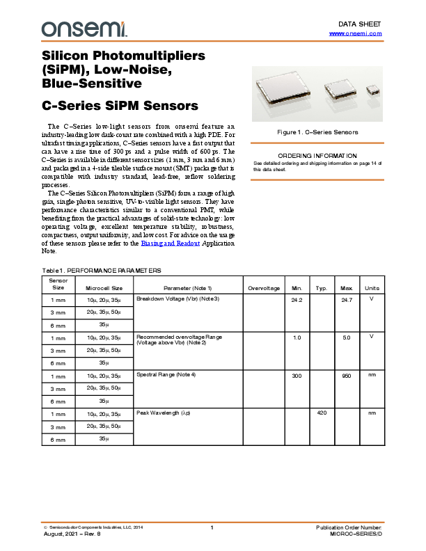
DATA SHEET www.onsemi.com

Silicon Photomultipliers (SiPM), Low-Noise, Blue-Sensitive
C-Series SiPM Sensors

The C-Series low-light sensors from onsemi feature an industry-leading low dark-count rate combined with a high PDE. For ultrafast timing applications, C-Series sensors have a fast output that can have a rise time of 300 ps and a pulse width of 600 ps. The C-Series is available in different sensor sizes (1 mm, 3 mm and 6 mm) and packaged in a 4-side tileable surface mount (SMT) package that is compatible with industry standard, lead-free, reflow soldering processes.
The C-Series Silicon Photomultipliers (SiPM) form a range of high gain, single-photon sensitive, UV-to-visible light sensors. They have performance characteristics similar to a conventional PMT, while benefiting from the practical advantages of solid-state technology: low operating voltage, excellent temperature stability, robustness, compactness, output uniformity, and low cost. For advice on the usage of these sensors please refer to the Biasing and Readout Application Note.

Figure 1. C-Series Sensors
ORDERING INFORMATION
See detailed ordering and shipping information on page 14 of this data sheet.

Table 1. PERFORMANCE PARAMETERS

Sensor Size

Microcell Size

Parameter (Note 1)

1 mm

10m, 20m, 35m

Breakdown Voltage (Vbr) (Note 3)

3 mm

20m, 35m, 50m

6 mm

35m

1 mm 3 mm

10m, 20m, 35m 20m, 35m, 50m

Recommended overvoltage Range (Voltage above Vbr) (Note 2)

6 mm

35m

1 mm

10m, 20m, 35m

Spectral Range (Note 4)

3 mm

20m, 35m, 50m

6 mm

35m

1 mm

10m, 20m, 35m

Peak Wavelength (lp)

3 mm

20m, 35m, 50m

6 mm

35m

Overvoltage Min. Typ. Max. Units

24.2

24.7

V

1.0

5.0

V

300

950

nm

420

nm

� Semiconductor Components Industries, LLC, 2014

1

August, 2021 - Rev. 8

Publication Order Number: MICROC-SERIES/D

C-Series SiPM Sensors

Table 1. PERFORMANCE PARAMETERS (continued)

Sensor Size

Microcell Size

Parameter (Note 1)

1 mm

10m

PDE (Note 5) at lp

20m

35m

1 mm

10m

20m

35m

3 mm

20m

35m

50m

3 mm

20m

35m

50m

6 mm

35m

6 mm 1 mm

35m

10m

Gain

(anode to cathode readout)

20m

35m

3 mm

20m

35m

50m

6 mm 1 mm

35m

10m

Dark Current (Note 6)

20m

35m

3 mm

20m

35m

50m

6 mm

35m

Overvoltage Vbr + 2.5 V Vbr + 5.0 V Vbr + 2.5 V Vbr + 5.0 V Vbr + 2.5 V Vbr + 5.0 V Vbr + 2.5 V
Vbr + 2.5 V

Min.

Typ. 14 24 31 18 31 41 24 31 35 31 41 47 31 41 2 � 105 1 � 106 3 � 106 1 � 106 3 � 106 6 � 106 3 � 106 1 5 15 50 154 319 618

Max.
3 16 49 142 443 914 1750

Units % % % % % % % % % % % % % %
nA nA nA nA nA nA nA

www.onsemi.com 2

C-Series SiPM Sensors

Table 1. PERFORMANCE PARAMETERS (continued)

Sensor Size

Microcell Size

Parameter (Note 1)

1 mm

10m

Dark Count Rate

Overvoltage Vbr + 2.5 V

20m

35m

3 mm

20m

35m

50m

6 mm 1 mm

35m 10m, 20m, 35m

Rise Time - Fast Output (Note 7)

3 mm

20m, 35m, 50m

6 mm 1 mm

35m 10m, 20m, 35m

Signal Pulse Width - Fast Output (FWHM)

3 mm

20m, 35m, 50m

6 mm 1 mm

35m

10m

Microcell recharge time constant (Note 8)

20m

35m

3 mm

20m

35m

50m

6 mm 1 mm

35m

10m

Capacitance (Note 9)

(anode-cathode)

20m

Vbr + 2.5 V

35m

3 mm

20m

35m

50m

6 mm 1 mm

35m

10m

Capacitance (Note 9)

(fast terminal to cathode)

20m

Vbr + 2.5 V

35m

Min.

Typ. 30 30 30 300 300 300 1200 0.3 0.6 1.0 0.6 1.5 3.2 5 23 82 23 82 159 95 50 90 100 770 850 920 3400 1 1 1

Max. 96 96 96 860 860 860
3400

Units kHz kHz kHz kHz kHz kHz kHz ns ns ns ns ns ns ns ns ns ns ns ns ns pF pF pF pF pF pF pF pF pF pF

www.onsemi.com 3

C-Series SiPM Sensors

Table 1. PERFORMANCE PARAMETERS (continued)

Sensor Size

Microcell Size

Parameter (Note 1)

Overvoltage Min. Typ. Max. Units

3 mm

20m

Capacitance (Note 9)

(fast terminal to cathode)

35m

Vbr + 2.5 V

20

pF

12

pF

50m

7

pF

6 mm

35m

48

pF

1 mm

10m, 20m, 35m Temperature dependence of Vbr

21.5

mV/�C

3 mm

20m, 35m, 50m

6 mm

35m

1 mm

10m, 20m, 35m Temperature dependence of Gain (Note 10)

-0.8

%/�C

3 mm

20m, 35m, 50m

6 mm

35m

1 mm

10m

Crosstalk

Vbr + 2.5 V

0.6

%

20m

3

%

35m

7

%

3 mm

20m

3

%

35m

7

%

50m

10

%

6 mm

35m

7

%

1 mm

10m

Afterpulsing

Vbr + 2.5 V

0.2

%

20m

0.2

%

35m

0.2

%

3 mm

20m

0.2

%

35m

0.2

%

50m

0.6

%

6 mm

35m

0.2

%

1. All measurements made at 2.5 V overvoltage and 21�C unless otherwise stated. 2. Please consult the maximum current levels on page 6 when selecting the overvoltage to apply. 3. The breakdown voltage (Vbr) is defined as the value of the voltage intercept of a straight line fit to a plot of I vs V, where I is the current and
V is the bias voltage. 4. The range where PDE > 1% at Vbr + 5.0 V. 5. Note that the PDE does not contain contributions from afterpulsing or crosstalk. 6. Dark current derived from dark count data as DC � M � q � (1 + CT), where DC is dark count, M is gain, q is the charge of an electron, and
CT is cross talk. 7. Measured as time to go from 10% to 90% of the peak amplitude. 8. RC charging time constant of the microcell (t) 9. Internal capacitance of the sensor. Typically add 2-3 pF for sensor in package. Listed by unique microcell size for each part version. 10. Quoted as the percentage change per degree C from the measured value at 21�C.

www.onsemi.com 4

C-Series SiPM Sensors
GENERAL PARAMETERS

Table 2. GENERAL PARAMETERS

1 mm

10010, 10020, 10035

Active area

1 � 1 mm2

No. of microcells

10010: 2880 10020: 1296 10035: 504

Microcell fill factor

10010: 28% 10020: 48% 10035: 64%

3 mm
30020, 30035, 30050
3 � 3 mm2
30020: 10998 30035: 4774 30050: 2668
30020: 48% 30035: 64% 30050: 72%

6 mm 60035 6 � 6 mm2 60035: 18980
60035: 64%

Table 3. PACKAGE PARAMETERS

1 mm

3 mm

6 mm

Package dimensions
Recommended operating temperature range

10010, 10020, 10035 1.5 � 1.8 mm2

30020, 30035, 30050 4 � 4 mm2
-40�C to +85�C

60035 7 � 7 mm2

Maximum storage temperature

+105�C

Soldering conditions
Encapsulant type Encapsulant refractive Index

Lead-free, reflow soldering process compatible (MSL 3 for tape & reel quantities; MSL 4 for tape only qty.)
See the SMT Handling Tech Note for more details.
Clear transfer molding compound
1.59 @ 420 nm

Table 4. MAXIMUM CURRENT LEVELS FOR EACH SENSOR SIZE

1 mm

3 mm

10010, 10020, 10035

30020, 30035, 30050

6 mA

15 mA

6 mm 60035 20 mA

www.onsemi.com 5

C-Series SiPM Sensors

CIRCUIT SCHEMATICS

An SiPM is formed of a large number (hundreds or thousands) of microcells. Each microcell is an avalanche photodiode with its own quench resistor and a capacitively coupled fast output. These microcells are arranged in

a close-packed array with all of the like terminals (e.g. all of the anodes) summed together. The array of microcells can thus be considered as a single photodiode sensor with three terminals: anode, cathode and fast output.

Circuit schematic of the SensL SiPM microcell, showing details of the Fast Output.
SensL SiPM component symbol. Simplified circuit schematic of the SensL� SiPM showing only a 12 microcell example. Typically, SiPM sensors have
hundreds or thousands of microcells. Figure 2. Circuit Schematic

www.onsemi.com 6

C-Series SiPM Sensors
PERFORMANCE
Figure 3. PDE versus Wavelength (MicroFC-30035-SMT)
Figure 4. Responsivity versus Wavelength (MicroFC-30035-SMT) www.onsemi.com 7

C-Series SiPM Sensors

Figure 5. PDE at 420 nm versus Voltage

Figure 6. Dark Count Rate versus Overvoltage

Figure 7. Gain versus Overvoltage

Figure 8. Dark Current versus Voltage and Temperature

www.onsemi.com 8

C-Series SiPM Sensors

EVALUATION BOARD OPTIONS

SMA Biasing Board (MicroFC-SMA-XXXXX) The MicroFC-SMA is a printed circuit board (PCB) that
can facilitate the evaluation of the C-Series SMT sensors. The board has three female SMA connectors for connecting the bias voltage, the standard output from the anode and the fast output signal. The output signals can be connected directly to a 50 W-terminated oscilloscope for viewing. The biasing and output signal tracks are laid out in such a way as to preserve the fast timing characteristics of the sensor.
The MicroFC-SMA is recommended for users who require a plug-and-play set-up to quickly evaluate C-Series SMT sensors with optimum timing performance. The board also allows the standard output from the anode-cathode readout to be observed at the same time as the fast output. The outputs can be connected directly to the oscilloscope or measurement device, but external preamplification may be required to boost the signal. The table below lists the SMA board connections. The SMA board electrical schematics are available to download in AND9809/D.

information is shown in the table below. The SMTPA board electrical schematics are shown in Figure 12 and are available to download in AND9809/D.
Figure 10. Pin Adapter

Figure 9. SMA Biasing Board

Output Vbias Fout Sout

MicroFC-SMA-XXXXX Function
Positive bias input (cathode) Fast output Standard output (anode)

Pin Adapter (MicroFC-SMTPA-XXXXX) The SMT Pin Adapter board (SMTPA) is a small PCB
board that houses the SMT sensor and has through-hole pins to allow for use with standard sockets or probe clips. This product is useful for those needing a quick way to evaluate the C-Series SMT sensors without the need for specialist surface-mount soldering. While this is a `quick fix' suitable for many evaluations, it should be noted that the timing performance from this board will not be optimized and if the best possible timing performance is required, the MicroFC-SMA-XXXXX is recommended. The pin-out

Figure 11. MicroFC-SMTPA-XXXXX

Figure 12. SMTPA Board Circuit Schematic

MicroFC-SMTPA-XXXXX

Pin No.

Connection

1

Anode

2

Fast output

3

Cathode

4

Ground

5

No connect

www.onsemi.com 9

C-Series SiPM Sensors
PACKAGE DIMENSIONS
(All Dimensions in mm)
MicroFC-60035-SMT

TOP VIEW

BOTTOM VIEW

SIDE VIEW

Pin # 1 2 3
4, 5

Pin Assignments
MicroFC-60035-SMT Anode
Fast Output Cathode
No Connect*

*The `No Connect' pin 4 should be soldered to the PCB. This pin can be connected to ground but it can also be left floating without affecting the dark noise. It is recommended that the Pin 5 paddle is NOT soldered to the PCB and is left floating to achieve optimal soldering on pins 1 to 4. Please note the full advice in the CAD file.
The complete MicroFC-60035-SMT POD is available to download here.

www.onsemi.com 10

C-Series SiPM Sensors
PACKAGE DIMENSIONS
(All Dimensions in mm)
MicroFC-30020-SMT, MicroFC-30035-SMT, MicroFC-30050-SMT

TOP VIEW

BOTTOM VIEW

SIDE VIEW

Pin # 1 2 3 4

Pin Assignments
MicroFC-300XX-SMT Anode
Fast Output Cathode
No Connect*

*The `No Connect' pin 4 should be soldered to the PCB. It can be connected to ground but it can also be left floating without affecting the dark noise.
The complete MicroFC-300xx-SMT POD is available to download here.

www.onsemi.com 11

C-Series SiPM Sensors
PACKAGE DIMENSIONS
(All Dimensions in mm)
MicroFC-10010-SMT, MicroFC-10020-SMT & MicroFC-10035-SMT

TOP VIEW

BOTTOM VIEW

SIDE VIEW

Pin # 1 2 3 4

Pin Assignments
MicroFC-100XX-SMT Anode
Fast Output Cathode
No Connect*

*The `No Connect' pin 4 should be soldered to the PCB. It can be connected to ground but it can also be left floating without affecting the dark noise.

The complete MicroFC-100XX-SMT POD is available to download here.

www.onsemi.com 12

C-Series SiPM Sensors
PACKAGE DIMENSIONS
(All Dimensions in mm)
MicroFC-SMTPA Board

TOP VIEW

SIDE VIEW

The electrical schematics for the SMTPA board is available in AND9809/D. MicroFC-SMA Board

BOTTOM VIEW

BOTTOM VIEW

SIDE VIEW

The electrical schematics for the SMA board is available in AND9809/D.

TOP VIEW

www.onsemi.com 13

C-Series SiPM Sensors
USEFUL LINKS
� Introduction to Silicon Photomultipliers Application Note - If you are new to SiPM, this document explains their
operation and main performance parameters.
� Biasing and Readout Application Note - This document gives detailed information on how to bias the sensor for both
standard and fast configurations, and amplifying and reading out the signal.
� How to Evaluate and Compare Silicon Photomultipliers Application Note - Information on what to consider when
selecting an SiPM.
� Handling and Soldering Guide - This document gives information on safe handling of the sensors and soldering to PCB.
ORDERING INFORMATION

Table 5. ORDERING INFORMATION

Product Code (Note 11)
10000 Series MICROFC-10010-SMT
MICROFC-SMA-10010-GEVB

Microcell Size (Total Number)
10 mm (2880 microcells)

MICROFC-SMTPA-10010-GEVB

MICROFC-10020-SMT MICROFC-SMA-10020-GEVB

20 mm (1296 microcells)

MICROFC-SMTPA-10020-GEVB

MICROFC-10035-SMT MICROFC-SMA-10035-GEVB

35 mm (576 microcells)

MICROFC-SMTPA-10035-GEVB

Sensor Active Area

Package Type

Delivery Options (Note 12)

1 mm � 1 mm

4-side tileable, surface mount package (SMT)
SMT sensor mounted onto a PCB with SMA connectors for bias and output.
SMT sensor mounted onto a pin adapter board.
4-side tileable, surface mount package (SMT)
SMT sensor mounted onto a PCB with SMA connectors for bias and output.
SMT sensor mounted onto a pin adapter board.
4-side tileable, surface mount package (SMT)
SMT sensor mounted onto a PCB with SMA connectors for bias and output.
SMT sensor mounted onto a pin adapter board.

TR1, TR PK PK
TR1, TR PK PK
TR1, TR PK PK

www.onsemi.com 14

C-Series SiPM Sensors

Table 5. ORDERING INFORMATION (continued)

Product Code (Note 11)

Microcell Size (Total Number)

Sensor Active Area

Package Type

Delivery Options (Note 12)

30000 Series MICROFC-30020-SMT MICROFC-SMA-30020-GEVB MICROFC-SMTPA-30020-GEVB MICROFC-30035-SMT MICROFC-SMA-30035-GEVB MICROFC-SMTPA-30035-GEVB MICROFC-30050-SMT MICROFC-SMA-30050-GEVB MICROFC-SMTPA-30050-GEVB

20 mm (10998 microcells)
35 mm (4774 microcells)
50 mm (2668 microcells)

3 mm � 3 mm

4-side tileable, surface mount package (SMT)
SMT sensor mounted onto a PCB with SMA connectors for bias and output.
SMT sensor mounted onto a pin adapter board
4-side tileable, surface mount package (SMT)
SMT sensor mounted onto a PCB with SMA connectors for bias and output.
SMT sensor mounted onto a pin adapter board
4-side tileable, surface mount package (SMT)
SMT sensor mounted onto a PCB with SMA connectors for bias and output.
SMT sensor mounted onto a pin adapter board

TR1, TR PK PK
TR1, TR PK PK
TR1, TR PK PK

60000 Series

MICROFC-60035-SMT

35 mm (18980 microcells)

6mm � 6mm

4-side tileable, surface mount package (SMT)

TR1, TR

MICROFC-SMA-60035-GEVB

SMT sensor mounted onto a PCB with

PK

SMA connectors for bias and output.

MICROFC-SMTPA-60035-GEVB

SMT sensor mounted onto a pin

PK

adapter board

11. All Devices are Pb-Free and are RoHS Compliant. 12. The two-letter delivery option code should be appended to the order number, e.g.) to receive MICROFC-60035-SMT on tape and reel, use
MICROFC-60035-SMT-TR. The codes are as follows: PK = ESD Package TR1 = Tape TR = Tape and Reel

There is a minimum order quantity (MOQ) of 3000 for the tape and reel (TR) option. The TR option is only available in multiples of the MOQ.

SensL is a registered trademark of Semiconductor Components Industries, LLC dba "onsemi" or its affiliates and/or subsidiaries in the United States and/or other countries.
www.onsemi.com 15

onsemi,

, and other names, marks, and brands are registered and/or common law trademarks of Semiconductor Components Industries, LLC dba "onsemi" or its affiliates

and/or subsidiaries in the United States and/or other countries. onsemi owns the rights to a number of patents, trademarks, copyrights, trade secrets, and other intellectual property.

A listing of onsemi's product/patent coverage may be accessed at www.onsemi.com/site/pdf/Patent-Marking.pdf. onsemi reserves the right to make changes at any time to any

products or information herein, without notice. The information herein is provided "as-is" and onsemi makes no warranty, representation or guarantee regarding the accuracy of the

information, product features, availability, functionality, or suitability of its products for any particular purpose, nor does onsemi assume any liability arising out of the application or use

of any product or circuit, and specifically disclaims any and all liability, including without limitation special, consequential or incidental damages. Buyer is responsible for its products

and applications using onsemi products, including compliance with all laws, regulations and safety requirements or standards, regardless of any support or applications information

provided by onsemi. "Typical" parameters which may be provided in onsemi data sheets and/or specifications can and do vary in different applications and actual performance may

vary over time. All operating parameters, including "Typicals" must be validated for each customer application by customer's technical experts. onsemi does not convey any license

under any of its intellectual property rights nor the rights of others. onsemi products are not designed, intended, or authorized for use as a critical component in life support systems

or any FDA Class 3 medical devices or medical devices with a same or similar classification in a foreign jurisdiction or any devices intended for implantation in the human body. Should

Buyer purchase or use onsemi products for any such unintended or unauthorized application, Buyer shall indemnify and hold onsemi and its officers, employees, subsidiaries, affiliates,

and distributors harmless against all claims, costs, damages, and expenses, and reasonable attorney fees arising out of, directly or indirectly, any claim of personal injury or death

associated with such unintended or unauthorized use, even if such claim alleges that onsemi was negligent regarding the design or manufacture of the part. onsemi is an Equal

Opportunity/Affirmative Action Employer. This literature is subject to all applicable copyright laws and is not for resale in any manner.

PUBLICATION ORDERING INFORMATION

LITERATURE FULFILLMENT: Email Requests to: orderlit@onsemi.com
onsemi Website: www.onsemi.com

TECHNICAL SUPPORT North American Technical Support: Voice Mail: 1 800-282-9855 Toll Free USA/Canada Phone: 011 421 33 790 2910

Europe, Middle East and Africa Technical Support: Phone: 00421 33 790 2910 For additional information, please contact your local Sales Representative