File info: application/pdf · 246 pages · 217.17MB
Document preview and download links are below.
Full PDF Document

If the inline viewer fails, it will open the original document in compatibility mode automatically. You can also open the file directly.
Extracted Text
THE MAGAZINE OF ESSENTIAL NEWS, PRODUCTS AND TECHNOLOGY
MAY 17, 1966
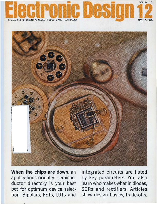
When the chips are down, an applications-oriented semiconductor directory is your best bet for optimum device selection. Bipolars, FETs, UJTs and
integrated circuits are listed by key parameters. You also learn who-makes-what in diodes, �SCRs and rectifiers. Articles show design basics, trade-offs.
#3704 - 16
LPDT�L 9040
LPDT ... L 9042
LPDT�L 9041
FEATURES:
Low Power drain .......................... less than 1mWI gate (typ.) @ 50% duty cycle less than 4mW/clocked flip-flop
Single power supply requirement ......... . . . 5V optimum, 4.5V to 5.5V range Guaranteed noise immunity ................. 450mV min. at temperature extremes Logic propagation delays .......... . ... . ... . 60nsec. typical Binary clock rate .......................... 2.5Mc
Full temperature range ... . .............. .. . - 55 � C to +125� C
LPDT�L LOW POWER DIODE-TRANSISTOR MICROLOGIC rM CIRCUITS
Fairchild LPDT,u.L integrated circuits offer high performance in the low milliwatt range. High
resistance values and small chip geometry hold down power consumption. The flip-flop
element operates either in the R-S or J-K mode, with maximum dissipation of 6mW at a
2Mc toggle rate. Gates provide fan-out capability of 10 LPDT,u.L low power logic un it loads,
or one standard Fairchild DT1tL diode-transistor logic unit load. (Standard Fairchild DT1_tl logic �circuits can be used to extend the fan-out capability still further). The circuits come in
Fairchild 's Cerpak flat package, and can be used in satellites, battery-operated field equ ip-
ment, or other instruments where reliability and high per- � � � � � � � � � � � � � �
F I I L CJ formance must be achieved with limited power. Fairchild
~ ~CH
LPDT,u.L low power integrated circuits are available in ~ r-1111.
evaluation quant ities from distributors. For complete � � � � � � � � � � � � � �
information write to :
SEMI CD ND U CTD R
FAIRCHILD SEMICONDUCTOR/ A D1v1sion of Fairchil d Camera and Instrument Corporation � 313 Fa i rchild Dr ive, M ountain View , California (415 ) 962 -5011 � TWX : 910 -3 79-64 3 5
Microlog ic is Fairchild's trademark for integrated circuits. ON READER-SERVICE CARD CIRCLE 2
ELECTRONIC DESIGN'S
SEMICONDUCTOR DIRECTORY
1966
Mark B. Leeds, Rene Colen
Technical Editors
Here is the industry's only complete applications-oriented semiconductor directory. Combini�g ELECTRONIC DESIGN'S fourteenth a�n~al transistor data chart and thi.rd annual microelectron.ics data chart with a who-makes-what diode g~ide, the directory gives you in one package:
� All the device information you need to pinpoint solid-state design needs-listed according to major design parameters.
Ii ' Technical articles explaining how to use the specifications, major application ~reas and the governing design parameters.
� Convenient Reader-Service Card (good for a full ye~r) to order detailed device specifications direct from the manufacturer.
Transistors are classified according �to seven application categories: Audio and General-Purpose, High-frequency, Power, Low-Level Switching, High-Level Switching, Unijunction and Field-Effect. Within each category, types are arranged in order of improving values of a key design parameter. This listing method permits �rapid identification of close substitutes, because device specifications can be compared at a glance. The manufacturer listed in the "Mfr." column is the original registrant of the type for which data are supplied. Alternate suppliers are listed in the "Remarks" column.
The diOde chart provides a fast guide to the manufacturers who make the specific type of diode you need.
Microelectronic devices are divided into two major categories: Digital and Linear. Within these categories the devices are listed by logic type, in the case of d~gital circuits, and by application, in the case of linear circuits.
Cross-indexes for both transistors and microcircuits simplify the job of finding the specific device when the type number is known. Keep your semiconductor data up-to-date by doing the following: Step 1: Obtain specification sheets and other data, by finding the appropriate numbers on the manufacturers' literature list (pp. 4-9) and circling them on the Reader-Service Card. Step 2: Get your own copy of the 1966 Semiconductor Directory by circling Reader-Service No. 500.
May 17, 1966.
1
Meet the XTX ... a totally new tantalum capacitor with unmatched volumetric efficiency. A capacitor which
offers twice the capacitance value of the
CL65-yet retains CL65 case sizes! Voltage range is widest, too: from 6 all the way to 100.
The inside story? Dependability. CDE's exclusive seal construction virtually eliminates the possibility of electrolytic leakage. Rugged internal construction makes the XTX incredibly shock and vibration-resistant. It is, in fact, an advanced product ... one just right for computer circuitry, copy machines and many other applications.
CDE's new XTX capacitor: just another example of doing the job just a little better.
CALL YOUR CPE AUTHORIZED INDUSTRIAL DISTRIBUTOR.
~CORNELL�
~DUBILi ER
Table o�t Contents
4
List of manufacturers and their literature offerings.
208 Technical article reprints and reader service card.
TRANSISTORS
10 Parameters key applications, govern transistor selection.
18 How to use the charts and key to transistor types.
21 Transistor who-makes-what chart.
22 Bipolar transistor data charts:
22 Audio and general purpose.
78 Low-level switching.
34 High-frequency.
86 High-level switching.
I
56 Power.
94 For the how, why and where of FET usage, consult parameters.
104 Field-effect transistor data charts: 104 Analog switching. 106 Digital switching. 107 Low-drift single-ended
de amplifier.
108 Differential de amplifier. 108 General-purpose ac amplifier. 111 Low-noise ac amplifier. 112 High -frequency ac amplifier.
114 Use the UJT that does the job best.
118 Unijunction transistor data charts: 118 Pulse generating and
SCR triggering.
118 High-fre.quency control. 118 Low-frequency control.
122 Transistor cross-index (bipolars, FETs and UJTs).
DIODES/RECTIFIERS
144 Selecting thyristors to fill a control need? 156 In choosing diodes, don't settle for second-best! 164 Diode data chart (who-makes-what).
MICROELECTRONICS
170 Choosing ICs needn't be a chore. 174 Microelectronics data charts: 174 Diode-transistor logic. 180 Direct-coupled transistor logic
and resistor-transistor logic 184 Transistor-transistor logic 190 Emitter-coupled logic 200 Microelectronics cross-index.
192 Resistor-capacitor logic.. 194 Complementary-transistor logic. 195 Digital circuits (miscellaneous
types). 196 Linear circuits.
The cover photo, courtesy of Fairchild Semiconductor, Mountain View, Calif., shows a number of popular solid-state devices. At the upper right is part of an SCR (2N4319 type); resting on the- left portion of the SCR structure is a FET (Fl 100 type); in the center foreground is a 2N 1724 power transistor with an isolated collector; to its left, a hybrid flip-flop (SH2300 type); slightly above and to the right of the flip-flop is a �A709 monolithic operational amplifier; at the extreme upper left is part of a dual -bipolar �unit (2N2060 type).
ELECTRONIC DESIGN is published bi -weekly by Hayden Publishing Company, Inc., 850 Third Avenue , New York, N. Y., 10022. James S. Mulholland, Jr., President. Printed at Poole Bros., Inc., Chicago, Ill. Controlled -circulation postage paid at Chicago, Ill., and New York, N . Y. Copyright � 1966, Hayden Publishing Company, Inc., 61 , 114 copies this issue.
<liE ON READER-SERVICE CARD CIRCLE 3
3
List of Manufacturers
'
Bring your semiconductor data file up to date. Use the ReaderService card to obtain data sheets, catalogs, application notes and other useful information. Consult dot charts (Transistors: p. 21, Diodes/Rectifiers: p. 164, and Microelectronics: p. 179, 182, 188) to learn who makes what in each device category. Starred (*) listings mean requests for literature and data sheets must go directly to the
manufacture rs.
Code
Company
Type of Information
Offered
.,s,, �:g
~
~
a 0
ou�ce.".:'.
:EU
11>
t-
CG
Airtron Div., Litton Industries Data sheets.
201
200 E. Hanover Ave.
Article reprints.
Morris Plains, N.J. 07950
(201 ) 539-5500
Alpha Industries
Data sheets. Catalogs.
202
381 Elliot St.
Customer applications
Newton Upper Fal Is, Mass. 02164 service.
(617) 969-5310
AL Amelco Semiconductor 1300 Terra Bella Ave. Mountain View, Calif. 9_4042 (415) 968-9241
American Electronic Laboratories Inc.
P.O. Box 552 Lansdale, Pa. 19446 (215) 822-2929
American Semiconductor Corp. 4 N. Hickory Ave. Arlington Heights, Ill. 60004 (312) 392-8830
AMP Amperex Electronic Corp.
Providence Pike Slatersvi Ile, R.I. 02876 (401) 762-9000
Atlantic Semiconductor Inc. 905 Mattison Ave. Asbu[y Park, N.J. 07712 (201) 775-1827
Short form catalog.
203
204
Data sheets. Catalogs.
205
Article reprints.
Customer applications
service.
Data sheets. Catalogs.
206
Data sheets. Catalogs. 207 208 209 Application notes. Customer applications
service. Design aids.
Data sheets. Catalogs.
210
Data manu.als.
Bell, F. W., Inc.
Data sheets.
211
1356 Norton Ave.
Columbus, Ohio 43212
(614) 294-4906
4
Code
Company
BE Bendix Semiconductor Div. South St. Holmdel, N.J. 07733 (201 ) 747-5400
Bradley Semiconductor Corp. 275 Welton St. New Haven, Conn. 06506 (203) 787-7181
BU Burroughs Corp. Electronic Components Div. P.O. Box 1226 Plainfield, N.J. 07061 (201) 757-5000
CBS CBS Laboratories High Ridge Road Stamford, Conn. (203) 325�4321
Chatham Electronics Div. Tung-Sol Electric Inc. 630 W. Mt. Pleasant Ave. Livingston, N.J. 07039 (201) 992-1100 .
Computer Diode Corp. Pollitt Drive Fair Lawn, N.J. 07410 (201) 797-3900
Conant Laboratories 6500 0 St. Lincoln, Neb. 68501 (402) 488-0432
CDC Continental Device Corp. 12515 Chadron St. Hawthorne, Calif. 90250 (213) 772-4551
Type of Information
Offered
.s
-"~'
!=
..."'
11>
e�= a ,g 'Cl
0
.:!
:E ...
-
11>
CG
Catalogs. Design aids. 212 213
Data sheets.
214
Data sheets. Facilities brochure.
215 216
* *
Data sheets. Catalogs.
217
Data sheets.
218
Catalogs.
219
Data sheets..Catalogs. 220 221 Article reprints.
-
ELECTRONIC DESIGN
Code
Company
CT Crystalonics Inc. 147 Sherman St. Cambridge, Mass. 02140 (617) 491�1670
DE Delco Radio Div., General Motors Corp. 700 E. Firmin St. Kokomo, Ind. 46901 (317) 457-8461
Delta Semiconductors Inc. 879 W. 16th St. Newport Beach, Cal if. 92660 (714) 646-3286
DIC Dickson Electronics Corp. P.O. Box 1387 Scottsdale, Ariz. 85252 (602) 947-5751
Diodes Incorporated 20235 Nordhoff Chatsworth, Calif. 91311 (213) 341-4850
Eastern Delta Corp. 29-09 Broadway Fairlawn, N.J. 07411 (201) 797-4200
Eastron Corp. 25 Locust St. Haverhi 11, Mass. 01830 (617) 373-3824
Edal Industries 4 Short Beach Road East Haven, Conn. 06512 (203) 467-2591
Edgerton, Genneshausen & Grier, Inc.
160 Brookline Ave. Boston, Mass. 02215 (617) 267-9700
Electro-Optical Systems Inc. 255 N. Halstead Pasadena, Calif. 91107 (213) 449-1230
Electronic Devices Inc. 21 Gray Oaks Ave. Yonkers, N.Y. 10710 (914) 965-4400
ETC Electronic Transistors Corp. 153-13 Northern Blvd. Flushing, N.Y. 11354 (212) 539-6700
Erie Technological Products Inc.
644 W. 12th St. Erie, Pa. 16512 (814) 456-8592
FA Fairchild Semiconductor 313 Fairchild Drive Mountain View, Calif. 94040 (415) 962-5011
Fansteel Metallurgical Corp. Number One Tantalum Place North Chicago, Ill. 60064 (312) 336-4900
Type of Information
Offered
Short form catalog.
~ Cl> o�c"u:'
-~ ~
"C 0
i5
--~.::0 . :E ~
I-
a:;
222 223
Short form cataIog.
224 225
Data sheets. Catalogs.
226
Data sheets. Catalogs. 227 228 Application notes. Article reprints. Customer applications
service.
Data sheets. Cata logs.
229
Data sheets.
230
Data sheets. Catalogs.
231
Application notes.
Data sheets. Catalogs.
232
Article reprints.
Customer applications
service. Design aids.
Data sheets.
233
Application notes.
*
Data sheets.
235
Data sheets. Catalogs. 236
Catalogs.
237
Application notes.
Data sheets. Cata Iogs. 238 239 240 Application notes. �Article reprints. Customer applications
service.
*
.May 17, 1966
Code
Company
GE General Electric Co. Semiconductor Products Dept. Bldg. 7, Electronics Park Syracuse, N. Y. (315) 456-2798
GI General Instrument Corp. Technical Service Center 600 W. John St. Hicksville, N.Y. 11802 (516) 681-8000
GME General Micro-electronics Inc. 2920 San Ysidro Way Santa Clara, Cal if. 95051 (408) 245-2966
General Semiconductors, Inc. 230 W. 5th St. Tempe, Ariz. 85281 (682) 966-7263
Green Rectifier Corp. 1-10 30 St. Fairlawn, N.J. 07411 (201) 797-8100
HP Associates 620 Page Mi 11 Road Palo Alto, Calif. 94304 (415) 321-8510
Heliotek Div., Textron Electronics Inc. 12500 Gladstone Ave. Sylmar, Calif. 91342 (213) 365-6301
HOF Hoffman Electronics Corp. Semiconductor Div. Hoffman Electronic Park El Monte, Calif. 91734 (213) 686-0123
HU Hughes Aircraft Co. Microelectronics Div. 500 Superior Ave. Newport Beach, Cal if. 92663 (714) 548-0671
Hunt Electronics Co. 2617 Andjon Dallas, Tex. 75220 (214) 352-8421
ITT ITT Semiconductors 3301 Electronics Way West Palm Beach, Fla. 33402 (305) 842-2411
IND lndustro Transistor Corp. 35-10 36th Ave. Long Island City, N.Y. (212) 392-8000
Instrument Systems Corp. 770 Park Ave. Huntington, N.Y. (516) 423-6200
IN lntellux, Inc. 26 Coromar Dr. Goleta, Cal if. 93017 (805) 968-3541
International Diode Corp. 90 Forrest St. Jersey City, N.J. 07304 (201) 432-7151
Type of Information
Offered
-~ I ~
o Cl>
_g 1 -~
"C 0
-~
~
i5 :E ~
I-
a:; '
Data sheets. Catalogs. 242 243 244 Application notes. Article reprints.
Data sheets. Catalogs. 245 246 247
Catalogs.
248
249
Data sheets. Catalogs.
250
Data manua Is.
Customer applications
service.
*
Data sheets.
252
Application notes.
*
Data sheets. Catalogs. 254 255 256 Application notes. Article reprints.
Data sheets. Application notes.
257 258 259
Catalogs.
*
260 261 262
Data sheets.
*
264
Data sheets. Catalogs. Application notes. Article reprints. Data manuals. Customer applications
service. Design aids.
265
*
5
Code
Company
IEC International Electronics Corp. 316 South Service Road Melville, LI., N.Y. 11749 (516) 694�7700
International Rectifier Corp. 233 Kansas St. El Segundo, Calif. 90245 (213) 678-6281
IRC Inc., Semiconductor Div. 71 Linden St. W. Lynn, Mass. 01905 (617) 598-4800
KMC KMC Semiconductor Corp. Parker Road Long Valley, N.J. 07853 (201) 876-3811
KSC KSC Semiconductor Corp. 437 Cherry St. West Newton, Mass. (617) 969-8451
Korad Corp. 2520 Colorado Ave. Santa Monica, Calif. 90404 (213) 393-6737
LAN Lansdale Transistor & Electronics Inc.
1111 N. Broad St. Lansdale, Pa. 19446 (215) 855-9004
Ledex, Inc. 123 Webster St. Dayton, Ohio 45402 (513) 224-9891
MSI Electronics Inc. 116-06 Myrtle Ave. Richmond Hill, N.Y. (212) 441-6420
Mallory Semiconductor Co. 424 S. Madison St. DuQuoin, Ill. 62832 (618) 542-2154
MEP Mepco, Inc. Columbia Road Morristown, N.J. 07960 (201) 539-2000
MicroSemiconductor Corp. 11250 Playa Court Culver City, Cal. 90230 (213) 391-8271
Micro State Electronics Corp. Subsidiary of Raytheon Co. 152 Floral Ave. Murray Hill, N.J. 07971 (201) 464-3000
Microwave Associates Northwest Industrial Park Burlington, Mass. 01803 (617) 272-3000
MO Motorola Semiconductor Products, Inc.
5005 E. McDowell Road Phoenix, Ariz. 85008 (602) 273-6900
Type of Information
Offered
~ -~
.=
~
0
o�c"..:'.
.~ _g
i5 ::E ~
a;
Data sheets. Catalogs. 267 268 Customer applications
service.
Data sheets. Catalogs.
269
Application notes.
Article reprints.
Customer applications
service. Design aids.
Data sheets. Catalogs.
270
Customer applications
service.
Data sheets. Catalogs. 271 272 Application notes. Article reprints. Customer applications
service.
*
*
*
Catalogs.
274
Data sheets. Catalogs.
275
Data sheets. Catalogs. Application notes. Article reprints. Data manuals. Customer applications
service. Design aids.
Data sheets.
276 277
Data sheets. Catalogs.
278
Application notes.
Article reprints.
Customer applications
service. Design aids.
Data sheets. Catalogs.
279
Application notes.
Article reprints.
Data sheets.
280
Data sheets. Short form catalogs. Application notes.
281 282 283
6
Code
Company
National Electronics Inc. Geneva, 111. 60134 (312) 232-4300
Type of Information
Offered
Data sheets.
~
'iii c 1! I-
~
0
i5
e'c"..'.
-~ ,g
::E ... aCl;>
284
NA National Semiconductor Corp. Conimerce Road Danbury, Conn. (203) 744-0060
*
*
NOR Norden Div., United Aircraft Corp. Data sheets. Catalogs.
285
Helen St.
Application notes.
Norwalk, Conn. 06856
Article reprints.
(203) 838-4471
Customer applications
service.
NUC Nucleonic Products Co., Inc. Components and Devices Div. 3133 E. 12th St. Los Angeles, Calif. 90023 (213) 968-3464
Data sheets.
286 287
'-. r�-~
Ohmite Manufacturing Co.
*
3601 Howard St.
Skokie, 111. 60076
(312) 675-2600
PR Philbrick Researches, Inc.
Data sheets. Catalogs.
288
Allied Drive at Route 128
Application notes.
Dedham, Mass. 02026
Article reprints.
(617) 329-1600
Data manuals.
Customer applications
service.
PH Philco Corp. Church Road Lansdale, Pa. 19446 (215) 855-4681
Data sheets. Short form catalogs. Application notes. Article reprints. Design aids.
289 290 291
Power Components, Inc. P.O. Box 421 Scottdale, Pa. 15683 (412) 887-6600
Data sheets. Catalogs.
292
Application notes.
Customer appl ications
service. Design aids.
RAD Radiation Inc. P.O. Box 37 Melbourne, Fla. 32901 (305) 723-1511
Data sheets.
293 294
RCA Radio Corp. of America
Cata logs.
Electronic Components & Devices
415 S. Fifth St.
Harrison, N.J. 07029
(201) 485-3900
295 296
RA Raytheon Co. Semiconductor Operation 350 Ellis St. Mountain View, Cal. 94041 (415) 968-9211
** *
Rectico Inc.
Cata logs.
297
20 Village Park Road
Cedar Grove, N.J. 07009
(201) 239-6464
Saratoga Semiconductor Div.
Data sheets.
298
Espey Mfg. Corp.
P.O. Box 422
Saratoga Springs, N.Y.
(518) 584-4100
Sarkes Tarzian, Inc. 415 N. College Ave. Bloomington, Ind. 47401 (812) 332:1435
Data sheets. Catalogs.
299
Application notes.
Data manuals.
Customer applications
service. Des ign aids.
Schauer Mfg. Corp. 4500 Alpine Ave. Cincinnati, Ohio 45242 (513) 791-3030
Catalogs. Application
300
notes. Price lists.
ELECTRONIC DESIGN
Show us where you can't
afford to use silicon power
and wen show you the
new Bend� B 5000 IX -
� (25wattsat2.5amps,) 10voltsand100 �C.
'
It costs under 40C.*
New manufacturing and packaging tech- B-5000 offers advances in size, weight and B-5000 lends itself equally well to other
niques make the B-5000 possible. These thermal resistance. Leads and collector commo~ly used production line
techniques include new internal device strips are a highly conductive material, techniques.
element assembly, along with new-concept offering excellent solderability, strength Electrical specifications
plastic molding operations. The result is and ability to withstand flex and pull. a simple, low-cost, reliable silicon power Plastic encapsulant offers outstanding in-
Charac-
Limits
Test Conditions
�
transistor with no power compromise when sulation resistance, hermeticity, adhesion
teristlc
Min. Max. Unit VvCB VvCE
IC A
IB mA
�TcJ
mounted upon the normal heat sink.
B-5000 's low cost opens up whole new application areas for you. Now you can afford to put silicon power to work in many industrial and consumer products.
ability and high temperature characteristics. In no way does B-5000 compromise traditionally accepted reliability practices.
With B-5000 you can tailor mounting techniques to fit your needs exactly. Depending
VCEO ICEO ICBO VBE hFE hFE VCE(s)
3---5
30
2-0
-
10 1.5 1.2
2-50
1.2
v
mA
m--vvA
14
25 14 14 14
0.2 0.5 0.5 1.0 1.0
50
150
Lighting equipment, TV sets, audio am- on heat sink, available space and degree Absolute muimum ratings
plifiers, appliance sensing amplifiers and of assembly line mechanization, B-5000 VCE0=35 volts, IC=3 amps, IB=l amp, Tstg=-65 to
industrial controls, to mention a few. can be mounted in the fashion best suited 175�C, TJ=-65to150�C.
Compare the cost of the Bendix� B-5000 to your operation. For example, B-5000 For complete information about the new
with any other silicon power unit of equal is readily adaptable to the newer assembly Bendix B-5000 silicon power transistor,
rating. You'll discover significant savings. solder techniques without degradation. write to us in Holmdel, New Jersey.
*In volume quantities
Bendix Semiconductor Division
HOLMDEL, NEW JERSEY
:~~ncff/
CORPORATION
ON READER-SERVICE CARD CIRCLE 4
May 17, 1966
7
Code
Company
Type of Information
Offered
j
�u";'
c:
~
."a
0
e�2"'
.~ ,g
. i:S :E u
a;
Code
Company
Type of Information
Offered
~
-~
.::: o�c"u:'
0
i5
. ~- J0:I ~~
t!:
Gi
Semcor Div., Components Inc. Data sheets. Catalogs.
301
SW Stewart-Warner Microcircuits
Data sheets. Catalogs.
322
3540 W. Osborn Road
Inc.
Application notes.
Phoenix, Ariz. 85019
730 E. Evelyn Ave.
Article reprints.
(602) 272-1341
Sunnyvale, Calif. 94086
Customer applications
Semicon Inc.
Data sheets. Catalogs.
302
(408) 245-9200
service.
Sweetwater Ave.
SY Sylvania Electric Prod.
Data sheets. Catalogs. 323 324 325
Bedford, Mass.. 01730
100 Sylvan Road
Application notes.
(617) 275�8542
Woburn, Mass. 01801
Customer applications
Semiconductor Devices Inc.
Data sheets. Catalogs.
303
(617) 933-3500
service. Design aids.
875 W. 15th St.
Syntron Company
Data sheets. Catalogs.
326
Newport Beach, Calif. 92663
283 Lexington Ave.
(714) 642-5100
Homer City, Pa. 15748
Semiconductor Specialists Inc. Data sheets. Catalogs.
304
(412) 479-8011
5700 W. North Ave. Chicago, Ill. 60639 (312) 622-8860
Customer applications service.
TRWS TRW Semiconductors Inc. 14520 Aviation Blvd. Lawndale, Cal if. 90260
Data sheets. Article reprhlts. Short form catalog.
327 328 "'-,
'
Semi-Elements Inc.
Catalogs.
305
(213) 679-4561
Saxonburg Blvd.
Tl Texas Instruments Inc.
Data sheets. Catalogs. 329 330 331
Saxonburg, Pa. 16056
P.O. Box 5012
Application notes.
(412) 352-1548
Dal las, Tex. 75222
Customer applications
Semtech Corp.
Data sheets. Catalogs.
306
(214) 235-3111
service.
652 Mitchell Road
Application notes.
TR Transitron Electronic Corp.
Short form catalog.
332 333 334
Newbury Park, Cal. 91320
Data manuals.
168 Albion St.
(213) 628-5392
Customer applications
Wakefield, Mass. 01881
service. Design aids.
(617) 245-4500
SA Siemens America Inc.
Data manuals.
307
230 Ferris Ave.
White Plains, N.Y. 10603
(914) 948-3434
Trio Laboratories 80 DuPont St. Plainview, N.Y. 11803 (516) 681-0400
Data sheets.
335
Application notes.
Customer applications
service.
SIG Signetics Corp. 811 E. Arques Ave. Sunnyvale, Cal if. 94086 (408) 739-7700
Data sheets. Application notes. Article reprints.
308
UC Union Carbide Electronics
Data sheets. Catalogs. 336
365 Middlefield Road
Application notes.
Mountain View, Calif. 94041
Customer applications
(415) 961-3300
service. Design aids.
STC Silicon Transistor Corp. E. Gate Blvd. Garden City, N.Y. (516) 742-4100
SI
Siliconix Inc.
1140 W. Evelyn Ave.
Sunnyvale, Calif. 94086
(408) 245-1000
Slater Electric Inc. 45 Sea Cliff Ave. Glen Cove, N.Y. (516) 671-7000
Solar Systems Inc. 8241 N. Kimbal I Ave. Skokie, Ill. 60076 (312) 676-2040
SSP Solid State Products Inc. One Pingree St. Salem, Mass. 01970 (617) 745-2900
SOL Solitron Devices Inc. 1177 Blue Heron Blvd. Riviera Beach, Fla. 33404 (301) 648-4311
SSD Sperry Semiconductor 380 Main Ave. Norwalk, Conn. 06852 (203) 847-3851
SPR Sprague Electric Co. 491 Marshall St. North Adams, Mass. 01247 (413) 664-4411
Data sheets. Catalogs. 309 310 Application notes. Customer applications
service.
Catalogs.
311
312
Data sheets. Catalogs.
313
Application notes.
Data sheets. Cata logs.
314
Application notes.
Article reprints.
Data manuals.
Customer applications
service.
Data sheets. Catalogs. 315 316 Application notes. Customer applications
service.
Data sheets. Short form catalogs. Data manuals.
317 318
Data sheets. Catalogs. 319
Data sheets.
320
321
Application notes.
Short form catalog.
Unitrode Corp. 580 Pleasant St. Watertown, Mass. 02172 (617) 926-0404
Vactec Inc. 2423 Northline Industrial Blvd. Maryland Heights, Mo. 63045 (314) 432-4200
Varian/ Bomac Div. Beverly, Mass. 01915 (617) 922-6000
VAR Varo Inc., Special Products Div. 2201 Walnut St. Garland, Tex. 75040 (214) 276-6141
VEC Vector Solid State Labs. Southampton, Pa. 18966 (215) 357-7600
Western Semiconductors Inc. 2200 Fairview St. Santa Ana, Cal if. 92704 (714) 546-2250
WH Westinghouse Electric Corp. Molecular Electronics Div. Box 7377 Elkridge, Md. 21227 (301) 796-3666
WH Westinghouse Electric Corp. Semiconductor Div. Youngwood, Pa. 15697 (412) 925-7272
Data sheets. Catalogs.
337
Data manuals.
Customer applications
service. Samples.
Test reports.
Data sheets.
338
Data sheets. Catalogs. Application notes. Customer applications
service. Design aids.
Data sheets. Catalogs. Article reprints. Design aids.
339 340 341
*
Data sheets. Catalogs. Application notes. Customer applications
service. Design aids.
Data sheets. Short form catalog.
343 344
Data sheets. Catalogs. 345 346 Application notes. Article reprints. Design aids. Short form catalog.
8
ELECTRONIC DESIGN
the price
of systems
'
power supplies
Just Dropped s100
(Con Avionics Has Another New Line)
When we cut $100 from the going market price for systems power supplies, we kept all the features you need most.
For example, Con Avionics' new line carries an unconditional five year guarantee. It has a Mean Time Between Failure of 35,000 hours, calculated according to Mil Handbook 217. We use silicon transistors exclusively, so the units operate to 75�C. They are designed and manufactured to meet specifications under the worst possible combination of operating conditions.
The secret to maintaining all this quality at a low price lies in designing a systems power supply right from the start. Most modules used in high power systems applications are just modified lab units.
But when you design a supply just for systems use you
PARTIAL SPECIFICATIONS
Input: 105-125 VAC, 47-63 cps
Regulation: (Line and load combined) � 0.05% Ripple: 1 mv RMS max.
Response time: 25 microseconds Temperature Coefficient: 0.015%/�C or
18 mv/�C., whichever is higher Temperature: 75�C max.
The entire voltage range between 5.5 vdc and 51.0 vdc is covered in twenty-six models. Currents range from 8.0 amps to 46.0 amps. Wattages from 104.5 to 816.
worry about things like panel space. So Con Avionics new HS supplies are available in rack and half-rack size. You can pack 12 volts at 20 amps into 514'' of panel height and 8" of width.
And in a system supply you design-in optimum air flow,
for both vented and forced air cabinets. Our units are selfcooled, too.
Before you buy another power supply for a systems application, remember that the price is now $100 lower than it
FULL RACK SIZE
used to be. Call, write, wire or TWX Mr. Gerry Albers at
Con Avionics for all the details.
HALF RACK SIZE
OF~CORPORATION ~ CONSOLIDATED AVIONICS
A DIVISION
800 Shames Drive� Westbury, L. I., New York� 516-ED 4-8400
ON READER-SERVICE CARD CIRCLE 5
May 17, 1966
9
Select the best transistor for the job by knowing
which parameters govern for a given application. Here is the lowdown-from de to RF and low-level thru large signal.
Modern bipolar transistors, unlike first-generation types (devices generally numbered below 2N700), have been specifically tailored to achieve optimum performance in certain applications. The key to transistor selection, then, lies in understanding and consulting the parameters which reflect a transistor's suitability for any particular a p p l i c at ion.
Here is a master chart which shows the governing parameters according to major application categories. It embraces small- and large-signal amplifiers, low- and high-speed low-level switching circuits, power switching networks and RF power amplifiers. The frequency range runs from de to the gigahertz region.
Application categories narrow the search
Simply stated, the best transistor for an application is one which performs the intended function at lowest cost. Years ago, when nearly all transistors were made by an alloy process, differences between types could be predicted quite readily. Compromises were inevitable; the general trade-off was between frequency response and power-handling ability.
For a time, the dream of a universal transistor was entertained with the advent of mesa, planar and annular types of transistors. But the vision never materialized because with each technologi~ cal advance it was found that transistors tailored to very specialized applications could be designed. These devices enabled performance in these applications to exceed by far all prior expectations.
To narrow �- the search for the transistor best suited to your application, a key para.meter chart (see table) has been developed. The chart is applicable to the majority of available devices, including modern ones made by mesa or passivated technologies as well as older types made by alloy and grown processes.
The following definitions delineate the application categories. � Small-signal amplifiers to 3 Mhz. These devices handle small amounts of power, and they need
William D. Roehr, Manager, Device Characterization Section, Applications Engineering, Motorola Semiconductor Products Inc., Phoenix, Ariz.
10
only have a limited frequency response. Operation is small-signal, that is, no large excursions of collector current are required, although collectorvoltage swings may be large. � Small-signal amplifiers above 30 MHz. �These devices are similar to those above but are primarily intended for RF applications. There are some differences in the significant characteristics, particularly in gain, noise and age. � Low level, low-speed switching and large-signal drivers. These cover switching speeds or amplification at frequencies below 1 MHz. They are generally of the same type as those in the first category, but additional specifications such as saturation voltages and response times are needed to define switching and large-signal performance. . � Low-level, high-speed switching. Devices� in
this group are typified by a high fr value ( > 50
MHz, generally) and a low storage time. � Large-signal amplifiers and power switching. Representative devices have a dissipation figure in excess of five watts at a 25 �C case temperature. � RF power amplifiers. Devices in this category
"Why settle for second-best?" Pick the optimum transistor type for your application by using author Roehr's guide to distinguishing between bipolar devices. It shows where and why transistors can and should be used.
ELECTRONIC DESIGN
are especially designed for use as power amplifiers and oscillators at frequencies exceeding 10 MHz.
Gain: major factor in small-signal amplifiers
In small-signal amplification to 30 MHz, the primary characteristic of the amplifier is the power gain of the circuit. The power gain of an amplifieroperated common-emitter with no circuit feedback is easily determined from the transistor h parameters :1
where Rds the load resistance, h rl' the small-signal current gain ((3), hoe the input admittance and h ie the input impedance. Note that llh is the determi-
nant of the h ie - hre-hre - hoe matrix where hre is
the voltage feedback. ratio. In many cases RL< <
hoe , so that llh and gain may be approximated by2
h1/R1
G=--.
(2)
hie
At low frequencies, input impedance h ie may be written as r'b + hrer e, so that Eq. 2 may be further simplified to
G = hie [ r, + ~~.lh1el ]'
(3)
where r'b is the transistor base resistance, and r e
the transistor dynamic emitter resistance. A
transistor stage has a power gain equal to the
product of a current gain and a voltage gain.
Parameter h1e establishes the current gain and the resistances (primarily the Rdre ratio) determine
the voltage gain.
�
The actual amplifier design can proceed once
the h parameters as a function of the operating point and some data on their inter-relationships are known. This infor mation is usually found on the curves of a transisto:r data sheet.
Frequency response: a figure of merit
Second in importance only to gain in smallsignal amplifiers is the frequency response. Here the gain-bandwidth frequency ([,,.) is of prime interest.3 It serves as a very useful figure of
merit. To calculate circuit cutoff-frequency, the capac-
itance from base to collector (Cob ) must also be considered. For a comm9n-emitter amplifier without degeneration, the response will be down 3 dB at the critical frequency given by
fr/hfe
f,=---
(4)
c 2 1T frRLCob
Older specification sheets generally use the term
"beta-Cutoff frequency," f ae, Which is related to f T
by
(5)
In the front ends of preamplifiers, the noise figure is all-important. Noise will be lowest for transistors having high h1e and low r'b values. Designing for low noise is usually quite involved,4 but helpful data sheet design curves are usually supplied. If it is not spBcified, assume that the transistor will usually be too high to be satisfactory for first-stage preamplifier operation, particularly when low frequencies are to be handlBd.
Aside from gain, frequency response and noise, there are a number of other, in general, secondary parameters that must be considered.
For linear operation, the available voltage swing must generally be confined. This avoids
This micropower switching transistor geometry is the 2N3493 device (Motorola). Featuring input and output capacitances of 0. 7 pF, the transistor itself is in the rectangular-shaped overlap area between the circles.
May 17, 1966
A ring-dot geometry is exhibited by the 2N3783 bipolar transistor. Suitable for very low-noise RF amplification, this Motorola device has a maximum noise of only 2.2 dB at 200 MHz. The yolk-colored pattern is the base area.
11
distortion due to saturation in the low-voltage region and avalanche effects in the high-voltage area. The guideline to follow-since linearity is seldom specified-is to take the specified value of
V BE and nine-tenths of VaEo as suitable limits for load-line excursions.
Even though small-signal amplifiers dissipate low power, the powe�r-dissipation rating at ambient temperature and the maximum junction-temperature rating deserve some attention. In addition, although the I aso leakage current is negligible in modern silicon transistors, it is large enough to cause stability problems in germanium types; where it, too, must be taken into account. In all transistors, the variation of base-emitter voltage and current gain as a function of temperature directly affects stability,5 although V BE and hre were neglected in older treatments of the subject because the effect of laso was so much greater.
Devices classified as general purpose transistors will perform best in audio and video amplifying applications. In general, the best present types are silicon pnp passivated units, as they have the flatest curve of hre vs I a and the lowest noise.
Engineers occasionally stretch a point in their search for a universal device. They may use a transistor which has been -optimized for some
other function in a small-signal amplifier application, just because the device is handy, or economical in large quantities. This may be foolhardy. For example, both silicon and germanium transistors intended for high-speed switching or RF amplification are poor choices as general-purpose devices. The switches, if made of silicon, will be gold-diffused to reduce storage time-in saturatedmode switching service. This manufacturing practice causes the h1e to be low and to fall off at low current, and also produces high leakage currents and high noise. A germanium-type switch is a poor choice because of low voltage-ratings and relatively high leakage currents. Similarly, the RF qevice will exhibit low gain at low frequencies and its her is often very sensitive to changes in I a and/ or VaE�
Oscillation frequency index of RF performance
RF small-signal amplifier applications require a new look at the gain and frequency parameters. The characteristics of importance in the RF region are in general quite different from those in the audio realm. Here too, gain is important, but the best indicator of it in the high-frequency region above the beta-cutoff frequency f ae is f fl'll(U;J the
Key parameters based on application
Device types
Use category
Required specification ratings
Characteristics Ii mi ts
VCEO
fT Cob hFE
Edge
Fune-
Pc PA TJ
Yceo
or *VcES
VEBO or *fmax
or *Cre
or *hfe
SVCE
Noise fig.
of sat
ts ti on al test
Alloy (GPA or GPS) Grown, mesa Planar Annular (no gold)
(s!~ndard diffusion)
Drift, mesa Planar Annular
(RF diffusion)
Alloy, grown (no gold) Mesa Planar Annular
Small-signal amplifiers (to 30 MHz)
Small-signal amplifiers (above 30 MHz)
Low-level, lowspeed switching (to 1.0 MHz);
Large-signa I drivers (below 30 MHz)
x x
x
x x X*
x x
-
x x
x
X* X*
x
Ge,
age
xx x x x x x x x
xx -
Mesa raid-doped
Planar
or
Annular low-voltage
(standard diffusion) �
Low-level, highspeed switching (above 1.0 MHz)
xx x
Large-signa I
All power types with
amp Iifiers;
x
standard base diffusion Power-sw itching
(below 10 MHz)
x x
x x x xx x x x x xx x
xx xx -
Power-class
RF types only
amplifiers;
x
x
Osc iIlators
X*
x
x
Ge, pout
(above 10 MHz)
12
ELECTRONIC DESIGN
)
maximum frequency of oscillation.6 The power gain at high frequencies for practi-
cal amplifiers is given as
G =
fr
(6)
e 8 'TT f2 r' b ere'
where f T is the gain-bandwidth product, f the frequency of operation, r'b the base-spreading
resistance and Cre the collector-base feedback
capacity. The maximum frequency of oscillation,
f max, may be found by solving Eq. 6 for the fre-
quency where power gain is unity. This yields
-v=
f,T
�
(7)
fmazs
7r r' b
C re
Note that power gain will increase at the approxi-
mate rate of 6 dB/octave as circuit operation is shifted down in frequency from f max� Precise calculations can be made by using the two-port admittance parameters provided on the modern
data sheet.
Once again, for the input stages of a system,
noise figure is important.1 As with audio amplifier
types, devices that do not have a specified noise
figure will probably not be suitable for front-end operation at vhf and uhf.
Age is a bias factor
RF devices generally exhibit a maximum gain when operated at certain bias conditions. Many transistors are designed to have special automatic gain control (age) characteristics, so that gain decreases at a certain rate in relation to changes in the de bias.
The gain may be reduced by decreasing the collector current (reverse age) , or increasing the colleCtor current (forward age) . All transistors are capable of reverse-age operation, whereas a forward age characteristic is obtained only by special device design. Forward-age operation is suitable only at frequencies above f ae ; reverse age may be used at any frequency. Forward age has the advantage of an increasing signal-handling capability with rising input signal. This age information is usually supplied for devices which are designed for particular use as gain-controlled amplifiers.
Other characteristics to be considered include the breakdown-voltage rating, V cEo, because it comes into play when choosing power supply voltages, and allowable output-voltage swings. Ambient-temperature power rating and the junetion-temperature limit are of only passing interest. This is because RF applications are typified by low power-dissipation figures. Functional tests of gain and noise, as specified on some data sheets, show th~ optimum operating point and are an excellent guide to whether the device will be suitable for a given application.
As for the matter of "universality," the RF device is most emphatically a special product. General-purpose and switching transistors are not nearly as suitable in RF applications. In general,.
May 17, 1966
the gain of these units will be very low, they will be unstable, and they will exhibit high noise.
Saturation, de modes set switching stage
In low-level, low-frequency (< 1 MHz) switching, many of the characteristics specified for most modern devices must be weighed. The same type of transistor that makes a good audio amplifier may very well serve as a good switch.
Here, specifications additional to the audio figures are required. Of primary importance in a switching system is the gain of the stage which approaches the de gain (hFE ). Also, because most devices operate in a saturated mode, the saturation voltage is of considerable interest. It sets a system-voltage level and largely determines the power dissipation.
Finally, the remaining set of major parameters is the switching times.8 Included here is the storage time, for in the case of the older, alloy-junction devices, it can be lengthy. Nearly all modern types of transistors, however, have storage times which are quite small by comparison; they are therefore suitable for low-speed switching circuits. It is nonetheless desirable to have a storage time U s), specification, which is approximated by
+ ]Bl I B2
ta = 'Ts ln (I /h + I ) '
(8)
c FE
B2
where T s is the storage-time time-constant, I B1 the turn-on base current, / 82 the turn-off base current,
I a the collector current and hFE the de current gain. Equation 8 is helpful in estimating storage time at a point other than the one specified on the
data sheet. For alloy devices, Eq. 8 holds quite
well; for modern devices, it is found that T s varies somewhat with I 0 � In the latter case, Eq. 8 may result in an error of 2:1 and therefore should not be used indiscriminately.
Another figure of merit is the sum of the rise and fall times. An index of the rise-and-fall-time
values. can be obtained from f T and Cob� Parameter f T predominates in the rise-time equation in the
high-current region, while output capacitance C00 is paramount in the low-current region. To pre-
dict rise time, t,., both parameters must be known
and used in:
tr=
( ~ 1
+
RL
)
cob
(
1
-
I cfI Bl
I /2 I
h
)
.
(9)
'TTJT
C
Bl FE
In Eq. 9 f T is the gain-bandwidth product, R L the load resistance, Cob the collector-base capacitance, I a the collector current, I n1 the base current and hFE the de current gain.
Load line control is essential
The expression is reasonably accurate provid-
ing that I 0 / I B1 < h FE/2. In applying it, the I B1
�value must approximate a step of current, RL should be a pure resistor and the values of f T and Ccb must be averaged over the load line used.
13
The voltage breakdown rating, VcEo, usually proves to be the best indicator of an upper voltage limit. But in many cases, careful control of the load line and the reverse bias placed on the transistor makes it possible to switch voltages up to the V cHo rating.9
For switching applications such as multivibrators and flip-flops, where capacitors are used in the base-coupling circuit, the V EBo rating must be known, as it is quite easy to exceed .this limit inadvertently.
The rated dissipation at ambient temperature and the maximum junction-temperature limit rate attention, but are not of prime importance, because the power dissipated here is fairly small.
The leakage currents of germanium and silicon devices may be a selection factor. In today's silicon transistors they are so low that they are not of design significance. On the other hand, the leakage of germanium devices may prove troublesome.
Silicon transistors are generally preferable to germanium types in switching applications because the former have a higher V BE turn-on voltage. This and their lower leakage currents make it easier to maintain the cut-off state.
Storage time a key in high-speed switching
The characteristics of importance to high-speed switching applications are essentially the same as those in the previous group. But there is greater emphasis on the storage-time specifications, since they prove to be a primary limit on how fast a logic system can operate.
To achieve low storage time, the recommended devices are low-voltage germanium or gold-doped silicon units. These transistors are generally un-
This power transistor features an isolated collector. Shown before being sealed, this semiconductor type (2N 1724) unit comes in a T0-61 package.
14
suitable for applications other than switching. Silicon npn types achieve the fastest switching.
Designers are sometimes tempted to use an RF transistor in a switching application. The results are disappointing, for RF devices have low V EBo ratings, low hFE values, high storage times and poor saturation ~hara~teristics.
Power rates high in large-signal amplifi~rs
In large-signal amplification, large amounts of power are handled and the power rating of the transistor at a specified case temperature becomes of paramount interest. The voltage which it can tolerated, as indicated primarily by the BVchJo rating, is also of great importance. The other voltages normally mentioned on data sheets generally do not greatly affect these applications.
In such devices, the edge of the saturation region, as evidenced by the knee in the collector V-I curve is significant. This is particularly so for the linear power amplifier, as it is obviously desirable to handle current peaks and voltage excursions as close to the saturation region as possible for maximum efficiency. Edge of saturation information can often be obtained from data sheet curves. In power transistors, saturation will often
occur when VcE > VBE�
These power units are also used in powerswitching, where many of the characteristics that are of consequence are the same parameters that govern in low-level applications. In this category, storage time may also limit the speed at which switching can be handled, although speed itself is usually not of primary importance.
Rise time at high currents is a major interest, but because of the current range over which these devices are switched, the use of fr measured at a single point does not correlate with measured rise time if fitted to Eq. 9, and the rise-time specifications and curves must be used. Gain (h PE ) matters because efficiency is a prime consideration, and so too does saturation voltage because of the large currents usually handled. The product of the current and saturation voltage largely determines the power dissipation and dictates .the requirements for the heat dissipator.
Current excursions modify frequency response
A common denominator for both large-signalamplification and power-switching applications is frequency response. The gain-bandwidth frequency (fT) serves as an indicator of amplifier highfrequency response, but as with switching service, the amplifier's large current excursions cause discrepancies. When attempting to calculate frequency response, Miller effect due to C ob should be considered as well as fr�
Generally, better amplifier performance predictions can be obtained from proper use of the transistor switching data. If rise-time data is plotted as a function of I c with V cB as a parameter (under
the condition I 0 / IB1 << hFE), a large� signal cut-
off frequency can be found from
ELECTRONIC DESIGN
' _/
f =
IC
(10)
A 27Ttr hFE [Bl
In Eq. 10, f A is the large-signal common-emitter
cut-off frequency and I c the ON collector current.
Parameter tr is the rise time obtained from
switching data at the collector current U c) and voltage swing of interest. Note that V cE of the switching test is the same as ~VcE in amplifiers, and I aeon> of the switching test corresponds to I c( PK> in amplifiers; hFE is the transistor de current gain and ls1 is the turn-on base current used in the switching test.
Flat curves of hFE vs I c are desirable for silicon transistors, as they are commonly driven from , high-impedance sources to obtain the best thermal
stability and the lowest distortion. For germanium power transistors, a low-impedance drive circuit is required to achieve the same ends, so
that a flat curve of transconductance vs collector current is needed.10
An extremely important characteristic of power
devices is the safe operating area.11 Data are usually presented in graphic form showing per-
missible regions of V cE-Ic operation as a function of time. Unfortunately, safe area does not correlate very well with the power ratings based upon thermal resistance. All the same, safe area, not power rating, is more often than not the arbiter of power-handling ability, and therefore is the prime concern.
Functional tests guide RF operation
RF operation creates conditions such that conventional parameters simply give no indication of a particular transistor's suitability. The only way to select devices, then, is to refer to the functional test on the manufacturer's data sheet. Here you will find the power gain at a given power output under the optimum conditions for which the devices were designed.
Bear in mind that the BVcEs voltage rating has proved to be the most useful single voltage rating for RF power transistors. As in low-frequency power applications, the edge of saturation is significant and so is safe area information. Secondary considerations are the maximum temperature rating and 25�C case power-dissipation ratin~. When designing the tuning circuit, output capacitance Cob must be known.
Sewing up the tailored device choice
A theme of this discussion has been that there is no universal transistor. It is wisest to select transistors with specifications tailored by the manufacturer to a given application.12
It is found, for example, that devices intended for high-speed, low-level saturated switching service possess very high noise figures and very low gain as audio-frequency amplifiers. Germanium switches, made from low-resistivity material to achieve low storage time, similarly should not be used indiscriminately in audio amplifiers.
Devices intended for RF applications are de-
May 17, 1966
Pick the right device! When faced with a number of transistor geometries, cans, etc., to choose from, use the key parameters as a guide to application.
signed to have very low base-spreading resistances. For this, a diffusion profile in the base is made to have an average low resistivity. As a result, the input capacity is rather high, the current gain very low, rendering this type of device unsuitable for audio and switching applications.
Conversely, the switching device, designed to have a high emitter-breakdown voltage and a low input capacitance, will have a high-base-spreading resistance. This results in low power gain and high noise when it is operated as an RF amplifier. In the power area, too, the same types of tradeoffs are evident. � �
References:
1. R. F. Shea et al., Transistor Circuit Engineering (New York: John Wiley & Sons, Inc., 1957), chap. iv.
2. A. B. Phillips, Transistor Engineering (New York: McGraw-Hill Book Co.. 1962, chaps. xii & xiii.
3. Ibid., chap. xiv. 4. J. R. Miller et al. Communications Handbook (Dallas, Tex.: Texas Instruments Inc.), Part II, chaps. i, vi & vii. 5. H. Weber, A Method of Predicting Thermal Stability (Phoenix, Ariz.: Motorola Semiconductor Products, Inc.), Technical Information Note AN 182. 6. Phillips, op. cit., chap. xv. 7. Miller, Zoe. cit. 8. W. D. Roehr et al., Switching Transistor Handbook (Phoenix, Ariz.: Motorola, Inc., 1963), chap v. 9. Ibid., chap. iii. 10. Weber, Zoe. cit. 11. R. Greenburg, Determining Maximum Reliable Load Lines for Power Transistors (Phoenix, Ariz.: Motorola Semiconductor Products, Inc.), Semiconductor Technical Information AN 137-Rl. 12. J. F. Kane, Silicon Annular Switching Transistor Design Considerations (Phoenix, Ariz.: Motorola Semiconductor Products, Inc.), Technical Information Note AN 167.
.15
MINUTES
SECONDS
New Microflex Timer/ Counter
Dials make accurate settings, easier!
NEW TWISTER ... ACCURATE TIME/ COUNT CONTROL
New and consistently better! At the left is the new face of our famous Microflex� reset timers and counters. High -visibility , direct reading dials enable you to make highly accurate settings, easier! The larger, 20-turn scale, for example, may be in minute divisions with
the inner in seconds. Settings as short as %0th
of a second with � 1/60th second accuracy are readily obtained. Other dial selections to 120 hours are available. After the desired pre-set time period, a variety of 15 amp. contacts can be opened or closed to control motors, solenoids, valves , etc. Uniform new lettering and attractive neutral grey color make units compatible with all other Eagle Signal types and with your most advanced machine designs. For full details about these new timers and counters, use Reader Service Card, circle number 91.
HZ60A6 COU NTER
CLUTCH
&<Q
START
And not one turn too many! The operating characteristics of radio tu~ing
coils depend on precise winding techniques . The Man from E.A.G.L.E. did a'
good turn for above. Using wire tension
acahMaleniacgdreoisnflgeaxrmecaontauuknfeatencrtu,crvaearreriwaohtifeonn.sh.ein. saumngdogteoasrntesdpaectech~derarsteyess.ute~ltrfi!n~l g~suhcfotrwo.n1~s
produced each time . The operator merely needs to set the h1gh-v1s1bll1ty dial
and press the button. The arbor turns the pre-set number of revolutions and
stops automatically. In this system, the Microflex counter controls brake,
clutch and motor. Complete information is in Bulletin 730. For a copy, use
Reader Service Card, circle number 92.
FILL'ER UP ..�
LIMIT SWITCH
r-~~~~~~~~--1
HA4 2A6 RESET TIME R
l
MOTOR
And not one ounce too many! A leading food supply manufa.cturer p~esented the Man from E.A.G.L.E. with the packaging requirement shown at the lef.t. This manuf.actu:er want~d to accurately fill containers. A versati.le M1croflex timer was th~ ?nswer. It moves the containers
u.nder the hopper.... filling and advancing them by the t1m.e lapse tec~rnque. The li'mit switch i"n this system
act1vate.s th.e M1croflex which control's hopper-valve and ~otor c1rcu1~s. ~n accuracy of 1;10 % ef ful'I sale is cons1ste~tly m~intained and the manufacturer can vary the con~a1~er sizes. and amounts he wants them to carry.
Intriguing? .write for Bulletin 110 for full data. Use.
Reader Service Card, circle number 93;
The..Man from,~.A.G.L.E. would like you to see his com�
~~r~ata!og? plete showcase of process control ideas. Ma we send
rcoeu
For your copy, use the handy Rlader Serv�
.
.'. ~1rcle number 94, or write directly to Ea le
Signal D1v1s1on, E. W. Bliss Company Federal Street o:v :
enport, Iowa 52803.
' �
� �
1:0~$J l�I EAGLE SIGNAL I
A DIVISION OF THE E. W . B'tlSS COMP.AN�Y
16
ELECTRONIC DESIGN
22AP Plug-in General Purpose Relay
�.. the epitome of relay craftsmanship and design. Versatile to the Nth
degree on loads to 10 amps. Available in 8- and 11-pin styles for AC,
DC and plate circuit requirements. Features include: forms to 3PDT plus
specials on request; standard units have gold-plated contacts for longer
shelf life; lower pull-in voltages me:
70% of nominal, AC: 75% of nominal); AC operating voltages 0.5 to
250, DC 0.2 to 130 in current ranges
from .005 to 10 amp. Complete information is in our new relay bulle-
tin. For your copy, use Reader Service Card, circle number 95.
SPECIFICATIONS
�Contacts: SPDT, DPDT, 3PDT � Contact Rating: S and 70 amps. �Pull-in: 22 milliseconds average � Drop-out Speed: 72 milliseconds
average
�Size: 7% � x 2.Ya �x tYa �
Q Weight: 3 ounces
25PS Medium Power Relay
POWERFUL PARTNER
... toss your toughest mediumpower-handling assignments to this
workhorse. 25PS types carry loads to
20 amps. on a fast duty cycle in a breeze. UL listed. Features include: rugged %" diameter silver cadmium oxide alloy contact; lower pull-in
voltages me: 75% of nominal, AC:
76% of nominal); AC operating voltages 4 to 250, DC 1 to 130 in current ranges from .02 to 10 amp. For full technical information on this and other Eagle Signal general purpose and medium power relays, use
nthuembReerad9e6r. Service Card, and circle
SPECIFICATIONS
� Contacts: SPD T
� Contact Rating: 20 amps. 77S/230 VAC 60 cycle resistive� 1 HP .@ 77S/230 VAC motor-inductive
� Pull-in: SO m illiseconds max.
� Drop-out Speed: 30 milliseconds max.
2 �Size: 2~ � x 1~ � x 113{ � 6 � Weight: 3 ounces
25AA Open Frame General Purpose Relay
Ask the man from E.~.G.L.E. to open
his "showcase" of ideas for you.
Many can help solve your process
control problems. Want our com�
plete catalog? Use the handy ~Sader
Service Card, circle nl!~b.er
or
write� Eagle Signal D1v1s1on, E. W.
Bliss.Company, Federal Street, Dav�
enport, Iowa 52803.
~~ti.lea,nddepbeonydwabhlaet,
a relay _it is! Ve,reconomical. You II
find hundreds of uses f?r the~e ~.or
10 amps UL listed h1gh-rel1ab11ity
types. s'tandard units haye gold-
~helflated contacts which permit longer life. Other significant features
include: lower pull-in voltages (D~:
70% of nominal, AC: 75% of nomi-
nal) 250:
AC DC
operating 0.2 to 130
invocltuargre~nst
0.5 to ran_ge.s
ffriocmati~0n0s5
to on
10 amp. Detailed these and other
spec1Eagle
Signal general purpose rela�s are
given in a new technical bul!etin. F~r
your copy, use Reader Service Car ,
circle number 97.
SPECIFICATIONS
e Contacts: SPDT, DPDT, JPDT
� Contact Rating: SA and JOA @ 7JS VAC�SA-1/10 HP@ 11S VAC, 1/6 HP@230 VACeJOA-7/6 HP@ 71S VAC, 1/3 HP@ 230 VAC
� Pull-in: 22 milliseconds average
� Drop-out Speed: 12 milliseconds average
�Size : 1Ya � x 1~2 � x 1 ~ � � Weight: 2 ounces
May 17, 1966
17
How to use the charts
A tint pairs the transistor type with the value of its key parameter for most applications in each transistor category. Devices are listed in order of increasing value of that key parameter. Note, however, that since various manufacturers may characterize their types differently, some "jumps" may take place in the sequence. Consider, for example, a type in the high-frequency category. Its key characteristic will be f ae or fr (values of fr are preceded by a single asterisk). But f ae is the frequency at which hre drops to 0.707 of its low-frequency value, and fr is the gain-bandwidth product, or the product of h1e and frequency at a point where hre is dropping by 6 dB per octave. Thus, f r is about hre times greater than f ae for a given type.
Under maximum ratings, manufacturers were asked to specify collctor power dissipation at 25 �C case temperature, this generally being the most meaningful single rating. The derating factor can then be used to estimate Pc for other operating temperatures.
Either V cEo or V cso is listed as a maximum voltage rating. VcEo is related to collectoremitter diode breakdown and V cRo to collector-base diode breakdown. But bear in mind that many manufacturers' data sheets will list other important voltage ratings, such
v v as CES or CER�
Under characteristics, ELECTRONIC DESIGN asked manufacturers to supply typical values -maximums, minimums or spreads. Where deviations from this occur, they are noted.
Finally, a word of caution: the characteristics listed serve primarily as a guide and generally should not be used exclusively for direct comparison of types. This is because it is impossible to list the wide variety of test conditions under which characteristics have been measured. V cEo, for example, can differ considerably for comparable devices when measured at a collector current of 100 �,A in one case and 1 mA in another. The best bet is to consult the manufacturers' data sheets before making the final selection. Also, scan the articles that preface each listing section. Each article contains important information about parameter evaluation.
18
Key to Symbols
= small-signal short-circuit forward current transfer ratio cutoff fre- .--- r~ quency (commont-emitter)
= small-signal short-circuit forward current transfer ratio cutoff frequency (common-base)
= gain-bandwidth product
= collector power dissipation (average)
Tj
=junction temperature �C
mW/�C = derating factor
VcEo = max collector voltage, collector to emitter, base open
VcBo = max collector voltage, collector to base, emitter open
= max collector current
= max collector current (peak)
= small-signal short-circuit forward current transfer ratio (commonemitter)
= de short-circuit forward current transfer ratio (common-emitter)
lco
=collector cutoff current (de), emitter
open
= output capacitance (common emit ter)
Cob
= output capacitance (common-base)
tr
=rise time
ts
=storage time
VoE( sat ) = collector-to-emitter saturation volt-
gm
age transconductance
VP
= pinch-off voltage
lnss BVnao
= zero-bias drain current =drain-gate breakdown voltage with
gate-source open-circuited
BVnas = breakdown voltage from drain to gate with drain shorted to source
= common source short-circuit input capacitance
N.F. = noise figure
'1]
= intrinsic standoff ratio
IEo
= max emitter reverse current
Ip
=max peak point emitter current
VE(Rat)
V ER2
Vo B1
= max emitter saturation voltage
= min emitter reverse voltage
= min base one peak pulse voltage
ELECTRONIC DESIGN
olitron
announces a family of
90 Amp NPN Silicon Planar Power Transistors featuring fast switching, high voltage capabilities with
Pr==350W @25�C!
DESIGN LIMITS
Type Number
MHT8920 MHT8921 MHT8922 MHT8923
PT
~
Watts
~
Case
Max.
350
350
350
350
BVeeo
Volts le= lmA
Min. 80 100 120 140
VeEo
(SUS)
Volts le= 0.2A
Min. 60 80
100 120
50�C Case
le= 2mA
2N3149
300
80
80
2N3150
300
100
100
2N3151
300
150
150
BVEBO
Volts IE=lmA
Min. 8 8 8 8
10 10 10
PERFORMANCE SPECIFICATIONS
h FE
VBE (sat)
VeE (sat)
leeo
le= 75A Min. 10 10 10 10
le =90A Min. 5 5 5 5
Volts
Volts
le = 50A, I e = 5A
Max.
Max.
2.0
1.5
2.0
1.5
2.0
1.5
2.0
1.5
,,.A Vee= 60V
Max. 10 10 10 10
fT
MHi!
Typ . 20 20 20 20
le= SOA
10
-
10
-
10
-
le= 50A, le =lOA
2.5
1.5
2.5
1.5
2.5
1.5
Vee= RATED 2000 2000 2000
MIN . 0.1 0.1
o.~
E3 olitron TRANSISTOR DIVISION DEVICES, INC.
1177 BLUE HERON BLVD. I RIVIERA BEACH, FLORIDA I (305) 848-4311 / �TWX: (510) 952-6676
Leader in Germanium and Silicon Power Transistors, Cryogenic Thermometers, High Voltage Rectifiers, Hot Carrier Diodes, Temperature Compensated Zeners, Voltage Variable Capacitors, Random/White Noise Components, Microelectronic Circuits, and High-Pac Interconnection Systems.
ON READER-SERVICE CARD CIRCLE 6
May 17, 1966
19
Key to Transistor Types
Construction
AE Annular epitaxial AJ Alloy junction AD Alloy diffused DD Double diffused DG Grown diffused DJ Diffused junction OM Diffused mesa DOM Double-diffused mesa DP Diffused planar DR Drift ED Electro-chemical diffused-collector EM Epitaxial mesa EP Epitaxial FA Fused alloy FJ Fused junction
GD Grown diffused GJ Grown junction GR Rate grown MB Meltback MD Micro-alloy diffused base MS Mesa PE Planar epitaxal PL Planar SBT Surface barrier SP Surface precision alloy TOP Triple-diffused planar PADT Past alloy diffused technique
Materials
ge germanium si silicon
New DC Scope! 1
�.. the Heathl<it� 10-14
� Sets New Standard for Performance & Value .�. $299.00 Kit � . � $399.00 Assembled � DC to 8 me Bandwidth-0.04 usec. rise time � Calibrated Vertical Attenuator - .OS v/cm to 600 v. (max.) Input � Triggered Sweep - 18 calibrated rates � Delay-Line Vertical Amplifiers for Fast Rise Signal Analysis � Electronically Regulated Power Supplies - Forced Air Cooling � Built for Continuous-Duty Industrial & Lab Use
A 5" DC scope with calibrated
time base & SX sweep magni-
fier. For 115/ 230 volt, 50-60
cycle operation.
Kit 10-14, 45 lbs ..... $299.00
Assembled IOW-14,
__________ 45 lbs..............$399.00 1�%frf5f+nw1
rr FREE CATALOG.'
I"'ttEATt1tt1T ;966 �-~ -~,
Il � � I !..� -.. II .�.~ .
.. ;�~ :-E:...
I �~
. .�.
Fully Describes over 250
Heathkit
Elecbook Products
I Heath Company, Dept, 60-5
I Benton Harbor, Michigan 49022� I D Please send FREE Heathkit Catalog &
Information describing the New
Heathkit 10-14 Oscilloscope
J
D Enclosed is $ - - - � plus shipping. J
Plme seod model Name
Address
. JI
City
State_ _Zip_ _
L~~~c!.!.'..:.a~~bject~~g~i~u~~ -----~~J
ON READER-SERVICE CARD CIRCLE 7
20
FREE FOLDER
ECCOSHIELD� RF SHIELDING MATERIALS
" .
Brand new six page folder in color describes a complete line of Eccoshield products to combat RFIconductive plastic sheet and gaskets, adhesives, coatings, caulking compounds, metallic foil-the works.
This valuable Folder is yours. Write or use Reader Service Card.
EMERSON & CUMING, INC �
� Canton, Massachusetts � 604 W. 182d St., Gardena, Calif. � 9667 Allen Ave., Rosemont, Ill.
Emerson &Cuming Europe N. V. Oml, Belgium
ON READER-SERVICE CARD CIRCLE 8
ELECTRONIC DESIGN
Manufacturers and their Ii nes
Manufacturer
Symbol
Audio A
High-Frequency HF
Power p
Low-Level LL
High-Level HL
Field-Effect Unijunction
FET
UJT
Amel co Amperex Bendix
AL
�
�
AMP
�
�
BE
�
Burroughs
BU
Continental Device
CDC
�
�
Crystalonics
CT
�
�
Delco
DE
Dickson
DIC -
Electronic Transistor
ETC
�
�
Fairchild
FA
�
�
General Electric
GE
�
�
General Instrument
GI
�
�
General Micro-electronics GME
�
�
Hughes
HU
ITT Semiconductors
ITT
�
lndustro Transistor
IND
�
�
International Electronics
IEC
�
�
KMC Semiconductor
KMC
�
KSC Semiconductor
KSC
�
Lansdale Motorola
LAN
�
�
MO
�
�
National Semiconductor
NA
�
�
Nucleonic Products
NUC
�
�
Philco
PH
�
Radio Corp. of America
RCA
�
�
Raytheon Siemens America
RA
�
�
SA
�
�
Silicon Transistor
STC
�
Siliconix
SI
Solid State Products
SSP
�
Solitron
SOL
Sperry Semiconductor
SSD
�
�
Sprague
SPR
�
�
Sylvania
SY
�
�
Texas Instruments
Tl
�
�
Transitron
TR
�
�
TRW Semiconductors
TRWS
�
�
Union Carbide
UC
�
�
Vector
VEC
�
Westinghouse
WH
�
�
�
�
�
�
�
�
�
�
�
�
�
�
�
�
�
�
�
�
�
�
�
�
�
�
�
�
�
�
�
�
�
�
�
�
�
�
�
�
�
�
�
�
�
�
�
�
�
�
�
�
�
�
�
�
�
�
�
�
�
�
�
�
�
� �
. �
.
� �
�
�
�
�
�
�
�
�
�
�
�
�
�
�
�
�
� �
� � �
I
�
�
�
�
�
�
�
� �
May 17, 1966
21
Audio and General Purpose
Mostly audio and general-purpose types handling less than one watt. Listed in order of increasing forward-current transfer ratio.
Cross
Index
Type
Key
Ho.
Mfr.
Type
MAX. RATINGS
CHARACTERISTICS
p
VCEO
* VCBO I,
I co
fae
Packoge
*fr Outline
(mw)
mW / �C (V) (mA)
(MHz) (TO-)
Remarks
2N 1439
NA
pnp,A,si
5-12
2N 1223
SSD AJ
6
A 1 NS-664
NA
pnp,A,si
7�22
NS-668
NA
pnp,A,si
7�22
2N927
NA
pnp,A,si
8-22
400
200
2.25 50
100 .025
25(}
175
1.67 40
100 0.1
400
175
2.5 50
100 1
150
175
l
50
100 1
150
200
.85 60
100 .025
5
CT
5
CT, SPR
5
Industrial Type
18
Industrial Type
18
SPR
2N935 2N938 2N 1024 2Nl025 2t-il028
SSD AJ SSD AJ SSD AJ SSD AJ SSD AJ
*9
385
160
2.85 40
50 0.1
0.2
18
CT, SPR
9
250
175
1.67 35
50 .025
9
250
175
1.67 15
100 .025
9
250
175
1.67 35
100 .025
9
250
175
1.67 10
10 0 .025
18
CT, SPR
5
AMP, CT,SPR
5
AMP, CT, SPR
5
CT, SPR
A 2
2Nll54
Tl
npn,si
9
750
150
6
*50 60 5
2Nll55
Tl
npn,si
9
750
150
6
*80 50 5
2Nll56
Tl
npn,si
9
750
150
6
*120 40 5
2N 1220
SSD AJ
*9
250
175
1.67 25
100 0.1
2N 1222
SSD AJ
9
250
175
1.67 25
100 0.1
TR, NA, ETC TR, NA, ETC TR, NA, ETC CT, SPR CT, SPR
2Nl586
Tl
npn,si
9
2N 1587
Tl
npn,si
9
2N 1588
Tl
npn,si
9
2N332A
GE
npn,DG,si
9-20
2N 1440
NA
pnp,A,si
9-22
A3
2N2673
GE
pnp, DG,si
9�22
2N 1394
GI
pnp,ge
10
2N 1408
GI
pnp,AJ,ge
*10
2N 1643
CT
pnp,si
*10
2Nl672A
GI
npn,AJ,ge
*10
125
87 .5
2
10
25 1
125
87.5
2
20
25 1
125
87.5
2
40
25 1
500
175
3.33 45
25 .5
400
200
2.25 50
100 .025
250
175
1.66 *60 25 .1
50
0.8 *10
15
150
100
2
*50
7.0
250
160
1.9 25
50 .001
120
85
2
*55
25
TR, ETC
TR, ETC
TR, ETC
5
TR
5
AMP, CT
46
MO
BCZ12
AMP pnp,AJ,si
10
250
150
2
60
50 0.1
2N925 2N470 2N471 2N472
NA
pnp,A,si
TR
npn,PL,si
TR
npn,PL,si
TR
npn,PL,si
10-24 10-25 10-25 10-25
150 200
200 200
200
.85 40
100 .025
175
1.2
15
25 .5
8
175
1.2 30
25 .5
8
175
1.2 45
25 .5
8
1
18
SPR
5
5
5
A4
2N472A
TR
npn,PL,si
10-25
200
175
1.2 45
25 .5
2N 1082 2N102
TR
npn,PL,si
SY
npn,AL,ge
*10-50 *10.5
200 1000
175 75
1.5 *25 50 .5 *30 1500 500
2Nll7
Tl
npn,si
12
150
175
*45 25 2
2N332
Tl
npn,si
12
150
175
*45 25 2
8
5
17.2
5
13
TR
GE;TR
2Nl474 2Nl476
SSD AJ SSD AJ
12
250
175
1.67 60
100 .050
12
250
175
1.67 100 100 0.2
2N756
NA
npn, DM,si
12-22
500
200
2.5 45
100 0.2
2N756A
NA
npn,DM,si
12�22
500
200
2.5 60
100 0.1
2N923
NA
pnp,A,si
12�30
150
200
.85 25
100 .025
AS
NS-731
NA
npn,DM,si
12�55
400
175
2.5 15
100 1
NS-733
NA
npn,DM,si
12-55
400
175
2.5 30
100 1
2Nll49
Tl
npn,si
12.3
150
175
1
*45 25 2
2N726
Tl
npn,si
15
300
175
2
20
50 1
2Nl248
TR
npn,PLE,si
*15
30
150
.24 6
5
.01
5
CT, AMP, SPR
5
CT, SPR
18
TR
18
TR
18
SPR
18
lndustri al Type
18
Industrial Type
TR
18
5
GE
2N 1311
GI
npn,AJ,ge
*1 5
2N 1655
RA
pnp,si
*15
2N2177
SSD AJ
*15
2N2178
SSD AJ
*15
2N2370
NA
pnp,A,si
*15
AG
2N2372
NA pnp,A,si
*15
2N239 l
Tl
pnp,si
15
BCY30
AMP pnp,AJ,si
15
BCY33
AMP pnp,AJ,si
15
120
85
2
*75
7.0
1.5
5
Tl
250
160
1.85 125 50 1.0
.050
5
CT,SPR
100
175
.67 6
50 .005
5
CT, SPR
100
175
.67 6
50 .005
200
200
1.0 15
100 .005
18
CT, SPR
5
Low Level, Low Noise, AMP, CT,
SPR
150
200
300
175
250
150
250
150
15
100 .005
18
Low Level, Low Noise, CT, SPR
20
50 10
50
*64 100 .1
.25
5
*32 100 .1
.4
5
BCZ13
AMP pnp,AJ,si
15
2N529
GI
-
15-20
NS-663
NA pnp,A,si
15�36
NS�667
NA pnp,A,si
15-36
MA885
MO
pnp,AJ ,ge
15-40
85
.9
*20 10 .01
100
85
2
*15
5.0
400
175
2.5 50
100 1
150
175
1
50
100 1
200
100
2.67 *50 500 15
1.5
Sub min case
2.5
5
5
Industrial Type
18
Industrial Type
t 0 .5
5
tfab
A7
2N243
Tl
npn,si
16
750
150
6
*60 60 1
-
-
TR, NA
2N936
SSD AJ
*18
385
160
2.85 35
50 0.1
-
18
CT, SPR
2N939
SSD AJ
18
250
175
1.67 35
50 .025
-
18
CT, SPR
.__ __,L-~N_Ni_~~-~--'----~~-~_.__~~---~-i-~_ __.__~-~~-_..__g_~__.__i_:~~_.__r~___,___rn_~-+---:~_~_~-----'---=-~---~-- J-~�~~~---�------'
(see pages 4-9 for explanation of company abbreviations.)
22
ELECTRONIC DESIGN
Audio (continued)
Cross
Index Type
Key
Ho� . Mfr.
Type
2Nl219 2Nl221 2N 1474A 2Nl441 2N757 AB 2N333A 2N2674 2N928 2N334A 2N758
2N758A 2N734 2N738 2N 1273 2N 1274 A9 2Nl310 2Nl312 2Nl372 2N 1373 2Nl380
2Nl381 2N 1383 2N 1445 2Nl564 2Nl572 A 10 2N 1672 2N2371
2N2373 2N3579
2N3877 2N3877A Al30 A310 A311 A 11 BCY38 2N530 ZN2042 2N2042A 2N926
2N339A 2N340A 2N341A 2Nll8 2N333
A 12 2Nll50 2N924 NS-662 NS-666 ZN330A
2N563 2N564 2Nl589 2Nl590 2Nl591
A 13 2Nl623 2N2304 2N2617 2N2831 BCY31
BCY34 SA2 253 2N531 2N658 2N 306
A 14 2N 2860 2N 279 2N662 2N7 27 ZN 1477
SSD AJ SSD AJ SSD AJ NA pnp,A,si
NA npn,DM,si
GE npn,DG,si GE npn,DG ,si
NA pnp,A,si
GE npn,DG,si
NA npn,DM,si
NA npn,DM,si
Tl
npn,si
Tl
npn,s i
Tl
pnp,ge
Tl
pnp ,ge
GI
npn,AJ,ge
GI
npn,AJ,ge
Tl
pnp ,ge
Tl
pnp ,ge
Tl
pnp ,ge
Tl
pnp,ge
Tl
pnp,ge
Tl
npn,si
Tl
npn,s i
Tl
npn,si
GI
npn ,AJ, ge
NA pnp,A,si
NA pnp,A,si SSD pnp ,EP
GE npn,PL,si GE npn,PEP,si AMP npn ,PL,si AMP npn, PL,si AMP npn,PL,si
AMP pnp,AJ,si
GI
-
MO pnp,AJ,ge
MO pnp ,AJ ,ge
NA pnp,A,si
TR npn,PL,si
TR npn,PL,si
TR npn,PL,si
Tl
npn,si
Tl
npn,si
Tl
npn,si
NA pnp,A,si
NA pnp,A,si
NA npn,A,si
RA pnp,si
GI
pnp , AJ,ge
GI
pnp,AJ,ge
Tl
npn,si
Tl
npn,si
Tl
npn,si
RA pnp,si
RA npn,PL,si
AMP pnp,si
SY
npn,PE,si
AMP pnp,AJ,si
AMP pnp ,AJ,si
AL npn ,si
GI
-
Tl
pnp,AJ ,ge
SY
npn,AL,ge
SY
npn,PE ,si
AMP pnp,AJ,si
Tl
pnp,AJ,ge
Tl
npn,si
SSD AJ
hie
p c
*hFE
(mW)
*18
250
18
250
18
250
18-36
400
18-40
500
18-44
500
18-44
250
18-55
150
18-90
500
18-90
500
18-90
500
20
500
20
500
20
150
20
150
*20
120
*20
120
*ZO
250
*zo20
250 250
zo
250
20
200
*20
800
20
600
20
600
*20
120
*20
200
*20
150
*20
400
*20 min . 200
*20 min.
200
*20
360
*20
300
*20
300
*20
120
20-25
100
*20-50
200
*20-50
200
20-55
150
*20-80
250
*20-80
250
*20-80
250
24
150
24
150
24
150
24-60
150
24-60
400
24-60
150
25
380
25
150
25
120
25
125
25
125
25
125
"'25
250
*25
600
*25
350
*25
360
25
Z50
25
250
*25
-
25-30
100
*25-80
250
*25-125
180
*25-125
200
30
125
*30
250
30
300
30
250
May 17, 1966
MAX. RATINGS
T. )
VCEO *VCBO Ic
(acl mW/ �C (V) (mA)
CHARACTERISTICS
Ico
fae Package *fT Outline
(/1A)
(MHz) (TO-)
Remarks
175 175 175 200 200
175 175 200 175 200
200 175 175 85 85
85 85 100 100 100
100 85 200 175 175
85 200
2z0o0o
100 100 200 175 175
150 85 100 100 200
175 175 175 175 175
175 200 175 175 160
85 85 87.5 87.5 87 .5
160 300 150 175 150
150 150 85 100 85
175 75 100 175 175 J
1.67 25
100 0.1
-
1.67 25
100 0.1
-
1.67 60
100 .050
-
2.25 35
100 .025
-
2.5 45
100 0.2
-
5
SPR
5
CT, SPR
5
CT , SPR
5
AMP, CT
18
TR, GI
3.33 45
25 .5
11
1.66 *60 25 .1
-
.85 60
100 .025
-
3.33 45
25 .5
12
2.5 45
100 0.2
-
5
TR
46
18
SPR
5
TR
18
TR, GI
2.5 60
100 0.1
-
18
GI
3.33 60
50 . 1
-
18
TRWS, TR
3.33 80
50 1
-
18
TR
2.5 *15 150 14
-
5
2.5 *25 150 14
-
5
2
*90 -
7
1
5
Tl
2
*50 -
7
2
5
Tl
3.3 *25 200 -
-
5
3.3 *45 200 -
-
5
3.3 *12 200 14
-
5
3.3 *25 200 14
-
3.3 *25 200 14
-
4.57 *120 750 10
-
4
60
50 1
-
4
80
50 1
-
2
*40 -
25
z
1.0 15
100 .005
-
1
15
100 .005
-
2.28 60
30 0.05
80
5
5
5
5
TRWS, TR
5
TR
5
5
Low Level, Low Noise, AMP, CT.
SPR
18
Low Level, Low Noise, CT, SPR
46
Z.67 70
50 0.5
2.67 85
50 0.5
2
*90 -
-
2
*135 -
.5
2
*80 -
.5
z
*32
2
*15
*2.67 105
*Z.67 105
.85 40
250 .1
-
5
200 10
200 10
100 .025
135
98
135
98
30
5
50
5
30
5
.45
5
3
5
-
5
Tl
-
5
Tl
-
18
SPR
3
60
150 1
3
85
150 1
3
125 150 1
1
*45 25 2
1
*45 25 2
10
11
10
11
10
11
-
-
TR
-
5
GE, TR
1
*45 25 2
.85 25
100 .025
2.5 40
100 1
1
40
100 1
2-9 �30
50 0.1
-
-
TR
-
18
-
5
lndustri al Type
-
18
Industrial Type
0.05
5
SSD, AMP, CT
2.5 *30 300 5
2
*30 300 5
2
10
25 1
2
20
25 1
2
40
25 1
0.8
-
0.8
5
IND
-
-
TR
-
-
TR
-
-
TR
1.85 20
3-4 30
2
*25
-z
*40 *64
50 1.0
250 .010
z5o0 o
.001 .30
100 .1
0.05
5
CT, SPR
10
5
3
-
250
18
TRWS
.Z5
5
2
*32
-
*40
2
*15
6.66 12
-
*20
100 .1
-
.05
-
5.0
1000 6
-
20
.6
5
-
5 �
3.5
5
-
5
.600
22
-
*30
2.5 30
6.66 12
2
20
1.67J 100
-
1
10 110
100 6
50 1
100 0.2
*1000 18
0.15
1
-
5
-
18
-
5
Low Noise CT, SPR
(see pages 4-9 for explanation of company abbreviations.)
23
Audio (continued)
Cross
Index Type
Key
Ho.
2Nl654 2Nl656 2N2173 2N2173 2N2392
A 15 2N2599A BCY39 BCZ14 2N532 2N 1101
2Nl102 2N 1442 2N650 2N650A 2N653
A 16 2N 1186 2Nl191 MA881 MA886 2N2711
2N2713 MPS2711 MPS2715 2Nl051 2Nl707
A 17 2N244 2N405 2N406 2N780 2Nl010
2N2389 BCY32 2N533 40234 AC 121
A 18 2N2926 MPS2926 2N937 2N940 2Nl469
2Nl475 2N759 2N759A 2N335A 2N2675
A 19 2N334 2Nll51 2N735 2N739 2N934
2Nl370 2Nl371 2Nl374 2Nl375 2Nl382
A 20 2Nl413 2Nl565 2Nl573 2Nl622 2N2868
2N2909 2N3064 2N3065 2N3580 A306
A 21 BCYll BCY12 ME900 SFT325 2N480A
Mfr.
Type
RA pnp,si
RA pnp,si
Tl
pnp,ge
MO pnp,ge
Tl
pnp,si
SSO pnp,EP
AMP pnp,AJ,si
AMP pnp,AJ,si
GI
-
SY
npn,AL,ge
SY
npn,AL,ge
NA pnp,A,si
MO pnp,AJ,ge
MO pnp,AJ,ge
MO pnp,AJ,ge
MO pnp,AJ,ge MO pnp,AJ,ge MO pnp,AJ,ge MO pnp,AJ,ge GE npn,PL,si
GE npn,PEP,si
MO npn,EP,si MO npn,EP,si
npn,00,si
MO pnp,AJ ,ge
Tl
npn,si .
RCA pnp,AJ,ge
RCA pnp,AJ,ge
Tl
npn,si
RCA npn,AJ,ge
Tl
npn,si
AMP pnp,AJ,si
GI
-
RCA npn,P,si
SA
pnp,AJ,ge
GE npn,PL,si MO npn,EP,si SSO AJ
SSO AJ SSO AJ
SSO AJ NA npn,OM,si NA npn,OM,si GE npn,OG,si GE npn,OG,si
Tl
npn,si
Tl
npn,si
Tl
npn,si
Tl
npn,si
RCA pnp,MS,ge
Tl
pnp,ge
Tl
pnp,ge
Tl
pnp,si
Tl
pnp,ge
Tl
pnp,ge
GE pnp,AJ,ge
Tl
npn,si
Tl
npn,si
GI
npn,AJ,ge
GE npn,PE,si
GE pnp,PE,si CT pnp,si CT pnp,si SSO pnp,EP AMP npn,PL,si
AMP pnp,AJ,si AMP pnp,AJ,si AMP npn,PL,si NUC pnp,ge TR npn,PL,si
24
hfe
p c
*hFE
(mW)
�30
250
�30
250
*30
240
�30
240
30
300
�30
400
*30
120
30
85
30-35
100
*30-SO
180
*30-SO
180
3o-65
400
30-70
200
30-70
200
30-7G
200
30-70
200
30-70
200
30-70
200
30-70
200
30-90
200
*30-90
200
*30-90
310
�30-90
310
30-100
500
30-150
200
32
750
35 .
150
35
150
*35
300
35
20
35
450
35
100
35-40
100
35-180
500
35-190
900
t35-470 200
35-470
310
*36
385
36
250
36
250
36
250
36-90
500
36�90
500
37-90
500
37�90
250
39
150
39
150
40
500
40
500
*40
150
40
150
40
150
40
250
40
250
40
200
*40
200
40
600
40
600
*40
120
4Q
2800
40
2800
40
400
40
400
�40
400
40
360
40
310
40
310
40
360
*40
500
40-100
200
MAX. RATINGS
CHARACTERISTICS
T.
J
VCEO
*VCBO Ic
Ico
(oc) mW/ �C (V) (mA) (J1A)
fae *fy (MHz)
Package Outline
(TO-)
Remarks
160
1.85 80
50 1
160
1.85 125 50 1
100
3.2 15
750 10
100
3.2 15
750 10
175
2
20
50 10
.050
5
CT, SPR
.050
5
CT, SPR
-
5
-
5
-
50
200
2.28 100 30 0.025
60
46
150
2
*69 250 .1
.85
5
-
.9
�20 10 .01
1.5
-
sub min case
85
2
*15 -
5
4.0
5
85
-
�20 100 50
.10
22
"''"'�
85
-
*40 100 50
0.10
22
200
2.25 30
100 .025
-
5
CT
100
2.67 �45 500 10
-
5
Tl
100
2.67 �45 500 10
-
5
Tl
100
2.67 *30 250 15
1
5
Tl
100
2.67 *60 500 10
100
2.67 *40 200 15
100
2.67 *60 500 10
100
2.67 *50 500 15
100
2.67 18
100 .5
-
5
-
5
Tl
t0.75 5
ttab
-t0.75
5 98
ttab NUC
100
2.67 18
200 0.5
-
98
Full line spread
135
2.81 18
100 0.5
135
2.81 18
25 0.5
--
92 92
150
4
40
100 .1
4
5�
NA
100
2.66 *30 400 15
t4
5
ttab
150
6
*60 60 1
71
-
*20 35 14
71
-
�20 35 14
175
2
45
50 0.01
55
-
*10 2
10
-
-
TR, NA
0.65
40
0.65
1
LAN
-
18
AL
2
1
LAN
200
2.57 *75 500 0.01
-
50
150
2
*64 50 -
4
9
85 175
2.0 *15 -
5
4;5
3.3 18
100 0.5 (max) *60
5
-
90
20
20
300 5
1.5
1
100
2.67 -
100 0.5
-
135
2.81 18
100 0.5
-
160
2.85 30
50 0.1
-
175
1.67 35
50 .025
-
175
1.67 35
100 .025
-
18
NUC, tFull linespread, GME
92
18
CT,SPR
18
CT, SPR
5
CT, SPR
175
1.67 60
100 .050
-
200
2.5 45
100 0.2
-
200
2.5 60
100 0.1
175
3.33 45
25 .5
--
175
1.66 *60 25 .1
-
5
AMP, CT, SPR
18
TR, GI, Tl
18
SPR, GI, Tl
5
TR
46
175
1
*45 25 2
-
5
GE;TR
175
1
*45 25 2
-
-
TR
175
3.33 60
50 1
-
18
TRWS, TR,
175
3.33 80
50 1
-
18
TR,
-
-
13 - -
-
18
85
2.5 25
150 14
-
5
85
2.5 45
150 14
-
5
100
3.3 *25 200 7
-
5
100
3.3 *45 200 7
-
5
85
3.3 *25 200 14
-
5
85
3.33 *35 200 12
-
5
175
4
60
50 1
-
5
TRWS, TR
175
4
80
50 1
-
5
TR
85
2
*90 -
7.0
1
5
200
16
40
1000 .010
130
5
200
16
40
1000 .010
130
46
200
2.3 *llO 100 .01
-
46
200
2.3 110 100 .01
-
46
200
2.28 60
30 0.05
80
46
200
2
*25 -
.01
100
18
150
2.5 60
500 0.1
150
2.5 32
500 0.1
200
2
*40 -
.01
85
-
*32 500 30
175
1.2 45
25 .5
1.5
1
1.5
1
100
18
-
1
20
5
GE
(see pages 4-9 for explanation of company abbreviations.)
ELECTRONIC DESIGN
Audio (continued)
Crass
Index Type
Key
Ho.
Mfr,
Type
hfe
p c
*hFE
(mW)
A 22
.- l "
2N2043 2N2043A 2N659 2N2244 2N2247
2N2250 2N2253 2N4030 2N403J NS�732
MO pnp,AJ,ge
MO pnp,AJ,ge
Tl
pnp,AJ,ge
NA npn,DM,si
NA npn,DM,si
NA npn,DM,si
NA. npn,DM ,si
FA
pnp ,PE,si
FA pnp,PE,si
NA npn,DM,si
*40-100
200
*40-100
200
*40-110 250
40-120
500
40-120
500
40-120
500
40-120
500
40-120
800
40� 120
800
40-125
400
NS-734
NA npn,DM,si
40-125
400
2Nll92
MO
pnp,AJ,ge
'40-135
200
2N3691
FA npn,PL ,si
*40-160 625
OC79
AMP pnp,PADT,ge 42
0.55
2N104
RCA pnp,AJ,ge
44
J50
A 23
2N215
RCA pnp,AJ,ge
44
150
2N3709
Tl
npn,PE ,si
*45-165
250
MPS3709
MO
npn,EP,si
*45-165
3JO
2N3708
Tl
npn,PE,si
*45-660
250
MPS3708
MO
npn,EP,si
*45-660
3JO
2N280
AMP pnp,AJ,ge
47
125
OC71N
AMP pnp,AJ,ge
47
110
2Nll9
Tl
npn,si
49
J50
2N335
Tl
npn,si
49
J50
2Nll52
Tl
npn,si
49
J50
A 24
2N917
FA npn,DP,si
50
300
2N918
FA npn,PE,si
*50
300
2Nl443
NA pnp,A,si
50
400
2N2616
FA npn,PE,si
*50
800
2N2729
FA npn,PE,si
*50
800
2N3581 A569 A570 Al341 BC410
A 25 ME216 NS-661 NS-665 2N214 2Nl059
SSD pnp,EP AMP npn ,PL,si AMP npn ,PL,si
AL npn ,si AMP pnp,AJ ,si
AMP npn,PL,si
NA pnp,A,si
NA pnp,A,si
SY
npn,AL,ge
SY
npn,AL,ge
*50
400
*50
300'
*50
300
*50
200
50
310
50
360
50
400
50
150
*50-100
180
*50�100
180
2N651 2N651A 2N 1187 MA882 MA887
A 26 2N654 2N27ffi PA1001 40232 BC 122
MO pnp,AJ,ge
MO
pnp,AJ,ge
MO
pnp,AJ,ge
MO
pnp,AJ,ge
MO
pnp,AJ ,ge
MO pnp,AJ,ge
MO
pnp,AJ ,ge
AL npn,DP ,si
RCA npn,P,si
SA
npn,PE,si
50-120
200
50-120
200
50-120
200
50-120
200
50�120
200
50-125
200
50-150
200
*50-150 -
50-180
500
50-400
75
2N51i5 2N566 2N2717 OC58 2N3394
A 27 MPS3394 MPS3397
MPS3398 2Nl69 2N449
GI
pnp,AJ,ge
GI
pnp,AJ,ge
GE npn,PL,si
AMP pnp,AJ ,ge
GE
npn,PL,si
MO
npn,EP,si
MO npn,EP,si
MO npn,EP ,Si
GE npn ,GR ,ge
GE npn ,GR,ge
55
150
55
120
55
200
55
20
*55-110
200
*55-110
310
*55-500
310
*55-800
310
*60
65
*60
65
2N736A
Tl
npn,si
60
500
2N929
Tl
npn,si'
60
300
2N957
FA npn,DD,si
*60
800
2Nl097
GE pnp ,AJ ,ge
*60
175
2Nl098
GE pnp,AJ ,ge
*60
175
A 28
2Nll21
GE npn ,GR,&e
*60
65
2Nl376
Tl
pnp,ge
60
250
2Nl377
Tl
pnp,ge
60
250
2Nl414
GE pnp,AJ,ge
*60
200
2Nl566A Tl
npn ,si
60
600
May 17, 1966
MAX. RATINGS
CHARACTERISTICS
,T.
VCEO
*VCBO IC
Ica
(oc) mW/ �C (V) (mA) (11A)
fae Package
*fr Outline (MHz) (TO-l
Remarks
100
2.67 105 200 10
100
2.67 105 200 10
100
6.66 12
1000 6
200
2.5 20
100 .01
200
2.5 45
100 .01
0.75
5
Tl
0.75
5
Tl
-
5
-
18
Low Level
-
18
Low Level
200
2.5 20
100 .OJ
200
7.5 45
JOO .OJ
200
22.8 60
-
.2
200
22.8 80
-
.2
175
2.5 15
JOO 1
-
J8
LowNoise, CDC
-
J8
Low Noise, CDC, AMP
JOO
5
150
5
-
18
Industrial Type
175
2.5 30
100 J
100
2.67 *40 200 J5
J50
2
*35 50 .05
75
1.2 *26 0.3 JO
70
-
*30 50 JO
-
J8
Industrial Type
-
5
*200
-
Tl R097A package, CDC
1.2
J
0.7
40
70
-
*30 50 10
125
2.5 30
30 O.J
135
2.81 30
30 0.1
125
2.5 30
30 0.1
135
2.81 30
30 OJ
0.7
J
--
t
t Pl asti c
92
-
t
t Plastic
-
92
75
2.5 30
JO 150
0.1
-
Special Case
75
0.45 30
JO -
-
J
175
1.19 *45 25 J
-
-
TR
175
J
*45 25 2
-
5
GE , TR
175
1
*45 25 2
-
-
TR
200
l.7J J5
-
0.0005 *800
J8
Tl , RCA , AL, TRWS
200
1.71 J5
50 0.002
*900
J8
MO , Tl , RCA, AL, TRWS
200
2.25 J5
JOO .025
-
5
CT
200
4.56 15
50 0.002
*900
J8
AL
200
4.56 15
50 0.002
900
18
AL
200
2.28 40
30 0.02
30
46
175
2
*20 -
.01
100
18
Chopper, &Voff,=50�V
175
2
*20 -
OJ
100
18
Chopper, Voff,=lOO�V
150
-
*75 -
.010
-
18
150
2.5 32
500 OJ
1.5
1
200
2
*20 -
.5
175
2.5 30
100 1
175 85
1
-
I 30
100 1
*40 100 50
85
-
*20 100 20
100
18
-
5
Industrial Type
-
18
Industrial Type
.01
22
.10
22
100
2.67 *45 500 10
100
2.67 *45 500 JO
100
2.67 *60 500 10
100
2.67 *60 500 JO
100
2.67 *50 500 15
-
5
Tl
-
5
Tl
2
5
t l.O
5
t tab
t l.O
5
t tab
100
2.67 *30 250 15
-
5
100
2.66 *25 400 JO
t3
5
t tab
200 175
2
*60 -
.010
.33 18
100 0.25
*60
1-8
125
5.0 20
50 0.01
250
-
85
2.5 *30 300 5
85
2.0 *30 300 5
100
2.67 -
100 0.5
75
1.5 7
5
1.5
100
2.67 25
100 OJ
1
-
1
5
IND
-
J8
1.6
-
Sub min case
-
98
Epoxy case
135
2.81 25
100 0.1
-
92
135
2.81 25
100 0.1
-
92
135
2.81 25
100 0.1
-
92
85
1.1
15
20 -
8
85
1.1
15
20 -
8
-
175
3.33 60
100 0.5
-
18
TR
175
2
45
30 0.01
-
18
FA, GI , TR, AL ,SPR, UC, MO
150
6.5 20
-
1.0
250
18
TRWS, AMP
-
2.9 *16 200 16
-
5
-
2.9 *16 200 16
-
5
85
1.1
15
20 -
8
-:
100
3.3 *25 200 7
-
5
100
3.3 *45 200 7
-
5
85
3.33 *35 200 12
-
5
175
4
60
JOO 0. 1
-
5
(see pages 4-9 for explanation of company abbreviations.)
25
Audio (continued)
Cross
Index Type
Key
No.
Mfr.
Type
hfe
pc
*hFE
(mW)
2N2387 2N2600A
Tssl o
npn,sr pnp,EP
60 *60
300 400
BCZlO
AMP pnp,AJ,si
60
250
BCZll
AMP pnp,AJ,,si
60
250
OC60
AMP pnp,AJ,ge
60
20
A '2.9
S15660
FA
npn,DPE,si
*60
600
SFT323
NUC pnp,ge
*60
200
SFT353
NUC pnp,ge
60
200
2N3858
GE npn,PEP,si
*60-120
200
2N3858A
GE
npn,PEP,si
*60-120
200
2N660 2N3721
MPS3721 2N2430 2N175
A 30 2N220 2N407 2N408 2N649 2N1924
Tl
pnp,AJ ,ge
GE. .npn,PL,si
MO npn,EP,si
AMP npn,ge
RCA pnp,AJ,ge
RCA pnp,AJ,ge
RCA pnp,AJ,ge
RCA pnp,AJ,ge
RCA pnp,AJ,ge
GE
pnp,ge
*60-150
250
60-660
200
6().660
310
*63
360
65
20
65
20
*65
150
*65
150
*65
100
*65
225
2N3062
CT pnp,si
65
400
2N3063
CT pnp,si
65
400
BCY40
AMP pnp,AJ,si
*68
120
2N270
RCA pnp,AJ,ge
*70
250
2N281
AMP pnp,AJ,ge
70
165
A 31
2N282
AMP pnp,AJ,ge
70
165
2N591
RCA pnp,AJ,ge
70
50
2N647
RCA pnp,AJ,ge
*70
100
2N 1592
Tl
npn,si
70
125
2N1593
Tl
npn,si
70
125
2N1594 2N3128 A1109 2Nll75A 2N 1705
A 32 2N213 2Nl251 2N109 2N217 2N412
Tl
npn,si
NA npn,PL,si
AL npn,si
MO pnp,AJ,ge
MO pnp,AJ,ge
SY
npn,AL,ge
SY
npn,AL,ge
RCA pnp,AJ,ge
RCA pnp,AJ,ge
RCA pnp,AJ,ge
70
125
70
150
*70
-
*70-140
200
70-150
200
70-250
180
*70-250
180
*75
150
*75
150
75
80
2N1378 2Nl379 40253 OC74 2Nl431
A 33 2Nll89 2N2712 2N2714 2N3402 2N3404
Tl
pnp,ge
Tl
pnp,ge
RCA pnp,AJ,ge
AMP pnp,AJ ,ge
SY
npn,AL,ge
75
250
75
250
*75
650
75
0.55
*75�150
180
MO pnp,AJ,ge
*75-175
200
GE
npn,PL,si
*75-225 200
GE
npn,PEP,si
*75-225
200
GE
npn,PE,si
*75-225
560
GE
npn,PE,si
*75-225
560
2N3414
GE
npn,PE,si
2N3416
GE
npn,PE,si
MPS2712
MO
npn,EP,si
MPS2716 MO npn,EP,si
2N336A
GE npn,OG,si
A 34 2N760 2N760A 2N2676 2N661 2N736
NA npn,OM,si
NA npn,DM,si
GE npn, OG,si
Tl
pnp,AJ ,ge
Tl
npn,si
*75-225
360
*75-225
360
*75-225
310
*75-225
310
76-333
500
76-333
500
76�333
500
76�333
250
*80
250
80
500
2N740
Tl
npn,si
80
500
2N1415
GE pnp ,AJ,ge
*80
200
2N 1566
Tl
npn,si
80
600
2N1574
Tl
npn,si
80
600
2N3462
AMP npn,si
*80
600
A 35 2N3463
AMP npn,si
*80
300
40261
RCA pnp,OR,ge
80
80
OC59
AMP pnp,AJ,ge
80
20
2N543A
TR npn,PL,si
80-200
200
2N2245
NA npn, OM,si
80�250
500
26
MAX. RATINGS
CHARACTERISTICS
T. )
VCEO
*VCBO Ic
Ico
(oc) mW/ �C '"' (mA) (/LA)
175
2
45
30 0.01
200
2.28 100 30 0.025
150
2
25' 50 0.1
150
2
25
50 0.1
75
1.5 7
5 1.5
fae *fy (MHz)
80 1 3 1.6
Package Outline
(TO-)
50 46 1 1 -
Remarks Sub min case
200
3.42 *40 1000 -
85
-
*24 250 15
85
-
*24 150 15
100
2.67 30
100 0.5
100
2.67 I 60
100 0.1
650
-
R083 package
-
1
-
1
-
98
-
98
100
6.66 12
1000 6
100
2.67 18
100 0.5
135
2.81 18
100 0.5
90
3.3 *32 30 -
71
-
*10 2 12
-
5
-
98
-
92
-
1
.85
40
71
-
*10 2 12
71
-
*20 70 14
71
-
*20 70 14
71
-
25
50 14
85
3.7 *60 500 10
0.85
1
-
40
-
1
LAN
-
1
LAN
-
5
200
2.3 *90 100 .01
200
2.3 *90 100 .01
150
2
*32 250 .1
50
-
*25 75 10
75
.3
*32 50 4.5
-
46
-
46
.85
5
1
7
0.9
1
75
.3
*32 50 4.5
71
-
32
20 7
71
-
25
50 14
87.5
2
10
25 1
87.5
2
20
25 1
0.9
1
Matched Pair 2N28l's
0.7
1
-
1
LAN
-
-
TR
-
-
TR
87.5
2
40
25 1
-
-
TR
150
1.2 20
100 .002
-
-
150
-
*45 -
.IO
100
3.33 *35 200 12
-
18 5
100
2.66 *18 400 10
t3
5
tfab
85
-
*40 100 50
85
-
*20 100 20
71
-
*25 70 7
71 71
-
*25 70 7
-
13
15 10
0.1
22
7.5
22
1
40
LAN
1
1
LAN
10
1
LAN
100
3.3 *12 200 7
-
5
100
3.3 *25 200 7
-
5
90
10
*25 500 14 (max) *1
1
75
.66
20
300 10
1.5
1
85
-
*25 100 20
.01
22
100
2.67 *45 500 10
-
100
2.67 18
100 0.5
-
100
2.67 18
200 0.5
-
150
4.47 25
500 OJ
-
150
4.47 50
500 0.1
-
5
98
NUC
98
98
Epoxy case, heat clip
98
Epoxy case, heat clip
150
2.67 25
500 0.1
-
98
Epoxy case
150
2.67 50
500 0.1
-
98
Epoxy case
135
2.81 18
100 0.5
-
92
135
2.81 18
25 0.5
-
92
175
3.33 45
25 .5
-
5
TR
200
2.5 45
100 0.2
-
18
TR, GI, AL
200
2.5 60
100 0.1
-
18
TR, GI, AL
175
1.66 *60 25 .1
-
46
100
6.66 12
100 6
-
5
175
3.33 60 ' 50 I
-
18
TRWS, TR
175
3.33 80
50 l
-
85
3.33 *35 200 12
-
175
4
60
50 1
-
175
4
80
50 I
-
200
1.7 35
50 0.07
-
18
TR,AL
5
5
TRWS, TR
5
TR
18
Low Noise
200
1.7 50
50 0.002
-
18
Low Noise
85
1.2 *50 10 12 (max) *40
1
75
1.5 7
5 1.5
2.2
-
Sub min case
175
1.2 50
25 .5
10
5
200
2.5 20
100 .01
-
18
Low Level
(see pages 4-9 for explanation of company abbreviations.)
ELECTRONIC DESIGN
Try a new source
for planar 2N2222 & N2369 farriilies
If you've been wishing for a new source of silicon planar general purpose amplifiers or high speed switches, ITT has now provided the answer.
ITT is in full production on the popular 2N2222 amplifier family and the 2N2369 highspeed switching family. You can have the same transistor performance you've been getting from other suppliers, plus the supplier
perfor ance you can only get from ITT. If y 're buying silicon planars from either
of the families, evaluate the new source. Order em today . . . get them today . . .
distributor of ITT Semiconductors. onductors, 3301 Electronics Way,
Beach, Florida, is a division of tional Telephone and Telegraph
F\CTO RIES IN PALO ALTO. CALIFORNIA; LAWRENCE. MASSACHUSETIS; WEST PALM BEACH . FLORIDA; HARLOW AND
May 17, 1966
ON READER-SERVICE CARD CIRCLE 9
/ITT SEMICONDUCTORS 27
Audio (continued)
Cross Index Key A 36
A 37
A 38
A 39
A 40
A 41
A 42
Type Ho.
2N2248 2N2251 2N2254 2N2715 2N3060
2Nll44 2Nll45 2Nl925 2N2431 2N3058
OC75N 2N2923 2N3393 MPS3393 40231
40233 2N3710 MPS3710 MPS3396 2Nl20
2N336 2N 1153 2N567 2N568 2N3130
2N3582 A307 ME213 ME217 ME900A
ME901 ME901A 2N508A 2N3859 2N3859A
2N652 2N652A 2N 1188 MA883 MA888
2N213A 2N655 2N 1193 2N4032 2N4033
PAlOOO 2N3692 2N3707 MPS3707 2N2716
40329 2N2171 2Nl926 2Nll90 BC 107
2N2903 2N2903A 2N2428 AC 163 2N2706
2N2707 AF 127 2N569 2N570 2N930
2N2388 2N2586 2N3129 40262 AC172
Mfr.
Type
NA npn ,DM,si NA npn,DM ,si NA npn,DM,si GE npn,PL,si CT pnp,si
GE pnp ,AJ ,ge
GE
pnp,AJ ,ge
I GE pnp,ge
AMP pnp,ge
CT pnp,si
AMP pnp,AJ,ge GE npn ,PL,si GE npn,PL,si MO npn,EP,si RCA npn,P,si
RCA npn, F,si
Tl
npn,PE,si
MO npn,EP,s i
MO npn,EP ,si
Tl
npn,si
Tl
npn,si
Tl
npn ,si
GI
pnp,AJ,ge
GI
pnp,AJ,ge
NA npn,PL,si
SSD pnp,EP AMP npn,PL,si AMP npn ,PL,si AMP npn,PL,si AMP npn,PL,si
AMP npn,PL ,si AMP npn ,PL,si MO pnp,AJ,ge GE npn,PEP,si GE npn,PEP,si
MO pnp,AJ,ge MO pnp,AJ,ge MO pnp,AJ,ge MO pnp ,AJ ,ge MO pnp ,AJ ,ge
SY
npn,AL,ge
MO pnp,AJ,ge
MO pnp,AJ,ge
FA pnp,PE,si
FA pnp,PE,si
AL npn ,DP ,si
FA npn,PL ,si
Tl
npn,PE ,si
MO npn,EP,si
GE npn,PL,si
RCA pnp,AJ,ge
MO pnp,AJ ,ge
GE
pnp ,ge
MO pnp,AJ ,ge
SA
npn,PE,si
AL npn ,DP ,si
AL npn ,DP,si
AMP pnp,ge
SA
pnp,AJ,ge
AMP pnp,AJ,ge
AMP ge
SA
pnp,AD,ge
GI
pnp,AJ,ge
GI
pnp,AJ,ge
Tl
npn,si
Tl
npn,si
Tl
npn,si
NA npn ,PL,si
RCA pnp,DR,ge
AMP npn,AJ,ge
hfe *hFE
p c (mW)
80-250
500
80-250
500
80-250
500
82
200
85
400
*90
175
*90
175
*90
225
*90
1000
90
400
90
110
90-180
200
*90-180
200
*90-180
310
90-300
500
90-300
500
*90-330
250
*90-330
310
*90-500
310
99
150
99
150
99
150
100
150
100
120
100
150
*100
400
100
360
100
360
100
360
100
360
100
360
100
360
*100-200 200
*100-200 200
100-200
200
100-225
200
100-225
200
100-225
200
100-225
200
100-225
200
100-250
180
100-250
200
100-250
200
100-300 800
100-300
800
*100-300 -
*100- 400 625
*100-400 250
*100-400 310
110
200
120
125
120-310
500
*121
85
.. 125-300 200
*125-500 260
*125-625 600
*125-625 600
130
500
*130
900
*135
500
*135
500
140
60
150
150
150
120
150
300
150
300
150
300
150
150
150
80
150
280
28
MAX. RAT IHGS
CHARACTERISTICS
Tj
VCEO
*vcso Ic
I co
(ocl mW/ �C (V) (mA) (11A)
fae
*fr (MHz)
Package Outline (TO -I
Remarks
200
2.5 45
100 .01
-
200
2.5 20
100 .01
200
2.5 45
100 .01
-
100
2.67 *18-18 100 0.5
-
200
2.3 *70 100 .005
-
18
Low Level
18
Low Noise, CDC
18
Lo w Noise
18
IEC, GME
46
85
2.9 *16 200 16
-
-
85
2.9 *16 200 16
85
3.7 *60 500 10
-
-
5
75
3.3 *32 1000 10
1.7
1
200
2.3 6
100 .0001
-
46
75
0.45 30
10 -
100
2.67 25
100 0.5
100
2.67 25
100 0.1
135
2.81 25
100 0.1
175
.33 18
100 0.5
175
.33 18
100 0.5
125
2.5 30
30 0.1
135
2.81 30
30 0.1
135
2.81 25
100 OJ
175
1
*45 25 2
-
1
-
98
IEC, GME
--
98
Epoxy case, GME
92
*60
-
*60
-
-
t
tPlastic
92
-
92
-
-
TR
' r, ,_
175
1
*45 25 2
-
5
GE, TR
175
1
*45 25 2
-
-
TR
85
2.5 *30 300 5.0
1.5
-
85
2.0 *30 300 5.0
1.5
5
IND
150
1.2 60
100 .002
-
-
200
2.28 40
30 0.02
30
46
200
2
*25 -
.01
100
18
200
2
*45 -
.1
100
18
200
2
*20 -
.5
100
18
200
2
*40 -
.01
100
18
200
2
*40 -
.01
200
2
*40 -
.01
100
3.33 *30 200 7
100
2.67 30
100 0.5
100
2.67 60
100 0.1
100
18
100
18
-�
5
-
98
-
98
100
2.67 *45 500 10
100
2.67 *45 500 10
100
2.67 *60 500 10
100
2.67 *60 500 10
100
2.67 *50 500 15
-
5
Tl
-
5
Tl
-
5
1.25
5
t fab
tl.25 5
tfab
85
-
*40 100 50
100
2.67 *30 250 15
100
2.67 *40 200 15
200
22.8 60
-
.2
200
22.8 80
-
.2
0.1
22
-
5
Tl
-
5
Tl
100
-
150
-
200
2
*30 -
.010
-
18
150
2
*35 50 .05
*200
-
R097A package, CDC
125
2.5 30
30 0.1
-
t
tPlastic
135
2.81 30
30 0.1
-
92
100
2.67 -
100 0.5
-
18
NUC, IEC, GME
100
2.8 *25 100 14 (max 1.5
1
100
6.7 *50 400 10
t 7.5
5
tfab
3.7
*60 500 10 -
-
5
100
2.67 *45 500 10
-
5
175
5.0 45
100 0.0007
150
18
200
3.5 *60 -
.010
-
5
Dual
200
3.5 *60 -
.010
-
5
Dual
75
0.3 32
100 -
1.7
1
90
20
24
200 10
2.3
1
90
0.37 *32 200 -
2.5
1
90
0.37 *32 200 -
2.5
1
Matched NPN, PNP Pair
75
2.5 32
10 1.2
75
18
85
2.5 *30 300 5
2
-
85
2.0 *30 300 5
2
5
IND
175
2
~5
30 0.01
-
18
FA, GI, TR, NUC, SPR, UC, MO
175
2
45
30 0.01
-
50
175
2
45
30 0.002
-
18
AMP, FA, AL, UC
150
1.2 45
100 .002
-
-
85
1.2 *50 10 12 (max *30
1
75
2.7 32 200 10
-
1
(see pages 4-9 for explanation of company abbreviations.)
ELECTRONIC DESIGN
========iJmliml!'J:im14 1-====-====-
After 130,000,000 diodes
1-amp glass rectifiers come easy
The basic technology required for making silicon glass rectifiers has long since been proved out in ITT's diode operation. More than 130,000,000 diodes last year paved the way for 1966 1-amp glass rectifier capability that's already operating at better than a 1.2 million annual rate.
If you're using old-fashioned top-hats because delivery is slow on D0-29 glass rectifiers, make the switch now.
ITT offers immediate shipment of 200 to 1000 V, 1-amp glass rectifiers from factory stock or from ITT distributors' shelves. See how fast silicon glass rectifier delivery can be - call your ITT factory representative or any of ITT's semiconductor distributors throughout the United States today. ITT Semiconductors, a division of International Telephone and Telegraph Corporation, 3301 Electronics Way, West Palm Beach, Florida.
ITT
SEMICONDUCTORS
FACTORIES IN PALO ALTO, CALIFORNIA; LAWRENCE. MASSACHUSETTS; WEST PALM BEACH. FLORIDA; HARLOW �AND FOOTSCRAY . ENGLAND. FREIBURG AND NURENBERG . GERMANY
ON READER-SERVICE CARD CIRCLE 10
May 17, 1966
29
Audio (continued)
Cross Index Key A 43
A 44
A 45
A 46
A 47
A 48
A 49
Type
Ho.
Mfr.
2N2924
GE
2N3392
GE
2N3860
GE
2N4086
GE
MPS3392
MO
2N2246
NA
2N2249
NA
2N2252
NA
2N2255
NA
MPS3395 MO
2N2453
AL
2N2453A AL
2N3061
CT
2N2613
RCA
2N3241
RCA
2N3242
RCA
2N3403
GE
2N3405
GE
2N3415
GE
2N3417
GE
2N3711 � Tl
MPS3711
MO
2N 1185
MO
MA884
MO
MA889
MO
2N 1194
MO
2N1086
GE
2N 1086A GE
2Nl087
GE
2N571
GI
2N572
GI
2N2614
RCA
2N3059
CT
2N3427
MO
MA1703
MO
MA1706
MO
2N2429
AMP
2N2925
GE
Dl6E7
GE
D16E9
GE
ME495
AMP
2N3900A GE
2N3391
GE
2N3391A GE
2N3900
GE
2N4087
GE
2N4087A
GE
ME213A
AMP
2N2953
RCA
2N4017
FA
2N3428
MO
MA1704
MO
MA1707
MO
2N3078
AMP
2N3390
GE
2N4018
FA
2N4019
FA
MAJ702
MO
MAJ705
MO
MA1708
MO
2N3077
AMP
A520/ A521 AMP
Sl5650
FA
2N3395
GE
2N3396
GE
2N3397
GE
2N3398
GE
2N2785
GE
2N997
Tl
2N35
-
Type
npn,PL,si npn,PL,si npn ,PEP,si npn ,PL,si npn,EP,si
npn,DM,si npn,DM,si npn,DM,si npn,DM,si npn,EP,si
npn,DP ,si npn,DP ,si pnp,si pnp ,AJ,ge npn ,PL,si
npn ,PL,si npn,PE,si npn,PE,si npn,PE,si npn,PE ,si
npn ,PE,si npn ,EP,si pnp,AJ,ge pnp ,AJ ,ge pnp,AJ ,ge
pnp,AJ,ge npn ,GR ,ge npn ,GR ,ge npn,GR ,ge pnp,AJ,ge
pnp ,AJ,ge pnp,AJ ,ge pnp,si pnp,AJ ,ge pnp,AJ ,ge
pnp,AJ ,ge pnp,ge npn,PL,si npn,PEP,si npn,PEP ,si
npn,PL,si npn,PL ,si npn ,PL,si npn,PL,si npn,PL,si
npn,PL,si npn,PL,si npn,PL,si pnp,AJ ,ge pnp ,DPE,si
pnp,AJ ,ge pnp ,AJ ,ge pnp,AJ ,ge npn,PL,si npn ,PL,si
pnp,DPE,si pnp ,DPE,si pnp ,AJ ,ge pnp ,AJ ,ge pnp ,AJ ,ge
npn,PL ,si npn,PL,si npn ,DPE,si npn ,PL,si npn ,PL,si
npn,PL,si npn ,PL,si npn,PL ,si npn,si pnp ,AS ,ge
hfe
p c
*hFE
(mW)
150-300
200
*150-300 200
*150-300 200
*150-300 200
*150-300 310
150�450
500
150-450
500
150-450
500
150-450
500
*150-500 310
*150 -600 600
*150-600 600
155
400
160
120
175
500
175
500
*180-540 560
*180-540 560
*180-540 360
*180.540 360
*180-660 250
*180-660 310
190-400
200
190-400
200
190-400
200
190-500
200
195
65
195
65
195
65
200
150
200
120
200
120
200
400
200-500
200
200-500
200
200-500
200
220
500
235-470
200
*235-470 200
*235-470 200
*250
360
250-500
200
*250: 500 200
*250-500 200
*250-500 200
250-500
200
250.500
200
300
360
350
120
*350
600
350-800
200
350-800
200
350-800
200
360
360
*400-800 200
*500
600
*500
600
500
200
500
200
500
200
600
360
600
300
*600
200
800
.200
800
200
800
200
1250
200
2000
1800
*7000
500
-
50
30
MAX. RATINGS
CHARACTERISTICS
T.
J
VCEO
*Vcso Ic
Ica
(oc) mW/ �C (V) (mA)
~1A)
100
2.67 25
100 0.5
100 100
2.67 25 2.67 30
100 100
0u.1s
100
2.67 12
JOO 0.1
135
2.81 25
JOO 0.1
fae *fr (MHz)
-
-
-
Package Outline
(TO-)
98 98 98 98 92
200
'2.5 20
JOO .01
-
18
200
2.5 45
100 .OJ
-
18
200
2.5 20
100 .01
-
18
200
2.5 45
JOO .01
-
18
135
2.81 25
100 0.1
-
92
200
114 *60 9
.005
-
5
200
1.14 *80 9
.005
-
5
200
2.3 *70 100 .005
-
46
100
-
*30 50 5
JO
I
175
-
25
100 0.1
60
-
175
-
25
200 0.01
60
-
150
4.47 25
500 0.1
-
98
150
4.47 50
500 0.1
-
98
150
2.67 25
500 0.1
-
98
150
2.67 50
500 0.1
-
98
125
2.5 30
30 0.1
135
2.81 30
30 0.1
100
2.67 *45 500 10
100
2.67 *60 500 10
100
2.67 *50 500 15
-
t 92
-
5
tl.75 5
tl.75 5
100
2.67 *40 200 15
-
5
85
1.1 9
20 -
8
-
85
1.1 9
20 -
8
-
85
1.1 9
20 -
8
-
85
2.5 *30 300 5
3
-
85
2.0 *30 300 5
3
5
100
-
*40 50 5
10
1
200
2.3 6
JOO .0001
-
46
100
2.67 *45 500 3.0
6.0
5
100
2.67 *25 500 3.0
t3.0
5
100
2.67 *15 500 15
75
3.3 32
JOO -
100
2.67 25
100 0.5
100
2.67 18
100 0.5
100
2.67 25
100 0.5
t3 .0
5
2.3
1
-
98
-
98
-
98
200
2
*40 -
1
-
18
100
2.67 18
100 0.1
-
98
100
2.67 25
100 0.1
-
98
100
2.67 25
100 0.1
-
98
100
2.67 18
100 0.1
-
98
100
2.67 12
100 0.1
100
2.67 12
100 0.1
200
2
45
-
.I
100
-
*30 150 5
200
3.4 *80 200 10
-
98
-
98
100
18
10
1
5.5
-
100
2.67 *45 500 3.0
100
2.67 *25 500 3. 0
100
2.67 *15 500 15
200
2.06 *80 50 .OJ
100
2.67 25
100 0.1
8.0
5
t 5.0
5
t4.0
5
-
18
-
98
200
3.4 *60 200 JO
200
3.4 *45 200 10
100
2.67 *45 500 3.0
100
2.67 *25 500 3.0
100
2.67 *15 500 15
7.0
-
7.0
-
t 7.0
5
t 6.0
5
t s.a
5
200
2.06 *80 50 .01
-
18
200
1.72 80
50 .005
60
5
125
5
25 -
.050
40
-
125
0.375 25
100 0.1
-
t
125
9.375 25
100 .J
-
t
125
0.375 25 100 0.1
-
t
125
0.375 25
JOO O.J
-
t
200
JO
40
500 JO
-
5
175
3.33 40
300 0.01
-
18
-
-
*25 -
-
-
-
Remarks
IEC, GME Epoxy case, GME
Low Level
t'
Low Level
Low Noise, CDC, AMP
Low Noise
Dual Dual
tfT
tfT Epoxy case, heat clip Epoxy case, heat clip Epoxy case Epoxy case, heat clip
t Plastic
tfab tfab
Tl
IND
tfab
tfab
IEC, GME
5 dB(max nf) Economy- Epoxy, NUC, IEC, GME 5 dB(max nf), GME
5 dB(max. nf)
R052A package, Dua I pnp
tfab tfab TR Economy-Epoxy, NUC, IEC, GME
R052A package, Dual pnp R052A package, Dua I pnp tfab t fab tfab
TR 6 lead diff amp ROllO package Economy- Epoxy, GME, IEC Economy- Epoxy, GME, IEC Economy - Epoxy, GME , IEC Economy- Epoxy, GME, IEC SPR (Darlington) ,FA, SPR SY , GI
(see pages 4-9 for explanation of company abbreviations.)
ELECTRONIC DESIGN
Why ITT VVet tantalum
capacitors can't leak
Every ITT Red Cap� wet tantalum capacitor gets a "total stress" seal that, unlike the ordinary single-crimp seal, positively prevents electrolyte leakage. To accomplish this, ITT inserts a teflon end seal, then spins down the open end of the can until end seal, anode and insulating washer are under a predetermined compressive force.
Seal integrity is further insured by the addition of an epoxy end fill. Since the epoxy's expansion coefficient is less than that of the can , temperature cycling cannot relax the spun seal.
If you 're tired of electrolyte leaks and the problems that go with them, here's an easy solution. Order the ones that can't leak - the Red Caps � - from your ITT Capacitor distributor or from ITT Semiconductors, a division of International Telephone and Telegraph Corporation , 3301 Electronics Way, West Palm Beach, Florida.
ITT
SEMICONDUCTORS
FACTORIES IN PALO ALTO, CALIFORNIA! LAWRENCE. MASSACHUSETTS: WEST PALM BEACK. FLO R I DA~ HARLOW AN O FOOTSCRAY. ENGLAND; FREIBURG ANO NURENBERG. GERMANY.
May 17, 1966
ON READER-SERVICE CARD CIRCLE 11
Audio (continued)
Cross Index Type
hfe
Key
Ha.
Mfr.
Type
*hFE
2N331 2N 1392 2N 1393
2N4020
pnp,AJ,ge
-
GI
pnp,ge
-
GI
pnp,ge
-
FA
pnp,DPE,si
-
2N4021
FA
pnp,DPE,si
-
A 50 2N4022 2N4023 2N4024
FA
pnp,DPE,si
-
FA
pnp,DPE,si
-
FA
pnp,DPE,si
-
2N4025
FA
pnp,DPE,si
-
FT4020
FA
pnp,DPE,si
-
FT4021
FA
pnp,DPE,si
-
FT4022 FT4023 FT4024 FT4025 A 51
FA
pnp, DPE,si
-
FA
pnp,DPE,si
-
FA
pnp,DPE,si
-
FA
pnp, DPE,si
-
ME209
AMP npn, PE, si
-
ME214
AMP npn,PE,si
-
SP10801
FA
npn,DP,si
-
SP10810
FA
pnp,DPE,si
-
SP10811
FA
pnp,DPE,si
-
MAX. RATINGS
CHARACTERISTICS
p c (mW)
T.
J
VCEO
*Vcso Ic
I ca
(oc) mW/ �C (V) (mA)
(/1A)
fae
*fr (MHz)
Package Outline (TO-)
Remarks
200
71
-
*30
-
16
50
-
0.8
*20
-
8.0
50
-
0.8
*20
-
8.0
600
200
2.3
*45
200 10
600
200
2.3
*45
200 10
-
5
MO, GI, IND
-
-
-
-
160
-
R052A package, Dua I pnp
160
-
R052A package, Dua I pnp
600
200
2.3
15
200 10
600
200
2.3
45
200 10
600
200
2.3
45
200 10
600
200
2.3
45
200 10
500
200
2.8
45
200 10
160
-
R052A package, Dual pnp
160
-
R052A package, Dual pnp
160
-
R052A package, Dua I pnp
160
-
R052A package, Dual pnp
0.7
-
Dual pnp
500
200
2.8
60
200 10
500
200
2.8
60
200 10
500
200
2.8 45
200 10
500
200
2.8
60
200 10
500
200
2.8
60
200 10
0.55
-
0.7
-
0.7
-
0.55
-
0.7
-
Dual pnp Dual pnp Dual pnp Dual pnp Dual pnp
300
175
2
*10 -
.002
-
18
Chopper, Voff=250nV
300
175
2
*45 -
.002
-
18
Chopper, Voff=500nV
350
200
2
*45 -
-
-
89
350
200
2
*20 -
-
-
89
350
200
2
*20 -
-
100
89
(see pages 4-9 for explanation of company abbreviations.)
Late-arrivals ...
The following bipolar transistor families, manufactured by General Instrument, are epoxy encapsulated units (T0-18 cans) similar or equivalent in characteristics to their metal-can counterparts (for detailed information on device properties use the literature offering form and reader-service card, p. 4):
Audio and general purpose
2N2711 � 2N2716 2N2721 - 2N2726
2N3390 - 2N3398 2N3414 - 2N3416
High-frequency
2N3563 - 2N3566 2N3605 - 2N3607 2N3638 - 2N3645
2N3702 � 2N3711 2N3900 . 2N3905 2N3983 - 2N3985
High-level switching
2N4140 - 2N4143 (similar to 2N2221, 2N2222, 2N2906, 2N2907) 2N4227 - 2N4228 (direct equivalents of metal-can types)
32
ELECTRONIC DESIGN
NEW contact/ess meter relays (4 �2 ") NEW miniature edgewise meters (1Y2")
Utter reliability ... utter simplicity. Completely fail-safe circuitry insures 1003 reliability. No limitation on pointer travel due to mechanical contacts. Model 3324XA meter relays are CONTACTLESS. An infinite life lamp and photo-conductors do the sensing. Solid state switching circuit and relay (IO amp, DPDT, 115 VAC) are contained internally on single control point units. Double control point models also available. Control point indication is within 2% of actual switching. Available THROUGH DISTRIBUTORS in ranges shown.
RANGE
IApprox. Single Control Ohms at. No. Price
DC Microammeters
0-50 0-100
131030000
0-200
570
0-500
220
16451 16452 16453 16454
99.00 96.15 96.15 96.15
DC Milliammeter
0-1
l 80
DC Millivoltmeter
0-50
I 10
16455 16460
95.10 63.60
Double Control Cat. No. Price
16470 16471 16472 16473
16474
16480
136.35 133.65 133.50 133.50
132.45
137.25
Takes only half the space of a 21h" Edgewise meter with little sacrifice in scale length. Movement is self-shielded. DC accuracy is � 23 (F.S.); AC
(rectifier type), � 33 (F.S.) at 25�, 60 cycle sine
wave. Dustproof case. Meter comes complete with bezel and mounting hardware. 20 Ranges are STOCKED (see sampling below). Contact your ELECTRONIC DISTRIBUTOR about Model 1521.
RANGE
DC Voltometers 0-150 DC Milliammeters 0-100 DC Millivoltmeters 0-50 DC Microammeters 0 -25 AC Voltmeters 0�150
Approx. Ohms
1000 o/v 1.35
10 3150 1000 o/v
Cat. No. 10358 6817 0713 4552 10415
Price
$15.45 15.90 16.20 23.40 20.10
For Complete Details, Request Bulletin 2073 and Meter Relay Reprint Article.
SIMPSON ELECTRIC COMPANY
5202 W. Kinzie Street, Chicago, Ill. 60644 �Phone: 312-379-1121
Export Dept.: 400 W. Madison Street, Chicago, Ill. 60606 �Cable, Amergaco
In Canada: Bach-Simpson Ltd., London, Ontario
In India:
Ruttonsha-Simpson Private Ltd., International House, Bombay-Agra Road, Vikhroli, Bombay
May 17, 1966.
ON READER-SERVICE CARD CIRCLE 12
High-Frequency
lndudes types ranging up to and above the vhf rarige. Listed in Order Of increasing fae Or fT�
Cross lnde,x Key HF l HF 2
HF 3
HF 4
HF 5
HF S
HF 7
Type Ho.
2N2709 2N444 2N444A 2N3296 2N3297
2N94 2N233 2N233A 2N445 2N445A
2N515 2N51S 2N3295 2Nl391 2N2946
SFT337 2N212 2N517 2Nl058 2Nl39
2N218 2N94A 2N211 2N446 2N44SA
2Nl090 2N2945 FK3962 FV39S2 2N227S
2N2277 3N90 3N91 3N92 3N93
3N94 3N95 3Nll2 3Nl13 2N409
2N410 FK39S4 FV3964 SA-313 SA-314
SA-316 SA-413 SA-414 SA41S 2N2378
2N3318 2N471A 2N472A 2N473 2N474
2N474A 2N475 2N475A 2N495 2N581
2N 1054 2Nlll8 2Nlll8A 2N2377 SA-312
34
1ae
*fT
p c
Mir.
Type
(MHz) (mW)
RA pnp,si
GI npn,AJ,ge GI npn,AJ,ge MO npn,E,si MO npn, E,si
0.05 250
1
100
l
150
�1
6W
�1
25W
SY npn,AL,ge
2
150
SY npn,AL,ge
2
150
SY npn,AL,ge
2
150
GI npn,AJ,ge
2
100
GI npn,AJ,ge
2.
150
SY npn,AL,ge
2
150
SY npn,AL,ge
2
150
MO npn,E,si
2
2w
GI npn,AJ,ge
3
150
CT pnp, PE, si
*3
400
NUC pnp,ge
3
150
SY npn,AL,ge
4
150
SY npn,AL,ge
4
150
SY npn,Al,ge
4
50
RCA pnp,AJ,ge
4.7
80
RCA pnp,AJ,ge SY npn,AL,ge SY npn,AL,ge GI npn,AJ,ge GI npn,AJ,ge
4.7 80
5
150
5
150
5
100
5
150
RCA npn,AJ,ge SPR pnp, PE, si FA pnp,DP,si
FA pnp, DP,si SPR pnp, AT, si
5
120
*5
400
5.5 175
5.5 175
*6
150
SPR pnp, SP,s i
*6
150
SPR pnp,PE,si
*6
300
SPR pnp,PE,si
*6
300
SPR pnp,PE,si
s
300
SPR pnp,PE,si
�s
300
SPR pnp,PE,si SPR pnp,PE,~i SPR pnp,PE, Si SPR pnp,PE, si RCA pnp,AJ,ge
�s
300
*6
300
*6
200
*6
200
6.7 80
RCA pnp,AJ,ge FA pnp,DP,si
FA pnp,DP,si
SPR pnp,SP,si SP-R pnp,SP,si
6.7 80
7
175
7
175
*7
150
*7
150
SPR pnp,SP,si SPR pnp,SP,si SPR pnp,SP,si SPR pnp,SP,si SPR pnp,SAT,si
*7
150
*7
150
*7
150
*7
150
*7.2 150
SPR pnp,SPAT ,si *7.6 150
TR npn,PL,si
8
200
TR npn,PL,si
8
200
TR npn,PL,si
8
200
TR npn,PL,si
8
200
TR npn,PL,si
8
200
TR npn,PL,si
8
200
TR npn,PL,si
8
200
SPR pnp,SPAT,si *8
150
RCA pnp,AJ,ge
8
150
TR npn,PL,si
8
soo
*SPR pnp,SA T,si
8
150
*SPR pnp,SAT,si
SPR PNP,SAT,si SPR pnp,SP,si
�8�aa
150 150 150
MAX. RA TINGS
T.
VCEO
J
*VCBO IC
(oC) mW / �C (V) (mA)
160 1.85 35
50
85 1.67 *15 -
100 2
�35 -
175 40
�so 700
175 1S7 �so l.5a
100 -
�20 100
85 -
�10 100
85 -
�10 100
85 l.S7 *15 -
100 2.0 *25 -
85 -
*18 100
85 -
*18 100
175 13.3 �so 250
100 2
*25 -
200 2. 4 *40 100
80 85 85 -
75 -
70 -
*15 100
*18 100
*18 100 *18 50 �1s 15
70 -
*16 15
100 -
�20 100
85 -
*18 100
85 1.67 *15 -
100 2
*25 -
85 -
�25 400
200 2. 4 *25 100
200 2
so
50
200 2
so
50
140 1.3 *15 50
140 1.3 *15 50
200 1.7
30
20
200 1.7
30
20
200 1.7
30
20
200 1.7
50
20
200 1.7
50
20
200 1.7
50
20
200 1.1 *50 20
200 1.1 �so 20
71 -
*13 15
71 -
*13 15
200 2
45
50
200 2
45
50
140 1.3 20
50
140 1.3 15
50
140 1.3
10
50
140 L3 20
50
140 1.3
15
50
140 1.3
10
50
140 1.3 �10 50
140 L3
15
50
175 1.2
30
25
175 1.2
45
25
175 1.2
15
25
175 1.2
30
25
175 1.2
30
25
175 1.2 45
25
175 1.2 45
25
140 1.3
25
50
85 -
~18
100
175 23 140 1.3
140 1.3
140 1.3 140 1.3
*125 750
25
50
25
50
*25 50
10
50
CHARACTERISTICS
1co
hfe *hFE
*1CEO Coe
t 1cEx *Cob
(�A) (pf)
Packoge Outline
(TO-)
Remarks
�10
1
�110 5
10
6
*16 5
Tl, ETC
15
4
*14 5
Tl, ETC
*5-50
0.1
�20 -
Special ceramic stud-mount
*2.5-35
1.0
�so 3
*10-80
30
10
-
�10
-
20
s
35
4
9
22
ETC
7
22
ETC
7
22
ETC
*lS 5
Tl, ETC
*14 5
Tl
*10-50
50
8
22
*15-75
50
8
22
*20-60
0.1
*8
5
*40-lSO 4
�20 5
*30-150
0. 0005 *10
46
SPR
so
2.5
-
l
*10-30
30
7
22
*20-100 50
8
22
*10-23
50
7
22
48
s
-
40
48
6
*7-21
30
*20-100 30
30
s.o
so
4.0
-
l
9
22
7
22
*16 5
Tl
*14 5
Tl
*30 *40-250 *300 *300
*15
8
*25 5
GI
0.0002 *10
- *6 - *6
46
-
51
Hermet package
0. 003 *6. 0 *18 Matched Pair 2N227
*15
0. 003 �s.o 18 Matched Pair 2N227S
-
0.01
8
18 Duet, Voff <50� V
-
0.01 8
18 Duet, Voff <100� V
-
0.01 8
18 Duet, Voff <20(J.i V
-
0.01 8
18 Duet, Voff < 50� V
-
0.01 8
18 Duet, Voff < 100� V
-
0.01 8
18 Duet, Voff <200� V
1.5
. 010 *10 90 Dual
1.5
.010 *10 90 Dual
48
10
-
40
48
10
-
2
LAN
*500
-
�s
-
Hermet package
*500
-
�s
51
*S
0.01 s
5
Symmetrical
*8
0.02 s
5
Symmetrical
*10
0.003 s
5
Symmetrical
�s
0.01 s
18 Symmetrical
*8
0.02 s
18 Symmetrical
*10
0.003 s
18 Symmetrical
*25
0.001 �s
18
-
0.001 *9
18 Chopper
10-25
.5
*8
5
10-25
.5
*8
5
20-50
.5
*8
5
20-50
.5
*8
5
20-50
.5
*8
5
20-50
.5
*8
5
20-50
.5
*8
5
15-30
0.1
�12 l
30
3
-
5
GI, Tl , LAN, IND
�20
5
*120 5
SSP
35
0.001 *6
5
*PH orig Reg, CT
25
0.001 *S
5
*PH orig Reg, CT
30
0.002 �s
18
*10
0.01 6
5
Symmetrical
(see pages 4-9 for explanation of company abbreviations.)
ELECTRONIC DESIGN
High-Frequency (continued)
Cross Index Key
HF 8
Type Ho.
SA-315 SA-412 SA-415 2N447 2N447A
2N447B 2Nl40 2N219 2N411 2N541
Mfr.
Type
SPR pnp,SP,si SPR pnp,SP,si SPR pnp,SP,si GI npn,AJ,ge GI npn,AJ,ge
GI npn,AJ,ge RCA pnp,AJ,ge RCA pnp,AJ,ge
RCA pnp,AJ,ge TR npn,PL,si
fae
*fr
(MHz)
*8 *8 *8 9 9
9 10 10 10 10
2N542 2N542A 2N543 2N602 2Nl206 HF 9
2N 1207 2N 1907 2N 1908 2Nl974 2N2944
TR npn,PL,si
10
TR npn,PL,si
10
TR npn,PL,si
10
GI pnp, DR,ge
*10
TR npn,PL,si
10
TR npn,PL,si
10
Tl pnp,ge
*10
Tl pnp,ge
*10
FA npn,DP,si
*10
CT pnp, PE, si
*10
HF 10
2N3317 2N3319 SA-310 SA�311 SA-410
SA�411 2N476 2N477 3Nl14 3Nll5
SPR pnp,SPAl,si *10
SPR pnp,SP,si
*10
SPR pnp,SP ,si
*10
SPR pnp,SP,si
*10
SPR pnp,SP,si
*10
SPR pnp,SP,si
*10
TR npn,PL,si
12
TR npn,PL,si
12
SPR pnp,PE,si
*12
SPR pnp,PE,si
*12
3Nl16 3Nl17
3Nl18 3Nl19
2N582
SPR pnp,.PE,si
*12
SPR pnp,PE,si
*12
SPR pnp,PE,si
*12
SPR pnp,PE,si
*12
pnp,AJ,ge
18
HF 11
2Nl429
pnp,SAT,si
18
2N478
TR npn,PL,si
20
2N479
TR npn,PL,si
20
2N479A 2N480
'
TR TR
npn,PL,si npn,PL,si
20 20
HF 12
2N496 2N1065 2N2432 2N4138 S15649
2Nl411 OC45 2N274 2N344 2N345
�sPR pnp,SPAT,si *20
GI pnp,DR,ge
*20
Tl npn,PE,si
*20
Tl npn,PE,si
*20
FA npn,DP,si
*211
SPR pnp, MA, ge *25 AMP pnp, AJ, ge *25 RCA pnp, DR, ge 30 *SPR pnp,SBT,ge 30 *SPR pnp,SBT,ge 30
HF 13
2N371 2N372 2N603 2N754 2N755
2N840 2N842 2N1224 2N 1226 2N 1395
RCA pnp,DR,ge
30
RCA pnpDR,ge
30
GI pnp, DR,ge
*30
TR npn,PLE,si 30
TR npn,PLE,si 30
TR npn,PLE,si 30
TR npn,PLE,si 30
RCA pnp,DR,ge
30
RCA pnp,DR,ge
30
RCA pnp,DR,ge
30
HF 14
2N 1983 2N 1984 2N 1985 2N2225 2N37 42
2N37 43 TN-55 TN-56 TN-57 TN-58
FA npn, DD,si
*30
FA npn, DD,si
*30
FA npn,DP,si
*30
KSC pnp,ge
30
MO npn,AE,si
*30
MO pnp,AE,si
*30
SPR npn,PE,si
30
SPR npn,PE,si
30
SPR npn,PE,si
30
SPR npn, PE,si
30
MAX. RA TINGS
p c
T
j
VCEO *VCBO 'c
(mW) (oC) mW / �C (V) (mA)
150
140 1.3 i2
50
150
140 1.3 10
50
150
140 1.3 12
50
100
85 1.67 *15 -
15
100 2
*25 -
150
100 2
*25 -
80
70 -
*16 15
80
70 -
*16 15
80
71 -
*13 15
200
175 1.2 15
25
200
175 1.2 30
25
200
175 1.2 30
25
200
175 1.2 50
25
120
85 2.0 *30 -
3000
175 25
60
150
3000
175 25
125 150
60000 100 2000 *100 20
60,000 100 2000 *130 20
3w
200 17.2 60
-
400
200 2. 4 *15 100
150
140 1.3 30
50
150
140 1.3 30
50
150
140 1.3 10
50
150
140 1.3 6
50
150
140 1.3 10
50
CHARACTERISTICS
'co
hie *hFE
*1cEO t 1cEx
Coe *C ob
(�A) (pF)
*10
0.01 6
*30
0.01 6
*10
0.01 6
50
6.
*16
85
4
*14
150
4
*14
75
6
-
75
6
-
75
10
-
80-200
.5
*20
80-200
.5
*20
80�200
.5
*8
80-200
.5
*20
*20�80
8
*7
*20-80
1
50
*20-80 *20 *20 70 *80-450
1
*50
500
-
500
-
0.005 *13
0. 0001 *10
-
0.001 *9
-
0.001 *9
*30
0.01 6
*15
0.01 6
*30
0.01 6
Pockoge Outline
(TQ.)
5 18 18 5 5
5 40 1 40 5
5 5 5 5 5
5 3 3 5 46
18 Hl� 5 5 18
Remarks Symmetrical Symmetrical Symmetrical
GE GE GE GE
TRWS, CDC, TR, AMP SPR Chopper Chopper Symmetrical Symmetrical Symmetrical
150
140 1.3 10
50
*30
0.01 6
18 Symmetrical
200
175 1.2 15
25
30-60
.5
*10 5
200
175 1.2 30
25
30-60
.5
*10 5
300
200 1.7 *30 20
3
.010 *10 18 Dual
300
200 1.7 *30 20
3
. 010 *10 18 Dual
300
200 1.7 *30 20
3
300
200 1.7 *50 20
3
300
200 1.7 *50 20
3
300
200 1.7 *50 20
3
150
85 -
*25 100
60
.010 *10 18 Dual
.010 *10 18 Dual
.010 *10 18 Dual
.010 *10 18 Dual
2
-
5
GI, Tl. RCA, LAN, IND
100
140 0.86 6
50
45
0.001 *7
5
SPR, CT
200
175 1.2
15
25
40-100
.5
*8
5
GE
200
175 1.2 30
25
40-100
.5
*8
5
GE
200
175 1.2 30
25
40-100
.5
*8
5
GE
200
175 1.2 45
25
40-100
.5
*8
5
GE
150
140 1.3 10
50
*25
0.1
*12 1
�PH orig. Reg.
120
85 2.0 *40 -
*20-80
8
*7
5
300
175 2
30
100
50
0.01 �12 18
300
175 2
30
100
50
0.01 *12 46
200
125 5
25
-
200-1000 3
4
-
ROl 10 package
25
85 -
*5
50
*75
83
75 -
*15 5
75
120
100 1.6 -
-10 60
20
55 1.33 *5
5
22
20
55 1.33 *5
5
35
0.3
*3
24 PH, GI
0. 5 -
-
4
*2
44 Vcev=-40
0.7
*3
24 *PH orig Reg
0.7
*3
24 *PH orig Reg
80
71 -
*24 10
80
10
-
7
80
71 -
*24 10
80
10
-
7
120
85 2
*30 -
*30� 100 8
*5
5
Tl
300
175 3
*60 50
*15
1
*10 18
300
175 3
*100 50
*15
1
*10 18
300
175 3
45
50
*30�100 1
*15 18 CDC
300
175 2
45
50
*20-55
1
10
18
120
85 -
*40 -
60
12
-
33 AMP
120
85 -
*60 -
60
120
100 -
*40 10
90
12
-
33 AMP
4
*2
33 SY, AMP
I
2000
150 16
25
-
100
1
*35 5
TRWS, CDC I AL
2000
150 16
25
-
80
1
*35 5
TRWS, CDC I AL, AMP
2000
150 0.016 25
-
60
200
100 -
*15 400
*60
1
*35 5
TRWS, CDC I AL, AMP
25
*14 5
5000
200 28.6 300 50
*20-200 0.2
*6
5
5000
200 28.6 300 50
*25-250 0.3
*15 5
800
200 4.57 30
800
100
. 010 8
5
500
200 2.86 30
800
100
.010 8
18
800
200 4.57 *40 800
80
0.010 *8
5
500
200 2.86 *40 800
80
0.010 *8
18
(see pages 4-9 for explanation of company abbreviations.)
May 17, 1966
35
WHAT GIVES YOU AN UNNEUTRALIZED, 3-STAGE TV-IF WITH 90db STABLE GAIN, HAS LOW FEEDBACK CAPACITANCE, CUTS COMPONENT COSTS, MINIMIZES ALIGNMENT TIME AND HAS NEVER BEEN USED IN A SINGLE TV SET?
36
ELECTRONIC DESIGN
Integrated-Shield Transistors. How come they've never been used before? Simple. They've never been available before; they're brand new from Amperex.
Until now, the big problem in (l.esigning transistorized TV-IF's has been the transistor feedback capacitance. Amperex's breakthrough to integrated shielding has now produced the types A467 and A473 with feedback capacitance so low that the need for neutralizing the circuit is completely eliminated.
In the Amperex Integrated-Shielding process, we diffuse a special shield between the collector and the base lead
May 17, 1966
"tab" to clamp the base at the emitter RF potential. In common emitter circuits of the type used in TV-IF amplifiers the net effect is the elimination of the major source of feedback capacitance: the capacity between the collector and the base-lead "tab." Thus the Cre for the type A467 is a low 150 mpf and only 220 mpf for the type A473.
Now you can build a three-stage, unneutralized video IF amplifier, using the A467 and two A473's to produce an overall minimum stable gain of 90db at 44mHz. The gain control range of the type A467 stag-e is 55db minimum ; in
ON READER-SERVICE CARD CIRCLE 13
the output stage the A473 will provide swings of 7.7 volts undistorted into 2700 ohms.
For complete data and application information, write: Amperex Electronic Corporation, Semiconductor and Special Purpose Tube Division, Slatersville,
Rhode Island, 02876.
45Mc 10.7Mc AGC Useable Useable Cre Range Gain Gain
A467 330 Mc 150 mpf 55 db 33 db
A473 550 Mc 230 mpf
34 db 36 db
Ampere�
37
High-Frequency (continued)
. Cross Index Key HF 15
HF 16
HF 17
HF 18
HF 19
HF 20
HF 21
Type No.
2Nl524 2N 1525 2N 1526 2N1527 2Nl 417
2Nl418 2N794 2N795 2N393 2N841
2N843 2N 1122 2N l122A 2Nl3aO 2N 1409
2Nl 410 2N1638 2N3565 2N3566 2N3712
PADT5a 2N128 2Nl631 2Nl632 2N 1637
2N 1639 2N25a9 2N2510 2N2511 OC44
2N5a4 2N6a4 2N6a5 2N606 2N607
2N796 2N844 2N845 2Nl409 2Nl4la
2N 1427 2Nl683 2N 1752 2Nl785 2Nl786
2N 1787 2Nl864 ZN1893 2N 1978 2Nl986
2Nl987 2Nl988 2N1989 2N2427 2N190a
2Nl903 2N2223 2N2223A Tl538 2N346
2N370 2N698 2N717
2N719
2N719A 2N720A
2N912 2N1301
1ae *fr
Mfr.
Type
(MHz)
RCA pnp,DR,ge
33
RCA pnp,DR,ge
33
RCA pnp,DR,ge
33
RCA pnp,DR,ge
33
TR npn,si
*34
TR npn,si
*34
RCA pnp,ge
*35
RCA pnp,ge
*35
*SPR pnp,MA,ge
4a
TR npn,PE,si
4a
TR npn ,PE,si
4a
*SPR pnp,MA,ge
*40
*SPR pnp,MA,ge
*4a
SPR pnp,ge
*4a
RA npn,si
*4a
RA npn,si
*4a
RCA pnp,DR,ge
4a
FA npn ,PL,si
*4a
FA npn,PL ,si
�*40
Tl npn ,PL,si
*40
AMP pnp,PADT,ge *4a
*SPR pnp,SBT,ge 45
RCA pnp,DR,ge
45
RCA pnp,DR,ge
45
RCA pnp,DR,ge
45
RCA pnp,DR,ge
45
AL DP
45
AL DP
45
AL DP
45
AMP pnp,PADT,ge *45
*SPR pnp,MD,ge
5a
GI pnp, DR,ge
*50
GI pnp,DR,ge
*Sa
GI pnp, DR,ge
�sa
GI pnp,DR,ge
*5a
RCA pnp,ge
*5a
TR npn,PLE,si 50
TR npn,PLE,si 50
TRWS npn,PL,si
*50
TRWS npn,PL,si
*50
*SPR pnp,MA,ge
*5a
RCA pnp,ge
�so
*SPR pnp,MD,ge
50
*SPR pnp,MD,ge
50
*SPR pnp,MD,ge
50
*SPR pnp,MD,ge
50
*SPR pnp,MD,ge
50
FA npn,si
5a
FA npn,DP,si
*50
FA npn, DD,si
*50
FA npn,DD,si
*50
FA npn,DD,si
*50
FA npn,DD,si
*50
TR npn,PE,si
50
TRWS npn,PL,si
"'> 50
TRWS npn,PL,si
"'>Sa
MO npn,AE,si
*50
MO npn,AE,si
�5a
Tl pnp,PE
*50
SPR pnp,SBT,ge 60
RCA pnp,DR,ge
60
FA npn,DP,si
*60
FA npn , DD, si
*60
FA npn, DD, si
*60
FA npn,DP,si
*60
FA npn,DP,si
*60
FA npn,DP,si
*60
SPR pnp,ge
*60
MAX. RA TINGS
p c
T. J
VCEO *VCBO 'c
(mW) (oC) mW / �C (V) (mA)
CHARACTERISTICS
lea
hie *hFE
*1cEO Coe t ic EX *Cob
(�A) (pf)
Package Outline
{TO-)
Remarks
8a
71 -
*24 la
6a
8a
71 -
*24 10
60
8a
71 -
*24 la
13a
80
85 -
*24 la
13a
15a
lSa 1.25 15
-
6a
16
-
1
16
-
4a
16
-
1
16
*2
4a
a.a5 *1.5 5
15a
15a 1.25 30
-
6a
. a.as *1.5 5
l'--
15a
85 -
*13 10a
*5a
13
*12 18 SPR
150
85 -
*13 laO
*75
13
12
18 SPR
25
laa a.63 *6
5a
155
1.5
*3.5 24
*PH orig ~eg , GI
3aa
175 3
45
5a
*60-4aa 1
*15 18 TRWS, CDC
3aa
175 2
45
5a
*45-15a 1
*la 18
25
85 a.63 *12 50
35
5
6
24 *PH orig Reg
25 15a
- 85 a.63 *15
85
*13
5a 10a
35 3a
5
6
24 *PH orig Reg
3
-
5
55a
15a 4.5 *30 5aa
*3a
la
35
5
GI
55a
15a 4.5
�3a 5aa
*30
la
35
5
GI
8a
85 -
*34 la
-
-
-
1
50a
125 5.0 25
-
*15a-6oa o.a5 *4.a -
CDC, IEC, GME
800
125 8.a 30
-
*400
a.a5 25
-
CDC, IEC , GME
0aa
175 5.33 15a 2aa
*30-15a a.1
9
5
Metal header, MO
60aa
75 -
�7a 1aa 4a
25
85 a.82 *10 5
4a
8a
85 -
*34 10
8a
8a
85 -
*34 la
8a
80
85 -
*34 10
48
-
-
3
a.6
*2.5 24 *PH orig Reg
16
-
4a
16
-
1
-
-
1
8a
85 -
*34 la
-
l.2W
2aa 6.9
8a
-
4a
l.2W
2aa 6.9 65
-
150
l.2W
2aa 6.9
5a
-
24a
83
75 -
*15 5
10a
-
-
.aa5 *6
.aa5 *6
.aa5 *6
a.5
-
1
18 GI. TR, AMP, UC
18 GI , TR, AMP, UC
18 GI, TR, AMP , UC
-
Special case
3a
85 0.75 *35 5a
16
10
*2.5 1
*PH orig Reg, GI
lZO
85 2
�3a -
*4a-14a 8
*5
5
Tl
12a
85 2
*15 -
4a
10
*7
5
12a
85 2
*15 -
6a
la
*7
5
12a
85 2
*15 -
8a
la
*7
5
15a
85 -
*13 laa
*85
13
*12 18 SPR
3aa
175 3
*6a 5a
*40� 12a 1
*la 18
3aa
175 3
*lOa sa
�4a.12a 1
10
18
6aa
175 4 �,�3a 5aa
*15�45
la
35
5
GI
6aa
175 4
*45 soa
*30�9a
la
24
5
GI
25
85 -
*6
sa
12a
1sa
85 -
12
10a
�sa
6a
1aa 0.8 *12 sa
2sa
45
85 a.75 *10 50
15a
45
85 a.75 *10 5a
250
a.s
*3.5 24 *PH orig Reg, GI
3
*12 5
SPR
a.8
*1.0 9
*PH orig Reg
2
*1.5 9
*PH orig Reg
2
*1.7 9
*PH orig Reg
45
85 a.75 *15 sa
12a
1.5
*1.5 9
*PH orig Reg
60
100 0.8 *20 50
6a
1.5
*1.6 9
*PH orig Reg
3
2aa a.017 80 a.5
*4a-12a a.al
*15 5
RCA, TR, NA, TRWS
3000
2ao 172 *6a -
*3a
1
*70 -
20ao
15a 16
25
-
15a
1
*25 5
TRWS, CDC. GI, AL. AMP
2aao
1sa 16
25
-
sa
2aoa
150 16
45
-
*75
2w
15a 16
45
-
*4a
soa
175 2.86 4a
50
4a
125000 15a 10ao *140 1oaaa 5.a
1
*25 5
1
*17 . 5
1
*17 5
.5
*8
18
10oao �10ac 38
TRWS. CDC. GI, AL. AMP TRWS, CDC, GI, AL TRWS, CDC, GI , AL
Single Ended
125aoo 15a 10ao *140 10000 5.a
3aao
2ac 17.2 60
500
*25-l 5a
30ao
20( 17.2 60
500
*25-150
200
125 2
32
5a
25
20
55 1.33 *5
5
35
8a
71 -
*24 10
10a
3.aw
2oa 17.2 60
-
*40
1.5W
175 1a
*60 -
*4a
l.5W
175 10
*120 -
� 4a
10aao .al .al a.1 0.7
10
a.aao~
a. 01
a. al
*lOaC 39
*15 77
*15 .77
*0.5 92
*3
24
-
7
*13 5
*17 18
*12 18
DoubIe Ended Diff. Amp. Diff. Amp .
*PH orig Reg
TRWS, TR, STC, AMP, CDC TRWS, CDC, TR, GI, AMP, NA TRWS, CDC, TR, GI, AMP
1.8W
2ao 10.3 *120 -
*40
1.8W
2ao 10.3 *120 -
*8a
180a
2ao 10.3 60
-
45
1sa
85 -
*13 10a
3a
a.a05 *12 18 TRWS, C.OC. AMP, AL, GI. TR
a.aas *12 18 TRWS, CDC, G_l,AMP, AL,
TR, RCA
a.oa5 *13 18 TRWS, CDC, AMP I AL
3
-5
(see pages 4-9 for explanation of company abbreviations.)
38
ELECTRONIC DESIGN
High-Frequency rcontinued)
Cross Index Key HF ZZ
HF Z3
HF 24
HF 25
HF 26
HF 27
Type No.
2Nl972 2Nl975 ZNZ060 2NZ060A ZNZ595
ZNZ598 ZNZ601 ZNZ980 ZNZ981 ZN3567
ZN3568 ZN3569 MMZ483 MMZ484 ZNZ483
ZN911 ZN 1335 ZN 1336 ZN 1337 ZN 1338
2N 1339 2Nl340 2Nl341 2Nl342 2Nl505
2N2092 2N2093 2N2914 2N2915 2N2916
2N2917 2N2918 2N2919 2N2920 2N2972
2N2973 2N2974 2N2975 2N2976 2N2977
2N2978 2N2979 2N2982 2N3056 2N3019
2N3020 2N3057 2N307 5 2N990 2N993
2N2089 2N2590 2N2671 2N2672 2N696
2N699
2N718
t--2N718 A
HF 28
2N720 2N870 2N910
2Nl252 2Nl6 13
m 74B 2N 1749
Mfr.
Type
FA npn, DD,si FA npn, DP,si MO npn,AE,si MO npn,AE,si SSD pnp,PL
1ae �
*fl
p c
(MHz) (mW)
*6�o 2.0 *60 3W *60 3000 *60 3000 *60 400
SSD pnp,PL SSD pnp,PL FA npn,DP,si FA npn, DP,si
FA npn,PE,si
*60 400 *60 400 *60 750 *60 750
*60 800
FA npn,PE,si FA npn,PE,si
MO npn,EP,si MO npn,EP ;si FA npn,DP,si
*60 800 *60 800 *60 lZOO *60 lZOO *69 l.2W
FA npn, DP,si TRWS npn,PL,si TRWS npn,PL,si TRWS npn,PL,si TRWS npn,PL,si
*70 1800 *70 800 *70 800 *70 800 *70 800
TRWS TRWS TRWS
TRWS TRWS
npn,PL,si npn,PL,si npn,PL,si npn,PL,si
npn,PL,si
*70 800 *70 800 *70 800 *70 800 4>70 3W
AMP pnp,PADT,ge *70 83
AMP pnp,PADT,ge *70 83
FA npn,DP ,si
*70 l.5W
FA npn,DP,si
*70 l.SW
FA npn,DP ,si
*70 l.5W
FA npn,DP,si FA npn,DP,si FA npn,DP,si FA npn,DP ,si FA npn,DP,si
*70 l.5W *70 l.5W *70 l.5W *70 l.5W *70 750
FA npn,DP,si FA npn,DP,si FA npn,DP,si FA npn,DP,si FA npn,DP,si
*70 750 *70 750 *70 750 *70 750 *70 750
FA ripn,DP,si FA npn, DP,si FA 'tlpn, OP,si RA npn,PL,EP RA npn,PL,EP
*70 450 *70 750 *70 750 *70 400
*70 800
RA npn,PL,EP *70 800
RA npn,PL,EP *70 400
AMP pnp,PADT,ge 70
140
AMP pnp,PADT,ge 75
67
AMP pnp,PADT,ge *75 67
AMP pnp,PADT,ge 75
100
SSD pnp,PL
*75 400
AMP pnp,AD,ge
75
100
AMP pnp,AD,ge
75
100
FA npn, DD,si
*80 2.0W
FA npn,DD,si FA npn, DD,si
*80 2.0W *80 l.5W
FA npn,DP,si
FA prp,00,si FA npn , DP, si FA npn,DP,si
FA npn, 00,si FA npn,DP,si
*SPR pnp,MO,ge *SPR pnp,MD,ge
*80 LBW
*80 l.5W *80 l.BW *80 1800
*80 2.0W *80 3W
*80 60 *80 75
MAX. RA TINGS
T.
VCEO
J
*VCBO IC
(oC) mW / �C (V) (mA)
175 10
*60 -
zoo 17.Z 60
-
zoo 17.Z 60
500
zoo 17.Z 60
500
zoo Z.3 60
50
CHARACTERISTICS
1co
hie *hFE
*1cEO Coe t 1cEx *Cob
(�A) (pf)
*250 45 *40-lZO *40-lZO
*15
0.1
*25
0.005 *13
.ooz *15
.ooz *15
.OZ5 *6
Packoge Outline
(TO-)
5 5 77 77 46
Remarks
TR, AMP, TRWS TRWS, CDC, AL. TR, AMP Diff. Amp. Diff. Amp.
zoo Z.3 80
50
*15
zoo Z.3 60
50
*lZ.5
zoo 4.3 60
500
*100
zoo 4.3 60
500
*100
125 8.0
40
-
*80
.OZ5 *6
46
.OZ5 *6
46
U.0001 *8. 18 GI
U.0001 "'!!
18
GI
0.05 *20 -
TEC, GME'
1Z5 8.0 60
-
1Z5 8.0 40
-
zoo 6.9 60
50
zoo 6,9 60
50
zoo 6.9 60
50
*80
0.05 *ZO -
*150
0.05 *18 -
IEC, GME
*40-lZO .01
*6
18
*100-500 .01
*6
1e
*ZBO
0.0001 *3.5 18 AMP, GI, TR, AL, UC
zoo 10.3 60
-
175 5.3 *lZO 300
175 5.3 *lZO 300
175 5.3 *lZO 300
175 5.3 *80 300
70
0.005 *13 18 TRWS, CDC, AMP, AL
*10�150 1
*8
5
*10�150 1
*10 5
*10-150 1
*8
5
*10�150 1
*10 5
175 5.3 *120 300
*10-150
l
175 5.3 *lZO 300
*10�150
l
175 5.3 *120 300
*10�150 l
175 5.3 *150 300
*12
10
175 20
*50 500
1.0
50
*8. 5
*8
5
*8
5
*8, 5
*10 5
NUC
85 0.6 *25 10
150
85 1.7 *25 10
150
zoo 3.42 45
30
*450
200 3.42 45
30
*240
200 3.42 45
30
*450
-
-
7
-
-
7
0.001 *5
5 SPR, GI, AL, UC, MO
0.001 *5
5
GI, AL, UC, MO, SPR
0.001 *5
5 SPR, GI, AL, UC, MO
200 3.42 45
30
*240
200 3.42 45
30
*450
200 3.42 60
30
*240
200 3.42 60
30
*450
200 1.71 45
30
*240
0.001 *5 0.001 *5 0.001 *5 0.001 *5 0.001 *5
5
SPR, GI, UC, RCA, AL, MO
5 SPR, GI, UC, RCA, AL, MO
5 SPR, GI, AL, UC, MO
5 SPR, GI, AL, UC, MO
18 GI, AL, UC, MO, SPR
200 1.71 45
30
*450
200 1.71 45
30
*240
200 1.71 45
30
*450
zoo 1.71 45
30
*240
200 1.71 45
30
*450
0.001 *5 0.001 *5 0.001 5 0.00! 5 o.~1 *5
18 GI, AL, UC, MO, SPR
-
Gl,AL,UC,MO,SPR, VEC
18 GI, AL, UC, MO, SPR, VEG
18 GI, AL, UC, MO, SPR
18 GI, AL, UC, MO, SPR
2oa 1.71 60 200 1.71 60 zoo 4.3 60 300 2.3 60 300 4.6 80
30
*240
30
*450
500
*100
1000 *40
1000 *100
0.001 5
18 GI, AL, UC, MQ SPR, VEG
0.001 *5
18 GI, AL, UC,MO,SPR, VEG
0.0001 *8
18 GI
.010 *12 46
.010 *12 5
MO, TRWS
300 4.6 80
1000 *40
300 2.3 60
1000 *100
90 3.1 30
20
27
75 1.33 *32 10
150
75 1.7 *32 10
150
.DlO *12 5
MO, TRWS
.010 *12 46
10
3
12
-
-
18 4 Lead
-
-
18 4 Lead
85 0.6 *32 10
150
200 2.3 60
50
*20
75 0.6 *32 10
150
85 0.6 *32 10
150
175 13.3 *60 -
*40
175 13.3 *120 -
*80
175 10
*60 -
*75
-
-
7
.025 *6
46
8
2.5 12
8
2.5 39 Veb=1 Volt
0.01
*20 5
TRWS, TR, GI, AMP, CDC,
NA '
0.01
12
5
TRWS, SY, TR, GI, AMP,
CDC, NA, RCA
0.01 *17 18 TRWS. CDC, SY , TR, GI,
AMP, AL, NA,MO
200 10.3 *75 -
*80
175 10
*120 -
*80
200 10. 3 60
-
*75
200 10.3 60
-
140
0.003 *18 18 CDC, MO, T.R, GI, AMP, AL,
NA, RCA, TRWS
0.01
12
18 TRWS, CDC; TR, GI , AMP, AL
0.004 *13 18 TRWS, CDC, GI, AMP, AL
0.005 *13 18 TRWS, CDC, AMP, AL
175 13.3 *30 -
*35
200 17.2 *75 -
*80
100 0.8 *25 50
45
100 1.0 *40 10
45
0.1
*30 5
0.003 *18 5
1.5
*1.3 9
1.5
*1.3 9
AL, NA, GI TRWS, CQC, MO, TR, GI, AMP, AL, RCA *PH orig Reg
*PH orig Reg
(see pages 4-9 for explanation of company abbreviations.)
May 17, 1966
39
High-Frequency (continued)
Cross Index Key HF 29
HF 30
HF 31
HF 32
HF 33
HF 34
HF 35
Type Ho.
ZN1973 ZNZ451 ZN2720 ZNZ721 Tl537
ZN501 ZNZ188 2N2190 ZN2596 2N2599
ZN2602 ZN4104 2N384 2N697
ZN728 ZN729 ZN 871
ZN956
ZN979 ZN980 ZN987 ZN1180 2N1225
ZN 1396 2Nl420
ZN1499A 2Nl711
2N 1726 2Nl727 ZN 1728 2N 1746 ZN 17 47
2N1748A ZN 1788 2N 1789 2N 1790 2N1893A
2N 1958 2N 1958A ZN 1959 ZN 1959A 2N 1964
ZN 1965 ZN20 84 2N2330 ZN2331 2N2405
ZNZ591 ZN2722 ZNZ 895 2N2896 2N2897
2N2898 2N2899 ZN2900 2N294 7 2N2948
2N2949 2NZ950 2N3702 2N3703 2N3704
2N3705 2N3706 2N3798 2N3799 2N3800
fae
*IT
p c
Mfr.
Type
(MHz) {mW)
FA npn,DP ,si
*80 3W
SPR pnp,MAT,ge *80 Z5
SSD npn,PL
*80 600
SSD -
*80 600
Tl pnp,PE
*80 200
*SPR pnp,MD,ge
Tl pnp,AD,ge Tl pnp,AD,ge SSD pnp,PL
SSD p.np,PL
*90 60
*90 125
90
125
*90 400
*90 400
SSD pnp,PL
Tl npn,PL,si RCA pnp,DR,ge
FA npn,DD,si
*90 400 *90 300 100 120
*100 2.0W
TR npn,PE,si TR npn,PE,si FA npn,DP,si
FA npn, DP, si
SPR pnp,MD,ge SPR pnp,MD,ge AMP pnp,PADT,ge RCA pnp,DR,ge RCA pnp,DR,ge
RCA pnp,DR,ge FA npn,DD,si
*SPR pnp,MD,ge FA npn,DP,si
*SPR pnp,MD,ge
*S PR pnp,MD,ge *SPR pnp,MD,ge *SPR pnp,MD,ge *SPR pnp,MD,ge
*SPR *SPR
*S PR *SPR TRWS
pnp,MD,ge pnp,MD,ge pnp,MD,ge pnp,MD,ge
npn,PL,si
SY npn,PE,si
SY npn,PE,si SY npn,PE,si
SY npn,PE,si SY npn,EP,PL,si
SY npn,EP,PL,si AMP pnp,PADT,ge MO npn ,PE,si
MO npn,PE,si RCA npn,si
SSD pnp,PL SSD npn,PL RCA npn,si RCA npn,si RCA npn,si
RCA npn,si RCA npn,si RCA npn,si MO pnp,EP,si MO npn, EP ,si
MO npn, EP ,si MO npn,EP,si
Tl pnp,PL,si Tl pnp,PL,si
Tl npn,EP,si
Tl npn,EP,si Tl npn ,EP,si
MO pnp,AE,si MO pnp,AE,si MO pnp,AE,si
100 300 100 300 *100 l.8W
*100 LBW
*100 60 *100 60 100 86 100 80 100 120
100 120 *100 2W
*100 60 *100 2W
100 60 100 60 100 60 100 60 100 60
*100 60 100 60 100 60 100 60 *>100 3W
*100 600 *100 600 *100 600 *100 600 *100 400
*100 400 100 1Z5 *100 3W *100 1.8W *100 5W
*100 400 *100 600 *100 1800 *100 1800 "'100 LBW
*100 1800 *100 1800 *100 1800 *100 25W *100 25W
*100 6W *100 6W *100 300 *100 300 *100 300
*100 300 *100 300 *100 1200 *100 1200
*100 J 360
MAX. RA TINGS
T
VCEO
j
*VCBO 'c
(oC) mW / �C (V) {mA)
200 4.56 60
-
85 4.54 *6
50
200 3.4 60
50
200 3.4 60
50
125 2
32
50
100 0.8 *15 50
85 2.1 *40 30
85 2.1 *60 30
200 2.3 60
50
200 2.3 80
50
CHARACTERISTICS
1co
hie *h FE
*1cEO Coe t ic EX *Cob
(�A) (pf)
140
0.005 *13
40
5
6
*35
.010 -
*35
.010 *6
45
0.1
*0.5
*35
1
*1.5
90
1.0
*1.6
90
1. 0
*1.6
*30
.025 *6
*30
.025 *6
Package Outline
(TO-)
5 24 5 5 92
1 58 58 46 46
Remarks TRWS, CDC, AL, AMP, TR Differential amp, AL, SPR Differential amp, AL, SPR
*PH orig �Reg, GI
200 2.3 60
50
*25
175 2
60
50
*400
100 -
40
-
60
175 13.3 *60 -
*75
.025 *6
46
0.01
4.5
18
12
-
44
0.01 *20 -
TRWS, MO, TR, GI, AMP, CDC, BE
NA, RCA
175 4
15
100
*20-200 5
*12 18
175 4
30
100
*20-200 5
12
18
200 10.3 60
lOA *30
0.004 *13 18 TRWS; CDC, GI, AMP, AL
NA, RCA, AMP
200 10. 3 *75 -
*130
0.003 *18 18 TRWS, CDC, MO, GI, AMP
100 0.8 *20 100
*70
100 0.8 *20 100
*70
90 1.33 *40 10
100
71 -
*30 10
100
85 -
*40 -
60
1
*1.5 18
1
*1.5 18
-
-
18 4 Lead
12
-
45
12
-
33 AMP
100 -
*40 10
90
175 13.3 *60 -
*200
100 0.8 *20 100
*70
200 17.2 *75 -
*130
4
*2
33 SY, AMP
0.01
17
5
TRWS, CDC, MO, TR, GI, AMP,
NA
1
*1.5 9
*PH orig Reg, GI
.003 *18 5
TRWS, CDC, MO, TR, GI, AL
100 0.8 *20 50
60
100 0.8 ' *20 50
*60
100 0.8 *20 50
*60
100 0.8 *20 50
70
100 0.8 *20 50
70
1.5
*1.5 9
*PH orig Reg
1.5
*1.5 9
*PH orig Reg
1.5
*1.5 9
*PH orig Reg
1
*1.2 9
*PH orig Reg
I
-
9
*PH orig Reg
100 0.8 *25 50
100 0.8 *35 50
100 0.8 *35 50 100 0.8 *35 50 200 17.14 *140 500
70
1.5
150
1.5
200
1.5
120
1.5
*40-120 .01
*1.3 9
*1.5 9
*1.5 9
*1.5 9
50
5
*PH orig Reg
*PH orig Reg *PH orig Reg *PH orig Reg GI, TR
175 175 -
175 175 175 -
*60 500
*20-60
0.5
18
!J
GI
*120 500
*20-60
300
18
5
GI
*60 500
*40-120 0.5
18
5
~.GI, NA
*120 500
*40-lZO 0.5
18
5
GI, NA
*60 500
*20-60
0.5
18
46
NA
175 -
*60 500
90 1.93 *40 10
175 5.33 *30 -
175 3.33 *30 -
200 28.6 *lZO IUOU
40-120 100 *50 *50 *60-200
0.5
18
46
-
-
33
0.001 *10 5
0.001 *10 5
0.01 *15 5
NA GI , MO, TRWS
200 2.3 60 200 3.4 45 200 10.3 65 200 10.3 90 200 10.3 45
50
*35
.025
50
*60
.001
1000 *40� lZO .002
1000 *60�200 .01
la
*50�200 .05
*6
46
*6
5
*15 18
*75 18
*15 18
Differential AMP, AL, SPR
200 10.3 65
1000 *40-120 .002 *75 46
200 10.3 90
1000 *60-200 .01
*15 46
200 10.3 45
1000 "'51J.ZUU
.u:i
� 1:i
4b
175 167 *60 1.5
2.5-35
1
*60 3
175 167 *40 1.5
2.5-100 1
*60 3
175 40 175 40 125 3 125 3 150 3
150 3 150 3 200 6.9 200 6.9 200 2.06
*60 .7
*60 .7
25
200
25
200
20 800
5-100
.1
5-100
.1
*60-300 0.1
*50-150 0.1
*90-330 0.1
*20 -
*20 -
*12 -
*12 -
12
-
Plas IEC, GME Plas IEC, GME
Plas IEC, GME
30
800
*45-165 0.1
12
-
Plas IEC, GME
20
800
*30-660 0.1
12
-
Plas IEC, GME
60
50
*150-450 .01
*4
18
60
50
*300-900 .01
*4
18
60
50
*150-450 .01
*4
71 Dual
J
(see pages 4-9 for explanation of company abbreviations.)
40
ELECTRONIC DESIGN
OF THE PNP SILICON TRANSISTOR FAMILY TREE
ARE YOU CON '.ERNED WITH?
LOW LEVEL LOW NOISE
ICBO < 1 nA hfE (10 �. A-5V'J 100-300 NF 3db
MEDIUM POWER
BVEBO BVcrn> GOV
hfE UmA to lOOmlV>lOO
trcr <100 NSEC
INTEGRATED CHOPPERS
BVEE > 50V
Vo< 50�. V
< IEEO 1nA
DIFFUSED EPITAXIAL
BVceo BVcEO > 50V BVEBQ
hfE > 50
< 1CBO 10 nA
DIFFERENTIAL AMPLIFIERS
hfE > 100
hfE I 10% hf E2 VaE�1-VBE2 = � 3 mV
2N2603 2N2604 2N2605 2N3544 2N3548 2N3549
May 17, 1966
2N2485A 2N2486A
2N2904A - 2N2907A 2N3502 - 2N3505
jN90-3N95 3N114- 3Nl19
2N328A 2N329A 2N2944
2N2945
2N2946
2N3857 2N3058 - 2N3065
NS7200 NS7201 2N3502 2N3503 2N3504 2N3505 2N3800 - 2N3811
NSC�l30
~4/i'C--....,
NATIONAL
ON READER-SERVICE CARD CIRCLE 14
SEMICONDUCTOR CORPORATION DANBURY. CONN.
41
High-Frequency (continued)
Cross
Index Type
Key
Ho.
HF 36
2N3801 2N3802 2N3803 2N3804 2N3805
2N3806 2N3807 2N3808 2N3809 2N3810
HF 37
2N3811 40084 40354 FT34A FT348
NS1355 MCS2135 MCS2136 MCS2137 NS1356
HF 38
MCS2138 Tl411 TN�53 TN-54 TN�59
TN-60 TN-61 TN-62 TN-63 TN-64
HF 39
TN-237 TN-238 2Nl253 2N2189 2N2191
2N501A 2N 1023 2N 1066 2N 1397 2N 1500
HF 40
2N2597 2N2600 2N2603 2N2798 2N2799
2N2837 2N2838 2N2943 2N 1710 2N768
2N2592 40340 40341 SFT443A 2N2193A
HF 41 2N2194A 2N2195A 2N2243A 2N2350A 2N2351A
I
2N2352A 2N2353A
2N2364A
2N3843
2N3843A
HF 42
2N3844
2N3844A
2N3845
2N3845A
2N 1177
MAX. RA TINGS
fae
*fr
p c
T
j
VCEO *VCBO IC
Mfr.
Type
(MHz) (mW) (oC) mW / �C (V) (mA)
MO pnp,AE,si MO pnp,AE,si MO pnp,AE,si MO pnp,AE,si MO pnp,AE,si
*100 360 *100 360
*100 360 *100 360
*100 360
200 2.06 60
50
200 2.06 60
50
200 2.06 60
50
200 2.06 60
50
200 2.06 60
50
MO pnp,AE,si
��100 600
MO pnp,AE,si
�100 600
MO pnp,AE,si . �100 600
MO pnp,AE,si
*100 600
MO pnp,AE,si
*100 600
200 3.4 60
50
200 3.4 60
50
20Q 3.4 60
50
200 3.4
60
5o
200 3.4
60
50
MO pnp,AE,si RCA npn,si � RCA npn,si FA npn,DPE,si FA npn,DPE,si
*100 600
*100 l.8W *100 500
100 100 -
200 3.4 60
50
200 10
40 la
175 3.3 *150 50
200 .0286 *150 -
200 .0286 *120 -
NA npn,PL,si MO npn,AE,si MO npn,AE,si MO pnp,AE,si NA npn,PL,si
*100 600 *100 150 *100 150 �100 150
*100 800
200 3.5 40
100
125 1.5 60
50
125 1.5
60
50
125 1.5 60
50
200 4.5 40
100
MO pnp,AE,si Tl npn,EP, si SPR npn,PE, si SPR npn, PE,si SPR npn,PE,si
*100 150 *100 300 100 800 100 800 100 800
125 1.5 60
50
150 2.4 30 800
200 4.57 45
800
200 2.86 45 800
200 4.57 30
800
SPR npn, PE, si SPR npn,PE,si SPR npn,PE,si SPR npn,PE,si SPR npn,PE,si
100 500 100 800 100 500 100 800 100 500
200 2.86 30
800
200 4.57 30
800
200 2.86 30
800
200 4.57 20 800
200 2. 86 20
800
SPR npn, PE, si SPR npn, PE,si FA npn,DD,si Tl pnp, AD, ge Tl pnp, AD ,ge
100 800 100 500 *110 2.0W 110 125 110 125
200 4.57 *35 800 200 2.86 �35 800 175 13.3 *30 85 2.1 *40 30 85 2.1 *60 30
*SPR pnp,MD,ge RCA pnp, DR,ge RCA pnp, DR,ge RCA pnp, DR,ge *SPR pnp,MD,ge
*120 60
120 120 120 120 120 120 *120 60
100 0.8 *15 50
100 -
40
-
100 -
*40 -
100 -
*40 10
100 0.8 *15 50
SSD pnp,PL SSD pnp,PL SSD pnp,PL SPR pnp,ED,ge SPR pnp,ED,ge
*120 400 *120 400
*120 400 *120 75 *120 75
200 2.3 60
50
200 2.3 80
50
200 2.3 60
50
100 1
*60 100
100 1
*30 100
MO pnp, EP,si MO pnp, EP,si SPR pnp,ED,ge TRWS npn,PL,si *SPR pnp,MD,ge
*120 l.8W
200 10.3 35
800
*120 l.8W
200 10.3 35
800
*120 150
100 2
*30 100
*>120 15000 175 100 *60 2000
*124 35
100 0.467 *12 100
SSD pnp,PL RCA npn,si RCA npn,si NUC npn,si GE npn,PE,si
*125 400
200 2.3 60
50
*125 70W
200 400 -
lOA
*125 70W
200 400 -
lOA
*125 12,000 - -
80 -
*130 2.8W
200 1.6 50
lA
GE npn,PE,si GE npn,PE,si GE npn,PE,si GE npn,PE,si GE npn,PE,si
*130 2.8W
200 16
40
lA
*130 2.8W
200 16
25
lA
*130 2.8W
200 16
80
la
*130 5,000 200 28.5 25
1,000
*130 5,000 200 28.5 50
1,000
GE npn,PE,si
*130 5,000 200 28.5 40
1,000
GE npn,PE,si
*"130 5,000 200 28.5 25
1,000
GE npn,PE,si
*130 5,000 200 28.5 80
1,000
GE npn,PE,si
*135 200
100 2.67 30
100
GE npn,PEP ,si *135 200
100 2.67 30
100
GE npn,PE,si GE npn,PEP,si GE npn,PE,si GE npn,PEP,si RCA pnp,DR,ge
*135 200 *135 200 *135 200 *135 200 140 80
100 2.67 30
100
100 2.67 30
100
100 2.67 30
100
100 2.67 30 0.5
71 -
*30 10
CHARACTERISTICS
1co
hfe *hFE
*1cEO Coe tic EX *C ob
(�A) (pf)
Pockoge Outline
(TO-)
Remarks
*300-900 .01
*4
71 Dual
*150-450 .01
*4
71 Diff. Amp.
*300-900 �01
�4
71 Diff. Amp .
*150-450 .01
�4
71 Diff. Amp.
*300-900 .01
�4
71 Diff. Amp.
*150-450 .01
*300-900 .01
*150-450 .01 *300-900 .01 *150-450 .01
�4
77 mod Dual; Low Profile Can
�4
77 mod Dua I; Low Profile Can
�4
77 mod Diff. Amp.; Low Profile Can
*4
77 mod Diff. Amp.; Low Profile Can
�4
77 mod Diff. Amp.; Low Profile Can
*300-900
*50-250
-
*120 *300
.01
*4
0.25 15
.005 (max) 2;8
-
1.2
-
1.2
77 mod
1-8
59 59
Diff. Amp.; Low Profile Can
*30� 100 .025 *7
18 VHF 400mW@ 70 Hz
*100-300 .01
*3
-
*250-750 .01
�3
-
*100-300 .02
�3
-
*30-100 .025 *7
5
VHF 400mW@70 Hz
*250-750 .02
�3
-
*180-660 0.1
*12 -
Plas IEC, GME
*50
. 010 8
5
*50
. 010 8
5
*100
.020 8
5
*100
.020 8
18
30
.020 8
5
30
. 020 8
18
20
0.1
8
5
20
0.1
8
18
30
1
*8
5
30
1
*8
18
*45
0.1
*30 5
AL, NA
135
1.0
*1.6 58
135
1. 0
*1.6 58
*100
1
*1.5 1 *PH orig Reg, GI
60
12
-
44
*60
12
-
33 AMP . KSC
90
4
*2
33 SY, AMP
*50
1
*1.5 9
*PH orig' Reg, GI
*60
.025 *6
46
*60
.025 *6
46
*50
.025 *6
46
*50
-
*2.5 9
*50
-
*2.5 9
*30-90
-
*75-225 -
*50
-
4.0
50
*40
1
*25 18 *25 18
*2.5 9 *40 8 *1.6 18
*PH orig�Reg
*70
.025 *6
46
-
*100 *120 60 Vcev= 60; overlay type
-
*100 *85 60 Vcev = 80; overlay type
*15
10
20
60
*40-120 .01
*20 5
CDC, GI, FA, NA, MQ AL
*20-60 20
.010 *20 5 0.01 *20 5
CDC, FA, GI, NA, MO, AL
cpc, FA, GI, MO, AL
*40-120 .01
*20 5
GI
*20
.01
*20 46
*40-120 .01
*20 46 NA
*20-60
.01
*20
.01
*40-120 .01
20-40
0.5
*20-40
0.5
*20 46 *20 46 *20 46
"'2.8 98 *2..8 98
NA NA CDC, NA
10.5 d 8 (max rf nf) 8.5 d B(max rf nf)
35-70
0.5
*35-70
0.5
60-120
0.5
*60-120 0.5
100
12
*2.8 98
*2.8 98
*2.8 98
*2.8 98
-
45
10.5 d 8 ( max rf nf) 8.5 d B(max rf nf) 10.5 d 8 (max rf nf) 8.5 d 8 (max rf nf) LAN
(see pages 4-9 for explanation of company abbreviations.)
42
ELECTRONIC DESIGN
High-Frequency (continued)
Cross
Index
Type
Key
Ho.
MAX. RA TINGS
CHARACTERISTICS
Mfr.
Type
1ae *fr
p c
T.
J
VCEO
*VCBO 'c
(MHz) (mW) (oC) mW / �C (V) (mA)
hie *hFE
1co
*1CEO t lCEX (�A)
Coe Pockoge *Cob Outline (pF) (TO-)
Remarks
HF 43
2N 1178 2N 1179 2Nl5!Xi 2Nl506A 2N287 4
2N2781 2N2782 2N2783 2N702 2N703
RCA RCA
TRWS
TRWS TRWS
pnp,DR,ge pnp, DR,ge npn,PL npn,PL,si npn,PL,si
TRWS npn,PL,si TRWS npn,PL,si TRWS npn,PL,si Tl npn,si Tl npn,s1
140 80
71 -
*30 10
40
140 80
71 -
*30 10
80
*>140 3W
175 20
*60 500
2
*>140 3.5W
200 20
*80 500
2
*140 15000 175 100 *75 2000 2
*> 140 :5000 175 100 *75 2000 2
*> 140 15000 175 100 *100 2000 2.
*> 140 15000 175 100 *100 2000 2
*150 300
175 2
25
50
*20
*150 300
175 2
25
50
*40
12
-
45 LAN
12
-
45 LAN
10
*10 5
NUC
.05
*10 5
10
*40 8
500
*40 8
500
*40 8
10
*40 8
0.5
*3
18 TRWS; GI, NA
0.5
*3
18
TRWS~ FA, SY, GI , NA
..
2N758B 2N995
SSD npn,PL
*150 500
200 2.85 60
50
*12 .5
.005 *6
18
FA pnp,PE,si
*150 l.2W
200 6.9
15
-
*70
0.001 *8
18 MO, TR
2Nl499B
SPR pnp,ED,ge
*150 75
100 1
*30 100
*70
0.6
*2.5 9
2Nl709
TRWS npn,PL,si
*150 15000 175 100 *75 2000 5
10
*40 8
NUC
2N2048
*SPR pnp,MD,ge
*150 150
100 2
*20 100
*125
1
*1.5 9
*PH orig Reg
HF 44
2N2048A
*SPR pno,MD,ge
*150 150
100 2
*30 100
*50
-
3
9
*PH orig Reg
2N2400
*SPR pnp,MD,ge �*150 150
100 2
*12 100
*30
3
4
18 *PH orig Reg
2N2520
SSD npn,PL
*150 400
200 2.3 60
50
*12 .5
.005 *6
46
2N2593
SSD pnp,PL
*150 400
200 2.3 60
50
*100
.025 *6
46
2N2604
SSD pnp,PL
*150 100
200 2.3 45
50
*60
.010 *6
46 Tl, AL, UC
HF 45
2N2654 2N2797 2N2927 2N2942 2N3081
ZN3081/ 46 ZN3081/51 2N324S 2N3262 2N3638
AMP pnp,AD,ge
150 100
SPR pnp,ED,ge
*150 75
FA pnp,PE,si
*150 3000
SPR pnp,EO,ge
*150 150
SY pnp,EP,PL,si *150 600
75 0.5 *32 10
100 1
*40 100
200 4.56 25
-
100 2
*50 100
175 -
*70 600
50 *80 *60
*80 *30-90
SY npn,PL,Ep,si *150 400
175 -
*70 600
*30-90
SY npn, PL, EP ,si *150 300
175 -
*70 600
*30-90
MO pnp,ED,si
*150 SW
200 28.6 50
lA
*30-90
RCA npn,si
*150 8.75W 200 5.71 80
1.5A 3
FA pnp,PE,si
*150 700
125 7.0 25
500
*40
8
*1.5 12
-
*2.5 9
0.001 *12 5
-
*2.5 9
.01
13
5
.01
13
46
.01
13
51
.050 *25 5
0.1
*20 39
0.0001 *12 -
Tl IEC, GME
HF 46
2N3763 2N3765 2N3818 SFT440 2Nl499A
2N3962 2N3963 2N3964 2N3965 40263
MO pnp,AE,si
*150 4000
200 22.8 60
1500 *20-80
-
*15 5
lcex=0.1
MO pnp,AE,si
*150 2000
200 11.4 60
lSOO *20-80
-
*15 46 lcex=0.1
MO npn ,EP,si
*150 25000 175 167 *60 2000 *5-50
1
*40 60
NUC npn,si
*150 12,000 - -
80
1000 *10
10
15
60
PH pnp,ge
*160 60
100 0.8 *20 100
*70
0.6
*1.5 9
GI
FA pnp,DP,si
160 1.2 w 200 6.85 60
50
*300
FA pnp,DP,si
160 1.2 w 200 6.85 80
50
*300
FA pnp,DP,si
160 1.2 w 200 6.85 45
50
*500
FA pnp,DP,si
160 1.2 w 200 6.85 60
50
*500
RCA pnp, DR,ge
160 120
100 2.66 *20 50
12
-
*6
18
-
*6
18
-
*6
18
-
*6
18
10
-
1
HF 47 HF 48
2N2525 A301 2N2913 2N735A 2N739A
2N759B 2N2207 2N2459 2N2463 2N2512
2N2SlS m518 2N2519 2N2S21 2N260S
2N3244 2N32S3 2Nl493 2N2494 2N249S
TRWS npn,PL,si AMP npn,PL,si FA npn,DP,si SSD npn,PL SSD npn,?L
SSD npn,PL AMP pnp,AO,ge SSD npn,PL SSD npn,PL
pnp,AD,ge
SSD npn,PL SSD npn,PL SSD npn,PL SSD npn,PL SSD pnp,P.L
MO pnp,ED,si MO npn,AE,si RCA npn,si AMP pnp,AD,ge AMP pnp,AD,ge
*162 16000 200 91.43 80
1000 2.23
*165 300
175 2
*40 40
*600
*170 l.5W
200 3.42 45
30
~240
*175 500 *175 500
200 2.85 60 200 2.85 80
5so0
*30 *30
-
*25 -
.5
11
l&
0.001 *5
5
SPR, GI, AL, UC, MO
.005 *6
18 TR
.005 *6
18
TR
*175 500
175
~60
*175 *175
4so0o0
175 260
*17S 400 *175 400 *175 400 *175 400 *175 400
*175 SW *175 SW
*180 3W 180 100 180 100
200 2. 8S 60
50
75 0.25 *70 50
200 2.3 60
50
200 2.85 60 7S 0.25 *70
s5o0
200 2.3 60 200 2.3 80
200 2.3 80
so so so
200 2.3 60 200 2.3 45
s5o0
200 28.6 40
lA
200 28.6 17S 20
*40 *1 00
s-o
8S 1.67 *3S 10
8S 1.67 *3S 10
*25
.005 *6
18
200
-
-
7
*20
.002 *6
46
*20
.002 *6
18
200
5
-
33 AMP
*30
.oos *6 46
*30 *60 *2S
.005 *6
46
..ooooss
*6 *6
46 46
*150
.010 *6
46 Tl, AL, UC
*50-150
.OSO
*2S
s
Tl
*2S-75
.5
*12 5
NA
lS- 200
10
*S
39
70
2
-
7
70
2
-
33
HF 49
2N2496 2N3074 2N3762 2N3764 2N588
2N706 /51 2N706A/ 51 2N706B/ 46 2N706B/ 51 2N706C /46
AMP pnp,AD,ge
180 100
AMP pnp,PADT,ge 180 140
MO pnp,AE,si
*180 4000
MO pnp,AE,si
*180 2000
*SPR pnp,MD,ge
200 30
SY npn,si SY npn,si SY npn,PE,si SY npn,si SY npn,si
200 300
200 300
~zoo
400
200 300
200 400
8S 1.67 *3S 10
70
2
90 3.1 25
20
*14
10
200 22.8 40
lSOO *30 -120 -
200 11.4 40
lSOO *30 -120 -
8S 0.75 *15 50
-
3
200 -
15
50
*20-60
.025
200 -
*25 50
*20-60
0.5
200 -
*25 50
*20-60
0.5
200 -
*25 50
*20-60
0.5
200 -
15
50
*20-60
.025
-
18
3
12
*lS 5
lcex=O.l
*15 46 lcex =O.l
-
1 *PH orig Reg, GI
s
51 TR
s
51 TR
s5'
46 GI, TR, NA 51 TR
5
46 GI, TR
(see pages 4-9 for explanation of company abbreviations.)
May 17, 1966
43
High- Frequency <continued)
Cross
Index
Type
Key
No.
MAX. RA TINGS
CHARACTERISTICS
Mfr.
Type
1ae *fr
p c
T
j
VCEO *VCBO IC
(MHz) (mW) (oC) mW / �C (V) (mA)
hie *hFE
1co
* 1cEO t ic Ex
Coe *C ob
Package Outline
(�A) (pf) (TO-)
Remarks
2N706C/ 51
SY npn,si
200 300
200 -
15
50
*20-60
.025 5
51
TR
2N736B
SSD npn,PL
*200 500
200 2.85 60
50
*6 0
.005 *6
18 TR
2N740A
SSD npn,PL
*200 500
200 2.85 80
50
*60
.005 6
18 TR
2N752
NA npn,DM,si
*200 500
200 2.5 45
100
40-120
0.1
5
18
2N760B
SSD npn,PL
*200 500
200 2.85 60
50
*50
.005 *6
18 TR
HF 50
2N783 2N869
SY npn,EP,si FA pnp, DP,si
200 300 *200 l.2W
100 -
*40 200
200 6.86 18
-
*20-80 *60
.025 3.5 18 FA 0.005 *60 18 MO
.
2N 1962
SY npn,PE,si
200 400
175 -
*40 200
*20-80
0.25 3.0 46
2N 1963
SY npn,PE,si
*200 400
175 -
*30 200
*25
0.25 3.5 46
2N2397
SY npn,PE,si
*200 300
200 -
*35 200
*2S� 120 0.1
5
51
HF 51
2N2401 2N2460 2N2464 2N2516 2N2S22
2N2618 2N2618/ 4 2N2876 2N29 04 2N2904A
*SPR pnp,MD,ge SSD npn,PL SSD npn,PL SSD npn,PL SSD npn,PL
SY npn,PE,si SY npn,PE,si RCA npn,si MO pnp,AE,si MO pnp,AE,si
*200 150 *200 400 *200 500 *200 400 *200 400
100 2.0
*IS 100
*50
200 2.3 60
so
*35
200 2.85 60
50
*35
200 2.3 60
so
*60
200 2.3 60
50
*SO
1.5
4
�18 *PH orig Reg
.002 *6
46
.002 *6
18
..ooooss
*6 *6
46 46
*200 600
175 -
*60 7SO
*50-200 .2S
*200 400
17S -
*60 7SO
*S0-200 .2S
*200 17500 200 100 60
2SOO S0-27S
0.1
*200 3W
200 17.2 40
600
*40-120 .02
*200 3W
200 17.2 60
600
*40-120 .01
14 s 14 s
*20 -
*8
5
*8
5
TRWS
Tl, VEC GI, TR, SPR, AL GI , TR, SPR , AL
HF 52 HF 53
2N290S 2N2905A 2N2906 2N29 06A 2N2907
2N2907 A 2N2951 2N2952 2N3133 2N3134
2N 313S 2N3 136 2N3229 2N3252 2N3298
2N3323 2N3324 2N33 2S 2N3426 2N361 9
MO pnp,AE ,si MO pnp,AE,si MO pnp,AE,si MO pnp,AE,si MO pnp,AE,si
MO pnp,AE,si MO npn, EP,si MO npn, EP ,si MO pnp,AE ,s i MO pnp,AE,si
MO pnp,AE,si MO pnp,AE,si RCA npn,si MO npn .AE,si MO npn,E,si
MO pnp,EA,ge MO pnp, EM,ge MO pnp,EM,ge FA npn ,PE ,si BE npn,PE,si
*200 3W
*100 200 40
600
100-300 .02
*200 3W
200 17.2 60
600
100-300 .01
*200 1.BW
*100 10.3 40
600
40-120
.02
*200 LBW
200 10.3 60
600
*40-120 0.01
*200 l.BW I 200 10.3 40
600
*100-300 .02
*200 l.BW
*200 3W *200 1.BW *200 3W
*200 3W
200 10.3 60
600
17S 20
*60 250
175 12
*60 2SO
200 17.3 3S
600
200 17.3 3S
600
*100-300 .01
*20/ 150 0.1 *20/ lSO .I *40-120 .OS *100-300 .OS
*200 1.BW
200 10.3 3S
600
*40-120 o.os
*200 I.SW
200 10.3 3S
600
*100-300 .OS
*200 17.SW 200 100 60
2.SA -
0.1
*200 5W
200 28.6 *30 -
*30-90
.s
*200 lW
175 6.67 *25 100
*60-120
0.S
*200 300 I 100 4
*3S 100
*30-20(} 10
*200 300
100 4
*3S 100
*30-200
10
*200 300
100 4
*3S 100
*30-200 10
*200 3W
200 17 .2 12
IA
~s o
1.5
*200 7.SW
17S so
*7S 2.SA *40
2S
*8 *8
s s
GI, TR, SPR, AL GI, TR, SPR, AL
*8
18 TR, SPR, AL
*8
18 GI, TR , SPR, AL
*8
18 GI , TR , SPR , AL
*8
18 GI, TR, SPR, AL
*8
s
TRWS, SPR
*8
18 TRWS
*10 s SPR
*10 s SPR
*10 18 SPR
*10 18 SPR
*20 60 15 W(min.)@ SOMHz
*12 5
NA
*6
18 TRWS
*3
18
*3
18
*3
18
*6.2 *SO
-s
HF 54
2N3621 2N3622 2N 3620 ZN 3623 2N3624
2N 362S 2N3626 2N3627 2N3628 2N3629
BE npn,PE,s i BE npn,PE,si BE npn,PE,si BE npn,PE,si BE npn, PE ,s i
BE npn,PE,si BE npn,PE,si BE npn,PE,si BE npn,PE ,s i BE npn, PE,si
200 lSW 200 15W 200 7.SW 200 7.5W 200 7.5W
200 15W 200 lSW 200 7.SW 200 7.SW 200 20W
175 200 *75 SA
*40
175
175 17S 17S
200
so so so
*75 *75 *7S *7S
IOA SA 2S SA
*40
*40 *40 *40
17S 200 *7S SA
*40
17S l 7S
200
so
*75 IOA *100 2.5A
*40 *40
l 7S so
*100 SA
*40
17S 200 *100 lOA *40
25
*50 61 Isolated Collector
2S
*50 61
2S
*50 t
tMT-27
1
*50 5
1
*50 t
tMT-27
2S
*50 61 Isolated Collector
1
*50 61
1
*50 5
1
*50 t
tMT-27
1
*50 61 Isolated collector
HF S5 HF 56
2N3630 2N3691 2N3692 2N3693 2N3694
2N3701 2N3766 2N412S A415 A1590
FT4017 FT4018 MPS7ffi MPS2923 MPS2924
MPS2925 SFT445 TN-81 UD-3005 UD-3006
BE npn,PE,si FA npn,PL,si FA npn,PL,si FA npn,DP,si FA npn,DP,si
FA npn,DPE,si FA npn,DPE,si MO pnp,AE,si AMP npn,PL,si AMP npn,si
FA pnp,DPE,si FA pnp,DPE,si MO npn,EP ,si MO npn,EP ,si MO npn,EP,si
MO npn,EP,si NUC npn,si SPR npn, PE,si SPR npn,PE,si SPR pnp,PE,si
200 20W *200 62S *200 62S
200 500
200 soo
17S 200
lSO 2
lSO 12S
2 s
12S s
*100 lOA
*3S 50
*3S so
45
-
4S -
200 1.8 w 200 10.3 80
1000
200 1.8 w 200 10.3 80
1000
*200 310
13S 2.81 30
200
*200 165
17S 1.1 *50 30
200 165
17S 1.1 *SO 30
*200 1.1 w 200 .0062 80
200
*200 1.1 w
*200 500
200 .0062
12S s
60 *2S
200
-
*200 200
100 2.67 2S
100
*200 200
100 2.67 2S
100
*200 200 *200 3 200 800 200 3SO 200 3SO
100 2.67 2S
100
--
*80 -
200 4.S7 20
800
200 -
*60 600
200 -
*60 600
*40
1
*40-160 .OS
*100-400 *40
.sOS
*100
5
*120
10
*300
10
*SO-lSO .OS
*12S
. 010
*12S
.010
*50 61
.S-3.S -
.5-3S -
--
-
-
-
18
-
18
*4.S 92
-
72
-
72
*100-SOO .010
*100-600 *20
.o0.1s0
235-470 o.s
IS0-300 o.s
--
--
*6 *12
I
92 92
*12 92
90-180
0.5
*12 92
*10 *50
1 0.1
8 *8
s s
*100-300 0. 010 *8
8S
*100-300 0.010 *8
BS
R097A package, CDC R097A package, CDC ROllO package ROllO package
Cre=0.S5 pf . Cre=0.55 pf. Dual pnp Dual pnp
npn Quad pnp Quad
--
-- - '
(see pages 4-9 for explanation of company abbreviations.)
44
ELECTRONIC DESIGN
Who could build abetter silicon power transistor than our DTS-423?
We could. Meet DTS-431.
PARAMETER
Vern
MAXIMUM TYPICAL MINIMUM
400V
Veso
400V
Vern (sus) le le
370 325
C/l o . si-----~,--
SA
a...
:E
~
2.0A
..!:! 0.2-----------,.-t---,....-t'_,..--1
Junction Temperature
150� c
-65� c
hr E (le =2.5A Ver =5V)
35
15
hf[ (le =3.5A Ver =5V)
10
TYPICAL SWITCHING TIMES:
Rise time . -0.40 Microseconds Storage time-0.45 Microseconds f~ll time -0.35 Microseconds
0.05
SQUARE WAVE PULSES OF_-+---+---4 THE SPECIFIED LENGTH
AT A DUTY CYCLE ~ 43
50 100 150 200 250 300 Ver (VOLTS)
SAFE OPERATING AREA CURVES
Introducing the DTS-431, the newest addi.. tion to Delco Radio's line of high voltage silicon power transistors. It offers you a number of distinct design advantages over the DTS-423, including an even higher . current capability.
What's more, the DTS-431 permits you to design with complete freedom within the rated specifications, for its safe operating data is not based on mere probability. Sustaining voltage (VCEO sus) tests are performed on every DTS-431 we make. Not just a sample. Every one.
Why not get all the facts from your nearest Delco Radio sales office or distributor?
FIELD SALES OFFICES
UNION, NEW JERSEY* Box 1018 Chestnut Station (201) 687 -3770
SYRACUSE, NEW YORK 1054 James Street (315) 472-2668
CHICAGO, ILLINOIS* 5151 N. Harlem Avenue (312) 775-5411
SANTA MONICA, CALIF.* 726 Santa Monica Blvd . (213) 870-8807
*Office includes field lab an4 residerit engineer for application assistance.
ON READER-SERVICE CARD CIRCLE 15
May 17, 1966
DETROIT, MICHIGAN 57 Harper Avenue (313) 873-65GO GENERAL SALES OFFICE: 700 E. Firm in Kokomo, Ind . (317) 457 -8461-Ext. 2175
45
High-frequency (continued)
Cross
Index Type
Key
Ho.
HF 57
U0 -3007 VIS154 AF 106 2N2461 2N246 5
2N 996
2 N ~ 99
2N499A 2N358B 2N 929A
HF 5B
2N947 2N957 2N1491 2N22 17
2N221 8
2N221 BA 2N32 92 2N3293
HF 59
2N3294 2N3326 2N3409 2N 3410 2N34 11
2N 3502 2N22 19
2N2220
2N222 1
2N222 1A 2N2222
HF 60
2N22 73
2N2402 2N 2462
2N2466 2N24 76
2N2477 2N2523 2N2537 2N2538 2N2539
HF 61 2N2540 2N2787
2N2788 2N27 89 2N2790
2N2791 2N27 92 2N2958 2N2959 2N301 5
HF 62 2N311 5 2N3116 2N3118 2N3119 2N32 48
HF 63
2N3250 2N3 283 2N3284 2N3285 2N3286
2N3 291 2N3503 2N3504 2N3505 2N2656
46
fae
*fr
p c
Mfr.
Type
(MHz) (mW)
SPR npn, pnp, PE,si 200 350
WH -
*200 -
SA pnp,MS,ge
220 60
sso sso
npn,PL npn ,PL
*225 400 *225 500
FA pnp,PE,si
~230 l.2W
*SPR pnp,MO,ge
240 30
*SPR pnp,MO,ge
240 60
sAsMo P
pnp,PAOT ,ge npn,PL
*240 *250
100 500
FA npn,OP,si FA npn,00,si RCA npn,si MO npn,PE,si
*250 1200
*250 BOO ~250 3000 *250 3W
MO npn,PE,si MO npn,AE,si MO npn ,E,si MO npn ,E,si MO npn, E,si GI npn ,PE,si MO npn,si MO npn ,PE,si MO npn ,PE,si FA pnp,PE,si MO npn,PE ,si MO npn,PE,si
*250 3W
*250 3W *250 300 *250 300
*250 300 *250 BOO 250 600 250 600 250 600
*250 3W *250 3W
*250 LBW
MO npn,AE ,si
MO npn,AE ,si MO npn ,AE ,si
*250 1.BW
*250 LBW *250 l.8W
MO pnp,EM,ge *SPR pnp,MO,ge
sso npn,PL sso npn,PL
RCA npn,PE,si
sRsCoA
npn,PE,si npn,PL
MO npn,AE ,si
MO npn,AE,si
MO npn,AE,si
MO npn ,AE,si GI npn,PE ,si GI npn,PE,si GI npn ,PE ,si GI npn,PE,si
GI npn,PE,si GI npn,PE,si MO npn ,AE,si MO npn ,AE,si FA npn ,PE ,si
MO npn ,AE ,si MO npn,Al:,si RCA npn,si RCA npn,si MO pnp,EO ,si
MO pnp,EO ,si MO pnp,EM,ge MO pnp,EM,ge MO pnp,EM ,ge MO pnp,EA,ge
MO npn ,E, si FA pnp,PE,si FA pnp ,PE ,si FA pnp,PE,si TRWS npn,PL,si
*250 150 *250 150 *250 400 *250 500 250 2W
250 2W *250 400 *250 3W *250 3W *250 1.BW
*250 LBW *250 3W *250 3W *250 3W *250 l.BW
*250 l.BW *250 l.BW *250 3W *250 3W *250 3W
*250 l.BW *250 l.8W *250 4000 *250 4000 *250 l.2W
*250 1.2W *250 100 *250 100 *250 100 *250 100
*250 300 *250 3W *250 l.3W *250 l.3W *> 250 1200
MAX . RA TINGS
T
VCEO
j
*VCBO 'c
(oC) mW / aC (V) (mA}
200 --
90 2.5 200 2.3 200 2.B5
200 6.B5 B5 0.75 100 0.8 75 2.2 200 2.B5
200 6.9 150 6.5 175 20 175 20
*60 600
--
18
10
60
50
60
50
12 -
*30 50
*30 *25
50 I 10
45
50
*20 100
20
-
*30 50
30 -
175 20
30
-
175 20
40
-
200 1.71 *25 50
200 1.71 *20 50
200 1.71 *20 50 175 5.33 45 BOO 200 3.4 *60 500 200 3.4 *60 500 200 3.4 *60 500
200 17.2 60
600
175 20
30
-
175 12
30
-
175 12
30
-
175 12
40
-
175 12
30
-
100 2
15
100
100 2
*18 100
200 2.3 60
50
200 2.85 60
50
200 3. 4 *60 -
200 3.4 *60 -
200 2.3 45 . 50
200 17.2 30
-
200 17.2 30
-
200 10.3 30
-
200 10.3 30
-
300 5. 33 �75 BOO
300 5.33 �75 800
300 5.33 �75 800
300 3.33 �75 BOO
300 3.33 �75 BOO
300 3.33 �75 BOO
175 20
20
600
- 175 20
200
20 *60
6-00
175 12
20
600
175 12
20
600
200 22.9 60
500
200 22.9 BO
500
200 6.9
12
-
200 6.9 *40 200 100 l.33 *25 50 100 1.33 *25 50 100 1.33 *20 50 100 1.33 � 20 50
200 1.71 *25 50 200 17.2 60 600
200 2.2B 45 600 200 2.2B 45 600 200 6.86 *25 200
CHARACTERISTICS
1co
hie *hFE
*1cEO Coe ticex *Cob
(�A} (pf)
Package Outline
(TO-)
Remarks
*100-300 0.010 *B B5 Complementary Quad
30
-
-
-
Quad
*50
0.5
-
lB
*70
.002 *6
46
*70
.002 *6
18
*75
0.0002 *7.5 lB TR
B. 5
1
*l.3 1
*PH orig Reg, GI
50
1
*l.3 1 *PH ori g Reg
*65
B
2
lB 4 lead
*60
.002 *6
18 AMP , TR , AL , UC
*40
*60 15-200 *2 0-60
0.1
*7
1
*5
10
*5
0.01 B
lB
18 TRWS, AMP
39
5
GI , FA , SPR, TR , NA, TRWS ,
AMP, AL
*40-1 20 0.01 B
5
GI, FA, SPR, TR, NA, TRWS,
AL, AMP
40-1 20
.01
*8
5
SPR, TR, NA, AL
10-200
0.1
*2
lB AL
10-200
0.1
*2
lB AL
10-200
0.1
*2
18
AL
*40-1 20 0.01 *B 5
*30-120 0.01 *B 5 SPR
*30-1 20 0.01 *B
5
SPR
*30-120
0.01
*B
5
SPR
*70
0.00005 4.5
5
*100-300 0.01 B
5
*20-60
0.01 8
18
*40-120 0.01 8
lB
40-120
.01
*100-300 0.01
*B lB
B
lB
*20-75
*60 *100 *100 *20
10
*3.5 lB
1.5
*4
18
.002 *6
46
.002 *6
lB
0. 2
10
5
*40
0.2
10
5
*40
.002 *6
46
*50-150
.2 5
*B
5
*100-300 .25
*8
5
*501.50 .25
*B
lB
*100/ 300 .25
*8 18
*20 -60
0. 01 *8
5
*40-120 0.01 *B 5
*100-300 0. 01 *B
5
*20-60
0.01 *B lB
*40-120 0.01 *B
lB
*100-300 0. 01 *8
18
*40-120 .025
*8
5
*100-300 .025 *8
5
�10
-
*8
5
*40-120 .025 *8
lB
*100-300 .025 *B lB
*50�275 .1
*6
5
*50-200 50
*6
5
*50-150 0.05 *B lB
*50-150 .02
*10-200 10
10-200
10
5�200
10
5-200
10
*6
18
*1.5 18
*1.5 18
*1.5 lB
*1.5 lB
10-200 *70 *70 *70 160
0.1
*2
lB
0.00007 4.5 5
0.00005 *4.5 18
0.00005 *4.5 lB
0.5
*5
lB
Tl GI, FA, SPR, TR, NA, TRWS, AL, AMP GI, FA, SPR, TR, NA, TRWS, AMP, AL
GI, FA, SPR, TR, NA, TRWS , AMP, AL GI, SPR , TR, NA, AL TRWS, GI, FA, SPR, TR , NA , AL, AMP
*PH orig Reg
SPR
SPR
GI, NA , SPR GI , NA , SPR GI, NA , SPR
GI , NA , SPR SPR SPR SPR SPR
SPR SPR GI , SPR, TRWS GI , SPR , TRWS SPR
GI, SPR , TRWS GI, SPR, TRWS
AL Tl Tl Tl KSC
(see pages 4-9 for explanation of company abbreviations.)
ELECTRONIC DESIGN
High-Frequency (continued)
Cross
Index Type
Key
Ha.
MAX. RA TINGS
CHARACTERISTICS
Mfr.
Type
1ae *fr
p c
T. J
v
*VCEO CBO 'c
(MHz) (mW) (aC) mW / �C (V) (mA)
hie *hFE
1co *1cEo tic EX
(�A)
Coe Pock age *C ab Outline (pf) (TO-)
Remarks
2N3734
MO npn,AE,si
*250 4000
200 22.8 30
1500 *30-120 t0.2 *9
5
2N3735
MO npn,AE,si
*250 4000
200 22.8 50
1500 *20-80
t0.2 *9
5
2N3736
MO npn,AE,si
*250 2000
200 11.4 30
1500 *30-120 t0.2 *9
46
2N3737
MO npn,AE,si
*250 2000
200 11.4 50
1500 *20-80
t0.2 *9
46
�
2N3903 HF 64
MO npn,AE,si
*250 310
135 2.81 40
200
*50-150 t.05 *4
92
2N3905
MO pnp,AE,si
*250 310
135 2.81 40
200
*50-150 t.05 *4.5 92
2N3946
MO
npn,AE,si *250 1200
200 6.9 40
200
*50-150 t.01 *4
18
2N4123
MO npn,AE,si
*250 310
135 2.81 30
200
*50-150 .05
*4
92
2N4126
MO pnp,AE,si
*250 310
135 2.81 25
200
*120-360 .05
*4.5 92
2N930A
SSD npn,PL
*275 500
200 2.85 45
50
*150
.002 *6
18 AMP, AL
HF 65 HF 66 HF 67
2N 1492 2N2524 AF 109 FT4019 2N784
2N784/ 5l 2N784A 2N835 2N835/ 46 2N835 151
2N914.'46 2N914/ 51 2N915 2N963 2N967
2N988 2N989 2Nl493 2N2219A 2N2222 A
2N2318 2N2319 2N2320 2N2381 2N2382
2N2489 2N2795 2N2796 2N2885 2N2887
RCA npn,si SSD npn,PL SA pnp,MS,ge FA pnp,DPE,si SY rpn ,EP,si
SY npn, EP,si SY npn,EP,si MO npn,EP,si SY npn,PE,si SY npn,PE,si
SY npn,PE,si SY npn,PE,si FA npn, DP,si MO pnp,EM,ge MO pnp,EM,ge
TRWS npn,PL,si TRWS npn,PL,si RCA npn ,s1 MO npn,PE,si MO npn,AE,si
GI npn,si GI npn,si GI npn,si MO pnp,EM,ge MO pnp,EM,ge
SPR pnp,ED,ge SPR pnp,ED,ge SPR pnp,ED,ge TR npn,PL,si TRWS npn,PL,si
*275 3000
175 20
*60 50
*275 400
200 2.3 45
50
280 60
90 2.5 18
12
*280 1.1 w 200 .0062 45
200
300 300
175 -
*30 200
15-200
10
*5
39
*100
.002 *6
46
*100
1.0
-
18
*250-600 .010 -
-
*25-150 .25
3.5 18
300 300 300 360 *300 lW
*300 400 *300 300
175 -
*30 200
*25-150 .025 3.5 51
200 -
*40 200
*25-150 .025 3.5
18
175 6.67 *25 200
201-
0.5
4
18
200 -
*25 200
*20
0.5
*4
46
200 -
*25 200
*20
0.5
*4
51
*300 400
200 -
*40 -
*300 300
200 -
*40 -
*300 1200
200 6.9
50
-
*300 300 100 4
*12 -
*300 300
100 4
*12 -
�~0-120
.025
*6
46
*30-120 .025 6
51
*100
0.005 *3
18
�201-
5
*5
18
40/ -
5
*5
18
*300 1000 *300 1000 *300 3000 *300 3W *300 LBW
175 6.67 *20 220
175 6.67 *20 220
175 20
*100 50
175 20
40
800
175 12
40
-
*20-120 0.5
*20-120 0.5
15-200
10
100-300 0.01
*100-300 .01
*4
18
*3.5 18
*5
39
*8
5
*8
18
*300 360 *300 300 *300 600 *300 750 *300 750
175 2.0
15
-
*40
175 1.7
15
-
*40
175 3.4
15
-
*40
100 10
15
500
*40
100 10
20
500
*40
.050 *5
18
.050 *5
46
.050 *5
5
1
*3.5 5
1
*3.5 5
*300 60
100 0.8 *20 100
*20
2.5
3
18
*300 75
100 1
*25 100
*100
-
*2.5 18
*300 75
100 1
*20 100
"'60
-
*2.5 18
300 150
175 1
15
50
*30� 120 .025 *6
51
*300 25000 200 142.8 80
1200 *15"80
-
*30 -
age pre-stages Dual pnp FA
SY, GE, GI, ITT, SPR GI
GI
AMP, NA,AL SY I Tl , RCA SY, Tl , RCA
CT TR , SPR , TRWS Gl,.SPR, TR, NA, TRWS
STC STC STC
HF 68
2N3043 2N3249 2N3251 2N3281 2N32 82
2N3289 2N32 90 2N3307 2N3308 2N33 09
SPR npn, PE,si MO pnp,AE,si MO pnp,AE,si MO pnp,EM,ge MO pnp,EM,ge
MO npn,E,si MO npn, E,si MO pnp, EA,si MO npn,EA,si MO npn,E,si
*300 l.4W *300 l.2W *300 l.2W *300 100 *300 100
*300 300 *300 300 *300 300 *300 300 *300 3.5W
200 9.33 45
30
200 6.9
12
-
200 6.9 *50 200
100 1.33 15
50
100 1.33 15
50
200 1.71 15
50
200 1.71 15
50
200 1.71 35
50
200 1.71 25
50
175 23.3 *50 500
*100-300 0.01 *100-300 -
*100-300 -
*10-100 5 *10-100 5
*8
*8
18
*6
18
*1.2 18
*1.2 18
*10-200 *10-200
*40-250 *25-250 *5-100
0.010 *1.5 18
0.010 *1.5 18
0.010 *1.3 18
0.010 *1.3 18
0.5
*10 5
Flat Pack
AL AL
HF 69 HF 70
2N3854 2N3 854A 2N3904 2N3906 2N3947
2N4124 2N4264 2N4265 40 292 A467
ED-322 MM700 T1408 Tl409 2N503
2N779A 2N846A 2N 968 2N969 2N97 0
GE npn,PE,si GE npn,PEP,si MO npn,AE,si MO pnp,AE,si MO npn,AE,si
MO npn,AE,si MO npn,AE,si MO npn,AE,si RCA npn,si AMP npn,PL,si
SPR pnp,ge MO npn,AE,si Tl npn ,PL ,si Tl npn ,PL ,si *SPR pnp,MD,ge
*SPR pnp,MD,ge *SPR pnp,MD ,ge MO pnp,MO,ge MO pnp,MD ,ge MO pnp,MD, ge
*300 200 *300 200 *300 310 *300 310 *300 1200
*300 310 *300 310 *300 310 *300 23.2W *300 150
*300 75 *300 750 *300 200 *300 200 320 25
*320 60 *320 60 *320 300 *320 300 *320 300
100 2.67 100 2.67 135 2.81 135 2.81 200 6.9
135 2.81 135 2.81 135 2.81 200 132 175 1.0
100 1.0 200 4.3 125 2 125 2 85 0.5
100 0.8 100 0.8 100 4 100 4 100 4
18
100
*35-70
0.5
*2.5 98
30
100
*35-70
0.5
*2.5 98
40
200
*100-300 *.05 *4
92
40
200
*100-300 *.05 *4.5 92
40
200
*100-300 *.01 *4
18_
25
200
*120-360 .05
*4
92
15
200
*40 -160 tO.l *4
92
12
200
*1 00-400 tO.l *4
92
-
l.25A -
*250 *30 60 Vces=90; overlay type
*40 25
*60
.001 -
72 Cre =.015 pf
15
100
*50
-
*3
18 Hi Rel 2N2795
8
100
*15-120 .015 *3
52
12
30
*15
0.5
2.2
Plast IEC , GME
12
30
*15
0.5
2.2 -
Plast IEC , GME
*20 50
4.2
3
2
9
*PH orig. Reg.
*15 100
*90
1.0
*1.9 18 *PH orig Reg
*15 100
*50
1.0
*1.9 18 *PH, orig, Reg
*15 -
*35
3
*4
18
SY I Tl
*12 -
*35
3
*4
18 Tl
*12 -
*35
3
*4
18 Tl
--'
(see pages 4-9 for explanation of company abbreviations.)
May 17, 1966 .
47
~ igh- Frequency <continued)
Cross Index Key
HF 71
HF 72
Type No.
2N971 2N972 2N973 2N974 2N97S
2N2256 2N2257 2N2258 2N22S9 2N834/ 46
2N834/ 51 2N914
2N984 2N2170
2N2501 2N2845 2N2846 2N2847 2N2848
Mfr.
Type
MO pnp,MO,ge MO pnp,MO,ge MO pnp,MO,ge MO pnp,MO,ge MO pnp,MO,ge
MO npn,ME,si MO npn,ME,si MO pnp,ME,ge MO pnp,ME,ge SY npn, EP,si
SY npn,EP,si FA npn,PE,si
SPR pnp,MO,ge SPR pnp,MO,ge
MO npn,AE,si FA npn,PE,si
FA npn,PE,si FA npn,PE,si FA npn,PE,si
fae
*fr
p c
(MHz) (mW}
*320 300 *320 300 *320 300 *320 300 *320 300
�320 1000 *320 1000 *320 300 *320 300 *350 400
*350 300 *350 l.2W
*350 60 *350 60
*350 l.2W *350 l.2W
*350 3W
*350 1.2W *350 3W
MAX. RATINGS
v
T.
*VCEO
J
CBO IC
(oC) mW / �C (V) (mA)
100 4 100 4
100 4
100 4 100 4
*7
-
*15 -
�12 -
*12 -
�7 -
175 6.67 7
100
175 6.67 7
100
100 4
7
100
100 4
7
100
200 -
*40 200
200 -
*40 200
200 6.9
lS
-
100 0.8 *15 100 100 0.8 *15 100
200 6.9 20
-
200 6.9
30
-
200 17.2 30
-
200 6.9 20
-
200 17.2 20
-
CHARACTERISTICS
lco
hfe *hFE
*1cEO Coe t 1cEx *Cob
(�A) (pf)
Pockoge Outline
(TO-)
Remarks
*35
10
�4
18 Tl
*75
3
*4
18 Tl
*75
3
*4
18 Tl
*7S
3
�4
18 Tl
*75
10
*4
18 Tl
*30
3
*4
18 CL
�so
3
*4
18 CL
*30
3
�4
18
�so
3
*4
18
*25
0.5
4
46
GI, NA
*2S
0.5
4
51
*SS
0.004 *4.5 18 SY, MP, TR, GI, AMP, SPR, NUC,
MO
*70
1
*1.9 18
*70
1
�i.9 9
*50-150 *60 *60
*60 *60
-
*4
0.04 *6
0.04 *6
0.04 *6
0.04 *6
18 SY, GI, TR, ~R
18 SPR,NA
5
SPR, NA
18 SPR, NA
5
SPR, NA, RCA, NUC
HF 73
2N2894 2N2955 2N3009
2N3287 2N3288 2N3855 2N3855A 40282
HF 74
MPS834 2N741 2N741A 2N2487 2N2488
2N2956 2N3856A 2N3856 2N706 2N706B
HF 75
2N706C 2N707 2N708 2N828 �N828A
2N829 2N916 2N2096 2N2097 2N2099
HF 76
2N2100 2N29S7 2N2996 2N2997 2N3279
2N3280 2N3299 2N3300 2N3301 2N3302
HF 77
2N3327 2N3337 2N3338 2N3339 2N3371
2N3632
2N3688 2N3689 2N3690
48
FA pnp,PE,si MO pnp, EM,ge FA npn, PE, si
MO npn, E,si MO npn, E,si GE npn,PE,si GE npn,PEP,si RCA npn,si
MO npn,EP,si MO pnp,OM,ge MO pnp,OM,ge SPR pnp,ED,ge SPR pnp, ED,g~
MO pnp,EM,ge GE npn,PEP,si GE npn,PE,si FA npn,00,si MO npn,EP,si
FA npn,00,si FA npn,00,si FA npn,OP ,si MO pnp, EM,ge MO pnp,EM,ge
MO pn�,EM,ge FA npn,OP,si
pnp,EO,ge pnp,ED,ge pnp,ED,ge
pnp,EO,ge MO pnp,EM,ge Tl pnp,ge Tl pnp,ge MO pnp, EM,ge
MO pnp, EM,ge FA npn,PE,si FA npn,PE,si FA npn,PE,si FA npn,PE,si
NSC npn FA npn,PE,si FA npn,PE,si FA npn,PE,si Tl pnp,ge
RCA npn ,si
FA npn,PL,si FA npn,PL,si FA npn,PL,si
*350 l.2W *350 300 *350 1200
*350 300 *350 300 *350 200 *350 200 *350 23.2W
*350 500 *360 300 *360 300 *360 60 *360 60
*37S 300 *375 200 *375 200 *400 LOW *400 lW
*400 l.2W 400 l.OW *400 l,2W *400 300 *400 300
*400 300 *400 1200 *400 750 *400 750 *400 750
*400 750 *400 300 *400 7S *400 7S *400 100
*400 100 *400 3W *400 3W *400 1.BW *400 LBW
400 20W *400 500 *400 500 *400 soo "'400 lSO
*400 23W
*400 soo 400 500 400 soo
200 6.85 100 4 200 6.85
200 1.71 200 1.71 100 2.67 100 2.67 200 015
12S s 100 2 100 2 100 0.8 100 0.8
100 4 100 2.67 100 2.67 l 7S 6.7 175 6-7
200 6.9 175 6.7 200 6.9 100 .4 100 4
100 4 200 6.9 100 10 100 10 100 10
100 10 100 4 100 1 100 1 100 1.33
100 1.33 200 17.2 200 17.2 200 10.3 200 10.3
200 134 200 2.86 200 2.86 200 2.86 100 2
200 130
12S s 125 5 12S s
12
-
*75
5
*40 100 *20/60
-
*40 200
*15
-
*3.3 18 Tl
*2.5 18
*5
52
20
50
*15-150 0.010 *1.1 18
20
50
'15-150 0.010 *1.5 18
18
100
*60-120 0.5
*2.5 98
30
100
*60-120 0.5
*2.5 98
18
2a
-
� 250 *4S 6'0
30
200
*2S
*lS 100
*2S
*20 100
*2S
*lS 100
*20
*lS 100
*20
0.S
*4
92
.2
*6
18 SY, Tl
.2
*6
18 SY, Tl
3
*3
18
3
3
18
*40 100
30
100
18
100
*25 -
*2S -
*40-120 10
�2.s 18
*100-200 o.s
*2.S 98
*100-200 o.s
*2.5 98
*4S
o.oos *5
18
�20.so
0.005 *S
18
SY, MO, TR, GI, AMP, SPR, ITI FA, SY, GI, TR, ITT
lS
so
*40
*56 -
*12
15
-
�so
*15 200
40
*15 200
*40
0.010 *4
18
0.005 �s
18
0.004 *4
18
.4
*3.5 18
0.4
*2.2 18
GI, TR TRWS, MO, GI FA, SY, MO, TR, GI, AMP, RCA SY, Tl, RCA, LAN
Tl
*15 200
*80
25 -
*100
*25 500
*40
*40 500
*70
*25 500
*40
0.4
*2.2 18
0.005 *5
18
6
*15 31
6
*15 31
6
*15 9
Tl TRWS, AMP, NA, MO MO MO MO
*40 500
*70
6
*40 100
*100
-
*lS so
35
s
*30 so
so
5
20
so
*10-70
s
*15 9
MO
*2.5 18
"'3
72
*1.8 72
*1.0 18
20
so
30 -
30 -
30 -
30 -
*10-70
*7S *220
*75 *220
s
*1.2 18
0.0002 *6.0 5
0.0002 *6.0 5
0.0002 *6.0 18
0.0002 *6.0 18
65
2.0a *10
40 -
*30
40 -
*30
40 -
*30
*2S 100
25-SOO
SOOmA *30 60
0.025 0.025
"'1.6 *1.6
--
0.02S *1.6 -
7
�4
18
40
3A
-
40
4
30-70
40
4
30-70
40
4
30-70
2SO
*20 60 RCA "Overlay" emitter type,
MO, VEG
5
1.1
-
ROllO package
s s
1.1 1.1
--
ROllO package ROllO package
(see pages 4.9 for explanation of company abbreviations.)
ON READER-SERVICE CARD CIRCLE 16 ~
GENERAL INSTRUMENT SEMICONDUCTORS
CONDENSED CATAlOG I 1988
INTRODUCTION
From the simplest diode ���
to the most complex Microelectronics array
... That, in a few words, is an apt description of Generar Instrument's Semiconductor line. But it is by no means complete, because this line is characterized by several far-reaching technical developments which � have had a profound effect on many segments of the electronic industry.
Two such developments are depicted on the cover of this publication: The enormously complex MOS array, for example, represents previously unimagined opportunity for the computer manufacturer. The idea of an entire computer on a single 80-by 58 mil chip is already entirely feasible. You'll find MOS arrays and field effect transistors listed on Page 4.
And, at the other end of the semiconductor spectrum, the simple diode has undergone an amazing evolution. The recent General Instrument announcement of the HERCULEADST.M. Beam-Lead Diode (listed on Page 10) has ushered in a new era in processing discrete semiconductors.
No bigger in its entirety than a typewriter period (it takes 4 million to make a pound), the HERCULEADS diode is practically indestructible - it can withstand impact shocks of 200,000 G's; is immune to the metallurgical "diseases" that plague conventional devices; and is completely "passivated" in the production process, so that it needs no hermetically sealed container to protect it from environmental effects.
These are just two of many technical achievements you'll find incorporated in General Instrument's semiconductor line. Glass-Amp� Rectifiers and Zener Diodes; Hybrid Micro-circuits; a new line of low-cost epoxypackaged silicon transistors - they're all listed on the following pages in an easy-to-use format. Also, you'll find the numerical index beginning on Page 22 an additional convenience.
And it goes without saying, of course, that service from any of the General Instrument sales offices or authorized distributors throughout the country is no further away than your telephone.
2
CONTENTS
PAGE
(~~-N_T_R_o~D_u_c_T_1_o_N~~-----)
PRODUCTS
MOS SEMICONDUCTORS
MOS MICROCIRCUIT ARRAYS MOS FIELD EFFECT TRANSISTORS
HYBRID MICROCIRCUITS
HIGH SPEED DIGITAL MICROCIRCUITS MULTICHIP ANALOG CIRCUITS
SILICON RECTIFIERS
Glass-Amp� SILICON RECTIFIERS
SILICON RECTIFIERS & DIODES
SILICON DIODES
HERCULEADSTM BEAM-LEAD DIODES
ZENER VOLTAGE REGULATOR DIODES
GERMANIUM TRANSISTORS SILICON TRANSISTORS EPOXY ENCAPSULATED
SILICON TRANSISTORS GERMANIUM DIODES SOLID STATE ASSEMBLIES SELENIUM RECTIFIER ASSEMBLIES
(NUMERICAL INDEX )
~~~ ::�~ ,, .:V ~':'Jr- ~. --- --r�. '.
(CASE DRAWINGS
)
~~k;~~u,,L.~...
SALES OFFICES AND AUTHORIZED DISTRIBUTORS
3
MOS MICROCIRCUIT ARRAYS (TA = -55�C to + 85�C)
TYPE
FUNCTION
CASE
FUNCTION DIAGRAM FIG. NO.
POWER CONSUMPTION
(mW)
SUPPLY VOLTAGE (VOLTS)
SHIFT PULSE FREQUENCY
(kHz)
INPUT
CAPACITANCE (pf)
OUTPUT IMPEDANCE
(Kfl)
SHIFT REGISTER, FLIP-FLOP CIRCUITS
1MEM 3021 21-Bit de, l <t> clock
1
1
2MEM 3020 20-Bit Dynamic, 2</J clock
1
2
3MEM 1005 RST Flip-Flop
3
< 200
-28 :�:5%
de to 500
2
< 200
-26 :�:5%
de to 1 Mc
2
< 80
-28 :�:5%
de to 1 Mc
2
1 Formerly MEM 501. 2 Formerly MEM 521. 3 Formerly MEM 529.
<2 <2 { 2@ "O"
10@ "1"
LOGIC CIRCUITS
1MEM1002 MEM 1000
Dual 3-lnput NOR-Gate Dual Full Adder
1 Formerly M EM 522.
1
4
7
5
PROPAGATION
DELAY (nsec)
CAPACITANCE (pf)
FREQUENCY (kHz)
30
-26 :�:5%
500
25
-12 & 26 :�:5%
500
3.0
de to 500
3.0
de to 500
SERIES SHUNT CHOPPER
[ 1MEM 2008
Integrated Series Shunt Chopper Circuit (See Fig. 6)
1 Formerly MEM 590.
MULTIPLEXER CIRCUITS
OFFSET VOLTAGE
CLOCK </J
FRE�
QUENCY (kHz)
SERIES SHUNT RESISTANCE RESISTANCE RATIO (TYP)
ON RESISTANCE PER UNIT (SERIES OR SHUNT) (!1 TYP)
OFF RESISTANCE PER UNIT (SERIES OR SHUNT) (fl TYP)
SIGNAL VOLTAGE HANDLING RANGE (TYP)
4
0
1
100
200 DB
6x10+3
1013
l�,V up to lOV
J l J l l CASE
OFF RESISTANCE ON RESISTANCE CAPACITANCE
(0 TYP)
(!J TYP)
(pf) Cgd
] BVoss
(VOLTS)
BVGSS (VOLTS)
1MEM 2001 MEM 2002 MEM 2003 MEM 2004
MEM 2004A MEM 2005 MEM 2006 MEM 2007
See circuit diagram No. 7 See circuit diagram No. 8 See circuit diagram No. 9 See circuit diagram No. 9
See circuit diagram No. 9 See circuit diagram No. 10 See circuit diagram No. 11 See circuit diagram No. 11
7
1011
500
7
1011
500
8
1011
500
8
1011
250
8
1011
250
7
1011
500
8
1011
500
8
1011
250
1.1
-30
-25
1.1
-30
-25
1.1
-30
-25
1.5
-30
:�:40
1.5
-30
-25
1.1
-30
-25
1.1
-30
-25
1.5
-30
-25
1MEM 2001 thru MEM 2007 formerly MEM 5001 thru MEM 5007
MOS SILICON P-CHANNEL ENHANCEMENT MODE FIELD EFFECT TRANSISTORS (TA = 25�C, body grounded)
TYPE
CASE
VGST
(VOLTS)
MAX.
MIN.
lo (ON) (mA TYP)
loss (nA TYP)
IGSS (nA TYP)
BVoss (VOLTS)
BVoss (VOLTS)
Yt s (�.mho TYP)
Cgd (pf TYP)
ms ON (fl TYP)
MEM 511 MEM 517 MEM 517A MEM 5178
MEM 520 MEM 550 MEM 551
10
-3
-6
-6
.2
5
-2.5 -5
-60
.8
6
-2.5 -5
-60
.8
10
-2.5 -5
-60
.8
10
-3
-6
-6
.2
2
-3
-6
-3
.2
13
-3
-6
-3
.2
.05 .05 .05 .05
.001 .05 .001
-40 -30 -30 -30
-30 -30 -30
-30 -25 -25 -25
:�:40 -25 :�:40
2500 12000 12000 12000
2500 2500 2500
1.5
250
10
45
16
45
10
45
1.5
250
1.1
500
1.1
500
FUNCTION DIAGRAMS
</> -Vs -Vo
</> </> Vs
IN
OUT
IN
OUT I N O BITS O OUT
IN
OUT
\..
MEM 302
~
FIGURE 2
DIRECT SET
'B'CL~CK-
_
R
Q
/
""'I
BA ,, ~
C,
OUTPUT ,
BA,,~
C,
OUTPUT,
DIRECT RESET MEM 1005
MEM1002 ~
FIGURE 3
FIGURE 4
""'I
'8'' :,~: -Vs -V.
B,
C,
C,
A,
S,
c8,1
C,
\..MEM 1000 FIGURE 5
MEM 2008 ~
FIGURE 6
MULTIPLEXER CIRCUIT
DIAGRAMS ...
FIGURE 7
MEM 2001
9 6 10 5 11 4 12 3
13 2
:~MJLiJYt ~
FIGURE 8
MEM 2002
MEM 2003, MEM 2004, AND MEM 2004A FIGURE 9
9 6 10 5
11 4 12 3
~~
\..'-~~~~M~E~M~2~00~5~~~~---'~ \..'-M~EM~2~00~6~AN~D~M~E~M ~20~07~~~-'
FIGURE 10
FIGURE 11
4
SEE PAGE 24 FOR CASE DRAWINGS
HYBRID MICROCIRCUITS
AMPLIFIERS
TYPE* (TA= 250C) NC/PC-101 PC-200 PC�201
PC-210 PC-212 PC-250
PC-251
FUNCTION
CASE
Voltage
Gain (db)
NANOCI RCUIT VIDEO AMPLIFIER
22&23 20
OPERATIONAL AMPLIFIER
24
73
GENERAL PURPOSE
OPERATIONAL AMPLIFIER
25
73
HIGH COMMON- MODE
REJECTION
OPERATIONAL AMPLIFIER
32
70
LOW NOISE, WIDE B.W., H.V.
OPERATIONAL AMPLIFIER
32
64
LOW NOISE, WIDE B.W.
OPERATIONAL AMPLIFIER
26
50
ULTRA-HIGH (MOS)
INPUT IMPEDANCE
OPERATIONAL AMPLIFIER
26
50
ULTRA-HIGH (MOS)
INPUT IMPEDANCE
SHORT CIRCUIT PROOF
Input Impedance (K ohms)
1.2 100 200
90 100 1014(ohms)
1014(ohms)
Input Offset Voltage (mV)
-
1 1
3 3 50
50
Offset Voltage
Drift (�,V/�C)
-
5
5
4
4
500
500
CommonMode
Rejection (db)
-
80
100
80
80
42
42
Input Broadband
Noise (�,Vrms)
10
5
5
4
4
-
-
Band Width (KHz) 20,000
15 15
l,500 l,200
30
30
Supply Voltages
(Vdc) +6 �12 �12
�18 �12 �12
�12
Temp.
Raoncge
-55 to +125 -55 to +125 -55 to+125
-55to +125 -55 to +125 -55to +85
-55 to+85
TYPE* (TA= 25�C)
FUNCTION
CASE
Output Voltage
(Vdc)
POWER SUPPLY VOLTAGE REGULATORS**
PC-501 PC-503
PC-502 PC-504
NC/PC�511 NC/PC-513
PC-512 PC-514
PC-521 PC-523
tNCS-675A
12 V OVERLOAD PROTECTION
24 V OVERLOAD PROTECTION
12 V GENERAL PURPOSE APPLICATION
24 V GENERAL PURPOSE APPLICATION
6 V GENERAL PURPOSE APPLICATION
t5 V GENERAL PURPOSE APPLICATION
18 18
18 18
19 & 20 19 & 20
20 20
21 21
+12V -12V +24V -24V +12V -12V +24V -24V
+6V -6V
14
+sv
Load Regulation
%
.025 .025 .05 .05 .025 .025 .05 .05 .07 .07
.04
Line Regulation
%
0.5 0.5 0.5 0.5 0.5 0.5 0.5 0.5 0.4 0.4
0.5
Ripple Rejection �,out/ �,in
.03 .03 .06 .06 .03 .03 .06 .06 .04 .04
-
Output Impedance
ohms
0.1 0.1 0.2 0.2 0.1 0.1 0.2 0.2
.05 .05
.005
Temp. Coefficient
mV/�C
Power Dissipation
2s 0c
(mW)
Temp.
Raoncge
0.3
500
-55 to+125
0.3
500
-55 to+125
1.5
500
-55to +125
1.5
500
-55 to+125
0.3
500
-55 to+125
0.3
500
-55 to+125
1.5
500
-55 to +125
1.5
500
-55 to +125
0.3
500
-55 to +125
0.3
500
-55 to +125
5
500
-55 to +125
HIGH VOLTAGE ANALOG SWITCHES
TYPE (TA= 25�C)
PC-401 PC-402
FUNCTION
S~NGLE INPUT COMPLEMENTARY INPUT
CASE
12 13
Turn On Time (nsec)
50 50
Turn Off Time (nsec)
200 200
Offset Voltage
(mV)
20 20
Turn On Voltage (Volts)
3 3
Repetition Rate (KHZ)
200 200
Maximum Supply Voltage (Volts)
+so +so
Maximum Analog Voltage (Volts)
+35 +35
Overshoot Voltage (Volts)
2.5 2.5
I HIGH-SPEED DIGITAL MULTICHIP MICROCIRCUITS
TEMPERATURE RANGE-55�C to +125�C
PROPAGATION} POWER
FANOUT
DELAY@ 25�C DISSIPATION
(EACH
TYPE*
FUNCTION
CASE (nsec TYP) (mW TYP)
OUTPUT)
BINARY CIRCUITS
NC-8, PC-8 NC-9, PC-9
PC�13
FLIP-FLOP STEERING GATE RST FLIP-FLOP
14 & 11 15 & 27
16
200
3 NORS
and/or
200
5 NANDS
SUPPLY VOLTAGE (VOLTS)
Vee
+12V +12V +12V
CLAMP
VOLTAGE (VOLTS)
VcL
MAXIMUM
REPETITION
RATE (MHZ)
LOGIC
LEVELS (VOLTS)
+4.2V +4.2V +4.2V
20
+.3V, +5V
20
+.3V, +sv
20
+.3V, +5V
NOR-GATES
NC-10 PC-10 PC-14
SINGLE 4-INPUT SINGLE 6-INPUT DUAL 3-INPUT
17
8
170
4 NORS
+12V
+4.2V
12
+.3V, +sv
16
8
170
and/or
+12V
+4.2V
12
+.3V, +sv
16
8
170
5 NANDS
+12V
+4.2V
12
+.3V, +sv
NA ND-GATES
NC-11 PC-11 PC-15
SINGLE 4-INPUT SINGLE 6-INPUT DUAL 3-INPUT
17
8
16
8
16
8
60
4NORS
60
and/or
60
5 NANDS
+12V +12V +12V
+4.2V +4.2V +4.2V
15
+.3v, +sv
15
+.3V, +sv
15
+ .3V, +sv
DELAY CIRCUITS
NC�16, PC-16 SINGLE SHOT
PC-18
TRIGGERED SINGLE SHOT
14 & 29 30
200 200
3 NORS
and/or 5 NANDS
+12V +12V
+4.2V +4.2V
101
+.3V, +sv
101
+.3V, +sv
TRIGGER CIRCUITS
NC-17, PC-17 SCHMITT TRIGGER
14 & 31
3 NORS
200
and/or
+12V
5 NANDS
+4.2V
5
+.3V, +sv
BUFFER AMPLIFIER
NC-12, PC-12 NON-INVERTING AMPLIFIER 15 & 28
200
120mA@.3V 70mA@5V2
+12V
+4.2V
12
+.3V, +sv
CUSTOM CIRCUITS: Complete facilities available to meet your special requirements.
* PC prefix indicates flat packs; NC indicates T0-5 package.
t Specified with external pass transistor with 3 amp load.
**These units are self-contained voltage regulators and with an external pass transistor can regulate leads up to 10 amperes.
NOTE: 1 60% maximum duty cycle.
2With external 100 ohm resistor.
SEE PAGE 24 AND 25 FOR CASE DRAWINGS
5
SILICON RECTIFIERS
TOP HAT TYPE RECTIFIERS
TYPE
PRY VOLTS
1N440 1 N440B 1 N441 1 N441 B 1N442
1 N442B 1N443 1N443B 1N444 1 N444B
1N445 1 N445B 1N530 1 N531 1 N532
1N533 1N534 1N535 1 N536 1 N537
1 N538 1N539 1-1 N540 1 N547 1-1 N560
1 N561 1 N599 1 N599A 1 N600 1 N600A
1 N601 1 N601A 1N602 1 N602A 1N603
1 N603A 1N604 1 N604A 1N605 1 N605A
1 N606 1 N606A 1N1095 1N1097 1N1100
1N1101 1N1102 1N1103 1N1104 1Nl105
1 N1169 1N1692 1N1693 1N1694 1N1695
1N1696 1N1697 1N1763 1N1764 PT505
PT510 PT515 PT520 PT525 PT530
PT540 PT550 PT560 PT580 591
591H 592 592H 593 593H
100 100 200 200 300
300 400 400 500 500
600 600 100 200 300
400 500 600
50 100
200 300 400 600 800
1000 50 50
100 100
150 150 200 200 300
300 400 400 500 500
600 600 500 600 100
200 300 400 500 600
400 100 200 300 400
500 600 400 500
50
100 150 200 250 300
400 500 600 800 100
100 200 200 300 300
�Indicates MIL Type
MAXIMUM AVERAGE
RECTIFIED CURRENT
V2 WAVE, RES. LOAD 60 Hz
AAV@ TA
I mA oc
300
50
750
50
300
50
750
50
300
50
750
50
300
50
750
50
300
50
650
50
300
50
650
50
300
100
300
100
300
100
300
100
300
100
300
100
250
150
250
150
250
150
250
150
250
150
250
150
500
100
500
100
300
100
300
100
300
100
300
100
300
100
300
100
300
100
300
100
300
100
300
100
300
100
300
100
300
100
300
100
300
100
300
100
250
135
250
130
250
150
250
150
250
150
250
150
250
150
250
150
300
100
250
ll'.lo
250
100
250
100
250
100
250
100
250
100
500
75
500
75
1000
100
1000
100
1000
100
1000
100
1000
100
1000
100
1000
100
1000
100
1000
100
1000
50
200
85
250
85
200
85
250
85
200
85
250
85
OPERATIONAL TEMP. RANGE
I MoIcN
MoAc X
-55
150
-55
165
-55
150
-55
165
-55
150
-55
165
-55
150
-55
165
-55
150
-55
150
-55
150
-55
150
-55
100
-55
100
-55
100
-55
100
-55
100
-55
100
-65
175
-65
175
-65
175
-65
175
-65
175
-65
175
-55
175
-55
175
-55
150
-55
150
-55
150
-55
150
-55
150
-55
150
-55
150
-55
150
-55
150
-55
150
-55
150
-55
150
-55
150
-55
150
-55
150
-55
150
-65
175
-65
175
-55
150
-55
150
-55
150
-55
150
-55
150
-55
150
-55
100
-55
115
-55
115
-55
115
-55
115
-55
115
-55
115
-65
100
-65
100
-55
125
-55
125
-55
125
-55
125
-55
125
-55
125
-55
125
-55
125
-55
125
-55
125
-55
185
-55
125
-55
185
-55
125
-55
185
-55
125
STORAGE TEMP. RANGE
l MoIcN
MoAc X
-55
175
-55
175
-55
175
-55
175
-55
175
-55
175
-55
175
-55
175
-55
175
-55
175
-55
175
-55
175
-55
180
-55
180
-55
180
-55
180
-55
180
-55
180
-65
200
-65
200
-65
200
-65
200
-65
200
-65
200
-65
175
-65
175
-55
175
-55
175
-55
175
-55
175
-55
175
-55
175
-55
175
-55
175
-55
175
-55
175
-55
175
-55
175
-55
175
-55
175
-55
175
-55
175
-65
200
-65
200
-55
180
-55
180
-55
180
-55
180
-55
180
-55
180
-55
180
-55
175
-55
175
-55
175
-55
175
-55
175
-55
175
-65
100
-65
100
-55
175
-55
175
-55
175
-55
175
-55
175
-55
175
-55
175
-55
175
-55
175
-55
175
-55
100
-55
150
-55
100
-55
150
-55
100
-55
150
MAXIMUM FORWARD PEAK SURGE CURRENT
1,_,, 60 Hz SUPERIMPOSED
APK
15 15 15 15 15
15 15 15 15 15
15 15 1.5 1.5 1.5
1.5 1.5 1.5 15 15
15 15 15 15 25
25 2 2 2 2
2 2 2 2 2
2 2 2 2 2
2 2 15 15 15
15 15 15 15 15
35 20 20 20 20
20 20 35 35 15
50 50 50 50 50
50 50 50 50
5
5 5 5 5 5
MAXIMUM FORWARD VOLTAGE @TA 25�C
AMB
lVF
IF
Voe
mAoc
1.5
300
1.5
750
1.5
300
1.5
750
1.5
300
1.5
750
1.5
300
1.5
750
1.5
300
1.5
650
1.5
300
1.5
650
2.0
300
2.0
300
2.0
300
2.0
300
2.0
300
2.0
300
1.1
500
1.1
500
1.1
500
1.1
500
1.1
500
1.1
500
1.1
500
1.1
500
1.5
300
1.5
300
1.5
300
1.5
300
1.5
300
1.5
300
1.5
300
1.5
300
1.5
300
1.5
300
1.5
300
1.5
300
1.5
300
1.5
300
1.5
300
1.5
300
1.1
500
1.1
500
1.2
750
1.2
750
1.2
750
1.2
750
1.2
750
1.2
750
1
300
0.6
250
0.6
250
0.6
250
0.6
250
0.6
250
0.6
250
1
500
1
500
1.5
500
1.5
500
1.5
500
1.5
500
1.5
500
1.5
500
1.5
500
1.5
500
1.5
500
1.5
500
1.5
200
1.5
250
1.5
200
1.5
250
1.5
200
1.5
250
CASE 33
MAXIMUM REVERSE CURRENT
@RATED DC BLOCKING VOLTAGE
@ 25�C AMB
l YR
IR
Voe
�.ADC
100
0.30
100
0.30
200
0.75
200
0.75
300
1.0
300
1.0
400
1.5
400
1.5
500
1.75
500
1.75
600
2.0
600
2.0
100
3.0
200
7.5
300
10.0
400
15.0
500
17.5
600
20.0
50
10
100
10
200
10
300
10
400
10
600
10
800
5
1000
5
50
2.5
50
1.0
100
2.5
100
1.0
150
2.5
150
1.0
200
2.5
200
1.0
300
2.5
300
1.0
400
2.5
400
1.0
500
2.5
500
1.0
600
2.5
600
1.0
500
10
600
10
100
0.1
200
0.1
300
0.1
400
0.1
500
0.1
600
0.1
400
100
100
500
200
500
300
500
400
500
500
500
600
500
400
10
500
10
50
10
100
10
150
10
200
10
250
10
300
10
400
10
500
10
600
10
800
10
100
10
100
10
200
10
200
10
300
10
300
10
6
SEE PAGE 25 FOR CASE DRAWINGS
Glass-Amp� SILICON RECTIFIERS
Glass-Amp� RECTIFIERS
TYPE NUMBER
G100B 1 N4383 1 N4384 1 N4385 1 N4585
1 N4586 1 N4250 1 N4251 1 N4252 1 N4253
1 N4254 1 N4255 1 N4256 1 N4257 DG1 OOJ
DG100K DG100M KG100F KG100G KG100H
MAXIMUM AVERAGE
RECTIFIED CURRENT V2WAVE, RES. LOAD
60 Hz
PRV VOLTS
AAV@ TA
mA l oc
OPERATIONAL TEMP.
lRANGE
MocIN MoAcX
100 1000 100 200 1000 100 400 1000 100 600 1000 100 800 600 100
-65 175 -65 175 -65 175 -65 175 -65 175
1000 600 100
800 500
55
1000 500
55
1200 500
55
1500 500
55
-65 175 -65 160 -65 160 -65 160 -65 160
1500 250
55
2000 250
55
2500 250
55
3000 250
55
1200 250 100
-65 160 -65 160 -65 160 -65 160 -55 150
1600 2000 3000 4000 5000
250 100
250 100
150
50
150
50
150
50
-55 150 -55 150 -55 150 -55 150 -55 150
STORAGE TEMP. RANGE
lMoIcN MoAcX
-65 175 -65 175 -65 175 -65 175 -65 175
-65 175 -65 200 -65 200 -65 200 -65 200
-65 200 -65 200 -65 200 -65 200 -55 175
-55 175 -55 175 -55 175 -55 175 -55 175
�Indicates MIL Type
MAXIMUM FORWARD PEAK SURGE CURRENT 1-, 60 Hz SUPERIMPOSED
APK
50 50 50 50 50 50 10 10 10 10
6.25 6.25 6.25 6.25 30 30 30 20 20 20
MAXIMUM
FORWARD
lVOTALT2AsG0 Ec@
VF Voe
mAIFoc
1.0 1000 1.0 1000 1.0 1000 1.0 1000 1.0 1000 1.0 1000 2.0 500 2.0 500 2.0 500 2.0 500 4.8 250 4.8 250 4.8 250 4.8 250 2.0 500 2.0 500 2.0 500 5.0 500 5.0 500 5.0 500
MAXIMUM
REVERSE
CURRENT@
RATED DC
BLOCKING
I2VsO0LcTAAGMEB
VR Voe
mIAR oc
100 10 200 10 400 10 600 10 800 10
1000 10 800 10 1000 10 1200 10 1500 10
1500 10
2000 10
2500 10
3000 10
1200
5
1600 5
2000
5
3000
5
4000
5
5000
5
MAXIMUM REVERSE RECOVERY
@ 2s0 c
AMB
IREF.
NOTE �,$
-
---
-
---
-
-
--
---
-
-
--
---
-
-
-----
-
-
-
-
--
-
-
-
CASE 38
TYPICAL JUNCTION CAPACITANCE
@ 2s0 c
*INDICATES MAX
VR CJ Voe pF
-
-
--
-
-----
-----
-----
--
-
-
--
-- --
--
-
---
----
Glass-Amp� FAST RECOVERY RECTIFIERS
1 N5055
100
1.0
50 -55 125 -55 175
30
1 N5056
200
1.0
50 -55 125 -55 175
30
1 N5057
400
0.7
50 -55 125 -55 175
30
1 N5058
600
0.7
50 -55 125 -55 175
30
CASE 38
1.3 1000 100
5
1
.2 -4 35
1.3 1000 200
5
1
.2 -4 35
1.3 1000 400
5
1
.4 -4 23
1.3 1000 600
5
1
.8 -4 23
IGlass-Amp� CONTROLLED AVALANCHE RECTIFIERS
AAGG110000GD
200 1000 400 1000
50 50
-55 175 -55 175 -55 175 -55 175
50 50
AG100J
600 1000
50
-55 175 -55 175
50
FLANGELESS RECTIFIERS
1N2610
100 750
50
-65 175 -65 175
30
1 N2611
200 750
50
-65 175 -65 175
30
1 N2612
300 750
50
-65 175 -65 175
30
1 N2613
400 750
50
-65 175 -65 175
30
1 N2614
500 750
50
-65 175 -65 175
30
1 N2615
600 750
50
-65 175 -65 175
30
1 N2616
800 750
50
-65 175 -65 175
30
1 N2617
1000 750
50
-65 175 -65 175
30
�1N3189
200 1000 100
-65 175 -65 175
30
�1 N3190
400 1000 100
-65 175 -65 175
30
�1 N3191
600 1000 100
-65 175 -65 175
30
PLASTIC RECTIFIERS
1 N2069
200 500 100
-65 100 -65 125
22
1 N2070
400 500 100
-65 100 -65 125
22
1 N2071 PA300 PA305
600 1000
50
500 100
500
50
500
50
-65 100 -65 125 -65 125 -65 150 -65 125 -65 150
22 15 15
PA310 PA315 PA320 PA325 PA330
100 500
50
-65 125 -65 150
150 500 200 500 250 500 300 500
50 50 50 50
-65 125 -65 150 -65 125 -65 150 -65 125 -65 150 -65 125 -65 150
15 15 15 15 15
PA340 PA350 PA380
400 500 500 500 800 500
50 50 50
-65 125 -65 150 -65 125 -65 150 -65 125 -65 150
15 15 15
Note: 1. When switched from 1 ampere forward current to -30 volts.
CASE 38
1 1000 200 1 1000 400 1 1000 600
AVALANCHE BREAKDOWN
VOLTAGE
lRANGE
Mf MvIN
MAXIMUM 1011.s PULSE
AVALANCHE POWER WATTS
5
500 240
700
5
750 450
700
5 1000 675
700
1.0 750 1.0 750 1.0 750 1.0 750 1.0 750
100 10 200 10 300 10 400 10 500 10
---
-
-
--
-
1.0 750 600 10
-
-
1.0 750 800 10 1.0 750 1000 10
-
-
--
1.0 750 200
5
-
-
1.0 750 400
5
1.0 750 600
5
-
-
-
CASE 36
----
----
--
-
-
--
-
-
-
-
-
-
-
-
1.2 500 200 10
-
-
1.2 500 400 10 1.2 500 600 10 1.5 500 1000 10
--
--
-
1.5 500
50 10
-
-
1.5 500 1.5 500 1.5 500 1.5 500
100 10 150 10 200 10 250 10
-
-
--
1.5 500 300 10
-
-
1.5 500 400 10 1.5 500 500 10 1.5 500 800 10
-
-
-
-
-
-
CASE 37
--
-
-
-
-
-
-
-
-
---
-
-
--
-
-
-
-
---
SEE PAGE 25 FOR CASE DRAWINGS
7
SILICON RECTIFIERS AND DIODES
STUD TYPE RECTIFIERS
TYPE
�1N253 �1 N254 �1 N255 �1 N256 1 N332
1 N333 1N334 1N335 1N336 1N337
1 N338 1N339 1N340 1N341 1N342
1 N343 1N344 1 N345 1N346 1N347
1N348 1N349 1N562 1 N563 1 N2026
1 N2027 1 N2028 1 N2029 1 N2030 1 N2031
PRY VOLTS
100 200 400 600 400
400 300 300 200 200
100 100 100 400 400
300 300 200 200 100
100 100 800 1000
50
200 300 400 500 600
MAXIMUM AVERAGE RECTIFIED CURRENT
1/2WAVE, RES. LOAD 60 Hz
AAv 0 Tc
l mA
oc
1000
135
400
135
400
135
200
135
400
150
200
150
400
150
200
150
400
150
200
150
70
150
400
150
200
150
400
150
200
150
400
150
200
150
400
150
200
150
70
150
400 200 400 400 1000
150 150 25AMB 25 AMB 150
1000
150
1000
150
1000
150
1000
150
1000
150
OPERATIONAL TEMP. RANGE
I MoIcN
MoAc X
-55
150
-55
150
-55
150
-55
150
-55
175
-55
175
-55
175
-55
175
-55
175
-55
175
-65
175
-55
175
-55
175
-55
175
-55
175
-55
175
-55
175
-55
175
-55
175
-65
175
-55
175
-55
175
-55
150
-55
150
-65
175
-65
175
-65
175
-65
175
-65
175
-65
175
STORAGE
TEMP. RANGE
l MoIcN
MoAc X
-55
175
-55
175
-55
175
-55
175
-55
175
-55
175
-55
175
-55
175
-55
175
-55
175
-65
175
-55
175
-55
175
-55
175
-55
175
-55
175
-55
175
-55
175
-55
175
-65
175
-55
175
-55
175
-55
175
-55
175
-65
175
-65
175
-65
175
-65
175
-65
175
-65
175
MAXIMUM FORWARD PEAK SURGE CURRENT
1,_,, 60 Hz SUPERIMPOSED
APK
4.0 1.5 1.5 1.0 2.5
1.5 2.5 1.5 2.5 1.5
6.0 2.5 1.5 2.5 1.5
2.5 1.5 2.5 1.5 6.0
2.5 1.5 1.5 1.5 25
25 25 25 25 25
MAXIMUM FORWARD VOLTAGE
@TA 2s0 c
AMB
l VF
IF
Voe
mAoc
1.5
1.5 1.5 2.0 1.25
1000 500 500 500 400
2.0
200
1.25
400
2.0
200
1.25
400
2.0
200
2.0
1.25 2.0 1.25 2.0
2000 400 200 400 200
1.25 2.0 1.25 2.0 2.0
400 200
400 200 2000
1.25
2.0 1.3
1.3 2.0
400 200
400
400 2000
2.0
2000
2.0
2000
2.0
2000
2.0
2000
2.0
2000
CASE 34
MAXIMUM REVERSE CURRENT
@RATED DC BLOCKING VOLTAGE
@ 2s0 c AMB
l YR
IR
Voe
�,Aoc
175
10
150
10
350
10
500
20
400
10
400
10
500
10
300
10
200
10
200
10
100
10
100
10
100
10
400
10
400
10
300
10
300
10
200
10
200
10
100
10
100
10
100
10
800
1.5
1000
2.0
50
10
200
10
300
10
400
10
500
10
600
10
GLASS DIODES
TYPE
1 N456 1 N456A �1N457 1 N457A �1N458
1 N458A �1 N459 1 N459A 1 N461 1 N461A
1 N462 1 N462A 1 N463 1 N463A 1N464
1 N464A 1N482 1 N482A 1 N4828 1 N483
1 N483A �1 N483B 1N484 1 N484A 1 N484B
1N485 1 N485A �1 N485B 1 N486 1 N486A �1 N486B
PRY VOLTS
25 25 60 60 125
125 175 175
25 25
60 60 175 175 125
125 36 36 36 70
70 70 136 130 130
180 180 180 225 225 225
MAXIMUM AVERAGE RECTIFIED CURRENT 1/2WAVE, RES. LOAD
60 Hz
AAV@ TA
I mA
oc
40
150
70
150
33
150
70
150
25
150
70
150
18
150
70
150
27
150
70
150
22
150
70
150
13.5
150
70
150
18
150
70
150
100
25
200
25
200
25
100
25
200
25
200
25
100
25
200
25
200
25
100
25
200
25
200
25
100
25
200
25
200
25
�Indicates MIL Types
OPERATIONAL TEMP. RANGE
l MoIcN
MoAc X
-65
175
-65
175
-65
175
-65
175
-65
175
-65
175
-65
175
-65
175
-65
175
-65
175
-65
175
-65
175
-65
175
-65
175
-65
175
-65
175
-55
200
-55
200
-55
200
-55
200
-55
200
-55
200
-55
200
-55
200
-55
200
-55
200
-55
200
-55
200
-55
200
-55
200
-55
200
STORAGE TEMP. RANGE
l MoIcN
MoAc X
-65
200
-65
200
-65
200
-65
200
-65
200
-65
200
-65
200
-65
200
-65
200
-65
200
-65
200
-65
200
-65
200
-65
200
-65
200
-65
200
-55
200
-55
200
-55
200
-55
200
-55
200
-55
200
-55
200
-55
200
-55
200
-55
200
-55
200
-55
200
-55
200
-55
200
-55
200
MAXIMUM FORWARD PEAK SURGE CURRENT
1,_,, 60 Hz SUPERIMPOSED
APK
1 1 1 1 1
1 1 1 1 1
1 1 1 1 1
1 1 2 2 1
2 2 1 2 2
1 2 2 1 2 2
MAXIMUM FORWARD VOLTAGE
@TA 2s0 c
AMB
l VF
IF
Voe
mAoc
1.0
40
1.0
100
1.0
20
1.0
100
1.0
7
1.0
100
1.0
3
1.0
100
1.0
15
1.0
100
1.0
5
1.0
100
1.0
1
1.0
100
1.0
3
1.0
100
1.1
100
1.0
100
1.0
100
1.1
100
1.0
100
1.0
100
1.1
100
1.0
100
1.0
100
1.1
100
1.0
100
1.0
100
1.1
100
1.0
100
1.0
100
CASE 35
MAXIMUM REVERSE CURRENT
@RATED
DC BLOCKING VOLTAGE
@ 2s 0 c AMB
I VR
IR
Voe
,uAoc
25
.025
25
.025
60
.025
60
.025
125
.025
125
.025
175
.025
175
.025
175
.50
25
.50
25
.50
60
.50
60
.50
175
.50
175
.50
175
.50
30
.25
30
.025
30
.025
60
.25
60
.025
60
.025
125
.25
125
.025
125
.025
175
.25
175
.025
175
.025
225
.25
225
.025
225
.025
8
SEE PAGE 25 FOR CASE DRAWINGS
SILICON DIODES
GLASS DIODES
TYPE
1N487 1N487A 1N488 1 N488A �1 N645
1N646 �1 N647 1N648 �1 N649 1 N881 1N882
1N883 1N884 1N885 1 N886
1N887 1N888 1N889 1N890
MAXIMUM AVERAGE
RECTIFIED CURRENT V2 WAVE, RES. LOAD
60 Hz
PRY VOLTS
AAV@ TA
l mA oc
OPERATIONAL
TEMP.
lRANGE
MoIcN MoAcX
300 100
25
300 200
25
380 100
25
380 200
25
225 150 150
-65 200 -65 200 -65 200
-65 200 -65 175
300 150 150
400 150 150
500 150 150
600 150 150
200
50
25
300
50
25
-65 175
-65 175 -65 175 -65 175 -65 150 -65 150
400
50
25
-65 150
500
50
25
-65 150
600
50
25
-65 150
700
50
25
-65 150
800
50
25
-65 150
900
50
25
-65 150
1000
50
25
-65 150
70 100
25
-55 150
STORAGE TEMP.
IRANGE
MoIcN MoAcX
-65 200 -65 200 -65 200 -65 200 -65 200
-65 200 -65 200 -65 200 -65 200 -65 200 -65 200
-65 200 -65 200 -65 200 -65 200
-65 200 -65 200 -65 200 -55 175
MAXIMUM FORWARD PEAK SURGE CURRENT 1-, 60 Hz SUPERIMPOSED
APK
1.0 2.0 1.0 2.0 5.0*
5.0 5.0* 5.0 5.0* 0.5 0.5
0.5 0.5 0.5 0.5
0.5 0.5 0.5 0.5
MAXIMUM
FORWARD
VOLTAGE@
TA 25�C
IAMB
VVoFe
IF mAoe
1.1
100
1.0
100
1.1
100
1.0
100
1.0
400
1.0
400
1.0
400
1.0
400
1.0
400
1.0
50
1.0
50
1.0
50
1.0
50
1.0
50
1.0
50
1.0
50
1.0
50
1.0
50
1.0
20
MAXIMUM REVERSE CURRENT@ RATED DC BLOCKING VOLTAGE 25�C AMB
::c I IR �,ADC
300 300 380 380 225
300 400 500 600 200 300
400 500 600 700
800 900 1000
70
.25 0.1
.25 0.1 .025
0.2 .025 0.2 .050 20 20
20 20 20 20
20 20 20 .025
MAXIMUM
REVERSE
RECOVERY
@ 25�C
lAMB
NROETFE.
�,$
-----
-----
-
-
--
--
------
----
----
-
-
--
----
CASE 35
TYPICAL
JUNCTION
CAPACITANCE
@25�C
if INDICATES
IMAX.
VYoRe
C.J pf
---- ----
4 20
--
-4
20
-
4
--
2--0
---
----
----
----
*At 150�C
FAST RECOVERY GLASS DIODES
1N625 1N626 1N627 1N628 1N629
�1N643 1 N643A �1 N658 1N659 �1 N660
�1 N661
�1 N662
�1N663 1N789 1N790
1 N791 1N792 1N793 1N794 1N795
1N796 1N797 1 N798 1N799 1N800
1 N801 1N802 1N803 1N804 1 N891
1N892 1N893
30
5 100
-80 150 -80 150
50
5 100
-80 150 -80 150
100
5 100
-80 150 -80 150
150
5 100
-80 150 -80 150
200
5 100
-80 150 -80 150
175
40
25
-65 150 -65 150
175
40
25
-65 150 -65 150
100
200
25
-65 175 -65 200
50
100
25
-65 175 -65 200
100
100
25
-65 175 -65 200
200
100
25
-65 175 -65 200
85
100
25
-65 175 -65 200
85
200
25
-65 175 -65 200
30
120
25
-65 150 -65 175
30
120
25
-65 150 -65 175
30
160
25
-65 150 -65 175
30
200
25
-65 150 -65 175
60
120
25
-65 150 -65 175
60
120
25
-65 150 -65 175
60
160
25
-65 150 -65 175
60
200
25
-65 150 -65 175
120
120
25
-65 150 -65 175
120
120
25
-65 150 -65 175
120
160
25
-65 150 -65 175
120
200
25
-65 150 -65 175
150
120
25
-65 150 -65 175
150
160
25
-65 150 -65 175
200
120
25
-65 150 -65 175
200
160
25
-65 150 -65 175
50
200
25
-65 175 -65 200
100
200
25
-65 175 -65 200
200
200
25
-65 175 -65 200
"W" SINGLE PHASE BRIDGE
woos
W02 W04 W06
50 1000 100
200 1000 100 400 1000 100
600 1000 100
-55 125 -55 150 -55 125 -55 150 -55 125 -55 150 -55 125 -55 150
Notes: 1. To 400K ohms minimum measured in modified IBM "Y" test circuit when switched from 30mA forward current to
-35 volts. 2. To 200K ohms when switched from 5mA forward current
(1 �,s pulse) to -40 volts in JAN 256 circuit. 3. To BOK ohms when switched from 5mA forward current to
-40 volts in JAN 256 circuit. 4. To 400K ohms when switched from 35mA forward current
to -35 volts in JAN 256 circuit. 5. To lOOK ohms when switched from 5mA forward current
to -40 volts in JAN 256 circuit.
CASE 35
0.5
1.5
4
20
1
1
1.0 4.0 8.0
0.5
1.5
4
35
1
1
1.0 4.0 8.0
0.5
1.5
4
75
1
1
1.0 4.0 8.0
0.5
1.5
4 125
1
1
1.0 4.0 8.0
0.5
1.5
4 175
1
1
1.0 4.0 8.0
0.5
1
10 100
1
2
0.3
10 �3
0.5
1
100 100
1
2
0.3
10 �3
0.6
1
100
50 .05
'3
0.3
4.0 6.0
0.5
1
6
50
5
4
0.3
4.0 6.0
0.5
1
6 100
5
4
0.3 4.0 6.0
0.5
1
6 200 10
4
0.3
4.0 6.0
0.5
1
{ 10
{ 10 50
1 20
5
0.5
4.0 6.0
0.5
1
100
50
5
5
0.5 4.0 6.0
0.5
1
10
20
1
6
0.5 4.0 6.0
0.5
1
10
20
5
6
0.25 4.0 6.0
0.5
1
50
20
5
6
0.5 4.0 6.0
0.6
1
100
20
5
7
0.5
4.0 6.0
0.5
1
10
50
1
8
0.5 4.0 8.0
0.5
1
10
50
5
8
0.25 4.0 8.0
0.5
1
50
50
5
8
0.5 4.0 8.0
0.6
1
100
50
5
9 0.5 4.0 a.a
0.5
1
10 100
1
8
0.5 4.0 8.0
0.5
1
10 100
5
8
0.25 4.0 8.0
0.5
1
50 100
5
8
0.5 4.0 8.0
0.6
1
100 100
5
9
0.5
4.0 8.0
0.5
1
10 125
1
8
0.5
4.0 8.0
0.5
1
50 125
5
8
0.5 4.0 8.0
0.5
1
10 125
5
8
0.5 4.0 8.0
0�.5
1
50 125 10
8
0.5 4.0 8.0
0.6
1
50
50 0.1
3
.3 4.0 8.0
0.6
1
50 100 0.1
3
.3
4.0 8.0
0.6
1
50 200
0.1
3
.3
4.0 8.0
CASE 41
50
1.0 1000
50
10
50
1.0 1000 200 10
50
1.0 1000 400 10
50
1.0 1000 600 10
6. To 200K ohms when switched from 5mA forward current to -20 volts in JAN 256 circuit.
7. To lOOK ohms when switched from 5mA forward current to -20 volts in JAN 256 circuit.
8. To 200K ohms when switched from 5mA forward current to -40 volts in JAN 256 circuit.
9. To lOOK ohms when switched from 5mA forward current to -40 volts in JAN 256 circuit.
� Indicates MIL types.
SEE PAGE 25 FOR CASE DRAWINGS
9
GLASS DIODES CAPSIL�
CASE 35
TYPE
CS7 CS10 CS12 CS15 IN3945 CS20 CS27 CS30 CS33 IN954 CS40 CS47 IN3628 IN955 IN3488 CS56 CS68 IN3947 IN3946 CS82 CS100
MAXIMUM WORKING
VOLTS @ 25�C
VOLTS DC
25 25 25 25 25 25 25 25 25 25 25 25 15 25 15 15 15
9 9 15 15
NOMINAL CAPACITANCE @ -4 VOLTS DC,
25�C
pF
CAPACITANCE RANGE
@ -4 VOLTS DC, 25�C
pF
7
5.6-8.4
10
8.0-12.0
12
9.6-14.4
15
12.0-18.0
20
18.0-22.0
20
16.0-24.0
27
21.6-32.4
30
24.0-36.0
33
26.4-39.6
35
28.0-42.0
40
32 .0-48 .0
47
37 .6-56 .4
50
47.0-53 .0
50
40.0-60.0
56
50.4-61.6
56
44.8-67.2
68
54.4-81.6
70
56.0-84.0
71
62.5-79.5
82
65.6-98.4
100
80.0-120.0
OPERATIONAL TEMP. RANGE
l MoIcN
MAocX
-65
175
-65
175
-65
175
-65
175
-65
175
-65
175
-65
175
-65
175
-65
175
-65
175
-65
175
-65
175
-65
175
-65
175
-65
175
-65
175
-65
175
-65
175
-65
175
-65
175
-65
175
STORAGE
TEMP.
lRANGE
MocIN
MoAcX
-65
200
-65
200
-65
200
-65
200
-65
200
-65
200
-65
200
-65
200
-65
200
-65
200
-65
200
-65
200
-65
200
-65
200
-65
200
-65
200
-65
200
-65
200
-65
200
-65
200
-65
200
MIN. Q @ 50 MHz, -4 VOLTS DC,
25�C
Q
Q @ 50 MHz, AND MAX. WORKING VOLTAGE
25�C
Q
20
50
20
50
20
50
20 7
5-0
20
50
18
45
18
45
18
45
7
20
18
45
18 30
4-5
7 7
2-0
16
25
16
9 7
-30
-
14
25
12
20
ULTRA-FAST PLANAR COMPUTER DIODE
CASE 40
TYPE
GP101A GP101 B GP102A GP102B GP103A GP103B GP104A GP104B GP105A GP105B
MAXIMUM AVERAGE
RECTIFIED CURRENT 112 WAVE, RES. LOAD
60 Hz
l l PRV ( AAv@ TA
VOLTS mA
�C
OPERATIONAL
ITEMP.
RANGE
MoIcN MoAcX
10
100
25
-65 175
10
100
25
-65 175
20
100
25
-65 175
20
100
25
-65 175
30
100
25
-65 175
30
100
25
-65 175
40
100
25
-65 175
40
100
25
-65 175
50
100
25
-65 175
50
100
25
-65 175
STORAGE
ITEMP.
RANGE
MoIcN MoAcX
-65 200 -65 200 -65 200 -65 200 -65 200
-65 200 -65 200 -65 200 -65 200 -65 200
MAXIMUM FORWARD PEAK SURGE CURRENT 1 -60 Hz SUPERIMPOSED
APK
1 1 1 1 1
1 1 1 1 1
MAXIMUM FORWARD VOLTAGE@ TA= 25�C
AMB
1
20
1
20
1
20
1
20
1
20
1
20
1
20
1
20
1
20
1
20
MAXIMUM REVERSE CURRENT@ RATED DC BLOCKING VOLTAGE
25�C
10
.05
10
.05
10
.05
10
.05
20
.05
20
.05
20
.05
20
.05
20
.05
20
.05
MAXIMUM
REVERSE
RECOVERY
@ 25�C
lAMB
REF.
NOTE
ns
1
2
1
2
1
2
1
2
1
2
1
2
1
2
1
2
1
2
1
2
TYPICAL JUNCTION
lCAPACITANCE @ 25�C
VR C.r Voe pF
0
2
0
4
0
2
0
4
0
2
0
4
0
2
0
4
0
2
0
4
Note 1-When switched from 10 mA forward current to -6V in special computer test circuit. Recovery to 1 mA through loop impedance 100 ohms.
HERCULEADS* ... The Ultimate Diode G actual size
General Instrument's HERCULEADS beam-lead diode is a selfcontained diode package with total environmental immunity - the smallest discrete diode available - and it is virtually indestructable.
1 Special low resistance contact area.
2 Gold leads. Lead mass large relative to mass of diode. Both leads on same face of chip.
3 Bonding area external to active device. 4 Junction completely shielded by leads. 5 Oxide-passivation.
6 Silicon Chip
OUTLINE DRAWING All Dimensions in Mils
Electrical Specifications
for XH100 SERIES at 25�C.
PRV ______________________ gov
I r _________________________40 mA @ 1V IT _________________________.2nA @ -40V
c __________________________2.4 pf@ ov
4 t r ee ----------------------- ns, 1Oma , I r to - 40V
*Trade Mark
The HERCULEADS* BEAM-LEAD DIODE is sold as a 10-PAK package containing 10-XHlOO
beam-lead diodes.
r-------- �
I HllRC\.LllAD� I
\'-\-O---�-\--\-l-J\
10
SEE PAGE 25 FOR CASE DRAWINGS
--
ZENER VOLTAGE REGULATOR DIODES
200 mW TYPES
CASE 39
TYPE
1N225 1N226 1N227 1N228 1N229
1N230 1 N231 1N232 1N233 1N234
1N235 1N236 1N237 1N238 1N239
1N465 1N466 1N467 1N468 1N469
1N470 1N471 1N472 1N473 1N474 1N475
POWER RATING
-
mW NOTES
ZENER VOLTS @IZT
VOLTS
TEST CUR� RENT IZT
mA
MAXIMUM DYNAMIC IMPEDANCE (See Note 1) @IZT @IZK
I OHMS OHMS
TEST CUR� RENT IZK
mA
200
2 7.5-10 0.2
200
2
9�12 0.2
200
2 11-14.5 0.2
200
2 13.5-18 0.2
200
2 17-21 0.2
200
2 20-27 0.2
200
2 25-32 0.2
200
2 30-39 0.2
200
2 37-45 0.2
200
2 43-54 0.2
200
2 52-64 0.2
200
2 62-80 0.2
200
2 75-100 0.2
200
2 90-120 0.2
200
2 110-145 0.2
200
3
2-3.2 5
200
3
3-3.9 5
200
3 3.7-4.5 5
200
3 4 .3 -5.4 5
200
3 5.2-6.4 5
200
3 6 .2 -8.0 5
200
2
3-3.9 5
200
2 3.7�4.5 5
200
2 4.3-5.4 5
200
2 5.2-6.4 5
200
2 6.2-8.0 5
60 10 55 10 45 10 35 10 20 10
10 10 65 10 60 10 50 10 40 10 25 10
REVERSE CURRENT @ 25�C IR@VR
�,A VOLTS
0.5 6.8 0.5 8.2 0.5 10 0.5 12 0.5 15
0.1 18 0.1 22 0.1 27 0.1 33 0.1 39
0.1 47 1 56 1 68 1 82 1 100
75 1 50 1 5 1 5 1.5 5 1.5
5 3.5 50 1 5 1 5 1.5 5 1.5 5 3.5
250 mW TYPES
CASE 39
1N702 250 1N703 250 1N704 250 1N705 250 1N706 250
1N707 250 1N708 250 1N709 250 1N710 250 1 N711 250
1N712 250 1N713 250 1N714 250 1N715 250 1 N716 250
1 N717 250 1N718 250 1 N719 250 1 N720 250 1 N721 250
1N722 250 1N723 250 1N724 250 1N725 250 1N726 250
1N727 250 1N728 250 1N729 250 1 N730 250 1 N731 250
4
2-3.2 5
4
3-3.9 5
4 3.7-4.5 5
4 4.3-5.4 5
4 5.2-6.4 5
60 10 75 1 55 10 50 1 45 10 5 1 35 10 5 1.5
30 10 5 1.5
4 6.2-8.0 5
4
5.6
25 3.6
4
6 .2
25 4.1
4
6.8
25 4.7
4
7.5
25 5.3
10 10
5 3.5
4
8.2
25 6
4
9.1
12 7
4
10
12 8
4
11
12 9
4
12
12 10
4
13
12 11
4
15
12 13
4
16
12 15
4
18
12 17
4
20
4 20
4
22
4
24
4
27
4
30
4
33
4 24 4 28 4 35
4 42
4 50
4
36
4
39
4
43
4
47
4
51
4 60 4 70
4 84 4 98
4 115
1N732 250
4
56
1N733 250
4
62
1N734 250
4
68
1N735 250
4
75
1N736 250
4
82
4 140 2 170 2 200 2 240
2 280
1N737 250
4
91
1N738 250
4
100
1N739 250
4
110
1N740 250
4
120
1N741 250
4
130
1 340 1 400 1 490
1 570 1 650
�Indicates MIL Type.
Notes: 1. Unless otherwise specified in notes, dynam ic impedance is measured by superimposing alternating current equal to 10% of the direct current IZT or IZK.
2. 10% tolerance: suffix A = 5%, Double anode type. 3. 10% tolerance: suffix A = 5%, suffix B = 1%.
4. 10% tolerance: suffix A = 5%.
5. 10% tolerance: suffix A = 5%. For dynamic impedance superimpose lmA ac upon IZT
6. 10% tolerance.
7. 20% tolerance: suffix A = 10%, suffix B = 5%.
250 mW TYPES Cont'd
CASE 39
TYPE
1N742 1N743 1N744 1N745 1 N761
POWER RATING
-
mW NOTES
ZENER VOLTS @ IZT
VOLTS
250
4
150
250
4
160
250
4
180
250
4
200
250
6 4.3-5.4
TEST CUR� Rf NT IZT
mA
MAXIMUM
DYNAMIC
IMPEDANCE (See Note 1) @IZT @IZK
I OHMS OHMS
TEST CUR � RENT IZK
mA
1 860 1 970 1 1200
1 1400 10 40
REVERSE CURRENT @ 25�C IR@VR
�,A VOLT~
1N762 250
6
1N763 250
6
1N764 250
6
1N765 250
6
1N766 250
6
1N767 250
6
1N768 250
6
1N769 250
6
1N3477 250
4
400 mW TYPES
�1 N746A 400
5
�1 N747A 400
5
�1 N748A 400
5
�1 N749A 400
5
�1 N750A 400
5
�1N751A 400
5
�1 N752A 400
5
�1 N753A 400
5
�1 N754A 400
5
�1 N755A 400
5
�1 N756A 400
5
�1 N757A 400
5
�1 N758A 400
5
�1 N759A 400
5
1N957
400
7
1 N958 400
7
1N959 400
7
1N960 400
7
1 N961 400
7
�1 N962B 400
7
�1 N963B 400
7
�1 N964B 400
7
�1 N965B 400
7
�1 N966B 400
7
�1 N967B 400
7
�1 N968B 400
7
�1 N969B 400
7
�1 N970B 400
7
�1 N971 B 400
7
�1 N972B 400
7
�1 N973B 400
7
�1 N974B 400
7
�1 N975B 400
7
�1 N976B 400
7
�1 N977B 400
7
�1 N978B 400
7
�1 N979B 400
7
�1 N980B 400
7
�1 N981 B 400
7
�1 N982B 400
7
�1 N983B 400
7
�1 N984B 400
7
�1 N985B 400
7
�1 N986B 400
7
�1 N987B 400
7
�1 N988B 400
7
�1 N989B 400
7
�1 N990B 400
7
�1 N991 B 400
7
�1 N992B 400
7
5.2-6.4 10 18 6.2-8.0 10 7 7.5-10 10 12
9-12 5 45 11-14.5 5 55
13.5-18 17-21 20-27
2.2
5 70 5 100
5 150
5 60
3.3
20 28
3 .6
20 24
3.9
20 23
4.3
20 22
4.7
20 19
5.1
20 17
5.6
20 11
6 .2
20 7
6.8
20 5
7.5
20 6
8.2
20 8
9.1
20 10
10
20 17
12
20 30
6.8 18.5 4.5
7.5 16.5 5.5
8.2 15 6.5 9.1 14 7.5 10 12.5 8.5
11 11.5 9.5
12 10.5 11.5
13
9.5 13
15
8.5 16
16
7.8 17
18
7.0 21
20
6.2 25
22
5.6 29
24
5.2 33
27
4.6 41
30
4.2 49
33
3.8 58
36
3.4 70
39
3.2 80
43
3.0 93
47
2.7 105
51
2.5 125
56
2.2 150
62
2.0 185
68
1.8 230
75
1.7 270
82
1.5 330
91
1.4 400
100
1.3 500
110
1.1 750
120
1.0 900
130
.95 1100
150
.85 1500
160
.80 1700
180
.68 2200
200
.65 2500
700
700 700 700 700 700
700 700 700 700 750
750 750 750 750 1000
1000 1000 1000 1500 1500
1500 2000 2000 2000 2000
3000 3000 3000 4000 4500
5000 6000 6500 7100 8000
CASE 39
5 1.0 5 1.0 5 1.0 5 1.0 10 2.0
10 2.0 10 3.0 10 4.0
5 5.0 5 6.0
5 6.5 5 7.0 5 8.0 5 9.0 1.0
0.5 0.5 0.5 0.25 0.25
0.25 0.25 0.25 0.25 0.25
0.25 0.25 0.25 0.25 0.25
0 .25 0.25 0.25 0.25 0.25
0.25 0.25 0.25 0.25 0.25
0.25 0.25 0.25 0.25 0.25
0.25 0.25 0.25 0.25 0.25
SEE PAGE 25 FOR CASE DRAWINGS
11
1 WATT FLANGELESS TYPES
CASE 36
TYPE
POWER RATING (Watts) NOTE
�1 N3021 1
1
�1 N3022 1
1
�1 N3023 1
1
�1 N3024 1
1
�1 N3025 1
1
�1N3026 1
1
�1 N3027 1
1
�1 N3028 1
1
�1 N3029 1
1
�1 N3030 1
1
�1 N3031 1
1
�1 N3032 1
1
�1 N3033 1
1
�1 N3034 1
1
�1 N3035 1
1
�1 N3036 1
1
�1 N3037 1
1
�1 N3038 1
1
�1 N3039 1
1
�1 N3040 1
1
�1 N3041 1
1
�1 N3042 1
1
�1 N3043 1
1
�1N3044 1
1
�1 N3045 1
1
�1N3046 1
1
�1 N3047 1
1
�1 N3048 1
1
�1 N3049 1
1
�1 N3050 1
1
�1 N3051 1
1
ZENER VOLTS @ IZT
VOLTS
11 12 13 15 16
18 20 22 24 27
30 33 36 39 43
47 51 56 62 68
75 82 91 100 110
120 130 150 160 180 200
TEST CUR� RENT IZT
mA
MAXIMUM
DYNAMIC
IMPEDANCE (See Note 1) @IZT @IZK
I OHMS OHMS
TEST CUR� RENT IZK
mA
REVERSE CURRENT
@ 2s0 c
IR@VR
�,A VOLT
23 8 21 9 19 10
17 14 15.5 16
700 0.25 10 700 0.25 10 700 0.25 10 700 0.25 10 700 0.25 10
14 20 12.5 22 11.5 23
10.5 25 9.5 35
750 0.25 10 750 0.25 10 750 0.25 10 750 0.25 10 750 0.25 10
8.5 40
7.5 45
7
50
6.5 60
6
70
5.5 80 5 95 4.5 110 4 125 3.7 150
1000 0.25 10
1000 0.25 10
1000 0.25 10
1000 0.25 10 N
1500 0.25 10 LL.I
.....
1500 1500
0.25 10 0.25 10
0 z
2000 2000 2000
0.25 10 0.25 10 0.25 10
LL.I
eLLn.I
3.3 175 3 200 2.8 250 2.5 350
2.3 450
2000 3000 3000 3000 4000
0.25 10 0.25 10 0.25 10 0.25 10 0.25 10
2 550 1.9 700 1.7 1000 1.6 1100 1.4 1200
1.2 1500
4500 5000 6000 6500 7000
8000
0.25 10 0.25 10 0.25 10 0.25 10 0.25 10 0.25 10
�Available in MIL Type.
Note: 1. 20% tolerance: suffix A= 10%, suffix B = 5%. 2. VR=Vzx [100-(% tolerance)] x0.8x 1/ 100
1 WAIT Glass-Amp�
CASE 38
TYPE
POWER RATING (Watts) NOTE
1N4162 1
1
1N4163 1
1
1N4164 1
1
1N4165 1
1
1N4166 1
1
1N4167 1
1
1N4168 1
1
1N4169 1
1
1N4170 1
1
1N4171 1
1
1N4172 1
1
1N4173 1
1
1N4174 1
1
1N4175 1
1
1N4176 1
1
1N4177 1
1
1N4178 1
1
1N4179 1
1
1N4180 1
1
1N4181 1
1
1N4182 1
1
1N4183 1
1
1N4184 1
1
1N4185 1
1
1N4186 1
1
1N4187 1
1
1N4188 1
1
1N4189 l
1
1N4190 1
1
1N4191 1
1
1N4192 1
1
1N4193 1
1
ZENER VOlTS @ IZT
VOLTS
10 11 12 13 15
16 18 20 22 24
27 30 33 36 39
43 47 51 56 62
68 75 82 91 100
110 120 130 150 160 180 200
TEST CUR� RENT IZT
mA
MAXIMUM
DYNAMIC
IMPEDANCE (See Note 1) @IZT @IZK
I OHMS OHMS
TEST CUR� RENT IZK
mA
REVERSE CURRENT @25�C IR@VR
�,A VOLT
25 7 23 8 21 9 19 10 17 14
700 0.25 10
700 0.25 5 700 0.25 5
700 0.25 5 700 0.25 5
15.5 16 14 20
12.5 22 11.5 23
10.5 25
700 0.25 5 750 0.25 5 750 0.25 5 750 0.25 5 750 0.25 5
9.5 35 8.5 40 7.5 45 7.0 50 6.5 60
6.0 70 5.5 80 5.0 95 4.5 110 4.0 125
3.7 150 3.3 175 3.0 200 2.8 250 2.5 350
750 1000 1000 1000 1000
1500 1500 1500 2000 2000
2000 2000 3000 3000 3000
0.25 0.25 0.25 0.25 0.25
0.25 0.25 0.25 0.25 0.25
0.25 0.25 0.25 0.25 0.25
5
5
5
5 N 5
5 5
.L.L....I 0 z
5
5 5
LL.I
eLLn.I
5 5 5 5 5
2.3 450 4000 0.25 5 2.0 550 4500 0.25 5
1.9 700 5000 0.25 5 1.7 1000 6000 0.25 5
1.6 1100 6500 0.25 5
1.4 1200 7000 0.25 5 1.2 1500 8000 0.25 5
Glass-Amp�
� Handles one full ampere at 100�C; PRY to 1, OOOV
� Miniature Space-Saver Symmetrical package (only .150" x .360")
STILL THE INDUSTRY'S MOST POPULAR 1-AMP SILICON RECTIFIER
OVER 50 MILLION NOW IN USE!
� Fully insulated, hermetically sealed body mounts directly on PC boards.
� Withstands 50-ampere surge current
12
SEE PAGE 25 FOR CASE DRAWINGS
GERMAN/UNI TRANSISTORS
GERMANIUM COMPUTER TRANSISTORS/INTERMEDIATE TO HIGH CURRENT/MEDIUM SPEED D.C. SWITCHING
RATINGS AT 25�C AMBIENT TEMPERATURE (UNLESS OTHERWISE SPECIFIED)
TYPE
2N315A 2N316 2N316A 2N356 2N356A
2N357A 2N358 �2N358A 2N377A 2N388A
�2N396A 2N579 2N580 �2N1306 �2N1307
Polarity
P�PNP N�NPN
Case
p
6
p
6
p
6
N
6
N
6
N
6
N
6
N
6
N 6 (G.B.)
N 6 (G.B.)
p 6 (G.B.)
p
6
p
6
N 6 (G.B.)
p 6 (G.B.)
MAXIMUM RATINGS @ 2s� c
c Pc
@2s0 mW
VCBO Volts
VEBO Volts
VCEO * VcES # VCER + VcEX Volts
1�0
30
20
20
100
20
20
10
150
30
20
15
100
20
20
18
150
30
20
20
150
30
20
20
100
20
20
12
150
30
20
15
150
40
15
+ 40
150
40
15
# 20
200
30
20
20
150
20
12
150
20
20
150
25
25
150
30
25
I CBO
Vcs Volts
Max. �,A
5
2
5
2
5
2
5
5
5
5
5
5
5
5
5
5
1.0
5
1.0
5
20
6
12
5
12
5
25
6
25
6
STATIC FORWARD CURRENT TRANSFER RATIO (hFE)
TEST CONDITIONS
LIMITS
Ile
mA
100 200 200 100 100
I 1 VcE
Volts
Min.
Max.
0.2 0.2 0.2
0.25 0.25
20
50
20
50
20
50
20
50
20
50
200
0.25
25
75
300
0.25
20
50
300
0.25
25
75
200
0.75
20
200
0.75
30
200
0.35
15
150
400
0.3
20
400
0.3
30
200
0.35
20
200
0.35
20
Alpha
Cutoff Collecto~
,,,,,, Frequency Capacity Cobo
Min.
Max.
MHz
PF
85
814
812
814
812
814
83
814
83
814
86
814
89
814
89
814
86
20
5
20
5
20
5
10
10
20
10
20
COMPUTER TRANSISTORS/MEDIUM CURRENT FOR MEDIUM SPEED D.C. SWITCHING
�2N404 �2N404A 2N438A 2N439A 2N440A
2N444A 2N445A 2N446A 2N447A 2N519A
2N520A 2N521A 2N522A 2N523A 2N585
p
6
150
25
12
p
6
150
40
25
N 6 (G .B.) 150
30
25
N
6
150
30
25
N
6
150
30
25
N
6
150
40
10
N
6
150
30
10
N
6
150
30
10
N
6
150
30
10
p
6
150
25
10
p
6
150
25
10
p
6
150
25
10
p
6
150
25
10
p
6
150
20
10
N
6
150
25
20
12
5
12
5
25
25
10
25
25
10
15
25
10
25
5
4
18
5
4
15
5
4
12
5
4
18
5
2
15
5
2
12
5
2
10
5
2
6
5
2
2.5
6
50
1.0
50
1.0
50
1.0
20
0.25
20
0.25
20
0.25
20
0.25
20
0.25
20
0.25
20
0.25
20
0.25
20
0.25
20
0.2
4
20
4
20
20
2.5
20
30
5
20
40
10
20
20
40
0.5
814
40
160
2
814
60
250
5
814
80
300
9
814
20
50
0.5
814
40
170
3
814
60
250
8
814
80
320
15
814
100
400
21
814
20
3
20
MEDIUM POWER ALLOY JUNCTION TRANSISTORS FOR SWITCHING AND AMPLIFIER APPLICATIONS
2N597
p
6
250
45
45
*40
1.5
5
�2N598
p
6
250
35
30
*35
1.5
5
�2N599
p
6
250
30
20
* 20
1.5
5
�2N600
p
Fig.12
750
35
30
*35
1.5
5
2N601
p
Fig.12
750
30
20
* 20
1.5
5
2N2648
p
6 (G .C.)
300
35
30
10
15
5
100
1.0
40
100
1.0
70
225
100
1.0
100
100
1.0
100
1.0
1.0A
0.5
70
225
100
80
500
3
20
5fT
20
lOfT
20
5fT
20
lOfT
20
lOfT
30
HIGH VOLTAGE TRANSISTORS FOR NIXIE AND OTHER NEON TUBE DRIVERS
2N398A
p
6
150 105
50
*105
2.5
14
�2N1310
N
6
150
90
20
5
7
2N1311
N
6
150
75
20
5
7
2N1312
N
6
150
50
20
5
7
2N1408
p
6
150
50
10
5
7
5
0.35
20
5
0.25
20
5
0.25
15
5
0.25
15
81.0
811
81.5
811
81.5
811
835
BILATERAL TRANSISTORS FOR CORE AND DRUM MEMORY ADDRESSING CHOPPER SERVICE
IB
2N594
N
6
150
20
20
20
5
5
2N595
N
6
150
20
20
15
5
5
2N596
N
6
150
20
20
10
5
5
1.0
0.2
20
1.0
0.2
35
1.0
0.2
50
1.5
815
3
815
5
815
AUDIO TRANSISTORS FOR AUDIO AND LOW SPEED COMPUTER APPLICATIONS
TYPE
�2N331 �2N464 �2N465 �2N466 �2N467
Polarity P�PNP N-NPN
p p p p p
Case
6 6 6 6 6
MAXIMUM RATINGS
l l l @ 2Psc0c mW
@25�C
Vc so Volts
vV.o.ltos
VcEo Volts
150
30
12
150
45
12
40
150
45
12
30
150
35
12
20
150
35
12
15
lcBO
1 Vcs
Volts
M�a,Ax.
20
15
20
15
20
15
20
15
A.C. CURRENT GAIN COMMON EMITIER (h te)
I J I CONDITIONS
le
VcE Freq.
mA
Volts kHz
LIMITS
I Min.
Max.
1
6
1
30
70
1
6
1
14
1
6
1
27
1
6
1
56
1
6
1
112
Notes: &Typical Values �Available to Military Specifications
G.B. - Base Connected to Case G.C. - Collector Connected to Case
ALPHA CUTOFF Frequency
fhtb Min. MHz
0.4 80.7 80.8 81.0 81.2
SEE PAGE 24 FOR CASE DRAWINGS
13
SILICON TRANSISTORS
TYPE
POLARITY
Pc
P-PNP @ 25�C
CASE N-NPN
mW
HIGH SPEED SWITCHES
MAXIMUM RATINGS
1 l VcBo
@ 25�C VEBO + VcE R
VOLTS VOLTS VOLTS
FORWARD CURRENT
TRANSFER RATIO (hFE)
l l le
mA
MIN. MAX.
1VBE
le
VOLTS
mA
MAX.
2N706
9
N
300
2S
3
+ 20
10
20
10 0.9
2N706A
9
N
300
2S
s
lS + 20
10
20
60
10 0.9
2N706B
9
N
300
2S
s
lS + 20
10
20
60
10 0.9
2N708
9
N
360
40
s
lS + 20
10
30 120
10 o.s
2N743
9
N
300
20
s
12
10
20
60
10 o.ss
2N744
9
N
300
20
s
12
10
40 120
10 o.ss
2N753
9
N
300
2S
s
lS + 20
10
40 120
10 0.9
2N834
9
N
300
40
s
10
2S
10 0.9
2N835
9
N
300
2S
3
20
10
20
10 0.9
LOW LEVEL, LOW NOISE AMPLIFIER
2N929
9
N
300
4S
s
2N929A
9
N
300
60
6
2N930
9
N
soo
4S
s
2N930A
9
N
soo
60
6
2N2483
9
N
360
60
6
2N2484
9
N
360
60
6
CORE DRIVER
4S
0.01
40 120
4S
0.01
40 120
4S
0.01
100 300
4S
0.01
100
300
60
0.01
40 120
60
0.01
100
soo
10 1.0 10 0.9 10 1.0
10 0.9
0.1
0.7
0.1 0.7
2N2537
6
N
soo
60
s
30 + 40
soo
20
2N2538
6
N
soo
60
s
30 + 40
soo
30
2N2539
9
N
soo
60
s
30 +40
soo
20
2N2540
9
N
soo
60
s
30 + 40
soo
30
soo
2.6
soo 2.6
500 2.6
soo
2.6
GENERAL PURPOSE, MEDIUM SPEED, MEDIUM POWER AMPLIFIER AND SWITCHES
2N696
6
N
600
60
s
+ 40
lSO
20
60
lSO 1.3
2N697
6
N
600
60
s
+ 40
lSO
40
120
lSO
1.3
2N698
6
N
soo 120
7
60 + so
lSO
20
60
lSO
1.3
2N699
6
N
600 120
s
+ so
lSO
40
120
lSO
1.3
2N718
9
N
400
60
s
+ 40
lSO
40 120
lSO
1.3
2N718A
9
N
500
7S
7
32 + so
150
40 120
lSO
1.3
2N721
9
p
400
50
s
35 + so
lSO
20
45
lSO
1.3
2N722
9
p
400
so
s
3S + so
lSO
30
90
lSO
1.3
2N1131
6
p
600
so
s
3S + so
150
20
4S
lSO
1.3
2N1132
6
p
600
so
s
3S +so
lSO
30
90
lSO
1.3
2N1613
6
N
soo
7S
7
+ so
lSO
40 120
lSO 1.3
2N1711
6
N
soo
7S
7
+ so
lSO
100 300
150
1.3
2N1893
6
N
soo 120
7
so + 100
150
40
120
150
1.3
2N2192
6
N
soo
60
s
40
lSO
100 300
lSO
1.3
2N2192A
6
N
soo
60
5
40
150
100 300
lSO
1.3
2N2192B
6
N
soo
60
s
2N2193
6
N
soo
so
s
2N2193A
6
N
soo
so
s
2N2193B
6
N
soo
so
s
2N2217
6
N
soo
60
s
40
lSO
100 300
150
1.3
50
150
40 120
lSO
1.3
50
150
40 120
150
1.3
50
lSO
40 120
lSO
1.3
30
150
20
60
lSO
1.3
2N2218
6
N
soo
60
s
2N2218A
6
N
soo
75
6
2N2219
6
N
soo
60
5
2N2219A
6
N
soo
7S
6
2N2220
9
N
soo
60
5
30
lSO
40
120
150
1.3
40
lSO
40 120
lSO
1.2
30
150
100 300
lSO
1.3
40
150
100 300
150 1.2
30
lSO
20
60
150 1.3
2N2221
9
N
500
60
5
30
150
40
120
150
1.3
2N2221A
9
N
500
75
6
40
150
40
120
150
1.2
2N2222
9
N
500
60
5
30
150
100 300
lSO
1.3
2N2222A
9
N
500
75
6
40
150
100 300
150 1.2
2N2303
6
p
600
50
5
35 +so
150
7S 200
lSO
1.3
2N2837
9
p
500
50
s
2N2838
9
p
500
so
s
2N2904
6
p
600
60
s
2N2904A
6
p
600
60
s
2N2905
6
p
600
60
5
3S
lSO
30
90
lSO
1.3
3S
150
75 225
lSO
1.3
40
lSO 500
40 120 20
150 1.3 500 2.6
150
40 120
150
1.3
60
soo
40
500 2.6
40
150 soo
100 300
lSO
1.3
30
::i J'.)
2.6
2N2905A
6
p
600
60
5
2N2906
9
p
400
60
5
2N2906A
9
p
400
60
5
2N2907
9
p
400
60
5
2N2907A
9
p
400
60
5
2N3133
6
p
600
50
4
2N3134
6
p
600
50
4
2N3135
9
p
400
so
4
2N3136
9
p
400
so
4
60
150 500
100 300
150
1.3
so
500 2.6
40
150 500
40
120
lSO
1.3
20
500 2.6
60
lSO soo
40 120
lSO
1.3
40
500 2.6
40
150 500
100 300 30
lSO
1.3
500 2.6
60
lSO 500
100 300
150
1.3
so
500 2.6
35
150
40 120
150
1.5
35
lSO
100 300
150
1.5
35
lSO
40 120
150
1,.5
3S
150
100 300
lSO 1.5
IVcE (SAT)
mleA
VOLTS MAX.
GAIN
BAND� WIDTH fT MIN.
MHz
COLLECTOR
CAPACITY C ob MAX.
pf
10 0.6
200
6
10 0.6
200
s
10 0.4
200
s
10 0.4
300
6
2SO
s
2SO
s
10 0.6
200
s
10 0.2S
3SO
4
10 0.3
300
4
10 1.0
30
s
10 o.s
4S
6
10 1.0
30
s
10 o.s
4S
6
1.0 0.3S
60
6
0.1 0.3S
60
6
soo
1.6
2SO
s
soo 1.6
2SO
s
soo 1.6
2SO
s
soo 1.6
2SO
s
lSO 1.S
40
3S
lSO
1.S
so
3S
lSO s
40
lS
lSO s
so
20
lSO 1.S
so
3S
150 1.S
60
2S
lSO 1.S
so
4S
lSO 1.S
60
4S
lSO 1.S
so
4S
lSO 1.S
60
45
lSO 1.S
60
2S
lSO
1.S
70
2S
lSO 5
so
lS
150 0.3S
so
20
lSO 0.2S
so
20
lSO O.lS
so
20
150 0.3S
so
20
150 0.2S
so
20
lSO O.lS
so
20
150 0.4
2SO
s
150 0.4
2SO
s
lSO 0.3
2SO
s
150 0.4
2SO
s
150 0.3
300
s
lSO 0.4
2SO
s
150 0.4
2SO
s
lSO 0.3
250
s
150 0.4
2SO
s
150 0.3
300
s
150 1.5
60
45
150 0.4
120
2S
lSO 0.4
120
2S
150 0.4 soo 1.6
200
s
150 0.4 soo 1.6
200
s
150 0.4 500 1.6
200
s
150 0.4 500 1.6
200
s
150 0.4 soo 1.6
200
s
lSO 0.4 soo 1.6
200
s
150 0.4 soo 1.6
200
s
lSO 0.4 soo 1.6
200
s
lSO 0.6
200
10
150 0.6
200
10
150 0.6
200
10
lSO 0.6
200
10
14
SEE PAGE 24 FOR CASE DRAWINGS
EPOXY ENCAPSULATED TRANSISTORS
EPOXY ENCAPSULATED TRANSISTORS
TYPE*
POLARITY N-NPN P-PNP
VCBO VcEO VEBO VOLTS VOLTS VOLTS
hFE@ VcE
le VOLTS mA
ht e @ VcE
le VOLTS mA
2N2711
N
2N2712
N
2N2713
N
2N2714
N
2N2715
N
2N2716
N
2N2921
N
2N2922
N
2N2923
N
2N2924
N
2N2925
N
2N2926
N
2N3390
N
2N3391
N
2N3391A N
2N3392
N
2N3393
N
2N3394
N
2N3395
N
2N3396
N
2N3397
N
2N3398
N
2N3414
N
2N3416
N
2N3563
N
2N3564
N
2N3565
N
2N3566
N
2N3605
N
2N3606
N
2N3607
N
2N3638
p
2N3638A
p
2N3641
N
2N3643
N
2N3644
p
2N3645
p
2N3662
N
2N3663
N
2N3691
N
2N3692
N
2N3702
p
2N3703
p
2N3704
N
2N3705
N
2N3706
N
2N3707
N
2N3708
N
2N3709
N
2N3710
N
2N3711
N
2N3721
N
2N3793
N
2N3794
N
2N3825
N
2N3828
N
2N3843A N
2N3844A N
2N3845A N
2N3858
N
2N3859
N
2N3860
N
2N3900
N
2N3900A N
2N3903
N
2N3904
N
2N3905
p
2N3906
p
2N3983
N
2N3984
N
2N3985
N
2N4140
N
2N4141
N
2N4142
p
2N4143
p
2N4227
N
2N4228
p
18 18 5.0
30-90
4.5 2
18 18 5.0
75-125 4.5
2
18 18 5.0
30-90
4.5 2
18 18 5.0
75-225 4.5 2
18 18 5.0
30-90
4.5 2
30-120 4.5 2 80-300 4.5 2 30-120 4.5 2
80-300 4.5 2 30-120 4.5 2
18 18 5.0
75-225 4.5
2
80-300 4.5 2
25 25 5.0
35-70
10 2
25 25 5.0
55-110 10 2
25 25 5.0
90-180 10 2
25 25 5.0
150-300 10 2
25 25 5.0
235-470 10 2
18 18 5.0
35-470 10 2
25 25 5.0 400-800 4.5 2 400-1250
25 25 5.0 250-500 4.5 2 250-800
25 25 5.0 250-500 4.5 2 250-800
25 25 5.0 150-300 4.5 2 150-500
25 25 5.0
90-180 4 .5
2
90-400
25 25 5.0
55-110 4.5 2
55-300
25 25 5.0 150-500 4.5 2 150-800
25 25 5.0
90-500 4.5
2
90-800
25 25 5.0 25 25 5.0
25 25 5.0 50 50 5.0 30 12 4 .0
55-500 4.5 2 55-800 4.5 2 75-225 4.5 2 75-225 4.5 2 20-200 10 8
55-800 55-1250
75
75 20-250 10 8
30 15 4.0
20-500 10 15
30 25 6.0 150-600 10 1 120-750
5
40 30 5.0 150-600 10 10
18 14 5.0
30
1 10
18 14 5.0
30
1 10
18 14 5.0
30
1 10
25 25 4.0
30
1 50
25
50 50 4.0
30-180
1
50
25
60 30 5.0
40-120 10 150
60 30 5.0 100-300 10 150
10 10 10 10
45 45 5.0 100-300 10 150
60 60 5.0 100-300 10 150
18 12 3.0
20
10 8
30 12 3.0
20
10 8
35 20 4.0
40-160
1 10
40-200 10 5
35 20 4.0 100-400
1
10 100-560
10
5
40 25 5.0
60-300
5
50
50 30 5.0
30-150
5 50
50 30 5.0 100-300
3
50
50 30 5.0
50-150
2 50
40 20 5.0
30-600
2 50
30 30 6.0 100-400
5 .1
100-550
5
.1
30 30 6.0
45-660
5
1
45-800
5
1
30 30 6.0
45-165
5
1
45-250
5
1
30 30 6.0
90-330
5
1
90-450
5
1
30 30 6.0 180-600
5
180-800
5
1
18 18 5.0
60-660 10 2
40 20 5.0
20-120 10 10
40 20 5.0 100-600 10 10
30 15 4.0
20
10 2
40 40 3.0 30 30 4.0
30 30 4.0 30 30 4.0 30 30 4.0
30-200 20 12
20-40
4.5
2
35-70
4.5
2
60-120 4.5 2
60-120 4.5 2
30 30 4.0 100-200 4.5 2
30 30 4.0 150-300 4.5 2
18 18 5.0 250-500 4.5 2 170-800 4.5 2
18 18 5.0 250-500 4.5 2 170-800 4.5 2
60 40 6.0
50-150
1 10
50-200 10 1
60 40 6.0 100-300
1
10 100-400
10
1
40 40 5.0
50-150
1 10
50-200 10 1
40 40 5.0 100-300
1
10 100-400 10
1
30 12 3.0
30
10 4
30 12 3.0
20
10 4
30 12 3.0
20
10 4
60 30 5.0 60 30 5.0 60 40 5.0 60 40 5.0 60 30 5.0 60 40 5.0
40-120 100-300
40-120 100-300
75-150 75-150
10 150 10 150 10 150 10 150 10 150 10 150
"'All devices are in a T0-18 type epoxy package.
CASE 42
VcE@ le
ft
Cob Vee VcE (SAT) le
IB
Po
MHz
pf
VOLTS VOLTS mA mA mW
4.5-12 10
4.5-12 10
.30
50
.30
50
5.0 10
5.0 10 4.5-12 10 4.5-12 10 4.5-12 10 4.5-12 10
4.5-12 10 4.5-12 4.5-10 10
4.5-10 10
4.5-10 10
4.5-10 10 4.5-10 10 4.5-10 10 4.5-10 10 4.5-10 10
4.5-10 10
4.5-10 10
.30
50
.30
50
600-1500
1.7 10
400-1200 40-240
40-240
300 300
3.5 10 4.0 5.0
25 10 6.0 10 6.0 10
.30
20
1.0 100
.25
10
.25
10
200
200
3
200
3
200
200
200 200
200 200
200
200 200 200
200
200
200 200
200 200
200
200
200
3
360
3
360
200
2
200
200
10 300
1
200
1
200
300
6.0 10
100
20 10
100
10 10
250
8.0 10
250
8.0 10
200
8.0 10
200
8.0 10
700-2100 .8-1.7 10
700-2100 .8-1.7 10
200-500
.5-3.5 10
200-500 100 100 100 100
.5-3.5 10 12 10
12 10 12 10 12 10
.25
10
1.0 300
1.0 300
.22 150
.22 150
.25
50
.25
50
.70
10
.70
10
.25
50
.25
50
.60 100
.80 100
1
200
30 300
30 300
15 350
15 350
2.5 300 2.5 300
200 200 200
1
200
5
300
5
300
5
360
5
360
100
12 10 1.0 100
5
360
1.0
10
5
250
1.0
10
5
250
1.0
10
5
250
1.0
10
5
250
1.0
10
5
250
4.5-12 10
200
100-600
10
10
.40
10
1
250
100-600
10
10
.40
10
1
250
200-800
3.5 10 .25
2
2
250
200-500* 2.5-5
20
300
60-230
2-4
10
200
90-250
2-4
10
200
126-290
2-4
10
200
90-250
2-4
10
200
90-250
2-4
10
200
90-250
2-4
10
200
4.5-12 10
200
4.5-12 10
200
250
4 .0
5.0 .30
50
5
310
300
4 .0
5.0 .30
50
5
310
200
4.5 5.0 .40
50
5
310
250
4.5 5.0 .40
50
5
310
500-1800 .7-1.6 10
200
400-1800 .7-1.6 10
200
300-1800 .7-2.2 10
200
250
8.0
10 .40 150
15 300
250
8.0
10 .40 150
15 300
200
8.0 10 .40 150
15 300
200
8.0
10 .40 150
15 300
250
8.0
10 .40 150
15 300
200
8.0 10 .40 150
15 300
SEE PAGE 25 FOR CASE DRAWINGS
15
GERMANIUM DIODES
GERMANIUM FAST RECOVERY DIODES
TYPE (@ 25�C)
MIN. PIV (Volt)
MINIMUM FORWARD CURRENT
(mA) @+1.0 VOLT
MAXIMUM REVERSE CURRENT
J l T J IR@VR
(�.a) (V)
IR @ VR @ TEMP. (1.ta) (V) (OC)
1N60
30
1 N191
90
1N192
70
1N276 100
1N480
90
1N490
90
1N631
90
1N770
25
1N777
70
1N994
8
1N995
15
1N996
25
1N3203 40
1N3467 15
1N3468 15
5.0 5.0 40 5.0
5.0
15mA @0.5V
100 10
lOmA @.5v 40mA @.av 35mA @.5V 20mA @.5v 20mA @.5V
67
10
25 10, 55�C 125 50 55
25 10, 55�C 250
50
55
100 50 100 10 75
50 20,60�C 125
50
60
100 20,60�C 250
50
60
20
10 120 60
40
10 40
25 10, 55�C 125 50 55
30
6
10
6
15
15
50
25 20
15
10
60
10
5
55
1 N3592
30
2mA@ .35V 15mA@ .5V
4
4.5 20
20
1N3666 80
200mA .5-1.0V
10 25
20 50
150
20
70
1 N3773
25
2mA@ .35V 15mA@ .5V
4
3
20
20
1N4008 25
lOmA @.5V
100 20 25
12 45
1 N4381
25
2mA .25-.35V
100 20
2
3
DR211
75
DR362
50
DR401
60
DR402
60
DR403
60
200
100 20mA @.5V 20mA @.5V 20mA @.5V
100 50
50
20
25 10, 50�C 125 50
50
50 10,5o0 c 250
50
50
20
10 100 50
DR404 DR407 DR408 DR419 DR422
60 75 60 25,55�C 75
20mA @.5V
5.0
200 lOmA @.5V
50
20
10 100 50
12
6
20
10 55
20
10 100 50
20
3
300 50
DR437
75
DR459
15
DR481
40
DR482
60
DR498
20
40mA @.5V lOmA @.5V
100
100 lOmA @ .37V
20 4, 55�C 50
200 10
200 20
20
40
10
10
10 55
DRSOO
50
GD400
15
GD401
15
GD402
45
GD403
35
20 lOmA @ .5V
lOmA @.5V
lOmA @ .5V
lOmA @.5V
12.5 25
3
5
5
5
5
10 15
30
10
10
GD404
35
GD405
35
GD406
60
GD407
50
GD408
75
lOmA @.5V lOmA @.5V
lOmA @.5V lOmA @ .5V
lOmA @ .5V
6
10 10
20
10
10 40
20
5
10 20
30
10
10 30
30
6
10 50
50
GD409
60
GD410 135
GD411 100
lOmA @ .5V
lOmA @.5V lOmA @.5V
10
10 100 50
30
40 65
40
100 100 100 80
CASE 35
REVERSE RECOVERY
J J IF
IR
VR
(mA) (mA) (Volts)
LEVEL I
(KQ)
LIMIT nsec
LEVEL II
(KQ)
LIMIT nsec
REVERSE RECOVERY CIRCUIT
5
1.0
00
80
30
35 50 500 400 3500
30
35 50 500 200 3500
5
40 80 300
30
35 50 500 400 3500
Tektronix "S" Unit IBM-Y Ckt IBM-Y Ckt
JAN 256 JAN 256
30
35 50 500 200 3500
JAN 256
Fwd. Recovery @ 50mA; lOOKC <3.5 Volts
5
10 15 350 50 700
IBM-Y Ckt
30
40 '!iO 500 400 3500
IBM-Y Ckt
10
6
2
2
Sampling Scope
10
6
2
6
5
10 20 300
20
4
16 300
10
6
1
2
10
6
1
2
Sampling Scope JAN 256 IBM-Y Ckt Sampling Scope Sampling Scope
2
0.2
00
40
30
10 20 300
2
0.2
00
40
10
1.0
00
70
2
0.2
00
100
5
40 50 300
40
10 20 300
30
35 50 500 400 2000
30
35 50 500 200 2000
5
40 80 300
Tektronix "S" Unit JAN 256 Tektronix "S" Unit Tektronix "S" Unit Tektronix "S" Unit
JAN 256 JAN 256 IBM-Y Ckt IBM-Y Ckt IBM-Y Ckt
5
40 50 300
5
10 50 500 500 3500
5
40 80 300
30
5
25 1000
5
40 50 3000
30
10 10 500 50 2000
5
6
20 200
5
20 50 1000
25
35 40 400
5
20 40 300
5 10 10 10 2.0 10 2.0
40 500 500
6
2.0 10
6
2.0 10
00
80
00
80
IBM-Y Ckt JAN 256 IBM-Y Ckt JAN 256 JAN 256
JAN 256
JAN 256 JAN 256 JAN 256 JAN 256
JAN 256 Sampling Scope
Sampling Scope
Tektronix "S" Unit
Tektronix "S" Unit
10 2.0
00
60
10 2.0
00
60
10 2.0
00
125
10 2.0
00
125
30
35 50 400
Tektronix "S" Unit Tektronix "S" Unit Tektronix "S" Unit Tektronix "S" Unit JAN 256
30
35 50 400
30
35 50 750
30
35 50 750
JAN 256 JAN 256 JAN 256
OPERATING TEMPERATURE
STORAGE TEMPERATURE
LEAD TEMPERATURE }16" � X2"
FROM CASE FOR 10 SECONDS
ABSOLUTE MAXIMUM RATINGS FOR ALL TYPES
-65�C to + 90�C l00�C 230�C
SURGE CURRENT (ONE SEC) CONT. POWER DISSIPATION @ 25 �C DERATING FACTOR AVERAGE RECTIFIED CURRENT
400mA BOmW
lOmWI l0�C ABOVE 25�C
50mA (Typ.)
16
SEE PAGE 25 FOR CASE DRAWINGS
GERMANIUM DIODES
MEDIUM VOUAGE GERMANIUM DIODES
CASE 35
TYPE (@ 25�C)
1N34A 1N48 1 N51 1N54 1N54A
1N56A 1N66 1N69 1N69A 1N90
1N95 1N96 1N96A 1N108 1 N116
1N117 1 N118 1 N118A 1 N126 1 N128
1 N281 1N287 1N288 1N289 1N292
1N294 1N294A 1N295 1N298A
1N498
1N499 1N500 1N632 1N636 1N772
1N772A 1N773
1N773A
1N774
1N774A
1N775
1N909
1 N3465 1 N3753 1 N3769
DR128 DR207 DR213 DR283 DR291 DR295
DR302 DR303 DR307 DR308 DR309 DR313 DR314 DR317 DR318
DR319 DR323 DR324 DR325 DR326
DR328 DR329 DR330 DR338 DR351
DR352
DR366 DR385
DR389 DR463
MIN. PIV (Volt)
75 85 50 85 75
50 60 75 75 75
75 75 75 65 75
75 75 75 75 50
75 60 85 85 75
70 70 50 85
60
75 80 90 60 80
80 75
75
70
70
MINIMUM FORWARD CURRENT
@ +(1m.0A)VOLT
5.0 4.0 4.0 4.0 5.0
15 5.0 5.0 5.0 5.0
10 20 40 50 5.0
10 20 40 5.0 3.0
100 20 40 20 100
5.0 5.0
-
30mA @ 2.0 Volts
100
100 100 7.0 2.5 100
200 100
200
100
200
70
100
60
lOmA
0.35-0.37
60
200
55
150
90
25mA
@ 0.5 Volts
60
40
75
20
75
100
75
100
60
50
60
lmA
@ 0.35 Volts
80
400
60
400
60
200
80
200
80
400
80
100
80
100
80
50
60
50
60
50
80
100
80
100
60
100
60
100
80
300
60
300
80
300
75
40
50
200
50
lOmA
@ 0.35 Volts
75
50
50
lOmA
@ 0.37 Volts
60
200
85
300
MAXIMUM REVERSE CURRENT
IR @YR
IR @ VR@TEMP.
J (�a) (V) I I (�a) I (V) coc)
30
10 500 50
833 50
1677 50
150 50
7
10 100 50
300 30
50
10 800 50
850 50 50 10
500 50 30 10
800 50
800 50 800 50 500 50 200 50 100 50
100 50
100 50
100 50
50
10 850 50
10
10
30
10 500 50
1500 50
350 50
50
50
200 50
10
10 800 50
10
10 800 50
200 10
250 40 50
25
40
30
50
40
60
20
10 120 60
10
10
50
50 500 80
50
50 500 80
10
10 100 50
500 75
10
10 100 50
500 75
15
10 150 50
500 70
15
10 150 50
500 70
20
10 250 50
500 70
10
10
20 45
5
10
5
5
20 65
100 50
50
50
20
50
2
10
100 25
4
2
50 50
100 50
50
50
50
20
10
10 50 50
10
10 50 50
2
10 20 50
50
50
50
50
2
10
5
10
200 50 75
500 50 75
75
10 250 50
250 50
100 50
50
20
10
10 50
50
100 50
1500 30 50
300 30 50
100 50
10
10
50
50
100 10 500 50
HIGH VOLTAGE GERMANIUM DIODES
CASE 35
TYPE (@ 25�C)
1N34 1N38 1N38A 1N55 1N55A
1N55B 1N57 1N58 1N58A 1 N61
1N62 1N63 1N67 1N67A 1N68
1N68A 1N70 1N88 1N89 1N97
1N98 1N98A 1N99 1 N100 1 N100A
1 N102 1 N127 1 N198
1N270 1N277
1N290 1 N291 1N297 1 N310 1 N313
1 N501 1N502 1N633 1N634 1 N771
1N771A 1 N771 B DR209 DR272 DR292
DR301 DR304 DR305 DR306 DR310
DR311 DR312 DR315 DR316 DR321
DR327 DR336 DR337 DR379
MIN. PIV (Volt)
100 120 120 170 170
190 100 115 120 140
120 125 100 100 120
130 100 110 100 100
100 100 100 100 100
125 125 100
100 120
120 120 100 130 125
100 120 120 115 100
100 100 125 150 120
100 190 100 100 120
120 100 120 100 100
100 120 100 150
MINIMUM FORWARD CURRENT
@ +(1m.0A)VOLT
8.5 4.0 4.0 3.0 4.0
5.0 3.6 5.0 4.0 5.0
5.0 4.0 4.0 4.0 3.0
3.0 3.0 2.5 3.5 10
20 40 10 20 40
15 3.0 4.0
200 100
5.0 40 3.5 40 40
100 100 125 50 100
200 400 40 400 4.0
400 200 200 200 100
100 100 50 50 200
300 4.0 40 200
MAXIMUM REVERSE CURRENT
T I l l IR @YR
(�a)
(V)
IR @YR@ TEMP. (�a) (V) (OC)
15
10 800 50
6
3 500 100
6
3 500 100
300 100 800 150
500 150
500 150 300 75 800 100 600 100 300 100 700 125
50
50
5
5
50
5
5
50
625 100
625 100
25
10 300
100 50
8
5 100
8
5 100
8
5 100
8
5 100
5
5
50
5
5
50
5
5
50
3
25
25
10 300
10
10 250
50
50
100 50
75 10, 75�C
100 100
100 100
10
5 100
20
20 100
10
20
40
80
50 100
40
20 180
45
45 100
25
50 500
25
50 500
25
50 500
100 100
20 100
200 100
100 50 500 150 100 50 100 50 50 100
100 100
5
10 20
50 100
100 100
125
100 50
8
5 100
5
5
50
50
50 50
50 50 50 50 50 50 50 50 50 50 75
50 100
90 100 100 100 100
100 50 75 50 50 20 50
LOW VOLTAGE GERMANIUM DIODES
CASE 35
TYPE (@ 25�C)
1N56 1N64 1N107 1N279 1N308 1N309 1N497 1N776 1 N910
1 N911
1N3466 1N4502
DR365 DR427
DR434
DR435 DR464
MIN. PIV (Volt)
MINIMUM FORWARD CURRENT
(mA)
@ +1.0 VOLT
40 20 15 40 10 40 30 30 40
30
40 20,55�C
20 20
30
20 12
-15
150 100 300
100 100 50 lOmA 0.35-0.37 lOmA 0.34-0.37
200 3mA 0.3 Volts lOmA 0.4 Volts 50
lOmA 0.37 Volts
lOmA 0.37 Volts
50
MAXIMUM REVERSE CURRENT
IR @YR
IR @ YR @ TEMP.
<�a> 1 cv> T <�a> T cv> I c�c>
300 30 100 10 200 10 200 20 500 8 100 20 20 20 200 10 500 30 10 10
10 10
15 30
10
6
80
6 55
60
6
500 10
10 10
10 10 100 5
SEE PAGE 25 FOR CASE DRAWINGS
17
SOLID STA TE ASSEMBLIES
General Instrument maintains complete facilities for design fabrication and testing of virtually any type of solid state assembly ... and at prices that can save substantial sums for the user who may be faced with a heavy investment to produce these assemblies "in house." You will find examples of G/'s capability in the wide range of standard devices shown here.
HIGH VOLTAGE RECTIFIER CARTRIDGES
� HIGH TEMPERATURE TYPES
Data Sheet No. RBl 163 Type 1N1731A�1N1734A,
1N2382A to 1N2384A PRV 1.5 kV to 10 kV 10 to 350 mA
� GENERAL PURPOSE TYPES
Data Sheet No. RBl 152 I-Pigtail 2-Ferrule 3-Fuse Clip Mounting All styles - PRV lkV to 30 kV 10 to 350 mA
� FAST SWITCHING TYPES
To 50 KC All Styles PRV lkV to 10 kV 10 to 300 mA Consult factory for data sheet.
HIGH VOLTAGE RECTIFIER BLOCKS
� GLASS-AMP HV BLOCKS
Featuring Controlled Avalanche Design PRV lkV to 18 kV 10 to 1.0 Amperes Data Sheet No. RBl 165
SOLID STATE TUBE REPLACEMENTS
1N1262 4.8 Volt Tube Replacement
1N570/6X4 Tube Replacement
PRV 1500 V @ 75 mA FW PRV 25,000 V @ 500 mA HW All intermediate types - Data Sheet SPR 3
KILOPOTENTIAL RECTIFIERS
� R-C COMPENSATED ASSEMBLIES
Standard Puck Modules Custom Board Assemblies
� MINIATURE TYPES
PRV to 10 kV 10 to 100 mA Consu It factory for data sheet.
18
PRY 20 to 200 kV
lo to 150 mA Data Sheet No. RB3'002�1
lo to 300 mA Data Sheet No. RB3002�2
PRV 20 to 200 kV oil immersed lo to 1.0 Amperes
Consult Factory for data sheet
GENERAL PURPOSE RECTIFIER ASSEMBLIES
,~
� 1.5 AMP FULL WAVE RECTIFIERS
~/
� 3.0 AMP FULL WAVE RECTIFIERS - STUD TYPE
aSingle Phase Bridge
Center Tap & Doubler
I Center Tap & Doubler
Single Phase Bridge
� 1.5 AMP TO 9.0 AMP OPEN FIN ASSEMBLIES
All Configurations shown on Data Sheet No. RB1176
CUSTOM SOLID STATE ASSEMBLIES
G. I. offers a complete custom packaging facility including: � Custom molding of shell and welded devices � Component interconnection by welding and soldering � Specialized test facilities
Zener Diodes & Controlled Forward Diodes
Modulator Bridge & Ring Assemblies
Matched Pair Modules
r-,
I~ I
I I
,ll!,i.J,
I I
Logic Gates
I I l~I
Limiters
19
SELENIUM RECTIFIER ASSEMBLIES
TRI-AMP POWER ASSEMBLIES
General Instrument Tri-Amp Selenium Power Rectifier Assemblies are completely unaffected by aging - a unique advantage which brings to the user reliability previously considered unattainable. In addition, they incorporate a true P-N diffused junction and safely withstand large transients.
Standard Power Assemblies use cells manufactured with the Tri-Amp process. As shown in the life test curve, Tri-Amp does not age!
LIFE CURVE PERCENT CHANGE IN FORWARD VOLTAGE DROP
~]1~ 1~ ~r-~1
0
1000
10,000
100,000
TIME IN HOURS
� A COMPLETE RANGE OF ASSEMBLIES ARE AVAILABLE FOR EVERY APPLICATION
Typical Units:
Three Phase Bridge For Elevator Control Panel. 260 V. AC 3.3 A. DC.
Center Tap Fast Battery Charger using Heat Sink Backing Plate. 26 V. AC 100 A. DC. Fan Cooled.
Single Phase Bridge with Special Edge Protection for unusual moisture and vibration conditions. 26 V. AC lOA. DC.
Single Phase Bridge Typical Cathodic Protection Unit. 26 V. AC 24 A. DC.
Three Phase Bridge Welding Stack 78 V. AC 400 A. DC. Fan Cooled.
NOTE: For detailed information, see Tri-Amp Bulletin No. RB2010A.
LOW COST MINIATURE BRIDGE ASSEMBLIES
Ideal for use in control equipment, AC-DC motors, and small battery chargers. These miniature assemblies are available in bridge, doubler and center-tap configuratior:s.
NOTE: All Miniature Bridge Assembly photos are actual size.
� LOW VOLTAGE
RMS = 26V Max.
PRV = 50V Max.
NCB-100 100 mA
DCBS-100
NCB-300 300 mA
See Bulletin No. RB-2019.
� LINE VOLTAGE
TLB-1 125 rnA
TLB-2 125 mA
150 mA
100 mA
RMS = 260V Max.
See Bulletin No. RB2015A
ASSEMBLIES FOR RADIO AND TV APPLICATIONS
� RADIO/PHONO
Voltage-380V PRV 130 RMS
General Instrument Selenium Assemblies have accumulated millions of hours of reliable performance in home entertainment products throughout the world. This "extra" quality is something you get free everytime you specify GI.
Gl65N 65 mA DC
See Bulletin No. RB-2017
� COLOR TELEVISION
a:;i1111111!illi!;\r- . . . - � � - � - � - - - _...,.._..~
___..
800 PRV Boost Rectifier
� TRANSISTORIZED TELEVISION
11GA300 300 mA DC
16GA500 500 mA DC
TVC 3 4 Diode Convergence Rectifier
~ ~---------��
~�~~-�,'�'�''"'
6500 PRV Focus Cartridge
HIGH VOLTAGE INDUSTRIAL CARTRIDGES
PRV 1 through 25 KV DC Current .4 to 30 mA See Bulletin No. RB-2002A
CUSTOM MINIATURE ASSEMBLIES
4 Diodes with 1 Common Electrode
PRV to 50 V DC Current to 150 mA
LOW COST- LOW VOLTAGE DIODES
An ideal answer to your high volume, mass production requirements where economy as well as dependability are maior considerations.
ZIP DIODE PRV to 50V DC Current to 150 mA See Bulletin No. RB-2020
ERMS = 26 Max. Ide = 500 mA
ERMS = 130V Max. Ide = 125 mA
21
t
i NUMERICAL INDEX
i
PRODUCT FAMILY IDENTIFICATION CODES
cs CAPSIL� Voltage Variable Capacitor Diode GD Germanium Diode GR Glass-Amp� Sil icon Rectifier GT Germanium Transistor GZ Glass-Amp� Zener Voltage Regulator Diode MC Microcircuit
MD Micro Diode MOS MOS Microcircuit RB Rectifier Bridge (Selenium) SB Stabistor SD Silicon Diode SR Sil icon Rectifier
Type No.
1N34 1N34A 1N38 1N38A 1N48
1N51 1N54 1N54A 1N55 1N55A
1N55B 1N56 1N56A 1N57 1N58
1N58A 1N60 1N61 1N62 1N63
1N64 1N66 1N67 1N67A 1N68
1N68A 1N69 1N69A 1N70 1N88
1N89 1N90 1N95 1N96 1N96A
1N97 1N98 1N98A 1N99 1N100
1N100A 1N102 1N107 1N108 1N116
1N117 1N118 1N118A 1N126 1N127
1N128 1N191 1N192 1N198 1N225
1N226 1N227 1N228 1N229 1N230
1N231 1N232 1N233 1N234 1N235
1N236 1N237 1N238 1N239 1N253
1N254 1N255 1N256 1N270 1N276
1N277 1N279 1N281 1N287 1N288
1N289 1N290 1N291 1N292 1N294
1N294A 1N295 1N297 1N298A 1N308
Prod. Page Code No.
GD 17 GD 17 GD 17 GD 17 GD 17 GD 17 GD 17 GD 17 GD 17 GD 17 GD 17 GD 17 GD 17 GD 17 GD 17 GD 17 GD 16 GD 17 GD 17 GD 17 GD 17 GD 17 GD 17 GD 17 GD 17 GD 17 GD 17 GD 17 GD 17 GD 17 GD 17 GD 17 GD 17 GD 17 GD 17 GD 17 GD 17 GD 17 GD 17 GD 17 GD 17 GD 17 GD 17 GD 17 GD 17 GD 17 GD 17 GD 17 GD 17 GD 17 GD 17 GD 16 GD 16 GD 17 ZD 11 ZD 11 ZD 11 ZD 11 ZD 11 ZD 11 ZD 11 ZD 11 ZD 11 ZD 11 ZD 11 ZD 11 ZD 11 ZD 11 ZD 11 SR 8 SR 8 SR 8 SR 8 GD 17 GD 16 GD 17 GD 17 GD 17 GD 17 GD 17 GD 17 GD 17 GD 17 GD 17 GD 17 GD 17 GD 17 GD 17 GD 17 GD 17
Type No.
1N309 1N310 1N313 1N332 1N333
1N334 1N335 1N336 1N337 1N338
1N339 1N340 1N341 1N342 1N343
1N344 1N345 1N346 1N347 1N348
1N349 1N440 1 N4408 1N441 1N441B
1N442 1N4428 1N443 1N443B 1N444
1N4448 1N445 1N445B 1N456 1N456A
1N457 1N457A 1N458 1N458A 1N459
1N459A 1N461 1N461A 1N462 1N462A
1N463 1N463A 1N464 1N464A 1N465
1N466 1N467 1N468 1N469 1N470
1N471 1N472 1N473 1N474 1N475
1N480 1N482 1N482A 1N482B 1N483
1N483A 1N483B 1N484 1N484A 1N484B
1N485 1N485A 1N485B 1N486 1N486A
1N486B 1N487 1N487A 1N488 1N488A
1N490 1N497 1N498 1N499 1N500
1N501 1N502 1N530 1N531 1N532
Prod. Page Code No.
GD 17 GD 17 GD 17 SR 8 SR 8 SR 8 SR 8 SR 8 SR 8 SR 8 SR 8 SR 8 SR 8 SR 8 SR 8 SR 8 SR 8 SR 8 SR 8 SR 8 SR 8 SR 6 SR 6 SR 6 SR 6 SR 6 SR 6 SR 6 SR 6 SR 6 SR 6 SR 6 SR 6 SD 8 SD 8 SD 8 SD 8 SD 8 SD 8 SD 8 SD 8 SD 8 SD 8 SD 8 SD 8 SD 8 SD 8 SD 8 SD 8 KZD 11 KZD 11 KZD 11 KZD 11 KZD 11 KZD 11 KZD 11 KZD 11 KZD 11 KZD 11 KZD 11 GD 16 SD 8 SD 8 SD 8 SD 8 SD 8 SD 8 SD 8 SD 8 SD 8 SD 8 SD 8 SD 8 SD 8 SD 8 SD 9 SD 9 SD 9 SD 9 SD 9 GD 16 GD 17 GD 17 GD 17 GD 17 GD 17 GD 17 SR 6 SR 6 SR 6
Type No.
1N533 1N534 1N535 1N536 1N537
1N538 1N539 1N540 1N547 1N560
1N561 1N562 1N563 1N570 1N599
1N599A 1N600 1N600A 1N601 1N601A
1N602 1N602A 1N603 1N603A 1N604
1N604A 1N605 1N605A 1N606 1N606A
1N625 1N626 1N627 1N628 1N629
1N631 1N632 1N633 1N634 tN636
1N643 1N643A 1N645 1N646 1N647
1N648 1N649 1N658 1N659 1N660
1N661 1N662 1N663 1N702 1N703
1N704 1N705 1N706 1N707 1N708
1N709 1N710 1N711 1N712 1N713
1N714 1N715 1N716 1N717 1N718
1N719 1N720 1N721 1N722 1N723
1N724 1N725 1N726 1N727 1N728
1N729 rn130 1N731 1N732 1N733
1N734 1N735 1N736 1N737 1N738
Prod. Page Code No.
SR 6 SR 6 SR 6 SR 6 SR 6 SR 6 SR 6 SR 6 SR 6 SR 6 SR 6 SR 8 SR 8 KSR 18 KSR 6 KSR 6 KSR 6 KSR 6 KSR 6 KSR 6 KSR 6 KSR 6 KSR 6 KSR 6 KSR 6 KSR 6 KSR 6 KSR 6 KSR 6 KSR 6 SD 9 SD 9 SD 9 SD 9 SD 9 GD 16 GD 17 GD 17 GD 17 GD 17 SD 9 SD 9 SD 9 SD 9 SD 9 SD 9 SD 9 SD 9 SD 9 SD 9 SD 9 SD 9 SD 9 ZD 11 ZD 11 ZD 11 ZD 11 ZD 11 ZD 11 ZD 11 ZD 11 ZD 11 ZD 11 ZD 11 ZD 11 ZD 11 ZD 11 ZD 11 ZD 11 ZD 11 ZD 11 ZD 11 ZD 11 ZD 11 ZD 11 ZD 11 ZD 11 ZD 11 ZD 11 ZD 11 ZD 11 ZD 11 ZD 11 ZD 11 ZD 11 ZD 11 ZD 11 ZD 11 ZD 11 ZD 11
ST Silicon Transistor STE Epoxy Silicon Transistor TR Tube Replacement ZD Zener Voltage Regulator Diode K- Before product identification code indicates
encapsulated assembly or epoxy package.
Type No.
1N739 1N740 1N741 1N742 1N743
1N744 1N745 1N746 1N747 1N748
1N749 1N750 1N751 1N752 1N753
1N754 1N755 1N756 1N757 1N758
1N759 1N761 1N762 1N763 1N764
1N765 1N766 1N767 1N768 1N769
1N770 1N771 1N771A 1N771B 1N772
1N772A 1N773 1N773A 1N774 1N774A
1N775 1N776 1N777 1N789 1N790
1N791 1N792 1N793 1N794 1N795
1N796 1N797 1N798 1N799 1N800
1N801 1N802 1N803 1N804 1N881
1N882 1N883 1N884 1N885 1N886
1N887 1N888 1N889 1N890 1N891
1N892 1N893 1N909 1N910 1N911
1N954 1N955 1N957 1N958 1N959
1N960 1N961 1N962 1N963 1N964
1N965 1N966 1N967 1N968 1N969
Prod. Page Code No.
ZD 11 ZD 11 ZD 11 ZD 11 ZD 11 ZD 11 ZD 11 ZD 11 ZD 11 ZD 11
ZD 11 ZD 11 ZD 11 ZD 11 ZD 11 ZD 11 ZD 11 ZD 11 ZD 11 ZD 11 ZD 11 ZD 11 ZD 11 ZD 11 ZD 11 ZD 11 ZD 11 ZD 11 ZD 11 ZD 11 GD 16 GD 17 GD 17 GD 17 GD 17 GD 17 GD 17 GD 17 GD 17 GD 17 GD 17 GD 17 GD 16 SD 9 SD 9 SD 9 SD 9 SD 9 SD 9 SD 9 SD 9 SD 9 SD 9 SD 9 SD 9 SD 9 SD 9 SD 9 SD 9 SD 9 SD 9 SD 9 SD 9 SD 9 SD 9 SD 9 SD 9 SD 9 SD 9 SD 9 SD 9 SD 9 GD 17 GD 17 GD 17
cs 10 cs 10 ZD 11 ZD 11 ZD 11 ZD 11 ZD 11
ZD 11 ZD 11 ZD 11 ZD 11 ZD 11 ZD 11 ZD 11 ZD 11
Type No.
1N970 1N971 1N972 1N973 1N974
1N975 1N976 1N977 1N978 1N979
1N980 1N981 1N982 1N983 1N984
1N985 1N986 1N987 1N988 1N989
1N990 1N991 1N992 1N994 1N995
1N996 1N1095 1N1097 1N1100 1N1101
1N1102 1N1103 1N1104 1N1105 1N1169
1N1262 1N1692 1N1693 1N1694 1N1695
1N1696 1N1697 1N1731A 1N1732A 1N1733A
1N1734A 1N1763 1N1764 1N2026 1N2027
1N2028 1N2029 1N2030 1 N2031 1N2069
1N2070 1N2071 1N2382A 1N2383A 1N2384A
1N2610 1N2611 1N2612 1N2613 1N2614
1N2615 1N2616 1N2617 1N30.21 1N3022
1N3G23 1N3024 1N3025 1N3026 1 N3027
1N3028 1N3029 1N3030 1N3031 1N3032
1N3033 1N3034 1N3035 1N3036 1N3037
1N3038 1N3039 1N3040 1N3041 1N3042
Prod. Page Code No.
ZD 11 ZD 11 ZD 11 ZD 11 ZD 11
ZD 11 ZD 11 ZD 11 ZD 11 ZD 11 ZD 11 ZD 11 ZD 11 ZD 11 ZD 11 ZD 11 ZD 11 ZD 11 ZD 11 ZD 11 ZD 11 ZD 11 ZD 11 GD 16 GD 16 GD 16 SR 6 SR 6 SR 6 SR 6 SR 6 SR 6 SR 6 SR 6 KTR 6 KTR 18 SR 6 SR 6 SR 6 SR 6 SR 6 SR 6 KSR 18 KSR 18 KSR 18 KSR 18 SR 6 SR 6 SR 8 SR 8 SR 8 SR 8 SR 8 SR 8 SR 7 SR 7 SR 7 KSR 18 KSR 18 KSR 18 SR 7 SR 7 SR 7 SR 7 SR 7 SR 7 SR 7 SR 7 ZD 12 ZD 12 ZD 12 ZD 12 ZD 12 ZD 12 ZD 12 ZD 12 ZD 12 ZD 12 ZD 12 ZD 12 ZD 12 ZD 12 ZD 12 ZD 12 ZD 12 ZD 12 ZD 12 ZD 30 ZD 12 ZD 12
22
t
'
,
I '
Type No.
Prod. Page Code No.
Type No.
1N3043 1N3044 1N3045 1N3046 1N3047
ZD 12 ZD 12 ZD 12 ZD 12 ZD 12
2N444A 2N445A 2N446A 2N447A 2N464
1N3048 1N3049 1N3050 1N3051 1N3189
ZD 12 ZD 12 ZD 12 ZD 12 SR 7
2N465 2N466 2N467 2N519A
2N520A
1N3190 1N3191 1N3203 1N3465 1N3466
SR 7 SR 7
GD 16 GD 17 GD 17
2N521A 2N522A 2N523A 2N579 2N580
1N3467 1N3468 1N3477 1N3488 1N3592
1N3628 1N3666 1N3753 1N3769 1N3773
1N3945 1N3946 1N3947 1N4008 1N4162
GD 16
GD 16
cZDs
11 10
GD 16
cs 10
GD 16
GD 17
GD 17
GD 16
cccsss
10 10 10
GD 16
GZ 12
2N585 2N594 2N595 2N596 "2N597
2N598 2N599 2N600 2N601 2N696
2N697 2N698 2N699 2N706 2N706A
1 N4163 1N4164
1N4165 1N4166 1N4167
GZ 12 GZ 12 GZ 12
GZ 12 GZ 12
2N7068 2N70.8 2N718 2N718A 2N721
1N4168 1N4169 1N4170 1N4171
1N4172
GZ 12 GZ 12 GZ 12 GZ 12 GZ 12
2N722 2N743 2N744 2N753 2N759
1N4173 1N4174 1N4175 1N4176 1N4177
GZ 12 GZ 12 GZ 12 GZ 12
GZ 12
2N759A 2N760 2N760A 2N834 2N835
1N4178 1N4179 1N4180 1N4181 1N4182
GZ 12 GZ 12 GZ 12 GZ 12 GZ 12
2N914 2N929 2N929A 2N930 2N930A
1N4183 1N4184 1N4185 1N4186 1N4187
GZ 12 GZ 12 GZ 12
GZ 12 GZ 12
2N1131 2N1132 2N1306 2N1307 2N1310
1N4188 1N4189 1N4190 1N4191 1N4192
GZ 12 GZ 12 GZ 12 GZ 12 GZ 12
2N1311 2N1312 2N1408 2N1613 2N1711
1N4193 1N4250 1N4251 1N4252
1N4253
GZ 12 GR 7 GR 7 GR 7 GR 7
2N1893 2N2192 2N2192A 2N2192B 2N2193
1N4254 tN4255 1N4256 1N4257 tN4381
GR 7 GR 7 GR 7 GR 7 GD 16
2N2193A 2N21938 2N2217 2N22t8 2N22t8A
t N4383(G1 DOD) GR 7
t N4384(G1 DOG) GR 7
1N4385(GtOOJ) GR 7
1N4502
GD 17
1N4585(G100K) GR 7
2N22t9 2N2219A 2N2220 2N222t
2N222tA
t N4586(Gt DOM) GR 7
2N2222
1N5055
SR 7
2N2222A
1N5056
SR 7
2N2303
"t
1N5057
SR 7
2N2368
1N5058
SR 7
2N2369
11GA300 11GA500 2N315A 2N316 2N316A
KSR 21 KSR 21
GT 13
GT 13
GT 13
2N2369A 2N2483 2N2484 2N2501
2N2537
2N331 2N356 2N356A 2N357A 2N358
GT 13 GT 13 GT 13 GT 13 GT 13
2N2538 2N2539 2N2540 2N2648 2N27tt
2N358A 2N377A 2N388A 2N396A 2N398A
GT 13 GT 13 GT 13 GT 13
GT 13
2N2712 2N2713 2N2714 2N27t5 2N27t6
2N404 2N404A 2N438A 2N439A 2N440A
GT 13 GT 13 GT 13 GT 13 GT 13
2N2837 2N2838 2N2904 2N2904A 2N2905
Prod. Page Code No.
GT 13 GT 13 GT 13 GT 13 GT 13
GT 13 GT 13 GT 13 GT 13 GT 13
GT 13 GT 13 GT 13 GT 13 GT 13
GT 13 GT 13 GT 13 GT 13 GT 13
GT 13 GT 13 GT 13 GT 13 ST 14
ST 14 ST 14 ST 14 ST 14 ST 14
ST 14 ST 14 ST 14 ST 14 ST 14
ST 14 ST 14 ST 14 ST 14 ST 14
ST 14 ST 14 ST 14 ST 14 ST 14
ST 14 ST 14 ST 14 ST 14 ST 14
ST 14 ST 14 GT 13 GT 13 GT 13
GT 13 GT 13 GT 13 ST 14 ST 14
ST 14 ST 14 ST 14 ST 14 ST 14
ST 14 ST 14 ST 14 ST 14 ST 14
ST 14 ST 14 ST 14 ST 14 ST 14
ST 14 ST 14 ST 14 ST 14 ST 14
ST 14 ST 14 ST 14 ST 14 ST 14
ST 14 ST 14 ST 14 GT 13 STE 15
STE 15 STE 15 STE 15 STE 15 STE 15
ST 14 ST 14 ST 14 ST 14 ST 14
Type No.
2N2905A 2N2906 2N2906A 2N2907 2N2907A
2N2921 2N2922 2N2923 2N2924 2N2925
2N2926 2N3015 2N3133 2N3134 2N3135
2N3136 2N3252 2N3253 2N3390 2N3391
2N3391A 2N3392 2N3393 2N3394 2NJ395
2NJJ96 2N3397 2N3398 2N3414 2N3416
2N3563 2N3564 2N3565 2N3566 2N3605
2N3606 2N3607 2N3638 2N3638A 2N3641
2N3643 2N3644 2N3645 2N3662 2N3663
2N3691 2N3692 2N3702 2N3703 2N3704
2N3705 2N3706 2N3707 2N3708 2N3709
2N3710 2N3711 2N3721 2N3793 2N3794
2N3825 2N3828 2N3843A 2NJ844A 2N3845A
2N3858 2N3859 2N3860 2N3900 2N3900A
2N3903 2N3904 2N3905 2N3906 2N3983
2N3984 2N3985 2N4140 2N4141 2N4142
2N4143 2N4227 2N4228 AG1000 AG100G
AG100J CS7 CStO CS12 CS15
CS20 CS27 CS30 CS33 CS40
CS47 CS56 CS68 CS82 CS100
Prod. Page Code No.
ST 14 ST 14 ST 14 ST 14 ST 14
STE 15 STE 15 STE 15 STE 15 STE 15
STE 15 ST 14 ST 14
ST 14 ST 14
ST 14 ST 14
ST 14 STE 15 STE 15
STE 15 STE 15 STE 15 STE 15 STE 15
STE 15 STE 15 STE 15 STE 15 STE 15
STE 15 STE 15 STE 15 STE 15 STE 15
STE 15 STE 15 STE 15
STE 15 STE 15
STE 15
STE 15 STE 15 STE 15 STE 15
STE 15 STE 15 STE 15 STE 15
STE 15
STE 15 STE 15 STE 15 STE 15 STE 15
STE 15 STE 15 STE 15 STE 15
STE 15
STE 15 STE 15
STE 15 STE 15 STE 15
STE 15 STE 15 STE 15 STE 15 STE 15
STE 15 STE 15 STE 15 STE 15 STE 15
STE 15 STE 15 STE 15
STE 15 STE 15
STE 15 STE 15 STE 15 GR 7 GR 7
GccccRssss
7 10 10 10 10
cccccsssss
10 10
10 10 10
cccccsssss
10 10 10 10 10
Type No.
OCBSlOOJ 06100J 06100K 06100M OR128
OR207 OR209 OR211 OR213 DR272
DR283 OR291 OR292 OR295 OR301
OR302 OR303 OR304 OR305 OR306
OR307 ORJOB OR309 OR310 OR311
OR312 OR313 OR314 OR315 OR316
OR317 ORJ18 ORJ19 OR321 OR323
OR324 OR325 OR326 OR327 ORJ28
OR329 OR330 OR336 OR337 OR338
OR351 OR352 OR362 OR365 OR366
OR379 OR385 OR389 OR401 OR402
OR403 OR404 OR407 OR408 OR419
DR422 OR427 OR434 DR435 DR437
OR459 OR463 OR464 OR481 DR482
OR498 ORSOO E6100
60400 60401 60402 60403 60404
60405 60406 G0407 604()8 60409
G0410 60411 Gl65N GP101A GPtOtB
6P102A GP102B GP103A GP1038 GP104A
GP104B GPt05A GP105B KG100F KG100G KGtOOH
Prod. Page Code No.
KSR 20 GR 7 GR 7 GR 7 GD 17
GD 17 GD 17 GD 16 GD 17 GD 17
GD 17 GD 17 GD 17 GD 17 GD 17
GD 17 GD 17 GD 17 GD 17 GD 17
GD 17 GD 17 GD 17 GD 17 GD 17
GD 17 GD 17 GD 17 GD 17 GD 17
GD 17 GD 17 GD 17 GD 17 GD 17
GD 17 GD 17 GD 17 GD 17 GD 17
GD 17 GD 17 GD 17 GD 17 GD 17
GD 17 GD 17 GD 16 GD 17 GD 17
GD 17 GD 17 GD 17 GD 16 GD 16
GD 16 GD 16 GD 16 GD 16 GD 16
GD 16 GD 17 GD 17 GD 17 GD 16
GD 16 GD 17 GD 17 GD 16 GD 16
GD 16 GD 16 GR 7
GD 16 GD 16 GD 16 GD 16 GD 16
GD 16 GD 16 GD 16 GD 16 GD 16
GD 16 GD 16 SD 21 SD 10 SD 10
SD 10 SD 10 SD 10 SD 10 SD 10
SD 10 SD 10 SD 10 SR 7 SR 7 SR 7
Type No.
MEM511 MEM517 MEM517A MEM517B MEM520
MEM550 MEM551 MEM1000 MEM1002 MEM1005
MEM2001 MEM2002 MEM2003 MEM2004 MEM2004A
MEM2005 MEM2006 MEM2007 MEM2008 MEM3020 MEM3021
NCB NC9 NC10 NC11 NC12 NC16 NC17
NC101 NC511 NC513 NCB75 NCB100
NCB300 NCS675A PA300 PA305 PA310
PA315 PA320 PA325 PA330 PA340
PA350 PA380 PCB PC9 PC10
PC11 PC12 PC13 PC14 PC15
PC16 PC17 PC18 PC101 PC200
PC201 PC210 PC212 PC401 PC402
PC501 PC502 PC503 PC504 PC511
PC512 PC513 PC514 PC521 PC523
PC250 PC251 PT505 PT510 PT515
PT520 PT525 PT530 PT540 PT550
PT560 PT580 S9t S91H S92
S92H S93 S93H TLB1 TLB2
TwVoCoJs
W02 W04 W06 XH100
Prod. Page Code No.
MOS 4 MOS 4 MOS 4 MOS 4 MOS 4
MOS 4 MOS 4 MOS 4 MOS 4 MOS 4
MOS 4 MOS 4 MOS 4 MOS 4 MOS 4
MOS 4 MOS 4 MOS 4 MOS 4 MOS 4 MOS 4
MC 5 MC 5 MC 5 MC 5 MC 5 MC 5 MC 5
MC 5 MC 5 MC 5 KSR 20 KSR 20
KSR 20 MC 5 SD 7 SR 7 SR 7
SR 7 SR 7 SR 7 SR 7 SR 7
SR 7 SR 7 MC 5 MC 5 MC 5
MC 5 MC 5 MC 5 MC 5 MC 5
MC 5 MC 5 MC 5 MC 5 MC 5
MC 5 MC 5 MC 5 MC 5 MC 5
MC 5 MC 5 MC 5 MC 5 MC 5
MC 5 MC 5 MC 5 MC 5 MC 5
MC 5 MC 5 SR 6 SR 6 SR 6
SR 6 SR 6 SR 6 SR 6 SR 6
SR 6 SR 6 SR 6 SR 6 SR 6
SR 6 SR 6 SR 6 RB 20 RB 20 KSR 21 SR 9 SR 9 SR 9 SR 9 SD 10
23
AUTHORIZED DISTRIBUTORS
ALABAMA BIRMINGHAM-M .G. Electronics,
(205) FA 8-4525 HUNTSVILLE-Electronic Wholesalers, Inc.
(205) 539-5722 M.G. Electronics, (205) 837-0350
ARIZONA-PHO EN IX R.V. Weatherford Co. , (602) 272-7144
CALIFORNIA-NORTHERN MOUNTAIN VIEW-Avnet Corp., (415) 961-7700
Kierulff Electronics, Inc., (415) 968-6292 OAKLAND-Elmar Electronics, (415) 834-3311 PALO ALTO-Elmar Electronics,
(415) 961-3611
CALIFORNIA-SOUTHERN CULVER CITY-Avnet, (213) 837-7111 INGLEWOOD-Liberty Electronics, Inc.,
(213) OR 8-8111 LOS ANGELES-Kierulff Electronics, Inc.,
(213) 685-5511 SAN DIEGO-Milo of California, Inc.,
(714) BE 2-8951
COLORADO-DENVER Industrial Electronic Sales Co.,
(303) 757-1261
FLORIDA MELBOURNE- Electronic Wholesalers, Inc.,
(305) PA 3-1441
MIAM(3I0-5E)leocxtr6o-n16ic20Wholesalers, Inc.,
GEORGIA-ATLANTA Southeastern Radio Parts Co ., (401) JA 4-7536
ILLINOIS-CHICAGO AREA CHICAGO-Newark Electronics Corp.,
(312) ST 2-2944 FRANKLIN PARK-Avnet Corp., (312) 678-8160 SCHILLER PARK-Pace Electronic
Supplies Inc., (312) 678-6310
INDIANA-INDIANAPOLIS Graham Electronic Supply, Inc.,
(317) ME 4-8486
IOWA-CEDAR RAPIDS Deeco, Inc., (319) EM 5-7551
LOUISIANA-BATON ROUGE Southern Radio Supply Co., (504) 355-0396
MARYLAND-WASHINGTON, D.C. BALTIMORE-Electronic Wholesalers, Inc.
(301) 945-3400 Radio Electric Service Co. of Baltimore, Inc.
(301) LA 9-3835 BETHESDA-Empire Electronics Supply Co .,
(301) OL 6-3300 HYATTSVILLE-Milgray Washington, Inc.,
(301) UN 4-6330 WASHINGTON, D.C.-Electronic
Wholesalers, Inc., (202) 483-5200
MASSACHUSETTS BURLINGTON-Avnet Corp., (617) 272-3060 CAMBRIDGE-R &D Electronics
Supply Co., Inc., (617) UN 8-6644 NEWTON-The Greene-Shaw Co.,
(617) WO 9-8900
MI CH IGAN-KALAMAZOO Electronic Supply Corp., (616) WO 5-1241
MISSOURI KANSAS CITY-Walters Radio Supply Co., Inc.,
(816) 531-7015 UNIVERSITY CITY-Olive Industrial
Electronics, Inc ., (314) VO 3-7800
NEW JERSEY-CAMDEN General Radio Supply, (609) 964-8560
NEW MEXICO-ALBUQUERQUE Electronic Parts Co., Inc ., Albuquerque
(505) 265-8401
NEW YORK (METROPOLITAN AREA) YONKERS-Delburn Electronics,
(914) 423-2800 NEW YORK-Milgray Electronics, Inc.,
(212) YU 9-1600 Terminal Hudson Electronics, Inc.,
(212) CH 3-5200
NEW YORK STATE BINGHAMTON-Stack Industrial Electronics,
(607) RA 3-6326
SALES OFFICES
EASTERN AREA
AREA HEADQUARTERS General Instrument Corporation 235 Passaic St., Newark, N.J. 07104 Tel.: (201) 485-0072 ; TWX: 201-621-8041
General Instrument Corporation 2021 Clinton Ave., W., Huntsville, Ala. 35805 Tel.: (205) 536-9671
General Instrument Corporation 608 Ferry Blvd., Stratford, Conn. 06497 Tel.: (203) 378-2992
General Instrument Corporation 2435 Virginia Ave., N.W., Washington, D.C. 20037 Tel.: (202) 965-3712; TWX: 202-965-0474
General Corporation 1520 Edgewater Drive, Orlando, Fla. Tel.: (305) 241-3384; TWX: 305-275-0424
General Instrument Corporation Southwest Park, Westwood, Mass. 02181 Tel.: (617) 329-1480 ; TWX : 617-326-9332
Harri es-Kershaw 15 Canterbury Lane, East Aurora, N.Y. 14052 Tel.: (716) 652-1221
Henry Reid Associates, Inc. 530 Main Street, Fort Lee, New Jersey Tel.: (201) 944-9323
C. H. Newson Assoc ., Inc. 627 Bethlehem Pike, Philadelphia, Pa. 19118 Tel.: (215) 248-3377
CENTRAL AREA
AREA HEADQUARTERS General Instrument Corporation 6054 W. Touhy Ave. , Chicago, Illinois 60648 Tel.: (312) 774-7800 ; TWX : 312-265-1424
Jerry Vrbik Co. 2818 "A" Ave. , N.E., Cedar Rap ids, Iowa 52402 Tel. : (319) 365-0461 ; TWX: 319-552-7118
G& H Sales 16815 James Couzens Highway, Detroit, Michigan 48235 Tel.: (313) 342-4747
Hamilton, Graydon, Flemmer Inc. Hamilton Rd ., Hopkins, Minn. Tel.: (612) 941-1120 ; TWX : 612-292-4013
Hyde Electronics Co. 5206 Constitution Ave. , N.E., Albuquerque, New Mexi co Tel. : (505) 265-8895
G & H Sales P.O. Box 37416, Cincinnati , Ohio 45237 Tel.: (513) 761-6185 ; TWX: 513-577-1239
G & H Sales P.O. Box 7013, Cranwood Station, Cleveland 28, Ohio Tel.: (212) 621-3242
G& H Sales 137 Lakeview Ave ., Dayton 59, Ohio Tel. : (513) 885-3181
NEW YORK STATE-(Continued) BUFFALO- Summit Distributors,
(716) TT 4-3450
NORTH CAROLINA-WINSTON SALEM Electronic Wholesalers, Inc., (919) 725-8711
OHIO-CINCINNATI Newark-Herrlinger Electronics Corp.,
(513) 421-5282
OKLAHOMA-TULSA Radio, Inc., (918) LU 7-9124
PENNSYLVANIA PHILADELPHIA-Herbach &Rademan, Inc.,
(215) LO 7-4309 Milgray Delaware Valley, Inc., (215) WA 3-2210
TENNESSEE KNOXVILLE-Mcclung Appliances,
(615) 524-1811 NASHVILLE-Electra Distributing Co .,
(615) AL 5-8444
TEXAS ARLINGTON- Beta Electronics, Inc .,
(214) TA 1-1120 DALLAS-Contact Electronics, Inc.,
(214) ME 1-9530 Solid State Electronics, (214) 352-2601 EL PASO-McN icol, Inc ., (915) 566-2936 FT. WORTH-Scooters Radio Supply Co. ,
(817) ED 6-7448 HOUSTON-Busacker Electronic
Equipment Co., (713) JA 6-4661
UTAH-SALT LAKE CITY Kimball Electronics, Inc., (810) 328-20'75
VIRGINIA CHARLOTTESVILLE-Virginia Radio
Supply Co., Inc ., (703) 296-4184 NORFOLK-Priest Electronics, Inc.,
(703) 855-0141
WASHINGTON-OREGON-SEATTLE Seattle Rad io Supp ly, Inc ., (206) MA 4-2341
WISCONSIN-MILWAUKEE Electronic Expeditors , Inc., (414) UP 1-3000
Ammon & Champion 5545 East Skelly Drive / Suite #5, Tulsa, Oklahoma 74114 Tel.: (918) 627-7670 ; TWX: 918-627-6033
Ammon & Champion P.0. Box 35263, Blanton Tower 628, Dallas, Texas 75235 Tel.: (214) 357-8441 ; TWX: 214-899-8306
Ammon & Champion 115-14 Burdine , Houston, Texas 77035 Tel.: (713) 729-1233; TWX: 713-571-3133
WESTERN AREA
AREA HEADQUARTERS General Instrument Corporation 6108 W. Venice Blvd., Los Angeles, Cal if. 90034 Tel.: (213) 933-7261 ; TWX : 213-937-2187
General Instrument Corporation 647 Veterans Blvd ., Redwood City, Calif. 94063 Tel.: (415) 365-1920 Suite No. 1
Vistronics 5957 Fairmont Ext., San Diego 20, Calif. Tel.: (714) 283-3946
Electronic Component Sales Inc. 2340 W. Main St. , Littleton, Colo . 80120 Tel.: (303) 798-8481 ; TWX: 303-798-8114
Bill Waddell Co. 10211 N.E. 31st Place , Bellevue, Wash . Tel. : (206) 822-9629 ; TWX: 206-999-1875
GENERAL INSTRUMENT CDRPDRATIDN
SEMICDNDUCTDR PRODUCTS GROUP
Cat. No. GIC-1000
4-Lead Flat Pack
CASE 28
-Hor---m ~ I 6L�"''
0011 011 ~
0
K[Y
113 41 6 1
371
7 89101111_1
_LA00 0 OIO
08S MAX
coca
� �=i ~
~f-
6-Lead Flat Pack
CASE 33
I
ml
�[Yo~ ~ ~ ~~fL
375
L
u GOL1D0 / KLEOAVDASR---11 .003 )( 0 15
~~ ~~
J__ ~.050
.100 MAX
ca co
r;:J
l .062
10-Lead Flat Pack�
f CASE 2C9 Jl-:1
~1\�~:1 aaa~ I
K[Y
113 4 561
371
1 89 10 1111 _ J
_J_Aooao .OIO
~P1 ~ ~I CICICICI
--j ~
:?:.t-
9-Lead Flat Pack
CASE 34
~~~~~~~~
~~lLlLl L L~,~
15-Lead Flat Pack
aooo
OIO
' - ~ (18) M~-.,-
OCICICJ
'-i~-- ~!-
10-Lead Flat Pack
CASE 3_5
I~
1.00 MIN.
HOCOLOPLATE l [ ADSIOO,.
;.u.JJ..U..U.J.L.J,1-1>-; INCHMIN
Lr~8�mHmttiOIO
01:fJLJLom
14-Lead Flat Pack
CASE 31
Lallla ~o 8 LEADS
I - n I 0011 011
u
-1 K�Y _;...,1-\lL.Ol...,4.._.l.__6_,
lll
_J_ 789 IOllIZ
o aa o
OIO
~~
-q;r=-~I-
8-Lead Flat Pack
CASE 36
1. 6 25 1.000
CASE 27
fr:-- 6 Lead'
003 .011
0m0~~ !
KEY
113 4 1 6 1
m
789 !01111_J
OIO
~ :J.E-LTI.~
6-Lead Flat Pack
J__~OIO
IOO MAX 062-l~~.062
12-Lead Flat Pack
CASE 37
!~
1.1 2 5 MIN .
.725 260
MAX. ~
tiS
MAX.
I. 6 2 5
1. 0 0 0
I
~ n .�~02D7IA.
D0-1
CASE 38
I~
1.00 MIN.
1.00 MI N.J _
~ I
.033 DIA .029 .
D.0-.29 (Glass-Amp )
FIGURE 1_2
D0-4
CASE 39
RED DOT INDICATES CATHODE LEAD
r
--,
.375 MAX .
1 1.062
j
r1 l-
.050"'�005
i0465LL )-
~~
E5l
r� -
#8-32 UNC - 2A
(THREAD LENGTH TO BE A MAXIMUM)
.324!:88b DIA. C'BORE 45� CHAMFER TO .342 DIA
.3 00 .230
l. OO M IN.j _
L:
.02201A .018 .
DO- 7 (Glass )
CASE 40
.02
I .019
l " MIN.
Li_
.13ffI MAX.
.076 MAX.
111 MIN.
L
1. 6 2 5
l.00 0
n
dt-- :~~;
D0-1 3 (Flangeless )
.�2.J0�t�-fJ:lh~2000
BOTTOM VIEW
1.125 MIN J _
L : .036DIA .028 D0-27
CASE 42
r. -_rr~ ~ ---::--~-t- 21855
L140
J LmEAODSlA
120
000 t100 _ l400MIN
1 00 ~ BAS�
DID
LeadNo2
EMITTER lead Nol
1' ... "
"~ � '
oso 100
COLL� CT OR leadNo3
T0-18 ( Epoxy Encapsulated ~
NOTES :
l. All dimensions in inches , un� less otherwise specified .
2. Co nstructiona l details for this transistor insert (shall be JED EC T0 -5).
3. Stud heat-sink material : alum� inum screw mach ine stock.
4. The specified dimension applies to the maximum per m i ss i ble p ro t rusion of t h e trans istor (face pla ne ) 1rom the heat-sink inclosure.
5. Orientation of exhaust hole is not restricted relative t o posi tioning of transistor insert within the stud heat-sink.
OUTLINE DIMENSIONS
All dimensions are i n inches. See respect ive data sheet for complete outline dimensions and specificat ions of industrial types.
25
........;..........c _..............._,
�;arr.GENERAL l~~~~U~ENT
'lllt.... ..... ""11111!!!!!!!!11 .
OUTLINE DIMENSIONS
All dimensions are in inches. See respective data sheet for complete outline dimensions and specifications of industrial types.
CASE 5 l~ DIAr
~~j~
-1.fs :m u--1 .QQ2 .125
n n n
MIN .
DIA --u LI
MAX . OUTSIDE
CORNER RADII .007
r:J35.2'10 DIAJ
fl~ ~ .260
.009 _[ TI5
1.foo~ill ~t MIN. I
nLI nLI
+ 10 L. eads 002 017 - :lllIT DIA.
�,gDIA.
10-Lead T0-5 Package
8-Lead T0-5 Package
CAS~, 7
:155
INDEX POINT
MAX . OUTSIDE
CORNER RADII .007
8-Lead T0-99 Package
CASE 9
r E332501�
1 I ~DIA~
11 l____Jl_ .305 1
OOUETTLAINILESOINF
THIS ZONE OPTIONAL -
.IOOM� IN~f i l2l60
~
��.
__2j40
009
m . ~DIA
1
n
u n
un___l._5tMl IN
4-Lead T0-5 Package
CASE 10
J ~DIA.A
_l___
~DIA
~1�050
=.1rI-O---.0-Lr3-~0 .lllii
~------.,2150-.-5-0r0 MIN .
.O f9
_l
.021
MAX . OUTSI OE CORNER
RADII 007
10-Lead TO-74 Package
CASE 13 r;-375~
~3:�~~1 ~ ~ I
KEY
1234561
375
789101112 J
4-Lead T0-72 Package
CASE 15 �
CASE 11
r-- �m~ I 8 leads
n
aa o 003' 015 f
KEY
1234561
.m
789101112_1
0 00 0
050
�* ~~ ~~
8-Lead Flat Pack
CASE 16
~:�~�f ;irn
KEY
1234161
m
789101112J
050
~f�Lj,~
7 :Lead Flat Pack
CASE 17
050
~.rLLJ.~ 6-Lead Flat Pack
11-Lead Flat Pack
CASE 19
~:. m--1C'
10-Lead T0-5 Package
6-Lead T0-5 Package
CASE 20
rooo"�'"tnrm~
I LEADS
a a a
~ ~~~~ l_~ � ���
. . :::JF9t...
9-Lead Flat Pack
OIO
*~ -T~~f--- ~~-
12.:Iead .Flat Pack
028_JC'
034
10-Lead T0-5 Package
CASE
l___~O>O
IOOMAX
cc cc
062_j
I- 062
11-Lead Flat Pack
~~om l-~....-
L_~
i
%mo-u!--..\...-...."....._\x
l
llAOS
:T.-
I CM
096"-
�
4-Lead T0-5 Package
24
High-Frequency (continued)
Cross
Index Type
Key
Ho.
HF 78 HF 79 HF 80
2N3728 2N3729 2N3733 40281 40307
A466 MM1945 MPS2894 2N834 2N9&2
2N983 2N 1562 2N2168 2N2169 Tl407
2N960 2N961 2N962 2N964 2N964A
2N965 2N966 2N502 2N700 2N835
2Nl561 . 2N2095 2N2098 2N2480A 2N2883
2N2884 2N3227 2N3375
2N3553
HF 81
2N3924 2N3925 2N3926 2N3927
GN3961'
2N4012 40290 40291 40305 HF 82 MPS3639 MPS3640 40306 A1243 AF139
HF 83
AFY39 MM1943 2N869A 2Nl195 2N2368
2N3013 2N30 14 2N4072 2N 4073 40280
HF 84
Am Am 2N709 46 2N709 '51 2N769
2N976
2~i2998
2N3049 2N3320 2N3321
fae
*fl
Mir.
Type
(MHz}
FA npn,OPE,si 400
FA npn,OPE,si 400
RCA npn,si
400
RCA npn,si
*400
RCA npn,si
*400
AMP npn,. L,si
*400
MO npn, E,si
*400
MO pnp,EP,si
*400
MO npn,EP,00,si *450
SPR pnp,MO,ge
*450
SPR pnp,MO,ge
*450
MO pnp,OM,ge
*450
SPR pnp,MD,ge
*450
SPR pnp,MD,ge
*450
Tl npn,PL,si
*450
MO pnp,EM,ge
*460
MO pnp,EM,ge
*460
MO pnp, EM,ge
*460
MO pnp, EM,ge
*460
MO pnp,EM,ge
*460
MO pnp,EM,ge
*460
MO pnp, EM,ge
*460
*SPR pnp,MO,ge
500
MO pnp, OM,ge
*500
MO npn, PE, si
*500
MO pnp,OM,ge
*500
SPR pnp, ED,ge
*500
SPR pnp,ED,ge
*500
-
npn,PE,si
*500
FA npn,PE,si
*500
FA npn,PE,si
*500
SPR npn,PE,si
*500
RCA npn ,si
*500
RCA npn ,si
*500
p c
(mW)
1.6 w 1.6 w
23W 11.6W 23W
150 800 1000 500 60
60 3W 60 60 200
300 300 300 300 300
300 300 60
-
500
3W lW lW 2W 1750
1150 1200 11.6W
7W
MAX. RA TINGS
v
T.
*VCEO
J
CBO IC
(oC) mW / �C (V) (mA)
200 9.15 30
500
200 9.15 30
500
200 130 -
3A
200 660 18
la
200 131 40
3A
175 1.0 *40 25 .
175 5.33 *40 500
125 10
12
-
175 2
*40 200
100 0.8 *20 100
100 0.8 *15 100
100 40
25
250
100 0.8 *20 100
100 0.8 *15 100
125 2
12
30
100 4 100 4
100 4
JOO 4 100 4
*15 -
*12 -
*12 -
*15 *15 -
100 4 JOO 4 85 1 JOO 1
175 2
*12 *12 -
*20 50 *25 50
*25 200
100 40
25
250
100 13.3 *30 300
100 13.3 *30 300
200 11.4 *80 500
200 10
200 300
200 10
20
300
200 6.85 *40 500
200 660 40
1.5A
200 1.14 40
1
MO npn,A*,si MO npn,A* ,si MO npn,A*,si MO npn,A*,si
MO npn,si RCA npn,si
RCA npn,si RCA npn,si RCA npn,si
MO pnp,EP,si MO pnp,EP,si RCA npn,si AMP pnp,MS,ge
SA pnp,MS,ge
SA pnp,MS,ge
MO npn, E,s i
FA pnp,PE,si
-
pnp, OM,ge
FA npn,PE,si
FA npn,PE,si FA npn,PE,si MO npn,AE,si MO npn,AE,si RCA npn ,si
AMP npn,si AMP npn,si SY npn,si SY npn,si *SPR pnp,MO,ge
SPR pnp,MO,ge Tl pnp,ge
Tl npn, PE,si SPR pnp,ge SPR pnp,ge
*500 7000
200 40
18
500
*500 10000 200 57.1 18
1000
*500 11600 200 66.3 18
1500
*500 23200 200 132.5 18
3000
*500 10000 200 57.2 40
1000
*500 11.6W *500 7W *500 ll.6W
200 61i 200 40
200 66
---
l.SA
0.5A 0.5A
*500 7W
200 40
40
1000
*500 500
125 5
6
80
*500 500
125 5
12
80
*500 ll.6W 200 66
40
l.5A
*500 50
75 .9
20
7
*500 60
90 2.5
15
10
500 225 *500 600 *550 1200
*550 250 *550 1200
90 5.0 *32 30
175 4.0 *40 200
200 6.85 18
200
100 3.33 *30 40.0
200 6.85 15
500
*550 l.2W *550 1.2W
200 6.85 15 200 6.85 20
--
*550 350
200 2.0 20
100
*550 1500
200 8.57 20
150
*550 7W
200 1.14 18
500
*550 230 *550 230
600 400 600 300 *600 35
175 1.54 *40 25
175 1.54 *40 25
200 -
*15 -
200 -
*15 -
100 0.467 *12 100
*600 100 *600 75 *600 l.4W *600 75 *600 75
100 1.33 *15 100
100 1
*15 20
200 9.33 *25 100
100 1.0 10
100
JOO 1.0 *12 100
CHARACTERISTICS
1co
hfe *hFE
*1cEo Coe tic EX *Cob
(�A) (pF)
Package Outline
(TO-)
Remarks
*30-280 *30-280
.010 .010
--
-
-
*250 *20 60 Vces=40; overlay type
-
*100 *22 60 t lceo
*10 (min) *0.25 *20 60 Overlay type
*60
.001 -
72 Cre=.015 pf
*25
0.5
*5
18
*40-150 .08
*6
92
5
.01
*2.8 18 SY, TR, GI, FA, NA, SPR, ITT
*100
1
*1.9 18
*85
1
*1.9 18
9
10
*10 -
*100
1
*1.9 9
*85
1
*1.9 9
*20
0.5
2.2 -
Plast, IEC, GME
*40
0.3
*4
18 SY, Tl, RCA
*40
.3
*4
18 Tl , RCA
*40
-
.3
18 SY, Tl, RCA
*70
.3
*4
18 SY , Tl, RCA
*80
.3
*4
18 SY, Tl
*70
0.3
*4
18 SY, Tl, RCA
*70
0.3
*4
18 SY, Tl, RCA
45
3
*1.0 9
*PH orig Reg
4
2
1.5 17
4. 5
0. 01 *2. 8 18
10
10
*10 -
-
2
*6.5 31 PG=6 dB @160 MHz
-
2
*6.5 9
PG =6 dB@ 160 MHz
*35
0.01
*20 5
diff amp, MO, TRWS
*30
0.1
*1.0 5
*30
0.1
*1.0 5
*30
0.2
*4
18
-
100
*10 60 RCA "Overlay" emitter type,
MO, VEC
-
100
*10 39
RCA "Overlay" emitter type,
MO, VEC
5
100
*12.5 39 *Annular
5
100
*12.5 102 *Annular
5
100
*12.5 60 *Annular
5
250
*25 60 *Annular
5
1000 *10 102
-
*0.1 *10 60 Vces=40; overlay type
-
*100 *17 39 Vces=90; overlay type
-
*100 *17 60 Vces=90; overlay type
*10 (min) *0.1 *10 39 Overlay type
*30-120 -
*30-120 -
*10 (min) �0.1
*10
8
*50
0.7
*3.5 92
*3.5 92
*10 60
-
18
-
18
lces=.01 lces=.01 Overlay type
uhf-stages
85
0.4
-
18 lg vhf antennas
*25
0.1
*4
18
*75
0.00005 *3.0 18
13.0
2.0
4.0
5
MO, Tl
*40
0.1
*2.5 18 SPR, MO
*60 *60 *10 *10
-
*150 *150 *20-120 *20-120 *55
-
*5
52
-
*5
52
0.1
*4
18
0.1
*4
5
*100 *15 39
.001 -
72 Cre =.023 pf.
.001 -
72 Cre=.023 pt.
.005 *3.0 46 TR
.005 *3.0 51 TR
0.3
*1.5 18 *PH orig Reg
*80 20-500
*20 *40 *80
1.0
*1.5 18 *PH, orig Reg
5
*1.7 72
0.01
*8
-
Flat Pack, SPR
5
*3
18
5
3.5
18
(see pages 4-9 for explanation of company abbreviations.)
May 17, 1966
49
High.--Frequency (continued)
Cross Index Key HF 85
HF 86
HF 87
HF 88
HF 89
HF 90
HF 91
Type No.
2N332 2 2N3399 2N3423 2N342 4 2N3544
2N3683 2N3995 AF139 MM1941 MPS918
MPS3563 2N502A 2N502B 2N2369 2N3303
016Kl 016K2 016K3 2N2369A 2N2708
2N2962 2N2963 2N3784 2N3785 2N2964
2N2965 2N3304 40404 211!3137 2N3564
SI 5657 SJ 5658 Sl5659 2N709 2N709A
2N709A/ 46 2N709A/ 51 2N917 2N3866 ZN 3783
Al220 2N2966 2N3600 40405 2N743/ 46
2N743/51 2N744/ 46 2N7 44/ 51 2N918 2N2729
2N3478 2N3563 2N3662 2N3663 40238
40239 40240 2N700A 2N955 2N2482
2N2784 2N2808 2N2809 2N2810 2N2857
2N3572 A4qQ MM2503 MM2550 MM2552
Mfr.
SPR AMP FA FA MO
KMC Tl AMP MO MO
MO *SPR *SPR FA FA
Type
pnp ,ge pnp ,MS,ge npn ,PE,si npn ,PE,si npn, E.si
-
pnp,ge pnp,MS,ge npn, E,si npn, EP ,si
npn,EP,si pnp,MO,ge pnp,MO,ge npn,PE,si npn,PE,si
fae
*fT
p c
(MHz) (mW)
*600 75 *600 80
*600 l.2W *600 1.2W
*600 400
*600 200
*600 300 *600 50 *600 600 *600 500
*600 500
620 75 620 75 *650 1200
650 3W
MAX. RATINGS
v
T.
*VCEO
J
CBO 'c
(oC) mW / �C (V) (mA)
100 1.0 *12 JOO
90 1.1 *20 7
200 3.44 15
50
200 3.44 15
50
'175 2.67 *25 JOO
200 1.74 *30 30
140 4
*20 100
75 .9
*20 7.0
175 4.0 *30 200
125 5
15
-
125 5
12 -
100 I
*30 50
100 I
*30 50
200 6.85 15
500
200 17
12
IA
CHARACTERISTICS
1co
hfe *hFE
*1crn Coe ticEX *Cob
(�A) (pF)
Pockage Outline
(TO-)
*25
5
3.5
18
*JO
I
1.27 18
*20-200
0.010 1.7
-
*20-200
0.010 1.7
-
*25
0.1
*2.5 18
*150
.05
150-450 3
*10
12
*25
0.1
*20
.OJ
*2.0 72
*4
39
-
18
*0.5 18
*1.7 92
*20�200 .05
*1.7 92
45
3.0
*1.0 9
50
3.0
*1.0 9
*80
O.l
*2.5 18
*60
100
*6.0 -
Remarks 4 Iead low Noise AL AL
PH orig Reg PH orig Reg TR , MO , SPR, NUC MO
GE npn,PL,si
650 200
JOO 2.67 30
25
*110
GE npn,PL,si
650 200
JOO 2.67 30
25
*Jl 0
GE npn,PE,si
*650 200
JOO 2.67 30
25
*110
FA npn, PE,si
*675 l.2W
200 6.85 15
200
*65
RCA npn,EP,si
*700 200
200 -
35
-
180
0.5
*1.4 98 For AGC @45 MHz
0.5
*1.4 98 For AGC @45 MHz
0.5
*1.4 98 For AGC @200 MHz
0. 05 *23 18 SPR
0.01
1.5
-
AL
SPR pnp, EO,ge
*700 . 3000
JOO 40
*40 300
-
1.5
7
37 PG =6db @160MHz
SPR pnp,EO,ge
*700 3000
JOO 40
*40 300
-
1.5
7
37 PG =5db @160MHz
MO pnp,EM,ge
*700 150
JOO 2
20
20
*20-200 5
*I
72
MO pnp,EM,ge
*700 150
JOO 2
12
20
*15-200 5
*I
72
SPR pnp,EO,ge
*700 3000
100 40
*30 300
-
1.5
*7
37 PG =6db @160MHz
SPR pnp, EO,ge FA pnp,PE,si RCA npn,EP,si FA npn,PE,si FA npn,PE,si
FA npn,DPE,si FA npn,DPE,si FA npn,DPE,si FA npn,PE,si FA npn,PE,si
*700 3000
*700 500 *700 300 *750 1000
*750 500
JOO 40
*30 300
200 2.0
6.0 -
175 2
*40 500
200 5.71 20
-
125 5.0
15
-
750 200
125 5
15
-
750 600
125 6
15 -
750 1.0 w 200 5.71 20
-
*800 0.5W
200 5
6.0 -
*800 500
200 5
6.0 -
-
*63 *25-65 *70 *70
-
*70 *70 *55 *60
1.5
*7
37
0.010 *1.9 18
.025 (max) 4 (max)
12
*2.8 5
0.05 *2.5 -
-
*2.5 -
.050 -
-
.050 -
5
0.005 *2.5 18
0.005 *2.5 18
PG =5db @160MHz
MO CDC, IEC, GME
ROllO package ROI 10 package
SY, AL, Tl, RCA, VEC SY, TR, VEC
SY npn,si SY npn ,si
FA npn,D.P,si MO npn,s1 MO pnp,EM,ge
800 400
800 400 *800 300 *800 5000
*800 150
200 -
*15 -
*30-90
5
*3.0 46
200 -
*15 -
*30-90
.005 *3.0 51
200 1.71 15
-
50
0.0005 *1.5 18 AL, Tl, TRWS
200 28.5 30
400
-
20
*3
39 RCA
100 2
20
20
*20-200 5
*I
72
AMP pnpPADT,ge *820 90
PH -
*850 60
RCA npn ,PE,si
*850 300
RCA npn,EP,si
*850 300
SY npn,si
900 400
SY npn,si SY npn,si SY npn,si
FA npn,PE,si
FA npn,PE,si
900 300 900 400
900 300 *900 300 *900 0.8W
RCA npn ,PE ,si
FA npn,PE,si GE npn,PEP ,si GE npn,PEP,si RCA npn,PL,si
900 200 *900 500 *900 200
*900 200 *900 180
RCA npn,PL,si
RCA npn,PL,si MO pnp,DM,ge RCA pnp,MS,ge RCA npn ,DM,si
*900 180 *900 180 *1000 -
*1000 150 *1000 150
SY npn ,si
RA npn,si RA npn,si RA npn,si
RCA npn, PE ,si
1000 300 *1000 200 *1000 200 *1000 200
*1000 300
Tl npn, PL, si
*1000 200
AMP npn,si
1000 200
MO pnp,EP,ge
1000 75
MO pnp, EP, OJ ,ge *1000 300
MO pnp, EP ,DJ ,ge *1000 600
90 JOO .5
--
175 2
200 -
25
15
20
JOO
*30 -
*40 500
*20 200
200 -
*20 200
200 -
*20 200
200 -
*20 200
200 1.71 15
50
200 4.56 15
50
200 -
*30 -
125 5.0
12
-
JOO 2.67 *18 25
100 2.67 *30 JOO
175 1.2 *35 50
175 1.2 *35 50
175 1.2 *35 50
JOO I
*25 50
JOO -
*12 150
100 -
*20 JOO
200 -
15 -
300 1.15 JO
25
300 1.15 15
25
300 1.15 JO
25
200 -
*30 20
200 1.14 13
50
200 1.12 *30 20
100 1.0
15
20
100 4
10
100
100 8
JO
JOO
*20 *15 *20 *20 (min) *20�60
*20-60 *40-120 *40-120 *50 *50
*25 50 *75 *75 40-170
27-100 27-275 4 *30 25-200
40-120 *20 *20 *20 *30-150
20-300 *70 *20 *20 *30
.6
*1.4 -
I
I
18
0.01
1.7 -
-
3.5 (max) -
JO
5
46
70
5
51
JO
5
46
10
5
51
0.0002 *1.4 18
0.0001 *2.4 46
0.02 *2
-
0.05
*1.4 -
0.5
1.2 98
0.5
1.2 98
0.02 (max) -
-
I 0.02 (max) -
-
0.02 (max) -
-
2
1.4 17
5
*4
18
5
*4.5 18
.005 3.0 t
.OJ
*0.7 18
.OJ
*0.7 18
.01
*0.7 18
0.01
1.3
-
0.01 0. 85 -
.010 1.8 72
10
*2
72
10
*3
18
10
*3
5
Low Noise type UHF amplifier GI, TR TR GI, TR TR MO, AL, Tl, NUC, TRWS AL CDC. IEC, GME
t TO�l8, 46, 51, VE.C
4 Leads 4 Leads 4 Leads 4 lead sim to TO 18
(see pages 4-9 for explanation of company abbreviations.)
50
ELECTRONIC DESIGN
NOW!
Solid State Time Delay Relays
for as little as
(P&B QUALITY,
OF COURSE)
why pay for operating characteristics you don't need?
Here is a practical cost-saving answer to many timing applications which do not require the extreme precision of much more expensive relays. CH Series solid state time delay relays are quality-built to perform dependably in most industrial applications. Where more critical perameters are required, we recommend our CD Series.
SAVE UP TO 60%-You can save up to 60% of your time delay relay costs with our new CH Series. Adjustable or fixed models are available with delays on operate or release as well as "interval on".
ACCURACY �10%-Accuracy is �10% over the -10� to 55�C temperature range for adjustable time delays. Fixed delays have an accuracy of � 5% at 25�C ambient temperature. Reset time is 100 milliseconds.
INTERNAL RELAY RATED 10 AMPERES-An internally-mounted DPDT relay is rated at 10 amperes, 115 VAC, resistive. Both AC and DC models are available and all come in a white nylon case with octal plug. CH relays for DC operation have an internal protection against damage by reversal of input polarity. Relays will not operate falsely nor be damaged by a transient input voltage having a magnitude up to twice rated input voltage and a duration of eight milliseconds.
Write for the complete catalog of P&B Time Delay Relays. You can get CH Series relays from your local electronic parts distributor.
SPECIFICATIONS
CH and CD Series Comparison
CH SERIES
CD SERIES
Dial Setting
Reference scale
Time-calibrated �5% of full scale
Temperature Range
-10�C to +55�C
-40�C to +55�C
Accuracy Over Temperature and Voltage Ran~e
�10% of nominal
� 5% of nominal
Transient Protection
Twice rated input voltage for 8 milliseconds
Tested to 1OOOV-
X cycle surges (on
all 115V AC models)
Inherent False Operation
Contacts may transfer momentarily if timing interval is interrupted
None
Reset Time
100 milliseconds
60 milliseconds
Repeatability
� 2%
� 1%
Polarity
Reversal
Yes
Yes
Protection
(on DC)
POTTER & BRUMFIELD
Division of American Machine & Foundry Co., Princeton, Ind.
Export: AMF International, 261 Madison Ave. , New York, N. Y.
ON READER-SERVICE CARD CIRCLE 17
May 17, 1966
51
High-Frequency (continued)
Cross Index Key
HF 92
Type Ho.
MM2554 2N2929 2N2808A 2N2809A 2N2810A
2N3571 2N3880 40235 40236 40237
HF 93
2N3633 2N3953 2N3959 2N2999 TIXM104
2N3570 TIX3024 TIXM101 2N3932 2N3933
HF 94
2N3960 2N4260 TIXM103 2N4261 2N2480
AFY34 2Nl44 2N231 2N262 2N374
2N656
2N657
Mfr.
MO MO RA RA RA
Tl KMC RCA RCA RCA
TR KMC MO Tl Tl
Tl Tl Tl RCA RCA
MO MO Tl MO GE
SA SY * SPR RCA RCA
Tl
Tl
HF 95
2N706A
Tl
2N710
Tl
2N715
Tl
2N716
Tl
2N738
Tl
2N739
Tl
2N740
Tl
2N743
Tl
2N744
Tl
2N753
Tl
HF 96
2N781
SY
2N782
SY
2N797
Tl
2N849/ Tl430 Tl
2N850/ Tl43 l Tl
2N851/Tl�422 Tl
2N852/Tl�423 Tl
ZN929
Tl
2N930
Tl
HF 97
2N985
Tl
2N998
FA
2N 1052
TR
2Nll41
Tl
2N 1141A
Tl
2N 1142
Tl
ZN1142A
Tl
2Nl 143
Tl
2N ll43 A
Tl
ZN 1247
TR
HF 98
2N1507
Tl
2N 1564
Tl
ZN 1565
Tl
2N 1566
Tl
2Nl572
Tl
Type
pnp,EP,DJ,ge pnp,EM,ge npn,si npn,si npn,si
npn, PL,si
-
npn,PL,si npn,PL,si npn,PL,si
npn,si
-
npn,si pnp,ge pnp,PL,ge
npn, PL, si pnp,PL,ge pnp,PL,ge npn,PE,si npn,PE,si
npn,si pnp,AE,si pnp,PL,ge pnp,AE,si npn,PE,si
pnp, EP ,MS,ge npn,AL,ge pnp,SBT,ge pnp,ge pnp, DR,ge
npn,si
npn,si
npn,si pnp,ge npn,si npn,si npn,si
npn,si npn,si npn,si npn,si npn,si
pnp, EP ,ge pnp,EP,ge npn,ge npn,s1 npn,si
npn,si npn,si npn,si npn,si
pnp,ge npn, DP ,si npn,PL,si pnp,ge pnp,ge
pnp,ge pnp,ge pnp,ge
p~p,ge
npn,PLE,si
npn,si si,npn npn,si npn,si npn,si
fae
*fr
(MHz)
*1000 *1100 *1200 *1200 *1200
*1200 *1200 *1200 *1200 �1200
1300 *1300 *1300 *1400 *1400
*1500 *1500 *1500 *1600 *1600
*1600 *1600 *1800 *2000 2500
3500 -
-
-
-
-
-
-
-
-
-
-
-
-
-
-
-
-
-
-
p c
(mW) .
600 750 200 200 200
200 200 180 180 180
300 *200 750 75 40
200 75 75 175 175
750 200 40 200 2W
-
1000 9 80 80
4
4
300 300 500 500 500
500 500 300 300 300
300 300 150 300 300
300 300 300 300
150 1800 600 750 750
750 750 750 750 30
600 600 600 600 600
MAX. RA TINGS
T.
J
VCEO
*VCBO 'c
(oC) mW / �C (V) (mA)
CHARACTERISTICS
1co
hfe *hFE
*1ceo Coe tic EX *C ob
(�A) (pF)
Pockoge Outline
(TO-)
Remarks
100 8
10
100
*30
10
100 10
10
100
*10-100 5
300 1.15 10
25
*20
.01
300 1.15 15
25
*20
.01
300 1.15 10
25
*20
.01
>113
5
*2.5 5
*0.7 18
*0.7 18
*0.7 18
4 Leads 4 Leads 4 Leads
200 1.14 15
50
200 1.74 *30 30
175 1.2 *35 50
175 1.2 �35 50
175 1.2 *35 50
20-200 *150
40�170
4~275
27-275
0. 01 0. 85 -
.01
*1.8 72
0.02 (max) -
-
0.02 (max) -
-
0.02 (max) 0.6 (max) -
4 lead sim to TO 18
200 1.71 6
50
200 1.74 *15 30
200 4.3
12
30
100 1
*15 20
125 1
*12 20
*75 *200
*40�200
15 10-250
0.005 *2.5 18
0.1
�2.0 72
t .005 *2.5 18
5
1.7
7~
6
-
-
200 1.14 15
50
100 1
*15 50
100 1
*15 50
175 1.12 30 175 1.12 40
--
20-150 30-300 30-300
40-150 60-200
0. 01 7
0. 75 *3
--�
4-lead sim to To 18
7
*3
72
0.01
0.55 -
0.01
0.55 -
200 4.3
12
30
200 1.14 15
30
125 1
*12 20
200 1.14 15
30
200 11.4 *75 500
90 6.3
75 -
55 0.9
71 71 -
*40 20
*60 800
*4.5 3
34
-
25
-
*40-200 *30-150 10-250 *30-150 *20
10 *10.5 66
-
-
t .005 *2.5 18
t.005 *2.5 72
6
--
t .005 *2.5 72
0.05 *20 5
-
-
t
500
-
13
3
-
24
5
-
7
8
-
7
diff amp, MO, SPR, TRWS t coax *PH orig Reg
200 22.8 60
-
*30
200 2.28 100 -
*30
10
-
-
TRWS, FA, TR, AMP, CDC,
STC, SSP
10
-
-
TRWS, FA, TR, AMP,CDC,
STC, SSP
RCA
175 2.0 20
50
2
100 4.0 *15 50
6
175 3.33 35
100
1
175 3.33 40
100
*10
175 3.33 80
50
20
10
*5
18 FA, SY, MP, TR, GI, ITT, MO
3
-
18 SY
1
*6
18 NA
1
*6
18 NA
1
*10 18 TR
175 3.33 80
50
40
175 3.33 80
50
80
175 2
12
200
*20
125 2
12
200
9
175 2
20
50
*40
1
*10 18 TR
1
*10 18 TR,AL
1
*5
18 FA, SY, GI, TR, ITT
1
*5
18 FA, SY, MP, TR, GI, ITT, MO
0.5
*5
18 FA, SY, MP, TR, GI, ITT, MO
100 -
100 100 2 175 2 175 2
*15 200
*25
*12 200
*20
7
150
6
15
50
6
15
50
6
3
-
18 AL
3
-
18
1
*4
18
0.5
*5
50
0.5
*5 50
175 2 175 2 175 2 175 2
12
200
9
12
200
9
45
30
60
45
30
150
-
*5
50
-
*5
50
0.01
*8
18 FA, GI, SPR, AL, TR, MO, UC
0.01 *8
18 FA, GI , SPR, AL, TR, NUC, MO,
UC
100 2
7
200
200 10.3 60
500
175 6
*200 200
100 10
*35 100
100 10
*35 100
100 10
*30 100
100 10
*30 100
100 10
*Z5 100
100 10
*30 100
150 .24 6
5
*60 *5 ,000 *20-80 *40 15.6
*40 15.6 *40 15.6 *15
3
*6
18 SY, MO
0.01 *25 18 AL
-
-
5
0.7
-
-
MO, SY
4
-
-
~y
0.7
-
-
SY, MO
4
-
-
SY
0.7
-
-
SY, MO
4
-
-
SY
.005
*20 5
Gt
175 4
*60 1000 *100
1
*35 5
TRWS, CDC
175 4
60
50
20
1
*10 5
TRWS, TR
175 4
60
50
40
1
*10 5 TRWS, TR
175 4
60 ,so
80
1
*10 5 TRWS, TR
175 4
80
50
20
1
*10 5
TR
(see pages 4-9 for explanation of company abbreviations.)
52
ELECTRONIC DESIGN
High-Frequency (continued)
Cross
Index
Type
Key
No.
1ae *I T
Mfr.
Type
(MHz)
HF 99
2N 1573 2Nl574 2N 1646 2N 1742 2N 1743
2Nl744 2N 1745 2N 1754 2N 1865 2N 1866
Tl npn,si
-
Tl npn,si
-
Tl pnp,ge
-
*SPR -
-
*SPR -
-
*SPR -
-
*SP R -
-
*SPR pnp,MD,ge
-
*SPR pnp,Md,ge
-
*SPR pnp,Md,ge
-
HF 100 HF 101
2N 1867 2N 1868 2N 1960 2Nl961 2Nl990
2N2188 2N2189 2N2190 2N2191
2N2192A 2N2360 2N2361 2N2362 2N2389
2N239S 2N2399 2N2398 2N2410 2N2411
*SPR pnp,MD,ge
-
*SPR pnp,MD,ge
-
SY pnp,ge
-
SY pnp,EP,ge
-
FA
npn, DD,si - ' �
I Tl pnp,ge
Tl pnp,ge
-
Tl pnp,ge
-
Tl pnp,ge
-
GE npn,PE,si
-
*SPR -
-
*SPR -
-
*SPR -
-
Tl npn,si
-
Tl
npn,si
-
*SPR -
-
*SPR -
-
Tl npn,si
-
Tl pnp,si
-
2N2412
Tl pnp,si
-
2N2413
Tl npn,si
-
2N241S
Tl pnp, ge
-
2N2416
Tl pnp,ge
-
2N248S
NA npn, D,si
-
HF 102
2N2486
NA npn,D,si
-
2N263S
Tl npn,ge
-
2N2649
NA npn,D,si
-
2N26SO
NA npn,D,si
-
2N2723 I SSD n,PL
-
HF 103 HF 104
2N2724 2N2725 2N2861 2N2862 2N2863
2N2864 2N2855 2N2936 2N2937 2N3016
2N3017 2N3018 2N3138 2N3139 2N3140
2N3W 2N3142 2N3143 2N3144 2N314S
SSD n,PL
-
SSD n,PL
-
Tl pnp,si
-
Tl pnp,si
-
Tl
npn,si
-
Tl
npn,si
-
Tl npn,si
-
Tl npn,si
-
Tl npn,si
-
BE npn,PE,si
-
BE npn,PE,si
-
BE npn,PE,si
-
NA npn, D,si
-
NA npn, D,si
-
NA npn,D,si
-
NA npn, D,si
-
NA npn,D,si
-
NA npn,D,si
-
NA npn, D,si
-
NA npn, D,si
-
HF 105
~0080
40081 40082 40242 40243
40244 4024S 40246 40279 A1170
RCA npn ,si
-
RCA npn,si
-
RCA npn,si
-
RCA npn,PL,si
-
RCA npn,PL,si
-
RCA npn,PL,si
-
RCA npn,PL,si
-
RCA npn,PL,si
-
RCA npn,si
-
AL npn,DP,si
-
HF 106
TIXS09 TIXSlO TIX3016A
Tl
npn ,EP ,si
-
Tl
npn,EP ,si
-
Tl npn, EP, si
-
MAX. RATINGS
p c
T.
J
VCEO *VCBO lc
(mW} (oC) lmW / 0 c (V) (mA)
CHARACTERISTICS
1co
hie *h FE
*1CEO t 1cEx
(�A)
Coe *C ab (pF)
Package Outline
(TO-)
Remarks
600 600 150 60 60
60 60 50 60 60
60 60 150 150 2W
125 125 125 12S
2.8W 60 60 60 4SO
450 60 60 800 300
300 300 75 75 8700
8700 150 8700 8700 800
800 800 300 300 800
800 200 300 300 25000
25W 25000 20000 20000 20000
20000 25,000 25,000 25,000 2S,000
soo
2W 5W 180 180
100 180 180 ll.6W 300
200 200 200
175 4 175 4 100 2
125 -
125 -
125 -
125 100 0.8 100 0.8 100 0.8
100 0.8 100 0.8 100 -
100 -
150 16
80
5
80
50
*15 50
*20 -
*20 -
*20 -
*20 -
*13 100 *20 50 *35 50
*35 50 *20 50 *15 200 *12 200
*100 lA
85 2.1
25
30
85 2.1
25
30
85 2.1
25
30
8S 2.1
2S
30
200 16
40
lA
125 -
*20 -
12S -
*20 -
125 -
*20 -
200 2.S7 *7S soo
200 2.S7 40
300
12S -
*20 -
125 -
*20 -
200 4.S7 30
800
200 1.72 20
100
40
1
*10 5
TR
80
1
*10 5
TR
*20
3
*5
-
*33
0.8
-
9
*PH orig. Reg.
*33
0.8
-
9
*PH orig. Reg.
*33
1
-
9
*PH orig. Reg.
*33
1
-
9
*PH orig. Reg.
*20
1.0
*1.5 9
*PH orig Reg, GI
70
1.0
-
9
*PH orig Reg
70
1.0
-
9
*PH orig Reg
50
1.0
-
9
*PH orig Reg
*33
1.5
-
9
*PH orig Reg
*25
3.0
-
46
*20
3.0
-
46
*30
1.0
-
5
TRWS, CDC, SY, GI, AMP, AL,
NUC
40
3
*2.5 -
60
3
*2.5
40
3
*2.5 -
60
3
*2.S -
*100-300 0.010 *20 5
CDC, GI, FA, NA, MO, AL
*33
0.8
-
12 RF Amp, *PH orig. Reg.
*33
0.8
-
12
RF mixer, "'PH orig. Reg.
*33
1
-
12
RF osc, *PH orig. Reg.
3S
0.01 *2S so
*20
0.01 *30 so
*33
. 8
-
12
RF mixer, *PH orig. Reg .
*33
0.8
-
12
RF amp, *PH orig. Reg.
*30
0.3
*11
s
FA, NA
*20
0.01
*S
18
200 1.72 20
100
*40
175 2
18
200
*30
100 1
10
20
lS
100 1
10
20
10
175 so
120 -
-
0.01
*S
18
0.1
*S
18
5
*2
18 MO
s
*2
18 MO
1.0
*12 5
VHF Power SW @lOOMHz
17S 50 100 2 175 50
17S so
200 4.6
140 -
12
100
6S
-
140 -
60
40
*4S *2000
1.0
*12 5
VHF Power 3W @200MHz
s
*S
18 SY, MO
1.0
*12
s
2W @l30MHz
1.0
*12 5
VHF Power 4.5W @130MHz
.010
-
18 Darlington amp, SPR
200 4.6
60
200 4.6
45
200 1.72 20
200 1.72 20
200 4.57 25
40
*7000
30
*2000
100
50
100
25
1000 *30
.010 -
18 Darlington amp, SPR
.002
-
18 Darlington amp, SPR
0.01
*6
18
0.01
*6
18
0.5
*13 5
200 4.S7 25
200 1.14 13
175 2
5S
175 2
55
150 420 50
1000 *20
-
*13 s
50
20
0.01
*2S
-
AL
30
150
30
150
0.01
*8
-
AMP, SPR
0.01
*8
-
AMP, GI, SPR
2500 *60-150
0.1
*50 5
SSP
150 420 50
SA
*60-lSO
0.1
lSO 420 50
10000 *60-lSO
0.1
200 12S 6S
2000 -
soo
200 12S 140 200
-
soo
200 125 65
2000 -
soo
*50
t
*SO -
tMT�7 Isolated Collector
30
24 VHF Power 7.SW :; 70MHz
*30 24 VHF Power 14 W@70 MHz
*30 24 VHF Power 4W @130MHz
200 125 140 2000 -
200 142 65
2000 -
200 142
140
2000
-
200 142 65
2000 -
200 142
140
2000
-
soo
*30 24 VHF Power 8\'i ' 130 MHz
500
*30
16
VHF Power 5.4 W@70 MHz
500
*30 16 VHF Power 8.3 @70 MHz
soo
*30 16 VHF Power 4.0\\ @130 MHz
500
*30 16 VHF Power 6.0W <? 130 MHz
17~ 3.33 30
*250
17S 13W/C t60 *2SO
17S 330 t 60 l.5a
175 1.2
*35
50
175 1.2
*35
50
175 1.2
*35
50
17S 1.2
*35
50
175 1.2 *35 so
200 0.66 40
l.SA
200 -
10
-
-
10
-
39
-
10
-
39
-
10
39
-
*80
0.02 (max) 0.5
-
*80
0.02 (rr.ax) 0.5
-
*6S
I
0.02 (max) 0.6
-
*120
0.02 (max) O.S
-
*SS
0.02 (max) 0.6
-
*10 (min) *0.1
*10
60
*10
0.010 *3.~ 18
t Vcex tVcex
200 1.14 13
so
200 1.14 15
50
200 1.14 lS
so
20-300 20-200
20-200
0.01
1.7
-
0.01
1.7
-
0. 01 1.7 -
Ti-Ii ne Package Ti-Line Package Ti-Line Package
(see pages 4-9 for explanation of company abbreviations.)
May 17, 1966
53
RCA HOMETAXIAL-BASE MEANS
HOMOGENEOUS-BASE DESIGN IN AXIAL DIRECTION REDUCES RISKS OF SECOND BREAKDOWN ...
Used in RCA Silicon Power Transistor Line for applications up to 50 Kc/s
EVERY RCA HOMETAXIAL-BASE TRANSISTO~ MEANS RUGGEDNESS!
� Power-Rating Tested (PRT) at maximum power level for 1 second. � Low saturation voltage for greater switching efficiency. � Sharp saturation voltage knee for greater circuit efficiency. � Mechanically r'ugged-p.roved after long experience in Mil-approved and demanding aerospace applications. � Demonstrated superior performance in environmental tests of vibration, shock, and acceleration. � Improved beta characteristics for less distortion during operation. � From a family of single diffused types manufactured by RCA since 1957 and backed by more than 50
million hours of operational life tests.
RCA HOMETAXIAL-BASE TRANSISTORS ARE NOW USED IN:
� Series Regulators � High Fidelity Power �
Amplifiers � lnvertera/Convertera � Solenoid or
Relay-Control Circuits
� Magnetic Deflection Circuits
� Switching Regulators
� Vehicular Voltage Regulators
� Ignition Circuits � Servo Power Amplifiers � Public Address Amplifiers
� Ultrasonic Power-Amplifiers
NO ELECTRICAL COLLAPSE
RCA'S HOMETAXIAL-BASE ECONOMY SILICON TRANSISTORS
Offer the ultimate in design simplicity for applications from I mA to 30A
40347 hFE = 20-SO @ le= 450 mA
veEv (Max) = 60V
4034S hFE := 30-100 @le= 300 mA
veEV (Max) = 90V
40349 hFE = 25-100 @ le= 150 mA
v = CEV (Max) 140V
40250 hFE = 25-100 @ le= 1.5A
veEV (Max) = 50V
2N3054 hFE = 25-100 @ le= 0.5A VCEV (Max) = 90V
2N3441 hFE = 20-SO @ le= 0.5A
= VCEV (Max) 160V
hFE = 15-60 @le= SA
veEV (Max) = 50V
2N3055 hFE = 20-70 @le= 4A
vCEV (Max) = lOOV
2N3442 hFE = 20-70 @le= 3A
= VcEV (Max) 160V
2N3771 hFE := 15-60 @le= 15A VeEO (SUS) (Min) = 40V
2N3772 hFE = 15-60 @le= lOA VeEo (sus) (Min) = 60V
2N3773 hFE = 15-60 @le= SA VcEo (SUS) (Min) = 140V
AVAILABLE FROM YOUR RCA SEMJCONDUCTOR DISTRIBUTOR
RCA's Hometaxial-Base Silicon Transistor line is the workhorse of the industry at medium and low frequencies. Check into it. You'll find the industry's widest choice in current and voltage ratings-the ri"ght combination of characteristics that's right for your applications. This economy silicon line is backed by a comprehensive program of testing, so you can be sure every unit measures up to its reliability specifications.
For prices and delivery information see your RCA Representative. For technical data, and your copy of SMA-35, 12-volt Audio Amplifier and Converter Designs using RCA Silicon Power Transistors, and a copy of the new 4-page folder describing RCA's Hometaxial-Base transistor line, write: RCA Commercial Engineering, Section IG5, Harrison, N.J.
RCA ELECTRONIC COMPONENTS AND DEVICES, HARRISON, N. J~
Power
Types rated at one watt and higher. In order of increasing power dissipation.
Cross Index Type
Key
Ho.
2N341A 2N709 p 1 2N2038 2N2039 2N 2040
2N2041 2N957 2N339 2N340 2N341 P2 2N342 2N34 2A 2N342B 2N343 2N343A
2N343B 2N706
2N707 2N2106 P3 2N2107 2N2108 2N708
2N 869
2N9 14 2N9 15 2N916 2N947 2N995 P4 2N996 2N2368 2N 2369 2N978 SFT367
SFT 377 Tll 59 Tll60 Tll61 Tll6 2 p 5 2N717
2N718
2N719
2N720
2N721 2N722 2N 4105 PG 2N 4106 2N718A
2N719A 2N7 20A
2N870 2N871
2N910 P7
2N91 1 2N912 2N696 2N697 2N699
56
Mir.
Type
TR
npn ,PL,si
FA
npn,PE ,si
TR npn,PL,si
TR npn,PL,si
TR npn,PL,si
TR npn,PL,si
FA npn,DD,si
Tl
npn,si
Tl
npn,si
Tl
npn,si
Tl
npn,si
Tl
npn,si
Tl
npn ,si
Tl
npn,si
Tl
npn,si
Tl
npn,si
FA
npn,DD ,si
FA
npn , DD, si
GE npn,si
GE
npn ;si
GE npn,si
FA npn ,DP,si
FA
pnp ,DP,si
FA
npn ,PE,si
FA
npn,DP ,si
FA
npn,DP ,si
FA
npn,DP,si
FA
pnp,PE,si
FA
pnp,PE,si
FA npn,PE,si
FA npn ,PE,si
FA
pnp,DD ,s i
NUC pnp ,ge
NUC npn ,ge
Tl
pnp ,ge
Tl
pnp ,ge
Tl
pnp,ge
Tl
pnp ,ge
FA
npn , DD , si
FA
npn , DD , si
FA
npn , DD , si
FA
npn , DD , si
FA
pnp,DD,si
FA pnp,DD,si
AMP npn,ge
AMP pnp,ge FA npn , DP , si
FA npn , DP, si FA npn , DP , si
FA npn, DP , si FA npn , DP, si
FA npn,DP,sj
FA
npn,DP,si
FA npn ,DP,si
FA
npn , DD , si
FA npn , DD , si
FA npn , DD, si
MAX. RATINGS
CHARACTERISTICS
1co
Pc (W)
VCEO
W/ �C
T.
J
*VCBO
I c
(oc) (V) (A)
hie *hFE
*lcEO tic EX
(mA)
fae
*fr (kHz)
Package Outline
(TO-)
�Remarks
0.25
0.003
175 125 0.15 *20-80
0.001
10000
11
ETC
0.5
0.005
200 6.0
-
*55
0.000005 80000
18
SY, Tl , TR, VEG
.6
.0055
175 45
.5
*12-36 .015
2,000
5
ETC
0.6
.0055
175 75
.5
*12-36 .015
2,000
5
ETC
.6
.0055 175 45
.5
*3~90
.015
2,000
5
ETC
.6
.0055
175 75
.5
* 3~90
.015
2,000
5
ETC
0.8
0.0065 150 20
-
*60
10
*250000 18
TRWS, AMP
1
0.008
150 55
0.06 9
0.001
-
11
TR, ETC
1
0.008
150 85
0.06 9
0.001
-
11
TR
1
0.008
150 85
0.06 9
0.001
-
11
TR
1
0.008
150 60
0.06 9
0.001
-
1
0.008
150 85
0.06 9
0.001
-
1
0.008
150 85
0.06 9
0.001
-
1
0.008
150 60
0.06 28
0.001
-
1
0.008
150 60
0.06 15
0.001
-
11
TR
11
TR
11
11
TR
11
TR
1
0.008
150 65
*0.06 28
0.001
-
11
TR
1
0.0067 175 *25 -
*45
0.000005 400000 18
ITT,SPR,SY,MO, TR, AMP
GI, RCA, NUC
1
0. 0067 175 *56 -
*12
0.000005 400000 18
TRWS, MO, GI
1
.008
200 *60 1
12-36
.2
15000
5
TR
1
.008
200 *60 1
3~90
.2
15000
5
TR, �1 �
1
.008
200 *60 1
75-200 .2
15000
5
TR, Tl
1.2
0.0069 200 15
-
*50
0.000004 400000 18
ITT, SY , MO, TR, G1, AfdP,
NA, RCA, NUC
1.2
0.00686 200 18
-
*60
0.000005 *200000 18
MO
1.2
0.0069 200 15
-
*55
0.000004 *370000 18
ITT, MO, TR, GI, NUC, SPR
1.2
0.0069 200 50
-
*100
0.000005 *300000 18
NA, MO
1.2
0.0069 200 25
-
*100
0.000005 *400000 18
TRWS , NA, MO
1.2
0.0069 200 *20 0.1 *40
10
*250000 18
1.2
0.0069 200 15
-
*70
0.000001 *150000 18
TR, MO
1.2
0.00685 200 12
-
*75
1.2
0.0685 200 15
0.5 *40
1.2
0.00685 200 15
0.5 *80
1.25
0.010
150 20
-
*30
1.25
-
85 16
1
*50
0.0002 0.001
0.001 0.001 0.01
*230000 18
550000 18
*650000 18
*60000 18
-
1
TR TR, AL, MO, SPR TR, MO, AL, NUC, SPR TR
1.25
-
85 16
0.6 *50
0.01
-
1
1. 4
.0187
100 40
3
*20-60 .65
6
-
1.4
.0187
100 60
3
*20-60 .65
6
-�
1.4
.0187
100 80
3
*20-60 .65
6
-
1.4
.0187
100 100 3
*20-60 .65
6
-
1. 5
0. 010 175 *60 -
*40
1.5
0. 010
175 *60 -
*75
1.5
0. 010 175 *120 -
*40
0.00001 60000
18
TRWS, CDC, TR, GI , AMP
NA
1
80
18
TRWS, CDC, SY , MO , TR , GI ,
AMP, AL, NA
0.001
60000
18
TRWS, CDC, TR, GI, AMP
1. 5
0. 010 175 *120 -
*80
0.001
80000
18
TRWS, CDC, TR , GI , AMP, AL,
NA
1.5
0.010
175 35
-
*60
0.001
*60000 18
KSC, TR
1.5
0.010 175 35
-
*50
0.001
*90000 18
KSC, MO, TR
1.6
2.5
90 *25 1.0 *200
.025
*1.0
1
1.6 1. 8
2.5
90 *25
0. 0103 200 *75
-1.0
*200 *80
. 025
*l. 0
1
0.0000003 80000
18
CDC, TR, AMP, AL , GI ,
RCA, NA, MO, TRWS
1.8
0. 0103 200 *120 -
*40
0.000005 60000
18
TRWS, CDC, AMP, AL, GI, TR
1.8
0. 0103 200 *120 -
*80
0.000005 60000
18
TRWS, CDC, GI , AMP, Al, RCA,
TR
1.8
0. 0103 200 60
-
*75
0.000004 80000
18
CDC, GI , AMP, AL
1.8
0. 0103 200 60
-
*130
0.000004 100000 18
CDC, GI , AMP , AL,
RCA, NA
1.8
0.0103 200 60
-
140
0.000005 *80000 18
TRWS, CDC, AL
1.8
0.0103 200 60
-
70
0.000005 *70000 18
TRWS,CDC,AL
1.8
0.0103 200 60
-
45
0.000005 *60000 18
TRWS, CDC, AL
2
0. 0133 175 *60 -
*40
0.00001 -
5
TRWS, TR, GI , AMP, CDC, NA
2
0. 0133 175 *60 -
*75
0.00001 -
5
TRWS, MO , TR , GI , AMP , CDC ,
2
0. 0133 175 *120 -
*80
0.00001 -
5
TRWS, SY , TR, GI , AMP, CDC ,
RCA, NA
(see pages 4-9 for explanation of company abbreviations.)
ELECTRONIC DESIGN
Power <continued)
Cross
Index Type
Key
Na.
2Nll31 2N 1132 2N 1252 2Nl253
p 8 2N 1420
2N 1837 2N 1838 2N 1839
2Nl840 2N 1983 2N 1984 2N 1985 2N 1986 P9
2N 1987 2N 1988 2N1989 2N 1990 2N 1991
2N 2303 BFY 33 BFY 34 BFY 46 p 10 BFY 12
2N 1335 2N 1336 2N 1337 2Nl338 2N 1339
2N 1340 2Nl341 2Nl342 2N 1409 2N 1410 p 11
2N2192A 2N2193A 2N2194A 2N2195A 2N2243A
2N698 2N 1206 2Nl207 2N 1505 2N 1506
p 12
2N 1561 2N 1562 2N 1613
2Nl692 2N 1693 2N1711 2Nl893A 2N1973 p 13 2N 1974 2N 1975 2N2049 2N3732 2N 1506A
� SP10800 2N497 2N498 2N656
p 14 2N657 2Nl445 2Nl943 2N2657 2N2658
p c
Mfr.
Type
(W)
FA pnp,DD,si
2
FA
pnp,DD,si
2
FA
npn,DD,si
2
FA npn,DD,si
2
FA
npn , DD, si
2
TRWS npn,Pl,si
2
TRWS npn,PL,si
2
TRWS npn,PL,si
2
TRWS npn,PL,si
2
FA npn, DD, si
2
FA npn, DD, si
2
FA npn , DP , si
2
FA
npn, DD, si
2
FA npn, DD, si
2
FA
npn , DD , Si
2
FA pnp, DD , si
2
FA
npn, DD, si
2
FA pnp , DD, si
2
FA pnp, DD , si
2
SA
npn,PL,si
2.6
SA
npn,PL,si
2.6
SA
npn ,PL,si
2.6
SA
npn,EP,PL,si 2.6
TRWS pnp,PL,si
2.8
TRWS npn,PL,si
2.8
TRWS npn,PL,si
2.8
TRWS npn,PL,si
2.8
TRWS npn,PL,si
2.8
TRWS npn,PL,si
2.8
TRWS npn,PL,si
2.8
TRWS npn,PL,si
2.8
TRWS npri,PL,si
2.8
TRWS npn,PL,si
2.8
GE
npn,si
2.8
GE
npn,PE,si
2.8
GE
npn,PE,si
2.8
GE
npn,PE,si
2.8
GE npn,PE,si
2.8
FA
npn,DP,si
3
TR
npn,PL,si
3
TR
npn,PL,si
3
TRWS npn,PL,si
3
TRWS npn,PL,si
3
MO
pnp,DM ,ge
3
MO
pnp,DM,ge
3
FA
npn , DP,si
3
MO
pnp ,DM,ge
3
MO
pnp,DM,ge
3
FA
npn, OT, si
3
TRWS npn,PL,si
3
FA
npn , DP, si
3
FA
npn,DP,si
3
FA npn, DP , Si
3
FA npn, DP, si
3
RCA pnp,DJ,ge
3
TRWS npn,PL,si
3.5
FA npn,DP,si
3.5
Tl
npn, TD, si
4
Tl
npn , TD, si
4
Tl
npn ,si
4
Tl
npn ,si
4
Tl
npn , TD , si
4
Tl
npn , TD, si
4
SOL npn,si
4
SOL npn ,si
4
May 17, 1966
MAX. RATINGS
CHARACTERISTICS
VCEO
T.
J
*VCBO
IC
hie
W/ �C (oc) (V) (A) *hFE
1co
*1cEO
t ic EX (mA)
fae *fr
(kHz)
Package Outline
(TO-)
Remarks
0.0133 175 35
0.6 *30
0.0133 175 35 . 0.6 *45
0.0133 175 *30 -
*35
0.0133 175 *30 -
*45
0.00001 *70000 5
0.00001 *90000 5
0.0001 *80000 5
0.0001
"' 11UUUU 5
0. 0133 175 *60 -
*700
0. 00001 100000 5
.013
175 *80 0.50 *40-120 .0005
4500
5
.013
175 *45 0.50 *40-150 .0015
2300
5
.013
175 *45 0.50 *12-50 .0015
3500
5
KSC, MO KSC, MO SY, TR, NA NA
TRWS, CPC, MO, TR, GI, NA, AMP CDC CDC CDC
.013
175 *25 0.50 *10-100 0.30
0. 016 150 25
-
100
0.001
0. 016 150 25
-
80
0.001
0. 016 150 25
-
60
0.001
0. 016 150 25
-
150
0.001
o. 016 o. 016
150 25 150 45
-
-
50 *75
0.001 0.001
0. 016 150 45
-
*40
0.001
0. 016 150 *100 1. 0 *30
0.001
0. 016 150 *30 -
*30
0.001
2000
5
30000
5
30000
5
30000
5
50000
5
50000
5
50000
5
50000
5
-
5
60000
5
CDC AMP, ETC, AL AMP, ETC, AL AMP , ETC, AL GI , AMP, ETC, AL
GI, AMP, ETC, AL GI , ETC, AL STC, ETC, AL SY , GI , AMP, AL KSC , TR , MO
0. 0133 175 35 0.016 200 *50 0.016 200 *75 0.016 200 50
0.016 200 40
-
*90
0.001
0.5 >35
.00002
0.5 *40-120 .00001
0.5
100-300 .OOQOI
0,5 33-170 .00002
70000
5
80000
5
80000
5
100,000 5
180,000 5
TR, MO
.019
175 *120 0.30 *10-150 0.001
-
5
.019
175 *120 0.30 *10-150 0.001
-
5
.019
175 *120 0.30 *10-150 0.001
-
5
.019
175 *80 0.30 *10-150 0.001
-
5
.019
175 *120 0.30 *10-150 0.001
-
5
.019
175 *120 0.30 *10-150 0.001
-
5
.019
175 *120 0.30 *10-150 0.001
-
5
.019
175 *150 0.30 *12
0.01
-
5
.0187 175 *30 0.50 *15-45 0.010
5000
5
GI
.0187 175 *45 0.50 *30-90 0.010
2500
5
GI
.016
200 40
1
100-300 0.01
.016
200 50
1
40-120 1
.016
200 40
1
*20-60
1
.016
200 25
1
20
.01
.016
200 80
1
*40� 120 0.1
130000 5
-
5
-
5
130000 5
-
5
0.0172 200 60
-
*40
0.000005 -
5
.025
175 60
.15 *20-80 0.001
10,000
5
.025
175 125 .15 *20-80 0.001
10,000 5
.175
175 *50 0.5 *7-100 .05
20000
5
.175
175 *60 0.5 *10-100 .01
20000
5
CDC, GI, MO, FA, NA, AL CDC, FA, GI, MO, NA, AL CDC, FA, GI, MO, NA, AL CDC, FA, GI, MO, AL CDC
TRWS, TR; GI, AMP, CDC Tl Tl NUC NUC STC, RCA, NA
0.04
100 25
.25 10
0.04
100 25
.25 9
0. 0172 200 *75 -
*80
0.01
*500
-
0.01
*450
-
0. 000000~ 80000
5
TRWS, CDC, MO , TR, GI, AMP, AL, RCA
0.04
100 25
.25 10
0.01
*500
0.04
100 0.04 .25 9
0.01
450
-
0. 0172 200 �*75 -
*130
0. 0000003 100000 5
.017
200 *140 0.50 *40-120 .0001
3000
5
0. 00456 200 60
-
140
0.000005 80000
5
0.0172 200 60
-
70
0.000005 70000
5
0. 0172 200 60
-
45
0.000005 60000
5
0. 0172 200 �75 -
*130
0.1
85 *-100 3
-
0.000004 86000
5
0.2
-
3
.200
200 *BO 0.5 *10-100 .0005
20000
5
.200
200 45
-
*60-600 .010
-
89
0. 0228 200 60
1
*12-36 0. 01
*20
5
0. 0228 200 100 1
*12-36 0. 01
*20
5
0.0228 200 60
-
*30
a.010
-
-
TRWS, CDC, MO, TR, GI, AMP, GI, TR, NA TRWS, AMP, TR
AL, TRWS, AMP, TR TRWS, AMP, TR AL
VEG
Dual npn TRWS TRWS TRWS, FA, TR, AMP, CDC, ST~, SSP
0.0228 200 100 -
*30
0.010
-
-
TRWS, FA, TR',AMP, CDC, STC
0. 0228 200 120 1
*20-80
0.01
*20
5
0. 0228 200 60
1
*30-90 0. 01
*20
5
.04
200 *80 5.0 *40-120 100
20000
5
Tl, AMP, SSP
.04
200 *100 5.0 *40-120 .0001
20000
5
Tl, AMP, SSP
(see pages 4-9 for explanation of company abbreviations.)
57
Power <continued)
Cross Index Type
Key
Ho.
2N3469 40264 NPC 514 2N497A 2N498A p 15 2N656A 2N657A 2N699 B
2Nl~7
2Nl479
2N 1480 2Nl481 2N 1482 2Nl615 2Nl700 p 16 2N2017 2N2282 2N2283 2N2284 2N2270
2N2297 2N2350A 2N2351A 2N2352A 2N2353A p 17 2N2364A 2N2726 2N2727 2N2890 2N2891
2N3016 2N3056 2N3056A 2N3057 2N3057A p 18 2N3114 2N3374 2N3439 2N3440 2N3660
2N3661 2N3665 2N3665 2N3666 2N3699 p 19 2N3731 2N3916 40309 40311 40314
40315 40317 40319 40320 40321 p 20 40323 40326 40327 40347 40348
40360 4036r 40362 40367 PT3500 p 21 40250VI 40375 2N3719 2N3720 OC30
pc
Mfr.
Type
(W)
SOL npn,si
4
RCA npn,si
4
NUC npn,si
4
GE
npn,si
5
GE
npn,si
5
GE
npn,si
5
GE
npn,si
5
FA
npn, DD, si
5
-
npn,si
5
RCA npn,si
5
RCA npn,si
5
RCA npn,si
5
RCA npn,si
5
TR
npn,PL,si
5
RCA npn
5
GE
npn,si
5
BE
pnp,ge
5
BE
pnp,ge
5
BE
pnp,ge
5
RCA npn,si
5
FA
npn , PE, si
5
GE
npn,PE,si
5
GE
npn,PE,si
5
GE
npn,PE,si
5
GE
npn,PE,si
5.
GE
npn,PE,si
5
GE
npn,si
5
GE npn,si
5
FA
npn,PE,si
5
FA npn,PE,si
5
BE
-
5
FA
npn,DPE,si
5
FA
npn,DPE,si
5
FA
npn,DPE,si
5
FA
npn,DPE,si
5
FA npn,DP,si
5
VEC npn,PE,si
5
RCA npn,si
5
RCA npn ,si
5
TR
pnp,si
5
TR
pnp,si
5
TR
npn ,si
5
FA
npn,DPE,si
5
FA
npn,DPE,si
5
MO
pnp, AE, si
5
RCA pnp,DJ,ge
5
FA
npn,DP,si
5
RCA npn, si
5
RCA npn, si
5
RCA npn,si
5
RCA npn, si
5
RCA npn,si
5
RCA pnp,si
5
RCA npn,si
5
RCA npn,si
5
RCA npn, si
5
RCA npn,si
5
RCA npn, si
5
RCA npn,si
5
RCA npn,si
5
RCA npn, si
5
RCA npn,si
5
RCA pnp,si
5
RCA npn, si
5
TRWS -
5
RCA npn,si
5.8
RCA npn,si
5.8
MO
pnp,AE,si
6
MO
pnp,AE,si
6
AMP pnp,PADT,ge 6.7
58
MAX. RATINGS
W/ �C
VCEO
T.
J
*VCBO
1,
(oc) (V) (A)
CHARACTERISTICS
1co
hfe *hFE
*1cEO
t ic EX (mA)
fae *fr
(kHz)
Package Outline (TO-)
Remarks
.04 0.2 -
.0286
.0286 .0286 0. 0286 0.33 .0286
.0286 .0286 .0286 .045 .0286
.0285 0.066 0.066 0.066 .0286
0. 0286 .0285 .0285 .0285 .0285
.0285 .0266 .0266 0.0286 0.0286
.286 .286 .286 .286
0.0286 .286 0.33 0.33 0.028
0.028 0.028 .0286 .0286 0. 0286
0.16 .040 0.028 0.028 0.028
0.028 0.028 0.028 0,028 0.028
0. 028 0.028 0.028 0.028 0.028
0.028 0. 028 0. 028 0. 028 0.03
0.033 0.033 .034 .034
-
200 35
5
*100
.0001
*20,000 5
150 300 0.1 *60
0.1
-
*300 0.2 *30
0.1
*25
-
-
200 60
1
12-36
.010
15,000
5
200 100 1
12-36
.01
15,000
5
200 60
1
30-90
.010
200 100 1
30-90
.01
200 80
-
*80
0. 3
175 *60 .5
*15-75 .5
200 40
1.5 *20-60
.01
15,000
5
15,000
5
-
5
10
8
50
5
200 55
1.5 *20-60 .01
200 40
1.5 *35-100 .01
200 55
1.5 *35-100 .01
175 100 .2
*25
.002
200 40
1
*20-80 .075
50
5
50
5
50
5
2,000
5
40
5
200 60
1
*15-200 0.01
-
5
110 30
3
20
-
-
37
110 60
3
*20
100
-
37
llO 100 3
*20
100
-
37
200 45
1
*50-200 50
1000
5
200 35 200 25 200 50 200 40 200 25
1.0 *50
0. 2
1
*20
0.1
1
*40-120 1
1
20-60
1
1
*20
1
!IUUOU
5
-
46
-
46
-
46
-
46
200 80
1
200 *200 1
200 *200 1
200 80
-
200 80
-
*40-120 .0001
-
46
*30-90 .01
-
5
*75-150 .01
-
5
55
0.000002 *50000 5
*80
0.000002 *50000 5
-
*100 2.5
200 *100 1
200 *140 1
200 *100 1
200 *140 1
*60-150 0.001
*120
.010
*120
.010
*300
.010
*300
.010
-
5
80,000 46
200 MHz 46
100 MHz 46
200 MHz 46
200 150 -
*60
0.3
*54000 5
200 80
.5 2.9
.00001
-
5
200 350 1
*40-160 *0.02
-
5
200 250 1
*40-160 *0.05
-
5
200 30
2
50
0.00001 30Mc
5
200 50
2
200 80
1
200 *120 1
200 *120 1
200 60
3
85 *-320 10
150 150 10
200 18
0.7
200 30
0.7
200 40
0.7
50 *80 *120 *300 *35-150
-
*150 *70-350 *70-350 *70-350
0.00001 0.00005 150 150 0. 001
0.2
-
250 250 250
30Mc
5
60Mc
5
60,000
5
60,000 5
*60 MHz 5
-
3
50,000 5
*100 MHz 5
*100 MHz 5
*100 MHz 5
200 35
0.7 *70- 350 250
200 40
0.7 *40-200 250
200 -40 -0.7 *35 -200 250
200 40
0.7 *40-200 250
200 -
1
*25-200 0.1
-*100 MHz 5 5
*100 MHz 5
-
5
-
5
200 18
- 200 40
200 200 40 200 65
0. 7 *70-350 250
0.7 *40 -200 250
1
*40-250 0.005
1
*20-80 0.001
1
*30-100 0.001
*100 MHz 5
-
5
-
5
-
5
-
5
200 70
0.7 *40-200 0.001
200 70
0.7
*70-350 -
200 -70 -0.7 *35-200 -
200 55
1. 5 *35-100 0.004
200 40
0.5 10-80
0.1
*100 MHz 5
*100 MHz 5
"'100 MHz 5
-
5
-
39
200 40 200 50 200 40
200 60 75 *16
4
*25-100 1
I lO(peak) *50-200 *5
3
�2~180 .01
3
*25-180 .01
1.4 *36
.012
*1000
66
*60 MHz 66
*60000 5
*60000 5
-
-
SSP, TR , TI TR, SSP, Tl TR, SSP, Tl TR, SSP, Tl GI, TRWS STC SIC, TR STC, TR STC, TR STC, TR CDC STC, TR, Tl CDC, TR
CDC, GI , TR, NA TR, NA NA NA NA Tl Tl
MO, TRWS
Ve ER= 300
lcER=300
lcER = 0.001 mA lcER = 0.001 mA
free air heat radiator free air heat radiator Special AF Power
(see pages 4-9 for explanation of company abbreviations.)
ELECTRONIC DESIGN
Power <continued)
Cross
Index Type
Key
No.
2N326 2Nll83 2N 1183A 2N 11838 2Nl 184 p 22
2N 1184A 2N 11848 2N4077 2N4078 2Nl22
2N2631 2N2881 2N2882 2N2911 V-600 p 23 V-601 V-602 2N 1068 2Nl714 2N 1715
2N 1716 2N 1717 2N 1718 2N 1719 2Nl720 p 24 2N1721 2N2017 2N2067 2N2067B 2N2067G
2N2067-0 2N2067W 2N2068 2N2068-0 2N2068G p 25 2N3418 2N 3419 2N3420 2N3421 2N3730
2N4041 40256 40255 TIP14 2N301 p 26
2N301A VX-3375 2N3212 2N3213 2N3214
2N3215 2N2147 2N2148 40022 40050 p 27
40051 40254 2Nl709 2N 1710 2N2196
2N219 7 2N2201 2N2202 2N2203 2N2204 p 28 2N2239 2N26 ll 2N2781 2N2782 2N27 83
Mfr.
Type
SY RCA RCA RCA RCA
RCA RCA AMP AMP Tl
RCA STC STC STC VEC
VEC VEC
Tl Tl
Tl Tl Tl Tl Tl
Tl BE ITT ITT ITT
ITT ITT ITT ITT ITT
Tl Tl Tl Tl RCA
TRWS RCA RCA Tl RCA
RCA VEC DE DE DE
DE RCA RCA RCA RCA
RCA RCA TRWS TRWS GE
GE GE GE GE GE
GE GE TRWS TRWS TRWS
npn,AL,ge pnp,ge pnp,ge pnp,ge pnp,ge
pnp,si pnp,ge npn,ge pnp, ge npn,si
npn,si pnp pnp npn npn,PE,si
npn,PE,si npn,PE,si npn,si npn,si npn,si
npn,si npn,si npn,si npn,si npn,si
npn,si pnp,AJ ,ge pnp,AJ ,ge pnp,AJ,ge
pnp,AJ ,ge pnp,AJ ,ge pnp,AJ ,ge pnp,AJ ,ge pnp,AJ ,ge
npn, EP, si npn, EP, si npn, EP, si npn,EP,si pnp,DJ,ge
-
npn,si npn, si npn,EP,si pnp,AJ ,ge
pnp,AJ,ge npn,PE,si ge pnp,AD,ge pnp,AD,ge
pnp,AD,ge pnp, DR ,ge pnp, DR, ge pnp, AJ,ge pnp,AD,ge
P.np,AD,ge pnp,AJ, ge npn,PL,si npn,PL,si npn,si
npn,si npn,si npn,si npn,si npn,si
npn,si npn,si npn,PL,si npn,PL,si npn,PL,si
May 17, 1966
MAX. RA TINGS
CHARACTERISTICS
lco
Pc (W)
VCEO
T.
J
*VCBO
I c
hfe
W/ �C (oc) (V) (A) *hFE
*1cEO
t ic EX (mA)
fae *fr
(kHz)
Pockage Outline
(TO-)
Remarks
7
-
85 *35 2
*15-60 .5
7.5
0.1
100 20
3
*20-60 .ZS
7.5
0.1
100 30
3
*20-60 .25
7.5
0.1
100 40
3
*20-60
.25
7.5
0.1
100 20
3
*40-120 .25
0.15
3
10
8
10
8
10
8
10
8
7.5
0.1
100 30
3
*40-1~
.25
7.5
0.1
100 40
3
*40-120 .25
7. 5
0.12
90 *32 1. 0 *150
.025
8. 0
0.13
90 *32 1. 0 *150
. 018
8.75
0.07
150 *120 0.14 *3
0.01
10
8
10
8
*1.0
-
*l. 0
-
-
-
8.75
.05
200 60
1.5
*50-250 0.0001
1500
8.75
.05
200 60
2
*20-60 -
-
8.75
.05
200 100 2
*20-60 -
-
8.75
.05
200 125 3
*20-60 -
-
8.75
.050
200 60
1.5 -
.000005 -
39
VEC, Tl
5
CT
5
CT
5
5
8.75
.050
200 60
1.5 -
.001
-
8.75
.050
200 40
1.5 -
.001
-
10
.067
175 *60
1.5
� 15.75
.5
10
10
0.134 175 60
1
*20
1
-
10
0.134 175 100 1
*20
1
-
10
0.134 175 60
1
*40
1
-
10
0.134 175 100 1
*40
1
-
10
0.134 175 60
1
*20
1
-
10
0.134 175 100 1
*20
1
-
10
0.134 175 60
1
*40
1
-
5
5
8
STC, KSC
-
SSP
-
AMP, BE, SSP
--1---
-
SSP
-
SSP
-
SSP
-
SSP
-
SSP
10
0.134 175 100 1
*40
1
-
10
-
-
*100 5.
*30
-
-
10
-
100 *40 3.0 -
-
7
10
-
100 *40
3.0
-
-
7
10
-
100 *40 3.0 -
-
7
-
SSP
t
t MT-27, Tl
t
tMS7, KSC
t
tMS7, KSC
t
tMS7, KSC
10
-
10
-
100 *40 3.0 100 *40 3.0 -
-
-
7 7
t
tMS7, KSC
t
tMS7, KSC
10
-
10
-
10
-
100 *80 3.0 100 *80 3.0 100 *80 3.0 -
-
-
-
7 7 7
t
tMS7, KSC
t
tMS7, KSC
t
tMS7, KSC
10
0 .133 175 60
5
*20-60
0. 00003 *40
5
10
0.133 175 80
5
*20-60 0. 00003 *40
5
10
0.133 175 60
5
*40-120 0. 00003 *40
5
10 10
0 133 0.33
175 85
80 *200
5 -3A
-*40-120
0. 00003 0.2
�40
-
5 3
10
0.06
200 40
0.5 10-80
0.2
-
-
MT59 package
10
0.066 200 350 1
*40-60 *0.05
-
-
10
0. 066 200 250 1
*40-160 *20
-
5
10
.133
150 60
1
*30-150 .o~.
10,000 -
Tab-Pac
11
-
85 *40 3
*70
3
-
3
DE, KSC, BE, ITT, LAN
11
-
11.6
-
12
7
12
7
12
7
85 60
3
*70
3
200 40
1.5 -
*0.1
110 80
5
*30�90 1
110 60
5
30-90
1
110 40
5
*30-90
1
-
3
*600,000 -
30
37
30
37
30
37
DE, KSC, BE, ITT
12
7
110 30
5
*30-90 1
30
37
12. 5 -
100 *60 5
*100
1
4000
3
LAN
12. 5 -
100 *75 5
*100
1
30C~
3
LAN
12.5
0.66
100 *32 5
*70
1
*300
3
12.5
0.66
100 *40 5
90
max. -0.5 500
3
12.5
0.66
100 *50 5
90
max. 0.5 500
3
12.5
0.66
100 *32 5
*70
3
*300
3
15
0.1
175 *75 2.0 *7.5-75 0.01
2000
8
NUC
15
0.1
175 *60 2
*7.5-75 0.05
1600
8
NUC
15
.0667 200 *80 1
*30-90 .075
-
-
Special Heat Sink
15
66.7
175 *80 1
*200
-
15
.067
175 100 1
*30-90 .05
15
.067
175 100 1
30-90
.05
15
.067
175 100 1
30-90
.05
15
.067
175 100 1
30-90
.05
-
-
15000
-
15000
-
15000
-
15000
-
15
.120
200 *60 1
*30-200 10
-
5
Special Heat Sink
15
.067
175 100 1
12-36
.05
15000
-
15
0.1
175 *75 2
*7 .5-75 0.50
1870
8
15
'0.1
175 *100 2
*7.5-75 0.50
1870
8
15
0.1
175 *100 2
*7 .5-75 0.01
1870
8
(see pages 4-9 for explanation of company abbreviations.)
59
Power <continued)
Cross Index Type
Key
Ho.
2N2874 2N2987 2N2988 2N2989 2N2990 p 29 2N2991 2N2992 2N2993 2N2994 2N2995
2N3919 2N3920 2N4000 2N4001 BD109 p 30 2N2525 2N2835 2N4040 V-610 V-611
V-612 2Nl56 2Nl58 2Nl58A 2Nl042 p 31
2N 1043 2Nl044 2N 1045 2N2552 2N2553
2N2554 2N2555 2N2556 2N2557 2N2558 p 32 2N2559 2N2560 2N2561 2N2562 2N2563
2N2697 2N2698 2N2875 2N37 38
2N3739 p 33
2N3766 2N3767
2N3917
KM7007 KM700S
KM7009 KM7010 2N234A 2N235A 2N235B p 34
2N2S5A 2N2S5B 2N399 2N401 2N41S
2N419 2N420 2N420A 2Nl21S 2N 14S3 p 35 ZN 14S4 2N 14S5 2N 14S6 2N2308 2N28S7
Mfr.
TRWS Tl Tl Tl Tl
Tl Tl Tl Tl GE
FA FA Tl Tl SA
TRWS AMP TRWS VEC VEC
VEC KSC KSC KSC Tl
Tl Tl Tl Tl Tl
Tl Tl Tl Tl Tl
Tl Tl Tl Tl Tl
SOL SOL TR MO MO
MO MO FA KSC KSC
KSC KSC BE BE BE
BE BE BE BE BE
BE BE
sBvE
RCA
RCA RCA RCA STC TRWS
Type
npn,PL,si npn, P, si npn, P, si npn,P,si npn, P, si
npn, P, si npn,P,si npn,P,si npn,P ,si npn,si
npn,DPE,si npn,DPE,si npn,EP,si npn,EP,si npn,PE, si
npn,PL,si pnp,AJ,ge npn,PE,si npn,PE,si
npn,PE,si pnp,ge pnp,ge pnp,ge pnp,ge
pnp,ge pnp,ge pnp,ge pnp,ge pnp,ge
pnp,ge pnp,ge pnp,ge pnp,ge pnp,ge
pnp,ge pnp,ge pnp,ge pnp,ge pnp,ge
npn, si npn, si pnp,PLE,si npn,si npn,si
npn,si npn,si npn,OPE,si pnp,AJ,ge pnp,AJ ,ge
pnp,AJ,ge pnp,AJ,ge pnp,ge pnp,ge pnp,ge
ge,PNP pnp,ge -
-
npn,AL,ge npn,s!
npn,si npn,si npn,si npn npn,PL,si
60
Pc (W)
15 15 15 15 15
15 15 15 15 15
15 15 15 15 15
16 <"'� 16 17.5 17.5 17.5
17.5 20 20 20 20
20 20 20 20 20
20 20 20 20 20
20 20 20 20 20
20 20 20 20 20
20 20 20 20 20
20 20 25 25 25
25 25 25 25 25
25 25 25 25 25
25 25 25 25 25
MAX. RATINGS
W/ ac
VCEO
T. J
*VCBO
I,
(oc) (V) (A)
CHARACTERISTICS
1co
hie *hFE
*1ceo
tic ex (mA)
fae *fr
(kHz)
Package
Outline !TO-)
Remarks
0.1
175 *75 2.
*7 .5-75 0.01
1870
8
0.15
200 80
1
*25-75 0. 000025 *30
5
0.15
200 100 1
*25-75 . 000025 *30
5
0.15
200 80
1
*60-120 0. 000025 *30
5
0.15
200 100 1
*60-120 . 000025 *30
5
0. 15
200 80
1
0.15
200 100 1
0.15
200 80
1
0.15
200 100 1
0.0667 175 100 1
.200
150 *120 10
.200
150 *120 10
0.15
200 80
1
0.15
200 100 1
0.15
175 40
2
*25-75 . 000025 *30
tt
*25-75 . 000025 *30
tt
*60-120 . 000025 *30
tt
*60-120 0.000025 *30
*90
0.01
-
t-t
120
-
80,000
3
300
-
80,000
3
30-120 0.002
40,000
5
40-120 0.002
40,000
5
20 .. .120 0.0001
50, 000 -
ttMT 13 ttMT 13 ttMT 13 ttMT 13
SOT -9 package
.091
200 *100 1
*>10
-
10000
-
0.25
90 32
1
*30
-
10
-
0.1
200 40
1.0
[(~80
.2
-
-
.100
200 60
2.5 -
.000005 -
-
.100
200 60
2.5 -
.001
-
-
Special MT59 package
.100
200 40
2.5 -
.333
100 *30 3
*25
.333
100 *60 3
*21
.333
100 *80 3
*21
0.267
100 *40 3.5 *20
0,267
100 *60 3.5 *20
0.267
100 *80 3.5 *20
0.267
100 �100 3.5 �20
0.267
100 *40 3
18
0.267
100 *60 3
lS
0.267 100 �so 3
lS
0.267
100 *100 3
lS
0.267
100 *40 3
lS
0.267 0.267
100 100
*�s6o0
3 3
lS lS
.001
-
1.0
4.0
1.0
4.0
1.0
4.0
0.125
-
0.125
-
0.125
-
0.125
-
0.125
-
0.125
-
0.125
-
0.125
-
0.125
-
0.125
-
0.125
-
-
13
13
13
-
SY, KSC, BE
-
SY, KSC, BE
-
'SY, KSC, BE
-
KSC, BE
-
KSC, BE
-
BE
-
KSC, BE
-
KSC, BE
-
KSC, SY, BE
-
KSC, SY, BE
-
KSC, SY , BE
0.267
100 *100 3
lS
0.267
100 *40 3.5
25
0.267 0.267
100 100
*�s6o0
3.5 3.5
25 25
0.267
100 *100 3.5
25
0.125
-
0.125
-
0.125
-
0.125
-
0.125
-
-
KSC, SY, BE
-
KSC, BE, NA
-
KSC, BE
-
KSC, BE
-
KSC, BE
0. 2
200 �so 5. 0 *40-120 . 0001
20000
-
0. 2
200 *100 5. 0 *40-120 . 0001
20000
-
. 14
175 50
2
*15-60 .001
-
-
.133
175 225 .250 *40-120 0.1
*15000 66
.133
175 300 .250 *40-120 0.1
*15000 66
.133 .133
175 175
s6o0
1 1
*40-160 0.1 *40-160 0.1
*15000 66 *15000 66
5
150 40 10
10
.00001
*2500
3
-
100 30
3.0 -
-
6
t
'fMS-7
-
100 60
3.0
-
-
6
t
tMS-7
-
100 so
3.0 -
-
6
t
tMS-7
-
100 100 3.0 -
0.5
90 25
3
-
-
6
-
t
tMS-7
3
KSC
0.5
90 *50 3
-
7
-
3
KSC, ITT
0.5
90 *50 3
-
-
-
3
ITT
0.5
95 -
3
-
-
-
3
0.5
95 -
3
-
-
-
3
-
--
3
*34-40
-
-
3
KSC
-
-
-
3
31-36
-
-
3
KSC
-
--
5
*40
-
-
3
KSC, JTT
-
-
-
3
35
-
-
-
--
5
*40
-
-
-
--
5
*40
-
-
-
100 *45 3
*40-160 3
7
.143
200 40
3
*20-60 .015
40
3
KSC
3
ITT
3
s 3
STC
.143
200 55
3
*20-tiO .015
40
.143
200 40
3
*35-100 .015
40
.143 .143
200 200
s5o5
3 3
35-100 .015 *20-tiO .250
40 -
s
STC
s
STC
s s
STC STC
.143
200 *100 1.2
*15-SO
-
5000
-
MO
(see pages 4-9 for explanation of company abbreviations.)
ON READER-SERVICE CARD CIRCLE 19 ~
Analyzes both power and signal types at specified voltages and currents.
Continuously adjustable current - up to 30 amp collector. Voltage control for transistor supply electrodes.
Great flexibility allows plotting of transistor characteristic curves along with setting up nearly any type of transistor test. Input bias reversing switch gives added versatility. TESTS: DC Beta Test � AC Beta Test � ICEO Leakage Test � ICO Leakage Test � IEO Leakage Test � Zener Diode Test � Punch Through Test � Saturation Test � Floating Potential Test � Alpha Test � Diode and Rectifier Tests � SCR Tests
TRIPLETT ELECTRICAL INSTRUMENT COMPANY, BLUFFTON, OHIO
RANGES
~I_._��.
Input Current (Emitter or
Base):
Collector Current:
lceo, lco (lcbo): Collector
Voltage ~
Emitter or Base Voltage: Tetrode :
MODEL 349D�A
0�100� 300 ua, 0�1� 3�10�30 Ma, O�. l�. 3� 1�3 Amp. 0-300 ua , 0-1-3-10�30 Ma, o-.l�.3-l �HO� 30 Amp.
0�6 Ma ; 0�600
ua, 0�60 ua , 0�6 ua.
00��13020vV, ,00� 1�620v,V,
0�6 V, 0-3 V, 0�1.2 V.
0�12 v, 0-1. 2 v.
0�10 V Ca l ibrat� ed Control. Shipping wt: 30 lbs.
Suggested U.S.A. User Net
. ..� . .$400.00
Power rcontinued)
Cross
Index Type
Key
Ha.
2N3018 2N 3021 2N3022 2N3023 2N3024 p 36 2N3025 2N3026 2N3230
2N323J
2N344J 2N3740 2N3741 2N3836
p 37 2N3837 40368 PT5694 T1156 Tll58
Tl539 Tl540 V-800 2N1755 2N 1756 p 38 2N 1757 2N J758 2N J759 2Nl760 2N 1761
2N J762 KM7000 KM7001 KM7002 40250
p 39 40310 403J2 40316 40324 2N J978
2N2J50 2N2151 2N2869 2N2870 2N2877 p 40 2N2878 2N2879 2N2880 2N2892 2N2893
2N3220 2N3221 2N3222 2N3744 2N37 45 p 41 2N 37 46 2N3747 2N3748 2N3749 2N3750
2N3751 2N3752 2N3850 2N3851 2N3852 p 42 2N3853 2N3996 2N3997 2N3998 2N3999
Mfr.
Type
BE
-
MO
pnp,AE,si
MO
pnp,AE,si
MO
pnp,AE,si
MO
pnp,AE,si
MO
pnp,AE,si
MO
pnp,AE,si
RCA npn,si�
RCA npn,si
RCA npn, si
MO pnp,si
MO pnp,si
Tl
npn,EP,si
Tl
npn,EP,si
RCA npn, si
TRWS -
Tl
pnp,ge
Tl
pnp,ge
Tl
pnp,ge
Tl
pnp,ge
VEG npn,PL,si
ITT -
ITT -
1T1 ITT ITT ITT ITT -
ITT -
KSC pnp,AJ,ge KSC pnp,AJ ,ge KSC pnp,AJ,ge RCA npn , si
RCA npn, si RCA npn,si
RCA npn, si
RCA npn,si FA npn,DP ,si
Tl
npn, TD, si
Tl
npn, TD, si
RCA pnp,AJ,ge
RCA pnp,A,ge
SOL npn,si
SOL npn,si SOL npn,si
SOL npn,si
FA npn,PE,si FA npn,PE,si
GE
npn ,si
GE
npn ,si
GE
npn,si
SOL npn,si
SOL npn,si
SOL npn,si
SOL npn,si SOL npn,si SOL npn,si SOL npn ,si
SOL npn,si SOL npn,si SSP npn,TDP
SSP npn,TDP SSP npn,TDP
SSP npn,TDP
Tl
npn,EP,si
Tl
npn, EP, si
Tl
npn,EP ,si
Tl
npn, EP ,si
62
M.AX. RATINGS
CHARACTERISTICS
1co
p
c (W)
VCEO
T.
J
*VC BO
I c
hie
W/ �C (oc) (V) (A) *h FE
*1c eo
t ic ex (mA)
fae *fr
(kHz)
Package Outline !TO-)
Remarks
25
-
-
*100 10
*40
-
25
1.67
175 30
3
*20-60 -
25
1.67
175 45
3
*20-60 -
25
1.67
175 60
3
*20-60 -
25
1.67
175 30 ' 3
*50-J80 -
25
1.67
175 45
3
*50-J80 -
25
1.67
175 60
3
*50-J80 -
25
0.143 200 60
7
*2,000 - O.l
20,000
25
0.143 200 80
7
*2,000 - 0.1
20,000
-
*
100,000 3
100,000 3
100,000 3
100,000 3
100,000 3
100,000 3
-
-
-
-
*MTIOA
Darlingtonlype, Tl Dari ington Type, Tl
25
0.143 200 140 3
*20-80 5
-
66
25
.143
200 60
1
*30-JOO 0.1
*4000
66
25
.143
200 80
1
*30-100 0.1
*4000
66
25
.143
200 60
7
*2 K-20 K O.OJ
40,000 -
Darlington
25
.143
200 80
7
*2 K-20 K 0.01
40,000 -
Darlington
25
0.143
200 55
3
*35 -100 0. 009
-
8
25
.143
200 40
2.0 10-80
2.0
3.0
-
MT59 package
25
.33
100 30
3
*25-75 .65
6
-
25
.33
100 60
3
*25-75 .65
6
-
25
.33
100 60
3.5 *30-75 1
6
25
.33
100 60
3.5 *30-75 1
6
25
.142
200 140 - -
.750
-
28
-
95 25
3
30
1
15
28
-
95 40
3
30
J
15
-
-
-
KSC
-
KSC
28
-
95 55
3
30
1
15
-
KSC
28
-
95 65
3
30
J
15
-
KSC
28
-
95 25
3
60
1
15
-
KSC
28
-
95 40
3
60
1
15
-
KSC
28
-
95 55
3
60
1
15
-
KSC
28
-
95 65
3
60
J
28
-
100 *60 3.0 -
-
28
-
JOO *100 3.0 J50
-
28
-
100 80
3.0 -
-
29
0.194 200 40
4
*25- JOO 1
J5
-
KSC
JO
t
tM S-7
9
t
tM S-7
-
t
tMS-7
-
66
29 29
0.16
200 35
4
*20-J20 0.01
*750
66
0.16
200 -
4
*20-120 o. 01
*750
66
VcER =60
29
0.16
200 40
4
*20- J20 0.01
*750
66
29
0.16
200 35
4
*20-120 0. 01
*750
66
30
0.172 200 *60 -
*30
.OJ
*50000 -
30
0. 4
175 80
2
*20�60 0. 01
*20
21
30
0. 4
175 80
2
*40- J20 0. 01
*20
tt
ttMT 21
30
-
JOO *60 JO
*90
0.5
-
3
LAN
30
-
100 50
10
*90
0.5
450
3
LAN
30
0.3
200 *80 5
*20-60 .OOOJ
30000
-
Tl, SSP
30
. 0.3
30
0.3
30
0.3
30
-
30
-
200 *80 5
200 *100 5
200 *100 5
200 80
-
200 80
-
*40-J20 .0001
50000
-
*20-60 .0001
30000
-
*40�J20 .0001
50000
-
*55
.0002
~0000
-
*80
0.0002 *50000 -
Tl, SSP Tl, SSP Tl, SSP
AMP AMP
30
0.4
J75 80
2
80
0.1
-
-
Tl
30
0.4
175 80
2
160
0.1
-
-
Tl
30
0.4
175 60
2
8�'
0.1
-
-
Tl
30
.3
200 *60 5
*20-60 .0001
*30,000 -
hex isolated col.
30
.3
200 *80 5
*20-60 .0001
*30,000 -
hex isolated col.
30
.3
200 *100 5
*20-60 .0001
*30,000 -
hex isolated col.
30 30 30
.3 .3 .3
200 *60 5 200 *80 5
200 *100 5
*40-120 .0001 *40-J20 .OOOJ *40-120 .0001
*40,000 *40,000
*40,000
---
hex isolated col.
hex isolated col. hex isolated col.
30
.3
200 *60 5
*100-300 .OOOJ
*50,000 -
hex isolated col.
30
.3
200 *80 5
*J00-300 .0001
*50,000 -
hex isolated col.
30
.3
200 *100 5
*100-300 .OOOJ
*50,000 -
hex isolated col.
30
0.4
200 *100 5
*J50
.0001
*40
59
30
0.4
200 *60 5
*90
.0001
*30
59
30
0.4
200 *60 5
*150
.0001
*40
59
30
0.4
200 *60 5
*90
.0001
*30
59
30
0.3
200 80
5
40-120 0.005
40,000 -
7/ 16 stud-lsol
30
0.3
200 80
5
80-240 0.005
40,000 -
7/ J6 stud-lsol
30
0.3
200 80
5
40-120 0.005
40,000 -
7/ 16 stud
30
0.3
200 80
5
80-240 ODDS
40,000 -
7/ J6 stud
(see pages 4-9 for explanation of company abbreviations.)
ELECTRONIC DESIGN
Power <continued)
Cross
Index Type
Key
Ha.
2N4075 2N4076 FT207A FT207B KM7011 p 43 KM7012 KM7013 KM7014 KM7015 KM7016
KM7017 OC26 2N538 2N538A 2N539 p 44 2N539A 2N540 2N540A 2N 1202 2N 1203
2Nl261 2N 1262 2N 1263 2Nl501 2N 1502 p 45 2N400 2N 1011 2N2836 2N3583 2N3584
2N3585 2N3878 40313 40318 40322 p 46 40328 40364 2N663 2N665 2N3154
2N3155 2N3156 2N3157 2N3158 2N4241 p 47 2N 1047 2Nl047A 2N1047B 2N 1047C 2N 1048
2N 1048A 2Nl048B 2N 1048C 2N 1049 2N1049A p 48 2Nl049B 2Nl049C 2N 1050 2Nl050A 2N10508
2Nl050C 2N 1647 2N 1648 2N 1649 2N1650 p 49 2N1690 2N1691 2N2018 2N2019 2N2020
Mir.
Type
FA
npn,DPE,si
FA
npn,DPE,si
FA npn,DPE,si
FA
npn,DPE,si
KSC pnp,AJ ,ge
KSC pnp,AJ,ge KSC pnp,AJ,ge KSC pnp,AJ,ge KSC pnp,AJ,ge KSC pnp,AJ,ge
KSC pnp,AJ ,ge AMP pnp,A,ge SOL pnp,ge SOL pnp,ge SOL pnp,ge
SOL pnp,ge SOL pnp,ge SOL pnp,ge SOL pnp,ge SOL pnp,ge
SOL pnp,ge SOL pnp,ge SOL pnp,ge SOL pnp,ge SOL pnp,ge
BE
-
BE pnp;ge
AMP pnp,AJ ,ge
RCA npn, si
RCA npn, si
RCA npn, si RCA npn, si RCA npn,si RCA npn,si RCA npn,si
RCA npn,si RCA npn, si DE pnp,AJ,ge DE pnp,AJ ,ge ITT -
ITT ITT ITT ITT AMP pnp, ge
Tl
npn,si
Tl
pnp,si
npn,si
Tl
npn,si
Tl
npn,si
Tl
npn,si
pnp,si
Tl
ripn,si
Tl
pnp,si
Tl
npn,si
npn,si
Tl
npn,si
Tl
npn,si
Tl
npn,si
npn,si
Tl
npn,si
TR
npn,PL,si
TR npn,PL,si
TR npn,PL;si
TR npn,PL,si
Tl
npn,si
Tl
npn,si
TR npn,PL,si
TR npn
TR npn,PL,si
May 17, 1966
MAX. RA TINGS
CHARACTERISTICS
1co
p
c
(W)
VCEO
T.
J
*VCBO
IC
hie
W/ �C (oc) (V) (A)
*hFE
* 1cEO tic EX
(mA)
lae *fr
(kHz)
Package
Outline !TO-)
Remarks
30
.171
200 80
3 . 30-90
.0001
30
.171
200 80
3
50-150 .0001
30
2.7
200 80
50
20
.0050
30
2.7
200 80
50
20
.0050
30
-
100 30
5.0 -
-
30
-
30
-
100 60 100 80
5.0 -
5.0 -
-
-
30
-
100 100 5.0 -
-
30
-
100 60
5.0 -
-
30
-
100 80
5.0 -
-
30
-
100 100 5.0 -
-
30
.9
90 32
3.5 *60
.20
34
0.46
100 *80 3.5 *20-50 2.
34
0.46
100 *80 3.5 *20-50 2
34
0.46
100 *80 3.5 *30-75 2
34
0.46
100 *80 3.5 *30/ 75 2
34
.46
100 *80 3.5 *45-113 2
. 34
0.46
100 *80 3.5 *45-113 2
34
0.46
100 *80 3.5 *200
2
34
0.46
100 *120 3.5 *25-75 2
34
0.46
100 *80 3.5 *20-50 2
34
0.46
100 *80 3.5 *30-75 2
34
0.46
100 *80 3.5 *45-113 2.
34
0.46
100 *60 3.5 *25-100 2
34
0.46
100 *40 3.5 *25-100 2
35
-
-
-
3
*30-40 -
35
0.5
95 *80 5
*30-75 15
35
.66
90 55
3.5 *30
.1
35
0. 2
200 175 *5
40
*10
35
0. 2
200 250 *5
*25-100 �5
35
0.2
200 300 5
*25-100 *5
35
0.2
200 50
lO(peak) *50-200 *5
35
0.2
200 -
2
*40-250 *5
35 35
0.2 0.2
- 200 -
200
2 2
*40(rnin.) *5 *40(rnin. *5
35 35
0.2 0. 2
200 200 -
2 7
- *20(rnin.) *5
*35 -175
37.5
2
100 25
4
*25�75 4
37.5
2
100 40
5
*40-80 10
37.5
-
100 25
3
60
1
37.5
-
100 40
3
60
1
37.5
-
100 55
3
60
1
37.5
-
100 65
3
60
1
37.5
-
100 25
3
30
1
37. 5
0.5
100 *32 5.0 *50
45
40
0.228 200 *80 0.500 *12
0.015
40
0.228 200 80
0.500 *12
0.350
40
0.228 200 80
0.750 *12
0.050
40
0.228 200 80
1
*12
0.010
40
0.228 200 *120 0.500 *12
0.015
40
0.228 200 120 0.500 *12
0.350
40
0.228 200 120 0.750 *12
0.100
40
0.228 200 120 1
*12
0.010
40
0.228 200 *80 0.500 *30
0.015
40
0.228 200 80
0.500 *30
0.350
40
0.228 200� 80
0.750 *30
0.050
40
0-.220 200 . 80
1
*30
0.010
40
0.228 200 *120 0.500 *30
0.015
40
0.228 200 120 0.500 *30
0.350
40
0.228 200 120 0.750 *30
0.100
40
0.228 200 120 1
*30
0.010
40
.267
175 *80 3
*15-45
.1
40
.267
175 120 3
*15-45
.1
40
.267
175 *80 3'
*30�90 .1
40
.267
175 120 3
*20
.1
40
0.228 200 80
500 *20
0.015
40
0.228 200 120 500 *20
0.015
40
.267
175 *150 2
*15
.1
40
.267
175 *200 2
*15
.1
40
.267
175 *150 2
*25
.1
*30,000 59
*30,000 59
*3.5
59
*3500
-
8
t
8
t
8
t
8
t
10
t
10
t
10
t
150
3
200
-
200
-
200
-
200
-
200
-
200
-
200
-
200
-
200
-
200
-
200
-
200
-
200
-
-
3
-
3
-
3
-
66
-
66
*10.000 66
*60, 000 66
-
66
-
66
-
66
-
66
*15
66
15
3
20
3
15
-
15
-
15
-
15
-
10
-
5
3
-
-
-
-
-
-
-
-
-
-
-
-
-
-
-
-
-
-
-
-
-
-
-
-
-
-
-
-
-
-
-
-
3,000
-
2,000
-
3,000
-
2,000
-
-
-
-
-
2,000
-
2,000
-
3,000
-
t MS-7
tMS-7 tMS-7 tMS-7 tMS-7 tMS-7
tMS-7
KSC KSC KSC
KSC KSC
KSC KSC
KSC KSC KSC KSC KSC
KSC DE, KSC, MO, ITT KSC
Ve ER =300 VcER=300 VcER=300
lcER=300 VCE; =60; le ER =0.5 KSC KSC, MO KSC
KSC KSC KSC KSC
STC, TR STC, TR T.I
STC;TR
STG;"'TR TI
STC, TR STC, TR
Tl
STC, TR STC, TR STC, Tl
STC STC STC STC
STC STC
(see pages 4-9 for explanation of company abbreviations.)
63
Power <continued;
Cross
Index Type
pc
Key
Ha.
Mfr.
Type
(W)
2N2021 2N2632
2N2633 2N2634 2N2828
p 50 2N2829
2N2902
2N3551 2N4004 2N4005
TR npn,PL,si
40
SOL npn, si
40
SOL npn, si
40
SOL npn, si
40
STC npn
40
STC npn
40
Tl
npn, TD, si
40
Tl
npn, TD, si
40
Tl
npn,EP,si
40
Tl
npn,EP ,si
40
2N3552 2N3851 PT5692 2N2266 2N2267
p 51 2N2268 2N2269 2N 1120 2N456A
2N457A
Tl
npn, EP, si
40
Tl
npn, EP,si
40
TRWS -
40
SOL pnp,ge
43
SOL pnp,ge
43
SOL pnp,ge
43
SOL pnp,ge
43
BE pnp,ge
45
Tl
pnp,ge
50
Tl
pnp,ge
50
2N458A 2N463 2N678 2N678A p 52 2N678B
2N678C 2Nl014 2Nl021 2Nl022 2Nl069
Tl
pnp,ge
50
t KSC pnp,AJ,ge
50
BE pnp,ge
50
BE pnp,ge
50
BE pnp,ge
50
BE pnp,ge
50
pnp,ge
50
Tl
pnp,ge
50
Tl
pnp,ge
50
npn,ge
50
2N 1070 2Nl430 2Nl722 2Nl722A 2Nl723 p 53
2N 1724 2Nl724A
2Nl725
2N 1905 2N 1906
npn,ge
50
BE -
50
Tl
npn,si
50
Tl
npn,si
50
Tl
npn,si
50
Tl
npn,si
50
Tl
npn,si
50
Tl
npn,si
50
RCA pnp, AJ, ge
50
RCA pnp, AJ, ge
50
2N2811
SOL npn, si
50
2N2812
SOL npn, si
50
2N2813
SOL npn, si
50
2N2814
SOL npn, si
50
2N236A
BE pnp,ge
60
p 54
2N236B
BE pnp,ge
60
2N 1073
BE pnp, ge
60
2N 1073A
BE pnp, ge
60
2N 1073B
BE pnp, ge
60
2N 1079
TR npn,PL,si
60
2N 1080 2N 1210 2N 1211
2Nl616 2Nl618 p 55
2N 1620 2N 1907 2N 1908 2N2288 2N2289
TR npn,PL,si
60
TR npn,PL,si
60
TR npn,PL,si
60
TR npn,PL,si
60
TR npn,PL,si
60
TR npn,PL,si
60
Tl
pnp,ge
60
Tl
pnp,ge
60
BE
-
60
BE -
60
2N2290 2N2291 2N2292 2N2293 2N2294 p 56 2N2295 2N2296
2N2137 / N2137 A
2N2138 J
BE
-
60
BE -
60
BE. -
60
BE
-
60
BE -
60
BE
-
60
BE
-
60
MO
pnp,AJ,ge
62.5
MO
pnp,AJ ,ge
62.5
MO
pnp,AJ ,ge
62.5
t'
64
MAX. RATINGS
CHARACTERISTICS
W/�C
.267 . 4 . 4 . 4 .229
VCEO
T. )
*VCBO
IC
(oc) (V) (A)
175 *200 2
200 *90 5. 0
200 *120 5. 0
200 *150 5. 0
200 60
3
hfe
*hFE
*25 *40-120 *40-120 *40-120 *20-60
1co *1cEO tic EX
(mA)
.1 0. 0001 0. 0001 0. 0001 -
fae *fr
(kHz)
3000 20000 20000 20000
-
Package Outline
(TO-)
-
-
*
Remarks �~�Hex, Tl
.229
200 60
3
*20-60 -
0. 228 200 120 2
*30-90 0. 25
0.53
175 60
12
*20-90 10
0.4
200 80
20
*30-150 1
0.4
200 100 20
*30-150 1
-
*
*2
57
*40
-
30,000 -
30,000 -
*'~�Hex, Tl
Thin-Pac Thin�Pac
0.53
175 80
12
*20-90 10
0.53
175 60
12
*20-90 10
.229
200 40
4.0 10-80
4.0
0.5
125 *100 5
*25-75 2
0.5
125 *120 5
*25-75 2
40,000 -
40,000 -
2.5
-
200
-
200
-
lsol Thin-Pac lsol Thin-Pac MT59 package
0.5
125 *100 5
*25-75 2
200
-
0.5
125 *120 5
*25-75 2
200
-
0.667 95 *80 15
30-120 15
-
41
MO, ITT
0.667
100 *40 7
*40
0.5
-
3
DE, BE, MO, ITT
0.667 100 *60 7
*40
0.5
-
3
DE, KSC, BE, MO, ITT
0.667 100 *80 7
*40
0.5
4
.67
100 *60 5
*20-100 0.3
5
0.66
100 *15 15
*50-100 2
-
0.66
100 *25 15
*50-100 2
-
0.66
100 *60 15
*50-100 5
-
3
DE, BE, MO, ITT
32
t WE Orig Reg
3
KSC, Tl, ITT
3
Tl, ITT
3
Tl, ITT
0.66
100 *60 15
*50-100 5
-
100
-
*100 -
*20
-
-
0.714 75 *100 5
*60
UlO
-
0.714 95 *120 5
*60
0.13
-
.33
175 45
4
*10-50 l
10
3
Tl, ITT
-
KSC
3
DE, KSC, BE, MO, ITT
3
DE, KSC, BE, MO, ITT
3
STC I BE
.33
175 45
4
*10-50 1
10
3
STC, BE
-
-
40
10
*30-100 -
-
41
0.667
175 80
5
*20
0.5
-
53
STC, TR, BE
0.67
175 120 5
*30
0.1
-
53
BE
0.67
175 80
5
*50
0.1
-
53
BE
0.667
175 80
5
*20
0.5
-
-
STC, TR , BE, MO
0.67
175 120 5
*30
0.1
-
-
BE
0.67
175 80
5
*50
0.1
-
-
BE.MO, TR
-
100 *60 3
*90
0. 15
*7500
3
LAN
-
100 *100 3
*125
0.15
*7500
3
LAN
0. 5
200 *80 10
*20-60 . 0001
20000
-
Tl
0. 5
200 *80 10
*40-120 . 0001
30000
-
Tl
0. 5
200 *120 10
*20-60
. 0001
20000
-
Tl
0. 5 0.83
- 200 *120 10
100
3
*40-120 . 0001
-
-
30000 -
61 3
Tl KSC
0.83
100 -
3
-
-.
0. 833 *110 *�25 -10 *20-60 15
0. 833 *llO *-60 -10 *20-60 20
0. 833 +llO *-100 -10 *20-60 20
.34
175 *60 3
*20-80 10
-
3
-
41
-
41
-
41
10,000 53
DE, MO DE, MO DE, MO
.34
175 *60 3
*20-80 10
.40
175 60
5
*15-75 10
.40
175 *80 5
*15-75 10
.40
175 60
5
*15-75 10
.40
175 *100 5
*15-75 10
10,000 53
3,000
-
3,000
53
3,000
-
3,000
-
BE BE, Tl STC, BE, Tl
STC, BE, Tl
.40
175 *100 5
1'15-75 10
2
100 *100 20
*20
0.5
2
100 *130 20
*20
0.5
-
-
-
10
*20-60
-
-
-
-
10
*20-60
-
-
-
-
10
*20-60
-
-
--
10
*50 -120 -
-
-
-
10
*50-120 -
-
--
10
*50-120 -
-
-
-
10
*50-120 -
-
-
-
10
*50-120 -
-
-
-
10
50-120 -
0.83
100 20
3
*30-60 2
0.83
100 20
3
*30-60 2
0.83
100 30
3
*30-60 2
3,000
53
STC, BE, Tl
-
3
-
3
-
3
-
3
-
3
-
3
ETC
-
3
ETC
-
3
ETC
-
41
-
41
-
41
20
3
20
3
20
3
(see pages 4-9 for explanation of company abbreviations.)
ELECTRONIC DESIGN
Power (continued )
Cross
Index Type
Key
No.
2N2138A 2N2139 2N2139A 2N2140 2N 2140A p 57 2N2141 2N2141A 2N2142 2N2142A 2N2143
2N2143A 2N2144 2N 2144A 2N2145 2N 2145A p 58 2N2146 2N2146A 2N554 2N555 2N4070
2N4071 2N 1430 2N3223 2Nl487 2N 1488 p 59 2Nl489 2N1490 2N 15ll 2Nl512 2Nl513
2Nl514 2N 1703 2N2912 40369 3N45 p 60
3N46 3N47 3N48 DTG600 DTG601
DTG602 2N3264 2N3266 2N389 2N424 p 61
2N1210 2N 1235 2Nl260 2N2383 2N2384
2N2526 2N2527 2N2528 2N2832 2N2833 p 62 2N2834 2N2908 2N3577 2N36ll 2N3612
2N3613 2N3614 2N3615 2N3616 2N3617 p 63 2N3618 MP2060 MP2061 MP 2062 MP 2063
p c
Mfr.
Type
(W)
MO pnp,AJ ,ge
62.5
MO pnp,AJ,ge
62.5
MO pnp,AJ,ge
62.5
MO
pnp,AJ,ge
62.5
MO pnp,AJ,ge
62.5
MO pnp,AJ,ge
62.5
MO pnp,AJ,ge
62.5
MO pnp ,AJ,ge
62.5
MO pnp,AJ,ge
62.5
MO pnp,AJ,ge
62.5
MO pnp,AJ ,ge
62.5
MO
pnp,AJ,ge
62.5
MO
pnp,AJ,ge
62.5
MO pnp,AJ,ge
62.5
MO pnp,AJ,ge
62.5
MO pnp,AJ,ge
62.5
MO pnp,AJ,ge
62.5
MO pnp,AJ,ge
65
MO pnp,AJ,ge
65
SOL npn,si
65
SOL npn,si
65
BE pnp,ge
70
GE npn,si
70
RCA npn,si
75
RCA npn,si
75
RCA npn,si
75
RCA npn,si
75
RCA npn,si
75
RCA npn,si
75
RCA npn,si
75
RCA npn,si
75
RCA npn,si
75
MO
pnp,EP,ge
75
RCA npn,si
75
SOL pnp,ge
75
SOL pnp,ge
75
SOL pnp,ge
75
SOL pnp,ge
75
DE
pnp,PADT, ge 75
DE
pnp,PADT,ge 75
DE
pnp,PADT,ge 75
RCA npn , si
t 84
RCA npn, si
84
Tl
npn,si
85
Tl
npn,si
85
Tl
npn, TD, si
85
Tl
npn,si
85
Tl
npn,si
85
STC npn
85
STC npn
85
MO pnp,AO,ge
85
MO pnp,AD,ge
85
MO pnp,AD,ge
85
MO
pnp,EP,ge
85
MO pnp, EP ,ge
85
MO pnp,EP,ge
85
STC npn
85
Tl
npn, TD, si
85
MO pnp,AJ,ge
85
MO
pnp,AJ,ge
85
MO pnp,AJ ,ge
85
MO pnp,AJ,ge
85
MO pnp,AJ,ge
85
MO pnp,AJ;ge
85
MO pnp,AJ ,ge
85
MO pnp,AJ,ge
85
MO
pnp,AJ ,ge
85
MO pnp,AJ,ge
85
MO
pnp,AJ ,ge
85
MO pnp,AJ,ge
85
May 17, 1966
MAX. RATINGS
W/ �C
VCEO
T.
J
*VCBO
I c
(oc) (V) (A)
CHARACTERISTICS
lco
hfe *hFE
*1cEO tic EX
(mA}
fae *fr
(kHz)
Package
Outline !TO-)
Remarks
0.83
100 30
3
*30-60 2
0.83
100 45
3
*30-60 2
0.83
100 45
3
*30-60 2
0.83
100 60
3
*30-60 2
0.83
100 60
3
*30-60 2
0.83
100 65
3
*30-60 2
0.83
100 65
3
*30-60 2
0.83
100 20
3
*50-100 2
0.83
100 20
3
*50-100 2
0.83
100 30
3
*50-100 2
0.83
100 30
3
*50-100 2
0.83
100 45
3
*50-100 2
0.83
100 45
3
*50-100 2
0.83
100 60
3
*50-100 2
0.83
100 60
3
*50-100 2
0.83
100 65
3
*50-100 2
0.83
100 65
3
*50-100 2
0.72
90 *15 3
55
10
0. 72
90 *30 3
55
20
.66
200 �120 10
*40-120 .0001
.66
200 *200 10
*40-120 .0001
0.833
llO 100 10
*30-90
-
0.4
175 60
2
160
0.1
.429
200 40
6
*15�45 .025
.429
200 55
6
*15-45 .025
.429
200 40
6
*25-75 .025
.429
200 55
6
*25-75 .025
.429
200 40
6
*15-45 .025
.429
200 55
6
*15-45 .025
.429
200 40
6
*25-75 .025
.429
200 55
6
*25�75 .025
200
.429 40
5
*15-60 .2
1
110 6
25
*75
0.2
0.429 200 55
3
*25 -75 0.01
1
100 *60 12
*30-120 3
1
100 *80 12
*20-80 3
1
100 *40 12
*30-120 3
1
100 *60 12
*20-80
3
1. 0
110 *90 25
115
-
1.0
110 90
25
115
-
1. 0
110 100 25
115
-
0. 66
200 90
25
*20-80 10
0.66
200 90
25
*20-80
10
0.485 200 -
1.5 12
-
0.485 200 -
0.75 12
-
0. 425 200 60
2
0.485 200 *100 2
0.485 200 �120 2
.5
200 60
3
.5
200 60
3
*15
0. 25
*12
10
*12
10
*20-60 -
*20-60 -
1
110 80
10
*20-50 3
1
110 120 10
*20-50
3
1
110 160 10
*20-50
3
1
llO 50
20
*25-100 .3
1
110 75
20
*25- 100 .3
1
110 100 20
*25-100 .3
.45
200 *80 5
*12-60 -
0. 565 175 80
2
*12-60 0. 1
1
110 25
7
*35-70 0.04
1
llO 35
7
*35-70 0.04
1
llO 25
7
*60-120 0.04
1
110 35
7
*60-120 0.04
1
llO 50
7
*30-60 0.06
1
llO 60
7
*30-60 0.06
1
llO 50
7
*45-90 0.06
1
llO 60
7
*45-90 0.06
1
110 25
7
*30-200 0.06
1
110 35
7
*30-200 0.06
1
llO 50
7
*30-200 0.06
1
110 60
7
*30-200 0.06
20
3
20
3
20
3
20
3
20
3
20
3
20
3
20
3
20
3
20
3
20
3
ETC
20
3
20
3
ETC
20
3
ETC
20
3
ETC
20
3
20
3
6
3
6
3
*20,000 3
ETC
ETC ITT DE, KSC, ITT
*20,000 3
-
41
-
-
30
3
30
3
Tl STC, BE, Tl STC, BE, Tl
30
3
STC, BE, Tl
30
3
STC, BE, Tl
30
36
STC
30
36
STC
30
36
STC
30
36
STC
25
36
STC
-
8
75w@ 35� C
-
3
600
15
300
15
500
15
300
15
-
3
-
3
-
3
-
-
tTc= 75C, Tl
-
63
Tl
-
53
TR, STC , BE
-
53
TR, STC , BE
*2
53
-
53
-
53
-
-
STC
-
*
*11 / ,."
Hex
12
3
12
3
12
3
50
3
50
3
50
3
-
53
*10
53
-
3,41
-
3,41
-
3,41
-
3.41
-
3,41
-
3.41
-
3.41
-
3.41
-
3
-
3
-
3
-
3
(see pages 4-9 for explanation of company abbreviations.)
65
FOUR
SPECIALISTS�
(and what they can do for you)
These four high power Nu-Base germanium transistors were created to relieve some special problems where reliable peak power handling is a requirement. Each is in a class by itself with special benefits for ignition, TV horizontal sweep circuits and high power audio output (tentative specifications are provided).
These are rugged, durable transistors with built-in protection against secondary b~eakdown (thanks to Delco's Hydrokinetic Alloy process). Extreme parameter stability is a result of our Surface Passivation and Ambient Control (SPAC).
THE DTG-1110
This is a 200-volt 15-amp transistor with high power dissipation characteristics, low thermal resistance and a rugged performance record.
The drive requirements for your circuits are substantially reduced because of the high saturated current gain of this special application transistor.
THE DTG-1010 A 325-volt 15-amp transistor, this device's higher voltage offers many advantages. It's ideal for switching high inductive loads as found in many CRT deflection circuits.
THE DTG-1200 With a (VCE Sus) rating of -120 volts, it offers excellent gain, high speed and high sustaining voltage characteristics.
-24VDC DTG-1110
ng:~:cr.
II
II
II
16KV
::
.,,.
ANODE
::
VOLTAGE
DAMP~
~~F~'.~
--:-
COILS ~
TV horizontal deflection incorporating the DTG~1110.
66
POINTS
100V ZENER
START +12V
T
T
1
Automobile ignition circuit with the DTG-1200. ELECTRONIC DESIGN
It's the ideal transistor for an ignition circuit. Also can be used in fluorescent light power inverter circuits. Mobile or portable operation is possible and fluorescent tube efficienqy is improved due to higher oscillation frequency.
DTG-1010
~ g200~~~~
~
0 w I-
~ 100
.-----------+-----<1+ 50V, 0.47Jl. 5W DTG-1108
750Jl. 5W
0.47Jl. 5W
DTG-1108
750Jl. 5W .___ _ _ _ _ _ _ __.,._ _---I~ -
50V.
This two-stage output circuit produces well in excess of 50 watts RMS audio power with a simple drive requirement.
THE T0-3 PACKAGE
Delco Radio's T0-3 package wraps up this group of transistors.
15ma COLLECTOR CURRENT
8000ma 1OOOOmQ
Tested sustaining voltage areas of the DTG-1110, DTG-1010 and DTG-1200.
THE DTG-110B
The DTG_,110B is a high power transistor which will substantially reduce component costs and improve the reliability of quality home entertainment audio output circuits. It's designed especially for use in high fidelity amplifiers.
The linear gain and the specific gain band-width product of the DTG-110B offer low distortion and improved amplifier gainphase characteristics.
Exceptional efficiency in the driver stages is possible because of the DTG-110B's superb transconductance properties.
OJ
0
With its solid copper base (1), maximum thermal resistance is just 0.8� per watt, arid freedom from conventional weld contamination is assured with Delco cold weld construction (2). The T0-3 heavy-duty connectors (3) offer high current ruggedness, and the large germanium wafer (4) delivers high continuous and peak power handling ability.
Totally, four Nu-Base specialists in Delco T0-3 packages. For data, prices and delivery, cail one of our sales offices or your Delco Radio Semiconductor Distributor.
DTG-1110
DTG-1010
Collector Emitter Voltage (VcE Sus) Collector to Emitter Voltage (VCEX)
-200V
--325V
Collector Emitter Voltage (VCEO)
*Emitter Diode Voltage (VEBO)
-1.0V
-1.0V
Collector Current (I c)
-15A
-15A
Base Current (I B)
-3A
-3A
Maximum Junction Temperature
110 �c
110 �c
Minimum Junction Temperature
-65 �C
-65 �C
Lead Temperature Vis" � V32 11 from case for 2 seconds
245�C
245�C
' *This voltage can be exceeded provided th e maximum IB and device dissipation limits are not exceeded.
DTG-1200 -i20V
-1.0V -15A -3A 110 �c -65 �C 245�C
I DTG-1 lOB
-40V
-90V
-40V
-2V
-25A
I
I
I
-5A
110�c
-65 �C
245 �C
FIELD
SALES OFFICES
UNION , NEW JERSEY' DETROIT, MICHIGAN
Box 1018 Chestnut Station 57 Harper Avenue
(20 1) 687-3770
(313) 873-6560
SYRACUSE , NEW YORK CHICAGO , ILLINOIS*
1054 James Street (315) 472- 2668
5151 N. Harlem Avenue (312) 775-5411
SANTA MONICA, CALIFORNIA * 726 Santa Monica Blvd. (213) 870-8807
General Sales Office: 700 E. Firmin , Kokomo , Ind. (317) 457-8461-Ext. 2175
DELCO RADIO
*Office includes field lab and resident engineer for application assistance.
Division of General Motors, Kokomo, Indiana
ON READER-SERVICE CARD CIRCLE 20
May 17, 1966
67
Power <continued)
Cross
Index Type
Key
Ho.
2Nl76 2Nl78 2N250A 2NZ51A 2NZ57 p 64 2N268 2N268A 2NZ97 A 2N350A ZN351A
ZN375 2N376A 2N627 ZN628 ZN629 p 65 ZN637 ZN637A 2N637B ZN63B ZN63BA
ZN638B 2N669 ZN677 ZN677A ZN677B
p 66 2N677C ZN 1031 ZN1031A 2Nl031B 2Nl031C
ZN103Z 2Nl03ZA ZN103ZB ZN103ZC ZN 1136 p 67 ZN1136A ZN 1136B ZN1137 ZN1137B ZN113B
ZN113BA 2Nll3BB 2N 1146 ZN1146A ZN1146B p 6B 2Nll46C 2N 1147 2Nll47A ZN 11478 2Nll47C
2N 116Z 2Nll62A 2Nll63 2Nll63A 2Nll64 p 69 2Nll64A 2Nll65 2Nll65A 2Nll66 2Nll66A
2Nll67 2Nll67A 2N 1359 2N 1360 ZN 1362 p 70 2Nl363 2N1364 2N 1365 2N 1529 2N1529A
Mfr.
Type
MO pnp,AJ,ge
MO pnp,ge
Tl
pnp,ge
Tl
pnp,~e
CL -
ITT -
ITT ITT -
MO pnp,AJ,ge MO pnp,AJ ,ge
MO pnp, AJ, ge MO pnp,AJ,ge MO pnp,AJ,ge MO pnp,ge MO pnp,AJ,ge
BE -
BE BE -
BE -
BE -
BE MO pnp,AJ ,ge BE pnp,ge BE pnp,ge BE pnp,ge
BE pnp,ge BE pnp,ge BE pnp,ge BE pnp,ge BE pnp,ge
BE pnp,ge BE pnp,ge BE pnp,ge BE pnp,ge BE -
BE -
BE BE BE -
BE -
BE BE -
ITT -
ITT -
ITT -
ITT ITT ITT ITT ITT -
MO pnp,AJ,ge MO pnp,AJ ,ge MO pnp,AJ,ge MO pnp,AJ ,ge MO pnp,AJ ,ge
MO pnp,AJ ,ge MO pnp,AJ ,ge MO pnp,AJ,ge MO pnp,AJ ,ge MO pnp,AJ,ge
MO pnp ,AJ ,ge MO pnp,AJ ,ge MO pnp,AJ,ge MO pnp,AJ ,ge MO pnp,AJ ,ge
MO pnp,AJ ,ge MO pnp,AJ,ge MO pnp,AJ ,ge MO pnp,AJ,ge MO pnp,AJ ,ge
68
MAX. RA TINGS
CHARACTERISTICS
1co
p c
VCEO
T. J
*VCBO
IC
hfe
* 1cEO
tic EX
fae Package
*fT
Outline
(W)
W/ �C (oc) (V) (A)
*hFE
(mA)
(kHz) !TO-)
Remarks
90
1.2
100 *40 3
*25-90 -
7
90
1.43
90 30
3
*15�45 3
5
90
0.42
100 *40 7
*35
1
-
90 90
1.2
-
100 *60 7
*35
100 35
5
-
2 z
5
90
-
90
-
90
-
100 60
5
-
100 60 100 60
5 5
2zo0
z z
2
6
-
90
1.2
100 *50 3
Z0-60
3
5
90
1.Z
100 *50 4
*Z5-90 3
5
90
1.2
100 �so 3
*35-90 zo
7
90
90 90
l.Z
1.Z 1.Z
100 *50 5 100 *40 10 100 *60 10
*35-lZO *10-30
*10-30
z3 o zo
5
8 8
90
1.2
100 *80 10
*10-30 20
8
3
DE, KSC, ITT
3
KSC
3
KSC, BE, ITT
3
KSC, BE, ITT
3
KSC, BE
3
KSC, BE
3
KSC, BE
3
MO, KSC, BE., DE
3
KSC, BE
3
KSC, ITT
3
3
KSC, ITT
3
KSC
3
KSC
3
KSC
90
-
-
30
5
30�60
-
-
3
KSC
90
-
-
55
5
*30-60
..,.
-
3
KSC
90
-
-
65
5
*3Q.60 -
-
3
KSC
90
-
-
30
5
*Z0-40 -
-
3
KSC
90
-
-
65
5
*30-60 -
-
3
KSC
90
-
-
65
5
*Z0�40 -
-
3
KSC
90 90
1.6 0.66
100 100
*zo40
3 15
90 *Z0-60
3 -
5
-
3
DE, KSC
3
KSC, Tl, ITT
90
0.66
100 30
15
*Z0-�0 -
-
3
KSC, Tl, ITT
90
0.66
100 60
15
*ZQ.60 -
-
3
KSC, Tl, ITT
90
0.66
100 70
15
*Z0-60 -
-
90
1.25
100 *50 15
*Z0�60
15
-
90
1.25
100 *60 15
*Z0-60 15
-
90
1.25
100 *90 15
*Z0-�0
15
-
90
1.Z5
100 *100 15
*ZQ.60
15
-
3
KSC, Tl, ITT
41
TL, ITT
41
Tl, ITT
41
Tl, ITT
41
Tl, ITT
90
1.25
100 *50 15
*50-100 15
-
90
1.25
100 *60 15
*50-100 15
-
90
1.25
100 *90 15
50-100 15
-
90
1.Z5
100 *100 15
*50-100 15
-
90
-
-
30
5
*50�100 -
-
41
ITT
41
ITT
41
ITT
41
ITT
3
KSC, ITT
90
-
-
55
5
*50-100 -
-
3
KSC, ITT
90
-
-
65
5
*50�100 -
-
3
KSC, ITT
90
-
-
30
5
75-150 -
-
3
KSC, ITT
90
-
-
65
5
*75-150 -
-
3
KSC, ITT
90
-
-
30
5
100-ZOO -
-
3
KSC, ITT
nn JU
-
-
55
5
100-200 -
-
90
-
90
-
-
100
6z5o
5 15
100-ZOO -
!iO
4
-
4
90
-
100 30
15
-
4
4
90
-
100 60
15
60
4
4
3
KSC, ITT
3
KSC, ITT
3
BE
3
KSC , BE
3
KSC, BE
90
-
90
-
100 100
7z.oS
15 15
60 60
4 4
4 4
90
-
100 30
15
-
4
4
90
-
100 60
15
60
4
4
90
-
100 75
15
60
4
4
3
KSC, BE
3
BE, Tl
3
KSC, BE, Tl
3
KSC , BE, Tl
3
KSC, BE , Tl
90
1.2
100 *50 25
*65
3
4
-
BE, ITT
90
1.2
100 *50 25
*65
-
4
3
BE
90
l.Z
100 *50 25
*65
-
4
3
BE, ITT
90
1.2
100 *50 Z5
*65
-
4
3
BE
90
1.2
100 *BO 25
*65
-
4
3
BE, ITT
90
l.Z
100 *80 25
65
-
4
3
BE
90
1.2
100 *BO 25
*65
-
4
3
BE, ITT
90
1.2
100 *BO Z5
*65
-
4
3
BE
90
1.2
100 *100 25
*65
-
4
3
BE, ITT
90
1.2
100 *100 25
*65
-
4
3
BE
90
1.2
100 *100 Z5
*65
-
90
1.2
100 *100 25
*65
-
90
1.2
100 *50 3
*35-90 3
90
1.2
100 *50 3
*60-140 3
90
1.2
100 *100 3
*35-90 3
4
3
BE, ITT
4
3
BE
10
3
KSC, BE
B.5
3
KSC, BE
10
3
KSC, BE
90
1.2
100 *100 3
*60-140 3
90
1.2
100 *120 3
*35-90 3
90
1.2
100 *lZO 3
*60-140 3
90
1.2
100 *40 5
*20
2
90
1.2
100 *40 5
*20
2
B.5
3
KSC, BE
10
3
KSC, BE
8.5
3
KSC, BE
10
3
KSC, BE
10
3
KSC, BE
(see pages 4-9 for explanation of company abbreviations.)
ELECTRONIC DESIGN
Power <continued)
Cross
Index Type
Key
No.
2NlS30 2NlS30A 2Nl531 2NlS31A 2N!S32 p 71
2Nl532A 2NlS33 2NlS34 2Nl534A 2NlS35
2NlS36 2N 1S36A 2NlS37 2NlS37A 2Nl53S p 72 2N 1S39 2NlS39A 2Nl540 2N !S40A 2Nl541
2NlS41A 2N 1S42 2NlS42A 2NlS43 2N!S44 p 73 2N!S44A 2Nl545 2N !S45A 2NlS46 2N 1546A
2N 1547 2Nl547A 2N 1S4S 2N 1S49 2NlS49A
p 74 2Nl550 2Nl5Sl 2NlS51A 2NlSS2 2NlSS2A
2NlSS3 2Nl5S3A 2NlSS4 2NlSS4A 2N lSSS p 7S 2NlSSSA 2NlSS6 2NlSS6A 2NlSS7 2NlSS7A
2N lSSB 2NlSSSA 2NlSS9 2NlSS9A 2NlS60 p 76 2NlS60A 2N2061A 2N2062A 2N2063A 2N2064A
2N206SA 2N2066A 2N2423 DTG411 3N49 p 77 3NSO 3NS1 3NS2 2N22S5 2N22S6
MAX. RATINGS
CHARACTERISTICS
Mfr.
Type
pc (W)
T.
J
VCEO *VCBO
I c
hie
W/ ac (oc) (V) (A) *hFE
1co *1cEO tic EX
(mA)
fae
*fr (kHz)
Package Outline (TO-)
Remarks
MO pnp,AJ,ge
90
1.2
100 *60 5
�20
2
MO pnp,AJ,ge
90
MO pnp,AJ,ge
90
MO pnp,AJ,ge
90
MO pnp,AJ,ge
90
1.2 1.2 1.2 1.2
100
100
100 100
�*�ss6oo0
�100
5 5
5 s
�20 �20
*20 *20
2 2 2 2
MO pnp,AJ,ge
90
1.2
100 �100 5
�20
2
MO pnp,AJ ,ge
90
1.2
100 *120 5
*20
2
MO pnp,AJ,ge
90
1.2
100 *40 5
*35
2
MO pnp,AJ,ge
90
1.2
100 *60 5
�35
2
MO pnp,AJ,ge
90
1.2
100 *60 5
*35
2
MO pnp,AJ,ge
90
MO pnp,AJ,ge
90
1.2 1.2
100 100
��ssoo
5 5
�35 *35
2 2
MO pnp,AJ,ge
90
1.2
100 �100 5
�35
2
MO pnp,AJ,ge
90
1.2
100 *100 5
*3S
2
MO pnp,AJ,ge�
90
1.2
100 �120 5
*35
2
MO pnp,AJ,ge
90
1.2
100 *40 5
*50
2
MO pnp,AJ,ge
90
1.2
100 �40 5
*50
2
MO pnp,AJ,ge
90
MO pnp,AJ,ge
90
1.2 1.2
100 *60 100 *60
s 5
*50 *50
2 2
MO pnp,AJ,ge
90
1.2
100 *SO 5
*50
2
MO pnp,AJ,ge
90
1.2
100 *SO 5
�so
2
MO pnp,AJ,ge
90
MO pnp,AJ,ge
90
1.2 1.2
100 *100 5 100 �100 5
*�s5o0
2 2
MO pnp,AJ,ge
90
1.2
100 �120 5
*50
2
MO pnp,AJ,ge
90
1.2
100 *40 5
�75
2
MO pnp,AJ,ge
90
1.2
100 *40 5
�75
2
MO pnp,AJ,ge
90
MO pnp,AJ,ge
90
1.2 1.2
100 *60 100 *60
s 5
*7S �75
2 2
MO pnp,AJ,ge
90
MO pnp,AJ,ge
90
1.2 1.2
100 100
�*sSoO
s 5
*7S *7S
2 2
MO pnp,AJ,ge
90
1.2
100 �100 5
�75
2
MO pnp,AJ,ge
90
1.2
100 *100 5
�75
2
MO pnp,AJ,ge
90
1.2
100 �120 5
�75
2
MO pnp,AJ,ge
90
1.2
100 20
15
*10
3
MO pnp,AJ,ge
90
1.2
100 20
15
�10
3
MO pnp,AJ,ge
90
1.2
100 30
15
*10
3
MO pnp,AJ,ge
90
1.2
100 40
15
*10
3
MO pnp,AJ,ge
90
1.2
100 40
lS
*10
3
MO pnp,AJ,ge
90
MO pnp,AJ,ge
90
1.2 1.2
100 100
5so0
lS lS
*10 *10
3 3
MO pnp,AJ,ge
90
1.2
100 20
15
*30
3
MO pnp,AJ ,ge
90
1.2
100 20
15
*30
3
MO pnp,AJ,ge
90
1.2
100 30
lS
*30
3
MO pnp,AJ,ge
90
1.2
100 30
15
*30
3
MO
pnp,AJ,ge
90
1.2
100 40
lS
*30
3
MO pnp,AJ,ge
90
MO pnp,AJ,ge
90
MO pnp,AJ,ge
90
1.2
1.2 1.2
100
100 100
s4o0 so
lS lS
lS
*30 *30 *30
3 3 3
MO pnp,AJ ,ge
90
1.2
100 20
lS
*SO
3
MO pnp,AJ,ge
90
1.2
100 20
lS
*SO
3
MO pnp,AJ,ge
90
1.2
100 30
lS
*SO
3
MO pnp,AJ ,ge
90
1.2
100 30
15
*50
3
MO pnp,AJ ,ge MO pnp,AJ,ge MO pnp,AJ ,ge
90
1.2
90
1.2
90 .
1.2
100 40
100 100
s4o0
15 15 15
�*sSoO
*SO
3 3 3
MO pnp,AJ ,ge
90
1.2
100 50
lS
*SO
3
ITT -
ITT ITT -
ITT -
90
-
90
-
90
-
90
-
100 15 100 lS 100 20
100 20
s s 5 s
20
50
2so0
2 2 2
2
ITT -
90
ITT -
90
ITT -
90
DE npn,TDP,si
90
SOL pnp,ge
94
-
100 40 100 40
s s
2so0
5 s
-o.s
100 75
5
20
lSO 300 1.0 *90
5
-
1.25
100 *60 lS
*30-120 3
SOL pnp,ge SOL pnp,ge SOL pnp,ge BE -
BE -
94
l.2S
100 �so 15
*20-SO 3
94
l.2S
100 *40 lS
*30-120 3.0
94
l.2S
100 *60 lS
*20-SO 3.0
100
-
-
30
2S
*20
-
100
-
-
60
25
*20
-
10
3
KSC, BE
10
3
KSC, BE
10
3
KSC, BE
10
3
KSC, BE
10
3
KSC, BE
10
3
KSC, BE
10
3
KSC, BE
Ss..s5
3
DE, KSC, BE, ITT
3
KSC, BE
S.5
3
DE, KSC, BE, ITT
sS..s5
3
DE, KSC, BE, ITT
3
KSC, BE
S.5
3
KSC, BE, ITT
S.5
3
KSC, BE
S.5
3
KSC, BE, ITT
4
3
DE, KSC, BE, Tl, ITT
4
3
KSC, BE
4
3
DE, KSC, BE, Tl, ITT
4
3
KSC, BE
4
3
DE, KSC, BE, Tl, ITT
4
3
KSC, BE
4
3
DE, KSC, BE, Tl, ITT
4
3
KSC, BE
4
3
DE, KSC, BE, Tl, ITT
4
3
DE, KSC, BE, ITT
4
3
KSC, BE
4
3
DE, KSC, BE, ITT
4
3
KSC, BE
4
3
DE, KSC, BE, ITT
4
3
KSC, BE
4
3
DE, KSC, BE, ITT
4
3
KSC, BE
4
3
KSC, BE, ITT
10
3
KSC, BE, ITT
10
3
KSC, BE
10
3
KSC, BE, ITT
10
3
KSC, BE, ITT
10
3
KSC, BE
10
3
KSC, BE, ITT
10
3
KSC, BE
6
3
KSC, BE, Tl, ITT, DE
6
3
KSC, BE
6
3
KSC, BE, Tl, ITT, DE
6
3
KSC, BE
6
3
KSC, BE, Tl, ITT, DE
6
3
KSC, BE
6
3
KSC, BE, Tl, ITT, DE
6 s
3
KSC, BE
3
KSC, BE, ITT, DE
5
3
KSC, BE
5 s s
3
KSC, BE, ITT, DE
3
KSC, BE
3
KSC, BE, ITT I DE
s 5
3
KSC, BE
3
KSC, BE, ITT I DE
5
3
KSC, BE
5
3
1
s
3 3
1
3
5
3
1
3
3
-
3
KSC
3
600
-
300
-
500
-
300
-
-
3
-
3
(see pages 4�9 for explanation of company abbreviations.)
May 17, 1966
69
Power <continued>
Cross Index Type
Key
Ho.
2N2287 2N3597 2N3598 2N3599 2N4002 p 78 2N4003 151-<}4 151-05 151-06 151-07
151.()8 151-09 151�10 151-12 151-14 p 79 151-16 151-18 151-20 152-04 152-05
152.()6 152-07 152-{)8 152-09 152-10 p 80 152-12 152-14 152-16 152-18 152-20
40355 DTS -423 40363 2N3442 2N3445
p 81 2N3446 2N3447 2N3448 2N3487 2N3488
2N3489 2N3490 2N3491 2N3492 40251 p 82 40325 156�04 156-06 156-08 156-10
2Nl899 2Nl900 2Nl901 2Nl902 2Nl903 p 83 2Nl904 2N3076 2N3263 2N3265 DTS430
DTS431 2N2733 2N2734 2N2735 2N2736
p 84 2N2737 2N2738 2N 173 2Nl74 2N174A
Mfr.
Type
BE -
SOL npn,si
SOL npn,si
SOL npn,si
Tl
npn,EP,si
Tl
npn,EP,si
WH npn,AJ,si
WH 'npn,AJ,si
WH npn,AJ ,si
WH npn,AJ,si
WH
npn,AJ,si
WH
npn,AJ,si
WH
npn,AJ,si
WH
npn,AJ,si
WH
npn,AJ ,si
WH
npn,AJ ,si
WH
npn,AJ ,si
WH
npn,AJ ,si
WH
npn,AJ,si
WH npn,AJ,si
WH npn,AJ,si
WH npn,AJ,si
WH
npn,AJ,si
WH
npn,AJ,si
WH npn, "J,si
WH
npn,AJ ,si
WH
npn,AJ ,si
WH
npn,AJ,si
WH
npn,AJ ,si
WH
npn,AJ ,si
RCA npn, si DE npn,si RCA npn,si RCA npn, si MO npn,AE,si
MO npn,AE,si
MO npn,AE,si
MO npn,AE,si
MO npn,AE ,si
MO
npn,AE,si
MO
npn,AE,si
MO npn,AE,si
MO
npn,AE,si
MO
npn,AE,si
RCA npn, si
RCA npn,si
WH
npn,DJ,si
WH
npn,DJ,si
WH
npn,DJ,si
WH
npn,DJ,si
TRWS npn,PL,si TRWS npn,PL,si TRWS npn,PL,si TRWS npn,PL,si TRWS npn,PL,si
TRWS npn,PL,si TRWS npn,PL,si RCA npn, si RCA npn, si DE npn, TDP,si
DE npn,TDP,si SOL pnp,ge SOL pnp,ge SOL pnp,ge SOL pnp,ge
SOL pnp,ge SOL pnp,ge DE pnp,AJ ,ge DE pnp,AJ,ge DE pnp,AJ,ge
70
MAX. RATINGS
CHARACTERISTICS
1co
pc (W)
VCEO
T.
J
*VCBO
I c
hfe
W/ �C (oc) (V) (A) *hFE
*1cEO t ic EX
(mA)
fae
*fr (kHz)
Packoge Outline !TO-)
Remorks
100
-
100
1
100
1
100
1
100
1
-
80
25
200 *60 20
200 *80 20
200 *100 20
200 80
30
*20
-
-
3
*40-120 *40-120 *40-120
0.0001 0.0001 0.0001
30000 30000 30000
� � *
20-80
1
30,000 63
*%"hex, Tl *%"hex, Tl *%"hex, Tl
100
1
100
1.4
100
1.4
100
1.4
100
1.4
200 100 30
*20-80 1
150 *80 6.0 �11
10
150 �100 6.0 *11
10
150 *120 6.0 *11
10
150 *140 6.0 *11
10
*30,000 63
25
t
25
t
25
t
25
t
tMT-1
tMT-1 tMT-1 tMT�l
100
1.4
150 *160 6.0 *11
10
25
t
tMT-1
100
1.4
150 *180 6.0 *11
10
25
t
tMT-1
100
1.4
150 �200 6.0 *11
10
100
1.4
150 *145 6.0 *11
10
25 25
-t
tMT-1
100
1.4
150 *165 6.0 *11
10
25
-
100
1.4
150 *185 6.0 *11
10
25
-
100
1.4
150 *205 6.0 *11
10
25
-
100
1.4
150 *225 6.0 *11
10
25
-
100
1.4
150 *80 6.0 *18
10
25
t
tMT-1
100
1.4
150 *100 6.0 *18
10
25
t
tMT-1
100
1.4
150 �120 6.0 *18
10
100
1.4
150 *140 6.0 *18
10
100
1.4
150 *160 6.0 *18
10
100
1.4
150 *180 6.0 *18
10
100
1.4
150 *200 6.0 *18
10
100
1.4
150 *145 6.0 *18
10
100
1.4
150 *165 6.0 *18
10
100
1.4
150 *185 6.0 *18
10
100
1.4
150 . *205 6.0 *18
10
100
1.4
150 *225 6.0 *18
10
100 100 115
1000
175 6.6 *150 50
-
1.33 0.657
150 400 200 70
3. 5 15
30-90 �20. 70
--
117
0.668 200 140 10
*20�70 5
117
0.66
200 BO
7.5 *20-60 0.1
25
t
25
t
25
t
25
t
25
t
25
-
25
-
25
-
25
-
25
-
.005(max 2.8
6000
3
*700
3
-
3
-
3
tMT-1 tMT-1 tMT-1 tMT-1 tMT-1
lcer=0.5 mA
117
0.66
200 60
7.5 *20-60 0.1
-
3
117
0.66
200 80
7.5 *40-120 0.1
-
3
117
0.66
200 60
7.5 *40-120 0.1
-
3
117
0.66
200 60
7.5 *20-60 0.025
-
61
117
0.66
200 80
7.5 *20-60
0.025
-
61
117
0.66
200 100 7.5 *15-45 0.025
-
61
117
0.66
200 60
7.5 *40-120 0.025
-
61
117
0.66
200 80
7.5 *40-120 0.025
-
61
117
0.66
200 100 7.5 *30-90 0.025
-
61
117
0.668 200 40
7
*15-60 5
-
3
117
0.668 200 35
15
*12-60 5
-
3
I
120
0. 68
200 40
8
*15
20
60
-
120
0.68
200 60
8
*15
20
60
-
120
0.68
200 BO
8
*15
20
60
-
120
0.68
200 100 B
*15
20
60
-
125
1.0
150 *140 10
5.0
10
125
1.0
150 *140 10
*>8
10
125
LO
150 *140 10
5
10
125
1.0
150 *140 10
5
10
125
LO
150 *140 10
*>8
10
2500
-
5000
-
2000
-
5000
-
5000
-
125
1
125
1.0
t 125 l
t 125 1
125
0.7
125
0.7
141
1.67
141
1.67
141
1.67
141
1.67
150 *140 10
5
10
150 *140 10
5
25
200 60
25
*25-75 4
200 60 150 400
25
*25�75
2. 5 �45
-4
150 400 2.5
110 *80 65 110 *60 65 110 *40 65
110 *80 65
*35
-
*30-120 5.0
*30-120 5.0
*30-120 5.0
*30-120 5.0
2000
-
2000
-
-
-
-
63
*4000 3
*4000 3
350
-
350
-
350
-
350
-
tTc=75C,TI tTc- 75C, Tl
141
1.67
110 *60 65
*30-120 5.0
350
-
141
1.67
110 *40 65
*30-120 5.0
350
-
150
.5
100 45
15
""37-70 4
10
36
MO I RCA
150
.5
100 55
15
*25-50 4
10
36
MO, RCA
150
.5
100 40
15
*41}�80 B
10
36
MO
(see pages 4-9 for explanation of company abbreviations)
ELECTRONIC DESIGN
May 17, 1966
precision de voltage standards now available withaccuracies to 0.003% stability to 15 ppm from Cohu Electronics
1 COHU'S NEW MODEL326 DC VOLTAGE STANDARD: an exceptionally accurate and stable source with a wide range of voltages at extremely low output impedance. Output voltages from 0to�1222.2221 volts in 3 decade ranges, with steps as small as 1 �V, and an accuracy of 0.003%_of setting; stability within 15 ppm for 7 days, 25 ppm for 6 months; output current to 50 mA; output impedance less than (0.00025
+ 0.00005Eout) ohms at DC; noise and hum less than 20 �V rms.
$2490.00.
I MODEL 3038 DC VOLTAGE STANDARD: highly accurate, direct setting, stable output over a wide range of voltages. Specifications: output voltage accuracy to within 0.01 % of setting; output voltage from O to � 1111.1110 volts in 3 decade ranges, steps as small as 1 �V; output current to 25 mA; stability within 25 ppm for 7 days, 50 ppm for 6 months; noise and hum less than 40 �V rms. $2000.00.
1 MODEL 313 PROGRAMABLE DC VOLTAGE STANDARD: from Oto � 1111.1110 volts in any desired sequence. The instrument automatically responds to any program applied in the form of parallel entry, 1-2-4-4 BCD signals; output voltage accuracy is within 0.01 %; stability is within 25 ppm for 8 hours and 50 ppm for 30 days; noise and hum is less than 40 �V rms; output current up to 25 mA; maximum settling time of output approx. 1 second. $3995.00.
I MODEL 321 / 323 DC VOLTAGE STANDARDS: accurate, stable voltages, to 25 mA current in rackmount or cabinet configurations. Voltage range 0 to � 1111.110 volts with steps as small as 10 �V; output voltage accuracy within 0.01 % of dial settings; stability is within 25 ppm for 8 hours and 50 ppm for 30 days; output noise and hum less than 40 �V rms; Model 321 (rackmount) or 323 (cabinet) versions available with or without nullmeter. $1600.00 to $1900.00.
1 MODEL 302 DC VOLTAGE STANDARD AND NULL VOLTMETER: range 1.000 to 502. llOV; short term stability, � 25 ppm � 25 �V; output current to 20 mA; accuracy within 0.01 % of setting � 200 �V. $1495.00.
1 MODEL 325 DC VOLTAGE CALIBRATOR: a stable de voltage source with an accuracy within 0.02%. Output voltage is from 0 to � 1111. llOV in steps as small as 10 �V; output current to 25 mA; lightweight; portable. $995.00.
Send for complete product information on these de voltage standards, or any of COHU's line of precision instruments. Representatives in all major cities.
ELEC:TRC>N IC:S, I NC: SAN DIEGO CALIFORNIA
Box 623, San Diego, Californ ia 92112 Phone 714-277-6700
ON READER-SERVICE CARD CIRCLE 21
71
Power rcontinued)
Cross
Index Type
Key
Ho.
Mfr.
Type
MAX. RATINGS
CHARACTERISTICS
1co
Pc (W)
T.
J
VCEO *VCBO
IC
hfe
W/ �C (oc) (V) (A) *hFE
*1cEO tic EX
(mA)
fae *fr
(kHz)
Pockoge Outline
(TO-)
Remarks
2N277
DE pnp,AJ,ge
150
.5
100 25
15
*35-70 8
10
2N278
DE pnp,AJ,ge
150
.5
100 30
15
*35-70 4
10
2N441
DE pnp,AJ,ge
150
.5
100 25
15
*20�40 8
10
2N442
DE pnp,AJ ,ge
150
.5
100 30
15
*20�40 4
10
2N443
DE pnp,AJ,ge
150
.5
100 45
15
*20-40 4
10
p 85
2N511 2N511A
Tl
pnp,ge
Tl
pnp,ge
150
'l
100 *40 25
*20
O.'i
-
150
2
100 *GU 25
*20
0.5
-
2N511B 2N512
Tl
pnp,ge
Tl
pnp,ge
150
2
100 *80 25
*20
0.5
-
150
2
100 *40 25
*2r
0.5
-
2N512A
Tl
pnp,ge
150
2
100 *60 25
�2~
0.5
-
36
MO, RCA
36
MO, RCA
36
MO, RCA
36
MO, RCA
36
MO , RCA
-
-
-
-
2N512B
Tl
pnp,ge
150
2
100 *80 25
*20
0.5
-
2N513
Tl
pnp,ge
150
2
100 *40 25
*20
0:5
-
2N513A
Tl
pnp,ge
150
2
100 *60 25
*20
0.5
-
2N513B
Tl
pnp,ge
150
2
100 *80 25
*20
0.5
-
2N514
Tl
pnp,ge
150
2.14
95 40
25
*40
0.2
-
p 86
2N514A
Tl
pnp,ge
150
2.14
95 50
25
*40
0.2
-
2N514B
Tl
pnp,ge
150
2.14
95 60
25
*40
0.2
-
2N1015C
WH npn, AJ, si
150
1. 43
150 150 7. 5 *10
10
25
2N 1099
OE pnp,AJ,ge
150
.5
100 55
15
*35 70 4
10
2N 1100
DE pnp,AJ ,ge
150
.5
100 65
15
*25-50 4
10
-
-
-
-
STC
36
MO, RCA
36
MO, RCA
2N1358
DE pnp, AJ, ge
150
0. 5
100 -80 -15 *40-80 �4
100
36
RCA
2N1412
DE pnp, AJ, ge
150
0. 5
100 100 15 *25-50
4
10
36
RCA
2Nl412USN DE pnp,AJ,ge
150
.5
100 60
15
*25-50 4
10
36
MO
2Nl936
Tl
npn,si
150
2
175 60
20
*12
-
-
-
2N 1937
Tl
npn,si
150
2
175 80
20
*12
-
-
-
p 87
2N2015
RCA npn,si
150
.855
200 50
10 *15-50 .05
25
36
STC
2N2016
RCA npn,si
150
.8S5
200 65
10 *15-50 .05
25
36
STC
2N2226
WH npn,AJ,si
150
2
150 50
10
*100
10
10
t
tMT 1
2N2227
WH npn,AJ,si
150
2
150 100 10
*100
10
10
t
tMTl
2N2228
WH npn,AJ,si
150
2
150 150 10
*100
10
10
t
tMT 1
2N2229 2N2230 2N2231 2N2232 2N2233 p 88
2N2338 2N 3429 2N3430 i1N3431 2N 3432
WH npn,AJ,si
150
l:
150 200 10
*100
10
10
WH npn,AJ,si
150
2.0
150 50
10
*400
10
7
WH npn,AJ,si
150
2.0
150 100 10
*400
10
7
WH npn,AJ,si
150
2.0
150 150 10
*400
10
7
WH npn,AJ,si
150
2.0
150 200 10
*400
10
7
RCA npn, si
150
0. 855 200 40
7. 5 *15-60 0. 2
20
WH npn,AJ,si
150
1.33
175 *50 7.5 *10
10
30
WH npn,AJ ,si
150
1.33
175 *100 7.3 *10
10
30
WH npn,AJ,si
150
1.33
175 *150 7.5 *10
10
30
WH npn,AJ ,si
150
1.33
175 *200 7.5 *10
10
30
t
tMT 1
t
tMT 1
t
tMT 1
t
tMT 1
t
tMT 1
36 -
-
2N3433
WH npn,AJ,si
150
1.33
175 *250 7.5 *10
10
30
-
2N3434
WH npnAJ.si
150
1.33
175 *30 7.5 *10
1 0
30
-
2N3470
WH npn,AJ ,si
150
2
150 *"50 10
*100
10
10
-
2N3471
WH npn,AJ ,si
150
2
150 *100 10
*100
10
10
-
2N3472
WH npn,AJ ,si
150
2
150 *150 10
*100
10
10
-
p 89
2N3473
WH npn,AJ ,si
150
2
150 *200 10
*100
10
10
-
2N3474
WH npn,AJ,si
150
2
150 *50 10
*400
10
10
-
2N 3475
WH npn,AJ ,si
150
2
150 *100 10
*400
10
10
-
2N3476
WH npn,AJ,si
150
2
150 *150 10
*400
10
10
-
2N3477
WH npn,AJ ,si
150
2
150 *200 10
*400
10
10
-
2N3713
2N3714 2N3715 2N3716
2N3771 p 90
2N3772 2N3773 2N3789 2N3790
2N3791
MO npn,si MO npn,si MO npn,si MO npn,si RCA npn,si
RCA npn, si RCA npn, si MO pnp,si MO pnp,si MO pnp,si
150
.857
200 60
10
*25-90 tl
150
.857
200 80
10
*25-90 tl
150
.857
200 60
10
*50-150 tl
150
.857
200 80
10
*50-150 tl
150
0. 855 200 40
30
*15-60 2
150
0.855
LOO 60
30
*15-60 5
150
.855
200 140 30
*15 -60 2
150
.857
200 60
10
*25-90 tl
150
.857
200 80
10
*25-90 tl
150
.857
200 60
10
*50-150 tl
*4000
3
*4000
3
*4000
3
*4000
3
*700
3
*700
3
*500
3
*4000
3
*4000
3
*4000
3
2N3792 2N3846 2N3847 2N3848 2N3849
p 91 Tl3027
Tl3028 Tl3029
Tl3030 Tl3031
MO pnp,si
150
Tl
npn,TDM,si
150
Tl
npn,TDM,si
150
Tl
npn, TDM,si
150
Tl
npn,TDM,si
150
Tl
pnp,ge
150
Tl
pnp,ge
150
Tl
pnp,ge
150
Tl
pnp,ge
150
Tl
pnp,ge
150
.85 /
200 80
10
*50-150 tl
?
175 200 20
*15-60 2
2
175 300 20
*15-60 2
2
175 200 20
*15-60 2
2
175 300 20
*15-60 2
*4000
3
10,000 63
10,000 63
10,000 63
10,000 63
2 2 2 2 2
100 *45 7 100 *60 7
100 *80 7 100 *100 7 100 *120 7
lll*40
1
*40
i
*40
1
*40
1
-
-
-
-
3 3 3 3 3
---'
(see pages 4-9 for explanation of company abbreviations.)
72
ELECTRONIC DESIGN
Power <continued)
Cross
Index Type
Key
Ho.
2N3146 2N3147 2N2075 2N2075A 2N2076 p 92 2N2076A 2N2077 2N2077A LN2078 2N2078A
2N2079 2N2079A 2N2080 2N2080A 2N2081 p 93 2N2081A 2N2082 2N2082A 2N2152 2N2152A
2N2153 2N2153A 2N2154 2N2154A 2N2156 p 94 2N2156A 2N2157 2N2157A 2N2158 2N2158A
2N2357 2N2358 2N2359 2N2728 2N2730 p 95 2N2731 2N2732 2N3311 2N3312 2N3313
2N3314 2N3315 2N3316 2N4048 2N4049 p 96 2N4050 2N4051 2N4052 2N4053 MP500
MP500A MP501 MP501A MP502 MP502A p 97
MP504 MP504A MP505 MP505A MP506
MP506A 2N2580 2N2581 2N2582 2N2583 p 98 2N574 2N574A 2N575 2N575A 2N 1157
Mfr.
Type
Tl
pnp,ge
Tl
pnp,ge
MO pnp,AJ ,ge
MO pnp,AJ,ge
MO pnp,AJ,ge
MO pnp,AJ,ge MO pnp,AJ,ge MO pnp,AJ,ge MO pnp,AJ,ge MO pnp,AJ,ge
MO pnp,AJ,ge MO pnp,AJ,ge MO pnp,AJ,ge MO pnp,AJ,ge MO pnp,AJ,ge
MO pnp,AJ,ge MO pnp,AJ ,ge MO pnp,AJ ,ge MO pnp,AJ ,ge MO pnp,AJ ,ge
MO pnp,AJ,ge MO pnp,AJ ,ge MO pnp,AJ ,ge MO pnp, AJ,ge MO pnp,AJ,ge
MO pnp,AJ,ge MO pnp,AJ,ge MO pnp,AJ,ge MO pnp,AJ,ge MO pnp,AJ ,ge
BE BE BE MO pnp,AJ,ge SOL pnp, ge
SOL pnp,ge SOL pnp,ge MO pnp,AJ,ge MO pnp,AJ,ge MO pnp,AJ,ge
MO pnp,AJ,ge
MO pnp,AJ,ge
MO
pnp,AJ,ge7
MO pnp,ge
MO
pnp,ge
MO pnp,ge MO pnp,ge MO pnp,ge MO pnp,ge MO pnp,AJ,ge
MO pnp,AJ,ge MO pnp,AJ,ge
MO pnp,AJ ,ge
MO pnp,AJ,ge
MO pnp,AJ,ge
MO pnp,AJ,ge MO pnp,AJ ,ge MO pnp,AJ ,ge MO pnp,AJ,ge MO pnp,AJ;ge
MO pnp,AJ ,ge DE pnp, DD,si
DE npn, DD,si DE npn,DD,si DE npn, DD,si
SDL pnp,ge SOL pnp,ge SOL pnp,ge SOL pnp,ge SOL pnp,ge
May 17, 1966
MAX. RATINGS
CHARACTERISTICS
p
c (W)
W/�C
VCEO
T. J
*VCBO
I c
(oc) (V) (A)
hie *hFE
1co *1cEO
tic EX (mA)
fae
*fr (kHz)
Package
Outline !TO-)
Remarks
150
2
150
2
170
2
170
2
170
2
170
2
170
2
170
2
170
2
170
2
170
2
170
2
170
2
170
2
170
2
170
2
170
2
170
2
170
2
170
2
170
2
170
2
170
2
170
2
170
2
170
2
170
2
170
2
170
2
170
2
170
-
170
-
170
-
170
2
170
2. 0
170
2
170
2
170
2
170
2
170
2
170
2
170
2
170
2
170
2
170
2
170
2
170
2
170
2
170
2
170
2
170
2
170
2
170
2
170
2
170
2
170
2
170
2
170
2
170
2
170
2
170
2
178
.7
178
.7
178
.7
178
.7
187
2.5
187
2.5
187
2.5
187
2.5
187
2.5
1
100 *150 15
*30-90 10
-
3
100 180 15
3().90
10
-
3
110 65
15
*25-100 4
5
36
DE
110 65
15
*25-100 4
5
36
110 55
15
*25-100 4
5
36
DE
110 55
15
*25-100 4
110 45
15
*25-100 4
110 45
15
*25-100 4
110 25
15
*25-100 4
110 25
15
*25-100 4
110 65
15
*40-160 4
110 65
15
*40-160 4
110 55
15
*40-160 4
110 55
15
*40-160 4
110 45
15
*40-160 4
110 45
15
*40-160 4
llO 25
15
*40-160 4
llO 25
15
*40-160 4
110 30
30
*50-100 4
110 30
30
*50-100 4
5
36
5
36
DE
5
36
5
36
DE
5
36
5
36
DE
5
36
5
36
DE
5
36
5
36
DE
5
36
5
36
DE
5
36
2.7
36
2.7
36
llO 45
30
*50-100 4
110 45
30
*50-100 4
llO 60
30
*50-100 4
llO 60
30
*50-100 4
110 30
30
*80-160 4
2.7
36
2.7
36
2.7
36
2.7
36
2.7
36
llO 30
30
*80-160 4
llO 45
30
*80-160 4
llO 45
30
*80-160 4
llO 60
30
*80-160 4
110 60
30
*80-160 4
2.7
36
2.7
36
2.7
36
2.7
36
2.7
36
-
30
50
*15
-
-
41
-
60
50
*15
-
-
41
-
80
50
*50
-
-
41
llO 5
50
*40-130 -
4.5
36
llO *80 65
*30-120 5. 0
350
36
llO *60 65
*30-120 5
350
36
llO *40 65
*30�120 5
350
36
110 20
5
60-120 0.3
1.0
36
llO 30
5
6().120 0.3
1.0
36
llO 40
5
60-120 0.3
1.0
36
llO 20
5
100-200 0.3
1.0
36
llO 30
5
100-200 0.3
1.0
36
llO 40
5
1()().200 0.3
1.0
36
110 30
60
*60-120 4
2
.36
llO 45
60
*6().120 4
2.
36
110 60
60
*60-120 4
110 30
60
*80-180 4
llO 45
60
*80-180 4
110 60
60
*8().180 4
llO 30
60
*30-60 4
110 30
60
*3().60 4
110 45
60
*30-60 4
llO 45
60
*30-60 4
110 60
60
*3().60 4
110 60
60
*30-60 3
2
36
2
36
2
36
2
36
3.6
36
3.6
36
3.6
36
3.6
36
3.6
36
3.6
36
llO 30
60
*50�100 4
110 30
60
*50-100 4
110 45
60
*5().100 4
110 45
60
*50-100 4
110 45
60
*50-100 4
3.6
36
3.6
36
3.6
36
3.6
36
3.6
36
110 45 150 400 150 400 150 500 150 500
100 *60 100 *80 100 *60 100 *80 100 *60
60
*50�100 4
10
10-40
-
*@lOA *10
-
*@SA *10�40 -
10
10
-
10
*9-22
7
10
*9�22
20.
25
*19�42 7
25
*19�42 20.
40
*38-84 7
3.6
36
50
36
50
36
50
36
50
36
100
-
100
-
150
-
150
-
200
-
(see pages 4-9 for explanation of company abbreviations.)
73
Power <continued)
Cross
Index Type
Key
Ho .
2Nll57A 2N2739 2N274 0 2N2741 2N2742 p 99 2N27 45 2N27 46 2N27 47 2N2748 2N2751
2N2752 2N2 753 2N2754 2N2757 2N2758 p 100 2N2 759 2N2 760 2N2761 2N27 63 2N2 76 4
2N2765 2N2766 2N27 69 2N277 0 2N2771 p 101 2N2772 2N2 815 2N2816 2N2817 2N2818
2N2819 2N2820 2N2821 2N2822 2N2823 p 102 2N2824 2N2825 153- 04 153-06 153-08
153-10 153-12 153-14 153-16 153-18 p 103 153-20 154-04 154-06 154-08 154-10
154-12 154-14 154-16 154-18 154-20 p 104 163-06 163-08 163-10 163�12 163-14
163-18 163-20 164-04 164-06 164-08 p 105 164-10 164- 12 164-14 164-16 164-1 8
Mfr.
SOL WH WH WH WH
WH WH WH WH WH
WH WH WH WH WH
WH WH WH WH WH
WH WH WH WH WH
WH STC STC STC STC
STC STC STC STC STC
STC STC WH WH WH
WH WH WH WH WH
WH WH WH WH WH
WH WH WH WH WH
WH WH WH WH WH
WH WH WH WH WH
WH WH WH WH WH
Type
pnp,ge npn,AJ,si npn,AJ,si npn,AJ,si npn,AJ,si
npn ,AJ,si npn,AJ,si np'n,AJ,si npn,AJ,si npn ,AJ ,si
npn,AJ,si npn,AJ,si npn,AJ,si npn,AJ,si npn,AJ ,si
npn,AJ,si npn,AJ,si npn,AJ ,si npn,AJ ,si npn ,AJ ,si
npn,AJ ,si npn,AJ,si npn,AJ,si npn, AJ ,si npn,AJ,si
npn,AJ ,si npn npn npn npn
npn npn npn npn npn
npn npn npn, AJ, si npn , AJ , si npn , AJ , si
npn, AJ, si npn, AJ , si npn, AJ, si npn, AJ , si npn, AJ , si
npn , AJ, si hpn,AJ,si npn, AJ , si npn , AJ, si npn , AJ, si
npn , AJ , si npn , AJ, si npn , AJ, si npn, AJ , si npn , AJ ,si
pnp, AJ , si npn,AJ,si npn,AJ,si npn,AJ,si npn,AJ,si
npn,AJ,si npn,AJ,si npn,AJ ,si npn,AJ,si npn,AJ,si
npn,AJ,si npn, AJ , si npn, AJ , si npn , AJ , si npn, AJ , si
74
MAX. RATINGS
CHARACTERISTICS
1co
p c (W)
T.
J
VCEO *VCBO
I c
hie
W/ �C (oq (V) (A) *hFE
*1cEo
tic EX (mA)
fae *IT
(kHz)
Package Outline
(TO-)
Remarks
187
2.5
100 *80 40
*38-84
20.
200
2
175 50
20
*10
15
200
2
175 100 20
*10
15
200
2
175 150 20
*10
15
200
2
175 200 20
*10
15
200
-
14
t
tMT 1
14 14
-t
tMT 1
14
-
200
2
200
2
200
2
200
2
200
2
200
2
200
2
200
2
200
2
200
2
175 50
20
*10
15
175 100 20
*10
15
175 150 20
*10
15
175 200 20
*10
15
175 50
20
*10
15
175 100 20
*10
15
175 150 20
*10
15
175 200 20
*10
15
175 50
30
*10
15
175 100 30
*10
15
14.5
t
tMT 1
14.5
t
tMT 1
14.5
t
tMT 1
14.5
t
tMT 1
16
t
tMT 1
16
t
tMTl
16
t
tMT 1
16
t
tMT 1
14
t
t MT 33
14
t
tMT 33
200
2
200
2
200
2
200
2
200
2
175 150 30
*10
15
175 200 30
*10
15
175 250 30
*10
15
175 50
30
*10
15
175 100 30
*10
15
14
t
tMT 33
14
t
t MT 33
14
t
tMT 33
14.5
t
t MT 33
14.5
t
tMT 33
200
2
200
2
200
2
200
1
200
2
175 150 30
*1 0
15
175 200 30
*10
15
175 50
30
*10
15
175 100 30
10
15
175 150 30
*10
15
14.5
t
t MT 33
14.5
t
t MT 33
16
t
t MT 33
16
-
16
t
tMT 33
200
2
175 200 30
*10
15
16
t
t MT 33
200
1
200 80
20
*10-50
-
-
*
*~�Hex, Tl
200
1
1.0 100 20
*10-50 -
-
*
*"%" Hex, Tl
200
l
200
1
200 150 20 200 200 20
*20-60 -
*10-50 -
-
-
* *
*1�*'t.' Hex Tl Hex,' Tl
200
1
200 80
25
*10-50
-
-
*
*~�Hex, Tl
200
1
200 100 25
*10-50 -
-
*
*~�Hex, Tl
200
1
200 150 25
*10-50 -
-
*
�~�Hex, Tl
200
1
200 200 25
*10-50 -
-
*
*'~�Hex, Tl
200
1
200 80
30
*10-40 -
-
*
*~�Hex, Tl
200
1
200 100 30
*10-40 -
-
*
*'~ �Hex, Tl
200
1
200 150 30
*10-40
-
-
*
�~�Hex, Tl
200
1.33
175 65
7. 5 *15
10
33
-
200
1.33
175 85
7. 5 *15
10
33
-
200
1.33
175 105 7. 5 *15
10
33
-
200
1.33
175 125 7. 5 *15
10
33
-
200
1.33
175 145 7. 5 *15
10
33
-
200
1.33
175 165 7. 5 *15
10
33
-
200
1.33
175 185 7. 5 *15
10
33
-
200
1.33
175 205 7. 5 *15
10
33
-
200
1.33
175 225 7. 5 *15
10
33
-
200
1.33
175 *65 7.5 *25
10
33
-
200
1.33
175 85
7. 5 *25
10
33
-
200
1.33
175 105 7. 5 *25
10
33
-
200
1.33
175 125 7. 5 *25
10
33
-
200
1.33
175 145 7. 5 *25
10
200
1.33
175 165 7. 5 *25
10
33 33
-
-
200
1.33
175 185 7. 5 *25
10
33
-
200
1.33
175 205 7. 5 *25
10
33
-
200
1.33
175 225 7. 5 *25
10
33
-
200
2. 0
175 75
20
*15
15
22
200
2
175 95
20
*15
15
22
200
2
175 115 20
*15
15
22
200
2
175 135 20
*15
15
22
200
2
175 155 20
*15
15
22
t
tMT33
t
tMT 33
t
tMT 33
t
t MT 33
t
tMT 33
200
2
175 175 20
*15
15
22
200
2
175 215 20
*15
15
22
200
2
175 55
20
*25
15
22
200
2
175 75
20
*2 5
15
22
200
2
175 95
20
*25
15
22
t
t MT 33
t
tMT 33
t
tMT 33
t
t MT 33
t
tMT 33
200
2
175 115 20
*25
15
22
200
2. 0
175 135 20
*25
15
22
200
2. 0
175 155 20
*25
15
22
200
2. 0
175 175 20
*25
15
22
200
2. 0
175 195 20
*25
15
22
t
tMT 33
t
tMT 33
t
tMT 33
t
tMT 33
t
tMT 33
(see pages 4-9 for explanation of company abbreviations.)
ELECTRONIC DESIGN
I INSPIRATIONAL THOUGHTS FOR THE TECHNICALLY INCLINED I
[_ _IT_TS--.--Y_BIT_S_ ]
I Why the baby talk? We're bubbling with happiness over our latest baby. It's the fifth generation of a nativeborn family, and although the smallest, it is undoubtedly the best today by virtue of its breeding. This latest offspring is the new Size 11 Shaft Encoder we have named ADAC. Now ADAC, like its ancestors, is characterized by engraved drums which are interconnected by high-speed, antibacklash, continuous gearing and by special brushes which interrogate and read out the drum position on the run or at rest.
At this point we can almost hear you say, "So what's new about that?" It's an ai'l-around better baby! First of al I, the ADAC is a high-speed device designed to run at 200 rpm input shaft speed. It can be interrogated on a bit-by-bit basis in 1 millisecond while on the run. Even more important, it packs a lot of bits into a tiny )ackage - for exam p Ie, in a can only ) \l62" in diameter and 2.355" long, you can buy a count of 16,384 bits (2 14). We have also included all the advantages of V scan (U scan optional) for unambiguous binary outputs and
May 17, 1966
have incorporated all necessary
diode logic as well.
ADAC units are available as
binary encoders covering the range
of
28
through
2 14 �
We
also
have
BCD
encoders in decimal counts to
99999 and angular counts to 359.9�.
A 2 10 gray code device is also
available.
To give you a better idea of the
new encoder's breeding, we think
these statistics will prove helpful.
TYPE SIZE 11 UNITS
CHARACTERISTIC Voltage/ Current Interrogat i on
Readout Output
Time Shar ing
C'luntsperrevolution Starting Torque Accuracy Life
BINARY
BCD
28vdc/ 20ma
28vdc/ 20ma
Pulsed or continuous
Ser ial
On run and static
Parallel
Parallel digit, serial between digits
Isolation diodes are standard to permit time sharing
126 or 256
100
0.20 in . oz.
0.20 in. oz .
::!:: 1 bit for any given input shaft angle
5,000,000 revolutions at 300 rpm (min)
---,.--_--
. ,,. I
- .. .#!'!��""""'- """
~ ! I ' I 'l'I /, ', I
*
-
'-
.--,.-.
,..
.,~ ....
"
"'
~ ""
y
A
SUMMARY OF OTHER FEATURES
� Solid gold alloy drums and brushes � In-line brush geometry � Continuous precision gearing � Flush conducting and nonconducting drum surface � Steel shafts and precision bearings �Standard Size 11 mounting � Isolation diodes for positive and negative logic included.
The proud parents are anxious to send you a brand new brochure celebrating the event, so let us know who you are and where we can find you.
ON READER-SERVICE CARD CIRCLE 22
(_ _INE---.--RT_IA_]
I Sometimes it takes a sharp push to get things going. We say we're working against inertia. At other times we pull and haul to get things "off the dime" overcoming a kind of viscous unwillingness. But inertia and viscosity can be real advantages instead of irritants. There are times, for example, when a tach generator (we make them, too) can be replaced by a viscous or inertial damped servo motor. There's been a lot written on the subject, and we're not going to discuss the obvious advantages of these devices except for the following summary and an invitation to write for more details.
TYPICAL DAMPED SERVOMOTOR CHARACTERISTICS
TYPE-Vl$COUS
SIZE Part Number Stall Torque No�Load Speed Rotor Moment of Inertia Theoretical Accel at Stall Time Constant Fly Wheel Damping Fly Wheel Inertia Weight
CMO 0180 450 0.26 in. oz . 5190 rpm 0.69 gm cm2 28,600 rad / sec 2 0.0531 sec
2.0 oz.
CMO 1302 450 0.31 6200 0.48 48 ,500 0.0119 196 dyne�cm �sec 4.6 gm cm2 2 .6
TYPE-INERTIAL
SIZE Part Number Stall Torque No�Load Speed Rotor Moment of Inertia Theoretical Acee I at Stall Time Constant Fly Wheel Damping Fly Wheel Inertia Weight
11 CRO 1300 660 0.60 6000 1.45 30 ,700 0.022 100 10 6.0
15 Tl310�41B 1.45 4500 5.48 18,700 0.0255 750 100 12.0
18 R l 3 2 0 � 2B 2.25 4500 6.25 26,000 0 .0185 750 100 18
KEARFOTT DIVISION
AEROSPACE GROUP L.ittle Falls, New Jersey
75
Power <continued)
Cross
Index Type
Key
Ho.
J64-20 2N2902 2N 1809 2N J8JO 2N l8JJ p 106
2N1 8J 2 2N J8J3 2N 1814 2NJ8J6 2N 1817
p 107
2N 1818 2Nl8J9 2N J823 2N 1824 2N 1825
2N 1826 2N 1830 2NJ83J 2N J8 32 2N 1833
p 108
2N21 09 2N2l 10 2N2 1JJ 2N21 J2 2N2113
2N2Jl4 2N2Jl6 2N2117 2N2JJ8 2N 2119
p 109
2N2123 2N2124 2N2125 2N2126 2N213 0
2N2J31 2N2J32 2N2133 2N3149 2N3150
p 110
'2N3151 DTG-1010 DTG1200 DTG-2000 DTG-2100
DTG-2200 DTG-2300 DTG�2400 OTS� 413 2N4079
p 111
2N4107 2N4136
Mfr.
WH Tl WH WH WH
WH WH WH WH WH
WH WH WH WH WH
WH WH WH WH WH
WH WH WH WH WH
WH WH WH WH WH
WH WH WH WH WH
WH WH WH STC STC
STC DE DE DE DE
DE DE DE DE AMP
AMP AMP
MAX. RA TINGS
CHARACTERISTICS
lco
Type
Pc (W)
W/ �C
VCEO
T. )
*VCBO
I c
(oc) (V) (A)
hie *hFE
*lcEO
t ic EX (mA)
fae *fr
(kHz)
Package Outline (TO-)
Remarks
npn, AJ , si
200
2. 0
175 215 20
*25
npn,si
240
1.37
200 120 0.5
30
npn,AJ,si
250
2. 22
175 50
30
*10
npn, AJ, si
250
2. 22
175 100 30
*10
npn , AJ, si
250
2. 22
175 150 30
*10
15
22
0.005
-
15
14
15
14
15
14
-t
tMT 33
t
tMT 14
t
tMT 14
t
tMT 14
npn, AJ, si
250
2. 22
175 200 30
*10
15
npn.AJ,si
250
2. 22
175 250 30
*JO
15
npn, AJ , si
250
2. 22
175 300 30
*JO
15
npn, AJ, si
250
2. 22
J75 50
30
*JO
15
npn, AJ , si
250
2. 22
175 100 30
*JO
15
14
t
tMT 14
14
t
tMT 14
14
t
tMT 14
J4.5
t
tMT 14
14. 5
t
tMT 14
npn, AJ , si
250
2. 22
175 150 30
*JO
15
npn, AJ , si
250
2. 22
175 200 30
*JO
J5
npn , AJ, si
250
2. 22
175 50
30
*10
15
npn, AJsi
250
2. 22
175 100 30
*10
15
npn, AJ , si
250
2. 22
175 150 30
*JO
15
14. 5
t
tM T 14
14. 5
t
tMT 14
16
t
tMT 14
16
t
tMT 14
16
t
tMT 14
npn, AJ , si
250
2. 22
175 200 30
*JO
15
16
npn, AJ, si
250
2. 22
175 50
30
*10
15
14
npn, AJ , si
250
2. 22
175 100 30
*JO
15
14
npn, AJ , si
250
2. 22
175 150 30
*10
15
14
npn, AJ , si
250
2. 22
175 200 30
*10
15
14
t
tMT 14
t
tM T 14
t
tMT 14
t
tMT 14
t
t MT 14
npn, AJ , si
250
2. 22
175 50
30
!!<JO
15
14
npn, AJ , si
250
2. 22
175 100 30
*10
15
14
npn, AJ , si
250
2. 22
175 150 30
*10
15
14
npn, AJ , si
250
2. 22
175 200 30
*10
15
14
npn, AJ , si
250
2. 22
175 250 30
*10
J5
14
t
tMT 17
t
tMT 17
t
tMT 17
t
tMT 17
t
tMT 17
npn, AJ, si
250
2. 22
175 300 30
* JO
J5
npn, AJ , si
250
2. 22
175 50
30
*JO
J5
npn, AJ , si
250
2. 22
175 100 30
*10
15
npn, AJ , si
250
2. 22
175 150 30
*JO
15
npn, AJ, si
250
2. 22
175 200 30
*JO
15
14
t
t MT 17
14. 5
t
tMT 17
14. 5
t
tMT 17
14. 5
t
tMT 17
14. 5
t
tMT 17
npn, AJ, si
250
2. 22
175 50
30
*JO
15
16
npn, AJ, si
250
2. 22
175 100 30
*JO
15
16
npn, AJ, si
250
2. 22
175 100 30
*JO
15
J6
npn, AJ, si
250
2. 22
175 150 30
*JO
15
16
npn, AJ, si
250
2. 22
175 50
30
*JO
15
14
t
t MT 17
t
tMT J7
t
tMT 17
t
tMT 17
t
tMT 17
npn,AJ,si
250
2.22
175 JOO 30
*10
15
14
t
tMT 17
npn,AJ,si
250
2.22
175 150 30
*JO
15
14
t
tMT 17
npn, AJ ,si
250
2.22
175 200 30
*10
15
npn
300
2
200 80
70
�JO
-
14 -
}
tMT 17
*1 1 /,."
Hex
npn
300
2
200 100 70
*10
-
-
*
*!'/.,'' Hex
-
pnp, ge pnp,ge pnp,ge pnp,ge
300
2
200 150 70
*10
-
-
0.8
110 *325 15
*12
-
-
1.25
110 *120 15
0.2
-
--
1.25
110 60
25
*25
JO
1.25
110 *80 25
*25
10
pnp,ge pnp,ge
pnp,g~
npn,s1
-
1.25
lJO 100 25
*25
10
-
1.25
110 *120 25
*25
10
-
1.25
110 *140 25
"'25
10
-
0.8
150 400 2. 0 20-80
-
2N4077 & 2N4078 combined to form matched comp!ementaiY pair
-
*
*!'/,." Hex
250
3
250
-
250
3
250
3
250
3
250
3
250
3
5000
3
2N4105 & 2N4106 combined to form matched complementary pair
2N2430 & 2N2431 combined to form matched complementary pair
�-
-
(see pages 4-9 for explanation of company abbreviations.)
76
ELECTRONIC DESIGN
This 5 MHz counter/timer trom Monsanto is on1r.3Y2 inches hiUh. and weiuhs iust 16 pounds. Yet ii uives rou atime base range trom 1� second to 100 seconds in decade steps, and resolution tor treuuencr measurement 01 0.01 Hz.
HOW COME? Integrated circuits. In 903 of the active circuits. That's how Monsanto builds big performance into a small package. Plus speed, accuracy, reliability, low power consumption, low heat generation and easy maintenance. Six of the 13 printed circuit boards are interchangeable. HOW MUCH? Just $1575. And that low selling price
goes with these "high-priced" specs: � Measures average frequency: 0-5 MHz � Measures average periods: 0.2 � sec. to 1 sec. � Measures single periods: 1 � sec. to 106 sec. � Measures frequency ratios: 10-6 to 106 � Measures time intervals: 1 �sec� to 106 sec.� Counts: random or uniformly spaced signals. Want to know more? Just clip the� coupon.
��e�
�
�
�
�
�
�
�
�
�
�
�
�
�
�
�
�
�
������
MONSANTO ,
�������
ELECTRONICS
���������
DEPT. 800 NORTH
������������������
LINDBERGH BLVD. � ST. LOUIS, MO.
�
� � � e
:
Details, please, on the Model 1010 5 MHz Counter/Timer D
:
�
Model 1000 20 MHz Counter/Timer D
�
�
�
� �
Name/Title
� �
�
Firm
�
� �
e
�
Address
� �
e
�
���
�
�
�
�
�
�
�
�
�
�
�
�
�
�
�
�
�
City/State/Zip
�������
�
�
�
�
�
�
�
�
�
�
�
�
�
�
�
�
�
�
�
�
�
�
�
�
�
�
�
�
�
�
�
�
�
�
� � � e
ON READER-SERVICE CARD CIRCLE 23
May 17, 1966
77
Low-Level Switching
Generally types rated under one watt. In order of fae or f.r.
Cross Index Key LL 1 LL 2
LL 3
LL 4
LL 5
LL 6
LL7
Type Ho.
2N327A 2N328A 2N3288 2N329 2N329A
2N3298 2N 1034 2N 1035 2N 1036 2N 1037
2N 1275 2N 1640 2Nl641 2N519 2N519A
2N943 2N946 2N944 2N945 2Nl091
2Nl6J4 2N3342 2N3344 2N3345 2N3346
2N3842 2N3977 2N3978 2N3979 2N 1642
2N594 2N3841 2N356 2N356A 2N426
2N520 2N528A ZN585 2N595 ZNlOJZ
2Nl051 2Nl694 2N2946
T-~04
2N404
2N404A 2N 1605 2N 1605A 2Nl808 2Nll69
2N 1170 ZN315 2N315A 2N315B 2N388
2N388A 2N427 2N596 2N858 2N 1090
2N2945 2N3677 2N357 ZN357A ZN859
Mir.
Type
RA pnp, si
RA pnp,si
Tl
pnp,PL,si
RA pnp,si
RA pnp,si
Tl pnp; PL,si RA pnp,si RA pnp,si RA pnp,si RA pnp,si
RA pnp,si CT pnp,SYM CT pnp,SYM GI pnp,AJ,ge GI pnp,AJ,ge
SSD AJ SSD AJ
SSD AJ SSD AJ RCA npn,AJ,ge
GE pnp, AJ, ge SSD pnp, AJ SSD pnp, AJ SSD pnp, AJ SSD pnp, AJ
SPR pnp,PE,si
SPR pnp,PE, si SPR pnp, PE, si SPR pnp, PE,si CT pnp,SYM
Tl npn,AJ,ge SPR pnp, PE,-si GI npn,AJ,ge GI npn,AJ,ge Tl pnp,AJ,ge
GI pnp,AJ,ge GI pnp,AJ,ge RCA npn,AJ,ge Tl npn,AJ,ge GI npn,AJ,ge
npn,DD,si GE npn, ge CT pnp,si NUC pnp,ge
pnp,AJ,ge
RCA pnp,AJ RCA pnp, AJ, ge RCA pnp, AJ, ge Tl npn,AJ ,ge RCA npn,AJ,ge
RCA npn,AJ,ge GI pnp,AJ,ge GI pnp,AJ,ge GI pnp,AJ,ge Tl pnp,AJ ,ge
Tl pnp,AJ,ge Tl pnp,AJ,ge Tl npn,AJ,ge *SPR pnp,SP,si
RCA npn,AJ,ge
CT pnp,si CT pnp,si GI npn,AJ,ge GI npn,AJ,ge *SPR pnp,SP,si
1ae
*fl
(MHz)
0. 05 0.05 0.05 0.05 0.05
0.05 0.05 0.05 0.05 0.05
0.05 *0.4 *.8 1 1
l 1 1 J 1
J J 1 J 1
*J 1 1 1 *1.2
*1.5 *1.5 3 3 3
3 3 3 *3 3
3 3 *3 3.5 4
4 4 4 4 4.5
4.5 5 5 5 5
5 5 *5 *5 5
*5 5 6 6 *6
MAX. RATINGS
CHARACTERISTICS
VCEO
'c p c
(mW)
Tj
*VCBO
(ocl mWl�C (V)
(mA)
380 160 2. 9 40
50
380 160 2.9 35
50
500 200 2.9 35
50
340 160 2.5 30
5
380 160 2.9 30
50
500 200 2.9 30
50
250 160 1.85 40
50
250 160 i.a; 35
50
250 160 1.85 30
50
250 160 1.85 35
50
250 160 1.85 80
50
250 160 1.9 20
50
250 160 1.9 10
50
100 85 1.67 *15 -
150 100 2.G *20 -
250 175 1.67 JS
50
250 175 1.67 80
50
250 J75 1.67 18
50
250 175 1.67 50
50
120 85 -
*25 400
240 85 4
J2
300
250 175 1.7 8
50
250 175 1.7 30
50
250 175 [7 50
50
250 175 1.7 50
50
300 200 1.7 120 JOO
400 200 2.3 JO
JOO
400 200 2.3 20
JOO
400 200 2.3 35
100
250 160 1.9 6
50
150 85 2.5 20
300
300 200 1.7 100 100
100 85 2.0 *20 -
150 100 2.0 *30 -
150 100 2.5 *30 400
100 85 1.67 *15 -
150 100 2.0 *20 -
120 71 -
*Z5 200
150 85 2.5 15
300
J50 100 � 2.0 *35 -
hfe
*hFE
*15 *30 *30 60 *60
*60 15 30 60 25
*15 *6 *10 15 J5
-
-
*40
*32 *30 *25 *J5 *25
J *40 *30 *20 15
50 1.5 *20-50 *20-50 *30-60
20 40 *20 75 *40
1co Coe *lceo *Cob
(�A) (pF)
0.1
*110
O.J
*JlO
.OOJ 110
0.1
*110
O.J
*110
.001 110
1
*110
1
*110
1
*JlO
1
*JlO
J
*110
.01
*50
.01
*50
2
*J4
2
*J4
.002 *14
.004 *J4
.003 *J4
.004 *J4
8
*25
25
-
0. 02 *JO
0. 002 *J2
0. 005 *J2
0. 005 *J2
.020 *9
O.OOJ *J4
0.00J *14
0.001 *14
.1
*50
5
17
.002 *9
5
*14
5
*14
25
*20
2
*14
2
*14
3
-
5
17
5
*20
Package Vce(sat) Outline
(V) (TO-)
0. 3
5
0.5
5
0.5
5
1.0
5
0.6
5
0.6
5
0.5
5
0.4
5
0.3
5
0.5
5
0.3
5
-
5
-
5
-
5
-
5
.003
J8
.005
J8
.004
JB
.005
J8
-
5
90
-
O. J
5
0. 0012 5
0. 003 5
0. OOJ5 5
-
18
O.JO
46
0.10
46
0.15
46
-
5
-
5
-
18
.20
5
.20
5
.32
5
-
5
-
5
0.1
9
-
5
.20
5
Remarks
SSD, CT,STC,ETC,SPR SSD, CT, STC I ETC, Tl, SPR SPR
SSD, CT, STC I ETC, SPR, Tl
SPR KSC, CT, ETC,SPR KSC, CT, ETC, SPR KSC, CT, ETC, SPR KSC, CT, ETC, SPR
CT, SPR
Tl Tl, IND
CT, Chopper Pairs, SPR CT, Chopper Pairs, SPR CT, Chopper Pairs, SPR CT, Chopper Pairs, SPR GI
SPR SPR SPR SPR
Chopper Chopper Chopper Chopper
Chopper Tl Tl
Tl
GI
500 150 4
40
100 30�100 .I
*7
3.0.
75 400
8z5oo
Z.3
20 *40
25 *50 100 *30
L5
6.
-
.0005 *l 0 -
120 80 -
*Z5 100 -
5
*20
0.2
150 85 -
24
lOC *24
2
-
.1
150 85 -
35
iOO 24
2
-
.1
150 JOO -
*25
100
*40
5
*20
0.15
200 100 -
*40
100 *40
10
*20
0.15
150 100 2.5 25
300 *125
5
*20
.15
J20 71 -
18
-
*20
JO
19
-
120 JOO
71 85
-
z
20 *2Ll
-zoo
*20 *15�30
8 2
J50 100 2 *25 200 *20�50 2
150 100 2 *30 200 *20-50 2
150 100 2 25
500 *60-180 10
19
-
*14
.15
*J4
.15
*14
.15
*20
-
J50 100 2
40
500 *60-180 10
*20
-
150 100 2.5 *30 400 *40-80 25
*20
.32
150 85 2.5 10
300 100
5
17
-
150 140 1.3 40
50
33
0.1
*5
0.07
120 85 -
*25
400 *30
8
*25
-
400 200 2.3 25
JOO *40
.0002 *JO
-
400 200 -
20
JOO -
.001 6
.OOJ
100 150
85 100
2 z
*20 *30
-
-
*20�50 5 *25�75 5
*14
.20
*14
.20
150 140 1.3 40
50
65
0.1
*5
0.06
5
NA
5
46
1
5
AMP, GI, Tl, RCA, NUC
5
NUC
5
Tl
5
5
5
5
AMP
5
Tl, IND
5
Tl, IND
5
5
5
5
5
18 *PH orig Reg, CT
5
GI
46
46
5
Tl
5
Tl
18 *PH orig Reg, CT
(see pages 4-9 for explanation of company abbreviations.)
78
ELECTRONIC DESIGN
Low-Level (continued)
Cross Index Key LLB
LL9
LL 10
LL 11
LL 12
LL 13
LL 14
Type
Ho.
2Nl319 2N2274 2N2275 2N2276 2N2277
2N3840 3Nl23 UD-1001 UD-1002 UD-1003
UD-2000 2N3317 2NB60 2N2185 2N2186
Mir.
RCA *SPR *SPR *SPR *SPR
SPR SPR SPR SPR SPR
SPR SPR *SPR
*SPR
Type
pnp,AJ,ge pnp,SP ,si pnp,SP,si pn p,SP ,si pnp,SP,si
pnp,PE,si pnp,PE,si npn, PE, si npn, PE,si pnp,PE,si
JXlp,PE,si pnp,SP,si pnp,SP,si pnp,SP,si pn p,SP,si
2N2187 2N 1000 2Nlll9 2NB61
2N227B 2N2279
2N3318 ZN414
2N521 2N521A 2N579 2N581 2N583
2N862 ZN2970 2N2971 2N358 2N358A
2N428 2N863 2N942 2N2165 2N2166
2N2944 2N2968 2N2969 2N2677 40346
TW-135 2N316 2N316A 2N3019 2N3020
2N3319 2N2162 2N2163 2N337 A 2N522
2N522A 2N580 2N 1276 2Nl277 2Nl278
2N1279 2Nl309A 2N2349 2N3677 2N864
2N941 2Nl676 2N 1677 2N2167 2N2280
pnp,SP ,si GI npn,AJ,ge *SPR pnp,SAT,si *SPR pnp,SR,si
*SPR pnp,SP,s1
t SPR pnp,SP ,si
SPR pnp,SP, si RCA pnp, AJ, ge
GI pnp,AJ,ge GI pnp,AJ,ge
pnp,AJ,ge RCA pnp,AJ,ge
pnp,AJ,ge
*SPR pnp,SP,si SPR pnp,SP,si SPR pnp,SP ,si GI npn,AJ,ge GI npn,AJ,ge
Tl npn,AJ,ge *SPR pnp,SP ,si SSD AJ SPR pnp,SP ,si SPR pnp,SP,si
CT pnp,si SPR pnp,SP ,si SPR pnp,SP ,si GE npn,DG,si RCA npn,si
SPR pnp, PE,si GI pnp,AJ,ge GI pnp,AJ,ge FA npn,DPE,si FA npn,DPE,si
SPR pnp,SP ,si SPR pnp,SP ,si SPR pnp,SP,si GE npn,DG,si GI pnp,AJ,ge
GI pnp,AJ,ge pnp,AJ,ge
GE npn,DG,si GE npn,DG,si GE npn,DG,si
GE npn,DG,si GI pnp,AJ,ge GE npn,DG,si CT EP,si *SPR pnp,SP,si
SSD AJ *SPR pnp,SAT,si *SPR pnp,SAT,si SPR pnp,SP,si *SPR pn p,SP,si
fae
*fr
(MHz)
6 *6 *6 *6 *6
*6 6 6 6 6
6 *6.4 *6.5 *6.5 *6.5
*6.5 7 *7.2 *7.5
*7.6 *7.6
*7.6 8
8 8 �8 8 8
*8 *8 *8 9 9
10 *10 10 *10 *10
*10 *10 *10 *10 *10
10 12 12 12 12
*12 *14 *14 *15 15
15 15 *15 *15 *15
*15 15 *15 *15 *16
16 *16 *16 *16 *16
MAX. RATINGS
p c (mW)
Tj
VCEO *VCBO
(oc) mW/�C (V)
120 71 -
*20
150 140 1.3 25
150 140 1.3 25
150 140 1.3 *15
150 140 1.3 *15
400 200 2. 3 50 100 200 0.58 *30 200 200 1.1 30 200 200 1.1 30 200 200 1.1 50
400 200 -
50
150 140 1.3 30
150 140 1.3 25
150 140 1.3 30
150 140 1.3 30
150 140 1.3 30 150 100 2.0 *40 150 140 1.3 10 150 140 1.3 25
150 140 1.3 15 150 140 . 1.3 15
150 140 1.3 15
150 85 -
*30
100 85 1.67 *15
150 100 2.0 *20
120 71 -
*20
150 85 -
*18
120 85 -
*18
150 140 1.3 15 150 140 1.3 *30 150 140 1.3 *30 100 85 2.0 *20
150 100 2.0 *30
150 100 2.5 *30 150 140 1.3 15 250 175 1.67 8 150 140 1.3 30 150 140 1.3 15
400 200 2.3 *15 150 140 1.3 *30 150 140 1.3 *30 250 175 1.66 *45
5W 200 28.5 -
400 200 2.4 30 100 85 2.0 *20 150 100 2.0 *25 800 200 28.6 *140 800 200 28.6 *140
150 140 1.3 *10 150 140 1.3 30 150 140 1.3 15 500 175 3.33 *45 100 85 1.67 *15
150 100 2.0 *20
120 71 -
*20
150 150 1.2 *40
150 150 1.2 *40
150 150 1.2 *40
150 150 1.2 *40 150 85 2.5 *35 150 150 1.25 *40 400 200 2.3 *30
150 140 1.3 6
250 175 1.67 8 100 140 0.87 4.5 100 140 0.87 4.5 150 140 1.3 *12 150 140 1.3 *10
CHARACTERISTiCS
'c (mA)
hie *hFE
400 *30
50
*15
50
*15
50
*15
50
*15
100 20 20 20
---1. 5
20 -
100 *50
50 -
50
33
50
-
50
-
1co *1cEo
(�A)
2.5 0.003 0.003 0.003 0.003
. 0005 0. 01 0.010 0. 010 0. 010
0.001 .001 0.1 0.001 0.001
Coe *Cob (pF)
*20 *6.0 *6.0 *6.0 *6.0
*9 *10 *8 *8 *8
*6 *9 *5 *6.0 *6.0
Package
Vce(sat) Outline (V) (TO-)
0.2
5
-
18
-
18
-
18
-
18
-
46
-
72
-
90
-
-
-
-
-0.1
-
18
0.07
18
-
18
-
18
Remarks
Tl Chopper, *PH orig Reg, CT M. Pair 2N2274*PH orig Reg, CT Chopper, *PH Orig Reg, CT M. Pair 2N2276 *PH orig Reg, CT
Chopper Dual Twin Dual Twin Dual, 8 lead flat pack Twin Dual, 8 lead flat pack
Twin Dual, 6 lead flat pack Chopper *PH orig Reg, CT Chopper; CT, SPR M. Pair 2N2185; *PH orig Reg, CT
50 -
-
*40
50
*25
50
65
0.001 *6.0 -
15
*20
.25
0.001 *6.0 0.08
0.1
*5
0.06
18 M. Pair 2N2185; CT. SPR 5 5 *PH ong Reg, CT
18 *PH orig Reg, CT
50
-
50
-
50 -
200 80
0.001 *6.0 0.001 *6.0 -
.001
*9
-
2
*11
-
18 Chopper *PH orig Reg, CT
18 MPair 2N2278 t PH Orig Reg,
CT
18 Chopper
5
LAN
-
35
-
70
400 *30
100 30
100 *30
2
*14
-
5
Tl
2
*14
-
5
Tl, IND
5
-
0.2
9
GI, IND
3
-
0.2
5
GI, Tl, LAN, IND
3
-
0.2
1
GI, LAN
50
33
0.1
*5
0.07
18 *PH orig Reg, CT
50
*10
0.01 *6.0 0.08
5
Symmetrical
50
*10
0.01 *6
0.08
18 Symmetrical
-
*20-50 5
*14
.20
5
Tl
-
*25�75 5
*14
.20
5
Tl
400 *60
50
65
50
*25
50
-
50
-
25
*20
.32
0.1
*5
0.06
.0025 *14
.004
0.020 *6
-
0.020 *6
-
5
18 *PH orig Reg
18 CT, Chopper Pairs, SPR
5
Chopper. CT
5
Chopper. CT
100 *80
.0001 *10
-
46
50
*15
0.01 *6
0.06
5
Symmetrical
50
*15
0.01 *6
0.06
18 Symmetrical
25
*20�55
.1
*3
1.5
46
0.5A *25 (min) *5
-
0.5
5
Ve ER= 175
100 *50
0.001 *9
0.15
18 Complementary to 2N2432
200 *20-50 2
*14
.18
5
IND
200 *20�50 2
*14
.18
5
IND
100 5
-
12
0.2
5
100 4
-
12
0.2
5
50 -
50
*10
-
50
35
0.001 *6
-
50
35
0.001 *6
-
20
*20�55
.5
*3
1.5
-
60
2
*14
-
18 Chopper
5
Chopper. CT
5
Chopper. CT
5 TR
5
Tl
-
100
2
400 *45
5
25
9-22
1
25
18�44
1
25
37-90
I
*14
-
-
0.2
*5
1
*5
1
*5.0
l
25
76�333
1
*5
I.
300 *80
6
20
0.2
25
*120-250 1
*4
1.5
100 -
0.001 *10
-
50
65
0.1
*5
0.06
5
Tl. IND
9
GI, IND
5
TR
5 TR
5
TR
--
5 TR
5
Tl
5
18 Low Rec (SAD Chopper
18 *PH orig Reg, CT
50
*25
50 -
50
50
50
-
50
-
.0025 *14
.002
18 CT, Chopper Pairs, SPR
0.001 *7
0.04
5
Chopper, *PH orig Reg
0.001 *7
0.-055
5
Chopper, *PH orig Reg
0.002 *6
-
5
Chopper , CT
0.003 *7
0.05
18 Chopper, *PH orig Reg, CT
(see pages 4-9 for explanation of company abbreviations.)
May 17, 1966
79
Low-Level (continued)
Cross Index Key LL 15
LL 16
LL 17
LL 18
LL19
LL20
LL 21
Type Ha.
2N2281 2N582 2N317 2N317A 2N 1384
2N23SO 2N2351 2N2352 2N2353 2N2678
UD-1000 2N523 2N523A 2N865 2N2164
2N338A 2N524A 2N842 2Nl060 2N525A
2N794 2N843 2N 1300 2Nl854 2Nl683
tN-79 TN-80 2N526A 2N795 2Nl301
Sl8200 2N398A 2N3107 2N3109 2N3340
2N3341 2N527A 2N796 2N 1131A 2Nll32A
2Nll32B 2Nl252 2N3108 2N3110 2Nll39
2N 1254 2N 1255 2Nl256 2N 1257 2Nl258
2N 1259 2Nl444 2N2102 2N2569 2N2570
2N3883 3N71 3N72 3N73 FT34C
FT34D MCS2135 MCS2136 MCS2137 MCS2138
2Nl204 2Nl204A 2N 1253 2N 1494 2N 1494A
Mfr.
Type
pnp, SP, si RCA pnp,AJ,ge GI pnp,AJ,ge GI pnp,AJ,ge RCA pnp,DR,ge
GE npn, PL,si GE npn, PL,si GE npn, PL, si GE npn, PL,si GE npn,DG,si
.SPR npn,PE,si GI pnp,AJ,ge GI pnp,AJ,ge *SPR pnp,SP,si SPR pnp,SP,si
GE npn,DG,si MO pnp,AJ,ge TR npn,PE,si
npn,DM,sl MO pnp,AJ ,ge
pnp,MS,ge TR npn, PE, si RCA pnp,MS,ge RCA pnp, DM, ge RCA pnp,MS,ge
SPR npn, PE, si SPR npn,PE,si MO pnp,AJ,ge
pnp,MS,ge
RCA pnp,MS,ge
FA npn,DPE,si MO prip,AJ,ge FA npn,DPE,si FA npn,DPE,si SSD npn,PL
SSD pnp, EP MO pnp,AJ,ge
pnp,MS,ge HU pnp HU pnp
11u pnp
FA npn,DD,si FA npn,DPE,si FA npn,DPE,si TR npn,PE,si
HU pnp HU pnp HU pnp HU pnp HU pnp
HU pnp npn, DM, si
RCA npn,si AMP npn,PE,si AMP npn,PE,si
MO pnp,EM,ge ~SD n,PL
SSD n,PL SSD n,PL FA npn,DPE,si
FA npn,DPE,si
MO npn,AE,si MO npn,AE,si MO pnp,AE,si MO pnp,AE,si
MO pnp, EP, ge MO pnp, EP, ge FA npn,DD,si MO POP., EP, ge MO pnp, EP, ge
MAX. RATINGS
CHARACTERISTICS
fae *fr (MHz.)
p c (mW)
Tj
VCEO
*VCBO
(acl mW/�C (V)
lc (mA)
hfe *hFE
1co Coe *1CEO *Cob
(�A) (pf)
Pockage Vce(sot) Outline
(V) (TO-)
Remarks
*16
150 140 1.3 *10 50
-
0. 003 *7
-
18
150 85 -
*25 100 60
2
-
0.2
70
100 85 2.0 *20 400 *20-60 2
�14
.20
20
150 100 2.0 *25 400 *20-60 2
*14
.20
*20 240 85 -
*30 500 *20
4
-
-
18 Matched 2N2280's, SPR, CT
5
GI, Tl, RCA, IND
5
Tl, IND
5
Tl, IND
11
20
400 200 2.3 40
1
*300
-
20
400 200 2.3 50
1
*120
-
20
400 200 2.3 40
1
*60
-
20
350 200 -
25
1
*20
-
*20 250 175 1.66 *45 25
45-150 .1
20
0. 35
46
20
0. 35
46
20
0. 35
46
20
0. 35
46
*3
1.5
46
20
200 200 1.1 20
20
-
21
100 85 1.67 *15 -
80
21
150 85 2.0 *15 -
125
*24 150 140 1.3 *10 50
150
*24 150 140 1.3 *12 50
40
0.010 *10
-
2
*14
-
2
*14
-
0.1
*5
0.05
0.002 *6
-
90 Twin Dual
5
5
IND
18 *PH orig Reg, CT
5
Chopper, CT
25
500 175 3.33 45
25
45-150 .5
3
1.5
5 TR
25-42 225 100 6.67 *45 500 18-41
10
*40
0.130 5
30
300 175 2
45
50
*20-55 1
10
1.2
18
30.0 350 150 2.0 40
50
20
0.1
*10
0.3
18 NA
34-65 225 100 6.67 *45 500 30-u4
10
*40
0.130 5
40
150 85 -
*13 100 *50
13
-
7'
18 SPR
40
300 175 2
45
50 *45-150 1
*10
1.2
18
*40 150 85 -
*13 100 30
3
-
-
5
SPR, Tl
40
150 85 -
*18 100 40-400 4. 2
-
0. 25
5
*50 150 85 -
12
100 *50
3
-
-
5
Tl, SPR
50
800 200 4.57 *30 800 *100
50
500 200 2.86 *30 800 *100
53�90 225 100 6.67 *45 500 44-88
60
150 85 -
*13 100 *75
*60
150 85 -
*13
100 30
0.010 *10
-
5
DC/AC Chopper
0. 010 *10
-
18 DC/AC Chopper
10
*40
U30 5
13
-
-
18 SPR
3
-
-
5
SPR, Tl
60
.4 200 11.4 60
500 300
65
150 100 2 105 200 *65
70
800 200 4.57 100 1000 60
70
800 200 4.57 80
1000 60
*70 400 200 2. 28 20
30 *60
-
20
.25
50
12
-
.11
5
GI, Tl, RCA
.01
20
10
5
.01
25
150
5
0. 001 *6
0. 2
46
*70 400 200 2. 28 20
30 *60
0. 01 *6
72-121 225 100 6.67 *45 500 60-120
10
*40
80
150 85 -
*13 100 *85
13
-
*80 750 175 -
*60 -
*30
-
-
*80 750 175 -
*60 -
*60
-
-
0. ?.5
46
0.130 5
-
18 SPR
-
5
-
5
MO
*80' 750 175 -
*70 -
*60
-
-
-
*80 2.0 175 13.3 *30 -
*35
0.1
*30
0.6
96
800 200 4.57 100 1000 40
.01
20
10
96
800 200 4.57 80
1000 40
.01
25
150
100 500 175 6.6 15
100 *20-200 5
12
.7
5
MO
5
SY, AL, NA
5
5
5
*100 275 175 -
30
-
30
-
8
-
*100 275 175 -
30
-
*60
-
8
-
*100 275 175 -
40
-
*30
-
8
-
*100 275 175 -
40
-
*60
-
8
-
*100 275 175 -
30
-
*100
-
8
-
*100 275 175 -
50
-
*50
-
8
-
100 500 150 4 *60 250 *25
0. 5
*32
I. 5
*100 SW 200 28.6 65
la
*40-120 .002 *75
0.5
100 300 175 2 *20 100 *50
.01
*10
0.2
100 300 175 2 *20 100 *50
.01
*10
0.2
5 5 5 5 5
5
5
NA
5
CDC, GI, TR, TRWS
18 Ch'opper - vottset=l4tl
18 Chopper - Voffset=350
*100 750 100 10 15
300 *30
t
*8
0.5
5
Ices =100
*100 100 200 .57 *15 10
*40
.010 *6
50
18 Dual-Emitter Chopper
*100 100 200 .57 *15 10
*40
.010 *6
100
18 Dual-Emitter Chopper
*100 100 200 .57 *15 10
*40
.010 *6
200
18 Dual-Emitter Chopper
100 800 200 .0286 *150 -
*120
-
-
1
5
100 800 200 .0286 120 -�
*300
-
-
1
5
*100 150 125 1.5 60
50
*100-300 .01
*3
*100 150 125 1. 5 60
50
*250-750 .01
*3
0.3 0.3
--
*100 150 125 1.5 60
50
*100-300 .02
*3
0.2
-
*100 150 125 1.5 60
50 *250-750 .02
*3
0.2
-
*110 750 100 10 15
500 *15
*110 750 100 10 15
500 *25
*110 2.0 175 13.3 *30 -
*45
*110 750 100 10 15
500 *15
*110 750 100 10 15
500 *25
7
*6. 5 0. 4
5
7
*6. 5 0. 4
5
0.1
*30
0.6
5
GI , AL, NA
7
*6. 5 0. 4
31
7
*6. 5 0. 4
31
(see pages 4-9 for explanation of company abbreviations.)
80
ELECTRONIC DESIGN
Low-Level (continued)
Cross Index Key
LL 22
Type
Ho.
2N2800 2N2801 40366 2Nl754 Sl8100
2N702 2N703 2Nl495 2N 1496 2N2330
Mir.
Type
MO pnp,AE,si
MO pnp,AE,si RCA npn,si *SPR MADT,ge
FA npn,DPE,si
Tl
npn,si
Tl npn,si
MO pnp, EP, ge
MO npn, EP, ge
MO npn,AE,si
MAX. RATINGS
1ae
VCEO
*IT (MHz)
p c
(mW)
T;
*VCBO
(oc) mW/� C (V)
lc (mA)
*120 3W 200 1.73 35
800
*120 3W 200 17.3 35
800
*120 SW 200 2 8.5 65
lA
*125 50 85 -
*13 100
130 .4 200 11.4 *60 500
*150 300 175 2
25
50
*150 300 175 2
25
50
*150 750 100 10 25
500
*150 750 100 10 25
500
*150 3W 175 20 20
-
CHARACTERISTICS
hie
1co Coe *1crn *Cob
*hFE
(�A) (pF)
*30-90 tO.l *25
*17 -225 tO.l *25
*40-120 2 nA *15
*75
.6
*1.5
150
-
10
*20
0.5
*3
*40
0.5
*3
*25
7
*6. 5
*25
7
*6. 5
50/ -
0. 001 *10
Package
Vce(sat) Outline (V) (TO-)
.4
5
.4
5
0.5
5
.12
9
.25
50
Remarks
tlcex tlcex High-Reliability type GI, *PH orig. Reg.
0.5
18 TRWS. GI, NA
0.5
18 TRWS, FA, SY, GI , NA
0. 3
5
0. 3
31
0. 001
5
SPR
2N2331 MO npn,AE,si
*150 LBW 175 12 20
-
50--
0001 *10
0.001
18 SPR
2N3554 Tl npn,EP ,si
*150 800 200 4.57 30
1200 *25-100 0.5
*25
0.7
5
2N 1499 PH pnp,ge
*160 60 100 -
*20 100 *70
.6
*1.5 .12
9
2Nl708 RCA npn,PE,si
*200 300 175 -
*25 200 *20
12
*6
0.22
46 FA,SY , GI
2N2205 RCA npn,PE,si
*200 300 175 -
*25 200 *20
0.025 *6
0.22
18 SY , RCA
LL 23
2N2206 RCA npn,PE,si
200 300 175 -
*25 -
*40
0.025 6
0.22
46 SY
2N3485 FA pnp,PE,si
200 360 200 11.4 40
600 40-120 .020 8
0.4
46
2N3485A FA pnp,PE,si
200 2000 200 11.4 40
600 40-120
.020 8
0.4
46
2N3486 FA pnp,PE,si
200 2000 200 11.4 40
600 100-300 .020 8
0.4
46
2N3486A FA pnp,PE,si
200 2000 200 11.4 40
600 100-300 .020 8
0.4
46
2N3644 FA npn,DPE,si 200 700 125 7.0 45
500 200
-
4.5
-
-
2M3645 FA pnp,DPE,si *200 700 125 7.0 60
500 *200
-
4.5
-
-
2N3905 MO pnp,AE,si
*200 310 135 2.81 4U
200 *50-150 t
*4.5 0.25
92
2N4125 MO pnp,AE,si
*200 310 135 2.81 30
200 *50-150 .OS
*4.5 0.4
92
40218
RCA npn,MS,si
*200 300 175 2
*25 50
*20-60 0.5 (max) 5 (max) 0.6 (max) 52
LL24
I
I
40222 FK3299
RCA npn,PE,si FA npn,DPE,si
*200 300 175 2 200 175 200 2
*25 30
200 20
- *20 (min) .025 (max) 6 (max) .22 (max) 52
40-120
.15
8
.22
Hermet package
MPS706 MO npn, EP,si UD-300J SPR npn, PE,si
- *200 500 125 5
200 350 200
*25 60
600
*20
0.5
*6
*100-300 0. 010 *8
0.6 0.4
92 85 npn Quad
UD-3006 SPR npn ,PE,si
200 350 200 -
60
600 *100-300 0.010 *8
0.4
85 pnp Quad
UD-3007 SPR npn,PE, si
- 200 350 200
60
600 *100-300 0. 010 *8
0.4
�N827
MO pnp,DM,ge
*250 150 100 2
*20 100 *100
5
9
0.25
2N2048 *SPR MADT,ge
*250 150 100 -
15
100 *125
1
*1.5
.13
2N2475 RCA npn,PE,si
250 600 200 -
*60 -
*20
0.2
*10
0.4
2N2476 RCA npn,PE ,si
250 600 200 -
*60 -
*40
0.2
*10
0.4
LL 25
2N3015 FA npn,EP,si
*250 800 200 4.57 30
-
*30-120 0.2
*8
0,4
2N3250 FA pnp,DPE,si 250 360 200 6.9 *50
200 150
-
.25
0.25
2N3641 FA npn, PE, si
*250 700 125 7. 0 30
-
*75
0. 05 *6. 0 0. 35
2N3642 FA npn , PE, si
*250 700 125 7. 0 45
-
*75
0. 5
*6. 0 0. 35
2N3643 FA npn , PE, si
*250 700 125 7. 0 30
-
*2 20
0. 5 *6. 0 0. 35
85 Complementary Quad
18 Tl
9
*PH orig. Reg.
5
5
SPR
5 Tl, SPR
18
-
CDC, IEC, GME
-
CDC, IEC, GME
-
CDC, IEC, GME
2N3903 MO 2N3906 MO 2N3946 MO 2N4123 MO 2N4126 MO
LL 26 FK3300 FA FK3502 FA
FK3503 FA
FV3503 FA MPS2713 MO
npn,AE,si pnp,AE,si npn,AE,si npn,AE,si pnp,AE,si
npn,DPE,si pnp,DPE ,si pnp,DPE,si pnp,DPE,si npn,AE,si
*250 310 135 2.81 40 *250 310 135 2.81 40 *250 1200 200 6.9 40 *250 310 135 2.81 30 *250 310 135 2.81 25
250 175 200 2
30
250 175 200 2
45
250 175 200 2
60
250 175 200 2
60
*250 310 135 2.81 18
200 *50-150 t 200 *100-300 t
200 *50-150 t 200 *50-150 .05 200 *120-360 .05
20
100-300 .15
500 300
10
500 300
10
500 300
10
200 *30-90 0.5
*4
0.2
*4.5 0.25
*4
0.2
*4
0.3
*4.5 0.4
8
.22
8
.25
8
.25
8
.25
*2.5 0.3
92 92 18 92 92
-
Hermet package
-
Hermet package
-
Hermet package
51
92
MPS2714 MO npn,AE,si
*250 310 135 2.81 18
200 *75-225 0.5
*2.5 0.3
NSlllO NA npn,PL,si
250 500 200 3
110 100 -
1
*6
-
NSllll NA npn,PL,si
250 500 200 3
60
100 -
.1
*6
-
NS1500 NA npn,PL,si
*250 500 200 25 20
100 *50�100 0.5
5
.1
NS1510 NA npn,PL,si
*250 500 200 2.5 20
100 *50� 100 0.5
3.8
.1
LL 27
2N784A SY npn,EO,si
300 360 200 -
*40 200 *25� 150 .025
3.5
.65
2N835
MO npn, EP, si
*300 lW 175 6. 67 *25
200 20
0. 01 *2.8 30
2N838
MO pnp,EM,ge
*300 150 100 2
*30 100 *30
10
4
0.18
2N914/ 4b SY npn,PL,EP,si 300 400 200 -
*40 -
*30-120 .025 *6
0.7
2N2381 MO pnp,EM,ge
*300 750 100 10 15
500 *40
1
*3.5 .25
92 18 Avalanche Transistor 18 Avalanche Transistor 18 18
18
18 ITT, SPR
18
46
GI
5
2N2382 MO pnp,EM,ge
*300 750 100 10 20
500 *40
1
*3.5 .25
5
2N2717 AMP pnp,AD,ge 300 275 75 0.50 *20 300 *50
-
-
2N3131 NA npn,si
*300 20(1 175 -
15
100 *30-120 .025 *4
0. 35
18
.25
-
2N3251 FA pnp,DPE,si 300 360 200 6.9 *50 200 300
-
.25
0.25
18
2N3605 GE npn,PEP,si 300 200 100 2.67 14
200 *65
0.5
*4.8 .25
98
LL 28
2N3606 GE npn,PEP,si 300 200 100 2.67 14
200 *65
0.5
*4.8 .25
98
2N3607 GE npn,PEP,si 300 200 100 2.67 14
200 *65
0.5
*4.8
.25
98
2N3904 MO npn,AE,si
*300 310 135 2.81 40
200 *100-300 t
*4
0.2
92
2N3947 MO npn,AE,si
*300 1200 200 6.9 40
200 *100-300 t
*4
0.2
18
2N4124 MO npn,AE,si
*300 310 135 2.81 25
200 *120-360 .05
*4
0.3
92
(see pages 4-9 for explanation of company abbreviations.)
May 17, 1966
81
Low-Level <continued)
Cross
Index Type
Key
Ho. Mfr.
Type
2N4264 2N4265 40219 40221
MM709 LL 29
2N2256 2N2257
2N2258 2N2259 2N834
MO npn,AE,si MO npn,AE,si RCA npn,PL,si RCA npn,PE,si MO npn,AE,si
MO npn,ME,si MO npn,ME,si MC pnp,ME,ge MO pnp,ME,ge MO npn,EM,si
LL30
2N3009 2N3647 2N3973 2N3974 2N3975
2N3976 40220 MPS834 MPS3646 2N706
FA npn, EP ,si FA npn,DPE,si GE npn,PEP,si GE npn,PEP,si GE npn,PEP,si
GE npn,GE,si RCA npn,PE,si MO npn,EP,si MO npn,AE,si FA npn,DD,si
2N706A Tl npn,si
LL 31
2N706B 2N707
2N708
MO npn,EP,si FA npn,DD,si
FA npn,DP,si
2N742 2N828
2N2537
NA npn,si MO pnp,EM,ge MO npn,AE,si
LL 32
2N2538 2N2539 2N2540 2N3011 2N3012
2N3493 2N3576 2N3722 2N3723 40217
MO npn,AE,si MO npn,AE,si MO npn,AE,si Tl npn, EP,si FA pnp,EP,si
MO npn, EA,si Tl pnp,EP,si FA npn,PE,si FA npn,PE,si RCA npn,MS,si
MPS2894 MO 2N3648 FA 2N4046 FA 2N4047 FA
2N960 MO
LL 33
2N961
MO
2N964 MO
2N965 MO
2N966
MO
MPS3639 MO
pnp,EP,si npn,DPE,si npn,PE,si npn,PE,si pnp,EM,ge
pnp,EM,ge pnp,EM,ge pnp,EM,ge pnp,EM,ge pnp,EP,si
MPS3640 MO pnp,EP,si
2Nll95
pnp,DM,ge
2N2368 FA npn,PE,si
2N3646 FA npn, PE, si
2N4121 FA pnp,OPE,si
LL 34 2N 1992
npn, O,si
2N2475 RCA npn,PE,si
2N3010 FA npn,EP,si
2N3640 FA pnp, PE, si
2N4122 FA pnp,DPE,si
2N2369 FA
2N2369A FA
2N27B7 GI
2N2788 GI
2N2789 GI
LL 35 2N2790 GI
2N2791 GI
2N2792 GI
2N709
FA
2N917
FA
npn,PE,si npn,PE,si npn,si npn,si npn,si
npn,si npn,si npn,si npn,PE,si npn,DP,si
fae *fT
(MHx)
*300 *300 "'300 *300 *300
*320 *320 *320 *320 350
*350 350 *350 *350 *350
*350 *350 *350 *350 *400
*400 *400
*400
*400 *400 *400
*400 *400 *400 *400 *400
*400 *400 400 400 *400
*400 450 450 450 *460
*460 *460 *460 *460 �500
*500 *550 *550 550 550
*600 *600 *600 *600 600
*650 *675 *700 *700 *700
*700 *700 *700 *800 *800
p c (mW)
310 310 360 360 750
1000 1000 300 300 lW
360 400 360 360 360
360 300 500 500 1.0
300
300 1.0
1.2
500 300 3W
3W BW LBW 360 360
250 360 800 BOO 300
1000 400 .8 .8 300
300 300 300 300 500
500 250 1200 500 200
350 500 300 500 200
1200 1200 800 800 BOO
500 500 500 0.5 0.3
MAX. RATINGS
Tj
VCEO
*VCBO (ocl mW/�C (V)
'c
(mA)
135 2.Bl 15
200
135 2.Bl 12
200
200 2.06 "'40 -
200 2.06 *40 -
200 4.3 B
100
175. 6.67 7
100
175 6.67 7
100
100 4 7
100
100 4 7
100
175 6.67 *40 200
200 2.06 15
200
200 11.43 10
500
150 2.67 *60 400
150 2.67 *60 400
150 2.67 *60 400
150 2.67 *60 400
175 2 *40 200
125 5 30
200
125 5.0 15
200
175 6.7 *25 -
175 2 20
50
17.5 2 *25 500
175 6. 7 *56 -
200 6.9 15
-
200 -
25
100
100 4
15
200
200 17.2 30
-
200 17.2 30
-
200 10.3 30
-
200 10.3 30
-
200 2. 06 12
200
200 2.06 12
200
200 1.43 8
-
175 2.4 15
200
200 22.8 60
500
200 22.8 80
500
175 2 *25 -
125 10 12
-
200 11.43 15
500
200 20 50
500
200 20 50
500
100 4 *15 -
100 4 *12 -
100 4 *15 -
100 4 *12 -
100 4 *12 -
125 5 6
80
125 5 12
80
100 3.33 *30 40.0
200 6.85 15
500
125 5. 0 15
-
125 5 40
100
150 2
15
50
200 - *15 -
200 1.71 6
50
125 5. 0 12 -
125 5 40
100
200 6.85 15
500
200 6.85 15
200
175 5.33 35
-
175 5.33 35
-
175 5.33 35
-
175 3.33 35
-
175 3.33 35
-
175 3.33 35
-
200 5 6
-
200 1.71 15
-
CHARACTERISTICS
hfe *hFE
*40-160 *100-400 *30-120 *30-120 *15-120
1co Coe *1crn *Cob
(�A) (pF)
tO.l *4 tO.l *4 .025 (max) 6 (max) .025 (max) 6 (rr.ax) .015 *3
Pockoge Vce(sot) Outline
(V) (TO-)
0.22
92
0.22
92
0.4 (max) 52
0.7 (max) 52
0.35
52
Remarks
*30
3
*4
-
18
*--50
3 3
3
*4
-
*4
-
*4
-
18 lB
18
25
0.01 *2.8 0.25
lB FA, SY, TR, GI, NA, ITT, SPR
*30-120 0.5
25-150 -
*35-100 0.5 *55-200 0.5 35-100 0.5
*5
0.18
4
0.4
*5.2 0.3
*5.2 0.3
*5.2 0.3
18 Tl 46
98 98 98
55-200 *25 (rr.in) *25 *30-120
*45
0.5
*5.2
0.5 (max) 4 (max)
0.5
*4
t
*5
0.005 *5
0.3
98
.25 (max) 52
0.25
92
0.2
92
0.3
18
tic Es =0.5
SY, MO, TR, GI, AMP, ITT, SPR, RCA, MO, NUC
*20
10
*5
0. 6
18 FA, SY, TR,,GI, ITT, GE, MO,
RA, RCA
4
.005 *5
.3
18 FA, SY, GI, TR, ITT
*12
0.005 *5
0.3
18 TRWS, MO, GI
*50
0.004 *4
0.3
*25
0.1
*40
.4
*50-150 .25
*B
0.5
*3.5 .18
*8
.45
18 SY, MO, TR, GI, AMP, ITT, RCA,
MO, NA, NUC
18
18 SY. RCA. Tl, LAN
5
SPR, GI, SY, NA
*100 -300 .25
*8
.45
5
SPR, GI, SY, NA
50-150 .25
*8
.45
18 SPR, GI, NA
*100 -300 .25
*8
.45
18 SPR, GI, NA
*30-120 0.4
*4
0.2
18
*30-120 0.0B *6
0.15
18 Tl
*40-120 t .005
*40-120 0.01 *4.5 0.15
-
-
9.0
.75
-
-
9.0
.75
*20 (min) 0.5 (max) 5
0.3
t lcex 18 5 5 52
*40-150 .OB
30-120 -
*150
-
*150
-
*40
.4
*40
.4
*70
.4
*70
.4
*70
.4
*30-120 t
*6
0.15
4
0.4
12
.75
10
.95
*2.2 0.13
�z.z .13
*2.2 .11 *2.2 .11
*2.2 .11 *3.5 0.16
92 46 5 5 18 RCA
18 RCA 18 RCA 18 RCA 18 RCA 92 tlcEs =.01
*30-120 t
*3.5 0.2
13.0
2.0
4.0
0.54
*40
0.1
*2.5 0.2
*60
0. 4 *3. 3 0. 39
200
-
4.5
.3
92 tlcEs =.01
5
Tl, MO
18 TR, AL, MO, SPR
-
ICE, GME
-
RO 110 package
*45
.5
*5
.25
18 NA
-
0.002 *2.1 0.26
18
*25-125 0.1
*3
0.25
52 Tl
*63 300
0. 00005 *l. 85 0.18
-
4.5
.3
--
IEC, GME ROllO package
*80
0.1
*2.5 0.2
*65
0.05 *2.3 0.14
*20-60 .01
*8
0.4
*40� 120 .01
*8
0.4
*100�300 .01
*8
0.4
18 TR, MO, AL
18 TR, AL, SPR
5
STC, SPR
5
STC,SPR
5
STC, SPR
*20-60 .01
*8
0.4
*40-120 .01
*8
0.4
*100�300 .01
*8
0.4
*55
0.005 *2.5 0.21
50
0.0005 *1.5 0.4
18 STC, SPR 18 STC,SPR 18 STC,SPR
18 SY, AL, Tl, TR, VEC 18 Tl, RCA, AL, TRWS
(see pages 4-9 for explanation of company abbreviations.)
82
ELECTRONIC DESIGN
Low-Level (continued)
Cross Index Key LL 36
LL 37
LL 38
LL 39
LL40
LL 41
LL 42
Type
Ho.
V-120 2N918 2N955A MM2550 MM2552
Mfr.
VEC FA RCA MO MO
MM2554 MO 2N3959 MO 2N3960 MO
2N4260 MO 2N4261 MO
BSY 62 SA
2N284
AMP
2N284A AMP
2N337
Tl
2N33B
Tl
2N39B
2N586
RCA
2N705
Tl
2N707 A Tl
2N710 Tl
2N711
Tl
2N711A Tl
2N711B Tl
2N725
Tl
2N744 Tl
2N781
SY
2N782
SY
2N797
Tl
2N849/ Tl430 Tl
2N850/T~31 Tl
2NB51/T14n Tl
2N852/T1423 Tl
2N985
Tl
2N999
FA
2Nl216 RCA
2Nl228 HU
2Nl229 HU 2N 1230 HU 2Nl231 HU 2N 1232 HU
2Nl233 HU 2N 1234 HU
2Nl302 Tl 2111303 Tl
2N 1304 Tl
2N 1305 Tl
2N 1306 Tl 2N 1307 Tl 2N 1308 Tl
2N 1309 Tl
2N 1404 Tl 2N 1404A Tl 2N 1507 Tl 2Nl510 GE 2Nl853 RCA
2Nl917 SSD 2Nl918 SSD
2Nl919 SSD
2N 1920 SSD
2Nl921 SSD
2N 1922 SSD 2Nl994 Tl
2Nl995 Tl 2N 1996 Tl 2N 1997 Tl 2N 1998 Tl 2Nl999 Tl
MAX. RATINGS
lae
*IT
p c
Type
(MHz) (mW)
npn,PE,si
*800 -
npn,PE,si
*900 0.3
npn, DD, ge *1000 150
pnp,EP,DJ,ge *1000 300
pnp, EP, DJ,ge *1000 600
T.
VCEO
J
*VCBO
(ocl mW/� C (V)
200 -
*15
200 1.71 15
100 -
*12
100 4 10
100 8 10
pnp, EP ,DJ ,ge �1000 600 100 8
10
npn,AE,si
*1300 750 200 4.3 12
npn,AE,si
*1600 750 200 4.3 12
pnp,AE,si
*1600 200 200 1.14 15
pnp,AE,si
*2000 200 200 1.14 15
npn,EP,PL,si *200000 860 175 7 15
pnp,AJ,ge
-
125 75 2.5 32
pnp,AJ,ge
-
125 75 2.5 60
npn,si
-
125 150 1 *45
npn ,si
-
125 150 1 *45
pnp,AJ,ge
-
50 55 -
105
pnp,AJ,ge
-
250 85 -
*45
pnp,ge
-
150 100 2 *15
npn,si
-
500 175 3.33 40
pnp,ge
-
300 100 4 *15
pnp,ge pnp,ge pnp,ge
pnp,ge
npn,si
-
150 100 2
*12
-
150 100 2 7
-
150 100 2 7
--
150 100 2 *15
300 175 2
12
pnp,EP,ge
-
pnp,EP,ge
-
npn,ge
-
npn,si
-
npn,si
-
300 100 -
*15
300 100 -
*12
150 100 2 7
300 175 2
15
300 175 2
15
npn,si
-
npn,si
-
pnp,ge
-
npn,DP,si
-
pnp,MS,ge
-
300 175 2
12
300 175 2 12
150 100 2
7
500 200 10.3 60
75 - -
*25
pnp
-
pnp
-
pnp,
-
pnp
-
pnp
-
pnp
-
pnp
-
npn,ge
-
pnp,ge
-
npn,ge
-
pnp,ge
-
npn,ge
-
pnp,ge
-
npn,ge
-
pnp,ge
-
pnp,ge
-
pnp,ge
-
npn,si
-
npn, GR, ge -
pnp, OM, ge -
AJ
-
AJ
-
AJ
-
400 160 -
15
400 160 -
15
400 160 -
35
400 160 -
35
400 160 -
60
400 160 -
60
400 160 -
110
150 85 2.5 *25
150 85 2.5 *30
150 85 2.5 *25
150 85 2.5 *30 150 85 2.5 *25 150 85 2.5 *30 150 85 2.5 *25 150 85 2.5 *30
150 85 2.5 *25
150 85 2.5 *25
600 175. 4 *60
75 85 1.25 *75
150 85 -
*18
250 175 1.67 8 250 175 1.67 8 250 175 1.67 18
AJ
-
250 175 1.67 18
AJ
AJ npn,ge
npn,ge npn,ge pnp,ge pnp,ge pnp,ge
-
250 175 1.67 50
-
250 175 1.67 80
-
150 85 2.5 15
-
150 85 2.5 15
-
150 85 2.5 15
-
250 100 3.3 15
-
250 100 3.3 15
-
250 100 3.3 15
CHARACTERISTICS
IC (mA)
hie *hFE
1co Coe *1cEO *Cab
(�A) (pF)
Package
Vce(sat) Outline (V) (TO-)
Remarks
-
*110
50
*50
150 *50
100 *20
100 *30
.00009 *2.1
.12
18
0.0002 *1.4 0.12
18 MO, Tl, RCA, AL, TRWS, VEC
0. 6 *4
0. 22
18
10
*3
0.2
18
10
*3
0.2
5
100 *30
10
*3
0.25
5
30
*40-200 0.1
*2.5 0.2
18
30
*40-200 0.1
*2.5 0.2
18
30
*30-150 t .005 *2.5 0.35
72
30
*30-150 t.005 *2.5 0.35
72
200 20-60
0.5
5
0.6
125 *45
4.5
-
0.4
125 *45
4.5
-
0.4
20
66
1
*1.2 -
20
99
1
*1.2 -
18
1
1
5
GE, TR
5
GE, Tff
100 *20
250 30
50
*40
100 *9
50
*40
14
-
0.35
5 MO, GI , Tl, RCA
12
-
0.25
7
0.3
*5
0.3
18 SY, MO , RCA
1 3
*-6
0.6 0.5
18 MO , GI 18 SY, RCA
100 1.5
100 *40
100 *40
50
*20
200 *40
3
*7.5 0.5
18 SY I MO, AMP ' RCA
1.5
*6
0.30
18 SY, MO
1.5
*6
0.25
18 SY, MO
3
*5
-
18
1
*5
0. 35
18 FA, SY, MO, TR, GI, ITT
200 *25
200 *20
150 *40
50
*20
50
*40
3
-
0.2
18 AL
3
-
0.2
18
1
*4
0.14
18
0.5
*5
0.6
50
0.5
*5
0.6
50
200 *20 200 *40
200 *60 500 100 -
-
*5
0.35
50
-
*5
0.35
50
3
*6
0.15
18 MO
0.0001 *15
1.2
18
-
-
-
5
-
20
-
40
-
20
-
40
-
20
.1
-
.2
5
SPR,AMP,CT
.1
-
.2
5
SPR,AMP, CT
.1 .1
I
-
-
.2 .2
5
SPR, AMP, CT
5
SPR,AMP, CT
.1
-
.2
5
SPR,AMP,CT
-
40
.1
-
.2
5
SPR,AMP,CT
-
20
.1
-
.2
5
SPR,AMP,CT
300 *20
6
*20
0.2
5
AMP, GE , RCA,NUC
300 �20
6
20
0.2
5 AMP,GI, RCA,NUC
300 *40
6
20
0.2
5 AMP, GI, RCA, NUC
300 *40
6
20
0.2
5
AMP,GI, RCA,NUC
300 *60
6
20
0.2
5 AMP, GI, RCA,NUC
300 *60
6
20
0.2
5
AMP, GI , RCA,NUC
300 *80
6
20
0.2
5 AMP, GI, RCA,NUC
300 *80
6
20
0.2
5
AMP,GI, RCA,NUC
300 -
5
*20
0.15
300 *30
5
*20
0.15
la
*100
1
*35
1.5
20
*30
0. 5 -
0.26
100 30-400
4. 2
-
0. 2
5
5
5
CDC, AL
-
5
Tl
50
*25
50
*25
50
-
50
-
.002 *14
.002
5 TRWS, CT, Chopper Pairs, SPR
.006 *14
.004
5
Chopper Pairs, CT, SPR
.002 *14
.003
5
TRWS, AMP, CT, Chopper Pairs,
SPR
.003 *14
.004
5
TRWS, AMP, CT, Chopper Pairs,
SPR
50
-
50 -
300 *15
.004 *14
.005
5 TRWS, AMP, CT, Chopper Pairs ,
SPR
.004 *14
.005
5
CT, Chopper Pairs, SPR
6
*20
0.25
5
300 *25
6
300 *35
6
500 *40
5
500 *70
5
500 *100
5
*20
0.25
*20
0.25
*20
0.2
*20
0.2
*20
0.2
5
5
5
ETC
5
ETC
5
ETC
(see pages 4-9 for explanation of company abbreviations.)
May 17, 1966
83
Low-Level (continued)
Cross Index Key LL 43
LL 44
LL 4S
Type Ho. Mfr.
2N2000 Tl 2N2001 Tl
2N21BB Tl 2N21B9 Tl 2N2190 Tl
2N2191 Tl 2N2SS1 HU
2N2692 Tl 2N2871 HU 2N2B72 HU
2N2938 RCA
3217
CT
3218
CT
3219
CT
2N40S8 Tl
2N4059 Tl
2N4060 Tl
2N4061 Tl
2N4062 Tl
2013
BU
PADT60 AMP
SA-537 SPR
SA-538 SPR
SA-539 SPR
SA-540 SPR
lV-120RH VEC
VV--121210
VEC VEC
V-222 VEC
fae
*fT
Type
(MHz)
pnp,ge
-
pnp,ge
-
pnp,ge
-
pnp,ge
-
pnp,ge
-
pnp,ge
-
pnp
-
npn,si
-
pnp
-
pnp
-
npn,PE,si
-
pnp,si
-
pnp,si
-
pnp,si
-
pnp,PE,si
-
pnp,PE,si
-
pnp,PE,si
-
pnp,PE,si
-
pnp,PE,si
-
-
-
pnpn,PADT,ge -
pnp,SP ,si
-
pnp, SP ,si
-
pnp,SP ,si
-
pnp,SP ,si
-
npn,PL,si
-
npn,PE,si
-
npn,PE,si
-
npn,PE,si
-
MAX. RATINGS
p c
(mW)
T.
VCEO
J
*VCBO
(ocl ~W/�C (V)
300 100 4
15
300 100 4
15
125 B5 2.1 25
125 BS 2.1 2S
12S BS 2.1 2S
12S 8S 2.1 2S
400 160 -
lSO
300 175 2
30
400 160 -
60
400 160 -
110
300 175 -
*25
400 200 2.3 *lS
400 200 2.3 *2S
400 200 2.3 *40
250 125 2.S 30
2SO 12S 2.S 30
2SO 12S 2.S 30
2SO 12S 2.5 30
2sSoOo
12S 2.5
lSO -
30 *6S
83 7S 1.7 *3S
150 140 1.3 *25 150 140 1.3 *10 150 140 1.3 *25 150 140 1.3 *10
350 200 -
10
- 200 - *lS
-
200 -
*15
- 200 - *lS
lc (mA)
1000 1000 30 30 30
30 -
so
-
500 100 100 100 30
30 30 30 30 3.0
25 50 50
s5o0
-
-
CHARACTERISTICS
hie *hFE
1co Coe *1c rn *Cob
(�A) (pF)
Pockoge
Vce(sot) Outline (V) (TO-)
*50
10
*35
0.25
5
*100
6
*35
0.2
5
40
3
*2.5 -
-
60
3
*2.S -
-
40
3
*2.S -
-
60 20
3
*2.S -
-
-
-
-
s
*90
0.01 *S
0.2
18
20 20
-
-
-
-
-
-
s 5
*60
.003 3.S
0.22
18
s10
.001 *14
-
.001 *14
-
46 46
3
0. 001 *14
-
46
100
0.1
-
0.7
92
4S
0.1
-
0.7
92
4S
0.1
-
0.7
92
90
0.1
-
0.7
92
110 *30
0o..1s
-
7.0
o0..7s
92
t
-
50
*5
0.6
1
10
0.1
*9
0.15
1
10
0.1
*9 .
0.15
1
10
0. 01 *9
0.15
18
10
0. 01 *9
O.IS
18
*110
.0001 *U .13
18
*70 *110 *140
s 5 s
*3.0 .30 *3.0 .30 *3.0 .30
18 18 18
Remorks
SPR SPR SPR
t flat pack
4 Layer Control Device
(see pages 4-9 for explanation of company abbreviations.)
84
ELECTRONIC DESIGN
IRC can fill your MIL and industrial needs
Now, I RC offers one of the industry's largest selections �of MIL and industrial zener diodes. And, with the addition of new production facilities, they are immediately available from stock to meet all your application, environment and price requirements.
� 229 MIL devices-power ratings range from 250mW up to 10 watts
� All popular industrial-type devices-power ratings up to 50 watts
� The industry's onlyl-wattzener in a 00-7 package
� New high-strength Poly-Sil zeners-up to 30% smaller and up to 2�2 times more wattage dissipation than glass packages. Over 400 J EDEC types
� Complete selection of package styles and mechanical configurations
If you specify or buy zener diodes, you should know about the money-saving advantages of IRC's complete zener diode line. Write for �new catalog, prices and samples to: I RC, l_nc., Semiconductor Division (formerly North American Electronics), 71 Linden Street, West Lynn, Massachusetts 01905.
; .ECTIFIERS
Complete choice, including sub-miniature, fast recovery and high-power types. All popular configurations.
/
AXIAL
/ tEAD RECTIFIERS
AR16-AR24 replaces 363 JEDEC devices for 50 to 1000 V/.25 to lA needs. Cost less than stud types.
MIL and industrial devices, including fast-switching types. Choice of ratings and package shapes.
/.
SPECIAL
/~/// ASSEMBLIES
< /
Rectifier stacks, potted bridges, epoxy resin encapsulations and high voltage assemblies.
ON READER-SERVICE CARD CIRCLE: 55
May 17, 1966
85
High-Level Switching
Generally types rated ~tone watt and above. In
order of fa(> or f.r.
Cross
!ndex Type
Key
Ho.
Mfr.
2N 1518
DE
2Nl519
OE
HL 1 2N 1520
DE
2N 1521
DE
2N 1522
DE
Type
pnp,AJ,ge pnp,AJ,ge pnp,AJ,ge pnp,AJ,ge pnp ,AJ ,ge
2N 1523
2N2230 2N2231 2N2232
2N2233
HL 2 2N2560 2N2564 2N2565 2N618 2N 1907
OE pnp,AJ,ge
WH
npn, AJ, si
WH
npn,AJ,si
WH
npn,AJ,si
WH
npn,AJ,si
Tl
pnp,ge
KSC pnp,ge
KSC pnp,ge
MO
pnp,AJ,ge
Tl
pnp,ge
2N 1908
Tl
pnp,ge
2N2226
~LH
npn, AJ, si
2N2227
WH
npn, AJ, si
2N2228
WH
npn, AJ, si
2N2229
WH
npn, AJ, si
HL3
2Nl809
WH
npn, AJ, si
2LNN:l8a1l0l
WH 'l/H
npn, AJ, si npn. AJ, si
2Nl812
WH
npn,AJ,si
2N 1813
WH
npn,AJ,si
2Nl814
l'IH
npn,AJ,si
2N 1830
WH
npn,AJ,si
2Nl831
WH
npn,AJ,si
2N 1832
WH
npn,AJ,si
ZN1833
WH
npn,AJ,si
HL 4
2N2109
WH
npn,AJ,si
2N2110
WH
npn,AJ,si
2N211 l
WH
npn,AJ,si
2N2112
WH
npn,AJ,si
2N2113
WH
npn,AJ,si
2N2114
WH
npn,AJ,si
2N2130
WH
npn,AJ,si
2N2131
WH
npn,AJ,si
2N2132
WH
npn,AJ,si
2N213 3
WH
npn,AJ,si
HL 5 2N2739
WH
npn,AJ ,si
2N2740
WH
npn,AJ,si
2N27 41
WH
npn,AJ,si
2N27 42
WH
npn,AJ,si
2N2757
WH
npn,AJ,si
2N2758
V/H
npn,AJ,si
2N2759
WH
npn,AJ,si
2N2760
WH
npn,AJ,si
2N2761
VIH
npn,AJ,si
2Nl816
WH
npn,AJ,si
HL 6
2N 1817
WH
npn,AJ,si
2Nl818
WH
npn,AJ,si
2Nl819
WH
npn,AJ,si
2N2116
WH
npn,AJ,si
2N2117
WH
npn,AJ,si
2N2118
WH
npn,AJ,si
2N2119
WH
npn,AJ,si
2N2745
WH
niJTl,AJ,si
2N2746
WH
npn,AJ,si
2N2747
WH
npn,AJ,si
HL 7
2N27 48
WH
npn,AJ,si
2N2763
WH
npn,AJ,si
2N2764
WH
npn,AJ~si
2N 2765
WH
npn,AJ,si
2N2766
WH
npn,AJ,si
86
fae
*fr
(kHz)
4 4 4 4 4
4 7 7 7 7
8 8 8 8.5 *10
*10 10 10 10 10
14 14 14 14 14
14 14 14 14 14
14 14 14 14 14
14 14 14 14 14
14 14 14 14 14
14 14 14 14 14.5
14.5 14.5 14.5 14.5 14.5
14.5 14.5 14.5 14.!:J 14.5
14.5 14.5 14.5 14.5 14.5
MAX. RATINGS
p
T;
c
(W)
(oC)
150 100
150 100 150 100
150 100 150 100
VCEO
*Vcso
'c
W/ �C
(V)
(A)
.5
40
25
.5
60
25
.5
40
35
.5
60
35
.5
40
50
CHARACTERISTICS
hie *hFE
1co * 1cEO
tic ex
(mA)
vce(sat)
Package Outline
(V) (TO-)
*!5-60
4
*15-60
4
*17-68
4
*17�68
4
"25-100
4
.7
36
.7
36
.7
36
.7
36
.7
36
Remorks
ETC ETC ETC ETC ETC
150 100
.5
150 150
2
150 150
2
150 150
2
150 150
2
60
50
50 10
100 10
150 10
200 10
*25� 100
4
*400
10
*402
10
*400
10
*400
10
.7
36
ETC
2. 2 -
2.2 -
2.2 -
2. 2 -
20
100
0.5
20
100
0.5
20
100
0.5
90
100
1.25
60
100
2
*40 3
*40 3
*..6~0o
3 3
*100 20
*20-60
0.65
*20-60
0.65
*20-60
0.65
*90
0.8
*20
0.5
-
-
-
-
-
-
.3
3
1.0
3
NA, KSC, BE KSC
60
100
2
150 150
2
150 150
2
150 150
2
150 150
2
*130 20
*20
0.5
50
10
*100
1'.l
100 10
*100
10
150 10
*100
10
200 10
*100
10
1.0 3
2. 2 2. 2 2.2 -
2.2 -
250 175
2.22
50
30
*10
15
0.4 -
250 175
2.22
100 30
*10
15
0. 4 -
250 175
2.22
150 30
*10
15
0.4 -
250 175
2.22
200 30
*10
15
0.4
-
250 175
2.22
250 30
*10
15
0.4 -
250 175
2.22
300 30
*10
15
0.4 -
250 175
2.22
50
30
*10
15
0.875 -
250 175
2.22
100 30
*10
15
0.875 -
250 175
2.22
150 30
*10
15
0.875 -
250 175
2.22
200 30
*10
15
0.875 -
250 .75
2.22
50
30
*10
15
0.4
-
250 175
2.22
100 30
*10
15
0.4
-
250 175
2.22
150 30
*10
15
0.4 -
250 175
2.22
200 30
*10
15
0.4 -
250 175
2.22
250 30
*10
15
0.4
-
250 175
2.22
300 30
*10
15
0.4
-
250 175
2.22
50
30
*10
15
0.875 -
250 175
2.22
100 30
*10
15
0.875 -
250 175
2.22
150 30
*10
15
0.875 -
250 175
2.22
200 30
*10
15
0.875 -
200 175
2
50
20
*10
15
0.4
-
200 175
2
100 20
*10
15
0.4
-
200 175
2
150 20
*10
15
0.4 -
200 175
2
200 20
*10
15
0.4
-
200 175
2
50
30
*10
15
0.4
-
200 175
2
100 30
*10
15
0.4 -
200 175
2
150 30
*10
15
0.4
-
200 175
2
200 30
*10
15
0.4 -
200 175
2
250 30
*10
15
0.4 -
250 175
2.22
50
30
*10
15
0.63 -
250 175
2.22
100 30
*10
15
0.63 -
250 175
2.22
150 30
*10
15
0.63 -
250 175
2.22
200 30
*10
15
0.63 -
250 175
2.22
50
30
*10
15
0.63 -
250 175
2.22
100 30
*10
15
0.63 -
250 175
2.22
150 30
*10
15
0.63 -
250 175
2.22
200 30
*10
15
0.63 -
200 175
2
50
20
*10
15
0.63 -
200 175
2
100 20
*10
15
0.63 -
200 175
2
150 20
*10
15
0.63 -
200 175
2
200 20
*10
15
0.63 -
200 175
2
50
30
*10
15
0.63 -
200 175
2
100 30
*10
15
0.63 -
200 175
2
lo50 30
*10
15
0.63 -
200 175
2
200 30
*10
15
0.63 -
(see pages 4-9 for explanation of company abbreviations.)
ELECTRONIC DESIGN
High- Level rcontinued)
Cross
Index Type
Key
Ha.
Mfr.
Type
2N 1823
WH
npn,AJ,si
2N 1824
WH
npn,AJ,si
2N 1825
WH
npn,AJ,si
2N 1826
WH
npn,AJ,si
2N2123
WH
npn,AJ ,si
HL 8
2N2124
WH
npn,AJ,si
2N2125
WH
npn,AJ,si
2N2126
WH
npn,AJ,si
2N2751
WH
npn,AJ.si
2N2752
WH
npn,AJ,si
2N2753
WH
npn,AJ,si
2N2754
WH
npn,AJ,si
2N2769
WH
npn,AJ,si
2N2770
WH
npn,AJ,si
2N2771
WH
npn,AJ,si
HL 9
2N2772
WH
npn,AJ,s,i
163-04
WH npn,AJ,si
163-0S
WH
npn,AJ,si
163�08
WH npn,AJ,si
163�10
WH
npn,AJ,si
HLlO
163�12 163�14 163�16 163�18 163�20
164-04 164-()6 164�08 164�10 164�12
WH npn,AJ,si
WH
npn,AJ,si
WH npn,AJ,si
WH
npn,AJ,si
WH npn,AJ ,si
WH
npn,AJ,si
WH 'npn,AJ,si
WH
npn,AJ,si
WH
npn,AJ,si
WH
npn,AJ,si
164�14
WH
164�16
WH
164�18
WH
164�20
WH
2N 1015
WH
HL 11 2Nl015A WH
2N 10158 WH
2Nl015C WH
2Nl015D WH
2Nl015E WH
npn,AJ,si npn,AJ,si npn,AJ,si npn,AJ,si npn,AJ,si
npn,AJ,si npn,AJ ,si npn,AJ,si npn,AJ,si npn,AJ,si
HL 12
2Nl702 151�04 151-06 151�08 151-10
152�04 152�06 152�08 152�10 2N 1016
RCA npn,si
WH
npn;AJ,si
WH
npn,AJ,si
WH
npn,AJ,si
WH npn,AJ,si
WH
npn,AJ,si
WH
npn,AJ,si
WH
npn,AJ,si
WH npn,AJ,si
WH npn,AJ,si
2Nl016A WH
npn,AJ,si
2Nl016B WH
npn,AJ,si
2Nl016C WH
npn,AJ,si
2Nl016D WH
npn,AJ,si
2N 1016E WH
npn,F J ,si
HL 13
2Nl701
RCA npn, si
HL 14
153-04 153�06
153-08 153�10 153�12 153�14 153-16
153-18 153�20 154�04 154-0S 154�08
WH
npn,AJ ,si
WH
npn,AJ,si
WH
npn,AJ,si
WH
npn,AJ,si
WH npn,AJ,si
WH
npn,AJ,si
WH
npn,AJ,si
WH
npn,AJ,si
WH
npn,AJ,si
WH
npn,AJ,si
WH
npn,AJ,si
WH
npn,AJ ,si
May 17, 1966
MAX. RATINGS
fae
*fy
p c
T.
I
Vern *Vcso le
(kHz)
(W)
(oC) W/ aC
(V)
(A)
16
250 175
2.22
50
30
16
250 175
2.22
100 30
16
250 175
2.22
150 30
16
250 175
2.22
200 30
16
250 175
2.22
50
30
16
250 175
2.22
100 30
16
250 175
2.22
150 30
16
250 175
2.22
200 30
16
200 175
2
50
20
16
200 175
20
100 2
16
200 175
2
16
200 175
2
16
200 175
2
16
200 175
2
16
200 175
2
150 20
200 20
50
30
100 30
150 30
16
200 175
2
22
200 175
2
22
200 175
2
22
200 175
2
22
200 175
2
200 30
55
20
75
20
%
20
115 20
22
200 175
2
22
200 175
2
22
200 175
2
22
200 175
2
22
200 175
2
135 20
155 20 175 20 195 20
215 20
22
200 175
2
22
200 175
2
22
200 175
2
22
200 175
2
22
200 175
2
55
20
75
20
95
20
ll5 20
135 20
22
200 175
2
155 20
22
200 175
2
175 20
22
200 175
2
195 20
22
200 175
2
m 20
25
150 150
1.43
30� 7.5
25
150 150
1.43
60
7.5
25
150 150
1.43
100 7.5
25
150 150
1.43
150 7.5
25
150 150
1.43
200 7.5
25
150 150
1.43
250 7.5
25
75
200
0. 429
40
5
25
100 150
1.4
80
6.0
25
100 150
1.4
120 6.0
25
100 150
1,4
160 6.0
25
100 150
1.4
200 6.0
25
100 150
1.4
80
6.0
25
100 150
1.4
6.0
25
100 150
1.4
160 6.0
25
100 150
1.4
200 �.0
30
150 150
1.43
30
7.5
30
150 150
1.43-
60
7.5
30
150 150
1.43
100 7.5
30
150 150
1.43
150 7.5
30
150 150
1.43
200 7.5
30
150 150
1.43
250 7.5
30
25
200
.143
40
2. 5
CHARACTERISTICS
1co
hie *hFE
*1cEo
Package
tic EX Vce(sat) Outline
(mA)
(V) (TO-)
*10
15
0.74 -
*10
15
0.74 -
*10
15
0.74 -
*10
15
0.74 -
*10
15
0.74 -
*10
15
0.74 -
*10
15
0.74 -
*10
15
0.74 -
*10
15
0.74 -
*10
15
0.74 -
*10
15
0.74 -
*10
15
0.74 -
*10
15
0.74 -
*10
15
0.74 -
*10
15
0.74 -
*10
1.5
0.74 -
*15
15
.30 -
*15
15
.30 -
*15
15
.30 -
*15
15
.30 -
*15
15
.30 -
*15
15
.30 -
*15
15
.30 -
*15
15
.30 -
*15
15
.30 -
*25
15
.25 -
*25
15
.25 -
*25
15
.25 -
*25
15
.25 -
*25
15
.25 -
*25
15
.25 -
*25
15
.25 -
*25
15
.25 -
*25
15
.25 -
*10
10
0.5
-
*10
10
*10
10
*10
10
*10
10
*10
10
*15�60
0.2
*11
10
*11
10
*11
10
*11
10
0.5
-
0.5 -
0.5
-
0.5
-
0.5 -
-
3
0.6
-
0.6
-
0.6 -
0.6
-
*18
10
0.9 -
*18
10
0.9 -
*18
IO
0.9 -
*18
10
0.9 -
*8
10
0.6 -
*10
10
0.6
-
*10
10
0.6 -
*10
10
0.6 -
*10
10
0.6 -
*10
10
0.6 -
*20-80
.1
-
8
Remarks
STC STC STC STC STC STC STC
STC STC STC STC STC STC STC
33
200 175
1.33
*65 7.5
*15
10
0.6 -
33
200 175
1.33
*85 7.5
*15
10
0.6 -
33
200 175
1.33
*105 7.5
*15
10
0.6 -
33
200 175
1.33
*125 7.5
*15
10
0.6
-
33
200 175
1.33
*145 7.5
*15
10
0.6 -
33
200 175
1.33
*165 7.5
*15
10
0.6 -
33
200 175
1.33
*185 7.5
*15
10
0.6 -
33
200 175
1.33
*205 7.5
*15
10
0.6 -
33
200 175
1.33
*225 75
*15
10
0.6 -
33
200 175
1.33
*65 7.5
*25
10
0.9
-
33
200 175
1.33
*85 7.5
*25
10
0.9
-
33
200 175
1.33
*105 7.5
*25
10
0.9 -
(see pages 4-9 for explanation of company abbreviations.)
87
High-Level <continued)
Cross
Index Type
Key No.
Mir.
Type
HL 15
154-10 154-12 154-14 154-16 154-18
154-24 2N 1409 2Nl410 2Nl768 2N 1769
VIH npn,AJ,si
WH npn,AJ ,si
WH
npn,AJ,si
WH npn,AJ ,si
WH npn,AJ,si
WH npn,AJ,si RA npn,si RA npn,si
npn, si
npn, si
1ae
*fr
p c
(kHz) (W)
33
200
33
200
33
200
33
200
33
250
33
200
*40
2.8
*40
2.8
40
40
40
40
HL 16
2N3850 2N3852 2N2310 2N2311 2N2312
2N2313 2N2314 2N2315 2N2316 2N2317
SSP npn,TDP SSP npn,TDP RA npn,s.i RA npn,si RA npn,si RA npn,si RA npn,si RA npn,si RA npn,si RA npn,si
*40
30
*40
30
*50
3
*50
'3
*50
3
*50
3
*50
3
*50
3
*50
3
*50
3
HL 17
2N3506 2N3507 2N2270 2N346B 2N3495
2N3497 2N3498 2N3499 2N3500 2N3501
MO npn, EA, si MO npn,EA,si RCA npn,si '.10 pnp,EA,si MO pnp.EA,si
MO pnp, EA,si MO npn,EA,si MO np�n,EA,si MO npn,EA.si MO npn,EA,si
*60
5
*60
5
*100
5
*150
5
�150
3
�150
1.8
*150
5
*150
5
*150
5
*150
5
2N3634
MO
pnp, EA,si
2N3636
MO
pnp,EA,si
mm MO npn, AE, si
2N3444
MO
npn,AE,si
2N3467
MO
pnp,EA,si
*150
5
*150
5
*175
5
*175
5
*175
5
HLIB 2N456B Tl
pnp,ge
*200
150
2N457B, Tl
pnp, ge
*200
150
2N458B Tl
pnp,ge
200
150
2Nl666
AMP pnp,PADT,ge 200
30
2Nl667
AMP pnp,PADT,ge 200
30
2Nl668
AMP pnp,PADT,ge 200
30
2Nl669
AMP pnp,PADT,ge 200
30
2N2397
SY
npn,PE,si
*200
300
2N3252
MO
npn, AE, si
*200
5
2N3426
FA
npn, PE, si
*200
3.0
HL 19
2N3429
WH
npn ,AJ,si
2N3430 WH npn ,AJ,si
2N3431
WH
npn,AJ ,si
2N3432
\'IH
npn,AJ .si
2N3433
WH
npn,AJ ,si
*200
150
*200
150
�200
150
*200
150
*200
150
-
2N3434
VIH
2tl3485
MO
2N3~85A
MO
2N3486
MO
npn,AJ,si pnp,AE,si
pnp,AE .si pnp,AE:.,si
*200
150
*200
2
*200
2
*200
2
HL20 2N3486A MO
2N3494
MO
2N3496 MO
2N3635
MO
2N3637
MO
pnp,AE,si pnp, EA,si pnp,EA,si pnp,EA,si pnp,EA,si
*200
2
*200
3
*200
1.8
*200
5
*200
5
2N2217
MO
npn,EA,si
250
3
2N2218
MO
npn,AE,si
*250
3
2N2219
MO
npn, AE, si
250
3
HL 21 2N2219
MO
npn,AE,si
250
3
2N2220
MO
npn,AE ,si
250
1.8
2N2221
MO
npn, AE, si
250
1.8
MAX. RATINGS
T.
VcEO
J
*Vcso 'c
(oC) W/ �C
(V)
(A)
175
1.33
175
1.33
175
1.33
175
1.33
175
1.33
*125 7.5 *145 7.5
*165 7.5
*185 7.5
*205 7.5
175
1.33
150
.22
150
.22
200
. 229
200
.229
*225 7.5 *30 05 *30 0.5
40 3
55 3
200
0. 4
200
0. 4
300
.017
300
.017
300
.017
*100 5
*60 5
60
0.5
100 0.5
60
0.5
300
.017
300
.017
300
.017
300
0.17
300
0.17
100 0.5
35
0.5
35
0.5
60
0.5
40
0.5
200
0.029
40
3
200
0.029
50
3
200
.0286
45
1
200
0.0057 50
1
200
0.0172 120 100
200
0.0103 120 100
200
0.0057
100 0.5
200
0.0057 100 0.50
200
0.0057 150 0.30
200
0.0057 150 0.300
200
0.029
140 1
200
0.029
175 1
200
0.029
40
-
200
0.029
50
-
200
0.0057 40
1
100
2.0
100
2.0
100
2
90
-
90
-
30
7
40
7
45
7
60
6
48
6
90
-
48
6
90
-
60
6
200
-
*35 200
200
0.029
30
-
200
0.017
12
1.0
175
1.33
175
1.33
175
1.33
175
1.33
175
1.33
�so 7.5
�100 7.5 150 7.5 *200 7.5 *250 7.5
175
1.33
*300 7.5
200
0.011
40
0.6
200
0.011
60
0.6
200
0.011
40
0.6
200
0.011
60
0.6
200
0.0172 80
100
200
0.0103 BO
100
200
0.029
140 1
200
0.029
175 I
175
. 02
30 0.8
175
. 02
30 0.8
175
.02
30
0.8
175
.02
30
0.8
175
.012
30
0.8
175
. 012
30
0.8
CHARACTERISTICS
hie
*hFE
*25 *25 *25 *25 *25
1co *1cEO
tic EX (mA}
10 10 10 10 10
vce(sot)
Packoge Outline
(V) (TO-)
0.9 -
0.9 0.9 0.9 -
0.9 -
*25
10
*30
.010
*60
.010
*35�100
� 015
*35�100
� 015
0.9
-
0.5 5
0.5 5
-
-
-
-
*150
.0001
0.25 59
*150
.0001
0. 25 59
*12
10
5
46
*12
10
5
46
*30
10
1.5 46
*30
10
5
46
*15
10
1.5 46
*40
10
1.5 46
*40
10
5
46
*40
10
1.5 46
*40-200
*30�150 *50�200 *25�75 *40
t 0. 001
t 0. 001
5 0.0001 0.0001
1. 0 5
I. 0 5
-
5
0.6 5
0.35 5
*40 *40-120 *100-300 *40-120 *100-300
0.0001 0.00005
0.00005
0.00005 0.00005
0.35 18 0.4 5 0.4 5 0.4 5
0.4 5
*50-150 *50-150
*25�75 *20-60 *40-120
0.00010 0.5 5
0.00010 0.5 5
0. 0005
0.6
5
0.0005
0.6 5
0.0001
0.5 5
*40
0. 5
-
3
*40
0.5
-
3
*40
7.0
-
3
*55
<100
-
3
140
<100
-
3
75 llO *25� 120 *30-90 *50
*10 *10 *10 *10 *10
*10 *40-120 *40-120 *100-300
<100
-
3
<100
-
3
0.1
0.3 51
0. 0005
0. 5 5
0. 0000015 0.18 -
10
0.9 -
10
0.9 -
10
0.9 -
10
0.9 -
10
0.9 -
10
0.9 -
0.00002 0.4 46
0.00001
0.4
46
0.00002 0.4 46
*1 00-300
0.00001
0.4
46
*40
0.0001
0.3 5
*40
0.0001
0.3
18
*100-300 0.00010 0.5 5
*100-300 0.00010 0.5 5
20-160 *40. 120 100�300
0. 00001 0. 00001
o. 00001
0. 4 5
-
5
C.4 5
100-300
0.00001
0.4
5
20-60
0. 00001 0. 4 18
40-120
0. 00001 0.4 18
Remorks
GI GI STC STC
t lcex t lcex TRWS, GI Tl
TRWS
DE, KSC, ITT DE, KSC, ITT Tl, DE
Tl Tl Tl Tl
GI, SY, SPR, TR, AMP, TRWS , AL Gl,SY,SPR, TR, AMP, TRWS, AL GI, SY, SPR, TR, AMP GI, SY, SPR, TR , AMP, AL GI, SPR, TR, AMP, AL GI, SPR, TR, AMP, AL
(see pages 4-9 for explanation of company abbreviations.)
88
ELECTRONIC DESIGN
High-Level (continued)
MAX. RA TINGS
CHA RAC TE RISTICS
Cross
Index Type
Key
Ho.
Mfr.
Type
fae
VcEO
*fy
p c
(kHz) (W)
T;
*Vcso le
(oC) W/�C
(V) (A)
hfe *hFE
1co *1cEo tic Ex (mA)
Package Vce(sat) Outline
(V) !TO-I
Remarks
2N2222
MO
npn,AE,si
250
1. 8 175
.012
30
0.8
100-300
0.00001 0.4 18
TRWS, GI, SPR, TR,
AMP, AL
2N3250A MO pnp ,AE,si
*250
1.7 200
0.0069 60
0.2
*50-150
t0.00002 0.25 18
tlcex
2N3734
MO
npn ,AE, si
*250
4
200
. 023
30 1.5
*30-120
t.0002
0.2 5
�
2N3504
FA
pnp, PE, si
2N3735
MP
npn, AE, si
*250
1.3 200
0. 0022 45
0.6
*250
4
200
. 023
50
1.5
*70 *20-80
0.050
0.5 18
Tl
t.0002
0.2 5
HL 22
2N3736
MO
npn, AE,si
*250
2
200
. Oll
30
1.5
*30-120
t.0002
0.2 46
2N3737
MO
npn,AE,si
*250
2
200
.Oll
50
1. 5
*20-80
t.0002
0.2 46
2N914/ 46 SY
npn,PL,EP,si *300
400 200
-
*40 -
*30-120
.025
0.7 46
GI
2N2481
MO
npn,AE,sl
*300
1.2 200
0.0069 15
-
*40-120
0.00005
Q25 18
Tl
2N3251A MO
pnp, AE, si
2N3647
MO
pnp, EA, si
2N3510
MO
npn, EA, -si
2N3714
MO
npn,si
2N3511
MO
npn, EA, si
HL 23
2N3648
MO
npn, EA, si
2N3227
MO
npn,AE ,si
2N30SS
RCA npn,si
2N3470
WH
npn,AJ,si
2N3471
WH
npn,AJ,si
*300
1.2 200
0. 0069 60
0.2
*350
2.0 200
0. Oll
10
0. 50
*350
1.2 200
0. 0069 10
0. 50
*400
150 200
.857
80 10
*450
1.2 200
0. 0069 15
0. so
*4SO
2.0 200
0.011
lS
0. 50
�soo
1.2 200
0.0069 20
-
�soo
llS 200
0.6S7
60
lS
�soo
lSO 150
2
�so 10
*SOO
lSO lSO
2
*100 10
"'100-300 *25-150 *25-150 *25-90 *30-120
*30-120 "'100-300 *20- 70 *100 *100
t 0. 00002 0. 25 t 0. 000025 0.4
18 46
t 0. 000025 0.4 52
ttl0.. 0000025I
1.0 0.4
3 S2
t0.00002S 0. 4 46
0.0002
�o.2s 18
ts 10
1.1 3
2.2 -
10
2.2 -
t lcev, MO
2N3472
WH
npn,AJ ,si
2N3473
WH
npn,AJ ,si
2N347 4 WH
npn,AJ ,si
2N3475
WH
npn,AJ,si
2N3476
WH
npn,AJ,si
HL 24
2N3477
WH
npn,AJ ,si
2N3508
MO
npn,EA,si
2N3509
MO
npn,EA,si
2N3013
FA
npn,PE,si
2N3014
FA npn,PE,si
*SOO
lSO lSO
2
*500
lSO lSO
2
*SOO
lSO lSO
2
*SOO
lSO lSO
2
�soo
lSO 150
2
*lSO 10 �200 10 �so -10 �100 10 *150 10
*SOO
lSO lSO
2
*200 10
*SOO
2.0 200
O.Oll
20
-
*SOO
2.0 200
0.0ll
20
-
*S50
1.2 200
0.0068S lS
-
*SSO
1.2 200
0.00685 20
-
*100
10
*100
10
*400
10
*400
10
*400
10
2.2 2.2 -
2.2 -
2.2 2.2 -
*400
10
2.2 -
*40-120
0.0002
0.25 46
*100-300 0.0002
0.25 46
*60
40
0.16 S2
Tl
*60
40
-
52
Tl
HL2S
2N3424 2N3546 2N30S4 156.{)4 1S6-06
156.{)8 1S6-10 OC80 OC22 OC23
FA
npn, PE, si
MO
pnp, EA,si
RCA npn, si
WH
npn,DJ ,si
WH npn,DJ,si
"'600
1.2 200
*700
1.2 200
*1000 2S
200
*1000 120 200
*1000 120 200
WH
npn,DJ ,si
*1000 120 200
WH
npn, DJ ,si
*1000 120 200
AMP pnp,PADT,ge 2000
.SS 7S
AMP pnp,PADT,ge 2SOO
lS
7S
AMt' pnp,PADT,ge 2SOO
16
75
0. 29
15
. oso
0. 0069
12
-
0.143
55
4
0.68
40
8
0.68
60
8
0.68 - 80
8
0.68
100 8
-
*32 0.3
.333
32
I
.333
40
1
�20-200 *30-120 *25-100 "'15 *lS
*lS *15 180 *200 *200
0. 000010 0. 4 -
0.000010 0.15 18
1.0
1. 0 66
20
1.0 3
20
1.0 3
20
1.0 3
20
1.0 3
.01
-
1
.03
-
3
.03
-
3
OC24 2N5Sl
AMP pnp,PADT,ge 2SOO
lS
7S
.333
TR npn,PL,si
3000
3
17S
.025
32
1
60
.2
2NSS2
TR npn,PL,si
2N 1055
TR
npn,PL,si
2Nl212
TR
npn,PL,si
3000
3
17S
.025 . 30
.2
3000
3
17S
.025
100 .2
3000
8S
17S
.485
60
s
Hl26
2Nl620
TR
npn,PL,si
2NS45
TR npn,PL,si
2NS46
TR npn,PL,si
2NS47
TR
pnp,PL,si
2N548
TR npn,PL,si
3000
60
175
.40
4000
s
175
.045
4000
s
17S
.04S
4000
s
175
.04S
4000
s
175
.04S
*100 5
60
.8
30
.8
60
.8
30
.8
*200
.03
*20-80
.015
*20-80
.OlS
*20-80
.OlS
*12-36
-
*15-7S
10
*lS-80-
.015
*15-80
.015
*20-80
.015
*20-80
.015
-
3
-
s
CDC, STC, SSP
-
s
CDC,STC
2
s
SSP
5
-
STC, Tl
-
53
-
5
SSP, Tl
-
5
SSP, Tl
-
5
CDC, STC, SSP, Tl
-
s
CDC, STC, SSP, Tl
2NS49
TR npn,PL,si
2N5SO
TR npn,PL,si
2Nlll7
TR
npn,PL,si
2N3713
MO
npn,si
2N3715
MO
npn, si
HL 27
2N3716
MO
npn ,si
2N3740
MO
pnp,si
2N37 41
MO
pnp, si
2N 1116
TR
npn,PL,si
2N3738
MO
npn,si
4000
s
17S
.04S
4000
s
17S
.04S
4000
s
175
.045
*4000 150
200
.857
*4000 150 200
.8S7
*4000 150 200
.8S7
*4000 2S
200
.143
*4000 25
200
.143
6000
5
175
.045
*15,000 20
175
.133
60
.8
30
.8
60
.8
60
10
60
10
*20-80
.015
*20-80
.OlS
*40-lSO
.015
*25-90
tl. 0
*SO-lSO
tl.O
80
10
*S0-150
tLO
60
1
*30-100
0.1
80
1
*30-100
0.1
60
.8
*40- lSO
.OlS
22S
.2SO
*40-200
0.1
-
s
-
-
4
5
1.0 3
1. 0 3
1.0 3
0.6 66
0. 6 66
s n
s 66
CDC, STC, SSP, Tl CDC, STC, Tl STC, CDC, SSP, Tl
STC, CDC, SSP, Tl
HL28
2N3739 2N3766 2N3767 2N 1983 2N 1984
2N 1985 2N698
2N28S2 2N28S6
MO
npn ,si
MO
npn,si
MO npn ,si
FA npn,DD,si
FA npn,DD,si
FA npn,DP,si FA npn,OP,si
SSP npn,PE,si SSP npn,PE,si
*15,000 20
17S
.133
*lS, 000 20
17S
.133
*lS,000 20
17S
.133
*30000 2
lSO
0.016
*30000 2
150
0.016
300 .250
60
1
80
1
25 -
25
-
*40-200
0.1
*40 -160
0.1
*40-160
0.1
100
0.001
80
0.001
*30000 2
lSO
0.016
2S
-
60
0.001
*40000 3
200
0.0172 60
-
*4 0
-
*40000 s
200
o.oos
*100 s
*45
0.001
*40000 s
200
o.oos
*60 5
45
0.001
2. s 66 2.5 66
2.S 66 0.25 5 0.25 s
0.2S s
-
s
0.2 s 0.2 s
TRWS, CDC, AMP . AL TRWS, CDC, AMP, AL
TRWS, CDC, AMP, AL TRWS, TR, GI, AMP, CDC Tl Tl
(see pages 4-9 for explanation of company abbreviations.)
May 17, 1966
89
High-Level (continued)
MAX. RATINGS
CHARACTERISTICS
Cross
Index Type
Key
Ho.
Mfr.
Type
fae
VcEO
*fy
p c
(kHzl (W)
T;
*Ycso le
(oC) W/ �C
(V)
(A)
hfe *hFE
1co *1cEO
t ic Ex (mA)
v ce(sat)
Package Outline
(V) (TO-)
Remarks
2N 1899
2Nl901 2N 1902
TRWS npn,PL,si TRWS npn,PL,si TRWS npn,PL,si
*50000 125 150
1
*50000 m 150
1
*50000 125 150
1
*140 10
*10-30
10
*140 10
*20-60
10
*140 10
* 10-30
IQ
1.0 -
1.0 1.0 -
2N 1904
TRWS npn,PL,si
*50000 125 150
1
*140 10
*20-60
10
1.0
-
2N 1978
FA npn,DP,si
*50000 30
200
0.172
*60 -
*30
0.001
1.0 -
HL 29
2N 1986
FA npn,DD,si
*50000 2
150
0.016
25 -
150
0.001
0.4
5
TRWS, CDC, GI
AMP, AL
�
2N 1987
FA npn,DD,si
*50000 2
150
0.016
25
-
50
0.001
0.4 5
TRWS, CDC, GI ,
2N 1988
FA npn,DD,si
*50000 2
150
0.016
45 -
*75
AMP,AL
0.001
1.5 5
TRWS, CDC, GI , AL
HL30
2N 1989 2N 1991 2N3076
2N717
2N719 2N719A
2N720A
FA npn,DD,si FA pnp,DD,si TRWS npn,PL,si
FA npn,DD,s i
FA npn,DD,si FA npn,DP ,si
FA npn ,DP,si
*50000 2
150
*50000 2
150
*50000 125 150
*60000 1.5 175
*60000 1.5 175 *60000 1.8 200
*60000 1.8 200
0.016 0.016 1
0.010
0.010 0.0103
0.0103
45
-
*30 -
*140 10
*60 -
*120 *120 *120 -
*4 0 *30 *30�90
*40
*40 *40
*80
0.001 0.001 25
.00001
0.001 .000005
.000005
1.5 5
1.2
5
1.0 *
0.7
18
2.5
18
0.8
18
0.9
18
TRWS, CDC, GI, AL TRWS, KSC, TR , MO Single Ended *MT-38 Case TRWS, CDC. TR. GI AMP, NA
TRWS, CDC, TR. GI TRWS, CDC, AMP, AL, GI, TR TRWS, CDC, GI, AMP, AL, NA, TR, RCA
2N721
FA pnp,DD,si
*60000 1.5 175
0.010
35
-
*60
2N909
FA npn,DD,si
*60000 1.5 175
0.010
*60 -
*250
2N912
FA npn,DP,si
*60000 1.8 200
0.0103 60
-
45
2N978
FA pnp,DD,si
*60000 1.25 150
0.010
20
-
*30
2N2850
SSP npn,PE,si
*60000 5
200
0.005
*100 5
*85
0.001 .00001 .000005 .001 -
1.0
18
0.3
18
0.16 18
1.3 18
0.15 5
KSC, TR TRWS, AMP TRWS, AMP, AL
TR
HL 31 2N2851
SSP npn,PE,si
*60000 5
200
0.005
*100 5
*85
-
0.2
5
2N2853
SSP npn,PE,si
*60000 5
200
0.005
*60 5
*85
0,001
1.0 5
2N2855
SSP npn,PE,si
*60000 5
200
0.005
60
5
85
0.001
0.2
5
2N 1972
FA npn,DD,si
*60000 2
175
0.010
*60 -
*250
.0001
0.4 5
AMP, TR, TRWS
2N 1975
FA npn,DP,si
*60000 3
200
0. 0172
60
-
45
. 00005
0.16 5
TRWS, CDC, AMP.
HL 32
2N3117 2N3719 2N3720 2N3879 2N911
2Nll31 2N 1974 2N696
2N699
FA npn,DP,si
MO
pnp, AE, si
MO
pnp,AE, si
RCA npn, si
FA npn,DP,si
F/..
~" ~.CD,s:
FA npn,DP,si
FA npn, DD,si
FA npn,DD,si
*60000 1.2 200
*60,000 6
200
*60,000 6
200
*60,000 35
200
*70000 1.8 200
*70000 2
175
*70000 3
200
*80000 2
175
*80000 2
175
0.00685 60
. 034
40
. 034
60
0.2
75
0.0103 60
-
3 3 10 (peak) -
*300 *25 -180 *25-180 *20-80
70
0.0133
35
600
*30
0.0172 60
-
70
0.0133 *60 -
*40
0.0133 *120 -
*80
.00001 .01 .01 *5 .00005
0.001 .000005 .00001
.00001
0.3
18
0.75 5
0.75 5
1.2 66
0.13 18
1.0 5
0.13 5
-
5
-
5
UC
TRWS, AMP , AL
KSC, TR. MO TRWS, CDC, AMP TRWS, TR, GI, AMP CDC, NA TRWS, SY, TR, CDC AMP, NA, RCA
2N718
FA npn ,DD,si
*80000 1.5 175
0.010
*60 -
*75
2N718A
FA
npn,DP,si
*80000 1.8 200
0.0103 *75 -
*80
HL 33 2N720
FA npn,DD,si
*80000 1.5 175
0.010
*120 -
*80
2N870
FA npn,DP,si
"80000 1.8 200
0.0103 60
-
*75
2N910
FA npn, DP,si
*80000 1.8 200
0.0103 60
-
140
2N 1252
FA npn,DD,si
*80000 2
175
0.0133 *30 -
*35
.00001
0.7
18
.0000003 0.6
18
.001
.00004 .00005 .0001
2.5
18
0.6
18
-0.13 18
0.6
5
TRWS, CDC, SY, TR GI, AMP, AL, NA, MO CDC, MO, TR, GI, AMP, AL, NA, RCA, MO, TRWS
TRWS, CDC, TR, GI AMP, AL, NA Gt, AMP, AL TRWS, AMP, AL SY, AL , NA
2Nl613
FA npn,DP,si
*80000 3
200
0.0172 *75 -
*80
2N 1973
FA npn,DP,si
*80000 3
200
0.00456 60
-
140
2N2849
SSP npn. PE.si
*80000 5
200
0.005
*100 5
*150
2N2854
SSP npn,PE,si
*80000 5
200
0.005
*60 5
*150
HL 34
2N3919
FA npn,DPE,si
80000 15
150
.200
60
2
*40
2N3920
FA npn,DPE,si
80000 15
150
.200
60
2
*100
2N3108
FA npn,DP,si
*86000 5
200
0.0286 60
-
*70
2N3110
FA npn ,DP,si
*86000 5
200
0.0286 40
-
*70
2N722
FA pnp, DD,si
*90000 1.5 175
0.010
35
.00001 *50
.00003
.0005
-
0.001
-
-
.0004 .0004 .001
0.6 5
0.13 5
0.2 5
0.2
5
.6
3
.6
3
0.16 5
0.16 5
1.0 18
TRWS, CDC, MO. TR. AMP, RCA TRWS, CDC, AMP,
KSC, MO, TR
HL35
2N 1132 2N 1838 2N 1839 2N 1840 2N871
2N 1420
2N 1711
FA pnp,DD,si TRWS npn,PL,si TRWS npn,PL,si TRWS npn,PL,si FA npn,DP,si
FA npn,DD,si
FA npn,DP,si
*90000 2
175
*90000 2
175
*90000 2
175
*90000 2
175
*100000 1.8 200
*100000 2
175
*100000 3
200
0.0133 35
0.6
.013
*45 0.50
.013
*45 0.50
013
*25 0.50
0.0103
60 -
0.0133 *60 -
0.0172 �75 -
*45 *40� 150 *12-50 *10�100 *130
*200
*130
.00001 .0015 .0015 0.30 .0004
.00001
.00003
1.0 5
1.4 5
1.4
Q
1.4 5
0.35 18
0.7 5
0.5 5
KSC, TR,MO CDC CDC CDC CDC , GI, AMP . AL
TRWS, CDC, MO, TR GI, NA, AMP TRWS, CDC, MO, AMP, GI, AL , TR, NA RCA
(see pages 4-9 for explanation of company abbreviations.)
90
ELECTRONIC DESIGN
High- Level <continued)
MAX. RATINGS
CHARACTERISTICS
Cross
Index Type
Key
Ho.
Mir.
Type
1ae
*f1
p c
(kH:r.) (W)
T.
J
VCEO
*Ycso
I. c
(oC) W/ �C
(V) (A)
hie *hFE
1co *1cEo tic EX (mA)
v ce(sat)
Package Outline
(V) (TO-)
Remarks
2Nl893A TRWS npn,PL,si
*100000 3
200
."017
80
0.50
*40-120
.0001
2.0 5
GI, TR, NA
2N3053 2N 1253
RCA npn, si FA npn,DD,si
*100, 000 5 *110000 2
200
0. 0286 40
0. 7
175
0.0133 *30 -
*50�250 *45
0. 00025 1.4 5
.0001
0.6 5
AL,NA
2N219A GE npn,PE,si
*130000 2.8 200
.016
40
1
*100-300 1
.25 5
GI, NA, CDC, FA, MO,
�
HL 36
AL
2N21.93A GE npn,PE,si
*130000 2.8 200
.o~
50
1
*40� 120
10
.25 5
CDC, GI, NA, MO, AL
2N2194A GE npn,PE,si
*130000 2.8 200
.016
40
1
*2~0
1
.25 5
CDC, Gl NA . FA
MO.AL
2N2195A GE npn,PE,si
*130000 2.8 200
.016
25
1
*20
10
.25 5
CDC, GI, MO, AL
2N2243A GE npn,PE,si
*130000 2.8 200
0.16
80
1
*40� 120
i
.25 5
GI, NA
- 2N2350A GE npn,PE,si
*130000 5
200
2N2351A GE npn ,PE,si
*130000 5
200
2N2352A GE npn,PE,si
*130000 5
200
2N2353A GE npn,PE,si
*130000 5
200
2N2364A GE npn,PE,si
*130000 5
200
HL 37 2N 1837
TRWS npn,PL,si
*140000 2
175
2N3763
MO
pnp, AE,si
*150,000 4
200
2N3765
MO
pnp, AE,si
*150,000 2
200
2N3762
MO
pnp, AE, si
*180,000 4
200
2N3764
MO
pnp,AE, si
*180,000 2
200
HL 38
BF140 BF155 2N947 2N3502 2N3503
2N3505 2N915
NUC npn,si NUC npn,si FA npn,DP,si FA pnp, PE, si FA pnp, PE, si
FA pnp, PE, si FA npn,DP ,si
*180 MHz 1
-
180 MHz 1
-
*250000 1.2 200
*250, 000 3. 0 200
*250, 000 3.0 200
*250, 000 1.3 200 *300000 1.2 200
BSY18 BSY63
SA
npn,EP,PL,si *300,000 1.0 200
SA
npn,EP,PL,si *300,000 1. 0 200
2N3512 2N708
RCA npn, EP, si FA npn,DP,si
375, 000 4
200
*400000 1.2 200
2N916
FA npn,DP,si
*400000 1.2 200
2N3299
FA
npn, PE, si
*400, 000 3.0 200
HL 39
2N3300
FA
npn, PE, si
*400, 000 3. 0 200
2N3301
FA
npn, PE, si
2N3302
FA
npn, PE,si
*400, 000 1. 8 200 *400, 000 1.8 200
BSY34 BSY58
SA
npn, EP,PL,si *400,000 2.6 200
SA
npn,EP,PL,si *400,000 2. 6 200
.0285 .0285 .0285 .0285 .0285
.013 .023 .011 .023 .Oll
--
0.0069 0.017 0.017
0. 0023 0.0069
0.007 0. 007
-
0.0069
0.0069 0.017
0. 017 0.010 0.010 0.016 0.016
25
1
50
1
40
1
25
1
80
1
*80 0.50
60
1.5
60
1.5
40
1.5
40
1.5
*135 *155 *20 0.1 60 .600 60 0.6
45
0.6
50
-
12
0. 2
*40 0.2
*60 -
15
-
25
-
*30 -
*30 -
*30 -
*30 -
40
0.6
25
0.6
*20
1
*40-120
1
*20-60
1
*20
1
*40� 125
1
25
46
25
46
.25 46
25
46
.25 46
*40-120 *20-80 *20-80 *30 -120 *30 -120
*40 *40 *40 *70 *70
*70 *100
.0005 t.0001 t.0001 t.0001 t.0001
0.8 5
0.1 5
0.1 46
0.1
5
0.1 46
0.001
-
5
0.001
-
5
.0001
0.3
18
0. 05
o. 5 5
0. 00000007 0. 5 5
I
0. 00000007 0. 5 18
.0005
0.8 18
*40 .. .120 0.000025 0.25 18 30... 120 0.000025 0.4 18
80
0. 5
0. 28 5
*50
.0004
0.3 18
*100
.0005
0.4 18
*75
0, 0000002 0. 4 5
I
*220 *75
0. 0000002 0. 0002
0o..44
5 18
*220
0, 0002
0.4 18
42
0.00001 0.3 5
*42
0.00012 0. 3 5
NA NA NA NA, CDC CDC
Tl Tl Tl TRWS, AMP, NA, MO, AL
SY, TR, GI, AMP RCA, MO, FA, NA TRWS, AMP , NA, MO
HL 40 HL 41
2N2368 2N3209 2N2455 2N3423 2N2369
2N3303 2N917 2N418 2N420 2N420A
2N424A 2N637 2N637 A 2N637B 2N638
2N638A 2N638B 2N656 2N657
FA npn,PE,si
FA npn,PE,si
SY
npn,EP,ge
FA npn, PE, si
FA npn,PE, si
FA npn,PE,si FA npn,DP ,si BE pnp,ge BE pnp,ge BE pnp,ge
STC npn BE pnp,ge BE pnp,ge BE pnp,ge BE -
BE -
BE -
Tl
npn,si
Tl
npn,si
*550000 1.2 200
*550000 1.2 200 600,000 150 100 *600, 000 1.2 200 *650000 1.2 200
*650000 3.0 200
*800000 0.3 200
-
25
100
-
25
100
-
25
100
-
85
200
-
25
100
-
25
100
-
25
100
-
-
-
-
-
-
-
-
-
-
4
200
-
4
200
0.0685 15
0.00685 20
-
*15
0. 29
15
0.00685 15
0.017
12
0.00171 ' 15
0.5
-
0.5
-
0.5
-
.483
80
05
*25
0.5
*60
0.5
*60
-
-
-
-
-
-
0.0228 60
0.0228 100
0.5 0.0002 200 .050 0.5
1.0
-
5 5 5
3 5 5 5 -
-
*40 *75 *20�100 *20�200 *80
*60 50 *40 *40 *40
* 12-60 *30�60 30-CO *30�60
-
*30 *30
.0001 .00002 2.0 0. 000010 .0001
0.1 .00005 1.0 -
-
0.5 2�5 2�5
-
-
0.010 0.010
0.2 18
0.07 18 .19 18
0. 4 -
0.2 18
0.18 -
0.4 18
-
3
-
3
-
3
-
53
.8-1.5 3
.5
3
.5
3
-
-
-
-
-
-
-
-
-
-
TR, AL, SPR
AL, NUC, SPR
MO AL, Tl, RCA, TRWS KSC, ITT ITT ITT
STC, TR, BE KSC KSC KSC KSC
KSC KSC TRWS, FA, TR, AMP, TRWS, FA, TR, AMP, CDC, STC , SSP
2N730
Tl
2N731
Tl
2Nl011
BE
2N 1038
Tl
2N 1039
Tl
HL 42
2N 1040
Tl
2N 1041
Tl
2N 1046
Tl
2N 1046A Tl
2N 10468 Tl
npn,si npn,si pnp,ge pnp,ge pnp,ge
pnp,ge pnp,ge pnp,ge pnp,ge pnp,ge
-
0.5 175
3.33
*60 1
*20
1
1.5
18
TR
-
0.5 175
3.33
*60 1
*40
1
1.5 18
TR
-
35
95
0.5
*80 5
*35�75
5
1.5 3
MO, ITT
-
20
100
0.267
*40 3
*20
0.125
0.25 -
SY
-
20
100
0.267
*60 3
*20
0.125
0.25 -
SY
-
20
100
0.267
*80 3
*20
-
20
100
0.267
*100 3
*20
-
30
100
0.400
50
12
*40
-
50
100
1.0
50
12
*40
-
50
100
1.0
50
12
*40
0.125
0.25 -
SY
0.125
0.25 -
SY
2.0
0.4 3
2.0
0.4 3
2.0
0.9 3
(see pages 4-9 for explanation of company abbreviations.)
May 17, 1966
91
High- Level <continued)
MAX. RATINGS
CHARACTERISTICS
Cross
Index Type
Key
No.
Mfr.
Type
fae
*fr
p c
T.
J
VCEO
*Vcso le
(kHz) (W)
(oC) W/ �C
(V)
(A)
hie *hFE
1co *1cEO tic EX (mA)
Pock age Vce(sot) Outline
(V) !TO-)
Remarks
2N 1073
BE
pnp,ge
-
ZN 1073A BE pnp,ge
-
2N 1073B BE pnp,ge
-
ZN 1Z08
TR
npn,PL,si
-
ZN.1209 TR npn,PL,si
-
60
110
0.833
*25 10
*Z0-60
15
60
110
0.833
*60 10
60
110
0.833
*100 10
*Z0-60 *Z0-60
20
zo
85
175
.485
60
5
*15
10
85
175
.485
45
5
*Z0-80
20
1
41
DE,MO
l
41
DE.MO
1
41
DE ,M O
5
-
STC , Tl
5
-
STC, Tl
HL 43
2N 1238
HU
pn p
-
1
160
-
15
-
20
-
-
-
�
I
ZN 1239
HU
pnp
ZN 1Z40
HU
pnp
-
1
160
-
15
-
40
-
--
-
l
160
-
35
-
20
-
-
-
I
ZN 1Z41
HU
pnp
-
1
160
-
35
-
40
-
-
-
ZN 1242
HU
pnp
-�
1
160
-
60
-
20
-
-
-
ZN 1Z43
HU
pnp
-
ZN 1Z44
HU
pnp
-
2N 1990
FA npn,DD,si
-
2N2285
BE
pnp,ge
-
HL 44
ZN2Z86
BE pnp,ge
-
2N2287
BE pnp,ge
-
2N2Z88
BE
pnp,ge
-
2N2Z89
BE
pnp,ge
-
2N2Z90
BE
pnp,ge
-
1
160
-
60
-
1
z
160 150
0.016
110 *100 1
100 110
1.25
30
25
100 110
1.25
60
25
100 110
1.25
80
25
60
110
0.833
*40 10
60
110
0.833
*80 10
60
110
0.833
*120 10
40 20 *30
*35-14 0
*35-140 *35-140 *20-60 *20-60 *20-60
0.00 1
5
5 5 5 5 5
-
-
-
-
0.4
5
-
3
-
3
-
3
-
3
-
3
-
3
TRWS, CDC, GI, AMP, AL, NUC
2N2291 ZN2Z9Z ZNZ293
ZN2294 ZN2295
BE pnp,ge BE pnp,ge BE npn,ge BE pnp,ge BE pnp,ge
HL 45 2N2Z96
BE pnp,ge
2N2359
BE
pnp,ge
ZN2358
BE pnp,ge
2N2357
BE pnp,ge
ZN2389
Tl
npn,si
-
60
110
0.833
30
10
50�200
5
-
60
110
0.833
50
10
50�200
5
-
60
110
0.833
70
10
50�200
5
-
60
110
0.833
30
10
50�200
1
-
60
110
0.833
50
10
50-200
1
-
60
110
0.833
70
10
50�ZOO
2
-
170 110
2
30
50
*30�90
50
-
170 110
2
60
50
*30�90
50
-
170 110
2
80
50
30-90
50
-
0.45 200
0.00257 *75 500
35
10
-
3
-
3
-
3
-
41
-
41
-
41
-
41
-
41
-
-
1.5
50
ZN2390
Tl
ZN2394
Tl
2NZ395
Tl
2N2410
Tl
ZNZ411
Tl
HL 46
ZN2526
MO
ZNZ527
MO
2NZ528
MO
DTGl 110 DE
npn,si
-
pnp,si
-
npn,si
-
npn,si
-
pnp,si
-
pnp,AD,ge
-
pnp,AD,ge
-
pnp,AD,ge
-
pnp,PADT,ge -
0.45 200
0.00257 *75 0.5
*100
10
0.45 175
0.003
35
0.3
30
1
0.45 200
0.00257 40
0.3
*20
10
0.8 200
0.00457 30
0.8
*30
0.3
0.3 200
0.00172 20
0.1
*20
10
85
110
1.25
80
10
Z0--50
3
85
110
1.25
120 10
20-50
3
85
110
1.25
160 10
Z0-50
3
80
110
1. 0
*200 15
-
-
1.5 50
1.5 50
1.0
50
0.45 5
0.2
18
0.8 3 0. 8 3 0. 8 3 0.5 3
SY, NA DE
(see pages 4-9 for explanation of company abbreviations.)
92
ELECTRONIC DESIGN
CRYSTAL SUPPORTS:FRONT AND CENTER
When you stop to realize that the crystal support is a required part of any semiconductor, you'll realize that it's more than coincidence that the leading semi-conductor manufacturers specify Stackpole crystal supports rather than manufacturing their own.
You see, they know that a compatible coefficient of thermal expansion just isn't enough. They also need Stackpole's unique combination of good electrical conductivity,
excellent thermal conductivity, and a surface finish which assures wetability. And they depend on the flat surfaces which Stackpole features to give them maximum contact and conductivity between the base and crystal.
Get on this bandwagon ... let Stackpole supply your guest conductors, too. Phone, wire or write Stackpole Carbon Company, Carbon Division, St. Marys, Pa.
ON READER-SERVICE CARD CIRCLE 25
May 17, 1966
93
How, why and where to use FETs can be
determined by referring to their parameters. Here's a detailed look at the meaning of these characteristics and how to apply them.
What's so special about field-effects? How alike are the junction-FET and the metal-oxide semiconductor (MOS)? Where are they to be preferred over bipolar transistors? Which of their parameters indicate their suitability for specific applications?
In response to these questions, we have prepared a detailed examination which shows how to choose between different units in the FET family. It also offers guide lines for making the most effective use of field-effect devices in circuit design. It takes a long look at FE'T specifications, shows how and why they are measured and where each one is of prime importance. And finally, it explains the meaning of each parameter.
This parameter-oriented analysis of field-effects clarifies:
� What's unique about them and how they work;
� How to interpret and use the parameter specifications;
� Which parameters govern their small-signal behavior; and
� The difference in characteristics and applications of junction-FETs and ~OSs.
The basic properties of FETs
The field-effect transistor (FET) has a number of important attributes that set it apart from other active semiconductor devices: extremely high input resistance, nearly constant current-output characteristics, an almost completely unilateral gain function, a controllable temperature coefficient, and voltage-controlled resistance when operated at low drain-source voltages.
Many users think of the highly popular FET as a near-universal replacement for the vacuum tube. And indeed, its qualities are such that it does possess the de characteristics of the pentode vacuum tube (Fig. la). Present limitations, however, generally restrict FET use to circuits operating below 500 MHz and at power levels less than a few hundred milliwatts.
The FET is simplicity itself, consisting only of a conducting channel flanked by a pair of control electrodes (Fig. lb). Source and drain connections are made to either end of the channel, and a gate
James S. Sherwin, Senior Applications Engineer, Siliconix Inc., Sunnyvale, Calif.
94
connection is made to the control electrodes. The primary gate electrode may be a pn junction (junction-FE'T) or an insulated metal electrode . (MOSFET). The secondary gate electrode is a pn j unction in any case. A voltage applied between gate and source (or gate and drain) modulates the crosssectional area of the channel, thus controlling channel resistance.1�2
Very high power gain is a FET feature
The input resistance is that of a reverse-biased silicon pn junction (Si02 insulated-metal electrode in MOS devices), and is measured in gi-
gaohms ( >1012 ohms for MOS) at de. The FET
is a voltage- or field-controlled device exhibiting very high power gain at low frequencies. Because neither load nor signal current crosses the gatechannel junction, there is almost perfect inputoutput isolation and unilateral gain.
The closer you pare the differing FET properties, the more apparent becomes their suitability for various applications. Author Sherwin measures FET parameters on a MONITOR automatic FET /transistor test set.
ELECTRON'rC DESIGN
Test conditions (must Parameter be specified) Mean of specification
BVGss
IG Vns= O
BVons BVono
IG Vns=O
In ls= O
BVsoo
BVn ss BVnGs
Is ln=O
In VGs=O
BVnsx
In
VGs
Breakdown voltage from gate to channel. Drain and source are shorted, and a reverse bias is placed across the gate-channel junction. This is shown as the breakdown_ point where VC;s =
BVoss . (Fig. 3)
Identical to BVoss.
Breakdown voltage from gate to drain with source open. Under these conditions VGs =VoscoFF> due to self-biasing required to prevent current flow from drain to source.
Breakdown voltage from gate
to source with drain open.
V = V GD
GDCOFFl,
Breakdown from drain to source with Vas= O. This is normally specified for Type-C MOS devices. It represents breakdown from drain to substrate.
Breakdown from drain to
source with Vas =I= 0. Nor-
mally specified only for Type-
> 8 MOS devices when Vas
Vas<0FF>. It represents break-
down from drain to sub-
strate.
Test conditions (must Parameter be specified) Meaning of specification
loss
VGs
Gate-channel leakage with
Vns= O
Vns = 0. This represents
total gate leakage current at
a point below breakdown
voltage (Fig. 3) Specified at
112 to 1 times the minimum
specified BVass . When speci-
fied at min BVoss , lass may
replace the BVass specifica-
tion in that lass is <lo in the
BVass specification.
lnoo
Vno
Drain-to-gate leakage current
Is= 0
= with source open. As V1.s
VascoFF> for reasons indicated
under BVnao, las =!= 0. Then
- lnoo = Ion [at specified
+ Vno] los [at Vos = Vosc0F1�'>].
See Fig. 4 for a comparison
of IGss ' lnoo, ISGO, and lncOFF).
lnoo is representative of la un-
der worst probable operating
conditions when Vas
Vos<0FF> and Vno= maximum
allowable.
l soo
Vso
Source -to-gate leakage cur-
In = 0
rent with drain open. Note
+ that - lsao = b, at [Voe]
Ion at [Von = Von<OYI�') ].
lo
Vns or Vno Gate leakage current under
VGs
certain operating conditions.
lo is usually somewhat lower
than lnoo since lnoo is the
limiting case of IG.
-2.4
-2.0
v-
(
-1.6
i
~
loss
k-1.2
-.0.8
.-
V'
v,._,
-0.4
v
,~..
0
0
-5
-10
l
VGs=-0.2V
_L
I
VGs=O
1
TA= 25�C
+ 0 .2V
+0.4V +0.6V
+ 0 .8
+1.0V
+ 1.2V
+1.4V
+ l.6V . +l.8V
-15
-20
Vos(V)
-25
I -30
BVoGS
GATE (G)
DRAIN (0)
SOURCE (S)
s
G
0
1. FET output characteristics resemble those of the pentode (a). Construction (b) shows how voltage applied
May 17, 1966
between the gate and source terminals modulates channel resistance.
95
TABLE 1 FET Specification Parameters
Test conditions (must Pararneter be specified) Meaning of specification
IDs s
ID(QN) ID IDx I Dz IDCOFF) VGS COFF)
VDs VGs = 0
VDs or VDG VGs VDs or VDG Vas VDs or VDa Vas
VDs ID
Drain saturation current, the value of ID measured above
> the knee of the VDs�ID charac-
teristic curve, where VDs VP (Fig. 1). IDss is actually defined as ID� at the VDs required for channel pinch-off when the two gate-channeljunction depletion regions meet near the drain. 6 Vas must be zero. At this point ID is self-limiting, and any increase in VDs causes only slight increase in ID. 7 In Type-C MOS devices, IDss is essentially the drain-substrate leakage plus any residual drain-source channel current.
Drain current under specified bias conditions. Specified for Type-8 and Type-C MOS devices as a max intended operating drain current when Vas is biased for max channel conduction.
Drain-source current under certain specified operating conditions. Same as ID but a particular set of operating conditions is implied.
Same as IDx but often used to denote drain current for zero temperat�re-coefficient operation.
> Drain-gate leakage current
with Vas
Vas<OFF) . This
represents the drain current
observed in � an analog-gate
circuit which has been bi-
ased to the OFF state. IDcoFF>
is slightly lower than IDao
(Fig. 7a).
Gate cut-off voltage. Gatesou rce voltage required to cut-off channel current (Fig. 5b).
Pinch-off voltage, interchangeable with VascoFF> .
Test conditions (must Parameter be specified) Meaning of specification
VI'1, Va1scoFF> VDs ID Va2s = 0
VP2, Va2s coFF> VDs ID VG1S = 0
Gate 1 cut-off voltage for tetrodes.
Gate 2 cut-off voltage for tetrodes.
VGB(tb)
VDe
ID
Gate-threshold voltage. Gatesource voltage required to initiate channel conduction in Type-C MOS devices (Fig. 5b).
Vascr -t>
VDs IG Va2s = 0
Vasx Vasz
VDs ID VDs or VDa ID
VDs or VDa ID
IVas1-Vas2I VDo Is or ID
Gate-to-gate reach-through voltage. Found in tetrodes only. This is the point at which gate current flows from gate to gate. Measured with Va2s = 0, hence the subscript GS(r-t) rather than G1G2(r-t). Gate-source voltage at any given operating point.
Same as Vas but a particular set of op~rating conditions is implied.
Same as Vasx but often used to denote Vas for zero tem perature coefficient opera tion.
Magnitude of gate-to-gate differential offset voltage in differential (matched) pairs.
6. IVsa1�Vos2I VDa Is or ID
Change in IVGs1�Vas2I over given temperature range.
6. IVas1�Vas2I TAl & TA2 6. T
Incremental change in !Vost" Vas2I expressed in �V / � C.
VD s Vas= 0
Match in IDss of differential pairs, expressed as a fraction.
VDs & Vas Vna or & ID
TA
Magnitude of match in la for differential pairs. Usually specified at an elevated temperature near 100 � C.
rDSCON)
ID VDs &/or Vas
Static drain-source resistance when biased to full ON condition (maximum operating ID).
The output resistance is that of a current-
limited device when operating with drain-gate
voltages of more than a few volts, as shown by the
flat section of the output-characteristic curves in
Fig. la. Magnitude of output conductance ranges
from 1 to 100 flmhos, depending on device geome-
try. When operating at very low values of drain-
source voltage, the FET behaves as a voltage-con-
trolled resistor. The output-characteristic curves
drawn in Fig. 2a for a low value of applied Vvs
retain the same slope crossing through the origin.
Thus, r ds exhibits a bidirectional characteristic for
low Vvs values of either polarity.8
�
The temperature dependence of drain current is
the combined effect of a negative temperature
96
coefficient due to the majority carrier mobility and a positive temperature coefficient due to the change in gate-channel depletion-layer potential. (As the depletion region narrows with increasing temperature, thus increasing the channel cross-section, a positive temperature coefficient of drain current results). The two temperature-dependent effects tend to cancel and, at a specific value of I 0 or V as, a zero temperature coefficient exists. The effect is shown on the transfer curves of Fig. 2b. 4�5
Breaking the specification dilemma
Despite wide use of field-effect units, a number of their parameter specifications are still not
ELECTRONIC DESIGN
typified by biasing so that the .largest ac signal to
be amplified is small in comparison to the de bias
current and voltage. Equally interesting are the
response times and equivalent-noise parameters,
the most important of whiCh are presented in
Table 3.
�
- 2.8 r----r----.---..----.-----r-----..---,
- 2 .4 ~-_._----4---+----+-----+----+----i
:;(" -1.6
E 0
-0.4 0
VGS (OFF) ~OR Vp
0.4
0 .8
1.2
1.6
2.0 2.4
2.8
VGS (V)
@
2. A voltage-controlled-resistance property exists in FETs; it is bidirectional and is limited to the low-level region of Vos (a). A zero temperature coefficient, exhibited by most FETs, can be seen on the transfer curve (point 0 on b).
clearly understood. FET data sheet specifications may also seem confusing to some who have worked only with bipolar transistors. Since a proper grasp of the parameters is essential, those likely to be encountered will be explained. Table 1 contains both the definitions and the necessary test conditions.
Some of the parameters are self-explanatory; others be~ome clearer if a schematic or characteristic curve is provided (see Figs. 3-6. Note that leakage effects are included.6�7 ). The ~mall~signal characteristics of FETs and MOSs involve admittance, transconductance, capacitance and resistance terms (Table 2). FET operation here is
May 17, 1966
The distinction between FET and MOS
The MOS or insulated-gate FET differs from the junction-FET in that the primary gate of the MOS is a metal electrode electrically isolated from the channel by an oxide.8 This gives it -its name, metal-oxide-semiconductor (MOS) or insulatedgate field-effect transistor '(IGFET). The �generalized structure of the MOS is shown in Fig. 7.
A p-type substrate is used for an n-channel MOS. Into the substrate are diffused two �separate
N + regions: these become the source and drain
connections. Next, an oxide layer is grown over the entire surface. Holes are then etched through
the oxide layer over the N + regions. .�Finally, a
metal pattern is deposited on the surface allowing metal contact through to the source� and drain connections. The metal region over the oxide
spanning the two N + regions is the gate elec-
trode. There is no .conducting channel from source to drain.
This process produces a normally-OFF or enhancement-mode MOS, which will not conduct until a � positive control signal' is applied to the gate. Fig. 8 shows the effect of a positive gate potential applied with respect to the channel. Owing to the electrostatic field created, a redistribution of the minority carriers in the p-type . substrate occurs~ .
This results in the formation of an n-type resistive channel between source and drain. As the gate potential is increased, the channel carrier concentration and induced-channel depth increase to form a lower resistance channel. Thus, the electric field at the gate creates and controls the resistance of a conducting channel between source and drain. This device is now qeing described on data sheets as a Type-C Field-Effect Transistor, an enhancement-type device, according to EIA JEDEC type registration procedures. It may be conveniently described as a normally-OFF device.
A second type of MOS is the normally-ON or depletion-mode MOS (Fig. 9). This is similar to the device in Fig. 7 except that a conducting channel exists from source to drain in the absence of a gate voltage. A negative gate voltage depletes the .channel of carriers, and a positive gate voltage enhances the channel or increases the number of carriers. This device may therefore operate in eith~r the depletion or enhancement mode. Data sheets refer to this device as a Type-B, a depletio:� unit intended for both enhancement"'.mode and depletion-mode operation.
The junction field-effect transistor (JFET or just plain FET) is referred to as Type-A, a depletion-type device only for depletion-mode operation. Operation of the three devices is made appar-
97
Table 2. Small Signal Characteristics of FETS
Test Conai-
Test Condi-
tions (must
tions (ml!st
Parameter be specified) Meaning of soecification
Parameter be specified) Meaning of specification
l~~~~~~~~~~~~~~~~~~~~~~~~~~~~~~~~~~~~~~~~~~----:--1
Vas
Drain-to-source resistance
Same as g1 s�.
Vos = 0 or Is when biased to full ON con-
frequency dition (max operating lo).
go ss
Magnitude of common-source
Common-source output conductance with input shorted.
forward transfer admittance. Sometimes the magnitude
RE /Yoss/,
Real part of Yos s. Identically equal to goss . Sometimes
signs are omitted. Measured at Va s = 0, unless otherwise specified.
Magnitude of common-source forward transfer conductance. Sometimes the magnitude signs are omitt~d. This
gos Im/Yoss/
Vos & Vas Voa & lo Vgs= O frequency
used instead of goss .
Same as gos s.
Imaginary part of Yoss . OutPL!t susceptance boss . Identically equal to 1 / wCoss. Sometimes used in lieu of Coss.
is perhaps a more informative term than yr�. At 1kHz,
Common-source input capac-
Vos
itance, output shorted. Ci ��
Yts ~ gr�. However, at high frequencies yr. includes the effect of gate-drain capacity, hence may be misleadingly
Vas Vds=O
fr~quency
=Cdg+Cg�. (Fig. 6). Same as Ci .. if Vds=O. Same as Ci ��.
high. The term gr. should
Crss
be used for all high-frequen-
Vos
Rev e r s e transfer capacitance, input shorted.
Vos & Vas or
cy measurements.
Same as gr. but a particular set of operating conditions
Vos Vgs=O
frequency
Same as Crss.
Same as Crss, actual value of drain-gate capacitance.
Voa & lo
is implied.
gr s1
frequency Match in gr. for differential
gr s2
pairs. Expressed as a frac-
tion.
Values in equivalent circuit not
Actual value of gate-capacitance.
Actual value of drain-source
Match in gr sx for differential pairs.
measurable capacitance, es sent i a 11 y
directly.
header capacitance.
Same as gr sx but often used
Co BB
Common-source output ca-
to denote gr. when biased
pacitance, input shorted. Coss
for zero temperature coef-
Vos
=Crss+Cds. However, Cds is
ficient operation.
Vas
essentially header capaci-
Mutual conductance. Sometimes used in lieu of gr�.
Vgs=O frequency
tance. Same as Coss if Vgs= O.
Same as gm, but specifically
Same as Cos s.
at Vas = O.
Vos
Source-to-gate capacitance,
Common-source input admit-
Vas
gate and drain shorted. Csgs
tance with output shorted.
Vdg=O
= Cgs +Cds.
Important for high-frequency
frequ~ncy
operation.
Vos Vas Vds= O frequency
Common-source input conductance with output shorted. This must be specified tfioornshaigsh-gfr1e.sqcru. le/nwc2y. applica-
Cs go
Voa Vas or ls=O i.= 0 frequency
Dr a i n-to-gate capacitance
with source open. Cdgo= C� ~�
+
Cgs Ccts Cgs +Cds
>Crss, cut <Cd~��
Vas
Source-to-gate capacitance
Real part of y1 ... Identically equal to g1 ... Sometimes used instead of g1 ��.
Vos or lo = O with drain open. Csgo= Ci:,
id = O
Cctg Cct.
frequ~ncy + Ccti:+Cds > Cgs, but <Cs;,:s.
ent by the Type-A, -B, and -C gate-to-drain transfer characteristics (see Fig. 5b).
Gate control separates MOS from FET
Construction differences between the MOS and FET result in some fairly significant differences in electrical characteristics, including bidirectional gate control, gate current, breakdown paths, de stability and noise. Bidirectional gate control, already described, is graphed in Fig. 5b.
While FET gate input resistance decreases sharply when forward-biased more than a few tenths of a volt, the MOS gate may be biased to:
98
either polarity. As a result, lV{OS drain current is limited by dissipation and breakdown characteristics rather than by input-resistance considerations. The ON resistance of the depletion-type MOS may then be considerably decreased below that of the zero-bias state. Characterization of the MOS will include rds(onJ in an enhanced state at a given V as, where Inro NJ is also specified.
The Type-C enhancement-mode MOS is unique in the FET famiiy because it is normally in an OFF state. I nss is a very low value, similar to Io ronJ of Types A and B. A new term for Type-C devices only, gate-source threshold voltage V asrthh describes the gate voltage at which drain current
ELECTRONIC DESIGN
Table 3. FET Performance Parameters
Test conditions (must Parameter be specified) Mean _of specification
t.I c l ay(on ) tra11 tdelay(oft) trlae
Voo
Delay time- before furn on
locoN>
when pulsed from OFF to
VascoN>
ON condition.
Vos<OFF> Test circuit Pulse rate Input pulse
character-
Fall time when pulsed from OFF to ON condition.
Delay time before turn off when pulsed from ON to OFF
istics
condition.
Oscilloscope Rise time when pulsed from character- ON to OFF condition. istics
tra 11 +tdelay(on).
t r I s e +tde lay(oft).
Vos � Vos or lo frequency bandwidth
Common-source equivalent short-circuit input nois�e voltage. Measured at the output with the input shorted, and referred to the input. Expressed as rms volts per
root cycle, �VI vHz.. A function of. frequency, so frequency value must be stated.
Vos Vos or lo frequency bandwidth
Common-source equivalent open-circuit input noise cur-
rent. Expressed as pA/ \/Hz, a function of �frequency.
NF
Vus
Noise figure. This represents
Vos or lu
a ratio between input signal
R gen era tor
to noise and output signal to
frequency noise. NF is a function both
bandwidth of frequency and of genera-
tor resistance Rs. Both must
be stated or the specification
is meaningless. When prop-
erly qualified, NF includes
the effects of both en and In.
begins to increase. Except for a translation along the V as axis, V asrt hJ is not unlike V asrofi'FJ in Types A and B. In fact, the difference between Type-B and Type-C devices is a simple translation of the transfer curve along the V as axis (see Fig. 5a).
Gate current of the MOS is predictably much less than that of the FET because of the insulating properties of the oxide layer. MOS and FET gate currents may be compared in much the same manner as the leakage of a ceramic dielectric capacitor may�be compared to the reverse current of a signal diode. Whereas FET gate current exhibits a significant temperature and voltage dependence, the de input resistance of the MOS gate is generally greater than 1012 ohms under all operating conditions.
A better understanding of breakdown
The voltage breakdown characteristics of the MOS differ markedly from those of the FET. The FE.T exhibits an avalanche breakdown a cr oss the most highly stressed point (draingate) of the gate-channel diode junction. In tetrode devices (junction FETs with two gates), there is also a reach-through breakdown from gate to gate when the channel becomes depleted of majority carriers at gate bias levels approaching the cut-off
May 17, 1966
1wzaa::
::> u
w
lei: C> I
.!?
T -10
2 -tI-+-
0
f--1
0 BVGSS
T
I
30
40
VGs -GATE VOLTAGE (V)
3. FET input gate characteristic shows the breakdown point where Vas ~ BVass (see Table 1).
Table 4. F~T and MOS applications Application
Ana log switch Digital switch General-purpose amplifier Low-noise amplifier High-frequency amplifier Differential amplifier Low-drift single-ended
amplifier
Preferred device
MOS
FET
x x
x
x
x
x x
x
:
x
voltage. Different values of reach-through voltage are observed on gaites 1 and 2, which are of unequal resistivity. It is important lo note that in tetrodes, where one gate (usually the substrate gate) has been internally connectect to the sourc~, it is impossible to measure I ass or BVass at voltage levels above the gate-1 reach-through value.
The MOS breakdown mechanisms are of a different nature. Take, for example, the enhancement of device. Breakdown from gate-to-source or gate-to-drain depends upon the thickness and quality of the insulating oxide. When the dielectric str~ngth of th~ oxide is exceeded, breakdown occurs, puncturing the insulating layer. The breakdown is destructive in nature because a virtual short circuit occurs at the puncture point. This type of breakdown is quite common in dry climates when adequate handling precautions are not observed. For instance, a static electric potential of several thousand volts may easily build up on the gate from contact with nylon smocks. The gate then becomes permanently damaged. To avoid this, some manufacturers supply units with built-in Zener protection or with shorting clips across the gate-to-source junction.
There is also a breakdown from source to drain
99
+
+
+
+
G) IGSS
@ IOGO
� ISGO
4. Leakage currents that flow in the FET are measured with these circuits (see Table 1).
� IO(OFF)
on the Type-C and Type-B units when either is biased to cut-off. In each case there is no channel connecting the source and drain which are isolated by the substrate. If the substrate is floating, two diodes appear back-to-back between source and drain. Drain-to-source breakdown (BVDss) occurs in either polarity across one or the other of
a these diodes. If Type-B device is under consideration, BVDss is usually replaced by BVnsx where the subscript X indicates some specific bias condition-Vas> V Gs roFFJ in this case. When the substrate is internally connected to the source, the breakdown takes place across the drain-substrate junction. A drain-source voltage greater than a f~w tenths of a volt of opposite polarity will cause forward conduction of the drain-substrate junction. This condition prevents use of the device in high-level, analog-switching circuits.
FET more stable than MOS
The de stability of the MOS is inferior to that of the FET.9 Whereas, with the FET, the equivalent drift of V Gs is a predictable and repeatable function of temperature, that of the MOS is dependent upon temperature and/ or V Gs history (recent past excursions). When a gate-channel voltage is applied to the MOS, there is a charge migration in the insulating oxide. When the bias is removed, the time required for restoration of equilibrium is a function of the bias applied, the length of time the bias had been applied, and the temperature both during biasing and after removal of bias.
As these relationships ._are complex, it is impossible to predict residual gate field conditions accurately. The effect of the disturbance in charge equilibrium is that a residual gate bias exists; this controls the channel as if a small but unknown gate voltage were present. The effect on drain current is that of an indeterminate translation of the gate-drain transfer-characteristic curve horizontally along the V Gs axis. High-voltage bias alone has some effect, but high-temperature
storage by itself has no effect except fo speed the
return to equilibrium. The variation in drain current from normal may be less than one per cent
100
after a period of low-voltage qiasing at room
temperature. It may rise to 30% after several
hours of 10-volt biasing at 100 �C. A specific bias point exists on FETs where the
drain current exhibits a zero temperature coefficient. Such a point also exists for the MOS, except that a true zero temperature coefficient is rarely, if ever, observed. In MOSs, a zero t.c. exists only for a much smaller range of temperature variation. Bias stability has been observed to be no better than t::..IVGsl 0 - ~ 10 m V for a variation of 75 � C. This compares with t::.. IVGs l <0.5 mV over t::..T = 100 � C for the FET.
The noise performance of the MOS is also inferior to that of the FET, except perhaps at VHF and above.10 A high level of excess noise is present at.low frequencies, and is believed to be due to the relatively unprotected nature of the MOS channel surface.
~OS forte is switching applications
From the preceding discussion of electrical characteristics, it is apparent that the MOS is well suited for some, but not all, circuit applications. Table 4 serves as a guide to suitable FET and MOS a�pplications. A listing in the table does not necessarily mean that the unlisted device is not suitable for the application, but that the listed device is preferred.
Several manufacturers have developed multiple MOS arrays in digital integrated circuits. They have been acclaimed as a means of reducing size, cost and power consumption of digital computers. The MOS is very well suited to switching applications because, as the control voltage varies to turn the device ON, a voltage clamp is not required to prevent gate current flow.
Considerable use of the MOS as an analog multiplexer gate may occur within the next few years. The capabilities of I DroFFJ less than 1 nA, rr1sronJ less than 100 n, and the normally-OFF advantage are all-important in this application. It is necessary in these analog gating circuits for the MOS substrate to be isolated from source and drain so that the V Ds may be of either polarity. Consider the analog gate circuit of Fig. lOa which uses a connected-substrate MOS. Note that if a
ELECTRONIC DESIGN
T TT
~F loss�-2.SmA
Vos�-5V
-Vp
MEASUREMENT
1so0 c
/
GATE-DRAIN AVALANCHE
Ir
-10-IO I
~OIOFFl MEASUREMENT
rn I~
��~
2
5
10
20
50
DEPLETION
1oss
5
41 3 0 NOT CHARACTERIZED
2
FOR OPERATION IN
THIS QUADRANT
TYPE A
-2 -1
OVGs I
2 3 45
DEPLETION
- lo(ON) - - - - -
TYPE 8
-3
+3
lo(ON)
lo ---=-=...+ - - - - - -
-3
5. Transfer characteristic (a) shows how key parameters Vp and ln r oFFJ are measured (see Table 1). This is for a Type-A FET unit (depletion mode). All three FET types
(depletion, depletion-enhancement (Type-8) and enhan.cement (Type-C) have unique transfer properties (b). Each governs device suitability for different applications.
GATE
Cdg=Crss
DRAIN
v;sl Cgs= Ciss-Crss
giss
o-------4--.,.____ _ __,,j~-.__
_.
Cds= Coss-Crss
SOURCE
6. The equivalent circuit of the FET is used in small-signal applications (see Table 2).
SOURCE
GATE
METAL OXIDE
N- TYPE CHANNEL
DRAIN
P SUBSTRATE
9. Depletion-type MOS is a normally-ON device. With zero gate potential, conducting channel from source to drain.
P-TYPE SUBSTRATE
P-TYPE SUBSTRATE
OXIDE
SUBSTRATE
�
SUBSTRATE
�
7. Starting with a p-type substrate (a), three additional steps are used in MOS construction.
INDUCED CHANNEL
P SUBSTRATE
8. An enhancement channel is formed in the MOS when a positive gate potential is applied.
May 17, 1966
negative input signal were present, the drainsubstrate junction would become forward-biased, allowing signals to appear at the output even in the absence of a gate drive. In the circuit of Fig. lOb, an MOS with isolated-substrate is used. Here the substrate is biased more negative than the largest signal to be handled, thus preventing drain-substrate conduction.
Another point of consideration in analog gate circuit design is the relationship between threshold voltage and signal voltage. With the gate at ground potential, a negative signal on the source is equivalent to a positive V 08� Then, if the MOS in Fig. lOb is in its normally-OFF state, the Vasrth; must exceed the maximum peak-signal level.
Low ON resistance a high� point
In digital switching applications, the MOS is the most promising device available. The desirable characteristics for this are low ON resistance, low capacitance, high switching speed, high input resistance, high threshold voltage, and a normally-OFF state. The Type-C MOS may be designed to meet all of these characteristics within reasonable limits. Low ON resistance increases switching speed and produces low VnsroN; values.
The latter term is equivalent ~xcept in magnitude to V cErsat; of bipolar transistors. Low
101
\ V --1 INPUT~UTPUT
10. The MOS is well suited for analog-switching. A connected-substrate unit is an analog gate (a) for basic multiplexing. The isolated-substrate version blocks output signals (b) when the input goes negative.
capacitance provides for increased switching speed. High input resistance yields a high fan-out capability. High threshold voltage produces good noise immunity. The normally-OFF state allows for simple direct-coupled operation with a single power supply. Combinations of normally-ON and normally-OFF MOS devices within a digital system are another intriguing possibility.
Tp.e MOS is not specifically suitable as a general-purpose amplifier because of the drain current instability with bias and temperature. In applications where ambient temperature is moderate and some drift in operating point is tolerable, the normally-ON MOS may be useful. Audio-frequency applications would be limited to medium and/ or high-level signals, owing to the large amount of excess noise exhibited by present MOS devices at low frequencies. Because of its relatively inferior noise performance, the MOS is ill-suited as a low-frequency, low-noise amplifier.
MOS is 0.K. for RF amplification
The MOS is also limited for use in de amplifier circuits because of the instability problem already noted. The only possibility at present for this application would be when the MOS is biased near the zero temperature coefficient point. This use is limited only to de amplifiers with moderate short-term drift performance requirements and a wide latitude on long-term drift performance. The instability restricts the MOS to laboratory uses allowing > 10-m V drift in V as and military applications allowing > 100-mV drift.
The MOS does, however, show promise for use as an RF amplifier, particularly where the squarelaw transfer characteristic produces very low levels of cross-modulation. The low input conductance of the MOS makes it suitable for efficient operation to several hundred megahertz. And, although low-frequency noise is excessive, highfrequency noise may be of a sufficiently low magnitude to permit uhf operation with noise figures below 5 dB.
FET applications are not exclusively limited to amplifiers. FETs are ideally suited to switching applications where the load resistance is high compared to channel resistance. The most important characteristics for each application are listed in Table 5. When referring to the FET tables (pp. 104 to 112), consult these key parameters. They are indices of the suitability of a device for a
102
Table 5. FET applications
Application
Characteristic Definition
Analog switch
rds(on) IDCOFF)
I cdgs C sgs
or
Cdgo I Csgo
Series ON resistance OFF leakage current
Gate-channel capacitance
Digital switch
rds(on) Vose th>
or
tVcoons)c+oFFtc>orn
ON resistance Control voltage threshold
Sum of rise, fall, and switch ing delay times
General- loss purpose gr. amplifier VoscoFF>
Drain current at zero gate
bias Transconductance at zero gate bias Gate cut-off voltage
Low-noise amplifier
Equivalent short-circuit input noise voltage
Equivalent open-circuit input noise current
NF
Noise figure for a given
source resistance
grs
Transconductance
High-fre- grs quency Crss amplifier
C ts s
Transconductance Reverse transfer capacitance, drain-to-gate Input conductance at intended operating frequency Input capacitance
Differential 6 IVos1- Vos2 I Differential input voltage
amplifier
6 T
drift with temperature
IVos1- Vos2 I llo1 -l 02I gr sx grs1/ grs2
Initial input offset voltage at
25 � C Input current match at maximum operating temperature Transconductance under op-
erating conditions
Transconductance match un -
der operating conditions
Low-drift loz
single- grsz
ended
lo
amplifier Vosz
Zero temperature coefficient drain current Transconductance at loz Gate current at loz Gate-source voltage at loz
particular application.*
*A more detailed treatment of FET and MOS applications will be provided in a three-part follow-up des.ign article appearing in the next 3 issues of ELECTRONIC DESIGN.
References:
1. A. D. Evans, "Characteristics of Unipolar FieldEffect Transistors," Electr onic Industries, March, 1963,
p. 99. 2. John D. Tomkins, "FET Terminology and Parame-
ters," EDN, July, 1964, p. 48. 3. C. D. Todd, "FETs As Voltage Variable ReBistors,"
ELECTRONIC DESIGN, Sept. 13, 1965, p. 66.
4. L. J. Sevin, "Effect of Temperature on FET Characteristics," Electro-Technology, April, 1964, p . 103.
5. L. L. Evans, "Biasing FETs for Zero DC Drift,"
Electro-Techn ology, Aug., 1964, p. 93. 6. W . Shackley, "A Unipolar Field-Effect Transistor,"
Proc. IRE, Nov., 1952, p. 1365. 7. G'rosvaldt et al. , "Physical Phenomenon Responsible
for Saturation Current in Field-Effect DeviceB,'' Solid
State E'lectronics, J an.-Feb., 1963, p. 65. � 8. Herman and Hapstein, "Metal-Oxide Semiconductor
Field-Effect Transistor," Electronics, Nov. 30, 1964, p. 50.
9. Mitchell and Ditrick, "Stability Effects in MOS En-
hancement Transistors," Solid State Design, Nov., 1965,
p. 19.
.
10. Jordan and Jordan, "Theorv of Noise in MOS Devices." TEEE Tran sactions on Electron Devices, ED:-XII
No. 3 (M'arch, 1965), 142.
ELECTRONIC DESIGN
LESS DISTORTION WITH FETs
the best performance from DC to 500 MHz
Cross-mpdulation distortion in FM,� TV, and communications receiver r-f
stages is minimized by using devices with square-law transfer characteristics. A tube's power-law characteristic produces much less cross-modulation than the bipolar transistor with its exponential characteristic. The best answer of all is the FET, with its perfect square-law characteristic. Next time you're working on an. r-f design, plug in one of the Siliconix 2N3821-24 series and measure the remarkable improvement.
Harmonic distortion in low-frequency amplifiers comes from (A) a nonlinear
transfer characteristic and (8) input impedance variations .with signal level, resulting in nonlinear loading on the signal source. The latter problem is the major cause of distortion in bipolar transistor amplifiers lacking a constantcurrent drive. With the high input impedance FET the problem is eliminated. The curve shows that amplitude distortion increases as the FET's bias point is moved toward cutoff. The square-law transfer characteristic explains this effect.
The whole distortion story is much longer, so we'd like to mail it to you. Circle the number on the card and you'll receive the undistorted viewpoint on lowdistortion FETs.
H
Silicanix incorporated
140 W. Evelyn A venue � Sunnyvale , California 94086 Phone 245-1000 � Area Code 408 � TWX 408-737-9948
FRANCHISED DISTRIBUTORS
ALA., HUNTSVILLE, Tec-Sel, Inc ., 837-4541 � ARIZ., PHOENIX, Barnhill Associates , 959-2115 � CALIF., HOLLYWOOD , Hollywood Radio and Electronics 4648321 � LO.S ANGELES , Kierulff Electronics Inc., 685-5511 � MENLO PARK, Hollywood Radio and Electronics, 322-3431 �SAN DIEGO , Kierulff Electronics fnc.' 2782112 �SAN JOSE, Weatherbie Industrial Electronics. , Inc., 297-9550 � COLO., DENVER, Barnhill Associates, 934-5505 �CONN., HAMDEN, Cramer Electronics Inc. 288-7771 � FLA., WEST PALM BEACH , Perrott Associates , Inc ., 585-8647 � WINTER PARK, Perrott Associates , Inc., 647-3038 � ILL, CHICAGO, Semiconductor Special i sts, Inc., 622-8860 � MD., BALTIMORE, Wholesale Radio Parts Co ., Inc., 685-2134 �MASS., NEWTON, Cramer Electronics., Inc ., 969-7700 �MICH., DEAR� BORN , Semiconductor Specialists, Inc. , 584-5901 � MINN., MINNEAPOLIS , Semiconductor Specialists, Inc ., 866-3435 � MO., ST. LOLI.IS , Semiconductor Specialists, Inc., 521-8866 � N. J., BERGENFIELD , Technical Electronics Distributors , Inc., 384-3643 � N. Y., BUFFALO, Summit Distributors, Inc:, 884-3'450 �NEW YORK CITY, Milgray , 989-1600 � SYRACUSE, Eastern Semiconductor Sales, Inc ., 455-6641 � OHIO, DAYTON, Alpine Industries, Inc ., 278-586'1 .� Stmiconductor Specialists, Inc., 277-9784 � OKLA., TULSA, Oil Capital Electronics Corp ., 836-2541 � PA., PHILADELPHIA, Simco Electronics, Inc ., 299-1880 � PITTSBURGH , Semiconductor Specialists , Inc., 731-2050 �YORK, Wholesale Radio Parts Co ., Inc ., 755-2891 �TEX., DALLAS, Sterling Electronics, 351-9921 � HOUSTON , Lenert Company, 224-2663 �WASH., SEATTLE, Garretson Radio Supply, Inc ., 682-8981 � WASH., D.C., HYATTSVILLE, MD., Milgray, 864-6330.
CANADA: MONTREAL; Prelco Electronics , Ltd ., 389-8051 � OTTAWA; Wack id Radio , Ltd ., 232-3563 � TORONTO; Electro Sonic Supply Co., Ltd ., 924-9251
ON READER-SERVICE CARD CIRCLE 27
Field-Effect
Type l(a). Analog-switching: Listed by descending order of rds{on)�
Cross Index Type
Key
Ho.
Mir.
Kl504
KMC
2N3610
GME
FET 1 2N3376
SI
2N3377
SI
C6692
CT
2N2497
Tl
2N3329
Tl
2N3460
AL
Dl\85
DIC
Dl303
DIC
FET 2
DNX9
DIC
TIXS!l
Tl
2N2498
Tl
2N3330 I Tl
2N3378
SI
2N3379
SI
2N3437
DIC
2N3459
DIC
C6690
CT
C6691
CT
FET 3
Dll84
DIC
D\302
DIC
DNX8
DIC
2N2499
Tl
2N3331
Tl
2N3380
SI
2N3381
SI
2N3631
SI
2N3436
DIC
2N3458
DIC
FET 4
D\183
DIC
D\301
DIC
DNX7
DIC
MlOO
SI
2N3382
SI
2N3383
SI.
� 2N3608
GME
2N3994
Tl
DE1004
GME
MIO!
SI
FET 5
' FI0049
FA
' 2N3824
Tl
UC401
UC
2N3966
AL
HA2010
HU
Ul39D
SI
2N3384
SI
2N3385
SI
2N3386
SI
2N3993
Tl
FET6
TIS05
Tl
2N3387
SI
Ul39
SI
UC451
UC
2N3972
SI
UC201
UC
2N4093
AL
CM600
CT
UC251
UC
TIXS42
Tl
FET 7
2N3971
SI
TIXS33
Tl
UC450
UC
2N4092
AL
CM601
CT
a.-el, Constructian, Class And Ho. of EIH1e11ts
p,M,4 p,M,4 p,DP,F,3 p,DP,F,3 n,EP,F,3
p,DP,F,3 p,DP,F,3 n,DPE,F,3 n,DPE,F,3 n,DPE,F,3
n,DPE,F,3 p,PL,M,3 p,DP,F,3 p,DP,F,3 p,DP,F,3
p,DP,F,3 n,DPE,F,3 n,DPE,F,3 n,EP,F,3 n,EP,F,3
n,DPE,F,3 n,DPE,F,3 n,DPE,F,3 p,DP,F,3 p,DP,.F,3
p,DP,F,3 p,DP,F,3 n,M,3 n,DPE,F,3 n,DPE,F,3
n,DPE, F,3 n,DPE,F,3 n,DPE,F,3 n,M,3 p,DP,F,3
p,DP,F,3 p,M,4 p,DP,F,3 p,M,4 n,M,3
p,DP,M,6 n,EP,F,3 p,F,3 n,DP,F3 p,M,4
p,DP,F,6 p,DP,F,3 p,DP,F, 3 p,DP,F,3 p,DP,F,3
p,DP,F,3 p,DP,F,3 p,DP,F,6 p,F,3 p,DPE,F, 3
n,F,3 n,DP,F, 3 n,EP,F,3 n,F,3 n,EP,F,3
n,DPE,F,3 n,EP,F,3 p,F,3 n,DP,F,3 n,EP,F,3
rds(an) I 1D(off) [Max.l [Mox.l (ohm) (�A)
cdgs or
*Csgs or
tCiss [Max.l (pf)
BVGSS
Of
*BVoss
[Min.l (volts)
VGS (off)
Of
*VGS(TH)
[Max.l (volts)
9fs [Min.-Max.l
(�mhos)
1css
or
*1oco
[max.] (nA)
loss [Min.-Miax.,
(.A)
Alternate Sources
and TO. Re111arks
10000 10
4.5
3000
-
0.6
1500
-.0004 3
1500
-.0004 2
1500
1.0
5
1000
0.01
-
1000
-
-
1000
-
6
1000
-
6
1000
-
6
1000
-
1000 0.01
6
-
800
0.01
-
800
-
-
750
-.0004 3
750
-.0004 2
700 700
--
6 6
700
1.0
5
7!X)
1.0
5
700
-
6
700
-
6
700
-
6
600
-
600
-
--
25
-8
*-20 *-7
30
5
30
5
25
6
--
15 5
50
2
40
2
25
2
50
2
30
*3-6
-
15
-
6
30
5
30
5
50
4
50
4
30
10
25
10
40
4
25
4
50
4
-
15
-
8
800 150 {min) . 800-2300 800-2300
-
1000-2000 1000-2000 1000-4500 1000-4500 1000-4500
1000-4500 800 {min) 1500-3000 1500-3000 150072300
1500-2300 1500-6000 1500-6000
-
-
1500-6000 1500-6000 1500-6000 2000-4000 2000-4000
0.05 0.0002 3 3 1.0
10 10
-
-
0.003 10 10 3
3 -
-
1.0 1.0
-
--
10 10
.05 0.00001 -{0.6-6.0) -{0.6-6.0)
-
1�3 1-3 0.2-1 0.2.1 0.2-1
0.2-1
-
2-6 2-6 -(3-6)
-{3-6) 0.8-4 0.8-4
-
0.8-4 0.8-4 0.8-4 0.5-15 5-15
18 18 72
- Flat pack
18
5 UC 72 UC 18 DIC,SI, UC
18
18
18 72 5 Sl,UC 72 72
- Flat pack
18 18 18 18
18
18
18 5
!
72
600
-.0005 3
600
-.0005 2
5.50
-.0001 1.6
450
-
6
450
-
6
450 450
--
6 6
450
-
6
350(typ) .001
-
300
-.002 6
300
-.002 5
300
-
3
300
1.2
-
300
-
3.5
300(typ) 1
t7.5
270 250
0.001 0.1
-OJ
250
.0001 4
220
0.001 1.5
200
1000
1
30
9.5
30
9.5
20
-6
50
8
50
8
40
8
25
8
50
8
20
-5
30
5
30
5
�-30 *-6
25
1-5.5
�-20 *-8
20
-8
30
-6
30
8
30
8
30
6.0
�-35 �5
1500-2300 3 1500-2300 3
1400-2800 2500-10,000 -
2500-10,000 0.25
- 2500-10,000 -
2500-10,000
2500-10,000 1000-2200 -
4500-12,500 15
4500-12,500 15
800 {min)
0.002
4000-10,000 1.2
600 {min)
1000
1500-3300 -
2000 (min) -
-
0.1
-
0.1
-
0.1
1000-2000 0
-(3-20) -{3-20) 2-10 3-15 3-15
72
- Flat pack
18 18
18
3-15
18
3-15
18
3-15
18
1.5-4.5
18
-(3-30)
72
-(3-30)
- Flat pack
0.00003 {max) 5
2 (min)
72
0.0001
18
4-12
18
-1000
8 (min) 2 (min)
-
-
72 UC 72 18
72
200
-.002 6
180
.... 002 6
180
-.002 5
150
-;0025 6
150
1.2
-
20
10
30
5
30
5
30
9.5
25
4-9.5
5000 (min) 10
7500-12,500 15
7500-12,500 15 7500-15,000 15 6000-12,000 1.2
-(4-50) -{15-30) -{15-30) -{15-50) 10 (min)
5 Dual
-72 Flat pack
72 72
150
2
5
25
10
150
-.0025 5
30
9.5
150
-.0025 6
30
7
150
.00025 6
25
6
100
0.25
t25
40
-3
100
.00025 6
50
8
80
.00002 5.0
40
5.0
75
3.0
15
10
7
75
.001
6
30
6
70
5
-
25
10
60 60
.00025 1
-t25
40 30
-5 10
60
.00025 6
25
10
50
.00002 5.0
40
7.0
50
.003 . 15
15
10
?000-12,000 2
7500-15,000 15
7000 {min) 10
-
0.25
-
*0.25
-
0.25
-
0.2
10-30000
3
-
1
-
-
-
�0.25
12000 (min) -
-
0.25
-
0.2
10-30000
3
10-45 -(15-50) -(9-35) 3.75-37 .5 5�30
15 (min) 8 {min)
-
7.5-75 10 (min)
25-75 25 (min) 25-75
-15 (min)
72
- Flat pack
5 Dual
I
18 18
I
72 18 18 18 92
18
72 18 18
18
(see pages 4-9 for explanation of company abbreviations.)
104
ELECTRONIC DESIGN
Key to FET listings
Definitions of parameters used appear in the artide devoted to FET and MOS characteristics (pp. 94 to 102). In the column headed "Channel, construction, class and number of elements": channel refers top or n type; classes F and M signify junction-FET and MOS-FET, respectively; construction is indicated by an abbreviated form of the manufacturing process (see page 20 for key to symbols); and number of elements designates the number of accessible leads on the package, e.g., 3 for FETs, 4 for tetrode FETs or MOSs, etc.
Crass
Index Type
Key
Ho.
Mir.
CM602
CT
TIXS36
Tl
Ul82
SI
CM603
CT
2N4091
AL
FET 8
UC250
UC
TIXS41
Tl
2N2386
Tl
2N2500
Ti
2N3332
Tl
2N3796
MO
2N3797
MO
2N3819
Tl
2N3820
Tl
2N3821
Tl
FET9
2N3822
Tl
2N3823
Tl
2N3909
Tl
2N4220
MO
2N4221
MO
2N4222
MO
3Nl24
MO
3Nl25
MO
3Nl26
MO
MFE2093
MO
FET 10
MFE2094
MO
MFE2095
MO
TIS14
Tl
TIS 34
Tl
TIXS35
Tl
May 17, 1966
a.-el, Construction, Class And Ho. of Elell!ellts
n,EP,F,3 n,EP,F,4 n,DPE,F,3 n,EP,F,3 n,DP,F,3
n,F,3 n,EP,F,3 p,DP,F,3 p,DP,F,3 p,DP,F,3
n,DP ,M,4 n,DP,M,4 n,EP,F,3 p,PL,F,3 n,EP,F,3
n,EP,F,3 n,EP,F,3 p,PL,F,3 n,DP,F ,3 n,DP,F,3
n,DP,F,3 n,DP,F,3 n,DP,F,4 n,DP,F,4 n,DP , F,3
n,DP ,F,3 n,DP,F,3 n,EP,F,3 n,EP,F,3 n,EP,F,4
rds(on) [Max.l (ohias)
50 50 40 35 30
30 25
-
-
-
-
---
-
-
-
-
---
-
1D(off) [Max.l (�A)
cdgs or
* csgs or
t Ciss [Max.l (pf)
BVGSS
Of
*BVoss
[Min.l (volts)
VGS (off)
Of
*VGS(TH)
[Max.] (volts)
!Ifs [Min.-Max.]
(�mhos I
1css
:ir
*1oco
[max.l (nA)
1oss
[Min.-Max.l (Ill.A)
Alternate Sources
and TO. Remarks
3.0
15
-
-
.00025 t25
3.0
15
.00002 5.0
.001
6
0.5
-
0.01
-
-
-
-
-
-
0.8
-
0.8
-
-
-
-
-
-
-
-
-
-
-
-
-
2
-
2
-
2
-
2
-
2
-
2
-
2
-
2
-
2
-
-
-
-
-
-
30
10
30
10
40
-10
15
10
40
10
30
10
30
10
-
8
-
15
-
6
*25
-4
*25
-4
25
8
70
8
50
4
50
6
30
8
20
0.3-7 .9
-30
-4
-30
-6
-30
-8
-50
-2.5
-50
-4.0
-50
-6.5
-50
-2.5
-50
-4.5
-50
-5.5
30
6.5
30
1-8
30
1-5
10-30000
10
-
18
10,000-20,000 10
lll,000-
18
-
*0.25 50-150
18
20-60000
3
-
18
-
0.2
30 (min)
18
-
0.1
-
0.2
1000 (min) 10
1000-2200 10
1000-2200 10
50-150
18
50 (min)
18
-
5
1-6
5
1-6
72
900-1800
-0.001 0.5-3
18
1500-3000 -0.001 4-6
18
2000-6500 2
2-20
92
800-5000
20
0.3-15
92
1500-4500 �o.i
0.5-2.5
72
3000-6500 0.1
2-10
72
3500-6500 0.5
1-7.5
72
1000-5000 10
0.3�15
72
1000-4000 -0.1
0.5-3
72
2000-5000
-0.1
2-6
72
2500-6000 -0.1
5�15
72
500�2000
-0.25 0.2�2
72
800-2400
-0.25 1.5-4.5
72
1200-3600 -0.25 3.0-9;0
72
250-500
-0.1 0.1-0.7
72
350-700
-0.1
0.4-1.4
72
400-800
-0.1
1-3
72
1000-7500 1
0.5-15
72
3500-6500 5
4-20
92
10,000-20,000 10
10-50
72
- ------1
(see pages 4 -9 for explanation of company abbreviations.)
105
Field-Effect rcontinued)
Type l(b). Digital-switching: Listed by descending order of VGs(TH>�
Cross
Index Type
Key
Ho.
FE.T 11
2N2497 2N2498 2N2499 2N2500 2N3970
FET 12
TIS05 TIXS33 TIXS41 TIXS42 2N2386
2N3331 2N3819 2N3820 2N3823 2N3824
FET 13
TIS14 2N3330 2N3332 2N3631 2N3329
2N3971 MlOl MlOO Ul82 2N3993
FET 14
2N3608 HA2000 2N3821 TIXS36 DE1004
2N4066 2N4067 2N4267 2N4 268 Fl-0049
Mfr.
Tl Tl Tl Tl UC
Tl Tl Tl Tl Tl
Tl Tl Tl Tl Tl
Tl Tl Tl SI Tl
UC SI SI SI Tl
GME HU Tl Tl GME
FA FA FA FA FA
a.a-1.
Construction, Class And
Ha.of Elements
p,DP,F ,3 p,DP,F,3 p,DP,F,3 p,DP,F,3 n,F,3
p,DP,F,3 n,EP,F,3 n,EP,F,3 n,EP,F,3 p,OP,F,3
p,DP,F,3 n,EP,F,3 p,PL,F,3 n,EP,F,3 n,EP,F,3
n,EP , F,3 p,DP,F,3 p,DP,F,3 n,M,4 p,DP,F,3
n,F,3 n,M,4 n,M,4 n,DPE,f , 3 p,OP,F,3
p,M,4 p,M ,4 n,EP,F,3 n,EP , F,4 p,M ,4
p,EP,M,6 p,EP,M,6 p,EP,M,4 p,EP,M,4 p,EP,M,6
Vcs(TH)
or
*Vp
[Min.-Max.1 (volts)
15 (max) 15 (max) 15 (max) 15 (max) 10 (max)
10 (max) 10 (max) 10 (max) 10 (max) 8 (max)
8 (max) 8 (max) 8 (max) 8 (max) 8 (max)
6.5 (max) 6 (max) 6 (max) �-6(max) 5 (max)
5 (max) �-B(max) �-5(max) �-(4-10) 4-9.5
-(4-6) 4.5 4 (max) 3-10 -(3-8)
3-6 3-6 3-6 3-6 3-6
rds (on) !Max.] ohms
1000 800 600
-
30
150 60 25 70
-
-6-00
-
250
-
800
-
550 1000
60 300 typ 350(typ) 40 150
300 200
-
50 300
500 250 250 125 500
1oss
[Min.-Max.l (mA)
1css *1oorco
[Max.1 (nA)
BYcss
or
*BVoss
or
tBYosx
[Min.] (volts)
1�3 2-6 5�15 1-6 50-150
10
-
10
-
10
-
10
-
0.25
40
10.45
2
25
25 (min)
-
30
50 (min)
0.2
8
-10 (min)
-
10
25
-
5�15
10
-
2�20
2
25
0.3-15
20
20
1-7.5
0.5
30
-
0.1
50
0.5-15
1
30
2-6
10
-
1-6
10
-
2�10
-
t20
1�3
10
-
25-75
0.25
40
4�12
-
t20
1.5-4.5
-
t20
50.150
*0.25
40
10 (min)
1.2
25
0.00003
-
0.5-2.5 40.200
0.0001
0.002
-30
-
�-35
0.1
50
10
30
1000
�-20
0.00 l
0.0025 30
0.001
0.0025 30
0.001 (max) 0.005
30
0.001 (max) 0.005
30
0.001 (max) 0.0025 j0
crss
[Max.] (pf)
ciss [Max.1 (pf)
1on + 'off
[Max.1 (�s)
-
32
-
-
32
-
-
32
-
-
32
-
6
25
50
-
12
-
5 18
9
20
-
18
-
18
-
-
50
-
-
4
16 2
20
8 32 6
----
3
6
-
4
8
-
-
20
-
-
20
-
1.6
7.5
-
-
20
-
6
25
90
--
7.5 7.5
--
6
25
50
4.5
16
-
-
-
-
1
8
0.003
3
6
-
5
12
-
3
10
-
1.5
7
0.01
1.5
7
0.01
3 3
15 15
--
0.7 (typ) 0.5(typ) -
Alternote Sources
and
TO. Remarks
5 5 5 5 18
72 72
92 5
72 92 92 72 72
72 72 72 18 72
18 18 18 18 72
5 72 72 72 18
76 76 72 72
-
Cross
Index Type
Key
Ho.
Mfr.
Oiannel, Construction,
Class And Ho. of Elements
Vcs(TH)
or
*Yp
[Min.-Max.1 (volts)
rds (on)
!Max.] ohms
1oss [Min .-Max. l
(mA)
1css *1oorco
[Max.l (nA)
BYcss
or
* BYoss
or
t BYosx
[Min .l (volts)
crss !Max.] (pf)
ciss
[Max.] (pf)
1on + 1off [Max.] (�s)
Alternate Sources
and
TO. Remarks
FET 15
TIXSll 2N3972 Fl-100 2N3971 2N3994
MM2103 TIXS35 TIS34 MM2102 2N3972
FET 16
2N3909 2N3824 2N4065 2N4120 2N42 20
2N4221 2N4222 3Nl24 3Nl 25 3Nl26
MFE2093
FET 17
MFE2094 MFE2095
Tl
p,PL ,M,4
UC
n,F,3
FA
p,EP,M,4
SI
n,DPE,F, 3
Tl
p,DP,F, 3
MO
p,OP ,M,4
Tl
n,EP,F,4
Tl
n,EP , F,3
MO
n,DP,M,3
SI
n,DPE,F ;3
Tl
p,PL,F,3
MO
n,DP,F ,3
FA
p,EP,M ,4
FA
p,EP ,M,4
MO
n,DP ,F,3
Md
n,DP,F,3
MO
n,DP,F,3
MO
n,DP , F,4
MO
n,DP , F,4
MO
n,DP,F,4
MO
n,DP,F,3
MO
n,DP,F ,3
MO
n,DP , F,3
3-6
250.1000
-
0.003
30
3
8
-
72
3 (max)
100
2.5-6.0
1000
5�30
-
0.25
40
6
0.0025 30
1.0
25 3.5
180
-
18 72
-2�5(Vp)
60
1�5.5
300
25-75
*0.25
40
6
2 (min)
1. 2
25
5
25
90
16
-
18 72
-(l.5-6)
600
1�5
-
1�8
-
1�4
200
�-(0.5-3)
100
0�0.005
0.010
� -25 2.5
6.5
0.15
72
10.50
10
30
5
4-20
5
30
2
12
-
6
-
72 92
0.Q.010
0.010
*25
1.5
4.5
0.15
72
5-30
*0. 25
40
6
25
180
18
--0.3�7.9
-
250 1500
--
1000
-
-----
-
-
-
---
-
-
0.3-15
10
20
16
32
-
72
-
-0.1
-50
3
6
-
72
0.0005(max) 0.0025 30
0.7
4.5
0.65
72
0.0005 (max) 0.0025 30
0.7
4.5
0.65
72
0.5�3
-0.1
-30
2
6
-
72
2-6
-0.1
-30
2
6
-
72
5�15
-0.1
-30
2
6
0.2�2.0
-0.25
-50
2.0
14
-
72 72
1.5-4.5
-0.25
-50
2.0
14
3.0.9.0
-0.25
-50
2.0
14
-
-
72 72
0.1.Q.7 0.4-1.4 l.0.3.0
-0.1
-50
2
-0.1
-50
2
-0.1
-50
2
6 6 6
--
72 72 72
(see pages 4-9 for explanation of company abbreviations.)
106
ELECTRONIC DESIGN:
Field-Effect (continued)
Type 2(a). Low-drift, single-ended de amplifiers: Listed by ascending order of lox�
Crass Index
Key FET 18
FET 19
FET 20
FET 21
FET 22 FET 23
Type Ho.
2N3112 2N3113 2N2606 2N2841 2N2607
2N2842 2N2608 MFE2093 2N2843 3Nl24
2N2609 2N3820 2N3909 2N2844 MFE2094
2N3969 2N3821 2N3796 2N4220 TISl4
2N2497 2N3329 MFE2095 2N3968 2N2500
2N3332 2N3823 3Nl25 2N3994 2N2498
2N3330 2N3797 2N4221 2N3822 2N3819
2N3967 3Nl26 TIS34 2N2499 2N3331
2N4222 3N98 TIXS35 3N99 TIXS36
2N2386 HA2020 TIXSll
ChoMtl,
Constructian,
Class And Mir. Ho. of Elements
SI
p,DP,F,3
SI
p,DP,F, 3
SI�
P.DP,F,3
SI
p,DP,F,3
SI
p,DP,F,3
SI
p,DP,F, 3
SI
p,DP,F, 3
MO
n,DP,F,3
SI
p,DP,F, 3
MO
n,DP,F,4
SI
p,DP,F,3
Tl
p,PL,F ,3
Tl
p,PL,F,3
SI
p,DP,F,3
MO
n,DP,F,3
AL
n,DP,F,3
Tl
n,EP,F,3
MO
n,DP,M,3
MO
n,DP, F,3
Tl
n,EP,F,3
Tl
p,DP,F,3
Tl
p,DP,F,3
MO
n,DP,F,3
AL
n,DP,F,3
Tl
p,DP,F,3
Tl
p,DP,F,3
Tl
n,EP,F,3
MO
n,DP,F,4
Tl
p,DP,F,3
Tl
p,DP,F,3
Tl
p,DP,F.,3
MO
n,DP,M,3
MO
n,DP,F,3
Tl
n,EP,F,3
Tl
n,EP,F ,3
AL
n,DP,F,3
MO
n,DP,F,4
Tl
n,EP,F,3
Tl
p,DP,F,3
Tl
p,DP,F,3
MO
n,DP,F,3
RCA n,DP,M, 4
Tl
n,EP,F,4
RCA n,DP,M,4
Tl
n,EP, F,4
Tl
p,DP,F,3
HU
p,M,4
Tl
p,PL,M,3
1ox
fMin.-Maii.l
(d)
.008(ttp) .008(typ) .01 (typ) .014 (typ) .03(typ)
.04(typ) .l(typ) 0.1-0.7 0.12(typ) 0.2-2
0.27(typ) 0.3-15 0.3�15 0.4(typ) 0.4-1.4
0.4-2.0 0.5-2.5 0.5-3 0.5-3 0.5-15
1-3 1-3 1.0-3.0 1.0-5.0 1-6
1-6 1-7.5 1.5-4.5 2 (min) 2-6
2-6 2-6 2-6 2�10 2-20
2.~10
3.9 4-20 5-15 5-15
5-15 7.7 (max) 10-50 10.5 40-200
---
9fsx [Min ..Max.1 (�mhos)
20 20(typ) 40(typ) 50(typ) 120(typ)
150(typ) 370(typ) 250-500 450(typ) 500-2000
1200(typ) 800-5000 1000-5000 1400(typ) 350-700
1300 (min) 1500-4500 900-1800 1000-4000 1000-7500
1000-2000 1000-2000 400-800 2000 (min) 1000-2200
1000-2200 3500-6500 800-2400 4000-10,000 1500-3000
1500-3000 1500-3000 2000-5000 3000-6500 2000-6500
2500 (min) 1200-3600 3500-6500 2000-4000 2000-4000
2500-6500 1000-3000 10,000-20,000 1000-4000 10,000-20,000
1000 (min) 1000-2000 800 (min)
1GX or
*1GSS
[Max .] (nA)
*0.05 *0.05 *l
-
*3
-
*10 -0.1 -0.25
*30 20 10
-
-0.1
0.1 0.1 -0.001 -0.1 1
10 10 -0.1 0.1 10
10 0.5 -0.25 1.2 . 10
10 -0.001 -0.1 0.1 2
0.1 -0.25 5 10 10
-0.1 0.05 10 0.05 10
10 0 0.003
BVGSS
or
�evoss
[Min.1 (volts)
VGSX
�vorp
[Min.-Max.1 (volts)
9osx [Max.1 {�nihos)
20
0.4-3.5 . -
20
0.4-3.5
-
30 30
0.4-3.5 1.2 (max)
--:-
30
0.4-3.5
-
30 30
- 1.2 (max) -
0.4-3.5
-50 -2�.5
1.5
30
1.2 (max) -
-50 -2.5
2
30
0.4-3.5
-
20
8 (max)
-
20
0.3-7.9
-
30
1.2 (max) -
-50
-4.5
3.0
30
�1.7 (typ) 5.0
50
4 (max)
-
*25
-4
25
-30 30
-4 6.5 (max)
10 -
.
--
15 (max) -
5 (max)
-
-50
-5.5
10
30
*3(typ) 15
-
15 (max) -
-
6 (max)
-
30
8 (max)
-
-50
-4.0
10
25
1-5.5
-
-
15 (max) -
-
6 (max)
-
�25
-4
60
-30
~
20
50
6 (max) -
25
8 (max)
-
30
*2.0-5.0 35
-50
~.5
20
30
-
1-8
-
15 (max) -
8 (max)
-
-30
-8
40
*32
6 (max)
200
30
1-5
-
*32
6 (max)
200
30
3-10
-
-
8 (max) -
*-35 80 (min) -
30
3-6
-
ciss
[Max.I (pf)
HF [Mox .] dBat(~
Rgen=-m TO.
Alternote Sources
and Remarks
2
-
3.5
-
6
-
-
18 18
6
3(1 / 10000)
10
-
18 18
10
3(1 / 10000)
18
17
-
18
6
-
72
17
3(1 / 1000)
18
14
-
72
30
-
32
-
18 92
32
-
72
30
3(1 I 1000)
6
-
18 72
5.0
1.5 (0.1 I 1000)
18
6
5(0.01, 1000)
72
7
-
6
-
18 72
8
-
72
32
-
20
3(1 / 1000)
lj
-
~.o I 1.5(0.1 I 1000)
l 32
-
I20
1(1 / 1000)
6
2.5(100000 / 1)
14
-
16 32
--
20
3-1-1000
8
-
6
-
6
5(0.01 I 1000)
8
-
5 72 72 18 5
72 72 72 72 5
72 18 72 72 MO 92
5.0
1.5(0.1 I 1000)
18
14
-
72
6 32
--
92 5
20
4(1 /1000)
72
6
-
72
7
7(1 I 1000)
12
-
72 72
, 7
7(1 / 1000)
72
12
-
72
50
-
5
8.0
2(5000 I .05)
72
8
-
72
Late-Arrivals. . .
The following silicon p-channel enhancement mode MOS-
FETs, manufactured by General Instrument, are general-
purpose ac amplifying units with characteristics similar
to cross-index group FET 41:
MEM 511
MEM 520
MEM 517
MEM 550
MEM 517A
MEM 551
MEM 5178
Use the literature offering and reader-service card (p. 5)
to obtain detailed information on the parameters of these
devices.
May 17, 1966
107
Field- Effect (continued)
Type 2(b). Differential de amplifiers: Listed by descending order of ~l~;j l
Cross Index Type
Channel, Construction,
Class And
~
BVcss
Vp
or
or
.1.ITI VGs1-VGs2 *8Voss "' VGS (off)
{Max.] [Mox .] [Min .] {Min .� Max.l
1css
or " 1GX [Mox .]
1oss 1G1. 1G2
[Min.-Max.l [MaJ1.]
9fsx [Min. �Max.]
Alternate Sources
and
Key
H11.
Mfr .
Ha. of Elements (�volts /"q (volts) (volts) (volts)
(nA)
(mA)
(nA)
{�mhos)
TO- Remarks
FET 24
2N3336 2N3335 TIS27 2N3334 TIS26
Tl
p,DP,F,6
Tl
p,DP,F,6
Tl
n,EP,F,6
Tl
p,DP,F,6
Tl
n,EP,F,6
520
0.050
20
0.3-1.6
10
0.3-1
200
280
0.040
20
0.3-1.6
10
0.3-1
100
210
0.015
50
6 (max)
0.25
0.5-8
10
200
0.020
20
0.3-1.6
10
0.3-1
50
140
0.010
50
6 (max)
0.25
0.5-8
10
600-1800 600-1800 1500-6000 600-1800 1500-6000
89
UC
89
UC
5
89
UC
5
2N3609 3N97 2N3958
GME p,M,4
SI
p,DP,F,6
UC
n,PL,F,6
110
OJ
�30 -
0.002
35
-
-
5
106
0.2
30
3.3
5
-0.5-2.5 3
250-500
5
100
0.025
50
1.0-4.5
0.0001
0.5-5.0
10
1000-3000
71
2N3333
Tl
p,OP,F,6
80
0.015
20
0.3-1.6
10
0.3-1
50
600-1800
89
2N3957 FET 25
UC
n,PL , F,6
75
0.020
50
1.0-4.5
0.1
0.5-5.0
10
1000-3000
71
TIS25
Tl
n,EP,F,6
70
0.005
50
6 (max)
0.25
0.5-8
10
1500-6000
5
SU2079
AL
n,F,6
60
0.015
50
4 (max)
0.25
0.25-2
-
300 (min)
18
SU2081 2N3935
AL
n,DP,F,6
AL
n,DP,F,6
60
0.015
50
0.005
50
4(typ)
0.5
50
3(typ)
OJ
1.0-10
-
0.25-1.3 -
1500 (min) 300 (min) .
18
18
UC
�
2N3956
UC
n,PL,F,6
50
0.015
50
1.0-4.5
OJ
0.5�5.0
10
1000-3000
71
FET 26
SU2078 SU2080 2N3922 2N3955 2N4083
2N4085 3N96 2N3921 2N3934 2N3954
AL
n,F ,6
AL
n,DP,F,6
AL
n,DP,F,6
UC
n,PL,F,6
AL
n,DP , F,6
AL
n,DP,F,6
SI
p,DP,F,6
AL
n,DP,F,6
AL
n,DP,F,6
UC
n,PL,F,6
35
0.015
35
0.015
25
0.005
25
0.010
25
0.015
25
0.015
13
OJ
10
0.005
10
0.005
10
0.005
50
4 (max)
0.25
50
4(typ)
0.5
0.25-2
-
1.0-10
-
50
3(typ)
0.25
1.0-10
-
50
1.0-4.5
0.0001
0.5-5.0
10
50
3(typ)
OJ
0.25-1.3 -
50
3(typ)
0.25
1.0-10
-
30
3.3 (typ) 5
-0.5-2.5 1.0
50
3(typ)
0.25
1.0-10
-
50
3(typ)
0.1
0.25-1.3 -
50
1.0-4.5
0.0001
0.5-5.0
10
300 (min) 1500 (min) 1500 (min) 1000-3000 300 (min)
1500 (min) 250-500 1500 (min) 300 (min) 1000-3000
18 18 18 71 18
18
5
18
UC
18
UC
71
2N4082 FET 27 2N4084
HA2030
AL _n,DP,F,6
AL
n,DP,F,6
HU
p,M,4
10
0.015
SQ
3(typ)
0.1
0.25-1.3 -
300 {min)
18
10
0.015
-
0.005
50 35
3.0(typ)
-
-0.25
1.0-10
-
0.000001 0
1500 (min) 1000-2000
18 72
Type 3(a). General-purpose ac amplifiers: Listed by ascending order of lnss�
Cross
Index Type
Key
Ho.
FET 28 FET 29 FET 30 FET 31
UC852 2N 2841 DNX3 2N4117 2N3112
2N3113 UC750 2N3068
2N3367
2N3454 2N3457 2N3698 Dll03
Dll79 DN3068A UC801 UC803 UC-41
UC-43 UC853 2N2842 2N4118 C680
C681 UC751 Ul285 2N2606
2N3687 Ull4 2N3071
2N3370
Channel, Construction,
Closs And Mfr. Ho. af Elements
UC
p, F,3
SI
p,DP,F,3
DIC
n,DPE , F,3
SI
p,DPE,F ,3
SI
p,DP,F ,3
SI
p,DP,F,3
UC
n,F,3
AL
n,DP,F,3
AL
n,DP,f ,3
AL
n,DP,F,3
AL
n,DP ,F,3
UC
p,F,3
DIC
n,DPE,F,3
DIC
n,DPE,F,3
DIC
n,DPE , F,3
UC
p,F ,3
UC
p,F ,3
UC
p,F ,3
UC
p,F,3
UC
p,F ,3
SI
p,DP ,F ,3
SI
p,DPE,F, 3
CT
n,F,3
CT
n,F,3
UC
n,F,3
AL
n,DP,F,3
SI
p,DPE,F,3
UC
n,F,3
SI
p,DP,F, 3
AL
n,F,3
AL
n,DP,F ,3
loss fMin.-Max.l
(mA)
9f,
[Min.-Max.l {�mhos)
0.025(min) -(.025-.12) 0.025-0.25 0.03..Q.09
-(.03~�.175)
-(.035-.175) Q.05(min) 0.05-0.25
0.05-0.25
60 60 (min) 200-700 60-170 50-115
50-115 120 200-1000
100-1000
0.05-0.25 0.05-0.25 0.05-0.25 0.05..Q.25
0.05-0.25 0.05-0.25 0.05-1.5 0.05-5.0 0.06-0.3
0.06-0.3 0.065(min) �(.065�.325) 0.00-0.24 0.08�0.4
0.08-0.4 0.l(min) 0.1 (min) -(0.1-0.5)
100-600 150-600 250-750 200-1000
200-1000 200-1000 75-750 250-2500 100 (min)
100 (min) 180 180 (min) 80-220 200-500
200-500 350 200-1200 110-500
0.1-0.5 -(0.10-0.50) 0.1-0.6
0.1�0.6
500-1500 110 (min) 500-2500
300-2500
Vp or "VGS(off)
[Min.-Max.l (volts)
BVGSS or
*BVoss
or 1css t BVoco [Mox.1 [Min.] (nA) (volts)
ciss
[Mox.] (pf)
crss
[Mox.] (pf)
9oss [Mox .l (�mhos)
Alternate Sources
ond TO- Remarks
6 (max) 2
25
6
-
-
1.7 (max) l
-6
-
-
-2 (max) -1.0 50
-
-
-
-0.7�2
-0.01 40
3
1.5
3
1-4
0.05 20
3.5
-
-
1�4
0.05 -
2.0
-
-
6 (max)
2
30
6
-
-
2.5 (max) 1.0
t50 10
-
-
2.5 (max) 5
--
-
2.5
0.1
t50 6
-
-
2.5
0.04 t50 5
1.5
-
0.3-1.2
0.1
30
5
1.2
-
-2.5 (max) -10
25
-
-
-
-2.5 (max) -5.0 50
-
-
-
-2.5 (max) -1.0 50
10
1.5
5
6 (max)
0.2
25
3
-
6 (max)
0.5
25
6
-
1-2.5
0.01 30
1.4
-
---
1-2.5
0.01 30
1.4
-
-
6 (max)
4
25
10
-
-
1.7 (max) 3
30
10
-
-
-1.0-3.5 -0.0 40
3
1.5
5
0.5�2.5
1.0
30
5
2
-
0.5-2.5
1.0
30
5
2
6 (max)
2
30
10
-
8.0 (max) 5.0
t30 -
-
---
4 (max)
1.0
-40 6
-
-
0.3-1.2
0.1
50
4.0
1.2
-
1-4
1
30
6
-
-
2.5 (max) 1.0
t 50 15
1.5
-
3.5 (max) 5.0
t 40 -
-
-
18 18 UC 18 72 72
- Flat pack 18 18 DIC,UC ,
SI 18 DIC, UC,
SI
18 UC,SI 18 UC,SI 72 18
18 18 72 72 72
-
18 18 UC 72 5
18 18 18 18 AL , DIC ,
UC
72 46 18 DIC.UC,
SI 18 DIC , UC
(see pages 4-9 for explanation of _company abbreviations.)
108
ELECTRONIC DESIGN
Field-Effect (continued)
Cross Index Key
FET 32
FET 33
Type Ho.
01182 01203 DN307lA DNX6 MFE2093
DNX2 UllO UC850 UC701 U1280
UC703 UC804 UC21 UC23 Ul286
UC854 2N3697 2N4119 2N2843
2N3067
FET 34
2N3366
2N3438
2N3453 2N3456 2N3460
FET 35 FET 36 FET 37
01102 Dl178 Dl185 Dl303 DN3067A
UC-40 UC-42 Ul279 3Nl24 UC704
Ul284 2N3277 UC752 2N2607 Ul33
2N3820 2N3909 UC814 UC805 2N3686
MFE2094 C682 C683 UC20 UC22
UC855 2N2844 Ul325 2N3696 2N3089 2N3089A
FET 38
2N3070
2N3369
2N3821
3N89 01181 D1202 DN3070A DNX5
Oiannel, Construction,
Class And Mfr. Ho. of Elements
DIC
n,DPE,F,3
DIC
n,DPE;F,3
DIC
n,DPE, F,3
DIC
n,DPE,F,3
MO
n,DP,F,3
DIC
n,DPE,F,3
SI
p,DP,F,3
UC
p,F,3
UC
n,F,3
AL
n,OP
UC
n,F,3
UC
p,F,3
UC
n,F,3
UC
n,F,3
AL
n,DP
UC
p,F,3
UC
p,F,3
SI
p,DPE,F,3
SI
p,DPE,F,3
AL
n,DP,F,3
AL
n,DP,F,3
AL
n,DP,F,3
AL
n, DP, F,3
AL
n,OP,F ,3
AL
n,DP,F,3
DIC
n,DPE,F,3
DIC
n,DPE,F,3
DIC
n,DPE,F,3
DIC
n,DPE,F,3
DIC
n,DPE,F,3
UC
p,F,3
UC
p,F,3
AL
n,DP
MO
n,DP,F,4
UC
n,F,3
AL
n,DP
F.A
p,EP,F,~
UC
n,F,3
SI
p,DP,F,3
SI
p,DP,F,3
Tl
p,PL,F,3
Tl
p,PL,F,3
UC
p,F,3
UC
p,F,3
UC
n,F,3
MO
n,DP,F,3
CT
n,F,3
CT
n,F,3
UC
n,F,3
UC
n,F,3
UC
p,F,3
SI
p,DP,F,3
AL
n,F,3
UC
p,F,3
DIC
n,DPE,F,3
DIC
n,DPE,F,3
AL
n,F,3
AL
n,DP,F,3
Tl
n,DP,F,3
SI
p,DP ,F, 4
DIC
n,DPE, F,3
DIC
n,DPE,F,3
DIC
n,DPE, F,3
DIC
n,DPE,F,3
1oss
[Min.-Max.l (mA)
0.1-0.6 0.1-0.6 0.1-0.6 0.1-0.6 0.1-0.7
0.1-1.0 -(0.1-1.0) 0.1-1 0.1-3.0 0.1-10
0.1-10 O.t-12 0.12-0.6 0.12-0.6 0.2 (min)
0.2(min) 0.2-0.6 0.20-0.60 -(0.2-1.0)
0.2-1.0
0.2-1.0
0.2-1.0
0.2-1.0 0.2-1.0 0.2-1.0
0.2-1.0 0.2�1 0.2-1.0 0.2-1.0 0.2-1.0
0.2-1.0 0.2-1.0 0.2-1.5 0.2-2.0 0.2-24
0.2-40 0.25(typ) 0.3(min) -(.30-1.5) -(0.30-1.5)
0.3-15 0.3-15 0.3-15 0.3-25 0.4-1.2
0.4-1.4 0.4-1.6 0.4-1.6 0.4-2.0 0.4-2.0
0.44(min) -(0.44-2.2) 0.5(typ) 0.5-1.5 0.5-2.0 0.5-2.0
0.5-2.5
0.5-2.5
0.5-2.5
-(0.5-2.5) 0.5-2.5 0.5-2.5 0.5-2.5 0.5-2.5
9f, [Min.-Max.l
(�mhos)
500-2500 300-1500 500-2500 500-2500 250-500
300-1000 110 (min) 110 150-1500 250 (min)
500-5000 500-5000 200 (min) 200 (min) 1000-10' 000
540 500-1000 100-250 540 (min)
300-1000
250-1000
800-4500
150-900 300-900 800-4500
BVcss
or
Vp
*8Voss
Of
*Vcs (off)
1css
or
tBVoco
ciss
crss
[Min.-Max.l [Max.l [Min.] [Max.] [Max.l
(volts)
(nA) (volts) (pf) (pf)
2.5 (max) 5
50 -
-
-2.5 (max) 10
25
-
-
-2.5 (max) -1.0 50
15
2 (max)
-
50 -
--
*-2.5
-0.1 -50 6
2
-4 (max) -1.0 50
-
-
1-6
4
20
6
-
6 (max)
2
�20 6
-
6 (max)
0.2
40
3
-
10 (max) 0.1
t50 -
-
6 (max)
0.5
40
6
-
8 (max)
0.5
25
1-2.5
0.1
30
1.0-2.5
0.01
30
8 2.0 1.3
-
--
8.0 (max) 10
t30 -
-
6 (max)
15
25
17
-
0.6-2.0
0.1
30
5
1.2
-2.5-6.0 -0.01 40
3
1.5
1.7 (max) 10
30
17
-
5 (max)
1.0
t50 10
-
7 (max)
5.0
t40 -
-
2.5 (max) 0.5
t50 18
-
5 (max)
0.1
t50 6
-
5 (max)
0.04
t50 5
1.5
2 (max)
0.25
t50 18
300-1000 300-1000
800-4500 800-4500 300-1000
-5 (max) -10
25
-
-5 (max) -5.0 50
-
-2 (max) -5 -2 (max) -10
50 25
--
---
-
-5 (max) -1.0 50
10
1.5
150 (min)
2-5
0.01 30
2.5
-
150 (min)
1.0-2.5
0.01
30
1.4
-
250 (min)
2.5 (max) 0.1
t50 -
-
500-2000
*-2.5
-0.25 -50 14
2
1000-10,000
8 (max)
0.5
40
8
-
1000 (min) 150 (min)
1000 330 (min) 330 (min)
10 (max) 0.5
5(typ)
0.1
t50 18
25 -
--
6 (max)
6
30
17
-
1-4
3
30
10
-
1-4
3
50
10
-
800-5000
*8 (max) 20
20
32
16
1000-5000
*0.3-7 .9 10
20
32
16
800-5000
8 (max)
2
1000-10,000
8 (max)
1
25 16
8
25
12
-
1000-2000
0.6-2.0
0.1
50
4.0
1.2
350-700 400-1000 400-1000 300 (min) 300 (min)
1400 1400 (min) 500 (min) 250-1250 300-900 300-900
*-4.5
-0.1 -50 6
2
1.0-5.0
1.0
30
5
2
1.0-5.0 2.0-5.0
2.0-5.0
1.0
30
0.01 30
0.01
30
5 2.0
1.3
2
--
6 (max)
50
25
25
-
1.7 (max) 30
30
30
-
1.2 (max) 0.1
-
-
-
1-3.5
0.1
30
5
1.2
-5 (max) -1.0 40
14
-
-5 (max) -1.0 40
14
-
9055
[Max.l (�mhos)
-
7
-
1.5
-----
--
10
-
-
-
-
--
-
20
-
--
2
-
--
-
-----
3.0
-
-
-
-
50 50
Alternate Sources
and TO- Remarks
18 18 18 18 72
18 18 18 72 18
72 72 72
-
18
18 72 72 18 UC
18 DIC,UC, SI
18 DIC,UC, SI
18 UC,SI
18 UC,SI 18 UC, SI 18 UC ,DIC,
SI
18 18 18 18 18
72
-
18 72 72
-
72 18 18 DIC, UC, AL 18
92 72 Sl,UC 72 72 72
72 5 18 72
-
18 18 UC 18 72 18 18
750-2500
600-2500
1500-4500
450-1300 750-2500 600-2000 750-2500 750-2500
5 (max)
1.0
t50 15
1.5
-
7 (max)
5.0
t40 -
-
-
*-4
--0.1 -50 6
3
10
3.3(typ) 5
30
3
-
5 (max) 5
50 -
-
-5 (max) 10
25 -
-
---
-5 (max) -1.0 50
15
-
30
4 (max)
-
50 -
-
-
18 DIC,UC , SI
18 DIC,UC, SI
72 MO,UC
72 18 18 18 ,18
(see pages 4-9 for explanation of company abbreviations.)
May 17, 1966
109
field-Effect (continued)
Cross
Index Type
Key
Ho.
FET 39
UC420 2N3796 2N4220 Ul278 U89
Kl004 2N3822 TIS14 UC705 2N3376
FET 40
2N3377 Pl003 Ul68 2N3278 2N3084
2N3085 2N3086 2N3087 2N3365 2N3066
FET 41
2N3437 2N3452 2N3455 2N3459
DI IOI Dll77 Dll84 Dl302 DN3066A
FET 42
DNXl UC753 2N2608 2N3578 2N2386
Ull2 UC851 2N3328 UC807 2N3821
FET 43
2N2497 2N3329 MFE2095 2N3685 UC220
2N2500 2N3332 2N3823 Ul283 UC240
FET 44
2N3695 3Nl25 C684 C685 Ul277
2N2498 2N3330 2N4221 UC410 2N3069
FET 45
2N3822 2N2609 Dll80 Dl201
DN3069A DNX4 2N3368
2N3819
Oionnel,
Construction,
Closs And
Mfr .
Ho. of Elements
UC
p,F,3
MO
n,DP,M,3
MO
n,DP,F,3
AL
n,DP
SI
p,DP,F,4
KMC n,M,4
UC
n,F,3
Tl
n,EP, F,3
UC
n,F,3
SI
SI
AL
p,PL,F,3
SI
p,DP,F,3
FA
p,EP,F,3
CT
n,F,3
CT
n,F,3
CT
n,F,3
CT
n,F,3
AL
n,DP,F,3
AL
n,DP,F,3
AL AL AL AL
DIC DIC DIC DIC DIC
DIC UC SI SI Tl
SI UC SI UC UC
Tl SI MO UC UC
Tl Tl Tl AL UC
UC MO CT . CT AL
Tl SI MO UC AL
n,DP,F,3 n,DP,F ,3 n,DP,F,3 n,DP,F,3
n,DPE, F,3 n,DPE , F,3 n,DPE,F,3 n,DPE,F,3 n,DPE,F,3
n,DPE, F,3 n,F;3 p,DP,F,3 p,DP,F, 3 p,DP,F,3
p,DP ,F, 3 p,F,3 p,DP ,F, 3 p,F,3 n,F,3
p,DP,F,3 p,DP,F,3 n,DP,F,3 n,F,3 n,F,3
p,DP,F,3 p,DP,f,3 n,EP , F,3 n,DP n,F,3
p,F,3 n,DP,F,4 n,F,3 n,F,3 n,DP
p,DP,F,3 p,DP,F ,3 n,DP,F,3 p,F,3 n,F, 3
Tl
n.EP ,F,3
SI
p,DP,F,3
DIC
n,DPE,F,3
DIC
n,DPE,F,3
DIC
n,DPE ,F,3
DIC
n,DPE, F,3
AL
n,DP,F, 3
Tl
n,EP,F,3
110
'o5s
[Min.-Max.1 (mA)
0.5-2.5 0.5-3.0 0.5-3.0 0.5-3.0 -(0.5-5.0)
0.5-7.0 0.5-10 0.5-15 0.5-50
0.6-6.0 -(0.6-6) 0.67.(typ) 0.8-3.0
0.8-3.0 0.8-3.0 0.8-3.0 0.8-4.0 0.8-4.0
0.8-4.0 0.8-4.0 0.8-4.0 0.8-4.0
0.8-4.0 0.8-4.0 0.8�4.0 0.8-4.0 0.8-4.0
0.8-6 0.9(min) -(0.90-4.5) -(0.9-4.5) -{0.9-9.0)
-(0.9-9.0) 0.9-9 -1 (max) l(min) 1-2.5
1�3 -(1�3) 1.0-3.0 l.(}.3.5 J.(}.5.0
1-6 1-6 . 1-7.5 1.0-10 l.(}.10
1.25-3.75 1.5-4.5 1.5-6.0 1.5-6.0 1.5-8.0
2-6 -(2-6) 2-6 2-6 2�10
2�10 -(2-10) 2-10 2-10
2-10 2-10 2-12
2-20
9fi (Min.-Max.1
(�mhqs)
1500 (min) 900-1800 1000-4000 350 (min) 450-1300
800 (min) 3000-6500 1000-7500 2000-20,000 800-2300
800-2300 1000-3500 800 (min) 200 (min) 400-1200
400-1200 400-1200 400-1200 400-2000 400-1000
1500-6000 200-1200 400-1700 1500-6000
400-2000 400-2000 1500-6000 1500-6000 400-1000
400-1500 2500 1000 (min) 1200-3500 1000 (min)
1000 (min) 1000 100 (min) 2500-25,000 1500-4500
1000-2000 1000-2000 400-800 1500-2500 3000 (min)
1000-2200 1000-2200 3500-6500 1500 (min) 1200 (min)
1000-1750 800-2400 600-1500 600-1500 450 (min)
1500-3000 1500-3000 2000-5000 2250 (min) 1000-2500
3000-6500 2500 (min) 1000-2500 1000-2500
1000-2500 1000-2500 1000-4000
2000-6500
Yp
Of
*Yes (off)
[Min.-Max.1 (volts)
1css
[Max.l
(nA)
BVcss
or
*BYoss
or
t BVoco
[Min.1 (volts)
ciss
[Max.1 (pF)
crss
fMax.1 (pF)
9ass [Max.] (�mhos)
Alternate Sources
and TO- Remarks
2.5 (max) 0.1
30
8
-
*-4
-0.01 -25 7
0.8
1-4
-0.1 -30 6
2
4.5 (max) 0.1
t50 -
-
3.3(typ) 10
20
3
-
-
72
25
18
10
72
-
18
-
72
12 (max) 0.05 15
4.5
0.7
6 (max) 0.1
50
6
3
*6.5 (max) 1
30
8
4
8 (max) 1
40
12
-
1-5
3
30
5
3
1-5
3
30
4
2
3 (max)
3
-50 20
-
5 (max)
30
20
65
-
8(typ)
0.1
25 -
-
-10
0.1
30
5
2
-10
0.1
30
5
2
-10
1.0
40
5
2
-10
1.0
40
5
2
12 (max) 5.0
t40 -
-
10 (max) 1.0
tSO 10
1.5
5.0
0.5
t50 18
-
10 (max) 0.1
tSO 6
-
10 (max) 0.04
t50 5
l.5
4 (max)
0.25
t50 18
5
-10 (max) -10
25
-
-
-10 (max) -5
50 -
-
-4 (max) -5
50 -
-
-4 (max) -10
25
-
-
-10 (max) -1.0 50
10
1.5
1000
18
-
72
-
72
-
72
-
72
-
-
18
---
18 72
5
-
18 DIC
-
5
--
18 DIC 18 DIC, UC
-
18 DIC,UC,
SI
-
18 UC , SI
-
18 UC.SI
-
18 UC ,S I
-
18 UC,SI
-
18
-
18
-
18
-
18
50
18
-8 (max) -1.0 50
-
-
6 (max)
10
30
25
-
1-4
10
30
17
-
1.5-4
15
20
65
-
8 (max)
10
20
50
-
16
4
20
17
-
6 (max)
4
*20 17
-
6 (max)
1
20
4
-
12 (max) 2
20
30
-
4 (max)
0.1
50
6
3
15 (max) 10
-
32
-
*5 (max) 0.01
-20 20
-
*-5.5
--0.1 -50 6
2
1.0-3.5
0.1
50
4.0
1.2
2.5 (max) 0.1
50
7.0
-
15 (max) 10
-
32
-
6 (max)
10
-
20
-
*8 (max) 0.5
30
6
2
2.5 (max) 0.5
t50 18
-
5.0 (max) 0.1
50
18
-
2-5
0.1
30
5
1.2
*-4.0
-0.25 -50 14
2
2.0-10
1.0
30
5
2
2.0-1.0
1.0
30
5
2
8.0 (max) 0.1
t50 -
-
15 (max) 10
-
32
-
6 (max)
0.01
-20 20
-
*-6
-0.1 -30 6
2
4 (max) 0.1
30
8
-
10 (max) 1.0
t50 15
1.5
*6 (max) 0.1
50
6
3
1-4
30
30
30
-
10 (max) 5
50
-
-
-10 (max) 10
25
-
-
-
18
-
18
-
18 AL, UC
-
18
-
5 SI , UC
-
18
-
18
-
72
-
18
-
72 UC
-
5 SI , UC
-
72 Tl, UC
10
72
-
72
-
72
-
5 UC 72 UC
-
~~UC
-
72
10
72
-
5
-
18
-
18
-
5 SI, UC
-
72 Tl . UC
20
72
-
72
-
18 DIC, UC,
SI
--
72 MO 18 AL , UC
-
18
-
18
-10 (max) -1.0 50
15
-
8 (max)
-
50 -
-
12 (max) 5.0
t40 -
-
*8 (max) 2
25
8
4
80
18
-
18
-
18 DIC, UC,
SI
-
92
.(see pages 4-9 for explanation of company abbreviations.)
ELECTRONIC DESIGN
Field-Effect (continued)
Cross Index Type Key Ho.
FET 46
Pl004 Ul83 UC714 2N3684 UC707
2N2386 2N3378 2N3379 3Nl26 2N3436
FET 47
Dll83 Dl301 2N3458 2N3797 UC210
TIS34 Ul282 2N2499 2N3331 2N4222
FET 48
UC400 Pl005 Ul281 UC200 TIXS35
Ul46 2N2841 TIXS36 Ul47 2N2842
FET 49
Ul287 Ul48 Ul49 2N3608 DE1004
HA2001 TIXSll
Mfr.
AL SI
[f(
UC UC
Tl SI SI MO AL
DIC DIC AL
MO
UC
Tl AL Tl Tl MO
UC AL AL UC Tl
SI DIC Tl SI DIC
AL SI SI GME GME
HU Tl
O.annel, Construdian,
Closs And Ha. of Elements
p,PL,F,3 n,DPE,F,3 n,F,3 n,F,3 n,F,3
p,F,3 p,DP,F,3 p,DP,F,3 n,DP,F,4 n,DP,F , 3
ri,DPE,F,3 n,DPE , F,3 n,DP n,DP,M,3 n,F,3
n;EP,F,3 n,DP p,DP,F,3 p,DP,F,3 n,DP,F,3
p,F,3 p,PL,F,3 n,DP n,F,3 n,EP,F,4
p,DP,F,3 n,DPE,F,3 n,EP,F,4 p,DP,F, 3 p,DPE , F,3
n,DP,F,3 p,DP,F, 3 p,DP,F,3 p,M,4 p,M,4
p,M,4 p,PL,M,3
loss [Min.-Max.l
(.A)
2-20 2-20 2-20 2.5-7.5 2.5-250
3(typ) -(3-6)
-(3-6)
3-9 3.0-15
3-15 3.0-15 3.0-15 4-6 4-12
4-20 4.0-20 5-15 5-15 5�15
5-15 5-25 S{max) 10-30 10-50
-25 (min) 25-125 40-200 -65 (min) -(65-325)
._lOO(typ)
~ --
--
9f,
[Min.-Max.l (�mhos)
Yp
Of
*VGS (off)
(Min.-Max.l (volts)
1Gss (Mox.l
(nA)
BVGSS or
*8Voss or
tBVoGo
[Min.l (volts)
ciss [Mox.] (pF)
crss [Mox .] (pF)
2500-6000
5 (max) 3
-50 20
-
2000-6500
-8 (max) -2
-25 8
4
2000-6500
8 (max) 1
30
8
4
2000-3000
2~s
0.1
50
4.0
1.2
5000-50,000
12 (max) 2
20
30
-
1000-3000
8 (max) 10
20 -
-
1500-2300
4.5
3
30
5
3
1500-2300
4-5
3
30
4
2
1200-3600 2500-10,000
�-6.5
-0.25 -50 14
10 (max) 0.5
t50 18
2
-
2500-10,000
-8 (max) -5
50 -
-
2500-10,000
-8 (max) -10
25
-
-
2500-10,000
8 (max) 0.25 t50 18
-
1500-3000 4500 (min)
�-4
-0.001 -25 8
0.8
4.0 (max) 0.1
50
7.0
-
3500-6500 2500 (min)
2000-4000 2000-4000 2500-6000
1-8
5
30
6
2
4.5 (max) 0.5
50
-
-
15 (max) 10
-
32
-
8 (max) 10
-
20
-
�-0
-0.1 -30 6
2
3000 (min)
6 (max) 0.1
30
8
-
3500-7000 250 (min) 6000 (min)
8 (max) 3
-50 20
-
10 (max) 0.1 6.0 (max) 0.1
t50 -
50
7.0
--
10,000-20,000 �1.5
10
30
12
5
60 (min) 60-300
6 (max) 10 l.7 (max) l.O
20 -
-40 6
-
10,000-20,000 180 (min) 180-500
�3-10
10
6 (max) 20
l.7 (max) 3
30
12
20 -
-40 6
-5-
20,000 540 (min) 1400 (min) 800 (min) 600(min)
1000-2000 800 (min)
15 (max) 2.0 . 30
-
6 (max) 60
20
-
6(max)
200
20
-
-
--
�.4 (typ) 0.002 �-30 8.0
2.5
�3
1000 �20 10
3
-
0
�35 8.0
l
3-6
0.003 30
8
3
9oss [Mox.] {t.tmhos)
-
~o
-
20
-
--
60
-
--
--
40
-----
--
--
---
--
--
Alternote Sources
and TO. Remarks
18 72 72 72 18
5 SI.UC 72
-
72 18 UC, SI
18 18 18 UC,SI 18 72
92 18 5 SI 72 SI, UC 72
72 18 18 72 72
18 18 72 18 18 UC
t tMT25 package 18 *loss (min.)= 0.2 18 *loss (min.)= 0.44 5 18
72 72
Type 3(b). Low-noise ac amplifiers: Listed by descending order of NF.
J e�n
i"
nV/y'Hz (Max .1 pA/ {Ri
at(l =-kH1) I
Cross Index Type
O.annel, Construction,
Class And
* HF [Max.]
or
I~
at
9fs fMin.-Mox.l
1oss [Min.-Max.l
Key
Ha.
Mir .
Ho. of Elements
(dB)
Rgen =-kO
{�mhos)
(mA)
BVGSS
Ol
* BVoss [Min.] (volts)
FET 50
Ul68 2N3578 2N3458 2N3796 2N3797
SI
p,DP,F,3
SI
p,DP,F , 3
SI
n,DPE,F ,3
MO
n,DP,F,3
MO
n,DP ,M,3
25/ (1)
0.019
800 (min)
-(0.6-6.0) 20
18/ (1)
0.017
1200-3500
0.9-4.5
20
*6
.02 / 1000 2500-10,000
3-15
-
�5
200000 / - 900-1800
0.5-3
-25
*5
200000 / - 1500-3000
4-6
-25
1GSS [Mox.] (nA)
ciss
(Mox.] (pF)
30
65
15
65
0.25 18
-0.001 7
-0.001 8
Yp or
* VGS (off) [Min.-Max. l
(volts)
5 (max) l.5-4 7.8 (max) -4(typ) -4(typ)
Alternate Sources
and TO. Remarks
18 18 18 72 72
FET 51
2N3821 2N3822 2N4220 2N4221 2N4222
2N4223 2N3331 2N3455 2N3456 2N3457
Tl
n,EP,F,3
Tl
n,EP , F,3
MO
n,DP,F,3
MO
n,DP,F,3
MO
n,DP,F,3
MO
n,DP,F ,3
Tl
p,DP,F,3
SI
n,DPE,F ,3
SI
n,DPE , F,3
SI
n,DPE,F,3
�5
0.01 / 1000 1500-4500
0.5�2.5
50
0.1
6
�4 (max) 72
�5
0.01 / 1000 3000-6500
2-10
50
0.1
6
*6 (max) 72
*5
200000 / - 1000-4000
0. 5-3
-30 -0.1 6
-4 (typ) 72
*5
200000 / - 2000-5000
2-6
-30 -0.1 6
-6(typ) 72
*5
200000 / - 2500-6000
5-15
-30 -0.1 6
-8(typ) 72
*5
200000 / - 3000-7000
3-18
-30 -0.25 6
�-1-7
72
�4
1/ 1000
2000-4000
5-15
-
10
20
*8 (max) 72
*4
.02 / 1000 400-1200
0.8-4.0
50
-0.04 5
-9.8 (max) 72
*4
.02 / 1000 300-900
0.2-l.O
50
-0.04 5
-4.8 (max) 72
*4
.02 / 1000 150�6QO
0.05-0.25 50
-0.04 5
-2.3 (max) 72
2N3460 2N3459
2N3088 2N3089 2N3329
FET 52
�2N3330 P-102 2N3452
2N3453
2N3454
SI
n,DPE,F,3
SI
n,DPE,F ,3
CT
n,F ,3
CT
n,F,3
Tl
p,DP ,F,3
Tl
p,DP ,F,3
SI
p,DP,F,3
SI
n,DPE ,F,3
SI
n,DPE,F,3
SI
n,DPE ,F,3
*4
.02/ 1000 800-4500
0.2-1.0
50
0.25
18
l.8 (max) 18
'4
.02 / 1000 1500-6000
0.8-4.0
50
0.25 18
3.4 (max) 18
�3
.01 / 1000 300-900
0.5-2.0
15
l.O
5
5(typ)
5
*3
.01 / 1000 300-900
0.5�2.0
15
1.0
5
5(typ)
18
*3
1/ 1000
1000-2000
1-3
-
10
20
*5 (max) 72
*3
l / 1000
1500-3000
2-6
-
10
20
*6 (max) 72
�3
1/ 1000
1600(typ)
0.90-4.5
30
10
17
1-4
18
�2.0
.1 / 1000
200-1200
0.8-4.0
50
-0.1 6
-9.8 (max) 72
*2.0
.1 / 1000
150-900
0.2-l.O
50
-0.1 6
-4.8 (max) 72
*2.0
.1 / 1000
100-600
0.05-0.25 50
-0.1 6
-2.3 (max) 72
(see pages 4-9 for explanation of company abbreviations.)
May 17, 1966
111
Field-Effect (continued)
0.111111el,
Cross
Canstructian,
Index Type
Class And
Key
Ho.
Mfr.
Ho. of Elernents
2N3823
Tl
n,EP , F,3
2N3823
SI
n,DPE,F,3
2N3332
Tl
p,DP,F,3
2N3088A
CT
n,F ,3
2N3089A
CT
n, F,3
FET 53
DN3066A
DIC
n,DPE, F,3
DN3067A
DIC
n,DPE , F,3
DN 3068A
DIC
n,DPE,F,3
DN 3069A
DIC
n,DPE,F ,3
DN 3070A
DIC
n,DPE,F,3
DN3071A
DIC
n,DPE, F,3
2N3695
UC
p, F,3
2N3696
UC
p,F,3
2N3697
UC
p,F,3
2N3698
UC
p,F,3
FET 54
2N3684
UC
n,F,3
2N3685
UC
n,F,3
2N3686
UC
n,F,3
2N3687
UC
n,F,3
UC 240
UC
n,F,3
2N2386
Tl
p;DP,F ,3
2N2497
Tl
p,DP,F,3
2N2498
Tl
p,DP,F,3
2N2499
Tl
p,DP,F,3
2N2500
Tl
p,DP,F ,3
FET 55
2N3819
Tl
n,EP,F,3
2N3820
Tl
p,PL,F,3
2N3909
Tl
p,PL , F,3
TIS14
Tl
n,EP ,F,3
TIS 34
T:
n,EP,F,3
TIXSJJ
Tl
p,PL,M,3
FET 56 TIXS35
Tl
n,EP , F,4
TIXS36
Tl
n,EP , F,4
... I in
11V/Vffi lMax.1 pA/VffZ
I at {f =-kHz) or
*HF [Max.l (dB)
I~
at Rgen =-k!l
�2.5
100000 / 1
�2.5
.I / 1000
,�1
1/ 1000
�o.5
.01 / 1000
�o.5
.01 / 1000
�0.25
1/ 1000
�o.25
1/ 1000
�0.25
I I 1000
�0.25
l / 1000
�Q.25
1/ 1000
�0.25
1/ 1000
0.20
-
0.20
-
0.20
-
0.20
-
0.15
-
0.15
-
0.15
-
0.15
-
0.02
-
--
--
----
----
---
--
---
9fs fMin .-Max.l (�mhos)
3500-6500 3200 (min) 1000-2200 300-900 300-900
400-1000 300-1000 300-1000 1000-2500 750-2500
500-2500 1000-1750 750-1250 500-1000 250-750
2000-3000 1500-2500 1000-2000 500-1500 1200 (min)
1000 (min) 1000-2000 1500-3000 2000-4000 1000-2200
2000-6500 800-5000 1000-5000 1000-7500 3500-6500
800 (min) 10,000-20,000 10,000-20,000
1oss [Min.-Max.]
(mA)
BVcss
or � svoss
[Min.] (valts)
less [Max.] (nA)
1�7.5 4-20 1-6 0.5-2.0 0.5-2.0
30
0.5
30
-0.5
-
10
15
1.0
15
1.0
0.8-4.0
50
1.0
0.2-1.0
50
1.0
0.05-0.25 50
1
2-10
50
-1.0
0.5-2.5
50
-1.0
0.1-0.6
50
-1.0
1.25-3.75 30
0.1
0.5-1.5
30
0.1
0.2-0.6
30
0.1
0.05-0.25 30
0.1
2.5-7.5 1-3.5 0.4-1.2 0.1-0.5 1-10
-
1-3 2-6 5-15 1-6
50
0.1
50
0.1
50
0.1
50
0.1
50
0.1
-
10
-
10
-
JO
-
10
-
10
2�20 0.3-15 0.3-15 0.5-15 4-20
-
10-50 40-200
25
2
20
20
20
JO
30
1
30
5
30
0.003
30
10
30
10
ciss
[Max.] (pf)
Vp
ar
� vGS (off)
[Min.-Max .l (volts)
Alternate Sources
and TO. Remarks
6
*8 (max) 72
6
-8 (max) 72
20
*6 (max) 72
5
5(typ)
5
5
5(typ)
18
10
-(3.5�10) 18
10
-(l.5-5) 18
10
-(.4�2.5) 18
15
-(2.5-10) 18
15
-(1.0-5) 18
15
-(0.4-7.5) 18
5
2-5
72
5
1-3.5
72
5
0.6-2.0
72
5
0.3-1.2
72
4
2-5
72
4
1-3.5
72
4
0.6-2.0
72
4
0.3-1.2
72
18
5-18
18
50
8.(max)
5
32
15 (max) 5
32
15 (max) 5
32
15 (max) 5
32
15 (max) 5
8
*8 (max) 72
32
*8 (max) 72
32
�o.3-7.9 72
8
*6.5 (max) 72
6
1-8
72
8
3-6
72
12
�1.5
72
12
*3-10
72
Type 3(c). High-frequency (f> lMHz) ac amplifiers: Listed by ascending order of grs�
Cro ss Index Key FET 57
FET 58
FET 59
FET 60
Type Ho .
3N89 U89 DE1004 2N3608 TIXSll
2N3376 2N3377 2N3820 KlOOI K1201
TIS14 2N3378 2N.3379 2N3380 2N3381
2N40 38 2N4039 2N3821 2N3819 2N422 4
2N3822 2N4223 2N3823
TIS 34
Kl003 FT 57 TI XS35 TI XS36
Mfr.
SI SI GME GME Tl
SI SI Tl KMC KMC
Tl SI SI SI SI
TRWS TRWS Tl Tl MO
Tl MO Tl
Tl
KMC FA Tl Tl
O.annel, Construction,
Class And Ho. of Elements
p,DP J. 4 p,DP,F, 4 p,M,4 p,M,4 p,PL,M ,3
p,DP,F , 3 p,DP ,F,3 p,PL,F ,3 n,M,4 n,M,4
n,EP,F,3 p,DP ,F,3 p,DP ,F, 3 p,DP ,F, 3 p,DP,F ,3
n,DP ,M,3 n,DP ,M,3 n,EP ,F, 3 n,EP,F ,3 n,DP,F,3
n,EP ,F,3 n,DP,F ,3 n, EP ,F,3
n,EP ,F,3
n,M, 4 n,EP ,M, 4 n,EP,F ,4 n,EP ,F,4
9fs [Min .-Max .l (�mhos)
450-1300 450-1800 600 (min) 800 (min) 800 (min)
800-2300 800-2300 800-5000 lOOO(min) 1000 (min)
1000-7500 1500-2300 1500-2300 1500-3000 1500-3000
1500-3000 1500-3000 1500-4500 2000-6500 2000-7500
3000-6500 3000-7000 3500-6500
3500-6500
4000 (min) 6000 (min) 10,000-20,000 10,000-20,000
crss [Max .] (pf)
3 2. 5 3
3 2 16 0.7 0.3
4 3 2 3 2
0.2 0.2 3 4 2
3 2 2
2
1.0 0.8 5 5
ciss [Mox .l (pf)
3 3 10 8 8
5 4 32 4.5 3.0
8 5 4 5 4
2.5 2.5 6 8 6
6 6 6
6
3.5 2.7 12 12
9iss [Max.l (�mhos)
-
-
-
-
800 800
---
-
-
--
800
800 ..
800 60 (typ) -
BVGSS or
�evoss
fMin .] (volts)
30 30 � - 20 � -30 30
30 30 20 15 15
30 30 30 30 30
*20 �20 50 25 30
50 30 30
30
15 25 30 30
1oss [Min .-Max.l
(mA)
Vp
or
* Yes (off) [Min .-Max.l
(vcilts)
-(0.5-2.5) - (0.5-5.0) 0.0001
0.00003
-
3.3 (typ) 3.3 (typ)
-
3-6
0.6-6
0.6-6 0.3-15 5-1 2 1-5
1-5 1-5 . �9 (max) 6 (max) 5 (max)
0.5-15 3-6 3-6 3-20 3-20
*6.5 (max) 4.5
4-5 5-9.5 5-9.5
~. 1
0-0.1 0.5-2.5 2-20 2-20
0-2 - (2-6) *4 (max) *8 (max)
*-(1-7.5)
2-10
*6
3-18
*-(1 -7)
1-7.5
*8 (max)
4-20
1-8
12-20 9-26 10-50 40-200
6 (max) 10 (max) *1�5 *3-10
--HF
[max .] dB at (! =-kHz
Rgen =-k!l
-
-
-
-
4.5 (200 MHz) 4.5 (450 MHz)
-
-
3(100MH z/ l MO ) 3(100MH z/ 1M!l) 5(0.01 KHz/ I Mn) -
-
5(0.01 KHz/ I Mn ) 5(200MH z/ 1KO ) 2.5(100MHz/ l KO )
-
4.5 (200 MHz) 4 at O.JGHz/ 2.5Kn -
-
Alternate Sources
and TO. Remarks
72 72 18 5 72
72
72 18 18
72 72 FP 72 FP
72 72 72 72 72
72 72 72 SI,
UC 72
18
72 72
(see pages 4 -9 for explanation of company abbreviations.)
112
ON READER-SERVICE CARD CIRCLE 28 ~
Now! All the Features of Larger Size�
Potentiometers- Except Larger Size! _
(1) Dimensions: 1/.i" x 1/.1" x 0.17"
(2) Multi-turn adjustment (3) Damage-proof Clutch action . . .. (4) Indestructible SILVERWELD� termination
(5) Standard resistances from lOc to 20K
(6) 20 pprri wire
Use the unijunction transistor that does
the job best. Listed by major parameters, these
three charts facilitate selection.
Choice of the right unijunction transistor (UJT) for any application will save a lot of design and test time. To facilitate selection, ELECTRONIC DESIGN has separated the UJTs into three categories, each intended for a specific set of applications. The parameter definitions and test set-ups that follow provide a good understanding of how the UJT works, and show the relationship between application and UJT parameter specifications.
Within the limits of its relatively low frequency capabilities (a few hundred kilohertz at most), the UJT is ideal for such applications as relaxation oscillators, timing circuits, voltage and current level-sensing, frequency dividing, precision triggering of the SCR, SCS, and Triac, control of frequency for inverters and oscillators, and sawtooth and pulse generation.
The UJT data listings are organized according to key design parameters. 'These are:
� Type 1-for pulse applications such as SCR triggering; in order of increasing VoB1 (base-one peak-pulse .voltage).
� Type 2-for high-frequency, short timing period, and voltage-sensing applications; in order of increasing Iv (valley current).
� Type 3-for low-frequency, long timing period, and current-sensing applications; in order of decreasing values of /p (peak-point current).
To select a UJT, many other factors should also be considered. These include circuit acceptance of parameter spreads, supply voltage requirements, frequency, ambient temperature range, power diss~pation, current limitations, package type and size, and device cost.
Basic concepts explained
The UJT, a three-terminal semiconductor device, is distinctive by having a negative resistance characteristic which is highly stable with voltage, temperature and time. Fig. 1 shows the schematic symbol for the UJT as well as the relationship of .the leads when the device is housed in a standard transistor can. By examining the simplified equivalent circuit shown in Fig. 2, the operation of this device can be easily visualized. Though different geometries exist , the UJT consists basically of a pellet of n-type silicon with ohmic
Dwight V. Jones, Applications Engineer, Semiconductor Products Dept., General Electric Co., Syracuse, N. Y.
114
contacts, base-one (B1) and base-two (B2), at opposite ends of the pellet. At some point between these two, a single rectifying contact, the emitter (E), is attached. The interbase resistance, R11Bo, is the sum of Rs1 and RB.2 and is between 5 and 10 kilohms.
In the equivalent circuit, the diode (D) represents the UJT's emitter diode. In normal circuit operation, a positive bias voltage (V88 ) is applied at base-two. With no emitter current flowing, the silicon pellet acts as a simple voltage divider; a certain fraction, TJ, of VBs appears at the emitter. If the emitter voltage, VE, is less than TJ V 118 , the emitter becomes reverse-biased and only a small emitter leakage current flows. If VE is greater than TJ V 11s, the emitter is forward-biased and emitter current flows. This causes a decrease in the resistance between the emitter and base-one. As the emitter current increases, the emitter voltage decreases and a negative-resistance characteristic is obtained.
This characteristic is shown in Fig. 3 for a
typical UJT. On this curve, the two major points of interest are the peak point and the valley point. To the left of the peak point is the cut-off region where the emitter is reverse-biased and only a small �leakage current flows. To the right of the valley point is the saturation region where the dynamic resistance is positive. The negative resistance region lies between these two points.
A better understanding can come from examining the relaxation oscillator circuit, shown in Fig. 4a, which is basic to most UJT applications. At the beginning of each cycle the emitter is reversebiased and hence non-conducting. As the capacitor (Cr) is charged through the resistor (Rr), the emitter voltage rises toward .the supply voltage,
E
1. Unijunction transistor is represented by this symbol, where the emitter, base-one and base-two are identified by E, 81 , and 82 � The circular outline shows the pin relationships for a transistor. type package.
ELECTRONIC DESIGN
IE E
le2 Rez
B2
I
Vee
VE
Re1
'7Vee
o----------jt---------11..---~e,
2. Simplified equivalent circuit of a unijunction transistor
aids device analysis. When VE is larger than 71 VBB + Vn,
the � diode � conducts, Rn, reduces in value, - and a large emitter current flows.
V 1� When the emitter voltage reaches the peakpoint voltage, Vp, the emitter becomes forwardbiased and the dynamic resistance between the emitter and base-one drops to a low value. Capacitor Cr then discharges through the emitter. When the emitter voltage reaches VE(MINh as shown in Fig. 4b, the emitter ceases to conduct and the cycle is repeated. The minimum emitter voltage, VE(M1N;, is approximately equal to 0.5 V E(SATJ� If Ri is zero, it is relatively independent of bias voltage, temperature and capacitance. For small values of Ri and R 2, the frequency of oscillation is:
f
~
1 -R-rC-Tln_(_I/-1---7/-)
.
(1)
The UJT relaxation oscillator is noteworthy for its ability to operate over a wide range of circuit parameters and ambient temperature. Several important conditions must be satisfied if this circuit is to operate satisfactorily. These are:
� The load line. formed by resistor RT, must intersect the emitter characteristic curve to the right of the peak point. This condition ensures that RT can supply sufficient current to the emit-
ter fo trigger the UJT. This condition may be
written:
(2)
Generally IP is specified at an interbase voltage of 25 volts and is inversely proportional to VBB� This equation sets the maximum limit on RT. RT must be chosen to satisfy this inequality under the worst conditions for each of the other parameters. The worst conditions would include the maximum value of V p, the minimum value of V1, and the maximum value of [p at the minimum temperature of operation.
� The load line formed by RT must also intersect the emitter characteristic to the left of the valley point. This may be written:
(3)
Since V v is circuit-dependent, its value should be measured in the actual circuit. If this condition is not satisfied, the load line will intersect the emitter-characteristic curve in the saturation region
May 17, 1966
VE
NEGATIVE
-CUTOFF- .,___ RESISTANCE
REGION_
REGION
SATURATION-REGION
Vp
~
I
PEAK POINT
I
I
Vee=IOV
I
.J/- - - - - - - I
VE (SAT)- - - , - - - -
I VALLEY POINT
--
Vv- - - ,- - - - - - - I
I
Ip
3. Emitter .characteristic curve shows the three operating regions. When the emitter diode goes into conduction, the device shifts its operating point through the negative resistance region to the saturation region.
and the UJT may not turn off after it triggers on the first cycle. Note that the value of valley current includes the effects of the base-one and basetwo external series resistors. If these are large, the value of Iv will be reduced as indicated in Fig.
5.
� Finally the operation of the UJT relaxation oscillator greatly depends on the allowable range of capacitance Cr. As the size of Cr decreases from 0.01 to 0.001 ,uF, the amplitude of the emitter waveform will decrease. This decrease is actually a function of the frequency capability of the UJT being used. For most UJTs the emitter peak current should not exceed two amperes for values of CT less than 10 ,uF and peak-point voltages less thari 30 volts. For higher values of Cr or V p, resistance should be used in series with the capacitor to protect the emitter circuit. This additional series resistance should be on the order of at least one ohm per microfarad of Cr.
In general the limitations i'mposed by the first two conditions are not severe. A maximum value of IP might be 2 ftA and a minimum value of I v might be 8 mA. The allowable range of RT then would be 1000 to 1 or approximately 3 kn to 3 Mn.
Defining the parameters
To properly select the device that will function
best in any particular circuit, it is important to
understand the meaning attached to each of the
parameters and the� methods by which these val-
ues can be checked in the laboratory. The follow-
ing definitions and test circuits will greatly help
in achieving a working design.
The intrinsic stand-off radio (1/), one of the most
important parameters, is defined by the equation:
+ v Vp = 1J V RB
D1
where VP is the peak-point emitter voltage, V RR is the interbase voltage, and V0 is the emitter diode's forward-voltage drop.
For a given UJT type, there is a range of values
for the intrinsic stand-off ratio from device to
device. Since the basic UJT circuit has a frequen-
cy characteristic which is dependent on R r, Cr
and 71, a wide range of 1/ will greatly affect the operating frequency of this basic oscillator.
Though Rr can be adjusted to compensate for this
115
CA-1 75K
50K
4; The basic unijunction circuit, .a relaxation oscillator (a), provides a sawtooth output. The characteristic curve (b) shows the effect of increasing the value of the charg� ing capacitor, CT.
14
12
en ~ 0
>I 10
~,-,.---+~~-+-~~-+-~~+-_,,~~~-::.:+~~-4
~
I
w
C>
~ 8
t--~-..+'~~--~~-+-~~-+-~---4~~--1-~~-'
> 0 aw : ~ 6 1--~----t-~----.--c--~-+-~~-+-~--l~~-+~~-t
w ~
Rl=O
0
2
4
6
8
10
12
14
EMITTER CURRENT-IE-MILLIAMPERES
G)
14
(/)
~IOH..-~-+-~~+-~-+-~~+--~-+-~~+-~-+-~--1
> 0
I
~
8 I
l-+-----~~..__~_._~~t--~-+-~~+--~-+-~--1
w
C>
~
> 6 0 t-------~--~~--~~t--~-+-~~+--~-+-~--1
wa:
II-
~ 4 1--~~~~~~-+-~~"-::,...--+-~~+--~-+-~--I
R2=colle2 =2.7mAl
0 ---~--~~---~_._~__..,__~__._~~....._~...._~_,
0
2
4
6
8
10
12
14
16
EMITTER CURRENT-IE -MILLIAMPERES
@
5. Emitter characteristic curves, for a typical unijunction transistor, as a function of the base-one series resistance (a) and the base-two series resitance (b).
116
100�.A
6. Test circuit for measuring the intrinsic �stand-off ratio (71) uses a simple peak detector to measure the peak emitter voltage. Direct reading meter is set to read full scale by Ra when the CAL button is pressed.
variation, in narrow-range and critical circuits,
the use of a unijunction having a narrow. range
of 71 will greatly simplify the design, assure better temperature stability, and lower component cost.
In addition, if the desired circuit is to operate with
a low supply voltage, a UJT with a high value of 71 will permit a lower resistance value for the base-
two temperature-compensating resistor (R2).
This results in a higher interbase voltage ( V BB)
which increases the control range of the emitter
timing resistor.
The circuit shown in Fig. 6 may be used to
measure 77� In this circuit R,, C1 and the UJT form a relaxation oscillator. The remainder of the
circuit serves as a peak-voltage detector. The
diode automatically subtracts the emitter-diode
voltage, Vn� To use the circuit, the "CAL" button
is pushed and Ra is adjusted until the meter reads
full scale. The "CAL" button is then released and
the value of 77 is read directly from the meter. To
protect the imijunction, the power supply should
have a current limit control.
The base-one peak-pulse voltage (V0B1) is an
important measurement when pulse generation is
desirable or required. Essentially a circuit meas-
urement, the use of a standard test circuit allows
for easy comparison of various devices. The output
of the circuit" shown in Fig. 7 can be monitored
with a scope to determine all of the pulse charac-
teristics.
�
The valley current U v ) is the emitter current at
the valley point. This current will increase as the
interbase voltage increases, and decrease with the
resistance in series with base-one or base-two.
Where fast response or high-frequency operation
is desirable, this becomes an important parameter.
Being circuit-dependent, this measurement should
be made on the actual cfrcuit.
The peak-point current (Ip) . represents the
minimum current which is required to trigger the
UJT. It corresponds to the emitter current at the
peak-point and is inversely proportional to the
interbase voltage. In applications that require a
high input impedance or a long timing period, this
parameter becomes important while Iv does not.
The circuit shown in Fig. 8 is used.to measure [p.
While observing th~ meter, the potentiometer
setting is slowly increased until the UJT fires, as
ELECTRONIC DESIGN
r-----------...------0 + 20V :t 0.5V
IOK
0.2�.F~5%
r--n
tJL
20� 1%
....---------------.--<>+ I0-30V
IOOK 20�.A
0.2
7. Base-one peak-pulse voltage may be measured by putting a scope across RBi� This simple circuit may be used to compare the pulse capabilities of different UJTs. For SCR triggering, a large pulse is desirable.
8. Peak-point emitter current is measured with this cir�
cuit. R1 is increased until a jump in reading is observed on the meter. The current reading just before the jump
is the peak-point emitter current:
evidenced by a sudden jump and oscillation of the meter needle. The current reading just prior to the jump is the peak-point current.
a The emitter reverse current (IEo), similar to
I co in conventional transistor, can be measured by applying a voltage between base-two and the emitter, with base-one open-circuited. Unijunction transistors that have a guaranteed low [p value generally also have a low leakage current. The stability of a UJT is improved as the ratio of the average capacitance-charging current to I Eo is increased.
The interbase resistance (RBso) is the resistance measured between base-one and base-two, with the emitter open-circuited. By using devices that have a higher R 880 rating, power dissipation can be decreased. This is important when higher values of interbase voltages are being used and the interbase power dissipation becomes an appreciable part of the total power dissipation. Since the interbase resistance has a positive tem-
perature coefficient of 0.8 %/ �C, this characteris-
tic can be used either for temperature compensation or in the design of temperature sensitive circuits. The value of the interbase resistance can be measured with any conventional ohm meter or resistance bridge, if the applied voltage is kept at fiv~ volts or less.
The emitter saturation voltage (VE(sAr;) indicates the forward drop from emitter to baseone when the device is in the saturation region. Generally, it's measured at an emitter current of 50 .mA and an interbase voltage of 10 volts. A low value of emitter saturation voltage will permit the generation of higher amplitude sawtooth voltages and also allow the use of lower supply voltages. In general, the higher the Vos1 rating a unij unction transistor has, the lower the saturation voltage will be.
The emitter reverse voltage (V Es2) is the maximum voltage rating for the emitter junction. This rating should never be exceeded and thus restricts the choice of device to one that is compatible with the supply voltage being used.
Data list simplifies selection
Type 1-The UJT is an excellent trigger source.
May 17, 1966
for firing silicon-controlled-rectifiers (SCR), silicon-controlled-switches (SCS), and triode-aeswitches (Triac). The trigger pulse generated rnay represent frequency control, time delay, amplitude level change, or phase control. The base-one peak pulse voltage, V0 8 1, is the key parameter for these applications. �The most desirable UJT types are those with the highest value of guaranteed minimum Vasi� Unij unction transistors that feature high values of VoB i �are especially useful for triggering the higher-current SCRs. They .are also preferred in circuits where the trigger supply voltage is low or where the size of the oscillator capacitance is limited. Many of the specification sheets will have trigger-circuit design curves which assure SCR triggering over a temperature range.
The minimum Iv specification should also be considered. High values of this parameter enable the circuit designer to use a low resistance for Rr without running into a "latch-on" problem. The lower value of Rr also increases the average charging current to the capacitance Cr; this minimizes the effect of the temperature-sensitive leakage currents in the charging circuit.
Type 2-In designing circuits for high-frequency-control, short-timing-period and voltage-sensing applications, the minimum value of I v, the valley current, is the key parameter.
Higher Iv ratings allow the use of lower values of Rr�� The result is a faster response time for any given capacitor size. Also, where large� pulse outputs are required, the capacitor value may be increased. Finally, since Iv decreases with supply voltage, the higher Iv ratings are an advantage for low-supply-voltage applications.
Type 3-In low-frequency-control, long-timingperiod, and current-sensing applications, the maximum value of Ip, the peak-point current, is the key design parameter. A low /p permits longer time constants (Rr Cr) in the emitter circuitry. This enables the designer to use smaller charging capacitors for a given timing period. These, in turn, will have lower leakage figures. Also, as the supply voltage decreases, the lower [prating helps to maintain a lower trigger-current requirement. This is an advantage in timing and level-sensing. � �
117
Unijunction
Type 1. Pulse Generation <e.g., SCR Triggering>: In order of increasing values of v081
Type Number
Orig. Reg.
Type
Yoa1 [min] (volts)
ly [min] (mA)
VEB2 [max] (volts)
T/ [min-max]
Raso [min] (kil)
2N489A 2N490A 2N491A 2N492A 2N493A
GE
pn,si
GE
pn,~i
GE
pn,si
GE
pn,si
GE
pn,si
3.0
8.0
60
0.51-0.62 4.7
3.0
8.0
60
0.51-0.62 6.2
3.0
8.0
60
0.56-0.68 4.7
3.0
8.0
60
0.56-0.68 6.2
3.0
8.0
60
0.62-0.75 4.7
2N494A
GE
pn,si
3.0
8.0
60
0.62-0.75 6.2
UJT
1
2N1671A 2Nl671B 2N2160
Tl GE GE
pn,si n,si pn,si
3.0
8.0
30
0.47-0.62 4.7
3.0
8.0
30
0.47-0.62 4.7
3.0
8.0
30
0.47-0.80 4.0
2N2646
GE
pn,AE,si
3.0
4.0
30
0.56-0.75 4.7
SJ1034 SJ5898 2N2647 SJ 1158 SJ1159
Tl
pn,si
Tl
pn,si
GE
pn,si
Tl
pn,si
Tl
pn,si
3.0
-
30
0.50-0.80 4.0
3.0
2.0
30
0.55-0.80 4.0
6.0
8.0
30
0.68-0.82 4.7
6.0
3.0
30
0.56-0.85 4.0
6.0
4.0
30
0.65-0.85 4.7
Ip
[max] (�A)
12.0 12.0 12.0 12.0 12.0
12.0 25.0 6.0 25.0 5.0
-
5.0 2.0 5.0 2.0
IEo [ma;ic:] (�A)
2.0 2.0 2.0 2.0 2.0
2.0 2.0 0.2 2.0 12.0
15.0 0.01 0.20 0.01 0.01
VE(SAT) [max] (volts)
Alternate Sources and
Remarks
4.0
Tl, T0-5
4.0
Tl, T0-5
4.3
Tl, T0-5
4.3
Tl, T0-5
4.6
Tl, T0-5
4.6 5.0
5.0
-
2.0 (typ)
Tl, T0-5
Tl, T0-5 MO, Tl
-
4.0 2.0 (typ)
4.0 4.0
T0-5 T-69 (Plastic Planar)
T0-18 (Planar) T0-18 (Planar)
Ty~e 2. High-Frequency Control, Voltage-sensing, Frequency Dividing and Short Timing Periods: In order of increasing values of Iv
Type Number
2N3980 SJ993 SJ1127 2N489
UJT 2N490
2 2N491 2N492 2N493 2N494 2Nl671
Orig. Reg.
Tl Tl Tl GE GE
GE GE GE GE Tl
Type
pn,AE,si pn,si pn,si pn,si pn,si
pn,si pn,si pn,si pn,si pn,si
Iv [min] (mA)
T/ [min-max]
Raso [min] (kil)
1.0 0.68-0.82 4.0 4.0 0,56-0.75 4.7 8.0 0.68-0.82 4.7 8.0 0.51-0.62 4.7 8.0 0.51-0.62 6.2
8.0 0.56-0.68 4.7 8.0 0.56-0.68 6.2 8.0 0.62-0.75 4.7 8.0 0.62-0.75 6.2 8.0 0.47-0.62 4.7
IEO [max] (JiA)
0.01 0.01 0.01 2.0 2.0
2.0 M 2.0 2.0 12.0
Ip
[max] (J1A)
2.0 5.0 2.0 12.0 12.0
12.0 12.0 12.0 12.0 25.0
VE(SAT) [max] (volts)
VEB2 [max] (volts)
3.0
30
4.0
30
4.0
60
5.0
60
5.0
60
5.0
60
5.0
60
5.0
60
5.0
60
5.0
30
Voa1 [min] (volts)
6.0 3.0 6.0
-
-
-
-
Alternate Sources and
Remarks
MO T0-18 (Planar) T0-18 (Planar) Tl, T0-5 Tl, T0-5
Tl, T0-5 Tl, T0-5 Tl, T0-5 Tl, T0�5 T0-5
Type 3. Low-Frequency Control, Long Timing-Periods anrt Current-Sensing: In order of decreasing values of Ip
Type Number
2N489B 2N490B 2N491B 2N492B 2N494B
UJT 2N495B
3 2N1671B 2N490C 2N492C 2N494C
2Nl671C 2N2647 2N3980
Orig. Reg.
GE GE GE GE GE
GE Tl GE GE GE
GE GE Tl
Type
pn,si pn,si pn,si pn,si pn,si
pn,si pn,si n,si n,si pn,si
pn,si pn,si pn,si
Ip [max] (1iA)
6.0 6.0 6.0 6.0 6.0
6.0 6.0 2.0 2.0 2.0
2.0 2.0 2.0
IEo [max] (1lA)
T/ [min-max]
Voa1 [min] (volts)
Raso [min] (kn)
Iv [min] (mA)
VE(SAT) [max] (volts)
VEB2 [max] (volts)
Alternate Sources and
Remarks
2.0
0.51-0.62 3.0
4.7
8.0
4.0
60
Tl, T0-5
2.0
0.51-0.62 3.0
6.2
8.0
4.0
60
Tl, T0-5
2.0
0.56-0.68 3.0
4.7
8.0
4.3
60
Tl, T0-5
2.0
0.56-0.68 3.0
6.2
8.0
4.3
60
Tl, T0-5
2.0
0.62-0.75 3.0
6.2
8.0
4.6
60
Tl, T0-5
2.0
0.62-0.75 3.0
4.7
8.0
4.6
60
Tl, T0-5
0.20
0.47-0.62 3.0
4.7
8.0
5.0
30
GE, T0-5
0.02
0.62-0.91 3.0
6.2
8.0
4.0
60
0.02
0.62-0.91 3.0
6.2
8.0
4.3
60
0.02
0.62-0.75 3.0
6.2
8.0
4.6
60
Tl, T0-5
0.02
0.47-0.62 3.0
4.7
8.0
5.0
60
0.20
0.68-0.82 6.0
4.7
8.0
2.0 (typ)
30
MO, T0-18 (Planar)
0.01
0.68-0.82 6.0
4.0
1.0
3.0
30
T0-18 (Planar)
(see pages 4-9 for explanation of company abbreviations.)
118
ELECTRONIC DESIGN
AND
STRIP!
Our new Mallinckrodt photoresist stripper needs no added chemicals, and it works hot or cool.
Here's the organic stripper that eliminates the mess of mixing and, in many cases, the need for heating. New Photostrip 66 TransistAR�. You just pour it out and put it to work at room temperature. Or heat it up where the application requires. �
Photostrip 66 is non-flammable �and non-alkaline. It softens and removes resist quickly, without attacking aluminum deposits on your silicon.
Give our new Photostrip 66 a whirl. It works beautifully and it's a step faster than anything you've ever used before. For product data, write Electronic Chemicals, Mallinckrodt Chemical Works, St. Louis, Mo. 63160.
�$ffilfl@.!.[9 MAL~INCKRODT CH EM ICAL WORKS/ Electronic Chemicals
m � � - � � � r@ St. Louis � New York � Los Angeles
May 17, 1966
ON READER-SERVICE CARD CIRCLE 29
119
120
ELECTRONIC DESIGN
Siemens
MKH
metallized polyester capacitors
t
SIEMENS
Small size and high reliability are new standards set by Siemens capacitors. Twenty years' experience in making metallized capacitors has resulted in advanced precision techniques which closely control every capacitor property, making them 100% "foolproof" in service.
Less than one breakdown (self-healing) per year and per mF - that is the consistent average shown by tests at nominal voltage.
Two-way self-healing gives double protection. Internal voltage breakdown very rarely occurs. If it does, the thin metal coatings at the breakthrough point, vaporize immediately, eliminating the breakthrough point within microseconds.
Electrochemical self-healing is the second protective process. It starts whenever and wherever insulation resistance decreases in the dielectric material and operates at any voltage, eliminating the point electrically.
Highly stable capacitance. Overload tests (at 2.2 nominal voltage and at 85 �C) show negligible change of characteristics.
Small size-MKH (metalliz~d polyester) capacitors are available with axial or radial leads, in flat compact form. Leads soldered to metallized ends ensure reliable contact.
MKH properties. Operating temperatures: -40 � to +125 �C (for 1000 hours), +100 �C for continuous operation. Insulation resistance: 20,000 megohms or 10,000 megohms X mF, whichever is lower. Dissipation factors: �0.5% at 1 kc; 1.5% at 10 kc (typical values).
Immediate shipment: Substantial stocks are held in White Plains, N. Y.
Write now for full information on Metallized Polyester Capacitors.
SIEMENS AMERICA INCORPORATED Components Division 230 Ferris Avenue, White Plains, N. Y.
tn canada: SIEMENS CANADA LIMITED
407 McGill Street. Montreal 1, P.Q.
May 17, 1966
ON READER-SERVICE CARD CIRCLE 30
121
How To Use The Cross Index
2N35 2N94 2N94A 2Nl02 2Nl04 2Nl09 2Nll7 2Nll8 2Nll9 2Nl20
2Nl22 2Nl28 2Nl39 2Nl40 2Nl44 2Nl56 2Nl58 2Nl58A 2Nl69 2Nl73
2Nl74 2Nl74A 2Nl75 2Nl76 2Nl78 2N211 2N212 2N213 2N213A 2N214
2N215 2N217 2N218 2N219 2N219A 2N220 2N231 2N233 2N233A 2N234A
2N235A 2N235B 2N236A 2N236B 2N243 2N244 2N250A
122
Types are listed in numerical sequence. EIA-registered types come first, followed by house-numbered types. The code following each type identifies its application category and the block of 10 types in which it is located. A3, for example, means the type can be found in the third block of the
= Audio section. Key to the letter codes is: A audio and = = general-purpose, P power, HF high-frequency, LL = = low-level switching, HL high-level switching, FET = = field-effect, UJT unijunction.
A49 HF2 HF3
A4 A23 A32
A4 Al2 A24 A37
P22 HF17
HF3 HF8 HF94 P31 P31 P31 A27 P84
P84 P84 A30 P64 P64 HF3 HF3 A32 A40 A25
A23 A32 HF3 HF8 HL36 A30 HF94 HF2 HF2 P34
P34 P34 P54 P54 A7 Al7 P64
2N251A 2N257 2N262
2N268 2N268A 2N270
2N274 2N277 2N278 2N279 2N280 2N281 2N282
2N284 2N284A 2N28SA 2N285B 2N297A 2N301 2N301A 2N306
2N315 2N315A
2N315B 2N316 2N316A 2N317 2N317A 2N326
2N327A 2N328A 2N328B 2N239
2N329A 2N329B 2N330A 2N331 2N332 2N332A
2N333 2N333A 2N334 2N335
2N335A 2N336 2N336A
P64 P64 HF94
P64 P64 A31 HF12 P85 P85 Al4 A24 A31 A31
LL37 LL37 P34 P34 P64 P26 P26 Al4
LL6 LL6
LL6 LU2 LU2 LU5 LU5 P22
LU LLl LU LU
LU LL2 Al2 A50 A4 A3 Al2 AS Al9 A24
Al9 A38 A34
2N337 2N337A 2N338 2N338A 2N339 2N339A 2N340
2N340A 2N341 2N341A 2N342 2N342A 2N342B 2N343 2N343A 2N343B 2N344
2N345 2N346 2N350A 2N351A 2N356 2N356A 2N357 2N357A
2N358 2N358A 2N370 2N371 2N372 2N374 2N375 2N376A 2N384 2N388 2N388A 2N389
2N393 2N398 2N398A 2N399 2N400 2N401 2N404 2N404A
2N405 2N406
LL37 LL13 LL37 LU6
P2 Al2
P2
Al2 P2
Pl, Al2 P2 P2 P2 P2 P2 P3
HF12
HF12 HF20
P64 P64 LL4 LL4 LL7 LL7 LUl LUl HF20 HF13 HF13 HF94 P65 P65 HF30 LL6 LL7 P61
HF15 LL37 LU8 P34 P45 P34
LL5 LL6
Al7 Al7
2N407 2N408 2N409 2N410 2N411 2N412 2N414 2N418 2N419 2N420
2N420A 2N424 2N424A 2N426 2N427 2N428 2N441 2N442 2N443 2N444
2N444A 2N445 2N445A 2N446 2N446A 2N447 2N447A 2N447B 2N449 2N456A
2N456B 2N457A 2N457B 2N458A 2N458B 2N463 2N470 2N471 2N471A 2N472
2N472A 2N473 2N474 2N474A 2N475 2N475A
A30 A30 HF5 HF5 HF8 A32 LUO HL40,P34 P35 HL40,P35
HL40,P35 P61
HL41 LL4 LL7
LUl P85 P85 P85 HFl
HFl HF2 HF2 HF3 HF3 HF8 HF8 HF8 A27 P51
HUS P51
HUS P52
HUS P52 A4 A4 HF6 A4
A4, HF6 HF6 HF6 HF7 HF7 HF7
ELECTRONIC DESIGN
There is no adhesive like EASTMAN ~
~nMAN 910"
910�
Adhesive
SETS FAST-Makes firm bonds in seconds to minutes. VERSATILE-Joins virtually any combination of materials. HIGH STRENGTH- Up to 5,000 lb./in.2 depending on the materials. READY TO USE-No catalyst or mixing necessary. CURES AT ROOM TEMPERATURE- No heat required to initiate or
accelerate setting. CONTACT PRESSURE SUFFICIENT. LOW SHRINKAGE-Virtually no shrinkage on setting as neither sol-
vent nor heat is used. GOES FAR-One pound contains about 30,000 one-drop applications.
(Or in more specific terms, approximately 20 fast setting one-drop applications for a nickel).
The use of EASTMAN 910 Adhesive is not suggested at prolonged temperatures above 175�F., or in the presence of extreme moisture for prolonged periods.
SHEAR STRENGTH OF BONDS
Bond Type Aluminum-
Aluminum
Steel-Steel
Aluminum-Steel
Butyl RubberButyl Rubber
Butyl RubberSteel
Butyl RubberAluminum
SBR RubberSBR Rubber
Tim� to Firm Set (minutes)
Representative Shear Strength t
(psi)
2
1,484
2,188
2,700
2
-=- T
2,800 {Tensile) 1,362
2,224
2,800
5,030 {Tensile)
10
112
(with surface activator*)
84 173 1,007 1,653
112
511
63
1
521
761
1
731
591
lh
901
561
881
Neoprene Rubber-
lh
Neoprene Rubber
Natural Rubber�
lh
Natural Rubber
SBR Rubber-
�2
Butyrate
SBR Rubber-
112
�Phenolic
Butyl-
lh
Polyester
541 45 461 39 951 1101 112 1
1051 1101 1021 154
Age of Bond
10 mins. �1 hr. 48 hrs. 24 hrs.
10 mins. 1 hr.
48 hrs. 4& ~rs.
10 mins. 1 hr.
10 mins. 1 hr.
.-,
10 mins. 4 yrs.2
10 mins. 4 yrs.2
10 mins. 4 yrs.2
10 mins. 4 yrs.2
30 days, salt spray cycle {ASTM B 117-57T)
10 mins. 4 yrs.2
10 mins. 4 yrs.2
10 mins. 2 yrs.2
30 days, salt spray cycle
{ASTM Bl17-57T)
10 mins. 2 yrs.2
15 mins. 2 yrs.2
Bond Type Butyl-
Phenoli c Neoprene-
Polyester Nylon-Nylon
Nylon-Aluminum
Phenolic-Phenolic
Phenolic� Aluminum
Polyester� Stainless Steel
Acrylic� Stainless Steel
Flexible VinylAluminum
Polystyrene� Polystyrene
Polypropylene� Polypropylene
Time to Firm Set (minutes)
112 1/2
2
112
{with surface activator*) 2 2 1/2
{with surface activator*)
Representative Shear Strengtht
(psi)
1141 1781
1121 136
327 1,400
500 1,436
956 1,024
747 6003
647 920 348
696 664 432
6203 4843 488
2073 1923 2003
327 70
4473
180 4113 (Flame treated polypropylene) 401 3 {Flame-treated polypropylene)
Age of Bond
15 mins. 2 yrs.2
15 mins. 2 yrs.2
10 mins. 48 hrs.
10 mins. 48 hrs.
1 yr." 2 yrs."
10 mins. 4 yrs."
10 mins. 48 hrs.
2 yrs."
48 hrs. 6 mos." 2 yrs."
6 mos." 1 yr." 2 yrs."
6 mos." 1 yr." 2 yrs."
10 mins. 1 yr.2
10 mins.
24 hrs. 24 hrs.
15 mins.
t Laboratory test results
1rubber failure
2weathered outdoors
3plastic failure
'450% Relative Humidity and 75�F.
*In certain cases, most notably those involving polystyrene , pickled or dissimilar metal surfaces, bonding with EASTMAN 910 Adhesive is sometimes slow. EASTMAN 910
Surface Activator is designed to restore the rapid polymerization of the adhesive. It is also quite valuable in maintaining consistent results in production line bonding
situations. Further information on this product is available.
Other materials that cap. be bonded successfully with EASTMAN 910 Adhesive are: polyurethanes, acetal resins; most hard woods; brass, copper. Recent work indicates that
polyolefin and acetal plastic bonds are significantly improved by flame treatment of the plastic material prior to bonding (shear strengths up to 500 psi).
If you have applications in which extreme speed of setting is needed, or where design requirements involve small joining surfaces,
complex mechanical fasteners, or heat sensitive assemblies, EASTMAN 910 Adhesive may save you many man-hours of production
time. Send $10 for a trial kit to use on your toughest bonding job. Kits and further information are available from Armstrong Cork Co., Industry Products Division, Lancaster, Pennsylvania, or from Chemicals Division, EASTMAN CHEMICAL PRODUCTS, INC., subsidiary
of Eastman Kodak Company, Kingsport, Tennessee.
See Sweet's 1966 Product Design File Ba/Ea.
May 17, 1966.
ON READER-SERVICE CARD CIRCLE 31
123
2N476 2N477 2N47B 2N479
2N479A 2N4BO 2N4BOA 2N4B9 2N4B9A 2N4B9B 2N490 2N490A 2N490B 2N490C
2N491 2N491A 2N491B 2N492 2N492A 2N492B 2N492C 2N493 2N493A 2N494
2N494A 2N494B 2N494C 2N495 2N495B 2N496 2N497 2N497A 2N49B 2N49BA
2N499 2N499A 2N501 2N501A 2N502 2N502A 2N502B 2N503 2N504 2N50BA
2N511 2N511A 2N511B 2N512 2N512A 2N512B 2N513 2N513A 2N513B 2N514
2N514A 2N514B 2N515 2N516 2N517 2N519 2 N519A 2 N52 0 2N521 2 N5 22 2 N5 22 A 2 N523 2 N523 A 2N524A 2 N525A 2N526A 2 N52 7A 2 N528A 2N529 2N530
2N531 2N532 2N533 2N538
124
HFlO HFlO HFll HFll
HFll HFll
A21 UJT2 UJTl UJT3 UJT2 UJTl UJT3 UJT3
UJT2 UJTl UJT3 UJT2 UJTl UJT3 UJT3 UJT2 UJTl UJT2
UJTl UJT3 UJT3 HF7 UJT3 HF12 P14 P15 P14 P15
HF57 HF57 HF29 HF39 HFBO HFB5 HFB6 HF70 HF17 �A39
PB5 PBS PB5 PB5 P85 P86 P86 PB6 P86 P86
P86 P86 HF2 HF2 HF3 LL2 LL2 LL5 LUO LL13 LU3 LU6 LU6 LU6 LU6 LU7 LU8 LL5 A7 All
A14 A15 A18 P44
2N53BA
P44
2N539
P44
2N539A
P44
2N540
P44
2N540A
P44
2N541
HFB
2N542
HF9
2N542A
HF9
2N543
HF9
2N543A 2N545
A35 HL26
2N546 2N547
HL26 HL26
2N54B 2N549
HL26 HL27
2N550
HL27
2N551
HL26
2N552
HL26
2N554
P5B
2N555
P5B
2N563
A13
2N564
Al3
2N565
A27
2N566
A27
2N567
A3B
2N56B
A3B
2N569
A42
2N570
A42
2N571
A45
2N572
A46
2N574
P9B
2N574A
P9B
2N575
P9B
2N575A
P98
2N579
LUO
2N5BO
LU3
2N5Bl 2N5B2 2N5B3 2N5B5 2N5B6 2N5BB 2N591 2N594 2N595 2N596
LUO, H.F7
LU5, HFl 1 LUO LL5 LL37 HF49 A31 LL4 LL5 LL7
2N602 2N603 2N604 2N605 2N606 2N607 2N61B
HF9 HF13 HFlB HF18 HF18 HFlB
HL2
2N627
P65
2N628
P65
2N629
P65
2N637 2N637A 2N637B 2N638 2N638A 2N638B 2N647 2N649 2N650 2N650A
HL41, P65 HL41 , P65 HL41 , P65 HL41, P65 HL41 , P65 HL41 , P66
A31 A30 A16 A16
2N651
A26
2N651A
A26
2N652
A39
2N652A
A39
2N653
A16
2N654
A26
2N655
A40
2N656 HL41 , P14, HF94
2N656A
P15
2N657 HL41 , P14, HF95
2N657A
P15
2N658
A14
2N659
A22
2N660
A30
2N661
A34
2N662
A14
2N663
P46
2N665
P46
2N669
P66
2N677
P66
2N677A
P66
2N677B
P66
2N677C
P66
2N67B
P52
2N67BA
P52
2N67BB
P52
2N67BC
P52
2N696 HL32 , P7 , HF27
2N697
P7,HF30
2N69B HL2B, P12, HF21
2N699 HL32, P7, HF27
2N699B
P15
2N700 2N700A
HFBO HF90
2N702 2N703 2N705
LL22 , HF43 LL22, HF43
LL37
2N706 LL30 , P3, HF74
2N706/51
HF49
2N706A LL31 , HF95
2N706A/51
HF49
2N706B LL31 , HF74
2N706B/46
HF49
2N706B/51 2N706C/46
HF49 HF49
2N706C/51
HF49
2N707 LL31, P3, HF74
2N707A
LL37
2N70B . HL39, LL31, P3, HF75
2N709 LL35, Pl, HFB7
2N709/46 2N709/51 2N709A 2N709A/46 2N709A/51
HFB4 HFB4 HFBB HF8B HFBB
2N710 2N711 2N711A 2N711B
LL37, HF95 LL38 LL38 LL38
2N715
HF95
2N716
HF95
2N717 HL30, P5,HF21
2N718 HL33, P5,HF27 2N718A HL33 , P6, HF27 2N719 HL30,P5,HF21 2N719A HL30 , P6, HF21
2N720 HL33,P6,HF28
2N720A HL30, P6, HF21
2N721 2N722
HL31, P6 HL34, P6
2N725
LL38
2N726
A5
2N727
A14
2N728
HF30
2N729
HF30
2N730
HL42
2N731
HL42
2N734
A9
2N735
A19
2N735A 2N736
HF47 A34
2N736A
A2B
2N736B
HF49
2N738 2N739 2N739A
A9, HF95 A19, HF95
HF47
2N740 2N740A
A35, HF95 HF50
2N741
HF73
2N741A 2N742
HF74 LL31
2N743 2N743/46 2N743/51
HF96 HFB9 HFB9
2N744 2N744/46 2N744/51 2N752 2N753 2N754 2N755
LL3B, HF96 HFB9 HFB9 HF50 HF96 HF13 HF13
2N756
A5
2N756A
A5
2N757
AB
2N75B
AB
2N758A
A9
2N75BB
HF43
2N759
A19
2N759A
A19
2N759B
Hf47
2N760
A34
2N760A 2N760B 2N76B
A34 HF50 HF40
2N769
HFB4
2N779A
HF70
2N7BO
A17
2N7Bl 2N7B2
LL3B,HF96 LL3B, HF96
2N7B3 2N7B4
Hf50 HF65
2N7B4A
LL27, HF65
2N7B4/51
HF65
2N794
LU 7, HF15
2N795 2N796
LU7, HF15 LUB, HFlB
2N797
LL3B, HF96
2NB27
LL25
2N82B 2NB2BA 2NB29
LL31, HF75 HF75 HF75
2N834
LL29, HF7B
2NB34/46
HF71
2N834/51
HF71
2NB35 LL27, HF65, BO
2NB35/46 2N835/ 51
HF65 HF65
2N838 2N840
LL27 HF13
2NB41
HF15
2N842
LU6, HF13
2N843
LU 7, HF16
2N844 2N845 2N846A
HF18 HFlB HF70
2N849 /Tl-430 LL3B,
2N850/Tl-431
HF96 LL3B,
HF96
2NB51 /Tl-422
LL3B , HF96
2N852/Tl -423 LL39,
HF96
2N858
LL7
2N859
LL7
2N860 2N861 2N862 2N863 2N864 2N865 2N869 2N869A
LL9 LL9 LUl LUl LU4 LU6 P3, HF50 HF83
2N870 HL33 , P7 , HF28
2N871 HL35, P7 HF30
2N909
HL31
ELECTRONIC DESIGN
2N910 HL33,P7,HF28
2N911 HL32,P7,HF23 2N912 HL31, P7, HF21
2N914
P4,HF72
2N914/46 HL22, LL27,
HF65
2N914/51
HF65
2N915 HL38, P4, HF66
2N916 HL39, P4, HF75
2N917 A24, HL40, LL35,
HF88
2N918 A24, LL36, HF89
2N923
A5
2N924
A12
2N925
A4
2N926
All
2N927
Al
2N928
A8
2N929
A28,HF97
2N929A
HF57
2N930
A42,HF97
2N930A
HF64
2N934
A19
2N935
A2
2N936
A7
2N937
A18
2N938
A2
2N939
A7
2N940
A18
2N941
LL14
2N942
Llll
2N943
LL3
2N944
LL3
2N945
LL3
2N946
LL3
2N947 HL38, P4, HF57
2N955
HF90
2N955A
LL36
2N956
HF30
2N957 A28, P2, HF57
2N960
LL33, HF79
2N961
LL33, HF79
2N962
HF79
2N963
HF66
2N964
LL33, HF79
2N964A
HF79
2N965
LL33, HF79
2N966
LL33, HF79
2N967
HF66
2N968
HF70
2N969
HF70
2N970
HF70
2N971
HF70
2N972
HF70
2N973
HF71
2N974
HF71
2N975
HF71
2N976 2N978
HF84 HL31, P4
2N979 2N980
HF30 HF30
2N982
HF78
2N983
HF78
2N984
HF72
2N985
LL39, HF97
2N987
HF31
2N988
HF66
2N989
HF66
2N990
HF26
2N993
HF26
2N995
P4,HF43
2N996
P4,HF57
2N997
A49
2N998
HF97
2N999
LL39
2Nl000
LL9
2N1010
A17
2N1011
HL42, P45
2N1012
LL5
May 17, 1966
I
Simultaneous Mass Attachment 01 comoonent3 means LOWER COST Hybrid Film Microcircuits
Mepco's S.M.A.C. technique eliminates many of the slow, costly individual handling
and joining processes that had been required to produce high quality film hybrid
microcircuits. This technique results in lower production costs for custom designed
hybrid microcircuits. This means lower costs to you!
If your programs call for custom-designed film hybrid microcircuits, in high volume, at lower costs, and with faster delivery dates than you thought possible, then be sure to
call Mepco ... Ask about S.M.A.C. Find out how this new breakthrough in
mass-producing film hybrid microcircuits can benefit your production plans.
MEPCO
I
MEPCO, INC.
COLUMBIA ROAD, MORRISTOWN, NEW JERSEY
07960
(201) 539-2000
MANUFACTURERS OF PRECISION ELECTRONIC DEVICES
ON READER-SERVICE CARD CIRCLE 32
125
2N1014 2N1015 2Nl015A 2N1015B 2N1015C
2N1015D 2N1015E 2N1016 2Nl016A 2N10168 2N1016C 2N1016D 2Nl016E 2N1021 2N1022
2N1023 2N1024 2N1025 2N1026 2N1027 2N1028 2N1031 2N1031A 2N10318 2Nl031C
2N1032 2N1032�A 2N10328 2N1032C 2N1034 2N1035 ZN1036 2N1037 2N1038 2N1039
2N1040 2N1041 2N1042 2N1043 2N1044 2N1045 2N1046 2N1046A 2N10468 2N1047
2N1047A 2N10478 2N1047C 2N1048 2N1048A 2N10488 2N1048C 2Nl049 2N1049A 2N10498 2N1049C 2N1050 2N1050A 2Nl0508 2N1050C 2N1051 2N1052 2N1054 2N1055 2N1058
2N1059 2N1060 2N1065 2N1066 2N1067 2N1068 2N1069 2N1070 2N1073A 2N10738
2N1079 2Nl080 2Nl082
126
P52' Hlll Hlll Hlll Hlll, P86
Hlll Hlll HL12 HL13 HL13 HL13 Hl-13 HL13
P52 P52
HF39 A2 A2 A7 A7 A2 P66 P66 P66 P66
P67 P67 P67 P67 LL2 LL2 LL2 LL2 HL42 HL42
HL42 HL42
P31 P31 P31 P31 HL42 HL42 HL42 P47
P47 P47 P47 P47 P48 P48 P48 P48 P48 P48 P48 P48 P49 P49 P49 A17, LL5 HF97 HF7 HL26 HF3
A25 LL16 HF12 HF39 P15 P23 P52 P53 HL43,P54 HL43,P54
P54 P55
A4
2N1086 2N1086A
2N1087 2N1090 2N1087 2Nl091 .
2N1097 2N1098 2N1099 2N1100 2N1101 2N1102 2N1116 2N1117 2N1118 2N1118A
2N1119 2N1120 2N1121 2N1122 2N1122A 2N1131 2N1131A 2N1132 2N1132A 2N11328
2N1136 2N1136A 2N11368 2N1137 2N11378 2N1138 2N1138A 2N11388 2N1139 2N1141
2N1141A 2N1142 2N1142A 2N1143 2N1143A 2N1144 2N1145 2N1146 2N1146A 2N11468
2N1146C 2Nl 147 2N1147A 2N11478 2N1147C 2N1149 2N1150 2N1151 2N1152 2N1153
2N1154 2N1155 2N1156
2N1157 2N1157A 2N1162 2N1162A 2N1163 2N1163A 2N1164
2N1164A 2N1165 2N1165A 2N1166 2N1166A 2N1166A 2N1167 2N1167A 2Nl169 2N1170
A45 A45
A45 LL7, HF4
A45 LL3
A28 A28
P86 P86 A15 A16 HL27
HL22
HF7 HF7
LL9 P51 A28
HF16 HF16 HL32, PB
LL18 HL35, PB
LL18 LL19
P67 P67 P67 P67 P67 P67
P68 P68 LL19 HF97
HF97 HF97 HF97 HF98 HF98
A36 A36
P68 P68 P68 �
P68 P68 P68 P68 P68 A5 A12 A19
A24 A38
A2 A2 A2
P98 P99 P69 P69 P69 P69 P69
P69 P69 P69 P69 P69
P70 P70 P70 LL6 ll6
2N1175A
A32
2N1177
HF42
2N1178
HF42
2N1179
HF42
2N1180 2N1183
HF31 P22
2N1183A
P22
2N1183B
P22
2N1184
P22
2N1184A
P22
2N1184B
P22
2N1185
A45
2N1186
A16
2N1187
A26
2N1188
A39
2N1189
A33
2N1190
A41
2N1191
A16
2N1192
,A23
2N1193
A40
2N1194
A45
2N1195
LL34, HF83
2N1202
P44
2N1203
P44
2N1204
LL21
2N1204A 2N1206 2N1207 2N1208
LL21 P12, HF9 Pl2, HF9
HL43
2Nl209
HL43
2N1210
P55, 61
2N1211
P55
2Nl212 2N1216 2N1218 2Nl219 2N1220 2N1221
HL26 LL39 P35
AB A2 ,AS
2N1222
.A2
2N1223
Al
2N1224 2N1225 2N1226 2N1228 2N1229 2N1230 2N1231 2Nl232 2N1233 2N1234
HF13 HF31 HF13 LL39 LL39 LL39 LL39 LL39 LL40 LL40
2N1235
P61
2N1238 2N1239 2N1240 2N1241 2N1242 2N1243 2N1244 2N1247
HL43 HL43 HL43 HL43 HL43 HL44 HL44 HF98
2N1248
A5
2N1251
A32
2N1252 HL33, LU 9, P8,
HF28 2N1253 HL36, LL21, P8,
2N1254 2N1255 2N1256 2N1257
HF39 LL19 LL19 LL19 LL19
2N1258 2N1259
LL19 LL20
2Nl260
P61
2N1261
P45
2N1262
P45
2N1263
P45
2N1273
A9
2N1274
A9
2N1275
ll2
2N1276
LL13
2N1277
LL13
2N1278
LL13
2N1279
LL14
2N1300 LL17, HF16
2N1301 2N1302 2N1303 2N1304 2N1305 2N1306
LL17, HF21 LL40 LL40 LL40 LL40 LL40
2N1307
LL40
2N1308
LL40
2N1309
LL40
2N1309A 2N1310 2Nl311 2N1312 2N1319 2N1335 2N1336
LL14 A9 A6 A9 LLB
PIO, HF23 PlO, HF23
2N1337 2N1338 2N1339
PlO, HF23 PlO, HF23 PlO, HF23
2N1340 2N1341 2N1342
Pll, HF24 Pll, HF24 Pll, HF24
2N1358
P87
2N1359
P70
2N1360
P70
2N1362
P70
2N1363
P70
2N1364
P70
2N1365
P70
2N1370
A20
2N1371
A20
2N1372
A9
2N1373
A9
2N1374
A20
2N1375
A20
2N1375
,A20
2N1376
A28
2N137T
A28
2N1378
A33
2N1379
A33
2N1380
A9
2N1381
AlO
2N1382
A20
2N1383
AlO
2N1384
LL15
2N1391
HF2
2N1392
A50
2N1393
A50
2N1394
A3
2N1395
HF13
2N1396
HF31
2N1397 2N1404
HF39 LL41
2N1404A
LL41
2N1408
A3
2N1409
HL15, Pll,
HF16, 18
2N1410
HL15, P11,
HF16, 18
2N1411
HF12
2N1412
P87
2N1412USN
P87
2N1413
A20
2N1414
A28
2N1415
A35
2N1417
HF15
2N1418
HF15
2N1420 HL35, P8, HF31
2N1427
HF18
2N1429 2N1430 2N1431 2N1439
HFll P5.3, 59
A33 Al
ELECTRONIC DESIGN
2N1440 2N1441 2N1442
2N1443 2N1444 2N1445 2N1469 2N1474
2N1474A 2N1475 2N1476 2N147T 2N1479 .
2N1480 2N1481 2N1482
2N1483 2N1484 2N1485 2N1486
2N1487 2N1488 2N1489
2N1490 2N1491 2N1492 2N1493 2N1494 2N1494A 2N1495 2N1496 2N1499 2N1499A 2N1499H 2N1500 2N1501 2N1502 2N1505 2N1506 2N1506A 2N1507 2Nl510 2N1511
2N1512 2N1513 2N1514
2N1518 2N1519 2N1520 2N1521 .2N1522 2N1523
2N1524 2N1525 2N1526 2N1527
2N1529 2N1529A
2N1530 2N1530A 2N1531 2N1531A
2N1532 2N1532A 2N1533 2N1534 2N1534A 2N1535
2N1536 2N1536A 2N1537 2N1537A
2N1538 2Nl539 2Nl539A 2N1540 2N1540A
A3
AS
A16
A24 LL20 AlO, P14 A18
A5
�AB A19
A5 A14 P15
Pl6 P16 P16 P35 .P35 �p35 P35 P59 P59 P59
P59 HF58 HF64 HF48, 66 LL21 LL21 . LL22
LL22 LL23 HF31, 46 HF44 HF39 P45 - P45 P12, HF24 P12, HF43 P13, HF43 LL41, HF98 LL41 P59
P59 P59 P60
HU HU
HU HU
HU
HL2
HF15 HF15 HF15 HF15
P70 P70
P71 P71 P71 P71
P71 P71 P71 P71 P71 P71 P72 P72 P72 P72
P72 P72 P72 P72 P72
May 17, 1966
General Electric is geared to produce a broad line of semiconductor parts. Make G. E. your one source for all components such as:
Component Assemblies-Semiconductor lead-in wires-Dumet "slug" leads -molybdenum "slug" leads-whisker welds and other 2 or 3 part welded lead wires-molybdenum diode slugs-plastic transistor headers-plastic integrated circuit packages.
Lead and Interconnection Wires-Tungsten, molybdenum, and borated Dumet wire for glass to metal sealing-unborated and gold plated Dumet for interconnections and "pigtail" leads-tungsten and molybdenum whisker wire, bare or gold plated.
Sheet and Discs-Molybdenum and tungsten sheet-molybdenum and tungsten discs (punched, pressed and sintered, cut from rod).
Evaporative Sources for Functional Coatings-Stranded tungsten metallizing wire and coils-tungsten and molybdenum boats.
And More! Get all the data. Write or call for our new booklet "Products for the Semiconductor Industry." General Electric Lamp Metals & Cc:nponents Dept., 21800 Tungsten Rd., Cleveland, Ohio 44117. Tel: (216) 266-2970
~gress Is Ovr Mosf lmporl4nf 1'n>t/vcf
GENERAL. ELECTRIC
ON READER-SERVICE CARD CIRCLE 33
127
2Nl541
P72
2Nl54i.A
P73
2Nl542
P73
2Nl542A
P73
2Nl543
P73
2Nl544
P73
2Nl544A
P73
2Nl545
P73
2Nl545A
P73
2Nl546
P74
2Nl546A
P74
2Nl547
P74
2Nl547A
P74
2Nl548
P74
2Nl549
P74
2Nl549A
P74
2Nl550
P74
2Nl551
P74
2Nl551A
P74
2Nl552
P74
2Nl552A
P74
2Nl553
P75
2Nl553A
P75
2Nl554
P75
2N1554A
P75
2N1555
P75
2Nl555A
P75
2Nl556
P75
2N1556A
P75
2N1557
P75
2N1557A
P75
2N1558
P76
2N1558A
P76
2N1559
P76
2Nl559A 2N1560 2N1560A 2Nl561 2N1562 2N1564
P76 P76 P76 Pl2, HF80 P12,HF78 AlO, HF98
2Nl565
A20,HF98
2N1566 2N1566A 2N1572
A35,HF98 A28
AlO, HF98
2N1573 2N1574
A20,HF98 A35, HF98
2Nl586
A3
2N1587
A3
2Nl588
A3
2N1589
Al3
2N1590
Al3
2N1591
Al3
2N1592
A31
2Nl593
A31
2N1594
A32
2N1605
LL6
2Nl605A
LL6
2Nl613 HL34,P12,HF28
2Nl614
LL3
2N1615
P16
2N1616
P55
2Nl618
P55
2N1620
HL26, P55
2N1622
A20
2N1623
A13
2N1631
HF17
2Nl632
HF17
2N1637
HF17
2N1638
HF16
2N1639
HF17
2Nl640
LL2
2N1641
LL2
2Nl642
LL4
2N1643
A3
2N1646
HF99
2Nl647
P49
2N1648
P49
128
2Nl649
P49
2Nl650
P49
2Nl654
Al5
2Nl655
A6
2Nl656
Al5
2Nl666
HL18
2Nl667 2Nl668
HL18 HL19
2Nl669
HL19
2Nl671
UJT2
2Nl671A
UJTl
2Nl6718 2Nl671C
UJTl, 3 UJT3
2Nl672 2Nl672A 2Nl676
AlO A3
LL14
2Nl677 2Nl683
LL14 LL17, HF19
2Nl690
P49
2Nl691
P49
2Nl692
Pl3
2Nl693
Pl3
2Nl694
LL5
2Nl700
Pl6
2N1701
HL13
2N1702
HL12
2N1703
P60
2Nl705
A32
2N1707
A17
2N1708
LL23
2Nl709
P27, HF44
2N1710
P27, HF40
2N1711 HL35,P13,HF31
2N1714
P23
2N1715
P23
2N1716
P24
2N1717
P24
2N1718
P24
2N1719
P24
2N1720
P24
2N1721
P24
2N1722
P53
2N1722A
P53
2Nl723
P53
2N1724
P53
2N1724A
P53
2N1725
P53
2N1726
HF31
2Nl727
HF31
2N1728
HF32
2N1742
HF99
2N1743
HF99
2N1744 2N1745
HF99 HF99
2Nl746
HF32
2Nl747
HF32
2Nl748
HF28
2H1748A 2N1749
HF32 HF28
2N1752
HF19
2N1754 LL22, HF99
2N1755
P38
2N1756
P38
2N1757
P38
2N1758
P38
2Nl759
P38
2N1760
P38
2Nl 761
P38
2N1762 2Nl768
P39 HL15
2Nl769
HL15
2Nl785
HF19
2N1786
HF19
2N1787
HF19
2Nl788
HF32
2N1789
HF32
2Nl790
HF32
2Nl808
LL6
2Nl809
HL3, Pl06
2Nl810
HL3, P106
2Nl811
HL3, P106
2Nl812
HL3, Pl06
2Nl813
HL3, P106
2Nl814
HL4, Pl06
2Nl816
HL6, Pl06
2Nl817
HL6, Pl06
2Nl818
HL6, P107
2Nl819
HL6,Pl07
2Nl823 2Nl824
HL8, P107 HL8, P107
2Nl825 2Nl826 2Nl830 2Nl831 2Nl832 2Nl833
HL8, Pl07 HL8, Pl07 HL4, Pl07 HL4, Pl07 HL4, Pl07 HL4, Pl07
2Nl837 2Nl838 2Nl839 2Nl840
HL37, PB HL35, PB HL35, PB HL35, P9
2Nl853 2N1854 2N1864
LL41 LL17 HF19
2Nl865
HF99
2N1866 2N1867
HF99 HF99
2N1868 2N1893
HF99 HF19
2N1893A HL36, P13,
2N1899
HF32 HL29, P83
2N1900
P83, HF20
2N1901 2N1902
HL29, P83 HL29, PB3
2N1903
P83, HF20
2N1904
HL29, P83
2N1905
P53
2N1906
P53
2N1907 HL2, P55, HF9
2N1908 HL3, P55, HF9
2N1917 2Nl918 2N1919
LL41 LL41 LL41 �
2N1920
LL41
2N1921
LL42
2N1922
LL42
2Nl924
A30
2Nl925
A36
�2N1926
Ml
2N1936
P87
2N1937
P87
2Nl943
Pl4
2N1958 2N1958A
HF32 HF32
2Nl959 2Nl959A 2N1960 2Nl961 2Nl962 2N1963 2N1964 2N1965
HF33 HF33 HFlOO HFlOO HF50 HF50 HF33 HF33
2N1972 HL31, HF21 2N1973 HL34,Pl3, HF28
2N1974 HL32, P13, HF9
2Nl975 HL31,P13,HF22 2N1978 HL29,P39,HF19
2N1983 HL28,P9,HF14 2N1984 HL28, P9, HF14 2N1985 HL28, P9, HF14
2N1986 HL29, P9, HF19 2Nl987 HL29,P9,HF19
2N1988 HL29, P9, HF20
2N1989 HL30,P9,HF20
2Nl990HL44, P9, HFlOO
2Nl991
HL30, P9
2Nl992
LL34
2Nl994
LL42
2Nl995
LL42
2Nl996
LL42
2Nl997
LL42
2Nl998
LL42
2Nl999
LL42
2N2000
LL43
2N2001
LL43
2N2015
P87
2N2016
P87
2N2017
Pl6, 24
2N2018
P49
2N2019
P49
2N2020
P49
2N2021
P50
2N2038
Pl
2N2039
Pl
2N2040
Pl
2N2041
Pl
2N2042
All
2N2042A
All
2N2043
A22
2N2043A
A22
2N2048 LL25, HF44
2N2048A
HF44
2N2049 2N2060 2N2060A
Pl3 HF22 HF22
2N2061A
P76
2N2062A
P76
2N2063A
P76
2N2064A
P76
2N2065A
P77
2N2066A
P77
2N2067
P24
2N20678
P24
2N2067G
P24
2N2067-0
P25
2N2067W
P25
2N2068
P25
2N2068G
P25
2N2068-0
P25
2N2075 2N2075A 2N2076
P92 P92 . P92
2N2076A
P92
2N2077
P92
2N2077A
P92
2N2078
P92
2N2078A
P92
2N2079
P93
2N2079A
P93
2N2080
P93
2N2080A
P93
2N2081
P93
2N2081�A
P93
2N2082
P93
2N2082A
P93
2N2084 2N2089 2N2092 2N2093 2N2095 2N2096 2N2097
HF32 HF26 HF24 HF24 HF80 HF75 HF-75
2N2098 2N2099 2N2100
HF80 HF75 HF75
2N2102 2N2106 2N2107
LL20 LL3, P3
P3
2N2108
P3
2N2109
HL4, P108
2N2110 2N21ll
HL4,Pl08 HL4, P108
ON READER-SERVICE CARD CIRCLE 51 ~
A unique new way to prevent hidden defects in IC's.
Only Westinghouse production lines use anything like this 18-wafer carrier (cover and below). It vastly reduces a major cause of hidden potential failures in IC's ... the oxide faults and scratches from tweezer-handling of wafers. At Westinghouse, 18 wafers at a time go from one mechanized work station to another without being touched by tweezers. The benefit for you: a new order of reliability in IC's.
A 200X eye on alignment and contacts.
This is how closely Westinghouse quality control people look at every IC wafer. Each one undergoes microscopic inspection. If any diffusion pattern or metallized contact isn't in perfect alignment, it shows up 200 times life size. Westinghouse takes a big look at quality.
100% electrical testing.
You're looking through a microscope as 18 electrical probes contact active test points on an IC wafer. Once aligned, this automatic machine indexes precisely ... running elaborate electrical tests for every device on the wafer. Every circuit. Not just samples.
Continuous strip bonding of IC's.
Here's another mechanized Westinghouse production step that eliminates defects caused by manual handling of assemblies. Glass and Kovar� packages are fed on strips through final assembly, not handled one by one. They come out as finished flat packs. Result: no mangled leads, scratched gold plating, or stresses in the glass-to-metal seal which could later cause hermetic failure.
Unique inside look at an operating integrated circuit.
The exclusiveWestinghouse Scanning Electron Microscope is the only one in the integrated circuit field. On a CRT, it displays what's happening 5, 10, or any number of microns inside the solid silicon of an operating IC chip. The picture here shows the isolation wall p-n junction of a typical flip-flop. It could be seen in no other way without cutting apart the silicon circuit. Such pictures reveal imperfections which elude all conventional electrical and visual tests. They lead to design changes for even more reliable IC's.
Exhaustive high-temperature test cycles.
Exposed to elevated temperatures for up to 1000 hours, Westinghouse integrated circuits undergo batteries of actual power-on tests. After this workout, the IC's are put through even more complex electrical and mechanical tests checking dozens of parameters. During all phases of environmental and final testing, the IC's are completely protected against handling damage. They remain in AUTO-PAK� carriers and test board systems, as shown here. Here's extra assurance they will be shipped to you in perfect "as tested" condition.
You can be sure if it's Westinghouse
Space projects and you both get ultimate IC reliability from Westinghouse
The Westinghouse IC's you buy are virtually as reliable as those used in missiles and satellites. The reason: production and quality control steps developed for Defense Department reliability programs ... particularly with North American Aviation's Autonetics Division for the Minuteman program ... are standard Westinghouse procedures. On the previous pages, you've just seen four examples. The 18-wafer carrier, the continuous strip bonders, the unique scanning microscope, and our high-temperature test cycles all resulted from development contracts with the Air Force Materials Laboratory, Manufacturing Technology Division. All contribute reliability by helping us prevent hidden defects. All raise IC production yields, thus making Westinghouse IC's more economical. The happy result is unmatched reliability and value ... both yours at once when you specify Westinghouse integrated circuits. Let us send you. information on Westinghouse integrated circuits. Write Westinghouse Electric Corporation, Molecular Electronics Division, Box 7377, Elkridge, Maryland 21227.
You can be sure if it's Westinghouse
J-09130
Printed in U.S.A.
2N2112 2N2113 2N2114
HL4, P108 HL4, P108 HL5, P108
2N2116 2N2117 2N2118 2N2119 2N2123 2N2124 2N2125 2N2126 2N2130 2N2131
HL6, P108 HL6, P108 HL7, P108 HL7, P108 HL8, P109 HL8, P109 HL8, P109 HL8, P109 HL5, P109 HL5, P109
2N2132 2N2133 2N2137 2N2137A 2N2138 2N2138A 2N2139 2N2139A 2N2140 2N2140A
' l\J2141 Q14i.A
~2142
J2142A 12143 J2143A
~2144
N2144A N2145
~N2145A
HL5, P109 HL5, P109
P56 P56 P-56 P57 P57 P57 P57 P57
P57 P57 P57 P57 P57 P58 P58 P58 P58 P58
2N2146
P58
2N2146A
P58
2N2147
P27
2N2148
P27
2N2150
P40
2N2151
P40
2N2152
P93
2N2152A
P93
2 N2153
P94
2N2153A
P94
2N2154
P94
2N2154A
P94
2N2156
P94
2N2156A
P94
2N2157
P94
2N2157A
P94
2N2158
P94
2N2158A ' 2N2160
P94
UJTl
'2N2162
LL13
2N2163
LL13
2N2164
LL16
2N2165
Llll
2N2166
Llll
2N2167 2N2168
LL14 HF79
2N2169 2N2170
HF79 HF72
2N2171
A41
2N2173
A15
2N2177
A6
2N2178
A6
2N2185
LL9
2N2186
LL9
2N2187
LL9
2N2188 LL43, HF29, 100 2N2189 Ll_43 . �F39, 100
2N2190 LL43, HF29, 100
2N2191 LL43, HF39, 100
2N2192A Pll , HFlOO
KLIXON�2ST Cooling Effect Detectors comb ine unprecedented sensitivity, reliabil ity, simplicity and economy to prevent harmful
I i
overheating in computers , radar and microwave systems,
copying machines, film projectors and other fan-cooled equipment.
I
I�
They completely eliminate the need for vane switches and thermostats. I
Reliable solid-state sensing makes the difference! The sensor is a se lf-heated NTC (negative temperature coefficient) resistor. Mounted in the air stream and connected in series with a special rating of the KLIXON 4MC magnetic circuit breaker, it monitors the cooling capacity of the air stream. Loss of cooling effect as a result of clogged inlets, fan failure, air conditioner loss, or any combination of these causes a sharp drop in sensor resistance . The resul tant increased current will trip the circuit breaker.
Unlike conventional thermistors, KLIXON 2ST Detectors sense over their entire surface, instead of only one point. This simplifies installation and mounting. Moreover, they can handle directly a current large enough to actuate a circuit breaker without intermediate amplification. They can be designed to operate at any voltage between 3 and 24 v-dc / 60 cycle ac.
Bulletin PRET-16 gives you all the facts you need to evaluate these exclusive Tl developments . Write for your copy today.
2 N2193A 2N2194A 2N219SA
HL36, P11,
HF41 HL36, P11,
HF41 HL36, P11 ,
~METALS & CONTROLS INC. 5 105 FOR ES T S T .. ATTLEBORO . MA S S . A CORPORATE DIV I SION OF
TEXAS INSTRUMENTS
INCORPORATED
~ ON READER-SERVICE CARD CIRCLE 34
ON READER-SERVICE CARD CIRCLE 35
129
2N2195A 2N2196 2N2197 2N2201 2N2202 2N2203 2N2204 2N2205
2N2206 2N2207 2N2217 2N2218 2N2218A 2N2219 2N2219A 2N2220 2N2221 2N2221A
2N2222 2N2222A 2N2223 2N2223A 2N2225 2N2226 2N2227 2N2228 2N2229 2N2230
2N2231 2N2232 2N2233 2N2238 2N2239 2N2243A
2N2244 2N2245 2N2246 2N2247
2N2248 2N2249 2N2250 2N2251 2N2252 2N2253 2N2254 2N2255 2N2256 2N2257
2N225B 2N2259 2N2266 2N2267 2N226B 2N2269 2N2270 2N2273 2N2274 2N2275
2N2276 2N2277 2N227B 2N2279 2N2280 2N22Bl 2N22B2 2N22B3 2N2284 2N2285
2N2286 2N22B7 2N2288 2N2289 2N2290 2N2291 2N2292 2N2293 2N2294
130
HF41 P27 P28 P28 P28 P28 P28 LL23
LL23 HF47 HL21, HF58 HL21 , HF58 HF58 HL21, HF59 HL21, HF66 HF21, HF59 HL21, HF59 HF60
HL22, HF60 HF66 HF20 HF20 HF14
HL3, P87 HL3, P87 HL3 , P87 HL3, P88 HL2, P88
HL2, P88 HL2, P88 HL2 , P88
P88 P28 HL36, Pll, HF41 A22 A35 A43 A22
A36
A43 A22 A36 A43 A22 A36 A43 LL29, HF71 LL29, HF71
LL29, HF71 LL29, HF71
P51 P51 P51 P51 HU7, P16 HF60 LLB LL8
LLB , HF4 LL8 , HF4
LUO LUO LL14 LL15 P16 P16 P16 HL44, P77
HL44, P77 HL44 , P7B HL44, P55 HL44, P55 HL44 , P56 HL45 , P56 HL45 , P56 HL45, P56 HL45, P56
2N2295 2N2296 2N2297 2N2303 2N2304 2N2308 2N2310 2N2311 2N2312 2N2313 2N2314 2N2315 2N2316 2N2317 2N23l8 2N2319 2N2320 2N2330 2N2331 2N2349 ,2N2350 2N2350A
2N2351 2N2351A
2N2352 2N2352A
2N2353 2N2353A
2N2357 2N2358 2N2359 2N2360 2N2361 2N2362 2N2364A
2N236B
2N2369
2N2369A 2N2370 2N2371 2N2372 2N2373 2N2377 2N2378 2N2381 2N2382 2N23B3 2N23B4 2N2386
2N23B7
2N23BB
2N23B9
2N2390 eN2391 2N2392 2N2394 2N2395 2N2397 2N239B 2N2399 2N2400 2N2401 2N2402 2N2405 2N2410 2N2411 2N2412 2N2413 2N2415
HL45, P56
HL45, P56 P17 PlO A13 P35
HU6 HU6 HU6 HU6 HU6
HU6 HU6 HU6 HF66 HF66 HF67 LL22, HF33 LL23, HF33 LU4 LU5
HL37, Pl7, HF41 LU5
HL37, P17, HF41. LU5
HL37, P17, HF41 LU5
HL37, P17, HF41
HL45, P95 HL45, P95 HL45, P95
HFlOO HF101 HF101 HL37, P17,
HF42 HL40, LL40,
P4,HF83 HL40, LL35,
P4,HFB6 LL35, HF86
A6 AlO A6 AlO
HF7 HF6 LL27 , HF67
LL2B, HF67 P61 P61
FET8, 12, 23, 43, 46,55 A29 A42
AlB, HL45 , HFlOl HL46 A6 A15 HL46
HL46, HFlOl HL19 , HF50 HF101 HFlOl HF44
HF50 HF60 HF33 HL46, HFlOl HL46, HF101 HF101
HFlOl HF102
2N2416 2N2423 2N2427 2N2428 2N2429 2N2430 2N2431 2N2432 2N2451 2N2453 2N2453A 2N2455 2N2459 2N2460 2N2461 2N2462 2N2463 2N2464 2N2465 2N2466 2N2475 2N2476 2N2477 2N2480 2N2480A 2N2481 2N2482 2N2483 2N2485 2N2486 2N2487 2N2488 2N24B9 2N2494 2N2495 2N2496 2N2497
2N249B
2N2499
2N2500
2N2501 2N2509 2N2510 2N2511 2N2512 2N2515 2N2516 2N2518 2N2519 2N2520 2N2521 2N2522 2N2523 2N2524 2N2525 2N2526 2N2527 2N2528 2N2537 2N2538 2N2539 2N2540 2N2551 2N2552 2N2553 2N2554 2N2555 2N2556 2N2557 2N2558 2N2559 2N2560
2N2561 2N2562
HF102 P77
HF20 A41 A46 A30 A36
HF12 HF28
A44 A44 HL40
HF47 HF50 HF57 HF60 HF47 HF51 HF57 HF60 LL25, 34 LL25, HF60
HF60 HF94 HF80 HL22 HF90 HF23 HF102 HF102 HF74 HF74
HF67 HF4B HF48 HF48 FET2, 11, 20, 42,55 FET2, 11, 21, 44, 55 FET3, 11, 22 , 47 , 55 FET8, 11 , 20, 43 , 55 HF72 HF17
HF17 HF17 HF47 HF47 HF51 HF47 HF4B HF44 HF48 HF51
HF60 HF64 P30, HF46 HL46 , P62 HL46, P62 HL46, P62 LL31, HF61 LL32, HF61 LL32 , HF6 1 LL32 , HF61
LL43 P31 P31 P32 P32 P32 P32 P32 P32 HL2, P32
P32 P32
2N2563 2N2564 2N2565 2N2569 2N2570 2N2580 2N2581 2N2582
2N2583 2N2586 2N2590 2N2591 2N2592 2N2593 2N2595 2N2596 2N2597 2N2598
2N2599 2N2599A 2N2600 2N2600A 2N2601 2N2602 2N2603 2N2604 2N2605 2N2606
2N2607 2N2608 2N 2609 2N 26 11 2N 2613 2N2614 2N2616 2N2617 2N26 1B 2N2618/4 2N2631
2N2632 2N2633 2N2634 2N2635 2N2646 2N2647 2N2649
2N2650 2N2654 2N2656 2N2657 2N2658
2N2671 2N2672 2N2673 2N2674 2N2675
2N2676 2N2677 2N2678 2N2692 2N2697 2N2698 2N2706 2N2707 2N2 70 8
2N2709 2N2711 2N2712 2N2713 2N2 714 2N2715 2N2716 2N2717 2N272 0 2N2721
2N2722 2N2723 2N2724
P32 HL2 HL2 LL20 L20 P98 P98 P98
P98 A42 HF27 HF33 HF40 HF44 HF22 HF29 HF3 9 HF22
HF29 A15
HF39 A29
HF2 2 HF29 HF4 HF4 HFLI FET1 8 , ...
FET18 , ; FET19, Ll FET1 9, 4
P2 t A4Li A46 A24 A13 HF51 HF51 P23 P50 P50 P50 HF102 UJTl UJTl , 3 HF102
HF102 HF44 HF63 P14 P14
HF27 HF27
A3 AB A19
A34 LU2 LU5 LL43 P33 P33 A26 , 41 A42 HF 8 6
HFl A16 A33 A17 A3 3 A36 A40 A27 , LL2B HF 2 9 HF29
HF33 HF10 2 HF102
E LECTRONIC DESIGN
2N2725 2N2726 2N2727 2N2728 2N2729 2N2730 2N2731
2N2732 2N2733 2N2734 2N2735 2N2736 2N2737 2N2738 2N2739 2N2740 2N2741
2N2742 2N2745 2N2746 2N2747 2N2748 2N2751 2N2752 2N2753 2N2754 2N2757
2N2758 2N2759 2N2760 2N2761 2N2763 2N2764 2N2765 2N2766 2N2769 2N2770
2N2771 2N2772 2N2781 2N2782 2N2783 2N2784 2N2785 2N2787 2N2788 2N2789
2N2790 2N2791 2N2792 2N2795 2N2796 2N2797 2N2798 2N2799 2N2800 2N2801
� 2N2801 2N2808 2N2808A 2N2809 2N2809A 2N2810 2N2810A 2N2811 2N2812 2N2813
2N2814 2N2815 2N2816 2N2817 2N2818 2N2819 2N2820 2N2821 2N2822 2N2823
HF102 P17 P17 P95
A24, HF89 P95 P95
P95 P84 P84 P84 P84 P84 P84 HL5, P99 HL5, P99 HL5, P99
HL5, P99 HL7, P99 HL7, P99 HL7, P99 HL7, P99 HL8, P99 HL8, PlOO HL9, PlOO HL9, PlOO HL5, PlOO
HL6, PlOO HL6, PlOO HL6, PlOO HL6, PlOO HL7, PlOO HL7, PlOO HL7, PlOl HL7, PlOl HL9, PlOl HL9, PlOl
HL9, PlOl HL9, PlOl P28, HF43 P28, HF43 P28, HF43
HF90 A49
LL35, HF61 LL35, HF61 LL35, HF61
LL35, HF61 LL35, HF61 LL35, HF61
HF67 HF67 HF44
HF40 HF40 LL22 LL22
HF90 HF90 HF92 HF91 HF92 HF91 HF92
P54 P54 P54
P54 PlOl PlOl
PlOl PlOl P102 P102
P102 P102 Pl02
May 17, 1966
WHY
g
CUTS?
Because it takes 9 different crystal cuts to cover the frequency spectrum. Hughes makes quartz crystal units in all 9 cuts, from lkc to over 150 me!
There's another reason for making 9 cuts. Usually any one frequency can be handled by several different cuts, but some cuts display better frequency tolerance with temperature than others. Hughes has the capability to provide the cut needed over any operating temperature range for minimum frequency drift.
Whether you need custom or MIL spec units in prototype or production quantities, why not call on Hughes' broad experience and engineering depth for all your crystal requirements. For specific information call or writ~ Hughes Electronic Devices, Newport Beach, Calif.
~r------------------,
I
I
: HUGHES:
Leader in Frequency Control Devic
IL __________________ JI
HUGHES AIRCRAFT COMPANY
ELECTRONIC DEVICES NEWPORT BEACH, CALIFORNIA
ON READER-SERVICE CARD CIRCLE 36
2
21 21
5~
2/\' 2ft 21
,2, 1
~
131
2N2824
P102
2N2825
P102
2N2828
P50
2N2829
P50
2N2831
A13
2N2832
P62
2N2833
P62
2N2834
P62
2N2835
P30
2N2836
P45
2N2837 2N2838
HF40 HF40
2N2841 FETl 8, 28, 48
2N2842 FETl 9, 30, 48
2N2843
FET19, 33
2N2844 2N2845
FET19, 37 HF72
2N2846 2N2847
HF72 HF72
2N2848 2N2849
HF72 HL34
2N2850
HL31
2N2851
HL31
2N2852
HL28
2N2853 2N2854
HL31 HL34
2N2855
HL31
2N2856 2N2857 2N?860 2N2861
HL28 HF91
A14 HF103
2N2862 2N2863 2N2864
HF103 HF103 HF103
2N2865 2N2868 2N2869 2N2870
HF10'3 A20 P40 P40
2N2871
LL43
2N2872 2N2874 2N2875
LL43 P29, HF43
P33
2N2876 2N2877 2N2878 2N2879 2N2880 2N2881
HF51 P40 P40 P40 P40 P23
2N2882 2N2883 2N2884 2N2885 2N2887 2N2890 2N2891 2N2892 2N2893 2N2894
P23 HF80 HF80 HF67 P35, HF67
P17 P17 P40 P40 HF73
2N2895 2N2896 2N2897 2N2898
HF34 HF34 HF34 HF34
2N2899 2N2900 2N2902
HF34 HF34 P50, 106
2N2903
A41
2N2903A
A41
2N2904
HF51
2N2904A
HF51
2N2905
HF51
2N2905A
HF51
2N2906
HF52
2N2906A
HF52
2N2907 2N2907A
HF52 HF52
2N2908
P62
2N2909
A21
2N2911
P23
132
2N2912 2N2913 2N2914 2N2915 2N2916 2N2917 2N2918 2N2919 2N2920 2N2923 2N2924 2N2925 2N2926 2N2927 2N2929 2N2936 2N2937 2N2938 2N2942 2N2943
2N2944 2N2945 2N2946 2N2947 2N2948 2N2949 2N2950 -2N2951 2N2952 2N2953
2N2955 2N2956 2N2957 2N2958 2N2959 2N2962 2N2963 2N2964 2N2965 . 2N2966
2N2968 2N2969 2N2970 2N2971 2N2972 2N2973 2N2974 2N2975 2N2976 2N2977 2N2978 2N2979 2N2980 2N2981 2N2982 2N2987 2N2988 2N2989 2N2990 2N2991
2N2992 2N2993 2N2994 2N2995 2N2996 2N2997 2N2998 2N2999 2N3009 2N3010
2N3011 2N3012 2N3013 2N3014 2N3015 2N3016 2N3017
P60 HF47 HF24 HF24 HF24 HF24 HF25 HF25 HF25
A37
A43 A46 Al8 HF45 HF91 HF103 HF103 LL44 HF45 HF40
LL12, HF9 LL7, HF4 LL5, HF2 HF34 HF34 HF34 HF34 HF52 HF52 A47
HF73 HF74 HF75 HF62 HF62 HF86 HF86 HF87 HF87 HF88
LL12 LL12 Llll Llll HF25 HF25 HF25 HF25 HF25 HF25
HF25 HF26 HF22 HF22 HF26
P29 P29 P29 P29 P29
P29 P29 P29 � P29 HF76 HF76 HF84 Hfq3 LL30, HF73 LL34
LL32 LL32 HL24, HF83 HL24, HF83 LL25, HF62 P18, HF103 HF103
2N3018 P36, HF103
2N3019 LL12, HF26
2N3020 LL12, HF26
2N3021
P36
2N3022
P36
2N3023
P36
2N3024
P36
2N3025
P36
2N3026
P36
2N3043
HF67
~N3049
HF84
2N3053
HL36
2N3054
HL25
2N3055
HL23
2N3056
P18, HF26
2N3056A
P18
2N3057
Pl8, HF26
2N3057A
P18
2N3058
A36
2N3059
A46
2N3060
A36
2N3061
A44
2N3062
A31
2N3063
A31
2N3064
A21
2N3065
A21
2N3066
FET40
2N3067
FET34
2N3068
FET29
2N3069
FET44
2N3070
FET38
2N3071
FET31
2N3074
HF48
2N3075
HF26
2N3076
HL30, P83
2N3077
A49
2N3078
A48
2N3081
HF45
2N3081/46
HF45
2N3081/51
HF45
2N3084
FET40
2N3085
FET40
2N3086
FET40
2N3087
FET40
2N3088
FET52
2N3088A
FET53
2N3089
FET37, 52
2N3089A FET37, 53
2N3107
LL18
2N3108 HL34, LL19
2N3109 2N3110
LL18 HL34, LL19
2N3112
FET18, 28
2N3113
FET18, 29
2N3114
P18
2N3115
HF62
2N3116
HF62
2N3117
HL32
2N3118 2N3119
HF62 HF62 .
2N3128
A32
2N3129
A42
2N3130
A38
2N3131
LL28
2N3133 2N3134
HF52 HF52
2N3135
HF52
2N3136
HF52
2N3137
HF87
2N3138
HF104
2N3139
HF104
2N3140
HF104
2N3141
HF104
2N3142
HF104
2N3143
HF104
2N3144
HF104
2N3145
HF104
2N3146
P92
2N3147 2N3149 2N3150 2N3151 2N3154
2N3155 2N3156 2N3157 2N3158 2N3209 2N3212 2N3213 2N3214 2N3215 2N3220
2N3221 2N3222 2N3223 2N3227 2N3229 2N3230 2N3231 2N3241 2N3242 2N3244
2N3245 2N3248 2N3249 2N3250 2N3250A 2N3251 2N3251A 2N3252 2N3253 2N3262
2N3263 2N3264 2N3265 2N3266 2N3277 2N3278 2N3279 2N3280 2N3281 2N3282
2N3283 2N3284 2N3285 2N3286 2N3287 2N3288 2N3289 2N3290 2N3291 2N3292
2N3293 2N3294 2N3295 2N3296 2N3297 2N3298 2N3299 2N3300 2N3301 2N3302
�2N3303 2N3304 2N3307 2N3308 2N3309 2N3311 2N3312 2N3313 2N3314 2N3315
2N3316 2N3317
P92 P109 P109 PllO
P46
P47 P47 P47 P47 HL40 P26 P26 P26 P27 P41
P41 P41 P59 HL23, HF80 HF53 P36 P36 A44 A44 HF48
HF45 HF62 HF67 LL25, HF62 HL22 LL28, HF68 HL23 HL19, HF53 HL18, HF48 HF45
P83 P61 P83 P61 FET36 FET40 HF76 HF76 HF68 HF68
HF62 HF63 HF63 HF63 HF73 HF73 HF68 HF68 HF63 HF58
HF58 HF58
HF2 HFl HFl HF53 HL39, HF76' ' HL39, HF76 HL39, HF76 HL39, HF76
HL40, HF86 HF87 HF68 HF68 HF68 P95 P95 P95 P96 P96
P96 LL9, HFlO
ELECTRONIC DESIGN
2N3318 2N3319 2N3320 2N3321 2N3322 2N3323 2N3324 2N3325 2N3326 2N3327 2N3328 2N3329
2N3330
2N3331
2N3332
2N3333 2N3334 2N3335 2N3336 2N3337 2N3338 2N3339 2N3340 2N3341 2N3342 2N3344 2N3345 2N3346 2N3365 2N3366 2N3367 2N3368 2N3369 2N3370 2N3371 2N3374 2N3375 2N3376 2N3377 2N3378 2N3379 2N3380 2N3381 2N3382 2N3383 2N3384 2N3385 2N3386 2N3387 2N3390 2N3391 2N3391A 2N3392 2N3393 2N3394 2N3395 2N3396 2N3397 2N3398 2N3399 2N3402 2N3403 2N3404 2N3405 2N3409 2N3410 2N3411 2N3414 2N3415 2N3416 2N3417 2N3418 2N3419 2N3420
LUO, HF6 LL13, HFlO
HF84 HF84 HF84 HF53 HF53 HF53
HF58 HF76 FET42 FET2, 13, 20, 43,52 FET2, 13, 21, 44, �52 FET3, 12, 22, 47,51 FET8, 13, 21, 43,53 FET25 FET24 FET24 FET24 HF76 HF77 HF77 LL18 LL18
LL3 LL3 LL3 LL3
FET40 FET34 FET29 FET45 FET38 FET31 HF77
"P18 HF81 FETl, 39, 58
FETl, 40, 58 FET2, 46, 58 FET3, 46, 58
FET4, 58 FET4, 58
FET4 FET5 FET6 FET6 FET6
FET6 A48 A47 A47 A43 A37 A27 A49 A49 A49
A49 HF84
A33 A44 A33 A44
HF59 HF59 HF59
A34 A44
A34 A44 P25 P25 P25
May 17, 1966
Type "A", open tips for fast response. Adjustable tip length, fixed brass or stainless steel fittings (Teflon* seal).
Type "R", Brake Drum type stainless steel or brass mounting -open or closed tip.
Type "Q", "jilfy-head" couples with quick-connect plugs
< or screw terminal for easy dismounting.
Type "C" thermocouples with fixed or adjustable fittings, for high pressures.
[lI~�&�..:~.;:)v@taUeeir-Rytti;E'a!ss~,p:~�~encgqn~p1n1~~1~eeh~se~~rl gQ.i~1b~1.:1.:�,
-~h~ oouples for ver! special oil or freon isystems.�Fo
�once 1: *~equir@m~nt~.
1
or twic~
At l~as~
a week.�
,.. � ' Mostly, though, we nnd
.!h.~e~r:ehas~r'e:~a~.ne."t.h;ant;'s:~n~ehe_td:e:d:.
~lis pr +~800�f.
And:_standard' .2! special-a
thermocouples are made fo �rn!et
or exceed the most rigorous m11i�
''tary �and' aerospace require!:"ents.
As a result, they've won the widest . ~
For engine exhaust gases, ac~eptance for precision measure- '\
hydraulics, fuels, engine ment throughout industrY�
r mt uw1s~ ENGINEERJNG COMPANY
I
Naugatuck; Connecticut
~
~
Lewis-custom producer to tems .�. high temperature
htdustry and aircraft of ~lectrical thermocouples and extension wire
m.�e.asaunrdinmgulifnl~~tcrounmdeuncttsora.ncdabslye~s;t
L-
ON READER-SERVICE CARD CIRCLE 37
133
If this can't faze our four-slides ... nothing can!
Stick Art Wire with your wire form nightmares. We're in business to handle impossible delivery dates, ridiculous tolerances and unbelieveable forms. We like to be challanged.
Save money, too. Art Wire takes over your down-time, overhead and inventory problems and makes them our own. Let us do the worrying. We're good at it.
Send us a part or a print. If you're in a hurry, phone 201621-7272.
Bulletin 501 shows what we can do. Use the inquiry card for your copy.
ART WIRE & STAMPING CO.
17 Boyden Place Newark, New Jersey 07102
134
ON READER-SERVICE CARD CIRCLE 38
2N3421 2N3423 2N3424 2N3426 2N3427
2N3428 2N3429 2N3430 2N3431 2N3432 2N3433 2N3434 2N3436 2N3437 2N3438
2N3439 2N3440 2N3441 2N3442 2N3444 2N3445 2N3446 2N3447 2N3448 2N3452
2N3453 2N3454 2N3455 2N3456 2N3457 2N3458 2N3459 2N3460 2N3462 2N3463
2N3467 2N3468 2N3469 2N3470 2N3471 2N3472 2N3473 2N3474 2N3475 2N3476 2N3477 2N3478 2N3485 2N3485A 2N3486 2N3486A 2N3487 2N3488 2N3489 2N3490
2N3491 2N3492 2N3493 2N3494 2N3495 2N3496 2N3497 2N3498 2N3499 2N3500
2N3501 2N3502 2N3503 2N3504 2N3505 2N3506 2N3507 2N3508 2N3509 2N3510
2N3511 2N3512 2N3544
P25 HL40, HF85 HL25, HF85 HL19, HF53
A46
A48
HL19, P88 HL19, P88 HL19, P88 HL19, P88 HL19, P89 HL20, P89
FET4, 46 FET3, 41
FET34
P18 P18 P37 P81 HL18 P81 P81 P81 P81 FET41, 52
FET34, 52 FET29, 52 FET41, 51 FET34, 51 FET29, 51 FET4, 47, 50 FET3, 41, 52 FET2, 34, 52
A35 A35
HL18 HL17
P15 HL23, P89 HL23, P89 HL24, P89 HL24, P89 HL24, P89 HL24, P89 HL24, P89 HL24,P89
HF89 LL23, HL20 LL23, HL20 LL23, HL20 LL23, HL20
P81 P81 P82 P82
P82 P82 LL32 HL20 HL17 HL20 HL17 HL17 HL17 HL17
HL17 HL38, HF59 HL38, HF63 HL22, HF63 HL38, HF63
HL17 HL17 HL24 HL24 HL23
HL23 HL39 HF85
2N3546 2N3551 2N3552 2N3553
HL25 P50 P51
HF81
2N3554 2N3563
LL23 HF89
2N3564
HF87
2N3565 2N35'66
HF16 HF16
2N3567 2N3568
HF22 HF22
2N3569
HF23
2N3570
HF93
2N3571
HF92
2N3572
HF91
2N3576
LL32
2N3577
P62
2N3578
FET42, 50
2N3579
AlO
2N3580
A21
2N3581
A25
2N3582
A38
2N3583
P45
2N3584
P45
2N3585
P46
2N3588
HF57
2N3597
P78
2N3598 2N3599 2N3600
P78 P78 HF89
2N3605
LL28
2N3606
LL28
2N3607
LL28
2N3608 FET5, 14,49, 57
2N3609
FET25
2N3610
FETl
2N3611
P62
2N3612
P62
2N3613
P63
2N3614
P63
2N3615
P63
2N3616
P63
2N3617
P63
2N3618
P63
2N3619
HF53
2N3620 2N3621
HF54 HF53
2N3622 2N3623
HF53 HF54
2N3624 2N3625
HF54 HF54
2N3626 2N3627
HF54 HF54
2N3628 2N3629
HF54 HF54
2N3630 2N3631
HF54 FET4, 13
2N3632
HF77
2N3633 2N3634
HF92 HL18
2N3635 2N3636
HL20 HL18
2N3637 2N3638
HL20 HF45
2N3640 2N3641
LL34 LL25
2N3642
LL25
2N3643 2N3644
LL25 LL24
2N3645
LL24
2N3646 2N3647 2N3648
LL34 HL23, LL30 HL23, LL33
2N3660
Pl8
2N3661
P19
2N3662 2N3663
HF90 HF90
2N3665
P19
ELECTRONIC DESIGN
2N3666 2N3677 2N3683 2N3684
P19 LL7,14
HF85 FET46,54
2N3685 2N3686 2N3687
FET43,54 FET36,54 FET31,54
2N3688 2N3689
HF77 HF77
2N3690 2N3691
HF77 A23, HF54
2N3692 2N3693
A40,HF55 HF55
2N3694 2N3695 2N3696 2N3697 2N3698
HF55 FET43, 54 FET37,54 FET33,54 FET29, 54
2N3699
P19
2N3701
HF55
2N3702 2N3703
HF35 HF35
2N3704 2N3705
HF35 HF35
2N3706 2N3707 2N3708 2N3709 2N3710 2N3711 2N3712
HF35 A40 A23 A23 A37 A45 HF16
2N3713 2N3714 2N3715 2N3716
HL27,P90 HL23, P90 HL27, P90 HL27, P90
2N3719 2N3720
HL32, P21 HL32,P21
2N3721
A30
2N3722
LL32
2N3723 2N3728
LL32 HF77
2N3729 2N3730 2N3731
HF77 P25 P19
2N3732 2N3733 2N3734 2N3735 2N3736
P13 HF78 HL22, HF63 HL22, HF63 HL22, HF64
2N3737 2N3738 2N3739 2N3740
HL22, HF~4 HL27,P33 HL28,P33 HL27, P37
2N3741 2N3742
HL27,P37 HF14
2N3743 2N3744
HF14 P41
2N3745
P41
2N3746
P41
2N3747
P41
2N3748
P41
2N3749
P41
2N3750
P41
2N3751
P42
2N3752
P42
2N3762 2N3763
HL37, HF49 HL37,HF45
2N3764 2N3765
HL37 , HF49 HL37,HF45
2N3766 HL28, P33, HF55
2N3767 2N3771
HL28, P33 P90
2N3772
P90
2N3773
P90
2N3783 2N3784
HF88 HF88
2N3785
HF88
2N3789
P90
May 17, 1966
WE'RE PROLIFERATING!!
We've developed an entirely new line of Press-Lite switches and press-to-test indicator lights-including a high quality series of lights and switches that meet industry standards for appearance and performance.
We're proliferating in the catalog department, too. Write for complete details of the industry's finest line of neon lamps, indicator lights, illuminated pushbutton �switches and their transistorized or EMI shielded versions. Many options available.
�
MARCO-OAK INDUSTRIES
A DIVISION OF OAK ELECTRO/NETICS CORP.
207 SOUTH HELENA STREET, ANAHEIM, CALIFORNIA 92803
PHONE: 714-535-6037 � TWX : 714- 776-6111 ON READER-SERVICE CARD CIRCLE 39
135
for T0-18, T0-5, duals, integrated circuits, lead converters, lead spreaders ... all are contained in Thermalloy's new catalog #65-8. Complete mechanical drawings, materials and specifications are included along with Thermalloy's new
PAD SELECTOR GUIDE!
ON READER-SERVICE CARD CIRCLE 40
136
2N3790
P90
2N3791
P90
2N3792
P91
2N3796 FET9,20,39,50
2N3797 FET9,21,47, 50
2N3798
HF35
2N3799 2N3800 2N3801 2N3802
HF35 HF35 HF35 HF35
2N3803
HF36
2N3804
HF36
2N3805
HF36
2N3806
HF36
2N3807
HF36
2N3808 2N3809
HF36 HF36
2N3810
HF36
2N3811
HF36
2N3818
HF46
2N3819 FET9, 12, 21, 45,55,59
2N3820 FET9, 12, 19,
36, 55, 58
2N3821 FET9, 14, 20, 38,42,51,59
2N3822 FET9, 21, 39,
45,51,59
2N3823 FET9, 12, 21, 43,52,53,59
2N3824 FET5, 12, 16
2N3837
P37
2N3838
P37
2N3840
LLB
2N3841
LL4
2N3842
LL4
2N3843
HF42
2N3843A
HF42
2N3844 2N3844A
HF42 HF42
2N3845
HF42
2N3845A
HF42
2N3846
P91
2N3847
P91
2N3848
P91
2N3849
P91
2N3850 2N3851
HL16, P42 P42,51
2N3852
HL16, P42
2N3853
P42
2N3854 2N3854A
HF68 HF68
2N3855
HF73
2N3855A
HF73
2N3856
HF74
2N3856A 2N3858 2N3858A 2N3859
HF74 A29 A29 A39
2N3959A
A39
2N3860
A43
2N3866
HF88
2N3877
All
2N3877A
All
2N3878
P46
2N3879 2N3880 2N3883 2N3900 2N3900A
HL32 HF92 LL20
A47 A47
2N3903
LL26, HF64
2N3904
LL28,HF69
2N3905
LL24,HF64
2N3906
LL26, HF69
2N3909 FET9, 16, 19, 36,55
2N3916
P19
2N3917
P33
2N3919 2N3920 2N3921 2N3922 2N3924 2N3925 2N3926 2N3927
2N3932 2N3933 2N3934 2N3935 2N3946 2N3947 2N3953 2N3954 2N3955 2N3956 2N3957 2N3958
2N3959 2N3960 2N3961 2N3960 2N3962 2N3963 2N3964 2N3965 2N3966 2N3967
2N3968 2N3969 2N3970 2N3971 2N3972 2N3973 2N3974 2N3975 2N3976 2N3977
2N3978 2N3979 2N3980 2N3993 2N3994 2N3995 2N3996 2N3997 2N3998 2N3999
2N4000 2N4001 2N4002 2N4003 2N4004 2N4005 2N4012 2N4017 2N4018 2N4019
2N4020 2N4021 2N4022 2N4023 2N4024 2N4025 2N4030 2N4031 2N4032 2N4033
2N4038 2N4039 2N4040 2N4041 2N4046 2N4047 2N4048 2N4049
HL34, P30 HL34,P30
FET26 FET26 HF81 HF81 HF81 HF81
HF93 HF93 FET26 FET25 LL26,HF64 LL28, HF69 HF92 FET26 FET26 FET25 FET25 FET25
LL36, HF93 LL36, HF93
HF81 LL37, HF93
HF46 HF46 HF46 HF46 FET5 FET22
FET20 FET20 FETll FET7, 13, 15 FET6, 15
LL30 LL30 LL30 LL30
LL4
LL4 LL4 UJT2,3 FET6, 13 FET5, 15,21 HF85 P42 P42 P42 P42
P30 P30 P78 P78 P50 P50 HF81 A47 A48 A48
A50 A50 A50 A50 A50 A50 A22 A22 A40 A40
FET59 FET59
P30 P26 LL33 LL33 P96 P96
2N4050 2N4051
2N4052 2N4053 2N4058 2N4059 2N4060 2N4061 2N4062 2N4065 2N4066 2N4067
2N4070 2N4071 2N4072 2N4073 2N4075 2N4076 2N4077 2N4078 2N4079 2N4082
2N4083 2N8084 2N4085 2N4086 2N4087 2N4087A 2N4091 2N4092 2N4093 2N4104
2N4105 2N4106 2N4107 2N4117 2N4118 � 2N4119 2N4120 2N4121 2N4122 2N4123 2N4124 2N4125 2N4126 2N4136 2N4138 2N4220
2N4221
2N4222
2N4223 2N4224 2N4241 2N4260 2N4261 2N4264 2N4265 2N4267 2N4268 3N45 3N46 3N47 3N48 3N49 3N50 3N51 3N52 3N71 3N72 3N73 3N89 3N90 3N91 3N92 3N93
P96 P96
P96 P96 LL44 LL44 LL44 LL44 LL44 FET16 FET14 FET14
P58 P59 HF83 HF83 P43 P43 P22 P22 PllO FET27
FET26 FET27 FET26
A43 A47 A47 FET8 FET7 FET7 HF29
P6 P6
Plll FET28 FET30 FET33 FET16
LL34 LL34 LL26, HF64
LL28, HF69 LL24, HF55 LL26, HF64
Plll HF12 FET9, 16, 20, 39,51 FET9, 16, 21, 44,51 FETlO, 16. 22, 47,51 FET51,59 FET59
P47 LL36, HF93 LL36, HF94 LL29, HF69 LL29, HF69
FET14 FET14
P60 P60 P60
P60 P77 P77 P77 P77 LL20 LL20 LL20 FET38, 57 HF4
HF4 HF4 HF4
ELECTRONIC DESIGN
3N94
HF5
3N95
HF5
3N96
FET26
3N97
FET25
3N98
FET22
3N99
FET22
3Nll2
HF5
3Nll3
HF5
3Nll4
HFlO
3Nll5
HFlO
3Nll6
Hfll
3Nll7
Hfll
3Nll8
HFll
3Nll9
HFll
3N123
LL8
3N 124 FETlO, 16, 19, 35
3N125 FETlO, 16,21,43
3N126 FETlO, 16,22,46
151-04
HL12, P78
151-05
P78
151-06
HL12, P78
151-07
P78
151-08
HL12, P79
151-09
P79
151-10
HL12, P79
151-12
P79
151-14
P79
151-16
P79
151-18
P79
151-20
P79
152-04
HL12, P79
152-05
P79
152-06
HL12, P80
152-07
P80
152-08
HL12, P80
152-09
P80
152-10
HL12, P80
152-12
P80
152-14
P80
152-16
P80
152-18
P80
152-20
P80
153-04
HL13, P102
153-06
HL13, P102
153-08
HL14, P102
153-10
HL14, P103
153-12
HL14, P103
153-14
HL14, P103
153-16
HL14, P103
153-18
HL14, P103
153-20
HL14, P103
154-04
HL14, Pl03
154-06
HL14, P103
154-08
HL14, P103
154-10
HL15, P103
154-12
HL15, P104
154-14
HL15, P104
154-16
HL15, P104
154-18
HL15, P104
154-20
P104
154-24
HL15
156-04
HL25,P82
156-06
HL25, P82
156-08
HL25,P82
156-10
HL25,P82
163-04
HL9
163-06
HL9,P104
163-08
HL9, P104
163 -10
HL9, P104
163-12
HLlO, P104
163-14
HLlO, P104
163 -16
HLlO
163-18
HLlO, P105
163-20
HLlO, P105
164-04
HLlO, Pl05
164-06
HLlO, P105
164-08
HLlO, P105
164-10
HLlO, .P105
164-12
HLlO, P105
164-14 164-16 164-18 164-20 2013 3217 2318 3219
40022 40050 40051 40080 40081 40082 40084 40217 40218 40219 40220 40221 40222 40231 40232 40233 40234 40235 40236 40237
40238 40239 40240 40242 40243 40244 40245 40246 40250 40250VI
40251 40253 40254 40255 40256 40261 40262 40263 40264 40279
40280 40281 40282 40290 40291 40292 40305 40306 40307 40309
40310 40311 40312 40313 40314 40315 40316 40317 40318 40319
40320 40321 40322 40323 40324 40325 40326 40327 40328 40329
Hll 1, P105 40340
Hll 1, P105 40341
Hll 1, P105 40346
Hll 1, P106 40347
LL44 40348
LL44 40354
LL44 40355
LL44 40360
P27 40361 P27 40362
P27 40363
HF104 40364
HF104 40366
HF105 40367
� HF36 40368
LL32 40369
LL24 40375
LL29 40404
LL30 40405
LL29 A130
LL24 A37 A26 A37 A18 HF92 HF92 HF92
A301 A306 A307 A310 A311 A415 A466 A467
HF90 A472
HF90 A473
HF90 HF105 HF105 HF105 HF105 HF105
P39 P21
A490 A520/A521 A569 A570 All09 AD70 A1220 A1243
P82 A1341
A33 A1519
P27 AC121
P26 AC163
P26 A35
.
AC172 AF106
A42 HF46
AF109 AF127
P15 AF139
HF105 AFY34
HF83 AFY39
HF78 BC107
HF73 HF82 HF82 HF69 HF82 HF82 HF78
P19
BC122 BC410 BCYll BCY12 BCY30 BCY31 BCY32
BCY33
P39 BCY34
P19 BCY38
P39 BCY39 P46 BCY40 P19 BCZlO P20 BCZll P39 BCZ12 P20 BCZ13 P46 BCZ14 P20 80109
P20 BF140
P20 BF155
P46 BFY12
P20 BFY33
P39 BFY34
P82 BFY46
P20 BSY18
P20 BSY34
P46 BSY58
A41 BSY62
HF40 HF41 LL12
P20 P20 HF37 P81 P21 P21 P21
P81 P46 LL22 P21 P37 P60 P21 HF87 HF89 All
HF46 A21 A38 All All
HF55 HF78 HF69 HF83 HF83
HF91 A49 A25 A25 A32
HF105 HF88 HF82 A25 HF55
A18 A41 A42 HF57 HF65 A42 � HF82,85 HF94 HF82 A41
A26 A25 A21 A21
A6 A13 A18
A6 A14 All
A15 A31 A29 A29
A4 A7 A15 P30 HL38 HL38 PlO PlO PlO PlO HL38 HL39 HL39 LL37
ON READER-SERVICE CARD CIRCLE 41 ~
Total production control for top quality in Gold Bonding Wire (99.99%)
Every production step is repeatedly checked to assure Gold Bonding Wire that meets our traditionally high standards ...The same critical care is taken with the spooling and packing ��� The wire is respooled on precision winding equipment especially designed by our plant engineers ...Winding tension and pitch are fully controlled so that the single layer winding will not shift or slip ... Plastic case with dust-free cushion keeps spool safe in transit.
The single layer package is designed for:
400 feet of .0007"
400 feet of .001 o"
250 feet of .0015" 150 feet of .002"
Write for latest brochure
Sigmund Cohn Corp.
121 So. Columbus Ave., Ml Vernon, N.Y.
Since 1901
&
rugged
CDS-5 (To-5)
reliable
CDS-7
top performance
CDS-9
POWER MASTER PHOTOCELLS
Outstanding construction and design of Pioneer Photocells assure long-life and top performance. New heavy base (.080) allows compression glass to metal seal on leads, eliminates danger of air leakage and cell deterioration.
Available in one inch, half inch and To-5 sizes over a wide sensitivity range.
Consult us on special applications of photo sensitive layers.
Photocells pictured are actual size.
The Pioneer
Electric &Research Corp.
momm Subsidiary of
Controls, Inc.
715 Circle Avenue � Forest Park, Ill.
ON READER-SERVICE CARD CIRCLE 42
138
BSY63 C680
HL38 FET30
C681 C682
C683 C684 C685 C6690 C6691 C6692 CM600 CM601
FET31 FET37 FET37 FET43 FET44
FET3 FET3 FETl FET7 FET7
CM602 CM603 016E7 016E9
FET8 FET8 A46 A46
016Kl 016K2 016K3 01101 01102 01103
HF86 HF86 HF86 FET41 FET35 FET29
01177 01178 01179 01180 01181 01182
01183 01184 01185 01201
FET41 FET35 FET30 FET45 FET38 FET32
FET4,46 FET3,41 FET2,35
FET45
01202
FET38
01203
FET32
01301
FET4,47
01302
FET3,41
01303
FET21, 35
OE1004 FET5, 14, 49, 57
ON3066A
FET41,53
ON3067A
FET35, 53
ON3068A
FET30, 53
DN3069A
FET45, 53
ON3070A DN3071A
FET38,53 FET32,54
ONXl DNX2 DNX3 ONX4 DNX5 ONX6 ONX7 DNX8
FET41 FET32 FET28 FET45 FET38 FET32
FET4 FET3
DNX9
FET2
DTG411
P77
OTG600
P60
OTG601
P60
DTG602
P61
OTG1010 DTGll 10 OTG1200 DTG2000 DTG2100
PllO HL46 PllO PllO PllO
DTG2200 DTG2300 DTG2400 DTS413 OTS423 DTS430 DTS431
PllO PllO PllO PllO
P81 P83 P84
ED322 FllOO FI0049
HF69 FET15 FET5, 14
FK3299 FK3300 FK3502 FK3503 FK3.962
LL24 LL26 LL26 LL26 HF4
FK3964 FT34A FT348 FT34C FT340
FT57 FT207A FT2078 FT4017 FT4018 FT4019 FT4020 FT4021 FT4022 FT4023
FT4024 FT4025 FV3503 FV3962 FV3964 HA2000 HA2001 HA2010 HA2020 HA2030
KlOOl K1003 K1004 K1201 K1504 KM7000 KM7001 KM7002 KM7007 KM7008
KM7009 KM7010 KM7011 KM7012 KM7013 KM7014 KM7015 KM7016 KM7017 'MlOO
MlOl MA881 MA882 MA883 MA884 MA885 MA886 MA887 MA888 MA889 MA1702 MA1703 MA1704 MAl 705 MA1706 MA1707 MA1708 MCS2135 MCS2136 MCS2137
MCS2138 ME209 ME213 ME213A ME214 ME216 ME217 ME495 ME900 ME900A
ME901 ME901A �MFE2093
HF5 HF37 HF37 LL20 LL21
FET60 P43 P43
HF55 HF55 HF65
A50 A51 A51 A51
A51 A15 LL26 HF4 HF5 FET14 FET49 FET5 FET23 FET27
FET58 FET60 FET39 FET58
FETl P39 P39 P39 P33 P33
P34 P34 P43 P43 P43 P43 P43 P43 P44 FET4, 13
FET5, 13 A16 A26 A39 A45 A7 A16 A26 A39 A45 A48 A46 A48 A48 A46 A48 A48
LL21, HF37 LL21, HF37 LL21, HF37
LL21, HF38 A51 A38 A47 A51 A25 A38 A47 A21 A38
A39 A39 FETlO, 17,
MFE2093 MFE2094
MFE2095
MM709 MM1941 MM1943 MM1945 MM2102
MM2103 MM2483 MM2484 MM2503 MM2550 MM2552 MM2554 MP500 MP500A MP501
MP501A MP502 MP5Q2,A MP504 MP504A MP505 MP505A MP506 MP506A MP2060
MP2061 MP2062 MP2063 MPS706 MPS834 MPS918 MPS2711 MPS2712 MPS2713 MPS2714
MPS2715 MPS2716 MPS2894 MPS2923 MPS2924 MPS2925 MPS2926 MPS3392 MPS3393 MPS3394
MPS3395 MPS3396 MPS3397 MPS3398 MPS3563 MPS3639 MPS3640 MPS3646 MPS3707 MPS3708
MPS3709 MPS3710 MPS3711 MPS3721 NPC514 NS661 NS662 NS663 NS664 NS665
NS666 NS667 NS668 NS731 NS732 NS733 NS734 NS1110
19, 32 FETlO, 17,
19,37 FETlO, 17,
20,43 LL29, HF69
HF85 HF82 HF78 FET15
FET15 HF23 HF23 HF91 LL36, HF91 LL36, HF91 LL36, HF91
P96 P97 P97
P97 P97 P97 P97 P97 P97 P97 P97 P98 P63
P63 P63 P63 LL24, HF56 LL30, HF73 HF85 A17 A34 LL26 LL27
A17 A34 LL33, HF78 HF56 HF56 HF56 A18 A43 A37 A27
A43 A37 A27 A27 HF85 LL33, HF82 LL34, HF82 LL30 MO A23
A23 A37 A45 A30 P15 A25 A12
,A7
Al'
A25
A12 A7 Al A5
A22 A5
A23 LL27
ELECTRONIC DESIGN
NSll 11 NS1355
NS1356 NS1500 NS1510 OC22 OC23 OC24 OC26 OC30 OC44 OC45
OC58 OC59 OC60 OC71N OC74 OC75N OC79
OCBO
P102 P1003
P1004 P1005 PAlOOO PAl 101 PADT50 PADT60 PT3500 PT5692 PT5.694 S15649 S1565.0 S15657 S15658 S15659 S15660 S18100 S18200 SA310 SA311 SA312
SA313 SA314 SA315 SA316 SA410 SA411 SA412 SA413 SA414 SA415 SA416 SA537 SA538 SA539 SA540 SA2253 SFT323 SFT325 SFT337 SFT353
SFT367 SFT377 SFT440 SFT445 SJ993 SJ1034 SJ1127 SJ1158 SJ1159 SJ5898 SP10800 SP10801 SP10810 SP10811 SU2078 SU2079
LL27 HF37
HF37 LL27 LL27 HL25 HL25 HL26 P44 P21 HF17 HF12
A27 A35 A29 A24 A33 A37 A23 HL25 FET52 FET40
FET45 FET48
A40 A26 HF16 LL45 P21 P51 P37 HF12 A49 HF87 HF87 HF87 A29 . LL22 LL18 HFlO HFlO HF7
HF5 HF5 HF8 HF6 HFlO HFlO HF8 HF6 HF6 HF8 HF6 LL45 LL45 LL45 LL45 A14 A29 A21 HF3 A29
P4 P5 HF46 HF56 UJT2 UJTl UJT2 UJTl UJTl UJTl P14 A51 A51 A51 FET26 FET25
May 17, 1966
~oTM&~~ &~~ ~o~&~~
~~@ ~~~~@@~
LOW-NOISE AMPLIFIER AND OSCILLATOR
AMPLIFIER NOISE FIGURE - 6 db @ 1.5 Ge. AMPLIFIER NOISE FIGURE - 7 db @ 2 Ge.
CLASS 11 A" OSCILLATOR - 1 WATT OUTPUT @ 1 Ge.
THE K 1201 MOS FET
4.5 db max. System Noise Figure at 450 me, 45 db AGC range, 400 niv Dynamic Range giving 1% cross-modulation. Selected Gm's to 3000 umhos minimum. All Kmc MOS transistors are produced with our exclusive MEGA-STABL process, for extra stabi Iity.
IMMEDIATE DELIVERY ON:
2N2857
2N3683
2N3953
2N3880
2N3570
2N3571
2N3572
~ lliJiJ CS TUNNEL DIODES
Back diodes . . . down to 25 microamps. Low-noise microwave diodes in Ge, GaSb and GaAs to
50 Ge., LO K - factor max. @ fro = 50 Ge.
KMC MANUFACTURES SEMICONDUCTOR DEVICES ONLY, AND IS NOT YOUR "BLACK-BOX" COMPETITOR.
FOR CATALOGS AND SPECIFICATIONS � � � WRITE OR PHONE
PARKER ROAD, LONG VALLEY, NEW JERSEY (201) 876-3811
ON READER-SERVICE CARD CIRCLE 43
139
We don't recommend our young friend's technique but we do applaud
OW t his resourcefulness. Because we at IERC figure we're pretty resource-
~;o.lJea ful at "beating the heat" too. We should be, because we go at it quite
i[Oet seriously. � The result is the most efficient heat dissipating devices for
ea electron tubes and semiconductors you'll ever see. Shucks, why be
H modest? We make more styles, versions, models, types, sizes, and kinds
than anybody else in the business. In fact, we started the whole heat dissipating shield
J business 12 years ago. � We've got a bushelful of reasons why you
I should use IERC heat dissipators in your circuit designs - such as better I performance, longer life, simpler circuits, lower costs, and so forth. �� .
nm ~ 0 And application ideas you probably never dreamed of.
Just mark our number on the magazine reply card
INTERNATIONAL
EL~~~~i>R~~
and you can see for yourself.
~~v~~:~:~~~. ,35 w. MAGNOLIA
cALIFORNIA 91 5ii2
First in a pictorial series of unique solutions to the problems of heat, by IERC. Dept. ED-56.
ON READER-SERVICE CARD CIRCLE 44
HEAT BEATERS
PERMACEL� Film Tapes of Kapton* provide outstanding thermal endurance, physical and dielectric strength in a wide range of hightemperature applications. At 200�C, these tapes have far greater tensile strength than any other available films. "Strength-with-thinness" makes them ideal for miniaturization and other critical insulating jobs. Two types, in 1
and 2-mil thicknesses, in 36-yard rolls from 112" to 17" wide. Write Dept.
919 for details and free sample.
*Du Pont trademark for its Polyimide Film
PERma~EL.:
T A P E S ~+""""' New Brunswick, N.J. 08903 a
company
140
ON READER-SERVICE CARD CIRCLE 45
SU2080 SU2081 T404 Tl156
Tl158 Tl159 Tl160 Tl161 Tl162 Tl407 Tl408 Tl409 Tl411 Tl537
Tl538 1"1539 Tl540 Tl3027 Tl3028 Tl3029 Tl3030 Tl3031 TIP14 TIS05
TIS14
TIS25 TIS26 TIS27 TIS34
TIX3016A TIX3024 TIXM101 TIXM103 TIXM104
TIXS09 TIXSlO TIXS.11
TIXS33 TIXS35
TIXS36
TIXS41 TIXS42 TN53 TN54
TN55 TN56 TN57 TN58 TN59 TN60 TN61 TN62 TN63 TN64 TN79 TN80 TN81 TN237 TN238 TW135 U89 UllO U112 U114
U133 U139 U139D U146 U147 U148 U149 U168 U182
FET26 FET25
LL5 P38
P38 P5 P5 P5 P5
HF79 HF70 HF70 HF37 HF29
HF20 P38 P38 P91 P91 P91 P91 P91 P26
FET6, 12
FETlO, 13, 39, 55,58 FET25 FET24 FET24
FETlO, 15, 22, 47,55,59 HF106 HF93 HF93 HF94 HF93
HF105 HF105 FET2, 15, 23, 49,56,57 FET7, 12 FETlO, 15, 22, 48,56,60 FET8, 14, 22, 48,56,60 FET8, 12 FET7, 12
HF38 HF38
HF14 HF14 HF14 HF14 HF38 HF38 HF38 HF38 HF38 HF38
LL17 LL17 HF56 HF38 HF38 LL12 FET39, 57 FET32 FET42 FET31
FET36 FET6 FET6
FET48 FET48 FET49 FET49 FET40, 50 FET8, 13
ELECTRONIC DESIGN
U1B3 U1277 U127B U1279 U12BO U12Bl U12B2 U12B3 U12B4 U12B5 U12B6 U12B7 U1325 UC20 UC21 UC22 UC23 UC40 UC41 UC42 UC43 UC200 UC201 UC210 UC220 UC240 UC250 UC251 UC400 UC401 UC410 UC420 UC450 UC451 UC701 UC703 UC704 UC705 UC707 UC714 UC750 UC751 UC752 UC753 UCBOl UCB03 UCB04 UCB05 UCB.07 UCB14 UCB50 UCB51 UCB52 UCB53 UCB54 UCB55 UDlOOO UD1001 UD1002 UD1003 UD2000 UD30.05 UD3006 UD3007 V120 V120RH V220 V221 V222 V600 V601 V602 V610 V611 V612 VBOO VX3375 WS154
FET46 FET43 FET39 FET35 FET32 FET4B FET47 FET44 FET36 FET31 FET33 FET4B FET37 FET37 FET33 FET37 FET33 FET35 FET30 FET35 FET30 FET4B FET7 FET47 FET43 FET44,54 FETB FET7 FET47 FET5 FET44 FET39 FET7 FET6 FET32 FET33 FET35 FET39 FET46 FET46 FET29 FET31 FET36 FET42 FET30 FET30 FET33 FET36 FET42 FET36 FET32 FET42 FET2B FET30 FET33 FET37 LL16
LLB LLB LLB LL9 LL24, HF56 LL24, HF56 LL25, HF56 LL36 LL45 LL45 LL45 LL45 P23 P23 P23 P30 P30 P31 P3B P26 HF56
May 17, 1966
HALF THE SIZE ���
HALF THE WEIGHT ...
HALF THE COST ...
FULL 2 WATT RATING ...
0.032 DIA SILVER LEAD
====DJ==~
H 0.175
8 _J_
0.090
T
LPM, LPMX SILICON MOLDED DIODES ARE LOW-COST REPLACEMENTS FOR ONEWATT METAL ZENER DIODES.
SEMCOR'S new LPM, LPMX silicon molded diodes are lowcost replacements for 1-watt metal zener diodes. Half the size, half the weight, and available at half the cost of conventional one-watt devices,, SEMCOR'S new molded 2-watt zeners have almost limitless military and commercial applications.
VOLTAGE CHARACTERISTICS
Ez
I~
I
~ Ez -J4ll Er
Ir
Ef
--
--
--
A lz - - _jlz
LPM's non-conductive epoxy body is capable of withstanding Mll-S-19500 environmental requirements. It has a full 2-watt rating. In tel'lms of temperature shock, the devices are taken through temperature cycling from -55 �C directly to 200�C before they are electrically tested.
LPMX, identical with LPM but with only zener voltage measured at the specified current, costs even less than the LPM.
.V..i'
:( 7�5.,.._.___,._ _P_O_W-ER-RA-T-IN_G_V-S.--
!
~ 2.0
AMBIENT TEMPERATURE
;::
~ 1.5 1 - - - 4 - - + - - - . . - - - - + - - - - + - - - 1
iii
"0' 1.0 1---4--+----l----+-'I~-+----'
1�
~ 0
0 . 51----1---+---+---+--~-�
a.
s< 0 ~C-1--1.25---5~0-~75--1~00--12~5-1-'50
1�
AMBIENT/CASE TEMPERATURE (oC)
~ q c~::~::~:~� /LIOmJ'ln!'J.1 . ~tJO//llJUIA
~
PHOENIX,ARIZONA85019
INC.
PHONE: 602-272.13.Cl
TWX: 602-255.0479
ON READER-SERVICE CARD CIRCLE 46
141
.. .new value from new pricing
on hot carrier diodes from hpa
Ultra-fast switching with hp associates 2900 Hot Carrier Diode is now more economical than ever. New production techniques and experience have reduced the cost of these popular devices, and the savings is passed on to you.
The performance characteristics and pricing listed in the chart make the hpa 2900 ideally suited for use in TV tuners, commercial communications limiters,
detecto~s and mixers, and multiplexing
in signal processing. Contact your Hewlett-Packard field
engineer for complete data.
TYPICAL SPECIFICATIONS, hpa 2900
Forward Current lr1
Breakdown Voltage BVR
20 ma min . @ VF =1.0 v 1.0 ma min . @ VF =0.4 v
10 v @ IR =10 11a
Leakage Current IR
100 na @ VR =-5.0 v
Lifetime
T
100 ps
Price
1 to 99 , $3 .00 100 to 999, $2.25
Data subject to change without notice. Prices f. o. b. factory.
142
ON READER-SERVICE CARD CIRCLE 47
ELECTRONIC DESIGN
Low-cost way
to solid state
G-E economy line semiconductors
� Today, low-cost sol id state is a reality for dozens of applications never before thought possible. The reason: G-E economy line semiconductors.
Now, for under $2.00, a single G-E Triac can control a 600-watt load. Yet, less than 10 years ago, it would have taken two $145.00 SCR's.
G-E economy transistors cost as little as 15� each. Many high-sensitivity SCR's, less than ha If a dollar.
And today you can buy one kind of rectifier to perform a number of different functions. New G-E A14 rectifiers will work almost anywhere you
Economy transistor
New A14 � low-current
rectifier i
Triac
Actual size General Electric economy line semiconductors
need dependable, low-power rectification.
Surely you have at least one application problem that ought to be solved by low-cost sol id state. Ask your G-E engineer/ salesman or semiconductor distributor about it �.. and the application experts they can call on to help you.
Or write to Section 220-32, General Electric Company, Schenectady, N. Y. In Canada: Canadian General Electric, 189 Dufferin St., Toronto, Ont. Export: Electronic Component Sales, IGE Export Division, 159 Madison Ave., New York, N. Y.
SEMICONDUCTOR PRODUCTS DEPARTMENT
GENERAL. ELECTRIC
May 17, 1966
ON READER-SERVICE CARD CIRCLE 48
143
Selecting a thyristor to fill a control need
doesn't have to be a difficult choice. These guidelines to the why, where and how of applications simplify the job.
When it comes to switching power or controlling phase, think thyristor. No other family of semiconductor devices offers such a wide choice of suitable designs with comparable efficiency, reliability, flexibility and simplicity.
In most cases the differences between thyristors and other semiconductor types is clear-cut. However, many users are not nearly as confident when it comes to selecting from among thyristors alone. At first glance, there appears to be some overlap in the differing thyristor roles. For example, one might ask, "Where does the SCR end and the Triac begin?"
The answer to this and similar questions lies in a detailed examination of the thyristor family tree:
� The silicon-controlled rectifier (SCR). � The silicon-controlled switch (SCS). � The gate-turn-off switch (GTO). � The four-layer (Shockley) diode, the siliconunilateral switch (SUS) and the silicon-bilateral switch (SBS). � The light-activated SCR (LASCR). � The three-element, static, ac switch (Triac). In each case let us consider first the salient characteristics of the device, then its governing design parameters, and, finally, the major application areas for which each has been tailored.
Understanding and using SCR parameters
The SCR is a regenerative device of pnpn construction with three external connections.1 To get the most out of this unit and to be able to select the best SCR for an application, one must have a good working knowledge of the basic parameters. The maximum allowable ratings of thyristors are listed on manufacturers' specification sheets, so the designer sees at a glance the one or two devices that are within his specifications. Here are the definitions of the maximum allowable ratings that are usually encountered on the specification sheets:
� P F V -The peak forward voltage rating is the maximum allowable instantaneous value of forward voltage that may be applied between anode and cathode without risking damage to the device if switching to the ON state occurs.
� V F'XM-The peak forward blocking voltage
James L. Brookmire, Applications Engineer, General Electric Semiconductor Products Dept., Auburn, N. Y.
144
rating is the maximum allowable instantaneous value of forward blocking voltage, including transient voltages, which will not switch the SCR to the ON state. This specification usually states a definite impedance between gate terminal and cathode, or a specific bias voltage.
� VROM(revJ-The repetitive peak reverse voltage rating (with the gate open) is the maximum allowable instantaneous value of reverse voltage, including all repetitive transient voltages -but excluding all nonrepetitive transient voltages-that may occur across the SCR.
� VROM(non- r evJ-The nonrepetitive peak reverse voltage rating (with the� gate open) is the maximum allowable instantaneous value of reverse voltage, including all nonrepetitive transient voltages-but excluding all repetitive transient voltages-that may be applied across the SCR. This rating is slightly higher than V ROM(repJ for each specific voltage rating of an SCR type.
Narrow down thyristor selection problems. Optimize and simplify your power and control designs by using Author Brookmire's guide to distinguishing between members of the thyristor family.
ELECTRONIC DESIGN
� V 07�-The gate trigger voltage rating is the de voltage between the gate and the cathode required to produce the de gate trigger current.
� IF rms-The rms forward current is the maximum steady-state rms current that the device is rated for. The rms or effective value in this specification is independent of waveform.
� IF( Av;-The maximum average forward current depends upon the conduction angle and is usually given in chart form. The chart shows maximum allowable case temperature vs average current for either de or various conduction angles of a sinusoidal waveform.
� I FM(surue;..--The peak one-cycle surge forward current, nonrepetitive, is the maximum allowable peak current through the collector junction for a positive anode to cathode voltage. This specification is for a single, forward, half cycle (8.3 ms) in a 60-Hz resistive load system. The surge may be preceded and followed by maximum reverse rated voltage, current and junction temperature conditions, and maximum allowable gate power may be concurrently dissipated. However, limitations on anode current during switching should not be exceeded.
� l"x-The holding current is the minimum current through the collector junction required to maintain the SCR in the ON state for specified conditions and load. The gate terminal is tied to the cathode through an impedance or bias voltage.
� I Gr-The de gate trigger current is the minimum de gate current required to cause switching from OFF to ON for a specified anodeto-cathode voltage, junction temperature and gate impedance. This is one of the most important specifications, for one should always design for the maximum gate current required to fire the particular device, unless selected units are desired.
� l 2t-This is the maximum allowable forward nonrecurring overcurrent capability for pulse durations greater than a specified time (usually given in milliseconds). Unit I is therms amperes,
and t is the pulse duration in seconds. This spec-
ification is for applicable fusing of the device used. � tof~The circuit-commutated turn-off time is
the interval between the time when the forward current decreases to zero and the device voltage reaches zero and is rising to a stated value of forward blocking voltage (at a stated rate of rise without turning on during switching). This is usually stated for specific conditions of junction temperature, gate impedance, etc.
Don't underestimate rate of rise
Two other SCR specifications that are very important in device selection are di' / dt and di / dt. Dv/ dt is the rate of change of voltage, with respect to time, that is applied to the anode-cathode junction. Note that any pn junction has capacitance, and the larger the junction area the higher this capacitance. It follows then that the charging current to this capacitance is equal to C dv / dt. I f a step function of voltage (line transient) is impressed across the anode to cathode of the thyris-
May 17, 1966
10
NOTES'(!) CURVES SHOWN ARE FOR VARIOUS
JUNCTION TEMPERATURES
c.st
~ 2.0 1----+----<>---:::!...._+--~..,.........::s...------. w a:
3a: 1.0l----1-=::-+---+-~~~-~8-==~.----y---..,.-~
4 _______._____.___..__...___.______.____.
100 200
500 IOOO 2000 5000 10,000
50,000
20,000 100,000
GATE TO CATHODE RESISTANCE-(OHMS)
1. Holding current is what keeps an SCR in the conducting state. It is a function of gate-to-cathode resistance and temperature, and is a critical parameter in low-power systems and switching circuits.
tor, the device may inadvertently switch on, due to the triggering action of this charging current.
The definition of the rate of rise of the anode voltage (dv/ dt) is the slope of a straight line starting at zero anode voltage and extending through the one-time constant point on an exponentially rising anode voltage. Methods used to increase the SCR's dv / dt capability are: select a higher voltage unit for the application; reversebias the gate with respect to the cathode, or provide a series-RC network across the anode-cathode junction to slow the rate of rise of the anode voltage transient.
Di/ dt is the rate of ris~ of the anode current with respect to time. In some cases where di/dt is faster than the time required for the junctions to . reach a state of full forward conduction (at uniform current density), localized hot-spot heating will occur in the junction region that has begun to conduct. This may cause excessive temperature rise and subsequent device failure.
Several methods may be utilized to reduce the harmful effect of di/ dt.2 To cite a few: seriessaturable reactors that limit the rise of current during the initial period of turn-on; small resistances placed in series with the anode-cathode, and combinations of these two remedies.
Other parameters, such as storage temperature, delay times, leakage currents, turn-on times and other voltage ratings, are generally less important in most applications. Moreover the specification sheets usually contain several charts that refer to these factors and to the instantaneous voltagecurrent relationships, power dissipation vs conduction angles, maximum allowable ambient temperature vs average forward current for rectangular waveshapes, and gate trigger current vs gate pulse width, among others. These charts or graphs are usually self-explanatory and give insight into how the device will perform in (specific) applications. An example of such a graph is one showing holding current vs gate-to-cathode impedance for the C5 SCR (Fig. 1). This charac-
145
teristic is especially important in low-power control logic and switching applications.
A model of SCR behavior
To obtain a basic understanding of how an SCR works, one may analyze its equivalent cfrcuit. Since the SCR and all other thyristors are pnpn structures, a two-transistor analog may be used (Fig. 2) .3 Figure 2a (from left to right) shows the four-layer structure with the three external connections. Figure 2b displays the two� complementary transistors tied in such a way that collectors and bases of like material, either porn, form a regenerative feedback connection. The complete transistor analog appears in Fig. 2c.
The total anode to cathode current, IA, equals the sum of I c1 and I c2� It is expressed as
I A= (I +hFE 1 ) (1 +hn 2 ) U co1 + I co2 )
(1)
1 - (hFE l h FE2 )
With proper bias applied to the transistor pair (positive anode to cathode voltage), h FE1 and h FE2 are both low, and their product is much less than unity. This condition exists because the only currents involved are the leakage currents, which are innately small. And because h FE is directly proportional to the collector current, these current gains are also small. Thus the equation develops a value of I A that is only slightly higher than the sum of I co1 and I co2� This mode of operation .in a pnpn structure is referred to as the forward blocking state, or the OFF condition.
Now, if the product of h FEi and h FE2 is made to approach unity, the numerator of Eq. 1 approaches infinity and rapid regeneration takes place. Here the current builds up and drives both transistors to their saturated states, causing the thyristor to unblock or turn ON. The anode-tocathode voltage becomes low and is the total drop of the three junctions indicated in Fig. 2a.
p
p
i1c1
N
N
N
GATE
G
p
G
N
N
CATHODE
c
c
0
�
�
2. The SCR is a pnpn structure with three external connections (a). It may be represented by two interconnected complementary transistors (b). The complete 2-transistor analogy (c) shows current flow and the regenerative feedback connection.
146
This condition of regeneration may be made to occur by increasing the temperature of the pnpn junction in such a way that the leakage currents become high enough to provide switching action by themselves. Another method is to increase the anode-to-cathode voltage, which again increases the leakage currents. The technique mainly used in the SCR is to provide a positive gate-to-cathode voltage (external base current to Q1), which causes an unblocking state to be reached by transistor action.
It is interesting to note that in some SCR specifications a maximum impedance to be applied between gate and cathode is usually specified. This is to insure that the SCR will block under a specific junction temperature and for a given forward voltage between anode and cathode. This impedance is necessary to divert part of I c2 (mostly leakage current) away from the base of Q1, so that regeneration will not occur during the blocking mode.
Charting the application course
Let us now see how to use the parameter data � given on specification sheets. We may consider the SCR as a two-circuit link-the gate section (input) and the anode portion (output). Note that the cathode is� common to both.
Figure 3 shows the gate-triggering characteris-
111 I I T
16 1--T"T-.,r-+--+---i MIN . GATE CURRENT REQUIRED TO
iii TRIGGER ALL UNITS AT
s 1--+--+--..1.+,-+------!
+ 2 5� c / - 6 5� c
14 t--t--t---1'"-t-----t! 31--H-~+-+-f-+-+-+-�T........,. -1l! TI Ul
1- 1-- - - - --1- t ~ \
...,
t--t--+--r----; o
II
MIN GATE VOLTAGE
REQUIRED TO
r-+-
TRIGGER ALL
>
UNITS
siii
1
2
1
--t
-
-+
--t
1
r---\--i 1�
~ w
2 i-a.------~-.--,..--.-~..--.-~-+--4
?0 .
' -1
e<.n!>
I
'
::::>
~ I01-+--+--+-\~ ~ I ......,_______ +-+-.....__..__._.....__..__._~---'--i
~ ~
w ~ <.!> 8 en
\ ~ <( \~
~MAX . GATE VOLTAGE
~ ~~~~G~~L~~~NITS
i)-'.....
AT 125�C = 0.25V
v I\ 0o
iilll~~~l
50
100
::::>
0zw
fz:! ef:n!
~
~-+-------1 \INSTANTANEOUS GATE CURRENT-mA
\ . - - MAX . ALLOWABLE INSTANTANEOUS
6 .-+----t---+---+--t..--_~GATE POWER DI SS I PAT ION =
" \.
5 .0 WATTS
'
4
T 2
- "'-.,.. -~ ..
~~
o.___.__
NOTEs:u )CASE TEMP.= -65�C TO +125�C
(2) SHADED AREAS REPRESENT LOCUS OF POSSIBLE TRIGGERING POINTS
_.__.___ _ _ _F_R_O_M_-6_5_�C..._T_O_+_l2~5-�C...__ ___.
0
0.4
0.8
1.2
1.6
2 .0
2 .4
INSTANTANEOUS GATE CURRENT- (AMPS)
3. Gate triggering characteristics for a typical SCR (type
C35). Note that a locus of firing points exists. Observe
that temperature, a major factor on the triggering re-
quirements, should be accounted for in the design.
ELECTRONIC DESIGN
tic of the C35 SCR family. The equivalent circuit between the SCR's gate and cathode terminals consists of a low-voltage pn junction with some series resistance. Thus the gate characteristics may be considered to be those of a modified silicon pn junction.
The small shaded area in Fig. 3 is enlarged in the upper portion of the graph. This area represents the locus of all points where triggering of all types of SCRs in the C35 family (C35U through C35N) will occur over the junction temperature
range of - 65 �C to +125 �C. The boundaries of
the locus are also shown for operation over lesser temperature ranges. For example, note that a minimum gate current of 40 mA is required at 25 �C to fire all units, whereas at -65 �C, 85 mA is needed. A minimum gate signal of three volts is required for reliable triggering at both temperatures. It is imperative that the circuit designer stay out of "shaded areas" to guarantee that 100 percent of the units will trigger. It is recommended that the trigger point be slightly above and to the right of the top-right corner of the shaded area (point T).
The preferred trigger area is bounded by the dotted peak-power dissipation curve and the outer limits of the shaded area. When operating with de trigger signals, be sure that the steady average gate power dissipation rating isn't exceeded.
The load line of the trigger source should pass through the preferred area of the gate characteristic graph so that the triggering signal is as close as possible to either the average .power dissipation (for de triggering) or to the peak power dissipation (for pulsed cases). The rise time of the trigger signal's leading edge should also be as fast as possible. Fast-rising, high-amplitude gate signals reduce anode switching time and minimize switching dissipation and jitter. This is especially desirable when switching into high anode currents. When the gate is driven with some intermediate type. of waveform, such as a rectangular pulse, the
average gate power is determined by computing the duty cycle and multiplying it by the peak power value of the pulse. The product should be less than the rated average gate power dissipation of the .SCR.
The gate source is established by the opencircuit, gate-source voltage at zero current and the shorted circuit current that is produced by the source voltage, divided by the source impedance.
One may easily visualize what actually occurs during a pulsed-gate triggered condition. The EI dynamic curve before triggering starts at the origin of the graph and sweeps out to intersect the trigger source load line. At some lesser value of current than that given by the intersection of these two curves, the SCR triggers.
The case for de over rms
For another example of how to use the specification sheet in designing with SCRs, refer to Fig. 4a. This graph shows the maximum allowable case temperature vs average forward current for different current conduction angles for a sinusoidal voltage waveform applied between the anode and cathode of the C35 SCR. Note that the current is not rms but average de. One reason average values are used is that it is much easier to measure average current with a de ammeter than to find a meter that will read the rms value of a phasecontrolled current. Curves are available that easily convert the average value to an rms value for any conduction angle. The specification sheets for leadmounted SCRs (like the C5 and C106 types) also give the curves for ambient temperature vs average current, since separate heatsinks are not generally used with these devices.
It is very important to appreciate the difference between case temperature and junction temperature. Junction temperature always is higher than case by an amount determined by the thermal resistance (e) of the device. Parameter e is
E 120~""".~...l ' l
NOTES: (I) DC, 14> , 34>, 64> CIRCUIT- RESISTIVE OR INDUCTIVE LOAD, 50 TO 400Hz
(2) 11.0 �C PER WATT MAXIMUM THERMAL
I
r"l_ I
~ ..... ~~
"-..1 ........,
RESISTANCE CASE TO AMBIENT (3) RATINGS DERIVED FOR 0.5 WATT �~�
~ IOOr-+-+~~~~~~ ~r---r--TA~V~ER~A,G~E~GArT~ErP~OWE~R~D~IS~Sl~PA~T~IU~IN~
~~~~uw 0600t--+-+--\+-~Jl-l'\~~ -~~I-S-~ :~+-~ ~~~ '~~~""N'+l~~--'+b--.-.f~--l~co_N~DU0=lf�~l~~~\~S:f\~1--0l'0-I1�-1----1
~ ~ 40
\ \ 'l1'1~
1'. 30�* 60�* 900~ "\ I 200* 1000~
~
~
f'J
~
~.___c._o-~~~'f-,cr~i-.1o~N -+-+-++-+--1~.......-1-~-4'--4-_._--1---1----'l.r.-"-:'----'
201--r--1:-~+-.....+-+--+1---+-++----+-1--+---4+-l'--l--+-+-+---~r~--I
~
DC I
~ ~
I 0 0..._..._4....___._~a.........._1u2-1.........u....16-1-.L.....J.20__,,.&--124-..._2~0-1....-3~2-L~35
AVERAGE FORWARD CURRENT-CAMPS)
0
4. Maximum allowable case temperature for sinusoidal currents is a function of conduction angle. Note that the current decreases (for a given case temperature) as the conduction angle decreases. This is because the ratio of rms to average current increases as the conduction angle
May 17, 1966
l4 FIN SIZE
NOTES: (I) RESISTIVE OR INDUCTIVE LOAD,
~"x 6" ~~+--+--+--+--~
50 TO 400 CPS FREE CONVECTION
'\J (j)n.. I 2 ~"xS" , h._
~~I 10
1-
~ 1
~'
~ "x4" "l~~ ~~
~o:
'\.. I\. t\.
3 Sl---l3-".x.31.-,~4--P.L3.lo".-.\-Jll~.-..J)l,.,.'+lD~+..~+~--+--I
COOLING.
(2) CURVES SHOWN ARE FOR 180� CONDUCTION ANGLES. FOR OTHER
CONDUCTION ANGLES MULTIPLY CURRENT
VAWES BY FOLLOWING FACTORS:
120�-0.91
9 0 � - 0.8 2
(3)
ALt6?�01�N-s01 l.7~2~"
3 0 � - 0.5 8 THICK COPPER
~ ~
~
~ 'l~ 6 t---1---f--"+"-'+~,.,".._.~ _l___"_'_\.l.~.,.'."l.J.~..''\+\.>~)~I~ '~\-. II
4
WITH EMISSIVITY = 90% STUD MOUNTED DIRECTLY TO
COPPER FIN,MINIMUM FIN
SPACING =3/4".
i ~
... 2
~ ~~
~~ N~
20 40 60 80 100 120 140 160 180 200 AMBIENT TEMPERATURE (�C)
@
decreases. Thus, average current must be derated to keep Tease constant. Data in a plot of maximum forward current vs ambient temperature for various fin sizes (b) is used to help maintain the junction at a proper operating temperature.
147
expressed in degree C rise-junction to case-per watt of dissipated junction power.
Since average heating in the device is determined to some extent by the rms current flowing, the more watts that are generated, the higher the average temperature difference will be between the junction and case. Since the ratio of rms current to average current increases at smallerconduction angles, the allowable average current for a given case temperature must decrease as the conduction angle decreases, if constant rms is to be maintained. This derating at small conduction angles also ensures that the peak junction temperature of the device is not exceeded. Remember that small conduction angles lead to high peak power as well as high average power and that high peak power means high peak junction temperatures. A similar derating is necessary with rectangular current pulses.
Note in Fig. 4a that the case temperature is absolute and defines the thermal gradient between case and junction. For example, if one selected an average current of 8 A at a 30� conduction angle, the maximum allowable case temperature would be 60 � C, and one could assume that the junction was close to its rated value of 125 �C. Since this particular device usually requires a heatsink to achieve any practical efficiency. the thermal resj stance from case to heatsink (�C/ watt) and the thermal resistance from heatsink to ambient must be known before values of current for specific ambients can be selected. The curve shown in Fig. 4b has already accomplished this for various fin sizes. It shows the maximum allowable average current, for various conduction angles and different heatsinks, that may be used with the SCR, so as to maintain proper junction temperature.
So much for the input circuit design. Let us turn now to the output circuit, starting with the role of the load.
Device trade-offs based on load
A realistic method for selecting the right device is to investigate the characteristics of the loarl. Let us then look at three types of typical loads and examine the requirements of each. They are:
1. Incandescent lamp load operating from ac supplies.
2. Resistance loads of a power factor greater than 99 percent, also operating from ac supplies.
3. Inductive loads (phase control of motors, static switching, etc.) with both ac and de supplies. � Incandescent lamps or tungsten loads.
Two major problems exist for the lamp load applications. First, the in-rush current due to a cold filament condition can be 15 to 20 times more than the steady-state current of the lamp for a single cycle of operation. This means that the SCR or Triac selected should be able to handle the trarisient in-rush current.
The second problem occurs when the lamp burns out. In this case the lamp filament at burnout has a tendency to arc, thus drawing large amounts of current for a short time interval. An
148
example of a potential misapplication would be to select an SCR that satisfied the steady-state load requirements of the lamp, plus in-rush conditions due to a cold filament, but was unable to handle the burnout condition with high enough reliability. Therefore an SCR of higher power than that required for steady-state conditions should be selected to handle the burnout. � Non-incandescent resistive loads with a power
factor of 99 percent or greater. With resistive load applications, di/ dt and / 2t are generally not problems, since there is no inrush or burnout condition. The device must be selected on the basis of rms-supply voltage and load current. Sufficient heat-sinking must be provided to keep the junction temperature within specifications. In some cases especially when using Triacs) the system inductance (leakage reactance of transformers for instance) can cause some concern. If enough inductance exists in the voltage source supplying the load, commutation dv/ dt can be a problem. The inductance causes a leading phase shift between the voltage applied to the thyristor and the current through it. This means that at the instant the current becomes zero for one polarity of conduction, a voltage is suddenly applied across the device in the opposite polarity. At this instant the thyristor to which forward voltage is applied may conduct, if the rate of rise of the applied voltage is higher than the dv/ dt rating of the device. Since control is lost if this happens, external circuitry would be needed to suppress the rate of rise of the applied voltage to within the pre-
scribed dvI dt rating of the device. A simple RC
network in parallel with the thyristor does this. � Inductive loads.
One good example of an inductive load is a de motor driven from an ac supply. Here, an SCR would normally be the logical choice for the following reasons:
POWER SCR
A.C. LINE
L
LOAD R
5. Time-extended trigger signals must be supplied to the gate of the power SCR in inductive load circuits. Achieved by a separate control transformer, it permits sufficient current build-up in the power SCR to guarantee latching. Alternatively, a series of pulses or a rectangular pulse may be applied to the gate.
ELECTRONIC DESIGN
Table 1. Classifying SCRs by application Category Light-industrial SCRs
SCR properties
Narrow temperature ranges. Low to medium current ratings. Normal turn-off times.
Heavy industrial and Military SCRs High-frequency SCRs
Wide temperature ranges. Highest current-handling capability. High voltage ratings.
Rapid turn-off. High current-handling capability. Medium voltage ratings.
Device characteristics
Passivated structures. Available in plastic case. Typical features (C106):
2 A rms, 25-200 volts. Typical medium current unit (C35):
35 A rms, 25-800 volts.
Usually a metal-encased unit. Typical features (2N2542):
235 Arms, 25-800 volts , -40 � Cto+ 125 � C.
Frequency response approaches 50 kHz. Typical features (C141):
35 A rms, 25-400 volts, 10 �s turn-off.
1. With the larger de motors, the voltage requirement is beyond the range of power transistor technology.
2. The power transistor for the smaller motor applications requires separate rectification of the ac voltage supply. If SCRs are used instead, they rectify as well as control.
3. In most cases of de motor speed control, the power loss in the SCR is minimal, compared with the needs of a power transistor operating from a de supply.
4. The locked rotor condition at turn-on is a severe problem, because the only circuit resistance at this time is the motor armature resistance. The SCR inherently has a higher multicycle surgecurrent rating than that of a power transistor of comparable steady-state ratings. Therefore it is more capable of handling this problem.
For most motors, ac or de, the problem of commutation dv / dt exists. The use of an RC circuit across the SCR or Triac will limit the rate of rise of the voltage across the device. In full-wave bridge applications for de motors, the motor inductance causes a holding current to flow through the SCR during the time the supply voltage goes through zero, thus preventing commutation. A free-wheeling diode placed across the load shunts this current away from the SCR, thereby permitting it to commutate properly.
One must also consider the effect of the gate circuit when an inductive load is to be driven. If pulse firing is used, the inductance of the load may prevent sufficient current build-up through the thyristor to ensure that it stays on when the gate pulse is finished. To eliminate this possibility, it is necessary to supply the gate with a sustained trigger signal that lasts as long as the thyristor is conducting (during each forward half-cycle). A typical way of doing this is shown in Fig. 5. The pulse transformer fires into the resistive gatecathode of the pilot SCR, which in turn fires the power SCR at the desired time. This method is suitable regardless of load power-failure.
May 17, 1966
Next consider the application itself. Here,
factors other than load are used to categorize
SCRs. The primary determinants are current, voltage, temperature and switching speed.
SCRs breakdown into 3 types
Today's SCRs can be generally classified under three basic categories: light-industrial types, heavy industrial and military units, and highfrequency devices (see Table 1).
The light industrial SCRs (Fig. 6a) are usually characterized by narrower temperature � �ranges, low-to-medium current ratings, and normal turnoff times. Low-current devices of planar-passivated structure are now entering this field. These SCRs are characterized ~ plastic molded cases and are relatively low priced. The planar construction gives a much higher gate-drift stability with junction temperature than the normal, diffused types. Note that this type of SCR may be selected with a tab heatsink. One may visualize the difference in size, case construction, and costs involved by comparing it with the medium-current unit (Fig. 6b).
The heavy industrial and military types are characterized by wide temperature ranges, high current handling capacities, and high voltage ratings. Representative of this SCR family is the unit shown in Fig. 6c.
The third general unit is the high-frequency or inverter type of SCR. While this device may generally be classified as a heavy industri~l type, it is uniquely characterized by its ability to turnoff rapidly. Figure 6d depicts a typical unit in this category. Note that high-frequency types differ from the heavy industrial units in their application; the former are the only SCRs used in inverters, choppers, cyclo-converters and other higher-frequency applications. Their frequency response is nearing the 50 kHz level; the upper limit for heavy industrial units is closer to 2.0 kHz.
Thus the case is made for the leading member of the thyristor family, the SCR. We now turn to
149
�
(a)
(b)
(c)
(d)
6. Thyristors may be classified according to application. Shown are light-industrial (a) and medium-industrial (b)' types, a high-frequency unit (c), and a heavy industrial type suitable for military use (d). Type (a) has low-current ratings (to 2 A rms), (b) medium current ratings (to 35 A rms), (d) highest current ratings (typically 235 A rms) and (c) the fastest turn-off time (10,us).
4 3
2
I
SYMBOL
�
2.,...__ _ _ __
CATHODE GATE
3 ANODE GATE
NPN
7. The SCS is a four-terminal device similar to the SCR. It is suitable for low-voltage and low-power applications (a). The equivalent circuit (b) shows the extra gate (terminal 3), which is sometimes used for preventing dv /dt effects from mistriggering the switch.
150
its relatives, the SCS, GTO, 4-layer diode, SBS and SUS, LASCR and Triac devices.
Spotlighting the rest of the thyristor family
The remaining thyristor devices are suited for a number of specialized, SCR-like applications (see Table 2). They have not as yet been made available in as wide a variety of package sizes or with as high a power-handling capability as the SCR.
The silicon-controlled switch (SCS), like the SCR, is a pnpn structure. However, it has four accessible leads (Fig. 7). The SCS is a device similar to two complementary transistors connected in a regenerative feedback arrangement. Therefore the normal parameters that cause beta to increase in a transistor, such as V aE, I a, V BE and temperature, will cause the SCS to unblock (as was the case with the SCR).
The main difference between the SCR and the SCS is that the latter is a four-terminal device used for low-voltage and low-power applications. The extra lead (anode gate) can be effectively used to prevent dv / dt triggering, by returning � this gate to the positive supply through a large resistance. The anode gate may also be used as a second gate trigger.
The transient response time of the SCS is dependent on the frequency response of the two transistors and the magnitude of the gate drive current. The larger the gate drive, the less the delay time with low anode currents, and thus the fastest response.
Recovery time, or turn-off time, is a function of diverting the npn base drive current in such a way that this transistor will turn off. This may be accomplished by providing a negative signal to the cathode gate or by placing a short between the anode and the anode gate. By reversebiasing the anode-cathode junction and tying the cathode gate to a negative polarity or ground, a fast recovery results.
One of the unique features of the SCS is its high triggering sensitivity. At moderate temperatures, where leakage is negligible, very large input resistances may be utilized to provide extremely sensitive triggering levels. Some of the more important parameters of a typical SCS (type 3N82) are:
A
+
1 GTO G6D
~ v
G
400
VOLTS
TIME
j J
25K
IK
0
�
8. The gate turn-off switch (GTO) is a pnpn device tailored to de switching application needs (a). It has a higher voltage rating than comparable bipolar transistors, as exemplified by this sawtooth generator application (b). Moreover, its trigger-power requirements are small.
ELECTRONIC DESIGN
� Anode to cathode (forward and 100 volts
reverse) voltage
(max)
� Continuous de forward current 200 mA (max)
� Total power
400 mW (max)
� Operating junction temperature - 65 �C-150 �C
� Holding current
1.5 mA (max)
� Cathode gate current to trigger 1 1J,A (max)
� Turn-on time
1.5 �,s (max)
� Recovery time
15 �,s (max)
The SCS may be used as a bistable device, such
as a Schmitt trigger; as a latching device, with
negative gate turn-off; like an SCR, with no dv / dt
problems, or as a signal SCR, with an extremely
fast recovery time.
GTO a natural for de switching
The gate turn-off switch (GTO) is a pnpn switching device with three terminals (Fig. 8). The GTO was designed primarily for de switching applications, where it has these advantages over the transistor: a higher voltage capability and a lower trigge.ring power requirement.
Like an SCR, it may be latched by a positive pulse between gate and cathode; unlike the SCR, it
may be unlatched by a negative pulse. A typical GTO is rated up to 400 volts in de forward-blocking voltage, and it has. a 25-volt (de) reversevoltage rating.. A series diode in the anode lead enables the device to tolerate high reverse voltages when needed. But since the GTO is largely used in de applications, the diode is a rare necessity. For fast turn-on and turn-off, the positive and negative gate pulses should have steep leading edges and slow decay times. These result in good turn-on and fast recovery times.
SUS and SBS have �two states
The unilateral pnpn switching diode, commonly known as the Shockley (or four-layer) diode, is designed to block voltage until the breakover region is attained. The diodes may be obtained at various breakover voltages up to approximately 400 volts. Like the SCR, the switching level is dependent upon the build-up of the breakover current to the. threshold point of regeneration. The device then switches to a low saturation voltage level between anode and cathode. This results in a large voltage swing at the time of
Table 2. Other members of the Thyristor cast
Type
Major application areas
Characteristics
Si Iicon-control led switch (SCS) (see Fig. 7)
Sensitive voltage-level detectors. Binary and ring counters. Osc i 11 ators. Time-delay generators. Pu Ise generators. Relay drivers. Alarm systems.
A 4-terminal device. Used in low voltage (<250 V) and low power (< 1.0 w)
applications. High triggering sensitivity. Fast recovery time.
Gate turn-off switch (see Fig. 8)
High voltage fIip-flops. Ring counters. De converters. High-speed solenoid devices. High-frequency chopping.
A 3-terminal device. Used in de switching applications typified by higher voltages
than transistors and low trigger-power requirements.
4-layer diode (Shockley diode) unilateral switch;
Silicon bilateral switch (SBS) (see Fig. 9)
Thresholding control. SCR/ Triac phase control. Pulse sharpening. Voltage clipping.
Two regions: blocking and saturation. Forms part of UJT device. Rapid regeneration results in fast response time.
Light-activated SCR (LASCR)
Optical relay control. SCR triggering. Power switching. Alarm systems. Fiber optic programming. Slaved light-activation.
An SCR with a bui It-in infrared and visible light-sensing capability.
Rated to 200 volts at 440 mA de.
Triac (see Fig. 10)
Ac phase control. Synchronous .switching. Motor-speed control. Lamp dimmers. Automotive systems. Temperature control. EI ectr ic heating.
Equivalent to two, inverse-parallel connected SCRs. Immune to voltage transients. May be triggered by ac or de signals. Maximum peak one-cycle forward current rating is 80 A. Holding current is 50 mA de (at 25 � C). Typical dv/ dt rating is 2 V/ �s .
May 17, 1966
151
switching, and since the regeneration is very
rapid, the response time is much faster than with
similar devices.
Another generation .of pnpn switches has suc-
ceeded the four-layer diode. These devices are the
silicon-unilateral switch (SUS) and the silicon-
bilateral switch (SES). They display excellent
leakage characteristics, a low breakover voltage
and a very good temperature coefficient of thresh-
old voltage. The threshold level is approximately
7 volts, with switchdown .to approximately 1 volt.
Other representative characteristics are as follows:
� Power level
350 mW (max)
� Forward current
200 mA
� Peak reverse voltage
30 volts (SUS)
� Operating temperature
- 65 � C to 150 � C
� Threshold voltage tempera- 0.05 %/� C (max)
ture coefficient
These devices show promise for applications
where accurate control of thresholding (triggering
level) under widely varying ambient temperatures
is needed. They are also useful in lower voltage
phase-control applications. Some units are avail-
able with a third lead for low voltage triggering and resetting, such as the UJT. The SES voltage~
current relationship is shown in Fig. 9.
Focus on LASCR for optical control
The light-activated SCR (LASCR) is another device in the thyristor family. It is a small SCR, typically mounted in a hermetically sealed T0-5 transistor case, with a glass window to permit triggering by means of light as well as by the normal gate signal. Typical devices are available up to 200 volts and are rated to 440 mA de.
These units were not developed to be highly accurate, threshold light-sensing devices, but they can be used in many applications where the sensing of infrared and visible light spectrums is needed. A typical unit (LR type) will trigger with an incident irradiation of 0.01 watts/ cm2 from a tungsten lamp producing 750 footcandles of illumination at the LASCR sensing surface.
The sensitivity of the device depends upon the external gate-to-cathode impedance, the junction temperature and ambient conditions. Moreover the anode voltage, anode current and frequency conditions also affect sensitivity.
Turn to the Triac for ac control
This recently developed thyristor provides lowcost control in many light-industrial applications. It is used when ac phase control and zero-voltage switching applications demand lower cost than can be provided with inverse-parallel SCRs. The Triac features bi-directional switching of load current with low power gate control (Fig. lOa). Unlike the SCR, the Triac cannot be damaged by voltage transients of either polarity, since excess
voltage or dvI dt causes it to conduct, with un-
wanted power being dissipated into the load. The Triac may �be triggered by ac or de gate
signals, with bi-directional gate voltages for each
152
v
9. The silicon bilateral switch (SBS) is a pnpn symmetrical device exhibiting two regions; blocking (high V, low I) and saturation (low V, high I). These are bordered by the breakover limit (point of changing state).
ANODE 2
GATE~
ANODE I
DIAC OR SBS
l
SOLENOID R
120Vrms 60Hz
l
7
I
I
REED RELAY I
G
�
10. The Triac is the equivalent of two SCRs placed in an inverse-parallel configuration (a). In a simple phasecontrol application (b), the Triac is triggered by an SBS. As a solenoid driver (c), the Triac is easily controlled by a simple reed relay.
anode polarity. For example, when anode 2 is positive with respect to anode 1, the most sensitive triggering polarity is gate-positive with respect to anode 1. Note that a maximum gate current specification for a typical Triac is 50 mA. This is referred to as first-quadrant positive firing. With the same respective anode polarities, the identical Triac may be triggered with negative polarity on the gate, with a maximum specification of 75 mA. This firing mode is referred to as Quadrant I-.
Similarly, Quadrant III refers to the opposite anode polarities; III- being the most sensitive (maximum is 50 mA) and III+ being the least sensitive of the four cases, with no maximum gate current guaranteed. However, 75 mA in III+ will trigger the majority of Triacs. The greatest percentage of Triacs will trigger in Quadrant J+ and I- with gate currents between 5 and 25 mA. Selected units may also be obtained for guaranteed specific maximum triggering levels.
At present, typical Triacs may be obtained in two voltage levels, namely 200 and 400 volts, with 6 and 10 A rms forward ratings in each voltage group. For resistive loads, single Triacs can switch up to 2.4 kW on a 240-volt rms line. Triacs are capable of being slave-driven in both phasecontrol and zero-voltage switching circuits. Thus
ELECTRONIC DESIGN
large amounts of power may easily be controlled. The limiting point in power-handling capability is an economic factor that dictates a comparison between the cost of additional Triacs vs the cost of two high-current SCRs connected inverse-parallel (with their associated firing circuits).
The typical dv / dt capability fa 4 volts per mi-
crosecond under the conditions of maximum rated rms current, a case temperature of 75 �C, and a peak voltage of 200 applied at an exponential rate. Fig. lOb shows a Triac being triggered by a Diac (or SES) in a simple phase-control application. In this circuit the Triac is being fired in Quadrants I+ and III-. For each half cycle, the capacitor begins to charge up to the line voltage until the threshold of the trigger switch is reached. At this time the capacitor discharges through the gate circuit of the Triac, switching the Triac ON. It remains latched until the end of the half cycle, at which �time the process repeats.
Let us now run through the step-by-step design procedure for a representative thyristor circuit. We choose the Triac device because it typifies �a second-generation SCR.
Step-by-step design of solenoid driver
Let us assume we have a solenoid that will be energized with the contacts of a reed type switching relay. We will use a Triac in such a way
that the contacts of the reed switch open and close the gate circuit of the Triac, thereby directly
switching the solenoid ON and OFF. The parameters of the solenoid coil are L = O.l H
and� R = 1.0 n. Line voltage is 120 volts 60 Hz.
Since this is a problem of static switching we first draw the proposed circuit diagram (Fig. lOc).
A quick calculation for the full wave, steady
state value of inductive reactance is: XL = jwL = j27rf L = j 37.7 n. Since the coil R is
1.0 n, the circuit impedance (Z) is approximately j38 n. The rms current is
I=
120+j 0 j38
=
120 L 0� 38 L 90 �
= 3.15 L _ 90 o
A
(2)
Thus we find that therms current in the anode circuit lags the applied voltage by 90� . We also know that we may use a 200-volt, 6-A rms Triac with a reasonably small heat sink, since the ambient requirement is normal room temperature. The Triac will be triggered in the first quadrant positive (I+) and third quadrant negative (III-) and the maximum gate trigger current needed for either quadrant is 50 mA to insure reliable triggering of all Triacs used.
We select R to be 150 n. This insures that the peak gate current is less than the 3-A rating; that the gate power dissipation is not excessive, and that the gate load line provides high gate current for fast switching. To test our final design, we constr�ct the circuit in the laboratory.
After switching on the circuit by energizing the reed switch, we find that we can't turn it off when the reed switch contacts are opened.
Could we have neglected the commutation dv / dt
May 17, 1966
Don't rule out high-power SCRs! This industrial SCR unit is water-cooled, operates directly from 480-volt distribution lines and can switch 1.5 MW loads. It blocks 1800 volts and can handle 1200 A rms.
of the Triac? The answer is yes. When the relay contacts are
turned off, the Triac will conduct until the load current becomes zero. At this time the line voltage is at a leading phase angle of approximately 90 � and the solenoid coil voltage is zero such that the applied voltage is felt directly across terminals T1 - T2. Depending upon the distributed capacity of the solenoid, the rate of rise of this applied peak line voltage could very easily be greater than the dv/dt capability of the Triac (typical value= 2 volts/ ,us). A dv/dt suppression network may be required.
The circuit is retested with a new Triac and the
dvI dt is checked oscilloscope for the condition of
circuit turn-off. Several trials indicate that dv/dt is approximately 5 volts/ ,us and that the Triac remains ON, even though the gate switch is OFF. A suppression network of 0.1 ,uF in series with a
100 n resistor is placed in parallel with T 1 - T2
and the circuit performs satisfactorily for all Triacs tested. � �
References: 1. General Electric SCR Manual, Third Edition 2. "Di/dt failures in SCR circuits-their cause and
prevention," By R. Weschler, ELECTRONIC DESIGN, Aug. 16, 1965, pp 140-145.
3. General Electric Transistor Manual, Seventh Edition
153
Hoffman provides semiconductors of inherent reliability completely compatible with the manufacturer's needs.
The Hoffman "N" series solar cell, an NIP, shallow diffused, photovoltaic device is optimized for operation in the spectrum of space. These eel Is are tested and qualified for radiation resistance in accordance with GSFC (NASA) Specification No. 63-106. An electrically conducting grid has been sintered to the active surface to reduce sheet resistance and thus increase conversion efficiency.
These physical characteristics are manufacturing tolerances for all Hoffman Semiconductor Solar Cell Types.
1. OHMIC CONTACT: (A) Electrically continuous and mechanically bonded. (B) Extends to .032 inches from the edge of the cell.
2. GRID LINES: Guaranteed to .100 inch tolerance. Hoffman's photo masking technique assures complete mechanical tolerances.
3. EDGE CHIPS: .010" wide, .100" long not to exceed one such chip per top and one per bottom edge of cell.
4. CORNER CHIPS: .030" on the hypotenuse of the chip.
5. WEIGHT: N120CG .18 Gr. Avg. N220CG .36 Gr. Avg. N210CG .18 Gr. Avg. N230CG .54 Gr. Avg.
Typical Electrical Specifications
2 x 2cm cell ...... .. .... ...... 430 mV@ 135 mA 1 x 2cm cell. ................. 430 mV@ 65 mA
Test Temperature: 28�C � 2�c.
Hoffman solar cells are coated with silicon monoxide to render the active area anti-reflective to obtain maximum use of solar energy. These cells withstand temperature excursions from -196�C to +200�C.
STANDARD ENVIRONMENTAL TEST : Each lot of cells is immersed in boiling DI water for periods to one hour fol lowed by a live steam test for a comparable period.
All of these advantages insure complete compatibility of products for industrial uses .
....
Hoffman solid state photo-sensing devices are now being used for measuring, cloth cutting, sequence counting, liquid level gauging, data processing and other manufacturing functions requiring absolute accuracy.
TYPICAL INDUSTRIAL COMPATIBLE PRODUCTS: A shaft encoder is currently being produced to mechanical tolerances of �.0005" and electrical parameters matched within 2%. Data processing readouts are being produced with an Id of 3 �A max.cat 1.5 volts reverse bias. Other sensing elements are being made with active areas as small as .002" x .023" and as large as 2.5" x 1.0".
For additional information regarding these products write: Hoffman Electronics, Dept. A, El Monte, Cal.if.
SEMICONDUCTORS
154
ON READER-SERVICE CARD CIRCLE 49
ELECTRONIC DESIGN
/ 1fi~--- "" -----
/ \
�V - ,"'� i//1
~.-:. --
the full dimension ofMotorola semiconductors, with instant capability
SemiconJuctor ~Specialists INC.
5700 WEST NORTH AVENUE� CHICAGO, ILLINOIS� (312) NA 2-8860
20203 Ann Arbor Trail � Suite 102, Bldg. A � Dearborn Heights, Michigan � (313} 271-4240 601 West 66th Street� Minneapolis, Minnesota � (612} UN 6-3434 6154 Jefferson Avenue� St. Louis, Missouri� (314} JA 1-8866
ON READER-SERVICE CARD CIRCLE SO
In choosing diodes, don't settle for second best. Nearly
all a�re optimized for a specific characteristic, so use this application guide to pick a winner every time.
Few engineers realize that each diode type, including general-purpose, has been tailored to meet the needs of a specific class of applications. This "application-fitness," achieved by V-I characteristic, electrical parameter control, package, or wafer construction, is the governing criterion for choosing the best diode for the job.
In line with this we have drafted a table of the major diode categories to help with selection.* It contains information on key application areas, critical design parameters and salient characteristics for the most popular diode types.
Although a diode may be used with some measur e of success in an application other than the one it has been optimized for, chances are that one or more of its parameters will be compromised and efficiency, life, or some other vital characteristic shortchanged. By contrasting the characteristics of different types, the table should give a clue to their suitability for any application.
To supplement this contrast and selection information, here is a breakdown of the maximum ratings and electrical characteristics common to nearly all diode types. This examination includes the definition and procedures used in calling out these diode parameters.
Maximum ratings
� VRM(wkuJ-Reverse voltage rating; the rated repetitive peak working voltage of a device is usually specified below the avalanche breakdown voltage to provide the safety factor required in the application for which it is designed. Higher voltage devices must sometimes be derated as a function of operating temperature due to forward and reverse power dissipation and increase leakage at elevated junction temperatures.
� I o-Average rectified forward current; this rating defines the current rating of diodes designed for use primarily in rectifying applicat ions. It is determined by the manufacturing process, wafer size, and package design, and is rated as a function of operating temperature.
� I FM-Peak forward current; this rating defines the recurrent peak forward current which
*This table is tailored to the "who-makes-what" chart in the diode section of this Directory (pp. 164). The table does not include thyristors, which are covered in a separate article (see p. 144).
Robert G. McKenna, Senior Engineer, Texas Instruments Inc., Semiconductor Division, Dallas, Tex.
156
may be seen by the diode. An example of a severe case is operation of the diode in a capacitive-input filter circuit. I FM is usually derated as a function of temperatures.
� I FM(surueJ-Surge current; this is the nonrepetitive current rating. It is usually specified as the current which a rectifier may be subjected to for a given number of times (usually 100) without failure, and as such, is a fault-condition rating. Some manufacturers provide a more conservative surge rating which is not limited to a given number of occurrences. That rating may be used to determine the safe inrush current in capacitivefilter type applications. It normally assumes that the device is allowed to return to thermal equilibrium prior to re-application of the surge.
� P-Power dissipation; the maximum power dissipation capabilities of the device under the conditions defined on the data sheet.
Electrical characteristics
� VBR-Reverse breakdown voltage; this is specified as a minimum characteristic of the diode, usually at a low leakage current and at a specific temperature.
� IR-Static reverse current; the reverse leakage current under specified reverse bias and temperature.
� VP-Static forward voltage; the forward voltage drop at a stated forward current and temperature. Usually measured with pulse techniques to overcome junction heating errors. � �
~ F
-
Pinpointing diode parameters. Author McKenna works out the design of a diode circuit. He developed U1e applications-oriented guide to selecting diodes and rectifie.rs so as to save time and optimize circuit performance.
ELECTRONIC DESIGN
Applications - Oriented Parameter Study
Device type General purpose diodes
(Fig. 1)
Rectifiers (Fig.2)
Fast-recovery rectifiers
Major applications
Governing parameters
Key characteristics
Low-power rectification with capacitive inputs (voltage-doublers, triplers).
Low-power rectification with inductive inputs (L-fi lters, high-L transformers, magnetic amplifiers).
Clamping, decoupling, biasing ci rcuits, de relay networks.
IFM (surge) for inrush current. IFM for peak, recurrent operating current.
Peak transient reverse voltage rating.
Devices optimized for high-forward transconductance. Application typified by medium voltage levels (1- 600 volts).
Forward transconductance~
Power rectification (includes conventional rectification, high-voltage power supplies, photomultiplier tube biasing, radar and infrared systems).
Average forward current rating. Peak reverse voltage rating. Power dissipation. Surge current. Peak transient reverse voltage rating. Thermal resistance. Transient thermal impedance.
Devices are high-power diodes especia Ily packaged for rectifier service.
Units are optimized for high forwardconductance and minimum thermal impedance.
High-frequency converters, multiphase rectifiers and high-speed power switching.
Reverse recovery time. Reverse recovery current. Total device capacitance.
Typified by recovery times of the order of 100 ns.
1000.0
100.0
~
Iz -
w
aa::::
u:::>
10 .0
a0::
<( ~
a:: u0..
0 w
I-
<(
1.0
a::
u..
0
Iz w u aw::
ll.
0.1
L
J_
L
~ L
t tt
v lL 1 1
j_ l
r 1:
IL
I
2
7_
_f_ L 1
y L
v L
jJ
I
l
I-
I
�.L
�.L
J...
z 1l L1 T =150�C
L
IL
_l
lJ
--:f_ T = 25�C
=-65�C
J -
J -
J -
.L
.L
J...
-]}
-f
lL
j
-t t
.L
t
t_J_
~ J
1
I 0 0 .0 l===:t===:::t::===t:==::::t:====l====t=:==:t:::==:::t:::==:::t::==:j
lj =1so0 c - + - -if--:-:=----'""""'f'~ =--+---+---1
10.0 ~-+---+----+----+----I--+---+---+---+---~
I - - - + - - --- - --1-�- - 1 - - - t - - - - + - - - - + - - - + - - - + - - - + - - - - - 4
<(
::i..
I 1z -
I. 0 l====::f===:::t====+===+====l====t=:==:t:::==::t==:::t===~
w
a::
a::
:::>
u w
VI
-
a::
w
> w
a::
I
0 .01 0
0 .2
0.4
0 .6
0.8
1.0
0 . 001,__~_._~_._~_._~__..~~..._~.1..-~.1..-~....L....~.....L-~-'
0
20
40
60
80
100
VF - FORWARD VOLTAGE- (VOLTS)
1. Forward-biased diode characteristics for a generalpurpose type show how temperature affects the V-1 relationship (a). The reverse-biased characteristics demon-
�
PERCENT OF RATED VR-%
strate that junction temperature has a greater influence
on the reverse current than that due to the applied reverse
voltage (b).
�
May 17, 1966
157
OUTPUT
M------trr
__l _________ _
EXTRAPOLATE SLOPE AT POINT OF INFLECTION TO ZERO REFERENCE
2. Reverse recovery time is a critical parameter in rectifiers. Denoted by �t rr� its measurement requires that a slope extrapolation be made.
120
100
80
60
Ui 40
~
0
>
20
w
(!)
<X
0
~
~ -20
w
8-40 z
<X
-60
-80
-100
-120
V(BF)-I - -~f ' ,
', ~
L ~
I'
VF(off )/
\
\
I\ ~
I\ \
} ~
I
IL-LATCH-IN CURRENT
IH-~~~~~~T
v
V(RM)_,...,...-
i..--1 V(GR)
-2.0
-1.0
0
1.0
2 .0
ANODE CURRENT (mAl
5. Current vs voltage relationship for a reverse-blocking diode thyristor shows how a blocking characteristic is
achieved in this device.
36.----.r -- - - - - . - - - - - - r - - - - . - - - - - - - - .
INPUT PORT
BIAS ISOLATION CAPACITORS
BIAS GROUND RETURN
ISOLATION CAPACITORS
~OUTPUT
-= PORT I
OUTPUT PORT2
BIAS PORT 2
3. RF diodes are often used to switch high-frequency signals (a). Plot of off-port isolation vs frequency (b) shows that the series resistance of the diode at 1 kHz
Iii
~301---------~----r----+----l----I
z
0 j:: <X ...I 0 en
....-241---------+-----+----=~---l""----l
a::
0 Cl.
I LL LL
0
25
50
75
100 125 150
FREQUENCY (mHz)
�
is within 15% of its value at 50 MHz. This magnitude
is usually less than 1.0 n. Note that VR refers to the
reverse voltage.
INPUT
INP~T VF 0
0 .05 �.F 6 K.!l
DIODE
OUTPUT
irr
I
I
I
I
I
I
I
I
IRM ---j----J
I
I.--- tr r --.I
'*'� A critical parameter for computer and high-speed di-
odes is the reverse recovery time, t 1']' . Measured by the
158
test circuit (a), it is calculated from observations of the output-current waveform (b).
ELECTRONIC DESIGN
<t E
I ~
NOISE REGION
100
<t
!
_"-
50
REGION OF MATCHED CHARACTERISTICS
<t
::l
I ~
6. Noise diode characteristic shows the useful operating region (at the point of avalanche breakdown) for white noise generation.
0.2
0.4
0.6
0.8
1.0
VF (VOLTS}
7. Forward voltage drop is the criterion for establishing the region of matched characteristics for matched-diodes. Current level and temperature are the other key factors.
Applications - Oriented l"arameter Study (continued)
Device type
Major applications
Governing parameters
Key characteristics
RF diodes (Fig. 3) Computer and high-speed
diodes (Fig. 4)
Reverse-blocking diode thyristors and 4-layer diodes (Fig.5)
Noise diodes (Fig. 6)
Matched diodes (Fig. 7)
Microwave diodes (Fig. 8)
RF detection circuits. Small-signal, low-voltage diode applica-
tions.
Reverse recovery time.
Units have small-area junctions for minimum capacitance.
Diode gates, diode-capacitor storage, low-power diode switching and other "speed" applications.
Reverse-recovery ti me (<300 ns). Low junction-capacitance (<4pF at zero
volts).
Typified by reverse voltage ratings < 100 volts and forward voltage drops of 1 volt (approx.) at 10 - 50 mA. Note that forward transconductance, surge current ratings and reverse voltage ratings are relatively poor here.
Low-power circuits (bistable circuits, switching circuits, ring counters and SCR triggering).
High-power circuits (power switching, squib firing, pulse-forming, tone generators, proportional power control ).
Working blocking voltage. Anode breakover voHage. Average forward current. Peak recurrent forward current. Power rating. Conducting voltage drop. Holding current. Latching current. Allowable rate of dv/ dt.
Blocking characteristic exists until a breakover value is reached; then devices switch through a negativeresistance region into a low-impedance conducting state.
White noise generation. Random noise source in ECM jamming
equipment. Random function generator (vibration
table drives).
Available noise level. Bias voltage requirements.
White noise is generated at the point of avalanche breakdown.
Critical biasing circuits. Differential circuits. Logarithmic attenuators. Signal limiters.
Forward voltage drop.
Matched at several different current levels and (if required ) at various ternperatures.
Parametric amp Iifiers. Parametric limiters. Microwave sw itches. Phase -shifters. Harmonic generators. Sub-harmonic oscillators.
Total capacitance, Cr. Cutoff frequency, fco� Figure of merit, Q. Noise figure, NF. Package inductance. Power and voltage ratings.
Optimized for use at frequencies above 1 GHz.
May 17, 1966
159
4.0
1600
3 .5
1400
3 .0
~2 . 5 w ~ 2 .0 ~
~- 1.5
<l 1.0 u ~ 0 .5
0
-0 .5
CAPACITANCE
(
CURRENT
1200
T
J
I7
~
.J
1000 ~
<l
800 ~
600 aaIwz-:: 400 :u:::>
200 ..!...
0
-200
-1.0
-400
-1.5
-2 .o - 14 -12
-10
-8 -6 -4
-2
V-VOLTAGE (VOLTS)
-600
-800 0 +12
8. Junction capacitance, a key design parameter, and diode current are non-linear functions of voltage in the microwave diode.
70 f=IMHz
<l
_ E
....
Iv
10. The various operating regions and threshold levels of the tunnel diode are depicted in this forward currentforward voltage characteristic.
VR-VOLTS
.J
0 ~
2 0 ----+---+---->----<>----+-+--+-+-+---__._-__.._....._..........................................
I-
I
J"
I 0 .__---+---+--4---l-4-+--+-+-+---~--+-+--~~4-<1--1
o..__ __.__ _.___.__.__.........................__ __.__ __...._.L-..._.L....l....J....J'-'
0 .1
0 .3
I
3
10
VR - REVERSE VOLTAGE - (VOLTS)
9. In varactor diodes, the total capacitance CT is inversely related to reverse voltage VR. Two to five times the nominal capacitance is the range available.
Applications - Oriented Parameter Study (continued)
<l E
11. Symmetrical characteristics in varistors are obtained when two identical diode junctions are placed in an inverse-parallel configuration.
Device type
Major applications
Governing parameters
Key characteristics
Varactor diodes (includes variable reactance types) (Fig. 9)
Automatic frequency-control. Voltage-variable tuning circuits. Harmonic generation. FM modulators.
Tunnel diodes (Fig. 10)
Memory units. Logic circuits. Oscillators. Amp Iifiers.
Normal peak reverse voltage. Power dissipation. Total device capacitance, Cr. Capacitance ratio, Cy / Cy2. Figure of merit, Q.
Peak current, Ip� Valley current, ly. Current ratio, ly/ IP� Valley voltage, Vy. Delta voltage, Vv - Vp.
Optimized for their voltage - variable junction capacitance. Peak reversevoltage ratings range between 15 and 100 volts. Device capacitance is between 2 and 50 pF and capacitance ratio range is 2.0 to 5.0.
Provide a negative-resistance characteristic in the forward-b ias region below the stand-off voltage.
Vari stors (Fig. 11)
160
Signa l�Iimiters. Audio-clipper circuits. Noise and transient suppression. Meter protection.
-
Non-linear impedance vs voltage charac- Usually two diode junctions connected in
teristic.
an inverse-parallel configuratior�.
FOR THE ADAMS & WESTLAKE COMPANY INSERT, ON READER-SERVICE CARD CIRCLE 51 ~
BULLETIN AW66
high speed mercury wetted relays
THE ADAMS & WESTLAKE COMPANY � ELKHART, INDIANA 46514 � U.S.A. Phone: (219) CO 4-1141
NO. 2 WINDING / WHEN REQ 'D
-
+ SINGLE OR NO I
_
~WINDING
WIRING DIAGRAM BOTTOM VIEW
To prevent the accidental bridging of terminal pins with accumulated solder, solder steps or standoffs are used. When included in the relay design the front to back dimension (projection) is increased by 1/32". Note: This feature is optional and will be included upon request, at no increase in cost.
1.125
~ W/ O SOLDER STEPS ::E
� r
I
i
I ~o9o~
--k
00000
~ -�= soLOERSTEPS
RING DIAGRAM TTOM VIEW
SINGLE OR NO. I { WINDING
- - /+ +
NO. 2 WINDING WHEN REQ 'O
To prevent the accidental bridging of terminal pins with accumulated solder, solder steps or standoffs are used. When included in the relay design the front to back dimension (projection) is increased by 1/32". Note: This feature is optional and will be included upon request, at no increase in cost.
1.100
Ql .040 DIA.
I
+
i
.8
THE ADAMS & WESTLAKE COMPANY � ELKHART, INDIANA 46514 � U.S.A.
form /D/ neutral mercury wetted contact relays
ctJ.750
e
~ .040
DIA. PINS
I
I
t
T T
i /+~~.=~:~.:GI
-
/
WINDING
-
+
WIRING DIAGRAM
BOTTOM VIEW
Relay types AWNA and AWPB are identical in size and configuration. Each is a single switch-Form D-neutral (bridging) type relay, and is available with either single or dual wound coil. Relay type AWPB is polarized by means of permanent magnets and is available in Single-Side-Stable, Bistable or Chopper form.
1.100
Q1 .040 DIA. PINS
I
I
f
o o Io o
' ff ' THE ADAMS & WESTLAKE COMPANY � ELKHART, INDIANA 46514 � U.S.A.
high speed mercury wetted relays
magnetic interaction data
Magnetic interaction is described as the unauthorized operation or variation in characteristics of a relay adjacent to another relay, when either device is energized or is being removed from the equipment. The following dimensions must be observed to insure that interaction between relays is eliminated.
I
r-s1s
D D....
Q [l
_j lF/B
key
F/8 == Front to Back Clearance SIS == Side to Side Clearance 8/T == Bottom to Top Clearance
AWNA
0"
0"
1/4"
AWPB
O"
O"
3/a"
AWCA
0"
0"
1/4"
AWCL
0"
O"
1/4"
AWCS-26000
0"
0"
1/4"
AWNA-2600
0"
O"
1/4"
THE ADAMS & WESTLAKE COMPANY � ELKHART, INDIANA 46514 � U.S.A.
Litho in U .S.A. 20M - 4-66
3 .0
en 2 .0 a.. :::!:
_<I:
I....
1.0
Vz
VR -VOLTS
\ 45
30
15
~
1
7_
0 .5
1.0
1.5
VF -VOLTS
100
lzM
<I:
- +- j - r --- r --- ~ :
-------+----+----+-------1200-
WAVELENGTH (ANGSTROMS) 4000 5000 6000 7000 8000 9000 .10.000 11,000
12 0 t---+--+---+-+---+--+---t-+---+---+--t---+--+---t-+.---+---+------4
~ 100 t---+--+---+-+--+--+--i-+--+---+.-....1..-J-v -t~.......-..""'"1~ -+--+---+----i
~
~
v o8 1---+--+---+-+---+--+---t-+v_
~l,-1---+---I VO-.--+--+---+--+-----+-____.
~ 60 t----+--+---+-+----+--+~ ----+----+---+--t---+--+---tf--+-II.____..-----4
~
~
4 0
t----+--+---+y-+--"'"-~-+----+--+---t--+--+---+--+-----+---+-j--*--4------4
20 t---+--+-~ --+-+----+--+---t-+----+---+--t---+--+---tl--+----~--4------4
oo----0.-4---0-.5---0-.6---0-.7----0 .-8---0-.9---1-.0----I.I-I ---1.2
WAVELENGTH (- MICRONS)
1
300
,=-OR EQUAL VALUES OF RADIANT FLUX AT ALL WAVE LENGTHS
�
12. Normal operating region in a typical zener diode char-
acteristic is between lzK and lzM� The normal quiescent
bias point is at lzT�
3
120
~ 118 t---,\r - - + - - - - + - - - + - - - t - - - - - i l - - - - + - - - 1
"l. ~ ~ 116 t---~~-+----+---+---t-----il----+---1
i= w u ~ I 14 1-----+~~,.----+~--+----+-----+---+---~
z :::i
-.........__
I--- -- ~
~
~ ~ ~
I 12 110
t - - - t - - - t'..:-::::!lo""""'"==--t----t----+---+-----4
t---+---+---+--=""'l-o=:~ ::=-----i---+---1
� ~ 108 r---+---+---+---t----it- --.:=.:..._..=---1
...... ......, 106 t-----,.----t---+---+----+---+--~
104 _ _ _ _ _ _ _ ____.__ __.__ __.__ _...___~
0
0 .5
1.5
2
2 .5
3
3 .5
2
Iii
"Cl
w 0
(/)
z
0a..
(/)
-I
w
~
OVEN POWER (WATTS)
-2
TT T TT TT
100 75 50 25 0 -25 -50
-3
TA -AMBIENT TEMPERATURE, STILL AIR ( �C)
~ N
~
~
T
T
75
50
I 0
~o
TA-AMBIENT TEMPERATURE ,CIRCULATING AIR (700-100 0 ft /min)-(�C)
13. Wide-range ambient - temperature excursions (~TA) have little influence on the junction temperature (TJ and oven power (W) in this compensated reference diode.
-4
20
60 100
1000
20,000
LIGHT MODULATION FREQUENCY (�Hz)
�
14. Photo diodes exhibit a variable response (impedance)
over a portion of the wavelength spectrum (a). Note, how-
ever, that their frequency response (b) is fairly flat.
Applications� Oriented Parameter Study (continued)
Device type
Major applications
Zener diodes (Fig. 12)
Reference elements. Shunt-voltage regulators. Voltage-reference elements. Biasing networks. Interstage coupling. Suppression circuits. Voltage clipping.
Low temperature-coefficient reference diodes (Fig. 13)
Voltage reference elements. Standard ce 11 replacements. Critical voltage regulators.
Photo diodes (Fig. 14)
Character recognition. Card/ tape readouts. Photoswitching. Proportional control systems. Difference amp Iifiers. Latching networks. Light-sensing. Photo-modulation.
Governing parameters
Key characteristics
Zener breakdown voltages, Vz.
Temperature-coefficient of zener voltage, !::.. Vzl !::.. TA�
Dynamic Zener impedance, Zz.
Power rating, p0.
Operate in avalanche-breakdown region. Voltage ranges between 3and 250 volts; power rating is from 150 mW to 50 W.
Zener voltage, Vz. Temperature coefficient, !::.. Vzl !::.. TA� Power requirements.
Light current, IL. Dark current, I0. Total capacitance, Cr. Rise time and fall time. Spectra I response.
Usually a series combination of selected low-vohage Zener di odes and forwardbiased diodes. Fixed bias current operation is recommended.
Output impedance is usually inversely proporti ona I to radiated Iight power levels.
May 17, 1966
161
One Good Single-Turn Calls for Another. Now Bourns Offers You Eight!
Whenever it's a question of single-turn precision potentiometers, you get more and better answers from Bourns. Here's the all-star lineup:
BUSHING MOUNT
Model 3530, Ya" Model 3430, 1Yi6"
Model 3410, 2" Model 3440, 3"
SERVO MOUNT
Model 3580, Ya" Model 3480, lYit
Model 3460, 2" Model 3490, 3"
In this complete single-turn line, the quality matches the
quantity. Exclusive SILVERWELD� multi-wire termination eliminates the chief cause of potentiometer failure. Construction insures humidity performance that meet�s the cycling requirements of MIL-R-12934. One hundred per cent inspection and the double-check follow-through of the Bourns Reliability Assurance Program are your final quality guarantees. Whatever you need in single-turns, you'll find the answer at Bourns - the complete source! Write for technical data on our entire line of bushing and servo models, KNOBPOT� potentiometers, and turns-counting dials.
#3530
Bourns' thin design lets you gang units in minimum depth; for example, Model 3580 allows 24 cup sections in less than 6 inches.
/ SILVERWELD and KNOBPOT are registered trademarks of Bourns, Inc.
OIVISION 1200 COLUMBIA AVE �� RlVERSIOE, CALIF. PHONE 664�1700 �TWX: 714�682 9!5B.2
CABLE: BOURNS1NC.
TRIMPOT� AND PRECISION POTENTIOMETERS - RELAYS - MICROCOMPONENTS: TRANSFORMERS. INDUCTORS. RESISTORS AND CAPACITORS ON READER-SERVICE CARD CIRCLE 52
Smaller and smaller and smaller parts ... tighter and tighter tolerances ... in larger and larger quantities ... this is the story of microceramics. Regular production includes substrates so tiny that a teaspoon holds more than 8,000 parts! Coors offers a complete facility for creating small, consistent, ceramic substrates-in several Coors Alumina and Beryllia ceramics, metallized or unmetallized. To assure economy, "as-fired" parts are produced in quantity, to extremely close tolerances (as shown at right). Let Coors provide the special help you need. Write for "Ceramic Substrate Design," Data Sheet No. 7002, or call your nearest Coors Regional Sales Manager: SouTHERN CALIFORNIA: R . E. Ousley, (213) 347-3060, Los Angeles, Calif. BAY AREA AND
NORTHWEST: W. Everitt, (408) 245-2595, Sunnyvale, Calif. MIDWEST: Tom Daly, (312) 529-2510, Chicago, Ill. CENTRAL: Don Lewis, (216) 228-1000, Cleveland, Ohio; EAST COAST: Robert F. Doran, (516) 427-9506, Huntington, N. Y .; H erbert W. Larisch, (215) 563-4487, Philadelphia, Pa.; NEW ENGLAND: Warren G. McDonald, (617) 222-9520, Attleboro, Mass. ; SOUTHWEST: William H. Ramsey, (713) 864-6369, Houston, Tex.; John West, (214) AD 1-4661, R ichardson, Tex.
ON READER-SERVICE CARD CIRCLE 53
CERAMICS
ALUMINAS � BERYLLIAS � MAGNESIAS � SPECIAL OXIDES
,... ____ 0 - - - - 1 .... : ... ,..._
1966 Diode Manufacturers' List
(According to Device Type)
To find the manufacturers of a specific type of diode, locate the device type in the columns on top. Dots are placed in the column to identify the manufacturers, listed at the left. To determine the diode product line of a specific manufacturer, locate the company name in the horizontal rows at the left. Dots are placed in that manufacturer's row under each type of diode device t.hat forms a part of his product line.
Manufacturer
Airtran Div., Litton Industries Alpha Industries Inc. American Electronics Labs. Inc. American Semiconductor Inc. Amperex Electronic Corp. Atlantic Semiconductor Inc. Bell, F. W., Inc. Bendix Semiconductor Div. Bradley Semiconductor Corp. Burroughs Corp. CBS Laboratories Chatham Electronics Computer Diode Corp. Conant Labs. Continental Device Corp. Crystalonics Inc. Delco Radio Div., Gen. Motors Delta Semiconductors Inc. Dickson Electronics Corp. Diodes Inc. Eastern Delta Corp. Eastron Corp. Eda I Industries Edgerton, Germeshausen & Grier Electro-Optical Systems Inc. Electronic Devices Inc. Erie Technological Products Fairchi Id Semiconductor Fansteel Metallurgical Corp. General Electric Co.
....
~
... "-~
;~;
' - .' f.lt
'f...!~!'
~
~
((. ~
..~
c.,q,
:if-
"' . ;;
~
;; ....~,
liq (Jo
~
((.0
~o�~
~
~
~li'
~
~~�~
.. "' ~
.l
,o ~~
~ 'jf ~o~
~ ~
,...~
::~
~,..~
~
~"'-;;.;..
~~ -~..;::":,
;~; l*l-�~l ~..
..
,...:~
cJ!iA:.
"'~~
c.," ,o 0
1-l ~~
~c.l ~
(J ;; : c., (Jo ~
Special Purpose
� � �
�
� �
N,P
�
� �
N,R
�
� �
�� ���
�
�
� �
� D,F
�
B, H,St
Ha
� �
� �
�
�
�
� �
�
� �� ��
�
B
� � �
� � �
c
� � � � �
� � �
B, Se
�� �
�
�
� �
D
� � � �
� � � �
� �
�
�
�
� �
� �
�
�
�
F B, D, H, St, S
� � �
�
�
�
�
�
�
B,S,St C,St 8, Df,H, S
� R
� �
� �
�
�
� �
�
� � � �
� �� �
�
B, D, H, M, V
B
� A,E
� �� ���
� �
Se .
� � � � � � � La, p
164
ELECTRONIC DESIGN
Key to special purpose diodes category
A Arrays B Bridges, stacked, or special assemblies
N Pin diodes p Snap diodes
Bi Bilateral switch
c Multi-junction forward regulators cc Constant-current source
Ph Photo SCRs
R Radiation detectors
s Suppressors
..
D TV dampers
Of Specially diffused si Iicon diodes
Se Selenium rectifiers St Stabistors
E Light emitting diodes
Sym Symmetrical switch
F Controlled forward conductance diodes
T Thin-fi Im applications types
H High voltage elements Ha Ha 11 effect generators
Tr Trigger diode
u Multi-current reference
La Lasers
y
Relay diode
;
Manufacturer
General Instrument Corp. General Semiconductors Inc. Green Rectifier Corp. H PAssociates
� � � �
� �
Hel iotek Div. Textron Elec� tronics Inc.
Hoffman Electronics Corp.
� �
Hughes Aircraft Co. Microelec� Ironies Div.
�
�
Hunt Electronics Co.
ITT Semiconductor
� �
Instrument Systems Corp.
International Diode Corp.
�
International Electronics Corp.
�
�
International Rectifier Corp.
� �
IR C Semiconductor
� �
KMC Semiconductor Corp.
Korad Corp. Led ex MSI Electron ics Inc. Mallory Semiconductoc Co. MicroSemiconductor Corp. Microstate Electronics Corp.
� � � �
Microwave Associates Inc.
Motorola Semiconductor Products
Inc.
�
National Electronics Corp. Nucleonic Products Co., Inc. Ohmite Mfg. Co. Philco Corp.
� � � �
Power Components Inc.
� �
May 17, 1966
� �
�
�
�
�
� �
� �
�
�
�
�
� � �
� �
�
�
�
� �
�
�
� �
�
� �
� � �
..� � �
�
� �
�
� � ��
�� � � �
� � � � � �
�
�
�
�
� ��
�
�
� � � � � �
�� � �
� �
. �
�
.....
�
�� �
� � � �� �
� � �� �
� �
Special Purpose
�
B,C,H,U B, S, St � E,N,P,F
�
A Bi,Sym
Ha
�
B E, R La
B,Tr,St T E,N,X N, P, Df
CC,B,Tr
� B
� B,CC,La,N,P,Ph,R, Sym, T, U, Y St
165
Tarzian value-researched
Some research develops new products ... some research develops better� products ... some research develops better products at lower cost... '
Comprehensive design engineering data, including applications, test circuits, manufacturing methods and detailed electrical and mechanical specifications are available on Tarzian Semiconductors. This is just one phase of Tarzian value oriented service that includes application engineering assistance, MIL testing, quick quotations, fast sampling and competitive prices.
AVALANCHE SILICON RECTIFIERS
Avalanche characteristics standard at no extra cost. Low Current (1.0-1.6 amps DC, 100-800 PIV) Medium Current (2-12 amps DC, 100-600 PIV) High Current (25-350 amps DC, 100-600 PIV) High Voltage Cartridges (to 30,000 PIV, 50-250MA) Tube Replacement (over 25 types available)
Check 191 Reader Service Card
SILICON RECTIFIER ASSEMBLIES
(AVALANCHE)
Avalanche characteristics standard at no extra cost. 2.0-400 amp DC (50-600 PIV) single phase bridge 15-500 amp DC (50-600 PIV) three phase bridge
Check 192 Reader Service Card
ZENER VOLTAGE REGULATORS
0.25-50 watts, 5.6-200 volts-over 940 IN types in 5 voltage ratings and 8 series
Check 193 Reader Service Card
SELENIUM RECTIFIERS
20-320 volts, full wave, half wave, single phase, three phase, open, embedded, metal enclosed, and dozens of special types
Check 194 Reader Service Card
SILICON CONTROLLED RECTIFIERS
3-5 amps 100-600 volts
Check 195 Reader Service Card
STS 6612
166
~
iiil
ELECTRONIC DESIGN
semiconductors
TARZIAN CONDUCTS All THREE KINDS� AND HERE IS AN EXAMPLE OF THE LATEST�
l'� MTTF (HOURS)
.I '-�,
!
�, , CONVENTIONAL
r /
' �,'- RECTIFIERS
I!11
........ '. ......'. :'-._
~~~~AN~HE
, ,~ ~ECTIFIERS
-- I
I
- - - - - - - ~ ' � ~-....-....__-_ >---E
- -- ---
---------- (VOLTS)
I
I
I ---- ----- ----- -----
----- ----- -------
(CURRENT)
MTTF (HOURS)
CONVENTIONAL RECTIFIERS
'�,�, /
I
�, I
--
�,, :
- '~ i
I - ~-
I TARZIAN I AVALANCHE
I / I RECTIFIERS
I �, , 'i. - E
MTTF (HOURS)
CONVENTIONAL
\ ~IERS
\:
: �\.~
" : �~
I.
11,
'-.. �'ii"-...
I \.
I
TARZIAN AVALANCHE RECTIFIERS
TARZIAN
AVALANCHE RECTIFIERS WITH UP TO 125% GREATER
MEAN TIME TO FAILURE*
KLIPVOLT SURGE SUPPRESSORS
63-1020 max. clamping volts single phase nonpolarized; peak discharge current .2 to 180 amps. 22-272 max. d-c blocking volts single phase polarized; max. discharge current .25 to 430 amps. 85-600 max. clamping volts three phase, nonpolarized; peak discharge current 2.5 to 180 amps.
Check 196 Reader Service Card
The highly condensed listings shown here represent literally thousands of diffei:-ent types of semiconductor rectifiers. Complete listings of standard units are given in the technical publications covering each product group. Special types can be designed to meet your specifications. Contact your local Sarkes Tarzian sales representative or write directly to us for details.
IMMEDIATE DELIVERY
on most types is available through a nation wide network of Tarzian Industrial Electronic Distributors.
SARKES TARZIAN, INC.
SEMICONDUCTOR DIVISION� BLOOMINGTON, INDIANA World 's leading Manufacturers of TV and FM Tuners � Closed Circuit TV systems � Broadcast Equipment � Air Trimmers � FM Radios � Magnetic Recording Tape � Semiconductor Devices
A 2,000,000 unit hour test program recently completed by Tarzian shows statistically significant advantages for avalanche rectifiers and shows that . the derating-safety factor concept is not applicable to avalanche rectifiers.
TEST METHODS: Random samples were
tested on an automatic life tester which provided load conditions closely approximating usual field operation. Daily test results of peak inverse voltage and forward voltage drop were automatically recorded and accumulated. Current and voltage variant sub-samples were used to test efficacy of derating-safety factor procedures.
TEST CONCLUSIONS: Greater MTTF is
exhibited by Tarzian avalanche rectifiers than by standard types without avalanche characteristics. When moderate, long term overloads are applied (133 3 of rated current), avalanche rectifiers have a minimum improvement of MTTF of 125 3 . At rated current, avalanche rectifiers have as much as 123 3 improvement of MTTF, and a minimum of 63 improvement in MTTF. Derated 33 3 from rated current, avalanche rectifiers have a 203 improvement in MTTF over conventional rectifiers.
*with 95 3 confidence
May 17, 1966
ON READER-SERVICE CARD CIRCLE 54
167
Key to special purpose diodes category
~-
A Arrays
N
B Bridges, stacked, or special assemblies
p
Bi Bi lateral switch
Ph
c Multi-junction forward regulators
R
cc Constant-current source
s
D TV dampers
Se
Df Specially diffused si Iicon diodes
St
E Light emitting diodes
Sym
F Controlled forward conductance diodes
T
H High voltage elements
Tr
Ha Hal I effect generators
u
La Lasers
y
Pin diodes Snap diodes Photo SCRs Radiation detectors Suppressors Selenium rectifiers Stabistors Symmetrical switch Thin-fi Im applications types� Trigger diode Multi-current reference Relay diode
Manufacturer
Radiation, Inc. Radio Corp. of America Raytheon Co. Rectico Inc. Saratoga Semiconductor Div.,
Espey Mfg. Sarkes Tarzian Inc. Schauer Mfg. Corp. Semcor Div., Components Inc. Semicon Inc. Semiconductor Devices Inc. Semiconductor Specialists Inc. Semi-Elements Inc. Semtech Corp. Silicon Transistor Corp. Slater Electric Inc. Solar Systems Inc. Solid State Products Inc. Solitron Devices Inc. Sylvania Electric Products Syntron Co. TRW Semiconductors Texas Instruments Inc. Transitron Ele~tronic Corp. Trio Laboratories Inc. Unitrode Corp. Vactec Inc. Varian/ Bomac Div. Vara, Inc., Special Products Div. Western Semicooductor Inc. Westinghouse Electric Corp., Semiconductor Div.
...
~
... q_:a .....
~
~~
~ ci~
~l:
�.
~
'b
l'
c.,CI.
:if
"';;~
~
.....G, o
�-; voftt:f. �.o~ ~
2>
"'~lf
~
~
.::i..,O
"' ._o~o~�
~~
~
~'l:
.::i..,O
~ ~ A...:a
~
-:-. ,.,.'--;:..
. .. :;~
. .::i...~
...~. ~
~ ~" I);
...
~
I
~�l��t l
~
AJi ~vo ~
~O.J...;.;"~
"';:;:.~
v ;; ;; ...,.. ~
0
c.,<.1. ~
Special Purpose
�
�
� �
�
� � � ��
� � � �
A
� B, La � E, N
� �
�
�
� �
�
�
� �
�
� � �
�
� � �
� �
�
�
�
� �
�
� �
� � �
� �
�
� � � � �
� �
B,H, Ph
H N,P
� E, La
B,H,St
Of
�� �
� � �
�
� � � Ph
� � �
N
�� ��
� � ��� �
�
N
�
�
B,H
�� ��
� � �
� �
St
� � ���
� ��� ��
� �
� -I E, L,St
� � ��
� � �
�
�� ��
u
�
cc
� �
� �
�
� �
B,C,H,N,S
�
� � �
N,P
�
�
H,B,D,Df
� �
� �� �
�
���� �
B
� �
�
� �
168
ELECTRONIC DESIGN
SILICON TRANSISTOR CORPORATION
(f) SILICON NPN AND PNP POWER TRANSISTORS (f)
Si Iicon Transistor Corp. m.akes more different si Iicon power transistors than any other manufacturer.
N.PN Types
NPN Types
Pd Watts Case 100�c BVeEo hFE Type Type Case Volts Min.
2N1016B 2N1016C 2Nl016D 2Nl483 2Nl484 2N1485 2Nl486 2N1487 2N1488 2N1489 2Nl490 2N1618 2Nl722 2N1724 2N1768 2N1769 2N2033 2N2034 2N2035 2N2036 2N2823 2N2824 2N2825 2N2828 2N2829 2N2858 2N2859 2N2911 2N3149
2N3150
2N3151
STC2500
STC2501
150W 150W 150W
T0-8 T0-8 T0-8 T0-8 T0-3 T0-3 T0-3 T0-3 T0-61 T0-53 T0-61 T0-75 T0-75 T0-5 T0-5 T0-8 T0-37 T0-63 T0-63 T0-63 T0-59 T0-59 T0-5 T0-5 T0-5
U{/' stud 1J{6" stud lJ{/' stud 11/4 " stud 11/4" stud
71 71 71 14.l 14.l 14.l 14.l 43 43 43 43 45 50 50 22.8 22.8
5.0 5.0 14.1 10 100 100 100 22.8 22.8 5.0 5.0 5.0 200
200
200
300
300
100 10 150 10 200 10 40 20 55 20 40 35 55 35 40 15 55 15 40 25 55 25
80 15 80 20 80 20 40 35 55 35 60 20 60 20 60 20 60 20 80 10 100 10 150 10 60 20 60 20 80 20 100 20 125 20 80 10
100 10
150 10
100 10
150 10
@ VeE(sat.) @ le Volts le Amps. Max. Amps.
5 2.5
5 2.5
5 2.5
0.75 2.0
0.75 2.0
0.75 0.75
0.75 0.75
1.5 3.0
1.5 3.0
1.5 1.0
1.5 1.0
2.0 2.0
2.0 1.0
2.0 1.0
0.75 0.75
0.75 0.75
0.5 0.8
1.0 0.3
1.5 0.45
2.0 1.0
20 1.1
20 1.1
20
1.1
0.5 0.4
1.0 0.3
1.0 0.3
1.0 0.3
1.0 0.3
50
1.5
5 5 5 0.75 0.75 0.75 0.75 1.5 1.5 1.5 1.5 2.0 2.0 2.0 0.75 0.75 0.5 1.0 1.5 2.0 20 20 20 0.5 1.0 1.0 1.0 1.0 50
50
1.5 50
50
1.5 50
100
1.5 100
100
1.5 100
Pd Watts
Case 100�c BVeEo hFE Type Type Case Volts Min.
2N3237 IND. 100 T0-3
2N3238 IND. 85 T0-3
2N3239 IND. 85 T0-3
2N3240 IND. 85 T0-3
75 12 80 8.5 80 8.5 160 8.5
@ VeE(sat.) @
le Volts
le
Amps. Max. Amps.
10
2.0
10
10
3.0
10
10
1.0 10
10
1.0 10
PNP Types
Type
2N2881 2N2882 2N3163 2N3164 2N3165 2N3166 2N3175 2N3176 2N3177 2N3178 2N3202 2N3203 2N3204 2N3205 2N3206 2N3207 2N3208
Pd
Watts Case 100�c BVeEO hFE Type Case Volts Min.
T0-5 T0-5 T0-61 T0-61 T0-61 T0-61 T0-61 T0-61 T0-61 T0-61 T0 -5 T0-5 T.0-5 T0-59 T0-59 T0-59 T0-5
5.0 60 20
5.0 100 20
45
40 12
45
60 12
45
80 12
45 100 12
45
40 10
45
60 10
45
80 10
45 100 10
5 40 20
5
60 20
5 80 20
22.8 40 20
22.8 60 20
22.8 100 20
5.0 40 20
@ VeE(sat.) @
le Volts
le
Amps. Max. Amps.
0.5 0.4
0.5
0.5 0.4
0.5
1.0 0.75 1.0
1.0 0.75 1.0
1.0 0.75 1.0
1.0 0.75 1.0
2.0 1.0
2.0
2.0 1.0
2.0
2.0 1.0
2.0
2.0 1.0
2.0
1.0 0.3
1.0
1.0 0.3
1.0
1.0 0.3
1.0
0.5 0.4
0.5
0.5 0.4
0.5
0.5 0.4
0.5
0.5 0.4
0.5
Write today for new, complete catalog.
SILICON TRANSISTOR CORPORATION
EAST GATE BOULEVARD, GARDEN CITY, N. Y. 11532, 516-742-4100
REGIONAL OFFICES: CHICAGO, ILL. 60625, 5555 NORTH LINCOLN AVE., 312-271-0366-7, TWX 910-221 -1304 / LOS ALTOS, CALIF. 94022, 1 FIRST ST., 415-941-2842
May 17, 1966
169
Choosing ICs need not be a chore. use
this directory of available circuits to eliminate
those hours spent searching in vain.
As the number of available microelectronic circuits, and in particular integrated circuits (ICs), becomes greater and greater, the task of selecting the best circuit for a given application becomes correspondingly more difficult and timeconsuming. By listing the available integrated circuits by major logic categories and a 'key parameter; ELECTRONIC DESIGN'S Microelectronic Data Charts will save you many hours of needless searching.
Data charts make selection easier
These data charts provide a method of comparing available standard devices within the limitation of manufacturers' available data. For convenience, the charts are separated into the following categories:
� Section 1-Diode Transistor Logic (DTL). � Section 2-Direct-Coupled Transistor Logic
(DCTL) and Resistor-Transistor Logic (RTL). � Section 3-Transistor-Transistor Logic (TTL). � Section 4-Emitter-Coupled Logic (ECL). � Section 5-Resistor-Capacitor Transistor Logic (RCTL). � Section 6~Complementary Transistor Logic (CTL). � Section 7-Miscellaneous Digital Circuits � Section 8-Linear Circuits The attached table gives a fast run-down of the major parameters associated with digital circuits. As an example of circuit designs, a two-input NOR gate circuit is shown for each of the logic types. The parameter values given are based on typical values and serve only as a guide. To further aid your search, the first three sections of the directory, because of their extreme length, also contain a dot chart listing of logic circuits and the names of the manufacturers m~k ing them. The data charts are each divided into circuit sub-categories with headings such as Gates, Binary Elements, and Expanders for the digital circuits and Operational Amplifiers, Comparators, and Voltage Regulators for the linear circuits.
Rene Colen, Microelectronics Editor
170
The listings are again divided up, especially for the gate circuits, into AND, NAND, NOR, etc., subgroups. Within any group or subgroup, the listings are in order of increasing propagation delays.
As is .often the case, a particular model number may be known and it is the data listing that has to be found. The Cross-Reference Index, following Section Eight, provides a fast method for locating this information. The first column of the index lists all of the model numbers in an alpha-numerical sequence. The second column consists of a two or three digit listing which calls out the section, category and subgroup where the device is located. On the charts, these cross-references are listed in the first two columns. For example, suppose you wished to locate a device whose model number you know to be MC1114. The cross-reference listing is lEl. In the first section (DTL), you would scan down the first column until you came to E (Gates). You then scan down the second column until you come to 1 (AND). The device will be listed in this grouping.
The charts are only a guide to the most useful circuits for a particular application. Though they will help to bring some order to the immense problem of selecting and purchasing integrated circuits, a thorough check of manufacturers' data sheets is imperative.
Understanding the specs is a must
Before analyzing the data listings, an understanding of what the various parameters mean is helpful. Manufacturers use various test methods, and though their reasons for doing so are usually meaningful, the design engineer should be aware of these different methods and understand their meaning in relation to his particular application.
Propagation delay, loosely defined as the time required to transfer a pulse through the integrateq circuit device, is one of the most important measures of circuit performance. Since different methods of testing this parameter exist, manufacturers' data sheets must include both a description of the test circuit and a full definition of the waveforms measured. In addition, data sheets should spell out switching times as well, and some indication should be made of variations in these
ELECTRONIC DESIGN
Typical IC characteristics and circuits
Symbol
Circuit diagram
+V
DCTL
Speed*
Power* Fan-out*
Noise immunity*
Remarks
Medium
Medium
Low
Variations in input characteristics result in
base-current "hogging" problem. Proper
Low
operation not always guaranteed. More sus-
ceptible to noise because of low operating
and signal vol tages.
�
RTL
+V
Low
Low
Low
Very similar to DCTL. Resistors resolve
Low
current "hogging" problem and reduce power
dissipation. However, operating speed is
affected and aIsa reduced.
RCTL
Low
Low
Low
Though capacitors can increase speed capa-
Low
bility , noise immunity is affected by capaci-
tive coupling of noise signals.
DTL
+V
TTL
CML
Medium
Medium Medium
Medium to
High
Use of pull -up resistor and charge-control technique improves speed capabilities. Many modifications of this circuit exist, each having specific advantages.
Medium
Medium Medium
Medium to High
Very similar to DTL. Has lower parasitic capacity at inputs. With the many existing variations, this is becoming very popular.
Similar to a differential amplifier, the refer-
Medium
ence voltage sets the threshold voltage.
High
High
High
to
High-speed , high fan-out operation is possi-
High
ble with associated high power dissipation.
Al so known as emitter-coupled logic (ECL).
CTL
May 17, 1966
More difficult manufacturing process results
High
High
Medium
Medium
in compromises of active device characteris-
tics and higher cost.
-v
* Legend Low = Medium = High =
<5 MHz
<5 mW
5 to 15 MHz 5 to 15 mW
>15 MHz > 15 mW
<5 5 to 10 > 10
<300 mV 300 to 500 mV
>500 mV
171
4-TRACKand 8-TRACK HEADS
measurements as a function of loading (fan-out) and temperature.
Fan-in -refers to the number of inputs that the device takes. A carry-over from older times, this rating, where given, many provide additional information to that given in the "Type" column in the data charts.
for stereo tape
Fan-out is the measure of a circuit's capability to drive a specified number of the same circuit from its output. Though both typical and maxi-
cartridge players!
mum values may be listed, only the latter value can realistically be used in making comparisons.
Power dissipation may be given per node, gate, stage, circuit, or package; or it may be given
without any qualifications. Any reasonable com-
parison of this rating is greatly complicated by
this lack of a standard. In the data charts, a slash
following a power rating indicates a per-gate value, if in the gates section, and a per-stage
,,
value, if in the binary elements section. Note that the power dissipation is a function of the supply voltage and that it varies directly with operating speed; in looking at manufacturer's data sheets,
check that all the test data are taken under the same operating conditions.
Noise margin or noise immunity indicates the
minimum amount of noise voltage that will cause
an "error" in the output of a logic circuit. Normally, noise immunity for a "O" logic state is defined as the difference between the minimum "0" input
threshold and the :r;naximum "O" output signal.
For a "1" logic state, it is the difference between the minimum output signal and the maximum "l"
input threshhold. With logic errors possible in either of two available states, the noise immunity
O-Z.Cf&jOft'-1.G.(i)~ pioneered their development for in-car and home cartridge players I
rating should be checked for both logical "O" and "l" conditions. Also, since supply voltage and loading conditions affect this circuit characteristic, only the worst-case measurement should be used.
Temperature ratings are for a -55�C to
+ 125 �C range unless otherwise noted.
If you're designing a cartridge tape recorder or playback unit-take a good look at Nortronics' B2Q and B2L heads! These two popular 4-Track and 8-Track stereo heads lead the industry in acceptance, and offer:
�Outstanding shielding against external magnetic fields.
�Optimum high frequency resolution. Precision deposited quartz gaps, available from 50 to 500 micro-inches.
� Hyperbolic, highly polished, all-metal faces for intimate tape-to-gap contact and reduced oxide build up.
B2L: 8-Track Stereo Head; 20-mil tracks spaced 127-mils on centers. B2Q: 4-Track Stereo; 43-mil tracks spaced 136-mils on centers.
Package types for integrated circuits basically fall into three categories : the flat-pack, the tenlead T0-5, and the dual-in-line packages. Though a number of manufacturers have registered their particular package designs with the JEDEC Semiconductor Device Council (JEDEC Publication 12E) there are still no standards set in the industry. The data charts in this directory use a letter code for the various packages, as follows :
� A= T0-5
� B = T0-47
~
For any tape head require-
ment, consult Nortronics
,... LfL,... .� : -� ... world's leading and
)J~ most respected man-
;-t-( ~
ufacturer of precision-
TiJtAL � quality n:iagnetic tape heads!
� C = 1/4 in. sq. flat-pack (T0-86, T0-91)
� D = 1/4 x 1/ 8 in. flat-pack (T0-84, T0-85, T0-89, T0-90)
� E = 3/ 8 in. sq. flat-pack
� F = 1/4 x 3/8 in. flat-pack (T0-87, T0-88, T0-95)
� G = Special package (T0-69, T0-70, T0-71, T0-73 through T0-80, T0-96, T0-97, T0-99, T0-100, T0-101)
_ ,...8.1.8.5-.C..10.th..A.ve...N.o.. .�..M.in.n.e.ap.o.li.s,.M.i.n.ne.s.o.ta.5.5.4.27...
The numbers in parentheses refer to the JEDEC
registered devices and are listed by their approximate size and style. � �
ON READER-SERVICE CARD CIRCLE 89
172
ELECTRONIC DESIGN
4 NEW LINEAR-ECONOMY-LINE RCA INTEGRATED CIRCUITS
Exceptionally high amplifier gain � Voltage Gain:
67 dB typical @ 4.5 MHz � Power Gain:
75 dB typical @ 4.5 MHz � Exceptional limiting
characteristics � Input Limiting Voltage (knee):
300 �,v@ 4.5 MHz typical In T0-5 style package.
Excellent AM rejection e>50 dB @ 4.5 MHz Four functions on a monolithic chip; � IF Amplifier � AM and Noise Limiter � f M Detector � Audio Preamplifier
NEW ECONOMY AND PERFORMANCE .FOR TV/FM/ INSTRUMENTATION FROM 100 KHz TO> 20 MHz
Now four new RCA linear types make integrated circuits a working reality for a broad spectrum of communications and instrumentation applications. Here are all the economy, performance, and reliability advantages you've been waiting for, in practical, lowcost linear circuits.
Included in this new RCA linear-economy-line, are:
CA3011 Wideband Amplifier-up to 7.5v supply*
CA3012 Wideband Amplifier-up to lOv supply*
CA3013 Wideband Amplifier-Discriminator-up to 7.5v supply'~
CA3014 Wideband Amplifier-Discriminator-up to lOv supply* '' suggested maximum Vee
All four circuits are available now for your design and evaluation requirements. For price and delivery information, call your RCA Field Representative today. For technical data, write Commercial Engineering, Section IC-G-5-3, RCA Electronic Components and Devices, Harrison, N. J. 07029.
tCA3011 $2.00 (single-unit price)
COMING! Thorough Grounding
in Theory and Applications for the
DESIGNER WHO NEEDS TO KNOW!
Type
CHECK RCA'S VERSATILE LINEAR LINE FOR:
CA3000 CA3001
CA3002
CA3004 CA3005 CA3006
CA3007
Function VIDEO AMPL. DC AMPL.
IF AMPL.
RF AMPLS.
AF AMPL.
Gain dB
-3dB Bandwidth
37 @ 1 KHz
650KHz
19
24.4
@ 1 MHz @ 1.75 MHz
16MHz
11 MHz
12-16 @ lOOMHz
lOOMHz
22 @l KHz
20KHz
CA3008 CA3010
OPERATIONAL AMPLS. 60
@ 1 KHz
300KHz
Available through your RCA distributor
The Most Trusted Name in Electronics
ON READER-SERVIC6 CARD CIRCLE . 82
1. Diode-Transistor Logic
Logic Function
Type
Model
P<0pog��l
Logic Levels
ti on Delay
� Fan-in
Fan-out
Power Supply Diss. Voltage
(Volts)
Noise Margin
Mfr~ (ns) Typ. Max. Typ. Max. {mW) (Volts) "O" "l" (mV)
2
Temp Range (oC)
Package Type
3
Remarks
Adders A
Binary Elements B
Half
A51
SI 35
- - - 5 40 5
1.1 2.7 700 0 to 70 A, D
Half
UC1Q048 SPR 40
- - - 5 130 6,-3 0.4 5.8 500 -
-
R-S Flip Flop RD-208 RAD 7
- - - 7 20 5
.250 4.5 800 -
D
R-S Flip Flop RD-308 RAu 7
- 4 - 4 20 5
0.25 5 800 -
D
Expandable
R-S Flip Flop -
-
-
RD-508 RAD 7 NC/PCB GI 8
NC/ PC12 GI 8
PC-13 GI 8
- 4 - 7 20 5
0.25 5 800 0+75
- - - 5 200 12, 4.2 0 5 -
-
- 1 - 22 - 12, 4.2 0 5 -
-
- - - 5 200 12, 4.2 0 5 -
-
D
Expandable
A, E MC 'lRCDT
A, E
E
MC RCDT
-
Counter Flip-Flop R-S Flip-Flop
8200
VAR 10
UC1002B SPR 14
MC282G MO 18
DT�L950 FA 20
- - 2 . 4 100 6, 3 0.5 3.5 -
-
- - - 5 65 6,-3 0.4 5.8 500 -
- - - - 7.5 -
- - 550 -
- 2 - 12 40 5.0 0. 2 5 600 -
-
TF
-
A
A, C
-
-
J-K Flip Flop J-K Flip Flop
ND1003 RD-207 RD-307 RD-507
NA 20 RAD 20
RAD 20
RAD 20
- 2 - 4 20 6
0.2 4.0 750 -
-
- - - 12 95 5 - - - 8 95 5 - - - 12 95 5
0.25 3 0.25 3
800 800
--
0.25 3 800 0+75
D D D
R�S
SW201 SW 20
- - - 10 7 6
0.35 2.0 550 -
A, C, D
R-S
SW212 SW 20
- - - 10 7 6
0.35 2.0 550 -
A, D And Expand.
-
WM202 WH 23
3 3 - 10 15 6
0.35 2.0 550 -
A, C, D
-
WM212 WH 23
3 3 - 10 15 6
0.35 2.0 550 -
A, D
R-S
RC202T RA 32
- - 10 - 9.5 6
- - 550 -
A, D
R-S
RC212T RA 32
- - 10 - 9.5 6
- - 550 -
A, D
Shift Reg.
A09
SI 32(0 to 1) - - - 5 54 5
1.0 2.7 900 -
A, D
52(1 to 0)
Shift- Reg
A49
SI 32( 0-1) - - - 5 54 5
1.1 2.7 700 0to 70 A, D
52( 1-0)
R-S, J�K
DT�L9 48 FA 40
- 2 - 12 45 5.0 0.2 5 600 0 to 75 A, C
I Clocked R-S, J-K MC831
CRl�So~kJe-Kd R-S,J-K
MC848 MC931
MO 40 MO 40
MO 40
- - - 7 20 5 - - - 11 45 5
- - - 7 20 5
R-S , J-K
MC948 MO 40
- - - 9 45 5
Shift Reg.
A03
SI 40(0 to 1) - - - 5 40 5
0.2 5 500 0.2 5 500
0.2 5 500 0.2 5 500 1.0 2.7 900
0to 75 0 to 75
--
-
A, C
A, C A, C A, C A, D
Modified DTL Modified DTL Modified DTL Modified DTL
I Sh;ft Reg
60(1 to 0)
A43
SI 40( 0-1) - - - 5 40 5
1.1 2.7 700 Oto 70 A, D
60( 1-0)
R-S J-K
$1948 SI 40
- 2 - 12 45 5
0.2 5.0 600 -25 to+l25 D
R-S J-K
Sl948D SI 40
- 2 - 12 45 5
0.2 5.0 600 0to 75
D
RS/ JK
SW931 SW 40
- - 8 10 20 4 to 6 0.3 3.0 1000 -
A
R-SJ-K Clocked SW948 SW 40
2 - 8 - 48 4-6 0.4 2.6 1000 -
-
J-K/ R-S
SN15848 Tl 45
- - - 9 35 4.5-5.5 - - 750 0- 75
D,
Pulse Triggered SN15850 Tl 45
- - - 8 - 4.5 -5.5 - - 750 0-75
D,
J-K/ R-S
SN15948 Tl 45
- - - 9 35 4.5-5.5 - - 750 -
D
Pulse Triggered SN15950 Tl 45
- - - 8 - 4.5- 5.5 - - 750 -
D
Clocked JK-RS DT11L931 FA 50
- 2 - 7 20 5
- 5 500 -
A, C
R-S , J-K
DT11L945 FA 50
- 2 - 9 35 5. 0 0.2 5 600 -
A, C
-
MC209 MO 50
- - - 8 16 8, -8 0.6 2.0 500 -
A, C
R-S, J-K
MC845 MO 50
- - - 12 35 5
0.2 5 500 0to 75 A, C Modified DTL
R-S , J-K J-K
Clocked J-K R-S Clocked J-K R-S
MC945 PL931 Sl931 Sl931D
MO 50 PH 50 SI 50 SI 50
- - - 10 35 5
0. 2 5 500 -
- - - 7 20 3�6 0.2 4.0 500 -
A, C Modified DTL
c
- 2 - 7 20 5
- 0.2 5 500
D
- 2 - 7 20 5
0.2 5 500 0to 75 D
R-S J-K R-S J-K
Sl945 SI 50 Sl945D SI 50
- 2 - 9 35 5
- 2 - 9 35 5
0.2 5 600 0.2 5 600
-25 to+l25 D 0 to 75 D
R-S J-K Clocked SW945 SW 50
J-K / R-S
SN15831 Tl 50
2 - 9 - 42 4-6 0.4 2.6 1000 -
-
- - - 7 20 4. 5-5.5 - - 750 0. 75
D,
J-K/ R-S
SN15931 Tl 50
- - - 7 20 4.5-5.5 - - 750 -
D
J- K/ R-S
SN15945 Tl 50
- - - 10 30 4.5-5.5 - - 750 -
D
J-K
SE125 SIG 55
- - - 8 40 +4 0.4 3.9 1000 -
F
Clocked R-S -
MC259 MO 60 MC260 MO 60
- - - 8 16 4 - - - 8 16 4
4 .3 500 0to 75 A, C 4 .3 500 0to 75 A, C
Single
CS704 SIG 60
- - - 7 20 +4-2 0.4 3.9 1000 -
A, C
Sing le
CS729 SIG 60
- - - 7 30 +4 0.4 3.9 1000 -
F
Single
SE.124 SIG 60
- - - 8 16 +4, - 2 0.4 3.9 1000 -
A, C, F
Single Phase J � K SN530 Tl 60
- - - 10 27 3-4 - - 300 -
D
Modified DTL
J-K
SN5301 Tl 60
- - - 10 27 3. 4 - - 300 -
D
Preset &
Clear
Dual J-K . Dua I J- K
SN5302 Tl 60 SN5304 Tl 60
-
-
-
-
3-4 1100 1 '277I 3-4
-
-
-
300 300
-
D
Preset
D
Preset &
ff
Clear
1) See pages 4-9 for manufacturer's name. 2) -55 � to +125 � C unless otherwise indicated. 3) MC = Multiple Chip; TF = Thin-film hybrid.
174
ELECTRONIC DESIGN
DTL (continued)
Logic Function
Type
Model
Logic
Propogo� ti on Deloy
Fan-in
Levels
Fan-out
Power Supply Diss. Voltage
(Volts)
Noise Margin
Mfr~ {ns) Typ. Mox. Typ. Max. (mW) (Volts) "O" "1" {mV)
2
Temp
Range (oC)
Package Type
3
Remark~
8
J-K
SN7301 Tl 60
- - - 10 27 3-4 - - -
0-70
D
Preset and
J-K Dual J-K Dual J-K
SN7300 Tl 60
- - - 10 27 3-4 - - 300 0-70
D
SN7302 Tl 60
- - - 10 27/ ff 3-4 - - -
0-7G
D
SN7304 Tl 60
- - - 10 27/ ff 3-4 - - -
0-70
D
Clear Preset Preset Preset and
Clear
-
RC203T RA t5MHz - - 4 - 75 6
- - 550 -
A. D tclock rate
J-K
WM215 WH t5MHz - - - 9 45 6.0 0.35 2.0 550 0 to 125 A, C, D t fT
Counter JK
WM203 WH t5MHz - - - 4 84 6
- RC215T RA t5MHz
- 9 - 56 6
0.35 2.0 550 -
- - 550 -
A, C tic
A, D
tclock rate
Pulse
RC213T RA tllMHz - - 8 - 40 6
---
-
A, D tclock rate
..
-
WM213 WH t12MHz - - - 9 35 6
0.35 2.0 550 -
A, C, D t it
J-K -
WM503 WH t20MHz - - 10 - 47 4.5 0.40 1.8 500 -
NC/ PC19 GI -
- - - 5 200 12, 4.2 0 5 -
-
D
t tt
A, E RCT
J -K
WM225G WH -
- - - 10 55 6
2 1 550 -
D
Converters
c
A to D D to A
WS815 WH -
WS150 WH -
- - - 5 60 20, 4.0 0.45 1.75 250 0 to 125 c - - - - 100 10, 6.4 0.45 1.75 250 0 to 125 c
Drivers / Buffers D
:
I
Dua I 4- input Dual 4-input Dual 4-input 3-input Dual Dual Dual 8- input Dua I 4-input Dua I 4-i nput Dua I 4-i nput Dual 4-input 4-input 4-input Dual Dual Dual 4-input Dua I 4-input Dual 4- input
Dual 4- input
Quad Inverter/ Driver Quad Dual
Dual Single Dual Dual Dual Dual input Dual output
Dual Dual
RD-209 RAD 7
RD-309 RAD 7
RD-509 RAD 7
UC1003B SPR 14
8213
VAR 15
WM510 WH 15
SE155 SIG 16
SE156 SIG 18
WM234G WH 19
DT�L932 FA 20
MC832 MO 20
MC932 MO 20
PL932 PH 20
Sl932 SI 20
Sl932D SI 20
CS715 SIG 20
SE157 SIG 20
SW932 SW 25
SW944 SW 25
SN5832 Tl 25
SN 15932 Tl 25
SN535 Tl 30
SN7350 Tl 30 RC210T RA 32 RC210Q
RC210G
ND1002 NA 35 WM210 WH 37 SE750 SIG 40
WS817 WH so
WS817Q WH 50 MC205 MO 55
MC255 MO 55 WS816 WH 80 SN343A Tl 500 SN346A Tl 850
A20
SI -
AGO
SI -
- 4 - 12 22 5 - 4 - 8 22 5
0.25
800 -
0.25 3 800 -
- 4 - 12 22 5
0.25 3 800 0+75
- 15 - 15 55 6,-3 0.4 5.8 500 -
- - - 10 - 6, 3, -3 0.5 ' 3.5 -
-
5 5 27 - 20 4.5 0.40 1.8 500 -
- 4 - 19 30 +4 0.4 3.9 1000 -
- 4 - 19 30 +41 0.4 3.9 1000 -
- - - 16 20 6
2 1 550 -
- 4 - 25 30 5
0.2 5 750 -
- - - 25 30 5 - - - 25 30 5
0.2 5 500 0to 75
0.2 5 500 -
- - - 25 90 3-6
- 4 - 25 30 5 - 4 - 25 30 5
0.2 4.0 500 0.2 5 750 0.2 5 750
-
-
0 to 75
- 2 - 19 30 +4-2 0.4 3.9 1000 -
- 3 - 19 30 +4, -2 0.4 3.9 1000 -
100 - 25 - 25 4-6 0.4 2.6 1000 -
100 - 27 - 20 4-6 0.4 2.6 1000 -
- - - 20 15/ 4.5-5.5 - - 750 0- 75
gate
- - - 20 15/ 4.5-5.5 - - 750 -
gate
- - - 10 9/ 3-4 - - 300 -
gate
- - - 10 9/i nv 3-4 - - -
0-70
- - 11 - 9.5/ 6
- - 550 -
gate
D D D
-
D F F D A, C A, C
cA, C
D D A A -
-
D
D
D
D, J A, D
Expandable Expandable Expandable TF
Expandable Modified DTL Modified DTL
Expandable Expandable
Modified DTL
- 2 20 - 20 6
0.2 4.0 750 -
-
3 3 - 22 60 6
0.35 2.0 550 -
A, C, D
- 2 - 20 36 +4,-2 0.4 3-9 1000 -
A, C
- 3 25 - 20 4.0 0.45 1.75 250 0 to 125 c
- - - 25 15 4.0 0.7 1.75 250 0-125 c
2 - - 20 50 6, -6 0.6 2.5 300 -
A, C 1000 ohm Load
- - - 2p 50 4
---
0 to 75 A, C
- 3 10 - 60 4.0 0.45 1.75 250 0 to 125 c
-
-
-
-
- 13 25 24, 6-3 - -
11 160 -
-
500 500
0 to 65 0 to 65
D D
Minuteman Minuteman
Type
- 4- - 75
1.0 2.7 -
-
A, D
- 4- - 75
1.1 2.7 700 0 to 70 A, D
Got es E
AND 1
-
-
-
3-4 input -
8-Diode Dua I 3-i nput 6-input Dua I 3-i nput Dual
MC203 8207 8208 8209 8210 MCllll MC111 2 MClll3 MC1114 MC215 MC253 MC265 CS705
MO 4 VAR 10 VAR 10 VAR 10 VAR 10 MO 15 MO 15 MO 15 MO 15
MO MO MO -
SIG -
6 - - - 100 6, 8 0.6 2.0 500 -
A, C
- - 6 10 - 6
---
-
-
T F, Expand.
- - 6 10 - 6
---
-
-
TF, Expand.
- - 6 10 - 6
-- -
-
-
T F, Expand.
- - 6 10 - 6
-- -
-
-
T F, Expand.
3-4 - - - 200 10 - - -
-
A
2,2 ,2 - - - 300 10 - - -
-
A
2, 1 1, 1 - - 300 10
---
-
A
8 - - - 100 10 - - -
-
A
----- -
4 .3 -
-
A, C
------
4 .3 -
0 to 75 A, C
--- ---
4 .3 -
0to 75 A, C
- 3 - 6 5 +4, 2 0.4 3.9 1000 -
A, C
1) See pages 4-9 for manufacturer's name. 2) -55 � to +125 � C unless otherwise indicated. 3) MC = Multiple Chip; TF = Thin-film hybrid.
May 17, 1966
175
DTL (continued)
Logic function
Type
Model
Logic
Propogo-
Levels
ti on Delay Mfr~ (ns)
Fon-in
Fon-out
Power Supply Diss. Voltage
(Volts)
Noise Margin
Typ. Mox. Typ. Mox. {mW} (Volts) "O" "l" (mV)
2
Temp
Range (o C)
Package Type
3
Remarks
E
AND/ NANO -
WS813Q WH 50
- 2 10 - 20 4.0 0.7 1.75 250 0 to 125 c
AND/ OR 2
5-input Dual
-
-
SN532 SN534
Tl 5 Tl 5
WS810Q WH 50 WS812Q WH 50
WS814Q WH 50
- - - 4 10 3-4 - - 300 -
D
- - - 4 10/ 3-4 - - 300 -
D
gate
c - 2 10 - 20 4.0 0.7 1.75 250 0 to 125 c - 3 10 - 15 4.0 0.7 1.75 250 0 to 125 c - 2 10 - 20 4.0 0.7 1.75 250 0 to 125
Modified DTL Modified DTL
NANO 3
-
Dual
Dual Triple Dual Triple Dual
Dual Dual Triple Triple 3-input Dual 4- input Dual Sextuple Dual 4-input Quad 2-input -
Dual Dual Dual Dual Dual Dual 4�input Quad 2-input Triple 3-input Dual Triple Dual Triple
Dual Quad Dual Dual 4- input
Dual 4- input
Quad 2- input
Triple 3- input
Dual 4-input
Dual 4- input
Quad 2- input
Triple 3- input
Dual 3-input
NC-11 PC -11
GI 8 GI 8
PC-15 GI 8
8214
VAR 10
WM506 WH 10
SWA05 SW 12 WM556 WH 12
UClOOlB SPR 15 SW708 SW 15
SW930 SW 17 SWAOl SW 18
SWA02 SW 18 WM226G WH 19 WM236G WH 19
WM241G WH 19 WM261G WH 19
WM296G WH 19 PL930 PH 20 PL946 PH 20 SWlOl SW 20 SW102 SW 20 SW115 SW 20 SW201 SW 20 SW204 SW 20
SW211 SW 20 SW221 SW 20 SW224 SW 20 SW231 SW 20 SW930 SW 20 SW946 SW 20 SW962 SW 20 WM201 WH 23 WM206 WH 23 WM211 WH 23 WM216 WH 23 WM221 WH 23 WM231 WH 23 WM246 WH 23 RC223 RA 25 RC224 RA 25 RC243 RA 25 SN15830 Tl 25
SN 15844 Tl 25
SN15846 Tl 25
SN15862 Tl 25
SN15930 Tl 25
SN 15944 Tl 25
SN 15946 Tl 25
SN15962 Tl 25
WM204 WH 28 WM214 WH 28 WM224 WH 28 RC201T RA 30
- 4- 5
- 6- 5
- 3+3 - 5
5 15 2 4 3 3 10 -
- 4 - 10 3 3 12 -
20 15 8 4 4 10 10 15
4 10
-4
-4
-----
-4 -
-2
4 3 -
-2
-3
4 -4
3 -
8 -
4 50 2 3 3 3
3 3 4 4
3 3 3 3 4 4
2 2 4 -
2, 3 -
4 -
--
-
8
- 15
- 15
- 16
- 16
- 16
- 16
- 16
-8
-8
5 7
5 7
5 7
- 11
- 11
- 11
- 11
- 11
- 11
8 -
8 -
8 -
- 11
- 11
- 11
- II
- 11
- 11
- II
6 -
2, 6 -
6 -
-8
- - - 20
- --8
---8
- - -8
- - - 20
- --8
- --8
4 4 - 11
6 6 - 11
8 8 - 11
- - 11 -
60 12, 4.2, 0 5 60 12, 4.2, 0 5 -
-3
60 12, 4.2 0 5 -
-3
50 6, 3, -3 0.5 3.5 -
57 4.5 0.40 1.8 500
15 5 30 4.5
0.8 4.8 900 0.40 1.8 500
30 6,-3 0.4 5.0 500
15 4 to 6 0.3 3.0 1000
5 4 to 6 0.3 3.0 1000
7 5
0.8 2.5 900
7 5
0.8 2.5 900
59 6
2 1 550
59 6
2 1 550
39 6
2 1 550
39 6
2 1 550
117 6
2 1 550
4 3-6 0.2 4.0 500
4 3-6 0.2 4.0 500
6 +4 , -2 0.6 2.0 500
6 +4, -2 0.6 2.0 500
6 +4,-2 0.6 2.0 500
7 6
0.35 2.0 550
7 6
0.35 2.0 550
7 6
0.35 2.0 550
7 6
0.35 2.0 550
7 6
0.35 2.0 550
7 6
0.35 2.0 550
7 4~ 0.4 2.6 1000
7 4-6 0.4 2.6 1000
7 4-6 0.4 2.6 1000
15 6
0.35 2.0 550
22.5 6.0 0.35 2.0 550
15 6
0.35 2.0 550
22.5 6.0 0.35 2.0 550
15 6
0.35 2.0 550
15 6
0.35 2.0 550
30 6.0 0.35 2.0 550
6 4.0 0.2 4.0 500
2, 6 4.0 0.2 4.0 500
6 4.0 0.2 4.0 500
5/ 4.5-5.5 - - 750
gate
15/ 4.5-5.5 - - 750
gate
5/ 4.5-5.5 - - 750
gate
5/ 4.5-5.5
gate
5/ 4.5-5.5 - - 750
gate
15/ 4.5-5.5 - - 750
gate
5/ 4.5-5.5 - - 750
gate
5/ 4.5 -5.5 - - 750
gate
7 6
0.35 2.0 550
7 6
0.35 2.0 550
7 6
0.35 2.0 550
9.5 6
- - 550
-
-
-
-
-
-
-
-
--
-
-
-
-
-
-
-
-
0 to 125 -
-
0- 75
0- 75
0- 75
-
-
-
-
-
-
A
MC RCDT
E
MC RCDT
E
MC RCDT
-
D
A D
-
A
A A A D D D D D
c c
A, E A, E A, E A, C, D A A, D A, D A D -
-
A, C, D D A, D D A, D D D D
TF
1000 Pf. load & Expandable And Expand. And Expand. Expandable
Expandable
And Expand. And Expand.
And Expand. And Expand. And Expand. And Expand. Expandable
D
D
D
D
D
D
A, C, D A, C, D A, D A
1) See pages 4-9 for manufacturer's name. 2) -55� to +125 � C unless otherwise indicated. 3) MC= Multiple Chip; TF= Thin-film hybrid.
176
ELECTRONIC DESIGN
OTL (continued)
Logic Function
Type
Model
Propagati an Delay
Mfr.1 (ns)
Fan-in Typ. Max.
Fan-out
Power Supply Diss. Voltage
Typ. Max. (mW) (Volts)
Logic Levels (Volts)
"O" "l"
Maise Margin
(mV)
2
Temp
Range (oC)
Package Type
3
Remarks
3
Dual 4 input
RC211T RA 3D
- - 11 - 9.5 6
- - SSD -
A, D
Dual 3-input
RC221T RA 3D
- - 11 - 9.5 6
- - SSD -
A, D
Dual 4-i nput Quad 2- input
RC231G RA 3D WM246G WH 3D
. --
-
11 - 9.5 6 - 11 38 6
- - SSD 2 1 SSD -
D D
Sextuple
WM286G WH 3D
- - - 11 57 6
2 1 550 -
D
Triple
RC2(X)G RA 32
- - 11 - 9.5 6
- - 550 -
D
3-input
RC216G RA 32
- - 11 - 9.5 6
- - 550 -
D
4-input
RC2D4T RA 35
- - 11 - 9.5 6
- - 550 -
A, D
6-input
RC214T RA 35
- - 11 - 9.5 6
- - 55D -
A, D
8-input
RC224T RA 35
- - 11 - 9.5 6
- - 550 -
A, D
Dual
WS811Q WH SD
- 3 10 - 10 4.D D.7 1.75 250 0 to 125 c
NANO I NOR 4
Triple 3- input
Quad 2- input Dual 4- input Triple 3- input
Quad 2- input Dual 4- input Triple 3-input Quad 2-input Dual 4-input Quad Inverter Dual Dual
-
Dual Line Driver
Single 4-input Dual 4-input 3-input Dual -
-
Dual Dual
Quad Quad Single 4-input Dua I 4-i nput Single 4-i'nput Dual 4-input Single 4-input Quad Quad Dual Dual Dual Dual Dual
Quad Triple Triple Dual Dual Triple
Quad Dua I 4-i nput
Quad Triple
Dua I 4-i nput
RD-205 RD -206 R0-21D RD -3D5 RD-306 RD-310 RD-5D5 RD-506 RD-510 �L927
ADS
AID Al2 Al3 A45
A50 A52
UCIOOIB MC281G MC284G ADI
A02 A06 A07 Al4 Al5 A41 A42 A46 A47 A53 A54 ASS SElll SE113 CS700 CS701 CS716 CS720 CS721 CS727 CS730 SE112 SEl70 SEl80 DT�L930 DT�L946 DT�L962
MC830
RAD 7 RAD 7 RAD 7 RAD 7
RAD 7 RAD 7
RAD 7 RAD 7 RAD 7 FA lD
SI 12 SI 12 SI 12 SI 12 SI 12
SI 12 SI 12 SPR 12 MO 18
MO 18 SI 18 SI 18 SI 18 SI 18 SI 18 SI 18
SI 18
SI 18 SI 18
SI 18
SI 18 SI 18
SI 18
SIG 19
SIG 19
SIG 2D
SIG 20 SIG 20
SIG .20 SIG 20 SIG 2D SIG 20
SIG 20 SIG 20
SIG 20 FA 25 FA 25 FA 25 MO 25
Quad 2-input MC846 MO 25
Triple 3-input MC862 MO 25
Dual 4-input
MC930 MO 25
- 3 - 8 10 5
- 2 - 8 lD 5
- 4 - 8 10 5
- - - 5 lD 5
- - - 5 10 5 - - - 5 10 5 - 3 - 8 10 5 - 2 - 8 JO 5 - 4 - 8 10 5
- 1 - 5 24 3.D
- 4 - 10 15 5
- 4 - lD 15 5
- 4 - 5 15 5 - 4 - 5 15 5 - 4 - 10 15 5
0.25 5 800 D.25 5 800 0.25 5 800 .250 4.5 800 .250 4.5 800 .25D 4.5 8DO D.25 5 800 0.25 5 800 0.25 5 800 D.21 0.844 250
l.D 2.7 90D 1.0 2.7 900 l.D 2.7 900 1.0 2.7 900 1.1 2.7 700
-
0+75 0+75 0+75 -
-
-
0to 70
D
D
D
Expandable
D
D
D
D
D
D
Expandable
A, C
A, D Line Driver
-
Expandable
-
-
Expandable
A, D
- 4 - 10 15 5
1.1 2.7 700 0to 70 A, D
- 4 - 5 15 5
1.1 2.7 700 0to 70 A, D
-
-
15 -
--
4 -
35 6,-3 7.5 -
0.4 5.8 500
- - 550
-
-
A
- - - - 7.5 -
- - 550 -
-
- 4 - 15 7 5
1.0 2.7 900 -
A, D
- 4 - 15 7 5
1.0 2.7 900 -
A, D
- 4- 5 7 5
1.0 2.7 900 -
A, D
- 4- 575
1.0 2.7 900 -
A, D
- 2- 575
1.0 2. 7 900 -
D
- 2 - ID 7 5
1.0 2.7 900 -
D
- 4 - 15 7 5
1.1 2.7 700 Oto 70 A, D
- 4 - 15 7 5
1.1 2.7 700 0to+70 A, D
- 4- 575
1.1 2.7 700 0to 70 A, D
- 4- 575
1.1 2.7 700 0to 70 A, D
- 4 - 5 15 5
1.1 2.7 700 Oto 70 A, D
- 2- 575
1.1 2.7 700 0to 70 D
- 2 - 10 7 5
1.1 2.7 700 0 to 70 D
- 4 - 19 24 +4 0.4 3.9 1000 -
F
-
-
3 3-2 -
19 24 6 l 10
+4 0.4 3.9 1000 +4, -2 0.4 3.9 1000
-
-
A A, C
- 3.2 - 6 10 +4-2 0.4 3.5 1000 -
A, C
- 2 - 19 30 +4,-2 0.4 3.9 1000 -
A
- 2 - 6 10 +4 0.4 3.9 1000 -
F
- 3 - 6 10 +4 0.4 3.9 1000 -
F
- 2 - 6 10 +4 0.4 3.9 1000 -
F
- 5 - 6 10 +4 0.4 3.9 1000 -
F
- 3 - 19 24 +4 0.4 3.9 1000 -
F
- 3 - 6 10 +4 0.4 3.9 1000 -
F
- 2 - 6 10 +4 0.4 3.9 1000 -
F
- 4- 855
0.2 5 750 -
A, C
- 2- 855
0.2 5 750 -
A, C
- 3- 855
0.2 5 750 -
A, C
-- - 855
0.2 5 500 Oto 75 A, C
WI expander
WI expander
Expandable Expandable Expandable Modified DTL,
- - - 855
0.2 5 500 Oto 75 c
Expandable Modified DTL,
- - -855
- - - 855
0.2 5 500 0to 75 c
Expandable Modified DTL,
Expandable
0.2 5 500 -
A, C Modified DTL,
Expandable
1) See pages 4-9 for manufacturer's name. 2) -55� to +125�C unless otherwise indicated. 3) MC = Multiple Chip; TF= Thin-film hybrid.
May 17, 1966
177
DTL (continued)
Logic
Propogo-
Levels
2
ti on Delay
Fon-in
Fan-out
Power Supply Diss . Voltage
(Volts)
Noise Temp Margin Range
Package
3
I
Logic Function
Type
Model Mfr: (ns} Typ. Max. Typ. Mox. (mW) (Volts) "O" "l" (mV} (oC)
Type
Remarks
I
E
4
Quad 2�input MC946 MO 25
- - -855
0.2 5 500 -
c
Modified DTL,
Expandable
Triple 3�input MC962 MO 25
- - - 855
0.2 5 500 -
c
Modifi ed DTL,
Dual 4-input
Sl930 SI 25
- 8- 855
0.2 5.0 750
Expandable D
Dua I 4-input
519300 SI 25
- 8- 855
0.2 5.0 750 0to 75 D
Quad
Sl946 Si 25
- 2- 855
0.2 5 750 -
D
Quad
Sl946D SI 25
- 2-855
0.2 5 750 0to 75
D
�
I
Triple Triple
SJ962 SI 25 SJ962D SI 25
- 3- 855
0.2 5 750 -
D
- 3-855
0.2 5 750 0to 75
D
Single
SElOl SIG 25
- 4 - 5 6 +4,-2 0.4 3.9 1000 -
A, C
Single
Dual Dual
Dual Dual Dual 3-input Dual 3-input 4-input
3�input Dual 2�input Dual Dual Dua I 3-i nput
Dua I 3�input 5 �input Dual 3-input Dua I 5�input
SE102 SE115 MC201 MC202 MC206 MC207 MC208 MC212 MC213 MC251 MC252 MC256 MC257 MC258 MC262 MC263 SN531 SN533 SN5311
SIG 25 SIG 25 MO 30 MO 30 MO 30 MO 30 MO 30 MO 30 MO 30 MO 30 MO 30 MO 30 MO 30 MO 30 MO 30 MO 30 Tl 30 Tl 30 Tl 30
- 3 - 5 6 +4,-2 0.4 3.9 1000 -
A, C
- 2 - 5 24 +4, - 2 0.4 3.9 1000 -
A, C
4 - - 5 6 8, �8 0.6 2.5 500 -
A, C
3 - - 5 6 8,-8 0.6 2.5 500 -
A, C
2-2 - - 5 12 8,-8 0.6 2.5 500 -
A, C
- 2-3 - 5 12 4
4 .3 500 -
A, C
- 2-3 - 4 30 4
4 .3 500 -
A, C
- 3-3 - 5 12 4
4 .3 500 -
A, C
- 3.3 - 4 30 4
4 .3 500 -
A, C
- - - 564
0.6 2.5 500 0 to 75
A, C
- - - 56 4
0.6 2.5 500 0to 75
A, C
2 - - 5 12 4
4 .3 500 0to 75
A, C
- 2-3 - 5 12 4
4 .3 500 0to 75 A, C
- 2-3 - 4 30 4
4 .3 500 0to 75
A, C
- 3-3 - 5 12 4
4 .3 500 0to 75 A, C
- 3.3 - 4 30 4
4 .3 500 0to 75 A, C
- - - 10, 4 10 3 to 4 - - 300 -
D
Modified DTL
- - - 10, 10 10, 10 3 to 4 - - 300 -
D
Mod ified DTL
- - - 10 10/ 3-4 - - 300 -
D
Modified DTL
Triple 3- input SN5331 Tl 30
gate
- - - 10 10/ 3. 4 - - 300 -
D
Modified DTL
Quad 2- input SN5360 Tl 30
gate
- - - 10 10/ 3-4 - - 300 -
D
Modified DTL
gate
5-input Dual 5-input
SN7310 Tl 30 SN7311 Tl 30
Dual 3-input / SN7330 Tl 30
- - - 10 10 3-4 - - - - - 10 10/ 3-4 - - -
gate
- - - 10 10/ 3-4 - - -
0-70
D
0-70
D
-
0-70
D
Expandable
gate
Tr iple 3-input SN7331 Tl 30
- - - 10 10/ 3-4 - - -
0-70
D
gate
Quad 2-input SN7360 Tl 30
- - - 10 � 101 3-4 - - -
0-70
D
gate
Single
3�inpu t Dual Dual Dual 3-input Dual 4-input
SEllO SIG 35 MC254 MO 40 Sl944 SI 40 Sl944 0 SI 40
MC650G MO 50 MC651F MO 50
- 3 - 20 36 +4,-2 0.4 3.9 1000 -
A, C
3 - - 20 30 4
4 .3 500 0to 75 A, C
- 4 - 27 20 -
0.2 5 750 -
D
- 4 - 27 20 -
0.2 5 750 0to 75 D
-4
5 180 10
- 5 I = 5 180 10
9.7 .70 5V 9. 7 .70 5V
0to 75 0to 75
A
c
Modified DTL Modified DTL
NOR
-
5
-
Dual
-
NC-10 GI 8
- 4 - 5 170 12, 4.2, 0 5 -
-
PC-10 GI 8
-3
- 6 - 15 170 12, 4.2, 0 I 5 -
-
PC-14 GI 8
-3
- 3+ 3 - 5 170 12, 4.2 0 5 -
-
�3
8204
VAR 10�15 - 9 3 4 100 6,3 0.5 3.5 -
-
A
MC RCDT
E
MC RCDT
t
MC RCDT
-
TF
Exclusive-OR -
ND1006 NA 35
6
Dual 4-input
-
DT�L944 FA 40 MC204 MO 40
Dual 4-input
MC844 MO 40
Dua I 4-input
MC944 MO 40
Dual
_ SN5370 Tl 90
Dual
SN7370 Tl 90
- 3 10 - 20 6
0.2 4.0 750 -
-
- 4 - 27 20 5.0 0.2 5 750 -
A, C
3 - - 20 40 6, -6 0.6 2.5 500 -
A, C
- - - 27 20 5 - - - 27 20 5
0.2 5 500 0to 75 0.2 5 500 -
A, C A, C
Modified DTL
Modified on
- - - 10 20/ 3-4 - - 300 -
D
Modified DTL
gate
- - - 10 20/ 3-4 - - -
0-70
D
gate
Gate Expanders F
-
RC226 RA 2
2,3 6 - - - -
---
-
-
-
RC246 RA 2
-6-- - -
---
-
-
-
A04
SI 4
- 6-- - -
---
-
A, D Diode Array
1) See pages 4 -9 for manufacturer's name. 2) -55�0 to +125 � C unless otherwise indicated. 3) MC = Multiple Chip; TF = Thin -film hybrid.
178
ELECTRONIC DESIGN
F
Inverters G
Logic Function
Type
5-input Dual 4-input Dua I 4-i nput Dua I 4�i nput Dual 4-input Dua I 4-i nput Dual 4-input Dual 4-input Dua I 4-input Dual Quad Single 6- input Dual Dual 4�input Dual 4- input Dual 4- input Dual Triple
Quad Dual
Logic Amplifier
H
Multivibrators I
Shift Bit J
-
Single-shot Single-shot 2- input Single -shot Single -shot Single -shot Single-shot Single-shot Single-shot Single -shot Single -shot Single� shot
-
Who makes what in DTL
Model
Propogo-
ti on Delay Mfr.1 {ns)
Fan-in Typ. Max.
Fan-out
Power Supply Diss. Voltage
Typ. Max. (mW) (Volts)
Logic Levels (Volts)
"O" "1"
Noise Margin
(mV)
A44
SI 4
SWA04 SW 4
SN7320 Tl 5
DT�L933 FA -
MC833 MO -
MC933 MO -
PL933 PH -
RD-111 RAD -
RD-711 RAD -
Sl933 SI -
Sl933D SI -
CS709 SIG -
CS731 SIG -
CS732 SIG -
SE105 SIG -
SE106 SIG -
UC1005B SPR -
UC1006B SPR -
SW933 SW -
SN15833 Tl -
SN15933 Tl -
WM21 7 WH -
WM227 WH -
- 6-- - -
---
- 6- - - -
---
- - - 4 10 3-4 - - -
- 4- - - -
---
- - ----
---
- -- ---
-- -
- - - - - 3-6 0. 2 4.0 500
- 4- - - -
---
- 4- - - -
---
- 4- - - -
---
-4-- - -
---
- 3- 1- -
-- -
- 2- 1- -
---
- 12 - 1 - -
---
- 6- 1- -
-- -
- 5- 1- -
- --
8- - - --
---
5- - - - -
---
4 - - - - 4-6 - - -
- - - 4 - 4.5-5.5 - - 750
- - - 4 - 4.5-5.5 - - 750
77- - - -
---
11 11 - - - -
---
2
Temp Range (oC)
0-70 -
0to 75
-
-
--
0to 75
-
-
-
-
-
0-75
-
-
Package
3
Type
Remarks
A, D D A, C
A, C A, C
c -
D D A, C F F A, C F -
-
D D A, C, D
D
Diode Array
Diode Array Modified DTL Modified DTL
Expandable Expandable Diode Array Diode Array
SE181 SIG 20
- 1 - 6 20 +4 0.4 3.9 1000 -
A
MClll5 MO Toff=45
- -
25 0 -
---
-
A
Ton=20
8201
VAF-. 10
8202 VAR -
1 - 4 - 50 6, 3, -3 0.5 3.5 -
-
2 - 8 - 100 6, 3, -3 0;5 3.5 -
-
-
TF
-
TF
NC/ PC16 GI 8
PC-1 8 GI 8
DT�L951 FA 25
A08
SI 30
A48
SI 30
8203 VAF 30
SN15851 Tl 50
SN15951 Tl 50
SN5380 Tl 100
SN7380 Tl 100
SE160 SIG -
SE161 SIG -
- - - 5 200 i2 , 4.2 o 5 -
-
- - - 5 200 12, 4.2 0 5 -
-
- - - 10 35 5.0 0. 2 5 950 -
- 1 - 5 42 5
1.0 2.7 900 -
-
1 -
-2
5 4
I 42 5
1.1 2.7 700
JOO 6, 3 0.5 3.5 -
0 to 70 -
- - - - - 4.5-5.5 - - 750 0- 75
- - - - - 4.5-5.5 - - 750 -
- - - 10 30 3-4 - - 300 -
- - - 10 30 3-4 - - -
0-70
- 2 - 4 25 +4,-2 0.4 3.9 1000 -
- 1 - 4 25 +4 0.4 3.9 1000 -
A, E E A, C A, D A, D D D D D A, C A, F
MC RCDT MC RCDT
TF Modified DTL
RC205T RA 200
WM205 WH t4
- - 4 - 75 6
- - 0.55 -
-
- - - 4 84 6.0 0.35 2.0 550 0 to 125 A, C t fT
l
Manufacturer
Symbol
Adders Binary Elements
Converters
Drivers/ Buffers
Q
z
c(
Fairchild
FA
�
General Instrument
GI
�
Motorola
MO
�
National Semi conductor
NA
�
�
� � �
Gates
Q
a::
z a::
c(
z
........
0 ........
Q
Q
z
z
c(
c(
Q
z
c(
z
0 z
........
Q
z
c(
z
�
�
�
a:: 0 z
a, �>;;;a::
..:!o
Gate Inverters Expanders
u
Logic Amplifiers
Multi� Shift vibrators Bit
)(
II.I
� �
�
�
�
�� �
�
Philco
PH
�
�
�
�
Radiation
RAD
�
�
�
�
Raytheon
RA
�
�
�
�
�
Signetics
SIG
�
� �
�
� �
�
Siliconix
SI
� �
�
�
�
�
Sprague
� SPR �
�
� �
�
Stewart� Warner SW
�
Texas Instruments Tl
�
Varo
VAR
�
�
�
�
�
��� � �
� �
� �
� � �
Westinghouse WH
� � �
�� �
�
�
2. Direct-Coupled Transistor Logic
Logic function Type
Model
Logic
Propogo�
,
ti on Deloy
Fon-in
Levels
Fan-out
Power Supply Diss. Voltage
(Volts)
Noise Margin
Mfr. (ns) Typ. Mox. Typ. Mox. (mW) (Volts) ''O'' "1" (mV)
2
Temp Range (oC)
Package Type
3
Remarks
Adders A
Full Full
�L904 FA 14 MC908G MO 60
- 2 - 5 45 3
- - - 4 10 3
0.15 1.0 1150 0.9 0.1 -
-
-
A, C A
Full
PL908 PH 80
2 - - 4 10 3
0 0.8 -
-
-
Full
MW�L908 FA 90
- 2 - 4 10 3
0.220 0.805 350 -
A, C
Full
MC708G MO -
- - - 4 3 3.6 0.9
-
+15 to 55 A
Half
MC804G MO 14
- - - 5 45 3
1.1 0.1 1 -
Oto 100 A
Half
MC904G MO 14
- - - 5 45 3
1.1 0.1 -
-
A
Half
PL904 PH 14
2 - - 5 45 3
0 0.8 -
-
-
�
Half Half
NB1004 NA 17 HllOOl AL 22
- 2, 2 4, 5 - 45 3 - - - - 42 3
- 0.18 1.2 300 -
0.12 1.1 -
B
Half
Hll004 AL 22
- - - - 42 3
0.12 1.1 -
70
B
-
All
SI 35
- - - 5 40 5
900 -
A, D
Half
MC912G MO 66
- - - 4 8 3 0.9 0.1 -
-
A
-
SN1734 Tl 70/105 - - - 4 8 3
- - 150 -
A, D
Half
PL912 PH 80
2- - 483
0 0.8 -
-
-
Half
MW�L912 FA 90
- 2- 483
0.220 0.805 350 -
A, C
Half
MC704G MO -
- - - 16 20 3.6 1.1 0.1 -
15 to 55 A
Half
MC712G MO -
- - - 4 3 3.6 0.9 0.1 -
+15 to 55 A
-
SN1729 Tl 70/105 - - - 3 10 3
- - 150 -
A, D
Binary Elements B
Flip-Flop -
Flip-Flop Flip-Flop
-
J.K J.K Toggle J�K J.K J-K J-K J-K -
-
J�K JK gated input gated
MC702G MO 10
- 2 - 13 - 3.6 1.1 0.1 300 15 to 55 A
�L902 FA 14
- 1 - 4 22 3
0.21 1.0 250 -
A,C
1.5
MC802G MO 14
MC902G MO 14 PL902 PH 14
-- 2 - 4 28 3
2 - 4 28 3 1 - - 4 22 3
- 1.1 0.1 300 Oto 100 A
1.1 0.1 300
A
0 0.8 -
-
-
PL916 PH 20
1 - - 3 54 3
0 0.8 -
-
-
NB1002 NA 22
- 1 4 - 22 - - - - -
-
MC723G MO 25
- 4 - 10 - 3.6 1.1 0.1 300 15to 55 A
F�L92329 FA 40
- 3 - 10 54 3, 4 0.15 1.0 300 15 to 55 A, C
�L916 FA 40
- 2 - 3 54 3 0.15 1.0 250 -
A, C
MC726G MO 40 FF1514B IN 50
- - 5 - 16 - 3.6
1 1
6 96 12
1.1 0.1 300 0.2 <12 2500
15 to 55
-
A G
TF
MC816G MO 50 MC916G MO 50 MC826G MO 60 MC926G MO 60
- - 4 - 3 54 3
-4
3 54 3
- 5 - 5 56 3
- 5 - 5 56 3
1.1 0.1 300 OtolOO A
1.1 0.1 300 -
A
- 1.1 0.1 300 Oto 100 A
1.1 0.1 300
A
MC720G MO 70
- 4 - 2 - 3.6 0.9 0.1 250 15 to55 A
MC813G MO 70 MC913G MO 70
- 4 - 3 - 3.6 - 4 - 3 12 3
- 0.9 0.1 250 15 to 55 A
0.9 0.1 250
A
MW�L913 FA 100
MC920G MO 100
Rl2001 AL 150
Al6
CBS 3000
-
-
1 - 3 15 3
0.220 0.805 350
4 - 2 15 3 ---34
I 0.9
250
1 01.17 -
5 - 25 t40E 7 max 0.65 0.30 -
----
A, C
A
A
G
t�w
A13
CBS 5000 - 1 - 4 tl8C 7 max 0.65 0.30 -
-
G
t�w
A17
CBS 5000 - 1 - 25 t52E 7 max 0.65 0.30 -
-
G
t�w
Buffers
c
-
NBlOOO NA 8
- 1 5, 25 - 45 3
0.18 1.2 300 -
-
-.
-
B11004 AL 15 BC11001 AL 15
- - - - 30 3 - - - - 30 3
0.12 1.1 0.12 1.1 -
70
-
B B
-
MC800G MO 15
- - - 25 24 3
1.3 0.1 -
0 to 100 A
-
MC900G MO 15
- - - 25 24 3
1.3 O.l -
-
A
-
PL900 PH 15
1 - - 25 30 3
0 0.8 -
-
-
-
F�L90029 FA 16
- 6 - 80 20 3.6 0.15 1.0 300 15 to 55 A, C
-
�L900 FA 16 MC909G MO 57
- 2 - 25 30 3 - - - 30 10 3
- 0.15 1.0 250 -
1.1 0.1 -
A, C Modified DCTL A
-
SN1730 Tl 70
- - - 30 15 3 - - 150 -
A, D
-
MW�L909 FA 80
- 4 - 30 10 3
0.220 0.805 350 -
A, C
-
PL909 PH 80
1 - - 30 10 3
0 0.8 -
-
-
-
MC700G MO -
- - - 80 20 3.6 1.3 0.1 -
+15 to 55 A
-
MC709G MO -
- - - 30 - 3.6 1.1 0.1 -
15 to 55 A
Counter Adopters D
-
NB1001 NA 21
- 1 5 - 55 3
0.18 1.2 300 -
-
-
MC801G MO 22 MC901G MO 22
-
-
--
-
5 5
55 3 55 3
1.3 0.1 1.3 0.1 -
Oto 100 A
-
A
-
PL901 PH 22
2 - - 25 55 3
0 0.8 -
-
-
-
CllOOl AL 28
- - - - 50 3 0.12 1.1 -
-
B
-
Cll004 AL 28
- - - - 50 3
0.12 1.1 -
70
B
-
MC701G MO -
- - - 16 20 3.6 1.3 0.1 -
15 toss A
Gates E
NANO/ NOR 1
3-input 2-input Dual 3-input
3-input 4-input Dual 2-input Dual 3�input
F�L90329 FA 10 F�L91429 FA 10 F�L91529 FA 10 MC703G MO 10 MC707G MO 10 MC714G MO 10 MC715G MO 10
- 3 - 16 20 3.6 0.25 0.86 300 15 to 55 A, C - 3 - 16 20 3.6 0.25 0.8~ 300 15 to SS A, C - 3 - 16 20 3.6 0.25 0.8~ 300 15 to SS A, C
- 3 - 16 - 3.6 1.1 0.1 300 15 to 55 A
- 4 - 16 - 3.6 1.1 0.1 300 15 to 5S A - 2 - 16 - 3.6 1.1 0.1 300 15 to S5 A - 3 - 16 - 3.6 1.1 0.1 300 15 to 55 A
1) See pages 4-9 for manufacturer's name. 2) -55 � to +125 � C unless otherwise indicated. 3) MC = Multiple Chip; TF= Thin-film hybrid.
180
ELECTRONIC DESIGN
DCTL and RTL (continued)
Logic Function Type
Model
Logic
Propaga-
Levels
ti an Delay
Fan-in
Fan-out
Power Supply Diss. Voltage
(Volts)
Noise Margin
Mfr. 1 (ns) Typ. Max. Typ. Max. (mW) (Volts) "O" "1" (mV)
2
Temp Range (o C)
Package Type
3
Remarks
E
1
5 input
GllOOl AL 12
- - - - 10 3
0.12 1.1 -
-
B
5-input 4-input 4-input
Gl1004 AL 12 JllOOl AL 12 Jll004 AL 12
- - - - 10 3 - - - - 10 3 - - - - 10 3
0.12 1.1 0.12 1.1 0.12 1.1 -
70
-
70
B
B B
3-input
KllOOl AL 12
- - - - 10 3
0.12 1.1 -
-
B
3-inp4t
Kl1004 AL 12
- - - - 10 3
0.12 1.1 -
70
B
Dua I 2-i nput LllOOl AL 12
- - - - 20 3
0.12 1.1 -
-
B
Dual 2-input Ll 1004 AL 12
- - - - 20 3
0.12 1.1 -
70
B
Dua I 3-i nput MllOOl AL 12
- - - - 20 3
0.12 1.1 -
-
A
Dua I 3-i nptit 3-input
Ml1004 AL 12 �L903 FA 12
-
3
-
- ! 20 3 5 12 3
0.12 1.1 -
70
0.15 1.0 250 -
A A, C
Dual
�L914 FA 12
- 2 - 5 24 3
0.15 1.0 250 -
A, C
Dual 3-input �L915 FA 12
- 3 - 5 24 3
0.15 1.0 250 -
A, C
3�input
MC803G MO 12
- 3 - 5 27 3
1.1 0.1 300 Oto 100 A
4.jnput
MC807G MO 12
- 4 - 5 '27 3
1.1 0.1 300 0to100 A
Dual 2�input MC814G MO 12
- 2 - 5 54 3
1.1 0.1 300 Oto 100 A
Dual 3�inpul 3-input
4�input Dual 2�input Dual 3-input 3-input
MC815G MO 12 MC903G MO 12 MC907G MO 12 MC914G MO 12 MC915G MO 12 PL903 PH 12
- 3 - 5 54 3
- 3 - 5 27 3
- 4 - 5 27 3
- 2 - 5 54 3
-
3
3
-
- I5 -5
54 3 12 3
1.1 0.1 300 Oto 100 A
1.1 0.1 300
1.1 0.1 300
1.1 0.1 300 1.1 0.1 300
----
A A
A A
0 0.8 -
-
-
4-input
PL907 PH 12
4 - - 5 12 3
0 0.8 -
-
-
Dual 3-input PL915 PH 12
3 - - 5 24 3
0 0.8 -
-
-
Dual 2-input F�L91029 FA 25
- 2 - 4 3 3.6 0.25 0.86 300 15 to 55 A, C
4-input
F�L91129 FA 25
- 4 - 4 3 3.6 0.25 0.86 300 15 to 55 A, C
Dual 2�input MC710G MO 25
- 2 - 4 - 3.6 0.9 0.1 250 15 to 55 A
4-input
MC711G MO 25
- 4 - 4 - 3.6 0.9 0.1 250 55 to 55 A
Dua I 3�i nput Dua I 2�input
Dual 3-input Dual 3-input
Dual 2- input
MC718G MO 25 MC910G MO 25 MC918G MO 25 GG1514B IN 30 SN1731 Tl 35
- 3 - 4 - 3.6 - 2- 443 - 3- 443 3 3 - 6 96 12 - - - 4 2.5/ 3
0.9 0.1 250
0.9 0.1 250 0.9 0.1 250 0. 2 <12 2500
- - 150
-15 to55
--
-
A A A
A, D
gate
4-input 4�input
SN1733 Tl 35/70 - - - 4 4 3
MC911G MO 40
- 4- 443
- - - 150 -
0.9 0.1 250
A, D A
Dual 2-input PL910 PH 40
2- - 443
- 0.8 -
-
-
4-input
PL911 PH 40
4- - 443
- 0.8 -
-
-
Dual 2-input MW�L910 FA 45
- 2- 443
0.15 1.0 350 -
A, C
4-input
MW�L911 FA 80
- 4- 443
0.15 1.0 350 -
A, C
NOR 2
3-input
NB1003 NA 11
- 3 5 - 19 3
0.18 1.2 300 -
-
4-input
NB1007 NA 11
- 4 5 - 19 3 0.18 1.2 300 -
-
Dual 2-input NB1014 NA 11
- 2.2 5 - 38 3
0.18 1.2 300 -
-
Dual 3-i nput NB1015 NA 11
- 3,3 5 - 38 3
0.18 1.2 300 -
-
4-input
�L907 FA 12
- 4 - 5 12 3
0.15 1.0 250 -
A, C
Dual 3-input �7095 PH 13
3 - - 5 3 3-6 0.2 1.0 300 -
A
Dual
RC323 RA 18
- - 5 - 4 3 - - 300 -
A, D
-
RC103 RA 20
3 - 5 - 15 3
0.15 1.0- 300 -
-
3.0
-
RC123 RA 20
3 - 5 - 15 3
0.15 l.G- 300 -
-
3.0
Dual
RC124 RA 20
2, 3 - 2, 5 - 2, 15 3
0.15 1.0- 300 -
-
3.0
Dual
RC144 RA 20
2, 3 - 2, 5 - 2, 15 3
0.15 1.0- 300 -
-
3.0
-
RC1033 RA 20
3 - 5 - 15 3
0.2 1.0- 300 -
-
3.0
-
RC1233 RA 20
3 - 5 - 15 3
0.15 1.0- 300 -
-
3.0
Dual
RC-1243 RA 20
2, 3 - 2, 5 - 2, 15 3
0.2 1.0- 300 -
-
3.U
Dual
RC1443 RA 20
2, 3 - 2, 5 - 2, 15 3
0.2 1.0- 300 -
-
3.0
-
RC401 RA 23.5
- - 4 - 3.5 3
- - 300 -
A, D
Dual
RC322 RA 25
2, 2 - 2, 5 - 2, 5 4
0.15 1.0- 300 -
-
4. 0
Dual
RC324 RA 25
2, 3 - 2, 5 - 2, 5 4
0.15 1.0- 300 -
-
4.0
Dual
RC342 RA 25
2, 2 - 2, 5 - 2, 5 4 0.15 1.0- 300 -
-
4.0
Dual
RC344 RA 25
2, 3 - 2, 5 - 2, 5 4
0.15 1.0- 300 -
-
4.0
-
RC1031 RA 25
3 - 5 - 15 3
0.225 1.0- 300 0 to 65 -
3.0
-
RC1032 RA 25
3 - 4 - 15 3
0.25 1.0- 200 0 to 65 -
3.0
-
RC1231 RA 25
3 - 5 - 15 3
0.225 1.0 - 300 0 to 65
3.0
-
RC1232 RA 25
3 - 4 - 15 3
0.25 1.0 - 200 0 to 65
2.0
-
WS277 WH 25
- 3 - 6 15 3
0.5 1.0 275 -
-
Dual Inverter AID
CBS 3000 - l - 5 tl80 7
0.30 0.65 -
-
G
t�w
Dual
All
CBS 3000 - 5 - 30 t816 7 max 0.30 0.65 -
-
G
t�w
1) See pages 4-9 for manufacturer's name. 2) -55 � to +125 � C unless otherwise indicated. 3) MC = Multiple Chip; TF = Thin-film hybrid.
May 17, 1966
181
DCTL and RTL <continued)
Logic Function Type
Model
Propogo� ti on
Deloy Mfr.1 (ns)
Fan-in Typ. Mox.
Fan-out
Power Supply Diss. Voltage
Typ. Mox. (mW) (Volts)
Logic Levels (Volts)
"O" "1"
Noise Margin
(mV)
2
Temp Range
(o C)
Package Type
3
Remarks
E
2
3-input
Al4
CBS 3000 - 1 - 5 tl20 7 max 0.30 0.65 -
-
G
t�w
Gate Expanders F
Dual 3-input Dual 3-input
Dual 2-input Dual 2-input Dua I 2- input Dual 2-input Dual 2-input
EllOOl AL 12 Ell004 AL 12
MC721G MO 25 MC921G MO 25 SNl 732 Tl 35 PL921 PH 40
F�L92129 FA MW�L921 FA -
-----3
0.12 1.1 -
-
A
-- - - - - 3
2 - - - 3.6 - 2- - - 3 - -- ---
0.12 1.1 -
0.9 0.1 250 0.9 0.1 250 - - 150
-70
15 to 55
. AA
A
-
A, D
2-- 303
0 0.8 -
-
-
- 2.66 - 0.5 0 3.6 0.25 0.86 300 15 to 55 A, C
- 2.66 - 0.5 - 3
0.220 0.805 350 -
A, C
Inverters
Quad
MC727G MO -
- - - - - 3.6 1.1 0.1 -
15 to 55 A
G Multi vibrators
Quad Quad
Single-shot
MC827G MO - I MC927G MO -
T35-002 AL 100
- - - 5 48 3 - - - 5 48 3
1.1 0.1 -
1.1 0.1 -
- - - - 20 3 . �0.12 1.1 -
Oto 100 A
-
A
-
A
�
H
Single� shot .A.15
CBS 4000 - 5 - 25 t408 7 max 0.30 0.65 -
-
G
t �w
Shift Registers I
I
Full 2-Phase PllOOl AL 35
Ful I 2-phase Pll004 AL 35
JK Full
RllOOl AL 35
JK Full
Rll004 AL 35
Full
RC301 RA 60
Full
PL913 PH 80
Half
NB1005 NA 11
Half .
PL905 PH 15
Half
F�L90529 FA 18
Half
�L905 FA 18
Half
MC705G MO 20
Half w/ o Inverter MC706G MO 20
Half
SllOOl AL 22
Half
Sll004
Half w/o Inverter �L906
AF.AL
22 22
Half
MC805G MO 22
Half
MC905G MO 22
Half w/ o Inverter MC906G MO 22
Half
PL9tXi PH 22
Half w/ o Inverter MC806G MO 23
-
SN1735 Tl 70
I
- - - - 84 3 - - - - 84 3 - - - - 84 3 - - - - 84 3 - - 5- 43 1 - - 3 15 3 - 1 4,5 - 53 3
1 - - 4 53 3
- 3 - 5 53 3
- 3 - 5 53 3
- 3 - 13 - 3.6 - 3 - 13 - 3.6 - - - - 50 3 - - - - 50 3 - 3 - 4 36 3 - 3 - 5 64 3 - 3 - 5 64 3 - 3 - 4 43 3
1 - - 4 36 3
- 3 - 4 43 3
I - - - 3 15 3
0.12 1.1 0.12 1.1 0.12 1.1 0.1 2 1.1 -
- - 300
0 0.8 0.18 1.2 300 0 0.8 0.25 0.86 300 0.15 1.0 250
1.1 0.1 300 1.1 0.1 300
0.12 1.1 -
0.12 1.1 0.15 1.0 250
1.1 0.1 300
1.1 0.1 300
1.1 0.1 300
0 0.8 -
1.1 0.1 300 - - 150
-
A
70
A
-
A
70
A
-
A, D
-
-
-
-
-
-
15 to 55 A, C
-
A, C
15 to 55 A
15 to 55 A
-
B
70
B
-
A, C
--0to100 A A A
-
-
0 tolOO A
-
A, D
1) See pages 4-9 for manufacturer's name. 2) -55 � to +125 � C unless otherwise indicated. 3) MC= Multiple Chip; TF= Thin-film hybrid.
Who makes what in DCTL/RTL
Manufacturer
Symbol
Adders
Binary Buffers Counter
Elements
Adapters
Gates
NANO/ NOR
NOR
Gate
Inverters MuItivibrators Shift
Expanders
Registers
Amel co
AL
�
�
�
�
�
�
CBS
CBS
�
�
�
�
�
Fairchild
FA
�
�
�
�� �
�
lntellux
IN
�
�
Motorola
MO
�
�
�
�
�
� �
�
National Semiconductor NA
�
�
�
�
�
�
Philco
PH
�
�
�
�
� � �
�
Raytheon
RA
�
�
Siliconix
SI
�
Texas Instruments
Tl
�
�
�
�
�
Westinghouse
WH
�
182
ELECTRONIC DESIGN
UNITROD~
in power rectifiers:
in power zeners:
in high voltage
'-
assemblies:
in fast recovery rectifiers:
in radiation resistant diodes:
High surge capability: 100 amp or 250 watt this size
Stability:
Controlled avalanche:
All parts meet initial specifications for each parameter after 2000 hours life test at 100� C at full rating
Equal surge capability in both forward and reverse directions
Failure rate< 0.0052%/1000 hours at 60% confidence without acceleration factors
May 17, 1966
THIS NEW RECTIFIER AND ZENER CATALOG contains
complete technical specifications, application
data, etc. on all Unitrode diodes. To receive your
copy, circle the reader service number below
or contact your nearest Compar office .
UNITRODE CORPORATION
-
580 PLEASANT STREET � WATERTOWN, MASSACHUSETIS 02172 � TELEPHONE (617) 926�0404 � TWX (710) 327-1296
ON READER-SERVICE CARD CIRCLE 58
183
3. Transistor-Transistor Logic
Logic function
Type
Model
Logic
Propoga�
Levels
Mir'.
ti on Delay (ns)
��o�� Fan-in
Fan�out
Power Supply Diss. Voltage
(Volts)
Moise Margin
Typ. Max. Typ. Mox. (mW) (Volts)
"l" (mVJ
2
Temp Range (o C)
Package Type
3
Remarks
Adders
A
Half
SG90,SG91,SY 12
- - 6 20 15 -
- - 1000 -
-
Differ in
SG92,SG93
Temp & F.0.
Full
SN5480 Tl Add:!() - - - - 105 4.5 �5.5 - - 1000 -
D
Includes
�
Carry:8
gating
Full
SN7480 Tl Add: 70 - - - - 105 4.75 - - 1000 0 to 70 D
Includes
Carry:8
5.25
gating
Binary Elements
B
R-S
Clocked
Single-phase
J-K J-K Dual Dual Dual Dual Dual J-K J-K Single Dual latch Dual latch
Dual M/ S Master I Slave
Dual M/ S
J-K J-K J-K
Master/Slave J-K
J-K/R-S J-K/ R-S
Gated R-S FF R-S R-S R-S R-S Dual Dual Dua.I Dual J-K J-K J-K J-K J-K J-K J-K J-K J-K J-K J-K J-K J-K J-K J-K J-K
SFlO,SFll,SY 12 SF12,SF13 SF20,SF21,SY 12 SF22,SF23 SF30,SF31,SY 12 SF32,SF33 SF50,51 SY 12 SF52,53 SY 12 TFF3011 TR 18 TFF3013 TR 18 TFF3015 TR 18 TFF3017 TR 18 SE826 SIG 20 SF60,61 SY 25 SF62,63 SY 25 SE825 SIG 30 SN5474 Tl 30 SN7474 Tl 30
SN5473 Tl 35 SN7472 Tl 35
--
--
--
-4 -4 '- 3 -3 -2
-2
--4
- I4
I~1=
I I -
--
SN7473 Tl 35
--
SW5470 SW 40 SW7470 SW 40 SN5470 Tl 40
6 6 -
I- -
SN5472 Tl 35 SN7470 Tl 40
---
SN54948 Tl 40 SN74948 Tl 40
---
MC652 MO 80
-6
SWFlO SW 1 20MHz 6 -
SWFll SW 20MHz 6 -
SWF12 SW 20MHz 6 -
SWF13 SW 20MHz 6 -
SWF20 SW 20MHz 6 -
SWF21 SW 20MHz 6 -
SWF22 SW 20MHz 6 -
SWF23 SW 20MHz 6 -
SWF50 SW 20MHz 6 -
SWF51 SW 20MHz 6 -
SWF52 SW 20MHz 6 -
SWF53 SW 20MHz 6 -
SWF250 SW 30MHz 6 -
SWF251 SW 30MHz 6 -
SWF252 SW 30MHz 6 -
SWF253 SW 30MHz 6 -
SWF260 SW 30MHz 6 -
SWF261 SW 30MHz 6 -
SWF262 SW 30MHz 6 -
SWF263 SW 30MHz 6 -
SF250,251 SY 30MHz - -
SF252,253 SY 30MHz - -
SF260,261 SY 30MHz - -
SF262.,263 SY 30MHz - -
6 20 15 -
- - 1000 -
6 20 15 -
- - 1000 -
6 20 15 -
- - 1000 -
- 15 15 8
0.26 3.3 1000 -
- 12 15 8
0.26 3.3 1000 0,+75
- 20 30 5-6 0.20 3.0 1000 -
- 7 30 5-6 0.20 3.0 1000 -
- 20 30 5-6
- 7 30 5-6 - 5 50 +5
0.20 3.0 1000 -
0.20 3.0 1000 0.4 2.4 1000 -
- 15 45 5.0 .26 3.3 1000 -
- 12 45 5.0 .26 3.3 1000 0,+75
- 10 50 +5 0.4 2.4 1000 -
- 10 40 / ff 4.5-5j - - 1000 -
- 10 40/ ff 4.75�
- 1000 0 to 70
5.25
- 10 50 / 4.5-5.5 - - 1000 -
- 10 50 4.75�
- 100 0 to 70
5.25
- 10 50 I ff 4.75- - - 1000 0 to 70
5.25
- 10 - 65 4.5-5.5 0.4 3 1000
10 - 65 4.8-5.3 0.45 3 900 Oto+75
- 10 60 4.5 to - - 1000 -
5.5
- 10 50 4.5-5.~ - - 1000 -
- 10 60 4.75- - - 1000 0-70
5.25
- 10 60 4.5-5.5 - - 1000 -
- 10 60 4.75- - - 1000 0-70
-4
15 7 12 -
5.25 200 10 10 .70 5V 30 4.5-6 0.4 3 1000 30 4.5-6 0.4 3 1000 30 4.5-6 0.45 3 900
0 to 75
--
Oto+75
6 - 30 4.5-6 0.45 3 900 0to+75
15 7 -
12 6 15 7 12 6 12 6 -
35 4.5-6 0.4 3 35 4.5-6 0.4 3 35 4.5-6 0.45 3 35 4.5-6 0.45 3 50 4.5-6 0.4 3 50 4.5-6 0.4 3 50 4.5-6 0.45 3 50 4.5-6 0.45 3 55 4.5-6 0.4 3 55 4.5-6 0.4 3
- 1000 -
1000 900 0to +75
- 900 0 to+75
1000
1000 -
900 0 to+75
- 900 0 to+75
1000
1000 -
10 -
5 -
12 -
6 10 -
55 4.5-6 0.45 3 55 4.5-6 0.45 3 55 4.5-6 0.4 3 55 4.5-6 0.4 3 55 4.5-6 0.45 3
900 Oto+75
900 0 to+75
1000 1000
--
900 0 to+75
5 - 55 4.5-6 0.45 3 900 Oto+75
- 12 55 -
0.25 3.5 1000 -
- 10 55 -
0.25 3.5 1000 0,+75
- 12 55 - 10 55 -
0.25 3.5 1000 0.25 3.5 1000 0,+75
-
Differ in
Temp & F.0.
-
Differ in
Temp & F.O.
-
Differ in
Temp & F.O.
D, G
D, G
A, F
A, F
A, F
A, F
F
D, G
D, G
F
D
D
D D
D
-
-
D
Single-phase
D
D
Single phase
D D
A, C -
-
-
-
-
-
-
-
-
-
-
D, G
D, G
D, G
D, G
Drivers / Buffers
c
Dual Triple 2-input Triple 2- input Dual 4-input
SE855 SIG 15 SG160,161 SY 15 SG162,163 SY 15 SN54932 Tl 18
- 4 - 30 25 +5 0.4 2.4 1000 -
F
-
-
-
-
-
- 15 15 -
0. 26 3.3 1000 -
12 15
0.26 3.3 1000 0 to 75
30 25/ 4.5-5.5 - - 1000 -
D, G D, G D
gate
1) See pages 4-9 for manufacturer's name. 2) -55 � to +125�C unless otherwise indicated. 3) MC = Multiple Chip; TF= Thin-film hybrid.
184
ELECTRONIC DESIGN
TTL (continued)
Logic Function Type
Model
Propogo-
ti on Deloy
Fon-in
Fon-out
Power Supply Diss. Vol toge
Logic
Levels {Volts)
Noise Morgin
Mir: {ns) Typ. Max. Typ. Max. (mW) (Volts) ''O'' "l" (mV)
2
Temp Range (oC)
Package Type
c
Dua I 4-i nput SN74932 Tl 18
- - - 30 25/ 4.75- - - 1000 0 to 70 D
Dua I 4-i nput Dual 4-input
SG130, 131 SY 25 SG132, 133 SY 25
--
--
-
-
gate 5.25
30 30 -
0.26 3. 3 1000 -
24 30 -
0.26 3.3 1000 Qto 75
D, G D, G
D
AND/OR/ NOT Dual 4-input SWG210 SW 7
1
Dual 4-input Dua I 4-i nput
SWG211 SW 7 SWG212 SW 7
Dua I 4-i nput SWG213 SW 7
Expandabl~Quad SWG250 SW 7.5
Expandable Quad SWG251 SW 7.5
Expandable Quad SWG252 SW 7.5
Expandable Quad SWG253 SW 7.5
Dual
SWG5A SW 12
Dual
SWG5B SW 12
4
4
4 4 9 9 9
--9
-
-------
3 4
12 6 10 -
30 4.5-6 0.4 3 30 4.5-6 0.4 3 30 4.5-6 0.45 3
- 1000 -
1000 900 0 to+75
5 6 6 10
-5
-----
15
30
43 43 43
43 15
4. 5-6 0.45 3
4.5-6 0.4 3 4.5-6 0.4 3 4.5-6 0.45 3
4.5-6 0.45 3
5 0.5 3.0
900 1000
1000 900 900
1000
0 to+75 -
-
0 to+75 0 to+75
-
- 15 J5 5
0.5 3.0 1000 -
-
-
-
-
-
-
A A
Dual 4-input Dua I 4-input Dua I 4-input
SWGJJO SW 13 SWGlll SW 13 SWG112 SW 13
20 20 20 -
15 7 -
J2 -
20 4.5-6 0.4 3 20 4.5-6 0.4 3 20 4.5-6 0.45 3
- JOOO -
JOOO 900 0to+75
-
-
-
Dual 4-input Quad 2-input Quad 2-input Quad 2-i nput
Quad 2-input Dual
Triple 3-input Triple 3-input Triple 3-input Triple 3-input
Quad 2- input
SWGJJ3 SW 13 SWG50 SW 14 SWG51 SW 14 SWG52 SW 14 SWG53 SW 14 SWG21 SW 15 SWGIOO SW 15 SWGJOl SW 15 SWG19'2 SW 15 SWG103 SW 15 SN7453 Tl 15
20 20
20 20 20 3 20
20 20
20
-
-
-
---------
6 -
15 -
7 -
12 -
6 -
7 15 7 12
6 -
-----
10
20 4.5-6 0.45 3 900 0to+75
- 20 4.5-6 0.4 3 JOOO -
20 4.5-6 0.4 3 JOOO
20 4.5-6 0.45 3 900 0 to+75
20 4.5-6 0.45 3 900 0to+75
J5 5
0.5 3.0 1000 -
25 4.5-6 0.4 3 1000 -
25 4.5-6 0.4 3 1000 -
25 4.5-6 0.45 3 900 0 to+75
25 4.5-6 0.45 3 900 Oto+75
25 4.75- - - JOOO 0 to 70
-
-
A -
-
D
5.25
NANO 2
Quad 2-input
Quad 2-i nput Quad 2-input Quad 2-input Dual 4-input Dual 4-input Dua I 4-i nput Dual 4-input 8-input 8-input
8-input 8-input Single
Dual Triple
Quad Dual
-
Dual Dual Dual
Dual 4-input Dual 4�input Dua I 4-i nput
Dual 4�input Power Driver
Power Driver Power Driver Power Driver
Quad 2-input
Quad 2-input Quad 2-input Quad 2�input
Quad 2-input
Triple 3-input Dual 4-input
Quad 2�input Triple 3-input
Dual 4�input Quad 2-input
SWG220 SW 6 SWG221 SW 6 SWG222 SW 6 SWG223 SW 6 SWG240 SW 6 SWG241 SW 6 SWG242 SW 6 SWG243 SW 6 SWG260 SW 8 SWG261 SW 8 SWG262 SW 8 SWG263 SW 8 SE808 SIG 10 SE816 SIG JO SE870 SIG 10 SE880 SIG 10 SWJ03 SW 10 SW104 SW 10 SWG4A SW 11 SWG48 SW 11 SWGJ4 SW 11 SWG40 SW 12 SWG41 SW 12 SWG42 SW 12 SWG43 SW 12
SWG130 SW 12 SWG131 SW 12
SWG132 SW 12 SWG133 SW 12 SWG140 SW 12 SWG141 SW 12 SWG142 SW J2 SWG143 SW 12 SW5400 SW 13 SW5410 SW 13 SW5420 SW 13 SW7400 SW 13 SW7410 SW 13 SW7420 SW 13 SN5400 Tl 13
2 - 12 - 22 4.5-6 0.4 3 1000 2 - 6 - 22 4.5-6 0.4 3 1000 -
-
2 2
-
-
10 5 -
22 4.5-6 0.45 3 22 4.5-6 0.45 3
900 900
Oto+75 Oto+75
-
4 - 12 - 22 4.5-6 0.4 3 1000 -
-
4 - 6 - 22 4.5-6 0.4 3 1000 -
-
4 - JO - 22 4.5-6 0.45 3 900 Oto+75 -
6 4 - 5 22 4.5-6 0.45 3 900 0to+75 -
8 - 12 - 22 4.5-6 0.4 3 1000 -
-
8 - 6 - 22 4.5-6 0.4 3 JOOO -
-
8 - JO - 22 4.5-6 0.45 3 900 Oto+75 -
8 - 5 - 22 4.5-6 0.45 3 900 0to+75 -
- 8 - JO 10 +5 0.4 2.4 1000 -
F
- 4 - 10 JO +5 0.4 2.4 1000 -
F
-
3 2
-
-
10 JO +5 10 10 +5
- 0.4 2.4 JOOO -
0.4 2.4 1000
F F
- 4 - 15 20 5
0.4 3.0 1000 -
A
- 8 - 15 20 5
0.4 3.0 JOOO -
A
- 3 - 15 J5 5
0.5 3.0 1000 -
A
- 4 - 15 15 5
0.5 3.0 1000 -
A
- 4 - 7 15 5
0.5 3.0 1000 -
A
4 - 15 - 15 4.5-6 0.4 3 JOOO -
-
4 - 7 - 15 4.5-6 0.4 3 1000 -
-
4 - J2 - 15 4.5-6 0.45 3 900 Oto+75 -
4 - 6 - 15 4.5-6 0.45 3 900 0to+75 -
4 - 15 - 30 4.5-6 0.4 3 1000 -
-
4 - 15 - 30 4.5-6 0.4 3 1000 -
-
4
4 2
-
-
- 24 -
12
15 -
30 4.5-6 0.45 3 30 4.5-6 0.45 3 15 4.5-6 0.4 3
900 Oto+75 900 Oto+75
1000 -
-
2 - 7 - 15 4.5-6 0.4 3 1000 -
-
2 - 12 - 15 4.5-6 0.45 3 900 0to+75 -
2 2
-
6 -
10 -
15 4.5-6 0.45 3 10 4.5-5.5 0.4 3
- 900 0 to+75
1000
-
-
3 4
2
-
10 -
10 10 -
10 4.5-5.5 0.4 3 10 4.5-5.5 0.4 3 10 4.8-5.3 0.45 3
- 1000 -
1000 900 0 to+75
-
-
3 - 10 - 10 4.8-5.3 0.45 3 900 0to +75 -
4 - 10 - 10 4.8-5.3 0.45 3 900 0to +75 -
- - - 10 10/ 4.5to - - 1000 -
D
gate 5.5
1) See pages 4-9 for manufacturer's name. 2) -55 � to +125 � C unless otherwise indicatea. 3) MC = Multiple Chip; TF = Thin-film hybrid.
3
Remarks
Expandable Expandable Expandable Expandable
Expandable Expandable Expandable Expandable Expandable Expandable Expandable Expandable OR Expandabk:l Expandable Expandable Expandable Expandable
May 17, 1966
185
TTL (continued)
Logic Function Type
Model
Logic
Mfr~
Propaga� ti an Delay (ns)
Fan�in
Fan�aut
Power Supply Diss. Voltage
Typ. Max. Typ. Max. (mW) (Volts)
Levels (Volts)
"O" "1"
Noise Margin (mV)
D
2
Triple 3�input SN5410 Tl 13
- - - 10 10/ 4.5to - - 1000
gate 5.5
Dua I 4- input SN5420 Tl 13
- - - 10 10/ 4.5 to - - 1000
gate 5.5
Quad 2- input SN7400 Tl 13
- - - 10 JO/ 4.75- - - JOOO
gate 5.25
Triple 3-input SN74JO Tl 13
- - - 10 10/ 4.75- - - 1000
gate 5.25
Dual 4- input SN7420 Tl 13
- - - 10 JO/ 4.75- - - 1000
Dual 4-input SN54930 Tl 13
gate 5.25
- - - JO lQ I 4.5-5.5 - - 1000
Quad 2-i nput SN54946 Tl 13
gate - - - 10 10/ 4.5-5.5 - - 1000
gate
Triple 3-input Dual 4-input
SN54962 Tl 13 SN74930 Tl 13
- - - JO IOI 4.5-5.5 - - 1000 gate
- - - JO JO/ 4.75- - - 1000
gate 5.25
Triple 3-input SN74962 Tl 13
- - - 10 10/ 4.75- - - 1000
Quad 2-input
8�input 8-input 8-input 8-input 8-input 8�input 8-input
SN74946 Tl 13
SW5430 SW 15 SW7430 SW 15 SWG60 SW 15 SWG61 SW 15 SWG62 SW 15 SWG63 SW 15 SN5430 Tl 15
-
-
-
gate 5.25 10 10/ 4.75- -
- 1000
gate 5.25
8 - 10 - JO 4.5�5.5 0.4 3 1000
8 - 10 - JO 4.8-5.3 0.45 3 900
8 - 7 - 15 4.5-6 0.4 3 1000
8 - 7 - 15 4.5-6 0.4 3 1000
8 - 12 - 15 4.5-6 0.45 3 900
8 - 6 - J5 4.5-6 0.45 3 900
- - - JO JO 4.5 to. - - 1000
8-input
SN7430 Tl 15
5.5
- - - 10 JO 4.75- - - 1000
8-input 8-input
SN54965 Tl 15 SN74965 Tl 15
5.25
- - - 10 10 4.5-5.5 - - 1000 - - - 10 JO 4.75- - - 1000
8-input 8-input 8-input 8-input Dua I 4-input Dual 4-input Dual 4-inpul
Dual 4-input
SWG16 SW 15
-8
SWG120 SW 16
20 -
SWG121 SW 16
20 -
SWG122. SW 16
20 -
SWG123 SW 16
20 -
SW5440 SW 17.5 4 -
- SW7440 SW 17.5
SN5440 Tl 18
4 --
SN7440 Tl 18
--
5.25
7 - 15 5
0.5 3.0 1000
7 - 15 4.5-6 0.4 3 1000
7 - J5 4.5-6 0.4 3 1000
12 - 15 4.5-6 0.45 3 900
6 - 15 4.5-6 0.45 3 900
30 - 10 4.5-5.5 0.4 3 1000
30 - JO 4.8-5.3 0.45 3 900
- 30 25/ 4.5 to - - 1000
gate 5.5
- 30 25 / 4.75- - - 1000
gate 5.25
Dual
SW402 SW 100
- 3 - 5 0.10 3.0 0.3 2.0 300
NANO / NOR 3
Quad 2-input Quad 2-input Dua I 4-i nput Dual 4-input Single 8-input Single 8-input
-
Dual
-
-
-
Dual Dual Dual Dual Dual Dual Dual Dual Triple 3-input Triple 3-input Dual 4-i nput
Single 8-input
SG220,221 SY 6 SG222,22J SY 6 SG240,24 SY 6 SG242,24J SY 6 SG260,261 SY 8 SG262,m SY 8 BOl SI 10 802 SI 10 TNG3041 TR 10
TNG3043 TR 10 TN G3045 TR 10 TNG3047 TR 10 TNG3141 TR 10 TNG3J43 TR 10 TNG3145 TR 10 TNG3147 TR 10 TNG3241 TR 10 TNG3243 TR 10 TNG3245 TR 10 TNG3247 TR 10 SG190,191 SY 10
SG192,193 SY JO SG40,SG4J ,SY 12 SG42,SG43
SG60,SG61,SY 12 SG62 ,SG63
- - - J2 22 -
0.25 3.5 1000
- - - JO 22 -
0.25 3. 5 1000
- - - J2 22 -
0.25 3.5 1000
- - - 10 22 -
0.25 3.5 1000
- - - 12 22 -
0.25 3.5 1000
- - - JO 22 -
0. 25 3. 5 1000
- 8 - 15 J6.5 4.5 0.5 2.3 1000
- 4 - 15 16.5 4.5 0.5 2.3 1000
- 8 - 20 J5 5-6 0.20 3.0 1000
- 8 - 7 J5 5-6 0.20 3.0 1000
- 6 - 20 15 5-6 0.20 3.0 1000
- 6 - 7 15 5-6 0.20 3.0 1000
- 4 - 20 15 5-6 0.20 3.0 1000
- 4 - 7 15 5-6 0.20 3.0 1000
- 3 - 20 J5 5-6 0.20 3.0 1000
- 3 - 7 15 5-6 0.20 3.0 1000
- 4 - 20 J5 5-6 0.20 3.0 1000
- 4 - 7 J5 5-6 0.20 3.0 1000
- 3 - 20 15 5-6 0.20 3.0 1000
- 3 - 7 J5 5-6 0.20 3.0 1000
- - - 15 15 -
0.26 3.3 1000
- - - 12 15 -
0.26 3.3 1000
- - 6 20 15 -
- - 1000
- - 6 20 15 - - - 1000
1) See pages 4-9 for manufacturer's name. 2) -55 � to +125 � C unless otherwise indicated. 3) MC = Multiple Chip; TF = Thin-film hybrid.
2
Temp Range
(oC)
-
-
0-70
0- 70
0. 70
-
-
-
0 to 70
Package Type D D D D D D D D D
0 to 70 D
0 to 70 D
-
-
0 to 75 -
-
-
-
-
Oto+75 -
0 to+75 -
-
D
0- 70
D
-
D
0 to 70 D
-
A
--
-
0 to+75 -
Oto+75 -
-
-
0 to+75 -
-
D
0-70
D
-
A
-
D, G
0 to 75 D, G
-
D, G
0,+75 D, G
-
D, G
0 to 75 D, G
�55 to 165 A, D
-55 to J65 A, D
-
A, F
-
A, F
-
A.F
-
A, F
-
A, F
-
A, F
-
A, F
-
A, F
-
A,F
-
A, F
-
A, F
-
A, F
-
D, G
0,+75 D, G
-
-
-
-
3
Remarks
Expandable Expandable Expandable Expandable Power gate Power gate
Differ in Temp & F.O. Differ in Temp & F.O.
186
ELECTRONIC DESIGN
TTL (continued)
Logic Function Type
D
3
Expandable
-
-
-
-
Dual Dual Dual Dual Dual Dual Dual Dual Dual Dual Dual 4-input 8-input Dual 4-input 8-input Dual 4-input 8-input Dual
-
Exclusive OR Dua I 4-i nput
4
Dual 4-input
Quad 2-input
Quad 2-i nput
Dual
Single 8-input
Maj. Voter
-
Gate Expanders E
Dual Dual Dual
Dual
Dual
Dual
Dual �
Quad 2-i nput Quad 2-input Quad 2-input Quad 2-i nput Dual 4-input Dua I 4�input Dual 4�input Dual 4-input Quad 2-input Quad 2-input Dual 4-input Dua I 4- input Dual Quad Quad Quad Quad Dua I 4�i nput
Model
Logic
I
Mfr .
Propaga� ti an Delay
(ns)
Fan-in Typ. Max.
Fan-out Typ. Max.
Power Supply Diss. Voltage (mW) (Volts)
Levels (Volts)
" O" "1"
Noise
Margin (mV)
SG 120, 121 SY 12
SG 122,123
TNG3011 TR 15 TNG3013 TR 15 TNG3015 TR 15 TNG3017 TR 15 TNG3031 TR 15 TNG3lll TR 15 TNG3ll~ TR 15 TNG3115 TR 15 TNG3117 TR 15 TNG3131 TR 15 TNG32ll TR 15 TNG3213 TR 15 TNG3215 TR 15 TN G3217 TR 15 TNG3231 TR 15 TT�Ll03 FA 25 TT11Ll04 FA 30
117103 PH 30 �7104 PH 30 �7105 PH 30 �7106 PH 30
WM701 WH 45 WM704 WH 45
- - 6 20 15 -
- 8 - 20 15 5�6
- 8 - 7 15 5�6 - 6 - 20 15 5�6
- 6 - 7 15 5�6 - 4 - 7 15 5�6 - 4 - 20 15 5-6 - 4 - 7 15 5-6
-- 3 - 20 15 5-6 3 - 7 15 5-6
- 2 - 7 15 5-6 - 4 - 20 15 5-6
- 4 - 7 15 5-6
- 3 - 20 15 5-6 - 3 - 7 15 5-6 - 2 - 7 15 5-6 - 4 - 15 25 5.0 - 8 - 15 25 5.0
- 4 10 - 25 5 - 8 10 - 25 5
- 4 10 - 25 5 - 8 10 - 25 5
4 4 15 - - 5.0 8 8 15 - - 5.0
- - 1000
0.20 3.0 1000
0.20 3.0 1000
0.20 3.0 1000
0.20 3.0 1000
0.20 3.0 1000
0.20 3.0 1000
0.20 3.0 1000
0.20 3.0 1000
0.02 3.0 0.20 3.0
1io0o0o0
0.20 3.0 1000
0.20 3.0 1000
0.20 3.0 1000
0.20 3.0 1000
0.20 3.0 1000
0.33 4 750
0.33 4 750
0 3.0 500
0 3.0 500
0 3.0 500
0 3.0 500
0.30 2.7 550
0.30 2.7 500
z
Temp Range (oC)
-
Package Type
-
-
-
-
-
+10 to 60 -
-
-
+10 to 60 -
10 to 60 -
-
-
-
-
A, F A, F A, F A, F A A, F A, F A, F A, F A A, F A, F A, F A, F A A, C A, C -
-
-
-
D, F, G D, F, G
3
Remarks
Differ in Temp & F.0.
SG210,21 l SY 7 SG212, 213 SY 7
SG250,251 SY 7.5 SG252,253 SY 7.5 SE840 SIG 10 SG50,SG51,SY 12 SG52,SG53 SGl00,101 SY 12 SG102,103 SGllO,lll SY 12 SG112,ll3 SWG90 SW 14 SWG91 SW 14 SWG92 SW 14 SWG93 SW 14 SW5450 SW 15 SW7450 SW 15 SN5450 Tl 15
SN5451 Tl 15
SN7451 Tl 15
SN54966 Tl 15
SN74966 Tl 15
-
-
-
-
-
12 30 10 30 -
0.25 3.5 1000 -
D, G
0. 25 3.5 1000 0 to 75 D, G
- - - 12 43 - - - 10 43 - 4 - 10 14 +5 - - 6 20 15 -
0.25 3.5 1000
0.25 3.5 1000 0.4 2.4 1000 - - 1000
0, +75 -
-
D, G Expandable
D, G Expandable
F
-
Differ in
- - 6 20 15 - - - 1000 -
Temp & F.O.
-
Differ in
-
6 6
-
-
6 20
15 7 -
~.5~ 15
30 I
--
0.4 3
30 4.5-6 0.4 3
1000 -
- 1000
1000 -
-
-
6 - 12 - 30 4.5-6 0.45 3 900 0to+75 -
6 - 6 - 30 4.5-6 0.45 3 900 Oto+75 -
20 - 10 - 10 4.5-5.5 0.4 3 1000 -
-
20 - 10 - 10 4.8-5.3 0.45 3 900 0to+75 -
- - - 10 14/ 4.5 to - - 1000 -
D
Temp & F.O. Differ in Temp & F.O .
Expandable Expandable Expander
gate 5.5
- - - 10 14 4.5-5.5 - - 1000 -
Inputs D
gate
- - - 10 14/ 4.75- - - 1000 0 to 70 D
gate 5.25
- - - 10 14/ 4.5-5.5 - - 1000 -
D
gate
- - - 10 14/ 4.75- - - 1000 0 to 70 D
gate 5.25
SWG230 SW 2 SWG231 SW 2
SWG232 SW 2 SWG233 SW 2
SWG270 SW 2 SWG271 SW 2 SWG272 SW 2 SWG273 SW 2 SG230,231 SY 2 SG232, 233 SY 2 SG270, 271 SY 2
SG272,273 SY 2 SE806 SIG -
SWG150 SW SWG151 SW SWG152 SW SWG153 SW SWG170 SW -
8 - - - 28 4.5-6 - - 8 - - - 28 4.5-6 - - -
--
-
-
8
-
:....
-
28 4.5-6 -
-
-
0to +75 -
8 - - - 28 4.5-6 - - -
8 - - - 6.7 4.5-6 - - -
-Oto+75 -
8 - - - 6.7 4.5-6 - - -
-
-
8 - - - 6.7 4.5-6 - - -
0to+75 -
8 - - - 6.7 4.5-6 - - -
0 to+75 -
- - - 12 28 -
0.25 3.5 1000 -
D, G
- - - 10 28 -
0. 25 3. 5 1000 0 to 75 D, G
- - - - 15 6.7 -
--
12 6.7 -
0. 25 3.5 1000 -
D, G
0. 25 3.5 1000 0 to 75 D, G
- 4 - 4 5 +5 0.4 2.0 1000 -
F
10 - - - 5 4.5-6 - - -
-
-
10 - - - 5 4.5-6 - - -
-
-
10 - - - 5 4. 5-6 - - -
-
-
10 - - - 5 4.5-6 - - 8 - - - 5 4.5-6 - - -
--
-
1) See pages 4-9 for manufacturer's name. 2) -55 � to +125 � C unless otherwise indicated. 3) MC = Multiple Chip; TF = Thin-film hybrid.
May 17, 1966
187
TTL (continued)
I
Logic Function Type
Model
Logic
Propago�
ti on Delay
Fan�in
Fan-out
Power Supply Diss. Voltage
Levels (Volts)
Noise Margin
Mfr.1 (ns) Typ. Max. Typ. Max. (mW) (Volts) "O" "1" (mV)
2
Temp Range (O()
Package Type
3
Remarks
E
Dua I 4-i nput SWG171 SW -
8 - - - 5 4.5�6 - - -
-
-
Dua I 4-i nput
SWG172 SW -
8 - - - 5 4.5-6 - - -
Oto+75 -
Dual 4-input Dual 4-input
Dual 4-input Du<il 4-input
SWG173 SW -
- SWG180 SW -
SWG181 SW
SWG182 SW -
8 - - - 5 4.5-6 - - 8 - - - 1 4.5-6 - - 8 - - - 1 4.5-6 - - 8 - - - 1 4.5�6 - - -
Oto+75 -
--
-
Oto+75 -
Dual 4-input SWG183 SW -
8 - - - 1 4.5�6 - - -
Oto+75 -
Dua I 4�i nput SW5460 SW -
4 - - - 5 4.5-5.5 - - -
-
-
Dual 4-input SW7460 SW -
4 - - - 5 4.8-5.3 - - -
0 to+75 -
3-input Dual 3-input
SG170,l71 SY -
SG172,173 SG180, 181 SY -
- - - - 15 - - 6 20 15 -
- - 1000 - - 1000 -
-
Ditter in
Temp & F.O.
-
Differ in
�
SG182,183
Temp & F.O .
Dual 4-input
SN5460 Tl -
- - - 4 5/ exp 4.5 to - - 1000 -
D
5.5
Dual 4-input SN7460 Tl -
- - - 4 5/ exp 4.75- - - 1000 0to 70 D
5.25
-
TNG305 TR -
- 8 - - 5 5-6 0.20 3.0 1000 -
A, F
-
TNG3251 TR -
- 4 - - 5 5-6 0.2!1._ 3.0 1000 -
A, F
Inverters F
~
Quad 2-input SN5453 Tl 15
- - - 10 25 4.5-51 - - 1000 -
D
I
1) See pages 4-9 for manufacturer's name. 2) -55� to +125 � C unless otherwise indicated. 3) MC = Multiple Chip; TF= Thin-film hybrid.
Who makes what in TTL
Manufacturer
Fairchild Motorola Philco Signetics Siliconix Stewart� Warner Sylvania Texas Instruments Transitron Westinghouse
Symbol � Adders
Binary Elements
Drivers/ Buffers
AND/OR/ NOT
FA
MO
�
PH
SIG
� �
SI
SW
�
�
SY
�
�
�
Tl
�
�
�
�
TR
�
WH
Gates
NANO
NANO/ NOR
�
� �
� �
� �
� �
Exclusive� OR
Gate Expanders
� �
�
�
� �
� �
�
Inverters
�
188
ELECTRONIC DESIGN
Amelco high-reliability silicon
______e_p_it_a_x_i_a_l_d__e_v_ic_e_s___f'A
May 17, 1966
MONOLITHIC LINEAR INTEGRATED CIRCUITS
These high� performance differential amplifiers, operational amplifiers and video amplifiers are the result of advanced planar diffusion techniques. Precise photo� etching and diffusion processes result in closely matched diffused resistors and small geometry transistors for high performance.
TRANSISTORS
Covering General Purpose, Small Signal Amplifiers and High Frequency types Amelco Transistors are of the passivated planar silicon diffused construction. Small Sigrial transistors provide excellent gain at low collector currents, and High Frequency devices benefit from precise control of small geometries.
HYBRID LINEAR INTEGRATED CIRCUITS
Characterized by high reliability and low cost engineering, these circuits utilize thin-film deposition on ceramic substrates for passive components and interconnections, and die attached active components. Standard circuits include analog gates amplifiers, multivibrators and counters, �with a variety of custom circuits readily available.
MONOLITHIC INTEGRATED LOGIC CIRCUITS
Amelco digital circuits encompass Direct Coupled Transistor Logic (DCTL) and Transistor-Transistor Logic (T2L). DCTL, called OM IC for Optimized Micro-circuits, include transistors with dual collectors for improved perform ance. Available in 3 grades and over 14 circuits. T2L circuits are designed for high packaging density and low power dissipation to meet the requirements of airborne systems.
Fl ELD EFFECT TRANSISTORS
Amelco offers an extensive line of N channel silicon FET's, noted for high transconductance, low noise, low leakage and high reliability. These devices are made by passivated planar diffusion techniques and are specified in a wide range of Pinch -Off Voltage and other parameters. Avail able in metal cans or epoxy packages.
DIFFERENTIAL AMPLIFIERS
Amelco 'Diff Amps' consist of two silicon transistors in a single package. The transistors are matched to close tolerances for use in many critical applications. Both conventional and field effect transistors are used.
Amelco's superior reliability and performance are in large part due to proprietary methods of ultra -precision photomasking and mask alignment combined with total quality control over the entire production process. Prompt attention is given to all inquiries through the home office or through Amelco Field Sales Offices, Representatives, and Distributors throughout the free World.
AMELCO SEMICONDUCTOR
DIVISION OF TELEDYNE, INC. 1300 TERRA BELLA AVENUE � MOUNTAIN VIEW, CALIFORNIA
Mail Address: P. 0 . Box 1030, Mountain View, California Phone: ( 415) 968 -9241 I TWX: (415) 969 -9112 I Telex : 34-8416
ON READER-SERVICE CARD CIRCLE 59
189
4. Emitter-Coupled Logic
..
Adders A
Logic Function
Type
Half Half
Model
MC303 MC353
Blnary Elements B
Set-Reset J-K Set-Reset J-K JK
MC302 MC308 MC352 MC358 SW308
Ori~ers
c
Line & Capacity
Line & Capacity
-
-
MC3J5 MC365 MC304 MC354 SW304
Gates D
NOR 1
Dual 2-input
Dual 2-input
Dual
Dual Dual Dual
MC309 MC3JO MC31J MC359 MC360 MC361 SW309 SW3JO SW311 MC312 MC362 WS371
Propaga� ti an Delay
Mfr.1 (ns)
Fan-in Typ. Max.
Fan-out
Power Supply Diss. Voltage
Typ. Max � {m'({} (Volts)
Logic Levels (Volts)
"O" "1"
Moise Margin
(mV)
MO 6 MO 6
MO 10 MO JO MO JO MO JO SW 10
MO JO MO 10 MO -
MO SW -
MO 6
- - - 25 60 10 - - - 25 60 10
1.55 0.75 1.55 0.75 -
- - - 25 35 JO
1.55 0.75 -
- - - - 52 JO 1.55 0.75 -
- - - 25 35 JO 1.55 0.75 -
- - - - 52 JO 1.55 0.75 -
- - - 25 52 -5.2 -1.55 -0.75 -
3 25 - 25 - -5.2 1.55 0.75 -
3 25 - 25 - -5.2 1.55 0.75 -
- - 5 25 J8 JO - - -
- - 5 25 18 JO - - -
- - 5 25 J8 -5.2 - - -
- - - 26 49 JO
1.55 0.75 -
MO 6
- - - 26 49 JO 1.55 0.75 -
SW 6
- 2 - 26 49 -5.2 -1.5 -0.75 -
MO 6.5 MO 6.5 WH 10
- 3 - 25 68 5.2 -.75 -1.6 400 - 3 - 25 68 5.2 -.75 -1.6 400
4 4 25 - 220 -5.0 -1.6 -0.8 250
z Temp Range (oC)
0 to 75
-
-
0 to 75 Oto 75 -
0to 75 0 to 75
-
-
0 to 75
-
-
0to 75 0 to 75
Package Type
A, C A, C
A, C A, C A, C A, C A, C
A, C A, C A, C A, C A, C
A, C
A, C
A, C
A, C
cA, C
3
Remarks
Units differ in output configuration Units differ in output configuration Units differ in output configuration
OR / NOR Dual 2 Dual
-
-
SN7000 Tl 5
SN7001 Tl 5
SW30J SW306
SW307
SW 6 SW 6
- - - - 40/ +J.25- - - 250 0 to 70 D
4 load resistors
gate -3.5
- - - - 40/ +l.25- - - 250 0 to 70 D
2 load resistors
gate -3.5
- 5 - 26 35 -5.2 -1.55 -0.75 -
-
A, C
3 25 - 26 35 -5.2 - -1.55 -0.75 -
-
A, C Units differ
in output
configuration
OR/ NOR/ AND 5-input
NANO
3
3-input
5-input 3-input
MC30J
MC306 MC307 MC351 MC356 MC357
MO 6
MO 6
MO 6 MO 6
3 25 - 26 35 JO
3 25 - 26 35 JO
3 5 - 26 35 JO 3 25 - 26 35 JO
1.55 0.75 -
1.55 0.75 -
1.55 0.75 1.55 0.75 -
-
A, C
-
A, C
0 to 75 A, C 0 to 75 A, C
Gate Expanders E
-
MC305 MO 6
- - - - - JO - - -
-
A, C
-
MC355 MO 6
- - - - - JO - - -
0 to 75 A, C
-
SW305 SW 6
- - - - - -5.2 - - -
-
A, C
Level Translators
F l
DTL to CML
MC1511 MO -
- 1 - 25 25 -
-1.97 -0.75 400 -
A
CML to DTL MC15}2 MO -
- 25 - - 80 -
-0.75 2.951 -
-
A
1) See pages 4-9 for manufacturer's name. 2) -55� to +125�C unless otherwise indicated. 3) MC = Multiple Chip; TF = Thin-film hybrid.
190
ELECTRONIC DESIGN
Report from .
BELL LABORATORIES
Diagram illustrating formation of high-purity thin film at ordinary vacuum level: Cathode consists of reactive metal which, transferred to substrate, forms thin film. Anode is shaped into enclosing cylinder. Surrounding atmosphere consists of argon and unwanted contaminants. When 1500-volt potential is applied, ionized argon "sputters" metal from cathode. During sputtering, metal atoms "getter" the contaminants-Le., remove them from surroundings and hold them at the container walls. Then a protective shutter is swung aside (as shown here) and pure, uncontaminated metal travels from the cathode to the substrate to form the film.
. .
.
:
........
.. �.. .
. �.. .
.. ....... . �.�.�.�:..� ... .. .
.. ..
��. .. .
.
� �. �� :: : BEING FORMED-.:,-.:->:�
. ._::::�.::=~�/-i-:: <i.).oN ~UBSTRATE: ::�: ��..�
High-purity thin films
H. C. Theuerer of Bell Laboratories prepares to place a thin-film substrate in getter sputtering equipment.
Very thin films of metal offer many opportunities for achieving small hi~h-performance, high-reliability electronic circuits. And the technology has now reached the point where numerous problems related to thin films are being solved.
One of these problems was contamination of the films during preparation. At ordinary levels of vacuum, enough contaminants remained .in the surrounding atmosphere to harm: the characteristics of the film. Yet establishing an ultrahigh vacuum is expensive and time-consuming.
A solution was found by H. C. Theuerer at Bell Telephone Laboratories. It consists of letting reactive metals do double duty. As shown in the drawing, the same metal that forms the film also removes the contaminants from the atmosphere. With the new process, known as "getter sputtering," film purities that formerly required a l0-12 Torr vacuum can now be achieved with 10-6 Torr equipment.
Iii\_ Bell Telephone Laboratories
~ Research and Development Unit of the Bell System
May 17, 1966
191
5. Resistor-Capacitor Transistor Logic
Logic Function
Type
Binary Elements A
Clock Driver B
Gates
c
NANO/ NOR
J-K R-S-T
-
Schmitt Trigg R�S FF/ Counter R-S FF/ Counter R-S R�S Ripple-Gou nter Ripple-Cou�nter
-
-
-
Dual 3-input Inverter 6 �input 6 �input
Dual 3- input Dual 2- input Triple 2�input
Multivibrators D
Triple 2�input
-
Exclusive OR Pulse Exclusive OR
One-Shot Medium Delay One-shot
Model
Logic
Propagati on Delay
Fan-in
Levels
Fan-out
Power Supply Diss . Voltage
{Volts)
Noise Margin
Mfr~ (ns) Typ. Max. Typ. Mox. (mW) (Volts) "O" "1" (mV)
2
Temp Range (OC)
FF7317E IN 8 FF8317E IN 8 TMC4000~ MEP 10 ST2514B IN 20 SN510B Tl 300
SN511B Tl 300
2 2 - 4 96 6 3 3 - 4 96 6
- 0.2 <6 1500
0.2 <6 1500 -
- - 5 5 48 -Hi, �3 0 6 1000 -
1 1 - 6 145 12
- 0. 2 <12 2500
- - - 4 2@3V 3-6 - - 200 -
- - - 20 2@3V 3-6 - - 200 -
SN5101 B Tl 300 SN5lll Tl 300 SN5112 Tl 300 SN5113 Tl 300
USOlOOA SPR USOlOlA SPR -
- - - 4 2@3V 3-6 - - 200 -
- - - 20 3@3V 3-6 - - 200 -
- - - 16 3ca1 3V 3-6 - - 200 -
- - - 16 -4@4V 3-6 - - 200 -
- - - 4 2�7 3-6 2.5 0.3 -
-
- - - 20 2�7 3-6 2.5 0.3 -
-
SN517B Tl -
- - - 20 3@3V 3-6 - - 200 -
GG3317 IN 4
3 3 - 5 96 6
0.2 <6 1500 -
TMC40001 MEP 10
- 4 5 5 48 -t6, �3 0 6 1000 -
TMC40004 MEP 10
-
SN512B Tl 65 @6V -
-
-
5
-
- 5 48 -Hi, -3 0 6
5 2@3V 3-6
-
500 200
-
SN513B Tl 65@6V - - - 25 3(aJ 3V 3-6 - - 200 -
SN514B Tl 65 @6V - - - 5 2@3V 3-6 - - 200 -
SN516B Tl 65@6V - - - 25 2@3V 3-6 - - 200 -
SN5161 B Tl 65@6V - - - 5 21 3-6 - - 200 -
gate
SN5162B Tl 65@6V - - - 25 21 3-6 - - 200 -
gate
US0102A SPR 100
- 6 - 5 2-7 3-6 2.5 0.3 -
-
US0103A SPR 100
- 6 - 25 2-7 3-6 2.5 0.3 -
-
SN515B Tl 100@6V - - - 5 3'-!l 3V 3-6 - - 200 -
SN5191 Tl -
- - - 5 6@3V 3-6 - - 200 -
TMC40002 MEP IO
DM3510B IN SN518 B Tl -
- - 5 5 48 -Hi, �3 0 6 500 -
1 1 - 5 96 12
0. 2 <12 2500 -
- - - 5 2@3V 3-6 - - 200 -
Package Type
G G G G D D
D D D D -
-
D
G G G D D
D D D
D
-
D D
G G D
3
Remarks TF TF TFH TF With Emitter Fol lower Dual Presets Dual Preset
US0101A
TF
With Emitter Follower
Emitter Follower
TF
1) See pages 4 -9 for manufacturer's name. 2) -55� to +125 � C unless otherwise indicated. 3) MC = Multiple Chip; TF= Thin -film hybrid.
192
ELECTRONIC DESIGN
Increase Production ... Lower Your Costs!
-walv
AH
AUTOMATIC ASSEMBLY and PRODUCTION MACHINES
TRANSISTORS:
� HEADER FORMING � CRYSTAL MOUNTING �WELDING � EXHAUSTING �SEALING
- and other production operations
KAHLE Engineers have the Experience and Facilities to Solve Your Production Problems I
Call or write KAHLE for recommendations on your specific electronic and related manufacturing operations. KAHLE Automatic assembly and production machines are in use by hundreds of leading manufacturers where they have earned an industry-wide reputation for b.igh efficiency and dependable performance I
3332 HUDSON AVE., UNION CITY, N. J. 07087
Telephone: UNion 7-6500 (Area Code 201)
EUROPEA S.p.A.- Via Spartaco, 16, Caravaggio (Bergamo), Italy
DESIGNERS AND BUILDERS OF AUTOMATIC ASSEMBLY AND PRODUCTION MACHINES FOR ELECTRONICS MANUFACTURING
May 17,. 1966
ON READER-SERVICE CARD CIRCLE 61
193
6. Complementary Transistor Logic
Logic Function
Type
Binoiy Elemen!A. Buffers B
Dual� rank
-
Gotes c
AND l
2, 2, 3 input Dual 4-input Single 8-input
NOR 2 -
Model
Logic
Propogo� ti on Deloy
I
Fon-in
Levels
Fon-out_
Power Diss.
Supply Voltage
(Volts)
Noise Margin
Mfr .' (ns) Typ. Mox. Typ. Mox. {mW) (Volts) "O" "1" {mV)
2
Temp
Range (oC)
CT�L951 FA 15-20 - - 15 - 150 4.5,�2 0.36 2.25 400 15 to55
CT�L956 FA 12
- - - 25 125 4.5,�2 0.36 2.25 400 15 to 55
CT�L953 FA 3 CT�L954 FA 3 CT�L955 FA 3
8 - 12 - - . 4.5,�2 0.36 2.25 400 15 to55
8 - 12 - - 4.5,�2 0.36
400 15 to55
8 - 12 - - 4.5,�2 0.36
400 15 to55
CT�L952 FA 9
- - 10 - 55 4.5,�2 0.36 2.25 400 15 to55
Package Type
G
G
G G G
G
3
Remarks
1) See pages 4-9 for manufacturer's name. 2) -55 � to +125 � C unless otherwise indicated. 3) MC = Multiple Chip; TF = Thin-film hybrid.
The Choice of the Discriminating
Communication Engineer ... the
Man who Never Settles for Anything Less than THE-VERY-BEST!
~ "BEAMED-POWER"
ANTENNAS and ANTENNA SYSTEMS
Provide optimum performance and reliability per element, per dollar. Antennas from 500 Kc to 1500 Mc. Free PL88 condensed data and pricing catalog, describes military and commercial antennas, systems, accessories, Towers, Masts, Rotators, "Baluns"
Irex~=~;~;. and transmission line data.
LABORATORIES
Asbury Park 41, New Jersey, U.S.A.
194
ON READER-SERVICE CARD CIRCLE 56
R. F. INTERFERENCE PLAGUING
YOU?
HOW ABOUT LITTELFUSE R.F. INTERFERENCE SHIELDED FUSE POSTS. MILITARY AND COMMERCIAL APPLICATIONS Write or phone for information
LITTELFUSE
DES PLA,.INES, ILLlNOlS
ON READER-SERVICE CARD CIRCLE 57
ELECTRONIC DESIGN
7. Miscellaneous Digital Circuits
Counter A
Logic Function
Type
BCD decade BCD decade
Diode Matrix
B
Level getector Level Shifter
D
Memory
E
-
Dua I 3-i nput Dual 3-input
-
-
16-bit
16-bit
MOS F
Pulse Source
G
Schmitt Trigger H
Shift Register
I
Adder
Dual-Full
Ana log Switch 4-channel
Converter BCD to Decimal
BCD to Binary
D to A
Counter
BCD Decade
Flip- Flop RST
J-K Flip Flop Dual
Multiplexer 6- Channel
5-Channel
4- Channel
4-Channel
4-Channel
4-Channel
3-Channel
3-Channel
NANO/ NOR Dual 4-input
NOR-Gate Dual 3-input
Shift Reg. 9-bit
9-bit
-
Shift Reg.
20-bit 21-bit
-
8-bit 8-bit
Steering Gate J
Utilogic
K
AND Gate
AND Gate NOR Gate NOR Gate NOR Gate OR Gate OR Gate Expander J-K Binary
-
Single Dual Single Dual Dual Dual Dual Dual Single
Model
Logic
Propaga�
Levels
ti on Delay
Fan-in
Fan-out
Power Supply (Volts) Diss. Voltage
Noise Margin
Mfr.' (ns) Typ. Max. Typ. Max. (mW) (Volts) "O" ''1" (mV)
SN5490 Tl tl2MHz - - - - 150 4.5-5.5 - - 1000 SN7490 Tl t12MHz - - - - 150 4.75to - - 1000
5.25
*
RAD t 10
- - - - 450 40
---
*Nine matrix sizes avail. from 5x5to15xl5 in RM-50,60,70 series.
MC1116 MO -
- - - - - 40(max) - - -
MC1117 MO -
- - - - - 40(max - - -
MCll 18 MO -
- - - - - 40(max - - -
MC217 MO -
-- - - --
4 .3 -
MC267 MO -
- -----
4 .3 -
WM208T WH 1MHz - - - - - 6
---
WS150Q WH -
- - - - 100 10, 6.4 0-1.5 2.5- -
-10, -64
9.0
SN5481 Tl Read:25 - - - - 150 4.5 -5. ~ - - 1000
Write:25
SN7481 Tl Read: 25 - - - - 150 4.75 to - - 1000
Write:25
5.25
MEMlOOO GI 500
- - - 5 25 -26,-12 -2 -10 lV
PL4S01 GME -
- - - - 150 -15-30-+ 10 0 1000
10
PL4G02 GME -
- - - - 100 -12, -24 -3 -9 1000
PL4G03 GME -
- - - - 50 -24 -3 -9 1000
PL4S02 GME -
- - - - 75 -12, -24 - 3 -9 1000
PL4C01 GME 2500 - - - - 75 -12, -24 -3 - 9 1000
MEM1005 GI 0-lMHz - - - 5 80 -28 -2 -10 lV
PL4M01 GME 2500
- - - - 100 -12, -24 -3
1000
MEM2001 GI -
- MEM2002 GI -
MEM2003 GI
- - - - - -30 - - - - - - - -30 - - - - - - - -30 - - -
MEM2004 GI MEM2004A GI MEM2005 GI -
- - - - - -30 - - -
- - - - - -30 - - -
- - - - - -30 - - -
MEM2006 GI MEM2007 GI -
- - - - - -30 - - -
- - - - - -30 - - -
PL4G01 GME 1000 - - - - 20 -12, -24 -3 -9 1000
MEM1002 GI 500
- - - 5 30 -26 -2 -10 lV
PL4R01 GME -
- - - - 75 -12, �24 - 3 -9 1000
PL4R07 GME PL5200 GME -
- - - - 75 -12, �24 -3
1000
- - - - - 2.5~ ~o -3 -9 1000
bit
MEM3020 GI 0-IMHz - - - 5 200 -26 -2 -10 IV
MEM302I GI 0-500MHz - - - 5 200 -28 -2 -10 IV
NM4002 NOR 25
- - - - 590 +20 0 +3 -
z Temp Range (o C)
0-70
Package Type
D D
-
-
-
0 to 75
-
-
D, G
A A A A, C A, C
A, C, D
c
-
D
0- 70
D, J
-55 to-H!5 F
-
G
-
G
-
G
-
G
-
G
-55 to +85 A
-
G
-55 to+85 F
-55 to+85 F
-55 to+85 G
-55 to+85 G
-55 to+85 G
-55 to+85 G
-55 to+85 G
-55 to+85 G
-
G
-55to+85 A
-
G
-
G
-
A
-55 to+85 A -55 to +85 A
-
A, B
NC/ PC17 GI 8
- 1 - 5 200 I2, 4.2, 0 5 -
-
A, E
-3
SN5491 Tl tl5MHz - - - - 190 4.5-5.5 - - 1000 -
D
SN7491 Tl t 15 MHz - - - - I90 4.75 to ~ - 1000 0- 70
D
5.25
NC/ PC9 GI -
-- -- - -
---
-
A, E
SU305
SU306 SU314 SU315 SU316 SU331 SU332 SU300 SU320
SIG 15
SIG 15 SIG 20 SIG 20 SIG 20 SIG 20 SIG 20
SIG -
SIG 65
- 6 - 10 5 +4.5 - - - -20,-H!5 A, C
- 3 - 10 5 +4.5 - - - -20, +85 A, C
- 7 - 17 18 +4.5 0.6 3.3 1200 -20, +85 A, C - 3 - 17 18 +4.5 0.6 3.3 1200 - 20, +85 A, C
- 2 - 17 18 +4.5 0.6 3.3 I200 -20, +85 A, C
- 2 - 17 36 +4.5 0.6 3.3 1200 - 20,+85 A, C
- 3 - 17 36 +4.5 0.6 3.3 1200 -20,+ 85 A, C
- - - - 5 +4.5 - - -
-20, +85 A, C
- - - 17 90 +4.5 0.6 3.3 1200 -20, +85 A, C
3
Remarks t Count freq . t Count freq. t Reverse Recovery Time
-24v clock
Apollo precore dri ver MC RCT t Shift freq . t Shift freq . MC RCDT
1) See pages 4-9 for manufacturer's name. 2) - 55 � to + 125 � C unless otherwise indicated. 3) MC = Multiple Chip; TF = Thin-film hybrid.
May 17, 1966
195
8. Linear Circuits
Function
Model Mfr.'
Frequency Range
Amplifier Demodulator MCM602 KE DC-2 kHz A
Analog switch
B
Audio Amp.
c
El6-501
45P912 4JP913 PC402 PC401 NM2017
I8A5M02CIO!
WC183G
AL Ton <500 ns Toft <600 ns
GE 100 MHz GE 100 MHz GI 200 kHz GI 200 kHz NOR 200 kHz
AMP dc-20 KHz VAR 10 Hz-100 KHz WH .5�-10 KHz
Bit Driver 0
] WS151 WH Ton= 100 ns Toft = 350 ns
Broadband Amp. E
4JP108 GE PA7600 PH SE501 SIG
WM1146Q WH
6 MHz 0-200 MHz 40 MHz
de -100 MHz
D'A Switch F
4JP380 GE 250 MHi
Demodulator ChopperG NM2024 NOR 5 kHz
Differential Amp.
H
013-000 AL 400 kHz 013-001 AL 400 kHz 013-002 AL 400 kHz �A7ll FA 40 ns PC200 GI 0-20 kHz PC201 GI 0-20 kHz TMC40005 MEP 100 kHz MC1519 MO l MHz MC1525 MO 1400 kHz MC1526 MO 500 kHz MC1527 MO 1400 kHz MC1528 MO 300 kHz
NM1005 NOR 300 kHz NMiOOG NOR 1 MHz NM1021 NOR 1 MHz SE505 SIG 1000 kHz
203 SN523A SN525A SN723 SN5510 WS115 WS123 WS141G WS142 WS143G
WS144 WS153
SSD 500 kHz Tl dc-3 MHz Tl dc-1 MHz Tl dc-3 MHz Tl dc-300 MHz WH 0-150 kHz WH 0-lOOkHz WH 0-50 kHz WH 0-100 kHz WH 0-50 kHz WH 0-100 kHz WH Ton = 150 ns
Toff=l50 ns
Differential Comparator �A710
I
�A710C �A7llC
NM1037
PA710
FA 40 ns FA 40 ns FA 40 ns
NOR 100 kHz PH 40 ns
SE560 SIG 10 MHz
Driver Switch J
NM1038 NOR 50 kHz
Emitter Coupled K MClllO MO DC - 300
General Purpose Amp. L
12X207 GE 10-100 kHz
12X218 GE 10-100 kHz
4JPA113 GE 100 kHz
l 4JP114 GE 1 MHz
MCM601 NM1032
KNEOR
3-100 kHz de - 190 kHz
Input (Volts)
Gain Output
(db) (mW)
or
or
*(Volts) "'(Volts)
Input Impedance
(ohms)
-
*2.6 - 35 k �10%
Output Impedance
(ohms)
4300 � 10%
�5
t40
0.0006 -
0.0006 -
3
-
3
-
5 -
-
80
0-20 46
-
94
-
-
--
-
--
-
--
-
-
10 k/ 3.9 k -
-
10 k/ 3.9 k -
- 10 k
-
.002 -
-
10 10 k
1000
45 40 k
-
-
5 k
-
-
-
-
26
-
t l mV �0.040 �5 �5 �5 �5 �5 t2mV tBmV t4mV
-
�3 �5 �5 �5 �4
-
-
-
*20 - 50
l
t43 2. 5 -
-
28
- 1.3 k
-
16
--
-
-
--
20
-
--
-
45
6-V 20 k
5 k
45
6 v 10 k
5.5 k
45
5v 5k
5.5 k
63
*+4.5,-0.5
200
73
-
100 k Diff. 200
73
- 200 k Diff. 200
20
- 2M
l k
73 / 45 t -
2.6 k/ l.2 kt 2.7 k/ 48 t
140 65
--
2 k 60 k
11 k 11 k
140 65
--
2 k 80 k
11 k 11 k
75
*16 3. 2 k
100
66
*8 250 k
100
60
*6 1.5 M
5 k
*1500 - 4k
-
Open Loop
40 I 150 75,000
300
66
4 10 k
10 k
88
4 100 k
10 k
64
4 10 k
10 k
40
0.4 3.5 k
35
34
- lM
8 k
50
-
150 k
0.5 k
43
- 50 k
-
43
- 20 k
-
60
- 10 k
-
63
18 2 k
-
hfe = 500 - -
-
t2 mV 63
*+3.2,-0.5
200
t2 mV 63
*+3.2,-0.5
200
tlmV 63
*+4.5,-0.5
200
�10 *1000 *6 -
3 k
t2mV 64
* +3.~ -
200
-
--0.5
*1700
-
-
Open Loop
�10 -
- 11 k
-
0.114 26
10 2 k
5 k
0.0001 *600 -
10 k
l M
-
-
- 50 M
250
-
85
50 20 k
50
-
t3,000 45 1.5
10
-
26
0.8 4M
500
-
45
- 34 k
2 k
1) See pages 4-9 for manufacturer's names. 2) MC = Multiple Chip; TF= Thin-film hybrid.
Supply Voltage (Volts)
tl5VDC
�12 voe
40
20 20 +45, +28 +45, +28 10
5 10 to 20 4.5
10
Noise Figure
(db) or *(Volts)
Package Type
-
G
-
A
-
A
-
A
-
E
-
E
-
D
6
G
10
-
*3
D
-
c
2
Remarks
thFE
15
-
A
6
5
A
-jMHz Video Bandwidth
6.0
4 dB
A, C
12
4
c
5
-
A
28
-
D
� 12
-
A,C
�12
-
A,C
� 12
-
+12,-6 -
A,C
A
dual input toffsetvoltage
�2 to �22 5�V
E
�6 to �22 5�V
F
�12
-
�14 �14 �14
�14 �14
-----
F
A
tCE!CC
A
A
Darington (npn)
A
(pnp)
A
Darlington (pnp)
+12, -6 *2. 5 mV A, D tOffset Voltage
10
*2mV
- +12, / 25 -
+6,-3
D
tOffset Voltage
-
totfset Voltage
A, C
25
2 �V*
�12 �12 �12 �6
----
12, -6 -
12, -6 -
-12, 6 -
6, -12 -
-12, 12, 6 -
6, 12, -12 -
20
-
c
A, D
D
A, D
D
D
D
D
D
D
c D
Dual Darlington
+12,-6 -
+12,-6 -
- +12,-6 -
30
+12-6 -
-
-
A,C A, C A A A, C
A, c
t offset voltage t offset voltage dual input toffsetvoltage Min -Max Limit Detector tOffset
- 34, 6, -6
D
�12
6
A
30
10 mv rms A
25
B
E
15
-
A
6
-
A
+15 voe -
-
6, -12 -
D
tCurrent gain
196
ELECTRONIC DESIGN
Linear Circuits (continued)
Function
l
Limiter M Mixer Osc. N Operational Amp.
0 I
Phase Splitter Amp. p
Power Amp. Q
Model Mfr.1
Frequency Range
NM1033 NOR de - 190 kHz UC1501A SPR 3 - 250 kHz
UC1503A SPR 200 Hz - 3 MHz UC1505A SPR 30 Hz - 11 MHz UC1507A SPR 10 Hz - 10 MHz PA7602 PH 0-100 Hz
WM108 WH 0-lOOkHz
UC1508A SPR 50 Hz - 12 kHz
WM1102 WH 30 MHz
Al3-251 AL 10 MHz �A702A FA dc-30MHz �A702C FA dc-30 MHz
�A709 FA dc-500 kHz �A709C FA dc-500 kHz
4JPA107 GE 200 kHz 4JPA135 GE 200 kHz TMC40006 MEP 100 kHz MC1530 MO 1.2 MHz
MC1531 MO 400 kHz PA702A/ PH 0.8 MHz
712 PA7026 PH 0-8MHz Q25AH PR 0-2 kHz Q85AH PR 0-2000 kHz SE506 SIG 300 kHz
SN521A Tl de - 50 kHz SN522A Tl de - 50 kHz SN524A Tl dc-3 MHz SN526A Tl dc-1 MHz SN724 Tl dc-3 MHz
WS161Q WH 500 kHz PL-210 GI l.5MHz PL-212 GI 1.2MHz PL-250 GI 30KHz PL-251 GI 30~~z
UC1502A SPR 3 - 250 kHz UC1504A SPR 200 Hz - 3 MHz UC1506A SPR 30 Hz - 11 MHz
MCM611 MC1524 NM1003 NM1008 WS140y
WS1454
KE de - 4 kHz MO 300 kHz NOR de - 20 kHz NOR de - 20 kHz WH Ton < 0.45 �sec
Toft < 1.8 �sec WH Ton<0.45 �sec
Toft < 1.8 �sec
Input (Volts)
-
-
-
--
-
Gain Output
(db) (mW)
or
or
*(Volts) ivalts)
66
-
84
500
60
600
40
600
34
600
76
*6
t20,000 -
Input lmpedonce
(ohms)
3.4 k 2 k 20 k 47 k 47 k t >25 k 10 M
Output Impedance
(ohms)
2 k 150 150 150 150 t<50
-
2
40
16 40 k
15
-
10
- 100
200
-
86
10 v 250 k
1 k
tts2mmVV
68 68
*�53 25 k *�5.3 20 k
200 200
ti mV 93
�14 400 k
150
t2 mV 93
�14 250 k
150
-
70
�10 750 k
-
70
*�4 1 M
100 100
-
60
- 100 k
5 k
�5
74
10 10 k
25
�5
71
10 1 M
25
t2 mV 68
� �5.3 25 k
200
t7 mV �10 �11
-
�4 �4 �5 �5 �5 tIO �8 �8 �20 �20
-
-
-
�5 0-60 0-60
-
-
68
*�5. 3 20 k
86 -116 24 10 12
- 86 -116 24
*13,000
10' 200 k
Open Loop
62
-
12 k - 100 k
62
-
12 k- 100 k
60
4 1M
88
70 1000 k
54
4 750 k
*2000 - 300 k
70
�15V 30k
64
�lOV lOOk
50
- JOI''
50
- JOM
84
160 2 k
58
230 20 k
39
230 20 k
-
5000 -
I *10/20/401000 8.5 k
54
8000 10 k
46
8000 10 k
hfe > 1000- -
I
hfe > 1000- -
200 100 k 100 k
-
10 k 160 75 12 k 75 40 50 50 150 150
100 100 100
2 0.58 500 300
-
-
Supply Voltage (Volts)
12, 6, -12 15 15 15 15 12 12
Noise Figure
(db) or *(Volts)
-
-
-
Package Type
D -
-
-
c A
2
Remarks
tGain of 40dB tgm
15
-
-
12
-
c
� 12
-
+12,-6 -
+12,-6 -
�15
-
�15
-
�12 �6
--
�12
-
�9 �9 12 -6, 6-3
---
12-6
-
�15
0.5
- �15
2
+15,-15
A
A,C f offset voltage
A, C t offset voltage
A
t offset voltage
A
t offset voltage
A
A
G
A
A
Darlington Input
A, C tOffset Voltage
A, C tOffset Voltage
G
FE Ts
G
A, C
10, 6, �9 -
10, 6, �9 -
�12
-
�12 �12 12
---
�18
4�.V
�12
4�V
�12
-
�12
-
D
D
Emitter follower
A, D
D
A, D
c
tOffset voltage
E
E
E
E
Short-circuit proof
15
-
-
15
-
-
15
-
-
�15
-
�12 36 36
---
40
-
-
A
G
Modified To-53
G
Modified To-53
stud
70
-
stud
Pulse Amp.
R
RF /IF Amp.
s
UC1509A SPR UC1510A SPR 12X264 GE 10 MHz
PA7602 PH 10-200 MHz PA713 PH 0-200 MHz
WMllOl WH 0-3 MHz
5
22
6.7
0
-
25
- 20 k - 40 k
--
--
18
l
90
- t33
450
-
30@ - 100
60 MHz
100, 10
15
-
100, 10
15
-
-
15
-
95
�6
-
900
6
7
200
12
5
-
A
A
A-C f 12 MHz Video
Bandwidth -
Read Amp. T
WS934 WH 0-1 MH~
-
*4-32 V/V- 180
100
Sense Amp.
u
v Summing Amp.
NM2012 NOR 0-1 MHz NM2016 NOR 0-1 MHz
SE500 SIG SE504 SIG
SAlO SAl SY SN5500 Tl SN7500 Tl
0-3 MHz 3000 kHz 7 MHz tl25 ns tl25 ns
4JP116 GE 100 MHz
tl mV 49 t4 mV 54
- *4 -
*4
,...
-
-
31
--
-
-
30
--
-
17 mV -
6
-
6
-
---
240
-
-
-
-
-
1 x 10' - 1
1
Video Amp.
w
El3-511 AL 50 MHz
0.26 22
- 520
520
NC/ PClO1 GI 40 MHz
0.2
20
4.5 1 k
500
SA20 SY up to 100 MHz
-
45
- 2.6 k
>5
WS112y WH 0-5 MHz
-
25
- 1k
1 k
WM1106 WH 0-6 MHz
-
20
- 100
1.3 k
WMlll6 WH 0-8 MHz
-
20
- 100
1.3 k
WM1126 WH 0-10 MHz
-
20
- 100
1.3 k
WM1136 WH 0-12 MHz
-
20
- 100
1.3 k
WMl146 WH 0-35 MHz
-
20
-
100
2 k
1) See pages 4-9 for manufacturer's names. 2) MC= Multiple Chip; T~= Thin-film hybrid.
�9
4
13
-
30
-
+13,+4,+l.5-
13
I-
-25, 12, +5 -
�6
-
�6
-
�25
-
+12
-
6
3
24
15
12
6
12
-
12
-
12
-
12
-
12
4
D
A, D A, D
A, C A, C D, G A, D D
tOffset Voltage tOffset Voltage Temp. Compensated
Digital Output 0-5V t Prop. delay tProp. delay
A
A A, E A
Ac, C, F, G c c c c
-
May 17, 1966
197 -
Linear Circuits (continued)
function
Voltage Regulators
x
Model Mfr. 1
PC501 GI PC502 GI PC503 GI PC504 GI NC/ PC511 GI PC512 I GI
I NC/ PC51 3 GI
PC514 GI PL-521 GI PL-523 GI
j NCS-675A GI
NM1004 NOR
Frequency
1
. Range
100 kHz 100 kHz 100 kHz 100 kHz 100 kHz 100 kHz 100 kHz 100 kHz lOOKHz
-
-
Jn put (Volts)
Gain Output
(db) (mW)
or
or
*(Volts) *(Volts)
Input Impedance
(ohms)
+16to-t24 -
-16 to -24 -
+28 to +36 -
-28 to -36 -
+15 to +2~
+27 to +36 -
-15 to-24 -
-27 to -36 -
+2 8 -28
+28
,_--
>20, >30
150mA -
150mA -
140mA -
140 mA -
150mA -
140mA -
150mA -
140mA -
+-66vV
-
-
+5V
-
tl.25mA -
1) See pages 4 -9 for manufacturer's names. 2) MC = Multiple Chip; TF= Thin-film hybrid.
Output lmpedonce
(ohms)
0. 2 0.2 0.4 0. 4 0. 1 0.2 0.1 0. 2 0.05 0.05 0.1
-
Supply Voltoge (Volts)
+12 -12 +24 -24 , 12 +24 -12 -24
-
-
715
Noise
Figure (db) or
*(Volts)
Package Type
2
Remarks
0.4 mV 0.4 mV 1 mV 1 mV 0.4 mV 1 mV 0.4 mV 1 mV
-
-
1 mV
E
E E E A or E E A or E
E
E E A
lmax=200 mA lmax =200 mA
lmax =200mA t Drive Current
MASKS
integrated circuitry thin film devic~s semiconductors
High resolution photo em~lsion.
EVAPORATION MASKS
Electroformed nickel. Etched molybdenum and stainless steel. Bi metal (electroformed nickel and copper).
y TQWNE LABORATORIES, INC. Somervil.le, N. J. �Tel. 201- 722-9500
198
ON READER-SERVICE OARD CIRCLE 62
YOUR
SHORTEST ROUTE
to what's new in Semiconductor Coolers
WAKEFIELD DISTRIBUTOR PRODUCTS CATALOG
The latest designs in Heat Sinks are as near as your nearby authorized WAKEFIELD Electronic Distributor. His name is in our catalog along with the full line he stocks: milliwatt to high power coolers, circuit board coole�rs, extrusions, thermal joint compound , DELTA BOND 152 Thermally Conductive Adhesive.
FOR YOUR COPY, WRITE
NC -680-1.0
WAKEFIELD ~
ENGINEERING, INC.
DIVISI ON
139 FOUNDRY ST. I WAKEFIELD , MASS . (617} 245 � 5900 � TWX 617 �245 -9213
ON READER-SERVICE CARD CIRCLE 63
ELECTRONIC DESIGN
A NE"W integrated-circuit, core �memory system from FABRl.;.TEK
� " ---
Here is a compact, versatile memory system at a truly economical price which can perform any of the standard data storage functions with reliability. Full cycle time is 2 microseconds, half-cycle time is 1.25 microseconds. Access time is 850 nanoseconds. Four access modes are possible: Random; Sequential; Random/Sequential; and Sequential-interlaced. Capacities available are: 64, 128, 256, 512, 1024, 2048, and 4096 words, with 2 to 30 bits per word in increments of 2 bits. A choice of input and output interface circuits and optional address register is offered. Power supply and selftest exerciser are available options. Fabri-Tek's "standardized design.. concept gives you a
custom fit to your particular memory requirements with the economy of mass production.
T~is new memory system from Fabri-Tek can be ordered out of a catalog. You choose the features by the number and your system will be delivered, ready to plug into your equipment rack. A connector wiring diagram of your specific system will be sent to you before delivery of the memory system so you '11 be ready to operate without waste of time.
Ask for Bulletin 6535, Series MUA2 Integratedcircuit core memory system. Write, call, or wke: Fabri-Tek, Incorporated, Amery, Wisconsin; phone 715-268-7155; TWX 510-378-1710.
FABRl-TEK LEADS IN MEMORY TECHNOLOGY
Check with Fabri� Tek for rewarding eng;neering opportunities!
May 17, 1966
ON READER-SERVICE CARD CIRCLE 64
199
Index of microelectronic devices
NUMERICAL
4JP
BE
4JP114
BL
4JP116
BV
4JP3BO
BF
4JP912
B8
4JP913
B8
4JPA107
BO
4JPA113
BL
4JPA135
BO
12X207
BL
12X21B
BL
12X264
BS
203
BH
B200
18
B20l
lH
B202
lH
B203
11
B204
1E5
8207
lEl
B20B
lEl
B209
lEl
B210
lEl
B213
1D
B214
1E3
B502
BC
-A-
AOl A02 A03 A04 A05
A06 A07 A08 A09 AlO
All A12 A13 A13 -251 A14
A15 A16 A17 A20 A41
A42 A43 A44 A45 A46
A47 A48 A49
1E4 1E4
18 lF 1E4
1E4 1E4
11 18 1E4, 2E2
2A, _2E2 1E4
1E4, 28
BO
1E4, 2E2
1E4 , 2H 28 28 1D 1E4
1E4 18 lF
1E4 1E4
1E4 11 18
200
A50 A51
A52 A53 A54 A55 A60 AMC101
-B-
801 802 811004 8C1100l
-C-
C11001 C11004 CS700 CS701 CS704
CS705 CS709 CS715 CS716 CS720
CS721 CS727 CS729 CS730 CS731
CS732 CT�,L952 CT �, L953 CT�, L 9 5 4 CT�, L955
CT�,L956 CT�, L957
-D-
013-000 013-001 013-002 OM35108 OT �, L930 OT �, L931 OT�, L932 OT�, L933 OT �, L 9 4 4 OT �, L945
OT�, L 9 4 6 OT�,L948 OT�, L950 OT�, L951 OT,u l 9 6 2
1E4 lA
1E4 1E4 1E4 1E4
1D
BC
303 303
2C 2C
20 20 1E4 1E4 18 lEl lF 1D 1E4 1E4 1E4 1E4 18 1E4 lF lF 6C2 6Cl 6Cl 6Cl 68 6A
SH SH SH 50 1E4 18 1D lF 1E6 18 1E4 18 18
11 1E4
-E-
El 1001 E11004 E13-511 E16 -501
-F-
FF15148 FF7317E FFB317E F�,L90029 F�,L90329 F�L90529 F�, L91029 F�, L91129 F�,L91429 F�,L91529 F�, L92129 F�, L92329
-G-
GllOOl G11004 GG15148 GG3317
-H-
HllOOl H11004
-J-
JllOOl J11004
-K-
K11001 K11004
-L-
Ll 1001 Ll 1004
-M-
MllOOl M11004 MC201 MC202 MC203 MC204 MC205 MC206
MC207
MC20B
2F
MC209
2F
MC212
BW MC213
B8
MC215
MC217
MC251
28 5A 5A 2C 2El
21 2El 2El 2El 2El
2F 28
MC252 MC253 MC254 MC255
MC256 MC257 MC25B MC259 MC260
MC262 MC263 MC265 MC267
MC2B1G
MC2B2G
2El 2El 2El
5C
MC2B4G MC301 MC302 MC303
MC304
MC305
MC306
2A
MC307
2A
MC308
MC309
MC310
MC311
2El
MC312
2El
MC315
MC351
MC352
2El 2El
MC353 MC354 MC355
MC356
MC357
2El
MC358
2El
MC359
MC360
MC361
MC362
2El
MC365
2El
MC650G
1E4
MC651F
1E4
MC652
lEl
MC700G
1E6 � MC701G
10
MC702G
1E4
MC7-03G
1E4 1E4
18 1E4 1E4 lEl
78
1E4 1E4 lEl 1E4
1D
1E4 1E4 1E4
18 18
1E4 1E4 lEl 78 1E4
18 1E4 403 48
4A
4C 4E 403 403 48
401 401 401 401
4C
403 48 4A 4C 4E
403 403
48 401 401
401 401
4C 1E4 1E4
38 2C 20 28 2El
ELECTRONIC DESIGN
@2EIBJrnL10J Weld, Solder and Bond
with this Versatile Machine I
ARE-MARKABLE NEW
I
IN-CIRC�lJIT
SIMICONOUCTORTESTER
Weltek's new Model 750 can be set up in minutes to do microminiature welding, controlled soldering or "nail head" bonding. With this one piece of equipment you can solder or weld :fiat packs to p.c. boards, do module welding, pointto-point microsoldering or bond a wire to a transistor chip! :The possibilities we unlimited. The 750 can do all of your miniature joining work ... in the lab or in production. And it is reasonably priced.
FREE SAMPl.ING SERVICE!
Send us your miniature joining problems �..we sample quickly. No obligation.
Precision Bonders
by WELLS ELECTRONICS, INC.
01 S. Main Street, South Bend, Indiana, U.S.A. . ON READER-SERVICE CARD CIRCLE 65
�send for your copy of this NEW catalog on ...
Greatly expanded line of three standard series plus wide range of modifications � Molded of tough Implex or Cy co lac in four standard colors � Concentrics, bar knobs and spinners � Standard with metal bushing and set screws
Complete stock maintained to provide samples and quick delivery.
mea~ures leakage IN-CIRCUIT �of transistors, diodes, F. E.T.'s �.. any semiconductor device
ALSO MEASURES .�� � Low and high power transistors for 1000 cycle
Beta within range 1 to 1000. � F. E.T. transconductance to 10,000 micromhos. � Resistance across semiconductor electrodes.
FEATURES ��� � Battery operated. � Rugged, drip-proof, high impact plastic case and
cover.
OPTIONAL FEATURES and EQUIPMENT � Automatic Beta calibration - sets collector cur-
rent of transistor under test at 1 ma. � One hand operated in -circuit test probe.
WRITE FOR TECHNICAL CATALOG
For Fast, Off-The�Shelf Delivery, Call DISTRIBUTORS Electronic Wholesalers� Washington , D. C. � (202) 483-5200 Allied Radio � Chicago, Ill. � (312) 421 -6800 Radio Electric Service Co. � Phila., Pa. � (215) 348-3010
STOCKING REPRESENTATIVES Bonn Assoc. � Metuchen, N. J. � (201) 549-9573 NBS, Inc. � Orlando, Fla. � (305) 423-4856 Lightstone Corp. � Syracuse, N. Y. � (315) 454-3209
� th�: B~C~~E st~mping co.
555 MARION RD., COLUMBUS, O. 43207.
"QUALITY PRODUCTS SINCE 1902"
ON READER-SERVICE CARD CIRCLE 66
May 17, 1966
~merlcan E1ectronlc Laboratories, Inc. P. 0. BOX 552 , LANSDALE, PA. 19446 � (215) 822-2929
ON READER-SERVICE CARD CIRCLE 67 .
201
@ Important Books on Electronics
INTRODUCTION TO LASER PHYSICS By BELA A. L~NGYEL. Includes material on solid:.state, fluid-state and gas lasers, variation of laser oscillations in space and time, and laser applications, with background on radiation, atomic physics and the theory of lasers. 1966. 311 pages. $8.95
NETWORK ANALYSIS AND SYNTHESIS
Second Edition. By F. R. Kuo. Cov-
ers modern network analysis and synthesis in a single unit. Includes new material on computer techniques in circuit design, Fourier
series and Fourier integral, and approximation. 1~66. 515 pages. $11.95
MODERN CERAMICS:
Some Principles and Concepts. Edited by J. E. HOVE and W. C. RILEY. Reviews scientific and engineering principles and concepts w.hich have led to the development of modern ceramic technology. Selected
examples of exciting new classes of ceramics are described. 1965. 409
pages. $14.50
ELECTRONICS
By R. H. MATTSON. Provides the basic tools for effective circuit design. 1966. 620 pages. $12.95
RECENT ADVANCES IN OPTIMIZATION TECHNIQUES
Edited by A. LAVI and T. P. VOGL. Comprises the papers presented at a symposium held in Pittsburgh in April, 1965. 1966. 656 pages. Prob.
$12.50
THIN FILM MICROELECTRONICS:
The Preparation and Properties of Components and Circuit Arrays. Edited by L. HOLLAND. 1966. 284 pages. $9.00
SEMI-CONDUCTORS
By D. A. WRIGHT. Third Edition. A Methuen Monograph ori Physical Subjects. 1966. $3.25. In press.
FERROMAGNETISM AND FERROMAGNETIC DOMAINS By D. �J. CRAIK and R. S. TEBBLE. A � North-Holland (Interscience) publication in the Wohlfarth series. 1965. 337 pages. $14.00
Available from your bookseller, or
JOHN WILEY & SONS, INC.
605 THIRD AVENUE
NEW YORK, N.Y. 10016
202
ON READER-SERVICE CARD CIRCLE 68
MC704G MC705G MC706G MC707G MC70SG
MC70"9G MC710G MC7UG MC712G MC714G
MC715G MC71SG MC720G MC721G MC723G
MC726G MC727G MCSOOG MCSOlG MCS02G
MCS03G MCS04G MCS05_G MCS06G MCS07G
MCS13G MCS14G MCS15G MCS16G MCS26G
MCS27G MCS30 MCS31 MCS32 MCS33
MCS44 MC845 MCS46 MC848 MCS62
MC900G MC901G MC902G MC903G MC904G
MC905G MC906G MC907G MC908G MC909G
MC910G MC911G MC912G MC913G MC914G
MC915G MC916G MC918G MC920G MC921G
MC926G MC927G MC930 MC931 MC932
MC933 MC944 MC945 MC946 MC94S
MC962 MCl 110 MCllll MC1112 MCl 113
MC1114
2A MCll 15
lG
21 MCll 16
78
21 MC1117
78
2El MClllS
78
2A MC1511
4F
2C MC1512
4F
2El MC1519
SH
2El MC1524
SQ
2A MC1525
SH
2El MC1526
SH
2El MC1527
SH
2El MC152S 28 MC1530 2F MC1531
SssHoo
28 MCM601
SL
28 MCM602
SA
2G MCM611
SQ
2C MEMlOOO
7F
20 MEM1002
7F
28 MEM1005
7F
2El 2A
21 21
MEM2001 MEM2002 MEM2003 MEM2004
7F 7F 7F
7F
(
2El MEM2004A
7F
28 2El 2El
28
MEM2005 MEM2006 MEM2007
MEM3020
7F 7F 7F 7F
28 MEM3021
7F
2G 1E4
18 lD
MW�L90S MW� L909 MW�.L910 MW�L911
2A 2C 2El 2El
lF MW�L912
2A
1E6 18 1E4 18
MW�L913 MW�L921 �7095 �7103
1E4 �7104
2C 20 28 2El
�7105 �7106 �A702A
�,A702C
2A
21 21 2El 2A 2C
2El 2El
2A 28
�A709 �A709C �A710 �.A710C �A711
�A711C � L900 �L902 �L903 � L904
2El
2El 28 2El 28 2F
� L9b5 �L906 �L907 �L914 �L915
� L916
28 �L927
28 2F 2E2 303
303 303
3s0soo3 s8o0
81 81 SH
SI 2C 28 2El 2A
21 21 2E2 2El 2El
28 1E4
2G 1E4
-N-
1B 10
N81000 N81001
2C 20
lF N81002
28
1E6 N81003
2E2
18 N81004
2A
1E4 18
N81005 N81007
21 2E2
1E4 N81014
2E2
SK N81015
2E2
lEl NC-10
1E5
lEl 1El
NC-11 NC / PCS
1E3 18
lEl NC/PC9
7J
ELECTRONIC DESIGN
NC/ PC12 NC/ PC16 NC/ PC17 NC/ PC19 NC/ PClOl NC / PC511 NC / PC513 N01002 N01003 N01006 NMJ.003 NM1004 NM1005 NM1006 NMlOOB NM1021 NM1032 NM1033 NM1037 NM103B NM2012 NM2016 NM2017 NM2024 NM4002
-P-
PllOOl Pl 1004 PA702A/ 712 PA710 P.A713 PA7026 PA7600 PA7602 PA7602 PC-10 PC-11 PC-13 PC-14 PC-15 PC-lB PC200 PC201 PC210 PC212 PC250 :PC251 PC401 'PC402 ��pcso1 PC502 PC503 PC504 . PC512 PC514 PC521 PC523 PC675A pl4C01 pL4G01 . pl4G02 pl4G03 pl4M01 pl4R01 pl4R02 pl4S01 pl4S02 pl5200 PL900 PL901 PL902 PL903 PL904 PL905 PL906
May 17, 1966
18
11 7H 18 BW BX BX 10 18 1E6 . BBQX
BH BH BQ BH BL BL Bl BJ BU BU BB BG 7G
21 21
80
Bl BS BO BE BL BS 1E5 1E3. 18 1E5 1E3
. 11
BH BH BO BO 80 BO 88 B8 BX BX BX BX BX BX BX BX BX 7F 7F 7F 7F 7F 7F 7F 7F 7F 7F 2C 20 28 2El .22A1 21
~Ll/2 "RUTAR
SWITCHES~: .
ESTABLISHING ANEW SET
~-
OF PERFORMANCE STANDARDS!
� Up fo 12 positions pe.r deck with stops.
� As many as 6 poles per deck. � Shorting and non-shorting poles may be
grouped on one deck in any combination.
� All individual deck parts are self-contained, and are permanently molded into place.
� Wiring to switches possible "in the flat". � Easily assembled and disassembled
with �JtnaEa.6J-! construction~
110ff-The-Shelf11 Delivery
ON READER-SERVICE CARD CIRCLE 69
You name the shape, we have it-or we'll make it for you:
For everything in meters you can count on ld~"'I.
Ideal is a specialist's specialist - a com� plete facility with 100% concentration on meter development and design exclusively.. Ideal meters are used by every branch of the Military and by leaders in defense and industry. Whatever you need in meters-ruggedized or commercial , custom and stock, 1/2 " to 7" -call Ideal, the proven leader.
Write for free 52-pg. handbook and catalog. Ideal Precision Meter Co., Inc., 218 Franklin St., Brooklyn, N.Y. 11222. (212) EVergreen 3-6904.
ON READER- SERVICE CARD CIRCLE 70
203
PL907 PL908 PL909 PL910 PL911 PL912 PL913 PL9I5 PL9I6 PL92I PL930 PL93I PL932 PL933 PL946
Q~�5AH
Q85AH
-Q"7"""
2El 2A 2C
� 2El 2El
2A 21 2EI 28 2F IE3 18 1D IF 1E3
8so0
RC243 RC246 RC301 RC322
RC323 RC324 RC342 RC344 RC40I
RC103I RC1032 RC1033 RC1231 RC1232
RCI233 RC1243 RC1443 R0-111 R0-205
R0-206
1E3 S1945 lF S19450 21 S1946
2E2 S19460 2E2 S1948 2E2 S19480 2E2 S1962 2E2 S19620 2E2 SllOOl 2E2 Sl 1004 2E2� SAlO 2E2 SAll 2E2 SA20 2E2 SE101 2E2 SE102 2E2 SE105 2E2 SE106
lF SEllO 1E4 SElll 1E4 SE112
18 18 1E4 1E4 18
18 1E4 1E4
21 21
8U 8U SW IE4 1E4
IF lF 1E4 1E4 1E4
-R-
R0-207
IB SE113
IE4
R0-208
18 SE115
IE4
RllOOl
21 R0-209
1D SE124
18
R11004
21 R0-210
1E4 SE125
18
RI2001 RC103 RC123
28 2E2 2E2
R0-305 R0-306 R0-307
1E4 SEI55 IE4 SE156 18 SE157
10
10 1D
RC124
2E2 R0-30S
18 SE160
11
RC144
2E2 R0-309
1D SE161
11
RC201G RC20IT RC202T
RC203T
1E3 IE3 IB
R0-310 R0-505 R0-506
18 R0-507
1E4 SE170 IE4 SElSO 1E4 SE181 18 SE500
1E4 IE4
aI.Gu
RC204G RC204Q RC204T RC205T
1E3 1E3 IE3 . lJ
R0-50S R0-509 R0-510 R0-711
IB 1D
SE501 SE504
1E4 SE505
lF SE506
SE SU
8H 80
RC206G
1E3 RM-50
78 SE560
81
RC210G RC210Q
10 RM-60 1D RM-70
78 SE750 78 SES06
10 3E
RC210T
1D
SESOS
302
RC211T
1E3
RC212T
18
-S-
SES16 SES25
302 38
RC2I3T RC214T RC215T RC2I6G
18 1E3 18 IE3
S1930 Sl9300 Sl931 SI9310
1E4 IE4
SES26 SE840
IB SE855
18 SES70
38 304
3C 302
RC221T RC223 RC224
1E3 S1932 1E3 S19320 1E3 $1933
1D SESSO
1D lF
SFlO SFll
302 38 38
RC224T
1E3 Sl9330
IF SF12
38
RC226
lF $1944
1E4 SF13
38
RC231G
1E3 S19440
1E4 SF20
38
Selection Guide� for Tubular Parts
.'i>....����....... !
A new Selection Guide for thin metal tubing and tubular parts covers 62 alloys regularly drawn and fabricated including glass-to-metal sealing alloys. To facilitate mating with other parts during assembly, electronic parts are offered with ID-radiused ends. The same machin.ery that does the cutting and ID-radiusing also forms flares, flanges, bulges and constrictions at the same
time thereby minimizing costs. Automated IDradiusing is limited to O.D.'s of 0.040" to 0.187", walls of 0.003" to 0.025" and lengths of Vs" to %". Standard forming techniques extend these sizes to 0.625" max. O.D., 0.003" min. O.D., walls as thi~ as 0.0005" and unlimited lengths.
Uniform Tubes, Inc.
Colleqe~e, Pa. 19426
SF21 SF22 SF23 SF30 SF31 SF32 SF33
SF50 SF51 SF52 SF53 SF60
SF6I Sf62 SF63 SF250 SF251
SF252 SF253 SF260 SF261 SF262
SF263 SG40 SG41 SG.42 SG43
SG50 SG51 SG52 SG53 SG60
SG61' SG62 SG63 SG92 SG93
SGlOO SG101 SG102 SG103 SGllO
S~lll
SG112 SG113 SG120 SG121
SG122 SG123 SG130 SG131 SG132
SG133 SG160 SG161 SG162 SGI63 SG170 SG171 SG172 SG173 SGlSO SGI81 SG1S2 SG1S3 SG190 SG191 SG192 SG193 SG210 $G211 SG212 SG213 SG220 SG221 SG222 SG223
38
38
38
38
38
38
38
38
38
38
38
38
38
38
38
38
38
38
38 3'9
38
38
38
t
303
303
303
303
304 304
304
304
303
303
303
303
3A
3A
304
304
304 304
304
304
304
304
303
303
303
303
3C
3C
3C
3C
3C
3C
3C
3C
3E
3E
3E
3E
3E
3E
3E
3E
303 303
303
303
304
304
304
304
303
303
303
303
204
ON READER-SERVICE CARD CIRCLE 86
ELECTRONIC DESIGN
SG230
3E SN5470
38
SG231
3E SN5472
38
SG232
3E SN5473
38
SG233
3E SN5474
38
SG240
303 SN5480
3A
SG241 SG242 SG243 SG250
303 SN5481 303 SN5490 303 SN5491 304 SN5500
7E 7A 71 BU
SG251
304 SN5510
SH
SG252 SG253 SG260 SG261
304 SN5832 304 SN7000 303 SN7001
1D
402 402
303 SN7300
lB
SG262
303 SN7301'
18
SG263 SG270 SG271 SG272
303 � SN7302
18
3E SN7304
18
3E SN7310
1E4
3E SN73H
:1~4
SG273
3E SN7320
lF
SN343A SN346A
1D SN7330
1E4
1D SN733l
1E4
SN5108 SN5118
5A SN7350
1D
5A SN7360
1E4
SN5128
5C SN7370
1E6
SN5138
�5c SN7380
11
SN5148
5C SN7400
302
SN5158
5C SN7410
302
SN5168
5C SN7420
302
SN5178
58 SN7430
302
SN5188
50 SN7440
302
SN521A
80 SN7451
304
SN522A
80 SN7453
301
SN523A
SH SN7460
3E
SN524A
80 SN7470
38
SN525A
SH SN7472
38
SN526A SN530 SN531
80 18 1E4
SN7473 SN7474 SN7480
38 38 3A
SN532
1E2 SN7481
7E
SN533
1E4 SN7490
7A
SN534 SN535
1E2 10
SN7491 SN7500
71 BU
SN723
SH SN15830
1E3
SN724
80 SN15831
18
SN1729 SN1730 SN1731 SN1732
2A 2C 2El' 2F
SN15833 SN15844 SN15846 SN15848
lF 1E3 f E3 18
SN1733
2El SN15850
18
SN1734 SN1735 SN51018 SN5111
2A 21 5A 5A
. SN15851 SN15862 SN15930 SN15931
11 1E3 1E3
18
SN5112
5A SN15932
1D
SN5113 SN51618 SN51628 SN5191
SN5~_0l
SN5302 SN5304 SN5311 SN5331' SN5360
SN5370 SN5380 SN5400 SN5410 SN5420
5A 5C 5C 5C
l~
18 18 1E4 1E4 1E4
SN15933 SN15944 SN15945 SN15946
SN15948 SN15950 SN15951 SN15962 SN54930
SN54932 SN54946
1E6 SN54948
11 SN54962
302 SN54965
302 302
SN54966 SN74930
iF 1E3 18 1E3
18
18 i I 1E3 302
3C 302
38 302 302
304 302
SN5430
302 SN74932
3C
SN5440
302 SN74946
302
SN5450
304 SN74948
38
SN5451 SN5453
304 3F
SN74962 SN74965
302 302
SN5460
3E SN74966
304
May 17, 1966
SHIELDED
"BLACK BOXES"
protect custom test
circuits with
effective
RF shielding
Use these unique component-mounting die-cast aluminum containers to package active, passive, or isolation networks, voltage dividers, attenuators, or Qther specific testing circuitry ... with RF shielding.
Select from 12 different connector combinations to fit existing test equipment. Aluminum cover secured by four selftapping screws. Solder turret terminals provide permanent, noise-free connections.
TYPICAL MODELS
MODEL 2391
The complete series of Shield~d "Black
Boxes" is described and illustrated in the
new Pomona General Catalog, 11-66.
Write for your free copy today.
POMONA
ELECTRONICS CO., INC.
1500 East Ninth Street, Pomona, California 91769
Telephone (714) 623-3463
ON READER-SERVICE CARD CIRCLE 71
2.0n
IS AIR MOVE
R PROBLEM?
WANT
� TROUBLE-FRE Over 5 million successful installations! That's the record of the Howard Unit Bearing Motor, available only in HOWARD. CYCLOHM Fans and Blowers. A complete line engineered to provide greater output at less cost, and guaranteed for 5 years to require no maintenance or re-lubrication. For rating tables, prices and full information, ask for the Howard Fan and Blower bulletins.
ON READER-SERVICE CARD CIRCLE 72
206
ST25148 SU300
SU305 SU306 SU314 SU315 SU316
SU320 SU331 SU332 SW101 SW102
SW103 SW104 SW115 SW201 SW204
SW211 SW212 SW221 SW224 SW231
SW301 SW304 SW305 SW306 SW307
SW308 SW309 SW310 SW311 SW402
SW708 SW930 SW931 SW932 SW933
SW944 SW945 SW946 SW948 SW962
SW5400 SW5410 SW5420 SW5430 SW5440
SW5450 SW5460 SW5470 SW7400 SW7410
SW7420 SW7430 SW7440 SW7450 SW7460 SW7470 SWAOl SWA02 SWA04 SWA05
SWFlO SWFll SWF12 SWF13 SWF20
SWF21 SWF22 SWF23 SWF50 SWF51
SWF52 SWF53 SWF250 SWF251 SWF252
5A 7K
7K 7K 7K 7K 7K
7K 7K 7K 1E3 1E3
302 302 1E3 1E3 1E3
1E3 18
1E3 1E3 1E3
402 4C 4E
402 402
48 401 401 401 302
1E3 1E3
18 1D lF
1D 18 1E3 18 1E3
302 302 302 302 302
304 3E 38
302 302
302 302 302 304
3E 38 1E3 1E3 IF 1E3
38 38 3B 38 38
38 38 38 38 38
38 38 38 38 38
SWF253 SWF260 SWF261 SWF262 SWF263
SWG4A SWG48 SWG5A SWG58 SWG14
SWG16 SWG21 SWG40 SWG41 SWG42
SWG43 SWG50 SWG51 SWG52 SWG53
SWG60 SWG61 SWG62 SWG63 SWG90
SWG91 SWG92 SWG93 SWGlOO SWG101
SWG102 SWG103 SWGllO SWGlll SWG112
SWG113 SWG120 SWG121 SWG122 SWG123
SWG130 SWG131 SWG132 SWG133 SWG140
SWG141 SWG142 SWG143 SWG150 SWG151
SWG152 SWG153 SWG170 SWG171 SWG172
SWG173 SWG180 SWG181 SWG182 SWG183
SWG210 SWG211 SWG212 SWG213 SWG220
SWG221 SWG222 SWG223 SWG230 SWG231
SWG232 SWG233 SWG240 SWG241 SWG242
SWG243
38 38 38 38 38
302 302 301 301 302
302 301 302 302 302
302
301
301
301
t-
301
302 302 302 302 304
304 304 304 301 301
301 301 301 301 301
301 302 302 302 302
302 302 302 302 302
302 302 302
3E 3E
3E 3E 3E 3E 3E
3E 3E 3E 3E 3E
301 301 301 301 302
302 302 302
3E 3E
3E 3E 302 302 302
302
ELECTRONIC DESIGN
SWG250 SWG251 SWG252 SWG253
SWG260 SWG261 SWG262 SWG263 SWG270
SWG271 SWG272 SWG273
-T-
T35-002 TFF3011 TFF3013 TFF3015 TFF3017
TMC40001 TMC40002 TMC40003 TMC40004 TMC.40005
TMC40006 TNG301.1 TNG30r3 TNG30:15 TNG3017
TNG3031 TNG3041 TNG3043 TNG3045 TNG3047
TNG3051 TNG3111 TNG3113 TNG3115 TNG3117
TNG3131 TNG3141 TNG3143 TNG3145 TNG3147
TNG3211 TNG3213 TNG3215 TNG3217 TNG3231
TNG3241 TNG3243 TNG3245 TNG3247 TNG3251
TT , u l 1 0 3 TT�,Ll04
-U-
UC 1001 B UC1002B UC1003B UC1004B UC10058
UC1006B UC1501A UC1502A UC1503A UC1504A
UC1505A UC1506A UC1507A UC1508A UC1509A UC1510A USOlOOA
May 17, 1966
301 301 301 301
302 302 302 302
3E
3E 3E 3E
2H 38 38 38 38
5C 50 5A 5C
BH
BO 303 303 303 303
303 3D3 303 303 303
3E 303 303 303 303
303 303 303 303 303
303 303 303 303 303
303 303 303 303
3E
303 303
1E3 18 1D lA lF
lF
BL
BP
BL
BP
BL
BP
BL
BM
BR
8R 5A
US0101A US0102A US0103A
-W-
WC1B3G WMl08 WM201 WM202 � WM203
WM204 WM205 WM206 WM20BT WM210
WM211 WM212 WM213 WM214 � WM215
WM216 WM217 WM221 WM224 WM225G
WM226G WM227 WM231 WM234G WM236G
WM241G WM246 WM246G WM261G WM2B6G
WM296G WM503 WM506 WM510 WM556
WM701 WM704 WM1101 WM1102 WM1106
WM1116 WM1126 WM1136 WM1146 WM1146Q
WS112y WS115 WS123 WS140y WS141G
WS142 WS143G WS144 WS150 WS150Q
WS151 WS153 WS161Q WS277 WS371
WSBlOQ WSBllQ WS812Q WSB13Q WSB14Q
WSB15 WSB16 WSS17 WSB17Q WS934
WS1454
5A 5C 5C
BC
BL
1E3 18 18
1E3 1J
1E3 7C 1D
1E3 18 18
1E3 18
1E3 lF
1E3 1E3
18
1E3 lF
1E3 1D
1E3
1E3 1E3 1E3 1E3 1E3
1E3 18
1E3 1D
1E3
303 303
BS BN BW BW BW BW BW
BE
BW BH BH
BQ
BH BH BH BH
lC 70
BO
BsoH
2E2 401
1E2 1E3 1E2 lEl 1E2
lC 10 1D 1D ST
SQ
4700 Series
MICRO-MINIATURE Highest O
Variable Air Capacitors
New Johanson 4700 Series variable air capa� citors provide, in micro miniature size, the high Q important in demanding aerospace applications. In addition their ultra-rugged construction assures highest reliability in the most critical environments.
Available in printed circuit, turret and threaded terminal types.
SPECIFICATIONS Size: .145 diameter, 1f2" length Q @ 100 MC, >5000 Q@ 250 MC, >2000 Capacity Range: 0.35 pF to 3.5 pF Working Voltage: 250 VDC (test voltage, 500 VDC) Insulation Resistance: > 106 Megohms Temp. Range: -55�C to 125�C Temp. Coefficient: 50�50 ppm/�C
Write today for full data.
~ /fW l-( .~_ MAJNUCFOARCPOTRUARTIIONNG
400 Rockaway Valley Road, Boonton, N. J. 07005 (201) 334-2676
� IU.,ECTRONIC ACCURACY THROUGH MECHANICAL. PRECISION .
ON READER-SERVICE CARD CIRCLE 26
207
Why IEE rear-projection readouts make good reading
Not the kind of good reading you'd curl
up with on a rainy night. But a more
important kind if you're designing
equipment that requires message dis-
play. Reason is that IEE readouts are
the most readable readouts around. If
you've seen them, you know this to be
fact. If you haven't as yet, here is why
our readouts make such good reading:
IEE's unique combination of singleplane projection, flat viewing screen,
balanced ratio of brightness/contrast,
and big, bold characters makes for For free reprints . . .
wide-angle clarity and long viewing distances.
. just circle the numbers
�
OTHER WAYS IEE READOUTS MAKE GOOD SENSE As if the superior readability of our
on your Reader-Service Card.
readouts weren't enough, here are a Planning to use MOS arrays?
SINGLE-PLANE PRESENTATION
No visual hash of tandem-stacked fila~ ments. IEE readouts are miniature rear-projectors that display the required messages, one at a time, on a non-glare viewing screen. Only the
few reasons why IEE readouts make good sense in other areas :
BPI
Learn which factors influence equipment weight, size and power as well as system cost. Circle Reader-Service No. 510.
message that's "on" is visible.
INFINITE DISPLAY VERSATILITY
New FETs replace tubes in audio
lll~:~�JN
Because our readouts use lamps, lenses, film, and a screen, they can display literally anything that can be put on film. That means you have up to 12 message positions with each readout to display any combination of letters, words, num-
equipment on a one-for-one basis. The advantages include higher gain and reduced distortion, with little parameter drift. Circle Reader-Service No. 511.
EASY-TO-READ CHARACTERS
bers, symbols, and even colors!
Since IEE readouts can display any-
Its what's up front that counts
thing that can be put on film, you're not
when good noise performance is
limited to thin wire filament, dotted, or segmented digits. Order your IEE readouts with familiar, highly legible characters that meet human factors and Mil Spec requirements. This section from our sample type sheet gives you an idea
FIVE SIZES TO PICK FROM
needed in integrated amplifiers. An analysis of direct-coupled cascades proves the point. Circle Reader-Service No. 512.
of the�styles available that offer optimal stroke/width/height ratio for good legibility.
IEE readouts now come in five sizes providing maximum character heights of%",%", 1", 2", and 3%". The smallest is the new Series 340 readout that's
A FET operating at UHF? That's right. And here's how to design a high-gain, low-noise,
BALANCED BRIGHTNESS/CONTRAST RATIO , only %,~, H x 1h '" W, yet can be read from stable 500 MHz amplifier with
The chart below is a reasonable f ac- 30 feet away. The largest, the Series simile of character brightness and how 80, is clearly legible from 100 feet away.
field-effect transistors. Circle Reader-Service No. 513.
EASY TO OPERATE
it affects readability. The background is constant, but the brightness increases from left to right. You can draw your own conclusions, armed with the fact that IEE readouts give you up to 90 foot lamberts of brightness. Brightness, however, isn't the sole factor in judging readability. Background contrast is equally important- a fact we've simu-
mm lated below, reading from left to right.
Obviously, brightness without contrast or vice versa, doesn't do much for readability. A balanced ratio of both gives you the crisp legibility of IEE readouts.
IEE readouts are available with voltage requirements from 6 to 28 volts, depending on lamps specified. Commercial or MS lamps may be used, with up to 30,000 hours of operation per lamp. Lamps may be rapidly replaced without tools of any kind.
Our readouts operate from straight decimal input or will accept conventional binary codes when used with IEE low-current driver/decoders.
For more proof why IEE rear-projection readouts make good reading, send us your inquiry. You'll see for yourself why they've been making the best seller list, year after year!
INDUSTRIAL ELECTRONIC ENGINEERS, INC.
7720 Lemona Avenue, Van Nuys, California
Phone: (213) 787-0311 � TWX (910) 495-1707
Representatives in Principal Cities
0 1966 1�e;
Simplify NAND-circuit synthesis in your next logic design. Here are the various methods for implementing a logic function entirely with NAND gates. Circle Reader-Service No. 514.
ON READER-SERVICE CARD CIRCLE 75
208
ELECTRONIC DESIGN
with Tl semiconductor instrumentation
MODEL 553 DYNA MIC TEST SYSTEM (upperright)
for single-socket d-c and dynamic testing of I C's, thin films, modules, discrete semiconductors. The 553 makes digitally-programmed automatic
measurements with an accuracy of 1% of read-
ing. Operators can easily learn to program tests using simple mnemonic language.
MODEL 665 TRANSISTOR TEST SYSTEM (upper left)
for transistors and diodes features fast program changes. Change paper tape program in 10 seconds. Make any number of d-c and pulse tests with programmable socket configuration.
MODEL 6358 RESISTIVITY METER
A portable a-c test instrument for measuring bulk, slice and sheet resistivity of semiconductor material. A 5-point probe gives high accu-
racy. Range is ~~liiiiiiiiii,
from .001 to 300 � ohm-cm fs; 0.1 to 3000 ohms/ sq.
INDUSTRIAL PRODUCTS GROUP
T EXAS INSTRUMENTS
INCORPORATED
APPARATUS DIVISION
P. O . BOX 66027 HOUSTON , TEXAS 77006
802
ON READER-SERVICE CARD CIRCLE 76
UNICIRCUIT� RCTL INTEGRATED CIRCUITS
UNICIRCUIT�mW RTL INTEGRATED CIRCUITS
Types US-0908 through US-0921 ... Fully interchangeable mW digital building blocks featuring power consumption of 4mW/node and propagation delay of 40 nsec
ON READER-SERVICE CIRCLE 102
DIFFERENTIAL AMPLIFIER TRANSISTOR PAIRS
~
T0 - 18
CASE
T0-5
FLAT
CASE � PACK
NPN or PNP � Matched characteristics.
hFE= 10-203. ~VBE = 5-20 mV. LW eE /Temp = 5-20�V /�C.
ON READER-SERVICE CIRCLE 103
(SX actual size)
Sprague Series US-0100 ��� a complete line of monolithic digital buildi ng bloc ks featuring low power consumption (2 mW typ.)
ON READER-SERVICE CIRCLE 101
'""' =...,.. ""-=-~':.::.::i
MULTIPLE TRANSISTORS (NPN-PNP PAIRS/QUADS)
ltiffflff
AMPLIFIERS SWITCHES CHOPPERS
Pairs
2 NPN 2 PNP 1 NPN- 1 PNP
Quads
4 NPN 4 PNP 2 NPN- 2 PNP
ON READER-SERVICE CIRCLE 104
UNICIRCUIT�CUSTOM HYBRID CIRCUITS
Combine monolithic sil icon circuits with tantal.um or Ni -Cr alloy resistors . Close resistance tolerances, low temperature
coefficient. Resistor matching, � Yz 3.
LOW-COST HERMETICALLY-
SEALED PLANAR TRANSISTORS
TN SERIES (NPN) High Voltage Switches
Low Level Ampl ifiers High Speed Switch/Amplifiers
Choppers Power Ampl ifiers
Core Drivers
TQ SERIES (PNP)
Low Level Amplifiers
High Gain Switch/Ampl ifiers High Speed Switches
C1A0S_E5
SILICON ALLOY REPLACEMENT TRANSISTORS
II
FULL PLANAR RELIABILITY
2N327A 2N328A 2N329A
2N945 2N946 2N1025
2Nl026 2Nl469 2Nl917
Sprague makes 82 standard high emitter- voltage full planar silicon alloy replacement types.
ON READER-SERVICE CIRCLE 105
ON READER-SERVICE CIRCLE 106
......-O-N READER-SERVICE CIRCLE 107
DIGIT Al-TO-ANALOG CONVERSION CIRCUITS
TW-3000 MICROPOWER PNP SILICON HIGH-SPEED
SWITCHING TRANSISTORS
UT-1000- Four-bit ladder network
UT-4001- Ladder switch for driving resistor ladder networks
UT-4024- Buffer amplifier
T0 -18
CASE
Fastest switching transistor available in the 1 to lOO�A range
C;b = 0.7 pF typ ., 1.5 pF max.
Cob = 1.5 pF typ., 2.5 pF max.
ON READER-SERVICE CIRCLE 108
ON READER-SERVICE CIRCLE 109
SPRAGUE COMPONENTS
INTEGRATED CIRCUITS THIN-FILM MICROCIRCUITS ! RANS ISTORS CAPACITORS RESISTORS
4SS� 6128
PULSE TRANSFORMERS INTERFERENCE FILTERS PULSE�FORMING NOWORKS TOROIDAL INDUCTORS ELECTRIC WAVE FILTERS
CERAMIC-BASE PRINTED NETWORKS PACKAGED COMPONENT ASSEMBLIES BOBBIN and TAPE WOUND MAGNETIC �CORES SILICON RECTIFIER GATE CONTROLS FUNCTIONAL DIGITAL CIRCUITS
For complete technical data on any of these products,
write to: Technical Literature Service Sprague Electric Company
347 Marshall Street North Adams, Mass. 01247
::ZC"
SPRllGUE�
THE MARK OF RELIABILITY
�6