File info: application/pdf · 11 pages · 162.28KB
NXP Semiconductors
For all instructions performing an update to the base register, the base register will be erroneously updated on each execution, resulting in the stack-pointer being loaded from...
Mask Set Errata for Mask 0N57U - NXP
The affected instructions that can result in the stack-pointer being loaded from an incorrect memory address are: 1) LDR SP,[Rn],#imm 2) LDR SP,[Rn,#imm]! Conditions: 1) An LDR is executed, with SP/R13 as the destinatio…
Full PDF Document

If the inline viewer fails, it will open the original document in compatibility mode automatically. You can also open the file directly.
Extracted Text
NXP Semiconductors Mask Set Errata
S32K144_0N57U Rev. 20/APR/2020
Mask Set Errata for Mask 0N57U
This report applies to mask 0N57U for these products: � S32K144
Erratum ID ERR010658 ERR006939 ERR009004 ERR009005 ERR006940 ERR011543 ERR050443
ERR010856
ERR010752
ERR010792 ERR011097 ERR011089 ERR010655 ERR010527 ERR010716 ERR010777 ERR011063
ERR011114
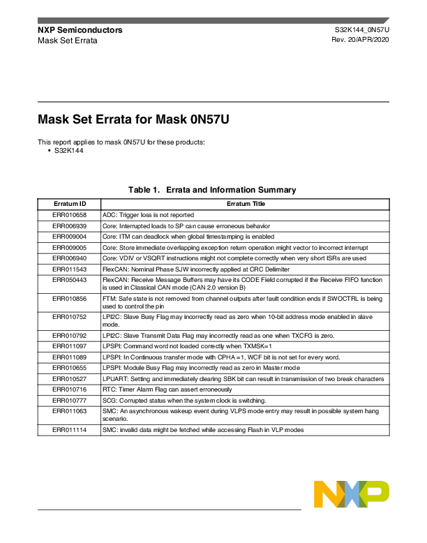
Table 1. Errata and Information Summary
Erratum Title
ADC: Trigger loss is not reported Core: Interrupted loads to SP can cause erroneous behavior Core: ITM can deadlock when global timestamping is enabled Core: Store immediate overlapping exception return operation might vector to incorrect interrupt Core: VDIV or VSQRT instructions might not complete correctly when very short ISRs are used FlexCAN: Nominal Phase SJW incorrectly applied at CRC Delimiter FlexCAN: Receive Message Buffers may have its CODE Field corrupted if the Receive FIFO function is used in Classical CAN mode (CAN 2.0 version B) FTM: Safe state is not removed from channel outputs after fault condition ends if SWOCTRL is being used to control the pin LPI2C: Slave Busy Flag may incorrectly read as zero when 10-bit address mode enabled in slave mode. LPI2C: Slave Transmit Data Flag may incorrectly read as one when TXCFG is zero. LPSPI: Command word not loaded correctly when TXMSK=1 LPSPI: In Continuous transfer mode with CPHA =1, WCF bit is not set for every word. LPSPI: Module Busy Flag may incorrectly read as zero in Master mode LPUART: Setting and immediately clearing SBK bit can result in transmission of two break characters RTC: Timer Alarm Flag can assert erroneously SCG: Corrupted status when the system clock is switching. SMC: An asynchronous wakeup event during VLPS mode entry may result in possible system hang scenario. SMC: invalid data might be fetched while accessing Flash in VLP modes
Revision 06/Mar/2019 20/APR/2020
Table 2. Revision History
Initial revision The following erratum was added.
� ERR011063
Changes
ERR010658: ADC: Trigger loss is not reported
Description: A trigger loss will not be reported in the following cases:
1. The time between two consecutive triggers on a trigger input is less than 4 cycles of ADC's Module interface clock.
2. One or multiple triggers come on any input while a trigger either stored or under process for that input in the trigger handler.
3. The trigger on a particular input asserts during the period of end-of-conversion cycle of a conversion initiated from this input.
� In these cases the Error in Multiplexed Trigger Request (ADC_SC2[TRGSTERR]) bit in the ADC Status and Control Register 2 will not be set.
� For the third case the Trigger status (ADC_SC2[TRGSTLAT]) bit in the ADC Status and Control Register 2 will also not be set.
Workaround: The time between two consecutive triggers on a particular input should be kept more than one ADC conversion time.
ERR006939: Core: Interrupted loads to SP can cause erroneous behavior
Description: Arm Errata 752770: Interrupted loads to SP can cause erroneous behavior
This issue is more prevalent for user code written to manipulate the stack. Most compilers will not be affected by this, but please confirm this with your compiler vendor. MQXTM and FreeRTOSTM are not affected by this issue.
Affects: Cortex-M4, Cortex-M4F
Fault Type: Programmer Category B
Fault Status: Present in: r0p0, r0p1 Open.
If an interrupt occurs during the data-phase of a single word load to the stack-pointer (SP/ R13), erroneous behavior can occur. In all cases, returning from the interrupt will result in the load instruction being executed an additional time. For all instructions performing an update to the base register, the base register will be erroneously updated on each execution, resulting in the stack-pointer being loaded from an incorrect memory location.
The affected instructions that can result in the load transaction being repeated are:
1) LDR SP,[Rn],#imm
Mask Set Errata for Mask 0N57U, Rev. 20/APR/2020
2
NXP Semiconductors
2) LDR SP,[Rn,#imm]!
3) LDR SP,[Rn,#imm]
4) LDR SP,[Rn]
5) LDR SP,[Rn,Rm]
The affected instructions that can result in the stack-pointer being loaded from an incorrect memory address are:
1) LDR SP,[Rn],#imm
2) LDR SP,[Rn,#imm]!
Conditions:
1) An LDR is executed, with SP/R13 as the destination.
2) The address for the LDR is successfully issued to the memory system.
3) An interrupt is taken before the data has been returned and written to the stack-pointer.
Implications:
Unless the load is being performed to Device or Strongly-Ordered memory, there should be no implications from the repetition of the load. In the unlikely event that the load is being performed to Device or Strongly-Ordered memory, the repeated read can result in the final stack-pointer value being different than had only a single load been performed.
Interruption of the two write-back forms of the instruction can result in both the base register value and final stack-pointer value being incorrect. This can result in apparent stack corruption and subsequent unintended modification of memory.
Workaround: Most compilers are not affected by this, so a workaround is not required.
However, for hand-written assembly code to manipulate the stack, both issues may be worked around by replacing the direct load to the stack-pointer, with an intermediate load to a generalpurpose register followed by a move to the stack-pointer.
If repeated reads are acceptable, then the base-update issue may be worked around by performing the stack pointer load without the base increment followed by a subsequent ADD or SUB instruction to perform the appropriate update to the base register.
ERR009004: Core: ITM can deadlock when global timestamping is enabled
Description: ARM ERRATA 806422
The Cortex-M4 processor contains an optional Instrumentation Trace Macrocell (ITM). This can be used to generate trace data under software control, and is also used with the Data Watchpoint and Trace (DWT) module which generates event driven trace. The processor supports global timestamping. This allows count values from a system-wide counter to be included in the trace stream.
When connected directly to a CoreSight funnel (or other component which holds ATREADY low in the idle state), the ITM will stop presenting trace data to the ATB bus after generating a timestamp packet. In this condition, the ITM_TCR.BUSY register will indicate BUSY.
Once this condition occurs, a reset of the Cortex-M4 is necessary before new trace data can be generated by the ITM.
Timestamp packets which require a 5 byte GTS1 packet, or a GTS2 packet do not trigger this erratum. This generally only applies to the first timestamp which is generated.
Mask Set Errata for Mask 0N57U, Rev. 20/APR/2020
NXP Semiconductors
3
Devices which use the Cortex-M optimized TPIU (CoreSight ID register values 0x923 and 0x9A1) are not affected by this erratum.
Workaround: There is no software workaround for this erratum. If the device being used is susceptible to this erratum, you must not enable global timestamping.
ERR009005: Core: Store immediate overlapping exception return operation might vector to incorrect interrupt
Description: Arm Errata 838869: Store immediate overlapping exception return operation might vector to incorrect interrupt Affects: Cortex-M4, Cortex-M4F Fault Type: Programmer Category B Rare Fault Status: Present in: r0p0, r0p1 Open. The Cortex-M4 includes a write buffer that permits execution to continue while a store is waiting on the bus. Under specific timing conditions, during an exception return while this buffer is still in use by a store instruction, a late change in selection of the next interrupt to be taken might result in there being a mismatch between the interrupt acknowledged by the interrupt controller and the vector fetched by the processor. Configurations Affected This erratum only affects systems where writeable memory locations can exhibit more than one wait state.
Workaround: For software not using the memory protection unit, this erratum can be worked around by setting DISDEFWBUF in the Auxiliary Control Register. In all other cases, the erratum can be avoided by ensuring a DSB occurs between the store and the BX instruction. For exception handlers written in C, this can be achieved by inserting the appropriate set of intrinsics or inline assembly just before the end of the interrupt function, for example: ARMCC: ... __schedule_barrier(); __asm{DSB}; __schedule_barrier(); } GCC: ... __asm volatile ("dsb 0xf" ::: "memory"); }
Mask Set Errata for Mask 0N57U, Rev. 20/APR/2020
4
NXP Semiconductors
ERR006940: Core: VDIV or VSQRT instructions might not complete correctly when very short ISRs are used
Description: Arm Errata 776924: VDIV or VSQRT instructions might not complete correctly when very short ISRs are used
Affects: Cortex-M4F
Fault Type: Programmer Category B
Fault Status: Present in: r0p0, r0p1 Open.
On Cortex-M4 with FPU, the VDIV and VSQRT instructions take 14 cycles to execute. When an interrupt is taken a VDIV or VSQRT instruction is not terminated, and completes its execution while the interrupt stacking occurs. If lazy context save of floating point state is enabled then the automatic stacking of the floating point context does not occur until a floating point instruction is executed inside the interrupt service routine.
Lazy context save is enabled by default. When it is enabled, the minimum time for the first instruction in the interrupt service routine to start executing is 12 cycles. In certain timing conditions, and if there is only one or two instructions inside the interrupt service routine, then the VDIV or VSQRT instruction might not write its result to the register bank or to the FPSCR.
Workaround: A workaround is only required if the floating point unit is present and enabled. A workaround is not required if the memory system inserts one or more wait states to every stack transaction.
There are two workarounds:
1) Disable lazy context save of floating point state by clearing LSPEN to 0 (bit 30 of the FPCCR at address 0xE000EF34).
2) Ensure that every interrupt service routine contains more than 2 instructions in addition to the exception return instruction.
ERR011543: FlexCAN: Nominal Phase SJW incorrectly applied at CRC Delimiter
Description: During the reception of a CAN-FD frame when the Bit Rate Switch (BRS) is enabled, the Synchronization Jump Width (SJW) for the CRC Delimiter bit is incorrectly defined by the Nominal Phase SJW. The CAN specification stipulates that the CRC Delimiter bit should have a SJW set by the Data Phase SJW.
When a resynchronization event is triggered for the CRC delimiter bit (recessive in correct operation), the sample point will be adjusted by an amount as defined by the Nominal Phase SJW rather than the specified Data Phase SJW. This may result in the incorrect detection of a dominant bit leading to a CAN error frame. However, as the CRC delimiter bit position will only apply the SJW upon the detection of an unexpected dominant bit on the CAN bus, an error frame is already likely. For the case the SJW is applied at the CRC delimiter and a recessive bit is not detected, the receiving node will issue an error frame.
The CAN protocol is designed to handle resynchronization errors and hence the CAN bus will recover from the insertion of the incorrect SJW at the CRC delimiter. Upon detecting the error frame the transmitting node will re-transmit the frame.
The following FlexCAN configurations are not affected:
� Classical CAN frames (CAN 2.0B) � CAN FD frames with bit rate switch disabled (BRS = 0)
Mask Set Errata for Mask 0N57U, Rev. 20/APR/2020
NXP Semiconductors
5
� CAN FD frames with Nominal Phase SJW equal to Data Phase SJW � CAN FD transmissions
Configuration for the FlexCAN:
� Nominal Phase SJW is configured by the Resync Jump Width bit in the CAN Control Register 1 (CAN_CTRL1[RJW]) or by the Extended Resync Jump Width bit in the CAN Bit Timing Register (CAN_CBT[ERJW])
� Data Phase SJW is configured by the Fast Resync Jump Width bit in the CAN FD Bit Timing Register (CAN_FDCBT[FRJW])
Workaround: The robustness of the CAN protocol ensures that the receiver automatically recovers from the application of the incorrect SJW. The CAN protocol is designed to recover from resynchronization errors and hence any frame that is not correctly received will be re-sent by the transmitting node.
ERR050443: FlexCAN: Receive Message Buffers may have its CODE Field corrupted if the Receive FIFO function is used in Classical CAN mode (CAN 2.0 version B)
Description: If the CODE Field of a Receive Message Buffer is corrupted it may deactivate the Message Buffer, so it is unable to receive new messages. It may also turn a Receive Message Buffer into any type of Message Buffer as defined in the Message buffer structure section in the device documentation.
The CODE Field of the FlexCAN Receive Message Buffers (MB) may get corrupted if the following sequence occurs.
1- A message is received and transferred to an MB (i.e. MBx)
2- A new message start being received (i.e. message1), SMB0 (Serial Message Buffer 0) receives the message1 intended for MBx
3- Before SMB0 being moved to MBx, MBx is locked by software for more than 20 CAN bit times (time determines the probability of erratum to manifest), therefore SMB0 is NOT transferred to MBx, it remains with message1.
4- A subsequent incoming message (i.e. message2) is being loaded into SMB1 (as SMB0 is full) and is evaluated by the FlexCAN hardware as being for the FIFO.
5- During the message2, the MBx is unlocked. Then, the content of SMB0 is transferred to MBx and the CODE field is updated with an incorrect value.
In case a customer does use Rx FIFO only or dedicated MB only, (i.e. either Rx MB or Rx FIFO is used) the problem doesn't occur. In case a customer does use Flexible Data Rate CAN (CAN FD), the problem does not occur also. So bottom line the problem does only occur if the FlexCAN is programmed to receive in the FIFO and dedicated MB at the same application.
Workaround: This defect only applies if the Receive FIFO is used. This feature is enabled by RFEN bit in the Module Control Register (MCR[RFEN]). If the Rx FIFO is not used, the Receive Message Buffer CODE Field is not corrupted.
The defect does not occur if the Receive Message Buffer lock time is less than or equal to the time equivalent to 20 x CAN bit time.
After receiving the Interrupt Flag for the corresponding MB (BUFx bit on the IFLAGx register) set by the hardware, the recommended way for the CPU to service (read) the frame received in a mailbox is by the following procedure:
Mask Set Errata for Mask 0N57U, Rev. 20/APR/2020
6
NXP Semiconductors
1. Read the Control and Status word of that mailbox.
2. Check if the BUSY bit (CODE[0]) is deasserted, indicating that the mailbox is not locked. Repeat step 1) while it is asserted.
3. Read the contents of the mailbox.
4. Clear the proper flag in the IFLAG register.
5. Read the Free Running Timer register (TIMER) to unlock the mailbox
In order to guarantee that this procedure occurs in less than 20 CAN bit times the MB receive handling process in software (step 1 to step 5 above) should be performed as a `critical code section' (interrupts disabled before execution) and should ensure that the MB receive handling occurs in a deterministic number of cycles.
If the MB receive handling process can't be guaranteed in a time, less than or equal to 20 CAN bit times, Rx FIFO should not be used together with the receive Message Buffers in a Classical CAN application.
ERR010856: FTM: Safe state is not removed from channel outputs after fault condition ends if SWOCTRL is being used to control the pin
Description: If an FTM channel output is being controlled using the software output control register (FTM_SWOCTRL) and fault detection is also enabled for the channel, then when a fault is detected the output is forced to its safe value. However, when the fault condition has been cleared, the channel output will stay in the safe state instead of reverting to the value programmed by the FTM_SWOCTRL register.
Workaround: If fault control is enabled while the software output control register is also being used (FTM_SWOCTRL), then the FTM should be configured as follows:
-- FTM_MODE[FAULTM] configured for manual fault clearing (0b10)
-- For devices that include the FTM_CONF[NUMTOF] field, it must be cleared to 0b00000 (TOF set for each counter overflow). For FTM versions that don't include the FTM_CONF[NUMTOF] field this doesn't apply.
The procedure below must be used in the TOF interrupt handler when a fault is detected to ensure that the outputs return to the value configured by FTM_SWOCTRL.
1. Check the value of FTM_FMS[FAULTF].
-- If FTM_FMS[FAULTF] = 1 (fault occurred or is occurring), then set a variable to indicate that a fault was detected and continue to step 2.
-- If FTM_FMS[FAULTF] = 0 but the fault variable is set (fault is not active, but was previously detected), continue to step 6.
2. Write the FTM_OUTMASK register to set the bit or bits corresponding to any channels that are controlled by FTM_SWOCTRL to temporarily inactivate the channel output.
3. Clear fault conditions by reading the FTM_FMS register and then writing FTM_FMS with all zeroes.
4. Clear the FTM_SC[TOF] bit by reading the FTM_SC register, then writing a 0 to FTM_SC[TOF].
5. Exit the interrupt handler to skip following steps (they will execute the next time the TOF handler is called).
6. Clear the FTM_SWOCTRL by writing all zeroes to it.
Mask Set Errata for Mask 0N57U, Rev. 20/APR/2020
NXP Semiconductors
7
7. Write FTM_SWOCTRL with the desired value again. 8. Clear the FTM_OUTMASK bits that were set in step 2. 9. Clear the fault variable that was set in step 1 when the fault condition was originally detected. 10. Clear the FTM_SC[TOF] bit by reading the FTM_SC register, then writing a 0 to FTM_SC[TOF].
ERR010752: LPI2C: Slave Busy Flag may incorrectly read as zero when 10-bit address mode enabled in slave mode.
Description: When operating in slave mode with 10-bit addressing enabled and an address match is detected on the first address byte, the Slave Busy Flag, SSR[SBF], may incorrectly read as zero.
Workaround: When using the LPI2C in slave mode when 10-bit addressing is enabled, and the SSR[SBF] bit is read as a one, then the flag is set. If it is read as a zero, it must be read a second time and this second read will be the correct state of the bit.
ERR010792: LPI2C: Slave Transmit Data Flag may incorrectly read as one when TXCFG is zero.
Description: When SCFGR1[TXCFG] = 0, the slave transmit data ready flag can incorrectly assert for one cycle.
Workaround: Set SCFGR1[TXCFG] = 1.
ERR011097: LPSPI: Command word not loaded correctly when TXMSK=1
Description: When the Transmit Command Register is written with TCR[TXMSK]=1 and the next write to the TX FIFO is another command, then the first command may not load correctly.
Workaround: When writing the Transmit Command Register with TCR[TXMSK]=1, wait for the TX FIFO to go empty (FSR[TXCOUNT] = 0) before writing another command to the Transmit Command Register.
ERR011089: LPSPI: In Continuous transfer mode with CPHA =1, WCF bit is not set for every word.
Description: When Transmit Command Register is written with TCR[CONT]=1 and TCR[CPHA]=1, SR[WCF] bit flag is not set after data is transferred. Therefore polling for SR[WCF] flag to identify if data has been sent can cause MCU to be stuck.
Workaround: When using continuous transfer mode TCR[CONT]=1 and TCR[CPHA]=1, do not use SR[WCF] flag to determine if data has been sent, fill up instead transmit FIFO with the following data without waiting for SR[WCF] flag to be set.
Mask Set Errata for Mask 0N57U, Rev. 20/APR/2020
8
NXP Semiconductors
ERR010655: LPSPI: Module Busy Flag may incorrectly read as zero in Master mode
Description: When operating in master mode, the Module Busy Flag, SR[MBF], may incorrectly read as zero. This applies only to master mode and not to slave mode.
Workaround: When using the LPSPI in master mode and the SR[MBF] bit is read as a one then the flag is set. If it is read as a zero, it must be read a second time and this second read will be the correct state of the bit.
ERR010527: LPUART: Setting and immediately clearing SBK bit can result in transmission of two break characters
Description: When the LPUART transmitter is idle (LPUART_STAT[TC]=1), two break characters may be sent when using LPUART_CTRL[SBK] to send one break character. Even when LUART_CTRL[SBK] is set to 1 and cleared (set to 0) immediately.
Workaround: To queue a single break character via the transmit FIFO, set LPUART_DATA[FRETSC]=1 with data bits LPUART_DATA[T9:T0]=0.
ERR010716: RTC: Timer Alarm Flag can assert erroneously
Description: Writing to the Time Alarm Register (RTC_TAR) at the same time the RTC Seconds Register is incrementing can assert the Time Alarm Flag (RTC_SR[TAF]) bit in the RTC Status Register.
Workaround: Write the Time Alarm Register (RTC_TAR) when the RTC Seconds Register is not incrementing. This can be when Time Counter Enable (RTC_SR[TCE]) bit in the RTC Status Register is clear or within the RTC_SR[TAF] interrupt routine.
Alternatively, if the RTC_SR[TAF] is asserted following a write to the RTC_TAR, then write the RTC_TAR again.
ERR010777: SCG: Corrupted status when the system clock is switching.
Description: The SCG_RCCR[SCS] and SCG_HCCR[SCS] may have a corrupted status during the interval when the system clock is switching
Workaround: The SCS field should be read twice by the software to ensure the system clock switch has completed.
ERR011063: SMC: An asynchronous wakeup event during VLPS mode entry may result in possible system hang scenario.
Description: When the bus clock is same system clock and an asynchronous wakeup occurs during a mode transition from RUN to VLPS or VLPR to VLPS, the MCU may hang in an undetermined state, which can only be recovered by a power-on reset event or a watchdog reset.
Workaround: Before executing the transition to VLPS ensure that the PREDIV_SYS_CLK frequency / BUS_CLK frequency configuration for RUN/VLPR mode is greater than or equal to 2.
Mask Set Errata for Mask 0N57U, Rev. 20/APR/2020
NXP Semiconductors
9
For example: Assuming a PREDIV_SYS_CLK of 8 MHz and SCG_RCCR[DIVCORE] = 0b0001 (divider of 2) and SCG_RCCR[DIVBUS] = 0b0000 (divider of 1), (PREDIV_SYS_CLK = 8 MHz) / (BUS_CLK = 4 MHz) , a ratio of 1:2.
ERR011114: SMC: invalid data might be fetched while accessing Flash in VLP modes
Description: VLPR and VLPS Low power modes are documented to work at System Clock and Core Clock at 4 Mhz and the Bus Clock at 4 MHz and DMA enabled from or to Flash memory. However any simultaneous access from any master (Core or DMA) to Dflash and Pflash may get invalid data while being in VLP modes and System clock, Core Clock and Bus Clock are above 1 Mhz
Workaround: There are two workarounds:
1. Restrict software to use either only Pflash or only Dflash only at a time in VLP modes for all masters (CPU,DMA) . When switching from Pflash only access to Dflash only access let current DMA transactions accessing flash to complete and jump to SRAM location , wait for 40 cycles for the ongoing accesses to complete on the current flash before accessing dflash.
When switching from dflash only accesses to pflash only accesses let the current DMA transactions accessing dflash to complete
and wait for 40 cycles for accesses to complete on the dflash before accessing the pflash.
2. If both Pflash and Dflash needs to be accessed simultaneously, the VLP modes must be run with System Clock, Core Clock and Bus Clock of 1 MHz.
Mask Set Errata for Mask 0N57U, Rev. 20/APR/2020
10
NXP Semiconductors
How to Reach Us:
Home Page: nxp.com
Web Support: nxp.com/support
Information in this document is provided solely to enable system and software implementers to use NXP products. There are no express or implied copyright licenses granted hereunder to design or fabricate any integrated circuits based on the information in this document. NXP reserves the right to make changes without further notice to any products herein.
NXP makes no warranty, representation, or guarantee regarding the suitability of its products for any particular purpose, nor does NXP assume any liability arising out of the application or use of any product or circuit, and specifically disclaims any and all liability, including without limitation consequential or incidental damages. "Typical" parameters that may be provided in NXP data sheets and/or specifications can and do vary in different applications, and actual performance may vary over time. All operating parameters, including "typicals," must be validated for each customer application by customers technical experts. NXP does not convey any license under its patent rights nor the rights of others. NXP sells products pursuant to standard terms and conditions of sale, which can be found at the following address: nxp.com/SalesTermsandConditions.
While NXP has implemented advanced security features, all products may be subject to unidentified vulnerabilities. Customers are responsible for the design and operation of their applications and products to reduce the effect of these vulnerabilities on customer's applications and products, and NXP accepts no liability for any vulnerability that is discovered. Customers should implement appropriate design and operating safeguards to minimize the risks associated with their applications and products.
NXP, the NXP logo, NXP SECURE CONNECTIONS FOR A SMARTER WORLD, COOLFLUX, EMBRACE, GREENCHIP, HITAG, I2C BUS, ICODE, JCOP, LIFE VIBES, MIFARE, MIFARE CLASSIC, MIFARE DESFire, MIFARE PLUS, MIFARE FLEX, MANTIS, MIFARE ULTRALIGHT, MIFARE4MOBILE, MIGLO, NTAG, ROADLINK, SMARTLX, SMARTMX, STARPLUG, TOPFET, TRENCHMOS, UCODE, Freescale, the Freescale logo, AltiVec, C-5, CodeTEST, CodeWarrior, ColdFire, ColdFire+, C-Ware, the Energy Efficient Solutions logo, Kinetis, Layerscape, MagniV, mobileGT, PEG, PowerQUICC, Processor Expert, QorIQ, QorIQ Qonverge, Ready Play, SafeAssure, the SafeAssure logo, StarCore, Symphony, VortiQa, Vybrid, Airfast, BeeKit, BeeStack, CoreNet, Flexis, MXC, Platform in a Package, QUICC Engine, SMARTMOS, Tower, TurboLink, and UMEMS are trademarks of NXP B.V. All other product or service names are the property of their respective owners. AMBA, Arm, Arm7, Arm7TDMI, Arm9, Arm11, Artisan, big.LITTLE, Cordio, CoreLink, CoreSight, Cortex, DesignStart, DynamIQ, Jazelle, Keil, Mali, Mbed, Mbed Enabled, NEON, POP, RealView, SecurCore, Socrates, Thumb, TrustZone, ULINK, ULINK2, ULINK-ME, ULINK-PLUS, ULINKpro, Vision, Versatile are trademarks or registered trademarks of Arm Limited (or its subsidiaries) in the US and/or elsewhere. The related technology may be protected by any or all of patents, copyrights, designs and trade secrets. All rights reserved. Oracle and Java are registered trademarks of Oracle and/or its affiliates. The Power Architecture and Power.org word marks and the Power and Power.org logos and related marks are trademarks and service marks licensed by Power.org.
� 2020 NXP B.V.