Contents
- 1. User manual
- 2. User manual (Statement)
User manual

ITON TECHNOLOGY LTD. Bluetooth 3.0 HID Module
1
Office Add.: Room 1302, Block A, Building 4, Tianan Cyber Park, Huangge Road,
Longgang District, Shenzhen, Guangdong, China
Tel: 86-755-82079392,82078660 Fax: 86-755-82079390 July 28,2011
Product:
Module Number:
FCC ID:
Bluetooth 3.0 HID Module ,Class 2
BT3GMD-B47P
User Manual
ID6ZFN-BK0
Brand name:
ZAGG
QTG-ZKMS

ITON TECHNOLOGY LTD. Bluetooth 3.0 HID Module
Section 1:Overview
The BT3GMD-B47P is a Bluetooth Human Interface Device(HID) module based on
the Broadcom BCM20730 Bluetooth 3.0 specification basic rate-compliant stand alone
baseband processor with an integrated 2.4GHz transceiver.
The module includes EEPROM, crystal, and PCB antenna.
1.1 Applications
●Wireless pointing devices: mice , trackballs , gestural controls
●Wireless keyboards
●3D glasses
●Game controllers
●Point-of-sale(POS)input devices
●Remote sensors
●Home automation
●Personal health and fitness monitoring
1.2 Features
The BT3GMD-B47P offers the following features:
●On-chip support for common keyboard and mouse interfaces eliminates external
processor
●Programmable keyscan matrix interface, up to 8 ×20 key-scanning matrix
●Bluetooth specification 3.0 compatible, includeing enhanced power control
●Bluetooth HID profile version 1.0 compliant
●Bluetooth Device ID profile version 1.3 compliant
●Bluetooth AVRCP-CT profile version 1.3 compliant
●Supports Adaptive Frequency Hopping(AFH)
●On-chip support for serial peripheral interface(SPI)
●Programmable output power control meets Class 2 or Class 3 requirements
●Excellent receiver sensitivity
●Integrated ARM CortexTM-M3 based
●On-chip power-on reset(POR)
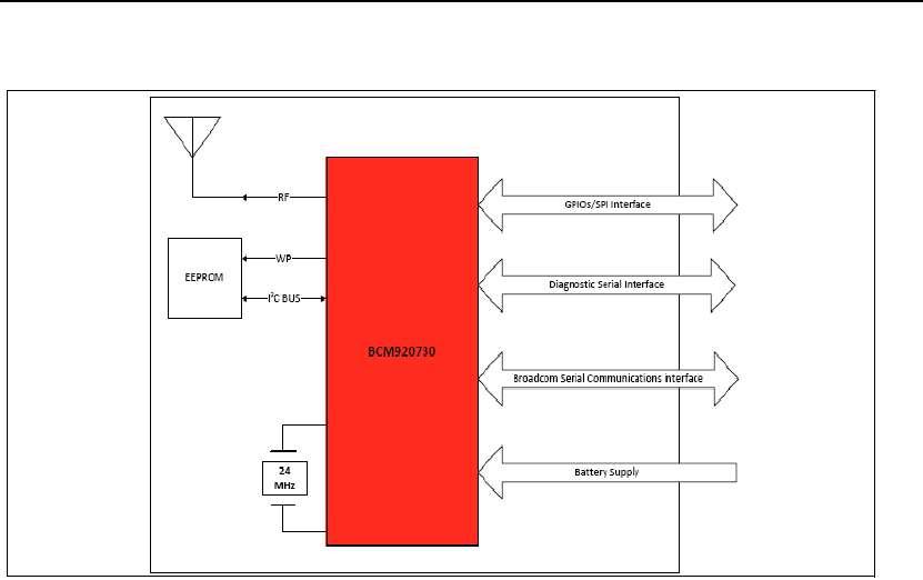
1.3 Functional Description
The primary component on the module is the Broadcom BCM20730, which is a
Bluetooth 3.0 compliant basic rate single-chip. The baseband and radio have been
integrated into a single chip implemented in standard digital CMOS. The block diagram of
the module is shown in Figure 1.
ITON TECHNOLOGY LTD. Bluetooth 3.0 HID Module
Figure 1: Block Diagram
The BT3GMD-B47P employs an integrated ARM CortexTM-M3 microprocessor core
that runs software from the Link Control layer up to the Host Controller Interface (HCI).The
baseband portion of the BT3GMD-B47P performs all the time-critical functions required
for high-performance Bluetooth operations.
The radio incorporates the complete receive and transmit paths, including PLL, VCO,
LNA, PA, upconverter,downconverter, modulator, demodulator, and channel select
filtering.
The BT3GMD-B47P on-chip keyboard scanner is designed to autonomously sample
keys and store them into buffer registers without requiring host microcontroller
intervention. A state machine of three states(Idle, Scan, and Scan-End)controls the
keyscan block.
The module has a SPI interface. The interface has a 16-byte transmit buffer and a
16-byte receive buffer .To support more flexibility for user applications. The module acts
as an SPI master device that supports 1.8V or 3.3V SPI slaves.
ITON TECHNOLOGY LTD. Bluetooth 3.0 HID Module
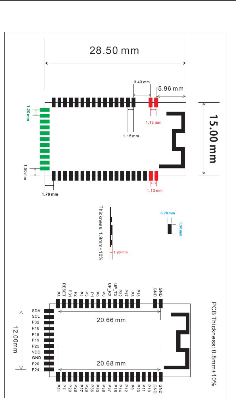
1.4 Physical Description
The BT3GMD-B47P is a 28.5mm×15mm FR4 PCB with 47 pads located around
the perimeter. Table 1 shows the pinout diagram of the module.
Table 1 Pin Location
Figure 2: Module PCB Top View
P
I
N
Signal
P
IN Signal
P
IN Signal
P
IN Signal
P
IN Signal
1 GND 2 GND 3 P13 4 P8 5 P17
6 P22 7 UP_TX 8 UP_RX 9 P6 10 P0
11 P1 12 P5 13 P4 14 P2 15 P31
16 RESET 17 P3 18 SDA 19 SCL 20 P32
21P1622P1823P1924P2525VDD
26 GND 27 P20 28 P24 29 P21 30 P7
31P2932P2833P2734P2635P36
36P3037P3838P3739P1540P14
41P1242 P9 43P2344P1145P10
46 GND 47 GND
2
8
.
5
mm
15mm

ITON TECHNOLOGY LTD. Bluetooth 3.0 HID Module
Table 2 Pin Function Descriptions
Pin
Number Pin
Name Default
Direction POR
State Function Description
1,2,
26,46,
47
GND Ground
25 VDD Power supply
16 RESET PU Active-low system reset with open-drain output & internal pull up resistor
18 SDA I/O PU Data signal for an extern I
2
C device
19 SCL I/O PU Clock signal for an extern I
2
C device
7 UP_TX output PU UART serial output-serial data output for the HCI UART interface
8 UP_RX input UART serial input-serial data output for the HCI UART interface
10 P0 input Floating GPIO:P0,Keyboard scan input(row):KSI0
11 P1 input Floating GPIO:P1,Keyboard scan input(row):KSI1
14 P2 input Floating GPIO:P2,Keyboard scan input(row):KSI2
17 P3 input Floating GPIO:P3,Keyboard scan input(row):KSI3
13 P4 input Floating GPIO:P4,Keyboard scan input(row):KSI4
12 P5 input Floating GPIO:P5,Keyboard scan input(row):KSI5
9 P6 input Floating GPIO:P6,Keyboard scan input(row):KSI6
30 P7 input Floating GPIO:P7,Keyboard scan input(row):KSI7
4 P8 input Floating GPIO:P8,Keyboard scan output(column):KSO0
42 P9 input Floating GPIO:P9,Keyboard scan output(column):KSO1
45 P10 input Floating GPIO:P10,Keyboard scan output(column):KSO2
44 P11 input Floating GPIO:P11,Keyboard scan output(column):KSO3
41 P12 input Floating GPIO:P12,Keyboard scan output(column):KSO4
3 P13 input Floating GPIO:P13,Keyboard scan output(column):KSO5
40 P14 input Floating GPIO:P14,Keyboard scan output(column):KSO6
39 P15 input Floating GPIO:P15,Keyboard scan output(column):KSO7
21 P16 input Floating GPIO:P16,Keyboard scan output(column):KSO8
5 P17 input Floating GPIO:P17,Keyboard scan output(column):KSO9
22 P18 input Floating GPIO:P18,Keyboard scan output(column):KSO10
23 P19 input Floating GPIO:P19,Keyboard scan output(column):KSO11
27 P20 input Floating GPIO:P20,Keyboard scan output(column):KSO12
29 P21 input Floating GPIO:P21,Keyboard scan output(column):KSO13
6 P22 input Floating GPIO:P22,Keyboard scan output(column):KSO14
43 P23 input Floating GPIO:P23,Keyboard scan output(column):KSO15
28 P24 input Floating GPIO:P24,Keyboard scan output(column):KSO16
24 P25 input Floating GPIO:P25,Keyboard scan output(column):KSO17,SPI MISO (Master mode)
34 P26 input Floating GPIO:P26,Current 16 mA @3.3V
33 P27 input Floating GPIO:P27,Current 16 mA @3.3V
32 P28 input Floating GPIO:P28,Current 16 mA @3.3V
31 P29 input Floating GPIO:P29,Current 16 mA @3.3V
36 P30 input Floating GPIO:P30,A/D converter input,Default as the battery capacity detection
15 P31 input Floating GPIO:P31, A/D converter input,
20 P32 input PU GPIO:P32,Default as the EEPROM write protect pin
35 P36 input Floating GPIO:P36,SPI CLK(Master mode)
38 P37 input Floating GPIO:P37,SPI CS(Master mode)
37 P38 input Floating GPIO:P38,SPI MOSI(Master mode)

ITON TECHNOLOGY LTD. Bluetooth 3.0 HID Module
Section 2: Supporting Documentions
2.1 Reference Schematic
The most recent schematic , bill of material ,and layout file are available
from the ITON Technology Limit. Contact your ITON representative for details.
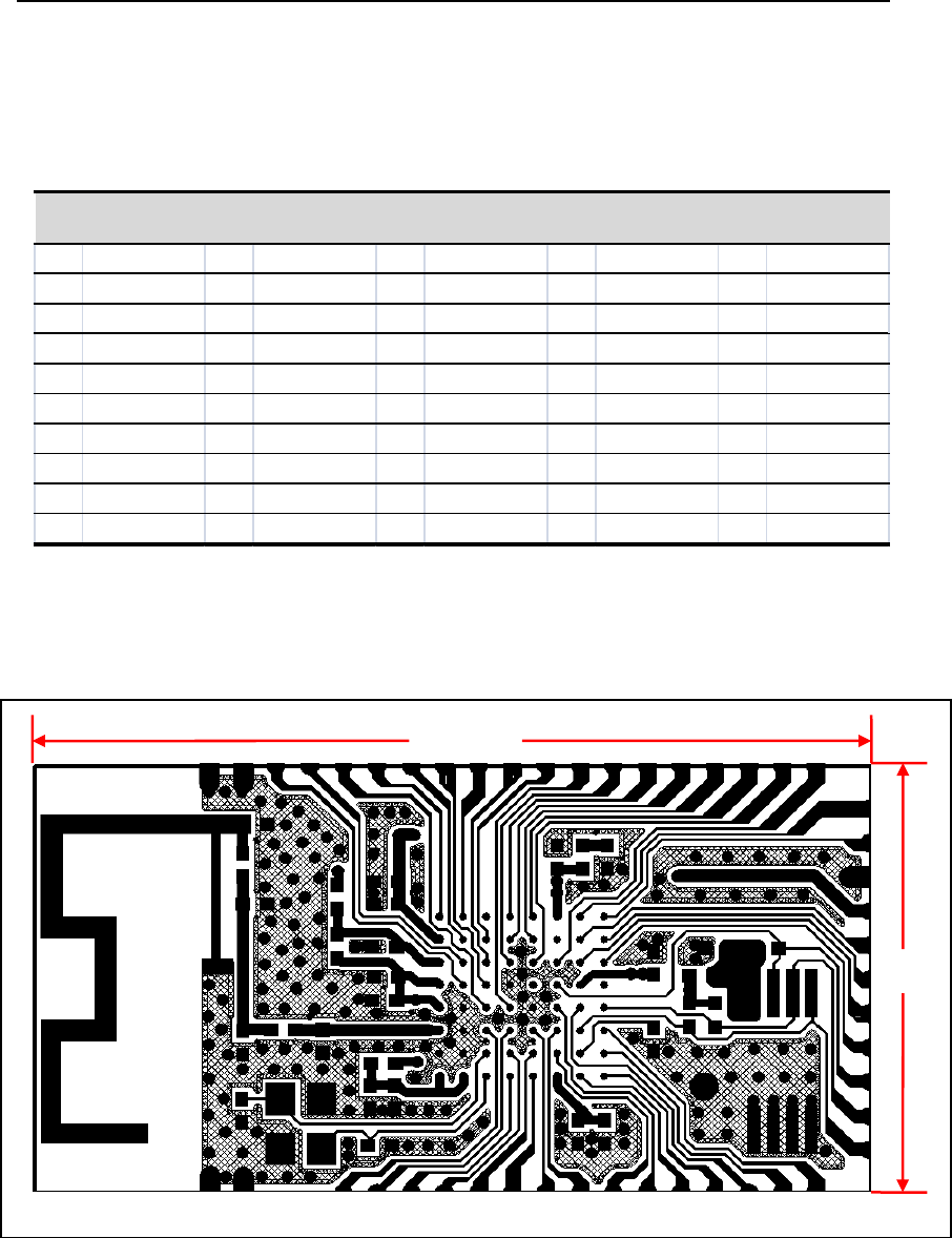
2.2 Layout Considerations
The BT3GMD-B47P module is placed at the location where the antenna is
away from the power supply(i.e.,BT1 Battery contacts)and any digital signal
traces. There should be no key matrix membrane under the antenna area and
the user’s hand should not be over the antenna area when the keyboard is in use.
The antenna keep-out area which is 5mm around the parameter of the module
region is shown in the red dotted box. PCB material and signal traces should not
be placed within the antenna keep-out area to assure optimum antenna
performance.
Figure 3: Keyboard PCB
2.3 Electrical Characteristics
Table 3: Maximum Electrical Rating
Table 4 :Power supply
Rating Symbol Value Unit
Dc supply voltage -1.4(Min)--3.8(Max) V
Voltage on input or output pin -Vs s -0.3 to Vdd +0.3 V
Operating ambient temperature range Topr 0 to +70 ℃
Storage temperature range Tstg -40 to +125 ℃
Rating Minimum Typical Maximum
Dc supply voltage 1.6V 2.8V 3.6V
ITON TECHNOLOGY LTD. Bluetooth 3.0 HID Module
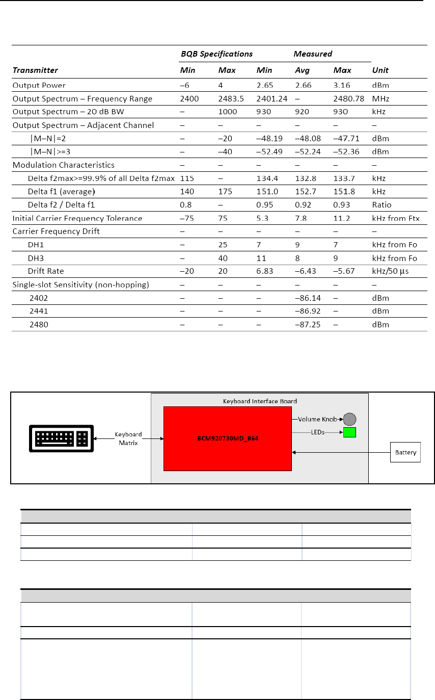
2.4 RF Specification
Table 5 : Module RF Specifications(Vdd_RF=1.5,T=25C)
Section3:Application Examples
Figure 4: Keyboard PCB
Table 6: keyboard Performance
Table 7: 3D Galsses Performance
Power consumption Vdd @1.8V Vdd @2.8V
operating current 1mA <2mA
Standby current 0.03-0.4mA 0.03-0.4mA
Deep sleep 22.5uA 22.5uA
Power consumption Vdd @3V Remark
Pairing current 15mA 30 second timeout, the 2
LEDs flash by tunes
operating current 1.2mA
Deep sleep 1.2uA
push power switch one
tim e will wake up the
device and push one
time again will power off
the device
ITON TECHNOLOGY LTD. Bluetooth 3.0 HID Module
Section 4: Mechanical Specification
Figure 5: 47Pin-Bluetooth Module
ITON TECHNOLOGY LTD. Bluetooth 3.0 HID Module
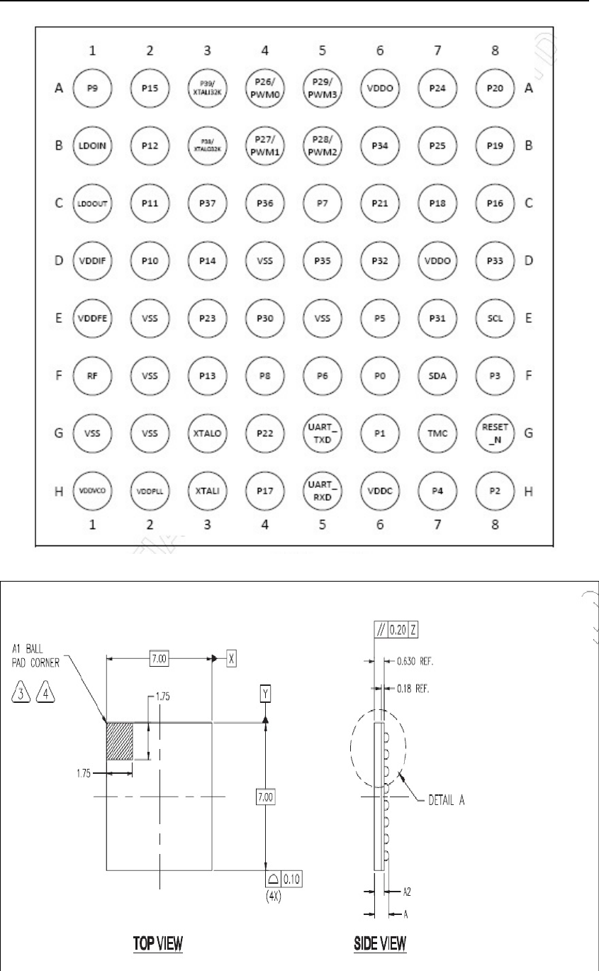
Figure 6: 64Pin BGA Ball Map

ITON TECHNOLOGY LTD. Bluetooth 3.0 HID Module
Figure 7: 64Pin FBGA Package
Attention: Limited Modular Approval ‐this RF Module may not be sold to the generic public and
requires professional installation. Due to the fact that this RF Module is not equipped with an own
shielding, the end‐product incl. this RF Module has to show compliance to the FCC rules
(15B/radiated emissions).
(OEM)Integrator has to assure compliance of the entire end‐product incl. the integrated RF
Module. Additional measurements (15B) and/ or equipment authorizations
(e.g Verification) may need to be addressed depending on co‐location or simultaneous
transmission issues if applicable.
Integrator is reminded to assure that these installation instructions will not be made available to the
end‐user of the final host device.
With the low output power, this RF Module meets the FCC SAR exemption.
The final host device, into which this RF Module is integrated "has to be labeled with an auxiliary
lable stating the FCC ID of the RF Module
The RF Module is powered by DC ,the antenna is PCB antenna and the antenna gain is 2 dBi.
This device complies with part15 of the FCC rules. Operation is subject to the following two
conditions:
(1) this device may not cause harmful interference, and
(2)this device must accept any interference received, including interference that may cause
undesired operation. "should be placed also on the device or alternatively within a prominent
location of the users manual
Changes or modifications to this unit not expressly approved by the party responsible for
compliance could void the user's authority to operate the equipment.
, such as" Contains FCC ID: QTG-ZKMS
This module is intended for OEM integrator. The OEM integrator is still responsible for the FCC
compliance requirement of the end product, which integrates this module. Due to missing shielding
the module is strictly limited to integration by the Grantee himself or his dedicated OEM Integrator.
The integration is strictly limited into following host platform(s) that are electrically identical incl.
variations that are defined as Class I Permissive Change to the documented and certified samples
under the control of the Grantee.
Additional hosts and/or platforms can be added via Class II Permissive Change by the Grantee.
-Bluetooth Keyboard
This RF Module will be exclusively integrated into battery power host devices
under strict control of the Grantee.