ADC Telecommunications DCX0801B Digivance CXD 800 MHz A and B Band System User Manual Cover 1
ADC Telecommunications Inc Digivance CXD 800 MHz A and B Band System Cover 1
Manual
ADCP-75-192
Issue 1
December 2005
Digivance
CXD Multi-Band
Distributed Antenna System
Operation Manual
1343155 Rev A

ADCP-75-192
Issue 1
December 2005
Digivance
CXD Multi-Band
Distributed Antenna System
Operation Manual
1343155 Rev A

ADCP-75-192 • Issue 1 • December 2005 • Preface
Page ii
COPYRIGHT
2005, ADC Telecommunications, Inc.
All Rights Reserved
Printed in the U.S.A.
REVISION HISTORY
ISSUE DATE REASON FOR CHANGE
Issue 1 12/2005 Original release
LIST OF CHANGES
The technical changes incorporated into this issue are listed below.
SECTION IDENTIFIER DESCRIPTION OF CHANGE
- - Original release
TRADEMARK INFORMATION
ADC and Digivance are registered trademarks of ADC Telecommunications, Inc.
DISCLAIMER OF LIABILITY
Contents herein are current as of the date of publication. ADC reserves the right to change the contents without prior notice. In no
event shall ADC be liable for any damages resulting from loss of data, loss of use, or loss of profits and ADC further disclaims
any and all liability for indirect, incidental, special, consequential or other similar damages. This disclaimer of liability applies
to all products, publications and services during and after the warranty period.
This publication may be verified at any time by contacting ADC’s Technical Assistance Center at 1-800-366-3891, extension 73476
(in U.S.A. or Canada) or 952-917-3476 (outside U.S.A. and Canada), or by e-mail to wireless.tac@adc.com.
ADC Telecommunications, Inc.
P.O. Box 1101, Minneapolis, Minnesota 55440-1101
In U.S.A. and Canada: 1-800-366-3891
Outside U.S.A. and Canada: (952) 917-3475
Fax: (952) 917-1717

ADCP-75-192 • Issue 1 • December 2005 • Preface
Page iii
2005, ADC Telecommunications, Inc.
TABLE OF CONTENTS
Content Page
FRONT MATTER
ABOUT THIS MANUAL ...................................................................... vii
RELATED PUBLICATIONS .................................................................... vii
ADMONISHMENTS ....................................................................... viii
GENERAL SAFETY PRECAUTIONS.............................................................. viii
SAVE WORKING DISTANCES .................................................................. ix
COMPLIANCE STATEMENT ................................................................... ix
ACRONYMS AND ABBREVIATIONS ............................................................... x
SECTION 1
OVERVIEW
1 INTRODUCTION .................................................................... 1-1
2
DIGIVANCE CXD SYSTEM OVERVIEW ...................................................... 1-1
2.1 Basic Components ............................................................. 1-2
2.2 General Description ............................................................ 1-2
2.3 Local Service Interface.......................................................... 1-3
2.4 Remote NOC Interface .......................................................... 1-4
3 SYSTEM FUNCTIONS AND FEATURES...................................................... 1-4
3.1 Fiber Optic Transport ........................................................... 1-4
3.2 Control and Monitoring Software ................................................... 1-5
3.3 Fault Detection and Alarm Reporting................................................. 1-5
3.4 Powering ................................................................... 1-5
3.5 Equipment Mounting and Configuration ............................................... 1-8
3.6 Hub Subsystem Assemblies....................................................... 1-8
3.7 RAN Subsystem Assemblies ..................................................... 1-11
3.8 Communication Interfaces....................................................... 1-14
SECTION 2
DESCRIPTION
1 INTRODUCTION .................................................................... 2-1
2 DIGITAL CHASSIS ................................................................... 2-2
3 RF CHASSIS....................................................................... 2-5
4 RADIO ACCESS NODE (RAN) ........................................................... 2-9
4.1 RAN cabinet ................................................................ 2-10
5 ELEMENTS COMMON TO HUB AND RAN ................................................... 2-11
5.1 Central Processor Unit (CPU) .................................................... 2-11
5.2 System Interface (STF2) ........................................................ 2-13
5.3 Sonet Interface (SIF) .......................................................... 2-15
5.4 Small Form-Factor Optical Transceiver (SFP) ......................................... 2-16
6 HUB SPECIFIC MODULES ............................................................. 2-17

ADCP-75-192 • Issue 1 • December 2005 • Preface
Page iv
2005, ADC Telecommunications, Inc.
TABLE OF CONTENTS
Content Page
6.1 Full Band Hub Down Converter (FBHDC) ............................................. 2-17
6.2 Forward Simulcast Card (FSC) .................................................... 2-18
6.3 Hub Upconverter Card (HUC) ..................................................... 2-19
6.4 Reverse Simulcast Card (RSC) .................................................... 2-20
6.5 Hub Reference Module (HRM) ................................................... 2-22
6.6 Ethernet Hub ................................................................ 2-24
6.7 BTS Interface Module (BIM) ..................................................... 2-25
6.8 Attenuator Shelf .............................................................. 2-28
7 RADIO ACCESS NODE (RAN) SPECIFIC MODULES ............................................. 2-29
7.1 Ran Down Converter (RDC or RDC2) ............................................... 2-29
7.2 Ran Up Converter (RUC2.X or RUC3) ............................................... 2-30
7.3 AC Power Entry Controller (APEC) .................................................. 2-31
7.4 DC Power Entry Controller (DPEC) ................................................. 2-32
7.5 CompactPCI Power Supply (cPCI P/S) ............................................... 2-34
7.6 RF Assembly Module (RFA) ..................................................... 2-35
7.7 Specifications ............................................................... 2-41
SECTION 3
NETWORK AND SYSTEM INSTALLATION AND SETUP
1 INTRODUCTION ..................................................................... 3-2
2 NETWORKING OVERVIEW .............................................................. 3-2
3 NODE IDENTIFICATION SCHEMES ......................................................... 3-3
4 IDENTIFICATION USING THE NETWORK IP RECEIVER/SENDER SYSTEM................................ 3-3
5 HUB EQUIPMENT IDENTIFICATIONS ....................................................... 3-3
6 ASSIGNING TENANTS ................................................................. 3-5
6.1 Understanding Tenant MIB Indexing.................................................. 3-5
6.2 BTS Connection MIB ............................................................ 3-6
6.3 Pathtrace Format .............................................................. 3-9
7 TENANT CONFIGURATION ............................................................. 3-13
7.1 Setting Protocol .............................................................. 3-13
7.2 Setting Channels ............................................................. 3-13
7.3 Setting Hub Measured Forward Gain ................................................ 3-13
7.4 Setting RAN Measured Forward Gain ................................................ 3-13
7.5 Setting FSC Gain ............................................................. 3-13
7.6 Setting RAN Forward Gain Offset ................................................... 3-14
7.7 Setting Reverse Gain........................................................... 3-14
7.8 Setting Reverse Cable Loss ...................................................... 3-14
7.9 Using Tenant Reset............................................................ 3-14
7.10 Enabling FGC / RGC............................................................ 3-14
7.11 Using Tenant Mode ............................................................ 3-15
7.12 Enabling / Disabling Delay Compensation ............................................. 3-15
7.13 Setting Forward / Reverse Delay Skew ............................................... 3-15

ADCP-75-192 • Issue 1 • December 2005 • Preface
Page v
2005, ADC Telecommunications, Inc.
TABLE OF CONTENTS
Content Page
7.14 Enabling / Disabling RAN slots.................................................... 3-15
7.15 Forward/Reverse Target Delay.................................................... 3-16
7.16 FSC Attenuator Offsets ......................................................... 3-16
7.17 Target Simulcast Degree........................................................ 3-16
7.18 Module Attenuators ........................................................... 3-16
8 MANAGING THE TENANT OAM ADDRESS AND HOSTNAME TABLES ................................. 3-17
8.1 RAN Ordering ............................................................... 3-17
8.2 Bracketing of Lost RANs ........................................................ 3-18
8.3 Clearing of RANs ............................................................. 3-18
9 HUB NODE ACCESS/MANAGEMENT ...................................................... 3-18
9.1 Managing Hub Nodes .......................................................... 3-18
9.2 Identification using the Network IP Receiver/Sender ..................................... 3-18
9.3 Accessing Nodes Locally........................................................ 3-19
9.4 Accessing Nodes via TCP/IP ..................................................... 3-19
9.5 Using a Third Party Network Management System with Digivance CXD ......................... 3-20
10 CONFIGURING THE HUBMASTER NODE.................................................... 3-20
10.1 Utilizing The Configure-Hubmaster Script ............................................ 3-21
10.2 Using Dynamic Host Configuration Protocol with Digivance CXD ............................. 3-22
11 CONFIGURING THE HUB “SLAVE” AND RAN NODES ........................................... 3-24
11.1 Managing The Hub Node MIB..................................................... 3-24
11.2 Managing the RAN Node MIB..................................................... 3-26
SECTION 4
BTS INTEGRATION
1 BTS VALIDATION ................................................................... 4-1
2 PATH BALANCING ................................................................... 4-1
2.1 Forward Path Balancing ......................................................... 4-2
2.2 Reverse Path Balancing ......................................................... 4-4
2.5 Functional RAN Call Verification ................................................... 4-5
SECTION 5
SOFTWARE UPDATES
1 SOFTWARE RELEASE DELIVERABLE ....................................................... 5-1
2 RELEASE NOTES .................................................................... 5-1
3 UPGRADING EXISTING SYSTEM.......................................................... 5-2
3.1 Preliminary Steps ............................................................. 5-2
3.2 Upgrade Steps ............................................................... 5-2
4 VERIFICATION ..................................................................... 5-3
5 FAILED UPGRADES .................................................................. 5-4
6 FPGA UPDATES .................................................................... 5-5
7 BACKUP/RESTORE .................................................................. 5-5
7.1 Backup .................................................................... 5-5

ADCP-75-192 • Issue 1 • December 2005 • Preface
Page vi
2005, ADC Telecommunications, Inc.
TABLE OF CONTENTS
Content Page
7.2 Restore..................................................................... 5-5
7.3 Adding/Removing SNMP Traps ..................................................... 5-6
8 UPDATING SPARE CPUS ............................................................... 5-6
9 MIB EXTRACTION.................................................................... 5-7
SECTION 6
AUTONOMOUS SOFTWARE FUNCTIONALITY
1 INTRODUCTION ..................................................................... 6-1
2 FORWARD GAIN MANAGEMENT .......................................................... 6-1
3 REVERSE AUTOMATIC GAIN CONTROL...................................................... 6-2
4 FORWARD DELAY MANAGEMENT ......................................................... 6-2
5 REVERSE DELAY MANAGEMENT .......................................................... 6-2
6 FORWARD CONTINUITY ............................................................... 6-2
7 REVERSE CONTINUITY ................................................................ 6-2
7.1 Noise Test ................................................................... 6-3
7.2 RAN Down Converter (RDC2) Tone Test ............................................... 6-3
7.3 Hub Up Converter (HUC) Tone Test .................................................. 6-3
8 PA OVERPOWER PROTECTION ........................................................... 6-4
9 HUB OVERPOWER PROTECTION .......................................................... 6-4
SECTION 7
MIB STRUCTURE
1 MIB RELATIONSHIPS ................................................................. 7-1
2 HARDWARE RELATIONSHIPS............................................................ 7-3
2.1 Hub/RAN Connection Relationships: ................................................. 7-3
2.2 Tennant Relationships........................................................... 7-3
SECTION 8
GENERAL INFORMATION
1 WARRANTY/SOFTWARE ............................................................... 8-1
2 SOFTWARE SERVICE AGREEMENT ........................................................ 8-1
3 REPAIR/EXCHANGE POLICY ............................................................. 8-1
4 REPAIR CHARGES ................................................................... 8-2
5 REPLACEMENT/SPARE PRODUCTS ........................................................ 8-2
6 RETURNED MATERIAL ................................................................ 8-2
7 CUSTOMER INFORMATION AND ASSISTANCE ................................................. 8-3

ADCP-75-192 • Issue 1 • December 2005 • Preface
Page vii
2005, ADC Telecommunications, Inc.
ABOUT THIS MANUAL
This Operation Manual provides the following information:
• An overview of the Digivance CXD system.
• A description of the basic system components including the Digital Chassis, RF
Chassis, RAN, CPU, STF2, FBHDC, HUC, SIF, FSC, RSC, RDC, RUC, APEC,
DPEC, cPCI Power Supplies, and RFA.
• Procedures for turning-up the system and verifying that the system is functioning
properly.
• Procedures for maintaining the system including troubleshooting problems and
replacing faulty components.
• Product warranty, repair, return, and replacement information.
The procedures for installing the Hub and RAN equipment and for installing and using the
EMS software are provided in other publications which are referenced in the Related
Publications section and at appropriate points within this manual.
RELATED PUBLICATIONS
Listed below are related manuals and their publication numbers. Copies of these publications
can be ordered by contacting the ADC Technical Assistance Center at 1-800-366-3891,
extension 73476 (in U.S.A. or Canada) or 952-917-3476 (outside U.S.A. and Canada).
Title/Description ADCP Number
Digivance CXD/NXD Hub Installation and Maintenance Manual 75-193
Provides instructions for installing and maintaining the Digivance CXD Hub
equipment.
Digivance CXD Radio Access Node Installation and Maintenance Manual 75-194
Provides instructions for installing and maintaining the Digivance CXD Radio
Access Node (RAN).
Digivance CXD/NXD SNMP Agent and Fault Isolation User Guide 75-195
Provides instructions for using the Digivance SNMP Agent to control and
monitor the system and software and troubleshooting system performance.
Digivance CXD /NXD Element Management System User Manual 75-199
Provides instructions for using the Digivance EMS to control and monitor the
system and software and troubleshooting system performance.
ADCP-75-192 • Issue 1 • December 2005 • Preface
Page viii
2005, ADC Telecommunications, Inc.
ADMONISHMENTS
Important safety admonishments are used throughout this manual to warn of possible hazards
to persons or equipment. An admonishment identifies a possible hazard and then explains what
may happen if the hazard is not avoided. The admonishments — in the form of Dangers,
Warnings, and Cautions — must be followed at all times. These warnings are flagged by use of
the triangular alert icon (seen below), and are listed in descending order of severity of injury or
damage and likelihood of occurrence.
Danger: Danger is used to indicate the presence of a hazard that will cause severe personal
injury, death, or substantial property damage if the hazard is not avoided.
Warning: Warning is used to indicate the presence of a hazard that can cause severe personal
injury, death, or substantial property damage if the hazard is not avoided.
Caution: Caution is used to indicate the presence of a hazard that will or can cause minor
personal injury or property damage if the hazard is not avoided.
GENERAL SAFETY PRECAUTIONS
Danger: This equipment uses a Class 1 Laser according to FDA/CDRH rules. Laser
radiation can seriously damage the retina of the eye. Do not look into the ends of any optical
fiber. Do not look directly into the optical transceiver of any digital unit or exposure to laser
radiation may result. An optical power meter should be used to verify active fibers. A
protective cap or hood MUST be immediately placed over any radiating transceiver or optical
fiber connector to avoid the potential of dangerous amounts of radiation exposure. This
practice also prevents dirt particles from entering the adapter or connector.
Danger: Do not look into the ends of any optical fiber. Exposure to laser radiation may
result. Do not assume laser power is turned-off or the fiber is disconnected at the other end.
Danger: Wet conditions increase the potential for receiving an electrical shock when
installing or using electrically-powered equipment. To prevent electrical shock, never install
or use electrical equipment in a wet location or during a lightning storm.
Warning: The Digital Chassis and other accessory components are powered by 48 VDC
power which is supplied over customer-provided wiring. To prevent electrical shock when
installing or modifying the power wiring, disconnect the wiring at the power source before
working with uninsulated wires or terminals.

ADCP-75-192 • Issue 1 • December 2005 • Preface
Page ix
2005, ADC Telecommunications, Inc.
Caution This system is a RF Transmitter and continuously emits RF energy. Maintain 3 foot
minimum clearance from the antenna while the system is operating. Wherever possible, shut
down the RAN before servicing the antenna.
Caution: Always allow sufficient fiber length to permit routing of patch cords and pigtails
without severe bends. Fiber optic patch cords or pigtails may be permanently damaged if bent
or curved to a radius of less than 2 inches (50 mm).
Caution: Exterior surface of the RAN may be hot. Use caution during servicing.
Caution: Hazardous voltages are present. The inverter located in the HUB FIR converts 12
VDC to 120 VAC. Use caution when servicing the equipment.
SAFE WORKING DISTANCES
The Digivance CXD, when connected to an antenna, radiates radio frequency energy. To
comply with Maximum Permissible Exposure (MPE) requirements, the maximum composite
output from the antenna cannot exceed 1000 Watts EIRP and the antenna must be permanently
installed in a fixed location that provides at least 6 meters (20 feet) of clearance.
For the Occupational Worker, safe working distance from the antenna depends on the workers
location with respect to the antenna and the number of wireless service providers being
serviced by that antenna.
Emission limits are from OET Bulletin 65 Edition 97-01, Table 1 A.
COMPLIANCE STATEMENT
Each respective SMR, Cellular, and PCS system in this CXD platform is singularly FCC and
IC approved. Information in this manual explains applicable portions of these systems.
FCC: This Digivance CXD complies with the applicable sections of Title 47 CFR Part 15, 22,
24 and 90.
The Digivance CXD Hub has been tested and found to comply with the limits for a Class A
digital device, pursuant to Part 15 of the FCC rules. These limits are designed to provide
reasonable protection against harmful interference when the equipment is operated in a
commercial environment. This equipment generates, uses and can radiate radio frequency
energy and, if not installed and used in accordance with the instruction manual, may cause
harmful interference to radio communications.
Changes and Modifications not expressly approved by the manufacturer or registrant of this
equipment can void your authority to operate this equipment under Federal Communications
Commissions rules.

ADCP-75-192 • Issue 1 • December 2005 • Preface
Page x
2005, ADC Telecommunications, Inc.
In order to maintain compliance with FCC regulations, shielded cables must be used with this
equipment. Operation with non-approved equipment or unshielded cables is likely to result in
interference to radio & television reception.
ETL: This equipment complies with ANSI/UL 60950-1 Information Technology Equipment.
This equipment provides the degree of protection specified by IP24 as defined in IEC
Publication 529. Ethernet signals not for outside plant use.
FDA/CDRH: This equipment uses a Class 1 LASER according to FDA/CDRH Rules. This
product conforms to all applicable standards of 21 CFR Part 1040.
IC: This equipment complies with the applicable sections of RSS-131. The term “IC:” before
the radio certification number only signifies that Industry Canada Technical Specifications
were met.
Wind Loading: The CXD RAN is able to withstand wind loads up to 150 mph.
ACRONYMS AND ABBREVIATIONS
The acronyms and abbreviations used in this manual are detailed in the following list:
AC Alternating Current
ANT Multi-band Antenna
APEC AC Power Entry Card
AWG American Wire Gauge
BER Bit Error Rate
BIM Base Station Interface Module
BTS Base Transceiver Station
C Centigrade
CD-ROM Compact Disk Read Only Memory
COM Common
CPU Central Processing Unit
DAS Distributed Antenna System
DC Direct Current
DHCP Dynamic Host Configuration Protocol
DNS Domain Name Service
DPEC DC Power Entry Card
EIA Electronic Industries Association
EMS Element Management System
ESD Electrostatic Discharge
F Fahrenheit
FBHDC Full Band Hub Down Converter
FCC Federal Communications Commission
FDA Food and Drug Administration
FSC Forward Simulcast Card

ADCP-75-192 • Issue 1 • December 2005 • Preface
Page xi
2005, ADC Telecommunications, Inc.
GUI Graphical User Interface
HCP Hardware Control Process
HLP High Level Process
HRM Hub Reference Module
HUC Hub Up Converter
IEL Injection/Extraction Locking
LED Light Emitting Diode
MHz Mega Hertz
MPE Maximum Permissible Exposure
NIPR/S Network IP Receiver/Sender
NMS Network Management System
NOC Network Operations Center
Node Any CPU in the Digivance CXD system
PA Power Amplifier
PC Personal Computer
PCS Personal Communications System
PDU Power Distribution Unit
PPS Pulse Per Second
RAN RAN, Tenant 1 – 3
RDC RAN Down Converter
RF Radio Frequency
RMA Return Material Authorization
RSC Reverse Simulcast Card
RUC RAN Up Converter (Dual)
RX Receive or Receiver
SIF Synchronous Interface (Fiber Interface also referred to as WBOT)
SMR Specialized Mobile Radio
STF System Interface
TX Transmit or Transmitter
UL Underwriters Laboratories
VAC Volts Alternating Current
VDC Volts Direct Current
VSWR Voltage Standing Wave Ratio
WECO Western Electric Company
WDM Wave Division Multiplexer

ADCP-75-192 • Issue 1 • December 2005 • Preface
Page xii
2005, ADC Telecommunications, Inc.
Blank

ADCP-75-192 • Issue 1• December 2005 • Section 1: Overview
Page 1-1
2005, ADC Telecommunications, Inc.
SECTION 1: OVERVIEW
Content Page
1 INTRODUCTION .................................................................... 1-1
2
DIGIVANCE CXD SYSTEM OVERVIEW ...................................................... 1-1
2.1 Basic Components ............................................................. 1-2
2.2 General Description ............................................................ 1-2
2.3 Local Service Interface.......................................................... 1-3
2.4 Remote NOC Interface .......................................................... 1-4
3 SYSTEM FUNCTIONS AND FEATURES...................................................... 1-4
3.1 Fiber Optic Transport ........................................................... 1-4
3.2 Control and Monitoring Software ................................................... 1-5
3.3 Fault Detection and Alarm Reporting................................................. 1-5
3.4 Powering ................................................................... 1-5
3.5 Equipment Mounting and Configuration ............................................... 1-8
3.6 Hub Subsystem Assemblies....................................................... 1-8
3.7 RAN Subsystem Assemblies ..................................................... 1-11
3.8 Communication Interfaces....................................................... 1-14
1 INTRODUCTION
This section provides basic description, application, and configuration information about the
Digivance CXD. Throughout this publication, all items referenced as “accessory items” are
not furnished with the basic product and must be purchased separately.
2 DIGIVANCE CXD SYSTEM OVERVIEW
The Digivance CXD is an RF signal transport system that provides long-range RF coverage in
areas where it is impractical to place a Base Transceiver Station (BTS) at the antenna site.
Digivance CXD is a multi-frequency, multi-protocol distributed antenna system, providing
microcellular SMR, Cellular and PCS coverage via a distributed RF access system. High real
estate costs and community restrictions on tower and equipment locations often make it
difficult to install the BTS at the same location as the antenna. The Digivance CXD is
designed to overcome equipment placement problems by allowing base stations to be hubbed
at a central location while placing remote antennas at optimum locations with minimal real
estate requirements. The Digivance CXD Hub is connected via high speed datalinks to Radio
Access Nodes (RAN’s) distributed over a geographical area of interest. With the Digivance
CXD, RF signals can be transported to one or more remote locations to expand coverage into
areas not receiving service or to extend coverage into difficult to reach areas such as canyons,
tunnels, or underground roadways.
ADCP-75-192 • Issue 1 • December 2005 • Section 1: Overview
Page 1-2
2005, ADC Telecommunications, Inc.
2.1 Basic Components
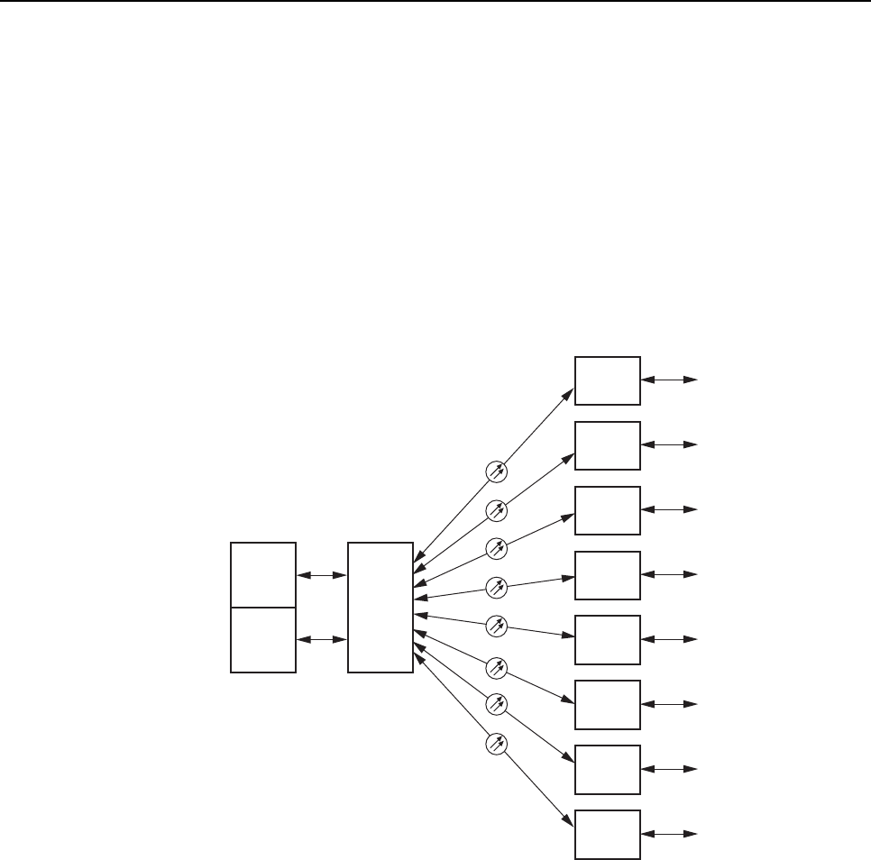
Figure 1-1 illustrates a Digivance system with RAN’s distributed over a desired geographical
area, connected back to a Wireless Service Provider (WSP) base station(s) at a Hub locale. The
illustration shows a dual-band SMR A and SMR B configuration with variable digital
simulcasting as a reference. The Digivance CXD Hub equipment consists of a rack assembly
containing RF Chassis and Digital Chassis equipment, high power attenuators, base station
interface modules, power distribution unit, Ethernet hub, Hub Reference Module and other
material sufficient to provide the interconnection at the RF layer between the base station
electronics and the Digivance CXD RAN’s located in the field.
CXD
RAN 1
SMRA/
SMRB
CXD
RAN 2
SMRA/
SMRB
CXD
RAN 3
SMRA/
SMRB
CXD
RAN 4
SMRA/
SMRB
CXD
RAN 5
SMRA/
SMRB
CXD
RAN 6
SMRA/
SMRB
CXD
RAN 7
SMRA/
SMRB
CXD
RAN 8
SMRA/
SMRB
SMR A
BTS
CXD
Hub
SMR B
BTS
20799-A
Figure 1-1. Digivance CXD Architectural Summary Diagram
2.2 General Description
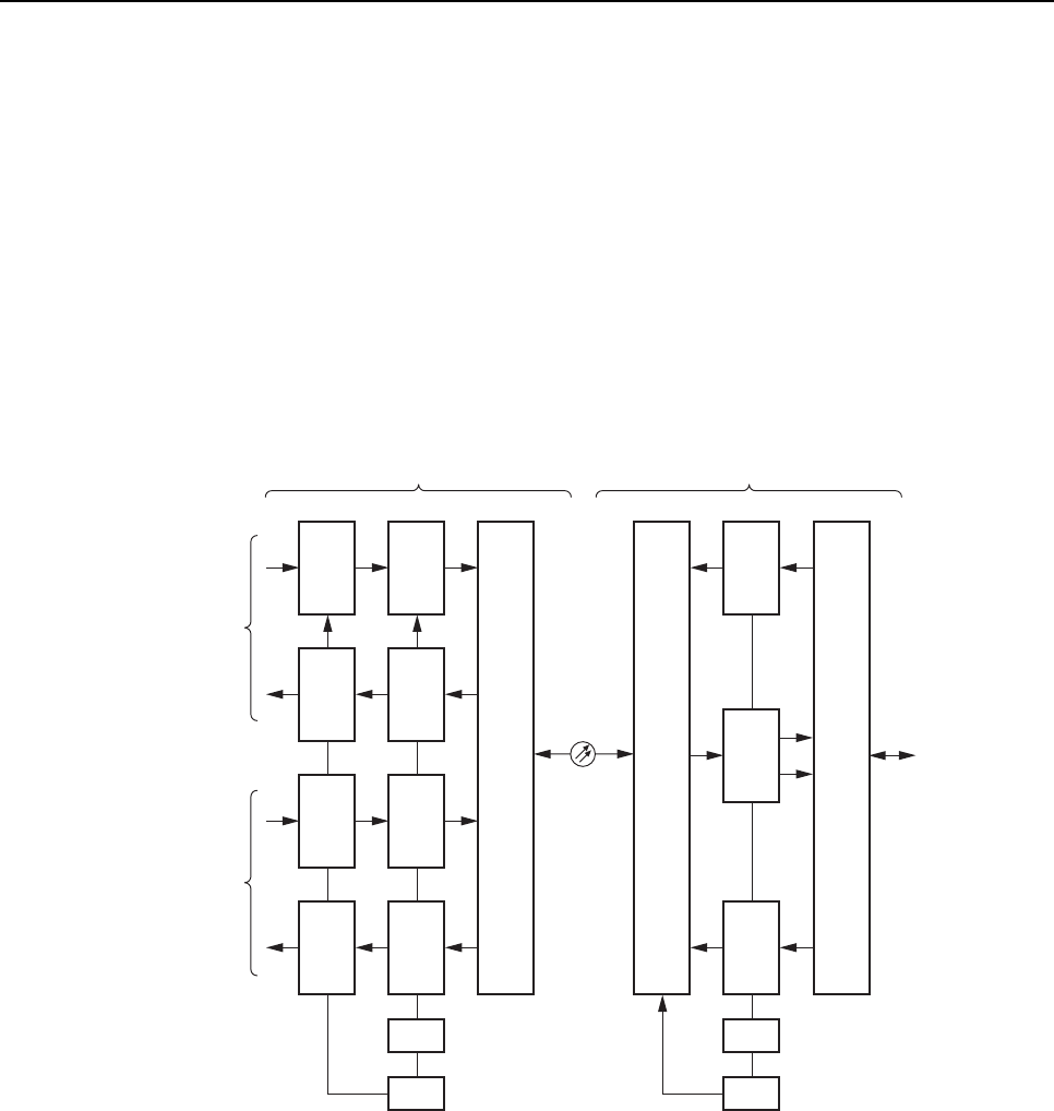
The Hub is co-located with the BTS and interfaces directly with the BTS over coaxial cables.
In the forward path, the Full Band Hub Down Converter (FBHDC) receives RF signals from
the BTS and down converts the signals to IF. The Forward Simulcast Card (FSC) digitizes the
RF signals and passes digital IF (DIF) signals into the Sonet Interface (SIF) that converts them
to digital optical signals for transport to the RAN. At the RAN, another SIF card receives the
digital optical signal, passes DIF to the Remote Up Converter (RUC) and inputs signals into a
RF Assembly (RFA). The RF signals are duplexed and combined with other RF signals using a
combination of diplexers or triplexers and then fed into a multi-band antenna.
ADCP-75-192 • Issue 1• December 2005 • Section 1: Overview
Page 1-3
2005, ADC Telecommunications, Inc.
In the reverse path, the antenna receives RF signals from a mobile and sends those signals into
the RFA which contains a diplexer and Low Noise Amplifier. The output of the RFA is
connected the RAN Down Converter (RDC) which down converts the RF back to IF and
digitizes the signals. The DIF signals are passed to the SIF, which sends digital optical signals
from the RAN to the HUB SIF. The Hub SIF combines with DIF signals from the other RAN’s
that are in that simulcast cluster through the Reverse Simulcast Card (RSC). The Hub Up
Converter (HUC) takes the RSC output and translates the digital optical signals back to RF
signals for transmission to the BTS.
Figure 1-2 shows the RF signal path through the Digivance CXD system. In the forward
direction, the signal starts from the base station sector on the left and moves to the right. In the
reverse direction, the RF path starts at the antenna and then flows from the RAN to the Hub
and to the base station sector receiver(s).
20800-A
HDC FSC
HUC RSC
HDC FSC
HUC RSC
STF
CPU
RDC
RUC
RDC
STF
CPU
SIF SIF
RFA
800/
900
800 MHz
BTS
900 MHz
BTS
800/900
DUPLEXED
OUTPUT
CXD Hub CXD RAN
Figure 1-2. Digivance CXD Block Diagram
2.3 Local Service Interface
Local communications with the Digivance CXD system is supported through an IP interface
capability. The Hub Digital Chassis and RAN Chassis both contain CPU modules with
Ethernet ports that act as nodes in an Ethernet-based network similar to that of a computer
local area network (LAN). Each RAN in the Digivance network contains one CPU, while the
Hub contains multiple CPUs within the Digital Chassis units depending on the number of
tenant sectors supported in the system. A local user is able to gain access to the CXD network
by the DHCP server resident on the Hubmaster CPU.

ADCP-75-192 • Issue 1 • December 2005 • Section 1: Overview
Page 1-4
2005, ADC Telecommunications, Inc.
The Digivance CXD Element Management System is a Web based system that provides the
various control and monitoring functions required for local management of each CXD system.
The user interface into the EMS is a PC-type laptop computer loaded with a standard Web
browser. The EMS is resident on the Hubmaster CPU and is accessible through an Ethernet
connection. Operation is effected through the EMS Graphical User Interface (GUI). The GUI
consists of a series of screens from which the user selects the desired option or function.
Ethernet ports are available at the Hub and RAN CPU for connecting the EMS computer at
either location.
For management and operation by a customer supplied Network Management Systems (NMS)
the Digivance CXD has imbedded in software a Simple Network Management Protocol
(SNMP) Agent and ADC Management Information Bases (MIB’s). Local communications
with the Digivance CXD SNMP Agent system is supported through the IP interface at the Hub
or RAN. All CPUs in the Digivance network support SNMP to provide NMS monitoring and
control access to the Digivance system. The NMS sends SNMP SET and GET messages to the
various nodes in the Digivance CXD network to access MIB’s which define the interface to the
Digivance system.
2.4 Remote NOC Interface
Remote communications between a Network Operations Center (NOC) and a networked
grouping of Digivance systems is supported by the Digivance CXD SNMP Agent. The primary
component of the remote NOC interface is a PC-type desktop computer loaded with a
customer supplied Network Management System (NMS). A NMS operating at a customer
NOC is able to discover and manage multiple Hub and RAN sites independently or as a
distributed network.
3 SYSTEM FUNCTIONS AND FEATURES
This section describes various system level functions and features of the Digivance CXD.
3.1 Fiber Optic Transport
The optical signal of a Digivance CXD is digital. The input and output RF signal levels at the
Hub SIF or the RAN SIF are not dependent on the level of the optical signal or the length of
the optical fiber. The maximum length of the optical fibers is dependent on the loss
specifications of the optical fiber and the losses imposed by the various connectors and splices.
The system provides an optical budget of 9 dB (typical) when used with 9/125 single-mode
fiber, or 26 dB with extended optics.
The optical wavelengths used in the system are 1310 nm for the forward path and 1310 nm for
the reverse path. Different wavelengths may be used for the forward and reverse paths
allowing for a pair of bi-directional wavelength division multiplexers (WDM) or coarse
wavelength division multiplexing (CWDM) to be used in applications where it is desirable to
combine the forward path and reverse path optical signals on a single optical fiber. One WDM
or CWDM multiplexer/demultiplxer module may be mounted with the Hub and the other
mounted with the RAN. The WDM or CWDM passive multiplexers are available as accessory
items.

ADCP-75-192 • Issue 1• December 2005 • Section 1: Overview
Page 1-5
2005, ADC Telecommunications, Inc.
3.2 Control and Monitoring Software
The Digivance CXD EMS or customer supplied NMS using the Digivance CXD/NXD SNMP
Agent is used to provision and configure the system for operation. This includes initializing the
system, setting up the Hub and RAN element identification schemes, tenant processing, setting
alarm thresholds, and setting forward and reverse path RF gain adjustments. The EMS or NMS
software is also used to get alarm messages (individual or summary), data measurements, or to
upgrade the Hub/RAN system software. All control and monitor functions can be effected
using either the EMS or through a NMS.
3.3 Fault Detection and Alarm Reporting
LED indicators are provided on each of the respective modules populating the Hub Digital
Chassis, RF Chassis and RAN Chassis to indicate if the system is normal or if a fault is
detected. In addition, a dry contact alarm interface can be provided as an accessory item that is
managed by the EMS software with normally open and normally closed alarm contacts for
connection to a customer-provided external alarm system. All Hub and RAN alarms can be
accessed through the SNMP manager or the EMS software GUI.
3.4 Powering
The Hub Digital and RF Chassis are powered by -48 Vdc and must be hard-wired to a local
office battery power source through a fuse panel. The power consumption of the system will
depend on the configuration of the system and how the Digital Chassis and RF Chassis are
populated.
Table 1-1 lists the typical power consumption of the respective modules for the Digital
Chassis.
Table 1-1. Digital Chassis Power Consumption
MODULE POWER
Digital Chassis 76.0 Watts
CPU 20.5 Watts
STF2 3.5 Watts
SIF 15.5 Watts
RSC 9.0 Watts
For a standard configuration of 4:1 simulcasting, Table 1-2 lists the estimated power
consumption for the Digital Chassis

ADCP-75-192 • Issue 1 • December 2005 • Section 1: Overview
Page 1-6
2005, ADC Telecommunications, Inc.
Table 1-2. Digital Chassis 4:1 Simulcast Power Consumption
MODULE # OF MODULES POWER
Digital Chassis 1 76.0 Watts
CPU 1 20.5 Watts
STF2 1 3.5 Watts
SIF 4 15.5 Watts
RSC 1 9.0 Watts
Total Power 170 Watts
Table 1-3 lists the typical power consumption of the respective modules for the RF Chassis.
Table 1-3. Digital Chassis Power Consumption
MODULE POWER
RF Chassis 55.0 Watts
FBHDC 11.0 Watts
HUC 8.0 Watts
FSC 13.5 Watts
For a single-band configuration, Table 1-4 lists the estimated power consumption for the RF
Chassis
Table 1-4. RF Chassis Single-band Power Consumption
MODULE # OF MODULES POWER
RF Chassis 1 55.0 Watts
FBHDC 1 11.0 Watts
HUC 1 8.0 Watts
FSC 1 13.5 Watts
Total Power 87.5 Watts
For a dual-band configuration Table 1-5 lists the estimated power consumption for the RF
Chassis
Table 1-5. RF Chassis Single-band Power Consumption
MODULE # OF MODULES POWER
RF Chassis 1 55.0 Watts
FBHDC 2 11.0 Watts
HUC 2 8.0 Watts
FSC 2 13.5 Watts
Total Power 120.0 Watts

ADCP-75-192 • Issue 1• December 2005 • Section 1: Overview
Page 1-7
2005, ADC Telecommunications, Inc.
The RAN is powered by 120 or 240 Vac (50 or 60 Hz) and must be hard-wired to the AC
power source through a breaker box. The RAN is pre-wired for 120 VAC operation but can
be converted to 240 VAC operation if required. On an optional basis, a back-up battery kit is
available for the RAN. The battery-backup system powers the RAN if the AC power source is
disconnected or fails.
3.4.1 HUB Power On/Off
Power to the Hub rack is provided using a power system supplied by the customer located in
the Hub shelter. Power to the Hub must be supplied through a fuse panel such as the 20
position ADC PowerWorx power distribution panel (available separately). The power circuit
for each active element of the system must be protected with a 5 Amp GMT fuse.
Hub Power On
• Power to the Hub racks is enabled at the power system supplied by the customer
Hub Power Off
• Power to the Hub racks is disabled at the power system supplied by the customer
Hub CompactPCI Chassis (RF & Digital) Power On
• Identify the power supply module(s) for the chassis to be powered on
• Insert the power supply module(s) in the chassis
Hub CompactPCI Chassis (RF & Digital) Power Off
• Identify the power supply module(s) for the chassis to be powered off
• Extract the power supply module(s) from the chassis
3.4.2 RAN Power on/off (APEC)
RAN Equipment Power On
• Plug the AC line cord into the receptacle located between the cPCI power supplies
• Turn power on at the customer supplied load center located on the utility pole
RAN Equipment Power Off (APEC)
• Turn the circuit breaker off at the customer supplied load center located on the utility
pole
• Unplug the AC line cord from the receptacle located between the cPCI power supplies

ADCP-75-192 • Issue 1 • December 2005 • Section 1: Overview
Page 1-8
2005, ADC Telecommunications, Inc.
3.4.3 RAN Power on/off (DPEC)
RAN Equipment Power On
• Plug the AC line cord into the receptacle located on all RFA’s
• Turn power on at the customer supplied load center located on the utility pole
RAN Equipment Power Off (APEC)
• Turn the circuit breaker off at the customer supplied load center located on the utility
pole
• Push battery disconnect switch (DISCON) on DPEC front panel
• Wait for all DPEC LEDs to go out
• Unplug the AC line cord from the receptacle located between the cPCI power supplies
3.5 Equipment Mounting and Configuration
The Digital Chassis and RF Chassis are designed for mounting in a non-condensing indoor
environment such as inside a wiring closet or within an environmentally-controlled cabinet.
The Hub equipment is intended for rack-mount applications and may be mounted in either a
19- or 23-inch WECO or EIA equipment rack, usually within 20 feet of the BTS. The RAN is
designed for mounting in either an indoor or outdoor environment.
3.6 HUB Subsystem Assemblies
The Hub is comprised of a single rack assembly with two chassis types. The Hub rack houses
the following modules:
1. The Digital Chassis houses the following modules:
• CPU (Hubmaster or Slave)
• System Interface card (STF2)
• Sonet Interface (SIF)
• Reverse Simulcast card (RSC)
• CompactPCI Power Supply (CPS)
• Fan assembly
2. The RF Chassis houses the following modules:
• Full Band Hub Down Converter card (FBHDC)
• Hub Up Converter card (HUC)
• Forward Simulcast card (FSC)
• CompactPCI Power Supply (cPCI P/S)
• Fan assembly
3. Attenuator Rack which houses up to twelve (12) attenuators.

ADCP-75-192 • Issue 1• December 2005 • Section 1: Overview
Page 1-9
2005, ADC Telecommunications, Inc.
4. Base Station Interface Module (BIM). The BIM is a multi-port transition module used to
interface with the Tenant’s base station sector. The BIM accepts either duplexed or non-
duplexed RF from the base station sector and provides the Digivance CXD-Hub RF
section separate transmit and receive paths.
5. Ethernet hub with twenty four (24) ports.
6. -48 VDC Power Distribution Unit.
7. Hub Reference Module (HRM).
The Attenuator Rack, BIM, Ethernet Hub and HRM are sold as accessory items. The
functionality of each of these card assemblies is defined in the following sections.
3.6.1 Digital CompactPCI Chassis & Backplane
The CompactPCI Digital Chassis houses cooling fans, the CPU, System Interface (STF2)
module, Sonet Interface (SIF) module, Reverse Simulcast Card (RSC), and power supplies.
The backplane provides the distribution for clock, communication, control data and timing.
3.6.2 RF CompactPCI Chassis & Backplane
The CompactPCI RF Chassis houses the cooling fans, RF transceiver modules, Hub Up
Converter (HUC), Hub Down Converter (FBHDC), Forward Simulcast card (FSC) and the
power supplies. The backplane provides the distribution for clock, communication and control
data and timing. RF and digital RF signals are interconnected between modules using the
appropriate cabling.
3.6.3 Central Processing Unit (CPU)
The Hub CPU is a cPCI single board computer with hot swap capabilities. The Operating
System of the Digivance CXD uses LINUX. There is one CPU per digital chassis. A Hub CPU
performs the following functions:
1. Manages a subset of Hub hardware including RF and Digital equipment.
2. Manages RANs connected to its Hub managed hardware.
One of the Hub CPUs must be configured as the Hubmaster processor. In addition to its regular
Hub CPU duties it is responsible for:
1. Reporting Tenant status.
2. Controlling all Tenant specific functions.
3. Synchronizing the date for all attached nodes.
4. Managing gain & delays.
5. Monitoring signal presence and quality.
6. Managing network services such as DHCP and DNS.
7. EMS.

ADCP-75-192 • Issue 1 • December 2005 • Section 1: Overview
Page 1-10
2005, ADC Telecommunications, Inc.
3.6.4 System Interface (STF2)
The System Interface (STF2) module, using four I2C busses, provides the ability to
communicate between the CPU and other modules. The STF2 also communicates with the
GPS modules found both in the Master Hub Reference Module and internal to the RAN STF2.
In the HUB, the STF2 communicates with chassis fans for monitoring purposes.
The four I2C busses are accessible via the CompactPCI backplane or via front panel
connectors.
3.6.5 Sonet Interface (SIF)
The Sonet Interface module provides the fiber interface between the Hub and RAN’s. This
interface includes:
1. Digitized RF Signal information.
2. 10BaseT Ethernet for command and control between Hub and the RAN’s.
3. Measures fiber delay used in Delay Management.
3.6.6 Full Band Hub Down Converter (FBHDC)
The Full Band Hub Down Converter (FBHDC) down converts the forward RF carrier to an
intermediate frequency (IF) that is then digitized by the Forward Simulcast Card (FSC). Each
FBHDC can support up to 15 MHz of contiguous spectrum.
3.6.7 Forward Simulcast Card (FSC)
The FSC converts the IF signals from the FBHDC to Digitized IF (DIF) format. There are
eight (8) separate analog-to-digital conversion circuits on one (1) FSC.
3.6.8 Reverse Simulcast Card (RSC)
The RSC sums the Digital IF (DIF) from up to four (4) RANs into DIF signals that are sent to
the appropriate HUC for up conversion to RF. Single and dual-branch diversity are supported.
3.6.9 Hub Up Converter (HUC)
The HUC accepts two (2) Digital IF (DIF) signals from a SIF or RSC. The two (2) DIF signals
are converted from digital-to-analog and provided as two (2) separate RF signals (primary and
diversity) to the BIM and BTS.
3.6.10 Base Station Interface Module (BIM)
The BIM provides the following BTS interface functions:

ADCP-75-192 • Issue 1• December 2005 • Section 1: Overview
Page 1-11
2005, ADC Telecommunications, Inc.
1. Interface to a low power forward BTS RF path.
2. Handles duplexed and non-duplexed signals.
3. Gain adjust for optional reverse path configurations.
The BIM is controlled via an I2C connection from its respective CPU.
3.6.11 Hub Reference Module (HRM)
The HRM generates the RF reference and fiber clocking for distribution within the Hub. In
addition, it contains a GPS that generates a 1 PPS (one pulse per second) for distribution to the
Digital Chassis modules for delay management.
3.6.12 Ethernet Hub
Each Hub rack is equipped with a 24 port Ethernet Hub. It is powered by 120 VAC, or optional
–48 VDC can be chosen. The Ethernet Hub is used to connect RAN CPUs (through Hub SIFs)
and Hub CPUs to and existing LAN/WAN and to each other.
3.7 RAN Subsystem Assemblies
The RAN consists of a cabinet, RAN Chassis and Backplane, a Central Processing Unit
(CPU), a System Interface (STF2), a Sonet Interface (SIF), RAN Down Converter (RDC or
RDC2), RAN Up Converter (RUC2.X or RUC3), AC Power Entry Card (APEC) or DC Power
Entry Card (DPEC); and the RF Assembly consisting of Power Amplifiers, duplexers, and
RFA interface controller. There are two cabinet options: the Standard CXD RAN Cabinet and
the Extended CXD RAN Cabinet. The standard cabinet supports two Radio Frequency
Assemblies (RFA) with no battery backup; or one RFA and one internal battery backup
assembly. The extended cabinet supports two RFA's and an extended battery backup assembly
housed in a battery compartment located on the side of the cabinet.
The Digivance CXD cabinet houses the RAN components and can be mounted from a flat-
vertical surface or from a utility pole using an accessory pole-mount kit. Within the enclosure
space is provided for storing short lengths of excess fiber slack.
3.7.1 Central Processing Unit (CPU)
The RAN has a cPCI based single-board computer with a Central Processing Unit (CPU)
operating LINUX. The RAN CPU provides the following functions:
1. Manages all RAN hardware including RF and Digital equipment
2. Manages gain & delays
3. Monitors signal presence and quality
4. Ethernet interconnect
5. Generates SNMP traps based upon fault conditions

ADCP-75-192 • Issue 1 • December 2005 • Section 1: Overview
Page 1-12
2005, ADC Telecommunications, Inc.
3.7.2 System Interface (STF2)
The STF2 module provides the ability to communicate between the CPU and other modules
(RDC, RUC, RFA interface controller) using four I2C busses. The STF2 also contains the GPS
module.
3.7.3 Sonet Interface (SIF)
The SIF module provides the optical interface between the Hub and RAN’s. The SIF has an
optical transceiver module installed that provides the optical transmit and receive functions.
The SIF has also the following functions:
1. Digitized RF Signal information.
2. 10 BaseT Ethernet for command and control between Hub and the RANs.
3.7.4 Small Form-Factor Pluggable (SFP) Optical Transceiver
The Small Form-factor Pluggable (SFP) optical transceiver module provides the optical
interface between the Hub equipment and the RAN hardware. The SFP has a laser transmitter
and optical receive detector. The Digivance CXD uses industry standard SFP optics which
offers a number of configuration options depending on the requirements of the project. The
SFP modules are available separately and may or may not be initially installed in the SIF
depending on the configuration ordered.
3.7.5 RAN Down Converter (RDC or RDC2)
The RDC is a dual-diversity wideband receiver that converts PCS, Cellular, SMR A and SMR
B signals to digitized IF. It also includes a CW test tone used in reverse continuity testing.
3.7.6 RAN Up Converter (RUC2.X or RUC3)
The RUC converts digitized IF into PCS, Cellular and SMR frequency bands. Each RUC
supports two simultaneous bands via wideband outputs. The RUC also provides clocking for
its neighboring RDC’s as well as extends an I2C interface to its respective RFA.
3.7.7 RAN Chassis & Backplane
The RAN chassis is a six slot CompactPCI unit. The backplane supports the basic CompactPCI
functions and has been extended to allow the routing of DIF, reference clocks and I2C signals
between CompactPCI modules.
3.7.8 AC Power Entry Card (APEC)
The APEC distributes AC power to the cPCI power supplies in the RAN. Its input range is
100 to 240 VAC. It has a built in EMI filter and fuse holder and provides an access point for
fan monitoring and control.

ADCP-75-192 • Issue 1• December 2005 • Section 1: Overview
Page 1-13
2005, ADC Telecommunications, Inc.
3.7.9 DC Power Entry Card (DPEC)
The DPEC is used to distribute DC power to the cPCI power supplies in the RAN when
supporting battery backup. It has a built in EMI filter and fuse holder and provides an access
point for fan monitoring and control.
3.7.10 CompactPCI RAN Power Supply (cPCI P/S)
The CompactPCI (cPCI) Power Supplies provide +/-12V, 5V and 3.3 V DC power to the cPCI
backplane for use by the RAN modules. These units are hot swappable and supports redundant
supply configurations.
3.7.11 RF Assembly
The RF Assembly (RFA) consists of the power amplifier (PA), power supply, fans, duplexers
and RFA interface controller. RF assemblies are PCS, Cellular and SMR 800/900 bands.
3.7.12 Internal Battery backup (BAT1) 1-Hour
The Digivance CXD has an option for an internal battery back-up located inside the Standard
CXD RAN cabinet. It is positioned in the space of a RFA and is used to provide short duration
power backup to the RAN. A cabinet using the internal battery backup option can only support
one single- or dual-band RFA.
3.7.13 Extended Internal Battery Backup (BAT2) 2-Hour
The Digivance CXD has an option for an extended internal battery back-up through use of the
Extended CXD RAN Cabinet with a separate compartment for the batteries. A cabinet using
the extended backup option can support two single- or dual-RFA’s and can provide up to two
hours of battery backup time.
3.7.14 Antenna (ANT)
The Digivance CXD RAN may be deployed and installed on a power distribution pole, on a
building wall, on a water tank, or on a rooftop, or within a building environment. ADC can
supply a number of antenna options for the Digivance CXD as accessory items. Antenna(s)
may be mounted on a facade, supporting member, wall or rooftop pedestal mount. Installations
may use conventional omni-directional or directional antenna, in either a sector or quasi-omni
antenna configuration, depending on the site’s coverage objective and design. When designing
a network, the azimuth and elevation beamwidths would be selected by the RF designer to
support the desired coverage objectives. Proper antenna selection and the mounting installation
is the responsibility of the customer.
When using a customer supplied antenna, they should meet or exceed the following antenna
specifications:

ADCP-75-192 • Issue 1 • December 2005 • Section 1: Overview
Page 1-14
2005, ADC Telecommunications, Inc.
• VSWR (all bands): 1.5:1 typ, 1.65:1 max
• Maximum power input: 200W (average) 1000W (peak)
• Passive Intermodulation Distortion: -153dBc (maximum)
3.8 Communication Interfaces
3.8.1 I2C
I2C is a bi-directional serial bus that provides a simple, efficient method of data exchange
between devices. It is used for the board level communications protocol.
I2C interfaces are used for communication to the following modules:
1. HUB - FBHDC, FSC, HUC, BIM, and HRM.
2. RAN - RDC, RUC, and RFA.
3.8.2 Network Interface
The Hubmaster CPU is able to communicate to any other CPU in the Digivance CXD system
(Hub and RAN) over an Ethernet LAN using the IP based Simple Network Management
Protocol (SNMP). Ethernet connections are aggregated with each rack via an Ethernet Hub.
Inter-rack communication is done by connecting the Ethernet Hubs between racks.
Each SIF has a 10BaseT Ethernet connection. The Hubmaster CPUs are able to communicate
with the RAN’s over this Ethernet connection.
3.8.3 SNMP
The ADC Digivance Simple Network Management Protocol (SNMP) Agent and the ADC
Management Information Bases (MIB’s) provide the interface into the Digivance CXD system.
A MIB is a database where scalar or tabular data “objects” known to both agent and the
manager are defined and stored. The MIB’s define a set of parameters with specific
characteristics, including name, data type, value range, description, and read-write
accessibility. An SNMP manager sends SNMP SET and GET messages to the various nodes in
the Digivance CXD network in order to access MIB’s.
The MIBs are compiled into a SNMP Manager as well as the Digivance CXD SNMP Agent so
that both manager and agent software can communicate. Agent and manager each have their
own copy of the MIB. Using the SNMP interface, the manager issues GET and SET
commands for object attributes stored in the agent MIB. In addition, the manager receives
unsolicited object attributes in the form of TRAP notices sent by the agent. The Digivance
software has the ability to send SNMP TRAPS when certain MIB conditions are detected.
reducing the amount of polling via SNMP GET requests from the SNMP manager.

ADCP-75-192 • Issue 1 • December 2005 • Section 2: Description
Page 2-1
2005, ADC Telecommunications, Inc.
SECTION 2: DESCRIPTION
Content Page
1 INTRODUCTION .................................................................... 2-1
2 DIGITAL CHASSIS ................................................................... 2-2
3 RF CHASSIS....................................................................... 2-5
4 RADIO ACCESS NODE (RAN) ........................................................... 2-9
4.1 RAN cabinet ................................................................ 2-10
5 ELEMENTS COMMON TO HUB AND RAN ................................................... 2-11
5.1 Central Processor Unit (CPU) .................................................... 2-11
5.2 System Interface (STF2) ....................................................... 2-13
5.3 Sonet Interface (SIF) ......................................................... 2-15
5.4 Small Form-Factor Optical Transceiver (SFP) ......................................... 2-16
6 HUB SPECIFIC MODULES ............................................................. 2-17
6.1 Full Band Hub Down Converter (FBHDC) ............................................ 2-17
6.2 Forward Simulcast Card (FSC) ................................................... 2-18
6.3 Hub Upconverter Card (HUC) .................................................... 2-19
6.4 Reverse Simulcast Card (RSC) ................................................... 2-20
6.5 Hub Reference Module (HRM) ................................................... 2-22
6.6 Ethernet Hub................................................................ 2-24
6.7 BTS Interface Module (BIM) .................................................... 2-25
6.8 Attenuator Shelf ............................................................. 2-28
7 RADIO ACCESS NODE (RAN) SPECIFIC MODULES ............................................. 2-29
7.1 Ran Down Converter (RDC or RDC2) ............................................... 2-29
7.2 Ran Up Converter (RUC2.X or RUC3) ............................................... 2-30
7.3 AC Power Entry Controller (APEC).................................................. 2-31
7.4 DC Power Entry Controller (DPEC) ................................................ 2-32
7.5 CompactPCI Power Supply (cPCI P/S) .............................................. 2-34
7.6 RF Assembly Module (RFA) ..................................................... 2-35
7.7 Specifications ............................................................... 2-41
1 INTRODUCTION
This section describes the basic components of the Digivance CXD system including the Hub
and Radio Access Node (RAN) equipment. The Hub equipment consists of the Central
Processing Unit (CPU), the System Interface (STF2), the Sonet Interface (SIF), the Full Band
Hub Down Converter (FBHDC), the Hub Up Converter (HUC), the Forward Simulcast Card
(FSC), Reverse Simulcast Card (RSC) and CompactPCI Power Supplies (cPCI P/S).
Additional hardware includes the Base Station Interface Module (BIM), Hub Reference
Module (HRM), a commercial Ethernet Hub and high power RF attenuators.
The RAN is an assembly that consists of the RAN equipment including the RAN Chassis,
CPU, STF2, RAN Down Converter (RDC or RDC2), RAN Up Converter (RUC2.X or RUC3),
AC Power Entry Controller (APEC), DC Power Entry Controller (DPEC), cPCI P/S and RF
Assembly (RFA).
ADCP-75-192 • Issue 1 • December 2005 • Section 2: Description
Page 2-2
2005, ADC Telecommunications, Inc.
2 DIGITAL CHASSIS
The Digivance Digital Chassis is a rack-mounted cPCI shelf capable of housing 8 industry
standard cPCI circuit card modules. The Digital Chassis houses cooling fans and specific
modules designed for use in the Digivance CXD system. The backplane of the Digital Chassis
provides for distribution of signals between modules including the reference clock,
communications, control and data signals. Modules used in the Digital Chassis include the
CPU module, System Interface module (STF2), and up to six Reverse Simulcast Cards (RSCs)
or Sonet Interface (SIF) digital modules.
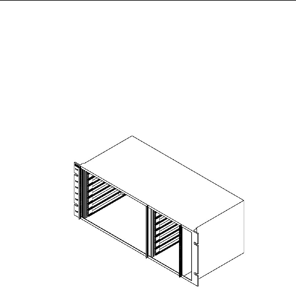
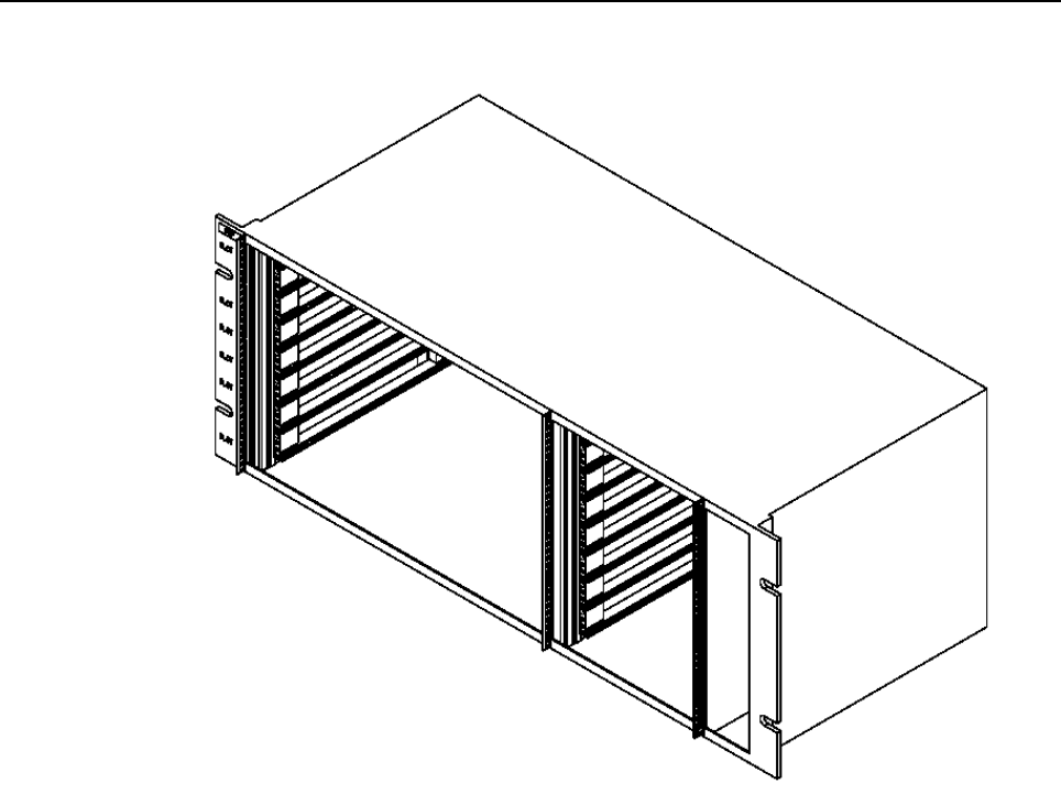
Figure 2-1 shows the empty Digital Chassis. The eight empty slots on the left are used for
Digivance CXD Hub modules. The slots on the right are used for housing the cPCI power
supplies and cPCI fan assembly.
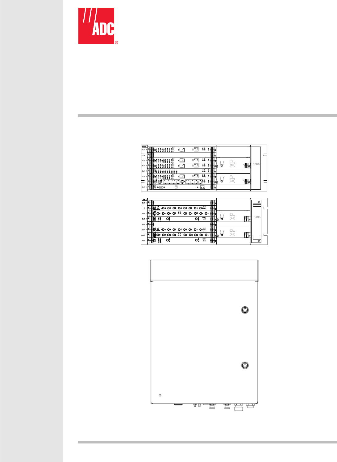
Figure 2-1. Digivance CXD Digital Chassis
Modules and circuit cards are placed into the Digital Chassis and are mated to standard cPCI
connectors on the backplane of the chassis. Data and signals are transported over busses on the
backplane of the chassis to other modules and ports on the backside of the chassis.
Rear connections are made to the Digital Chassis to connect power, route DIF signals to inputs
and outputs of respective modules mounted in the chassis, connect the I2C bus to the chassis,
input a 1 Hz reference signal, input a sample clock, input FAN tachometer readings from the
RF Chassis, and distribute 12 VDC to other elements of the system. The Digital Chassis also
has a Module/Port status indicator that can be used to trace signals through the system and
show activity on the ports. Figure 2-2 shows the back panel connections for the Digital
Chassis. The references for the back connectors of the Digital Chassis are shown in Table 2-1.
ADCP-75-192 • Issue 1 • December 2005 • Section 2: Description
Page 2-3
2005, ADC Telecommunications, Inc.
(1) MODULE AND P ORT STATUS INDICATORS
(10) 12 VDC OUTPUT(11) -48 VDC INP UT
(2) 7/8 DIF I/O (3-8)
(4) 3/4 DIF I/O (3-8)
(5) 1/2 DIF I/O (3-8)
(3) 5/6 DIF I/O (3-8) (6) 1 HZ REFERENCE
(8) 9/10 DIF OUTP UT (3-8)(9) FANS TACHOMETER INP UTS (7) I2C BUSSES
Figure 2-2. Digital Chassis – Rear Connectors
Table 2-1. Digital Chassis References – Rear Connectors
REF
No.
USER INTERFACE
DESIGNATION
DEVICE FUNCTIONAL DESCRIPTION
1 Slot/DIF Multi-colored LED Indicators showing module and port status
(see Digital Chassis rear indicators)
2 7/8 DIF I/O Six RJ-45
Connectors
Output channels 7 & 8 from SIF. Maps to
SIFs in Slots 3-8. Input channels 7 & 8 to
RSC. Maps to RSCs in Slots 3-8.
3 5/6 DIF I/O Six RJ-45
Connectors
Outputs channels 5 & 6 from SIF. Maps to
SIFs in Slots 3-8. Input channels 5 & 6 to
RSC. Maps to RSCs in Slots 3-8.
4 3/4 DIF Input Six RJ-45
Connectors
Input channels 3 & 4 to SIF/RSC. Maps to
SIFs/RSCs in Slots 3-8
5 1/2 DIF Input Six RJ-45
Connectors
Input channels 1 & 2 to SIF?RSC. Maps to
SIFs/RSC in Slots 3-8
6 1Hz/Ref One RJ-45 connector 1 pulse per second and Reference clock
from HRM
7 I2C A-D Busses Four RJ-45
connectors
I2C comms to RF Chassis, BIMs and HRMs
over four busses (A-D)
8 9/10 DIF Output (3-8) 6 RJ-45 connectors DIF signals from RSC output to HUC in RF
Chassis. Maps to RSC in Slots 3-8.
9 FANS Two RJ-45 connector Monitors Fans speed of RF Chassis above
and below
10 12V Two 3-pin power
output connector
Provides 12V power to BIMs and HRMs
11 -48V Single 3-pin power
input connector
Provides -48VDC to chassis.
ADCP-75-192 • Issue 1 • December 2005 • Section 2: Description
Page 2-4
2005, ADC Telecommunications, Inc.
The main purpose of the Module/Port status indicators shown in Figure 2-3 is to provide the
user instant feedback on the success or failure of a new connection. It also provides path status
to aid in troubleshooting missing or degraded connections. The references for the back
connectors of the Digital Chassis are shown in the Table 2-2.
(1) 7/8 LEDS (3-8)
(3) 3/4 LEDS (3-8)
(4) 1/2 LEDS (3-8)
(2) 5/6 LEDS (3-8)
(5) 1 HZ CLOCK LEDS
(6) I2C A-D LEDS
(7) 9/10 LEDs (3-8)
Figure 2-3. Digital Chassis – Rear Indicators
Table 2-2. Digital Chassis References
REF
No.
USER INTERFACE
DESIGNATION
DEVICE FUNCTIONAL DESCRIPTION
1 7/8 DIF LEDs (3-8) 12 tri-color LEDs
(r/o/g)
SIF/RSC DIF output/input 7 & 8.
Green=good, orange=marginal,
blinking=clocking issue, red=bad or
missing. Maps to Slots 3-8.
2 5/6 DIF LEDs (3-8) 12 tri-color LEDs
(r/o/g)
SIF/RSC DIF output/input 5 & 6.
Green=good, orange=marginal,
blinking=clocking issue, red=bad or
missing. Maps to Slots 3-8.
3 3/4 DIF LEDs (3-8) 12 tri-color LEDs
(r/o/g)
SIF/RSC DIF input 3 & 4. Green=good,
orange=marginal, blinking=clocking issue,
red=bad or missing. Maps to Slots 3-8.
4 1/2 DIF LEDs (3-8) 12 tri-color LEDs
(r/o/g)
SIF/RSC DIF input 1 & 2. Green=good,
orange=marginal, blinking=clocking issue,
red=bad or missing. Maps to Slots 3-8.
5 1HZ/CLOCK LEDs Two green LED 1 Hz blinks once per second. Clock is solid
green when reference is present into chassis
6 I2C A-D LEDs Four green LEDs Indicates communications activity over the
four I2C busses (A-D)
7 9/10 DIF LEDs (3-8) 12 tri-color LEDs
(r/o/g)
RSC DIF output. Green=good,
orange=marginal, blinking=clocking issue,
red=bad or missing. Maps to Slots 3-8.
ADCP-75-192 • Issue 1 • December 2005 • Section 2: Description
Page 2-5
2005, ADC Telecommunications, Inc.
Figure 2-4 shows an empty Digital Chassis from the front. Slots on the left are numbered from
1 to 8 starting at the bottom of the chassis. Slots on the right of the chassis are used for the
cPCI power supplies used to power the chassis and modules and the cPCI fan assembly.
Mounting of modules and circuit cards into the Digital Chassis should be done in accordance
with Table 2-3.
Figure 2-4. Digital Chassis - Front
Table 2-3. Digital Chassis Slot Assignments
SLOT MODULE
8 SIF or RSC
7 SIF or RSC
6 SIF or RSC
5 SIF or RSC
4 SIF or RSC
3 SIF or RSC
2 STF2
1 CPU
3 RF CHASSIS
The Hub RF Chassis is a rack-mounted chassis capable of housing 8 industry standard cPCI
circuit card modules. The RF Chassis houses cooling fans and specific modules designed for
use in the Digivance CXD system. The backplane of the RF Chassis provides for distribution
of signals between modules including the reference clock, communications, control and data
signals. Modules used in the RF Chassis include up to two Full-band Hub Down-Converter
(FBHDC) modules, two Forward Simulcast Card (FSC) modules and two Hub Up-Converter
(HUC) modules.
Figure 2-5 shows the empty RF Chassis. The eight empty slots on the left are used for
Digivance CXD modules. The eight empty slots on the right used for housing the cPCI power
supplies which power the modules and the cPCI fan assembly.
ADCP-75-192 • Issue 1 • December 2005 • Section 2: Description
Page 2-6
2005, ADC Telecommunications, Inc.
Figure 2-5 Digivance CXD RF Chassis
Modules and circuit cards are placed into the RF Chassis and are mated using standard cPCI
connectors on the backplane of the chassis. Data and signals are transported over busses on the
backplane of the chassis to other modules and ports on the backside of the chassis.
Rear connections are made to the RF Chassis to connect power, route Digital IF (DIF) signals
to inputs and outputs of respective modules, connect the I2C bus to the chassis, input a 1 Hz
reference signal, input sample and reference clocks, output FAN tachometer readings to the
Digital Chassis, and distribute 12 VDC to other elements of the system. The RF Chassis also
has a Module/Port status indicator that can be used to trace signals through the system and
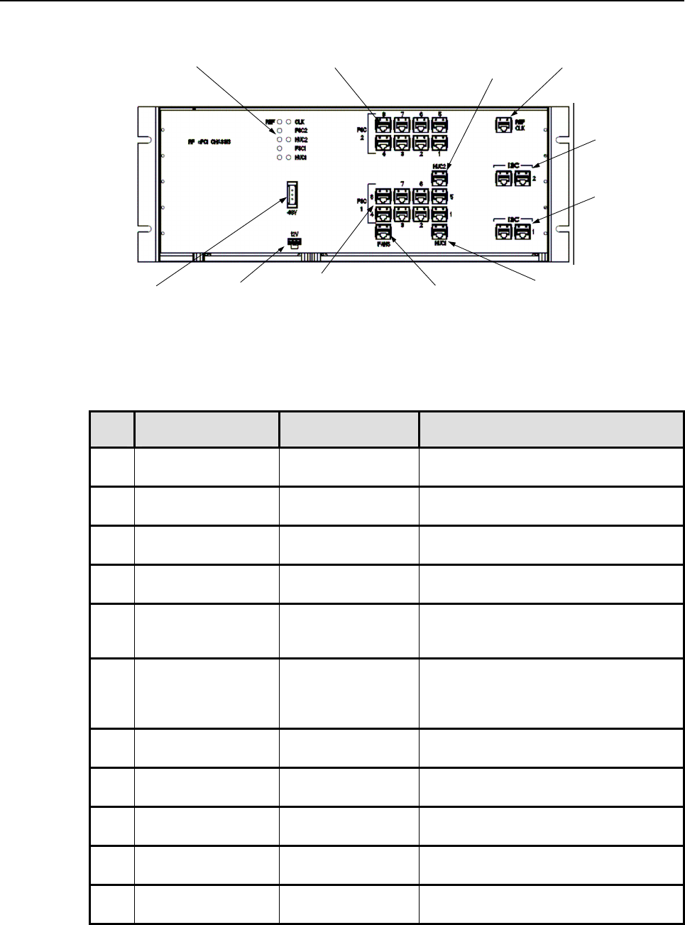
show activity on the ports. Figure 2-6 shows the back panel connections for the RF Chassis.
The references for the back connectors of the RF Chassis are shown in Table 2-4.
ADCP-75-192 • Issue 1 • December 2005 • Section 2: Description
Page 2-7
2005, ADC Telecommunications, Inc.
(1) MODULE AND PORT S TATUS
INDICATORS
(10) 12 VDC OUTPUT(11) -48 VDC INPUT
(2) FS C2 DIF OUTP UT 1-8
(3) HUC2 DIF INP UT
(4) REFERENCE/CLOCK
(6) I2C DAIS Y CHAIN (1-4)
(8) FANS TACHOMETER
OUTPUTS
(5) I2C DAIS Y CHAIN (5-8)
(7) HUC1 DIF INP UT(9) FSC1 DIF OUTP UTS (1-8)
Figure 2-6. RF Chassis – Rear Connectors
Table 2-4. Digital Chassis References – Rear Connectors
REF
No.
USER INTERFACE
DESIGNATION
DEVICE FUNCTIONAL DESCRIPTION
1 Status Indicators Multi-colored LED Indicators showing module and port status
(see RF Chassis rear indicators).
2 FSC 2 DIF Output
(1-8)
Eight RJ-45
Connectors
FSC DIF outputs. Eight simulcast outputs.
Maps to FSC in slot 7.
3 HUC2 DIF Input Single RJ-45
connector
Two DIF signals into HUC (primary and
diversity). Maps to HUC in Slot 5.
4 REF/CLK One RJ-45 connector 1 pulse per second, Sample, and Reference
clocks from HRM.
5 I2C daisy chain (5-8) Two RJ-45
connectors
One of four I2C busses controlling cards in
Slots 5-8. Typically bus B. Must be daisy
chained to BIM.
6 I2C daisy chain (1-4) Two RJ-45
connectors
One of four I2C busses controlling cards in
Slots 1-4. Typically bus A. Must be daisy
chained to BIM, which in turn can be daisy
chained to HRM.
7 HUC1 DIF Input Single RJ-45
connector
Two DIF signals into HUC (primary and
diversity). Maps to HUC in Slot 1.
8 FANS Single RJ-45
connector
Sends chassis fan speed to Digital Chassis.
9 FSC 1 DIF Output
(1-8)
Eight RJ-45
Connectors
FSC DIF outputs. Eight simulcast outputs.
Maps to FSC in slot 23.
10 12V 3-pin power output
connector
Provides 12V power to BIM.
11 -48V Single 3-pin power
input connector
Provides -48VDC to chassis.
ADCP-75-192 • Issue 1 • December 2005 • Section 2: Description
Page 2-8
2005, ADC Telecommunications, Inc.
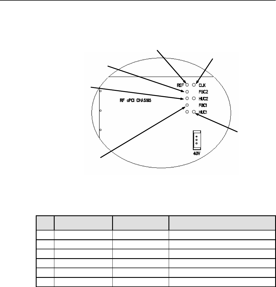
Figure 2-7 shows the RF Chassis viewed from the rear. The references for the back connector
of the RF Chassis are shown in Table 2-5.
(2) FSC2 OUTP UT LED
(3) REFERENCE LED
(4) CLOCK LED
(1) HUC2 P RI/DIV LED
(6) FS C1 OUTP UT LED
(5) HUC1 P RI/DIV LED
Figure 2-7. RF Chassis – Rear Indicators
Table 2-5. RF Chassis References – Rear Indicators
REF
No.
USER INTERFACE
DESIGNATION
DEVICE FUNCTIONAL DESCRIPTION
1 HUC2 LED One green LED FUTURE USE. Maps to slot 5.
2 FSC2 LED One green LED FUTURE USE. Maps to slot 7.
3 REFERENCE LED One green LED Green indicates reference clock is present.
4 CLOCK LED One green LED Green indicates sample clock is present.
5 HUC1 LED One green LED FUTURE USE. Maps to slot 1.
6 FSC1 LED One green LED FUTURE USE. Maps to slot 3.
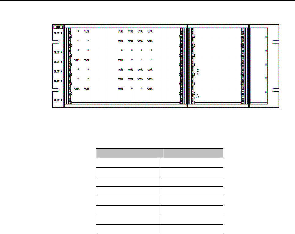
Figure 2-8 shows an empty RF Chassis from the front. Slots on the left are numbered from 1 to
8 starting at the bottom of the chassis. Slots on the right of the chassis are used for the cPCI
power supplies used to power the modules and the cPCI fan assembly. Mounting of modules
and circuit cards into the RF Chassis should be done in accordance with Table 2-6.
ADCP-75-192 • Issue 1 • December 2005 • Section 2: Description
Page 2-9
2005, ADC Telecommunications, Inc.
Figure 2-8. RF Chassis – Front
Table 2-6. RF Chassis Slot Assignments
SLOT MODULE
8
7 FSC
6 FBHDC
5 HUC
4
3 FSC
2 FBHDC
1 HUC
4 RADIO ACCESS NODE (RAN)
The Radio Access Node (RAN) is the remote hardware that transmits and receives radio
signals. It consists of a cabinet, RAN Chassis, a Central Processing Unit (CPU), a System
Interface (STF2), a Sonet Interface (SIF), RAN Down Converter (RDC or RDC2), RAN Up
Converter (RUC2.X or RUC3), AC Power Entry Card (APEC), a DC Power Entry Card
(DPEC) (battery backup option only), and the RF Assembly consisting of Power Amplifiers,
duplexers, and RFA interface controller. There are two cabinet options, the CXD RAN
Standard Cabinet, and the CXD RAN Extended Cabinet. The standard cabinet is capable of
supporting two Radio Frequency Assemblies (RFA’s) with no battery backup or one RFA and
one internal battery backup assembly. The extended cabinet is capable of supporting two
RFA’s and an extended battery backup assembly housed in battery assembly compartment
located on the side of the cabinet.
ADCP-75-192 • Issue 1 • December 2005 • Section 2: Description
Page 2-10
2005, ADC Telecommunications, Inc.
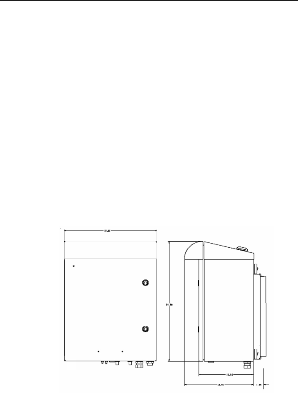
4.1 RAN cabinet
The CXD RAN standard and extended cabinets, shown in Figure 2-9 and Figure 2-10, are
NEMA-3R enclosures (with removable dust filter) that provides the following basic functions:
• Houses the various electronic modules including the following
− RAN Chassis and Backplane
− Central Processing Unit (CPU)
− System Interface (STF2)
− Sonet Interface (SIF)
− RAN Down Converter (RDC or RDC2)
− RAN Up Converter (RUC2.X or RUC3)
− AC Power Entry Card (APEC)
− DC Power Entry Card (DPEC)
− RF Assembly (RFA) consisting of Power Amplifiers, duplexers, and RF interface
controller.
− Enclosure and chassis fans
• Houses accessory items such as back-up battery and WDM modules
• Protects all modules from the weather.
• Provides electrical interface connections for the RAN Chassis and RFA modules.
• Provides ventilation openings to allow the entry of cool air and the escape of heated air.
Figure 2-9. CXD RAN Standard Cabinet
ADCP-75-192 • Issue 1 • December 2005 • Section 2: Description
Page 2-11
2005, ADC Telecommunications, Inc.
Figure 2-10. CXD RAN Extended Cabinet
• Provides a point for terminating the coaxial antenna cable, the fiber optic cable, the
AC power cable, and ground cable.
• Provides AC power surge protection
• Provides lightning protection
• Provides limited storage for fiber optic pigtails.
The CXD RAN cabinets are weather-tight but contact with salt-air mist should be avoided as it
may degrade the MTBF of the product. The cabinet can be mounted from a flat-vertical
surface, on a wooden utility pole (requires wood pole-mount kit) or from a metal street pole
(requires metal pole-mount kit). Slots within the RAN cabinet are designated for either the
RAN Chassis or RFA modules.
5 ELEMENTS COMMON TO HUB AND RAN
This section describes the various modules, controls and indicators that are common between
the Hub and RAN.
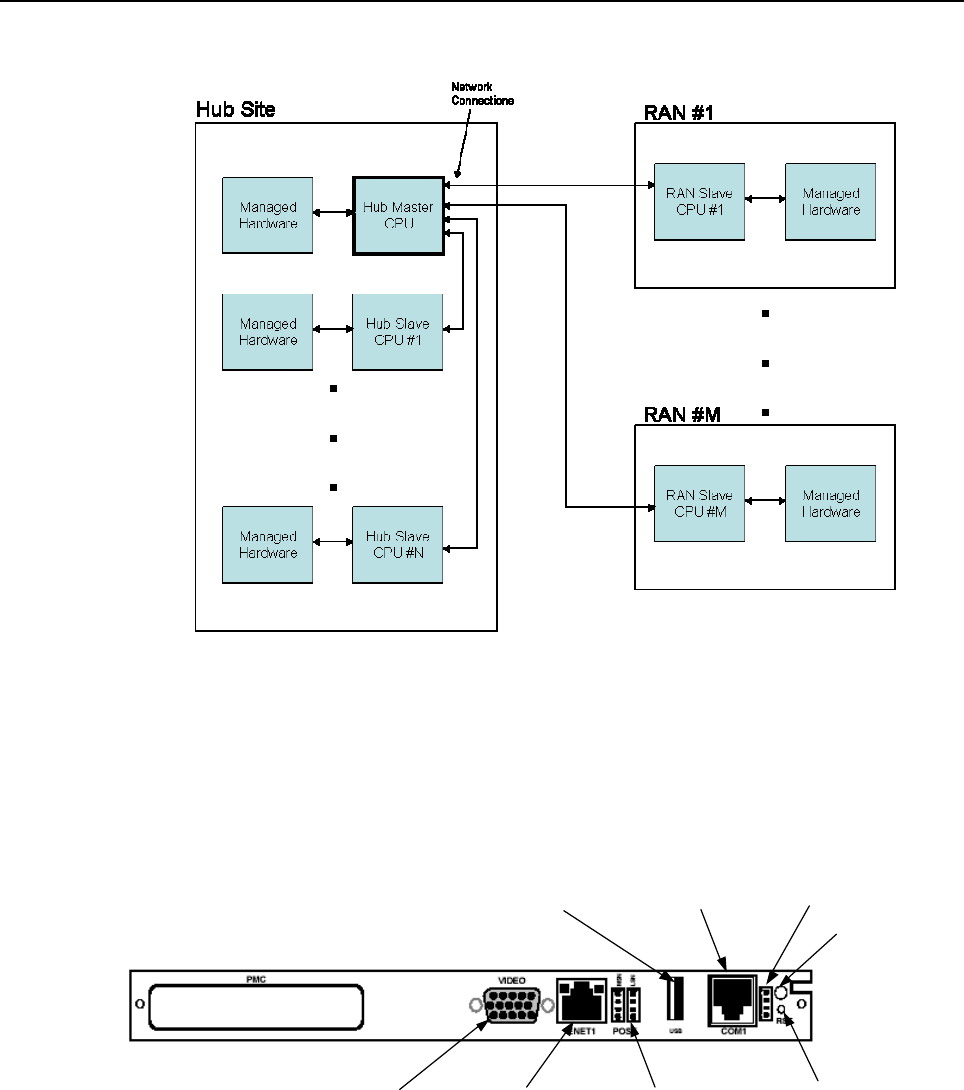
5.1 Central Processor Unit (CPU)
The Hub Central Processor Unit (CPU) installs into the Digital Chassis. There are two CPU
types used in the CXD system, Hubmaster and Slave CPUs. The Hubmaster manages its own
local hardware as well as controlling the overall system. The Slave CPUs only manage their
local hardware. All Slave CPUs communicate to the Hubmaster over a network connection.
Figure 2-11 shows the relationship between Hubmaster and Slave CPUs.
ADCP-75-192 • Issue 1 • December 2005 • Section 2: Description
Page 2-12
2005, ADC Telecommunications, Inc.
Figure 2-11. Hubmaster and Slave Block Diagram
There is one Hubmaster (HM) CPU per system. All CPUs at the Hub, with the exception of the
Hubmaster CPU, are Slave CPUs. The CPU used in the RAN is also a Slave CPU to the
Hubmaster CPU. The CPU is shown in Figure 2-12. The references for the CPU are shown in
Table 2-7.
(7) ETHERNET
CONNECTOR
(1) UNIVERS AL
SERIAL BUS
CONNECTOR
(6) ACTIVITY LED'S
(2) COM 1
CONNECTOR
(5) RES ET BUTTON
(4) HOT S WAP
LED
(8) VIDEO
CONNECTOR
(3) S TATUS LED'S
Figure 2-12. CPU Front Panel

ADCP-75-192 • Issue 1 • December 2005 • Section 2: Description
Page 2-13
2005, ADC Telecommunications, Inc.
Table 2-7. CPU User Interface
REF
No.
USER INTERFACE
DESIGNATION
DEVICE FUNCTIONAL DESCRIPTION
1 Universal Serial Bus
Connector
USB connector Front panel Input/Output for keyboard
connectivity.
2 COM 1 Connector RJ-11C connector Front panel interface for COM1.
3 Status LEDs LEDs LED 1 (red) is hotswap
LED 2 & 3 are undefined
LED 4 (green) is power
4 Hot Swap LED Single-colored LED
(Red)
Status indicator turns red when board can
be hot swap extracted.
5 Reset Button Recessed switch Used to manual reset CPU.
6 Activity LED’s Single-colored LED
(Amber)
Eight LEDs give status of CPU during initial
boot process and four status LEDs for board
operation status.
7 Ethernet Connector RJ-45 connector and
single-colored LED
(Green and Yellow)
Ethernet connector, 10 BaseT connection
status and port activity status indicators
8 Video Connector 15-PIN VGA
connector
Not used by Digivance CXD system
5.2 System Interface (STF2)
The System Interface (STF2) module, shown in Figure 2-13, is installed into the Digital
Chassis and RAN Chassis and provides the ability to communicate between the CPU and other
modules (e.g., FBHDC, FSC, HUC, RUC and RDC), using four I2C busses. The STF2 also
communicates with the GPS module found in the Hubmaster Hub Reference Module. The
STF2 used at the RAN differs from the module at the Hub in that it has the GPS antenna input
located in the center of the module and additional GPS circuitry to control that device. STF2
modules are specified according to the number of qualifying communications devices being
utilized. The references for the STF2 are shown in Table 2-8.
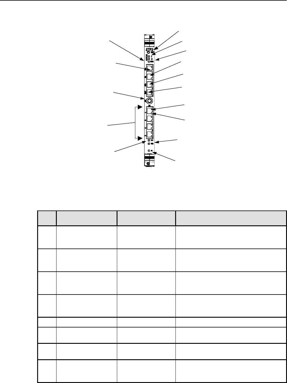
ADCP-75-192 • Issue 1 • December 2005 • Section 2: Description
Page 2-14
2005, ADC Telecommunications, Inc.
(8) I2C COMM LED
(10) FAULT LED
( 11) HO T
SWAP LED
(12) POWER LED
(13) I2C
CONNECTORS
(1) GPS LED
(2) RES ET
SWITCH
(3) S TATUS LED 1
(4) S TATUS LED 2
(9) I2C ERROR LED
(14) GP S ANTENNA
CONNECTOR (RAN ONLY)
(5) DOOR ALARM CONNECTOR
(6) GP S COMMS CONNECTOR
(7) RECTIFIER COMMS
CONNECTOR
(15) TOWER LIGHT
ALARM CONNECTOR
Figure 2-13. STF2 Front Panel
Table 2-8. STF2 User Interface
REF
No.
USER INTERFACE
DESIGNATION
DEVICE FUNCTIONAL DESCRIPTION
1 GPS LED Single-color LED
(Green)
Indicator showing that 1PPS signal is
available. LED toggles once per second
(RAN only).
2 Reset Button Recessed switch Used to halt operation of the CPU operating
system. A power ON reset is required to
restart CPU.
3 Status LED 1 Single-colored LED
(Yellow)
Reserved for future use. Status indicator
turns yellow when CPU is not installed or
has malfunctioned.
4 Status LED 2 Single-colored LED
(Yellow)
Reserved for future use. Status indicator
turns yellow when CPU is not installed or
has malfunctioned.
5 Door Switch Input RJ-45 connector Door switch input (RAN only)
6 GPS Comms
Connector
RJ-45 connector Communications to HRM GPS (Hub Maser
STF only)
7 Rectifier Comms
Connector
RJ-45 connector Communications to rectifier (NXD RAN’s
only)
8 I2C Comm LED’s Single-colored LED
(Green)
On each I2C RJ-45 connector. Status
indicator turns green when an I2C message
is sent on port.
continued
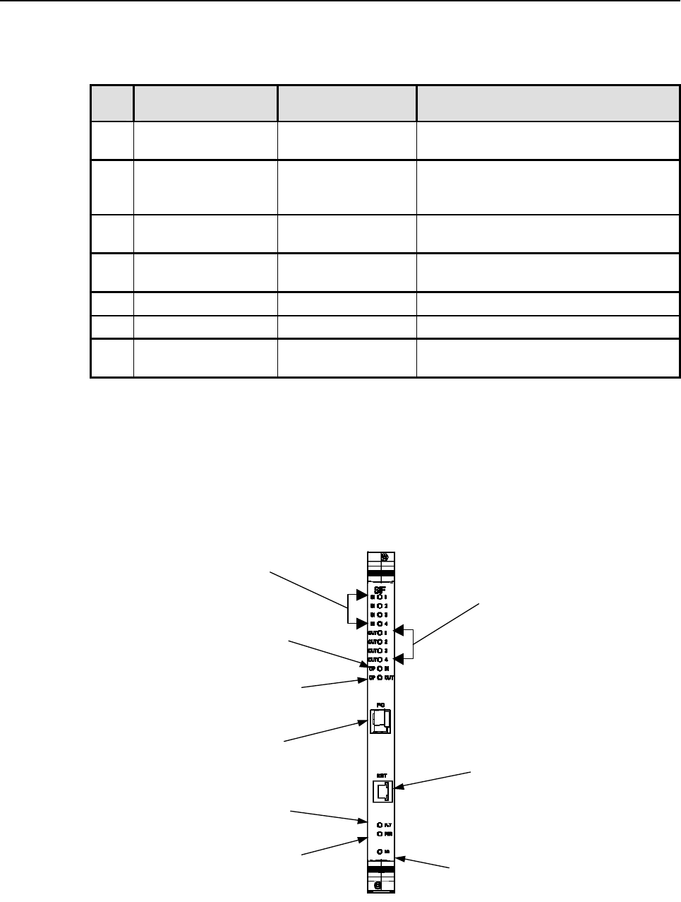
ADCP-75-192 • Issue 1 • December 2005 • Section 2: Description
Page 2-15
2005, ADC Telecommunications, Inc.
Table 2-8. STF2 User Interface, continued
REF
No.
USER INTERFACE
DESIGNATION
DEVICE FUNCTIONAL DESCRIPTION
9 I2C Error LED’s Single-colored LED
(Red)
On each I2C RJ-45 connector. Status
indicator turns red when no response on port.
10 Fault LED Single-colored LED
(Red)
Status indicator turns red when module has
failed or upon startup until the module has
completed initialization.
11 Hot Swap LED Single-colored LED
(Blue)
Status indicator turns blue when board can
be hot swap extracted. (not used)
12 Power LED Single-colored LED
(Green)
Status indicator turns green when module
has power.
13 I2C Connectors RJ-45 connectors I2C interface
14 GPS Antenna SMA connector Input for GPS antenna signal (RAN only)
15 Tower Light Alarm
Connector
RJ-45 connector Contact closure for tower light alarm (not
used)
5.3 Sonet Interface (SIF)
The Sonet Interface (SIF) module, shown in Figure 2-14, is a Digital Chassis and RAN Chassis
module that can be placed in slots designated for either the SIF or RSC (Digital Chassis only).
It provides the DIF to optical interface between the Hub and RANs using an optical
transceiver. This interface includes RF signal information and 10BaseT Ethernet command and
control information.
(7) S FP FIBER OPTIC
CONNECTOR
(6) FAULT LED
(4) HOT S WAP
LED
(5) P OWER LED
(3) ETHERNET
CONNECTOR
(1) DIF INPUT
LED 1-4
(2) DIF OUTPUT
LED 1-4
(9) OPTICAL INPUT LED
(8) OP TICAL OUTP UT
LED
Figure 2-14. SIF Front Panel

ADCP-75-192 • Issue 1 • December 2005 • Section 2: Description
Page 2-16
2005, ADC Telecommunications, Inc.
The SIF module is able to support up to four independent 15 MHz Digital IF (DIF) data
streams (15 MHz band blocks) consisting of either four (4) forward path signals and four (4)
reverse path signals in a non-diversity configuration, or two (2) forward path signals and four
(4) reverse path signals in a receive-diversity configuration. The references for the SIF are
shown in Table 2-9.
Table 2-9. SIF User Interface
REF
No.
USER INTERFACE
DESIGNATION
DEVICE FUNCTIONAL DESCRIPTION
1 DIF Input 1-4 LED Multi-colored LED
(Green/Yellow/Red)
Indicator showing if the interface is not
enabled (off), good (green), degraded
(yellow), clock issue (blinking), or no DIF
tone lock or unused channel (red).
2 DIF Output 1-4 LED Multi-colored LED
(Green/Yellow/Red)
Indicator showing if the interface is not
enabled (off), good (green), degraded
(yellow), clock issue (blinking), or bad data
on output of unused channel (red).
3 Ethernet Connector RJ-45 connector Provides IP connectivity over fiber
4 Hot Swap LED Single-colored LED
(Blue)
Status indicator turns blue when board can
be hot swap extracted.
5 Power LED Single-colored LED
(Green)
Status indicator turns green when module
has power.
6 Fault LED Single-colored LED
(Red)
Status indicator turns red when module has
failed. Indicator is lit during start-up until
the module has initialized.
7 SFP Fiber Optic
Connector
Dual-LC connectors Fiber connector on SFP optical transceiver.
8 Optical Output LED Multi-colored LED
(Green/Yellow/Red)
Indicator showing if the SFP interface is
not enabled (off), good (green), degraded
(yellow) or bad output signals (red).
9 Optical Input LED Multi-colored LED
(Green/Yellow/Red)
Indicator showing if the SFP interface is
not enabled (off), good (green), degraded
(yellow) or bad framing, bad parity, no
signal, or no signal lock (red).
5.4 Small Form-Factor Optical Transceiver (SFP)
The small form-factor pluggable optical transceiver (SFP), shown in Figure 2-15, provides the
optical interface between the Hub equipment and the RAN hardware. The Digivance CXD
system uses industry standard SFP optics which offers a number of configuration options
depending on the requirements of the project. The SFP modules are typically factory installed
with the SIF, or may be purchased separately depending on the system as ordered.
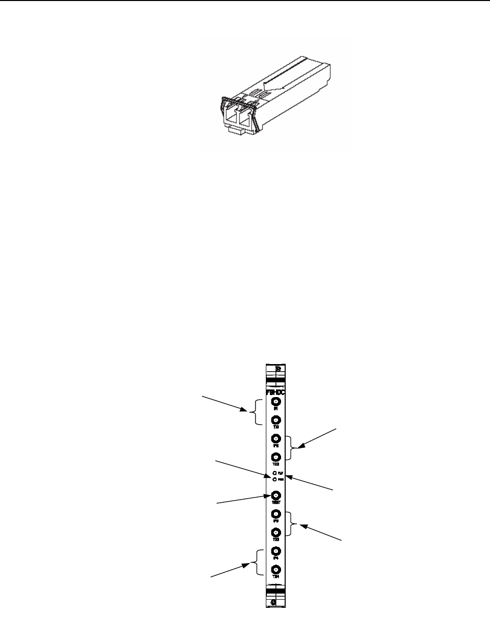
ADCP-75-192 • Issue 1 • December 2005 • Section 2: Description
Page 2-17
2005, ADC Telecommunications, Inc.
Figure 2-15. SFP Optical Transceiver Module
6 HUB SPECIFIC MODULES
This section describes the various controls and indicators for Hub specific modules.
6.1 Full Band Hub Down Converter (FBHDC)
The Full Band Hub Down Converter (FBHDC), shown in Figure 2-16, down converts the
forward RF carrier to an intermediate frequency (IF) that can be digitized. Each FBHDC can
support up to 15 MHz of contiguous spectrum. The FBHDC can be inserted into slots 2, 4, 6
and 8 (see Table 2-6) of the Hub RF Chassis. The references for the FBHDC are shown in
Table 2-10.
(3) FAULT LED
(7) P OWER LED
(2) IF2 AND TX2
CONNECTORS
(1) IF1 AND TX1
CONNECTORS
(4) IF3 AND TX3
CONNECTORS
(5) IF4 AND TX4
CONNECTORS
(6) TEST TONE
IN P U T
Figure 2-16. FBHDC Module

ADCP-75-192 • Issue 1 • December 2005 • Section 2: Description
Page 2-18
2005, ADC Telecommunications, Inc.
Table 2-10. FBHDC User Interface
REF
No.
USER INTERFACE
DESIGNATION
DEVICE FUNCTIONAL DESCRIPTION
1 IF1 and Tx1 Connectors SMA Connector Connect to FSC and BIM, respectively. If
direct connect is desired, supply -4dBm
composite power to Tx1 (-7 dBm for iDEN).
2 IF2 and Tx2 Connectors SMA Connector Additional downlink path (see Ref(1)).
3 Fault LED Single-colored LED
(Red)
Status indicator turns red when module has
failed. Indicator is lit during start-up until
the module has initialized. Indicator will
blink after module receives a system clock
and is awaiting initialization
4 IF3 and Tx3 Connectors SMA Connector Additional downlink path (see Ref(1)).
5 IF4 and Tx4 Connectors SMA Connector Additional downlink path (see Ref(1)).
6 Test SMA Connector Accepts test signal from BIM
7 Power LED Single-colored LED
(Green)
Status indicator turns green when module
has power.
Attenuation is required between the BTS and each input of the FBHDC (in direct connection
configuration), or the Tx0 input of the BIM (in duplex mode) to restrict the FBHDC input
range to a max composite value of -4dBm (–7 dBm for iDEN). For each channel, a cable is
required between this power attenuator and the FBHDC or BIM input.
• One (1) FSC is required per sector. One FSC can accept the output of two (2) FBHDCs per
sector.
• One (1) cable is required per FBHDC to carry the test tone from the BIM FWD 1 or 2
ports to the Test input on the FBHDC.
6.2 Forward Simulcast Card (FSC)
The Forward Simulcast Card (FSC), shown in Figure 2-17, converts the IF signals from the
FBHDC to Digitized IF (DIF) format. There are eight (8) separate analog-to-digital conversion
circuits on one (1) FSC. This module is specified at one per sector per tenant per 8 RANs. The
references for the FSC are shown in Table 2-11.
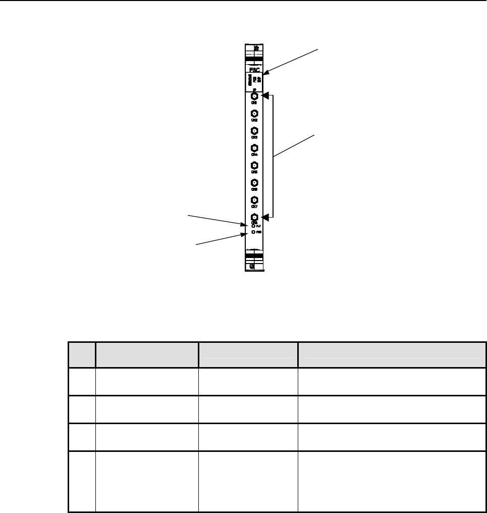
ADCP-75-192 • Issue 1 • December 2005 • Section 2: Description
Page 2-19
2005, ADC Telecommunications, Inc.
(4) FAULT LED
(3) POWER LED
(2) IF CONNECTORS 1-8
(1) EXPANS ION
PORT
Figure 2-17. Forward Simulcast Card
Table 2-11. FSC User Interface
REF
No.
USER INTERFACE
DESIGNATION
DEVICE FUNCTIONAL DESCRIPTION
1 Expansion Port
Connector
RJ-45 connector Optional DIF signal I/O to expansion FSC
(unused)
2 IF Connectors 1-8 SMA connectors IF signal inputs from Hub Down Converter
module
3 Power LED Single-colored LED
(Green)
Status indicator turns green when module
has power.
4 Fault LED Single-colored LED
(Red)
Status indicator turns red when module has
failed. Indicator is lit during start-up until
the module has initialized. Indicator will
blink after module receives a system clock
and is awaiting initialization
6.3 Hub Up Converter Card (HUC)
The Hub Up Converter (HUC) accepts two (2) Digital IF (DIF) signals from a SIF or RSC.
The two (2) DIF signals are converted from digital-to-analog and provided as two (2) separate
RF signals (primary and diversity) to the BIM and BTS.
The HUC, shown in Figure 2-18, can be inserted into slots 1 and 5 in the Hub RF cPCI chassis.
The outputs of the HUC are cabled to the reverse path inputs of the BIM module. Refer to
Table 2-17 for BIM to HUC interconnect. There are two RF cables per HUC for primary and
diversity. Cables are routed from BIM down or up to SMA connector of the adjacent HUC.
The references for the HUC are shown in Table 2-12.
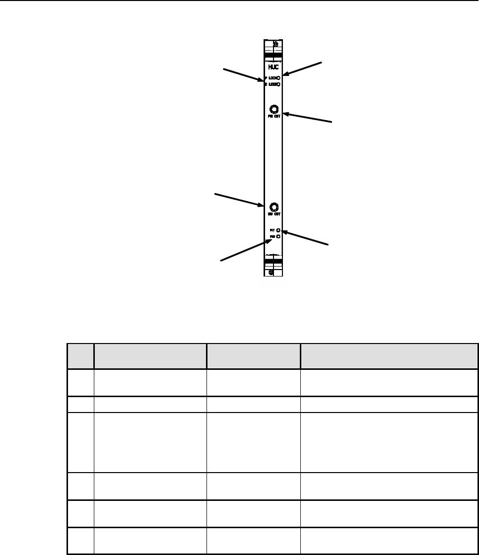
ADCP-75-192 • Issue 1 • December 2005 • Section 2: Description
Page 2-20
2005, ADC Telecommunications, Inc.
(1) PRIMARY P ATH
LO C KE D LE D
(6) DIVERS ITY
P A T H LO C KE D LE D
(3) FAULT LED
(4) P OWER LED
(2) P RIMARY P ATH
SMA CONNECTOR
(5) DIVERS ITY P ATH
SMA CONNECTOR
Figure 2-18. HUC Module
Table 2-12. HUC User Interface
REF
No.
USER INTERFACE
DESIGNATION
DEVICE FUNCTIONAL DESCRIPTION
1 Primary Path Locked
LED
Single-colored LED
(Yellow)
Status indicator turns yellow when
primary path is locked to RSC or SIF.
2 Primary Path RF connector SMA connector RF connector for primary receive path.
3 Fault LED Single-colored LED
(Red)
Status indicator turns red when module
has failed. Indicator is lit during start-up
until the module has initialized. Indicator
will blink after module receives a system
clock and is awaiting initialization
4 Power LED Single-colored LED
(Green)
Status indicator turns green when module
has power.
5 Diversity Path RF
connector
SMA connector RF connector for diversity receive path.
6 Diversity Path Locked
LED
Single-colored LED
(Yellow)
Status indicator turns yellow when diversity
receive path is locked to RSC or SIF.
6.4 Reverse Simulcast Card (RSC)
The Reverse Simulcast Card (RSC) is shown in Figure 2-19. The RSC sums the Digital IF (DIF)
from up to four (4) RANs into a single DIF signal that is sent to the HUC via DIF cables and the
chassis rear panel for conversion to RF. The RSC is utilized in the Digital Chassis and is specified
as one per tenant per sector per 4 RANs, plus an additional one RSC for RANs 5-7, and an
additional one RSC for RAN 8. The references for the RSC are shown in Table 2-13.
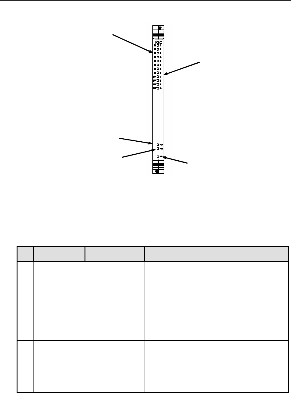
ADCP-75-192 • Issue 1 • December 2005 • Section 2: Description
Page 2-21
2005, ADC Telecommunications, Inc.
(5) FAULT LED
(3) HOT SWAP
LE D
(4) P OWER LED
(1) DIF INP UT
LE D 1- 8
(2) DIF OUTP UT
LE D 1- 4
Figure 2-19. RSC Module
The DIF input and output LEDs describe the status of the digital signal. The RSC defaults to
using two 4:1 digital simulcast groups. To determine the relationship between the RSC channel
LED number and the signal type, use the guidelines in Table 2-13.
Table 2-13. RSC User Interface
REF
No.
USER INTERFACE
DESIGNATION
DEVICE FUNCTIONAL DESCRIPTION
1 DIF Input LED
1-8
Multi-colored LED
(Green/Yellow/Red)
Indicator showing if no input signal (off), good (green),
degraded (yellow), clock issue (blinking), or bad data on
channel (red).
IN 1: Band Sector Primary (1st Simulcast)
IN 2: Band Sector Primary (2nd Simulcast)
IN 3: Band Sector Primary (3rd Simulcast)
IN 4: Band Sector Primary (4th Simulcast)
IN 5: Band Sector Diversity (1st Simulcast)- if used
IN 6: Band Sector Diversity (2nd Simulcast)- if used
IN 7: Band Sector Diversity (3rd Simulcast)- if used
IN 8: Band Sector Diversity (4th Simulcast)- if used
2 DIF Output LED
1-4
Multi-colored LED
(Green/Yellow/Red)
Indicator showing if no input signal (off), good (green),
degraded (yellow), clock issue (blinking), or bad data on
channel (red).
OUT 1: Band Sector-Primary
OUT 2: Band Sector-Diversity- if used
OUT 3: Not Used
OUT 4: Not Used
continued

ADCP-75-192 • Issue 1 • December 2005 • Section 2: Description
Page 2-22
2005, ADC Telecommunications, Inc.
Table 2-13. RSC User Interface, continued
REF
No.
USER INTERFACE
DESIGNATION
DEVICE FUNCTIONAL DESCRIPTION
3 Hot Swap LED Single-colored LED
(Blue)
Status indicator turns blue when board can be hot swap
extracted.
4 Power LED Single-colored LED
(Green)
Status indicator turns green when module has power.
5 Fault LED Single-colored LED
(Red)
Status indicator turns red when module has failed.
6.5 Hub Reference Module (HRM)
The Hub Reference Module (HRM) is used to:
• Provide clock referencing (RF and digital) to the cPCI chassis.
• Interface to GPS antenna.
• Provide 1PPS, derived from GPS, to Digital Chassis for delay management.
For every Hubmaster CPU there is only one Master HRM. This unit is the interface to the GPS
antenna. The Hub rack managing this Master HRM must be setup to monitor the GPS antenna.
Therefore, only the Master HRM must be monitored for “antenna feedline” fault status. All
other HRMs must be daisy chained to this GPS input. Starting with the Master HRM, connect
“GPS AUX” of the donor HRM to “GPS IN” of the next HRM in line using an SMA coax
cable.
For simulcasting, redundancy, and other functions, HRMs must also share the same clock
reference across multiple racks. This is accomplished by daisy-chaining the reference via RJ-
45 ports on the back of the unit (see figure 2-21). Starting with “9.6 MHz” RJ-45 port “B” of
the Hubmaster HRM, connect a crossover CAT-5 from port B of each donor HRM to port A of
the next HRM in line. Port B will remain open on the last HRM in the chain. Be sure to daisy
chain HRMs prior to powering them on or connecting them to I2C.
The HRM front panel is shown in Figure 2-20. The references for the HRM front panel are
shown in Table 2-14. The HRM rear panel is shown in Figure 2-21. The references for the
HRM rear panel are shown in Table 2-15.
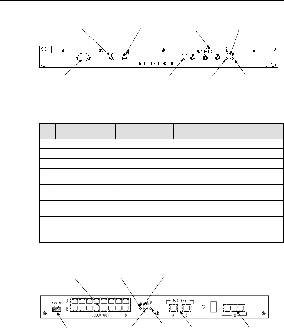
ADCP-75-192 • Issue 1 • December 2005 • Section 2: Description
Page 2-23
2005, ADC Telecommunications, Inc.
(8) RS -232
CONNECTOR
(1) GPS IN
(7) 1 HZ LED
(2) GPS
AUXILLARY
(5) POWER LED
(3) CLOCK
TES T POINTS
(4) FAULT LED
(6) P LL LOCK LED
Figure 2-20. Hub Reference Module Front Panel
Table 2-14. HRM Front Panel User Interface
REF
No.
USER INTERFACE
DESIGNATION
DEVICE FUNCTIONAL DESCRIPTION
1 GPS Input Connector SMA connector Input of GPS antenna signal.
2 GPS Auxiliary SMA connector Auxiliary GPS output for daisy-chaining.
3 Clock Test Points SMA connectors Used for testing of reference clocks
4 Fault LED Single-colored LED
(Red)
Status indicator turns red when module has
failed.
5 Power LED Single-colored LED
(Green)
Status indicator turns green when module
has power.
6 PLL Lock Single-colored LED
(Yellow)
Status indicator turns yellow when phase
lock loop circuit is locked
7 1 Hz LED Single-colored LED
(Yellow)
Status indicator toggles at the rate of 1 PPS
when 1 Hz signal detected
8 GPS RS-232 DB9 connector GPS comms to STF2 module
(8) 12 VDC
IN P U T
(1) CLOCK OUT
(6) 1 HZ LED (4) I2C CONNECTORS
(2) POWER LED (3) FAULT LED
(7) P LL LOCK LED (5) 9.6 MHz
CONNECTORS
Figure 2-21. Hub Reference Module Rear Panel
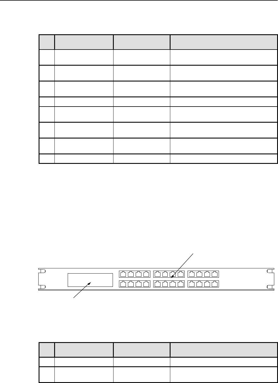
ADCP-75-192 • Issue 1 • December 2005 • Section 2: Description
Page 2-24
2005, ADC Telecommunications, Inc.
Table 2-15. HRM Rear Panel User Interface
REF
No.
USER INTERFACE
DESIGNATION
DEVICE FUNCTIONAL DESCRIPTION
1 Clock Out (A1-8, B1-
8)
RJ-45 Sample clock, Reference clock, and 1PPS
output connectors (x16)
2 Power LED Single-colored LED
(Green)
Status indicator turns green when module
has power.
3 Fault LED Single-colored LED
(Red)
Status indicator turns red when module has
failed.
4 I2C Connectors RJ-45 connectors I2C interface (x3)
5 9.6 MHz connectors RJ-45 connectors Used for HRM daisy-chaining between
racks.
6 PLL Lock LED Single-colored LED
(Yellow)
Status indicator turns yellow when phase
lock loop circuit is locked
7 1 Hz LED Single-colored LED
(Yellow)
Status indicator toggles at a rate of 1 PPS
when 1 Hz signal detected
8 12 VDC Input 3-pin molex Input power to HRM
6.6 Ethernet Hub
The Ethernet Hub (or Ethernet Switch sold as optional item) is used to consolidate Ethernet
connections within a Hub rack. The module is a commercially available unit rated for industrial
use and is available as an accessory item to the Digivance CXD system. The standard Ethernet
Hub requires 120 VAC power. For projects requiring all DC connections a -48 VDC Ethernet
Switch is available as an option. Figure 2-22 shows the layout of a 24 port 120 VAC Ethernet
Hub. The references for the Ethernet Hub front panel are shown in Table 2-16.
(2) PORT LED
STATUS INDICATORS
(1) 24 ETHERNET
PORTS
Figure 2-22. Ethernet Hub Interconnect
Table 2-16. Ethernet Hub Front Panel User Interface
REF
No.
USER INTERFACE
DESIGNATION
DEVICE FUNCTIONAL DESCRIPTION
1 Ethernet Connectors RJ-45 Ethernet ports
2 Activity LEDs Single-colored LED
Array
Status indicators show Ethernet traffic on
hub ports.
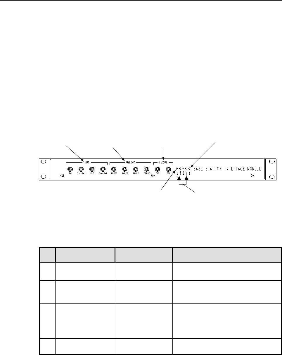
ADCP-75-192 • Issue 1 • December 2005 • Section 2: Description
Page 2-25
2005, ADC Telecommunications, Inc.
6.7 BTS Interface Module (BIM)
The Base Station Interface Module provides the following BTS interface functionality:
• Interface to a low power forward BTS RF path.
• Handles duplexed and non-duplexed signals.
• Forward path gain adjustment.
• Reverse path gain adjustment.
The BIM, shown in Figure 2-23, is a 1RU module that mounts into the HUB Base Rack. There
are four (4) BIM types depending on the frequency band to be supported: Cellular, SMR A,
SMR B, or PCS. The references for the BIM front panel are shown in Table 2-17.
(1) BAS E S TATION
DUP LEXED RF
CONNECTORS
(3) RECEIVE P RIMARY AND
DIVERS ITY RF
CONNECTORS
(2) TRANS MIT S IMP LEXED
RF CONNECTORS
(5) LED BAND
INTERFACE
INDICATORS
(6) FAULT
(4) P OWER
Figure 2-23. BTS Interface Module
Table 2-17. BIM Front Panel User Interface
REF
No.
USER INTERFACE
DESIGNATION
DEVICE FUNCTIONAL DESCRIPTION
1 Base Station RF
Connectors
Four SMA
connectors
Tx0/Rx0 & Tx1/Rx1 duplexed connections
Rx0/Rx1 used for non-duplexed
2 Transmit Forward
Path RF Connectors
Four SMA
connectors
Forward path connections to FBHDC
Fwd1P/Fwd2P – Summed Tx0/Tx1
Fwd1D/Fwd2D – Separated Tx0/Tx1
3 LED Indicators Red LED
Green LED
Yellow LED
Yellow LED
Yellow LED
Fault– Lighted when module fault
Power– Lighted when power present
PCS– BIM supports the PCS band
Cell– BIM supports Cell band
SMR– BIM Supports SMR band
4 Receive Reverse path
RF Connectors
Two SMA
connectors
Connect to HUC module. Primary and
diversity connections
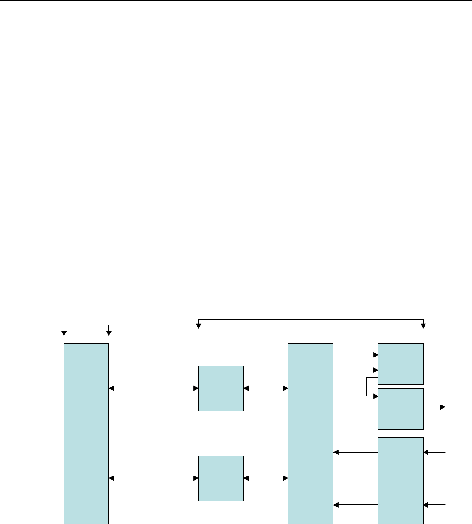
ADCP-75-192 • Issue 1 • December 2005 • Section 2: Description
Page 2-26
2005, ADC Telecommunications, Inc.
The BIM is designed to support the desired interface to the wireless service provider BTS. The
BIM can support all duplex or simplex configurations. The standard BIM input power level is
low power; -10 to +26 dBm composite. A high power option can be ordered to support a BTS
feed 42 to 47 dBm composite per connection. Dual receive and transmit diversity is also
provided in the BIM.
There are three typically configurations for the BIM Module. Refer to the figure specified for a
diagram of each configuration.
1. BIM Basic – Two cable duplexed interface (see Figure 2-24).
2. Direct Cable – Forward path bypasses, reverse path still used (see Figure 2-25).
3. Transmit Diversity – Keep Tx0/Tx1 separated (see Figure 2-26).
Table 2-18 shows how to connect a BIM for all possible RF connections. One BIM is required
per tenant sector.
BTS
Sector
20 dB
High Power
Attenuator
(50 watts max)
Tx/RxP
WSP Equipment
BIM
FBHDC
HUC
20 dB
High Power
Attenuator
(50 watts max)
Tx/RxD
CXD Hub Equipment
FSC
Tx0/Rxo
Tx1/Rx1
Transmit
Fwd1P TX1
IF1
CH1
Receive
Pri
Receive
Div
Pri Out
Div Out
DIF Output (x8)
DIF Input Pri
DIF Input Div
Transmit
Fwd1D
Test
Figure 2-24. BIM Basic Configuration
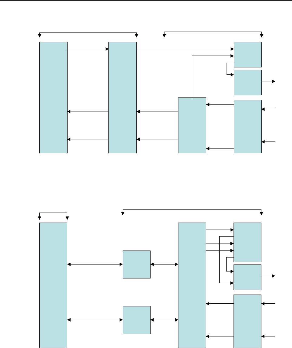
ADCP-75-192 • Issue 1 • December 2005 • Section 2: Description
Page 2-27
2005, ADC Telecommunications, Inc.
BTS
Sector
Tx
WSP Equipment
BIM
FBHDC
HUC
CXD Hub Equipment
FSC
TX1
IF1
CH1
Receive
Pri
Receive
Div
Pri Out
Div Out
DIF Output (x8)
DIF Input Pri
DIF Input Div
Rx0
Rx1
RxP
RxD
DAS
Interface
Equipment
-4 dBm
composite (max)
Fwd1D
Test
BTS
Sector
Tx
WSP Equipment
BIM
FBHDC
HUC
CXD Hub Equipment
FSC
TX1
IF1
CH1
Receive
Pri
Receive
Div
Pri Out
Div Out
DIF Output (x8)
DIF Input Pri
DIF Input Div
Rx0
Rx1
RxP
RxD
DAS
Interface
Equipment
-4 dBm
composite (max)
Fwd1D
Test
Figure 2-25. Direct Cable Configuration
BTS
Sector
20 dB
High Power
Attenuator
(50 watts max)
Tx/RxP
WSP Equipment
BIM
FBHDC
HUC
20 dB
High Power
Attenuator
(50 watts max)
Tx/RxD
CXD Hub Equipment
FSC
Tx0/Rxo
Tx1/Rx1
Transmit
Fwd1D
TX1
IF1
CH1
Receive
Pri
Receive
Div
Pri Out
Div Out
DIF Output (x8)
DIF Input Pri
DIF Input Div
Transmit
Fwd2D
Test
TX2
IF2
CH3
Transmit
Fwd1P
Figure 2-26. Transmit Diversity

ADCP-75-192 • Issue 1 • December 2005 • Section 2: Description
Page 2-28
2005, ADC Telecommunications, Inc.
Table 2-18. BIM RF Connections
CONFIGURATION FROM TO
BIM Basic BIM BTS TX0/RX0 High Power Attenuator X
BIM BTS TX1/RX1 High Power Attenuator Y
Transmit Fwd1P FBHDC Tx1
Transmit Fwd1D FBHDC Test
Receive RX0 HUC PRI
Receive RX1 HUC DIV
Direct Cable WSP BTS Tx FBHDC Tx1
WSP BTS RxP BIM Rx0
WSP BTS RxD BIM Rx1
BIM Receive PRI HUC PRI
BIM Receive DIV HUC DIV
Transmit Diversity BIM BTS TX0/RX0 High Power Attenuator X
BIM BTS TX1/RX1 High Power Attenuator Y
Transmit Fwd1D FBHDC Tx1
Transmit Fwd2D FBHDC Tx2
Transmit Fwd1P FBHDC Test
Receive RX0 HUC PRI
Receive RX1 HUC DIV
Note: The Digivance CXD/NXD Hub is very flexible and is capable of other interface
options. Contact ADC directly for other options.
6.8 Attenuator Shelf
The attenuators are mounted on an attenuator shelf. The attenuator shelf, shown in Figure 2-27,
is mounted at the top of the Hub rack. It can hold up to twelve (12) 50 watt attenuators. One
attenuator can handle up to a 47 dBm composite signal level.
Figure 2-27. Attenuator Shelf
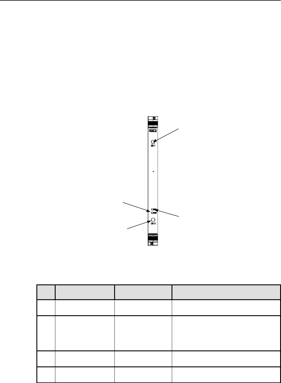
ADCP-75-192 • Issue 1 • December 2005 • Section 2: Description
Page 2-29
2005, ADC Telecommunications, Inc.
7 RADIO ACCESS NODE (RAN) SPECIFIC MODULES
This section describes the various controls and indicators for RAN specific modules.
7.1 Ran Down Converter (RDC or RDC2)
The RAN Down Converter (RDC), shown in Figure 2-28, takes RF signals from a primary and
secondary antenna and down converts the signals into IF. Signals are input into the card over
coax cable terminated with SMA connectors on to the front panel of the module. The
references for the RDC user interface are shown in Table 2-19. Two versions of the RDC, the
RDC and RDC2, are available.
(2) FAULT LED
(4) P OWER LED
(3) CHANNEL 2
(1) CHANNEL 1
Figure 2-28. RDC Front Panel
Table 2-19. RDC User Interface
REF
No.
USER INTERFACE
DESIGNATION
DEVICE FUNCTIONAL DESCRIPTION
1 Channel 1 RF
Connector
SMA connector RF input for Channel 1
2 Fault LED Single-colored LED
(Red)
Status indicator turns red when module has
failed. Indicator is lit during start-up until
the module has initialized. Indicator will
blink after module receives a system clock
and is awaiting initialization
3 Channel 2 RF
Connector
SMA connector RF input for Channel 2. Used in diversity
systems or 3/4 bands systems (future)
4 Power LED Single-colored LED
(Green)
Status indicator turns green when module
has power.
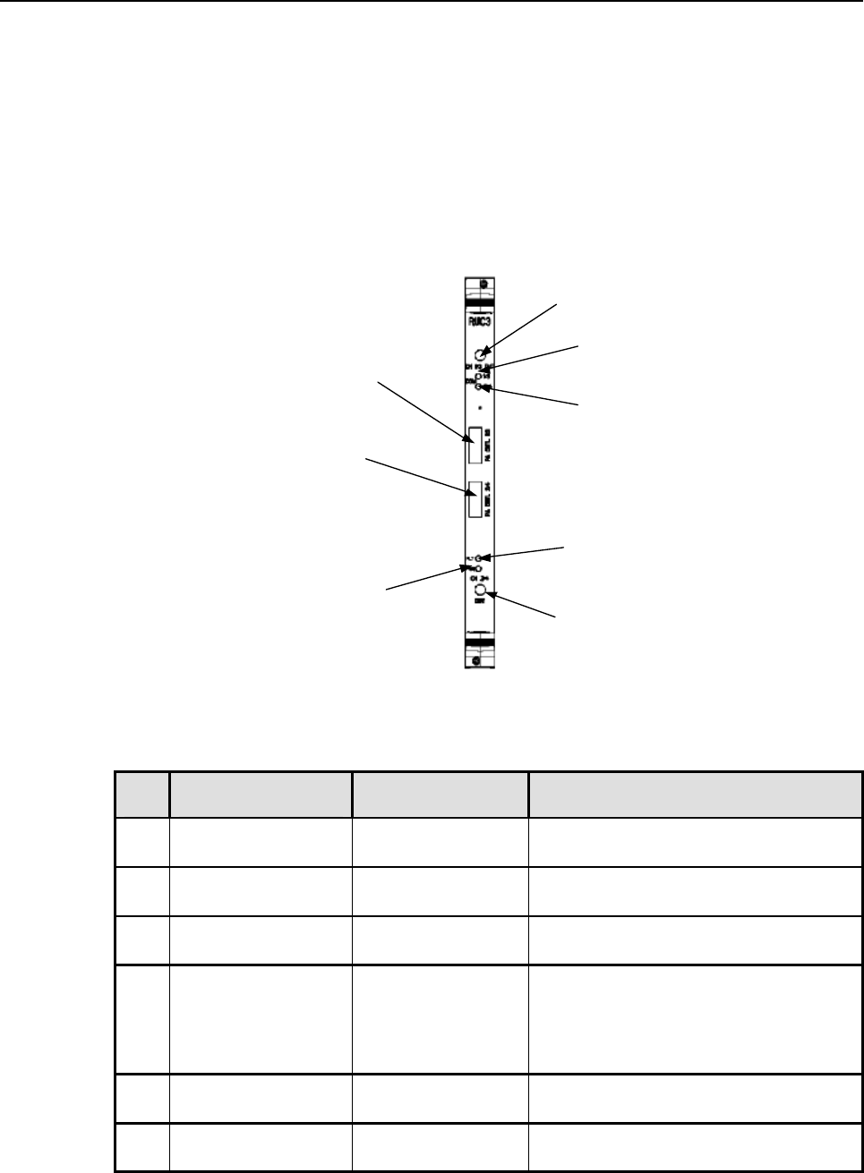
ADCP-75-192 • Issue 1 • December 2005 • Section 2: Description
Page 2-30
2005, ADC Telecommunications, Inc.
7.2 Ran Up Converter (RUC2.X or RUC3)
The RAN Up Converter (RUC), shown in Figure 2-29, takes IF signals from a DIF signal
generated by a SIF and up converts the signals to RF. The RF outputs of the RUC are
connected to the RFA’s using coax cable jumpers. The RUC is used to monitor and control the
RFA and communicates over the provided cable using I2C. The references for the RUC user
interface are shown in Table 2-20. Two versions of the RUC, the RUC2.X and RUC3, are
available.
(4) FAULT LED
(5) CHANNEL 2/4 OUT
(6) P OWER LED
(8) P A CNTL 1/3
(2) COM 1/3
(3) COM 2/4
(7) P A CNTL 2/4
(1) CHANNEL 1/3 OUT
Figure 2-29. RUC Front Panel
Table 2-20. RUC User Interface
REF
No.
USER INTERFACE
DESIGNATION
DEVICE FUNCTIONAL DESCRIPTION
1 Channel 1/3 Out
Connector
SMA connector RF output for signal coming from RAN
SIF OUT channel 1 or 3
2 COM 1/3 LED Single-colored LED
(Yellow)
Status indicator turns yellow when DIF lock
to SIF Channel 1 or 3
3 COM 2/4 LED Single-colored LED
(Yellow)
Status indicator turns yellow when DIF lock
to SIF Channel 2 or 4
4 Fault LED Single-colored LED
(Red)
Status indicator turns red when module has
failed. Indicator is lit during start-up until
the module has initialized. Indicator will
blink after module receives a system clock
and is awaiting initialization
5 Channel 2/4 Out
Connector
SMA connector RF output for signal coming from RAN
SIF OUT channel 2 or 4
6 Power LED Single-colored LED
(Green)
Status indicator turns green when module
has power.
continued
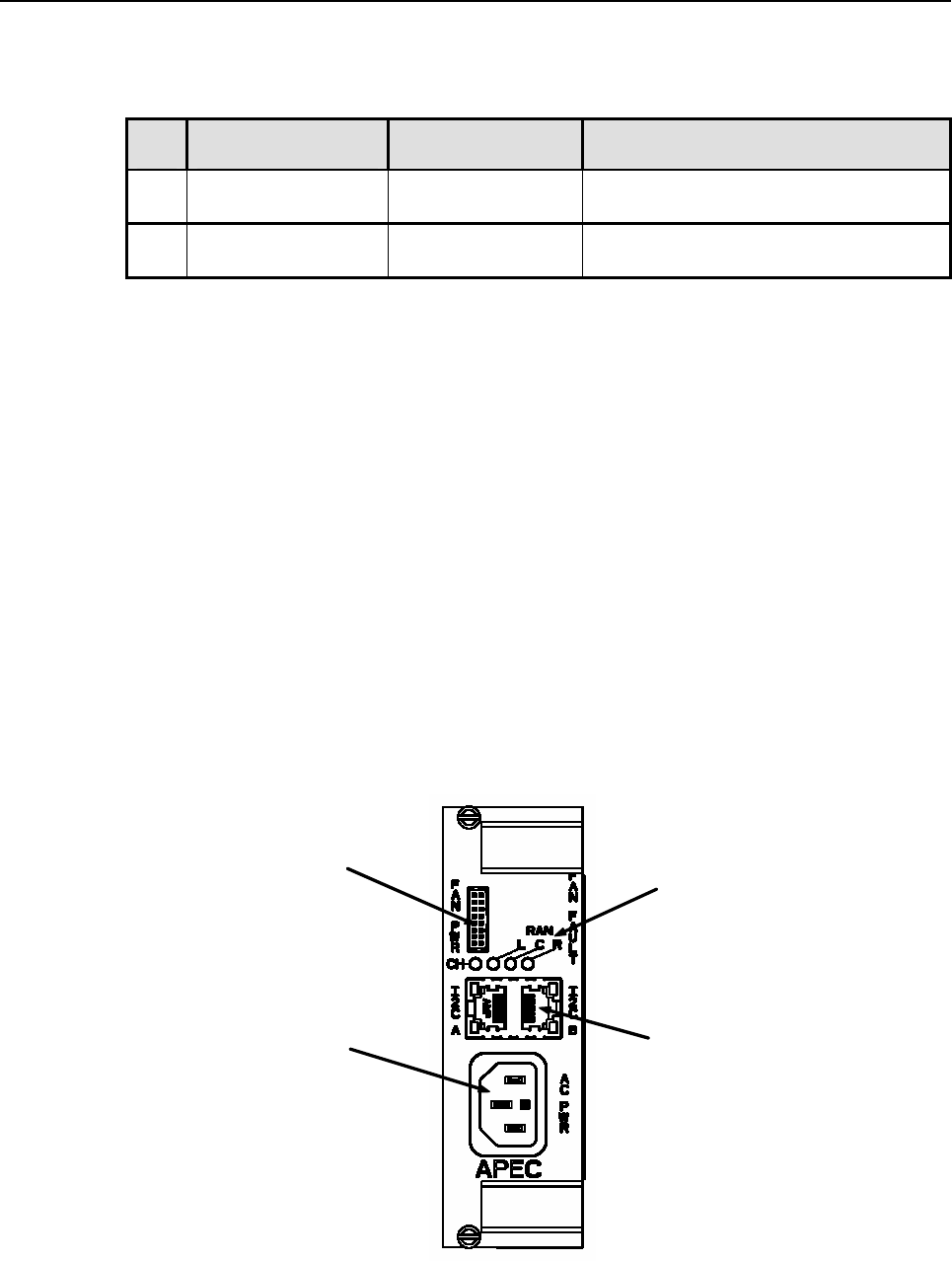
ADCP-75-192 • Issue 1 • December 2005 • Section 2: Description
Page 2-31
2005, ADC Telecommunications, Inc.
Table 2-20. RUC User Interface, continued
REF
No.
USER INTERFACE
DESIGNATION
DEVICE FUNCTIONAL DESCRIPTION
7 PA CNTL 2/4 I2C flatpack
Connector
I2C Communications to RFA
8 PA CNTL 1/3 I2C flatpack
Connector
I2C Communications to RFA
7.3 AC Power Entry Controller
The AC Power Entry Controller (APEC) is used for installations requiring AC power only. It
has a 100-240 VAC input and has an EMI filter to condition the signal. The APEC provides
the following functions:
• AC Power for the cPCI power supplies
• Fan tachometer monitoring and control
• FAN fault indicator LED’s
• Future growth for I2C and GPS connections to backplane (not currently used).
The APEC contains two fan controllers that control and monitor the six enclosure fans that are
used to cool the RAN enclosure. The APEC front panel has an IEC-320 for AC power entry
and 16-pin Molex connector near the top connects to both the enclosure Fans and the RF
Assembly (RFA). The RFA provides +28VDC power to the APEC, which uses this power to
provide PWM signals to the six enclosure fans. The APEC front panel is shown in Figure 2-30
and the user interface is described in Table 2-21.
(2) FAN POWER
CONNECTOR (3) FAN FAULT LEDS
(4 STATUS LEDS)
(4) I2C INTERFACE
(FUTURE)
(1) AC P OWER
CONNECTOR
Figure 2-30. AC Power Entry Controller (APEC)

ADCP-75-192 • Issue 1 • December 2005 • Section 2: Description
Page 2-32
2005, ADC Telecommunications, Inc.
Table 2-21. APEC User Interface
REF
No.
USER INTERFACE
DESIGNATION
DEVICE FUNCTIONAL DESCRIPTION
1 AC Power Input
Connector
3-wire AC power
cord connector
Provides AC power into the cPCI chassis
2 Fan Power Connector 20 pin enclosed
header connector
Provides power to chassis and enclosure
fans. Monitors fan speeds
3 Fan fault LEDS LED (red) CH – cPCI chassis fans not turning
L – Left two enclosure fans not turning
C – Center two enclosure fans not turning
R – Right two enclosure fans not turning
4 I2C Connectors RJ45 connector Reserved for future use
7.4 DC Power Entry Controller (DPEC)
The DC Power Entry Controller (DPEC) is used for any installation requiring battery backup.
It provides the following functions:
• DC Power for cPCI power supplies
• Fan tachometer monitoring and control
• FAN fault indicator LED’s
• Future growth for I2C and GPS connections to backplane (not currently used)
• Battery controller
i. Charge controller
ii. Low Voltage Disconnect
iii. Temperature monitor
iv. Fault detection
The DPEC powers the six-slot chassis from the +28VDC power supplies located in the RF
Assemblies. The DPEC provides swap-over circuitry which monitors the +28VDC input and
switches to battery if this input power disappears. It also charges the battery as necessary when
normal operating power is present. The DPEC front panel is shown in Figure 2-31 and the user
interface is described in Table 2-22.
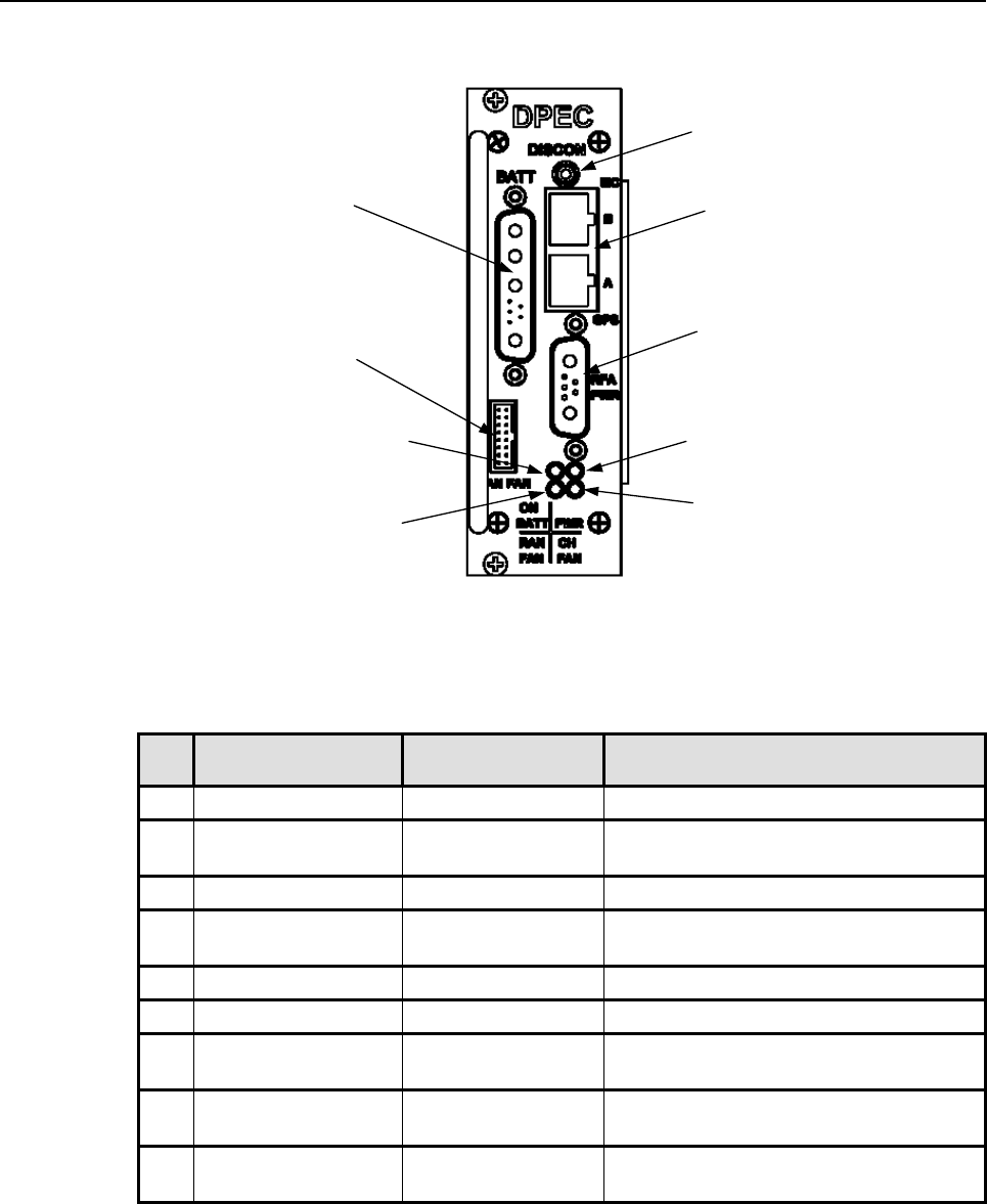
ADCP-75-192 • Issue 1 • December 2005 • Section 2: Description
Page 2-33
2005, ADC Telecommunications, Inc.
(9) FAN P OWER CONNECTOR
(5) DC INPUT POWER LED
(3) I2C INTERFACE
(FUTURE)
(1) BATTERY CONNECTOR
(4) RFA (AC) INPUT
P OWER CONNECTOR
(2) BATTERY
DIS CONNECT S W ITCH
(6) CHAS S IS FAN LED
(8) BATTERY POWER LED
(7) RAN FAN LED
Figure 2-31, DC Power Entry Controller (DPEC)
Table 2-22. DPEC User Interface
REF
No.
USER INTERFACE
DESIGNATION
DEVICE
FUNCTIONAL DESCRIPTION
1 Battery Connector Multi-pin connector Battery cable connector.
2 Battery Disconnect Push button Pushed to disconnect batteries from
powering RAN.
3 I2C Connectors RJ45 connector Reserved for future use.
4 RFA (DC) Power
Input Connector
DB 9 connector Provides DC power into the cPCI chassis
from the RFA Module.
5 DC Power Input LED LED (green) Lighted when DC power is present.
6 RAN Chassis fan LED (red) Lighted when cPCI chassis fans have faulted
7 RAN fan LED (red) Lighted when RAN enclosure fans have
faulted
8 Battery Power LED (yellow) Lighted when RAN is being powered by the
batteries.
9 Fan Power Connector 20 pin enclosed
header connector
Provides power to chassis and enclosure
fans. Monitors fan speeds.
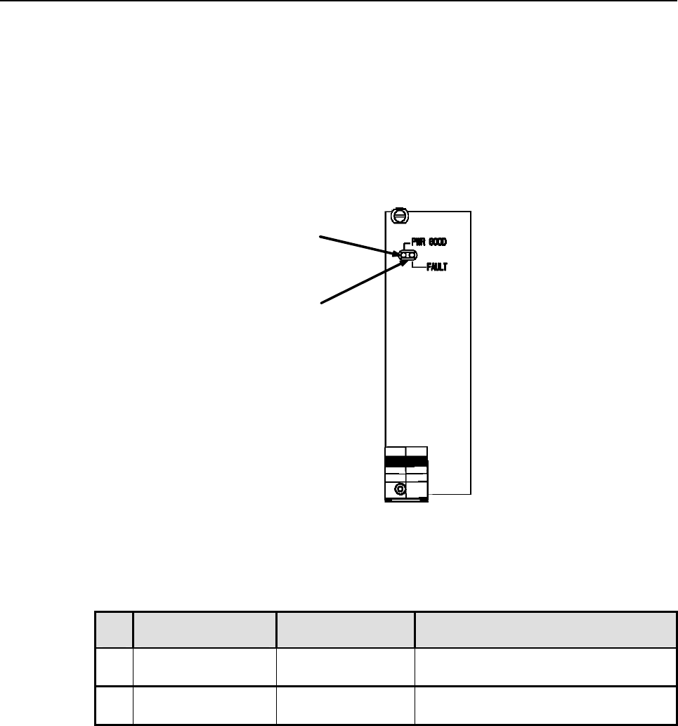
ADCP-75-192 • Issue 1 • December 2005 • Section 2: Description
Page 2-34
2005, ADC Telecommunications, Inc.
7.5 CompactPCI Power Supply (cPCI P/S)
7.5.1 AC cPCI Power Supply
The AC cPCI P/S distributes power to the CXD Ran Chassis cPCI modules. It is used in the
RAN Chassis for applications requiring AC only (no battery backup option). The AC cPCI is
shown in Figure 2-32 and the user reference is shown in Table 2-23.
(2) FAULT LED
(1) P OWER LED
Figure 2-32. RAN Chassis AC cPCI Power Supply
Table 2-23. AC cPCI P/S User Interface
REF
No.
USER INTERFACE
DESIGNATION
DEVICE FUNCTIONAL DESCRIPTION
1 Power LED Single-colored LED
(Green)
Status indicator turns green when power
supply has power.
2 Fault LED Single-colored LED
(Yellow)
Status indicator turns yellow when power
supply has failed
7.5.2 DC cPCI Power Supply
The DC cPCI P/S, shown in Figure 2-33, distributes power to the CXD Ran Chassis when
configured for the battery backup option. It is not used for standard AC power only
configurations. The user reference is shown in Table 2-24.
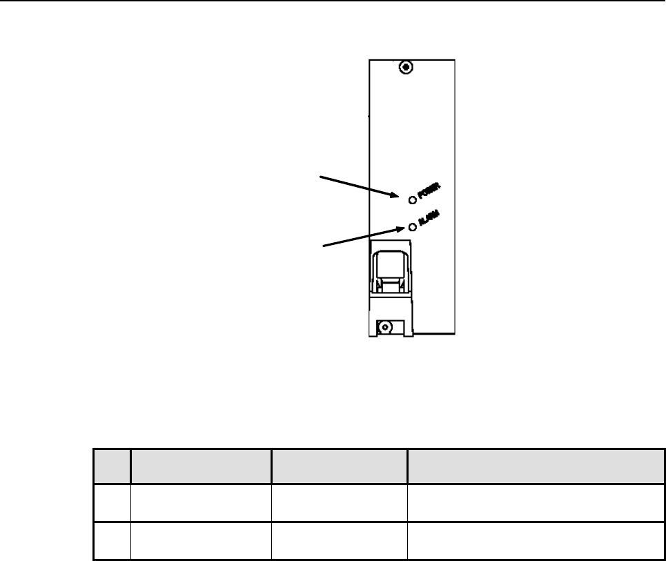
ADCP-75-192 • Issue 1 • December 2005 • Section 2: Description
Page 2-35
2005, ADC Telecommunications, Inc.
(2) FAULT LED
(1) P OWER LED
Figure 2-33. RAN Chassis DC cPCI Power Supply
Table 2-24. DC cPCI P/S User Interface
REF
No.
USER INTERFACE
DESIGNATION
DEVICE FUNCTIONAL DESCRIPTION
1 Power LED Single-colored LED
(Green)
Status indicator turns green when power
supply has power.
2 Alarm LED Single-colored LED
(Yellow)
Status indicator turns yellow when power
supply has failed
7.6 RF Assembly Module (RFA)
The Radio Frequency Assembly (RFA) is used to amplify the forward path RF output signal,
receive the reverse path RF signals and amplify the signals with a low noise amplifier, duplex
RF signals and filter out-of-band emissions and signals. On the forward path RF signal passes
to the RFA from the Ran Up Converter (RUC) for amplification, filtering and duplexing and
output in the antenna port on the module. On the reverse path, signals are separated by the
duplexer, filtered, and amplified by a Low Noise Amplifier (LNA) which sets the noise figure
of the system. Signals are passed to the Ran Down Converter.
The RFA contains redundant power supplies. In the event that one supply fails, the other unit
will maintain power to the RFA and the power LED will be lighted.
There are several types of RFA’s depending on the band, number of power amplifier, and
signal combining using diplexers. The RFA’s may be used with the CXD standard and
extended battery cabinet. Other cabinet options are available as accessory items.
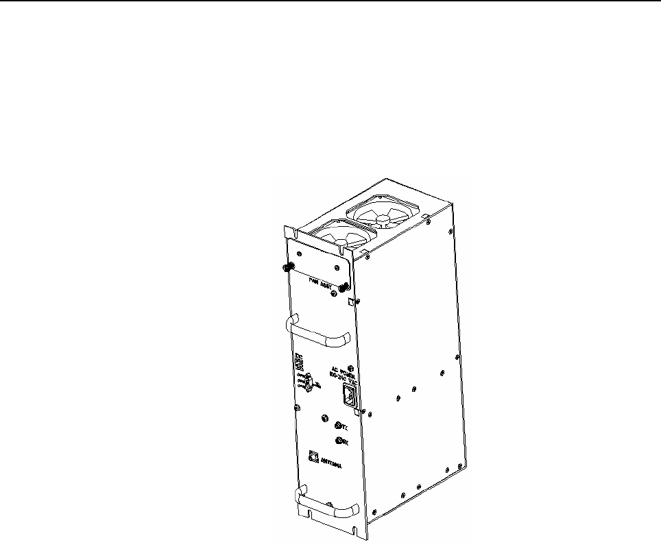
ADCP-75-192 • Issue 1 • December 2005 • Section 2: Description
Page 2-36
2005, ADC Telecommunications, Inc.
The RFA consists of an electronic component circuit board assembly and fan assembly that are
mounted within a sheet metal enclosure. The metal enclosure provides a mounting point for the
electronic components and controls RF emissions. Except for the fan assembly, the electronic
components are not user replaceable. All controls, indicators, and switches are mounted on the
RFA front panel for easy access. A carrying handle is provided on the front of the RFA to
facilitate installation and transport. A single-band 10 W RFA is shown in Figure 2-34.
Figure 2-34. Single-Band 10 Watt Radio Frequency Assembly (RFA)
7.6.1 Single-Band 10 Watt RFA
The single-band 10 Watt RFA user interface consists of various LED's, power,
communications and RF connectors. The RFA user interface is shown in Figure 2-35 and
described in Table 2-25.
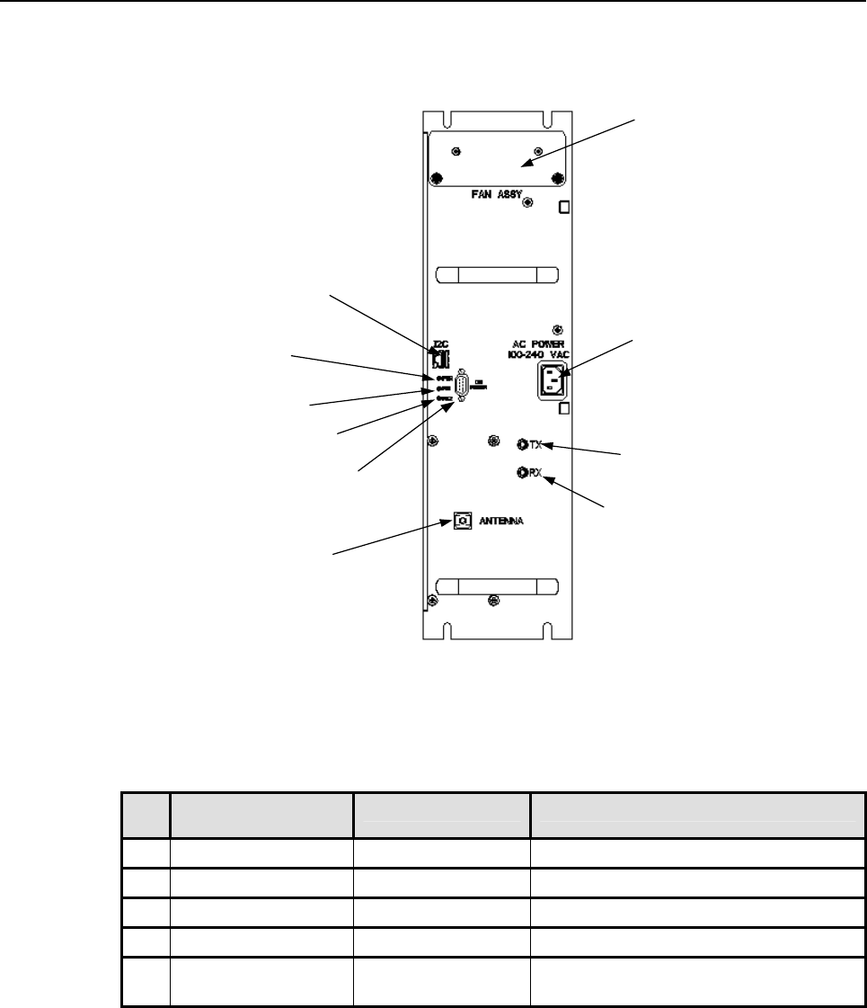
ADCP-75-192 • Issue 1 • December 2005 • Section 2: Description
Page 2-37
2005, ADC Telecommunications, Inc.
(10) I2C CONNECTOR
(3) RF TX
PORT
(9) P OWER LED
(2) AC INPUT
(1) RFA FANS
(4) RF RX
PORT
(6) 28 VDC CONNECTOR
(5) ANTENNA
CONNECTOR
(8) PA FAULT LED
(7) AC FAULT LED
Figure 2-35. Single-Band 10 Watt RF Assembly Module Front Panel
Table 2-25. Single-Band 10 Watt RFA User Interface
REF
No.
USER INTERFACE
DESIGNATION
DEVICE FUNCTIONAL DESCRIPTION
1 RFA Fans Fan tray assembly Access panel of RFA assembly
2 AC Input 3-prong connector AC power interface IEC-320
3 RF Tx Port SMA connector RF transmit input signal from RUC
4 RF Rx Port SMA connector RF receive output signal from duplexer
5 Antenna Connector SMA connector Duplexed transmit and receive RF signals
interface into antenna
continued
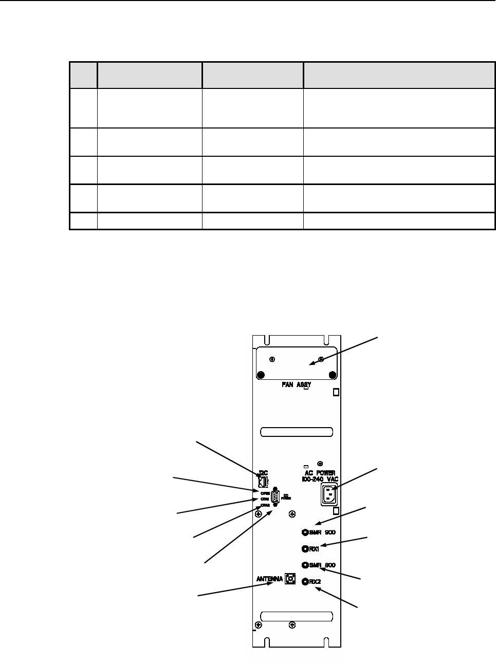
ADCP-75-192 • Issue 1 • December 2005 • Section 2: Description
Page 2-38
2005, ADC Telecommunications, Inc.
Table 2-25. Single-Band 10 Watt RFA User Interface, continued
REF
No.
USER INTERFACE
DESIGNATION
DEVICE FUNCTIONAL DESCRIPTION
6 28 VDC Connector DB-9 connector Connects to fan assembly in AC
configuration. Connects to DPEC when
battery backup is used.
7 AC Fault LED Single-colored LED
(Red)
Status indicator turns red when redundant
power supply of RFA has failed
8 PA Fault LED Single-colored LED
(Red)
Status indicator turns red when power
amplifier has failed
9 Power LED Single-colored LED
(Green)
Status indicator turns green when RFA has
power.
10 I2C RJ-45 connector I2C communications interface
7.6.2 Dual-Band 10 Watt RFA
The dual-band 10 Watt RFA user interface consists of various LED's, power, communications
and RF connectors. The RFA user interface is shown in Figure 2-36 and described in Table 2-26.
(12) I2C CONNECTOR
(3) RF TX1 P ORT
( 11) P O WE R LE D
(2) AC INP UT
(1) RFA FANS
(4) RF RX1 P ORT
(9) AC FAULT LED
(7) ANTENNA
CONNECTOR
(10) P A FAULT LED
(5) RF TX2 P ORT
(6) RF RX2 P ORT
(8) 28 VDC CONNECTOR
Figure 2-36. Dual-Band 10 Watt RF Assembly Module Front Panel

ADCP-75-192 • Issue 1 • December 2005 • Section 2: Description
Page 2-39
2005, ADC Telecommunications, Inc.
Table 2-26. Dual-Band 10 Watt RFA User Interface
REF
No.
USER INTERFACE
DESIGNATION
DEVICE FUNCTIONAL DESCRIPTION
1 RFA Fans Fan tray assembly Front panel of RFA assembly
2 AC Input 3-prong connector AC power interface IEC-320
3 RF Tx1 Port SMA connector RF transmit input signal from RUC
4 RF Rx1 Port SMA connector RF receive output signal from duplexer
5 RF Tx2 Port SMA connector RF transmit input signal from RUC
6 RF Rx2 Port SMA connector RF receive output signal from duplexer
7 Antenna connector SMA connector Duplexed transmit and receive RF signals
interface into antenna
8 28 VDC Connector DB-9 connector Connects to fan assembly in AC
configuration. Connects to DPEC when
battery backup is used.
9 AC Fault LED Single-colored LED
(Red)
Status indicator turns red when redundant
power supply of RFA has failed
10 PA Fault LED Single-colored LED
(Red)
Status indicator turns red when power
amplifier has failed
11 Power LED Single-colored LED
(Green)
Status indicator turns green when RFA has
power.
12 I2C RJ-45 connector I2C communications interface
7.6.3 Single-Band 20 Watt RFA
The single-band 20 Watt RFA user interface consists of various LED's, power,
communications and RF connectors. The RFA user interface is shown in Figure 2-37 and
described in Table 2-27.
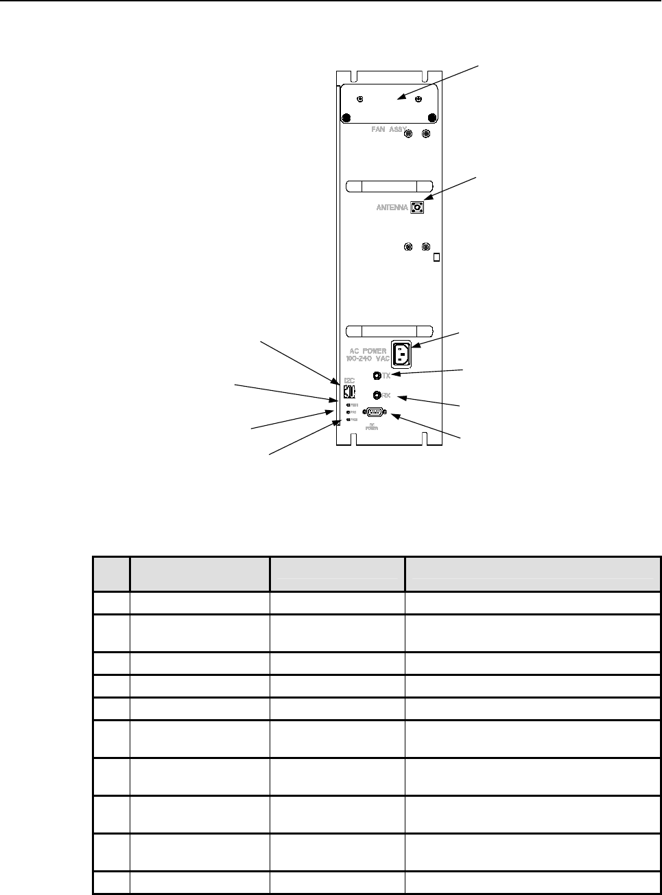
ADCP-75-192 • Issue 1 • December 2005 • Section 2: Description
Page 2-40
2005, ADC Telecommunications, Inc.
(10) I2C CONNECTOR
(4) RF TX1 PORT
(9) POWER LED
(3) AC INP UT
(1) RFA FANS
(5) RF RX1 PORT
(7) AC FAULT LED
(2) ANTENNA
CONNECTOR
(8) PA FAULT LED
(6) 28 VDC CONNECTOR
Figure 2-37. Single-Band 20 Watt RF Assembly Module Front Panel
Table 2-27. Single-Band 20 Watt RFA User Interface
REF
No.
USER INTERFACE
DESIGNATION
DEVICE FUNCTIONAL DESCRIPTION
1 RFA Fans Fan tray assembly Front panel of RFA assembly
2 Antenna connector SMA connector Duplexed transmit and receive RF signals
interface into antenna
3 AC Input 3-prong connector AC power interface IEC-320
4 RF Tx1 Port SMA connector RF transmit input signal from RUC
5 RF Rx1 Port SMA connector RF receive output signal from duplexer
6 28 VDC Connector DB-9 connector Connects to fan assembly in AC configuration.
Connects to DPEC when battery backup is used.
7 AC Fault LED Single-colored LED
(Red)
Status indicator turns red when redundant
power supply of RFA has failed
8 PA Fault LED Single-colored LED
(Red)
Status indicator turns red when power
amplifier has failed
9 Power LED Single-colored LED
(Green)
Status indicator turns green when RFA has
power.
10 I2C RJ-45 connector I2C communications interface

ADCP-75-192 • Issue 1 • December 2005 • Section 2: Description
Page 2-41
2005, ADC Telecommunications, Inc.
7.7 Specifications
The specifications for the Digivance CXD are provided in Table 2-28. All specifications apply
after a five minute warm-up period.
Table 2-28. Digivance CXD Specifications
PARAMETER SPECIFICATION REMARKS
Optical – Hub and RAN
Fiber type 9/125, single-mode
Number of fibers required
Without WDM 2
With WDM
With CWDM
1
1 per 4 RANS
Requires CWDM optical
transceivers and wavelength
division multiplexers (WDM)
which are accessory items.
Optical transceiver type SFP
Forward and reverse path wavelength
Standard range
Extended range
1310nm
1550 nm
Optical transmit power output
Standard range
Extended range
0 dBm
0 dBm
Typical
Optical receive input
Standard range
Extended range
-9 dBm
-26 dBm
Optical budget
Standard range
Extended range
9 dB
26 dB
Typical
Optical connectors LC Dual-connector
RF Forward Path
800 MHz Fullband 869 to 894 MHz 15 MHz bandwidth selectable
800 MHz A’’/A 869 to 880 MHz
SMR 800 MHz 851 to 866 MHz
SMR 800 MHz Upper Band 862 to 869 MHz
SMR 900 MHz 935 to 940 MHz
1900 MHz Lowerband 1930 to 1965 MHz 15 MHz bandwidth selectable
1900 MHz Upperband 1965 to 1995 MHz 15 MHz bandwidth selectable
Intermodulation -60 dBc At remote output, two tone
Spurious -60 dBc
RF gain 10 dB
continued

ADCP-75-192 • Issue 1 • December 2005 • Section 2: Description
Page 2-42
2005, ADC Telecommunications, Inc.
Table 2-28. Digivance CXD Specifications, continued
PARAMETER SPECIFICATION REMARKS
Gain flatness
Band flatness
Channel flatness
±2.0 dB across freq. Range
±1 dB variation across any 1.25
MHz channel
Gain Variation ± 3 dB Over frequency, temperature,
and unit-to-unit.
Peak to Average Ratio 10 dB
Propagation Delay 12 microseconds forward path Excludes fiber
Configurable propagation delay
Range
Delay step size
0 – 566 microseconds
13 nanosecond increments
Manual or automatic
Composite RF input signal level -25 to +10 dBm Per RF band, non-duplexed
Composite RF output power
Cellular 10 MCPA
SMR 10 Watt MCPA
PCS 10 Watt MCPA
PCS 20 Watt MCPA
6.5 Watts (+38 dBm)
3.2 Watts (+35 dBm)
6.5 Watts (+38 dBm)
12.5 Watts (+41 dBm)
Composite at antenna port. See
Note 1 at end of table.
Performance merit functions
TDMA/EDGE
GSM
iDEN
CDMA
5% EVM
3.5º RMS
SQE decrease < 1 dB
0.98 Rho factor
RF Reverse Path
800 MHz Fullband 824 to 849 MHz 15 MHz bandwidth selectable
800 MHz A’’/A 824 to 835 MHz
SMR 800 MHz 806 to 824 MHz
SMR 800 MHz Upper Band 817 to 824 MHz
SMR 900 MHz 896 to 901 MHz
1900 MHz Lowerband 1850 to 1885 MHz 15 MHz bandwidth selectable
1900 MHz Upperband 1885 to 1915 MHz 15 MHz bandwidth selectable
Gain -10 to +35 dB
Gain flatness
Band flatness
Channel flatness
±2.0 dB across freq. Range
±1 dB variation across any 1.25
MHz channel
Gain variation ± 3 dB Over frequency, temperature,
and unit-to-unit.
Propagation Delay 12 microseconds forward path Excludes fiber
Configurable propagation delay
Range
Delay step size
0 – 566 microseconds
13 nanosecond increments
Manual or automatic
continued

ADCP-75-192 • Issue 1 • December 2005 • Section 2: Description
Page 2-43
2005, ADC Telecommunications, Inc.
Table 2-28. Digivance CXD Specifications, continued
PARAMETER SPECIFICATION REMARKS
Input IP3 -16 dBm
Noise figure
800/850/900 MHz
1900 MHz
5 dB
6 dB
Minimum RF output level 10 dBm
-5 dBm
Absolute maximum
Operational maximum
Automatic Gain Limiting (AGC)
Range
Maximum input signals
25 dB
-38 dBm
Peak signal input
Reverse path VSWR 2.0:1
Physical/Environmental/Electrical – Hub
Dimensions (HxWxD) 78 x 24 x 24 Inches Hub rack
RF connections 50 ohm SMA-type (female) 50 ohm input/output impedance
Weather resistance Indoor installation only
Operating temperature 0º to 50º C (32º to 122º F)
Storage temperature –40º to +70º C (–40 to 158º F)
Humidity 10% to 90% Non condensing
IP interface RJ-45
DC power connector Screw-type terminal
Power Input ±48 VDC Floating
Input current 34 A @ -42 VDC Per rack assembly
Reliability MTBF 80,000 Excluding fan assemblies
Digital Chassis
Dimensions (HxWxD)
7.0 x 19.0 x 7.9 Inches
7.0 x 17.1 x 7.9 Inches
Mounting flange
Body
Color Brushed aluminum
Backplane connections RJ-45
Power Input ±48 VDC Floating
Power Consumption
Digital Chassis
CPU
STF2
RSC
SIF
76.0 Watts
20.2 Watts
3.5 Watts
8.8 Watts
15.2 Watts
Typical
Fans and 12 VDC P/S
RF Chassis
Dimensions (HxWxD)
7.0 x 19.0 x 7.9 Inches
7.0 x 17.1 x 7.9 Inches
Mounting flange
Body
Color Brushed aluminum
Continued

ADCP-75-192 • Issue 1 • December 2005 • Section 2: Description
Page 2-44
2005, ADC Telecommunications, Inc.
Table 2-28. Digivance CXD Specifications, continued
PARAMETER SPECIFICATION REMARKS
Backplane connections RJ-45
Power Input ±48 VDC Floating
Power Consumption
RF Chassis
FBHDC
HUC
FSC
55.0 Watts
11.0 Watts
7.7 Watts
13.5 Watts
Typical
Fans and 12 VDC P/S
Base Station Interface Module (BIM)
Dimensions (HxWxD)
1.75 x 19.0 x 7.1 Inches
1.75 x 17.1 x 7.1 Inches
Mounting flange
Body
Color Brushed aluminum
I2C connections RJ-45
RF connections 50 ohm SMA-type (female) 50 ohm input/output impedance
Power Input ±48 VDC Floating
Power Consumption 20 Watts Typical
Hub Reference Module (HRM)
Dimensions (HxWxD)
1.75 x 19.0 x 7.1 Inches
1.75 x 17.1 x 7.1 Inches
Mounting flange
Body
Color Brushed aluminum
Clock, 9.6 MHz signals and I2C
connections
RJ-45
RF connections 50 ohm SMA-type (female) 50 ohm input/output impedance
RS-232 connection DB-9
Power Input ±48 VDC Floating
Power Consumption 17 Watts Typical
Physical/Environmental/Electrical – RAN
Dimensions (HxWxD)
Standard RAN Cabinet
Extended RAN Cabinet
23 x 18 x 11 Inches
23 x 18 x 17 Inches
2.6 cubic feet
4.1 cubic feet
Weight
CXD RAN Standard Cabinet
CXD RAN Extended Cabinet
Pole mount bracket
Single-band 10 W RFA
Single-band 20 W RFA
Dual-band 10 W/10 W RFA
23 lbs.
49 lbs.
7 lbs.
24 lbs.
27 lbs.
33 lbs.
Empty, no modules
Empty, no modules
Metal and wood pole brackets
Color Gray
continued

ADCP-75-192 • Issue 1 • December 2005 • Section 2: Description
Page 2-45
2005, ADC Telecommunications, Inc.
Table 2-28. Digivance CXD Specifications, continued
PARAMETER SPECIFICATION REMARKS
RF connections 50 ohm N-type (female) 50 ohm input/output impedance
Weather resistance NEMA-3R Removable dust filter
Operating temperature –40º to 50º C (-40º to 122º F)
Start-up temperature –20º C (-4º F)
Storage temperature –40º to +85º C (–40 to 185º F)
Humidity 10% to 90%
IP interface RJ-45
AC power ingress ¾-inch conduit Internal diameter
Fiber optical cable ingress ¾-inch conduit Internal diameter
Power input 100 to 260 VAC 47 to 63 Hz
Lightning protection 20 kA IEC 1000-4-5 8/20
microsecond waveform
Battery backup options
Internal – RFA Slot Assembly
External
1 hour
2 hour
Takes one RFA slot
Requires Extended RAN Cabinet
Battery Weight
Internal – RFA Slot Assembly
External
61 lbs.
140 lbs.
Two batteries and tray
Two batteries
Power consumption 600 Watts Two 10 W PA option
Reliability at 25º MTBF 50,000 Excluding fan assemblies
Note 1: Per Industry Canada Section 5.3 - The rated output power of this equipment is for single
carrier operation. For situations where multiple carrier signals are present, the rating would have to
be reduced by 3.5 dB, especially where the output signal is re-radiated and can cause interference to
adjacent band users. The power reduction is to be by means of input power or gain reduction and not
by an attenuator at the output of the device.

ADCP-75-192 • Issue 1 • December 2005 • Section 2: Description
Page 2-46
2005, ADC Telecommunications, Inc.
Blank

ADCP-75-192 • Issue 1 • December 2005 • Section 3: Network and System Installation and Setup
Page 3-1
2005, ADC Telecommunications, Inc.
SECTION 3: NETWORK AND SYSTEM INSTALLATION AND SETUP
Content Page
1 INTRODUCTION .................................................................... 3-2
2 NETWORKING OVERVIEW.............................................................. 3-2
3 NODE IDENTIFICATION SCHEMES ........................................................ 3-3
4 IDENTIFICATION USING THE NETWORK IP RECEIVER/SENDER SYSTEM ............................... 3-3
5 HUB EQUIPMENT IDENTIFICATIONS ....................................................... 3-3
6 ASSIGNING TENANTS ................................................................ 3-5
6.1 Understanding Tenant MIB Indexing ................................................. 3-5
6.2 BTS Connection MIB............................................................ 3-6
6.3 Pathtrace Format.............................................................. 3-9
7 TENANT CONFIGURATION............................................................. 3-13
7.1 Setting Protocol.............................................................. 3-13
7.2 Setting Channels ............................................................. 3-13
7.3 Setting Hub Measured Forward Gain ................................................ 3-13
7.4 Setting RAN Measured Forward Gain ............................................... 3-13
7.5 Setting FSC Gain ............................................................. 3-13
7.6 Setting RAN Forward Gain Offset .................................................. 3-14
7.7 Setting Reverse Gain .......................................................... 3-14
7.8 Setting Reverse Cable Loss ...................................................... 3-14
7.9 Using Tenant Reset ........................................................... 3-14
7.10 Enabling FGC / RGC ........................................................... 3-14
7.11 Using Tenant Mode ........................................................... 3-15
7.12 Enabling / Disabling Delay Compensation ............................................ 3-15
7.13 Setting Forward / Reverse Delay Skew .............................................. 3-15
7.14 Enabling / Disabling RAN slots.................................................... 3-15
7.15 Forward/Reverse Target Delay.................................................... 3-16
7.16 FSC Attenuator Offsets ......................................................... 3-16
7.17 Target Simulcast Degree........................................................ 3-16
7.18 Module Attenuators ........................................................... 3-16
8 MANAGING THE TENANT OAM ADDRESS AND HOSTNAME TABLES ................................. 3-17
8.1 RAN Ordering ............................................................... 3-17
8.2 Bracketing of Lost RANs ........................................................ 3-18
8.3 Clearing of RANs ............................................................. 3-18
9 HUB NODE ACCESS/MANAGEMENT ...................................................... 3-18
9.1 Managing Hub Nodes .......................................................... 3-18
9.2 Identification using the Network IP Receiver/Sender ..................................... 3-18
9.3 Accessing Nodes Locally........................................................ 3-19
9.4 Accessing Nodes via TCP/IP ..................................................... 3-19
9.5 Using a Third Party Network Management System with Digivance CXD ......................... 3-20
10 CONFIGURING THE HUBMASTER NODE.................................................... 3-20
10.1 Utilizing The Configure-Hubmaster Script ............................................ 3-21
10.2 Using Dynamic Host Configuration Protocol with Digivance CXD ............................. 3-22
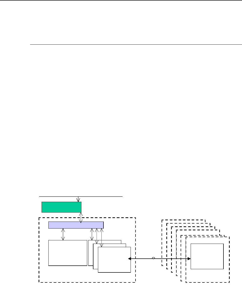
ADCP-75-192 • Issue 1 • December 2005 • Section 3: Network and System Installation and Setup
Page 3-2
2005, ADC Telecommunications, Inc.
11 CONFIGURING THE HUB “SLAVE” AND RAN NODES............................................ 3-24
11.1 Managing The Hub Node MIB ..................................................... 3-24
11.2 Managing the RAN Node MIB ..................................................... 3-26
1 INTRODUCTION
This section discusses the steps necessary to setup the Digivance CXD system communications
and operating parameters. It is assumed for the purposes of this discussion that the required
system elements have already been installed and powered on, and that the reader has an
understanding of TCP/IP networking basics.
2 NETWORKING OVERVIEW
A Digivance CXD network consists of several CPUs running the Linux operating system as
shown in Figure 3-1 Network Architecture. The CPUs residing in the Digivance CXD Hub
(called “Hub nodes”) are connected through a router to an existing LAN to effect SNMP status
and control. The CPUs in the RAN’s (called “RAN nodes”) are connected to the LAN using
WAN bridges in each SIF, which transmit packet data across a fiber back-haul from each RAN
node to its corresponding Hub. All Digivance CXD nodes support telnet, ftp, and vnc by
default.
Ethernet HUB
HUB
Master
Slave
N
ode
HUB
Slave
N
ode
Slave
N
ode RA
Slave
N
ode
RAN
Slave
N
ode
RAN
Slave
N
ode
RAN
Slave
N
ode
RAN
Fiber
CAT5 Ethernet
ROUTER
Slave
N
ode
RAN
Slave
N
ode
Existing WAN/LAN
Figure 3-1. Network Architecture

ADCP-75-192 • Issue 1 • December 2005 • Section 3: Network and System Installation and Setup
Page 3-3
2005, ADC Telecommunications, Inc.
A CPU called the Hubmaster is a special Hub node that controls tenant processing for
Digivance CXD nodes on its subnet. For a definition of tenant sectors, see Section 6.1. The
Hubmaster also functions as a time server for a Digivance CXD subnet (using Network Timing
Protocol), and can be set up to provide DHCP (Dynamic Host Configuration Protocol) and
DNS (Domain Name Service) to its subnet as well. It is important for Digivance CXD system
software that only one Hubmaster node resides on each subnet, and that each subnet has a
unique domain name. The Hubmaster node is the only node that requires a static IP. The
Digivance CXD network architecture utilizes DHCP and DNS to identify the rest of the nodes,
either through pre-existing LAN servers, or through the Digivance CXD Hubmaster CPU. For
more on configuring these features and the Hubmaster itself, see Section 10, "Configuring the
Hubmaster node.
3 NODE IDENTIFICATION SCHEMES
It is important to follow a convention when naming nodes in the Digivance CXD system so that
CPUs can be quickly located and accessed for troubleshooting and maintenance. The suggested
naming conventions for both Hub and RAN nodes are discussed in the following sections. For
more information concerning node identity configuration, see Sections 11.1 and 11.2.
4 IDENTIFICATION USING THE NETWORK IP RECEIVER/SENDER SYSTEM
The Digivance CXD Hubmaster node dynamically keeps track of which nodes are under its
control using a script called NIPR (Network IP Receiver). It receives an IP and hostname from
every node it controls via NIPS (Network IP Sender), which runs on all “slave” nodes. NIPR
senses any changes to its list of slave nodes, and updates the Hubmaster DNS accordingly. The
NIPR/S system is also a key component to maintaining the Hub/RAN Node MIB’s and tenant
processing, since it is the mechanism by which the Hub/RAN Node MIB entries are filled. For
more on these MIB’s, see Sections 11.1 and 11.2.
5 HUB EQUIPMENT IDENTIFICATIONS
Table 3-1 shows the recommended convention to be used for identifying and placing Hub
equipment:

ADCP-75-192 • Issue 1 • December 2005 • Section 3: Network and System Installation and Setup
Page 3-4
2005, ADC Telecommunications, Inc.
Table 3-1. HUB Rack Numbering
CHASSIS OR SHELF HEIGHT LOCATION*
Attenuator Shelf 2U U42
PDU 2U U40
Ethernet Hub 1U U38
Digital Chassis (top) 4U U37
BIM 1U U33
RF Chassis (top) 4U U32
BIM 1U U28
Digital Chassis (top) 4U U27
BIM 1U U23
RF Chassis (top) 4U U22
BIM 1U U18
Digital Chassis (top) 4U U17
BIM 1U U13
RF Chassis (top) 4U U12
BIM 1U U8
Reference Module (bottom) 1U U7
*’U’ numbers are printed on the rack rails of the OP-HUB2 rack.
• Hub Racks are numbered sequentially, Rack1, Rack2, etc, or by serial number.
• Chassis in Hub racks are numbered by ‘U’ number. For example, the lowest RF
chassis shown in Table 3-1 would be numbered U12.
• BIMs in racks are numbered by ‘U’ number. For example, the lowest BIM shown in
Table 3-1 Would be numbered U8.
• Power Attenuators are located at the top of the Hub rack or mounted to a wall.
• WSP Base stations should be given unique Tenant Name and BTS ID designations.
• Each base station sector is cabled to a separate attenuator and BIM unit in the Hub
rack.
• Ensure that RF cables from the BIM forward output ports are connected to FBHDC
modules in its related HUB RF chassis (not used if BTS is directly cabled to FBHDC)
• Ensure that RF cables from the BIM reverse input ports are connected to HUC
modules (primary to primary and diversity to diversity (if diversity is used)). Ensure
that any HUC and FBHDC modules connected to a given BIM must reside in the same
Hub RF chassis.

ADCP-75-192 • Issue 1 • December 2005 • Section 3: Network and System Installation and Setup
Page 3-5
2005, ADC Telecommunications, Inc.
• Ensure that FBHDC modules are connected to FSC modules. (See Hub Installation
and Maintenance Manual for details)
• An RF chassis in a Hub rack contains enough slots for 2 sets of tenant RF equipment,
where a set of tenant RF equipment consists of one FSC, one HUC and up to two
FBHDC’s. A set of tenant equipment in an RF chassis is installed in a particular
manner, from bottom to top, the order of modules is HUC, FBHDC, FSC, and
FBHDC. The locations of modules in the chassis must also follow a particular pattern,
such that the first set of tenant modules must occupy the four bottom-most slots in the
chassis, the second set must occupy the next four slots. Refer to Table 3-2. RF Chassis
Configuration for more details.
Table 3-2. RF Chassis Configuration
CHASSIS SLOT MODULE BAND
8 2
7 FSC 2
6 FBHDC 2
5 HUC 2
4 1
3 FSC 1
2 FBHDC 1
1 HUC 1
6 ASSIGNING TENANTS
6.1 Understanding Tenant MIB Indexing
Throughout the Digivance CXD system, there are several MIB’s that are used to monitor and
control tenant activity. These tenant-based MIB’s contain tables with 96 separate
entries/columns, where each entry/column in a table belongs to a given tenant base station
sector. The index value used for each base station sector is constant across the entire system
such that once a tenant sector is configured and an index is established, the same index will be
associated with that tenant sector in all system-wide tenant-based MIB’s.
Note: The Digivance CXD system can support up to 96 unique base station sectors per
Hubmaster CPU.

ADCP-75-192 • Issue 1 • December 2005 • Section 3: Network and System Installation and Setup
Page 3-6
2005, ADC Telecommunications, Inc.
6.2 BTS Connection MIB
Within the Hubmaster node, the BTS Connection MIB is used to create new tenant base station
sector instances (simply called "tenants" from here on) to be configured, monitored, and
controlled in the Digivance CXD system. In order to create a new tenant in the Digivance CXD
system, the Hub Config Process in the Hubmaster must first locate a unique BIM instance
controlled by one of the Hub CPUs. This requires that the Hub Node first be configured such
that the CPU Rack ID and Chassis ID (described in Section 11.1) are known. The software in
the Hubmaster continues to send requests to all configured Hub Nodes to determine if there are
any BIM modules that have come online.
When a new BIM module is located, the Hub Config Process creates an "Unconfigured" tenant
in the BTS Connection MIB. This can be seen by noticing that the Tenant ID in the BTS
Connection MIB is "UnconfiguredX", where X is 1-96. Also, it can be seen that the CPU Rack
and Chassis IDs are filled in and the BIM I2C Bus/Slot information is filled in.
For ease of setup, when a new BIM module is found, the required BTS Connection MIB is
automatically filled in with default values. These values can be changed manually by the user
(see section 6.2.6. for details).
6.2.1 Setting the Tenant Name
Tenant Name is the name of the Wireless Service Provider (WSP). The allowable value is a
string length of 1-17 characters. The MIB field is:
transceptBtsConnectionTable.transceptBtsConnectionTenantName.
6.2.2 Setting the BTS ID
Since WSPs may have more than one base station (BTS) in the system, it is important to
uniquely identify them - the allowable value is a string of 1-8 characters. The MIB field is:
transceptBtsConnectionTable.transceptBtsConnectionBTSID.
6.2.3 Setting the BTS Sector
The BTS Sector field of the BTS Connection MIB is an enumerated value, where the allowable
selections are ALPHA (0), BETA (1), or GAMMA (2). The MIB field is:
transceptBtsConnectionTable.transceptBtsConnectionBTSSector.
6.2.4 Setting the Tenant Band
The Tenant Band field of the BTS Connection MIB is an enumerated value, where the
allowable selections are the bands supported by the Digivance CXD system, currently:
No Band (0) - no band selected, will not result in a configured tenant
US1900A (1) - PCS band A
US1900B (2) - PCS band B
US1900C (3) - PCS band C

ADCP-75-192 • Issue 1 • December 2005 • Section 3: Network and System Installation and Setup
Page 3-7
2005, ADC Telecommunications, Inc.
US1900D (4) - PCS band D
US1900E (5) - PCS band E
US1900F (6) - PCS band F
US800AAPP (7) - Cellular A and A'' bands
US800BBP (8) - Cellular B and B' bands
US800AP (9) - Cellular A' band
US800SMRA (10) – SMR 800 band (806-821/851-866MHz)
US800SMRUpper (11) – SMR 800 band Extended (818-824/862-869MHz)
US900SMRB(12) – SMR 900 band
US1900G (13) - PCS band G
The MIB field is:
transceptBtsConnectionTable.transceptBtsConnectionTenantBand
6.2.5 Setting the BIM Rack/Shelf ID
The location information (rack/shelf) of the BIM module belonging to this tenant can be
manually configured. The valid values for these MIB fields are strings of 1-16 characters. The
Hub Config Process will push these ID strings down to the Network Node MIB of the CPU
that controls this BIM. This will allow the NMS to identify the location of the BIM when it is
reporting a fault condition. The MIB fields are:
transceptBtsConnectionTable.transceptBtsConnectionBimRackID
and
transceptBtsConnectionTable.transceptBtsConnectionBimShelfID
6.2.6 Designating the Tenant Hardware
The BTS Connection MIB contains several fields pertaining to the location of the tenant-
specific hardware. Some of the connections made between hardware are not automatically
detectable, and therefore may require some manual entering of information.
The I2C addresses of the RF modules belonging to the tenant being configured can be set (if
changes from default values are required) as follows:
• The BIM I2C Address (bus/slot) will automatically be filled in by the Hub Config
Process. The MIB fields are:
transceptBtsConnectionTable.transceptBtsConnectionBimI2cBus
and
transceptBtsConnectionTable.transceptBtsConnectionBimI2cSlot
• The BIM module belonging to this tenant must have RF connections to one FBHDC
modules. Select the I2C Bus of the FBHDC module that matches the BIM I2C bus
value. Set the FBHDC I2C slot value to “1”. The FBHDCs belonging to a single tenant
(i.e. having RF connections to the same BIM module) should be co-located in the RF
chassis, with an FSC and HUC modules separating them. The MIB fields are:

ADCP-75-192 • Issue 1 • December 2005 • Section 3: Network and System Installation and Setup
Page 3-8
2005, ADC Telecommunications, Inc.
transceptBtsConnectionTable.transceptBtsConnectionHdcXI2cBus
and
transceptBtsConnectionTable.transceptBtsConnectionHdcXI2cSlot, where X = 1 or 2.
• The FBHDC module belonging to this tenant is cabled to a single FSC module, which is
located in a chassis slot directly above the tenant's FBHDC module. Select the I2C Bus
and Slot of the FSC module to that of its corresponding BIM. Set the I2C slot value to
“2”. The MIB fields are:
transceptBtsConnectionTable.transceptBtsConnectionFscI2cBus
and
transceptBtsConnectionTable.transceptBtsConnectionFscI2cSlot.
• When using receive diversity, the BIM module belonging to this tenant must have two
RF connections to a single HUC module. One for primary reverse signals and the other
for diversity reverse signals. Without receive diversity, only the Primary HUC output
need be cabled to the BIM. The location of the HUC module for this tenant must be
co-located with the FBHDC and FSC modules belonging to this tenant. Set the I2C
Bus of the HUC module to that of its corresponding BIM. Set the I2C slot value to
“0”. The MIB fields are:
transceptBtsConnectionTable.transceptBtsConnectionHucI2cBus
and
transceptBtsConnectionTable.transceptBtsConnectionHucI2cSlot.
Once the above I2C addresses are set for the tenant being configured, the Hub Config Process
will push this information down to the Hub RF Connection MIB on the node/CPU that
manages the tenant RF hardware.
6.2.7 Clearing tenants
It is possible to "de-configure" a tenant, which will clear all of the configuration information
described above, by setting the Clear field in the BTS Connection MIB for this tenant to a
value of '1'. This will allow the configuration process to be restarted from the beginning. The
MIB field is:
transceptBtsConnectionTable.transceptBtsConnectionClear
6.2.8 HUC Invalid Config
The BTS Connection MIB contains a read-only field that reports the state of the HUC Invalid
Configuration fault field. This information will allow the person configuring the system to
know that the tenant has been completely and correctly configured - this is known when the
value in this field is reported as "No Fault" or '0'. The MIB field is:
transceptBtsConnectionTable.transceptBtsConnectionHucInvalidConnection.

ADCP-75-192 • Issue 1 • December 2005 • Section 3: Network and System Installation and Setup
Page 3-9
2005, ADC Telecommunications, Inc.
6.2.9 Composite Mode
The Digivance CXD default forward gain balance is called “composite mode”. In this mode, a
composite RF signal will have gain of +42dB (Cell/SMR) and +45dBm (PCS) through the
system. The maintainer is responsible for ensuring the desired signal level into the system.
See Table 3-3 for sample input and output signal strengths:
Table 3-3. Output Signal Strengths
INPUT
(RMS AT FBHDC INPUT)
CELL/SMR OUTPUT
(RMS AT ANTENNA PORT)
PCS OUTPUT
(RMS AT ANTENNA PORT)
-2 dBm +40 dBm +43 dBm
-4 dBm +38 dBm +41 dBm
-7 dBm +35 dBm +38 dBm
As the protocol is irrelevant in this mode, the default protocol is “none”. In addition, only a
single FSC channel is activated. To sum multiple FSC channels, set the composite mode entry
to “disabled” and follow instructions on setting channels in Section 7 Tenant Configuration.
The MIB field is:
transceptBtsConnectionForwardGainTable.transceptBtsConnectionForwardGainCompositeM
odeFlag
6.2.10 Power Attenuator IDs
The BTS Connection MIB contains two fields that allow the external power attenuators to be
identified. The attenuators reside in a shelf at the top of each rack. To configure these two MIB
fields, the nomenclature described in Table 3-1. HUB Rack Numbering, should be used. This
dictates that the attenuators should be given names that indicate the shelf number and the
location on the shelf. For a given tenant, the two power attenuators must be configured with
unique IDs, where the allowable values are strings of length 1-16. If both attenuators are
configured, then software will configure the BIM to operate in duplexed mode, otherwise,
software will configure the BIM to operate in non-duplex mode. The MIB fields are:
transceptBtsControlParamsTable.transceptBtsControlParamsPowerAttenXLoc, where X = 1 or 2.
6.3 Pathtrace Format
Pathtrace is a term used to describe the 64-byte data stream that is transmitted between all DIF-
connected modules in the Digivance CXD system. The contents of the pathtrace strings have
been designed such that each set of connected tenant equipment will transmit/receive a
pathtrace string containing information about that particular tenant. The following is the format
of the pathtrace string:
<Tenant ID><delimiter><IP Address><delimiter><Path Flag>

ADCP-75-192 • Issue 1 • December 2005 • Section 3: Network and System Installation and Setup
Page 3-10
2005, ADC Telecommunications, Inc.
• The Tenant ID sub-string is comprised of four particular pieces of information: Tenant
Name, BTS ID, BTS Sector, and Tenant Band. These four pieces of information form
the Tenant ID sub-string, where each piece of information is delimited by a single
character (currently a colon ":").
• The IP Address sub-string indicates the IP Address of the CPU node that transmits the
pathtrace string.
• The Path Flag is a one-character string, “M”, "P" or "D" that indicates the path on
which the path trace was transmitted (“M”=Main Forward, “P”=Primary Reverse,
“D”=Diversity Reverse). The delimiter used to separate the primary sub-strings of the
pathtrace string is a single character, currently a comma (",").
An example of a complete pathtrace string is as follows:
wspname:bts4:alpha:us1900A,172.20.1.1,P
6.3.1 Pathtrace Creation
Pathtrace is automatically created using information contained in the BTS Connection MIB..
6.3.2 Pathtrace Forward Transmission
Though the BIM, FBHDC, and FSC all create the pathtrace string and report it in their MIB’s,
the FSC is the originator of the pathtrace string in the forward path of the system. The
pathtrace string will be routed to all RAN’s belonging to this tenant.
6.3.3 Pathtrace Forward Reception
In the forward path, the SIF modules in the Hub that are connected to the FSC outputs, as well
as the SIF’s in the simulcasted RAN’s, pass-through the pathtrace strings from their inputs to
their outputs. In addition, the SIF Hardware Control Process (HCP) report the passed-through
pathtrace strings in the SIF MIB for use by tenant processing and other higher-level processes.
In each of the simulcasted RAN’s, the RUC module receives the pathtrace string into its FPGA
from one of its two DIF input connections. The RUC HCP then reports the received pathtrace
strings in its MIB for use by tenant processing and other higher-level processes.
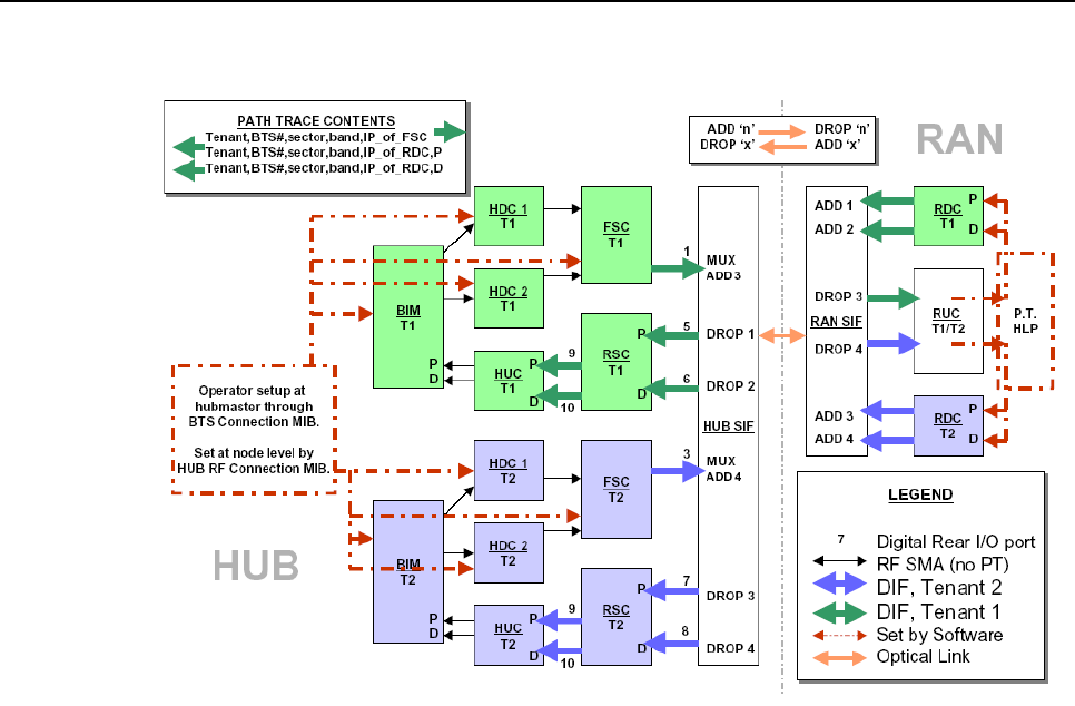
ADCP-75-192 • Issue 1 • December 2005 • Section 3: Network and System Installation and Setup
Page 3-11
2005, ADC Telecommunications, Inc.
Figure 3-2. Tracing Pathtrace, Two Tenants
6.3.4 Pathtrace Reverse Transmission
The RDC is the originator of the pathtrace string in the reverse paths of the system. However, it
is desirable to maintain continuity between the forward and reverse pathtrace strings. To manage
this, the Pathtrace Process that runs in the RAN CPUs is responsible for reading pathtrace strings
from the RUC MIB, parsing out the Tenant ID sub-strings from the pathtrace strings, and writing
the Tenant IDs into the MIB’s of the RDC’s that are associated with the RUC’s.
The RDC HCP creates up to two new pathtrace strings (primary/diversity(if present)) starting
with the Tenant ID that was provided in its MIB by the Pathtrace Process. The RDC HCP
appends its own CPU IP Address to the pathtrace strings, and then appends the
primary/diversity flags ("P" or "D"). Finally, the RDC transmits the pathtrace strings out on up
to two outputs. The pathtrace strings are then transmitted back to the Hub reverse modules
belonging to this tenant.
6.3.5 Pathtrace Reverse Reception
In the reverse path, the SIF modules in the RAN’s that are connected to the RDC outputs, as well
as the SIF’s in the Hub, pass-through the pathtrace strings from their inputs to their outputs. In
addition, the SIF HCP’s report the passed-through pathtrace strings in the SIF MIB for use by
tenant processing and other higher-level processes.

ADCP-75-192 • Issue 1 • December 2005 • Section 3: Network and System Installation and Setup
Page 3-12
2005, ADC Telecommunications, Inc.
In the Hub, the RSC module receives the pathtrace strings from several RDC’s into its FPGA
from its DIF input connection. The RSC HCP reports the received input pathtrace strings in its
MIB for use by higher-level processes, as described in sections below. The RSC has the added
responsibility of determining the "majority inputs" to determine the most-prevalent input
pathtrace based on Tenant ID sub-strings. When the majority input is discovered, the RSC will
parse the Tenant ID from one of the majority inputs, append its own CPU IP Address, and
transmit the newly created pathtrace string to its two outputs (primary/diversity).
The HUC module receives the reverse pathtrace strings into its FPGA from up to two DIF
input connections. The HUC HCP then reports the received pathtrace strings in its MIB for use
by higher-level processes, as described in the following sections.
6.3.6 Pathtrace Detection/Reporting
On each node in the system, a Pathtrace Process is responsible for gathering up all the
pathtrace strings reported in the HCP MIB’s on its own CPU. The Pathtrace Process then
reports all the discovered pathtrace strings in its own Pathtrace MIB, which indicates the HCP
type, I2C/PCI address, MIB index, and pathtrace string value.
On each node in the system, a Node Paths Process is responsible for examining the Pathtrace
MIB, identifying valid, complete, and stable Tenant IDs, and reporting the results in the Node
Paths MIB in a manner that simplifies tenant processing algorithms.
On the Hubmaster node, the Tenantscan process is responsible for examining the Node Paths
MIBs on all nodes and determining whether the contents contain Tenant IDs that match
configured tenants in the system. If so, then the Hostname and IP Address tables in the Tenant
OAM MIB are updated.
The Tenant processes in the Hubmaster node are responsible for updating the Equipment MIB’s
on each node with the appropriate Tenant IDs and indices that are used on that node. The
Equipment Process then acts as the middle-level interface to the tenant hardware, reporting status
of all the hardware in the Status Table of the Equipment MIB and allowing hardware
configurations to occur via the Control Table of the Equipment MIB. Tenant processing in the
Hubmaster node is the primary user of the Equipment MIB for status and control of tenant
hardware. The details of this are described in more detail in the following section.

ADCP-75-192 • Issue 1 • December 2005 • Section 3: Network and System Installation and Setup
Page 3-13
2005, ADC Telecommunications, Inc.
7 TENANT CONFIGURATION
The Tenant OAM MIB is the primary interface for configuring the operating parameters of
tenants in the Digivance CXD system. The Tenant OAM MIB is used exclusively at the
Hubmaster node, where any changes made to operating parameters are validated and pushed
down to the proper node(s) by Tenant processing.
7.1 Setting Protocol
transceptTenantOAMTable.transceptTenantProtocol
The Protocol field of the Tenant OAM MIB is an enumerated value, where the allowable
selections are the protocols supported by the Digivance CXD system, currently.
No Protocol (0), CDMA (1), TDMA (2), GSM (3), IDEN (4), AMPS (5), CW_WB (6), CW_NB
(7). In Composite Mode, protocol need not be selected, and defaults to No Protocol (0).
7.2 Setting Channels
transceptTenantOAMTable.transceptTenantChannelXVal, where X = 1-8
Each Tenant sector in the Digivance CXD system can support from 1-4 RF paths. Each of these RF
paths can be individually enabled in the Tenant OAM MIB.
Note: In Composite Mode, one (1) RF path is automatically enabled.
7.3 Setting Hub Measured Forward Gain
transceptTenantOAMTable.transceptTenantHubMeasuredForwardGain
This parameter is no longer used in the Digivance CXD system.
7.4 Setting RAN Measured Forward Gain
transceptTenantOAMTable.transceptTenantRanXMeasuredForwardGain, where X = 1-8
This parameter is no longer used in the Digivance CXD system.
7.5 Setting FSC Gain
transceptTenantMoreControlsTable.transceptTenantMoreControlsFscOutputGain
and
transceptTenantMoreControlsTable.transceptTenantMoreControlsFscOutputGainOverride
This feature allows the user to adjust FSC output gain outside of the default setting. The FSC
Output Gain value is in tenths of a dB, and represents the amount of loss from full scale
entered digitally in the forward path. For example, if a set of input signals had a peak to
average value higher than 12 dB, an operator may wish to remove 3 dB of gain to allow for the
extra peak power. The transceptTenantMoreControlsTable.FscOutputGain entry would be set
to a value of -30 in such a case. The default state of FscOutputGainOverride is “disabled”. In
its default state the system counts active FSC channels and governs FSC gain accordingly. To
begin using a desired override value, set FscOutputGainOverride to “enabled”.

ADCP-75-192 • Issue 1 • December 2005 • Section 3: Network and System Installation and Setup
Page 3-14
2005, ADC Telecommunications, Inc.
7.6 Setting RAN Forward Gain Offset
transceptTenantOAMTable.transceptTenantRanForwardGainOffsetX, where X = 1-8
The RAN Forward Gain Offset is a parameter in the Tenant OAM MIB that allows the target
RAN Gains for this tenant to be adjusted. This effectively allows the cell coverage provided by
a given RAN to be adjusted. There is one RAN Gain offset parameter in the Tenant OAM MIB
for each RAN in a tenant simulcast group. The valid range of values for these parameters is -
120 to +80, which is -12 to +8 dB in 1/10 dB units.
Note: It is possible to overdrive the forward path, which will cause the PA to fault and shut down.
7.7 Setting Reverse Gain
transceptTenantOAMTable.transceptTenantReverseGain
The Reverse Gain parameter in the Tenant OAM MIB allows the Reverse Gain Target to be
set. This value sets the gain for the entire reverse path. The valid range of values for this
parameter is -100 to +100, which is -10 to +10 dB in 1/10 dB units. The system assumes a 20
dB pad between the BIM and the BTS. If the 20 dB pad is not used then the +/- 10 dB gain
setting maps to +10 to +30 dB of gain.
7.8 Setting Reverse Cable Loss
transceptTenantOAMTable.transceptTenantReverseCableLoss
Reverse Cable Loss is a parameter in the Tenant OAM MIB to allow the signal loss due to
cabling between the base stations and the Digivance CXD system to be factored into the
reverse gain management processing. This parameter has a valid range of values of 0 to 50,
which is 0 to +5 dB in 1/10 dB units. The maximum cable loss between the BTS and the BIM
is 5 dB.
7.9 Using Tenant Reset
transceptTenantOAMTable.transceptTenantReset
Tenant Reset is a parameter in the Tenant OAM MIB that will allow all of the hardware that is
associated with a tenant to be reset. This functionality is not currently supported in the
Digivance CXD software.
7.10 Enabling FGC / RGC
transceptTenantOAMTable.transceptTenantForwardAGCDisable
and
transceptTenantOAMTable.transceptTenantReverseAGCDisable
The Forward and Reverse Gain/Continuity Management processes can be disabled on a per tenant
basis using the enable/disable parameters in the Tenant MIB. These MIB fields are enumerated
types with values "Enabled" = 0, and "Disabled" = 1. The reason for the inverse boolean logic is so
that the desired default values are set to be zero, which is the MIB default value.

ADCP-75-192 • Issue 1 • December 2005 • Section 3: Network and System Installation and Setup
Page 3-15
2005, ADC Telecommunications, Inc.
7.11 Using Tenant Mode
transceptTenantOAMTable.transceptTenantMode
Tenant Mode is a parameter in the Tenant OAM MIB that will allow the tenant to be put into a
special mode such as "disabled", or "test",. This functionality is not currently supported in the
Digivance CXD software.
7.12 Enabling / Disabling Delay Compensation
transceptTenantOAMTable.transceptTenantForwardDelayCompensationDisable
and
transceptTenantOAMTable.transceptTenantReverseDelayCompensationDisable
The Forward and Reverse Delay Compensation processes, which balance the signal delay in a
simulcast group, can be enabled/disabled using the associated parameters in the Tenant OAM
MIB. These MIB fields are enumerated types with values "Enabled" = 0 and "Disabled" = 1.
The reason for the inverse boolean logic is so that the desired default values are set to be zero,
which is the MIB default value.
7.13 Setting Forward / Reverse Delay Skew
transceptTenantOAMTable.transceptTenantForwardSkew
and
transceptTenantOAMTable.transceptTenantReverseSkew
The delay skew used in the Forward/Reverse Delay Compensation processes can be adjusted
using the associated Tenant OAM MIB parameters.
The valid range of values for the Forward/Reverse Delay Skew parameters is 0-10000, in units
of nanoseconds (0-10 usecs). The default setting is 0.
7.14 Forward/Reverse Target Delay
transceptTenantTargetDelayTable.transceptTenantForwardTargetDelay
and
transceptTenantTargetDelayTable.transceptTenantReverseTargetDelay
The Forward/Reverse Target delays can be adjusted using the Tenant Forward/Reverse Target
Delay entries in the Tenant OAM MIB. The valid range of values for the Forward/Reverse
target Delay is 12,000 to 150,000 ns with a default of 100,000 ns.

ADCP-75-192 • Issue 1 • December 2005 • Section 3: Network and System Installation and Setup
Page 3-16
2005, ADC Telecommunications, Inc.
7.15 Enabling / Disabling RAN slots
transceptTenantOAMTable.transceptTenantRanDisableX, where X = 1-8
The RAN paths belonging to a tenant can be disabled using the RAN Enable/Disable
parameters of the Tenant OAM MIB. Doing so will disable the PA in the RAN. These MIB
fields are enumerated types with values "Enabled" = 0, and "Disabled" = 1. The reason for the
inverse boolean logic is so that the desired default values are set to be zero, which is the MIB
default value. For example:
To disable RAN 3 in a simulcast, set transceptTenantOAMTable.transceptTenantRANDisable3
to a “1” (disabled).
7.16 FSC Attenuator Offsets
transceptTenantCalTable.transceptTenantFscAttenX
If not using Composite Mode, there is a step during Forward RF Path Balancing that requires
that the FSC Digital path attenuators be adjusted. These adjustments need to be made in the
Tenant OAM MIB in the FSC Attenuator Offset fields, of which there is one per channel in the
Tenant OAM MIB with the naming convention. The values that are set in the Tenant OAM
MIB will be pushed down to the appropriate FSC MIB Attenuator fields. Doing these settings
in the Tenant OAM MIB will allow consistency with the maintenance of configuration data.
7.17 Target Simulcast Degree
In order for the Digivance CXD software to determine the correct number of tenant paths
throughout the system, it can be provided with the target simulcast degree. This will allow the
Tenant process to properly determine and report missing boards and path conditions and
quantities. The Tenant Simulcast Degree field in the Tenant OAM MIB is used to configure
this parameter. This MIB parameter accepts values ranging from 1-8, the range of simulcasting
supported in Digivance CXD on a per sector basis.
7.18 Module Attenuators
In order to be consistent with all other configuration parameters in the system, and to ensure
that configuration data is properly managed, the Tenant OAM MIB contains several
parameters to allow the configuration of tenant module attenuators. When configured in the
Tenant OAM MIB, tenant processing will push these attenuators offsets to the appropriate
HCP MIB. It is important to note that it is not always desirable to modify HCP attenuators, and
should only be done per operating instructions (see Path Balancing, Section 4, Subsection 2). It
is also important to note that the attenuator offset values configured in the Tenant OAM MIB
will supercede (and therefore overwrite) those configured in the HCP MIBs. The following is
the list of all supported tenant attenuators in the Tenant OAM MIB:
• TransceptTenantGenTwoTable.transceptTenantRucYAttenOffset - Y = RAN 1-8.
• TransceptTenantGenTwoTable.transceptTenantRdcYAttenOffsetPrimary - Y = RAN
1-8.

ADCP-75-192 • Issue 1 • December 2005 • Section 3: Network and System Installation and Setup
Page 3-17
2005, ADC Telecommunications, Inc.
• TransceptTenantMoreAttenTable.transceptTenantRdcYAttenOffsetDiversity - Y =
RAN 1-8.
• TransceptTenantMoreAttenTable.transceptTenantBimForwardAttenZOffset - Z = Path
1-2.
• TransceptTenantMoreAttenTable.transceptTenantHdcChXAttenOffset - X = Channel
1-8.
8 MANAGING THE TENANT OAM ADDRESS AND HOSTNAME TABLES
Within the Tenant OAM MIB, there are two (2) tables used to capture the current IP Addresses
and Hostnames of all CPUs that are associated with a given tenant sector. The ordering of the
CPUs in the MIB tables is such that the RAN CPUs are listed first from 1-8, followed by the
Hub CPUs. The RAN ordering from 1-8 is important so that the RAN CPUs can be correlated
to the RAN ID values used throughout the Tenant OAM MIB.
8.1 RAN Ordering
The IP Address and Hostname tables in the Tenant OAM MIB indicate which RAN, based on
IP address and hostname, corresponds to RAN X, where X is the RAN ID (1-8).
Tenant processing uses a least-recently-used scheme to determine the RAN ID to assign to
newly discovered RANs. When Tenant processing discovers new RANs that contain hardware
associated with that tenant (based on Tenant ID of pathtrace string), the new RAN is assigned
the next sequential "never-been-used" RAN ID, a value from 1-8. If there are no RAN IDs that
have never been used, then Tenant processing will find the least-recently-used RAN ID and
assign that ID to the newly discovered RAN.
The RAN ID is important because it lets the user of the Tenant OAM MIB determine which
RAN corresponds to the RAN-specific MIB parameters, such as:
TenantRanDisableX, TenantRanXForwardMeasuredGain
and
TenantRanForwardGainOffsetX where X is the RAN ID, a value from 1-8.
The RAN ID assignments will be persistently maintained through resets of the Hubmaster
CPU and other CPUs in the network, which will allow the NMS to program the RAN IDs
when new RANs are added to the tenant simulcast group. In the future, the RAN ID
assignments will not be persistent through resets of the network nodes, which will require that
the NMS automatically correlate RAN ID to RAN CPU relationships.

ADCP-75-192 • Issue 1 • December 2005 • Section 3: Network and System Installation and Setup
Page 3-18
2005, ADC Telecommunications, Inc.
8.2 Bracketing of Lost RANs
When a RAN CPU is removed from the network, or if tenant processing is unable to
communicate with one of its RANs, then that RAN ID in the Hostname table is bracketed. For
example hostname would be reported as [hostname]. In addition, the RAN ID in the Address
table is also reported in a different fashion when a RAN is "lost". The IP address is bracketed,
with the IP address string being replaced by another form of the number. For example,
172.20.1.248 could be replaced by [1921681.248]. The point is that if the IP address reported
in the Address table is not a valid combination of 4 octet values with decimal points separating
the octets, then that RAN should be considered not present.
8.3 Clearing of RAN’s
In order to facilitate swap outs of RAN CPUs, it is possible for the RAN Hostname values in
the Hostname table of the Tenant OAM MIB to be cleared by deleting the hostname from the
MIB table. Doing so will allow that RAN ID to be cleared, and will allow the next RAN CPU
discovered to occupy that RAN ID.
9 HUB NODE ACCESS/MANAGEMENT
9.1 Managing Hub Nodes
The Hub in a Digivance CXD network consists of several racks and chassis, which translate to
several CPUs per HUB. Since these CPUs all reside at a single geographical location, it is
necessary to establish a relationship of each CPU to its rack and chassis location such that field
service personnel can be deployed to the correct location within the Hub when the need arises.
There can be many CPUs at a single Hub Site within the many racks and chassis, but there is
no way to correlate an IP address to its physical rack/chassis location automatically. Therefore,
a convention for identifying racks and chassis needs to be established. At installation time,
each hostname, as written on the front tag of each CPU, must be recorded in conjunction with
its physical location. This information is used when the operator fills in the Hub Node MIB,
which is discussed in detail below. Digivance CXD Hub naming conventions are also
discussed below.
The Hub Node MIB correlates Hub node IP addresses with their hostnames and physical
locations. It resides solely at Hubmaster nodes. Refer to Section 11.1 for details.
9.2 Identification using the Network IP Receiver/Sender (NIPR/S)
The Digivance CXD Hubmaster node dynamically keeps track of which nodes are under its
control using a script called NIPR/S (Network IP Receiver/Sender). It receives an IP and
hostname from each element in the subnet it controls via the client functionality of NIPR/S,
which runs on all “slave” nodes. NIPR/S senses any changes to its list of slave nodes, and
updates the Hubmaster DNS accordingly. The NIPR/S script is also a key component to
maintaining the HUB/RAN Node MIBs and, ultimately, tenant processing as a whole, since it
is the mechanism by which the HUB/RAN Node MIB entries are filled.

ADCP-75-192 • Issue 1 • December 2005 • Section 3: Network and System Installation and Setup
Page 3-19
2005, ADC Telecommunications, Inc.
There are two main ways to access the output of NIPR/S for use in the identification of related
nodes. The most accessible way is to utilize SNMP to view the Hub Node MIB and RAN Node
MIB at the Hubmaster node. To get an unbroken list of Digivance CXD IP addresses that the
Hubmaster is currently servicing, telnet into the Hubmaster node on port 7401. No user name
or password is necessary. The output format is a series of text strings, each containing an IP
preceded by a “+” or “-” and terminated with a line feed. The Hubmaster is always the first
entry in the list. An example of a typical output for a five-node system is shown in Figure 3-3.
+172.20.1.1
+172.20.1.249
+172.20.1.250
-172.20.1.246
+172.20.1.247
+172.20.1.242
Figure 3-3. Typical NIPR/S Output Using Telnet
The “+” indicates the IP has been added to the list. A “-“ would indicate the IP has been
removed from the list. This would occur, for example, if the communication link to that node
was removed due to a power shutdown or other disruption.
9.3 Accessing Nodes Locally
Nodes can be accessed locally through the serial link. The required hardware is as follows:
• Terminal with serial interface and terminal software such as Tera-Term Pro or
Hyperlink.
• RS-232 cable 9 pin D shell male to male type.
• Adapter for the Digivance CXD CPU low profile I/O connector (DB-9F to RJ-11).
Once the link is made, run the terminal software. If a login prompt is not already available in
the terminal window, hit enter a few times to bring it up. Then follow a normal login
procedure.
9.4 Accessing Nodes via TCP/IP
To perform some installation maintenance activities, the network operator will need to log into
Digivance CXD nodes. Each node runs a daemon for Telnet, File Transfer Protocol (FTP), and
Virtual Network Connections (VNC). Depending on the LAN’s DNS configuration, a user
may or may not be able to use hostnames (instead of literal IP addresses) when accessing
Digivance CXD nodes. Nodes can always be accessed by IP address. These three access types
are available for Windows and Unix strains.

ADCP-75-192 • Issue 1 • December 2005 • Section 3: Network and System Installation and Setup
Page 3-20
2005, ADC Telecommunications, Inc.
There are two default user accounts that come standard in the Digivance CXD network. The
“operator” account has access to the Digivance CXD binaries and is used for regular
maintenance. The “root” account has full access privileges to the entire file system. In
addition, the “operator” account has “sudo” privileges, which may be modified by the network
operator to tailor operator access. To learn more about “sudo”, log onto any Linux operating
system and type “man sudo” at the prompt. Note that, among other privileges, a “root” user
can create more user accounts on each node.
9.5 Using a Third Party Network Management System with Digivance CXD
Digivance CXD control and monitoring is executed via Simple Network Management Protocol
(SNMP). As such, any Network Management System (NMS) based on SNMP will be
compatible with the Digivance CXD system. However, not all NMS products are the same.
While it is up to the operator to determine which NMS is right for their needs, it is
recommended that the chosen NMS will have the following features:
• Auto-polling
• The NMS must regularly poll all nodes for MIB entry updates.
• The NMS must regularly search for new nodes on its network.
• Graphical User Interface for data display and manipulation
• At a minimum, a MIB browser capable of SNMP level 2 sets and gets, coupled with a
node map generator, would suffice.
• Ability to output poll data to a database for customizable GUI operations such as user
accounts and data sorting is strongly recommended.
• Trouble ticket generation
• The Digivance CXD system outputs a wealth of raw event information. It is up to the
NMS to determine what alarms are generated, and how to dispatch resources to rectify
the situation.
• E-mail, pager, and cell phone notification methods are recommended for a user-
defined subset of fault conditions.
• Scheduling tables are a plus for those operators who are not on call 24 hours a day.
Note: The CXD Element Manager System (EMS) may be used to control and monitor the system.
10 CONFIGURING THE HUBMASTER NODE
A correctly configured Hubmaster Node is required to operate a Digivance CXD network. To
simplify this task, the Digivance CXD system software includes the configure-hubmaster
script. The use of this script is described in Section 10.1. In addition to the common node tasks
throughout this document, the Hubmaster has the following responsibilities:
• Network Timing Protocol Daemon (/usr/sbin/ntpd), synchronous with GPS input.
• Dynamic Host Configuration Protocol server (/usr/sbin/dhcpd3).

ADCP-75-192 • Issue 1 • December 2005 • Section 3: Network and System Installation and Setup
Page 3-21
2005, ADC Telecommunications, Inc.
• Domain Name Server (/usr/sbin/named).
• Node IP Receiver/Sender (/usr/sbin/niprs) server-side properties discussed in Section
9.2.
• Digivance CXD Tenant processing (/usr/bin/tenantscan and /usr/bin/tenant).
10.1 Utilizing The Configure-Hubmaster Script
Use the following procedure to invoke the configure-hubmaster script:
• Login locally to the target node as operator
• Type “sudo /usr/sbin/configure-hubmaster” and enter the password when prompted.
• Enter the information as shown in the following paragraphs.
10.1.1 IP Address / Netmask
At the IP prompt, enter the static IP address that has been assigned to this Hubmaster node.
This is a crucial step, as it not only defines the node’s identity, but, in conjunction with the
netmask input, it also defines the subnet it services. It is advised that the node IP be in the form
XXX.YYY.ZZZ.1, to match the default Digivance CXD DHCP settings. The netmask prompt
further defines which subnet the Hubmaster node will service. The default is 255.255.255.0, or
a “class C netmask”. This is the recommended netmask value for the Digivance CXD system.
10.1.2 DHCP Address Range
The DHCP address range portion of the script first prompts the operator for the beginning of
the range. It uses the IP address and netmask input described previously to provide a default
lower limit of XXX.YYY.ZZZ.3. When in doubt, depress the enter key to select the default
lower limit. Likewise, a default upper limit will be generated, servicing nodes up to and
including XXX.YYY.ZZZ.250. Again, unless a different upper limit is desired, simply press
the enter key to use the default value.
10.1.3 Default Gateway / Router
At the prompt, enter the IP address of the router interfacing with the node being configured. If
there is to be no upstream router, enter in the IP address of the Hubmaster node itself. Failure
to enter a valid IP address in this field will result in the improper network operation of the
Digivance CXD System.
10.1.4 HUBMASTER Domain
Each Hubmaster node requires its own domain to service. This is to allow multiple Hubmaster
nodes to use the same upstream DNS, and also negates the problem where slave nodes try to
talk to the “wrong” Hubmaster. The default value is Digivance CXD, which is suggested to be
changed to something more descriptive in the target network. At a minimum, numbering the

ADCP-75-192 • Issue 1 • December 2005 • Section 3: Network and System Installation and Setup
Page 3-22
2005, ADC Telecommunications, Inc.
domains serially will achieve the desired result (i.e. Digivance CXD, Digivance CXD-4XD-
G22, etc.).
10.1.5 DNS Forwarding
The script will prompt “Enter a list of upstream DNS servers, one per line: (control-d when
done)” to set up DNS forwarding. It is expecting as input the IP address of each Domain Name
Server that the Hubmaster node can connect to. If there are no upstream DNS servers, leave
this entry blank. Hit CNTRL-D when finished entering DNS upstream servers.
Note: It is advisable to reboot the Hubmaster node once the script has been run to ensure that
the modifications made via configure-hubmaster are in effect.
10.1.6 NTP Service
The script will prompt "Enter a list of NTP servers, one per line: (control-d when done)" to set
up NTP services, which will allow the data/time to be pushed to this domain from the
configured servers. If none are specified, then the Hubmaster will use its current time as the
default.
10.1.7 SNMP Trap Sinks
The script will prompt "Enter a list of SNMP v1 trap-sinks, one per line: (control-d when
done)" in order to set up any SNMP-V1 trap receivers that traps should be transmitted to. The
script will then prompt "Enter a list of SNMP v2 trap-sinks, one per line: (control-d when
done)" in order to set up any SNMP-V2 trap receivers that traps should be transmitted to.
Any number of trap-sinks can be configured, though the quantity should be kept to a minimum
in order to minimize processor load on network nodes. Also, SNMP V1 and V2 trap-sinks can
configured simultaneously within the same domain. In the event that SNMP-V1 trap-sinks are
configured, the Digivance software will convert the SNMP-V2 traps to SNMP-V1 traps before
transmitting them.
10.2 Using Dynamic Host Configuration Protocol with Digivance CXD
All Hub and RAN nodes, except the Hubmaster node, utilize DHCP to obtain their IP
addresses. Each Digivance CXD Hubmaster comes standard with a DHCP server to configure
its subnet. The following sections explain its use.
10.2.1 Using The Provided Hubmaster DHCP
The Digivance CXD Hubmaster node comes standard with DHCP already activated. When
employing multiple Hubmaster nodes, it is important to run the configure-hubmaster script as
outlined in Section 10.1 to prevent collisions.

ADCP-75-192 • Issue 1 • December 2005 • Section 3: Network and System Installation and Setup
Page 3-23
2005, ADC Telecommunications, Inc.
10.2.2 Incorporating Existing LAN DHCP
Using a pre-existing LAN DHCP server is ideal when the Digivance CXD network only
contains one Hubmaster node. In this configuration, there is no need for a router between the
Hubmaster and the rest of the LAN, since all nodes are on the same subnet. To use this
configuration, the Hubmaster DHCP must be disabled using the following steps:
• Login to Hubmaster node
• Type “sudo rm /etc/init.d/dhcp3-server” and enter your login password at the prompt.
This stops the DHCP server from being run.
• Type “sudo killall dhcpd3” to stop the current service.
• Type “sudo reboot” to reboot the machine.
As the Hubmaster is not configured to be a DHCP client, it requires a static IP that must be
outside the range of the existing LAN DHCP. This may mean narrowing the existing DHCP
server’s address range. For example, take the case where the original DHCP range is
172.20.88.3 through 172.20.88.254 inclusive, and assume it assigns these addresses from the
upper limit towards the lower. Also assume that there’s a router at 172.20.88.1 and another
static IP device at 172.20.88.2. The Hubmaster needs a static IP, but the DHCP is serving all
the “free” addresses in that subnet. To avoid DHCP collisions and the perturbation of
preexisting addresses, the operator would increase the DHCP server’s lower address limit from
172.20.88.3 to 172.20.88.4, and set the Hubmaster to be IP 172.20.88.3.
It is also important to have a mechanism in place to update the LAN DNS with the Hubmaster
IP address, so that the Digivance CXD nodes know where to send data. Since the Hubmaster
IP is static, this can be manually entered at installation time.
The setup becomes more complicated when multiple subnets are introduced. However, it is
recommended that in such a case the Hubmaster DHCP server be utilized instead.
10.2.3 Using Domain Name Service With Digivance CXD
The DNS offers a way to represent nodes using hostnames instead of IP addresses. This is an
important relationship when using DHCP, since the hostnames are more likely to be static than
their associated IP addresses. The Digivance CXD Hubmaster node comes standard with a
DNS which services its related subnet. In addition, the Hubmaster node can employ DNS
forwarding to utilize a pre-existing LAN DNS. The following sections outline the steps
necessary to use the Digivance CXD DNS.
10.2.4 Using The HUBMASTER DNS
The Digivance CXD DNS is automatically updated via NIPR/S so there is no need to manually
configure it. As this process does not interfere with existing upstream DNS activities, it need
not be disabled.

ADCP-75-192 • Issue 1 • December 2005 • Section 3: Network and System Installation and Setup
Page 3-24
2005, ADC Telecommunications, Inc.
10.2.5 Incorporating Existing LAN DNS
The method of incorporating an existing LAN DNS begins with configuring the Hubmaster
DNS forwarding as outlined in Section 10.1.5 and continues with some maintenance at the
upstream DNS. At a minimum, the upstream DNS needs to be updated with each Hubmaster
node’s IP address and full hostname (including its domain). Ideally, this maintenance would be
automated, and the RAN nodes would also be maintained in the upstream DNS.
Implementations of this are as varied as the networks being maintained, and may need to be
custom designed by a network administrator.
11 CONFIGURING THE HUB “SLAVE” AND RAN NODES
The Digivance CXD system takes care of networking setup for the Hub “Slave” and RAN
nodes Non network setup is shown on the following sections.
11.1 Managing The Hub Node MIB
This MIB correlates Hub node IP addresses with their hostnames and physical locations. It
resides solely at Hubmaster nodes. It is comprised of the following elements:
11.1.1 Site ID
transceptHubNodeTable.transceptHubNodeSiteID
The Site ID designates the physical location of the CXD Hub. Often, wireless operators
already have site IDs laid out for their markets and BTS installations, such as “Memphis203”
or “Cell29PA”, and these designators work well for pinpointing the location of the CXD Hub.
GPS coordinates or road names also work well. The Site ID can be up to 64 characters long.
11.1.2 CPU Rack ID
transceptHubNodeTable.transceptHubNodeCPURackID
Hub Racks must be given unique identifiers using the CPU Rack ID field. This can be as
simple as numbering Hub Racks from 1...N, numbering them based on their serial number, or
coming up with some other naming convention. Once a plan is adopted, it is highly
recommended that the racks be labeled accordingly at installation. The CPU Rack ID is limited
to 15 characters.
11.1.3 CPU Chassis ID
transceptHubNodeTable.transceptHubNodeCPUChassisID
Any chassis in a rack needs to be uniquely identifiable by using the CPU Chassis ID field. The
convention is to number the chassis based on the highest U-number they occupy in the rack.
The CPU Chassis ID can be comprised of up to 15 characters.

ADCP-75-192 • Issue 1 • December 2005 • Section 3: Network and System Installation and Setup
Page 3-25
2005, ADC Telecommunications, Inc.
11.1.4 Hostname
transceptHubNodeTable.transceptHubNodeHostname
This entry shows the hostname of the CPU occupying a specific index of the Hub Node MIB.
This entry is automatically set up by Digivance CXD system software. Changing hostnames on
Digivance CXD nodes is not recommended, but can be accomplished by logging into the target
node.
11.1.5 IP Address
transceptHubNodeTable.transceptHubNodeIPAddress
This entry displays the current IP address for the CPU occupying a specific index in the Hub
Node MIB. This entry is automatically set up by Digivance CXD system software. For more
information on the NIPR/S function, see Section 9.2.
11.1.6 Clean
transceptHubNodeTable.transceptHubNodeClean
The Hub Node MIB contains a history of any Digivance CXD CPU ever seen by the Hubmaster.
If a CPU is swapped out as part of a maintenance activity, the old entry will still exist. To remove
old and unwanted node information from this MIB, the operator must set the “Clean” field to 1.
The old node information will be removed. No further action is required. Note if the node is
valid, it will re-appear within seconds, even if it is cleared.
11.1.7 Setting the RF Rack/Chassis ID
transceptHubNodeRfTable.transceptHubNodeRfRackID
and
transceptHubNodeRfTable.transceptHubNodeRfChassisID
The Hub CPU may manage the I2C communications to the chassis that contains the RF
equipment belonging to some (1 – 2) of the tenants. The chassis and its rack are configured
with the Hub Node RF Rack ID and the Hub Node RF chassis ID fields. As not all Hub CPU’s
control RF chassis, this field is optional. If used, the allowable values are strings of 1 – 16
characters. The Hub configuration process will push these values to the Tenant Node MIB of
the CPU being configured as well as to the previously used locations in the BTS Connection
MIB.
11.1.8 Setting The GPS Coordinates (Hubmaster Only)
(transceptHubNodeGpsCoordTable.transceptHubNodeGpsLongitude)
and
(transceptHubNodeGpsCoordTable.transceptHubNodeGpsLatitude)

ADCP-75-192 • Issue 1 • December 2005 • Section 3: Network and System Installation and Setup
Page 3-26
2005, ADC Telecommunications, Inc.
For cases where a GPS receiver is not present and it is desired to manually enter the GPS
coordinates, the Hub Node MIB contains two MIB fields to configure the GPS longitude and
latitude settings. Since only the Hubmaster node in the Digivance CXD system contains a GPS
receiver, these MIB fields will not be used for Hub Slave nodes. The Digivance CXD software
(Hub Config Process) checks for the presence of a GPS on the Hubmaster node - if the GPS is
present, then the GPS longitude/latitude values will be automatically populated from the
Hubmaster Network Node MIB. If the GPS is not present, then the manually entered values
will be pushed to the Network Node MIB of the Hubmaster node.
When entering in the GPS longitude and latitude values, the format is a string representing
degrees as follows:
(-)xxx.yyyyyy, where the leading minus sign is optional.
11.2 Managing the RAN Node MIB
This MIB correlates RAN node IP addresses with their hostnames and physical locations. It
also documents where RF connections are made in each RAN. It resides solely at Hubmaster
node. It is comprised of the following elements:
11.2.1 IP Address
This entry (transceptRanNodeTable.transceptRanNodeIPAddress) displays the IP Address of
each RAN attached to the Hubmaster node. RAN IP addresses are assigned by DHCP. This
entry is automatically entered by Digivance CXD system software.
11.2.2 Hostname
transceptRanNodeTable.transceptRanNodeHostname
This entry displays the hostname of each RAN attached to the Hubmaster node. This entry is
automatically entered by Digivance CXD system software. Changing the default hostname is
not recommended, but can be accomplished.
11.2.3 Pole Number
transceptRanNodeTable.transceptRanNodePoleNumber
This entry displays the number of the pole on which each RAN is installed. In conjunction with
the Site ID, this is the mechanism used to pinpoint any RAN’s physical location. GPS can also
be used, where available. The pole number may be 15 characters long.
Note: For tenant information propagation to occur, this field must be populated.

ADCP-75-192 • Issue 1 • December 2005 • Section 3: Network and System Installation and Setup
Page 3-27
2005, ADC Telecommunications, Inc.
11.2.4 Site ID
transceptRanNodeTable.transceptRanNodeSiteID
This entry displays the RF Network’s Site ID where each RAN is installed. In conjunction with
the Pole Number, this is the mechanism used to pinpoint any RAN’s physical location. GPS
can also be used, where available. The Site ID may be 64 characters long.
Note: For tenant information propagation to occur, this field must be populated.
11.2.5 RucXPaY Connection
transceptRanNodeTable.transceptRanNodeRucXPaYConnection, where X=1-3, Y=1-2
These entries manually record the RF connection path between the RAN UpConverter’s RFA
outputs and the antenna. For example, if the RFA attached to RUC A1’s “1/3” output is connected
to a PCS ADB RFA, then transceptRanNodeTable.transceptRanNodeRuc1Pa1Connection should
be set to “pcsADB”. This data is best gathered at installation time. Repeat for all RUCs and RFAs
as necessary.
The RFA configuration options are pcsA, pcsB, pcsC, pcsD, pcsE, pcsF, smrA, smrB,
pcsADB, pcsEFCG, smrA, smrB, cellA, and cellB.
11.2.6 RdcZ Multicoupler/LNA Connection
transceptRanNodeTable.transceptRanNodeRdcZMucOrLnaConnection, Z=1-5
These entries manually record the RF connection path between the RAN downConverter’s
outputs and the RFA. For example, if the RFA attached to RDC A2’s output is connected to a
PCS ADB RFA, then transceptRanNodeTable.transceptRanNodeRdcZMuOrLnaConnection
should be set to “pcsADB”. This data is best gathered at installation time. Repeat for all RUCs
and RFAs as necessary.
The Multicoupler/LNA configuration options are pcs, cell, smrA, smrB, cellSMR
11.2.7 Invalid
transceptRanNodeExtTable.transceptRanNodeExtInvalid
This entry resides in the "expansion" table of the RAN Node MIB. If a node in the network
that is now found to be a Hub node resides in the RAN Node MIB (i.e. was previously resident
in a RAN), the Invalid field in the RAN Node MIB will be set to true. This will alert the NMS
to clear that node entry in the RAN Node MIB.
11.2.8 Clean
transceptRanNodeExtTable.transceptRanNodeExtClean
This entry resides in the expansion MIB table of the RAN Node MIB. The RAN Node MIB
keeps a history of every RAN ever seen by the Hubmaster node. At times these entries will
become invalid as CPUs are swapped out, etc. To remove old and unwanted node information

ADCP-75-192 • Issue 1 • December 2005 • Section 3: Network and System Installation and Setup
Page 3-28
2005, ADC Telecommunications, Inc.
from this MIB, the operator must set the “Clean” value to 1. The old node information will be
removed. No further action is required. Note that if the node is present and valid, it will re-
appear within seconds, even if it is cleared.
11.2.9 RAN Disable
transceptRanNodeDisableTable.transceptRanNodeDisableRanState
This entry in the RAN Node MIB allows a given RAN to have all of its PAs disabled(*). By
setting this field to "disabled", the Digivance CXD software will automatically push the value
down to the Network Node MIB on the selected RAN, which will cause all PAs to be turned
off. If this value is set to "enabled", then the RAN Disable states that are maintained on a per-
tenant basis in the Tenant OAM MIB will be used instead.
*Note: This overrides the tenant OAM MIB setting.
11.2.10 Setting The GPS Coordinates
transceptRanNodeGpsCoordTable.transceptRanNodeGpsLongitude
and
transceptRanNodeGpsCoordTable.transceptRanNodeGpsLatitude
For cases where a GPS receiver is not present on a given node and it is desired to manually
enter the GPS coordinates, the RAN Node MIB contains two MIB fields to configure the GPS
longitude and latitude settings. The Digivance CXD software (Hub Config Process) checks for
the presence of a GPS on the RAN nodes - if the GPS is present on a given node, then the GPS
longitude/latitude values for that node will be automatically populated from that RAN's
Network Node MIB. If the GPS is not present, then the manually entered values will be pushed
to the Network Node MIB of that RAN node. When entering in the GPS longitude and latitude
values, the format is a string representing degrees as follows:
(-)xxx.yyyyyy, where the leading minus sign is optional.

ADCP-75-192 • Issue 1 • December 2005 • Section 4: BTS Integration
Page 4-1
2005, ADC Telecommunications, Inc.
SECTION 4: BTS INTEGRATION
Content Page
1 BTS VALIDATION ................................................................... 4-1
2 PATH BALANCING ................................................................... 4-1
2.1 Forward Path Balancing ......................................................... 4-2
2.2 Reverse Path Balancing ......................................................... 4-4
2.3 Functional RAN Call Verification.................................................... 4-5
1 BTS VALIDATION
Prior to connecting the base station to the Digivance CXD HUB, the host BTS should be tested
to assure the BTS is operating per the manufacturer’s specification.
2 PATH BALANCING
This section defines the procedure for balancing the forward and reverse paths for a given
Tenant Sector.
Note: When adjusting power and attenuator levels in the Digivance CXD MIBs, values are
represented in 0.1 dB increments (e.g. –100 indicates –10.0 dBm).
2.1 Forward Path Balancing
There are two ways to interface the forward signals into the CXD Hub, via the BIM or to the
FBHDC directly. This section describes the balancing of each.
2.1.1 FBHDC Input
A direct input to the FBHDC is possible when the composite level of the input signals is -
4dBm or less and the forward signals are non-duplexed. A block diagram of the forward path
balancing components is shown in Figure 4-1.
• Composite Input Power – Sum of all carriers, no more than -4 dBm
• PA Output Power – Tenant MIB value used to measure Output of PA
• RAN Output Power – PA Output Power Minus 2dB diplexer/cable loss
• RUC Attn Offset – Tenant MIB value used to adjust PA output power to account for
variations in RF chain
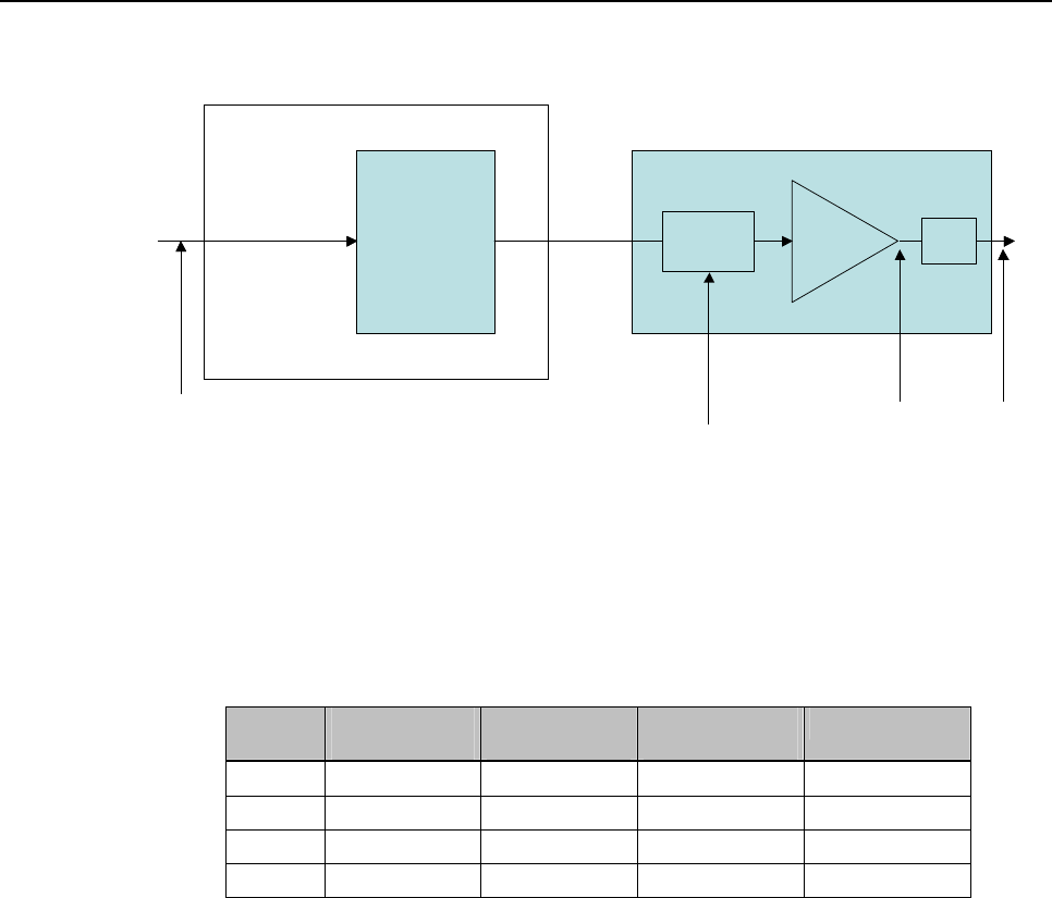
ADCP-75-192 • Issue 1 • December 2005 • Section 4: BTS Integration
Page 4-2
2005, ADC Telecommunications, Inc.
FBHDC PA
RAN
PA
Output
Power
RUC
Attn
RAN
Output
Power
Output
Loss
Hub
Composite
Input
Power RUC
Attn
Offset
FBHDC PA
RAN
PA
Output
Power
RUC
Attn
RAN
Output
Power
Output
Loss
Hub
Composite
Input
Power RUC
Attn
Offset
Figure 4-1. FBHDC Direct Cable Balancing
Table 4-1 shows the recommended power levels and gains for the various CXD bands.
Table 4-1. Forward Setting
BAND COMPOSITE
INPUT POWER
PA OUTPUT
POWER
RAN OUTPUT
POWER
FORWARD GAIN
SMR-A -7 dBm +37 dBm +35 dBm +42 dB
SMR-B -7 dBm +37 dBm +35 dBm +42 dB
Cellular -4 dBm +40dBm +38 dBm +42 dB
PCS -4 dBm +43 dBm +41 dBm +45 dB
The FBHDC input balancing procedure is as follows:
1. Insert signals into FBHDC at the recommended input level (composite)
2. Using the transceptTenantCalTable.transceptTenantRanYOutputPower fields of the
Tenant OAM MIB, examine the PA output power for each RAN in the simulcast
3. Using the transceptTenantGenTwoTable. transceptTenantRucYAttenOffset field in the
Tenant OAM MIB, adjust the RUC attenuator to perform final adjustments with all
carriers present. A positive offset lowers the output power and a negative offset increases
it.
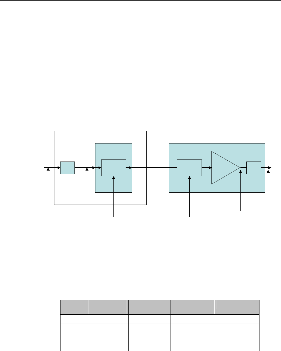
ADCP-75-192 • Issue 1 • December 2005 • Section 4: BTS Integration
Page 4-3
2005, ADC Telecommunications, Inc.
2.1.2 BIM Input
High Power duplexed interfaces requires the use of the High Power Attenuator and the BIM
Module. A block diagram of the forward path balancing components is shown in Figure 4-2.
• Composite Input Power – Sum of all carriers, no more than 47 dBm
• PA Output Power – Tenant MIB value used to measure Output of PA
• RAN Output Power – PA Output Power Minus 2dB diplexer/cable loss
• RUC Attn Offset – Tenant MIB value used to adjust PA output power to account for
variations in RF chain
• BIM Attn Offset – MIB value used to adjust for lower input levels
PA
RAN
PA
Output
Power
RUC
Attn
RAN
Output
Power
Output
Loss
Hub
20 dB
HP pad
Composite
Input
Power RUC
Attn
Offset
BIM
BIM
At tn
BIM
At tn
Offset
BIM
Input
Power
PA
RAN
PA
Output
Power
RUC
Attn
RAN
Output
Power
Output
Loss
Hub
20 dB
HP pad
Composite
Input
Power RUC
Attn
Offset
BIM
BIM
At tn
BIM
At tn
Offset
BIM
Input
Power
Figure 4-2. BIM Forward Balance
Table 4-2 shows the recommended power levels and gains for the various CXD bands when
interfaced to the 20 dB Attenuator and the BIM.
Table 4-2. Recommended Forward Balance
BAND COMPOSITE
INPUT LEVEL
PA OUTPUT
POWER
RAN OUTPUT
POWER
FORWARD GAIN
SMR-A 44 dBm +37 dBm +35 dBm -9 dB
SMR-B 44 dBm +37 dBm +35 dBm -9 dB
Cellular 47 dBm +40dBm +38 dBm -9 dB
PCS 47 dBm +43 dBm +41 dBm -6 dB

ADCP-75-192 • Issue 1 • December 2005 • Section 4: BTS Integration
Page 4-4
2005, ADC Telecommunications, Inc.
The BIM input balancing procedure is as follows:
1. Insert signals into the HP Attenuator at the recommended input level (composite).
2. If the input level is lower than the recommended value, adjust the
transceptTenantMoreAttenTable.transceptTenantBimForwardAttenZOffset fields in the
Tenant OAM MIB by a comparable amount.
For example: If the PCS composite input is 44 dBm, enter a -30 into the
transceptTenantMoreAttenTable.transceptTenantBimForwardAttenZOffset field.
3. Using the transceptTenantCalTable.transceptTenantRanYOutputPower fields of the
Tenant OAM MIB, examine the PA output power for each RAN in the simulcast
4. Using the transceptTenantGenTwoTable. transceptTenantRucYAttenOffset field in the
Tenant OAM MIB, adjust the RUC attenuator to perform final adjustments with all
carriers present.
2.2 Reverse Path Balancing
The reverse gain indicates how much gain the Digivance CXD will give to a reverse path
signal before presenting it to the base station (e.g. a –100 dBm signal at the RAN input will be
–90 at the input to the BTS when Reverse Gain is set to 10 dB). The reverse gain settings are
shown in Table 4-3.
Table 4-3. Reverse Gain Settings
REVERSE GAIN (DB) COMMENT
+10 Normal setting, for dedicated BTS sector
0 Shared BTS tower sector, 3dB impact on
BTS tower coverage
-10 Shared BTS tower sector, no impact on
BTS tower coverage, 3dB impact on
Digivance CXD coverage
Use the following procedure to balance the reverse path:
1. Measure or calculate cable loss from BIM Output to BTS input
2. Enter cable loss value (forward and reverse) into the transceptTenantForwardCableLoss
and transceptTenantReverseCable Loss fields of the Tenant OAM MIB field for this
Tenant Sector
3. Enter reverse gain setting (-10 to +10 dB, typically +10 dBm) into the
transceptTenantReverseGain field of the Tenant OAM MIB for this Tenant Sector.
Note: The +/- 10 dB reverse gain setting assumes a 20 dB attenuator. Without the
attenuator, the gain is +10 to +30 dB.

ADCP-75-192 • Issue 1 • December 2005 • Section 4: BTS Integration
Page 4-5
2005, ADC Telecommunications, Inc.
2.3 Functional RAN Call Verification
At the completion of BTS integration, it is recommended that the coverage area be driven to
insure all RANs are operational. The following procedure is recommended:
1. Place calls on all RF channels supported by targeted RAN sector
2. Ensure hand-offs between RANs and RAN to tower are functional.

ADCP-75-192 • Issue 1 • December 2005 • Section 4: BTS Integration
Page 4-6
2005, ADC Telecommunications, Inc.
Blank

ADCP-75-192 • Issue 1 • December 2005 • Section 5: Software Updates
Page 5-1
2005, ADC Telecommunications, Inc.
SECTION 5: SOFTWARE UPDATES
Content Page
1 SOFTWARE RELEASE DELIVERABLE ....................................................... 5-1
2 RELEASE NOTES .................................................................... 5-1
3 UPGRADING EXISTING SYSTEM.......................................................... 5-2
3.1 Preliminary Steps ............................................................. 5-2
3.2 Upgrade Steps ............................................................... 5-2
4 VERIFICATION ..................................................................... 5-3
5 FAILED UPGRADES .................................................................. 5-4
6 FPGA UPDATES .................................................................... 5-5
7 BACKUP/RESTORE .................................................................. 5-5
7.1 Backup .................................................................... 5-5
7.2 Restore .................................................................... 5-5
7.3 Adding/Removing SNMP Traps..................................................... 5-6
8 UPDATING SPARE CPUS............................................................... 5-6
9 MIB EXTRACTION ................................................................... 5-7
1 SOFTWARE RELEASE DELIVERABLE
The ADC software upgrade process is based on packaging utilities built into the Linux-based
operating system used by ADC. The software upgrade is a set of interdependent packages
delivered in a self-extracting executable named so as to reflect the revision of the contained
software; for example: hr-3.2.0-upgrade would be used to upgrade a target Hub or RAN CPU
to version 3.1.0. When invoked, the upgrade executable will automatically take the appropriate
actions to upgrade the target CPU.
2 RELEASE NOTES
The release notes delivered with each software release distribution will contain specific details
about the changes being made in that software release. The release notes will itemize each
change made, including a description of the problem/issue being addressed, a description of
how the problem/issue was resolved, and the impact of the change on the NMS.
Included in the release notes are details of any upgrades to the FPGA images, including
revision number information contained in the latest release build. To ensure the latest
documentation matches the current packaged images, the release notes will be the only place
where this information is captured in external/customer documentation.
Also included are the steps needed to complete the upgrade.

ADCP-75-192 • Issue 1 • December 2005 • Section 5: Software Updates
Page 5-2
2005, ADC Telecommunications, Inc.
3 UPGRADING EXISTING SYSTEM
The most common upgrade scenario is one where an existing, fielded, operational system is
having all of its CPUs upgraded to the next version of software. Some important notes
regarding this type of upgrade:
3.1 Preliminary Steps
The following are some general notes that need to be considered when upgrading a fielded
system:
• The Hub Master should be the final CPU upgraded in the network to ensure that any new
network-level functions are managed and supported properly.
• It is assumed that a network administrator will be performing the upgrade.
• Upgrading an operational system will interrupt service, so upgrades should be planned
during the maintenance window.
• An upgrade of a test CPU should be attempted prior to upgrading an entire system or set of
systems.
• For upgrade verification purposes, note the PA power, RUC attenuator values, and module
pathtrace values (see the transceptOpencellPathtraceTable MIB) on a test RAN CPU and
follow instructions found in the section in this document labeled “Verification”.
• The upgrade executable should be FTP'd to all target machines prior to upgrading any
machine. This is more efficient than updating one machine at a time.
• The RAN CPUs should be upgraded first, as upgrading the HUB CPUs may interrupt
telnet sessions to the RAN, thereby stopping the RAN upgrades.
3.2 Upgrade Steps
• The upgrade steps are found in the Release Notes for that software version release.
4 VERIFICATION
It is important to be sure that the upgrade was successful before continuing on with upgrading
other CPUs in the network. Some of this verification is done automatically by the upgrade
executable, but there are certain steps that need to be done manually as well.
Actions that are automatically taken by the upgrade executable to verify success include the
following:
• Built in package management checks to be sure that files are being written and removed as
expected.
• Checks to be sure that upon completion of the upgrade, certain processes are running (or
no longer running, as the case may be) as expected.

ADCP-75-192 • Issue 1 • December 2005 • Section 5: Software Updates
Page 5-3
2005, ADC Telecommunications, Inc.
• Test scripts being run to ensure that processes are running as expected.
• If the autonomous actions taken by the upgrade executable discover that the upgrade was
not successful, the upgrade executable will report this information in the log file located at
/var/log/opencell-upgrade. Otherwise, a successful status message will be reported to that
log.
• Manual steps must also be taken to ensure that the upgrade process completed
successfully. Note that some of the manual validation steps below may also be performed
by the automatic validation described above.
• The process list should be examined to be sure that the appropriate processes are running.
This can be done by telnetting into the target CPU (see Upgrade Steps Section 3.2) and
entering the following:
ps ax | grep "/usr/bin/”. The list that is returned will indicate all processes that were run
from the system binary directory. At a minimum, this list should include the following:
/usr/bin/pathtrace /usr/bin/rgc
/usr/bin/nodepaths /usr/bin/equipment
/usr/bin/netnode /usr/bin/stf
/usr/bin/hlpwatch /usr/bin/i2cbusscan
/usr/bin/pcibusscan /usr/bin/i2cbusmaster (6 instances)
/usr/bin/fgc /usr/bin/gps
/usr/bin/niprs (4 instances) /usr/bin/hcp
Where hcp represents the listing of all HCPs that correspond to the modules being controlled
by the target CPU. These are specific to the target CPU being upgraded and include HDC,
BIM, FSC, HUC, MUC, RUC, RDC, SIF, and RSC. There should be one instance of each
HCP per module managed by the target CPU.
When evaluating the process list, it is important to be sure that the process ID’s of each of the
listed processes above stay stable to ensure that processes are not continually restarting. Run
the command ps ax | grep /usr/bin/ multiple times over the course of a minute or two to be
sure that this is the case.
In addition to the above processes, it must be verified that the SNMP agent software is
running. This is done by entering: ps as | grep "/usr/local/sbin" and verifying that
/usr/local/sbin/snmpd is one of the processes listed.
Evaluate the software version to be sure that it matches what is intended. This can be done
from the NMS by evaluating the Network Node MIB field transceptNetwork
NodeOpencellSoftwareRev. Alternatively, this value can be retrieved in the telnet session to
the CPU opened in the previous step by entering: snmpget localhost patriots
transceptNetworkNodeOpencellSoftwareRev.0.
On the upgraded CPU, verify pathtrace values are as expected by viewing the
transceptOpencellPathtraceTable MIB. Refer to the above "Preliminary Steps" section for
details.

ADCP-75-192 • Issue 1 • December 2005 • Section 5: Software Updates
Page 5-4
2005, ADC Telecommunications, Inc.
On the upgraded RAN CPU, verify PAs are functioning and power levels are as expected.
Refer to the above "Preliminary Steps" section for details.
5 FAILED UPGRADES
In the case of a failed upgrade, it will be desirable to attempt to return the target CPU to its
previous revision by uninstalling the most recent software upgrade. This action will be
accomplished with the use of a downgrade script that is installed as part of the upgrade. The
name of the downgrade script will contain the name of the version being downgraded to; for
example, hr-3.0.0-downgrade would be used to revert a CPU that has been upgraded to
version 3.1.0 back to 3.0.0.
Note that it is difficult to guarantee that a CPU reverted to its previous revision will work
exactly as the CPU did prior to the upgrade. There are simply too many variables to guarantee
this. The regression test cycle here at ADC will include a series of steps to validate that the
uninstall/downgrade process works, but it is extremely difficult to guarantee that all possible
failure paths will be exercised.
It is important that, upon completion of a downgrade, the verification steps described in the
previous section are taken to ensure that the CPU is left in an operational state.
6 FPGA UPDATES
Certain software releases will contain updates to the FPGA images that the ADC modules load
on startup. These FPGA image updates need to be programmed into an EEPROM on the
module(s) in question. The ADC software processes, upon detection of an out of date FPGA
image, will notify the maintainer via an ADC trap. The maintainer is responsible for
programming the EEPROM at the earliest convienence (See Reference #80-83 in Section 4).
Depending on the module(s) being updated with new FPGA images, this action could take as
long as 20-30 minutes to complete
Caution: While FGPAs are being downloaded, service will be interrupted.
7 BACKUP/RESTORE
There are several files on a hubmaster CPU being upgraded that should be backed up in case
something goes wrong with the upgrade and need to be restored. This set of files includes the
MIBmap files where MIB data is stored, as well as several system configuration files.
The upgrade executable will automatically run the backup script to take care of backing up all
key files. These files will be bundled into a file that will be stored on the CPU being upgraded,
in the /var directory. This file will be given a name that associates it with version of the
upgrade being performed, for example: backup-pre-2.1.0.tar.gz.

ADCP-75-192 • Issue 1 • December 2005 • Section 5: Software Updates
Page 5-5
2005, ADC Telecommunications, Inc.
Upgrading a CPU does not require that a restore of the backed up files be performed unless a
problem is encountered. Any data contained in the MIBmap files and any configuration data in
the system configuration files will remain untouched through a software upgrade. The only
time that backup data needs to be recovered is when an upgrade has failed and the CPU is
being reverted to the previous version using the downgrade script. In this event, the downgrade
script will automatically attempt to restore the backup data at the end of the downgrade
process.
Alternatively, the backup/restore steps can be run manually, with the backup file being saved
to any location on any CPU connected to the network. The steps for doing this are as follows:
7.1 Backup
Telnet to the target hubmaster CPU, using operator/operate as the username/password
Run the backup script:
sudo backup-hubmaster operator@<target-IP>:/var <backupname>.tar
7.2 Restore
Again, note that a restore only needs to be performed if problems with the upgrade have been
encountered and the CPU is going to be downgraded.
Telnet to the target hubmaster CPU, using operator/operate as the username/password
Run the restore script:
sudo backup-hubmaster -r operator@<target-IP>:/var <backupname>.tar
Reboot by entering: sudo reboot
Note that the restore script is simply the backup script invoked with a "-r" switch. The "-r"
switch is identical to the switch "--restore".
7.3 Adding/Removing SNMP Traps
SNMP traps are sent automatically by the ADC system to all managers named “trap-sink” in
DNS.
To add an entry to DNS, use the nsupdate (sudo nsupdate) command on the hubmaster. The
application nsupdate will prompt for an input, (‘>’) at which point enter:
update add version-trap-sink.domain 3600 A address
Note that:
• version should be either “v1” or “v2”, depending on whether you want SNMP version 1
traps or version 2 notifications to be sent to the sink, respectively.

ADCP-75-192 • Issue 1 • December 2005 • Section 5: Software Updates
Page 5-6
2005, ADC Telecommunications, Inc.
• address should be the IP address of a trap-sink (an SNMP manager that can receive traps);
there can be any number of trap-sinks – simply enter one line per trap sink.
• domain is that of the ADC system subnet on which nsupdate is being run.
After completing the desired number of lines, finish by entering two blank lines and then a
Ctrl-D.
To remove a trap-sink, do as above except at the prompt for input (‘>’), enter:
update delete version-trap-sink.domain A address
8 UPDATING SPARE CPUS
There are times when it is desirable to update the software on a spare CPU. The general
approach for updating a spare CPU is to install the CPU into an available chassis that is
connected to the network and execute the upgrade steps detailed in the previous section above.
The software upgrade process associated with upgrading a spare CPU is exactly as described in
the "Upgrading Existing System" section above. The only difference between upgrading a
spare CPU and an existing system is that a physical location for upgrading the spare CPU must
be determined.
There are a few ways to make a CPU chassis slot available:
• Each digital chassis in the Hub supports two CPUs - it is possible that one of the installed
Hub digital chassis is only half-populated and contains an available CPU slot. This note is
only applicable to Generation 1 Hubs, since Generation 2 Hub chassis only contain one
CPU.
• Unplug a CPU that resides in the existing fielded system and replace it (temporarily) with
the spare CPU. When finished upgrading the spare CPU, return the original CPU to that
slot in the chassis.
• Dedicate a chassis to be used strictly for this type of update and for verification and test.
This is the recommended option for CPUs not slated for immediate installation.
There are limitations with this type of update that need to be observed:
• It is important that all Hub/RAN CPUs that reside on the same network are able to
communicate with their Hub Master. Therefore, if the spare CPU is too far outdated, this
may not be possible. In order to avoid a conflict, it is only possible to update a spare CPU
on the fielded system network if the current major version of the spare CPU is the same as
that of the CPUs in the fielded system. For example, if all the CPUs in the fielded system
are currently at revision 2.2.0 and the spare CPU is at 2.0.0, it is possible to update that
CPU with the method described above. However, if the spare CPU in this example is at
1.7.0, it is not possible. This implies that if an ADC software release is of a new major
revision, spare CPUs in stock need to be upgraded at the same time as all of the other
CPUs in the fielded system.

ADCP-75-192 • Issue 1 • December 2005 • Section 5: Software Updates
Page 5-7
2005, ADC Telecommunications, Inc.
• In the event that a spare CPU cannot be updated because of the above restriction, the CPU
will have to be upgraded on a standalone chassis that is not resident on the fielded system
or be returned to the factory for upgrading.
• It is NOT possible to update a spare Hub Master CPU while the fielded system's Hub
Master is still installed, because two Hub Masters in the same domain will cause chaos on
the network. The only way to update the software on a spare Hub Master CPU in a fielded
system is to unplug the Ethernet cable from the original Hub Master CPU and plug that
cable into the spare Hub Master CPU. When the upgrade of the spare Hub Master CPU is
complete, the Ethernet cable can be plugged back into the original Hub Master CPU.
Caution: It is highly recommended that spare CPUs not slated for immediate installation are
upgraded in a dedicated chassis in a depot or warehouse environment.
9 MIB EXTRACTION
The following procedure outlines the process for extracting the Digivance SNMP Agent MIBs
needed to update the NMS after a software update:
• Once the software upgrade is complete, FTP to one of the updated CPUs, logging in as
username = operator and password = operate.
• Change to the MIB directory by entering: cd /usr/share/mibs/transcept/
• Extract/get all of the MIB text files located there by entering: mget TRANSCEPT-*.txt,
answering yes to each prompt.
• Extracting the MIBs in this fashion will ensure that the correct and compatible versions of
all of MIBs are compiled into the NMS.
Alternatively, the MIBs can all be extracted in the form of a tarball by executing the following
steps:
• FTP to one of the updated CPUs, logging in as username = operator and password =
operate.
• Change to the directory containing the ADC MIBs directory by entering:
cd /usr/share/mibs/
Bundle and zip all the MIBs into a tarball and extract them by entering: get transcept.tar.gz.

ADCP-75-192 • Issue 1 • December 2005 • Section 5: Software Updates
Page 5-8
2005, ADC Telecommunications, Inc.
Blank

ADCP-75-192 • Issue 1 • December 2005 • Section 6: Autonomous Software Functionality
Page 6-1
2005, ADC Telecommunications, Inc.
SECTION 6: AUTONOMOUS SOFTWARE FUNCTIONALITY
Content Page
1 INTRODUCTION .................................................................... 6-1
2 FORWARD GAIN MANAGEMENT.......................................................... 6-1
3 REVERSE AUTOMATIC GAIN CONTROL ..................................................... 6-2
4 FORWARD DELAY MANAGEMENT ........................................................ 6-2
5 REVERSE DELAY MANAGEMENT ......................................................... 6-2
6 FORWARD CONTINUITY ............................................................... 6-2
7 REVERSE CONTINUITY................................................................ 6-2
7.1 Noise Test .................................................................. 6-3
7.2 RAN Down Converter (RDC) Tone Test................................................ 6-3
7.3 Hub Up Converter (HUC) Tone Test .................................................. 6-3
8 PA OVERPOWER PROTECTION .......................................................... 6-4
9 HUB OVERPOWER PROTECTION ......................................................... 6-4
1 INTRODUCTION
This section outlines the concepts and performance objectives involved in the gain
management and fault detection (continuity) of the Digivance CXD system. This section
breaks these topics down into the following areas:
• Forward gain management
• Reverse Automatic Gain Control
• Forward delay management
• Reverse delay management
• Forward continuity
• Reverse continuity.
• PA Overpower Protection
• Hub Overpower Protection
2 FORWARD GAIN MANAGEMENT
The Digivance CXD system has a compensation feature in the forward path to account for
changes in gain as a function of temperature.. This feature applies on a per RAN basis and is
enabled by default. The operator can disable this feature if desired.

ADCP-75-192 • Issue 1 • December 2005 • Section 6: Autonomous Software Functionality
Page 6-2
2005, ADC Telecommunications, Inc.
3 REVERSE AUTOMATIC GAIN CONTROL
The Digivance CXD system autolimits any strong in-band signal which reaches the RAN at a
peak input level of greater than -38 dBm relative to the antenna port. The process does this by
monitoring A/D overflows and adding attenuation in the RDC when these overflow occur.
“AGC events” are logged on the CPU running the RDC process. Attenuation is backed out as
the signal strength subsides.
4 FORWARD DELAY MANAGEMENT
Forward Delay Management (FDM) is a software function that is part of Tenant Processing
and whose responsibility is to equalize the path delays to all RANs in a simulcast group. The
FDM process is "enabled" in the Tenant OAM MIB (see Section 3, Sub-Section 7 Tenant
Configuration).
5 REVERSE DELAY MANAGEMENT
Reverse Delay Management (RDM) is a software function that is part of Tenant Processing
and whose responsibility is to equalize the path delays to all RANs in a simulcast group. The
RDM process is "enabled" in the Tenant OAM MIB (see Section 3, Sub-Section 7 Tenant
Configuration).
6 FORWARD CONTINUITY
Forward Continuity Management (FCM) is a software function that may be used to verify that
the forward RF paths are functioning properly and are able to pass signals. This function is
disabled by default.
7 REVERSE CONTINUITY
Reverse Continuity Management (RCM) is a software function that is a subset of Tenant
Processing and is responsible for verifying that the reverse RF paths for each tenant-sector are
functioning properly and are able to pass signals. This function is enabled by default.
The various parts of RCM are defined in the sections that follow.

ADCP-75-192 • Issue 1 • December 2005 • Section 6: Autonomous Software Functionality
Page 6-3
2005, ADC Telecommunications, Inc.
7.1 Noise Test
The front-end noise will be monitored by reading the noise power value from the reverse
channels in the RAN SIF module belonging to the tenant-sector being analyzed. The in-band
noise power (N) and total signal power (S+N) will be measured and analyzed in the SIF using
an FFT analysis, as follows:
The RCM software will generate faults if the integrated power levels are below the specified
thresholds.
7.2 RAN Down Converter (RDC) Tone Test
The RDC Tone will be enabled at all times, unless explicitly disabled via the RDC MIB. Its
frequency corresponds to the first channel in the band set for that tenant-sector. Additional
requirements are:
• The RDC tone level is –80 dBm referenced to the front end antenna port of the RAN
• The RDC Tone is available on the primary and diversity paths
In the RAN, power measurements are taken at the reverse channels of the RAN SIF belonging
to each tenant-sector. In the Hub, these power measurements are taken at the BIM. These
power measurements are performed continuously on a one-minute poll rate and are compared
to specified threshold values.
• If the test tone is not detected in the RAN SIF, then the RDC is reported as faulting.
See troubleshooting guide for details.
7.3 Hub Up Converter (HUC) Tone Test
The HUC tone will be enabled at all times, unless explicitly disabled via the HUC MIB. Its
frequency corresponds to the last channel in the band set for that tenant-sector. Additional
requirements are:
• The HUC tone level is –70 dBm relative to the antenna port at the RAN.
• If the test tone is not detected at the BIM, it and the HUC are reported as faulting.
• See “SNMP Agent and Fault Isolation Guide” for details.

ADCP-75-192 • Issue 1 • December 2005 • Section 6: Autonomous Software Functionality
Page 6-4
2005, ADC Telecommunications, Inc.
8 PA OVERPOWER PROTECTION
PA Overpower Protection (POP) is a software function that prevents damage to the PA as well
as preventing the PA from exceeding FCC spurious output limits.
POP measures the PA Output Power once per second from the RUC/PA MIB. If the PA
Output Power exceeds a determined threshold, then POP will deactivate the FGC process for
the tenant-sector in question, add attenuation to the RUC, and set a fault in the FGC MIB.
Once the PA Output Power returns to a value that is less than a determined threshold, then the
POP fault will be cleared and normal operation will resume.
The limits are set to 1 dB above the rated output for a given Power Amplifier. For 10 watt PAs
(40 dBm), the limit is 41 dBm. For 20 watt PAs (43 dBm), the limit is 44 dBm.
See the “SNMP Agent and Fault Isolation Guide” guide for details.
9 HUB OVERPOWER PROTECTION
Hub Overpower Protection (HOP) is a software function to control the output levels of the
FSC. HOP periodically measures the FSC output power. If the power exceeds a target level (-
3.5 dBFS), HOP will decrease the FSC output gain until the power level is below the allowable
threshold. HOP will continue to monitor the FSC Output Power until the level drops
sufficiently to allow the gain level to be returned to normal.
If HOP is required to take autonomous action on any of the FSC output, a HOP Status field in
the FSC MIB will be set such that the NMS report the condition and an operator can take
corrective action. This MIB entry can be found as follows:
transceptFscHopTable.transceptFscHopModeRms
Status values include hopActive and hopInactive. See the “SNMP Agent and Fault Isolation
Guide” guide for details.

ADCP-75-192 • Issue 1 • December 2005 • Section 7: MIB Structure
Page 7-1
2005, ADC Telecommunications, Inc.
SECTION 7: MIB STRUCTURE
Content Page
1 MIB RELATIONSHIPS................................................................. 7-1
2 HARDWARE RELATIONSHIPS ........................................................... 7-2
2.1 Hub/RAN Connection Relationships: ................................................ 7-3
2.2 Tennant Relationships .......................................................... 7-3
1 MIB RELATIONSHIPS
MIB is an acronym for Management Information Base, and defines a set of managed objects
used in the SNMP protocol. MIB’s define the supported interface into an SNMP device. The
managed objects defined in the Digivance CXD MIB’s provide the monitoring and control
capability into the Digivance CXD system.
SNMP Management applications, such as the customer Network Management System, use the
definitions provided in MIB’s to monitor and control SNMP devices, such as the CPUs in the
Digivance CXD network. SNMP Management applications may or may not allow direct access
to MIB’s through a MIB Browser, so it is important to refer to the User’s Manual for the
SNMP Management application being used. Digivance CXD MIB’s are provided as part of the
software package delivered to Digivance CXD customers so that the customer can compile the
Digivance CXD MIB’s into the NMS and monitor/control the Digivance CXD equipment.
Figure 7-1 displays the MIB’s used in the Digivance CXD system, which node* type(s) each
MIB is used in, and how the MIB’s are related to each other. The sections that follow will
describe each of the MIB’s and how they are used in the Digivance CXD system.
(*) Within the Digivance CXD network, there are four node types: Hub Node, RAN Node, LSE
node, and Hubmaster Node, where "node" is simply shorthand for "network node". In the
Digivance CXD system, node simply refers to the CPUs used in the Digivance CXD network. It
is also important to note that the Hubmaster node is a regular Hub node with additional
functionality that is particular to the one and only Hubmaster node in the network. The LSE
node is also a regular Hub node with additional functionality particular to location services
applications.
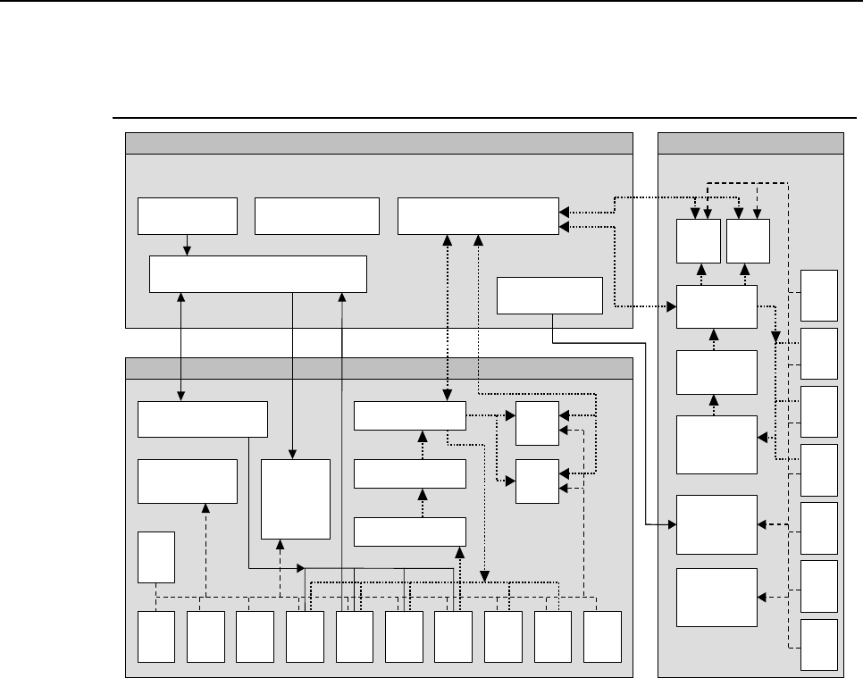
ADCP-75-192 • Issue 1 • December 2005 • Section 7: MIB Structure
Page 7-2
2005, ADC Telecommunications, Inc.
HUB MASTER
HUB NODE
RAN NODE
RDC
MIB
RUC
MIB
MUC
MIB
SIF
MIB
SIF
MIB
RSC
MIB
FSC
MIB
HUC
MIB
BIM
MIB
HDC
MIB
PSI
MIB
STF
MIB
STF
MIB
BUS SCANNER
MIB
PATHTRACE MIB
EQUIPMENT MIB
HUB RF CONN MIB
N
ODE PATH MIB
BUS
SCANNER
MIB
PATHTRACE
MIB
N
ODE PATH
MIB
EQUIPMENT
MIB
N
ETWOR
K
N
ODE
MIB
N
ETWOR
K
N
ODE
MIB
BTS CONNECTION MIB
TENANT OAM MIB
WD
MIB
WD
MIB
HUB NODE MIB
GPS
MIB
GPS
MIB
HRM
MIB
FGC
MIB
RGC
MIB
FGC
MIB
RGC
MIB
MIB RELATIONSHIPS
RAN NODE MIB
HUB CONFIG MIB
Figure 7-1. MIB Relationships
MIB’s described in Figure 7-1 and in the sections below provide a general overview of the
MIB’s used in the Digivance CXD system. MIB’s may be added, deleted or changed as the
product is developed and as enhancements are added.
Changes to MIB’s are made in such a way as to make them backward compatible with existing
SNMP Managers. This is accomplished by only allowing new MIB objects to be added to the
end of MIB’s instead of deleting or changing existing MIB objects. MIB objects that are no
longer required will still exist in the MIB’s, but will no longer be accessed.
2 HARDWARE RELATIONSHIPS
In Figure 7-1, the dashed lines seen in the Hub and RAN Nodes show the relationships among
MIB’s associated with specific hardware modules.
A separate software HCP (hardware control process) is used to manage each hardware module
in a node, where HCP MIB’s are the interface to these HCP’s. A single MIB instance is used in
each node for each type of hardware (FBHDC, RDC, etc.).

ADCP-75-192 • Issue 1 • December 2005 • Section 7: MIB Structure
Page 7-3
2005, ADC Telecommunications, Inc.
Each Hub/RAN node contains a Bus Scanner process whose responsibility is to discover the
presence/absence of hardware modules and to start/stop HCP’s to manage those hardware
modules. The Bus Scanner MIB reports the information defining the hardware “discovered” at
that node.
Each node contains a Network Node process to manage information about that CPU, where the
interface is the Network Node MIB. This MIB contains information about the CPU itself (e.g.
IP Address, Hostname, etc.), Hub/RAN specific information (Pole ID, RAN Box ID, etc.), and
other miscellaneous status information. In addition, this MIB reports a high-level fault status
for each HCP type. If any HCP in that node reports a fault of any type in its HCP MIB, the
Network Node MIB fault field corresponding to that HCP will report a problem.
2.1 Hub/RAN Connection Relationships:
In Figure 7-1, the solid lines between the Hubmaster and Hub/RAN nodes illustrate Hub/RAN
connection relationships.
The Hubmaster contains a process called the Hub/RAN Config Process that is responsible for
managing the connections between the Hubmaster and the other nodes in the network. This
process uses the Hub Node MIB and RAN Node MIB to manage these connections. The
Hub/RAN Node MIB’s allow specific information about the Hub/RAN nodes to be configured.
This includes such things as Site ID, Pole ID, and RAN hardware connections. The Hub/RAN
Config Process will push the information configured in these MIB’s down to the Network
Node MIB at each node. Refer to Section 3 Network and System Installation and Setup for a
more in-depth explanation of how to use these MIB’s.
The Hub/RAN Config Process is also responsible for preparing the Hubmaster to have tenant
relationships established. This process uses the information set in the Hub Node MIB and BTS
Connection MIB to configure the tenant relationships. Information that is provided in the BTS
Connection MIB as part of Tenant Setup will be pushed down to the Hub RF Connection MIB
in the Hub Nodes. Refer to Section 3 Network and System Installation and Setup for a more in-
depth explanation of how these MIB’s are used.
2.2 Tenant Relationships:
In Figure 7-1, the dotted lines among Hubmaster and Hub/RAN nodes illustrate tenant
relationships.
Once a tenant is created using the BTS Connection of the previous section, then a Tenant
process is kicked off to manage that new tenant. This tenant process uses the Tenant OAM
MIB in the Hubmaster node to allow tenant specific parameters to be configured. These
parameters allow the setting of frequency, gain, and delay values as well as any other tenant
specific information. When these values are set, the Tenant process pushes this information to
the Equipment MIB at the appropriate node(s).
In addition, the Tenant process uses the Tenant OAM MIB to report any status information
about the tenant, such as hardware faults and RAN location information, which is gathered
from the Equipment MIB’s at the Hub/RAN nodes.

ADCP-75-192 • Issue 1 • December 2005 • Section 7: MIB Structure
Page 7-4
2005, ADC Telecommunications, Inc.
Tenant processing determines the location of its related nodes and hardware using a process
called the Tenant Scan process that polls the Equipment MIB’s located at each node in the
network. If the Equipment MIB indicates that there is hardware belonging to that tenant on that
node, then the Tenant process in the Hubmaster will add that node to its "managed node" list.
The Tenant process will then use the Equipment MIB’s on its managed nodes to interface to
the hardware equipment belonging to it.
The Tenant Equipment process on each Hub/RAN node will process all Equipment MIB
requests and will report all tenant equipment status in the Equipment MIB.
In the Hub/RAN nodes, the Node Paths process is responsible for detecting tenant equipment
using the results of the Pathtrace MIB and reporting this information in the Node Path MIB. In
effect, the information of the Node Path MIB is just a reorganization of the Pathtrace MIB
information to simplify the Tenant Equipment process. The Tenant Equipment process uses the
information in the Node Paths MIB to identify equipment belonging to specific tenants.
The information reported in the Pathtrace MIB is generated by the Pathtrace process on each
Hub/RAN node. The Pathtrace process examines the pathtrace fields of each HCP MIB and
reports them in a single MIB containing only information related to pathtrace, such as the HCP
type and location, as well as the pathtrace string value itself.
Tenant processes in the Hubmaster push down gain control information from the Tenant OAM
MIB to the Forward/Reverse Gain MIB’s located in the Hub/RAN nodes. Forward/Reverse
Gain processes use the values set in the Forward/Reverse Gain MIB’s as target values when
managing the gain in those nodes.
The Forward/Reverse Gain processes in the Hub/RAN nodes use the Equipment MIB to
determine the location of the hardware belonging to the tenant whose gain is being managed.
The Forward/Reverse Gain processes then access the HCP MIB’s to read power values and set
attenuator values as part of gain control. The results of the gain control processes are then
reported into the Forward/Reverse Gain MIB’s.

ADCP-75-192 • Issue 1 • December 2005 • Section 8: General Information
Page 8-1
2005, ADC Telecommunications, Inc.
SECTION 8: GENERAL INFORMATION
Content Page
1 WARRANTY/SOFTWARE ............................................................... 8-1
2 SOFTWARE SERVICE AGREEMENT ........................................................ 8-1
3 REPAIR/EXCHANGE POLICY ............................................................ 8-1
4 REPAIR CHARGES................................................................... 8-2
5 REPLACEMENT/SPARE PRODUCTS........................................................ 8-2
6 RETURNED MATERIAL ................................................................ 8-2
7 CUSTOMER INFORMATION AND ASSISTANCE ................................................ 8-3
1 WARRANTY/SOFTWARE
The Product and Software warranty policy and warranty period for all ADC products is
published in ADC’s Warranty/Software Handbook. Contact the Technical Assistance Center at
1-800-366-3891, extension 73476 (in U.S.A. or Canada) or 952-917-3476 (outside U.S.A. and
Canada) for warranty or software information or for a copy of the Warranty/Software
Handbook.
2 SOFTWARE SERVICE AGREEMENT
ADC software service agreements for some ADC Products are available at a nominal fee. Contact
the Technical Assistance Center at 1-800-366-3891, extension 73476 (in U.S.A. or Canada) or 952-
917-3476 (outside U.S.A. and Canada) for software service agreement information.
3 REPAIR/EXCHANGE POLICY
All repairs of ADC Products must be done by ADC or an authorized representative. Any attempt
to repair or modify ADC Products without authorization from ADC voids the warranty.
If a malfunction cannot be resolved by the normal troubleshooting procedures, Technical
Assistance Center at 1-800-366-3891, extension 73476 (in U.S.A. or Canada) or 952-917-3476
(outside U.S.A. and Canada). A telephone consultation can sometimes resolve a problem without
the need to repair or replace the ADC Product.
If, during a telephone consultation, ADC determines the ADC Product needs repair, ADC will
authorize the return of the affected Product for repair and provide a Return Material
Authorization number and complete shipping instructions. If time is critical, ADC can arrange
to ship the replacement Product immediately. In all cases, the defective Product must be
carefully packed and returned to ADC.

ADCP-75-192 • Issue 1 • December 2005 • Section 8: General Information
Page 8-2
2005, ADC Telecommunications, Inc.
4 REPAIR CHARGES
If the defect and the necessary repairs are covered by the warranty, and the applicable warranty
period has not expired, the Buyer’s only payment obligation is to pay the shipping cost to
return the defective Product. ADC will repair or replace the Product at no charge and pay the
return shipping charges.
Otherwise, ADC will charge a percentage of the current Customer Product price for the repair
or NTF (No Trouble Found). If an advance replacement is requested, the full price of a new
unit will be charged initially. Upon receipt of the defective Product, ADC will credit Buyer
with 20 percent of full price charged for any Product to be Out-of-Warranty. Products must be
returned within (30) days to be eligible for any advance replacement credit. If repairs
necessitate a visit by an ADC representative, ADC will charge the current price of a field visit
plus round trip transportation charges from Minneapolis to the Buyer’s site.
5 REPLACEMENT/SPARE PRODUCTS
Replacement parts, including, but not limited to, button caps and lenses, lamps, fuses, and patch
cords, are available from ADC on a special order basis. Contact the Technical Assistance Center
at 1-800-366-3891, extension 73476 (in U.S.A. or Canada) or 952-917-3476 (outside U.S.A. and
Canada) for additional information.
Spare Products and accessories can be purchased from ADC. Contact Sales Administration at
1-800-366-3891, extension 73000 (in U.S.A. or Canada) or 1-952-9938-8080 (outside U.S.A.
and Canada) for a price quote and to place your order.
6 RETURNED MATERIAL
Contact the ADC Product Return Department at 1-800-366-3891, extension 73748 (in U.S.A.
or Canada) or 952-917-3748 (outside U.S.A. and Canada) to obtain a Return Material
Authorization number prior to returning an ADC Product.
All returned Products must have a Return Material Authorization (RMA) number clearly
marked on the outside of the package. The Return Material Authorization number is valid for
90 days from authorization.
ADCP-75-192 • Issue 1 • December 2005 • Section 8: General Information
Page 9-3
7 CUSTOMER INFORMATION AND ASSISTANCE
13944-M
WRITE:
ADC TELECOMMUNICATIONS, INC
PO BOX 1101,
MINNEAPOLIS, MN 55440-1101, USA
ADC TELECOMMUNICATIONS (S'PORE) PTE. LTD.
100 BEACH ROAD, #18-01, SHAW TOWERS.
SINGAPORE 189702.
ADC EUROPEAN CUSTOMER SERVICE, INC
BELGICASTRAAT 2,
1930 ZAVENTEM, BELGIUM
PHONE:
EUROPE
Sales Administration: +32-2-712-65 00
Technical Assistance: +32-2-712-65 42
EUROPEAN TOLL FREE NUMBERS
UK: 0800 960236
Spain: 900 983291
France: 0800 914032
Germany: 0180 2232923
U.S.A. OR CANADA
Sales: 1-800-366-3891 Extension 73000
Technical Assistance: 1-800-366-3891
Connectivity Extension 73475
Wireless Extension 73476
ASIA/PACIFIC
Sales Administration: +65-6294-9948
Technical Assistance: +65-6393-0739
ELSEWHERE
Sales Administration: +1-952-938-8080
Technical Assistance: +1-952-917-3475
Italy: 0800 782374
PRODUCT INFORMATION AND TECHNICAL ASSISTANCE:
Contents herein are current as of the date of publication. ADC reserves the right to change the contents without prior notice.
In no event shall ADC be liable for any damages resulting from loss of data, loss of use, or loss of profits and ADC further
disclaims any and all liability for indirect, incidental, special, consequential or other similar damages. This disclaimer of
liability applies to all products, publications and services during and after the warranty period. This publication may be
verified at any time by contacting ADC's Technical Assistance Center.
euro.tac@adc.com
asiapacific.tac@adc.com
wireless.tac@adc.com
connectivity.tac@adc.com
© 2005, ADC Telecommunications, Inc.
All Rights Reserved
Printed in U.S.A.

ADCP-75-192 • Issue 1 • December 2005 • Section 8: General Information
Page 8-4
2005, ADC Telecommunications, Inc.
Blank

i
www.adc.com