AVITA BMW-18XX BLE Module User Manual UV3BMW 18XX UM
AVITA Corporation BLE Module UV3BMW 18XX UM
AVITA >
Confidential_UV3BMW-18XX UM
AViTA BLE MODULE
V1.0 Page 1 March 21, 2018
1 Introduction
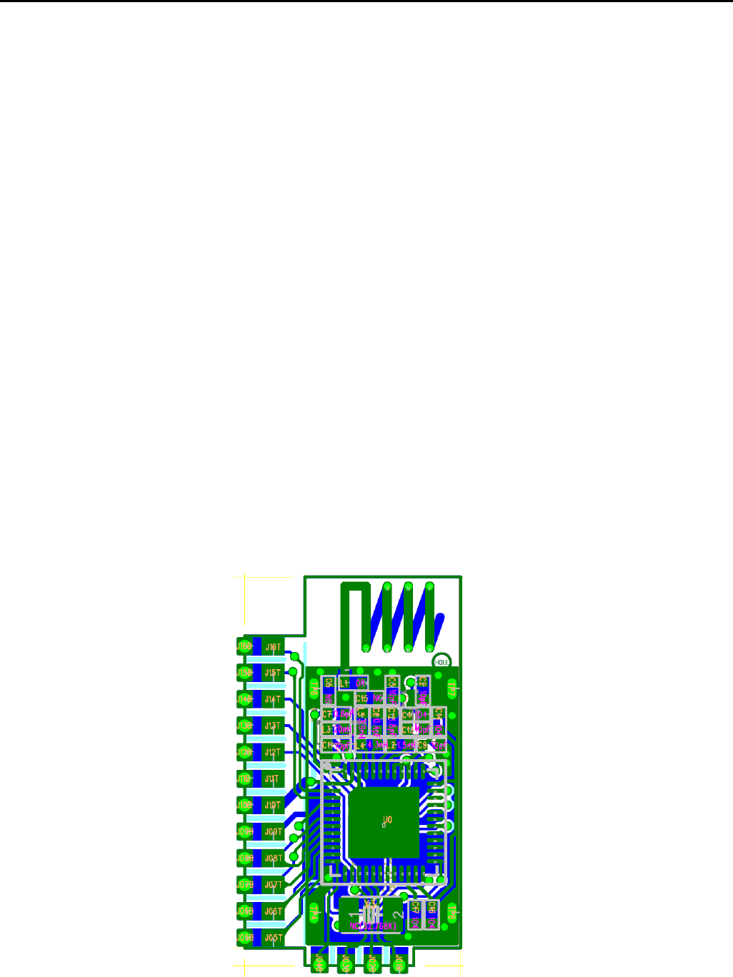
AVITA BLE MODULE is a Bluetooth low energy module designed by Avita Corporation. This
module is based on SH87F8801 BLE chip, which integrates a ultra low power Bluetooth transceiver and a
high performance low power 32 bit microprocessor. It is a data transparent transmission module, supports
many of the wireless data applications.
1.1 Feature
y Frequency range: 2.400~2.4835GHz
y Bluetooth 4.2 specification
y Receive Sensitivity = -87 dBm @ 1.0 Mbps
y Output power range: -20 ~ 0 dBm
y Data Rate = 1 Mbps
y 32-bit CPU core
y Flash ROM: 128KB
y SRAM: 17KB
y Two UART interfaces
y Serial two wire debug interface
y 16.5 mA @ Receive
y 12.1 mA @ 0 dBm Transmit
y 10.1 mA @ -6 dBm Transmit
y Deep Sleep Mode(< 3uA)
y Power Down Mode(< 0.3uA)
AViTA BLE MODULE
V1.0 Page 2 March 21, 2018
2 Description
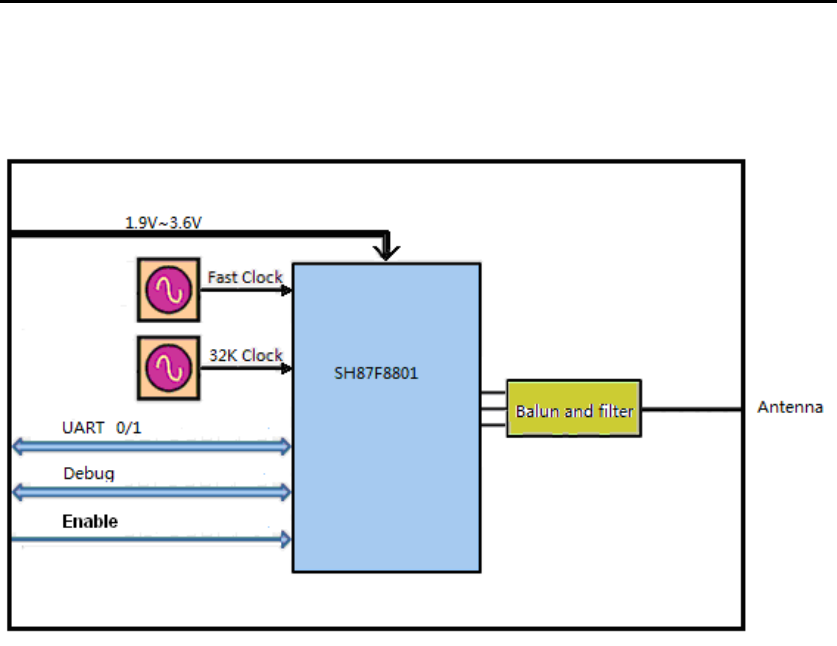
2.1 Block diagram
AViTA BLE MODULE
V1.0 Page 3 March 21, 2018
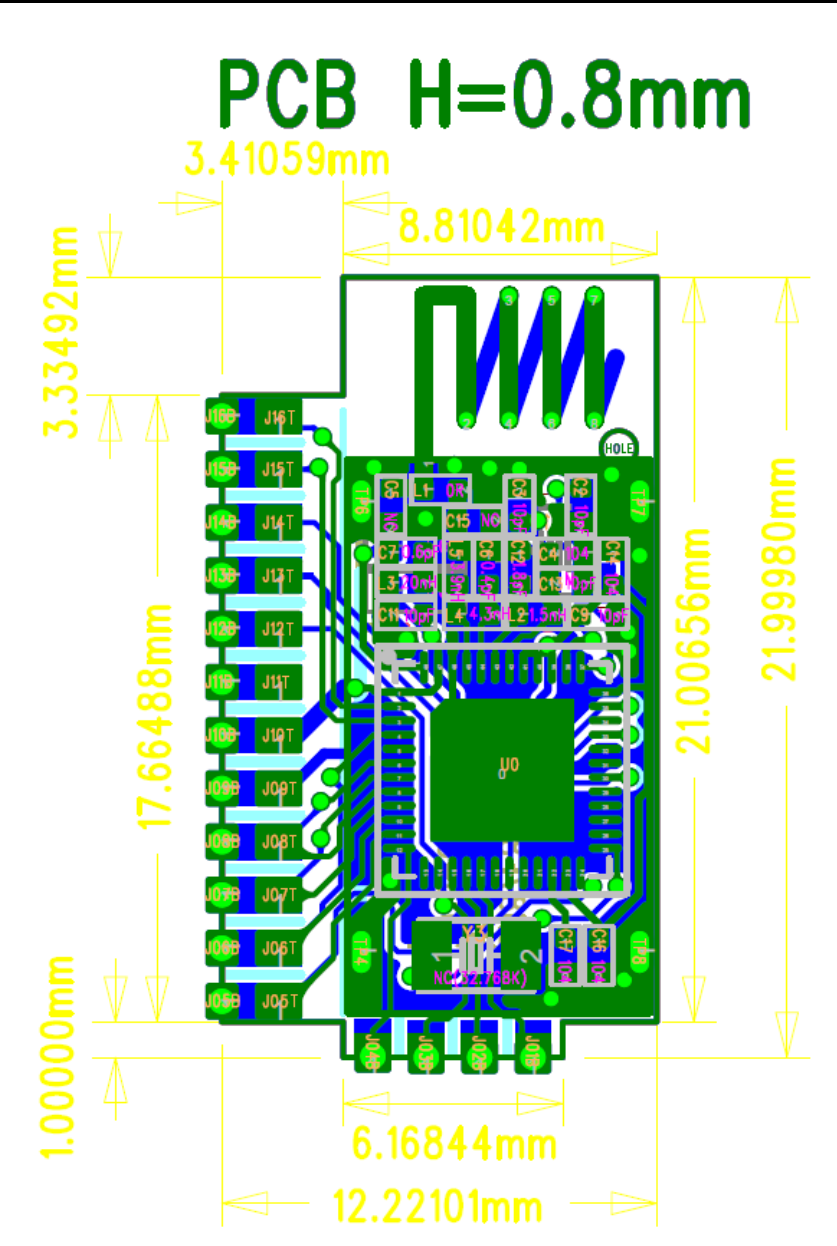
2.2 Module Size

AViTA BLE MODULE
V1.0 Page 4 March 21, 2018
2.3 Module Pin assignment
Pin# Name Type Description Note
J01B P15 Digital I/O GPIO 15/ TDA
J02B P14 Digital I/O GPIO 14/ TCK
J03B P13 Digital I/O GPIO 13/RSTN
J04B P10 Digital I/O GPIO 10/PWM2
J05B P26 Digital I/O,Analog GPIO 26/AIN5 WakeUp
J05T P09 Digital I/O GPIO 09/PWM1
J06B P02 Digital I/O P02 LINK
J06T P08 Digital I/O GPIO 08/PWM0
J07B P05 Digital I/O GPIO 05/TXD 0 TX
J07T P07 Digital I/O GPIO 07/TXD 1
J08B P04 Digital I/O GPIO 04/RXD 0 RX
J08T P06 Digital I/O GPIO 06/RXD 1
J09B GND Power Ground
J10B VDD Power Power supply Default 3.3V
J11B,J09T,J
10T,J11T,J12
T,J13T,J14T,
J15T,J16T
NC Not connected
J12B RESET Digital I/O GPIO 13/RSTN
J13B P29
Digital I/O,Analog GPIO 29/AIN2
J14B P31
Digital I/O,Analog GPIO 31/AIN0
J15B P01 Digital I/O P01
J16B P00 Digital I/O P00
AViTA BLE MODULE
V1.0 Page 5 March 21, 2018
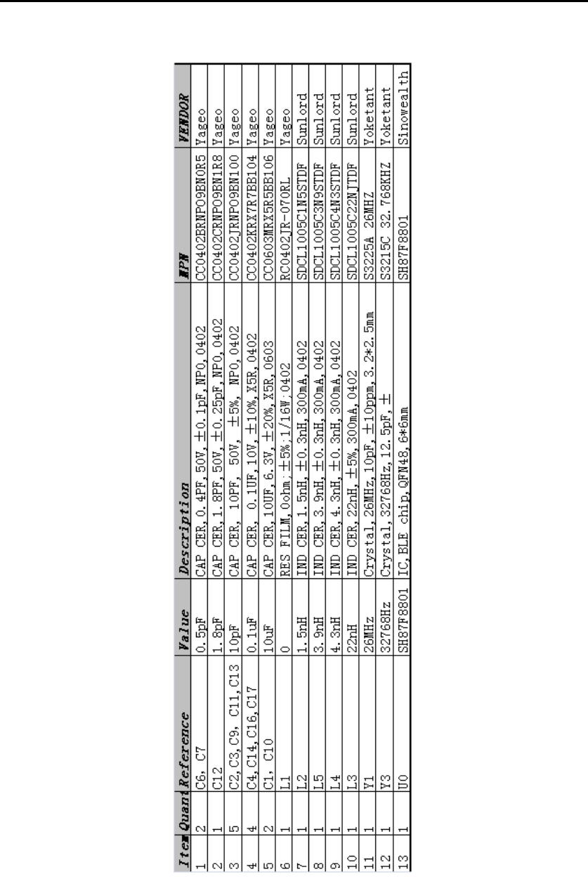
2.4 Module BOM
AViTA BLE MODULE
V1.0 Page 6 March 21, 2018
3 Electical characters
3.1 Absolute Maximum Ratings
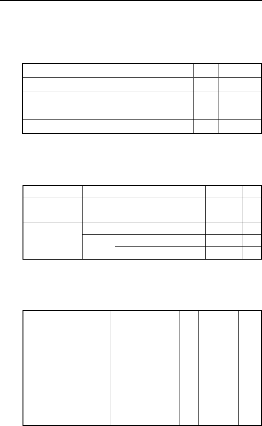
Parameter Min. Typ. Max. Unit
Supply Voltage 3.6 V
VIN (Input Voltage) 1.9 3.3 3.6 V
Operating Temperature -40 85 ℃
Storage Temperature -40 125 ℃
Table 1. Absolute Maximum Ratings
3.2 DC Electrical Specifications
Parameter Symbol Conditions Min. Typ. Max. Unit
Supply Voltage
Range VDD Supply voltage 1.9 3.3 3.6 V
Current
Consumption
IPOWERDOWNPower down current - 0.2 0.3 μA
Ideep_sleep
RC32K active - 3 6 μA
RC32K off - 2 4 μA
Table 2. DC Electrical Specifications
3.3 Synthesizer Electrical Specifications
Parameter Symbol Conditions Min. Typ. Max. Unit
Frequency Range FSYN 2400 - 2483.5 MHz
Frequency
Resolution FRES - 400 - Hz
Reference
Frequency FREF - 26 - MHz
Reference
Frequency
tolerance
FTOL - - ±40 ppm

AViTA BLE MODULE
V1.0 Page 7 March 21, 2018
Synthesizer
Settling Time tLOCK - - 30 μs
Synthesizer Wake
up Time TWAKE-UP
Including references,
calibrations and
synthesizer lock
- - 80 μs
Phase Noise at
offset
LФ(fM) ∆F = 1 MHz - -106 - dBc/Hz
LФ(fM) ∆F = 2 MHz - -111 - dBc/Hz
LФ(fM) ∆F = 3 MHz - -114 - dBc/Hz
RMS Phase Error ФRMS Integrated from 1kHz
to 13MHz - 2.0 - Deg
Table 3. Synthesizer Electrical Specifications
3.4 Transmitter Electrical Specifications
Parameter Symbol Conditions Min. Typ. Max. Unit
TX Frequency
Range FTX World Wide 2400 - 2483.5 MHz
FSK Data Rate DRFSK - 1.0 - Mbps
Modulation
Deviation ∆f 250 kHz
20dB signal
bandwidth (1Mbps) BW20dB 0.95 1.2 MHz
Output Power
Range PTX -20 - +2 dBm
Current
Consumption
ITX2 Supply current @
+2dBm - 13.4 - mA
ITX0 Supply current @
0dBm - 12.1 - mA
ITX-6 Supply current @
-6dBm - 10.1 - mA
TX RF Output
Steps ∆PTX-OUT Controlled by 3bits - 2 - Db
TX Power Variation ∆PTX-TEMP -40 to +85 oC - ±0.5 - Db

AViTA BLE MODULE
V1.0 Page 8 March 21, 2018
vs. Temperature
TX Power Variation
vs. VDD ∆PTX-VDD From 1.9 to 3.6V - ±1 - Db
TX Power Variation
vs. Frequency ∆PTX-FREQ
Measured across any
frequency band
(2400–2483.5 MHz)
- ±1 - Db
Transmit
Modulation
Filtering
BT
Gaussian filter
bandwidth time
product
- 0.5 -
In band Spurious
Frequency offset
≦2MHZ -20 dBm
Frequency offset
≧3MHZ -30 dBm
Out of band
Spurious
Emissions
POUT = 0 dBm,
Frequencies <2.4 GHz - - -52 dBm
2.4~12 GHz, excluding
harmonics - - -50 dBm
Harmonics
2HARM POUT = 0 dBm, using
of-chip Harmonic filter - - -40 dBc
3HARM POUT = 0 dBm, using
of-chip Harmonic filter - - -42 dBc
Table 4. Transmitter Electrical Specifications
3.5 Receiver Electrical Specifications
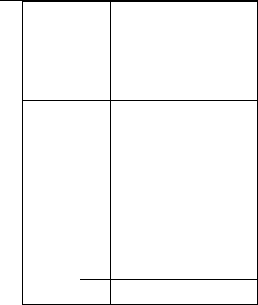
Parameter Symbol Conditions Min. Typ. Max. Unit
RX Frequency
Range FTX World Wide (Not
Supported) 2400 - 2483.5 MHz
Intermediate
frequency FLIF 1Mbps data rate,RX BW
1MHz 1 MHz
RX Sensitivity
(BER < 0.1%) PRX-1MHz
Sensitivity at 1.0 Mbps,
GFSK
∆f = ±250 kHz,
- -87 dBm
AViTA BLE MODULE
V1.0 Page 9 March 21, 2018
channel-spacing
= 2 MHz
Maximum Receiving
Power PRX-MAX - -10 - dBm
Current
Consumption IRX Synthesizer & Receiver
enabled - 16.5 - mA
RX Channel
Bandwidth BW Depends on the input data
rate - 1.0 - MHz
RSSI Resolution RESRSSI Analog RSSI 2 dB
Selectivity (For
Desired signal at
-67dBm)
C/Ico-channel Desired Ref Signal 3 dB
above sensitivity, BER <
0.1%. Interferer and
desired modulated with
the desired data rate and
channel spacing
accordingly, GFSK with
BT = 0.5
- 21 - dB
C/I1MHz - 15 - dB
C/I2MHz - -17 - dB
C/ I≧3MHz -27 dB
Blockers
( For Desired signal
at -67dBm)
PBLOCK1
Blockers from 30 to 2000
MHz - -30 - dBm
PBLOCK2
Blockers from 2003 to
2399 GHz - -35 - dBm
PBLOCK3
Blockers from 2.484 to
2.997 GHz - -35 - dBm
PBLOCK4
Blockers from 3.0 to
12.75 GHz - -30 - dBm
Table 5. Receiver Electrical Specifications
4 Software introduction
Please contact SINOWEALTH Electronic LTD. for detailed software application
documents.

AViTA BLE MODULE
V1.0 Page 10 March 21, 2018
FCC warning
Compliance Information:
This device complies with Part 15 of the FCC Rules. Operation is subject to the
following two conditions: 1. This device may not cause harmful interference, 2. This
device must accept any interference received, including interference that may cause
undesired operation. Any changes or modifications to this device not expressly
approved by AViTA Corporation. For compliance could void the user's authority to
operate the equipment.
Note:
This equipment has been tested and found to comply with the limits for a Class B
digital device, pursuant to part 15 of the FCC Rules. These limits are designed to
provide reasonable protection against harmful interference in a residential installation.
This equipment generates, uses and can radiate radio frequency energy and, if not
installed and used in accordance with the instructions, may cause harmful interference
to radio communications. However, there is no guarantee that interference will not
occur in a particular installation. If this equipment does cause harmful interference to
radio or television reception, which can be determined by turning the equipment off
and on, the user is encouraged to try to correct the interference by one or more of the
following measures:
—Reorient or relocate the receiving antenna.
—Increase the separation between the equipment and receiver.
—Connect the equipment into an outlet on a circuit different from that to which the
receiver is connected.
—Consult the dealer or an experienced technician for help.
If the module's FCC ID is not visible when installed in the host, or if the host is
marketed so that end users do not have straightforward commonly used methods for
access to remove the module so that the FCC ID of the module is visible; then an
additional permanent label referring to the enclosed module: “Contains Transmitter
Module FCC ID: UV3BMW-18XX” or “Contains FCC ID: UV3BMW-18XX” must
be used.