Adcon Telemetry A720 WIRELESS SENSOR INTERFACE User Manual A720Specs
Adcon Telemetry Inc WIRELESS SENSOR INTERFACE A720Specs
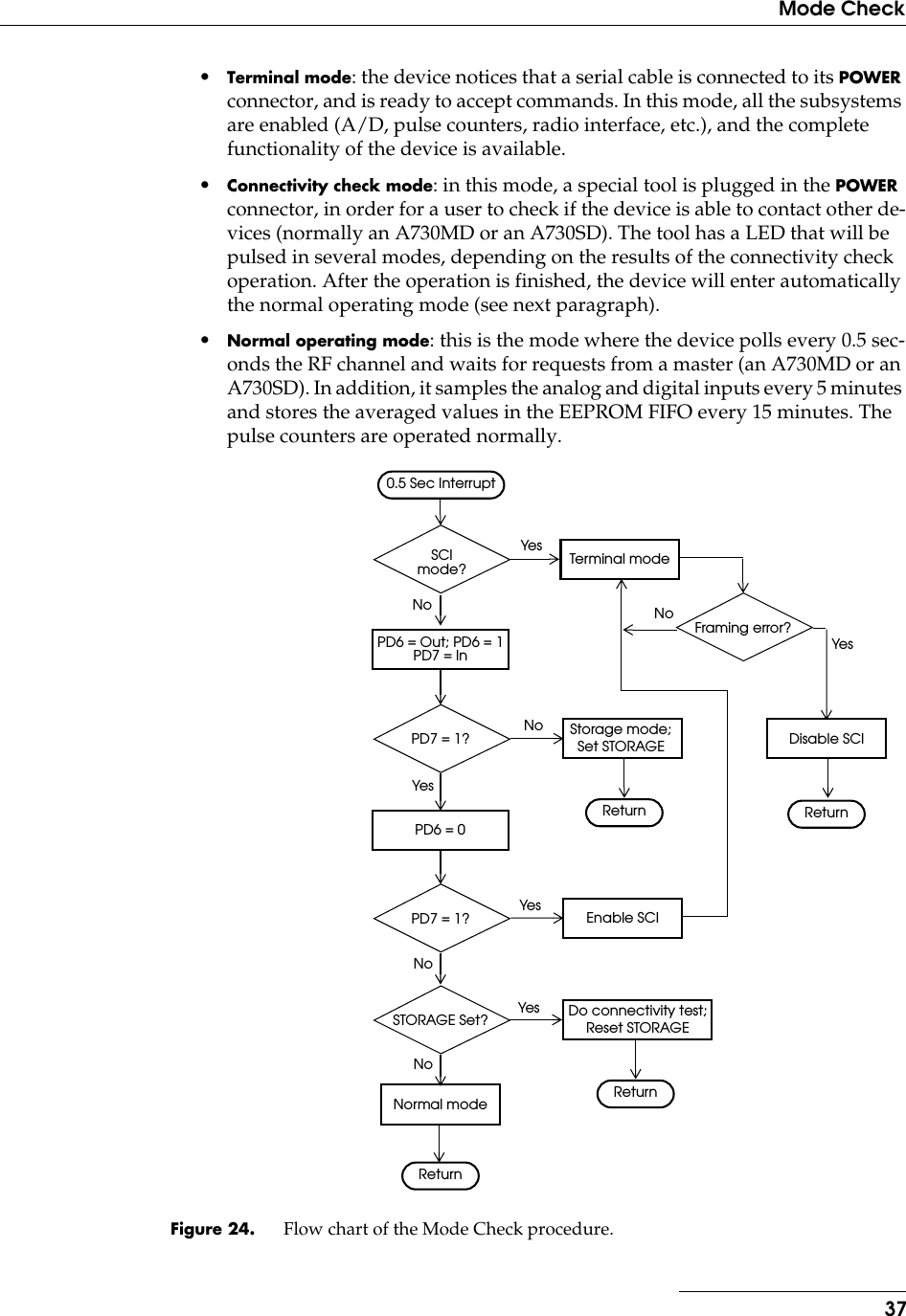
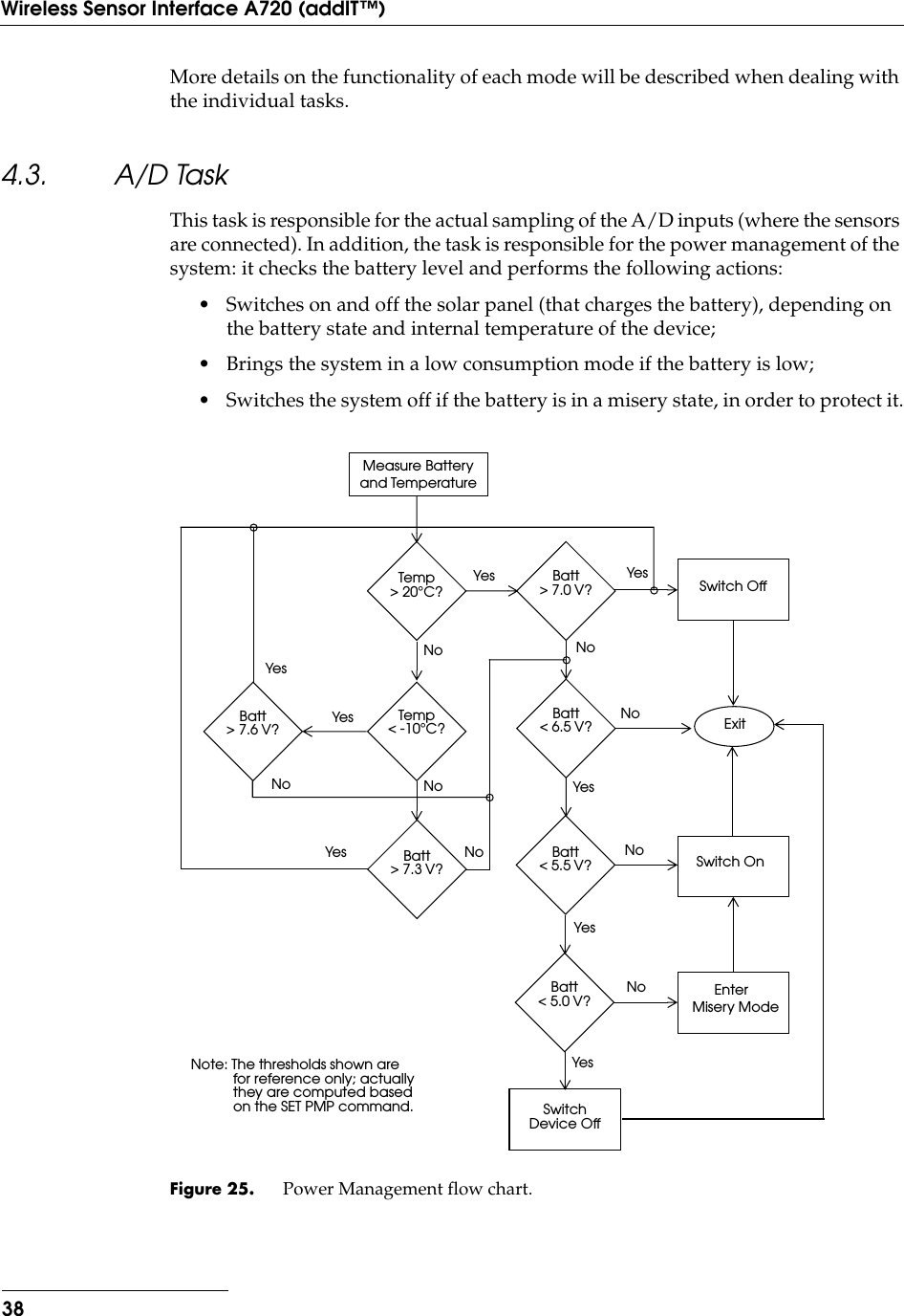
Contents
- 1. Revised Technical Manual with schematics and parts lists removed
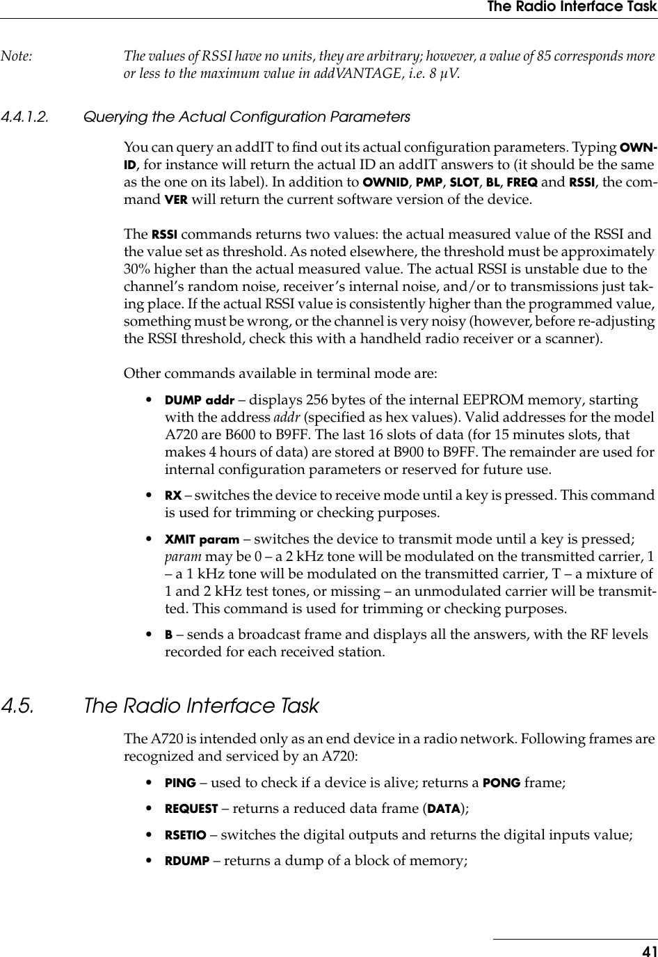
- 2. Revised technical manual with schematics and parts lists removed
Revised Technical Manual with schematics and parts lists removed
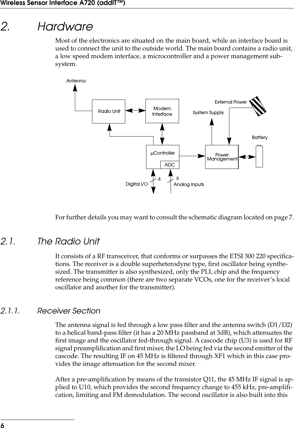
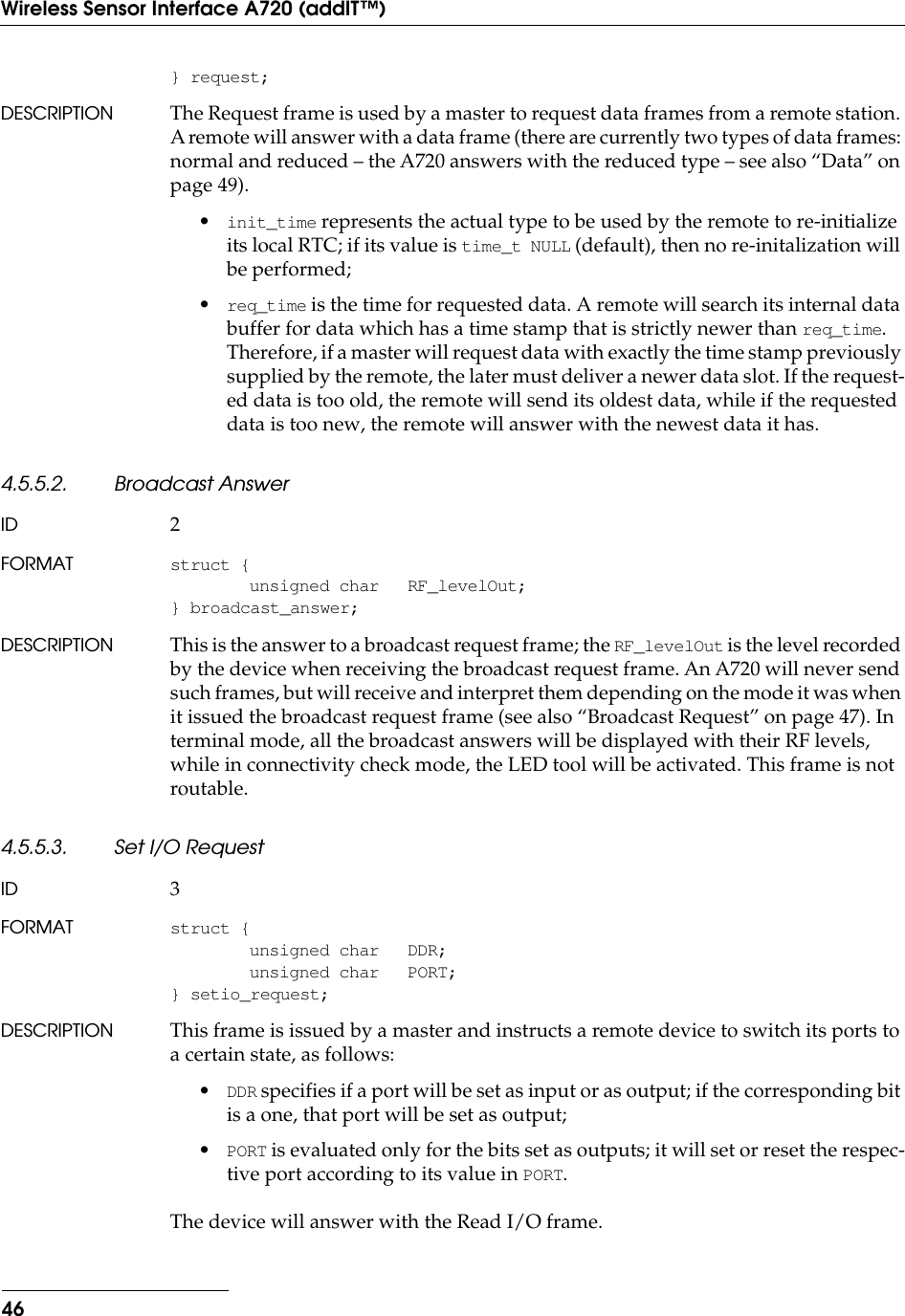
![47The Radio Interface Task4.5.5.4. Read I/O AnswerID 4FORMAT struct {unsigned char RF_levelIn;unsigned char RF_levelOut;unsigned char DDR;unsigned char PORT;} readio_answer;DESCRIPTION This is the answer to a Set I/O request frame. It returns the actual state of the port and its data direction register.4.5.5.5. Broadcast RequestID 6FORMAT The data frame body is empty.DESCRIPTION This frame is send by the device when the LED tool is inserted in the POWER connec-tor, or if the command “B” is issued in terminal mode. This frame is special in that the destination address (DST) in the header is 0. In addition, this type of frame is not routable. All the devices having received this frame must reply in a random fashion with a Broadcast answer frame.4.5.5.6. PingID 9FORMAT The data frame body is empty.DESCRIPTION This frame is used to request an answer from a device; it is used to check if the device is available. The addressed device must answer with a Pong frame. The A720 does not send such frames, but must answer to them.4.5.5.7. PongID 10FORMAT struct {unsigned char RF_levelIn;unsigned char RF_levelOut;time_t RTC;unsigned char version;unsigned char clkfail;unsigned char stackfail;unsigned char WDT;unsigned char batt;unsigned char internalTemp;time_t uptime;unsigned char reserved[4];} pong;](https://usermanual.wiki/Adcon-Telemetry/A720.Revised-Technical-Manual-with-schematics-and-parts-lists-removed/User-Guide-107020-Page-41.png)
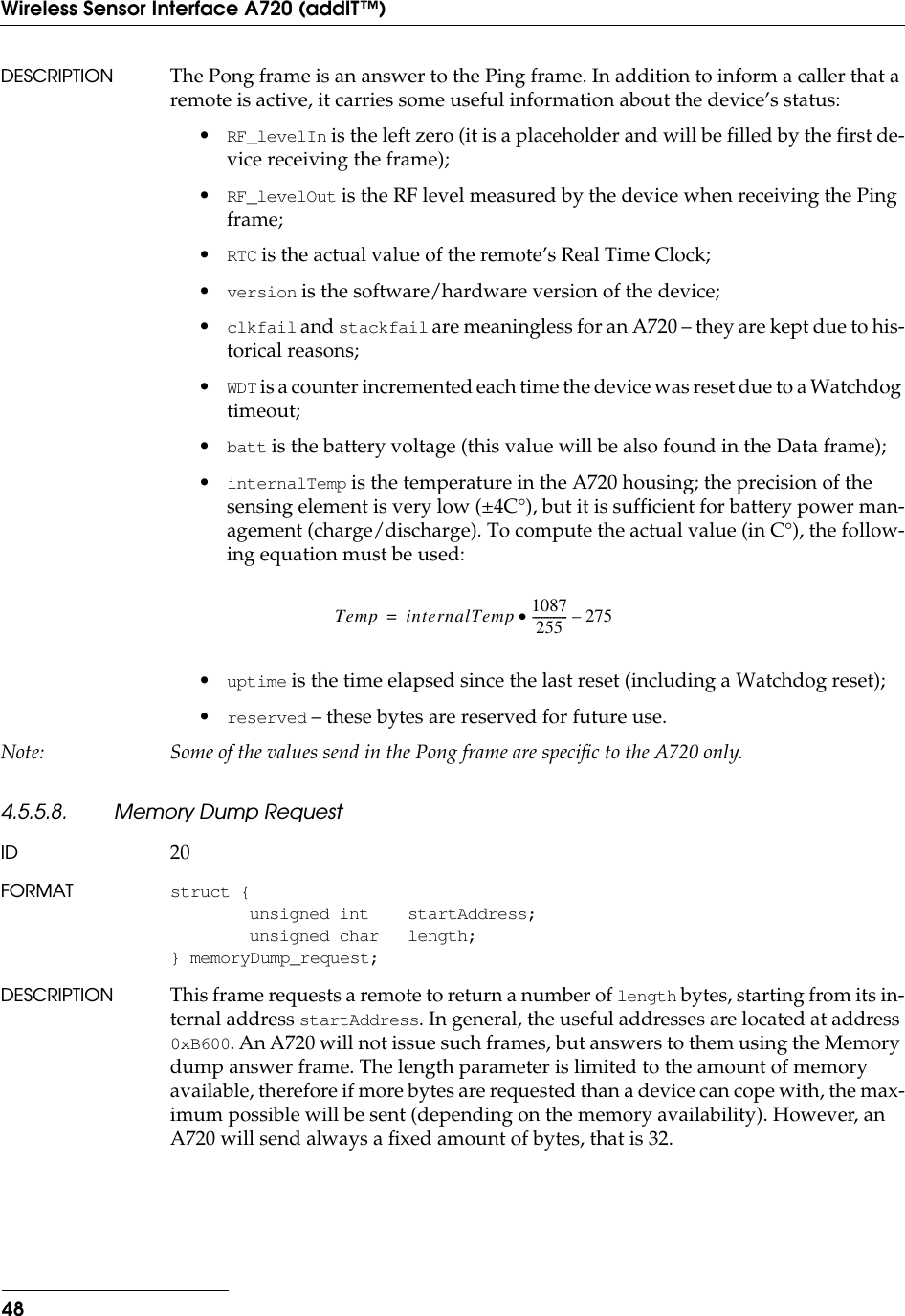
![49The Radio Interface Task4.5.5.9. Memory Dump AnswerID 21FORMAT struct {unsigned int startAddress;unsigned char 32;unsigned char data[32];} memoryDump_answer;DESCRIPTION This is the answer to a Memory dump request frame; although the frame has a flex-ible format, an A720 will always return 32 bytes of data.4.5.5.10. DataID 38FORMAT struct {unsigned char RF_levelIn;unsigned char RF_levelOut;time_t slot_timeStamp;unsigned char digibyte;unsigned char counter1; /* Pulse Counter I/O B input */unsigned char counter2; /* Pulse Counter I/O A input */unsigned char battery;unsigned char analog0; /* I/O B input, pin x */unsigned char analog1; /* I/O B input, pin x */unsigned char analog2; /* I/O B input, pin x */unsigned char analog4; /* I/O A input, pin x */unsigned char analog5; /* I/O A input, pin x */unsigned char analog6; /* I/O A input, pin x */unsigned char internalTemp; /* Internal Temperature */} data_frame;DESCRIPTION This frame will be sent back by the device as an answer to the Request frame.•RF_levelIn is the left zero (it is a placeholder and will be filled by the first de-vice receiving the frame);•RF_levelOut is the RF level measured by the device on the Request frame;•slot_timeStamp is the actual time stamp on the data sent;•digibyte represents the result of OR-ing the following bits:— RD7 represents the battery charge switch’ status;— u means undefined;— RD2, RD1 and RD0 are the DIG2, DIG1 and DIG0 pins respectively.Note: For additional info on the bits in the digibyte, check also the hardware section of this manual.•counter1 and counter2 are the values of the pulse counters;RD7 RB7 u u RB6 RD2 RD1 RD0b0b7](https://usermanual.wiki/Adcon-Telemetry/A720.Revised-Technical-Manual-with-schematics-and-parts-lists-removed/User-Guide-107020-Page-43.png)