Advanced Card Systems ACR1222U Contactless Smart Card Reader and Writer User Manual
Advanced Card Systems Limited Contactless Smart Card Reader and Writer Users Manual
Users Manual

Advanced Card Systems Ltd. Page 1 of 46
ACR1222U
Technical Specification
V1.02

Advanced Card Systems Ltd. `Page 2 of 46
Revision History
Rev
Number
Date Author Notes
V1.01 17/12/2009 Vincent Zhong
Teddy Liu
Preliminary specification for ACR1222U
V1.02 30/09/2010 Vincent Zhong
Kit Au
Added Remark on “Refresh the interface status”
command

Advanced Card Systems Ltd. Page 3 of 46
INDEX
Index .................................................................................................................................................... 3
Scopes .................................................................................................................................................. 5
Hightlights ........................................................................................................................................... 5
Terms ................................................................................................................................................... 6
Quick Overview of the ACR1222U Reader ........................................................................................ 7
1. ACR1222U (with Contact Card Option) ..................................................................................... 7
2. ACR1222U (without Contact Card Option) ................................................................................ 7
3. ACR1222U ICC Interface ........................................................................................................... 8
4. ACR1222U PICC Interface ......................................................................................................... 8
5. ACR1222U SAM Interface ......................................................................................................... 9
6. ACR1222U Firmware Upgrade Procedure ................................................................................ 10
System description ............................................................................................................................. 14
1. The Reader Block Diagram ....................................................................................................... 14
2. Communication between the PCSC Driver and the ICC, PICC & SAM .................................. 15
3. Smart Card Readers Interfaces Overview. ................................................................................ 16
Hardware Description ........................................................................................................................ 17
1. LED Indicatior ........................................................................................................................... 17
2. Buzzer ........................................................................................................................................ 17
3. USB Interface ............................................................................................................................ 18
4. ICC Interface (Contact Smart Card) .......................................................................................... 18
5. SAM Interface (Contact Smart Card) ........................................................................................ 18
6. PICC Interface (Contactless Smart Card) .................................................................................. 18
Software Description ......................................................................................................................... 19
1. TAPDUDemoCard Demo App .................................................................................................. 19
2. ACR1222U PCSC Direct Command Test ................................................................................. 20
Peripherals Control ............................................................................................................................ 21
1. Get Firmware Version ............................................................................................................... 21
2. LED Control .............................................................................................................................. 21
3. Buzzer Control ........................................................................................................................... 22
4. Default LED and Buzzer Behaviors .......................................................................................... 22
5. Refresh the Interface Status ....................................................................................................... 23
6. Set the Configure Mode ............................................................................................................. 23
7. Set the PICC Operating Parameter ............................................................................................ 24
PICC Interface Description ................................................................................................................ 25
1. ATR Generation ........................................................................................................................ 25
Pseudo APDUs for Contactless Interface .......................................................................................... 27
1. Direct Transmit .......................................................................................................................... 27
PICC Commands for General Purposes ............................................................................................ 28
1. Get Data ..................................................................................................................................... 28
PICC Commands (T=CL Emulation) for MIFare 1K/4K MEMORY Cards .................................... 29
2.1 Load Authentication Keys ....................................................................................................... 29
2.2 Authentication for MIFARE 1K/4K ........................................................................................ 30

Advanced Card Systems Ltd. `Page 4 of 46
2.3 Read Binary Blocks ................................................................................................................. 33
2.4 Update Binary Blocks .............................................................................................................. 34
2.5 Value Block Related Commands ............................................................................................. 35
2.5.1 Value Block Operation ......................................................................................................... 35
2.5.2 Read Value Block ................................................................................................................. 36
2.5.3 Restore Value Block ............................................................................................................. 37
Basic Program Flow for Contactless Applications ............................................................................ 38
1. How to access PCSC Compliant Tags (ISO14443-4)? ............................................................. 39
2. How to access DESFIRE Tags (ISO14443-4)? ......................................................................... 42
3. How to access FeliCa Tags (ISO18092)? .................................................................................. 43
4. How to access NFC Forum Type 1 Tags (ISO18092)? E.g. Jewel and Topaz Tags ................. 44
Technical Specification ..................................................................................................................... 46
Advanced Card Systems Ltd. Page 5 of 46
SCOPES
This document describes the contactless part (PICC & PCD) of the ACR1222U reader only.
HIGHTLIGHTS
The ACR1222U is a dual-interface reader (IFD and PCD) that supports both contact (ICC) and
contactless (PICC) smart cards.
• One standard ICC landing type card acceptor.
• One SAM socket is provided for highly secure applications.
• A built-in antenna for PICC contactless access applications.
• ISO 7816 Parts 1-4 Compliant for Contact Smart Card Interface.
• Intelligent Support for Hybrid Cards and Combi Cards.
• Energy saving modes for turning off the antenna field whenever the PICC is inactive, or no
PICC is found. It prevents the PICC from exposing to the field all the time.
• Contactless interface Support ISO14443 Part 4 Type A & B, MIFARE, FeliCa and NFC-1
tags.
• User-Controllable Peripherals. E.g. LED, Buzzer.
• CCID Compliant.
• PCSC Compliant for Contact, Contactless and SAM Interfaces.
• USB V2.0 Interface. (12M bps)
• Device Firmware Upgradeable through the USB Interface.

Advanced Card Systems Ltd. Page 6 of 46
TERMS
• IFD: Interface Device. A terminal, communication device, or machine to which the
integrated circuit(s) card is electrically connected during operation.
• PCD: Proximity Coupling Device. ISO 14443 Contactless Reader.
• ICC: Integrated Circuit(s) Card. Refer to a plastic card containing an integrated circuit,
which is compatible with ISO 7816.
• SAM: Security Access Module, similar to ICC but in smaller size.
• PICC: Proximity Integrated Circuit(s) Card. Contactless Cards operating without
mechanical contact to the IFD, using magnetic coupling.
• Combi-Card: A smart card that supports both ICC and PICC Interfaces. But only one
interface can be operating at any one time.
• Hybrid-Card: A smart card that consists of both ICC and PICC cards. Both ICC and PICC
cards can be operating at the same time.
• USB: Universal Serial Bus, a common device interface used in PC environment.
• CCID: The specifications for USB devices that interface with ICC or act as interfaces with
ICC/PICC.
• PCSC: Personal Computer Smart Card, a specification that can facilitate the interoperability
necessary to allow ICC/PICC technology to be effectively utilized in the PC environment.
• ISO 7816: A standard for contact smart cards (ICC).
• T=0: Character-oriented asynchronous half duplex transmission protocol for ICCs (ISO
7816).
• T=1: Block-oriented asynchronous half duplex transmission protocol for ICCs (ISO 7816).
• ISO 14443: A standard for contactless smart cards (PICC)
• T=CL: Block-oriented asynchronous half duplex transmission protocol for PICCs (ISO
14443).
• APDU: Application Protocol Data Unit.
• ATR: Answer-to-Reset. The transmission sent by an ICC to the reader (IFD) in response to
a RESET condition.
• ATS: Answer-to-Select. The transmission sent by a PICC Type A to the reader (PCD) in
response to a SELECT condition.
• ATQB: Answer-to-Request. The transmission sent by a PICC Type B to the reader (PCD)
in response to a REQUEST condition.
• Card Insertion Event: Either an ICC or a PICC is just appeared to the reader.
• Card Removal Event: Either an ICC or a PICC is removed from the reader.
Advanced Card Systems Ltd. `Page 7 of 46
QUICK OVERVIEW OF THE ACR1222U READER
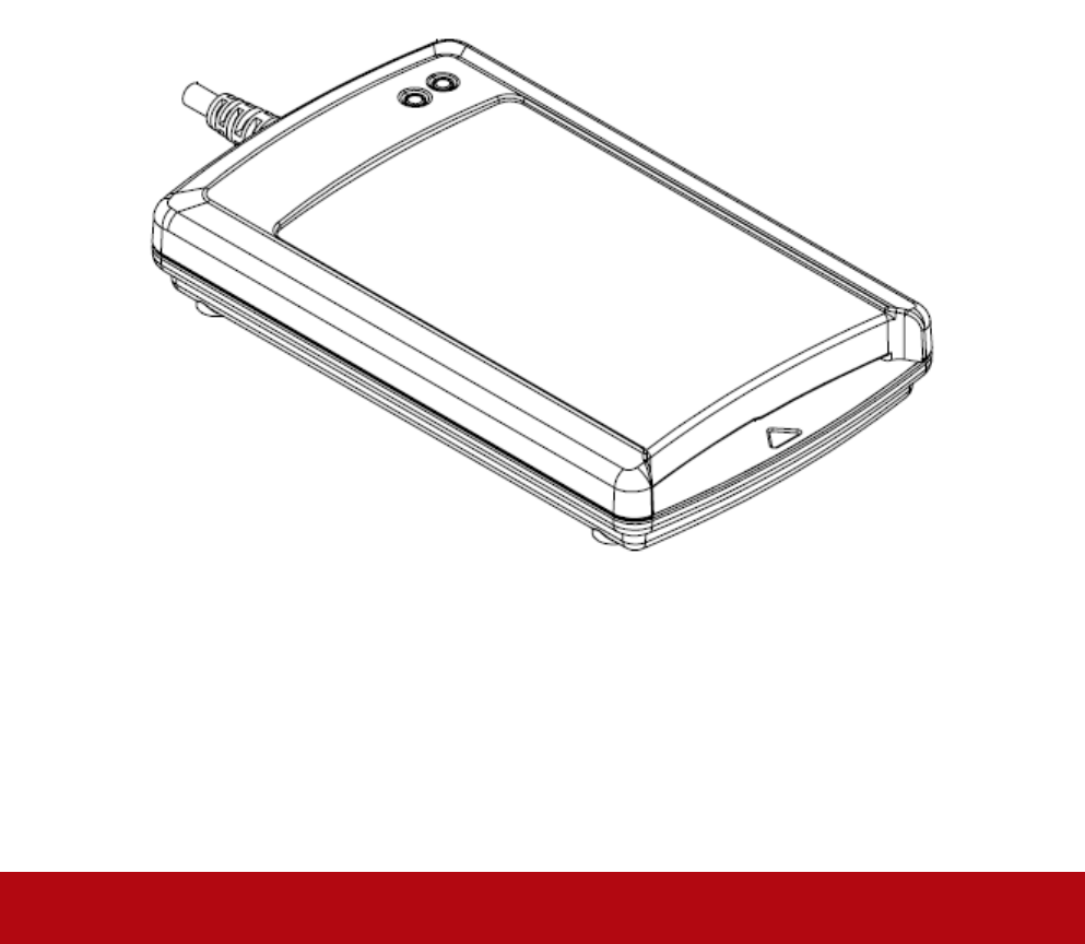
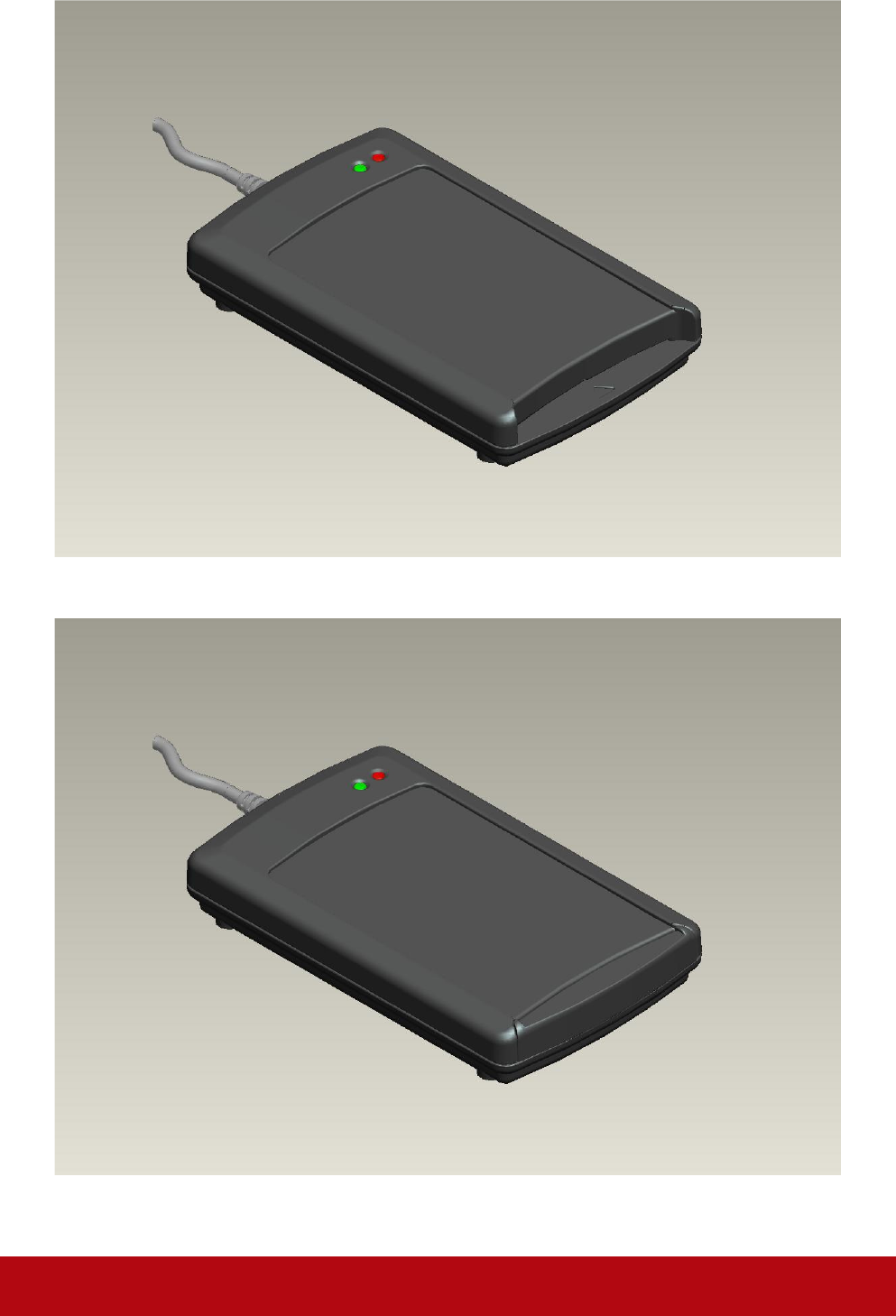
1. ACR1222U (with Contact Card Option)
2. ACR1222U (without Contact Card Option)
Advanced Card Systems Ltd. `Page 8 of 46
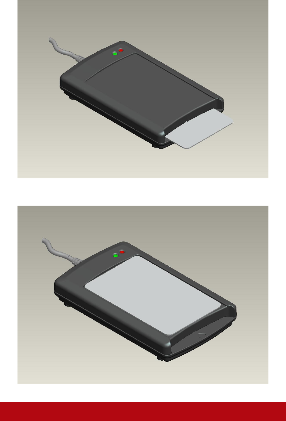
3. ACR1222U ICC Interface
4. ACR1222U PICC Interface
Advanced Card Systems Ltd. `Page 9 of 46
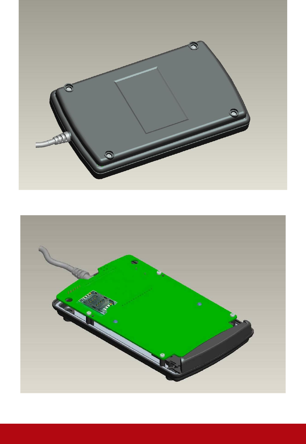
5. ACR1222U SAM Interface
Step 1: Open the plastic covers by unscrewing the four screws first
Step 2: The SAM socket is inside the reader.
Advanced Card Systems Ltd. `Page 10 of 46
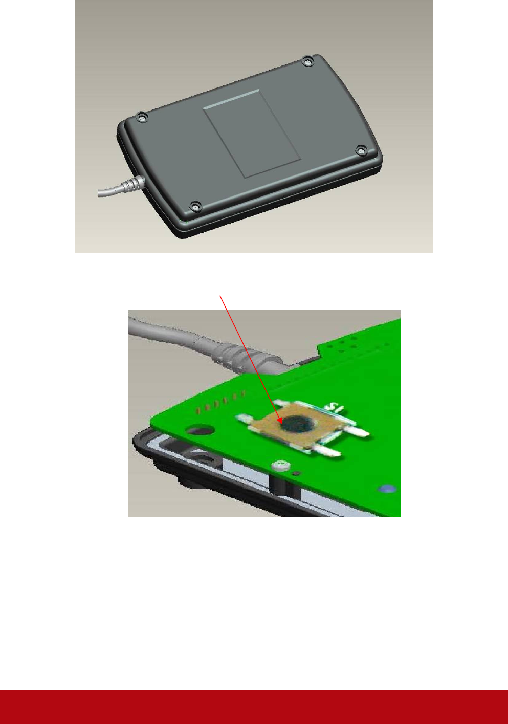
6. ACR1222U Firmware Upgrade Procedure
Step 1: Unplug the USB Cable from the PC.
Step 2: Open the plastic covers by unscrewing the four screws first.
The Button Used For Firmware Upgrade
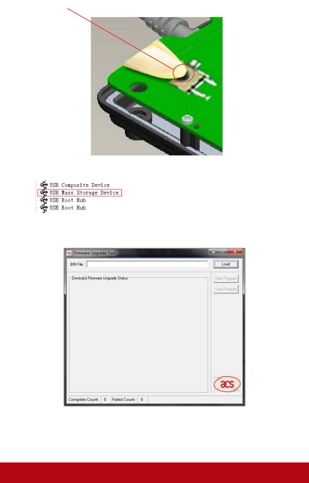
Advanced Card Systems Ltd. `Page 11 of 46
Step 3: Insert the USB plug to USB Port before pressing the button.
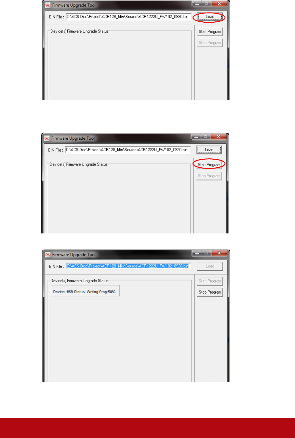
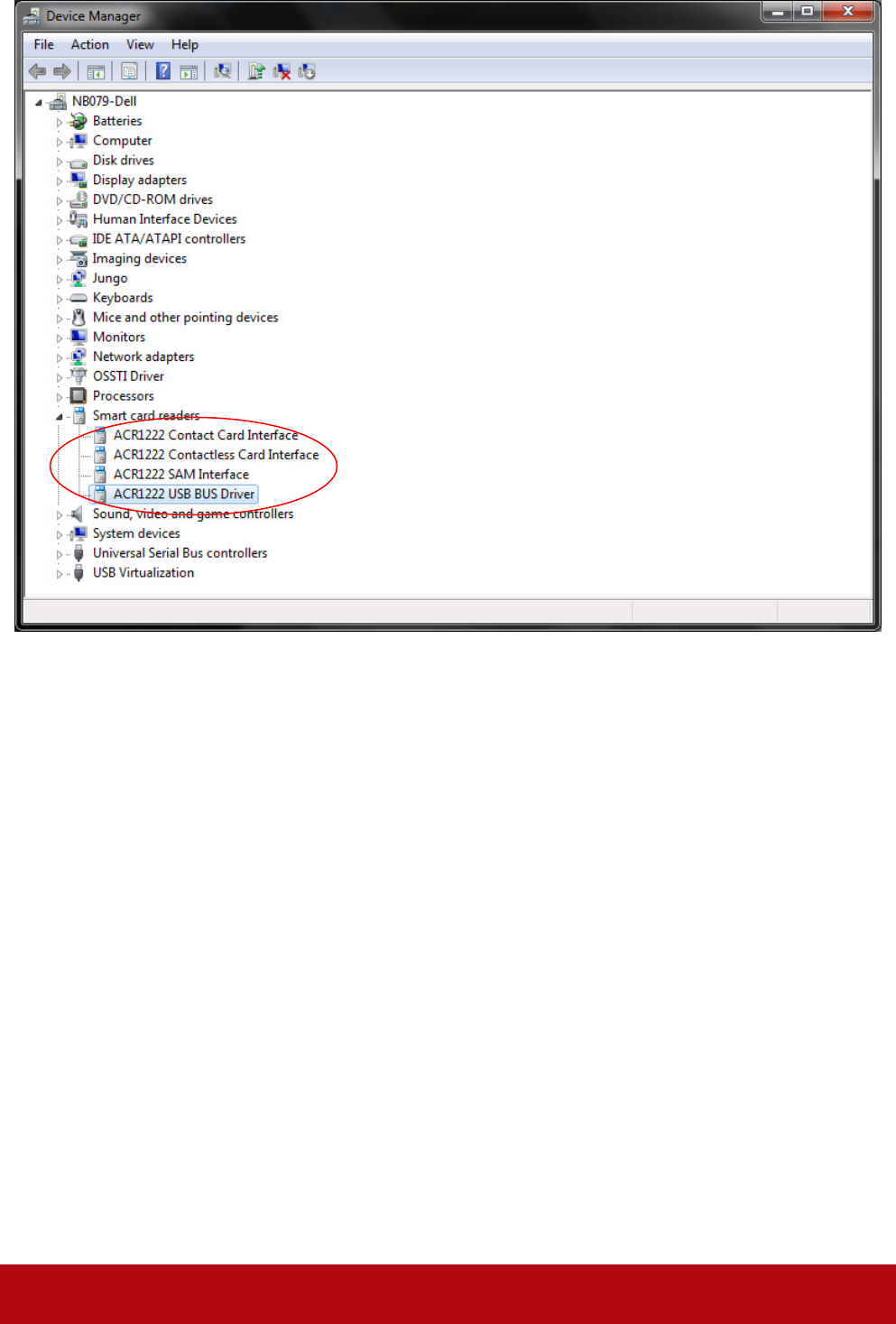
Step 4: The USB Mass Storage Device can be found in Device Manager.
Step 5: Execute the Firmware Upgrade Program:
“FW Upgrade Tool.exe”
Advanced Card Systems Ltd. `Page 12 of 46
Step 6: Pressing the “Load BIN” Button.
Select the “Firmware” file for Upload to the Reader
Step 7: Pressing the “Start Program” Button.
Start Program
The firmware is being uploaded to the reader

Advanced Card Systems Ltd. `Page 13 of 46
The firmware upgrade is completed.
Step 8: Close the plastic covers. After that, reconnect the USB cord.
Noted:
If the upgrade firmware “fail”, please repeat do from steps 3 to 7.
Advanced Card Systems Ltd. Page 14 of 46
SYSTEM DESCRIPTION
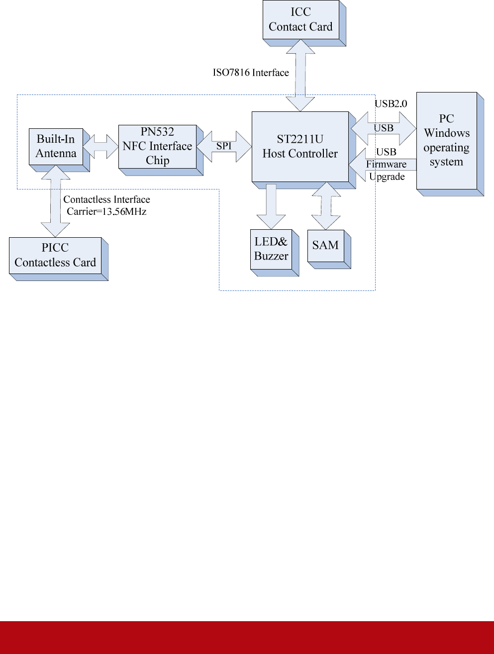
1. The Reader Block Diagram
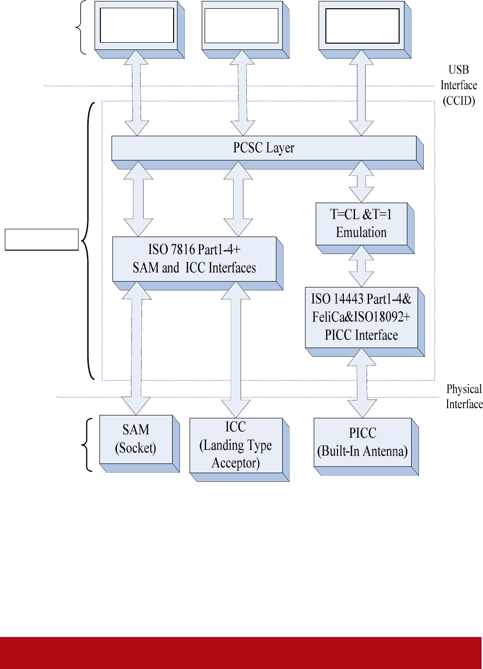
Advanced Card Systems Ltd. Page 15 of 46
2. Communication between the PCSC Driver and the ICC, PICC & SAM
ICCs
and
PICC
PCSC
Driver
ACR1222U
ACR1222U
PCSC SAM
ACR1222U
PCSC ICC
ACR1222U
PCSC PICC
Advanced Card Systems Ltd. Page 16 of 46
3. Smart Card Readers Interfaces Overview.
Advanced Card Systems Ltd. Page 17 of 46
HARDWARE DESCRIPTION
1. LED Indicatior
The LEDs are used for showing the state of the contact and contactless interfaces.The Red LED is
used for showing PICC status and Green LED for ICC.
Reader States Red LED
PICC Indicator
Green LED
ICC Indicator
1. No PICC Found or PICC present but not
activated.
A single pulse per
~ 5 seconds
2. PICC is present and activated ON
3. PICC is operating Blinking
4. ICC is present and activated ON
5. ICC is absent or not activated OFF
6. ICC is operating Blinking
2. Buzzer
A monotone buzzer is used to show the “Card Insertion” and “Card Removal” events.
Events Buzzer
1. The reader powered up and initialization
success.
Beep
2. Card Insertion Event (ICC or PICC) Beep
3. Card Removal Event (ICC or PICC) Beep

Advanced Card Systems Ltd. Page 18 of 46
3. USB Interface
The ACR1222U is connected to a computer through USB interface as specified in the USB
Specification 2.0. The ACR1222U is working in full speed mode, i.e. 12 Mbps.
USB Interface Wiring
Pin Signal Function
1 VBUS +5V power supply for the reader (~200mA)
2 D- Differential signal transmits data between ACR1222U and PC.
3 D+ Differential signal transmits data between ACR1222U and PC.
4 GND Reference voltage level for power supply
NOTE - In order for the ACR1222U functioning properly through USB interface, ACS
proprietary device drive has to be installed. Please refer to the Device Driver Installation Guide for
more details. {VID = 0x072F; PID = 0x1280}
4. ICC Interface (Contact Smart Card)
A landing type Smart Card Acceptor is used for providing reliable operations. The minimum life
cycle of the acceptor is about 300K times of card insertion and removal.
5. SAM Interface (Contact Smart Card)
One SAM socket is provided for highly secure application requirement.
6. PICC Interface (Contactless Smart Card)
A built-in antenna is used for communication between the PCD and PICC.
Advanced Card Systems Ltd. Page 19 of 46
SOFTWARE DESCRIPTION
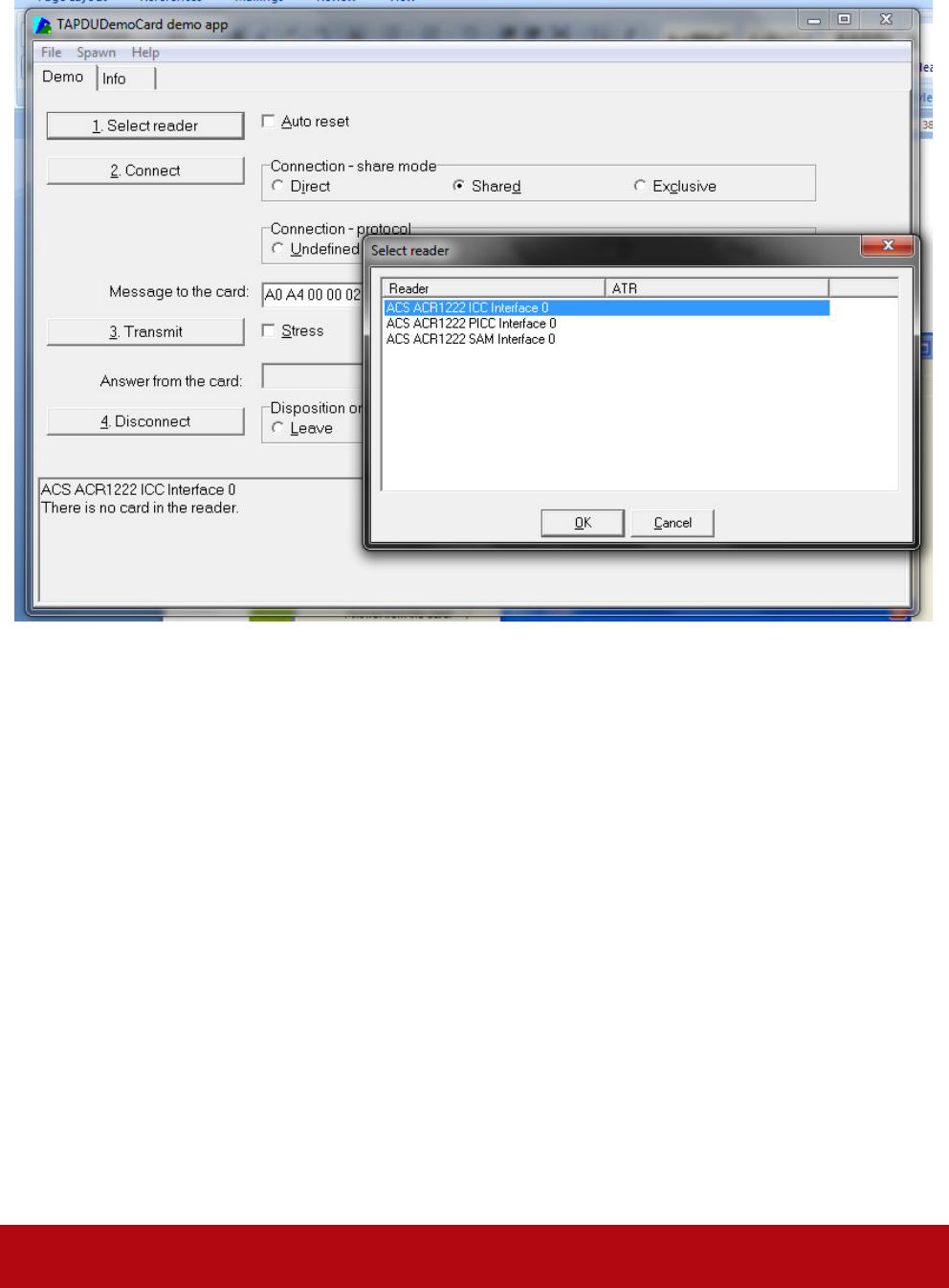
1. TAPDUDemoCard Demo App
This program is used to demonstrate the PCSC functions of the ACR1222U readers.
Operating Procedures:
1) Place a PICC on the top of the ACR1222U reader.
2) Press “1. Select Reader” and select the “ACR1222 PICC Interface”
3) Select “T1” in the connection-protocol. Press “2. Connect “to establish a connection
between the card and reader.
4) Enter the APDU in text box “Message to the card”
5) Press “3. Transmit” to send the APDU to the card.
6) Press “4. Disconnect” to terminate the connection between the card and reader.
Remarks:
The program can be used to test all the PCSC interfaces. E.g. ACR1222U ICC or SAM Interface.
Advanced Card Systems Ltd. `Page 20 of 46
2. ACR1222U PCSC Direct Command Test
This program is used to demonstrate the PCSC Escape functions of the ACR1222U readers.
Operating Procedures:
1. Select the “ACS ACR1222 SAM Interface 0”.
2. Select the “Shared Mode” if a SAM is inserted or “Direct Mode if no Sam is inserted.
3. Press the button “Connect” to establish a connection between the PC and the
ACR1222U reader.
4. Enter “2079” in the Command Text Box.
5. Enter the PCSC Escape Command, e.g. “21 01 8F” and press the button “Send” to send
the command to the reader.
6. Press the button “Disconnect” to break the connection.
Hints: “21 01 8F” is used for setting the LED and Buzzer Behaviors.
Remarks:
The program can be used to test all the PCSC interfaces. E.g. ACR1222U ICC or PICC
Interface.

Advanced Card Systems Ltd. `Page 21 of 46
PERIPHERALS CONTROL
The reader’s peripherals control is implemented by Escape Command.
1. Get Firmware Version
Command = {18 00}
Response = {E1 00 00 00 “Frame Length” {Firmware Version} }
In which, Firmware Version = 20 bytes; RFU = 10 bytes
e.g. Response = E1 00 00 00 0D 41 43 52 31 32 32 32 55 5F 56 31 30 32
Firmware Version (HEX) = 41 43 52 31 32 32 32 55 5F 56 31 30 32
Firmware Version (ASCII) = “ACR1222U_V102”
2. LED Control
Setting the LED State:
Command = {29 01 “CMD”}.
Response = {E1 00 00 00 01 “Status”}
Reading the existing LED State:
Command = {29 00}.
Response = {E1 00 00 00 01 “Status”}
CMD Bit Map
CMD Description Description
Bit 0 RED LED 1 = ON; 0 = OFF
Bit 1 GREEN LED 1 = ON; 0 = OFF
Bit 2 RFU RFU
Bit 3 RFU RFU
Bit 4 RFU RFU
Bit 5 RFU RFU
Bit 6 RFU RFU
Bit 7 RFU RFU
The “Status” bit map is the same as “CMD”.

Advanced Card Systems Ltd. Page 22 of 46
3. Buzzer Control
Setting the Buzzer State:
Command = {28 01 “Duration”} Unit = 10mS
00 = Turn off
01 – FE = Duration
FF = Turn on
Response = {E1 00 00 00 01 “Status”}
Reading the existing Buzzer State:
Command = {28 00}
Response = {E1 00 00 00 01 “Status”}
4. Default LED and Buzzer Behaviors
CMD MODE Description
Bit 0 ICC Activation Status
LED
To show the activation status of the
ICC interface.
1 = Enable; 0 =Disable
Bit 1 PICC Polling Status LED To show the PICC Polling Status.
1 = Enable; 0 =Disable
Bit 2 PICC Activation Status LED To show the activation status of the
PICC interface
1 = Enable; 0 =Disable
Bit 3 Card Insertion and Removal
Events Buzzer
To make a beep whenever a card
insertion or removal event is
detected. (For both ICC and PICC)
1 = Enable; 0 =Disabled
Bit 4 RFU RFU
Bit 5 RFU RFU
Bit 6 RFU RFU
Bit 7 Card Operation Blinking
LED
To blink the LED whenever the card
(PICC or ICC) is being accessed.
Setting the LED and Buzzer behaviors:
Command = {21 01 “CMD”}. Default value of CMD = 8F;
Response = {E1 00 00 00 01 “Status”}
Reading the existing behaviors of the LED and Buzzer:
Command = {21 00}
Response = {E1 00 00 00 01 “Status”}
Hints:
If you want to enjoy the silent environment, just set the CMD value to “87”.

Advanced Card Systems Ltd. `Page 23 of 46
5. Refresh the Interface Status
Read the existing status:
Command = {2D 00}
Response = {E1 00 00 00 01 “Interfaces refreshed”}
Refresh Interface:
Command = {2D 01 “Interfaces to be refreshed”}
Response = {E1 00 00 00 01 “Interfaces refreshed”}
<Interface No>
Bit 0 = ICC Interface
Bit 1 = PICC Interface
Bit 2 = SAM Interface
Hints: This command is useful for refreshing the SAM status after a new SAM is inserted.
(* Only Can Use if have SAM inserted before Power-up the reader*)
Example 1. Refresh the SAM status after a new SAM is inserted
Step 1. Connect the “SAM Interface” in “Direct” connection mode.
Step 2. Send the direct command “2D 01 04”
Step 3. Disconnect the “SAM Interface”
Step 4. Connect the “SAM Interface: again in either “Direct” or “Shared” connection mode.
Example 2. Refresh the ICC status (Reset the ICC)
Step 1. Connect the “SAM Interface” in “Direct” or “Shared” connection mode.
Step 2. Send the direct command “2D 01 01”
6. Set the Configure Mode
Read the existing status:
Command = {2B 00}
Response = {E1 00 00 00 01 “Configure Mode”}
Set Configure Mode:
Command = {2B 01 “Configure Mode”}
Response = {E1 00 00 00 01 “Configure Mode”}
“Configure Mode” = 00: Default Mode, enable auto antenna off when ICC reset fail even at the
same time reader access PICC with APDU exchange.
“Configure Mode” = 01: Manual Mode, disable auto antenna off when ICC reset fail when reader
access PICC with APDU exchange.

Advanced Card Systems Ltd. `Page 24 of 46
7. Set the PICC Operating Parameter
This command is used to control the PICC Operating Parameter of the reader.
Read the existing status:
Command = {20 00}
Response = {E1 00 00 00 01 “PICC Operating Parameter”}
Setting the PICC Operating Parameter:
Command = {20 01 “CMD”}
Response = {E1 00 00 00 01 “PICC Operating Parameter”}
PICC Operating Parameter. Default Value = FF
CMD
Parameter Description Option
Bit0
ISO14443 Type A
#To detect the MIFARE
Tags, the Auto ATS
Generation must be
disabled first.
The Tag Types to be detected during
PICC Polling.
1 = Detect
0 = Skip
Bit1 ISO14443 Type B 1 = Detect
0 = Skip
Bit2 Topaz 1 = Detect
0 = Skip
Bit3 FeliCa 212K 1 = Detect
0 = Skip
Bit4 FeliCa 424K 1 = Detect
0 = Skip
Bit5 Polling Interval To set the time interval between
successive PICC Polling.
1 = 250 ms
0 = 500 ms
Bit6 Auto ATS Generation To issue ATS Request whenever an
ISO14443-4 Type A tag is activated
1 = Enable
0 = Disable
Bit7 Auto PICC Polling To enable the PICC Polling 1 = Enable
0 = Disable
Advanced Card Systems Ltd. Page 25 of 46
PICC INTERFACE DESCRIPTION
1. ATR Generation
If the reader detects a PICC, an ATR will be sent to the PCSC driver for identifying the PICC.
1.1 ATR format for ISO 14443 Part 3 PICCs.
Byte
Value
(Hex)
Designation Description
0 3B Initial Header
1 8N T0 Higher nibble 8 means: no TA1, TB1, TC1
only TD1 is following.
Lower nibble N is the number of historical
bytes (HistByte 0 to HistByte N-1)
2 80 TD1 Higher nibble 8 means: no TA2, TB2, TC2
only TD2 is following.
Lower nibble 0 means T = 0
3 01 TD2 Higher nibble 0 means no TA3, TB3, TC3,
TD3 following.
Lower nibble 1 means T = 1
4
To
3+N
80 T1 Category indicator byte, 80 means A status
indicator may be present in an optional
COMPACT-TLV data object
4F Tk Application identifier Presence Indicator
0C Length
RID Registered Application Provider Identifier
(RID) # A0 00 00 03 06
SS Byte for standard
C0 .. C1 Bytes for card name
00 00 00 00
RFU RFU # 00 00 00 00
4+N UU TCK Exclusive-oring of all the bytes T0 to Tk
e.g. ATR for MIFare 1K = {3B 8F 80 01 80 4F 0C A0 00 00 03 06 03 00 01 00 00 00 00 6A}
Length (YY) = 0x0C
RID = {A0 00 00 03 06} (PC/SC Workgroup)
Standard (SS) = 03 (ISO14443A, Part 3)
Card Name (C0 .. C1) = {00 01} (MIFare 1K)
Card Name (C0 .. C1)
00 01: Mifare 1K
00 02: Mifare 4K
00 03: Mifare Ultralight
00 26: Mifare Mini
F0 04: Topaz and Jewel
F0 11: FeliCa 212K
F0 12: FeliCa 424K
FF 28: JCOP 30
FF [SAK]: undefined tags

Advanced Card Systems Ltd. `Page 26 of 46
1.2 ATR format for ISO 14443 Part 4 PICCs.
Byte
Value
(Hex)
Designation Description
0 3B Initial Header
1 8N T0 Higher nibble 8 means: no TA1, TB1, TC1
only TD1 is following.
Lower nibble N is the number of historical
bytes (HistByte 0 to HistByte N-1)
2 80 TD1 Higher nibble 8 means: no TA2, TB2, TC2
only TD2 is following.
Lower nibble 0 means T = 0
3 01 TD2 Higher nibble 0 means no TA3, TB3, TC3,
TD3 following.
Lower nibble 1 means T = 1
4
to
3 + N
XX T1 Historical Bytes:
ISO14443A:
The historical bytes from ATS response. Refer
to the ISO14443-4 specification.
ISO14443B:
The higher layer response from the ATTRIB
response (ATQB). Refer to the ISO14443-3
specification.
XX
XX
XX
Tk
4+N UU TCK Exclusive-oring of all the bytes T0 to Tk
E.g 1. ATR for DESFire = { 3B 81 80 01 80 80 } // 6 bytes of ATR
Hint: Use the APDU “FF CA 01 00 00” to distinguish the ISO14443A-4 and ISO14443B-4 PICCs,
and retrieve the full ATS if available. ISO14443A-3 or ISO14443B-3/4 PICCs do have ATS
returned.
APDU Command = FF CA 01 00 00
APDU Response = 06 75 77 81 02 80 90 00
ATS = {06 75 77 81 02 80}
E.g 2. ATR for ST19XRC8E = { 3B 8C 80 01 50 12 23 45 56 12 53 54 4E 33 81 C3 55}
// 12 bytes of ATQB, No CRC-B
ATQB = {50 12 23 45 56 12 53 54 4E 33 81 C3}

Advanced Card Systems Ltd. Page 27 of 46
PSEUDO APDUS FOR CONTACTLESS INTERFACE
ACR1222U comes with two primitive commands for this purpose. <Class 0xFF>
1. Direct Transmit
To send a Pseudo APDU (PN532 and TAG Commands), and the Response Data will be returned.
Table 1.0A: Direct Transmit Command Format (Length of the PN532_TAG Command + 5 Bytes)
Command
Class INS P1 P2 Lc Data In
Direct
Transmit
0xFF 0x00 0x00 0x00
Number
of Bytes
to send
PN532_TAG
Command
Lc: Number of Bytes to Send (1 Byte)
Maximum 255 bytes.
Data In: PN532_TAG Command
The data to be sent to the PN532 and Tag.
Table 1.0B: Direct Transmit Response Format (Response Length + 2 Bytes)
Response
Data Out
Result
PN532_TAG
Response
SW1 SW2
Data Out: PN532_TAG Response
PN532_TAG Response returned by the reader.
Data Out: SW1 SW2
Status Code returned by the reader.
Table 1.0C: Status Code
Results
SW1 SW2 Meaning
Success 90 00 The operation is completed
successfully.
Error
63 00 The operation is failed.
Checksum
Error
63 27 The checksum of the Response is
wrong.

Advanced Card Systems Ltd. Page 28 of 46
PICC COMMANDS FOR GENERAL PURPOSES
1. Get Data
The “Get Data command” will return the serial number or ATS of the “connected PICC”.
Table 1.1-1a: Get UID APDU Format (5 Bytes)
Command
Class INS P1 P2 Le
Get Data FF CA 00
01
00 00
(Max
Length)
Table 2.1-1b: Get UID Response Format (UID + 2 Bytes) if P1 = 0x00
Response
Data Out
Result
UID
(LSB)
UID
(MSB)
SW1 SW2
Table 2.1-1c: Get ATS of a ISO 14443 A card (ATS + 2 Bytes) if P1 = 0x01
Response
Data Out
Result
ATS SW1 SW2
Table 2.1-1d: Response Codes
Results
SW1 SW2 Meaning
Success 90 00 The operation is completed successfully.
Warning 62 82 End of UID/ATS reached before Le bytes
(Le is greater than UID Length).
Error 6C XX Wrong length (wrong number Le: ‘XX’
encodes the exact number) if Le is less
than the available UID length.
Error 63 00 The operation is failed.
Error 6A 81 Function not supported
Examples:
// To get the serial number of the “connected PICC”
UINT8 GET_UID[5]={0xFF, 0xCA, 0x00, 0x00, 0x00};
// To get the ATS of the “connected ISO 14443 A PICC”
UINT8 GET_ATS[5]={0xFF, 0xCA, 0x01, 0x00, 0x00};
Advanced Card Systems Ltd. `Page 29 of 46
PICC COMMANDS (T=CL EMULATION) FOR MIFARE 1K/4K MEMORY CARDS
2.1 Load Authentication Keys
The “Load Authentication Keys command” will load the authentication keys into the reader. The
authentication keys are used to authenticate the particular sector of the Mifare 1K/4K Memory Card.
Two kinds of authentication key locations are provided, volatile and non-volatile key locations
respectively.
Table 2.1-1a: Load Authentication Keys APDU Format (11 Bytes)
Command
Class INS P1 P2 Lc Data In
Load
Authentication
Keys
FF 82 Key
Structure
Key
Number
06 Key
(6 bytes)
Key Structure (1 Byte):
0x00 = Key is loaded into the reader volatile memory.
Other = Reserved.
Key Number (1 Byte):
0x00 ~ 0x01 = Key Location. The keys will be disappeared once the reader is disconnected from
the PC.
Key (6 Bytes):
The key value loaded into the reader. E.g. {FF FF FF FF FF FF}
Table 2.1-1b: Load Authentication Keys Response Format (2 Bytes)
Response
Data Out
Result
SW1 SW2
Table 2.1-1c: Load Authentication Keys Response Codes
Results
SW1 SW2 Meaning
Success 90 00 The operation is completed
successfully.
Error
63 00 The operation is failed.
Examples:
// Load a key {FF FF FF FF FF FF} into the key location 0x00.
APDU = {FF 82 00 00 06 FF FF FF FF FF FF}

Advanced Card Systems Ltd. `Page 30 of 46
2.2 Authentication for MIFARE 1K/4K
The “Authentication command” uses the keys stored in the reader to do authentication with the
MIFARE 1K/4K card (PICC). Two types of authentication keys are used, TYPE_A and TYPE_B
respectively.
Table 2.2-1a: Load Authentication Keys APDU Format (6 Bytes) #Obsolete
Command
Class INS P1 P2 P3 Data In
Authentication
FF 88 00 Block
Number
Key
Type
Key Number
Table 2.2-1b: Load Authentication Keys APDU Format (10 Bytes)
Command
Class INS P1 P2 Lc Data In
Authentication
FF 86 00 00 05 Authenticate Data
Bytes
Authenticate Data Bytes (5 Byte):
Byte1
Byte 2
Byte 3 Byte 4
Byte 5
Version
0x01
0x00 Block
Number
Key
Type
Key
Number
Block Number (1 Byte):
The memory block to be authenticated.
For MIFARE 1K Card, it has totally 16 sectors and each sector consists of 4 consecutive blocks.
E.g. Sector 0x00 consists of Blocks {0x00, 0x01, 0x02 and 0x03}; Sector 0x01 consists of Blocks
{0x04, 0x05, 0x06 and 0x07}; the last sector 0x0F consists of Blocks {0x3C, 0x3D, 0x3E and
0x3F}. Once the authentication is done successfully, there is no need to do the authentication again
provided that the blocks to be accessed are belonging to the same sector. Please refer to the
MIFARE 1K/4K specification for more details.
#Once the block is authenticated successfully, all the blocks belonging to the same sector are
accessible.
Key Type (1 Byte):
0x60 = Key is used as a TYPE A key for authentication.
0x61 = Key is used as a TYPE B key for authentication.
0x00 ~ 0x01 = Key Location.
Table 2.2-1b: Load Authentication Keys Response Format (2 Bytes)
Response
Data Out
Result
SW1 SW2
Advanced Card Systems Ltd. `Page 31 of 46
Table 2.2-1c: Load Authentication Keys Response Codes
Results
SW1 SW2 Meaning
Success 90 00 The operation is completed
successfully.
Error
63 00 The operation is failed.
MIFARE 1K Memory Map.
Sectors
(Total 16 sectors. Each
sector consists of 4
consecutive blocks)
Data Blocks
(3 blocks, 16 bytes
per block)
Trailer Block
(1 block, 16 bytes)
Sector 0 0x00 ~ 0x02 0x03
Sector 1 0x04 ~ 0x06 0x07
..
..
Sector 14 0x38 ~ 0x0A 0x3B
Sector 15 0x3C ~ 0x3E 0x3F
MIFARE 4K Memory Map.
Sectors
(Total 32 sectors. Each
sector consists of 4
consecutive blocks)
Data Blocks
(3 blocks, 16 bytes
per block)
Trailer Block
(1 block, 16 bytes)
Sector 0 0x00 ~ 0x02 0x03
Sector 1 0x04 ~ 0x06 0x07
..
..
Sector 30 0x78 ~ 0x7A 0x7B
Sector 31 0x7C ~ 0x7E 0x7F
Sectors
(Total 8 sectors. Each
sector consists of 16
consecutive blocks)
Data Blocks
(15 blocks, 16 bytes
per block)
Trailer Block
(1 block, 16 bytes)
Sector 32 0x80 ~ 0x8E 0x8F
Sector 33 0x90 ~ 0x9E 0x9F
..
..
Sector 38 0xE0 ~ 0xEE 0xEF
Sector 39 0xF0 ~ 0xFE 0xFF
1K
Byte
s
2K
Bytes
2K
Bytes
Advanced Card Systems Ltd. `Page 32 of 46
Examples:
// To authenticate the Block 0x04 with a {TYPE A, key number 0x00}.
// PC/SC V2.01, Obsolete
APDU = {FF 88 00 04 60 00};
<Similarly>
// To authenticate the Block 0x04 with a {TYPE A, key number 0x00}.
// PC/SC V2.07
APDU = {FF 86 00 00 05 01 00 04 60 00}
Hints:
MIFARE Ultralight does not need to do any authentication. The memory is free to access.
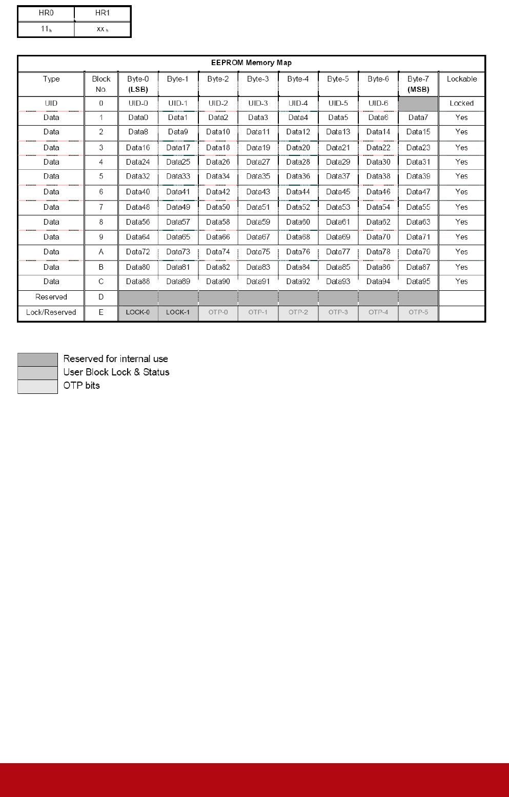
MIFARE Ultralight Memory Map.
Byte Number
0 1 2 3 Page
Serial Number
SN0 SN1 SN2 BCC0 0
Serial Number
SN3 SN4 SN5 SN6 1
Internal / Lock
BCC1 Internal Lock0 Lock1 2
OTP OPT0 OPT1 OTP2 OTP3 3
Data read/write
Data0 Data1 Data2 Data3 4
Data read/write
Data4 Data5 Data6 Data7 5
Data read/write
Data8 Data9 Data10 Data11 6
Data read/write
Data12 Data13 Data14 Data15 7
Data read/write
Data16 Data17 Data18 Data19 8
Data read/write
Data20 Data21 Data22 Data23 9
Data read/write
Data24 Data25 Data26 Data27 10
Data read/write
Data28 Data29 Data30 Data31 11
Data read/write
Data32 Data33 Data34 Data35 12
Data read/write
Data36 Data37 Data38 Data39 13
Data read/write
Data40 Data41 Data42 Data43 14
Data read/write
Data44 Data45 Data46 Data47 15
512 bits
Or
64 bytes

Advanced Card Systems Ltd. Page 33 of 46
2.3 Read Binary Blocks
The “Read Binary Blocks command” is used for retrieving a multiple of “data blocks” from the
PICC. The data block/trailer block must be authenticated first before executing the “Read Binary
Blocks command”.
Table 2.3-1a: Read Binary APDU Format (5 Bytes)
Command
Class INS P1 P2 Le
Read Binary
Blocks
FF B0 00 Block
Number
Number
of Bytes
to Read
Block Number (1 Byte):
The starting block.
Number of Bytes to Read (1 Byte):
Multiply of 16 bytes for MIFARE 1K/4K or Multiply of 4 bytes for MIFARE Ultralight
• Maximum 16 bytes for MIFARE Ultralight.
• Maximum 48 bytes for MIFARE 1K. (Multiple Blocks Mode; 3 consecutive blocks)
• Maximum 240 bytes for MIFARE 4K. (Multiple Blocks Mode; 15 consecutive blocks)
Example 1: 0x10 (16 bytes). The starting block only. (Single Block Mode)
Example 2: 0x40 (64 bytes). From the starting block to starting block+3. (Multiple Blocks Mode)
#For safety reason, the Multiple Block Mode is used for accessing Data Blocks only. The Trailer
Block is not supposed to be accessed in Multiple Blocks Mode. Please use Single Block Mode to
access the Trailer Block.
Table 2.3-1b: Read Binary Block Response Format (Multiply of 4/16 + 2 Bytes)
Response
Data Out
Result
Data (Multiply of 4/16 Bytes)
SW1 SW2
Table 2.3-1c: Read Binary Block Response Codes
Results
SW1 SW2 Meaning
Success 90 00 The operation is completed
successfully.
Error
63 00 The operation is failed.
Examples:
// Read 16 bytes from the binary block 0x04 (MIFARE 1K or 4K)
APDU = {FF B0 00 04 10}
// Read 240 bytes starting from the binary block 0x80 (MIFARE 4K)
// Block 0x80 to Block 0x8E (15 blocks)
APDU = {FF B0 00 80 F0}

Advanced Card Systems Ltd. `Page 34 of 46
2.4 Update Binary Blocks
The “Update Binary Blocks command” is used for writing a multiple of “data blocks” into the
PICC. The data block/trailer block must be authenticated first before executing the “Update Binary
Blocks command”.
Table 2.3-1a: Update Binary APDU Format (Multiple of 16 + 5 Bytes)
Command
Class INS P1 P2 Lc Data In
Update Binary
Blocks
FF D6 00 Block
Number
Number
of Bytes
to
Update
Block Data
(Multiple of 16
Bytes)
Block Number (1 Byte):
The starting block to be updated.
Number of Bytes to Update (1 Byte):
• Multiply of 16 bytes for MIFARE 1K/4K or 4 bytes for MIFARE Ultralight.
• Maximum 48 bytes for MIFARE 1K. (Multiple Blocks Mode; 3 consecutive blocks)
• Maximum 240 bytes for MIFARE 4K. (Multiple Blocks Mode; 15 consecutive blocks)
Example 1: 0x10 (16 bytes). The starting block only. (Single Block Mode)
Example 2: 0x30 (48 bytes). From the starting block to starting block+2. (Multiple Blocks Mode)
#For safety reason, the Multiple Block Mode is used for accessing Data Blocks only. The Trailer
Block is not supposed to be accessed in Multiple Blocks Mode. Please use Single Block Mode to
access the Trailer Block.
Block Data (Multiply of 16 + 2 Bytes, or 6 bytes):
The data to be written into the binary block/blocks.
Table 2.3-1b: Update Binary Block Response Codes (2 Bytes)
Results
SW1 SW2 Meaning
Success 90 00 The operation is completed
successfully.
Error
63 00 The operation is failed.
Examples:
// Update the binary block 0x04 of MIFARE 1K/4K with Data {00 01 .. 0F}
APDU = {FF D6 00 04 10 00 01 02 03 04 05 06 07 08 09 0A 0B 0C 0D 0E 0F}
// Update the binary block 0x04 of MIFARE Ultralight with Data {00 01 02 03}
APDU = {FF D6 00 04 04 00 01 02 03}

Advanced Card Systems Ltd. Page 35 of 46
2.5 Value Block Related Commands
The data block can be used as value block for implementing value-based applications.
2.5.1 Value Block Operation
The “Value Block Operation command” is used for manipulating value-based transactions. E.g.
Increment a value of the value block etc.
Table 2.5.1-1a: Value Block Operation APDU Format (10 Bytes)
Command
Class INS P1 P2 Lc Data In
Value Block
Operation
FF D7 00 Block
Number
05 VB_OP
VB_Value
(4 Bytes)
{MSB .. LSB}
Block Number (1 Byte):
The value block to be manipulated.
VB_OP (1 Byte):
0x00 = Store the VB_Value into the block. The block will then be converted to a value block.
0x01 = Increment the value of the value block by the VB_Value. This command is only valid for
value block.
0x02 = Decrement the value of the value block by the VB_Value. This command is only valid for
value block.
VB_Value (4 Bytes):
The value used for value manipulation. The value is a signed long integer (4 bytes).
E.g. 1: Decimal –4 = {0xFF, 0xFF, 0xFF, 0xFC}
VB_Value
MSB LSB
FF FF FF FC
E.g. 2: Decimal 1 = {0x00, 0x00, 0x00, 0x01}
VB_Value
MSB LSB
00 00 00 01
Table 2.5.1-1b: Value Block Operation Response Format (2 Bytes)
Response
Data Out
Result SW1 SW2
Table 2.5.1-1c: Value Block Operation Response Codes
Results
SW1 SW2 Meaning
Success 90 00 The operation is completed
successfully.
Error
63 00 The operation is failed.
Advanced Card Systems Ltd. `Page 36 of 46
2.5.2 Read Value Block
The “Read Value Block command” is used for retrieving the value from the value block. This
command is only valid for value block.
Table 2.5.2-1a: Read Value Block APDU Format (5 Bytes)
Command
Class INS P1 P2 Le
Read Value
Block
FF B1 00 Block
Number
00
Block Number (1 Byte):
The value block to be accessed.
Table 2.5.2-1b: Read Value Block Response Format (4 + 2 Bytes)
Response
Data Out
Result
Value
{MSB .. LSB}
SW1 SW2
Value (4 Bytes):
The value returned from the card. The value is a signed long integer (4 bytes).
E.g. 1: Decimal –4 = {0xFF, 0xFF, 0xFF, 0xFC}
Value
MSB LSB
FF FF FF FC
E.g. 2: Decimal 1 = {0x00, 0x00, 0x00, 0x01}
Value
MSB LSB
00 00 00 01
Table 2.5.3-1c: Read Value Block Response Codes
Results
SW1 SW2 Meaning
Success 90 00 The operation is completed
successfully.
Error
63 00 The operation is failed.

Advanced Card Systems Ltd. Page 37 of 46
2.5.3 Restore Value Block
The “Restore Value Block command” is used to copy a value from a value block to another value
block.
Table 2.5.3-1a: Restore Value Block APDU Format (7 Bytes)
Command
Class INS P1 P2 Lc Data In
Value Block
Operation
FF D7 00 Source
Block
Number
02 03 Target
Block
Number
Source Block Number (1 Byte): The value of the source value block will be copied to the target
value block.
Target Block Number (1 Byte): The value block to be restored. The source and target value
blocks must be in the same sector.
Table 2.5.3-1b: Restore Value Block Response Format (2 Bytes)
Response
Data Out
Result
SW1 SW2
Table 2.5.3-1c: Restore Value Block Response Codes
Results
SW1 SW2 Meaning
Success 90 00 The operation is completed
successfully.
Error
63 00 The operation is failed.

Advanced Card Systems Ltd. `Page 38 of 46
Examples:
// Store a value “1” into block 0x05
APDU = {FF D7 00 05 05 00 00 00 00 01}
// Read the value block 0x05
APDU = {FF B1 00 05 00}
// Copy the value from value block 0x05 to value block 0x06
APDU = {FF D7 00 05 02 03 06}
// Increment the value block 0x05 by “5”
APDU = {FF D7 00 05 05 01 00 00 00 05}
BASIC PROGRAM FLOW FOR CONTACTLESS APPLICATIONS
Step 0. Start the application. The reader will do the PICC Polling and scan for tags continuously.
Once the tag is found and detected, the corresponding ATR will be sent to the PC.
Step 1. Connect the “ACR1222U PICC Interface” with T=1 protocol.
Step 2. Access the PICC by exchanging APDUs.
Step 2. Access the PICC by exchanging APDUs.
..
Step N. Disconnect the “ACR1222U PICC Interface”. Shut down the application.
Remarks:
1) The antenna can be switched off in order to save the power.
• Turn off the antenna power: FF 00 00 00 04 D4 32 01 00
• Turn on the antenna power: FF 00 00 00 04 D4 32 01 01

Advanced Card Systems Ltd. Page 39 of 46
1. How to access PCSC Compliant Tags (ISO14443-4)?
Basically, all ISO 14443-4 complaint cards (PICCs) would understand the ISO 7816-4 APDUs.
The ACR1222U Reader just has to communicate with the ISO 14443-4 complaint cards through
exchanging ISO 7816-4 APDUs and Responses. ACR1222U will handle the ISO 14443 Parts 1-4
Protocols internally.
MIFARE 1K, 4K, MINI and Ultralight tags are supported through the T=CL emulation. Just simply
treat the MIFARE tags as standard ISO14443-4 tags. For more information, please refer to topic
“PICC Commands for MIFARE Classic Memory Tags”
Table 3.1-1a: ISO 7816-4 APDU Format
Command Class INS P1 P2 Lc Data In
Le
ISO 7816 Part
4 Command
Length
of the
Data In
Expected
length of
the
Response
Data
Table 3.1-1b: ISO 7816-4 Response Format (Data + 2 Bytes)
Response
Data Out
Result
Response Data SW1 SW2
Table 3.1-1c: Common ISO 7816-4 Response Codes
Results
SW1 SW2 Meaning
Success 90 00 The operation is completed
successfully.
Error
63 00 The operation is failed.

Advanced Card Systems Ltd. Page 40 of 46
Typical sequence may be:
- Present the Tag and Connect the PICC Interface
- Read / Update the memory of the tag
Step 1) Connect the Tag
The ATR of the tag is 3B 8C 80 01 50 00 05 70 3B 00 00 00 00 33 81 81 20
In which,
The ATQB = 50 00 05 70 3B 00 00 00 00 33 81 81. It is an ISO14443-4 Type B tag.
Step 2) Send an APDU, Get Challenge.
<< 00 84 00 00 08
>> 1A F7 F3 1B CD 2B A9 58 [90 00]
Hint:
For ISO14443-4 Type A tags, the ATS can be obtained by using the APDU “FF CA 01 00 00”

Advanced Card Systems Ltd. Page 41 of 46
For Example: ISO7816-4 APDU
// To read 8 bytes from an ISO 14443-4 Type B PICC (ST19XR08E)
APDU ={80 B2 80 00 08}
Class = 0x80
INS = 0xB2
P1 = 0x80
P2 = 0x00
Lc = None
Data In = None
Le = 0x08
Answer: 00 01 02 03 04 05 06 07 [$9000]

Advanced Card Systems Ltd. Page 42 of 46
2. How to access DESFIRE Tags (ISO14443-4)?
The DESFIRE supports ISO7816-4 APDU Wrapping and Native modes. Once the DESFire Tag is
activated, the first APDU sent to the DESFire Tag will determine the “Command Mode”. If the first
APDU is “Native Mode”, the rest of the APDUs must be in “Native Mode” format. Similarly, If the
first APDU is “ISO7816-4 APDU Wrapping Mode”, the rest of the APDUs must be in “ISO7816-4
APDU Wrapping Mode” format.
Example 1: DESFIRE ISO7816-4 APDU Wrapping.
// To read 8 bytes random number from an ISO 14443-4 Type A PICC (DESFIRE)
APDU = {90 0A 00 00 01 00 00}
Class = 0x90; INS = 0x0A (DESFire Instruction); P1 = 0x00; P2 = 0x00
Lc = 0x01; Data In = 0x00; Le = 0x00 (Le = 0x00 for maximum length)
Answer: 7B 18 92 9D 9A 25 05 21 [$91AF]
# Status Code{91 AF} is defined in DESFIRE specification. Please refer to the DESFIRE
specification for more details.
Example 2: DESFIRE Frame Level Chaining (ISO 7816 wrapping mode)
// In this example, the application has to do the “Frame Level Chaining”.
// To get the version of the DESFIRE card.
Step 1: Send an APDU {90 60 00 00 00} to get the first frame. INS=0x60
Answer: 04 01 01 00 02 18 05 91 AF [$91AF]
Step 2: Send an APDU {90 AF 00 00 00} to get the second frame. INS=0xAF
Answer: 04 01 01 00 06 18 05 91 AF [$91AF]
Step 3: Send an APDU {90 AF 00 00 00} to get the last frame. INS=0xAF
Answer: 04 52 5A 19 B2 1B 80 8E 36 54 4D 40 26 04 91 00 [$9100]

Advanced Card Systems Ltd. `Page 43 of 46
Example 3: DESFIRE Native Command.
// We can send Native DESFire Commands to the reader without ISO7816 wrapping if we find that
the Native DESFire Commands are more easier to handle.
// To read 8 bytes random number from an ISO 14443-4 Type A PICC (DESFIRE)
APDU = {0A 00}
Answer: AF 25 9C 65 0C 87 65 1D D7[$1DD7]
In which, the first byte “AF” is the status code returned by the DESFire Card.
The Data inside the blanket [$1DD7] can simply be ignored by the application.
Example 4: DESFIRE Frame Level Chaining (Native Mode)
// In this example, the application has to do the “Frame Level Chaining”.
// To get the version of the DESFIRE card.
Step 1: Send an APDU {60} to get the first frame. INS=0x60
Answer: AF 04 01 01 00 02 18 05[$1805]
Step 2: Send an APDU {AF} to get the second frame. INS=0xAF
Answer: AF 04 01 01 00 06 18 05[$1805]
Step 3: Send an APDU {AF} to get the last frame. INS=0xAF
Answer: 00 04 52 5A 19 B2 1B 80 8E 36 54 4D 40 26 04[$2604]
Hints:
In DESFIRE Native Mode, the status code [90 00] will not be added to the response if the response
length is greater than 1. If the response length is less than 2, the status code [90 00] will be added in
order to meet the requirement of PCSC. The minimum response length is 2.
3. How to access FeliCa Tags (ISO18092)?
Typical sequence may be:
- Present the FeliCa Tag and Connect the PICC Interface
- Read / Update the memory of the tag
Step 1) Connect the Tag
The ATR = 3B 8F 80 01 80 4F 0C A0 00 00 03 06 03 F0 11 00 00 00 00 8A
In which,
F0 11 = FeliCa 212K
Step 2) Read the memory block without using Pseudo APDU.
<< 10 06 [8-byte NFC ID] 01 09 01 01 80 00
>> 1D 07 [8-byte NFC ID] 00 00 01 00 AA 55 AA 55 AA 55 AA 55 AA 55 AA 55 AA 55
AA [90 00]
Or
Step 2) Read the memory block using Pseudo APDU.
<< FF 00 00 00 [13] D4 40 01 10 06 [8-byte NFC ID] 01 09 01 01 80 00
In which,

Advanced Card Systems Ltd. `Page 44 of 46
[13] is the length of the Pseudo Data “D4 40 01.. 80 00”
D4 40 01 is the Data Exchange Command
>> D5 41 00 1D 07 [8-byte NFC ID] 00 00 01 00 AA 55 AA 55 AA 55 AA 55 AA 55 AA
55 AA 55 AA [90 00]
In which, D5 41 00 is the Data Exchange Response
Hint:
The NFC ID can be obtained by using the APDU “FF CA 00 00 00”
#please refer to the FeliCa specification for more detailed information.
4. How to access NFC Forum Type 1 Tags (ISO18092)? E.g. Jewel and Topaz
Tags
Typical sequence may be:
- Present the Topaz Tag and Connect the PICC Interface
- Read / Update the memory of the tag
Step 1) Connect the Tag
The ATR = 3B 8F 80 01 80 4F 0C A0 00 00 03 06 03 F0 04 00 00 00 00 9F
In which,
F0 04 = Topaz
Step 2) Read the memory address 08 (Block 1: Byte-0) without using Pseudo APDU
<< 01 08
>> 18 [90 00]
In which, Response Data = 18
Or
Step 2) Read the memory address 08 (Block 1: Byte-0) using Pseudo APDU
<< FF 00 00 00 [05] D4 40 01 01 08
In which,
[05] is the length of the Pseudo APDU Data “D4 40 01 01 08”
D4 40 01 is the DataExchange Command.
01 08 is the data to be sent to the tag.
>> D5 41 00 18 [90 00]
In which, Response Data = 18
Tip: To read all the memory content of the tag
<< 00
>> 11 48 18 26 .. 00 [90 00]
Step 3) Update the memory address 08(Block 1: Byte-0)with the data FF
<< 53 08 FF
>> FF [90 00]
In which, Response Data = FF
Topaz Memory Map.
Memory Address = Block No * 8 + Byte No
e.g. Memory Address 08 (hex) = 1 x 8 + 0 = Block 1: Byte-0 = Data0
e.g. Memory Address 10 (hex) = 2 x 8 + 0 = Block 2: Byte-0 = Data8
Advanced Card Systems Ltd. `Page 45 of 46
#please refer to the Jewel and Topaz specification for more detailed information.
FCC Warning:
Any Changes or modifications not expressly approved by the party responsible for compliance
could void the user's authority to operate the equipment.
This device complies with part 15 of the FCC Rules. Operation is subject to the following two conditions:
(1) This device may not cause harmful interference, and
(2) this device must accept any interference received, including interference that may cause
undesired operation.
Advanced Card Systems Ltd. Page 46 of 46
TECHNICAL SPECIFICATION
Universal Serial Bus Interface
Power source ........................................ From USB
Speed ................................................... 12 Mbps (Full Speed)
Supply Voltage ...................................... Regulated 5V DC
Supply Current ..................................... 200mA (max); 100mA (normal)
Contactless Smart Card Interface
Standard ............................................... ISO 14443 A & B Parts 1-4
Protocol ................................................ ISO14443 T=CL for ISO14443-4 compliant cards and T=CL Emulation for MIFARE 1K/4K,
FeliCa, ISO18092.
Smart card read / write speed ............... 106 kbps for ISO14443 Type A & Type B, 212 kbps and 424 kbps for FeliCa,
Contact Smart Card Interface
Standard ............................................... ISO 7816 1/2/3, Class A, B (5V, 3V), T=0 and T=1
Supply current ....................................... max. 60mA
Smart card read / write speed ............... 9,600 – 115,200 bps
Short circuit protection ......................... +5V / GND on all pins
CLK frequency ...................................... 3.58 MHz
Card connector ..................................... Landing
Card insertion cycles ............................. min. 300,000
SAM Card Interface
Standard SAM Socket
Case
Dimensions ........................................... 120.48 mm (L) x 71.97 mm (W) x 20.4 mm (H)
Material ................................................. ABS
Color ..................................................... Metallic Silver Grey
Antenna
Antenna Size ........................................ 65mm x 60mm
Operating distance ................................ up to 50 mm
Operating Frequency for Contactless Cards Access
Operating Frequency ............................ 13.56 MHz
Built-in peripherals
Monotone buzzer
Dual-Color LED
Operating Conditions
Temperature ......................................... 0 - 50° C
Humidity ................................................ 10% - 80%
Cable Connector
Length................................................... 1m (USB)
Standard/Certifications
CE, FCC
OS
Windows 98, ME, 2K, XP
OEM
OEM-Logo possible, customer-specific colors, casing, and card connector