Advanced Card Systems ACR122L Contactless Smart Card Reader and Writer User Manual
Advanced Card Systems Limited Contactless Smart Card Reader and Writer Users Manual
Users Manual

Advanced Card Systems Ltd. Website: www.acs.com.hk
Email:
info@acs.com.hk
A
AC
CR
R1
12
22
2L
L-
-A
AC
CS
S
Design Specification
ACR122L-ACS Design Specification
Version 0.03 19/05/2010
Page
2
of
50
ACR122L
-
ACS
Revision History
Version
Date Prepared By Description
V0.01 16.Oct.2009 Macross Ng, Kit Au Initial Release
V0.02 23.Nov.2009 Updated LCD command
V0.03 19.May.2010 Macross Ng Update the product photo
V0.04 20.Sept.2010
Macross Ng Add the Technical Specification

ACR122L-ACS Design Specification
Version 0.03 19/05/2010
Page
3
of
50
ACR122L
-
ACS
Table of Contents
1.0.
Introduction .............................................................................................................4
2.0.
Feature .....................................................................................................................5
3.0.
Hardware Interfaces ................................................................................................6
3.1.
Serial Interface .............................................................................................................................6
3.2.
LEDs.............................................................................................................................................6
3.3.
Buzzer ..........................................................................................................................................6
3.4.
SAM Interface...............................................................................................................................6
3.5.
LCD ..............................................................................................................................................6
3.6.
Built-in Antenna ............................................................................................................................6
4.0.
Implementation........................................................................................................7
4.1.
The ACR122L is built based on the AC1038-2, AC1038s and PN5321 chips.............................7
4.2.
Communication between the Host and the Contactless interface, SAM and Peripherals. ..........8
5.0.
Serial Interface (CCID-liked FRAME Format) .........................................................9
5.1.
Direct Transmit ...........................................................................................................................18
5.2.
Pseudo APDU for LEDs and Buzzer Control .............................................................................24
5.3.
Pseudo APDU for LEDs Control Enable ....................................................................................30
5.4.
Pseudo APDU for LEDs Control ................................................................................................30
5.5.
Pseduo APDU for Buzzer Control ..............................................................................................31
5.6.
Pseudo APDU for Clear LCD .....................................................................................................32
5.7.
Pseudo APDU for LCD Display (ASCII Mode)...........................................................................33
5.8.
Pseudo APDU for LCD Display (GB Mode) ...............................................................................35
5.9.
Pseudo APDU for LCD Display (Graphic Mode)........................................................................36
5.10.
Pseudo APDU for Scrolling LCD Current Display ................................................................37
5.11.
Pseudo APDU for Pause LCD Scrolling ...............................................................................38
5.12.
Pseudo APDU for Stop LCD Scrolling ..................................................................................39
5.13.
Pseudo APDU for LCD Contrast Control ..............................................................................39
5.14.
Pseudo APDU for LCD Backlight Control .............................................................................40
5.15.
Pseudo APDU for changing the communication speed........................................................41
5.16.
Get the Firmware Version of the reader ...............................................................................47
5.17.
Basic Program Flow for FeliCa Applications ........................................................................48
6.0.
Mechanical Design ................................................................................................49
7.0.
TECHNICAL SPECIFICATION ...............................................................................50

ACR122L-ACS Design Specification
Version 0.03 19/05/2010
Page
4
of
50
ACR122L
-
ACS
1.0. Introduction
The ACR122L is a module for accessing both contact and contactless cards with LCD Display. It can
support 3 SAMs access and ISO14443 Part 4 Type A & B, MIFARE, FeliCa and NFC tags.

ACR122L-ACS Design Specification
Version 0.03 19/05/2010
Page
5
of
50
ACR122L
-
ACS
2.0. Feature
• Serial Interface. Baud Rate = 9600 bps (default) or 115200 bps, 8-N-1. Initial Baud Rate is
determined by the existence of R12. A command is also provided for changing the baud rate
while the reader is running.
• CCID-liked Frame Format.
• Support ISO14443 Part 4 Type A & B, MIFARE, FeliCa and NFC tags.
• Built-in Antenna for contactless tags access.
• Support ISO7816 T=0 cards. (SAM Socket)
• 3 X SAM Interface
• 4 LEDs.
• Buzzer.
ACR122L-ACS Design Specification
Version 0.03 19/05/2010
Page
6
of
50
ACR122L
-
ACS
3.0. Hardware Interfaces
3.1. Serial Interface
The ACR122L is connected to a Host through the RS232C Serial Interface at 9600 bps and 115200
bps. 8-N-1
Pin Signal Function
1 VCC +5V power supply for the reader (Max 200mA, Normal 100mA)
2 TXD The signal from the reader to the host.
3 RXD The signal from the host to the reader.
4 GND Reference voltage level for power supply
3.2. LEDs
• 4 x User-controllable single color LEDs
• Can select control by firmware or by User
• From Left to right, the color of the LED is: Green, Blue, Yellow and Red
3.3. Buzzer
• User-controllable Mono-Tone buzzer.
• The default Buzzer State is OFF
3.4. SAM Interface
• 3 x SAMs socket is provided.
• Support ISO7816 Parts 1-3 T=0 cards
3.5. LCD
• User-controllable LCD
• User-controllable Yellow-Green Backlight
• 2 Line x 16 Character, 5 x 8 dot matrix, STN Yellow Green LCD Type
• 6 O’clock view angle
3.6. Built-in Antenna
• 3 turns symmetric loop antenna. Center tapped.
• The estimated size = 46mm x 64mm.
• The loop inductance should be around ~ 1.6uH to 2.5uH
• Operating Distance for different Tags ~ up to 50mm (depend on the Tag)
• Only one Tag can be accessed at any one time.

ACR122L-ACS Design Specification
Version 0.03 19/05/2010
Page
7
of
50
ACR122L
-
ACS
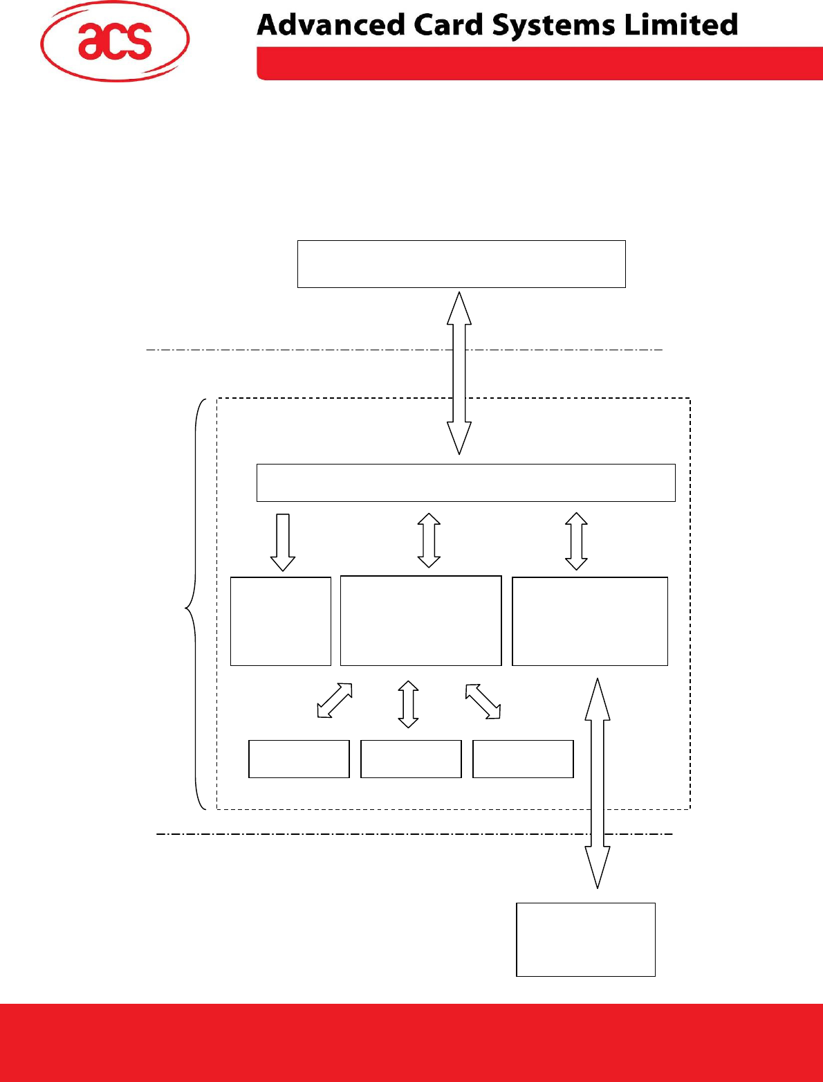
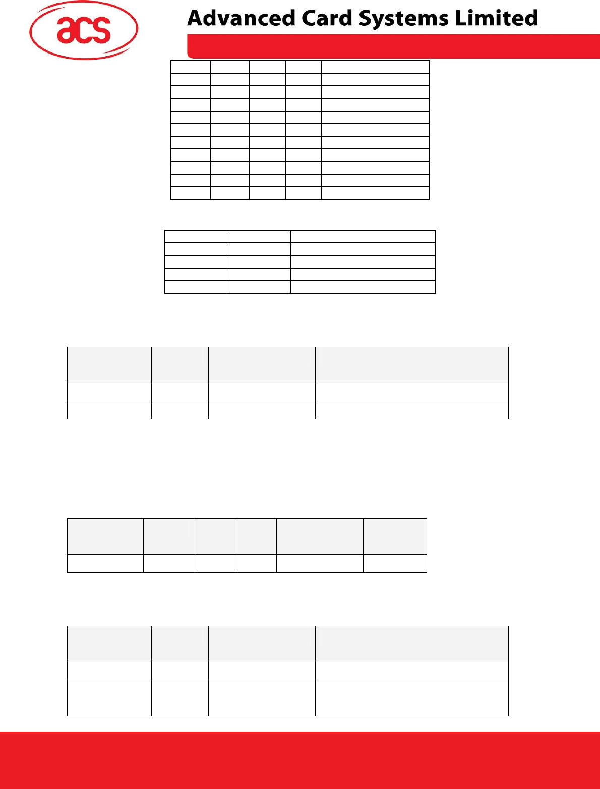
4.0. Implementation
4.1. The ACR122L is built based on the AC1038-2, AC1038s and
PN5321 chips.
PN5321
NFC Interface
Chip
AC1038-2
Controller
Built-In
Antenna
Host
Controller
Serial
Interface
9600 bps
Contactless
Tag
Contactless Interface
Carrier = 13.56MHz
Serial Interface
115200 Kbps
Figure 1.ACR122L System Block Diagram
SAM 1
<Peripherals>
- 4 x LEDs
- Buzzer
- LCD
- I/O Ports
AC1038
Controller
SAM 2
AC1038
Controller
SAM 3
Main
Controller
Second SAM
Controller
Third SAM
Controller
ACR122L-ACS Design Specification
Version 0.03 19/05/2010
Page
8
of
50
ACR122L
-
ACS
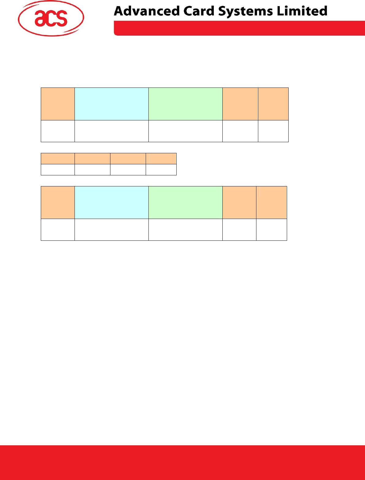
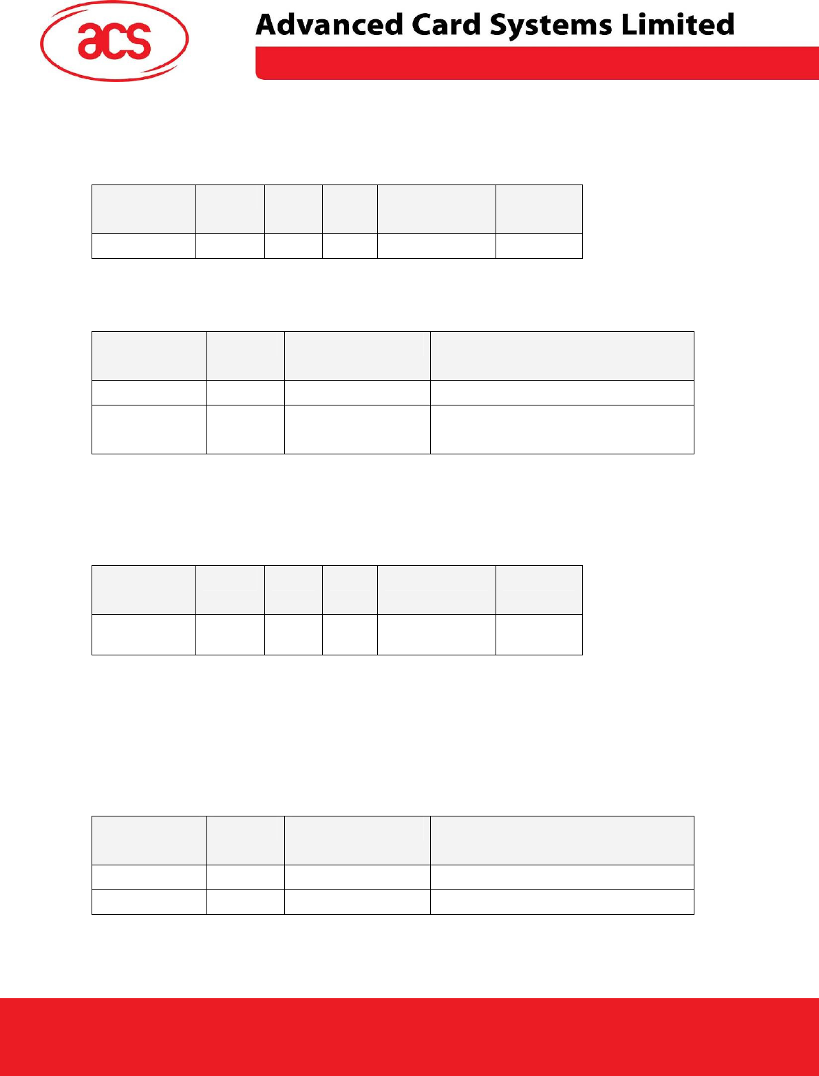
4.2. Communication between the Host and the Contactless
interface, SAM and Peripherals.
The Contactless interface & Peripherals are accessed through the use of Pseduo-APDUs.
The SAM interface are accessed through the use of standard APDUs.
Serial
Interface
(CCID-liked
protocol)
ISO 7816 Parts 1-3
+
T=0 SAM Interfaces
Contactless
Interface
SAM 1
Contactless Tag
(Built-In Antenna)
Host
ACR122L
PCSC Layer
Peripherals
SAM 3 SAM 2
RF
Interface
ACR122L-ACS Design Specification
Version 0.03 19/05/2010
Page
9
of
50
ACR122L
-
ACS
5.0. Serial Interface (CCID-liked FRAME Format)
Communication setting: 9600 bps, 8-N-1
The communication protocol between the Host and ACR122L is very similar to the CCID protocol.
ACR122L Command Frame Format
STX Bulk-OUT Header APDU Command
Or
Parameters
Checksum
ETX
1 Byte 10 Bytes M Bytes
(If applicable)
1 Byte 1 Byte
ACR122L Status Frame Format
STX Status Checksun ETX
1 Byte 1 Byte 1 Byte 1 Byte
ACR122L Response Frame Format
STX Bulk-IN Header APDU Response
Or
abData
Checksun
ETX
1 Byte 10 Bytes N Bytes
(If applicable)
1 Byte 1 Byte
Checksum = XOR {Bulk-OUT Header, APDU Command or Parameters}
Checksum = XOR {Bulk-IN Header, APDU Response or abData}
For control SAM Socket 1, the STX must be equal to 0x02 and ETX must be equal to 0x03.
For control SAM Socket 2, the STX must be equal to 0x12 and ETX must be equal to 0x13.
For control SAM Socket 3, the STX must be equal to 0x22 and ETX must be equal to 0x23.
For control access contactless interface, peripherals (i.e. LEDs, LCD and Buzzer), the STX must be
equal to 0x02 and ETX must be equal to 0x03, which is the same with control SAM Socket1.
In general, we would make use of three types of Bulk-OUT Header.
• HOST_to_RDR_IccPowerOn: To activate the SAM interface. The ATR of the SAM will be
returned if available.
• HOST_to_RDR_IccPowerOff: To deactivate the SAM interface.
• HOST_to_RDR_XfrBlock: To exchange APDUs between the Host and ACR122L.
#The SAM1 interface must be activated in order to use the Contactless interface and Peripherals. In
short, all the APDUs are exchanged through the SAM1 Interface.
Similarly, two types of Bulk-IN Header are used.
• RDR_to_HOST_DataBlock: In response to the “HOST_to_RDR_IccPowerOn” and
“HOST_to_RDR_XfrBlock” Frames.
• RDR_to_HOST_SlotStatus: In response to the “HOST_to_RDR_IccPowerOff” Frame.
ACR122L-ACS Design Specification
Version 0.03 19/05/2010
Page
10
of
50
ACR122L
-
ACS
RDR = ACR122L; HOST = Host Controller.
HOST_to_RDR = Host Controller -> ACR122L
RDR_to_HOST = ACR122L -> Host Controller
Protocol Flow Examples(Use SAM Interface 1 as Example)
1) Activate a SAM
HOST
RDR
1. HOST sends a frame 02
62 00 00 00 00 00 01 01 00 00
[Checksum] 03
2. RDR sends back a
positive status frame
immediately
02 00 00 03 (positive status frame)
.. After some processing delay...
3. RDR sends back the
response of the command
02 80 0D 00
00 00 00 01 00 00 00 3B 2A 00
80 65 24 B0 00 02 00 82 90 00 [Checksum]
03
2) Activate a SAM (Incorrect Checksum, HOST)
HOST
RDR
1. HOST sends a
corrupted frame
02 62 00 00 00 00 00 01 01 00 00
[Incorrect Checksum] 03
2. RDR sends b
ack a
negative status frame
immediately
02 FF FF 03 (negative status frame)
3. HOST sends the frame
again.
02 62 00 00 00 00 00 01 01 00 00
[Checksum] 03
4. RDR sends back a
positive status frame
immediately
02 00 00 03 (positive status frame)
.. After some processing delay...
5. RDR sends back the
response of the command
02 80 0D 00 00 00 00 01 00 00 00 3B 2A 00
80 65 24 B0 00 02 00 82 90 00 [Checksum]
03

ACR122L-ACS Design Specification
Version 0.03 19/05/2010
Page
11
of
50
ACR122L
-
ACS
3) Activate a SAM (Incorrect Checksum, RDR)
HOST
RDR
1. HOST sends a frame
02 62 00 00 00 00 00 01 01 00 00
[Checksum] 03
2. RDR sends back a
positive status frame
immediately
02 00 00 03 (positive status frame)
.. After some processing delay...
3. RDR sends back the
response (corrupted) of
the command
4. HOST sends a NAK
frame to get the
response again.
5. RDR sends back the
response of the command
02 80 0D 00 00 00 00 01 00 00 00 3B 2A 00
80 65 24 B0 00 02 00 82 90 00 [Incorrect
Checksum] 03
02 00 00 00 00 00 00 00 00 00 00 00 03
(NAK)
02 80 0D 00 00 00 00 01 00 00 00 3B 2A 00
80 65 24 B0 00 02 00 82 90 00 [Checksum]
03
Remarks:
If the frame sent by the HOST is correctly received by the RDR, a positive status frame = {02 00 00
03} will be sent to the HOST immediately to inform the HOST the frame is correctly received. The
HOST has to wait for the response of the command. The RDR will not receive any more frames while
the command is being processed.
In case of errors, a negative status frame will be sent to the HOST to indicate the frame is either
corrupted or wrong formatted.
- CheckSum Error Frame = {02 FF FF 03}
- Length Error Frame = {02 FE FE 03}. The length “dDwLength” is greater than 0x0105 bytes.
- ETX Error Frame = {02 FD FD 03}. The last byte is not equal to ETX “0x03”.
- TimeOut Error Frame = {02 FC FC 03}. Not Complete Package Received.
The NAK Frame is only used by the HOST to get the last response.
{02 00 00 00 00 00 00 00 00 00 00 00 03} // 11 zeros
ACR122L-ACS Design Specification
Version 0.03 19/05/2010
Page
12
of
50
ACR122L
-
ACS
To activate the SAM Interface
ACR122L Command Frame Format
STX Bulk-OUT Header
(HOST_to_RDR_IccPowerOn)
Parameters Checksum
ETX
1 Byte 10 Bytes 0 Byte 1 Byte 1 Byte
For SAM Interface 1, STX = 0x02 and ETX = 0x03
For SAM Interface 2, STX = 0x12 and ETX = 0x13
For SAM Interface 3, STX = 0x22 and ETX = 0x23
HOST_to_RDR_IccPowerOn Format
Offset Field Size Value Description
0 bMessageType 1 62h
1 dDwLength
<LSB .. MSB>
4 00000000h Message-specific data length
5 bSlot 1 00-FFh Identifies the slot number for this
command. Default=00h
6 bSeq 1 00-FFh Sequence number for command
7 bPowerSelect 1 00h, 01h,
02h, or 03h
Voltage that is applied to the ICC
00h – Automatic Voltage Selection
01h – 5.0 volts
02h – 3.0 volts
03h – 1.8 volts
8 abRFU 2 Reserved for Future Use
ACR122L Response Frame Format
STX Bulk-IN Header
(RDR_to_HOST_DataBlock)
abData Checksum
ETX
1 Byte 10 Bytes N Bytes
(ATR)
1 Byte 1 Byte
For SAM Interface 1, STX = 0x02 and ETX = 0x03
For SAM Interface 2, STX = 0x12 and ETX = 0x13
For SAM Interface 3, STX = 0x22 and ETX = 0x23
ACR122L-ACS Design Specification
Version 0.03 19/05/2010
Page
13
of
50
ACR122L
-
ACS
RDR_to_HOST_DataBlock Format
Offset Field Size Value Description
0 bMessageType 1 80h Indicates that a data block is being sent
from the ACR122L
1 dwLength
<LSB .. MSB>
4 N Size of abData field. (N Bytes)
5 bSlot
1 Same as Bulk-
OUT
Identifies the slot number for this
command
6 bSeq 1 Same as Bulk-
OUT
Sequence number for corresponding
command
7 bStatus 1
8 bError 1
9 bChainParameter 1
Example1. To activate the SAM Interface 1 slot 0 (default), sequence number = 1, 5V card.
HOST -> 02 62 00 00 00 00 00 01 01 00 00 [Checksum] 03
RDR -> 02 00 00 03
RDR -> 02 80 0D 00 00 00 00 01 00 00 00 3B 2A 00 80 65 24 B0 00 02 00 82 90
00 [Checksum] 03
The ATR = 3B 2A 00 80 65 24 B0 00 02 00 82; SW1 SW2 = 90 00
Example2. To activate the SAM Interface 2 slot 0 (default), sequence number = 1, 5V card.
HOST -> 12 62 00 00 00 00 00 01 01 00 00 [Checksum] 13
RDR -> 12 00 00 13
RDR -> 12 80 0D 00 00 00 00 01 00 00 00 3B 2A 00 80 65 24 B0 00 02 00 82 90
00 [Checksum] 13
The ATR = 3B 2A 00 80 65 24 B0 00 02 00 82; SW1 SW2 = 90 00
Example3. To activate the SAM Interface 3 slot 0 (default), sequence number = 1, 5V card.
HOST -> 22 62 00 00 00 00 00 01 01 00 00 [Checksum] 23
RDR -> 22 00 00 23
RDR -> 22 80 0D 00 00 00 00 01 00 00 00 3B 2A 00 80 65 24 B0 00 02 00 82 90
00 [Checksum] 23
The ATR = 3B 2A 00 80 65 24 B0 00 02 00 82; SW1 SW2 = 90 00
ACR122L-ACS Design Specification
Version 0.03 19/05/2010
Page
14
of
50
ACR122L
-
ACS
To deactivate the SAM Interface
ACR122L Command Frame Format
STX Bulk-OUT Header
(HOST_to_RDR_IccPowerOff)
Parameters Checksum
ETX
1 Byte 10 Bytes 0 Byte 1 Byte 1 Byte
For SAM Interface 1, STX = 0x02 and ETX = 0x03
For SAM Interface 2, STX = 0x12 and ETX = 0x13
For SAM Interface 3, STX = 0x22 and ETX = 0x23
HOST_to_RDR_IccPowerOff Format
Offset Field Size Value Description
0 bMessageType 1 63h
1 dDwLength
<LSB .. MSB>
4 00000000h Message-specific data length
5 bSlot 1 00-FFh Identifies the slot number for this
command. Default=00h
6 bSeq 1 00-FFh Sequence number for command
7 abRFU 3 Reserved for Future Use
ACR122L Response Frame Format
STX Bulk-IN Header
(RDR_to_HOST_SlotStatus)
abData Checksum
ETX
1 Byte 10 Bytes 0 Byte 1 Byte 1 Byte
For SAM Interface 1, STX = 0x02 and ETX = 0x03
For SAM Interface 2, STX = 0x12 and ETX = 0x13
For SAM Interface 3, STX = 0x22 and ETX = 0x23
RDR_to_HOST_DataBlock Format
Offset Field Size Value Description
0 bMessageType 1 81h Indicates that a data block is being sent
from the ACR122L
1 dwLength
<LSB .. MSB>
4 0 Size of abData field. (0 Bytes)
5 bSlot 1 Same as Bulk-
OUT
Identifies the slot number for this
command
6 bSeq 1 Same as Bulk-
OUT
Sequence number for corresponding
command
7 bStatus 1
8 bError 1
9 bClockStatus 1
ACR122L-ACS Design Specification
Version 0.03 19/05/2010
Page
15
of
50
ACR122L
-
ACS
Example1. To deactivate the SAM Interface 1 slot 0 (default), sequence number = 2.
HOST -> 02 63 00 00 00 00 00 02 00 00 00 [Checksum] 03
RDR -> 02 00 00 03
RDR -> 02 81 00 00 00 00 00 02 00 00 00 [Checksum] 03
Example2. To deactivate the SAM Interface 2 slot 0 (default), sequence number = 2.
HOST -> 12 63 00 00 00 00 00 02 00 00 00 [Checksum] 13
RDR -> 12 00 00 13
RDR -> 12 81 00 00 00 00 00 02 00 00 00 [Checksum] 13
Example3. To deactivate the SAM Interface 3 slot 0 (default), sequence number = 2.
HOST -> 22 63 00 00 00 00 00 02 00 00 00 [Checksum] 23
RDR -> 22 00 00 23
RDR -> 22 81 00 00 00 00 00 02 00 00 00 [Checksum] 23
To do data-exchange through the SAM Interface
ACR122L Command Frame Format
STX Bulk-OUT Header
(HOST_to_RDR_XfrBlock)
Parameters Checksum
ETX
1 Byte 10 Bytes M Byte 1 Byte 1 Byte
For SAM Interface 1, STX = 0x02 and ETX = 0x03
For SAM Interface 2, STX = 0x12 and ETX = 0x13
For SAM Interface 3, STX = 0x22 and ETX = 0x23
HOST_to_RDR_XfrBlock Format
Offset Field Size Value Description
0 bMessageType 1 6Fh
1 dDwLength
<LSB .. MSB>
4 M Message-specific data length
5 bSlot 1 00-FFh Identifies the slot number for this
command. Default=00h
6 bSeq 1 00-FFh Sequence number for command
7 bBWI 1 00-FFh Used to extend the Block Waiting
Timeout.
8 wLevelParameter 2 0000h
ACR122L-ACS Design Specification
Version 0.03 19/05/2010
Page
16
of
50
ACR122L
-
ACS
ACR122L Response Frame Format
STX Bulk-IN Header
(RDR_to_HOST_DataBlock)
abData Checksum
ETX
1 Byte 10 Bytes N Bytes
(ATR)
1 Byte 1 Byte
For SAM Interface 1, STX = 0x02 and ETX = 0x03
For SAM Interface 2, STX = 0x12 and ETX = 0x13
For SAM Interface 3, STX = 0x22 and ETX = 0x23
RDR_to_HOST_DataBlock Format
Offset Field Size Value Description
0 bMessageType 1 80h Indicates that a data block is being sent
from the ACR122L
1 dwLength
<LSB .. MSB>
4 N Size of abData field. (N Bytes)
5 bSlot
1 Same as Bulk-
OUT
Identifies the slot number for this
command
6 bSeq 1 Same as Bulk-
OUT
Sequence number for corresponding
command
7 bStatus 1
8 bError 1
9 bChainParameter 1
Example1. To send an APDU “80 84 00 00 08” to the SAM Interface 1 slot 0 (default), sequence
number = 3.
HOST -> 02 6F 05 00 00 00 00 03 00 00 00 80 84 00 00 08 [Checksum] 03
RDR -> 02 00 00 03
RDR -> 02 80 0A 00 00 00 00 03 00 00 00 E3 51 B0 FC 88 AA 2D 18 90 00
[Checksum] 03
Response = E3 51 B0 FC 88 AA 2D 18; SW1 SW2 = 90 00
Example2. To send an APDU “80 84 00 00 08” to the SAM Interface 2 slot 0 (default), sequence
number = 3.
HOST -> 12 6F 05 00 00 00 00 03 00 00 00 80 84 00 00 08 [Checksum] 13
RDR -> 12 00 00 13
RDR -> 12 80 0A 00 00 00 00 03 00 00 00 E3 51 B0 FC 88 AA 2D 18 90 00
[Checksum] 13
Response = E3 51 B0 FC 88 AA 2D 18; SW1 SW2 = 90 00

ACR122L-ACS Design Specification
Version 0.03 19/05/2010
Page
17
of
50
ACR122L
-
ACS
Example3. To send an APDU “80 84 00 00 08” to the SAM Interface 3 slot 0 (default), sequence
number = 3.
HOST -> 22 6F 05 00 00 00 00 03 00 00 00 80 84 00 00 08 [Checksum] 23
RDR -> 22 00 00 23
RDR -> 22 80 0A 00 00 00 00 03 00 00 00 E3 51 B0 FC 88 AA 2D 18 90 00
[Checksum] 23
Response = E3 51 B0 FC 88 AA 2D 18; SW1 SW2 = 90 00

ACR122L-ACS Design Specification
Version 0.03 19/05/2010
Page
18
of
50
ACR122L
-
ACS
Pseudo APDUs for Contactless Interface and Peripherals Control
ACR122L comes with two primitive commands for this purpose. <Class 0xFF>
**Remark: For all the Pseduo APDUs below (except Section 5.9 “GET the Firmware Version of
the Reader” and “5.8 Pseduo APDU for changing the communication speed”), STX MUST
EQUAL to 0x02 and ETX MUST EQUAL to 0x03
5.1. Direct Transmit
To send a Pseudo APDU (PN532 and TAG Commands), and the Response Data will be returned.
Table 1.0A: Direct Transmit Command Format (Length of the PN532_TAG Command + 5 Bytes)
Command
Class INS P1 P2 Lc Data In
Direct
Transmit
0xFF 0x00 0x00 0x00 Number
of Bytes
to send
PN532_TAG
Command
Lc: Number of Bytes to Send (1 Byte)
Maximum 255 bytes
Data In: PN532_TAG Command
The data to be sent to the PN532 and Tag.
Table 1.0B: Direct Transmit Response Format (Response Length + 2 Bytes)
Response
Data Out
Result
PN532_TAG
Response
SW1 SW2
Data Out: PN532_TAG Response
PN532_TAG Response returned by the reader.
Data Out: SW1 SW2
Status Code returned by the reader.
Table 1.0C: Status Code
Results
SW1 SW2 Meaning
Success 90 00 The operation is completed successfully.
Error
63 00 The operation is failed.
Time Out Error 63 01 The PN532 does not response.
Checksum Error
63 27 The checksum of the Response is
wrong.
Parameter Error 63 7F The PN532_TAG Command is wrong.

ACR122L-ACS Design Specification
Version 0.03 19/05/2010
Page
19
of
50
ACR122L
-
ACS
Example 1. How to access MIFARE Classic Tags?
Typical sequence may be:
- Scanning the tags in the field (Polling)
- Authentication
- Read / Write the memory of the tag
- Halt the tag (optional)
Step 1) Polling for the MIFARE 1K/4K Tags, 106 kbps
<< 02 6F 09 00 00 00 00 01 00 00 00
FF 00 00 00 04 D4 4A 01 00 [Checksum] 03
>> 02 00 00 03
>> 02 80 0E 00 00 00 00 01 01 00 00
D5 4B 01 01 00 02 18 04 F6 8E 2A 99 90 00 [Checksum] 03
In which, Number of Tag found = [01]; Target number = 01
SENS_RES = 00 02; SEL_RES = 18,
Length of the UID = 4; UID = F6 8E 2A 99
Operation Finished = 90 00
Tip: The tag type can be determined by recognizing the SEL_RES.
SEL_RES of some common tag types.
00 = MIFARE Ultralight
08 = MIFARE 1K
09 = MIFARE MINI
18 = MIFARE 4K
20 = MIFARE DESFIRE
28 = JCOP30
98 = Gemplus MPCOS
Step 2) KEY A Authentication, Block 04, KEY = FF FF FF FF FF FF, UID = F6
8E 2A 99
<< 02 6F 14 00 00 00 00 00 01 00 00 00
FF 00 00 00 0F D4 40 01 60 04 FF FF FF FF FF FF F6 8E 2A 99 [Checksum]
03
>> 02 00 00 03
>> 02 80 05 00 00 00 00 01 01 00 00
D5 41 [00] 90 00 [Checksum] 03

ACR122L-ACS Design Specification
Version 0.03 19/05/2010
Page
20
of
50
ACR122L
-
ACS
Tip: If the authentication failed, the error code [XX] will be returned.
[00] = Valid, other = Error. Please refer to Error Codes Table for
more details.
Tip: For KEY B Authentication
<< 02 6F 14 00 00 00 00 00 01 00 00 00
FF 00 00 00 0F D4 40 01 61 04 FF FF FF FF FF FF F6 8E 2A 99 [Checksum]
03
Step 3) Read the content of Block 04
<< 02 6F 0A 00 00 00 00 01 00 00 00
FF 00 00 00 05 D4 40 01 30 04 [Checksum] 03
>> 02 00 00 03
>> 02 80 05 00 00 00 00 01 01 00 00
D5 41 [00] 01 02 03 04 05 06 07 08 09 10 11 12 13 14 15 16 90 00
[Checksum] 03
In which, Block Data = 01 02 03 04 05 06 07 08 09 10 11 12 13 14 15 16
Step 4) Update the content of Block 04
<< 02 6F 1A 00 00 00 00 01 00 00 00
FF 00 00 00 15 D4 40 01 A0 04 01 02 03 04 05 06 07 08 09 0A 0B 0C 0D
0E 0F 10 [Checksum] 03
>> 02 00 00 03
>> 02 6F 0A 00 00 00 00 01 00 00 00
FF 00 00 00 05 D5 41 [00] 90 00 [Checksum] 03
Step 5) Halt the tag (optional)
<< 02 6F 08 00 00 00 00 01 00 00 00
FF 00 00 00 03 D4 44 01 [Checksum] 03
>> 02 00 00 03
>> 02 80 05 00 00 00 00 01 01 00 00
D5 45 [00] 90 00 [Checksum] 03

ACR122L-ACS Design Specification
Version 0.03 19/05/2010
Page
21
of
50
ACR122L
-
ACS
MIFARE 1K Memory Map.
Sectors
(Total 16 sectors. Each sector
consists of 4 consecutive
blocks)
Data Blocks
(3 blocks, 16 bytes per
block)
Trailer Block
(1 block, 16 bytes)
Sector 0 0x00 ~ 0x02 0x03
Sector 1 0x04 ~ 0x06 0x07
..
..
Sector 14 0x38 ~ 0x0A 0x3B
Sector 15 0x3C ~ 0x3E 0x3F
MIFARE 4K Memory Map.
Sectors
(Total 32 sectors. Each sector
consists of 4 consecutive
blocks)
Data Blocks
(3 blocks, 16 bytes per
block)
Trailer Block
(1 block, 16 bytes)
Sector 0 0x00 ~ 0x02 0x03
Sector 1 0x04 ~ 0x06 0x07
..
..
Sector 30 0x78 ~ 0x7A 0x7B
Sector 31 0x7C ~ 0x7E 0x7F
Sectors
(Total 8 sectors. Each sector
consists of 16 consecutive
blocks)
Data Blocks
(15 blocks, 16 bytes per
block)
Trailer Block
(1 block, 16 bytes)
Sector 32 0x80 ~ 0x8E 0x8F
Sector 33 0x90 ~ 0x9E 0x9F
..
..
Sector 38 0xE0 ~ 0xEE 0xEF
Sector 39 0xF0 ~ 0xFE 0xFF
Tip: Once the authentication is done, all the data blocks of the same
sector are free to access. For example, once the data block 0x04 is
successfully authenticated (Sector 1), the data blocks 0x04 ~ 0x07 are free
to access.
1K
Bytes
2K
Bytes
2K
Bytes
ACR122L-ACS Design Specification
Version 0.03 19/05/2010
Page
22
of
50
ACR122L
-
ACS
Example 2. How to handle Value Blocks of MIFARE 1K/4K Tag?
The value blocks are used for performing electronic purse functions. E.g. Increment, Decrement,
Restore and Transfer .. etc. The value blocks have a fixed data format which permits error detection
and correction and a backup management.
Byte Number 0 1 2 3 4 5 6 7 8 9 10 11 12 13 14 15
Description
Value
______
Value
Value
Adr
___
Adr
Adr
___
Adr
Value: A signed 4-Byte value. The lowest significant byte off a value is stored in the lowest address
byte. Negative values are stored in standard 2’s complement format.
Adr: 1-Byte address, which can be used to save the storage address of a block. (optional)
e.g. Value 100 (decimal) = 64 (Hex), assume Block = 0x05
The formatted value block = 64 00 00 00 9B FF FF FF 64 00 00 00 05 FA 05 FA
Step 1) Update the content of Block 05 with a value 100 (dec)
<< 02 6F 1A 00 00 00 00 01 00 00 00
FF 00 00 00 15 D4 40 01 A0 05 64 00 00 00 9B FF FF FF 64 00 00 00 05
FA 05 FA [Checksum] 03
>> 02 6F 0A 00 00 00 00 01 00 00 00
FF 00 00 00 05 D5 41 [00] 90 00 [Checksum] 03
Step 2) Increment the value of Block 05 by 1 (dec)
<< 02 6F 0E 00 00 00 00 01 00 00 00
FF 00 00 00 09 D4 40 01 C1 05 01 00 00 00 [Checksum] 03
>> 02 6F 0A 00 00 00 00 01 00 00 00
FF 00 00 00 05 D5 41 [00] 90 00 [Checksum] 03
Tip: Decrement the value of Block 05 by 1 (dec)
<< 02 6F 0E 00 00 00 00 01 00 00 00
FF 00 00 00 09 D4 40 01 C0 05 01 00 00 00 [Checksum] 03
Step 3) Transfer the prior calculated value of Block 05 (dec)
<< 02 6F 0A 00 00 00 00 01 00 00 00
FF 00 00 00 05 D4 40 01 B0 05 [Checksum] 03

ACR122L-ACS Design Specification
Version 0.03 19/05/2010
Page
23
of
50
ACR122L
-
ACS
>> 02 6F 0A 00 00 00 00 01 00 00 00
FF 00 00 00 05 D5 41 [00] 90 00 [Checksum] 03
Tip: Restore the value of Block 05 (cancel the prior Increment or Decrement
operation)
<< 02 6F 0A 00 00 00 00 01 00 00 00
FF 00 00 00 05 D4 40 01 C2 05 [Checksum] 03
Step 4) Read the content of Block 05
<< 02 6F 0A 00 00 00 00 01 00 00 00
FF 00 00 00 05 D4 40 01 30 05 [Checksum] 03
>> 02 6F 1A 00 00 00 00 01 00 00 00
FF 00 00 00 05 D5 41 [00] 65 00 00 00 9A FF FF FF 65 00 00 00 05 FA
05 FA 90 00 [Checksum] 03
In which, the value = 101 (dec)
Step 5) Copy the value of Block 05 to Block 06 (dec)
<< 02 6F 0A 00 00 00 00 01 00 00 00
FF 00 00 00 05 D4 40 01 C2 05 [Checksum] 03
>> 02 6F 0A 00 00 00 00 01 00 00 00
FF 00 00 00 05 D5 41 [00] 90 00 [Checksum] 03
<< 02 6F 0A 00 00 00 00 01 00 00 00
FF 00 00 00 05 D4 40 01 B0 06 [Checksum] 03
>> 02 6F 0A 00 00 00 00 01 00 00 00
FF 00 00 00 05 D5 41 [00] 90 00 [Checksum] 03
Step 6) Read the content of Block 06
<< 02 6F 0A 00 00 00 00 01 00 00 00
FF 00 00 00 05 D4 40 01 30 06 [Checksum] 03
>> 02 6F 1A 00 00 00 00 01 00 00 00
FF 00 00 00 15 D5 41 [00] 65 00 00 00 9A FF FF FF 65 00 00 00 05 FA
05 FA 90 00 [Checksum] 03
In which, the value = 101 (dec). The Adr “05 FA 05 FA” tells us the value
is copied from Block 05.
ACR122L-ACS Design Specification
Version 0.03 19/05/2010
Page
24
of
50
ACR122L
-
ACS
5.2. Pseudo APDU for LEDs and Buzzer Control
This APDU is used to control the states of the LED_0, LED_1 and Buzzer.
Table 2.0A: LED_0, LED_1 and Buzzer Control Command Format (9 Bytes)
Command
Class INS P1 P2 Lc Data In
(4 Bytes)
LEDs and
Buzzer
LED Control
0xFF 0x00 0x40 LED
State
Control
0x04 Blinking Duration Control
P2: LED State Control
Table 2.0B: LED_0, LED_1 and Buzzer Control Format (1 Byte)
CMD Item Description
Bit 0 Final LED_1 State 1 = On; 0 = Off
Bit 1 Final LED_0 State 1 = On; 0 = Off
Bit 2 LED_1 State Mask 1 = Update the State
0 = No change
Bit 3 LED_0 State Mask 1 = Update the State
0 = No change
Bit 4 Initial LED_1 Blinking State 1 = On; 0 = Off
Bit 5 Initial LED_0 Blinking State 1 = On; 0 = Off
Bit 6 LED_1 Blinking Mask 1 = Blink
0 = Not Blink
Bit 7 LED_0 Blinking Mask 1 = Blink
0 = Not Blink
Data In: Blinking Duration Control
Table 2.0C: LED_0, LED_1 Blinking Duration Control Format (4 Bytes)
Byte 0 Byte 1 Byte 2 Byte 3
T1 Duration
Initial Blinking State
(Unit = 100ms)
T2 Duration
Toggle Blinking State
(Unit = 100ms)
Number of
repetition
Link to Buzzer
Byte 3: Link to Buzzer. Control the buzzer state during the LED Blinking.
0x00: The buzzer will not turn on
0x01: The buzzer will turn on during the T1 Duration
ACR122L-ACS Design Specification
Version 0.03 19/05/2010
Page
25
of
50
ACR122L
-
ACS
0x02: The buzzer will turn on during the T2 Duration
0x03: The buzzer will turn on during the T1 and T2 Duration.
Data Out: SW1 SW2. Status Code returned by the reader.
Table 2.0D: Status Code
Results
SW1 SW2 Meaning
Success 90 Current LED State The operation is completed successfully.
Error
63 00 The operation is failed.
Table 3.0E: Current LED State (1 Byte)
Status Item Description
Bit 0 Current LED_1 LED 1 = On; 0 = Off
Bit 1 Current LED_0 LED 1 = On; 0 = Off
Bits 2 – 7 Reserved
Remark:
1. The LED State operation will be performed after the LED Blinking operation is completed.
2. The LED will not be changed if the corresponding LED Mask is not enabled.
3. The LED will not be blinking if the corresponding LED Blinking Mask is not enabled. Also, the
number of repetition must be greater than zero.
4. T1 and T2 duration parameters are used for controlling the duty cycle of LED blinking and Buzzer
Turn-On duration.
For example, if T1=1 and T2=1, the duty cycle = 50%. #Duty Cycle = T1 / (T1 + T2).
5. To control the buzzer only, just set the P2 “LED State Control” to zero.
6. The make the buzzer operating, the “number of repetition” must greater than zero.
7. To control the LED only, just set the parameter “Link to Buzzer” to zero.

ACR122L-ACS Design Specification
Version 0.03 19/05/2010
Page
26
of
50
ACR122L
-
ACS
Example 1: To read the existing LED State.
// Assume both LED_0 and LED_1 are OFF initially //
// Not link to the buzzer //
APDU = “FF 00 40 00 04 00 00 00 00”
Response = “90 00”. LED_0 and LED_1 LEDs are OFF.
Example 2: To turn on LED_0 and LED_1
// Assume both LED_0 and LED_1 are OFF initially //
// Not link to the buzzer //
APDU = “FF 00 40 0F 04 00 00 00 00”
Response = “90 03”. LED_0 and LED_1 are ON,
#To turn off both LED_0 and LED_1, APDU = “FF 00 40 0C 04 00 00 00 00”
Example 3: To turn off the LED_1 only, and left the LED_0 unchanged.
// Assume both LED_0 and LED_1 are ON initially //
// Not link to the buzzer //
APDU = “FF 00 40 04 04 00 00 00 00”
Response = “90 02”. LED_0 is not changed (ON); LED_1 is OFF,
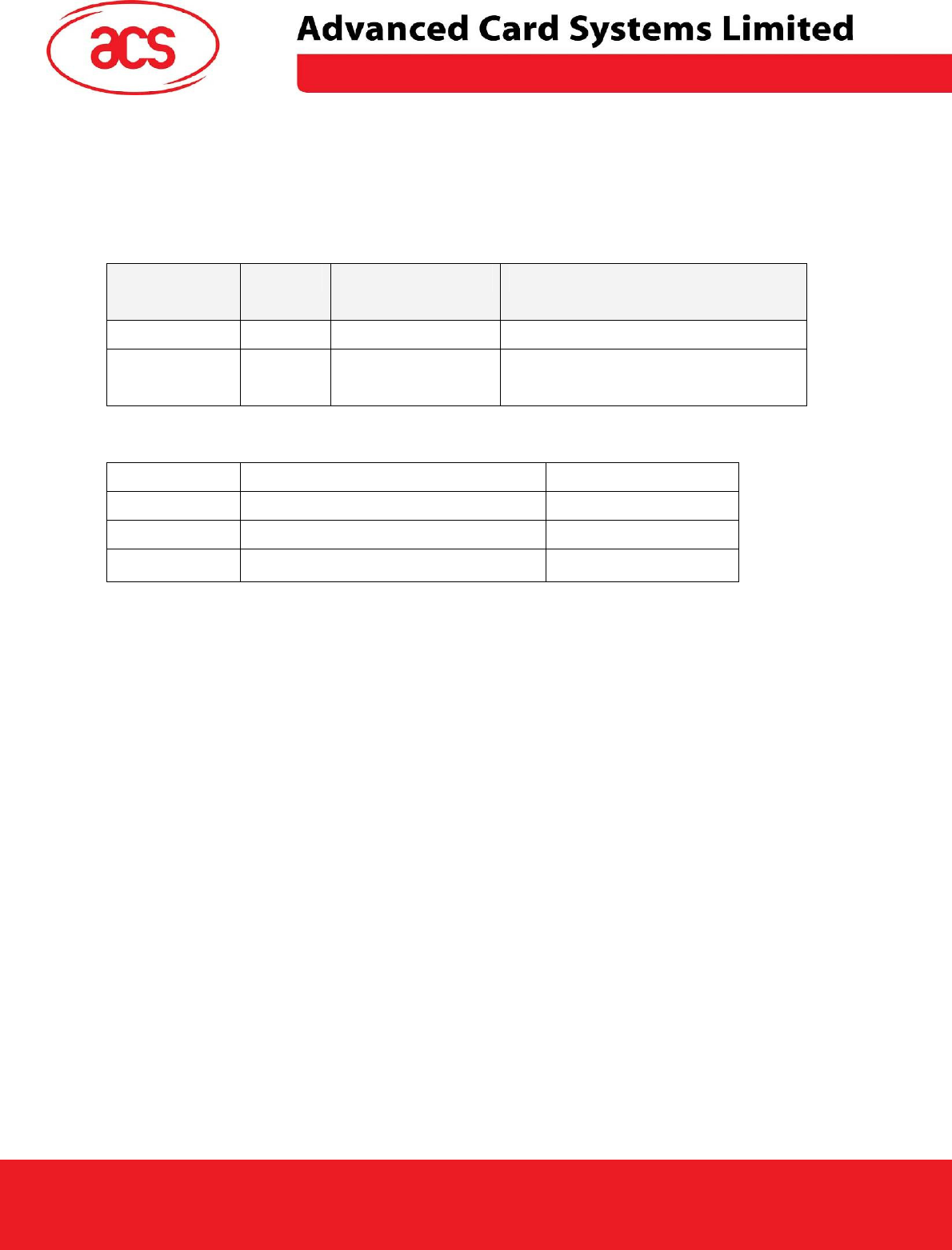
LED_1 On
LED_1 Off
LED_0 On
LED_0 Off

ACR122L-ACS Design Specification
Version 0.03 19/05/2010
Page
27
of
50
ACR122L
-
ACS
Example 4: To turn on the LED_1 for 2 sec. After that, resume to the initial state
// Assume the LED_1 is initially OFF, while the LED_0 is initially ON. //
// The LED_1 and buzzer will turn on during the T1 duration, while the LED_0 will turn off during the
T1 duration. //
1Hz = 1000ms Time Interval = 500ms ON + 500 ms OFF
T1 Duration = 2000ms = 0x14
T2 Duration = 0ms = 0x00
Number of repetition = 0x01
Link to Buzzer = 0x01
APDU = “FF 00 40 50 04 14 00 01 01”
Response = “90 02”
Example 5: To blink the LED_1 of 1Hz for 3 times. After that, resume to initial state
// Assume the LED_1 is initially OFF, while the LED_0 is initially ON. //
// The Initial LED_1 Blinking State is ON. Only the LED_1 will be blinking.
// The buzzer will turn on during the T1 duration, while the LED_0 will turn off during both the T1 and
T2 duration.
// After the blinking, the LED_0 will turn ON. The LED_1 will resume to the initial state after the
blinking //
T1 = 2000ms T2 = 0ms
LED_1 On
LED_1 Off
LED_0 Off
Buzzer On
Buzzer Off
LED_0 On
ACR122L-ACS Design Specification
Version 0.03 19/05/2010
Page
28
of
50
ACR122L
-
ACS
1Hz = 1000ms Time Interval = 500ms ON + 500 ms OFF
T1 Duration = 500ms = 0x05
T2 Duration = 500ms = 0x05
Number of repetition = 0x03
Link to Buzzer = 0x01
APDU = “FF 00 40 50 04 05 05 03 01”
Response = “90 02”
Example 6: To blink the LED_1 and LED_0 of 1Hz for 3 times
// Assume both the LED_0 and LED_1 are initially OFF. //
// Both Initial LED_0 and LED_1 Blinking States are ON //
// The buzzer will turn on during both the T1 and T2 duration//
1Hz = 1000ms Time Interval = 500ms ON + 500 ms OFF
T1 =
500ms
T2 =
500ms
LED_1 On
LED_1 Off
LED_0 On
LED_0 Off
Buzzer On
Buzzer Off
T1 = 500ms
T2 = 500ms
LED_1 On
LED_1 Off
LED_0 Off
LED_0 On
Buzzer On
Buzzer Off

ACR122L-ACS Design Specification
Version 0.03 19/05/2010
Page
29
of
50
ACR122L
-
ACS
T1 Duration = 500ms = 0x05
T2 Duration = 500ms = 0x05
Number of repetition = 0x03
Link to Buzzer = 0x03
APDU = “FF 00 40 F0 04 05 05 03 03”
Response = “90 00”
Example 7: To blink the LED_1 and LED_0 in turn of 1Hz for 3 times
// Assume both LED_0 and LED_1 LEDs are initially OFF. //
// The Initial LED_1 Blinking State is ON; The Initial LED_0 Blinking States is OFF //
// The buzzer will turn on during the T1 duration//
1Hz = 1000ms Time Interval = 500ms ON + 500 ms OFF
T1 Duration = 500ms = 0x05
T2 Duration = 500ms = 0x05
Number of repetition = 0x03
Link to Buzzer = 0x01
APDU = “FF 00 40 D0 04 05 05 03 01”
Response = “90 00”
T1 =
500ms
T2 =
500ms
LED_1 On
LED_1 Off
LED_0 On
LED_0 Off
Buzzer Off
Buzzer On
ACR122L-ACS Design Specification
Version 0.03 19/05/2010
Page
30
of
50
ACR122L
-
ACS
5.3. Pseudo APDU for LEDs Control Enable
This APDU is used to set the LEDs Control Enable/ Disable by user.
Default “Disable”, the LED perform by the firmware
Table 3.0A: Clear LCD Command Format (5 Bytes)
Command
Class INS P1 P2 Lc
LED Control 0xFF 0x00 0x43 bLEDCtrl 0x00
P2: bLEDCtrl (1 Byte)
CMD Description
0x00 Disable LEDs Control by user
0xFF Enable LEDs Control by user
Data Out: SW1 SW2.
Table 3.0B: Status Code
Results
SW1 SW2 Meaning
Success 90 00 The operation is completed successfully.
Error
63 00 The operation is failed.
5.4. Pseudo APDU for LEDs Control
This APDU is used to control 4 LEDs
Table 4.0A: Clear LCD Command Format (5 Bytes)
Command
Class INS P1 P2 Lc
LED Control 0xFF 0x00 0x41 bLEDsState 0x00
P2: bLEDsState
LED_0, LED_1, LED_2 and LED_3 Control Format (1 Byte)
CMD Item Description
Bit 0 LED_0 State 1 = On; 0 = Off
Bit 1 LED_1 State 1 = On; 0 = Off
Bit 2 LED_2 State 1 = On; 0 = Off
ACR122L-ACS Design Specification
Version 0.03 19/05/2010
Page
31
of
50
ACR122L
-
ACS
Bit 3 LED_3 State 1 = On; 0 = Off
Bits 4 – 7 Reserved
Data Out: SW1 SW2.
Table 4.0B: Status Code
Results
SW1 SW2 Meaning
Success 90 00 The operation is completed successfully.
Error
63 00 The operation is failed.
5.5. Pseduo APDU for Buzzer Control
This APDU is used to control Buzzer
Table 5.0A: Buzzer Control Command Format (5 Bytes)
Command
Class
INS P1 P2 Lc Data In
(3 Bytes)
Buzzzer Control
0xFF 0x00
0x42
0x00
0x03
Buzzer Control
Data In: Buzzer Control
Table 5.0B: Buzzer On/Off Duration Control Format (4 Bytes)
Byte 0 Byte 1 Byte 2
T1 Duration
On State
(Unit = 100ms)
T2 Duration
Off State
(Unit = 100ms)
Number of
repetition
Data Out: SW1 SW2.
Table 5.0C: Status Code
Results
SW1 SW2 Meaning
Success 90 00 The operation is completed successfully.
Error
63 00 The operation is failed.
ACR122L-ACS Design Specification
Version 0.03 19/05/2010
Page
32
of
50
ACR122L
-
ACS
5.6. Pseudo APDU for Clear LCD
This APDU is used to clear all content show on the LCD
Table 6.0A: Clear LCD Command Format (5 Bytes)
Command
Class INS P1 P2 Lc
Clear LCD 0xFF 0x00 0x60 0x00 0x00
Data Out: SW1 SW2.
Table 6.0B: Status Code
Results
SW1 SW2 Meaning
Success 90 00 The operation is completed successfully.
Error
63 00 The operation is failed.
ACR122L-ACS Design Specification
Version 0.03 19/05/2010
Page
33
of
50
ACR122L
-
ACS
5.7. Pseudo APDU for LCD Display (ASCII Mode)
This APDU is used to Display LCD Message in ASCII Mode
Table 7.0A: LCD Display Command Format (5 Bytes + LCD Message Length)
Command
Class INS P1 P2 Lc Data In
(Max. 16Bytes)
LCD Display 0xFF Option
Byte
0x68 LCD XY Position
LCD
Message
Length
LCD Message
INS: Option Byte (1 Byte)
CMD Item Description
Bit 0 Character Bold Font 1 = Bold; 0 = Normal
Bit 1 - 3 Reserved
Bit 4 - 5 Table Index 00 = Fonts Set A
01 = Fonts Set B
10 = Fonts Set C
Bits 6 – 7 Reserved
P2: LCD XY Position
The Character to be displayed on the LCD position specified by DDRAM Address
Please follow the DDRAM table below for the LCD character position’s representation
For Fonts Set 1 and 2,
1 2 3 4 5 6 7 8 9 10 11 12 13 14 15 16 DISPLAY
POSITION
1
st
LINE 00 01 02 03 04 05 06 07 08 09 0A 0B 0C 0D 0E 0F
2
nd
LINE 40 41 42 43 44 45 46 47 48 49 4A 4B 4C 4D 4E 4F
LCD XY
POSITION
For Fonts Set 3,
1 2 3 4 5 6 7 8 9 10 11 12 13 14 15 16 DISPLAY
POSITION
1
st
LINE 00 01 02 03 04 05 06 07 08 09 0A 0B 0C 0D 0E 0F
2
nd
LINE 20 21 22 23 24 25 26 27 28 29 2A 2B 2C 2D 2E 2F
3
rd
LINE 40 41 42 43 44 45 46 47 48 49 4A 4B 4C 4D 4E 4F
4
th
LINE 60 61 62 63 64 65 66 67 68 69 6A 6B 6C 6D 6E 6F
LCD XY
POSITION
Lc: LCD Message Length
The length of the LCD message (max. 0x10); If the message length is longer than the number of
character that the LCD screen’s can be shown, then the redundant character will not be shown on the
LCD
ACR122L-ACS Design Specification
Version 0.03 19/05/2010
Page
34
of
50
ACR122L
-
ACS
Data In:
LCD Message
The data to be sent to LCD, maximum 16 Character for each line
Please follow the Fonts tables (selected by INS Bit 4 - 5) below for the LCD Character Index
Remarks: Size of the Characters in Fonts Set A and Fonts Set B is 8x16, but size of the Characters in
Fonts Set C is 8x8
Character Set A Character Set B Character Set C
Data Out: SW1 SW2.
Table 7.0B: Status Code
Results
SW1 SW2 Meaning
Success 90 00 The operation is completed successfully.
Error 63 00 The operation is failed.
Advanced Card Systems Ltd. Website: www.acs.com.hk
Email:
info@acs.com.hk
5.8. Pseudo APDU for LCD Display (GB Mode)
This APDU is used to Display LCD Message in GB Mode
Table 8.0A: LCD Display Command Format (5 Bytes + LCD Message Length)
Command
Class INS P1 P2 Lc Data In
(Max. 16 Bytes)
LCD Display 0xFF Option
Byte
0x69 LCD XY Position
LCD
Message
Length
LCD Message
INS: Option Byte (1 Byte)
CMD Item Description
Bit 0 Character Bold Font 1 = Bold; 0 = Normal
Bit 1 - 7 Reserved
P2: LCD XY Position
The Character to be displayed on the LCD position specified by DDRAM Address
Please follow the DDRAM table below for the LCD character position’s representation
1 2 3 4 5 6 7 8 9 10 11 12 13 14 15 16 DISPLAY
POSITION
FIRST LINE 00 01 02 03 04 05 06 07
SECOND LINE 40 41 42 43 44 45 46 47
LCD XY
POSITION
Lc: LCD Message Length
The length of the LCD message (max. 0x10); If the message length is longer than the number of
character that the LCD screen’s can be shown, then the redundant character will not be shown on the
LCD
The length of the LCD message should multiple of 2 because each Chinese Character (GB code)
should be contain two bytes
Data In:
LCD Message
The data to be sent to LCD, maximum 8(2 x 8bit each character) Character for each line
Please follow the Fonts table of GB Coding
Data Out: SW1 SW2.
Table 8.0B: Status Code
Results
SW1 SW2 Meaning
Success 90 00 The operation is completed successfully.
Error 63 00 The operation is failed.
ACR122L-ACS Design Specification
Version 0.03 19/05/2010
Page
36
of
50
ACR122L
-
ACS
5.9. Pseudo APDU for LCD Display (Graphic Mode)
This APDU is used to Display LCD Message in Graphic Mode
Table 9.0A: LCD Display Command Format (5 Bytes + LCD Message Length)
Command
Class INS P1 P2 Lc Data In
(max. 128 Bytes)
LCD Display 0xFF 0x00 0x6A Line Index
Pixel Data
Length
Pixel Data
P2: Line Index
To set which line to start to update the LCD Display
Refer to Below LCD Display Position
Lc:
Pixel Data
Length
The length of the pixel data (max. 0x80)
Data In:
Pixel Data
The pixel data to be sent to LCD for display
LCD Display Position (Total LCD Size: 128x32):
Byte 0x00 (X = 0x00) Byte 0x01 (X = 0x01) … Byte 0x0F (X = 0x0F)
7 6 5 4 3 2 1 0 7 6 5 4 3 2 1 0 … 7 6 5 4 3 2 1 0
0x00
0x01
0x02
0x03
0x04
0x05
0x06
0x07
0x08
0x09
… …
0x1F
Data Out: SW1 SW2.
Table 9.0B: Status Code
Results
SW1 SW2 Meaning
Success 90 00 The operation is completed successfully.
Error 63 00 The operation is failed.
Line Index
X
-axis
ACR122L-ACS Design Specification
Version 0.03 19/05/2010
Page
37
of
50
ACR122L
-
ACS
5.10. Pseudo APDU for Scrolling LCD Current Display
This APDU is used to set scrolling feature of the Current LCD Display
Table 10.0A: Scrolling LCD Command Format (5 Bytes + LCD Message Length)
Command
Class INS P1 P2 Lc Data In
(6 Bytes)
LCD Display 0xFF 0x00 0x6D 0x00
0x06
Scroll Ctrl
Data In: Scroll Ctrl
Table 10.0B: Scrolling Control Format (6 Bytes)
Byte 0 Byte 1 Byte 2 Byte 3 Byte 4 Byte 5
X Position Y Position Scrolling Range
(Horizontal)
Scrolling Range
(Vertical)
Refresh Speed
Ctrl
Scrolling
Direction
X Position: Horizontal Start Up Position, Ref to LCD Display Position Below
Y Position: Vertical Start Up Position, Ref to LCD Display Position Below
LCD Display Position (Total LCD Size: 128x32):
Byte 0x00 (X = 0x00) Byte 0x01 (X = 0x01) … Byte 0x0F (X = 0x0F)
7 6 5 4 3 2 1 0 7 6 5 4 3 2 1 0 … 7 6 5 4 3 2 1 0
0x00
0x01
0x02
0x03
0x04
0x05
0x06
0x07
0x08
0x09
… …
0x1F
Scrolling Range (Horizontal): How many 8 pixels in Horizontal after X position will be scrolled
Scrolling Range (vertical): How many pixels in Vertical after Y position will be scrolled
Refresh Speed Ctrl:
Bit0~Bit3 – how many pixel move pre scrolling
Bit4~Bit7 – Scrolling period
Bit7 Bit6 Bit5 Bit4 Scrolling period
0 0 0 0 1 Unit
0 0 0 1 3 Units
0 0 1 0 5 Units
0 0 1 1 7 Units
0 1 0 0 17 Units
ACR122L-ACS Design Specification
Version 0.03 19/05/2010
Page
38
of
50
ACR122L
-
ACS
0 1 0 1 19 Units
0 1 1 0 21 Units
0 1 1 1 23 Units
1 0 0 0 129 Units
1 0 0 1 131 Units
1 0 1 0 133 Units
1 0 1 1 135 Units
1 1 0 0 145 Units
1 1 0 1 147 Units
1 1 1 0 149 Units
1 1 1 1 151 Units
Scrolling Direction: the Scrolling Direction
Bit1 Bit0 Scrolling Direction
0 0 From Left to Right
0 1 From Right to Left
1 0 From Top to Bottom
1 1 From Bottom to Top
Data Out: SW1 SW2.
Table 10.0C: Status Code
Results
SW1 SW2 Meaning
Success 90 00 The operation is completed successfully.
Error 63 00 The operation is failed.
5.11. Pseudo APDU for Pause LCD Scrolling
This APDU is used to Pause the LCD Scrolling set before
To resume the scrolling, send again the scrolling LCD command (5.10) to perform
Table 11.0A: Pause Scrolling Command Format (5 Bytes)
Command
Class INS P1 P2 Lc
Clear LCD 0xFF 0x00 0x6E 0x00 0x00
Data Out: SW1 SW2.
Table 11.0B: Status Code
Results
SW1 SW2 Meaning
Success 90 00 The operation is completed successfully.
Error
63 00 The operation is failed.
ACR122L-ACS Design Specification
Version 0.03 19/05/2010
Page
39
of
50
ACR122L
-
ACS
5.12. Pseudo APDU for Stop LCD Scrolling
This APDU is used to stop the LCD Scrolling set before, the LCD display will back to normal display
position
Table 12.0A: Stop Scrolling LCD Command Format (5 Bytes)
Command
Class INS P1 P2 Lc
Clear LCD 0xFF 0x00 0x6F 0x00 0x00
Data Out: SW1 SW2.
Table 12.0B: Status Code
Results
SW1 SW2 Meaning
Success 90 00 The operation is completed successfully.
Error
63 00 The operation is failed.
5.13. Pseudo APDU for LCD Contrast Control
This APDU is used to Control the LCD Contrast
Table 13.0A: LCD Contrast Control Command Format (5 Bytes)
Command
Class INS P1 P2 Lc
LCD Contrast
Control
0xFF 0x00 0x6C Contrast Control 0x00
P2: Contrast Control
The value range is between 0x00 to 0x0F. It is as large as brighten on contrast. Otherwise the
contrast will been darken.
Data Out: SW1 SW2.
Table 13.0B: Status Code
Results
SW1 SW2 Meaning
Success 90 00 The operation is completed successfully.
Error 63 00 The operation is failed.
ACR122L-ACS Design Specification
Version 0.03 19/05/2010
Page
40
of
50
ACR122L
-
ACS
5.14. Pseudo APDU for LCD Backlight Control
This APDU is used to Control the LCD Backlight
Table 14.0A: LCD Backlight Control Command Format (5 Bytes)
Command
Class INS P1 P2 Lc
LCD Backlight
Control
0xFF 0x00 0x64 Backlight
Control
0x00
P2: Backlight Control
Table 14.0B: Backlight Control Format (1 Byte)
CMD Description
0x00 LCD Backlight Off
0xFF LCD Backlight On
Data Out: SW1 SW2.
Table 14.0C: Status Code
Results
SW1 SW2 Meaning
Success 90 00 The operation is completed successfully.
Error
63 00 The operation is failed.
ACR122L-ACS Design Specification
Version 0.03 19/05/2010
Page
41
of
50
ACR122L
-
ACS
5.15. Pseudo APDU for changing the communication speed
This APDU is used to change the baud rate.
**Remark: STX = 0x32 and ETX = 0x33
Table 15.0A: Baud Rate Control Command Format (9 Bytes)
Command
Class INS P1 P2 Lc
Baud Rate
Control
0xFF 0x00 0x44 New Baud Rate 0x00
P2: New Baud Rate
0x00: Set the new baud rate to 9600 bps.
0x01: Set the new baud rate to 115200 bps.
**Remark: The feedback’s STX = 0x02 and ETX = 0x03
Data Out: SW1 SW2.
Table 15.0B: Status Code
Results
SW1 SW2 Meaning
Success 90 Current Baud Rate The operation is completed successfully.
Error
63 00 The operation is failed.
SW2: Current Baud Rate
0x00: The current baud rate is 9600 bps.
0x01: The current baud rate is 115200 bps.
Remark:
After the communication speed is changed successfully, the program has to adjust its communication
speed so as to continue the rest of the data exchanges.
The initial communication speed is determined by the existence of R12 (0 ohm).
• With R12 = 115200 bps
• Without R12 = 9600 bps (default)

ACR122L-ACS Design Specification
Version 0.03 19/05/2010
Page
42
of
50
ACR122L
-
ACS
Example 1: To initialize a FeliCa Tag (Tag Polling)
Step 1: Issue a “Direct Transmit” APDU.
The APDU Command should be “FF 00 00 00 09 D4 4A 01 01 00 FF FF 01 00”
#In which,
Direct Transmit APDU = “FF 00 00 00”
Length of the PN532_Tag Command = “09”
PN532 Command (InListPassiveTarget 212Kbps) = “D4 4A 01 01”
Tag Command (System Code Request) = “00 FF FF 01 00”
To send an APDU to the slot 0 (default), sequence number = 1.
HOST -> 02 6F 0E 00 00 00 00 01 00 00 00
FF 00 00 00 09 D4 4A 01 01 00 FF FF 01 00
[Checksum] 03
RDR -> 02 00 00 03
RDR -> 02 81 1A 00 00 00 00 01 00 00 00
D5 4B 01 01 14 01 01 01 05 01 86 04 02 02 03 00
4B 02 4F 49 8A 8A 80 08 90 00
[Checksum] 03
The APDU Response is
“D5 4B 01 01 14 01 01 01 05 01 86 04 02 02 03 00 4B 02 4F 49 8A 8A 80 08 90 00”
#In which,
Response returned by the PN532 =
“D5 4B 01 01 14 01 01 01 05 01 86 04 02 02 03 00 4B 02 4F 49 8A 8A 80 08”
NFCID2t of the FeliCa Tag = “01 01 05 01 86 04 02 02”
Status Code returned by the reader = “90 00”

ACR122L-ACS Design Specification
Version 0.03 19/05/2010
Page
43
of
50
ACR122L
-
ACS
Example 2: To write 16 bytes data to the FeliCa Tag (Tag Write)
Step 1: Issue a “Direct Transmit” APDU.
The APDU Command should be “FF 00 00 00 23 D4 40 01 20 08 01 01 05 01 86 04 02 02 01 09 01
01 80 00 00 AA 55 AA 55 AA 55 AA 55 AA 55 AA 55 AA 55 AA”
#In which,
Direct Transmit APDU = “FF 00 00 00”
Length of the PN532_Tag Command = “23”
PN532 Command (InDataExchange) = “D4 40 01”
Tag Command (Write Data) = “20 08 01 01 05 01 86 04 02 02 01 09 01 01 80 00 00 AA 55 AA 55 AA
55 AA 55 AA 55 AA 55 AA 55 AA”.
To send an APDU to the slot 0 (default), sequence number = 2.
HOST -> 02 6F 28 00 00 00 00 02 00 00 00
FF 00 00 00 00 23 D4 40 01 20 08 01 01 05 01 86
04 02 02 01 09 01 01 80 00 00 AA 55 AA 55 AA 55
AA 55 AA 55 AA 55 AA
[Checksum] 03
RDR -> 02 00 00 03
RDR -> 02 81 11 00 00 00 00 02 00 00 00
D5 41 00 0C 09 01 01 05 01 86 04 02 02 00 00 90 00
[Checksum] 03
The APDU Response would be
“D5 41 00 0C 09 01 01 05 01 86 04 02 02 00 00 90 00”
#In which,
Response returned by the PN532 = “D5 41”
Response returned by the FeliCa Tag = “00 0C 09 01 01 05 01 86 04 02 02 00 00”
Status Code returned by the reader = “90 00”

ACR122L-ACS Design Specification
Version 0.03 19/05/2010
Page
44
of
50
ACR122L
-
ACS
Example 3: To read 16 bytes data from the FeliCa Tag (Tag Write)
Step 1: Issue a “Direct Transmit” APDU.
The APDU Command should be “FF 00 00 00 13 D4 40 01 10 06 01 01 05 01 86 04 02 02 01 09 01
01 80 00”
#In which,
Direct Transmit APDU = “FF 00 00 00”
Length of the PN532_Tag Command = “13”
PN532 Command (InDataExchange) = “D4 40 01”
Tag Command (Read Data) = “10 06 01 01 05 01 86 04 02 02 01 09 01 01 80 00”
To send an APDU to the slot 0 (default), sequence number = 3.
HOST -> 02 6F 18 00 00 00 00 03 00 00 00
FF 00 00 00 13 D4 40 01 10 06 01 01 05 01 86 04
02 02 01 09 01 01 80 00 FF
[Checksum] 03
RDR -> 02 00 00 03
RDR -> 02 81 22 00 00 00 00 03 00 00 00
D5 41 00 1D 07 01 01 05 01 86 04 02 02 00 00 01 00
AA 55 AA 55 AA 55 AA 55 AA 55 AA 55 AA 55 AA 90 00
[Checksum] 03
The APDU Response would be
“D5 41 00 1D 07 01 01 05 01 86 04 02 02 00 00 01 00 AA 55 AA 55 AA 55 AA 55 AA 55 AA 55 AA 55
AA 90 00”
#In which,
Response returned by the PN532 = “D5 41”
Response returned by the FeliCa Tag =
“00 1D 07 01 01 05 01 86 04 02 02 00 00 01 00 AA 55 AA 55 AA 55 AA 55 AA 55 AA 55 AA 55 AA”
Status Code returned by the reader = “90 00”

ACR122L-ACS Design Specification
Version 0.03 19/05/2010
Page
45
of
50
ACR122L
-
ACS
Example 4: To initialize an ISO 14443-4 Type B Tag (Tag Polling)
Step 1: Issue a “Direct Transmit” APDU.
The APDU Command should be “FF 00 00 00 05 D4 4A 01 03 00”
#In which,
Direct Transmit APDU = “FF 00 00 00”
Length of the PN532_Tag Command = “05”
PN532 Command (InListPassiveTarget Type B 106Kbps) = “D4 4A 01 03 00”
To send an APDU to the slot 0 (default), sequence number = 4.
HOST -> 02 6F 0A 00 00 00 00 04 00 00 00
FF 00 00 00 05 D4 4A 01 03 00
[Checksum] 03
RDR -> 02 00 00 03
RDR -> 02 81 14 00 00 00 00 04 00 00 00
D5 41 01 01 50 00 01 32 F4 00 00 00 00 33 81 81 01 21
90 00 [Checksum] 03
The APDU Response is
“D5 4B 01 01 50 00 01 32 F4 00 00 00 00 33 81 81 01 21 90 00”
#In which,
Response returned by the PN532 =
“D5 4B 01 01”
ATQB of the Type B Tag = “50 00 01 32 F4 00 00 00 00 33 81 81”
CRC-B = “01 21”
Status Code returned by the reader = “90 00”

ACR122L-ACS Design Specification
Version 0.03 19/05/2010
Page
46
of
50
ACR122L
-
ACS
Example 5: To send an APDU to an ISO 14443-4 Type B Tag (Data Exchange)
Step 1: Issue a “Direct Transmit” APDU.
The USER APDU Command should be “00 84 00 00 08”
The Composed APDU Command should be “FF 00 00 00 08 D4 40 01 00 84 00 00 08”
#In which,
Direct Transmit APDU = “FF 00 00 00”
Length of the PN532_Tag Command = “08”
PN532 Command (InDataExchange) = “D4 40 01”
Tag Command (Get Challenge) = “00 84 00 00 08”
To send an APDU to the slot 0 (default), sequence number = 5.
HOST -> 02 6F 0D 00 00 00 00 05 00 00 00
FF 00 00 00 08 D4 40 01 00 84 00 00 08
[Checksum] 03
RDR -> 02 00 00 03
RDR -> 02 81 0F 00 00 00 00 05 00 00 00
D5 41 00 01 02 03 04 05 06 07 08 90 00 90 00
[Checksum] 03
The APDU Response is
“D5 41 00 0B 01 02 03 04 05 06 07 08 90 00”
#In which,
Response returned by the PN532 =
“D5 41 00”
Response from the Type B Tag = “01 02 03 04 05 06 07 08 90 00”
Status Code returned by the reader = “90 00”
ACR122L-ACS Design Specification
Version 0.03 19/05/2010
Page
47
of
50
ACR122L
-
ACS
5.16. Get the Firmware Version of the reader
To retrieve the firmware versions of the reader.
For SAM Interface 1 controller, STX = 0x02 and ETX = 0x03
For SAM Interface 2 controller, STX = 0x12 and ETX = 0x13
For SAM Interface 3 controller, STX = 0x22 and ETX = 0x23
Table 16.0A: Get Firmware Version Command Format (5 Bytes)
Command
Class INS P1 P2 Le
Get Response 0xFF 0x00 0x48 0x00 0x00
Le: Number of Bytes to Retrieve (1 Byte)
Maximum 255 bytes
For SAM Interface 1 controller, the feedback’s STX = 0x02 and ETX = 0x03
For SAM Interface 2 controller, the feedback’s STX = 0x12 and ETX = 0x13
For SAM Interface 3 controller, the feedback’s STX = 0x22 and ETX = 0x23
Table 16.0B: Get Firmware Version Response Format (14 bytes)
Response
Data Out
Result
Firmware Version
E.g. 1 Response for SAM Interface 1 controller
= 41 43 52 31 32 32 4C 31 30 31 53 41 4D 31(Hex) = ACR122L101SAM1 (ASCII)
E.g. 2 Response for SAM Interface 2 controller
= 41 43 52 31 32 32 4C 31 30 31 53 41 4D 32(Hex) = ACR122L101SAM2 (ASCII)
E.g. 3 Response for SAM Interface 3 controller
= 41 43 52 31 32 32 4C 31 30 31 53 41 4D 33(Hex) = ACR122L101SAM3 (ASCII)

ACR122L-ACS Design Specification
Version 0.03 19/05/2010
Page
48
of
50
ACR122L-ACS
5.17. Basic Program Flow for FeliCa Applications
Step 0. Start the application. The first thing is to activate the “SAM Interface”. The ATR of the
SAM (if a SAM is inserted) or a Pseduo-ATR “3B 00” (if no SAM is inserted) will be
returned. In other word, the SAM is always existed from the view of the application.
Step 1. The second thing to do is to change the operating parameters of the PN531. Set the
Retry Time to one.
Step 2. Poll a FeliCa Tag by sending “Direct Transmit” and “Get Response” APDUs (Tag
Polling).
Step 3. If no tag is found, go back to Step 2 until a FeliCa Tag is found.
Step 4. Access the FeliCa Tag by sending APDUs (Tag Read or Write)
Step 5. If there is no any operation with the FeliCa Tag, then go back to Step 2 to poll the other
FeliCa Tag.
..
Step N. Deactivate the “SAM Interface”. Shut down the application.
Remark:
1. The default Retry Time of the PN532 command “InListPassiveTarget” is infinity. Send the APDU
“FF 00 00 00 06 D4 32 05 00 00 00” to change the Retry Time to one.
2. It is recommended to turn off the Antenna if there is no contactless access.
APDU for turning on the Antenna Power = APDU “FF 00 00 00 04 D4 32 01 03”
APDU for turning off the Antenna Power = APDU “FF 00 00 00 04 D4 32 01 02”
FCC Warning:
Any Changes or modifications not expressly approved by the party responsible for compliance
could void the user's authority to operate the equipment.
This device complies with part 15 of the FCC Rules. Operation is subject to the following two conditions:
(1) This device may not cause harmful interference, and
(2) this device must accept any interference received, including interference that may cause
undesired operation.
ACR122L-ACS Design Specification
Version 0.03 19/05/2010
Page
49
of
50
ACR122L
-
ACS
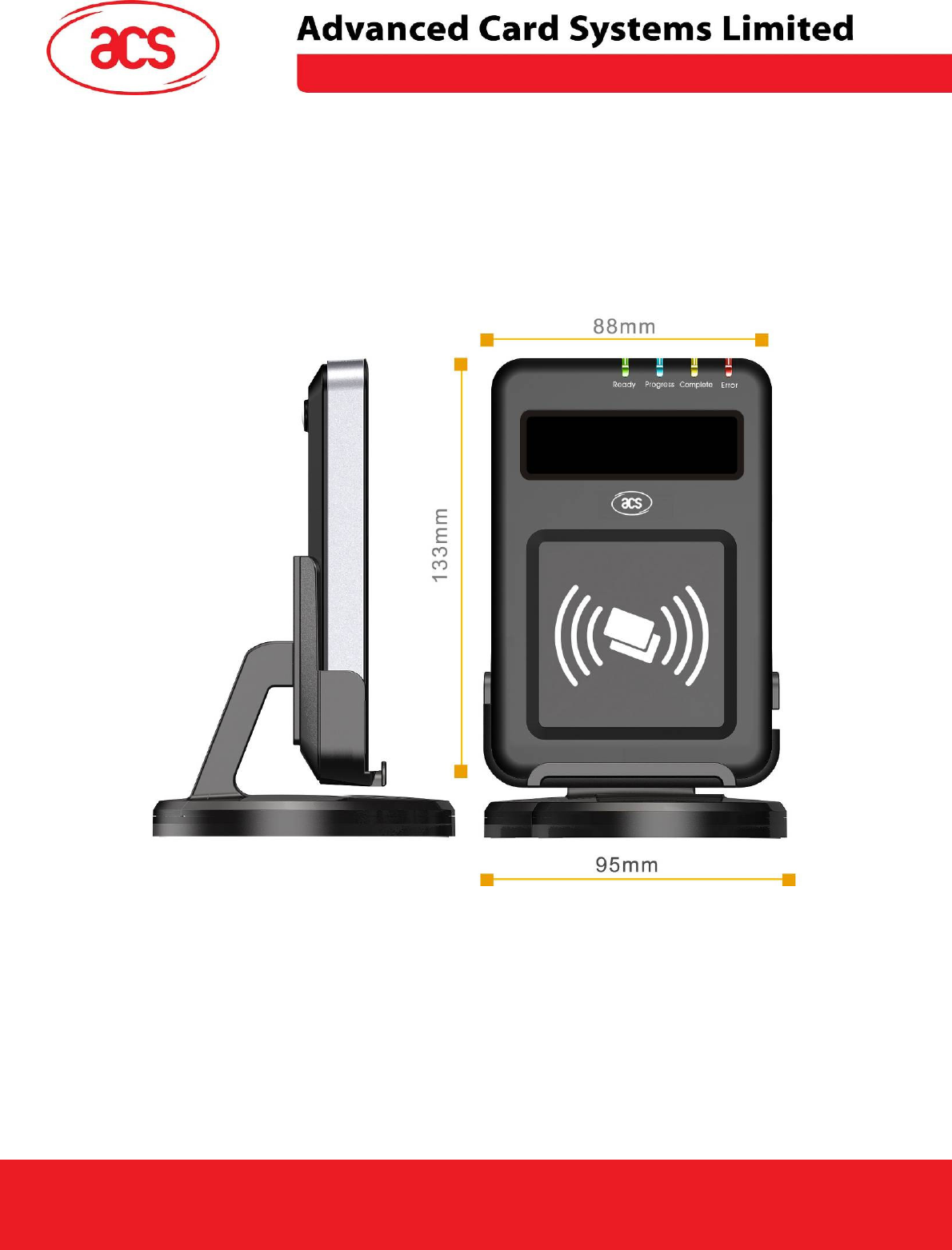
6.0. Mechanical Design
Advanced Card Systems Ltd. Website: www.acs.com.hk
Email:
info@acs.com.hk
7.0. Technical Specification
Serial Interface
Power source ....................................... 7V AC/DC Switching Power Supply
Speed................................................... 9.6Kbps, 115.2Kbps (default)
Supply Voltage ..................................... Regulated 5V DC
Supply Current ..................................... 350mA (maximum); 200mA (normal)
Contactless Smart Card Interface
Standard............................................... MIFARE Classic, ISO14443-4 Type A & B, FeliCa, ISO/IEC 18092 NFC
Operating Frequency............................ 13.56 MHz
Smart card read / write speed............... 106, 212, 424 kbps
SAM Interface
Standard............................................... ISO 7816
Protocol ................................................ T=0 protocol
Operating Frequency............................ 4 MHz
Smart card read / write speed............... 9600 - 115200 bps
Case
Dimensions........................................... 133 mm (L) x 88.66 mm (W) x 19 mm (H)
Material ................................................ ABS
Color..................................................... Black
Antenna Size ........................................ 64mm x 46mm
Operating distance ............................... up to 50 mm (depended on tag type)
Modulation............................................ ASK and BPSK
Built-in peripherals
LED ...................................................... Green, Blue Orange and Red
Buzzer .................................................. Monotone
Operating Conditions
Temperature......................................... 0 - 50° C
Humidity ............................................... 10% - 80%
Cable Connector
Length .................................................. 1.5 M (DB9 + DC Plug)
Standard/Certifications
CE, FCC, VCCI
OS
Windows 98, ME, 2K, XP, Vista, 7
OEM
OEM-Logo possible, customer-specific colors, casing, and card connector