Advanced Card Systems ACR1281S Contactless Smart Card Reader and Writer User Manual
Advanced Card Systems Limited Contactless Smart Card Reader and Writer Users Manual
Users Manual

ACR1281S
Advanced Card Systems Ltd. Page 1 of 56
ACR1281S
Specification
V1.01

ACR1281S
Advanced Card Systems Ltd. Page 2 of 56
Revision History
Rev
Number
Date Author Notes
V1.00 2010-08-19 Nathan Li/ Kit Au Preliminary specification for ACR12
V1.01 2010-12-15 Vincent Zhong/Jessy Wei Modify Peripherals Control command

ACR1281S
Advanced Card Systems Ltd. Page 3 of 56
INDEX
Index ....................................................................................................................................................3
Introduction..........................................................................................................................................5
features.................................................................................................................................................5
Terms ...................................................................................................................................................6
Quick Overview of the ACR1281S Reader.........................................................................................7
1. ACR1281S (with Contact Card Option)......................................................................................7
2. ACR1281S (without Contact Card Option).................................................................................7
3. ACR1281S ICC Interface............................................................................................................8
4. ACR1281S PICC Interface..........................................................................................................8
System description.............................................................................................................................10
1. The Reader Block Diagram .......................................................................................................10
2. Communication Flow Chart of ACR1281S...............................................................................11
Hardware Description........................................................................................................................12
3. USB Interface ............................................................................................................................12
4. LED Indicator ............................................................................................................................12
5. Buzzer........................................................................................................................................13
6. ICC Interface (Contact Smart Card)..........................................................................................13
7. PICC Interface (Contactless Smart Card)..................................................................................13
Serial Communication Protocol (CCID-liked FRAME Format).......................................................14
8. Bulk-OUT Command ................................................................................................................15
8.1 HOST_to_RDR_IccPowerOn..............................................................................................15
8.2 HOST_to_RDR_IccPowerOff.............................................................................................15
8.3 HOST_to_RDR_XfrBlock ..................................................................................................16
8.4 HOST_to_RDR_GetSlotStatus............................................................................................16
8.5 HOST_to_RDR_SetParameters...........................................................................................17
8.6 HOST_to_RDR_Escape ......................................................................................................17
9. Bulk-IN Response......................................................................................................................19
9.1 RDR_to_HOST_DataBlock ................................................................................................19
9.2 RDR_to_HOST_SlotStatus .................................................................................................20
9.3 RDR_to_HOST_Parameters................................................................................................20
9.4 RDR_to_HOST_Escape ......................................................................................................21
10. RDR_to_PC_NotifySlotChange Messages .............................................................................21
11. Error Handling.........................................................................................................................23
12. Protocol Flow Examples..........................................................................................................24
Peripherals Control ............................................................................................................................26
1. Set Serial Communication Mode...............................................................................................26
2. Get Firmware Version ...............................................................................................................26
3. Enter Firmware Upgrade Mode.................................................................................................27
4. LED Control ..............................................................................................................................27
5. Buzzer Control...........................................................................................................................28
6. Default LED and Buzzer State ..................................................................................................28
7. Automatic PICC Polling............................................................................................................29
8. PICC Polling for specific PICC Types ......................................................................................29
9. Auto PPS for the PICC Interface (Communication Speed Change) .........................................30
10. Antenna Field ON/OFF for the PICC Interface.......................................................................30

ACR1281S
Advanced Card Systems Ltd. Page 4 of 56
11. Exclusive Mode Configure......................................................................................................30
12. Request Command Test...........................................................................................................31
13. Continuous Wake Up Command Sending Test for the PICC Interface ..................................32
14. Read and Update the RC531 Register for the PICC Interface ................................................32
15. Go into Contactless EMV Terminal Loop...............................................................................32
16. Go into Contact EMV Terminal Loop.....................................................................................32
17. Read and Initial Card Insert Counter.......................................................................................32
18. Initial RC531 Setting For PICC...............................................................................................33
PICC Interface Description................................................................................................................34
1. ATR Generation ........................................................................................................................34
PICC APDU Commands for General Purposes.................................................................................36
1. Get Data.....................................................................................................................................36
PICC APDU Commands (T=CL Emulation) for MIFare 1K/4K MEMORY Cards ........................37
2.1 Load Authentication Keys .......................................................................................................37
2.2.1 Authentication for MIFARE 1K/4K.....................................................................................39
2.3 Read Binary Blocks .................................................................................................................42
2.4 Update Binary Blocks..............................................................................................................43
2.5 Value Block Related Commands.............................................................................................44
2.5.1 Value Block Operation .........................................................................................................44
2.5.2 Read Value Block.................................................................................................................45
2.5.3 Restore Value Block.............................................................................................................46
Basic Program Flow for Contactless Applications............................................................................47
1. How to access PCSC Compliant Tags (ISO14443-4)? .............................................................48
2. How to access DESFIRE Tags (ISO14443-4)?.........................................................................51
Basic Program Flow for Contact Applications.................................................................................53
1. How to access ACOS3 ICC Cards (ISO7816)?.........................................................................53
Annex A.............................................................................................................................................55
Technical Specification .....................................................................................................................56
ACR1281S
Advanced Card Systems Ltd. Page 5 of 56
INTRODUCTION
The ACR1281S is a dual-interface reader(IFD and PCD) that supports both contact and contactless
(PICC) smart cards.
FEATURES
• One standard ICC landing type card acceptor.
• ISO 7816 Parts 1-4 Compliant for Contact Smart Card Interface.
• Support contact memory cards.
• ISO 14443 Parts 1-4 Compliant for Contactless Smart Card Interface.
• A built-in antenna for PICC contactless access applications.
• The ACR1281 supports the following Tag Types:
o MIFARE Classic. E.g. MIFARE 1K, 4K, MINI and Ultralight.
o ISO14443-4 Type A and B.
• T=CL emulation for MIFare 1K/4K PICCs. Multi-Blocks Transfer Mode is provided for
efficient PICC access.
• High Speed (424 kbps) Communication for PICCs. #Maximum 848 kbps.
• Intelligent Support for Hybrid Cards and Combi Cards.
• Energy saving modes for turning off the antenna field whenever the PICC is inactive, or no
PICC is found. It prevents the PICC from exposing to the field all the time.
• User-Controllable Peripherals. E.g. LED, Buzzer.
• CCID-liked Frame Format.
• Serial Interface up to 500kbps.
• Device Firmware Upgradeable through the USB Interface.

ACR1281S
Advanced Card Systems Ltd. Page 6 of 56
TERMS
• IFD: Interface Device. A terminal, communication device, or machine to which the
integrated circuit(s) card is electrically connected during operation.
• PCD: Proximity Coupling Device. ISO 14443 Contactless Reader.
• ICC: Integrated Circuit(s) Card. Refer to a plastic card containing an integrated circuit,
which is compatible with ISO 7816.
• PICC: Proximity Integrated Circuit(s) Card. Contactless Cards operating without
mechanical contact to the IFD, using magnetic coupling.
• Combi-Card: A smart card that supports both ICC and PICC Interfaces. But only one
interface can be operating at any one time.
• Hybrid-Card: A smart card that consists of both ICC and PICC cards. Both ICC and PICC
cards can be operating at the same time.
• USB: Universal Serial Bus, a common device interface used in PC environment.
• CCID: The specifications for USB devices that interface with ICC or act as interfaces with
ICC/PICC.
• PCSC: Personal Computer Smart Card, a specification that can facilitate the interoperability
necessary to allow ICC/PICC technology to be effectively utilized in the PC environment.
• ISO 7816: A standard for contact smart cards (ICC).
• T=0: Character-oriented asynchronous half duplex transmission protocol for ICCs (ISO
7816).
• T=1: Block-oriented asynchronous half duplex transmission protocol for ICCs (ISO 7816).
• ISO 14443: A standard for contactless smart cards (PICC)
• T=CL: Block-oriented asynchronous half duplex transmission protocol for PICCs (ISO
14443).
• APDU: Application Protocol Data Unit.
• ATR: Answer-to-Reset. The transmission sent by an ICC to the reader (IFD) in response to
a RESET condition.
• ATS: Answer-to-Select. The transmission sent by a PICC Type A to the reader (PCD) in
response to a SELECT condition.
• ATQB: Answer-to-Request. The transmission sent by a PICC Type B to the reader (PCD)
in response to a REQUEST condition.
• Card Insertion Event: Either an ICC or a PICC is just appeared to the reader.
•
Card Removal Event: Either an ICC or a PICC is removed from the reader.
• NAK: Negative Acknowledge, only used to get the last response or slot change message
report in ACR1281S.
• XOR : Exclusive OR
• RDR: ACR1281S.
• HOST: Host Controller.
• HOST_to_RDR: Host Controller -> ACR1281S
• RDR_to_HOST: ACR1281S -> Host Controlle
ACR1281S
Advanced Card Systems Ltd. Page 7 of 56
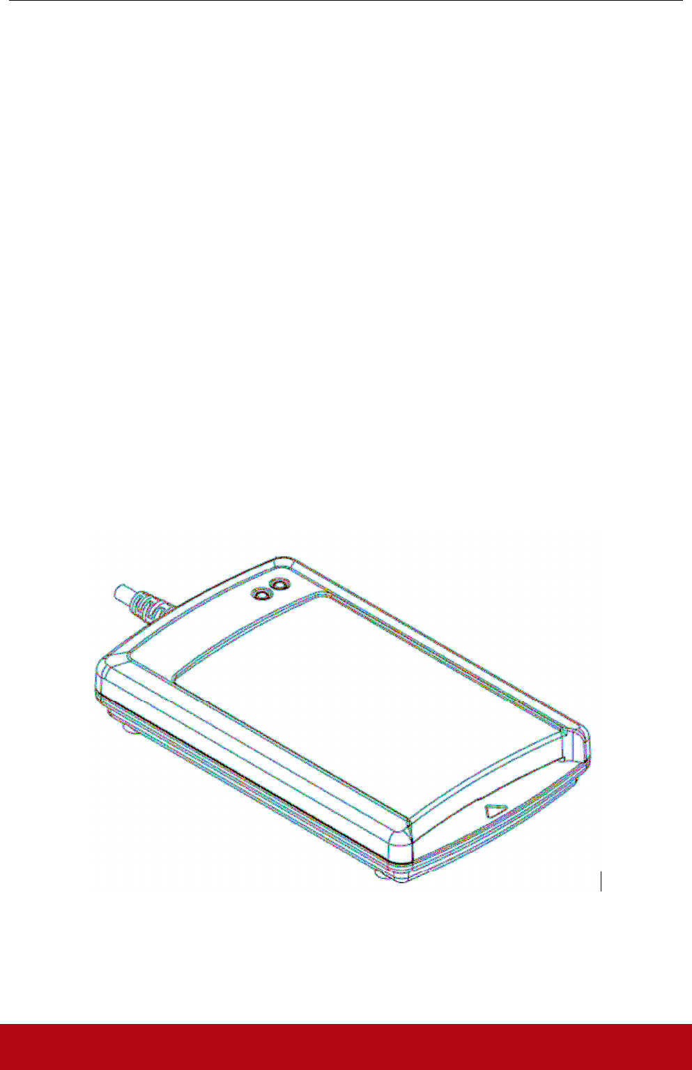
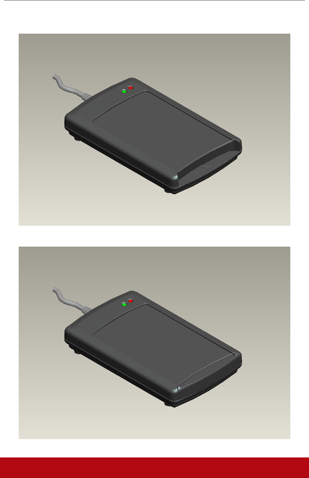
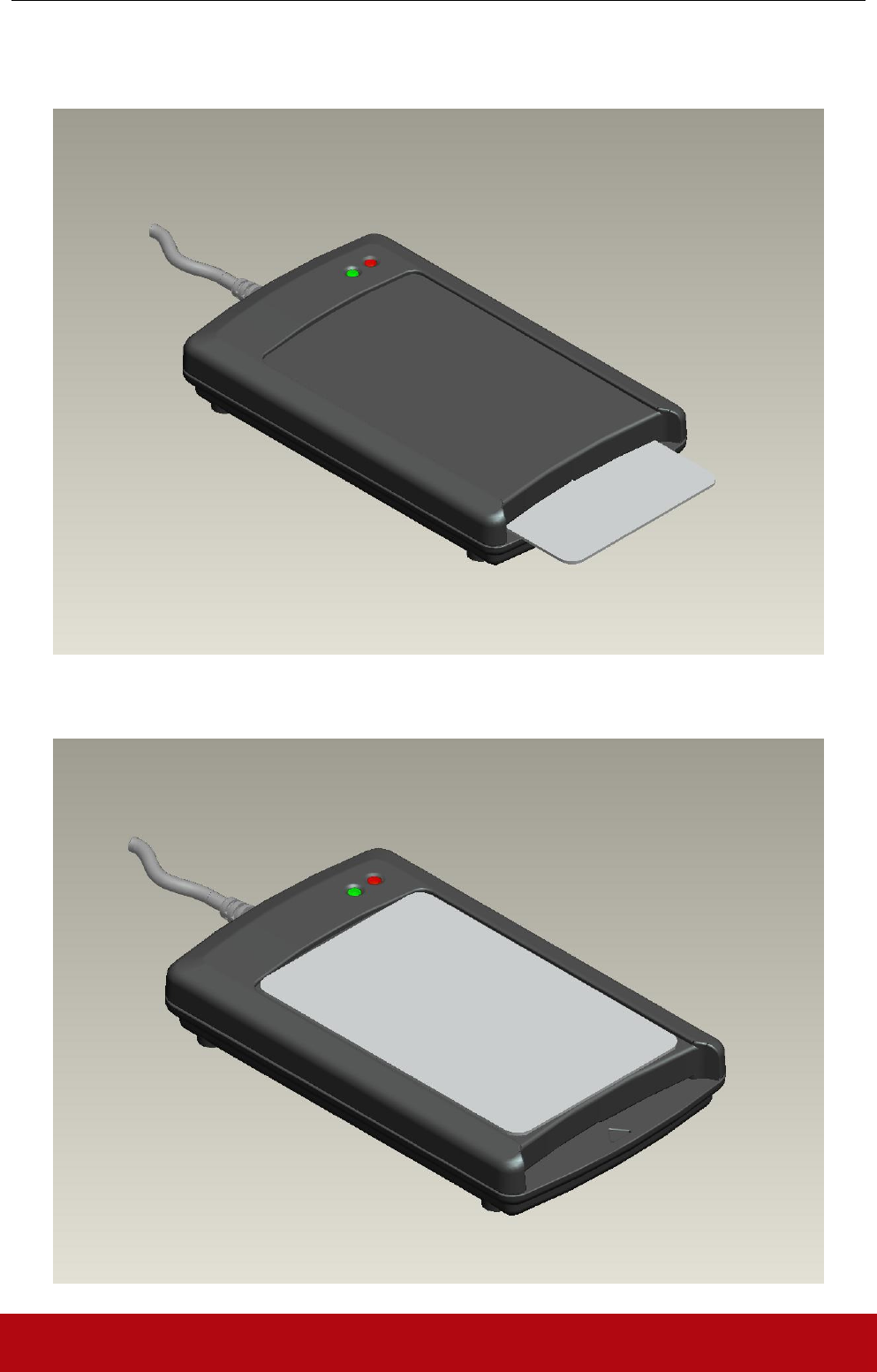
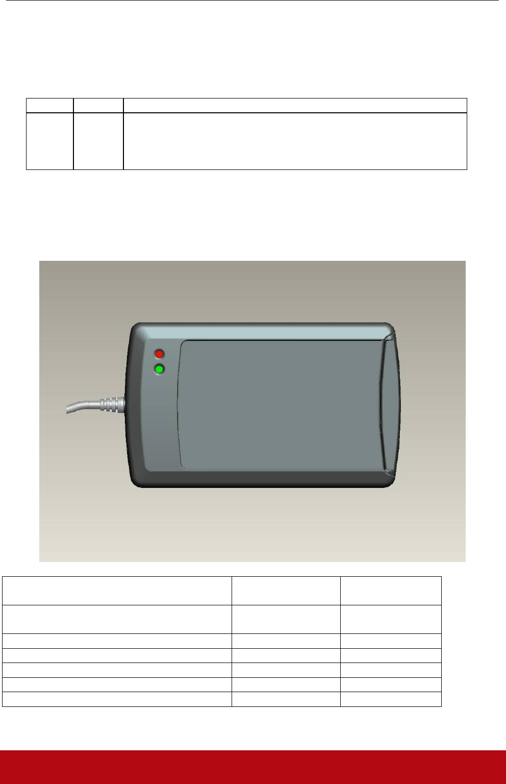
QUICK OVERVIEW OF THE ACR1281S READER
1. ACR1281S (with Contact Card Option)
2. ACR1281S (without Contact Card Option)
ACR1281S
Advanced Card Systems Ltd. Page 8 of 56
3. ACR1281S ICC Interface
4. ACR1281S PICC Interface
ACR1281S
Advanced Card Systems Ltd. Page 9 of 56
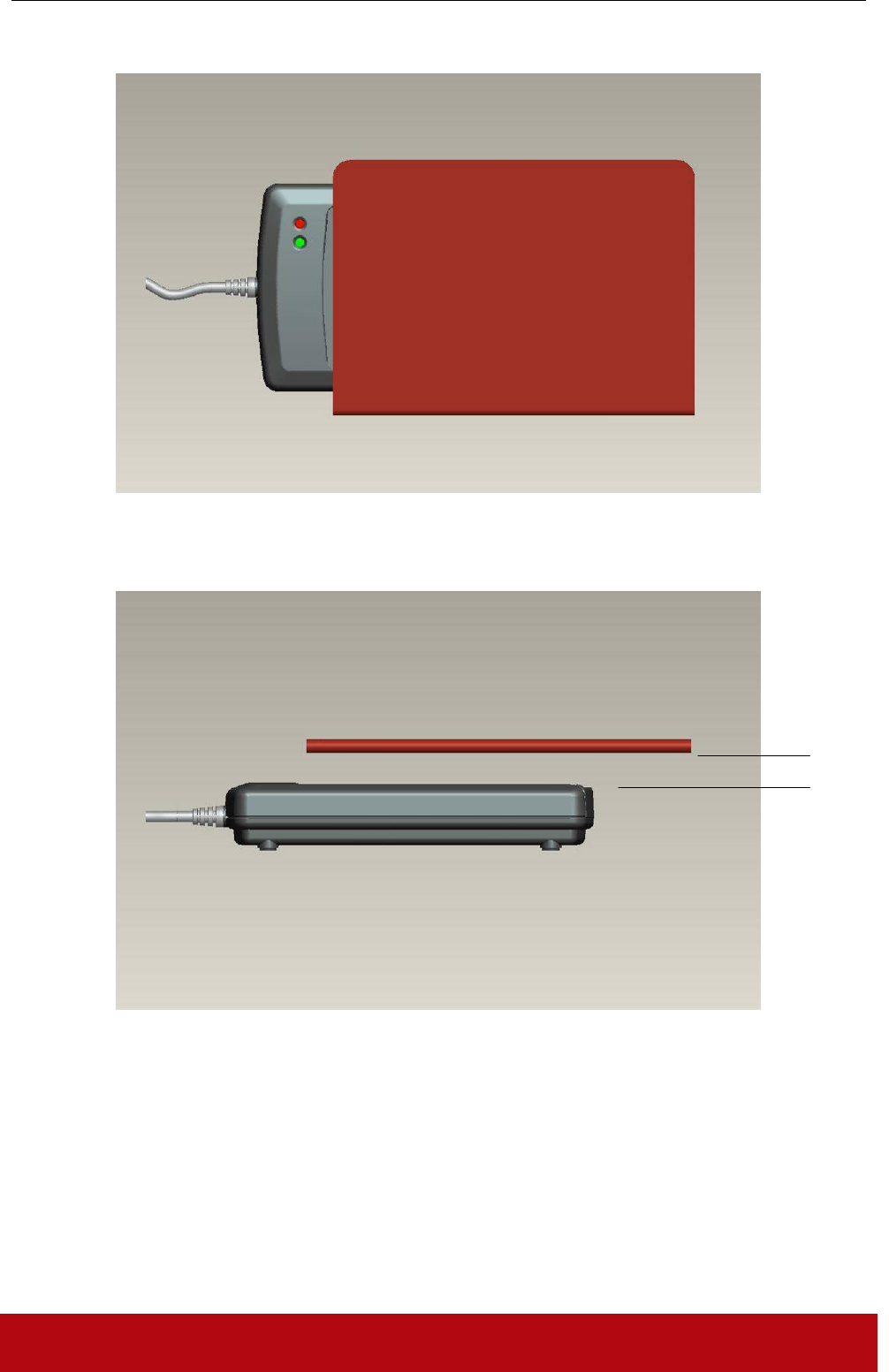
Recommended ICAO E-Passport Placement
• In case the E-Passport is not accessible, try to place the E-Passport above the reader by
5~10mm.
ICAO
E-Passport
5~10mm
ACR1281S
Advanced Card Systems Ltd. Page 10 of 56
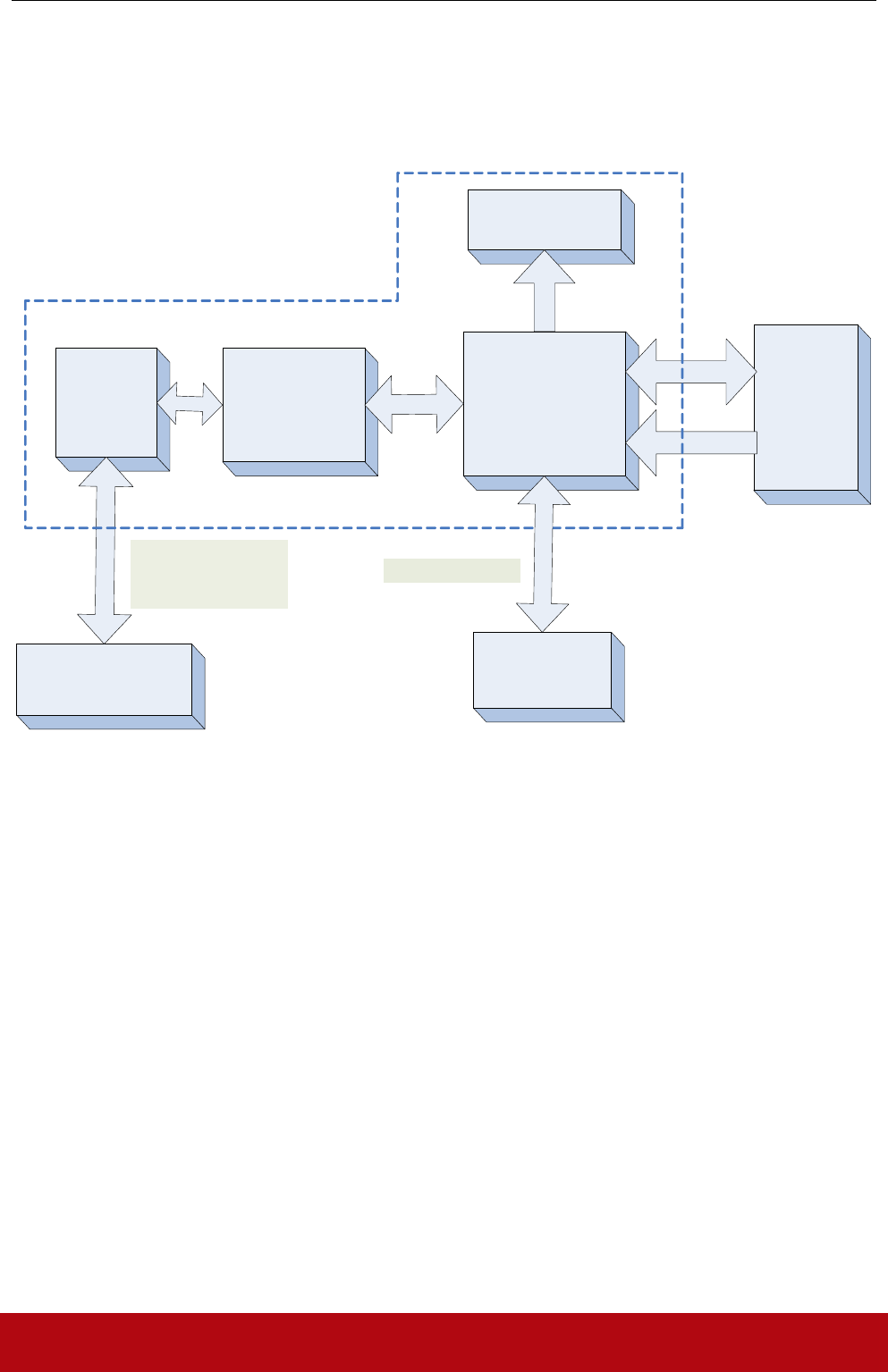
SYSTEM DESCRIPTION
1. The Reader Block Diagram
AT90SCR100H
Host Controller
LED & Buzzer
PC
Operation
System
Serial
USB
Firmware
Upgrade
RC531
NFC Interface
Chip
SPI
Built-In
Antenna
PICC
Contactless Card
Contactless Interface
Carrier = 13.56MHz
ISO7816 Interface
ICC
Contact Card
ACR1281S
Advanced Card Systems Ltd. Page 11 of 56
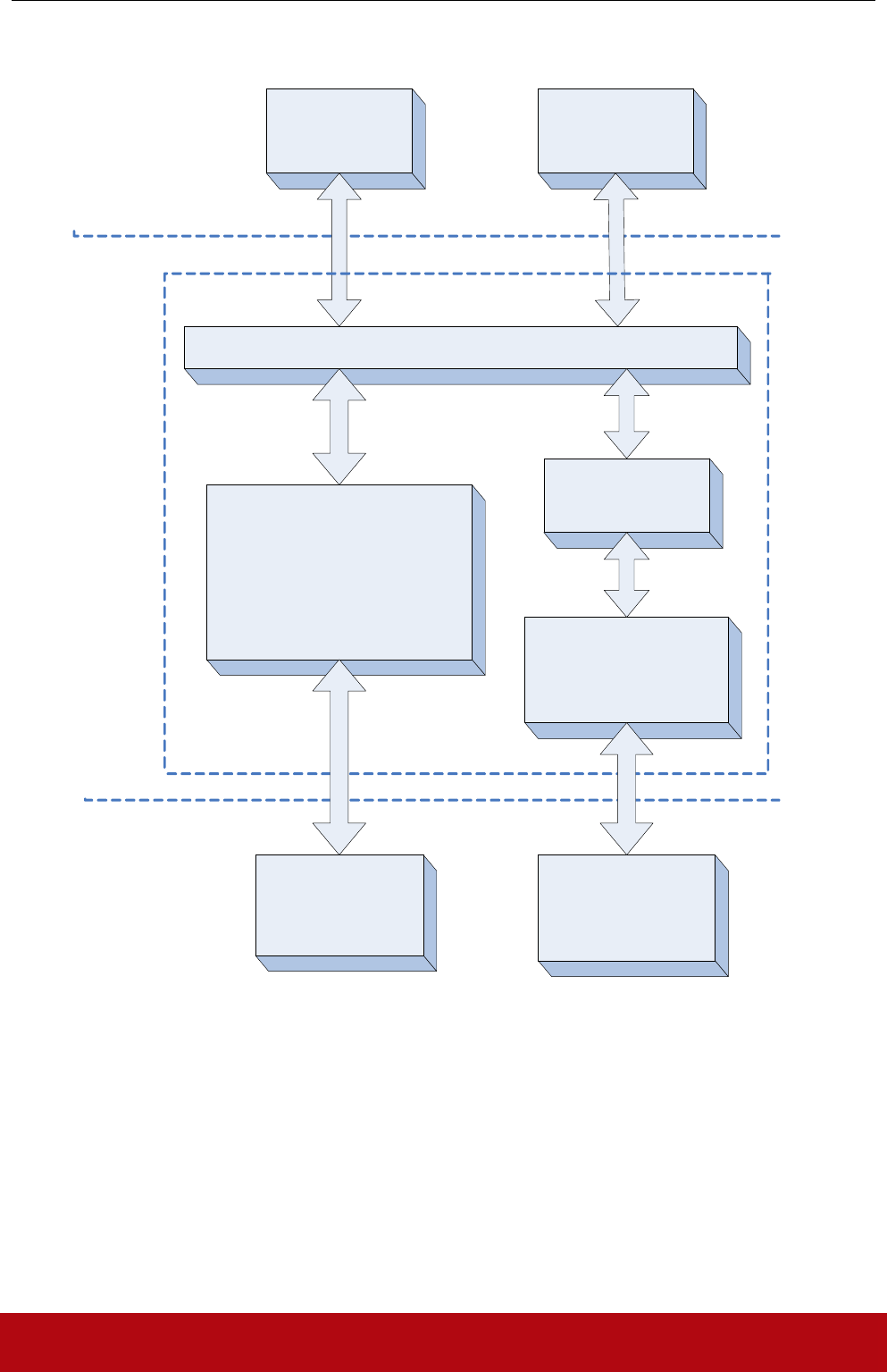
2. Communication Flow Chart of ACR1281S
PCSC Layer
ISO 7816 Part1-4
ICC Interface
T=CL &T=1
Emulation
ISO 14443 Part1-4
PICC Interface
ICC
(Landing Type
Acceptor )
PICC
(Built-In Antenna )
ACR1281S
ACR128U PCSC
ICC Interface
ACR128U PCSC
PICC Interface
Serial
Interface
(CCID
liked
Format)
Physical
Interface
ICC
And
PICC
Host
ACR1281S
Advanced Card Systems Ltd. Page 12 of 56
HARDWARE DESCRIPTION
3. USB Interface
The ACR1281S is connected to a Host through the RS232 Serial Interface; the max speed is up to
500kbps.
Pin Signal Function
1 VCC +5V power supply for the reader.
2 RXD The signal from the reader to the host.
3 TXD The signal from the host to the reader.
4 GND Reference voltage level for power supply
4. LED Indicator
The LEDs are used for showing the state of the contact and contactless interfaces.The Red LED is
used for showing PICC status and Green LED for ICC.
Reader States Red LED
PICC Indicator
Green LED
ICC Indicator
1. No PICC Found or PICC present but not
activated.
A single pulse per
~ 5 seconds
2. PICC is present and activated ON
3. PICC is operating Blinking
4. ICC is present and activated ON
5. ICC is absent or not activated OFF
6. ICC is operating Blinking

ACR1281S
Advanced Card Systems Ltd. Page 13 of 56
5. Buzzer
A monotone buzzer is used to show the “Card Insertion” and “Card Removal” events.
Events Buzzer
1. The reader powered up and initialization
success.
Beep
2. Card Insertion Event (ICC or PICC) Beep
3. Card Removal Event (ICC or PICC) Beep
6. ICC Interface (Contact Smart Card)
A landing type Smart Card Acceptor is used for providing reliable operations. The minimum life
cycle of the acceptor is about 300K times of card insertion and removal.
7. PICC Interface (Contactless Smart Card)
A built-in antenna is used for communication between the PCD and PICC.

ACR1281S
Advanced Card Systems Ltd. Page 14 of 56
SERIAL COMMUNICATION PROTOCOL (CCID-LIKED FRAME FORMAT)
Communication setting: 9600 bps(Default), 19200 bps, 38400 bps, 57600 bps and 115200
bps,128000bps, 250000bps, 500000bps.
Byte format: 8-N-1.
The communication protocol between the Host and ACR1281S is very similar to the CCID
protocol.
Command Frame Format
STX
(0x02)
Bulk-OUT Header APDU Command
Or
Parameters
Checksum
ETX
(0x03)
1 Byte 10 Bytes M Bytes
(If applicable)
1 Byte 1 Byte
NOTE: Checksum = XOR {Bulk-OUT Header, APDU Command or Parameters}
Status Frame Format
STX
(0x02)
Status Checksun
ETX
(0x03)
1 Byte 1 Byte 1 Byte 1 Byte
NOTE: Checksum = Status
Response Frame Format
STX
(0x02)
Bulk-IN Header APDU Response
Or
abData
Checksum
ETX
(0x03)
1 Byte 10 Bytes N Bytes
(If applicable)
1 Byte 1 Byte
NOTE: Checksum = XOR {Bulk-IN Header, APDU Response or abData}

ACR1281S
Advanced Card Systems Ltd. Page 15 of 56
8. Bulk-OUT Command
8.1 HOST_to_RDR_IccPowerOn
This command is used to activate the ICC and PICC . The ATR will be returned if available in
response “RDR_to_HOST_DataBlock” Format (See 2.1).
Command Frame Format
STX
(0x02)
Bulk-OUT Header
(HOST_to_RDR_IccPowerOn)
Parameters Checksum
ETX
(0x03)
1 Byte 10 Bytes 0 Byte 1 Byte 1 Byte
HOST_to_RDR_IccPowerOn Format
Offset Field Size Value Description
0 bMessageType 1 62h
1 dwLength
<LSB .. MSB>
4 00000000h Message-specific data length
5 bSlot 1 00h,01h 00h forPICC interface, 01h for ICC
6 bSeq 1 00h-FFh Sequence number for command
7 bPowerSelect 1 00h, 01h,
02h, 03h
Voltage that is applied to the ICC
00h – Automatic Voltage Selection
01h – 5.0 volts
02h – 3.0 volts
03h – 1.8 volts
8 abRFU 2 Reserved for Future Use
Note: The ICC interface must be activated before access contact cards while PICC interface is
optional.
Example: Power on PICC slot
Command: 02 62 00 00 00 00 00 00 00 00 00 62 03
ACK: 02 00 00 03
Response: 02 80 10 00 00 00 00 00 00 81 00 3B 8B 80 01 4A 43 4F 50 33 31 33 36 47 44 54 4C
2A 03
8.2 HOST_to_RDR_IccPowerOff
This command is used to deactivate the ICC. For PICC, it does nothing.
Command Frame Format
STX
(0x02)
Bulk-OUT Header
(HOST_to_RDR_IccPowerOff)
Parameters Checksum
ETX
(0x03)
1 Byte 10 Bytes 0 Byte 1 Byte 1 Byte
HOST_to_RDR_IccPowerOff Format
Offset Field Size Value Description
0 bMessageType 1 63h
1 dwLength
<LSB .. MSB>
4 00000000h Message-specific data length
5 bSlot 1 00h,01h 00h forPICC interface, 01h for ICC
6 bSeq 1 00-FFh Sequence number for command
7 abRFU 3 Reserved for Future Use

ACR1281S
Advanced Card Systems Ltd. Page 16 of 56
Example: Power off PICC slot
Command: 02 63 00 00 00 00 00 00 00 00 00 63 03
ACK: 02 00 00 03
Response: 02 81 00 00 00 00 00 00 00 81 00 00 03
8.3 HOST_to_RDR_XfrBlock
This command is used to exchange APDUs between the Host and ACR1281S.
Command Frame Format
STX
(0x02)
Bulk-OUT Header
(HOST_to_RDR_XfrBlock)
APDU Commands Checksum
ETX
(0x03)
1 Byte 10 Bytes M Bytes 1 Byte 1 Byte
HOST_to_RDR_XfrBlock Format
Offset Field Size Value Description
0 bMessageType 1 6Fh
1 dwLength
<LSB .. MSB>
4 M Message-specific data length
5 bSlot 1 00h,01h 00h forPICC interface, 01h for ICC
6 bSeq 1 00-FFh Sequence number for command
7 bBWI 1 00-FFh Used to extend the Block Waiting
Timeout.
8 wLevelParameter
2 0000h
10 abData Byte
array
Data sent to the reader.
Example: Read 256 bytes from PICC slot
Command: 02 6F 05 00 00 00 00 00 00 00 00 80 B2 00 00 00 58 03
ACK: 02 00 00 03
Response: 02 80 02 01 00 00 00 00 00 81 00 01 02 03 04 05 06 07 08 09 0A 0B 0C 0D 0E 0F 10
11 12 13 14 15 16 17 18 19 1A 1B 1C 1D 1E 1F 20 21 22 23 24 25 26 27 28 29 2A 2B 2C 2D 2E
2F 30 31 32 33 34 35 36 37 38 39 3A 3B 3C 3D 3E 3F 40 41 42 43 44 45 46 47 48 49 4A 4B 4C
4D 4E 4F 50 51 52 53 54 55 56 57 58 59 5A 5B 5C 5D 5E 5F 60 61 62 63 64 65 66 67 68 69 6A
6B 6C 6D 6E 6F 70 71 72 73 74 75 76 77 78 79 7A 7B 7C 7D 7E 7F 80 81 82 83 84 85 86 87 88
89 8A 8B 8C 8D 8E 8F 90 91 92 93 94 95 96 97 98 99 9A 9B 9C 9D 9E 9F A0 A1 A2 A3 A4 A5
A6 A7 A8 A9 AA AB AC AD AE AF B0 B1 B2 B3 B4 B5 B6 B7 B8 B9 BA BB BC BD BE BF
C0 C1 C2 C3 C4 C5 C6 C7 C8 C9 CA CB CC CD CE CF D0 D1 D2 D3 D4 D5 D6 D7 D8 D9 DA
DB DC DD DE DF E0 E1 E2 E3 E4 E5 E6 E7 E8 E9 EA EB EC ED EE EF F0 F1 F2 F3 F4 F5 F6
F7 F8 F9 FA FB FC FD FE FF 00 90 00 92 03
8.4 HOST_to_RDR_GetSlotStatus
This command is used to get the status of ICC, PICC slots.
Command Frame Format
STX
(0x02)
Bulk-OUT Header
(HOST_to_RDR_XfrBlock)
Parameters Checksum
ETX
(0x03)
1 Byte 10 Bytes 0 Byte 1 Byte 1 Byte
HOST_to_RDR_GetSlotStatus Format
ACR1281S
Advanced Card Systems Ltd. Page 17 of 56
Offset Field Size Value Description
0 bMessageType 1 65h
1 dwLength
<LSB .. MSB>
4 00000000h Message-specific data length
5 bSlot 1 00h,01h 00h forPICC interface, 01h for ICC
6 bSeq 1 00-FFh Sequence number for command
7 abRFU 3 Reserved for Future Use
8.5 HOST_to_RDR_SetParameters
This command is used to change the parameters for contact interface to implement PPS.
Command Frame Format
STX
(0x02)
Bulk-OUT Header
(HOST_to_RDR_XfrBlock)
Parameters Checksum
ETX
(0x03)
1 Byte 10 Bytes 5 or 7 bytes 1 Byte 1 Byte
HOST_to_RDR_SetParameters Format
Offset Field Size Value Description
0 bMessageType 1 61h
1 dwLength
<LSB .. MSB>
4 00000005h,
00000007h
Message-specific data length
5 bSlot 1 00h,01h 00h forPICC interface, 01h for ICC
6 bSeq 1 00-FFh 00h for protocol T=0, 01h for T=1.
7 bProtocolNum 1 00h,01h Used to extend the Block Waiting
Timeout.
8 abRFU 2 Reserved for Future Use
10 abProtocolDataStructure
Byte
array
Protocol Data Structure
Remarks:
For protocol T = 0, dwLength = 00000005h; for protocol T = 1, dwLength = 00000007h. More
detail about the abProtocolDataStructure field, please refer to CCID specification.
8.6 HOST_to_RDR_Escape
This command is used to peripherals control such as LED & Buzzer control, Get firmware
Version, set the serial communication mode and so on.
Command Frame Format
STX
(0x02)
Bulk-OUT Header
(HOST_to_RDR_XfrBlock)
Commands Checksum
ETX
(0x03)
1 Byte 10 Bytes M bytes 1 Byte 1 Byte
HOST_to_RDR_Escape Format
Offset Field Size Value Description
0 bMessageType 1 6Bh
1 dwLength
<LSB .. MSB>
4 M Message-specific data length

ACR1281S
Advanced Card Systems Ltd. Page 18 of 56
5 bSlot 1 00h,01h 00h for PICC interface, 01h for ICC
6 bSeq 1 00-FFh 00h for protocol T=0, 01h for T=1.
7 abRFU 3 Reserved for Future Use
10 abData Byte
array
Data block sent to the reader.
Example for buzzer on 50ms :
Command: 02 6B 06 00 00 00 01 00 00 00 00 E0 00 00 28 01 05 A0 03
ACK: 02 00 00 03
Response: 02 83 06 00 00 00 01 00 02 00 00 E1 00 00 00 01 05 63 03

ACR1281S
Advanced Card Systems Ltd. Page 19 of 56
9. Bulk-IN Response
9.1 RDR_to_HOST_DataBlock
The reader in response to the “HOST_to_RDR_IccPowerOn” and “HOST_to_RDR_XfrBlock”
command messages.
Response to the “HOST_to_RDR_IccPowerOn”:
Response Frame Format
STX
(0x02)
Bulk-IN Header
(RDR_to_HOST_DataBlock)
abData Checksum
ETX
(0x03)
1 Byte 10 Bytes N Bytes of ATR
(If card is available)
1 Byte 1 Byte
RDR_to_HOST_DataBlock Format
Offset Field Size Value Description
0 bMessageType 1 80h Indicates that a data block is being
sent from the ACR1281S
1 dwLength
<LSB .. MSB>
4 N Size of abData field. (N Bytes)
5 bSlot
1 Same as
Bulk-OUT
00h for PICC interface, 01h for ICC
6 bSeq 1 Same as
Bulk-OUT
Sequence number for corresponding
command.
7 bStatus 1
8 bError 1
9 bChainParameter
1
Response to “HOST_to_RDR_XfrBlock”
Response Frame Format
STX
(0x02)
Bulk-IN Header
(RDR_to_HOST_DataBlock)
abData Checksum
ETX
(0x03)
1 Byte 10 Bytes N Bytes 1 Byte 1 Byte
RDR_to_HOST_DataBlock Format
Offset Field Size Value Description
0 bMessageType 1 80h Indicates that a data block is being
sent from the ACR1281S
1 dwLength
<LSB .. MSB>
4 N Size of abData field. (N Bytes)
5 bSlot
1 Same as
Bulk-OUT
00h for PICC interface, 01h for ICC
6 bSeq 1 Same as
Bulk-OUT
Sequence number for corresponding
command.
7 bStatus 1
8 bError 1
9 bChainParameter
1

ACR1281S
Advanced Card Systems Ltd. Page 20 of 56
9.2 RDR_to_HOST_SlotStatus
The reader in response to the “HOST_to_RDR_IccPowerOff” and
“HOST_to_RDR_GetSlotStatus” command messages.
Response Frame Format
STX
(0x02)
Bulk-IN Header
(RDR_to_HOST_SlotStatus)
abData Checksum
ETX
(0x00)
1 Byte 10 Bytes 0 Byte 1 Byte 1 Byte
RDR_to_HOST_SlotStatus Format
Offset Field Size Value Description
0 bMessageType 1 81h Indicates that a data block is being
sent from the ACR1281S
1 dwLength
<LSB .. MSB>
4 00000000h Size of abData field. (0 Bytes)
5 bSlot
1 Same as
Bulk-OUT
00h for PICC, 01h for ICC
6 bSeq 1 Same as
Bulk-OUT
Sequence number for corresponding
command
7 bStatus 1
8 bError 1
9 bClockStatus 1
9.3 RDR_to_HOST_Parameters
The reader in response to the “HOST_to_RDR_SetParameters” command messages.
Response Frame Format
STX
(0x02)
Bulk-IN Header
(RDR_to_HOST_SlotStatus)
abData Checksum
ETX
(0x00)
1 Byte 10 Bytes 5 or 7 Bytes 1 Byte 1 Byte
RDR_to_HOST_SlotStatus Format
Offset Field Size Value Description
0 bMessageType 1 82h Indicates that a data block is being
sent from the ACR1281S
1 dwLength
<LSB .. MSB>
4 00000005h,
00000007h
Size of abData field.
5 bSlot
1 Same as
Bulk-OUT
00h for PICC, 01h for ICC
6 bSeq 1 Same as
Bulk-OUT
Sequence number for corresponding
command
7 bStatus 1
8 bError 1
9 bProtocolNum 1
10 abProtocolDataStructure
Byte
array
Protocol Data Structure
Remarks:
For protocol T = 0, dwLength = 00000005h; for protocol T = 1, dwLength = 00000007h. More
detail about the abProtocolDataStructure field, please refer to CCID specification.
ACR1281S
Advanced Card Systems Ltd. Page 21 of 56
9.4 RDR_to_HOST_Escape
The reader in response to “HOST_to_RDR_Escape” command messages.
Response Frame Format
STX
(0x02)
Bulk-IN Header
(RDR_to_HOST_DataBlock)
abData Checksum
ETX
(0x03)
1 Byte 10 Bytes N Bytes 1 Byte 1 Byte
RDR_to_HOST_Escape Format
Offset Field Size Value Description
0 bMessageType 1 83h Indicates that a data block is being
sent from the ACR1281S
1 dwLength
<LSB .. MSB>
4 N Size of abData field. (N Bytes)
5 bSlot
1 Same as
Bulk-OUT
00h for PICC, 01h for ICC
6 bSeq 1 Same as
Bulk-OUT
Sequence number for corresponding
command
7 bStatus 1
8 bError 1
9 bRFU 1 00h Reserved for Future Use
10 abData Byte
array
Data sent from reader.
10. RDR_to_PC_NotifySlotChange Messages
This message is used to report the Card Insertion/Removal Event to the HOST.
Frame Format
STX
(0x02)
Interrupt-In Messages Checksum
ETX
(0x03)
1 Byte 2 Bytes 1 Byte 1 Byte

ACR1281S
Advanced Card Systems Ltd. Page 22 of 56
RDR_to_PC_NotifySlotChange Format
Offset Field Size Value Description
0 bMessageType 1 50h
1 bmSlotCardState 1 Each slot has 2 bits. The least
significant bit reports the current
state of the slot (0b = no card present,
1b = card present). The most
significant bit reports whether the
slot has changed state since the last
RDR_to_PC_NotifySlotChange
message was sent (0b = no change,
1b = change).
bmSlotCardState Bit Map
Offset Field Description
Bit0 Slot 0 current state PICC slot state
Bit1 Slot 0 changed status PICC slot changed status
Bit2 Slot 1 current state ICC slot state
Bit3 Slot 1 changed status ICC slot changed status
Bit4 Slot 2 current state RFU
Bit5 Slot 2 changed status RFU
Bit6 RFU RFU
Bit7 RFU RFU

ACR1281S
Advanced Card Systems Ltd. Page 23 of 56
11. Error Handling
- ACK Frame: {02 00 00 03}.
If the frame sent by the HOST is correctly received by the RDR, a positive status frame = {02
00 00 03} will be sent to the HOST immediately to inform the HOST the frame is correctly
received. The HOST has to wait for the response of the command. The RDR will not receive any
more frames while the command is being processed.
- NAK Frame = {02 00 00 00 00 00 00 00 00 00 00 00 03} // 11 zeros
The NAK Frame is only used by the HOST to get the last response or card insertion/ removal
event messages.
In case of errors, a negative status frame will be sent to the HOST to indicate the frame is either
corrupted or wrong formatted.
- Checksum Error Frame = {02 FF FF 03}.
The received data checksum is not correct.
- Length Error Frame = {02 FE FE 03}.
The length “dwLength” is greater than 0x0105 bytes.
- ETX Error Frame = {02 FD FD 03}.
The last byte is not equal to ETX “0x03”.
- Slot error Frame = {02 FB FB 03}.
The Slot number is not 00 or 01 .
- Time out Error Frame : {02 99 99 03}.
The time of data transmit is over.

ACR1281S
Advanced Card Systems Ltd. Page 24 of 56
12. Protocol Flow Examples
1) Activate a ICC
HOST RDR
1. HOST sends a frame 02 62 00 00 00 00 01 00 00 00 00 63 03
2. RDR sends back a
positive status frame
immediately
02 00 00 03 (positive status frame)
.. after some processing delay ..
3. RDR sends back the
response of the command
02 80 13 00 00 00 01 00 00 81 00 3B BE 11 00
00 41 01 38 00 00 01 00 00 00 00 00 01 90 00 6F
03
2) Activate a ICC (Incorrect Checksum, HOST )
HOST RDR
1. HOST sends a corrupted
frame
02 62 00 00 00 00 01 00 00 00 00 [Incorrect
Checksum] 03
2. RDR sends back a
negative status frame
immediately
02 FF FF 03 (negative status frame)
3. HOST sends the frame
again.
02 62 00 00 00 00 01 00 00 00 00 63 03
4. RDR sends back a
positive status frame
immediately
02 00 00 03 (positive status frame)
.. after some processing delay ..
5. RDR sends back the
response of the command
02 80 13 00 00 00 01 00 00 81 00 3B BE 11 00
00 41 01 38 00 00 01 00 00 00 00 00 01 90 00 6F
03
3) Activate a ICC (Incorrect Checksum, RDR)
HOST RDR
1. HOST sends a frame 02 62 00 00 00 00 01 00 00 00 00 63 03
2. RDR sends back a
positive status frame
immediately
02 00 00 03 (positive status frame)
.. after some processing delay ..
3. RDR sends back the
response (corrupted) of the
command
4. HOST sends a NAK
frame to get the response
again.
5. RDR sends back the
response of the command
02 80 13 00 00 00 01 00 00 81 00 3B BE 11 00
00 41 01 38 00 00 01 00 00 00 00 00 01 90 00
[Incorrect Checksum] 03
02 00 00 00 00 00 00 00 00 00 00 00 03
02 80 13 00 00 00 01 00 00 81 00 3B BE 11 00
00 41 01 38 00 00 01 00 00 00 00 00 01 90 00 6F
03

ACR1281S
Advanced Card Systems Ltd. Page 25 of 56
4) Exchange APDU with ICC
HOST RDR
1. HOST sends a frame
02 6F 05 00 00 00 01 00 00 00 00 80 84 00 00 08
67 03
2. RDR sends back a
positive status frame
immediately
02 00 00 03 (positive status frame)
.. after some processing delay ..
3. RDR sends back the
response of the command
:02 80 0A 00 00 00 01 00 00 81 00 C2 FF 2D 23
C5 F6 5C F2 90 00 34 03
APDU Command: 80 84 00 00 08
APDU Response: 22 5C E9 1C A4 5A A4 D6 90 00
5) Insert contact card into the ICC slot
HOST RDR
1. Insert contact card into
the ICC slot
2. RDR sends a Interrupt-In
Message frame to HOST
02 50 0C [Checksum] 03
3. Present contactless card
to the Antenna field
4. RDR sends a Interrupt-In
Message frame to HOST
02 50 07 [Checksum] 03
5. HOST sends a NAK
frame to get the Message
again.
->
6. RDR sends back the last
messages.
02 50 07 [Checksum] 03

ACR1281S
Advanced Card Systems Ltd. Page 26 of 56
PERIPHERALS CONTROL
The reader’s peripherals control is implemented by Escape Command.
1. Set Serial Communication Mode
APDU Command = {44 “CMD”}
APDU Response = {90 “Status”}
CMD Bit Map
Offset Description Description
Bit 0-3 Indicate Serial
Communication Speed
0 = 9600bps(Default)
1= 19200bps
2 = 38400bps
3 = 57600bps
4 = 115200bps
5 = 128000bps
6 = 230400bps
7 = 250000bps
8 = 256000bps
9 = 500000bps
Other value reserve for future use.
Bit 4 RFU RFU
Bit 5 RFU RFU
Bit 6 RFU RFU
Bit 7 Interrupt-In Message(CCID-
liked Format)
1 = Report Interrupt-In Message.
0 = Not report(Default).
The “Status” bit map is the same as “CMD”.
Example: change the communication speed to 115200bps
Command:
02 6B 02 00 00 00 01 00 00 00 00 44 04 28 03
ACK :
02 00 00 03
Response:
02 83 02 00 00 00 01 00 00 81 00 90 04 95 03
Remarks:
After the communication speed is changed successfully, the program has to adjust its
communication speed so as to continue the rest of the data exchanges.
The initial communication speed is 9600 bps (Default) and not report Interrupt-In Message.
2. Get Firmware Version
APDU Command = {E0 00 00 18 00}
APDU Response = {E1 00 00 00 “Frame Length” {Firmware Version}}
Example:
Command: 02 6B 05 00 00 00 01 00 00 00 00 E0 00 00 18 00 97 03
ACK:
02 00 00 03
Response: 02 83 12 00 00 00 01 00 00 81 00 E0 00 00 00 00 41 43 52 31 32 38 31 53 20 56 31 30
33 BC 03
In which, Firmware Version = 11 bytes;
e.g. Response = E1 00 00 00 0F 41 43 52 31 32 38 31 53 20 56 31 30 33

ACR1281S
Advanced Card Systems Ltd. Page 27 of 56
Firmware Version (HEX) = 41 43 52 31 32 38 31 53 20 56 31 30 33
Firmware Version (ASCII) = “ACR1281S V103”
3. Enter Firmware Upgrade Mode
Command = {FF 00 00 E0 00}
Response = {FF 00 00 E1 02 90 00}
Example:
Command: 02 6B 05 00 00 00 01 00 00 00 00 FF 00 00 E0 00 70 03
ACK:
02 00 00 03
Response: 02 83 07 00 00 00 01 00 00 00 00 FF 00 00 E1 02 90 00 09 03
Hints:
After the response display, the reader will enter the firmware upgrade mode that the reader can be
upgraded firmware.
4. LED Control
Setting the LED State:
APDU Command = {E0 00 00 29 01 “CMD”}.
APDU Response = {E1 00 00 00 01 “Status”}
Reading the existing LED State:
APDU Command = {E0 00 00 29 00}.
APDU Response = {E1 00 00 00 01 “Status”}
CMD Bit Map
CMD Description Description
Bit 0 RED LED 1 = ON; 0 = OFF
Bit 1 GREEN LED 1 = ON; 0 = OFF
Bit 2 RFU RFU
Bit 3 RFU RFU
Bit 4 RFU RFU
Bit 5 RFU RFU
Bit 6 RFU RFU
Bit 7 RFU RFU
The “Status” bit map is the same as “CMD”.
Example: Red LED ON
Command: 02 6B 06 00 00 00 01 00 00 00 00 E0 00 00 29 01 01 A5 03
ACK:
02 00 00 03
Response: 02 83 06 00 00 00 01 00 00 81 00 E0 00 00 00 01 01 E5 03

ACR1281S
Advanced Card Systems Ltd. Page 28 of 56
5. Buzzer Control
Setting the Buzzer State:
APDU Command = {E0 00 00 28 01 “Duration”} Unit = 10mS
00 = Turn off
01 ~ FE = Duration
FF = Turn o
APDU Response = {E1 00 00 00 01 “Status”}
Reading the existing Buzzer State:
APDU Command = {E0 00 00 28 00}
APDU Response = {E1 00 00 00 01 “Status”}
Example for buzzer on 50ms :
Command: 02 6B 06 00 00 00 01 00 00 00 00 E0 00 00 28 01 05 A0 03
ACK: 02 00 00 03
Response: 02 83 06 00 00 00 01 00 00 81 00 E0 00 00 00 01 05 E1 03
6. Default LED and Buzzer State
CMD MODE Description
Bit 0 ICC Activation Status
LED
To show the activation status of the
ICC interface.
1 = Enable; 0 =Disable
Bit 1 PICC Polling Status LED To show the PICC Polling Status.
1 = Enable; 0 =Disable
Bit 2 PICC Activation Status LED To show the activation status of the
PICC interface
1 = Enable; 0 =Disable
Bit 3 Card Insertion and Removal
Events Buzzer
To make a beep whenever a card
insertion or removal event is
detected. (For both ICC and PICC)
1 = Enable; 0 =Disabled
Bit 4 RFU RFU
Bit 5 RFU RFU
Bit 6 RFU RFU
Bit 7 Card Operation Blinking
LED
To blink the LED whenever the card
(PICC or ICC) is being accessed.
Setting the LED and Buzzer behaviors:
Command = { E0 00 00 21 01 “CMD”}. Default value of CMD = 8F;
Response = {E1 00 00 00 01 “Status”}
Reading the existing behaviors of the LED and Buzzer:
Command = { E0 00 00 21 00}
Response = {E1 00 00 00 01 “Status”}
Hints:
If you want to enjoy the silent environment, just set the CMD value to “87”.

ACR1281S
Advanced Card Systems Ltd. Page 29 of 56
7. Automatic PICC Polling
Whenever the reader is connected to the PC, the PICC polling function will start the PICC scanning
to determine if a PICC is placed on / removed from the built-antenna.
We can send a command to disable the PICC polling function. The command is sent through the
PCSC Escape command interface. To meet the energy saving requirement, special modes are
provided for turning off the antenna field whenever the PICC is inactive, or no PICC is found. The
reader will consume less current in power saving mode.
Register 0x23: Automatic PICC Polling (Default value = 0x8F)
CMD Description Description
Bit 0 Auto PICC Polling 1 = Enable; 0 =Disable
Bit 1 Turn off Antenna Field if no
PICC found
1 = Enable; 0 =Disable
Bit 2 Turn off Antenna Field if the
PICC is inactive.
1 = Enable; 0 =Disable
Bit 3 Activate the PICC when
detected.
1 = Enable; 0 =Disable
Bit 5 .. 4 PICC Poll Interval for PICC <Bit 5 – Bit 4>
<0 – 0> = 250 msec
<0 – 1> = 500 msec
<1 – 0> = 1000 msec
<1 – 1> = 2500 msec
Bit 6 RFU -
Bit 7 Enforce ISO14443A Part 4 1= Enable; 0= Disable.
• Enable Auto PICC Polling Function = { E0 00 00 23 01 8F}
• Disable Auto PICC Polling Function = { E0 00 00 23 01 8E}
• Read the existing status = { E0 00 00 23 00}; Response = {E1 00 00 00 01 “Status”}
Hints:
1. It is recommended to enable the option “Turn Off Antenna Field if the PICC is inactive”, so that
the “Inactive PICC” will not be exposed to the field all the time so as to prevent the PICC from
“warming up”.
2. The longer the PICC Poll Interval, the more efficient of energy saving. However, the response
time of PICC Polling will become longer. The Idle Current Consumption in Power Saving Mode is
about 60mA, while the Idle Current Consumption in Non-Power Saving mode is about 130mA.
#Idle Current Consumption = PICC is not activated.
3. The reader will activate the ISO14443A-4 mode of the “ISO14443A-4 compliant PICC”
automatically. Type B PICC will not be affected by this option.
4. The JCOP30 card comes with two modes: ISO14443A-3 (MIFARE 1K) and ISO14443A-4
modes. The application has to decide which mode should be selected once the PICC is activated.
8. PICC Polling for specific PICC Types
The PICC polling function can be configured to detect “ISO14443 Type A PICCs” or “ISO14443
Type B PICCs” or both.

ACR1281S
Advanced Card Systems Ltd. Page 30 of 56
• ISO 14443 Type A PICCs Only = { E0 00 00 20 01 01}
• ISO 14443 Type B PICCs Only = { E0 00 00 20 01 02 }
• ISO 14443 Type A and B PICCs = { E0 00 00 20 01 03} #default setting
• Read the existing status = { E0 00 00 20 00}; Response = {E1 00 00 00 01 “Status”}
Hints:
1. It is recommended to specific the PICC types in the application so as to speed up the card
detection process.
9. Auto PPS for the PICC Interface (Communication Speed Change)
Whenever a PICC is recognized, the reader will try to change the communication speed between
the PCD and PICC defined by the Maximum Connection Speed. If the card does not support the
proposed connection speed, the reader will try to connect the card with a slower speed setting.
• Set Connection Speed = {E0 00 00 24 02 “Max Tx Speed” “Max Rx Speed”}
<Max Tx Speed> & <Current Tx Speed> or <Max Rx Speed> & <Current Rx Speed>
106k bps = 00
212k bps = 01
424k bps = 02 #default setting
848k bps = 03
• Read the existing status = {E0 00 00 24 00};
Response = {E1 00 00 00 04 “Max Tx Speed” “Current Tx Speed” “Max Rx Speed”
“Current Rx Speed”}
Hints:
1. Normally, the application should know the maximum connection speed of the PICCs being used.
#The environment also affects the maximum achievable speed. The reader just uses the proposed
communication speed to talk with the PICC. The PICC will become inaccessible if the PICC or
environment does not meet the requirement of the proposed communication speed.
2. The reader supports different speed between sending and receiving.
10. Antenna Field ON/OFF for the PICC Interface
This command is used for turning on/off the antenna field.
• Antenna Field ON APDU Command = {E0 00 00 25 01 01}
• Antenna Field OFF APDU Command = {E0 00 00 25 01 00}
• Read the existing status APDU Command = {E0 00 00 25 00};
• APDU Response = {E1 00 00 00 01 “Status”}
Hints:
1. Make sure the Auto PICC Polling is disabled first before turning off the antenna field.
11. Exclusive Mode Configure

ACR1281S
Advanced Card Systems Ltd. Page 31 of 56
To speed up the card detection time, we can enable the “Enforce ICC & PICC Exclusive Mode”
• Enforce ICC & PICC Exclusive Mode = {E0 00 00 2B 01 “New Mode Configuration”}.
<New Mode Configuration> #default value 01
00 = Both ICC & PICC interfaces can be activated at the same time.
01 = Either ICC or PICC interface can be activated at any one time. But not both!
• Read the existing status = {E0 00 00 2B 00}
Response {E1 00 00 00 01 “Current Mode”}
<Current Mode >
00 = Exclusive Mode is not activated. PICC Interface is available.
01 = Exclusive Mode is activated now. PICC Interface is not available until the ICC interface is
deactivated.
Hints:
1.Don’t insert any card into the contact card acceptor while the PICC is activate,or the PICC may
be deselected.
12. Request Command Test
This command is used for sending REQA/REQB by the reader to test antenna field and the
response.
• Command = {E0 00 00 26 02 “Command” “Speed”}
• Response = {E1 00 00 00 “Length” “Data”}
Command coding:
REQA = 01
REQB = 02
WUPA = 03
WUPB = 04
Speed coding:
106k bps = 00
212k bps = 01
424k bps = 02
Length:
No response: 00
ATQA: 02
ATQB: 0C
Others: RFU
Data:
Response Data (ATQA/ATQB/Others)
Hints:
1. Make sure the Auto PICC Polling is disabled first before sending this command.

ACR1281S
Advanced Card Systems Ltd. Page 32 of 56
13. Continuous Wake Up Command Sending Test for the PICC Interface
This command is used for sending WUPA/WUPB by the reader continuously to test antenna field.
• Command = {E0 00 00 27 02 “Command” “Speed”}
• Disable Command Sending = { E0 00 00 27 02 00 00}
• Response = {E1 00 00 00 01 “Status”}
Command coding:
WUPA = 01
WUPB = 02
Speed coding:
106k bps = 00
212k bps = 01
424k bps = 02
Status:
WUPA Sending = 01
WUPB Sending = 02
Hints:
1. Make sure the Auto PICC Polling is disabled first before sending this command.
2. The reader will send the command continuously as long as the command starts. It can be stopped
by “E0 00 00 27 02 00 00”.
14. Read and Update the RC531 Register for the PICC Interface
• Read the Register APDU Command = {E0 00 00 19 01 “Register No”}
• APDU Response = {E1 00 00 00 01 “Current Value”}
• Update the Register APDU Command = {E0 00 00 1A 02 “Register No” “New Value”}
• APDU Response = {E1 00 00 00 00}
15. Go into Contactless EMV Terminal Loop
• Command = {0E 00 01 00 00}
• Response = {90“Current Value”}
16. Go into Contact EMV Terminal Loop
• Command = {0E 01 01 00 00}
• Response = {E1 00 00 00 01 “Current Value”}
17. Read and Initial Card Insert Counter
• Read the Register = {E0 00 00 09 00}
• Initialize the counter = {E0 00 00 09 04 “ICC Counter (LSB)” “ICC Counter (MSB)”
“PICC Counter (LSB)” “PICC Counter (MSB)”}
Response = {E1 00 00 00 04 “ICC Counter (LSB)” “ICC Counter (MSB)” “PICC Counter
(LSB)” “PICC Counter (MSB)”}
• Update the counter data to static storage unit = {E0 00 00 0A 00}

ACR1281S
Advanced Card Systems Ltd. Page 33 of 56
18. Initial RC531 Setting For PICC
• Read the Register = {E0 00 00 2F 00}
•
• Update the Registers:
E0 00 00 2F 13 BModeIndex RxAThres106 RxAThres212 RxAThres424 RxAThres848
RxBThres106 RxBThres212 RxBThres424 RxBThres848 RxACtl106 RxACtl212
RxACtl424 RxACtl848 RxBCtl106 RxBCtl212 RxBCtl424 RxBCtl848 CWAConductonce
CWBConductonce
• Response:
E1 00 00 00 13 BModeIndex RxAThres106 RxAThres212 RxAThres424 RxAThres848
RxBThres106 RxBThres212 RxBThres424 RxBThres848 RxACtl106 RxACtl212
RxACtl424 RxACtl848 RxBCtl106 RxBCtl212 RxBCtl424 RxBCtl848 CWAConductonce
CWBConductonce

ACR1281S
Advanced Card Systems Ltd. Page 34 of 56
PICC INTERFACE DESCRIPTION
1. ATR Generation
If the reader detects a PICC, an ATR will be sent to the PCSC driver for identifying the PICC.
1.1 ATR format for ISO 14443 Part 3 PICCs.
Byte
Value
(Hex)
Designation Description
0 3B Initial Header
1 8N T0 Higher nibble 8 means: no TA1, TB1, TC1
only TD1 is following.
Lower nibble N is the number of historical
bytes (HistByte 0 to HistByte N-1)
2 80 TD1 Higher nibble 8 means: no TA2, TB2, TC2
only TD2 is following.
Lower nibble 0 means T = 0
3 01 TD2 Higher nibble 0 means no TA3, TB3, TC3,
TD3 following.
Lower nibble 1 means T = 1
80 T1 Category indicator byte, 80 means A status
indicator may be present in an optional
COMPACT-TLV data object
4F Application identifier Presence Indicator
0C Length
RID Registered Application Provider Identifier
(RID) # A0 00 00 03 06
SS Byte for standard
C0 .. C1
Tk
Bytes for card name
4
To
3+N
00 00 00 00 RFU RFU # 00 00 00 00
4+N UU TCK Exclusive-oring of all the bytes T0 to Tk
e.g. ATR for MIFare 1K = {3B 8F 80 01 80 4F 0C A0 00 00 03 06 03 00 01 00 00 00 00 6A}
Length (YY) = 0x0C
RID = {A0 00 00 03 06} (PC/SC Workgroup)
Standard (SS) = 03 (ISO14443A, Part 3)
Card Name (C0 .. C1) = {00 01} (MIFare 1K)
Card Name (C0 .. C1)
00 01: Mifare 1K
00 02: Mifare 4K
00 03: Mifare Ultralight
00 26: Mifare Mini
FF [SAK]: undefined tags

ACR1281S
Advanced Card Systems Ltd. Page 35 of 56
1.2 ATR format for ISO 14443 Part 4 PICCs.
Byte
Value
(Hex)
Designation Description
0 3B Initial Header
1 8N T0 Higher nibble 8 means: no TA1, TB1, TC1
only TD1 is following.
Lower nibble N is the number of historical
bytes (HistByte 0 to HistByte N-1)
2 80 TD1 Higher nibble 8 means: no TA2, TB2, TC2
only TD2 is following.
Lower nibble 0 means T = 0
3 01 TD2 Higher nibble 0 means no TA3, TB3, TC3,
TD3 following.
Lower nibble 1 means T = 1
XX T1 4
to
3 + N
XX
XX
XX
Tk
Historical Bytes:
ISO14443A:
The historical bytes from ATS response. Refer
to the ISO14443-4 specification.
ISO14443B:
The higher layer response from the ATTRIB
response (ATQB). Refer to the ISO14443-3
specification.
4+N UU TCK Exclusive-oring of all the bytes T0 to Tk
E.g 1. ATR for DESFire = { 3B 81 80 01 80 80 } // 6 bytes of ATR
Hint: Use the APDU “FF CA 01 00 00” to distinguish the ISO14443A-4 and ISO14443B-4 PICCs,
and retrieve the full ATS if available. ISO14443A-3 or ISO14443B-3/4 PICCs do have ATS
returned.
APDU Command = FF CA 01 00 00
APDU Response = 04 2C 46 71 E6 23 80 90 00
ATS = {04 2C 46 71 E6 23 80}
Command: 02 6F 05 00 00 00 00 00 00 00 00 FF CA 00 00 00 5F 03
ACK: 02 00 00 03
Response: 02 80 09 00 00 00 00 00 00 81 00 04 2C 46 71 E6 23 80 90 00 C2 03

ACR1281S
Advanced Card Systems Ltd. Page 36 of 56
PICC APDU COMMANDS FOR GENERAL PURPOSES
1. Get Data
The “Get Data command” will return the serial number or ATS of the “connected PICC”.
Table 1.1-1a: Get UID APDU Format (5 Bytes)
Command
Class INS P1 P2 Le
Get Data FF CA 00
01
00 00
(Max
Length)
Table 2.1-1b: Get UID Response Format (UID + 2 Bytes) if P1 = 0x00
Response
Data Out
Result
UID
(LSB)
UID
(MSB)
SW1 SW2
Table 2.1-1c: Get ATS of a ISO 14443 A card (ATS + 2 Bytes) if P1 = 0x01
Response
Data Out
Result
ATS SW1 SW2
Table 2.1-1d: Response Codes
Results
SW1 SW2 Meaning
Success 90 00 The operation is completed successfully.
Warning 62 82 End of UID/ATS reached before Le bytes
(Le is greater than UID Length).
Error 6C XX Wrong length (wrong number Le: ‘XX’
encodes the exact number) if Le is less
than the available UID length.
Error 63 00 The operation is failed.
Error 6A 81 Function not supported
Examples:
// To get the serial number of the “connected PICC”
UINT8 GET_UID[5]={0xFF, 0xCA, 0x00, 0x00, 0x00};
// To get the ATS of the “connected ISO 14443-4 A PICC”
UINT8 GET_ATS[5]={0xFF, 0xCA, 0x01, 0x00, 0x00};

ACR1281S
Advanced Card Systems Ltd. Page 37 of 56
PICC APDU COMMANDS (T=CL EMULATION) FOR MIFARE 1K/4K MEMORY CARDS
2.1 Load Authentication Keys
The “Load Authentication Keys command” will load the authentication keys into the reader. The
authentication keys are used to authenticate the particular sector of the Mifare 1K/4K Memory Card.
Two kinds of authentication key locations are provided, volatile and non-volatile key locations
respectively.
Table 2.1-1a: Load Authentication Keys APDU Format (11 Bytes)
Command
Class INS P1 P2 Lc Data In
Load
Authentication
Keys
FF 82 Key
Structure
Key
Number
06 Key
(6 bytes)
Key Structure (1 Byte):
0x00 = Key is loaded into the reader volatile memory.
0x20 = Key is loaded into the reader non-volatile memory.
Other = Reserved.
Key Number (1 Byte):
0x00 ~ 0x1F = Non-volatile memory for storing keys. The keys are permanently stored in the
reader and will not be disappeared even the reader is disconnected from the PC. It
can store up to 32 keys inside the reader non-volatile memory.
0x20 (Session Key) = Volatile memory for storing a temporally key. The key will be disappeared
once the reader is disconnected from the PC. Only 1 volatile key is provided. The volatile
key can be used as a session key for different sessions. Default Value = {FF FF FF FF FF
FF}
Key (6 Bytes):
The key value loaded into the reader. E.g. {FF FF FF FF FF FF}
Table 2.1-1b: Load Authentication Keys Response Format (2 Bytes)
Response
Data Out
Result
SW1 SW2
Table 2.1-1c: Load Authentication Keys Response Codes
Results
SW1 SW2 Meaning
Success 90 00 The operation is completed
successfully.
Error
63 00 The operation is failed.

ACR1281S
Advanced Card Systems Ltd. Page 38 of 56
Examples:
// Load a key {FF FF FF FF FF FF} into the non-volatile memory location 0x05.
APDU = {FF 82 20 05 06 FF FF FF FF FF FF}
<Similarly>
// Load a key {FF FF FF FF FF FF} into the volatile memory location 0x20.
APDU = {FF 82 00 20 06 FF FF FF FF FF FF}
Hints:
1. Basically, the application should know all the keys being used. It is recommended to store all the
required keys to the non-volatile memory for security reasons. The contents of both volatile and
non-volatile memories are not readable by the outside world.
2. The content of the volatile memory “Session Key 0x20” will remain valid until the reader is reset
or power-off. The session key is useful for storing any key value that is changing from time to time.
The session key is stored in the “Internal RAM”, while the non-volatile keys are stored in
“EEPROM” that is relatively slower than “Internal RAM”.
3. It is not recommended to use the “non-volatile key locations 0x00 ~ 0x1F” to store any
“temporally key value” that will be changed so often. The “non-volatile keys” are supposed to be
used for storing any “key value” that will not change frequently. If the “key value” is supposed to
be changed from time to time, please store the “key value” to the “volatile key location 0x020”.

ACR1281S
Advanced Card Systems Ltd. Page 39 of 56
2.2.1 Authentication for MIFARE 1K/4K
The “Authentication command” uses the keys stored in the reader to do authentication with the
MIFARE 1K/4K card (PICC). Two types of the keys are used for authentication, TYPE_A and
TYPE_B respectively.
Table 2.2-1a: Load Authentication Keys APDU Format (6 Bytes) #Obsolete
Command
Class INS P1 P2 P3 Data In
Authentication
FF 88 00 Block
Number
Key
Type
Key Number
Table 2.2-1b: Load Authentication Keys APDU Format (10 Bytes)
Command
Class INS P1 P2 Lc Data In
Authentication
FF 86 00 00 05 Authenticate Data
Bytes
Authenticate Data Bytes (5 Byte):
Byte1
Byte 2 Byte 3 Byte 4 Byte 5
Version
0x01
0x00 Block
Number
Key
Type
Key
Number
Block Number (1 Byte):
The memory block is authenticated.
For MIFARE 1K Card, it has totally 16 sectors and each sector consists of 4 consecutive blocks.
E.g. Sector 0x00 consists of Blocks {0x00, 0x01, 0x02 and 0x03}; Sector 0x01 consists of Blocks
{0x04, 0x05, 0x06 and 0x07}; the last sector 0x0F consists of Blocks {0x3C, 0x3D, 0x3E and
0x3F}. Once the authentication is done successfully, there is no need to do the authentication again
provided that the blocks to be accessed are belonging to the same sector. Please refer to the
MIFARE 1K/4K specification for more details.
#Once the block is authenticated successfully, all the blocks belonging to the same sector are
accessible.
Key Type (1 Byte):
0x60 = Key is used as a TYPE A key for authentication.
0x61 = Key is used as a TYPE B key for authentication.
Key Number (1 Byte):
0x00 ~ 0x1F = Non-volatile memory for storing keys. The keys are permanently stored in the
reader and will not be disappeared even the reader is disconnected from the PC. It
can store 32 keys into the reader non-volatile memory.
0x20 = Volatile memory for storing keys. The keys will be disappeared when the reader is
disconnected from the PC. Only 1 volatile key is provided. The volatile key can be used as
a session key for different sessions.
Table 2.2-1b: Load Authentication Keys Response Format (2 Bytes)

ACR1281S
Advanced Card Systems Ltd. Page 40 of 56
Response
Data Out
Result
SW1 SW2
Table 2.2-1c: Load Authentication Keys Response Codes
Results
SW1 SW2 Meaning
Success 90 00 The operation is completed
successfully.
Error
63 00 The operation is failed.
MIFARE 1K Memory Map.
Sectors
(Total 16 sectors. Each
sector consists of 4
consecutive blocks)
Data Blocks
(3 blocks, 16 bytes
per block)
Trailer Block
(1 block, 16 bytes)
Sector 0 0x00 ~ 0x02 0x03
Sector 1 0x04 ~ 0x06 0x07
..
..
Sector 14 0x38 ~ 0x0A 0x3B
Sector 15 0x3C ~ 0x3E 0x3F
MIFARE 4K Memory Map.
Sectors
(Total 32 sectors. Each
sector consists of 4
consecutive blocks)
Data Blocks
(3 blocks, 16 bytes
per block)
Trailer Block
(1 block, 16 bytes)
Sector 0 0x00 ~ 0x02 0x03
Sector 1 0x04 ~ 0x06 0x07
..
..
Sector 30 0x78 ~ 0x7A 0x7B
Sector 31 0x7C ~ 0x7E 0x7F
Sectors
(Total 8 sectors. Each
sector consists of 16
consecutive blocks)
Data Blocks
(15 blocks, 16 bytes
per block)
Trailer Block
(1 block, 16 bytes)
Sector 32 0x80 ~ 0x8E 0x8F
Sector 33 0x90 ~ 0x9E 0x9F
..
..
Sector 38 0xE0 ~ 0xEE 0xEF
Sector 39 0xF0 ~ 0xFE 0xFF
Examples:
1K
Bytes
2K
Bytes
2K
Bytes

ACR1281S
Advanced Card Systems Ltd. Page 41 of 56
// To authenticate the Block 0x04 with a {TYPE A, non-volatile, key number 0x05}.
// PC/SC V2.01, Obsolete
APDU = {FF 88 00 04 60 05};
<Similarly>
// To authenticate the Block 0x04 with a {TYPE A, non-volatile, key number 0x05}.
// PC/SC V2.07
APDU = {FF 86 00 00 05 01 00 04 60 05}
Hints:
MIFARE Ultralight does not need to do any authentication. The memory is free to access.

ACR1281S
Advanced Card Systems Ltd. Page 42 of 56
2.3 Read Binary Blocks
The “Read Binary Blocks command” is used for retrieving a multiple of “data blocks” from the
PICC. The data block/trailer block must be authenticated first before executing the “Read Binary
Blocks command”.
Table 2.3-1a: Read Binary APDU Format (5 Bytes)
Command
Class INS P1 P2 Le
Read Binary
Blocks
FF B0 00 Block
Number
Number
of Bytes
to Read
Block Number (1 Byte):
The starting block.
Number of Bytes to Read (1 Byte):
Multiply of 16 bytes for MIFARE 1K/4K or Multiply of 4 bytes for MIFARE Ultralight
• Maximum 16 bytes for MIFARE Ultralight.
• Maximum 48 bytes for MIFARE 1K. (Multiple Blocks Mode; 3 consecutive blocks)
• Maximum 240 bytes for MIFARE 4K. (Multiple Blocks Mode; 15 consecutive blocks)
Example 1: 0x10 (16 bytes). The starting block only. (Single Block Mode)
Example 2: 0x40 (64 bytes). From the starting block to starting block+3. (Multiple Blocks Mode)
#For safety reason, the Multiple Block Mode is used for accessing Data Blocks only. The Trailer
Block is not supposed to be accessed in Multiple Blocks Mode. Please use Single Block Mode to
access the Trailer Block.
Table 2.3-1b: Read Binary Block Response Format (Multiply of 4/16 + 2 Bytes)
Response
Data Out
Result
Data (Multiply of 4/16 Bytes)
SW1 SW2
Table 2.3-1c: Read Binary Block Response Codes
Results
SW1 SW2 Meaning
Success 90 00 The operation is completed
successfully.
Error
63 00 The operation is failed.
Examples:
// Read 16 bytes from the binary block 0x04 (MIFARE 1K or 4K)
APDU = {FF B0 00 04 10}
// Read 240 bytes starting from the binary block 0x80 (MIFARE 4K)
// Block 0x80 to Block 0x8E (15 blocks)
APDU = {FF B0 00 80 F0}

ACR1281S
Advanced Card Systems Ltd. Page 43 of 56
2.4 Update Binary Blocks
The “Update Binary Blocks command” is used for writing a multiple of “data blocks” into the
PICC. The data block/trailer block must be authenticated first before executing the “Update Binary
Blocks command”.
Table 2.3-1a: Update Binary APDU Format (Multiple of 16 + 5 Bytes)
Command
Class INS P1 P2 Lc Data In
Update Binary
Blocks
FF D6 00 Block
Number
Number
of Bytes
to
Update
Block Data
(Multiple of 16
Bytes)
Block Number (1 Byte):
The starting block to be updated.
Number of Bytes to Update (1 Byte):
• Multiply of 16 bytes for MIFARE 1K/4K or 4 bytes for MIFARE Ultralight.
• Maximum 48 bytes for MIFARE 1K. (Multiple Blocks Mode; 3 consecutive blocks)
• Maximum 240 bytes for MIFARE 4K. (Multiple Blocks Mode; 15 consecutive blocks)
Example 1: 0x10 (16 bytes). The starting block only. (Single Block Mode)
Example 2: 0x30 (48 bytes). From the starting block to starting block+2. (Multiple Blocks Mode)
#For safety reason, the Multiple Block Mode is used for accessing Data Blocks only. The Trailer
Block is not supposed to be accessed in Multiple Blocks Mode. Please use Single Block Mode to
access the Trailer Block.
Block Data (Multiply of 16 + 2 Bytes, or 6 bytes):
The data to be written into the binary block/blocks.
Table 2.3-1b: Update Binary Block Response Codes (2 Bytes)
Results
SW1 SW2 Meaning
Success 90 00 The operation is completed
successfully.
Error
63 00 The operation is failed.
Examples:
// Update the binary block 0x04 of MIFARE 1K/4K with Data {00 01 .. 0F}
APDU = {FF D6 00 04 10 00 01 02 03 04 05 06 07 08 09 0A 0B 0C 0D 0E 0F}
// Update the binary block 0x04 of MIFARE Ultralight with Data {00 01 02 03}
APDU = {FF D6 00 04 04 00 01 02 03}

ACR1281S
Advanced Card Systems Ltd. Page 44 of 56
2.5 Value Block Related Commands
The data block can be used as value block for implementing value-based applications.
2.5.1 Value Block Operation
The “Value Block Operation command” is used for manipulating value-based transactions. E.g.
Increment a value of the value block etc.
Table 2.5.1-1a: Value Block Operation APDU Format (10 Bytes)
Command
Class INS P1 P2 Lc Data In
Value Block
Operation
FF D7 00 Block
Number
05 VB_OP
VB_Value
(4 Bytes)
{MSB .. LSB}
Block Number (1 Byte):
The value block to be manipulated.
VB_OP (1 Byte):
0x00 = Store the VB_Value into the block. The block will then be converted to a value block.
0x01 = Increment the value of the value block by the VB_Value. This command is only valid for
value block.
0x02 = Decrement the value of the value block by the VB_Value. This command is only valid for
value block.
VB_Value (4 Bytes):
The value used for value manipulation. The value is a signed long integer (4 bytes).
E.g. 1: Decimal –4 = {0xFF, 0xFF, 0xFF, 0xFC}
VB_Value
MSB LSB
FF FF FF FC
E.g. 2: Decimal 1 = {0x00, 0x00, 0x00, 0x01}
VB_Value
MSB LSB
00 00 00 01
Table 2.5.1-1b: Value Block Operation Response Format (2 Bytes)
Response
Data Out
Result SW1 SW2
Table 2.5.1-1c: Value Block Operation Response Codes
Results
SW1 SW2 Meaning
Success 90 00 The operation is completed
successfully.
Error
63 00 The operation is failed.

ACR1281S
Advanced Card Systems Ltd. Page 45 of 56
2.5.2 Read Value Block
The “Read Value Block command” is used for retrieving the value from the value block. This
command is only valid for value block.
Table 2.5.2-1a: Read Value Block APDU Format (5 Bytes)
Command
Class INS P1 P2 Le
Read Value
Block
FF B1 00 Block
Number
00
Block Number (1 Byte):
The value block to be accessed.
Table 2.5.2-1b: Read Value Block Response Format (4 + 2 Bytes)
Response
Data Out
Result
Value
{MSB .. LSB}
SW1 SW2
Value (4 Bytes):
The value returned from the card. The value is a signed long integer (4 bytes).
E.g. 1: Decimal –4 = {0xFF, 0xFF, 0xFF, 0xFC}
Value
MSB LSB
FF FF FF FC
E.g. 2: Decimal 1 = {0x00, 0x00, 0x00, 0x01}
Value
MSB LSB
00 00 00 01
Table 2.5.3-1c: Read Value Block Response Codes
Results
SW1 SW2 Meaning
Success 90 00 The operation is completed
successfully.
Error
63 00 The operation is failed.

ACR1281S
Advanced Card Systems Ltd. Page 46 of 56
2.5.3 Restore Value Block
The “Restore Value Block command” is used to copy a value from a value block to another value
block.
Table 2.5.3-1a: Restore Value Block APDU Format (7 Bytes)
Command
Class INS P1 P2 Lc Data In
Value Block
Operation
FF D7 00 Source
Block
Number
02 03 Target
Block
Number
Source Block Number (1 Byte): The value of the source value block will be copied to the target
value block.
Target Block Number (1 Byte): The value block to be restored. The source and target value
blocks must be in the same sector.
Table 2.5.3-1b: Restore Value Block Response Format (2 Bytes)
Response
Data Out
Result
SW1 SW2
Table 2.5.3-1c: Restore Value Block Response Codes
Results
SW1 SW2 Meaning
Success 90 00 The operation is completed
successfully.
Error
63 00 The operation is failed.
Examples:
// Store a value “1” into block 0x05
APDU = {FF D7 00 05 05 00 00 00 00 01}
// Read the value block 0x05
APDU = {FF B1 00 05 00}
// Copy the value from value block 0x05 to value block 0x06
APDU = {FF D7 00 05 02 03 06}
// Increment the value block 0x05 by “5”
APDU = {FF D7 00 05 05 01 00 00 00 05}

ACR1281S
Advanced Card Systems Ltd. Page 47 of 56
BASIC PROGRAM FLOW FOR CONTACTLESS APPLICATIONS
Step 0. Start the application. The reader will do the PICC Polling and scan for tags continuously.
Present a PICC tag at the field of the reader.
Step 1.
Power on the PICC Interface
Step 2. Access the PICC by exchanging APDUs.
Step 2. Access the PICC by exchanging APDUs.
..
Step N. Power off the PICC Interface. Shut down the application.

ACR1281S
Advanced Card Systems Ltd. Page 48 of 56
1. How to access PCSC Compliant Tags (ISO14443-4)?
Basically, all ISO 14443-4 complaint cards (PICCs) would understand the ISO 7816-4 APDUs.
The ACR1281S Reader just has to communicate with the ISO 14443-4 complaint cards through
exchanging ISO 7816-4 APDUs and Responses. ACR1281S will handle the ISO 14443 Parts 1-4
Protocols internally.
MIFARE 1K, 4K, MINI and Ultralight tags are supported through the T=CL emulation. Just simply
treat the MIFARE tags as standard ISO14443-4 tags. For more information, please refer to topic
“PICC Commands for MIFARE Classic Memory Tags”
Table 3.1-1a: ISO 7816-4 APDU Format
Command Class INS P1 P2 Lc Data In Le
ISO 7816 Part
4 Command
Length
of the
Data In
Expected
length of
the
Response
Data
Table 3.1-1b: ISO 7816-4 Response Format (Data + 2 Bytes)
Response
Data Out
Result
Response Data SW1 SW2
Table 3.1-1c: Common ISO 7816-4 Response Codes
Results
SW1 SW2 Meaning
Success 90 00 The operation is completed
successfully.
Error
63 00 The operation is failed.

ACR1281S
Advanced Card Systems Ltd. Page 49 of 56
Typical sequence may be:
- Present the Tag and Connect the PICC Interface
- Read / Update the memory of the tag
Step 1) Connect the Tag
The ATR of the tag is 3B 8C 80 01 50 00 05 70 3B 00 00 00 00 33 81 81 20
In which,
The ATQB = 50 00 05 70 3B 00 00 00 00 33 81 81. It is an ISO14443-4 Type B tag.
Step 2) Send an APDU, Get Challenge.
APDU Command: 00 84 00 00 08
APDU Response: 1A F7 F3 1B CD 2B A9 58 90 00
Hint:
For ISO14443-4 Type A tags, the ATS can be obtained by using the APDU “FF CA 01 00 00

ACR1281S
Advanced Card Systems Ltd. Page 50 of 56
For Example: ISO7816-4 APDU
// To read 8 bytes from an ISO 14443-4 Type B PICC (ST19XR08E)
APDU Command ={80 B2 80 00 08}
Class = 0x80
INS = 0xB2
P1 = 0x80
P2 = 0x00
Lc = None
Data In = None
Le = 0x08
APDU Response: 00 01 02 03 04 05 06 07 90 00

ACR1281S
Advanced Card Systems Ltd. Page 51 of 56
2. How to access DESFIRE Tags (ISO14443-4)?
The DESFIRE supports ISO7816-4 APDU Wrapping and Native modes. Once the DESFire Tag is
activated, the first APDU sent to the DESFire Tag will determine the “Command Mode”. If the first
APDU is “Native Mode”, the rest of the APDUs must be in “Native Mode” format. Similarly, If the
first APDU is “ISO7816-4 APDU Wrapping Mode”, the rest of the APDUs must be in “ISO7816-4
APDU Wrapping Mode” format.
Example 1: DESFIRE ISO7816-4 APDU Wrapping.
// To read 8 bytes random number from an ISO 14443-4 Type A PICC (DESFIRE)
APDU = {90 0A 00 00 01 00 00}
Class = 0x90; INS = 0x0A (DESFire Instruction); P1 = 0x00; P2 = 0x00
Lc = 0x01; Data In = 0x00; Le = 0x00 (Le = 0x00 for maximum length)
Answer: 7B 18 92 9D 9A 25 05 21 91AF
# Status Code{91 AF} is defined in DESFIRE specification. Please refer to the DESFIRE
specification for more details.
Example 2: DESFIRE Frame Level Chaining (ISO 7816 wrapping mode)
// In this example, the application has to do the “Frame Level Chaining”.
// To get the version of the DESFIRE card.
Step 1: Send an APDU {90 60 00 00 00} to get the first frame. INS=0x60
Answer: 04 01 01 00 02 18 05 91 AF
Step 2: Send an APDU {90 AF 00 00 00} to get the second frame. INS=0xAF
Answer: 04 01 01 00 06 18 05 91 AF
Step 3: Send an APDU {90 AF 00 00 00} to get the last frame. INS=0xAF
Answer: 04 52 5A 19 B2 1B 80 8E 36 54 4D 40 26 04 91 00

ACR1281S
Advanced Card Systems Ltd. Page 52 of 56
Example 3: DESFIRE Native Command.
// We can send Native DESFire Commands to the reader without ISO7816 wrapping if we find that
the Native DESFire Commands are more easier to handle.
// To read 8 bytes random number from an ISO 14443-4 Type A PICC (DESFIRE)
APDU = {0A 00}
Answer: AF 25 9C 65 0C 87 65 1D D7
In which, the first byte “AF” is the status code returned by the DESFire Card.
The Data inside the blanket [1DD7] can simply be ignored by the application.
Example 4: DESFIRE Frame Level Chaining (Native Mode)
// In this example, the application has to do the “Frame Level Chaining”.
// To get the version of the DESFIRE card.
Step 1: Send an APDU {60} to get the first frame. INS=0x60
Answer: AF 04 01 01 00 02 18 05
Step 2: Send an APDU {AF} to get the second frame. INS=0xAF
Answer: AF 04 01 01 00 06 18 05
Step 3: Send an APDU {AF} to get the last frame. INS=0xAF
Answer: 00 04 52 5A 19 B2 1B 80 8E 36 54 4D 40 26 04
Hints:
In DESFIRE Native Mode, the status code [90 00] will not be added to the response if the response
length is greater than 1. If the response length is less than 2, the status code [90 00] will be added in
order to meet the requirement of PCSC. The minimum response length is 2.

ACR1281S
Advanced Card Systems Ltd. Page 53 of 56
BASIC PROGRAM FLOW FOR CONTACT APPLICATIONS
Step 0. Start the application and insert a ICC Card into the ICC Interface.
Step 1. Power on the ICC Interface
Step 2. Access the ICC by exchanging APDUs.
..
Step N. Power off the ICC Interface. Shut down the application.
1. How to access ACOS3 ICC Cards (ISO7816)?
Typical sequence may be:
- Insert the Card and Power On the ICC Interface
- Read / Update the date of the Card
Step 1) Power on the Tag
Command: 02 62 00 00 00 00 01 00 00 00 00 63 03
ACK:02 00 00 03
Response:
02 80 13 00 00 00 01 00 00 81 00 3B BE 11 00 00 41 01 38 00 00 01 00 00 00 00 00 01
90 00 6F 03
The ATR of the Card is 3B BE 11 00 00 41 01 38 00 00 01 00 00 00 00 00 01 90 00
In which,
TD1 = 00 and TD2 is absent ,So the Card is a T=0 ICC Card
2) Get a random for the ACOS3
Command:02 6F 05 00 00 00 01 00 00 00 00 80 84 00 00 08 67 03
ACK:02 00 00 03
Response:02 80 0A 00 00 00 01 00 00 81 00 C2 FF 2D 23 C5 F6 5C F2 90 00 34 03
3) Create a file at the Card and Open it
Command:
02 6F 0D 00 00 00 01 00 00 00 00 80 20 07 00 08 41 43 4F 53 54 45 53 54 C4 03
ACK:02 00 00 03
Response:02 80 02 00 00 00 01 00 00 81 00 90 00 92 03
Command:02 6F 07 00 00 00 01 00 00 00 00 80 A4 00 00 02 FF 02 B2 03
ACK:02 00 00 03
Response:
02 80 02 00 00 00 01 00 00 81 00 90 00 92 03
Command:
02 6F 09 00 00 00 01 00 00 00 00 80 D2 00 00 04 00 00 01 00 30 03
ACK:02 00 00 03
Response:
02 80 02 00 00 00 01 00 00 81 00 90 00 92 03
Command:
02 6F 07 00 00 00 01 00 00 00 00 80 A4 00 00 02 FF 04 B4 03
ACK:02 00 00 03
Response:
02 80 02 00 00 00 01 00 00 81 00 90 00 92 03
Command:
02 6F 0B 00 00 00 01 00 00 00 00 80 D2 00 00 06 FF 01 00 00 55 55 CF 03
ACK:02 00 00 03
Response:
02 80 02 00 00 00 01 00 00 81 00 90 00 92 03

ACR1281S
Advanced Card Systems Ltd. Page 54 of 56
Command:
02 6F 07 00 00 00 01 00 00 00 00 80 A4 00 00 02 55 55 4F 03
ACK:02 00 00 03
Response:
02 80 02 00 00 00 01 00 00 81 00 91 00 93 03
File name is 55 55
4)Write a date to the file in 3)step
Command:
02 6F 0d 00 00 00 01 00 00 00 00 80 d2 00 00 08 01 02 03 04 05 06 07 08 31 03
ACK:02 00 00 03
Response:
02 80 02 00 00 00 01 00 00 81 00 90 00 92 03
5) Read a date from a file
Command:
02 6F 05 00 00 00 01 00 00 00 00 80 B2 00 00 08 51 03
ACK:02 00 00 03
Response:
02 80 0A 00 00 00 01 00 00 81 00 01 02 03 04 05 06 07 08 90 00 92 03
ACR1281S
Advanced Card Systems Ltd. Page 55 of 56
ANNEX A
Example of XOR:
The Checksum byte is one byte in length and is calculated as the exclusive-OR of all the bytes with
the Bulk-Header field and information field.
E.g.:
Command:
02 6F 05 00 00 00 01 00 00 00 00 80 B2 00 00 08 51 03
The Bulk-Header field is 6F 05 00 00 00 01 00 00 00 00, and the information field is 80 B2 00 00
08 and the checksum is 0x51
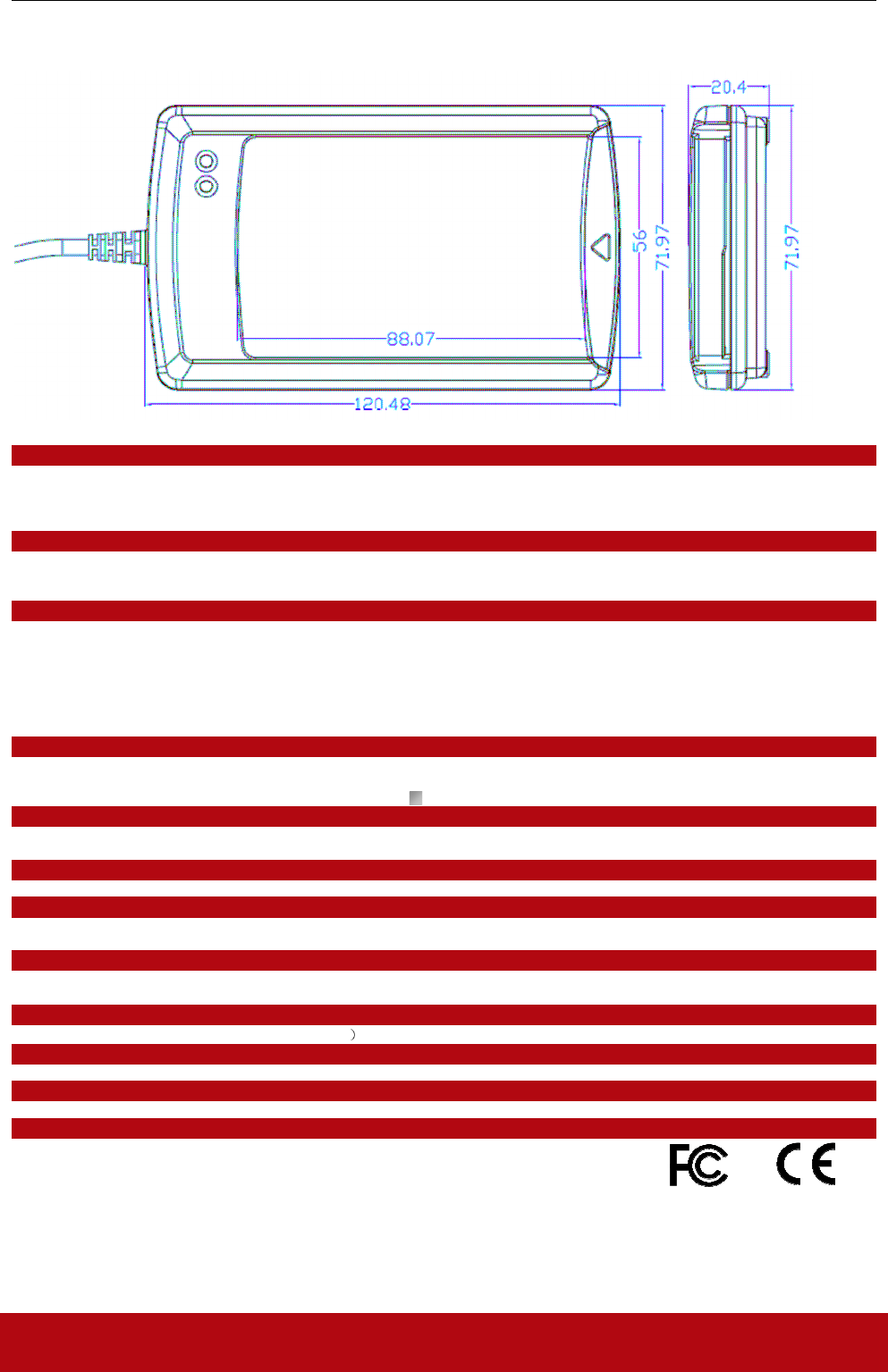
ACR1281S
Advanced Card Systems Ltd. Page 56 of 56
TECHNICAL SPECIFICATION
Universal Serial Bus Interface
Power source........................................ From +5V power or USB
Speed ................................................... up to 500Kbps
Supply Voltage...................................... Regulated 5V DC
Supply Current ..................................... 200mA (max); 100mA (normal)
Contactless Smart Card Interface
Standard ............................................... ISO 14443 A & B Parts 1-4
Protocol ................................................ ISO14443 T=CL for ISO14443-4 compliant cards and T=CL Emulation for MIFARE 1K/4K.
Smart card read / write speed ............... 106 kbps, 212 kbps, 424 kbps and 848 kbps
Contact Smart Card Interface
Standard ............................................... ISO 7816 1/2/3, Class A, B (5V, 3V), T=0 and T=1
Supply current....................................... max. 60mA
Smart card read / write speed ............... max412kbps
Short circuit protection ......................... +5V / GND on all pins
CLK frequency ...................................... 4.8 MHz
Card connector ..................................... Landing
Card insertion cycles............................. min. 300,000
Case
Dimensions........................................... 120.48 mm (L) x 71.97 mm (W) x 20.4 mm (H)
Material................................................. ABS
Color..................................................... Metallic Silver Grey
Antenna
Antenna Size ........................................65mm x 60mm
Operating distance................................ up to 50 mm
Operating Frequency for Contactless Cards Access
Operating Frequency ............................13.56 MHz
Built-in peripherals
Monotone buzzer
Dual-Color LED
Operating Conditions
Temperature ......................................... 0 - 50° C
Humidity................................................ 10% - 80%
Cable Connector
Length................................................... 10m (RS232
Standard/Certifications
CE, FCC
OS
Windows 98, ME, 2K, XP
OEM
OEM-Logo possible, customer-specific colors, casing, and card connector
FCC Caution:
Any Changes or modifications not expressly approved by the party responsible for compliance
could void the user’s authority to operate the equipment.
This device complies with part 15 of the FCC Rules. Operation is subject to the following
two conditions:
(1) This device may not cause harmful interference, and (2) this device must accept any
interference received, including interference that may cause undesired operation.
Note: This equipment has been tested and found to comply with the limits for a Class B digital
device, pursuant to part 15 of the FCC Rules. These limits are designed to provide reasonable
protection against harmful interference in a residential installation. This equipment generates,
uses and can radiate radio frequency energy and, if not installed and used in accordance with
the instructions, may cause harmful interference to radio communications. However, there is
no guarantee that interference will not occur in a particular installation. If this equipment does
cause harmful interference to radio or television reception, which can be determined by turning
the equipment off and on, the user is encouraged to try to correct the interference by one or
more of the following measures:
—Reorient or relocate the receiving antenna.
—Increase the separation between the equipment and receiver.
—Connect the equipment into an outlet on a circuit different from that to which the receiver is
connected.
—Consult the dealer or an experienced radio/TV technician for help.