Advanced Card Systems ACR1281U Contactless Smart Card Reader and Writer User Manual
Advanced Card Systems Limited Contactless Smart Card Reader and Writer Users Manual
Users Manual

ACR1281U
Advanced Card Systems Ltd. Page 1 of 81
ACR1281U
Specification
V1.04
Note: This equipment has been tested and found to comply with the limits for a Class B digital device, pursuant to part 15 of the FCC Rules. These limits are designed to provide reasonable protection against harmful interference in a residential installation. This equipment generates uses and can radiate radio frequency energy and, if not installed and used in accordance with the instructions, may cause harmful interference to radio communications. However, there is no guarantee that interference will not occur in a particular installation. If this equipment does cause harmful interference to radio or television reception, which can be determined by turning the equipment off and on, the user is encouraged to try to correct the interference by one or more of the following measures:
—Reorient or relocate the receiving antenna.
—Increase the separation between the equipment and receiver.
—Connect the equipment into an outlet on a circuit different from that to which the receiver is connected.
—Consult the dealer or an experienced radio/TV technician for help.

ACR1281U
Advanced Card Systems Ltd. Page 2 of 81
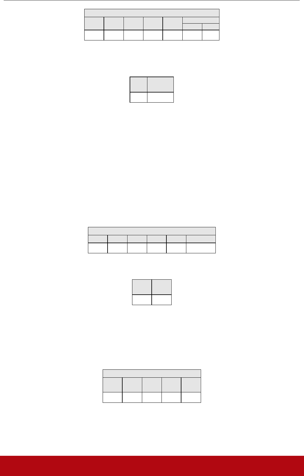
Revision History
Rev
Number
Date Author Notes
V1.00 20-May-2010 Vincent Zhong Preliminary specification for ACR1281U
V1.01 28-May-2010 Vincent Zhong/Nathan
Li/Kit Au
1) Firmware Upgrade Instruction Added
2) Extended APDU Example Added
V1.02 8-Oct-2010 Vincent Zhong/Nathan
Li/Kit Au
1) Added Counter Command
V1.03 28-Oct-2010 Vincent Zhong/Nathan
Li/Kit Au
1) Modify the command of RC531 register
write/read.
2) Request command Test added.
3) Continuous request command updated.
4) Contactless EMV loop command added.
5) Default LED and Buzzer Behavior Command
added.
V1.04 8-Dec-2010 Vincent Zhong/Jessy Wei 1) Modify PICC Polling control command.
2) Contact memory cards operation command is
added.

ACR1281U
Advanced Card Systems Ltd. Page 3 of 81
Index
Introduction..........................................................................................................................................6
features.................................................................................................................................................6
Terms ...................................................................................................................................................7
Quick Overview of the ACR1281U Reader ........................................................................................8
1. ACR1281U (with Contact Card Option) .....................................................................................8
2. ACR1281U (without Contact Card Option)................................................................................8
3. ACR1281U ICC Interface ...........................................................................................................9
4. ACR1281U PICC Interface .........................................................................................................9
5. ACR1281U Firmware Upgrade Procedures ..............................................................................11
System description.............................................................................................................................12
1. The Reader Block Diagram .......................................................................................................12
2. Communication Flow Chart of ACR1281U..............................................................................13
Hardware Description........................................................................................................................13
1. USB Interface ............................................................................................................................13
2. LED Indicator ............................................................................................................................13
3. Buzzer........................................................................................................................................14
4. ICC Interface (Contact Smart Card)..........................................................................................14
5. PICC Interface (Contactless Smart Card)..................................................................................14
Software Description .........................................................................................................................15
1. TAPDUDemoCard Demo App..................................................................................................15
Peripherals Control ............................................................................................................................16
1. Get Firmware Version ...............................................................................................................16
2. LED Control ..............................................................................................................................17
3. Buzzer Control...........................................................................................................................17
4. Default LED and Buzzer Behaviors ..........................................................................................18
5. Automatic PICC Polling............................................................................................................18
6. PICC Polling for specific PICC Types ......................................................................................19
7. Auto PPS (Communication Speed Change) ..............................................................................19
8. Antenna Field ON/OFF .............................................................................................................20
9. Request Command Test.............................................................................................................21
10. Continuous Request Command Sending Test .........................................................................22
11. Read and Update the RC531 Register .....................................................................................23
12. Go into Contactless EMV Terminal Loop...............................................................................24
13. Go into Contact EMV Terminal Loop.....................................................................................24
14. Read and Initial Card Insert Counter.......................................................................................25
15. Initial RC531 Setting For PICC...............................................................................................25
PICC Interface Description................................................................................................................26
1. ATR Generation ........................................................................................................................26
PICC Commands for General Purposes ............................................................................................28
1. Get Data.....................................................................................................................................28

ACR1281U
Advanced Card Systems Ltd. Page 4 of 81
PICC Commands (T=CL Emulation) for MIFare 1K/4K MEMORY Cards ....................................29
2.1 Load Authentication Keys .......................................................................................................29
2.2.1 Authentication for MIFARE 1K/4K.....................................................................................31
2.3 Read Binary Blocks .................................................................................................................34
2.4 Update Binary Blocks..............................................................................................................35
2.5 Value Block Related Commands.............................................................................................36
2.5.1 Value Block Operation .........................................................................................................36
2.5.2 Read Value Block.................................................................................................................37
2.5.3 Restore Value Block.............................................................................................................38
Memory Card Access ........................................................................................................................41
1. Memory Card – 1,2,4,8,16 kbit I2C card...................................................................................41
1.1 Select Card Type .....................................................................................................................41
1.2 Select Page Size.......................................................................................................................41
1.3 Read Memory Card .................................................................................................................41
1.4 Write Memory Card.................................................................................................................42
2. Memory Card – 32,64,128,256,512,1024 kbit I2C card............................................................42
2.1 Select Card Type .....................................................................................................................42
2.2 Select Page Size.......................................................................................................................43
2.3 Read Memory Card .................................................................................................................43
2.4 Write Memory Card.................................................................................................................44
3. Memory Card – ATMEL AT88SC153......................................................................................44
3.1 Select Card Type .....................................................................................................................44
3.2 Read Memory Card .................................................................................................................45
3.3 Write Memory Card.................................................................................................................45
3.4 Verify Password ......................................................................................................................46
3.5 Initialize Authentiction ............................................................................................................47
3.6 Verify Authentication ..............................................................................................................47
4. Memory Card – ATMEL AT88SC1608....................................................................................47
4.1 Select Card Type .....................................................................................................................47
4.2 Read Memory Card .................................................................................................................48
4.3 Write Memory Card.................................................................................................................48
4.4 Verify Password ......................................................................................................................49
4.5 Initialize Authentiction ............................................................................................................49
4.6 Verify Authentication ..............................................................................................................50
5. Memory Card – SLE4418/SLE4428/SLE5518/SLE5528.........................................................50
5.1 Select Card Type .....................................................................................................................50
5.2 Read Memory Card .................................................................................................................51
5.3 Presentation Error Counter Memory Card (only SLE4428 and SLE5528).............................51
5.4 Read Protection Bit..................................................................................................................51
5.5 Write Memory Card.................................................................................................................52
5.6 Write Protection Memory Card ...............................................................................................53
5.7 Present Code Memory Card (only SLE 4428 and SLE5528)..................................................53
6. Memory Card – SLE4432/SLE4442/SLE5532/SLE5542.........................................................54
6.1 Select Card Type .....................................................................................................................54
6.2 Read Memory Card .................................................................................................................54
6.3 Read Present Error Counter Memory Card (only SLE4442 and SLE5542)............................55
6.4 Read Protection Bits ................................................................................................................55
6.5 Write Memory Card.................................................................................................................56
6.6 Write Protection Memory Card ...............................................................................................56
6.7 Present Code Memory Card (only SLE 4442 and SLE5542)..................................................57
6.8 Change Code Memory Card (only SLE 4442 and SLE5542) .................................................57

ACR1281U
Advanced Card Systems Ltd. Page 5 of 81
7. Memory Card – SLE4406/SLE4436/SLE5536/SLE6636.........................................................58
7.1 Select Card Type .....................................................................................................................58
7.2 Read Memory Card .................................................................................................................58
7.3 Write One Byte Memory Card ................................................................................................59
7.4 Present Code Memory Card ....................................................................................................60
7.5 Authenticate Memory Card (SLE4436, SLE5536 and SLE6636 only) ..................................60
8. Memory Card – SLE4404..........................................................................................................62
8.1 Select Card Type .....................................................................................................................62
8.2 Read Memory Card .................................................................................................................62
8.3 Write Memory Card.................................................................................................................62
8.4 Erase Scratch Pad Memory Card.............................................................................................63
8.5 Verify User Code.....................................................................................................................63
8.6 Verify Memory Code...............................................................................................................64
9. Memory Card – AT88SC101 / AT88SC102 / AT88SC1003....................................................65
9.1 Select Card Type .....................................................................................................................65
9.2 Read Memory Card .................................................................................................................65
9.3 Write Memory Card.................................................................................................................66
9.4 ERASE_NON_APPLICATION_ZONE .................................................................................66
9.5 Erase Application Zone with erase..........................................................................................67
9.6 Erase Application Zone with Write and Erase ........................................................................68
9.7 Verify Security Code ...............................................................................................................69
9.8 Blown Fuse ..............................................................................................................................69
Basic Program Flow for Contactless Applications............................................................................71
1. How to access PCSC Compliant Tags (ISO14443-4)? .............................................................72
2. How to access DESFIRE Tags (ISO14443-4)? .........................................................................75
3. Extended APDU ........................................................................................................................77
Appendix A: Supported Card Types.................................................................................................78
Technical Specification .....................................................................................................................79
ACR1281U
Advanced Card Systems Ltd. Page 6 of 81
INTRODUCTION
The ACR1281U is a dual-interface reader (IFD and PCD) that supports both contact and
contactless (PICC) smart cards.
FEATURES
• One standard ICC landing type card acceptor.
• ISO 7816 Parts 1-4 Compliant for Contact Smart Card Interface.
• The ACR1281U supports contact memory cards (refer to appendix A).
• ISO 14443 Parts 1-4 Compliant for Contactless Smart Card Interface.
• A built-in antenna for PICC contactless access applications.
• The ACR1281U supports the following Tag Types:
o MIFARE Classic. E.g. MIFARE 1K, 4K, MINI and Ultralight.
o ISO14443-4 Type A and B.
• T=CL emulation for MIFare 1K/4K PICCs. Multi-Blocks Transfer Mode is provided for
efficient PICC access.
• High Speed (424 kbps) Communication for PICCs. #Maximum 848 kbps.
• Intelligent Support for Hybrid Cards and Combi Cards.
• Extended APDU supported (max: 64k bytes)
• Energy saving modes for turning off the antenna field whenever the PICC is inactive, or no
PICC is found. It prevents the PICC from exposing to the field all the time.
• User-Controllable Peripherals. E.g. LED, Buzzer.
• Microsoft CCID Compliant for both ICC and PICC interface.
• PCSC Compliant for Contact and Contactless Interfaces.
• USB V2.0 Interface. (12M bps)
• Device Firmware Upgradeable through the USB Interface.

ACR1281U
Advanced Card Systems Ltd. Page 7 of 81
TERMS
• IFD: Interface Device. A terminal, communication device, or machine to which the
integrated circuit(s) card is electrically connected during operation.
• PCD: Proximity Coupling Device. ISO 14443 Contactless Reader.
• ICC: Integrated Circuit(s) Card. Refer to a plastic card containing an integrated circuit,
which is compatible with ISO 7816.
• PICC: Proximity Integrated Circuit(s) Card. Contactless Cards operating without
mechanical contact to the IFD, using magnetic coupling.
• Combi-Card: A smart card that supports both ICC and PICC Interfaces. But only one
interface can be operating at any one time.
• Hybrid-Card: A smart card that consists of both ICC and PICC cards. Both ICC and PICC
cards can be operating at the same time.
• USB: Universal Serial Bus, a common device interface used in PC environment.
• CCID: The specifications for USB devices that interface with ICC or act as interfaces with
ICC/PICC.
• PCSC: Personal Computer Smart Card, a specification that can facilitate the interoperability
necessary to allow ICC/PICC technology to be effectively utilized in the PC environment.
• ISO 7816: A standard for contact smart cards (ICC).
• T=0: Character-oriented asynchronous half duplex transmission protocol for ICCs (ISO
7816).
• T=1: Block-oriented asynchronous half duplex transmission protocol for ICCs (ISO 7816).
• ISO 14443: A standard for contactless smart cards (PICC)
• T=CL: Block-oriented asynchronous half duplex transmission protocol for PICCs (ISO
14443).
• APDU: Application Protocol Data Unit.
• ATR: Answer-to-Reset. The transmission sent by an ICC to the reader (IFD) in response to
a RESET condition.
• ATS: Answer-to-Select. The transmission sent by a PICC Type A to the reader (PCD) in
response to a SELECT condition.
• ATQB: Answer-to-Request. The transmission sent by a PICC Type B to the reader (PCD)
in response to a REQUEST condition.
• Card Insertion Event: Either an ICC or a PICC is just appeared to the reader.
• Card Removal Event: Either an ICC or a PICC is removed from the reader.
ACR1281U
Advanced Card Systems Ltd. Page 8 of 81
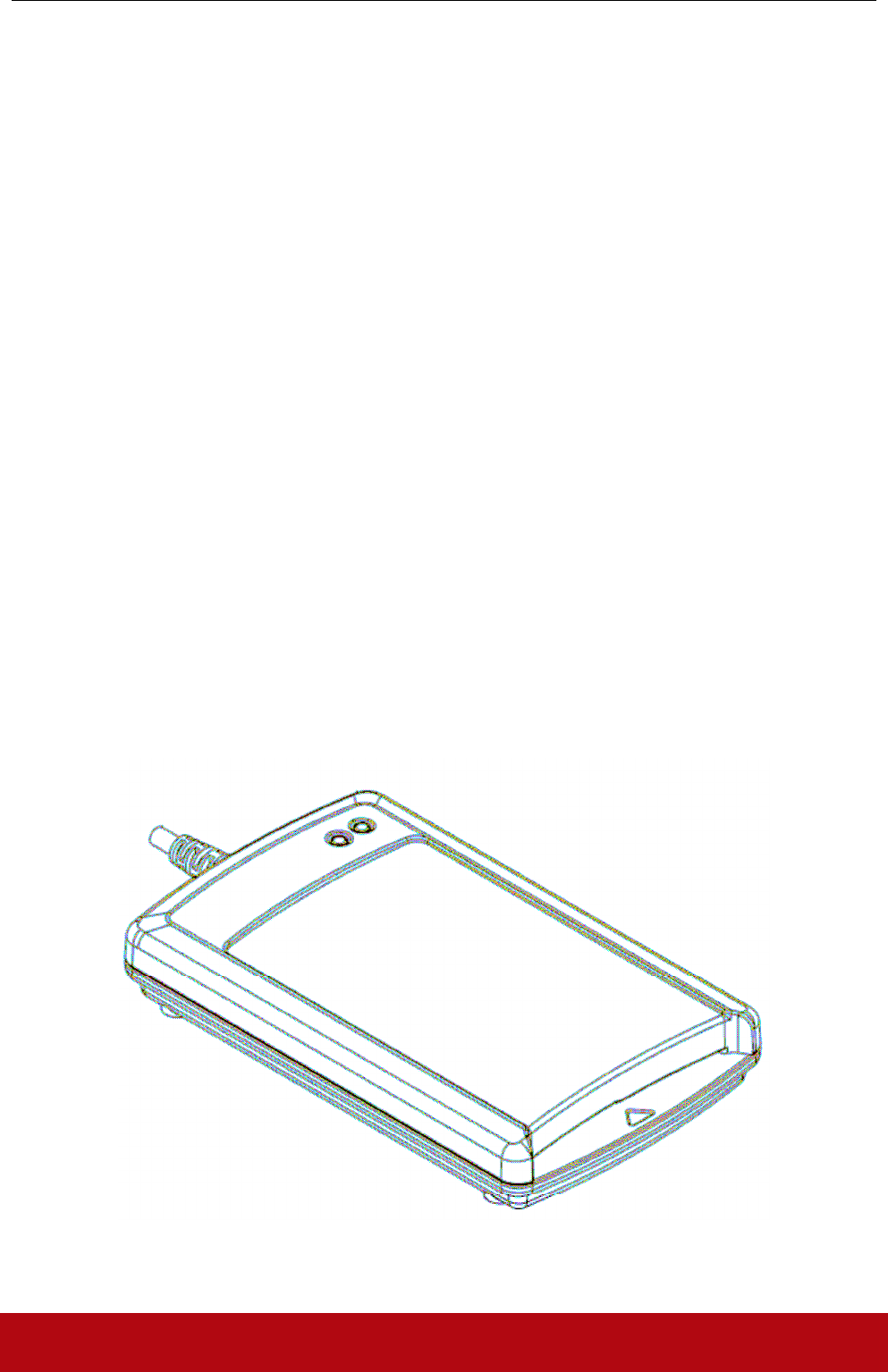
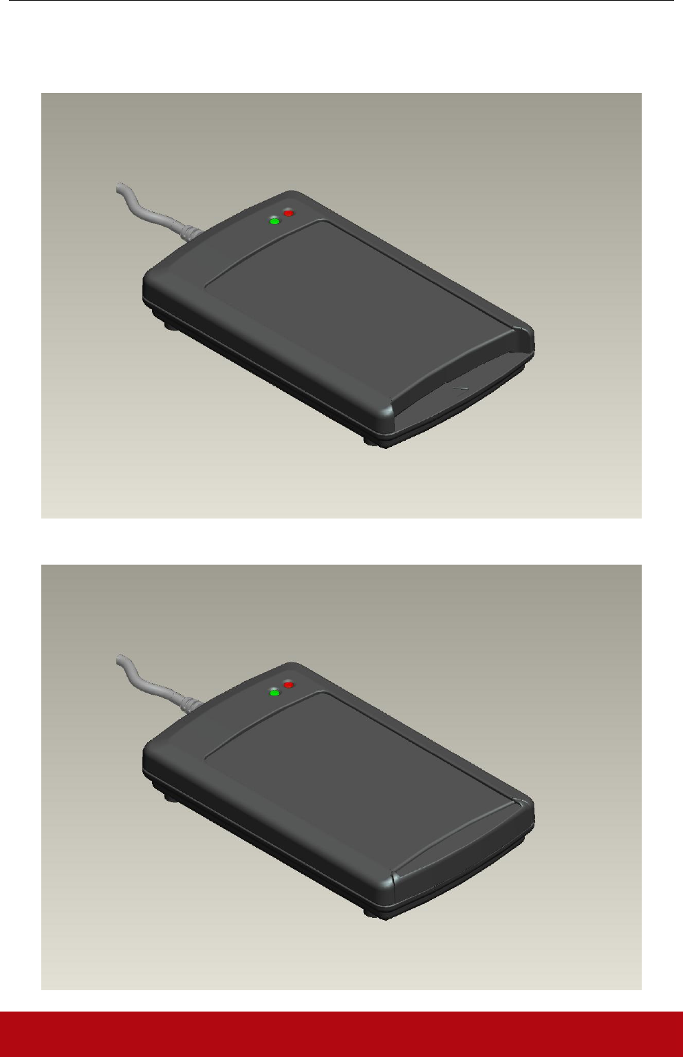
QUICK OVERVIEW OF THE ACR1281U READER
1. ACR1281U (with Contact Card Option)
2. ACR1281U (without Contact Card Option)
ACR1281U
Advanced Card Systems Ltd. Page 9 of 81
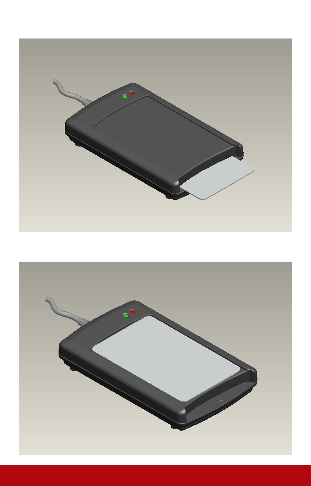
3. ACR1281U ICC Interface
4. ACR1281U PICC Interface
ACR1281U
Advanced Card Systems Ltd. Page 10 of 81
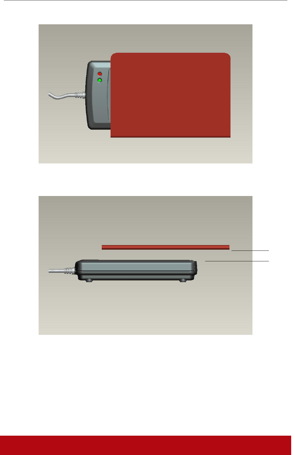
Recommended ICAO E-Passport Placement
• In case the E-Passport is not accessible, try to place the E-Passport above the reader by
5~10mm.
ICAO
E-Passport
5~10mm
ACR1281U
Advanced Card Systems Ltd. Page 11 of 81
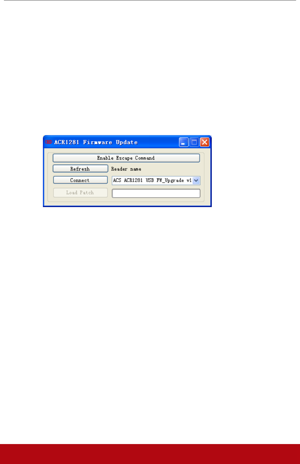
5. ACR1281U Firmware Upgrade Procedures
5.1 Upgrade by “FW” Key
Step 1: Unplug the Reader
Step 2: Open Casing
Step 3: Press the “FW, and Hold it
Step 4: Plug the Reader into PC’s USB Port
Step 5: Release the “FW” key
Step 6: Run Firmware Upgrade Application for Firmware Upgrade
5.2 Upgrade by APDU command
Step 1: Plug the Reader into PC’s USB Port
Step 2: Run Firmware Upgrade Application for Firmware Upgrade
Step 3: Select the Reader Name and Connect, then Press “Load Patch” For firmware upgrade.
ACR1281U
Advanced Card Systems Ltd. Page 12 of 81
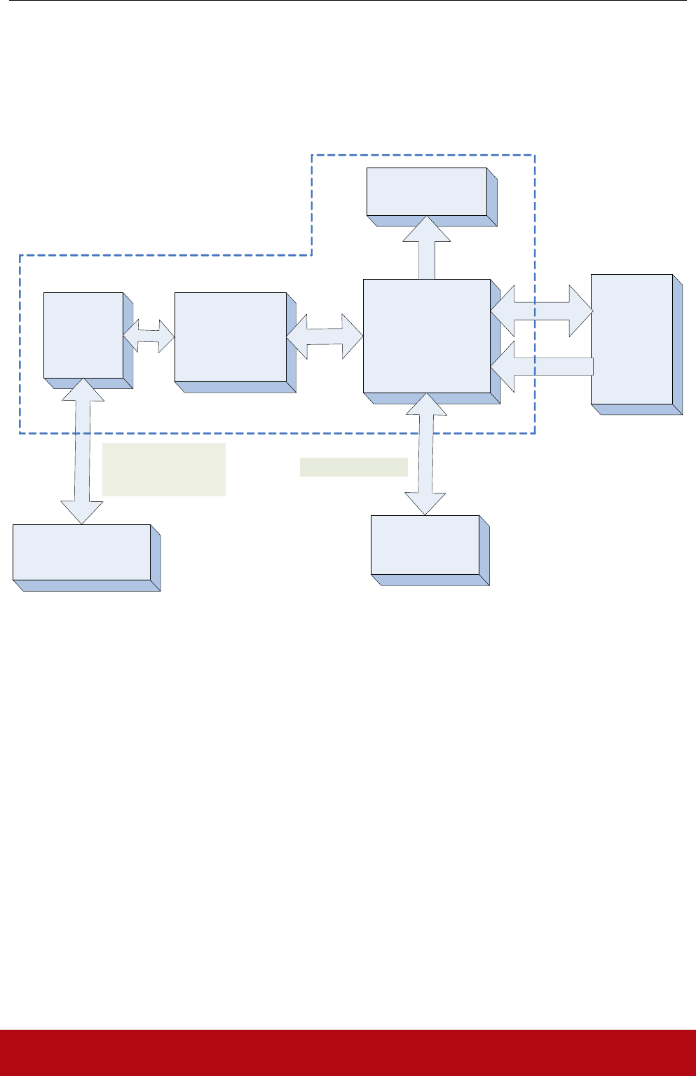
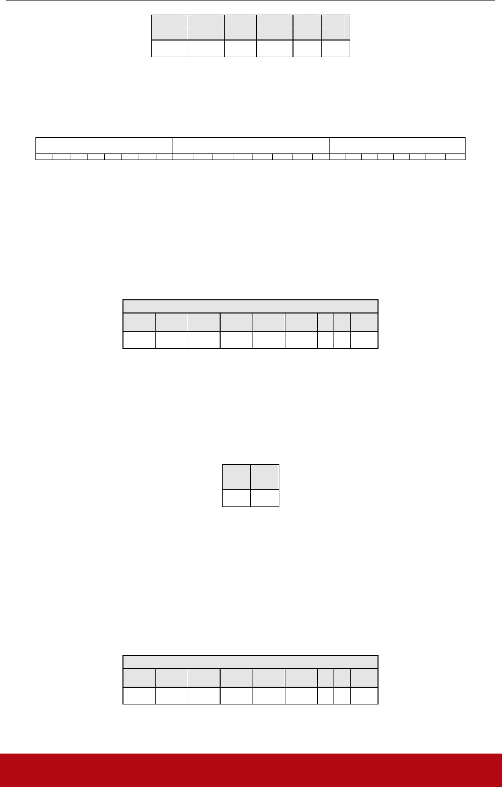
SYSTEM DESCRIPTION
1. The Reader Block Diagram
AT90SCR100H
Host Controller
LED & Buzzer
PC
Operation
System
USB CCID
USB
Firmware
Upgrade
RC531
NFC Interface
Chip
SPI
Built-In
Antenna
PICC
Contactless Card
Contactless Interface
Carrier = 13.56MHz ISO7816 Interface
ICC
Contact Card
ACR1281U
Advanced Card Systems Ltd. Page 13 of 81
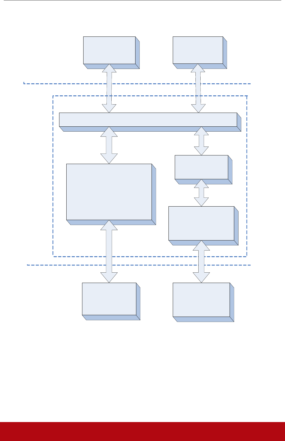
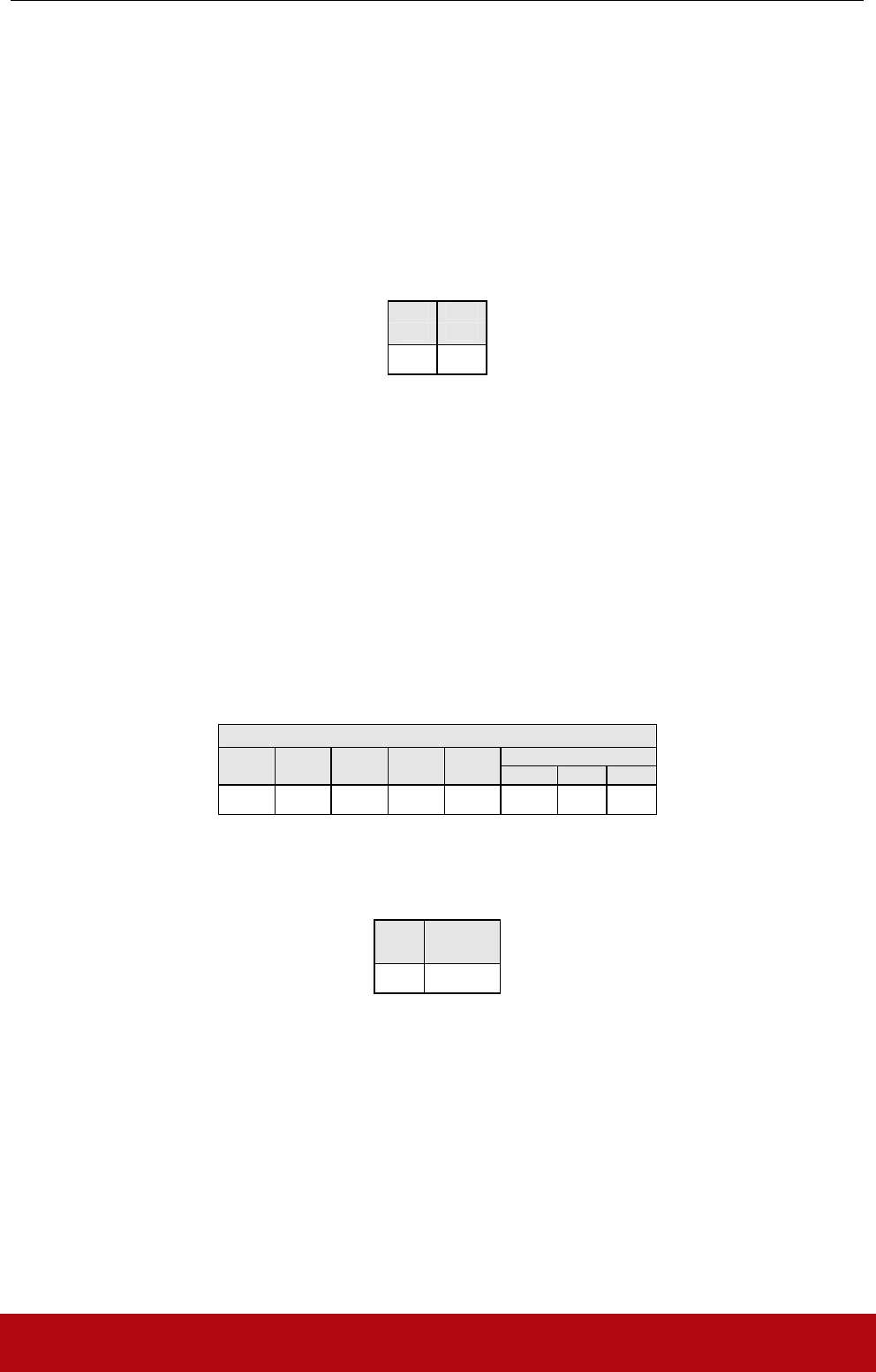
2. Communication Flow Chart of ACR1281U
PCSC Layer
ISO 7816 Part1-4
ICC Interface
T=CL &T=1
Emulation
ISO 14443 Part1-4
PICC Interface
ICC
(Landing Type
Acceptor )
PICC
(Built-In Antenna )
ACR1281U
ACR1281U PCSC
ICC Interface
ACR1281U PCSC
PICC Interface
USB
Interface
(CCID)
Physical
Interface
ICC
And
PICC
Host
ACR1281U
Advanced Card Systems Ltd. Page 15 of 81
HARDWARE DESCRIPTION
1. USB Interface
The ACR1281U is connected to a computer through USB as specified in the USB Specification 2.0.
ACR1281U is working in Full speed mode, i.e. 12 Mbps.
Pin Signal Function
1 VBUS +5V power supply for the reader (Max 200mA)
2 D- Differential signal transmits data between ACR1281U and PC.
3 D+ Differential signal transmits data between ACR1281U and PC.
4 GND Reference voltage level for power supply
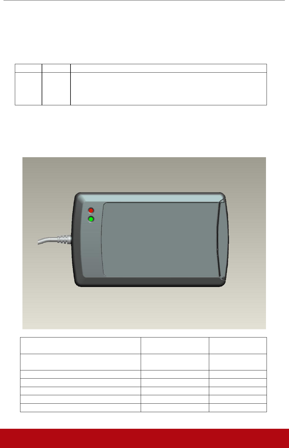
2. LED Indicator
The LEDs are used for showing the state of the contact and contactless interfaces. The Red LED is
used for showing PICC status and Green LED for ICC.
Reader States Red LED
PICC Indicator
Green LED
ICC Indicator
1. No PICC Found or PICC present but
not activated.
A single pulse per ~ 5
seconds
2. PICC is present and activated ON
3. PICC is operating Blinking
4. ICC is present and activated ON
5. ICC is absent or not activated OFF
6. ICC is operating Blinking

ACR1281U
Advanced Card Systems Ltd. Page 16 of 81
3. Buzzer
A monotone buzzer is used to show the “Card Insertion” and “Card Removal” events.
Events Buzzer
1. The reader powered up and initialization success. Beep
2. Card Insertion Event (ICC or PICC) Beep
3. Card Removal Event (ICC or PICC) Beep
4. ICC Interface (Contact Smart Card)
A landing type Smart Card Acceptor is used for providing reliable operations. The minimum life
cycle of the acceptor is about 300K times of card insertion and removal.
5. PICC Interface (Contactless Smart Card)
A built-in antenna is used for communication between the PCD and PICC.
ACR1281U
Advanced Card Systems Ltd. Page 17 of 81
SOFTWARE DESCRIPTION
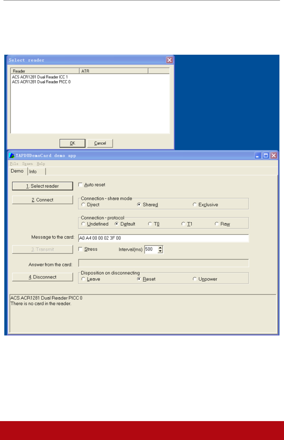
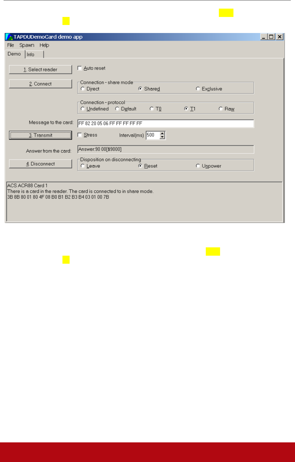
1. TAPDUDemoCard Demo App
This program is used to demonstrate the PCSC functions of the ACR1281U readers.
Operating Procedures:
1) Place a PICC on the top of the ACR1281U reader.
2) Press “1. Select Reader” and select the “ACS ACR1281Dual Reader PICC 0”.
3) Select “T1” in the connection-protocol. Press “2. Connect” to establish a connection
between the card and reader.
4) Enter the APDU in text box “Message to the card”
5) Press “3. Transmit” to send the APDU to the card.
6) Press “4. Disconnect” to terminate the connection between the card and reader.

ACR1281U
Advanced Card Systems Ltd. Page 20 of 81
1. Get Firmware Version
Command = {E0 00 00 18 00}
Response = {E1 00 00 00 “Frame Length” {Firmware Version}}
In which, Firmware Version = 13 bytes;
e.g. Response = E1 00 00 00 0D 41 43 52 31 32 38 31 55 5F 56 31 30 33
Firmware Version (HEX) = 41 43 52 31 32 38 31 55 5F 56 31 30 33
Firmware Version (ASCII) = “ACR1281U_V103
2. Enter Firmware Upgrade Mode
Command = {FF 00 00 E0 00}
Response = {FF 00 00 E1 02 90 00}
Hints:
After the response display, the reader will enter the firmware upgrade mode that the reader can be
upgraded firmware.
3. LED Control
Setting the LED State:
Command = {E0 00 00 29 01 “CMD”}.
Response = {E1 00 00 00 01 “Status”}
Reading the existing LED State:
Command = {E0 00 00 29 00}.
Response = {E1 00 00 00 01 “Status”}
CMD Bit Map
CMD Description Description
Bit 0 RED LED 1 = ON; 0 = OFF
Bit 1 GREEN LED 1 = ON; 0 = OFF
Bit 2 RFU RFU
Bit 3 RFU RFU
Bit 4 RFU RFU
Bit 5 RFU RFU
Bit 6 RFU RFU
Bit 7 RFU RFU
The “Status” bit map is the same as “CMD”.

ACR1281U
Advanced Card Systems Ltd. Page 21 of 81
4. Buzzer Control
Setting the Buzzer State:
Command = {E0 00 00 28 01 “Duration”} Unit = 10mS
00 = Turn off
01 ~ FE = Duration
FF = Turn o
Response = {E1 00 00 00 01 “Status”}
Reading the existing Buzzer State:
Command = {E0 00 00 28 00}
Response = {E1 00 00 00 01 “Status”}
5. Default LED and Buzzer Behaviors
CMD MODE Description
Bit 0 ICC Activation Status
LED
To show the activation status of the
ICC interface.
1 = Enable; 0 =Disable
Bit 1 PICC Polling Status LED To show the PICC Polling Status.
1 = Enable; 0 =Disable
Bit 2 PICC Activation Status LED To show the activation status of the
PICC interface
1 = Enable; 0 =Disable
Bit 3 Card Insertion and Removal
Events Buzzer
To make a beep whenever a card
insertion or removal event is
detected. (For both ICC and PICC)
1 = Enable; 0 =Disabled
Bit 4 RFU RFU
Bit 5 RFU RFU
Bit 6 RFU RFU
Bit 7 Card Operation Blinking
LED
To blink the LED whenever the card
(PICC or ICC) is being accessed.
Setting the LED and Buzzer behaviors:
Command = { E0 00 00 21 01 “CMD”}. Default value of CMD = 8F;
Response = {E1 00 00 00 01 “Status”}
Reading the existing behaviors of the LED and Buzzer:
Command = { E0 00 00 21 00}
Response = {E1 00 00 00 01 “Status”}
Hints:
If you want to enjoy the silent environment, just set the CMD value to “87”.

ACR1281U
Advanced Card Systems Ltd. Page 22 of 81
6. Automatic PICC Polling
Whenever the reader is connected to the PC, the PICC polling function will start the PICC scanning
to determine if a PICC is placed on / removed from the built-antenna.
We can send a command to disable the PICC polling function. The command is sent through the
PCSC Escape command interface. To meet the energy saving requirement, special modes are
provided for turning off the antenna field whenever the PICC is inactive, or no PICC is found. The
reader will consume less current in power saving mode.
Register 0x23: Automatic PICC Polling (Default value = 0x8F)
CMD Description Description
Bit 0 Auto PICC Polling 1 = Enable; 0 =Disable
Bit 1 Turn off Antenna Field if no
PICC found
1 = Enable; 0 =Disable
Bit 2 Turn off Antenna Field if the
PICC is inactive.
1 = Enable; 0 =Disable
Bit 3 Activate the PICC when
detected.
1 = Enable; 0 =Disable
Bit 5 .. 4 PICC Poll Interval for PICC <Bit 5 – Bit 4>
<0 – 0> = 250 msec
<0 – 1> = 500 msec
<1 – 0> = 1000 msec
<1 – 1> = 2500 msec
Bit 6 RFU -
Bit 7 Enforce ISO14443A Part 4 1= Enable; 0= Disable.
• Enable Auto PICC Polling Function = { E0 00 00 23 01 8F}
• Disable Auto PICC Polling Function = { E0 00 00 23 01 8E}
• Read the existing status = { E0 00 00 23 00}; Response = {E1 00 00 00 01 “Status”}
Hints:
1. It is recommended to enable the option “Turn Off Antenna Field if the PICC is inactive”, so that
the “Inactive PICC” will not be exposed to the field all the time so as to prevent the PICC from
“warming up”.
2. The longer the PICC Poll Interval, the more efficient of energy saving. However, the response
time of PICC Polling will become longer. The Idle Current Consumption in Power Saving Mode is
about 60mA, while the Idle Current Consumption in Non-Power Saving mode is about 130mA.
#Idle Current Consumption = PICC is not activated.
3. The reader will activate the ISO14443A-4 mode of the “ISO14443A-4 compliant PICC”
automatically. Type B PICC will not be affected by this option.
4. The JCOP30 card comes with two modes: ISO14443A-3 (MIFARE 1K) and ISO14443A-4
modes. The application has to decide which mode should be selected once the PICC is activated.

ACR1281U
Advanced Card Systems Ltd. Page 23 of 81
7. PICC Polling for specific PICC Types
The PICC polling function can be configured to detect “ISO14443 Type A PICCs” or “ISO14443
Type B PICCs” or both.
• ISO 14443 Type A PICCs Only = { E0 00 00 20 01 01}
• ISO 14443 Type B PICCs Only = { E0 00 00 20 01 02 }
• ISO 14443 Type A and B PICCs = { E0 00 00 20 01 03} #default setting
• Read the existing status = { E0 00 00 20 00}; Response = {E1 00 00 00 01 “Status”}
Hints:
1. It is recommended to specific the PICC types in the application so as to speed up the card
detection process.
8. Auto PPS (Communication Speed Change)
Whenever a PICC is recognized, the reader will try to change the communication speed between
the PCD and PICC defined by the Maximum Connection Speed. If the card does not support the
proposed connection speed, the reader will try to connect the card with a slower speed setting.
• Set Connection Speed = {E0 00 00 24 02 “Max Tx Speed” “Max Rx Speed”}
<Max Tx Speed> & <Current Tx Speed> or <Max Rx Speed> & <Current Rx Speed>
106k bps = 00
212k bps = 01
424k bps = 02 #default setting
848k bps = 03
No Auto PPS = FF
• Read the existing status = {E0 00 00 24 00};
Response = {E1 00 00 00 04 “Max Tx Speed” “Current Tx Speed” “Max Rx Speed”
“Current Rx Speed”}
Hints:
1. Normally, the application should know the maximum connection speed of the PICCs being used.
#The environment also affects the maximum achievable speed. The reader just uses the proposed
communication speed to talk with the PICC. The PICC will become inaccessible if the PICC or
environment does not meet the requirement of the proposed communication speed.
2. The reader supports different speed between sending and receiving.
9. Antenna Field ON/OFF
This command is used for turning on/off the antenna field.
• Enable the Antenna Field = {E0 00 00 25 01 01}
• Disable the Antenna Field = {E0 00 00 25 01 00}
• Read the existing status = {E0 00 00 25 00}; Response = {E1 00 00 00 01 “Status”}
Hints:
1. Make sure the Auto PICC Polling is disabled first before turning off the antenna field.

ACR1281U
Advanced Card Systems Ltd. Page 24 of 81
10. Request Command Test
This command is used for sending REQA/REQB by the reader to test antenna field and the
response.
• Command = {E0 00 00 26 02 “Command” “Speed”}
• Response = {E1 00 00 00 “Length” “Data”}
Command coding:
REQA = 01
REQB = 02
WUPA = 03
WUPB = 04
Speed coding:
106k bps = 00
212k bps = 01
424k bps = 02
Length:
No response: 00
ATQA: 02
ATQB: 0C
Others: RFU
Data:
Response Data (ATQA/ATQB/Others)
Hints:
1. Make sure the Auto PICC Polling is disabled first before sending this command.
11. Continuous Request Command Sending Test
This command is used for sending WUPA/WUPB by the reader continuously to test antenna field.
• Command = {E0 00 00 27 02 “Command” “Speed”}
• Disable Command Sending = { E0 00 00 27 00}
• Response = {E1 00 00 00 01 “Status”}
Command coding:
WUPA = 01
WUPB = 02
Speed coding:
106k bps = 00
212k bps = 01
424k bps = 02
Status:
WUPA Sending = 01
WUPB Sending = 02
Hints:
1. Make sure the Auto PICC Polling is disabled first before sending this command.
2. The reader will send the command continuously as long as the command starts. It can be stopped
by “E0 00 00 27 00”.

ACR1281U
Advanced Card Systems Ltd. Page 25 of 81
12. Read and Update the RC531 Register
• Read the Register = {E0 00 00 19 “Register No”}
• Response = {E1 00 00 00 01 “Current Value”}
• Update the Register = {E0 00 00 1A “Register No” “New Value”}
• Response = {E1 00 00 00 00}
13. Go into Contactless EMV Terminal Loop
• Command = {0E 00 01 00 00}
• Response = {90“Current Value”}
14. Go into Contact EMV Terminal Loop
• Command = {0E 01 01 00 00}
• Response = {E1 00 00 00 01 “Current Value”}
15. Read and Initial Card Insert Counter
• Read the Register = {E0 00 00 09 00}
• Initialize the counter = {E0 00 00 09 04 “ICC Counter (LSB)” “ICC Counter (MSB)”
“PICC Counter (LSB)” “PICC Counter (MSB)”}
Response = {E1 00 00 00 04 “ICC Counter (LSB)” “ICC Counter (MSB)” “PICC Counter
(LSB)” “PICC Counter (MSB)”}
• Update the counter data to static storage unit = {E0 00 00 0A 00}
16. Initial RC531 Setting For PICC
• Read the Register = {E0 00 00 2F 00}
•
• Update the Registers:
E0 00 00 2F 13 BModeIndex RxAThres106 RxAThres212 RxAThres424 RxAThres848
RxBThres106 RxBThres212 RxBThres424 RxBThres848 RxACtl106 RxACtl212
RxACtl424 RxACtl848 RxBCtl106 RxBCtl212 RxBCtl424 RxBCtl848 CWAConductonce
CWBConductonce
• Response:
E1 00 00 00 13 BModeIndex RxAThres106 RxAThres212 RxAThres424 RxAThres848
RxBThres106 RxBThres212 RxBThres424 RxBThres848 RxACtl106 RxACtl212
RxACtl424 RxACtl848 RxBCtl106 RxBCtl212 RxBCtl424 RxBCtl848 CWAConductonce
CWBConductonce
Default value:
1. E0 00 00 2F 13 0B 8F AF 85 80 8F 8F 8F 8F 72 53 32 12 76 52 32 12 3f 3f
ACR1281U
Advanced Card Systems Ltd. Page 26 of 81
PICC INTERFACE DESCRIPTION
1. ATR Generation
If the reader detects a PICC, an ATR will be sent to the PCSC driver for identifying the PICC.
1.1 ATR format for ISO 14443 Part 3 PICCs.
Byte
Value
(Hex)
Designation Description
0 3B Initial Header
1 8N T0 Higher nibble 8 means: no TA1, TB1, TC1
only TD1 is following.
Lower nibble N is the number of historical
bytes (HistByte 0 to HistByte N-1)
2 80 TD1 Higher nibble 8 means: no TA2, TB2, TC2
only TD2 is following.
Lower nibble 0 means T = 0
3 01 TD2 Higher nibble 0 means no TA3, TB3, TC3,
TD3 following.
Lower nibble 1 means T = 1
80 T1 Category indicator byte, 80 means A status
indicator may be present in an optional
COMPACT-TLV data object
4F Application identifier Presence Indicator
0C Length
RID Registered Application Provider Identifier
(RID) # A0 00 00 03 06
SS Byte for standard
C0 .. C1
Tk
Bytes for card name
4
To
3+N
00 00 00 00 RFU RFU # 00 00 00 00
4+N UU TCK Exclusive-oring of all the bytes T0 to Tk
e.g. ATR for MIFare 1K = {3B 8F 80 01 80 4F 0C A0 00 00 03 06 03 00 01 00 00 00 00 6A}
Length (YY) = 0x0C
RID = {A0 00 00 03 06} (PC/SC Workgroup)
Standard (SS) = 03 (ISO14443A, Part 3)
Card Name (C0 .. C1) = {00 01} (MIFare 1K)
Card Name (C0 .. C1)
00 01: Mifare 1K
00 02: Mifare 4K
00 03: Mifare Ultralight
00 26: Mifare Mini
FF 28: JCOP 30
FF [SAK]: undefined tags

ACR1281U
Advanced Card Systems Ltd. Page 27 of 81
1.2 ATR format for ISO 14443 Part 4 PICCs.
Byte
Value
(Hex)
Designation Description
0 3B Initial Header
1 8N T0 Higher nibble 8 means: no TA1, TB1, TC1
only TD1 is following.
Lower nibble N is the number of historical
bytes (HistByte 0 to HistByte N-1)
2 80 TD1 Higher nibble 8 means: no TA2, TB2, TC2
only TD2 is following.
Lower nibble 0 means T = 0
3 01 TD2 Higher nibble 0 means no TA3, TB3, TC3,
TD3 following.
Lower nibble 1 means T = 1
XX T1 4
to
3 + N
XX
XX
XX
Tk
Historical Bytes:
ISO14443A:
The historical bytes from ATS response. Refer
to the ISO14443-4 specification.
ISO14443B:
Byte1-4 Byte5-7 Byte8
Application
Data from
ATQB
Protocol Info
Byte from
ATQB
Higher
nibble=MBLI
from
ATTRIB
command
Lower nibble
(RFU)=0
4+N UU TCK Exclusive-oring of all the bytes T0 to Tk
E.g 1. ATR for DESFire = { 3B 81 80 01 80 80 } // 6 bytes of ATR
Hint: Use the APDU “FF CA 01 00 00” to distinguish the ISO14443A-4 and ISO14443B-4 PICCs,
and retrieve the full ATS if available. ISO14443A-3 or ISO14443B-3/4 PICCs do have ATS
returned.
APDU Command = FF CA 01 00 00
APDU Response = 06 75 77 81 02 80 90 00
ATS = {06 75 77 81 02 80}
E.g 2. ATR for ez-link = { 3B 88 80 01 1C 2D 94 11 F7 71 85 00 BE}
Application Data of ATQB = 1C 2D 94 11
Protocol Information of ATQB = F7 71 85
MBLI of ATTRIB = 00

ACR1281U
Advanced Card Systems Ltd. Page 28 of 81
PICC COMMANDS FOR GENERAL PURPOSES
1. Get Data
The “Get Data command” will return the serial number or ATS of the “connected PICC”.
Table 1.1-1a: Get UID APDU Format (5 Bytes)
Command
Class INS P1 P2 Le
Get Data FF CA 00
01
00 00
(Max
Length)
Table 2.1-1b: Get UID Response Format (UID + 2 Bytes) if P1 = 0x00
Response
Data Out
Result
UID
(LSB)
UID
(MSB)
SW1 SW2
Table 2.1-1c: Get ATS of a ISO 14443 A card (ATS + 2 Bytes) if P1 = 0x01
Response
Data Out
Result
ATS SW1 SW2
Table 2.1-1d: Response Codes
Results
SW1 SW2 Meaning
Success 90 00 The operation is completed successfully.
Warning 62 82 End of UID/ATS reached before Le bytes
(Le is greater than UID Length).
Error 6C XX Wrong length (wrong number Le: ‘XX’
encodes the exact number) if Le is less
than the available UID length.
Error 63 00 The operation is failed.
Error 6A 81 Function not supported
Examples:
// To get the serial number of the “connected PICC”
UINT8 GET_UID[5]={0xFF, 0xCA, 0x00, 0x00, 0x00};
// To get the ATS of the “connected ISO 14443 A PICC”
UINT8 GET_ATS[5]={0xFF, 0xCA, 0x01, 0x00, 0x00};

ACR1281U
Advanced Card Systems Ltd. Page 29 of 81
PICC COMMANDS (T=CL EMULATION) FOR MIFARE 1K/4K MEMORY CARDS
2.1 Load Authentication Keys
The “Load Authentication Keys command” will load the authentication keys into the reader. The
authentication keys are used to authenticate the particular sector of the Mifare 1K/4K Memory Card.
Two kinds of authentication key locations are provided, volatile and non-volatile key locations
respectively.
Table 2.1-1a: Load Authentication Keys APDU Format (11 Bytes)
Command
Class INS P1 P2 Lc Data In
Load
Authentication
Keys
FF 82 Key
Structure
Key
Number
06 Key
(6 bytes)
Key Structure (1 Byte):
0x00 = Key is loaded into the reader volatile memory.
0x20 = Key is loaded into the reader non-volatile memory.
Other = Reserved.
Key Number (1 Byte):
0x00 ~ 0x1F = Non-volatile memory for storing keys. The keys are permanently stored in the
reader and will not be disappeared even the reader is disconnected from the PC. It
can store up to 32 keys inside the reader non-volatile memory.
0x20 (Session Key) = Volatile memory for storing a temporally key. The key will be disappeared
once the reader is disconnected from the PC. Only 1 volatile key is provided. The volatile
key can be used as a session key for different sessions. Default Value = {FF FF FF FF FF
FF}
Key (6 Bytes):
The key value loaded into the reader. E.g. {FF FF FF FF FF FF}
Table 2.1-1b: Load Authentication Keys Response Format (2 Bytes)
Response
Data Out
Result
SW1 SW2
Table 2.1-1c: Load Authentication Keys Response Codes
Results
SW1 SW2 Meaning
Success 90 00 The operation is completed
successfully.
Error
63 00 The operation is failed.
Examples:
ACR1281U
Advanced Card Systems Ltd. Page 30 of 81
// Load a key {FF FF FF FF FF FF} into the non-volatile memory location 0x05.
APDU = {FF 82 20 05 06 FF FF FF FF FF FF}
<Similarly>
// Load a key {FF FF FF FF FF FF} into the volatile memory location 0x20.
APDU = {FF 82 00 20 06 FF FF FF FF FF FF}
Hints:
1. Basically, the application should know all the keys being used. It is recommended to store all the
required keys to the non-volatile memory for security reasons. The contents of both volatile and
non-volatile memories are not readable by the outside world.
2. The content of the volatile memory “Session Key 0x20” will remain valid until the reader is reset
or power-off. The session key is useful for storing any key value that is changing from time to time.
The session key is stored in the “Internal RAM”, while the non-volatile keys are stored in
“EEPROM” that is relatively slower than “Internal RAM”.
3. It is not recommended to use the “non-volatile key locations 0x00 ~ 0x1F” to store any
“temporally key value” that will be changed so often. The “non-volatile keys” are supposed to be
used for storing any “key value” that will not change frequently. If the “key value” is supposed to
be changed from time to time, please store the “key value” to the “volatile key location 0x020”.

ACR1281U
Advanced Card Systems Ltd. Page 31 of 81
2.2.1 Authentication for MIFARE 1K/4K
The “Authentication command” uses the keys stored in the reader to do authentication with the
MIFARE 1K/4K card (PICC). Two types of authentication keys are used, TYPE_A and TYPE_B
respectively.
Table 2.2-1a: Load Authentication Keys APDU Format (6 Bytes) #Obsolete
Command
Class INS P1 P2 P3 Data In
Authentication
FF 88 00 Block
Number
Key
Type
Key Number
Table 2.2-1b: Load Authentication Keys APDU Format (10 Bytes)
Command
Class INS P1 P2 Lc Data In
Authentication
FF 86 00 00 05 Authenticate Data
Bytes
Authenticate Data Bytes (5 Byte):
Byte1
Byte 2 Byte 3 Byte 4 Byte 5
Version
0x01
0x00 Block
Number
Key
Type
Key
Number
Block Number (1 Byte):
The memory block to be authenticated.
For MIFARE 1K Card, it has totally 16 sectors and each sector consists of 4 consecutive blocks.
E.g. Sector 0x00 consists of Blocks {0x00, 0x01, 0x02 and 0x03}; Sector 0x01 consists of Blocks
{0x04, 0x05, 0x06 and 0x07}; the last sector 0x0F consists of Blocks {0x3C, 0x3D, 0x3E and
0x3F}. Once the authentication is done successfully, there is no need to do the authentication again
provided that the blocks to be accessed are belonging to the same sector. Please refer to the
MIFARE 1K/4K specification for more details.
#Once the block is authenticated successfully, all the blocks belonging to the same sector are
accessible.
Key Type (1 Byte):
0x60 = Key is used as a TYPE A key for authentication.
0x61 = Key is used as a TYPE B key for authentication.
Key Number (1 Byte):
0x00 ~ 0x1F = Non-volatile memory for storing keys. The keys are permanently stored in the
reader and will not be disappeared even the reader is disconnected from the PC. It
can store 32 keys into the reader non-volatile memory.
0x20 = Volatile memory for storing keys. The keys will be disappeared when the reader is
disconnected from the PC. Only 1 volatile key is provided. The volatile key can be used as
a session key for different sessions.
ACR1281U
Advanced Card Systems Ltd. Page 32 of 81
Table 2.2-1b: Load Authentication Keys Response Format (2 Bytes)
Response
Data Out
Result
SW1 SW2
Table 2.2-1c: Load Authentication Keys Response Codes
Results
SW1 SW2 Meaning
Success 90 00 The operation is completed
successfully.
Error
63 00 The operation is failed.
MIFARE 1K Memory Map.
Sectors
(Total 16 sectors. Each
sector consists of 4
consecutive blocks)
Data Blocks
(3 blocks, 16 bytes
per block)
Trailer Block
(1 block, 16 bytes)
Sector 0 0x00 ~ 0x02 0x03
Sector 1 0x04 ~ 0x06 0x07
..
..
Sector 14 0x38 ~ 0x0A 0x3B
Sector 15 0x3C ~ 0x3E 0x3F
MIFARE 4K Memory Map.
Sectors
(Total 32 sectors. Each
sector consists of 4
consecutive blocks)
Data Blocks
(3 blocks, 16 bytes
per block)
Trailer Block
(1 block, 16 bytes)
Sector 0 0x00 ~ 0x02 0x03
Sector 1 0x04 ~ 0x06 0x07
..
..
Sector 30 0x78 ~ 0x7A 0x7B
Sector 31 0x7C ~ 0x7E 0x7F
Sectors
(Total 8 sectors. Each
sector consists of 16
consecutive blocks)
Data Blocks
(15 blocks, 16 bytes
per block)
Trailer Block
(1 block, 16 bytes)
Sector 32 0x80 ~ 0x8E 0x8F
Sector 33 0x90 ~ 0x9E 0x9F
..
..
Sector 38 0xE0 ~ 0xEE 0xEF
Sector 39 0xF0 ~ 0xFE 0xFF
1K
Bytes
2K
Bytes
2K
Bytes

ACR1281U
Advanced Card Systems Ltd. Page 33 of 81
Examples:
// To authenticate the Block 0x04 with a {TYPE A, non-volatile, key number 0x05}.
// PC/SC V2.01, Obsolete
APDU = {FF 88 00 04 60 05};
<Similarly>
// To authenticate the Block 0x04 with a {TYPE A, non-volatile, key number 0x05}.
// PC/SC V2.07
APDU = {FF 86 00 00 05 01 00 04 60 05}
Hints:
MIFARE Ultralight does not need to do any authentication. The memory is free to access.

ACR1281U
Advanced Card Systems Ltd. Page 34 of 81
2.3 Read Binary Blocks
The “Read Binary Blocks command” is used for retrieving a multiple of “data blocks” from the
PICC. The data block/trailer block must be authenticated first before executing the “Read Binary
Blocks command”.
Table 2.3-1a: Read Binary APDU Format (5 Bytes)
Command
Class INS P1 P2 Le
Read Binary
Blocks
FF B0 00 Block
Number
Number
of Bytes
to Read
Block Number (1 Byte):
The starting block.
Number of Bytes to Read (1 Byte):
Multiply of 16 bytes for MIFARE 1K/4K or Multiply of 4 bytes for MIFARE Ultralight
• Maximum 16 bytes for MIFARE Ultralight.
• Maximum 48 bytes for MIFARE 1K. (Multiple Blocks Mode; 3 consecutive blocks)
• Maximum 240 bytes for MIFARE 4K. (Multiple Blocks Mode; 15 consecutive blocks)
Example 1: 0x10 (16 bytes). The starting block only. (Single Block Mode)
Example 2: 0x40 (64 bytes). From the starting block to starting block+3. (Multiple Blocks Mode)
#For safety reason, the Multiple Block Mode is used for accessing Data Blocks only. The Trailer
Block is not supposed to be accessed in Multiple Blocks Mode. Please use Single Block Mode to
access the Trailer Block.
Table 2.3-1b: Read Binary Block Response Format (Multiply of 4/16 + 2 Bytes)
Response
Data Out
Result
Data (Multiply of 4/16 Bytes)
SW1 SW2
Table 2.3-1c: Read Binary Block Response Codes
Results
SW1 SW2 Meaning
Success 90 00 The operation is completed
successfully.
Error
63 00 The operation is failed.
Examples:
// Read 16 bytes from the binary block 0x04 (MIFARE 1K or 4K)
APDU = {FF B0 00 04 10}
// Read 240 bytes starting from the binary block 0x80 (MIFARE 4K)
// Block 0x80 to Block 0x8E (15 blocks)
APDU = {FF B0 00 80 F0}

ACR1281U
Advanced Card Systems Ltd. Page 35 of 81
2.4 Update Binary Blocks
The “Update Binary Blocks command” is used for writing a multiple of “data blocks” into the
PICC. The data block/trailer block must be authenticated first before executing the “Update Binary
Blocks command”.
Table 2.3-1a: Update Binary APDU Format (Multiple of 16 + 5 Bytes)
Command
Class INS P1 P2 Lc Data In
Update Binary
Blocks
FF D6 00 Block
Number
Number
of Bytes
to
Update
Block Data
(Multiple of 16
Bytes)
Block Number (1 Byte):
The starting block to be updated.
Number of Bytes to Update (1 Byte):
• Multiply of 16 bytes for MIFARE 1K/4K or 4 bytes for MIFARE Ultralight.
• Maximum 48 bytes for MIFARE 1K. (Multiple Blocks Mode; 3 consecutive blocks)
• Maximum 240 bytes for MIFARE 4K. (Multiple Blocks Mode; 15 consecutive blocks)
Example 1: 0x10 (16 bytes). The starting block only. (Single Block Mode)
Example 2: 0x30 (48 bytes). From the starting block to starting block+2. (Multiple Blocks Mode)
#For safety reason, the Multiple Block Mode is used for accessing Data Blocks only. The Trailer
Block is not supposed to be accessed in Multiple Blocks Mode. Please use Single Block Mode to
access the Trailer Block.
Block Data (Multiply of 16 + 2 Bytes, or 6 bytes):
The data to be written into the binary block/blocks.
Table 2.3-1b: Update Binary Block Response Codes (2 Bytes)
Results
SW1 SW2 Meaning
Success 90 00 The operation is completed
successfully.
Error
63 00 The operation is failed.
Examples:
// Update the binary block 0x04 of MIFARE 1K/4K with Data {00 01 .. 0F}
APDU = {FF D6 00 04 10 00 01 02 03 04 05 06 07 08 09 0A 0B 0C 0D 0E 0F}
// Update the binary block 0x04 of MIFARE Ultralight with Data {00 01 02 03}
APDU = {FF D6 00 04 04 00 01 02 03}
ACR1281U
Advanced Card Systems Ltd. Page 36 of 81
2.5 Value Block Related Commands
The data block can be used as value block for implementing value-based applications.
2.5.1 Value Block Operation
The “Value Block Operation command” is used for manipulating value-based transactions. E.g.
Increment a value of the value block etc.
Table 2.5.1-1a: Value Block Operation APDU Format (10 Bytes)
Command
Class INS P1 P2 Lc Data In
Value Block
Operation
FF D7 00 Block
Number
05 VB_OP
VB_Value
(4 Bytes)
{MSB .. LSB}
Block Number (1 Byte):
The value block to be manipulated.
VB_OP (1 Byte):
0x00 = Store the VB_Value into the block. The block will then be converted to a value block.
0x01 = Increment the value of the value block by the VB_Value. This command is only valid for
value block.
0x02 = Decrement the value of the value block by the VB_Value. This command is only valid for
value block.
VB_Value (4 Bytes):
The value used for value manipulation. The value is a signed long integer (4 bytes).
E.g. 1: Decimal –4 = {0xFF, 0xFF, 0xFF, 0xFC}
VB_Value
MSB LSB
FF FF FF FC
E.g. 2: Decimal 1 = {0x00, 0x00, 0x00, 0x01}
VB_Value
MSB LSB
00 00 00 01
Table 2.5.1-1b: Value Block Operation Response Format (2 Bytes)
Response
Data Out
Result SW1 SW2
Table 2.5.1-1c: Value Block Operation Response Codes
Results
SW1 SW2 Meaning
Success 90 00 The operation is completed
successfully.
Error
63 00 The operation is failed.

ACR1281U
Advanced Card Systems Ltd. Page 37 of 81
2.5.2 Read Value Block
The “Read Value Block command” is used for retrieving the value from the value block. This
command is only valid for value block.
Table 2.5.2-1a: Read Value Block APDU Format (5 Bytes)
Command
Class INS P1 P2 Le
Read Value
Block
FF B1 00 Block
Number
00
Block Number (1 Byte):
The value block to be accessed.
Table 2.5.2-1b: Read Value Block Response Format (4 + 2 Bytes)
Response
Data Out
Result
Value
{MSB .. LSB}
SW1 SW2
Value (4 Bytes):
The value returned from the card. The value is a signed long integer (4 bytes).
E.g. 1: Decimal –4 = {0xFF, 0xFF, 0xFF, 0xFC}
Value
MSB LSB
FF FF FF FC
E.g. 2: Decimal 1 = {0x00, 0x00, 0x00, 0x01}
Value
MSB LSB
00 00 00 01
Table 2.5.3-1c: Read Value Block Response Codes
Results
SW1 SW2 Meaning
Success 90 00 The operation is completed
successfully.
Error
63 00 The operation is failed.

ACR1281U
Advanced Card Systems Ltd. Page 38 of 81
2.5.3 Restore Value Block
The “Restore Value Block command” is used to copy a value from a value block to another value
block.
Table 2.5.3-1a: Restore Value Block APDU Format (7 Bytes)
Command
Class INS P1 P2 Lc Data In
Value Block
Operation
FF D7 00 Source
Block
Number
02 03 Target
Block
Number
Source Block Number (1 Byte): The value of the source value block will be copied to the target
value block.
Target Block Number (1 Byte): The value block to be restored. The source and target value
blocks must be in the same sector.
Table 2.5.3-1b: Restore Value Block Response Format (2 Bytes)
Response
Data Out
Result
SW1 SW2
Table 2.5.3-1c: Restore Value Block Response Codes
Results
SW1 SW2 Meaning
Success 90 00 The operation is completed
successfully.
Error
63 00 The operation is failed.
ACR1281U
Advanced Card Systems Ltd. Page 39 of 81
Examples:
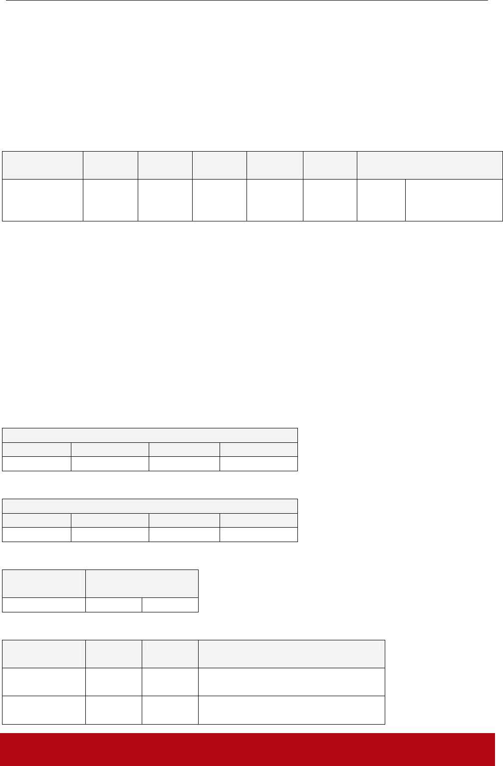
// Store a value “1” into block 0x05
APDU = {FF D7 00 05 05 00 00 00 00 01}
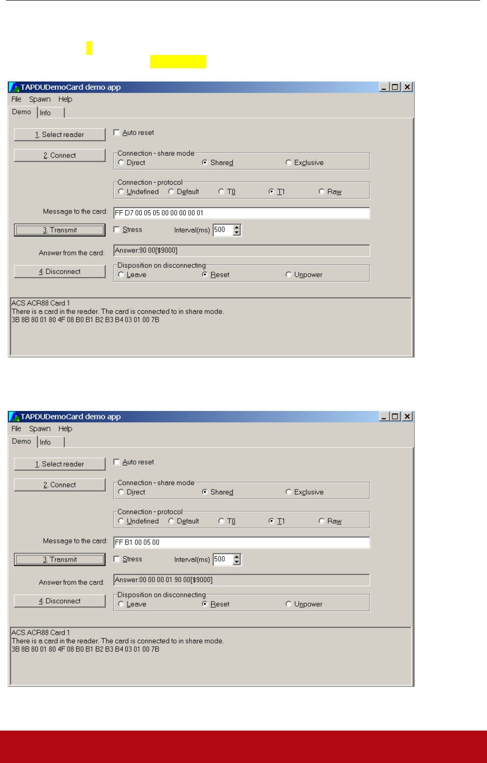
// Read the value block 0x05
APDU = {FF B1 00 05 00}
ACR1281U
Advanced Card Systems Ltd. Page 40 of 81
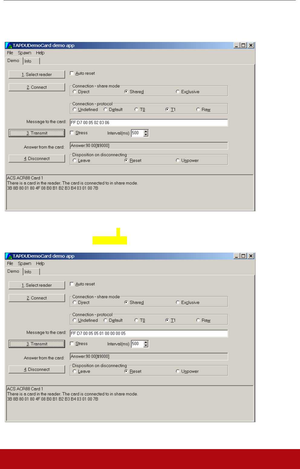
// Copy the value from value block 0x05 to value block 0x06
APDU = {FF D7 00 05 02 03 06}
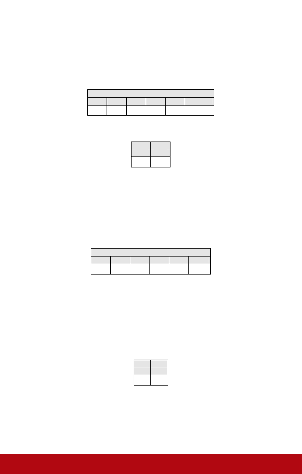
// Increment the value block 0x05 by “5”
APDU = {FF D7 00 05 05 01 00 00 00 05}
ACR1281U
Advanced Card Systems Ltd. Page 41 of 81
MEMORY CARD ACCESS
1. Memory Card – 1,2,4,8,16 kbit I2C card
1.1 Select Card Type
This command powers down and up the selected card inserted in the card reader and performs a
card reset.
• Command format
Pseudo-APDU
CLA INS P1 P2 Lc Card Type
FF H A4 H 00 H 00 H 01 H 01 H
• Response data format
SW1 SW2
• SW1, SW2 = 90 00 if no error
1.2 Select Page Size
This command will choose the page size to read the smart card. The default value is 8-byte page
write. It will reset to default value whenever the card is removed or the reader is powered off.
• Command format
Pseudo-APDU
CLA INS P1 P2 Lc Page size
FF H 01 H 00 H 00 H 01 H
• Page size = 03 for 8-byte page write
= 04 for 16-byte page write
= 05 for 32-byte page write
= 06 for 64-byte page write
= 07 for 128-byte page write
• Response data format
SW1 SW2
• SW1, SW2 = 90 00 if no error
1.3 Read Memory Card
• Command format
ACR1281U
Advanced Card Systems Ltd. Page 42 of 81
Pseudo-APDU
Byte Address CLA INS
MSB LSB
MEM_L
FF H B0 H
Byte Address Memory address location of the memory card.
MEM_L Length of data to be read from the memory card.
• Response data format
BYTE 1 … … BYTE N SW1 SW2
BYTE x Data read from memory card
SW1, SW2 = 90 00 if no error
1.4 Write Memory Card
• Command format
Pseudo-APDU
Byte Address CLA INS
MSB LSB
MEM_L Byte 1 .... .... Byte n
FF H D0 H
Byte Address Memory address location of the memory card.
MEM_L Length of data to be written to the memory card.
Byte x Data to be written to the memory card.
• Response data format
SW1 SW2
• SW1, SW2 = 90 00 if no error
2. Memory Card – 32,64,128,256,512,1024 kbit I2C card
2.1 Select Card Type
This command powers down and up the selected card inserted in the card reader and performs a
card reset.
• Command format
ACR1281U
Advanced Card Systems Ltd. Page 43 of 81
Pseudo-APDU
CLA INS P1 P2 Lc Card Type
FF H A4 H 00 H 00 H 01 H 02 H
• Response data format
SW1 SW2
• SW1, SW2 = 90 00 if no error
2.2 Select Page Size
This command will choose the page size to read the smart card. The default value is 8-byte page
write. It will reset to default value whenever the card is removed or the reader is powered off.
• Command format
Pseudo-APDU
CLA INS P1 P2 Lc Page size
FF H 01 H 00 H 00 H 01 H
Data TPDU to be sent to the card
Page size = 03 for 8-byte page write
= 04 for 16-byte page write
= 05 for 32-byte page write
= 06 for 64-byte page write
= 07 for 128-byte page write
• Response data format
SW1 SW2
• SW1, SW2 = 90 00 if no error
2.3 Read Memory Card
• Command format
Pseudo-APDU
Byte Address CLA INS
MSB LSB
MEM_L
FF H
INS = B0 for 32,64,128,256,512kbit iic card
ACR1281U
Advanced Card Systems Ltd. Page 44 of 81
= 1011 000* b for 1024kbit ICC card, where * is the MSB of the 17 bit addressing
Byte Address Memory address location of the memory card.
MEM_L Length of data to be read from the memory card.
• Response data format
BYTE 1 … … BYTE N SW1 SW2
• BYTE x Data read from memory card
• SW1, SW2 = 90 00 if no error
2.4 Write Memory Card
• Command format
Pseudo-APDU
Byte Address CLA INS
MSB LSB
MEM_L Byte 1 .... .... Byte n
FF H
INS = D0 for 32,64,128,256,512kbit iic card
= 1101 000* b for 1024kbit ICC card, where * is the MSB of the 17 bit addressing
Byte Address Memory address location of the memory card.
MEM_L Length of data to be written to the memory card.
Byte x Data to be written to the memory card.
• Response data format
SW1 SW2
• SW1, SW2 = 90 00 if no error
3. Memory Card – ATMEL AT88SC153
3.1 Select Card Type
This command powers down and up the selected card inserted in the card reader and performs a
card reset. It will also select the page size to be 8-byte page write.
• Command format
ACR1281U
Advanced Card Systems Ltd. Page 45 of 81
Pseudo-APDU
CLA INS P1 P2 Lc Card Type
FF H A4 H 00 H 00 H 01 H 03 H
• Response data format
SW1 SW2
• SW1, SW2 = 90 00 if no error
3.2 Read Memory Card
• Command format
Pseudo-APDU
CLA INS P1 Byte
Address
MEM_L
FF H 00 H
INS = B0 for reading zone 00 b
= B1 for reading zone 01 b
= B2 for reading zone 10 b
= B3 for reading zone 11 b
= B4 for reading fuse
Byte Address Memory address location of the memory card.
MEM_L Length of data to be read from the memory card.
• Response data format
BYTE 1 … … BYTE N SW1 SW2
• BYTE x Data read from memory card
• SW1, SW2 = 90 00 if no error
3.3 Write Memory Card
• Command format
Pseudo-APDU
CLA INS P1 Bye
Address
MEM_L Byte 1 .... .... Byte n
FF H 00 H
INS = D0 for writing zone 00 b
ACR1281U
Advanced Card Systems Ltd. Page 46 of 81
= D1 for writing zone 01 b
= D2 for writing zone 10 b
= D3 for writing zone 11 b
= D4 for writing fuse
Byte Address Memory address location of the memory card.
MEM_L Length of data to be written to the memory card.
MEM_D Data to be written to the memory card.
• Response data format
SW1 SW2
• SW1, SW2 = 90 00 if no error
3.4 Verify Password
• Command format
Pseudo-APDU
CLA INS P1 P2 Lc Pw(0) Pw(1) Pw(2)
FF H 20 H 00 H 03 H
Pw(0),Pw(1),Pw(2) Passwords to be sent to memory card.
P2 = 0000 00rp b
where the two bits “rp” indicate the password to compare
r = 0 : Write password,
r = 1: Read password,
p: Password set number,
rp = 01 for the secure code.
• Response data format
SW1 SW2
ErrorCnt
90 H
• SW1 = 90
• SW2 (ErrorCnt) = Error Counter. FF indicates the verification is correct. 00 indicates the
password is locked (exceed maximum number of retries). Other values indicate the current
verification is failed.
ACR1281U
Advanced Card Systems Ltd. Page 47 of 81
3.5 Initialize Authentiction
• Command format
Pseudo-APDU
CLA INS P1 P2 Lc Q(0) Q(1) … Q(7)
FF H 84 H 00 H 00 H 08 H
Q(0),Q(1)…Q(7) Host random number, 8 bytes.
• Response data format
SW1 SW2
• SW1, SW2 = 90 00 if no error
3.6 Verify Authentication
• Command format
Pseudo-APDU
CLA INS P1 P2 Lc Ch(0)
Ch(1)
… Ch(7)
FF H 82 H 00 H 00 H 08 H
Ch(0),Ch(1)…Ch(7) Host challenge, 8 bytes.
• Response data format
SW1 SW2
• SW1, SW2 = 90 00 if no error
4. Memory Card – ATMEL AT88SC1608
4.1 Select Card Type
This command powers down and up the selected card inserted in the card reader and performs a
card reset. It will also select the page size to be 16-byte page write.
• Command format
Pseudo-APDU
CLA INS P1 P2 Lc Card Type
FF H A4 H 00 H 00 H 01 H 04 H
• Response data format
ACR1281U
Advanced Card Systems Ltd. Page 48 of 81
SW1 SW2
• SW1, SW2 = 90 00 if no error
4.2 Read Memory Card
• Command format
Pseudo-APDU
CLA INS Zone
Address
Byte
Address
MEM_L
FF H
INS = B0 for reading user zone
= B1 for reading configuration zone or reading fuse
Zone Address = 0000 0A10A9A8 b, where A10 is the MSB of zone address
= don’t care for reading fuse
Byte Address = A7A6A5A4 A3A2A1A0 b is the memory address location of the memory card.
= 1000 0000 b for reading fuse
MEM_L Length of data to be read from the memory card.
• Response data format
BYTE 1 … … BYTE N SW1 SW2
• BYTE x Data read from memory card
• SW1, SW2 = 90 00 if no error
4.3 Write Memory Card
• Command format
Pseudo-APDU
CLA INS Zone
Address
Byte
Address
MEM_L Byte 1 .... .... Byte n
FF H
INS = D0 for writing user zone
= D1 for writing configuration zone or writing fuse
Zone Address = 0000 0A10A9A8 b, where A10 is the MSB of zone address
= don’t care for writing fuse
ACR1281U
Advanced Card Systems Ltd. Page 49 of 81
Byte Address = A7A6A5A4 A3A2A1A0 b is the memory address location of the memory card.
= 1000 0000 b for writing fuse
MEM_L Length of data to be written to the memory card.
Byte x Data to be written to the memory card.
• Response data format
SW1 SW2
• SW1, SW2 = 90 00 if no error
4.4 Verify Password
• Command format
Pseudo-APDU
CLA INS P1 P2 Lc Data
FF H 20 H 00 H 00 H 04 H RP Pw(0) Pw(1)
Pw(2)
Pw(0),Pw(1),Pw(2) Passwords to be sent to memory card.
RP = 0000 rp2p1p0 b
where the four bits “rp2p1p0” indicate the password to compare:
r = 0: Write password,
r = 1: Read password,
p2p1p0: Password set number.
(rp2p1p0 = 0111 for the secure code).
• Response data format
SW1 SW2
ErrorCnt
90 H
• SW1 = 90
• SW2 (ErrorCnt) = Error Counter. FF indicates the verification is correct. 00 indicates the
password is locked (exceed maximum number of retries). Other values indicate the current
verification is failed.
4.5 Initialize Authentiction
• Command format
Pseudo-APDU
CLA INS P1 P2 Lc Q(0) Q(1) … Q(7)
FF H 84 H 00 H 00 H 08 H
ACR1281U
Advanced Card Systems Ltd. Page 50 of 81
Byte Address Memory address location of the memory card.
Q(0),Q(1)…Q(7) Host random number, 8 bytes.
• Response data format
SW1 SW2
• SW1, SW2 = 90 00 if no error
4.6 Verify Authentication
• Command format
Pseudo-APDU
CLA INS P1 P2 Lc Q1(0)
Q1(1)
… Q1(7)
FF H 82 H 00 H 00 H 08 H
Byte Address Memory address location of the memory card.
Q1(0),Q1(1)…Q1(7) Host challenge, 8 bytes.
• Response data format
SW1 SW2
• SW1, SW2 = 90 00 if no error
5. Memory Card – SLE4418/SLE4428/SLE5518/SLE5528
5.1 Select Card Type
This command powers down and up the selected card inserted in the card reader and performs a
card reset.
• Command format
Pseudo-APDU
CLA INS P1 P2 Lc Card Type
FF H A4 H 00 H 00 H 01 H 05 H
• Response data format
SW1 SW2
• SW1, SW2 = 90 00 if no error
ACR1281U
Advanced Card Systems Ltd. Page 51 of 81
5.2 Read Memory Card
• Command format
Pseudo-APDU
Byte Address CLA INS
MSB LSB
MEM_L
FF H B0 H
MSB Byte Address = 0000 00A9A8 b is the memory address location of the memory card.
LSB Byte Address = A7A6A5A4 A3A2A1A0 b is the memory address location of the memory
card.
MEM_L Length of data to be read from the memory card.
• Response data format
BYTE 1 … … BYTE N SW1 SW2
• BYTE x Data read from memory card
• SW1, SW2 = 90 00 if no error
5.3 Presentation Error Counter Memory Card (only SLE4428 and SLE5528)
To read the presentation error counter for the secret code.
• Command format
Pseudo-APDU
CLA INS P1 P2 MEM_L
FF H B1 H 00 H 00 H 03 H
• Response data format
ERRCNT DUMMY 1 DUMMY 2 SW1 SW2
• ERRCNT The value of the presentation error counter. FF indicates the last verification
is correct. 00 indicates the password is locked (exceed maximum number of retries). Other
values indicate the last verification is failed.
• DUMMY Two bytes dummy data read from the card.
• SW1, SW2 = 90 00 if no error
5.4 Read Protection Bit
• Command format
ACR1281U
Advanced Card Systems Ltd. Page 52 of 81
Pseudo-APDU
Byte Address CLA INS
MSB LSB
MEM_L
FF H B2 H
MSB Byte Address = 0000 00A9A8 b is the memory address location of the memory card.
LSB Byte Address = A7A6A5A4 A3A2A1A0 b is the memory address location of the memory
card.
MEM_L Length of protection bits to be read from the card, in multiples of 8 bits.
Maximum value is 32.
MEM_L = 1 + INT( (number of bits-1)/8 )
For example, to read eight protection bits starting from memory 0x0010, the
following pseudo-APDU should be issued:
0xFF 0xB1 0x00 0x10 0x01
• Response data format
PROT 1 … … PROT L SW1 SW2
• PROT y Bytes containing the protection bits
• SW1,SW2 = 90 H 00 H if no error
• The arrangement of the protection bits in the PROT bytes is as follows:
PROT 1 PROT 2 ….
P8 P7 P6 P5 P4 P3 P2 P1 P16 P15 P14 P13 P12 P11 P10 P9 .. .. .. .. .. .. P18 P17
• Px is the protection bit of BYTE x in the response data
• ‘0’ byte is write protected
• ‘1’ byte can be written
5.5 Write Memory Card
• Command format
Pseudo-APDU
Byte Address CLA INS
MSB LSB
MEM_L Byte 1 .... .... Byte N
FF H D0 H
MSB Byte Address = 0000 00A9A8 b is the memory address location of the memory card.
LSB Byte Address = A7A6A5A4 A3A2A1A0 b is the memory address location of the memory
card.
MEM_L Length of data to be written to the memory card.
ACR1281U
Advanced Card Systems Ltd. Page 53 of 81
Byte x Data to be written to the memory card.
• Response data format
SW1 SW2
• SW1, SW2 = 90 00 if no error
5.6 Write Protection Memory Card
Each of the bytes specified in the command is internally in the card compared with the byte stored
at the specified address and if the data match, the corresponding protection bit is irreversibly
programmed to ‘0’.
• Command format
Pseudo-APDU
Byte Address CLA INS
MSB LSB
MEM_L Byte 1 .... .... Byte N
FF H D1 H
MSB Byte Address = 0000 00A9A8 b is the memory address location of the memory card.
LSB Byte Address = A7A6A5A4 A3A2A1A0 b is the memory address location of the memory
card.
MEM_L Length of data to be written to the memory card.
Byte x Byte values to be compared with the data in the card starting at Byte Address. BYTE 1
is compared with the data at Byte Address; BYTE N is compared with the data at (Byte
Address+N-1).
• Response data format
SW1 SW2
• SW1, SW2 = 90 00 if no error
5.7 Present Code Memory Card (only SLE 4428 and SLE5528)
To submit the secret code to the memory card to enable the write operation with the SLE4428 and
SLE5528 card. The following actions are executed:
- search a ‘1’ bit in the presentation error counter and write the bit to ‘0’
- present the specified code to the card
- try to erase the presentation error counter
• Command format
ACR1281U
Advanced Card Systems Ltd. Page 54 of 81
Pseudo-APDU
CODE CLA INS P1 P2 MEM_L
Byte 1 Byte 2
FF H 20 H 00 H 00 H 02 H
CODE Two bytes secret code (PIN)
• Response data format
SW1 SW2
ErrorCnt
90 H
• SW1 = 90
• SW2 (ErrorCnt) = Error Counter. FF indicates the verification is correct. 00 indicates the
password is locked (exceed maximum number of retries). Other values indicate the current
verification is failed.
6. Memory Card – SLE4432/SLE4442/SLE5532/SLE5542
6.1 Select Card Type
This command powers down and up the selected card inserted in the card reader and performs a
card reset.
• Command format
Pseudo-APDU
CLA INS P1 P2 Lc Card Type
FF H A4 H 00 H 00 H 01 H 06 H
• Response data format
SW1 SW2
• SW1, SW2 = 90 00 if no error
6.2 Read Memory Card
• Command format
Pseudo-APDU
CLA INS P1 Byte
Address
MEM_L
FF H B0 H 00 H
Byte Address = A7A6A5A4 A3A2A1A0 b is the memory address location of the memory card.
MEM_L Length of data to be read from the memory card.
• Response data format
ACR1281U
Advanced Card Systems Ltd. Page 55 of 81
BYTE 1 … … BYTE N PROT 1 PROT 2 PROT3 PROT 4 SW1 SW2
• BYTE x Data read from memory card
• PROT y Bytes containing the protection bits from protection memory
• SW1, SW2 = 90 00 if no error
• The arrangement of the protection bits in the PROT bytes is as follows:
PROT 1 PROT 2 …
P8 P7 P6 P5 P4 P3 P2 P1 P16 P15 P14 P13 P12 P11 P10 P9 .. .. .. .. .. .. P18 P17
• Px is the protection bit of BYTE x in the response data
• ‘0’ byte is write protected
• ‘1’ byte can be written
6.3 Read Present Error Counter Memory Card (only SLE4442 and SLE5542)
To read the presentation error counter for the secret code.
• Command format
Pseudo-APDU
CLA INS P1 P2 MEM_L
FF H B1 H 00 H 00 H 04 H
• Response data format
ERRCNT DUMMY 1 DUMMY 2 DUMMY 3 SW1 SW2
• ERRCNT The value of the presentation error counter. 07 indicates the last verification
is correct. 00 indicates the password is locked (exceed maximum number of retries). Other
values indicate the last verification is failed.
• DUMMY Three bytes dummy data read from the card.
• SW1, SW2 = 90 00 if no error
6.4 Read Protection Bits
To read the protection bits for the first 32 bytes.
• Command format
Pseudo-APDU
CLA INS P1 P2 MEM_L
FF H B2 H 00 H 00 H 04 H
• Response data format
ACR1281U
Advanced Card Systems Ltd. Page 56 of 81
PROT 1 PROT 2 PROT3 PROT 4 SW1 SW2
• PROT y Bytes containing the protection bits from protection memory
• SW1, SW2 = 90 00 if no error
• The arrangement of the protection bits in the PROT bytes is as follows:
•
PROT 1 PROT 2 …
P8 P7 P6 P5 P4 P3 P2 P1 P16 P15 P14 P13 P12 P11 P10 P9 .. .. .. .. .. .. P18 P17
• Px is the protection bit of BYTE x in the response data
• ‘0’ byte is write protected
• ‘1’ byte can be written
6.5 Write Memory Card
• Command format
Pseudo-APDU
CLA INS P1 Byte
Address
MEM_L Byte 1 .... .... Byte N
FF H D0 H 00 H
Byte Address = A7A6A5A4 A3A2A1A0 b is the memory address location of the memory card.
MEM_L Length of data to be written to the memory card.
Byte x Data to be written to the memory card.
• Response data format
SW1 SW2
• SW1, SW2 = 90 00 if no error
6.6 Write Protection Memory Card
Each of the bytes specified in the command is internally in the card compared with the byte stored
at the specified address and if the data match, the corresponding protection bit is irreversibly
programmed to ‘0’.
• Command format
Pseudo-APDU
CLA INS P1 Byte
Address
MEM_L Byte 1 .... .... Byte N
FF H D1 H 00 H
ACR1281U
Advanced Card Systems Ltd. Page 57 of 81
Byte Address = 000A4 A3A2A1A0 b (00 H to 1F H) is the protection memory address location of
the memory card.
MEM_L Length of data to be written to the memory card.
Byte x Byte values to be compared with the data in the card starting at Byte Address. BYTE
1 is compared with the data at Byte Address; BYTE N is compared with the data at
(Byte Address+N-1).
• Response data format
SW1 SW2
• SW1, SW2 = 90 00 if no error
6.7 Present Code Memory Card (only SLE 4442 and SLE5542)
To submit the secret code to the memory card to enable the write operation with the SLE4442 and
SLE5542 card. The following actions are executed:
- search a ‘1’ bit in the presentation error counter and write the bit to ‘0’
- present the specified code to the card
- try to erase the presentation error counter
• Command format
Pseudo-APDU
CODE CLA INS P1 P2 MEM_L
Byte 1 Byte 2 Byte 3
FF H 20 H 00 H 00 H 03 H
CODE Three bytes secret code (PIN)
• Response data format
SW1 SW2
ErrorCnt
90 H
• SW1 = 90
• SW2 (ErrorCnt) = Error Counter. 07 indicates the verification is correct. 00 indicates the
password is locked (exceed maximum number of retries). Other values indicate the current
verification is failed.
6.8 Change Code Memory Card (only SLE 4442 and SLE5542)
To write the specified data as new secret code in the card.
The current secret code must have been presented to the card with the PRESENT_CODE command
prior to the execution of this command!
• Command format
ACR1281U
Advanced Card Systems Ltd. Page 58 of 81
Pseudo-APDU
CODE CLA INS P1 P2 MEM_L
Byte 1 Byte 2 Byte 3
FF H D2 H 00 H 01 H 03 H
• Response data format
SW1 SW2
• SW1, SW2 = 90 00 if no error
7. Memory Card – SLE4406/SLE4436/SLE5536/SLE6636
7.1 Select Card Type
This command powers down and up the selected card inserted in the card reader and performs a
card reset.
• Command format
Pseudo-APDU
CLA INS P1 P2 Lc Card Type
FF H A4 H 00 H 00 H 01 H 07 H
• Response data format
SW1 SW2
• SW1, SW2 = 90 00 if no error
7.2 Read Memory Card
• Command format
Pseudo-APDU
CLA INS P1 Byte
Address
MEM_L
FF H B0 H 00 H
Byte Address = Memory address location of the memory card.
MEM_L Length of data to be read from the memory card.
• Response data format

ACR1281U
Advanced Card Systems Ltd. Page 59 of 81
BYTE 1 … … BYTE N SW1 SW2
• BYTE x Data read from memory card
• SW1, SW2 = 90 00 if no error
7.3 Write One Byte Memory Card
To write one byte to the specified address of the inserted card. The byte is written to the card with
LSB first, i.e., the bit at card address 0 is regarded as the LSB of byte 0.
Four different WRITE modes are available for this card type, which are distinguished by a flag in
the command data field:
a) Write
The byte value specified in the command is written to the specified address. This command
can be used for writing personalization data and counter values to the card.
b) Write with carry
The byte value specified in the command is written to the specified address and the
command is sent to the card to erase the next lower counter stage. This write mode can
therefore only be used for updating the counter value in the card.
c) Write with backup enabled (SLE4436, SLE5536 and SLE6636 only)
The byte value specified in the command is written to the specified address. This command
can be used for writing personalization data and counter values to the card. Backup bit is
enabled to prevent data loss when card tearing occurs.
d) Write with carry and backup enabled (SLE4436, SLE5536 and SLE6636 only)
The byte value specified in the command is written to the specified address and the
command is sent to the card to erase the next lower counter stage. This write mode can
therefore only be used for updating the counter value in the card. Backup bit is enabled to
prevent data loss when card tearing occurs.
With all write modes, the byte at the specified card address is not erased prior to the write operation
and, hence, memory bits can only be programmed from '1' to '0'.
The backup mode available in the SLE4436 and SLE5536 card can be enabled or disabled in the
write operation.
• Command format
Pseudo-APDU
CLA INS P1 Byte
Address
MEM_L MODE BYTE
FF H D0 H 00 H 02 H
Byte Address = Memory address location of the memory card.
MODE Specifies the write mode and backup option
00 : write
01 : write with carry
ACR1281U
Advanced Card Systems Ltd. Page 60 of 81
02 : write with backup enabled (SLE4436, SLE5536 and SLE6636 only)
03 : write with carry and with backup enabled (SLE4436, SLE5536 and SLE6636 only)
BYTE Byte value to be written to the card
• Response data format
SW1 SW2
• SW1, SW2 = 90 00 if no error
7.4 Present Code Memory Card
To submit the secret code to the memory card to enable the card personalization mode. The
following actions are executed:
- search a '1' bit in the presentation counter and write the bit to '0'
- present the specified code to the card
The ACR1281U does not try to erase the presentation counter after the code submission! This must
be done by the application software through a separate 'Write with carry' command.
• Command format
Pseudo-APDU
CODE CLA INS P1 P2 MEM_L
ADDR
Byte 1 Byte 2 Byte 3
FF H 20 H 00 H 00 H 04 H 09 H
ADDR Byte address of the presentation counter in the card
CODE Three bytes secret code (PIN)
• Response data format
SW1 SW2
• SW1, SW2 = 90 00 if no error
7.5 Authenticate Memory Card (SLE4436, SLE5536 and SLE6636 only)
To read a card authentication certificate from a SLE5536 or SLE6636 card. The following actions
are executed by the ACR1281U:
- select Key 1 or Key 2 in the card as specified in the command
- present the challenge data specified in the command to the card
- generate the specified number of CLK pulses for each bit of authentication data
computed by the card
- read 16 bits of authentication data from the card
- reset the card to normal operation mode
ACR1281U
Advanced Card Systems Ltd. Page 61 of 81
The authentication has to be performed in two steps. The first step is to send the Authentication
Certificate to the card. The second step is to get back two bytes of authentication data calculated
by the card.
• Step 1: Send Authentication Certificate to the Card
• Command format
Pseudo-APDU
MEM_L
CODE CLA INS P1 P2
KEY
CLK_CNT Byte1 Byte 2 …… Byte 5 Byte 6
FF H 84 H 00 H 00 H 08 H
KEY Key to be used for the computation of the authentication certificate:
00 : key 1 with no cipher block chaining
01 : key 2 with no cipher block chaining
80 : key 1 with cipher block chaining (SLE5536 and SLE6636 only)
81 : key 2 with cipher block chaining (SLE5536 and SLE6636 only)
CLK_CNT Number of CLK pulses to be supplied to the card for the computation of each bit of the
authentication certificate. Typical value is 160 clocks (A0)
BYTE 1...6 Card challenge data
• Response data format
SW1 SW2
61 H 02 H
• SW1, SW2 = 61 02 if no error, meaning two bytes of authentication data are ready.
The authentication data can be retrieved by “Get_Response” command.
• Step 2: Get back the Authentication Data (Get_Response)
• Command format
Pseudo-APDU
CLA INS P1 P2 MEM_L
FF H C0 H 00 H 00 H 02 H
• Response data format
CERT SW1 SW2
CERT 16 bits of authentication data computed by the card. The LSB of BYTE 1 is
the first authentication bit read from the card.
• SW1, SW2 = 90 00 if no error
ACR1281U
Advanced Card Systems Ltd. Page 62 of 81
8. Memory Card – SLE4404
8.1 Select Card Type
This command powers down and up the selected card inserted in the card reader and performs a
card reset.
• Command format
Pseudo-APDU
CLA INS P1 P2 Lc Card Type
FF H A4 H 00 H 00 H 01 H 08 H
• Response data format
SW1 SW2
• SW1, SW2 = 90 00 if no error
8.2 Read Memory Card
• Command format
Pseudo-APDU
CLA INS P1 Byte
Address
MEM_L
FF H B0 H 00 H
Byte Address = Memory address location of the memory card.
MEM_L Length of data to be read from the memory card.
• Response data format
BYTE 1 … … BYTE N SW1 SW2
• BYTE x Data read from memory card
• SW1, SW2 = 90 00 if no error
8.3 Write Memory Card
To write data to the specified address of the inserted card. The byte is written to the card with LSB
first, i.e., the bit at card address 0 is regarded as the LSB of byte 0.
The byte at the specified card address is not erased prior to the write operation and, hence, memory
bits can only be programmed from '1' to '0'.
• Command format
ACR1281U
Advanced Card Systems Ltd. Page 63 of 81
Pseudo-APDU
CLA INS P1 Byte
Address
MEM_L Byte 1 .... .... Byte N
FF H D0 H 00 H
Byte Address = Memory address location of the memory card.
MEM_L Length of data to be written to the memory card.
BYTE Byte value to be written to the card
• Response data format
SW1 SW2
• SW1, SW2 = 90 00 if no error
8.4 Erase Scratch Pad Memory Card
To erase the data of the scratch pad memory of the inserted card. All memory bits inside the
scratch pad memory will be programmed to the state of ‘1’.
• Command format
Pseudo-APDU
CLA INS P1 Byte
Address
MEM_L
FF H D2 H 00 H 00 H
Byte Address = Memory byte address location of the scratch pad. Typical value is 0x02.
• Response data format
SW1 SW2
• SW1, SW2 = 90 00 if no error
8.5 Verify User Code
To submit User Code (2 bytes) to the inserted card. User Code is to enable the memory access of
the card.
The following actions are executed:
- present the specified code to the card
- search a '1' bit in the presentation error counter and write the bit to '0'
- erase the presentation error counter. The User Error Counter can be erased when
the submitted code is correct.
• Command format
ACR1281U
Advanced Card Systems Ltd. Page 64 of 81
Pseudo-APDU
CODE CLA INS Error Counter
LEN
Byte
Address
MEM_L
Byte 1
Byte 2
FF H 20 H 04 H 08 H 02 H
Error Counter LEN Length of presentation error counter in bits.
Byte Address Byte address of the key in the card.
CODE 2 bytes User Code
• Response data format
SW1 SW2
• SW1, SW2 = 90 00 if no error.
= 63 00 if there is no more retry chance
Note: After SW1SW2 = 90 00 has been received, read back the User Error Counter can check
whether the VERIFY_USER_CODE is correct. If User Error Counter is erased and equals to “FF”,
the previous verification is success.
8.6 Verify Memory Code
To submit Memory Code (4 bytes) to the inserted card. Memory Code is used to authorize the
reloading of the user memory, together with the User Code.
The following actions are executed:
- present the specified code to the card
- search a '1' bit in the presentation error counter and write the bit to '0'
- erase the presentation error counter. Please note that Memory Error Counter
cannot be erased.
• Command format
Pseudo-APDU
CODE CLA INS Error Counter
LEN
Byte
Address
MEM_L
Byte 1
Byte 2 Byte 3 Byte 4
FF H 20 H 40 H 28 H 04 H
Error Counter LEN Length of presentation error counter in bits.
Byte Address Byte address of the key in the card.
CODE 4 bytes Memory Code
• Response data format
SW1 SW2
• SW1, SW2 = 90 00 if no error
= 63 00 if there is no more retry chance
ACR1281U
Advanced Card Systems Ltd. Page 65 of 81
Note: After SW1SW2 = 0x9000 has been received, read back the Application Area can check
whether the VERIFY_MEMORY_CODE is correct. If all data in Application Area is erased and
equals to “FF”, the previous verification is success.
9. Memory Card – AT88SC101 / AT88SC102 / AT88SC1003
9.1 Select Card Type
This command powers down and up the selected card inserted in the card reader and performs a
card reset.
• Command format
Pseudo-APDU
CLA INS P1 P2 Lc Card Type
FF H A4 H 00 H 00 H 01 H 09 H
• Response data format
SW1 SW2
• SW1, SW2 = 90 00 if no error
9.2 Read Memory Card
• Command format
Pseudo-APDU
CLA INS P1 Byte
Address
MEM_L
FF H B0 H 00 H
Byte Address = Memory address location of the memory card.
MEM_L Length of data to be read from the memory card.
• Response data format
BYTE 1 … … BYTE N SW1 SW2
• BYTE x Data read from memory card
• SW1, SW2 = 90 00 if no error
ACR1281U
Advanced Card Systems Ltd. Page 66 of 81
9.3 Write Memory Card
To write data to the specified address of the inserted card. The byte is written to the card with LSB
first, i.e., the bit at card address 0 is regarded as the LSB of byte 0.
The byte at the specified card address is not erased prior to the write operation and, hence, memory
bits can only be programmed from '1' to '0'.
• Command format
Pseudo-APDU
CLA INS P1 Byte
Address
MEM_L Byte 1 .... .... Byte N
FF H D0 H 00 H
Byte Address = Memory address location of the memory card.
MEM_L Length of data to be written to the memory card.
BYTE Byte value to be written to the card
• Response data format
SW1 SW2
• SW1, SW2 = 90 00 if no error
9.4 Erase Non-Application Zone
To erase the data in Non-Application Zones. The EEPROM memory is organized into 16 bit
words. Although erases are performed on single bits the ERASE operation clears an entire word in
the memory. Therefore, performing an Erase on any bit in the word will clear All 16 bits of that
word to the state of ‘1’.
To erase Error Counter or the data in Application Zones, please refer to:
- Erase Application Zone With Erase command as specified
- Erase Application Zone With Write and Erase command as specified
- Verify Security Code commands as specified
• Command format
Pseudo-APDU
CLA INS P1 Byte
Address
MEM_L
FF H D2 H 00 H 00 H
Byte Address = Memory byte address location of the word to be erased.
• Response data format
ACR1281U
Advanced Card Systems Ltd. Page 67 of 81
SW1 SW2
• SW1, SW2 = 90 00 if no error
9.5 Erase Application Zone with erase
This command can be used in the following cases:
- AT88SC101: To erase the data in Application Zone with EC Function Disabled
- AT88SC102: To erase the data in Application Zone 1
- AT88SC102: To erase the data in Application Zone 2 with EC2 Function Disabled
- AT88SC1003: To erase the data in Application Zone 1
- AT88SC1003: To erase the data in Application Zone 2 with EC2 Function Disabled
- AT88SC1003: To erase the data in Application Zone 3
The following actions are executed for this command:
- present the specified code to the card
- erase the presentation error counter. The data in corresponding Application Zone can be
erased when the submitted code is correct.
• Command format
Pseudo-APDU
CODE CLA INS Error Counter
LEN
Byte
Address
MEM_L
Byte 1
Byte 2 ……. …… Byte N
FF H 20 H 00 H
Error Counter LEN Length of presentation error counter in bits. The value should be 0x00
always.
Byte Address Byte address of the Application Zone Key in the card. Please refer to the
table below for the correct value.
MEM_L Length of the Erase Key. Please refer to the table below for the correct value.
CODE N bytes of Erase Key
Byte
Address
LEN
AT88SC101: Erase Application Zone with EC function disabled 96 H 04 H
AT88SC102: Erase Application Zone 1 56 H 06 H
AT88SC102: Erase Application Zone 2 with EC2 function disabled 9C H 04 H
AT88SC1003: Erase Application Zone 1 36 H 06 H
AT88SC1003: Erase Application Zone 2 with EC2 function disabled 5C H 04 H
AT88SC1003: Erase Application Zone 3 C0 H 06 H
• Response data format
SW1 SW2
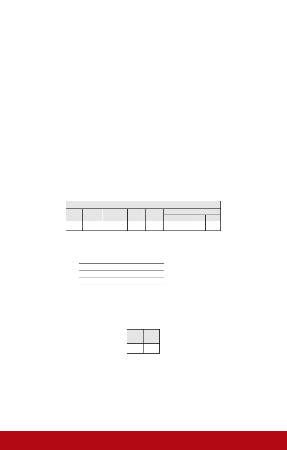
ACR1281U
Advanced Card Systems Ltd. Page 68 of 81
• SW1, SW2 = 90 00 if no error.
Note: After SW1SW2 = 90 00 has been received, read back the data in Application Zone can
check whether the Erase Application Zone with Erase is correct. If all data in Application Zone is
erased and equals to “FF”, the previous verification is success.
9.6 Erase Application Zone with Write and Erase
This command can be used in the following cases:
- AT88SC101: To erase the data in Application Zone with EC Function Enabled
- AT88SC102: To erase the data in Application Zone 2 with EC2 Function Enabled
- AT88SC1003: To erase the data in Application Zone 2 with EC2 Function Enabled
With EC or EC2 Function Enabled (that is, ECEN or EC2EN Fuse is unblown and in “1” state), the
following actions are executed:
- present the specified code to the card
- search a '1' bit in the presentation error counter and write the bit to '0'
- erase the presentation error counter. The data in corresponding Application Zone can be
erased when the submitted code is correct.
• Command format
Pseudo-APDU
CODE CLA INS Error Counter
LEN
Byte
Address
MEM_L
Byte 1
Byte 2 Byte 3
Byte 4
FF H 20 H 80H 04 H
Error Counter LEN Length of presentation error counter in bits. The value should be 80 always.
Byte Address Byte address of the Application Zone Key in the card.
Byte Address
AT88SC101 96 H
AT88SC102 9C H
AT88SC1003 5C H
CODE 4 bytes Erase Key
• Response data format
SW1 SW2
• SW1, SW2 = 90 00 if no error.
= 63 00 if there is no more retry chance
Note: After SW1SW2 = 90 00 has been received, read back the data in Application Zone can
check whether the Erase Application Zone with Write and Erase is correct. If all data in
Application Zone is erased and equals to “FF”, the previous verification is success.
ACR1281U
Advanced Card Systems Ltd. Page 69 of 81
9.7 Verify Security Code
To submit Security Code (2 bytes) to the inserted card. Security Code is to enable the memory
access of the card.
The following actions are executed:
- present the specified code to the card
- search a '1' bit in the presentation error counter and write the bit to '0'
- erase the presentation error counter. The Security Code Attempts Counter can be erased
when the submitted code is correct.
• Command format
Pseudo-APDU
CODE CLA INS Error Counter
LEN
Byte
Address
MEM_L
Byte 1
Byte 2
FF H 20 H 08 H 0A H 02 H
Error Counter LEN Length of presentation error counter in bits.
Byte Address Byte address of the key in the card.
CODE 2 bytes Security Code
• Response data format
SW1 SW2
• SW1, SW2 = 90 00 if no error.
= 63 00 if there is no more retry chance
Note: After SW1SW2 = 90 00 has been received, read back the Security Code Attempts Counter
(SCAC) can check whether the Verify User Code is correct. If SCAC is erased and equals to “FF”,
the previous verification is success.
9.8 Blown Fuse
To blow the fuse of the inserted card. The fuse can be EC_EN Fuse, EC2EN Fuse, Issuer Fuse or
Manufacturer’s Fuse.
Note: The blowing of Fuse is an irreversible process.
• Command format
Pseudo-APDU
CODE CLA INS Error Counter
LEN
Byte
Address
MEM_L
Fjuse Bit Addr
(High)
Fuse Bit Addr
(Low)
State of FUS
Pin
State of RST
Pin
FF H 05 H 00 H 00 H 04 H 01 H 00 H or 01 H
Fuse Bit Addr (2 bytes) Bit address of the fuse. Please refer to the table below for the
correct value.
State of FUS Pin State of the FUS pin. Should be 0x01 always.
ACR1281U
Advanced Card Systems Ltd. Page 70 of 81
State of RST Pin State of the RST pin. Please refer to below table for the correct
value.
Fuse Bit
Addr (High)
Fuse Bit
Addr (Low)
State of RST
Pin
Manufacturer Fuse 05 H 80 H 01 H
EC_EN Fuse 05 H C9 H 01 H
AT88SC101
Issuer Fuse 05 H E0 H 01 H
Manufacturer Fuse 05 H B0 H 01 H
EC2EN Fuse 05 H F9 H 01 H
AT88SC102
Issuer Fuse 06 H 10 H 01 H
Manufacturer Fuse 03 H F8 H 00 H
EC2EN Fuse 03 H FC H 00 H
AT88SC1003
Issuer Fuse 03 H E0 H 00 H
• Response data format
SW1 SW2
• SW1, SW2 = 90 00 if no error

ACR1281U
Advanced Card Systems Ltd. Page 71 of 81
BASIC PROGRAM FLOW FOR CONTACTLESS APPLICATIONS
Step 0. Start the application. The reader will do the PICC Polling and scan for tags continuously.
Once the tag is found and detected, the corresponding ATR will be sent to the PC.
Step 1. Connect the “ACR1281U Interface” with T=1 protocol.
Step 2. Access the PICC by exchanging APDUs.
Step 2. Access the PICC by exchanging APDUs.
..
Step N. Disconnect the “ACR1281U Interface”. Shut down the application.

ACR1281U
Advanced Card Systems Ltd. Page 72 of 81
1. How to access PCSC Compliant Tags (ISO14443-4)?
Basically, all ISO 14443-4 complaint cards (PICCs) would understand the ISO 7816-4 APDUs.
The ACR1281U Reader just has to communicate with the ISO 14443-4 complaint cards through
exchanging ISO 7816-4 APDUs and Responses. ACR1281U will handle the ISO 14443 Parts 1-4
Protocols internally.
MIFARE 1K, 4K, MINI and Ultralight tags are supported through the T=CL emulation. Just simply
treat the MIFARE tags as standard ISO14443-4 tags. For more information, please refer to topic
“PICC Commands for MIFARE Classic Memory Tags”
Table 3.1-1a: ISO 7816-4 APDU Format
Command Class INS P1 P2 Lc Data In Le
ISO 7816 Part
4 Command
Length
of the
Data In
Expected
length of
the
Response
Data
Table 3.1-1b: ISO 7816-4 Response Format (Data + 2 Bytes)
Response
Data Out
Result
Response Data SW1 SW2
Table 3.1-1c: Common ISO 7816-4 Response Codes
Results
SW1 SW2 Meaning
Success 90 00 The operation is completed
successfully.
Error
63 00 The operation is failed.
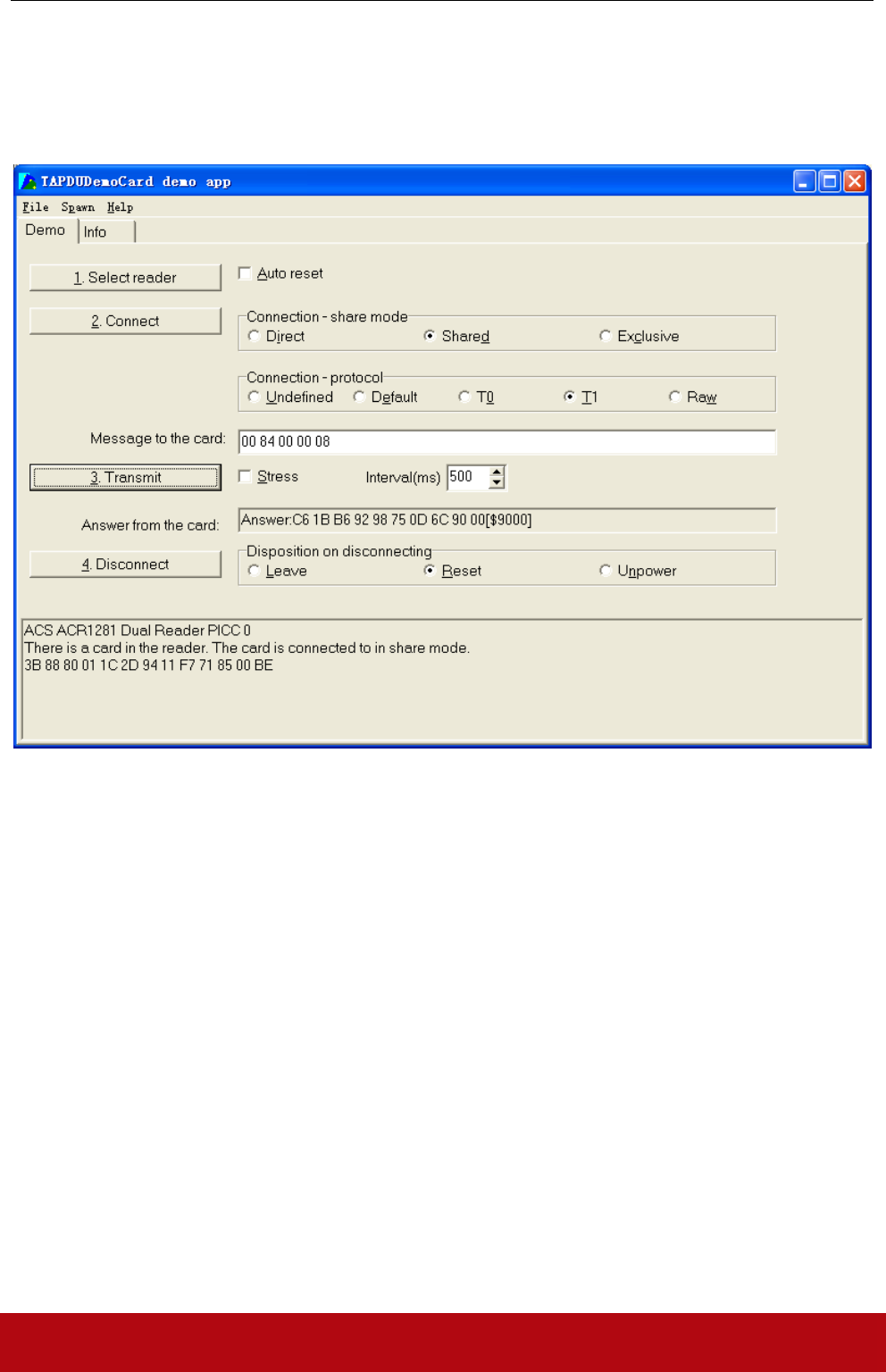
ACR1281U
Advanced Card Systems Ltd. Page 73 of 81
Typical sequence may be:
- Present the Tag and Connect the PICC Interface
- Read / Update the memory of the tag
Step 1) Connect the Tag
Step 2) Send an APDU, Get Challenge.
<< 00 84 00 00 08
>> D1 04 32 5A 9C E9 FF 0D [90 00]
Hint:
For ISO14443-4 Type A tags, the ATS can be obtained by using the APDU “FF CA 01 00 00”
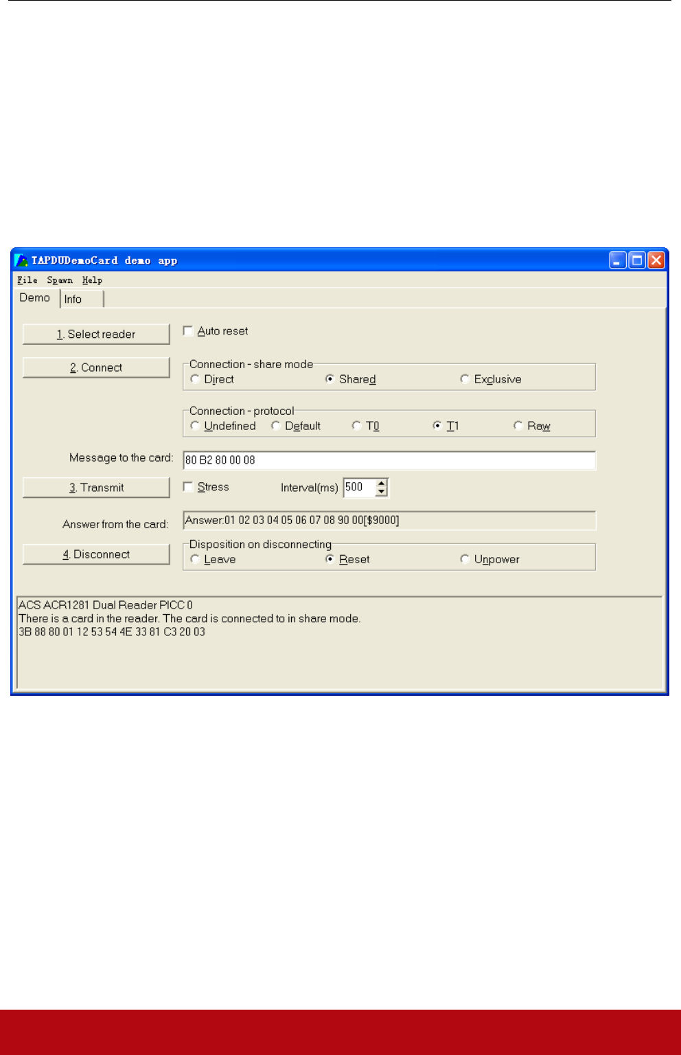
ACR1281U
Advanced Card Systems Ltd. Page 74 of 81
For Example: ISO7816-4 APDU
// To read 8 bytes from an ISO 14443-4 Type B PICC (ST19XR08E)
APDU ={80 B2 80 00 08}
Class = 0x80
INS = 0xB2
P1 = 0x80
P2 = 0x00
Lc = None
Data In = None
Le = 0x08
Answer: 01 02 03 04 05 06 07 08 [$9000]
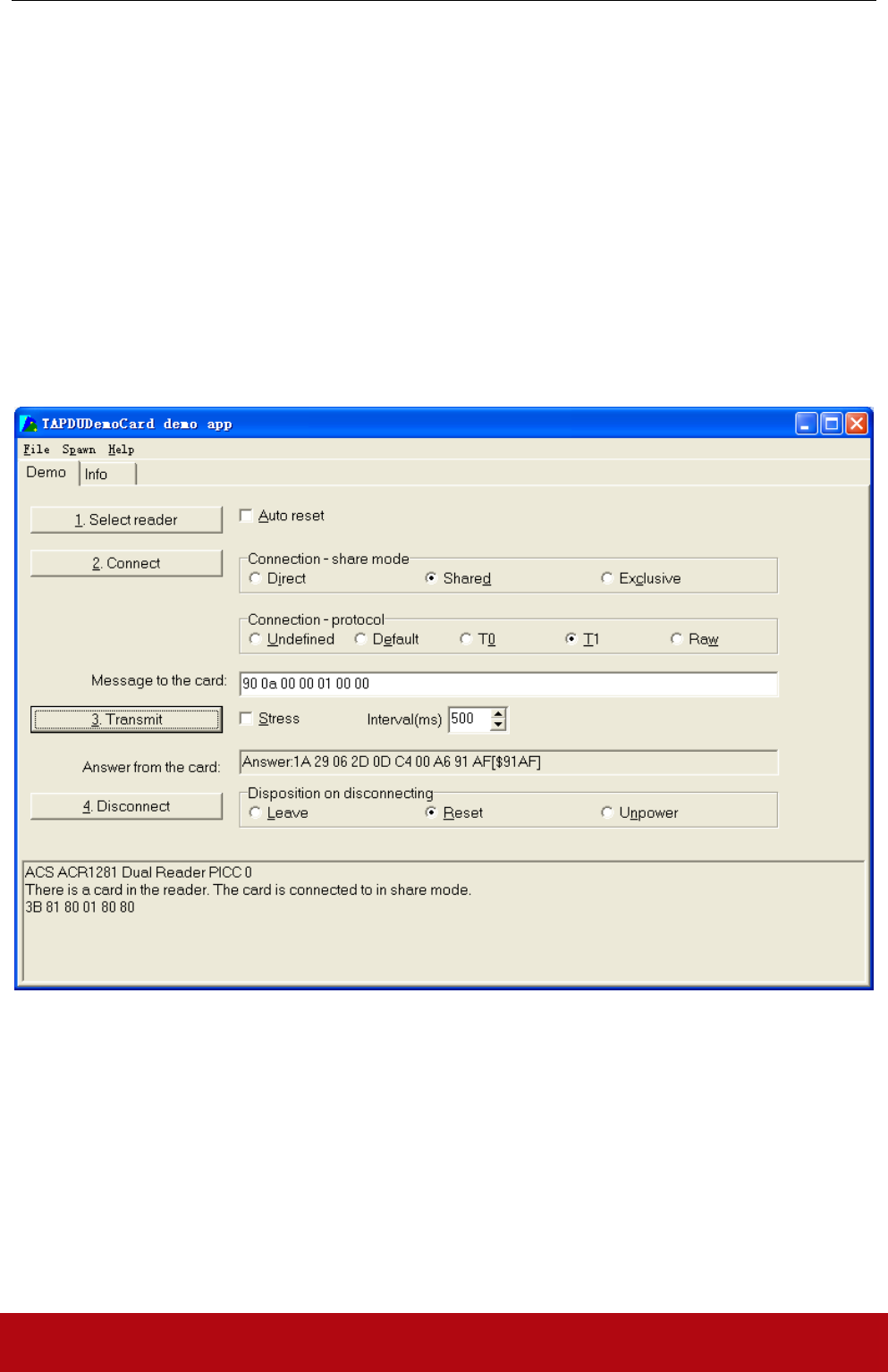
ACR1281U
Advanced Card Systems Ltd. Page 75 of 81
2. How to access DESFIRE Tags (ISO14443-4)?
The DESFIRE supports ISO7816-4 APDU Wrapping and Native modes. Once the DESFire Tag is
activated, the first APDU sent to the DESFire Tag will determine the “Command Mode”. If the first
APDU is “Native Mode”, the rest of the APDUs must be in “Native Mode” format. Similarly, If the
first APDU is “ISO7816-4 APDU Wrapping Mode”, the rest of the APDUs must be in “ISO7816-4
APDU Wrapping Mode” format.
Example 1: DESFIRE ISO7816-4 APDU Wrapping.
// To read 8 bytes random number from an ISO 14443-4 Type A PICC (DESFIRE)
APDU = {90 0A 00 00 01 00 00}
Class = 0x90; INS = 0x0A (DESFire Instruction); P1 = 0x00; P2 = 0x00
Lc = 0x01; Data In = 0x00; Le = 0x00 (Le = 0x00 for maximum length)
Answer: 1A 29 06 2D 0D C4 00 A6 [$91AF]
# Status Code{91 AF} is defined in DESFIRE specification. Please refer to the DESFIRE
specification for more details.
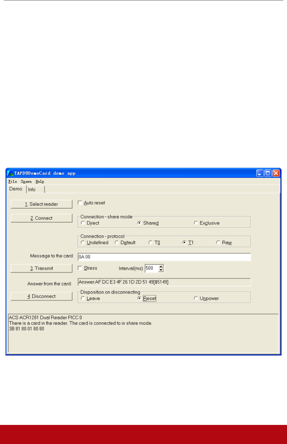
ACR1281U
Advanced Card Systems Ltd. Page 76 of 81
Example 2: DESFIRE Frame Level Chaining (ISO 7816 wrapping mode)
// In this example, the application has to do the “Frame Level Chaining”.
// To get the version of the DESFIRE card.
Step 1: Send an APDU {90 60 00 00 00} to get the first frame. INS=0x60
Answer: 04 01 01 00 02 18 05 91 AF [$91AF]
Step 2: Send an APDU {90 AF 00 00 00} to get the second frame. INS=0xAF
Answer: 04 01 01 00 06 18 05 91 AF [$91AF]
Step 3: Send an APDU {90 AF 00 00 00} to get the last frame. INS=0xAF
Answer: 04 52 5A 19 B2 1B 80 8E 36 54 4D 40 26 04 91 00 [$9100]
Example 3: DESFIRE Native Command.
// We can send Native DESFire Commands to the reader without ISO7816 wrapping if we find that
the Native DESFire Commands are more easier to handle.
// To read 8 bytes random number from an ISO 14443-4 Type A PICC (DESFIRE)
APDU = {0A 00}
Answer: AF DC E3 4F 26 1D 2D 51 49 [$5149]
In which, the first byte “AF” is the status code returned by the DESFire Card.
The Data inside the blanket [$5149]can simply be ignored by the application.

ACR1281U
Advanced Card Systems Ltd. Page 77 of 81
Example 4: DESFIRE Frame Level Chaining (Native Mode)
// In this example, the application has to do the “Frame Level Chaining”.
// To get the version of the DESFIRE card.
Step 1: Send an APDU {60} to get the first frame. INS=0x60
Answer: AF 04 01 01 00 02 18 05[$1805]
Step 2: Send an APDU {AF} to get the second frame. INS=0xAF
Answer: AF 04 01 01 00 06 18 05[$1805]
Step 3: Send an APDU {AF} to get the last frame. INS=0xAF
Answer: 00 04 52 5A 19 B2 1B 80 8E 36 54 4D 40 26 04[$2604]
Hints:
In DESFIRE Native Mode, the status code [90 00] will not be added to the response if the response
length is greater than 1. If the response length is less than 2, the status code [90 00] will be added in
order to meet the requirement of PCSC. The minimum response length is 2.

ACR1281U
Advanced Card Systems Ltd. Page 78 of 81
3. Extended APDU
Testing Card: ACOS7 (support Extended APDU, echo response)
Write CMD: 80 D2 00 00 XX XX XX
CLA = 80
INS = D2
P1 = 00
P2 = 00
Data Len = XX XX XX
Example1: APDU length = 263 bytes
APDU Command:
80D20000000100000102030405060708090A0B0C0D0E0F101112131415161718191A1B1C1D1
E1F202122232425262728292A2B2C2D2E2F303132333435363738393A3B3C3D3E3F40414243
4445464748494A4B4C4D4E4F505152535455565758595A5B5C5D5E5F60616263646566676869
6A6B6C6D6E6F707172737475767778797A7B7C7D7E7F808182838485868788898A8B8C8D8E
8F909192939495969798999A9B9C9D9E9FA0A1A2A3A4A5A6A7A8A9AAABACADAEAFB0
B1B2B3B4B5B6B7B8B9BABBBCBDBEBFC0C1C2C3C4C5C6C7C8C9CACBCCCDCECFD0D
1D2D3D4D5D6D7D8D9DADBDCDDDEDFE0E1E2E3E4E5E6E7E8E9EAEBECEDEEEFF0F1F
2F3F4F5F6F7F8F9FAFBFCFDFEFF
Response:
000102030405060708090A0B0C0D0E0F101112131415161718191A1B1C1D1E1F202122232425
262728292A2B2C2D2E2F303132333435363738393A3B3C3D3E3F404142434445464748494A4
B4C4D4E4F505152535455565758595A5B5C5D5E5F606162636465666768696A6B6C6D6E6F7
07172737475767778797A7B7C7D7E7F808182838485868788898A8B8C8D8E8F9091929394959
69798999A9B9C9D9E9FA0A1A2A3A4A5A6A7A8A9AAABACADAEAFB0B1B2B3B4B5B6B
7B8B9BABBBCBDBEBFC0C1C2C3C4C5C6C7C8C9CACBCCCDCECFD0D1D2D3D4D5D6D
7D8D9DADBDCDDDEDFE0E1E2E3E4E5E6E7E8E9EAEBECEDEEEFF0F1F2F3F4F5F6F7F8F
9FAFBFCFDFEFF9000
Example2: APDU length = 775 bytes
APDU Command:
80D20000000300000102030405060708090A0B0C0D0E0F101112131415161718191A1B1C1D1
E1F202122232425262728292A2B2C2D2E2F303132333435363738393A3B3C3D3E3F40414243
4445464748494A4B4C4D4E4F505152535455565758595A5B5C5D5E5F60616263646566676869
6A6B6C6D6E6F707172737475767778797A7B7C7D7E7F808182838485868788898A8B8C8D8E
8F909192939495969798999A9B9C9D9E9FA0A1A2A3A4A5A6A7A8A9AAABACADAEAFB0
B1B2B3B4B5B6B7B8B9BABBBCBDBEBFC0C1C2C3C4C5C6C7C8C9CACBCCCDCECFD0D
1D2D3D4D5D6D7D8D9DADBDCDDDEDFE0E1E2E3E4E5E6E7E8E9EAEBECEDEEEFF0F1F
2F3F4F5F6F7F8F9FAFBFCFDFEFF000102030405060708090A0B0C0D0E0F101112131415161
718191A1B1C1D1E1F202122232425262728292A2B2C2D2E2F303132333435363738393A3B3C
3D3E3F404142434445464748494A4B4C4D4E4F505152535455565758595A5B5C5D5E5F60616
2636465666768696A6B6C6D6E6F707172737475767778797A7B7C7D7E7F80818283848586878
8898A8B8C8D8E8F909192939495969798999A9B9C9D9E9FA0A1A2A3A4A5A6A7A8A9AAA
BACADAEAFB0B1B2B3B4B5B6B7B8B9BABBBCBDBEBFC0C1C2C3C4C5C6C7C8C9CAC
BCCCDCECFD0D1D2D3D4D5D6D7D8D9DADBDCDDDEDFE0E1E2E3E4E5E6E7E8E9EAE
BECEDEEEFF0F1F2F3F4F5F6F7F8F9FAFBFCFDFEFF000102030405060708090A0B0C0D0E0
F101112131415161718191A1B1C1D1E1F202122232425262728292A2B2C2D2E2F30313233343

ACR1281U
Advanced Card Systems Ltd. Page 79 of 81
5363738393A3B3C3D3E3F404142434445464748494A4B4C4D4E4F505152535455565758595A
5B5C5D5E5F606162636465666768696A6B6C6D6E6F707172737475767778797A7B7C7D7E7F
808182838485868788898A8B8C8D8E8F909192939495969798999A9B9C9D9E9FA0A1A2A3A4
A5A6A7A8A9AAABACADAEAFB0B1B2B3B4B5B6B7B8B9BABBBCBDBEBFC0C1C2C3C4
C5C6C7C8C9CACBCCCDCECFD0D1D2D3D4D5D6D7D8D9DADBDCDDDEDFE0E1E2E3E4
E5E6E7E8E9EAEBECEDEEEFF0F1F2F3F4F5F6F7F8F9FAFBFCFDFEFF
Response:
000102030405060708090A0B0C0D0E0F101112131415161718191A1B1C1D1E1F202122232425
262728292A2B2C2D2E2F303132333435363738393A3B3C3D3E3F404142434445464748494A4
B4C4D4E4F505152535455565758595A5B5C5D5E5F606162636465666768696A6B6C6D6E6F7
07172737475767778797A7B7C7D7E7F808182838485868788898A8B8C8D8E8F9091929394959
69798999A9B9C9D9E9FA0A1A2A3A4A5A6A7A8A9AAABACADAEAFB0B1B2B3B4B5B6B
7B8B9BABBBCBDBEBFC0C1C2C3C4C5C6C7C8C9CACBCCCDCECFD0D1D2D3D4D5D6D
7D8D9DADBDCDDDEDFE0E1E2E3E4E5E6E7E8E9EAEBECEDEEEFF0F1F2F3F4F5F6F7F8F
9FAFBFCFDFEFF000102030405060708090A0B0C0D0E0F101112131415161718191A1B1C1D1
E1F202122232425262728292A2B2C2D2E2F303132333435363738393A3B3C3D3E3F40414243
4445464748494A4B4C4D4E4F505152535455565758595A5B5C5D5E5F60616263646566676869
6A6B6C6D6E6F707172737475767778797A7B7C7D7E7F808182838485868788898A8B8C8D8E
8F909192939495969798999A9B9C9D9E9FA0A1A2A3A4A5A6A7A8A9AAABACADAEAFB0
B1B2B3B4B5B6B7B8B9BABBBCBDBEBFC0C1C2C3C4C5C6C7C8C9CACBCCCDCECFD0D
1D2D3D4D5D6D7D8D9DADBDCDDDEDFE0E1E2E3E4E5E6E7E8E9EAEBECEDEEEFF0F1F
2F3F4F5F6F7F8F9FAFBFCFDFEFF000102030405060708090A0B0C0D0E0F101112131415161
718191A1B1C1D1E1F202122232425262728292A2B2C2D2E2F303132333435363738393A3B3C
3D3E3F404142434445464748494A4B4C4D4E4F505152535455565758595A5B5C5D5E5F60616
2636465666768696A6B6C6D6E6F707172737475767778797A7B7C7D7E7F80818283848586878
8898A8B8C8D8E8F909192939495969798999A9B9C9D9E9FA0A1A2A3A4A5A6A7A8A9AAA
BACADAEAFB0B1B2B3B4B5B6B7B8B9BABBBCBDBEBFC0C1C2C3C4C5C6C7C8C9CAC
BCCCDCECFD0D1D2D3D4D5D6D7D8D9DADBDCDDDEDFE0E1E2E3E4E5E6E7E8E9EAE
BECEDEEEFF0F1F2F3F4F5F6F7F8F9FAFBFCFDFEFF9000

ACR1281U
Advanced Card Systems Ltd. Page 80 of 81
APPENDIX A: SUPPORTED CARD TYPES
The following table summarizes the card type returned by GET_READER_INFORMATION
correspond with the respective card type.
Card type code Card Type
00H Auto-select T=0 or T=1 communication protocol
01H I2C memory card (1k, 2k, 4k, 8k and 16k bits)
02H I2C memory card (32k, 64k, 128k, 256k, 512k and 1024k bits)
03H Atmel AT88SC153 secure memory card
04H Atmel AT88SC1608 secure memory card
05H Infineon SLE4418 and SLE4428
06H Infineon SLE4432 and SLE4442
07H Infineon SLE4406, SLE4436 and SLE5536
08H Infineon SLE4404
09H Atmel AT88SC101, AT88SC102 and AT88SC1003
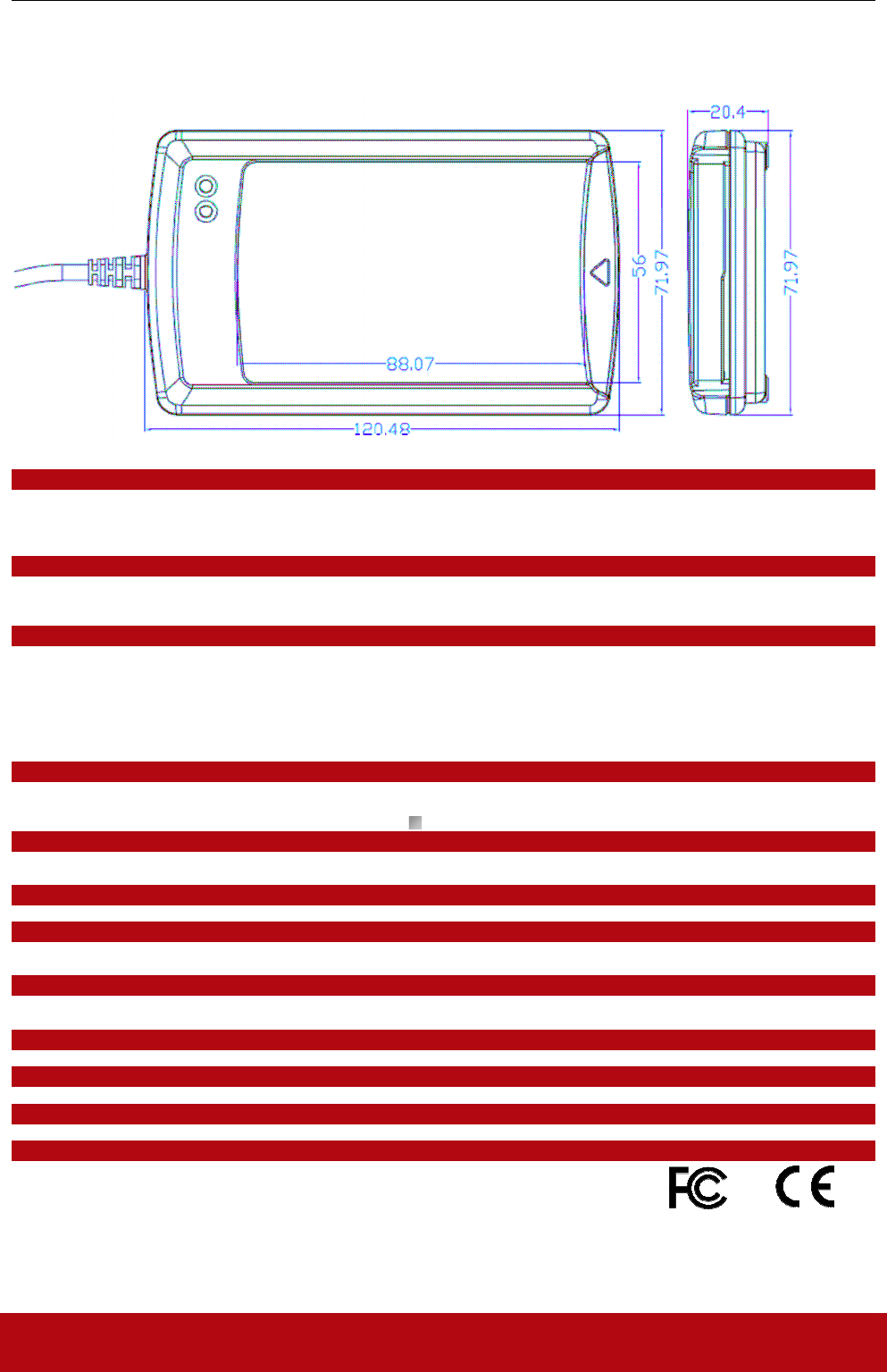
ACR1281U
Advanced Card Systems Ltd. Page 81 of 81
TECHNICAL SPECIFICATION
Universal Serial Bus Interface
Power source........................................ From USB
Speed ...................................................12 Mbps (Full Speed)
Supply Voltage......................................Regulated 5V DC
Supply Current ..................................... 200mA (max); 100mA (normal)
Contactless Smart Card Interface
Standard............................................... ISO 14443 A & B Parts 1-4
Protocol ................................................ ISO14443 T=CL for ISO14443-4 compliant cards and T=CL Emulation for MIFARE 1K/4K.
Smart card read / write speed ............... 106 kbps, 212 kbps, 424 kbps and 848 kbps
Contact Smart Card Interface
Standard............................................... ISO 7816 1/2/3, Class A, B (5V, 3V), T=0 and T=1
Supply current.......................................max. 60mA
Smart card read / write speed ............... max 344kbps
Short circuit protection ......................... +5V / GND on all pins
CLK frequency...................................... 4.8 MHz
Card connector .....................................Landing
Card insertion cycles.............................min. 300,000
Case
Dimensions........................................... 120.48 mm (L) x 71.97 mm (W) x 20.4 mm (H)
Material................................................. ABS
Color.....................................................Metallic Silver Grey
Antenna
Antenna Size ........................................65mm x 60mm
Operating distance................................ up to 50 mm
Operating Frequency for Contactless Cards Access
Operating Frequency ............................13.56 MHz
Built-in peripherals
Monotone buzzer
Dual-Color LED
Operating Conditions
Temperature ......................................... 0 - 50° C
Humidity................................................10% - 80%
Cable Connector
Length...................................................1.5 M (USB)
Standard/Certifications
CE, FCC
OS
Windows 98, ME, 2K, XP
OEM
OEM-Logo possible, customer-specific colors, casing, and card connector
Note: This equipment has been tested and found to comply with the limits for a Class B digital
device, pursuant to part 15 of the FCC Rules. These limits are designed to provide reasonable
protection against harmful interference in a residential installation. This equipment generates
uses and can radiate radio frequency energy and, if not installed and used in accordance with
the instructions, may cause harmful interference to radio communications. However, there is
no guarantee that interference will not occur in a particular installation. If this equipment does
cause harmful interference to radio or television reception, which can be determined by turning
the equipment off and on, the user is encouraged to try to correct the interference by one or
more of the following measures:
—Reorient or relocate the receiving antenna.
—Increase the separation between the equipment and receiver.
—Connect the equipment into an outlet on a circuit different from that to which the receiver is
connected.
—Consult the dealer or an experienced radio/TV technician for help.
The users manual or instruction manual for an intentional or unintentional radiator shall caution
the user that changes or modifications not expressly approved by the party responsible for compliance
could void the user's authority to operate the equipment. In cases where the manual is provided only
in a form other than paper, such as on a computer disk or over the Internet, the information required
by this section may be included in the manual in that alternative form, provided the user can reasonably
be expected to have the capability to access information in that form.
waring