Agilent Technologies 8510 Users Manual 5956 4352.07.13.06
8510 to the manual f8bfe3f5-5597-475c-97d5-b23ec6de9b38
2015-02-02
: Agilent-Technologies Agilent-Technologies-8510-Users-Manual-413247 agilent-technologies-8510-users-manual-413247 agilent-technologies pdf
Open the PDF directly: View PDF ![]() .
.
Page Count: 32
Agilent
Specifying Calibration
Standards for the Agilent 8510
Network Analyzer
Application Note 8510-5B
Discontinued Product Information
— For Support Reference Only —
Information herein, may refer to products/services no longer supported.
We regret any inconvenience caused by obsolete information. For the
latest information on Agilent’s test and measurement products go to:
www.agilent.com/find/products
In the US, call Agilent Technologies at 1-800-829-4444
(any weekday between 8am–5pm in any U.S. time zone)
World-wide Agilent sales office contact information is available at:
www.agilent.com/find/contactus

2
3
3
3
4
5
5
7
7
8
9
9
9
11
12
12
12
14
14
15
16
16
17
17
17
18
18
18
18
19
19
19
19
19
20
20
20
21
21
22
22
22
23
23
26
29
Introduction
Measurement errors
Measurement calibration
Calibration kit
Standard definition
Class assignment
Modification procedure
Select standards
Define standards
Standard number
Standard type
Open circuit capacitance: C0, C1, C2and C3
Short circuit inductance: L0, L1, L2and L3
Fixed or sliding
Terminal impedance
Offset delay
Offset Z0
Offset loss
Lower/minimum frequency
Upper/maximum frequency
Coax or waveguide
Standard labels
Assign classes
Standard classes
S11A,B,C and S22 A,B,C
Forward transmission match/thru
Reverse transmission match/thru
Isolation
Frequency response
TRL Thru
TRL Reflect
TRL Line
Adapter
Standard class labels
TRL options
Calibration kit label
Enter standards/classes
Verify performance
User modified cal kits and Agilent 8510 specifications
Modification examples
Modeling a thru adapter
Modeling an arbitrary impedance
Appendix A
Calibration kit entry procedure
Appendix B
Dimensional considerations in coaxial connectors
Appendix C
Cal coefficients model
Table of contents
Known devices called calibration standards
provide the measurement reference for net-
work analyzer error-correction. This note
covers methods for specifying these stan-
dards and describes the procedures for their
use with the Agilent Technologies 8510 net-
work analyzer.
The 8510 network analyzer system has the
capability to make real-time error-corrected
measurements of components and devices
in a variety of transmission media.
Fundamentally, all that is required is a set
of known devices (standards) that can be
defined physically or electrically and used
to provide a reference for the physical inter-
face of the test devices.
Agilent Technologies supplies full calibration
kits in 1.0-mm, 1.85-mm, 2.4-mm, 3.5-mm,
7-mm, and Type-N coaxial interfaces. The
8510 system can be calibrated in other inter-
faces such as other coaxial types, waveguide
and microstrip, given good quality stan-
dards that can be defined.
The 8510’s built-in flexibility for calibration
kit definition allows the user to derive a
precise set of definitions for a particular set
of calibration standards from precise physi-
cal measurements. For example, the charac-
teristic impedance of a matched impedance
airline can be defined from its actual physi-
cal dimensions (diameter of outer and inner
conductors) and electrical characteristics
(skin depth). Although the airline is
designed to provide perfect signal transmis-
sion at the connection interface, the dimen-
sions of individual airlines will vary
somewhat—resulting in some reflection due
to the change in impedance between the test
port and the airline. By defining the actual
impedance of the airline, the resultant
reflection is characterized and can be
removed through measurement calibration.
The scope of this product note includes a
general description of the capabilities of the
8510 to accept new cal kit descriptions via
the MODIFY CAL KIT function found in the
8510 CAL menu. It does not, however,
describe how to design a set of physical
standards. The selection and fabrication of
appropriate calibration standards is as var-
ied as the transmission media of the partic-
ular application and is beyond the scope of
this note.
3
Introduction
This product note covers measurement calibration
requirements for the Agilent 8510B/C network
analyzer. All of the capabilities described in this
note also apply to the Agilent 8510A with the
following exceptions: response & isolation calibra-
tion; short circuit inductance; class assignments
for forward/reverse isolation, TRL thru, reflect,
line and options; and adapter removal.
Measurement errors
Measurement errors in network analysis can be
separated into two categories: random and system-
atic errors. Both random and systematic errors are
vector quantities. Random errors are non-repeat-
able measurement variations and are usually
unpredictable. Systematic errors are repeatable
measurement variations in the test setup.
Systematic errors include mismatch and leakage
signals in the test setup, isolation characteristics
between the reference and test signal paths, and
system frequency response. In most microwave
measurements, systematic errors are the most sig-
nificant source of measurement uncertainty. The
source of these errors can be attributed to the sig-
nal separation scheme used.
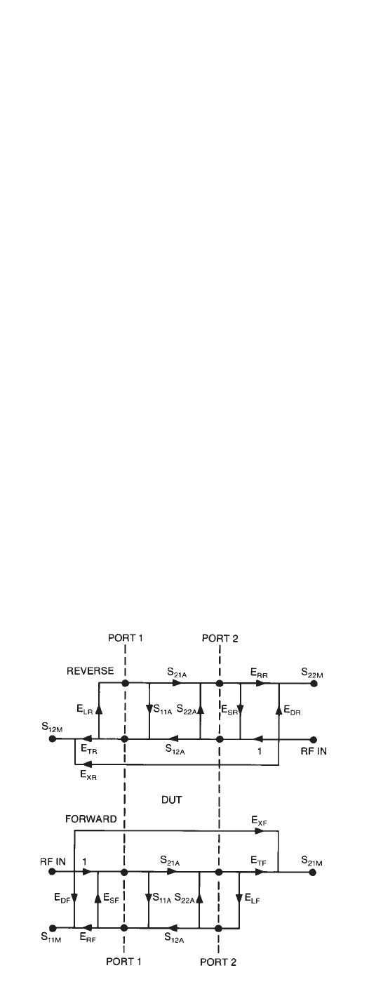
The systematic errors present in an S-parameter
measurement can be modeled with a signal flow-
graph. The flowgraph model, which is used for error
correction in the 8510 for the errors associated with
measuring the S-parameters of a two port device, is
shown in the figure below.
The six systematic errors in the forward direction
are directivity, source match, reflection tracking,
load match, transmission tracking, and isolation.
The reverse error model is a mirror image, giving a
total of 12 errors for two-port measurements. The
process of removing these systematic errors from
the network analyzer S-parameter measurement is
called measurement calibration.
EDF, EDR-Directivity ELF, ELR-Load Match
ESF, ESR-Source Match ETF, ETR-Trans. Tracking
ERF, ERR-Refl. Tracking EXF, EXR-Isolation
Measurement calibration
A more complete definition of measurement cali-
bration using the 8510, and a description of the
error models is included in the 8510 operating and
programming manual. The basic ideas are summa-
rized here.
A measurement calibration is a process which
mathematically derives the error model for the
8510. This error model is an array of vector coeffi-
cients used to establish a fixed reference plane of
zero phase shift, zero magnitude and known
impedance. The array coefficients are computed by
measuring a set of “known” devices connected at a
fixed point and solving as the vector difference
between the modeled and measured response.
Figure 1. Agilent 8510 full 2-port error model

4
The array coefficients are computed by measuring
a set of “known” devices connected at a fixed point
and solving as the vector difference between the
modeled and measured response.
The full 2-port error model shown in Figure 1 is
an example of only one of the measurement calibra-
tions available with the 8510. The measurement
calibration process for the 8510 must be one of
seven types: RESPONSE, RESPONSE & ISOLATION,
Sll 1-PORT, S22 1-PORT, ONE PATH 2-PORT, FULL
2-PORT, and TRL 2-PORT. Each of these calibration
types solves for a different set of the systematic
measurement errors. A RESPONSE calibration
solves for the systematic error term for reflec-
tion or transmission tracking depending on the
S-parameter which is activated on the 8510 at the
time. RESPONSE & ISOLATION adds correction
for crosstalk to a simple RESPONSE calibration.
An S11 l-PORT calibration solves for the forward
error terms, directivity, source match and reflec-
tion tracking. Likewise, the S22 1-PORT calibration
solves for the same error terms in the reverse
direction. A ONE PATH 2-PORT calibration solves
for all the forward error terms. FULL 2-PORT and
TRL 2-PORT calibrations include both forward and
reverse error terms.
The type of measurement calibration selected by
the user depends on the device to be measured
(i.e., 1-port or 2-port device) and the extent of
accuracy enhancement desired. Further, a combi-
nation of calibrations can be used in the measure-
ment of a particular device.
The accuracy of subsequent test device measure-
ments is dependent on the accuracy of the test
equipment, how well the “known” devices are mod-
eled and the exactness of the error correction
model.
Calibration kit
A calibration kit is a set of physical devices called
standards. Each standard has a precisely known or
predictable magnitude and phase response as a
function of frequency. In order for the 8510 to use
the standards of a calibration kit, the response of
each standard must be mathematically defined and
then organized into standard classes which corre-
spond to the error models used by the 8510.
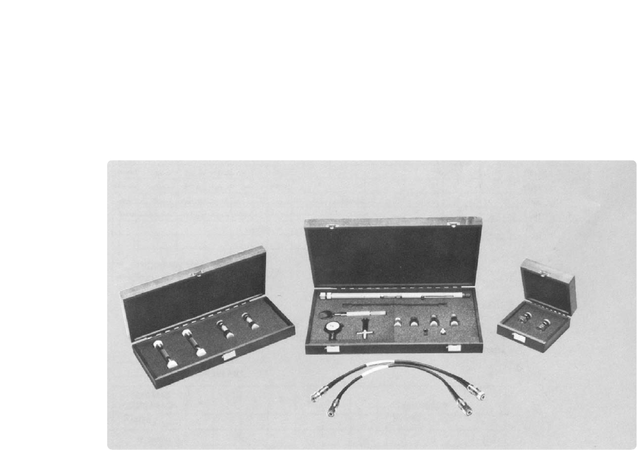
Agilent currently supplies calibration kits with
1.0-mm (85059A), 1.85-mm (85058D), 2.4-mm
(85056A/D/K), 3.5-mm (85052A/B/C/D/E), 7-mm
(85050B/C/D) and Type-N (85054B) coaxial con-
nectors. To be able to use a particular calibration
kit, the known characteristics from each standard
in the kit must be entered into the 8510 non-
volatile memory. The operating and service manu-
als for each of the Agilent calibration kits contain
the physical characteristics for each standard in
the kit and mathematical definitions in the format
required by the 8510.
Waveguide calibration using the 8510 is possible.
Calibration in microstrip and other non-coaxial
media is described in Agilent Product Note 8510-8A.
5
Standard definition
Standard definition is the process of mathematical-
ly modeling the electrical characteristics (delay,
attenuation and impedance) of each calibration
standard. These electrical characteristics can be
mathematically derived from the physical dimen-
sions and material of each calibration standards or
from its actual measured response. A standard
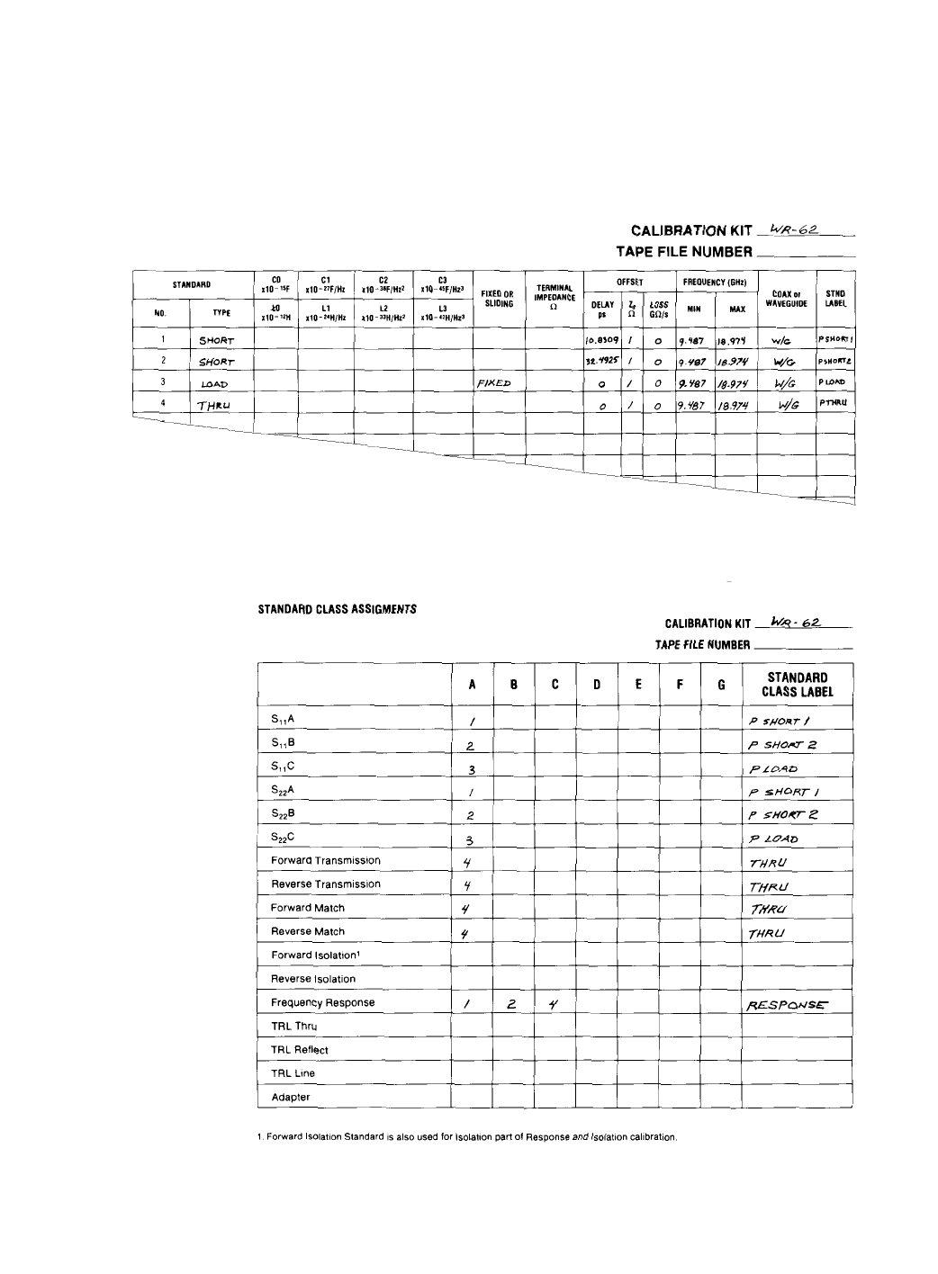
definition table (see Table 1) lists the parameters
that are used by the 8510 to specify the mathemati-
cal model.
Class assignment
Class assignment is the process of organizing cali-
bration standards into a format which is compati-
ble with the error models used in measurement
calibration. A class or group of classes correspond
to the seven calibration types used in the 8510.
The 17 available classes are identified later in this
note (see Assign classes).
6
Table 1. Standard definitions table
Table 2. Standard class assignments

7
Modification procedure
Calibration kit modification provides the capability
to adapt to measurement calibrations in other con-
nector types or to generate more precise error
models from existing kits. Provided the appropri-
ate standards are available, cal kit modification
can be used to establish a reference plane in the
same transmission media as the test devices and at
a specified point, generally the point of device con-
nection/insertion. After calibration, the resultant
measurement system, including any adapters
which would reduce system directivity, is fully cor-
rected and the systematic measurement errors are
mathematically removed. Additionally, the modifi-
cation function allows the user to input more pre-
cise physical definitions for the standards in a
given cal kit. The process to modify or create a cal
kit consists of the following steps:
1. Select standards
2. Define standards
3. Assign classes
4. Enter standards/classes
5. Verify performance
To further illustrate, an example waveguide cali-
bration kit is developed as the general descriptions
in MODIFY CAL KIT process are presented.
Select standards
Determine what standards are necessary for cali-
bration and are available in the transmission
media of the test devices.
Calibration standards are chosen based on the fol-
lowing criteria:
• A well defined response which is mechanically
repeatable and stable over typical ambient tem-
peratures and conditions. The most common
coaxial standards are zero-electrical-length
short, shielded open and matched load termina-
tions which ideally have fixed magnitude and
broadband phase response. Since waveguide
open circuits are generally not modelable, the
types of standards typically used for waveguide
calibration are a pair of offset shorts and a fixed
or sliding load.
• A unique and distinct frequency response. To
fully calibrate each test port (that is to provide
the standards necessary for S11 or S22 1-PORT
calibration), three standards are required that
exhibit distinct phase and/or magnitude at each
particular frequency within the calibration
band. For example, in coax, a zero-length short
and a perfect shielded open exhibit 180 degree
phase separation while a matched load will pro-
vide 40 to 50 dB magnitude separation from
both the short and the open. In waveguide, a
pair of offset shorts of correct length provide
phase separation.
• Broadband frequency coverage. In broadband
applications, it is often difficult to find stan-
dards that exhibit a known, suitable response
over the entire band. A set of frequency-banded
standards of the same type can be selected in
order to characterize the full measurement
band.
• The TRL 2-PORT calibration requires only a sin-
gle precision impedance standard—a transmis-
sion line. An unknown high reflection device
and a thru connection are sufficient to complete
this technique.
8
Define standards
A glossary of standard definition parameters used
with the Agilent 8510 is included in this section.
Each parameter is described and appropriate con-
versions are listed for implementation with the
8510. To illustrate, a calibration kit for WR-62 rec-
tangular waveguide (operating frequency range
12.4 to 18 GHz) will be defined as shown in Table
1. Subsequent sections will continue to develop
this waveguide example.
The mathematical models are developed for each
standard in accordance with the standard defini-
tion parameters provided by the 8510. These stan-
dard definition parameters are shown in Figure 2.
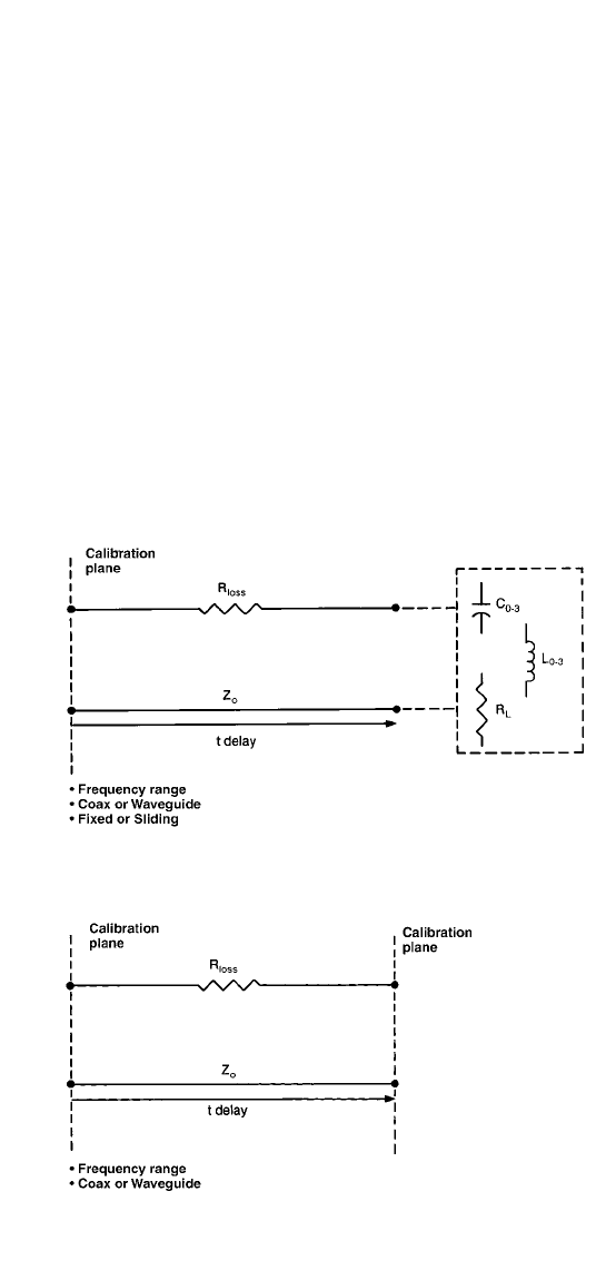
Figure 2. Standard definition models
Model for reflection standard
(short, open, load or arbitrary
impedance)
Model for transmission
standard (Thru)

9
Each standard is described using the Standard
Definition Table in accordance with the 1- or 2-
port model. The Standard Definition table for a
waveguide calibration kit is shown in Table 1. Each
standard type (short, open, load, thru, and arbi-
trary impedance) may be defined by the parame-
ters as specified below.
• Standard number and standard type
• Fringing capacitance of an open, or inductance
of a short, specified by a third order polynomial
• Load/arbitrary impedance, which is specified as
fixed or sliding
• Terminal resistance of an arbitrary impedance
• Offsets which are specified by delay, Z0, Rloss
• Frequency range
• Connector type: coaxial or waveguide
• Label (up to 10 alphanumeric characters)
Standard number
A calibration kit may contain up to 21 standards
(See Table 1). The required number of standards
will depend on frequency coverage and whether
thru adapters are needed for sexed connectors.
For the WR-62 waveguide example, four standards
will be sufficient to perform the FULL 2-PORT cali-
bration. Three reflection standards are required,
and one transmission standard (a thru) will be suf-
ficient to complete this calibration kit.
Standard type
A standard type must be classified as a “short”
“open,” “load”, “thru,” or “arbitrary impedance.”
The associated models for reflection standards
(short, open, load, and arbitrary impedance) and
transmission standards (thru) are shown in Figure 1.
For the WR-62 waveguide calibration kit, the four
standards are a 1/8λ
λand 3/8λ
λ offset short, a fixed
matched load, and a thru. Standard types are
entered into the Standard Definition table under
STANDARD NUMBERS 1 through 4 as short, short,
load, and thru respectively.
Open circuit capacitance: C0, C1, C2and C3
If the standard type selected is an “open,” the C0
through C3coefficients are specified and then used
to mathematically model the phase shift caused by
fringing capacitance as a function of frequency.
As a reflection standard, an “open” offers the
advantage of broadband frequency coverage, while
offset shorts cannot be used over more than an
octave. The reflection coefficient (Γ= pe-je) of a
perfect zero-length-open is 1 at 0° for all frequen-
cies. At microwave frequencies however, the magni-
tude and phase of an “open” are affected by the
radiation loss and capacitive “fringing” fields,
respectively. In coaxial transmission media, shield-
ing techniques are effective in reducing the radia-
tion loss. The magnitude (p) of a zero-length
“open” is assigned to be 1 (zero radiation loss) for
all frequencies when using the Agilent 8510
Standard Type “open.”

10
It is not possible to remove fringing capacitance,
but the resultant phase shift can be modeled as a
function of frequency using C0through C3(C0+Cl
x
f + C2
x
f2+ C3
x
f3,with units of F(Hz), C0(fF),
C1(10-27F/Hz), C2(10-36F/Hz2) and C3(10-45F/Hz3),
which are the coefficients for a cubic polynomial
that best fits the actual capacitance of the “open.”
A number of methods can be used to determine the
fringing capacitance of an “open.” Three tech-
niques, described here, involve a calibrated reflec-
tion coefficient measurement of an open standard
and subsequent calculation of the effective capaci-
tance. The value of fringing capacitance can be cal-
culated from the measured phase or reactance as a
function of frequency as follows.
Ceff – effective capacitance
∆∅ – measured phase shift
f – measurement frequency
F – farad
Z0 – characteristic impedance
X – measured reactance
This equation assumes a zero-length open. When
using an offset open the offset delay must be
backed-out of the measured phase shift to obtain
good C0through C3coefficients.
This capacitance can then be modeled by choosing
coefficients to best fit the measured response
when measured by either method 3 or 4 below.
1. Fully calibrated 1-Port–Establish a calibrated
reference plane using three independent standards
(that is, 2 sets of banded offset shorts and load).
Measure the phase response of the open and solve
for the capacitance function.
2. TRL 2-PORT–When transmission lines standards
are available, this method can be used for a com-
plete 2-port calibration. With error-correction
applied the capacitance of the open can be meas-
ured directly.
3. Gating–Use time domain gating to correct the
measured response of the open by isolating the
reflection due to the open from the source match
reflection and signal path leakage (directivity).
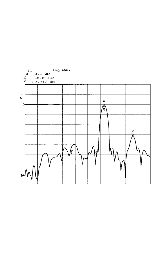
Figure 3 shows the time domain response of the
open at the end of an airline. Measure the gated
phase response of the open at the end of an airline
and again solve for the capacitance function.
tan( )
∆∅
2
2πfZ0
1
2πfX
Ceff ==
11
Note
In some cases (when the phase response is linear
with respect to frequency) the response of an open
can be modeled as an equivalent “incremental”
length.
This method will serve as a first order approxima-
tion only, but can be useful when data or stan-
dards for the above modeling techniques are not
available.
For the waveguide example, this parameter is not
addressed since opens cannot be made valid stan-
dards in waveguide, due to the excessive radiation
loss and indeterminant phase.
Short circuit inductance L0, L1, L2and L3
If the standard type selected is a ‘short,’ the L0
through L3coefficients are specified to model the
phase shift caused by the standard’s residual
inductance as a function of frequency. The reflec-
tion coefficient of an ideal zero-length short is 1 at
180° at all frequencies. At microwave frequencies,
however, the residual inductance can produce
additional phase shift. When the inductance is
known and repeatable, this phase shift can be
accounted for during the calibration.
Figure 3. Time domain response of open at the end of
an airline
2πf (∆length)
c
∆∅(radians) =

The inductance as a function of frequency can be
modeled by specifying the coefficients of a third-
order polynomial (L0+ L1
x
f + L2
x
f2+ L3
x
f3),
with units of L0(nH), L1(10-24H/Hz),
L2(10-33 H/Hz2) and L3(10-42H/Hz3).
For the waveguide example, the inductance of the
offset short circuits is negligible. L0through L3are
set equal to zero.
Fixed or sliding
If the standard type is specified to be a load or an
arbitrary impedance, then it must be specified as
fixed or sliding. Selection of “sliding” provides a
sub-menu in the calibration sequence for multiple
slide positions and measurement. This enables cal-
culation of the directivity vector by mathematically
eliminating the response due to a non-ideal termi-
nal impedance. A further explanation of this tech-
nique is found in the Measurement Calibration
section in the Agilent 8510 Operating and
Programming manual.
The load standard #4 in the WR-62 waveguide cali-
bration kit is defined as a fixed load. Enter FIXED
in the table.
Terminal impedance
Terminal impedance is only specified for “arbitrary
impedance” standards. This allows definition of
only the real part of the terminating impedance in
ohms. Selection as the standard type “short,”
“open,” or “load” automatically assigns the termi-
nal impedance to be 0, ∞or 50 ohms respectively.
The WR-62 waveguide calibration kit example does
not contain an arbitrary impedance standard.
Offset delay
If the standard has electrical length (relative to the
calibration plane), a standard is specified to have
an offset delay. Offset delay is entered as the one-
way travel time through an offset that can be
obtained from the physical length using propaga-
tion velocity of light in free space and the appro-
priate permittivity constant. The effective
propagation velocity equals . See Appendix B
for a further description of physical offset lengths
for sexed connector types.
Delay (seconds) =
= precise measurement of offset length in meters
εr = relative permittivity (= 1.000649 for coaxial
airline or air-filled waveguide in standard lab
conditions)
c = 2.997925 x10⁸m/s
In coaxial transmission line, group delay is con-
stant over frequency. In waveguide however, group
velocity does vary with frequency due to disper-
sion as a function of the cut-off frequency.
√εr
c
12
c
√εr

13
The convention for definition of offset delay in
waveguide requires entry of the delay assuming no
dispersion. For waveguide transmission line, the
Agilent 8510 calculates the effects of dispersion as
a function of frequency as follows:
fco = lower cutoff frequency
f = measurement frequency
Note
To assure accurate definition of offset delay, a
physical measurement of offset length is recom-
mended.
The actual length of offset shorts will vary by man-
ufacturer. For example, the physical length of a
1/8λoffset depends on the center frequency chosen.
In waveguide this may correspond to the arith-
metic or geometric mean frequency. The arithmetic
mean frequency is simply (F1+ F2)/2, where F1and
F2are minimum and maximum operating frequen-
cies of the waveguide type. The geometric mean
frequency is calculated as the square root of F1x
F2. The corresponding (λg) is then calculated from
the mean frequency and the cutoff frequency of the
waveguide type. Fractional wavelength offsets are
then specified with respect to this wavelength.
For the WR-62 calibration kit, offset delay is zero
for the “thru” (std #4) and the “load” (std #3). To
find the offset delay of the 1/8λand 3/8λoffset
shorts, precise offset length measurements are nec-
essary. For the 1/8λoffset short, l = 3.24605 mm,
εr= 1.000649, c = 2.997925 x 10⁸m/s.
Delay = (3.24605 x 10⁻³ m) (√1.000649) = 10.8309 pS
2.997925 x 10⁸m/s
For the 3/8λoffset short, I = 9.7377 mm, εr= 1.000649,
c = 2.997925 x 10⁸m/s.
Delay = (9.7377 x 10⁻³ m) (√1.000649) = 32.4925 pS
2.997925 x 10⁸m/s
Offset Z0
Offset Z0is the characteristic impedance within the
offset length. For coaxial type offset standards,
specify the real (resistive) part of the characteris-
tic impedance in the transmission media. The char-
acteristic impedance in lossless coaxial
transmission media can be calculated from its
physical geometry as follows.
Actual delay = Linear delay
1 - (fco/f)2
14
µr= relative permeability constant of the medium
(equal to 1.0 in air)
εr= relative permittivity constant of the medium
(equal to 1.000649 in air)
D = inside diameter of outer conductor
d = outside diameter of inner conductor
The 8510 requires that the characteristic imped-
ance of waveguide transmission line is assigned to
be equal to the SET Z0.
The characteristic impedance of other transmis-
sion media is not as easily determined through
mechanical dimensions. Waveguide impedance, for
example, varies as a function of frequency. In such
cases, normalized impedance measurements are
typically made. When calibrating in waveguide, the
impedance of a “matched” load is used as the
impedance reference. The impedance of this load is
matched that of the waveguide across frequency.
Normalized impedance is achieved by entering SET
Z0and OFFSET Z0to 1 ohm for each standard.
Offset Z0equal to system Z0(SET Z0) is the
assigned convention in the 8510 for matched wave-
guide impedance.
Offset loss
Offset loss is used to model the magnitude loss due
to skin effect of offset coaxial type standards only.
The value of loss is entered into the standard defi-
nition table as gigohms/second or ohms/nanosec-
ond at 1 GHz.
The offset loss in gigohms/second can be calculat-
ed from the measured loss at 1 GHz and the physi-
cal length of the particular standard by the
following equation.
where:
dBlOSS |1 GHz =measured insertion loss at 1 GHz
Z0= offset Z0
= physical length of the offset
The 8510 calculates the skin loss as a function of
frequency as follows:
Note: For additional information refer to
Appendix C.
For all offset standards, including shorts or opens,
enter the one way skin loss. The offset loss in
waveguide should always be assigned zero ohms by
the 8510.
Z0= = 59.9585
µ
εIn
1
2π
D
d
µr
εr
() In D
d
()
Offset loss =
GΩ
s 10 loge(10) er
1 GHz
dBloss 1 GHz C Z0
()
Offset loss X
GΩ
s1GHz
f(GHz)
Offset loss GΩ
s=
() ()

15
Therefore, for the WR-62 waveguide standard defi-
nition table, offset loss of zero ohm/sec is entered
for all four standards.
Lower/minimum frequency
Lower frequency defines the minimum frequency at
which the standard is to be used for the purposes
of calibration.
Note
When defining coaxial offset standards, it may be
necessary to use banded offset shorts to specify a
single standard class. The lower and upper fre-
quency parameters should be used to indicate the
frequency range of desired response. It should be
noted that lower and upper frequency serve a dual
purpose of separating banded standards which
comprise a single class as well as defining the over-
all applicable frequency range over which a cali-
bration kit may be used.
In waveguide, this must be its lower cut-off fre-
quency of the principal mode of propagation.
Waveguide cutoff frequencies can be found in most
waveguide textbooks. The cutoff frequency of the
fundamental mode of propagation (TE10) in rectan-
gular waveguide is defined as follows.
f = c
2a
c = 2.997925 x 1010 cm/sec.
a = inside width of waveguide, larger dimension in cm
As referenced in offset delay, the minimum fre-
quency is used to compute the dispersion effects in
waveguide.
For the WR-62 waveguide example, the lower cutoff
frequency is calculated as follows.
f = c = 2.997925 x 1010 cm/s = 9.487 GHz
2a 2 x 1.58 cm
c = 2.997925 x 1010 cm/s
a = 1.58 cm
The lower cut-off frequency of 9.487 GHz is entered
into the table for all four WR-62 waveguide standards.
16
Upper/maximum frequency
This specifies the maximum frequency at which
the standard is valid. In broadband applications, a
set of banded standards may be necessary to pro-
vide constant response. For example, coaxial offset
standards (i.e., 1/4λoffset short) are generally spec-
ified over bandwidths of an octave or less.
Bandwidth specification of standards, using mini-
mum frequency and maximum frequency, enables
the 8510 to characterize only the specified band
during calibration. Further, a submenu for banded
standards is enabled which requires the user to
completely characterize the current measurement
frequency range. In waveguide, this is the upper
cutoff frequency for the waveguide class and mode
of propagation. For the fundamental mode of prop-
agation in rectangular waveguide the maximum
upper cutoff frequency is twice the lower cutoff
frequency and can be calculated as follows.
F(upper) = 2 x F(lower)
The upper frequency of a waveguide standard may
also be specified as the maximum operating fre-
quency as listed in a textbook.
The MAXIMUM FREQUENCY of the WR-62 wave-
guide cal kit is 18.974 GHz and is entered into the
standard definition table for all four standards.
Coax or waveguide
It is necessary to specify whether the standard
selected is coaxial or waveguide. Coaxial transmis-
sion line has a linear phase response as
Waveguide transmission line exhibits dispersive
phase response as follows:
where
Selection of WAVEGUIDE computes offset delay
using the dispersive response, of rectangular wave-
guide only, as a function of frequency as
This emphasizes the importance of entering “fco” as
the LOWER FREQUENCY.
Selection of COAXIAL assumes linear response of
offset delay.
1-(fco/f)2
Delay (seconds) Linear delay
=
1-(λ/λco)2
λgλ
=
2πᐉ
∅(radians) λg
=
2πᐉ2πf(delay)
∅(radians) λ==

17
Note
Mathematical operations on measurements (and
displayed data) after calibration are not corrected
for dispersion.
Enter WAVEGUIDE into the standard definition
table for all four standards.
Standard labels
Labels are entered through the title menu and may
contain up to 10 characters. Standard Labels are
entered to facilitate menu driven calibration.
Labels that describe and differentiate each stan-
dard should be used. This is especially true for
multiple standards of the same type.
When sexed connector standards are labeled, male
(M) or female (F), the designation refers to the test
port connector sex—not the connector sex of the
standard. Further, it is recommended that the label
include information carried on the standard such
as the serial number of the particular standard to
avoid confusing multiple standards which are simi-
lar in appearance.
The labels for the four standards in the waveguide
example are; #1-PSHORT1, #2-PSHORT2, #3-PLOAD,
and #4-THRU.
Assign classes
In the previous section, define standards, the
characteristics of calibration standards were
derived. Class assignment organizes these stan-
dards for computation of the various error models
used in calibration. The Agilent 8510 requires a
fixed number of standard classes to solve for the n
terms used in the error models (n = 1, 3, or 12).
That is, the number of calibration error terms
required by the 8510 to characterize the measure-
ment system (1-Port, 2-Port, etc.) equals the num-
ber of classes utilized.
Standard Classes
A single Standard Class is a standard or group of
(up to 7) standards that comprise a single calibra-
tion step. The standards within a single class are
assigned to locations A through G as listed on the
Class Assignments table. It is important to note
that a class must be defined over the entire fre-
quency range that a calibration is made, even
though several separate standards may be required
to cover the full measurement frequency range. In
the measurement calibration process, the order of
standard measurement within a given class is not
important unless significant frequency overlap
exists among the standards used. When two stan-
dards have overlapping frequency bands, the last
standard to be measured will be used by the 8510.
The order of standard measurement between dif-
ferent classes is not restricted, although the 8510
requires that all standards that will be used within
a given class are measured before proceeding to
the next class. Standards are organized into speci-
fied classes which are defined by a Standards
Class Assignment table. See Table 2 for the class
assignments table for the waveguide calibration kit.

18
S11 A,B,C and S22 A,B,C
S11 A, B,C and S22 A,B,C correspond to the S11 and
S22 reflection calibrations for port 1 and port 2
respectively. These three classes are used by the
Agilent 8510 to solve for the systematic errors;
directivity, source match, and reflection tracking.
The three classes used by the 7-mm cal kit are
labeled “short,” “open,” and “loads.” “Loads” refers
to a group of standards which is required to com-
plete this standard class. A class may include a set
of standards of which there is more than one
acceptable selection or more than one standard
required to calibrate the desired frequency range.
Table 2 contains the class assignment for the WR-
62 waveguide cal kit. The 1/8λoffset short (stan-
dard #1) is assigned to S11A. The 3/8λoffset short
(standard #2) is assigned to S11B. The matched
load (standard #3) is assigned to S11C.
Forward transmission match and thru
Forward Transmission (Match and Thru) classes
correspond to the forward (port 1 to port 2) trans-
mission and reflection measurement of the
“delay/thru” standard in a FULL 2-PORT or ONE-
PATH 2-PORT calibration. During measurement
calibration the response of the “match” standard is
used to find the systematic Load Match error term.
Similarly the response of the thru standard is used
to characterize transmission tracking.
The class assignments for the WR-62 waveguide cal
kit are as follows. The thru (standard #4) is
assigned to both FORWARD TRANSMISSION and
FORWARD MATCH.
Reverse transmission match and thru
Reverse Transmission (Match and Thru) classes
correspond to the reverse transmission and reflec-
tion measurement of the “delay/thru” standard.
For S-parameter test sets, this is the port 2 to port 1
transmission path. For the reflection/transmission
test sets, the device is reversed and is measured in
the same manner using the forward transmission
calibration.
The class assignments for the WR-62 waveguide cal
kit are as follows. The thru (Standard #4) is
assigned to both REVERSE TRANSMISSION and
REVERSE MATCH.
Isolation
Isolation is simply the leakage from port 1 to port 2
internal to the test set.
To determine the leakage signals (crosstalk), each
port should be terminated with matched loads
while measuring S21 and S12.
The class assignments for forward and reverse iso-
lation are both loads (standard #3).
Frequency response
Frequency Response is a single class which corre-
sponds to a one-term error correction that charac-
terizes only the vector frequency response of the
test configuration. Transmission calibration typi-
cally uses a “thru” and reflection calibration typi-
cally uses either an “open” or a “short.”
Note
The Frequency Response calibration is not a sim-
ple frequency normalization. A normalized
response is a mathematical comparison between
measured data and stored data. The important dif-
ference is, that when a standard with non-zero
phase, such as an offset short, is remeasured after
calibration using Frequency Response, the actual
phase offset will be displayed, but its normalized
response would display zero phase offset (meas-
ured response minus stored response).
Therefore, the WR-62 waveguide calibration kit class
assignment includes standard #1, standard #2, and
standard #4.

19
TRL Thru
TRL Thru corresponds to the measurement of the
S-parameters of a zero-length or short thru connec-
tion between port 1 and port 2. The Thru, Reflect
and Line classes are used exclusively for the three
steps of the TRL 2-PORT calibration. Typically, a
“delay/thru” with zero (or the smallest) Offset
Delay is specified as the TRL Thru standard.
TRL Reflect
TRL Reflect corresponds to the S11 and S22 meas-
urement of a highly reflective 1-port device. The
Reflect (typically an open or short circuit) must be
the same for port 1 and 2. The reflection coeffi-
cient magnitude of the Reflect should be close to 1
but is not specified. The phase of the reflection
coefficient need only be approximately specified
(within ± 90 degrees).
TRL Line
TRL Line corresponds to the measurement of the
S-parameters of a short transmission line. The
impedance of this Line determines the reference
impedance for the subsequent error-corrected
measurements. The insertion phase of the Line
need not be precisely defined but may not be the
same as (nor a multiple of pi) the phase of the
Thru.
TRM Thru
Refer to “TRL Thru” section.
TRM Reflec
Refer to “TRL Reflec” section.
TRM Match
TRM Match corresponds to the measurement of the
S-parameters of a matched load. The input reflec-
tion of this Match determines the reference imped-
ance for the subsequent error-corrected
measurements. The phase of the Match does not
need to be precisely defined.
Adapter
This class is used to specify the adapters used for
the adapter removal process. The standard num-
ber of the adapter or adapters to be characterized
is entered into the class assignment. Only an esti-
mate of the adapter’s Offset Delay is required
(within ± 90 degrees). A simple way to estimate
the Offset Delay of any adapter would be as fol-
lows. Perform a 1-port calibration (Response or
S11 1-PORT) and then connect the adapter to the
test port. Terminate the adapter with a short cir-
cuit and then measure the Group Delay. If the
short circuit is not an offset short, the adapter’s
Offset Delay is simply l/2of the measured delay.
If the short circuit is offset, its delay must be sub-
tracted from the measured delay.
Modifying a cal set with connector compensation
Connector compensation is a feature that provides
for compensation of the discontinuity found at the
interface between the test port and a connector.
The connector here, although mechanically com-
patible, is not the same as the connector used for
the calibration. There are several connector fami-
lies that have the same characteristic impedance,
but use a different geometry. Examples of such
pairs include:
3.5 mm / 2.92 mm
3.5 mm / SMA
SMA / 2.92 mm
2.4 mm / 1.85 mm
The interface discontinuity is modeled as a
lumped, shunt-susceptance at the test port refer-
ence plane. The susceptance is generated from a
capacitance model of the form:
C=C0+ C1
x
f + C2
x
f2+ C3
x
f3
where f is the frequency. The coefficients are pro-
vided in the default Cal Kits for a number of typi-
cally used connector-pair combinations. To add
models for other connector types, or to change the
coefficients for the pairs already defined in a Cal
Kit, use the “Modifying a Calibration Kit” proce-
dure in the “Calibrating for System Measurements”
chapter of the 8510 network analyzer systems
Operating and Programming Manual (part number
08510-90281). Note that the definitions in the
default Cal Kits are additions to the Standard
Class Adapter, and are Standards of type “OPEN.”

20
Each adapter is specified as a single delay/thru
standard and up to seven standards numbers can
be specified into the adapter class.
Standard Class labels
Standard Class labels are entered to facilitate
menu-driven calibration. A label can be any user-
selected term which best describes the device or
class of devices that the operator should connect.
Predefined labels exist for each class. These labels
are
S11A, S11B, S11C, S22A, S22B, S22C, FWD TRANS,
FWD MATCH, REV TRANS, REV MATCH,
RESPONSE, FWD ISOLATION, REV ISOLATION,
THRU, REFLECT, LINE, and ADAPTER.
The class labels for the WR-62 waveguide calibra-
tion kit are as follows; S11A and S22A–PSHORT1;
S11B and S22B–PSHORT2; S11C and S22C–PLOAD;
FWD TRANS, FWD MATCH, REV TRANS and REV
MATCH–PTHRU; and RESPONSE–RESPONSE.
TRL options
When performing a TRL 2-PORT calibration, cer-
tain options may be selected. CAL Z is used to
specify whether skin-effect-related impedance vari-
ation is to be used or not. Skin effect in lossy
transmission line standards will cause a frequency-
dependent variation in impedance. This variation
can be compensated when the skin loss (offset
loss) and the mechanically derived impedance
(Offset Z0) are specified and CAL Z0: SYSTEM Z0
selected. CAL Z0: LINE Z0specifies that the imped-
ance of the line is equal to the Offset Z0at all
frequencies.
The phase reference can be specified by the Thru
or Reflect during the TRL 2-PORT calibration. SET
REF: THRU corresponds to a reference plane set by
Thru standard (or the ratio of the physical lengths
of the Thru and Line) and SET REF: REFLECT cor-
responds to the Reflect standard.
LOWBAND FREQUENCY is used to select the mini-
mum frequency for coaxial TRL calibrations. Below
this frequency (typically 2 to 3 GHz) full 2-port
calibrations are used.
Note
The resultant calibration is a single cal set
combining the TRL and conventional full 2-port
calibrations. For best results, use TRM calibration
to cover frequencies below TRL cut-off frequency.
Calibration kit label
A calibration kit label is selected to describe the
connector type of the devices to be measured. If a
new label is not generated, the calibration kit label
for the kit previously contained in that calibration
kit register (CAL 1 or CAL 2) will remain. The pre-
defined labels for the two calibration kit registers
are:
Calibration kit 1 Cal 1 Agilent 85050B
7-mm B.1
Calibration kit 2 Cal 2 Agilent 85052B
3.5-mm B.1

21
Again, cal kit labels should be chosen to best
describe the calibration devices. The “B.1” default
suffix corresponds to the kit’s mechanical revision
(B) and mathematical revision (1).
Note
To prevent confusion, if any standard definitions
in a calibration kit are modified but a new kit label
is not entered, the default label will appear with
the last character replaced by a “*”. This is not the
case if only a class is redefined without changing a
standard definition.
The WR-62 waveguide calibration kit can be
labeled simply – P BAND.
Enter standards/classes
The specifications for the Standard Definition
table and Standard Class Assignments table can be
entered into the 8510 through front panel menu-
driven entry or under program control by an exter-
nal controller. The procedure for entry of standard
definitions, standard labels, class assignments,
class labels, and calibration kit label is described
in Appendix A.
Note
DO NOT exit the calibration kit modification
process without saving the calibration kit defini-
tions in the appropriate register in the 8510.
Failure to save the redefined calibration kit will
result in not saving the new definitions and the
original definitions for that register will remain.
Once this process is completed, it is recommended
that the new calibration kit should be saved on
tape.
Verify performance
Once a measurement calibration using a particular
calibration kit has been generated, its performance
should be checked before making device measure-
ments. To check the accuracy that can be obtained
using the new calibration kit, a device with a well
defined frequency response (preferably unlike any
of the standards used) should be measured. It is
important to note that the verification device must
not be one of the calibration standards. Calibrated
measurement of one of the calibration standards is
merely a measure of repeatability.
A performance check of waveguide calibration kits
is often accomplished by measuring a zero length
short or a short at the end of a straight section of
waveguide. The measured response of this device
on a polar display should be a dot at 1 ∠180°. The
deviation from the known is an indication of the
accuracy. To achieve a more complete verification
of a particular measurement calibration, (including
dynamic accuracy) accurately known verification
standards with a diverse magnitude and phase
response should be used. NBS traceable or Agilent
standards are recommended to achieve verifiable
measurement accuracy. Further, it is recommend-
ed that verification standards with known but dif-
ferent phase and magnitude response than any of
the calibration standards be used to verify per-
formance of the 8510.

22
User modified cal kits and Agilent 8510
specifications
As noted previously, the resultant accuracy of the
8510 when used with any calibration kit is depend-
ent on how well its standards are defined and is
verified through measurement of a device with
traceable frequency response.
The published Measurement Specifications for the
8510 Network Analyzer system include calibration
with Agilent calibration kits such as the 85050B.
Measurement calibrations made with user defined
or modified calibration kits are not subject to the
8510 performance specifications although a proce-
dure similar to the standard verification procedure
may be used.
Modification examples
Modeling a “thru” adapter
The MODIFY CAL KIT function allows more precise
definition of existing standards, such as the “thru.”
For example, when measuring devices with the
same sex coaxial connectors, a set of “thru” stan-
dards to adapt non-insertable devices on each end
is needed. Various techniques are used to cancel
the effects of the “thru” adapters. However, using
the modify cal kit function to make a precise defi-
nition of the “thru” enables the 8510 to mathemati-
cally “remove” the attenuation and phase shift due
to the “thru” adapter. To model correctly a “thru”
of fixed length, accurate gauging (see OFFSET
DELAY) and a precise measurement of skin-loss
attenuation (see OFFSET LOSS) are required. The
characteristic impedance of the “thru” can be
found from the inner and outer conductor diame-
ters and the permittivity of the dielectric (see OFF-
SET Z0).
Modeling an arbitrary impedance standard
The arbitrary impedance standard allows the user
to model the actual response of any one port pas-
sive device for use as a calibration standard. As
previously stated, the calibration is mathematically
derived by comparing the measured response to
the known response which is modeled through the
standard definition table. However, when the
known response of a one-port standard is not
purely reflective (short/open) or perfectly matched
(load) but the response has a fixed real impedance,
then it can be modeled as an arbitrary impedance.
A “load” type standard has an assigned terminal
impedance equal to the system Z0. If a given load
has an impedance which is other than the system
Z0, the load itself will produce a systematic error in
solving for the directivity of the measurement sys-
tem during calibration. A portion of the incident
signal will be reflected from the mismatched load
and sum together with the actual leakage between
the reference and test channels within the meas-
urement system. However, since this reflection is
systematic and predictable (provided the terminat-
ing impedance is known) it may be mathematically
removed. The calibration can be improved if the
standard’s terminal impedance is entered into the
definition table as an arbitrary impedance rather
than as a “load.”
A procedure similar to that used for measurement
of open circuit capacitance (see method #3) could
be used to make a calibrated measurement of the
terminal impedance.

23
Appendix A
Calibration kit entry procedure
Calibration kit specifications can be entered into
the Agilent 8510 using the 8510 disk drive, a disk
drive connected to the system bus, by front panel
entry, or through program control by an external
controller.
Disk procedure
This is an important feature since the 8510 can
internally store only two calibration kits at one
time while multiple calibration kits can be stored
on a single disk.
Below is the generic procedure to load or store cal-
ibration kits from and to the disk drive or disk
interface.
To load calibration kits from disk into the
Agilent 8510
1. Insert the calibration data disk into the 8510
network analyzer (or connect compatible disk drive
to system bus).
2. Press the DISC key; select STORAGE IS:
INTERNAL or EXTERNAL; then press the following
display softkeys:
LOAD
CAL KIT 1-2
CAL KIT 1 or CAL KIT 2 (This selection determines
which of the 8510 non-volatile registers that the
calibration kit will be loaded into.)
FILE #_ or FILE NAME (Select the calibration kit
data to load.)
LOAD FILE.
3. To verify that the correct calibration kit was
loaded into the instrument, press the CAL key. If
properly loaded, the calibration kit label will be
shown under “CAL 1” or “CAL 2” on the CRT dis-
play.
To store calibration kits from the Agilent 8510 onto a disk
1. Insert an initialized calibration data disk into
the 8510 network analyzer or connect compatible
disk drive to the system bus.
2. Press the DISC key; select STORAGE IS:
INTERNAL or EXTERNAL; then press the following
CRT displayed softkeys:
STORE
CAL KIT 1-2
CAL KIT 1 or CAL KIT 2 (This selection determines
which of the 8510 non-volatile calibration kit regis-
ters is to be stored.)
FILE #_ or FILE NAME (Enter the calibration kit
data file name.)
STORE FILE.
3. Examine directory to verify that file has been
stored. This completes the sequence to store a cali-
bration kit onto the disk.
To generate a new cal kit or modify an existing
one, either front panel or program controlled entry
can be used.
In this guide, procedures have been given to define
standards and assign classes. This section will list
the steps required for front panel entry of the stan-
dards and appropriate labels.

24
Front panel procedure: (P-band waveguide example)
1. Prior to modifying or generating a cal kit, store
one or both of the cal kits in the 8510’s non-
volatile memory to a disk.
2. Select CAL menu, MORE.
3. Prepare to modify cal kit 2: press MODIFY 2.
4. To define a standard: press DEFINE STANDARD.
5. Enable standard no. 1 to be modified: press 1,
X1.
6. Select standard type: SHORT.
7. Specify an offset: SPECIFY OFFSETS.
8. Enter the delay from Table 1: OFFSET DELAY,
0.0108309, ns.
9. Enter the loss from Table 1: OFFSET LOSS, 0,
X1.
10. Enter the Z0from Table 1: OFFSET Z0, 50, X1.
11. Enter the lower cutoff frequency: MINIMUM
FREQUENCY, 9.487 GHz.
12. Enter the upper frequency: MAXIMUM FRE-
QUENCY, 18.97 GHz.
13. Select WAVEGUIDE.
14. Prepare to label the new standard: PRIOR
MENU, LABEL STANDARD, ERASE TITLE.
15. Enter PSHORT 1 by using the knob, SELECT
LETTER soft key and SPACE soft key.
16. Complete the title entry by pressing TITLE
DONE.
17. Complete the standard modification by press-
ing STANDARD DONE (DEFINED).
Standard #1 has now been defined for a 1/8λP-band
waveguide offset short. To define the remaining
standards, refer to Table 1 and repeat steps 4 -17.
To define standard #3, a matched load, specify
“fixed.”
The front panel procedure to implement the class
assignments of Table 2 for the P-band waveguide
cal kit are as follows:
1. Prepare to specify a class: SPECIFY CLASS.
2. Select standard class S11A.
3. Inform the 8510 to use standard no. 1 for the
S11A class of calibration: l, X1, CLASS DONE
(SPECIFIED).

25
4. Change the class label for S11A: LABEL CLASS,
S11A, ERASE TITLE.
5. Enter the label of PSHORT 1 by using the knob,
the SELECT soft key and the SPACE soft key.
6. Complete the label entry procedure: TITLE
DONE, LABEL DONE.
Follow a similar procedure to enter the remaining
standard classes and labels as shown in the table
below:
Finally, change the cal kit label as follows:
1. Press LABEL KIT, ERASE TITLE.
2. Enter the title “P BAND.”
3. Press TITLE DONE, KIT DONE (MODIFIED). The
message “CAL KIT SAVED” should appear.
This completes the entire cal kit modification for
front panel entry. An example of programmed
modification over the GPIB bus through an exter-
nal controller is shown in the Introduction To
Programming section of the Operating and Service
manual (Section III).
Standard Standard Class
class numbers label
S11B 2 PSHORT 2
S11C 3 PLOAD
S22A 1 PSHORT 1
S22B 2 PSHORT 2
S22C 3 PLOAD
FWD TRANS 4 THRU
FWD MATCH 4 THRU
REV TRANS 4 THRU
REV MATCH 4 THRU
RESPONSE 1,2,4 RESPONSE

26
Appendix B
Dimensional considerations in coaxial
connectors
This appendix describes dimensional considera-
tions and required conventions used in determin-
ing the physical offset length of calibration
standards in sexed coaxial connector families.
Precise measurement of the physical offset length
is required to determine the OFFSET DELAY of a
given calibration standard. The physical offset
length of one and two port standards is as follows.
One port standard–Distance between “calibration
plane” and terminating impedance.
Two port standard–Distance between the Port 1
and Port 2 “calibration planes.”
The definition (location) of the “calibration plane”
in a calibration standard is dependent on the
geometry and sex of the connector type. The “cali-
bration plane” is defined as a plane which is per-
pendicular to the axis of the conductor coincident
with the outer conductor mating surface. This mat-
ing surface is located at the contact points of the
outer conductors of the test port and the calibra-
tion standard.
To illustrate this, consider the following connector
type interfaces:
7-mm coaxial connector interface
The “calibration plane” is located coincident to
both the inner and outer conductor mating sur-
faces as shown. Unique to this connector type is
the fact that the inner and outer conductor mating
surfaces are located coincident as well as having
hermaphroditic (sexless) connectors. In all other
coaxial connector families this is not the case.
3.5-mm coaxial connector interface
The location of the “calibration plane” in 3.5-mm
standards, both sexes, is located at the outer con-
ductor mating surface as shown.
Type-N coaxial connector interface
The location of the “calibration plane” in Type-N
standards is the outer conductor mating surfaces
as shown below.
Note
During measurement calibration using the Agilent
85054 Type-N Calibration Kit, standard labels for
the “opens” and “shorts” indicate both the stan-
dard type and the sex of the calibration test port.
The sex (M or F) indicates the sex of the test port,
NOT the sex of the standard. The calibration plane
in other coaxial types should be defined at one of
the conductor interfaces to provide an easily veri-
fied reference for physical length measurements.
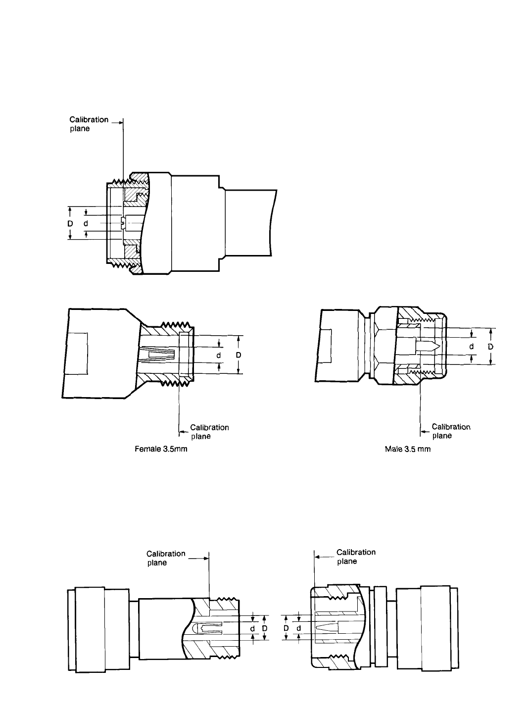
27
Female type-N Male type-N
7 mm Coaxial connector
Type-N coaxial connector interface
The location of the “calibration plane” in Type-N standards is the outer conductor mating surfaces as shown below.
Note: 1.0mm, 1.85mm and 2.4mm connectors not shown, but similar to 3.5mm calibration planes.
28
29
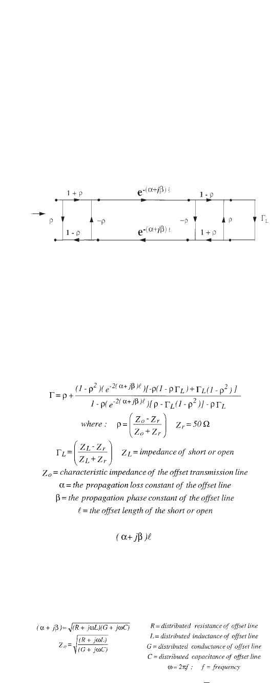
Appendix C
Cal coefficients model
Offset devices like offset shorts and offset opens can
be modeled by the following signal flow graph :
Figure 1 Signal flow graph model of offset devices
The offset portion of the open or short, is modeled
as a perfectly uniform lossy air dielectric transmis-
sion line. The expected coefficient of reflection, Γ,
of the open or short then can be solved by signal
flow graph technique.
Equation 1
The terms Zo, and are related to the cal
coefficients - Offset Zo, Offset Loss, and Offset
Delay - as follows:
Recall that
Equation 2
L ≈ L +
0
R
ω
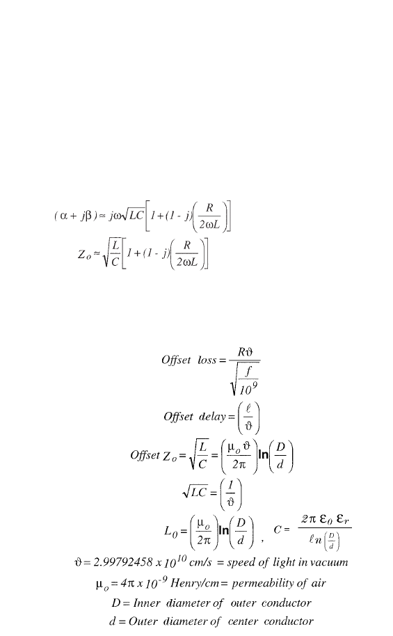
30
Their first order approximations, R is small and G=0, are:
Equation 3
Since
Equation 4
For coaxial devices
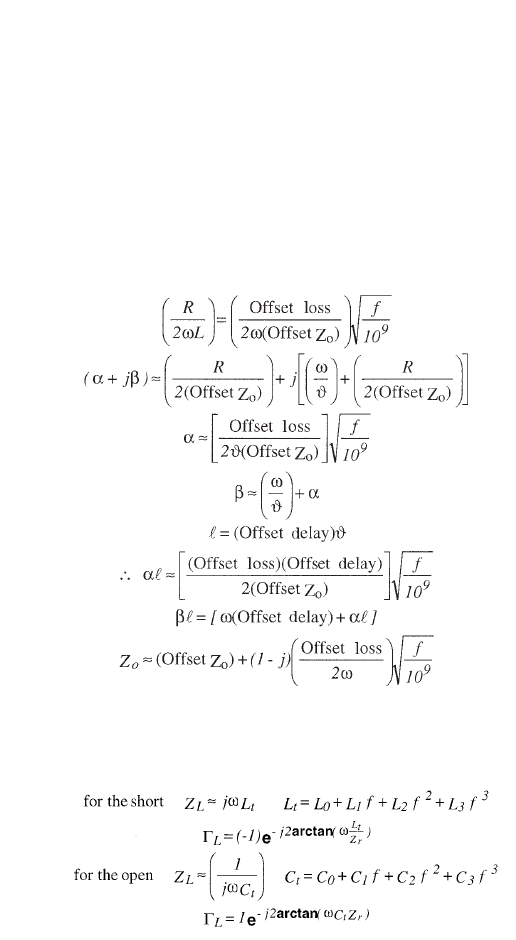
31
then:
Equation 5
Equation 6
If the Offset delay=0, then the coefficient of reflection,
Γ= ΓL.

www.agilent.com/find/emailupdates
Get the latest information on the products and
applications you select.
Agilent Email Updates
www.agilent.com
Agilent Technologies’ Test and Measurement
Support, Services, and Assistance
Agilent Technologies aims to maximize the value you
receive, while minimizing your risk and problems. We
strive to ensure that you get the test and measurement
capabilities you paid for and obtain the support you
need. Our extensive support resources and services
can help you choose the right Agilent products for
your applications and apply them successfully. Every
instrument and system we sell has a global warranty.
Two concepts underlie Agilent’s overall support policy:
“Our Promise” and “Your Advantage.”
Our Promise
Our Promise means your Agilent test and measurement
equipment will meet its advertised performance
and functionality. When you are choosing new equip-
ment, we will help you with product information,
including realistic performance specifications and
practical recommendations from experienced test
engineers. When you receive your new Agilent equip-
ment, we can help verify that it works properly and
help with initial product operation.
Your Advantage
Your Advantage means that Agilent offers a wide
range of additional expert test and measurement
services, which you can purchase according to your
unique technical and business needs. Solve problems
efficiently and gain a competitive edge by contracting
with us for calibration, extra-cost upgrades, out-of-
warranty repairs, and onsite education and training,
as well as design, system integration, project manage-
ment, and other professional engineering services.
Experienced Agilent engineers and technicians world-
wide can help you maximize your productivity, optimize
the return on investment of your Agilent instruments
and systems, and obtain dependable measurement
accuracy for the life of those products.
For more information on Agilent Technologies’
products, applications or services, please contact
your local Agilent office.
Phone or Fax
United States: Korea:
(tel) 800 829 4444 (tel) (080) 769 0800
(fax) 800 829 4433 (fax) (080) 769 0900
Canada: Latin America:
(tel) 877 894 4414 (tel) (305) 269 7500
(fax) 800 746 4866 Taiwan:
China: (tel) 0800 047 866
(tel) 800 810 0189 (fax) 0800 286 331
(fax) 800 820 2816 Other Asia Pacific
Europe: Countries:
(tel) 31 20 547 2111 (tel) (65) 6375 8100
Japan: (fax) (65) 6755 0042
(tel) (81) 426 56 7832 Email: tm_ap@agilent.com
(fax) (81) 426 56 7840 Contacts revised: 09/26/05
The complete list is available at:
www.agilent.com/find/contactus
Product specifications and descriptions in this
document subject to change without notice.
© Agilent Technologies, Inc. 2001, 2004, 2006
Printed in USA, July 13, 2006
5956-4352
www.agilent.com/find/agilentdirect
Quickly choose and use your test equipment
solutions with confidence.
Agilent Direct
Agilent
Open
www.agilent.com/find/open
Agilent Open simplifies the process of connecting
and programming test systems to help engineers
design, validate and manufacture electronic prod-
ucts. Agilent offers open connectivity for a broad
range of system-ready instruments, open industry
software, PC-standard I/O and global support,
which are combined to more easily integrate test
system development.
