Amazon com Services VA2L LTE Data module User Manual
Folksy LLC LTE Data module
UserManual.wiki
>
Amazon com Services
>
VA2L User Manual
User Manual
Navigation menu
Upload a User Manual
Namespaces
Wiki Guide
HTML
PDF
Info
Views
User Manual
Discussion / Help
Navigation
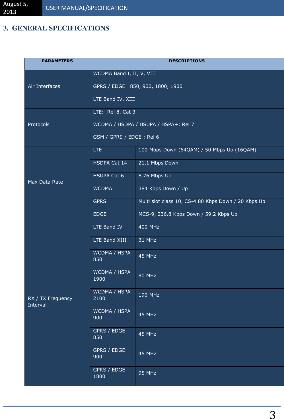
![August 5, 2013 USER MANUAL/SPECIFICATION 4 GPRS / EDGE 1900 80 MHz Nominal output power (+/-1dB) LTE Band IV 24 dBm (Power class 3) LTE Band XIII 23 dBm (Power class 3) WCDMA 23 dBm (Power class: 3) GPRS 850 / 900 32 dBm (Power class: 4) GPRS 1800 / 1900 29.5 dBm (Power class: 1) EDGE 850 / 900 26.5 dBm (Power class: E2) EDGE 1800 / 1900 25.5 dBm (Power class: E2) Operating Voltage VBATT 3.4V ~ 4.4V Low voltage 3.4V Nominal voltage 4.4V High voltage 4.4V Sleep / Off Current Off Leakage 5uA Rock Bottom [Sleep] 2mA Standby Current ` (single cell, no neighbors) LTE standby 128 Frames 5.15mA WCDMA standby 64 Frames 128 Frames 256 Frames 512 Frames 5.51mA 4.15mA 3.05mA 2.90mA GPRS standby MFRMS = 2 5.8mA](https://usermanual.wiki/Amazon-com-Services/VA2L/User-Guide-2078034-Page-5.png)
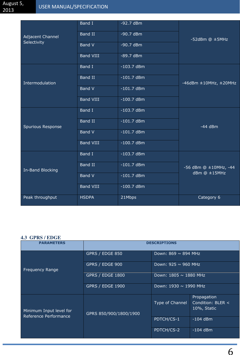
![August 5, 2013 USER MANUAL/SPECIFICATION 5 4. RECEIVE SPECIFICATIONS 4.1 LTE PARAMETERS DESCRIPTIONS Frequency Range Band IV [AWS] Down: 2110 ~ 2155 MHz Band XIII [700] Down: 746 ~ 756 MHz Reference Sensitivity Level (PRX and DRX combined) Band IV BW (MHz) PRX and DRX combined Reference Sensitivity (dBm) Modulation 5 -100 QPSK 10 -97 QPSK Band XIII BW (MHz) PRX and DRX combined Reference Sensitivity (dBm) Modulation 5 -97 QPSK 10 -94 QPSK Adjacent Channel Selectivity BW (MHz) Adjacent Channel Selectivity (dB) 5 33 dB 10 33 dB 4.2 WCDMA/HSDPA PARAMETERS DESCRIPTIONS Frequency Range Band I [2100] Down: 2110 ~ 2170 MHz Band II [1900] Down: 1930 ~ 1990 MHz Band V [850] Down: 869 ~ 894 MHz Band VIII [900] Down: 925 ~ 960 MHz Reference Sensitivity Level WCDMA Band I -106.7 dBm WCDMA Band II -104.7 dBm WCDMA Band V -104.7 dBm WCDMA Band VIII -103.7 dBm](https://usermanual.wiki/Amazon-com-Services/VA2L/User-Guide-2078034-Page-6.png)
![August 5, 2013 USER MANUAL/SPECIFICATION 7 PDTCH/CS-3 -104 dBm PDTCH/CS-4 -101 dBm EDGE 850/900/1800/1900 PDTCH/MCS-5 -98 dBm PDTCH/MCS-6 -96 dBm PDTCH/MCS-7 -93 dBm PDTCH/MCS-8 -90.5 dBm PDTCH/MCS-9 -86 dBm 5. TRANSMIT SPECIFICATIONS 5.1 LTE PARAMETERS DESCRIPTIONS Frequency Range Band IV [AWS] Up: 1710 ~ 1755 MHz Band XIII [700] Up: 777 ~ 787 MHz Max Output Power 23dBm ±2 dBm Min Output Power Below -40dBm Error Vector Magnitude 17.5% QPSK or BPSK 12.5% 16QAM ACLR1 30dB 5, 10 MHz bandwidth ACLR2 33dB 5, 10 MHz bandwidth 5.2 WCDMA/HSDPA PARAMETERS DESCRIPTIONS Frequency Range 2100 (Band I) Up: 1920 ~ 1980 MHz 1900 (Band II) Up: 1850 ~ 1910 MHz](https://usermanual.wiki/Amazon-com-Services/VA2L/User-Guide-2078034-Page-8.png)