Amd Geode Lx 800 0 9W Users Manual Processor Data Book
LX 800@0.9W to the manual 9c1eba8e-8e2b-4e96-82f1-677ad4c74f72
2015-02-05
: Amd Amd-Geode-Lx-800-0-9W-Users-Manual-507577 amd-geode-lx-800-0-9w-users-manual-507577 amd pdf
Open the PDF directly: View PDF ![]() .
.
Page Count: 680 [warning: Documents this large are best viewed by clicking the View PDF Link!]
- List of Figures
- List of Tables
- Overview
- Architecture Overview
- Signal Definitions
- 3.1 Buffer Types
- 3.2 Bootstrap Options
- 3.3 Ball Assignments
- 3.4 Signal Descriptions
- 3.4.1 System Interface Signals
- 3.4.2 PLL Interface Signals
- 3.4.3 Memory Interface Signals (DDR)
- 3.4.4 Internal Test and Measurement Interface Signals
- 3.4.5 PCI Interface Signals
- 3.4.6 TFT Display Interface Signals
- 3.4.7 CRT Display Interface Signals
- 3.4.8 VIP Interface Signals
- 3.4.9 Power and Ground Interface Signals
- GeodeLink™ Interface Unit
- 4.1 MSR Set
- 4.2 GLIU Register Descriptions
- 4.2.1 Standard GeodeLink™ Device (GLD) MSRs
- 4.2.2 GLIU Specific Registers
- 4.2.2.1 Coherency (COH)
- 4.2.2.2 Port Active Enable (PAE)
- 4.2.2.3 Arbitration (ARB)
- 4.2.2.4 Asynchronous SMI (ASMI)
- 4.2.2.5 Asynchronous ERR (AERR)
- 4.2.2.6 GLIU Physical Capabilities (PHY_CAP)
- 4.2.2.7 N Outstanding Response (NOUT_RESP)
- 4.2.2.8 N Outstanding Write Data (NOUT_WDATA)
- 4.2.2.9 SLAVE_ONLY
- 4.2.2.10 WHO AM I (WHOAMI)
- 4.2.2.11 GLIU Slave Disable (GLIU_SLV)
- 4.2.2.12 Arbitration2 (ARB2)
- 4.2.3 GLIU Statistic and Comparator MSRs
- 4.2.3.1 Descriptor Statistic Counter (STATISTIC_CNT[0:3])
- 4.2.3.2 Statistic Mask (STATISTIC_MASK[0:3]
- 4.2.3.3 Statistic Action (STATISTIC_ACTION[0:3]
- 4.2.3.4 Request Compare Value (RQ_COMPARE_VAL[0:3]
- 4.2.3.5 Request Compare Mask (RQ_COMPARE_MASK[0:3]
- 4.2.3.6 DA Compare Value Low (DA_COMPARE_VAL_LO[0:3]
- 4.2.3.7 DA Compare Value High (DA_COMPARE_VAL_HI[0:3]
- 4.2.3.8 DA Compare Mask Low (DA_COMPARE_MASK_LO[0:3])
- 4.2.3.9 DA Compare Mask High (DA_COMPARE_MASK_HI[0:3])
- 4.2.4 P2D Descriptor Registers
- 4.2.5 SPARE MSRs (SPARE_MSR[0:9], A:F)
- 4.2.6 I/O Descriptors
- CPU Core
- 5.1 Core Processor Initialization
- 5.2 Instruction Set Overview
- 5.3 Application Register Set
- 5.4 System Register Set
- 5.5 CPU Core Register Descriptions
- 5.5.1 Standard GeodeLink™ Device MSRs
- 5.5.2 CPU Core Specific MSRs
- 5.5.2.1 Time Stamp Counter MSR (TSC_MSR)
- 5.5.2.2 Performance Event Counter 0 MSR (PERF_CNT0_MSR)
- 5.5.2.3 Performance Event Counter 1 MSR (PERF_CNT1_MSR)
- 5.5.2.4 SYSENTER/SYSEXIT Code Segment Selector MSR (SYS_CS_MSR)
- 5.5.2.5 SYSENTER/SYSEXIT Stack Pointer MSR (SYS_SP_MSR)
- 5.5.2.6 SYSENTER/SYSEXIT Instruction Pointer MSR (SYS_IP_MSR)
- 5.5.2.7 Performance Event Counter 0 Select MSR (PERF_SEL0_MSR
- 5.5.2.8 Performance Event Counter 1 Select MSR (PERF_SEL1_MSR)
- 5.5.2.9 Instruction Fetch Configuration MSR (IF_CONFIG_MSR)
- 5.5.2.10 IF Invalidate MSR (IF_INVALIDATE_MSR)
- 5.5.2.11 IF Test Address MSR (IF_TEST_ADDR_MSR)
- 5.5.2.12 IF Test Data MSR (IF_TEST_DATA_MSR)
- 5.5.2.13 IF Sequential Count MRS (IF_SEQCOUNT_MSR)
- 5.5.2.14 IF Built-In Self-Test MSR (IF_BIST_MSR)
- 5.5.2.15 Exception Unit (XC) Configuration MSR (XC_CONFIG_MSR)
- 5.5.2.16 XC Mode MSR (XC_MODE_MSR)
- 5.5.2.17 XC History MSR (XC_HIST_MSR)
- 5.5.2.18 XC Microcode Address MSR (XC_UADDR_MSR)
- 5.5.2.19 ID Configuration MSR (ID_CONFIG_MSR)
- 5.5.2.20 SMM Control MSR (SMM_CTL_MSR)
- 5.5.2.21 Debug Management Interrupt (DMI) Control Register
- 5.5.2.22 Temporary MSRs
- 5.5.2.23 Segment Selector/Flags MSRs
- 5.5.2.24 SMM Header MSR (SMM_HDR_MSR)
- 5.5.2.25 DMM Header MSR (DMM_HDR_MSR)
- 5.5.2.26 Segment Base/Limit MSRs
- 5.5.2.27 Debug Registers 1 and 0 MSR (DR1_DR0_MSR)
- 5.5.2.28 Debug Registers 3 and 2 MSR (DR3_DR2_MSR)
- 5.5.2.29 Debug Registers 7 and 6 MSR (DR6_DR7_MSR)
- 5.5.2.30 Extended Debug Registers 1 and 0 MSR (XDR1_XDR0_MSR)
- 5.5.2.31 Extended Debug Registers 3 and 2 MSR (XDR3_XDR2_MSR)
- 5.5.2.32 Extended Debug Registers 5 and 4 MSR (XDR5_XDR4_MSR)
- 5.5.2.33 Extended Debug Registers 7 and 6 MSR (XDR7_XDR6_MSR)
- 5.5.2.34 Extended Debug Registers 9 and 8 MSR (XDR9_XDR8_MSR)
- 5.5.2.35 Extended Debug Registers 11 and 10 MSR (XDR11_XDR10_MSR)
- 5.5.2.36 EX Stage Instruction Pointer MSR (EX_IP_MSR)
- 5.5.2.37 WB Stage Instruction Pointer MSR (WB_IP_MSR)
- 5.5.2.38 EX Stage Linear Instruction Pointer MSR (EX_LIP_MSR)
- 5.5.2.39 WB Stage Linear Instruction Pointer MSR (WB_LIP_MSR)
- 5.5.2.40 C1/C0 Linear Instruction Pointer MSR (C1_C0_LIP_MSR)
- 5.5.2.41 C3/C2 Linear Instruction Pointer MSR (C3_C2_LIP_MSR)
- 5.5.2.42 Floating Point Environment Code Segment (FPENV_CS_MSR)
- 5.5.2.43 Floating Point Environment Instruction Pointer (FPENV_IP_MSR)
- 5.5.2.44 Floating Point Environment Data Segment (FPENV_DS_MSR)
- 5.5.2.45 Floating Point Environment Data Pointer (FPENV_DP_MSR)
- 5.5.2.46 Floating Point Environment Opcode Pointer (FPENV_OP_MSR)
- 5.5.2.47 Address Calculation Unit Configuration MSR (AC_CONFIG_MSR)
- 5.5.2.48 General Register MSRs
- 5.5.2.49 Extended Flags MSR (EFLAG_MSR)
- 5.5.2.50 Control Register 0 MSR (CR0_MSR)
- 5.5.2.51 Instruction Memory Configuration MSR (IM_CONFIG_MSR)
- 5.5.2.52 Instruction Cache Index MSR (IC_INDEX_MSR)
- 5.5.2.53 Instruction Cache Data MSR (IC_DATA_MSR)
- 5.5.2.54 Instruction Cache Tag (IC_TAG_MSR)
- 5.5.2.55 Instruction Cache Tag with Increment (IC_TAG_I_MSR)
- 5.5.2.56 L0 Instruction Cache Data MSR (L0_IC_DATA_MSR)
- 5.5.2.57 L0 Instruction Cache Tag with Increment MSR (L0_IC_TAG_I_MSR)
- 5.5.2.58 L1 Instruction TLB Index (ITB_INDEX_MSR)
- 5.5.2.59 L1 Instruction TLB Least Recently Used MSR (ITB_LRU_MSR)
- 5.5.2.60 L1 Instruction TLB Entry MSRs
- 5.5.2.61 Instruction Memory Subsystem BIST Tag MSR (IM_BIST_TAG_MSR)
- 5.5.2.62 Instruction Memory Subsystem BIST Data MSR (IM_BIST_DATA_MSR)
- 5.5.2.63 Data Memory Subsystem Configuration 0 MSR (DM_CONFIG0_MSR)
- 5.5.2.64 Data Memory Subsystem Configuration 1 MSR (DM_CONFIG1_MSR)
- 5.5.2.65 Data Memory Subsystem Prefetch Lock MSR (DM_PFLOCK_MSR)
- 5.5.2.66 Default Region Configuration Properties MSR (RCONF_DEFAULT_MSR)
- 5.5.2.67 Region Configuration Bypass MSR (RCONF_BYPASS_MSR)
- 5.5.2.68 Region Configuration A0000-BFFFF MSR (RCONF_A0_BF_MSR)
- 5.5.2.69 Region Configuration C0000-DFFFF MSR (RCONF_C0_DF_MSR)
- 5.5.2.70 Region Configuration E0000-FFFFF MSR (RCONF_E0_FF_MSR)
- 5.5.2.71 Region Configuration SMM MSR (RCONF_SMM_MSR)
- 5.5.2.72 Region Configuration DMM MSR (RCONF_DMM_MSR)
- 5.5.2.73 Region Configuration Range MSRs 0 through 7
- 5.5.2.74 x86 Control Registers MSRs (CR1, CR2, CR3, CR4)
- 5.5.2.75 Data Cache Index MSR (DC_INDEX_MSR)
- 5.5.2.76 Data Cache Data MSR (DC_DATA_MSR)
- 5.5.2.77 Data Cache Tag MSR (DC_TAG_MSR)
- 5.5.2.78 Data Cache Tag with Increment MSR (DC_TAG_I_MSR)
- 5.5.2.79 Data/Instruction Cache Snoop Register (SNOOP_MSR)
- 5.5.2.80 L1 Data TLB Index Register (L1DTLB_INDEX_MSR)
- 5.5.2.81 L1 Data TLB Least Recently Used MSR (L1DTLB_LRU_MSR)
- 5.5.2.82 L1 Data TLB Entry MSR (L1DTLB_ENTRY_MSR)
- 5.5.2.83 L1 Data TLB Entry with Increment MSR (L1DTLB_ENTRY_I_MSR)
- 5.5.2.84 L2 TLB/DTE/PTE Index MSR (L2TLB_INDEX_MSR)
- 5.5.2.85 L2 TLB/DTE/PTE Least Recently Used MSR (L2TLB_LRU_MSR)
- 5.5.2.86 L2 TLB/DTE/PTE Entry MSR (L2TLB_ENTRY_MSR)
- 5.5.2.87 L2 TLB/DTE/PTE Entry with Increment MSR (L2TLB_ENTRY_I_MSR)
- 5.5.2.88 Data Memory Subsystem Built-In Self-Test MSR (DM_BIST_MSR)
- 5.5.2.89 Bus Controller Configuration 0 MSR (BC_CONFIG0_MSR)
- 5.5.2.90 Bus Controller Configuration 1 MSR (BC_CONFIG1_MSR)
- 5.5.2.91 Reserved Status MSR (RSVD_STS_MSR)
- 5.5.2.92 MSR Lock MSR (MSR_LOCK_MSR)
- 5.5.2.93 Real Time Stamp Counter MSR (RTSC_MSR)
- 5.5.2.94 TSC and RTSC Low DWORDs MSR (RTSC_TSC_MSR)
- 5.5.2.95 L2 Cache Configuration MSR (L2_CONFIG_MSR)
- 5.5.2.96 L2 Cache Status MSR (L2_STATUS_MSR)
- 5.5.2.97 L2 Cache Index MSR (L2_INDEX_MSR)
- 5.5.2.98 L2 Cache Data MSR (L2_DATA_MSR)
- 5.5.2.99 L2 Cache Tag MSR (L2_TAG_MSR)
- 5.5.2.100 L2 Cache Tag with Increment MSR (L2_TAG_I_MSR)
- 5.5.2.101 L2 Cache Built-In Self-Test MSR (L2_BIST_MSR)
- 5.5.2.102 L2 Cache Treatment Control MSR (L2_TRTMNT_CTL_MSR)
- 5.5.2.103 Power Mode MSR (PMODE_MSR)
- 5.5.2.104 Bus Controller Extended Debug Registers 1 and 0 MSR (BXDR1_BXDR0_MSR)
- 5.5.2.105 Bus Controller Extended Debug Registers 3 and 2 MSR (BXDR3_BXDR2_MSR)
- 5.5.2.106 Bus Controller Extended Debug Registers 6 and 7 MSR (BXDR6_BXDR7_MSR)
- 5.5.2.107 Bus Controller Debug Registers 0 through 3 MSRs
- 5.5.2.108 Bus Controller Debug Register 6 MSR (BDR6_MSR)
- 5.5.2.109 Bus Controller Debug Register 7 MSR (BDR7_MSR)
- 5.5.2.110 Memory Subsystem Array Control Enable MSR (MSS_ARRAY_CTL_EN_MSR)
- 5.5.2.111 Memory Subsystem Array Control 0 MSR (MSS_ARRAY_CTL0_MSR)
- 5.5.2.112 Memory Subsystem Array Control 1 MSR (MSS_ARRAY_CTL1_MSR)
- 5.5.2.113 Memory Subsystem Array Control 2 MSR (MSS_ARRAY_CTL2_MSR)
- 5.5.2.114 FPU Modes MSR (FP_MODE_MSR)
- 5.5.2.115 FPU Reserved MSR (FPU_RSVD_MSR)
- 5.5.2.116 FPU Reserved MSR (FPU_RSVD_MSR)
- 5.5.2.117 FPU x87 Control Word MSR (FPU_CW_MSR)
- 5.5.2.118 FPU x87 Status Word MSR (FPU_SW_MSR)
- 5.5.2.119 FPU x87 Tag Word MSR (FPU_TW_MSR)
- 5.5.2.120 FPU Busy MSR (FPU_BUSY_MSR)
- 5.5.2.121 FPU Register Map MSR (FPU_MAP_MSR)
- 5.5.2.122 Mantissa of Rx MSRs
- 5.5.2.123 Exponent of Rx MSRs
- 5.5.2.124 FPU Reserved MSRs (FPU_RSVD_MSR)
- 5.5.2.125 CPU ID MSRs
- Integrated Functions
- 6.1 GeodeLink™ Memory Controller
- 6.2 GeodeLink™ Memory Controller Register Descriptions
- 6.2.1 Standard GeodeLink™ Device (GLD) MSRs
- 6.2.2 GLMC Specific MSRs
- 6.2.2.1 Row Addresses Bank0 DIMM0, Bank1 DIMM0 (MC_CF_BANK01)
- 6.2.2.2 Row Addresses Bank2 DIMM0, Bank3 DIMM0 (MC_CF_BANK23)
- 6.2.2.3 Row Addresses Bank4 DIMM0, Bank5 DIMM0 (MC_CF_BANK45)
- 6.2.2.4 Row Addresses Bank6 DIMM0, Bank7 DIMM0 (MC_CF_BANK67)
- 6.2.2.5 Row Addresses Bank0 DIMM1, Bank1 DIMM0 (MC_CF_BANK89)
- 6.2.2.6 Row Addresses Bank2 DIMM1, Bank3 DIMM1 (MC_CF_BANKAB)
- 6.2.2.7 Row Addresses Bank4 DIMM1, Bank5 DIMM1 (MC_CF_BANKCD)
- 6.2.2.8 Row Addresses Bank6 DIMM1, Bank7 DIMM1 (MC_CF_BANKEF)
- 6.2.2.9 Refresh and SDRAM Program (MC_CF07_DATA)
- 6.2.2.10 Timing and Mode Program (MC_CF8F_DATA)
- 6.2.2.11 Feature Enables (MC_CF1017_DATA)
- 6.2.2.12 Performance Counters (MC_CFPERF_CNT1)
- 6.2.2.13 Counter and CAS Control (MC_PERCNT2)
- 6.2.2.14 Clocking and Debug (MC_CFCLK_DBUG)
- 6.2.2.15 Page Open Status (MC_CFPG_OPEN)
- 6.2.2.16 Reserved Register
- 6.2.2.17 PM Sensitivity Counters (MC_CF_PMCTR)
- 6.3 Graphics Processor
- 6.4 Graphics Processor Register Definitions
- 6.4.1 Standard GeodeLink™ Device (GLD) MSRs
- 6.4.2 Graphics Processor Configuration Registers
- 6.4.2.1 Destination Offset (GP_DST_OFFSET)
- 6.4.2.2 Source Offset (GP_SRC_OFFSET)
- 6.4.2.3 Vector Error (GP_VEC_ERR)
- 6.4.2.4 Stride (GP_STRIDE)
- 6.4.2.5 BLT Width/Height (GP_WID_HEIGHT)
- 6.4.2.6 Vector Length (GP_VEC_LEN)
- 6.4.2.7 Source Color Foreground (GP_SRC_COLOR_FG)
- 6.4.2.8 Source Color Background (GP_SRC_COLOR_BG)
- 6.4.2.9 Pattern Color (GP_PAT_COLOR_x)
- 6.4.2.10 Pattern Data (GP_PAT_DATA_x)
- 6.4.2.11 Raster Mode (GP_RASTER_MODE)
- 6.4.2.12 Vector Mode (GP_VECTOR_MODE)
- 6.4.2.13 BLT Mode (GP_BLT_MODE)
- 6.4.2.14 Status and Reset (GP_BLT_STATUS, GP_RESET)
- 6.4.2.15 Host Source (GP_HST_SRC)
- 6.4.2.16 Base Offset (GP_BASE_OFFSET)
- 6.4.2.17 Command Top (GP_CMD_TOP)
- 6.4.2.18 Command Bottom (GP_CMD_BOT)
- 6.4.2.19 Command Read (GP_CMD_READ)
- 6.4.2.20 Command Write (GP_CMD_WRITE)
- 6.4.2.21 Offset (GP_CH3_OFFSET)
- 6.4.2.22 Stride (GP_CH3_MODE_STR)
- 6.4.2.23 Width/Height (GP_CH3_WIDHI)
- 6.4.2.24 Host Source (GP_CH3_HSRC)
- 6.4.2.25 LUT Index (GP_LUT_INDEX)
- 6.4.2.26 LUT Data (GP_LUT_DATA)
- 6.4.2.27 Interrupt Control (GP_INT_CNTRL)
- 6.5 Display Controller
- 6.6 Display Controller Register Descriptions
- 6.6.1 Standard GeodeLink™ Device (GLD) Registers (MSRs)
- 6.6.2 Display Controller Specific MSRs
- 6.6.3 Configuration and Status Registers
- 6.6.4 Memory Organization Registers
- 6.6.4.1 DC Frame Buffer Start Address (DC_FB_ST_OFFSET)
- 6.6.4.2 DC Compression Buffer Start Address (DC_CB_ST_OFFSET)
- 6.6.4.3 DC Cursor Buffer Start Address (DC_CURS_ST_OFFSET)
- 6.6.4.4 DC Video Y Buffer Start Address Offset (DC_VID_Y_ST_OFFSET)
- 6.6.4.5 DC Video U Buffer Start Address Offset (DC_VID_U_ST_OFFSET)
- 6.6.4.6 DC Video V Buffer Start Address Offset (DC_VID_V_ST_OFFSET)
- 6.6.4.7 DC Dirty/Valid Region Top (DC_DV_TOP)
- 6.6.4.8 DC Line Size (DC_LINE_SIZE)
- 6.6.4.9 DC Graphics Pitch (DC_GFX_PITCH)
- 6.6.4.10 DC Video YUV Pitch (DC_VID_YUV_PITCH)
- 6.6.5 Timing Registers
- 6.6.5.1 DC Horizontal and Total Timing (DC_H_ACTIVE_TIMING)
- 6.6.5.2 DC CRT Horizontal Blanking Timing (DC_H_BLANK_TIMING)
- 6.6.5.3 DC CRT Horizontal Sync Timing (DC_H_SYNC_TIMING)
- 6.6.5.4 DC Vertical and Total Timing (DC_V_ACTIVE_TIMING)
- 6.6.5.5 DC CRT Vertical Blank Timing (DC_V_BLANK_TIMING)
- 6.6.5.6 DC CRT Vertical Sync Timing (DC_V_SYNC_TIMING)
- 6.6.5.7 DC Frame Buffer Active Region Register (DC_FB_ACTIVE)
- 6.6.6 Cursor Position and Line Count/Status Registers
- 6.6.7 Palette Access FIFO Diagnostic Registers
- 6.6.8 Video Downscaling
- 6.6.9 GLIU Control Registers
- 6.6.10 Graphics Scaling Control Registers
- 6.6.11 VBI Control Registers
- 6.6.12 Color Key Control Registers
- 6.6.13 Interrupt and GenLock Registers
- 6.6.14 Even Field Video Address Registers
- 6.6.15 Even Field Vertical Timing Registers
- 6.6.16 VGA Block Configuration Registers
- 6.6.17 VGA Block Standard Registers
- 6.6.18 VGA Sequencer Registers
- 6.6.19 VGA CRT Controller Registers
- 6.6.19.1 CRTC Index
- 6.6.19.2 CRTC Data
- 6.6.19.3 Horizontal Total
- 6.6.19.4 Horizontal Display Enable End
- 6.6.19.5 Horizontal Blank Start
- 6.6.19.6 Horizontal Blank End
- 6.6.19.7 Horizontal Sync Start
- 6.6.19.8 Horizontal Sync End
- 6.6.19.9 Vertical Total
- 6.6.19.10 Overflow
- 6.6.19.11 Preset Row Scan
- 6.6.19.12 Maximum Scan Line
- 6.6.19.13 Cursor Start
- 6.6.19.14 Cursor End
- 6.6.19.15 Start Address High
- 6.6.19.16 Start Address Low
- 6.6.19.17 Cursor Location High
- 6.6.19.18 Cursor Location Low
- 6.6.19.19 Vertical Sync Start
- 6.6.19.20 Vertical Sync End
- 6.6.19.21 Vertical Display Enable End
- 6.6.19.22 Offset
- 6.6.19.23 Underline Location
- 6.6.19.24 Vertical Blank Start
- 6.6.19.25 Vertical Blank End
- 6.6.19.26 CRTC Mode Control
- 6.6.19.27 Line Compare
- 6.6.19.28 CPU Data Latch State
- 6.6.19.29 Attribute Index/Data FF State
- 6.6.19.30 Attribute Index State
- 6.6.20 VGA Graphics Controller Registers
- 6.6.20.1 VGA Graphics Controller Index
- 6.6.20.2 VGA Graphics Controller Data
- 6.6.20.3 VGA Set/Reset
- 6.6.20.4 VGA Enable Set/Reset
- 6.6.20.5 VGA Color Compare
- 6.6.20.6 VGA Data Rotate
- 6.6.20.7 VGA Read Map Select
- 6.6.20.8 VGA Graphics Mode
- 6.6.20.9 VGA Miscellaneous
- 6.6.20.10 VGA Color Don’t Care
- 6.6.20.11 VGA Bit Mask
- 6.6.21 Attribute Controller Registers
- 6.6.22 Video DAC Registers
- 6.6.23 VGA Block Extended Registers
- 6.7 Video Processor
- 6.8 Video Processor Register Descriptions
- 6.8.1 Standard GeodeLink™ Device MSRs
- 6.8.2 Video Processor Module Specific MSRs
- 6.8.3 Video Processor Module Control/Configuration Registers
- 6.8.3.1 Video Configuration (VCFG)
- 6.8.3.2 Display Configuration (DCFG)
- 6.8.3.3 Video X Position (VX)
- 6.8.3.4 Video Y Position (VY)
- 6.8.3.5 Video Scale (SCL)
- 6.8.3.6 Video Color Key Register (VCK)
- 6.8.3.7 Video Color Mask (VCM)
- 6.8.3.8 Palette Address (PAR)
- 6.8.3.9 Palette Data (PDR)
- 6.8.3.10 Saturation Scale (SLR)
- 6.8.3.11 Miscellaneous (MISC)
- 6.8.3.12 CRT Clock Select (CCS)
- 6.8.3.13 Video Y Scale (VYS)
- 6.8.3.14 Video X Scale (VXS)
- 6.8.3.15 Video Downscaler Control (VDC)
- 6.8.3.16 CRC Signature (CRC)
- 6.8.3.17 32-Bit CRC Signature (CRC32)
- 6.8.3.18 Video De-Interlacing and Alpha Control (VDE)
- 6.8.3.19 Cursor Color Key (CCK)
- 6.8.3.20 Cursor Color Mask (CCM)
- 6.8.3.21 Cursor Color 1 (CC1)
- 6.8.3.22 Cursor Color 2 (CC2)
- 6.8.3.23 Alpha Window 1 X Position (A1X)
- 6.8.3.24 Alpha Window 1 Y Position (A1Y)
- 6.8.3.25 Alpha Window 1 Color (A1C)
- 6.8.3.26 Alpha Window 1 Control (A1T)
- 6.8.3.27 Alpha Window 2 X Position (A2X)
- 6.8.3.28 Alpha Window 2 Y Position (A2Y)
- 6.8.3.29 Alpha Window 2 Color (AC2)
- 6.8.3.30 Alpha Window 2 Control (A2T)
- 6.8.3.31 Alpha Window 3 X Position (A3X)
- 6.8.3.32 Alpha Window 3 Y Position (A3Y)
- 6.8.3.33 Alpha Window 3 Color (A3C)
- 6.8.3.34 Alpha Window 3 Control (A3T)
- 6.8.3.35 Video Request (VRR)
- 6.8.3.36 Alpha Watch (AWT)
- 6.8.3.37 Video Processor Test Mode (VTM)
- 6.8.3.38 Even Video Y Position (VYE)
- 6.8.3.39 Even Alpha Window 1 Y Position (A1YE)
- 6.8.3.40 Even Alpha Window 2 Y Position (A2YE)
- 6.8.3.41 Even Alpha Window 3 Y Position (A3YE)
- 6.8.3.42 Video Coefficient RAM (VCR)
- 6.8.3.43 Panel Timing Register 1 (PT1)
- 6.8.3.44 Panel Timing Register 2 (PT2)
- 6.8.3.45 Power Management (PM)
- 6.8.3.46 Dither and Frame Rate Control (DFC)
- 6.8.3.47 Dither RAM Control and Address (DCA)
- 6.8.3.48 Dither Memory Data (DMD)
- 6.8.3.49 Panel CRC Signature (CRC)
- 6.8.3.50 32-Bit Panel CRC (CRC32)
- 6.8.3.51 Video Output Port Configuration (VOP_CONFIG)
- 6.8.3.52 Video Output Port Signature (VOP_SIG)
- 6.9 Video Input Port
- 6.9.1 Features
- 6.9.2 VIP Block Descriptions
- 6.9.3 Functional Description
- 6.9.4 VIP Operation Modes
- 6.9.5 Mode 1a,b,c - VIP Input Data (simplified BT.656)
- 6.9.6 Message Passing Mode
- 6.9.7 Data Streaming Mode
- 6.9.8 BT.601 Mode
- 6.9.9 YUV 4:2:2 to YUV 4:2:0 Translation
- 6.9.10 Software Model
- 6.9.11 Bob and Weave
- 6.9.12 VIP Interrupts
- 6.9.13 VIP Input Video Status
- 6.10 Video Input Port Register Descriptions
- 6.10.1 Standard GeodeLink™ Device (GLD) MSRs
- 6.10.2 VIP Control/Configuration Registers
- 6.10.2.1 VIP Control Register 1 (VIP_CTL_REG1)
- 6.10.2.2 VIP Control Register 2 (VIP_CTL_REG2)
- 6.10.2.3 VIP Status (VIP_STATUS)
- 6.10.2.4 VIP Interrupt (VIP_INT)
- 6.10.2.5 VIP Current/Target (VIP_CUR_TAR)
- 6.10.2.6 VIP Max Address (VIP_MAX_ADDR)
- 6.10.2.7 VIP Task A Video Even Base Address (VIP_TASK_A_VID_EVEN_BASE)
- 6.10.2.8 VIP Task A Video Odd Base Address (VIP_TASK_A_VID_ODD_BASE)
- 6.10.2.9 VIP Task A VBI Even Base Address (VIP_TASK_A_VBI_EVEN_BASE)
- 6.10.2.10 VIP Task A VBI Odd Base Address (VIP_TASK_A_VBI_ODD_BASE)
- 6.10.2.11 VIP Task A Video Pitch (VIP_TASK_A_VID_PITCH)
- 6.10.2.12 VIP Control Register 3 (VIP_CONTRL_REG3)
- 6.10.2.13 VIP Task A V Offset (VIP_TASK_A_V_OFFSET)
- 6.10.2.14 VIP Task A U Offset (VIP_TASK_A_U_OFFSET)
- 6.10.2.15 VIP Task B Video Even Base/Horizontal End (VIP_TASK_B_VID_EVEN_BASE_HORIZ_END)
- 6.10.2.16 VIP Task B Video Odd Base/Horizontal Start (VIP_TASK_B_VID_ODD_BASE_HORIZ_START)
- 6.10.2.17 VIP Task B VBI Even Base/VBI End (VIP_TASK_B_VBI_EVEN_BASE_VBI_END)
- 6.10.2.18 VIP Task B VBI Odd Base/VBI Start (VIP_TASK_B_VBI_ODD_BASE_VBI_START)
- 6.10.2.19 VIP Task B Data Pitch/Vertical Start Even (VIP_TASK_B_DATA_PITCH_VERT_START_EVEN)
- 6.10.2.20 VIP Task B V Offset (VIP_TASK_B_V_Offset)
- 6.10.2.21 VIP Task B U Offset (VIP_TASK_B_U_OFFSET)
- 6.10.2.22 VIP Ancillary Data/Message Passing/Data Streaming Buffer1 Base Address (VIP_ANC_MSG_1_BASE)
- 6.10.2.23 VIP Ancillary Data/Message Passing/Data Streaming Buffer 2 Base Address (VIP_ANC_MSG_2_BASE)
- 6.10.2.24 VIP Ancillary Data/Message Passing/Data Streaming Buffer Size (VIP_ANC_MSG_SIZE)
- 6.10.2.25 VIP Page Offset/ Page Count (VIP_PAGE_OFFSET)
- 6.10.2.26 VIP Vertical Start/Stop (VIP_VERT_START_STOP)
- 6.10.2.27 VIP FIFO Address (VIP_FIFO_R_W_ADDR)
- 6.10.2.28 VIP FIFO Data (VIP_FIFO_DATA)
- 6.10.2.29 VIP VSYNC Error Count (VIP_SYNC_ERR_COUNT)
- 6.10.2.30 VIP Task A U Even Offset (VIP_TASK_A_U_EVEN_OFFSET)
- 6.10.2.31 VIP Task A V Even Offset (VIP_TASK_A_V_EVEN_OFFSET)
- 6.11 Security Block
- 6.12 Security Block Register Descriptions
- 6.12.1 Standard GeodeLink™ (GLD) Device MSRs
- 6.12.2 Security Block Specific MSRs
- 6.12.3 Security Block Configuration/Control Registers
- 6.12.3.1 SB Control A (SB_CTL_A)
- 6.12.3.2 SB Control B (SB_CTL_B)
- 6.12.3.3 SB AES Interrupt (SB_AES_INT)
- 6.12.3.4 SB Source A (SB_SOURCE_A)
- 6.12.3.5 SB Destination A (SB_DEST_A)
- 6.12.3.6 SB Length A (SB_LENGTH_A)
- 6.12.3.7 SB Source B (SB_SOURCE_B)
- 6.12.3.8 SB Destination B (SB_DEST_B)
- 6.12.3.9 SB Length B (SB_LENGTH_B)
- 6.12.3.10 SB Writable Key 0 (SB_WKEY_0)
- 6.12.3.11 SB Writable Key 1 (SB_WKEY_1)
- 6.12.3.12 SB Writable Key 2 (SB_WKEY_2)
- 6.12.3.13 SB Writable Key 3 (SB_WKEY_3)
- 6.12.3.14 SB CBC Initialization Vector 0 (SB_CBC_IV_0)
- 6.12.3.15 SB CBC Initialization Vector 1 (SB_CBC_IV_1)
- 6.12.3.16 SB CBC Initialization Vector 2 (SB_CBC_IV_2)
- 6.12.3.17 SB CBC Initialization Vector 3 (SB_CBC_IV_3)
- 6.12.3.18 SB Random Number (SB_RANDOM_NUM)
- 6.12.3.19 SB Random Number Status (SB_RANDOM_NUM_STATUS)
- 6.12.3.20 SB EEPROM Command (SB_EEPROM_COMM)
- 6.12.3.21 SB EEPROM Address (SB_EEPROM_ADDR)
- 6.12.3.22 SB EEPROM Data (SB_EEPROM_DATA)
- 6.12.3.23 SB EEPROM Security State (SB_EEPROM_SEC_STATE)
- 6.13 GeodeLink™ Control Processor
- 6.14 GeodeLink™ Control Processor Register Descriptions
- 6.14.1 Standard GeodeLink™ Device MSRs
- 6.14.2 GLCP Specific MSRs - GLCP Control MSRs
- 6.14.2.1 GLCP Clock Disable Delay Value (GLCP_CLK_DIS_DELAY)
- 6.14.2.2 GLCP Clock Mask for Sleep Request (GLCP_PMCLKDISABLE)
- 6.14.2.3 Chip Fabrication Information (GLCP_FAB)
- 6.14.2.4 GLCP Global Power Management Controls (GLCP_GLB_PM)
- 6.14.2.5 GLCP Debug Output from Chip (GLCP_DBGOUT)
- 6.14.2.6 GLCP Processor Status (GLCP_PROCSTAT)
- 6.14.2.7 GLCP DOWSER (GLCP_DOWSER)
- 6.14.2.8 GLCP I/O Delay Controls (GLCP_DELAY_CONTROLS)
- 6.14.2.9 GLCP Clock Control (GLCP_CLKOFF)
- 6.14.2.10 GLCP Clock Active (GLCP_CLKACTIVE)
- 6.14.2.11 GLCP Clock Mask for Debug Clock Stop Action (GLCP_CLKDISABLE)
- 6.14.2.12 GLCP Clock Active Mask for Suspend Acknowledge (GLCP_CLK4ACK)
- 6.14.2.13 GLCP System Reset and PLL Control (GLCP_SYS_RSTPLL)
- 6.14.2.14 GLCP Dot Clock PLL Control (GLCP_DOTPLL)
- 6.14.2.15 GLCP Debug Clock Control (GLCP_DBGCLKCTL)
- 6.14.2.16 Chip Revision ID (GLCP_CHIP_REVID)
- 6.14.2.17 GLCP Control (GLCP_CNT)
- 6.14.2.18 GLCP Level 2 (GLCP_LVL2)
- 6.14.2.19 GLCP Throttle or C2 Start Delay (GLCP_TH_SD)
- 6.14.2.20 GLCP Scale Factor (GLCP_TH_SF)
- 6.14.2.21 GLCP Processor Throttle Off Delay (GLCP_TH_OD)
- 6.14.3 GLCP IGNNE I/Os
- 6.14.4 GLCP Specific MSRs - GLCP Debug Interface MSRs
- 6.14.5 GLCP Specific MSRs - GLCP Companion Device Interface MSRs
- 6.15 GeodeLink™ PCI Bridge
- 6.16 GeodeLink™ PCI Bridge Register Descriptions
- 6.16.1 Standard GeodeLink™ Device (GLD) MSRs
- 6.16.2 GLPCI Specific Registers
- 6.16.2.1 GLPCI Global Control (GLPCI_CTRL)
- 6.16.2.2 GLPCI Arbiter Control (GLPCI_ARB)
- 6.16.2.3 GLPCI VPH / PCI Configuration Cycle Control (GLPCI_PBUS)
- 6.16.2.4 GLPCI Debug Packet Configuration (GLPCI_DEBUG)
- 6.16.2.5 GLPCI Fixed Region Enables (GLPCI_REN)
- 6.16.2.6 GLPCI Fixed Region Configuration A0-BF (GLPCI_A0)
- 6.16.2.7 GLPCI Fixed Region Configuration C0-DF (GLPCI_C0)
- 6.16.2.8 GLPCI Fixed Region Configuration E0-FF (GLPCI_E0)
- 6.16.2.9 GLPCI Memory Region 0 Configuration (GLPCI_R0)
- 6.16.2.10 GLPCI Memory Region 1 Configuration (GLPCI_R1)
- 6.16.2.11 GLPCI Memory Region 2 Configuration (GLPCI_R2)
- 6.16.2.12 GLCPI Memory Region 3 Configuration (GLPCI_R3)
- 6.16.2.13 GLCPI Memory Region 4 Configuration (GLPCI_R4)
- 6.16.2.14 GLPCI Memory Region 5 Configuration (GLPCI_R5)
- 6.16.2.15 GLPCI External MSR Access Configuration (GLPCI EXT_MSR)
- 6.16.2.16 GLPCI Spare
- 6.16.2.17 GLPCI General Purpose I/O (GLPCI_GPIO)
- Electrical Specifications
- Instruction Set
- 8.1 General Instruction Set Format
- 8.2 CPUID Instruction Set
- 8.3 Processor Core Instruction Set
- 8.3.1 Opcodes
- 8.3.2 Clock Counts
- 8.3.3 Flags
- 8.3.4 Non-Standard Processor Core Instructions
- 8.3.4.1 DMINT - Enter Debug Management Mode
- 8.3.4.2 ICEBP - Call Debug Exception Handler
- 8.3.4.3 MOV - Move to/from Test Registers
- 8.3.4.4 RDM - Leave Debug Management Mode
- 8.3.4.5 RSDC - Restore Segment Register and Descriptor
- 8.3.4.6 RSLDT - Restore Local Descriptor Table Register and Descriptor
- 8.3.4.7 RSM - Leave System Management Mode
- 8.3.4.8 RSTS - Restore Task Register and Descriptor
- 8.3.4.9 SETALC - Set AL to CF
- 8.3.4.10 SMINT - Enter System Management Mode
- 8.3.4.11 Exceptions
- 8.3.4.12 SVDC - Save Segment Register and Descriptor
- 8.3.4.13 SVLDT - Save Local Descriptor Table Register and Descriptor
- 8.3.4.14 SVTS - Save Task Register and Descriptor
- 8.4 MMX™, FPU, and AMD 3DNow!™ Technology Instructions Sets
- Package Specifications
- Support Documentation

AMD Geode™ LX Processors Data Book
AMD Geode™ LX Processors
Data Book
February 2009
Publication ID: 33234H

2AMD Geode™ LX Processors Data Book
© 2009 Advanced Micro Devices, Inc. All rights reserved.
The contents of this document are provided in connection with Advanced Micro
Devices, Inc. (“AMD”) products. AMD makes no representations or warranties with
respect to the accuracy or completeness of the contents of this publication and
reserves the right to make changes to specifications and product descriptions at
any time without notice. No license, whether express, implied, arising by estoppel
or otherwise, to any intellectual property rights is granted by this publication.
Except as set forth in AMD’s Standard Terms and Conditions of Sale, AMD
assumes no liability whatsoever, and disclaims any express or implied warranty,
relating to its products including, but not limited to, the implied warranty of mer-
chantability, fitness for a particular purpose, or infringement of any intellectual
property right.
AMD’s products are not designed, intended, authorized or warranted for use as
components in systems intended for surgical implant into the body, or in other
applications intended to support or sustain life, or in any other application in which
the failure of AMD’s product could create a situation where personal injury, death,
or severe property or environmental damage may occur. AMD reserves the right to
discontinue or make changes to its products at any time without notice.
Contacts
www.amd.com
Trademarks
AMD, the AMD Arrow logo, AMD Athlon, Geode, GeodeLink, 3DNow!, and combinations thereof, are trademarks of
Advanced Micro Devices, Inc.
Linux is a registered trademark of Linus Torvalds.
WinBench is a registered trademark of Ziff Davis, Inc.
Windows is a registered trademark of Microsoft Corporation in the United States and/or other jurisdictions.
Pentium is a registered trademark and MMX is a trademark of Intel Corporation in the United States and/or other jurisdictions.
Other product names used in this publication are for identification purposes only and may be trademarks of their respective
companies.

AMD Geode™ LX Processors Data Book 3
Contents 33234H
Contents
List of Figures . . . . . . . . . . . . . . . . . . . . . . . . . . . . . . . . . . . . . . . . . . . . . . . . . . . . . . . . . . 5
List of Tables . . . . . . . . . . . . . . . . . . . . . . . . . . . . . . . . . . . . . . . . . . . . . . . . . . . . . . . . . . . 7
1.0 Overview . . . . . . . . . . . . . . . . . . . . . . . . . . . . . . . . . . . . . . . . . . . . . . . . . . . . . . . . . 11
1.1 General Description . . . . . . . . . . . . . . . . . . . . . . . . . . . . . . . . . . . . . . . . . . . . . . . . . . . . . . . . . . 11
1.2 Features . . . . . . . . . . . . . . . . . . . . . . . . . . . . . . . . . . . . . . . . . . . . . . . . . . . . . . . . . . . . . . . . . . . 12
2.0 Architecture Overview . . . . . . . . . . . . . . . . . . . . . . . . . . . . . . . . . . . . . . . . . . . . . . 15
2.1 CPU Core . . . . . . . . . . . . . . . . . . . . . . . . . . . . . . . . . . . . . . . . . . . . . . . . . . . . . . . . . . . . . . . . . 15
2.2 GeodeLink™ Control Processor . . . . . . . . . . . . . . . . . . . . . . . . . . . . . . . . . . . . . . . . . . . . . . . .16
2.3 GeodeLink™ Interface Units . . . . . . . . . . . . . . . . . . . . . . . . . . . . . . . . . . . . . . . . . . . . . . . . . . . 16
2.4 GeodeLink™ Memory Controller . . . . . . . . . . . . . . . . . . . . . . . . . . . . . . . . . . . . . . . . . . . . . . . . 16
2.5 Graphics Processor . . . . . . . . . . . . . . . . . . . . . . . . . . . . . . . . . . . . . . . . . . . . . . . . . . . . . . . . . . 17
2.6 Display Controller . . . . . . . . . . . . . . . . . . . . . . . . . . . . . . . . . . . . . . . . . . . . . . . . . . . . . . . . . . . . 18
2.7 Video Processor . . . . . . . . . . . . . . . . . . . . . . . . . . . . . . . . . . . . . . . . . . . . . . . . . . . . . . . . . . . . 18
2.8 Video Input Port . . . . . . . . . . . . . . . . . . . . . . . . . . . . . . . . . . . . . . . . . . . . . . . . . . . . . . . . . . . . . 18
2.9 GeodeLink™ PCI Bridge . . . . . . . . . . . . . . . . . . . . . . . . . . . . . . . . . . . . . . . . . . . . . . . . . . . . . . 18
2.10 Security Block . . . . . . . . . . . . . . . . . . . . . . . . . . . . . . . . . . . . . . . . . . . . . . . . . . . . . . . . . . . . . . 19
3.0 Signal Definitions . . . . . . . . . . . . . . . . . . . . . . . . . . . . . . . . . . . . . . . . . . . . . . . . . . 21
3.1 Buffer Types . . . . . . . . . . . . . . . . . . . . . . . . . . . . . . . . . . . . . . . . . . . . . . . . . . . . . . . . . . . . . . . . 23
3.2 Bootstrap Options . . . . . . . . . . . . . . . . . . . . . . . . . . . . . . . . . . . . . . . . . . . . . . . . . . . . . . . . . . . 24
3.3 Ball Assignments . . . . . . . . . . . . . . . . . . . . . . . . . . . . . . . . . . . . . . . . . . . . . . . . . . . . . . . . . . . . 24
3.4 Signal Descriptions . . . . . . . . . . . . . . . . . . . . . . . . . . . . . . . . . . . . . . . . . . . . . . . . . . . . . . . . . . 33
4.0 GeodeLink™ Interface Unit . . . . . . . . . . . . . . . . . . . . . . . . . . . . . . . . . . . . . . . . . . 45
4.1 MSR Set . . . . . . . . . . . . . . . . . . . . . . . . . . . . . . . . . . . . . . . . . . . . . . . . . . . . . . . . . . . . . . . . . . 45
4.2 GLIU Register Descriptions . . . . . . . . . . . . . . . . . . . . . . . . . . . . . . . . . . . . . . . . . . . . . . . . . . . . 50
5.0 CPU Core . . . . . . . . . . . . . . . . . . . . . . . . . . . . . . . . . . . . . . . . . . . . . . . . . . . . . . . . 89
5.1 Core Processor Initialization . . . . . . . . . . . . . . . . . . . . . . . . . . . . . . . . . . . . . . . . . . . . . . . . . . . 89
5.2 Instruction Set Overview . . . . . . . . . . . . . . . . . . . . . . . . . . . . . . . . . . . . . . . . . . . . . . . . . . . . . . 90
5.3 Application Register Set . . . . . . . . . . . . . . . . . . . . . . . . . . . . . . . . . . . . . . . . . . . . . . . . . . . . . . 91
5.4 System Register Set . . . . . . . . . . . . . . . . . . . . . . . . . . . . . . . . . . . . . . . . . . . . . . . . . . . . . . . . . 94
5.5 CPU Core Register Descriptions . . . . . . . . . . . . . . . . . . . . . . . . . . . . . . . . . . . . . . . . . . . . . . . .99

4AMD Geode™ LX Processors Data Book
Contents
33234H
6.0 Integrated Functions . . . . . . . . . . . . . . . . . . . . . . . . . . . . . . . . . . . . . . . . . . . . . . 209
6.1 GeodeLink™ Memory Controller . . . . . . . . . . . . . . . . . . . . . . . . . . . . . . . . . . . . . . . . . . . . . . . 210
6.2 GeodeLink™ Memory Controller Register Descriptions . . . . . . . . . . . . . . . . . . . . . . . . . . . . . 219
6.3 Graphics Processor . . . . . . . . . . . . . . . . . . . . . . . . . . . . . . . . . . . . . . . . . . . . . . . . . . . . . . . . . 237
6.4 Graphics Processor Register Definitions . . . . . . . . . . . . . . . . . . . . . . . . . . . . . . . . . . . . . . . . . 254
6.5 Display Controller . . . . . . . . . . . . . . . . . . . . . . . . . . . . . . . . . . . . . . . . . . . . . . . . . . . . . . . . . . . 278
6.6 Display Controller Register Descriptions . . . . . . . . . . . . . . . . . . . . . . . . . . . . . . . . . . . . . . . . . 300
6.7 Video Processor . . . . . . . . . . . . . . . . . . . . . . . . . . . . . . . . . . . . . . . . . . . . . . . . . . . . . . . . . . . 388
6.8 Video Processor Register Descriptions . . . . . . . . . . . . . . . . . . . . . . . . . . . . . . . . . . . . . . . . . . 412
6.9 Video Input Port . . . . . . . . . . . . . . . . . . . . . . . . . . . . . . . . . . . . . . . . . . . . . . . . . . . . . . . . . . . . 462
6.10 Video Input Port Register Descriptions . . . . . . . . . . . . . . . . . . . . . . . . . . . . . . . . . . . . . . . . . . 482
6.11 Security Block . . . . . . . . . . . . . . . . . . . . . . . . . . . . . . . . . . . . . . . . . . . . . . . . . . . . . . . . . . . . . 510
6.12 Security Block Register Descriptions . . . . . . . . . . . . . . . . . . . . . . . . . . . . . . . . . . . . . . . . . . . . 513
6.13 GeodeLink™ Control Processor . . . . . . . . . . . . . . . . . . . . . . . . . . . . . . . . . . . . . . . . . . . . . . . 533
6.14 GeodeLink™ Control Processor Register Descriptions . . . . . . . . . . . . . . . . . . . . . . . . . . . . . . 539
6.15 GeodeLink™ PCI Bridge . . . . . . . . . . . . . . . . . . . . . . . . . . . . . . . . . . . . . . . . . . . . . . . . . . . . . 566
6.16 GeodeLink™ PCI Bridge Register Descriptions . . . . . . . . . . . . . . . . . . . . . . . . . . . . . . . . . . . 572
7.0 Electrical Specifications . . . . . . . . . . . . . . . . . . . . . . . . . . . . . . . . . . . . . . . . . . . 597
7.1 Electrical Connections . . . . . . . . . . . . . . . . . . . . . . . . . . . . . . . . . . . . . . . . . . . . . . . . . . . . . . . 597
7.2 Absolute Maximum Ratings . . . . . . . . . . . . . . . . . . . . . . . . . . . . . . . . . . . . . . . . . . . . . . . . . . . 597
7.3 Operating Conditions . . . . . . . . . . . . . . . . . . . . . . . . . . . . . . . . . . . . . . . . . . . . . . . . . . . . . . . . 598
7.4 DC Current . . . . . . . . . . . . . . . . . . . . . . . . . . . . . . . . . . . . . . . . . . . . . . . . . . . . . . . . . . . . . . . . 599
7.5 DC Characteristics . . . . . . . . . . . . . . . . . . . . . . . . . . . . . . . . . . . . . . . . . . . . . . . . . . . . . . . . . . 604
7.6 AC Characteristics . . . . . . . . . . . . . . . . . . . . . . . . . . . . . . . . . . . . . . . . . . . . . . . . . . . . . . . . . . 607
8.0 Instruction Set . . . . . . . . . . . . . . . . . . . . . . . . . . . . . . . . . . . . . . . . . . . . . . . . . . . 619
8.1 General Instruction Set Format . . . . . . . . . . . . . . . . . . . . . . . . . . . . . . . . . . . . . . . . . . . . . . . . 619
8.2 CPUID Instruction Set . . . . . . . . . . . . . . . . . . . . . . . . . . . . . . . . . . . . . . . . . . . . . . . . . . . . . . . 627
8.3 Processor Core Instruction Set . . . . . . . . . . . . . . . . . . . . . . . . . . . . . . . . . . . . . . . . . . . . . . . . 633
8.4 MMX™, FPU, and AMD 3DNow!™ Technology Instructions Sets . . . . . . . . . . . . . . . . . . . . . . 658
9.0 Package Specifications . . . . . . . . . . . . . . . . . . . . . . . . . . . . . . . . . . . . . . . . . . . . 675
9.1 Physical Dimensions . . . . . . . . . . . . . . . . . . . . . . . . . . . . . . . . . . . . . . . . . . . . . . . . . . . . . . . . 675
Appendix A Support Documentation . . . . . . . . . . . . . . . . . . . . . . . . . . . . . . . . . . . . 677
A.1 Order Information . . . . . . . . . . . . . . . . . . . . . . . . . . . . . . . . . . . . . . . . . . . . . . . . . . . . . . . . . . 677
A.2 Data Book Revision History . . . . . . . . . . . . . . . . . . . . . . . . . . . . . . . . . . . . . . . . . . . . . . . . . . 679

AMD Geode™ LX Processors Data Book 5
List of Figures 33234H
List of Figures
Figure 1-1. Internal Block Diagram . . . . . . . . . . . . . . . . . . . . . . . . . . . . . . . . . . . . . . . . . . . . . . . . . . . . . . 11
Figure 3-1. Signal Groups . . . . . . . . . . . . . . . . . . . . . . . . . . . . . . . . . . . . . . . . . . . . . . . . . . . . . . . . . . . . 21
Figure 3-2. BGU481 Ball Assignment Diagram . . . . . . . . . . . . . . . . . . . . . . . . . . . . . . . . . . . . . . . . . . . . 25
Figure 4-1. GeodeLink™ Architecture . . . . . . . . . . . . . . . . . . . . . . . . . . . . . . . . . . . . . . . . . . . . . . . . . . . 46
Figure 6-1. Integrated Functions Block Diagram . . . . . . . . . . . . . . . . . . . . . . . . . . . . . . . . . . . . . . . . . . 209
Figure 6-2. GLMC Block Diagram . . . . . . . . . . . . . . . . . . . . . . . . . . . . . . . . . . . . . . . . . . . . . . . . . . . . . 210
Figure 6-3. HOI Addressing Example . . . . . . . . . . . . . . . . . . . . . . . . . . . . . . . . . . . . . . . . . . . . . . . . . . . 211
Figure 6-4. HOI Example . . . . . . . . . . . . . . . . . . . . . . . . . . . . . . . . . . . . . . . . . . . . . . . . . . . . . . . . . . . . 211
Figure 6-5. LOI Addressing Example . . . . . . . . . . . . . . . . . . . . . . . . . . . . . . . . . . . . . . . . . . . . . . . . . . . 212
Figure 6-6. LOI Example . . . . . . . . . . . . . . . . . . . . . . . . . . . . . . . . . . . . . . . . . . . . . . . . . . . . . . . . . . . . 212
Figure 6-7. Request Pipeline . . . . . . . . . . . . . . . . . . . . . . . . . . . . . . . . . . . . . . . . . . . . . . . . . . . . . . . . . 215
Figure 6-8. DDR Reads . . . . . . . . . . . . . . . . . . . . . . . . . . . . . . . . . . . . . . . . . . . . . . . . . . . . . . . . . . . . . 216
Figure 6-9. DDR Writes . . . . . . . . . . . . . . . . . . . . . . . . . . . . . . . . . . . . . . . . . . . . . . . . . . . . . . . . . . . . . 217
Figure 6-10. Graphics Processor Block Diagram . . . . . . . . . . . . . . . . . . . . . . . . . . . . . . . . . . . . . . . . . . . 237
Figure 6-11. 14-Bit Repeated Pattern . . . . . . . . . . . . . . . . . . . . . . . . . . . . . . . . . . . . . . . . . . . . . . . . . . . 244
Figure 6-12. Display Controller High-Level Block Diagram . . . . . . . . . . . . . . . . . . . . . . . . . . . . . . . . . . . 278
Figure 6-13. GUI Block Diagram . . . . . . . . . . . . . . . . . . . . . . . . . . . . . . . . . . . . . . . . . . . . . . . . . . . . . . . 279
Figure 6-14. VGA Block Diagram . . . . . . . . . . . . . . . . . . . . . . . . . . . . . . . . . . . . . . . . . . . . . . . . . . . . . . . 280
Figure 6-15. VGA Frame Buffer Organization . . . . . . . . . . . . . . . . . . . . . . . . . . . . . . . . . . . . . . . . . . . . . 288
Figure 6-16. Graphics Controller High-level Diagram . . . . . . . . . . . . . . . . . . . . . . . . . . . . . . . . . . . . . . . 289
Figure 6-17. Write Mode Data Flow . . . . . . . . . . . . . . . . . . . . . . . . . . . . . . . . . . . . . . . . . . . . . . . . . . . . . 290
Figure 6-18. Read Mode Data Flow . . . . . . . . . . . . . . . . . . . . . . . . . . . . . . . . . . . . . . . . . . . . . . . . . . . . . 291
Figure 6-19. Color Compare Operation . . . . . . . . . . . . . . . . . . . . . . . . . . . . . . . . . . . . . . . . . . . . . . . . . . 292
Figure 6-20. Graphics Filter Block Diagram . . . . . . . . . . . . . . . . . . . . . . . . . . . . . . . . . . . . . . . . . . . . . . . 293
Figure 6-21. Flicker Filter and Line Buffer Path . . . . . . . . . . . . . . . . . . . . . . . . . . . . . . . . . . . . . . . . . . . . 295
Figure 6-22. Interlaced Timing Settings . . . . . . . . . . . . . . . . . . . . . . . . . . . . . . . . . . . . . . . . . . . . . . . . . . 298
Figure 6-23. Video Processor Block Diagram . . . . . . . . . . . . . . . . . . . . . . . . . . . . . . . . . . . . . . . . . . . . . 389
Figure 6-24. Video Processor Block Diagram . . . . . . . . . . . . . . . . . . . . . . . . . . . . . . . . . . . . . . . . . . . . . 390
Figure 6-25. Downscaler Block Diagram . . . . . . . . . . . . . . . . . . . . . . . . . . . . . . . . . . . . . . . . . . . . . . . . . 392
Figure 6-26. Linear Interpolation Calculation . . . . . . . . . . . . . . . . . . . . . . . . . . . . . . . . . . . . . . . . . . . . . . 393
Figure 6-27. Mixer Block Diagram . . . . . . . . . . . . . . . . . . . . . . . . . . . . . . . . . . . . . . . . . . . . . . . . . . . . . . 395
Figure 6-28. Color Key and Alpha-Blending Logic . . . . . . . . . . . . . . . . . . . . . . . . . . . . . . . . . . . . . . . . . . 396
Figure 6-29. VOP Internal Block Diagram . . . . . . . . . . . . . . . . . . . . . . . . . . . . . . . . . . . . . . . . . . . . . . . . 398
Figure 6-30. 525-Line NTSC Video Window . . . . . . . . . . . . . . . . . . . . . . . . . . . . . . . . . . . . . . . . . . . . . . 399
Figure 6-31. HBLANK and VBLANK for Lines 20-262, 283-524 . . . . . . . . . . . . . . . . . . . . . . . . . . . . . . . 399
Figure 6-32. HBLANK and VBLANK for Lines 263, 525 . . . . . . . . . . . . . . . . . . . . . . . . . . . . . . . . . . . . . . 400
Figure 6-33. HBLANK and VBLANK for Lines 1-18, 264-281 . . . . . . . . . . . . . . . . . . . . . . . . . . . . . . . . . 400
Figure 6-34. HBLANK and VBLANK for Lines 19, 282 . . . . . . . . . . . . . . . . . . . . . . . . . . . . . . . . . . . . . . . 400
Figure 6-35. BT.656 8/16 Bit Line Data . . . . . . . . . . . . . . . . . . . . . . . . . . . . . . . . . . . . . . . . . . . . . . . . . . 403
Figure 6-36. Flat Panel Display Controller Block Diagram . . . . . . . . . . . . . . . . . . . . . . . . . . . . . . . . . . . . 405
Figure 6-37. Dithered 8x8 Pixel Pattern . . . . . . . . . . . . . . . . . . . . . . . . . . . . . . . . . . . . . . . . . . . . . . . . . . 408
Figure 6-38. N-Bit Dithering Pattern Schemes . . . . . . . . . . . . . . . . . . . . . . . . . . . . . . . . . . . . . . . . . . . . . 409
Figure 6-39. VIP Block Diagram . . . . . . . . . . . . . . . . . . . . . . . . . . . . . . . . . . . . . . . . . . . . . . . . . . . . . . . . 463
Figure 6-40. BT.656, 8/16-Bit Line Data . . . . . . . . . . . . . . . . . . . . . . . . . . . . . . . . . . . . . . . . . . . . . . . . . . 467
Figure 6-41. 525 line, 60 Hz Digital Vertical Timing . . . . . . . . . . . . . . . . . . . . . . . . . . . . . . . . . . . . . . . . . 468

6AMD Geode™ LX Processors Data Book
List of Figures
33234H
Figure 6-42. Ancillary Data Packets . . . . . . . . . . . . . . . . . . . . . . . . . . . . . . . . . . . . . . . . . . . . . . . . . . . . . 469
Figure 6-43. Message Passing Data Packet . . . . . . . . . . . . . . . . . . . . . . . . . . . . . . . . . . . . . . . . . . . . . . 470
Figure 6-44. Data Streaming Data Packet . . . . . . . . . . . . . . . . . . . . . . . . . . . . . . . . . . . . . . . . . . . . . . . . 470
Figure 6-45. BT.601 Mode Default Field Detection . . . . . . . . . . . . . . . . . . . . . . . . . . . . . . . . . . . . . . . . . 471
Figure 6-46. BT.601 Mode Programmable Field Detection . . . . . . . . . . . . . . . . . . . . . . . . . . . . . . . . . . . 472
Figure 6-47. BT.601 Mode Horizontal Timing . . . . . . . . . . . . . . . . . . . . . . . . . . . . . . . . . . . . . . . . . . . . . 472
Figure 6-48. BT.601 Mode Vertical Timing . . . . . . . . . . . . . . . . . . . . . . . . . . . . . . . . . . . . . . . . . . . . . . . . 473
Figure 6-49. YUV 4:2:2 to YUV 4:2:0 Translation . . . . . . . . . . . . . . . . . . . . . . . . . . . . . . . . . . . . . . . . . . 474
Figure 6-50. Dual Buffer for Message Passing and Data Streaming Modes . . . . . . . . . . . . . . . . . . . . . . 476
Figure 6-51. Example VIP YUV 4:2:2 SAV/EAV Packets Stored in System Memory in a Linear Buffer . 477
Figure 6-52. Example VIP YUV 4:2:0 Planar Buffer . . . . . . . . . . . . . . . . . . . . . . . . . . . . . . . . . . . . . . . . . 478
Figure 6-53. Example VIP 8/16- and 10-bit Ancillary Packets Stored in System Memory . . . . . . . . . . . . 479
Figure 6-54. Security Block Diagram . . . . . . . . . . . . . . . . . . . . . . . . . . . . . . . . . . . . . . . . . . . . . . . . . . . . 510
Figure 6-55. GLCP Block Diagram . . . . . . . . . . . . . . . . . . . . . . . . . . . . . . . . . . . . . . . . . . . . . . . . . . . . . . 533
Figure 6-56. Processor Clock Generation . . . . . . . . . . . . . . . . . . . . . . . . . . . . . . . . . . . . . . . . . . . . . . . . 536
Figure 6-57. GIO Interface Block Diagram . . . . . . . . . . . . . . . . . . . . . . . . . . . . . . . . . . . . . . . . . . . . . . . . 537
Figure 6-58. GLPCI Block Diagram . . . . . . . . . . . . . . . . . . . . . . . . . . . . . . . . . . . . . . . . . . . . . . . . . . . . . 566
Figure 6-59. Atomic MSR Accesses Across the PCI Bus . . . . . . . . . . . . . . . . . . . . . . . . . . . . . . . . . . . . 568
Figure 6-60. Simple Round-Robin . . . . . . . . . . . . . . . . . . . . . . . . . . . . . . . . . . . . . . . . . . . . . . . . . . . . . . 570
Figure 6-61. Weighted Round-Robin . . . . . . . . . . . . . . . . . . . . . . . . . . . . . . . . . . . . . . . . . . . . . . . . . . . . 570
Figure 7-1. VMEMLX Power Split . . . . . . . . . . . . . . . . . . . . . . . . . . . . . . . . . . . . . . . . . . . . . . . . . . . . . 600
Figure 7-2. Drive Level and Measurement Points for Switching Characteristics . . . . . . . . . . . . . . . . . . 607
Figure 7-3. Drive Level and Measurement Points for Switching Characteristics . . . . . . . . . . . . . . . . . . 608
Figure 7-4. Power Up Sequencing . . . . . . . . . . . . . . . . . . . . . . . . . . . . . . . . . . . . . . . . . . . . . . . . . . . . . 609
Figure 7-5. Drive Level and Measurement Points for Switching Characteristics . . . . . . . . . . . . . . . . . . 609
Figure 7-6. Drive Level and Measurement Points for Switching Characteristics . . . . . . . . . . . . . . . . . . 610
Figure 7-7. Drive Level and Measurement Points for Switching Characteristics . . . . . . . . . . . . . . . . . . 611
Figure 7-8. DDR Write Timing Measurement Points . . . . . . . . . . . . . . . . . . . . . . . . . . . . . . . . . . . . . . . 615
Figure 7-9. DDR Read Timing Measurement Points . . . . . . . . . . . . . . . . . . . . . . . . . . . . . . . . . . . . . . . 616
Figure 9-1. BGU481 Top/Side View/Dimensions . . . . . . . . . . . . . . . . . . . . . . . . . . . . . . . . . . . . . . . . . . 675
Figure 9-2. BGU481 Bottom View/Dimensions . . . . . . . . . . . . . . . . . . . . . . . . . . . . . . . . . . . . . . . . . . . 676
Figure A-1. AMD Geode™ LX Processors OPN Example . . . . . . . . . . . . . . . . . . . . . . . . . . . . . . . . . . . 677

AMD Geode™ LX Processors Data Book 7
List of Tables 33234H
List of Tables
Table 2-1. Graphics Processor Feature Comparison . . . . . . . . . . . . . . . . . . . . . . . . . . . . . . . . . . . . . . . 17
Table 3-1. Video Signal Definitions Per Mode . . . . . . . . . . . . . . . . . . . . . . . . . . . . . . . . . . . . . . . . . . . . 22
Table 3-2. Buffer Type Characteristics . . . . . . . . . . . . . . . . . . . . . . . . . . . . . . . . . . . . . . . . . . . . . . . . . . 23
Table 3-3. Bootstrap Options . . . . . . . . . . . . . . . . . . . . . . . . . . . . . . . . . . . . . . . . . . . . . . . . . . . . . . . . . 24
Table 3-4. Ball Type Definitions . . . . . . . . . . . . . . . . . . . . . . . . . . . . . . . . . . . . . . . . . . . . . . . . . . . . . . . 24
Table 3-5. Ball Assignments - Sorted by Ball Number . . . . . . . . . . . . . . . . . . . . . . . . . . . . . . . . . . . . . . 26
Table 3-6. Ball Assignments - Sorted Alphabetically by Signal Name . . . . . . . . . . . . . . . . . . . . . . . . . . 30
Table 3-7. Signal Behavior During and After Reset . . . . . . . . . . . . . . . . . . . . . . . . . . . . . . . . . . . . . . . .43
Table 4-1. MSR Addressing . . . . . . . . . . . . . . . . . . . . . . . . . . . . . . . . . . . . . . . . . . . . . . . . . . . . . . . . . . 45
Table 4-2. MSR Mapping . . . . . . . . . . . . . . . . . . . . . . . . . . . . . . . . . . . . . . . . . . . . . . . . . . . . . . . . . . . . 47
Table 4-3. GLIU Memory Descriptor Address Hit and Routing Description . . . . . . . . . . . . . . . . . . . . . . 48
Table 4-4. GLIU I/O Descriptor Address Hit and Routing Description . . . . . . . . . . . . . . . . . . . . . . . . . . 49
Table 4-5. GeodeLink™ Device Standard MSRs Summary . . . . . . . . . . . . . . . . . . . . . . . . . . . . . . . . . . . . . . . . . . 50
Table 4-6. GLIU Specific MSRs Summary . . . . . . . . . . . . . . . . . . . . . . . . . . . . . . . . . . . . . . . . . . . . . . . 50
Table 4-7. GLIU Statistic and Comparator MSRs Summary . . . . . . . . . . . . . . . . . . . . . . . . . . . . . . . . . . 51
Table 4-8. GLIU P2D Descriptor MSRs Summary . . . . . . . . . . . . . . . . . . . . . . . . . . . . . . . . . . . . . . . . . 53
Table 4-9. GLIU Reserved MSRs Summary . . . . . . . . . . . . . . . . . . . . . . . . . . . . . . . . . . . . . . . . . . . . . .53
Table 4-10. GLIU IOD Descriptor MSRs Summary . . . . . . . . . . . . . . . . . . . . . . . . . . . . . . . . . . . . . . . . . . 54
Table 5-1. Initialized Core Register Controls . . . . . . . . . . . . . . . . . . . . . . . . . . . . . . . . . . . . . . . . . . . . . 89
Table 5-2. Application Register Set . . . . . . . . . . . . . . . . . . . . . . . . . . . . . . . . . . . . . . . . . . . . . . . . . . . . . 91
Table 5-3. Segment Register Selection Rules . . . . . . . . . . . . . . . . . . . . . . . . . . . . . . . . . . . . . . . . . . . . 92
Table 5-4. EFLAGS Register . . . . . . . . . . . . . . . . . . . . . . . . . . . . . . . . . . . . . . . . . . . . . . . . . . . . . . . . . 93
Table 5-5. System Register Set . . . . . . . . . . . . . . . . . . . . . . . . . . . . . . . . . . . . . . . . . . . . . . . . . . . . . . . 94
Table 5-6. Control Registers Map . . . . . . . . . . . . . . . . . . . . . . . . . . . . . . . . . . . . . . . . . . . . . . . . . . . . . . 95
Table 5-7. CR4 Bit Descriptions . . . . . . . . . . . . . . . . . . . . . . . . . . . . . . . . . . . . . . . . . . . . . . . . . . . . . . . 96
Table 5-8. CR3 Bit Descriptions . . . . . . . . . . . . . . . . . . . . . . . . . . . . . . . . . . . . . . . . . . . . . . . . . . . . . . . 96
Table 5-9. CR2 Bit Descriptions . . . . . . . . . . . . . . . . . . . . . . . . . . . . . . . . . . . . . . . . . . . . . . . . . . . . . . . 96
Table 5-10. CR0 Bit Descriptions . . . . . . . . . . . . . . . . . . . . . . . . . . . . . . . . . . . . . . . . . . . . . . . . . . . . . . . 96
Table 5-11. Effects of Various Combinations of EM, TS, and MP Bits . . . . . . . . . . . . . . . . . . . . . . . . . . . 98
Table 5-12. Standard GeodeLink™ Device MSRs Summary . . . . . . . . . . . . . . . . . . . . . . . . . . . . . . . . . . 99
Table 5-13. CPU Core Specific MSRs Summary . . . . . . . . . . . . . . . . . . . . . . . . . . . . . . . . . . . . . . . . . . .99
Table 5-14. XC_HIST_MSR Exception Types . . . . . . . . . . . . . . . . . . . . . . . . . . . . . . . . . . . . . . . . . . . . 126
Table 5-15. Region Properties Register Map . . . . . . . . . . . . . . . . . . . . . . . . . . . . . . . . . . . . . . . . . . . . . 170
Table 5-16. Read Operations vs. Region Properties . . . . . . . . . . . . . . . . . . . . . . . . . . . . . . . . . . . . . . . 170
Table 5-17. Write Operations vs. Region Properties . . . . . . . . . . . . . . . . . . . . . . . . . . . . . . . . . . . . . . . . 170
Table 6-1. LOI - 2 DIMMs, Same Size, 1 DIMM Bank . . . . . . . . . . . . . . . . . . . . . . . . . . . . . . . . . . . . . 213
Table 6-2. LOI - 2 DIMMs, Same Size, 2 DIMM Banks . . . . . . . . . . . . . . . . . . . . . . . . . . . . . . . . . . . . . 213
Table 6-3. Non-Auto LOI - 1 or 2 DIMMs, Different Sizes, 1 DIMM Bank . . . . . . . . . . . . . . . . . . . . . . . 214
Table 6-4. Non-Auto LOI - 1 or 2 DIMMs, Different Sizes, 2 DIMM Banks . . . . . . . . . . . . . . . . . . . . . . 214
Table 6-5. Standard GeodeLink™ Device MSRs Summary . . . . . . . . . . . . . . . . . . . . . . . . . . . . . . . . . 219
Table 6-6. GLMC Specific MSR Summary . . . . . . . . . . . . . . . . . . . . . . . . . . . . . . . . . . . . . . . . . . . . . . 219
Table 6-7. Graphics Processor Feature Comparison . . . . . . . . . . . . . . . . . . . . . . . . . . . . . . . . . . . . . . 238
Table 6-8. BLT Command Buffer Structure . . . . . . . . . . . . . . . . . . . . . . . . . . . . . . . . . . . . . . . . . . . . . . 239
Table 6-9. Vector Command Buffer Structure . . . . . . . . . . . . . . . . . . . . . . . . . . . . . . . . . . . . . . . . . . . . 240
Table 6-10. LUT (Lookup Table) Load Command Buffer Structure . . . . . . . . . . . . . . . . . . . . . . . . . . . . 240

8AMD Geode™ LX Processors Data Book -
List of Tables
33234H
Table 6-11. Data Only Command Buffer Structure . . . . . . . . . . . . . . . . . . . . . . . . . . . . . . . . . . . . . . . . . 240
Table 6-12. Bit Descriptions . . . . . . . . . . . . . . . . . . . . . . . . . . . . . . . . . . . . . . . . . . . . . . . . . . . . . . . . . . 241
Table 6-13. Pixel Ordering for 4-Bit Pixels . . . . . . . . . . . . . . . . . . . . . . . . . . . . . . . . . . . . . . . . . . . . . . . 243
Table 6-14. Example Vector Pattern . . . . . . . . . . . . . . . . . . . . . . . . . . . . . . . . . . . . . . . . . . . . . . . . . . . . 244
Table 6-15. Example Vector Length . . . . . . . . . . . . . . . . . . . . . . . . . . . . . . . . . . . . . . . . . . . . . . . . . . . . 244
Table 6-16. Example of Monochrome Pattern . . . . . . . . . . . . . . . . . . . . . . . . . . . . . . . . . . . . . . . . . . . . 247
Table 6-17. Example of 8-Bit Color Pattern (3:3:2 Format) . . . . . . . . . . . . . . . . . . . . . . . . . . . . . . . . . . . 248
Table 6-18. Example of 16-Bit Color Pattern (5:6:5 Format) . . . . . . . . . . . . . . . . . . . . . . . . . . . . . . . . . . 248
Table 6-19. 32-bpp 8:8:8:8 Color Data Format . . . . . . . . . . . . . . . . . . . . . . . . . . . . . . . . . . . . . . . . . . . . 249
Table 6-20. 16-bpp Color Data Format . . . . . . . . . . . . . . . . . . . . . . . . . . . . . . . . . . . . . . . . . . . . . . . . . . 249
Table 6-21. 8-bpp 3:3:2 Color Data Format . . . . . . . . . . . . . . . . . . . . . . . . . . . . . . . . . . . . . . . . . . . . . . 249
Table 6-22. Monochrome Data Format . . . . . . . . . . . . . . . . . . . . . . . . . . . . . . . . . . . . . . . . . . . . . . . . . . 249
Table 6-23. Example of Byte-Packed Monochrome Source Data . . . . . . . . . . . . . . . . . . . . . . . . . . . . . . 250
Table 6-24. Example of Unpacked Monochrome Source Data . . . . . . . . . . . . . . . . . . . . . . . . . . . . . . . . 250
Table 6-25. GP_RASTER_MODE Bit Patterns . . . . . . . . . . . . . . . . . . . . . . . . . . . . . . . . . . . . . . . . . . . . 251
Table 6-26. Common Raster Operations . . . . . . . . . . . . . . . . . . . . . . . . . . . . . . . . . . . . . . . . . . . . . . . . 251
Table 6-27. Alpha Blending Modes . . . . . . . . . . . . . . . . . . . . . . . . . . . . . . . . . . . . . . . . . . . . . . . . . . . . . 252
Table 6-28. Standard GeodeLink™ Device MSRs Summary . . . . . . . . . . . . . . . . . . . . . . . . . . . . . . . . . 254
Table 6-29. Graphics Processor Configuration Register Summary . . . . . . . . . . . . . . . . . . . . . . . . . . . . 254
Table 6-30. PAT_COLOR Usage for Color Patterns . . . . . . . . . . . . . . . . . . . . . . . . . . . . . . . . . . . . . . . . 264
Table 6-31. PAT_DATA Usage for Color Patterns . . . . . . . . . . . . . . . . . . . . . . . . . . . . . . . . . . . . . . . . . 265
Table 6-32. Display Modes . . . . . . . . . . . . . . . . . . . . . . . . . . . . . . . . . . . . . . . . . . . . . . . . . . . . . . . . . . . 281
Table 6-33. Cursor Display Encodings . . . . . . . . . . . . . . . . . . . . . . . . . . . . . . . . . . . . . . . . . . . . . . . . . . 283
Table 6-34. Icon Display Encodings . . . . . . . . . . . . . . . . . . . . . . . . . . . . . . . . . . . . . . . . . . . . . . . . . . . . 283
Table 6-35. Cursor/Color Key/Alpha Interaction . . . . . . . . . . . . . . . . . . . . . . . . . . . . . . . . . . . . . . . . . . . 284
Table 6-36. Video Bandwidth . . . . . . . . . . . . . . . . . . . . . . . . . . . . . . . . . . . . . . . . . . . . . . . . . . . . . . . . . 286
Table 6-37. YUV 4:2:0 Video Data Ordering . . . . . . . . . . . . . . . . . . . . . . . . . . . . . . . . . . . . . . . . . . . . . . 287
Table 6-38. YUV 4:2:2 Video Data Ordering . . . . . . . . . . . . . . . . . . . . . . . . . . . . . . . . . . . . . . . . . . . . . . 287
Table 6-39. VGA Text Modes . . . . . . . . . . . . . . . . . . . . . . . . . . . . . . . . . . . . . . . . . . . . . . . . . . . . . . . . . 288
Table 6-40. Text Mode Attribute Byte Format . . . . . . . . . . . . . . . . . . . . . . . . . . . . . . . . . . . . . . . . . . . . . 288
Table 6-41. VGA Graphics Modes . . . . . . . . . . . . . . . . . . . . . . . . . . . . . . . . . . . . . . . . . . . . . . . . . . . . . 288
Table 6-42. Programming Image Sizes . . . . . . . . . . . . . . . . . . . . . . . . . . . . . . . . . . . . . . . . . . . . . . . . . . 297
Table 6-43. Vertical Timing in Number of Lines . . . . . . . . . . . . . . . . . . . . . . . . . . . . . . . . . . . . . . . . . . . 298
Table 6-44. Timing Register Settings for Interlaced Modes . . . . . . . . . . . . . . . . . . . . . . . . . . . . . . . . . . 299
Table 6-45. Standard GeodeLink™ Device MSRs Summary . . . . . . . . . . . . . . . . . . . . . . . . . . . . . . . . . 300
Table 6-46. DC Specific MSRs Summary . . . . . . . . . . . . . . . . . . . . . . . . . . . . . . . . . . . . . . . . . . . . . . . . 300
Table 6-47. DC Configuration Control Register Summary . . . . . . . . . . . . . . . . . . . . . . . . . . . . . . . . . . . 300
Table 6-48. VGA Block Configuration Register Summary . . . . . . . . . . . . . . . . . . . . . . . . . . . . . . . . . . . 303
Table 6-49. VGA Block Standard Register Summary . . . . . . . . . . . . . . . . . . . . . . . . . . . . . . . . . . . . . . . 303
Table 6-50. VGA Block Extended Register Summary . . . . . . . . . . . . . . . . . . . . . . . . . . . . . . . . . . . . . . . 304
Table 6-51. VGA Sequencer Registers Summary . . . . . . . . . . . . . . . . . . . . . . . . . . . . . . . . . . . . . . . . . 358
Table 6-52. Font Table . . . . . . . . . . . . . . . . . . . . . . . . . . . . . . . . . . . . . . . . . . . . . . . . . . . . . . . . . . . . . . 360
Table 6-53. CRTC Register Settings . . . . . . . . . . . . . . . . . . . . . . . . . . . . . . . . . . . . . . . . . . . . . . . . . . . . 361
Table 6-54. CRTC Registers Summary . . . . . . . . . . . . . . . . . . . . . . . . . . . . . . . . . . . . . . . . . . . . . . . . . 362
Table 6-55. CRTC Memory Addressing Modes . . . . . . . . . . . . . . . . . . . . . . . . . . . . . . . . . . . . . . . . . . . 371
Table 6-56. Graphics Controller Registers Summary . . . . . . . . . . . . . . . . . . . . . . . . . . . . . . . . . . . . . . . 373
Table 6-57. Attribute Controller Registers Summary . . . . . . . . . . . . . . . . . . . . . . . . . . . . . . . . . . . . . . . 378
Table 6-58. Video DAC Registers Summary . . . . . . . . . . . . . . . . . . . . . . . . . . . . . . . . . . . . . . . . . . . . . . 382
Table 6-59. Extended Registers Summary . . . . . . . . . . . . . . . . . . . . . . . . . . . . . . . . . . . . . . . . . . . . . . . 384
Table 6-60. Truth Table for Alpha-Blending . . . . . . . . . . . . . . . . . . . . . . . . . . . . . . . . . . . . . . . . . . . . . . 397
Table 6-61. VOP Mode . . . . . . . . . . . . . . . . . . . . . . . . . . . . . . . . . . . . . . . . . . . . . . . . . . . . . . . . . . . . . . 401
Table 6-62. SAV/EAV Sequence . . . . . . . . . . . . . . . . . . . . . . . . . . . . . . . . . . . . . . . . . . . . . . . . . . . . . . 402
Table 6-63. Protection Bit Values . . . . . . . . . . . . . . . . . . . . . . . . . . . . . . . . . . . . . . . . . . . . . . . . . . . . . . 402
Table 6-64. SAV VIP Flags . . . . . . . . . . . . . . . . . . . . . . . . . . . . . . . . . . . . . . . . . . . . . . . . . . . . . . . . . . . 404
Table 6-65. VOP Clock Rate . . . . . . . . . . . . . . . . . . . . . . . . . . . . . . . . . . . . . . . . . . . . . . . . . . . . . . . . . . 404

AMD Geode™ LX Processors Data Book 9
List of Tables 33234H
Table 6-66. Panel Output Signal Mapping . . . . . . . . . . . . . . . . . . . . . . . . . . . . . . . . . . . . . . . . . . . . . . . 406
Table 6-67. Register Settings for Dither Enable/Disable Feature . . . . . . . . . . . . . . . . . . . . . . . . . . . . . . 410
Table 6-68. Display RGB Modes . . . . . . . . . . . . . . . . . . . . . . . . . . . . . . . . . . . . . . . . . . . . . . . . . . . . . . . 411
Table 6-69. Standard GeodeLink™ Device MSRs Summary . . . . . . . . . . . . . . . . . . . . . . . . . . . . . . . . . 412
Table 6-70. Video Processor Module Specific MSRs Summary . . . . . . . . . . . . . . . . . . . . . . . . . . . . . . . 412
Table 6-71. Video Processor Module Configuration Control Registers Summary . . . . . . . . . . . . . . . . . 412
Table 6-72. VIP Capabilities . . . . . . . . . . . . . . . . . . . . . . . . . . . . . . . . . . . . . . . . . . . . . . . . . . . . . . . . . . 462
Table 6-73. SAV/EAV Sequence . . . . . . . . . . . . . . . . . . . . . . . . . . . . . . . . . . . . . . . . . . . . . . . . . . . . . . 466
Table 6-74. VIP Data Types / Memory Registers . . . . . . . . . . . . . . . . . . . . . . . . . . . . . . . . . . . . . . . . . . 475
Table 6-75. Standard GeodeLink™ Device MSRs Summary . . . . . . . . . . . . . . . . . . . . . . . . . . . . . . . . . 482
Table 6-76. VIP Configuration/Control Registers Summary . . . . . . . . . . . . . . . . . . . . . . . . . . . . . . . . . . 482
Table 6-77. EEPROM Address Map . . . . . . . . . . . . . . . . . . . . . . . . . . . . . . . . . . . . . . . . . . . . . . . . . . . . 512
Table 6-78. Standard GeodeLink™ Device MSRs Summary . . . . . . . . . . . . . . . . . . . . . . . . . . . . . . . . . 513
Table 6-79. Security Block Specific MSRs . . . . . . . . . . . . . . . . . . . . . . . . . . . . . . . . . . . . . . . . . . . . . . . 513
Table 6-80. Security Block Configuration/Control Registers Summary . . . . . . . . . . . . . . . . . . . . . . . . . . 513
Table 6-81. TAP Control Instructions (25-Bit IR) . . . . . . . . . . . . . . . . . . . . . . . . . . . . . . . . . . . . . . . . . . . 534
Table 6-82. TAP Instruction Bits . . . . . . . . . . . . . . . . . . . . . . . . . . . . . . . . . . . . . . . . . . . . . . . . . . . . . . . 534
Table 6-83. GIO_PCI Outputs . . . . . . . . . . . . . . . . . . . . . . . . . . . . . . . . . . . . . . . . . . . . . . . . . . . . . . . . . 537
Table 6-84. CIS Signaling Protocol . . . . . . . . . . . . . . . . . . . . . . . . . . . . . . . . . . . . . . . . . . . . . . . . . . . . . 538
Table 6-85. Standard GeodeLink™ Device MSRs Summary . . . . . . . . . . . . . . . . . . . . . . . . . . . . . . . . . 539
Table 6-86. GLCP Specific MSRs Summary . . . . . . . . . . . . . . . . . . . . . . . . . . . . . . . . . . . . . . . . . . . . . 539
Table 6-87. Bootstrap Bit Settings and Reset State of GLCP_SYS_RSTPLL (PW1 and IRQ13 = 0) . . 556
Table 6-88. Bootstrap Bit Settings and Reset State of GLCP_SYS_RSTPLL (PW1 and IRQ13 vary) . . 557
Table 6-89. Format for Accessing the Internal PCI Configuration Registers . . . . . . . . . . . . . . . . . . . . . 569
Table 6-90. PCI Device to AD Bus Mapping . . . . . . . . . . . . . . . . . . . . . . . . . . . . . . . . . . . . . . . . . . . . . . 570
Table 6-91. Standard GeodeLink™ Device MSRs Summary . . . . . . . . . . . . . . . . . . . . . . . . . . . . . . . . . 572
Table 6-92. GLPCI Specific Registers Summary . . . . . . . . . . . . . . . . . . . . . . . . . . . . . . . . . . . . . . . . . . 572
Table 6-93. Region Properties . . . . . . . . . . . . . . . . . . . . . . . . . . . . . . . . . . . . . . . . . . . . . . . . . . . . . . . . 586
Table 7-1. Absolute Maximum Ratings . . . . . . . . . . . . . . . . . . . . . . . . . . . . . . . . . . . . . . . . . . . . . . . . . 597
Table 7-2. Operating Conditions . . . . . . . . . . . . . . . . . . . . . . . . . . . . . . . . . . . . . . . . . . . . . . . . . . . . . . 598
Table 7-3. AMD Geode LX 900@1.5W Processor DC Currents . . . . . . . . . . . . . . . . . . . . . . . . . . . . . 600
Table 7-4. AMD Geode LX 800@0.9W Processor DC Currents . . . . . . . . . . . . . . . . . . . . . . . . . . . . . 601
Table 7-5. AMD Geode LX 700@0.8W Processor DC Currents . . . . . . . . . . . . . . . . . . . . . . . . . . . . . 602
Table 7-6. AMD Geode LX 600@0.7W Processor DC Currents . . . . . . . . . . . . . . . . . . . . . . . . . . . . . 603
Table 7-7. DC Characteristics . . . . . . . . . . . . . . . . . . . . . . . . . . . . . . . . . . . . . . . . . . . . . . . . . . . . . . . 604
Table 7-8. System Interface Signals . . . . . . . . . . . . . . . . . . . . . . . . . . . . . . . . . . . . . . . . . . . . . . . . . . . 608
Table 7-9. PCI Interface Signals . . . . . . . . . . . . . . . . . . . . . . . . . . . . . . . . . . . . . . . . . . . . . . . . . . . . . . 609
Table 7-10. VIP Interface Signals . . . . . . . . . . . . . . . . . . . . . . . . . . . . . . . . . . . . . . . . . . . . . . . . . . . . . . 610
Table 7-11. Flat Panel Interface Signals . . . . . . . . . . . . . . . . . . . . . . . . . . . . . . . . . . . . . . . . . . . . . . . . . 611
Table 7-12. CRT Interface Signals . . . . . . . . . . . . . . . . . . . . . . . . . . . . . . . . . . . . . . . . . . . . . . . . . . . . . 612
Table 7-13. CRT Display Recommended Operating Conditions . . . . . . . . . . . . . . . . . . . . . . . . . . . . . . . 612
Table 7-14. CRT Display Analog (DAC) Characteristics . . . . . . . . . . . . . . . . . . . . . . . . . . . . . . . . . . . . . 613
Table 7-15. Memory (DDR) Interface Signals . . . . . . . . . . . . . . . . . . . . . . . . . . . . . . . . . . . . . . . . . . . . . 614
Table 7-16. JTAG Interface Signals . . . . . . . . . . . . . . . . . . . . . . . . . . . . . . . . . . . . . . . . . . . . . . . . . . . . 617
Table 8-1. General Instruction Set Format . . . . . . . . . . . . . . . . . . . . . . . . . . . . . . . . . . . . . . . . . . . . . . 619
Table 8-2. Instruction Fields . . . . . . . . . . . . . . . . . . . . . . . . . . . . . . . . . . . . . . . . . . . . . . . . . . . . . . . . . 620
Table 8-3. Instruction Prefix Summary . . . . . . . . . . . . . . . . . . . . . . . . . . . . . . . . . . . . . . . . . . . . . . . . . 620
Table 8-4. w Field Encoding . . . . . . . . . . . . . . . . . . . . . . . . . . . . . . . . . . . . . . . . . . . . . . . . . . . . . . . . . 621
Table 8-5. d Field Encoding . . . . . . . . . . . . . . . . . . . . . . . . . . . . . . . . . . . . . . . . . . . . . . . . . . . . . . . . . 621
Table 8-6. s Field Encoding . . . . . . . . . . . . . . . . . . . . . . . . . . . . . . . . . . . . . . . . . . . . . . . . . . . . . . . . . 621
Table 8-7. eee Field Encoding . . . . . . . . . . . . . . . . . . . . . . . . . . . . . . . . . . . . . . . . . . . . . . . . . . . . . . . 622
Table 8-8. mod r/m Field Encoding . . . . . . . . . . . . . . . . . . . . . . . . . . . . . . . . . . . . . . . . . . . . . . . . . . . . 622
Table 8-9. General Registers Selected by mod r/m Fields and w Field . . . . . . . . . . . . . . . . . . . . . . . . 623
Table 8-10. reg Field . . . . . . . . . . . . . . . . . . . . . . . . . . . . . . . . . . . . . . . . . . . . . . . . . . . . . . . . . . . . . . . . 624
Table 8-11. sreg2 Field Encoding . . . . . . . . . . . . . . . . . . . . . . . . . . . . . . . . . . . . . . . . . . . . . . . . . . . . . . 624

10 AMD Geode™ LX Processors Data Book -
List of Tables
33234H
Table 8-12. sreg3 Field (FS and GS Segment Register Selection) . . . . . . . . . . . . . . . . . . . . . . . . . . . . 624
Table 8-13. ss Field Encoding . . . . . . . . . . . . . . . . . . . . . . . . . . . . . . . . . . . . . . . . . . . . . . . . . . . . . . . . . 625
Table 8-14. index Field Encoding . . . . . . . . . . . . . . . . . . . . . . . . . . . . . . . . . . . . . . . . . . . . . . . . . . . . . . 625
Table 8-15. mod base Field Encoding . . . . . . . . . . . . . . . . . . . . . . . . . . . . . . . . . . . . . . . . . . . . . . . . . . 626
Table 8-16. CPUID Instruction with EAX = 00000000h . . . . . . . . . . . . . . . . . . . . . . . . . . . . . . . . . . . . . 627
Table 8-17. CPUID Instruction with EAX = 00000001h . . . . . . . . . . . . . . . . . . . . . . . . . . . . . . . . . . . . . 627
Table 8-18. CPUID Instruction Codes with EAX = 00000000 . . . . . . . . . . . . . . . . . . . . . . . . . . . . . . . . . 628
Table 8-19. CPUID Instruction with EAX = 80000000h . . . . . . . . . . . . . . . . . . . . . . . . . . . . . . . . . . . . . 629
Table 8-20. CPUID Instruction with EAX = 80000001h . . . . . . . . . . . . . . . . . . . . . . . . . . . . . . . . . . . . . 629
Table 8-21. CPUID Instruction Codes with EAX = 80000001h . . . . . . . . . . . . . . . . . . . . . . . . . . . . . . . . 630
Table 8-22. CPUID Instruction with EAX = 80000002h, 80000003h, or 80000004h . . . . . . . . . . . . . . . 631
Table 8-23. CPUID Instruction with EAX = 80000005h . . . . . . . . . . . . . . . . . . . . . . . . . . . . . . . . . . . . . 632
Table 8-24. CPUID Instruction with EAX = 80000006h . . . . . . . . . . . . . . . . . . . . . . . . . . . . . . . . . . . . . 632
Table 8-25. Processor Core Instruction Set Table Legend . . . . . . . . . . . . . . . . . . . . . . . . . . . . . . . . . . . 633
Table 8-26. Processor Core Instruction Set . . . . . . . . . . . . . . . . . . . . . . . . . . . . . . . . . . . . . . . . . . . . . . 634
Table 8-27. MMX™, FPU, and AMD 3DNow!™ Instruction Set Table Legend . . . . . . . . . . . . . . . . . . . 658
Table 8-28. MMX™ Instruction Set . . . . . . . . . . . . . . . . . . . . . . . . . . . . . . . . . . . . . . . . . . . . . . . . . . . . . 660
Table 8-29. FPU Instruction Set . . . . . . . . . . . . . . . . . . . . . . . . . . . . . . . . . . . . . . . . . . . . . . . . . . . . . . . 667
Table 8-30. AMD 3DNow!™ Technology Instruction Set . . . . . . . . . . . . . . . . . . . . . . . . . . . . . . . . . . . . 671
Table A-1. Valid OPN Combinations . . . . . . . . . . . . . . . . . . . . . . . . . . . . . . . . . . . . . . . . . . . . . . . . . . . 678
Table A-2. Revision History . . . . . . . . . . . . . . . . . . . . . . . . . . . . . . . . . . . . . . . . . . . . . . . . . . . . . . . . . . 679
Table A-3. Edits to Current Revision . . . . . . . . . . . . . . . . . . . . . . . . . . . . . . . . . . . . . . . . . . . . . . . . . . . 679
AMD Geode™ LX Processors Data Book 11
1
Overview 33234H
1.0Overview
1.1 General Description
AMD Geode™ LX processors are integrated x86 proces-
sors specifically designed to power embedded devices for
entertainment, education, and business. Serving the needs
of consumers and business professionals alike, it’s an
excellent solution for embedded applications, such as thin
clients, interactive set-top boxes, single board computers,
and mobile computing devices.
Available with a core voltage of 1.2V, 1.25V, or 1.4V it offers
extremely low typical power consumption leading to longer
battery life and enabling small form-factor, fanless designs.
While the processor core provides maximum compatibility
with the vast amount of Internet content available, the intel-
ligent integration of several other functions, including
graphics and video datapaths, offers a true system-level
multimedia solution.
For implementation details and suggestions for this device,
see the supporting documentation (i.e., application notes,
schematics, etc.) on the AMD Embedded Developer Sup-
port Web site (http://wwwd.amd.com/dev, NDA required).
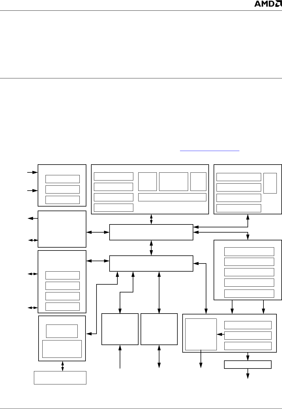
Figure 1-1. Internal Block Diagram
GeodeLink™ Interface Unit 0
GeodeLink™ Interface Unit 1
GeodeLink™
Control
Diagnostic
Te s t
Power Mgmnt
GeodeLink™
SDCLKs
TLB
Integer
Unit
MMU
Load/Store FPU
64 KB L1 D-cache
64 KB L1 I-cache
Bus Controller
CPU Core
Alpha Compositing
ROP Unit
BLT Engine
Graphics Processor (GP)
Timing
Palette RAM
Compression Buffer
Display Controller (DC)
Alpha Blender
Video Mixer
Video Scalar
Video Processor (VP)
RGB YUV
Graphics Filter/Scaling
(GLIU0)
(GLIU1)
Memory
Clock Module
CPU PLL
System PLL
TFT/VOP
3x8-Bit DAC
CRT
GeodeLink™
PCI
Video Input
SYSREF
DOTREF
Test/Reset
Interface
Processor (GLCP)
PCI Bridge
(GLPCI)
Controller (GLMC)
Port (VIP)
DOTCLK PLL
128 KB L2 cache
1 KB
LUT
Rotation BLT
Companion I/F
VIP
HW VGA
128-bit AES
TFT
Controller/
Video
Output
Port (VOP)
AMD Geode™
Companion
Device
64-Bit
DDR
Security Block
Random Number
Generator
EEPROM on package
64-bit DDR SDRAM
(CBC/ECB)
Tr u e
(optional)

12 AMD Geode™ LX Processors Data Book
Overview
33234H
1.2 Features
General Features
■Functional blocks include:
—CPU Core
— GeodeLink™ Control Processor
— GeodeLink Interface Units
— GeodeLink Memory Controller
— Graphics Processor
— Display Controller
— Video Processor
– TFT Controller/Video Output Port
— Video Input Port
— GeodeLink PCI Bridge
— Security Block
■0.13 micron process
■Packaging:
— 481-Terminal BGU (Ball Grid Array Cavity Up) with
internal heatspreader
■Single packaging option supports all features
■Industrial temperature range available for the
LX 800@0.9W processor*
CPU Processor Features
■x86/x87-compatible CPU core
■Performance:
— Processor frequency: up to 600 MHz
— Dhrystone 2.1 MIPs: 150 to 450
— Fully pipelined FPU
■Split I/D cache/TLB (Translation Look-aside Buffer):
— 64 KB I-cache/64 KB D-cache
— 128 KB L2 cache configurable as I-cache, D-cache,
or both
■Efficient prefetch and branch prediction
■Integrated FPU that supports the MMX™ and
AMD 3DNow!™ instruction sets
■Fully pipelined single precision FPU hardware with
microcode support for higher precisions
GeodeLink™ Control Processor
■JTAG interface:
— ATPG, Full Scan, BIST on all arrays
— 1149.1 Boundary Scan compliant
■ICE (in-circuit emulator) interface
■Reset and clock control
■Designed for improved software debug methods and
performance analysis
■Power Management:
— LX 900@1.5W processor* (Unterminated):
Total Dissipated Power (TDP) 5.1W,
2.6W typical @ 600 MHz max power
— LX 800@0.9W processor* (Unterminated):
Total Dissipated Power (TDP) 3.6W,
1.8W typical @ 500 MHz max power
— LX 700@0.8W processor* (Unterminated):
Total Dissipated Power (TDP) 3.1W,
1.3W typical @ 433 MHz max power
— LX 600@0.7W processor* (Unterminated):
Total Dissipated Power (TDP) 2.8W,
1.2W typical @ 366 MHz max power
— GeodeLink active hardware power management
— Hardware support for standard ACPI software power
management
— I/O companion SUSP/SUSPA power controls
— Lower power I/O
— Wakeup on SMI/INTR
■Works in conjunction with the AMD Geode™ CS5536
(USB 2.0) or CS5535 (USB 1.1) companion device
GeodeLink™ Architecture
■High bandwidth packetized uni-directional bus for
internal peripherals
■Standardized protocol to allow variants of products to be
developed by adding or removing modules
■GeodeLink Control Processor (GLCP) for diagnostics
and scan control
■Dual GeodeLink Interface Units (GLIUs) for device inter-
connect
GeodeLink™ Memory Controller
■Integrated memory controller for low latency to CPU and
on-chip peripherals
■64-bit wide DDR SDRAM bus operating frequency:
— 200 MHz, 400 MT/S
■Supports unbuffered DDR DIMMS using up to 2 GB
DRAM technology
■Supports up to 2 DIMMS (16 devices max)
2D Graphics Processor
■High performance 2D graphics controller
■Alpha BLT
■Windows® GDI GUI acceleration:
— Hardware support for all Microsoft RDP codes
■Command buffer interface for asynchronous BLTs
■Second pattern channel support
■Hardware screen rotation
*The AMD Geode LX 900@1.5W processor operates at 600 MHz, the AMD Geode LX 800@0.9W processor operates at 500 MHz, the
AMD Geode LX 700@0.8W processor operates at 433 MHz and the AMD Geode LX 600@.07W processor operates at 366 MHz. Model
numbers reflect performance as described here: http://www.amd.com/connectivitysolutions/geodelxbenchmark.

AMD Geode™ LX Processors Data Book 13
Overview 33234H
Display Controller
■Hardware frame buffer compression improves Unified
Memory Architecture (UMA) memory efficiency
■CRT resolutions supported:
— Supports up to 1920x1440x32 bpp at 85 Hz
— Supports up to 1600x1200x32 bpp at 100 Hz
■Supports up to 1600x1200x32 bpp at 60 Hz for TFT
■Standard Definition (SD) resolution for Video Output
Port (VOP):
— 720x482 at 59.94 Hz interlaced for NTSC
— 768x576 at 50 Hz interlaced for PAL
■High Definition (HD) resolution for Video Output Port
(VOP):
— Up to 1920x1080 at 30 Hz interlaced (1080i HD)
(74.25 MHz)
— Up to 1280x720 at 60 Hz progressive (720p HD)
(74.25 MHz)
■Supports down to 7.652 MHz Dot Clock (320x240
QVGA)
■Hardware VGA
■Hardware supported 48x64 32-bit cursor with alpha
blending
Video Processor
■Supports video scaling, mixing and VOP
■Hardware video up/down scalar
■Graphics/video alpha blending and color key muxing
■Digital VOP (SD and HD) or TFT outputs
■Legacy RGB mode
■VOP supports SD and HD 480p, 480i, 720p, and 1080i
■VESA 1.1, 2.0 and BT.601 24-bit (out only), BT.656
compliant
Integrated Analog CRT DAC, System Clock PLLs and
Dot Clock PLL
■Integrated Dot Clock PLL with up to 350 MHz clock
■Integrated 3x8-bit DAC with up to 350 MHz sampling
■Integrated x86 core PLL
■Memory PLL
GeodeLink™ PCI Bridge
■PCI 2.2 compliant
■3.3V signaling and 3.3V I/Os
■33 to 66 MHz operation
■32-bit interface
■Supports virtual PCI headers for GeodeLink devices
Video Input Port (VIP)
■VESA 1.1 and 2.0 compliant, 8 or 16-bit
■Video Blanking Interval (VBI) support
■8 or 16-bit 80 MHz SD or HD capable
Security Block
■Serial EEPROM interface for 2K bit unique ID and AES
(Advanced Encryption Standard) hidden key storage
(EEPROM optional inside package)
■Electronic Code Book (ECB) or Cipher Block Chaining
(CBC)128-bit AES hardware support
■True random number generator (TRNG)

14 AMD Geode™ LX Processors Data Book
Overview
33234H

AMD Geode™ LX Processors Data Book 15
2
Architecture Overview 33234H
2.0Architecture Overview
The CPU Core provides maximum compatibility with the
vast amount of Internet content available while the intelli-
gent integration of several other functions, including graph-
ics, makes the AMD Geode™ LX processor a true system-
level multimedia solution.
The AMD Geode LX processor can be divided into major
functional blocks (as shown in Figure 1-1 on page 11):
•CPU Core
•GeodeLink™ Control Processor
•GeodeLink Interface Units
•GeodeLink Memory Controller
•Graphics Processor
•Display Controller
•Video Processor
— TFT Controller/Video Output Port
•Video Input Port
•GeodeLink PCI Bridge
•Security Block
2.1 CPU Core
The x86 core consists of an Integer Unit, cache memory
subsystem, and an x87 compatible FPU (Floating Point
Unit). The Integer Unit contains the instruction pipeline and
associated logic. The memory subsystem contains the
instruction and data caches, translation look-aside buffers
(TLBs), and an interface to the GeodeLink Interface Units
(GLIUs).
The instruction set supported by the core is a combination
of Intel Pentium® processor, AMD Athlon™ processor, and
AMD Geode LX processor specific instructions. Specifi-
cally, it supports the Pentium, Pentium Pro, AMD 3DNow!™
technology and MMX™ instructions for the AMD Athlon
processor. It supports a subset of the specialized
AMD Geode LX processor instructions including special
SMM instructions. The CPU Core does not support the
entire Katmai New Instruction (KNI) set as implemented in
the Pentium 3. It does support the MMX instructions for the
AMD Athlon processor, which are a subset of the
Pentium 3 KNI instructions.
2.1.1 Integer Unit
The Integer Unit consists of a single issue 8-stage pipeline
and all the necessary support hardware to keep the pipe-
line running efficiently.
The instruction pipeline in the integer unit consists of eight
stages:
1) Instruction Prefetch - Raw instruction data is fetched
from the instruction memory cache.
2) Instruction Pre-decode - Prefix bytes are extracted
from raw instruction data. This decode looks-ahead to
the next instruction and the bubble can be squashed if
the pipeline stalls down stream.
3) Instruction Decode - Performs full decode of instruc-
tion data. Indicates instruction length back to the
Prefetch Unit, allowing the Prefetch Unit to shift the
appropriate number of bytes to the beginning of the
next instruction.
4) Instruction Queue - FIFO containing decoded x86
instructions. Allows Instruction Decode to proceed
even if the pipeline is stalled downstream. Register
reads for data operand address calculations are per-
formed during this stage.
5) Address Calculation #1 - Computes linear address of
operand data (if required) and issues request to the
Data Memory Cache. Microcode can take over the
pipeline and inject a micro-box here if multi-box
instructions require additional data operands.
6) Address Calculation #2 - Operand data (if required)
is returned and set up to the Execution stage with no
bubbles if there was a data cache hit. Segment limit
checking is performed on the data operand address.
The µROM is read for setup to Execution Unit.
7) Execution Unit - Register and/or data memory fetch
fed through the Arithmetic Logic Unit (ALU) for arith-
metic or logical operations. µROM always fires for the
first instruction box down the pipeline. Microcode can
take over the pipeline and insert additional boxes here
if the instruction requires multiple Execution Unit
stages to complete.
8) Writeback - Results of the Execution Unit stages are
written to the register file or to data memory.

16 AMD Geode™ LX Processors Data Book
Architecture Overview
33234H
2.1.2 Memory Management Unit
The memory management unit (MMU) translates the linear
address supplied by the integer unit into a physical address
to be used by the cache unit and the internal bus interface
unit. Memory management procedures are x86-compati-
ble, adhering to standard paging mechanisms.
The MMU also contains a load/store unit that is responsible
for scheduling cache and external memory accesses. The
load/store unit incorporates two performance-enhancing
features:
• Load-store reordering gives memory reads required by
the integer unit a priority over writes to external memory.
• Memory-read bypassing eliminates unnecessary
memory reads by using valid data from the execution
unit.
2.1.3 Cache and TLB Subsystem
The cache and TLB subsystem of the CPU Core supplies
the integer pipeline with instructions, data, and translated
addresses (when necessary). To support the efficient deliv-
ery of instructions, the cache and TLB subsystem has a
single clock access 64 KB 16-way set associative instruc-
tion cache and a 16-entry fully associative TLB. The TLB
performs necessary address translations when in protected
mode. For data, there is a 64 KB 16-way set associative
writeback cache, and a 16-entry fully associative TLB.
When there is a miss to the instruction or data TLBs, there
is a second level unified (instruction and data) 64-entry 2-
way set associative TLB that takes an additional clock to
access. When there is a miss to the instruction or data
caches or the TLB, the access must go to the GeodeLink
Memory Controller (GLMC) for processing. Having both an
instruction and a data cache and their associated TLBs
improves overall efficiency of the integer unit by enabling
simultaneous access to both caches.
The L1 caches are supported by a 128 KB unified L2 victim
cache. The L2 cache can be configured to hold data,
instructions, or both. The L2 cache is 4-way set associa-
tive.
2.1.4 Bus Controller Unit
The bus controller unit provides a bridge from the proces-
sor to the GLIUs. When external memory access is
required, due to a cache miss, the physical address is
passed to the bus controller unit, that translates the cycle
to a GeodeLink cycle.
2.1.5 Floating Point Unit
The Floating Point Unit (FPU) is a pipelined arithmetic unit
that performs floating point operations as per the IEEE 754
standard. The instruction sets supported are x87, MMX,
and AMD 3DNow! technology. The FPU is a pipelined
machine with dynamic scheduling of instructions to mini-
mize stalls due to data dependencies. It performs out of
order execution and register renaming. It is designed to
support an instruction issue rate of one per clock from the
integer core. The datapath is optimized for single precision
arithmetic. Extended precision instructions are handled in
microcode and require multiple passes through the pipe-
line. There is an execution pipeline and a load/store pipe-
line. This allows load/store operations to execute in parallel
with arithmetic instructions.
2.2 GeodeLink™ Control Processor
The GeodeLink Control Processor (GLCP) is responsible
for reset control, macro clock management, and debug
support provided in the Geode LX processor. It contains
the JTAG interface and the scan chain control logic. It sup-
ports chip reset, including initial PLL control and program-
ming and runtime power management macro clock control.
The JTAG support includes a TAP Controller that is IEEE
1149.1 compliant. CPU control can be obtained through
the JTAG interface into the TAP Controller, and all internal
registers, including CPU Core registers, can be accessed.
In-circuit emulation (ICE) capabilities are supported
through this JTAG and TAP Controller interface.
The GLCP also includes the companion device interface.
The companion device has several unique signals con-
nected to this module that support Geode LX processor
reset, interrupts, and system power management.
2.3 GeodeLink™ Interface Units
Together, the two GeodeLink Interface Units (GLIU0 and
GLIU1) make up the internal bus derived from the
GeodeLink architecture. GLIU0 connects five high band-
width modules together with a seventh link to GLIU1 that
connects to the five low bandwidth modules.
2.4 GeodeLink™ Memory Controller
The GeodeLink Memory Controller (GLMC) is the source
for all memory needs in a typical Geode LX processor sys-
tem. The GLMC supports a memory data bus width of 64
bits and supports 200 MHz, 400 MT/S for DDR (Double
Data Rate).
The modules that need memory are the CPU Core, Graph-
ics Processor, Display Controller, Video Input Port, and
Security Block. Because the GLMC supports memory
needs for both the CPU Core and the display subsystem,
the GLMC is classically called a UMA (Unified Memory
Architecture) subsystem. PCI accesses to main memory
are also supported.
Up to four banks, with eight devices maximum in each bank
of SDRAM, are supported with up to 512 MB in each bank.
Four banks means that one or two DIMM or SODIMM mod-
ules can be used in a AMD Geode LX processor system.
Some memory configurations have additional restrictions
on maximum device quantity.
AMD Geode™ LX Processors Data Book 17
Architecture Overview 33234H
2.5 Graphics Processor
The Graphics Processor is based on the graphics proces-
sor used in the AMD Geode GX processor with several fea-
tures added to enhance performance and functionality. Like
its predecessor, the AMD Geode LX processor’s Graphics
Processor is a BitBLT/vector engine that supports pattern
generation, source expansion, pattern/source transpar-
ency, 256 ternary raster operations, alpha blenders to sup-
port alpha-BLTs, incorporated BLT FIFOs, a GeodeLink
interface and the ability to throttle BLTs according to video
timing. Features added to the Graphics Processor include:
•Command buffer interface
•Hardware accelerated rotation BLTs
•Color depth conversion
•Paletized color
•Full 8x8 color pattern buffer
•Channel 3 - third DMA channel
•Monochrome inversion
Table 2-1 presents a comparison between the Graphics
Processor features of the AMD Geode GX and LX proces-
sors.
Table 2-1. Graphics Processor Feature Comparison
Feature AMD Geode™ GX Processor AMD Geode™ LX Processor
Color Depth 8, 16, 32 bpp 8, 16, 32 bpp (A) RGB 4 and 8-bit indexed
ROPs 256 (src, dest, pattern) 256 (2-src, dest and pattern)
BLT Buffers FIFOs in Graphics Processor FIFOs in Graphics Processor
BLT Splitting Managed by hardware Managed by hardware
Video Synchronized BLT/Vector Throttle by VBLANK Throttle by VBLANK
Bresenham Lines Yes Yes
Patterned (stippled) Lines No Yes
Screen to Screen BLT Yes Yes
Screen to Screen BLT with
mono expansion
Ye s Ye s
Memory to Screen BLT Yes (through CPU writes) Yes (throttled rep movs writes)
Accelerated Text No No
Pattern Size (Mono) 8x8 pixels 8x8 pixels
Pattern Size (Color) 8x1 (32 pixels) 8x8 pixels
8x2 (16 pixels)
8x4 (8 pixels)
Monochrome Pattern Yes Yes (with inversion)
Dithered Pattern (4 color) No No
Color Pattern 8, 16, 32 bpp 8, 16, 32 bpp
Transparent Pattern Monochrome Monochrome
Solid Fill Yes Yes
Pattern Fill Yes Yes
Transparent Source Monochrome Monochrome
Color Key Source Transparency Y with mask Y with mask
Variable Source Stride Yes Yes
Variable Destination Stride Yes Yes
Destination Write Bursting Yes Yes
Selectable BLT Direction Vertical and Horizontal Vertical and Horizontal
Alpha BLT Yes (constant α or α/pix) Yes (constant α, α/pix, or sep. α channel)
VGA Support Decodes VGA Register Decodes VGA Register
Pipeline Depth 2 ops Unlimited
Accelerated Rotation BLT No 8, 16, 32 bpp
Color Depth Conversion No 5:6:5, 1:5:5:5, 4:4:4:4, 8:8:8:8

18 AMD Geode™ LX Processors Data Book
Architecture Overview
33234H
2.6 Display Controller
The Display Controller performs the following functions:
1) Retrieves graphics, video, and cursor data.
2) Serializes the streams.
3) Performs any necessary color lookups and output for-
matting.
4) Interfaces to the Video Processor for driving the dis-
play device(s).
The Display Controller consists of a memory retrieval sys-
tem for rasterized graphics data, a VGA, and a back-end fil-
ter. The AMD Geode LX processor’s Display Controller
corresponds to the Display Controller function found in the
AMD Geode GX processor with additional hardware for
graphics filter functions. The VGA provides full hardware
compatibility with the VGA graphics standard. The raster-
ized graphics and the VGA share a single display FIFO and
display refresh memory interface to the GeodeLink Mem-
ory Controller (GLMC). The VGA uses 8 bpp and syncs,
that are expanded to 24 bpp via the color lookup table, and
passes the information to the graphics filter for scaling and
interlaced display support. The stream is then passed to
the Video Processor, which is used for video overlay. The
Video Processor forwards this information to the DAC (Dig-
ital-to-Analog Converter), that generates the analog red,
green, and blue signals, and buffers the sync signals that
are then sent to the display. The Video Processor output
can also be rendered as YUV data, and can be output on
the Video Output Port (VOP).
2.7 Video Processor
The Video Processor mixes the graphics and video
streams, and outputs either digital RGB data to the internal
DACs or the flat panel interface, or digital YUV data via the
VOP interface.
The Video Processor delivers high-resolution and true-
color graphics. It can also overlay or blend a scaled true-
color video image on the graphic background.
The Video Processor interfaces with the CPU Core via a
GLIU master/slave interface. The Video Processor is a
slave only, as it has no memory requirements.
2.7.1 CRT Interface
The internal high performance DACs support CRT resolu-
tions up to:
— 1920x1440x32 bpp at 85 Hz
— 1600x1200x32 bpp at 100 Hz
2.7.2 TFT Controller
The TFT Controller converts the digital RGB output of a
Video Mixer block to the digital output suitable for driving a
TFT flat panel LCD.
The flat panel connects to the RGB port of the Video Mixer.
It interfaces directly to industry standard 18-bit or 24-bit
active matrix thin film transistor (TFT). The digital RGB or
video data that is supplied by the video logic is converted
into a suitable format to drive a wide range of panels with
variable bits. The LCD interface includes dithering logic to
increase the apparent number of colors displayed for use
on panels with less than 6 bits per color. The LCD interface
also supports automatic power sequencing of panel power
supplies.
It supports panels up to a 24-bit interface and up to
1600x1200 resolution.
The TFT Controller interfaces with the CPU Core via a
GLIU master/slave interface. The TFT Controller is both a
GLIU master and slave.
2.7.3 Video Output Port
The VOP receives YUV 4:4:4 encoded data from the Video
Processor and formats the data into a video stream that is
BT.656 compliant. Output from the VOP goes to either a
VIP or a TV encoder. The VOP is BT.656/601 compliant
since its output may go directly (or indirectly) to a display.
2.8 Video Input Port
The Video Input Port (VIP) receives 8- or 16-bit video or
ancillary data, 8-bit message data, or 8-bit raw video and
passes it to data buffers located in system memory. The
VIP is a DMA engine. The primary operational mode is as a
compliant VESA 2.0 slave. The VESA 2.0 specification
defines the protocol for receiving video, VBI, and ancillary
data. The addition of the message passing and data
streaming modes provides additional flexibility in receiving
non-VESA 2.0 compliant data streams. Input data is
packed into QWORDS, buffered into a FIFO, and sent to
system memory over the GLIU. The VIP masters the inter-
nal GLIU and transfers the data from the FIFO to system
memory. The maximum input data rate (8- or 16-bits) is 150
MHz.
2.9 GeodeLink™ PCI Bridge
The GeodeLink PCI Bridge (GLPCI) contains all the neces-
sary logic to support an external PCI interface. The PCI
interface is PCI v2.2 specification compliant. The logic
includes the PCI and GLIU interface control, read and write
FIFOs, and a PCI arbiter.

AMD Geode™ LX Processors Data Book 19
Architecture Overview 33234H
2.10 Security Block
The AMD Geode LX processor has an on-chip AES 128-bit
crypto acceleration block capable of 44 Mbps throughput
on either encryption or decryption at a processor speed of
500 MHz. The AES block runs asynchronously to the pro-
cessor core and is DMA based. The AES block supports
both EBC and CBC modes and has an interface for
accessing the optional EEPROM memory for storing
unique IDs and/or security keys. The AES and EEPROM
sections have separate control registers but share a single
set of interrupt registers. The AES module has two key
sources: one hidden 128-bit key stored in the “on-package”
EEPROM, and a write only 128-bit key (reads as all zeros).
The hidden key is loaded automatically by the hardware
after reset and is not visible to the processor. The
EEPROM can be locked. The initialization vector for the
CBC mode can be generated by the True Random Number
Generator (TRNG). The TRNG is addressable separately
and generates a 32-bit random number.

20 AMD Geode™ LX Processors Data Book
Architecture Overview
33234H
AMD Geode™ LX Processors Data Book 21
3
Signal Definitions 33234H
3.0Signal Definitions
This chapter defines the signals and describes the external interface of the AMD Geode™ LX processor. Figure 3-1 shows
the pins organized by their functional groupings. Where signals are multiplexed, the default signal name is listed first and is
separated by a plus sign (+). Multi-function pins are described in Table 3-1 on page 22.
Figure 3-1. Signal Groups
RESET#
INTA#
IRQ13 (STRAP)
SDCLK[5:0]N
CKE[1:0]
CS[3:0]#
RAS[1:0]#
CAS[1:0]#
WE[1:0]#
DQM[7:0]
DQS[7:0]
BA[1:0]
DQ[63:0]
MA[13:0]
AD[31:0]
CBE[3:0]#
FRAME#
IRDY#
TRDY#
STOP#
DEVSEL#
DOTREF
PAR
(STRAP)
GNT[2:0]#
CIS
SUSPA# (STRAP)
TDP
TDN
System
Memory
Display (TFT Option)
VDDEN+VIP_HSYNC
DRGB[25:24]+VID[9:8]+
DOTCLK+VOPCLK
VSYNC+VOP_VSYNC
HSYNC+VOP_HSYNC
GREEN
BLUE
RED
LDEMOD+VIP_VSYNC
SYSREF
TLA[1:0]
REQ[2:0]#
VID[7:0]
VIPCLK
VIPSYNC
VIP
PW[1:0] (STRAP)
(Total of 32) VCORE
(Total of 33) VMEM
(Total of 128) VSS
(Total of 30) VIO Power/Ground
Interface
TCLK
TMS
TDI
TDO
TDBGI
TDBGO
Internal Test
and
Measurement
AMD Geode™
VAVDD, CAVDD, MAVDD
VAVSS, CAVSS, MAVSS
MVREF
Display (CRT Option)
DVREF
DRSET
(Total of 4) DAVDD
(Total of 4) DAVSS
DISPEN+VOP_BLANK
CLPF
MLPF
VLPF
LX Processor
PLL
PCI
Interface
Signals
Signals
Interface
Signals
Interface
Signals
Interface
Signals
Interface
Signals
Interface
Signals
Interface
Signals
Interface
Signals
SDCLK[5:0]P
VSYNC
HSYNC
DRGB[23:16]
DRBG[15:8]+VOP[15:8]
DRGB[7:0]+VOP[7:0]
MSGSTART+MSGSTOP
DRGB[31:26]+VID[15:10]
22 AMD Geode™ LX Processors Data Book
Signal Definitions
33234H
Table 3-1. Video Signal Definitions Per Mode
Signal Name CRT w/16-bit VIP
RGB w/16-bit
VIP
ARGB (Note 1)
w/8-bit VIP
TFT w/16-bit VIP
(not 601)
8- or 16-bit VOP
w/16-bit VIP
RED RED
GREEN GREEN
BLUE BLUE
DRGB[31:24] (I/O) VID[15:8] (I) VID[15:8] (I) Alpha VID[15:8] (I) VID[15:8] (I)
DRGB[23:16] (O) R[7:0] R[7:0] R[7:0] R[7:0] (Note 2) Driven low
DRGB[15:8] (O) G[7:0] G[7:0] G[7:0] G[7:0] (Note 2) VOP[15:8] (O)
DRGB[7:0] (O) B[7:0] B[7:0] B[7:0] B[7:0] (Note 2) VOP[7:0] (O)
DOTCLK (O) DOTCLK (O) DOTCLK (O) DOTCLK (O) DOTCLK (O) VOPCLK (O)
HSYNC (O) HSYNC (O) HSYNC (O) HSYNC (O) VOP_HSYNC (O) VOP_HSYNC (O)
VSYNC (O) VSYNC (O) VSYNC (O) VSYNC (O) VSYNC (O) VOP_VSYNC (O)
DISPEN (O) DISPEN (O) VOP_BLANK (O)
VDDEN (I/O) VIP_HSYNC (I) VIP_HSYNC (I) VIP_HSYNC (I) VDDEN (O) VIP_HSYNC (I)
LDEMOD (I/O) VIP_VSYNC (I) VIP_VSYNC (I) VIP_VSYNC (I) LDEMOD (O) VIP_VSYNC (I)
VID[7:0] (I) VID[7:0] VID[7:0] VID[7:0] VID[7:0] VID[7:0]
VIPCLK (I) VIPCLK VIPCLK VIPCLK VIPCLK VIPCLK
VIPSYNC (I) VIPSYNC VIPSYNC VIPSYNC VIPSYNC VIPSYNC
Note 1. Alpha RED/GREEN/BLUE: Useful for off-chip graphics digital interfaces.
Note 2. Pin usage depends on TFT mode. See Section 6.7.7 "Flat Panel Display Controller" on page 405 for details.
AMD Geode™ LX Processors Data Book 23
Signal Definitions 33234H
3.1 Buffer Types
The Ball Assignment tables starting on page 26 include a
column labeled “Buffer Type”. The details of each buffer
type listed in this column are given in Table 3-2. The col-
umn headings in Table 3-2 are identified as follows:
TS: Indicates whether the buffer may be put into the TRI-
STATE mode. Note some pins that have buffer types that
allow TRI-STATE may never actually enter the TRI-STATE
mode in practice, since they may be inputs or provide other
signals that are always driven. To determine if a particular
signal can be put in the TRI-STATE mode, consult the indi-
vidual signal descriptions in Section 3.4 "Signal Descrip-
tions" on page 33.
OD: Indicates if the buffer is open-drain, or not. Open-drain
outputs may be wire ORed together and require a discrete
pull-up resistor to operate properly.
5VT: Indicates if the buffer is 5-volt tolerant, or not. If it is 5-
volt tolerant, then 5 volt TTL signals may be safely applied
to this pin.
PU/PD: Indicates if an internal, programmable pull-up or
pull-down resistor may be present.
Current High/Low (mA): This column gives the current
source/sink capacities when the voltage at the pin is high,
and low. The high and low values are separated by a “/”
and values given are in milli-amps (mA).
Rise/Fall @ Load: This column indicates the rise and fall
times for the different buffer types at the load capacitance
indicated. These measurements are given in two ways:
rise/fall time between the 20%-80% voltage levels, or, the
rate of change the buffer is capable of, in volts-per-nano-
second (V/ns).
Note the presence of “Wire” type buffer in this table. Sig-
nals identified as a wire-type are not driven by a buffer,
hence no rise/fall time or other measurements are given;
these are marked “NA” in Table 3-2. The wire-type connec-
tion indicates a direct connection to internal circuits such
as power, ground, and analog signals.
Table 3-2. Buffer Type Characteristics
Name TS OD 5VT PU/PD
Current
High/Low
(mA) Rise/Fall @ Load
24/Q3 X X 24/24 3 ns @ 50 pF
24/Q5 X X 24/24 5 ns @ 50 pF
24/Q7 X X 24/24 7 ns @ 50 pF
5V X X 16/16 1.25V/ns @ 40 pF
PCI X 0.5/1.5 1-4V/ns @ 10 pF
DDRCLK 10/10 8.5V/ns @ 15 pF
DDR 2.4V/ns @ 50 pF
Wire NA NA NA NA NA

24 AMD Geode™ LX Processors Data Book
Signal Definitions
33234H
3.2 Bootstrap Options
The bootstrap options shown in Table 3-3 are supported in
the AMD Geode LX processor for configuring the system.
3.3 Ball Assignments
The tables in this chapter use several common abbrevia-
tions. Table 3-4 lists the mnemonics and their meanings.
Table 3-3. Bootstrap Options
Pins Description
IRQ13 0: Normal boot operation, TAP reset
active during PCI reset
1: Debug stall of CPU after CPU
reset, TAP reset active until VIO valid
PW1 0: PCI (SYSREF) is 33 MHz
1: PCI (SYSREF) is 66 MHz
PW0,
SUSPA#,
GNT[2:0]#
Select CPU and GeodeLink system
MHz options including a PLL bypass
option. Refer to Table 6-87 on page
556 for programming.
Table 3-4. Ball Type Definitions
Mnemonic Definition
AAnalog
I Input ball
I/O Bidirectional ball
CAVSS Core PLL Ground ball: Analog
CAVDD Core PLL Power ball: Analog
DAVSS DAC PLL Ground ball: Analog
DAVDD DAC PLL Power ball: Analog
MAVSS GLIU PLL Ground ball: Analog
MAVDD GLIU PLL Power ball: Analog
O Output ball
VAVSS Video PLL Ground ball: Analog
VAVDD Video PLL Power ball: Analog
VCORE Power ball: 1.2V (Nominal)
VIO I/O Power ball: 3.3V (Nominal)
VMEM Power ball: 2.5V
VSS Ground ball
# The “#” symbol at the end of a signal
name indicates that the active, or
asserted state, occurs when the sig-
nal is at a low voltage level. When “#”
is not present after the signal name,
the signal is asserted when at a high
voltage level.
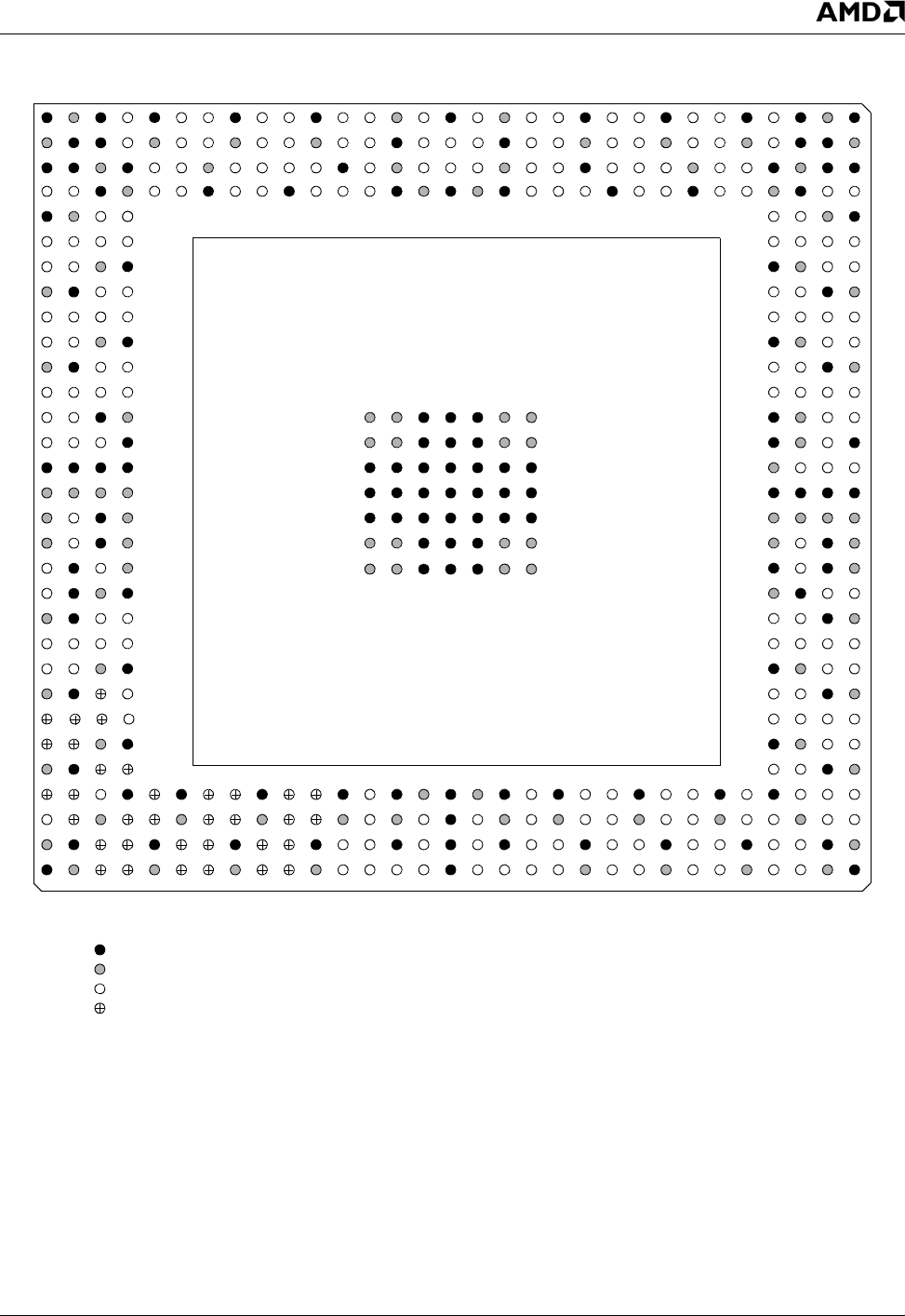
AMD Geode™ LX Processors Data Book 25
Signal Definitions 33234H
Figure 3-2. BGU481 Ball Assignment Diagram
12345678910111213141516171819202122232425262728293031
A
B
C
D
E
F
G
H
J
K
L
M
N
P
R
T
U
V
W
Y
AA
AB
AC
AD
AE
AF
AG
AH
AJ
AK
AL
A
B
C
D
E
F
G
H
J
K
L
M
N
P
R
T
U
V
W
Y
AA
AB
AC
AD
AE
AF
AG
AH
AJ
AK
AL
Note: Signal names have been abbreviated in this figure due to space constraints.
VSS VMEM VSS DQ21 VSS DQM2 DQ22 VSS DQ28 DQS3 VSS DQ26 DQ31 VMEM DQ32 VSS DQ37 VMEM DQM4 DQ39 VSS DQ40 DQ41 VSS DQ42 DQ43 VSS WE1# VSS VMEM VSS
12345678910111213141516171819202122232425262728293031
VMEM VSS VSS DQ17 VMEM DQ18 DQ23 VMEM DQ24 DQM3 VMEM DQ27 TLA1 VSS TLA0 DQ36 DQ33 VSS DQ34 DQ38 VMEM DQ35 DQS5 VMEM DQ46 DQ47 VMEM CS0# VSS VSS VMEM
VSS VSS VMEM VSS MA12 DQS2 VMEM DQ19 DQ29 DQ25 DQ30 VSS MA3 VMEM MA2 MA0 MA1 VMEM DQS4 BA1 VSS DQ44 DQ45 DQM5 VMEM RAS0# WE0# VSS VMEM VSS VSS
DQ20 DQ16 VSS VMEM MA11 MA9 VSS MA7 MA8 VSS MA5 MA6 MA4 VSS VCORE VSS VCORE VSS MA10 SDK5P SDK5N VSS SDK4P SDK4N VSS BA0 RAS1# VMEM VSS CS3# DQ48
VSS VMEM DQ11 CKE0 CAS0# CAS1# VMEM VSS
DQ15 DQ14 DQ10 CKE1 CS1# CS2# MA13 DQ49
DQ13 DQM1 VMEM VSS VSS VMEM DQ52 DQ53
VMEM VSS DQS1 SDK1N SDK3N DQM6 VSS VMEM
DQ9 DQ8 DQ12 SDK1P SDK3P DQS6 DQ55 DQ54
DQ7 DQ3 VMEM VSS VSS VMEM DQ50 DQ51
VMEM VSS DQ6 SDK0N SDK2N DQ60 VSS VMEM
DQM0 DQS0 DQ2 SDK0P SDK2P DQ61 DQ57 DQ56
DQ5 DQ1 VSS VMEM
MVREF DQ0 DQ4 VSS
VSS VMEM DQM7 DQS7
VSS VMEM DQ62 VSS
VSS VSS VSS VSS
VCORE VCORE VCORE VCORE
DAVDD BLUE DAVSS VCORE
DAVDD GREEN DAVSS DAVDD
DVREF DAV SS RED DAVDD
DRSET DAVSS VIO VSS
VAV DD VAV SS VLPF TMS
DOTREF TDBGI TDI TDBGO
TDO TCLK VIO VSS
VIO VSS VSYNC LDEMOD
DOTCLK VDEN HSYNC DISPEN
DRB17 DRB16 VIO VSS
VIO VSS DRB18 DRB19
VCORE DQ63 DQ58 DQ59
VSS VSS VSS VSS
VCORE VCORE VCORE VCORE
VCORE MLPF MAVSS MAVDD
VSS CLPF CAVSS CAVDD
VCORE VSS RESET# SYREF
GNT0# REQ0# VSS VIO
REQ2# IRQ13 GNT1# REQ1#
VSS VIO GNT2# SUPA#
INTA# AD31 VSS VIO
AD27 CIS AD29 AD30
VSS VIO AD26 AD28
AD25 AD24 VSS VIO
DRB20 DRB21 DRB22 VSS DRB11 VSS DRB0 DRB6 VSS DRB29 DRB24 VSS VID3 VSS VCORE VSS VCORE VSS AD1 VSS AD5 AD11 VSS AD14 IRDY# VSS CBE2# VSS AD23 AD22 CBE3#
DRB23 DRB8 VIO DRB12 DRB15 VIO DRB3 DRB7 VIO DRB28 DRB25 VIO VID4 VIO VID0 VSS PW1 VIO AD0 VIO AD6 CBE0# VIO AD15 STOP# VIO PA R A D 1 6 V IO AD19 AD21
VIO VSS DRB9 DRB14 VSS DRB1 DRB4 VSS DRB31 DRB26 VSS VID7 VID5 VSS VID1 VSS TDN VSS AD4 AD3 VSS AD8 AD10 VSS DEVSL# TRDY# VSS AD17 AD20 VSS VIO
VSS VIO DRB10 DRB13 VIO DRB2 DRB5 VIO DRB30 DRB27 VIO VIPCLK VID6 VIPSYNC VID2 VSS TDP PW0 AD7 AD2 VIO AD9 AD12 VIO AD13 CBE1# VIO FRAME# AD18 VIO VSS
AMD Geode™
LX Processor
S
= GND Ball
= PWR Ball
= Strap Option Ball
= Multiplexed Ball
VCORE VCORE VSS VSS VSS VCORE VCORE
VCORE VCORE VSS VSS VSS VCORE VCORE
VSS VSS VSS VSS VSS VSS VSS
VSS VSS VSS VSS VSS VSS VSS
VSS VSS VSS VSS VSS VSS VSS
VCORE VCORE VSS VSS VSS VCORE VCORE
VCORE VCORE VSS VSS VSS VCORE VCORE
(Top View)
s
s
s
ss
s
s

26 AMD Geode™ LX Processors Data Book
Signal Definitions
33234H
Ball
No.
Signal Name
(Note 1)
Type
(PD)
Buffer
Type
A1 VSS GND ---
A2 VMEM PWR ---
A3 VSS GND ---
A4 DQ21 I/O DDR
A5 VSS GND ---
A6 DQM2 I/O DDR
A7 DQ22 I/O DDR
A8 VSS GND ---
A9 DQ28 I/O DDR
A10 DQS3 I/O DDR
A11 VSS GND ---
A12 DQ26 I/O DDR
A13 DQ31 I/O DDR
A14 VMEM PWR ---
A15 DQ32 I/O DDR
A16 VSS GND ---
A17 DQ37 I/O DDR
A18 VMEM PWR ---
A19 DQM4 I/O DDR
A20 DQ39 I/O DDR
A21 VSS GND ---
A22 DQ40 I/O DDR
A23 DQ41 I/O DDR
A24 VSS GND ---
A25 DQ42 I/O DDR
A26 DQ43 I/O DDR
A27 VSS GND ---
A28 WE1# I/O DDR
A29 VSS GND ---
A30 VMEM PWR ---
A31 VSS GND ---
B1 VMEM PWR ---
B2 VSS GND ---
B3 VSS GND ---
B4 DQ17 I/O DDR
B5 VMEM PWR ---
B6 DQ18 I/O DDR
B7 DQ23 I/O DDR
B8 VMEM PWR ---
B9 DQ24 I/O DDR
B10 DQM3 I/O DDR
B11 VMEM PWR ---
B12 DQ27 I/O DDR
B13 TLA1 I/O DDR
B14 VSS GND ---
B15 TLA0 I/O DDR
B16 DQ36 I/O DDR
B17 DQ33 I/O DDR
B18 VSS GND ---
B19 DQ34 I/O DDR
B20 DQ38 I/O DDR
B21 VMEM PWR ---
B22 DQ35 I/O DDR
B23 DQS5 I/O DDR
B24 VMEM PWR ---
B25 DQ46 I/O DDR
B26 DQ47 I/O DDR
B27 VMEM PWR ---
B28 CS0# I/O DDR
B29 VSS GND ---
B30 VSS GND ---
B31 VMEM PWR ---
C1 VSS GND ---
C2 VSS GND ---
C3 VMEM PWR ---
C4 VSS GND ---
C5 MA12 I/O DDR
C6 DQS2 I/O DDR
C7 VMEM PWR ---
C8 DQ19 I/O DDR
C9 DQ29 I/O DDR
C10 DQ25 I/O DDR
C11 DQ30 I/O DDR
C12 VSS GND ---
C13 MA3 I/O DDR
C14 VMEM PWR ---
C15 MA2 I/O DDR
C16 MA0 I/O DDR
C17 MA1 I/O DDR
C18 VMEM PWR ---
C19 DQS4 I/O DDR
C20 BA1 I/O DDR
C21 VSS GND ---
C22 DQ44 I/O DDR
C23 DQ45 I/O DDR
C24 DQM5 I/O DDR
C25 VMEM PWR ---
C26 RAS0# I/O DDR
C27 WE0# I/O DDR
C28 VSS GND ---
C29 VMEM PWR ---
C30 VSS GND ---
C31 VSS GND ---
D1 DQ20 I/O DDR
D2 DQ16 I/O DDR
D3 VSS GND ---
D4 VMEM PWR ---
D5 MA11 I/O DDR
D6 MA9 I/O DDR
Ball
No.
Signal Name
(Note 1)
Type
(PD)
Buffer
Type
D7 VSS GND ---
D8 MA7 I/O DDR
D9 MA8 I/O DDR
D10 VSS GND ---
D11 MA5 I/O DDR
D12 MA6 I/O DDR
D13 MA4 I/O DDR
D14 VSS GND ---
D15 VCORE PWR ---
D16 VSS GND ---
D17 VCORE PWR ---
D18 VSS GND ---
D19 MA10 I/O DDR
D20 SDCLK5P O DDRCLK
D21 SDCLK5N O DDRCLK
D22 VSS GND ---
D23 SDCLK4P O DDRCLK
D24 SDCLK4N O DDRCLK
D25 VSS GND ---
D26 BA0 I/O DDR
D27 RAS1# I/O DDR
D28 VMEM PWR ---
D29 VSS GND ---
D30 CS3# I/O DDR
D31 DQ48 I/O DDR
E1 VSS GND ---
E2 VMEM PWR ---
E3 DQ11 I/O DDR
E4 CKE0 I/O DDR
E28 CAS0# I/O DDR
E29 CAS1# I/O DDR
E30 VMEM PWR ---
E31 VSS GND ---
F1 DQ15 I/O DDR
F2 DQ14 I/O DDR
F3 DQ10 I/O DDR
F4 CKE1 I/O DDR
F28 CS1# I/O DDR
F29 CS2# I/O DDR
F30 MA13 I/O DDR
F31 DQ49 I/O DDR
G1 DQ13 I/O DDR
G2 DQM1 I/O DDR
G3 VMEM PWR ---
G4 VSS GND ---
G28 VSS GND ---
G29 VMEM PWR ---
G30 DQ52 I/O DDR
G31 DQ53 I/O DDR
H1 VMEM PWR ---
Ball
No.
Signal Name
(Note 1)
Type
(PD)
Buffer
Type
Table 3-5. Ball Assignments - Sorted by Ball Number
AMD Geode™ LX Processors Data Book 27
Signal Definitions 33234H
H2 VSS GND ---
H3 DQS1 I/O DDR
H4 SDCLK1N O DDRCLK
H28 SDCLK3N O DDRCLK
H29 DQM6 I/O DDR
H30 VSS GND ---
H31 VMEM PWR ---
J1 DQ9 I/O DDR
J2 DQ8 I/O DDR
J3 DQ12 I/O DDR
J4 SDCLK1P O DDRCLK
J28 SDCLK3P O DDRCLK
J29 DQS6 I/O DDR
J30 DQ55 I/O DDR
J31 DQ54 I/O DDR
K1 DQ7 I/O DDR
K2 DQ3 I/O DDR
K3 VMEM PWR ---
K4 VSS GND ---
K28 VSS GND ---
K29 VMEM PWR ---
K30 DQ50 I/O DDR
K31 DQ51 I/O DDR
L1 VMEM PWR ---
L2 VSS GND ---
L3 DQ6 I/O DDR
L4 SDCLK0N O DDRCLK
L28 SDCLK2N O DDRCLK
L29 DQ60 I/O DDR
L30 VSS GND ---
L31 VMEM PWR ---
M1 DQM0 I/O DDR
M2 DQS0 I/O DDR
M3 DQ2 I/O DDR
M4 SDCLK0P O DDRCLK
M28 SDCLK2P O DDRCLK
M29 DQ61 I/O DDR
M30 DQ57 I/O DDR
M31 DQ56 I/O DDR
N1 DQ5 I/O DDR
N2 DQ1 I/O DDR
N3 VSS GND ---
N4 VMEM PWR ---
N13 VCORE PWR ---
N14 VCORE PWR ---
N15 VSS GND ---
N16 VSS GND ---
N17 VSS GND ---
N18 VCORE PWR ---
N19 VCORE PWR ---
Ball
No.
Signal Name
(Note 1)
Type
(PD)
Buffer
Type
N28 VSS GND ---
N29 VMEM PWR ---
N30 DQM7 I/O DDR
N31 DQS7 I/O DDR
P1 MVREF I ---
P2 DQ0 I/O DDR
P3 DQ4 I/O DDR
P4 VSS GND ---
P13 VCORE PWR ---
P14 VCORE PWR ---
P15 VSS GND ---
P16 VSS GND ---
P17 VSS GND ---
P18 VCORE PWR ---
P19 VCORE PWR ---
P28 VSS GND ---
P29 VMEM PWR ---
P30 DQ62 I/O DDR
P31 VSS GND ---
R1 VSS GND ---
R2 VSS GND ---
R3 VSS GND ---
R4 VSS GND ---
R13 VSS GND ---
R14 VSS GND ---
R15 VSS GND ---
R16 VSS GND ---
R17 VSS GND ---
R18 VSS GND ---
R19 VSS GND ---
R28 VCORE PWR ---
R29 DQ63 I/O DDR
R30 DQ58 I/O DDR
R31 DQ59 I/O DDR
T1 VCORE PWR ---
T2 VCORE PWR ---
T3 VCORE PWR ---
T4 VCORE PWR ---
T13 VSS GND ---
T14 VSS GND ---
T15 VSS GND ---
T16 VSS GND ---
T17 VSS GND ---
T18 VSS GND ---
T19 VSS GND ---
T28 VSS GND ---
T29 VSS GND ---
T30 VSS GND ---
Ball
No.
Signal Name
(Note 1)
Type
(PD)
Buffer
Type
T31 VSS GND ---
U1 DAVDD APWR ---
U2 BLUE A ---
U3 DAVSS AGND ---
U4 VCORE PWR ---
U13 VSS GND ---
U14 VSS GND ---
U15 VSS GND ---
U16 VSS GND ---
U17 VSS GND ---
U18 VSS GND ---
U19 VSS GND ---
U28 VCORE PWR ---
U29 VCORE PWR ---
U30 VCORE PWR ---
U31 VCORE PWR ---
V1 DAVDD APWR ---
V2 GREEN A ---
V3 DAVSS AGND ---
V4 DAVDD APWR ---
V13 VCORE PWR ---
V14 VCORE PWR ---
V15 VSS GND ---
V16 VSS GND ---
V17 VSS GND ---
V18 VCORE PWR ---
V19 VCORE PWR ---
V28 VCORE PWR ---
V29 MLPF A ---
V30 MAVSS AGND ---
V31 MAVDD APWR ---
W1 DVREF A ---
W2 DAVSS AGND ---
W3 RED A ---
W4 DAVDD APWR ---
W13 VCORE PWR ---
W14 VCORE PWR ---
W15 VSS GND ---
W16 VSS GND ---
W17 VSS GND ---
W18 VCORE PWR ---
W19 VCORE PWR DDR
W28 VSS GND ---
W29 CLPF A ---
W30 CAVSS AGND ---
W31 CAVDD APWR ---
Y1 DRSET A ---
Ball
No.
Signal Name
(Note 1)
Type
(PD)
Buffer
Type
Table 3-5. Ball Assignments - Sorted by Ball Number (Continued)

28 AMD Geode™ LX Processors Data Book
Signal Definitions
33234H
Y2 DAVSS AGND ---
Y3 VIO PWR ---
Y4 VSS GND ---
Y28 VCORE PWR ---
Y29 VSS GND ---
Y30 RESET# I PCI
Y31 SYSREF I PCI
AA1 VAVDD APWR ---
AA2 VAVSS AGND ---
AA3 VLPF A ---
AA4 TMS I 24/Q7
AA28 GNT0# I/O PCI
AA29 REQ0# I PCI
AA30 VSS GND ---
AA31 VIO PWR ---
AB1 DOTREF I PCI
AB2 TDBGI I 24/Q7
AB3 TDI I 24/Q7
AB4 TDBGO O (PD) 24/Q3
AB28 REQ2# I/O PCI
AB29 IRQ13 I/O (PD) 24/Q5
AB30 GNT1# I/O PCI
AB31 REQ1# I/O PCI
AC1 TDO O 24/Q5
AC2 TCLK I 24/Q7
AC3 VIO PWR ---
AC4 VSS GND ---
AC28 VSS GND ---
AC29 VIO PWR ---
AC30 GNT2# I/O PCI
AC31 SUSPA# I/O 24/Q5
AD1 VIO PWR ---
AD2 VSS GND ---
AD3 VSYNC O (PD) 5V
VOP_VSYNC O
AD4 LDEMOD I/O (PD) 24/Q5
VIP_VSYNC I
AD28 INTA# I/O (PD) 24/Q5
AD29 AD31 I/O PCI
AD30 VSS GND ---
AD31 VIO PWR ---
AE1 DOTCLK O (PD) 24/Q3
VOPCLK O
AE2 VDDEN I/O (PD) 24/Q5
VIP_HSYNC I
AE3 HSYNC O (PD) 5V
VOP_HSYNC O
AE4 DISPEN O (PD) 24/Q5
VOP_BLANK O
AE28 AD27 I/O PCI
Ball
No.
Signal Name
(Note 1)
Type
(PD)
Buffer
Type
AE29 CIS I/O 24/Q7
AE30 AD29 I/O PCI
AE31 AD30 I/O PCI
AF1 DRGB17 O (PD) 24/Q5
AF2 DRGB16 O (PD) 24/Q5
AF3 VIO PWR ---
AF4 VSS GND ---
AF28 VSS GND ---
AF29 VIO PWR ---
AF30 AD26 I/O PCI
AF31 AD28 I/O PCI
AG1 VIO PWR ---
AG2 VSS GND ---
AG3 DRGB18 O (PD) 24/Q5
AG4 DRGB19 O (PD) 24/Q5
AG28 AD25 I/O PCI
AG29 AD24 I/O PCI
AG30 VSS GND ---
AG31 VIO PWR ---
AH1 DRGB20 O (PD) 24/Q5
AH2 DRGB21 O (PD) 24/Q5
AH3 DRGB22 O (PD) 24/Q5
AH4 VSS GND ---
AH5 DRGB11 O (PD) 24/Q5
VOP12 O
AH6 VSS GND ---
AH7 DRGB0 O (PD) 24/Q5
VOP7 O
AH8 DRGB6 O (PD) 24/Q5
VOP1 O
AH9 VSS GND ---
AH10 DRGB29 I/O (PD) 24/Q5
VID13 I
AH11 DRGB24 I/O (PD) 24/Q5
MSGSTART I
VID8 I
AH12 VSS GND ---
AH13 VID3 I/O (PD) 24/Q7
AH14 VSS GND ---
AH15 VCORE PWR ---
AH16 VSS GND ---
AH17 VCORE PWR ---
AH18 VSS GND ---
AH19 AD1 I/O PCI
AH20 VSS GND ---
AH21 AD5 I/O PCI
AH22 AD11 I/O PCI
AH23 VSS GND ---
AH24 AD14 I/O PCI
AH25 IRDY# I/O PCI
Ball
No.
Signal Name
(Note 1)
Type
(PD)
Buffer
Type
AH26 VSS GND ---
AH27 CBE2# I/O PCI
AH28 VSS GND ---
AH29 AD23 I/O PCI
AH30 AD22 I/O PCI
AH31 CBE3# I/O PCI
AJ1 DRGB23 O (PD) 24/Q5
AJ2 DRGB8 O (PD) 24/Q5
VOP15 O
AJ3 VIO PWR ---
AJ4 DRGB12 O (PD) 24/Q5
VOP11 O
AJ5 DRGB15 O (PD) 24/Q5
VOP8 O
AJ6 VIO PWR ---
AJ7 DRGB3 O (PD) 24/Q5
VOP4 O
AJ8 DRGB7 O (PD) 24/Q5
VOP0 O
AJ9 VIO PWR ---
AJ10 DRGB28 I/O (PD) 24/Q5
VID12 O
AJ11 DRGB25 I/O (PD) 24/Q5
MSGSTOP I
VID9 I
AJ12 VIO PWR ---
AJ13 VID4 I/O (PD) 24/Q7
AJ14 VIO PWR ---
AJ15 VID0 I/O (PD) 24/Q7
AJ16 VSS GND ---
AJ17 PW1 I/O 24/Q7
AJ18 VIO PWR ---
AJ19 AD0 I/O PCI
AJ20 VIO PWR ---
AJ21 AD6 I/O PCI
AJ22 CBE0# I/O PCI
AJ23 VIO PWR ---
AJ24 AD15 I/O PCI
AJ25 STOP# I/O PCI
AJ26 VIO PWR ---
AJ27 PAR I/O PCI
AJ28 AD16 I/O PCI
AJ29 VIO PWR ---
AJ30 AD19 I/O PCI
AJ31 AD21 I/O PCI
AK1 VIO PWR ---
AK2 VSS GND ---
AK3 DRGB9 O (PD) 24/Q5
VOP14 O
Ball
No.
Signal Name
(Note 1)
Type
(PD)
Buffer
Type
Table 3-5. Ball Assignments - Sorted by Ball Number (Continued)
AMD Geode™ LX Processors Data Book 29
Signal Definitions 33234H
AK4 DRGB14 O (PD) 24/Q5
VOP9 O
AK5 VSS GND ---
AK6 DRGB1 O (PD) 24/Q5
VOP6 O
AK7 DRGB4 O (PD) 24/Q5
VOP3 O
AK8 VSS GND ---
AK9 DRGB31 I/O (PD) 24/Q5
VID15 I
AK10 DRGB26 I/O (PD) 24/Q5
VID10 I
AK11 VSS GND ---
AK12 VID7 I/O (PD) 24/Q7
AK13 VID5 I/O (PD) 24/Q7
AK14 VSS GND ---
AK15 VID1 I/O (PD) 24/Q7
AK16 VSS GND ---
AK17 TDN A A
AK18 VSS GND ---
AK19 AD4 I/O PCI
AK20 AD3 I/O PCI
AK21 VSS GND ---
AK22 AD8 I/O PCI
AK23 AD10 I/O PCI
Ball
No.
Signal Name
(Note 1)
Type
(PD)
Buffer
Type
AK24 VSS GND ---
AK25 DEVSEL# I/O PCI
AK26 TRDY# I/O PCI
AK27 VSS GND ---
AK28 AD17 I/O PCI
AK29 AD20 I/O PCI
AK30 VSS GND ---
AK31 VIO PWR ---
AL1 VSS GND ---
AL2 VIO PWR ---
AL3 DRGB10 O (PD) 24/Q5
VOP13 O
AL4 DRGB13 O (PD) 24/Q5
VOP10 O
AL5 VIO PWR ---
AL6 DRGB2 O (PD) 24/Q5
VOP5 O
AL7 DRGB5 O (PD) 24/Q5
VOP2 O
AL8 VIO PWR ---
AL9 DRGB30 I/O (PD) 24/Q5
VID14 I
AL10 DRGB27 I/O (PD) 24/Q5
VID11 I
Ball
No.
Signal Name
(Note 1)
Type
(PD)
Buffer
Type
AL11 VIO PWR ---
AL12 VIPCLK I/O (PD) 5V
AL13 VID6 I/O (PD) 24/Q7
AL14 VIPSYNC I/O (PD) 5V
AL15 VID2 I/O (PD) 24/Q7
AL16 VSS GND ---
AL17 TDP A ---
AL18 PW0 I/O 24/Q7
AL19 AD7 I/O PCI
AL20 AD2 I/O PCI
AL21 VIO PWR ---
AL22 AD9 I/O PCI
AL23 AD12 I/O PCI
AL24 VIO PWR ---
AL25 AD13 I/O PCI
AL26 CBE1# I/O PCI
AL27 VIO PWR ---
AL28 FRAME# I/O PCI
AL29 AD18 I/O PCI
AL30 VIO PWR ---
AL31 VSS GND ---
Note 1.The primary signal name is listed first.
Ball
No.
Signal Name
(Note 1)
Type
(PD)
Buffer
Type
Table 3-5. Ball Assignments - Sorted by Ball Number (Continued)

30 AMD Geode™ LX Processors Data Book
Signal Definitions
33234H
Signal Name Ball No.
AD0 AJ19
AD1 AH19
AD2 AL20
AD3 AK20
AD4 AK19
AD5 AH21
AD6 AJ21
AD7 AL19
AD8 AK22
AD9 AL22
AD10 AK23
AD11 AH22
AD12 AL23
AD13 AL25
AD14 AH24
AD15 AJ24
AD16 AJ28
AD17 AK28
AD18 AL29
AD19 AJ30
AD20 AK29
AD21 AJ31
AD22 AH30
AD23 AH29
AD24 AG29
AD25 AG28
AD26 AF30
AD27 AE28
AD28 AF31
AD29 AE30
AD30 AE31
AD31 AD29
BA0 D26
BA1 C20
BLUE U2
CAS0# E28
CAS1# E29
CAVDD W31
CAVSS W30
CBE0# AJ22
CBE1# AL26
CBE2# AH27
CBE3# AH31
CIS AE29
CKE0 E4
CKE1 F4
CLPF W29
CS0# B28
CS1# F28
CS2# F29
CS3# D30
DAVDD U1, V1, V4, W4
DAVSS U3, V3, Y2, W2
DEVSEL# AK25
DISPEN AE4
DOTCLK AE1
DOTREF AB1
DQ0 P2
DQ1 N2
DQ2 M3
DQ3 K2
DQ4 P3
DQ5 N1
DQ6 L3
DQ7 K1
DQ8 J2
DQ9 J1
DQ10 F3
DQ11 E3
DQ12 J3
DQ13 G1
DQ14 F2
DQ15 F1
DQ16 D2
DQ17 B4
DQ18 B6
DQ19 C8
DQ20 D1
DQ21 A4
DQ22 A7
DQ23 B7
DQ24 B9
DQ25 C10
DQ26 A12
DQ27 B12
DQ28 A9
DQ29 C9
DQ30 C11
DQ31 A13
DQ32 A15
DQ33 B17
DQ34 B19
DQ35 B22
DQ36 B16
DQ37 A17
DQ38 B20
Signal Name Ball No.
DQ39 A20
DQ40 A22
DQ41 A23
DQ42 A25
DQ43 A26
DQ44 C22
DQ45 C23
DQ46 B25
DQ47 B26
DQ48 D31
DQ49 F31
DQ50 K30
DQ51 K31
DQ52 G30
DQ53 G31
DQ54 J31
DQ55 J30
DQ56 M31
DQ57 M30
DQ58 R30
DQ59 R31
DQ60 L29
DQ61 M29
DQ62 P30
DQ63 R29
DQM0 M1
DQM1 G2
DQM2 A6
DQM3 B10
DQM4 A19
DQM5 C24
DQM6 H29
DQM7 N30
DQS0 M2
DQS1 H3
DQS2 C6
DQS3 A10
DQS4 C19
DQS5 B23
DQS6 J29
DQS7 N31
DRGB0 AH7
DRGB1 AK6
DRGB2 AL6
DRGB3 AJ7
DRGB4 AK7
DRGB5 AL7
DRGB6 AH8
Signal Name Ball No.
Table 3-6. Ball Assignments - Sorted Alphabetically by Signal Name
AMD Geode™ LX Processors Data Book 31
Signal Definitions 33234H
DRGB7 AJ8
DRGB8 AJ2
DRGB9 AK3
DRGB10 AL3
DRGB11 AH5
DRGB12 AJ4
DRGB13 AL4
DRGB14 AK4
DRGB15 AJ5
DRGB16 AF2
DRGB17 AF1
DRGB18 AG3
DRGB19 AG4
DRGB20 AH1
DRGB21 AH2
DRGB22 AH3
DRGB23 AJ1
DRGB24 AH11
DRGB25 AJ11
DRGB26 AK10
DRGB27 AL10
DRGB28 AJ10
DRGB29 AH10
DRGB30 AL9
DRGB31 AK9
DRSET Y1
DVREF W1
FRAME# AL28
GNT0# AA28
GNT1# AB30
GNT2# AC30
GREEN V2
HSYNC AE3
INTA# AD28
IRDY# AH25
IRQ13 AB29
LDEMOD AD4
MA0 C16
MA1 C17
MA2 C15
MA3 C13
MA4 D13
MA5 D11
MA6 D12
MA7 D8
MA8 D9
MA9 D6
MA10 D19
Signal Name Ball No.
MA11 D5
MA12 C5
MA13 F30
MAVDD V31
MAVSS V30
MLPF V29
MSGSTART AH11
MSGSTOP AJ11
MVREF P1
PAR A J2 7
PW0 AL18
PW1 AJ17
RAS0# C26
RAS1# D27
RED W3
REQ0# AA29
REQ1# AB31
REQ2# AB28
RESET# Y30
SDCLK0N L4
SDCLK0P M4
SDCLK1N H4
SDCLK1P J4
SDCLK2N L28
SDCLK2P M28
SDCLK3N H28
SDCLK3P J28
SDCLK4N D24
SDCLK4P D23
SDCLK5N D21
SDCLK5P D20
STOP# AJ25
SUSPA# AC31
SYSREF Y31
TCLK AC2
TDBGI AB2
TDBGO AB4
TDI AB3
TDN AK17
TDO AC1
TDP AL17
TLA0 B15
TLA1 B13
TMS AA4
TRDY# AK26
VAVDD AA1
VAVSS AA2
Signal Name Ball No.
VCORE (Total
of 32)
D15, D17, N13, N14,
N18, N19, P13, P14,
P18, P19, R28, T1, T2,
T3, T4, U4, V13, V14,
V18, V19, U28, U29,
U30, U31, V28, W13,
W14, W18, W19, Y28,
AH15, AH17
VDDEN AE2
VIO (Total of
30)
Y3, AA31, AJ3, AJ6, AJ9,
AJ12, AJ14, AJ18, AJ20,
AJ23, AJ26, AJ29, AC3,
AK1, AK31, AL2, AL5,
AL8, AL11, AL21, AL24,
AL27, AL30, AC29, AD1,
AD31, AF3, AF29, AG1,
AG31
VID0 AJ15
VID1 AK15
VID2 AL15
VID3 AH13
VID4 AJ13
VID5 AK13
VID6 AL13
VID7 AK12
VID8 AH11
VID9 AJ11
VID10 AK10
VID11 AL10
VID12 AJ10
VID13 AH10
VID14 AL9
VID15 AK9
VIPCLK AL12
VIP_HSYNC AE2
VIPSYNC AL14
VIP_VSYNC AD4
VLPF AA3
VOP0 AJ8
VOP1 AH8
VOP2 AL7
VOP3 AK7
VOP4 AJ7
VOP5 AL6
VOP6 AK6
VOP7 AH7
VOP8 AJ5
VOP9 AK4
VOP10 AL4
VOP11 AJ4
VOP12 AH5
Signal Name Ball No.
Table 3-6. Ball Assignments - Sorted Alphabetically by Signal Name (Continued)
32 AMD Geode™ LX Processors Data Book
Signal Definitions
33234H
VOP13 AL3
VOP14 AK3
VOP15 AJ2
VOP_BLANK AE4
VOPCLK AE1
VOP_HSYNC AE3
VOP_VSYNC AD3
VMEM (Total
of 33)
A2, A14, B1, B5, B8,
B11, B21. B24, B27, B31,
C3, C7, C14, C18, C25,
C29, D4, D28, A18, E2,
E30, G3, G29, H1, H31,
K3, K29, L1, L31, A30,
N4, N29, P29
Signal Name Ball No.
VSS (Total of
128)
A1, A3, A29, A31, AA30,
AC4, AC28, AD2, AD30,
AF4, AF28, AG2, AG30,
AH4, AH6, AH9, AH12,
AH14, AH16, AH18,
AH20, B2, AH23, AH26,
AH28, AJ16, AK2, AK5,
AK8, AK11, AK14, AK16,
B3, AK18, AK21, AK24,
AK27, AK30, AL1, AL16,
AL31, B14, B18, B29,
B30, C1, C2, C4, A5,
C12, C21, C28, C30,
C31, D3, D7, D10, D14,
D16, A8, D18, D22, D25,
D29, E1, E31, G4, G28,
H2, H30, A11, K4, K28,
L2, L30, N3, N15, N16,
N17, N28, P4, A16, P15,
P16, P17, P28, P31, R1,
R2, R3, R4, R13, A21,
R14, R15, R16, R17,
R18, R19, T13, T14, T15,
T16, A24, T17, T18, T19,
T28, T29, T30, T31, U13,
U14, U15, A27, U16,
U17, U18, U19, V15,
V16, V17, W15, W16,
W17, W28, Y4, Y29
Signal Name Ball No.
VSYNC AD3
WE0# C27
WE1# A28
Signal Name Ball No.
Table 3-6. Ball Assignments - Sorted Alphabetically by Signal Name (Continued)

AMD Geode™ LX Processors Data Book 33
Signal Definitions 33234H
3.4 Signal Descriptions
3.4.1 System Interface Signals
Signal Name
Ball
No. Type f V Description
SYSREF Y31 I 33, 66 MHz 3.3 System Reference. PCI input clock; typically 33 or
66 MHz.
DOTREF AB1 I 48 MHz 3.3 Dot Clock Reference. Input clock for DOTCLK PLL.
INTA# AD28 I/O
(PD)
0-66 Mb/s 3.3 Interrupt. Interrupt from the AMD Geode LX proces-
sor to the CS5536 companion device (open drain).
IRQ13 AB29
(Strap)
I/O
(PD)
0-66 Mb/s 3.3 Interrupt Request Level 13. When a floating point
error occurs, the AMD Geode LX processor asserts
IRQ13. The floating point interrupt handler then per-
forms an OUT instruction to I/O address F0h or F1h.
The AMD Geode LX processor accepts either of
these cycles and clears IRQ13.
IRQ13 is an output during normal operation. It is an
input at reset and functions as a boot strap for tester
features on a board. It must be pulled low for normal
operation.
CIS AE29 I/O 0-66 Mb/s 3.3 CPU Interface Serial. The GLCP I/O companion
interface uses the CIS signal to create a serial bus. It
contains INTR#, SUSP#, NMI#, INPUT_DIS#,
OUTPUT_DIS#, and SMI#. For details see
"GIO_PCI Serial Protocol" on page 538.
SUSPA# AC31
(Strap)
I/O 0-66 Mb/s 3.3 Suspend Acknowledge. Suspend Acknowledge
indicates that the AMD Geode LX processor has
entered low-power Suspend mode as a result of
SUSP# assertion (as part of the packet asserted on
the CIS signal) or execution of a HLT instruction.
(The AMD Geode LX processor enters Suspend
mode following execution of a HLT instruction if the
SUSPONHLT bit, MSR 00001210h[0], is set.)
The SYSREF input may be stopped after SUSPA#
has been asserted to further reduce power con-
sumption if the system is configured for 3 Volt Sus-
pend mode.
SUSPA# is an output during normal operation. It is
an input at reset and functions as a boot strap for fre-
quency selection on a board. It must be pulled high
or low to invoke the strap.
PW0, PW1 AL18,
AJ17
(Strap)
I/O 0-300 Mb/s 3.3 PowerWise Controls. Used for debug.
PWx is an output during normal operation. It is an
input at reset and functions as a boot strap for fre-
quency selection on a board. It must be pulled high
or low to invoke the strap.
34 AMD Geode™ LX Processors Data Book
Signal Definitions
33234H
TDP AL17 A Analog N/A Thermal Diode Positive (TDP). TDP is the positive
terminal of the thermal diode on the die. The diode is
used to do thermal characterization of the device in
a system. This signal works in conjunction with TDN.
For accurate die temperature measurements, a dual
current source remote sensor, such as the National
Semiconductor LM82, should be used. Single cur-
rent source sensors may not yield the desired level
of accuracy.
If reading the CPU temperature is required while the
system is off, then a small bias (<0.25V) on VIO is
required for the thermal diode to operate properly.
TDN AK17 A Analog N/A Thermal Diode Negative (TDN). TDN is the nega-
tive terminal of the thermal diode on the die. The
diode is used to do thermal characterization of the
device in a system. This signal works in conjunction
with TDP.
For accurate die temperature measurements, a dual
current source remote sensor, such as the National
Semiconductor LM82, should be used. Single cur-
rent source sensors may not yield the desired level
of accuracy.
If reading the CPU temperature is required while the
system is off, then a small bias (<0.25V) on VIO is
required for the thermal diode to operate properly.
3.4.1 System Interface Signals (Continued)
Signal Name
Ball
No. Type f V Description
3.4.2 PLL Interface Signals
Signal Name
Ball
No. Type f V Description
CAVDD W31 APWR Analog 3.3 Core PLL Analog Power. Connect to 3.3V.
CAVSS W30 APWR Analog 0 Core PLL Analog Ground. Connect to ground.
MAVDD V31 APWR Analog 3.3 GLIU PLL Analog Power. Connect to 3.3V.
MAVSS V30 APWR Analog 0 GLIU PLL Analog Ground. Connect to ground.
VAVDD AA1 APWR Analog 3.3 Video PLL Analog Power. Connect to 3.3V.
VAVSS AA2 APWR Analog 0 Video PLL Analog Ground. Connect to ground.
CLPF W29 A Analog N/A Core PLL Low Pass Filter. 220 pF to CAVSS.
MLPF V29 A Analog N/A GLIU PLL Low Pass Filter. 220 pF to MAVSS.
VLPF AA3 A Analog N/A Video PLL Low Pass Filter. 220 pF to VAVSS.

AMD Geode™ LX Processors Data Book 35
Signal Definitions 33234H
3.4.3 Memory Interface Signals (DDR)
Signal Name Ball No. Type f V Description
SDCLK[5:0]P,
SDCLK[5:0]N
D20, D21,
D23, D24,
J28, H28,
M28, L28,
J4, H4,
M4, L4
O up to 200 MHz 2.5 SDRAM Clock Differential Pairs. The SDRAM
devices sample all the control, address, and
data based on these clocks. All clocks are dif-
ferential clock outputs.
MVREF P1 I Analog VMEM Memory Voltage Reference. This input oper-
ates at half the VMEM voltage.
CKE[1:0] F4, E4 I/O up to 200 Mb/s 2.5 Clock Enable. For normal operation, CKE is
held high. CKE goes low during Suspend.
CKE0 is used with CS0# and CS1#. CKE1 is
used with CS2# and CS3#.
CS[3:0]# D30, F29,
F28, B28
I/O up to 200 Mb/s 2.5 Chip Selects. The chip selects are used to
select the module bank within the system mem-
ory. Each chip select corresponds to a specific
module bank.
If CS# is high, the bank(s) do not respond to
RAS#, CAS#, or WE# until the bank is selected
again.
RAS[1:0]# D27, C26 I/O up to 200 Mb/s 2.5 Row Address Strobe. RAS#, CAS#, WE#, and
CKE are encoded to support the different
SDRAM commands. RAS0# is used with CS0#
and CS1#. RAS1# is used with CS2# and
CS3#.
CAS[1:0]# E29, E28 I/O up to 200 Mb/s 2.5 Column Address Strobe. RAS#, CAS#, WE#,
and CKE are encoded to support the different
SDRAM commands. CAS0# is used with CS0#
and CS1#. CAS1# is used with CS2# and
CS3#.
WE[1:0]# A28, C27 I/O up to 200 Mb/s 2.5 Write Enable. RAS#, CAS#, WE#, and CKE
are encoded to support the different SDRAM
commands. WE0# is used with CS0# and
CS1#. WE1# is used with CS2# and CS3#.
BA[1:0] C20, D26 I/O up to 200 Mb/s 2.5 Bank Address Bits. These bits are used to
select the component bank within the SDRAM.
MA[13:0] See Table
3-6 on
page 30
I/O up to 200 Mb/s 2.5 Memory Address Bus. The multiplexed row/
column address lines driven to the system
memory.
Supports 256-Mbit SDRAM.
TLA[1:0] B13, B15 I/O up to 200 Mb/s 2.5 Memory Debug Pins. These pins provide use-
ful memory interface debug timing signals.
(Should be wired to DIMM slot.)
TLA[0] is wired to DQS[8] on the DIMM
TLA[1] is wired to CB[0] on the DIMM
DQS[7:0] N31, J29,
B23, C19,
A10, C6,
H3, M2
I/O up to 200 MHz 2.5 DDR Data Strobe.
36 AMD Geode™ LX Processors Data Book
Signal Definitions
33234H
DQM[7:0] N30, H29,
C24, A19,
B10, A6,
G2, M1
I/O 166-400 Mb/s 2.5 Data Mask Control Bits. During memory read
cycles, these outputs control whether the
SDRAM output buffers are driven on the Mem-
ory Data Bus or not. All DQM signals are
asserted during read cycles.
During memory write cycles, these outputs con-
trol whether or not memory data is written into
the SDRAM.
DQM[0] is associated with MD[7:0].
DQM[7] is associated with MD[63:56].
DQ[63:0] See Table
3-6 on
page 30
I/O 166-400 Mb/s 2.5 Memory Data Bus.
3.4.3 Memory Interface Signals (DDR) (Continued)
Signal Name Ball No. Type f V Description
3.4.4 Internal Test and Measurement Interface Signals
Signal Name Ball No. Type f V Description
TCLK AC2 I 0-66 MHz 3.3 Test Clock. JTAG test clock.
TMS AA4 I 0-66 Mb/s 3.3 Test Mode Select. JTAG test mode select.
TDI AB3 I 0-66 Mb/s 3.3 Test Data Input. JTAG serial test data input.
TDO AC1 O 0-66 Mb/s 3.3 Test Data Output. JTAG serial test data output.
TDBGI AB2 I 0-400 Mb/s 3.3 Test Debug Input. The Debug Management
Interrupt (DMI) is input via TDBGI. The selects
for TDBGI are MSR programmable via the GLCP
module. When using TDBGI for DMI, it cannot be
used for other debug purposes. DMI can be
setup via the GLCP module to be edge sensitive
or level sensitive
TDBGO AB4 O
(PD)
0-400 Mb/s 3.3 Test Debug Output. The AMD Geode LX pro-
cessor can output internal clocks on TDBGO.
The selects for TDBGO are MSR programmable
via the GLCP module. The internal clock can be
selected from any clock domain and may be
divided down by 2 or 3 before output. This
enables tester and board level visibility of the
internal clock quality.

AMD Geode™ LX Processors Data Book 37
Signal Definitions 33234H
3.4.5 PCI Interface Signals
Signal Name Ball No. Type f V Description
AD[31:0] See Table
3-6 on
page 30
I/O 33-66 Mb/s 3.3 Multiplexed Address and Data. Addresses and
data are multiplexed together on the same pins.
A bus transaction consists of an address phase
in the cycle in which FRAME# is asserted fol-
lowed by one or more data phases. During the
address phase, AD[31:0] contain a physical 32-
bit address. During data phases, AD[7:0] contain
the least significant byte (LSB) and AD[31:24]
contain the most significant byte (MSB). Write
data is stable and valid when IRDY# is asserted
and read data is stable and valid when TRDY# is
asserted. Data is transferred during the SYSREF
when both IRDY# and TRDY# are asserted.
CBE[3:0]# AH31,
AH27,
AL26,
AJ22
I/O 33-66 Mb/s 3.3 Multiplexed Command and Byte Enables. C/
BE# are the bus commands and byte enables.
During the address phase of a transaction when
FRAME# is active, C/BE# define the bus com-
mand. During the data phase C/BE# are used as
byte enables. The byte enables are valid for the
entire data phase and determine which byte
lanes carry meaningful data. C/BE0# applies to
byte 0 (LSB) and C/BE3# applies to byte 3
(MSB). The command encoding and types are
listed below:
0000: Interrupt Acknowledge
0001: Special Cycle
0010: I/O Read
0011: I/O Write
0100: Reserved
0101: Reserved
0110: Memory Read
0111: Memory Write
1000: Reserved
1001: Reserved
1010: Configuration Read
1011: Configuration Write
1100: Memory Read Multiple
1101: Dual Address Cycle (RSVD)
1110: Memory Read Line
1111: Memory Write and Invalidate
PAR AJ27 I/O 33-66 Mb/s 3.3 Parity. PAR is used with AD[31:0] and C/BE# to
generate even parity. Parity generation is
required by all PCI agents: the master drives PAR
for address and write-data phases and the target
drives PAR for read-data phases.
For address phases, PAR is stable and valid one
SYSREF after the address phase.
For data phases, PAR is stable and valid one
SYSREF after either IRDY# is asserted on a
write transaction or after TRDY# is asserted on a
read transaction. Once PAR is valid, it remains
valid until one SYSREF after the completion of
the data phase.

38 AMD Geode™ LX Processors Data Book
Signal Definitions
33234H
RESET# Y30 I 0-1 Mb/s 3.3 PCI Reset. RESET# aborts all operations in
progress and places the AMD Geode LX proces-
sor into a reset state. RESET# forces the CPU
and peripheral functions to begin executing at a
known state. All data in the on-chip cache is
invalidated upon a reset.
RESET# is an asynchronous input, but must
meet specified setup and hold times to guarantee
recognition at a particular clock edge. This input
is typically generated during the power-on-reset
(POR) sequence.
STOP# AJ25 I/O 33-66 Mb/s 3.3 Target Stop. STOP# is asserted to indicate that
the current target is requesting the master to stop
the current transaction. This signal is used with
DEVSEL# to indicate retry, disconnect, or target
abort. If STOP# is sampled active while a master,
FRAME# is de-asserted and the cycle is stopped
within three SYSREFs. STOP# can be asserted
when the PCI write buffers are full or a previously
buffered cycle has not completed.
FRAME# AL28 I/O 33-66 Mb/s 3.3 Frame. FRAME# is driven by the current master
to indicate the beginning and duration of an
access. FRAME# is asserted to indicate a bus
transaction is beginning. While FRAME# is
asserted, data transfers continue. When
FRAME# is de-asserted, the transaction is in the
final data phase.
IRDY# AH25 I/O 33-66 Mb/s 3.3 Initiator Ready. IRDY# is asserted to indicate
that the bus master is able to complete the cur-
rent data phase of the transaction. IRDY# is used
in conjunction with TRDY#. A data phase is com-
pleted on any SYSREF in which both IRDY# and
TRDY# are sampled asserted. During a write,
IRDY# indicates valid data is present on
AD[31:0]. During a read, it indicates the master is
prepared to accept data. Wait cycles are inserted
until both IRDY# and TRDY# are asserted
together.
TRDY# AK26 I/O 33-66 Mb/s 3.3 Target Ready. TRDY# is asserted to indicate that
the target agent is able to complete the current
data phase of the transaction. TRDY# is used in
conjunction with IRDY#. A data phase is com-
plete on any SYSREF in which both TRDY# and
IRDY# are sampled asserted. During a read,
TRDY# indicates that valid data is present on
AD[31:0]. During a write, it indicates the target is
prepared to accept data. Wait cycles are inserted
until both IRDY# and TRDY# are asserted
together.
3.4.5 PCI Interface Signals (Continued)
Signal Name Ball No. Type f V Description

AMD Geode™ LX Processors Data Book 39
Signal Definitions 33234H
DEVSEL# AK25 I/O 33-66 Mb/s 3.3 Device Select. DEVSEL# indicates that the driv-
ing device has decoded its address as the target
of the current access. As an input, DEVSEL#
indicates whether any device on the bus has
been selected. DEVSEL# is also driven by any
agent that has the ability to accept cycles on a
subtractive decode basis. As a master, if no
DEVSEL# is detected within and up to the sub-
tractive decode clock, a master abort cycle
results, except for special cycles that do not
expect a DEVSEL# returned.
REQ[2:0]# AB28,
AB31,
AA29
I 33-66 Mb/s 3.3 Request Lines. REQ# indicates to the arbiter
that an agent desires use of the bus. Each mas-
ter has its own REQ# line. REQ# priorities are
based on the arbitration scheme chosen.
REQ2# is reserved for the interface with the
AMD Geode CS5536 companion device.
GNT[2:0]# AC30,
AB30,
AA28
(Strap)
I/O 33-66 Mb/s 3.3 Grant Lines. GNT# indicates to the requesting
master that it has been granted access to the
bus. Each master has its own GNT# line. GNT#
can be pulled away any time a higher REQ# is
received or if the master does not begin a cycle
within a set period of time.
GNT# is an output during normal operation. It is
an input at reset and functions as a boot strap for
frequency selection on a board. It must be pulled
high or low to invoke the strap.
GNT2# is reserved for the interface with the
AMD Geode CS5536 companion device.
3.4.5 PCI Interface Signals (Continued)
Signal Name Ball No. Type f V Description

40 AMD Geode™ LX Processors Data Book
Signal Definitions
33234H
3.4.6 TFT Display Interface Signals
Signal Name Ball No. Type f V Description
DRGB[31:24]
DRGB[23:0]
See Table
3-6 on
page 30
I/O
O
(PD)
0-162 Mb/s 3.3 Display Data Bus.
DOTCLK AE1 O
(PD)
0-162 MHz 3.3 Dot Clock. Output clock from DOTCLK PLL.
HSYNC AE3 O
(PD)
0-162 Mb/s 3.3
(5vt)
Horizontal Sync. Horizontal Sync establishes
the line rate and horizontal retrace interval for an
attached flat panel. The polarity is programmable
(See Section 6.8.3.43 on page 451, VP Memory
Offset 400h[29]).
VSYNC AD3 O
(PD)
0-162 Mb/s 3.3
(5vt)
Vertical Sync. Vertical Sync establishes the
screen refresh rate and vertical retrace interval
for an attached flat panel. The polarity is pro-
grammable (See Section 6.8.3.43 on page 451,
VP Memory Offset 400h[30]).
DISPEN AE4 O
(PD)
0-162 Mb/s 3.3 Flat Panel Backlight Enable.
VDDEN AE2 I/O
(PD)
0-162 Mb/s 3.3 LCD VDD FET Control. When this output is
asserted high, VDD voltage is applied to the
panel. This signal is intended to control a power
FET to the LCD panel. The FET may be internal
to the panel or not, depending on the panel man-
ufacturer.
LDEMOD AD4 I/O
(PD)
0-162 Mb/s 3.3 Flat Panel Display Enable (TFT Panels).
MSGSTART AH11 I 0-75 Mb/s 3.3 Message Start. Used in VIP message passing
mode to indicate start of message.
MSGSTOP AJ11 I 0-75 Mb/s 3.3 Message Stop. Used in VIP message passing
mode to indicate end of message.
VID[15:8] See Table
3-6 on
page 30
I
(PD)
0-75 Mb/s 3.3 Video Input Port Data. When in 16 bit VIP
mode, these are the eight MSBs of the VIP data.
VOP[15:0] See Table
3-6 on
page 30
O 0-75 Mb/s 3.3 Video Output Port Data. VOP output data.
VOPCLK AE1 O 0-75 MHz 3.3 Video Output Port Clock.
VOP_BLANK AE4 O 0-75 Mb/s 3.3 Video Output Port Blank.
VOP_HSYNC AE3 O 0-75 Mb/s 3.3 Video Output Port Horizontal Sync.
VOP_VSYNC AD3 O 0-75 Mb/s 3.3 Video Output Port Vertical Sync.
AMD Geode™ LX Processors Data Book 41
Signal Definitions 33234H
3.4.7 CRT Display Interface Signals
Signal Name Ball No. Type f V Description
HSYNC AE3 I/O 0-350 Mb/s 3.3
(5vt)
Horizontal Sync. Horizontal Sync establishes
the line rate and horizontal retrace interval for an
attached CRT. The polarity is programmable
(See Section 6.8.3.2 on page 422, VP Memory
Offset 008h[8]).
VSYNC AD3 I/O 0-350 Mb/s 3.3
(5vt)
Vertical Sync. Vertical Sync establishes the
screen refresh rate and vertical retrace interval
for an attached CRT. The polarity is programma-
ble (See Section 6.8.3.2 on page 422, VP Mem-
ory Offset 008h[9]).
DVREF W1 A Analog 1.235 Video DAC Voltage Reference. Connect this
pin to a 1.235V voltage reference.
DRSET Y1 A Analog N/A DAC Current Setting Resistor. 1.21K, 1% to
DAVSS.
DAVDD[3:0] W4, V4,
V1, U1
APWR Analog 3.3 DAC Analog Power Connection.
DAVSS[3:0] W2, Y2,
V3, U3
AGND Analog 0 DAC Analog Ground Connection.
RED W3 A Analog N/A Red DAC Output. Red analog output.
GREEN V2 A Analog N/A Green DAC Output. Green analog output.
BLUE U2 A Analog N/A Blue DAC Output. Blue analog output.
3.4.8 VIP Interface Signals
Signal Name Ball No. Type f V Description
VIPCLK AL12 I/O
(PD)
0-75 MHz 3.3 Video Input Port Clock.
VID[7:0] AK12,
AL13,
AK13,
AJ13,
AH13,
AL15,
AK15,
AJ15
I/O
(PD)
0-150 Mb/s 3.3 Video Input Port Data.
VIPSYNC AL14 I/O
(PD)
0-150 Mb/s 3.3 Video Input Port Sync Signal.
VIP_HSYNC AE2 I 0-150 Mb/s 3.3 Video Input Port Horizontal Sync.
VIP_VSYNC AD4 I 0-150 Mb/s 3.3 Video Input Port Vertical Sync.

42 AMD Geode™ LX Processors Data Book
Signal Definitions
33234H
For additional electrical details on pins, refer to Section 7.0 "Electrical Specifications" on page 597.
3.4.9 Power and Ground Interface Signals
Signal Name
(Note 1) Ball No. Type f V Description
VCORE See Table
3-6 on
page 30
PWR N/A 1.2 Core Power Connection (Total of 32).
VIO See Table
3-6 on
page 30
PWR N/A 3.3 I/O Power Connection (Total of 30)
VMEM See Table
3-6 on
page 30
PWR N/A 2.5 Memory Power Connection (Total of 33).
VSS See Table
3-6 on
page 30
GND N/A 0 Ground Connection (Total of 128).
Note 1.For module specific power and ground signals see:
Section 3.4.2 "PLL Interface Signals" on page 34
Section 3.4.7 "CRT Display Interface Signals" on page 41
AMD Geode™ LX Processors Data Book 43
Signal Definitions 33234H
Table 3-7. Signal Behavior During and After Reset
Signal Name Type Behavior
AD[31:0] PCI TRI-STATE during RESET#
low
INTA#
PAR
REQ#
IRDY#
FRAME#
GNT#
DEVSEL#
TRDY#
STOP#
BA[1:0] DDR
CAS[1:0]#
CBE[3:0]#
CS[3:0]#
DQ[63:0]
DQM[7:0]
DQS[7:0]
MA[13:0]
RAS[1:0]#
SDCLK[5:0]P
SDCLK[5:0]N
TLA[1:0]
WE[1:0]#
TDO Debug
TDBGO
VIPSYNC (PD) VIP
IRQ13 System
SUSPA#
DRGB[31:24] Video PD during reset.
VSYNC Video Driven low during RESET# low
HSYNC
DISPEN
DOTCLK
DRGB[23:0]
LDEMOD
VDDEN
CKE[1:0]# DDR
VID[7:0] (PD) Video Inputs during RESET# low
VIPCLK
CIS System
TDBGI Debug
TMS
TDI
TCLK
SYREF System
DOTREF
Power-up states after RESET#
DRGB[31:24] Video TRI-STATE with pin PD:
— Display filter can enable
outputs to drive alpha
(disables PDs).
— VIP can enable as inputs
(disables PDs).
DRGB[23:0] Driven
DOTCLK
HSYNC
VSYNC
DISPEN
VDDEN Input with PD
LDEMOD
VID[7:0]
VIPCLK
VIPSYNC Input with PD:
— PD remains if pin is used
as input.
— PD disables if VIP drives
pin.
PW[1:0] System TRI-STATE
Signal Name Type Behavior

AMD Geode™ LX Processors Data Book 45
4
GeodeLink™ Interface Unit 33234H
4.0GeodeLink™ Interface Unit
Many traditional architectures use buses to connect mod-
ules together, which usually requires unique addressing for
each register in every module. This requires that some kind
of house-keeping be done as new modules are designed
and new devices are created from the module set. Using
module select signals to create the unique addresses can
get cumbersome and requires that the module selects be
sourced from some centralized location.
To alleviate this issue, AMD developed an internal bus
architecture based on GeodeLink™ technology. The
GeodeLink architecture connects the internal modules of a
device using the data ports provided by GeodeLink Inter-
face Units (GLIUs). Using GLIUs, all internal module port
addresses are derived from the distinct port that the mod-
ule is connected to. In this way, a module’s Model Specific
Registers (MSRs) do not have unique addresses until a
device is defined. Also, as defined by the GeodeLink archi-
tecture, a module’s port address depends on the location of
the module sourcing the cycle, or source module (e.g.,
source module can be CPU Core, GLCP, and GLPCI; how-
ever, under normal operating conditions, accessing MSRs
is from the CPU Core).
4.1 MSR Set
The AMD Geode™ LX processor incorporates two GLIUs
into its device architecture. Except for the configuration
registers that are required for x86 compatibility, all internal
registers are accessed through a Model Specific Register
(MSR) set. MSRs have a 32-bit address space and a 64-bit
data space. The full 64-bit data space is always read or
written when accessed.
An MSR can be read using the RDMSR instruction, opcode
0F32h. During an MSR read, the contents of the particular
MSR, specified by the ECX register, are loaded into the
EDX:EAX registers. An MSR can be written using the
WRMSR instruction, opcode 0F30h. During an MSR write,
the contents of EDX:EAX are loaded into the MSR speci-
fied in the ECX register. The RDMSR and WRMSR instruc-
tions are privileged instructions.
Table 4-1 shows the MSR port address to access the mod-
ules within the AMD Geode LX processor with the CPU
Core as the source module.
Table 4-1. MSR Addressing
Module Name GLIU Port
MSR Address
(Relative to CPU Core)
GeodeLink™ Interface Unit 0 (GLIU0) 0 0 1000xxxxh
GeodeLink Memory Controller (GLMC) 0 1 2000xxxxh
CPU Core (CPU Core) 0 3 0000xxxxh
Display Controller (DC) 0 4 8000xxxxh
Graphics Processor (GP) 0 5 A000xxxxh
GeodeLink Interface Unit 1 (GLIU1) 1 0 4000xxxxh
Video Processor (VP) 1 2 4800xxxxh
GeodeLink Control Processor (GLCP) 1 3 4C00xxxxh
GeodeLink PCI Bridge (GLPCI) 1 4 5000xxxxh
Video Input Port (VIP) 1 5 5400xxxxh
Security Block (SB) 1 6 5800xxxxh
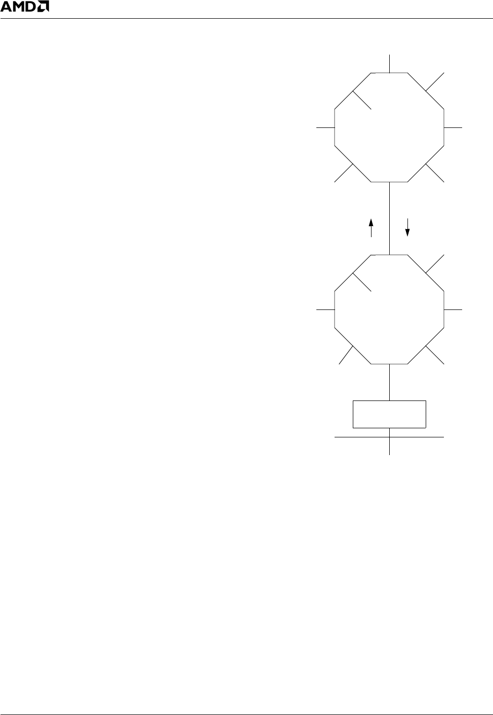
46 AMD Geode™ LX Processors Data Book
GeodeLink™ Interface Unit
33234H
4.1.1 Port Address
Each GLIU has seven channels with Channel 0 being the
GLIU itself and therefore not considered a physical port.
Figure 4-1 illustrates the GeodeLink architecture in a
AMD Geode LX processor, showing how the modules are
connected to the two GLIUs. GLIU0 has five channels con-
nected, and GLIU1 has six channels connected. To get
MSR address/data across the PCI bus, the GLPCI converts
the MSR address into PCI cycles and back again.
An MSR address is parsed into two fields, the port address
(18 bits) and the index (14 bits). The port address is further
parsed into six 3-bit channel address fields. Each 3-bit field
represents, from the perspective of the source module, the
GLIU channels that are used to get to the destination mod-
ule, starting from the closest GLIU to the source (left most
3-bit field) to the farthest GLIU (right most 3-bit field).
In aN AMD Geode LX processor/CS5536 system, the com-
panion device is connected to the processor via the PCI
bus. The internal architecture of the companion device
uses the same GeodeLink architecture with one GLIU
being in that device. Hence, in a AMD Geode LX proces-
sor/CS5536 system there are a total of three GLIUs: two in
the processor and one in the companion device. Therefore
at most, only the two left most 3-bit fields of the base
address field should be needed to access any module in
the system. There are exceptions that require more; see
Section 4.1.2 "Port Addressing Exceptions" on page 47.
For the CPU Core to access MSR Index 300h in the
GeodeLink Control Processor (GLCP) module, the address
is 010_011_000_000_000_000b (six channel fields of the
port address) + 300h (Index), or 4C000300h. The 010b
points to Channel 2 of GLIU0, which is the channel con-
nected to GLIU1. The 011b points to the GLIU1 Channel 3,
which is the channel to the GLCP module. From this point
on, the port address is abbreviated by noting each channel
address followed by a dot. From the above example, this is
represented by 2.3.0.0.0.0. It is important to repeat here
that the port address is derived from the perspective of the
source module.
For a module to access an MSR within itself, the port
address is zero.
Figure 4-1. GeodeLink™ Architecture
GLMC
CPU Core
DC
GLIU1
7
6
1
3
4
5
2
0
GLIU0
GP
GLIU0
1
2
3
5
4
6
7
0
GLIU1
GLPCI
GLPCI
PCI Bus
VP
GLCP
VIP
Not Used
Not Used
SB
Not Used
(AES)
AMD Geode™ LX Processors Data Book 47
GeodeLink™ Interface Unit 33234H
4.1.2 Port Addressing Exceptions
There are some exceptions to the port addressing rules.
If a module accesses an MSR from within its closest GLIU
(e.g., CPU Core accessing a GLIU0 MSR), then, by con-
vention, the port address should be 0.0.0.0.0.0. But this
port address accesses an MSR within the source module
and not the GLIU as desired. To get around this, if the port
address contains a 0 in the first channel field and then con-
tains a 1 in any of the other channel fields, the access goes
to the GLIU nearest the module sourcing the cycle. By con-
vention, set the MSB of the second channel field,
0.4.0.0.0.0. If the MSR access is to a GLIU farther removed
from the module sourcing the cycle, then there is no con-
vention conflict, so no exception is required for that situa-
tion.
If a module attempts to access an MSR to the channel that
it is connected to, a GLIU error results. This is called a
reflective address attempt. An example of this case is the
CPU Core accessing 3.0.0.0.0.0. Since the CPU Core is
connected to Channel 3 of GLIU0, the access causes a
reflective address error. This exception is continued to the
next GLIU in the chain. The CPU Core accessing
2.1.0.0.0.0 also causes a reflective address error.
To access modules in the AMD Geode companion device,
the port address must go through the GLPCI (PCI control-
ler) in the processor and through the GLPCI in the compan-
ion device. The port address of the MSRs in the
processor’s GLPCI when accessed from the CPU Core is
2.4.0.0.0.0. To get the port address to go through the
GLPCI, the third field needs a non-zero value. By conven-
tion, this is a 2. We now have a port address of 2.4.2.0.0.0.
But this accesses the MSRs in the GLPCI in the compan-
ion device. The port to be accessed must be added in the
fourth field, 2.4.2.5.0.0, to access the AC97 audio bus mas-
ter, for example.
To access the GLIU in the companion device, the same
addressing exception occurs as with GLIU0 due to the
GLPCI’s address. A port address of 2.4.2.0.0.0 accesses
the companion device’s GLPCI, not the GLIU. To solve this,
a non-zero value must be in at least one of the two right-
most port fields. By convention, a 4 in the left-most port
field is used. To access the companion device’s GLIU from
the CPU Core, the port address is 2.4.2.0.0.4.
Table 4-2 shows the MSR port address to access all the
modules in a AMD Geode LX processor/CS5536 system
with the CPU Core as the source module. Included in the
table is the MSR port address for module access using the
GLCP and GLPCI as the source module. However, under
normal operating conditions, accessing MSRs is from the
CPU Core. Therefore, all MSR addresses in the following
chapters of this data book are documented using the CPU
Core as the source.
4.1.3 Memory and I/O Mapping
The GLIU decodes the destination ID of memory requests
using a series of physical to device (P2D) descriptors.
There can be up to 32 descriptors in each GLIU. The GLIU
decodes the destination ID of I/O requests using a series of
I/O descriptors (IOD).
4.1.3.1 Memory Routing and Translation
Memory addresses are routed and optionally translated
from physical space to device space. Physical space is the
32-bit memory address space that is shared between all
GeodeLink devices. Device space is the unique address
space within a given device. For example, a memory con-
troller may implement a 4 MB frame buffer region in the 12-
16 MB range of main memory. However, the 4 MB region
may exist in the 4 GB region of physical space. The actual
location of the frame buffer in the memory controller with
respect to itself is a device address, while the address that
all the devices see in the region of memory is in physical
space.
Memory request routing and translation is performed with a
choice of five descriptor types. Each GLIU may have any
number of each descriptor type up to a total of 32. The P2D
descriptor types satisfy different needs for various software
models.
Table 4-2. MSR Mapping
Destination
Source (Note 1)
Note 1. The xxxx contains the lower two bits of the 18 bits from
the port fields plus the 14-bit MSR offset.
CPU Core GLCP GLPCI
CPU Core 0000xxxxh 2C00xxxxh 2C00xxxxh
GLIU0 1000xxxxh 2000xxxxh 2000xxxxh
GLMC 2000xxxxh 2400xxxxh 2400xxxxh
GLIU1 4000xxxxh 1000xxxxh 1000xxxxh
GLCP 4C00xxxxh 0000xxxxh 6000xxxxh
GLPCI 5000xxxxh 8000xxxxh 0000xxxxh
DC 8000xxxxh 3000xxxxh 3000xxxxh
GP A000xxxxh 3400xxxxh 3400xxxxh
VP 4800xxxxh 4000xxxxh 3800xxxxh
VIP 5400xxxxh
Security Block 5800xxxxh
Companion
Device
51Y0xxxxh
(Note 2)
Note 2. Y is the hex value obtained from one bit (always a 0) plus
the port number (#) of the six port field addresses [0+#].
Example: # = 5, therefore the Y value is [0+101] which is
5h, thus the address = 5150xxxxh.
8ZK0xxxxh
(Note 3)
Note 3. ZK are the hex values obtained from the concatenation
of [10+#+000], where # is the port number from the six
port field address. Example # = 5, the ZK value is
[10+101+000] which is [1010,1000]. In hex. it is A8h; thus
the address is 8A80xxxxh.
NA

48 AMD Geode™ LX Processors Data Book
GeodeLink™ Interface Unit
33234H
Each memory request is compared against all the P2D
descriptors. If the memory request does not hit in any of
the descriptors, the request is sent to the subtractive port. If
the memory requests hit more than one descriptor, the
results are undefined. The software must provide a consis-
tent non-overlapping address map.
The way each descriptor checks if the request address hits
its descriptor and how to route the request address to the
device address is described in Table 4-3.
P2D Base Mask Descriptor (P2D_BM)
P2D_BM is the simplest descriptor. It usually maps a power
of two size aligned region of memory to a destination ID.
P2D_BM performs no address translation.
P2D Base Mask Offset Descriptor (P2D_BMO)
P2D_BMO has the same routing features as P2D_BM with
the addition of a 2s complement address translation to the
most-significant bits of the address.
P2D Range Descriptor (P2D_R)
P2D_R maps a range of addresses to a device that is NOT
a power of 2 size aligned. There is no address translation
(see Table 4-3).
P2D Range Offset Descriptor (P2D_RO)
P2D_RO has the same address routing as P2D_R with the
addition of address translation with a 2s complement off-
set.
P2D Swiss Cheese Descriptor (P2D_SC)
The P2D_SC maps a 256 KB region of memory in 16 KB
chunks to a device or the subtractive decode port. The
descriptor type is useful for legacy address mapping. The
Swiss cheese feature implies that the descriptor is used to
“poke holes” in memory.
Note: Only one P2D can hit at a time for a given port. If
the P2D descriptors are overlapping, the results
are undefined.
Table 4-3. GLIU Memory Descriptor Address Hit and Routing Description
Descriptor Function Description
P2D_BM,
P2D_BMO
Checks that the physical address supplied by the device’s request on address bits [31:12] with a logical AND with
PMASK bits of the descriptor register bits [19:0] are equal to the PBASE bits on the descriptor register (bits [39:20]).
Also checks that the BIZZARO bit of the request is equal to the PCMP_BIZ bit of the descriptor register bit [60].
If the above matches, then the descriptor has a hit condition and it routes the received address to the programmed des-
tination PDID1 of the descriptor register (bits [63:61]).
For P2D_BM:
DEVICE_ADDR = request address
For P2D_BMO:
DEVICE_ADDR [31:12] = [request address [31:12] + descriptor POFFSET]
DEVICE_ADDR [11:0] = request address [11:0]
P2D_R,
P2D_RO
Checks that the physical address supplied by the device’s request on address bits [31:12] are within the range speci-
fied by PMIN and PMASK field bits [39:20] and [19:0], respective of the descriptor register. PMIN is the minimum
address range and PMAX is the maximum address range.The condition is: PMAX > physical address [31:12] > PMIN.
Also checks that the BIZZARO bit of the request is equal to the PCMP_BIZ bit of the descriptor register bit [60].
If the above matches, then the descriptor has a hit condition and routes the received address to the programmed des-
tination ID, PDID1 of the descriptor register (bits [63:61]).
For P2D_R:
DEVICE_ADDR = request address
For P2D_RO:
DEVICE_ADDR [31:12] = [request address [31:12] + descriptor POFFSET]
DEVICE_ADDR [11:0] = request address [11:0]
P2D_SC Checks that the physical address supplied by the device’s request on address bits [31:18] are equal to the PBASE field
of descriptor register bits [13:0] and that the enable write or read conditions given by the descriptor register fields WEN
and REN in bits [47:32] and [31:16], respectively matches the request type and enable fields given on the physical
address bits [17:14] of the device’s request.
If the above matches, then the descriptor has a hit condition and routes the received address to the programmed des-
tination ID, PDID1 field of the descriptor register bits [63:61].
DEVICE_ADDR = request address

AMD Geode™ LX Processors Data Book 49
GeodeLink™ Interface Unit 33234H
4.1.3.2 I/O Routing and Translation
I/O addresses are routed and are never translated. I/O
request routing is performed with a choice of two descriptor
types. Each GLIU may have any number of each descriptor
type. The IOD types satisfy different needs for various soft-
ware models.
Each I/O request is compared against all the IOD. If the I/O
request does not hit in any of the descriptors, the request is
sent to the subtractive port. If the I/O request hits more
than one descriptor, the results are undefined. Software
must provide a consistent non-overlapping I/O address
map. The methods of check and routing are described in
Table 4-4.
IOD Base Mask Descriptors (IOD_BM)
IOD_BM is the simplest descriptor. It usually maps a power
of two size aligned region of I/O to a destination ID.
IOD Swiss Cheese Descriptors (IOD_SC)
The IOD_SC maps an 8-byte region of memory in 1 byte
chunks to one of two devices. The descriptor type is useful
for legacy address mapping. The Swiss cheese feature
implies that the descriptor is used to “poke holes” in I/O.
4.1.3.3 Special Cycles
PCI special cycles are performed using I/O writes and set-
ting the BIZARRO flag in the write request. The BIZARRO
flag is treated as an additional address bit, providing
unaliased I/O address. The I/O descriptors are set up to
route the special cycles to the appropriate device (i.e.,
GLCP, GLPCI, etc.). The I/O descriptors are configured to
default to the appropriate device on reset. The PCI special
cycles are mapped as:
Name BIZZARO Address
Shutdown 1 00000000h
Halt 1 00000001h
x86 specific 1 00000002h
0003h-FFFFh 1 00000002h-0000FFFFh
Table 4-4. GLIU I/O Descriptor Address Hit and Routing Description
Descriptor Function Description
IOD_BM Checks that the physical address supplied by the device on address bits [31:12] with a logic AND with PMASK bits of
the register bits [19:0] are equal to the PBASE bits of the descriptor register bits [39:20].
Also checks that the BIZZARO bit of the request is equal to the PCMP_PIZ bit of the descriptor register bit [60].
If the above matches, then the descriptor has a hit condition and routes the received address to the programmed des-
tination of the P2D_BM register bit [63:61].
DEVICE_ADDR = request address
IOD_SC Checks that the physical address supplied by the device’s request on address bits [31:18] are equal to the PBASE field
of descriptor register bits [13:0] and that the enable write or read conditions given by the descriptor register fields WEN
and REN in bits [47:32] and [31:16], respectively matches the request type and enable fields given on the physical
address bits [17:14] of the device’s request.
If the above matches, then the descriptor has a hit condition and routes the received address to the programmed des-
tination ID, PDID1 field of the descriptor register bits [63:61].
DEVICE_ADDR = request address

50 AMD Geode™ LX Processors Data Book
GLIU Register Descriptions
33234H
4.2 GLIU Register Descriptions
All GeodeLink™ Interface Unit (GLIU) registers are Model
Specific Registers (MSRs) and are accessed through the
RDMSR and WRMSR instructions.
The registers associated with the GLIU are the Standard
GeodeLink Device (GLD) MSRs, GLIU Specific MSRs.
GLIU Statistic and Comparator MSRs, P2D Descriptor
MSRs, and I/O Descriptor MSRs. The tables that follow are
register summary tables that include reset values and page
references where the bit descriptions are provided.
Note: The MSR address is derived from the perspective
of the CPU Core. See Section 4.1 "MSR Set" on
page 45 for more details on MSR addressing.
Reserved (RSVD) fields do not have any meaningful stor-
age elements. They always return 0.
Table 4-5. GeodeLink™ Device Standard MSRs Summary
MSR Address Type Register Name Reset Value Reference
GLIU0: 10002000h
GLIU1: 40002000h
RO GLD Capabilities MSR (GLD_MSR_CAP) 00000000_000014xxh Page 55
GLIU0: 10002001h
GLIU1: 40002001h
R/W GLD Master Configuration MSR
(GLD_MSR_CONFIG)
GLIU0:
00000000_00000002h
GLIU1:
00000000_00000004h
Page 55
GLIU0: 10002002h
GLIU1: 40002002h
R/W GLD SMI MSR (GLD_MSR_SMI) 00000000_00000001h Page 56
GLIU0: 10002003h
GLIU1: 40002003h
R/W GLD Error MSR (GLD_MSR_ERROR) 00000000_00000000h Page 57
GLIU0: 10002004h
GLIU1: 40002004h
R/W GLD Power Management MSR
(GLD_MSR_PM)
00000000_00000000h Page 59
GLIU0: 10002005h
GLIU1: 40002005h
R/W GLD Diagnostic MSR (GLD_MSR_DIAG) 00000000_00000000h Page 60
Table 4-6. GLIU Specific MSRs Summary
MSR Address Type Register Name Reset Value Reference
GLIU0: 10000080h
GLIU1: 40000080h
R/W Coherency (COH) Configuration Dependent Page 60
GLIU0: 10000081h
GLIU1: 40000081h
R/W Port Active Enable (PAE) Boot Strap Dependent Page 61
GLIU0: 10000082h
GLIU1: 40000082h
R/W Arbitration (ARB) 10000000_00000000h Page 62
GLIU0: 10000083h
GLIU1: 40000083h
R/W Asynchronous SMI (ASMI) 00000000_00000000h Page 62
GLIU0: 10000084h
GLIU1: 40000084h
R/W Asynchronous ERR (AERR) 00000000_00000000h Page 63
GLIU0: 10000086h
GLIU1: 40000086h
R/W GLIU Physical Capabilities (PHY_CAP) GLIU0:
20291830_010C1086h
GLIU1:
20311030_0100400Ah
Page 65
GLIU0: 10000087h
GLIU1: 40000087h
RO N Outstanding Response (NOUT_RESP) 00000000_00000000h Page 66
GLIU0: 10000088h
GLIU1: 40000088h
RO N Outstanding Write Data (NOUT_WDATA) 00000000_00000000h Page 67

AMD Geode™ LX Processors Data Book 51
GLIU Register Descriptions 33234H
GLIU0: 10000089h
GLIU1: 40000089h
RO SLAVE_ONLY GLIU0:
00000000_00000010h
GLIU1:
00000000_00000100h
Page 67
GLIU0: 1000008Ah
GLIU1: 4000008Ah
RO Reserved --- ---
GLIU0: 1000008Bh
GLIU1: 4000008Bh
RO WHO AM I (WHOAMI) Configuration Dependent Page 68
GLIU0: 1000008Ch
GLIU1: 4000008Ch
R/W GLIU Slave Disable (GLIU_SLV) 00000000_00000000h Page 69
GLIU0: 1000008Dh
GLIU1: 4000008Dh
R/W Arbitration2 (ARB2) 00000000_00000000h Page 70
Table 4-6. GLIU Specific MSRs Summary (Continued)
MSR Address Type Register Name Reset Value Reference
Table 4-7. GLIU Statistic and Comparator MSRs Summary
MSR Address Type Register Reset Value Reference
GLIU0: 100000A0h
GLIU1: 400000A0h
WO Descriptor Statistic Counter
(STATISTIC_CNT[0])
00000000_00000000h Page 71
GLIU0: 100000A1h
GLIU1: 400000A1h
R/W Descriptor Statistic Mask
(STATISTIC_MASK[0])
00000000_00000000h Page 72
GLIU0: 100000A2h
GLIU1: 400000A2h
R/W Descriptor Statistic Action
(STATISTIC_ACTION[0])
00000000_00000000h Page 73
GLIU0: 100000A3h
GLIU1: 400000A3h
-- Reserved -- --
GLIU0: 100000A4h
GLIU1: 400000A4h
WO Descriptor Statistic Counter
(STATISTIC_CNT[1])
00000000_00000000h Page 71
GLIU0: 100000A5h
GLIU1: 400000A5h
R/W Descriptor Statistic Mask
(STATISTIC_MASK[1])
00000000_00000000h Page 72
GLIU0: 100000A6h
GLIU1: 400000A6h
R/W Descriptor Statistic Action
(STATISTIC_ACTION[1])
00000000_00000000h Page 73
GLIU0: 100000A7h
GLIU1: 400000A7h
-- Reserved -- --
GLIU0: 100000A8h
GLIU1: 400000A8h
WO Descriptor Statistic Counter
(STATISTIC_CNT[2])
00000000_00000000h Page 71
GLIU0: 100000A9h
GLIU1: 400000A9h
R/W Descriptor Statistic Mask
(STATISTIC_MASK[2])
00000000_00000000h Page 72
GLIU0: 100000AAh
GLIU1: 400000AAh
R/W Descriptor Statistic Action
(STATISTIC_ACTION[2])
00000000_00000000h Page 73
GLIU0: 100000ABh
GLIU1: 40000ABh
-- Reserved -- --
GLIU0: 100000ACh
GLIU1: 400000ACh
WO Descriptor Statistic Counter
(STATISTIC_CNT[3])
00000000_00000000h Page 71
GLIU0: 100000ADh
GLIU1: 400000ADh
R/W Descriptor Statistic Mask
(STATISTIC_MASK[3])
00000000_00000000h Page 72
GLIU0: 100000AEh
GLIU1: 400000AEh
R/W Descriptor Statistic Action
(STATISTIC_ACTION[3])
00000000_00000000h Page 73

52 AMD Geode™ LX Processors Data Book
GLIU Register Descriptions
33234H
GLIU0: 100000C0h
GLIU1: 400000C0h
R/W Request Compare Value
(RQ_COMPARE_VAL[0])
001FFFFF_FFFFFFFFh Page 74
GLIU0: 100000C1h
GLIU1: 400000C1h
R/W Request Compare Mask
(RQ_COMPARE_MASK[0])
00000000_00000000h Page 75
GLIU0: 100000C2h
GLIU1: 400000C2h
R/W Request Compare Value
(RQ_COMPARE_VAL[1])
001FFFFF_FFFFFFFFh Page 74
GLIU0: 100000C3h
GLIU1: 400000C3h
R/W Request Compare Mask
(RQ_COMPARE_MASK[1])
00000000_00000000h Page 75
GLIU0: 100000C4h
GLIU1: 400000C4h
R/W Request Compare Value
(RQ_COMPARE_VAL[2])
001FFFFF_FFFFFFFFh Page 74
GLIU0: 100000C5h
GLIU1: 400000C5h
R/W Request Compare Mask
(RQ_COMPARE_MASK[2])
00000000_00000000h Page 75
GLIU0: 100000C6h
GLIU1: 400000C6h
R/W Request Compare Value
(RQ_COMPARE_VAL[3])
001FFFFF_FFFFFFFFh Page 74
GLIU0: 100000C7h
GLIU1: 400000C7h
R/W Request Compare Mask
(RQ_COMPARE_MASK[3])
00000000_00000000h Page 75
GLIU0: 100000C9h
GLIU1: 400000CFh
-- Reserved -- --
GLIU0: 100000D0h
GLIU1: 400000D0h
R/W Data Compare Value Low
(DA_COMPARE_VAL_LO[0])
00001FFF_FFFFFFFFh Page 76
GLIU0: 100000D1h
GLIU1: 400000D1h
R/W Data Compare Value High
(DA_COMPARE_VAL_HI[0])
0000000F_FFFFFFFFh Page 77
GLIU0: 100000D2h
GLIU1: 400000D2h
R/W Data Compare Mask Low
(DA_COMPARE_MASK_LO[0])
00000000_00000000h Page 78
GLIU0: 100000D3h
GLIU1: 400000D3h
R/W Data Compare Mask High
(DA_COMPARE_MASK_HI[0])
00000000_00000000h Page 79
GLIU0: 100000D4h
GLIU1: 400000D4h
R/W Data Compare Value Low
(DA_COMPARE_VAL_LO[1])
00001FFF_FFFFFFFFh Page 76
GLIU0: 100000D5h
GLIU1: 400000D5h
R/W Data Compare Value High
(DA_COMPARE_VAL_HI[1])
0000000F_FFFFFFFFh Page 77
GLIU0: 100000D6h
GLIU1: 400000D6h
R/W Data Compare Mask Low
(DA_COMPARE_MASK_LO[1])
00000000_00000000h Page 78
GLIU0: 100000D7h
GLIU1: 400000D7h
R/W Data Compare Mask High
(DA_COMPARE_MASK_HI[1])
00000000_00000000h Page 79
GLIU0: 100000DBh
GLIU1: 400000DBh
R/W Data Compare Value Low
(DA_COMPARE_VAL_LO[2])
00000000_00000000h Page 79
GLIU0: 100000D9h
GLIU1: 400000D9h
R/W Data Compare Value High
(DA_COMPARE_VAL_HI[2])
0000000F_FFFFFFFFh Page 77
GLIU0: 100000DAh
GLIU1: 400000DAh
R/W Data Compare Mask Low
(DA_COMPARE_MASK_LO[2])
00000000_00000000h Page 78
GLIU0: 100000DBh
GLIU1: 400000DBh
R/W Data Compare Mask High
(DA_COMPARE_MASK_HI[2])
00000000_00000000h Page 79
GLIU0: 100000DCh
GLIU1: 400000DCh
R/W Data Compare Value Low
(DA_COMPARE_VAL_LO[3])
00001FFF_FFFFFFFFh Page 76
GLIU0: 100000DDh
GLIU1: 400000DDh
R/W Data Compare Value High
(DA_COMPARE_VAL_HI[3])
0000000F_FFFFFFFFh Page 77
Table 4-7. GLIU Statistic and Comparator MSRs Summary (Continued)
MSR Address Type Register Reset Value Reference

AMD Geode™ LX Processors Data Book 53
GLIU Register Descriptions 33234H
GLIU0: 100000DEh
GLIU1: 400000DEh
R/W Data Compare Mask Low
(DA_COMPARE_MASK_LO[3])
00000000_00000000h Page 78
GLIU0: 100000DFh
GLIU1: 400000DFh
R/W Data Compare Mask High
(DA_COMPARE_MASK_HI[3])
00000000_00000000h Page 79
Table 4-7. GLIU Statistic and Comparator MSRs Summary (Continued)
MSR Address Type Register Reset Value Reference
Table 4-8. GLIU P2D Descriptor MSRs Summary
MSR Address Type Register Reset Value Reference
GLIU0
10000020h-
10000025h
R/W P2D Base Mask Descriptor
(P2D_BM): P2D_BM[5:0]
000000FF_FFF00000h Page 80
10000026h-
10000027h
R/W P2D Base Mask Offset Descriptor
(P2D_BMO): P2D_BMO[1:0]
00000FF0_FFF00000h Page 81
10000028h R/W P2D Range Descriptor (P2D_R:
P2D_R[0]
00000000_000FFFFFh Page 82
10000029h-
1000002Bh
R/W P2D Range Offset Descriptor
(P2D_RO): P2D_RO[2:0]
00000000_000FFFFFh Page 83
1000002Ch R/W P2D Swiss Cheese Descriptor
(P2D_SC): P2D_SC[0]
00000000_00000000h Page 84
1000002Dh-
1000003Fh
R/W P2D Reserved Descriptors --- ---
GLIU1
40000020h-
40000029h
R/W P2D Base Mask Descriptor
(P2D_BM): P2D_BM[9:0]
000000FF_FFF00000h Page 80
4000002Ah-
4000002Dh
R/W P2D Range Descriptor (P2D_R):
P2D_R[3:0]
00000000_000FFFFFh Page 82
4000002Eh R/W P2D Swiss Cheese Descriptor
(P2D_SC): P2D_SC[0]
00000000_00000000h Page 84
4000002Fh-
4000003Fh
R/W P2D Reserved Descriptor
(P2D_RSVD)
00000000_00000000h ---
Table 4-9. GLIU Reserved MSRs Summary
MSR Address Type Register Reset Value Reference
GLIU0: 10000006h-
1000000Fh
GLIU1: 40000006h-
4000000Fh
R/W Reserved for future use by AMD. 00000000_00000000h ---
GLIU0: 10000040h-
1000004Fh
GLIU1: 40000040h-
4000004Fh
R/W Reserved for future use by AMD. 00000000_00000000h ---
GLIU0: 10000050h-
1000007Fh
GLIU1: 40000050h-
4000007Fh
R/W Reserved for future use by AMD. 00000000_00000000h ---

54 AMD Geode™ LX Processors Data Book
GLIU Register Descriptions
33234H
Table 4-10. GLIU IOD Descriptor MSRs Summary
MSR Address Type Register Reset Value Reference
GLIU0
100000E0h-
100000E2h
R/W IOD Base Mask Descriptors (IOD_BM) 000000FF_FFF00000h Page 86
100000E3h-
100000E8h
R/W IOD Swiss Cheese Descriptors (IOD_SC) 00000000_00000000h Page 87
100000E9h-
100000FFh
R/W IOD Reserved Descriptors --- ---
GLIU1
400000E0h-
400000E2h
R/W IOD Base Mask Descriptors (IOD_BM) 000000FF_FFF00000h Page 86
400000E3h-
400000E6h
R/W IOD Swiss Cheese Descriptors (IOD_SC) 00000000_00000000h Page 87
400000E7h-
400000FFh
R/W IOD Reserved Descriptors --- ---

AMD Geode™ LX Processors Data Book 55
GLIU Register Descriptions 33234H
4.2.1 Standard GeodeLink™ Device (GLD) MSRs
4.2.1.1 GLD Capabilities MSR (GLD_MSR_CAP)
4.2.1.2 GLD Master Configuration MSR (GLD_MSR_CONFIG)
MSR Address GLIU0: 10002000h
GLIU1: 40002000h
Ty p e RO
Reset Value 00000000_000014xxh
GLD_MSR_CAP Register Map
63 62 61 60 59 58 57 56 55 54 53 52 51 50 49 48 47 46 45 44 43 42 41 40 39 38 37 36 35 34 33 32
RSVD
313029282726252423222120191817161514131211109876543210
RSVD DEV_ID REV_ID
GLD_MSR_CAP Bit Descriptions
Bit Name Description
63:24 RSVD Reserved.
23:8 DEV_ID Device ID. Identifies device (0014h).
7:0 REV_ID Revision ID. Identifies device revision. See AMD Geode™ LX Processors Specification
Update document for value
MSR Address GLIU0: 10002001h
GLIU1: 40002001h
Ty p e R / W
Reset Value GLIU0: 00000000_00000002h
GLIU1: 00000000_00000004h
GLD_MSR_CONFIG Register Map
63 62 61 60 59 58 57 56 55 54 53 52 51 50 49 48 47 46 45 44 43 42 41 40 39 38 37 36 35 34 33 32
RSVD
31 30 29 28 27 26 25 24 23 22 21 20 19 18 17 16 15 14 13 12 11 10 9 8 7 6 5 4 3 2 1 0
SUBP
GLD_MSR_CONFIG Bit Descriptions
Bit Name Description
63:3 RSVD Reserved.
2:0 SUBP Subtractive Port. Subtractive port assignment for all negative decode requests.
000: Port 0 (GLIU0 = GLIU; GLIU1 = GLIU)
001: Port 1 (GLIU0 = GLMC; GLIU1 = Interface to GLIU0)
010: Port 2 (GLIU0 = Interface to GLIU1; GLIU1 = VP)
011: Port 3 (GLIU0 = CPU Core; GLIU1 = GLCP)
100: Port 4 (GLIU0 = DC; GLIU1 = GLPCI)
101: Port 5 (GLIU0 = GP; GLIU1 = VIP)
110: Port 6 (GLIU0 = Not Used; GLIU1 = SB)
111: Port 7 (GLIU0 = Not Used; GLIU1 = Not Used)
56 AMD Geode™ LX Processors Data Book
GLIU Register Descriptions
33234H
4.2.1.3 GLD SMI MSR (GLD_MSR_SMI)
The flags are set with internal conditions. The internal conditions are always capable of setting the flag, but if the mask is 1,
the flagged condition will not trigger the SMI signal. Reads to the flags return the value. Write = 1 to the flag, clears the
value. Write = 0 has no effect on the flag.
MSR Address GLIU0: 10002002h
GLIU1: 40002002h
Ty p e R / W
Reset Value 00000000_00000001h
GLD_MSR_SMI Register Map
63 62 61 60 59 58 57 56 55 54 53 52 51 50 49 48 47 46 45 44 43 42 41 40 39 38 37 36 35 34 33 32
RSVD
SFLAG4
SFLAG3
SFLAG2
SFLAG1
SFLAG0
31 30 29 28 27 26 25 24 23 22 21 20 19 18 17 16 15 14 13 12 11 10 9 8 7 6 5 4 3 2 1 0
RSVD
SMASK4
SMASK3
SMASK2
SMASK1
SMASK0
GLD_MSR_SMI Bit Descriptions
Bit Name Description
63:37 RSVD Reserved.
36 SFLAG4 SMI Flag4. If high, records that an SMI was generated due to a Statistic Counter 3
(GLIU0 MSR 100000ACh, GLIU1 MSR 400000ACh) event. Write 1 to clear; writing 0 has
no effect. SMASK4 (bit 4) must be low to generate SMI and set flag.
35 SFLAG3 SMI Flag3. If high, records that an SMI was generated due to a Statistic Counter 2
(GLIU0 MSR 100000A8h, GLIU1 MSR 400000A8h) event. Write 1 to clear; writing 0 has
no effect. SMASK3 (bit 3) must be low to generate SMI and set flag.
34 SFLAG2 SMI Flag2. If high, records that an SMI was generated due to a Statistic Counter 1
(GLIU0 MSR 100000A4h, GLIU1 MSR 400000A4h) event. Write 1 to clear; writing 0 has
no effect. SMASK2 (bit 2) must be low to generate SMI and set flag.
33 SFLAG1 SMI Flag1. If high, records that an SMI was generated due to a Statistic Counter 0
(GLIU0 MSR 100000A0h, GLIU1 MSR 400000A0h) event. Write 1 to clear; writing 0 has
no effect. SMASK1 (bit 1) must be low to generate SMI and set flag.
32 SFLAG0 SMI Flag0. Unexpected Type (HW Emulation).
31:5 RSVD Reserved.
4 SMASK4 SMI Mask4. Write 0 to enable SFLAG4 (bit 37) and to allow a Statistic Counter 3 (GLIU0
MSR 100000ACh, GLIU1 MSR 400000ACh) event to generate an SMI.
3 SMASK3 SMI Mask3. Write 0 to enable SFLAG3 (bit 36) and to allow a Statistic Counter 2 (GLIU0
MSR 100000A8h, GLIU1 MSR 400000A8h) event to generate an SMI.
2 SMASK2 SMI Mask2. Write 0 to enable SFLAG2 (bit 34) and to allow a Statistic Counter 1 (GLIU0
MSR 100000A4h, GLIU1 MSR 400000A4h) event to generate an SMI.
1 SMASK1 SMI Mask1. Write 0 to enable SFLAG1 (bit 33) and to allow a Statistic Counter 0 (GLIU0
MSR 100000A0h, GLIU1 MSR 400000A0h) event to generate an SMI.
0 SMASK0 SMI Mask0. Unexpected Type (HW Emulation).

AMD Geode™ LX Processors Data Book 57
GLIU Register Descriptions 33234H
4.2.1.4 GLD Error MSR (GLD_MSR_ERROR)
The flags are set with internal conditions. The internal conditions are always capable of setting the flag, but if the mask is 1,
the flagged condition will not trigger the ERR signal. Reads to the flags return the value. Write = 1 to the flag, clears the
value. Write = 0 has no effect on the flag.
MSR Address GLIU0: 10002003h
GLIU1: 40002003h
Ty p e R / W
Reset Value 00000000_00000000h
GLD_MSR_ERROR Register Map
63 62 61 60 59 58 57 56 55 54 53 52 51 50 49 48 47 46 45 44 43 42 41 40 39 38 37 36 35 34 33 32
RSVD
EFLAG14
EFLAG13
EFLAG12
EFLAG11
EFLAG10
EFLAG9
EFLAG8
EFLAG7
EFLAG6
EFLAG5
EFLAG4
EFLAG3
EFLAG2
EFLAG1
EFLAG0
313029282726252423222120191817161514131211109876543210
RSVD
EMASK14
EMASK13
EMASK12
EMASK11
EMASK10
EMASK9
EMASK8
EMASK7
EMASK6
EMASK5
EMASK4
EMASK3
EMASK2
EMASK1
EMASK0
GLD_MSR_ERROR Bit Descriptions
Bit Name Description
63:47 RSVD Reserved.
46 EFLAG14 Data Comparator Error Flag 3. If high, records that an ERR was generated due to a
Data Comparator 3 (DA_COMPARE_VAL_LO3/DA_COMPARE_VAL_HI3, GLIU0 MSR
100000DCh/100000DDh, GLIU1 MSR 400000DCh/400000DDh) event. Write 1 to clear;
writing 0 has no effect. EMASK14 (bit 14) must be low to generate ERR and set flag.
45 EFLAG13 Data Comparator Error Flag 2. If high, records that an ERR was generated due to a
Data Comparator 2 (DA_COMPARE_VAL_LO2/DA_COMPARE_VAL_HI2, GLIU0 MSR
100000D8h/100000D9h, GLIU1 MSR 400000D8h/400000D9h) event. Write 1 to clear;
writing 0 has no effect. EMASK13 (bit 13) must be low to generate ERR and set flag.
44 EFLAG12 Data Comparator Error Flag 1. If high, records that an ERR was generated due to a
Data Comparator 1 (DA_COMPARE_VAL_LO1/DA_COMPARE_VAL_HI1, GLIU0 MSR
100000D4h/100000D5h, GLIU1 MSR 400000D4h/400000D5h) event. Write 1 to clear;
writing 0 has no effect. EMASK12 (bit 12) must be low to generate ERR and set flag.
43 EFLAG11 Data Comparator Error Flag 0. If high, records that an ERR was generated due to a
Data Comparator 0 (DA_COMPARE_VAL_LO0/DA_COMPARE_VAL_HI0, GLIU0 MSR
100000D0h/100000D1h, GLIU1 MSR 400000D0h/400000D1h) event. Write 1 to clear;
writing 0 has no effect. EMASK11(bit 11) must be low to generate ERR and set flag.
42 EFLAG10 Request Comparator Error Flag 3. If high, records that an ERR was generated due to a
Request Comparator 3 (RQ_COMPARE_VAL3, GLIU0 MSR 100000C6h, GLIU1 MSR
400000C6h) event. Write 1 to clear; writing 0 has no effect. EMASK10 (bit 10) must be
low to generate ERR and set flag.
41 EFLAG9 Request Comparator Error Flag 2. If high, records that an ERR was generated due to a
Request Comparator 2 (RQ_COMPARE_VAL2, GLIU0 MSR 100000C4h, GLIU1 MSR
400000C4h) event. Write 1 to clear; writing 0 has no effect. EMASK9 (bit 9) must be low
to generate ERR and set flag.
40 EFLAG8 Request Comparator Error Flag 1. If high, records that an ERR was generated due to a
Request Comparator 1 (RQ_COMPARE_VAL1, GLIU0 MSR 100000C2h, GLIU1 MSR
400000C2h) event. Write 1 to clear; writing 0 has no effect. EMASK8 (bit 8) must be low
to generate ERR and set flag.

58 AMD Geode™ LX Processors Data Book
GLIU Register Descriptions
33234H
39 EFLAG7 Request Comparator Error Flag 0. If high, records that an ERR was generated due to a
Request Comparator 0 (RQ_COMPARE_VAL0, GLIU0 MSR 100000C0h, GLIU1 MSR
400000C0h) event. Write 1 to clear; writing 0 has no effect. EMASK7 (bit 7) must be low
to generate ERR and set flag.
38 EFLAG6 Statistic Counter Error Flag 3. If high, records that an ERR was generated due to a
Statistic Counter 3 (GLIU0 MSR 100000ACh, GLIU1 MSR 400000ACh) event. Write 1 to
clear; writing 0 has no effect. EMASK6 (bit 6) must be low to generate ERR and set flag.
37 EFLAG5 Statistic Counter Error Flag 2. If high, records that an ERR was generated due to a
Statistic Counter 2 (GLIU0 MSR 100000A8h, GLIU1 MSR 400000A8h) event. Write 1 to
clear; writing 0 has no effect. EMASK5 (bit 5) must be low to generate ERR and set flag.
36 EFLAG4 Statistic Counter Error Flag 1. If high, records that an ERR was generated due to a
Statistic Counter 1 (GLIU0 MSR 100000A4h, GLIU1 MSR 400000A4h) event. Write 1 to
clear; writing 0 has no effect. EMASK4 (bit 4) must be low to generate ERR and set flag.
35 EFLAG3 Statistic Counter Error Flag 0. If high, records that an ERR was generated due to a
Statistic Counter 0 (GLIU0 MSR 100000A0h, GLIU1 MSR 400000A0h) event. Write 1 to
clear; writing 0 has no effect. EMASK3 (bit 3) must be low to generate ERR and set flag.
34 EFLAG2 Unhandled SMI Error Flag. If high, records that an ERR was generated due an unhan-
dled SSMI (synchronous error). Write 1 to clear; writing 0 has no effect. EMASK2 (bit 2)
must be low to generate ERR and set flag Unhandled SMI.
33 EFLAG1 Unexpected Address Error Flag. If high, records that an ERR was generated due an
unexpected address (synchronous error). Write 1 to clear; writing 0 has no effect.
EMASK1 (bit 1) must be low to generate ERR and set flag.
32 EFLAG0 Unexpected Type Error Flag. If high, records that an ERR was generated due an unex-
pected type (synchronous error). Write 1 to clear; writing 0 has no effect. EMASK0 (bit 0)
must be low to generate ERR and set flag.
31:15 RSVD Reserved.
14 EMASK14 Data Comparator Error Mask 3. Write 0 to enable EFLAG14 (bit 46) and to allow a Data
Comparator 3 (DA_COMPARE_VAL_LO3/DA_COMPARE_VAL_HI3, GLIU0 MSR
100000DCh/100000DDh, GLIU1 MSR 400000DCh/400000DDh) event to generate an
ERR and set flag.
13 EMASK13 Data Comparator Error Mask 2. Write 0 to enable EFLAG13 (bit 45) and to allow a Data
Comparator 2 (DA_COMPARE_VAL_LO2/DA_COMPARE_VAL_HI2, GLIU0 MSR
100000D8h/100000D9h, GLIU1 MSR 400000D8h/400000D9h) event to generate an
ERR and set flag.
12 EMASK12 Data Comparator Error Mask 1. Write 0 to enable EFLAG12 (bit 44) and to allow a Data
Comparator 1 (DA_COMPARE_VAL_LO1/DA_COMPARE_VAL_HI1, GLIU0 MSR
100000D4h/100000D5h, GLIU1 MSR 400000D4h/400000D5h) event to generate an
ERR and set flag.
11 EMASK11 Data Comparator Error Mask 0. Write 0 to enable EFLAG11 (bit 43) and to allow a Data
Comparator 0 (DA_COMPARE_VAL_LO0/DA_COMPARE_VAL_HI0, GLIU0 MSR
100000D4h/100000D5h, GLIU1 MSR 400000D4h/400000D5h) event to generate an
ERR and set flag.
10 EMASK10 Request Comparator Error Mask 3. Write 0 to enable EFLAG10 (bit 42) and to allow a
Request Comparator 3 (RQ_COMPARE_VAL3, GLIU0 MSR 100000C6h, GLIU1 MSR
400000C6h) event to generate an ERR
9 EMASK9 Request Comparator Error Mask 2. Write 0 to enable EFLAG9 (bit 41) and to allow a
Request Comparator 2 (RQ_COMPARE_VAL2, GLIU0 MSR 100000C4h, GLIU1 MSR
400000C4h) event to generate an ERR.
GLD_MSR_ERROR Bit Descriptions (Continued)
Bit Name Description

AMD Geode™ LX Processors Data Book 59
GLIU Register Descriptions 33234H
4.2.1.5 GLD Power Management MSR (GLD_MSR_PM)
8 EMASK8 Request Comparator Error Mask 1. Write 0 to enable EFLAG8 (bit 40) and to allow a
Request Comparator 1 (RQ_COMPARE_VAL1, GLIU0 MSR 100000C2h, GLIU1 MSR
400000C2h) event to generate an ERR
7 EMASK7 Request Comparator Error Mask 0. Write 0 to enable EFLAG7 (bit 39) and to allow a
Request Comparator 0 (RQ_COMPARE_VAL0, GLIU0 MSR 100000C0h, GLIU1 MSR
400000C0h) event to generate an ERR
6 EMASK6 Statistic Counter Error Mask 3. Write 0 to enable EFLAG6 (bit 38) and to allow a Statis-
tic Counter 3 (GLIU0 MSR 100000ACh, GLIU1 MSR 400000ACh) event to generate an
ERR.
5 EMASK5 Statistic Counter Error Mask 2. Write 0 to enable EFLAG5 (bit 37) and to allow a Statis-
tic Counter 2 (GLIU0 MSR 100000A8h, GLIU1 MSR 400000A8h) event to generate an
ERR.
4 EMASK4 Statistic Counter Error Mask 1. Write 0 to enable EFLAG4 (bit 36) and to allow a Statis-
tic Counter 1 (GLIU0 MSR 100000A4h, GLIU1 MSR 400000A4h) event to generate an
ERR.
3 EMASK3 Statistic Counter Error Mask 0. Write 0 to enable EFLAG3 (bit 35) and to allow a Statis-
tic Counter 0 (GLIU0 MSR 100000A0h, GLIU1 MSR 400000A0h) event to generate an
ERR.
2 EMASK2 Unhandled SMI Error Mask 2. Write 0 to enable EFLAG2 (bit 34) and to allow the
unhandled SSMI (synchronous error) event to generate an ERR.
1 EMASK1 Unexpected Address Error Mask 1. as Write 0 to enable EFLAG1 (bit 33) and to allow
the unexpected address (synchronous error) event to generate an ERR.
0 EMASK0 Unexpected Type Error Mask 0. Write 0 to enable EFLAG0 (bit 32) and to allow the
unexpected type (synchronous error) event to generate an ERR.
MSR Address GLIU0: 10002004h
GLIU1: 40002004h
Ty p e R / W
Reset Value 00000000_00000000h
GLD_MSR_ERROR Bit Descriptions (Continued)
Bit Name Description
GLD_MSR_PM Register Map
63 62 61 60 59 58 57 56 55 54 53 52 51 50 49 48 47 46 45 44 43 42 41 40 39 38 37 36 35 34 33 32
RSVD
313029282726252423222120191817161514131211109876543210
RSVD
PMODE_1
PMODE_0
60 AMD Geode™ LX Processors Data Book
GLIU Register Descriptions
33234H
4.2.1.6 GLD Diagnostic MSR (GLD_MSR_DIAG)
This register is reserved for internal use by AMD and should not be written to.
4.2.2 GLIU Specific Registers
4.2.2.1 Coherency (COH)
GLD_MSR_PM Bit Descriptions
Bit Name Description
63:4 RSVD Reserved.
3:2 PMODE_1 Power Mode 1. Statistics and Time Slice Counters.
00: Disable clock gating. Clocks are always on.
01: Enable hardware clock gating. Clock goes off whenever this module’s circuits are not
busy.
10, 11: Reserved.
1:0 PMODE_0 Power Mode 0. Online GLIU logic.
00: Disable clock gating. Clocks are always on.
01: Enable hardware clock gating. Clock goes off whenever this module’s circuits are not
busy.
10, 11: Reserved.
MSR Address GLIU0: 10002005h
GLIU1: 40002005h
Ty p e R / W
Reset Value 00000000_00000000h
MSR Address GLIU0: 10000080h
GLIU1: 40000080h
Ty p e R / W
Reset Value Configuration Dependent
COH Register Map
63 62 61 60 59 58 57 56 55 54 53 52 51 50 49 48 47 46 45 44 43 42 41 40 39 38 37 36 35 34 33 32
RSVD
313029282726252423222120191817161514131211109876543210
RSVD COHP
COH Bit Descriptions
Bit Name Description
63:3 RSVD Reserved.
2:0 COHP Coherent Device Port. The port that coherents snoops are routed to. If the coherent
device is on the other side of a bridge, the COHP points to the bridge.
AMD Geode™ LX Processors Data Book 61
GLIU Register Descriptions 33234H
4.2.2.2 Port Active Enable (PAE)
Ports that are not implemented return 00 (RSVD). Ports that are slave only return 11. Master/Slave ports return the values
as stated.
GLIU0 will reset all PAE to 11 (ON) except that GLIU0 PAE3 resets to 00 when the debug stall bootstrap is active (CPU port
resets inactive for debug stall).
MSR Address GLIU0: 10000081h
GLIU1: 40000081h
Ty p e R / W
Reset Value Boot Strap Dependent
PAE Register Map
63 62 61 60 59 58 57 56 55 54 53 52 51 50 49 48 47 46 45 44 43 42 41 40 39 38 37 36 35 34 33 32
RSVD
313029282726252423222120191817161514131211109876543210
RSVD PAE0 PAE7 PAE6 PAE5 PAE4 PAE3 PAE2 PAE1
PAE Bit Descriptions
Bit Name Description
63:16 RSVD Reserved.
15:14 PAE0 Port Active Enable for Port 0. (GLIU0 = GLIU; GLIU1 = GLIU.)
00: OFF - Master transactions are disabled.
01: LOW - Master transactions limited to 1 outstanding transaction.
10: Reserved.
11: ON - Master transactions enabled with no limitations.
13:12 PAE7 Port Active Enable for Port 7. (GLIU0 = Not Used; GLIU1 = Not Used.)
See bits [15:14] for decode.
11:10 PAE6 Port Active Enable for Port 6. (GLIU0 = Not Used; GLIU1 = SB.)
See bits [15:14] for decode.
9:8 PAE5 Port Active Enable for Port 5. (GLIU0 = GP; GLIU1 = VIP.)
See bits [15:14] for decode.
7:6 PAE4 Port Active Enable for Port 4. (GLIU0 = DC; GLIU1 = GLPCI.)
See bits [15:14] for decode.
5:4 PAE3 Port Active Enable for Port 3. (GLIU0 = CPU Core; GLIU1 = GLCP.)
See bits [15:14] for decode.
3:2 PAE2 Port Active Enable for Port 2. (GLIU0 = Interface to GLIU1; GLIU1 = VP.)
See bits [15:14] for decode.
1:0 PAE1 Port Active Enable for Port 1. (GLIU0 = GLMC; GLIU1 = Interface to GLIU0.)
See bits [15:14] for decode.
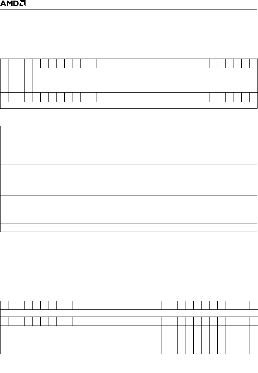
62 AMD Geode™ LX Processors Data Book
GLIU Register Descriptions
33234H
4.2.2.3 Arbitration (ARB)
4.2.2.4 Asynchronous SMI (ASMI)
ASMI is a condensed version of the port ASMI signals. The MASK bits can be used to prevent a device from issuing an
ASMI. If the MASK = 1, the device’s ASMI is disabled.
MSR Address GLIU0: 10000082h
GLIU1: 40000082h
Ty p e R / W
Reset Value 10000000_00000000h
ARB Register Map
63 62 61 60 59 58 57 56 55 54 53 52 51 50 49 48 47 46 45 44 43 42 41 40 39 38 37 36 35 34 33 32
QUACK_EN
PIPE_DIS
RSVD
DACK_EN
RSVD
313029282726252423222120191817161514131211109876543210
RSVD
ARB Bit Descriptions
Bit Name Description
63 QUACK_EN Quadruple Acknowledge Enabled. Allow four acknowledgements in a row before
advancing round-robin arbitration. Only applies when arbitrating matching priorities.
0: Disable.
1: Enable.
62 PIPE_DIS Pipelined Arbitration Disabled.
0: Pipelined arbitration enabled and GLIU is not limited to one outstanding transaction.
1: Limit the entire GLIU to one outstanding transaction.
61 RSVD Reserved.
60 DACK_EN Double Acknowledge Enabled. Allow two acknowledgements in a row before advanc-
ing round-robin arbitration. Only applies when arbitrating matching priorities.
0: Disable.
1: Enable.
59:0 RSVD Reserved.
MSR Address GLIU0: 10000083h
GLIU1: 40000083h
Ty p e R / W
Reset Value 00000000_00000000h
ASMI Register Map
63 62 61 60 59 58 57 56 55 54 53 52 51 50 49 48 47 46 45 44 43 42 41 40 39 38 37 36 35 34 33 32
RSVD
31 30 29 28 27 26 25 24 23 22 21 20 19 18 17 16 15 14 13 12 11 10 9 8 7 6 5 4 3 2 1 0
RSVD
ASMI_MASK7
ASMI_MASK6
ASMI_MASK5
ASMI_MASK4
ASMI_MASK3
ASMI_MASK2
ASMI_MASK1
ASMI_MASK0
ASMI_FLAG7
ASMI_FLAG6
ASMI_FLAG5
ASMI_FLAG4
ASMI_FLAG3
ASMI_FLAG2
ASMI_FLAG1
ASMI_FLAG0

AMD Geode™ LX Processors Data Book 63
GLIU Register Descriptions 33234H
4.2.2.5 Asynchronous ERR (AERR)
AERR is a condensed version of the port ERR signals. The MASK bits can be used to prevent a device from issuing an
AERR. If the MASK = 1, the device’s AERR is disabled.
ASMI Bit Descriptions
Bit Name Description
63:16 RSVD Reserved.
15 ASMI_MASK7 Asynchronous SMI Mask for Port 7. (GLIU0 = Not Used; GLIU1 = Not Used.) Write 0 to
allow Port 7 to generate an ASMI. ASMI status is reported in bit 7.
14 ASMI_MASK6 Asynchronous SMI Mask for Port 6. (GLIU0 = Not Used; GLIU1 = SB.) Write 0 to allow
Port 6 to generate an ASMI. ASMI status is reported in bit 6.
13 ASMI_MASK5 Asynchronous SMI Mask for Port 5. (GLIU0 = GP; GLIU1 = VIP.) Write 0 to allow Port 5
to generate an ASMI. ASMI status is reported in bit 5.
12 ASMI_MASK4 Asynchronous SMI Mask for Port 4. (GLIU0 = DC; GLIU1 = GLPCI.) Write 0 to allow
Port 4 to generate an ASMI. ASMI status is reported in bit 4.
11 ASMI_MASK3 Asynchronous SMI Mask for Port 3. (GLIU0 = CPU Core; GLIU1 = GLCP.) Write 0 to
allow Port 3 to generate an ASMI. ASMI status is reported in bit 3.
10 ASMI_MASK2 Asynchronous SMI Mask for Port 2. (GLIU0 = Interface to GLIU1; GLIU1 = VP.) Write 0
to allow Port 2 to generate an ASMI. ASMI status is reported in bit 2.
9 ASMI_MASK1 Asynchronous SMI Mask for Port 1. (GLIU0 = GLMC; GLIU1 = Interface to GLIU0.)
Write 0 to allow Port 1 to generate an ASMI. ASMI status is reported in bit 1.
8 ASMI_MASK0 Asynchronous SMI Mask for Port 0. (GLIU0 = GLIU; GLIU1 = GLIU.) Write 0 to allow
Port 0 to generate an ASMI. ASMI status is reported in bit 0.
7 ASMI_FLAG7
(RO)
Asynchronous SMI Flag for Port 7 (Read Only). (GLIU0 = Not Used; GLIU1 = Not
Used.). If 1, this bit indicates that an ASMI was generated by Port 7. Cleared by source.
6 ASMI_FLAG6
(RO)
Asynchronous SMI Flag for Port 6 (Read Only). (GLIU0 = Not Used; GLIU1 = SB.) If 1,
this bit indicates that an ASMI was generated by Port 6. Cleared by source.
5 ASMI_FLAG5
(RO)
Asynchronous SMI Flag for Port 5 (Read Only). (GLIU0 = GP; GLIU1 = VIP.) If 1, this
bit indicates that an ASMI was generated by Port 5. Cleared by source.
4 ASMI_FLAG4
(RO)
Asynchronous SMI Flag for Port 4 (Read Only). (GLIU0 = DC; GLIU1 = GLPCI.) If 1,
this bit indicates that an ASMI was generated by Port 4. Cleared by source.
3 ASMI_FLAG3
(RO)
Asynchronous SMI Flag for Port 3 (Read Only). (GLIU0 = CPU Core; GLIU1 = GLCP.)
If 1, this bit indicates that an ASMI was generated by Port37. Cleared by source.
2 ASMI_FLAG2
(RO)
Asynchronous SMI Flag for Port 2 (Read Only). (GLIU0 = Interface to GLIU1; GLIU1 =
VP.) If 1, this bit indicates that an ASMI was generated by Port 2. Cleared by source.
1 ASMI_FLAG1
(RO)
Asynchronous SMI Flag for Port 1 (Read Only). (GLIU0 = GLMC; GLIU1 = Interface to
GLIU0.) If 1, this bit indicates that an ASMI was generated by Port 1. Cleared by source.
0 ASMI_FLAG0
(RO)
Asynchronous SMI Flag for Port 0 (Read Only). (GLIU0 = GLIU; GLIU1 = GLIU.) If 1,
this bit indicates that an ASMI was generated by Port 0. Cleared by source.
MSR Address GLIU0: 10000084h
GLIU1: 40000084h
Ty p e R / W
Reset Value 00000000_00000000h

64 AMD Geode™ LX Processors Data Book
GLIU Register Descriptions
33234H
AERR Register Map
63 62 61 60 59 58 57 56 55 54 53 52 51 50 49 48 47 46 45 44 43 42 41 40 39 38 37 36 35 34 33 32
RSVD
313029282726252423222120191817161514131211109876543210
RSVD
AERR_MASK7
AERR_MASK6
AERR_MASK5
AERR_MASK4
AERR_MASK3
AERR_MASK2
AERR_MASK1
AERR_MASK0
AERR7
AERR6
AERR5
AERR4
AERR3
AERR2
AERR1
AERR0
AERR Bit Descriptions
Bit Name Description
63:16 RSVD Reserved.
15 AERR_MASK7 Asynchronous Error Mask for Port 7. (GLIU0 = Not Used; GLIU1 = Not Used.) Write 0
to allow Port 7 to generate an AERR. AERR status is reported in bit 7.
14 AERR_MASK6 Asynchronous Error Mask for Port 6. (GLIU0 = Not Used; GLIU1 = SB.) Write 0 to
allow Port 6 to generate an AERR. AERR status is reported in bit 6.
13 AERR_MASK5 Asynchronous Error Mask for Port 5. (GLIU0 = GP; GLIU1 = VIP.) Write 0 to allow Port
5 to generate an AERR. AERR status is reported in bit 5.
12 AERR_MASK4 Asynchronous Error Mask for Port 4. (GLIU0 = DC; GLIU1 = GLPCI.) Write 0 to allow
Port 4 to generate an AERR. AERR status is reported in bit 4.
11 AERR_MASK3 Asynchronous Error Mask for Port 3. (GLIU0 = CPU Core; GLIU1 = GLCP.) Write 0 to
allow Port 3 to generate an AERR. AERR status is reported in bit 3.
10 AERR_MASK2 Asynchronous Error Mask for Port 2. (GLIU0 = Interface to GLIU1; GLIU1 = VP.) Write
0 to allow Port 2 to generate an AERR. AERR status is reported in bit 2.
9 AERR_MASK1 Asynchronous Error Mask for Port 1. (GLIU0 = GLMC; GLIU1 = Interface to GLIU0.)
Write 0 to allow Port 1 to generate an AERR. AERR status is reported in bit 1.
8 AERR_MASK0 Asynchronous Error Mask for Port 0. (GLIU0 = GLIU; GLIU1 = GLIU.) Write 0 to allow
Port 0 to generate an AERR. AERR status is reported in bit 0.
7 AERR_FLAG7
(RO)
Asynchronous Error for Port 7 (Read Only). (GLIU0 = Not Used; GLIU1 = Not Used.) If
1, indicates that an AERR was generated by Port 7. Cleared by source.
6 AERR_FLAG6
(RO)
Asynchronous Error for Port 6 (Read Only). (GLIU0 = Not Used; GLIU1 = SB.) If 1,
indicates that an AERR was generated by Port 6. Cleared by source.
5 AERR_FLAG5
(RO)
Asynchronous Error for Port 5 (Read Only). (GLIU0 = GP; GLIU1 = VIP.) If 1, indicates
that an AERR was generated by Port 5. Cleared by source.
4 AERR_FLAG4
(RO)
Asynchronous Error for Port 4 (Read Only). (GLIU0 = DC; GLIU1 = GLPCI.) If 1, indi-
cates that an AERR was generated by Port 4. Cleared by source.
3 AERR_FLAG3
(RO)
Asynchronous Error for Port 3 (Read Only). (GLIU0 = CPU Core; GLIU1 = GLCP.) If 1,
indicates that an AERR was generated by Port 3. Cleared by source.
2 AERR_FLAG2
(RO)
Asynchronous Error for Port 2 (Read Only). (GLIU0 = Interface to GLIU1; GLIU1 =
VP.) If 1, indicates that an AERR was generated by Port 2. Cleared by source.
1 AERR_FLAG1
(RO)
Asynchronous Error for Port 1 (Read Only). (GLIU0 = GLMC; GLIU1 = Interface to
GLIU0.) If 1, indicates that an AERR was generated by Port 1. Cleared by source.
0 AERR_FLAG0
(RO)
Asynchronous Error for Port 0 (Read Only). (GLIU0 = GLIU; GLIU1 = GLIU.) If 1, indi-
cates that an AERR was generated by Port 0. Cleared by source.
AMD Geode™ LX Processors Data Book 65
GLIU Register Descriptions 33234H
4.2.2.6 GLIU Physical Capabilities (PHY_CAP)
MSR Address GLIU0: 10000086h
GLIU1: 40000086h
Ty p e R / W
Reset Value GLIU0: 20291830_010C1086h
GLIU1: 20311030_0100400Ah
PHY_CAP Register Map
63 62 61 60 59 58 57 56 55 54 53 52 51 50 49 48 47 46 45 44 43 42 41 40 39 38 37 36 35 34 33 32
RSVD
NSTAT_CNT
NDBG_DA_CMP
NDBG_RQ_CMP
NPORTS NCOH NIOD_SC NIOD_BM NP2D_BMK
31 30 29 28 27 26 25 24 23 22 21 20 19 18 17 16 15 14 13 12 11 10 9 8 7 6 5 4 3 2 1 0
NP2D_BMK
NP2D_SC NP2D_RO NP2D_R NP2D_BMO NP2D_BM
PHY_CAP Bit Descriptions
Bit Name Description
63 RSVD Reserved.
62:60 NSTAT_CNT Number Of Statistic Counters.
59:57 NDBG_DA_CMP Number Of Data Comparators.
56:54 NDBG_RQ_CMP Number Of Request Comparators.
53:51 NPORTS Number of Ports on the GLIU.
50:48 NCOH Number of Coherent Devices.
47:42 NIOD_SC Number of IOD_SC Descriptors.
41:36 NIOD_BM Number of IOD_BM Descriptors.
35:30 NP2D_BMK Number of P2D_BMK Descriptors.
29:24 NP2D_SC Number of P2D_SC Descriptors.
23:18 NP2D_RO Number of P2D_RO Descriptors.
17:12 NP2D_R Number of P2D_R Descriptors.
11:6 NP2D_BMO Number of P2D_BMO Descriptors.
5:0 NP2D_BM Number of P2D_BM Descriptors.
66 AMD Geode™ LX Processors Data Book
GLIU Register Descriptions
33234H
4.2.2.7 N Outstanding Response (NOUT_RESP)
MSR Address GLIU0: 10000087h
GLIU1: 40000087h
Ty p e RO
Reset Value 00000000_00000000h
NOUT_RESP Register Map
63 62 61 60 59 58 57 56 55 54 53 52 51 50 49 48 47 46 45 44 43 42 41 40 39 38 37 36 35 34 33 32
NOUT_RESP7 NOUT_RESP6 NOUT_RESP5 NOUT_RESP4
31 30 29 28 27 26 25 24 23 22 21 20 19 18 17 16 15 14 13 12 11 10 9 8 7 6 5 4 3 2 1 0
NOUT_RESP3 NOUT_RESP2 NOUT_RESP1 NOUT_RESP9
NOUT_RESP Bit Descriptions
Bit Name Description
63:56 NOOUT_RESP7 Number of Outstanding Responses on Port 7. (GLIU0 = Not Used; GLIU1 = Not
Used.)
55:48 NOOUT_RESP6 Number of Outstanding Responses on Port 6. (GLIU0 = Not Used; GLIU1 = SB.)
47:40 NOOUT_RESP5 Number of Outstanding Responses on Port 5. (GLIU0 = GP; GLIU1 = VIP.)
39:32 NOOUT_RESP4 Number of Outstanding Responses on Port 4. (GLIU0 = DC; GLIU1 = GLPCI.)
31:24 NOOUT_RESP3 Number of Outstanding Responses on Port 3. (GLIU0 = CPU Core; GLIU1 = GLCP.)
23:16 NOOUT_RESP2 Number of Outstanding Responses on Port 2. (GLIU0 = Interface to GLIU1; GLIU1 =
VP.)
15:8 NOOUT_RESP1 Number of Outstanding Responses on Port 1. (GLIU0 = GLMC; GLIU1 = Interface to
GLIU0.)
7:0 NOOUT_RESP0 Number of Outstanding Responses on Port 0. (GLIU0 = GLIU; GLIU1 = GLIU.)
AMD Geode™ LX Processors Data Book 67
GLIU Register Descriptions 33234H
4.2.2.8 N Outstanding Write Data (NOUT_WDATA)
4.2.2.9 SLAVE_ONLY
MSR Address GLIU0: 10000088h
GLIU1: 40000088h
Ty p e RO
Reset Value 00000000_00000000h
NOUT_WDATA Register Map
63 62 61 60 59 58 57 56 55 54 53 52 51 50 49 48 47 46 45 44 43 42 41 40 39 38 37 36 35 34 33 32
NOUT_WDATA7 NOUT_WDATA6 NOUT_WDATA5 NOUT_WDATA4
313029282726252423222120191817161514131211109876543210
NOUT_WDATA3 NOUT_WDATA2 NOUT_WDATA1 NOUT_WDATA0
NOUT_WDATA Bit Descriptions
Bit Name Description
63:56 NOOUT_WDATA7 Number of Outstanding Write Data on Port 7. (GLIU0 = Not Used; GLIU1 = Not
Used.)
55:48 NOOUT_WDATA6 Number of Outstanding Write Data on Port 6. (GLIU0 = Not Used; GLIU1 = SB.)
47:40 NOOUT_WDATA5 Number of Outstanding Write Data on Port 5. (GLIU0 = GP; GLIU1 = VIP.)
39:32 NOOUT_WDATA4 Number of Outstanding Write Data on Port 4. (GLIU0 = DC; GLIU1 = GLPCI.)
31:24 NOOUT_WDATA3 Number of Outstanding Write Data on Port 3. (GLIU0 = CPU Core; GLIU1 =
GLCP.)
23:16 NOOUT_WDATA2 Number of Outstanding Write Data on Port 2. (GLIU0 = Interface to GLIU1; GLIU1
= VP.)
15:8 NOOUT_WDATA1 Number of Outstanding Write Data on Port 1. (GLIU0 = GLMC; GLIU1 = Interface
to GLIU0.)
7:0 NOOUT_WDATA0 Number of Outstanding Write Data on Port 0. (GLIU0 = GLIU; GLIU1 = GLIU.)
MSR Address GLIU0: 10000089h
GLIU1: 40000089h
Ty p e RO
Reset Value GLIU0: 00000000_00000010h
GLIU1: 00000000_00000100h
SLAVE_ONLY Register Map
63 62 61 60 59 58 57 56 55 54 53 52 51 50 49 48 47 46 45 44 43 42 41 40 39 38 37 36 35 34 33 32
RSVD
31 30 29 28 27 26 25 24 23 22 21 20 19 18 17 16 15 14 13 12 11 10 9 8 7 6 5 4 3 2 1 0
RSVD SLAVE_ONLY
SLAVE_ONLY Bit Descriptions
Bit Name Description
63:8 RSVD Reserved.
7 P7_SLAVE_ONLY Port 7 Slave Only. (GLIU0 = Not Used; GLIU1 = Not Used.) If high, indicates that Port
7 is a slave port. If low, Port 7 is a master/slave port.
68 AMD Geode™ LX Processors Data Book
GLIU Register Descriptions
33234H
4.2.2.10 WHO AM I (WHOAMI)
6 P6_SLAVE_ONLY Port 6 Slave Only. (GLIU0 = Not Used; GLIU1 = SB.) If high, indicates that Port 6 is a
slave port. If low, Port 6 is a master/slave port.
5 P5_SLAVE_ONLY Port 5 Slave Only. (GLIU0 = GP; GLIU1 = VIP.) If high, indicates that Port 5 is a slave
port. If low, Port 5 is a master/slave port.
4 P4_SLAVE_ONLY Port 4 Slave Only. (GLIU0 = DC; GLIU1 = GLPCI.) If high, indicates that Port 4 is a
slave port. If low, Port 4 is a master/slave port.
3 P3_SLAVE_ONLY Port 3 Slave Only. (GLIU0 = CPU Core; GLIU1 = GLCP.) If high, indicates that Port 3
is a slave port. If low, Port 3 is a master/slave port.
2 P2_SLAVE_ONLY Port 2 Slave Only. (GLIU0 = Interface to GLIU1; GLIU1 = VP.) If high, indicates that
Port 2 is a slave port. If low, Port 2 is a master/slave port.
1 P1_SLAVE_ONLY Port 1 Slave Only. (GLIU0 = GLMC; GLIU1 = Interface to GLIU0.) If high, indicates
that Port 1 is a slave port. If low, Port 1 is a master/slave port.
0 P0_SLAVE_ONLY Port 0 Slave Only. (GLIU0 = GLIU; GLIU1 = GLIU.) If high, indicates that Port 0 is a
slave port. If low, Port 0 is a master/slave port.
MSR Address GLIU0: 1000008Bh
GLIU1: 4000008Bh
Ty p e RO
Reset Value Configuration Dependent
SLAVE_ONLY Bit Descriptions (Continued)
Bit Name Description
WHO AM I Register Map
63 62 61 60 59 58 57 56 55 54 53 52 51 50 49 48 47 46 45 44 43 42 41 40 39 38 37 36 35 34 33 32
RSVD
31 30 29 28 27 26 25 24 23 22 21 20 19 18 17 16 15 14 13 12 11 10 9 8 7 6 5 4 3 2 1 0
RSVD DSID
WHO AM I Bit Descriptions
Bit Name Description
63:3 RSVD Reserved.
2:0 DSID Source ID of the Initiating Device. Used to prevent self referencing transactions.
000: Port 0 (GLIU0 = GLIU; GLIU1 = GLIU.)
001: Port 1 (GLIU0 = GLMC; GLIU1 = Interface to GLIU0.)
010: Port 2 (GLIU0 = Interface to GLIU1; GLIU1 = VP.)
011: Port 3 (GLIU0 = CPU Core; GLIU1 = GLCP.)
100: Port 4 (GLIU0 = DC; GLIU1 = GLPCI.)
101: Port 5 (GLIU0 = GP; GLIU1 = VIP.)
110: Port 6 (GLIU0 = Not Used; GLIU1 = SB.)
111: Port 7 (GLIU0 = Not Used; GLIU1 = Not Used.)
AMD Geode™ LX Processors Data Book 69
GLIU Register Descriptions 33234H
4.2.2.11 GLIU Slave Disable (GLIU_SLV)
The slave disable registers are available for the number of ports on the GLIU. The unused ports return 0.
MSR Address GLIU0: 1000008Ch
GLIU1: 4000008Ch
Ty p e R / W
Reset Value 00000000_00000000h
GLIU_SLV Register Map
63 62 61 60 59 58 57 56 55 54 53 52 51 50 49 48 47 46 45 44 43 42 41 40 39 38 37 36 35 34 33 32
RSVD
31 30 29 28 27 26 25 24 23 22 21 20 19 18 17 16 15 14 13 12 11 10 9 8 7 6 5 4 3 2 1 0
RSVD
SLAVE_DIS7
SLAVE_DIS6
SLAVE_DIS5
SLAVE_DIS4
SLAVE_DIS3
SLAVE_DIS2
SLAVE_DIS1
SLAVE_DIS0
GLIU_SLV Bit Descriptions
Bit Name Description
63:8 RSVD Reserved.
7 SLAVE_DIS7 Slave Transactions Disable for Port 7. (GLIU0 = Not Used; GLIU1 = Not Used.) Write
1 to disable slave transactions to Port 7.
6 SLAVE_DIS6 Slave Transactions Disable for Port 6. (GLIU0 = Not Used; GLIU1 = SB.) Write 1 to
disable slave transactions to Port 6.
5 SLAVE_DIS5 Slave Transactions Disable for Port 5. (GLIU0 = GP; GLIU1 = VIP.) Write 1 to disable
slave transactions to Port 5.
4 SLAVE_DIS4 Slave Transactions Disable for Port 4. (GLIU0 = DC; GLIU1 = GLPCI.) Write 1 to dis-
able slave transactions to Port 4.
3 SLAVE_DIS3 Slave Transactions Disable for Port 3. (GLIU0 = CPU Core; GLIU1 = GLCP.) Write 1
to disable slave transactions to Port 3.
2 SLAVE_DIS2 Slave Transactions Disable for Port 2. (GLIU0 = Interface to GLIU1; GLIU1 = VP.)
Write 1 to disable slave transactions to Port 2.
1 SLAVE_DIS1 Slave Transactions Disable for Port 1. (GLIU0 = GLMC; GLIU1 = Interface to GLIU0.)
Write 1 to disable slave transactions to Port 1.
0 SLAVE_DIS0 Slave Transactions Disable for Port 0. (GLIU0 = GLIU; GLIU1 = GLIU.) Write 1 to dis-
able slave transactions to Port 0.
70 AMD Geode™ LX Processors Data Book
GLIU Register Descriptions
33234H
4.2.2.12 Arbitration2 (ARB2)
MSR Address GLIU0: 1000008Dh
GLIU1: 4000008Dh
Ty p e R / W
Reset Value 00000000_00000000h
ARB2 Register Map
63 62 61 60 59 58 57 56 55 54 53 52 51 50 49 48 47 46 45 44 43 42 41 40 39 38 37 36 35 34 33 32
RSVD
31 30 29 28 27 26 25 24 23 22 21 20 19 18 17 16 15 14 13 12 11 10 9 8 7 6 5 4 3 2 1 0
RSVD
THROT_EN
THRESH
ARB2 Bit Descriptions
Bit Name Description
63:4 RSVD Reserved.
3THROT_EN Arbitration Throttling Enable. When set, arbitration is prevented in this GLIU if the
other GLIU is retreating a priority above the THRESH priority.
2:0 THRESH Priority Threshold. See THROT_EN description. Priority threshold value must be 4 or
less.
0: Disable.
1: Enable.

AMD Geode™ LX Processors Data Book 71
GLIU Register Descriptions 33234H
4.2.3 GLIU Statistic and Comparator MSRs
4.2.3.1 Descriptor Statistic Counter (STATISTIC_CNT[0:3])
Descriptor Statistic Counter (STATISTIC_CNT[0])
Descriptor Statistic Counter (STATISTIC_CNT[1])
Descriptor Statistic Counter (STATISTIC_CNT[2])
Descriptor Statistic Counter (STATISTIC_CNT[3])
MSR Address GLIU0: 100000A0h
GLIU1: 400000A0h
Typ e R/W
Reset Value 00000000_00000000h
MSR Address GLIU0: 100000A4h
GLIU1: 400000A4h
Typ e R/W
Reset Value 00000000_00000000h
MSR Address GLIU0: 100000A8h
GLIU1: 400000A8h
Typ e R/W
Reset Value 00000000_00000000h
MSR Address GLIU0: 100000ACh
GLIU1: 400000ACh
Typ e R/W
Reset Value 00000000_00000000h
STATISTIC_CNT[0:3] Registers Map
63 62 61 60 59 58 57 56 55 54 53 52 51 50 49 48 47 46 45 44 43 42 41 40 39 38 37 36 35 34 33 32
LOAD_VAL
31 30 29 28 27 26 25 24 23 22 21 20 19 18 17 16 15 14 13 12 11 10 9 8 7 6 5 4 3 2 1 0
CNT
STATISTIC_CNT[0:3] Bit Descriptions
Bit Name Description
63:32 LOAD_VAL Counter Load Value. The value loaded here is used as the initial Statistics Counter
value when a LOAD action occurs or is commanded.
31:0 CNT Counter Value. These bits provide the current counter value when read.
72 AMD Geode™ LX Processors Data Book
GLIU Register Descriptions
33234H
4.2.3.2 Statistic Mask (STATISTIC_MASK[0:3]
Descriptor Statistic Mask (STATISTIC_MASK[0])
Descriptor Statistic Mask (STATISTIC_MASK[1])
Descriptor Statistic Mask (STATISTIC_MASK[2])
Descriptor Statistic Mask (STATISTIC_MASK[3])
MSR Address GLIU0: 100000A1h
GLIU1: 400000A1h
Ty p e R / W
Reset Value 00000000_00000000h
MSR Address GLIU0: 100000A5h
GLIU1: 400000A5h
Ty p e R / W
Reset Value 00000000_00000000h
MSR Address GLIU0: 100000A9h
GLIU1: 400000A9h
Typ e R / W
Reset Value 00000000_00000000h
MSR Address GLIU0: 100000ADh
GLIU1: 400000ADh
Typ e R / W
Reset Value 00000000_00000000h
STATISTIC_MASK[0:3] Register Map
63 62 61 60 59 58 57 56 55 54 53 52 51 50 49 48 47 46 45 44 43 42 41 40 39 38 37 36 35 34 33 32
IOD_MASK
31 30 29 28 27 26 25 24 23 22 21 20 19 18 17 16 15 14 13 12 11 10 9 8 7 6 5 4 3 2 1 0
P2D MASK
STATISTIC_MASK[0:3] Bit Descriptions
Bit Name Description
63:32 IOD_MASK Mask for Hits to Each IOD. Hits are determined after the request is arbitrated. A hit is
determined by the following logical equation: Hit = |(IOD_MASK[n-1:0] &
RQ_DESC_HIT[n-1:0] && is_io) | |(P2D_MASK[n-1:0] & RQ_DESC_HIT[n-1:0] &&
is_mem).
31:0 P2D_MASK Mask for Hits to Each P2D. A hit is determined by the following logical equation: Hit =
|(IOD_MASK[n-1:0] & RQ_DESC_HIT[n-1:0] && is_io) | |(P2D_MASK[n-1:0] &
RQ_DESC_HIT[n-1:0] && is_mem).
AMD Geode™ LX Processors Data Book 73
GLIU Register Descriptions 33234H
4.2.3.3 Statistic Action (STATISTIC_ACTION[0:3]
Descriptor Statistic Action (STATISTIC_ACTION[0])
Descriptor Statistic Action (STATISTIC_ACTION[1])
Descriptor Statistic Action (STATISTIC_ACTION[2])
Descriptor Statistic Action (STATISTIC_ACTION[3])
MSR Address GLIU0: 100000A2h
GLIU1: 400000A2h
Ty p e R / W
Reset Value 00000000_00000000h
MSR Address GLIU0: 100000A6h
GLIU1: 400000A6h
Ty p e R / W
Reset Value 00000000_00000000h
MSR Address GLIU0: 100000AAh
GLIU1: 400000AAh
Typ e R / W
Reset Value 00000000_00000000h
MSR Address GLIU0: 100000AEh
GLIU1: 400000AEh
Typ e R / W
Reset Value 00000000_00000000h
STATISTIC_ACTION[0:3] Register Map
63 62 61 60 59 58 57 56 55 54 53 52 51 50 49 48 47 46 45 44 43 42 41 40 39 38 37 36 35 34 33 32
RSVD
31 30 29 28 27 26 25 24 23 22 21 20 19 18 17 16 15 14 13 12 11 10 9 8 7 6 5 4 3 2 1 0
RSVD PREDIV
WRAP
ZERO_AERR
ZXERO_ASMI
ALWAYS_DEC
HIT_AERR
HIT_ASMI
HIT_DEC
HIT_LDEN
STATISTIC_ACTION[0:3] Bit Descriptions
Bit Name Description
63:24 RSVD Reserved.
23:8 PREDIV Pre Divider. Used if ALWAYS_DEC (bit 4) is set. The predivider is free running and
extends the depth of the counter.
7WRAP Decrement Counter Beyond Zero and Wrap.
0: Disable wrap; counter stops when it reaches zero.
1: Enable wrap; counter decrements through 0 to all ones.
6 ZERO_AERR Assert AERR on cnt = 0. Assert AERR when STATISTIC_CNT[x] reaches 0.
0: Disable.
1: Enable.
5 ZERO_ASMI Assert ASMI on cnt = 0. Assert ASMI when STATISTIC_CNT[x] reaches 0.
0: Disable.
1: Enable.
4 ALWAYS_DEC Always Decrement Counter. If enabled, the counter decrements on every memory
clock subject to the prescaler value PREDIV (bits [23:8]). Decrementing continues unless
loading is occurring due to another action, or if the counter reaches zero and WRAP is
disabled (bit 7).
0: Disable.
1: Enable
3 HIT_AERR Assert AERR on Descirptor Hit. The descriptor hits are ANDed with the masks and
then all ORed together.
0: Disable.
1: Enable
74 AMD Geode™ LX Processors Data Book
GLIU Register Descriptions
33234H
4.2.3.4 Request Compare Value (RQ_COMPARE_VAL[0:3]
The RQ Compare Value and the RQ Compare Mask enable traps on specific transactions. A hit to the RQ Compare is
determined by hit = (RQ_IN & RQ_COMPARE_MASK) == RQ_COMPARE_VAL). A hit can trigger the RQ_CMP error
sources when they are enabled. The value is compared only after the packet is arbitrated.
Request Compare Value (RQ_COMPARE_VAL[0])
Request Compare Value (RQ_COMPARE_VAL[1])
Request Compare Value (RQ_COMPARE_VAL[2])
Request Compare Value (RQ_COMPARE_VAL[3])
2 HIT_ASMI Assert ASMI on Descriptor Hit. The descriptor hits are ANDed with the masks and then
all ORed together.
0: Disable.
1: Enable.
1HIT_DEC Decrement Counter on Descriptor Hit. The descriptor hits are ANDed with the masks
and then all ORed together.
0: Disable.
1: Enable.
0HIT_LDEN Load Counter on Descriptor Hit. The descriptor hits are ANDed with the masks and
then all ORed together.
0: Disable.
1: Enable.
STATISTIC_ACTION[0:3] Bit Descriptions
Bit Name Description
MSR Address GLIU0: 100000C0h
GLIU1: 400000C0h
Ty p e R / W
Reset Value 001FFFFF_FFFFFFFFh
MSR Address GLIU0: 100000C2h
GLIU1: 400000C2h
Ty p e R / W
Reset Value 001FFFFF_FFFFFFFFh
MSR Address GLIU0: 100000C4h
GLIU1: 400000C4h
Typ e R / W
Reset Value 001FFFFF_FFFFFFFFh
MSR Address GLIU0: 100000C6h
GLIU1: 400000C6h
Typ e R / W
Reset Value 001FFFFF_FFFFFFFFh
RQ_COMPARE_VAL[0:3] Register
63 62 61 60 59 58 57 56 55 54 53 52 51 50 49 48 47 46 45 44 43 42 41 40 39 38 37 36 35 34 33 32
RSVD RQ_VAL
313029282726252423222120191817161514131211109876543210
RQ_VAL
RQ_COMPARE_VAL[0:3] Bit Descriptions
Bit Name Description
63:53 RSVD Reserved.
52:0 RQ_VAL Request Packet Value. This is the value compared against the logical bit-wise AND of
the incoming request packet and the RQ_COMPMASK in order to determine a ‘hit”.

AMD Geode™ LX Processors Data Book 75
GLIU Register Descriptions 33234H
4.2.3.5 Request Compare Mask (RQ_COMPARE_MASK[0:3]
The RQ Compare Value and the RQ Compare Mask enable traps on specific transactions. A hit to the RQ Compare is
determined by hit = (RQ_IN & RQ_COMPARE_MASK) == RQ_COMPARE_VAL). A hit can trigger the RQ_CMP error
sources when they are enabled. The value is compared only after the packet is arbitrated.
Request Compare Mask (RQ_COMPARE_MASK[0])
Request Compare Mask (RQ_COMPARE_MASK[1])
Request Compare Mask (RQ_COMPARE_MASK[2])
Request Compare Mask (RQ_COMPARE_MASK[3])
MSR Address GLIU0: 100000C1h
GLIU1: 400000C1h
Ty p e R / W
Reset Value 00000000_00000000h
MSR Address GLIU0: 100000C3h
GLIU1: 400000C3h
Ty p e R / W
Reset Value 00000000_00000000h
MSR Address GLIU0: 100000C5h
GLIU1: 400000C5h
Typ e R / W
Reset Value 00000000_00000000h
MSR Address GLIU0: 100000C7h
GLIU1: 400000C7h
Typ e R / W
Reset Value 00000000_00000000h
RQ_COMPARE_MASK[0:3] Register Map
63 62 61 60 59 58 57 56 55 54 53 52 51 50 49 48 47 46 45 44 43 42 41 40 39 38 37 36 35 34 33 32
RSVD RQ_MASK
313029282726252423222120191817161514131211109876543210
RQ_MASK
RQ_COMPARE_MASK[0:3] Bit Descriptions
Bit Name Description
63:53 RSVD Reserved.
52:0 RQ_MASK Request Packet Mask. This field is bit-wise logically ANDed with the incoming request
packet before it is compared to the RQ_COMPVAL.
76 AMD Geode™ LX Processors Data Book
GLIU Register Descriptions
33234H
4.2.3.6 DA Compare Value Low (DA_COMPARE_VAL_LO[0:3]
The DA Compare Value and the DA Compare Mask enable traps on specific transactions. A hit to the DA Compare is deter-
mined by hit = (DA_IN & DA_COMPARE_MASK) == DA_COMPARE_VAL). A hit can trigger the DA_CMP error sources
when they are enabled. The value is compared only after the packet is arbitrated.
Data Compare Value Low (DA_COMPARE_VAL_LO[0])
Data Compare Value Low (DA_COMPARE_VAL_LO[1])
Data Compare Value Low (DA_COMPARE_VAL_LO[2])
Data Compare Value Low (DA_COMPARE_VAL_LO[3])
MSR Address GLIU0: 100000D0h
GLIU1: 400000D0h
Ty p e R / W
Reset Value 00001FFF_FFFFFFFFh
MSR Address GLIU0: 100000D4h
GLIU1: 400000D4h
Ty p e R / W
Reset Value 00001FFF_FFFFFFFFh
MSR Address GLIU0: 100000D8h
GLIU1: 400000D8h
Typ e R / W
Reset Value 00001FFF_FFFFFFFFh
MSR Address GLIU0: 100000DCh
GLIU1: 400000DCh
Typ e R / W
Reset Value 00001FFF_FFFFFFFFh
DA_COMPARE_VAL_LO[0:3] Register
63 62 61 60 59 58 57 56 55 54 53 52 51 50 49 48 47 46 45 44 43 42 41 40 39 38 37 36 35 34 33 32
RSVD DALO_VAL
313029282726252423222120191817161514131211109876543210
DALO_VAL
DA_COMPARE_VAL_LO[0:3] Bit Descriptions
Bit Name Description
63:45 RSVD Reserved.
44:0 DALO_VAL DA Packet Compare Value [44:0]. This field forms the lower portion of the data value,
which is compared to the logical bit-wise AND of the incoming data value and the data
value compare mask in order to determine a ‘hit’. The “HI” and “LO” portions of the
incoming data, the compare value, and the compare mask, are assembled into complete
bit patterns before these operations occur.
AMD Geode™ LX Processors Data Book 77
GLIU Register Descriptions 33234H
4.2.3.7 DA Compare Value High (DA_COMPARE_VAL_HI[0:3]
The DA Compare Value and the DA Compare Mask enable traps on specific transactions. A hit to the DA Compare is deter-
mined by hit = (DA_IN & DA_COMPARE_MASK) == DA_COMPARE_VAL). A hit can trigger the DA_CMP error sources
when they are enabled. The value is compared only after the packet is arbitrated.
Data Compare Value High (DA_COMPARE_VAL_HI[0])
Data Compare Value High (DA_COMPARE_VAL_HI[1])
Data Compare Value High (DA_COMPARE_VAL_HI[2])
Data Compare Value High (DA_COMPARE_VAL_HI[3])
MSR Address GLIU0: 100000D1h
GLIU1: 400000D1h
Ty p e R / W
Reset Value 0000000F_FFFFFFFFh
MSR Address GLIU0: 100000D5h
GLIU1: 400000D5h
Ty p e R / W
Reset Value 0000000F_FFFFFFFFh
MSR Address GLIU0: 100000D9h
GLIU1: 400000D9h
Typ e R / W
Reset Value 0000000F_FFFFFFFFh
MSR Address GLIU0: 100000DDh
GLIU1: 400000DDh
Typ e R / W
Reset Value 0000000F_FFFFFFFFh
DA_COMPARE_VAL_HI[0:3] Register Map
63 62 61 60 59 58 57 56 55 54 53 52 51 50 49 48 47 46 45 44 43 42 41 40 39 38 37 36 35 34 33 32
RSVD DAHI_VAL
313029282726252423222120191817161514131211109876543210
DAHI_VAL
DA_COMPARE_VAL_HI[0:3] Bit Descriptions
Bit Name Description
63:36 RSVD Reserved.
35:0 DAHI_VAL DA Packet Compare Value [80:45]. This field forms the upper portion of the data value
which is compared to the logical bit-wise AND of the incoming data value AND the data
value compare mask in order to determine a ‘hit’. The “HI” and “LO” portions of the
incoming data, the compare value, and the compare mask, are assembled into complete
bit patterns before these operations occur.
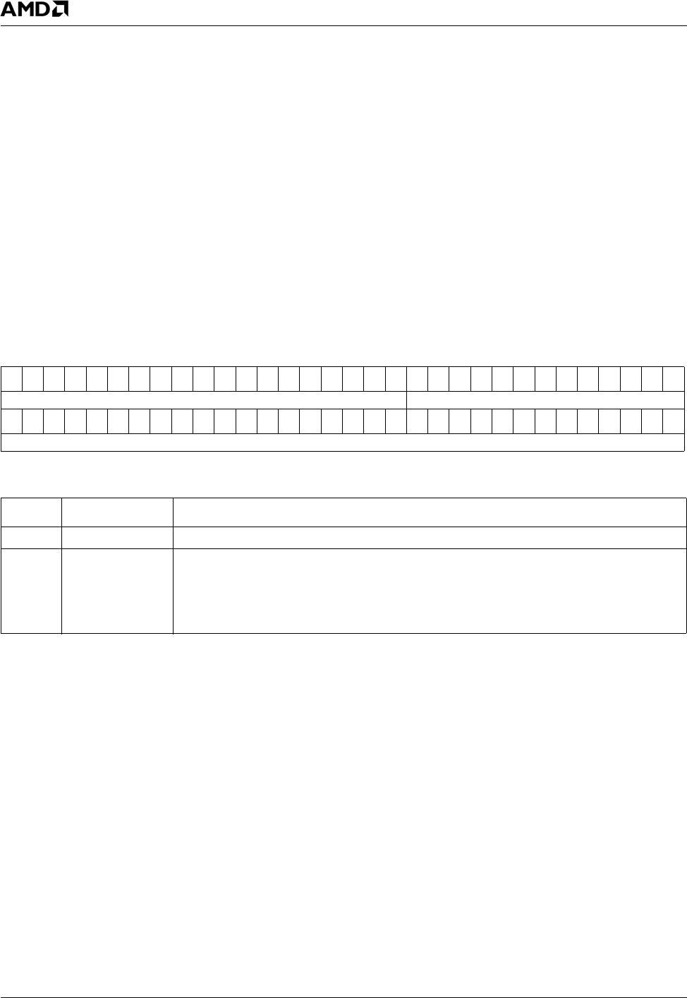
78 AMD Geode™ LX Processors Data Book
GLIU Register Descriptions
33234H
4.2.3.8 DA Compare Mask Low (DA_COMPARE_MASK_LO[0:3])
Data Compare Mask Low
(DA_COMPARE_MASK_LO[0])
Data Compare Mask Low
(DA_COMPARE_MASK_LO[1])
Data Compare Mask Low
(DA_COMPARE_MASK_LO[2])
Data Compare Mask Low
(DA_COMPARE_MASK_LO[3])
The DA Compare Value and the DA Compare Mask enable traps on specific transactions. A hit to the DA Compare is deter-
mined by hit = (DA_IN & DA_COMPARE_MASK) == DA_COMPARE_VAL). A hit can trigger the DA_CMP error sources
when they are enabled. The value is compared only after the packet is arbitrated.
MSR Address GLIU0: 100000D2h
GLIU1: 400000D2h
Ty p e R / W
Reset Value 00000000_00000000h
MSR Address GLIU0: 100000D6h
GLIU1: 400000D6h
Ty p e R / W
Reset Value 00000000_00000000h
MSR Address GLIU0: 100000DAh
GLIU1: 400000DAh
Typ e R / W
Reset Value 00000000_00000000h
MSR Address GLIU0: 100000DEh
GLIU1: 400000DEh
Typ e R / W
Reset Value 00000000_00000000h
DA_COMPARE_VAL_HI[0:3] Register Map
63 62 61 60 59 58 57 56 55 54 53 52 51 50 49 48 47 46 45 44 43 42 41 40 39 38 37 36 35 34 33 32
RSVD DALO_MASK
31 30 29 28 27 26 25 24 23 22 21 20 19 18 17 16 15 14 13 12 11 10 9 8 7 6 5 4 3 2 1 0
DALO_MASK
DA_COMPARE_MASK_LO[0:3] Bit Descriptions
Bit Name Description
63:45 RSVD Reserved.
44:0 DALO_MASK DA Packet Compare Value [44:0]. This field forms the lower portion of the data COMP-
MASK value, which is then bit-wise logically ANDed with the incoming data value before
it is compared to the DA_COMPVAL. The “HI” and “LO” portions of the incoming data,
the compare value, and the compare mask, are assembled into complete bit patterns
before these operations occur.

AMD Geode™ LX Processors Data Book 79
GLIU Register Descriptions 33234H
4.2.3.9 DA Compare Mask High (DA_COMPARE_MASK_HI[0:3])
Data Compare Mask High
(DA_COMPARE_MASK_HI[0])
Data Compare Mask High
(DA_COMPARE_MASK_HI[1])
Data Compare Mask High
(DA_COMPARE_MASK_HI[2])
Data Compare Mask High
(DA_COMPARE_MASK_HI[3])
MSR Address GLIU0: 100000D3h
GLIU1: 400000D3h
Ty p e R / W
Reset Value 00000000_00000000h
MSR Address GLIU0: 100000D7h
GLIU1: 400000D7h
Ty p e R / W
Reset Value 00000000_00000000h
MSR Address GLIU0: 100000DBh
GLIU1: 400000DBh
Typ e R / W
Reset Value 00000000_00000000h
MSR Address GLIU0: 100000DFh
GLIU1: 400000DFh
Typ e R / W
Reset Value 00000000_00000000h
DA_COMPARE_MASK_HI[0:3] Register Map
63 62 61 60 59 58 57 56 55 54 53 52 51 50 49 48 47 46 45 44 43 42 41 40 39 38 37 36 35 34 33 32
RSVD DAHI_MASK
31 30 29 28 27 26 25 24 23 22 21 20 19 18 17 16 15 14 13 12 11 10 9 8 7 6 5 4 3 2 1 0
DAHI_MASK
DA_COMPARE_MASK_HI[0:3] Bit Descriptions
Bit Name Description
63:36 RSVD Reserved.
35:0 DAHI_MASK DA Packet Compare Mask [80:45]. This field forms the upper portion of the data
COMPMASK value, which is then bit-wise logically ANDed with the incoming data value
before it is compared to the DA_COMPVAL.The “HI” and “LO” portions of the incoming
data. the compare value, and the compare mask, are assembled into complete bit pat-
terns before these operations occur.
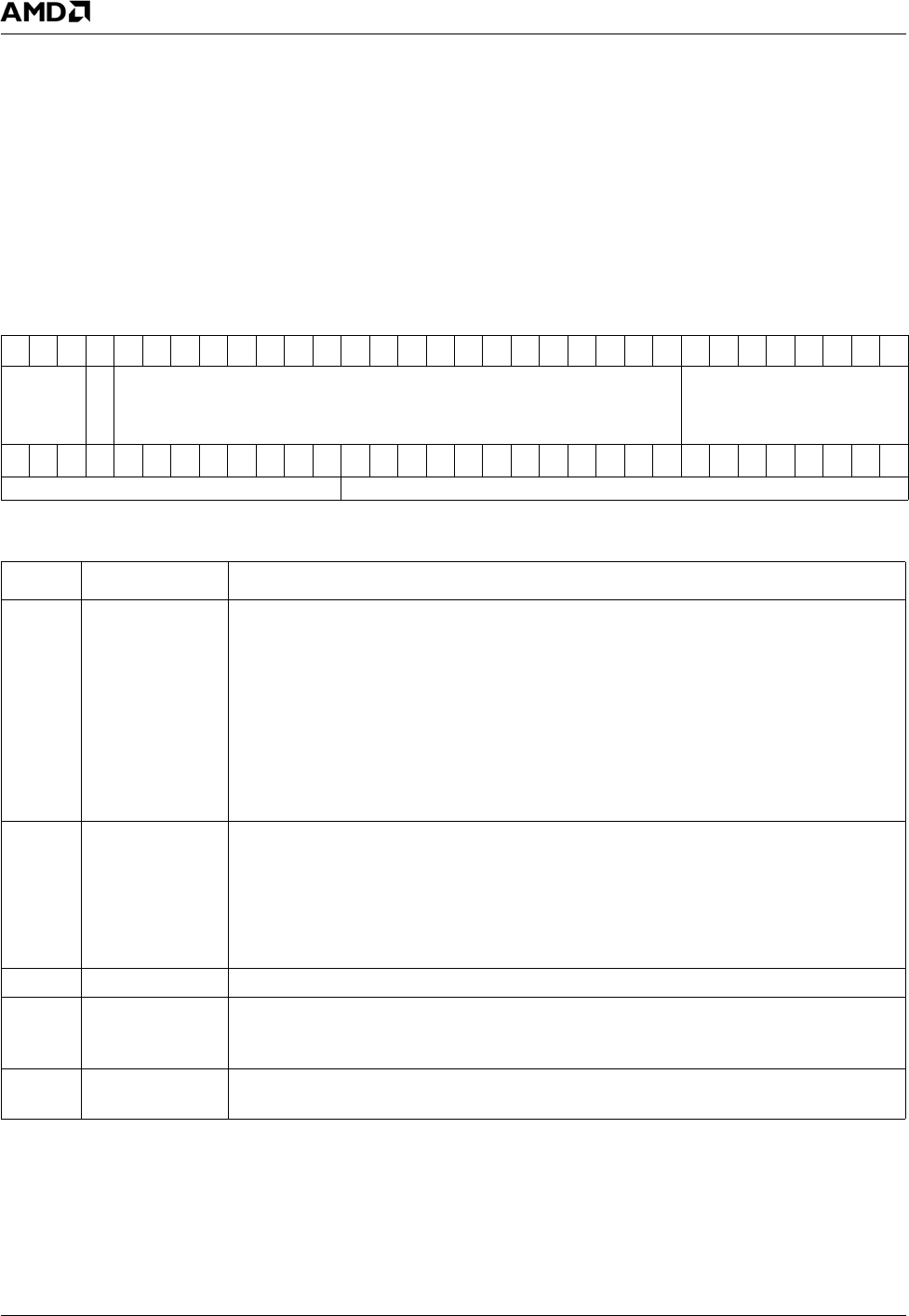
80 AMD Geode™ LX Processors Data Book
GLIU Register Descriptions
33234H
4.2.4 P2D Descriptor Registers
P2D descriptors are ordered P2D_BM, P2D_BMO, P2D_R, P2D_RO, P2D_SC, P2D_BMK. For example if NP2D_BM=3
and NP2D_BM0=2, IMSR EO = P2D_BM[0], MSR E3 = P2D_SC[0].
4.2.4.1 P2D Base Mask Descriptor (P2D_BM)
See Table 4.1.3.1 "Memory Routing and Translation" on page 47 for details on the descriptor usage.
GLIU0 P2D_BM[5:0]
MSR Address 10000020h-10000025h
Ty p e R / W
Reset Value 000000FF_FFF00000h
GLIU1 P2D_BM[9:0]
MSR Address 40000020h-40000029h
Typ e R / W
Reset Value 000000FF_FFF00000h
P2D_BM Register Map
63 62 61 60 59 58 57 56 55 54 53 52 51 50 49 48 47 46 45 44 43 42 41 40 39 38 37 36 35 34 33 32
PDID1
PCMP_BIZ
RSVD PBASE
313029282726252423222120191817161514131211109876543210
PBASE PMASK
P2D_BM Bit Descriptions
Bit Name Description
63:61 PDID1 Descriptor Destination ID. These bits define which Port to route the request to, if it is a
‘hit’ based on the other settings in this register.
000: Port 0 (GLIU0 = GLIU; GLIU1 = GLIU.)
001: Port 1 (GLIU0 = GLMC; GLIU1 = Interface to GLIU0.)
010: Port 2 (GLIU0 = Interface to GLIU1; GLIU1 = VP.)
011: Port 3 (GLIU0 = CPU Core; GLIU1 = GLCP.)
100: Port 4 (GLIU0 = DC; GLIU1 = GLPCI.)
101: Port 5 (GLIU0 = GP; GLIU1 = VIP.)
110: Port 6 (GLIU0 = Not Used; GLIU1 = SB.)
111: Port 7 (GLIU0 = Not Used; GLIU1 = Not Used.)
60 PCMP_BIZ Compare Bizzaro Flag.
0: Consider only transactions whose Bizzaro flag is low as a potentially valid address hit.
A low Bizzaro flag indicates a normal transaction cycle such as a memory or I/O.
1: Consider only transactions whose Bizzaro flag is high as a potentially valid address
hit. A high Bizzaro flag indicates a ‘special’ transaction, such as a PCI Shutdown or
Halt cycle.
59:40 RSVD Reserved.
39:20 PBASE Physical Memory Address Base. These bits form the matching value against which the
masked value of the physical address, bits [31:12] are directly compared. If a match is
found, then a “hit’ is declared, depending on the setting of the Bizzaro flag comparator.
19:0 PMASK Physical Memory Address Mask. These bits are used to mask address bits [31:12] for
the purposes of this ‘hit’ detection.
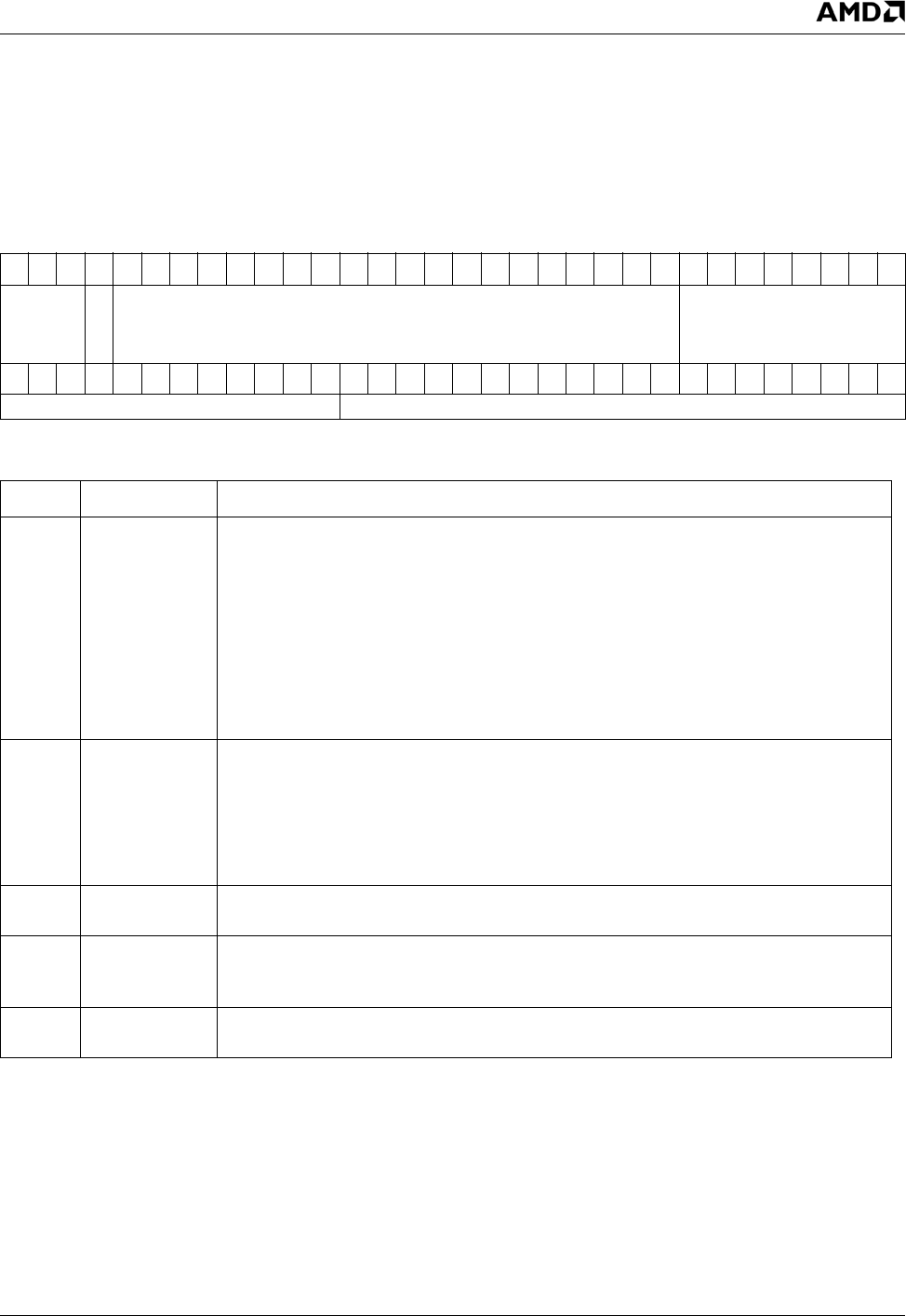
AMD Geode™ LX Processors Data Book 81
GLIU Register Descriptions 33234H
4.2.4.2 P2D Base Mask Offset Descriptor (P2D_BMO)
See Table 4.1.3.1 "Memory Routing and Translation" on page 47 for details on the descriptor usage.
GLIU0 P2D_BMO[1:0]
MSR Address 10000026h-10000027h
Ty p e R / W
Reset Value 00000FF0_FFF00000h
P2D_BMO Register Map
63 62 61 60 59 58 57 56 55 54 53 52 51 50 49 48 47 46 45 44 43 42 41 40 39 38 37 36 35 34 33 32
PDID1
PCMP_BIZ
POFFSET PBASE
31 30 29 28 27 26 25 24 23 22 21 20 19 18 17 16 15 14 13 12 11 10 9 8 7 6 5 4 3 2 1 0
PBASE PMASK
P2D_BMO Bit Descriptions
Bit Name Description
63:61 PDID1 Descriptor Destination ID. These bits define which Port to route the request to, if it is a
‘hit’ based on the other settings in this register.
000: Port 0 (GLIU0 = GLIU; GLIU1 = GLIU.)
001: Port 1 (GLIU0 = GLMC; GLIU1 = Interface to GLIU0.)
010: Port 2 (GLIU0 = Interface to GLIU1; GLIU1 = VP.)
011: Port 3 (GLIU0 = CPU Core; GLIU1 = GLCP.)
100: Port 4 (GLIU0 = DC; GLIU1 = GLPCI.)
101: Port 5 (GLIU0 = GP; GLIU1 = VIP.)
110: Port 6 (GLIU0 = Not Used; GLIU1 = SB.)
111: Port 7 (GLIU0 = Not Used; GLIU1 = Not Used.)
60 PCMP_BIZ Compare Bizzaro Flag.
0: Consider only transactions whose Bizzaro flag is low as a potentially valid address hit.
A low Bizzaro flag indicates a normal transaction cycle such as a memory or I/O.
1: Consider only transactions whose Bizzaro flag is high as a potentially valid address
hit. A high Bizzaro flag indicates a ‘special’ transaction, such as a PCI Shutdown or
Halt cycle.
59:40 POFFSET Physical Memory Address 2s Comp Offset. 2s complement offset that is added to
physical address on a hit.
39:20 PBASE Physical Memory Address Base. These bits form the matching value against which the
masked value of the physical address, bits [31:12] are directly compared. If a match is
found, then a “hit’ is declared, depending on the setting of the Bizzaro flag comparator.
19:0 PMASK Physical Memory Address Mask. These bits are used to mask address bits [31:12] for
the purposes of this ‘hit’ detection.
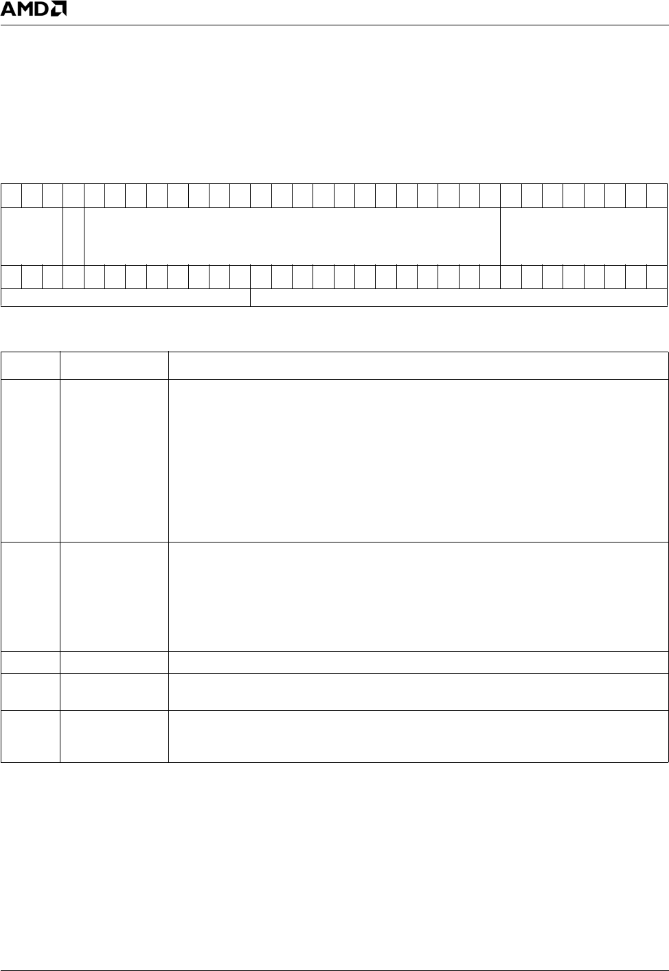
82 AMD Geode™ LX Processors Data Book
GLIU Register Descriptions
33234H
4.2.4.3 P2D Range Descriptor (P2D_R)
See Table 4.1.3.1 "Memory Routing and Translation" on page 47 for details on the descriptor usage.
GLIU0 P2D_R[0]
MSR Address 10000028h
Ty p e R / W
Reset Value 00000000_000FFFFFh
GLIU1 P2D_R[3:0]
MSR Address 4000002Ah-4000002Dh
Typ e R / W
Reset Value 00000000_000FFFFFh
P2D_R Register Map
63 62 61 60 59 58 57 56 55 54 53 52 51 50 49 48 47 46 45 44 43 42 41 40 39 38 37 36 35 34 33 32
PDID1
PCMP_BIZ
RSVD PMAX
313029282726252423222120191817161514131211109876543210
PMAX PMIN
P2D_R Bit Descriptions
Bit Name Description
63:61 PDID1 Descriptor Destination ID. These bits define which Port to route the request to, if it is a
‘hit’ based on the other settings in this register.
000: Port 0 (GLIU0 = GLIU; GLIU1 = GLIU.)
001: Port 1 (GLIU0 = GLMC; GLIU1 = Interface to GLIU0.)
010: Port 2 (GLIU0 = Interface to GLIU1; GLIU1 = VP.)
011: Port 3 (GLIU0 = CPU Core; GLIU1 = GLCP.)
100: Port 4 (GLIU0 = DC; GLIU1 = GLPCI.)
101: Port 5 (GLIU0 = GP; GLIU1 = VIP.)
110: Port 6 (GLIU0 = Not Used; GLIU1 = SB.)
111: Port 7 (GLIU0 = Not Used; GLIU1 = Not Used.)
60 PCMP_BIZ Compare Bizzaro Flag.
0: Consider only transactions whose Bizzaro flag is low as a potentially valid address hit.
A low Bizzaro flag indicates a normal transaction cycle such as a memory or I/O.
1: Consider only transactions whose Bizzaro flag is high as a potentially valid address
hit. A high Bizzaro flag indicates a ‘special’ transaction, such as a PCI Shutdown or
Halt cycle.
59:40 RSVD Reserved.
39:20 PMAX Physical Memory Address Max. These bits form the value denoting the upper (ending)
address of the physical memory, which is compared to determine a hit.
19:0 PMIN Physical Memory Address Min. These bits form the value denoting the lower (starting)
address of the physical memory, which is compared to determine a hit. Hence, a hit
occurs if the physical address [31:12] >= PMIN and <= PMAX.

AMD Geode™ LX Processors Data Book 83
GLIU Register Descriptions 33234H
4.2.4.4 P2D Range Offset Descriptor (P2D_RO)
See Table 4.1.3.1 "Memory Routing and Translation" on page 47 for details on the descriptor usage.
GLIU0 P2D_RO[2:0]
MSR Address 10000029h-1000002Bh
Ty p e R / W
Reset Value 00000000_000FFFFFh
P2D_RO Register Map
63 62 61 60 59 58 57 56 55 54 53 52 51 50 49 48 47 46 45 44 43 42 41 40 39 38 37 36 35 34 33 32
PDID1
PCMP_BIZ
OFFSET PMAX
31 30 29 28 27 26 25 24 23 22 21 20 19 18 17 16 15 14 13 12 11 10 9 8 7 6 5 4 3 2 1 0
PMAX PMIN
P2D_RO Bit Descriptions
Bit Name Description
63:61 PDID1 Descriptor Destination ID. These bits define which Port to route the request to, if it is a
‘hit’ based on the other settings in this register.
000: Port 0 (GLIU0 = GLIU; GLIU1 = GLIU.)
001: Port 1 (GLIU0 = GLMC; GLIU1 = Interface to GLIU0.)
010: Port 2 (GLIU0 = Interface to GLIU1; GLIU1 = VP.)
011: Port 3 (GLIU0 = CPU Core; GLIU1 = GLCP.)
100: Port 4 (GLIU0 = DC; GLIU1 = GLPCI.)
101: Port 5 (GLIU0 = GP; GLIU1 = VIP.)
110: Port 6 (GLIU0 = Not Used; GLIU1 = SB.)
111: Port 7 (GLIU0 = Not Used; GLIU1 = Not Used.)
60 PCMP_BIZ Compare Bizzaro Flag.
0: Consider only transactions whose Bizzaro flag is low as a potentially valid address hit.
A low Bizzaro flag indicates a normal transaction cycle such as a memory or I/O.
1: Consider only transactions whose Bizzaro flag is high as a potentially valid address
hit. A high Bizzaro flag indicates a ‘special’ transaction, such as a PCI Shutdown or
Halt cycle.
59:40 POFFSET Physical Memory Address 2’s Comp Offset. 2s complement offset that is added to
physical address on a hit.
39:20 PMAX Physical Memory Address Max. These bits form the value denoting the upper (ending)
address of the physical memory, which is compared to determine a hit.
19:0 PMIN Physical Memory Address Min. These bits form the value denoting the lower (starting)
address of the physical memory, which is compared to determine a hit. Hence, a hit
occurs if the physical address [31:12] >= PMIN and <= PMAX.
84 AMD Geode™ LX Processors Data Book
GLIU Register Descriptions
33234H
4.2.4.5 P2D Swiss Cheese Descriptor (P2D_SC)
See Table 4.1.3.1 "Memory Routing and Translation" on page 47 for details on the descriptor usage.
GLIU0 P2D_SC[0]
MSR Address 1000002Ch
Ty p e R / W
Reset Value 00000000_00000000h
GLIU1 P2D_SC[0]
MSR Address 4000002Eh
Typ e R / W
Reset Value 00000000_00000000h
P2D_SC Register Map
63 62 61 60 59 58 57 56 55 54 53 52 51 50 49 48 47 46 45 44 43 42 41 40 39 38 37 36 35 34 33 32
PDID1
PCMP_BIZ
RSVD WEN
313029282726252423222120191817161514131211109876543210
REN
RSVD
PSCBASE
P2D_SC Bit Descriptions
Bit Name Description
63:61 PDID1 Descriptor Destination ID 1. These bits define which Port to route the request to, if it is
a ‘hit’ based on the other settings in this register.
000: Port 0 (GLIU0 = GLIU; GLIU1 = GLIU.)
001: Port 1 (GLIU0 = GLMC; GLIU1 = Interface to GLIU0.)
010: Port 2 (GLIU0 = Interface to GLIU1; GLIU1 = VP.)
011: Port 3 (GLIU0 = CPU Core; GLIU1 = GLCP.)
100: Port 4 (GLIU0 = DC; GLIU1 = GLPCI.)
101: Port 5 (GLIU0 = GP; GLIU1 = VIP.)
110: Port 6 (GLIU0 = Not Used; GLIU1 = SB.)
111: Port 7 (GLIU0 = Not Used; GLIU1 = Not Used.)
60 PCMP_BIZ Compare Bizzaro Flag.
0: Consider only transactions whose Bizzaro flag is low as a potentially valid address hit.
A low Bizzaro flag indicates a normal transaction cycle such as a memory or I/O.
1: Consider only transactions whose Bizzaro flag is high as a potentially valid address
hit. A high Bizzaro flag indicates a ‘special’ transaction, such as a PCI Shutdown or
Halt cycle.
59:48 RSVD Reserved.
47:32 WEN Enable hits to the base for the ith 16K page for writes. When set to 1, causes the
incoming request to be routed to the port specified in PDID1 if the incoming request is a
write type.
31:16 REN Enable hits to the base for the ith 16K page for reads. When set to 1, causes the
incoming request to be routed to the port specified in PDID1 if the incoming request is a
read type.
15:14 RSVD Reserved.
13:0 PBASE Physical Memory Address Base for Hit. These bits form the basis of comparison with
incoming checks that the physical address supplied by the device’s request on address
bits [31:18] are equal to PBASE. Bits [17:14] of the physical address are used to choose
the ith 16K region of WEN/REN for a hit.

AMD Geode™ LX Processors Data Book 85
GLIU Register Descriptions 33234H
4.2.5 SPARE MSRs (SPARE_MSR[0:9], A:F)
MSR Address GLIU0: 10000040h-1000004Fh
GLIU1: 40000040h-4000004Fh
Ty p e R / W
Reset Value 00000000_00000000h
SPARE_MSR[x] Register Map
63 62 61 60 59 58 57 56 55 54 53 52 51 50 49 48 47 46 45 44 43 42 41 40 39 38 37 36 35 34 33 32
SPARE_MSR
313029282726252423222120191817161514131211109876543210
SPARE_MSR
SPARE_MSR[x] Bit Descriptions
Bit Name Description
63:0 SPARE_MSR Spare MSR.
86 AMD Geode™ LX Processors Data Book
GLIU Register Descriptions
33234H
4.2.6 I/O Descriptors
I/O descriptors are ordered IOD_BM, IOD_SC. For example if NIOD_BM = 3 and NIOD_SC = 2, MSR 100000EOh =
IOD_BM[0] and MSR 100000E3h = IOD_SC[0].
4.2.6.1 IOD Base Mask Descriptors (IOD_BM)
See Table 4.1.3.1 "Memory Routing and Translation" on page 47 for details on the descriptor usage.
GLIU0 IOD_BM[0:3]
MSR Address 100000E0h-100000E2h
Ty p e R / W
Reset Value 000000FF_FFF00000h
GLIU1 IOD_BM[0:3]
MSR Address 400000E0h-400000E2h
Typ e R / W
Reset Value 000000FF_FFF00000h
IOD_BM[x] Register Map
63 62 61 60 59 58 57 56 55 54 53 52 51 50 49 48 47 46 45 44 43 42 41 40 39 38 37 36 35 34 33 32
IDID
ICMP_BIZ
RSVD IBASE
313029282726252423222120191817161514131211109876543210
IBASE IMASK
IOD_BM[x] Bit Descriptions
Bit Name Description
63:61 IDID I/O Descriptor Destination ID. These bits define which Port to route the request to, if it
is a ‘hit’ based on the other settings in this register.
000: Port 0 (GLIU0 = GLIU; GLIU1 = GLIU.)
001: Port 1 (GLIU0 = GLMC; GLIU1 = Interface to GLIU0.)
010: Port 2 (GLIU0 = Interface to GLIU1; GLIU1 = VP.)
011: Port 3 (GLIU0 = CPU Core; GLIU1 = GLCP.)
100: Port 4 (GLIU0 = DC; GLIU1 = GLPCI.)
101: Port 5 (GLIU0 = GP; GLIU1 = VIP.)
110: Port 6 (GLIU0 = Not Used; GLIU1 = SB.)
111: Port 7 (GLIU0 = Not Used; GLIU1 = Not Used.)
60 ICMP_BIZ Compare Bizzaro Flag.
0: Consider only transactions whose Bizzaro flag is low as a potentially valid address hit.
A low Bizzaro flag indicates a normal transaction cycle such as a memory or I/O.
1: Consider only transactions whose Bizzaro flag is high as a potentially valid address
hit. A high Bizzaro flag indicates a ‘special’ transaction, such as a PCI Shutdown or
Halt cycle.
59:40 RSVD Reserved.
39:20 IBASE Physical I/O Address Base. These bits form the matching value against which the
masked value of the physical address, bits [19:0] are directly compared. If a match is
found, then a “hit’ is declared, depending on the setting of the Bizzaro flag comparator.
19:0 IMASK Physical I/O Address Mask. These bits are used to mask address bits [31:12] for the
purposes of this ‘hit’ detection.
AMD Geode™ LX Processors Data Book 87
GLIU Register Descriptions 33234H
4.2.6.2 IOD Swiss Cheese Descriptors (IOD_SC)
See Table 4.1.3.1 "Memory Routing and Translation" on page 47 for details on the descriptor usage.
GLIU0 IOD_SC[0:5]
MSR Address 100000E3h-100000E8h
Ty p e R / W
Reset Value 00000000_00000000h
GLIU1 IOD_SC[0:3]
MSR Address 400000E3h-400000E6h
Typ e R / W
Reset Value 00000000_00000000h
IOD_SC[x] Register Map
63 62 61 60 59 58 57 56 55 54 53 52 51 50 49 48 47 46 45 44 43 42 41 40 39 38 37 36 35 34 33 32
IDID1
ICMP_BIZ
RSVD
313029282726252423222120191817161514131211109876543210
EN RSVD
WEN
REN
IBASE RSVD
IOD_SC[x] Bit Descriptions
Bit Name Description
63:61 IDID1 Descriptor Destination ID 1. Encoded port number of the destination of addresses
which produce a ‘hit’ based on the other fields in this descriptor.
60 ICMP_BIZ Compare Bizzaro Flag. Used to check that the Bizzaro flag of the request is equal to
the PICMP_BIZ_SC bit (this bit). If a match does not occur, then the incoming request
cannot generate a hit. The Bizzaro flag, if set in the incoming request, signifies a “spe-
cial’ cycle such as a PCI Shutdown or Halt.
59:32 RSVD Reserved. Write as read.
31:24 EN Enable for Hits to IDID1 or else SUBP. Setting these bits enables hits to IDID1. If not
enabled, subtractive port is selected per GLD_MSR_CONFIG, bits [2:0] (MSR GLIU0:
10002001h; GLIU1: 40002001h). (See Section 4.2.1.2 "GLD Master Configuration MSR
(GLD_MSR_CONFIG)" on page 55 for bit descriptions).
23:22 RSVD Reserved.
21 WEN Descriptor Hits IDID1 on Write Request Types else SUBP. If set, causes the incom-
ing request to be routed to the port specified in IDID1 if the incoming request is a Write
type. If not set, subtractive port is selected per GLD_MSR_CONFIG, bits [2:0] (MSR
GLIU0: 10002001h; GLIU1: 40002001h). (See Section 4.2.1.2 "GLD Master Configura-
tion MSR (GLD_MSR_CONFIG)" on page 55 for bit descriptions).
20 REN Descriptors Hit IDID1 on Read Request Types else SUBP. If set, causes the incom-
ing request to be routed to the port specified in IDID1 if the incoming request is a Read
type. If not set, subtractive port is selected per GLD_MSR_CONFIG, bits [2:0] (MSR
GLIU0: 10002001h; GLIU1: 40002001h). (See Section 4.2.1.2 "GLD Master Configura-
tion MSR (GLD_MSR_CONFIG)" on page 55 for bit descriptions).
19:3 IBASE I/O Memory Base. This field forms the basis of comparison with the incoming checks
that the physical address supplied by the device’s request on address bits [31:18] are
equal to the PBASE field of descriptor register bits [13:0].
2:0 RSVD Reserved. Write as read.

88 AMD Geode™ LX Processors Data Book
GLIU Register Descriptions
33234H
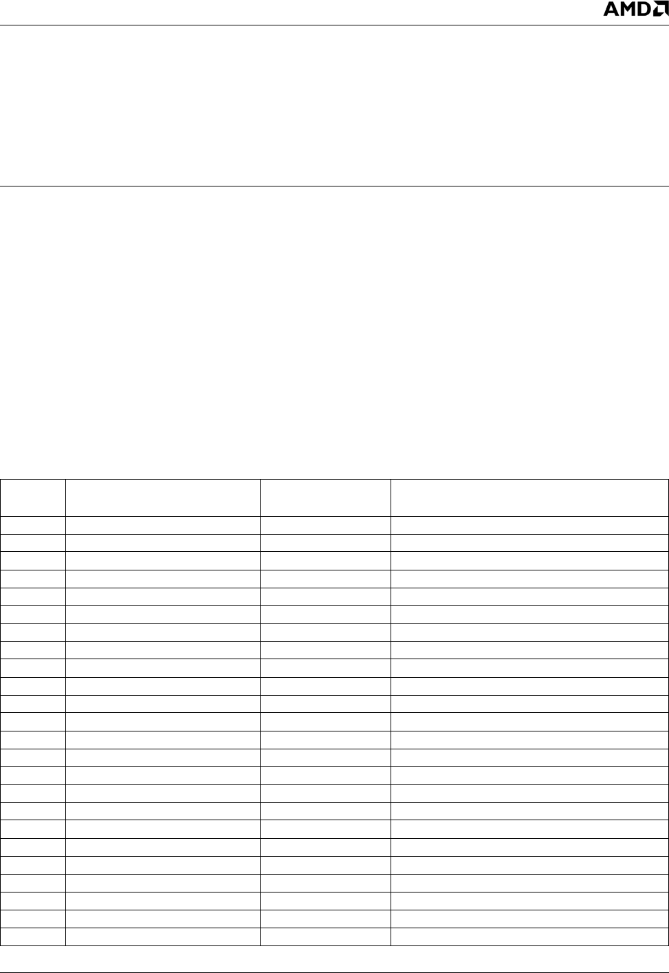
AMD Geode™ LX Processors Data Book 89
5
CPU Core 33234H
5.0CPU Core
This section describes the internal operations of the
AMD Geode™ LX processor’s CPU Core from a program-
mer’s point of view. It includes a description of the tradi-
tional “core” processing and FPU operations. The
integrated function registers are described in the next
chapter.
The primary register sets within the processor core include:
•Application Register Set
•System Register Set
5.1 Core Processor Initialization
The CPU Core is initialized when the RESET# (Reset) sig-
nal is asserted. The CPU Core is placed in real mode and
the registers listed in Table 5-1 are set to their initialized
values. RESET# invalidates and disables the CPU cache,
and turns off paging. When RESET# is asserted, the CPU
terminates all local bus activity and all internal execution.
While RESET# is asserted, the internal pipeline is flushed
and no instruction execution or bus activity occurs.
Approximately 150 to 250 external clock cycles after
RESET# is de-asserted, the processor begins executing
instructions at the top of physical memory (address location
FFFFFFF0h). The actual number of clock cycles depends
on the clock scaling in use. Also, before execution begins,
an additional 220 clock cycles are needed when self-test is
requested.
Typically, an intersegment jump is placed at FFFFFFF0h.
This instruction forces the processor to begin execution in
the lowest 1 MB of address space. Table 5-1 lists the CPU
Core registers and illustrates how they are initialized.
Table 5-1. Initialized Core Register Controls
Register Register Name
Initialized Contents
(Note 1) Comments
EAX Accumulator xxxxxxxxh 00000000h indicates self-test passed.
EBX Base xxxxxxxxh
ECX Count xxxxxxxxh
EDX Data xxxx 04 [DIR0]h DIR0 = Device ID
EBP Base Pointer xxxxxxxxh
ESI Source Index xxxxxxxxh
EDI Destination Index xxxxxxxxh
ESP Stack Pointer xxxxxxxxh
EFLAGS Extended Flags 00000002h See Table 5-4 on page 93 for bit definitions.
EIP Instruction Pointer 0000FFF0h
ES Extra Segment 0000h Base address set to 00000000h. Limit set to FFFFh.
CS Code Segment F000h Base address set to FFFF0000h. Limit set to FFFFh.
SS Stack Segment 0000h Base address set to 00000000h. Limit set to FFFFh.
DS Data Segment 0000h Base address set to 00000000h. Limit set to FFFFh.
FS Extra Segment 0000h Base address set to 00000000h. Limit set to FFFFh.
GS Extra Segment 0000h Base address set to 00000000h. Limit set to FFFFh.
IDTR Interrupt Descriptor Table Register Base = 0, Limit = 3FFh
GDTR Global Descriptor Table Register xxxxxxxxh
LDTR Local Descriptor Table Register xxxxh
TR Task Register xxxxh
CR0 Control Register 0 60000010h See Table 5-10 on page 96 for bit descriptions.
CR2 Control Register 2 xxxxxxxxh See Table 5-9 on page 96 for bit descriptions.
CR3 Control Register 3 xxxxxxxxh See Table 5-8 on page 96 for bit descriptions.
CR4 Control Register 4 00000000h See Table 5-7 on page 96 for bit descriptions.
Note 1. x = Undefined value.

90 AMD Geode™ LX Processors Data Book
CPU Core
33234H
5.2 Instruction Set Overview
The CPU Core instruction set can be divided into nine
types of operations:
•Arithmetic
•Bit Manipulation
•Shift/Rotate
•String Manipulation
•Control Transfer
•Data Transfer
•Floating Point
•High-Level Language Support
•Operating System Support
The instructions operate on as few as zero operands and
as many as three operands. A NOP (no operation) instruc-
tion is an example of a zero-operand instruction. Two-oper-
and instructions allow the specification of an explicit source
and destination pair as part of the instruction. These two-
operand instructions can be divided into ten groups accord-
ing to operand types:
•Register to Register
•Register to Memory
•Memory to Register
•Memory to Memory
•Register to I/O
•I/O to Register
•Memory to I/O
•I/O to Memory
•Immediate Data to Register
•Immediate Data to Memory
An operand can be held in the instruction itself (as in the
case of an immediate operand), in one of the processor’s
registers or I/O ports, or in memory. An immediate operand
is fetched as part of the opcode for the instruction.
Operand lengths of 8, 16, 32 or 48 bits are supported as
well as 64 or 80 bits associated with floating-point instruc-
tions. Operand lengths of 8 or 32 bits are generally used
when executing code written for 386- or 486-class (32-bit
code) processors. Operand lengths of 8 or 16 bits are gen-
erally used when executing existing 8086 or 80286 code
(16-bit code). The default length of an operand can be
overridden by placing one or more instruction prefixes in
front of the opcode. For example, the use of prefixes allows
a 32-bit operand to be used with 16-bit code or a 16-bit
operand to be used with 32-bit code.
The Processor Core Instruction Set (see Table 8-26 on
page 634) contains the clock count table that lists each
instruction in the CPU instruction set. Included in the table
are the associated opcodes, execution clock counts, and
effects on the EFLAGS register.
5.2.1 Lock Prefix
The LOCK prefix may be placed before certain instructions
that read, modify, then write back to memory. The PCI will
not be granted access in the middle of locked instructions.
The LOCK prefix can be used with the following instructions
only when the result is a write operation to memory.
•Bit Test Instructions (BTS, BTR, BTC)
•Exchange Instructions (XADD, XCHG, CMPXCHG)
•One-Operand Arithmetic and Logical Instructions (DEC,
INC, NEG, NOT)
•Two-Operand Arithmetic and Logical Instructions (ADC,
ADD, AND, OR, SBB, SUB, XOR).
An invalid opcode exception is generated if the LOCK pre-
fix is used with any other instruction or with one of the
instructions above when no write operation to memory
occurs (for example, when the destination is a register).
5.2.2 Register Sets
The accessible registers in the processor are grouped into
two sets:
1) The Application Register Set contains the registers
frequently used by application programmers. Table 5-2
on page 91 shows the General Purpose, Segment,
Instruction Pointer and EFLAGS registers.
2) The System Register Set contains the registers typi-
cally reserved for operating systems programmers:
Control, System Address, Debug, Configuration, and
Test registers. All accesses to the these registers use
special CPU instructions.
Both of these register sets are discussed in detail in the
subsections that follow.
AMD Geode™ LX Processors Data Book 91
CPU Core 33234H
5.3 Application Register Set
The Application Register Set consists of the registers most
often used by the applications programmer. These regis-
ters are generally accessible, although some bits in the
EFLAGS registers are protected.
The General Purpose register contents are frequently
modified by instructions and typically contain arithmetic
and logical instruction operands.
In real mode, Segment registers contain the base
address for each segment. In protected mode, the Seg-
ment registers contain segment selectors. The segment
selectors provide indexing for tables (located in memory)
that contain the base address for each segment, as well as
other memory addressing information.
The Instruction Pointer register points to the next instruc-
tion that the processor will execute. This register is auto-
matically incremented by the processor as execution
progresses.
The EFLAGS register contains control bits used to reflect
the status of previously executed instructions. This register
also contains control bits that affect the operation of some
instructions.
Table 5-2. Application Register Set
313029282726252423222120191817161514131211109876543210
General Purpose Registers
AX
AH AL
EAX (Extended A Register)
BX
BH BL
EBX (Extended B Register)
CX
CH CL
ECX (Extended C Register)
DX
DH DL
EDX (Extended D Register)
SI (Source Index)
ESI (Extended Source Index)
DI (Destination Index)
EDI (Extended Destination Index)
BP (Base Pointer)
EBP (Extended Base Pointer)
SP (Stack Pointer)
ESP (Extended Stack Pointer)
Segment (Selector) Registers
CS (Code Segment)
SS (Stack Segment)
DS (D Data Segment)
ES (E Data Segment)
FS (F Data Segment)
GS (G Data Segment)
Instruction Pointer and EFLAGS Registers
EIP (Extended Instruction Pointer)
ESP (Extended EFLAGS Register)

92 AMD Geode™ LX Processors Data Book
CPU Core
33234H
5.3.1 General Purpose Registers
The General Purpose registers are divided into four data
registers, two pointer registers, and two index registers as
shown in Table 5-2 on page 91.
The Data registers are used by the applications program-
mer to manipulate data structures and to hold the results of
logical and arithmetic operations. Different portions of gen-
eral data registers can be addressed by using different
names.
An “E” prefix identifies the complete 32-bit register. An “X”
suffix without the “E” prefix identifies the lower 16 bits of the
register.
The lower two bytes of a data register are addressed with
an “H” suffix (identifies the upper byte) or an “L” suffix (identi-
fies the lower byte). These _L and _H portions of the data
registers act as independent registers. For example, if the
AH register is written to by an instruction, the AL register
bits remain unchanged.
The Pointer and Index registers are listed below.
SI or ESI Source Index
DI or EDI Destination Index
SP or ESP Stack Pointer
BP or EBP Base Pointer
These registers can be addressed as 16- or 32-bit registers,
with the “E” prefix indicating 32 bits. The Pointer and Index
registers can be used as general purpose registers; how-
ever, some instructions use a fixed assignment of these
registers. For example, repeated string operations always
use ESI as the source pointer, EDI as the destination
pointer, and ECX as a counter. The instructions that use
fixed registers include multiply and divide, I/O access,
string operations, stack operations, loop, variable shift and
rotate, and translate instructions.
The CPU Core implements a stack using the ESP register.
This stack is accessed during the PUSH and POP instruc-
tions, procedure calls, procedure returns, interrupts, excep-
tions, and interrupt/exception returns. The Geode LX
processor automatically adjusts the value of the ESP dur-
ing operations that result from these instructions.
The EBP register may be used to refer to data passed on
the stack during procedure calls. Local data may also be
placed on the stack and accessed with BP. This register
provides a mechanism to access stack data in high-level
languages.
5.3.2 Segment Registers
The 16-bit Segment registers are part of the main memory
addressing mechanism. The six segment registers are:
CS - Code Segment
DS - Data Segment
SS - Stack Segment
ES - Extra Segment
FS - Additional Data Segment
GS - Additional Data Segment
The Segment registers are used to select segments in
main memory. A segment acts as private memory for differ-
ent elements of a program such as code space, data space
and stack space. There are two segment mechanisms, one
for real and virtual 8086 operating modes and one for pro-
tected mode.
The active Segment register is selected according to the
rules listed in Table 5-3 and the type of instruction being
currently processed. In general, the DS register selector is
used for data references. Stack references use the SS reg-
ister, and instruction fetches use the CS register. While
some selections may be overridden, instruction fetches,
stack operations, and the destination write operation of
string operations cannot be overridden. Special segment-
override instruction prefixes allow the use of alternate seg-
ment registers. These segment registers include the ES,
FS, and GS registers.
5.3.3 Instruction Pointer Register
The Instruction Pointer (EIP) register contains the offset
into the current code segment of the next instruction to be
executed. The register is normally incremented by the
length of the current instruction with each instruction exe-
cution unless it is implicitly modified through an interrupt,
exception, or an instruction that changes the sequential
execution flow (for example JMP and CALL).
Table 5-3. Segment Register Selection Rules
Type of Memory Reference
Implied (Default)
Segment
Segment-Override
Prefix
Code Fetch CS None
Destination of PUSH, PUSHF, INT, CALL, PUSHA instructions SS None
Source of POP, POPA, POPF, IRET, RET instructions SS None
Destination of STOS, MOVS, REP STOS, REP MOVS instructions ES None
Other data references with effective address using base registers of:
EAX, EBX, ECX, EDX, ESI, EDI, EBP, ESP
DS
SS
CS, ES, FS, GS, SS
CS, DS, ES, FS, GS

AMD Geode™ LX Processors Data Book 93
CPU Core 33234H
5.3.4 EFLAGS Register
The EFLAGS register contains status information and con-
trols certain operations on the Geode LX processor. The
lower 16 bits of this register are used when executing 8086
or 80286 code. Table 5-4 gives the bit formats for the
EFLAGS register.
Table 5-4. EFLAGS Register
Bit Name Flag Type Description
31:22 RSVD -- Reserved. Set to 0.
21 ID System Identification Bit. The ability to set and clear this bit indicates that the CPUID instruction is sup-
ported. The ID can be modified only if the CPUID bit in CCR4 (Index E8h[7]) is set.
20:19 RSVD -- Reserved. Set to 0.
18 AC System Alignment Check Enable. In conjunction with the AM flag (bit 18) in CR0, the AC flag deter-
mines whether or not misaligned accesses to memory cause a fault. If AC is set, alignment
faults are enabled.
17 VM System Virtual 8086 Mode. If set while in protected mode, the processor switches to virtual 8086 oper-
ation handling segment loads as the 8086 does, but generating exception 13 faults on privileged
opcodes. The VM bit can be set by the IRET instruction (if current privilege level is 0) or by task
switches at any privilege level.
16 RF Debug Resume Flag. Used in conjunction with debug register breakpoints. RF is checked at instruction
boundaries before breakpoint exception processing. If set, any debug fault is ignored on the next
instruction.
15 RSVD -- Reserved. Set to 0.
14 NT System Nested Task. While executing in protected mode, NT indicates that the execution of the current
task is nested within another task.
13:12 IOPL System I/O Privilege Level. While executing in protected mode, IOPL indicates the maximum current
privilege level (CPL) permitted to execute I/O instructions without generating an exception 13
fault or consulting the I/O permission bit map. IOPL also indicates the maximum CPL allowing
alteration of the IF bit when new values are popped into the EFLAGS register.
11 OF Arithmetic Overflow Flag. Set if the operation resulted in a carry or borrow into the sign bit of the result but
did not result in a carry or borrow out of the high-order bit. Also set if the operation resulted in a
carry or borrow out of the high-order bit but did not result in a carry or borrow into the sign bit of
the result.
10 DF Control Direction Flag. When cleared, DF causes string instructions to auto-increment (default) the
appropriate index registers (ESI and/or EDI). Setting DF causes auto-decrement of the index
registers to occur.
9 IF System Interrupt Enable Flag. When set, maskable interrupts (INTR input pin) are acknowledged and
serviced by the CPU.
8 TF Debug Trap Enable Flag. Once set, a single-step interrupt occurs after the next instruction completes
execution. TF is cleared by the single-step interrupt.
7 SF Arithmetic Sign Flag. Set equal to high-order bit of result (0 indicates positive, 1 indicates negative).
6 ZF Arithmetic Zero Flag. Set if result is zero; cleared otherwise.
5 RSVD -- Reserved. Set to 0.
4 AF Arithmetic Auxiliary Carry Flag. Set when a carry out of (addition) or borrow into (subtraction) bit position
3 of the result occurs; cleared otherwise.
3 RSVD -- Reserved. Set to 0.
2 PF Arithmetic Parity Flag. Set when the low-order 8 bits of the result contain an even number of ones; other-
wise PF is cleared.
1 RSVD Reserved. Set to 1.
0 CF Arithmetic Carry Flag. Set when a carry out of (addition) or borrow into (subtraction) the most significant
bit of the result occurs; cleared otherwise.
94 AMD Geode™ LX Processors Data Book
CPU Core
33234H
5.4 System Register Set
The System Register Set, shown in Table 5-5, consists of
registers not generally used by application programmers.
These registers are either initialized by the system BIOS or
employed by system level programmers who generate
operating systems and memory management programs.
Associated with the System Register Set are certain tables
and registers that are listed in Table 5-5.
The Control registers control certain aspects of the CPU
Core such as paging, coprocessor functions, and segment
protection.
The CPU Core Configuration registers are used to initial-
ize, provide for, test or define most of the features of the
CPU Core. The attributes of these registers include:
•CPU setup - Enable cache, features, operating modes.
•Debug support - Provide debugging facilities for the
Geode™ LX processor and enable the use of data
access breakpoints and code execution breakpoints.
•Built-in Self-test (BIST) support.
•Test - Support a mechanism to test the contents of the
on-chip caches and the Translation Lookaside Buffers
(TLBs).
•In-Circuit Emulation (ICE) - Provide for a alternative
accessing path to support an ICE.
•CPU identification - Allow the BIOS and other software
to identify the specific CPU and stepping.
•Power Management.
•Performance Monitoring - Enables test software to
measure the performance of application software.
The Descriptor Table registers point to tables used to
manage memory segments and interrupts.
The Task State register points to the Task State Segment,
which is used to save and load the processor state when
switching tasks.
Table 5-5 lists the System Register Sets along with their
size and function.
Table 5-5. System Register Set
Group Name Function
Width
(Bits)
Control
Registers
CR0 System Control
Register
32
CR2 Page Fault Linear
Address Register
32
CR3 Page Directory Base
Register
32
CR4 Feature Enables 32
CPU Core
Configuration
Registers
PLn Pipeline
Control Registers
64
IMn Instruction Memory
Control Registers
64
DMn Data Memory Con-
trol Registers
64
BCn Bus Controller Con-
trol Registers
64
FPUn Floating Point Unit
Shadow Registers
64
Descriptor
Ta b l e
Registers
GDTR GDT Register 32
IDTR IDT Register 32
LDTR LDT Register 16
Task Register TR Task Register 16
Performance
Registers
PCRn Performance
Control Registers
8
AMD Geode™ LX Processors Data Book 95
CPU Core 33234H
5.4.1 Control Registers
A map of the Control registers (CR0, CR1, CR2, CR3, and
CR4) is shown in Table 5-6 and the bit descriptions are in
the tables that follow. (These registers should not be con-
fused with the CRRn registers.) CR0 contains system con-
trol bits that configure operating modes and indicate the
general state of the CPU. The lower 16 bits of CR0 are
referred to as the Machine Status Word (MSW).
When operating in real mode, any program can read and
write the control registers. In protected mode, however,
only privilege level 0 (most-privileged) programs can read
and write these registers.
L1 Cache Controller
The Geode LX processor contains an on-board 64 KB L1
instruction cache, a 64 KB L1 write-back data cache, and a
128 KB unified L2 victim cache. With the memory controller
on-board, the L1 cache requires no external logic to main-
tain coherency. All DMA cycles automatically snoop the L1
and L2 caches.
The CD bit (Cache Disable, bit 30) in CR0 globally controls
the operating mode of the L1 and L2 caches. LCD and
LWT, Local Cache Disable and Local Write-through bits in
the Translation Lookaside Buffer, control the mode on a
page-by-page basis. Additionally, memory configuration
control can specify certain memory regions as non-cache-
able.
If the cache is disabled, no further cache line fills occur.
However, data already present in the cache continues to be
used. For the cache to be completely disabled, the cache
must be invalidated with a WBINVD instruction after the
cache has been disabled.
Write-back caching improves performance by relieving con-
gestion on slower external buses.
The Geode LX processor caches SMM regions, reducing
system management overhead to allow for hardware emu-
lation such as VGA.
Table 5-6. Control Registers Map
313029282726252423222120191817161514131211109876543210
CR4 Register Control Register 4 (R/W)
RSVD
PCE
PGE
RSVD
PSE
DE
TSC
RSVD
CR3 Register Control Register 3 (R/W)
PDBR (Page Directory Base Register) RSVD 0 0 RSVD
CR2 Register Control Register 2 (R/W)
PFLA (Page Fault Linear Address)
CR1 Register Control Register 1 (R/W)
RSVD
CR0 Register Control Register 0 (R/W)
PG
CD
NW
RSVD
AM
RSVD
WP
RSVD
NE
RSVD
TS
EM
MP
PE
Machine Status Word (MSW)
96 AMD Geode™ LX Processors Data Book
CPU Core
33234H
Table 5-7. CR4 Bit Descriptions
Bit Name Description
31:9 RSVD Reserved. Set to 0 (always returns 0 when read).
8PCE Performance Counter Enable. Set PCE = 1 to make RDPMC available at nonzero privi-
lege levels.
7PGE Page Global Enable. Set PGE = 1 to make global pages immune to INVLPG instruc-
tions.
6:5 RSVD Reserved. Set to 0 (always returns 0 when read).
4 PSE Page Size Extensions. Set PSE = 1 to enable 4 MB pages.
3DE Debug Extensions. Set DE = 1 to enable debug extensions (i.e., DR4, DR5, and I/O
breakpoints).
2TSC Time Stamp Counter Instruction.
0: RDTSC instruction enabled for all CPL states.
1: RDTSC instruction enabled for CPL = 0 only.
1:0 RSVD Reserved. Set to 0 (always returns 0 when read).
Table 5-8. CR3 Bit Descriptions
Bit Name Description
31:12 PDBR Page Directory Base Register. Identifies page directory base address on a 4 KB page
boundary.
11:0 RSVD Reserved. Set to 0.
Table 5-9. CR2 Bit Descriptions
Bit Name Description
31:0 PFLA Page Fault Linear Address. With paging enabled and after a page fault, PFLA contains
the linear address of the address that caused the page fault.
Table 5-10. CR0 Bit Descriptions
Bit Name Description
31 PG Paging Enable Bit. If PG = 1 and protected mode is enabled (PE = 1), paging is
enabled. After changing the state of PG, software must execute an unconditional branch
instruction (e.g., JMP, CALL) to have the change take effect.

AMD Geode™ LX Processors Data Book 97
CPU Core 33234H
30 CD Cache Disable/Not Write-Through (Snoop). Cache behavior is based on the CR0 CD
and NW bits.
CD NW
0 0 Normal Cache operation, coherency maintained.
Read hits access the cache,
Write hits update the cache,
Read/write misses may cause line allocations based on memory
region configuration settings.
0 1 Invalid, causes a General Protection Fault (GPF).
1 0 Cache off, coherency maintained (i.e., snooping enabled).
Read hits access the cache,
Write hits update the cache,
Read/write misses do not cause line allocations.
1 1 Cache off, coherency not maintained (i.e., snooping disabled).
Read hits access the cache,
Write hits update the cache,
Read/write misses do not cause line allocations.
29 NW
28:19 RSVD Reserved.
18 AM Alignment Check Mask. If AM = 1, the AC bit in the EFLAGS register is unmasked and
allowed to enable alignment check faults. Setting AM = 0 prevents AC faults from occur-
ring.
17 RSVD Reserved
16 WP Write Protect. Protects read only pages from supervisor write access. WP = 0 allows a
read only page to be written from privilege level 0-2. WP = 1 forces a fault on a write to a
read only page from any privilege level.
15:6 RSVD Reserved.
5NE Numerics Exception. NE = 1 to allow FPU exceptions to be handled by interrupt 16.
NE = 0 if FPU exceptions are to be handled by external interrupts.
4ET (RO) Extension Type (Read Only). (Default = 1)
3TS Task Switched. Set whenever a task switch operation is performed. Execution of a float-
ing point instruction with TS = 1 causes a Device Not Available (DNA) fault. If MP = 1 and
TS = 1, a WAIT instruction also causes a DNA fault. (Note 1)
2EM Emulate Processor Extension. If EM = 1, all floating point instructions cause a DNA
fault 7. (Note 1)
1MP Monitor Processor Extension. If MP = 1 and TS = 1, a WAIT instruction causes DNA
fault 7. The TS bit is set to 1 on task switches by the CPU. Floating point instructions are
not affected by the state of the MP bit. The MP bit should be set to 1 during normal oper-
ations. (Note 1)
0PE Protected Mode Enable. Enables the segment based protection mechanism. If PE = 1,
protected mode is enabled. If PE = 0, the CPU operates in real mode and addresses are
formed as in an 8086-style CPU.
Note 1. For effects of various combinations of the TS, EM, and MP bits, see Table 5-11 on page 98.
Table 5-10. CR0 Bit Descriptions (Continued)
Bit Name Description

98 AMD Geode™ LX Processors Data Book
CPU Core
33234H
Table 5-11. Effects of Various Combinations of EM, TS, and MP Bits
CR0[3:1] Instruction Type
TS EM MP WAIT ESC
000 Execute Execute
001 Execute Execute
1 0 0 Execute Fault 7
101 Fault 7 Fault 7
0 1 0 Execute Fault 7
0 1 1 Execute Fault 7
1 1 0 Execute Fault 7
111 Fault 7 Fault 7

AMD Geode™ LX Processors Data Book 99
CPU Core Register Descriptions 33234H
5.5 CPU Core Register Descriptions
All CPU Core registers are Model Specific Registers
(MSRs) and are accessed via the RDMSR and WRMSR
instructions.
Each module inside the processor is assigned a 256 regis-
ter section of the address space. The module responds to
any reads or writes in that range. Unused addresses within
a module’s address space are reserved, meaning the mod-
ule returns zeroes on a read and ignores writes. Addresses
that are outside all the module address spaces are invalid,
meaning a RDMSR/WRMSR instruction attempting to use
the address generates a General Protection Fault.
The registers associated with the CPU Core are the Stan-
dard GeodeLink™ Device MSRs and CPU Core Specific
MSRs. Table 5-12 and Table 5-13 are register summary
tables that include reset values and page references where
the bit descriptions are provided. Note that the standard
GLD MSRs for the CPU Core start at 00002000h.
Table 5-12. Standard GeodeLink™ Device MSRs Summary
MSR
Address Type Register Name Reset Value Reference
00002000h RO GLD Capabilities MSR (GLD_MSR_CAP) 00000000_000864xxh Page 108
00002001h R/W GLD Master Configuration MSR
(GLD_MSR_CONFIG)
00000000_00000320h Page 108
00002002h R/W GLD SMI MSR (GLD_MSR_SMI) - Not Used 00000000_00000000h Page 109
00002003h R/W GLD Error MSR (GLD_MSR_ERROR) - Not Used 00000000_00000000h Page 109
00002004h R/W GLD Power Management MSR (GLD_MSR_PM) -
Not Used
00000000_00000000h Page 109
00002005h R/W GLD Diagnostic Bus Control MSR
(GLD_MSR_DIAG)
00000000_00000000h Page 109
Table 5-13. CPU Core Specific MSRs Summary
MSR
Address Type Register Name Reset Value Reference
00000010h R/W Time Stamp Counter MSR (TSC_MSR) 00000000_00000000h Page 110
000000C1h R/W Performance Event Counter 0 MSR
(PERF_CNT0_MSR)
00000000_00000000h Page 110
000000C2h R/W Performance Event Counter 1 MSR
(PERF_CNT1_MSR)
00000000_00000000h Page 111
00000174h R/W SYSENTER/SYSEXIT Code Segment Selector
MSR (SYS_CS_MSR)
00000000_C09B0000h Page 112
00000175h R/W SYSENTER/SYSEXIT Stack Pointer MSR
(SYS_SP_MSR)
00000000_00000000h Page 113
00000176h R/W SYSENTER/SYSEXIT Instruction Pointer MSR
(SYS_IP_MSR)
00000000_00000000h Page 113
00000186h R/W Performance Event Counter 0 Select MSR
(PERF_SEL0_MSR
00000000_00000000h Page 114
00000187h R/W Performance Event Counter 1 Select MSR
(PERF_SEL1_MSR)
00000000_00000000h Page 114
00001100h R/W Instruction Fetch Configuration MSR
(IF_CONFIG_MSR)
00000000_00005051h Page 115
00001102h W IF Invalidate MSR (IF_INVALIDATE_MSR) 00000000_00000000h Page 118
00001108h R/W IF Test Address MSR (IF_TEST_ADDR_MSR) 00000000_00000000h Page 118
00001109h R/W IF Test Data MSR (IF_TEST_DATA_MSR) 00000000_xxxxxxxxh Page 119

100 AMD Geode™ LX Processors Data Book
CPU Core Register Descriptions
33234H
00001110h RO IF Sequential Count MRS (IF_SEQCOUNT_MSR) 00000000_00000000h Page 122
00001140h RO IF Built-In Self-Test MSR (IF_BIST_MSR) 00000000_00000000h Page 123
00001210h R/W Exception Unit (XC) Configuration MSR
(XC_CONFIG_MSR)
00000000_00000000h Page 124
00001211h R/W XC Mode MSR (XC_MODE_MSR) 00000000_00000000h Page 125
00001212h RO XC History MSR (XC_HIST_MSR) 00000000_00000000h Page 126
00001213h RO XC Microcode Address MSR (XC_UADDR_MSR) 00000000_00000000h Page 127
00001250h R/W ID Configuration MSR (ID_CONFIG_MSR) 00000000_00000002h Page 127
00001301h R/W SMM Control MSR (SMM_CTL_MSR) 00000000_00000000h Page 128
00001302h R/W Debug Management Interrupt (DMI) Control Reg-
ister
00000000_00000000h Page 129
00001310h R/W Temporary 0 MSR (TEMP0_MSR) xxxxxxxx_xxxxxxxxh Page 130
00001311h R/W Temporary 1 MSR (TEMP1_MSR) xxxxxxxx_xxxxxxxxh Page 130
00001312h R/W Temporary 2 MSR (TEMP2_MSR) xxxxxxxx_xxxxxxxxh Page 130
00001313h R/W Temporary 3 MSR (TEMP3_MSR) xxxxxxxx_xxxxxxxxh Page 130
00001320h R/W ES Segment Selector/Flags Register
(ES_SEL_MSR)
xxxxxxxx_xxxxxxxxh Page 131
00001321h R/W CS Segment Selector/Flags Register
(CS_SEL_MSR)
xxxxxxxx_xxxxxxxxh Page 131
00001322h R/W SS Segment Selector/Flags Register
(SS_SEL_MSR)
xxxxxxxx_xxxxxxxxh Page 131
00001323h R/W DS Segment Selector/Flags Register
(DS_SEL_MSR)
xxxxxxxx_xxxxxxxxh Page 131
00001324h R/W FS Segment Selector/Flags Register
(FS_SEL_MSR)
xxxxxxxx_xxxxxxxxh Page 131
00001325h R/W GS Segment Selector/Flags Register
(GS_SEL_MSR)
xxxxxxxx_xxxxxxxxh Page 131
00001326h R/W LDT Segment Selector/Flags Register
(LDT_SEL_MSR)
xxxxxxxx_xxxxxxxxh Page 131
00001327h R/W Temp Segment Selector/Flags Register
(TM_SEL_MSR)
xxxxxxxx_xxxxxxxxh Page 131
00001328h R/W TSS Segment Selector/Flags Register
(TSS_SEL_MSR)
xxxxxxxx_xxxxxxxxh Page 131
00001329h R/W IDT Segment Selector/Flags Register
(IDT_SEL_MSR)
xxxxxxxx_xxxxxxxxh Page 131
0000132Ah R/W GDT Segment Selector/Flags Register
(GDT_SEL_MSR)
xxxxxxxx_xxxxxxxxh Page 131
0000132Bh R/W SMM Header MSR (SMM_HDR_MSR) 00000000_00000000h Page 132
0000132Ch R/W DMM Header MSR (DMM_HDR_MSR) 00000000_00000000h Page 133
00001330h R/W ES Segment Base/Limit MSR (ES_BASE_MSR) xxxxxxxx_xxxxxxxxh Page 134
00001331h R/W CS Segment Base/Limit MSR (CS_BASE_MSR) xxxxxxxx_xxxxxxxxh Page 134
00001332h R/W SS Segment Base/Limit MSR (SS_BASE_MSR) xxxxxxxx_xxxxxxxxh Page 134
00001333h R/W DS Segment Base/Limit MSR (DS_BASE_MSR) xxxxxxxx_xxxxxxxxh Page 134
00001334h R/W FS Segment Base/Limit MSR (FS_BASE_MSR) xxxxxxxx_xxxxxxxxh Page 134
Table 5-13. CPU Core Specific MSRs Summary (Continued)
MSR
Address Type Register Name Reset Value Reference

AMD Geode™ LX Processors Data Book 101
CPU Core Register Descriptions 33234H
00001335h R/W GS Segment Base/Limit MSR (GS_BASE_MSR) xxxxxxxx_xxxxxxxxh Page 134
00001336h R/W LDT Segment Base/Limit MSR (LDT_BASE_MSR) xxxxxxxx_xxxxxxxxh Page 134
00001337h R/W Temp Segment Base/Limit MSR
(TEMP_BASE_MSR)
xxxxxxxx_xxxxxxxxh Page 134
00001338h R/W TSS Segment Base/Limit MSR
(TSS_BASE_MSR)
xxxxxxxx_xxxxxxxxh Page 134
00001339h R/W IDT Segment Base/Limit MSR (IDT_BASE_MSR) xxxxxxxx_xxxxxxxxh Page 134
0000133Ah R/W GDT Segment Base/Limit MSR
(GDT_BASE_MSR)
xxxxxxxx_xxxxxxxxh Page 134
0000133Bh R/W SMM Segment Base/Limit MSR
(SMM_BASE_MSR
xxxxxxxx_xxxxxxxxh Page 134
0000133Ch R/W DMM Segment Base/ Limit MSR
(DMM_BASE_MSR)
xxxxxxxx_xxxxxxxxh Page 134
00001340h R/W Debug Registers 1 and 0 MSR (DR1_DR0_MSR) xxxxxxxx_xxxxxxxxh Page 135
00001341h R/W Debug Registers 3 and 2 MSR (DR3_DR2_MSR) xxxxxxxx_xxxxxxxxh Page 135
00001343h R/W Debug Registers 7 and 6 MSR (DR6_DR7_MSR) 00000000_FFFF0000h Page 136
00001350h R/W Extended Debug Registers 1 and 0 MSR
(XDR1_XDR0_MSR)
00000000_00000000h Page 137
00001351h R/W Extended Debug Registers 3 and 2 MSR
(XDR3_XDR2_MSR)
00000000_00000000h Page 137
00001352h R/W Extended Debug Registers 5 and 4 MSR
(XDR5_XDR4_MSR)
FFFFFFFF_00000000h Page 138
00001353h R/W Extended Debug Registers 7 and 6 MSR
(XDR7_XDR6_MSR)
xxxxxxxx_xxxxxxxxh Page 138
00001354h R/W Extended Debug Registers 9 and 8 MSR
(XDR9_XDR8_MSR)
FFFFFFFF_00000000h Page 140
00001355h R/W Extended Debug Registers 11 and 10 MSR
(XDR11_XDR10_MSR)
xxxxxxxx_xxxx0000h Page 141
00001360h R/W EX Stage Instruction Pointer MSR (EX_IP_MSR) 00000000_00000000h Page 141
00001361h R/W WB Stage Instruction Pointer MSR (WB_IP_MSR) 00000000_00000000h Page 142
00001364h RO EX Stage Linear Instruction Pointer MSR
(EX_LIP_MSR)
00000000_00000000h Page 142
00001365h RO WB Stage Linear Instruction Pointer MSR
(WB_LIP_MSR)
00000000_00000000h Page 143
00001366h RO C1/C0 Linear Instruction Pointer MSR
(C1_C0_LIP_MSR)
00000000_00000000h Page 143
00001367h RO C3/C2 Linear Instruction Pointer MSR
(C3_C2_LIP_MSR)
00000000_00000000h Page 144
00001370h R/W Floating Point Environment Code Segment
(FPENV_CS_MSR)
00000000_00000000h Page 144
00001371h R/W Floating Point Environment Instruction Pointer
(FPENV_IP_MSR)
00000000_00000000h Page 145
00001372h R/W Floating Point Environment Data Segment
(FPENV_DS_MSR)
00000000_00000000h Page 145
00001373h R/W Floating Point Environment Data Pointer
(FPENV_DP_MSR)
00000000_00000000h Page 146
Table 5-13. CPU Core Specific MSRs Summary (Continued)
MSR
Address Type Register Name Reset Value Reference

102 AMD Geode™ LX Processors Data Book
CPU Core Register Descriptions
33234H
00001374h R/W Floating Point Environment Opcode Pointer
(FPENV_OP_MSR)
00000000_00000000h Page 146
00001380h RO Address Calculation Unit Configuration MSR
(AC_CONFIG_MSR)
00000000_00000000h Page 147
00001408h R/W General Register EAX MSR (GR_EAX_MSR) 00000000_00000000h Page 148
00001409h R/W General Register ECX MSR (GR_ECX_MSR) 00000000_00000000h Page 148
0000140Ah R/W General Register EDX MSR (GR_EDX_MSR) 00000000_00000000h Page 148
0000140Bh R/W General Register EBX MSR (GR_EBX_MSR) 00000000_00000000h Page 148
0000140Ch R/W General Register ESP MSR (GR_ESP_MSR) 00000000_00000000h Page 148
0000140Dh R/W General Register EBP MSR (GR_EBP_MSR) 00000000_00000000h Page 148
0000140Eh R/W General Register ESI MSR (GR_ESI_MSR) 00000000_00000000h Page 148
0000140Fh R/W General Register EDI MSR (GR_EDI_MSR) 00000000_00000000h Page 148
00001410h R/W General Register Temp 0 MSR
(GR_TEMP0_MSR)
00000000_00000000h Page 148
00001411h R/W General Register Temp 1 MSR
(GR_TEMP1_MSR)
00000000_00000000h Page 148
00001412h R/W General Register Temp 2 MSR
(GR_TEMP2_MSR)
00000000_00000000h Page 148
00001413h R/W General Register Temp 3 MSR
(GR_TEMP3_MSR)
00000000_00000000h Page 148
00001414h R/W General Register Temp 4 MSR
(GR_TEMP4_MSR)
00000000_00000000h Page 148
00001415h R/W General Register Temp 5 MSR
(GR_TEMP5_MSR)
00000000_00000000h Page 148
00001416h R/W General Register Temp 6 MSR
(GR_TEMP6_MSR)
00000000_00000000h Page 148
00001417h R/W General Register Temp 7 MSR
(GR_TEMP7_MSR)
00000000_00000000h Page 148
00001418h R/W Extended Flags MSR (EFLAG_MSR) 00000000_00000002h Page 149
00001420h R/W Control Register 0 MSR (CR0_MSR) 00000000_60000010h Page 149
00001700h R/W Instruction Memory Configuration MSR
(IM_CONFIG_MSR)
00000000_00000000h Page 150
00001710h R/W Instruction Cache Index MSR (IC_INDEX_MSR) 00000000_00000000h Page 152
00001711h R/W Instruction Cache Data MSR (IC_DATA_MSR) xxxxxxxx_xxxxxxxxh Page 152
00001712h R/W Instruction Cache Tag (IC_TAG_MSR) 00000000_00000000h Page 153
00001713h R/W Instruction Cache Tag with Increment
(IC_TAG_I_MSR)
00000000_00000000h Page 154
00001714h RO L0 Instruction Cache Data MSR
(L0_IC_DATA_MSR)
xxxxxxxx_xxxxxxxxh Page 154
00001715h RO L0 Instruction Cache Tag with Increment MSR
(L0_IC_TAG_I_MSR)
00000000_xxxxxxxxh Page 154
00001720h R/W L1 Instruction TLB Index (ITB_INDEX_MSR) 00000000_0000000xh Page 155
00001721h R/W L1 Instruction TLB Least Recently Used MSR
(ITB_LRU_MSR)
00000000_00000000h Page 156
Table 5-13. CPU Core Specific MSRs Summary (Continued)
MSR
Address Type Register Name Reset Value Reference
AMD Geode™ LX Processors Data Book 103
CPU Core Register Descriptions 33234H
00001722h R/W ITB Entry MSR (ITB_ENTRY_MSR) xxxxxxxx_xxxxxxxxh Page 157
00001723h R/W ITB Entry with Increment MSR
(ITB_ENTRY_I_MSR)
xxxxxxxx_xxxxxxxxh Page 157
00001724h R/W ITB L0 Cache Entry MSR (ITB_L0_ENTRY_MSR) xxxxxxxx_xxxxxxxxh Page 157
00001730h RO Instruction Memory Subsystem BIST Tag MSR
(IM_BIST_TAG_MSR)
00000000_0000000xh Page 158
00001731h RO Instruction Memory Subsystem BIST Data MSR
(IM_BIST_DATA_MSR)
00000000_0000000xh Page 158
00001800h R/W Data Memory Subsystem Configuration 0 MSR
(DM_CONFIG0_MSR)
00000000_00000000h Page 159
00001801h R/W Data Memory Subsystem Configuration 1 MSR
(DM_CONFIG1_MSR)
00000000_00000000h Page 162
00001804h R/W Data Memory Subsystem Prefetch Lock MSR
(DM_PFLOCK_MSR)
00000000_00000000h Page 163
00001808h R/W Default Region Configuration Properties MSR
(RCONF_DEFAULT_MSR)
01FFFFF0_10000001h Page 164
Warm Start Value:
04xxxxx0_1xxxxx01h
0000180Ah R/W Region Configuration Bypass MSR
(RCONF_BYPASS_MSR)
00000000_00000101h Page 165
Warm Start Value:
00000000_00000219h
0000180Bh R/W Region Configuration A0000-BFFFF MSR
(RCONF_A0_BF_MSR)
01010101_01010101h Page 165
Warm Start Value:
19191919_19191919h
0000180Ch R/W Region Configuration C0000-DFFFF MSR
(RCONF_C0_DF_MSR)
01010101_01010101h Page 166
Warm Start Value:
19191919_19191919h
0000180Dh R/W Region Configuration E0000-FFFFF MSR
(RCONF_E0_FF_MSR)
01010101_01010101h Page 166
Warm Start Value:
19191919_19191919h
0000180Eh R/W Region Configuration SMM MSR
(RCONF_SMM_MSR)
00000001_00000001h Page 167
Warm Start Value:
xxxxx001_xxxxx005h
0000180Fh R/W Region Configuration DMM MSR
(RCONF_DMM_MSR)
00000001_00000001h Page 168
Warm Start Value:
xxxxx001_xxxxx005h
00001810h R/W Region Configuration Range 0 MSR
(RCONF0_MSR)
00000000_00000000h Page 169
Warm Start Value:
xxxxx000_xxxxx0xxh
00001811h R/W Region Configuration Range 1 MSR
(RCONF1_MSR)
00000000_00000000h Page 169
Warm Start Value:
xxxxx000_xxxxx0xxh
00001812h R/W Region Configuration Range 2 MSR
(RCONF2_MSR)
00000000_00000000h Page 169
Warm Start Value:
xxxxx000_xxxxx0xxh
Table 5-13. CPU Core Specific MSRs Summary (Continued)
MSR
Address Type Register Name Reset Value Reference

104 AMD Geode™ LX Processors Data Book
CPU Core Register Descriptions
33234H
00001813h R/W Region Configuration Range 3 MSR
(RCONF3_MSR)
00000000_00000000h Page 169
Warm Start Value:
xxxxx000_xxxxx0xxh
00001814h R/W Region Configuration Range 4 MSR
(RCONF4_MSR)
00000000_00000000h Page 169
Warm Start Value:
xxxxx000_xxxxx0xxh
00001815h R/W Region Configuration Range 5 MSR
(RCONF5_MSR)
00000000_00000000h Page 169
Warm Start Value:
xxxxx000_xxxxx0xxh
00001816h R/W Region Configuration Range 6 MSR
(RCONF6_MSR)
00000000_00000000h Page 169
Warm Start Value:
xxxxx000_xxxxx0xxh
00001817h R/W Region Configuration Range 7 MSR
(RCONF7_MSR)
00000000_00000000h Page 169
Warm Start Value:
xxxxx000_xxxxx0xxh
00001881h R/W x86 Control Register 1 MSR (CR1_MSR) 00000000_xxxxxxxxh Page 172
00001882h R/W x86 Control Register 2 MSR (CR2_MSR) 00000000_xxxxxxxxh Page 172
00001883h R/W x86 Control Register 3 MSR (CR3_MSR) 00000000_xxxxxxxxh Page 172
00001884h R/W x86 Control Register 4 MSR (CR4_MSR) 00000000_xxxxxxxxh Page 172
00001890h R/W Data Cache Index MSR (DC_INDEX_MSR) 00000000_00000000h Page 172
00001891h R/W Data Cache Data MSR (DC_DATA_MSR) 00000000_00000000h Page 173
00001892h R/W Data Cache Tag MSR (DC_TAG_MSR) 00000000_00000000h Page 173
00001893h R/W Data Cache Tag with Increment MSR
(DC_TAG_I_MSR)
00000000_00000000h Page 174
00001894h WO Data/Instruction Cache Snoop Register
(SNOOP_MSR)
00000000_xxxxxxxxh Page 175
00001898h R/W L1 Data TLB Index Register
(L1DTLB_INDEX_MSR)
00000000_00000000h Page 175
00001899h R/W L1 Data TLB Least Recently Used MSR
(L1DTLB_LRU_MSR)
00000000_00000000h Page 176
0000189Ah R/W L1 Data TLB Entry MSR (L1DTLB_ENTRY_MSR) 00000000_00000000h Page 177
0000189Bh R/W L1 Data TLB Entry with Increment MSR
(L1DTLB_ENTRY_I_MSR)
00000000_00000000h Page 178
0000189Ch R/W L2 TLB/DTE/PTE Index MSR
(L2TLB_INDEX_MSR)
00000000_00000000h Page 178
0000189Dh R/W L2 TLB/DTE/PTE Least Recently Used MSR
(L2TLB_LRU_MSR)
00000000_00000000h Page 179
0000189Eh R/W L2 TLB/DTE/PTE Entry MSR
(L2TLB_ENTRY_MSR)
00000000_00000000h Page 180
0000189Fh R/W L2 TLB/DTE/PTE Entry with Increment MSR
(L2TLB_ENTRY_I_MSR)
00000000_00000000h Page 182
000018C0h R/W Data Memory Subsystem Built-In Self-Test MSR
(DM_BIST_MSR)
00000000_00000000h Page 182
00001900h R/W Bus Controller Configuration 0 MSR
(BC_CONFIG0_MSR)
00000000_00000111h Page 183
Table 5-13. CPU Core Specific MSRs Summary (Continued)
MSR
Address Type Register Name Reset Value Reference

AMD Geode™ LX Processors Data Book 105
CPU Core Register Descriptions 33234H
00001901h R/W Bus Controller Configuration 1 MSR
(BC_CONFIG1_MSR)
00000000_00000000h Page 184
00001904h RO Reserved Status MSR (RSVD_STS_MSR) 00000000_00000000h Page 185
00001908h R/W MSR Lock MSR (MSR_LOCK_MSR) 00000000_00000000h Page 185
00001910h R/W Real Time Stamp Counter MSR (RTSC_MSR) 00000000_00000000h Page 186
00001911h RO TSC and RTSC Low DWORDs MSR
(RTSC_TSC_MSR)
00000000_00000000h Page 186
00001920h R/W L2 Cache Configuration MSR (L2_CONFIG_MSR) 00000000_0000000Eh Page 187
00001921h RO L2 Cache Status MSR (L2_STATUS_MSR) 00000000_00000001h Page 188
00001922h R/W L2 Cache Index MSR (L2_INDEX_MSR) 00000000_00000000h Page 188
00001923h R/W L2 Cache Data MSR (L2_DATA_MSR) 00000000_00000000h Page 189
00001924h R/W L2 Cache Tag MSR (L2_TAG_MSR) 00000000_00000000h Page 189
00001925h R/W L2 Cache Tag with Increment MSR
(L2_TAG_I_MSR)
00000000_00000000h Page 190
00001926h R/W L2 Cache Built-In Self-Test MSR (L2_BIST_MSR) 00000000_00000000h Page 190
00001927h R/W L2 Cache Treatment Control MSR
(L2_TRTMNT_CTL_MSR)
00000000_00000000h Page 192
00001930h R/W Power Mode MSR (PMODE_MSR) 00000000_00000300h Page 193
00001950h R/W Bus Controller Extended Debug Registers 1 and 0
MSR (BXDR1_BXDR0_MSR)
00000000_00000000h Page 194
00001951h R/W Bus Controller Extended Debug Registers 3 and 2
MSR (BXDR3_BXDR2_MSR)
00000000_00000000h Page 194
00001953h R/W Bus Controller Extended Debug Registers 6 and 7
MSR (BXDR6_BXDR7_MSR)
00000000_00000000h Page 195
00001970h R/W Bus Controller Debug Register 0 MSR
(BDR0_MSR)
00000000_00000000h Page 197
00001971h R/W Bus Controller Debug Register 1 MSR
(BDR1_MSR)
00000000_00000000h Page 197
00001972h R/W Bus Controller Debug Register 2 MSR
(BDR2_MSR)
00000000_00000000h Page 197
00001973h R/W Bus Controller Debug Register 3 MSR
(BDR3_MSR)
00000000_00000000h Page 197
00001976h R/W Bus Controller Debug Register 6 MSR
(BDR6_MSR)
00000000_00000000h Page 198
00001977h R/W Bus Controller Debug Register 7 MSR
(BDR7_MSR)
00000000_00000000h Page 198
00001980h R/W Memory Subsystem Array Control Enable MSR
(MSS_ARRAY_CTL_EN_MSR)
00000000_00000000h Page 200
00001981h R/W Memory Subsystem Array Control 0 MSR
(MSS_ARRAY_CTL0_MSR)
00000000_2010F3C9h Page 200
00001982h R/W Memory Subsystem Array Control 1 MSR
(MSS_ARRAY_CTL1_MSR)
00000000_104823CFh Page 201
00001983h R/W Memory Subsystem Array Control 2 MSR
(MSS_ARRAY_CTL2_MSR)
00000104_820C30C3h Page 201
00001A00h R/W FPU Modes MSR (FP_MODE_MSR) 00000000_00000000h Page 202
Table 5-13. CPU Core Specific MSRs Summary (Continued)
MSR
Address Type Register Name Reset Value Reference

106 AMD Geode™ LX Processors Data Book
CPU Core Register Descriptions
33234H
00001A03h R/W FPU Reserved MSR (FPU_RSVD_MSR) 00000000_00000000h Page 202
00001A10h R/W FPU x87 Control Word MSR (FPU_CW_MSR) 00000000_00000040h Page 203
00001A11h R/W FPU x87 Status Word MSR (FPU_SW_MSR) 00000000_00000000h Page 203
00001A12h R/W FPU x87 Tag Word MSR (FPU_TW_MSR) 00000000_00000000h Page 203
00001A13h RO FPU Busy MSR (FPU_BUSY_MSR) 00000000_00000000h Page 204
00001A14h RO FPU Register Map MSR (FPU_MAP_MSR) 00000000_76543210h Page 204
00001A40h R/W Mantissa of R0 MSR (FPU_MR0_MSR) xxxxxxxx_xxxxxxxxh Page 205
00001A41h R/W Exponent of R0 MSR (FPU_ER0_MSR) 00000000_0000xxxxh Page 206
00001A42h R/W Mantissa of R1 MSR (FPU_MR1_MSR) xxxxxxxx_xxxxxxxxh Page 205
00001A43h R/W Exponent of R1 MSR (FPU_ER1_MSR) 00000000_0000xxxxh Page 206
00001A44h R/W Mantissa of R2 MSR (FPU_MR2_MSR) xxxxxxxx_xxxxxxxxh Page 205
00001A45h R/W Exponent of R2 MSR (FPU_ER2_MSR) 00000000_0000xxxxh Page 206
00001A46h R/W Mantissa of R3 MSR (FPU_MR3_MSR) xxxxxxxx_xxxxxxxxh Page 205
00001A47h R/W Exponent of R3 MSR (FPU_ER3_MSR) 00000000_0000xxxxh Page 206
00001A48h R/W Mantissa of R4 MSR (FPU_MR4_MSR) xxxxxxxx_xxxxxxxxh Page 205
00001A49h R/W Exponent of R4 MSR (FPU_ER4_MSR) 00000000_0000xxxxh Page 206
00001A4Ah R/W Mantissa of R5 MSR (FPU_MR5_MSR) xxxxxxxx_xxxxxxxxh Page 205
00001A4Bh R/W Exponent of R5 MSR (FPU_ER5_MSR) 00000000_0000xxxxh Page 206
00001A4Ch R/W Mantissa of R6 MSR (FPU_MR6_MSR) xxxxxxxx_xxxxxxxxh Page 205
00001A4Dh R/W Exponent of R6 MSR (FPU_ER6_MSR) 00000000_0000xxxxh Page 206
00001A4Eh R/W Mantissa of R7 MSR (FPU_MR7_MSR) xxxxxxxx_xxxxxxxxh Page 205
00001A4Fh R/W Exponent of R7 MSR (FPU_ER7_MSR) 00000000_0000xxxxh Page 206
00001A50h R/W Mantissa of R8 MSR (FPU_MR8_MSR) xxxxxxxx_xxxxxxxxh Page 205
00001A51h R/W Exponent of R8 MSR (FPU_ER8_MSR) 00000000_0000xxxxh Page 206
00001A52h R/W Mantissa of R9 MSR (FPU_MR9_MSR) xxxxxxxx_xxxxxxxxh Page 205
00001A53h R/W Exponent of R9 MSR (FPU_ER9_MSR) 00000000_0000xxxxh Page 206
00001A54h R/W Mantissa of R10 MSR (FPU_MR10_MSR) xxxxxxxx_xxxxxxxxh Page 205
00001A55h R/W Exponent of R10 MSR (FPU_ER10_MSR) 00000000_0000xxxxh Page 206
00001A56h R/W Mantissa of R11 MSR (FPU_MR11_MSR) xxxxxxxx_xxxxxxxxh Page 205
00001A57h R/W Exponent of R11 MSR (FPU_ER11_MSR) 00000000_0000xxxxh Page 206
00001A58h R/W Mantissa of R12 MSR (FPU_MR12_MSR) xxxxxxxx_xxxxxxxxh Page 205
00001A59h R/W Exponent of R12 MSR (FPU_ER12_MSR) 00000000_0000xxxxh Page 206
00001A5Ah R/W Mantissa of R13 MSR (FPU_MR13_MSR) xxxxxxxx_xxxxxxxxh Page 205
00001A5Bh R/W Exponent of R13 MSR (FPU_ER13_MSR) 00000000_0000xxxxh Page 206
00001A5Ch R/W Mantissa of R14 MSR (FPU_MR14_MSR) xxxxxxxx_xxxxxxxxh Page 205
00001A5Dh R/W Exponent of R14 MSR (FPU_ER14_MSR) 00000000_0000xxxxh Page 206
00001A5Eh R/W Mantissa of R15 MSR (FPU_MR15_MSR) xxxxxxxx_xxxxxxxxh Page 205
00001A5Fh R/W Exponent of R15 MSR (FPU_ER15_MSR) 00000000_0000xxxxh Page 206
00001A60h-
00001A6Fh
R/W FPU Reserved MSRs (FPU_RSVD_MSR) xxxxxxxx_xxxxxxxxh Page 207
Table 5-13. CPU Core Specific MSRs Summary (Continued)
MSR
Address Type Register Name Reset Value Reference

AMD Geode™ LX Processors Data Book 107
CPU Core Register Descriptions 33234H
00003000h R/W Standard Levels and Vendor ID String 1
(CPUID0_MSR)
68747541_00000001h Page 207
00003001h R/W Vendor ID Strings 2 and 3 (CPUID1_MSR) 69746E65_444D4163h Page 207
00003002h R/W Type/Family/Model/Step (CPUID2_MSR) 00000400_000005A2h Page 207
00003003h R/W Feature Flags (CPUID3_MSR) 0088A93D_00000000h Page 207
00003004h WO Reserved (CPUID4_MSR) 00000000_00000000h Page 207
00003005h WO Reserved (CPUID5_MSR) 00000000_00000000h Page 207
00003006h R/W Max Extended Levels 1 (CPUID6_MSR) 68747541_80000006h Page 207
00003007h R/W Max Extended Levels 2 (CPUID7_MSR) 69746E65_444D4163h Page 207
00003008h R/W Extended Type/Family/Model/Stepping
(CPUID8_MSR)
00000000_000005A1h Page 207
00003009h R/W Extended Feature Flags (CPUID9_MSR) C0C0A13D_00000000h Page 207
0000300Ah R/W CPU Marketing Name 1 (CPUIDA_MSR) 4D542865_646F6547h Page 207
0000300Bh R/W CPU Marketing Name 2 (CPUIDB_MSR) 72676574_6E492029h Page 207
0000300Ch R/W CPU Marketing Name 3 (CPUIDC_MSR) 6F725020_64657461h Page 207
0000300Dh R/W CPU Marketing Name 4 (CPUIDD_MSR) 6220726F_73736563h Page 207
0000300Eh R/W CPU Marketing Name 5 (CPUIDE_MSR) 43502044_4D412079h Page 207
0000300Fh R/W CPU Marketing Name 6 (CPUIDF_MSR) 00000000_00000053h Page 207
00003010h R/W L1 TLB Information (CPUID10_MSR) FF10FF10_00000000h Page 207
00003011h R/W L1 Cache Information (CPUID11_MSR) 40100120_40100120h Page 207
00003012h R/W L2 TLB Information (CPUID12_MSR) 00002040_0000F004h Page 207
00003013h R/W L2 Cache Information (CPUID13_MSR) 00000000_00804120h Page 207
Table 5-13. CPU Core Specific MSRs Summary (Continued)
MSR
Address Type Register Name Reset Value Reference
108 AMD Geode™ LX Processors Data Book
CPU Core Register Descriptions
33234H
5.5.1 Standard GeodeLink™ Device MSRs
5.5.1.1 GLD Capabilities MSR (GLD_MSR_CAP)
5.5.1.2 GLD Master Configuration MSR (GLD_MSR_CONFIG)
MSR Address 00002000h
Ty p e RO
Reset Value 00000000_000864xxh
GLD_MSR_CAP Register Map
63 62 61 60 59 58 57 56 55 54 53 52 51 50 49 48 47 46 45 44 43 42 41 40 39 38 37 36 35 34 33 32
RSVD
313029282726252423222120191817161514131211109876543210
RSVD DEV_ID REV_ID
GLD_MSR_CAP Bit Descriptions
Bit Name Description
63:24 RSVD Reserved. Reads as 0.
23:8 DEV_ID Device ID. Identifies device (0864h).
7:0 REV_ID Revision ID. Identifies device revision. See AMD Geode™ LX Processors Specification
Update document for value.
MSR Address 00002001h
Ty p e R / W
Reset Value 00000000_00000320h
GLD_MSR_CONFIG Register Map
63 62 61 60 59 58 57 56 55 54 53 52 51 50 49 48 47 46 45 44 43 42 41 40 39 38 37 36 35 34 33 32
RSVD
313029282726252423222120191817161514131211109876543210
RSVD RSVD PRI0
RSVD
PID
GLD_MSR_CONFIG Bit Descriptions
Bit Name Description
63:11 RSVD Reserved. Write as read.
10:7 RSVD Reserved. (Default = 3)
6:4 PRI0 Priority Level. Priority value used for CPU Core GLIU requests. (Default = 2)
3 RSVD Reserved. Write as read.
2:0 PID Priority ID Value. Priority ID value used for CPU Core GLIU requests. Always write to 0.
(Default = 0)

AMD Geode™ LX Processors Data Book 109
CPU Core Register Descriptions 33234H
5.5.1.3 GLD SMI MSR (GLD_MSR_SMI)
This register is not used in the CPU Core module.
5.5.1.4 GLD Error MSR (GLD_MSR_ERROR)
This register is not used in the CPU Core module.
5.5.1.5 GLD Power Management MSR (GLD_MSR_PM)
This register is not used in the CPU Core module.
5.5.1.6 GLD Diagnostic Bus Control MSR (GLD_MSR_DIAG)
This register is reserved for internal use by AMD and should not be written to.
MSR Address 00002002h
Ty p e R / W
Reset Value 00000000_00000000h
MSR Address 00002003h
Ty p e R / W
Reset Value 00000000_00000000h
MSR Address 00002004h
Ty p e R / W
Reset Value 00000000_00000000h
MSR Address 00002005h
Ty p e R / W
Reset Value 00000000_00000000h
110 AMD Geode™ LX Processors Data Book
CPU Core Register Descriptions
33234H
5.5.2 CPU Core Specific MSRs
5.5.2.1 Time Stamp Counter MSR (TSC_MSR)
5.5.2.2 Performance Event Counter 0 MSR (PERF_CNT0_MSR)
MSR Address 00000010h
Ty p e R / W
Reset Value 00000000_00000000h
TSC_MSR Register Map
63 62 61 60 59 58 57 56 55 54 53 52 51 50 49 48 47 46 45 44 43 42 41 40 39 38 37 36 35 34 33 32
TSC (High DWORD)
313029282726252423222120191817161514131211109876543210
TSC (Low DWORD)
TSC_MSR Bit Descriptions
Bit Name Description
63:0 TSC Time Stamp Counter. This register is the 64-bit time stamp counter, also readable via
the RDTSC instruction.
Bus Controller Configuration 0 Register (MSR 00001900h) contains configuration bits
that determine if TSC counts during SMM, DMM, or Suspend modes.
Writes to this register clears the upper DWORD to 0. The lower DWORD is written nor-
mally.
MSR Address 000000C1h
Ty p e R / W
Reset Value 00000000_00000000h
PERF_CNT0_MSR Register Map
63 62 61 60 59 58 57 56 55 54 53 52 51 50 49 48 47 46 45 44 43 42 41 40 39 38 37 36 35 34 33 32
RSVD PERF_CNT0 (High Byte)
313029282726252423222120191817161514131211109876543210
PERF_CNT0 (Low DWORD)
PERF_CNT0_MSR Bit Descriptions
Bit Name Description
63:40 RSVD Reserved. Write as read.
39:0 PERF_CNT0 Performance Event Counter 0. This register is a 40-bit event counter used to count
events or conditions inside of the CPU Core. This counter is controlled by Performance
Event Counter 0 Select MSR (MSR 00000186h).
AMD Geode™ LX Processors Data Book 111
CPU Core Register Descriptions 33234H
5.5.2.3 Performance Event Counter 1 MSR (PERF_CNT1_MSR)
MSR Address 000000C2h
Ty p e R / W
Reset Value 00000000_00000000h
PERF_CNT1_MSR Register Map
63 62 61 60 59 58 57 56 55 54 53 52 51 50 49 48 47 46 45 44 43 42 41 40 39 38 37 36 35 34 33 32
RSVD PERF_CNT1 (High Byte)
313029282726252423222120191817161514131211109876543210
PERF_CNT1 (Low DWORD)
PERF_CNT1_MSR Bit Descriptions
Bit Name Description
63:40 RSVD Reserved. Write as read.
39:0 PERF_CNT1 Performance Event Counter 1. This register is a 40-bit event counter used to count
events or conditions inside the CPU Core. This counter is controlled by Performance
Event Counter 1 Select MSR (MSR 00000187h).
112 AMD Geode™ LX Processors Data Book
CPU Core Register Descriptions
33234H
5.5.2.4 SYSENTER/SYSEXIT Code Segment Selector MSR (SYS_CS_MSR)
SYS_CS_MSR is used by the SYSENTER instruction (fast system call) as the selector of the most privileged code seg-
ment. SYS_CS plus 8 is used by SYSENTER as the selector of the most privileged stack segment. SYS_CS plus 16 is
used by SYSEXIT as the selector of the least privileged code segment. SYS_CS plus 24 is used by SYSEXIT as the selec-
tor of the least privileged stack segment.
MSR Address 00000174h
Ty p e R / W
Reset Value 00000000_C09B0000h
SYS_CS_MSR Register Map
63 62 61 60 59 58 57 56 55 54 53 52 51 50 49 48 47 46 45 44 43 42 41 40 39 38 37 36 35 34 33 32
RSVD
313029282726252423222120191817161514131211109876543210
G D RSVD P DPL S X C R A CS_SEL TI RPL
SYS_CS_MSR Bit Descriptions
Bit Name Description
63:32 RSVD Reserved.
31 G (RO) Granularity (Read Only). Code segment limit granularity is 4 KB. (Default = 1)
30 D (RO) Default (Read Only). Code segment default size is 32 bits. (Default = 1)
29:24 RSVD (RO) Reserved (Read Only).
23 P (RO) Present (Read Only). Code segment descriptor is present. (Default = 1)
22:21 DPL (RO) Descriptor Privilege Level (Read Only). Code segment descriptor privilege level.
(Default = 11)
20 S (RO) Segment (Read Only). Code segment is not a system segment. (Default = 1)
19 X (RO) Executable (Read Only). Code segment is executable. (Default = 1)
18 C (RO) Conforming (Read Only). Code segment is conforming. (Default = 0)
17 R (RO) Readable (Read Only). Code segment is readable. (Default = 1)
16 A (RO) Accessed (Read Only). Code segment was accessed. (Default = 1)
15:3 CS_SEL Code Segment Selector. (Default = 0)
2TI Descriptor Table Indicator. (Default = 0)
1:0 RPL (RO) Requestor Privilege Level (Read Only). (Default = 0)

AMD Geode™ LX Processors Data Book 113
CPU Core Register Descriptions 33234H
5.5.2.5 SYSENTER/SYSEXIT Stack Pointer MSR (SYS_SP_MSR)
SYS_SP MSR is used by the SYSENTER instruction (fast system call) as the most privileged stack pointer.
5.5.2.6 SYSENTER/SYSEXIT Instruction Pointer MSR (SYS_IP_MSR)
SYS_IP MSR is used by the SYSENTER instruction (fast system call) as the offset into the most privileged code segment.
MSR Address 00000175h
Ty p e R / W
Reset Value 00000000_00000000h
SYS_SP_MSR Register Map
63 62 61 60 59 58 57 56 55 54 53 52 51 50 49 48 47 46 45 44 43 42 41 40 39 38 37 36 35 34 33 32
RSVD
313029282726252423222120191817161514131211109876543210
ESP
SYS_SP_MSR Bit Descriptions
Bit Name Description
63:32 RSVD Reserved.
31:0 ESP Enter Stack Pointer. Stack pointer to be used after SYSENTER in most privileged code.
(Default = 0)
MSR Address 00000176h
Ty p e R / W
Reset Value 00000000_00000000h
SYS_IP_MSR Register Map
63 62 61 60 59 58 57 56 55 54 53 52 51 50 49 48 47 46 45 44 43 42 41 40 39 38 37 36 35 34 33 32
RSVD
313029282726252423222120191817161514131211109876543210
EIP
SYS_IP_MSR Bit Descriptions
Bit Name Description
63:32 RSVD Reserved.
31:0 EIP Enter Instruction Pointer. Offset into the most privileged code segment. (Default = 0)

114 AMD Geode™ LX Processors Data Book
CPU Core Register Descriptions
33234H
5.5.2.7 Performance Event Counter 0 Select MSR (PERF_SEL0_MSR
5.5.2.8 Performance Event Counter 1 Select MSR (PERF_SEL1_MSR)
MSR Address 00000186h
Ty p e R / W
Reset Value 00000000_00000000h
PERF_SEL0_MSR Register Map
63 62 61 60 59 58 57 56 55 54 53 52 51 50 49 48 47 46 45 44 43 42 41 40 39 38 37 36 35 34 33 32
RSVD
313029282726252423222120191817161514131211109876543210
RSVD
PC_EN
RSVD PC0_UMASK PC0_EVENT
PERF_SEL0_MSR Bit Descriptions
Bit Name Description
63:23 RSVD Reserved. Write as read.
22 PC_EN Performance Event Counters 0 and 1 Enable.
0: Disable counters.
1: Enable counters.
21:16 RSVD Reserved. Write as read.
15:8 PC0_UMASK Performance Event Counter 0 Unit Mask. Selects sub-events.
00h: All sub-events counted.
7:0 PC0_EVENT Performance Event Counter 0 Event Select Value. See individual module chapters for
performance event selections.
MSR Address 00000187h
Ty p e R / W
Reset Value 00000000_00000000h
PERF_SEL1_MSR Register Map
63 62 61 60 59 58 57 56 55 54 53 52 51 50 49 48 47 46 45 44 43 42 41 40 39 38 37 36 35 34 33 32
RSVD
313029282726252423222120191817161514131211109876543210
RSVD PC1_UMASK PC1_EVENT
PERF_SEL1_MSR Bit Descriptions
Bit Name Description
63:16 RSVD Reserved. Write as read.
15:8 PC1_UMASK Performance Event Counter 1 Unit Mask. Selects sub-events.
00h: All sub-events counted.
7:0 PC1_EVENT Performance Event Counter 1 Event Select Value. See individual module chapters for
performance event selections.

AMD Geode™ LX Processors Data Book 115
CPU Core Register Descriptions 33234H
5.5.2.9 Instruction Fetch Configuration MSR (IF_CONFIG_MSR)
IF_CONFG_MSR controls the operation of the Instruction Fetch (IF). The Level-0 COF cache (Change of Flow (COF)
cache), L1 COF cache, return stack, and power saving mode may be turned on or off. The WRMSR instruction can access
IF_CONFIG MSR at any time. Devices external to the CPU should issue writes to IF_CONFIG MSR only if the CPU is sus-
pended or stalled.
MSR Address 00001100h
Ty p e R / W
Reset Value 00000000_00005051h
IF_CONFIG_MSR Register Map
63 62 61 60 59 58 57 56 55 54 53 52 51 50 49 48 47 46 45 44 43 42 41 40 39 38 37 36 35 34 33 32
RSVD
BETD
BIVD
LSNPD
PSNPD
RSVD BSP
RSVD
W_DIS
313029282726252423222120191817161514131211109876543210
RSVD
II_NS
RSVD
CC_SER
RSVD
RQ_SER
RSVD
II_SER
RSVD
II_IMFLSH
RSVD
CC_L0
RSVD
DMM_DIS
RSVD
CC_PS
RSVD
STRONG
RSVD
RS
RSVD
CC_INVL
RSVD
CC_L1
IF_CONFIG_MSR Bit Descriptions
Bit Name Description
63:48 RSVD Reserved.
47 BETD Branch Tree Messaging (BTM) Exception Type. Allow the BTM stream to contain
exception type records.
0: Enable. (Default)
1: Disable.
46 BIVD Branch Tree Messaging Interrupt Vector. Allow the BTM stream to contain interrupt
vector records.
0: Enable. (Default)
1: Disable.
45 LSNPD Linear Snooping.
0: Enable. (Default)
1: Disable.
44 PSNPD Physical Snooping.
0: Enable. (Default)
1: Disable.
43:41 RSVD Reserved.
40:37 BSP Branch Tree Messaging Sync Period. Specifies the maximum period between BTM
synchronization records. If BSP is non-zero, the IF will insert a synchronization record
into the BTM stream whenever it sees a series of 32*BSP non-synchronization records.
(Default = 0)
36 RSVD Reserved.
35:32 W_DIS Branch Target Buffer (BTB) Way. Each bit is used to disable one Way of the BTB. Bit
32 = Way 0, bit 33 = Way 1, bit 34 = Way 2, and bit 35 = Way 3.
0: Enable Way. (Default)
1: Disable Way.
31:29 RSVD Reserved.

116 AMD Geode™ LX Processors Data Book
CPU Core Register Descriptions
33234H
28 II_NS Instruction Pipeline (IP) Empty Mode.
0: IM Interface may make requests to Instruction Memory (IM) when the IP is not empty.
(Default)
1: IM Interface only makes requests to IM after the IP is empty.
Note: Enabling this mode reduces performance.
27:25 RSVD Reserved.
24 CC_SER COF Cache Serialization.
0: Allow more than one outstanding request in COF cache. (Default)
1: Allow only one request in the COF cache.
Note: Enabling COF cache serialization may reduce performance.
23:21 RSVD Reserved.
20 RQ_SER Request Queue Serialization.
0: Allow more than one request in the Request Queue. (Default)
1: Only one request is allowed in the Request Queue.
Note: Enabling RQ serialization reduces performance.
19:17 RSVD Reserved.
16 II_SER Instruction Memory Request Serialization.
0: IM requests are not serialized. (Default)
1: IM Interface waits until IM responds to a request before IM Interface issues the next
request.
Note: Enabling IM Interface serialization reduces performance.
15 RSVD Reserved.
14 II_IMFLSH Instruction Memory Flush.
0: IF never issues flush requests to IM.
1: IF may issue flush requests to IM. (Default)
Note: Enabling IM flushing usually increases performance.
13 RSVD Reserved.
12 CC_L0 Level-0 COF Cache.
0: Disable.
1: Enable. (Default)
Note: Enabling the L0 COF cache increases performance. Unless CC_L1 is enabled
(bit 0 = 1), then CC_L0 has no effect.
11 RSVD Reserved.
10 DMM_DIS Debug Management Mode (DMM).
0: The COF cache and return stack is neither used nor updated during DMM. (Default)
1: The COF cache and return stack may be used and updated during DMM.
Note: Disabling the COF cache and return stack during DMM may reduce performance
but make debug easier.
9 RSVD Reserved.
8 CC_PS Power Saving Mode.
0: Disable. (Default)
1: Enable.
Note: CC_L1 must be disabled (bit 0 = 0) to enable power saving.
7 RSVD Reserved.
IF_CONFIG_MSR Bit Descriptions (Continued)
Bit Name Description
AMD Geode™ LX Processors Data Book 117
CPU Core Register Descriptions 33234H
6STRONG Strong Prediction. Allow the IF to make strong predictions.
0: Disable.
1: Enable. (Default)
Note: Enabling strong predictions may improve performance.
5 RSVD Reserved.
4RS Return Stack.
0: Disable.
1: Enable. (Default)
Note: Enabling the return stack increases performance unless CC_L1 is enabled (bit 0
= 1), then the return stack has no effect.
3 RSVD Reserved.
2 CC_INVL COF Cache Invalidation.
0: Translation Look-aside Buffer (TLB) invalidations do not invalidate the COF cache.
(Default)
1: Whenever the TLB is invalidated, the COF cache is also invalidated.
Note: Invalidating the COF cache whenever the TLB is invalidated may reduce perfor-
mance.
1 RSVD Reserved.
0 CC_L1 Level-1 COF Cache.
0: Disable.
1: Enable. (Default)
Note: Enabling the L1 COF cache increases performance.
IF_CONFIG_MSR Bit Descriptions (Continued)
Bit Name Description
118 AMD Geode™ LX Processors Data Book
CPU Core Register Descriptions
33234H
5.5.2.10 IF Invalidate MSR (IF_INVALIDATE_MSR)
IF_INVALIDATE MSR may be used to invalidate the contents of the Tag RAMs (Level-1 COF cache), Level-0 COF cache,
and the return stack. Devices external to the CPU should issue writes to IF_INVALIDATE_MSR only if the CPU is sus-
pended or stalled.
5.5.2.11 IF Test Address MSR (IF_TEST_ADDR_MSR)
IF_TEST_ADDR_MSR is used to indirectly address the IF state elements, while IF_TEST_DATA_MSR (MSR 0000109h) is
used to read/write the elements. The format of the data written to, or read from IF_TEST_DATA_MSR depends on the value
in IF_TEST_ADDR MSR.
MSR Address 00001102h
Ty p e W
Reset Value 00000000_00000000h
IF_INVALIDATE_MSR Register Map
63 62 61 60 59 58 57 56 55 54 53 52 51 50 49 48 47 46 45 44 43 42 41 40 39 38 37 36 35 34 33 32
RSVD
313029282726252423222120191817161514131211109876543210
RSVD RS CC
IF_INVALIDATE_MSR Bit Descriptions
Bit Name Description
63:2 RSVD Reserved.
1RS Invalidate Return Stack.
0: Do not alter the return stack. (Default)
1: Empty the return stack.
0CC Invalidate L0 and L1 COF Cache.
0: Do not alter the COF cache. (Default)
1: Empty the COF cache.
MSR Address 00001108h
Ty p e R / W
Reset Value 00000000_00000000h
IF_TEST_ADDR_MSR Register Map
63 62 61 60 59 58 57 56 55 54 53 52 51 50 49 48 47 46 45 44 43 42 41 40 39 38 37 36 35 34 33 32
RSVD
313029282726252423222120191817161514131211109876543210
RSVD BLOCK INDEX
IF_TEST_ADDR_MSR Bit Descriptions
Bit Name Description
63:13 RSVD Reserved.
AMD Geode™ LX Processors Data Book 119
CPU Core Register Descriptions 33234H
5.5.2.12 IF Test Data MSR (IF_TEST_DATA_MSR)
12:8 BLOCK Block Identifier.
00h: Target RAM 0 (Way 0). (Default)
01h: Target RAM 1 (Way 0).
02h: Target RAM 2 (Way 0).
03h: Target RAM 3 (Way 0).
04h: Target RAM 4 (Way 1).
05h: Target RAM 5 (Way 1).
06h: Target RAM 6 (Way 1).
07h: Target RAM 7 (Way 1).
08h: Target RAM 8 (Way 2).
09h: Target RAM 9 (Way 2).
0Ah: Target RAM 10 (Way 2).
0Bh: Target RAM 11 (Way 2).
0Ch: Target RAM 12 (Way 3).
0Dh: Target RAM 13 (Way 3).
0Eh: Target RAM 14 (Way 3).
0Fh: Target RAM 15 (Way 3).
10h: Tag RAM 0 (Way 0).
11h: Tag RAM 1 (Way 1).
12h: Tag RAM 2 (Way 2).
13h: Tag RAM 3 (Way 3).
14h: L0 COF cache.
15h: Return stack.
7:0 INDEX Block Index. (Default = 00h)
When accessing a Tag RAM or a Target RAM, the index is the address of the RAM loca-
tion (0-255).
When accessing the L0 COF cache, indexes 0-1 refer to the 2 tag entries, 4-5 refer to the
2 source addresses, 8-9 refer to the 2 target addresses, and 12-13 refer to the 2 return
addresses.
When accessing the return stack, indexes 0-7 refer to the 8 non-speculative return
addresses, indexes 8-15 refer to the IF speculative return addresses, and address 16
refers to the valid bits, indexes 17-24 refer to the ID speculative return addresses.
MSR Address 00001109h
Ty p e R / W
Reset Value 00000000_xxxxxxxxh
IF_TEST_ADDR_MSR Bit Descriptions (Continued)
Bit Name Description
IF_TEST_DATA_MSR Register Map for Target RAMs
63 62 61 60 59 58 57 56 55 54 53 52 51 50 49 48 47 46 45 44 43 42 41 40 39 38 37 36 35 34 33 32
RSVD
313029282726252423222120191817161514131211109876543210
TGT
IF_TEST_DATA_MSR Bit Descriptions for Target RAMs
Bit Name Description
63:32 RSVD Reserved.
31:0 TGT COF Target.
120 AMD Geode™ LX Processors Data Book
CPU Core Register Descriptions
33234H
IF_TEST_DATA_MSR Register Map for Tag RAMs
63 62 61 60 59 58 57 56 55 54 53 52 51 50 49 48 47 46 45 44 43 42 41 40 39 38 37 36 35 34 33 32
RSVD
313029282726252423222120191817161514131211109876543210
V LIP RSVD STRENGTH TYPE END
IF_TEST_DATA_MSR Bit Descriptions for Tag RAMs
Bit Name Description
63:32 RSVD Reserved.
31 V Tag is Valid. (Default = 0)
30:22 LIP Linear Address Bits [19:11].
21:20 RSVD Reserved.
19:16 STRENGTH Prediction Strength. Bit 19 = STRENGTH3, bit 18 = STRENGTH2, bit 17 =
STRENGTH1, and bit 16 = STRENGTH0.
0: Weakly predicted.
1: Strongly predicted.
15:8 TYPE COF Type. Bits [15:14] = TYPE3, bits [13:12] = TYPE2, bits [11:10] = TYPE1, and bits
[9:8] = TYPE0.
7:0 END Predicted Taken COF End Markers.
IF_TEST_DATA_MSR Register Map for Level-0 COF Cache Tag
63 62 61 60 59 58 57 56 55 54 53 52 51 50 49 48 47 46 45 44 43 42 41 40 39 38 37 36 35 34 33 32
RSVD
313029282726252423222120191817161514131211109876543210
RSVD
PNTKN
RSVD
VLD
LEN RSVD
PTKN
RSVD TYPE RSVD
LRU
IF_TEST_DATA_MSR Bit Descriptions for Level-0 COF Cache Tag
Bit Name Description
63:21 RSVD Reserved.
20 PNTKN Predicted Not Taken. Entry ends with a predicted not-taken change of flow.
19:17 RSVD Reserved.
16 VLD Valid. If an entry is valid, then all the tag information as well as the entry’s address and
target must also be valid. (Default = 0)
15:12 LEN Number of Bytes. Number of bytes from address to either end of QWORD or end of pre-
dicted taken change of flow (0-8).
11:9 RSVD Reserved.
8 PTKEN Predicted Taken. Entry ends with a predicted taken change of flow.
7:6 RSVD Reserved.
5:4 TYPE Change of Flow Type.
3:1 RSVD Reserved.
0LRU Next Entry. Indicates that entry is the next entry to be written. Exactly one of the four
entries should have this bit set.
AMD Geode™ LX Processors Data Book 121
CPU Core Register Descriptions 33234H
IF_TEST_DATA_MSR Register Map for Level-0 COF Cache Address
63 62 61 60 59 58 57 56 55 54 53 52 51 50 49 48 47 46 45 44 43 42 41 40 39 38 37 36 35 34 33 32
RSVD
313029282726252423222120191817161514131211109876543210
ADDR[31:0]
IF_TEST_DATA_MSR Bit Descriptions for Level-0 COF Cache Address
Bit Name Description
63:32 RSVD Reserved.
31:0 ADDR[31:0] Address Bits [31:0]. Linear address for which the entry contains data.
IF_TEST_DATA_MSR Register Map for Level-0 COF Cache Target
63 62 61 60 59 58 57 56 55 54 53 52 51 50 49 48 47 46 45 44 43 42 41 40 39 38 37 36 35 34 33 32
RSVD
313029282726252423222120191817161514131211109876543210
TARGET[31:0]
IF_TEST_DATA_MSR Bit Descriptions for Level-0 COF Cache Target
Bit Name Description
63:32 RSVD Reserved.
31:0 TARGET[31:0] Target Bits [31:0]. If an entry is valid and contains a predicted taken change of flow,
then this is the predicted target for the change of flow.
IF_TEST_DATA_MSR Register Map for Return Stack Addresses
63 62 61 60 59 58 57 56 55 54 53 52 51 50 49 48 47 46 45 44 43 42 41 40 39 38 37 36 35 34 33 32
RSVD
313029282726252423222120191817161514131211109876543210
ADDR[31:0]
IF_TEST_DATA_MSR Bit Descriptions for Return Stack Addresses
Bit Name Description
63:32 RSVD Reserved.
31:0 ADDR[31:0] Address Bits [31:0]. Linear address to which a Return instruction should return.
122 AMD Geode™ LX Processors Data Book
CPU Core Register Descriptions
33234H
5.5.2.13 IF Sequential Count MRS (IF_SEQCOUNT_MSR)
IF SEQCOUNT MSR is a read only MSR containing the number of sequential instructions executed since the last change of
flow. This is useful when the CPU is halted, since it helps determine the instructions executed since the last record of the
BTM stream.
IF_TEST_DATA_MSR Register Map for Return Stack Valids
63 62 61 60 59 58 57 56 55 54 53 52 51 50 49 48 47 46 45 44 43 42 41 40 39 38 37 36 35 34 33 32
RSVD
313029282726252423222120191817161514131211109876543210
RSVD ID_SPEC_VLD IF_SPEC_VLD[7:0] NONSPEC_VLD[7:0]
IF_TEST_DATA_MSR Bit Descriptions for Return Stack Valids
Bit Name Description
63:24 RSVD Reserved.
23:16 ID_SPEC_VLD Valid Instruction Decode Speculative. ID speculative return stack entries that are
valid. The lease significant entry is the next to be popped from the stack. (Default = 0)
15:8 IF_SPEC_VLD Valid Instruction Fetch Speculative. IF speculative return stack entries that are valid.
The least significant entry is the next to be popped from the stack. (Default = 0)
7:0 NONSPEC_VLD Valid Non-Speculative. Non-speculative return stack entries that are valid. The least
significant entry the next to be popped from the stack. (Default = 0)
MSR Address 00001110h
Ty p e RO
Reset Value 00000000_00000000h
IF_SEQCOUNT_MSR Register Map
63 62 61 60 59 58 57 56 55 54 53 52 51 50 49 48 47 46 45 44 43 42 41 40 39 38 37 36 35 34 33 32
RSVD
313029282726252423222120191817161514131211109876543210
RSVD SEQCOUNT
IF_SEQCOUNT_MSR Bit Descriptions
Bit Name Description
63:5 RSVD Reserved.
4:0 SEQCOUNT Sequential Count. Number of sequential instructions executed since the last change of
flow.

AMD Geode™ LX Processors Data Book 123
CPU Core Register Descriptions 33234H
5.5.2.14 IF Built-In Self-Test MSR (IF_BIST_MSR)
IF_BIST_MSR may be used to run built-in self-test (BIST) on the IF Tag and Target RAMs, and to get an indication of
whether the BIST run passed or failed. There are separate BIST controllers for the Tag RAM and for the Target RAMs. A
MSR read of IF_BIST_MSR causes BIST to be run.
IF_BIST_MSR can only be run when the level-1 COF cache, the level-0 COF cache, and the return stack is disabled in the
IF_CONFIG MSR. If the COF cache is enabled, reading IF_BIST_MSR does not cause BIST to be run, and returns zero.
After BIST has been run by reading IF_BIST_MSR, the contents of the IF Tag RAMs is invalidated (cleared).
MSR Address 00001140h
Ty p e RO
Reset Value 00000000_00000000h
IF_BIST_MSR Register Map
63 62 61 60 59 58 57 56 55 54 53 52 51 50 49 48 47 46 45 44 43 42 41 40 39 38 37 36 35 34 33 32
RSVD
313029282726252423222120191817161514131211109876543210
RSVD
TGT_PASS
TAG_PASS
IF_BIST_MSR Bit Descriptions
Bit Name Description
63:2 RSVD Reserved.
1TGT_PASS Target RAM BIST Status.
0: Target RAM BIST did not pass. (Default)
1: Target RAM BIST passed.
0TAG_PASS Tag RAM BIST Status.
0: Tag RAM BIST did not pass. (Default)
1: Tar RAM BIST passed.
124 AMD Geode™ LX Processors Data Book
CPU Core Register Descriptions
33234H
5.5.2.15 Exception Unit (XC) Configuration MSR (XC_CONFIG_MSR)
XC_CONFIG_MSR allows the processor to be configured so that when the processor is in its HALT state, it can request
that its clocks be turned off. It also allows the processor to be configured so that the processor is suspended when a
PAUSE instruction is executed.
MSR Address 00001210h
Ty p e R / W
Reset Value 00000000_00000000h
XC_CONFIG_MSR Register Map
63 62 61 60 59 58 57 56 55 54 53 52 51 50 49 48 47 46 45 44 43 42 41 40 39 38 37 36 35 34 33 32
RSVD
313029282726252423222120191817161514131211109876543210
RSVD
SUSPONPAUSE
SUSPONHLT
XC_CONFIG_MSR Bit Descriptions
Bit Name Description
63:2 RSVD Reserved.
1 SUSPONPAUSE Suspend on Pause. When set, if a pause instruction is executed, the processor is sus-
pended for the number of clocks specified in the PAUSEDLY field of
BC_CONFIG0_MSR (MSR 00001900h[27:24]). (Default = 0)
0 SUSPONHLT Suspend on Halt. When set, if the processor is halted, then it requests that its clocks
be turned off. (Default = 0)
AMD Geode™ LX Processors Data Book 125
CPU Core Register Descriptions 33234H
5.5.2.16 XC Mode MSR (XC_MODE_MSR)
XC_MODE_MSR contains information about the current status of the processor.
MSR Address 00001211h
Ty p e R / W
Reset Value 00000000_00000000h
XC_MODE_MSR Register Map
63 62 61 60 59 58 57 56 55 54 53 52 51 50 49 48 47 46 45 44 43 42 41 40 39 38 37 36 35 34 33 32
RSVD
313029282726252423222120191817161514131211109876543210
RSVD
DM_AC_STALL
FP_STALL
FP_ERROR
FP_BUSY
IP_BUSY
DM_BUSY
IF_BUSY
DM_EX_DELAY
IQ_EMPTY
WAIT_FPINTR
FLUSHING
HALTED
SUSPENDED
NMI_ACTIVE
DMM_ACTIVE
SMM_ACTIVE
XC_MODE_MSR Bit Descriptions
Bit Name Description
63:16 RSVD (RO) Reserved (Read Only).
15 DM_AC_STALL
(RO)
Data Memory Subsystem Stall Address Calculation Unit (Read Only). DM wants no
more requests from AC.
14 FP_STALL (RO) Floating Point Stall (Read Only). FP is stalling the pipeline.
13 FP_ERROR
(RO)
Floating Point Error (Read Only). FP is reporting an error.
12 FP_BUSY (RO) Floating Point Busy (Read Only). FP is reporting that it is not idle.
11 IP_BUSY (RO) Instruction Pipeline Busy (Read Only). IP is reporting that it is not idle.
10 DM_BUSY (RO) Data Memory Subsystem Busy (Read Only). DM is reporting that it is not idle.
9 IF_BUSY (RO) Instruction Fetch Busy (Ready Only). IF is reporting that it is not idle.
8 DM_EX_DELAY
(RO)
Data Memory Subsystem Execution Delay (Read Only). Pipeline is waiting for DM to
provide instruction data.
7 IQ_EMPTY (RO) Instruction Queue Empty (Read Only). Instruction Queue is empty.
6 WAIT_FPINTR
(RO)
Wait for Floating Point Interrupt (Read Only). Processor is waiting for an external
maskable interrupt due to a FP error (CR0 NE bit is set, See Table 5-10 "CR0 Bit
Descriptions" on page 96). (Default = 0)
5 FLUSHING (RO) Flushing (Read Only). Processor is flushing the pipeline while waiting for DM to empty.
4HALTED (RO)Halted (Read Only). Processor is halted. (Default = 0)
3 SUSPENDED
(RO)
Suspended (Read Only). Processor is suspended. (Default = 0)
2NMI_ACTIVENon-Maskable Interrupt Active. Processor is in a NMI handler. (Default = 0)
1 DMM_ACTIVE Debug Management Mode. Processor is in debug management mode. (Default = 0)
0SMM_ACTIVESystem Management Mode. Processor is in system management mode. (Default = 0)
126 AMD Geode™ LX Processors Data Book
CPU Core Register Descriptions
33234H
5.5.2.17 XC History MSR (XC_HIST_MSR)
MSR Address 00001212h
Ty p e RO
Reset Value 00000000_00000000h
XC_HIST_MSR Register Map
63 62 61 60 59 58 57 56 55 54 53 52 51 50 49 48 47 46 45 44 43 42 41 40 39 38 37 36 35 34 33 32
RSVD TYPE11 TYPE10 TYPE9 TYPE8 TYPE7 TYPE6
313029282726252423222120191817161514131211109876543210
RSVD TYPE5 TYPE4 TYPE3 TYPE2 TYPE1 TYPE0
XC_HIST_MSR Bit Descriptions
Bit Name Description (Note 1)
63:62 RSVD Reserved.
61:57 TYPE11 Exception Type 11.
56:52 TYPE10 Exception Type 10.
51:47 TYPE9 Exception Type 9.
46:42 TYPE8 Exception Type 8.
41:37 TYPE7 Exception Type 7.
36:32 TYPE6 Exception Type 6.
31:30 RSVD Reserved.
29:25 TYPE5 Exception Type 5.
24:20 TYPE4 Exception Type 4.
19:15 TYPE3 Exception Type 3.
14:10 TYPE2 Exception Type 2.
9:5 TYPE1 Exception Type 1.
4:0 TYPE0 Exception Type 0.
Note 1. Table 5-14 shows the definition of the types in the XC_HIST MSR.
Table 5-14. XC_HIST_MSR Exception Types
Value Description Value Description Value Description
00h Divide error 0Bh Segment not present 16h External system management
during I/O instruction
01h Debug 0Ch Stack fault 17h External system management
02h External non-maskable interrupt 0Dh General protection fault 18h Init
03h Breakpoint 0Eh Page fault 19h Reset
04h Overflow 0Fh Reserved 1Ah Internal suspend/stall
05h Bound 10h FPU error trap 1Bh External suspend/stall
06h Invalid operation code 11h Alignment fault 1Ch Unsuspend/unstall
07h FPU unavailable 12h FPU error interrupt 1Dh Triple fault shutdown
08h Double fault 13h Internal debug management 1Eh External maskable interrupt
09h Self-modified code fault 14h External debug management 1Fh No exception
0Ah Invalid task-state segment 15h I/O-initiated system management -- --
AMD Geode™ LX Processors Data Book 127
CPU Core Register Descriptions 33234H
5.5.2.18 XC Microcode Address MSR (XC_UADDR_MSR)
5.5.2.19 ID Configuration MSR (ID_CONFIG_MSR)
MSR Address 00001213h
Ty p e RO
Reset Value 00000000_00000000h
XC_UADDR_MSR Register Map
63 62 61 60 59 58 57 56 55 54 53 52 51 50 49 48 47 46 45 44 43 42 41 40 39 38 37 36 35 34 33 32
RSVD UADDR4 UADDR3 UADDR2[11:8]
313029282726252423222120191817161514131211109876543210
UADDR2[7:0] UADDR1 UADDR0
XC_UADDR_MSR Bit Descriptions
Bit Name Description
63:60 RSVD Reserved.
59:48 UADDR4 Microcode Address for Exception 4.
47:36 UADDR3 Microcode Address for Exception 3.
35:24 UADDR2 Microcode Address for Exception 2.
23:12 UADDR1 Microcode Address for Exception 1.
11:0 UADDR0 Microcode Address for Exception 0. Most recent exception.
MSR Address 00001250h
Ty p e R / W
Reset Value 00000000_00000002h
ID_CONFIG_MSR Register Map
63 62 61 60 59 58 57 56 55 54 53 52 51 50 49 48 47 46 45 44 43 42 41 40 39 38 37 36 35 34 33 32
RSVD
313029282726252423222120191817161514131211109876543210
RSVD
GPF_TR
INV_3DNOW
SERIAL
ID_CONFIG_MSR Bit Descriptions
Bit Name Description
63:3 RSVD (RO) Reserved (Read Only).
2GPF_TR General Protection Faults on Test Register Accesses. Generate general protection
faults on accesses to Test Registers.
0: Disable. (Default)
1: Enable.
1 INV_3DNOW Inverse 3DNow!™. Inverse AMD 3DNow!™ instructions PFRCPV and RFRSQRTV.
0: Disable.
1: Enable. (Default)
0 SERIAL Serialize. Serialize the CPU integer pipeline by only allowing one instruction in the pipe-
line at a time.
0: Integer pipeline is not serialized. (Default)
1: Integer pipeline is serialized.
128 AMD Geode™ LX Processors Data Book
CPU Core Register Descriptions
33234H
5.5.2.20 SMM Control MSR (SMM_CTL_MSR)
MSR Address 00001301h
Ty p e R / W
Reset Value 00000000_00000000h
SMM_CTL_MSR Register Map
63 62 61 60 59 58 57 56 55 54 53 52 51 50 49 48 47 46 45 44 43 42 41 40 39 38 37 36 35 34 33 32
RSVD
313029282726252423222120191817161514131211109876543210
RSVD
SMI_EXTL
SMI_IO
SMI_INST
SMM_NEST
SMM_SUSP
SMM_NMI
SMM_CTL_MSR Bit Descriptions
Bit Name Description
63:6 RSVD (RO) Reserved (Read Only).
5 SMI_EXTL Enable External ASMI Pin. Enable external asynchronous SMIs.
0: Disable.
1: Enable.
4SMI_IO Enable I/O Generated SMI. Enable SMIs caused by an I/O instruction.
0: Disable.
1: Enable.
3SMI_INST Enable SMI Instructions. Enable SMI instructions: SMINT, RSM, SVDC, RSDC,
SVLDT, RSLDT, SVTS, RSTS. If not enabled, executing an SMI instruction causes an
invalid operation fault.
0: Disable.
1: Enable.
2 SMM_NEST Enable SMI Nesting. Enable non-software SMIs during SMM mode.
0: Disable.
1: Enable.
1SMM_SUSP Enable Suspend during SMM. Enable Suspend during SMM mode.
0: Disable.
1: Enable.
0 SMM_NMI Enable Non-Maskable Interrupts during SMM. Enable NMI during SMM mode.
0: Disable.
1: Enable.
AMD Geode™ LX Processors Data Book 129
CPU Core Register Descriptions 33234H
5.5.2.21 Debug Management Interrupt (DMI) Control Register
MSR Address 00001302h
Ty p e R / W
Reset Value 00000000_00000000h
DMI Control Register Map
63 62 61 60 59 58 57 56 55 54 53 52 51 50 49 48 47 46 45 44 43 42 41 40 39 38 37 36 35 34 33 32
RSVD
313029282726252423222120191817161514131211109876543210
RSVD
DMI_TF
DMI_STALL
DMM_SUSP
DMI_TSS
DMM_CACHE
DMI_ICEBP
DMI_DBG
DMI_EXT
DMI_GPF
DMI_INST
DMI Control Register Bit Descriptions
Bit Name Description
63:10 RSVD Reserved. Write as read.
9DMI_TF DMI Trap Flag.
0: Disable DMI single stepping.
1: If DMI_STALL (bit 8) is 0, DMI occurs after the successful execution of each instruc-
tion. If DMI_STALL is 1, debug stall occurs after the successful execution of each
instruction.
8DMI_STALL DMI Stall.
0: If not in DMM, DMI conditions cause DMIs.
1: DMI conditions cause a debug stall.
7 DMM_SUSP Enable SUSP# during DMM. Enable SUSP# during DMM mode.
0: Disable.
1: Enable.
6DMI_TSS Task Switch Debug Fault Control.
0: Task switch debug faults cause debug exceptions.
1: Task switch debug exceptions cause DMIs when not in DMM.
5 DMM_CACHE Cache Control during DMM.
0: Do not change CR0 CD and NW bits when entering DMM.
1: Set CR0, CD and NW bits when entering DMM.
See Table 5-10 "CR0 Bit Descriptions" on page 96 for CD and NW bit descriptions.
4 DMI_ICEBP Enable DMIs on ICEBP (F1) Instructions.
0: Disable.
1: Enable.
3DMI_DBG Enable Replacing Debug Exceptions as DMIs.
0: Disable.
1: Enable.
2 DMI_EXT Enable External TDBGI Pin. Enable DMIs caused by the TDBGI pin (ball AB2) when not
in DMM.
0: Disable.
1: Enable.
130 AMD Geode™ LX Processors Data Book
CPU Core Register Descriptions
33234H
5.5.2.22 Temporary MSRs
Temporary 0 MSR (TEMP0_MSR)
Temporary 1 MSR (TEMP1_MSR)
Temporary 2 MSR (TEMP2_MSR)
Temporary 3 MSR (TEMP3_MSR)
1DMI_GPF DMI General Protection Faults. When enabled and not in DMM mode, allow general
protection faults to generate DMIs.
0: Disable.
1: Enable.
0DMI_INST DMI Instructions. Enable DMI instructions DMINT and RDM. If not enabled, executing a
DMI instruction generates an invalid operation fault.
0: Disable.
1: Enable.
DMI Control Register Bit Descriptions (Continued)
Bit Name Description
MSR Address 00001310h
Ty p e R / W
Reset Value xxxxxxxx_xxxxxxxxh
MSR Address 00001311h
Ty p e R / W
Reset Value xxxxxxxx_xxxxxxxxh
MSR Address 00001312h
Typ e R / W
Reset Value xxxxxxxx_xxxxxxxxh
MSR Address 00001313h
Typ e R / W
Reset Value xxxxxxxx_xxxxxxxxh
TEMPx_MSR Register Map
63 62 61 60 59 58 57 56 55 54 53 52 51 50 49 48 47 46 45 44 43 42 41 40 39 38 37 36 35 34 33 32
RSVD
313029282726252423222120191817161514131211109876543210
TEMPx
TEMPx_MSR Bit Descriptions
Bit Name Description
63:32 RSVD Reserved. Write as read.
31:0 TEMPx Temporary x. Used by microcode, usually for holding operands for address calculations.

AMD Geode™ LX Processors Data Book 131
CPU Core Register Descriptions 33234H
5.5.2.23 Segment Selector/Flags MSRs
The Segment Selector/Flags MSRs provide access to the segment selector and segment flags parts of a segment register.
The contents of segment registers should be accessed using MOV or SVDC/RSDC.
ES Segment Selector/Flags Register (ES_SEL_MSR)
CS Segment Selector/Flags Register (CS_SEL_MSR)
SS Segment Selector/Flags Register (SS_SEL_MSR)
DS Segment Selector/Flags Register (DS_SEL_MSR)
FS Segment Selector/Flags Register (FS_SEL_MSR)
GS Segment Selector/Flags Register (GS_SEL_MSR)
LDT Segment Selector/Flags Register (LDT_SEL_MSR)
Temp Segment Selector/Flags Register (TM_SEL_MSR)
TSS Segment Selector/Flags Register (TSS_SEL_MSR)
IDT Segment Selector/Flags Register (IDT_SEL_MSR)
GDT Segment Selector/Flags Register (GDT_SEL_MSR)
MSR Address 00001320h
Ty p e R / W
Reset Value xxxxxxxx_xxxxxxxxh
MSR Address 00001321h
Ty p e R / W
Reset Value xxxxxxxx_xxxxxxxxh
MSR Address 00001322h
Ty p e R / W
Reset Value xxxxxxxx_xxxxxxxxh
MSR Address 00001323h
Ty p e R / W
Reset Value xxxxxxxx_xxxxxxxxh
MSR Address 00001324h
Ty p e R / W
Reset Value xxxxxxxx_xxxxxxxxh
MSR Address 00001325h
Ty p e R / W
Reset Value xxxxxxxx_xxxxxxxxh
MSR Address 00001326h
Typ e R / W
Reset Value xxxxxxxx_xxxxxxxxh
MSR Address 00001327h
Typ e R / W
Reset Value xxxxxxxx_xxxxxxxxh
MSR Address 00001328h
Typ e R / W
Reset Value xxxxxxxx_xxxxxxxxh
MSR Address 00001329h
Typ e R / W
Reset Value xxxxxxxx_xxxxxxxxh
MSR Address 0000132Ah
Typ e R / W
Reset Value xxxxxxxx_xxxxxxxxh
Segment Selector/Flags MSR Register Map
63 62 61 60 59 58 57 56 55 54 53 52 51 50 49 48 47 46 45 44 43 42 41 40 39 38 37 36 35 34 33 32
RSVD
313029282726252423222120191817161514131211109876543210
G
B/D
RSVD
AVL
RSVD P DPL S X
E/C
W/R
A SELECTOR TI RPL
Segment Selector/Flags MSR Bit Descriptions
Bit Name Description
63:32 RSVD Reserved.
31 G Limit Granularity Bit.
30 B/D Stack Address Size / Code Default Size.
29 RSVD Reserved.
28 AVL Available. Bit available for operating system use.
27:24 RSVD Reserved.
23 P Present.
22:21 DPL Descriptor Privilege Level.
20 S Non-System Descriptor.
132 AMD Geode™ LX Processors Data Book
CPU Core Register Descriptions
33234H
5.5.2.24 SMM Header MSR (SMM_HDR_MSR)
The SMM_HDR_MSR provides access to the address register that controls where SMI data is written.
19 X Executable Non-System Segment.
18 E/C Expand Down Data Segment / Conforming Code Segment.
17 W/R Writable Data Segment / Readable Code Segment.
16 A Accessed Segment.
15:3 SELECTOR Segment Selector.
2TI Descriptor Table Indicator (LDT/GDT).
1:0 RPL Requestor Privilege Level.
MSR Address 0000132Bh
Ty p e R / W
Reset Value 00000000_00000000h
SMM_HDR_MSR Register Map
63 62 61 60 59 58 57 56 55 54 53 52 51 50 49 48 47 46 45 44 43 42 41 40 39 38 37 36 35 34 33 32
RSVD
313029282726252423222120191817161514131211109876543210
SMM_HDR
Segment Selector/Flags MSR Bit Descriptions (Continued)
Bit Name Description
SMM_HDR_MSR Bit Descriptions
Bit Name Description
63:32 RSVD Reserved. Write as read.
31:0 SMM_HDR SMM Header. Address that indicates where SMI data is written. SMI data is written at
lower addresses than SMM_HDR (negative offsets).

AMD Geode™ LX Processors Data Book 133
CPU Core Register Descriptions 33234H
5.5.2.25 DMM Header MSR (DMM_HDR_MSR)
DMM_HDR_MSR provides access to the address register that controls where DMI data is written.
MSR Address 0000132Ch
Ty p e R / W
Reset Value 00000000_00000000h
DMM_HDR_MSR Register Map
63 62 61 60 59 58 57 56 55 54 53 52 51 50 49 48 47 46 45 44 43 42 41 40 39 38 37 36 35 34 33 32
RSVD
313029282726252423222120191817161514131211109876543210
DMM_HDR
DMM_HDR_MSR Bit Descriptions
Bit Name Description
63:32 RSVD Reserved. Write as read.
31:0 DMM_HDR DMM Header. Address that indicates where DMI data is written. DMI data is written at
lower addresses than DMM_HDR (negative offsets).

134 AMD Geode™ LX Processors Data Book
CPU Core Register Descriptions
33234H
5.5.2.26 Segment Base/Limit MSRs
The segment base/limit MSRs provide access to the segment limit and segment base parts of a segment register. The limit
value is the true limit; it does not need to be altered based on the limit granularity bit. The contents of segment registers
should be accessed using MOV or SVDC/RSDC.
ES Segment Base/Limit MSR (ES_BASE_MSR)
CS Segment Base/Limit MSR (CS_BASE_MSR)
SS Segment Base/Limit MSR (SS_BASE_MSR)
DS Segment Base/Limit MSR (DS_BASE_MSR)
FS Segment Base/Limit MSR (FS_BASE_MSR)
GS Segment Base/Limit MSR (GS_BASE_MSR)
LDT Segment Base/Limit MSR (LDT_BASE_MSR)
Temp Segment Base/Limit MSR (TEMP_BASE_MSR)
TSS Segment Base/Limit MSR (TSS_BASE_MSR)
IDT Segment Base/Limit MSR (IDT_BASE_MSR)
GDT Segment Base/Limit MSR (GDT_BASE_MSR)
SMM Segment Base/Limit MSR (SMM_BASE_MSR
DMM Segment Base/ Limit MSR (DMM_BASE_MSR)
MSR Address 00001330h
Ty p e R / W
Reset Value xxxxxxxx_xxxxxxxxh
MSR Address 00001331h
Ty p e R / W
Reset Value xxxxxxxx_xxxxxxxxh
MSR Address 00001332h
Ty p e R / W
Reset Value xxxxxxxx_xxxxxxxxh
MSR Address 00001333h
Ty p e R / W
Reset Value xxxxxxxx_xxxxxxxxh
MSR Address 00001334h
Ty p e R / W
Reset Value xxxxxxxx_xxxxxxxxh
MSR Address 00001335h
Ty p e R / W
Reset Value xxxxxxxx_xxxxxxxxh
MSR Address 00001336h
Ty p e R / W
Reset Value xxxxxxxx_xxxxxxxxh
MSR Address 00001337h
Typ e R / W
Reset Value xxxxxxxx_xxxxxxxxh
MSR Address 00001338h
Typ e R / W
Reset Value xxxxxxxx_xxxxxxxxh
MSR Address 00001339h
Typ e R / W
Reset Value xxxxxxxx_xxxxxxxxh
MSR Address 0000133Ah
Typ e R / W
Reset Value xxxxxxxx_xxxxxxxxh
MSR Address 0000133Bh
Typ e R / W
Reset Value xxxxxxxx_xxxxxxxxh
MSR Address 0000133Ch
Typ e R / W
Reset Value xxxxxxxx_xxxxxxxxh
Segment Base/Limit MSR Register Map
63 62 61 60 59 58 57 56 55 54 53 52 51 50 49 48 47 46 45 44 43 42 41 40 39 38 37 36 35 34 33 32
LIMIT
313029282726252423222120191817161514131211109876543210
BASE
Segment Base/Limit MSR Bit Descriptions
Bit Name Description
63:32 LIMIT Segment Limit.
31:0 BASE Segment Base.

AMD Geode™ LX Processors Data Book 135
CPU Core Register Descriptions 33234H
5.5.2.27 Debug Registers 1 and 0 MSR (DR1_DR0_MSR)
DR1_DR0_MSR provides access to Debug Register 1 (DR1) and Debug Register 0 (DR0). DR0 and DR1 each contain
either an I/O port number or a linear address for use as a breakpoint. The contents of debug registers are more easily
accessed using the MOV instruction.
5.5.2.28 Debug Registers 3 and 2 MSR (DR3_DR2_MSR)
DR3/DR2_MSR provides access to Debug Register 3 (DR3) and Debug Register 2 (DR2). DR2 and DR3 each contain
either an I/O port number or a linear address for use as a breakpoint. The contents of debug registers are more easily
accessed using the MOV instruction.
MSR Address 00001340h
Ty p e R / W
Reset Value xxxxxxxx_xxxxxxxxh
DR1_DR0_MSR Register Map
63 62 61 60 59 58 57 56 55 54 53 52 51 50 49 48 47 46 45 44 43 42 41 40 39 38 37 36 35 34 33 32
DR1
313029282726252423222120191817161514131211109876543210
DR0
DR1_DR0_MSR Bit Descriptions
Bit Name Description
63:32 DR1 Breakpoint 1 I/O Port Number/Linear Address.
31:0 DR0 Breakpoint 0 I/O Port Number/Linear Address.
MSR Address 00001341h
Ty p e R / W
Reset Value xxxxxxxx_xxxxxxxxh
DR3_DR2_MSR Register Map
63 62 61 60 59 58 57 56 55 54 53 52 51 50 49 48 47 46 45 44 43 42 41 40 39 38 37 36 35 34 33 32
DR3
313029282726252423222120191817161514131211109876543210
DR2
DR2_DR3_MSR Bit Descriptions
Bit Name Description
63:32 DR3 Breakpoint 3 I/O Port Number/Linear Address.
31:0 DR2 Breakpoint 2 I/O Port Number/Linear Address.

136 AMD Geode™ LX Processors Data Book
CPU Core Register Descriptions
33234H
5.5.2.29 Debug Registers 7 and 6 MSR (DR6_DR7_MSR)
DR7_DR6_MSR provides access to Debug Register 7 (DR7) and Debug Register 6 (DR6). DR6 contains status information
about debug conditions that have occurred. DR7 contains debug condition enables, types, and lengths. The contents of
debug registers are more easily accessed using the MOV instruction.
MSR Address 00001343h
Ty p e R / W
Reset Value 00000000_FFFF0000h
DR7_DR6_MSR Register Map
63 62 61 60 59 58 57 56 55 54 53 52 51 50 49 48 47 46 45 44 43 42 41 40 39 38 37 36 35 34 33 32
LEN3 TYPE3 LEN2 TYPE2 LEN1 TYPE1 LEN0 TYPE0 RSVD GD RSVD G3 L3 G2 L2 G1 L1 G0 L0
313029282726252423222120191817161514131211109876543210
RSVD (FFFFh) BT BS BD RSVD (FFh) B3 B2 B1 B0
DR7_DR6_MSR Bit Descriptions
Bit Name Description
63:62 LEN3 Breakpoint 3 Length.
61:60 TYPE3 Breakpoint 3 Type.
59:58 LEN2 Breakpoint 2 Length.
57:56 TYPE2 Breakpoint 2 Type.
55:54 LEN1 Breakpoint 1 Length.
53:52 TYPE1 Breakpoint 1 Type.
51:50 LEN0 Breakpoint 0 Length.
49:48 TYPE0 Breakpoint 0 Type.
47:46 RSVD Reserved.
45 GD Enable Global Detect Faults.
44:40 RSVD Reserved.
39, 38 G3, L3 Breakpoint 3 Enables.
37, 36 G2, L2 Breakpoint 2 Enables.
35, 34 G1, L1 Breakpoint 1 Enables.
33, 32 G0, L0 Breakpoint 0 Enables.
31:16 RSVD Reserved.
15 BT TSS T-Bit Trap Occured.
14 BS Single-Step Trap Occured.
13 BD Global Detect Fault Occured.
12:4 RSVD Reserved.
3B3 Breakpoint 3 Matched.
2B2 Breakpoint 2 Matched.
1B1 Breakpoint 1 Matched.
0B0 Breakpoint 0 Matched.
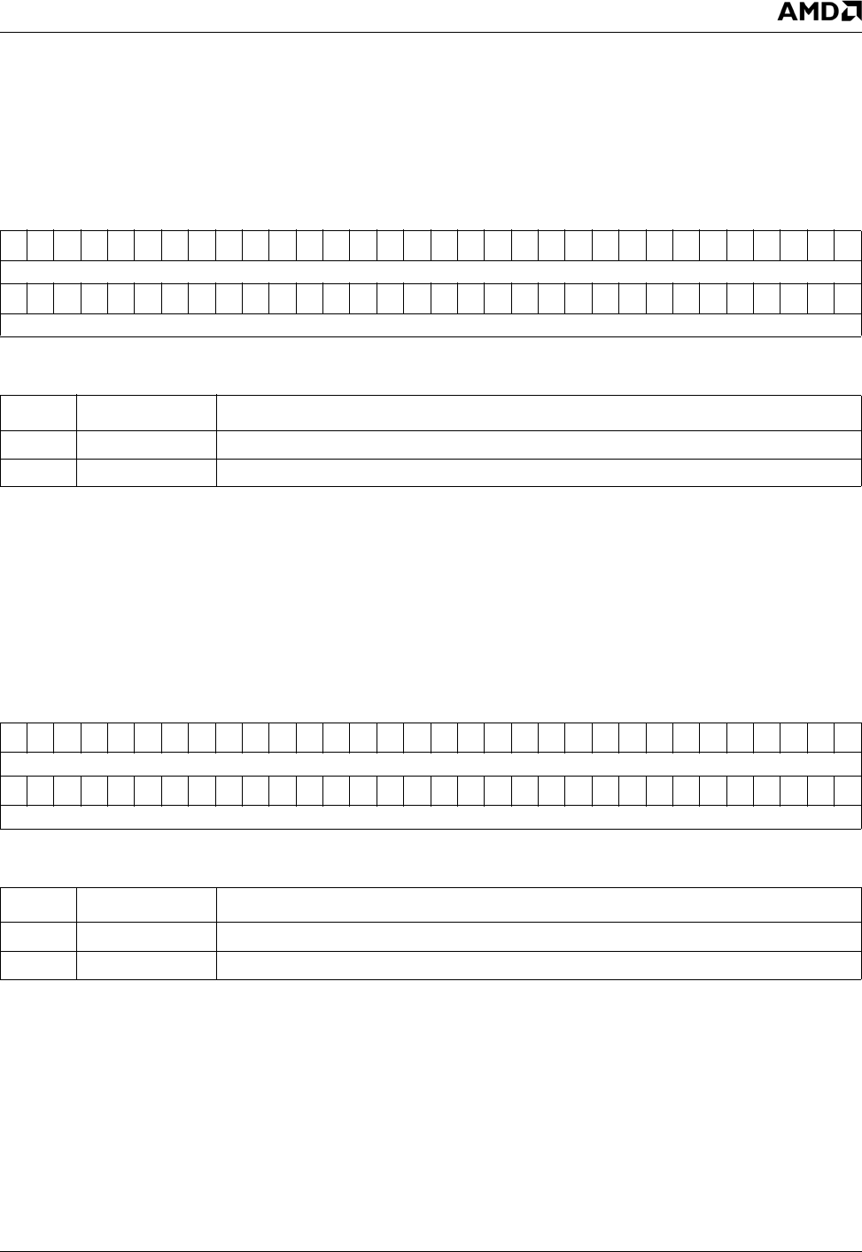
AMD Geode™ LX Processors Data Book 137
CPU Core Register Descriptions 33234H
5.5.2.30 Extended Debug Registers 1 and 0 MSR (XDR1_XDR0_MSR)
XDR1/XDR0_MSR provides access to Extended Debug Register 1 (XDR1) and Extended Debug Register 0 (XDR0). XDR0
and XDR1 each contain either an I/O port number or a linear address for use as an extended breakpoint.
5.5.2.31 Extended Debug Registers 3 and 2 MSR (XDR3_XDR2_MSR)
XDR3/XDR2_MSR provides access to Extended Debug Register 3 (XDR3) and Extended Debug Register 2 (XDR2). XDR2
and XDR3 each contain either an I/O port number or a linear address for use as an extended breakpoint.
MSR Address 00001350h
Ty p e R / W
Reset Value 00000000_00000000h
XDR1_XDR0_MSR Register Map
63 62 61 60 59 58 57 56 55 54 53 52 51 50 49 48 47 46 45 44 43 42 41 40 39 38 37 36 35 34 33 32
XDR1
313029282726252423222120191817161514131211109876543210
XDR0
XDR1_XDR0_MSR Bit Descriptions
Bit Name Description
63:32 XDR1 Extended Breakpoint 1 I/O Port Number/Linear Address.
31:0 XDR0 Extended Breakpoint 0 I/O Port Number/Linear Address.
MSR Address 00001351h
Ty p e R / W
Reset Value 00000000_00000000h
XDR3_XDR2_MSR Register Map
63 62 61 60 59 58 57 56 55 54 53 52 51 50 49 48 47 46 45 44 43 42 41 40 39 38 37 36 35 34 33 32
XDR3
313029282726252423222120191817161514131211109876543210
XDR2
XDR3_XDR2_MSR Bit Descriptions
Bit Name Description
63:32 XDR3 Extended Breakpoint 3 I/O Port Number/Linear Address.
31:0 XDR2 Extended Breakpoint 2 I/O Port Number/Linear Address.
138 AMD Geode™ LX Processors Data Book
CPU Core Register Descriptions
33234H
5.5.2.32 Extended Debug Registers 5 and 4 MSR (XDR5_XDR4_MSR)
XDR5/XDR4_MSR provides access to Extended Debug Register 5 (XDR5) and Extended Debug Register 4 (XDR4). XDR4
contains an opcode match value. XDR5 contains an opcode match mask.
5.5.2.33 Extended Debug Registers 7 and 6 MSR (XDR7_XDR6_MSR)
XDR7_XDR6_MSR provides access to the extended breakpoint enables, types, lengths, and status.
MSR Address 00001352h
Ty p e R / W
Reset Value FFFFFFFF_00000000h
XDR5_XDR4_MSR Register Map
63 62 61 60 59 58 57 56 55 54 53 52 51 50 49 48 47 46 45 44 43 42 41 40 39 38 37 36 35 34 33 32
PREFIX_MASK4 OPCODE_MASK4
313029282726252423222120191817161514131211109876543210
PREFIX_VALUE4 OPCODE_VALUE4
PN PR PL PC PS PO PA PF
XDR5_XDR4_MSR Bit Descriptions
Bit Name Description
63:56 PREFIX_MASK4 Prefix Mask Value for Extended Breakpoint 4.
55:32 OPCODE_MASK4 Opcode Mask Value for Extended Breakpoint 4.
31 PN REPNE/REPNZ Prefix Value for Extended Breakpoint 4.
30 PR REP/REPE/REPZ Prefix Value for Extended Breakpoint 4.
29 PL LOCK Prefix Value for Extended Breakpoint 4.
28 PC CS Segment Override Prefix Value for Extended Breakpoint 4.
27 PS SS/DS/ES/FS/GS Segment Override Prefix Value for Extended Breakpoint 4.
26 PO Operand Size Prefix Value for Extended Breakpoint 4.
25 PA Address Size Prefix Value for Extended Breakpoint 4.
24 PF 0F or 0F 0F Prefix Value for Extended Breakpoint 4.
23:0 OPCODE_VALUE4 Opcode Match Value for Extended Breakpoint 4.
MSR Address 00001353h
Ty p e R / W
Reset Value xxxxxxxx_xxxxxxxxh
XDR7_XDR6_MSR Register Map
63 62 61 60 59 58 57 56 55 54 53 52 51 50 49 48 47 46 45 44 43 42 41 40 39 38 37 36 35 34 33 32
LEN3 TYPE3 LEN2 TYPE2 LEN1 TYPE1 LEN0 TYPE0 RSVD E6 E5 E4 E3 E2 E1 E0
313029282726252423222120191817161514131211109876543210
RSVD (1FFFFh) BS
RSVD (1)
BI RSVD (1Fh) B6B5B5B3B2B1B0

AMD Geode™ LX Processors Data Book 139
CPU Core Register Descriptions 33234H
XDR7_XDR6_MSR Bit Descriptions
Bit Name Description
63:62 LEN3 Extended Breakpoint 3 Length.
61:60 TYPE3 Extended Breakpoint 3 Type.
59:58 LEN2 Extended Breakpoint 2 Length.
57:56 TYPE2 Extended Breakpoint 2 Type.
55:54 LEN1 Extended Breakpoint 1 Length.
53:52 TYPE1 Extended Breakpoint 1 Type.
51:50 LEN0 Breakpoint 0 Length.
49:48 TYPE0 Breakpoint 0 Type.
47:39 RSVD Reserved.
38 E6 Extended Breakpoint 6 Enable.
37 E5 Extended Breakpoint 5 Enable.
36 E4 Extended Breakpoint 4 Enable.
35 E3 Extended Breakpoint 3 Enable.
34 E2 Extended Breakpoint 2 Enable.
33 E1 Extended Breakpoint 1 Enable.
32 E0 Extended Breakpoint 0 Enable.
31:15 RSVD Reserved. Default = 1FFFFh.
14 BS Extended Single-Step Trap Status.
13 RSVD Reserved. Default = 1.
12 BI ICEBP or INT_1 Status.
11:7 RSVD Reserved. Default = 1Fh.
6B6 Extended Breakpoint 6 Status.
5B5 Extended Breakpoint 5 Status.
4B4 Extended Breakpoint 4 Status.
3B3 Extended Breakpoint 3 Status.
2B2 Extended Breakpoint 2 Status.
1B1 Extended Breakpoint 1 Status.
0B0 Extended Breakpoint 0 Status.
140 AMD Geode™ LX Processors Data Book
CPU Core Register Descriptions
33234H
5.5.2.34 Extended Debug Registers 9 and 8 MSR (XDR9_XDR8_MSR)
XDR9_XDR8_MSR provides access to Extended Debug Register 9 (XDR9) and Extended Debug Register 8 (XDR8).
XDR8 contains an opcode match value. XDR9 contains an opcode match mask.
MSR Address 00001354h
Ty p e R / W
Reset Value FFFFFFFF_00000000h
XDR9_XDR8_MSR Register Map
63 62 61 60 59 58 57 56 55 54 53 52 51 50 49 48 47 46 45 44 43 42 41 40 39 38 37 36 35 34 33 32
PREFIX_MASK5 OPCODE_MASK5
313029282726252423222120191817161514131211109876543210
PREFIX_VALUE5 OPCODE_VALUE5
PN PR PL PC PS PO PA PF
XDR9_XDR8_MSR Bit Descriptions
Bit Name Description
63:56 PREFIX_MASK5 Prefix Mask Value for Extended Breakpoint 5.
55:32 OPCODE_MASK5 Opcode Mask Value for Extended Breakpoint 5.
31 PN REPNE/REPNZ Prefix Value for Extended Breakpoint 5.
30 PR REP/REPE/REPZ Prefix Value for Extended Breakpoint 5.
29 PL LOCK Prefix Value for Extended Breakpoint 5.
28 PC CS Segment Override Prefix Value for Extended Breakpoint 5.
27 PS SS/DS/ES/FS/GS Segment Override Prefix Value for Extended Breakpoint 5.
26 PO Operand Size Prefix Value for Extended Breakpoint 5.
25 PA Address Size Prefix Value for Extended Breakpoint 5.
24 PF 0F or 0F 0F Prefix Value for Extended Breakpoint 5.
23:0 OPCODE_VALUE5 Opcode Match Value for Extended Breakpoint 5.

AMD Geode™ LX Processors Data Book 141
CPU Core Register Descriptions 33234H
5.5.2.35 Extended Debug Registers 11 and 10 MSR (XDR11_XDR10_MSR)
XDR11_XDR10_MSR provides access to the extended I/O breakpoint.
5.5.2.36 EX Stage Instruction Pointer MSR (EX_IP_MSR)
EX_IP_MSR provides access to the EX stage instruction pointer (effective address).
MSR Address 00001355h
Ty p e R / W
Reset Value xxxxxxxx_xxxx0000h
XDR11_XDR10_MSR Register Map
63 62 61 60 59 58 57 56 55 54 53 52 51 50 49 48 47 46 45 44 43 42 41 40 39 38 37 36 35 34 33 32
RSVD
313029282726252423222120191817161514131211109876543210
RSVD IO_PORT
XDR11_XDR10_MSR Bit Descriptions
Bit Name Description
63:16 RSVD Reserved. These bits are not writable.
15:0 IO_PORT I/O Port for Extended I/O Breakpoint 6.
MSR Address 00001360h
Ty p e R / W
Reset Value 00000000_00000000h
EX_IP_MSR Register Map
63 62 61 60 59 58 57 56 55 54 53 52 51 50 49 48 47 46 45 44 43 42 41 40 39 38 37 36 35 34 33 32
RSVD
313029282726252423222120191817161514131211109876543210
EX_IP
EX_IP_MSR Bit Descriptions
Bit Name Description
63:32 RSVD Reserved.
31:0 EX_IP EX Stage Effective Instruction Pointer.
142 AMD Geode™ LX Processors Data Book
CPU Core Register Descriptions
33234H
5.5.2.37 WB Stage Instruction Pointer MSR (WB_IP_MSR)
WB_IP_MSR provides access to the WB stage instruction pointer (effective address).
5.5.2.38 EX Stage Linear Instruction Pointer MSR (EX_LIP_MSR)
EX_LIP_MSR provides access to the EX stage linear instruction pointer.
MSR Address 00001361h
Ty p e R / W
Reset Value 00000000_00000000h
WB_IP_MSR Register Map
63 62 61 60 59 58 57 56 55 54 53 52 51 50 49 48 47 46 45 44 43 42 41 40 39 38 37 36 35 34 33 32
RSVD
313029282726252423222120191817161514131211109876543210
WB_IP
WB_IP_MSR Bit Descriptions
Bit Name Description
63:32 RSVD Reserved.
31:0 WB_IP WB Stage Effective Instruction Pointer.
MSR Address 00001364h
Ty p e RO
Reset Value 00000000_00000000h
EX_LIP_MSR Register Map
63 62 61 60 59 58 57 56 55 54 53 52 51 50 49 48 47 46 45 44 43 42 41 40 39 38 37 36 35 34 33 32
RSVD
313029282726252423222120191817161514131211109876543210
EX_LIP
EX_LIP_MSR Bit Descriptions
Bit Name Description
63:32 RSVD Reserved.
31:0 EX_LIP EX Stage Linear Instruction Pointer.

AMD Geode™ LX Processors Data Book 143
CPU Core Register Descriptions 33234H
5.5.2.39 WB Stage Linear Instruction Pointer MSR (WB_LIP_MSR)
WB_LIP_MSR provides access to the WB stage linear instruction pointer.
5.5.2.40 C1/C0 Linear Instruction Pointer MSR (C1_C0_LIP_MSR)
C1_C0_LIP_MSR provides access to linear instruction pointers when the code segment was loaded.
MSR Address 00001365h
Ty p e RO
Reset Value 00000000_00000000h
WB_LIP_MSR Register Map
63 62 61 60 59 58 57 56 55 54 53 52 51 50 49 48 47 46 45 44 43 42 41 40 39 38 37 36 35 34 33 32
RSVD
313029282726252423222120191817161514131211109876543210
WB_LIP
WB_LIP_MSR Bit Descriptions
Bit Name Description
63:32 RSVD Reserved.
31:0 WB_LIP WB Stage Linear Instruction Pointer.
MSR Address 00001366h
Ty p e RO
Reset Value 00000000_00000000h
C1_C0_LIP_MSR Register Map
63 62 61 60 59 58 57 56 55 54 53 52 51 50 49 48 47 46 45 44 43 42 41 40 39 38 37 36 35 34 33 32
C1_LIP
313029282726252423222120191817161514131211109876543210
C0_LIP
C1_C0_LIP_MSR Bit Descriptions
Bit Name Description
63:32 C1_LIP CS 1 Linear Instruction Pointer. Second most recent linear instruction point when code
segment was loaded.
31:0 C0_LIP CS 0 Linear Instruction Pointer. Most recent linear instruction point when code seg-
ment was loaded.

144 AMD Geode™ LX Processors Data Book
CPU Core Register Descriptions
33234H
5.5.2.41 C3/C2 Linear Instruction Pointer MSR (C3_C2_LIP_MSR)
C3_C2_LIP_MSR provides access to linear instruction pointers when the code segment was loaded.
5.5.2.42 Floating Point Environment Code Segment (FPENV_CS_MSR)
FPENV_CS_MSR provides access to the floating point (FP) environment code segment. Software better accesses the
floating point environment data using the FLDENV/FSTENV and FSAVE/FRSTOR instructions.
MSR Address 00001367h
Ty p e RO
Reset Value 00000000_00000000h
C3_C2_LIP_MSR Register Map
63 62 61 60 59 58 57 56 55 54 53 52 51 50 49 48 47 46 45 44 43 42 41 40 39 38 37 36 35 34 33 32
C3_LIP
313029282726252423222120191817161514131211109876543210
C2_LIP
C3_C2_LIP_MSR Bit Descriptions
Bit Name Description
63:32 C3_LIP CS 3 Linear Instruction Pointer. Fourth most recent linear instruction point when code
segment was loaded.
31:0 C2_LIP CS 2 Linear Instruction Pointer. Third most recent linear instruction point when code
segment was loaded.
MSR Address 00001370h
Ty p e R / W
Reset Value 00000000_00000000h
FPENV_CS_MSR Register Map
63 62 61 60 59 58 57 56 55 54 53 52 51 50 49 48 47 46 45 44 43 42 41 40 39 38 37 36 35 34 33 32
RSVD
313029282726252423222120191817161514131211109876543210
RSVD CS
FPENV_CS_MSR Bit Descriptions
Bit Name Description
63:16 RSVD Reserved.
15:0 CS Code Segment. Selector of code segment of last FP instruction that may have caused
an FP error.

AMD Geode™ LX Processors Data Book 145
CPU Core Register Descriptions 33234H
5.5.2.43 Floating Point Environment Instruction Pointer (FPENV_IP_MSR)
FPENV_IP_MSR provides access to the floating point (FP) environment instruction pointer. Software better accesses the
floating point environment data using the FLDENV/FSTENV and FSAVE/FRSTOR instructions.
5.5.2.44 Floating Point Environment Data Segment (FPENV_DS_MSR)
FPENV_DS_MSR provides access to the floating point (FP) environment data segment. Software better accesses the float-
ing point environment data using the FLDENV/FSTENV and FSAVE/FRSTOR instructions.
MSR Address 00001371h
Ty p e R / W
Reset Value 00000000_00000000h
FPENV_IP_MSR Register Map
63 62 61 60 59 58 57 56 55 54 53 52 51 50 49 48 47 46 45 44 43 42 41 40 39 38 37 36 35 34 33 32
RSVD
313029282726252423222120191817161514131211109876543210
IP
FPENV_IP_MSR Bit Descriptions
Bit Name Description
63:32 RSVD Reserved.
31:0 IP Instruction Pointer. Effective address of last FP instruction that may have caused an FP
error.
MSR Address 00001372h
Ty p e R / W
Reset Value 00000000_00000000h
FPENV_DS_MSR Register Map
63 62 61 60 59 58 57 56 55 54 53 52 51 50 49 48 47 46 45 44 43 42 41 40 39 38 37 36 35 34 33 32
RSVD
313029282726252423222120191817161514131211109876543210
RSVD DS
FPENV_DS_MSR Bit Descriptions
Bit Name Description
63:16 RSVD Reserved.
15:0 DS Data Segment. Selector of data segment of memory operand of last FP instruction that
may have caused an FP error.
146 AMD Geode™ LX Processors Data Book
CPU Core Register Descriptions
33234H
5.5.2.45 Floating Point Environment Data Pointer (FPENV_DP_MSR)
FPENV_DP_MSR provides access to the floating point (FP) environment data pointer. Software better accesses the float-
ing point environment data using the FLDENV/FSTENV and FSAVE/FRSTOR instructions.
5.5.2.46 Floating Point Environment Opcode Pointer (FPENV_OP_MSR)
FPENV_OP_MSR provides access to the floating point (FP) environment opcode. Software better accesses the floating
point environment opcode using the FLDENV/FSTENV and FRSTOR/FSAVE instructions.
MSR Address 00001373h
Ty p e R / W
Reset Value 00000000_00000000h
FPENV_DP_MSR Register Map
63 62 61 60 59 58 57 56 55 54 53 52 51 50 49 48 47 46 45 44 43 42 41 40 39 38 37 36 35 34 33 32
RSVD
313029282726252423222120191817161514131211109876543210
DP
FPENV_DP_MSR Bit Descriptions
Bit Name Description
63:32 RSVD Reserved.
31:0 DP Data Pointer. Effective address of memory operand of last FP instruction that may have
caused an FP error.
MSR Address 00001374h
Ty p e R / W
Reset Value 00000000_00000000h
FPENV_OP_MSR Register Map
63 62 61 60 59 58 57 56 55 54 53 52 51 50 49 48 47 46 45 44 43 42 41 40 39 38 37 36 35 34 33 32
RSVD
313029282726252423222120191817161514131211109876543210
RSVD OP
FPENV_OP_MSR Bit Descriptions
Bit Name Description
63:11 RSVD Reserved.
10:0 OP Opcode Pointer. Opcode of last FP instruction executed that may have caused an FP
error.
AMD Geode™ LX Processors Data Book 147
CPU Core Register Descriptions 33234H
5.5.2.47 Address Calculation Unit Configuration MSR (AC_CONFIG_MSR)
MSR Address 00001380h
Ty p e RO
Reset Value 00000000_00000000h
AC_CONFIG_MSR Register Map
63 62 61 60 59 58 57 56 55 54 53 52 51 50 49 48 47 46 45 44 43 42 41 40 39 38 37 36 35 34 33 32
RSVD
313029282726252423222120191817161514131211109876543210
RSVD
LOCK_EN
AC_CONFIG_MSR Bit Descriptions
Bit Name Description
63:1 RSVD Reserved.
0 LOCK_EN Lock Enable. Allow Address Calculation Unit (AC) to issue locked requests to Data
Memory Subsystem (DM).
148 AMD Geode™ LX Processors Data Book
CPU Core Register Descriptions
33234H
5.5.2.48 General Register MSRs
General Register EAX MSR (GR_EAX_MSR)
General Register ECX MSR (GR_ECX_MSR)
General Register EDX MSR (GR_EDX_MSR)
General Register EBX MSR (GR_EBX_MSR)
General Register ESP MSR (GR_ESP_MSR)
General Register EBP MSR (GR_EBP_MSR)
General Register ESI MSR (GR_ESI_MSR)
General Register EDI MSR (GR_EDI_MSR)
General Register Temp 0 MSR (GR_TEMP0_MSR)
General Register Temp 1 MSR (GR_TEMP1_MSR)
General Register Temp 2 MSR (GR_TEMP2_MSR)
General Register Temp 3 MSR (GR_TEMP3_MSR)
General Register Temp 4 MSR (GR_TEMP4_MSR)
General Register Temp 5 MSR (GR_TEMP5_MSR)
General Register Temp 6 MSR (GR_TEMP6_MSR)
General Register Temp 7 MSR (GR_TEMP7_MSR)
MSR Address 00001408h
Ty p e R / W
Reset Value 00000000_00000000h
MSR Address 00001409h
Ty p e R / W
Reset Value 00000000_00000000h
MSR Address 0000140Ah
Ty p e R / W
Reset Value 00000000_00000000h
MSR Address 0000140Bh
Ty p e R / W
Reset Value 00000000_00000000h
MSR Address 0000140Ch
Ty p e R / W
Reset Value 00000000_00000000h
MSR Address 0000140Dh
Ty p e R / W
Reset Value 00000000_00000000h
MSR Address 0000140Eh
Ty p e R / W
Reset Value 00000000_00000000h
MSR Address 0000140Fh
Ty p e R / W
Reset Value 00000000_00000000h
MSR Address 00001410h
Typ e R / W
Reset Value 00000000_00000000h
MSR Address 00001411h
Typ e R / W
Reset Value 00000000_00000000h
MSR Address 00001412h
Typ e R / W
Reset Value 00000000_00000000h
MSR Address 00001413h
Typ e R / W
Reset Value 00000000_00000000h
MSR Address 00001414h
Typ e R / W
Reset Value 00000000_00000000h
MSR Address 00001415h
Typ e R / W
Reset Value 00000000_00000000h
MSR Address 00001416h
Typ e R / W
Reset Value 00000000_00000000h
MSR Address 00001417h
Typ e R / W
Reset Value 00000000_00000000h
General Registers MSRs Register Map
63 62 61 60 59 58 57 56 55 54 53 52 51 50 49 48 47 46 45 44 43 42 41 40 39 38 37 36 35 34 33 32
RSVD
313029282726252423222120191817161514131211109876543210
GR_REG
General Registers MSRs Bit Descriptions
Bit Name Description
63:32 RSVD Reserved. Write as read.
31:0 GR_REG General Register.
AMD Geode™ LX Processors Data Book 149
CPU Core Register Descriptions 33234H
5.5.2.49 Extended Flags MSR (EFLAG_MSR)
5.5.2.50 Control Register 0 MSR (CR0_MSR)
This is the standard x86 Control Register 0 (CR0). CR1, CR2, CR3, and CR4 are located at MSRs 00001881h-00001884h
(see Section 5.5.2.74 on page 172). The contents of CR0-CR4 should only be accessed using the MOV instruction. They
are mentioned here for completeness only. See Section 5.4.1 “Control Registers” on page 95 for bit descriptions.
MSR Address 00001418h
Ty p e R / W
Reset Value 00000000_00000002h
EFLAG_MSR Register Map
63 62 61 60 59 58 57 56 55 54 53 52 51 50 49 48 47 46 45 44 43 42 41 40 39 38 37 36 35 34 33 32
RSVD
313029282726252423222120191817161514131211109876543210
RSVD (0) ID RSVD
(0)
AC VM RF
RSVD (0)
NT IOPL OF DF IF TF SF ZF
RSVD (0)
AF
RSVD (0)
PF
RSVD (1)
CF
EFLAG_MSR Bit Descriptions
Bit Name Description
63:22 RSVD Reserved. (Default = 0)
21 ID Identification Flag. (Default = 0)
20:19 RSVD Reserved. (Default = 0)
18 AC Alignment Check Flag. (Default = 0)
17 VM Virtual 8086 Flag. (Default = 0)
16 RF Resume Flag. Disable instruction address breakpoints. (Default = 0)
15 RSVD Reserved. (Default = 0)
14 NT Nested Task Flag. (Default = 0)
13:12 IOPL Input/Output Privilege Level. (Default = 0)
11 OF Overflow Flag. (Default = 0)
10 DF Repeated-String Direction Flag. (Default = 0)
9IF Eternal Maskable Interrupt Enable. (Default = 0)
8TF Single-Step Trap Flag. (Default = 0)
7SF Sign Flag. (Default = 0)
6ZF Zero Flag. (Default = 0)
5 RSVD Reserved. (Default = 0)
4AF Auxiliary Carry Flag. (Default = 0)
3 RSVD Reserved. (Default = 0)
2PF Parity Flag. (Default = 0)
1 RSVD Reserved. (Default = 1)
0CF Carry Flag. (Default = 1)
MSR Address 00001420h
Ty p e R / W
Reset Value 00000000_60000010h

150 AMD Geode™ LX Processors Data Book
CPU Core Register Descriptions
33234H
5.5.2.51 Instruction Memory Configuration MSR (IM_CONFIG_MSR)
MSR Address 00001700h
Ty p e R / W
Reset Value 00000000_00000000h
IM_CONFIG_MSR Register Map
63 62 61 60 59 58 57 56 55 54 53 52 51 50 49 48 47 46 45 44 43 42 41 40 39 38 37 36 35 34 33 32
RSVD
313029282726252423222120191817161514131211109876543210
LOCK RSVD
DRT
RSVD
ABSE
EBE
RSVD
ICD
TUS
RSVD
L0D
L0IN
RSVD
SER
FLD
TBE
IM_CONFIG_MSR Bit Descriptions
Bits Name Description
63:32 RSVD Reserved. (Default = 0)
31:24 LOCK Lock. Locks ways of the instruction cache from being allocated or replaced on an
instruction cache miss. If all ways are locked, caching is effectively disabled.
Bit 31: Ways 15 & 14
Bit 30: Ways 13 & 12
Bit 29: Ways 11 & 10
Bit 28: Ways 9 & 8
Bit 27: Ways 7 & 6
Bit 26: Ways 5 & 4
Bit 25: Ways 3 & 2
Bit 24: Ways 1 & 0
0: Not locked. (Default)
1: Locked
23:17 RSVD Reserved.
16 DRT Dynamic Retention Test. Allow dynamic retention test for BIST of tag array.
0: Disable. (Default)
1: Enable.
15:12 RSVD Reserved. (Default = 0)
11 ABSE Aborts for Speculative Instruction Fetch Requests Enable. Enable aborts for specu-
lative IF requests for which there is an L1 TLB miss. IM passes the speculative informa-
tion from IF directly to DM. DM responds in one of four ways:
Returns page if it hits in the L2.
Returns abort if it does not hit in the L2 and it a speculative request.
Returns a retry if it does not hit in the L2 and it was a non-speculative request and the
pipe is not idle,
Does a tablewalk if it does not hit in the L2 and it was a non-speculative request and the
pipe is idle.
0: Disable. (Default)
1: Enable.
10 EBE Instruction Memory Eviction Bus Enable. The default is to have IM evictions disabled.
This bit should be set when the L2 cache is enabled, since the L2 cache operates exclu-
sively in Victim mode.
0: Disable. Invalidate clean cache lines when replaced, do not evict. (Default)
1: Enable. Evict clean cache lines when they are replaced.
9 RSVD Reserved.

AMD Geode™ LX Processors Data Book 151
CPU Core Register Descriptions 33234H
8ICD Instruction Cache Disable. Completely disable L0 and L1 instruction caches. Contents
of cache is not modified and no cache entry is read.
0: Use standard x86 cacheability rules. (Default)
1: Instruction cache will always generate a miss.
7TUS Translation Look-aside Buffer Updates Select. Select L1 TLB updates (not L1 TLB
evictions) to go out on the IM’s Translation Bus. Otherwise, only L1 TLB evictions go out
on IM’s Translation Bus. IM only supports either updates or evictions going out on the
bus, but not both.
0: Disable. (Default)
1: Enable.
6 RSVD Reserved. Always write zero.
5 L0D L0 Cache Disable.
0: Disable. (Default)
1: Enable.
4 L0IN L0 Cache Invalidate.
0: Disable. (Default)
1: Enable.
3 RSVD Reserved.
2 SER Serialize Cache State Machine. If this bit is set, only one outstanding request to the bus
controller is allowed at one time.
0: Disable. (Default)
1: Enable.
1FLD Flushing Disable. Disable full flushing of the IM (including outstanding bus controller
requests) on IF aborts. If this bit is disabled, the IM only aborts requests that have not
already gone out to the bus controller.
0: Enable. (Default)
1: Disable.
0TBE Treatment Bus Enable. If this bit is set, then the treatment bus from the GLCP is able to
modify the IM’s behavior.
0: Disable. (Default)
1: Enable
IM_CONFIG_MSR Bit Descriptions (Continued)
Bits Name Description
152 AMD Geode™ LX Processors Data Book
CPU Core Register Descriptions
33234H
5.5.2.52 Instruction Cache Index MSR (IC_INDEX_MSR)
5.5.2.53 Instruction Cache Data MSR (IC_DATA_MSR)
MSR Address 00001710h
Ty p e R / W
Reset Value 00000000_00000000h
IC_INDEX_MSR Register Map
63 62 61 60 59 58 57 56 55 54 53 52 51 50 49 48 47 46 45 44 43 42 41 40 39 38 37 36 35 34 33 32
RSVD
313029282726252423222120191817161514131211109876543210
RSVD DSEL RSVD WAY LINE
IC_INDEX_MSR Bit Descriptions
Bits Name Description
63:18 RSVD (RO) Reserved (Read Only).
17:16 DSEL Data QWORD Select for L1 Cache MSR Access. Determines which QWORD in a
cache line is accessed by a read or a write to IC_DATA_MSR (MSR 00001711h). This
field resets to 0 on any access to IC_TAG_MSR (MSR 00001712h) or IC_TAG_I_MSR
(MSR 00001713h) and increments on access to IC_DATA_MSR. This field is not used
when accessing the L0 cache. (Default = 0)
15:11 RSVD (RO) Reserved (Read Only).
10:7 WAY L1 Cache Way to Access. Forms the high-order bits of an 11-bit counter. The LINE field
(bits [6:0]) forms the low seven bits of the counter. This field increments when the LINE
field overflows on a access to IC_TAG_I_MSR (MSR 00001713h). This field is not used
for the L0 cache. (Default = 0)
6:0 LINE L1 Cache Line to Access. Forms the low-order bits of an 11-bit counter. The WAY field
(bits [3:0]) forms the high four bits of the counter. This field post-increments on an access
to IC_TAG_I_MSR (MSR 00001713h). When accessing the L0 cache, only bits [4:0] are
important and are used to select the line to read in the L0 cache. (Default = 0)
MSR Address 00001711h
Ty p e R / W
Reset Value xxxxxxxx_xxxxxxxxh
IC_DATA_MSR Register Map
63 62 61 60 59 58 57 56 55 54 53 52 51 50 49 48 47 46 45 44 43 42 41 40 39 38 37 36 35 34 33 32
DATA (Upper)
313029282726252423222120191817161514131211109876543210
DATA (Lower)
IC_DATA_MSR Bit Descriptions
Bits Name Description
63:0 DATA QWORD to Read from or Write to the L1 Cache. The address to the QWORD specified
by the LINE and DSEL fields from IC_INDEX_MSR (MSR 00001710h). The way in the
cache to read and write is specified by the WAY field in IC_INDEX_MSR. Each access to
IC_DATA_MSR increments DSEL.

AMD Geode™ LX Processors Data Book 153
CPU Core Register Descriptions 33234H
5.5.2.54 Instruction Cache Tag (IC_TAG_MSR)
MSR Address 00001712h
Ty p e R / W
Reset Value 00000000_00000000h
IC_TAG_MSR MSR Register Map
63 62 61 60 59 58 57 56 55 54 53 52 51 50 49 48 47 46 45 44 43 42 41 40 39 38 37 36 35 34 33 32
RSVD LRU
313029282726252423222120191817161514131211109876543210
TAG RSVD V
IC_TAG_MSR Bit Descriptions
Bits Name Description
63:47 RSVD (RO) Reserved (Read Only).
46:32 LRU Least Recently Used Bits for the Cache Line. Same data will be read for all ways in a
line. If bit(s) are set to 1:
Bit 46: Ways (15-8) more recent than ways (7-0)
Bit 45: Ways (15-12) more recent than ways (11-8)
Bit 44: Ways (15,14) more recent than ways (13,12)
Bit 43: Way 15 more recent than way 14
Bit 42: Way 13 more recent than way 12
Bit 41: Ways (11,10) more recent than ways (9,8)
Bit 40: Way 11 more recent than way 10
Bit 39: Way 9 more recent than way 8
Bit 38: Ways (7-4) more recent than ways (3-0)
Bit 37: Ways (7,6) more recent than ways (5,4)
Bit 36: Way 7 more recent than way 6
Bit 35: Way 5 more recent than way 4
Bit 34: Ways (2,3) more recent than ways (1,0)
Bit 33: Way 3 more recent than way 2
Bit 32: Way 1 more recent than way 0
31:12 TAG Tag. Cache tag value for the line/way selected by IC_INDEX_MSR (MSR 00001710h).
(Default = 0)
11:1 RSVD (RO) Reserved (Read Only).
0V Valid. Valid bit for the line/way selected by IC_INDEX_MSR (MSR 00001710h).
(Default = 0)
154 AMD Geode™ LX Processors Data Book
CPU Core Register Descriptions
33234H
5.5.2.55 Instruction Cache Tag with Increment (IC_TAG_I_MSR)
5.5.2.56 L0 Instruction Cache Data MSR (L0_IC_DATA_MSR)
5.5.2.57 L0 Instruction Cache Tag with Increment MSR (L0_IC_TAG_I_MSR)
MSR Address 00001713h
Ty p e R / W
Reset Value 00000000_00000000h
IC_TAG_I_MSR Register Map
63 62 61 60 59 58 57 56 55 54 53 52 51 50 49 48 47 46 45 44 43 42 41 40 39 38 37 36 35 34 33 32
RSVD LRU
313029282726252423222120191817161514131211109876543210
TAG RSVD V
IC_TAG_I_MSR Bit Descriptions
Bit Name Description
63:0 --- Definition same as Instruction Cache Tag MSR (MSR 00001712h). Except read/write
of this register causes an auto-increment on the IC_INDEX_MSR (MSR 00001710h).
MSR Address 00001714h
Ty p e RO
Reset Value xxxxxxxx_xxxxxxxxh
L0_IC_DATA_MSR Register Map
63 62 61 60 59 58 57 56 55 54 53 52 51 50 49 48 47 46 45 44 43 42 41 40 39 38 37 36 35 34 33 32
DATA (Upper)
313029282726252423222120191817161514131211109876543210
DATA (Lower)
L0_IC_DATA_MSR Bit Descriptions
Bits Name Description
63:0 DATA QWORD Read from L0 Cache. The address to the QWORD specified by the LINE field
from IC_INDEX_MSR (MSR 00001710h[4:0]).
MSR Address 00001715h
Ty p e RO
Reset Value 00000000_xxxxxxxxh
L0_IC_TAG_I_MSR Register Map
63 62 61 60 59 58 57 56 55 54 53 52 51 50 49 48 47 46 45 44 43 42 41 40 39 38 37 36 35 34 33 32
RSVD
313029282726252423222120191817161514131211109876543210
TLB_NUM RSVD TAG LINE RSVD V
AMD Geode™ LX Processors Data Book 155
CPU Core Register Descriptions 33234H
5.5.2.58 L1 Instruction TLB Index (ITB_INDEX_MSR)
The L1 Instruction TLB is accessible via an index/data mechanism. The index of the entry to access is set via
ITB_INDEX_MSR and an entry is read or written via ITB_ENTRY_MSR or ITB_ENTRY_I_MSR. An autoincrement mecha-
nism is provided to post-increment ITB_INDEX_MSR after every access to ITB_ENTRY_I_MSR. The L0 TLB can be
accessed by a read only MSR and it is not necessary to use the ITB_INDEX_MSR to read the L0 TLB. The L1 TLB LRU
bits can be accessed using the ITB_LRU_MSR. Diagnostic accesses to the L0 or L1 Instruction TLB array do not affect the
values of the LRU bits.
Note that the L1 Instruction TLB is always in use and cannot be disabled. That means that diagnostic accesses generated
by code running on the processor are unreliable at best, since the TLB contents may be changing while the code is running.
Furthermore, the L1 Instruction TLB is flushed on any mode change, so a debug handler would no longer see the TLB con-
tents prior to the DMI. Thus the L1 Instruction TLB accesses are intended only to be used by the GLCP after the pipeline
has been halted.
L0_IC_TAG_I_MSR Bit Descriptions
Bits Name Description
63:32 RSVD Reserved.
31:16 TLB_NUM TLB Number. This is the one-hot-value of the TLB entry corresponding to the L0 cache
entry. (Default = 0)
15:12 RSVD Reserved.
11:8 TAG Tag/Line. This is a combination of the 4-bit tag and the 5-bit line. Together they make up
bits [11:3] of the physical address for the line selected by IC_INDEX_MSR (MSR
00001710h).
7:3 LINE
2:1 RSVD Reserved.
0V Valid. Valid bit for the line selected by IC_INDEX_MSR (MSR 00001710h). (Default = 0)
MSR Address 00001720h
Ty p e R / W
Reset Value 00000000_0000000xh
ITB_INDEX_MSR Register Map
63 62 61 60 59 58 57 56 55 54 53 52 51 50 49 48 47 46 45 44 43 42 41 40 39 38 37 36 35 34 33 32
RSVD
313029282726252423222120191817161514131211109876543210
RSVD INDEX
ITB_INDEX_MSR Bit Descriptions
Bits Name Description
63:4 RSVD Reserved.
3:0 INDEX Index.

156 AMD Geode™ LX Processors Data Book
CPU Core Register Descriptions
33234H
5.5.2.59 L1 Instruction TLB Least Recently Used MSR (ITB_LRU_MSR)
MSR Address 00001721h
Ty p e R / W
Reset Value 00000000_00000000h
ITB_LRU_MSR Register Map
63 62 61 60 59 58 57 56 55 54 53 52 51 50 49 48 47 46 45 44 43 42 41 40 39 38 37 36 35 34 33 32
RSVD
313029282726252423222120191817161514131211109876543210
RSVD LRU
ITB_LRU_MSR Bit Descriptions
Bits Name Description
63:30 RSVD (RO) Reserved (Read Only). (Default = 0)
29:0 LRU Least Recently Used Value.
Bit 29: Entries 8-11 more recent than entries 12-15
Bit 28: Entries 4-7 more recent than entries 12-15
Bit 27: Entries 4-7 more recent than entries 8-11
Bit 26: Entries 0-3 more recent than entries 12-15
Bit 25: Entries 0-3 more recent than entries 8-11
Bit 24: Entries 0-3 more recent than entries 4-7
Bit 23: Entry 14 more recent than entry 15
Bit 22: Entry 13 more recent than entry 15
Bit 21: Entry 13 more recent than entry 14
Bit 20: Entry 12 more recent than entry 15
Bit 19: Entry 12 more recent than entry 14
Bit 18: Entry 12 more recent than entry 13
Bit 17: Entry 10 more recent than entry 11
Bit 16: Entry 9 more recent than entry 11
Bit 15: Entry 9 more recent than entry 10
Bit 14: Entry 8 more recent than entry 11
Bit 13: Entry 8 more recent than entry 10
Bit 12: Entry 8 more recent than entry 9
Bit 11: Entry 6 more recent than entry 7
Bit 10: Entry 5 more recent than entry 7
Bit 9: Entry 5 more recent than entry 6
Bit 8: Entry 4 more recent than entry 7
Bit 7: Entry 4 more recent than entry 6
Bit 6: Entry 4 more recent than entry 5
Bit 5: Entry 2 more recent than entry 3
Bit 4: Entry 1 more recent than entry 3
Bit 3: Entry 1 more recent than entry 2
Bit 2: Entry 0 more recent than entry 3
Bit 1: Entry 0 more recent than entry 2
Bit 0: Entry 0 more recent than entry 1
0: False (Default)
1: True
AMD Geode™ LX Processors Data Book 157
CPU Core Register Descriptions 33234H
5.5.2.60 L1 Instruction TLB Entry MSRs
ITB Entry MSR (ITB_ENTRY_MSR)
ITB Entry with Increment MSR (ITB_ENTRY_I_MSR)
ITB L0 Cache Entry MSR (ITB_L0_ENTRY_MSR)
MSR Address 00001722h
Ty p e R / W
Reset Value xxxxxxxx_xxxxxxxxh
MSR Address 00001723h
Ty p e R / W
Reset Value xxxxxxxx_xxxxxxxxh
MSR Address 00001724h
Typ e R / W
Reset Value xxxxxxxx_xxxxxxxxh
ITB_ENTRY_MSR, ITB_ENTRY_I_MSR, ITB_L0_ENTRY_MSR Register Map
63 62 61 60 59 58 57 56 55 54 53 52 51 50 49 48 47 46 45 44 43 42 41 40 39 38 37 36 35 34 33 32
LINADDR RSVD
313029282726252423222120191817161514131211109876543210
PHYSADDR WS RSVD CD
RSVD
US
RSVD
V
ITB_ENTRY_MSR, ITB_ENTRY_I_MSR, ITB_L0_ENTRY_MSR Bit Descriptions
Bits Name Description
63:44 LINADDR Linear Address.
43:32 RSVD (RO) Reserved (Read Only). (Default = 0)
31:12 PHYSADDR Physical Address.
11 WS Write Serialize Property.
0: Not write serialized. (Default)
1: Write serialized.
10:5 RSVD (RO) Reserved (Read Only). (Default = 0)
4CD Cache Disable.
0: Cache enabled.
1: Cache disabled.
3 RSVD (RO) Reserved (Read Only). (Default = 0)
2US User Access Privileges.
0: Supervisor.
1: User.
1 RSVD (RO) Reserved (Read Only). (Default = 0)
0V Valid Bit.
0: Not valid. (Default)
1: Valid.
158 AMD Geode™ LX Processors Data Book
CPU Core Register Descriptions
33234H
5.5.2.61 Instruction Memory Subsystem BIST Tag MSR (IM_BIST_TAG_MSR)
The Instruction Memory subsystem supports built-in self-test (BIST) for the tag and data arrays. Normally, BIST is run dur-
ing manufacturing test. For convenience, BIST can be activated by reading the BIST MSRs.
WARNING: It is important that the instruction cache be disabled before initiating BIST via MSRs. There are no guarantees
of proper behavior if BIST is activated with the instruction cache enabled. The instruction cache can be disabled through
the IM_CONFIG_MSR (MSR 00001700h[4]).
5.5.2.62 Instruction Memory Subsystem BIST Data MSR (IM_BIST_DATA_MSR)
MSR Address 00001730h
Ty p e RO
Reset Value 00000000_0000000xh
IM_BIST_TAG_MSR Register Map
63 62 61 60 59 58 57 56 55 54 53 52 51 50 49 48 47 46 45 44 43 42 41 40 39 38 37 36 35 34 33 32
RSVD
313029282726252423222120191817161514131211109876543210
RSVD
CMP
TAG
IM_BIST_TAG_MSR Bit Descriptions
Bits Name Description
63:2 RSVD (RO) Reserved (Read Only). (Default = 0)
1CMP Tag Compare Logic BIST.
0: Fail (Default)
1: Pass
0TAG Valid and Tag Array BIST.
0: Fail (Default)
1: Pass
MSR Address 00001731h
Ty p e RO
Reset Value 00000000_0000000xh
IM_BIST_DATA_MSR Register Map
63 62 61 60 59 58 57 56 55 54 53 52 51 50 49 48 47 46 45 44 43 42 41 40 39 38 37 36 35 34 33 32
RSVD
313029282726252423222120191817161514131211109876543210
RSVD
DATA
IM_BIST_DATA_MSR Bit Descriptions
Bits Name Description
63:1 RSVD (RO) Reserved (Read Only). (Default = 0)
0DATA Data Array BIST.
0: Fail
1: Pass
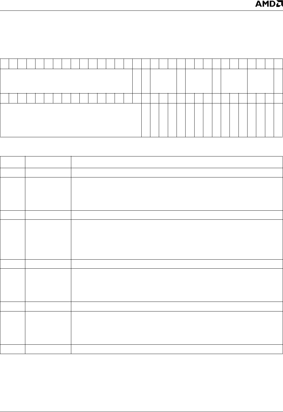
AMD Geode™ LX Processors Data Book 159
CPU Core Register Descriptions 33234H
5.5.2.63 Data Memory Subsystem Configuration 0 MSR (DM_CONFIG0_MSR)
MSR Address 00001800h
Ty p e R / W
Reset Value 00000000_00000000h
DM_CONFIG0_MSR Register Map
63 62 61 60 59 58 57 56 55 54 53 52 51 50 49 48 47 46 45 44 43 42 41 40 39 38 37 36 35 34 33 32
RSVD
SNOOPTO
RSVD
WSREQ
RSVD
WCTO
RSVD
WBTO RSVD
WBDIS
313029282726252423222120191817161514131211109876543210
LSLOCK
NOLOCKEVCT
EVCTONRPL
NOFTTBRES
DTCNINV
P4MDIS
DTCDIS
L2TDIS
DCDIS
SPCDEC
WTBRST
WBINVD
NOSMC
NOFWD
BLOCKC
MISSER
LDSER
DM_CONFIG0_MSR Bit Descriptions
Bits Name Description
63:49 RSVD Reserved. (Default = 0)
48 SNOOPTO Snoop Timeout. Allow DM to escape a snoop deadlock by timing out a snoop request to
the DM tag machine.
0: Disable.
1: Enable. (Default)
47 RSVD Reserved. (Default = 0)
46:44 WSREQ Number of Outstanding Write-Serialized Requests. The system must be able to
accept WSREQ+1 cacheline + 2-4 QWORD writes without backing up the bus controller
to prevent a lockup condition in the event of an inbound snoop hit.
000: Unlimited. (Default)
001-111: Binary value.
43 RSVD Reserved. (Default = 0)
42:40 WCTO Write-Combine Timeout. Flushes write-combinable entry from write buffer if it has not
been written for the specified number of clocks.
000: Disable timeout. (Default)
001-111: 2**(4 + WCTO) clocks (32, 64, ..., 2048).
39 RSVD Reserved. (Default = 0)
38:36 WBTO Write-Burst Timeout. Flushes write-burstable entry from write buffer if it has not been
written for the specified number of clocks.
000: Disable timeout. (Default)
001-111: 2**(4 + WBTO) clocks (32, 64, ..., 2048).
35:33 RSVD Reserved. (Default = 0)

160 AMD Geode™ LX Processors Data Book
CPU Core Register Descriptions
33234H
32 WBDIS Write Buffer Disable. Disabling the write buffer forces stores to be sent directly from the
output of the store queue to the bus controller. Enabling the write buffer allows memory
stores to be buffered, with or without combining based on region properties.
0: Enable write buffer. (Default)
1: Disable write buffer.
Note: If write allocate is used in any region configuration register, then the write buffer
must be enabled.
31:16 LSLOCK Load/Store Lockout. Bit mask of ways which cannot be allocated or replaced on a load
or store miss. If all ways are locked, caching is effectively disabled, though the cache will
still be interrogated. Use DCDIS (bit 8) to disable the interrogations as well. Note that this
field has been increased from 4 bits in the AMD Geode™ GX processor to 16 bits to
allow for the new 16 way cache). (Default = 0)
15 NOLOCKEVCT Do Not Evict Clean Lines Locked by LSLOCK. When this bit is 1, clean lines locked by
LSLOCK will not be evicted into the L2 cache upon replacement. This feature is intended
to be used with the auto-prefetch mechanism to prevent auto-prefetched data from get-
ting into the L2 cache. In this case, LSLOCK and APFLOCK would divide the ways of the
cache into prefetched and non-prefetched ways. Only the non-prefetched ways would be
evicted into the L2. (Default = 0)
14 EVCTONRPL Evict Clean Lines on Replacement. This bit should be set when an external L2 cache is
operating in Victim mode.
0: Invalidate clean cache lines when replaced, do not evict. (Default)
1: Evict clean cache lines when they are replaced.
13 NOFTTBRES No Page Fault. Do not page fault if any reserved bits are set in the Directory Table
Entries (DTE)/Page Table Entries (PTE).
0: Take the page fault. (Default)
1: Do not take the page fault.
12 DTCNINV Do Not Invalidate DTE Cache Entry. Do not invalidate DTE cache entry on INVLPG
instruction. Entire DTE cache is still flushed on a store into the directory page.
0: Invalidate DTE cache entry if INVLPG hits. (Default)
1: Do not invalidate DTE cache entry on INVLPG.
11 P4MDIS Disable 4M PTE Cache.
0: Allow 4M PTEs to be cached. (Default)
1: Do not cache 4M PTEs and flush any existing entries.
10 DTCDIS Disable DTE Cache.
0: Allow DTEs to be cached. (Default)
1: Do not cache DTEs, flush any existing entries.
9 L2TDIS Disable L2 TLB. Contents will not be modified.
0: Interrogate and allocate entries in the L2 TLB. (Default)
1: L2 TLB will always generate a miss.
8 DCDIS Disable Data Cache (completely). Contents will not be modified. Intended to be used
for array testing or in case of cache array failure.
0: Use standard x86 cacheability rules. (Default)
1: Data cache will always generate a miss.
DM_CONFIG0_MSR Bit Descriptions (Continued)
Bits Name Description

AMD Geode™ LX Processors Data Book 161
CPU Core Register Descriptions 33234H
7 SPCDEC Decrease Number of Speculative Reads of Data Cache.
0: Actively resync cache tag and data arrays so that loads can be speculatively handled
in one clock if the MRU way is hit. (Default)
1: Do not attempt to resync cache tag and data arrays.
This is a performance optimization bit and the preferred value may have to be empirically
determined. The cache tag and data arrays get “out of sync” when there is a miss to the
MRU way or if the data array is busy with a store, linefill, or eviction. While the arrays are
out of sync, all hits take 2 clocks. When they are in sync, hits to the MRU way take 1
clock while hits to other ways take 3.
6WTBRST Write-Through Bursting.
0: Writes are sent unmodified to the bus on write-through operations. (Default)
1: Writes may be combined using write-burstable semantics on write-through operations.
5WBINVD Convert INVD to WBINVD Instruction.
0: INVD instruction invalidates cache without writeback. (Default)
1: INVD instruction writes back any dirty cache lines
4NOSMC Snoop Detecting on Self-Modified Code. Generates snoops on stores for detecting
self-modified code.
0: Generate snoops. (Default)
1: Disable snoops.
3NOFWD Forward Data from Bus Controller. Enable forwarding of data directly from bus control-
ler if a new request hits a line fill in progress.
0: Forward data from bus controller if possible. (Default)
1: Wait for valid data in cache, then read cache array.
2BLOCKC Blocking Cache.
0: New request overlapped with linefill. (Default)
1: Linefill must complete before starting new request.
1 MISSER Serialize Load Misses. Stall everything but snoops on a load miss. Set this bit if part of
PCI space is marked as cacheable (e.g., for a ROM), data accesses will be made from
that cacheable space, and there is a PCI master device which must complete a master
request before it will complete a slave read.
0: Load misses are treated the same as load hits. (Default)
1: Load misses prevent non-snoop requests from being handled until the miss data is
returned by the bus controller.
0 LDSER Serialize Loads vs Stores. All loads are serialized versus stores in the store queue, but
a load that hits the cache completes without affecting any pending stores in the write
buffers.
0: Loads bypass stores based on region properties. (Default)
1: All loads and stores are executed in program order.
DM_CONFIG0_MSR Bit Descriptions (Continued)
Bits Name Description
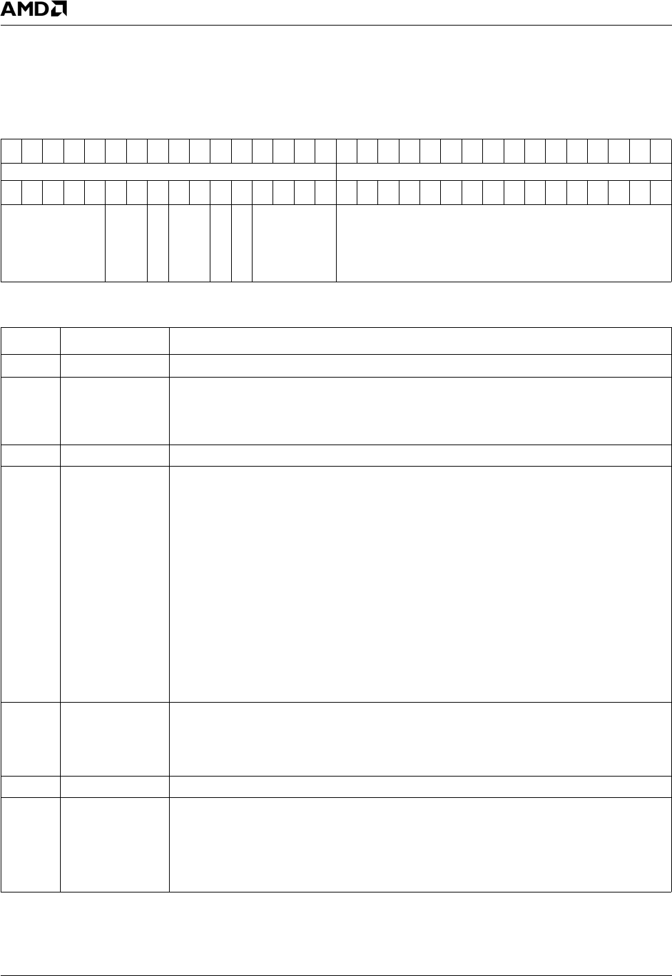
162 AMD Geode™ LX Processors Data Book
CPU Core Register Descriptions
33234H
5.5.2.64 Data Memory Subsystem Configuration 1 MSR (DM_CONFIG1_MSR)
MSR Address 00001801h
Ty p e R / W
Reset Value 00000000_00000000h
DM_CONFIG1_MSR Register Map
63 62 61 60 59 58 57 56 55 54 53 52 51 50 49 48 47 46 45 44 43 42 41 40 39 38 37 36 35 34 33 32
RSVD APFLOCK
313029282726252423222120191817161514131211109876543210
RSVD
APFMODE
APFENA
RSVD
PFXLOCKENA
NOPFXEVCT
ARRAYDIS PFXLOCK
DM_CONFIG1_MSR Bit Descriptions
Bits Name Description
63:48 RSVD Reserved.
47:32 APFLOCK Auto-Prefetch Lock. Bit mask of ways that cannot be allocated or replaced on an auto-
prefetch issued for a cache miss due to an instruction that is not using the restricted
cache prefix. Automatic prefetches that result from restricted cache prefix instructions
use the PFXLOCK field (bits [15:0]) for way masking. (Default = 0)
31:27 RSVD Reserved.
26:25 APFMODE Auto-Prefetch Mode. When auto-prefetching is enabled via the APFENA bit (bit 24),
APFMODE determines how the prefetches are issued as follows:
00: Even Only. An auto-prefetch is issued for the odd cache line when a fill is issued for
an even cache line, but no auto-prefetch is issued for a fill on an odd cache line. For
example, when a fill request is issued for address 0h, a prefetch will be issued for
address 20h. (Default)
01: Even/Odd. Auto-prefetches are issued for an odd cache line when an even fill is
issued, and for even cache lines when an odd fill is issued. (i.e the auto-prefetch
address is the toggle of fill address A[5]). Using this mode effectively increases the
DM logical cache line size to 64 bytes for fills. Line replacements and snoop evictions
are still done using a 32-byte line size.
1x: Increment. Auto-prefetches are issued for the next cache line (auto-prefetch line = fill
line + 1) when a fill is issued, except for the last cache line in a 4K page (fill address
bits [11:5] = 1111111b).
24 APFENA Auto-Prefetch Enable. Allows DM to perform automatic prefetch operations based on
cache fills as specified by the APFMODE field (bits [26:25]).
0: Disable.
1: Enable.
23:22 RSVD Reserved.
21 PFXLOCKENA Prefetch Prefix Instructions Lock Enable. When this bit is enabled, the LSLOCK field
in DM_CONFIG0 (MSR 00001800h[31:16]) determines which ways are available for
replacement for all processor memory references except prefetch instructions.
0: Disable the restricted cache feature. (Default)
1: Enable the restricted cache feature (PFXLOCK field, bits [15:0]).
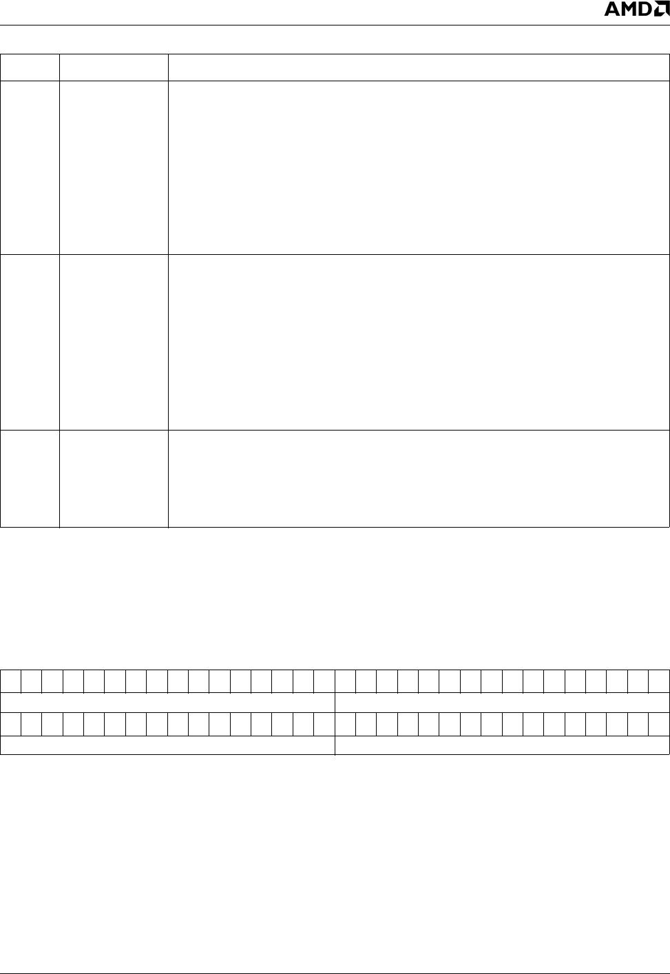
AMD Geode™ LX Processors Data Book 163
CPU Core Register Descriptions 33234H
5.5.2.65 Data Memory Subsystem Prefetch Lock MSR (DM_PFLOCK_MSR)
20 NOPFXEVCT No Prefetch Prefix Evictions. This bit disables clean line eviction in the case where a
new allocation occurs on a load/store miss when a move string operation uses the
REPNZ prefix instead of the normal REP prefix (restricted cache move feature, see PFX-
LOCK, bits [15:0]). When NOPFXEVCT is set, cache lines replaced by a load instruction
using the restricted cache prefix (REPNZ) will not be evicted if they are clean. (See EVC-
TONRPL bit description in DM_CONFIG0_MSR (MSR 00001800h[14]) for clean line
eviction feature). Clean line evictions of this type can be disabled in order to protect the
Victim mode L2 cache from being polluted by the transient data being moved. If this bit is
a 0, then normal clean line eviction occurs on any line replacement if enabled by the
EVCTONRPL bit. Note that any dirty line that is replaced will be evicted regardless of the
state of this bit. (Default = 0)
19:16 ARRAYDIS Array Disable. Mask used to disable individual cache arrays (way groups) in the DM to
save power or to avoid array defects. When an array is disabled, the DM will not read or
write the data array or tag array associated with this way group, reducing power. Any
data in the cache must be flushed before disabling an array or it will be lost.
Bit 19: Ways 15-12
Bit 18: Ways 11-8
Bit 17: Ways 7-4
Bit 16: Ways 3-0
0: Enable. (Default)
1: Disable.
15:0 PFXLOCK Prefetch Prefix Instructions Lock. Bit mask of ways that cannot be allocated or
replaced on a load miss when a move string operation uses the REPNZ prefix (instead of
the normal REP prefix). If all ways are locked, caching is effectively disabled, though the
cache will still be interrogated. Note that the REPNZ prefix has no effect on PREFETCH
instructions or writes to a write-allocate region that miss the cache and cause a write-
allocate. (Default = 0)
MSR Address 00001804h
Ty p e R / W
Reset Value 00000000_00000000h
DM_CONFIG1_MSR Bit Descriptions (Continued)
Bits Name Description
DM_PFLOCK_MSR Register Map
63 62 61 60 59 58 57 56 55 54 53 52 51 50 49 48 47 46 45 44 43 42 41 40 39 38 37 36 35 34 33 32
PFLOCKT2 PFLOCKT1
313029282726252423222120191817161514131211109876543210
PFLOCKT0 PFLOCKNTA
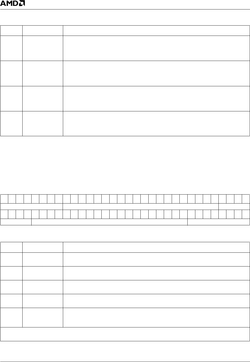
164 AMD Geode™ LX Processors Data Book
CPU Core Register Descriptions
33234H
5.5.2.66 Default Region Configuration Properties MSR (RCONF_DEFAULT_MSR)
DM_PFLOCK_MSR Bit Descriptions
Bits Name Description
63:48 PFLOCKT2 Prefetch Lockout of PREFETCHT2. Bit mask of ways that cannot be allocated or
replaced on a data prefetch miss on a PREFECTHT2 instruction. If all ways are locked,
PREFETCHT2 is effectively disabled. Use this field to prevent data prefetch operations
from polluting too much of the cache. (Default = 0)
47:32 PFLOCKT1 Prefetch Lockout of PREFETCHT1. Bit mask of ways that cannot be allocated or
replaced on a data prefetch miss on a PREFECTHT1 instruction. If all ways are locked,
PREFETCHT1 is effectively disabled. Use this field to prevent data prefetch operations
from polluting too much of the cache. (Default = 0)
31:16 PFLOCKT0 Prefetch Lockout of PREFETCHT0. Bit mask of ways that cannot be allocated or
replaced on a data prefetch miss on a PREFECTHT0 instruction. If all ways are locked,
PREFETCHT0 is effectively disabled. Use this field to prevent data prefetch operations
from polluting too much of the cache. (Default = 0)
15:0 PFLOCKNTA Prefetch Lockout of PREFETCHNTA. Bit mask of ways that cannot be allocated or
replaced on a data prefetch miss on a PREFECTHNTA instruction. If all ways are locked,
PREFETCHNTA is effectively disabled. Use this field to prevent data prefetch operations
from polluting too much of the cache. (Default = 0)
MSR Address 00001808h
Ty p e R / W
Reset Value 01FFFFF0_10000001h
Warm Start Value 04xxxxx0_1xxxxx01h
RCONF_DEFAULT_MSR Register Map
63 62 61 60 59 58 57 56 55 54 53 52 51 50 49 48 47 46 45 44 43 42 41 40 39 38 37 36 35 34 33 32
ROMRP ROMBASE DEVRP
313029282726252423222120191817161514131211109876543210
DEVRP SYSTOP SYSRP
RCONF_DEFAULT_MSR Bit Descriptions
Bit Name Description
63:56 ROMRP ROM Region Properties. Region properties for addresses greater than ROMBASE (bits
55:36]).
55:36 ROMBASE ROM Base Address. Base address for boot ROM. This field represents A[32:12] of the
memory address space, 4 KB granularity.
35:28 DEVRP SYSTOP to ROMBASE Region Properties. Region properties for addresses less than
ROMBASE (bits 55:36]) and addresses greater than or equal to SYSTOP (bits [27:8]).
27:8 SYSTOP Top of System Memory. Top of system memory that is available for general processor
use. The frame buffer and other private memory areas are located above SYSTOP.
7:0 SYSRP System Memory Region Properties. Region properties for addresses less than SYS-
TOP (bits [27:8]). Note that Region Configuration 000A0000h-000FFFFFh takes prece-
dence over SYSRP.
Note: Region Properties: Bits [7:6] = RSVD; Bit 5 = WS; Bit 4 = WC; Bit 3 = WT; Bit 2 = WP; Bit 1 = WA; Bit 0 = CD.
See "Region Properties" on page 170 for further details.

AMD Geode™ LX Processors Data Book 165
CPU Core Register Descriptions 33234H
5.5.2.67 Region Configuration Bypass MSR (RCONF_BYPASS_MSR)
5.5.2.68 Region Configuration A0000-BFFFF MSR (RCONF_A0_BF_MSR)
MSR Address 0000180Ah
Ty p e R / W
Reset Value 00000000_00000101h
Warm Start Value 00000000_00000219h
RCONF_BYPASS_MSR Register Map
63 62 61 60 59 58 57 56 55 54 53 52 51 50 49 48 47 46 45 44 43 42 41 40 39 38 37 36 35 34 33 32
RSVD
313029282726252423222120191817161514131211109876543210
RSVD RPSMHDR RPTLB
RCONF_BYPASS_MSR Bit Descriptions
Bit Name Description
63:16 RSVD Reserved.
15:8 RPSMHDR Region Properties during SMM/DMM. Region configuration properties used during
SMM/DMM header accesses.
7:0 RPTLB Region Properties during Tablewalks.
Note: Region Properties: Bits [7:6] = RSVD; Bit 5 = WS; Bit 4 = WC; Bit 3 = WT; Bit 2 = WP; Bit 1 = WA; Bit 0 = CD.
See "Region Properties" on page 170 for further details.
MSR Address 0000180Bh
Ty p e R / W
Reset Value 01010101_01010101h
Warm Start Value 19191919_19191919h
RCONF_A0_BF_MSR Register Map
63 62 61 60 59 58 57 56 55 54 53 52 51 50 49 48 47 46 45 44 43 42 41 40 39 38 37 36 35 34 33 32
RPBC RPB8 RPB4 RPB0
313029282726252423222120191817161514131211109876543210
RPAC RPA8 RPA4 RPA0
RCONF_A0_BF_MSR Bit Descriptions
Bit Name Description
63:56 RPBC Region Properties for 000BC000-000BFFFF.
55:48 RPB8 Region Properties for 000B8000-000BBFFF.
47:40 RPB4 Region Properties for 000B4000-000BAFFF.
39:32 RPB0 Region Properties for 000B0000-000B3FFF.
31:24 RPAC Region Properties for 000AC000-000AFFFF.
23:16 RPA8 Region Properties for 000A8000-000ABFFF.
15:8 RPA4 Region Properties for 000A4000-000A7FFF.
7:0 RPA0 Region Properties for 000A0000-000A3FFF.
Note: Region Properties: Bits [7:6] = RSVD; Bit 5 = WS; Bit 4 = WC; Bit 3 = WT; Bit 2 = WP; Bit 1 = WA; Bit 0 = CD.
See "Region Properties" on page 170 for further details.
166 AMD Geode™ LX Processors Data Book
CPU Core Register Descriptions
33234H
5.5.2.69 Region Configuration C0000-DFFFF MSR (RCONF_C0_DF_MSR)
5.5.2.70 Region Configuration E0000-FFFFF MSR (RCONF_E0_FF_MSR)
MSR Address 0000180Ch
Ty p e R / W
Reset Value 01010101_01010101h
Warm Start Value 19191919_19191919h
RCONF_C0_DF_MSR Register Map
63 62 61 60 59 58 57 56 55 54 53 52 51 50 49 48 47 46 45 44 43 42 41 40 39 38 37 36 35 34 33 32
RPDC RPD8 RPD4 RPD0
313029282726252423222120191817161514131211109876543210
RPCC RPC8 RPC4 RPC0
RCONF_C0_DF_MSR Bit Descriptions
Bit Name Description
63:56 RPDC Region Properties for 000DC000-000DFFFF.
55:48 RPD8 Region Properties for 000D8000-000DBFFF.
47:40 RPD4 Region Properties for 000D4000-000DAFFF.
39:32 RPD0 Region Properties for 000D0000-000D3FFF.
31:24 RPCC Region Properties for 000CC000-000CFFFF.
23:16 RPC8 Region Properties for 000C8000-000CBFFF.
15:8 RPC4 Region Properties for 000C4000-000C7FFF.
7:0 RPC0 Region Properties for 000C0000-000C3FFF.
Note: Region Properties: Bits [7:6] = RSVD; Bit 5 = WS; Bit 4 = WC; Bit 3 = WT; Bit 2 = WP; Bit 1 = WA; Bit 0 = CD.
See "Region Properties" on page 170 for further details.
MSR Address 0000180Dh
Ty p e R / W
Reset Value 01010101_01010101h
Warm Start Value 19191919_19191919h
RCONF_E0_FF_MSR Register Map
63 62 61 60 59 58 57 56 55 54 53 52 51 50 49 48 47 46 45 44 43 42 41 40 39 38 37 36 35 34 33 32
RPFC RPF8 RPF4 RIF0
313029282726252423222120191817161514131211109876543210
RPEC RPE8 RPE4 RPE0
AMD Geode™ LX Processors Data Book 167
CPU Core Register Descriptions 33234H
5.5.2.71 Region Configuration SMM MSR (RCONF_SMM_MSR)
RCONF_E0_FF_MSR Bit Descriptions
Bit Name Description
63:56 RPFC Region Properties for 000FC000-000FFFFF.
55:48 RPF8 Region Properties for 000F8000-000FBFFF.
47:40 RPF4 Region Properties for 000F4000-000FAFFF.
39:32 RPF0 Region Properties for 000F0000-000F3FFF.
31:24 RPEC Region Properties for 000EC000-000EFFFF.
23:16 RPE8 Region Properties for 000E8000-000EBFFF.
15:8 RPE4 Region Properties for 000E4000-000E7FFF.
7:0 RPE0 Region Properties for 000E0000-000E3FFF.
Note: Region Properties: Bits [7:6] = RSVD; Bit 5 = WS; Bit 4 = WC; Bit 3 = WT; Bit 2 = WP; Bit 1 = WA; Bit 0 = CD.
See "Region Properties" on page 170 for further details.
MSR Address 0000180Eh
Ty p e R / W
Reset Value 00000001_00000001h
Warm Start Value xxxxx001_xxxxx005h
RCONF_SMM_MSR Register Map
63 62 61 60 59 58 57 56 55 54 53 52 51 50 49 48 47 46 45 44 43 42 41 40 39 38 37 36 35 34 33 32
SMMTOP RSVD RPSMM
313029282726252423222120191817161514131211109876543210
SMMBASE RSVD
RPSMM_EN
SMM_NORM
RCONF_SMM_MSR Bit Descriptions
Bit Name Description
63:44 SMMTOP Top of SMM. Top of SMM region, 4 KB granularity inclusive.
43:40 RSVD Reserved.
39:32 RPSMM Region Properties in SMM Region when SMM Active.
31:12 SMMBASE Start of SMM. Start of SMM region, 4 KB granularity inclusive
11:9 RSVD Reserved.
8 RPSMM_EN SMM Properties Region Enable.
0: Disable.
1: Enable.
7:0 SMM_NORM Region Properties in SMM Region when SMM Inactive.
Note: Region Properties: Bits [7:6] = RSVD; Bit 5 = WS; Bit 4 = WC; Bit 3 = WT; Bit 2 = WP; Bit 1 = WA; Bit 0 = CD.
See "Region Properties" on page 170 for further details.
168 AMD Geode™ LX Processors Data Book
CPU Core Register Descriptions
33234H
5.5.2.72 Region Configuration DMM MSR (RCONF_DMM_MSR)
MSR Address 0000180Fh
Ty p e R / W
Reset Value 00000001_00000001h
Warm Start Value xxxxx001_xxxxx005h
RCONF_DMM_MSR Register Map
63 62 61 60 59 58 57 56 55 54 53 52 51 50 49 48 47 46 45 44 43 42 41 40 39 38 37 36 35 34 33 32
DMMTOP RSVD RPDMM
313029282726252423222120191817161514131211109876543210
DMMBASE RSVD
RPDMM_EN
DMM_NORM
RCONF_DMM_MSR Register Bit Descriptions
Bit Name Description
63:44 DMMTOP Top of DMM. Top of DMM region, 4 KB granularity inclusive.
43:40 RSVD Reserved.
39:32 RPDMM Region Properties in DMM Region when DMM Active.
31:12 DMMBASE Start of DMM. Start of DMM region, 4 KB granularity inclusive.
11:9 RSVD Reserved.
8 RPDMM_EN DMM Properties Region Enable.
0: Disable.
1: Enable.
7:0 DMM_NORM Region Properties in DMM Region when DMM Inactive.
Note: Region Properties: Bits [7:6] = RSVD; Bit 5 = WS; Bit 4 = WC; Bit 3 = WT; Bit 2 = WP; Bit 1 = WA; Bit 0 = CD.
See "Region Properties" on page 170 for further details.
AMD Geode™ LX Processors Data Book 169
CPU Core Register Descriptions 33234H
5.5.2.73 Region Configuration Range MSRs 0 through 7
Region Configuration Range 0 MSR (RCONF0_MSR)
Region Configuration Range 1 MSR (RCONF1_MSR)
Region Configuration Range 2 MSR (RCONF2_MSR)
Region Configuration Range 3 MSR (RCONF3_MSR)
Region Configuration Range 4 MSR (RCONF4_MSR)
Region Configuration Range 5 MSR (RCONF5_MSR)
Region Configuration Range 6 MSR (RCONF6_MSR)
Region Configuration Range 7 MSR (RCONF7_MSR)
MSR Address 00001810h
Ty p e R / W
Reset Value 00000000_00000000h
Warm Start Value xxxxx000_xxxxx0xxh
MSR Address 00001811h
Ty p e R / W
Reset Value 00000000_00000000h
Warm Start Value xxxxx000_xxxxx0xxh
MSR Address 00001812h
Ty p e R / W
Reset Value 00000000_00000000h
Warm Start Value xxxxx000_xxxxx0xxh
MSR Address 00001813h
Ty p e R / W
Reset Value 00000000_00000000h
Warm Start Value xxxxx000_xxxxx0xxh
MSR Address 00001814h
Typ e R / W
Reset Value 00000000_00000000h
Warm Start Value xxxxx000_xxxxx0xxh
MSR Address 00001815h
Typ e R / W
Reset Value 00000000_00000000h
Warm Start Value xxxxx000_xxxxx0xxh
MSR Address 00001816h
Typ e R / W
Reset Value 00000000_00000000h
Warm Start Value xxxxx000_xxxxx0xxh
MSR Address 00001817h
Typ e R / W
Reset Value 00000000_00000000h
Warm Start Value xxxxx000_xxxxx0xxh
RCONFx_MSR Register Map
63 62 61 60 59 58 57 56 55 54 53 52 51 50 49 48 47 46 45 44 43 42 41 40 39 38 37 36 35 34 33 32
RPTOP RSVD
313029282726252423222120191817161514131211109876543210
RPBASE RSVD
RPEN
RP
RCONFx_MSR Bit Descriptions
Bit Name Description
63:44 RPTOP Top of Range. 4 KB granularity, inclusive.
43:32 RSVD Reserved.
31:12 RPBASE Start of Range. 4 KB granularity, inclusive.
11:9 RSVD Reserved.
8 RPEN Enable Range.
0: Disable range.
1: Enable range.
7:0 RP Range Properties.
Note: Region Properties: Bits [7:6] = RSVD; Bit 5 = WS; Bit 4 = WC; Bit 3 = WT; Bit 2 = WP; Bit 1 = WA; Bit 0 = CD.
See "Region Properties" on page 170 for further details.
170 AMD Geode™ LX Processors Data Book
CPU Core Register Descriptions
33234H
Region Properties
The region properties consist of an 8-bit field as shown in Table 5-15. Table 5-16 and Table 5-17 describe the various region
properties effects on read and write operations. Note that the cache is always interrogated even in regions that are not
cacheable, and read hits are serviced from the cache while write hits update the cache and are sent to the bus using the
region’s write semantics.
Table 5-15. Region Properties Register Map
76543210
(RSVD)
Reserved
WS
(Write-serialize)
WC
(Write-combine)
WT
(Write-through)
WP
(Write-protect)
WA
(Write-allocate)
CD
(Cache Disable)
Table 5-16. Read Operations vs. Region Properties
WS WC WT WP WA CD Description
0xxxx0Cacheable. Read misses cause a cache line to be allocated.
1xxxx0Undefined State. Unpredictable behavior occurs.
xxxxx1Uncacheable. Reads are sent unmodified to the bus. Cache is still interro-
gated and provides data for read hits. Used for accessing memory-mapped
devices.
Note: “x” indicates setting or clearing this bit has no effect.
Table 5-17. Write Operations vs. Region Properties
WS WC WT WP WA CD Description
xxx1xxWrite-protected. Writes to the region are discarded.
1xxxx0Undefined State. Unpredictable behavior occurs.
x1xxx0Undefined State. Unpredictable behavior occurs.
xxxx11Undefined State. Unpredictable behavior occurs.
000000Write-back Cacheable. Write misses are sent to the bus, a cache line is not
allocated on a write miss.
000010Write-back Cacheable/Write-allocate. Write misses allocate a line in the
cache.
0010x0Write-through cacheable. Write misses do not allocate a line in the cache.
Write hits update the cache but do not mark the line as dirty. All writes are sent
to the bus.
000001Uncacheable. All writes are sent to the bus in strict program order without any
combining. Write hits still update the cache. Traditionally used for accessing
memory-mapped devices (but see write-burstable below).
100001Uncacheable. All writes are sent to the bus in strict program order without any
combining. Write hits still update the cache. Traditionally used for accessing
memory-mapped devices (but see write-burstable below).
Write-serialize. Limit the number of outstanding writes to the value of the
WSREQ field in DM_CONFIG0_MSR (MSR 00001800h[46:44]).
010001Write-combined (uncacheable). Writes to the same cache line may be com-
bined. Multiple writes to the same byte results in a single write with the last
value specified. Write order is not preserved; ideal for use with frame buffers.
AMD Geode™ LX Processors Data Book 171
CPU Core Register Descriptions 33234H
If paging is enabled, the region properties can be further modified by the PCD and PWT flags in the page table entry. The
PCD flag is OR’d with the CD bit of the region properties, and the PWT bit is OR’d with the WT bit of the region properties.
A similar combination is performed during tablewalks using the PCD/PWT bits from CR3 for the DTE access and the
PCD/PWT bits from the DTE for the PTE access. The net effect is that the WC and WS flags may actually be used even for
a region that is marked cacheable if a page table mapping later forces it to be uncacheable. For regions that are write-com-
bined, the PWT flag in the page table can be used to force write-burstable properties for selected pages.
110001Write-combined (uncacheable). Writes to the same cache line may be com-
bined. Multiple writes to the same byte results in a single write with the last
value specified. Write order is not preserved; ideal for use with frame buffers.
Write-serialize. Limit the number of outstanding writes to the value of the
WSREQ field in DM_CONFIG0_MSR (MSR 00001800h[46:44]).
011001Write-burstable (uncacheable). Writes to the same cache line are combined
as long as they are to increasing addresses and do not access a previously
written byte. Multiple writes to the same byte results in multiple bytes on the
bus. The semantics match write bursting on PCI and should therefore be suit-
able for accessing memory-mapped devices.
111001Write-burstable (uncacheable). Writes to the same cache line are combined
as long as they are to increasing addresses and do not access a previously
written byte. Multiple writes to the same byte results in multiple bytes on the
bus. The semantics match write bursting on PCI and should therefore be suit-
able for accessing memory-mapped devices.
Write-serialize. Limit the number of outstanding writes to the value of the
WSREQ field in DM_CONFIG0_MSR (MSR 00001800h[46:44]).
Note: “x” indicates setting or clearing this bit has no effect.
Table 5-17. Write Operations vs. Region Properties (Continued)
WS WC WT WP WA CD Description
172 AMD Geode™ LX Processors Data Book
CPU Core Register Descriptions
33234H
5.5.2.74 x86 Control Registers MSRs (CR1, CR2, CR3, CR4)
These are the standard x86 Control Registers CR1, CR2, CR3, and CR4. CR0 is located at MSR 00001420h (see Section
5.5.2.50 on page 149). The contents of CR0-CR4 should only be accessed using the MOV instruction. They are mentioned
here for completeness only. See Section 5.4.1 “Control Registers” on page 95 for bit descriptions
x86 Control Register 1 MSR (CR1_MSR)
x86 Control Register 2 MSR (CR2_MSR)
x86 Control Register 3 MSR (CR3_MSR)
x86 Control Register 4 MSR (CR4_MSR)
5.5.2.75 Data Cache Index MSR (DC_INDEX_MSR)
MSR Address 00001881h
Ty p e R / W
Reset Value 00000000_xxxxxxxxh
MSR Address 00001882h
Ty p e R / W
Reset Value 00000000_xxxxxxxxh
MSR Address 00001883h
Typ e R / W
Reset Value 00000000_xxxxxxxxh
MSR Address 00001884h
Typ e R / W
Reset Value 00000000_xxxxxxxxh
MSR Address 00001890h
Ty p e R / W
Reset Value 00000000_00000000h
DC_INDEX_MSR Register Map
63 62 61 60 59 58 57 56 55 54 53 52 51 50 49 48 47 46 45 44 43 42 41 40 39 38 37 36 35 34 33 32
RSVD
313029282726252423222120191817161514131211109876543210
RSVD
DC_DSEL
RSVD DC_LINE DC_WAY
DC_INDEX_MSR Bit Descriptions
Bit Name Description
63:18 RSVD (RO) Reserved (Read Only).
17:16 DC_DSEL Data QWORD Select. Determines which QWORD in a cache line is accessed by a read
or a write to DC_DATA_MSR (MSR 00001891h). DC_DSEL increments on accesses to
DC_DATA and resets to 0 on accesses to DC_TAG_MSR (MSR 00001892h) or
DC_TAG_I_MSR (MSR 00001893h).
15:11 RSVD (RO) Reserved (Read Only).
10:4 DC_LINE Cache Line Select. Forms the high 7 bits of a 9-bit counter. The DC_WAY field (bits
[1:0]) forms the low 2 bits of the counter. This field increments when DC_WAY overflows
on an access to DC_TAG_I_MSR (MSR 00001893h).
3:0 DC_WAY Cache Way Select. Forms the low 2 bits of a 9-bit counter. The DC_LINE field (bits
[10:4]) forms the high 7 bits of the counter. This field post-increments on accesses to
DC_TAG_I_MSR (MSR 00001893h).
AMD Geode™ LX Processors Data Book 173
CPU Core Register Descriptions 33234H
5.5.2.76 Data Cache Data MSR (DC_DATA_MSR)
5.5.2.77 Data Cache Tag MSR (DC_TAG_MSR)
MSR Address 00001891h
Ty p e R / W
Reset Value 00000000_00000000h
DC_DATA_MSR Register Map
63 62 61 60 59 58 57 56 55 54 53 52 51 50 49 48 47 46 45 44 43 42 41 40 39 38 37 36 35 34 33 32
DC_DATA
313029282726252423222120191817161514131211109876543210
DC_DATA
DC_DATA_MSR Bit Descriptions
Bit Name Description
63:0 DC_DATA Data Cache Data. QWORD data to read from or write to the cache line buffer. The buffer
is filled from the cache data array on a read to DC_TAG_MSR (MSR 00001892h) or
DC_TAG_I_MSR (MSR 00001893h), and the buffer is written to the cache data array on
a write to DC_TAG_MSR or DC_TAG_I_MSR MSRs. The DC_DSEL field in the
DC_INDEX_MSR (MSR 00001890h[17:16]) selects which QWORD in the buffer is
accessed by DC_DATA, and each access to DC_DATA increments DC_DSEL.
MSR Address 00001892h
Ty p e R / W
Reset Value 00000000_00000000h
DC_TAG_MSR Register Map
63 62 61 60 59 58 57 56 55 54 53 52 51 50 49 48 47 46 45 44 43 42 41 40 39 38 37 36 35 34 33 32
RSVD LRU
313029282726252423222120191817161514131211109876543210
TAG RSVD
DIRTY
VALID
DC_TAG_MSR Bit Descriptions
Bits Name Description
63:50 RSVD (RO) Reserved (Read Only). (Default = 0)
174 AMD Geode™ LX Processors Data Book
CPU Core Register Descriptions
33234H
5.5.2.78 Data Cache Tag with Increment MSR (DC_TAG_I_MSR)
Bit descriptions for this register are the same as for MSR 00001892h, except read/write of this register causes an auto-
increment on DC_INDEX_MSR (MSR 00001890h).
49:32 LRU Least Recently Used Value. (Default = 0)
Bit 49: Ways 11-8 more recent than ways 15-12.
Bit 48: Ways 7-4 more recent than ways 15-12.
Bit 47: Ways 7-4 more recent than ways 11-8.
Bit 46: Ways 3-0 more recent than ways 15-12.
Bit 45: Ways 3-0 more recent than ways 11-8.
Bit 44: Ways 3-0 more recent than ways 7-4.
Bit 43: Ways 15-14 more recent than ways 13-12.
Bit 42: Ways 11-10 more recent than ways 9-8.
Bit 41: Ways 7-6 more recent than ways 5-4.
Bit 40: Ways 3-2 more recent than ways 1-0.
Bit 39: Way 15 more recent than way 14.
Bit 38: Way 13 more recent than way 12.
Bit 37: Way 11 more recent than way 10.
Bit 36: Way 9 more recent than way 8.
Bit 35: Way 7 more recent than way 6.
Bit 34: Way 5 more recent than way 4.
Bit 33: Way 3 more recent than way 2.
Bit 32: Way 1 more recent than way 0.
0: False
1: True
31:12 TAG Tag. Cache Tag Value for line/way selected by DC_INDEX (MSR 00001890h).
(Default = 0)
11:2 RSVD (RO) Reserved (Read Only). (Default = 0)
1DIRTY Dirty. Dirty bit for line/way. (Default = 0)
WARNING: Operation is undefined if the Dirty bit is set to 1 and the Valid bit is 0.
0VALID Valid. Valid bit for the line/way selected by DC_INDEX (MSR 00001890h). (Default = 0)
MSR Address 00001893h
Ty p e R / W
Reset Value 00000000_00000000h
DC_TAG_MSR Bit Descriptions (Continued)
Bits Name Description
DC_TAG_I_MSR Register Map
63 62 61 60 59 58 57 56 55 54 53 52 51 50 49 48 47 46 45 44 43 42 41 40 39 38 37 36 35 34 33 32
RSVD LRU
313029282726252423222120191817161514131211109876543210
TAG RSVD
DIRTY
VALID

AMD Geode™ LX Processors Data Book 175
CPU Core Register Descriptions 33234H
5.5.2.79 Data/Instruction Cache Snoop Register (SNOOP_MSR)
The SNOOP_MSR provides a mechanism for injecting a “snoop-for-write” request into the memory subsystem. Both the I
and D caches are snooped for the specified physical address. A hit to a dirty line in the D cache results in a writeback fol-
lowed by the line being invalidated. A hit to a clean line results in only an invalidation. The SNOOP_MSR is write-only - the
read value is undefined. There is no indication as to whether the snoop hit in the caches.
5.5.2.80 L1 Data TLB Index Register (L1DTLB_INDEX_MSR)
MSR Address 00001894h
Ty p e WO
Reset Value 00000000_xxxxxxxxh
SNOOP_MSR Register Map
63 62 61 60 59 58 57 56 55 54 53 52 51 50 49 48 47 46 45 44 43 42 41 40 39 38 37 36 35 34 33 32
RSVD
313029282726252423222120191817161514131211109876543210
SNOOP_ADD
SNOOP_MSR Bit Descriptions
Bit Name Description
63:32 RSVD Reserved (Write Only). Write as 0.
31:0 SNOOP_ADD Cache Snoop Address (Write Only). Physical address to snoop in the caches. A hit to a
dirty line results in a writeback followed by an invalidation. A hit to a clean line results in
an invalidation only. Both the data and instruction caches are snooped.
MSR Address 00001898h
Ty p e R / W
Reset Value 00000000_00000000h
L1DTLB_INDEX_MSR Register Map
63 62 61 60 59 58 57 56 55 54 53 52 51 50 49 48 47 46 45 44 43 42 41 40 39 38 37 36 35 34 33 32
RSVD
313029282726252423222120191817161514131211109876543210
RSVD INDEX
L1DTLB_INDEX_MSR Bit Descriptions
Bit Name Description
63:3 RSVD (RO) Reserved (Read Only).
2:0 INDEX L1 Data TLB Index. Index of L1 Data TLB entry to access. Post increments on each
access to L1TLB_ENTRY_I_MSR (MSR 0000189Bh).

176 AMD Geode™ LX Processors Data Book
CPU Core Register Descriptions
33234H
5.5.2.81 L1 Data TLB Least Recently Used MSR (L1DTLB_LRU_MSR)
MSR Address 00001899h
Ty p e R / W
Reset Value 00000000_00000000h
L1DTLB_LRU_MSR Register Map
63 62 61 60 59 58 57 56 55 54 53 52 51 50 49 48 47 46 45 44 43 42 41 40 39 38 37 36 35 34 33 32
RSVD
313029282726252423222120191817161514131211109876543210
RSVD LRU
L1DTLB_LRU_MSR Bit Descriptions
Bits Name Description
63:18 RSVD (RO) Reserved (Read Only).
17:0 LRU Least Recently Used Value.
Bit 17: Entries 8-11 more recent than entries 12-15.
Bit 16: Entries 4-7 more recent than entries 12-15.
Bit 15: Entries 4-7 more recent than entries 8-11.
Bit 14: Entries 0-3 more recent than entries 12-15.
Bit 13: Entries 0-3 more recent than entries 8-11.
Bit 12: Entries 0-3 more recent than entries 4-7.
Bit 11: Entries 12/13 more recent than entries 14/15.
Bit 10: Entries 8/9 more recent than entries 10/11.
Bit 9: Entries 4/5 more recent than entries 6/7.
Bit 8: Entries 0/1 more recent than entries 2/3.
Bit 7: Entry 14 more recent than entry 15.
Bit 6: Entry 12 more recent than entry 13.
Bit 5: Entry 10 more recent than entry 11.
Bit 4: Entry 8 more recent than entry 9.
Bit 3: Entry 6 more recent than entry 7.
Bit 2: Entry 4 more recent than entry 5.
Bit 1: Entry 2 more recent than entry 3.
Bit 0: Entry 0 more recent than entry 1.
0: False (Default)
1: True
AMD Geode™ LX Processors Data Book 177
CPU Core Register Descriptions 33234H
5.5.2.82 L1 Data TLB Entry MSR (L1DTLB_ENTRY_MSR)
MSR Address 0000189Ah
Ty p e R / W
Reset Value 00000000_00000000h
L1DTLB_ENTRY_MSR Register Map
63 62 61 60 59 58 57 56 55 54 53 52 51 50 49 48 47 46 45 44 43 42 41 40 39 38 37 36 35 34 33 32
LINADDR RSVD
WP
WA_WS
WC
313029282726252423222120191817161514131211109876543210
PHYSADDR RSVD
DIRTY
ACC
CD
WT_BR
US
WR
VALID
L1DTLB_ENTRY_MSR Bit Descriptions
Bit Name Description
63:44 LINADDR Linear Address. Address [32:12].
43:35 RSVD (RO) Reserved (Read Only).
34 WP Write-protect Flag.
0: Page can be written.
1: Page is write-protected.
33 WA_WS Write-allocate/Write-serialize Flag. If the page is cacheable, a 1 indicates the write-
allocate flag. If the page is non-cacheable, a 1 indicates the write-serialize flag.
32 WC Write-combine Flag. When this page is marked as non-cacheable, a 1indicates that
writes may be combined before being sent to the bus.
31:12 PHYSADDR Physical Address. Address [32:12]
11:7 RSVD (RO) Reserved (Read Only).
6DIRTY Dirty Flag. A 1 indicates that the page has been written to.
5ACC Accessed Flag. A 1 indicates an entry in the TLB.
4CD Cache Disable Flag. A 1 indicates that the page is uncacheable.
3WT_BR Write-through/Write-burst Flag. When the page is cacheable, a 1 indicates that the
page is write-through. When the page is non-cacheable, a 1 indicates that the page
allows write bursting.
2US User Access Privileges.
0: Supervisor.
1: User.
1WR Writable Flag.
0: Page can not be written.
1: Page can be written.
0VALID Valid Bit. A 1 indicates that the entry in the TLB is valid.
178 AMD Geode™ LX Processors Data Book
CPU Core Register Descriptions
33234H
5.5.2.83 L1 Data TLB Entry with Increment MSR (L1DTLB_ENTRY_I_MSR)
Bit descriptions for this register are the same as for MSR 0000189Ah, except read/write of this register causes an auto-
increment on the L1 TLB_INDEX_MSR (MSR 00001898h).
5.5.2.84 L2 TLB/DTE/PTE Index MSR (L2TLB_INDEX_MSR)
MSR Address 0000189Bh
Ty p e R / W
Reset Value 00000000_00000000h
L1DTLB_ENTRY_I_MSR Register Map
63 62 61 60 59 58 57 56 55 54 53 52 51 50 49 48 47 46 45 44 43 42 41 40 39 38 37 36 35 34 33 32
LINADDR RSVD
WP
WA_WS
WC
313029282726252423222120191817161514131211109876543210
PHYSADDR RSVD
DIRTY
ACC
CD
WT_BR
US
WR
VALID
MSR Address 0000189Ch
Ty p e R / W
Reset Value 00000000_00000000h
L2TLB_INDEX_MSR Register Map
63 62 61 60 59 58 57 56 55 54 53 52 51 50 49 48 47 46 45 44 43 42 41 40 39 38 37 36 35 34 33 32
RSVD
313029282726252423222120191817161514131211109876543210
RSVD SEL RSVD INDEX
WAY
INDEX
L2TLB_INDEX_MSR Bit Descriptions
Bit Name Description
If SEL (bits [17:16]) = 0x
63:18 RSVD (RO) Reserved (Read Only). (Default = 0)
17:16 SEL Select Array to Access.
0x: L2 TLB (64 entries, values 0-63).
10: DTE cache (12 entries, values 0-11).
11: 4M PTE cache (4 entries, values 0-3).
15:6 RSVD (RO) Reserved (Read Only). (Default = 0)
5:1 INDEX L2 TLB Index. Post-increments on an access to L2TB_ENTRY_I_MSR (MSR
0000189Fh) if WAY (bit 0) = 1.
0WAY Way to Access. Toggles on each access to L2TB_ENTRY_I_MSR (MSR 0000189Fh).
If SEL (bits [17:16]) = 1x
63:18 RSVD (RO) Reserved (Read Only). (Default = 0)
17:16 SEL Select Array to Access.
0x: L2 TLB (64 entries, values 0-63).
10: DTE cache (12 entries, values 0-11).
11: 4M PTE cache (4 entries, values 0-3).
AMD Geode™ LX Processors Data Book 179
CPU Core Register Descriptions 33234H
5.5.2.85 L2 TLB/DTE/PTE Least Recently Used MSR (L2TLB_LRU_MSR)
15:6 RSVD (RO) Reserved (Read Only). (Default = 0)
5:0 INDEX DTE/PTE Index. Increments on every access to L2TLB_ENTRY_I_MSR (MSR
0000189Fh).
MSR Address 0000189Dh
Ty p e R / W
Reset Value 00000000_00000000h
L2TLB_INDEX_MSR Bit Descriptions (Continued)
Bit Name Description
L2TLB_LRU_MSR Register Map
63 62 61 60 59 58 57 56 55 54 53 52 51 50 49 48 47 46 45 44 43 42 41 40 39 38 37 36 35 34 33 32
RSVD DTE_LRU
313029282726252423222120191817161514131211109876543210
RSVD PTE_LRU RSVD
L2WR1
L2TLB_LRU_MSR Bit Descriptions
Bits Name Description
63:53 RSVD (RO) Reserved (Read Only). (Default = 0)
52:32 DTE_LRU DTE Least Recently Used Value.
Bit 52: DTE entries 0-3 more recent than entries 4-7.
Bit 51: DTE entries 0-3 more recent than entries 8-11.
Bit 50: DTE entries 4-7 more recent than entries 8-11.
Bit 49: DTE entry 8 more recent than entry 9.
Bit 48: DTE entry 8 more recent than entry 10.
Bit 47: DTE entry 8 more recent than entry 11.
Bit 46: DTE entry 9 more recent than entry 10.
Bit 45: DTE entry 9 more recent than entry 11.
Bit 44: DTE entry 10 more recent than entry 11.
Bit 43: DTE entry 4 more recent than entry 5.
Bit 42: DTE entry 4 more recent than entry 6.
Bit 41: DTE entry 4 more recent than entry 7.
Bit 40: DTE entry 5 more recent than entry 6.
Bit 39: DTE entry 5 more recent than entry 7.
Bit 38: DTE entry 6 more recent than entry 7.
Bit 37: DTE entry 0 more recent than entry 1.
Bit 36: DTE entry 0 more recent than entry 2.
Bit 35: DTE entry 0 more recent than entry 3.
Bit 34: DTE entry 1 more recent than entry 2.
Bit 33: DTE entry 1 more recent than entry 3.
Bit 32: DTE entry 2 more recent than entry 3.
0: False (Default)
1: True
31:22 RSVD (RO) Reserved (Read Only). (Default = 0)
180 AMD Geode™ LX Processors Data Book
CPU Core Register Descriptions
33234H
5.5.2.86 L2 TLB/DTE/PTE Entry MSR (L2TLB_ENTRY_MSR)
21:16 PTE_LRU 4M PTE Least Recently Used Value.
Bit 21: 4M PTE entry 0 more recent than entry 1.
Bit 20: 4M PTE entry 0 more recent than entry 2.
Bit 19: 4M PTE entry 0 more recent than entry 3.
Bit 18: 4M PTE entry 1 more recent than entry 2.
Bit 17: 4M PTE entry 1 more recent than entry 3.
Bit 16: 4M PTE entry 2 more recent than entry 3.
0: False (Default)
1: True
15:1 RSVD (RO) Reserved (Read Only). (Default = 0)
0 L2WR1 L2 Write to Way 1. Next L2 TLB write to way 1 if both ways are valid. (Default = 0)
MSR Address 0000189Eh
Ty p e R / W
Reset Value 00000000_00000000h
L2TLB_LRU_MSR Bit Descriptions (Continued)
Bits Name Description
L2TLB_ENTRY_MSR Register Map
63 62 61 60 59 58 57 56 55 54 53 52 51 50 49 48 47 46 45 44 43 42 41 40 39 38 37 36 35 34 33 32
LINADDR RSVD
WP
WA_WS
WC
LINADDR RSVD
313029282726252423222120191817161514131211109876543210
PHYSADDR RSVD
GLOBAL
RSVD
DIRTY
ACC
CD
WT_BR
US
WR
VALID
4MPTE
WT
L2TLB_ENTRY_MSR Bit Descriptions
Bit Name Description
If SEL bits in L2TLB_INDEX MSR = 0x (MSR 0000189Ch[17:16] = 0x)
63:44 LINADDR Linear Address. Address [32:12].
43:35 RSVD (RO) Reserved (Read Only).
34 WP Write-protect Flag.
0: Page can be written.
1: Page is write-protected.
33 WA_WS Write-allocate/Write-serialize Flag. If the page is cacheable, a 1 indicates the write-
allocate flag. If the page is non-cacheable, a 1 indicates the write-serialize flag.
32 WC Write-combine Flag. When this page is marked as non-cacheable, a 1indicates that
writes may be combined before being sent to the bus.
31:12 PHYSADDR Physical Address. Address [32:12]
11:9 RSVD (RO) Reserved (Read Only).
8 GLOBAL Global Page Flag. A 1 indicates a global page.
AMD Geode™ LX Processors Data Book 181
CPU Core Register Descriptions 33234H
7 RSVD (RO) Reserved (Read Only).
6DIRTY Dirty Flag. A 1 indicates that the page has been written to.
5ACC Accessed Flag. A 1 indicates an entry in the TLB.
4CD Cache Disable Flag. A 1 indicates that the page is uncacheable.
3WT_BR Write-Through/Write Burst Flag. When the page is cacheable, a 1 indicates that the
page is write-through. When the page is non-cacheable, a 1 indicates that the page
allows write bursting.
2US User Access Privileges.
0: Supervisor.
1: User.
1WR Writable Flag.
0: Page can not be written.
1: Page can be written.
0VALID Valid Bit. A 1 indicates that the entry in the TLB is valid.
If SEL bits in L2TLB_INDEX MSR = 1x (MSR 0000189Ch[17:16] = 1x)
63:44 LINADDR Linear Address. Address [32:22].
53:32 RSVD (RO) Reserved (Read Only).
31:12 PHYSADDR Physical Address. Address [32:12]
11:9 RSVD (RO) Reserved (Read Only).
8 GLOBAL Global Page Flag. A 1 indicates a global page.
74MPTE 4M PTE Flag.
0: DTE access.
1: 4M PTE access.
6DIRTY Dirty Flag. A 1 indicates that the page has been written to.
5ACC Accessed Flag. A 1 indicates an entry in the TLB.
4CD Cache Disable Flag. A 1 indicates that the page is uncacheable.
3WT Write-through Flag. A 1 indicates that the page is write-through.
2US User Access Privileges.
0: Supervisor.
1: User.
1WR Writable Flag.
0: Page can not be written.
1: Page can be written.
0VALID Valid Bit. A 1 indicates that the entry in the TLB is valid.
L2TLB_ENTRY_MSR Bit Descriptions (Continued)
Bit Name Description
182 AMD Geode™ LX Processors Data Book
CPU Core Register Descriptions
33234H
5.5.2.87 L2 TLB/DTE/PTE Entry with Increment MSR (L2TLB_ENTRY_I_MSR)
Bit descriptions for this register are the same as for MSR 0000189Eh, except read/write of this register causes an auto-
increment on the L2TLB_INDEX_MSR (MSR 0000189Ch).
5.5.2.88 Data Memory Subsystem Built-In Self-Test MSR (DM_BIST_MSR)
MSR Address 0000189Fh
Ty p e R / W
Reset Value 00000000_00000000h
L2TLB_ENTRY_I_MSR Register Map
63 62 61 60 59 58 57 56 55 54 53 52 51 50 49 48 47 46 45 44 43 42 41 40 39 38 37 36 35 34 33 32
LINADDR RSVD
WP
WA_WS
WC
313029282726252423222120191817161514131211109876543210
PHYSADDR RSVD
GLOBAL
RSVD
DIRTY
ACC
CD
WT_BR
US
WR
VALID
MSR Address 000018C0h
Ty p e R / W
Reset Value 00000000_00000000h
DM_BIST_MSR Register Map
63 62 61 60 59 58 57 56 55 54 53 52 51 50 49 48 47 46 45 44 43 42 41 40 39 38 37 36 35 34 33 32
TAGC M P TAGDAT
313029282726252423222120191817161514131211109876543210
TLBCMP
TLBDAT
DATA RSVD
RETEN_TLB
RUN_TLB
RETEN_DATA
RUN_DATA
RETEN_TAG
RUN_TAG
DM_BIST_MSR Bit Descriptions
Bits Name Description
63:48 TAGCMP[15:0]
(RO)
Cache Tag Comparators (Read Only). BIST results for cache tag comparators
(array15...array0).
0: Fail.
1: Pass.
47:32 TAGDAT[15:0]
(RO)
Cache Tag Data (Read Only). BIST results for cache tag data integrity (array15...array0).
0: Fail.
1: Pass.
31:30 TLBCMP[1:0]
(RO)
L2 TLB Comparators (Read Only). BIST results for L2 TLB comparators (array1, array0).
0: Fail.
1: Pass.
29:28 TLBDAT[1:0]
(RO)
L2 TLB Data (Read Only). BIST results for L2 TLB data integrity (array1, array0).
0: Fail.
1: Pass.
27:24 DATA[3:0] (RO) Data Cache Data (Read Only). BIST results for data cache data arrays[3:0].
0: Fail.
1: Pass.
23:6 RSVD (RO) Reserved (Read Only). Read as 0.
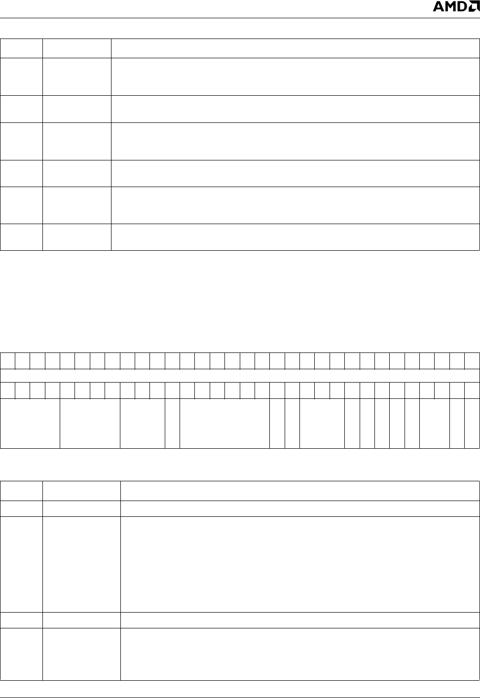
AMD Geode™ LX Processors Data Book 183
CPU Core Register Descriptions 33234H
5.5.2.89 Bus Controller Configuration 0 MSR (BC_CONFIG0_MSR)
5 RETEN_TLB L2 TLB Retention Timer. Enable retention timer for L2 TLB BIST.
0: Disable.
1: Enable.
4 RUN_TLB L2 TLB Run. Start BIST test on L2 TLB arrays. Should read as 0 because BIST will have
completed before the MSR read can start.
3 RETEN_DATA Cache Data Retention Timer. Enable retention timer for cache data array BIST.
0: Disable.
1: Enable.
2 RUN_DATA Cache Data Run. Start BIST test on cache data array. Should read as 0 because BIST will
have completed before the MSR read can start.
1 RETEN_TAG Cache Tag Retention Timer. Enable retention timer for cache tag array BIST.
0: Disable.
1: Enable.
0 RUN_TAG Cache Tag Run. Start BIST test on cache tag arrays. Should read as 0 because BIST will
have completed before the MSR read can start.
MSR Address 00001900h
Ty p e R / W
Reset Value 00000000_00000111h
DM_BIST_MSR Bit Descriptions
Bits Name Description
BC_CONFIG0_MSR Register Map
63 62 61 60 59 58 57 56 55 54 53 52 51 50 49 48 47 46 45 44 43 42 41 40 39 38 37 36 35 34 33 32
RSVD
313029282726252423222120191817161514131211109876543210
RSVD PAUSEDLY RSVD
GPF_X
RSVD
CLK_ONS
SUSP
RSVD
RTSC_SUSP
RSVD
TSC_DMM
TSC_SUSP
TSC_SMM
RSVD
ISNINV
SNOOP
BC_CONFIG0_MSR Bit Descriptions
Bit Name Description
63:28 RSVD Reserved. Write as read.
27:24 PAUSEDLY Pause Delay. This field sets the number of clocks for which the bus controller will attempt
to suspend the CPU when a PAUSE instruction is executed. The approximate number of
clocks is PAUSEDLY*8. NOTE that the actual number of clocks that the CPU is sus-
pended will differ from this value, and will vary from pause to pause due to the overhead
of the suspend/unsuspend mechanism and any other CPU activity that would affect how
it responds to suspend requests.
Note also that bit 1 of MSR 00001210h must be set in order for suspend on pause to be
enabled.
23:21 RSVD Reserved.
20 GPF_X General Protection Faults on EXCEPT Flags. Generate general protection faults on
MSR accesses whose response packets have the EXCEPT flag set.
0: Disable.
1: Enable.

184 AMD Geode™ LX Processors Data Book
CPU Core Register Descriptions
33234H
5.5.2.90 Bus Controller Configuration 1 MSR (BC_CONFIG1_MSR)
This register is reserved. Write as read.
19:14 RSVD Reserved. Write as read.
13 CLK_ONS CPU Core Clocks On during Suspend.
0: All CPU Core clocks off during Suspend. (Default)
1: All CPU Core clocks on during Suspend.
12 SUSP Suspend Active. Enable Suspend input.
0: Ignore Suspend input. (Default)
1: Enable Suspend input.
11:9 RSVD Reserved. Write as read.
8 RTSC_SUSP Real Time Stamp Counter Counts during Suspend.
0: Disable.
1: Enable. (Default)
7 RSVD Reserved. Write as read.
6TSC_DMM Time Stamp Counter Counts during DMM.
0: Disable. (Default)
1: Enable.
5TSC_SUSP Time Stamp Counter Counts during Suspend.
0: Disable. (Default)
1: Enable.
4TSC_SMM Time Stamp Counter Counts during SMM.
0: Disable.
1: Enable. (Default)
3:2 RSVD Reserved. Write as read.
1ISNINV Ignore Snoop Invalidate. Allow the CPU Core to ignore the INVALIDATE bit in the GLIU
snoop packet. When a snoop hits to a dirty cache line it is evicted, regardless of the state
of the INVALIDATE bit in the GLIU packet.
0: Process snoop packet.
1: Ignore snoop packet. (Default)
0SNOOP Instruction Memory (IM) to Data Memory (DM) Snooping. Allow code fetch snoops
from the IM to the DM cache.
0: Disable.
1: Enable. (Default)
MSR Address 00001901h
Ty p e R / W
Reset Value 00000000_00000000h
BC_CONFIG0_MSR Bit Descriptions (Continued)
Bit Name Description
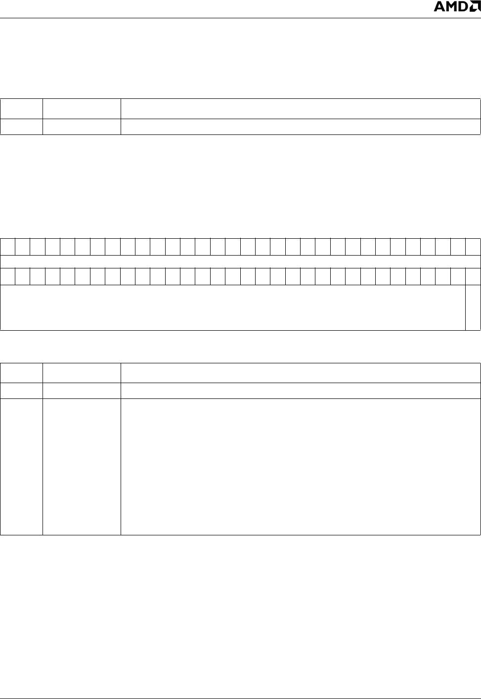
AMD Geode™ LX Processors Data Book 185
CPU Core Register Descriptions 33234H
5.5.2.91 Reserved Status MSR (RSVD_STS_MSR)
5.5.2.92 MSR Lock MSR (MSR_LOCK_MSR)
MSR Address 00001904h
Ty p e RO
Reset Value 00000000_00000000h
RSVD_STS_MSR Bit Descriptions
Bit Name Description
63:0 RSVD (RO) Reserved (Read Only). Reads back as 0.
MSR Address 00001908h
Ty p e R / W
Reset Value 00000000_00000000h
MSR_LOCK_MSR Register Map
63 62 61 60 59 58 57 56 55 54 53 52 51 50 49 48 47 46 45 44 43 42 41 40 39 38 37 36 35 34 33 32
RSVD
313029282726252423222120191817161514131211109876543210
RSVD
MSR_LOCK
MSR_LOCK_MSR Bit Descriptions
Bit Name Description
63:1 RSVD Reserved. Write as read
0 MSR_LOCK Lock MSRs. The CPU Core MSRs above 0xFFF (with the exception of the MSR_LOCK
register itself) are locked when this bit reads back as 1. To unlock these MSRs, write the
value 45524F434C494156h to this register. Writing any other value locks the MSRs.
The lock only affects software access via the WRMSR and RDMSR instructions when the
processor is NOT in SMM or DMM mode. MSRs are always writable and readable from
the GLBus and when the processor is in SMM or DMM mode regardless of the state of
the LOCK bit.
Note that a write or read to a locked MSR register causes a protection exception in the
pipeline.
When MSRs are locked, no GLBus MSR transactions are generated (GLBus MSR
addresses are above 3FFFh).
186 AMD Geode™ LX Processors Data Book
CPU Core Register Descriptions
33234H
5.5.2.93 Real Time Stamp Counter MSR (RTSC_MSR)
5.5.2.94 TSC and RTSC Low DWORDs MSR (RTSC_TSC_MSR)
MSR Address 00001910h
Ty p e R / W
Reset Value 00000000_00000000h
RTSC_MSR Register Map
63 62 61 60 59 58 57 56 55 54 53 52 51 50 49 48 47 46 45 44 43 42 41 40 39 38 37 36 35 34 33 32
RTSC (High DWORD)
313029282726252423222120191817161514131211109876543210
RTSC (Low DWORD)
RTSC_MSR Bit Descriptions
Bit Name Description
63:0 RTSC Real Time Stamp Counter. This register is the 64-bit secondary, or “real” time stamp
counter. This counter allows software to configure the TSC not to include SMM or DMM
time, and still have an accurate real time measurement that includes these times.
BC_CONFIG0_MSR (MSR 00001900h) contains configuration bits that determine if the
RTSC counts during Suspend mode. It always counts during SMM and DMM modes.
All bits in this register are writable, unlike the TSC that clears the upper DWORD to 0 on
writes.
MSR Address 00001911h
Ty p e RO
Reset Value 00000000_00000000h
RTSC_TSC_MSR Register Map
63 62 61 60 59 58 57 56 55 54 53 52 51 50 49 48 47 46 45 44 43 42 41 40 39 38 37 36 35 34 33 32
RTSC_LOW
313029282726252423222120191817161514131211109876543210
TSC_LOW
RTSC_TSC_MSR Bit Descriptions
Bit Name Description
63:32 RTSC_LOW Real Time Stamp Counter Low DWORD. This field provides a synchronized snapshot
of the low DWORD of the RTSC register (MSR 00001910h).
31:0 TSC_LOW Time Stamp Counter Low DWORD. This field provides a synchronized snapshot of the
low DWORD of the TSC register (MSR 00000010h).
AMD Geode™ LX Processors Data Book 187
CPU Core Register Descriptions 33234H
5.5.2.95 L2 Cache Configuration MSR (L2_CONFIG_MSR)
L2_CONFIG_MSR controls the behavior of the L2 cache.
MSR Address 00001920h
Ty p e R / W
Reset Value 00000000_0000000Eh
L2_CONFIG_MSR Register Map
63 62 61 60 59 58 57 56 55 54 53 52 51 50 49 48 47 46 45 44 43 42 41 40 39 38 37 36 35 34 33 32
RSVD
313029282726252423222120191817161514131211109876543210
RSVD L2_IM_LOCK L2_DM_LOCK RSVD
L2_TAG_CLKGT_EN
L2_PASS_IOMSR
L2_DMEVCT_DIRTY
L2_WAIT_DM_WR
L2_INVALID
L2_IM_ALLOC_EN
L2_DM_ALLOC_EN
L2_ALLOC_EN
L2_EN
L2_CONFIG_MSR Bit Descriptions
Bit Name Description
63:24 RSVD Reserved.
23:20 L2_IM_LOCK L2 Instruction Memory Subsystem Lock. On allocations from the IM, avoid using the
ways that have the corresponding bits set to 1. (Default = 0)
19:16 L2_DM_LOCK L2 Cache Data Memory Subsystem Lock. On allocations from the DM, avoid using the
ways that have the corresponding bits set to 1. (Default = 0)
15:9 RSVD Reserved.
8 L2_TAG_
CLKGT_EN
L2 Cache Tag Clock Gating Enable. If set, the L2 tags would be clocked only when
accessed. Otherwise, the tags would be clocked whenever the bus controller clocks are
active. (Default = 0)
7 L2_PASS_
IOMSR
L2 Cache (always) Pass I/Os and MSRs. Reserved for Debug only. Pass I/Os and
MSRs through regardless of the state of the L2. (Default = 0)
6 L2_DMEVCT_
DIRTY
L2 Cache Data Memory Subsystem Evictions (always) Dirty. Reserved for Debug
only. Treats all DM evictions as dirty. (Default = 0)
5 L2_WAIT_DM_
WR
L2 Cache Wait for Data Memory Subsystem Writes. Reserved for debug only. Waits
for all data beats from DM before proceeding. (Default = 0)
4 L2_INVALID L2 Cache Invalidate. Invalidate the entire contents of the L2 cache. This bit always
reads back as 0. (Default = 0)
3 L2_IM_ALLOC_
EN
L2 Cache Instruction Memory Subsystem Allocation Enable. A new IM access is
allocated into the L2 cache only if this bit is on. (Default = 1)
2 L2_DM_ALLOC
_EN
L2 Cache Data Memory Subsystem Allocation Enable. A new DM access is allocated
into the L2 cache only if this bit is on. (Default = 1)
1 L2_ALLOC_EN L2 Cache Allocation Enable. A new line is allocated into the L2 cache only if this bit is
on (Default = 1)
0 L2_EN L2 Cache Enable. If this bit is on, the arbiter redirects memory accesses to the L2 block.
(Default = 0)
188 AMD Geode™ LX Processors Data Book
CPU Core Register Descriptions
33234H
5.5.2.96 L2 Cache Status MSR (L2_STATUS_MSR)
L2_STATUS_MSR returns the status of the L2 cache controller.
5.5.2.97 L2 Cache Index MSR (L2_INDEX_MSR)
L2_INDEX_MSR has the L2 cache index, the way and the data QWORD select for diagnostic accesses.
MSR Address 00001921h
Ty p e RO
Reset Value 00000000_00000001h
L2_STATUS_MSR Register Map
63 62 61 60 59 58 57 56 55 54 53 52 51 50 49 48 47 46 45 44 43 42 41 40 39 38 37 36 35 34 33 32
RSVD
313029282726252423222120191817161514131211109876543210
RSVD
L2_IDLE
L2_STATUS_MSR Bit Descriptions
Bit Name Description
63:1 RSVD Reserved.
0 L2_IDLE L2 Cache Idle. Returns 1 if the L2 cache controller is idle. (Default = 1)
MSR Address 00001922h
Ty p e R / W
Reset Value 00000000_00000000h
L2_INDEX_MSR Register Map
63 62 61 60 59 58 57 56 55 54 53 52 51 50 49 48 47 46 45 44 43 42 41 40 39 38 37 36 35 34 33 32
RSVD
313029282726252423222120191817161514131211109876543210
RSVD
L2_DSEL
RSVD
L2_INDEX RSVD
L2_WAY
L2_INDEX_MSR Bit Descriptions
Bit Name Description
63:18 RSVD Reserved. (Default = 0)
17:16 L2_DSEL L2 Cache Data QWORD Select. (Default = 0)
15 RSVD Reserved. (Default = 0)
14:5 L2_INDEX L2 Cache Index for Diagnostics Accesses. (Default = 0)
4:2 RSVD Reserved. (Default = 0)
1:0 L2_WAY L2 Cache Way Selected for Diagnostics Accesses. (Default = 0)
AMD Geode™ LX Processors Data Book 189
CPU Core Register Descriptions 33234H
5.5.2.98 L2 Cache Data MSR (L2_DATA_MSR)
L2_DATA_MSR is used to access the L2 cache data for diagnostic accesses.
5.5.2.99 L2 Cache Tag MSR (L2_TAG_MSR)
L2_TAG_MSR has the L2 cache tag, MRU and valid bits for diagnostic accesses.
MSR Address 00001923h
Ty p e R / W
Reset Value 00000000_00000000h
L2_DATA_MSR Register Map
63 62 61 60 59 58 57 56 55 54 53 52 51 50 49 48 47 46 45 44 43 42 41 40 39 38 37 36 35 34 33 32
L2_DATA (High DWORD)
313029282726252423222120191817161514131211109876543210
L2_DATA (Low DWORD)
L2_DATA_MSR Bit Descriptions
Bit Name Description
63:0 L2_DATA L2 Cache Array Data. (Default = 0)
MSR Address 00001924h
Ty p e R / W
Reset Value 00000000_00000000h
L2_TAG_MSR Register Map
63 62 61 60 59 58 57 56 55 54 53 52 51 50 49 48 47 46 45 44 43 42 41 40 39 38 37 36 35 34 33 32
RSVD
313029282726252423222120191817161514131211109876543210
L2_TAG RSVD
L2_MRU_2
L2_MRU_1
L2_MRU_0
RSVD
L2_VALID
L2_TAG_MSR Bit Descriptions
Bit Name Description
63:32 RSVD Reserved. (Default = 0)
31:15 L2_TAG L2 Cache Tag. Tag entry of the current way. (Default = 0)
14:7 RSVD Reserved. (Default = 0)
6 L2_MRU_2 L2 Cache 2 Most Recently Used. MRU bit for the current index. If equal to 1, ways 3-2
more recent than ways 1-0. (Default = 0)
5 L2_MRU_1 L2 Cache 1 Most Recently Used. MRU bit for the current index. If equal to 1, way 3
more recent than way 2. (Default = 0)
4 L2_MRU_0 L2 Cache 0 Most Recently Used. MRU bit for the current index. If equal to 1, way 1
more recent than way 0. (Default = 0)
3:1 RSVD Reserved. (Default = 0)
0 L2_VALID L2 Cache Valid. Valid bit for the current way.
0: Invalid. (Default)
1: Valid.
190 AMD Geode™ LX Processors Data Book
CPU Core Register Descriptions
33234H
5.5.2.100 L2 Cache Tag with Increment MSR (L2_TAG_I_MSR)
The L2_TAG_I_MSR has the auto incremented L2 cache tag, MRU and valid bits for diagnostic accesses.
Bit descriptions for this register are the same as for L2_TAG_MSR (MSR 00001924h), except read/write of this register
causes an auto increment on the L2_INDEX_MSR (MSR 00001922h).
5.5.2.101 L2 Cache Built-In Self-Test MSR (L2_BIST_MSR)
L2_BIST_MSR has the L2 cache index for diagnostic accesses.
MSR Address 00001925h
Ty p e R / W
Reset Value 00000000_00000000h
L2_TAG_I_MSR Register Map
63 62 61 60 59 58 57 56 55 54 53 52 51 50 49 48 47 46 45 44 43 42 41 40 39 38 37 36 35 34 33 32
RSVD
313029282726252423222120191817161514131211109876543210
L2_TAG RSVD L2_MRU RSVD
L2_VALID
MSR Address 00001926h
Ty p e R / W
Reset Value 00000000_00000000h
L2_BIST_MSR Register Map
63 62 61 60 59 58 57 56 55 54 53 52 51 50 49 48 47 46 45 44 43 42 41 40 39 38 37 36 35 34 33 32
RSVD
313029282726252423222120191817161514131211109876543210
RSVD
BIST_MRU_GO
BIST_DATA_CMP_STAT
BIST_DATA_GO
BIST_TAG_GO_CMP
BIST_TAG_GO_WAY3
BIST_TAG_GO_WAY2
BIST_TAG_GO_WAY1
BIST_TAG_GO_WAY0
BIST_TAG_GO
BIST_MRU_DRT_EN
BIST_MRU_EN
BIST_DATA_DRT_EN
BIST_DATA_EN
BIST_TAG_DRT_EN
BIST_TAG_EN
L2_BIST_MSR Bit Descriptions
Bit Name Description
63:30 RSVD (RO) Reserved (Read Only). (Default = 0)
29 BIST_MRU_GO
(RO)
L2 Cache Most Recently Used BIST Result (Read Only).
0: Fail. (Default)
1: Pass.
28:13 BIST_DATA_
CMP_STAT (RO)
L2 Cache Data BIST Result (Read Only). One for each passed comparator - 16
total. (Default = 0)
12 BIST_DATA_GO
(RO)
L2 Cache Data BIST Result (Read Only).
0: Fail. (Default)
1: Pass.
11 BIST_TAG_GO_
CMP (RO)
L2 Cache Tag Comparator BIST Result (Read Only).
0: Fail. (Default)
1: Pass.

AMD Geode™ LX Processors Data Book 191
CPU Core Register Descriptions 33234H
10 BIST_TAG_GO_
WAY3 (RO)
L2 Cache Tag BIST Way 3 Result (Read Only).
0: Fail. (Default)
1: Pass.
9 BIST_TAG_GO_
WAY2 (RO)
L2 Cache Tag BIST Way 2 Result (Read Only).
0: Fail. (Default)
1: Pass.
8 BIST_TAG_GO_
WAY1 (RO)
L2 Cache Tag BIST Way 1 Result (Read Only).
0: Fail. (Default)
1: Pass.
7 BIST_TAG_GO_
WAY0 (RO)
L2 Cache Tag BIST Way 0 Result (Read Only).
0: Fail. (Default)
1: Pass.
6 BIST_TAG_GO
(RO)
L2 Cache Tag BIST Result (Read Only).
0: Fail. (Default)
1: Pass.
5 BIST_MRU_DRT_
EN
L2 Cache Most Recently Used Data Retention Timer BIST Enable. Enable the
data retention timer for the MRU BIST.
0: Disable. (Default)
1: Enable
4BIST_MRU_EN L2 Cache Most Recently Used BIST Enable. Start MRU BIST (on a write).
0: Disable. (Default)
1: Enable
3BIST_DATA_
DRT_EN
L2 Cache Data Retention Timer BIST Enable. Enable data retention timer for the
data BIST.
0: Disable. (Default)
1: Enable
2BIST_DATA_EN L2 Cache Data BIST Enable. Start data BIST (on a write).
0: Don’t start BIST. (Default)
1: Start BIST
1BIST_TAG_
DRT_EN
L2 Cache Tag Data Retention Timer BIST Enable. Enable Data Retention timer for
the Tag BIST.
0: Disable. (Default)
1: Enable
0BIST_TAG_EN L2 Cache Tag BIST Enable. Start Tag BIST (on a write).
0: Don’t start BIST. (Default)
1: Start BIST
L2_BIST_MSR Bit Descriptions (Continued)
Bit Name Description
192 AMD Geode™ LX Processors Data Book
CPU Core Register Descriptions
33234H
5.5.2.102 L2 Cache Treatment Control MSR (L2_TRTMNT_CTL_MSR)
MSR Address 00001927h
Ty p e R / W
Reset Value 00000000_00000000h
L2_TRTMNT_CTL_MSR Register Map
63 62 61 60 59 58 57 56 55 54 53 52 51 50 49 48 47 46 45 44 43 42 41 40 39 38 37 36 35 34 33 32
RSVD
313029282726252423222120191817161514131211109876543210
RSVD
TAG_ST_RST_CODE
RSVD
IMEVCT_INVAL_CODE
RSVD
L2_INVAL_CODE
RSVD
TAG_ST_RST_EN
IMEVCT_INVAL_EN
L2_INVAL_EN
L2_TRTMNT_CTL_MSR Bit Descriptions
Bit Name Description
63:19 RSVD Reserved.
18:16 TAG_ST_RST_
CODE
L2 Cache Tag State Machine Reset Code. If TAG_ST_RST_ENA (bit 2) is set, the
code on the treatment bus forces the tag state machine to reset. (Caution: Extremely
destructive - use only to poke around on hard hangs.) (Default = 0)
15 RSVD Reserved.
14:12 IMEVCT_INVAL
_CODE
Instruction Memory Subsystem Eviction Invalidate Code. If IMEVCT_INVAL_ENA
(bit 1) is set, the code on the treatment bus forces invalidation of the IM eviction buffer.
(Default = 0)
11 RSVD Reserved.
10:8 L2_INVAL_
CODE
L2 Cache Invalidate Code. If L2_INVAL_ENA (bit 0) is set, the code on the treatment
bus forces invalidation of the L2 cache. (Default = 0)
7:3 RSVD Reserved.
2TAG_ST_RST_
EN
L2 Cache Tag State Machine Reset Enable. Allows tag state machine reset through
the treatment bus.
0: Disable. (Default)
1: Enable.
1 IMEVCT_INVAL
_EN
Instruction Memory Subsystem Eviction Invalidate Enable. Allows IM eviction buffer
invalidation through the treatment bus.
0: Disable. (Default)
1: Enable.
0 L2_INVAL_EN L2 Cache Invalidate Enable. Allows L2 cache invalidation through the treatment bus.
0: Disable. (Default)
1: Enable.
AMD Geode™ LX Processors Data Book 193
CPU Core Register Descriptions 33234H
5.5.2.103 Power Mode MSR (PMODE_MSR)
This MSR enables some modules to turn their clocks off when they are idle to save power. Most of these bits are off by
default. It is recommended that they be set by BIOS.
MSR Address 00001930h
Ty p e R / W
Reset Value 00000000_00000300h
PMODE_MSR Register Map
63 62 61 60 59 58 57 56 55 54 53 52 51 50 49 48 47 46 45 44 43 42 41 40 39 38 37 36 35 34 33 32
RSVD
313029282726252423222120191817161514131211109876543210
RSVD
IRS_IF
IRS_IMTAG
IRS_IMDATA
RSVD
FPU_EX
FPU_FP
RSVD
BCL2_MSR
BCL2_GATED
PMODE_MSR Bit Descriptions
Bit Name Description
63:19 RSVD Reserved.
18 IRS_IF Reserved, Instruction Fetch. Reserved for possible future clock gating of IF.
(Default = 0)
17 IRS_IMTAG Reserved, Instruction Memory Subsystem. Reserved for possible future clock gating
IM tag. (Default = 0)
16 IRS_IMDATA Instruction Memory Subsystem Data. When bit is set, IM may turn off the clock when
IM_DATA is idle. (Default = 0)
9FPU_EX FPU EX. When bit is set, FPU may turn off the clock to FPU Region 1 when FP_EX is
idle. (Default = 1)
8FPU_FP FPU_FP. When bit is set, FPU may turn off the clock to FPU Region 2 when FPU is idle.
(Default = 1)
1 BCL2_MSR BCL2 MSR. When bit is set, BCL2 may turn off the clock to BC Region 1 when
BCL2_MSR is idle. (Default = 0)
0 BCL2_GATED BCL2 Gated. When bit is set, BCL2 may turn off the clock to BC Region 2 when BCL2 is
idle. (Default = 0)
194 AMD Geode™ LX Processors Data Book
CPU Core Register Descriptions
33234H
5.5.2.104 Bus Controller Extended Debug Registers 1 and 0 MSR (BXDR1_BXDR0_MSR)
5.5.2.105 Bus Controller Extended Debug Registers 3 and 2 MSR (BXDR3_BXDR2_MSR)
MSR Address 00001950h
Ty p e R / W
Reset Value 00000000_00000000h
BXDR1_BXDR0_MSR Register Map
63 62 61 60 59 58 57 56 55 54 53 52 51 50 49 48 47 46 45 44 43 42 41 40 39 38 37 36 35 34 33 32
BXDR1_PHYS_ADDR
313029282726252423222120191817161514131211109876543210
BXDR0_PHYS_ADDR
BXDR1_BXDR0_MSR Bit Descriptions
Bit Name Description
63:32 BXDR1_PHYS_
ADDR
Address Match Value for BXDR1. This field specifies addresses that must match the
physical address currently in the bus controller in order to trigger the extended break-
point. (Default = 0)
31:0 BXDR0_PHYS_
ADDR
Address Match Value for BXDR0. This field specifies addresses that must match the
physical address currently in the bus controller in order to trigger the extended break-
point. (Default = 0)
MSR Address 00001951h
Ty p e R / W
Reset Value 00000000_00000000h
BXDR3_BXDR2_MSR Register Map
63 62 61 60 59 58 57 56 55 54 53 52 51 50 49 48 47 46 45 44 43 42 41 40 39 38 37 36 35 34 33 32
BXDR3_PHYS_ADDR
313029282726252423222120191817161514131211109876543210
BXDR2_PHYS_ADDR
BXDR3_BXDR2_MSR Bit Descriptions
Bit Name Description
63:32 BXDR3_PHYS_
ADDR
Address Match Value for BXDR3. This field specifies addresses that must match the
physical address currently in the bus controller in order to trigger the extended break-
point. (Default = 0)
31:0 BXDR2_PHYS_
ADDR
Address Match Value for BXDR2. This field specifies addresses that must match the
physical address currently in the bus controller in order to trigger the extended break-
point. (Default = 0)
AMD Geode™ LX Processors Data Book 195
CPU Core Register Descriptions 33234H
5.5.2.106 Bus Controller Extended Debug Registers 6 and 7 MSR (BXDR6_BXDR7_MSR)
BXDR6 (bits [31:0]) contains the status of the extended bus controller breakpoints. When a breakpoint occurs, the corre-
sponding status bit is set in this register. The status bits remain set until cleared by an MSR write.
BXDR7 (bits [63:32]) is used to enable and specify the type of BXDR0-BXDR3. BXDR7 is also used to specify the length of
the breakpoint. For example, if BXDR0 is set to 00000006h, and BXDR7 indicates it has a length of 2 bytes, then an access
to 00000006h or 00000007h triggers the breakpoint. BXDR0 and BXDR1 can be paired to specify a range breakpoint if the
LEN0 or LEN1 field of BXDR7 is set accordingly. BXDR2 and BXDR3 can be paired to specify a range breakpoint if the
LEN2 or LEN3 field of BXDR7 is set accordingly.
MSR Address 00001953h
Ty p e R / W
Reset Value 00000000_00000000h
BXDR6_BXDR7_MSR Register Map
63 62 61 60 59 58 57 56 55 54 53 52 51 50 49 48 47 46 45 44 43 42 41 40 39 38 37 36 35 34 33 32
TYPE3 TYPE2 TYPE1 TYPE0 LEN3 LEN2 LEN1 LEN0 RSVD E3 E2 E1 E0
313029282726252423222120191817161514131211109876543210
RSVD T3 T2 T1 T0
BXDR6_BXDR7_MSR Bit Descriptions
Bit Name Description
BXDR7
63:60 TYPE3 Extended Breakpoint 3 Type. Selects the type of extended breakpoint 3.
0000: IM memory read (Default)
0001: DM memory read
0010: DM memory write
0011: DM memory read/write
0100: DM I/O read
0101: DM I/O write
0110: DM I/O read/write
0111: GLBus snoop for read
1000: GLBus snoop for write
1001: GLBus snoop for write-invalidate
1010: MSR read
1011: MSR write
All Others: Undefined, breakpoint will not trigger
59:56 TYPE2 Extended Breakpoint 2 Type. Selects the type of extended breakpoint 2. See TYPE3
(bits [63:60]) for decode.
55:52 TYPE1 Extended Breakpoint 1 Type. Selects the type of extended breakpoint 1. See TYPE3
(bits [63:60]) for decode.
51:48 TYPE0 Extended Breakpoint 0 Type. Selects the type of extended breakpoint 0. See TYPE3
(bits [63:60]) for decode.
47:46 LEN3 Extended Breakpoint 3 Length. Selects the size of extended breakpoint 3.
00: 1 byte. (Default)
01: 2 bytes.
10: Range from even to odd register.
11: 4 bytes.
45:44 LEN2 Extended Breakpoint 2 Length. Selects the size of extended breakpoint 2. See LEN3
(bits [47:46]) for decode.
43:42 LEN1 Extended Breakpoint 1 Length. Selects the size of extended breakpoint 0. See LEN3
(bits [47:46]) for decode.

196 AMD Geode™ LX Processors Data Book
CPU Core Register Descriptions
33234H
41:40 LEN0 Extended Breakpoint 0 Length. Selects the size of extended breakpoint 1. See LEN3
(bits [47:46]) for decode.
35 E3 Extended Breakpoint 3 Enable. Allows extended breakpoint 3 to be enabled.
0: Disable.
1: Enable.
34 E2 Extended Breakpoint 2 Enable. Allows extended breakpoint 2 to be enabled.
0: Disable.
1: Enable.
33 E1 Extended Breakpoint 1 Enable. Allows extended breakpoint 1 to be enabled.
0: Disable.
1: Enable.
32 E0 Extended Breakpoint 0 Enable. Allows extended breakpoint 0 to be enabled.
0: Disable.
1: Enable.
BXDR6
31:4 RSVD Reserved.
3T3 Extended Breakpoint 3 Triggered. A 1 Indicates that extended breakpoint 3 has trig-
gered. Write to clear. (Default = 0)
2T2 Extended Breakpoint 2 Triggered. A 1 Indicates that extended breakpoint 2 has trig-
gered. Write to clear. (Default = 0)
1T1 Extended Breakpoint 1 Triggered. A 1 Indicates that extended breakpoint 1 has trig-
gered. Write to clear. (Default = 0)
0T0 Extended Breakpoint 0 Triggered. A 1 Indicates that extended breakpoint 0 has trig-
gered. Write to clear. (Default = 0)
BXDR6_BXDR7_MSR Bit Descriptions (Continued)
Bit Name Description
AMD Geode™ LX Processors Data Book 197
CPU Core Register Descriptions 33234H
5.5.2.107 Bus Controller Debug Registers 0 through 3 MSRs
Each of these registers specifies an address that must match the physical address currently in the bus controller in order to
trigger the breakpoint. BDR7 is used to enable and specify the type of BDR0-BDR3. If a breakpoint is configured as a mem-
ory breakpoint, the address is matched on a QWORD granularity. If a breakpoint is configured as an I/O or MSR breakpoint,
the address is matched based on all 32 bits.
Bus Controller Debug Register 0 MSR (BDR0_MSR)
Bus Controller Debug Register 1 MSR (BDR1_MSR)
Bus Controller Debug Register 2 MSR (BDR2_MSR)
Bus Controller Debug Register 3 MSR (BDR3_MSR)
MSR Address 00001970h
Ty p e R / W
Reset Value 00000000_00000000h
MSR Address 00001971h
Ty p e R / W
Reset Value 00000000_00000000h
MSR Address 00001972h
Typ e R / W
Reset Value 00000000_00000000h
MSR Address 00001973h
Typ e R / W
Reset Value 00000000_00000000h
BDRx_MSR Register Map
63 62 61 60 59 58 57 56 55 54 53 52 51 50 49 48 47 46 45 44 43 42 41 40 39 38 37 36 35 34 33 32
RSVD
313029282726252423222120191817161514131211109876543210
PHYS_ADDR
BDRx_MSR Bit Descriptions
Bit Name Description
63:32 RSVD Reserved. (Default = 0)
31:0 PHYS_ADDR Address Match Value for BDRx. (Default = 0)

198 AMD Geode™ LX Processors Data Book
CPU Core Register Descriptions
33234H
5.5.2.108 Bus Controller Debug Register 6 MSR (BDR6_MSR)
This register contains the status of the bus controller breakpoints. When a breakpoint occurs, the corresponding status bit
is set in this register. The status bits remain set until cleared by an MSR write.
5.5.2.109 Bus Controller Debug Register 7 MSR (BDR7_MSR)
This register is the bus controller breakpoint control/enable register.
MSR Address 00001976h
Ty p e R / W
Reset Value 00000000_00000000h
BDR6_MSR Register Map
63 62 61 60 59 58 57 56 55 54 53 52 51 50 49 48 47 46 45 44 43 42 41 40 39 38 37 36 35 34 33 32
RSVD
313029282726252423222120191817161514131211109876543210
RSVD T3 T2 T1 T0
BDR6_MSR Bit Descriptions
Bit Name Description
63:4 RSVD Reserved. (Default = 0)
3T3 Breakpoint 3 Triggered. A 1 Indicates that breakpoint 3 has triggered. Write to clear.
(Default = 0)
2T2 Breakpoint 2 Triggered. A 1 Indicates that breakpoint 2 has triggered. Write to clear.
(Default = 0)
1T1 Breakpoint 1 Triggered. A 1 Indicates that breakpoint 1 has triggered. Write to clear.
(Default = 0)
0T0 Breakpoint 0 Triggered. A 1 Indicates that breakpoint 0 has triggered. Write to clear.
(Default = 0)
MSR Address 00001977h
Ty p e R / W
Reset Value 00000000_00000000h
BDR7_MSR Register Map
63 62 61 60 59 58 57 56 55 54 53 52 51 50 49 48 47 46 45 44 43 42 41 40 39 38 37 36 35 34 33 32
RSVD
313029282726252423222120191817161514131211109876543210
TYPE3 TYPE2 TYPE1 TYPE0 RSVD E3 E2 E1 E0
BDR7_MSR Bit Descriptions
Bit Name Description
63:32 RSVD Reserved. (Default = 0)

AMD Geode™ LX Processors Data Book 199
CPU Core Register Descriptions 33234H
31:28 TYPE3 Breakpoint 3 Type. Selects the type of extended breakpoint 3.
0000: IM memory read (Default).
0001: DM memory read.
0010: DM memory write.
0011: DM memory read/write.
0100: DM I/O read.
0101: DM I/O write.
0110: DM I/O read/write.
0111: GLBus snoop for read.
1000: GLBus snoop for write.
1001: GLBus snoop for write-invalidate.
1010: MSR read.
1011: MSR write.
All Others: Undefined, breakpoint will not trigger.
27:24 TYPE2 Breakpoint 2 Type. Selects the type of extended breakpoint 2. See TYPE3 (bits [31:28])
for decode.
23:20 TYPE1 Breakpoint 1 Type. Selects the type of extended breakpoint 1. See TYPE3 (bits [31:28])
for decode.
19:16 TYPE0 Breakpoint 0 Type. Selects the type of extended breakpoint 0. See TYPE3 (bits [31:28])
for decode.
15:4 RSVD Reserved. (Default = 0)
3E3 Breakpoint 3 Enable. Allows extended breakpoint 3 to be enabled.
0: Disable.
1: Enable.
2E2 Breakpoint 2 Enable. Allows extended breakpoint 2 to be enabled.
0: Disable.
1: Enable.
1E1 Breakpoint 1 Enable. Allows extended breakpoint 1 to be enabled.
0: Disable.
1: Enable.
0E0 Breakpoint 0 Enable. Allows extended breakpoint 0 to be enabled.
0: Disable.
1: Enable.
BDR7_MSR Bit Descriptions
Bit Name Description
200 AMD Geode™ LX Processors Data Book
CPU Core Register Descriptions
33234H
5.5.2.110 Memory Subsystem Array Control Enable MSR (MSS_ARRAY_CTL_EN_MSR)
The MSRs at addresses 00001980h-00001983h provide alternate array delay control values for the MSS arrays. After a
reset, the MSS clock modules provide JTAG-accessible control values. These MSRs can be used by software to override
these values.
5.5.2.111 Memory Subsystem Array Control 0 MSR (MSS_ARRAY_CTL0_MSR)
MSR Address 00001980h
Ty p e R / W
Reset Value 00000000_00000000h
MSS_ARRAY_CTL_EN_MSR Register Map
63 62 61 60 59 58 57 56 55 54 53 52 51 50 49 48 47 46 45 44 43 42 41 40 39 38 37 36 35 34 33 32
RSVD
313029282726252423222120191817161514131211109876543210
RSVD EN
MSS_ARRAY_CTL_EN_MSR Bit Descriptions
Bit Name Description
63:1 RSVD Reserved. (Default = 0)
0EN Enable. Enable the array control values in this register to be used instead of those pro-
vided by the clock modules.
0: Disable.
1: Enable.
MSR Address 00001981h
Ty p e R / W
Reset Value 00000000_2010F3C9h
MSS_ARRAY_CTL0_MSR Register Map
63 62 61 60 59 58 57 56 55 54 53 52 51 50 49 48 47 46 45 44 43 42 41 40 39 38 37 36 35 34 33 32
RSVD DMDATA1
313029282726252423222120191817161514131211109876543210
DMDATA1 DMDATA0 DMTAG1 DMTAG0 L2TLB1 L2TLB0
MSS_ARRAY_CTL0_MSR Bit Descriptions
Bit Name Description
63:36 RSVD Reserved. (Default = 0)
35:27 DMDATA1 Data Memory Subsystem Data 1 Delay Control. (Default = 04)
26:18 DMDATA0 Data Memory Subsystem Data 0 Delay Control. (Default = 04)
17:12 DMTAG1 Data Memory Subsystem Tag 1 Delay Control. (Default = F)
11:6 DMTAG0 Data Memory Subsystem Tag 0 Delay Control. (Default = F)
5:3 L2TB1 Data Memory Subsystem L2 TLB 1 Delay Control. (Default = 1)
2:0 L2TB0 Data Memory Subsystem L2 TLB 0 Delay Control. (Default = 1)

AMD Geode™ LX Processors Data Book 201
CPU Core Register Descriptions 33234H
5.5.2.112 Memory Subsystem Array Control 1 MSR (MSS_ARRAY_CTL1_MSR)
5.5.2.113 Memory Subsystem Array Control 2 MSR (MSS_ARRAY_CTL2_MSR)
L2 delay control settings.
MSR Address 00001982h
Ty p e R / W
Reset Value 00000000_104823CFh
MSS_ARRAY_CTL1_MSR Register Map
63 62 61 60 59 58 57 56 55 54 53 52 51 50 49 48 47 46 45 44 43 42 41 40 39 38 37 36 35 34 33 32
RSVD
313029282726252423222120191817161514131211109876543210
RSVD IMDATA1 IMDATA0 IMTAG1 IMTAG0
MSS_ARRAY_CTL1_MSR Bit Descriptions
Bit Name Description
63:30 RSVD Reserved. (Default = 0)
29:21 IMDATA1 Instruction Memory Subsystem Data 1 Delay Control. (Default = 82)
20:12 IMDATA0 Instruction Memory Subsystem Data 0 Delay Control. (Default = 82)
11:6 IMTAG1 Instruction Memory Subsystem Tag 1 Delay Control. (Default = F)
5:0 IMTAG0 Instruction Memory Subsystem Tag 0 Delay Control. (Default = F)
MSR Address 00001983h
Ty p e R / W
Reset Value 00000104_820C30C3h
MSS_ARRAY_CTL2_MSR Register Map
63 62 61 60 59 58 57 56 55 54 53 52 51 50 49 48 47 46 45 44 43 42 41 40 39 38 37 36 35 34 33 32
RSVD L2DATA1
L2DATA0
313029282726252423222120191817161514131211109876543210
L2DATA0 L2TAG3 L2TAG2 L2TAG1 L2TAG0
MSS_ARRAY_CTL2_MSR Bit Descriptions
Bit Name Description
63:42 RSVD Reserved. (Default = 0)
41:33 L2DATA1 L2 Cache Data 1 Delay Setting. (Default = 82)
32:24 L2DATA0 L2 Cache Data 0 Delay Setting. (Default = 82)
23:18 L2TAG3 L2 Cache Tag 3 Delay Setting. (Default = 3)
17:12 L2TAG2 L2 Cache Tag 2 Delay Setting. (Default = 3)
11:6 L2TAG1 L2 Cache Tag 1 Delay Setting. (Default = 3)
5:0 L2TAG0 L2 Cache Tag 0 Delay Setting. (Default = 3)

202 AMD Geode™ LX Processors Data Book
CPU Core Register Descriptions
33234H
5.5.2.114 FPU Modes MSR (FP_MODE_MSR)
5.5.2.115 FPU Reserved MSR (FPU_RSVD_MSR)
This register is reserved for internal testing; do not write.
5.5.2.116 FPU Reserved MSR (FPU_RSVD_MSR)
This register is reserved for internal testing; do not write.
MSR Address 00001A00h
Ty p e R / W
Reset Value 00000000_00000000h
FP_MODE_MSR Register Map
63 62 61 60 59 58 57 56 55 54 53 52 51 50 49 48 47 46 45 44 43 42 41 40 39 38 37 36 35 34 33 32
RSVD
313029282726252423222120191817161514131211109876543210
RSVD
FPU_SP
FPU_IPE
FP_MODE_MSR Bit Descriptions
Bit Name Description
63:2 RSVD Reserved. Write as read.
1FPU_SP Limit Results to Single Precision. The FPU datapath width is single-precision. Opera-
tions on single precision numbers can generally be completed in one cycle, but double or
extended precision numbers takes many cycles. This bit overrides the precision control
bits in the x87 Mode Control register (of the FPU Instruction Set), and causes the FPU to
operate as if the precision control is set to single precision (00).
0: Disable.
1: Enable limit to single precision.
0 FPU_IPE Enable Force of Imprecise Exceptions. For precise exceptions, the FPU allows only
one instruction to be in the pipeline at a time when any FPU exceptions are unmasked.
This results in a huge performance penalty. To run the FPU at full speed, it is necessary
to mask all exceptions in the FPU_CW_MSR (MSR 00001A10h[11:0]).
When this bit is set, the FPU is allowed to run at full speed even if there are unmasked
exceptions in the FPU_CW. With this bit set, exceptions will be generated, however,
there is no guarantee that the exception will occur on any particular instruction boundary.
It is known that setting this bit will cause some diagnostic software to fail. It is recom-
mended to be set only when the FPU exception handler does not need to handle excep-
tions on the specific instruction boundary.
0: Disable.
1: Enable.
MSR Address 00001A01h
Ty p e R / W
Reset Value 00000000_00000000h
MSR Address 00001A03h
Ty p e R / W
Reset Value 00000000_00000000h
AMD Geode™ LX Processors Data Book 203
CPU Core Register Descriptions 33234H
5.5.2.117 FPU x87 Control Word MSR (FPU_CW_MSR)
5.5.2.118 FPU x87 Status Word MSR (FPU_SW_MSR)
5.5.2.119 FPU x87 Tag Word MSR (FPU_TW_MSR)
MSR Address 00001A10h
Ty p e R / W
Reset Value 00000000_00000040h
FPU_CW_MSR Register Map
63 62 61 60 59 58 57 56 55 54 53 52 51 50 49 48 47 46 45 44 43 42 41 40 39 38 37 36 35 34 33 32
RSVD
313029282726252423222120191817161514131211109876543210
RSVD FPU_CW
FPU_CW_MSR Bit Descriptions
Bit Name Description
63:12 RSVD Reserved. Write as read.
11:0 FPU_CW FPU Control Word.
MSR Address 00001A11h
Ty p e R / W
Reset Value 00000000_00000000h
FPU_SW_MSR Register Map
63 62 61 60 59 58 57 56 55 54 53 52 51 50 49 48 47 46 45 44 43 42 41 40 39 38 37 36 35 34 33 32
RSVD
313029282726252423222120191817161514131211109876543210
RSVD FPU_SW
FPU_SW_MSR Bit Descriptions
Bit Name Description
63:16 RSVD Reserved. Write as read.
15:0 FPU_SW FPU Status Word.
MSR Address 00001A12h
Ty p e R / W
Reset Value 00000000_00000000h
FPU_TW_MSR Register Map
63 62 61 60 59 58 57 56 55 54 53 52 51 50 49 48 47 46 45 44 43 42 41 40 39 38 37 36 35 34 33 32
RSVD
313029282726252423222120191817161514131211109876543210
RSVD FPU_TW
204 AMD Geode™ LX Processors Data Book
CPU Core Register Descriptions
33234H
5.5.2.120 FPU Busy MSR (FPU_BUSY_MSR)
5.5.2.121 FPU Register Map MSR (FPU_MAP_MSR)
FPU_TW_MSR Bit Descriptions
Bit Name Description
63:16 RSVD Reserved. Write as read.
15:0 FPU_TW FPU Tag Word.
MSR Address 00001A13h
Ty p e RO
Reset Value 00000000_00000000h
FPU_BUSY_MSR Register Map
63 62 61 60 59 58 57 56 55 54 53 52 51 50 49 48 47 46 45 44 43 42 41 40 39 38 37 36 35 34 33 32
RSVD
313029282726252423222120191817161514131211109876543210
RSVD
FPU_BUSY
FPU_BUSY_MSR Bit Descriptions
Bit Name Description
63:1 RSVD Reserved. Reads back as 0.
0FPU_BUSY FPU Busy. Software must check that the FPU is Idle before accessing MSRs
00001A10h-00001A12h and 00001A40h-00001A6Fh.
0: FPU Idle.
1: FPU Busy.
MSR Address 00001A14h
Ty p e RO
Reset Value 00000000_76543210h
FPU_MAP_MSR Register Map
63 62 61 60 59 58 57 56 55 54 53 52 51 50 49 48 47 46 45 44 43 42 41 40 39 38 37 36 35 34 33 32
RSVD
313029282726252423222120191817161514131211109876543210
FPU_REG_MAP
FPU_MAP_MSR Bit Descriptions
Bit Name Description
63:32 RSVD Reserved.
31:0 FPU_REG_MAP FPU Register Map. Internal mapping of architectural registers to physical registers in the
register array.
AMD Geode™ LX Processors Data Book 205
CPU Core Register Descriptions 33234H
5.5.2.122 Mantissa of Rx MSRs
Mantissa of R0 MSR (FPU_MR0_MSR)
Mantissa of R1 MSR (FPU_MR1_MSR)
Mantissa of R2 MSR (FPU_MR2_MSR)
Mantissa of R3 MSR (FPU_MR3_MSR)
Mantissa of R4 MSR (FPU_MR4_MSR)
Mantissa of R5 MSR (FPU_MR5_MSR)
Mantissa of R6 MSR (FPU_MR6_MSR)
Mantissa of R7 MSR (FPU_MR7_MSR)
Mantissa of R8 MSR (FPU_MR8_MSR)
Mantissa of R9 MSR (FPU_MR9_MSR)
Mantissa of R10 MSR (FPU_MR10_MSR)
Mantissa of R11 MSR (FPU_MR11_MSR)
Mantissa of R12 MSR (FPU_MR12_MSR)
Mantissa of R13 MSR (FPU_MR13_MSR)
Mantissa of R14 MSR (FPU_MR14_MSR)
Mantissa of R15 MSR (FPU_MR15_MSR)
MSR Address 00001A40h
Ty p e R / W
Reset Value xxxxxxxx_xxxxxxxxh
MSR Address 00001A42h
Ty p e R / W
Reset Value xxxxxxxx_xxxxxxxxh
MSR Address 00001A44h
Ty p e R / W
Reset Value xxxxxxxx_xxxxxxxxh
MSR Address 00001A46h
Ty p e R / W
Reset Value xxxxxxxx_xxxxxxxxh
MSR Address 00001A48h
Ty p e R / W
Reset Value xxxxxxxx_xxxxxxxxh
MSR Address 00001A4Ah
Ty p e R / W
Reset Value xxxxxxxx_xxxxxxxxh
MSR Address 00001A4Ch
Ty p e R / W
Reset Value xxxxxxxx_xxxxxxxxh
MSR Address 00001A4Eh
Ty p e R / W
Reset Value xxxxxxxx_xxxxxxxxh
MSR Address 00001A50h
Typ e R / W
Reset Value xxxxxxxx_xxxxxxxxh
MSR Address 00001A52h
Typ e R / W
Reset Value xxxxxxxx_xxxxxxxxh
MSR Address 00001A54h
Typ e R / W
Reset Value xxxxxxxx_xxxxxxxxh
MSR Address 00001A56h
Typ e R / W
Reset Value xxxxxxxx_xxxxxxxxh
MSR Address 00001A58h
Typ e R / W
Reset Value xxxxxxxx_xxxxxxxxh
MSR Address 00001A5Ah
Typ e R / W
Reset Value xxxxxxxx_xxxxxxxxh
MSR Address 00001A5Ch
Typ e R / W
Reset Value xxxxxxxx_xxxxxxxxh
MSR Address 00001A5Eh
Typ e R / W
Reset Value xxxxxxxx_xxxxxxxxh
FPU_MRx_MSR Register Map
63 62 61 60 59 58 57 56 55 54 53 52 51 50 49 48 47 46 45 44 43 42 41 40 39 38 37 36 35 34 33 32
FPU_MRx
313029282726252423222120191817161514131211109876543210
FPU_MRx
FPU_MRx_MSR Bit Descriptions
Bit Name Description
63:0 FPU_MRx Mantissa of FPU Rx MSR.

206 AMD Geode™ LX Processors Data Book
CPU Core Register Descriptions
33234H
5.5.2.123 Exponent of Rx MSRs
Exponent of R0 MSR (FPU_ER0_MSR)
Exponent of R1 MSR (FPU_ER1_MSR)
Exponent of R2 MSR (FPU_ER2_MSR)
Exponent of R3 MSR (FPU_ER3_MSR)
Exponent of R4 MSR (FPU_ER4_MSR)
Exponent of R5 MSR (FPU_ER5_MSR)
Exponent of R6 MSR (FPU_ER6_MSR)
Exponent of R7 MSR (FPU_ER7_MSR)
Exponent of R8 MSR (FPU_ER8_MSR)
Exponent of R9 MSR (FPU_ER9_MSR)
Exponent of R10 MSR (FPU_ER10_MSR)
Exponent of R11 MSR (FPU_ER11_MSR)
Exponent of R12 MSR (FPU_ER12_MSR)
Exponent of R13 MSR (FPU_ER13_MSR)
Exponent of R14 MSR (FPU_ER14_MSR)
Exponent of R15 MSR (FPU_ER15_MSR)
MSR Address 00001A41h
Ty p e R / W
Reset Value 00000000_0000xxxxh
MSR Address 00001A43h
Ty p e R / W
Reset Value 00000000_0000xxxxh
MSR Address 00001A45h
Ty p e R / W
Reset Value 00000000_0000xxxxh
MSR Address 00001A47h
Ty p e R / W
Reset Value 00000000_0000xxxxh
MSR Address 00001A49h
Ty p e R / W
Reset Value 00000000_0000xxxxh
MSR Address 00001A4Bh
Ty p e R / W
Reset Value 00000000_0000xxxxh
MSR Address 00001A4Dh
Ty p e R / W
Reset Value 00000000_0000xxxxh
MSR Address 00001A4Fh
Ty p e R / W
Reset Value 00000000_0000xxxxh
MSR Address 00001A51h
Typ e R / W
Reset Value 00000000_0000xxxxh
MSR Address 00001A53h
Typ e R / W
Reset Value 00000000_0000xxxxh
MSR Address 00001A55h
Typ e R / W
Reset Value 00000000_0000xxxxh
MSR Address 00001A57h
Typ e R / W
Reset Value 00000000_0000xxxxh
MSR Address 00001A59h
Typ e R / W
Reset Value 00000000_0000xxxxh
MSR Address 00001A5Bh
Typ e R / W
Reset Value 00000000_0000xxxxh
MSR Address 00001A5Dh
Typ e R / W
Reset Value 00000000_0000xxxxh
MSR Address 00001A5Fh
Typ e R / W
Reset Value 00000000_0000xxxxh
FPU_ERx_MSR Register Map
63 62 61 60 59 58 57 56 55 54 53 52 51 50 49 48 47 46 45 44 43 42 41 40 39 38 37 36 35 34 33 32
RSVD
313029282726252423222120191817161514131211109876543210
FPU_ERx
FPU_ERx_MSR Bit Descriptions
Bit Name Description
63:16 RSVD Reserved. Write as read.
15:0 FPU_ERx Exponent of FPU Rx MSR.

AMD Geode™ LX Processors Data Book 207
CPU Core Register Descriptions 33234H
5.5.2.124 FPU Reserved MSRs (FPU_RSVD_MSR)
MSR addresses 00001A60h through 00001A6F are reserved for internal storage purposes and should not be written to.
5.5.2.125 CPU ID MSRs
Standard Levels and Vendor ID String 1 (CPUID0_MSR)
Vendor ID Strings 2 and 3 (CPUID1_MSR)
Type/Family/Model/Step (CPUID2_MSR)
Feature Flags (CPUID3_MSR)
Reserved (CPUID4_MSR)
Reserved (CPUID5_MSR)
Max Extended Levels 1 (CPUID6_MSR)
Max Extended Levels 2 (CPUID7_MSR)
Extended Type/Family/Model/Stepping (CPUID8_MSR)
Extended Feature Flags (CPUID9_MSR)
CPU Marketing Name 1 (CPUIDA_MSR)
CPU Marketing Name 2 (CPUIDB_MSR)
CPU Marketing Name 3 (CPUIDC_MSR)
CPU Marketing Name 4 (CPUIDD_MSR)
CPU Marketing Name 5 (CPUIDE_MSR)
CPU Marketing Name 6 (CPUIDF_MSR)
L1 TLB Information (CPUID10_MSR)
L1 Cache Information (CPUID11_MSR)
L2 TLB Information (CPUID12_MSR)
L2 Cache Information (CPUID13_MSR)
MSR Address 00003000h
Ty p e R / W
Reset Value 68747541_00000001h
MSR Address 00003001h
Ty p e R / W
Reset Value 69746E65_444D4163h
MSR Address 00003002h
Ty p e R / W
Reset Value 00000400_000005A2h
MSR Address 00003003h
Ty p e R / W
Reset Value 0088A93D_00000000h
MSR Address 00003004h
Ty p e WO
Reset Value 00000000_00000000h
MSR Address 00003005h
Ty p e WO
Reset Value 00000000_00000000h
MSR Address 00003006h
Ty p e R / W
Reset Value 68747541_80000006h
MSR Address 00003007h
Ty p e R / W
Reset Value 69746E65_444D4163h
MSR Address 00003008h
Ty p e R / W
Reset Value 00000000_000005A1h
MSR Address 00003009h
Ty p e R / W
Reset Value C0C0A13D_00000000h
MSR Address 0000300Ah
Typ e R / W
Reset Value 4D542865_646F6547h
MSR Address 0000300Bh
Typ e R / W
Reset Value 72676574_6E492029h
MSR Address 0000300Ch
Typ e R / W
Reset Value 6F725020_64657461h
MSR Address 0000300Dh
Typ e R / W
Reset Value 6220726F_73736563h
MSR Address 0000300Eh
Typ e R / W
Reset Value 43502044_4D412079h
MSR Address 0000300Fh
Typ e R / W
Reset Value 00000000_00000053h
MSR Address 00003010h
Typ e R / W
Reset Value FF10FF10_00000000h
MSR Address 00003011h
Typ e R / W
Reset Value 40100120_40100120h
MSR Address 00003012h
Typ e R / W
Reset Value 00002040_0000F004h
MSR Address 00003013h
Typ e R / W
Reset Value 00000000_00804120h

208 AMD Geode™ LX Processors Data Book
CPU Core Register Descriptions
33234H
CPUIDx_MSR Register Map
63 62 61 60 59 58 57 56 55 54 53 52 51 50 49 48 47 46 45 44 43 42 41 40 39 38 37 36 35 34 33 32
CPUIDx
313029282726252423222120191817161514131211109876543210
CPUIDx
CPUIDx_MSR Bit Descriptions
Bit Name Description
63:0 CPUID0 Standard Levels and Vendor ID String 1. Same data as CPUID instruction [00000000]
EBX/EAX.
63:0 CPUID1 Vendor ID Strings 2 and 3. Same data as CPUID instruction [00000000] EDX/ECX.
63:0 CPUID2 Type/Family/Model/Step. Same data as CPUID instruction [00000001] EBX/EAX.
63:0 CPUID3 Feature Flags. Same data as CPUID instruction [00000001] EDX/ECX.
63:0 CPUID4 Reserved. This register is not used in the CPU Core module.
63:0 CPUID5 Reserved. This register is not used in the CPU Core module.
63:0 CPUID6 CPUID Max Extended Levels. Same data as CPUID instruction [80000000] EBX/EAX.
63:0 CPUID7 CPUID Max Extended Levels. Same data as CPUID instruction [80000000] EDX/ECX.
63:0 CPUID8 Extended Type/Family/Model/Stepping. Same data as CPUID instruction [80000001]
EBX/EAX.
63:0 CPUID9 Extended Feature Flags. Same data as CPUID instruction [80000001] EDX/ECX.
63:0 CPUIDA CPU Marketing Name 1. Same data as CPUID instruction [80000002] EBX/EAX.
63:0 CPUIDB CPU Marketing Name 2. Same data as CPUID instruction [80000002] EDX/ECX.
63:0 CPUIDC CPU Marketing Name 3. Same data as CPUID instruction [80000003] EBX/EAX.
63:0 CPUIDD CPU Marketing Name 4. Same data as CPUID instruction [80000003] EDX/ECX.
63:0 CPUIDE CPU Marketing Name 5. Same data as CPUID instruction [80000004] EBX/EAX.
63:0 CPUIDF CPU Marketing Name 6. Same data as CPUID instruction [80000004] EDX/ECX.
63:0 CPUID10 L1 TLB Information. Same data as CPUID instruction [80000005] EBX/EAX.
63:0 CPUID11 L1 Cache Information. Same data as CPUID instruction [80000005] EDX/ECX.
63:0 CPUID12 L2 TLB Information. Same data as CPUID instruction [80000006] EBX/EAX.
63:0 CPUID13 L2 Cache Information. Same data as CPUID instruction [80000006] EDX/ECX.
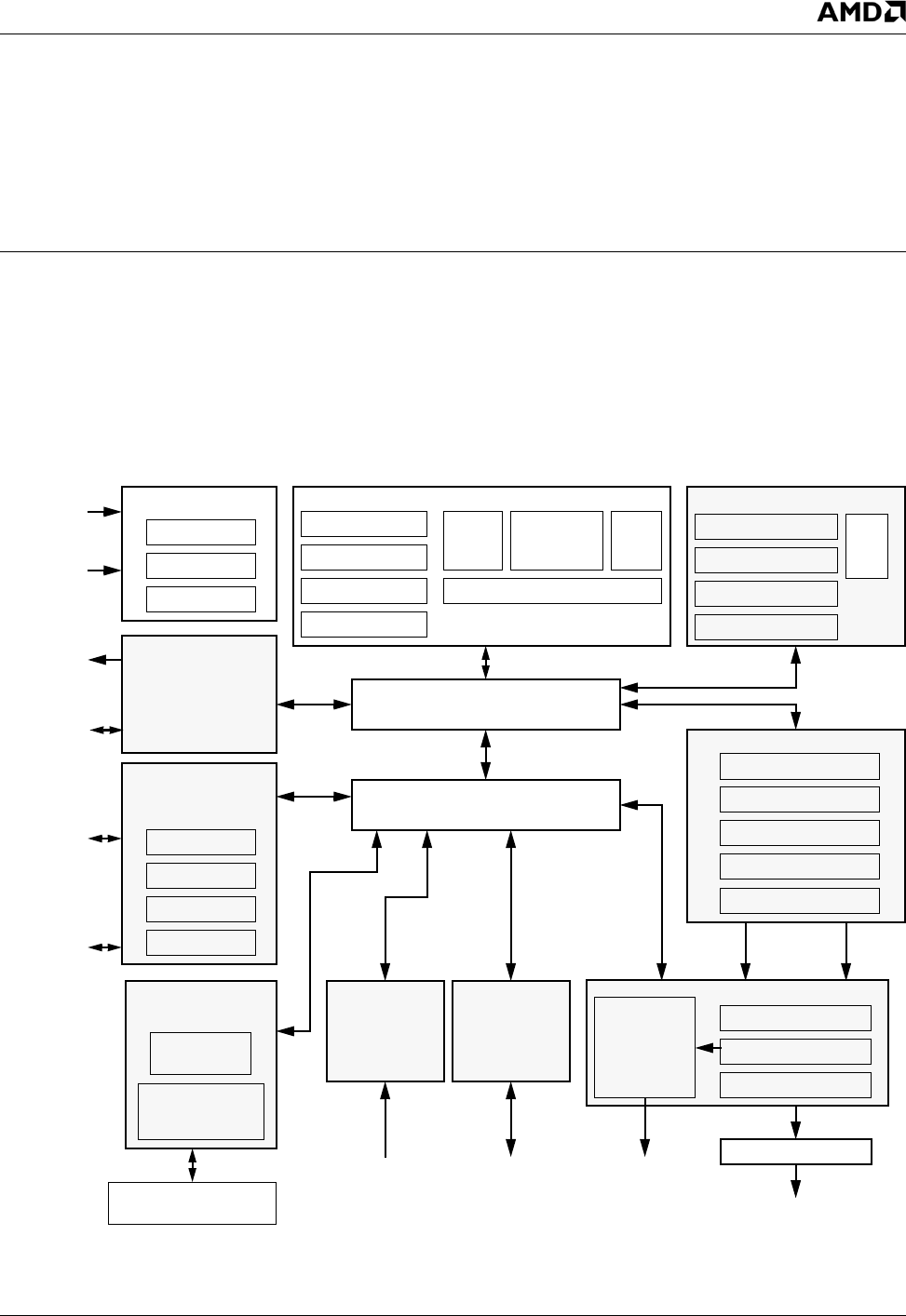
AMD Geode™ LX Processors Data Book 209
6
Integrated Functions 33234H
6.0Integrated Functions
The integrated functions of the AMD Geode™ LX proces-
sor are:
•GeodeLink™ Memory Controller (GLMC)
•Graphics Processor (GP)
•Display Controller (DC)
•Video Processor (VP)
•GeodeLink Control Processor (GLCP)
•GeodeLink PCI Bridge (GLPCI)
•Video Input Port (VIP)
•Security Block (SB)
This section provides a functional description of each mod-
ule and its respective registers.
Figure 6-1. Integrated Functions Block Diagram
GeodeLink™ Interface Unit 0
GeodeLink™ Interface Unit 1
GeodeLink™
Control
Diagnostic
Te s t
Power Mgmnt
GeodeLink™
SDCLKs
TLB
Integer
Unit
MMU
Load/Store FPU
64 KB L1 D-cache
64 KB L1 I-cache
Bus Controller
CPU Core
Alpha Compositing
ROP Unit
BLT Engine
Graphics Processor (GP)
Timing
Palette RAM
Compression Buffer
Display Controller (DC)
Alpha Blender
Video Mixer
Video Scalar
Video Processor (VP)
RGB YUV
Graphics Filter/Scaling
(GLIU0)
(GLIU1)
Memory
Clock Module
CPU PLL
System PLL
TFT/VOP
3x8-Bit DAC
CRT
PCI
SYSREF
DOTREF
Test/Reset
Interface
Processor (GLCP)
Controller (GLMC)
DOTCLK PLL
128 KB L2 cache
1 KB
LUT
Rotation BLT
Companion I/F
VIP
HW VGA
128-bit AES
TFT
Controller/
Video
Output
Port (VOP)
AMD Geode™
Companion
Device
64-Bit
DDR
Security Block
Random Number
Generator
EEPROM on package
64-bit DDR SDRAM
(CBC/ECB)
Tr u e
(optional)
GeodeLink™
PCI Bridge
(GLPCI)
Video Input
Port (VIP)
(SB)

210 AMD Geode™ LX Processors Data Book
GeodeLink™ Memory Controller
33234H
6.1 GeodeLink™ Memory Controller
The GeodeLink™ Memory Controller (GLMC) module sup-
ports the Unified Memory Architecture (UMA) of the
AMD Geode™ LX processor and controls a 64-bit DDR
SDRAM interface without any external buffering. The inter-
nal block diagram of the GLMC is shown in Figure 6-2.
The SDRAM memory array contains both the main system
memory and the graphics frame buffer. Up to four module
banks of SDRAM are supported. Each module bank can
have two or four component banks depending on the mem-
ory size and organization. The maximum configuration is
four module banks with four component banks, each pro-
viding a total of 16 open banks with the maximum memory
size supported being 2 GB.
The GLMC handles multiple requests for memory data
from the CPU Core, the Graphics Processor, the Display
Controller, and the external PCI bus via the GeodeLink
Interface Units (GLIUs). The GLMC contains extensive
buffering logic that helps minimize contention for memory
bandwidth between the various requests.
Figure 6-2. GLMC Block Diagram
Adrs/Ctl
Gen Req Req
Refresh
Arbiter
Data
Control
SDRAM IF
MSR
Registers
W_DATA
Write
Response
MSR
Rd Resp
Data Path
RAS
CAS
WE
CKE
MA
BA
CS
DQ
DQM
DQS
Bank/
Page
Logic
Buf Buf
R_DATA
MemRd
Response
GLUI0
Request
Packet
GLUI0
Write
Packet
GLUI0
Response
Packet
Write
Buf
Write
Buf
Write
Buf
Capture/
Resync
AMD Geode™ LX Processors Data Book 211
GeodeLink™ Memory Controller 33234H
Features
• Supports up to 400 MT/S (million transfers per second)
DDR SDRAMs
• Supports 64-bit data interface
• Supports unbuffered DIMMs and SODIMMs
• Can maintain up to 16 open banks at a time
• Can support up to three outstanding requests at a time
• Arbiter reorders requests from different sources to opti-
mize data bus utilization
• Single and burst data phase optimization
• Programmable modes of high and low order address
interleaving
• Queues up to eight refreshes
• Supports low power mode
• Highly configurable to obtain best performance for
installed DRAM
6.1.1 Functional Hardware
6.1.1.1 Address Translation
The GLMC module supports two address translations
depending on the method used to interleave pages. The
hardware supports High Order Interleaving (HOI) or Low
Order Interleaving (LOI). Select the interleaving mode used
by programming the HOI_LOI bit of the MC_CF8F_DATA
register (MSR 20000019h[33]. See Section 6.2.2.10 "Tim-
ing and Mode Program (MC_CF8F_DATA)" on page 229 for
bit description.
High Order Interleaving
High Order Interleaving (HOI) uses the most significant
address bits to select which bank the page is located in.
Figure 6-3 shows an example of how the Geode LX pro-
cessor’s internal physical addresses are connected to the
memory interface address lines.
This interleaving scheme works with any mixture of DIMM
types. However, it spreads the pages over wide address
ranges. For example, assume a 64 MB memory subsystem
with two 32 MB DIMMs installed. Each DIMM has a single
module bank, and each module bank contains four compo-
nent banks. This gives a total of eight component banks in
this memory configuration. Each page in a component
bank is separated from the next component bank page by
8 MB. See Figure 6-4.
Figure 6-3. HOI Addressing Example
Figure 6-4. HOI Example
aaaaaaaaaaaaaaaaaaaaaaaaaa
22222222211111111110000000
87654321098765432109876543
BA[1:0]
MB[1]
RA[9:0]
CA[7:0]
MB[0]
RA[12:10]
Internal
Physical
Address
CA are the CAS addresses on MA[7:0]
RA are the RAS addresses on MA[12:0]
Module Bank
Component Banks
Bank
3
Page 0
DIMM0 DIMM1
00000000h
00800000h
01000000h
01800000h 24M
Bank
2
Page 0 16M
Bank
1
Page 0 8M
Bank
0
Page 0 0M
Module Bank
Component Banks
Bank
3
Page 0
02000000h
02800000h
03000000h
03800000h 56M
Bank
2
Page 0 48M
Bank
1
Page 0 40M
Bank
0
Page 0 32M
212 AMD Geode™ LX Processors Data Book
GeodeLink™ Memory Controller
33234H
Auto Low Order Interleaving
The GLMC requires that module banks [0:1], if both
installed, be identical and module banks [2:3], if both
installed, be identical. Standard DIMMs and SODIMMs are
configured this way. Because of this requirement, when
module banks [0:1] are installed or module banks [2:3] are
installed, LOI is in effect, when enabled for those bank
pairs. If all four module banks [0:3] are identical, then LOI
is in effect across all four module banks.
LOI uses the least significant bits after the page bits to
select which bank the page is located in. An example is
shown in Figure 6-5.
As stated previously, for LOI to be most effective, module
banks [0:1] and module banks [2:3] must be of identical
configuration. LOI is least effective when only two module
banks are installed and of different configuration. This can
only happen when one of the module banks is installed in
module bank [0 or 1] and the second module bank is
installed in module bank [2 or 3]. LOI has the advantage of
creating an effective larger moving page throughout mem-
ory. Using an example of four identical module banks, with
four component banks, and a 1 KB address (8 KB data)
page, there would be an effective moving page of 64 KB of
data (see Figure 6-6).
Physical Address to DRAM Address Conversion
Tables 6-1 and 6-2 on page 213 show Auto LOI address
conversion examples when two DIMMs of the same size
are used in a system. Table 6-1 shows a one DIMM bank
conversion example, while Table 6-2 shows a two DIMM
bank example.
Tables 6-3 and 6-4 on page 214 show Non-Auto LOI
address conversion examples when either one or two
DIMMs of different sizes are used in a system. Table 6-3
shows a one DIMM bank address conversion example,
while Table 6-4 shows a two DIMM bank example. The
addresses are computed on a per DIMM basis.
Since the DRAM interface is 64 bits wide, the lower three
bits of the physical address get mapped onto the DQM[7:0]
lines. Thus, the address conversion tables (Tables 6-1
through 6-4) show the physical address starting from A3.
Figure 6-5. LOI Addressing Example
Figure 6-6. LOI Example
aaaaaaaaaaaaaaaaaaaaaaaaaa
22222222211111111110000000
87654321098765432109876543
RA[12:0]
MB[0]
BA[1:0]
CA[7:0]
MB[1]
Internal
Physical
Address
CA are the CAS addresses on MA[7:0]
RA are the RAS addresses on MA[12:0]
Module Bank
0
Page 0
00000000h 00002000h 00004000h 00006000h
Component Banks
Page 0
Address Page 0
Address Page 0
Address Page 0
Address
Bank
1
Page 0
Bank
2
Page 0
Bank 0
Bank
3
Page 0
Module Bank
0
Page 0
00008000h 0000A000h 0000C000h 0000E000h
Component Banks
Page 0
Address Page 0
Address Page 0
Address Page 0
Address
Bank
1
Page 0
Bank
2
Page 0
Bank 1
Bank
3
Page 0
Module Bank
0
Page 0
00010000h 00012000h 00014000h 00016000h
Component Banks
Page 0
Address Page 0
Address Page 0
Address Page 0
Address
Bank
1
Page 0
Bank
2
Page 0
Bank 2
Bank
3
Page 0
Module Bank
0
Page 0
00018000h 0001A000h 0001C000h 0001E000h
Component Banks
Page 0
Address Page 0
Address Page 0
Address Page 0
Address
Bank
1
Page 0
Bank
2
Page 0
Bank 3
Bank
3
Page 0
AMD Geode™ LX Processors Data Book 213
GeodeLink™ Memory Controller 33234H
Table 6-1. LOI - 2 DIMMs, Same Size, 1 DIMM Bank
1 KB Page Size 2 KB Page Size 4 KB Page Size 1 KB Page Size 2 KB Page Size 4 KB Page Size
Row Col Row Col Row Col Row Col Row Col Row Col
Address 2 Component Banks 4 Component Banks
MA13 A25 -- A26 -- A27 -- A26 -- A27 -- A28 --
MA12 A24 -- A25 -- A26 -- A25 -- A26 -- A27 --
MA11 A23 -- A24 -- A25 -- A24 -- A25 -- A26 --
MA10 A22 -- A23 -- A24 -- A23 -- A24 -- A25 --
MA9 A21 -- A22 -- A23 --- A22 -- A23 -- A24 --
MA8 A20 -- A21 -- A22 A11 A21 -- A22 -- A23 A11
MA7 A19 -- A20 A10 A21 A10 A20 -- A21 A10 A22 A10
MA6 A18 A9 A19 A9 A20 A9 A19 A9 A20 A9 A21 A9
MA5 A17 A8 A18 A8 A19 A8 A18 A8 A19 A8 A20 A8
MA4 A16 A7 A17 A7 A18 A7 A17 A7 A18 A7 A19 A7
MA3 A15 A6 A16 A6 A17 A6 A16 A6 A17 A6 A18 A6
MA2 A14 A5 A15 A5 A16 A5 A15 A5 A16 A5 A17 A5
MA1 A13 A4 A14 A4 A15 A4 A14 A4 A15 A4 A16 A4
MA0 A12 A3 A13 A3 A14 A3 A13 A3 A14 A3 A15 A3
CS0#/CS1# A11 A12 A13 A12 A13 A14
CS2#/CS3# -- -- -- -- -- --
BA0/BA1 A10 A11 A12 A11/A10 A12/A11 A13/A12
Table 6-2. LOI - 2 DIMMs, Same Size, 2 DIMM Banks
1 KB Page Size 2 KB Page Size 4 KB Page Size 1 KB Page Size 2 KB Page Size 4 KB Page Size
Row Col Row Col Row Col Row Col Row Col Row Col
Address 2 Component Banks 4 Component Banks
MA13 A26 -- A27 -- A28 -- A27 -- A28 -- A29 --
MA12 A25 -- A26 -- A27 -- A26 -- A27 -- A28 --
MA11 A24 -- A25 -- A26 -- A25 -- A26 -- A27 --
MA10 A23 -- A24 -- A25 -- A24 -- A25 -- A26 --
MA9 A22 -- A23 -- A24 -- A23 -- A24 -- A25 --
MA8 A21 -- A22 -- A23 A11 A22 -- A23 -- A24 A11
MA7 A20 -- A21 A10 A22 A10 A21 -- A22 A10 A23 A10
MA6 A19 A9 A20 A9 A21 A9 A20 A9 A21 A9 A22 A9
MA5 A18 A8 A19 A8 A20 A8 A19 A8 A20 A8 A21 A8
MA4 A17 A7 A18 A7 A19 A7 A18 A7 A19 A7 A20 A7
MA3 A16 A6 A17 A6 A18 A6 A17 A6 A18 A6 A19 A6
MA2 A15 A5 A16 A5 A17 A5 A16 A5 A17 A5 A18 A5
MA1 A14 A4 A15 A4 A16 A4 A15 A4 A16 A4 A17 A4
MA0 A13 A3 A14 A3 A15 A3 A14 A3 A15 A3 A16 A3
CS0#/CS1# A12 A13 A14 A13 A14 A15
CS2#/CS3# A11 A12 A13 A12 A13 A14
BA0/BA1 A10 A11 A12 A11/A10 A12/A11 A13/A12
214 AMD Geode™ LX Processors Data Book
GeodeLink™ Memory Controller
33234H
Table 6-3. Non-Auto LOI - 1 or 2 DIMMs, Different Sizes, 1 DIMM Bank
1 KB Page Size 2 KB Page Size 4 KB Page Size 1 KB Page Size 2 KB Page Size 4 KB Page Size
Row Col Row Col Row Col Row Col Row Col Row Col
Address 2 Component Banks 4 Component Banks
MA13 A24 -- A25 -- A26 -- A25 -- A26 -- A27 --
MA12 A23 -- A24 -- A25 -- A24 -- A25 -- A26 --
MA11 A22 -- A23 -- A24 -- A23 -- A24 -- A25 --
MA10 A21 -- A22 -- A23 -- A22 -- A23 -- A24 --
MA9 A20 -- A21 -- A22 -- A21 -- A22 -- A23 --
MA8 A19 -- A20 -- A21 A11 A20 -- A21 -- A22 A11
MA7 A18 -- A19 A10 A20 A10 A19 -- A20 A10 A21 A10
MA6 A17 A9 A18 A9 A19 A9 A18 A9 A19 A9 A20 A9
MA5 A16 A8 A17 A8 A18 A8 A17 A8 A18 A8 A19 A8
MA4 A15 A7 A16 A7 A17 A7 A16 A7 A17 A7 A18 A7
MA3 A14 A6 A15 A6 A16 A6 A15 A6 A16 A6 A17 A6
MA2 A13 A5 A14 A5 A15 A5 A14 A5 A15 A5 A16 A5
MA1 A12 A4 A13 A4 A14 A4 A13 A4 A14 A4 A15 A4
MA0 A11 A3 A12 A3 A13 A3 A12 A3 A13 A3 A14 A3
CS0#/CS1#-- ---- ------
CS2#/CS3#-- ---- ------
BA0/BA1 A10 A11 A12 A11/A10 A12/A11 A13/A12
Table 6-4. Non-Auto LOI - 1 or 2 DIMMs, Different Sizes, 2 DIMM Banks
1 KB Page Size 2 KB Page Size 4 KB Page Size 1 KB Page Size 2 KB Page Size 4 KB Page Size
Row Col Row Col Row Col Row Col Row Col Row Col
Address 2 Component Banks 4 Component Banks
MA13 A25 -- A26 -- A27 -- A26 -- A27 -- A28 --
MA12 A24 -- A25 -- A26 -- A25 -- A26 -- A27 --
MA11 A23 -- A24 -- A25 -- A24 -- A25 -- A26 --
MA10 A22 -- A23 -- A24 -- A23 -- A24 -- A25 --
MA9 A21 -- A22 -- A23 -- A22 -- A23 -- A24 --
MA8 A20 -- A21 -- A22 A11 A21 -- A22 -- A23 A11
MA7 A19 -- A20 A10 A21 A10 A20 -- A21 A10 A22 A10
MA6 A18 A9 A19 A9 A20 A9 A19 A9 A20 A9 A21 A9
MA5 A17 A8 A18 A8 A19 A8 A18 A8 A19 A8 A20 A8
MA4 A16 A7 A17 A7 A18 A7 A17 A7 A18 A7 A19 A7
MA3 A15 A6 A16 A6 A17 A6 A16 A6 A17 A6 A18 A6
MA2 A14 A5 A15 A5 A16 A5 A15 A5 A16 A5 A17 A5
MA1 A13 A4 A14 A4 A15 A4 A14 A4 A15 A4 A16 A4
MA0 A12 A3 A13 A3 A14 A3 A13 A3 A14 A3 A15 A3
CS0#/CS1# A11 A12 A13 A12 A13 A14
CS2#/CS3# -- --
BA0/BA1 A10 A11 A12 A11/A10 A12/A11 A13/A12
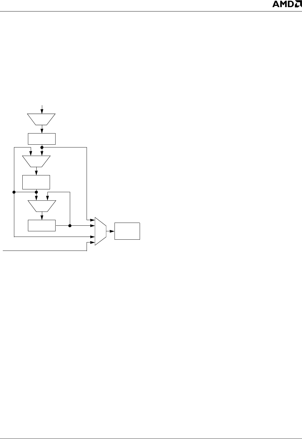
AMD Geode™ LX Processors Data Book 215
GeodeLink™ Memory Controller 33234H
6.1.1.2 Arbitration
The pipelining of the GLMC module requests consists of
the GLIU0 interface request plus two request buffers: the C
(closed) and O (open) slots (see Figure 6-7). A request is
accepted at the GLIU0 interface as long as there is a slot
available. The C slot holds a request to a closed page, or a
request to an open page that matches a row address. The
O slot holds a request to an open page that matches a row
address.
Figure 6-7. Request Pipeline
Arbitration between the request at the GLIU0 interface, the
C request, and the O request at the DRAM end, depend on
selection factors that try to optimize DRAM bus utilization
and maximize throughput. This may involve reordering
transactions as long as ordering rules and coherency are
maintained. Requests from the same GeodeLink device
source are kept in order. Requests from different sources
may pass each other as long as the addresses do not
match.
If reordering is allowable, requests may be reordered for
the following reasons:
1) A request with a higher priority can pass a request in
front of it with a lower priority, as long as the higher-
priority request is ready to run and nothing else is
already running. (Conversely, a request with a lower
priority may not pass a request in front of it with
greater or equal priority.)
2) A younger request that hits to an open page can pass
an older request in front of it that is not a page hit.
3) A write request still gathering its write data may be
passed by a request behind it that is ready to run.
4) Writes and reads are clumped together by the GLMC
to minimize bus turnarounds.
The criteria for reordering is prioritized as above, with the
requests’ priority fields (PRI) taking top precedence in
determining if reordering may be performed. Reordering
based on criterion #2 may only happen if the relative priori-
ties are sorted out as per criterion #1, and so on.
Requests in the C and O slots are run before the request at
the GLIU0 interface if the DRAM is ready to receive them.
The GLIU0 interface request can pass C and O requests
only if the interface request is a read; a write needs to
gather data in the write buffer first so it ends up moving to
the C and possibly O slot while waiting. (For the case
where a GLIU0 non-burst write request and its single beat
of write datum are valid in the same clock, writes could
possibly be optimized to bypass the write buffer, thus
allowing write requests from the GLIU0 interface to be run
on the fly at the DRAM interface. Note that only single
writes may be optimized; burst writes must be buffered first
as there may be bubbles between data beats.)
Requests from the same source whose addresses are
within the same cache line are run in order; otherwise,
reordering from the same source is allowed.
Typically, refresh requests are run when GLIU0 has indi-
cated that a refresh can be initiated via a NULL refresh
request transaction. The GLMC has a refresh counter that,
once enabled and initialized with an interval count, freely
counts down to keep track of refresh intervals. Each time
this refresh counter times out, a refresh request is added to
the GLMC refresh queue, which can queue up to eight
refresh requests. Once a NULL refresh request is received
from GLIU0, and there is at least one refresh request in the
refresh queue, and all outstanding transactions are fin-
ished in the GLMC, the GLMC deletes one request from
the queue and performs one refresh cycle.
If GLIU0 fails to send a NULL request in a timely manner,
and eight refreshes queue up without a NULL request from
GLIU0, the refresh request is upgraded to the highest prior-
ity, and one refresh proceeds. Requests from the GLIU0
interface will not be accepted until the high-priority refresh
runs. Mode-register-set requests and low-power-entry are
arbitrated at the same level as high priority refresh.
GLIU FF
Refresh/Low Power/Mode Set
C Slot FF
O Slot FF
SD FF
GLIU0
Req

216 AMD Geode™ LX Processors Data Book
GeodeLink™ Memory Controller
33234H
6.1.1.3 Data Path
The write datapath utilizes three write buffers to gather
write data within a burst, each one is 4 deep x 64 bits.
Writes to the buffers are alternated between the three buff-
ers or whichever one is empty. The SID, PID, and implied
BEX are also buffered along with the write data. Once the
write request has been processed and arbitrated, and the
corresponding GLIU0 write data transfer is complete into
the buffers, the buffers are then read out and the write
command is dispatched out to memory. Which of the three
buffers is read out depends on which buffer’s SID, PID
matches the SID, PID of the write request that won the
arbitration for the DRAM. If more than one buffer’s SID,
PID matches the write request’s SID, PID, then the buffer
with the older data is read out. The write data is clocked out
using a delay-tuned version of the GLMC/SDRAM write
clock. Only one transaction’s set of write data is written into
a buffer; therefore, only three write transactions can be
buffered at any time.
The write data is written into and read out of the buffers on
the GLIU0 clock, which is twice the frequency of the
GLMC/SDRAM clock. The data strobes DQS are also
shipped out with each data beat, center-aligned with the
data to strobe the data into the DRAM. Unlike SDRAM,
there is a write latency tDQSS between the write command
and the first write data presented to DRAM.
Read data is not buffered to minimize latency. The DQS
strobes generated by the DRAM are edge-aligned with the
read data, and are used to register the read data.The clock
ratio between the GLIU0 clock and GLMC clock is a syn-
chronous 2:1. Since the arrival of the data can vary by as
much as one clock from byte to byte, and vary over time
and temperature, the GLMC captures and resyncs the data
byte by byte as it becomes valid.
6.1.1.4 GLMC/GLCP/Pad Delay Control Settings
GLMC signals to and from the pads are controlled with var-
ious delay lines in the pads. These delay lines are pro-
grammable in the GLCP module. For details on these
delay controls, refer to the Section 6.14.2.8 "GLCP I/O
Delay Controls (GLCP_DELAY_CONTROLS)" on page
549.
6.1.1.5 Basic Timing Diagrams
Figure 6-8 and Figure 6-9 on page 217 illustrate timing
waveforms for DDR reads and DDR writes.
Figure 6-8. DDR Reads
rd3
rd1rd0 rd0
drdywx
m_sd_data
daout
drdyrx
clock
ds
r_data_sync
rd2
rd3
rd1rd0 rd0rd2
r_data_pad rd3
rd1rd0 rd0rd2
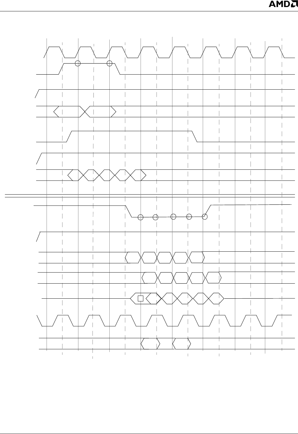
AMD Geode™ LX Processors Data Book 217
GeodeLink™ Memory Controller 33234H
Figure 6-9. DDR Writes
mph1
m_sd_data
drdyrx
rqin_ready
dain
rqin_take
wrx0 wrx1 wrx2 wrx3
drdywx
wry0
dain_ready
dain_take
rqin WRREQY
WRREQX
wrx0 wrx1 wrx2 wrx3 wry0
w_databuf_out
daout wrrespx wrrespy
wrx1
m_sd_dqs
wrx0 wrx2 wrx3 wry0
wrx1
wrx0 wrx2 wrx3 wry0
w_dataf

218 AMD Geode™ LX Processors Data Book
GeodeLink™ Memory Controller
33234H
6.1.2 Power Control
The GLMC employs some methods of power control for
power savings. One method is that it TRI-STATEs the
GLMC address and control pins when there is no valid
address or control data being driven (i.e., when all the chip
selects are inactive (high). This feature is enabled via
GLMC MSR 2000001Dh[12] (TRI_STATE_DIS), and is dis-
abled by default.
The second and third methods of power control are
effected via the GLMC’s GLD_MSR_PM register (MSR
20002004h). The two modes of power control achievable
via this register are PMode0 and PMode1. If PMode0 is
enabled, whenever the GLMC’s internal state machines
are idle and no requests or data are being processed, the
GLMC will shut off one of its two clocks, mb_clk, to save
power. Its other clock, mc_clk, remains active to maintain
the refresh counters. If it needs to perform a refresh, or if a
GLIU request comes into the GLMC, mb_clock is reacti-
vated on the next cycle and the GLMC resumes full power.
If PMode1 is enabled, the GLMC goes into a deeper level
of power-down when it becomes idle. It first sets up the
DRAM to go into self-refresh, then shuts off both of its
clocks. A wakeup signal in the form of a GLIU request (or
reset if the system powers down completely) gets the
GLMC back into full power. Per DRAM requirements, the
GLMC waits 200 mc_clocks before accepting the next
GLIU request (see GLMC MSR 2000001Ah[15:8]). Also, in
order to avoid going into PMode0 or PMode1 unnecessar-
ily, there are programmable sensitivity counters for both
modes (see GLMC MSR 20000020h) that provide a way to
filter out idle periods less than the duration specified in
these counters.
Sequence of steps that occur on entry into PMode1 (i.e.,
Save-to-RAM):
6.1.2.1 Entry into PMode1 (Save-to-RAM)
When Save-to-RAM is requested:
1) ACPI software performs all required memory writes.
2) If necessary, write a non-zero value to PM1_SENS
counter (MSR 200000020h[63:32]). This filters out
GLMC idle periods less than counter value, so
PMode1/Save-to-RAM is only entered on sufficiently
long idle periods.
3) Set PMode1 in MSR 20002004h[2] to 1 to enable
PMode1. On the next GLMC idle condition that is
longer than the value in PM1_SENS, the GLMC per-
forms the following:
4) Finish any outstanding memory transactions if any.
5) Issue self-refresh command to put DIMMs in self-
refresh. This entails issuing a refresh command with
CKE = 0.
6) Turn off both GLMC’s internal mc_clk and mb_clk.
6.1.2.2 Resume from PMode1
Either a reset or a GLIU request wakes up the GLMC from
PMode1, triggering the following sequence:
1) Both internal clocks, mb_clk and mc_clk, resume on
next clock after wakeup event.
2) CKE is released on next clock after clocks resume. If
power was removed during entry into PMode1, CKE is
released as in a cold boot sequence.
3) A Mode Register Set cycle to the DRAM is generated
using the data that was programmed into the
MC_CF07_DATA register (MSR 20000018h)
4) After 200 SDCLKs (as set in PM1_UP_DLY (MSR
2000001Ah[15:8])), the GLMC starts accepting mem-
ory reads/writes.
6.1.3 BIOS Initialization Sequence
This is the recommended sequence that BIOS should take
to initialize the GLMC and DRAMs properly:
1) Initialize the following GLMC registers/bits based on
Serial Presence Detect (SPD) values:
— MSR 20000018h except REF_INT bits [23:8]
— MSR 20000019h
2) Initialize the following GLMC registers:
— MSR 2000001Ah[15:8] = C8h
— MSR 20002004h[2] = 0, [0] = 1
3) Release MASK_CKE[1:0] (MSR 2000001Dh[9:8] =
11).
4) Set/clear REF_TST bit (MSR 20000018h[3]) 16 times
to force 8 refreshes. This also causes a precharge-all
before the first refresh, per JEDEC requirement.
5) Initialize REF_INT (MSR 20000018h[23:8]) to set
refresh interval.
6) Perform load-mode with MSR_BA = 01 (MSR
200000018h[29:28] = 01) to initialize DIMM Extended
Mode register. Load-mode is performed by setting/
clearing PROG_DRAM (MSR 200000018h[0]).
7) Set RST_DLL (MSR 20000018h[27] = 1), perform sec-
ond load-mode with MSR_BA = 00 (MSR
20000018h[29:28]) to initialize Mode register and reset
DLL.
8) Perform third load-mode (MSR 20000018h[29:28] =
00) and RST_DLL cleared (MSR 20000018h[27] = 0).
9) Clear TRISTATE_DIS (MSR 2000001Dh[12] = 0) to
enable the GLMC TRI_STATE during idle cycles (i.e.,
CS[3:0]# = Fh).
10) Wait at least 200 SDCLKs before performing the first
read/write operation.
AMD Geode™ LX Processors Data Book 219
GeodeLink™ Memory Controller Register Descriptions 33234H
6.2 GeodeLink™ Memory Controller Register Descriptions
All GLMC registers are Model Specific Registers (MSRs)
and are accessed via the RDMSR and WRMSR instruc-
tions.
The registers associated with the GLMC are the Standard
GeodeLink Device (GLD) MSRs and GLMC Specific
MSRs. Table 6-5 and Table 6-6 are register summary
tables that include reset values and page references where
the bit descriptions are provided.
Note: MSR addresses are documented using the CPU
Core as the source. Refer to Section 4.1 "MSR
Set" on page 45 for further details.
Table 6-5. Standard GeodeLink™ Device MSRs Summary
MSR
Address Type Register Name Reset Value Reference
20002000h RO GLD Capabilities MSR (GLD_MSR_CAP) 00000000_000204xxh Page 220
20002001h --- GLD Master Configuration MSR
(GLD_MSR_CONFIG) - Not Used
00000000_00000000h Page 220
20002002h R/W GLD SMI MSR (GLD_MSR_SMI) 00000000_00000000h Page 220
20002003h R/W GLD Error MSR (GLD_MSR_ERROR) 00000000_00000000h Page 221
20002004h R/W GLD Power Management (GLD_MSR_PM) 00000000_00000000h Page 222
20002005h R/W GLD Diagnostic (GLD_MSR_DIAG) 00000000_00000000h Page 222
Table 6-6. GLMC Specific MSR Summary
MSR
Address Type Register Name Reset Value Reference
20000010h RO Row Addresses Bank0 DIMM0, Bank1 DIMM0
(MC_CF_BANK01)
xxxxxxxx_xxxxxxxxh Page 223
20000011h RO Row Addresses Bank2 DIMM0, Bank3 DIMM0
(MC_CF_BANK23)
xxxxxxxx_xxxxxxxxh Page 223
20000012h RO Row Addresses Bank4 DIMM0, Bank5 DIMM0
(MC_CF_BANK45)
xxxxxxxx_xxxxxxxxh Page 224
20000013h RO Row Addresses Bank6 DIMM0, Bank7 DIMM0
(MC_CF_BANK67)
xxxxxxxx_xxxxxxxxh Page 224
20000014h RO Row Addresses Bank0 DIMM1, Bank1 DIMM0
(MC_CF_BANK89)
xxxxxxxx_xxxxxxxxh Page 225
20000015h RO Row Addresses Bank2 DIMM1, Bank3 DIMM1
(MC_CF_BANKAB)
xxxxxxxx_xxxxxxxxh Page 225
20000016h RO Row Addresses Bank4 DIMM1, Bank5 DIMM1
(MC_CF_BANKCD)
xxxxxxxx_xxxxxxxxh Page 226
20000017 RO Row Addresses Bank6 DIMM1, Bank7 DIMM1
(MC_CF_BANKEF)
xxxxxxxx_xxxxxxxxh Page 226
20000018h R/W Refresh and SDRAM Program
(MC_CF07_DATA)
10071007_00000040h Page 227
20000019h R/W Timing and Mode Program (MC_CF8F_DATA) 18000008_287337A3h Page 229
2000001Ah R/W Feature Enables (MC_CF1017_DATA) 00000000_11080001h Page 231
2000001Bh RO Performance Counters (MC_CFPERF_CNT1) 00000000_00000000h Page 232
2000001Ch R/W Counter and CAS Control (MC_PERCNT2) 00000000_00FF00FFh Page 233
2000001Dh R/W Clocking and Debug (MC_CFCLK_DBUG) 00000000_00001300h Page 233
2000001Eh RO Page Open Status (MC_CFPG_OPEN) 00000000_0000FFFFh Page 235
220 AMD Geode™ LX Processors Data Book
GeodeLink™ Memory Controller Register Descriptions
33234H
6.2.1 Standard GeodeLink™ Device (GLD) MSRs
6.2.1.1 GLD Capabilities MSR (GLD_MSR_CAP)
6.2.1.2 GLD Master Configuration MSR (GLD_MSR_CONFIG) - Not Used
This register is not used in the GLMC module.
6.2.1.3 GLD SMI MSR (GLD_MSR_SMI)
This register is not used in the GLMC module
2000001Fh --- Reserved --- ---
20000020h R/W PM Sensitivity Counters (MC_CF_PMCTR) 00000000_00000006h Page 236
MSR Address 20002000h
Ty p e RO
Reset Value 00000000_000204xxh
Table 6-6. GLMC Specific MSR Summary
MSR
Address Type Register Name Reset Value Reference
GLD_MSR_CAP Register
63 62 61 60 59 58 57 56 55 54 53 52 51 50 49 48 47 46 45 44 43 42 41 40 39 38 37 36 35 34 33 32
RSVD
313029282726252423222120191817161514131211109876543210
RSVD DEV_ID REV_ID
GLD_MSR_CAP Bit Descriptions
Bit Name Description
63:24 RSVD Reserved.
23:8 DEV_ID Device ID. Identifies device (0204).
7:0 REV_ID Revision ID. Identifies device revision. See AMD Geode™ LX Processors Specification
Update document for value.
MSR Address 20002001h
Ty p e
Reset Value 00000000_00000000h
MSR Address 20002002h
Ty p e R / W
Reset Value 00000000_00000000h

AMD Geode™ LX Processors Data Book 221
GeodeLink™ Memory Controller Register Descriptions 33234H
6.2.1.4 GLD Error MSR (GLD_MSR_ERROR)
MSR Address 20002003h
Ty p e R / W
Reset Value 00000000_00000000h
GLD_MSR_ERROR Register Map
63 62 61 60 59 58 57 56 55 54 53 52 51 50 49 48 47 46 45 44 43 42 41 40 39 38 37 36 35 34 33 32
RSVD
313029282726252423222120191817161514131211109876543210
ERRVAL[15:1] (RSVD)
ERR_VAL0
ERRMAS[15:1] (RSVD)
ERR_MASK0
GLD_MSR_ERROR Bit Descriptions
Bit Name Description
63:32 RSVD Reserved.
31:17 RSVD Reserved.
16 ERR_VAL0 Error Value 0. Synchronous error flag, sent out with GLIU response packet. Hardware
sets error value; writes of 1 clears the error. The GLMC only implements the ‘type-excep-
tion’ error on bit 16, which is set when the GLIU request’s type field is either an I/O type
or snoop type. This bit will be set on such error condition, regardless of the value of
ERR_MASK0. An asynchronous error is also flagged via the mb_p_err output signal.
Note that when an error condition exists, the response packet that corresponds with the
GLIU request that caused the error may be returned to the GLIU out of order (i.e., ahead
of response data for older, outstanding requests in the GLMC). Moreover, the older, out-
standing requests may return corrupt data. (Default = 0)
15:1 RSVD Reserved.
0 ERR_MASK0 Error Mask 0. Masks the corresponding error in bit 16. The GLMC only implements error
mask 0 that corresponds to error bit 16. This bit masks the reporting of the error event
recorded in bit 16. (Default = 0h)

222 AMD Geode™ LX Processors Data Book
GeodeLink™ Memory Controller Register Descriptions
33234H
6.2.1.5 GLD Power Management (GLD_MSR_PM)
6.2.1.6 GLD Diagnostic (GLD_MSR_DIAG)
This register is reserved for internal use by AMD and should not be written to.
MSR Address 20002004h
Ty p e R / W
Reset Value 00000000_00000000h
GLD_MSR_PM Register Map
63 62 61 60 59 58 57 56 55 54 53 52 51 50 49 48 47 46 45 44 43 42 41 40 39 38 37 36 35 34 33 32
RSVD
31 30 29 28 27 26 25 24 23 22 21 20 19 18 17 16 15 14 13 12 11 10 9 8 7 6 5 4 3 2 1 0
RSVD
PM1
RSVD
PM0
GLD_MSR_PM Bit Descriptions
Bit Name Description
63:32 RSVD (RO) Reserved (Read Only). Reads back 0s.
31:3 RSVD Reserved.
2PM1 Power Mode 1. Clock gating for clock domains 0 (GLIU clock) and 1 (GLMC clock). Once
the GLMC becomes idle, it enters PMode1 by 1) closing all banks with a ‘precharge all’
command to the DIMMs, 2) issuing a self-refresh command, 3) bringing CKE1 and CKE0
(balls F4 and E4 respectively) low and putting the address and control pins in TRI_STATE
mode, and 4) shutting off its GLIU and GLMC clocks on the next clock after the self-
refresh. The GLMC resumes to full power after any activity is detected (i.e., a GLIU
request after reset).
0: Disable clock gating. Clocks are always ON. (Default)
1: Enable active hardware clock gating.
1 RSVD Reserved.
0PM0 Power Mode 0. Clock gating for clock domain 0 (GLIU clock). Once the GLMC becomes
idle, it enters PMode0 by shutting off its GLIU clock on the next cycle. Its GLMC clock
remains on to maintain the refresh counters, as do the SDRAM clocks. The GLMC
resumes full power either after any activity is detected, or when it needs to perform a
refresh.
0: Disable clock gating. Clocks are always ON. (Default)
1: Enable active hardware clock gating.
MSR Address 20002005h
Ty p e R / W
Reset Value 00000000_00000000h

AMD Geode™ LX Processors Data Book 223
GeodeLink™ Memory Controller Register Descriptions 33234H
6.2.2 GLMC Specific MSRs
6.2.2.1 Row Addresses Bank0 DIMM0, Bank1 DIMM0 (MC_CF_BANK01)
6.2.2.2 Row Addresses Bank2 DIMM0, Bank3 DIMM0 (MC_CF_BANK23)
MSR Address 20000010h
Ty p e RO
Reset Value xxxxxxxx_xxxxxxxxh
MC_CF_BANK01 Register Map
63 62 61 60 59 58 57 56 55 54 53 52 51 50 49 48 47 46 45 44 43 42 41 40 39 38 37 36 35 34 33 32
RSVD MC_CF_BANK1
31 30 29 28 27 26 25 24 23 22 21 20 19 18 17 16 15 14 13 12 11 10 9 8 7 6 5 4 3 2 1 0
RSVD MC_CF_BANK0
MC_CF_BANK01 Bit Descriptions
Bit Name Description
63:54 RSVD Reserved. Reads back as 0.
53:32 MC_CF_BANK1 Memory Configuration Back 1. Open row address (31:10) for Bank1, DIMM0.
31:22 RSVD Reserved. Reads back as 0.
21:0 MC_CF_BANK0 Memory Configuration Back 0. Open row address (31:10) for Bank0, DIMM0.
MSR Address 20000011h
Ty p e RO
Reset Value xxxxxxxx_xxxxxxxxh
MC_CF_BANK23 Register Map
63 62 61 60 59 58 57 56 55 54 53 52 51 50 49 48 47 46 45 44 43 42 41 40 39 38 37 36 35 34 33 32
RSVD MC_CF_BANK3
31 30 29 28 27 26 25 24 23 22 21 20 19 18 17 16 15 14 13 12 11 10 9 8 7 6 5 4 3 2 1 0
RSVD MC_CF_BANK2
MC_CF_BANK23 Bit Descriptions
Bit Name Description
63:54 RSVD Reserved. Reads back as 0.
53:32 MC_CF_BANK3 Memory Controller Configuration Bank 3. Open row address (31:10) for Bank3,
DIMM0.
31:22 RSVD Reserved. Reads back as 0.
21:0 MC_CF_BANK2 Memory Controller Configuration Bank 2. Open row address (31:10) for Bank2,
DIMM0.
224 AMD Geode™ LX Processors Data Book
GeodeLink™ Memory Controller Register Descriptions
33234H
6.2.2.3 Row Addresses Bank4 DIMM0, Bank5 DIMM0 (MC_CF_BANK45)
6.2.2.4 Row Addresses Bank6 DIMM0, Bank7 DIMM0 (MC_CF_BANK67)
MSR Address 20000012h
Ty p e RO
Reset Value xxxxxxxx_xxxxxxxxh
MC_CF_BANK45 Register Map
63 62 61 60 59 58 57 56 55 54 53 52 51 50 49 48 47 46 45 44 43 42 41 40 39 38 37 36 35 34 33 32
RSVD MC_CF_BANK5
31 30 29 28 27 26 25 24 23 22 21 20 19 18 17 16 15 14 13 12 11 10 9 8 7 6 5 4 3 2 1 0
RSVD MC_CF_BANK4
MC_CF_BANK45 Bit Descriptions
Bit Name Description
63:54 RSVD Reserved. Reads back as 0.
53:32 MC_CF_BANK5 Memory Controller Configuration Bank 5. Open row address (31:10) for Bank5,
DIMM0.
31:22 RSVD Reserved. Reads back as 0.
21:0 MC_CF_BANK4 Memory Controller Configuration Bank 4. Open row address (31:10) for Bank4,
DIMM0.
MSR Address 20000013h
Ty p e RO
Reset Value xxxxxxxx_xxxxxxxxh
MC_CF_BANK67 Register Map
63 62 61 60 59 58 57 56 55 54 53 52 51 50 49 48 47 46 45 44 43 42 41 40 39 38 37 36 35 34 33 32
RSVD MC_CF_BANK7
313029282726252423222120191817161514131211109876543210
RSVD MC_CF_BANK6
MC_CF_BANK67 Bit Descriptions
Bit Name Description
63:54 RSVD Reserved. Reads back as 0.
53:32 MC_CF_BANK7 Memory Controller Configuration Bank 7. Open row address (31:10) for Bank7,
DIMM0.
31:22 RSVD Reserved. Reads back as 0.
21:0 MC_CF_BANK6 Memory Controller Configuration Bank 6. Open row address (31:10) for Bank6,
DIMM0.
AMD Geode™ LX Processors Data Book 225
GeodeLink™ Memory Controller Register Descriptions 33234H
6.2.2.5 Row Addresses Bank0 DIMM1, Bank1 DIMM0 (MC_CF_BANK89)
6.2.2.6 Row Addresses Bank2 DIMM1, Bank3 DIMM1 (MC_CF_BANKAB)
MSR Address 20000014h
Ty p e RO
Reset Value xxxxxxxx_xxxxxxxxh
MC_CF_BANK89 Register Map
63 62 61 60 59 58 57 56 55 54 53 52 51 50 49 48 47 46 45 44 43 42 41 40 39 38 37 36 35 34 33 32
RSVD MC_CF_BANK9
31 30 29 28 27 26 25 24 23 22 21 20 19 18 17 16 15 14 13 12 11 10 9 8 7 6 5 4 3 2 1 0
RSVD MC_CF_BANK8
MC_CF_BANK89 Bit Descriptions
Bit Name Description
63:54 RSVD Reserved. Reads back as 0.
53:32 MC_CF_BANK9 Memory Controller Configuration Bank 9. Open row address (31:10) for Bank1,
DIMM1.
31:22 RSVD Reserved. Reads back as 0.
21:0 MC_CF_BANK8 Memory Controller Configuration Bank 8. Open row address (31:10) for Bank0,
DIMM1.
MSR Address 20000015h
Ty p e RO
Reset Value xxxxxxxx_xxxxxxxxh
MC_CF_BANKAB Register Map
63 62 61 60 59 58 57 56 55 54 53 52 51 50 49 48 47 46 45 44 43 42 41 40 39 38 37 36 35 34 33 32
RSVD MC_CF_BANKB
31 30 29 28 27 26 25 24 23 22 21 20 19 18 17 16 15 14 13 12 11 10 9 8 7 6 5 4 3 2 1 0
RSVD MC_CF_BANKA
MC_CF_BANKAB Bit Descriptions
Bit Name Description
63:54 RSVD Reserved. Reads back as 0.
53:32 MC_CF_BANKB Memory Controller Configuration Bank B. Open row address (31:10) for Bank3,
DIMM1.
31:22 RSVD Reserved. Reads back as 0.
21:0 MC_CF_BANKA Memory Controller Configuration Bank A. Open row address (31:10) for Bank2,
DIMM1.
226 AMD Geode™ LX Processors Data Book
GeodeLink™ Memory Controller Register Descriptions
33234H
6.2.2.7 Row Addresses Bank4 DIMM1, Bank5 DIMM1 (MC_CF_BANKCD)
6.2.2.8 Row Addresses Bank6 DIMM1, Bank7 DIMM1 (MC_CF_BANKEF)
MSR Address 20000016h
Ty p e RO
Reset Value xxxxxxxx_xxxxxxxxh
MC_CF_BANKCD Register Map
63 62 61 60 59 58 57 56 55 54 53 52 51 50 49 48 47 46 45 44 43 42 41 40 39 38 37 36 35 34 33 32
RSVD MC_CF_BANKD
31 30 29 28 27 26 25 24 23 22 21 20 19 18 17 16 15 14 13 12 11 10 9 8 7 6 5 4 3 2 1 0
RSVD MC_CF_BANKC
MC_CF_BANKCD Bit Descriptions
Bit Name Description
63:54 RSVD Reserved. Reads back as 0.
53:32 MC_CF_BANKD Memory Controller Configuration Bank C. Open row address (31:10) for Bank5,
DIMM1.
31:22 RSVD Reserved. Reads back as 0.
21:0 MC_CF_BANKC Memory Controller Configuration Bank B. Open row address (31:10) for Bank4,
DIMM1.
MSR Address 20000017
Ty p e RO
Reset Value xxxxxxxx_xxxxxxxxh
MC_CF_BANKEF Register Map
63 62 61 60 59 58 57 56 55 54 53 52 51 50 49 48 47 46 45 44 43 42 41 40 39 38 37 36 35 34 33 32
RSVD MC_CF_BANKF
313029282726252423222120191817161514131211109876543210
RSVD MC_CF_BANKE
MC_CF_BANKEF Bit Descriptions
Bit Name Description
63:54 RSVD Reserved. Reads back as 0.
53:32 MC_CF_BANKF Memory Controller Configuration Bank F. Open row address (31:10) for Bank7,
DIMM1.
31:22 RSVD Reserved. Reads back as 0.
21:0 MC_CF_BANKE Memory Controller Configuration Bank E. Open row address (31:10) for Bank6,
DIMM1.

AMD Geode™ LX Processors Data Book 227
GeodeLink™ Memory Controller Register Descriptions 33234H
6.2.2.9 Refresh and SDRAM Program (MC_CF07_DATA)
MSR Address 20000018h
Ty p e R / W
Reset Value 10071007_00000040h
MC_CF07_DATA Register Map
63 62 61 60 59 58 57 56 55 54 53 52 51 50 49 48 47 46 45 44 43 42 41 40 39 38 37 36 35 34 33 32
D1_SZ RSVD
D1_MB
RSVD
D1_CB
RSVD
D1_PSZ D0_SZ RSVD
D0_MB
RSVD
D0_CB
RSVD
D0_PSZ
31 30 29 28 27 26 25 24 23 22 21 20 19 18 17 16 15 14 13 12 11 10 9 8 7 6 5 4 3 2 1 0
RSVD
MSR_BA
RST_DLL
EMR_QFC
EMR_DRV
EMR_DLL
REF_INT
REF_STAG
REF_TST
RSVD
SOFT_RST
PROG_DRAM
MC_CF07_DATA Bit Descriptions
Bit Name Description
63:60 D1_SZ DIMM1 Size.
0000: Reserved 0100: 64 MB 1000: 1 GB
0001: 8 MB (Default) 0101: 128 MB 1001-1111: Reserved
0010: 16 MB 0110: 256 MB
0011: 32 MB 0111: 512 MB
59:57 RSVD Reserved.
56 D1_MB DIMM1 Module Banks. Number of module banks for DIMM1.
0: 1 Module bank. (Default)
1: 2 Module banks.
55:53 RSVD Reserved.
52 D1_CB DIMM1 Component Banks. Number of component banks per module bank for DIMM1.
0: 2 Component banks. (Default)
1: 4 Component banks.
51 RSVD Reserved.
50:48 D1_PSZ DIMM1 Page Size.
000: 1 KB 100: 16 KB
001: 2 KB 101: 32 KB
010: 4 KB 110: Reserved
011: 8 KB 111: DIMM 1 Not Installed (Default)
47:44 D0_SZ DIMM0 Size.
0000: Reserved 0100: 64 MB 1000: 1 GB
0001: 8 MB (Default) 0101: 128 MB 1001-1111: Reserved
0010: 16 MB 0110: 256 MB
0011: 32 MB 0111: 512 MB
43:41 RSVD Reserved.
40 D0_MB DIMM0 Module Banks. Number of module banks for DIMM0.
0: 1 Module bank. (Default)
1: 2 Module banks.
39:37 RSVD Reserved.

228 AMD Geode™ LX Processors Data Book
GeodeLink™ Memory Controller Register Descriptions
33234H
36 D0_CB DIMM0 Component Banks. Number of component banks per module bank for DIMM0.
0: 2 Component banks. (Default)
1: 4 Component banks.
35 RSVD Reserved.
34:32 D0_PSZ DIMM0 Page Size.
000: 1 KB 100: 16 KB
001: 2 KB 101: 32 KB
010: 4 KB 110: Reserved
011: 8 KB 111: DIMM0 Not Installed (Default)
31:30 RSVD Reserved.
29:28 MSR_BA Mode Register Set Bank Address. These are the bank select bits used for program-
ming the DDR DIMM’s Extended Mode Register. These bits select whether the GLMC is
programming the Mode Register or the Extended Mode Register.
00: Program the DIMM Mode Register. (Default)
01: Program the DIMM Extended Mode Register. Bits [26:24] determine the program
data.
10: Reserved.
11: Reserved.
27 RST_DLL Mode Register Reset DLL. This bit represents A8 in the Mode Register, which when set
to 1 resets the DLL as part of the DIMM initialization sequence. JEDEC recommends
clearing this bit back to 0 on the final load-mode-register command before activating any
bank.
0: Do not reset DLL. (Default.
1: Reset DLL.
26 EMR_QFC Extended Mode Register FET Control. This bit programs the DIMM’s QFC# signal. The
QFC# signal provides control for FET switches that are used to isolate module loads from
the system memory busy at times when the given module is not being accessed. Only
pertains to x4 configurations.
0: Enable. (Default)
1: Disable.
25 EMR_DRV Extended Mode Register Drive Strength Control. This bit selects either normal or
reduced drive strength.
0: Normal. (Default)
1: Reduced.
24 EMR_DLL Extended Mode Register DLL. This bit disables/enables the DLL.
0: Enable. (Default)
1: Disable.
23:8 REF_INT Refresh Interval. This field determines the number of SDRAM clocks between refresh.
This value multiplied by 16 is the average number of clocks between refresh. The default
value, 00h, disables refresh.
7:4 REF_STAG Refresh Staggering. This field controls the number of clocks (0-16) between REF com-
mands to different banks during refresh cycles. Staggering is used to help reduce power
spikes during refresh. Note that with a setting of 0, no staggering occurs, so all module
banks are refreshed simultaneously. (Default = 1)
3 REF_TST Test Refresh. This bit, when set high, generates one refresh request that the GLMC
queues in its refresh request queue. Since the refresh queue is 8-deep, 8 sets/clears of
this bit queues 8 refresh requests, thus forcing a refresh request out to DRAM. This bit
should only be used for initialization and test. (Default = 0)
MC_CF07_DATA Bit Descriptions (Continued)
Bit Name Description
AMD Geode™ LX Processors Data Book 229
GeodeLink™ Memory Controller Register Descriptions 33234H
6.2.2.10 Timing and Mode Program (MC_CF8F_DATA)
2 RSVD Reserved.
1SOFT_RST Software Reset. Puts the GLMC in a known state. Does not change configuration regis-
ters. The recommended sequence to use is:
1) Make sure SDRAM interface has “been idle for a while”.
2) Set software reset, then clear software reset.
3) Do a refresh cycle.
Accesses to memory may resume as normal following this.
Note that configuration registers are not scannable. To reproduce a problem in simulation
requires saving the configuration registers with software in silicon and reprogramming the
values in simulation. (Default = 0)
0PROG_DRAMProgram Mode Register in SDRAM. When this bit is set, the GLMC will issue one Load
Mode Register command to the DRAMs. It either programs the Mode Register (if
MSR_BA, bits [29:28] = 00), or the Extended Mode Register (if MSR_BA, bits [29:28] =
01). The Mode Register is programmed with CAS latency (see MSR 2000019h[30:28]),
wrap type sequential, and burst length of 4 for 64-bit data path, or burst length of 8 for 32-
bit wide data path. The Extended Mode Register in DDR DIMMs is programmed with the
QFC#, drive strength and DLL disable bits [26:24]. The Extended Mode Register must be
programmed first to enable the DLLs, then the Mode Register. This bit must be set and
cleared for each Load Mode Register command. (Default = 0)
MSR Address 20000019h
Ty p e R / W
Reset Value 18000008_287337A3h
MC_CF07_DATA Bit Descriptions (Continued)
Bit Name Description
MC_CF8F_DATA Register Map
63 62 61 60 59 58 57 56 55 54 53 52 51 50 49 48 47 46 45 44 43 42 41 40 39 38 37 36 35 34 33 32
STALE_REQ RSVD
XOR_BIT_SEL
XOR_MB0
XOR_BA1
XOR_BA0
RSVD
TRUNC_DIS
REORDER_DIS
RSVD
HOI_LOI
RSVD
31 30 29 28 27 26 25 24 23 22 21 20 19 18 17 16 15 14 13 12 11 10 9 8 7 6 5 4 3 2 1 0
THZ_DLY
CAS_LAT ACT2ACTREF ACT2PRE
RSVD
PRE2ACT
RSVD
ACT2CMD ACT2ACT
DPLWR
DPLRD
RSVD

230 AMD Geode™ LX Processors Data Book
GeodeLink™ Memory Controller Register Descriptions
33234H
MC_CF8F_DATA Bit Descriptions
Bit Name Description
63:56 STALE_REQ GLIU Max Stale Request Count. Non-high priority requests (PRI = 0) are made high-pri-
ority requests when the request is not serviced within max stale request count clocks.
(Default = 18h)
55:53 RSVD Reserved.
52:51 XOR_BIT_SEL XOR Bit Select. Selects which upper GLIU address bit to XOR with MB0, BA1 or BA0
(see "Auto Low Order Interleaving" on page 212). Only applies to LOI mode. (Default =
00).
00: ADDR[18] 01: ADDR[19] 10: ADDR[20] 11: ADDR[21]
50 XOR_MB0 XOR MB0 Enable. Enables XORing of module bank select MB0 with upper GLIU
address bit selected by XOR_BIT_SEL (bits [52:51]). (Default = 0, Disabled)
49 XOR_BA1 XOR BA1 Enable. Enables XORing of component bank select BA1 with upper GLIU
address bit selected by XOR_BIT_SEL (bits [52:51]). (Default = 0, Disabled)
48 XOR_BA0 XOR BA0 Enable. Enables XORing of component bank select BA0 with upper GLIU
address bit selected by XOR_BIT_SEL (bits [52:51]). (Default = 0, Disabled)
47:42 RSVD Reserved.
41 TRUNC_DIS Burst Truncate Disable. Disables truncation of read/write bursts. This disable reduces
performance and should only be used during debug. (Default = 0, bursts enabled)
40 REORDER_DIS Reorder Disable. Disables the reordering of requests. This bit must be set to 1.
39:34 RSVD Reserved.
33 HOI_LOI High / Low Order Interleave Select (HOI / LOI). Selects the address interleaving mode.
HOI uses fixed upper address bits to map the GLIU address to a component bank. LOI
uses variable lower address bits depending on page size, number of module banks, and
number of component banks of the DIMMs, plus an option to XOR with upper address
bits.
1: HOI.
0: LOI. (Default)
32 RSVD Reserved.
31 THZ_DLY tHZ Delay. Add 1 extra clock on read-to-write turnarounds to satisfy DRAM parameter
tHZ for higher frequencies. (Default = 0)
30:28 CAS_LAT Read CAS Latency. Number of clock delays between Read command and Data valid.
CAS Latency:
000: RSVD 010: 2 (Default) 100: 4 110: 2.5
001: RSVD 011: 3 101: 1.5 111: 3.5
27:24 ACT2ACTREF ACT to ACT/REF Period. tRC. Minimum number of SDRAM clocks between ACTIVE
and ACTIVE/AUTO REFRESH commands. (Default = 8h)
23:20 ACT2PRE ACT to PRE Period. tRAS. Minimum number of clocks from ACT to PRE commands on
the same component bank. (Default = 7h)
19 RSVD Reserved.
18:16 PRE2ACT Pre to Act Period. tRP. Minimum number of SDRAM clocks between PRE and ACT com-
mands. (Default = 011)
15 RSVD Reserved.
14:12 ACT2CMD Delay Time from Act To read/WRITE. tRCD. Minimum number of SDRAM clocks
between ACT and READ/WRITE commands. (6..2 valid). (Default = 011)
AMD Geode™ LX Processors Data Book 231
GeodeLink™ Memory Controller Register Descriptions 33234H
6.2.2.11 Feature Enables (MC_CF1017_DATA)
11:8 ACT2ACT ACT(0) to ACT(1) Period. tRRD. Minimum number of SDRAM clocks between ACT and
ACT command to two different component banks within the same module bank. (Default
= 7h)
7:6 DPLWR Data-in to PRE Period. tDPLW. Minimum number of clocks from last write data to pre-
charge command on the same component bank. (3..1 valid). Default = 10)
5:4 DPLRD Data-in to PRE Period. tDPLR. Minimum number of clocks from last read data to pre-
charge command on the same component bank.(3..1 valid) The count starts on the same
clock that the last data would have been if the command was a write. (Default = 10)
3 RSVD Reserved.
2:0 RSVD Reserved.
MSR Address 2000001Ah
Ty p e R / W
Reset Value 00000000_11080001h
MC_CF8F_DATA Bit Descriptions (Continued)
Bit Name Description
MC_CF1017_DATA Register Map
63 62 61 60 59 58 57 56 55 54 53 52 51 50 49 48 47 46 45 44 43 42 41 40 39 38 37 36 35 34 33 32
RSVD
31 30 29 28 27 26 25 24 23 22 21 20 19 18 17 16 15 14 13 12 11 10 9 8 7 6 5 4 3 2 1 0
RSVD
WR_TO_RD
RSVD
RD_TMG_CTL
RSVD REF2ACT PM1_UP_DLY RSVD WR2DAT
MC_CF1017_DATA Bit Descriptions
Bit Name Description
63:30 RSVD Reserved.
29:28 WRITE_TO_RD Write to Read Delay. tWTR. Minimum number of SDCLKS between last write data
beat to next read command. (Default = 01)
27 RSVD Reserved.
26:24 RD_TMG_CTL Read Timing Control. Number of half-GLIU clocks that the read data is delayed in
arriving at the GLMC beyond the CAS latency delay. This number increases as the
round-trip read delay increases. (Default = 001)
23:21 RSVD Reserved.
20:16 REF2ACT Refresh to Activate Delay. tRFC. Minimum number of SDCLKS (0-31) between
refresh and next command, usually an activate. (Default = 8h)
15:8 PM1_UP_DLY PMode1 Up Delay. Sets the delay in DRAM clocks from exit from PMode1 to accep-
tance of the next GLIU memory request. PMode1 power down involves a self-refresh
command to DRAM. This is to satisfy a 200-clock delay from self-refresh exit to first
read command (although this bit will delay all commands, read and write). (Default =
0, No delay)
7:3 RSVD Reserved.
232 AMD Geode™ LX Processors Data Book
GeodeLink™ Memory Controller Register Descriptions
33234H
6.2.2.12 Performance Counters (MC_CFPERF_CNT1)
2:0 WR2DAT Write Command To Data Latency. Number of clocks between the write command
and the first data beat. Valid values are: [2,1,0], and must correspond to the installed
DIMMs as follows:
0h: No delay.
1h: 1-clock delay for DDR unbuffered DIMMs. (Default)
MSR Address 2000001Bh
Ty p e RO
Reset Value 00000000_00000000h
MC_CF1017_DATA Bit Descriptions
Bit Name Description
MC_CFPERF_CNT1 Register Map
63 62 61 60 59 58 57 56 55 54 53 52 51 50 49 48 47 46 45 44 43 42 41 40 39 38 37 36 35 34 33 32
CNT1
313029282726252423222120191817161514131211109876543210
CNT0
MC_CFPERF_CNT1 Bit Descriptions
Bit Name Description
63:32 CNT0 Counter 0. Performance counter 0. Counts the occurrence of events at the GLIU inter-
face. Events are specified in CNT0_DATA (MSR 2000001Ch[7:0]). Reset and stop con-
trol on this counter is done via MSR 200001Ch[33:32]. (Default = 0h)
31:0 CNT1 Counter 1. Performance counter 1. Counts the occurrence of events at the GLIU inter-
face. Events are specified in CNT1_DATA (MSR 2000001Ch[23:16]. Reset and stop con-
trol on this counter is done via MSR 200001Ch[35:34]. (Default = 0h)
AMD Geode™ LX Processors Data Book 233
GeodeLink™ Memory Controller Register Descriptions 33234H
6.2.2.13 Counter and CAS Control (MC_PERCNT2)
6.2.2.14 Clocking and Debug (MC_CFCLK_DBUG)
MSR Address 2000001Ch
Ty p e R / W
Reset Value 00000000_00FF00FFh
MC_PERFCNT2 Register Map
63 62 61 60 59 58 57 56 55 54 53 52 51 50 49 48 47 46 45 44 43 42 41 40 39 38 37 36 35 34 33 32
RSVD
STOP_CNT1
RST_CNT1
STOP_CNT0
RST_CNT0
313029282726252423222120191817161514131211109876543210
RSVD
MC_PERFCNT2 Bit Descriptions
Bit Name Description
63:36 RSVD Reserved.
35 STOP_CNT1 Stop Counter 1. If set, stops counter 1. (Default = 0)
34 RST_CNT1 Reset Counter 1. If set, resets counter 1. (Default = 0)
33 STOP_CNT0 Stop Counter 0. If set, stops counter 0. (Default = 0)
32 RST_CNT0 Reset Counter 0. If set, resets counter 0. (Default = 0)
31:0 RSVD Reserved.
MSR Address 2000001Dh
Ty p e R / W
Reset Value 00000000_00001300h
MC_CFCLK_DBUG Register Map
63 62 61 60 59 58 57 56 55 54 53 52 51 50 49 48 47 46 45 44 43 42 41 40 39 38 37 36 35 34 33 32
RSVD
B2B_DIS
MTEST_RBEX_EN
MTEST_EN
31 30 29 28 27 26 25 24 23 22 21 20 19 18 17 16 15 14 13 12 11 10 9 8 7 6 5 4 3 2 1 0
RSVD
FORCE_PRE
RSVD
TRISTATE_DIS
RSVD
MASK_CKE1
MASK_CKE0
CNTL_MSK1
CNTL_MSK0
ADRS_MSK
RSVD

234 AMD Geode™ LX Processors Data Book
GeodeLink™ Memory Controller Register Descriptions
33234H
MC_CFCLK_DBUG Bit Descriptions
Bit Name Description
63:35 RSVD Reserved.
34 B2B_DIS Back-to-Back Command Disable. Setting this bit disables the issuing of DRAM com-
mands within back-to-back cycles in both MTEST and normal functional mode. To maxi-
mize performance, this should only be used in MTEST mode, where the cycle following
the command cycle should be idle for the logic analyzer to be able to properly capture
and interpret the MTEST data. (Default = 0) (back-to-back commands allowed).
33 MTEST_RBEX_
EN
MTEST RBEX Enable. Enables the outputting of read byte enables information on reads
with RBEXs.
0: Disable. (Default)
1: Enable.
32 MTEST_EN MTEST Enable. Enables MTEST debug mode, which multiplexes debug data onto the 13
DRAM address output pins, one cycle after the command cycle. (Default = 0)
31:17 RSVD Reserved.
16 FORCE_PRE Force Precharge-all. Force precharge-all command before load-mode and refresh com-
mands, even when banks are already all closed. Normally, a precharge-all command only
gets issued conditionally before a load-mode or refresh command: only if the module
banks are not all closed yet. With this bit set, the precharge-all will be issued uncondition-
ally before the load-mode or refresh command.
0: Disable. (Default)
1: Enable.
15:13 RSVD Reserved.
12 TRISTATE_DIS TRI-STATE Disable.This bit controls the power saving feature that puts the GLMC's
address and control pins into TRI-STATE mode during idle cycles or during PMode1.
0: Tri-stating enabled.
1: Tri-stating disabled. (Default)
11:10 RSVD Reserved.
9:8 MASK_CKE[1:0] CKE Mask. Mask output enables for CKE[1:0]. After power-up or warm reset, software
can complete all necessary initialization tasks before clearing this mask to allow commu-
nication with the DRAM. These bits can also be used to selectively mask off the CKE sig-
nal of a DIMM that is not installed.
00: CKE1 and CKE0 unmasked.
01: CKE1 unmasked, CKE0 masked.
10: CKE1 masked, CKE0 unmasked.
11: CKE1 and CKE0 masked. (Default)
7 CNTL_MSK1 Control Mask 1. Mask output enable bit for DIMM1’s CAS1#, RAS1#, WE1#, CS[3:2]#.
0: Unmasked. (Default)
1: Masked.
6 CNTL_MSK0 Control Mask 0. Mask output enable bit for DIMM0’s CAS0#, RAS0#, W0#, CS[1:0]#.
0: Unmasked. (Default)
1: Masked.
5 ADRS_MSK Address Mask. Mask output enable bit for MA and BA. (Default = 0)
4:0 RSVD Reserved.
AMD Geode™ LX Processors Data Book 235
GeodeLink™ Memory Controller Register Descriptions 33234H
6.2.2.15 Page Open Status (MC_CFPG_OPEN)
6.2.2.16 Reserved Register
This register is reserved and should not be written to.
MSR Address 2000001Eh
Ty p e RO
Reset Value 00000000_0000FFFFh
MC_CFPG_OPEN Register Map
63 62 61 60 59 58 57 56 55 54 53 52 51 50 49 48 47 46 45 44 43 42 41 40 39 38 37 36 35 34 33 32
RSVD
313029282726252423222120191817161514131211109876543210
RSVD PGOPEN1 PGOPEN0
MC_CFPG_OPEN Bit Descriptions
Bit Name Description
63:16 RSVD Reserved. Reads back as 0.
15:8 PGOPEN1 Page Open DIMM 1. Page open indication of the second DIMM. Each bit position repre-
sents a page and a 1 indicates an open page. All pages are initialized ‘open’. After reset,
a ‘precharge all’ command closes all the banks.
7:0 PGOPEN0 Page Open DIMM 0. Page open indication of the first DIMM. Each bit position represents
a page and a 1 indicates an open page. All pages are initialized ‘open’. After reset, a ‘pre-
charge all’ command closes all the banks.
MSR Address 2000001Fh
Ty p e RW
Reset Value 00000000_00000000h

236 AMD Geode™ LX Processors Data Book
GeodeLink™ Memory Controller Register Descriptions
33234H
6.2.2.17 PM Sensitivity Counters (MC_CF_PMCTR)
MSR Address 20000020h
Ty p e R / W
Reset Value 00000000_00000006h
MC_CF_PMCTR Register Map
63 62 61 60 59 58 57 56 55 54 53 52 51 50 49 48 47 46 45 44 43 42 41 40 39 38 37 36 35 34 33 32
PM1_SENS
313029282726252423222120191817161514131211109876543210
PM0_SENS
MC_CF_PMCTR Bit Descriptions
Bit Name Description
63:32 PM1_SENS PMode1 Sensitivity Counter. Counter that controls the GLMC’s sensitivity to entering
PMode1 power down mode. If PMode1 is enabled, PM1_SENS starts counting down
from its loaded value whenever the GLMC becomes idle. If it times out and the GLMC is
still idle, the GLMC goes into PMode1. If, however, the GLMC resumes activity before
time-out, the counter is reset to its loaded value and PMode1 is not entered. (Default =
0h)
31:0 PM0_SENS PMode0 Sensitivity Counter. Counter that controls the GLMC’s sensitivity to entering
PMode0 power down mode. If PMode0 is enabled, PM0_SENS starts counting down
from its loaded value whenever the GLMC becomes idle. If it times out and the GLMC is
still idle, the GLMC goes into PMode0. If, however, the GLMC resumes activity before
time-out, the counter is reset to its loaded value and PMode0 is not entered. (Default =
6h, to allow 32-bit bursts to finish).
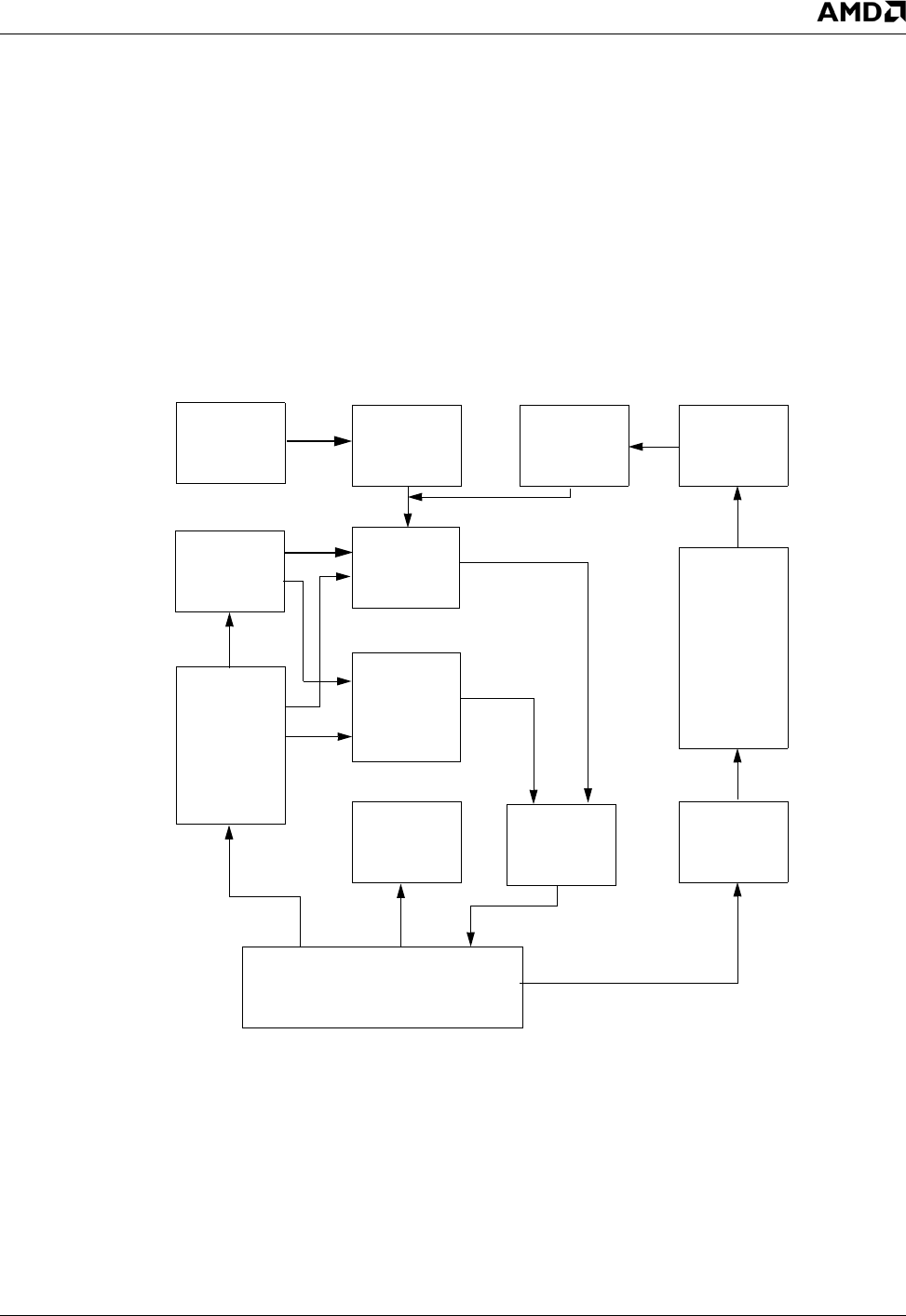
AMD Geode™ LX Processors Data Book 237
Graphics Processor 33234H
6.3 Graphics Processor
The Graphics Processor is based on the graphics proces-
sor used in the AMD Geode™ GX processor with several
features added to enhance performance and functionality.
Like its predecessor, the AMD Geode LX processor’s
Graphics Processor is a BitBLT/vector engine that supports
pattern generation, source expansion, pattern/source
transparency, 256 ternary raster operations, alpha blenders
to support alpha-BLTs, incorporated BLT FIFOs, a
GeodeLink™ interface and the ability to throttle BLTs
according to video timing. Features added to the Graphics
Processor include:
•Command buffer interface
•Hardware accelerated rotation BLTs
•Color depth conversion
•Palletized color
•Full 8x8 color pattern buffer
•Channel 3 - third DMA channel
•Monochrome inversion
The block diagram of the AMD Geode LX processor’s
Graphics Processor is shown in Figure 6-10. Table 6-7 on
page 238 presents a comparison between the Graphics
Processor features of the AMD Geode GX and LX proces-
sors.
Figure 6-10. Graphics Processor Block Diagram
Pattern
Registers
Pattern
Expansion
Raster
Source
Aligner &
Expansion Operation
Source &
Destination
Read FIFOs
Alpha
Blend
Unit
Write
Accumulation
FIFO
GeodeLink™ Interface Unit 0
(GLIU0)
Channel 3
Data Flow
Control
Channel 3
Data
Formatter
2K FIFO
and
LUT and
Pattern
Memory
Channel 3
Fetch
Engine
Command
Buffer Control
Logic and
Registers

238 AMD Geode™ LX Processors Data Book
Graphics Processor
33234H
Table 6-7. Graphics Processor Feature Comparison
Feature AMD Geode™ GX Processor AMD Geode™ LX Processor
Color Depth 8, 16, 32-bpp 8, 16, 32-bpp (A) RGB 4 and 8-bit indexed
ROPs 256 (src, dest, pattern) 256 (2-src, dest and pattern)
BLT Buffers FIFOs in Graphics Processor FIFOs in Graphics Processor
BLT Splitting Managed by hardware Managed by hardware
Video Synchronized BLT/Vector Throttle by VBLANK Throttle by VBLANK
Bresenham Lines Yes Yes
Patterned (stippled) Lines No Yes
Screen to Screen BLT Yes Yes
Screen to Screen BLT with
mono expansion
Ye s Ye s
Memory to Screen BLT Yes (through CPU writes) Yes (throttled rep movs writes)
Accelerated Text No No
Pattern Size (Mono) 8x8 pixels 8x8 pixels
Pattern Size (Color) 8x1 (32 pixels) 8x8 pixels
8x2 (16 pixels)
8x4 (8 pixels)
Monochrome Pattern Yes Yes (with inversion)
Dithered Pattern (4 color) No No
Color Pattern 8, 16, 32-bpp 8, 16, 32-bpp
Transparent Pattern Monochrome Monochrome
Solid Fill Yes Yes
Pattern Fill Yes Yes
Transparent Source Monochrome Monochrome
Color Key Source Transparency Y with mask Y with mask
Variable Source Stride Yes Yes
Variable Destination Stride Yes Yes
Destination Write Bursting Yes Yes
Selectable BLT Direction Vertical and Horizontal Vertical and Horizontal
Alpha BLT Yes (constant α or α/pix) Yes (constant α, α/pix, or sep. α channel)
VGA Support Decodes VGA Register Decodes VGA Register
Pipeline Depth 2 ops Unlimited
Accelerated Rotation BLT No 8, 16, 32-bpp
Color Depth Conversion No 5:6:5, 1:5:5:5, 4:4:4:4, 8:8:8:8
AMD Geode™ LX Processors Data Book 239
Graphics Processor 33234H
6.3.1 Command Buffer
The AMD Geode LX processor supports a command buffer
interface in addition to the normal two-deep pipelined regis-
ter interface. It is advised that software use either the com-
mand buffer interface or the register interface. It is possible
to use both, however, all pending operations should be
allowed to complete before making the switch. The com-
mand buffer interface is controlled through four registers
that specify the starting address of the command buffer,
the ending address of the command buffer, the current
write pointer and the current read pointer. The base
address (top 12 bits) of the command buffer is specified in
the GLD_MSR_CONFIG (MSR A0002001h). During initial-
ization, a block of memory is allocated to be the command
buffer space. This block must be entirely contained within a
non-cacheable 16 MB region of physical memory. The
Geode LX processor will not issue coherent transactions
for the command buffer or any other memory operations.
The starting address should be written to GP_CMD_TOP
and the ending address should be written to
GP_CMD_BOT (GP Memory Offset 50h and 54h respec-
tively). The starting address should also be written to
GP_CMD_READ (GP Memory Offset 58h). Writing to
GP_CMD_READ automatically updates GP_CMD_WRITE
(GP Memory Offset 5Ch). From this point, software can ini-
tiate an action in the processor by writing a command
buffer structure into memory at the write address
(GP_CMD_WRITE), then updating the write address to
point to the next available space in the command buffer,
either the next contiguous DWORD address, or the buffer
starting address (GP_CMD_TOP) if the wrap bit is set in
the command buffer control word. Command buffers are
allowed to wrap around the end of the command buffer
space (i.e., whenever the end of the space is reached, the
hardware will continue fetching at the beginning of the
space creating a circular buffer). However, software may
force a wrap before the end of the buffer space is reached
by setting the wrap bit in the control word, which causes
the hardware to reset its read pointer to the beginning of
the buffer space when the current command buffer is com-
plete.
Do not attempt to perform a BLT that expects host source
data for both the old source channel and channel 3 unless
one of the channels is receiving its host source data
through the command buffer, and the other is receiving it
directly from the processor. If this rule is violated, the GP
and/or the entire system may hang.
The structure of a BLT command buffer is as follows:
Table 6-8. BLT Command Buffer Structure
31 30 29 28 27 26 25 24 23 22 21 20 19 18 17 16 15 14 13 12 11 10 9 8 7 6 5 4 3 2 1 0
W 0 0 S RSVD Write Enables
GP_RASTER_MODE Data
GP_DST_OFFSET Data
GP_SRC_OFFSET Data
GP_STRIDE Data
GP_WID_HEIGHT Data
GP_SRC_COLOR_FG Data
GP_SRC_COLOR_BG Data
GP_PAT_COLOR_0 Data
GP_PAT_COLOR_1 Data
GP _PAT _DATA_ 0 Da ta
GP _PAT _DATA_ 1 Da ta
GP_CH3_OFFSET Data
GP_CH3_MODE_STR Data
GP_CH3_WIDHI Data
GP_BASE_OFFSET Data
GP_BLT_MODE Data
DTYPE RSVD DCOUNT
Optional Data Word 0
Optional Data Word 1
...
Optional Data Word n
240 AMD Geode™ LX Processors Data Book
Graphics Processor
33234H
Table 6-9. Vector Command Buffer Structure
31 30 29 28 27 26 25 24 23 22 21 20 19 18 17 16 15 14 13 12 11 10 9 8 7 6 5 4 3 2 1 0
W 0 1 S RSVD Write Enables
GP_RASTER_MODE Data
GP_DST_OFFSET Data
GP_VEC_ERR Data
GP_STRIDE Data
GP_VEC_LEN Data
GP_SRC_COLOR_FG Data
GP_PAT_COLOR_0 Data
GP_PAT_COLOR_1 Data
GP _PAT _DATA_ 0 Da ta
GP _PAT _DATA_ 1 Da ta
GP_CH3_MODE_STR Data
GP_BASE_OFFSET Data
GP_VECTOR_MODE Data
Table 6-10. LUT (Lookup Table) Load Command Buffer Structure
313029282726252423222120191817161514131211109876543210
W 1 0 S RSVD WE
GP_LUT_INDEX Data
DTYPE RSVD DCOUNT
Optional Data Word 0
Optional Data Word 1
...
Optional Data Word n
Table 6-11. Data Only Command Buffer Structure
31 30 29 28 27 26 25 24 23 22 21 20 19 18 17 16 15 14 13 12 11 10 9 8 7 6 5 4 3 2 1 0
W 1 1 0 RSVD 1
DTYPE RSVD DCOUNT
Optional Data Word 0
Optional Data Word 1
...
Optional Data Word n

AMD Geode™ LX Processors Data Book 241
Graphics Processor 33234H
Where:
6.3.2 Channel 3
Channel 3 is an additional DMA channel (in addition to the
first two channels: source and destination) that can fetch
data from memory or receive it through host source writes.
This channel has all of the data conversion features built in
to perform rotational BLTs, color depth conversions, pallet-
ized color support (LUT lookups), 8x8 color pattern, and
patterned vector support. The data coming out of this DMA
pipeline can selectively be steered into the old source
channel or the old pattern channel, whichever is more nat-
ural for a given ROP. Note that not all data coming out of
this pipeline can be arbitrarily ROPed with other data (i.e.,
rotational BLT data can not be ROPed with any other chan-
nel, alpha data is expected to be used as input to the alpha
unit). The behavior of channel 3 is controlled through
GP_CH3_MODE_STR (GP Memory Offset 64h). Channel
3 is also set up to be mostly independent from the other
two channels, so it calculates its own addresses and pixel
counters based on the GP_CH3_OFFSET and
GP_CH3_WIDHI (GP Memory Offset 60h and 68h respec-
tively). It is possible to set up this channel with a different
width and height than the destination (i.e., a rotation BLT
will have width and height swapped from the destination).
As long as the number of pixels to be fetched is the same
as the output, there should be no problem. If this channel
has too few pixels to complete the BLT and is not in host
source mode, the BLT will terminate when this channel has
fetched all of the requested data, and the underflow bit will
be set in GP_BLT_STATUS (GP Memory Offset 44h). If
this channel has pixels left when the BLT is complete, the
extra pixels are discarded and the overflow bit is set in
GP_BLT_STATUS.
Channel 3 has the ability to begin prefetching data for a
pending BLT before the active BLT has completed. The PE
bit in the GP_CH3_MODE_STR register (GP Memory Off-
set 64h[19]) can be set to allow prefetching for that BLT.
Prefetching can safely be set for any BLT that does not
require write data from the previous BLT as read data on
channel 3. The GP does no hazard checking to verify the
safety of the prefetch. This feature will incrementally
improve performance as it allows the GP to make use of
bus bandwidth that would otherwise have gone unused.
Prefetching has the lowest bus priority and is only done
opportunistically.
The X and Y bits (bits 29 and 28) in the
GP_CH3_MODE_STR register do not need to be pro-
grammed the same as the bits in the GP_BLT_MODE reg-
ister (GP Memory Offset 40h). If they are the same, the
result is a source copy. If both bits are programmed oppo-
site from the GP_BLT_MODE register, then the result is a
180° rotation. If only one bit is opposite, the result is a flip in
that direction.
When the current operation is a vector, channel 3 can gen-
erate byte enables to stylize the vector based upon the pro-
grammed pattern. Channel 3 cannot be used to generate
any pixel data while rendering vectors.
Table 6-12. Bit Descriptions
Name Description
WE Write Enable. One bit for each of the required DWORDs which follow in the command buffer. A
set bit indicates that the field is valid and should be updated in the GP. A clear bit indicates the field
should be skipped.
WWrap Bit. If set, then return to the top of command buffer space after executing this buffer.
SStall Bit. Execution of this command will be stalled until the GP’s pipeline is empty.
DTYPE Data Type. Type of data that follows:
000: Host source data to old host source channel
001: Host source data to new channel 3
010: Pattern data to GP_PAT_COLOR_2 - GP_PAT_COLOR5 (GP Memory Offset 20h-2Ch)
011: Write data for LUT/color pattern space
1xx: Reserved
DCOUNT DWORD Count. Number of DWORDs of data that follow.

242 AMD Geode™ LX Processors Data Book
Graphics Processor
33234H
6.3.2.1 Rotating BLTs
This feature of the GP allows bitmaps to be rotated 90°,
180° or 270°. The 90° and 270° modes work by reading
vertical strips of the source bitmap that are one cache line
(32 bytes) wide starting at either the top right or bottom left
corner of the bitmap. The output is written as tiles that are
one cache line wide by either 8, 16 or 32 pixels tall,
depending on the color depth of the input data stream.
Because the data is not written out in scan line order, none
of the other channels can be correctly ROPed with the
data, so this operation should be treated as a source copy.
Also, because the entire buffer memory will be used for the
fetched data, the input data stream may not be indexed
color (it may be declared as 8-bpp, but it will not be con-
verted through LUT lookups. This may be done on a sec-
ond pass after the rotation).
To program a rotation BLT of 90° clockwise, the rotation bit
should be on in the GP_CH3_MODE_STR register (GP
Memory Offset 64h[23]), the X and Y bits for channel 3
should be clear and set respectively, the X and Y in the
GP_BLT_MODE register (GP Memory Offset 40h[9:8])
should both be clear, GP_CH3_OFFSET (GP Memory Off-
set 60h) should point to the bottom left corner of the source
and GP_DST_OFFSET (GP Memory Offset 00h) should
point to the top left corner of the destination.
To program a rotation BLT of 270° clockwise, the rotation
bit should be on in the GP_CH3_MODE_STR register, the
X and Y bits for channel 3 should be set and clear respec-
tively, the X and Y in the GP_BLT_MODE register should
both be clear, GP_CH3_OFFSET should point to the top
right corner of the source and GP_DEST_OFFSET should
point to the top left corner of the destination.
To program a rotation BLT of 180° clockwise, the rotation
bit should be off in the GP_CH3_MODE_STR register, the
X and Y bits for channel 3 should be opposite their counter-
parts in the GP_BLT_MODE register, and
GP_CH3_OFFSET should point to the opposite corner
from GP_DEST_OFFSET.
For all rotations, it is required that both the source stride
and the destination stride be aligned to a cache line bound-
ary (i.e., bottom 5 bits of stride are all 0s). Do not attempt to
rotate host source data. The fill algorithm would be too
complex and the likelihood of causing a FIFO underrun and
hanging the GP is too high.
Note that for rotation BLTs, the PL bit in the
GP_CH3_MODE_STR register (GP Memory Offset
64h[20]) may not be set. The entire buffer is needed for the
rotation so the LUT and pattern data may not be retained.
6.3.2.2 Rotating Video
The GP is primarily an RGB engine that does not natively
understand YUV data. However, it is possible to perform
video rotations using the GP hardware assuming the data
is formatted correctly. If the data is in 4:2:0 format with the
Y data separated from the UV data, the rotation can be
performed by passing each channel of the image sepa-
rately through the GP and setting the color depth appropri-
ately. For the Y data, the color depth should be set to 8-bpp
3:3:2. The same is true for the U and V data if they are in
separate channels. If the U and V data are combined in
one buffer then the color depth should be set to 16-bpp
5:6:5. Similarly, 4:4:4 format data can also be supported if
each channel is stored in its own buffer.
6.3.2.3 Color Depth Conversion
If the BPP/FMT bits in the GP_CH3_MODE_STR register
(GP Memory Offset 64h]27:24]) are set different than the
BPP/FMT bits in the GP_RASTER_MODE register (GP
Memory Offset 38h[31:28]), then the incoming data is con-
verted to match the output format. If the BGR bit (GP Mem-
ory Offset 64h[22]) is set, then the red and blue channels of
the data will be swapped prior to the depth conversion (if
any).
A 24-bpp source format is supported on channel 3 allowing
packed RGB pixels to be unpacked as they are written into
the frame buffer. For this format, the channel 3 width is
specified in DWORDs, not pixels. As a result, the channel 3
offset for 24-bpp data must therefore be aligned to a
DWORD boundary. BGR conversion is not possible in this
format since this operation is done before the depth con-
version. 24-bpp images may not be rotated, they would
need to be converted into another format first.

AMD Geode™ LX Processors Data Book 243
Graphics Processor 33234H
6.3.2.4 Palletized Color Support
If the Preserve LUT Data bit is set in the
GP_CH3_MODE_STR register (GP Memory Offset
64h[20]) then 1K of the 2K buffer space will be allocated to
be a LUT. As long as this bit remains set, the LUT data is
preserved as written. Setting this bit has the impact of
slightly lowering performance since it limits the prefetch
ability of the GP, or its ability to receive massive amounts
of host source data. This is unlikely to be a significant
issue, but if the LUT is not needed for future BLTs, then
clearing this bit is recommended. It is required to be
cleared during rotations since the entire 2K buffer space is
needed.
If the BPP/FMT bits in the GP_CH3_MOD_STR register
(GP Memory Offset 64h[27:24]) indicate that the incoming
data is either 4 or 8-bpp indexed mode, then the LUT will
be used to convert the data into 16 or 32-bpp mode as
specified in the GP_RASTER_MODE register’s BPP/FMT
field (GP Memory Offset 38h[31:28]). The LUT should be
loaded prior to initiating such a BLT by writing an address
to the GP_LUT_INDEX register (GP Memory Offset 70h)
followed by one or more DWORD writes to the
GP_LUT_DATA register (GP Memory Offset 74h) that will
be loaded into the LUT starting at that address. The
address automatically increments with every write.
Addresses 00h-FFh are used for 8-bpp indexed pixels and
addresses 00h-0Fh are used for 4-bpp indexed pixels. The
result of a lookup is always a DWORD. If the output format
is only 16-bpp, then only the data in the two least signifi-
cant bytes is used.
For 4-bpp incoming data, two pixels are packed within a
byte such that bits[7:4] contain the leftmost pixel and
bits[3:0] contain the rightmost pixel. The pixel ordering for
4-bit pixels is shown in Table 6-13.
For host source data, the starting offset into the first
DWORD is taken from GP_CH3_OFFSET[1:0] (and
GP_CH3_OFFSET[28] if the data is 4-bpp). For data being
fetched from memory, GP_CH3_OFFSET[23:0] specifies
the starting byte and GP_CH3_OFFSET[28] specifies the
nibble within the byte for 4-bpp mode.
Note that, regardless of the output pixel depth, palletized
color has a throughput of no more than one clock per pixel.
The LUTs share memory with the incoming data FIFO, so
the datapath first pops the incoming indexed pixels out of
the FIFO (8 or 16 at a time), then performs the LUT lookup,
one pixel per clock, for the next 8 or 16 clocks, then must
pop more data out of the FIFO.
Table 6-13. Pixel Ordering for 4-Bit Pixels
313029282726252423222120191817161514131211109876543210
Pixel 6 Pixel 7 Pixel 4 Pixel 5 Pixel 2 Pixel 3 Pixel 0 Pixel 1
244 AMD Geode™ LX Processors Data Book
Graphics Processor
33234H
6.3.2.5 Anti-Aliased Text Support
Channel 3 can be setup to fetch 4-bpp alpha channel data
that can be combined with either 16 or 32-bpp color or
monochrome source data using the alpha unit in the GP.
The depth and type in the GP_CH3_MODE_STR register
should be setup to indicate 4-bpp alpha and the AS bits in
the GP_RASTER_MODE register (GP Memory Offset
38h[19:17]) should be set to 110 to select the alpha from
channel 3.
6.3.2.6 8x8 Color Pattern
Channel 3 can also be configured to source full color pat-
terns into the GP. The pattern data is stored in the 2K
buffer using writes to the GP_LUT_INDEX and
GP_LUT_DATA registers (GP Memory Offset 70h and
74h, respectively) as done for loading the LUT. Addresses
100h-10Fh are used for 8-bpp patterns, 100h-11Fh are
used for 16-bpp patterns and 100h-13Fh are used for 32-
bpp patterns. Note that this data will not be persistent in the
buffer. If channel 3 is later used in non-pattern mode, then
the pattern data will no longer be present in the buffer.
Therefore it is usually necessary to reload the pattern data
before any BLT requiring 8x8 color pattern support. The
depth of the pattern is determined by the BPP/FMT bits
(GP Memory Offset 64h[27:24]) of the
GP_CH3_MODE_STR register (4-bpp is not allowed in
pattern mode). The output of the pattern hardware is con-
verted to the depth specified in the BPP/FMT GP bits
(Memory Offset 38h[31:28]) of the GP_RASTER_MODE
register if the two depths do not match.
6.3.2.7 Patterned Vectors
When pattern mode is enabled during a vector operation,
channel 3 generates a patterned (stippled) vector. This is a
linear monochrome pattern that is stored in the LUT at
locations 100h and 101h. The first DWORD (100h) con-
tains the pattern, which is a string of four to 32 bits starting
at bit 0. The second DWORD is used to indicate the length
of the pattern and is a string of four to 32 ones starting at
bit 0. Tables 6-14 and 6-15 show an example vector pattern
and length. The result of this vector pattern/length would be
a 14-bit long pattern that, when repeated, looks Figure 6-
11.
The dark pixels are rendered using the selected ROP,
while the light pixels are transparent. The ROP may con-
tain any combination of source, destination and pattern. If
pattern is enabled in the ROP, it comes from the old (non-
channel 3) pattern hardware. Note that a vector pattern
must be at least four pixels long. For shorter patterns (i.e.,
two on, one off), repeat the pattern in the pattern registers
until it is at least four pixels long.
Figure 6-11. 14-Bit Repeated Pattern
Table 6-14. Example Vector Pattern
313029282726252423222120191817161514131211109876543210
00000000000000000000110011001111
Table 6-15. Example Vector Length
313029282726252423222120191817161514131211109876543210
00000000000000000011111111111111

AMD Geode™ LX Processors Data Book 245
Graphics Processor 33234H
6.3.2.8 Channel 3 Host Source
Channel 3 also supports host source data writes. When the
HS bit is set in the GP_CH3_MODE_STR register (GP
Memory Offset 64h[18]), the channel 3 fetch engine is dis-
abled and the FIFOs are filled via register writes to the
GP_CH3_HSRC register (GP Memory Offset 6Ch) or its
aliased space. If the PL bit in the GP_CH3_MODE_STR
register (GP Memory Offset 64h[20]) is not set then the GP
can accept 2 KB of data through host source writes before
its buffers are full. However, since monochrome is not sup-
ported on this channel, the output flow rate of data closely
matches the input flow (worst case is 8:1 if output is 32-bpp
and input is 4-bpp) so it is unlikely that the GP will ever fill
up. If it does fill its 2K buffer, then writes from the GLIU will
be disabled until there is space available to store it. Soft-
ware should not have to poll this interface to keep from
overrunning the FIFOs. It should be noted that, while it is
possible to program the GP to accept host source data on
both the source channel and channel 3, this should not be
done unless one of the channels is filled through the com-
mand buffer and the other through direct writes to the reg-
ister. If this is the case, it is recommended that the source
channel be filled through the command buffer and channel
3 be filled through register writes, since this will eliminate
polling and provide higher performance. It will probably
require less memory as well since the data into the source
channel will likely be monochrome and fit into a smaller
command buffer.
6.3.2.9 Channel 3 Hints
Software should try to setup the BLTs to use channel 3
whenever possible. This channel is designed to have the
highest performance, since it is capable of prefetching
great quantities of data even before a BLT actually starts.
This channel must be used when performing rotating BLTs,
color depth conversions, palletized color, or 8x8 color pat-
terns. This channel can carry source data, destination data,
per-pixel alpha data, or pattern data. This channel cannot
be used for monochrome data, and cannot be used for
source or destination data if it must be ROPed with 8x8
pattern data. If the pattern does not need to be 8x8, then
the old pattern hardware should be used as this will free up
channel 3 to be used for higher performance memory
fetches and host source data.
The source channel has the next highest performance, and
should be used if two channels are necessary or if the data
cannot be carried on channel 3. This channel can be used
to fetch destination data, and the performance will be
higher than using the destination channel.
The destination channel should only be used to carry desti-
nation data when it cannot be carried on either of the other
two channels. This should only be the case when the ROP
calls for source, destination and pattern, when the opera-
tion is a vector, or when alpha requires an A and B chan-
nel. In all other cases, performance will be higher if
destination is fetched on either the source channel or chan-
nel 3.
6.3.3 BLT Operation
To perform a BLT, several registers must first be config-
ured by the driver to specify the operation of the BLT
engine. These registers specify the source and destination
offsets into the frame buffer, the width and height of the
BLT rectangle, and the raster mode or alpha blend mode.
In addition, any source colors, pattern colors, and pattern
data should be loaded before initiating a BLT.
BLTs are initiated by writing to the GP_BLT_MODE regis-
ter (GP Memory Offset 40h). This register indicates the
need for source and destination data, and defines the type
of source data, and the direction in which the BLT should
proceed. Color BLTs may be performed from left to right or
right to left, top to bottom or bottom to top. This allows data
to be transferred within the screen space without corrupting
the areas from where the data is being copied. When
monochrome source is used, however, the BLT must be
performed from left to right.
Instead of BLT buffers (L1 cache), Source Read, Destina-
tion Read, and Destination Write FIFOs are used to tempo-
rarily store the data that flows through the Graphics
Processor. Overflowing the FIFOs is not possible since the
transfer is managed by the hardware anywhere within the
16 MB frame buffer memory region. At the start of a BLT,
two cache lines of destination data and up to four cache
lines of source data are fetched (if needed). Source data is
fetched in groups of four cache lines, when possible.
Source data may either be read from within the frame
buffer memory space or received from the CPU via writes
to the GP_HST_SRC register (GP Memory Offset 48h). In
either case, the data may be monochrome or color, as
specified in the GP_BLT_MODE register (GP Memory Off-
set 40h). If no source color is specified, the contents of the
GP_SRC_COLOR_FG register (GP Memory Offset 10h) is
used as the default. For a solid fill, neither source, destina-
tion, nor pattern are required and the resulting output pixel
is derived from the contents of the GP_PAT_COLOR_0
register (GP Memory Offset 18h). The destination of the
BLT is always within the frame buffer memory region and is
always the specified color depth, never monochrome.
A bit is provided in the mode registers to allow BLTs and
vectors to be throttled. When this bit is set for a particular
operation, that operation does not begin executing until the
next time the video timing enters vertical blank (VBLANK).
This function can be used to improve 2D quality by mini-
mizing tearing that occurs when writing to the frame buffer
while the image is being drawn to the screen.

246 AMD Geode™ LX Processors Data Book
Graphics Processor
33234H
6.3.4 Vector Operation
Generating a vector requires a similar setup to a BLT. Reg-
isters must be written to specify the X and Y offsets of the
starting position of the vector within the frame buffer, the
vector length, and the three error terms required by the
Bresenham algorithm. In addition, any pattern colors and
pattern data should be loaded before initiating the vector.
Source data is not fetched when rendering vectors.
Instead, the contents of the GP_SRC_COLOR_FG register
(GP Memory Offset 10h) are used as the constant color for
the vector.
Vectors are initiated by writing to the GP_VECTOR_MODE
(GP Memory Offset 3Ch) register. This register also indi-
cates the need for destination data, and defines the major
axis (X or Y) and the major and minor directions (incre-
menting or decrementing) of the vector.
As in the BLT operation, vectors can be throttled by video
timing to prevent tearing. Setting the TH bit in the
GP_VECTOR_MODE register (GP Memory Offset 3Ch[4])
causes the Graphics Processor to wait until the next time
that video timing enters VBLANK before beginning to ren-
der the vector.
6.3.5 Pipelined Operation
Most of the graphics registers are pipelined. When the reg-
isters are programmed and the operation begins, the con-
tents of the registers are moved from slave registers to
master registers, leaving the slave registers available for
another operation. A second BLT or vector operation can
then be loaded into the slave registers while the first opera-
tion is rendered. If a second BLT is pending in the slave
registers, additional write operations to the graphics regis-
ters will corrupt the register values of the pending BLT.
Software must prevent this from happening by checking
the Primitive Pending bit in the GP_BLT_STATUS register
(GP Memory Offset 44h[2]).
The GP_PAT_COLOR_2 through GP_PAT_COLOR_5
(GP Memory Offset 20h-2Ch) registers are not pipelined. If
they are used in a new graphics operation, they should not
be written when the Primitive Busy bit (GP Memory Offset
44h[0]) is set and the Primitive Pending bit is not set in the
GP_BLT_STATUS register, and the active operation is
using these registers. Writing to these registers when a
BLT is active corrupts that operation.
6.3.6 Pattern Generation
The Graphics Processor contains hardware support for 8x8
monochrome patterns (expanded to two colors), and color
patterns. Color patterns can be 8x4 in 8-bpp mode, 8x2 in
16-bpp mode, and 8x1 in 32-bpp mode. Pattern alignment
is based on the destination X and Y LSBs of the pixel being
drawn, so software can perform pattern justifications by
adjusting these two parameters. For solid fill primitives, the
pattern hardware is disabled and the pattern color is
always sourced from the GP_PAT_COLOR_0 register (GP
Memory Offset 18h).
6.3.6.1 Monochrome Patterns
Monochrome patterns are enabled by selecting mono-
chrome pattern mode in the GP_RASTER_MODE register
(GP Memory Offset 38h). Pixels that correspond to a clear
bit in the pattern are rendered using the color specified in
the GP_PAT_COLOR_0 (GP Memory Offset 18h) register,
and pixels that correspond to a set bit in the pattern are
rendered using the color specified in the
GP_PAT_COLOR_1 register (GP Memory Offset 1Ch).
If the pattern transparency bit is set in the
GP_RASTER_MODE register (GP Memory Offset 38h),
those pixels corresponding to a clear bit in the pattern data
are not drawn, leaving the frame buffer pixels at these loca-
tions untouched.
The pattern itself is loaded into the GP_PAT_DATA_0 and
GP_PAT_DATA_1 registers, with row 0 loaded into
GP_PAT_DATA_0 (GP Memory Offset 30h[7:0] (bit 7
being the left-most pixel on the screen)), and row 7 loaded
into GP_PAT_DATA_1 (GP Memory Offset 34h[31:24], see
Table 6-16).
AMD Geode™ LX Processors Data Book 247
Graphics Processor 33234H
6.3.6.2 Color Patterns
Color patterns are enabled by selecting the color pattern
mode in the GP_RASTER_MODE register (GP Memory
Offset 38h). In this mode, both of the GP_PAT_DATA reg-
isters and all six of the GP_PAT_COLOR registers are
combined to provide a total of 256 bits of pattern. The num-
ber of lines that the pattern can hold is dependent upon the
number of bits per pixel. When performing a BLT that
needs a deeper color pattern than is supported (such as
8x8), software is responsible for breaking the BLT into
blocks such that the height of each block does not exceed
the depth of the pattern. After each block is completed,
software must update the pattern registers before continu-
ing with the next block of the BLT. As a result of having a
programmable stride value, it is now possible to reduce the
number of passes required to perform a BLT requiring a
color pattern, by multiplying the stride value by the number
of passes that are required to perform the BLT. For exam-
ple, in 8-bpp mode, where only an 8x4 pattern fits, the
stride value could be doubled such that all of the even lines
would be BLTed during the first pass, and all of the odd
lines during the second pass. The pattern registers should
be programmed with the even lines on the first pass and
the odd lines on the second pass, and the Y Offset value
should be the start of the bitmap on the first pass and the
start of the second line of the bitmap on the second pass.
The algorithm can be extended to handle 8x2 and 8x1 pat-
terns in four and eight passes. This only works, however,
when the source and destination are non-overlapping.
When performing an overlapping BLT, it is necessary to fall
back to breaking the BLT into four, two, or one consecutive
lines and reprogramming the pattern registers between
each block.
Pattern transparency is not supported in color pattern
mode.
In 8-bpp mode, there is a total of four lines of pattern, each
line with eight pixels as illustrated in Table 6-17 on page
248.
Table 6-16. Example of Monochrome Pattern
Bit 7 Bit 6 Bit 5 Bit 4 Bit 3 Bit 2 Bit 1 Bit 0
GP_PAT_DATA_0[7:0] - 14h
GP_PAT_DATA_0[15:8] - 22h
GP_PAT_DATA_0[23:16] - 41h
GP_PAT_DATA_0[31:24] - 80h
GP_PAT_DATA_1[7:0] - 41h
GP_PAT_DATA_1[15:8] - 22h
GP_PAT_DATA_1[23:16] - 14h
GP_PAT_DATA_1[31:24] - 08h
248 AMD Geode™ LX Processors Data Book
Graphics Processor
33234H
In 16-bpp mode, there is a total of two lines of pattern, each line with eight pixels as illustrated in Table 6-18. In 32-bpp
mode, there is only one line of pattern with eight pixels. The ordering of the registers in the line from left to right is as fol-
lows:
1) GP_PAT_COLOR_5
2) GP_PAT_COLOR_4
3) GP_PAT_COLOR_3
4) GP_PAT_COLOR_2
5) GP_PAT_COLOR_1
6) GP_PAT_COLOR_0
7) GP_PAT_DATA_1
8) GP_PAT_DATA_0.
Table 6-17. Example of 8-Bit Color Pattern (3:3:2 Format)
Byte 7 Byte 6 Byte 5 Byte 4 Byte 3 Byte 2 Byte 1 Byte 0
GP_PAT_DATA_1 (02024002h)
GP_PAT_DATA_0 (40024002h) 02 02 40 02 40 02 40 02
GP_PAT_COLOR_1 (0240E340h)
GP_PAT_COLOR_0 (0240E340h) 02 40 E3 403 02 40 E3 40
GP_PAT_COLOR_3 (40E300E3h)
GP_PAT_COLOR_2 (40E300E3h) 40 E3 00 E3 40 E3 00 E3
GP_PAT_COLOR_5 (0240E340h)
GP_PAT_COLOR_4 (0240E340h) 02 40 E3 40 02 40 E3 40
Table 6-18. Example of 16-Bit Color Pattern (5:6:5 Format)
Byte
15:14
Byte
13:12
Byte
11:10
Byte
9:8
Byte
7:6
Byte
5:4
Byte
3:2
Byte
1:0
GP_PAT_COLOR_1
(00100010h)
GP_PAT_COLOR_0
(40000010h)
GP_PAT_DATA_1
(02028002h)
GP_PAT_DATA_0
(80028002h)
0010 0010 4000 0010 4000 0010 4000 0010
GP_PAT_COLOR_5
(00104000h)
GP_PAT_COLOR_4
(F81F4000h)
GP_PAT_COLOR_3
(0280E380h)
GP_PAT_COLOR_2
(0280E380h)
0010 4000 F81F 4000 0010 4000 F81F 4000
AMD Geode™ LX Processors Data Book 249
Graphics Processor 33234H
6.3.7 8x8 Color Patterns
The new channel 3 hardware provides the capability of per-
forming BLTs with 64 pixel color patterns at all color
depths. To setup this mode, software first loads the pattern
data into the LUT beginning at address 100h The least sig-
nificant byte of this first DWORD contains the upper left
most pixel of the pattern. For 8-bpp mode, the most signifi-
cant byte of the next DWORD contains the upper right
most pixel of the pattern. In 16-bpp mode, the upper right
most pixel is contained in the most significant bytes of the
fourth DWORD, and for 32-bpp mode, the eighth DWORD
contains the upper right most pixel. The next line of the pat-
tern begins at the DWORD that follows the last pixel of the
previous line, such that the pattern is packed into the space
required to hold it. So for 8-bpp mode, the top left pixel is in
the least significant byte of the DWORD at address 100h in
the LUT, the top right pixel is in the most significant byte of
the DWORD at address 101. The bottom left pixel is in the
least significant byte of the DWORD at address 10Eh and
the bottom right pixel is in the most significant byte of the
DWORD at address 10Fh.
To enable this mode, the EN and PM bits should be set in
the GP_CH3_MODE_STR register (GP Memory Offset
64h[31, 21]): EN, PM. The PS, HS, RO, X, and Y bits
should not be set in the GP_CH3_MODE_STR register.
The BPP/FMT bits in the GP_CH3_MODE_STR register
(bits [27:24]) indicate the color depth of the pattern data. If
this does not match the BPP/FMT bits in the
GP_RASTER_MODE register (GP Memory Offset
38h[31:28]), then the pattern is translated to the depth
specified by the GP_RASTER_MODE register.
6.3.8 Source Data
When called for by the raster operation or alpha blender,
software should set the source required bits in the
GP_BLT_MODE register (GP Memory Offset 40h) so that
source data is fetched from the frame buffer memory or
can be written by the host to the GP_HST_SRC register
(GP Memory Offset 48h). Regardless of its origination,
source data can either be monochrome (expanded to two
colors) or color. The hardware aligns the incoming source
data to the appropriate pixel lanes for writing to the destina-
tion. Source data is only used when in BLT mode. In vector
mode, GP_SRC_COLOR_FG (GP Memory Offset 10h) is
forced onto the source channel.
6.3.8.1 Source Data Formats
The Graphics Processor expects to see the left-most pixels
on the screen in the least significant bytes of the DWORD
and the right-most pixels in the most significant bytes. For
monochrome data within a byte, the left-most pixels are in
the most significant bits of the byte, and the right-most pix-
els are in the least significant bits. These formats are
shown more clearly in Table 6-19, Table 6-20, Table 6-21,
and Table 6-22.
Table 6-19. 32-bpp 8:8:8:8 Color Data Format
Byte 3 Byte 2 Byte 1 Byte 0
Alpha/Unused Red Green Blue
Table 6-20. 16-bpp Color Data Format
Format
Byte 3 Byte 2 Byte 1 Byte 0
Right Pixel Data Left Pixel Data
5:6:5 Red Green Blue Red Green Blue
4:4:4:4 Alpha Red Green Blue Alpha Red Green Blue
1:5:5:5 A Red Green Blue A Red Green Blue
Table 6-21. 8-bpp 3:3:2 Color Data Format
Byte 3 Byte 2 Byte 1 Byte 0
Right Pixel Data (3:3:2) Pixel 2 Data Pixel 1 Data Left Pixel Data (3:3:2)
Table 6-22. Monochrome Data Format
Byte 3 Byte 2 Byte 1 Byte 0
01234567012345670123456701234567
24 25 26 27 28 29 30 31 16 17 18 19 20 21 22 23 8 9 10 11 12 13 14 15 0 1 2 3 4 5 6 7
Right Most Pixel Left Most Pixel
250 AMD Geode™ LX Processors Data Book
Graphics Processor
33234H
6.3.8.2 Host Source
For source data that is not already in the frame buffer
region of memory, software can use the GP_HST_SRC
register (GP Memory Offset 48h) for loading the data into
the Graphics Processor. This is achieved by selecting host
source as the origination of the source data when setting
up the BLT. After writing to the GP_BLT_MODE register
(GP Memory Offset 40h) to initiate the BLT, software must
first check to make sure that the host source BLT is active
by checking that the BP bit of the GP_BLT_STATUS regis-
ter (GP Memory Offset 44h[0]) is not set before proceeding
with successive writes to the GP_HST_SRC register (GP
Memory Offset 48h). Enough writes must be generated to
complete the requested BLT operation. Any extra writes, or
writes when host source data is not required, are ignored,
not saved, and will not be used for the next BLT. Writes to
this register are buffered into the source FIFO to decouple
the processor from the Graphics Processor. The source
FIFO is currently two cache lines deep, allowing the pro-
cessor to load up to 64 bytes of data. If more data is
needed, the driver can then poll the SHE (Source FIFO
Half Empty) bit of the GP_BLT_STATUS register (GP
Memory Offset 44h[3]). When this bit is set, the source
FIFO can accept at least one more cache line of data. Writ-
ing to the Graphics Processor while the Host Source FIFO
is full causes the Graphics Processor to drop the writes,
which means that the BLT is corrupt and most likely will not
complete. Since there is not enough host source data left,
the Graphics Processor hangs waiting for more source
data.
The two LSBs of the source OFFSET are used to deter-
mine the starting byte of the host source data and the
XLSBs are used in the case of monochrome source data to
determine the starting bit. The starting pixel of the source
data is aligned to the starting pixel of the destination data
by the hardware. In monochrome byte-packed mode, the
hardware begins BLTing at the specified pixel, and after
WIDTH pixels have been transferred, skips the remaining
bits in the byte plus the number specified in XLSBs, and
begins the next line at that location. In unpacked mono-
chrome mode or color mode, the hardware discards any
data remaining in the DWORD after WIDTH pixels have
been transferred and begins the next line at the byte speci-
fied by the two LSBs of the offset in the next DWORD
received. Examples of these two modes are shown in Table
6-23 and Table 6-24, with OFFSET set to 0h, XLSBs set to
2h, and WIDTH set to 8h.
Table 6-23. Example of Byte-Packed Monochrome Source Data
Byte 3 Byte 2 Byte 1 Byte 0
01234567012 3 45670123456701234567
16 17 101 1121314150607 00 01 02 03 04 05
36 37 30 31 32 33 34 35 26 27 20 21 22 23 24 25
56 57 50 51 52 53 54 55 46 47 40 41 42 43 44 45
Skip specified by XLSBs
Trailing bits at end of line
Table 6-24. Example of Unpacked Monochrome Source Data
Byte 3 Byte 2 Byte 1 Byte 0
012345670123456701234567012 3 4567
06 07 00 01 02 03 04 05
16 17 101 112131415
26 27 20 21 22 23 24 25
Skip specified by XLSBs
Trailing bits at end of line
AMD Geode™ LX Processors Data Book 251
Graphics Processor 33234H
6.3.8.3 Source Expansion
The Graphics Processor contains hardware support for
color expansion of monochrome source data. Those pixels
corresponding to a clear bit in the source data are rendered
using the color specified in the GP_SRC_COLOR_BG reg-
ister (GP Memory Offset 14h), and the pixels that are set in
the source data are rendered using the color specified in
the GP_SRC_COLOR_FG register (GP Memory Offset
10h).
6.3.8.4 Source Transparency
If the source transparency bit is set in the
GP_RASTER_MODE register (GP Memory Offset
38h[11]), not all source pixels result in a write to the frame
buffer.
In monochrome mode, source pixels that are clear are
inhibited from writing to the frame buffer, so only fore-
ground colored pixels are written.
In color mode, the source pixel is compared to the value
stored in the GP_SRC_COLOR_FG register (GP Memory
Offset 10h). The resulting compare is masked by the value
in the GP_SRC_COLOR_BG register (GP Memory Offset
14h), allowing color keying on specific channels within a
pixel. If all the bits that are not masked compare with their
corresponding bits in the GP_SRC_COLOR_FG register,
then the pixel write is inhibited. For example, to make all
blue pixels transparent in 8-bpp mode,
GP_SRC_COLOR_FG is loaded with 03h (hardware
expands this into four blue pixels) and
GP_SRC_COLOR_BG (GP Memory Offset 14h) is loaded
with FFh (perform compare on all bits). To make all pixels
transparent that have more than 50% in their alpha chan-
nel for 32-bpp data, load GP_SRC_COLOR_FG with
80000000h and GP_SRC_COLOR_BG with 80000000h.
6.3.9 Destination Data
When required by the raster operation or alpha blender,
destination data is fetched from the frame buffer memory.
This data is required to be in color at the depth specified (8,
16, or 32-bpp). Source or pattern transparent mode does
not necessarily require destination data to be fetched,
since transparent pixels are inhibited from being written to
the frame buffer rather than re-written with the destination
data. Transparency is never keyed off of destination data.
6.3.10 Raster Operations (ROP)
The GP_RASTER_MODE register (GP Memory Offset
38h) specifies how the pattern data, source data, and des-
tination data are combined to produce the output from the
Graphics Processor. The definition of the ROP value
matches that of the Microsoft® API. This allows Microsoft
Windows® display drivers to load the raster operation
directly into hardware. See Table 6-25 and Table 6-26 for
the definition of the ROP value.
Table 6-25. GP_RASTER_MODE Bit Patterns
Pattern (bit) Source (bit) Destination (bit) Output (bit)
00 0 ROP[0]
00 1 ROP[1]
01 0 ROP[2]
01 1 ROP[3]
10 0 ROP[4]
10 1 ROP[5]
11 0 ROP[6]
11 1 ROP[7]
Table 6-26. Common Raster Operations
ROP Description
F0h Output = Pattern
CCh Output = Source
5Ah Output = Pattern xor destination
66h Output = Source xor destination
55h Output = ~Destination
33h Output = ~Source

252 AMD Geode™ LX Processors Data Book
Graphics Processor
33234H
6.3.11 Image Compositing Using Alpha
Whereas the raster operation allows different streams of
data to be logically combined, alpha channel composition
allows two streams of data to be mathematically combined
based on the contents of their alpha channel, which is an
additional channel to the red, blue, and green data con-
tained in the stream. The use of alpha channel composition
allows the streams of data to be combined in more com-
plex functions than that available from the raster operation.
For example, assume that image A, containing a blue trian-
gle, is to be combined with image B, containing a red trian-
gle. These images can be combined such that image A sits
on top of image B or vice versa. The alpha values in these
images reflect the percentage of a given pixel that is cov-
ered by the image. In image A, for instance, a pixel com-
pletely within the triangle has an alpha value of 1, while a
pixel completely outside of the triangle has an alpha value
of 0. A pixel on the edge of the triangle has a value
between 0 and 1 depending on how much of it is covered
by the triangle. When combining these images such that A
appears over B, pixels within the blue triangle appear blue,
pixels outside the blue triangle but within the red triangle
appear red, and pixels entirely outside of both triangles are
black. Pixels on the edge of either triangle have their color
scaled by the percentage of the pixel that lies within the tri-
angle.
When working with images using alpha channels, it is
assumed that each pixel of the entire image is premulti-
plied by the alpha values at that pixel. This is assumed
since every compositing operation on the data stream
requires this multiplication. If an image has not been pre-
multiplied, the Graphics Processor can perform this multi-
plication in a single pass prior to setting up the composition
operation. By setting up the Graphics Processor to fetch
destination data, this operation can be done in-place with-
out requiring a temporary storage location to hold the multi-
plied image. Once the image is premultiplied, it can be
manipulated through alpha composition without ever hav-
ing to perform this multiplication step again.
Table 6-27 describes the various ways that the two images
can be composited using the alpha blender. For some of
these cases, a third alpha value, in addition to the image
stream data alphas is needed. This alpha, αR, is specified
in the GP_RASTER_MODE register (GP Memory Offset
38h). The two channels specified, A and B, represent the
two streams of image data being fetched by the Graphics
Processor as source and destination data. Use the CS bit
to select whether channel A gets source data or destination
data. Channel B always gets the data not selected on
channel A. Note that if the combination of OS and AS bits
in the GP_RASTER_MODE register select data from one
channel and α from another, then both source and destina-
tion data are required to correctly perform the BLT. It is up
to software to assure that the appropriate controls are set
in the GP_BLT_MODE register (GP Memory Offset 40h) to
fetch the required data. See Section 6.3.10 "Raster Opera-
tions (ROP)" on page 251 for details on how to program
these functions.
Alpha blending is NOT supported for 8-bpp color depth. For
16 and 32-bpp, the alpha unit supports all of the formats.
Note that the 0:5:6:5 format does not support an alpha
channel with the data. When using 0:5:6:5, alpha must
always be selected from the register or else it is the con-
stant 1 (100%) and selecting αA or αB yields indeterminate
results.
To perform the premultiply of a given data stream, use the
“A” operation in Table 6-27, but set the alpha select to αA
(AS = 00) instead of 1. In this case, the enable bits should
be set so that the operation only applies to the RGB values
(EN = 01).
The operation “A stop B” requires two passes through the
alpha unit. The first pass creates an “A in B” image and the
second pass uses this intermediate image and performs an
“A over B” operation.
The operation “A xor B” requires three passes through the
alpha unit. The first two perform “B held out by A” on each
image independently, and the final pass adds the two
images together using “A plus B.”
The result of an alpha calculation is clamped at the maxi-
mum pixel value. Thus, if the result of A + (1-α)B (the only
calculation that could possibly overflow) does overflow in a
given color channel, then the result for that channel is all
1s.
Table 6-27. Alpha Blending Modes
Operation Diagram FAFBDescription AS Bits OS Bits
CLEAR 0 0 Resulting image is clear.
A1
(αΑ)
0 Display only one of the images (or
multiply an image by its alpha).
011
(00)
00
(00)
AMD Geode™ LX Processors Data Book 253
Graphics Processor 33234H
A over B 1 1-αΑDisplay image A on top of image
B. Wherever image A is transpar-
ent, display image B.
000 10
A in B αB0 Use image B to mask image A.
Wherever image B is non-trans-
parent, display image A.
001 00
B held out by
A
01-αAUse image A to mask image B.
Wherever image A is transpar-
ent, display image B.
000 01
A stop B αB1-αAUse image B to mask image A.
Display A if both images are non-
transparent, otherwise display B.
001
000
00
10
A xor B 1-αB1-αADisplay images only where they
do not overlap.
001
000
01
10
darken A αR0 Multiply RGB channels of image
A by specified value.
(Use enables to apply to RGB.)
010 00
opaque A αR0 Multiply α channel of image A by
a specified value.
(Use enables to apply to alpha.)
010 00
fade A αR0 Multiply all channels of image A
by a specified value.
010 00
fade A
plus
fade B
αR1−αRBlend images A and B using αR to
specify percentage of A and B in
the resulting image.
010 11
A plus B 1 1 Add images A and B. 010 (α = 0) 10
Table 6-27. Alpha Blending Modes (Continued)
Operation Diagram FAFBDescription AS Bits OS Bits

254 AMD Geode™ LX Processors Data Book
Graphics Processor Register Definitions
33234H
6.4 Graphics Processor Register Definitions
The registers associated with the Graphics Processor (GP)
are the Standard GeodeLink™ Device (GLD) MSRs and
Graphics Processor Configuration registers. Table 6-28
and Table 6-29 are register summary tables that include
reset values and page references where the bit descrip-
tions are provided.
The Standard GLD MSRs (accessed via the RDMSR and
WRMSR instructions) control the Graphics Processor’s
behavior as a GLIU module. These registers should be
programmed at configuration time and left alone thereafter.
They do not need to be modified by software to set up any
of the graphics primitives. The MSRs are 64 bits wide,
although not all bits are used in each register. Unused bits
marked as “write as read” return the value that was last
written to them. All other unused bits return 0.
All of the GP registers are accessible by the CPU through
memory mapped reads and writes on the GLIU. Note that
due to the pipelining operation of the GP, the value
returned during a read is the value stored in the slave reg-
ister, while the value in the master register is the actual
value being used by an ongoing BLT or vector operation.
Also note that the command buffer has the ability to write
into the slave registers. There is no reason, therefore, to
read registers other than the GP_BLT_STATUS,
GP_INT_CNTRL, and command buffer registers while the
command buffer is active.
Reserved bits, marked as “write as read,” indicate that
there is a real register backing those bits, which may be
used in some future implementation of the GP. Reserved
register bits that do not have a register backing them
always return a 0, regardless of what value software
decides to write into them.
The GP register space occupies 4 KB of the memory map.
The bottom 256 bytes are defined as access to GP’s pri-
mary registers. The remainder of the lower 1K of address
space is used to alias the host source register for the
source channel, allowing REP MOVS access. The upper
3K of address space is used to alias the host source regis-
ter for channel 3. This is the only aliasing that is supported
by the GP, so all register accesses should use the full 12-
bit offset.
Table 6-28. Standard GeodeLink™ Device MSRs Summary
MSR Address Type Register Name Reset Value Reference
A0002000h RO GLD Capabilities MSR
(GLD_MSR_CAP)
00000000_0003D4xxh Page 256
A0002001h R/W GLD Master Configuration MSR
(GLD_MSR_CONFIG)
00000000_00000000h Page 256
A0002002h R/W GLD SMI MSR (GLD_MSR_SMI) 00000000_00000000h Page 257
A0002003h R/W GLD Error MSR
(GLD_MSR_ERROR)
00000000_00000000h Page 257
A0002004h R/W GLD Power Management MSR
(GLD_MSR_PM)
00000000_00000000h Page 258
A0002005h R/W GLD Diagnostic MSR
(GLD_MSR_DIAG)
00000000_00000000h Page 258
Table 6-29. Graphics Processor Configuration Register Summary
GP Memory
Offset Type Group Register Name Reset Value Reference
00h R/W Address Config Destination Offset
(GP_DST_OFFSET)
00000000h Page 259
04h R/W Address Config Source Offset
(GP_SRC_OFFSET)
00000000h Page 259
04h R/W Vector Config Vector Error (GP_VEC_ERR) 00000000h Page 260
08h R/W Address Config Stride (GP_STRIDE) 00000000h Page 260
0Ch R/W BLT Config BLT Width/Height
(GP_WID_HEIGHT)
00000000h Page 261
0Ch R/W Vector Config Vector Length (GP_VEC_LEN) 00000000h Page 261

AMD Geode™ LX Processors Data Book 255
Graphics Processor Register Definitions 33234H
10h R/W Color Config Source Color Foreground
(GP_SRC_COLOR_FG)
00000000h Page 262
14h R/W Color Config Source Color Background
(GP_SRC_COLOR_BG)
00000000h Page 263
18h-2Ch R/W Pattern Config Pattern Color
(GP_PAT_COLOR_x)
00000000h Page 265
30h-34h R/W Pattern Config Pattern Data (GP_PAT_DATA_x) 00000000h Page 265
38h R/W BLT Config Raster Mode
(GP_RASTER_MODE)
00000000h Page 265
3Ch WO Vector Config Vector Mode
(GP_VECTOR_MODE)
00000000h Page 267
40h WO BLT Config BLT Mode (GP_BLT_MODE) 00000000h Page 268
44h RO BLT Config Status (GP_BLT_STATUS) 00000008h Page 269
44h RO Reset Gen Reset (GP_RESET) none
48h WO BLT Data Host Source (GP_HST_SRC) xxxxxxxxh Page 269
4Ch R/W Address Config Base Offset
(GP_BASE_OFFSET)
01004010h Page 270
50h R/W Command Buff Command Top (GP_CMD_TOP) 01000000h Page 270
54h R/W Command Buff Command Bottom
(GP_CMD_BOT)
00FFFFE0h Page 271
58h R/W Command Buff Command Read
(GP_CMD_READ)
00000000h Page 271
5Ch R/W Command Buff Command Write
(GP_CMD_WRITE)
00000000h Page 272
60h R/W Channel3 Offset (GP_CH3_OFFSET) 00000000h Page 272
64h R/W Channel3 Stride (GP_CH3_MODE_STR) 00000000h Page 273
68h R/W Channel3 Width/Height (GP_CH3_WIDHI) 00000000h Page 275
6Ch WO Channel3 Host Source (GP_CH3_HSRC) xxxxxxxxh Page 275
70h R/W Channel3 LUT Index (GP_LUT_INDEX) 00000000h Page 276
74h R/W Channel3 LUT Data (GP_LUT_DATA) xxxxxxxxh Page 276
78h R/W Interrupt Control Interrupt Control
(GP_INT_CNTRL)
0000FFFFh Page 277
3FF:100h WO BLT Data Host Source (GP_HST_SRC)
(alias)
xxxxxxxxh Page 269
FFF:400h WO Channel3 Host Source (GP_CH3_HSRC)
(alias)
xxxxxxxxh Page 275
Table 6-29. Graphics Processor Configuration Register Summary
GP Memory
Offset Type Group Register Name Reset Value Reference
256 AMD Geode™ LX Processors Data Book
Graphics Processor Register Definitions
33234H
6.4.1 Standard GeodeLink™ Device (GLD) MSRs
6.4.1.1 GLD Capabilities MSR (GLD_MSR_CAP)
This MSR contains the revision and device IDs for the particular implementation of the Graphics Processor. This register is
read only.
6.4.1.2 GLD Master Configuration MSR (GLD_MSR_CONFIG)
This MSR contains the GLIU priority domain bits and priority level bits that are sent out to the GLIU on every GeodeLink
transaction.
MSR Address A0002000h
Ty p e RO
Reset Value 00000000_0003D4xxh
GLD_MSR_CAP Register Map
63 62 61 60 59 58 57 56 55 54 53 52 51 50 49 48 47 46 45 44 43 42 41 40 39 38 37 36 35 34 33 32
RSVD
31 30 29 28 27 26 25 24 23 22 21 20 19 18 17 16 15 14 13 12 11 10 9 8 7 6 5 4 3 2 1 0
RSVD CLKDOM DID RID
GLD_MSR_CAP Bit Descriptions
Bit Name Description
63:27 RSVD Reserved.
26:24 CLKDOM Clock Domain. Number of clock domains. The GP has one clock domain.
23:8 DID Device ID. Identifies device (03D4h).
7:0 RID Revision ID. Identifies device revision. See AMD Geode™ LX Processors Specification
Update document for value.
MSR Address A0002001h
Ty p e R / W
Reset Value 00000000_00000000h
GLD_MSR_CONFIG Register Map
63 62 61 60 59 58 57 56 55 54 53 52 51 50 49 48 47 46 45 44 43 42 41 40 39 38 37 36 35 34 33 32
RSVD
31 30 29 28 27 26 25 24 23 22 21 20 19 18 17 16 15 14 13 12 11 10 9 8 7 6 5 4 3 2 1 0
RSVD CBASE RSVD
GLD_MSR_CONFIG Bit Descriptions
Bit Name Description
63:28 RSVD Reserved.
27:16 CBASE Command Buffer Base. 16M region aligned to 1M boundary. See Section 6.3.1 "Com-
mand Buffer" on page 239 for details.
15:0 RSVD Reserved.
AMD Geode™ LX Processors Data Book 257
Graphics Processor Register Definitions 33234H
6.4.1.3 GLD SMI MSR (GLD_MSR_SMI)
This MSR contains the SMI and Mask bits for the GP. An SMI is asserted whenever an illegal address or an illegal type is
detected on the GLIU and the mask bit is not set. This also causes the mb_p_asmi output to be asserted. This signal
remains asserted until the SMI is cleared or the mask bit is set. An illegal address is defined as a memory mapped access
to an address offset greater than 07Fh or an MSR access to an address greater than 20000007h. An illegal type is flagged
if the GP receives a transaction whose type is not one of the following: NCOH_READ, NCOH_WRITE, NCOH_READ_BEX,
MSR_READ, MSR_WRITE, BEX, NULL.
6.4.1.4 GLD Error MSR (GLD_MSR_ERROR)
This MSR contains the Errors and Mask bits for the GP. An error is asserted whenever an illegal address or an illegal type
is detected on the GLIU and the mask bit is not set. This also causes the internal mb_p_asmi output to be asserted if the
Mask bit (MSR A0002002h[0]) is not set. The error bits remain asserted until they are cleared. An illegal address is defined
as a memory mapped access to an address offset greater than 07Fh or an MSR access to an address greater than
20000007h. An illegal type is flagged if the GP receives a transaction whose type is not one of the following: NCOH_READ,
NCOH_WRITE, NCOH_READ_BEX, MSR_READ, MSR_WRITE, BEX, NULL.
MSR Address A0002002h
Ty p e R / W
Reset Value 00000000_00000000h
GLD_MSR_SMI Register Map
63 62 61 60 59 58 57 56 55 54 53 52 51 50 49 48 47 46 45 44 43 42 41 40 39 38 37 36 35 34 33 32
RSVD S
31 30 29 28 27 26 25 24 23 22 21 20 19 18 17 16 15 14 13 12 11 10 9 8 7 6 5 4 3 2 1 0
RSVD M
GLD_MSR_SMI Bit Descriptions
Bit Name Description
63:33 RSVD Reserved. Read returns 0.
32 S SMI. Indicates address or type violation. Write = 1 clears bit, write = 0 has no effect.
31:1 RSVD Reserved. Read returns 0.
0M Mask. Ignore address and type violations when set; also disable ASMI output.
MSR Address A0002003h
Ty p e R / W
Reset Value 00000000_00000000h
GLD_MSR_ERROR Register Map
63 62 61 60 59 58 57 56 55 54 53 52 51 50 49 48 47 46 45 44 43 42 41 40 39 38 37 36 35 34 33 32
RSVD
3130292827262524232221201918171615141312111098765432 1 0
RSVD AE TE RSVD AM TM
258 AMD Geode™ LX Processors Data Book
Graphics Processor Register Definitions
33234H
6.4.1.5 GLD Power Management MSR (GLD_MSR_PM)
This MSR contains the power management controls for the GP. Since there is only one clock domain within the GP, most
bits in this register are unused. This register allows the GP to be switched off by disabling the clocks to this block. If hard-
ware clock gating is enabled, the GP will turn off its clocks whenever there is no BLT busy or pending and no GLIU transac-
tions destined to the GP. A register or MSR write causes the GP to wake up temporarily to service the request, then return
to power down. A write to the GP_BLIT_MODE or GP_VECTOR_MODE registers (GP Memory Offset 40h and 3Ch
respectively) causes the GP to wake up for the duration of the requested operation. If software clock gating is enabled, a
write to the PRQ bit causes the GP to stop its clocks the next time that it is idle. It automatically wakes itself up when it is
busy again, clearing the PRQ bit.
6.4.1.6 GLD Diagnostic MSR (GLD_MSR_DIAG)
This register is reserved for internal use by AMD and should not be written to.
GLD_MSR_ERROR Bit Descriptions
Bit Name Description
63:18 RSVD Reserved. Read returns 0.
17 AE Address Error. 1 indicates address violation. Write = 1 clears bit, write = 0 has no effect.
16 TE Type Error. 1 indicates type error. Write = 1 clears bit, write = 0 has no effect.
15:2 RSVD Reserved. Read returns 0.
1AM Address Mask. Ignore address violations when set.
0TM Type Mask. Ignore type violations when set.
MSR Address A0002004h
Ty p e R / W
Reset Value 00000000_00000000h
GLD_MSR_PM Register Map
63 62 61 60 59 58 57 56 55 54 53 52 51 50 49 48 47 46 45 44 43 42 41 40 39 38 37 36 35 34 33 32
RSVD
PRQ
313029282726252423222120191817161514131211109876543210
RSVD PM
GLD_MSR_PM Bit Descriptions
Bit Name Description
63:33 RSVD Reserved. Read returns 0.
32 PRQ Software Power Request. If software clock gating is enabled, disable the clocks the next
time the device is not busy. This bit is cleared when the device wakes up.
31:2 RSVD Reserved. Read returns 0.
1:0 PM Power Mode.
00: Disable clock gating. Clocks are always on.
01: Enable active hardware clock gating.
10: Enable software clock gating.
11: Enable hardware and software clock gating.
MSR Address A0002005h
Ty p e R / W
Reset Value 00000000_00000000h
AMD Geode™ LX Processors Data Book 259
Graphics Processor Register Definitions 33234H
6.4.2 Graphics Processor Configuration Registers
6.4.2.1 Destination Offset (GP_DST_OFFSET)
GP_DST_OFFSET is used to give a starting location for the destination of a BLT or vector in the destination region of mem-
ory. It consists of three fields, the OFFSET, XLSBS and YLSBS. The OFFSET is a pointer, which when added to the desti-
nation base address, gives the memory address of the first byte of the BLT or vector. For a left-to-right direction BLT or a
vector, the address should be aligned to the least significant byte of the first pixel, since this is the leftmost byte. For a right-
to-left direction BLT, the address should be aligned to the most significant byte of the first pixel, since this is the rightmost
byte of the BLT. The address alignment must also be correct with respect to the pixel depth. In 32-bpp mode, the address
specified must be aligned to the least significant or most significant byte of a DWORD, depending upon BLT direction. Pix-
els may not straddle a DWORD boundary. In 16-bpp mode, the address specified must be aligned to a 16-bit boundary. The
XLSBS and YLSBS are used to inform the hardware of the location of the pixel within the pattern memory for pattern align-
ment.
6.4.2.2 Source Offset (GP_SRC_OFFSET)
GP_SRC_OFFSET is used during a BLT to give a starting location for the source in the source region of memory. In this
mode, the register consists of two fields, the OFFSET and XLSBS. The OFFSET is a pointer, which when added to the
source base address, gives the memory location of the byte containing the first pixel of the BLT. As in the destination offset,
this value must be aligned correctly for BLT direction and pixel depth. When host source data is used, the two LSBs of the
OFFSET must still be initialized with the byte location of the first source pixel in the host source data stream. The XLSBs
are used when the source is monochrome to give an offset within the specified byte to the bit representing the starting pixel.
In byte-packed mode, the XLSBs are used to index into the first byte of every new line of source data. In unpacked mode,
both the OFFSET and XLSBs are used to index into the first DWORD of every new line of source data.
GP Memory Offset 00h
Ty p e R / W
Reset Value 00000000h
GP_DST_OFFSET Register Map
31 30 29 28 27 26 25 24 23 22 21 20 19 18 17 16 15 14 13 12 11 10 9 8 7 6 5 4 3 2 1 0
YLSBS XLSBS RSVD OFFSET
GP_DST_OFFSET Bit Descriptions
Bit Name Description
31:29 YLSBS Y LSBs. Indicates Y coordinate of starting pixel within pattern memory.
28:26 XLSBS X LSBs. Indicates X coordinate of starting pixel within pattern memory.
25:24 RSVD Reserved. Write as read.
23:0 OFFSET Offset. Offset from the destination base address to the first destination pixel.
GP Memory Offset 04h
Ty p e R / W
Reset Value 00000000h
GP_SRC_OFFSET Register Map
31 30 29 28 27 26 25 24 23 22 21 20 19 18 17 16 15 14 13 12 11 10 9 8 7 6 5 4 3 2 1 0
RSVD XLSBS RSVD OFFSET
GP_SRC_OFFSET Bit Descriptions
Bit Name Description
31:29 RSVD Reserved. Write as read.
28:26 XLSBS X LSBs. Offset within byte to first monochrome pixel.
260 AMD Geode™ LX Processors Data Book
Graphics Processor Register Definitions
33234H
6.4.2.3 Vector Error (GP_VEC_ERR)
This register specifies the axial and diagonal error terms used by the Bresenham vector algorithm. GP_VEC_ERR shares
the same storage space as GP_SRC_OFFSET and thus a write to one of these registers will be reflected in both, since
they both have the same offset. The name change is only for documentation purposes.
6.4.2.4 Stride (GP_STRIDE)
The GP_STRIDE register is used to indicate the byte width of the destination and source images. Whenever the Y coordi-
nate is incremented, this value is added to the previous start address to generate the start address for the next line. Stride
values up to 64 KB minus one are supported. Adding the GP_STRIDE to the OFFSET gives the byte address for the first
pixel of the next line of a BLT. In the case of monochrome source, the XLSBs specified in the GP_SRC_OFFSET register
are used to index into the first byte of every line to extract the first pixel.
Note that the Display Controller may not support variable strides for on-screen space, especially when compression is
enabled. Refer to DC Memory Offset 034h[15:0] for frame buffer pitch. Display Controller restrictions do not apply to source
stride.
When copying from on-screen frame buffer space (e.g., window move), the values of S_STRIDE and D_STRIDE should
match. When copying from off-screen space, S_STRIDE should be the number of bytes to add to get from one line in the
source bitmap to the next. This allows software to linearly pack a bitmap into off-screen space (e.g., for an 800x600 mono-
chrome bitmap packed linearly into off-screen space, bytes per line is 100, so S_STRIDE should be written with 100).
25:24 RSVD Reserved. Write as read.
23:0 OFFSET Offset. Offset from the source base address to the first source pixel.
GP Memory Offset 04h
Ty p e R / W
Reset Value 00000000h
GP_SRC_OFFSET Bit Descriptions (Continued)
Bit Name Description
GP_VEC_ERR Register Map
31 30 29 28 27 26 25 24 23 22 21 20 19 18 17 16 15 14 13 12 11 10 9 8 7 6 5 4 3 2 1 0
A_ERR D_ERR
GP_VEC_ERR Bit Description
Bit Name Description
31:16 A_ERR Axial Error Term. Axial error term (2’s complement format).
15:0 D_ERR Diagonal Error Term. Diagonal error term (2’s complement format).
GP Memory Offset 08h
Ty p e R / W
Reset Value 00000000h
GP_STRIDE Register Map
31 30 29 28 27 26 25 24 23 22 21 20 19 18 17 16 15 14 13 12 11 10 9 8 7 6 5 4 3 2 1 0
S_STRIDE D_STRIDE

AMD Geode™ LX Processors Data Book 261
Graphics Processor Register Definitions 33234H
6.4.2.5 BLT Width/Height (GP_WID_HEIGHT)
This register is used to specify the width and the height of the BLT in pixels. Note that operations that extend beyond the
bounds of the frame buffer space “wrap” into the other end of the frame buffer.
6.4.2.6 Vector Length (GP_VEC_LEN)
This register is used to specify the length of the vector in pixels and the initial error term. Note that this is the same register
as GP_WID_HEIGHT, and that writing to one overwrites the other. They are separated for documentation purposes. As with
BLT operations, vectors that extend below or above the frame buffer space wrap to the other end of the frame buffer.
GP_STRIDE Bit Descriptions
Bit Name Description
31:16 S_STRIDE Source Stride. Width of the source bitmap (in bytes).
15:0 D_STRIDE Destination Stride. Width of the destination scan line (in bytes).
GP Memory Offset 0Ch
Ty p e R / W
Reset Value 00000000h
GP_WID_HEIGHT Register Map
31 30 29 28 27 26 25 24 23 22 21 20 19 18 17 16 15 14 13 12 11 10 9 8 7 6 5 4 3 2 1 0
RSVD WID RSVD HI
GP_WID_HEIGHT Bit Descriptions
Bit Name Description
31:28 RSVD Reserved. Write as read.
27:16 WID Width. Width in pixels of the BLT operation.
15:12 RSVD Reserved. Write as read.
11:0 HI Height. Height in pixels of the BLT operation.
GP Memory Offset 0Ch
Ty p e R / W
Reset Value 00000000h
GP_VEC_LEN Register Map
31 30 29 28 27 26 25 24 23 22 21 20 19 18 17 16 15 14 13 12 11 10 9 8 7 6 5 4 3 2 1 0
RSVD LEN I_ERR
GP_VEC_LEN Bit Descriptions
Bit Name Description
31:28 RSVD Reserved. Write as read.
27:16 LEN Length. Length of the vector in pixels.
15:0 I_ERR Initial Error. Initial error for rendering a vector (2’s complement format).
262 AMD Geode™ LX Processors Data Book
Graphics Processor Register Definitions
33234H
6.4.2.7 Source Color Foreground (GP_SRC_COLOR_FG)
When source data is monochrome, the contents of this register are used for expanding pixels that are set in the mono-
chrome bitmap, thus replacing the monochrome bit with a color that is appropriately sized for the destination.
When source data is color, this register contains the color key for transparency. The value(s) in this register is XOR’ed with
the color source data, after which the GP_SRC_COLOR_BG register (GP Memory Offset 14h) is used to mask out bits that
are don’t cares. If all bits of a pixel that are not masked off compare, and source transparency is enabled, then the write of
that pixel will be inhibited and the frame buffer data will be unchanged. Otherwise, the frame buffer will be written with the
color data resulting from the raster operation.
If no source is required for a given BLT, the value of this register is used as the default source data into the raster operation.
This register should only be written after setting the bpp in GP_RASTER_MODE (GP Memory Offset 38h), since the value
written is replicated as necessary to fill the register. Thus a write to this register in 8-bpp mode takes the least significant
data byte and replicates it in the four bytes of the register. In 16-bpp mode, the least significant two bytes are replicated in
the upper half of the register. A read returns the replicated data.
GP Memory Offset 10h
Ty p e R / W
Reset Value 00000000h
GP_SRC_COLOR_FG Register Map
31 30 29 28 27 26 25 24 23 22 21 20 19 18 17 16 15 14 13 12 11 10 9 8 7 6 5 4 3 2 1 0
SRC _FG
GP_SRC_COLOR_FG Bit Descriptions
Bit Name Description
31:0 SRC_FG Source Foreground.
Mono source mode: Foreground source color.
Color source mode: Color key for transparency.

AMD Geode™ LX Processors Data Book 263
Graphics Processor Register Definitions 33234H
6.4.2.8 Source Color Background (GP_SRC_COLOR_BG)
When source data is monochrome, the contents of this register are used for expanding pixels that are clear in the mono-
chrome bitmap, thus replacing the monochrome bit with a color that is appropriately sized for the destination.
When source data is color, this register contains the color key mask for transparency. The value(s) in this register are
inverted and OR’ed with the result of the compare of the source data and the GP_SRC_COLOR_FG register. Thus, a bit
that is clear implies that bit position is a don’t care for transparency, and a bit that is set implies that bit position must match
in both the source data and GP_SRC_COLOR_FG register. If the result of the OR produces all ones for an entire pixel and
transparency is enabled, then the write of that pixel is inhibited and the destination data is unchanged.
This register should only be written after setting the BPP/FMT bits in GP_RASTER_MODE (GP Memory Offset
38h[31:28]), since the value written is replicated as necessary to fill the register. Thus a write to this register in 8-bpp mode
takes the least significant data byte and replicates it in all four bytes of the register. In 16-bpp mode, the least significant two
bytes are replicated in the upper half of the register. A read returns the replicated data.
GP Memory Offset 14h
Ty p e R / W
Reset Value 00000000h
GP_SRC_COLOR_BG Register Map
31 30 29 28 27 26 25 24 23 22 21 20 19 18 17 16 15 14 13 12 11 10 9 8 7 6 5 4 3 2 1 0
SRC _BG
GP_SRC_COLOR_BG Bit Descriptions
Bit Name Description
31:0 SRC_BG Source Background.
Mono source mode: Background source color.
Color source mode: Color key mask for transparency.
264 AMD Geode™ LX Processors Data Book
Graphics Processor Register Definitions
33234H
6.4.2.9 Pattern Color (GP_PAT_COLOR_x)
In solid pattern mode, the pattern hardware is disabled and GP_PAT_COLOR_0 is selected as the input to the raster oper-
ation.
In monochrome pattern mode, GP_PAT_COLOR_0 and GP_PAT_COLOR_1 are used for expanding the monochrome pat-
tern into color. A clear bit in the pattern is replaced with the color stored in GP_PAT_COLOR_0 and a set bit in the pattern
is replaced with the color stored in GP_PAT_COLOR_1.
In color pattern mode, these registers each hold part of the pattern according to Table 6-30.
These registers should only be written after setting the BPP/FMT and PM bits in GP_RASTER_MODE (GP Memory Offset
38h[31:28, 9:8]), since the value written may be replicated if necessary to fill the register. If the pattern is color, no replica-
tion is performed and the data is written to the registers exactly as it is received. If the pattern is monochrome, the write
data is expanded if the color depth is less than 32-bpp. Thus a write to these registers in 8-bpp monochrome pattern mode
takes the least significant data byte and replicates it in the four bytes of the register. In 16-bpp monochrome pattern mode,
the least significant two bytes are replicated in the upper half of the register. A read returns the replicated data.
GP Memory Offset 18h GP_PAT_COLOR_0
1Ch GP_PAT_COLOR_1
20h GP_PAT_COLOR_2
24h GP_PAT_COLOR_3
28h GP_PAT_COLOR_4
2Ch GP_PAT_COLOR_5
Ty p e R / W
Reset Value 00000000h
Table 6-30. PAT_COLOR Usage for Color Patterns
Register 8-bpp Mode 16-bpp Mode 32-bpp Mode
GP_PAT_COLOR_0 Line 1, pixels 3-0 Line 0, pixels 5-4 Line 0, pixel 2
GP_PAT_COLOR_1 Line 1, pixels 7-4 Line 0, pixels 7-6 Line 0, pixel 3
GP_PAT_COLOR_2 Line 2, pixels 3-0 Line 1, pixels 1-0 Line 0, pixel 4
GP_PAT_COLOR_3 Line 2, pixels 7-4 Line 1, pixels 3-2 Line 0, pixel 5
GP_PAT_COLOR_4 Line 3, pixels 3-0 Line 1, pixels 5-4 Line 0, pixel 6
GP_PAT_COLOR_5 Line 3, pixels 7-4 Line 1, pixels 7-6 Line 0, pixel 7
GP_PAT_COLOR_x Register Map
31 30 29 28 27 26 25 24 23 22 21 20 19 18 17 16 15 14 13 12 11 10 9 8 7 6 5 4 3 2 1 0
PAT_COLOR_x
GP_PAT_COLOR_x Bit Descriptions
Bit Name Description
31:0 PAT_COLOR_x Pattern Color x.
Mono pattern mode: Pattern color for expansion.
Color pattern mode: Color pattern.
AMD Geode™ LX Processors Data Book 265
Graphics Processor Register Definitions 33234H
6.4.2.10 Pattern Data (GP_PAT_DATA_x)
In solid pattern mode, these registers are not used.
In monochrome pattern mode, GP_PAT_DATA_0 and GP_PAT_DATA_1 combine to hold the entire 8x8 pattern (64 bits).
GP_PAT_DATA_0[7:0] is the first line of the pattern, with bit 7 corresponding to the leftmost pixel on the screen.
GP_PAT_DATA_1[31:24] is the last line of the pattern.
In color pattern mode, these registers each hold part of the pattern according to Table 6-31.
6.4.2.11 Raster Mode (GP_RASTER_MODE)
This register controls the manipulation of the pixel data through the graphics pipeline. Refer to section Section 6.3.10 "Ras-
ter Operations (ROP)" on page 251 for more information on the functionality of the ROP and Section 6.3.11 "Image Com-
positing Using Alpha" on page 252 for information on alpha blending and compositing. This register is byte writable to allow
modification of the ROP and other control bits without having to rewrite the BPP and FMT every time.
GP Memory Offset 30h GP_PAT_DATA_0
34h GP_PAT_DATA_1
Ty p e R / W
Reset Value 00000000h
Table 6-31. PAT_DATA Usage for Color Patterns
Register 8-bpp Mode 16-bpp Mode 32-bpp Mode
GP_PAT_DATA_0 Line 0, pixels 3-0 Line 0, pixels 1-0 Line 0, pixel 0
GP_PAT_DATA_1 Line 0, pixels 7-4 Line 0, pixels 3-2 Line 0, pixel 1
GP_PAT_DATA_x Register Map
31 30 29 28 27 26 25 24 23 22 21 20 19 18 17 16 15 14 13 12 11 10 9 8 7 6 5 4 3 2 1 0
PAT_ DATA_ x
GP_PAT_DATA_x Bit Descriptions
Bit Name Description
3 1 : 0 PAT _ DATA _xPattern Data x.
Mono pattern mode: Pattern data.
Color pattern mode: Color pattern.
GP Memory Offset 38h
Ty p e R / W
Reset Value 00000000h
GP_RASTER_MODE Register Map
31 30 29 28 27 26 25 24 23 22 21 20 19 18 17 16 15 14 13 12 11 10 9 8 7 6 5 4 3 2 1 0
BPP/FMT RSVD EN OS AS
CS
RSVD SI PI ST PT PM ROP/aR

266 AMD Geode™ LX Processors Data Book
Graphics Processor Register Definitions
33234H
GP_RASTER_MODE Bit Descriptions
Bit Name Description
31:28 BPP/FMT Color Depth and Format.
0000: 8-bpp, 3:3:2 format.
0100: 16-bpp, 4:4:4:4 format.
0101: 16-bpp, 1:5:5:5 format.
0110: 16-bpp, 0:5:6:5 format.
1000: 32-bpp, 8:8:8:8 format.
All Others: Undefined.
27:24 RSVD Reserved. Write as read.
23:22 EN Alpha Enable Bits. Also used to select how to apply the specified operation.
00: Alpha disabled/ROP enabled.
01: Alpha operation applies to only the RGB values of the pixel. Output alpha is from
channel B if the OS is 01; otherwise from channel A.
10: Alpha operation applies to only the alpha of the pixel. Output RGB is from channel B
if the OS is 01; otherwise from channel A.
11: Alpha operation applies to all channels of the pixel (ARGB).
21:20 OS Alpha Operation Select. Determines the alpha operation to be performed if enabled.
00: a∗A.
01: (1-a)*B.
10: A + (1-a)*B.
11: a∗A + (1-a)*B.
* Channel A is added in this case only if the selected α is also from channel A.
19:17 AS Alpha Select. Chooses which alpha value to use for the multiplication.
000: aA 100: ColorA
001: aB 101: ColorB
010: aR 110: aR
011: Constant 1 111: Constant 1
16 CS Channel Select. Determines which data stream gets put on which channel.
0: A is source, B is destination.
1: A is destination, B is source.
15:14 RSVD Reserved. Write as read.
13 SI Source Invert. Inverts the sense of monochrome source data.
12 PI Pattern Invert. Inverts the sense of monochrome pattern data.
11 ST Source Transparency. Enables transparency for monochrome source data and color
keying for color source data.
0: Disable.
1: Enable.
10 PT Pattern Transparency. Enables transparency for monochrome pattern data.
0: Disable.
1: Enable.
9:8 PM Pattern Mode. Specifies the format of the pattern data.
00: Solid pattern. Pattern data always sourced from GP_PAT_COLOR_0 (GP Memory
Offset 18h).
01: Mono pattern.
10: Color pattern.
11: Undefined.
AMD Geode™ LX Processors Data Book 267
Graphics Processor Register Definitions 33234H
6.4.2.12 Vector Mode (GP_VECTOR_MODE)
Writing to this register configures the vector mode and initiates the rendering of the vector. If a BLT or vector operation is
already in progress when this register is written, the BLT pending bit in GP_BLT_STATUS (GP Memory Offset 44h)is set
and the vector is queued to begin when the current operation is complete. Software should not write to any register (other
than GP_HOST_SRC if required) while the BLT pending bit is set since it will corrupt the pending vector operation. Setting
the TH bit causes the vector operation to wait until the next VBLANK before beginning rendering. Software may still queue
another operation behind a throttled vector as long as the BLT pending bit is clear.
7:0 ROP/aRRaster Operations (ROP). Combination rule for source, pattern and destination when
performing raster operations. (See Section 6.3.10 "Raster Operations (ROP)" on page
251.)
Alpha Value (aR). Alpha value that can be used for some of the alpha compositing oper-
ations.
GP Memory Offset 3Ch
Ty p e WO
Reset Value 00000000h
GP_RASTER_MODE Bit Descriptions (Continued)
Bit Name Description
GP_VECTOR_MODE Register Map
31 30 29 28 27 26 25 24 23 22 21 20 19 18 17 16 15 14 13 12 11 10 9 8 7 6 5 4 3 2 1 0
RSVD CP TH DR DN DJ YJ
GP_VECTOR_MODE Bit Descriptions
Bit Name Description
31:6 RSVD Reserved. Write to 0.
5CP Checkpoint. Generates interrupt when this vector is completed if checkpoint interrupt is
enabled.
4TH Throttle.
0: Operation begins immediately.
1: Operation waits until next VBLANK before beginning.
3DR Destination Required.
0: Destination data is not needed for operation.
1: Destination data is needed from frame buffer.
2DN Minor Direction.
0: Negative minor axis step.
1: Positive minor axis step.
1DJ Major Direction.
0: Negative major axis step.
1: Positive major axis step
0YJ Y Major.
0: X major vector.
1: Y major vector.

268 AMD Geode™ LX Processors Data Book
Graphics Processor Register Definitions
33234H
6.4.2.13 BLT Mode (GP_BLT_MODE)
Writing to this register configures the BLT mode and initiates the rendering of the BLT. If a BLT or vector operation is already
in progress when this register is written, the BLT pending bit in GP_BLT_STATUS (GP Memory Offset 44h) is set and the
BLT is queued to begin when the current operation is complete. Software should not write to any register (other than
GP_HOST_SRC if required) while the BLT pending bit is set since it will corrupt the pending BLT. Setting the TH bit causes
the BLT operation to wait until the next VBLANK before beginning. Software may still queue another operation behind a
throttled BLT as long as the BLT pending bit is clear.
GP Memory Offset 40h
Ty p e WO
Reset Value 00000000h
GP_BLT_MODE Register Map
31 30 29 28 27 26 25 24 23 22 21 20 19 18 17 16 15 14 13 12 11 10 9 8 7 6 5 4 3 2 1 0
RSVD
CP
TH X Y SM RSVD DR SR
GP_BLT_MODE Bit Descriptions
Bit Name Description
31:12 RSVD Reserved. Write to 0.
11 CP Checkpoint. Generates interrupt when this BLT is completed if checkpoint interrupt is
enabled.
10 TH Throttle. BLT does not begin until next VBLANK.
0: Disable.
1: Enable.
9X X Direction.
0: Indicates a positive increment for the X position.
1: Indicates a negative increment for the X position.
8Y Y Direction.
0: Indicates a positive increment for the Y position.
1: Indicates a negative increment for the Y position.
7:6 SM Source Mode. Specifies the format of the source data.
00: Source is color bitmap.
01: Source is unpacked monochrome.
10: Source is byte-packed monochrome.
11: Undefined.
5:3 RSVD Reserved. Write as read.
2DR Destination Required.
0: No destination data is required.
1: Indicates that destination data is needed from frame buffer.
1:0 SR Source Required.
00: No source data.
01: Source from frame buffer.
10: Source from GP_HST_SRC register (GP Memory Offset 48h).
11: Undefined.
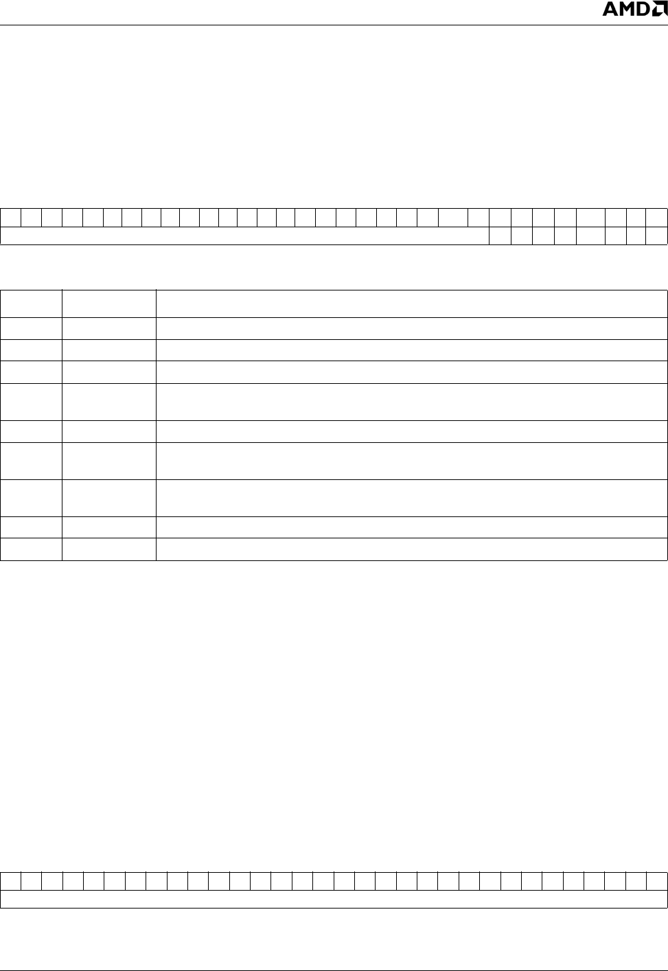
AMD Geode™ LX Processors Data Book 269
Graphics Processor Register Definitions 33234H
6.4.2.14 Status and Reset (GP_BLT_STATUS, GP_RESET)
This register is used to provide software with the current status of the GP in regards to operations pending and currently
executing. A write to this register has no effect unless byte 3 is 69h, which causes a reset of the GP, losing all state informa-
tion and discarding any active or pending BLT or vector. This is only intended to be used during debug to restore the GP in
the event of a hang. It is not required as part of the initialization or power on sequence for GP.
6.4.2.15 Host Source (GP_HST_SRC)
This register is used by software to load source data that is not originated in the frame buffer memory region. When per-
forming a BLT that requires host source data, software should first set up all of the configuration registers that are required
and initiate the BLT by writing to the GP_BLT_MODE register (GP Memory Offset 40h). This initiates the BLT in hardware,
which then waits for writes to the GP_HST_SRC register. Software should then perform enough writes to this register to
complete the BLT operation. Writes to this register are moved immediately into the source FIFO, allowing the CPU to per-
form successive writes. The EH bit in the GP_BLT_STATUS (GP Memory Offset 44h[5]) register indicates that the GP can
accept another cache line (32 bytes) of data.
This register is also aliased to the address range 100h-3FFh to allow the processor to move large blocks of data to the GP
through the repeat MOVS instruction. The GP throttles the incoming data by holding off register writes on the GLIU when
the source FIFO is full.
GP Memory Offset 44h
Ty p e RO
Reset Value 00000008h
GP_BLT_STATUS Register Map
31 30 29 28 27 26 25 24 23 22 21 20 19 18 17 16 15 14 13 12 11 10 9 8 7 6 5 4 3 2 1 0
RSVD UF RP EH CE SHE PP IN PB
GP_BLT_STATUS Bit Descriptions
Bit Name Description
31:8 RSVD Reserved.
7UF Underflow. If bit is set, Channel 3 had too few pixels to complete the BLT.
6RP Read Pending. If bit is set, read request is waiting for data from GLIU.
5EH Expecting Host Source Data. If bit is set, current BLT is expecting to receive host source
data on Channel 3.
4CE Command Buffer Empty. If bit is set, read and write pointers are equal.
3SHE Source FIFO Half Empty. If bit is set, source FIFO can accept another cache line of host
source data.
2PP Primitive Pending. If bit is set, a second BLT or vector is in the queue behind the currently
executing operation.
1IN Interrupt Pending. If bit is set, the GP interrupt signal is active.
0PB Primative Busy. If bit is set, an operation is currently executing in the GP.
GP Memory Offset 48h
Ty p e WO
Reset Value xxxxxxxxh
GP_HST_SRC Register Map
31 30 29 28 27 26 25 24 23 22 21 20 19 18 17 16 15 14 13 12 11 10 9 8 7 6 5 4 3 2 1 0
HST_SRC
270 AMD Geode™ LX Processors Data Book
Graphics Processor Register Definitions
33234H
6.4.2.16 Base Offset (GP_BASE_OFFSET)
This register is used to define the physical base addresses of the regions used for all GP read and write operations to mem-
ory. Each base defines a 16 MB region that begins on a 4 MB boundary. Thus the top two bits of the offset [23:22] are
added to the base to identify the correct 4 MB region in memory for a given transfer. Because there are different bases
defined for each potential source of data, each can come from a different memory region. If a memory operation goes
beyond the 16 MB region that has been assigned, it wraps back to the beginning of the 16 MB region.
6.4.2.17 Command Top (GP_CMD_TOP)
This register defines the starting address of the command buffer within the command buffer region. Bits [23:0] of this regis-
ter are combined with the CBASE in GLD_MSR_CONFIG (MSR A0002001h) to form the 32-bit address. This register
should only be changed when the GP is not actively executing out of the command buffer, which can be checked by reading
the CE bit in the GP_BLT_STATUS register (GP Memory Offset 44h[4]) or by verifying that GP_CMD_READ (GP Memory
Offset 58h) and GP_CMD_WRITE (GP Memory Offset 5Ch) have the same value.
GP_HST_SRC Bit Descriptions
Bit Name Description
31:0 HST_SRC Host Source Data. Used during BLT in host source mode.
GP Memory Offset 4Ch
Ty p e R / W
Reset Value 01004010h
GP_BASE_OFFSET Register Map
31 30 29 28 27 26 25 24 23 22 21 20 19 18 17 16 15 14 13 12 11 10 9 8 7 6 5 4 3 2 1 0
DBASE SBASE CH3BASE RSVD
GP_BASE_OFFSET Bit Descriptions
Bit Name Description
31:22 DBASE Destination Base. Base address of destination data region in physical memory.
21:12 SBASE Source Base. Base address of source data region in physical memory.
11:2 CH3BASE Channel 3 Base. Base address of channel 3 data region in physical memory.
1:0 RSVD Reserved.
GP Memory Offset 50h
Ty p e R / W
Reset Value 01000000h
GP_CMD_TOP Register Map
31 30 29 28 27 26 25 24 23 22 21 20 19 18 17 16 15 14 13 12 11 10 9 8 7 6 5 4 3 2 1 0
RSVD CMD_TOP RSVD
GP_CMD_TOP Bit Descriptions
Bit Name Description
31:24 RSVD Reserved. Read returns 0.
23:5 CMD_TOP Command Top. Starting address of the command buffer in the command buffer region.
4:0 RSVD Reserved. Read returns 0.
AMD Geode™ LX Processors Data Book 271
Graphics Processor Register Definitions 33234H
6.4.2.18 Command Bottom (GP_CMD_BOT)
This register defines the ending address of the command buffer within the command buffer region. Bits [23:0] of this register
are combined with the CBASE in GLD_MSR_CONFIG (MSR A0002001h) to form the 32 bit address. This register should
only be changed when the GP is not actively executing out of the command buffer, which can be checked by reading the CE
bit in GP_BLT_STATUS (GP Memory Offset 44h[4]) or by verifying that GP_CMD_READ and GP_CMD_WRITE (GP Mem-
ory Offset 58h and 5Ch respectively) have the same value.
6.4.2.19 Command Read (GP_CMD_READ)
This register points to the location from which the GP fetches the next command buffer data. As data is fetched, this register
increments. When this register equals GP_CMD_BOT (GP Memory Offset 54h) and the data has been fetched, it is
reloaded with the value from GP_CMD_TOP (GP Memory Offset 50h). If the current command buffer had the W (wrap) bit
set in the command word, then this register is reset to GP_CMD_TOP after the execution of the current command buffer.
Typically, this register is read only by the software, and is used in combination with GP_CMD_WRITE (GP Memory Offset
5Ch) to determine how much space is available in the command buffer for new commands. However, this register can be
written. A write to this register also affects the GP_CMD_WRITE register such that when creating and initializing a new
command buffer in memory, the read and write pointers can be updated simultaneously to point to the beginning of the
buffer without the GP thinking that the buffer was non-empty and beginning to fetch. This register must not be written while
the GP is actually executing command buffers as this could cause the GP to hang.
GP Memory Offset 54h
Ty p e R / W
Reset Value 00FFFFE0h
GP_CMD_BOT Register Map
31 30 29 28 27 26 25 24 23 22 21 20 19 18 17 16 15 14 13 12 11 10 9 8 7 6 5 4 3 2 1 0
RSVD CMD_BOT RSVD
GP_CMD_BOT Bit Descriptions
Bit Name Description
31:24 RSVD Reserved. Read returns 0.
23:5 CMD_BOT Command Bottom. Ending address of the command buffer in the command buffer
region.
4:0 RSVD Reserved. Read returns 0.
GP Memory Offset 58h
Ty p e R / W
Reset Value 00000000h
GP_CMD_READ Register Map
31 30 29 28 27 26 25 24 23 22 21 20 19 18 17 16 15 14 13 12 11 10 9 8 7 6 5 4 3 2 1 0
RSVD CMD_READ
GP_CMD_READ Bit Descriptions
Bit Name Description
31:24 RSVD Reserved. Read returns 0.
23:0 CMD_READ Command Read. Pointer to the tail of the command buffer in the command buffer region.
272 AMD Geode™ LX Processors Data Book
Graphics Processor Register Definitions
33234H
6.4.2.20 Command Write (GP_CMD_WRITE)
This register points to the next location to be written with command buffer data from the processor. After the processor
writes out a complete command buffer starting at this address, it should write to this register to update the value to point to
the next location to be written. This write is what queues the GP that there is command buffer data that needs to be fetched
and activates the command buffer logic within GP. If the Wrap bit is set in a command buffer control WORD, this register
should be written with the same value as that found in GP_CMD_TOP (GP Memory Offset 50h) after the CPU has com-
pleted loading the command buffer in memory.
6.4.2.21 Offset (GP_CH3_OFFSET)
The GP_CH3_OFFSET register is used during a BLT to give a starting location for the BLT data in the channel 3 region of
memory. The register consists of two fields to compose the address, the OFFSET and Nibble Select. The OFFSET field is
a pointer, which when added to the channel 3 base address, gives the memory location of the byte containing the first pixel
of the BLT. As in the destination and source offsets, this value must be aligned correctly for BLT direction and pixel depth.
When host source data is used, the two LSBs of OFFSET must still be initialized with the byte location of the first source
pixel in the host source data stream. Nibble Select is used when the source is 4-bpp, to give an offset within the specified
byte to the nibble representing the starting pixel. Both the OFFSET LSBs and Nibble Select are used to index into the first
DWORD of every new line of source data.
For a rotation of 90° counterclockwise, the offset should point to the top rightmost byte of the source bitmap. For a rotation
of 90° clockwise, the offset should point to the bottom leftmost byte of the source bitmap. For a rotation of 180°, the offset
should point to the opposite corner from that pointed to by the destination offset (e.g., If GP_BLT_MODE (GP Memory Off-
set 40h) indicates a left to right, top to bottom fill, then the destination offset should point to the upper left corner and the
channel 3 offset should point to the bottom right most byte of the source bitmap).
GP Memory Offset 5Ch
Ty p e R / W
Reset Value 00000000h
GP_CMD_WRITE Register Map
31 30 29 28 27 26 25 24 23 22 21 20 19 18 17 16 15 14 13 12 11 10 9 8 7 6 5 4 3 2 1 0
RSVD CMD_WRITE
GP_CMD_WRITE Bit Descriptions
Bit Name Description
31:24 RSVD Reserved. Read returns 0.
23:0 CMD_WRITE Command Write. Pointer to where the next command buffer will be written in the com-
mand buffer region.
GP Memory Offset 60h
Ty p e R / W
Reset Value 00000000h
GP_CH3_OFFSET Register Map
31 30 29 28 27 26 25 24 23 22 21 20 19 18 17 16 15 14 13 12 11 10 9 8 7 6 5 4 3 2 1 0
YLSBS XLSBS N
RSVD
OFFSET
AMD Geode™ LX Processors Data Book 273
Graphics Processor Register Definitions 33234H
6.4.2.22 Stride (GP_CH3_MODE_STR)
The GP_ CH3_MODE_STR register has multiple uses. The STRIDE field is used to indicate the byte width of the channel 3
bitmaps. Whenever the Y coordinate is incremented, this value is added (or subtracted if the Y bit is set) to (from) the previ-
ous start address to generate the start address for the next line. Stride values up to 64 KB minus one are supported.
The remaining fields of this register describe the type, size and source of the channel 3 data. The output of channel 3 can
be used to replace either source or pattern data into the ROP unit. The PS bit is used to select which pipeline the data will
be placed on. If the FMT indicates that the incoming data is alpha, then the incoming data can be used as alpha data in the
alpha blend unit if the AS bits in the GP_RASTER_MODE (GP Memory Offset 38h[19:17]) register are set to 110. If the
BPP/FMT bits in the GP_RASTER_MODE register (bits [31:28]) indicate the output pixel is 32-bpp, then the incoming alpha
data is converted to 8 bits and is consumed at the rate of one pixel per clock. If the BPP/FMT bits are set for 16-bpp, then
the incoming alpha data is converted to 4 bits and is consumed at the rate of two pixels per clock. Alpha blending is not sup-
ported in 8-bpp mode.
Some operating systems store color data in reverse color order (Blue/Green/Red). This data can be converted into the cor-
rect display order by setting the BGR bit. This works for all input formats except for alpha, so if the incoming data is alpha,
do not set this bit.
Rotation is controlled by the RO bit. If this bit is set, the direction of rotation is determined by the X and Y bits. When this bit
is set, the GP_DST_OFFSET (GP Memory Offset 00h) should point to the upper left corner of the destination and the X
and Y bits in the GP_BLT_MODE (GP Memory Offset 40h[9,8]) should not be set. The output must be left to right, top to
bottom. The output is actually written in horizontal strips, 8, 16 or 32 pixels high and as wide as the output. For 8-bpp rota-
tion, 1K of buffer space is the minimum required to perform the operation. Having 2K available allows data to be prefetched
while the previous tile is being written out. Setting the PL bit limits the buffer size to 1K as it preserves the LUT data in the
other 1K of the buffer. This bit should be set when performing any indexed color BLT or if it is likely that the LUT data that
has been loaded will be needed again for a future BLT. The performance is higher when this bit is not set.
GP_CH3_OFFSET Bit Descriptions
Bit Name Description
31:29 YLSBS YLSBS. Y coordinate of starting pixel within color pattern memory.
28:26 XLSBS XLSBS. X coordinate of starting pixel within color pattern memory.
25 N Nibble Select. Nibble address for 4-bpp pixels/alpha. 0 starts at the leftmost nibble, 1
starts at the rightmost.
24 RSVD Reserved. Write as read.
23:0 OFFSET Offset. Offset from the channel 3 base address to the first source pixel.
GP Memory Offset 64h
Ty p e R / W
Reset Value 00000000h
GP_CH3_MODE_STR Register Map
31 30 29 28 27 26 25 24 23 22 21 20 19 18 17 16 15 14 13 12 11 10 9 8 7 6 5 4 3 2 1 0
EN PS X Y BPP/FMT RO BGR PM PL PE HS RSVD STRIDE
GP_CH3_MODE_STR Bit Descriptions
Bit Name Description
31 EN Enable.
0: Channel 3 is off. Old pipelines behave exactly as they used to.
1: Channel 3 is on. Data is forced into either source or pattern pipeline from channel 3.
30 PS Pipeline Select.
0: Channel 3 data directed to/replaces old pattern pipeline.
1: Channel 3 data directed to/replaces old source pipeline

274 AMD Geode™ LX Processors Data Book
Graphics Processor Register Definitions
33234H
29 X X Direction for Fetch. Data is reversed if fetch direction does not match destination
direction.
0: Left to right direction.
1: Right to left direction.
28 Y Y Direction for Fetch. Data is reversed if fetch direction does not match destination
direction.
0: Top to bottom direction.
1: Bottom to top direction.
27:24 BPP/FMT Color Depth and Format of Input.
0000: 8-bpp 3:3:2.
0001: 8-bpp indexed.
0010: 8-bpp alpha.
0100: 16-bpp 4:4:4:4.
0110: 16-bpp 0:5:6:5.
0111: 4:2:2 YUV.
1000: 32-bpp.
1011: 24-bpp packed.
1101: 4-bpp indexed.
1110: 4-bpp alpha.
All others: Undefined.
23 RO Rotate Bitmap.
0: Disable rotation.
1: Enable rotation direction determined by X and Y. See Section 6.3.2.1 "Rotating BLTs"
on page 242.
22 BGR BGR Mode (applies only when 16-bpp or 32-bpp).
0: Pass through (or YUY2 for 4:2:2 mode).
1: Swap red and blue channels on output (or UYVY for 4:2:2 mode).
21 PM Pattern Mode.
0: Bitmap mode, data from memory or host source.
1: Pattern mode.
20 PL Preserve LUT Data.
0: Entire 2K buffer available for fetch data.
1: 1K reserved for LUT.
19 PE Prefetch Enable. When this bit is set, data may be fetched while the BLT is still pending.
18 HS Host Source.
0: Data fetched from memory.
1: Data written through host source writes.
17:16 RSVD Reserved.
15:0 STRIDE Stride. Increment between lines of bitmap in bytes.
GP_CH3_MODE_STR Bit Descriptions (Continued)
Bit Name Description

AMD Geode™ LX Processors Data Book 275
Graphics Processor Register Definitions 33234H
6.4.2.23 Width/Height (GP_CH3_WIDHI)
This register is used to specify the width and the height of the bitmap to be fetched on channel 3 in pixels. This need not
match the destination width and height, as in the case of a rotation BLT where the width and height are swapped, but the
total number of pixels should be equal to the number of pixels in the destination.
6.4.2.24 Host Source (GP_CH3_HSRC)
This register is used by software to load channel 3 data when the channel 3 pattern mode bit is not set, the channel 3
enable bit is set, and the channel 3 host source bit is set.This register is also aliased to the address range 400h-FFFh
allowing the processor to load large blocks of data to the GP using the repeat MOVS instruction.
GP Memory Offset 68h
Ty p e R / W
Reset Value 00000000h
GP_CH3_WIDHI Register Map
31 30 29 28 27 26 25 24 23 22 21 20 19 18 17 16 15 14 13 12 11 10 9 8 7 6 5 4 3 2 1 0
RSVD WID RSVD HI
GP_CH3_WIDHI Bit Descriptions
Bit Name Description
31:28 RSVD Reserved. Write as read.
27:16 WID Width. Width in pixels of the BLT operation.
15:12 RSVD Reserved. Write as read.
11:0 HI Height. Height in pixels of the BLT operation.
GP Memory Offset 6Ch
Ty p e WO
Reset Value xxxxxxxxh
GP_CH3_HSRC Register Map
31 30 29 28 27 26 25 24 23 22 21 20 19 18 17 16 15 14 13 12 11 10 9 8 7 6 5 4 3 2 1 0
HST_SRC
GP_CH3_HSRC Bit Descriptions
Bit Name Description
31:0 HST_SRC Host Source Data. Used during BLT in host source mode
276 AMD Geode™ LX Processors Data Book
Graphics Processor Register Definitions
33234H
6.4.2.25 LUT Index (GP_LUT_INDEX)
This register is used to initialize the LUT_INDEX pointer that is used for subsequent LUT operations. All LUT accesses are
DWORD accesses so only the 9 LSBs of the pointer are used to index into the 2 KB LUT. Addresses 000h-0FFh are used
for 8-bit indexed LUT data. Addresses 000h-00Fh are used for 4-bit indexed LUT data. Addresses 100h-13Fh are used for
storing color patterns. All addresses are used for storing incoming data (unless the PL bit is set in the
GP_CH3_MODE_STR register, GP Memory Offset 64h[20]), but none of the remaining addresses have any significance to
software.
6.4.2.26 LUT Data (GP_LUT_DATA)
This register is used to store data into the LUT for indexed color translations and color patterns. The 32 bits written to this
register are stored in the LUT at the location specified in the GP_LUT_INDEX register (GP Memory Offset 70h). A read of
this register returns the contents of the LUT at the location specified by the GP_LUT_INDEX register. Either a read or write
of this register will cause the GP_LUT_INDEX register to increment, so the LUT can be loaded through successive writes to
the GP_LUT_DATA register.
GP Memory Offset 70h
Ty p e R / W
Reset Value 00000000h
GP_CH3_HSRC Register Map
31 30 29 28 27 26 25 24 23 22 21 20 19 18 17 16 15 14 13 12 11 10 9 8 7 6 5 4 3 2 1 0
RSVD LUT_INDEX
GP_CH3_HSRC Bit Descriptions
Bit Name Description
31:9 RSVD Reserved.
8:0 LUT_INDEX LUT Index. Used to initialize the LUT_INDEX pointer that is used for subsequent LUT
operations. The LUT_INDEX automatically increments on a write to the GP_LUT_DATA
register (GP Memory Offset 74h). When performing a read, bit 31 must be set to cause
the hardware to perform the read and update the GP_LUT_DATA register. If this bit is not
set, then a write is assumed and the read will not be performed.
GP Memory Offset 74h
Ty p e R / W
Reset Value xxxxxxxxh
GP_CH3_HSRC Register Map
31 30 29 28 27 26 25 24 23 22 21 20 19 18 17 16 15 14 13 12 11 10 9 8 7 6 5 4 3 2 1 0
LUT_DATA
GP_CH3_HSRC Bit Descriptions
Bit Name Description
31:0 LUT_DATA LUT_DATA. Used to store data into the LUT for indexed color translations and color pat-
terns.
AMD Geode™ LX Processors Data Book 277
Graphics Processor Register Definitions 33234H
6.4.2.27 Interrupt Control (GP_INT_CNTRL)
This register is used to control the interrupt signal from the GP. It contains a 16-bit mask and a 16-bit interrupt detect. The
mask portion is read/write. A bit set in the mask register disables the corresponding interrupt bit. At reset, all interrupts are
disabled. The interrupt detect bits are automatically set by the hardware to indicate that the corresponding condition has
occurred and that the mask bit for that condition is not set. The interrupt detect bits remain set until they are cleared by a
write to the GP_INT_CNTRL register. Writing a 1 to an interrupt detect bit clears the bit. Writing a 0 to an interrupt detect bit
has no effect. Therefore, all of the interrupts in the GP may be cleared by reading the GP_INT_CNTRL register and writing
back the value that was read. Whenever any of the interrupt detect bits are set in this register, the IN bit will be set in the
GP_BLT_STATUS register (GP Memory Offset 44h[1]).
GP Memory Offset 78h
Ty p e R / W
Reset Value 0000FFFFh
GP_INT_CNTRL Register Map
31 30 29 28 27 26 25 24 23 22 21 20 19 18 17 16 15 14 13 12 11 10 9 8 7 6 5 4 3 2 1 0
RSVD I1 I0 RSVD M1 M0
GP_INT_CNTRL Bit Descriptions
Bit Name Description
31:18 RSVD Reserved. Read returns 0.
17 I1 GP Idle Detect Interrupt.
16 I0 Command Buffer Empty Detect Interrupt.
15:2 RSVD Reserved. Read returns 1.
1M1 GP Idle Mask Bit.
0M0 Command Buffer Empty Mask Bit.
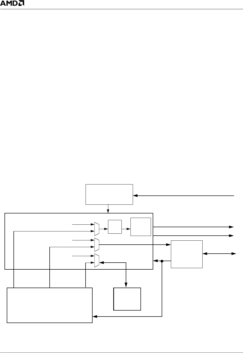
278 AMD Geode™ LX Processors Data Book
Display Controller
33234H
6.5 Display Controller
The Display Controller (DC) module retrieves graphics,
video, and overlay streams from the frame buffer, serial-
izes the streams, performs any necessary color lookups
and output formatting, and interfaces to the VP for driving
the display device.
Features
•512x64-bit display FIFO
•64x64x2-bit hardware cursor
•64x vertical resolution x2-bit hardware icon overlay
•3x261x8-bit palette/gamma RAM (including five exten-
sion colors)
•Display refresh compression
•64x64-bit compressed line buffer
•Flexible timing generator
•Support for Video Blanking Interval (VBI) data
•Support for interlaced modes up to 1920x1080
•3-tap flicker filter for support of interlaced NTSC and
PAL display modes
•Flexible memory addressing
•Video overlay support
•Independent VGA block for complete hardware VGA
implementation
•Dirty/Valid RAM and controller to monitor memory traffic
in support of display refresh compression
•Six 512x64-bit line buffers to support downscaling and
flicker filtering
•3x5-tap graphics filter for scaling and filtering
The DC module consists of a GUI (Graphical User Inter-
face) block, a VGA block, and back-end scaling/filter. The
GUI is compatible with the Display Controller found in the
GX processor. The VGA block provides hardware compati-
bility with the VGA graphics standard. The GUI and VGA
blocks share a single display FIFO and display refresh
memory interface to the memory controller. The VGA block
passes 8-bpp and syncs to the GUI, which expands the
pixels to 24-bpp via the CLUT (color lookup table). The
VGA block also passes the information to the graphics filter
for scaling and interlaced display support. This stream is
then passed to the Video Processor (VP), which is used for
video overlay. The VP forwards this information to the DAC
(Digital-to-Analog Converter), which generates the analog
red, green, and blue signals and buffers the sync signals,
that are then sent to the display. The VP output can also be
rendered as YUV data that can be output on the Video Out-
put Port. The DC block diagram is shown in Figure 6-12.
Figure 6-12. Display Controller High-Level Block Diagram
VGA Block
Graphical User Interface Block
FIFO
Host I/F
FIFO
Pixel, Syncs, DISPEN
Display Memory I/F
Display Refresh
Memory Control
8-Bit Pixel,
Syncs,
Display enable CTL
Dirty/Valid Flags
Video Data Output to VP
Dirty/Valid RAM
and Control
GLIU0 Port
GLIU0 Memory Port
GeodeLink™
Interface
Unit 0
(GLIU0)
CLUT
Graphics
Scaler/
Filter
AMD Geode™ LX Processors Data Book 279
Display Controller 33234H
The GUI block, shown in Figure 6-13, provides sophisti-
cated graphics functionality suitable for a GUI environment
such as Windows® XP, Windows CE, or Linux® operating
systems. The GUI is optimized for high resolution and high
color depth display modes.
Figure 6-13. GUI Block Diagram
Compressed
Graphics
Decompressor
Cursor &
Display FIFO
Compressor
Video
32
32
64
64
64
Display
24
Display
CRT_HSYNC
CRT_VSYNC
ENA_DISP
DCLK PCLK
VID_CLK
VID_DATA[32:0] PIXEL[31:0]
32
Video
VID_RDY VID_VALVP_VSYNC
Timing
Generator Control
Serializer
Address
Generator
Icon Overlay
(512x64-bit)
Serializer
Line Buffer
(64x64-bit)
GLIU
32
Palette RAM
(3x261x8 bit)
Line Buffer
(3x1024 pixels)
Scaling
Filter
Line Buffer
(2x1024 pixels)
Flicker
Filter
Synchronizing Line Buffer
(1x1024 pixels)
32
32
32
32
32
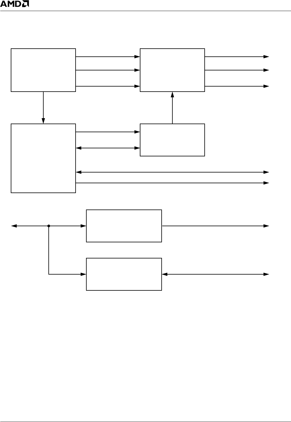
280 AMD Geode™ LX Processors Data Book
Display Controller
33234H
The VGA block, shown in Figure 6-14, provides hardware
support for a compatible VGA solution. It consists of an
independent CRT controller and pixel formatting units. It
also provides the standard VGA host memory data manip-
ulation functions such as color compare, set, reset, etc.
This block provides complete support for all VGA text and
graphics modes.
Figure 6-14. VGA Block Diagram
CRTC Pixel Formatter
Shared FIFO
FIFO Control
Syncs
DISPEN
Syncs
DISPEN
8-bit Pixel
Clock Control
Display Memory I/F Control
Display Memory I/F Data
FIFO R/W Data
FIFO Control
FIFO Read Data
VGA DAC I/O Unit
Host Memory I/F Unit
Host CPU I/F GUI CLUT I/O Control
Host Memory I/F
AMD Geode™ LX Processors Data Book 281
Display Controller 33234H
6.5.1 GUI Functional Overview
6.5.1.1 Display Mode Support
The display modes listed in Table 6-32 are supported by
the GUI block. 32- and 24-bpp display support is provided
across all resolutions. The Dot Clock source (DOTCLK) is
provided by a PLL. Available memory bandwidth deter-
mines the resolutions and color depths that will function
without display tearing. Memory controller configuration,
GLIU frequency, and other demands on the memory con-
troller set the available bandwidth. The GLIU frequency
determines the memory controller frequency. Other
demands on the memory controller such as the CPU and
bus masters affect on available bandwidth are difficult to
predict. Use of the video overlay feature additionally
decreases the bandwidth available for screen refresh.
The Minimum GLIU Frequency criteria listed in Table 6-32
must be met for quality operation of the display. This fre-
quency provides sufficient memory bandwidth for the mem-
ory controller to maintain reliable display refresh under all
operating conditions, including the video overlay. As a gen-
eral rule, Table 6-32 indicates what the minimum relation-
ship of DOTCLK to GLIU frequency should be at the
various color depths.
Bandwidth requirements for the VGA engine are not listed
in this table. Most graphics modes require the same band-
width as comparable 8-bpp display modes listed in Table 6-
32. Text modes generally require higher bandwidth. Sup-
ported text modes require a GLIU clock frequency of 100
MHz or more to obtain the necessary memory bandwidth.
Table 6-32. Display Modes
Resolution Color Depth (bpp) Refresh Rate (Hz) Dot Clock (MHz) Min. GLIU Frequency (MHz)
640 x 480 8, 16, or 24/32 60 25.175 75
8, 16, or 24/32 70 28.560 75
8, 16, or 24/32 72 31.500 75
8, 16, or 24/32 75 31.500 75
8, 16, or 24/32 85 36.000 75
8, 16, or 24/32 90 37.889 400
8, 16, or 24/32 100 43.163 400
800 x 600 8, 16, or 24/32 60 40.000 75
8, 16, or 24/32 70 45.720 75
8, 16, or 24/32 72 49.500 75
8, 16, or 24/32 75 49.500 75
8, 16, or 24/32 85 56.250 75
8, 16, or 24/32 90 60.065 400
8, 16, or 24/32 100 68.179 400
1024 x 768 8, 16 or 24/32 60 65.000 75
8, 16, or 24/32 70 75.000 100
8, 16, or 24/32 72 78.750 100
8, 16, or 24/32 75 78.750 100
8, 16, or 24/32 85 94.500 100
8, 16, or 24/32 90 100.187 400
8, 16, or 24/32 100 113.310 400
1152x864 8, 16, or 24/32 60 81.600 100
8, 16, or 24/32 70 97.520 100
8, 16, or 24/32 72 101.420 200
8, 16, or 24/32 75 108.000 200
8, 16, or 24/32 85 119.650 200
8, 16, or 24/32 90 129.600 400
8, 16, or 24/32 100 144.000 400
282 AMD Geode™ LX Processors Data Book
Display Controller
33234H
1280 x 1024 8, 16, or 24/32 60 108.000 200
8, 16, or 24/32 70 129.600 200
8, 16, or 24/32 72 133.500 200
8, 16, or 24/32 75 135.000 200
8, 16, or 24/32 85 157.500 200
8, 16, or 24/32 90 172.800 400
8, 16, or 24/32 100 192.000 400
1600 x 1200 8, 16, or 24/32 60 162.000 200
8, 16, or 24/32 70 189.000 200
8, 16, or 24/32 72 198.000 233
8, 16, or 24/32 75 202.500 233
8, 16, or 24/32 85 229.500 266
8, 16, or 24/32 90 251.182 400
8, 16, or 24/32 100 280.640 400
1920x1440 8, 16, or 24/32 60 234.000 266
8, 16, or 24/32 70 278.400 400
8, 16, or 24/32 72 288.000 400
8, 16, or 24/32 75 297.000 400
8, 16, or 24/32 85 341.349 400
Television Modes
720x483 SD NTSC up to 32 59.94i 27.000 200
640x480 SD NTSC up to 32 up to 60.00i 27.000 200
768x576 SD PAL up to 32 50.00i 27.000 200
720x576 SD PAL up to 32 50.00i 27.000 200
1280x720 HD up to 32 up to 60.00i up to 74.750 200
1280x768 HD up to 32 50.00i 74.750 200
1440x720 HD up to 32 60.00i 74.750 400
1440x768 HD up to 32 50.00i 74.750 400
1920x1080 HD up to 32 up to 60.00i up to 148.500 400
Table 6-32. Display Modes (Continued)
Resolution Color Depth (bpp) Refresh Rate (Hz) Dot Clock (MHz) Min. GLIU Frequency (MHz)
AMD Geode™ LX Processors Data Book 283
Display Controller 33234H
6.5.1.2 Display FIFO
The DC module incorporates a 512-entry x 64-bit display
FIFO that queues up all display data, including graphics
frame buffer data, compressed display buffer data, cursor
and icon overlay data, and video overlay YUV data. When
the video output port is enabled, 32 slots of the display
FIFO are allocated for the video transfer buffer.
The DFHPSL and DFHPEL (DC Memory Offset 004h[11:8]
and [15:12]) bits are used to set the thresholds for high-pri-
ority memory request assertion. These levels can be tuned
for a particular display mode to optimize memory band-
width utilization.
6.5.1.3 Hardware Cursor and Icon Overlays
The GUI supports a 64x64x2-bit hardware cursor overlay.
The 2-bit codes are defined in Table 6-33.
A hardware icon overlay is also supported for applications
that require a fixed sprite overlay. This is particularly useful
in portable applications for display status indicators that are
independent of the application that is running. When
enabled, the icon overlay is displayed on each active scan
line. The icon is 64 pixels wide and supports three colors
plus transparency as shown in Table 6-34.
The display of cursor and icon overlays is controlled by
CURE (bit 1) and CLR_CUR (bit 2) in DC_GENERAL_CFG
(DC Memory Offset 004h), which take effect on the next
vertical sync after the bits are programmed. The cursor is
always displayed on top of the icon if both are enabled.
The cursor and icon are inserted into the graphics stream
prior to mixing the video overlay data. Since the back-
ground color-keyed value generally does not match the
cursor or icon colors, the cursor and icon may be displayed
on top of any active video. Note that the cursor and icon
features are not available in VGA modes.
Table 6-33. Cursor Display Encodings
AND Mask XOR Mask Color Displayed
0 0 Cursor Color 0 - Palette Index 100h
0 1 Cursor Color 1 - Palette Index 101h
1 0 Transparent - Background Pixel
1 1 Inverted - Bitwise Inversion of Background Pixel
Table 6-34. Icon Display Encodings
AND Mask XOR Mask Color Displayed
0 0 Icon Color 0 - Palette Index 102h
0 1 Icon Color 1 - Palette Index 103h
1 0 Transparent - Background Pixel
1 1 Border Color - Palette Index 104h

284 AMD Geode™ LX Processors Data Book
Display Controller
33234H
Cursor/Icon Buffer Formats
In 2-bpp mode, the cursor buffer is stored as a linear dis-
play buffer containing interlaced AND and XOR QWORDs
(8-byte segments). Each QWORD contains the appropriate
mask for 64 pixels. Even QWORDs contain the AND
masks and odd QWORDs contain the XOR masks. The
masks are stored “in display order” with the leftmost pixel
being most significant and the rightmost pixel being least
significant.
For 32-bpp cursors, the cursor pixels include an alpha
value, and are alpha blended with the underlying graphics
pixels. For the purposes of cursor overlay, the cursor alpha
value is used. If the graphics stream includes an alpha
value, that value is not used for the purposes of cursor
overlay. However, the graphics alpha value is retained in
the resulting pixel stream.
The cursor buffer stores 192 bytes of data per scan line (for
48 horizontal pixels) in 32-bpp mode. In this mode, the cur-
sor size is 48 pixels wide and 64 pixels high, and so the
buffer is 12 KB in size.
In 2-bpp mode, cursor buffer includes 16 bytes of data per
scan line (for 64 horizontal pixels). The cursor is 64x64,
therefore the cursor buffer is 1 KB in size.
The DC contains logic to address the overlay of the cursor
on top of a color key region. Table 6-35 indicates what pixel
value is output from the DC’s rendering engine when the
cursor is overlayed on the color key region.
Note that this behavior varies slightly when the graphics
are represented in 32-bpp mode, which includes a per-
pixel alpha value.
Table 6-35. Cursor/Color Key/Alpha Interaction
Cursor Per-Pixel Alpha
Color Key Match, Per-
Pixel Alpha No Per-Pixel Alpha
Color Key Match, No
Per-Pixel Alpha
No Cursor COLOR = graphics
color
ALPHA = graphics
alpha
COLOR = graphics
color
ALPHA = 00
COLOR = graphics
color
ALPHA = FF
COLOR = graphics
color
ALPHA = 00
2-bpp Cursor
(cursor color)
COLOR = cursor color
ALPHA = graphics
alpha or FF (config-
urable)
COLOR = cursor color
ALPHA = FF
COLOR = cursor color
ALPHA = FF
COLOR = cursor color
ALPHA = FF
2-bpp Cursor
(invert color)
COLOR = invert graph-
ics color
ALPHA = graphics
alpha or FF (config-
urable)
COLOR = invert
graphics color
ALPHA = FF
COLOR = invert
graphics color
ALPHA = FF
COLOR = invert
graphics color
ALPHA = FF
2-bpp Cursor
(transparent)
COLOR = graphics
color
ALPHA = graphics
alpha
COLOR = graphics
color
ALPHA = 00
COLOR = graphics
color
ALPHA = FF
COLOR = graphics
color
ALPHA = 00
Color Cursor
(with alpha)
COLOR = blend cur-
sor/graphics
ALPHA = pp alpha or
FF (configurable)
COLOR = cursor color
ALPHA = cursor alpha
COLOR = blend
cursor/graphics
ALPHA = FF
COLOR = cursor color
ALPHA = cursor alpha

AMD Geode™ LX Processors Data Book 285
Display Controller 33234H
6.5.1.4 Display Refresh Compression
To reduce the system memory contention caused by the
display refresh, the GUI block contains compression and
decompression logic for compressing the frame buffer
image in real time as it is sent to the display. The DC does
not modify the standard frame buffer, but rather, it utilizes a
separate compressed display buffer for updating the dis-
play under certain conditions. This compressed display
buffer can be allocated within the extra off-screen memory
within the graphics memory region.
Coherency of the compressed display buffer is maintained
by use of dirty and valid bits for each line. Whenever a line
has been successfully compressed, it is retrieved from the
compressed display buffer for all future accesses until the
line becomes dirty again. Dirty lines are retrieved from the
normal uncompressed frame buffer.
The compression logic has the ability to insert a “static”
frame every other display frame, during which time dirty
bits are ignored and the valid bits are read to determine
whether a line should be retrieved from the frame buffer or
compressed display buffer. This allows a latency of one
frame between pixels actually being rendered and showing
up on the display. This effect typically goes unnoticed for
traditional 2D applications but may result in increased tear-
ing in single-buffered animation sequences. This feature
may be used to tune for maximum performance or optimal
display quality.
The compression algorithm used commonly achieves com-
pression ratios between 10:1 and 50:1, depending on the
nature of the display data. The compression algorithm
employed is lossless and therefore results in no loss of
visual quality. This high level of compression provides
higher system performance by reducing typical latency for
normal system memory access, higher graphics perfor-
mance by increasing available drawing bandwidth to the
memory subsystem, and lower power consumption by sig-
nificantly reducing the number of off-chip memory
accesses required for refreshing the display. These advan-
tages become more pronounced as display resolution,
color depth, and refresh rate are increased, and as the size
of the installed DRAM increases.
As uncompressed lines are fed to the display, they are
compressed and stored in an on-chip compressed line
buffer (64x64 bits). Lines will not be written back to the
compressed display buffer in the DRAM unless a success-
ful compression has resulted, so there is no penalty for
pathological frame buffer images where the compression
algorithm is sub-optimal.
6.5.1.5 Dirty/Valid RAM
The DC module incorporates the Dirty/Valid RAM
(DVRAM) in the Display Controller module. The Dirty/Valid
RAM controller directly snoops GLIU0 request packets on
the memory data port.
The Dirty/Valid RAM may be used to monitor locations in
memory other than the frame buffer. (Compression and
decompression must be disabled in order for the Display
Controller to continue to function properly.) This may be
used for scenarios where software (or the Graphics Pro-
cessor) must modify or re-render a frame whenever corre-
sponding modifications occur in an offscreen graphics
buffer. The “palletized” bit is set upon writes to the corre-
sponding region of memory. However, it is up to software
to clear the dirty bit by writing to the Dirty/Valid RAM
Access register (DC Memory Offset 08Ch).
6.5.1.6 Palette/Gamma RAM
The GUI block contains a 261x24 color lookup table RAM
used for palletized display modes (Indexes 0-255), cursor
colors (Indexes 256-257), and the GUI mode border color
(Index 260). This color lookup table is also used by the
VGA block to map the 8-bit VGA pixels to a 24-bit RGB
color value. In true color display modes (16, 24, or 32-bpp),
the color lookup table can be used as a gamma correction
RAM.
6.5.1.7 Display Address Generator
The GUI block supports flexible address generation for the
frame buffer, compressed display buffer, cursor and icon
buffers, and video buffers (YUV 4:2:2 or 4:2:0 format). A
separate start offset register is provided for each display
buffer. The start offset may be programmed to be relative
to frame buffer space (up to 256 MB).
6.5.1.8 Display Timing Generator
The GUI block includes a flexible timing generator capable
of handling up to a 1920x1440 resolution display. Horizon-
tal timings are programmable with 1-pixel granularity. Verti-
cal timings are programmable with scan line granularity.
The timing registers are master-slaved such that a new tim-
ing set may be programmed while the working set is still
active. The TRUP configuration bit (DC_DISPLAY_CFG,
DC Memory Offset 008h[6]) is used to allow the new set of
timings to take effect at the start of vertical sync. As long as
the horizontal and vertical total counts do not change when
a new timing set is loaded, the sync pulses should remain
stable and the display should not glitch.
286 AMD Geode™ LX Processors Data Book
Display Controller
33234H
6.5.1.9 Video Overlay Support
The GUI block also supports a video overlay function. The
DC has flexible addressing capability for YUV 4:2:2 and
YUV 4:2:0 display surfaces. Video data is stored in a sepa-
rate buffer within the off-screen frame buffer. Independent
surface pitch control is provided for Y and U/V.
The DC fetches the contents of the video and transmits it to
the Video Processor once per frame.
The Video Processor provides enhanced overlay scaling
and filtering options.
The width of the video output port is 32 bits. This allows the
display of high-resolution video source material (up to 1920
horizontal pixels) mixed with high-resolution graphics data.
Table 6-36 illustrates the minimum video port bandwidth
required for a number of different graphics display resolu-
tions.
Table 6-36. Video Bandwidth
Resolution Refresh Rate (Hz)
Line Rate
(KHz)
Video Source
Size (B)
Video Port Bandwidth
Required (MB/s)
640x480 60 31.5 1440 45.4
2160 68.0
85 43.3 1440 62.4
2160 93.5
800x600 60 37.9 1440 54.5
2160 81.9
85 53.7 1440 77.3
2160 116.0
1024x768 60 48.4 1440 69.7
2160 105
85 68.7 1440 98.9
2160 148.4
1280x1024 60 64.0 1440 92.2
2160 138
85 91.1 1440 131
2160 197
1600x1200 60 75.0 1440 108
2160 162
70 87.5 1440 126
2160 189
AMD Geode™ LX Processors Data Book 287
Display Controller 33234H
6.5.1.10 Output Formats
Video Output Data Sequencing
The order that video data is transmitted from the DC to the
VP depends on the format of the video data. For YUV 4:2:0
mode, the entire stream of Y data is transmitted for a
source line, followed by the entire stream of U data for the
line, and finally, the entire stream of V data for the line. The
size of the U and V streams are always one-half the size of
the Y stream. The data is not interlaced as in the YUV 4:2:2
mode. The data ordering is shown in Table 6-37.
For YUV 4:2:2 mode, YUV data is interlaced in a single
stream, with a maximum size of 1440 bytes.
In YUV 4:2:2 mode, four orders of YUV data are supported.
The data format is selectable via the Video Configuration
register (VP Memory Offset 000h) in the Video Processor
module. The data ordering is shown in Table 6-38.
6.5.2 VBI Data
VBI (Video Blanking Interval) data is fetched by the DC at
the start of each frame. The data is fetched from a buffer in
memory, separately from video or graphics data. It is pre-
sented to the VP on the graphics port. VBI data is provided
via a path that circumvents the gamma correction palette
and the graphics filter. The data presented to the VP/VOP
is only the data in memory. There are no additional head-
ers attached by the DC. Configuration registers in the DC
determine how many lines of VBI data are sent during each
field; the lines can be enabled/disabled independently of
one another. If a line is disabled, no data is fetched (from
memory) for that line, and the memory line pointer is NOT
incremented. Thus, non-contiguous lines of screen VBI
must be stored contiguously in memory if there are no
active VBI lines between them. The DC can be pro-
grammed to fetch multiple fields worth of VBI data from lin-
ear frame buffer space without resetting to the start of the
buffer on each field. This minimizes the interrupt overhead
required to manage VBI data. VBI data streams of up to 4
KB per scan line are supported.
The VBI horizontal timings are controlled in a manner simi-
lar to the horizontal active timings. The reference point for
the horizontal (pixel) counter is the start of active video.
This means that if the VBI data is to be active before this
point on the line (i.e., to the left of, and above active video),
it may be necessary to set the VBI horizontal start point to
a large number (less than the horizontal total, but larger
than the VBI horizontal end point). The line counter used to
calculate VBI offsets is incremented at the start of each
HSYNC, and NOT at the start of active video. This means
that even if the VBI horizontal timings are such that it starts
during the horizontal “back porch” region, the line counts
and enables are the same as if the VBI horizontal timing
was the same as the graphics timing.
6.5.3 GenLock
The DC has the ability to use an external source to deter-
mine the timing and frequency of VSYNC. This is primarily
used in systems in which the VIP is providing video data to
be displayed in a native screen resolution and frame rate.
The DC can also be configured to detect the loss of
VSYNC in this case, and temporarily generate its own
VSYNC pulse until the external source resumes generation
of video data and synchronization. This is accomplished
through the use of a VSYNC timeout counter. The DC can
also generate an interrupt when a loss of synchronization
is detected.
Table 6-37. YUV 4:2:0 Video Data Ordering
Sequence Data Type Max Size (Bytes)
1 Y stream 1920
2 U stream 960
3 V stream 960
Table 6-38. YUV 4:2:2 Video Data Ordering
Mode YUV Ordering (Note 1)
Note 1. U = Cb, V = Cr.
0 U Y0 V Y1
1 Y1 V Y0 U
2Y0 U Y1 V
3 Y0 V Y1 U
288 AMD Geode™ LX Processors Data Book
Display Controller
33234H
6.5.4 VGA Block Functional Overview
The VGA block provides full hardware support for a VGA
graphics subsystem. It is compatible with the IBM VGA as
defined in the IBM Video Subsystem Technical Reference
manual. This section provides an overview of VGA features
and functions.
6.5.4.1 VGA Modes
A VGA “mode” is a programmed VGA configuration defined
by the VGA BIOS that produces a graphics frame buffer
format and a screen image with specific characteristics.
The base VGA function provides coded text modes for text-
based applications, and graphics modes for graphics-
based applications. Many of these modes are compatible
with older graphics adapter standards, such as mono-
chrome display adapter, color graphics adapter, and
enhanced graphics adapter.
Text Modes
There are five text modes defined by VGA BIOS as shown
Table 6-39.
Each of the text modes provides a coded frame buffer con-
sisting of a 16-bit value for each character. The low byte is
the ASCII character code for the character to display, and
the high byte is an attribute byte that determines how the
character is displayed (foreground, background colors,
blink, underline, etc.). There are two formats defined by
BIOS for the attribute byte: color and monochrome as
shown in Table 6-40.
Graphics Modes
The graphics modes defined by VGA BIOS are shown in
Table 6-41.
Figure 6-15. VGA Frame Buffer Organization
Table 6-39. VGA Text Modes
BIOS
Mode
#
Screen
Size in
Characters
Attribute
Type
Buffer
Address Compatibility
0, 1 40 x 25 Color B8000h-
BFFFFh
CGA
2, 3 80 x 25 Color B8000h-
BFFFFh
EGA, VGA
7 80 x 25 Mono-
chrome
B0000h-
B7FFFh
MDA
Table 6-40. Text Mode Attribute Byte Format
Bit Color Definition Monochrome Definition
7 Blink Blink
6 Background Color (R) Background
5 Background Color (G) Background
4 Background Color (B) Background
3 Foreground Intensity/Font
Select
Foreground Intensity/Font
Select
2 Foreground Color (R) Foreground
1 Foreground Color (G) Foreground
Table 6-41. VGA Graphics Modes
BIOS Mode #
Screen Size in
Pixels # of Colors
Frame Buffer
Format Buffer Address
4, 5 320 x 200 4 Packed Pixel B8000h-BFFFFh
6 640 x 200 2 Packed Pixel B8000h-BFFFFh
0xD 320 x 200 16 Planar A0000h-AFFFFh
0xE 640 x 200 16 Planar A0000h-AFFFFh
0xF 640 x 400 4 Planar A0000h-AFFFFh
0x10 640 x 350 16 Planar A0000h-AFFFFh
0x11 640 x 480 2 Planar A0000h-AFFFFh
0x12 640 x 480 16 Planar A0000h-AFFFFh
0x13 320 x 200 256 Packed Pixel A0000h-AFFFFh
3210
Byte Byte Byte Byte
64 KB
DWORDs
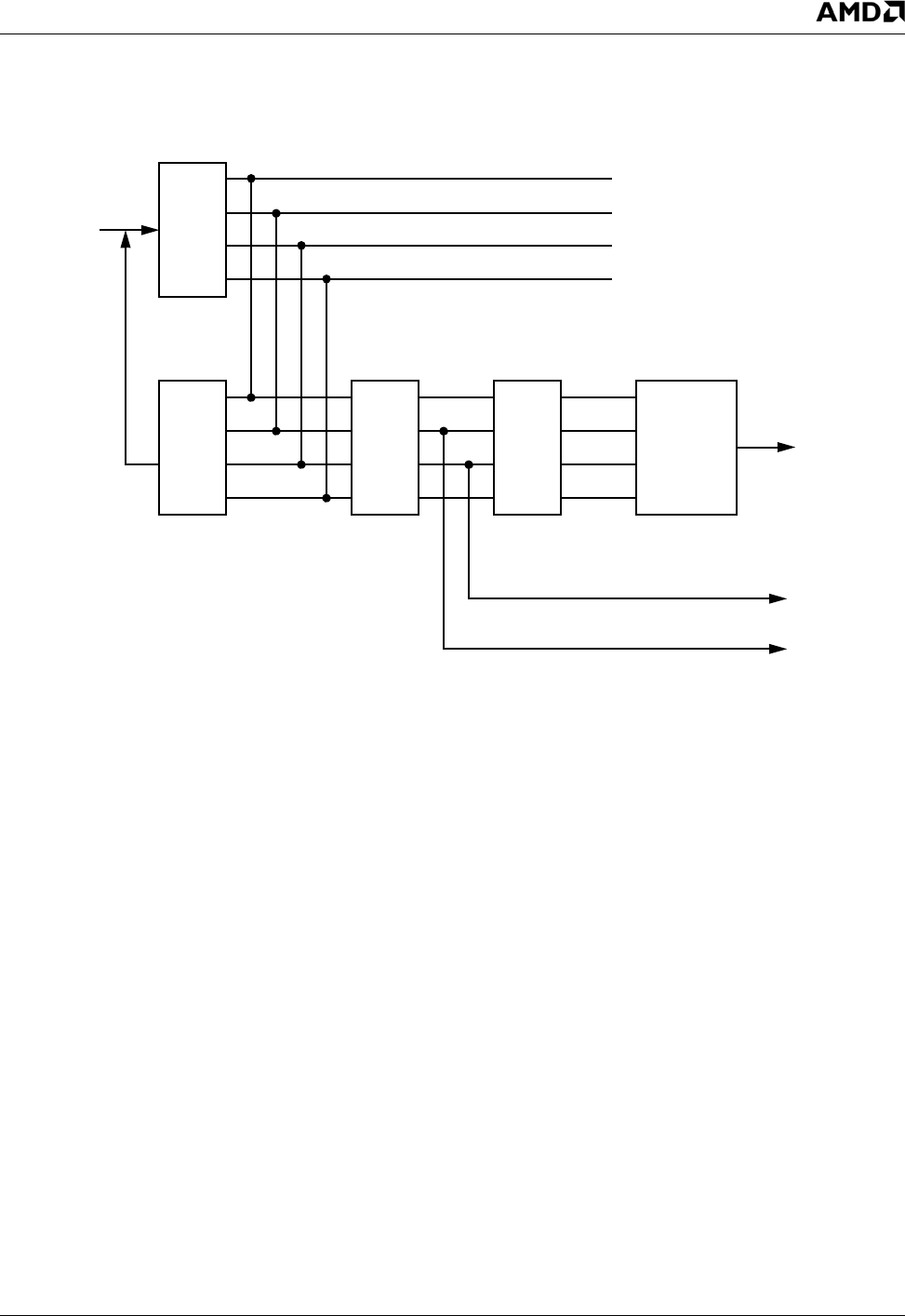
AMD Geode™ LX Processors Data Book 289
Display Controller 33234H
6.5.5.2 Graphics Controller
The graphics controller manages the CPU interaction with
video memory, and contains the video serializers that feed
the front end of the attribute controller. Several memory
read and write modes are supported that provide various
forms of acceleration for VGA graphics operations. A high-
level diagram of the graphics controller is shown in Figure
6-16.
Figure 6-16. Graphics Controller High-level Diagram
Memory Map 3 Data
Memory Map 2 Data
Memory Map 1 Data
Memory Map 0 Data
Write
Read M
Serializers
CPU Data
PIX Out
Character Gen Data
Attribute Byte
Each bus is 8 bits except for PIX Out,
Video
Mode
Mode Latch U
X
which is 4 bits.
Note:
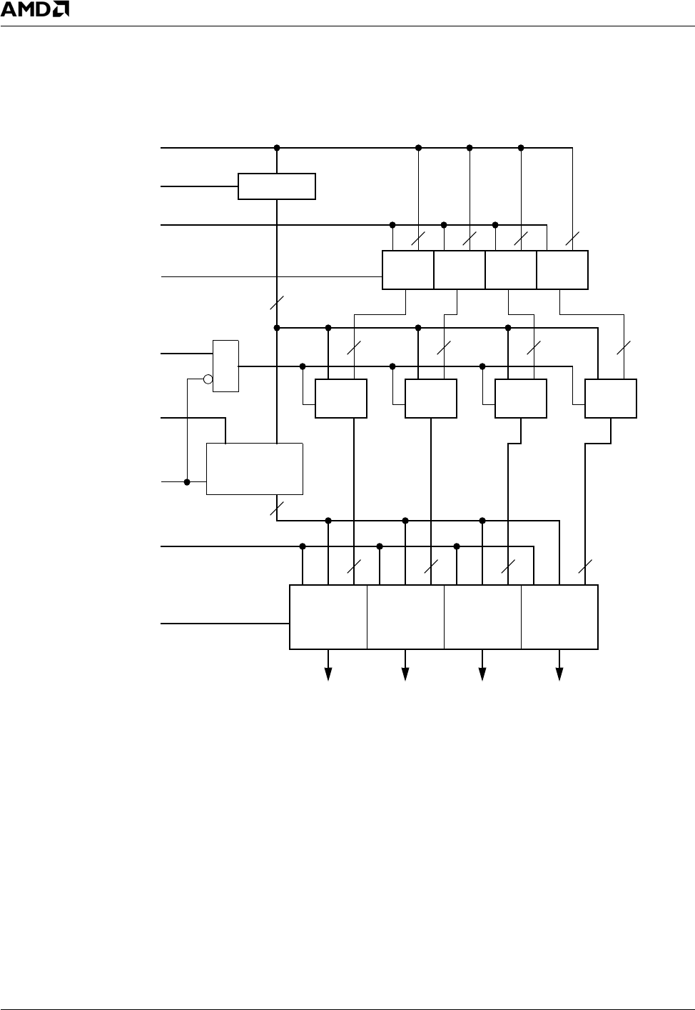
290 AMD Geode™ LX Processors Data Book
Display Controller
33234H
6.5.5.3 Write Modes
There are four write modes supported by the graphics con-
troller (mode 0, 1, 2, and 3). These write modes provide
assistance to the CPU when the frame buffer is in a planar
graphics format. Figure 6-17 shows the data flow logic that
supports these modes.
Figure 6-17. Write Mode Data Flow
CPU Data [7:0]
Rotator
Data Rotate [2:0]
Set/Reset [3:0] 3210
3210
B
WriteMode2
BBBB
Enable Set/Reset [3:0]
3210
Bit Mask [7:0]
-A/+A*B
Write Mode 3
A
Read Data Latch [31:0]
ALU
Function [1:0]
31:24 23:16 15:8 7:0
Map 3
Write Data
Map 2
Write Data
Map 1
Write Data
Map 0
Write Data
F
ABABABAB
AB AB AB AB
AB
DMSDMSDMSDMS
N
D
Memory Maps
88 88
8888
8
8888
8
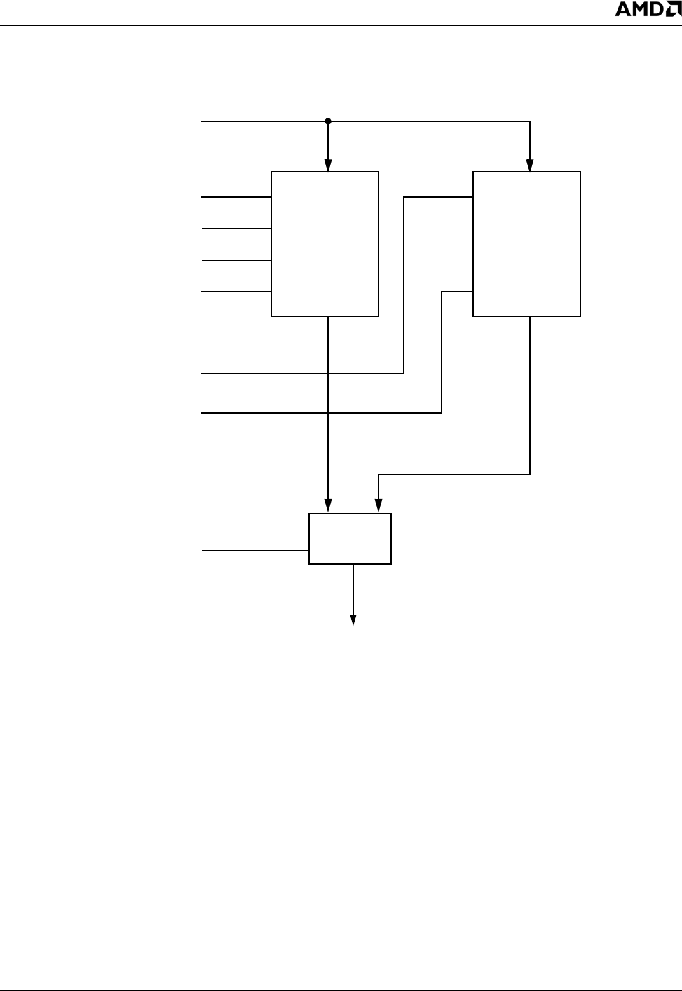
AMD Geode™ LX Processors Data Book 291
Display Controller 33234H
6.5.5.4 Read Modes
There are two read modes provided to assist the CPU with
graphics operations in planar modes. Read mode 0 simply
returns the frame buffer data. Read mode 1 allows the CPU
to do a single color compare across eight pixels. Figure 6-
18 shows the data flow for read modes. Figure 6-19 on
page 292 shows how the color compare logic in Figure 6-
18 works.
Figure 6-18. Read Mode Data Flow
Memory Read Data [31:0]
Read Map Select [1:0]
Chain2
Chain4
CPU A[1:0]
Select Read
Map Logic
ReadMode1 B
CPU Read Data [7:0]
In [31:0]
Out [7:0]
Color Compare
In [31:0]
Out [7:0]
Color Compare [3:0]
Color Don’t Care [3:0]
AB
Logic
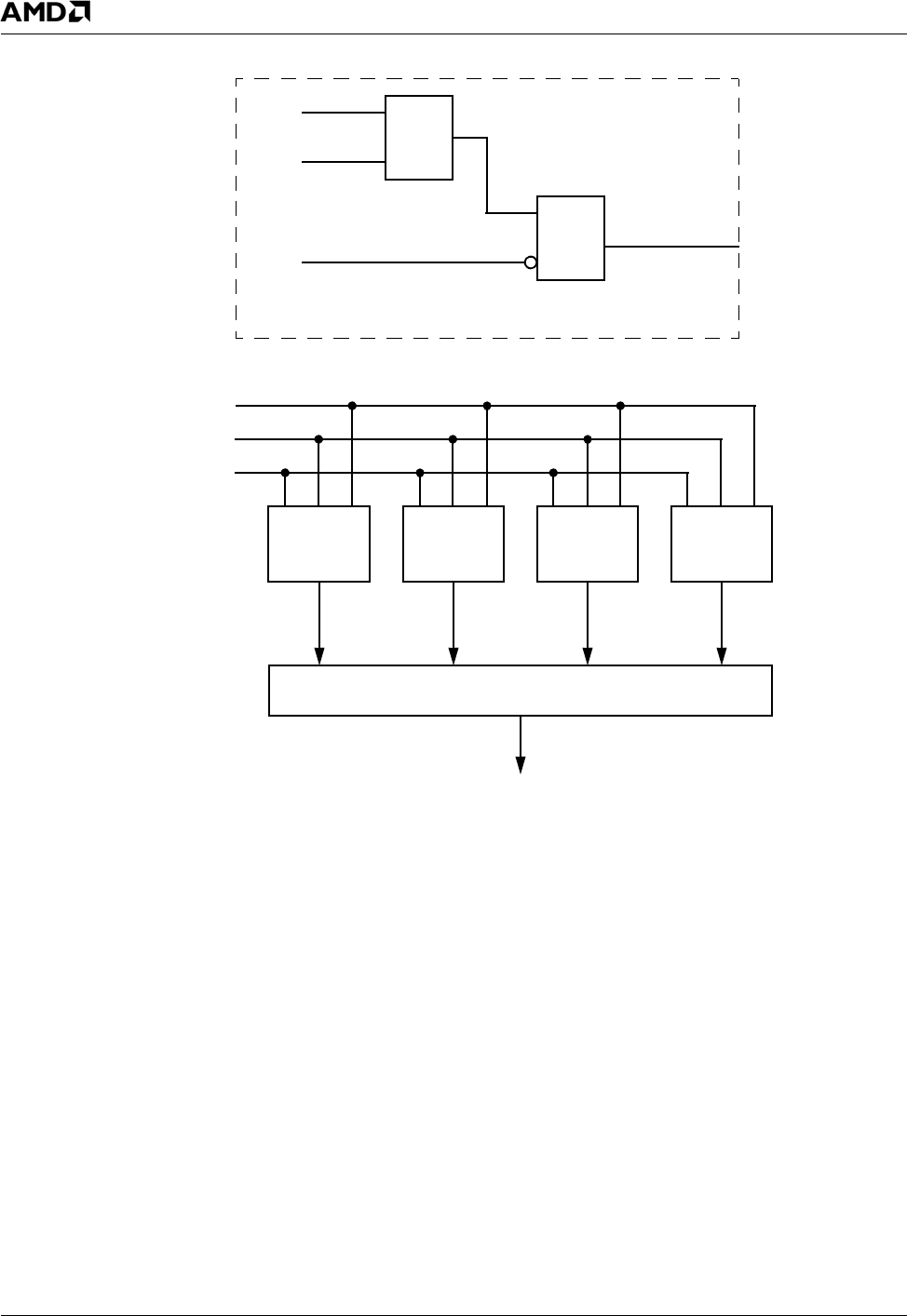
292 AMD Geode™ LX Processors Data Book
Display Controller
33234H
Figure 6-19. Color Compare Operation
8x4 Input AND
Compare Result [7:0]
CC3 CC2 CC1 CC0
Memory Data [31:0] 31:24 23:16 15:8 7:0
Color Compare [3:0] 3210
Color Don’t Care [3:0] 3210
D[7:0]
C
XOR
OR CCx[7:0]
E
Color Compare Block Detail
ECD ECD EC D ECD
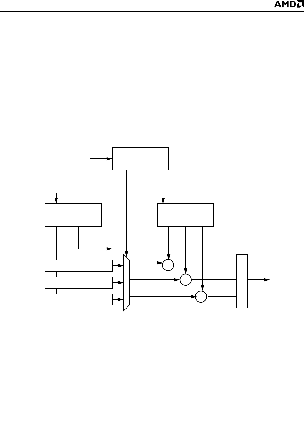
AMD Geode™ LX Processors Data Book 293
Display Controller 33234H
6.5.6 Graphics Scaler/Filter
The DC incorporates a 3x5 tap filter to be used for up/
downscaling of the graphics image. In order to support the
filter, three lines of buffering are also included. These three
line buffers support a frame buffer resolution of up to 1024
pixels wide. For wider images, the buffers are automatically
reconfigured into one line, and scaling is not supported. For
frame buffer images up to and including 1024 pixels in
width, vertical downscaling of up to (but not including) 2:1
is supported and horizontal downscaling of up to (but not
including) 2:1 is supported.
The filter is organized as five 3-tap vertical filters that feed
the five taps of a horizontal filter. The filter supports 1/256
inter-pixel quantization (i.e., 256-phase) in both the hori-
zontal and vertical directions. The filter coefficients are 10
bits wide.
Scaling is controlled by adjusting the horizontal and vertical
filter scale factors (through configuration register 90).
These numbers represent binary rational numbers in a
2.14 format. At the start of each frame, the H Phase Adder
and V Phase Adder are reset to 0. At the start of each scan
line, the V Phase adder is added to V Phase and the result
is stored in V Phase Adder. The integer portion of the value
in V Phase Adder indicates on which line the filter kernel is
centered. The most significant eight bits of the fractional
portion of this value determine the vertical phase for the
purpose of determining the filter coefficients.
The H Phase Adder mechanism is similar but operates on
pixels instead of lines.
A block diagram of the filter is shown in Figure 6-20.
Figure 6-20. Graphics Filter Block Diagram
V Phase Adder
H Phase Adder V. Coefficient RAM
X
X
X
+
Address
H Phase
V Phase
Line buffer selection
and routing Address
Address for H.
Coefficient RAM
Line Buffer
Line Buffer
Line Buffer
To
horizontal
latches
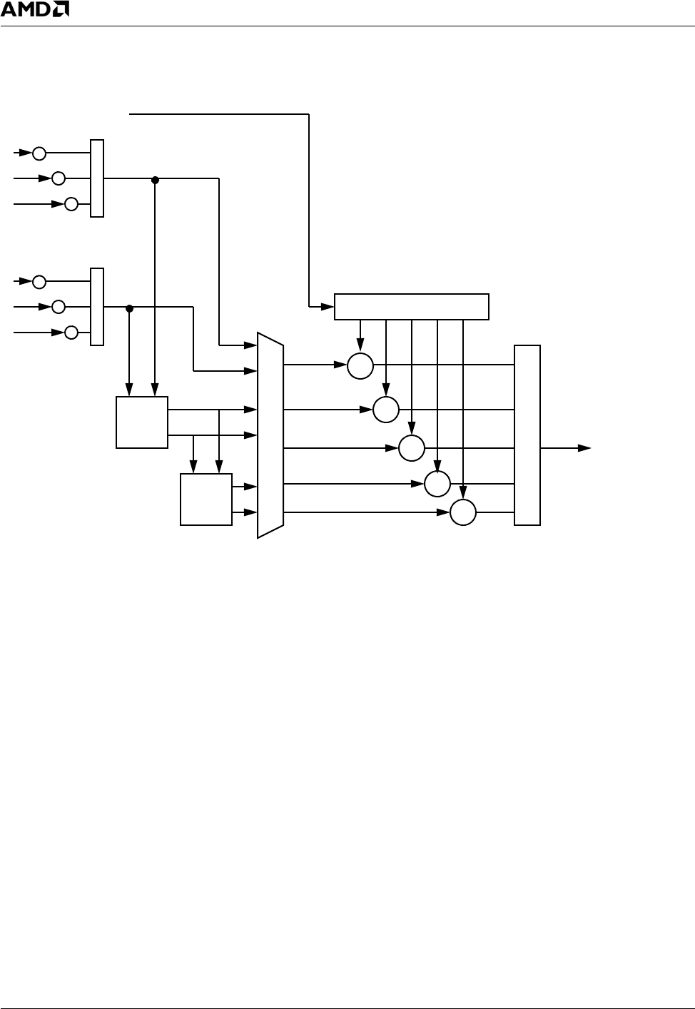
294 AMD Geode™ LX Processors Data Book
Display Controller
33234H
Figure 6-20. Graphics Filter Block Diagram (Continued)
2 Pixel
Latch
x
x
x
+
x
x
x
+
2 Pixel
Latch
H. Coefficient RAM
X
X
X
X
X
+
Addresses for H. Coefficient RAM
from H Phase Adder
The entire structure is replicated for each pixel
component (red, green, blue, and alpha).
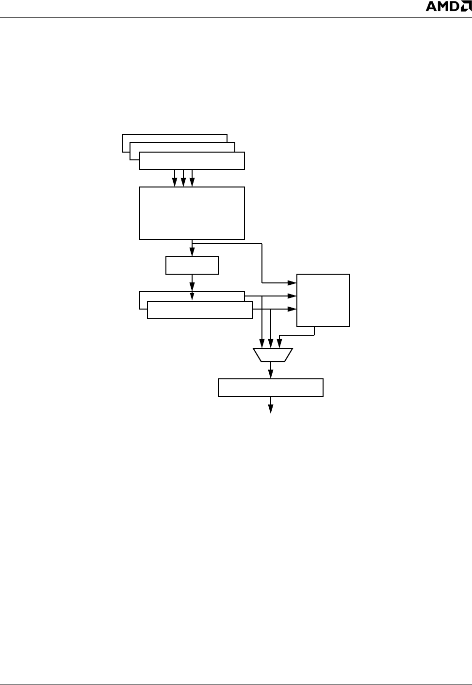
AMD Geode™ LX Processors Data Book 295
Display Controller 33234H
To support the flicker filter, the scaling filter then feeds two
additional line buffers. These buffers are 1024 pixels wide.
The scaling filter directly feeds a tap of the 3x1-tap flicker
filter. (The other two taps are fed by the two line buffers.) All
filtering is performed in the GeodeLink I/F clock domain.
The result from the flicker filter feeds a final line buffer,
which is used to synchronize the data stream to the Dot
clock domain. When the flicker filter is enabled, the final
image width is dictated by this final line buffer, which is
1024 pixels wide. When the flicker filter is disabled, the two
line buffers normally used to feed the flicker filter are used
as one line buffer, that feeds the final synchronizing line
buffer. This enables scaling to image sizes up to 2048 pix-
els wide, provided that interlacing is not required. Figure 6-
21 illustrates the flicker filter and line buffer path.
Figure 6-21. Flicker Filter and Line Buffer Path
1024-Pixel Line Buffers
Graphics Scaler Filter
Delay
1024-Pixel Line Buffers
3-Tap
Vertical
Flicker
Filter
1024-Pixel Line Buffers

296 AMD Geode™ LX Processors Data Book
Display Controller
33234H
6.5.7 Color Key Elimination
Additional logic, not shown in the diagrams, is used to pre-
serve the color key color. This logic, when enabled, adjusts
the alpha value for each filter input pixel in which a color
key match is detected. The filter then uses the alpha value
to determine if a pixel matches the color key. For informa-
tion on the interaction of cursor and color key, Table 6-35
on page 284.
The filter contains specialized logic to remove color key pix-
els from the blended output and replace them with nearby
pixels. This prevents halo effects if the color key contrasts
sharply with the surrounding graphics image.
For each of the 3-tap vertical filters, except the center one,
the replacement algorithm is as follows:
•If the top pixel is the only color key pixel, the center pixel
is used in its place.
•If the bottom pixel is the only color key pixel, the center
pixel is used in its place.
•If the center pixel is the only color key pixel, the top pixel
is used in its place.
•If any two pixels are color key pixels, the remaining pixel
is output to the horizontal filter.
•If all pixels are color key pixels, the bottom pixel is output
to the horizontal filter. (The vertical output is a color key
pixel and the alpha value is set accordingly.)
For the center 3-tap vertical filter, the algorithm is as fol-
lows:
•If the top pixel is a color key pixel, the center pixel is
used in its place.
•If the bottom pixel is a color key pixel, the center pixel is
used in its place.
•If the center pixel is a color key pixel, the center pixel is
output to the horizontal filter regardless of the values of
the other two pixels. (The vertical output is a color key
pixel, and the alpha value is set accordingly.)
The horizontal filter algorithm follows. Assume that the
pixel inputs are numbered 1-5, left to right.
•If pixel 1 is a color key pixel and pixel 2 is not, pixel 2 is
used in place of pixel 1.
•If pixel 1 and pixel 2 are both color key pixels, pixel 3 is
used in place of pixel 1.
•If pixel 2 is a color key pixel, pixel 3 is used in place of
pixel 2.
•If pixel 5 is a color key pixel and pixel 4 is not, pixel 4 is
used in place of pixel 5.
•If pixel 4 and pixel 5 are both color key pixels, pixel 3 is
used in place of pixel 5.
•If pixel 4 is a color key pixel, pixel 3 is used in place of
pixel 4.
•If pixel 3 is a color key pixel, pixel 3 is output from the
filter regardless of the values of pixels 1, 2, 4, and 5.
(The result is a color key pixel; the alpha value is set
accordingly.)
If the center pixel matches the color key, it is passed
through directly. If the center pixel does not match the color
key, then any other filter input pixel that matches the color
key is discarded and replaced by a nearby non-color-key-
matching neighbor.
6.5.8 Using the Graphics Filter
From a software perspective, the AMD Geode LX proces-
sor DC appears much like its predecessor in the
AMD Geode GX processor design. The graphics filter is
disabled by default, and the timing and addressing regis-
ters operate as before. One significant change is the addi-
tion of color key detection logic to the DC block. This logic
was previously only in the VP.
When enabling the VP for the purpose of scaling the output
image, some additional parameters must be programmed
(These parameters need not be programmed if the graph-
ics filter/scaler is to remain disabled.):
•The horizontal and vertical size of the source image
•The horizontal and vertical scaling factors to be used to
scale the source image
•The filter coefficients
The timing registers (DC Memory Offsets 040h-058h)
should be programmed based on the parameters for the
resulting output image. Note that this image may differ in
size from the frame buffer image. The frame buffer image
size is used to determine the value to be written to the
Frame Buffer Active Region Register (DC Memory Offset
05Ch).
The scaling factors are programmed into the Graphics Fil-
ter Scale Register (DC Memory Offset 090h). These fields
are 16 bits each (horizontal and vertical). The 16 bits repre-
sent the ratio of the destination image size to the source
image size. They are right-shifted 14 bits to represent frac-
tional values between 0 and 3.99993896484375. However,
due to hardware limitations, the downscale factors cannot
exceed 2.0. Thus the image can be downscaled by nearly
2X in the horizontal and vertical directions. The image can
be upscaled by up to 16384X, although the CRTC does not
support images beyond 1920x1440 pixels, so it is unlikely
that scale factors beyond about 4X would ever be used.
VBI data is not filtered. The scaling factors in the Graphics
Filter Scale register have no effect on VBI data.
The filter supports 256 sub-pixel phases in both the hori-
zontal and vertical directions. Each coefficient is 10 bits,
and is represented as a 2’s compliment number, right-
shifted 9 bits to represent values between -1 and
0.998046875. The coefficients must be loaded into the
RAMs by software, using the IRQ/Filter Control register, Fil-
ter Coefficient Data register 1, and Filter Coefficient Data
Register 2 (DC Memory Offsets 094h-09Ch).

AMD Geode™ LX Processors Data Book 297
Display Controller 33234H
6.5.9 Interlaced Modes
For interlaced modes, the V_ACTIVE and V_TOTAL fields
are configured for the odd field. The Even Field Vertical
Timing registers (DC Memory Offsets 0E4h-0ECh) are
configured for the corresponding even field. Figure 6-22 on
page 298 shows a representative timing diagram for the
odd and even timing register settings in interlaced modes,
and Table 6-43 on page 298 presents the (decimal) timing
values for some common interlaced modes.
The DC is capable of producing an interlaced output using
any of three separate mechanisms. It can fetch the graph-
ics data in an interlaced manner, flicker filter the graphics
data, or use the same graphics data for both odd and even
fields, (which would effectively line-double the resulting
image). When the VGA is being used, interlaced address-
ing is not supported, and scaling must be used. When the
frame buffer source image or the output image is wider
than 1024 active pixels, the flicker filter is not supported.
When scaling and/or interleaving is enabled, the size of the
frame buffer image (in pixels) will vary from the size of the
output image. Table 6-42 and Table 6-44 on page 299 indi-
cates how the DC’s timing register fields should be pro-
grammed for supported scaling and interlacing modes.
(Note that for VGA modes, there are several VGA registers
that can affect the size of the frame buffer image. These
registers are not enumerated in the table.)
Table 6-42. Programming Image Sizes
Mode
Pre-scale
Horizontal
Width
Pre-scale
Height
Post-scaler
Width
Post-scaler
Height
Final (Output)
Width
Final (Output)
Height
Default (no VGA, scal-
ing, interlacing, or flicker
filter)
H_ACTIVE V_ACTIVE H_ACTIVE V_ACTIVE H_ACTIVE V_ACTIVE
Scaling only FB_H_ACTIVE FB_V_ACTIVE H_ACTIVE V_ACTIVE H_ACTIVE V_ACTIVE
Interlacing only (no flicker
filter)
H_ACTIVE V_ACTIVE or
V_ACTIVE_EVE
N (alternating)
H_ACTIVE V_ACTIVE or
V_ACTIVE_EVE
N (alternating)
H_ACTIVE V_ACTIVE or
V_ACTIVE_EVE
N (alternating)
Interlacing with flicker fil-
ter
H_ACTIVE V_ACTIVE +
V_ACTIVE_EVE
N + 1 (Note 1)
H_ACTIVE V_ACTIVE +
V_ACTIVE_EVE
N + 11
H_ACTIVE V_ACTIVE or
V_ACTIVE_EVE
N (alternating)
Interlacing with inter-
laced addressing (no
flicker filter)
H_ACTIVE V_ACTIVE or
V_ACTIVE_EVE
N (alternating)
H_ACTIVE V_ACTIVE or
V_ACTIVE_EVE
N (alternating)
H_ACTIVE V_ACTIVE or
V_ACTIVE_EVE
N (alternating)
Interlacing with scaler (no
flicker filter, no interlaced
addressing)
FB_H_ACTIVE FB_V_ACTIVE H_ACTIVE V_ACTIVE or
V_ACTIVE_EVE
N (alternating)
H_ACTIVE V_ACTIVE or
V_ACTIVE_EVE
N (alternating)
Interlacing with scaler
and flicker filter
FB_H_ACTIVE FB_V_ACTIVE H_ACTIVE V_ACTIVE +
V_ACTIVE_EVE
N + 11
H_ACTIVE V_ACTIVE or
V_ACTIVE_EVE
N (alternating)
VGA (no scaling, interlac-
ing, or flicker filter)
VGA CRTC VGA CRTC VGA CRTC VGA CRTC VGA CRTC VGA CRTC
VGA with scaling (no
interlacing or flicker filter
VGA CRTC VGA CRTC H_ACTIVE V_ACTIVE H_ACTIVE V_ACTIVE
VGA with scaling and
interlacing (no flicker fil-
ter)
VGA CRTC VGA CRTC H_ACTIVE V_ACTIVE or
V_ACTIVE_EVE
N (alternating)
H_ACTIVE V_ACTIVE or
V_ACTIVE_EVE
N (alternating)
VGA with scaling, inter-
lacing, and flicker filter
VGA CRTC VGA CRTC H_ACTIVE V_ACTIVE +
V_ACTIVE_EVE
N + 11
H_ACTIVE V_ACTIVE or
V_ACTIVE_EVE
N (alternating)
Note 1. Because the register value represents the image size minus 1, an additional 1 is added when these two register values are added
together to retain the convention.

298 AMD Geode™ LX Processors Data Book
Display Controller
33234H
6.5.10 Interlaced Timing Examples
Figure 6-22 shows how the DC's timing registers are used
to control timings for interlaced display modes. The SMTPE
standards define the even and odd fields as starting at
VSYNC, while the register settings define the timings
based on the start of the active display region, as is com-
mon in (non-interlaced) VESA timing standards. As a
result, the V_Sync_End and V_Total register settings each
define a region that begins in the odd field and ends in the
next even field. Similarly, the V_Sync_Even_End and
V_Total_Even register settings each define a region that
begins in the even field and ends in the next odd field.
All register values are in hex; assuming VSYNC pulse
width of one line.
Table 6-43 lists timings for various interlaced modes for ref-
erence. The user should verify these timings against cur-
rent specifications for their application.) Table 6-44 on page
299 provides the corresponding register settings (hexadec-
imal values) for these modes. The VSYNC pulse is
assumed to be one line wide. Further information on these
registers can be found in Section 6.6.5 on page 327.
Figure 6-22. Interlaced Timing Settings
.
VSYNC
Vertical Display Active
Odd Field Even Field
Back
Porch Front
Porch Back
Porch Front
Porch
Active Region Active Region
V_Active_End
V_Total
V_Sync_Start
V_Sync_End
V_Active_Even_End
V_Total_Even
V_Sync_Even_Start
V_Sync_Even_End
Back
Porch
Table 6-43. Vertical Timing in Number of Lines
Timing Set
Odd Field Even Field
Back Porch Active Front Porch Back Porch Active Front Porch
525 16 242 2 17 241 3
625 22 288 2 23 288 2
720i 12 360 3 13 360 2
1080i 20 540 3 20 540 2
1080i 50 Hz 80 540 5 80 540 5

AMD Geode™ LX Processors Data Book 299
Display Controller 33234H
Table 6-44. Timing Register Settings for Interlaced Modes
Timing Set Parameter Odd Register Even Register
Formula V_Active_End (odd_active-1) (even_active-1)
V_Total (odd_active + odd_fp + even_bp - 1) (even_active + even_fp + odd_bp - 1)
V_Sync_Start (odd_active + odd_fp - 1) (even_active + even_fp - 1)
V_Sync_End (odd_active + odd_fp + odd_vsync - 1) (even_active +even_fp + even_vsync - 1)
525 V_Active_End F1 F0
V_Total 106 105
V_Sync_Start F5 F5
V_Sync_End F6 F6
625 V_Active_End 11F 11F
V_Total 138 137
V_Sync_Start 121 121
V_Sync_End 122 122
720i V_Active_End 167 167
V_Total 177 177
V_Sync_Start 16A 169
V_Sync_End 16B 16A
1080i V_Active_End 21B 21B
V_Total 232 231
V_Sync_Start 21E 21D
V_Sync_End 21F 21E
1080i 50 Hz V_Active_End 21B 21B
V_Total 270 270
V_Sync_Start 220 220
V_Sync_End 221 221
300 AMD Geode™ LX Processors Data Book
Display Controller Register Descriptions
33234H
6.6 Display Controller Register Descriptions
This section provides information on the registers associ-
ated with the Display Controller (DC) (i.e., GUI and VGA
blocks), including the Standard GeodeLink™ Device (GLD)
MSRs and the Display Controller Specific MSRs (accessed
via the RDMSR and WRMSR instructions). Table 6-45
through Table 6-50 are register summary tables that
include reset values and page references where the bit
descriptions are provided.
Note: The MSR address is derived from the perspective
of the CPU Core. See Section 4.1 "MSR Set" on
page 45 for more details on MSR addressing.
Table 6-45. Standard GeodeLink™ Device MSRs Summary
MSR
Address Type Register Name Reset Value Reference
80002000h RO GLD Capabilities MSR (GLD_MSR_CAP) 00000000_0003E4xxh Page 305
80002001h R/W GLD Master Configuration MSR
(GLD_MSR_CONFIG)
00000000_00000000h Page 305
80002002h R/W GLIU0 Device SMI MSR (GLD_MSR_SMI) 00000000_00000000h Page 306
80002003h R/W GLD Error MSR (GLD_MSR_ERROR) 00000000_00000000h Page 308
80002004h R/W GLD Power Management MSR
(GLD_MSR_PM)
00000000_00000015h Page 310
80002005h R/W GLIU0 Device Diagnostic MSR
(GLD_MSR_DIAG)
00000000_00000000h Page 310
Table 6-46. DC Specific MSRs Summary
MSR
Address Type Register Name Reset Value Reference
80000012h R/W DC RAM Control MSR
(DC_RAM_CTL_MSR)
00000000_02020202h Page 311
Table 6-47. DC Configuration Control Register Summary
DC
Memory
Offset Type Register Name Reset Value Reference
Configuration and Status Registers
000h R/W DC Unlock (DC_UNLOCK) 00000000h Page 312
004h R/W DC General Configuration (DC_GENERAL_CFG) 00000000h Page 314
008h R/W DC Display Configuration (DC_DISPLAY_CFG) 00000000h Page 317
00Ch R/W DC Arbitration Configuration (DC_ARB_CFG) 00000000h Page 319
Memory Organization Registers
010h R/W DC Frame Buffer Start Address
(DC_FB_ST_OFFSET)
xxxxxxxxh Page 321
014h R/W DC Compression Buffer Start Address
(DC_CB_ST_OFFSET)
xxxxxxxxh Page 322
018h R/W DC Cursor Buffer Start Address
(DC_CURS_ST_OFFSET)
xxxxxxxxh Page 322
AMD Geode™ LX Processors Data Book 301
Display Controller Register Descriptions 33234H
020h R/W DC Video Y Buffer Start Address Offset
(DC_VID_Y_ST_OFFSET)
xxxxxxxxh Page 323
024h R/W DC Video U Buffer Start Address Offset
(DC_VID_U_ST_OFFSET)
xxxxxxxxh Page 323
028h R/W DC Video V Buffer Start Address Offset
(DC_VID_V_ST_OFFSET)
xxxxxxxxh Page 324
02Ch R/W DC Dirty/Valid Region Top (DC_DV_TOP) 00000000h Page 324
030h R/W DC Line Size (DC_LINE_SIZE) xxxxxxxxh Page 325
034h R/W DC Graphics Pitch (DC_GFX_PITCH) xxxxxxxxh Page 326
038h R/W DC Video YUV Pitch (DC_VID_YUV_PITCH) xxxxxxxxh Page 326
Timing Registers
040h R/W DC Horizontal and Total Timing
(DC_H_ACTIVE_TIMING)
xxxxxxxxh Page 328
044h R/W DC CRT Horizontal Blanking Timing
(DC_H_BLANK_TIMING)
xxxxxxxxh Page 329
048h R/W DC CRT Horizontal Sync Timing
(DC_H_SYNC_TIMING)
xxxxxxxxh Page 329
050h R/W DC Vertical and Total Timing
(DC_V_ACTIVE_TIMING)
xxxxxxxxh Page 330
054h R/W DC CRT Vertical Blank Timing
(DC_V_BLANK_TIMING)
xxxxxxxxh Page 331
058h R/W DC CRT Vertical Sync Timing
(DC_V_SYNC_TIMING)
xxxxxxxxh Page 331
05Ch R/W DC Frame Buffer Active Region Register
(DC_FB_ACTIVE)
xxxxxxxxh Page 332
Cursor Position and Count Status Registers
060h R/W DC Cursor X Position (DC_CURSOR_X) xxxxxxxxh Page 332
064h R/W DC Cursor Y Position (DC_CURSOR_Y) xxxxxxxxh Page 333
06Ch RO DC Line Count/Status (DC_LINE_CNT/STATUS) xxxxxxxxh Page 333
Palette Access and FIFO Diagnostic Registers
070h R/W DC Palette Address (DC_PAL_ADDRESS) xxxxxxxxh Page 335
074h R/W DC Palette Data (DC_PAL_DATA) xxxxxxxxh Page 336
078h R/W DC Display FIFO Diagnostic (DC_DFIFO_DIAG) xxxxxxxxh Page 336
07Ch R/W DC Compression FIFO Diagnostic
(DC_CFIFO_DIAG)
xxxxxxxxh Page 337
Video Downscaling Registers
080h R/W DC Video Downscaling Delta (DC_VID_DS_DELTA) 00000000h Page 338
GLIU0 Control Registers
084h R/W DC GLIU0 Memory Offset
(DC_GLIU0_MEM_OFFSET)
00000000h Page 339
088h R/W DC Dirty/Valid RAM Control (DC_DV_CTL) 00000000h Page 339
Table 6-47. DC Configuration Control Register Summary (Continued)
DC
Memory
Offset Type Register Name Reset Value Reference
302 AMD Geode™ LX Processors Data Book
Display Controller Register Descriptions
33234H
08Ch R/W DC Dirty/Valid RAM Access (DC_DV_ACCESS) 0000000xh Page 340
Graphics Scaling Control Registers
090h R/W DC Graphics Filter Scale (DC_GFX_SCALE) 40004000h Page 341
094h R/W DC IRQ/Filter Control (DC_IRQ_FILT_CTL) 00000000h Page 342
098h R/W DC Filter Coefficient Data Register 1
(DC_FILT_COEFF1)
xxxxxxxxh Page 343
09Ch R/W DC Filter Coefficient Data Register 2
(DC_FILT_COEFF2)
xxxxxxxxh Page 344
VBI Control Registers
0A0h R/W DC VBI Even Control (DC_VBI_EVEN_CTL) xxxxxxxxh Page 344
0A4h R/W DC VBI Odd Control (DC_VBI_ODD_CTL) xxxxxxxxh Page 345
0A8h R/W DC VBI Horizontal Control (DC_VBI_HOR) xxxxxxxxh Page 345
0ACh R/W DC VBI Odd Line Enable (DC_VBI_LN_ODD) xxxxxxxxh Page 346
0B0h R/W DC VBI Even Line Enable (DC_VBI_LN_EVEN) xxxxxxxxh Page 346
0B4h R/W DC VBI Pitch and Size (DC_VBI_PITCH) xxxxxxxxh Page 347
Color Key Control Registers
0B8h R/W DC Color Key (DC_CLR_KEY) 00000000h Page 347
0BCh R/W DC Color Key Mask (DC_CLR_KEY_MASK) 00xxxxxxh Page 348
0C0h R/W DC Color Key Horizontal Position (DC_CLR_KEY_X) 00000000h Page 348
0C4h R/W DC Color Key Vertical Position (DC_CLR_KEY_Y) 00000000h Page 348
Interrupt and GenLock Registers
0C8h R/W DC Interrupt (DC_IRQ) 00000003h Page 349
0D4h R/W DC GenLock Control (DC_GENLK_CTL) xxxxxxxxh Page 350
Even Field Video Address Registers
0D8h R/W DC Even Field Video Y Start Address Offset
(DC_VID_EVEN_Y_ST_OFFSET)
xxxxxxxxh Page 351
0DCh R/W DC Even Field Video U Start Address Offset
(DC_VID_EVEN_U_ST_OFFSET)
xxxxxxxxh Page 352
0E0h R/W DC Even Field Video V Start Address Offset
(DC_VID_EVEN_V_ST_OFFSET)
xxxxxxxxh Page 352
Even Field Vertical Timing Registers
0E4h R/W DC Vertical and Total Timing for Even Fields
(DC_V_ACTIVE_EVEN_TIMING)
xxxxxxxxh Page 353
0E8h R/W DC CRT Vertical Blank Timing for Even Fields
(DC_V_BLANK_EVEN_TIMING)
xxxxxxxxh Page 354
0ECh R/W DC CRT Vertical Sync Timing for Even Fields
(DC_V_SYNC_EVEN_TIMING)
xxxxxxxxh Page 354
Table 6-47. DC Configuration Control Register Summary (Continued)
DC
Memory
Offset Type Register Name Reset Value Reference
AMD Geode™ LX Processors Data Book 303
Display Controller Register Descriptions 33234H
Table 6-48. VGA Block Configuration Register Summary
DC
Memory
Offset Type Register Name Reset Value Reference
100h R/W VGA Configuration (VGA_CONFIG) 00000000h Page 355
104h RO VGA Status (VGA_STATUS) 00000000h Page 355
Table 6-49. VGA Block Standard Register Summary
I/O Read
Address
I/O Write
Address Register Name/Group Reset Value Reference
3CCh 3C2h (W) VGA Miscellaneous Output 02h Page 356
3C2h -- VGA Input Status Register 0 00h Page 357
3BAh or 3DAh
(Note 1)
-- VGA Input Status Register 1 01h Page 357
3CAh 3BAh or 3DAh
(Note 1)
VGA Feature Control xxh Page 357
3C4h VGA Sequencer Index 0xh Page 358
3C5h VGA Sequencer Data xxh Page 358
3B4h or 3D4h (Note 1) CRTC Index 00h Page 362
3B5h or 3D5h (Note 1) CRTC Data 00h Page 363
3CEh VGA Graphics Controller Index xxh Page 373
3CFh VGA Graphics Controller Data xxh Page 374
3C0h Attribute Controller Index/Data xxh Page 379
3C1h (R) 3C0h (W)
3C8h 3C7h (Palette
Read Mode)
Video DAC Palette Address 00h Page 382
3C8h (Palette
Write Mode)
3C7h-- Video DAC State 00h Page 383
3C9h Video DAC Palette Data 00h Page 383
3C6h Video DAC Palette Mask 00h Page 384
Note 1. The I/O addresses are determined by bit 0 of the Miscellaneous Output Register. See the description of this register
in Section 6.6.17.1 on page 356 for more information.

304 AMD Geode™ LX Processors Data Book
Display Controller Register Descriptions
33234H
Table 6-50. VGA Block Extended Register Summary
VGA CRTC
Index Type Register Name Reset Value Reference
0030h R/W ExtendedRegisterLock FFh Page 385
043h R/W ExtendedModeControl 00h Page 385
044h R/W ExtendedStartAddress 00h Page 385
047h R/W WriteMemoryAperture 00h Page 386
048h R/W ReadMemoryAperture 00h Page 386
060h R/W BlinkCounterCtl 00h Page 386
061h RO BlinkCounter 00h Page 387
070h R/W VGALatchSavRes 00h Page 387
071h R/W DACIFSavRes 00h Page 387
AMD Geode™ LX Processors Data Book 305
Display Controller Register Descriptions 33234H
6.6.1 Standard GeodeLink™ Device (GLD) Registers (MSRs)
6.6.1.1 GLD Capabilities MSR (GLD_MSR_CAP)
6.6.1.2 GLD Master Configuration MSR (GLD_MSR_CONFIG)
MSR Address 80002000h
Ty p e RO
Reset Value 00000000_0003E4xxh
GLD_MSR_CAP Register Map
63 62 61 60 59 58 57 56 55 54 53 52 51 50 49 48 47 46 45 44 43 42 41 40 39 38 37 36 35 34 33 32
RSVD
313029282726252423222120191817161514131211109876543210
RSVD DEV_ID REV_ID
GLD_MSR_CAP Bit Descriptions
Bit Name Description
63:24 RSVD Reserved. Set to 0.
23:8 DEV_ID Device ID. Identifies device (03E4h).
7:0 REV_ID Revision ID. Identifies device revision. See AMD Geode™ LX Processors Specification
Update document for value.
MSR Address 80002001h
Ty p e R / W
Reset Value 00000000_00000000h
GLD_MSR_CONFIG Register Map
63 62 61 60 59 58 57 56 55 54 53 52 51 50 49 48 47 46 45 44 43 42 41 40 39 38 37 36 35 34 33 32
RSVD
313029282726252423222120191817161514131211109876543210
RSVD PRI1
RSVD
PRI0
RSVD
PID
GLD_MSR_CONFIG Bit Descriptions
Bit Name Description
63:11 RSVD Reserved. Set to 0.
10:8 PRI1 Secondary Priority Level. This value is the priority level the DC uses when performing
high priority GLIU0 accesses. This is the case when the FIFOs are nearly empty.
7 RSVD Reserved. Set to 0.
6:4 PRI0 Primary Priority Level. This value is the priority level the DC uses for most accesses
(i.e., when the display FIFO is not in danger of being emptied).
3 RSVD Reserved. Set to 0.
2:0 PID Priority ID. This value is the Priority ID (PID) value used when the DC initiates GLIU0
transactions.
306 AMD Geode™ LX Processors Data Book
Display Controller Register Descriptions
33234H
6.6.1.3 GLIU0 Device SMI MSR (GLD_MSR_SMI)
MSR Address 80002002h
Ty p e R / W
Reset Value 00000000_00000000h
GLD_MSR_SMI Register Map
63 62 61 60 59 58 57 56 55 54 53 52 51 50 49 48 47 46 45 44 43 42 41 40 39 38 37 36 35 34 33 32
RSVD
VGA_RES_CHANGE_SMI
RSVD
ISR1R_SMI
MISCIOR_SMI
DACIOR_SMI
DACIOW_SMI
AT R I O R _S M I
AT R I OW_ S M I
GFXIOR_SMI
GFXIOW_SMI
SEQIOR_SMI
SEQIOW_SMI
CRTCIOR_SMI
CRTCIOW_SMI
CRTCIO_SMI
VGA_BL_SMI
ISR0_SMI
MISC_SMI
VG_BL_SMI
313029282726252423222120191817161514131211109876543210
RSVD
VGA_RES_CHANGE_MASK
RSVD
ISR1R_MSK
MISCIOR_MSK
DACIOR_MSK
DACIOW_MSK
ATR IO R_ M SK
AT R I OW _ M S K
GFXIOR_MSK
GFXIOW_MSK
SEQIOR_MSK
SEQIOW_MSK
CRTCIOR_MSK
CRTCIOW_MSK
CRTCIO_MSK
VGA_BL_MSK
ISR0_MSK
MISC_MSK
VG_BL_MSK
GLD_MSR_SMI Bit Descriptions
Bit Name Description
63:61 RSVD Reserved. Set to 0.
60 VGA_RES_
CHANGE_SMI
VGA Resolution Change SMI. Reading a 1 indicates that the VGA’s output image size
has changed while scaling is enabled. The handler for this SMI should update the hori-
zontal and/or vertical scale factor(s) accordingly.
59:49 RSVD Reserved. Set to 0.
48 ISR1R_SMI Input Status Register 1 Read SMI. Reading a 1 indicates that the VGA Input Status
Register 1 has been read; writing this bit to 1 clears it.
47 MISCIOR_SMI Miscellaneous Output Register Read SMI. Reading a 1 indicates that the VGA Mis-
cellaneous Output Register has been read; writing this bit to 1 clears it.
46 DACIOR_SMI Video DAC Register Read SMI. Reading a 1 indicates that one or more of the VGA’s
Video DAC registers has been read; writing a 1 to this bit clears it.
45 DACIOW_SMI Video DAC Register Write SMI. Reading a 1 indicates that one or more of the VGA’s
Video DAC registers has been written; writing a 1 to this bit clears it.
44 ATRIOR_SMI Attribute Register Read SMI. Reading a 1 indicates that one or more of the VGA’s
Attribute registers has been read; writing a 1 to this bit clears it.
43 ATRIOW_SMI Attribute Register Write SMI. Reading a 1 indicates that one or more of the VGA’s
Attribute registers has been written; writing a 1 to this bit clears it.
42 GFXIOR_SMI Graphics Controller Register Read SMI. Reading a 1 indicates that one or more of
the VGA’s Graphics Controller registers has been read; writing a 1 to this bit clears it.
41 GFXIOW_SMI Graphics Controller Register Write SMI. Reading a 1 indicates that one or more of
the VGA’s Graphics Controller registers has been written; writing a 1 to this bit clears it.

AMD Geode™ LX Processors Data Book 307
Display Controller Register Descriptions 33234H
40 SEQIOR_SMI Sequencer Register Read SMI. Reading a 1 indicates that one or more of the VGA’s
Sequencer registers has been read; writing a 1 to this bit clears it.
39 SEQIOW_SMI Sequencer Register Write SMI. Reading a 1 indicates that one or more of the VGA’s
Sequencer registers has been written; writing a 1 to this bit clears it.
38 CRTCIOR_SMI CRTC Register Read SMI. Reading a 1 indicates that one or more of the VGA’s CRTC
registers has been read; writing a 1 to this bit clears it.
37 CRTCIOW_SMI CRTC Register Write SMI. Reading a 1 indicates that one or more of the VGA’s CRTC
registers has been written; writing a 1 to this bit clears it.
36 CRTCIO_SMI CRTC Invalid Register I/O SMI. Reading a 1 indicates that this SMI has been gener-
ated; writing a 1 to this bit clears it; writing 0 has no effect.
35 VGA_BL_SMI VGA Vertical Blank SMI. Reading a 1 indicates that the ASMI corresponding to VGA
Vertical Blank has been triggered. Writing a 1 to this bit clears it (and deactivates the
ASMI signal); writing a 0 to this bit has no effect.
34 ISR0_SMI Input Status Register 0 SMI. Reading a 1 indicates that a synchronous SMI was gen-
erated because of a read to VGA Input Status Register 0. Writing a 1 to this bit clears it;
writing a 0 has no effect.
33 MISC_SMI Miscellaneous Output Register SMI. Reading a 1 indicates that a synchronous SMI
was generated due to a write to the Miscellaneous Output Register. Writing a 1 to this
bit clears it; writing a 0 has no effect.
32 VG_BL_SMI DC Vertical Blank SMI. Reading a 1 indicates that the ASMI corresponding to DC Ver-
tical Blank has been triggered. Writing a 1 to this bit clears it (and deactivates the ASMI
signal); writing a 0 has no effect.
31:29 RSVD Reserved. Set to 0.
28 VGA_RES_
CHANGE_MASK
VGA Resolution Change SMI Mask. When set to 1, disables generation of an asyn-
chronous SMI when all of the following conditions occur at once:
- The VGA timing engine is enabled.
- Scaling is enabled.
- The horizontal or vertical resolution of the image produced by the VGA timing engine
changes.
27:17 RSVD Reserved. Set to 0.
16 ISR1R_MSK Input Status Register 1 Read SMI Mask. When set to 1, disables generation of the
SMI that indicates that VGA Input Status Register 1 has been read.
15 MSICIOR_MSK Miscellaneous Output Register Read SMI. When set to 1, disables generation of the
SMI that indicates that the VGA Miscellaneous Output Register has been read.
14 DACIOR_MSK Video DAC Register Read SMI. When set to 1, disables generation of the SMI that
indicates that one or more of the VGA’s Video DAC registers has been read.
13 DACIOW_MSK Video DAC Register Write SMI. When set to 1, disables generation of the SMI that
indicates that one or more of the VGA’s Video DAC registers has been written.
12 ATRIOR_MSK Attribute Register Read SMI. When set to 1, disables generation of the SMI that indi-
cates that one or more of the VGA’s Attribute registers has been read.
11 ATRIOW_MSK Attribute Register Write SMI. When set to 1, disables generation of the SMI that indi-
cates that one or more of the VGA’s Attribute registers has been written.
10 GFXIOR_MSK Graphics Controller Register Read SMI. When set to 1, disables generation of the
SMI that indicates that one or more of the VGA’s Graphics Controller registers has
been read.
GLD_MSR_SMI Bit Descriptions (Continued)
Bit Name Description
308 AMD Geode™ LX Processors Data Book
Display Controller Register Descriptions
33234H
6.6.1.4 GLD Error MSR (GLD_MSR_ERROR)
9GFXIOW_MSKGraphics Controller Register Write SMI. When set to 1, disables generation of the
SMI that indicates that one or more of the VGA’s Graphics Controller registers has
been written.
8 SEQIOR_MSK Sequencer Register Read SMI. When set to 1, disables generation of the SMI that
indicates that one or more of the VGA’s Sequencer registers has been read.
7 SEQIOW_MSK Sequencer Register Write SMI. When set to 1, disables generation of the SMI that
indicates that one or more of the VGA’s Sequencer registers has been written.
6 CRTCIOR_MSK CRTC Register Read SMI. When set to 1, disables generation of the SMI that indi-
cates that one or more of the VGA’s CRTC registers has been read; writing a 1 to this
bit clears it.
5CRTCIOW_MSKCRTC Register Write SMI. When set to 1, disables generation of the SMI that indi-
cates that one or more of the VGA’s CRTC registers has been written.
4 CRTCIO_MSK CRTC Invalid Register I/O SMI Mask. When set to 1, disables generation of a syn-
chronous SMI when a non-implemented VGA CRT Controller Register is read or writ-
ten.
3VGA_BL_MSK VGA Vertical Blank SMI Mask. When set to 1, disables generation of the VGA Vertical
Blank SMI.
2 ISR0_MSK Input Status Register 0 SMI Mask. When set to 1, disables generation of the VGA
Input Status Register SMI.
1MISC_MSK Miscellaneous Output Register SMI Mask. When set to 1, disables generation of the
Miscellaneous Output Register synchronous SMI.
0VG_BL_MSK DC Vertical Blank SMI Mask. When set to 1, disables the DC Vertical Blank SMI when
set to 1.
MSR Address 80002003h
Ty p e R / W
Reset Value 00000000_00000000h
GLD_MSR_SMI Bit Descriptions (Continued)
Bit Name Description
GLD_MSR_ERROR Register Map
63 62 61 60 59 58 57 56 55 54 53 52 51 50 49 48 47 46 45 44 43 42 41 40 39 38 37 36 35 34 33 32
RSVD
CWD_CHECK_ERR
SYNCBUF_ERR
DFIFO_ERR
SMI_ERR
ADDR_ERR
TYPE_ERR
313029282726252423222120191817161514131211109876543210
RSVD
CWD_CHECK_MASK
SYNCBUF_MASK
DFIFO_ERR_MASK
SMI_ERR_MASK
ADDR_ERR_MASK
TYPE_ERR_MASK

AMD Geode™ LX Processors Data Book 309
Display Controller Register Descriptions 33234H
GLD_MSR_ERROR Bit Descriptions
Bit Name Description
63:38 RSVD Reserved. Set to 0.
37 CWD_CHECK_ERR Control Word Check Error. Reading a 1 indicates that an invalid control word was
read from the Display FIFO, which is indicative of a FIFO underrun. Writing a 1 to this
bit clears it.
36 SYNCBUF_ERR Synchronizer Buffer Error. Reading a 1 indicates that the display pipe attempted to
read the synchronizer buffer while it was invalid. This is indicative of a synchronizer
buffer underrun. Writing a 1 to this bit clears it.
35 DFIFO_ERR Display FIFO Underrun Error. Reading a 1 indicates that the asynchronous error
signal is being driven because the display FIFO has “run dry”. This implies that at
least one frame of the display was corrupted. Writing a 1 to this bit clears it; writing a
0 has no effect.
34 SMI_ERR Uncleared SMI Error. Reading a 1 indicates that the asynchronous error signal is
being driven because a second SMI occurred while the first SMI went unserviced.
33 ADDR_ERR Unexpected Address Error. Reading a 1 indicates that the exception flag was set
because the DC received a GLIU0 transaction request.
32 TYPE_ERR Unexpected Type Error. Reading a 1 indicates that an asynchronous error has
occurred because the DC received a GLIU0 transaction with an undefined or unex-
pected type.
31:6 RSVD Reserved. Set to 0.
5 CWD_CHECK_MSK Control Word Check Error Mask. When set to 1, disables generation of the asyn-
chronous error signal when an invalid control word is read from the data FIFO.
4 SYNCBUF_MSK Synchronizer Buffer Error Mask. When set to 1, disables generation of the asyn-
chronous error signal when invalid data is read from the synchronizer buffer.
3 DFIFO_ERR_MASK Display FIFO Underrun Error Mask. When set to 1, disables generation of the asyn-
chronous error signal when at least one frame of the display was corrupted.
2 SMI_ERR_MASK Uncleared SMI Error Mask. When set to 1, disables generation of the asynchronous
error signal when a second SMI occurred while the first SMI went unserviced.
1 ADDR_ERR_MASK Unexpected Address Error Mask. When set to 1, disables generation of an excep-
tion flag when the DC receives a GLIU0 request.
0 TYPE_ERR_MASK Unexpected Type Error Mask. When set to 1, disables generation of the asynchro-
nous error signal when the DC received a GLIU0 transaction with an undefined or
unexpected type.

310 AMD Geode™ LX Processors Data Book
Display Controller Register Descriptions
33234H
6.6.1.5 GLD Power Management MSR (GLD_MSR_PM)
6.6.1.6 GLIU0 Device Diagnostic MSR (GLD_MSR_DIAG)
This register is reserved for internal use by AMD and should not be written to.
MSR Address 80002004h
Ty p e R / W
Reset Value 00000000_00000015h
GLD_MSR_PM Register Map
63 62 61 60 59 58 57 56 55 54 53 52 51 50 49 48 47 46 45 44 43 42 41 40 39 38 37 36 35 34 33 32
RSVD
313029282726252423222120191817161514131211109876543210
RSVD
VGA_GLCLK_PMODE
DCLK_PMODE
GLCLK_PMODE
GLD_MSR_PM Bit Descriptions
Bit Name Description
63:6 RSVD Reserved. Set to 0.
5:4 VGA_GLCLK_
PMODE
VGA GLIU0 Clock Power Management Mode. This field controls the internal clock
gating for the GLIU0 clock to the VGA module.
00: Clock is not gated.
01: Enable active hardware clock gating. Hardware automatically determines when it is
idle, and internally disables the GLIU0 clock whenever possible.
10: Reserved.
11: Reserved.
3:2 DCLK_PMODE Dot Clock Power Management Mode. This field controls the internal clock gating for
the Dot clock to all logic other than the VGA unit.
00: Clock is not gated.
01: Enable active hardware clock gating. Hardware automatically determines when it is
idle, and internally disables the Dot clock whenever possible.
10: Reserved.
11: Reserved.
1:0 G:CLK_PMODE GLIU0 Clock Power Management Mode. This field controls the internal clock gating
for the GLIU0 Clock to all logic other than the VGA unit.
00: Clock is not gated.
01: Enable active hardware clock gating. Hardware automatically determines when it is
idle, and internally disables the GLIU0 clock whenever possible.
10: Reserved.
11: Reserved.
MSR Address 80002005h
Ty p e R / W
Reset Value 00000000_00000000h
AMD Geode™ LX Processors Data Book 311
Display Controller Register Descriptions 33234H
6.6.2 Display Controller Specific MSRs
6.6.2.1 SPARE MSR
6.6.2.2 DC RAM Control MSR (DC_RAM_CTL_MSR)
MSR Address 80000011h
Ty p e R / W
Reset Value 00000000_00000000h
SPARE_MSR Register Map
63 62 61 60 59 58 57 56 55 54 53 52 51 50 49 48 47 46 45 44 43 42 41 40 39 38 37 36 35 34 33 32
RSVD
313029282726252423222120191817161514131211109876543210
RSVD
DISABLE_VFIFO_WM
RSVD
SPARE_MSR Bit Descriptions
Bit Name Description
63:7 RSVD Reserved.
6DISABLE_
VFIFO_WM
Disable Video FIFO Watermarks. When set, the video watermarks in
DC_ARB_CFG[19:12] have no effect.
5:0 RSVD Reserved.
MSR Address 80000012h
Ty p e R / W
Reset Value 00000000_02020202h
DC_RAM_CTL_MSR Register Map
63 62 61 60 59 58 57 56 55 54 53 52 51 50 49 48 47 46 45 44 43 42 41 40 39 38 37 36 35 34 33 32
RSVD
313029282726252423222120191817161514131211109876543210
RSVD
CFIFO_CTL
RSVD
DV_RAM_CTL
DC_RAM_CTL_MSR Bit Descriptions
Bit Name Description
63:11 RSVD Reserved.
10:8 CFIFO_CTL CFIFO RAM Delay Control.
7:3 RSVD Reserved.
2:0 DV_RAM_CTL DV RAM Delay Control.

312 AMD Geode™ LX Processors Data Book
Display Controller Register Descriptions
33234H
6.6.3 Configuration and Status Registers
All DC registers are DWORD accessible only.
6.6.3.1 DC Unlock (DC_UNLOCK)
This register is provided to lock the most critical memory-mapped DC registers to prevent unwanted modification (write
operations). Read operations are always allowed.
DC Memory Offset 000h
Ty p e R / W
Reset Value 00000000h
DC_UNLOCK Register Map
313029282726252423222120191817161514131211109876543210
RSVD DC_UNLOCK

AMD Geode™ LX Processors Data Book 313
Display Controller Register Descriptions 33234H
DC_UNLOCK Bit Descriptions
Bit Name Description
31:16 RSVD Reserved.
15:0 DC_UNLOCK Unlock Code. This register must be written with the value 4758h in order to write to the
protected registers. The following registers are protected by the locking mechanism:
DC_GENERAL_CFG (DC Memory Offset 004h)
DC_DISPLAY_CFG (DC Memory Offset 008h)
DC_ARB_CFG (DC Memory Offset 00Ch)
DC_FB_ST_OFFSET (DC Memory Offset 010h)
DC_CB_ST_OFFSET (DC Memory Offset 014h)
DC_CURS_ST_OFFSET (DC Memory Offset 018h)
DC_VID_Y_ST_OFFSET (DC Memory Offset 020h)
DC_VID_U_ST_OFFSET (DC Memory Offset 024h)
DC_VID_V_ST_OFFSET (DC Memory Offset 028h)
DC_LINE_SIZE (DC Memory Offset 030h)
DC_GFX_PITCH (DC Memory Offset 034h)
DC_VID_YUV_PITCH (DC Memory Offset 038h)
DC_H_ACTIVE_TIMING (DC Memory Offset 040h)
DC_H_BLANK_TIMING (DC Memory Offset 044h)
DC_H_SYNC_TIMING (DC Memory Offset 048h)
DC_V_ACTIVE_TIMING (DC Memory Offset 050h)
DC_V_BLANK_TIMING (DC Memory Offset 054h)
DC_V_SYNC_TIMING (DC Memory Offset 058h)
DC_DFIFO_DIAG (DC Memory Offset 078h)
DC_CFIFO_DIAG (DC Memory Offset 07Ch)
DC_VID_DS_DELTA (DC Memory Offset 080h)
DC_GLIU0_MEM_OFFSET (DC Memory Offset 084h)
DC_DV_CTL (DC Memory Offset 088h)
DC_GFX_SCALE (DC Memory Offset 090h)
DC_IRQ_FILT_CTL (DC Memory Offset 094h)
DC_FILT_COEFF1 (DC Memory Offset 098h)
DC_FILT_COEFF2 (DC Memory Offset 09Ch)
DC_VBI_EVEN_CTL (DC Memory Offset 0A0h)
DC_VBI_ODD_CTL (DC Memory Offset 0A4h)
DC_VBI_HOR_CTL (DC Memory Offset 0A8h)
DC_VBI_LN_ODD (DC Memory Offset 0ACh)
DC_VBI_LN_EVEN (DC Memory Offset 0B0h)
DC_VBI_PITCH (DC Memory Offset 0B4h)
DC_CLR_KEY (DC Memory Offset 0B8h)
DC_CLR_KEY_MASK (DC Memory Offset 0BCh)
DC_CLR_KEY_X (DC Memory Offset 0C0h)
DC_CLR_KEY_Y (DC Memory Offset 0C4h)
DC_GENLK_CTL (DC Memory Offset 0D4h)
DC_VID_EVEN_Y_ST_OFFSET (DC Memory Offset 0D8h)
DC_VID_EVEN_U_ST_OFFSET (DC Memory Offset 0DCh)
DC_VID_EVEN_V_ST_OFFSET (DC Memory Offset 0E0h)
DC_V_ACTIVE_EVEN_TIMING (DC Memory Offset 0E4h)
DC_V_BLANK_EVEN_TIMING (DC Memory Offset 0E8h)
DC_V_SYNC_EVEN_TIMING (DC Memory Offset 0ECh)

314 AMD Geode™ LX Processors Data Book
Display Controller Register Descriptions
33234H
6.6.3.2 DC General Configuration (DC_GENERAL_CFG)
This register contains general control bits for the DC. Unless otherwise noted in the bit descriptions table, settings written to
this register do not take effect until the start of the following frame or interlaced field.
DC Memory Offset 004h
Ty p e R / W
Reset Value 00000000h
DC_GENERAL_CFG Register Map
313029282726252423222120191817161514131211109876543210
DBUG
DBSL
CFRW
DIAG
CRC_MODE
SGFR
SGRE
SIGE
SIG_SEL
FRC8PIX
RSVD
YUVM
VDSE
VGAFT
FDTY
STFM
DFHPEL DFHPSL
VGAE
DECE
CMPE
FILT_SIG_SEL
VIDE
CLR_CUR
CURE
DFLE
DC_GENERAL_CFG Bit Descriptions
Bit Name Description
31 DBUG Debug Mode. Effective immediately.
0: Disable
1: Enable.
30 DBSL Debug Select. Effective immediately.
0: FIFO control signals transmitted to debug port.
1: Memory control signals transmitted to debug port.
29 CFRW Compressed Line Buffer Read/Write Select. Effective immediately.
Only has effect if in DIAG mode (bit 28 = 1).
0: Write address enabled to Compressed Line Buffer (CLB) in diagnostic mode.
1: Read address enabled to CLB in diagnostic mode.
28 DIAG RAM Diagnostic Mode. Effective immediately.
0: Normal operation.
1: RAM diagnostic mode. This bit allows testability of the on-chip Display FIFO and CLB
via the diagnostic access registers. A low to high transition resets the Display FIFO
and Compressed Line Buffer read and write pointers.
27 CRC_MODE CRC Mode. Effective immediately.
This bit selects the CRC algorithm used to compute the signature.
0: nxt_crc[23:0] <= {crc[22:0], (crc[23], crc[3], crc[2])} ^ data[23:0].
1: nxt_crc = (reset) ? 32’h01 :( {crc[30:0], 1’b0} ^ ((crc[31]) ? 32’h04c11db7 : 0) )^ data.
26 SGFR Signature Free Run. Effective immediately.
0: Capture display signature for one frame.
1: Capture display signature continuously for multiple frames.
When this bit is cleared, the signature accumulation stops at the end of the current frame.
25 SGRE Signature Read Enable. Effective immediately.
0: Reads to DC_PAL_DATA (DC Memory Offset 074h[23:0]) return palette data.
1: Reads to DC_PAL_DATA (DC Memory Offset 074h[23:0]) return signature data. The
palette address register contents are ignored in this case. Note that the automatic pal-
ette address increment mechanism will still operate even though the address is
ignored.

AMD Geode™ LX Processors Data Book 315
Display Controller Register Descriptions 33234H
24 SIGE Signature Enable. Effective immediately.
0: CRC Signature is reset to 000001h and held (no capture).
1: CRC Logic captures the pixel data signature with each pixel clock beginning with the
next leading edge of vertical blank. Note that the CRC Logic treats each 24-bit pixel
value as an autonomous 24-bit value (RGB color components are not captured sepa-
rately in 8-bit signature registers).
23 SIG_SEL Signature Select. Effective immediately.
1: Causes the CRC signature to be generated based on data being fed into the graphics
scaling filter. This data stream does not include border/overscan pixels.
0: Clearing this bit allows bit 4 to select between the CRC calculation at the output of the
scaler filter or the CRC signature based on the data being output from the DC, including
border/overscan pixels. Also note that the CRC calculation can be affected by the VBI
CRC enable bit, located in DC_VBI_EVEN_CTL (DC Memory Offset 0A0h[31]).
22 FRC8PIX Force 8-pixel Character Width. When VGA mode is enabled, setting this bit forces the
character width to be 8 pixels, overriding the setting in bit 0 (8-Dot character width) of the
VGA’s Sequencer Clocking Mode Register (index 01h). This causes the selection of an
8-pixel character width. This bit should be set for 640x480 flat panels when VGA fixed
timing mode is enabled.
21 RSVD Reserved. Always set to 0.
20 YUVM YUV Mode. Selects YUV display mode for video overlay.
0: YUV 4:2:2 display mode.
1: YUV 4:2:0 display mode.
19 VDSE Video Downscale Enable.
0: Send all video lines to the display filter.
1: Use DC_VID_DS_DELTA (DC Memory Offset 080h[31:18]) as a Digital Differential
Analyzer (DDA) delta value to skip certain video lines to support downscaling in the
display filter.
18 VGAFT VGA Fixed Timing. When in VGA mode (VGAE bit 7 = 1), this bit indicates that the GLIU
block (DC) timing generator should provide the display timings. The VGA will slave its
display activity to the regular DC sync and display enable signals. The VGA image will be
centered on the screen, but not scaled to fill the screen. If upscaling is desired, the scaler
filter should be used instead of this feature. The final image must have at least six more
active lines than the native VGA display settings indicate (i.e., at least three lines of bor-
der on the top and bottom of the image).
17 FDTY Frame Dirty Mode.
0: Frame buffer writes mark associated scan line dirty. Used when FB_PITCH (DC Mem-
ory Offset 034h[15:0]) is equal to 1 KB, 2 KB, or 4 KB.
1: Frame buffer writes mark entire frame as dirty. Used when FB_PITCH (DC Memory
Offset 034h[15:0]) is not equal to 1 KB, 2 KB, or 4 KB.
16 STFM Static Frame Mode. When compression is enabled (CMPE bit 5 = 1), this bit controls the
update of dirty scan lines.
0: Update dirty scan lines every frame.
1: Update dirty scan lines every other frame.
15:12 DFHPEL Display-FIFO High Priority End Level. This field specifies the depth of the display FIFO
(in multiples of 256 bytes) at which a high-priority request previously issued to the mem-
ory controller will end. The value is dependent upon display mode. This field should
always be non-zero and should be larger than the start level. Note that the settings in the
DC_ARB_CFG register (DC Memory Offset 00Ch) can also affect the priority of requests.
DC_GENERAL_CFG Bit Descriptions (Continued)
Bit Name Description

316 AMD Geode™ LX Processors Data Book
Display Controller Register Descriptions
33234H
11:8 DFHPSL Display-FIFO High Priority Start Level. This field specifies the depth of the display
FIFO (in multiples of 256 bytes) at which a high-priority request is sent to the memory
controller to fill up the FIFO. The value is dependent upon display mode. This field should
always be non-zero and should be less than the high-priority end level. Note that the set-
tings in the DC_ARB_CFG register (DC Memory Offset 00Ch) can also affect the priority
of requests.
7VGAE VGA Enable. When changing the state of this bit, both the DC and VGA should be
stopped, and not actively fetching and displaying data.
No other DC features operate with the VGA pass-through feature enabled, with the
exception of the CRC/signature feature, the filters, and the timing generator (when the fil-
ters or VGA fixed timings are enabled). All other features should be turned off to prevent
interference with VGA operation.
0: Normal DC operation.
1: Allow the hardware VGA use of the display FIFO and the memory request interface.
The VGA HSYNC, VSYNC, blank, and pixel outputs are routed through the back end
of the DC pixel and sync pipeline and then to the I/O pads.
6DECE Decompression Enable.
0: Disable display refresh decompression.
1: Enable display refresh decompression.
5CMPE Compression Enable.
0: Disable display refresh compression.
1: Enable display refresh compression.
4 FILT_SIG_SEL Filter Signature Select. When bit 23 is clear and this bit is set, the CRC mechanism at
the output of the scaler filter (before the flicker filter) is enabled. Setting this bit when bit
23 is also set has no effect. When both this bit and bit 23 are cleared, the CRC is taken at
the output of the DC, including the border/overscan pixels. Also note that the CRC calcu-
lation can be affected by the VBI CRC enable bit, located in DC_VBI_EVEN_CTL (DC
Memory Offset 0A0h[31].
3VIDE Video Enable.
0: Disable video port/overlay.
1: Enable video port/overlay.
2 CLR_CUR Color Cursor.
0: 2-bpp format.
1: 32-bpp color cursor.
1 CURE Cursor Enable.
0: Disable hardware cursor.
1: Enable hardware cursor.
0DFLE Display-FIFO Load Enable.
0: Disable display FIFO.
1: Enable display FIFO. Setting this bit high initiates display refresh requests to the mem-
ory controller at the trailing edge of vertical sync.
DC_GENERAL_CFG Bit Descriptions (Continued)
Bit Name Description
AMD Geode™ LX Processors Data Book 317
Display Controller Register Descriptions 33234H
6.6.3.3 DC Display Configuration (DC_DISPLAY_CFG)
This register contains configuration bits for controlling the various display functions of the DC.
Unless otherwise noted, settings written to this register do not take effect until the start of the following frame or interlaced
field.
DC Memory Offset 008h
Ty p e R / W
Reset Value 00000000h
DC_DISPLAY_CFG Register Map
313029282726252423222120191817161514131211109876543210
RSVD
VISL
RSVD
PAL B
DCEN
RSVD VFHPEL VFHPSL
16BPP_MODE
DISP_MODE
RSVD
TRUP
RSVD
VDEN
GDEN
RSVD
TGEN
DC_DISPLAY_CFG Bit Descriptions
Bit Name Description
31:28 RSVD Reserved.
27 VISL Vertical Interrupt Select. Effective immediately.
0: SMI generated at start of vertical blank when VIEN is enabled (bit 5 = 1).
1: SMI generated at end of vertical sync when VIEN is enabled (bit 5 = 1).
26 RSVD Reserved.
25 PALB PAL Bypass.
0: Graphics data is routed through palette RAM in 16, 24, and 32-bpp display modes.
1: Graphics data bypasses palette RAM in 16, 24, and 32-bpp display modes. While con-
figured in this mode, 2-bpp cursor and border overlays are supported, but the palette
entries for these items must be modified. See Section 6.6.7.1 on page 335 for more
information.
24 DCEN Display Center.
0: Normal active portion of scan line is qualified with DISPEN (ball AE4).
1: Border and active portions of scan line are qualified with DISPEN. This enables cen-
tering the display for flat panels.
23:20 RSVD Reserved.
19:16 VFHPEL Video-FIFO High Priority End Level. This field specifies the depth of the video FIFO (in
multiples of 64 bytes) at which a high priority request previously issued to the memory
controller for video data will end. This field should always be non-zero and should be
larger than the start level. Note that the settings in the DC_ARB_CFG register (DC Mem-
ory Offset 00Ch) can also affect the priority of requests. This field should be set to 0 if
video overlay is disabled.
15:12 VFHPSL Video-FIFO High Priority Start Level. This field specifies the depth of the video FIFO
(in multiples of 64 bytes) at which a high priority request is sent to the memory controller
to fill up the video FIFO. This field should always be non-zero and should be less than the
high-priority end level. Note that the settings in the DC_ARB_CFG register (DC Memory
Offset 00Ch) can also affect the priority of requests.
11:10 16BPP_MODE Per-Pixel Mode. Based on the number of bits per pixel (DISP_MODE bits [9:8] must
equal 01), this determines how those bits are allocated to color and alpha information:
For 16-bpp display format:
00: 16-bpp (RGB 5:6:5)
01: 15-bpp (RGB 5:5:5)
10: XRGB (ARGB 4:4:4)
11: Reserved

318 AMD Geode™ LX Processors Data Book
Display Controller Register Descriptions
33234H
9:8 DISP_MODE Display Mode. Bits per pixel.
00: 8-bpp (also used in VGA emulation)
01: 16-bpp
10: 24-bpp (RGB 8:8:8)
11: 32-bpp
7 RSVD Reserved.
6TRUP Timing Register Update. Effective immediately.
0: Prevent update of working timing registers. This bit should be set low when a new tim-
ing set is being programmed, but the display is still running with the previously pro-
grammed timing set.
1: Update working timing registers on next active edge of vertical sync.
5 RSVD Reserved.
4VDEN Video Data Enable. Set this bit to 1 to allow transfer of video data to the VP.
3GDEN Graphics Data Enable. Set this bit to 1 to allow transfer of graphics data through the dis-
play pipeline.
2:1 RSVD Reserved.
0TGEN Timing Generator Enable. Effective immediately.
0: Disable timing generator.
1: Enable timing generator.
This bit must be set to 0 when using VGA mode unless the filters or VGA Fixed Timings
are also enabled (DC_GENERAL_CFG register, bit 18, DC Memory Offset 004h[18]).
DC_DISPLAY_CFG Bit Descriptions (Continued)
Bit Name Description
AMD Geode™ LX Processors Data Book 319
Display Controller Register Descriptions 33234H
6.6.3.4 DC Arbitration Configuration (DC_ARB_CFG)
This register contains configuration bits for controlling the priority level of GLIU requests by the DC. It allows high priority to
be enabled under several conditions (see bits [8:1]). These conditions are ORed with other sources of high-priority, includ-
ing the FIFO watermark mechanisms. Settings written to this register take effect immediately. The features in this register
do not affect the DC’s internal prioritization of video vs. graphics data fetches -- just the priority that is presented on the
GeodeLink request. The low priority at VSYNC mechanism (bits [15:9, 0]) takes precedence over all priority mechanisms
except the high priority when line buffer fill in progress” mechanism bit [1].
DC Memory Offset 00Ch
Ty p e R / W
Reset Value 00000000h
DC_ARB_CFG Register Map
313029282726252423222120191817161514131211109876543210
RSVD
LB_LOAD_WM_EN
LB_LOAD_WM LPEN_END_COUNT
HPEN_SB_INV
HPEN_FB_INV_HALFSB
HPEN_FB_INV_SBRD
HPEN_FB_INV
HPEN_1LB_INV
HPEN_2LB_INV
HPEN_3LB_INV
HPEN_LB_FILL
LPEN_VSYNC
DC_ARB_CFG Bit Descriptions
Bit Name Description
31:21 RSVD Reserved.
20 LB_LOAD_WM_
EN
Line Buffer Load Watermark Enable. When set, allows line buffer loads from the dis-
play FIFO to begin when the display FIFO has at least as much data as defined by the
watermark in bits [19:16] (LB_LOAD_WM). When this bit is cleared, line buffer loads are
not permitted until the display FIFO is full.
19:16 LB_LOAD_WM Line Buffer Load Watermark. When enabled via bit 20 (LB_LOAD_WM_EN), this
watermark determines how much data must be in the DFIFO before a line buffer load is
permitted. This level is set in 256-byte increments.
15:9 LPEN_END_
COUNT
Low Priority End Counter. When bit 0 (LPEN_VSYNC) is set, this field indicates the
number of scan lines after VSYNC that the DC will force its requests to low priority.
Because the line buffers, flicker filter buffers, sync buffer, and data FIFO are all cleared at
VSYNC, this mechanism prevents the DC from spending an inordinate amount of time in
high priority while filling all of these buffers. In most cases this value should be set three
or four lines less than the distance between VSYNC start and V_TOTAL. This value may
need to be lowered if VBI data is enabled.
8 HPEN_SB_INV High Priority Enable when Sync Buffer Invalid. This bit enables the DC to arbitrate in
high priority whenever the synchronizer buffer does not contain valid data.
7 HPEN_FB_INV_
HALFSB
High Priority Enable when Flicker Buffer invalid and Sync Buffer less than Half
Full. This bit enables the DC to arbitrate in high priority whenever the synchronizer buffer
is less than half full and the flicker filter buffer does not contain valid data.
6 HPEN_FB_INV_
SBRD
High Priority Enable when Flicker Buffer invalid and Sync Buffer Being Read. This
bit enables the DC to arbitrate in high priority whenever the synchronizer buffer is being
read and the flicker filter buffer does not contain valid data.
5 HPEN_FB_INV High Priority Enable when Flicker Buffer Invalid. This bit enables the DC to arbitrate
at high priority whenever the flicker filter buffer does not contain valid data.
4 HPEN_1LB_INV High Priority Enable when Any One Line Buffer Invalid. This bit enables the DC to
arbitrate at high priority if any of the three line buffers is invalid. (When the scaler filter is
disabled, only one logical line buffer is used, and the state of the others is ignored.)

320 AMD Geode™ LX Processors Data Book
Display Controller Register Descriptions
33234H
3 HPEN_2LB_INV High Priority Enable when Any Two Line Buffers Invalid. This bit enables the DC to
arbitrate at high priority if the scaler filter is enabled and any two of the three line buffers
that feed this filter are invalid. (The state of this bit is ignored if the scaler filter is dis-
abled.)
2 HPEN_3LB_INV High Priority Enable when Any Three Line Buffers Invalid. This bit enables the DC to
arbitrate at high priority if the scaler filter is enabled and all of the three line buffers that
feed this filter are invalid. (The state of this bit is ignored if the scaler filter is disabled.)
1 HPEN_LB_FILL High Priority Enable when Line Buffer Fill in Progress. This bit enables the DC to
maintain high priority requests whenever it is in the process of filling a line buffer. The line
buffer fill requires an entire scan line of data to be read from the data FIFO without inter-
ruption. Because the FIFO typically does not contain a full scan line of data, it is neces-
sary to fetch additional data from memory during this process.
0 LPEN_VSYNC Low Priority Enable at VSYNC. When this bit is set, the DC is forced to arbitrate at low
priority for a number of lines after the start of VSYNC. (This number of lines is pro-
grammed in bits [15:9] (LPEN_END_COUNT)) Because the line buffers, flicker filter buff-
ers, sync buffer, and data FIFO are all cleared at VSYNC, this mechanism prevents the
DC from spending an inordinate amount of time in high priority while filling all of these
buffers.
In most cases this value should be set three or four lines less than the distance between
VSYNC start and V_TOTAL This value may need to be lowered if VBI data is enabled.
During this low priority period after VSYNC, this mechanism overrides the watermark
mechanism for the data FIFO and all of the other mechanisms in this register except the
high priority enable when line buffer fill in progress mechanism enabled in bit 1
(HPEN_LB_FILL). Outside of this period, this mechanism has no effect on the priority
level of outgoing DC requests on the GLIU.
DC_ARB_CFG Bit Descriptions (Continued)
Bit Name Description
AMD Geode™ LX Processors Data Book 321
Display Controller Register Descriptions 33234H
6.6.4 Memory Organization Registers
The graphics memory region is up to 16 MB in size. The graphics memory is made up of the normal uncompressed frame
buffer, compressed display buffer, cursor buffer, cursor color buffer (for 16-bit color cursor), and video buffer(s). Each buffer
begins at a programmable offset within the graphics memory region.
The various memory buffers are arranged so as to efficiently pack the data within the graphics memory region. This
requires flexibility in the way that the buffers are arranged when different display modes are in use. The cursor and cursor
color buffers are linear blocks, so addressing is straightforward. The frame buffer and compressed display buffer are
arranged based upon scan lines. Each scan line has a maximum number of valid or active QWORDs and a pitch that, when
added to the previous line offset, points to the next line. In this way, the buffers may be stored as linear blocks or as rectan-
gular blocks.
The various buffers’ addresses are all located within the same 1 MB-aligned region. Thus, a separate register,
DC_GLIU0_MEM_OFFSET (DC Memory Offset 084h), is used to set a 1 MB-aligned base address.
GART address translation is not supported.
6.6.4.1 DC Frame Buffer Start Address (DC_FB_ST_OFFSET)
This register specifies the offset at which the frame buffer starts. Settings written to this register do not take effect until the
start of the following frame or interlaced field.
DC Memory Offset 010h
Ty p e R / W
Reset Value xxxxxxxxh
DC_FB_ST_OFFSET
313029282726252423222120191817161514131211109876543210
RSVD OFFSET
DC_FB_ST_OFFSET Bit Descriptions
Bit Name Description
31:28 RSVD Reserved.
27:0 OFFSET Frame Buffer Start Offset. This value represents the byte offset of the starting location
of the displayed frame buffer. This value may be changed to achieve panning across a
virtual desktop or to allow multiple buffering.
When this register is programmed to a non-zero value, the compression logic should be
disabled. The memory address defined by bits [27:3] takes effect at the start of the next
frame scan. The pixel offset defined by bits [2:0] is latched at the end of vertical sync and
added to the pixel panning offset to determine the actual panning value.

322 AMD Geode™ LX Processors Data Book
Display Controller Register Descriptions
33234H
6.6.4.2 DC Compression Buffer Start Address (DC_CB_ST_OFFSET)
This register specifies the offset at which the compressed display buffer starts. Settings written to this register do not take
effect until the start of the following frame or interlaced field.
6.6.4.3 DC Cursor Buffer Start Address (DC_CURS_ST_OFFSET)
This register specifies the offset at which the cursor memory buffer starts. Settings written to this register do not take effect
until the start of the following frame or interlaced field.
DC Memory Offset 014h
Ty p e R / W
Reset Value xxxxxxxxh
DC_CB_ST_OFFSET Register Map
313029282726252423222120191817161514131211109876543210
RSVD OFFSET 0h
DC_CB_ST_OFFSET Bit Descriptions
Bit Name Description
31:28 RSVD Reserved.
27:0 OFFSET Compressed Display Buffer Start Offset. This value represents the byte offset of the
starting location of the compressed display buffer. The lower five bits should always be
programmed to zero so that the start offset is aligned to a 32-byte boundary. This value
should change only when a new display mode is set due to a change in size of the frame
buffer.
DC Memory Offset 018h
Ty p e R / W
Reset Value xxxxxxxxh
DC_CURS_ST_OFFSET Register Map
313029282726252423222120191817161514131211109876543210
RSVD OFFSET 0h
DC_CURS_ST_OFFSET Bit Descriptions
Bit Name Description
31:28 RSVD Reserved.
27:0 OFFSET Cursor Start Offset. This value represents the byte offset of the starting location of the
cursor display pattern. The lower five bits should always be programmed to zero so that
the start offset is 32-byte aligned. Note that if there is a Y offset for the cursor pattern, the
cursor start offset should be set to point to the first displayed line of the cursor pattern.
AMD Geode™ LX Processors Data Book 323
Display Controller Register Descriptions 33234H
6.6.4.4 DC Video Y Buffer Start Address Offset (DC_VID_Y_ST_OFFSET)
This register specifies the offset at which the video Y (YUV 4:2:0) or YUV (YUV 4:2:2) buffer starts.
The upper 4 bits of this register are for the field count mechanism. This mechanism, which did not exist on previous
AMD Geode processors, allows the DC to fetch multiple fields or frames of VIP data without requiring software intervention
to move the offset. This mechanism has the constraint that the buffers for multiple video frames must be contiguous in
memory. (The VIP hardware will meet this constraint.)
Settings written to this register do not take effect until the start of the following frame or interlaced field.
6.6.4.5 DC Video U Buffer Start Address Offset (DC_VID_U_ST_OFFSET)
This register specifies the offset at which the video U (YUV 4:2:0) buffer starts.
Settings written to this register do not take effect until the start of the following frame or interlaced field.
DC Memory Offset 020h
Ty p e R / W
Reset Value xxxxxxxxh
DC_VID_Y_ST_OFFSET Register Map
313029282726252423222120191817161514131211109876543210
RSVD OFFSET 0h
DC_VID_Y_ST_OFFSET Bit Descriptions
Bit Name Description
31:28 RSVD Reserved. Reserved for field count mechanism
27:0 OFFSET Video Y Buffer Start Offset. This value represents the starting location for Video Y
Buffer. The lower five bits should always be programmed as zero so that the start offset
is aligned to a 32-byte boundary. If YUV 4:2:2 mode is selected (DC Memory Offset
004h[20] = 0), the Video Y Buffer is used as a singular buffer holding interleaved Y, U and
V data. If YUV 4:2:0 is selected (DC Memory Offset 004h[20] = 1), the Video Y Buffer is
used to hold only Y data while U and V data are stored in separate buffers whose start
offsets are represented in DC_VID_U_ST_OFFSET (DC Memory Offset 024h[27:0]) and
DC_VID_V_ST_OFFSET (DC Memory Offset 028h[27:0]).
DC Memory Offset 024h
Ty p e R / W
Reset Value xxxxxxxxh
DC_VID_U_ST_OFFSET Register Map
313029282726252423222120191817161514131211109876543210
FRAME_COUNT OFFSET 0
324 AMD Geode™ LX Processors Data Book
Display Controller Register Descriptions
33234H
6.6.4.6 DC Video V Buffer Start Address Offset (DC_VID_V_ST_OFFSET)
This register specifies the offset at which the video V buffer starts.
Settings written to this register do not take effect until the start of the following frame or interlaced field.
6.6.4.7 DC Dirty/Valid Region Top (DC_DV_TOP)
This register specifies the top of the frame buffer memory region to be watched for frame-dirty mode.
Settings written to this register take effect immediately.
DC_VID_U_ST_OFFSET Bit Descriptions
Bit Name Description
31:28 FRAME_COUNT Frame Count. When reading this register, this field indicates the current frame count, as
determined by counting rising edges of VIP VSYNC. This value is reset to 0 when
VIP_VSYNC occurs and FRAME_CNT >= FRAME_LIMIT. It can also be written to pro-
vide a mechanism for software to synchronize activities between the VIP and the Dis-
play Controller. However, this can result in corrupted video data until the next reset of
this counter.
27:0 OFFSET Video U Buffer Start Offset. This value represents the starting location for the Video U
Buffer. The lower three bits should always be programmed as zero so that the start off-
set is aligned to a QWORD boundary. A buffer for U data is only used if YUV 4:2:0 dis-
play mode is selected (DC Memory Offset 004h[20] = 1).
DC Memory Offset 028h
Ty p e R / W
Reset Value xxxxxxxxh
DC_VID_V_ST_OFFSET Register Map
313029282726252423222120191817161514131211109876543210
RSVD OFFSET 0
DC_VID_V_ST_OFFSET Bit Descriptions
Bit Name Description
31:28 RSVD Reserved.
27:0 OFFSET Video V Buffer Start Offset. This value represents the starting location for the Video V
Buffer. The lower three bits should always be programmed as zero so that the start offset
is aligned to a QWORD boundary. A buffer for V data is only used if YUV 4:2:0 display
mode is selected (DC Memory Offset 004h[20] = 1).
DC Memory Offset 02Ch
Ty p e R / W
Reset Value 00000000h
DC_DV_TOP Register Map
313029282726252423222120191817161514131211109876543210
RSVD DV_TOP RSVD
DV_TOP_EN
AMD Geode™ LX Processors Data Book 325
Display Controller Register Descriptions 33234H
6.6.4.8 DC Line Size (DC_LINE_SIZE)
This register specifies the number of bytes to transfer for a line of frame buffer, compression buffer, and video buffer data.
The compressed line buffer is invalidated if it exceeds the CB_LINE_SIZE (bits [18:12]).
Settings written to this register do not take effect until the start of the following frame or interlaced field.
DC_DV_TOP Bit Descriptions
Bit Name Description
31:24 RSVD Reserved. These bits should be programmed to zero.
23:10 DV_TOP_ADDR Dirty/Valid Region Top Address. When enabled via bit 0 (DV_TOP_EN), this field indi-
cates the size of the region to be watched for frame buffer accesses. When writes to this
region occur and the compression logic is in frame-dirty mode, the frame is marked as
dirty. (Writes outside this region, regardless of the settings in the DV_CTL register (DC
Memory Offset 088h), do not cause the frame to be marked as dirty in frame-dirty mode.)
The bits in this field correspond to address bits [23:10].
9:1 RSVD Reserved. These bits should be programmed to zero.
0 DV_TOP_EN Dirty/Valid Region Top Enable. This bit enables the top-of-region check for frame-dirty
mode. This bit should be cleared if the compression logic is NOT configured for frame-
dirty mode.
DC Memory Offset 030h
Ty p e R / W
Reset Value xxxxxxxxh
DC_LINE_SIZE Register Map
313029282726252423222120191817161514131211109876543210
RSVD VID_LINE_SIZE
RSVD
CB_LINE_SIZE RSVD FB_LINE_SIZE
DC_LINE_SIZE Bit Descriptions
Bit Name Description
31:30 RSVD Reserved. These bits should be programmed to zero.
29:20 VID_LINE_SIZE Video Line Size. This value specifies the number of QWORDs (8-byte segments) to
transfer for each source line from the video buffer in YUV 4:2:2 mode. In YUV 4:2:0
mode, it specifies the number of QWORDs to transfer for the U or V stream for a source
line (2x this amount is transferred for the Y stream). In YUV 4:2:2 mode, this field must be
set to a multiple of four QWORDs -- bits [21:20] must be 0.
19 RSVD Reserved. This bit should be programmed to zero.
18:12 CB_LINE_SIZE Compressed Display Buffer Line Size. This value represents the number of QWORDs
for a valid compressed line plus 1. It is used to detect an overflow of the compressed
data FIFO. When the compression data for a line reaches CB_LINE_SIZE QWORDs, the
line is deemed incompressible. Note that DC actually writes CB_LINE_SIZE + 4
QWORDs to memory, so if X QWORDs are allocated for each compression line, then
X - 4 + 1 (or X - 3) should be programmed into this register. Note also that the
CB_LINE_SIZE field should never be larger than 65 (041h) since the maximum size of
the compressed data FIFO is 64 QWORDs.
11:10 RSVD Reserved. These bits should be programmed to zero.
9:0 FB_LINE_SIZE Frame Buffer Line Size. This value specifies the number of QWORDs (8-byte seg-
ments) to transfer for each display line from the frame buffer.
326 AMD Geode™ LX Processors Data Book
Display Controller Register Descriptions
33234H
6.6.4.9 DC Graphics Pitch (DC_GFX_PITCH)
This register stores the pitch for the graphics display buffers.
6.6.4.10 DC Video YUV Pitch (DC_VID_YUV_PITCH)
This register stores the pitch for the video buffers.
DC Memory Offset 034h
Ty p e R / W
Reset Value xxxxxxxxh
DC_GFX_PITCH Register Map
313029282726252423222120191817161514131211109876543210
CB_PITCH FB_PITCH
DC_GFX_PITCH Bit Descriptions
Bit Name Description
31:16 CB_PITCH Compressed Display Buffer Pitch. This value represents the number of QWORDs
between consecutive scan lines of compressed buffer data in memory. This pitch must
be set to a multiple of four QWORDs (i.e., bits [17:16] must be 00).
15:0 FB_PITCH Frame Buffer Pitch. This value represents the number of QWORDs between consecu-
tive scan lines of frame buffer data in memory.
DC Memory Offset 038h
Ty p e R / W
Reset Value xxxxxxxxh
DC_VID_YUV_PITCH Register Map
313029282726252423222120191817161514131211109876543210
UV_PITCH Y_PITCH
DC_VID_YUV_PITCH Bit Descriptions
Bit Name Description
31:16 UV_PITCH Video U and V Buffer Pitch. This value represents the number of QWORDs between
consecutive scan lines of U or V buffer data in memory. (U and V video buffers are
always the same pitch.) A pitch up to 512 KB is supported to allow for vertical decimation
for downscaling.
15:0 Y_PITCH Video Y Buffer Pitch. This value represents the number of QWORDs between consecu-
tive scan lines of Y buffer data in memory. A pitch up to 512 KB is supported to allow for
vertical decimation for downscaling.

AMD Geode™ LX Processors Data Book 327
Display Controller Register Descriptions 33234H
6.6.5 Timing Registers
The DC timing registers control the generation of sync, blanking, and active display regions. These registers are generally
programmed by the BIOS from an INT 10h call or by the extended mode driver from a display timing file.
Example: To display a 1024x768 graphics (frame buffer) image on a 720x483/59.94 television. The DC CRTC settings are
as follows:
Note: The above timings are based on tables B.1 and B.2 in the ANSI/SMTPE 293M-1996 spec. They assume that the
frame buffer image should be displayed over the entire 720x483 screen, with no additional border.
The DC_GFX_SCALE (DC Memory Offset 090h) register would be set up to scale the 1024x768 image to a 720x483
frame:
v_scale = (768/(483-1)) = 1.593360995...
h_scale = (1024/(720 - 1)) = 1.424200278...
DC_GFX_SCALE = 65F9_5B26h
(v_scale = 1.593322754; h_scale = 1.424194336)
In addition, the FILT_ENA and INTL_EN bits would be set (DC Memory Offset 94h[12,11] = 11), and the filter coefficients
would be programmed. This example also presumes that the FLICK_EN bit is set (DC Memory Offset 0D4h[24] = 1).
Because the output is to be interlaced, the flicker filter can be used. (Use of the flicker filter is not required.) For information
on the configuration bits for the flicker filter, see "DC GenLock Control (DC_GENLK_CTL)" on page 350.
DC_H_ACTIVE_TIMING (040h) = 0x035A_02D0 // h_total = 858; h_active = 720
DC_H_BLANK_TIMING (044h) = 0x35A_02D0 // h_blank_start = 720; h_blank_end=858 -- no overscan
DC_H_SYNC_TIMING (048h) = 0x031F_02E0 // h_sync start = 736; h_sync_end = 799
DC_V_ACTIVE_TIMING (050h) = 0x0106_00F1 // v_total = 262 (even) 263(odd); v_active = 241 (even & odd)
DC_V_BLANK_TIMING (054h) = 0x0106_00F1 // v_blank_start = 241; v_blank_end = 262 -- no overscan
DC_V_SYNC_TIMING (058h) = 0x00F6_00F5 // v_sync_start = 245; vsync_end = 246
DC_V_ACTIVE_EVEN_TIMING (0E4h) =
0x0105_00F0
// v_total = 261; v_active = 240
DC_V_BLANK_EVEN_TIMING (0E8h) =
0x0105_00F0
// v_blank_start = 240; v_blank_end = 261
DC_V_SYNC_EVEN_TIMING (0ECh) = 0x00F6_00F5 // v_sync_start = 245; v_sync_end = 246
DC_B_ACTIVE (05Ch) = 03FF_02FFh // frame buffer size1024x768
328 AMD Geode™ LX Processors Data Book
Display Controller Register Descriptions
33234H
6.6.5.1 DC Horizontal and Total Timing (DC_H_ACTIVE_TIMING)
This register contains horizontal active and total timing information.
DC Memory Offset 040h
Ty p e R / W
Reset Value xxxxxxxxh
DC_H_ACTIVE_TIMING Register Map
313029282726252423222120191817161514131211109876543210
RSVD H_TOTAL RSVD H_ACTIVE
DC_H_ACTIVE_TIMING Bit Descriptions
Bit Name Description
31:28 RSVD Reserved. These bits should be programmed to zero.
27:16 H_TOTAL Horizontal Total. This field represents the total number of pixel clocks for a given scan
line minus 1. Note that the value must represent a value greater than the H_ACTIVE field
(bits [11:0]) because it includes border pixels and blanked pixels. For flat panels, this
value will never change. Unlike previous versions of the DC, the horizontal total can be
programmed to any pixel granularity; it is not limited to character (8-pixel) granularity.
15:12 RSVD Reserved. These bits should be programmed to zero.
11:0 H_ACTIVE Horizontal Active. This field represents the total number of pixel clocks for the displayed
portion of a scan line minus 1. Note that for flat panels, if this value is less than the panel
active horizontal resolution (H_PANEL), the parameters H_BLK_START, H_BLK_END
(DC Memory Offset 044h[11:0, 27:16]), H_SYNC_ST, and H_SYNC_END (DC Memory
Offset 048h[11:0, 27:16]) should be reduced by the value of H_ADJUST (or the value of
H_PANEL - H_ACTIVE / 2) to achieve horizontal centering.
Unlike previous versions of the DC, this field can be programmed to any pixel granularity;
it is not limited to character (8-pixel) granularity.
If graphics scaling is enabled, this value represents the width of the final (scaled) image
to be displayed. The width of the frame buffer image may be different in this case;
DC_FB_ACTIVE (DC Memory Offset 05Ch) is used to program the horizontal and verti-
cal active values in the frame buffer when graphics scaling is enabled.
H_ACTIVE must be set to at least 64 pixels.
AMD Geode™ LX Processors Data Book 329
Display Controller Register Descriptions 33234H
6.6.5.2 DC CRT Horizontal Blanking Timing (DC_H_BLANK_TIMING)
This register contains CRT horizontal blank timing information.
Note: A minimum of 32 pixel clocks is required for the horizontal blanking portion of a line in order for the timing generator
to function correctly.
6.6.5.3 DC CRT Horizontal Sync Timing (DC_H_SYNC_TIMING)
This register contains CRT horizontal sync timing information. Note however, that this register should also be programmed
appropriately for flat panel only display, since the horizontal sync transition determines when to advance the vertical
counter.
DC Memory Offset 044h
Ty p e R / W
Reset Value xxxxxxxxh
DC_H_BLANK_TIMING Register Map
313029282726252423222120191817161514131211109876543210
RSVD H_BLK_END RSVD H_BLK_START
DC_H_BLANK_TIMING Bit Descriptions
Bit Name Description
31:28 RSVD Reserved. These bits should be programmed to zero.
27:16 H_BLK_END Horizontal Blank End. This field represents the pixel clock count at which the horizontal
blanking signal becomes inactive minus 1.
Unlike previous versions of the DC, this field can be programmed to any pixel granularity;
it is not limited to character (8-pixel) granularity.
15:12 RSVD Reserved. These bits should be programmed to zero.
11:0 H_BLK_START Horizontal Blank Start. This field represents the pixel clock count at which the horizon-
tal blanking signal becomes active minus 1.
Unlike previous versions of the DC, this field can be programmed to any pixel granularity;
it is not limited to character (8-pixel) granularity.
DC Memory Offset 048h
Ty p e R / W
Reset Value xxxxxxxxh
DC_H_SYNC_TIMING Register Map
313029282726252423222120191817161514131211109876543210
RSVD H_SYNC_END RSVD H_SYNC_ST
DC_H_SYNC_TIMING Bit Descriptions
Bit Name Description
31:28 RSVD Reserved. These bits should be programmed to zero.
27:16 H_SYNC_END Horizontal Sync End. This field represents the pixel clock count at which the CRT hori-
zontal sync signal becomes inactive minus 1.
Unlike previous versions of the DC, this field can be programmed to any pixel granularity;
it is not limited to character (8-pixel) granularity.
The horizontal sync must be at least 8 pixels in width.
330 AMD Geode™ LX Processors Data Book
Display Controller Register Descriptions
33234H
6.6.5.4 DC Vertical and Total Timing (DC_V_ACTIVE_TIMING)
This register contains vertical active and total timing information. The parameters pertain to both CRT and flat panel display.
All values are specified in lines.
15:12 RSVD Reserved. These bits should be programmed to zero.
11:0 H_SYNC_ST Horizontal Sync Start. This field represents the pixel clock count at which the CRT hori-
zontal sync signal becomes active minus 1.
Unlike previous versions of the DC, this field can be programmed to any pixel granularity;
it is not limited to character (8-pixel) granularity.
The horizontal sync must be at least 8 pixels in width, and cannot begin until at least 8
pixels after H_BLK_START (DC Memory Offset 044h[11:0]).
DC Memory Offset 050h
Ty p e R / W
Reset Value xxxxxxxxh
DC_H_SYNC_TIMING Bit Descriptions
Bit Name Description
DC_V_ACTIVE_TIMING Register Map
313029282726252423222120191817161514131211109876543210
RSVD V_TOTAL RSVD V_ACTIVE
DC_V_ACTIVE_TIMING Bit Descriptions
Bit Name Description
31:27 RSVD Reserved. These bits should be programmed to zero.
26:16 V_TOTAL Vertical Total. This field represents the total number of lines for a given frame scan
minus 1. Note that the value is necessarily greater than the V_ACTIVE field (bits [10:0])
because it includes border lines and blanked lines. If the display is interlaced, the total
number of lines must be odd, so this value should be an even number.
15:11 RSVD Reserved. These bits should be programmed to zero.
10:0 V_ACTIVE Vertical Active. This field represents the total number of lines for the displayed portion of
a frame scan minus 1. Note that for flat panels, if this value is less than the panel active
vertical resolution (V_PANEL), the parameters V_BLANK_START, V_BLANK_END (DC
Memory Offset 054h[10:0, 26:16]), V_SYNC_START, and V_SYNC_END (DC Memory
Offset 058h[10:0, 26:16]) should be reduced by the following value (V_ADJUST) to
achieve vertical centering:
V_ADJUST = (V_PANEL - V_ACTIVE) / 2
If the display is interlaced, the number of active lines should be even, so this value
should be an odd number.
If graphics scaling is enabled (and interleaved display is disabled), this value represents
the height of the final (scaled) image to be displayed. The height of the frame buffer
image may be different in this case; DC_FB_ACTIVE (DC Memory Offset 05Ch) is used
to program the horizontal and vertical active values in the frame buffer when graphics
scaling is enabled.
If interleaved mode is enabled, this value represents half the height of the final (scaled
and interleaved) displayed image.
AMD Geode™ LX Processors Data Book 331
Display Controller Register Descriptions 33234H
6.6.5.5 DC CRT Vertical Blank Timing (DC_V_BLANK_TIMING)
This register contains vertical blank timing information. All values are specified in lines. For interlaced display, no border is
supported, so blank timing is implied by the total/active timing.
6.6.5.6 DC CRT Vertical Sync Timing (DC_V_SYNC_TIMING)
This register contains CRT vertical sync timing information. All values are specified in lines.
DC Memory Offset 054h
Ty p e R / W
Reset Value xxxxxxxxh
DC_V_BLANK_TIMING Register Map
313029282726252423222120191817161514131211109876543210
RSVD V_BLANK_END RSVD V_BLANK_START
DC_V_BLANK_TIMING Bit Descriptions
Bit Name Description
31:27 RSVD Reserved. These bits should be programmed to zero.
26:16 V_BLANK_END Vertical Blank End. This field represents the line at which the vertical blanking signal
becomes inactive minus 1. If the display is interlaced, no border is supported, so this
value should be identical to V_TOTAL.
15:11 RSVD Reserved. These bits should be programmed to zero.
10:0 V_BLANK_
START
Vertical Blank Start. This field represents the line at which the vertical blanking signal
becomes active minus 1. If the display is interlaced, this value should be programmed to
V_ACTIVE plus 1.
DC Memory Offset 058h
Ty p e R / W
Reset Value xxxxxxxxh
DC_V_SYNC_TIMING Register Map
313029282726252423222120191817161514131211109876543210
RSVD V_SYNC_END RSVD V_SYNC_START
DC_V_SYNC_TIMING Bit Descriptions
Bit Name Description
31:27 RSVD Reserved. These bits should be programmed to zero.
26:16 V_SYNC_END Vertical Sync End. This field represents the line at which the CRT vertical sync signal
becomes inactive minus 1.
15:11 RSVD Reserved. These bits should be programmed to zero.
10:0 V_SYNC_
START
Vertical Sync Start. This field represents the line at which the CRT vertical sync signal
becomes active minus 1. For interlaced display, note that the vertical counter is incre-
mented twice during each line and since there are an odd number of lines, the vertical
sync pulse will trigger in the middle of a line for one field and at the end of a line for the
subsequent field.
332 AMD Geode™ LX Processors Data Book
Display Controller Register Descriptions
33234H
6.6.5.7 DC Frame Buffer Active Region Register (DC_FB_ACTIVE)
6.6.6 Cursor Position and Line Count/Status Registers
The cursor registers contain pixel coordinate information for the cursor. These values are not latched by the timing genera-
tor until the start of the frame to avoid tearing artifacts when moving the cursor.
The Line Count/Status register holds status information for the current display status, including the current scan line for the
display.
6.6.6.1 DC Cursor X Position (DC_CURSOR_X)
This register contains the X position information of the hardware cursor.
Settings written to this register do not take effect until the start of the following frame or interlaced field.
DC Memory Offset 05Ch
Ty p e R / W
Reset Value xxxxxxxxh
DC_FB_ACTIVE Register Map
313029282726252423222120191817161514131211109876543210
FB_H_ACTIVE FB_V_ACTIVE
DC_FB_ACTIVE Bit Descriptions
Bit Name Description
31:16 FB_H_ACTIVE Horizontal Frame Buffer Active End. This field is used only when graphics scaling is
enabled. The lower three bits of this register are ignored and presumed to be 111. Includ-
ing these bits, the value in this field represents the total number of pixels in a line in the
graphics frame buffer minus 1.
This field is analogous to the H_ACTIVE field in the DC_H_ACTIVE_TIMING register
(DC Memory Offset 040h[11:0]), except that this field is used only for the fetching and
rendering of pixel data, not the display timings. When graphics scaling is disabled, this
field is not used. (The H_ACTIVE field is used instead.
15:0 FB_V_ACTIVE Vertical Frame Buffer Active. This field is used only when graphics scaling is enabled.
It represents the total number of lines in the graphics frame buffer minus 1.
This field is analogous to the V_ACTIVE field in the DC_V_ACTIVE_TIMING register (DC
Memory Offset 050h[10:0]), except that this field is used only for the fetching and render-
ing of pixel data, not the display timings. When graphics scaling is disabled, this field is
not used. (The V_ACTIVE field is used instead.)
DC Memory Offset 060h
Ty p e R / W
Reset Value xxxxxxxxh
DC_CURSOR_X Register Map
313029282726252423222120191817161514131211109876543210
RSVD X_OFFSET CURSOR_X
DC_CURSOR_X Bit Descriptions
Bit Name Description
31:17 RSVD Reserved.
AMD Geode™ LX Processors Data Book 333
Display Controller Register Descriptions 33234H
6.6.6.2 DC Cursor Y Position (DC_CURSOR_Y)
This register contains the Y position information of the hardware cursor.
Settings written to this register will not take effect until the start of the following frame or interlaced field.
6.6.6.3 DC Line Count/Status (DC_LINE_CNT/STATUS)
This register contains status information for the current display state, including the current scan line for the display
(V_LINE_CNT). This portion of the register is read only and is used by software to time update the frame buffer to avoid
tearing artifacts. This scan line value is driven directly off of the Dot clock, and consequently it is not synchronized with the
CPU clock. Software should read this register twice and compare the result to ensure that the value is not transitioning.
Several additional read only display status bits are provided to allow software to properly time the programming of registers
and to detect the source of display generated interrupts.
16:11 X_OFFSET X Offset. This field represents the X pixel offset within the 64x64 cursor pattern at which
the displayed portion of the cursor is to begin. Normally, this value is set to zero to dis-
play the entire cursor pattern, but for cursors for which the “hot spot” is not at the left
edge of the pattern, it may be necessary to display the right-most pixels of the cursor only
as the cursor moves close to the left edge of the display.
10:0 CURSOR_X Cursor X. This field represents the X coordinate of the pixel at which the upper left cor-
ner of the cursor is to be displayed. This value is referenced to the screen origin (0,0),
which is the pixel in the upper left corner of the screen.
DC Memory Offset 064h
Ty p e R / W
Reset Value xxxxxxxxh
DC_CURSOR_X Bit Descriptions
Bit Name Description
DC_CURSOR_Y Register Map
313029282726252423222120191817161514131211109876543210
RSVD Y_OFFSET CURSOR_Y
DC_CURSOR_Y Bit Descriptions
Bit Name Description
31:17 RSVD Reserved.
16:11 Y_OFFSET Y Offset. This field represents the Y line offset within the 64x64 cursor pattern at which
the displayed portion of the cursor is to begin. Normally, this value is set to zero to dis-
play the entire cursor pattern, but for cursors for which the “hot spot” is not at the top
edge of the pattern, it may be necessary to display the bottom-most lines of the cursor
only as the cursor moves close to the top edge of the display. Note that if this value is
non-zero, the DC_CURS_ST_OFFSET (DC Memory Offset 018h) must be set to point to
the first cursor line to be displayed.
10:0 CURSOR_Y Cursor Y. This field represents the Y coordinate of the line at which the upper left corner
of the cursor is to be displayed. This value is referenced to the screen origin (0,0), which
is the pixel in the upper left corner of the screen.
DC Memory Offset 06Ch
Ty p e RO
Reset Value xxxxxxxxh

334 AMD Geode™ LX Processors Data Book
Display Controller Register Descriptions
33234H
DC_LINE_CNT/STATUS Register Map
313029282726252423222120191817161514131211109876543210
DNA
VNA
VSA
RSVD
FLIP
V_LINE_CNT
VFLIP
SIGC
EVEN_FIELD
RSVD DOT_LINE_CNT
DC_LINE_CNT/STATUS Bit Descriptions
Bit Name Description
31 DNA Display Not Active.
0: Display active.
1: Display not active (i.e., blanking or border).
30 VNA Vertical Not Active.
0: Vertical display active.
1: Vertical display not active (i.e., vertical blanking or border).
29 VSA Vertical Sync Active.
0: Vertical sync not active.
1: Vertical sync active.
28 RSVD Reserved.
27 FLIP Flip.
0: Newly programmed DC_FB_ST_OFFSET (DC Memory Offset 010h[27:0]) has not
been latched by display address generation hardware yet.
1: Previously programmed DC_FB_ST_OFFSET (DC Memory Offset 010h[27:0]) has
been latched by display address generation hardware.
26:16 V_LINE_CNT DC Line Count. This value is the current scan line of the DC Engine. The DC Engine,
which fetches the frame buffer data, performs compression and de-compression, and
overlays cursor data, typically runs several scan lines ahead of the actual display. This
allows for buffering and scaling/filtering of graphics data.
15 VFLIP Video Flip.
0: Newly programmed DC_VID_Y_ST_OFFSET (DC Memory Offset 020h[27:0]) has not
been latched by display address generation hardware yet.
1: Previously programmed DC_VID_Y_ST_OFFSET (DC Memory Offset 020h[27:0]) has
been latched by display address generation hardware.
14 SIGC Signature Complete. A 1 in this bit indicates that the CRC signature operation has com-
pleted and the resulting signature value may be safely read by software.
13 EVEN_FIELD Even Field Indicator. When interlacing is enabled, a 1 in this bit indicates that the cur-
rent field is the even field.
12:11 RSVD Reserved.
10:0 DOT_LINE_
CNT
Dot Line Count. This value is the current scan line of the display. This field is NOT syn-
chronized in hardware, so software should read this value twice to ensure that the result
is correct.

AMD Geode™ LX Processors Data Book 335
Display Controller Register Descriptions 33234H
6.6.7 Palette Access FIFO Diagnostic Registers
The Palette Access registers are used for accessing the internal palette RAM and extensions. In addition to the standard
256 entries for color translation, the palette has extensions for cursor colors and overscan (border) color.
The diagnostics registers enable testability of the display FIFO and compression FIFO.
6.6.7.1 DC Palette Address (DC_PAL_ADDRESS)
This register should be written with the address (index) location to be used for the next access to the (DC_PAL_DATA regis-
ter DC Memory Offset 074h).
DC Memory Offset 070h
Ty p e R / W
Reset Value xxxxxxxxh
DC_PAL_ADDRESS Register Map
313029282726252423222120191817161514131211109876543210
RSVD PAL_ADDR
DC_PAL_ADDRESS Bit Descriptions
Bit Name Description
31:9 RSVD Reserved.
8:0 PAL_ADDR PAL Address. This 9-bit field specifies the address to be used for the next access to the
DC_PAL_DATA register (DC Memory Offset 074h). Each access to the data register auto-
matically increments the palette address register. If non-sequential access is made to the
palette, the address register must be loaded between each non-sequential data block. The
address ranges are as follows:
Address Color
0h - FFh Standard Palette Colors
100h Cursor Color 0
101h Cursor Color 1
102h RSVD
103h RSVD
104h Overscan Color
105h - 1FFh Not Valid
Note that in general, 24-bit values are loaded for all color extensions. However, if a 16-bpp
mode is active, only the appropriate most significant bits are used (5:5:5 or 5:6:5).
336 AMD Geode™ LX Processors Data Book
Display Controller Register Descriptions
33234H
6.6.7.2 DC Palette Data (DC_PAL_DATA)
This register contains the data for a palette access cycle. When a read or write to the palette RAM occurs, the previous out-
put value is held for one additional Dot clock period. This effect should go unnoticed and will provide for sparkle-free
updates. Prior to a read or write to this register, the DC_PAL_ADDRESS register (DC Memory Offset 070h) should be
loaded with the appropriate address. The address automatically increments after each access to this register, so for
sequential access, the address register need only be loaded once.
If the SGRE bit in DC_GENERAL_CFG is set (DC Memory Offset 004h[25] = 1), this register reads back the state of the
graphics output pixel stream signature.
6.6.7.3 DC Display FIFO Diagnostic (DC_DFIFO_DIAG)
This register is provided to enable testability of the display FIFO RAM. Before it is accessed, the DIAG bit in the
DC_GENERAL_CFG register should be set high (DC Memory Offset 004h[28] = 1) and the DFLE bit should be set low (DC
Memory Offset 004h[0] = 0). In addition, the TGEN bit should be set low (DC Memory Offset 008h[0] = 0) and all clock gat-
ing should be disabled (MSR 80002004h = 0). Since each FIFO entry is 64 bits, an even number of write operations should
be performed. Each pair of write operations causes the FIFO write pointer to increment automatically. After all write opera-
tions are performed, a pair of reads of don't care data should be performed to load 64 bits of data into the output latch. Each
subsequent read contains the appropriate data that was previously written. Each pair of read operations causes the FIFO
read pointer to increment automatically.
This register is also used for writing to the compressed line buffer. Each pair of writes to this register stores a 64-bit data
value that is used for the next write to the compressed line buffer. The write pulse to the compressed line buffer is gener-
ated by writing dummy data to the DC_PAL_DATA register (DC Memory Offset 074h[23:0]) while in DIAG mode.
DC Memory Offset 074h
Ty p e R / W
Reset Value xxxxxxxxh
DC_PAL_DATA Register Map
313029282726252423222120191817161514131211109876543210
RS V D PAL _DATA
DC_PAL_DATA Bit Descriptions
Bit Name Description
31:24 RSVD Reserved.
23:0 PAL_DATA PAL Data. This 24-bit field contains the read or write data for a palette access. If
DC_GENERAL_CFG[SGRE] (DC Memory Offset 004h[25]) is set, a read to this register
will read back the state of the graphics output pixel stream signature.
DC Memory Offset 078h
Ty p e R / W
Reset Value xxxxxxxxh
DC_DFIFO_DIAG Register Map
313029282726252423222120191817161514131211109876543210
DFIFO_DATA
DC_DFIFO_DIAG Bit Descriptions
Bit Name Description
31:0 DFIFO_DATA Display FIFO Diagnostic Read or Write Data.
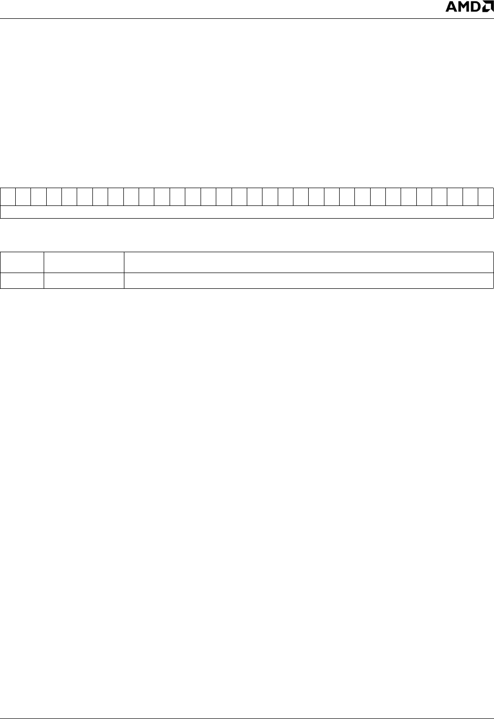
AMD Geode™ LX Processors Data Book 337
Display Controller Register Descriptions 33234H
6.6.7.4 DC Compression FIFO Diagnostic (DC_CFIFO_DIAG)
This register is provided to enable testability of the compressed line buffer (FIFO) RAM. Before it is accessed, the DIAG bit
should be set high (DC Memory Offset 004h[28] = 1) and the DFLE bit should be set low (DC Memory Offset 004h[0] = 0).
Also, the CFRW bit in DC_GENERAL_CFG (DC Memory Offset 004h[29]) should be set appropriately depending on
whether a series of reads or writes is to be performed. After each write, the FIFO write pointer automatically increments.
After all write operations are performed, the CFRW bit should be set high to enable read addresses to the FIFO and a pair
of reads of don't care data should be performed to load 64 bits of data into the output latch. Each subsequent read contains
the appropriate data that was previously written. After each pair of reads, the FIFO read pointer automatically increments.
DC Memory Offset 07Ch
Ty p e R / W
Reset Value xxxxxxxxh
DC_CFIFO_DIAG Register Map
313029282726252423222120191817161514131211109876543210
CFIFO_DATA
DC_CFIFO_DIAG Bit Descriptions
Bit Name Description
31:0 CFIFO_DATA Compressed Data FIFO Diagnostic Read or Write Data.

338 AMD Geode™ LX Processors Data Book
Display Controller Register Descriptions
33234H
6.6.8 Video Downscaling
6.6.8.1 DC Video Downscaling Delta (DC_VID_DS_DELTA)
This register is provided to allow downscaling of the video overlay image by selective skipping of source lines. A DDA
engine is used to identify lines to be skipped according to the following algorithm:
At vertical retrace:
PHASE = 0; // clear PHASE initially
skip_flag = 0; // never skip the first line
linenum = 0; // point to first line
For each line of video: send_video_line(linenum); // send line to DF
linenum++ // increment to next line
{skip_flag, PHASE} = PHASE + DELTA; // skip_flag is carry from add
if (skip_flag) linenum = linenum + 1 // skip an additional line if flag was set
else linenum = linenum // otherwise, just skip n lines
The value to program into DC_VID_DS_DELTA is calculated as follows:
parms: DWORD ORIGINAL_LINES = full size image line count
DWORD SCALED_LINES = line count of scaled image equation:
DWORD DC_VID_DS_DELTA = ((ORIGINAL_LINES << 14) / SCALED_LINES) << 18;
Note: The scaling algorithm is only intended to work for ratios from 1 down to 1/2. The equation above clips the value to
the 14 bits of accuracy in the hardware. The equation could be modified to allow for higher bits in the future by
changing the 14-bit and 18-bit shift values. The only requirement is that the sum of the shift values be 32.
DC Memory Offset 080h
Ty p e R / W
Reset Value 00000000h
DC_VID_DS_DELTA Register Map
313029282726252423222120191817161514131211109876543210
DELTA RSVD
VSYNC_SHIFT_EN
RSVD VSYNC_SHIFT
DC_VID_DS_DELTA Bit Descriptions
Bit Name Description
31:18 DELTA Delta. A 0.14 fixed-point fraction used as the delta value for the DDA engine that calcu-
lates which video lines to skip for video downscaling. This register is enabled when the
VDSE bit in DC_GENERAL_CFG is set (DC Memory Offset 004h[19] = 1).
17:16 RSVD Reserved.
15 VSYNC_SHIFT_
EN
VSYNC Shift Enable. When this bit is set, the VSYNC output is delayed during even
fields in interlaced modes. The amount of delay is defined in VSYNC_SHIFT (bits [11:0]).
14:12 RSVD Reserved.
11:0 VSYNC_SHIFT VSYNC Shift. When VSYNC_SHIFT_EN is set (bit 15 = 1), this field determines the
number of dot clocks of delay that is inserted on VSYNC during even fields in interlaced
modes.
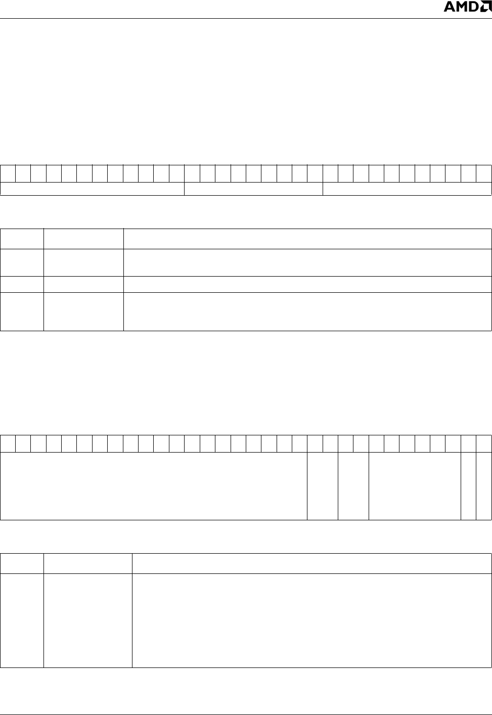
AMD Geode™ LX Processors Data Book 339
Display Controller Register Descriptions 33234H
6.6.9 GLIU Control Registers
6.6.9.1 DC GLIU0 Memory Offset (DC_GLIU0_MEM_OFFSET)
This register is used to set a base address for the graphics memory region. The value in this register is added to all outgo-
ing memory addresses. Because the base address must be aligned to a 16 MB region, only bits [31:24] of this register are
used.
6.6.9.2 DC Dirty/Valid RAM Control (DC_DV_CTL)
DC Memory Offset 084h
Ty p e R / W
Reset Value 00000000h
DC_GLIU0_MEM_OFFSET Register Map
313029282726252423222120191817161514131211109876543210
GLIU0_MEM_OFFSET RSVD DV_RAM_AD
DC_GLIU0_MEM_OFFSET Bit Descriptions
Bit Name Description
31:20 GLIU0_
MEM_OFFSET
GLIU0 Memory Offset. Base address (1 MB aligned) for the graphics memory region.
This value is added to all outgoing memory addresses.
19:11 RSVD Reserved. Equal to 0.
10:0 DV_RAM_AD DV RAM Address. This value is used to allow direct software access to the Dirty/Valid
(DV) RAM. The address must be written in this location before reading or writing the DV
RAM Access Register (DC Memory Offset 08Ch).
DC Memory Offset 088h
Ty p e R / W
Reset Value 00000000h
DC_DV_CTL Register Map
313029282726252423222120191817161514131211109876543210
DV Address Offset
DV_LINE_SIZE
DV_RANGE
RSVD
DV_MASK
CLEAR_DV_RAM
DV_CTL Bit Descriptions
Bit Name Description
31:12 DV Address
Offset
DV Address Offset. When the DV RAM observes memory transactions, the
addresses correspond to memory controller device address space. However, the DV
RAM is organized based on the internal DC device address space. To account for this,
the value indicated by this field is shifted to correspond to address bits [31:12], and
then subtracted from memory addresses before determining an offset into the DV
RAM. When programming the value in this field, software must calculate the sum of the
GLIU0_MEM_OFFSET (DC Memory Offset 084h[31:24] and the appropriate Physical-
to-Device descriptor(s) in GLIU0.
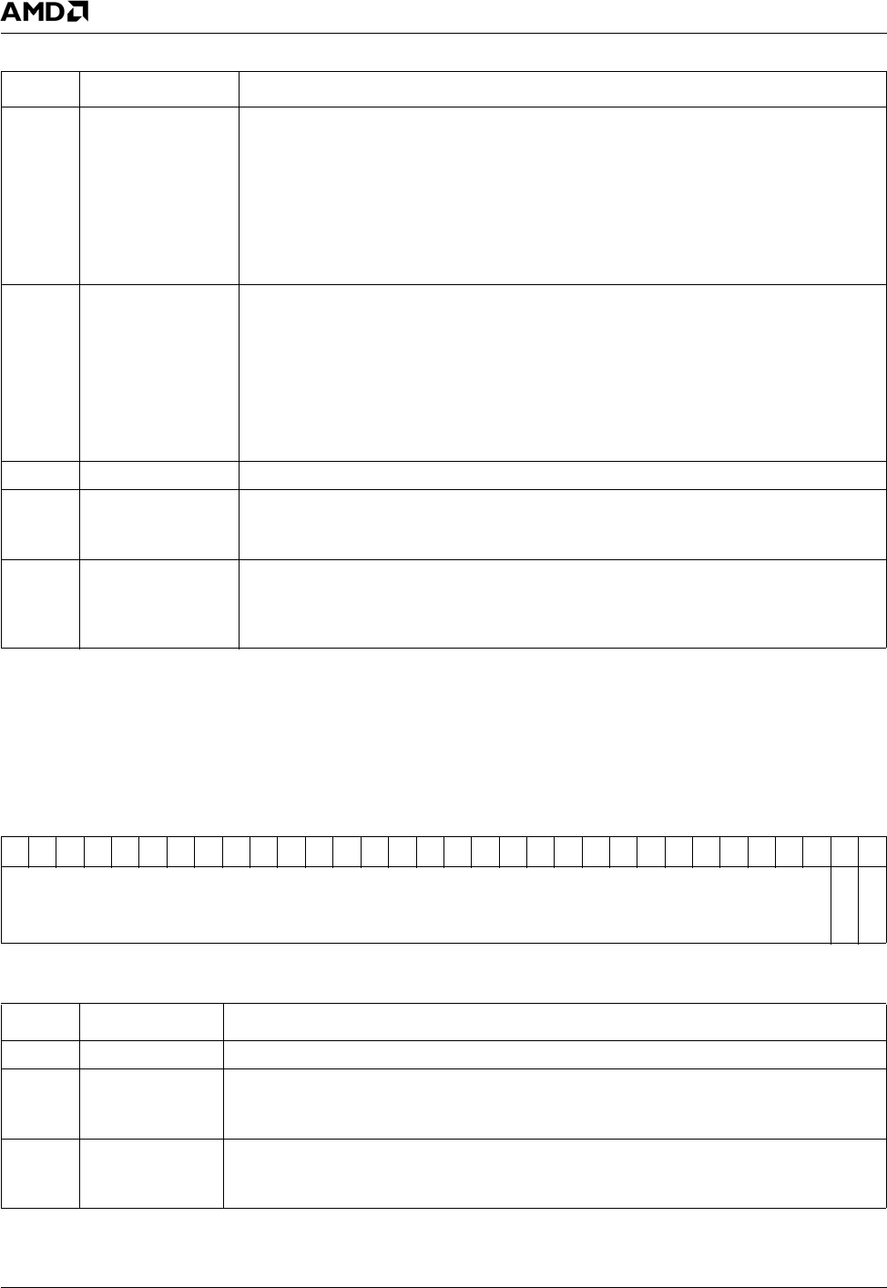
340 AMD Geode™ LX Processors Data Book
Display Controller Register Descriptions
33234H
6.6.9.3 DC Dirty/Valid RAM Access (DC_DV_ACCESS)
11:10 DV_LINE_SIZE DV Line Size. This field determines how many bytes of frame buffer space correspond
to an entry in the DV RAM. The value selected by this field must be greater than or
equal to the FB_LINE_SIZE, as programmed in the DC_LINE_SIZE register (DC Mem-
ory Offset 030h[9:0]).
00: 1024 (256 QWORDs)
01: 2048 (512 QWORDs)
10: 4096 (1024 QWORDs)
11: 8192 (2048 QWORDs)
9:8 DV_RANGE DV Range. The value selected by this field is an upper bound of the number of entries
used in the DV RAM. By setting this value to a number less than the maximum (2048),
there is a potential savings in power, since the DV RAM will not be accessed for lines
that may be just above the frame buffer space.
00: 2048 lines
01: 512 lines
10: 1024 lines
11: 1536 lines
7:2 RSVD Reserved. Set to 0.
1 DV_MASK DV MASK. While this bit is set, the DV RAM controller does not monitor writes to mem-
ory; no DIRTY bits will be set in response to memory activity. When this bit is cleared,
the DV RAM behaves normally.
0 CLEAR_DV_RAM Clear DV RAM. Writing a 1 to this bit causes the contents of the DV RAM to be cleared
(i.e., every entry is set to dirty and invalid). This process requires approximately 2050
GLIU0 clocks. This bit may be read to determine if this clear operation is underway (1)
or completed (0). Writing a 0 to this bit has no effect.
DC Memory Offset 08Ch
Ty p e R / W
Reset Value 0000000xh
DV_CTL Bit Descriptions (Continued)
Bit Name Description
DC_DV_ACCESS Register Map
313029282726252423222120191817161514131211109876543210
RSVD
DV_VALID
DV_DIRTY
DC_DV_ACCESS Bit Descriptions
Bit Name Description
31:2 RSVD Reserved. Set to 0.
1DV_VALID DV Valid. Writes to this register place the value of this bit into the “valid” entry of the DV
RAM. Reads return the value of the “valid” entry. The DV RAM Address is determined by
the value in DV_RAM_AD (DC Memory Offset 084h[10:0]).
0DV_DIRTY DV Dirty. Writes to this register will place the value of this bit into the “dirty” entry of the
dirty/valid RAM. Reads will return the value of the “dirty” entry. The DV RAM Address is
determined by the value in DV_RAM_AD (DC Memory Offset 084h[10:0]).
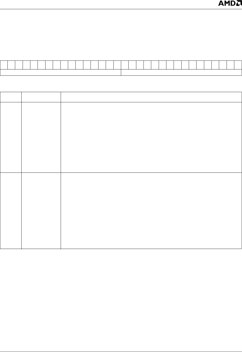
AMD Geode™ LX Processors Data Book 341
Display Controller Register Descriptions 33234H
6.6.10 Graphics Scaling Control Registers
6.6.10.1 DC Graphics Filter Scale (DC_GFX_SCALE)
DC Memory Offset 090h
Ty p e R / W
Reset Value 40004000h
DC_GFX_SCALE Register Map
313029282726252423222120191817161514131211109876543210
V_SCALE H_SCALE
DC_GFX_SCALE Bit Descriptions
Bit Name Description
31:16 V_SCALE Vertical Filter Scale. The value in this field, represents the number of vertical lines of
source data that are consumed for every line of filtered data produced by the scaler filter.
This field is treated as a rational number, with the decimal point between bits 30 and 29.
To determine the value to be programmed into this field, use the following formula:
V_SCALE = (V_SOURCE / (V_DEST-1)) << 14
Where V_SOURCE is the height (in scan lines) of the frame buffer and V_DEST is the
height (in scan lines) of the destination field.
The default value of this field (4000h) represents 1:1 scaling. This value must be pro-
grammed when the vertical filter is disabled.
The value in this field must not exceed 8000h, which represents a 2:1 downscale ratio. If
the width of the source image is more than 1024 pixels, scaling is not supported.
15:0 H_SCALE Horizontal Filter Scale. The value in this field, represents the number of (horizontal) pix-
els of source data that are consumed for every pixel of data produced by the scaler filter.
This field is treated as a rational number, with the decimal point between bits 14 and 13.
To determine the value to be programmed into this field, use the following formula:
H_SCALE = (H_SOURCE/(H_DEST-1)) << 14
Where H_SOURCE is the width (in pixels) of the frame buffer and H_DEST is the width
(in pixels) of the destination image.
The default value of this field (4000h) represents 1:1 scaling. This value must be pro-
grammed when the horizontal filter is disabled.
The value in this field must never exceed 8000h, which represents a 2:1 horizontal down-
scale. If the width of the source image is greater than 1024 pixels, scaling is not sup-
ported.
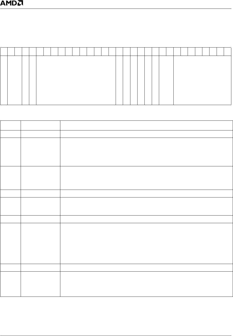
342 AMD Geode™ LX Processors Data Book
Display Controller Register Descriptions
33234H
6.6.10.2 DC IRQ/Filter Control (DC_IRQ_FILT_CTL)
DC Memory Offset 094h
Ty p e R / W
Reset Value 00000000h
DC_IRQ_FILT_CTL Register Map
313029282726252423222120191817161514131211109876543210
RSVD
LINEBUF_SEL
INTERLACE_ADDRESSING
RSVD
LINE_COUNT
RSVD
ALPHA_FILT_ENA
RSVD
FILT_ENA
INTL_EN
H_FILT_SEL
RSVD FILT_ADDR
DC_IRQ_FILT_CTL Bit Descriptions
Bit Name Description
31 RSVD Reserved.
30:29 LINEBUF_SEL Line Buffer Select. When LINEBUF_REG_EN[0] is set (bit 9 = 1), the coefficient RAM
address bits (FILT_ADDR, bits [7:0) and the Filter Coefficient Data registers (DC Memory
Offset 098h and 09Ch) can be used to read and write the line buffer or flicker filter RAMs.
This field selects which of the three line buffer RAMS (or two flicker filter RAMs) is to be
accessed.
28 INTERLACE_
ADDRESSING
Interlace Addressing. This bit indicates whether each field should be vertically deci-
mated when interlacing. If this bit is set, each field of the interlaced frame will include
every other line of the original (unscaled) frame buffer image. The flicker filter and scaler
filter should both be disabled if this bit is set.
27 RSVD Reserved.
26:16 LINE_COUNT Interrupt Line Count. This value determines which scan line will trigger a line count
interrupt. When the DC’s display engine reaches the line number determined by this
value, it will assert an interrupt if IRQ_MASK is cleared (DC Memory Offset 0C8h[0] = 0).
15 RSVD Reserved.
14 ALPHA_FILT_
ENA
Alpha Filter Enable. Settings written to this field will not take effect until the start of the
following frame or interlaced field.
Setting this bit to 1 enables the scaler filter for the alpha channel. This filter is provided to
support scaling and interlacing of graphics data. If the graphics filter is disabled or this bit
is cleared, the alpha channel is not filtered; a nearest-neighbor mechanism is used
instead. This can provide cleaner transitions between regions with significantly different
alpha values.
13 RSVD Reserved.
12 FILT_ENA Graphics Filter Enable. Settings written to this field will not take effect until the start of
the following frame or interlaced field.
Setting this bit to 1 enables the graphics scaler filter; This filter is provided to support
scaling and interlacing of graphics data.
AMD Geode™ LX Processors Data Book 343
Display Controller Register Descriptions 33234H
6.6.10.3 DC Filter Coefficient Data Register 1 (DC_FILT_COEFF1)
Any read or write of this register causes a read or write of the horizontal or filter coefficient RAM. If this occurs while the dis-
play is active, improper filtering of an output pixel can occur, which may cause temporary visual artifacts (speckling). To
avoid this, either disable the display or avoid accessing this register unless during vertical blank.
11 INTL_EN Interlace Enable. Settings written to this field will not take effect until the start of the fol-
lowing frame or interlaced field.
Setting this bit to 1 configures the output to interlaced mode. In this mode, the vertical
timings are based on the even timing registers for every other field. This bit must be set if
the flicker filter or address interlacing is enabled.
When using the VGA and interlacing, the scaler must also be used (i.e., bit 12 of this reg-
ister must be set).
10 H_FILT_SEL Horizontal Filter Select. Setting this bit to 1 allows access to the horizontal filter coeffi-
cients via this register and the Filter Data Registers (DC Memory Offset 098h and 09Ch).
When this bit is cleared, the vertical filter coefficients are accessed instead.
9:8 RSVD Reserved.
7:0 FILT_ADDR Filter Coefficient Address. This indicates which filter location is accessed through
reads and writes of the DC Filter Coefficient Data Register 1 (DC Memory Offset 098h).
DC Memory Offset 098h
Ty p e R / W
Reset Value xxxxxxxxh
DC_IRQ_FILT_CTL Bit Descriptions (Continued)
Bit Name Description
DC_FILT_COEFF1 Register Map
313029282726252423222120191817161514131211109876543210
RSVD TAP3 TAP2 TAP1
DC_ FILT_COEFF1 Bit Descriptions
Bit Name Description
31:30 RSVD Reserved. Set to 0.
29:20 TAP3 Tap 3 Coefficient. This coefficient is used for the third tap in the filter (the lower tap of
the vertical filter or the center tap of the horizontal filter). Each of the four components of
the pixel color (Red, Green, Blue, and Alpha, if available) is expanded to 8 bits and then
multiplied by this value before being summed with the weighted results of the other filter
taps.
19:10 TAP2 Tap 2 Coefficient. This coefficient is used for the second tap in the filter (the center tap
of the vertical filter or the second tap from the left in the horizontal filter).
9:0 TAP1 Tap 1 Coefficient. This coefficient is used for the first tap in the filter (the upper tap of the
vertical filter or the leftmost tap of the horizontal filter).
344 AMD Geode™ LX Processors Data Book
Display Controller Register Descriptions
33234H
6.6.10.4 DC Filter Coefficient Data Register 2 (DC_FILT_COEFF2)
Any read or write of this register causes a read or write of the horizontal or filter coefficient RAM. If this occurs while the dis-
play is active, improper filtering of an output pixel can occur, which may cause temporary visual artifacts (speckling). To
avoid this, either disable the display or avoid accessing this register unless during vertical blank.
6.6.11 VBI Control Registers
6.6.11.1 DC VBI Even Control (DC_VBI_EVEN_CTL)
Settings written to this register do not take effect until the start of the following frame or interlaced field.
DC Memory Offset 09Ch
Ty p e R / W
Reset Value xxxxxxxxh
DC_FILT_COEFF2 Register Map
313029282726252423222120191817161514131211109876543210
RSVD TAP5 TAP4
DC_FILT_COEFF2 Bit Descriptions
Bit Name Description
31:20 RSVD Reserved. Set to 0. This field is used only when reading or writing the Line Buffer Regis-
ter.
19:10 TAP5 Tap 5 Coefficient. This coefficient is used for the fifth tap (rightmost) in the horizontal fil-
ter.
9:0 TAP4 Tap 4 Coefficient. This coefficient is used for the fourth tap (second from the right) in the
horizontal filter.
DC Memory Offset 0A0h
Ty p e R / W
Reset Value xxxxxxxxh
DC_VBI_EVEN_CTL Register Map
313029282726252423222120191817161514131211109876543210
VBI_SIG_EN
VBI_16
VBI_UP
VBI_ENA
VBI_EVEN_OFFSET 0
DC_VBI_EVEN_CTL Bit Descriptions
Bit Name Description
31 VBI_SIG_EN VBI Signature Enable. This bit allows the CRC engine at the output of the DC to be
used to check VBI data instead of graphics data. When this bit is set, the CRC is gener-
ated based only on VBI data; when cleared, only graphics data is used for the CRC cal-
culation.
30 VBI_16 VBI 16-bit Enable. When set, VBI data is sent 16 bits per Dot clock. When clear, VBI
data is sent 8 bits per Dot clock.
29 VBI_UP VBI Upscale. When set, the VBI data is upscaled by 2. This is accomplished by repeat-
ing data twice.

AMD Geode™ LX Processors Data Book 345
Display Controller Register Descriptions 33234H
6.6.11.2 DC VBI Odd Control (DC_VBI_ODD_CTL)
Settings written to this register do not take effect until the start of the following frame or interlaced field.
6.6.11.3 DC VBI Horizontal Control (DC_VBI_HOR)
Settings written to this register do not take effect until the start of the following frame or interlaced field.
28 VBI_ENA VBI Enable. Setting this bit to 1 enables VBI (Vertical Blank Interrupt) data. This is a data
stream that is placed in the off-screen region at the start of each field. This data is passed
through the graphics output path, but is not filtered or modified in any way.
27:0 VBI_EVEN_
OFFSET
VBI Even Address Offset. Indicates the starting offset for VBI data for even fields. This
address must be QWORD aligned; the low three bits are always 0. If interlacing is dis-
abled, this offset is used for VBI data.
DC Memory Offset 0A4h
Ty p e R / W
Reset Value xxxxxxxxh
DC_VBI_EVEN_CTL Bit Descriptions (Continued)
Bit Name Description
DC_VBI_ODD_CTL Register Map
313029282726252423222120191817161514131211109876543210
RSVD VBI_ODD_OFFSET 0
DC_VBI_ODD_CTL Bit Descriptions
Bit Name Description
31:28 RSVD Reserved. Set to 0.
27:0 VBI_ODD_
OFFSET
VBI Odd Address Offset. Indicates the starting offset for VBI data for odd fields. This
address must be QWORD aligned; the low three bits are always 0. If interlacing is dis-
abled, the even offset is used for VBI data.
DC Memory Offset 0A8h
Ty p e R / W
Reset Value xxxxxxxxh
DC_VBI_HOR Register Map
313029282726252423222120191817161514131211109876543210
RSVD VBI_H_END RSVD VBI_H_START
DC_VBI_HOR Bit Descriptions
Bit Name Description
31:28 RSVD Reserved. Set to 0.
27:16 VBI_H_END VBI Horizontal End. Specifies the horizontal end position for VBI data minus 1 pixel.
15:12 RSVD Reserved. Set to 0.
11:0 VBI_H_START VBI Horizontal Start. Specifies the horizontal start position for VBI data minus 1 pixel.

346 AMD Geode™ LX Processors Data Book
Display Controller Register Descriptions
33234H
6.6.11.4 DC VBI Odd Line Enable (DC_VBI_LN_ODD)
Settings written to this register do not take effect until the start of the following frame or interlaced field.
6.6.11.5 DC VBI Even Line Enable (DC_VBI_LN_EVEN)
Settings written to this register do not take effect until the start of the following frame or interlaced field.
DC Memory Offset 0ACh
Ty p e R / W
Reset Value xxxxxxxxh
DC_VBI_LN_ODD Register Map
313029282726252423222120191817161514131211109876543210
LN_OFFSET_ODD LN_EN_ODD RSVD
DC_VBI_LN_ODD Bit Descriptions
Bit Name Description
31:25 LN_OFFSET_
ODD
Odd Line Offset. Specifies the offset (in lines) of the start of VBI data from the initial
edge of VSYNC. This field is not used if interlacing is disabled. This field must be set to a
value of 126 or less.
24:2 LN_EN_ODD Odd Line Enable. Each of the bits in this field corresponds to a line (24-2) of VBI data.
Setting a bit in this field to 1 enables the corresponding line of VBI data in the odd field.
This field is not used if interlacing is disabled.
1:0 RSVD Reserved. Set to 0.
DC Memory Offset 0B0h
Ty p e R / W
Reset Value xxxxxxxxh
DC_VBI_LN_EVEN Register Map
313029282726252423222120191817161514131211109876543210
LN_OFFSET_EVEN LN_EN_EVEN RSVD
DC_VBI_LN_EVEN Bit Descriptions
Bit Name Description
31:25 LN_OFFSET_
EVEN
Even Line Offset. Specifies the offset (in lines) of the start of VBI data from the initial
edge of VSYNC. This field is used for all frames if interlacing is disabled. This field must
be set to a value of 126 or less.
24:2 LN_EN_EVEN Even Line Enable. Each of the bits in this field corresponds to a line (24-2) of VBI data.
Setting a bit in this field to 1 enables the corresponding line of VBI data in the even field.
This field is used for all frames if interlacing is disabled.
1:0 RSVD Reserved. Set to 0.
AMD Geode™ LX Processors Data Book 347
Display Controller Register Descriptions 33234H
6.6.11.6 DC VBI Pitch and Size (DC_VBI_PITCH)
6.6.12 Color Key Control Registers
6.6.12.1 DC Color Key (DC_CLR_KEY)
DC Memory Offset 0B4h
Ty p e R / W
Reset Value xxxxxxxxh
DC_VBI_PITCH Register Map
313029282726252423222120191817161514131211109876543210
RSVD VBI_Size VBI_Pitch
DC_VBI_PITCH Bit Descriptions
Bit Name Description
31:26 RSVD Reserved. Set to 0.
25:16 VBI_SIZE VBI Data Size. Indicates how many QWORDs of data to fetch from memory for each line
of VBI
15:0 VBI_PITCH VBI Data Pitch. Indicates how many QWORDs of memory space to increment when
moving from the start of one active VBI line to the start of the next.
DC Memory Offset 0B8h
Ty p e R / W
Reset Value 00000000h
DC_CLR_KEY Register Map
313029282726252423222120191817161514131211109876543210
RSVD
CLR_KEY_EN
CLR_KEY
DC_CLR_KEY Bit Descriptions
Bit Name Description
31:25 RSVD Reserved. Set to 0.
24 CLR_KEY_EN Color Key Enable. This bit enables color key detection in the DC. When this bit is set,
the DC adjusts the alpha value of pixels whose 24-bit RGB values match the value in
CLR_KEY (bits [23:0]). A mask is also provided in CLR_KEY_MASK (DC Memory Offset
0BCh[23:0]) to indicate which bits can be ignored when performing this match. Color key
detection is performed after the data has been decompressed and the cursor has been
overlayed, but before scaling and filtering take place.
23:0 CLR_KEY Color Key. This field represents the RGB value that will be compared to DC pixels when
performing color key detection.
348 AMD Geode™ LX Processors Data Book
Display Controller Register Descriptions
33234H
6.6.12.2 DC Color Key Mask (DC_CLR_KEY_MASK)
6.6.12.3 DC Color Key Horizontal Position (DC_CLR_KEY_X)
Settings written to this register do not take effect until the start of the following frame or interlaced field.
6.6.12.4 DC Color Key Vertical Position (DC_CLR_KEY_Y)
Settings written to this register do not take effect until the start of the following frame or interlaced field.
DC Memory Offset 0BCh
Ty p e R / W
Reset Value 00xxxxxxh
DC_CLR_KEY_MASK Register Map
313029282726252423222120191817161514131211109876543210
RSVD CLR_KEY_MASK
DC_CLR_KEY_MASK Bit Descriptions
Bit Name Description
31:24 RSVD Reserved. Set to 0.
23:0 CLR_KEY_
MASK
Color Key Mask. This field is ANDed with both the pixel and the color key value (in
DC_CLR_KEY, DC Memory Offset 0B8h[23:0]) before comparing the values. This allows
the value of some bits to be ignored when performing the match.
DC Memory Offset 0C0h
Ty p e R / W
Reset Value 00000000h
DC_CLR_KEY_X Register Map
313029282726252423222120191817161514131211109876543210
RSVD CLR_KEY_X_END RSVD CLR_KEY_X_START
DC_CLR_KEY_X Bit Descriptions
Bit Name Description
31:27 RSVD Reserved. Set to 0.
26:16 CLR_KEY_X_
END
Color Key Horizontal End. This field indicates the horizontal end position of the color
key region minus 1.This represents the first pixel past the end of the color key region.
This field is 0-based; the upper left pixel of the screen is represented by (0,0).
15:11 RSVD Reserved. Set to 0.
10:0 CLR_KEY_X_
START
Color Key Horizontal Start. This field represents the horizontal start position of the color
key region minus 1. This represents the first pixel within the color key region.
DC Memory Offset 0C4h
Ty p e R / W
Reset Value 00000000h
DC_CLR_KEY_Y Register Map
313029282726252423222120191817161514131211109876543210
RSVD CLR_KEY_Y_END RSVD CLR_KEY_Y_START
AMD Geode™ LX Processors Data Book 349
Display Controller Register Descriptions 33234H
6.6.12.5 DC Interrupt (DC_IRQ)
DC_CLR_KEY_Y Bit Descriptions
Bit Name Description
31:27 RSVD Reserved. Set to 0.
26:16 CLR_KEY_Y_
END
Color Key Vertical End. This field represents the vertical end position of the color key
region minus 1. This represents the first line past the end of the color key region.
15:11 RSVD Reserved. Set to 0.
10:0 CLR_KEY_Y_
START
Color Key Vertical Start. This field represents the vertical start position of the color key
region minus 1. This represents the first line within the color key region.
DC Memory Offset 0C8h
Ty p e R / W
Reset Value 00000003h
DC_IRQ Register Map
313029282726252423222120191817161514131211109876543210
RSVD
VIP_VSYNC_LOSS_IRQ
IRQ
RSVD
VIP_VSYNC_LOSS_IRQ_MASK
IRQ_MASK
DC_IRQ Bit Descriptions
Bit Name Description
31:18 RSVD Reserved. Set to 0.
17 VIP_VSYNC_
LOSS_IRQ
VIP VSYNC Loss IRQ. If set to 1, this field indicates that while GenLock was enabled,
GenLock timeout was enabled, and the DC reached the end of a frame and detected
VIP_VIDEO_OK (DC Memory Offset D4h[23]) inactive. As a result of this condition, the
DC began display of a field/frame based on its own timings.
16 IRQ IRQ Status. If set to 1, this field indicates that the vertical counter has reached the value
set in the IRQ/Filter Control Register. The state of the IRQ_MASK, bit 0, will not prevent
this bit from being set. To clear the interrupt, write a 1 to this bit.
15:2 RSVD Reserved. Set to 0.
1 VIP_VSYNC_
LOSS_IRQ_
MASK
VIP VSYNC Loss IRQ Mask. Masks generation of an interrupt in the event that the DC
reaches the end of a frame with GenLock enabled and GenLock timeout enabled and
determines that the VIP_VIDEO_OK (DC Memory Offset D4h[23]) input is inactive.
0 IRQ_MASK IRQ Mask. Setting this bit to 1 prevents the Display Controller from generating an inter-
rupt signal when the vertical counter reaches the value programmed in
DC_IRQ_FILT_CTL (DC Memory Offset 094h). Clearing this bit disables interrupt gener-
ation, but will NOT prevent IRQ, bit 16, from being set.
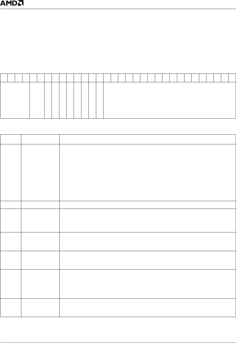
350 AMD Geode™ LX Processors Data Book
Display Controller Register Descriptions
33234H
6.6.13 Interrupt and GenLock Registers
6.6.13.1 DC GenLock Control (DC_GENLK_CTL)
Settings written to this register do not take effect until the start of the frame or interlaced field after the timing register
update bit (DC Memory Offset 008h[6]) is set.
DC Memory Offset 0D4h
Ty p e R / W
Reset Value xxxxxxxxh
DC_GENLK_CTL Register Map
313029282726252423222120191817161514131211109876543210
FLICK_SEL RSVD
ALPHA_FLICK_EN
FLICK_EN
VIP_VIDEO_OK
GENLOCK_ACTIVE
SKEW_WAIT
VIP_VSYNC_WAIT
GENLK_TO_EN
GENLK_EN
GENLK_SKW
DC_GENLK_CTL Bit Descriptions
Bit Name Description
31:28 FLICK_SEL Flicker Filter Select. When the flicker filter is enabled (FLICK_EN, bit 24 = 1), this field
selects the weighting of the three taps in this vertical filter:
0000: 0, 1, 0 (top, middle, bottom)
0001: 1/16, 7/8, 1/16
0010: 1/8, 3/4, 1/8
0100: 1/4, 1/2, 1/4
0101: 5/16, 3/8, 5/16
All other combinations in this field are reserved.
27:26 RSVD Reserved. Set to 0.
25 ALPHA_FLICK_
EN
Alpha Flicker Filter Enable. If set, this bit enables flicker filtering of the alpha value
when the flicker filter is enabled (FLICK_EN, bit 24 = 1). If the flicker filter is enabled and
this bit is cleared, the alpha value of the center pixel is passed through the flicker filter
unchanged.
24 FLICK_EN Flicker Filter Enable. Enables the 3-tap vertical flicker filter (primarily used for interlaced
modes). When set, the graphics output is filtered vertically using the coefficients as indi-
cated in bits [22:21]. When clear, no flicker filtering is performed.
23 VIP_VIDEO_OK
(RO)
VIP Video OK (Read Only). This bit indicates the state of the internal VIP VIDEO_OK
input. This signal is driven by the VIP to indicate that the VIP is detecting a valid input
stream.
22 GENLOCK_
ACTIVE (RO)
GenLock Active (Read Only). This bit indicates that the current (or most recent) field/
frame was initiated as the result of an active VIP VSYNC. The state of this bit will change
coincident with the activation of the VSYNC output. If the VSYNC output occurs as the
result of a timeout condition, this bit will be cleared. If GenLock is not enabled
(GENLK_EN, bit 18 = 0), this bit will be cleared.
21 SKEW_WAIT
(RO)
Skew Wait (Read Only). This status bit indicates that the DC has received a VSYNC
from the VIP and that the skew counter is running. This bit is set when the VIP_VSYNC
input is set and cleared when the skew counter expires.

AMD Geode™ LX Processors Data Book 351
Display Controller Register Descriptions 33234H
6.6.14 Even Field Video Address Registers
6.6.14.1 DC Even Field Video Y Start Address Offset (DC_VID_EVEN_Y_ST_OFFSET)
Settings written to this register do not take effect until the start of the next even interlaced field.
20 VIP_VSYNC_
WAIT (RO)
VIP VSYNC Wait (Read Only). If set to 1 this status bit indicates that the DC has com-
pleted a field or frame and is waiting for the VIP’s VSYNC to go active before beginning
another frame. Typically, this will occur only if the VIP_VIDEO_OK (bit 23) input is active
or the GENLOCK_TO _EN (bit 19) is inactive.
19 GENLK_TO_EN GenLock Time Out Enable. Setting this bit allows the DC to revert to its own internal
timer if a loss of sync is detected by the VIP. This allows for seamless operation of the
DC in GenLock mode when the VIP input becomes unstable. Clearing this bit forces the
DC to wait for a VSYNC signal from the VIP even if the VIP indicates a loss of sync.
18 GENLK_EN GenLock Enable. When set to 1, the DC resets to the start of the frame/field upon
receipt of a rising edge on the VIP_VSYNC signal.
17:0 GENLK_SKW GenLock Skew. This value indicates how many Dot clocks to delay the internal recogni-
tion of the VIP VSYNC by the DC when GenLock is enabled. If GenLock timeout is also
enabled (GENLK_TO_EN, bit 19 = 1), internal recognition of VSYNC occurs immediately
upon timeout (without allowing this skew time to elapse after the timeout is detected.)
This allows seamless transition from a VIP-supplied VSYNC to an internally-determined
VSYNC, while still allowing for a delay in timeout detection.
DC Memory Offset 0D8h
Ty p e R / W
Reset Value xxxxxxxxh
DC_GENLK_CTL Bit Descriptions (Continued)
Bit Name Description
DC_VID_EVEN_Y_ST_OFFSET Register Map
313029282726252423222120191817161514131211109876543210
RSVD OFFSET
DC_VID_EVEN_Y_ST_OFFSET Bit Descriptions
Bit Name Description
31:28 RSVD Reserved. Set to 0.
27:0 OFFSET Video Y Even Buffer Start Offset. This value represents the starting location for Video
Y Buffer for even fields when interlacing is enabled. This field is not used when interlac-
ing is disabled (DC Memory Offset 094h[11] = 0).
This value represents the starting location for Video Y Buffer for even fields when inter-
lacing is enabled (DC Memory Offset 094h[11] = 1). The lower five bits should always be
programmed as zero so that the start offset is aligned to a 32-byte boundary. If YUV
4:2:2 mode is selected (DC Memory Offset 004h[20] = 0), the Video Y Buffer is used as a
singular buffer holding interleaved Y, U and V data. If YUV 4:2:0 is selected (DC Memory
Offset 004h[20] = 1), the Video Y Buffer is used to hold only Y data while U and V data
are stored in separate buffers.
352 AMD Geode™ LX Processors Data Book
Display Controller Register Descriptions
33234H
6.6.14.2 DC Even Field Video U Start Address Offset (DC_VID_EVEN_U_ST_OFFSET)
Settings written to this register do not take effect until the start of the next even interlaced field.
6.6.14.3 DC Even Field Video V Start Address Offset (DC_VID_EVEN_V_ST_OFFSET)
Settings written to this register do not take effect until the start of the next even interlaced field.
DC Memory Offset 0DCh
Ty p e R / W
Reset Value xxxxxxxxh
DC_VID_EVEN_U_ST_OFFSET Register Map
313029282726252423222120191817161514131211109876543210
RSVD OFFSET
DC_VID_EVEN_U_ST_OFFSET Bit Descriptions
Bit Name Description
31:28 RSVD Reserved. Set to 0.
27:0 OFFSET Video U Even Buffer Start Offset. This value represents the starting location for Video
U Buffer for even fields when interlacing is enabled (DC Memory Offset 094h[11] = 1)
and YUV 4:2:0 mode is selected (DC Memory Offset 004h[20] = 1). The lower five bits
should always be programmed as zero so that the start offset is aligned to a 32-byte
boundary.
DC Memory Offset 0E0h
Ty p e R / W
Reset Value xxxxxxxxh
DC_VID_EVEN_V_ST_OFFSET Register Map
313029282726252423222120191817161514131211109876543210
RSVD OFFSET
DC_VID_EVEN_V_ST_OFFSET Bit Descriptions
Bit Name Description
31:28 RSVD Reserved. Set to 0.
27:0 OFFSET Video V Even Buffer Start Offset. This value represents the starting location for Video
V Buffer for even fields when interlacing is enabled (DC Memory Offset 094h[11] = 1) and
YUV 4:2:0 is selected (DC Memory Offset 004h[20] = 1). The lower five bits should
always be programmed as zero so that the start offset is aligned to a 32-byte boundary.
AMD Geode™ LX Processors Data Book 353
Display Controller Register Descriptions 33234H
6.6.15 Even Field Vertical Timing Registers
6.6.15.1 DC Vertical and Total Timing for Even Fields (DC_V_ACTIVE_EVEN_TIMING)
This register contains vertical active and total timing information. These parameters pertain ONLY to even fields in inter-
laced display modes (The DC_V_ACTIVE_TIMING register (DC Memory Offset 050h) will take effect for odd fields in inter-
laced display modes.) Settings written to this register will not take effect until the start of the frame or interlaced field after
the timing register update bit is set (DC Memory Offset 008h[6] = 1).
DC Memory Offset 0E4h
Ty p e R / W
Reset Value xxxxxxxxh
DC_V_ACTIVE_EVEN_TIMING Register Map
313029282726252423222120191817161514131211109876543210
RSVD V_TOTAL RSVD V_ACTIVE
DC_V_ACTIVE_EVEN_TIMING Bit Descriptions
Bit Name Description
31:27 RSVD Reserved. These bits should be programmed to zero.
26:16 V_TOTAL Vertical Total. This field represents the total number of lines for a given frame scan
minus 1. Note that the value is necessarily greater than the V_ACTIVE field (bits 10:0])
because it includes border lines and blanked lines.
15:11 RSVD Reserved. These bits should be programmed to zero.
10:0 V_ACTIVE Vertical Active. This field represents the total number of lines for the displayed portion of
a frame scan minus 1. Note that for flat panels, if this value is less than the panel active
vertical resolution (V_PANEL), the parameters V_BLANK_START, V_BLANK_END,
V_SYNC_START, and V_SYNC_END should be reduced by the following value
(V_ADJUST) to achieve vertical centering:
V_ADJUST = (V_PANEL - V_ACTIVE) / 2
If graphics scaling is enabled (and interleaved display is enabled), this value represents
the height of the final (scaled) field to be displayed. The height of the frame buffer image
may be different in this case; FB_ACTIVE (DC Memory Offset 5Ch) is used to program
the horizontal and vertical active values in the frame buffer when graphics scaling is
enabled.
354 AMD Geode™ LX Processors Data Book
Display Controller Register Descriptions
33234H
6.6.15.2 DC CRT Vertical Blank Timing for Even Fields (DC_V_BLANK_EVEN_TIMING)
This register contains vertical blank timing information. All values are specified in lines. This register is used ONLY for even
fields in interlaced display modes. Settings written to this register do not take effect until the start of the frame or interlaced
field after the timing register update bit is set (DC Memory Offset 008h[6] = 1).
6.6.15.3 DC CRT Vertical Sync Timing for Even Fields (DC_V_SYNC_EVEN_TIMING)
This register contains CRT vertical sync timing information. All values are specified in lines. This register is used ONLY for
even fields in interlaced modes. Settings written to this register do not take effect until the start of the frame or interlaced
field after the timing register update bit is set (DC Memory Offset 008h[6] = 1).
DC Memory Offset 0E8h
Ty p e R / W
Reset Value xxxxxxxxh
DC_V_BLANK_EVEN_TIMING Register Map
313029282726252423222120191817161514131211109876543210
RSVD V_BLANK_END RSVD V_BLANK_START
DC_V_BLANK_EVEN_TIMING Bit Descriptions
Bit Name Description
31:27 RSVD Reserved. These bits should be programmed to zero.
26:16 V_BLANK_END Vertical Blank End. This field represents the line at which the vertical blanking signal
becomes inactive minus 1. If the display is interlaced, no border is supported, so this
value should be identical to V_TOTAL (DC Memory Offset 0E4h[26:16]).
15:11 RSVD Reserved. These bits should be programmed to zero.
10:0 V_BLANK_
START
Vertical Blank Start. This field represents the line at which the vertical blanking signal
becomes active minus 1. If the display is interlaced, this value should be programmed to
V_ACTIVE (DC Memory Offset 0E4h[10:0]) plus 1.
DC Memory Offset 0ECh
Ty p e R / W
Reset Value xxxxxxxxh
DC_V_SYNC_EVEN_TIMING Register Map
313029282726252423222120191817161514131211109876543210
RSVD V_SYNC_END RSVD V_SYNC_START
DC_V_SYNC_EVEN_TIMING Bit Descriptions
Bit Name Description
31:27 RSVD Reserved. These bits should be programmed to zero.
26:16 V_SYNC_END Vertical Sync End. This field represents the line at which the CRT vertical sync signal
becomes inactive minus 1.
15:11 RSVD Reserved. These bits should be programmed to zero.
10:0 V_SYNC_
START
Vertical Sync Start. This field represents the line at which the CRT vertical sync signal
becomes active minus 1. For interlaced display, note that the vertical counter is incre-
mented twice during each line and since there are an odd number of lines, the vertical
sync pulse will trigger in the middle of a line for one field and at the end of a line for the
subsequent field.
AMD Geode™ LX Processors Data Book 355
Display Controller Register Descriptions 33234H
6.6.16 VGA Block Configuration Registers
6.6.16.1 VGA Configuration (VGA_CONFIG)
This register controls palette write operations.
6.6.16.2 VGA Status (VGA_STATUS)
This register provides status information for the individual SMI events enabled in the VGA_CONFIG register (DC Memory
Offset 100h), as well as certain other status bits. Reading this register clears all active events.
DC Memory Offset 100h
Ty p e R / W
Reset Value 00000000h
VGA_CONFIG Register Map
313029282726252423222120191817161514131211109876543210
RSVD
WPPAL
VGA_CONFIG Bit Descriptions
Bit Name Description
31:1 RSVD Reserved. Set to 0.
0 WPPAL Write Protect Palette. If set to 1, VGA palette write operations are NOT written to the
palette RAMs. Palette writes behave normally, except that the data is discarded.
DC Memory Offset 104h
Ty p e RO
Reset Value 00000000h
VGA_STATUS Register Map
313029282726252423222120191817161514131211109876543210
RSVD BLINK_CNT RSVD V_CNT RSVD
VSYNC
DISPEN
CRTCIO_SMI
VBLANK_SMI
ISR0_SMI
MISC_SMI
VGA_STATUS Bit Descriptions
Bit Name Description
31:30 RSVD Reserved.
29:24 BLINK_CNT Blink Counter Value. Unsynchronized, used as a simulation aid.
23:22 RSVD Reserved.
21:12 V_CNT Vertical Counter Value. Unsynchronized, used as a simulation aid.
11:6 RSVD Reserved.
5 VSYNC VSYNC. 1 If VSYNC is active (copy of bit 3 of ISR1).
4DISPEN Display Enable. 0 if both horizontal and vertical display enable are active (copy of bit 0
of ISR1).
3 CRTCIO_SMI CRTC Register SMI. If = 1, an SMI was generated due to an I/O read or write to an non-
implemented CRTC register.

356 AMD Geode™ LX Processors Data Book
Display Controller Register Descriptions
33234H
6.6.17 VGA Block Standard Registers
6.6.17.1 VGA Miscellaneous Output
2 VBLANK_SMI VBLANK SMI. If = 1, an SMI was generated due to leading edge vertical blank.
1 ISR0_SMI Input Status Register 0 SMI. If = 1, an SMI was generated from an I/O IN to Input Status
Register 0.
0MISC_SMI Miscellaneous Output Register SMI. If = 1, an SMI was generated from an I/O OUT to
the Miscellaneous Output Register.
Read Address 3CCh
Write Address 3C2h
Ty p e R / W
Reset Value 02h
VGA_STATUS Bit Descriptions (Continued)
Bit Name Description
VGA Miscellaneous Output Register Bit Descriptions
Bit Name Description
7 VSYNC_POL Vertical Sync Polarity. Selects a positive-going VSYNC pulse (bit = 0) or a negative-
going VSYNC pulse (bit = 1).
6 HSYNC_POL Horizontal Sync Polarity. Selects a positive-going HSYNC pulse (bit = 0) or a negative-
going HSYNC pulse (bit = 1).
5PAGE Page Bit. This bit is used to replace memory address bit A0 as the LSB when bit 1 of the
Miscellaneous register (Index 06h[1]) in the VGA Graphics Controller is set to 1.
4 RSVD Reserved.
3:2 CLK_SEL Clock Select. Selects the VGA pixel clock source. Writes to this register will directly
affect the frequency generated by the Dot clock PLLs. The value of this register is sam-
pled when it is written; The Dot clock frequency can be overridden by subsequent writes
to the Dot clock PLL controls. If the VGA is disabled or in fixed timing mode, the Dot clock
frequency is NOT affected by writes to this register.
00: Selects clock for 640/320 pixels per line (25.175 MHz Dot clock).
01: Selects clock for 720/360 pixels per line (28.325 MHz Dot clock).
10: Reserved.
11: Reserved.
1RAM_EN RAM Enable. Enables the video frame buffer address decode when set to 1.
0 ID_ADDR_SEL I/O Address Select. Determines the I/O address of the CRTC Index and Data registers
(Index 3?4h and 3?5h), Feature Control register (Index 3?Ah), and Input Status Register
1 (Index 3?Ah) as follows: ? = B when bit set to 0 (MDA I/O address emulation), ? = D
when bit set to 1 (CGA address emulation).
AMD Geode™ LX Processors Data Book 357
Display Controller Register Descriptions 33234H
6.6.17.2 VGA Input Status Register 0
6.6.17.3 VGA Input Status Register 1
6.6.17.4 VGA Feature Control
Read Address 3C2h
Write Address --
Ty p e R / W
Reset Value 00h
VGA Input Status Register 0 Bit Descriptions
Bit Name Description
7 RSVD Not Implemented. (CRTC Interrupt Pending)
6:5 RSVD Reserved.
4 RSVD Not Implemented. (Display Sense)
3:0 RSVD Reserved.
Read Address 3BAh or 3DAh
Write Address --
Ty p e R / W
Reset Value 01h
VGA Input Status Register 1 Bit Descriptions
Bit Name Description
7:4 RSVD Reserved.
3 VSYNC Vertical SYNC. When a 1, indicates that the VSYNC signal is active.
2:1 RSVD Reserved.
0DISP_EN Display Enable. Reads as a 0 when both horizontal and vertical display enable are
active. Reads as a 1 when either display enable signal is inactive.
Read Address 3CAh
Write Address 3BAh or 3DAh
Ty p e R / W
Reset Value xxh
VGA Feature Control Register Bit Descriptions
Bit Name Description
7:0 RSVD Reserved.
358 AMD Geode™ LX Processors Data Book
Display Controller Register Descriptions
33234H
6.6.18 VGA Sequencer Registers
The Sequencer registers are accessed by writing an index value to the Sequencer Index register (3C4h) and reading or
writing the register using the Sequencer Data register (3C5h).
6.6.18.1 VGA Sequencer Index
6.6.18.2 VGA Sequencer Data
6.6.18.3 VGA Reset
Table 6-51. VGA Sequencer Registers Summary
Index Type Register Reset Value Reference
-- R/W VGA Sequencer Index 0xh Page 358
-- R/W VGA Sequencer Data xxh Page 358
00h R/W VGA Reset 00h Page 358
01h R/W VGA Clocking Mode 02h Page 359
02h R/W VGA Map Mask 00h Page 359
03h R/W VGA Character Map Select xxh Page 360
04h R/W VGA Memory Mode 02h Page 360
Index Address 3C4h
Ty p e R / W
Reset Value 0xh
VGA Sequencer Index Register Bit Descriptions
Bit Name Description
7:3 RSVD Reserved.
2:0 INDEX Index.
Data Address 3C5h
Ty p e R / W
Reset Value xxh
VGA Sequencer Data Register Bit Descriptions
Bit Name Description
7:0 DATA Data.
Index 00h
Ty p e R / W
Reset Value 00h
VGA Reset Register Bit Descriptions
Bit Name Description
7:2 RSVD Reserved.
1:0 DIS_EN Enable Display. Both these bits should be set to 1 (value = 11) to enable display of the
VGA screen image. If either of these bits are 0, the display is blanked. The VGA contin-
ues to respond to I/O and memory accesses.
AMD Geode™ LX Processors Data Book 359
Display Controller Register Descriptions 33234H
6.6.18.4 VGA Clocking Mode
6.6.18.5 VGA Map Mask
These bits enable (bit = 1) writing to their corresponding bytes in each DWORD of the frame buffer (i.e., EM3 enables byte
3, EM2 enables byte 2, etc.). The four maps or planes correspond to the four bytes in each DWORD of the frame buffer.
Reads to all maps are always enabled, and are unaffected by these bits.
Index 01h
Ty p e R / W
Reset Value 02h
VGA Clocking Mode Register Bit Descriptions
Bit Name Description
7:6 RSVD Reserved.
5 SCREEN_OFF Screen Off. Setting this bit to a 1 blanks the screen while maintaining the HSYNC and
VSYNC signals. This is intended to allow the CPU full access to the memory bandwidth.
This bit must be 0 for the display image to be visible.
4 RSVD Not Supported. (Shift4)
3 DCLK_DIV2 Dot Clock Divide By 2. When set to 1, the incoming pixel clock is divided by two to form
the actual Dot clock. When 0, the incoming pixel clock is used unchanged.
2 RSVD Not Supported. (Shift Load)
1 RSVD Reserved. Always 1.
0 CHAR_WIDTH 8-Dot Character Width. When set to a 1, the character cells in text mode are eight pixels
wide. When set to 0, the character cells are nine pixels wide. The 9th pixel is equal to the
8th pixel for character codes C0h-DFh (the line graphics character codes), and is 0
(background) for all other codes.
Index 02h
Ty p e R / W
Reset Value 00h
VGA Map Mask Register Bit Descriptions
Bit Name Description
7:4 RSVD Reserved.
3EM3 Enable Map 3.
2EM2 Enable Map 2.
1EM1 Enable Map 1.
0EM0 Enable Map 0.
360 AMD Geode™ LX Processors Data Book
Display Controller Register Descriptions
33234H
6.6.18.6 VGA Character Map Select
Character Map A (bits [5,3:2]) and Character Map B (bits [4,1:0]) determine which font tables are used when displaying a
character in text mode. When bit 3 of the character's attribute = 1, Character Map A is used; when bit 3 of the character's
attribute = 0, Character Map B is used. The font tables are stored in the 64 KB in map 2. There are eight font tables. The
character map codes select the font tables as shown in Table 6-52.
6.6.18.7 VGA Memory Mode
Index 03h
Ty p e R / W
Reset Value xxh
VGA Character Map Select Register Bit Descriptions
Bit Name Description
7:6 RSVD Reserved. Write as read.
5 CHAR_AZ Character Map A bit 2.
4 CHAR_BZ Character Map B bit 2.
3:2 CHAR_A Character Map A bits 1:0.
1:0 CHAR_B Character Map B bits 1:0.
Table 6-52. Font Table
Code Font Table Location in Map 2 Code Font Table Location in Map 2
0 8 KB Block 0 4 8 KB Block 1
1 8 KB Block 2 5 8 KB Block 3
2 8 KB Block 4 6 8 KB Block 5
3 8 KB Block 6 7 8 KB Block 7
Index 04h
Ty p e R / W
Reset Value 02h
VGA Memory Mode Register Bit Descriptions
Bit Name Description
7:4 RSVD Reserved.
3 CHAIN4 Chain4. When set to a 1, CPU address bits 1 and 0 are used to select the map or plane
in the frame buffer DWORD. For example, if CPU A1:A0 = 3, then map 3 is selected. If
CPU A1:A0 = 1, then map 1 is selected. If Chain4 is 0, then the frame buffer addressing
is controlled by the CHAIN2 (bit 2).
2 CHAIN2 Chain2. When set to a 0, CPU address bit 0 selects between frame buffer maps 0 and 1,
or maps 2 and 3, depending on the value in the graphics controller Read Map Select field
(Index 04h[1:0]). For example, if CPU A0 is 0, then map 0 (or 2) is selected.
1 EXT_MEM Extended Memory. This bit should always be set to a 1. It is a throwback to EGA where
the standard frame buffer size was 64 KB and was upgradeable to 256 KB. VGA always
has (at least) 256 KB.
0 RSVD Reserved.
AMD Geode™ LX Processors Data Book 361
Display Controller Register Descriptions 33234H
6.6.19 VGA CRT Controller Registers
The CRTC registers are accessed by writing an index value to the CRTC Index register (3B4h or 3D4h) and reading or writ-
ing the register using the CRTC Data register (3B5h or 3D5h). See the description of the I/O Address Select bit in the Mis-
cellaneous Output register (Section 6.6.17.1 on page 356) for more information on the I/O address of the CRTC registers.
The CRT timings are controlled by the CRT Controller registers when the VGA is active. Various third-party VGA adapters
implement these registers differently, and so different cards can produce different timings with the same settings. The set-
tings shown in Table 6-53 are recommended for various VGA modes when programming the CRTC registers.
Note: The Extended VGA Registers are accessed through the CRTC interface. This section only discusses the base VGA
registers, however. See Section 6.6.23 "VGA Block Extended Registers" on page 384 for more information on the
extended registers.
Table 6-53. CRTC Register Settings
VGA Mode
Index00010203040506070D0E0F10111213
0 2D2D5F5F2D2D5F5F2D5F5F5F5F5F5F
1 27274F4F27274F4F274F4F4F4F4F4F
2 282850502828505028505050505050
3 909082829090828290828282828282
4 292951512929515129515151515151
5 8E8E9E9E8E8E9E9E8E9E9E9E9E9E9E
6 BFBFBFBFBFBFBFBFBFBFBFBF0B0BBF
7 1F1F1F1F1F1F1F1F1F1F1F1F3E3E1F
8 000000000000000000000000000000
9 4F4F4F4FC1C1C14FC0C04040404041
A 0D0D0D0D0000000D00000000000000
B 0E0E0E0E0000000E00000000000000
C 000000000000000000000000000000
D 000000000000000000000000000000
E 000000000000000000000000000000
F 000000000000000000000000000000
10 9B 9B 9B 9B 9B 9B 9B 9B 9B 9B 83 83 E9 E9 9B
11 8D 8D 8D 8D 8D 8D 8D 8D 8D 8D 85 85 8B 8B 8D
12 8F 8F 8F 8F 8F 8F 8F 8F 8F 8F 5D 5D DF DF 8F
13 14 14 28 28 14 14 28 28 14 28 28 28 28 28 28
14 1F 1F 1F 1F 00 00 00 0F 00 00 0F 0F 00 00 40
15 97 97 97 97 97 97 97 97 97 97 65 65 E7 E7 98
16 B9 B9 B9 B9 B9 B9 B9 B9 B9 B9 B9 B9 04 04 B9
17 A3 A3 A3 A3 A2 A2 C2 A3 E3 E3 E3 E3 C3 E3 A3
18 FF FF FF FF FF FF FF FF FF FF FF FF FF FF FF

362 AMD Geode™ LX Processors Data Book
Display Controller Register Descriptions
33234H
6.6.19.1 CRTC Index
Table 6-54. CRTC Registers Summary
Index Type Register Reset Value Reference
-- R/W CRTC Index 00h Page 362
-- R/W CRTC Data 00h Page 363
00h R/W Horizontal Total 00h Page 363
01h R/W Horizontal Display Enable End 00h Page 363
02h R/W Horizontal Blank Start 00h Page 363
03h R/W Horizontal Blank End 00h Page 364
04h R/W Horizontal Sync Start 00h Page 364
05h R/W Horizontal Sync End 00h Page 364
06h R/W Vertical Total 00h Page 365
07h R/W Overflow xxh Page 365
08h R/W Preset Row Scan 00h Page 365
09h R/W Maximum Scan Line 00h Page 366
0Ah R/W Cursor Start 00h Page 366
0Bh R/W Cursor End 00h Page 367
0Ch R/W Start Address High 00h Page 367
0Dh R/W Start Address Low 00h Page 367
0Eh R/W Cursor Location High 00h Page 367
0Fh R/W Cursor Location Low 00h Page 368
10h R/W Vertical Sync Start 00h Page 368
11h R/W Vertical Sync End 00h Page 368
12h R/W Vertical Display Enable End 00h Page 369
13h R/W Offset 00h Page 369
14h R/W Underline Location 00h Page 369
15h R/W Vertical Blank Start 00h Page 370
16h R/W Vertical Blank End 00h Page 370
17h R/W CRTC Mode Control 00h Page 370
18h R/W Line Compare 00h Page 372
22h R/W CPU Data Latch State 00h Page 372
24h R/W Attribute Index/Data FF State 00h Page 372
26h R/W Attribute Index State xxh Page 373
Index Address 3B4h or 3D4h
Ty p e R / W
Reset Value 00h
CRTC Index Register Bit Descriptions
Bit Name Description
7 RSVD Reserved.
6:0 INDEX Index.
AMD Geode™ LX Processors Data Book 363
Display Controller Register Descriptions 33234H
6.6.19.2 CRTC Data
6.6.19.3 Horizontal Total
6.6.19.4 Horizontal Display Enable End
6.6.19.5 Horizontal Blank Start
Data Address 3B5h or 3D5h
Ty p e R / W
Reset Value 00h
CRTC Data Register Bit Descriptions
Bit Name Description
7 RSVD Reserved.
6:0 DATA Data.
Index 00h
Ty p e R / W
Reset Value 00h
Horizontal Total Register Bit Descriptions
Bit Name Description
7:0 H_TOTAL Horizontal Total. This value specifies the number of character clocks per horizontal
scan line minus 5. It determines the horizontal line rate/period.
Index 01h
Ty p e R / W
Reset Value 00h
Horizontal Display Enable End Register Bit Descriptions
Bit Name Description
7:0 H_DISP_END Horizontal Display Enable End. This value specifies the number of displayed charac-
ters minus 1. It determines the width of the horizontal display enable signal.
Index 02h
Ty p e R / W
Reset Value 00h
Horizontal Blank Start Register Bit Descriptions
Bit Name Description
7:0 H_BLANK_ST Horizontal Blank Start. This value specifies the character position on the line where the
horizontal blanking signal goes active.
364 AMD Geode™ LX Processors Data Book
Display Controller Register Descriptions
33234H
6.6.19.6 Horizontal Blank End
6.6.19.7 Horizontal Sync Start
6.6.19.8 Horizontal Sync End
Index 03h
Ty p e R / W
Reset Value 00h
Horizontal Blank End Register Bit Descriptions
Bit Name Description
7 RSVD Reserved. Set to 1.
6:5 DISPEN_SKEW Display Enable Skew Control. This value is a binary encoded value that specifies how
many character clocks to skew the horizontal display enable signal by (0 character clocks
- 3 character clocks) before it is sent to the attribute controller. This field is used to
accommodate differences in the length of the video pipeline (frame buffer to pixel output)
in various text and graphics modes.
4:0 H_BLANK_END
[4:0]
Horizontal Blank End Register Bits [4:0]. This 6-bit value is a compare target for the
character count where the horizontal blank signal ends. Bit 5 of this value is in the Hori-
zontal Sync End register (Index 05h[7]). Note that not all horizontal counter bits are com-
pared, which can create aliased compares depending upon the binary values involved in
the count range and compare values.
Index 04h
Ty p e R / W
Reset Value 00h
Horizontal Sync Start Register Bit Descriptions
Bit Name Description
7:0 H_SYNC_ST Horizontal Sync Start. This value specifies the character position where the horizontal
sync pulse starts.
Index 05h
Ty p e R / W
Reset Value 00h
Horizontal Sync End Register Bit Descriptions
Bit Name Description
7 H_BLANK_END5 Horizontal Blank End bit 5. See H_BLANK_END[4:0] bit description (Index 03h[4:0]).
6:5 RSVD Not Implemented. (HSync Delay).
4:0 H_SYNC_END Horizontal Sync End. These bits represent the low five bits of the character position
where the horizontal sync signal ends.
AMD Geode™ LX Processors Data Book 365
Display Controller Register Descriptions 33234H
6.6.19.9 Vertical Total
6.6.19.10 Overflow
These are the high-order bits for several of the vertical programming values. See the descriptions of the respective vertical
registers for descriptions of these fields.
6.6.19.11 Preset Row Scan
Index 06h
Ty p e R / W
Reset Value 00h
Vertical Total Register Bit Descriptions
Bit Name Description
7:0 V_TOTAL[7:0] Vertical Total Register Bits [7:0]. This is the low eight bits of a value that specifies the
total number of scan lines on the screen minus 2. This value includes the blanking area
and determines the vertical refresh rate. The high two bits of this value are in the Over-
flow register (Index 07h[5,1]).
Index 07h
Ty p e R / W
Reset Value xxh
Overflow Register Bit Descriptions
Bit Name Description
7 V_SYNC_ST9 Vertical Sync Start Bit 9. See V_SYNC_ST[7:0] bit description (Index 10h[7:0]).
V_SYNC_ST8 is located at bit 2
6 V_DISP_EN_END9 Vertical Display Enable End Bit 9. See V_DISP_END[7:0] bit description (Index
12h[7:0]). V_DISP_END8 is located at bit 1
5V_TOTAL9 Vertical Total Bit 9. See V_TOTAL[7:0] bit description (Index 06h[7:0]). V_TOTAL8
is located at bit 0.
4LINE_COMP8 Line Compare Bit 8. See LINE_COMP[7:0] bit description (Index 18h[7:0]).
LINE_COMP9 is located at Index 09h[6].
3 V_BLANK_ST8 Vertical Blank Start Bit 8. See V_BLANK_ST[7:0] bit description (Index 15h[7:0]).
V_BLANK_ST9 is located at Index 09h[5].
2 V_SYNC_ST8 Vertical Sync Start Bit 8. See V_SYNC_ST[7:0] bit description (Index 10h[7:0]).
V_SYNC_ST9 is located at bit 7.
1 V_DISP_EN_END8 Vertical Display Enable End Bit 8. See V_DISP_END[7:0] bit description (Index
12h[7:0]). V_DISP_END9 is located at bit 6.
0V_TOTAL8 Vertical Total Bit 8. See VTOTAL[7:0] bit description (Index 06h[7:0]). V_TOTAL9 is
located at bit 5.
Index 08h
Ty p e R / W
Reset Value 00h
Preset Row Scan Register Bit Descriptions
Bit Name Description
7 RSVD Reserved.

366 AMD Geode™ LX Processors Data Book
Display Controller Register Descriptions
33234H
6.6.19.12 Maximum Scan Line
6.6.19.13 Cursor Start
6:5 BYPE_PAN Byte Panning. This value causes the pixel data stream to be fetched zero, one, two, or
three character positions early for use with pel panning in the attribute controller. This
field is used when the video serializers are chained together (by two or by four).
4:0 ROW_SCAN Starting Row Scan. This specifies the value loaded into the row scan counter on the first
text line of the screen. Changing this value in text modes allows the screen to be scrolled
on a scan line basis rather than a text line basis. The starting row scan count for all sub-
sequent scan lines is 0.
Index 09h
Ty p e R / W
Reset Value 00h
Preset Row Scan Register Bit Descriptions
Bit Name Description
Maximum Scan Line Register Bit Descriptions
Bit Name Description
7 DBL_SCAN Double Scan. When this bit is set to a 1, the row scan counter increments every other
scan line. When this bit is cleared to 0, the row scan counter increments on every scan
line. This bit is used to make 200 line text modes occupy 400 physical scan lines on the
screen.
6 LN_CMP9 Line Compare Register Bit 9. See LINE_COMP[7:0] bit description (Index 18h[7:0]).
LINE_COMP8 is located at Index 07h[4].
5 V_BLANK_ST9 Vertical Blank Start Register Bit 9. See V_BLANK_ST[7:0] bit description (Index
15h[7:0]). V_BLANK_ST8 is located at Index 09h[3]).
4:0 MAX_LINE Maximum Scan Line. This field specifies the number of scan lines per character row
minus 1. The row scan counter will count up to this value then go to 0 for the next charac-
ter row.
Index 0Ah
Ty p e R / W
Reset Value 00h
Cursor Start Register Bit Descriptions
Bit Name Description
7:6 RSVD Reserved.
5 CURS_OFF Cursor Off. When set to 1, the cursor is turned off and will not appear on the screen.
When this bit is 0, the cursor is displayed. This bit is only applicable in text modes.
4:0 CURS_ST Cursor Start. This field specifies the first scan line in the character box where the cursor
is displayed. If this value is greater than the Cursor End value (CURS_END, Index
0Bh[4:0]), then no cursor is displayed. If this value is equal to the CURS_END value,
then the cursor occupies a single scan line.

AMD Geode™ LX Processors Data Book 367
Display Controller Register Descriptions 33234H
6.6.19.14 Cursor End
6.6.19.15 Start Address High
6.6.19.16 Start Address Low
6.6.19.17 Cursor Location High
Index 0Bh
Ty p e R / W
Reset Value 00h
Cursor End Register Bit Descriptions
Bit Name Description
7 RSVD Reserved.
6:5 CURS_SKEW Cursor Skew. This field allows the cursor to be skewed by zero, one, two, or three char-
acter positions to the right.
4:0 CURS_END Cursor End. This field specifies the last scan line in the character box where the cursor
is displayed. See CURS_ST bit descriptions (Index 0Ah[4:0]) for more information.
Index 0Ch
Ty p e R / W
Reset Value 00h
Start Address High Register Bit Descriptions
Bit Name Description
7:0 ST_ADDR_HI Start Address Register Bits [15:8]. Together with the register (ST_ADDR_LOW, Index
0Dh[7:0]), this value specifies the frame buffer address used at the beginning of a screen
refresh. It represents the upper left corner of the screen.
Index 0Dh
Ty p e R / W
Reset Value 00h
Start Address Low Register Bit Descriptions
Bit Name Description
7:0 ST_ADDR_LOW Start Address Register Bits [7:0]. Together with the register (ST_ADDR_HI, Index
0Ch[7:0]), this value specifies the frame buffer address used at the beginning of a screen
refresh. It represents the upper left corner of the screen.
Index 0Eh
Ty p e R / W
Reset Value 00h
Cursor Location High Register Bit Descriptions
Bit Name Description
7:0 CURS_HI Cursor Location Register Bits [15:8]. Together with the register (CURS_LOW, Index
0Fh[7:0]), this value specifies the frame buffer address where the cursor is displayed in
text mode. The cursor will appear at the character whose memory address corresponds
to this value.
368 AMD Geode™ LX Processors Data Book
Display Controller Register Descriptions
33234H
6.6.19.18 Cursor Location Low
6.6.19.19 Vertical Sync Start
6.6.19.20 Vertical Sync End
Index 0Fh
Ty p e R / W
Reset Value 00h
Cursor Location Low Register Bit Descriptions
Bit Name Description
7:0 CURS_LOW Cursor Location Register Bits [7:0]. Together with the register (CURS_HI, Index
0Eh[7:0]), this value specifies the frame buffer address where the cursor is displayed in
text mode. The cursor will appear at the character whose memory address corresponds
to this value.
Index 10h
Ty p e R / W
Reset Value 00h
Vertical Sync Start Register Bit Descriptions
Bit Name Description
7:0 VERT_SYNC_ST Vertical Sync Start Register Bits [7:0]. This value specifies the scan line number
where the vertical sync signal will go active. This is a 10-bit value. Bits 9 and 8 are in the
Overflow register (Index 07h[7,2]).
Index 11h
Ty p e R / W
Reset Value 00h
Vertical Sync End Register Bit Descriptions
Bit Name Description
7WR_PROT Write-Protect Registers. This bit is used to prevent old EGA programs from writing
invalid values to the VGA horizontal timing registers. The LINE_COMP8 (Index 07h[4])
is not protected by this bit.
6 RSVD Not Implemented. (Refresh Cycle Select)
5 RSVD Not Implemented. (Enable Vertical Interrupt)
4 RSVD Not Implemented.(Clear Vertical Interrupt)
3:0 V_SYNC_END Vertical Sync End Register Bits [3:0]. This field represents the low four bits of a com-
pare value that specifies which scan line that the vertical sync signal goes inactive.
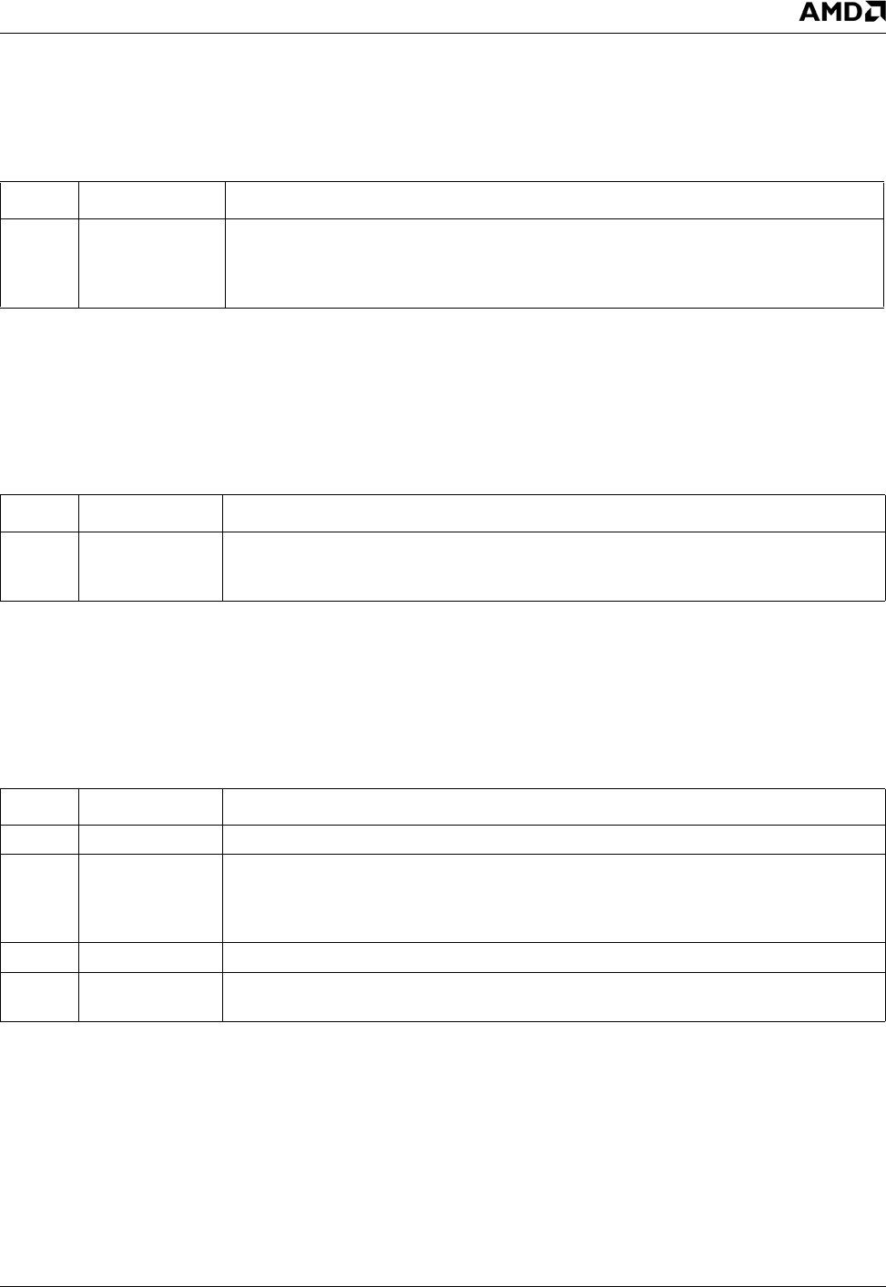
AMD Geode™ LX Processors Data Book 369
Display Controller Register Descriptions 33234H
6.6.19.21 Vertical Display Enable End
6.6.19.22 Offset
6.6.19.23 Underline Location
Index 12h
Ty p e R / W
Reset Value 00h
Vertical Display Enable End Register Bit Descriptions
Bit Name Description
7:0 V_DISP_EN_
END
Vertical Display Enable End Register Bits [7:0]. This is a 10-bit value that specifies
the scan line where the vertical display enable signal goes inactive. It represents the
number of active scan lines minus 1. Bits 9 and 8 of this value are in the Overflow regis-
ter (Index 07h[6,1]).
Index 13h
Ty p e R / W
Reset Value 00h
Offset Register Bit Descriptions
Bits Name Description
7:0 OFST Offset. This field specifies the logical line width of the screen. This value (multiplied by
two or four depending on the CRTC clocking mode) is added to the starting address of
the current scan line to get the starting address of the next scan line.
Index 14h
Ty p e R / W
Reset Value 00h
Underline Location Register Bit Descriptions
Bit Name Description
7 RSVD Reserved.
6DW Doubleword Mode. When this bit is a 1, CRTC memory addresses are DWORD
addresses, and the CRTC refresh counter effectively increments by 4. When this bit is a
0, the address increment is determined by the Byte Mode bit in the CRTC Mode Control
register (Index 17h[6]).
5 RSVD Not Implemented. (Count by 4)
4:0 UL Underline Location. This field specifies the row scan value where the underline appears
in the character box in text modes.

370 AMD Geode™ LX Processors Data Book
Display Controller Register Descriptions
33234H
6.6.19.24 Vertical Blank Start
6.6.19.25 Vertical Blank End
6.6.19.26 CRTC Mode Control
Index 15h
Ty p e R / W
Reset Value 00h
Vertical Blank Start Register Bit Descriptions
Bit Name Description
7:0 V_BL_ST Vertical Blank Start Register Bits [7:0]. This is the low eight bits of a value that speci-
fies the starting scan line of the vertical blank signal. This is a 10-bit value. Bit 8 is in the
Overflow register (Index 07h[3]) and bit 9 is in the Maximum Scan Line register (Index
09h[5]).
Index 16h
Ty p e R / W
Reset Value 00h
Vertical Blank End Register Bit Descriptions
Bit Name Description
7:0 V_BL_END Vertical Blank End. This value specifies the low eight bits of a compare value that repre-
sents the scan line where the vertical blank signal goes inactive.
Index 17h
Ty p e R / W
Reset Value 00h
CRTC Mode Control Register Bit Descriptions
Bit Name Description
7 ENSYNC Enable Syncs. When set to 1, this bit enables the horizontal and vertical sync signals.
When 0, this bit holds both sync flip-flops reset.
6BTMD Byte Mode. If the DWORD mode bit (DW, Index 14h[6]) is 0, then this bit configures the
CRTC addresses for byte addresses when set to 1, or WORD addresses when set to 0. If
DW is set to 1, then this bit is ignored. See Table 6-55 on page 371 for information on the
various CRTC addressing modes.
5AW Address Wrap. When the CRTC is addressing the frame buffer in Word Mode (Byte
Mode = 0, DWORD Mode = 0) then this bit determines which address bit occupies the
MA0 bit position of the address sent to the frame buffer memory. If Address Wrap = 0,
CRTC address counter bit 13 occupies the MA0 position. If Address Wrap = 1, then
CRTC address counter bit 15 is in the MA0 position. See Table 6-55 on page 371 for
information on the various CRTC addressing modes.
4 RSVD Reserved.
3 RSVD Not Implemented. (Count by 2)
2 VCKL_SL VCLK Select. This bit determines the clocking for the vertical portion of the CRTC. If this
bit is 0, the horizontal sync signal clocks the vertical section. If this bit is 1, the horizontal
sync divided by two clocks the vertical section.
AMD Geode™ LX Processors Data Book 371
Display Controller Register Descriptions 33234H
Table 6-55 illustrates the various frame buffer addressing schemes. In the table, MAx represents the frame buffer memory
address signals, Ax represents the CRTC address counter signals, RSx represents row scan counter output bits. The
binary value in the column headings is a concatenation of the DWORD Mode and Byte Mode bits. (i.e., {DWORD Mode,
ByteMode} in verilog.)
1 SL_RSCBT Select Row Scan Bit. This bit determines which CRTC signal appears on the MA14
address bit sent to the frame buffer memory. If this bit is a 0, bit 1 of the Row Scan
counter appears on MA14. If this bit is a 1, then CRTC address counter bit 14, 13, or 12
appears on MA14. See Table 6-55 on page 371 for more information.
0 SL_A13 Select A13. This bit determines which CRTC signal appears on the MA13 address bit
sent to the frame buffer memory. If this bit is a 0, bit 0 of the Row Scan counter appears
on MA13. If this bit is a 1, then CRTC address counter bit 13, 12, or 11 appears on MA13.
See Table 6-55 on page 371 for more information.
Table 6-55. CRTC Memory Addressing Modes
Frame Buffer Memory Address Bit Byte Mode (01) Word Mode (00) DWORD Mode (1X)
MA0 A0 A15 or A13 A12
MA1 A1 A0 A13
MA2 A2 A1 A0
MA3 A3 A2 A1
MA4 A4 A3 A2
MA5 A5 A4 A3
MA6 A6 A5 A4
MA7 A7 A6 A5
MA8 A8 A7 A6
MA9 A9 A8 A7
MA10 A10 A9 A8
MA11 A11 A10 A9
MA12 A12 A11 A10
MA13 A13 or RS0 A12 or RS0 A11 or RS0
MA14 A14 or RS1 A13 or RS1 A12 or RS1
MA15 A15 A14 A13
CRTC Mode Control Register Bit Descriptions (Continued)
Bit Name Description

372 AMD Geode™ LX Processors Data Book
Display Controller Register Descriptions
33234H
6.6.19.27 Line Compare
6.6.19.28 CPU Data Latch State
6.6.19.29 Attribute Index/Data FF State
Index 18h
Ty p e R / W
Reset Value 00h
Line Compare Register Bit Descriptions
Bit Name Description
7:0 LINE_COMP[7:0] Line Compare Register Bits [7:0]. This value specifies the low eight bits of a compare
value that represents the scan line where the CRTC frame buffer address counter is
reset to 0. This can be used to create a split screen by using the Start Address registers
to specify a non-zero location at which to begin the screen image. The lower portion of
the screen (starting at frame buffer address 0) is immune to screen scrolling (and pel
panning as specified in the Attribute Mode Control register (Index 10h). Line Compare is
a 10-bit value. Bit 8 is located in the Overflow register (Index 07h[4]) and bit 9 is in the
Maximum Scan Line register (Index 09h[6]).
Index 22h
Ty p e RO
Reset Value 00h
CPU Data Latch State Register Bit Descriptions
Bit Name Description
7:0 DLV Data Latch Value. This read only field returns a byte of the CPU data latches and can be
used in VGA save/restore operations. The graphics controller’s Read Map Select field
(Index 04h[1:0]) specifies which byte/map (0-3) is returned.
Index 24h
Ty p e RO
Reset Value 00h
Attribute Index/Data FF State Register Bit Descriptions
Bit Name Description
7FFST FF State. This read only bit indicates the state of the attribute controller index/data flip-
flop. When this bit is 0, the next write to Index 3C0h will write an index value; when this
bit is 1, the next write to Index 3C0h will write a data register value.
6:0 RSVD Reserved.
AMD Geode™ LX Processors Data Book 373
Display Controller Register Descriptions 33234H
6.6.19.30 Attribute Index State
6.6.20 VGA Graphics Controller Registers
The graphics controller registers are accessed by writing an index value to the Graphics Controller Index register (Index
Address 3CEh) and reading or writing the register using the Graphics Controller Data register (Data Address 3CFh).
6.6.20.1 VGA Graphics Controller Index
Index 26h
Ty p e RO
Reset Value xxh
Attribute Index State Register Bit Descriptions
Bit Name Description
7:6 RSVD Reserved.
5:0 ATT_IN_VA Attribute Index Value. This read only value indicates the value of Attribute Index regis-
ter bits [5:0] (Index 3C0h).
Table 6-56. Graphics Controller Registers Summary
Index Type Register Reset Value Reference
-- R/W VGA Graphics Controller Index xxh Page 373
-- R/W VGA Graphics Controller Data xxh Page 374
00h R/W VGA Set/Reset xxh Page 374
01h R/W VGA Enable Set/Reset xxh Page 374
02h R/W VGA Color Compare xxh Page 375
03h R/W VGA Data Rotate xxh Page 375
04h R/W VGA Read Map Select xxh Page 376
05h R/W VGA Graphics Mode xxh Page 376
06h R/W VGA Miscellaneous xxh Page 377
07h R/W VGA Color Don’t Care xxh Page 378
08h R/W VGA Bit Mask xxh Page 378
Index Address 3CEh
Ty p e R / W
Reset Value xxh
VGA Graphics Controller Index Register Bit Descriptions
Bit Name Description
7:4 RSVD Reserved.
3:0 INDEX Index.
374 AMD Geode™ LX Processors Data Book
Display Controller Register Descriptions
33234H
6.6.20.2 VGA Graphics Controller Data
6.6.20.3 VGA Set/Reset
Bits [3:0] allow bits in their respective maps to be set or reset through write modes 0 or 3. See Section 6.5.5.3 "Write
Modes" on page 290 for more information.
6.6.20.4 VGA Enable Set/Reset
Bits [3:0] enable the Set/Reset function for their respective maps in write mode 0. See Section 6.5.5.3 "Write Modes" on
page 290 for more information.
Data Address 3CFh
Ty p e R / W
Reset Value xxh
VGA Graphics Controller Data Register Bit Descriptions
Bit Name Description
7:4 RSVD Reserved.
3:0 DATA Data.
Index 00h
Ty p e R / W
Reset Value xxh
VGA Set/Reset Register Bits Bit Descriptions
Bit Name Description
7:4 RSVD Reserved.
3SR_MP3 Set/Reset Map 3.
2SR_MP2 Set/Reset Map 2.
1SR_MP1 Set/Reset Map 1.
0SR_MP0 Set/Reset Map 0
Index 01h
Ty p e R / W
Reset Value xxh
VGA Enable Set/Reset Register Bit Descriptions
Bit Name Description
7:4 RSVD Reserved.
3 EN_SR_MP3 Enable Set/Reset Map 3.
2 EN_SR_MP2 Enable Set/Reset Map 2.
1 EN_SR_MP1 Enable Set/Reset Map 1.
0 EN_SR_MP0 Enable Set/Reset Map 0.
AMD Geode™ LX Processors Data Book 375
Display Controller Register Descriptions 33234H
6.6.20.5 VGA Color Compare
Bits [3:0] specify a compare value that allows the CPU to compare pixels in planar modes. Read mode 1 performs a com-
parison based on these bits combined with the Color Don’t Care bits. Data returned will contain a 1 in each one of the eight
pixel positions where a color match is found. See the description of read modes (Section 6.5.5.4 on page 291) for more
information.
6.6.20.6 VGA Data Rotate
Index 02h
Ty p e R / W
Reset Value xxh
VGA Color Compare Register Bit Descriptions
Bit Name Description
7:4 RSVD Reserved.
3CO_CM_MP3Color Compare Map 3.
2CO_CM_MP2Color Compare Map 2.
1CO_CM_MP1Color Compare Map 1.
0CO_CM_MP0Color Compare Map 0.
Index 03h
Ty p e R / W
Reset Value xxh
VGA Data Rotate Bit Descriptions Bit Descriptions
Bit Name Description
7:5 RSVD Reserved.
4:3 WROP Write Operation. Data written to the frame buffer by the CPU can be logically combined
with data already in the CPU data latches.
00: Copy (CPU data written unmodified).
01: CPU data ANDed with latched data.
10: CPU data ORed with latched data.
11: CPU data XORed with latched data.
See the description of write modes (Section 6.5.5.3 on page 290) for more information.
2:0 ROTCNT Rotate Count. This value is used to rotate the CPU data before it is used in write modes
0 and 3. The CPU data byte written is rotated right, with low bits wrapping to the high bit
positions. See the description of write modes (Section 6.5.5.3 on page 290) for more
information.

376 AMD Geode™ LX Processors Data Book
Display Controller Register Descriptions
33234H
6.6.20.7 VGA Read Map Select
6.6.20.8 VGA Graphics Mode
Index 04h
Ty p e R / W
Reset Value xxh
VGA Read Map Select Register Bit Descriptions
Bit Name Description
7:2 RSVD Reserved.
1:0 R_MP_SL Read Map Select. This field specifies which map CPU read data is taken from in read
mode 0. In Odd/Even modes (specified by the Odd/Even bit in the Graphics Mode regis-
ter, Index 05h[4]) bit 1 of this field specifies which pair of maps returns data.
When bit 1 is 0, data is returned from maps 0 and 1. When bit 1 is 1, data is returned from
maps 2 and 3. The CPU read address bit A0 determines which byte is returned (low or
high) in Odd/Even modes. In non-Odd/Even modes, these bits (both bits [1:0]) specify
the map to read (0, 1, 2, or 3) and the CPU accesses data sequentially within the speci-
fied map.
Index 05h
Ty p e R / W
Reset Value xxh
VGA Graphics Mode Register Bit Descriptions
Bit Name Description
7 RSVD Reserved.
6 256_CM 256 Color Mode. When set to a 1, this bit configures the video serializers in the graphics
controller for the 256 color mode (BIOS mode 13h). When this bit is 0, the Shift Register
Mode bit (bit 5) controls the serializer configuration.
5 SH_R_MD Shift Register Mode. When set to a 1, this bit configures the video serializers for BIOS
modes 4 and 5. When this bit is 0, the serializers are taken in parallel (i.e., configured for
4-bit planar mode operation).
Note that the serializers are also wired together serially so that map 3 bit 7 feeds map 2
bit 0, map 2 bit 7 feeds map 1 bit 0, and map 1 bit 7 feeds map 0 bit 0. This allows for a
32-pixel 1 bit-per-pixel serializer to be used. For this configuration, color planes 1, 2, and
3 should be masked off using the Color Plane Enable register (Attribute Controller, Index
12h, on page 381.)
4 ODD_EVEN Odd/Even. When this bit is set to 1, CPU address bit A0 will select between maps 0 and
1 or maps 2 and 3 depending on the state of the Read Map Select field (Index 04h[1:0]).
When this bit is 0, the CPU accesses data sequentially within a map. This bit is equiva-
lent to the Odd/Even bit in the VGA Miscellaneous register (Index 06h[2]), but is inverted
in polarity from that bit.
3 RD_MD Read Mode. This bit determines what is returned to the CPU when it reads the frame
buffer. When this bit is 1, the result of a color compare operation is returned. The eight
bits in the CPU read data contain a 1 in each pixel position where the color compare
operation was true, and a 0 where the operation was false. When this bit is 0, frame
buffer map data is returned.
2 RSVD Reserved.

AMD Geode™ LX Processors Data Book 377
Display Controller Register Descriptions 33234H
6.6.20.9 VGA Miscellaneous
1:0 WR_MD Write Mode. This field specifies how CPU data is written to the frame buffer. Note that
the Write Operation field in the VGA Data Rotate register (Index 03h[4:3]) specifies how
CPU data is combined with data in the data latches for write modes 0, 2, and 3.
00: Write Mode 0: CPU data is rotated by the count in the VGA Data Rotate register.
Each map enabled by the VGA Map Mask Register (Index 02h) is written by the
rotated CPU data combined with the latch data (if set/reset is NOT enabled for that
map) or by the map’s corresponding set/reset bit replicated across the 8-bit byte (if
set/reset IS enabled for that map). The VGA Bit Mask Register (Index 08h) is used to
protect individual bits in each map from being updated.
01: Write Mode 1: Each map enabled by the VGA Map Mask Register is written with its
corresponding byte in the data latches.
10: Write Mode 2: CPU data is replicated for each map and combined with the data
latches and written to memory. The VGA Bit Mask Register (Index 08h) is used to
protect individual bits in each map from being updated.
11: Write Mode 3: Each map is written with its corresponding Set/Reset bit replicated
through a byte (Enable Set/Reset is ignored). The CPU data is rotated and ANDed
with the VGA Bit Mask Register (Index 08h). The resulting mask is used to protect
individual bits in each map.
Index 06h
Ty p e R / W
Reset Value xxh
VGA Miscellaneous Register Bit Descriptions
Bit Name Description
7:4 RSVD Reserved.
3:2 MEM_MAP Memory Map. This field controls the address mapping of the frame buffer in the CPU
memory space.
00: Memory Map 0: A0000 to BFFFF (128 KB)
01: Memory Map 1: A0000 to AFFFF (64 KB)
10: Memory Map 2: B0000 to B7FFF (32 KB)
11: Memory Map 3: B8000 to BFFFF (32 KB)
1 ODD_EVEN Odd/Even. When set to 1, this bit replaces the CPU A0 address bit with a higher order bit
when addressing the frame buffer. Odd maps are then selected when CPU A0 = 1, and
even maps selected when CPU A0 = 0.
0GPH_MD Graphics Mode.
0: Text mode operation.
1: Graphics mode operation.
VGA Graphics Mode Register Bit Descriptions
Bit Name Description
378 AMD Geode™ LX Processors Data Book
Display Controller Register Descriptions
33234H
6.6.20.10 VGA Color Don’t Care
6.6.20.11 VGA Bit Mask
6.6.21 Attribute Controller Registers
The attribute controller registers are accessed by writing an index value to the Attribute Controller Index register (3C0h) and
reading or writing the register using the Attribute Controller Data register (3C0h for writes, 3C1h for reads).
Index 07h
Ty p e R / W
Reset Value xxh
VGA Color Don’t Care Register Bit Descriptions
Bit Name Description
7:4 RSVD Reserved.
3CM_PR3 Compare Map 3. This bit enables (bit = 1) or excludes (bit = 0) map 3 from participating
in a color compare operation.
2CM_PR2 Compare Map 2. This bit enables (bit = 1) or excludes (bit = 0) map 2 from participating
in a color compare operation.
1CM_PR1 Compare Map 1. This bit enables (bit = 1) or excludes (bit = 0) map 1 from participating
in a color compare operation.
0CM_PR0 Compare Map 0. This bit enables (bit = 1) or excludes (bit = 0) map 0 from participating
in a color compare operation.
Index 08h
Ty p e R / W
Reset Value xxh
VGA Bit Mask Register Bit Descriptions
Bit Name Description
7:0 BT_MSK Bit Mask. The bit mask is used to enable or disable writing to individual bits in each map.
A 1 in the bit mask allows a bit to be updated, while a 0 in the bit mask writes the contents
of the data latches back to memory, effectively protecting that bit from update. The data
latches must be set by doing a frame buffer read in order for the masking operation to
work properly. The bit mask is used in write modes 0, 2, and 3.
Table 6-57. Attribute Controller Registers Summary
Index Type Register Reset Value Reference
-- R/W Attribute Controller Index/Data/Data xxh Page 379
00h-0Fh R/W EGA Palette xxh Page 379
10h R/W Attribute Mode Control xxh Page 380
11h R/W Overscan Color xxh Page 380
12h R/W Color Plane Enable xxh Page 381
13h R/W Horizontal Pel Panning xxh Page 381
14h R/W Color Select xxh Page 382
AMD Geode™ LX Processors Data Book 379
Display Controller Register Descriptions 33234H
6.6.21.1 Attribute Controller Index/Data
The attribute controller registers do not have a separate address for writing index and data information. Instead, an internal
flip-flop alternates between index and data registers. Reading Input Status Register 1 (3BAh or 3DAh) clears the flip-flop to
the index state. The first write to 3C0h following a read from Input Status Register 1 will update the index register. The next
write will update the selected data register. The next write specifies a new index, etc.
6.6.21.2 EGA Palette
Index Address 3C0h
Data Address 3C1h (R)
3C0h (W)
Ty p e R / W
Reset Value xxh
Attribute Controller Index Register Bit Descriptions
Bit Name Description
7:6 RSVD Reserved.
5 INT_PAL_AD Internal Palette Address. This bit determines whether the EGA palette is addressed by
the video pixel stream (bit = 1) or by the Attribute Controller Index register (bit = 0). This
bit should be set to 1 for normal VGA operation. CPU I/O accesses to the palette are dis-
abled unless this bit is a 0.
4:0 DATA_RG_INX Data Register Index. This field addresses the individual palette and data registers.
Index 00h-0Fh
Ty p e R / W
Reset Value xxh
EGA Palette Register Bit Descriptions
Bit Name Description
7:6 RSVD Reserved.
5:0 COL_VAL Color Value. Each of these 16 registers is used to expand the pixel value from the frame
buffer (one, two, or four bits wide) into a 6-bit color value that is sent the video DAC. The
EGA palette is “programmed out of the way” in 256 color mode. These registers can only
be read or written when the Internal Palette Address bit in the Index register (3C0h) is 0.

380 AMD Geode™ LX Processors Data Book
Display Controller Register Descriptions
33234H
6.6.21.3 Attribute Mode Control
6.6.21.4 Overscan Color
Index 10h
Ty p e R / W
Reset Value xxh
Attribute Mode Control Register Bit Descriptions
Bit Name Description
7 P5:4_SEL P5:4 Select. When this bit is a 1, bits [5:4] of the 8-bit VGA pixel value are taken from
bits [1:0] of the Color Select register (Index 14h). When a 0, bits [5:4] of the pixel are
taken from bits [5:4] of the EGA palette output.
6 PEL_W Pel Width. This bit is used in 256 color mode to shift four pixels through the attribute
controller for each character clock. Clearing this bit shifts eight pixels for each charac-
ter clock.
5 PEL_PAN_COMP Pel Panning Compatibility. When this bit is a 1, the scan lines following a line com-
pare are immune to the effects of the pel panning. When this bit is a 0, the entire
screen is affected by pel panning, regardless of the line compare operation.
4 RSVD Reserved.
3EN_BLINK Enable Blink. When this bit is a 1, attribute bit 7 is used to cause a character to blink
(bit 7 = 1) or not (bit 7 = 0). When this bit is 0, attribute bit 7 is used as a background
intensity bit.
2 EN_LGC Enable Line Graphics Codes. When this bit is 0, the 9th Dot in 9-wide character
modes is always set to the background color. When this bit is 1, the 9th Dot is equal to
the foreground color for character codes C0h-DFh, which are the line graphics charac-
ter codes.
1MON_EMU Monochrome Emulation. When this bit is a 1, the underline in 9-Dot mode extends for
all nine Dots and an underlined phrase will have a continuous line under it. When this
bit is 0, the underline is only active for eight Dots, and an underlined phrase will have a
broken line under it.
0GR_MODE Graphics Mode. When this bit is 1, graphics mode is selected and pixel data from the
frame buffer is used to produce the pixel stream. When this bit is 0, text mode is
selected, and text attribute and font pattern information is used to produce the pixel
stream.
Index 11h
Ty p e R / W
Reset Value xxh
Overscan Color Register Bit Descriptions
Bit Name Description
7:0 OVER_COLOR Overscan Color. This value is output as the pixel value to the video DAC when the Dis-
play Enable signal from the CRTC is inactive.
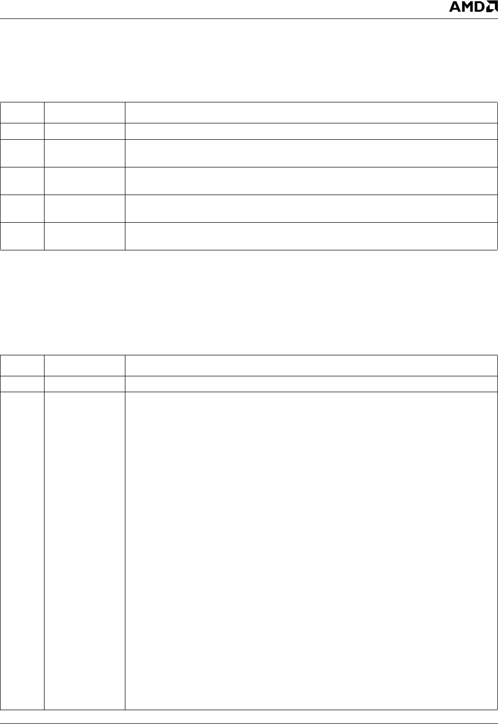
AMD Geode™ LX Processors Data Book 381
Display Controller Register Descriptions 33234H
6.6.21.5 Color Plane Enable
6.6.21.6 Horizontal Pel Panning
Index 12h
Ty p e R / W
Reset Value xxh
Color Plane Enable Register Bit Descriptions
Bit Name Description
7:4 RSVD Reserved.
3 EN_CO_PN3 Enable Color Plane 3. This bit enables color plane 3. It is ANDed with it corresponding
pixel bit and the resulting 4-bit value is used as the address into the EGA palette.
2 EN_CO_PN2 Enable Color Plane 2. This bit enables color plane 2. It is ANDed with it corresponding
pixel bit and the resulting 4-bit value is used as the address into the EGA palette.
1 EN_CO_PN1 Enable Color Plane 1. This bit enables color plane 1. It is ANDed with it corresponding
pixel bit and the resulting 4-bit value is used as the address into the EGA palette.
0 EN_CO_PN0 Enable Color Plane 0. This bit enables color plane 0. It is ANDed with it corresponding
pixel bit and the resulting 4-bit value is used as the address into the EGA palette.
Index 13h
Ty p e R / W
Reset Value xxh
Horizontal Pel Panning Register Bit Descriptions
Bit Name Description
7:4 RSVD Reserved.
3:0 HPP Horizontal Pel Panning: This field specifies how many pixels the screen image should
be shifted to the left by.
Bits [3:0] Mode 13h
Panning
9-Wide Text Mode
Panning
Panning for All
Other Modes
0000 0 1 0
0001 -- 2 1
0010 1 3 2
0011 -- 4 3
0100 2 5 4
0101 -- 6 5
0110 3 7 6
0111 -- 8 7
1000 -- 0 -
1001 -- -- --
1010 -- -- --
1011 -- -- --
1100 -- -- --
1101 -- -- --
1110 -- -- --
1111 -- -- --
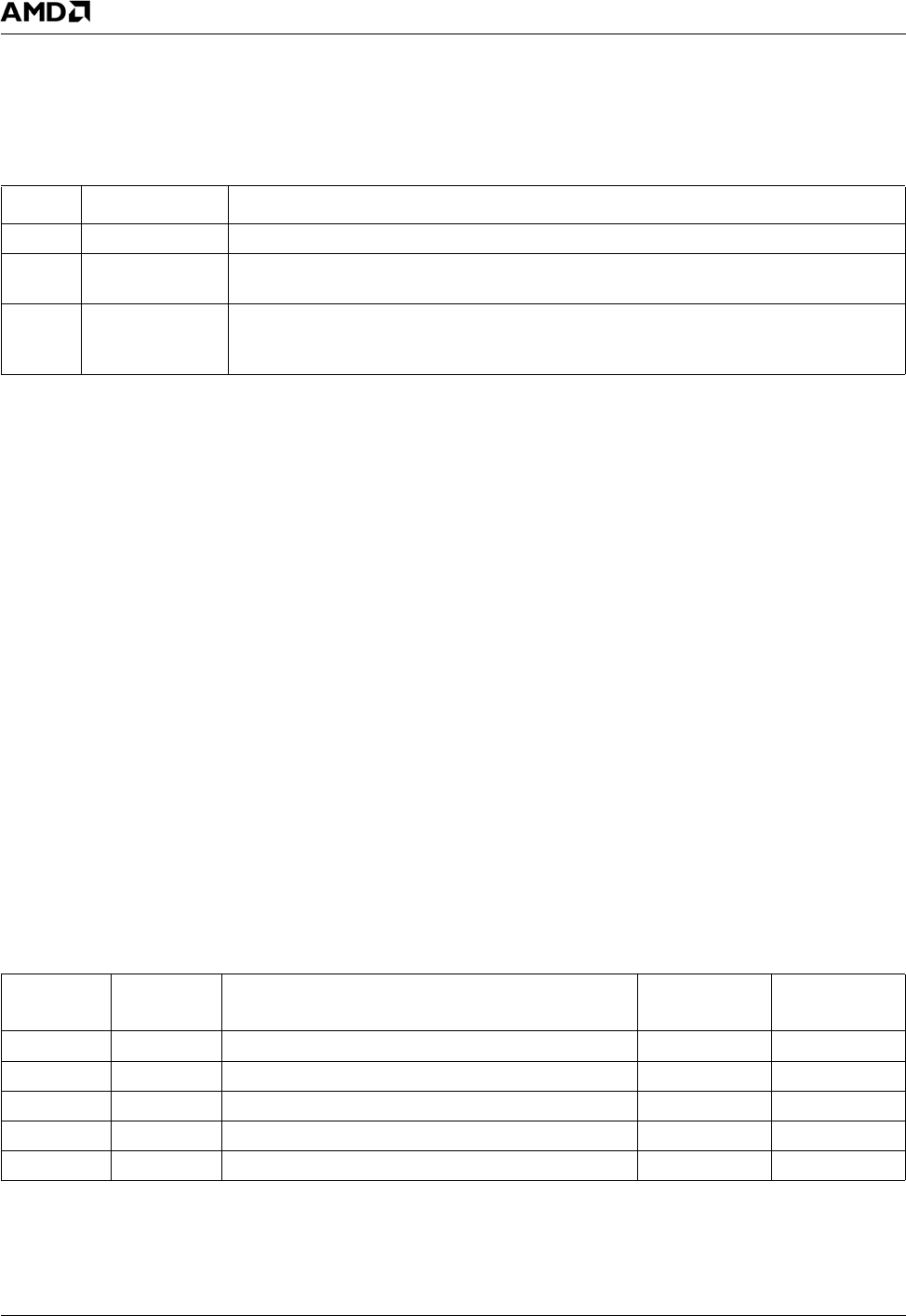
382 AMD Geode™ LX Processors Data Book
Display Controller Register Descriptions
33234H
6.6.21.7 Color Select
6.6.22 Video DAC Registers
Video DAC palette registers are accessed by writing the Palette Address register at the read or write address, then perform-
ing three reads or writes, one for each of the red, green, and blue color values. The video DAC provides an address incre-
ment feature that allows multiple sets of color triplets to be read or written without writing the Palette Address register again.
To invoke this feature, simply follow the first triplet read/write with the next triplet read/write.
The original IBM video DAC behavior for read operations is:
1) CPU initiates a palette read by writing INDEX to I/O address 3C7h.
2) Video DAC loads a temporary register with the value stored at palette[INDEX].
3) Video DAC increments INDEX (INDEX = INDEX + 1).
4) CPU reads red, green, blue color values from temporary register at I/O address 3C9h.
5) Loop to step 2.
The original IBM video DAC behavior for write operations is:
1) CPU initiates a palette write by writing INDEX to I/O address 3C8h.
2) CPU writes red, green, blue color values to temporary DAC registers at I/O address 3C9h.
3) Video DAC stores the temporary register contents in palette[INDEX].
4) Video DAC increments INDEX (INDEX = INDEX + 1).
5) Loop to step 2.
Index 14h
Ty p e R / W
Reset Value xxh
Color Select Register Bit Descriptions
Bit Name Description
7:4 RSVD Reserved.
3:2 P[7:6] P7 and P6. These bits are used to provide the upper two bits of the 8-bit pixel value sent
to the video DAC in all modes except the 256 color mode (mode 13h).
1:0 P[5:4] P5 and P4. These bits are used to provide bits 5 and 4 of the 8-bit pixel value sent to the
video DAC when the P5:4 Select bit is set in the Attribute Mode Control register (Index
10h[7]). In this case, they replace bits [5:4] coming from the EGA palette.
Table 6-58. Video DAC Registers Summary
I/O
Address Type Register Reset Value Reference
3C8h RO Palette Address (Write Mode) 00h Page 383
3C7h RO Palette Address (Read Mode) 00h Page 383
3C7h RO DAC State 00h Page 383
3C9h R/W Palette Data 00h Page 380
3C6h R/W Pel Mask 00h Page 380
AMD Geode™ LX Processors Data Book 383
Display Controller Register Descriptions 33234H
6.6.22.1 Video DAC Palette Address
6.6.22.2 Video DAC State
6.6.22.3 Video DAC Palette Data
Read Address 3C8h
Write Address 3C7h (Palette Read Mode)
3C8h (Palette Write Mode)
Ty p e RO
Reset Value 00h
Video DAC Palette Address Register Bit Descriptions
Bit Name Description
7:0 ADDR Palette Address.
Read Address 3C7h
Write Address --
Ty p e RO
Reset Value 00h
Video DAC State Register Bit Descriptions
Bit Name Description
7:2 RSVD Reserved.
1:0 DAC_ST DAC State. This register returns the DAC state for save/restore operations. If the last
palette address write was to 3C7h (read mode), both bits are 1 (value = 11). If the last
palette address write was to 3C8h (write mode), both bits are 0 (value = 00).
Read Address 3C9h
Write Address 3C9h
Ty p e R / W
Reset Value 00h
Video DAC Palette Data Register Bit Descriptions
Bit Name Description
7:6 RSVD Reserved.
5:0 CO_CPN_VAL Color Component Value. This is a 6-bit color component value that drives the video
DAC for the appropriate color component when the current palette write address is used
to address the video DAC in the pixel stream.

384 AMD Geode™ LX Processors Data Book
Display Controller Register Descriptions
33234H
6.6.22.4 Video DAC Palette Mask
6.6.23 VGA Block Extended Registers
The Extended registers are accessed by writing an index value to the CRTC Index register (3B4h or 3D4h) and reading or
writing the register using the CRTC Data register (3B5h or 3D5h). See the description of the I/O Address Select bit in the
Section 6.6.17.1 "VGA Miscellaneous Output" on page 356 for more information on the I/O address of the CRTC registers.
Read Address 3C6h
Write Address 3C6h
Ty p e R / W
Reset Value 00h
Video DAC Palette Mask Register Bit Descriptions
Bit Name Description
7:0 PAL_MSK Palette Mask. These bits enable their respective color bits between the final VGA 8-bit
pixel output and the DAC palette. The bits are ANDed with the incoming VGA pixel value
and the result used to address the palette RAM.
Table 6-59. Extended Registers Summary
Index Type Register Reset Value Reference
0030h R/W ExtendedRegisterLock FFh Page 385
043h R/W
(Note 1)
Note 1. R/W when unlocked, RO otherwise (see Section 6.6.23.1 "ExtendedRegisterLock" for details).
ExtendedModeControl 00h Page 385
044h R/W
(Note 1)
ExtendedStartAddress 00h Page 385
047h R/W
(Note 1)
WriteMemoryAperture 00h Page 386
048h R/W
(Note 1)
ReadMemoryAperture 00h Page 386
060h R/W
(Note 1)
BlinkCounterCtl (for Sim/Test) 00h Page 386
061h R/W
(Note 1)
BlinkCounter (for Sim/Test) 00h Page 387
070h R/W
(Note 1)
VGALatchSavRes 00h Page 387
071h R/W
(Note 1)
DACIFSavRes 00h Page 387
AMD Geode™ LX Processors Data Book 385
Display Controller Register Descriptions 33234H
6.6.23.1 ExtendedRegisterLock
6.6.23.2 ExtendedModeControl
6.6.23.3 ExtendedStartAddress
CRTC Index 030h
Ty p e R / W
Reset Value FFh
ExtendedRegisterLock Register Bit Descriptions
Bit Name Description
7:0 LOCK Lock. A value of 4Ch unlocks the extended registers. Any other value locks the extended
registers so they are read only. If the extended registers are currently locked, a read to
this register will return FFh. If they are unlocked, a read will return 0.
CRTC Index 043h
Ty p e R / W
Reset Value 00h
ExtendedModeControl Register Bit Descriptions
Bit Name Description
7:3 RSVD Reserved.
2:1 VG_RG_MAP DC Register Mapping. These bits determine the DC register visibility within the standard
VGA memory space (A0000h-BFFFFh). Note that the VGA address space control bits
override this feature. If the Miscellaneous Output register RAM Enable bit is 0, all VGA
memory space is disabled. Or, if the Memory Map bits of the Graphics Miscellaneous
register are set the same as these bits, then the VGA frame buffer memory will appear in
this space instead of the GUI registers.
00: Disabled
01: A0000h
10: B0000h
11: B8000h
0 PACK_CH4 Packed Chain4: When this bit is set, the chain4 memory mapping will not skip DWORDs
as in true VGA. Host reads and writes to frame buffer DWORDs are contiguous. When
this bit is 0, host accesses behave normally and access 1 DWORD out of every 4. Note
that this bit has no effect on the VGA display refresh activity. This bit is only intended to
provide a front end for packed SVGA modes being displayed by DC.
CRTC Index 044h
Ty p e R / W
Reset Value 00h
ExtendedStartAddress Register Bit Descriptions
Bit Name Description
7:6 RSVD Reserved.
5:0 ST_AD_RG
[21:16]
Start Address Register Bits [21:16]. Start Address Register Bits [23:18]: These bits
extend the VGA start address to 24 bits. Bits [17:10] are in Start Address Hi (Index 0Ch),
and bits [9:2] are in Start Address Lo (Index 0Ch).
386 AMD Geode™ LX Processors Data Book
Display Controller Register Descriptions
33234H
6.6.23.4 WriteMemoryAperture
6.6.23.5 ReadMemoryAperture
6.6.23.6 BlinkCounterCtl
This register is for simulation and test only.
CRTC Index 047h
Ty p e R / W
Reset Value 00h
WriteMemoryAperture Register Bit Descriptions
Bit Name Description
7:0 WR_BASE WriteBase. Offset added to the graphics memory base to specify where VGA write oper-
ations start. This value provides DWORD address bits [21:14] when mapping host VGA
writes to graphics memory. This allows the VGA base address to start on any 64 KB
boundary within the 8 MB of graphics memory.
CRTC Index 048h
Ty p e R / W
Reset Value 00h
ReadMemoryAperture Register Bit Descriptions
Bit Name Description
7:0 RD_BASE ReadBase. Offset added to the graphics memory base to specify where VGA read oper-
ations start. This value provides DWORD address bits [21:14] when mapping host VGA
reads to graphics memory. This allows the VGA base address to start on any 64 KB
boundary within the 8 MB of graphics memory.
CRTC Index 060h
Ty p e R / W
Reset Value 00h
BlinkCounterCtl Register Bit Descriptions
Bit Name Description
7 HLD_CNT Hold Count. When set, prevents the blink counter from incrementing with each leading
edge VSYNC.
6:5 RSVD Reserved.
4:0 BLNK_CNT Blink Count. The blink counter is loaded with this value while the Sequencer Reset reg-
ister is in the reset state.

AMD Geode™ LX Processors Data Book 387
Display Controller Register Descriptions 33234H
6.6.23.7 BlinkCounter
This register is for simulation and test only.
6.6.23.8 VGALatchSavRes
6.6.23.9 DACIFSavRes
CRTC Index 061h
Ty p e RO
Reset Value 00h
BlinkCounter Register Bit Descriptions
Bit Name Description
7:5 RSVD Reserved.
4:0 BLNK_CNT Blink Count. These bits provide a real-time blink counter value. This register is not syn-
chronized to the system clock domain.
CRTC Index 070h
Ty p e R / W
Reset Value 00h
VGALatchSavRes Register Bit Descriptions
Bit Name Description
7:0 VGA_LSR VGALatchSavRes. This register is used to save/restore the 32-bit VGA data latch.
When the CRTC index register is written, an internal byte counter is cleared to 0. Four
successive reads or writes to the CRTC data register at this index will return or write
bytes 0 (bits [7:0]), 1 (bits [15:8]), 2 (bits [23:16]), then 3 (bits [31:24]) in sequence.
CRTC Index 071h
Ty p e R / W
Reset Value 00h
DACIFSavRes Register Bit Descriptions
Bit Name Description
7:0 DACIFSR DACIFSavRes. This register is used to save/restore the VGA palette interface logic
state. When the CRTC index register is written, an internal byte counter is cleared to 0.
Four successive reads or writes to the CRTC data register at this index will return or write
bytes 0 (bits [7:0]), 1 (bits [15:8]), 2 (bits [23:16]), then 3 (bits [31:24]) in sequence.

388 AMD Geode™ LX Processors Data Book
Video Processor
33234H
6.7 Video Processor
The Video Processor (VP) module provides a high-perfor-
mance, low-power CRT/TFT display or video output inter-
face. There are three main functions contained within the
VP: the Video Processor, the TFT controller, and the video
output port (VOP). The scaling, filtering, and color space
conversion algorithms implemented in the VP are of much
higher quality than those used in software-only video play-
back systems. The VP is capable of delivering high-resolu-
tion and true-color graphics. It can also overlay or blend a
scaled true-color video image on the graphic background.
For video input, integrated scaling, and X and Y interpola-
tion, enable real-time motion video output. The video path
of the VP also contains horizontal and vertical scaling hard-
ware, and an optional YUV-to-RGB color space converter.
This motion video acceleration circuitry is integrated into
the Video Processor to improve video playback. By off-
loading these arithmetic-intensive tasks from the proces-
sor, 30 frame-per-second playback can be easily achieved,
while keeping processor utilization to acceptable perfor-
mance levels. The graphics and video path is illustrated in
Figure 6-23 on page 389.
General Features
•Hardware video acceleration
•Graphics/video overlay and blending
•Progressive video from the Display Controller module
•Dot Clocks up to 350 MHz
Hardware Video Acceleration
•Arbitrary X and Y interpolation using three line-buffers
•YUV-to-RGB color space conversion
•Horizontal filtering and downscaling
•Supports 4:2:2 and 4:2:0 YUV formats and RGB 5:6:5
format
Graphics-Video Overlay and Blending
•Overlay of true-color video up to 24-bpp
•Supports chroma key and color key for both graphics
and video streams
•Supports alpha-blending with up to three alpha windows
that can overlap one another
•8-bit alpha values with automatic increment or decre-
ment on each frame
•Optional gamma correction for video or graphics
Compatibility
•Supports Microsoft’s Direct Draw/Direct Video and DCI
(Display Controller Interface) v2.0 for full motion video
playback acceleration
•Compatible with VESA, VGA, and DPMS standards for
enhanced display control and power management
6.7.1 Architecture Overview
The Video Processor module contains the following func-
tional blocks. (Figure 6-23 on page 389 shows the relation-
ships between these blocks):
•Video Data Interface
— Video Formatter
—Downscaler
— 5 Line Buffers
— Vertical Upscaler (Programmable up to x8)
— Horizontal Upscaler (Programmable up to x8)
•Control Registers
•Mixer/Blender
— Color Space Converter (CSC)
—Gamma RAM
— Color Keys
— Alpha Blender
•CRT DACs
•TFT Interface
•Video Output Port
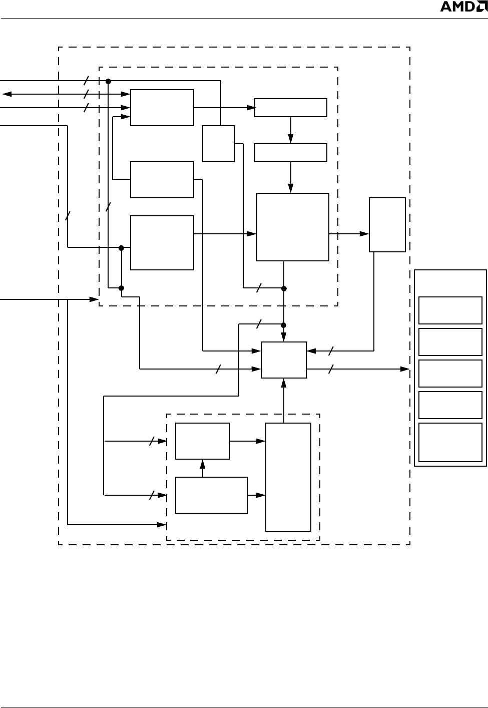
AMD Geode™ LX Processors Data Book 389
Video Processor 33234H
Figure 6-23. Video Processor Block Diagram
Video Data
Interface
(YUV)
Control
Registers
Interface
Graphics Data
Interface
(RGB)
Video Formatter
X and Y Scaler
Mixer/Blender
(Overly with
Alpha Blending,
CSC and
Gamma RAM)
Delay
Video
Output
Port
Output
Format
(MUX)
Output
Devices
VIP
TV
Encoder
CRT DAC
(3x8 bit)
TFT Panel
AMD Geode™
Companion
Video Processor
Panel
Interface
Dither
Engine
TFT Timing
Generator
Flat Panel
Display Controller
Display Controller
Video Data Controller
Video Data
Graphics Data
Dot Clock
Flat Panel
Data + Cntl
VP
RGB + Cntl
VP YUV
+ Cntl
fmt_sel
24
3
27
3
27
16
31
3
24
3
2
16
Pixel Data
Pixel Cntl
Video Processor Module
Companion
Device
Bypass
Device
390 AMD Geode™ LX Processors Data Book
Video Processor
33234H
6.7.2 Functional Description
The VP receives the input video stream in either YUV
(4:2:2 or 4:2:0) or RGB (5:6:5) format. The VP has an inte-
grated color space converter to convert YUV data to RGB
data. The video clock must always be active (regardless of
the source of video input).
Either graphics, or graphics and video mixed (via color-
keying or alpha-blending) can be displayed. Mixing can be
performed in either the RGB or YUV domain.
For video input, integrated scaling and X and Y interpola-
tion enable real-time motion video output. The video path
of the VP also contains horizontal and vertical scaling hard-
ware, and an optional YUV-to-RGB color space converter.
This motion video acceleration circuitry is integrated into
the VP to improve video playback. By off-loading these
arithmetic-intensive tasks from the CPU, 30 frame-per-sec-
ond playback can be easily achieved, while keeping CPU
utilization to acceptable performance levels.
Figure 6-24. Video Processor Block Diagram
8
DAC
RGB
Downscaler Formatter
24
(5x480x64 bit)
DAC
DAC
8
8to CRT
Graphic
m
m + 1 1
m + 1
or
(4:2:2 or 4:2:0)
4:4:4
96
YUV444 or RGB888
Line Buffer 0
RGB
Video
Formatter
Mixer/Blender
(Overlay with Alpha-Blending,
Color Space Converter, and
Gamma RAM)
24
Video
Data I/F
(YUV)
Data I/F
(RGB)
Line Buffer 1
Line Buffer 2
Line Buffer 3
Line Buffer 4
96
32
96
96
80
80
80
Vertical
Scale
4 Parallel
4-tap filters
Horizontal
Scale
4-tap Filter
or YUV

AMD Geode™ LX Processors Data Book 391
Video Processor 33234H
6.7.2.1 Video Formatter
The Video Processor module accepts video data at a rate
asynchronous to the GLIU clock rate. The byte order of
video input data can be configured using the VID_FMT bits
in the Video Configuration register (VP Memory Offset
000h[3:2]).
Video input data can be in YUV 4:2:2, YUV 4:2:0, or RGB
5:6:5 format. The video input data is packed into a 32-bit
WORD and written to one of three on-chip line buffers to
significantly reduce video bandwidth. Each line buffer is
480x64 bits, and supports up to a maximum of 1920 hori-
zontal source video pixels.
YUV Video Formats
Two different input data formats can be used by the video
formatter for overlay of video or graphics data:
1) 4:2:2 Video Format
Four different types of 4:2:2 formats may be used. See
the VID_FMT bits in the Video Configuration register
(VP Memory Offset 000h[3:2]) for details about these
formats. Ensure that the selected format is appropriate
for the data source.
2) 4:2:0 Video Format
This format contains all Y data for each line followed
by all U data and all V data. For example, for a line
with 720 pixels, 720 bytes of Y data is followed by 360
bytes of U data and 360 bytes of V data for that line.
This format is usually used for input from the proces-
sor video buffer (i.e., generated by application soft-
ware).
This format is selected when the EN_420 bit (VP
Memory Offset 000h[28]) is set to 1. The following
possible subformat types (described for four bytes of
data) can be selected via the VID_FMT bits (VP Mem-
ory Offset 000h[3:2]):
00: Y0 Y1 Y2 Y3
01: Y3 Y2 Y1 Y0
10: Y1 Y0 Y3 Y2
11: Y1 Y2 Y3 Y0
Note: The above formats describe Y data. U and V
data have the same format (where “U” and “V” replace
the “Y” in this sample).
RGB Video Format
In this format, each pixel is described by 16 bits:
Bits [15:11]: Red
Bits [10:5]: Green
Bits [4:0]: Blue
This format can be used for a second graphics plane if
video mixing is not used.
Four subformats can be selected via the VID_FMT bits (VP
Memory Offset 000h[3:2]):
00: P1L P1M P2L P2M
01: P2M P2L P1M P1L
10: P1M P1L P2M P2L
11: P1M P2L P2M P1L
Notes:
1) P1M is the most significant byte (MSB) of pixel 1.
2) P1L is the least significant byte (LSB) of pixel 1.
3) P2M is the MSB of pixel 2.
4) P2L is the LSB of pixel 2.
5) Within each pixel (2 bytes) RGB ordering is constant.
6) This mode does not work if EN_420 is high (VP Mem-
ory Offset 000h[28] = 1).
6.7.2.2 4x4 Filter/Scaler
•Accepts all SD and HD television resolutions as well as
non-standard video window sizes.
•Horizontal arbitrary scaling:
— Up to 1:8 upscale.
— Down to 8:1 downscale.
•Vertical arbitrary scaling:
— Up to 1:8 upscale.
— Down to 2:1 downscale.
•16-pixel filtering:
— One horizontal 4-tap filter.
— Four parallel vertical 4-tap filters.
— 128 or 256 phase in both horizontal and vertical
directions.
— Programmable 16-bit signed horizontal and vertical
coefficients.
•Five video line buffers:
— Four active line buffers.
— One extra line buffer for buffer elasticity and down-
scale.
•Line buffer interface operates at GLIU clock up to 400
MHz.
•Horizontal and vertical filter/scaler operates at Dot clock
up to 350 MHz
The VP 4x4 filter/scaler contains multiple 4-tap filters that
are used in conjunction with an upscale/downscale pro-
cessing section. There are five video line buffers that store
YUV pixels for upcoming display lines.
392 AMD Geode™ LX Processors Data Book
Video Processor
33234H
6.7.2.3 Horizontal Downscaling
The Video Processor module supports horizontal down-
scaling (see Figure 6-25). The downscaler can be imple-
mented in the Video Processor module to shrink the video
window by a factor of up to 8:1, in one-pixel increments.
The Downscaler Factor Select (m) is programmed in the
Video Downscaler Control register (VP Memory Offset
078h[4:1]). If bit 0 (DCF) of this register is set to 0, the
downscaler logic is bypassed.
Note: Horizontal downscaling is supported in 4:2:2 YUV
video format only, not 4:2:0 YUV or 5:6:5 RGB.
The downscaler supports up to 29 downscaler factors.
There are two types of factors:
• Type A is (1/m+1). One pixel is retained, and m pixels
are dropped. This enables downscaling factors of 1/8, 1/
7, 1/6, 1/5, 1/4, 1/3, and 1/2.
• Type B is (m/m+1). m pixels are retained, and one pixel
is dropped. This enables downscaling factors of 2/3, 3/4,
4/5, 5/6, 6/7, 7/8.
Bit 6 of the Video Downscaler Control register (VP Memory
Offset 078h) selects the type of downscaling factor to be
used.
Note: There is no vertical downscaling in the Video Pro-
cessor module.
Figure 6-25. Downscaler Block Diagram
Bypass
4-Tap Horizontal
4x8 Downscale
Filtering
Coefficients
Downscaler
Factors
To line
buffers
Video
Input
AMD Geode™ LX Processors Data Book 393
Video Processor 33234H
6.7.3 X and Y Upscaler
After the video data has been buffered, the upscaling algo-
rithm is applied. The Video Processor module employs a
Digital Differential Analyzer-style (DDA) algorithm for both
horizontal and vertical upscaling. The scaling parameters
are programmed via the Video Scale register (VP Memory
Offset 020h). The scalers support up to 8x scale factors
both horizontally and vertically. The scaled video pixel
stream is then passed through bi-linear interpolating filters
(2-tap, 8-phase) to smooth the output video, significantly
enhancing the quality of the displayed image.
The X and Y Upscaler uses the DDA and linear interpolat-
ing filter to calculate (via interpolation) the values of the pix-
els to be generated. The interpolation formula uses Ai,j,
Ai,j+1, Ai+1,j, and Ai+1,j+1 values to calculate the value of
intermediate points. The actual location of calculated
points is determined by the DDA algorithm.
The location of each intermediate point is one of eight
phases between the original pixels (see Figure 6-26).
6.7.4 Color Space Converter
After scaling and filtering have been performed, YUV video
data is passed through the color space converter to obtain
24-bit RGB video data.
Color space conversion equations are based on the
BT.601-1 recommendation:
Standard definition color space conversion equations are
based on Microsoft’s recommendations as follows:
R = 1.164383(Y-16) + 1.596027(V-128)
G = 1.164383(Y-16) - 0.812968(V-128) - 0.391762
(U-128)
B = 1.164383(Y-16) + 2.017232(U-128)
For high definition video, the color space conversion equa-
tions are based on Rec. ITU-R BT.709 as follows:
R = 1.164383(Y-16) + 1.792742(V-128)
G = 1.164383(Y-16) - 0.532909(V-128) - 0.213249
(U-128)
B = 1.164383(Y-16) + 2.112402(U-128)
The color space converter clamps inputs to prevent them
from exceeding acceptable limits.
The color space converter can be bypassed for overlaying
16-bpp graphics data.
Figure 6-26. Linear Interpolation Calculation
b1b2
x
z
y
Ai,j+1
Ai+1,j+1
Ai+1,j
Ai,j Notes:
x and y are 0 - 7
b1Aij,
()
8y–
8
------------Ai1j,+
()
y
8
---+=
b2Aij,1+
()
8y–
8
------------Ai1j1+,+
()
y
8
---+=
zb
1
()
8x–
8
------------b2
()
x
8
---+=

394 AMD Geode™ LX Processors Data Book
Video Processor
33234H
6.7.5 Video Overlay
Video data is mixed with graphics data according to the
video window position. The video window position is pro-
grammable via the Video X Position (VP Memory Offset
010h) and Video Y Position (VP Memory Offset 018h) reg-
isters. A color-keying and alpha-blending mechanism is
employed to compare either the source (video) or destina-
tion (graphics) color to the color key programmed via the
Video Color Key register (VP Memory Offset 028h), and to
select the appropriate bits in the Video Color Mask register
(VP Memory Offset 030h). This mechanism greatly
reduces the software overhead for computing visible pix-
els, and ensures that the video display window can be par-
tially hidden by overlapping graphics data. See Figure 6-27
on page 395.
The Video Processor module accepts graphics data at the
graphics Dot clock rate. The Video Processor module can
display graphics resolutions up to 1920x1440 on CRT, at
color depths up to 24-bpp while simultaneously overlaying
a video window.
6.7.5.1 Alpha-Blending
Alpha-blending can be performed using RGB blending or
YUV blending:
•For RGB blending, graphic data in RGB format and
video data in RGB format (YUV to RGB conversion) are
blended.
•YUV blending eliminates video de-interlacing and YUV
to RGB conversion of video data. For YUV blending, the
graphic data is converted to YUV and blended with
video in YUV format.
Up to three alpha windows can be defined in the video win-
dow. Alpha values for blending are defined for each pixel in
the upper 8 bits of video data. If alpha windows overlap,
the alpha window with the highest priority (programmable)
is used (for the overlapped area).
Alpha-blending is performed using the following formula:
alpha * G + (1 - alpha) * V
Where G is the graphic value and V is the video value of
the current pixel.
Color Keys
A color key mechanism is used with alpha-blending. Color
key values are defined for a cursor color key and for a nor-
mal color key. The cursor color key is compared to each 24-
bit value of graphic input data. If a match is found, the
selected cursor color is displayed. Two possible cursor col-
ors can be defined. The COLOR_REG_OFFSET field (in
the Cursor Color Key register, VP Memory Offset
0A0h[28:24]) is used to select the bit in the input graphic
stream that determines the cursor color to use. Each cur-
sor color is stored in a separate cursor color register. Fig-
ure 6-28 on page 396 illustrates the logic used to
determine how to implement the color key and alpha-blend-
ing logic.
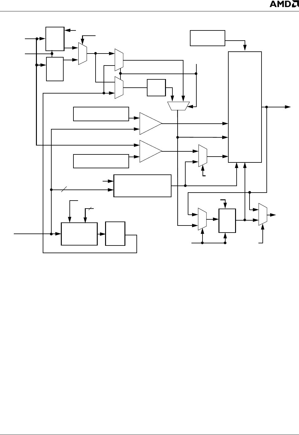
AMD Geode™ LX Processors Data Book 395
Video Processor 33234H
Figure 6-27. Mixer Block Diagram
CSC_VIDEO
Video YUV
Graphics
GV_PAL_BP
RGB/YUV
VSYNC
Current Pixel
Color Key
and
Blending
Logic
Palette
Alpha Color
Registers and Cursor
Color Values
Cursor_Color_Key
VID_CLR_KEY
Location
RAM
CUR_COLOR_MASK
Compare
Compare
VID_CLR_MASK
1
0
0
1
0
1
YUV
to
RGB
CSC
HSV
to
RGB
CSC
RGB to HSV
Saturation
Control
SAT_Scale_EN
SAT_Scale
8
RGB
RGB
YUV
31:24
1
0
0
1
CSC_GFX
RGB
to
YUV
CSC
To VOP
0
1
bypass_stream
palette_stream
1
0
VG_CK
HD/SD
YUV
to
YUV
CSC
Video HD/SD
YUV_CSC_EN
CSC_VOP
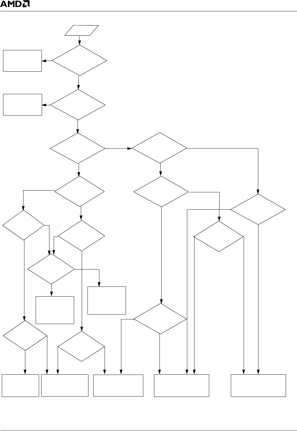
396 AMD Geode™ LX Processors Data Book
Video Processor
33234H
Figure 6-28. Color Key and Alpha-Blending Logic
No
Ye s
Ye s
No
Ye s
No
No
Ye s
No
Ye s
Notes:
1) VG_CK: Video/Graphics color key select (VP Memory
Offset 008h[20]). Selects whether graphic data is used
for color keying or video data is used for chroma keying.
2) GFX_INS_VIDEO: Graphics inside Video (VP Memory
Offset 098h[8]). Graphics inside video enable.
3) Graphics [31:24] = 00h: Graphics color key match
if VG_CK = 1, Graphics(31:24) is pixel alpha value.
No
Ye s
Ye s
No
No
No Yes
Ye s
No
Start
Cursor color
key matches
graphics value?
Pixel inside
the video
window?
Use selected
cursor color
for pixel.
Use graphics
value for this
pixel.
Pixel inside
Alpha window?
Video pixel
Blend graphic
values and video
values using the
Alpha value for
this window
Replace the pixel
with the color
register value
value
for this pixel
Use video value
for this pixel
Color register
video pixel matches
VG_CK = 1? VG_CK = 1?
matches chroma
Color register
enabled for this
window?
Ye s
Use video value
for this pixel
No
Ye s
Ye s
chroma key?
VG_CK = 1?
Ye s
key?
Graphics [31:24] =
enabled for
this window?
Use graphics value
for this pixel
Use graphics
Per-pixel
alpha blending
enabled?
No
No
Blend graphic
values and video
values using the
Alpha value for
this pixel
Ye s
GFX_INX_VIDEO = 1?
00h?
No
graphics[31:24] =
00h?
AMD Geode™ LX Processors Data Book 397
Video Processor 33234H
Table 6-60 represents the same logic that is displayed in Figure 6-28 on page 396.
6.7.5.2 Gamma RAM
Either the graphics or video stream can be routed through
an integrated palette RAM for gamma-correction of the
data stream or (for video data) contrast/brightness adjust-
ments.
A bypass path is provided for either the graphics or video
stream (depending on which is sent through the gamma
RAM).
6.7.5.3 Video Processor Module Display
Interface
The Video Processor module connects directly to either the
internal CRT DACs, or provides a standard digital TFT
interface.
6.7.5.4 Video Interface
The VP uses a two-wire protocol to control the sequence of
data on the video port. This protocol consists of VID_VAL
and VID_RDY. VID_VAL indicates the DC has placed valid
data on the 32-bit VID_DATA bus. VID_RDY indicates the
VP is ready to accept video data for the next video source
line. The VP typically starts fetching video data five scan
lines before the data is required for display.
Table 6-60. Truth Table for Alpha-Blending
VG_CK
(Note 1)
Note 1. VG_CK is bit 20 in the Display Configuration register (VP Memory Offset 0008h).
Windows Configuration (Note 2)
Note 2. GFX_INS_VIDEO is bit 8 in the Video De-interlacing and Alpha Control register (VP Memory Offset 0098h).
ALPHAx_COLOR_REG_EN are bit 24 in the Alpha Window Color registers (VP Memory Offsets 0D0h, 0F0h, and 110h).
Graphics
Data
Match
Cursor
Color Key
Graphics
[31:24] =
00h
Per-pixel
Alpha
Blending
Enabled
Video Data
Match
Normal
Color Key Mixer Output
x (Note 3)
Note 3. x = Don’t care.
xx YesxxxCursor color
x Not in Video
Window
x No x x x Graphic data
Graphics
Color Key
(VG_CK = 0)
Not in Alpha
Window
GFX_INS_VIDEO = 0 No Yes x x Video data
No No x x Graphic data
GFX_INS_VIDEO = 1 No x x x Video data
Inside Alpha
Window x
ALPHAx_COLOR_REG_EN = 1 No Yes x x Color from color
register
ALPHAx_COLOR_REG_EN = 0 No Yes x x Video data
x No No No x Window alpha-
blended data
x No No Yes x Per-pixel alpha-
blended data
Video
Chroma Key
(VG_CK = 1)
Not in Alpha
Window
GFX_INS_VIDEO = 0 No x x Yes Graphic data
No x x No Video data
GFX_INS_VIDEO = 1 No x x x Graphic data
Inside Alpha
Window x
ALPHAx_COLOR_REG_EN = 1 No x x Yes Color from color
register
ALPHAx_COLOR_REG_EN = 0 No x x Yes Graphic data
x No x Yes No Per-pixel alpha-
blended data
x No x No No Window alpha-
blended data
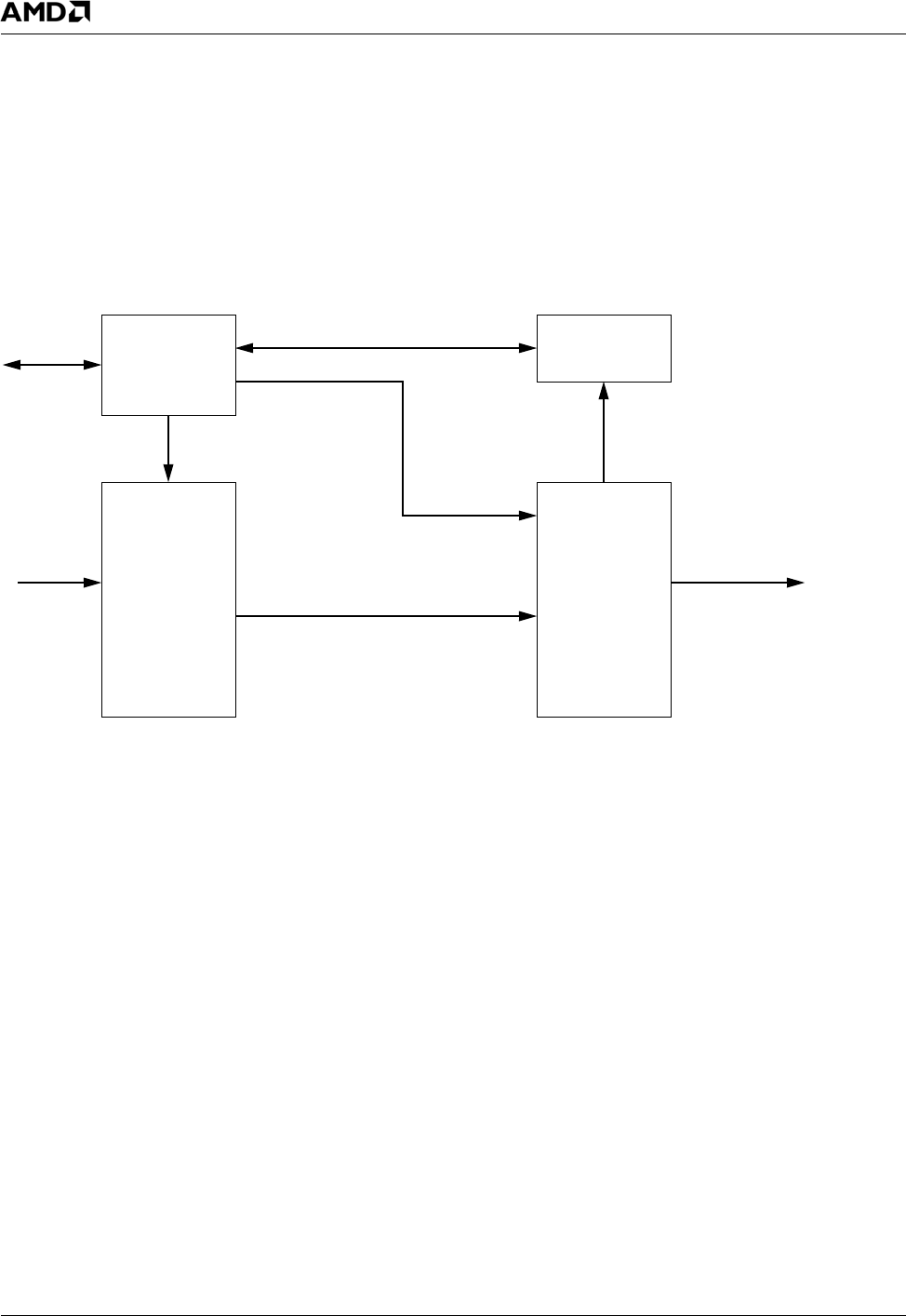
398 AMD Geode™ LX Processors Data Book
Video Processor
33234H
6.7.6 Video Output Port
6.7.6.1 Functional Overview
The Video Output Port (VOP) receives YUV 4:4:4 encoded
data from the VP and formats the data into a video-stream
that is BT.656) or BT.601 compliant. Output from the VOP
goes to either a VIP or a TV encoder. The VOP must be
BT.656/BT.601 compliant since its output may go directly
(or indirectly) to a display.
6.7.6.2 Supported Features
•VIP 2.0 (level I and II) with VIP 1.1 compatibility mode,
BT.656 mode supported
•Support for VIP 2.0 NON_INT bit (REPEAT and
EXT_FLAG not supported)
•BT.601 mode supported
•VBI data supported (no support for ancillary data)
Figure 6-29. VOP Internal Block Diagram
VOP
Registers
Slave
Interface
4:4:4
to
4:2:2
Converter
Data
from
Blender VOP
Data
Formatter
CRC
Generator
VOP
Data
Out
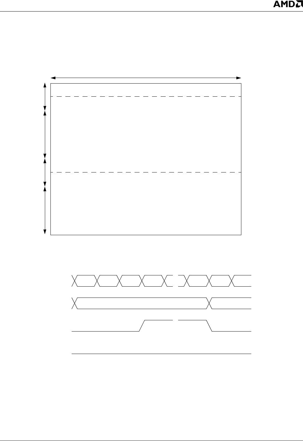
AMD Geode™ LX Processors Data Book 399
Video Processor 33234H
6.7.6.3 HBLANK and VBLANK Signals
HBLANK and VBLANK signals are different from HSYNC
and VSYNC. The HSYNC and VSYNC signals are only
active for a portion of the blanking time, while the HBLANK
and VBLANK signals are active through the entire time.
HBLANK is a function of horizontal pixel position, while
VBLANK is a function of the vertical line number and the
horizontal pixel position. Figures 6-30 to 6-34 show the for-
mation of these signals using a 525-line NTSC video win-
dow.
Figure 6-30. 525-Line NTSC Video Window
Figure 6-31. HBLANK and VBLANK for Lines 20-262, 283-524
Pixel Position
Line Number
Frame 1
858
525
1
1
V = 1
V = 0
V = 1
V = 0
20
264
283
Frame 0 (continued)
Frame 0
Pixel Position
Line Number
HBLANK
VBLANK
720 721 858 001
L# L# + 1
400 AMD Geode™ LX Processors Data Book
Video Processor
33234H
Figure 6-32. HBLANK and VBLANK for Lines 263, 525
Figure 6-33. HBLANK and VBLANK for Lines 1-18, 264-281
Figure 6-34. HBLANK and VBLANK for Lines 19, 282
Pixel Position
Line Number
HBLANK
VBLANK
720 721 858 001
244 245
Pixel Position
Line Number
HBLANK
VBLANK
720 721 858 001
L# L# + 1
Pixel Position
Line Number
HBLANK
VBLANK
720 721 858 001
294 001

AMD Geode™ LX Processors Data Book 401
Video Processor 33234H
6.7.6.4 Interface to Video Processor
The output from the Video Processor is connected via a
24-bit bus. Bytes on this bus are aligned as shown below:
[23:16] Y
[15:8] Cr (V)
[7:0] Cb (U)
The VOP takes this 24-bit 4:4:4 data bus and converts it to
a 16-bit 4:2:2 data bus (the Y component on the high byte,
the U/V components alternating on the low byte).
The VOP provides three different methods for translating
from 4:4:4 to 4:2:2 data depending on the value of the
mode select bits from the VOP Configuration register (VP
Memory Offset 800h[5:4]) as shown in Table 6-61.
Mode 0: 4:2:2 Co-sited
In this mode, the U/V samples are dropped on alternating
sample sets, resulting in the below representation.
Sampling algorithm:
Y, U, V : 4:4:4 Input data
Y’, U’, V’ : 4:2:2 Sampled data
Y1’ = Y1, U1’ = U1, V1’ = V1
Y2’ = Y2
Y3’ = Y3, U3’ = U3, V3’ = V3
etc.
Mode 1: 4:2:2 Interspersed
In this mode, adjacent pairs of U/V sample data are aver-
aged, with the U/V samples coming from the same adja-
cent sample sets.
Sampling algorithm:
Y, U, V : 4:4:4 Input data
Y’, U’, V’ : 4:2:2 Sampled data
Y1’ = Y1, U1’ = (U1+U2)/2, V1’ = (V1+V2)/2
Y2’ = Y2
Y3’ = Y3, U3’ = (U3+U4)/2, V3’ = (V3+V4)/2
etc.
Mode 2: 4:2:2 Interspersed (free-running)
This mode is the same as Mode 1 with the exception that
the U sample is averaged between the first two samples,
and the V sample is averaged between the second and
third samples.
Sampling algorithm:
Y, U, V : 4:4:4 Input data
Y’, U’, V’ : 4:2:2 Sampled data
Y1’ = Y1, U1’ = (U1+U2)/2
Y2’ = Y2, V2’ = (V2+V3)/2
Y3’ = Y3, U3’ = (U3+U4)/2
Y4’ = Y4, V3’ = (V4+V5)/2
etc.
Table 6-61. VOP Mode
Mode Bits Description
000
4:2:2 Co-sited (Recommended)
101
4:2:2 Interspersed
210
4:2:2 Interspersed, free-running
Luminance (Y) Samples
Chromance (U,V) Samples
Luminance (Y) Samples
Chromance (U,V) Samples
Luminance (Y) Samples
Chromance (U) Samples
Chromance (V) Samples
402 AMD Geode™ LX Processors Data Book
Video Processor
33234H
6.7.6.5 Operating Modes
BT.656 Mode
BT.656 is the basic standard that specifies the encoding of
the control lines into the data bus. In this mode the sepa-
rate control lines are encoded into the data bus as speci-
fied by Recommendation ITU-R BT.656.
Each line begins with a Start of Active Video (SAV) header,
and ends with an End of Active Video (EAV) header. Each
of these are four-byte sequences beginning with FF, 00,
00. The fourth byte of the header provides important infor-
mation about this line. The bit format of the SAV and EAV
headers is shown in Table 6-62.
The T bit is specified in BT.656 as a constant logic 1. The F
bit indicates Field - 1 for even (also called Field 2), 0 for
odd (Field 1). The V bit indicates Vertical Blanking. The H
bit indicates Horizontal Blanking. Bits P3 through P0 are
protection bits used to detect and correct single-bit errors.
The bits are defined as follows:
P3 = (V + H) + ~T
P2 = (F + H) + ~T
P1 = (F + V) + ~T
P0 = (F + V) + H
Using the above formulas, the bit values are listed in Table
6-63.
VIP 1.1 Compatible Mode
VIP 1.1 compatible mode builds on CBT.656 mode with the
following changes/additions:
— Video Flags T, F, and V can only be changed in the
EAV code. During vertical blanking there must be a
minimum of one SAV/EAV scan line in order to
convey the updated T, F, and V bits.
— Task bit is used to indicate VBI data within the video
stream (T = 0 for VBI Data, T = 1 for active video).
— P3-P0 are ignored.
Table 6-62. SAV/EAV Sequence
Parameter D7D6D5D4D3D2D1D0
Preamble 11111111
00000000
00000000
Status Word T F V H P3 P2 P1 P0
Table 6-63. Protection Bit Values
T F V H P3 P2 P1 P0 Hex
00001110 0E
00010011 13
0010 0 1 0 1 25
00111000 38
01001001 49
01010100 54
0110 0 0 1 0 62
01111111 7F
10000000 80
100111019D
1010 1 0 1 1 AB
10110110 B6
11000111C7
11011010DA
1110 1 1 0 0 EC
11110001 F1
AMD Geode™ LX Processors Data Book 403
Video Processor 33234H
VIP 2.0 Modes (8 or 16 bits)
VIP 2.0 mode builds on VIP 1.1 with the following changes/
additions:
— Video Flags T, F, and V are valid in the EAV and
SAV code, valid values must appear no later then the
SAV of the first scan line of the next active region
(see Figure 6-35).
— Task bit differentiates between two video streams.
These streams can be interleaved at a line or field
rate.
— New Video Flags - The P Nibble is redefined as
[NON_INT,REPEAT,Reserved,EXT_FLAG].
– NON_INT - 1 = non-interlaced source, 0 = inter-
laced source.
– REPEAT - 1 = repeat field in 3:2 pull-down,
0 = not a repeat field (tied to 0).
– EXT_FLAG - 1 = extra flag byte follows this EAV,
0 = no extra flag byte (this flag is always 0).
Figure 6-35. BT.656 8/16 Bit Line Data
F
F0
00
0X
Y8
01
08
01
08
01
0F
F
0
00
0X
YC
BC
R
YYC
BC
R
Y
EAV Code SAV Code
4Horizontal Blanking 4Active Video
Start of Digital Line
4:2:2 Sampled Video Data
F
F0
00
0X
Y
EAV Code
F
F0
00
0X
Y1
01
01
01
01
01
0F
F0
00
0X
YYYYYYYY F
F0
00
0X
Y
8
08
08
08
08
08
0C
BC
BC
BC
B
8-Bit VIP Data (VIP 1.1 and VIP 2.0 Level I)
16-Bit VIP Data (VIP 2.0 Level II)
4Horizontal Blanking 4Active Video
C
RC
RC
R
4
EAV Code SAV Code 4:2:2 Sampled Video Data EAV Code
vip_data[7:0]
vip_data[7:0]
vip_data[15:8]
404 AMD Geode™ LX Processors Data Book
Video Processor
33234H
6.7.6.6 New VIP 2.0 Video Flags
Four bits are defined (shown in Table 6-64) by the VIP
specification that allow the VIP slave to communicate field/
frame-specific information to the graphics chip during the
video stream output. These flags are embedded in the
lower nibble of the SAV or EAV header. These video flags
allow the graphics chip to handle Bob and Weave, as well
as 3:2 pull-down in hardware. Only bit 3 is implemented in
the AMD Geode LX processor.
6.7.6.7 BT.601 Support
When VOP is configured for BT.601 mode, the HSYNCs
and VSYNCs are used to determine the timing of each data
line sent out. The SAV/EAV codes are not used.
6.7.6.8 VIP 2.0 Level System
For even field detection, some devices require a shift in
VSYNC with respect to HSYNC. This shift is programmed
at DC Memory Offset 080h. Also for correct odd/even field
shift, VP Memory Offset 800h[6] = 1.
6.7.6.9 VBI Data
Vertical Blanking Interval (VBI) data is not part of the active
video (i.e., not directly displayed). This data is sent
between fields of active video data during vertical blanking.
VBI data has many uses: closed captioning, timecodes,
teletext, etc. Although there are some specified standards
with respect to closed captioning which are generally
decoded at the TV, basically, as long as the data is sent
and received correctly, there are no restrictions.
Indication of VBI data is configurable for the different
modes.
In BT.656 mode, typically the TASK bit in the EAV/SAV
header is fixed at 1. In this case, there is no indication of
VBI data. If the VBI bit in the VOP Configuration register is
set to 1 (VP Memory Offset 800h[11] = 1), then VBI data
will be indicated by a TASK bit value of 0 (active video has
the value of 1).
In VIP 1.1 mode, by definition the TASK bit in the EAV/SAV
header is 0 for VBI data, and 1 for active video. The VBI bit
in the VOP Configuration register has no effect in this
mode.
In VIP 2.0 mode, the TASK bit value in the EAV/SAV
header is configurable by selecting a value for the TASK bit
in the VOP Configuration register. If it is desired to have
the TASK bit in the EAV/SAV header indicate VBI data,
then setting the VBI bit will use the inverse value of the
TASK bit in the VOP Configuration register to indicate VBI
data (i.e., if TASK = 1, then VBI data is indicated by a
TASK bit value of 0 in the EAV/SAV, if TASK = 0, then VBI
data is indicated by a TASK bit value of 1 in the EAV/SAV).
Table 6-64. SAV VIP Flags
Bit Flag Description
3
NON_INT 1 indicates that the video is from
a non-interlaced source. 0 indi-
cates that the video is from an
interlaced source.
2
REPEAT 1 indicates that the current field
is a repeat field. This occurs
during 3:2 pull-down. This flag
enables a VIP master to drop
the repeat field in the weave
mode. This bit is not supported
in the AMD Geode™ LX proces-
sor (tied to 0).
1 RSVD Reserved.
0
EXT_FLAG 0 indicates no extended flags.
This bit is not supported in the
AMD Geode LX processor (tied
to 0).
Table 6-65. VOP Clock Rate
Level Video Port Max. PIXCLK
I 8-bit 75 MHz
II 16-bit 75 MHz

AMD Geode™ LX Processors Data Book 405
Video Processor 33234H
6.7.7 Flat Panel Display Controller
6.7.7.1 FP Functional Overview
The flat panel (FP) display controller converts the digital
RGB output of the Video Mixer block to digital output suit-
able for driving a TFT flat panel LCD.
Features include:
•24-bit color support for digital pixel input.
•170 MHz pixel clock operation supports up to
1600x1200 TFT panels.
•Supports most SVGA TFT panels and the VESA FPDI
(Flat Panel Display Interface) Revision 1.0 Specification.
•TFT panel support provided by use of one connector
allows a pass-through mode for the digital pixel input.
•9-, 12-, 18-, and 24-bit 1 pixel per clock TFT support.
•9+9 or 12+12-bit, and 24-bit 2 pixels per clock TFT panel
support.
•Programmable dither, up to 64 levels.
6.7.7.2 FP Architecture Overview
The FP display controller contains the following functional
blocks, as shown in Figure 6-36:
•Dither Engine
•Control Registers
•TFT Timing Generator
•Panel Interface
•CRC (Cyclical Redundancy Check) Engine
Figure 6-36. Flat Panel Display Controller Block Diagram
Dither
Pixel
Pixel
Panel
Panel
Control Registers
Control
Data
Control
Data Engine
TFT Timing
Generator
Panel
Interface
CRC
Engine
24
24
24
3
24
7

406 AMD Geode™ LX Processors Data Book
Video Processor
33234H
6.7.7.3 FP Functional Description
The FP connects to the RGB port of the video mixer.
LCD Interface
The FP interfaces directly to industry standard 18-bit or 24-
bit active matrix thin-film-transistor (TFT). The digital RGB
or video data that is supplied by the video logic is con-
verted into a suitable format to drive a wide variety range of
panels with variable bits. The LCD interface includes dith-
ering logic to increase the apparent number of colors dis-
played for use on panels with less than 6 bits per color. The
LCD interface also supports automatic power sequence of
panel power supplies.
Mode Selection
The FP can be configured for operation with most standard
TFT panels:
•Supports TFT panels with up to 24-bit interface with
640x480, 800x600, 1024x768, 1280x1024, and
1600x1200 pixel resolutions. Either one or two pixels per
clock is supported for all resolutions. Other resolutions
below 640x480 are also supported.
Table 6-66 shows the mapping of the data in the supported
modes.
For TFT panel support, the output from the dither block is
directly fed on to the panel data pins (DRGBx). The data
that is being sent on to the panel data pins is in sync with
the TFT timing signals such as HSYNC, VSYNC, and LDE.
One pixel (or two pixels in 2 pix/clk mode) is shifted on
every positive edge of the clock as long as DISP_ENA is
active.
Table 6-66. Panel Output Signal Mapping
Pin Name
TFT
9-Bit
TFT
18-Bit
TFT
24-Bit
TFT
9+9-Bit
TFT
12+12-Bit
DRGB0 B0 BB0
DRGB1 B1 BB0 BB1
DRGB2 B0 B2 BB1 BB2
DRGB3 B1 B3 BB2 BB3
DRGB4 B2 B4 GB0
DRGB5 B0 B3 B5 GB0 GB1
DRGB6 B1 B4 B6 GB1 GB2
DRGB7 B2 B5 B7 GB2 GB3
DRGB8 G0 RB0
DRGB9 G1 RB0 RB1
DRGB10 G0 G2 RB1 RB2
DRGB11 G1 G3 RB2 RB3
DRGB12 G2 G4 BA0
DRGB13 G0 G3 G5 BA0 BA1
DRGB14 G1 G4 G6 BA1 BA2
DRGB15 G2 G5 G7 BA2 BA3
DRGB16 R0 GA0
DRGB17 R1 GA0 GA1
DRGB18 R0 R2 GA1 GA2
DRGB19 R1 R3 GA2 GA3
DRGB20 R2 R4 RA0
DRGB21 R0 R3 R5 RA0 RA1
DRGB22 R1 R4 R6 RA1 RA2
DRGB23 R2 R5 R7 RA2 RA3

AMD Geode™ LX Processors Data Book 407
Video Processor 33234H
Maximum Frequency
The FP will operate at a DOTCLK frequency of up to 170
MHz. There is no minimum frequency; however, many flat
panels have signal timings that require minimum frequen-
cies. Refer to the flat panel display manufacturer’s specifi-
cations as appropriate.
CRC Signature
The FP contains hardware/logic that performs Cyclical
Redundancy Checks (CRCs) on the digital video/graphics
pipeline. This feature is used for error detection and makes
it possible to capture a unique 24-or 32-bit signature for
any given mode setup. An error in the video/graphics mem-
ory interface, control logic, or pixel pipeline will produce a
different signature when compared to a known good signa-
ture value. This allows the programmer to quickly and
accurately test a video screen without having to visually
inspect the screen for errors. By default, a 24-bit signature
generator is used. For more accuracy, a 32-bit signature
generator my be selected.
Dithering
After the video mixer gamma RAM logic, the graphic data
or the video data goes through the dithering logic.
Some panels have limitations of supporting maximum num-
ber of bits to display all color shades that the CRT monitor
can support. For example, if the selected mode is 24-bpp
and the panel can support only 18-bpp, the remaining two
bits for each color is used for dithering to get the desired
number of shades as compared to the CRT.
The idea behind dithering is to achieve intermediate color
intensities by allowing the human eye to blend or average
the intensities of adjacent pixels on a screen. Intensity res-
olution is gained by sacrificing spatial resolution.
For example, consider just the red color component of a
2x2 square of pixels. If the only two options for the red color
component were to be turned on or off, then there would
only be two colors, black and the brightest red. However, if
two of the pixels’ red color components in the 2x2 square
were turned on and two were turned off, the human eye
would blend these adjacent pixels and the 2x2 pixel square
would appear to be half as bright as the brightest red. The
drawback is that fine details and boundaries between
regions of differing color intensities become slightly blurred.
The FP supports dithering patterns over an 8x8 pixel area.
An 8x8 pixel area supports 64 different dithering patterns.
This means that the 8-bit input intensity for a given pixel pri-
mary color component can be reduced down to its two
most significant bits by using the six least significant bits to
select a 8x8 pixel pattern whose average intensity is equal
to the original 8-bit input intensity value.
As an example, consider a display screen that is capable of
producing six different intensities of the red color compo-
nent for each pixel. Given an 8-bit red intensity value,
01010110, the problem is to come up with a 8x8 pixel pat-
tern, using only the six available red pixel intensities, that
when averaged together, yield the value of the original 8-bit
intensity.
The values of the six available intensities, padded out to
eight bits, are 00000000, 01000000, 01010000, 10000000,
11000000, and 11010000. The given intensity, 010110, lies
between 01000000 and 10000000, so these two intensities
are used in the 8x8 pixel pattern, as shown in Figure 6-37
on page 408. The average intensity of this 8x8 pattern is
01010110.
The actual dithering pattern is an 8x8 pattern of 1s and 0s.
A 0 in a given position of the pattern indicates that the trun-
cated value of the input color component intensity be used.
A 1 means use the next higher truncated value. In the pre-
vious example, the intensity value was 01010110, the trun-
cated value is 01000000 (least significant six bits set to 0),
and the next higher truncated value is 10000000.
The 8x8 dithering pattern for an input intensity value whose
least significant six bits are already zero is made up of all
0s. This means that the next higher truncated intensity
value is never used because the input intensity value is the
same as its truncated value. As the value of the least signif-
icant six bits of the input intensity value increases, the input
intensity value gets closer to the next higher truncated
intensity value, and more 1s are added to the pattern. For
example, when the value of the least significant six bits of
the input intensity value is 16, there will be sixteen 1s in the
dithering pattern and the next higher truncated intensity
value will be used sixteen times within the 8x8 pattern.
DOTCLK CLK CLK CLK CLK CLK
HSYNC HSYNC HSYNC HSYNC HSYNC HSYNC
VSYNC VSYNC VSYNC VSYNC VSYNC VSYNC
LDEMOD LDE LDE LDE LDE LDE
VDDEN ENLVDD ENLVDD ENLVDD ENLVDD ENLVDD
Table 6-66. Panel Output Signal Mapping (Continued)
Pin Name
TFT
9-Bit
TFT
18-Bit
TFT
24-Bit
TFT
9+9-Bit
TFT
12+12-Bit
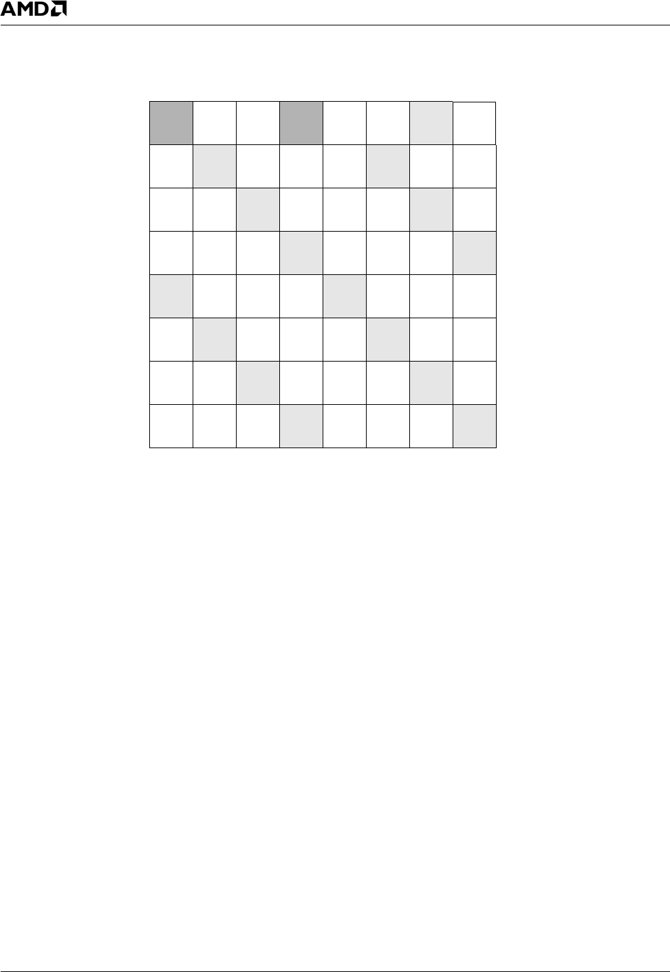
408 AMD Geode™ LX Processors Data Book
Video Processor
33234H
Figure 6-37. Dithered 8x8 Pixel Pattern
All discussions to this point have referred to a 6-bit dither-
ing scheme. A 6-bit dithering scheme is one in which the
least significant six bits of the input intensity value for each
pixel color component are truncated and these least signifi-
cant six bits are used to select an 8x8 dithering pattern.
The FP also supports 4-, 3-, 2-, and 1-bit dithering
schemes. In the 4-bit dithering scheme, only the least sig-
nificant four bits of the input intensity value for each color
component are truncated. As the value of the least signifi-
cant four bits increases from 0 to 15, the order in which 1s
are added to the dithering is much the same as in a 6-bit
scheme except that two 1s are added to the pattern for
each increment of the 4-bit value.
The 3-bit dithering scheme selects a dithering pattern
based on the least significant three bits of the input inten-
sity value for each color component. The order in which 1s
are added to the dithering pattern as the value of these two
bits increases from 0 to 7 is the same as the order for the
6-bit scheme except that two 1s are added to the pattern
for each increment of the 3-bit value.
The 2-bit dithering scheme selects a dithering pattern
based on the least significant two bits of the input intensity
value for each color component. The order in which 1s are
added to the dithering pattern as the value of these two bits
increases from 0 to 3 is the same as the order for the 6-bit
scheme except that four 1s are added to the pattern for
each increment of the 2-bit value.
The 1-bit dithering scheme uses the least significant bit of
the input intensity value to select one of two dithering pat-
terns. The order that 1s are added to the dithering pattern
is the same as the 6-bit scheme except that eight 1s are
added to the pattern when the least significant bit is a 1.
When the least significant bit is 0, the pattern is all 0s.
When the least significant bit is 1, the pattern is alternating
0s and 1s.
Figure 6-38 on page 409 shows the suggested order for
adding 1s to the dithering patterns for the 4-, 3-, 2-, and 1-
bit dithering schemes.
X-Count[3:0]
Y-Count[3:0]
10000000
10000000
01000000
01000000
01000000
01000000
10000000
0100000001000000
01000000
01000000
01000000
10000000
10000000
01000000
01000000
000 001 010 011 100 101 110 111
000
001
010
011
100
101
110
111
10000000
10000000
01000000
01000000
01000000
01000000
01000000
0100000001000000
01000000
01000000
01000000
10000000
10000000
01000000
01000000
01000000
10000000
01000000
01000000
01000000 01000000
01000000
01000000
01000000
10000000
10000000
10000000
01000000
01000000
10000000
10000000
01000000
01000000
01000000
01000000
0100000001000000
01000000
01000000
10000000
10000000
01000000
01000000
0100000001000000
01000000
01000000
AMD Geode™ LX Processors Data Book 409
Video Processor 33234H
Figure 6-38. N-Bit Dithering Pattern Schemes
15 13
1412
000
001
010
011
100
111
101
110
000 001 010 011 100 111101 110
75
3111 9
46
8210
15 13
1412
75
3111 9
46
8210
15 13
1412
75
46
8210
15 13
1412
75
46
8210
3111931119
X-Count[3:0]
Y-Count
[3:0]
12
12
000
001
010
011
100
111
101
110
000 001 010 011 100 111101 110
56
73 4
65
473
12
12
56
73 4
65
473
12
12
56
65
473
12
12
56
65
473
73 473 4
X-Count[3:0]
Y-Count
[3:0]
33
33
000
001
010
011
100
111
101
110
000 001 010 011 100 111101 110
11
22
11
22
33
33
11
22
11
22
33
33
11
11
22
33
33
11
11
22
2222
X-Count[3:0]
Y-Count
[3:0]
11
11
000
001
010
011
100
111
101
110
000 001 010 011 100 111101 110
11
11
11
11
11
11
11
11
11
11
11
11
1114
X-Count[3:0]
Y-Count
[3:0]
4-Bit Scheme 3-Bit Scheme
2-Bit Scheme 1-Bit Scheme

410 AMD Geode™ LX Processors Data Book
Video Processor
33234H
CRC Signature
The FP contains hardware/logic that performs Cyclical
Redundancy Checks (CRCs) on the panel data digital pipe-
line. This feature is used for error detection and makes it
possible to capture a unique 24- or 32-bit signature for any
given mode setup. An error in the dither pixel pipeline pro-
duces a different signature when compared to a known
good signature value. The dither data path can be config-
ured in two basic modes: dither enable and dither disable
by programming the DENB bit (FP Memory Offset 418h[0]).
This allows the programmer to quickly and accurately test a
video screen without having to visually inspect the screen
for errors. Table 6-67 shows the bit settings that provide
this feature.
Panel selection is done through FP Memory Offset
408h[18:16]. The selection of these bits results in two func-
tions.
1) Generates the desired PANEL CLK from the pixel
clock based on the panel type selected.
2) Steers the internal pixel bus on to the panel interface
data pins. All the unused pins are driven with 0s.
This panel data is sent to the CRC signature generator.
The CRC number varies for each panel configuration for a
fixed on-screen image.
Addressing the Dithering Memories
The least significant four bits of each color component
intensity value are used to select a 4x4 dithering pattern. In
other words, there are 16 different 16-bit dithering patterns
for each color component (red, green, and blue). This
requires one 256x1-bit memory for each color component.
The address to one of these dithering pattern memories is
then eight bits in length.
The bit address for dithering memory is defined as the con-
catenation of:
1) The least significant two bits of the display screen hori-
zontal position pixel count
2) The least significant two bits of the display screen
vertical position pixel count
3) The least significant four bits of the input intensity
value
This concatenation is as shown below:
The FP GLIU interface programs the red, green, and blue
dither memories individually, or all at once. Writing to all
three dither memories at the same time means that the
dithering patterns are the same for each of the three color
components.
Table 6-67. Register Settings for Dither Enable/
Disable Feature
Dither Enable
for TFT
Bypass Dither
for TFT Bypass FP
FP Memory
Offset 418h[6:0]
000,001,1
001,010,1
010,011,1
011,100,1
100,101,1
101,xxx,x
FP Memory
Offset 418h[6:0]
101,xxx,x
FP Memory
Offset 408h[30]
is set to 1
Dithering Memory Bit Address[7:0]
= {X-Count[1:0], Y-Count[1:0], Intensity[3:0]}
AMD Geode™ LX Processors Data Book 411
Video Processor 33234H
6.7.8 VP Resolution Table
Supported CRT and flat panel resolutions of the VP are
provided in Table 6-32 on page 281. All resolutions can be
up to 8 bits per color, or 24 bits per pixel. In general, all dis-
play resolutions contained in VESA Monitor Timing Specifi-
cations Version 1.0 v0.8 are supported for CRT. Flat panels
up to 1600x1200x60 are supported. For those resolutions
not listed in the VESA specification, the maximum Dot
clock frequency is 340 MHz for CRT and 170 MHz for TFT.
All SDTV and HDTV resolutions are also supported
6.7.9 Display RGB Modes
Mode overview:
1) CRT: Normal functional, CRT display.
2) TFT Online: Normal functional, TFT display.
3) CRT Legacy RGB: Use companion device as off-chip
display controller, graphics only for CRT.
4) TFT Legacy RGB: Use the AMD Geode companion
device as off-chip display controller, graphics only for
CRT.
5) CRT Debug: Normal functional, access to debug sig-
nals. The DBG signals are driven on the specified pins
outside the VP module, listed here for information only.
6) TFT Legacy RGB Debug: Use companion device as
off-chip display controller, reduced graphics only for
CRT, access to debug signals. The DBG signals are
driven on the specified pins outside the VP module,
listed here for information only.
7) VOP: Normal function
Table 6-68. Display RGB Modes
Pin
CRT
1
TFT
ONLINE
2
CRT
Legacy RGB
3
TFT
Legacy RGB
4
CRT Debug
5
TFT
LEGACY
RGB
Debug
6
VOP
7
DRGB23 0 TFT23 R7 R7 DBG15 DBG15 0
DRGB22 0 TFT22 R6 R6 DBG14 DBG14 0
DRGB21 0 TFT21 R5 R5 DBG13 DBG13 0
DRGB20 0 TFT20 R4 R4 DBG12 DBG12 0
DRGB19 0 TFT19 R3 R3 DBG11 DBG11 0
DRGB18 0 TFT18 0 R2 0 R7 0
DRGB17 0 TFT17 0 R1 0 R6 0
DRGB16 0 TFT16 0 R0 0 R5 0
DRGB15 0 TFT15 G7 G7 DBG10 DBG10 VOP8
DRGB14 0 TFT14 G6 G6 DBG09 DBG09 VOP9
DRGB13 0 TFT13 G5 G5 DBG08 DBG08 VOP10
DRGB12 0 TFT12 G4 G4 DBG07 DBG07 VOP11
DRGB11 0 TFT11 G3 G3 DBG06 DBG06 VOP12
DRGB10 0 TFT10 G2 G2 DBG05 DBG05 VOP13
DRGB9 0 TFT9 0 G1 0 G7 VOP14
DRGB8 0 TFT8 0 G0 0 G6 VOP15
DRGB7 0 TFT7 B7 B7 DBG04 DBG04 VOP0
DRGB6 0 TFT6 B6 B6 DBG03 DBG03 VOP1
DRGB5 0 TFT5 B5 B5 DBG02 DBG02 VOP2
DRGB4 0 TFT4 B4 B4 DBG01 DBG01 VOP3
DRGB3 0 TFT3 B3 B3 DBG00 DBG00 VOP4
DRGB2 0 TFT2 0 B2 0 G5 VOP5
DRGB1 0 TFT1 0 B1 0 B7 VOP6
DRGB0 0 TFT0 0 B0 0 B6 VOP7
DOTCLK 0 FP_SHFCLK DF_DOT_CLK DF_DOT_CLK DBG_CLK DF_DOT_CLK VOPCLK
HSYNC VP_HSYNC FP_HSYNC VG_HSYNC VG_HSYNC VP_HSYNC VG_HSYNC 0
VSYNC VP_VSYNC FP_VSYNC VG_VSYNC VG_VSYNC VP_VSYNC VG_VSYNC 0
DISPEN 0 BKLEN 0 VG_DISP_EN 0 VG_DISP_EN 0
VDDEN 0 FP_VDDEN 0 0 0 0 0
LDEMOD 0 FP_LDE 0 0 0 0 0
412 AMD Geode™ LX Processors Data Book
Video Processor Register Descriptions
33234H
6.8 Video Processor Register Descriptions
This section provides information on the registers associ-
ated with the Video Processor: Standard GeodeLink
Device (GLD) and Video Processor Specific MSRs
(accessed via the RDMSR and WRMSR instructions), and
two blocks of functional memory mapped registers (Video
Processor and Flat Panel).
Table 6-75 through Table 6-78 are register summary tables
that include reset values and page references where the bit
descriptions are provided.
Note: The MSR address is derived from the perspective
of the CPU Core. See Section 4.1 "MSR Set" on
page 45 for more details on MSR addressing.
For memory offset mapping details, see Section
4.1.3 "Memory and I/O Mapping" on page 47.
Table 6-69. Standard GeodeLink™ Device MSRs Summary
MSR
Address Type Register Name Reset Value Reference
48002000h RO GLD Capabilities MSR (GLD_MSR_CAP) 00000000_0013F0xxh Page 415
48002001h R/W GLD Master Configuration MSR
(GLD_MSR_CONFIG)
00000000_00040E00h Page 415
48002002h R/W GLD SMI MSR (GLD_MSR_SMI) 00000000_00000000h Page 417
48002003h R/W GLD Error MSR (GLD_MSR_ERROR) 00000000_00000000h Page 417
48002004h R/W GLD Power Management MSR
(GLD_MSR_PM)
00000000_00000555h Page 418
48002005h R/W GLD Diagnostic MSR (GLD_MSR_DIAG) 00000002_00000000h Page 418
Table 6-70. Video Processor Module Specific MSRs Summary
MSR
Address Type Register Name Reset Value Reference
48002010h R/W VP Diagnostic MSR (MSR_DIAG_VP) 00000000_00000000h Page 419
48002011h R/W Pad Select MSR (MSR_PADSEL) 00000000_00000000h Page 420
Table 6-71. Video Processor Module Configuration Control Registers Summary
VP
Memory
Offset Type Register Name Reset Value Reference
Video Processor
000h R/W Video Configuration (VCFG) 00000000_00000000h Page 421
008h R/W Display Configuration (DCFG) 00000000_00000000h Page 422
010h R/W Video X Position (VX) 00000000_00000000h Page 424
018h R/W Video Y Position (VY) 00000000_00000000h Page 425
020h R/W Video Scale (SCL) 00000000_00000000h Page 425
028h R/W Video Color Key Register (VCK) 00000000_00000000h Page 426
030h R/W Video Color Mask (VCM) 00000000_00000000h Page 427
038h R/W Palette Address (PAR) 00000000_000000xxh Page 428
040h R/W Palette Data (PDR) 00000000_00xxxxxxh Page 428
048h R/W Saturation Scale (SLR) 00000000_00000000h Page 429

AMD Geode™ LX Processors Data Book 413
Video Processor Register Descriptions 33234H
050h R/W Miscellaneous (MISC) 00000000_00000C00h Page 430
058h R/W CRT Clock Select (CCS) 00000000_00000000h Page 431
060h R/W Video Y Scale (VYS) 00000000_00000000h Page 431
068h R/W Video X Scale (VXS) 00000000_00000000h Page 431
070h -- Reserved (RSVD) -- --
078h R/W Video Downscaler Control (VDC) 00000000_00000000h Page 432
080h -- Reserved -- --
088h R/W CRC Signature (CRC) 00000000_00000000h Page 433
090h RO 32-Bit CRC Signature (CRC32) 00000000_00000001h Page 434
098h R/W Video De-Interlacing and Alpha Control
(VDE)
00000000_00000400h Page 434
0A0h R/W Cursor Color Key (CCK) 00000000_00000000h Page 436
0A8h R/W Cursor Color Mask (CCM) 00000000_00000000h Page 437
0B0h R/W Cursor Color 1 (CC1) 00000000_00000000h Page 437
0B8h R/W Cursor Color 2 (CC2) 00000000_00000000h Page 438
0C0h R/W Alpha Window 1 X Position (A1X) 00000000_00000000h Page 438
0C8h R/W Alpha Window 1 Y Position (A1Y) 00000000_00000000h Page 439
0D0h R/W Alpha Window 1 Color (A1C) 00000000_00000000h Page 439
0D8h R/W Alpha Window 1 Control (A1T) 00000000_00000000h Page 440
0E0h R/W Alpha Window 2 X Position (A2X) 00000000_00000000h Page 441
0E8h R/W Alpha Window 2 Y Position (A2Y) 00000000_00000000h Page 442
0F0h R/W Alpha Window 2 Color (AC2) 00000000_00000000h Page 442
0F8h R/W Alpha Window 2 Control (A2T) 00000000_00000000h Page 443
100h R/W Alpha Window 3 X Position (A3X) 00000000_00000000h Page 444
108h R/W Alpha Window 3 Y Position (A3Y) 00000000_00000000h Page 445
110h R/W Alpha Window 3 Color (A3C) 00000000_00000000h Page 445
118h R/W Alpha Window 3 Control (A3T) 00000000_00000000h Page 446
120h R/W Video Request (VRR) 00000000_001B0017h Page 447
128h RO Alpha Watch (AWT) 00000000_00000000h Page 448
130h R/W Video Processor Test Mode (VTM) 00000000_00000000h Page 448
138h R/W Even Video Y Position (VYE) 00000000_00000000h Page 449
140h R/W Even Alpha Window 1 Y Position (A1YE) 00000000_00000000h Page 449
148h R/W Even Alpha Window 2 Y Position (A2YE) 00000000_00000000h Page 450
150h R/W Even Alpha Window 3 Y Position (A3YE) 00000000_00000000h Page 450
158h-3FFh -- Reserved -- --
Table 6-71. Video Processor Module Configuration Control Registers Summary (Continued)
VP
Memory
Offset Type Register Name Reset Value Reference

414 AMD Geode™ LX Processors Data Book
Video Processor Register Descriptions
33234H
Flat Panel
400h R/W Panel Timing Register 1 (PT1) 00000000_00000000h Page 451
408h R/W Panel Timing Register 2 (PT2) 00000000_00000000h Page 453
410h R/W Power Management (PM) 00000000_00000002h Page 454
418h R/W Dither and Frame Rate Control (DFC) 00000000_00000000h Page 456
420h -- Reserved -- --
428h -- Reserved -- --
430h -- Reserved -- --
438h -- Reserved -- --
440h -- Reserved -- --
448h R/W Dither RAM Control and Address (DCA) 00000000_00000000h Page 457
450h R/W Dither Memory Data (DMD) 00000000_00000000h Page 458
458h R/W Panel CRC Signature (CRC) 00000000_00000000h Page 458
460h -- Reserved -- --
468h RO 32-Bit Panel CRC (CRC32) 00000000_00000001h Page 459
Video Output Port (VOP)
800h R/W Video Output Port Configuration
(VOP_CONFIG)
00000000_00000000h Page 459
808h RO Video Output Port Signature (VOP_SIG) 00000000_00000000h Page 461
810h-8FFh -- Reserved -- --
1000h-
1FFFh
R/W Video Coefficient RAM (VCR) xxxxxxxx_xxxxxxxxh Page 451
Table 6-71. Video Processor Module Configuration Control Registers Summary (Continued)
VP
Memory
Offset Type Register Name Reset Value Reference

AMD Geode™ LX Processors Data Book 415
Video Processor Register Descriptions 33234H
6.8.1 Standard GeodeLink™ Device MSRs
6.8.1.1 GLD Capabilities MSR (GLD_MSR_CAP)
6.8.1.2 GLD Master Configuration MSR (GLD_MSR_CONFIG)
MSR Address 48002000h
Ty p e RO
Reset Value 00000000_0013F0xxh
GLD_MSR_CAP Register Map
63 62 61 60 59 58 57 56 55 54 53 52 51 50 49 48 47 46 45 44 43 42 41 40 39 38 37 36 35 34 33 32
RSVD
313029282726252423222120191817161514131211109876543210
RSVD DEV_ID REV_ID
GLD_MSR_CAP Bit Descriptions
Bit Name Description
63:24 RSVD Reserved. Reads back as 0.
23:8 DEV_ID Device ID. Identifies device (13F0h).
7:0 REV_ID Revision ID. Identifies device revision. See AMD Geode™ LX Processors Specification
Update document for value.
MSR Address 48002001h
Ty p e R / W
Reset Value 00000000_00040E00h
GLD_MSR_CONFIG Register Map
63 62 61 60 59 58 57 56 55 54 53 52 51 50 49 48 47 46 45 44 43 42 41 40 39 38 37 36 35 34 33 32
RSVD
313029282726252423222120191817161514131211109876543210
SP
VIDPRI
MSKCS
GPRI
FPC
IUV
DIV FMTBO FMT PID
GLD_MSR_CONFIG Bit Descriptions
Bit Name Description
63:32 RSVD (RO) Reserved (Read Only). Reads back as 0.
31:21 SP Spares. Bits are read/write, but have no function.
20 VIDPRI Video Priority. Sets the video priority level to the video generator. If this bit is set the
video stream will be put in high priority mode.
19 MSKCS Mask Palette Chip Select Fix. If this bit is set, the fix for the chip select bug in the pal-
ette RAM is inactivated and the chip select remains active if the bypass both is not set. If
this bit is clear, then the chip select is throttled on individual accesses to the RAM.
18:16 GPRI GLIU Master Priority. 000 in this field sets the Video Processor module at the lowest
GLIU priority and 111 sets the Video Processor module at the highest GLIU priority.

416 AMD Geode™ LX Processors Data Book
Video Processor Register Descriptions
33234H
15 FPC Simultaneous Flat Panel (or VOP) and CRT. Primary display is flat panel. Setting this
bit activates the CRT DAC interface to allow simultaneous display of both panel and
CRT. Leaving this bit reset forces the CRT DAC signals to zero.
This bit is ignored if bits [5:3] of this register are set to 0 or 4.
14 IUV Interchange UV. Interchange byte order of the U and V bytes (see bits [7:6]). This
applies only to DRGB mode (see bits [5:3]).
13:8 DIV Clock Divider. GLIU clock divider to produce 14.3 MHz reference clock. Result must be
equal to or less than 14.3 MHz. GLIU clock speed/DIV = reference clock.
7:6 FMTBO Format Byte Order. The lower 24 bits of the DRGB output bus byte order can be modi-
fied for any required interface. These bits, along with bit 14, are used to output the follow-
ing combinations of byte order. This applies only to DRGB mode.
000 = RGB / YUV (YCbCr)
001 = BGR / VUY (CrCbY)
010 = BGR / VYU (CrYCb)
011 = BRG / VUY (CrCbY)
100 = RGB / YVU (YCrCb)
101 = BGR / VYU (CrYCb)
110 = BGR / VUY (CrCbY)
111 = BRG / VYU (CrYCb)
5:3 FMT VP Output Format Select. Video Processor module display outputs formatted for CRT
or flat panel. Resets to CRT; software must change if a different mode is required.
000: CRT.
001: Flat Panel.
010: Reserved.
011: Reserved.
100: CRT Debug mode.
101: Reserved.
110: VOP.
111: DRGB.
2:0 PID VP Priority Domain. Video Processor module assigned priority domain identifier.
GLD_MSR_CONFIG Bit Descriptions (Continued)
Bit Name Description
AMD Geode™ LX Processors Data Book 417
Video Processor Register Descriptions 33234H
6.8.1.3 GLD SMI MSR (GLD_MSR_SMI)
The Video Processor does not produce SMI interrupts, therefore this register is not used. Always write 0.
6.8.1.4 GLD Error MSR (GLD_MSR_ERROR)
MSR Address 48002002h
Ty p e R / W
Reset Value 00000000_00000000h
MSR Address 48002003h
Ty p e R / W
Reset Value 00000000_00000000h
GLD_MSR_ERROR Register Map
63 62 61 60 59 58 57 56 55 54 53 52 51 50 49 48 47 46 45 44 43 42 41 40 39 38 37 36 35 34 33 32
RSVD
E
313029282726252423222120191817161514131211109876543210
RSVD
EM
GLD_MSR_ERROR Bit Descriptions
Bit Name Description
63:33 RSVD (RO) Reserved (Read Only). Reads back as 0.
32 E VP Error Status. Any GLIU request made of an unsupported function type causes this
bit to be set by the hardware. Writing a 1 to this bit clears the status. Bit 0 must be 0 for
the error to be generated.
0: Error not pending.
1: Error pending.
31:1 RSVD (RO) Reserved (Read Only).
0EM DF Error Mask.
0: Unmask the Error (i.e., error generation is enabled).
1: Mask the Error (i.e., error generation is disabled).

418 AMD Geode™ LX Processors Data Book
Video Processor Register Descriptions
33234H
6.8.1.5 GLD Power Management MSR (GLD_MSR_PM)
6.8.1.6 GLD Diagnostic MSR (GLD_MSR_DIAG)
This register is reserved for internal use by AMD and should not be written to.
MSR Address 48002004h
Ty p e R / W
Reset Value 00000000_00000555h
GLD_MSR_PM Register Map
63 62 61 60 59 58 57 56 55 54 53 52 51 50 49 48 47 46 45 44 43 42 41 40 39 38 37 36 35 34 33 32
RSVD
313029282726252423222120191817161514131211109876543210
RSVD SP RSVD
PMD5
RSVD
PMD4
RSVD
PMD3
RSVD
PMD2
RSVD
PMD1
RSVD
PMD0
GLD_MSR_PM Bit Descriptions
Bit Name Description
63:28 RSVD Reserved.
27:24 SP Spare. Read/write, no function.
23:11 RSVD Reserved.
10 PMD5 VOP 2x Dot Clock Power Mode.
0: Disable clock gating. Clocks are always ON.
1: Enable active hardware clock gating.
9 RSVD Reserved.
8PMD4 VP Video Dot Clock Power Mode.
0: Disable clock gating. Clocks are always ON.
1: Enable active hardware clock gating.
7 RSVD Reserved.
6PMD3 FP Dot Clock Power Mode.
0: Disable clock gating. Clocks are always ON.
1: Enable active hardware clock gating.
5 RSVD Reserved.
4PMD2 FP GLIU Clock Power Mode.
0: Disable clock gating. Clocks are always ON.
1: Enable active hardware clock gating.
3 RSVD Reserved.
2PMD1 VP Graphics Dot Clock Power Mode.
0: Disable clock gating. Clocks are always ON.
1: Enable active hardware clock gating.
1 RSVD Reserved.
0PMD0 VP GLIU Clock Power Mode.
0: Disable clock gating. Clocks are always ON.
1: Enable active hardware clock gating.
MSR Address 48002005h
Ty p e R / W
Reset Value 00000002_00000000h
AMD Geode™ LX Processors Data Book 419
Video Processor Register Descriptions 33234H
6.8.2 Video Processor Module Specific MSRs
6.8.2.1 VP Diagnostic MSR (MSR_DIAG_VP)
MSR Address 48002010h
Ty p e R / W
Reset Value 00000000_00000000h
MSR_DIAG_VP Register Map
63 62 61 60 59 58 57 56 55 54 53 52 51 50 49 48 47 46 45 44 43 42 41 40 39 38 37 36 35 34 33 32
RSVD
313029282726252423222120191817161514131211109876543210
CM
NDM
SM DVAL D TSEL SP
MSR_DIAG_VP Bit Descriptions
Bit Name Description
63:32 RSVD Reserved.
31 CM 32-Bit CRC Mode. Selects 32-bit CRC generation.
0: Disable.
1: Enable.
30 NDM New Dither Mode. Selects either the legacy dither mode, or new dither mode.
The legacy dither mode has an errata with the first pixel. The new dither mode fixes this
errata. This bit provided for backward compatibility.
0: Legacy dither mode.
1: New dither mode.
29:28 SM Sim Mode. This field is used to put the VP in modes to aid verification.
00: Normal operation.
01: Graphics input bypasses VP and goes directly to FP.
10: Reserved.
11: Reserved.
27:20 DVAL DAC Test Value. 8-bit data value to drive to CRT DAC when selected by bit 19. Dupli-
cate copies of DAC Test Value are driven on DAC RGB.
crt_dac_r[7:0] = DAC Test Value[7:0] ([27:20] is this register)
crt_dac_g[7:0] = DAC Test Value[7:0] ([27:20] is this register)
crt_dac_b[7:0] = DAC Test Value[7:0] ([27:20] is this register)
To enable DAC Test Value to be driven to CRT DAC:
(DAC Test Value Select must = 0) AND
((VTM[6] = 0 AND MBD_MSR_DIAG[18:16] = 101h) OR
(VTM[6] = 1 AND VTM[3:0] = 0001h)
19 D DAC Test Value Select. Selects which data stream is sent to CRT DAC during CRT
DAC test mode.
0: 24-bit data to CRT DAC = {3{DAC Test Value[27:20]}} (3 time repeated 8-bit value).
1: 24-bit data to CRT DAC = gfx_data[23:0] (raw input from Display Controller).
18:16 RSVD Reserved. Reserved for test purposes. Set to 000 for normal operation.
15:0 SP Spares. Read/write, no function.
420 AMD Geode™ LX Processors Data Book
Video Processor Register Descriptions
33234H
6.8.2.2 Pad Select MSR (MSR_PADSEL)
MSR Address 48002011h
Ty p e R / W
Reset Value 00000000_00000000h
MSR_PADSEL Register Map
63 62 61 60 59 58 57 56 55 54 53 52 51 50 49 48 47 46 45 44 43 42 41 40 39 38 37 36 35 34 33 32
RSVD
VOPCINV
RSVD
DF_DRGB[31:26]
313029282726252423222120191817161514131211109876543210
DF_DRGB[25:24]
RSVD
DF_DCLK
DF_DISP_EN
DF_LDE
DF_VSYNC
DF_HSYNC
DF_DRGB[23:0]
MSR_PADSEL Bit Descriptions
Bit Name Description
63:40 RSVD Reserved.
39 VOPCINV Invert VOP Clock. This is used to invert the VOP output clock. This may be used to meet
system timing requirements.
0: Non-inverted.
1: Inverted.
38 RSVD Reserved.
37:0 PADS Select for Registered or Non-Registered VP Outputs. Bits select whether to use the
registers in the pad logic. The reset value of 38’b0 is valid for TFT 2 pixel per clock and
CRT mode.
Bits [37:30]: DF_DRGB[31:24]
0: Registered output.
1: Direct output.
Bit 29: RSVD.
Always write 0.
Bit 28: DF_DCLK
Bit 27: DF_DISP_EN
Bit 26: DF_LDE
Bit 25: DF_VSYNC
Bit 24: DF_HSYNC
Bits [23:0]: DF_DRGB[23:0]
0: Registered output.
1: Direct output.
AMD Geode™ LX Processors Data Book 421
Video Processor Register Descriptions 33234H
6.8.3 Video Processor Module Control/Configuration Registers
6.8.3.1 Video Configuration (VCFG)
VP Memory Offset 000h
Ty p e R / W
Reset Value 00000000_00000000h
VCFG Register Map
63 62 61 60 59 58 57 56 55 54 53 52 51 50 49 48 47 46 45 44 43 42 41 40 39 38 37 36 35 34 33 32
RSVD
313029282726252423222120191817161514131211109876543210
RSVD
EN_420
BIT_8_LINE_SIZE
BIT_9_LINE_SIZE
SP
INIT_RD_LN_SIZE
INIT_RD_ADDR VID_LIN_SIZ
SP
SC_BYP
RSVD
VID_FMT
RSVD
VID_EN
VCFG Bit Descriptions
Bit Name Description
63:29 RSVD (RO) Reserved (Read Only). Reads back as 0.
28 EN_420 Enable 4:2:0 Format.
0: Disable.
1: Enable.
Note: When the input video stream is RGB, this bit must be set to 0.
27 BIT_8_
LINE_SIZE
Bit 8 Line Size. When enabled, this bit increases line size from VID_LIN_SIZ (bits [15:8])
DWORDs by adding 256 DWORDs.
0: Disable.
1: Enable.
26 BIT_9_
LINE_SIZE
Bit 9 Line Size. When enabled, this bit increases line size from {BIT_8_LINE_SIZE,
VID_LIN_SIZ (bits [15:8])} DWORDs by adding 512 DWORDs.
0: Disable.
1: Enable.
25 SP Spare. Bit is R/W but has no function.
24 INIT_RD_
LN_SIZE
Increase Initial Buffer Read Address. Increases INIT_RD_ADDR (bits [23:16]) by add-
ing 256 DWORDs to the initial buffer address. (Effectively INIT_RD_ADDR becomes 9
bits (bits [24:16]) of address to the line buffers. Each line buffer location contains 4 pixels.
Therefore INIT_RD_ADDR is restricted to 4 pixel resolution.)
If sub-4 pixel start is desired, use the VP Memory Offset 010h[11:0].
0: Disable.
1: Enable.
23:16 INIT_RD_ADDR Initial Buffer Read Address. This field preloads the starting read address for the line
buffers at the beginning of each display line. It is used for hardware clipping of the video
window at the left edge of the active display. Since each line buffer contains 4 pixels,
INIT_RD_ADDR is restricted to 4 pixel resolution.
For an unclipped window, this value should be 0. For 420 mode, set bits [17:16] to 00.
15:8 VID_LIN_SIZ Video Line Size (in DWORDs). Represents the number of DWORDs that make up the
horizontal size of the source video data.
7:6 SP Spares. Bits are R/W but have not function.
422 AMD Geode™ LX Processors Data Book
Video Processor Register Descriptions
33234H
6.8.3.2 Display Configuration (DCFG)
5 SC_BYP Scaler Bypass. Bypass scaling math functions. Should only be used for non-scaled
video outputs. Scale factors set to 10000h.
0: Scaler enabled.
1: Scaler disabled.
4 RSVD (RO) Reserved (Read Only). Reads back as 0.
3:2 VID_FMT Video Format. Byte ordering of video data on the video input bus. The interpretation of
these bits depends on the settings for bit 28 (EN_420) and bit 13 (GV_SEL) of the VDE
register (VP Memory Offset 098h).
If GV_SEL and EN_420 are both set to 0 (4:2:2):
00: Cb Y0 Cr Y1
01: Y1 Cr Y0 Cb
10: Y0 Cb Y1 Cr
11: Y0 Cr Y1 Cb
If GV_SEL is set to 0 and EN_420 is set to 1 (4:2:0):
00: Y0 Y1 Y2 Y3
01: Y3 Y2 Y1 Y0
10: Y1 Y0 Y3 Y2
11: Y1 Y2 Y3 Y0
If GV_SEL is set to 1 and EN_420 is set to 0 (5:6:5):
00: P1L P1M P2L P2M
01: P2M P2L P1M P1L
10: P1M P1L P2M P2L
11: P1M P2L P2M P1L
Both RGB 5:6:5 and YUV 4:2:2 contain two pixels in each 32-bit DWORD. YUV 4:2:0
contains a stream of Y data for each line, followed by U and V data for that same line.
Cb = u, Cr = v.
1 RSVD (RO) Reserved (Read Only). Reads back as 0.
0VID_EN Video Enable. Enables video acceleration hardware.
0: Disable (reset) video module.
1: Enable.
VP Memory Offset 008h
Ty p e R / W
Reset Value 00000000_00000000h
VCFG Bit Descriptions (Continued)
Bit Name Description
DCFG Register Map
63 62 61 60 59 58 57 56 55 54 53 52 51 50 49 48 47 46 45 44 43 42 41 40 39 38 37 36 35 34 33 32
RSVD
313029282726252423222120191817161514131211109876543210
SP
RSVD
DAC_VREF
RSVD
GV_GAM
VG_CK
RSVD
CRT_SYNC_SKW
SP
CRT_VSYNC_POL
CRT_HSYNC_POL
RSVD SP
DAC_BL_EN
VSYNC_EN
HSYNC_EN
CRT_EN

AMD Geode™ LX Processors Data Book 423
Video Processor Register Descriptions 33234H
DCFG Bit Descriptions
Bit Name Description
63:32 RSVD (RO) Reserved (Read Only). Reads back as 0.
31:28 SP Spares. Bits are read/write, but have no function.
27 RSVD (RO) Reserved (Read Only). Reads back as 0.
26 DAC_VREF Select CRT DAC VREF. Allows use of an external voltage reference for CRT DAC.
0: Disable external VREF.
1: Use external VREF.
25:22 RSVD (RO) Reserved (Read Only). Reads back as 0.
21 GV_GAM Graphics/Video Gamma. Selects whether the graphic or video data should pass
through the Gamma Correction RAM.
0: Graphic data passes through the Gamma Correction RAM.
1: Video data passes through the Gamma Correction RAM.
20 VG_CK Video/Graphics Color Key Select. Selects whether the graphic data is used for color-
keying or the video data is used for chroma-keying. Note that this affects the final output
with or without blending enabled. See Figure 6-31 on page 438 and Table 6-64 on page
439 for details.
0: Graphic data is compared to the color key.
1: Video data is compared to the chroma key.
19:17 RSVD (RO) Reserved (Read Only). Reads back as 0.
16:14 CRT_SYNC
_SKW
CRT Sync Skew. Represents the number of pixel clocks to skew the horizontal and ver-
tical sync that are sent to the CRT. This field should be programmed to 100 (i.e., baseline
sync is not moved) as the baseline. Via this register, the sync can be moved forward
(later) or backward (earlier) relative to the pixel data. This register can be used to com-
pensate for possible delay of pixel data being processed via the Video Processor.
000: Sync moved 4 clocks backward.
001: Sync moved 3 clocks backward.
010: Sync moved 2 clocks backward.
011: Sync moved 1 clock backward.
100: Baseline sync is not moved. (Default)
101: Sync moved 1 clock forward.
110: Sync moved 2 clocks forward.
111: Sync moved 3 clocks forward.
13:10 SP Spares. Bits are read/write, but have no function.
9 CRT_VSYNC
_POL
CRT Vertical Synchronization Polarity. Selects the polarity for CRT vertical sync.
0: CRT vertical sync is normally low and is set high during the sync interval.
1: CRT vertical sync is normally high and is set low during the sync interval
8CRT_HSYNC
_POL
CRT Horizontal Synchronization Polarity. Selects the polarity for CRT horizontal sync.
0: CRT horizontal sync is normally low and is set high during sync interval.
1: CRT horizontal sync is normally high and is set low during sync interval.
7:6 RSVD (RO) Reserved (Read Only). Reads back as 0.
5:4 SP Spares. Bits are read/write, but have no function.
3 DAC_BL_EN DAC Blank Enable. Controls blanking of the CRT DACs.
0: DACs are constantly blanked.
1: DACs are blanked normally (i.e., during horizontal and vertical blank).
424 AMD Geode™ LX Processors Data Book
Video Processor Register Descriptions
33234H
6.8.3.3 Video X Position (VX)
2 VSYNC_EN CRT Vertical Sync Enable. Enables/disables CRT vertical sync (used for VESA DPMS
support).
0: Disable.
1: Enable.
1 HSYNC_EN CRT Horizontal Sync Enable. Enables/disables CRT horizontal sync (used for VESA
DPMS support).
0: Disable.
1: Enable.
0CRT_EN CRT Enable. Enables the graphics display control logic. This bit is also used to reset the
display logic.
0: Reset display control logic.
1: Enable display control logic.
VP Memory Offset 010h
Ty p e R / W
Reset Value 00000000_00000000h
DCFG Bit Descriptions (Continued)
Bit Name Description
VX Register Map
63 62 61 60 59 58 57 56 55 54 53 52 51 50 49 48 47 46 45 44 43 42 41 40 39 38 37 36 35 34 33 32
RSVD
313029282726252423222120191817161514131211109876543210
RSVD VID_X_END RSVD VID_X_START
VX Bit Descriptions
Bit Name Description
63:28 RSVD (RO) Reserved (Read Only). Reads back as 0.
27:16 VID_X_END Video X End Position. Represents the horizontal end position of the video window. This
register is programmed relative to CRT horizontal sync input (not the physical screen
position). This value is calculated according to the following formula:
Value = Desired screen position + (H_TOTAL – H_SYNC_END) – 13. (Note 1)
15:12 RSVD (RO) Reserved (Read Only). Reads back as 0.
11:0 VID_X_START Video X Start Position. Represents the horizontal start position of the video window.
This value is calculated according to the following formula:
Value = Desired screen position + (H_TOTAL – H_SYNC_END) – 14. (Note 1)
Note 1. H_TOTAL and H_SYNC_END are the values written in the Display Controller module registers.
AMD Geode™ LX Processors Data Book 425
Video Processor Register Descriptions 33234H
6.8.3.4 Video Y Position (VY)
6.8.3.5 Video Scale (SCL)
VP Memory Offset 018h
Ty p e R / W
Reset Value 00000000_00000000h
VY Register Map
63 62 61 60 59 58 57 56 55 54 53 52 51 50 49 48 47 46 45 44 43 42 41 40 39 38 37 36 35 34 33 32
RSVD
313029282726252423222120191817161514131211109876543210
RSVD VID_Y_END RSVD VID_Y_START
VY Bit Descriptions
Bit Name Description
63:27 RSVD (RO) Reserved (Read Only). Reads back as 0.
26:16 VID_Y_END Video Y End Position. Represents the vertical end position of the video window. This
value is calculated according to the following formula:
Value = Desired screen position + (V_TOTAL – V_SYNC_END) + 2. (Note 1)
15:11 RSVD (RO) Reserved (Read Only). Reads back as 0.
10:0 VID_Y_START Video Y Start Position. Represents the vertical start position of the video window. This
register is programmed relative to CRT Vertical sync input (not the physical screen posi-
tion). This value is calculated according to the following formula:
Value = Desired screen position + (V_TOTAL – V_SYNC_END) + 1. (Note 1)
Note 1. V_TOTAL and V_SYNC_END are the values written in the Display Controller module registers.
VP Memory Offset 020h
Ty p e R / W
Reset Value 00000000_00000000h
SCL Register Map
63 62 61 60 59 58 57 56 55 54 53 52 51 50 49 48 47 46 45 44 43 42 41 40 39 38 37 36 35 34 33 32
RSVD
313029282726252423222120191817161514131211109876543210
GP
GB
RSVD
SP
DHD
COED
LPS
SP
VSL
SCL Bit Descriptions
Bit Name Description
63:32 RSVD (RO) Reserved (Read Only). Reads back as 0.
31 GP (RO) GLIU Passed (Read Only). This bit set indicates the GLIU line buffer fill has been
passed by the Dot display. Screen display tearing might occur. This bit clears on read.
This bit is typically set if during vertical downscale, the 2nd line buffer fill hasn’t started
before the Dot display has started. This indicates an error in that the GLIU line buffer fill
can’t keep up with the Dot clock display rate.
426 AMD Geode™ LX Processors Data Book
Video Processor Register Descriptions
33234H
6.8.3.6 Video Color Key Register (VCK)
30 GB (RO) GLIU Behind (Read Only). This bit set indicates the GLIU line buffer fill is falling behind
the Dot display. This bit clears on read.
This bit is typically set if during vertical downscale, the 2nd line buffer fill has not com-
pleted before the Dot display has started. This does not necessarily indicate an error,
recovery is possible.
29:16 RSVD Reserved.
15 SP Spare. Bit is R/W but has no function.
14 DHD Double Horizontal Downscale. Selects which method data gets written into line buffers.
0: Write data from video interface directly.
1: Write data from video interface averaged each 2 pixels.
This bit should only be set when horizontal downscale greater than 4:1 is desired.
13 COED Coefficient Mode. Selects between 128 and 256 coefficient usage.
0: Use common 256 vert/horz coefficient table.
1: Use separate 128 vert/horz coefficient tables.
When using separate tables, the vertical coefficient should be placed in the lower half of
the coefficient RAM (0-127 = vertical 128-255 = horizontal).
12 LPS Last Pixel Select. Selects method to choose last pixel for the scaler to use.
0: Use video source line size.
1: Use video window size.
The preferred setting is 0. This will avoid unnecessary horizontal mirroring.
11 SP Spare. Bit is R/W but has no function.
10:0 VSL Video Source Lines. Represents the total number of video source lines. For example, a
720x480 video image would have VSL = 480.
VP Memory Offset 028h
Ty p e R / W
Reset Value 00000000_00000000h
SCL Bit Descriptions
Bit Name Description
VCK Register Map
63 62 61 60 59 58 57 56 55 54 53 52 51 50 49 48 47 46 45 44 43 42 41 40 39 38 37 36 35 34 33 32
RSVD
313029282726252423222120191817161514131211109876543210
RSVD VID_CLR_KEY
VCK Bit Descriptions
Bit Name Description
63:24 RSVD (RO) Reserved (Read Only). Reads back as 0.
AMD Geode™ LX Processors Data Book 427
Video Processor Register Descriptions 33234H
6.8.3.7 Video Color Mask (VCM)
23:0 VID_CLR_KEY Video Color Key. The video color key is a 24-bit RGB or YUV value.
•If VG_CK (VP Memory Offset 008h[20]) is set to 0, the video pixel is selected within
the target window if the corresponding graphics pixel matches the color key. The color
key is an RGB value.
•If VG_CK (VP Memory Offset 008h[20]) is set to 1, the video pixel is selected within
the target window only if it (the video pixel) does not match the color key. The color key
is usually an RGB value. However, if both GV_SEL and CSC_VIDEO (VP Memory
Offset 098[13,10] are set to 0, the color key is a YUV value (i.e., video is not converted
to RGB).
The graphics or video data being compared can be masked prior to the compare via the
Video Color Mask register (VP Memory Offset 030h). The video color key can be used to
allow irregular shaped overlays of graphics onto video, or video onto graphics, within a
scaled video window.
VP Memory Offset 030h
Ty p e R / W
Reset Value 00000000_00000000h
VCK Bit Descriptions (Continued)
Bit Name Description
VCM Register Map
63 62 61 60 59 58 57 56 55 54 53 52 51 50 49 48 47 46 45 44 43 42 41 40 39 38 37 36 35 34 33 32
RSVD
313029282726252423222120191817161514131211109876543210
RSVD VID_CLR_MASK
VCM Bit Descriptions
Bit Name Description
63:24 RSVD (RO) Reserved (Read Only). Reads back as 0.
23:0 VID_CLR_
MASK
Video Color Mask. This mask is a 24-bit RGB value. Zeros in the mask cause the corre-
sponding bits in the graphics or video stream to be forced to match.
For example:
A mask of FFFFFFh causes all 24 bits to be compared (single color match).
A mask of 000000h causes none of the 24 bits to be compared (all colors match).
For more information about the color key, see VP Memory Offset 028h on page 426. The
video color mask is used to mask bits of the graphics or video stream being compared to
the color key. It allows a range of values to be used as the color key.
428 AMD Geode™ LX Processors Data Book
Video Processor Register Descriptions
33234H
6.8.3.8 Palette Address (PAR)
6.8.3.9 Palette Data (PDR)
VP Memory Offset 038h
Ty p e R / W
Reset Value 00000000_000000xxh
PAR Register Map
63 62 61 60 59 58 57 56 55 54 53 52 51 50 49 48 47 46 45 44 43 42 41 40 39 38 37 36 35 34 33 32
RSVD
313029282726252423222120191817161514131211109876543210
RSVD PAL_ADDR
PAR Bit Descriptions
Bit Name Description
63:8 RSVD (RO) Reserved (Read Only). Reads back as 0.
7:0 PAL_ADDR Gamma Address. Specifies the address to be used for the next access to the Palette
Data register (VP Memory Offset 040h[23:0]). Each access to the PDR automatically
increments the PAR. If non-sequential access is made to the palette, the PAR must be
loaded between each non-sequential data block.
VP Memory Offset 040h
Ty p e R / W
Reset Value 00000000_00xxxxxxh
PDR Register Map
63 62 61 60 59 58 57 56 55 54 53 52 51 50 49 48 47 46 45 44 43 42 41 40 39 38 37 36 35 34 33 32
RSVD
313029282726252423222120191817161514131211109876543210
RSVD PAL_DATA
PDR Bit Descriptions
Bit Name Description
63:24 RSVD (RO) Reserved (Read Only). Reads back as 0.
23:0 PAL_DATA Palette Data. Contains the read or write data for a Gamma Correction RAM (palette).
Provides the video palette data. The data can be read or written to the Gamma Correc-
tion RAM (palette) via this register. Prior to accessing this register, an appropriate
address should be loaded to the PAR (VP Memory Offset 038h[7:0]). Subsequent
accesses to the PDR cause the internal address counter to be incremented for the next
cycle.
Note: When a read or write to the Gamma Correction RAM occurs, the previous output
value is held for one additional DOTCLK period. This effect should go unnoticed
during normal operation.
AMD Geode™ LX Processors Data Book 429
Video Processor Register Descriptions 33234H
6.8.3.10 Saturation Scale (SLR)
VP Memory Offset 048h
Ty p e R / W
Reset Value 00000000_00000000h
SLR Register Map
63 62 61 60 59 58 57 56 55 54 53 52 51 50 49 48 47 46 45 44 43 42 41 40 39 38 37 36 35 34 33 32
RSVD
313029282726252423222120191817161514131211109876543210
RSVD
EN
SPARE
SAT_SCALE
SLR Bit Descriptions
Bit Name Description
63:10 RSVD (RO) Reserved (Read Only). Reads back as 0.
9EN Enable. Enable Saturation Scaling. If this bit is cleared, saturation conversion does not
occur. If it is set, saturation conversion and scaling occurs prior to YUV conversion of the
graphics.
8SPARE SPARE. Bit is R/W but has no function.
7:0 SAT_SCALE Saturation Scale. Saturation scale value set by software to scale the saturation value
derived by the RGB to HSV conversion of the graphics. After scaling the S value, the
result is then converted to YUV format prior to blending with the video. This 8-bit value
represents 256 equal steps between 0 and 1.
430 AMD Geode™ LX Processors Data Book
Video Processor Register Descriptions
33234H
6.8.3.11 Miscellaneous (MISC)
VP Memory Offset 050h
Ty p e R / W
Reset Value 00000000_00000C00h
MISC Register Map
63 62 61 60 59 58 57 56 55 54 53 52 51 50 49 48 47 46 45 44 43 42 41 40 39 38 37 36 35 34 33 32
RSVD
313029282726252423222120191817161514131211109876543210
RSVD
SP
APWRDN
DACPWRDN
RSVD
BYP_BOTH
MISC Bit Descriptions
Bit Name Description
63:13 RSVD (RO) Reserved (Read Only). Reads back as 0.
12 SP Spare. Read/write; no function.
11 APWRDN Analog Interface Power Down. Enables power down of the analog section of the inter-
nal CRT DAC.
0: Normal.
1: Power down.
10 DACPWRDN DAC Power Down. Enables power down of the digital section of the internal CRT DAC.
For this bit to take effect:
VP Memory Offset 130h[6] must be = 1 or
MSR Address 48000010h[18:16] must not equal 101.
0: Normal.
1: Power down.
9:1 RSVD (RO) Reserved (Read Only). Reads back as 0.
0 BYP_BOTH Bypass Both. Indicates if both graphics and video data should bypass gamma correc-
tion RAM.
0: The stream selected by the Display Configuration (DCFG) register (VP Memory Offset
008h[21]) is passed through gamma correction RAM.
1: Both graphics and video bypass gamma correction RAM.
AMD Geode™ LX Processors Data Book 431
Video Processor Register Descriptions 33234H
6.8.3.12 CRT Clock Select (CCS)
This register is made up of read only reserved bits and spare bits with no functions.
6.8.3.13 Video Y Scale (VYS)
6.8.3.14 Video X Scale (VXS)
VP Memory Offset 058h
Ty p e R / W
Reset Value 00000000_00000000h
VP Memory Offset 060h
Ty p e R / W
Reset Value 00000000_00000000h
VYS Register Map
63 62 61 60 59 58 57 56 55 54 53 52 51 50 49 48 47 46 45 44 43 42 41 40 39 38 37 36 35 34 33 32
RSVD
313029282726252423222120191817161514131211109876543210
Y_ACC_INIT VID_Y_SCL
VYS Bit Descriptions
Bit Name Description
63:32 RSVD (RO) Reserved (Read Only). Reads back as 0.
31:20 Y_ACC_INIT Y Accumulator Initial Value. Load this value before each video frame. Works with verti-
cal scaling, in case a sub-line offset is required prior to displaying video. Pad 4 LSBs with
0 when loading.
19:0 VID_Y_SCL Video Y Scale Factor. Bits [19:16] represent the integer part of vertical scale factor of
the video window according to the following formula:
Y_SCL_INT = 1/Ys
Where:
Ys = Arbitrary vertical scaling factor.
Bits [15:0] represent the fractional part of vertical scale factor of the video window
according to the following formula:
VID_Y_SCL = FFFFh * 1/Ys
Note: If no scaling is intended, set to 10000h. Will be greater than 10000h when down-
scaling. Will be less than 10000h when upscaling.
VP Memory Offset 068h
Ty p e R / W
Reset Value 00000000_00000000h
VXS Register Map
63 62 61 60 59 58 57 56 55 54 53 52 51 50 49 48 47 46 45 44 43 42 41 40 39 38 37 36 35 34 33 32
RSVD
313029282726252423222120191817161514131211109876543210
X_ACC_INIT VID_X_SCL
432 AMD Geode™ LX Processors Data Book
Video Processor Register Descriptions
33234H
6.8.3.15 Video Downscaler Control (VDC)
VXS Bit Descriptions
Bit Name Description
63:32 RSVD (RO) Reserved (Read Only). Reads back as 0.
31:20 X_ACC_INIT X Accumulator Initial Value. Load this value before each video line. Works with hori-
zontal scaling, in case a sub-pixel offset is required prior to displaying video. Pad 4 LSBs
with 0 when loading.
19:0 VID_X_SCL Video X Scale Factor. Bits [19:16] represent the integer part of horizontal scale factor of
the video window according to the following formula:
X_SCL_INT = 1/Xs
Where:
Xs = Arbitrary horizontal scaling factor.
Bits [5:0] represent the fractional part of horizontal scale factor of the video window
according to the following formula:
VID_X_SCL = FFFFh * 1/Xs
Note: If no scaling is intended, set to 10000h. Will be greater than 1000h when down-
scaling. Will be less than 10000h when upscaling.
VP Memory Offset 078h
Ty p e R / W
Reset Value 00000000_00000000h
VDC Register Map
63 62 61 60 59 58 57 56 55 54 53 52 51 50 49 48 47 46 45 44 43 42 41 40 39 38 37 36 35 34 33 32
RSVD
313029282726252423222120191817161514131211109876543210
RSVD
DTS
RSVD
DFS
DCF
VDC Bit Descriptions
Bit Name Description
63:7 RSVD (RO) Reserved (Read Only). Reads back as 0.
6DTS Downscale Type Select.
0: Type A (downscale formula is 1/m + 1, m pixels are dropped, one pixel is kept).
1: Type B (downscale formula is m/m + 1, m pixels are kept, one pixel is dropped).
5 RSVD (RO) Reserved (Read Only). Reads back as 0.
4:1 DFS Downscale Factor Select. Determines the downscale factor to be programmed into
these bits, where m is used to derive the desired downscale factor depending on bit 6
(DTS). Only values up to 7 are valid.
0 DCF Downscaler and Filtering. Enables/disables downscaler and filtering logic.
0: Disable.
1: Enable.
AMD Geode™ LX Processors Data Book 433
Video Processor Register Descriptions 33234H
6.8.3.16 CRC Signature (CRC)
VP Memory Offset 088h
Ty p e R / W
Reset Value 00000000_00000000h
CRC Register Map
63 62 61 60 59 58 57 56 55 54 53 52 51 50 49 48 47 46 45 44 43 42 41 40 39 38 37 36 35 34 33 32
RSVD
313029282726252423222120191817161514131211109876543210
RSVD
SIGVAL
SIGFR
SIGEN
CRC Bit Descriptions
Bit Name Description
63:3 RSVD (RO) Reserved (Read Only). Reads back as 0.
2 SIGVAL (RO) Signature Valid (Read Only). If this bit is set, the signature operation has completed
and the signature may be safely read from the 32-Bit CRC Signature Register (VP Mem-
ory Offset 090h).
1SIGFR Signature Free Run.
0: Disable. (Default). If this bit was previously set to 1, the signature process will stop at
the end of the current frame (i.e., at the next falling edge of VSYNC).
1: Enable. If SIGNEN (bit 0) is set to 1, the signature register captures data continuously
across multiple frames.
0SIGEN Signature Enable.
0: Disable. The SIGVAL (bits [31:8]) is reset to 000001h in 24-bit mode or 000000h in 32-
bit mode and held (no capture). (Default)
1: Enable. When this bit is set to 1, the next falling edge of VSYNC is counted as the start
of the frame to be used for CRC checking with each pixel clock beginning with the next
VSYNC.
If SIGFR (bit 1) is set to 1, the signature register captures the pixel data signature con-
tinuously across multiple frames.
If SIGFR (bit 1) is cleared to 0, a signature is captured one frame at a time, starting
from the next falling VSYNC.
After a signature capture is complete, the SIGVAL (bit 2) can be read to determine the
CRC check status. In 32-bit CRC mode, the full 32-bit signature can be read from the 32-
Bit CRC Signature (VP Memory Offset 090h[31:0]). Then proceed to reset SIGEN, which
initializes SIGVAL as an essential preparation for the next round of CRC checks.
434 AMD Geode™ LX Processors Data Book
Video Processor Register Descriptions
33234H
6.8.3.17 32-Bit CRC Signature (CRC32)
6.8.3.18 Video De-Interlacing and Alpha Control (VDE)
VP Memory Offset 090h
Ty p e RO
Reset Value 00000000_00000001h
CRC32 Register Map
63 62 61 60 59 58 57 56 55 54 53 52 51 50 49 48 47 46 45 44 43 42 41 40 39 38 37 36 35 34 33 32
RSVD
313029282726252423222120191817161514131211109876543210
SIG_VALUE
CRC32 Bit Descriptions
Bit Name Description
63:32 RSVD (RO) Reserved (Read Only). Reads back as 0.
31:0 SIG_VALUE
(RO)
Signature Value (Read Only). A 32-bit signature value is stored in this field when in 32-
bit CRC mode and can be read at any time. The 32-bit CRC mode select bit is located in
VP Diagnostic MSR (MSR 48000010h[31]). The signature is produced from the RGB
data before it is sent to the CRT DACs. This field is used for test purposes only.
See VP Memory Offset 088h for more information.
VP Memory Offset 098h
Ty p e R / W
Reset Value 00000000_00000400h
VDE Register Map
63 62 61 60 59 58 57 56 55 54 53 52 51 50 49 48 47 46 45 44 43 42 41 40 39 38 37 36 35 34 33 32
RSVD
313029282726252423222120191817161514131211109876543210
RSVD A3P A2P A1P
ALPHA_DRBG
VID_ALPHA_EN
GV_SEL
CSC_VOP
CSC_GFX
CSC_VIDEO
HDSD
GFX_INS_VIDEO
YUV_CSC_EN
HDSD_VIDEO
RSVD
SP
RSVD
SP
VDE Bit Descriptions
Bit Name Description
63:22 RSVD (RO) Reserved (Read Only). Reads back as 0.
21:20 A3P Alpha Window 3 Priority. Indicates the priority of alpha window 3. A higher number indi-
cates a higher priority. Priority is used to determine display order for overlapping alpha
windows.
This field is reset by hardware to 00.
19:18 A2P Alpha Window 2 Priority. Indicates the priority of alpha window 2. A higher number indi-
cates a higher priority. Priority is used to determine display order for overlapping alpha
windows.
This field is reset by hardware to 00.

AMD Geode™ LX Processors Data Book 435
Video Processor Register Descriptions 33234H
17:16 A1P Alpha Window 1 Priority. Indicates the priority of alpha window 1. A higher number indi-
cates a higher priority. Priority is used to determine display order for overlapping alpha
windows.
This field is reset by hardware to 00.
15 ALPHA_DRGB Enable Alpha on DRGB[31:24]. The source of the alpha value is the upper 8 bits [31:24]
of the graphics input bus. When this bit is set, the upper 8 bits of the graphics input bus is
passed through to the upper 8 bits [31:24] of the DRGB output bus. If bit 14 is also set,
the actual video blended alpha value replaces the graphics alpha value when inside an
alpha window.
00: DRGB[31:24] are not driven.
01: DRGB[31:24] are not driven.
10: DRGB[31:24] contain contents of graphics input bus [31:24].
11: DRGB[31:24] contain contents of graphics input bus [31:24] when NOT inside any
alpha window; inside any alpha window, DRGB[31:24] contains actual video alpha
value.
14 VID_ALPHA_EN Enable Video Alpha value onto DRGB[31:24]. When inside an alpha window, drive the
video alpha value (graphics per-pixel alpha value multiplied by the multiplier) onto bits
[31:24] of the DRGB output bus.
00: DRGB[31:24] are not driven.
01: DRGB[31:24] are not driven.
10: DRGB[31:24] contain contents of graphics input bus [31:24].
11: DRGB[31:24] contain contents of graphics input bus [31:24] when NOT inside any
alpha window; inside any alpha window, DRGB[31:24] contains actual video alpha
value.
13 GV_SEL Graphics Video Select. Selects input video format.
0: YUV format.
1: RGB format.
If this bit is set to 1, bit EN_420 (VP Memory Offset 000h[28]) must be set to 0.
12 CSC_VOP Color Space Converter for VOP. Determines whether or not the output from the blender
is passed through the Color Space Converter (CSC) before entering the VOP.
0: Disable. The output of the blender is sent “as is” to the mixer/blender.
1: Enable. The output of the blender is passed through the CSC (for RGB to YUV conver-
sion).
11 CSC_GFX Color Space Converter for Graphics. Determines whether or not the graphics stream
is passed through the Color Space Converter (CSC).
0: Disable. The graphics stream is sent “as is” to the mixer/blender.
1: Enable. The graphics stream is passed through the CSC (for RGB to YUV conver-
sion).
10 CSC_VIDEO Color Space Converter for Video. Determines whether or not the video stream from the
video module is passed through the Color Space Converter (CSC).
0: Disable. The video stream is sent “as is” to the video mixer/blender.
1: Enable. The video stream is passed through the CSC (for YUV to RGB conversion).
9 HDSD High Definition/Standard Definition CSC. Determines which algorithm to use for
graphics color space conversion from RGB to YUV.
0: Standard Definition.
1: High Definition.
VDE Bit Descriptions (Continued)
Bit Name Description
436 AMD Geode™ LX Processors Data Book
Video Processor Register Descriptions
33234H
6.8.3.19 Cursor Color Key (CCK)
8GFX_INS_
VIDEO
Graphics Window inside Video Window.
0: Disable. The video window is assumed to be inside the graphics window. Outside the
alpha window, graphics or video is displayed, depending on the result of color key
comparison.
1: Enable. The graphics window is assumed to be inside the video window. Outside the
alpha windows, video is displayed instead of graphics. Color key comparison is not
performed outside the alpha window.
7YUV_CSC_ENYUV Color Space Conversion Enable. Enables YUV to YUV color space conversion on
the video YUV input. HDSD_VIDEO (bit 6) is used to determine which resolution the
source video is. The video will be converted to the opposite resolution.
If HDSD_VIDEO = 0: YUVSD -> YUVHD
If HDSD_VIDEO = 1: YUVHD -> YUVSD
6 HDSD_VIDEO High Definition/Standard Definition CSC on Video. Determines what the source video
resolution is for both YUV to RGB and YUV to YUV color space conversion algorithms.
0: Video source is in Standard Definition (Rec.ITU-R BT-601).
1: Video source is in High Definition (Rec.ITU-R BT-709).
5 RSVD (RO) Reserved (Read Only). Reads back as 0.
4SP Spare. Read/write, no function.
3 RSVD (RO) Reserved (Read Only). Reads back as 0.
2:0 SP Spares. Read/write, no function.
VP Memory Offset 0A0h
Ty p e R / W
Reset Value 00000000_00000000h
VDE Bit Descriptions (Continued)
Bit Name Description
CCK Register Map
63 62 61 60 59 58 57 56 55 54 53 52 51 50 49 48 47 46 45 44 43 42 41 40 39 38 37 36 35 34 33 32
RSVD
313029282726252423222120191817161514131211109876543210
RSVD
CCK_EN
COLOR_REG_
OFFSET
CUR_COLOR_KEY
CCK Bit Descriptions
Bit Name Description
63:30 RSVD (RO) Reserved (Read Only). Reads back as 0.
29 CCK_EN Cursor Color Key Enable. This bit enables the cursor color key matching function.
0: Disable. Graphics data will never match the cursor color key.
1: Enable. Graphics data is compared to the cursor color key.
28:24 COLOR_REG_
OFFSET
Cursor Color Register Offset. This field indicates a bit in the incoming graphics stream
that is used to indicate which of the two possible cursor color registers should be used for
color key matches for the bits in the graphics stream.
23:0 CUR_COLOR_
KEY
Cursor Color Key. Specifies the 24-bit RGB value of the cursor color key. The incoming
graphics stream is compared with this value. If a match is detected, the pixel is replaced
by a 24-bit value from one of the cursor color registers.

AMD Geode™ LX Processors Data Book 437
Video Processor Register Descriptions 33234H
6.8.3.20 Cursor Color Mask (CCM)
6.8.3.21 Cursor Color 1 (CC1)
VP Memory Offset 0A8h
Ty p e R / W
Reset Value 00000000_00000000h
CCM Register Map
63 62 61 60 59 58 57 56 55 54 53 52 51 50 49 48 47 46 45 44 43 42 41 40 39 38 37 36 35 34 33 32
RSVD
313029282726252423222120191817161514131211109876543210
RSVD CUR_COLOR_MASK
CCM Bit Descriptions
Bit Name Description
63:24 RSVD (RO) Reserved (Read Only). Reads back as 0.
23:0 CUR_COLOR_
MASK
Cursor Color Mask. This mask is a 24-bit value. Zeroes in the mask cause the corre-
sponding bits in the incoming graphics stream to be forced to match.
Example:
A mask of FFFFFFh causes all 24 bits to be compared (single color match).
A mask of 000000h causes none of the 24 bits to be compared (all colors match).
VP Memory Offset 0B0h
Ty p e R / W
Reset Value 00000000_00000000h
CC1 Register Map
63 62 61 60 59 58 57 56 55 54 53 52 51 50 49 48 47 46 45 44 43 42 41 40 39 38 37 36 35 34 33 32
RSVD
313029282726252423222120191817161514131211109876543210
RSVD CUR_COLOR_REG1
CC1 Bit Descriptions
Bit Name Description
63:24 RSVD (RO) Reserved (Read Only). Reads back as 0.
23:0 CUR_COLOR_
REG1
Cursor Color Register 1. Specifies a 24-bit cursor color value. This is an RGB value (for
RGB blending).
This is one of two possible cursor color values. Bits[28:24] of the Cursor Color Key regis-
ter (VP Memory Offset 0A0h) determine a bit of the graphics data that if even, selects this
color to be used.

438 AMD Geode™ LX Processors Data Book
Video Processor Register Descriptions
33234H
6.8.3.22 Cursor Color 2 (CC2)
6.8.3.23 Alpha Window 1 X Position (A1X)
VP Memory Offset 0B8h
Ty p e R / W
Reset Value 00000000_00000000h
CC2 Register Map
63 62 61 60 59 58 57 56 55 54 53 52 51 50 49 48 47 46 45 44 43 42 41 40 39 38 37 36 35 34 33 32
RSVD
313029282726252423222120191817161514131211109876543210
RSVD CUR_COLOR_REG2
CC2 Bit Descriptions
Bit Name Description
63:24 RSVD (RO) Reserved (Read Only). Reads back as 0.
23:0 CUR_COLOR_
REG2
Cursor Color Register 2. Specifies a 24-bit cursor color value. This is an RGB value (for
RGB blending).
This is one of two possible cursor color values.COLOR_REG_OFFSET (VP Memory Off-
set 0A0h[28:24] determine a bit of the graphics data that if odd, selects this color to be
used.
VP Memory Offset 0C0h
Ty p e R / W
Reset Value 00000000_00000000h
A1X Register Map
63 62 61 60 59 58 57 56 55 54 53 52 51 50 49 48 47 46 45 44 43 42 41 40 39 38 37 36 35 34 33 32
RSVD
313029282726252423222120191817161514131211109876543210
RSVD ALPHA1_X_END RSVD ALPHA1_X_START
A1X Bit Descriptions
Bit Name Description
63:28 RSVD (RO) Reserved (Read Only). Reads back as 0.
27:16 ALPHA1_X_
END
Alpha Window 1 X End. Indicates the horizontal end position of alpha window 1. This
value is calculated according to the following formula:
Value = Desired screen position + (H_TOTAL – H_SYNC_END) – 1. (Note 1)
15:12 RSVD (RO) Reserved (Read Only). Reads back as 0.
11:0 ALPHA1_X_
START
Alpha Window 1 X Start. Indicates the horizontal start position of alpha window 1. This
value is calculated according to the following formula:
Value = Desired screen position + (H_TOTAL – H_SYNC_END) – 2. (Note 1)
Note 1. H_TOTAL and H_SYNC_END are values programmed in the Display Controller module registers.
The value of (H_TOTAL – H_SYNC_END) is sometimes referred to as “horizontal back porch.”

AMD Geode™ LX Processors Data Book 439
Video Processor Register Descriptions 33234H
6.8.3.24 Alpha Window 1 Y Position (A1Y)
6.8.3.25 Alpha Window 1 Color (A1C)
VP Memory Offset 0C8h
Ty p e R / W
Reset Value 00000000_00000000h
A1Y Register Map
63 62 61 60 59 58 57 56 55 54 53 52 51 50 49 48 47 46 45 44 43 42 41 40 39 38 37 36 35 34 33 32
RSVD
313029282726252423222120191817161514131211109876543210
RSVD ALPHA1_Y_END RSVD ALPHA1_Y_START
A1Y Bit Descriptions
Bit Name Description
63:27 RSVD (RO) Reserved (Read Only). Reads back as 0.
26:16 ALPHA1_Y_
END
Alpha Window 1 Y End. Indicates the vertical end position of alpha window 1. This
value is calculated according to the following formula:
Value = Desired screen position + (V_TOTAL – V_SYNC_END) + 2. (Note 1)
15:11 RSVD (RO) Reserved (Read Only). Reads back as 0.
10:0 ALPHA1_Y_
START
Alpha Window 1 Y Start. Indicates the vertical start position of alpha window 1. This
value is calculated according to the following formula:
Value = Desired screen position + (V_TOTAL – V_SYNC_END) + 1. (Note 1)
Note 1. V_TOTAL and V_SYNC_END are values programmed in the Display Controller module registers.
The value of (V_TOTAL – V_SYNC_END) is sometimes referred to as “vertical back porch.”
VP Memory Offset 0D0h
Ty p e R / W
Reset Value 00000000_00000000h
A1C Register Map
63 62 61 60 59 58 57 56 55 54 53 52 51 50 49 48 47 46 45 44 43 42 41 40 39 38 37 36 35 34 33 32
RSVD
313029282726252423222120191817161514131211109876543210
RSVD
ALPHA1_COLOR_REG_EN
ALPHA1_COLOR_REG
440 AMD Geode™ LX Processors Data Book
Video Processor Register Descriptions
33234H
6.8.3.26 Alpha Window 1 Control (A1T)
A1C Bit Descriptions
Bit Name Description
63:25 RSVD (RO) Reserved (Read Only). Reads back as 0.
24 ALPHA1_
COLOR_REG_
EN
Alpha Window 1 Color Register Enable. Enable bit for the color key matching in alpha
window 1.
0: Disable. If this bit is disabled, the alpha window is enabled, and VG_CK = 0 (VP Mem-
ory Offset 008h[20]); then where there is a color key match within the alpha window,
video is displayed.
If this bit is disabled, the alpha window is enabled, and VG_CK = 1 (VP Memory Offset
008h[20]); then where there is a chroma-key match within the alpha window, graphics
are displayed. See Figure 6-31 on page 438.
1: Enable. If this bit is enabled and the alpha window is enabled, then where there is a
color key match within the alpha window; the color value in ALPHA1_COLOR_REG
(bits [23:0]) is displayed.
23:0 ALPHA1_
COLOR_REG
Alpha Window 1 Color Register. Specifies the color to be displayed inside the alpha
window when there is a color key match in the alpha window.
This color is only displayed if the alpha window is enabled and
ALPHA1_COLOR_REG_EN (bit 24) is enabled.
VP Memory Offset 0D8h
Ty p e R / W
Reset Value 00000000_00000000h
A1T Register Map
63 62 61 60 59 58 57 56 55 54 53 52 51 50 49 48 47 46 45 44 43 42 41 40 39 38 37 36 35 34 33 32
RSVD
313029282726252423222120191817161514131211109876543210
RSVD
PPA1_EN
LOAD_ALPHA
ALPHA1_WIN_EN
ALPHA1_INC ALPHA1_MUL
AMD Geode™ LX Processors Data Book 441
Video Processor Register Descriptions 33234H
6.8.3.27 Alpha Window 2 X Position (A2X)
A1T Bit Descriptions
Bit Name Description
63:19 RSVD (RO) Reserved (Read Only). Reads back as 0.
18 PPA1_EN Per-Pixel Alpha Window 1 Enable. Enable per-pixel alpha functionality for alpha win-
dow 1.
0: Single alpha value for entire alpha window 1 (ALPHA1_MUL).
1: Each pixel has its own alpha value defined in the upper 8 bits of the graphics bus.
17 LOAD_ALPHA
(WO)
Load Alpha (Write Only). When set to 1, this bit causes the Video Processor to load the
alpha value (bits [31:24] of the video data path) multiplied with the alpha multiplier bits
(ALPHA1_MUL, bits [7:0]) at the start of the next frame. This bit is cleared by the de-
assertion of VSYNC.
16 ALPHA1_WIN_
EN
Alpha Window 1 Enable. Enable bit for alpha window 1.
0: Disable alpha window 1.
1: Enable alpha window 1.
15:8 ALPHA1_INC Alpha Window 1 Increment. Specifies the alpha value increment/decrement. This is a
signed 8-bit value that is added to the alpha value for each frame. The MSB (bit 15) indi-
cates the sign (i.e., increment or decrement). When this value reaches either the maxi-
mum or the minimum alpha value (255 or 0), it keeps that value (i.e., it is not
incremented/decremented) until it is reloaded via LOAD_ALPHA (bit 17).
7:0 ALPHA1_MUL Alpha Window 1 Value. Specifies the alpha value to be used for this window.
VP Memory Offset 0E0h
Ty p e R / W
Reset Value 00000000_00000000h
A2X Register Map
63 62 61 60 59 58 57 56 55 54 53 52 51 50 49 48 47 46 45 44 43 42 41 40 39 38 37 36 35 34 33 32
RSVD
313029282726252423222120191817161514131211109876543210
RSVD ALPHA2_X_END RSVD ALPHA2_X_START
A2X Bit Descriptions
Bit Name Description
63:28 RSVD (RO) Reserved (Read Only). Reads back as 0.
27:16 ALPHA2_X_
END
Alpha Window 2 X End. Indicates the horizontal end position of alpha window 2. This
value is calculated according to the following formula:
Value = Desired screen position + (H_TOTAL – H_SYNC_END) – 1. (Note 1)
15:12 RSVD (RO) Reserved (Read Only). Reads back as 0.
11:0 ALPHA2_X_
START
Alpha Window 2 X Start. Indicates the horizontal start position of alpha window 2. This
value is calculated according to the following formula:
Value = Desired screen position + (H_TOTAL – H_SYNC_END) – 2. (Note 1)
Note 1. H_TOTAL and H_SYNC_END are values programmed in the Display Controller module registers.
The value of (H_TOTAL – H_SYNC_END) is sometimes referred to as “horizontal back porch.”
442 AMD Geode™ LX Processors Data Book
Video Processor Register Descriptions
33234H
6.8.3.28 Alpha Window 2 Y Position (A2Y)
6.8.3.29 Alpha Window 2 Color (AC2)
VP Memory Offset 0E8h
Ty p e R / W
Reset Value 00000000_00000000h
A2Y Register Map
63 62 61 60 59 58 57 56 55 54 53 52 51 50 49 48 47 46 45 44 43 42 41 40 39 38 37 36 35 34 33 32
RSVD
313029282726252423222120191817161514131211109876543210
RSVD ALPHA2_Y_END RSVD ALPHA2_Y_START
A2Y Bit Descriptions
Bit Name Description
63:27 RSVD (RO) Reserved (Read Only). Reads back as 0.
26:16 ALPHA2_Y_
END
Alpha Window 2 Y End. Indicates the vertical end position of alpha window 2. This
value is calculated according to the following formula:
Value = desired screen position + (V_TOTAL – V_SYNC_END) + 2. (Note 1)
15:11 RSVD (RO) Reserved (Read Only). Reads back as 0.
10:0 ALPHA2_Y_
START
Alpha Window 2 Y Start. Indicates the vertical start position of alpha window 2. This
value is calculated according to the following formula:
Value = desired screen position + (V_TOTAL – V_SYNC_END) + 1. (Note 1)
Note 1. V_TOTAL and V_SYNC_END are values programmed in the Display Controller module registers.
The value of (V_TOTAL – V_SYNC_END) is sometimes referred to as “vertical back porch.”
VP Memory Offset 0F0h
Ty p e R / W
Reset Value 00000000_00000000h
A2C Register Map
63 62 61 60 59 58 57 56 55 54 53 52 51 50 49 48 47 46 45 44 43 42 41 40 39 38 37 36 35 34 33 32
RSVD
313029282726252423222120191817161514131211109876543210
RSVD
ALPHA2_COLOR_REG_EN
ALPHA2_COLOR_REG
AMD Geode™ LX Processors Data Book 443
Video Processor Register Descriptions 33234H
6.8.3.30 Alpha Window 2 Control (A2T)
A2C Bit Descriptions
Bit Name Description
63:25 RSVD (RO) Reserved (Read Only). Reads back as 0.
24 ALPHA2_
COLOR_REG_
EN
Alpha Window 2 Color Register Enable. Enable bit for the color key matching in alpha
window 2.
0: Disable. If this bit is disabled, the alpha window is enabled, and VG_CK = 0 (VP Mem-
ory Offset 008h[20]); then where there is a color key match within the alpha window,
video is displayed.
If this bit is disabled, the alpha window is enabled, and VG_CK = 1 (VP Memory Offset
008h[20]); then where there is a chroma-key match within the alpha window, graphics
are displayed. See Figure 6-31 on page 438.
1: Enable. If this bit is enabled and the alpha window is enabled, then where there is a
color key match within the alpha window; the color value in ALPHA2_COLOR_REG
(bits [23:0]) is displayed.
23:0 ALPHA2_
COLOR_REG
Alpha Window 2 Color Register. Specifies the color to be displayed inside the alpha
window when there is a color key match in the alpha window.
This color is only displayed if the alpha window is enabled and
ALPHA2_COLOR_REG_EN (bit 24) is enabled.
VP Memory Offset 0F8h
Ty p e R / W
Reset Value 00000000_00000000h
A2T Register Map
63 62 61 60 59 58 57 56 55 54 53 52 51 50 49 48 47 46 45 44 43 42 41 40 39 38 37 36 35 34 33 32
RSVD
313029282726252423222120191817161514131211109876543210
RSVD
PPA2_EN
LOAD_ALPHA
ALPHA2_WIN_EN
ALPHA2_INC ALPHA2_MUL
A2T Bit Descriptions
Bit Name Description
63:19 RSVD (RO) Reserved (Read Only). Reads back as 0.
18 PPA2_EN Per-Pixel Alpha Window 2 Enable. Enable per-pixel alpha functionality for alpha win-
dow 2.
0: Single alpha value for entire alpha window 2 (ALPHA2_MUL).
1: Each pixel has its own alpha value defined in the upper 8 bits of the graphics bus.
17 LOAD_ALPHA Load Alpha (Write Only). When set to 1, this bit causes the Video Processor module to
load the alpha value (bits [31:24] of the video data path) multiplied with the alpha multi-
plier (ALPHA2_MUL, bits [7:0]) at the start of the next frame. This bit is cleared by the de-
assertion of VSYNC.
444 AMD Geode™ LX Processors Data Book
Video Processor Register Descriptions
33234H
6.8.3.31 Alpha Window 3 X Position (A3X)
16 ALPHA2_WIN_
EN
Alpha Window 2 Enable. Enable bit for alpha window 2.
0: Disable alpha window 2.
1: Enable alpha window 2.
15:8 ALPHA2_INC Alpha Window 2 Increment. Specifies the alpha value increment/decrement. This is a
signed 8-bit value that is added to the alpha value for each frame. The MSB (bit 15) indi-
cates the sign (i.e., increment or decrement). When this value reaches either the maxi-
mum or the minimum alpha value (255 or 0) it keeps that value (i.e., it is not incremented/
decremented) until it is reloaded via LOAD_ALPHA (bit 17).
7:0 ALPHA2_MUL Alpha Window 2 Value. Specifies the alpha value to be used for this window.
VP Memory Offset 100h
Ty p e R / W
Reset Value 00000000_00000000h
A2T Bit Descriptions (Continued)
Bit Name Description
A3X Register Map
63 62 61 60 59 58 57 56 55 54 53 52 51 50 49 48 47 46 45 44 43 42 41 40 39 38 37 36 35 34 33 32
RSVD
313029282726252423222120191817161514131211109876543210
RSVD ALPHA3_X_END RSVD ALPHA3_X_START
A3X Bit Descriptions
Bit Name Description
63:28 RSVD (RO) Reserved (Read Only). Reads back as 0.
27:16 ALPHA3_X_
END
Alpha Window 3 X End. Indicates the horizontal end position of alpha window 3. This
value is calculated according to the following formula:
Value = Desired screen position + (H_TOTAL – H_SYNC_END) – 1. (Note 1)
15:12 RSVD (RO) Reserved (Read Only). Reads back as 0.
11:0 ALPHA3_X_
START
Alpha Window 3 X Start. Indicates the horizontal start position of alpha window 3. This
value is calculated according to the following formula:
Value = Desired screen position + (H_TOTAL – H_SYNC_END) – 2. (Note 1)
Note 1. H_TOTAL and H_SYNC_END are values programmed in the Display Controller module registers.
The value of (H_TOTAL – H_SYNC_END) is sometimes referred to as “horizontal back porch.”
AMD Geode™ LX Processors Data Book 445
Video Processor Register Descriptions 33234H
6.8.3.32 Alpha Window 3 Y Position (A3Y)
6.8.3.33 Alpha Window 3 Color (A3C)
VP Memory Offset 108h
Ty p e R / W
Reset Value 00000000_00000000h
A3Y Register Map
63 62 61 60 59 58 57 56 55 54 53 52 51 50 49 48 47 46 45 44 43 42 41 40 39 38 37 36 35 34 33 32
RSVD
313029282726252423222120191817161514131211109876543210
RSVD ALPHA3_Y_END RSVD ALPHA3_Y_START
A3Y Bit Descriptions
Bit Name Description
63:27 RSVD (RO) Reserved (Read Only). Reads back as 0.
26:16 ALPHA3_Y_
END
Alpha Window 3 Y End. Indicates the vertical end position of alpha window 3. This
value is calculated according to the following formula:
Value = Desired screen position + (V_TOTAL – V_SYNC_END) + 2. (Note 1)
15:11 RSVD (RO) Reserved (Read Only). Reads back as 0.
10:0 ALPHA3_Y_
START
Alpha Window 3 Y Start. Indicates the vertical start position of alpha window 3. This
value is calculated according to the following formula:
Value = Desired screen position + (V_TOTAL – V_SYNC_END) + 1. (Note 1)
Note 1. V_TOTAL and V_SYNC_END are values programmed in the Display Controller module.
The value of (V_TOTAL – V_SYNC_END) is sometimes referred to as “vertical back porch.”
VP Memory Offset 110h
Ty p e R / W
Reset Value 00000000_00000000h
A3C Register Map
63 62 61 60 59 58 57 56 55 54 53 52 51 50 49 48 47 46 45 44 43 42 41 40 39 38 37 36 35 34 33 32
RSVD
313029282726252423222120191817161514131211109876543210
RSVD
ALPHA3_COLOR_REG_EN
ALPHA3_COLOR_REG
446 AMD Geode™ LX Processors Data Book
Video Processor Register Descriptions
33234H
6.8.3.34 Alpha Window 3 Control (A3T)
A3C Bit Descriptions
Bit Name Description
63:25 RSVD (RO) Reserved (Read Only). Reads back as 0.
24 ALPHA3_
COLOR_REG_
EN
Alpha Window 3 Color Register Enable. Enable bit for the color key matching in alpha
window 3.
0: Disable. If this bit is disabled, the alpha window is enabled, and VG_CK = 0 (VP Mem-
ory Offset 008h[20]); then where there is a color key match within the alpha window,
video is displayed.
If this bit is disabled, the alpha window is enabled, and VG_CK = 1 (VP Memory Offset
008h[20]); then where there is a chroma-key match within the alpha window; graphics
are displayed. See Figure 6-31 on page 438.
1: Enable. If this bit is enabled and the alpha window is enabled, then where there is a
color key match within the alpha window; the color value in ALHPA3_COLOR_REG
(bits [23:0]) is displayed.
23:0 ALPHA3_
COLOR_REG
Alpha Window 3 Color Register. Specifies the color to be displayed inside the alpha
window when there is a color key match in the alpha window.
This color is only displayed if the alpha window is enabled and the
ALPHA3_COLOR_REG_EN (bit 24) is enabled.
VP Memory Offset 118h
Ty p e R / W
Reset Value 00000000_00000000h
A3T Register Map
63 62 61 60 59 58 57 56 55 54 53 52 51 50 49 48 47 46 45 44 43 42 41 40 39 38 37 36 35 34 33 32
RSVD
313029282726252423222120191817161514131211109876543210
RSVD
PPA3_EN
LOAD_ALPHA
ALPHA3_WIN_EN
ALPHA3_INC ALPHA3_MUL
A3T Bit Descriptions
Bit Name Description
63:19 RSVD (RO) Reserved (Read Only). Reads back as 0.
18 PPA3_EN Per-Pixel Alpha Window 3 Enable. Enable per-pixel alpha functionality for alpha win-
dow 3.
0: Single alpha value for entire alpha window 3 (ALPHA3_MUL)
1: Each pixel has its own alpha value defined in the upper 8 bits of the graphics bus.
17 LOAD_ALPHA
(WO)
Load Alpha (Write Only). When set to 1, this bit causes the video processor to load the
alpha value (bits [31:24] of the video data path) multiplied with the alpha multiplier
(ALPHA3_MUL, bits [7:0]) at the start of the next frame. This bit is cleared by the de-
assertion of VSYNC.
AMD Geode™ LX Processors Data Book 447
Video Processor Register Descriptions 33234H
6.8.3.35 Video Request (VRR)
16 ALPHA3_WIN_
EN
Alpha Window 3 Enable. Enable bit for alpha window 3.
0: Disable alpha window 3.
1: Enable alpha window 3.
15:8 ALPHA3_INC Alpha Window 3 Increment. Specifies the alpha value increment/decrement. This is a
signed 8-bit value that is added to the alpha value for each frame. The MSB (bit 15) indi-
cates the sign (i.e., increment or decrement). When this value reaches either the maxi-
mum or the minimum alpha value (255 or 0) it keeps that value (i.e., it is not incremented/
decremented) until it is reloaded via LOAD_ALPHA (bit 17).
7:0 ALPHA3_MUL Alpha Window 3 Value. Specifies the alpha value to be used for this window.
VP Memory Offset 120h
Ty p e R / W
Reset Value 00000000_001B0017h
A3T Bit Descriptions (Continued)
Bit Name Description
VRR Register Map
63 62 61 60 59 58 57 56 55 54 53 52 51 50 49 48 47 46 45 44 43 42 41 40 39 38 37 36 35 34 33 32
RSVD
313029282726252423222120191817161514131211109876543210
RSVD XRQ RSVD YRQ
VRR Bit Descriptions
Bit Name Description
63:28 RSVD (RO) Reserved (Read Only). Reads back as 0.
27:16 XRQ Video X Request. Indicates the horizontal (pixel) location to start requesting video data
from.
15:11 RSVD (RO) Reserved (Read Only). Reads back as 0.
10:0 YRQ Video Y Request. Indicates the line number to start requesting video data from.
448 AMD Geode™ LX Processors Data Book
Video Processor Register Descriptions
33234H
6.8.3.36 Alpha Watch (AWT)
Alpha values may be automatically incremented/decremented for successive frames. This register can be used to read
alpha values that are being used in the current frame.
6.8.3.37 Video Processor Test Mode (VTM)
VP Memory Offset 128h
Ty p e RO
Reset Value 00000000_00000000h
AWT Register Map
63 62 61 60 59 58 57 56 55 54 53 52 51 50 49 48 47 46 45 44 43 42 41 40 39 38 37 36 35 34 33 32
RSVD
313029282726252423222120191817161514131211109876543210
RSVD AW3 AW2 AW1
AWT Bit Descriptions
Bit Name Description
63:24 RSVD Reserved. Reads back as 0.
23:16 AW3 Alpha Value for Window 3.
15:8 AW2 Alpha Value for Window 2.
7:0 AW1 Alpha Value for Window 1.
VP Memory Offset 130h
Ty p e R / W
Reset Value 00000000_00000000h
VTM Register Map
63 62 61 60 59 58 57 56 55 54 53 52 51 50 49 48 47 46 45 44 43 42 41 40 39 38 37 36 35 34 33 32
RSVD
313029282726252423222120191817161514131211109876543210
SP RSVD SP RSVD RSVD RSVD
VTM Bit Descriptions
Bit Name Description
63:32 RSVD (RO) Reserved (Read Only). Reads back as 0.
31 SP Spare. Read/write; no function.
30:11 RSVD (RO) Reserved (Read Only). Reads back as 0.
10:9 SP Spares. Read/write; no function.
8:7 RSVD (RO) Reserved (Read Only). Reads back as 0.
6 RSVD Reserved. Reserved for test purposes.
5:4 RSVD (RO) Reserved (Read Only). Reads back as 0.
3:0 RSVD Reserved. Reserved for test purposes.

AMD Geode™ LX Processors Data Book 449
Video Processor Register Descriptions 33234H
6.8.3.38 Even Video Y Position (VYE)
6.8.3.39 Even Alpha Window 1 Y Position (A1YE)
VP Memory Offset 138h
Ty p e R / W
Reset Value 00000000_00000000h
VYE Register Map
63 62 61 60 59 58 57 56 55 54 53 52 51 50 49 48 47 46 45 44 43 42 41 40 39 38 37 36 35 34 33 32
RSVD
313029282726252423222120191817161514131211109876543210
RSVD VID_Y_END RSVD VID_Y_START
VYE Bit Descriptions
Bit Name Description
63:27 RSVD (RO) Reserved (Read Only). Reads back as 0.
26:16 VID_Y_END Video Y End Position. Represents the vertical end position of the video window. This
value is calculated according to the following formula:
Value = Desired screen position + (V_TOTAL – V_SYNC_END) + 2. (Note 1)
15:11 RSVD (RO) Reserved (Read Only). Reads back as 0.
10:0 VID_Y_START Video Y Start Position. Represents the vertical start position of the video window. This
register is programmed relative to CRT Vertical sync input (not the physical screen posi-
tion). This value is calculated according to the following formula:
Value = Desired screen position + (V_TOTAL – V_SYNC_END) + 1. (Note 1)
Note 1. V_TOTAL and V_SYNC_END are the values written in the Display Controller module registers.
VP Memory Offset 140h
Ty p e R / W
Reset Value 00000000_00000000h
A1YE Register Map
63 62 61 60 59 58 57 56 55 54 53 52 51 50 49 48 47 46 45 44 43 42 41 40 39 38 37 36 35 34 33 32
RSVD
313029282726252423222120191817161514131211109876543210
RSVD ALPHA1_Y_END RSVD ALPHA1_Y_START
A1YE Bit Descriptions
Bit Name Description
63:27 RSVD (RO) Reserved (Read Only). Reads back as 0.
26:16 ALPHA1_Y_
END
Alpha Window 1 Y End. Indicates the vertical end position of alpha window 1. This value
is calculated according to the following formula:
Value = Desired screen position + (V_TOTAL – V_SYNC_END) + 2. (Note 1)
15:11 RSVD (RO) Reserved (Read Only). Reads back as 0.
10:0 ALPHA1_Y_
START
Alpha Window 1 Y Start. Indicates the vertical start position of alpha window 1. This
value is calculated according to the following formula:
Value = Desired screen position + (V_TOTAL – V_SYNC_END) + 1. (Note 1)
Note 1.V_TOTAL and V_SYNC_END are values programmed in the Display Controller module registers. The value of
(V_TOTAL – V_SYNC_END) is sometimes referred to as “vertical back porch”.
450 AMD Geode™ LX Processors Data Book
Video Processor Register Descriptions
33234H
6.8.3.40 Even Alpha Window 2 Y Position (A2YE)
6.8.3.41 Even Alpha Window 3 Y Position (A3YE)
VP Memory Offset 148h
Ty p e R / W
Reset Value 00000000_00000000h
A2YE Register Map
63 62 61 60 59 58 57 56 55 54 53 52 51 50 49 48 47 46 45 44 43 42 41 40 39 38 37 36 35 34 33 32
RSVD
313029282726252423222120191817161514131211109876543210
RSVD ALPHA2_Y_END RSVD ALPHA2_Y_START
A2YE Bit Descriptions
Bit Name Description
63:27 RSVD (RO) Reserved (Read Only). Reads back as 0.
26:16 ALPHA2_Y_
END
Alpha Window 2 Y End. Indicates the vertical end position of alpha window 2. This value
is calculated according to the following formula:
Value = Desired screen position + (V_TOTAL – V_SYNC_END) + 2. (Note 1)
15:11 RSVD (RO) Reserved (Read Only). Reads back as 0.
10:0 ALPHA2_Y_
START
Alpha Window 2 Y Start. Indicates the vertical start position of alpha window 2. This
value is calculated according to the following formula:
Value = Desired screen position + (V_TOTAL – V_SYNC_END) + 1. (Note 1)
Note 1. V_TOTAL and V_SYNC_END are values programmed in the Display Controller module registers. The value of
(V_TOTAL – V_SYNC_END) is sometimes referred to as “vertical back porch”.
VP Memory Offset 150h
Ty p e R / W
Reset Value 00000000_00000000h
A3YE Register Map
63 62 61 60 59 58 57 56 55 54 53 52 51 50 49 48 47 46 45 44 43 42 41 40 39 38 37 36 35 34 33 32
RSVD
313029282726252423222120191817161514131211109876543210
RSVD ALPHA3_Y_END RSVD ALPHA3_Y_START
A3YE Bit Descriptions
Bit Name Description
63:27 RSVD (RO) Reserved (Read Only). Reads back as 0.
26:16 ALPHA3_Y_
END
Alpha Window 3 Y End. Indicates the vertical end position of alpha window 3. This value
is calculated according to the following formula:
Value = Desired screen position + (V_TOTAL – V_SYNC_END) + 2. (Note 1)
15:11 RSVD (RO) Reserved (Read Only). Reads back as 0.
10:0 ALPHA3_Y_
START
Alpha Window 3 Y Start. Indicates the vertical start position of alpha window 3. This
value is calculated according to the following formula:
Value = Desired screen position + (V_TOTAL – V_SYNC_END) + 1. (Note 1)
Note 1. V_TOTAL and V_SYNC_END are values programmed in the Display Controller module registers. The value of
(V_TOTAL – V_SYNC_END) is sometimes referred to as “vertical back porch”.
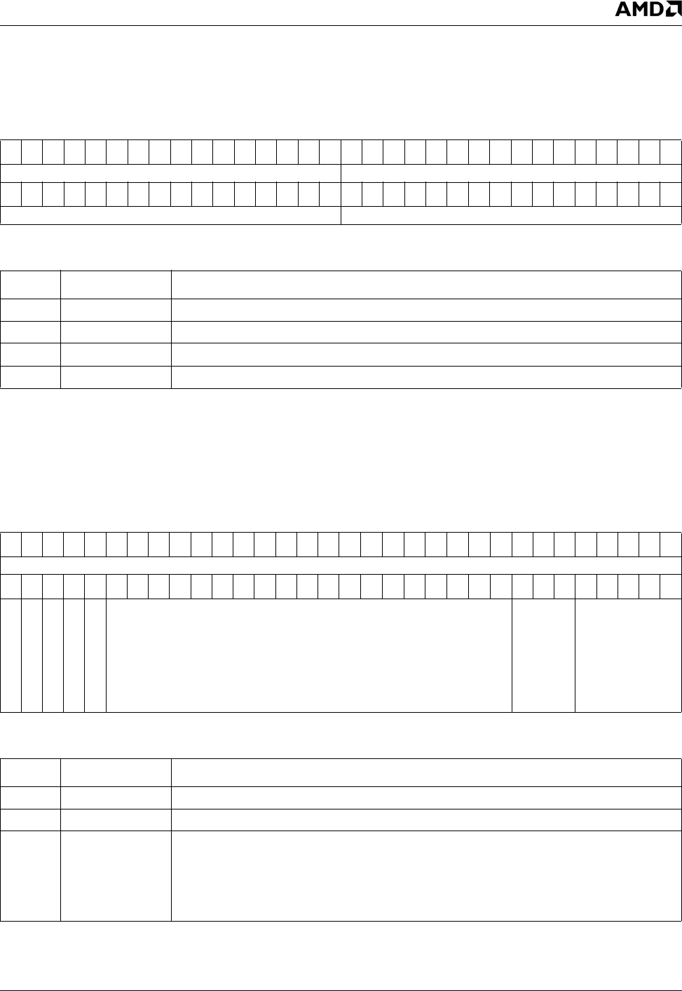
AMD Geode™ LX Processors Data Book 451
Video Processor Register Descriptions 33234H
6.8.3.42 Video Coefficient RAM (VCR)
6.8.3.43 Panel Timing Register 1 (PT1)
VP Memory Offset 1000h-1FFFh
Ty p e R / W
Reset Value xxxxxxxx_xxxxxxxxh
VCR Register Map
63 62 61 60 59 58 57 56 55 54 53 52 51 50 49 48 47 46 45 44 43 42 41 40 39 38 37 36 35 34 33 32
VC3 VC2
313029282726252423222120191817161514131211109876543210
VC1 VC0
VCR Bit Descriptions
Bit Name Description
63:48 VC3 Coefficient 3. Coefficient for tap 3 of filter.
47:32 VC2 Coefficient 2. Coefficient for tap 2 of filter.
31:16 VC1 Coefficient 1. Coefficient for tap 1 of filter.
15:0 VC0 Coefficient 0. Coefficient for tap 0 of filter.
VP Memory Offset 400h
Ty p e R / W
Reset Value 00000000_00000000h
PT1 Register Map
63 62 61 60 59 58 57 56 55 54 53 52 51 50 49 48 47 46 45 44 43 42 41 40 39 38 37 36 35 34 33 32
RSVD
313029282726252423222120191817161514131211109876543210
RSVD
FP_VSYNC_POL
FP_HSYNC_POL
RSVD
HSYNC_SRC
RSVD
HSYNC_DELAY
HSYNC_PLS_WIDTH
PT1 Bit Descriptions
Bit Name Description
63:32 RSVD (RO) Reserved (Read Only). Reads back as 0.
31 RSVD Reserved. This bit is not defined.
30 FP_VSYNC_
POL
FP_VSYNC Input Polarity. Selects positive or negative polarity of the FP_VSYNC input.
Program this bit to match the polarity of the incoming FP_VSYNC signal. Note that FP
Memory Offset 408h[23] controls the polarity of the output VSYNC.
0: FP_VSYNC is normally low, transitioning high during sync interval. (Default)
1: FP_VSYNC is normally high, transitioning low during sync interval

452 AMD Geode™ LX Processors Data Book
Video Processor Register Descriptions
33234H
29 FP_HSYNC_
POL
FP_HSYNC Input Polarity. Selects positive or negative polarity of the FP_HSYNC input.
Program this bit to match the polarity of the incoming FP_HSYNC signal. Note that FP
Memory Offset 408h[22] controls the polarity of the output HSYNC.
0: FP_HSYNC is normally low, transitioning high during sync interval. (Default)
1: FP_HSYNC is normally high, transitioning low during sync interval
28 RSVD Reserved. This bit is not defined.
27 HSYNC_SRC TFT Horizontal Sync Source. Selects a delayed or undelayed TFT horizontal sync out-
put. This bit determines whether to use the HSYNC for the TFT panel without delaying
the input HSYNC, or delay the HSYNC before sending it on to TFT. HSYNC_DELAY
(bits [7:5]) determine the amount of the delay.
0: Do not delay the input HSYNC before it is output onto the LP/HSYNC. (Default)
1: Delay the input HSYNC before it is output onto the LP/HSYNC
26:8 RSVD Reserved. R/W; no function.
7:5 HSYNC_DELAY Horizontal Sync Delay. Selects the amount of delay in the output HSYNC pulse with
respect to the input HSYNC pulse. The delay is programmable in steps of one DOTCLK.
SYNC_SRC (bit 27) must be set in order for HSYNC_DELAY to be recognized.
HSYNC_DELAY is only used for TFT modes.
000: No delay from the input HSYNC. (Default)
001-111: Delay the HSYNC start by one to seven DOTCLKs.
4:0 HSYNC_PLS_
WIDTH
Horizontal Sync Pulse Width. Stretch the HSYNC pulse width by up to 31 DOTCLKs.
The pulse width is programmable in steps of one DOTCLK. HSYNC_PLS_WIDTH is only
used for TFT modes.
00000: Does not generate the HSYNC pulse. The TFT panel uses the default input tim-
ing, which is selected by keeping the HSYNC_SRC bit (bit 27) set to 0. (Default)
00001-11111: The HSYNC pulse width can be varied from one to 31 DOTCLKs.
PT1 Bit Descriptions (Continued)
Bit Name Description
AMD Geode™ LX Processors Data Book 453
Video Processor Register Descriptions 33234H
6.8.3.44 Panel Timing Register 2 (PT2)
VP Memory Offset 408h
Ty p e R / W
Reset Value 00000000_00000000h
PT2 Register Map
63 62 61 60 59 58 57 56 55 54 53 52 51 50 49 48 47 46 45 44 43 42 41 40 39 38 37 36 35 34 33 32
RSVD
313029282726252423222120191817161514131211109876543210
SP
TFT_PASS_THRU
LPOL
RSVD
SCRC
RSVD
VSP
HSP
RSVD
MCS
PIXF RSVD
PT2 Bit Descriptions
Bit Name Description
63:32 RSVD (RO) Reserved (Read Only). Reads back as 0.
31 SP Spare. Bit is read/write, but has no function.
30 TFT_PASS_
THRU
TFT Pass Through. Activates the TFT Pass Through mode. In TFT Pass Through
mode, the input timing and the pixel data is passed directly on to the panel interface tim-
ing and the panel data pins to drive the TFT panel. In Pass Through mode the internal FP
TFT logic and timing is not used.
0: Normal mode; uses the TFT logic and timing from the FP.
1: TFT Pass Through mode; FP TFT timing logic functions are not used.
29 LPOL Display Timing Strobe Polarity Select. Selects the polarity of the LDE/MOD pin. This
can be used for panels that require an active low timing LDE interface signal.
0: LDE/MOD signal is active high. (Default)
1: LDE/MOD signal is active low
28 RSVD Reserved. This bit is not defined.
27 SCRC Panel Shift Clock Retrace Activity Control. Programs the shift clock (SHFCLK) to be
either free running, or active only during the display period. Some TFT panels recom-
mend keeping the shift clock running during the retrace time.
0: Shift clock is active only during active display period.
1: Shift clock is free running during the entire frame period.
26:24 RSVD Reserved. These bits are not defined.
23 VSP Vertical Sync Output Polarity. Selects polarity of the output VSYNC signal. Note that
VP Memory Offset 400h[30] selects the polarity of the input VSYNC.
0: VSYNC output is active high.
1: VSYNC output is active low
22 HSP Horizontal Sync Output Polarity. Selects polarity of output HSYNC signal. Note that
VP Memory Offset 400h[29] selects the polarity of the input HSYNC, and this bit controls
the output polarity.
0: HSYNC output is active high.
1: HSYNC output is active low
21:20 RSVD Reserved. These bits are not defined.

454 AMD Geode™ LX Processors Data Book
Video Processor Register Descriptions
33234H
6.8.3.45 Power Management (PM)
19 MCS Color/Mono Select. Selects color or monochrome LCD panel.
0: Color.
1: Monochrome.
18:16 PIXF Pixel Output Format. These bits define the pixel output format. The selection of the
pixel output format determines how the pixel data is formatted before being sent on to the
DRGB pins. These settings also determine the SHFCLK frequency for the specific panel.
000: Up to 24-bit TFT panel with one pixel per clock.
SHFCLK = DOTCLK.
001: 18/24-bit TFT XGA panel with two pixels per clock.
SHFCLK = 1/2 of DOTCLK.
010, 011, 100, 101, 110, and 111: Reserved.
15:0 RSVD Reserved. These bits are not defined.
FP Memory Offset 410h
Ty p e R / W
Reset Value 00000000_00000002h
PT2 Bit Descriptions (Continued)
Bit Name Description
PM Register Map
63 62 61 60 59 58 57 56 55 54 53 52 51 50 49 48 47 46 45 44 43 42 41 40 39 38 37 36 35 34 33 32
RSVD
313029282726252423222120191817161514131211109876543210
SP
PWR_SEQ_SEL
PNL_PWR_SIM
D
P
PUB2
PUB1
PUB0
PD2
PD1
PD0
HDEL VDEL
SINV
SP
PANEL_PWR_UP
PANEL_PWR_DOWN
PA N E L _ OF F
PANEL_ON
PM Bit Descriptions
Bit Name Description
63:32 RSVD (RO) Reserved (Read Only). Reads back as 0.
31:28 SP Spares. Read/write; no function.
27 PWR_SEQ_SEL Power Sequence Select. Selects whether to use internal or external power
sequence. The power sequence controls the order in which VDDEN, the data and
control signals, and the backlight control signal DISPEN become active during power
up, and inactive during power down.
0: Use internal power sequencing (timing is controlled by bits [24:18]).
1: Use external power sequencing.
Must be written to 0.
26 PNL_PWR_SIM Panel Power Sequence Test Mode. This bit should always be set to 0.
For simulating the model of the panel power sequence logic, this bit may be set to 1. It
connects the 14 MHz reference clock to the 32 Hz panel power sequence clock for
faster simulations. The hardware will not function properly if this bit is set to 1.

AMD Geode™ LX Processors Data Book 455
Video Processor Register Descriptions 33234H
25 D Display Off Control Source. Selects how DISPEN is controlled. Independent control
may be used to disable the backlight to save power even if the panel is otherwise ON.
0: DISPEN is controlled by with the power up/down sequence.
1: DISPEN is controlled independently of the power sequence.
24 P Panel Power On. Selects whether the panel is powered down or up following the
power sequence mechanism.
0: Power down.
1: Power up.
23 PUB2 Panel Power Up Phase Bit 2. Selects the amount of time from when VCORE is
enabled to when the panel data signals are enabled.
0: 32 ms
1: 128 ms
22 PUB1 Panel Power Up Phase Bit 1. Selects the time amount of from when the panel data
signals are enabled to PUB0.
0: 32 ms.
1: 128 ms.
21 PUB0 Panel Power Up Phase Bit 0. Selects the amount of time from PUB1 to when DIS-
PEN is enabled.
0: 32 ms.
1: 128 ms.
20 PD2 Panel Power Down Phase Bit 2. Selects the amount of time from when panel DIS-
PEN is disabled to PD1.
0: 32 ms.
1: 128 ms.
19 PD1 Panel Power Down Phase Bit 1. Selects the amount of time from PD2 to when the
panel data signals are disabled.
0: 32 ms.
1: 128 ms.
18 PD0 Panel Power Down Phase Bit 0. Selects the amount of time from when the panel
data signals are disabled to when panel VCORE is disabled.
0: 32 ms.
1: 128 ms.
17:16 HDEL HSYNC Delay. Delays HSYNC 0 - 3 Dot clocks.
15:14 VDEL VSYNC Delay. Delays VSYNC 0 - 3 Dot clocks.
13 SINV SHFCLK Invert. Invert SHFCLK to panel.
12:4 SP Spares. Read/write; no function.
3 PANEL_PWR_UP
(RO)
Panel Power-Up Status (Read Only). A 1 indicates the flat panel is currently power-
ing up.
2 PANEL_PWR_
DOWN (RO)
Panel Power-Down Status (Read Only). A 1 indicates the flat panel is currently pow-
ering down.
1 PANEL_OFF (RO) Panel OFF Status (Read Only). A 1 indicates the flat panel is currently fully off.
0 PANEL_ON (RO) Panel ON Status (Read Only). A 1 indicates the flat panel is currently fully on.
PM Bit Descriptions (Continued)
Bit Name Description

456 AMD Geode™ LX Processors Data Book
Video Processor Register Descriptions
33234H
6.8.3.46 Dither and Frame Rate Control (DFC)
VP Memory Offset 418h
Ty p e R / W
Reset Value 00000000_00000000h
DFC Register Map
63 62 61 60 59 58 57 56 55 54 53 52 51 50 49 48 47 46 45 44 43 42 41 40 39 38 37 36 35 34 33 32
RSVD
313029282726252423222120191817161514131211109876543210
RSVD
RRS
RSVD
RVRS
RSVD BC DBS
DENB
DFC Bit Descriptions
Bit Name Description
63:13 RSVD (RO) Reserved (Read Only). Reads back as 0.
12 RRS RAM or ROM Select. This bit selects either internal ROM or internal RAM as the source of the
dither patterns.
0: Selects fixed (internal to FP) ROM for dither patterns. (Default)
1: Selects programmable (internal to FP) RAM for dither patterns.
To update the dither RAM, this bit must = 1. See FP Memory Offset 448h[6].
11 RSVD (RO) Reserved (Read Only). Reads back as 0.
10 RVRS Negative Image. This converts the black to white and white to black and all colors in between
to their logical inverse to provide a negative image of the original image. It acts as though the
incoming data stream were logically inverted (1 becomes 0 and 0 becomes 1).
0: Normal display mode.
1: Negative image display mode.
9:7 RSVD (RO) Reserved (Read Only). Reads back as 0.
6:4 BC Base Color. This field is used in conjunction with the DBS field (bits [3:1[). The value in bits
[6:4] sets the base color used prior to dithering.
000: Select 1 MSB for base color use prior to dithering.
001: Select 2 MSB for base color use prior to dithering.
010: Select 3 MSB for base color use prior to dithering.
011: Select 4 MSB for base color use prior to dithering.
100: Select 5 MSB for base color use prior to dithering.
101: Select 6 MSB for base color use prior to dithering.
110: Select 7 MSB for base color use prior to dithering.
111: Select 8 MSB for base color, no dithering.
3:1 DBS Dithering Bits Select. This field is used to select the number of bits to be used for the dither-
ing pattern. Dither bits are the LSBs of each pixel’s final color value; FRM bits are the MSBs.
000: Selects 6 bits as dither bits.
001: Selects 5 bits as dither bits.
010: Selects 4 bits as dither bits.
011: Selects 3 bits as dither bits.
100: Selects 2 bits as dither bits.
101: Selects 1 bits as dither bits.
110, 111: Reserved.

AMD Geode™ LX Processors Data Book 457
Video Processor Register Descriptions 33234H
6.8.3.47 Dither RAM Control and Address (DCA)
0DENB Dithering Enable. Enable/disable dithering. The dither bit must be enabled in order for dither
RAM reads or writes to occur. When this bit is cleared, the internal dither RAM is powered
down, which saves power.
0: Dither disable. The dithering function is turned off. When the dither is disabled the Dithering
Bits Select (bits [3:1]) do not have any effect and the dither RAM is not accessible.
1: Dither enable. The dither functions with the number of dither bits as set in the Dithering Bits
Select (bits [3:1]).
VP Memory Offset 448h
Ty p e R / W
Reset Value 00000000_00000000h
DFC Bit Descriptions (Continued)
Bit Name Description
DCA Register Map
63 62 61 60 59 58 57 56 55 54 53 52 51 50 49 48 47 46 45 44 43 42 41 40 39 38 37 36 35 34 33 32
RSVD
313029282726252423222120191817161514131211109876543210
RSVD A U ADDR
DCA Bit Descriptions
Bit Name Description
63:8 RSVD (RO) Reserved (Read Only). Reads back as 0.
7A Dither RAM Access Bit. Allows reads and writes to/from Dither RAM.
0: Disable (do not allow reads or writes).
1: Enable (allow reads and writes).
To perform dither RAM writes and reads, both bits 7 and 6 must be set to 1. In addition
VP Memory Offset 418h bits 12 and 0 must both be set to 1. If any of these bits are not
set to 1, the RAM goes into power-down mode.
6U Dither RAM Update. This bit works in conjunction with bit 7. If this bit is enabled, it
allows the data to update the RAM.
0: Disable (do not allow dither RAM accesses).
1: Enable (allow dither RAM accesses).
To perform dither RAM writes and reads, both bits 7 and 6 must be set to 1. In addition
VP Memory Offset 418h bits 12 and 0 must both be set to 1. If any of these bits are not
set to 1, the RAM goes into power-down mode.
5:0 ADDR RAM Address. This 6-bit field specifies the address to be used for the next access to the
dither RAM.

458 AMD Geode™ LX Processors Data Book
Video Processor Register Descriptions
33234H
6.8.3.48 Dither Memory Data (DMD)
6.8.3.49 Panel CRC Signature (CRC)
VP Memory Offset 450h
Ty p e R / W
Reset Value 00000000_00000000h
DMD Register Map
63 62 61 60 59 58 57 56 55 54 53 52 51 50 49 48 47 46 45 44 43 42 41 40 39 38 37 36 35 34 33 32
RSVD
313029282726252423222120191817161514131211109876543210
RDAT
DMD Bit Descriptions
Bit Name Description
63:32 RSVD (RO) Reserved (Read Only). Reads back as 0.
31:0 RDAT RAM Data. This 32-bit field contains the read or write data for the RAM access.
VP Memory Offset 458h
Ty p e R / W
Reset Value 00000000_00000000h
CRC Register Map
63 62 61 60 59 58 57 56 55 54 53 52 51 50 49 48 47 46 45 44 43 42 41 40 39 38 37 36 35 34 33 32
RSVD
313029282726252423222120191817161514131211109876543210
RSVD FRCT
SIGVAL
SIGFR
SIGEN
CRC Bit Descriptions
Bit Name Description
63:9 RSVD (RO) Reserved (Read Only). Reads back as 0.
8:3 FRCT (RO) Frame Count (Read Only). Represents the frame count, which is an index for the gener-
ated signature for that frame.
2 SIGVAL (RO) Signature Valid (Read Only). If this bit is set, the signature operation has completed
and the signature may be safely read from the 32-Bit Panel CRC Register (VSP Memory
Offset 468h).
1SIGFR Signature Free Run. If this bit is high, with signature enabled (bit 0 = 1), the signature
generator captures data continuously across multiple frames. This bit may be set high
when the signature is started, then later set low, which causes the signature generation
process to stop at the end of the current frame.
0: Capture signature for only one frame.
1: Free run across multiple frames.
0SIGEN Signature Enable. Enables/disables signature capture.
1: Enable signature capture.
0: Disable signature capture.
AMD Geode™ LX Processors Data Book 459
Video Processor Register Descriptions 33234H
6.8.3.50 32-Bit Panel CRC (CRC32)
6.8.3.51 Video Output Port Configuration (VOP_CONFIG)
VP Memory Offset 468h
Ty p e RO
Reset Value 00000000_00000001h
CRC32 Register Map
63 62 61 60 59 58 57 56 55 54 53 52 51 50 49 48 47 46 45 44 43 42 41 40 39 38 37 36 35 34 33 32
RSVD
313029282726252423222120191817161514131211109876543210
CRC
CRC32 Bit Descriptions
Bit Name Description
63:32 RSVD Reserved. Reads back as 0.
31:0 CRC 32-Bit CRC. 32-Bit Signature when in 32-bit CRC mode. See FP Memory Offset 458h for
additional information.
VP Memory Offset 800h
Ty p e R / W
Reset Value 00000000_00000000h
VOP_CONFIG Register Map
63 62 61 60 59 58 57 56 55 54 53 52 51 50 49 48 47 46 45 44 43 42 41 40 39 38 37 36 35 34 33 32
RSVD
313029282726252423222120191817161514131211109876543210
SPARE
VBI_SWAP
RSVD
RGB_MODE
VALID_SIG
INV_DE_POL
INV_VS_POL
INV_HS_POL
UV_SWAP
VSYNC_SHFT
DIS_DEC
601_MODE
VBI
RSVD
TASK
SGFR
SIGE
SC120X_MODE
422_MODE
EXT_VIP_CODES
VIP_LEVEL
VIP_MODE
VOP_CONFIG Bit Descriptions
Bit Name Description
63:32 RSVD (RO) Reserved (Read Only). Reads back as 0.
31:25 SPARE Spare.
24 VBI SWAP VBI Swap. When set to 1, swap upper and lower bytes of VBI data.
22:23 RSVD Reserved.
21 RGB MODE RGB Mode. Set this bit to 1 if RGB data sent: applicable in 24-bit 601 mode so as to
choose correct blanking data. If this bit is set, then blanking data is 0, otherwise it is YUV
= 10, 80, 80.
20 VALID SIG (RO) Valid Signature (Read Only). If signature enabled, this bit can be read to determine if
the signature is valid.
19 INV DE POL Invert Display Enable Polarity. Set to 1 to invert polarity of display enable (for 601
mode only).

460 AMD Geode™ LX Processors Data Book
Video Processor Register Descriptions
33234H
18 INV VS POL Invert VSYNC Polarity. Set to 1 to invert polarity of VSYNC (for 601 mode only).
17 INV HS POL Invert HSYNC Polarity. Set to 1 to invert polarity of HSYNC (for 601 mode only).
16 UV SWAP UV Swap.
0: No swap.
1: Swap lowest byte with next lowest byte in [23:0] input data stream. This is essentially
swapping the U and V, and if in RGB, swapping G and B.
15:14 VSYNC SHFT VSYNC Shift. This is the number of VOP clocks to shift the VSYNC with respect to
HSYNC for odd field detection in 601 mode.
00: Shift VSYNC earlier by 4 cycles (-4).
01: Shift VSYNC earlier by 2 cycles (-2).
10: Zero shift - both are aligned as they were received from Display Controller.
11: Shift later based on programmable value in DC Memory Offset 080h.
13 DIS DEC Disable Decimation. This is used in conjunction with 601 mode for 24-bit YUV/RGB out-
put on VOP.
12 601 MODE Enable 601 Mode.
0: Disable.
1: Enable.
11 VBI Vertical Blanking Interval. When this bit is set to 1, the Task bit (bit 9) is used to indi-
cate VBI data.
In BT.656 mode, the TASK bit (bit 9) in the EAV/SAV is fixed at 1, if this VBI bit is set,
then a value of 0 in the TASK bit location indicates VBI data.
In VIP 1.1 mode, the TASK bit in the EAV/SAV is defined such that 0 is VBI data, and 1 is
active video data. Therefore, this VBI bit has no effect in VIP 1.1 mode.
In VIP 2.0 mode, the TASK bit determines the value of the TASK bit in the EAV/SAV.
With the VBI bit set, the inverse of TASK indicates VBI data.
10 RSVD Reserved. Reads back as 0.
9 TASK TASK. Value for the Task bit in VIP 2.0 mode.
8SGFR Signature Free Run.
0: Disable. If this bit was previously set to 1, the signature process will stop at the end of
the current frame.
1: Enable. If SIGE (bit 7) is set to 1, the signature register captures data continuously
across multiple frames.
7SIGE Signature Enable.
0: Disable. VP Memory Offset 808h[31:0] is reset to 0000_0000h and held (no capture).
1: Enable. The next falling edge of VSYNC is counted as at the start of the frame to be
used for CRC checking with each pixel clock beginning with the next VSYNC.
If the SGFR bit (bit 8) is set to 1, the signature register captures the pixel data signature
continuously across multiple frames.
If SGFR is cleared to 0, a signature is captured for one frame at a time, starting from the
next falling VSYNC.
After a signature capture is complete, VP Memory Offset 808h[31:0] can be read to
determine the CRC check status. Then proceed to reset the SIGE which initializes VP
Memory Offset 808h[31:0] as an essential preparation for the next round of CRC checks.
VOP_CONFIG Bit Descriptions (Continued)
Bit Name Description
AMD Geode™ LX Processors Data Book 461
Video Processor Register Descriptions 33234H
6.8.3.52 Video Output Port Signature (VOP_SIG)
6 SC120X_MODE SC120X Compatible Mode. Creates EAV/SAV codes consistent with the AMD Geode™
SC1200 and SC1201 processor’s VOP.
0: Normal mode.
1: SC1200/SC1201 compatible mode. Set to 1 for BT.601 mode.
5:4 422_MODE 4:4:4 to 4:2:2 Conversion Algorithm. Selects which method is used to convert 4:4:4
data to 4:2:2.
00: 4:2:2 Co-sited.
01: 4:2:2 Interspersed (U,V samples from respective co-samples).
10: 4:2:2 Interspersed (U,V samples from alternating successive samples).
11: Not used.
3 EXT_VIP_
CODES
Extended VIP SAV Codes. Additional SAV codes not defined in VIP 2.0 spec, but used
in numerous available other applications (also used in BT.656).
0: Do not use extended codes.
1: Use extended codes.
Note: Selecting BT.656 mode (in bits [1:0]) automatically uses the extended codes.
2 VIP_LEVEL VIP 2.0 Level Selection.
0: VIP 2.0 Level I (8-bit), 601 8-bit.
1: VIP 2.0 Level II (16-bit), 601 16-bit.
1:0 VIP_MODE VIP Mode. Selects between VESA VIP standards.
00: VOP disabled (logic 0’s on data buses).
01: VIP v1.1.
10: VIP v2.0/ BT.601. Selects VIP v2.0 or BT.601 if 601 MODE bit (bit 12) is set.
11: BT.656.
VP Memory Offset 808h
Ty p e RO
Reset Value 00000000_00000000h
VOP_CONFIG Bit Descriptions (Continued)
Bit Name Description
VOP_SIG Register Map
63 62 61 60 59 58 57 56 55 54 53 52 51 50 49 48 47 46 45 44 43 42 41 40 39 38 37 36 35 34 33 32
RSVD
313029282726252423222120191817161514131211109876543210
CRC
VOP_SIG Bit Descriptions
Bit Name Description
63:32 RSVD Reserved. Reads back as 0.
31:0 CRC 32-Bit CRC. 32-Bit Signature when in 32-bit CRC mode.

462 AMD Geode™ LX Processors Data Book
Video Input Port
33234H
6.9 Video Input Port
6.9.1 Features
•VESA 1.1, 2.0 and BT.601, BT.656 compliant, 150 MHz
(excludes host interface).
— Standard 9 or 17 pin interface (8/16 data + clock)
— 8/16-bit BT.656 video
— TASK A/B video and VBI (two video streams)
— 8/16-bit ancillary data
— HD capable (up to 1280x720 progressive scan,
1920x1080 interlaced)
— VIP 1.1 compatible mode (8 bit)
•8/16-bit BT.601 type input video with HSYNC and
VSYNC
•8-bit message and streaming video transfer mode
— (8 + clock + control on vid[10:8])
•Video data stored in linear or planar buffers
•Even line or even field decimation (4:2:2 -> 4:2:0 transla-
tion)
•Automatic paging for multi-frame storage
•Provides full frame buffer generation from interlaced
input (Weave)
•Mutli-burst GLIU packets (programmable)
•Internal loopback using VOP outputs as source data
•vip_sync_to_pin output pin to request next frame or data
packet from external data source (GenLock)
•vip_sync_to_vg output to DC/VP for frame synchroniza-
tion (VSYNC indication)
•frame_to_vg output to DC/VP for frame synchronization
(odd/even field indication)
•vip_int output for interrupt generation on frame/field/line
boundaries
6.9.1.1 Performance Metrics
— System goals:
— 150 MHz video interface
— 400 MHz GLIU interface
— Adequate GLIU bandwidth in HD capture mode (HD
VIP requires ~20 million QWORDs/sec)
— GLIU Latency requirements
Table 6-72. VIP Capabilities
Input
Output
(to memory) Memory Storage Supports Task
YUV 4:2:2 Interlaced (8/16-bit)
SD/HD
YUV 4:2:2 Linear, Single Frame Buffer Weave A or B
YUV 4:2:2 Planar, Single Frame Buffer Not Applicable A or B
YUV 4:2:2 Linear, Odd/Even Field Buffers Bob A or B
YUV 4:2:2 Planar, Odd/Even Field Buffers Not Applicable A or B
YUV 4:2:0 Planar, Single Frame Buffer Rotation/Weave A or B
YUV 4:2:0 Planar, Odd/Even Field Buffers Rotation/Bob A or B
YUV 4:2:2 Progressive
(8/16-bit)
SD/HD
YUV 4:2:2 Linear, Single Frame Buffer Standard Mode A or B
YUV 4:2:2 Planar, Single Frame Buffer Not Applicable A or B
YUV 4:2:0 Planar, Single Frame Buffer Rotation A or B
YUV 4:2:0 YUV 4:2:0 Linear SC1200 Compatible A or B
VBI Data (8/16-bit) VBI Data Linear VBI Data A or B
Ancillary Data (8/16-bit) ANC Data Linear, Circular Buffer Ancillary Data N/A
Message Data (8-bit only) MSG Data Linear, Dual Buffers Message Data N/A
Streaming Data (8-bit only) RAW Data Linear, Dual Buffers RAW Data N/A
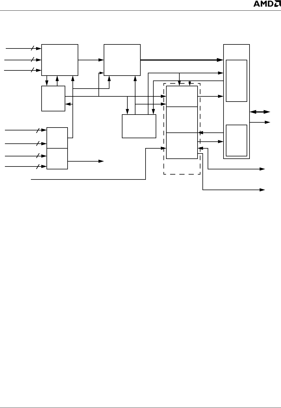
AMD Geode™ LX Processors Data Book 463
Video Input Port 33234H
6.9.2 VIP Block Descriptions
Figure 6-39. VIP Block Diagram
8/16
Address address
Formatter
Generator
Memory
Registers
VIP Data
VIP Clock
VIP Clock Control
GLIU Clock
GLIU Clock Control
VIPCLK
GLIU_CLK
Input
Control
QWORD = 64 bits
take
req
reg write
reg read
Mapped
GLIU
Interface
Clock Control
Input
Output
Control
Dual Port
input ctl
output ctl
16 bits Capture RAM
VIP INT
SYNC_TO_PIN
SYNC_TO_VG
(256x64)
VIDEO_OK
FIELD_TO_VG
VIPSYNC
VIP VSYNC
VIP HSYNC
VIP
Clock
GLIU
Clock
MSR
Registers
GLIU
Write
Master
GLIU
Slave
GLIU
Planar mode: 512 byte(64 QWORDs) YUV, Ancillary FIFO
Linear mode: 1536 byte(192 QWORDs) Video, 256 (64 QWORDs) byte Ancillary FIFO
VIP Register
Block

464 AMD Geode™ LX Processors Data Book
Video Input Port
33234H
6.9.2.1 Input Formatter
The Input Formatter receives 8- or 16-bit VIP input data, It
does a 4:2:2 to 4:2:0 translation (if enabled) and formats it
into either linear data or planar data for storage in the Cap-
ture RAM.
6.9.2.2 Input Control
The Input Control block operates in either VIP 2.0 16-bit
mode, VIP 2.0 8-bit mode, VIP 1.1 compatible mode, Mes-
sage Passing mode, Data Streaming mode, or BT.601
Input mode. The Input Control block decodes preamble
and status from EAV/SAV and ancillary packets as well as
start/stop control for message passing packets or HSYNC/
VSYNC timing in BT.601 like input mode and generates
control to the Input Formatter and Capture RAM. Video
frame timing is decoded and passed on to the Address
Generator and GLIU. The VIP input state machine is imple-
mented in the Input Control block.
It should be noted that values from the configuration and
control registers are synchronized to the video clock before
being used by the Input Control block.
The VIP Input Control block contains:
• A state machine that keeps track of the video stream
protocol.
• Logic to infer the odd/even VBI/ancillary packet informa-
tion necessary to store data in memory.
• Sequencing control generation for the Input Formatter.
• Generation of start and stop capture, as well as capture
active status.
• Line start and end logic.
6.9.2.3 VIP Capture RAM
The Capture FIFO is a 256 WORDx64bit dual port RAM.
The input side is driven by the VIP clock. The output side is
driven by the GLIU clock. The memory is divided into a 192
QWORD buffer for video and a 64 QWORD buffer for ancil-
lary data when linear buffers are defined in system mem-
ory. It is partitioned into four 64 QWORD buffers when
planar buffers are defined in system memory. One 64
QWORD buffer is used for each of the Y, U, V and ancillary
data types. Data is stored in QWORDs. The watermark at
which the FIFO begins emptying is programmable. Gener-
ally, a minimum of eight QWORDs are stored in a buffer
before GLIU write. This enables two consecutive burst write
requests to be issued, which should provide the most effi-
cient cycle times to system memory. Programmable thresh-
old level flags are available to monitor data levels. This
should be helpful in debugging. Memory BIST is imple-
mented and can be invoked from the JTAG logic from a
MSRs. The memory can also be read/written using VIP
memory mapped registers.
6.9.2.4 VIP Register Block
The VIP register block contains the Address Generator,
MSR registers and memory mapped registers.
The Address Generator supports up to four data streams
(Y, Cr, Cb, and ancillary). Each data stream has an inde-
pendent logical FIFO. The Capture RAM is partitioned into
four FIFOS for planar storage mode (Y, Cr, Cb, and ancil-
lary) each being 64 QWORDs deep. In linear storage mode
the Capture RAM is partitioned into two FIFOs (Y = 192
QWORDs, ancillary = 64 QWORDs). Four vip_output_addr
blocks provide individual FIFO management and the VIP
Output Control block controls the time-slicing of GLIU
request for each FIFO. A separate buffer (system memory
address) is maintained for each data type as described by
Table 6-74 on page 475. The video base addresses regis-
ters are double buffered so address updates can be made
for the next frame while the current frame is being pro-
cessed.
The memory mapped registers are contained in the VIP
register block. Interrupt generation, and logic for updating
the base registers at frame boundaries is also implemented
in this block.
6.9.2.5 GLIU Interface
The GLIU provides a standard interface to the AMD Geode
LX processor. The VIP is both a write master and a slave
on this bus.
As a write master, the VIP performs write requests to send
single beat writes, or a burst of four QWORDs to memory.
The VIP is considered a low-bandwidth isochronous mas-
ter to the GLIU. A FIFO watermark threshold is program-
mable, which allows the write transaction priority to be
increased when the data count in the FIFO exceeds the
threshold. Handshaking exists between the GLIU master
and the Output Control/Address Generation blocks so that
address and data is supplied at the correct cycles.
As a slave, the VIP stores register data from the GLIU and
returns register data being read by the GLIU. Bursts are not
supported by the slave interface. Both MSRs and memory
mapped registers are accessible through the slave inter-
face. The front end control generates the per-byte write
enables to all registers except the base registers.

AMD Geode™ LX Processors Data Book 465
Video Input Port 33234H
6.9.3 Functional Description
The Video Input Port (VIP) receives 8- or 16-bit video or
ancillary data, 8-bit message data, or 8-bit raw video, and
passes it to data buffers located in system memory. The
primary operational mode is as a compliant VIP 2.0 slave.
The VIP 2.0 specification defines the protocol for receiving
video, VBI, and ancillary data. The addition of the Message
Passing and Data Streaming modes provide flexibility in
receiving non-VIP 2.0 compliant data streams. The VIP is
essentially a DMA engine. Input data is packed into
QWORDs, buffered into a FIFO, and sent to system mem-
ory over the GLIU. The VIP masters the internal GLIU and
transfers the data from the FIFO to system memory. The
maximum input data rate (8 or 16 bits) is 150 MHz. The
GLBus (64 bits) operates from 200-400 MHz correspond-
ing to the DDR clock rate to external memory.
The VIP can successfully input line sizes as small as 12
clocks with 20 clocks of blanking, with a 16-bit data/100
MHz VIP clock rate at 400 MHz GLIU, when the VIP's prior-
ity is equal to that of the DC. The limitation has to do with
the total line length (active data + blanking time). Any size
of active data can be received if a reasonable amount of
blanking is provided. The above case corresponds to a 6-
pixel line. This is likely smaller then anything that realisti-
cally will be received (and at a higher frequency then the 75
MHz max). The VIP line size limitation is determined by the
input frequency and the GLIU latency. The worst case is
with a high frequency VIP clock and low frequency GLIU
clock in a busy system. The VIP FIFO Line Wrap Interrupt
(INT) is generated if the line is not received correctly. If this
INT occurs, VIP priority should be increased and/or the
blanking time of the input line increased. As there is no
specification/requirement regarding VIP minimum line size,
it is recommended that any non-standard input have ~100
clocks of blanking. This prevents any special priority
requirements for “postage stamp” size frames.
6.9.4 VIP Operation Modes
The VIP provides direct hardware compatibility with the
VESA 2.0 Standard (VIP 2.0), Level II. VIP 2.0 data is a
simplified BT.656 video format. The simplification is due to
VIP only having to receive data. (VIP does not concern
itself with specific frame timing) The data the VIP receives
is only stored in system memory. In addition to receiving
BT.656 video format data, the VIP can also receive 8-bit
message data and 8-bit streaming data, allowing the
AMD Geode CS5536 companion device connected to the
VIP to load data directly into the AMD Geode LX proces-
sor’s system memory. The Message Passing and Data
Streaming modes are not defined in the VESA 2.0 specifi-
cation. The VIPSYNC output provides a software controlled
output that can be used for frame/data synchronization with
output devices that support data throttling. VIP must be
configured to receive specific data types. The following
input modes are supported by the VIP.
•Mode 1a - VIP 1.1 compatible mode (BT.656 data with
following notes):
— Task bit is used to indicate VBI data within the video
stream (T = 0 for VBI Data, T = 1 for active video).
— Video data is stored in the Task A video base
address. VBI data is saved in the Task A VBI base
address.
— Video Flags T, F, and V can only be changed in the
EAV code.
— During vertical blanking there must be a minimum of
one SAV/EAV scan line.
— 8-bit data only (EAV/SAV packets + ancillary data
packets).
•Mode 1b - 8-bit VIP 2.0 Level I mode (BT.656 data with
following notes):
— Video Flags T, F, and V are valid in the EAV and SAV
code, valid values must appear no later then the SAV
of the first scan line of the next active region.
— Task bit differentiates between two video streams.
These streams can be interleaved at a scan or field
rate.
— V bit differentiates between active video and VBI data
(V = 1 for VBI data, V = 0 for active video).
— During vertical blanking there must be a minimum of
one SAV/EAV scan line.
— New Video Flags - The P Nibble is redefined as
[NON_INT,REPEAT,Reserved,EXT_FLAG].
— 8-bit data only (EAV/SAV packets + ancillary data
packets).
•Mode 1c - 16-bit VIP 2.0 Level II mode (BT.656 data with
following notes):
— Video Flags T, F, and V are valid in the EAV and SAV
code, valid values must appear no later then the SAV
of the first scan line of the next active region.
— Task bit differentiates between two video streams.
These streams can be interleaved at a scan or field
rate.
— V bit differentiates between active video and VBI data
(V = 1 for VBI data, V = 0 for active video).
— During vertical blanking there must be a minimum of
one SAV/EAV scan line.
— New Video Flags - The P Nibble is redefined as
[NON_INT,REPEAT,Reserved,EXT_FLAG].
— 16-bit data only (EAV/SAV packets + ancillary data
packets).
•Mode 2 - Message Passing mode (8-bit):
— vip_vdata[8] = start_msg, vip_vdata[9] = end_msg.
— 8-bit data only.
•Mode 3 - Data Streaming mode (8-bit):
— vip_data[8] = start_msg, vip_vdata[9] =
vip_data_enable.
— 8-bit data only.
•Mode 4 - BT.601 mode (8/16-bit):
— No SAV/EAV recognition. Input timing based on
VSYNC and HSYNC inputs.
— HSYNC input on pin LDEMOD, VSYNC input on pin
VDDEN.
— TFT output mode cannot be used when VIP is config-
ured in BT.601 mode.
466 AMD Geode™ LX Processors Data Book
Video Input Port
33234H
6.9.5 Mode 1a,b,c - VIP Input Data
(simplified BT.656)
The VIP 2.0 specification describes an 8- or 16-bit data
stream incorporating both control and data. The data/con-
trol is delivered in packets. There are two different packet
types, SAV/EAV and ancillary packets. The specification
also requires backwards compatibility to VIP 1.1 data for-
mats. Three different VIP data modes are supported: VIP
1.1 compatible mode, VIP 2.0 8-bit mode, and VIP 2.0 16-
bit mode. Differences in these modes are noted in the
descriptions of the different packet types in Section 6.9.5.1
on page 466.
6.9.5.1 SAV/EAV Packets
The SAV/EAV packets begin with 3 bytes of preamble fol-
lowed by a Start of Active Video (SAV) status WORD.
Active data follows. The packet ends with the reception of
another 3 bytes of preamble followed by an End of Active
Video (EAV) status WORD. The preamble consists of FF-
00-00. The codes FF and 00 codes are prohibited as video
samples and reserved for header and synchronization pur-
poses. The code 00 can be used within a packet to mark an
empty cycle. If a 00 code appears between the SAV and
EAV, that sample is ignore. Note that in 16-bit mode, only
the 8 LSBs are checked. If 00, the entire 16-bit WORD is
ignored. The preamble and status WORD always occurs on
bits [7:0] of the input data, even in 16-bit mode. The active
data is received on bits [7:0] in 8-bit mode and on bits
[15:0] in 16-bit mode. The Y values appear on bits [7:0] and
Cx values on bits [15:8]. Both active video and VBI data are
received in SAV/EAV packets. The format of the SAV and
EAV preamble and status WORD is shown in Table 6-73. A
sample SAV/EAV line is shown in Figure 6-40 on page 467.
A full frame is shown in Figure 6-41 on page 468.
The status WORD provides the raster reference information:
VIP 1.1 compatible mode:
— Video Flags T, F, and V can only be changed in the
EAV code per the VIP 1.1 specification. These flags
are only captured in the EAV code.
— In VIP 1.1, the Task bit is used to indicate VBI data
within the video stream (T = 0 for VBI data, T = 1 for
active video). In VIP 1.1 mode, the Task bit is used in
place of the V bit to indicate VBI data.
— P3-P0 are ignored.
VIP 2.0 modes (8- or 16-bit data):
— Video Flags T, F, and V are valid in the EAV and SAV
code. Valid values must appear no later then the SAV
of the first scan line of the next active region.
— Task bit differentiates between two video streams.
These streams can be interleaved at a line or field
rate.
— V bit differentiates between active video and VBI data
(V = 1 for VBI data, V = 0 for active video).
— New Video Flags - The P Nibble is redefined as
[NON_INT,REPEAT,Reserved,EXT_FLAG]:
– NON_INT: 1 = non-interlaced source, 0 = inter-
laced source (not used).
– REPEAT: 1 = Repeat field in 3:2 pull-down, 0 = not
a repeat field (repeat fields can be ignored by
VIP). The repeat flag must be set in the SAV for
every line in the field. The line will be saved to
memory if the repeat flag is not set. (This function
needs to be enabled in VIP Memory Offset
04h[29]).
– EXT_FLAG: 1 = Extra flag byte follows this EAV, 0
= no extra flag byte (not implemented).
Table 6-73. SAV/EAV Sequence
Parameter D7D6D5D4D3D2D1D0
Preamble 11111111
00000000
00000000
Status WORD T F V H P3 P2 P1 P0
T = Task BIT 0 = Task B 1 = Task A
F = Field ID 0 = Odd 1 = Even
V = Vertical blanking 0 = Active video 1 = Vertical blanking
H = Horizontal blanking 0 = Active line 1 = Horizontal blanking
P3-0 = Reserved in VIP 1.1, New Flags in VIP 2.0
AMD Geode™ LX Processors Data Book 467
Video Input Port 33234H
VIP 2.0 Video Flags
Two new video flags are defined in the VIP 2.0 specification
to decode whether the input video is interlaced or noninter-
laced and whether the data is merely a repeated field.
These flags are meant to enable VIP to handle Bob and
Weave, as well as 3:2 pull down in hardware. The new
flags are embedded in the lower nibble of the SAV and EAV
header. The non-interlace flag NON_INT (bit 3 of the status
WORD) is ignored by the VIP. The video stream must be
known and the software must set up the appropriate base
and pitch addresses to store the video into system mem-
ory. The repeat flag (bit 2 of the status WORD) can be
decoded by the VIP if the feature is enabled in the VIP
Control Register 2 (VIP Memory Offset 04h[29]). The
repeat flag is set during 3:2 pull down. In 3:2 pull down,
fields are repeated to increase the frame rate. The VIP
ignores fields (lines) with the repeat flag set. This reducers
the amount of data being transferred to system memory,
reducing overall bandwidth requirements. Additional flag
bytes are also supported in the VIP 2.0 specification.
These extra flag bytes can only occur during EAV (NOT
SAV). The VIP ignores extra flag bytes.
Note: Since the extra flag byte can only occur during
EAV, they can be ignored without effecting the
reception of following SAV/EAV packets.
.
Figure 6-40. BT.656, 8/16-Bit Line Data
F
F0
00
0X
Y8
01
08
01
08
01
0F
F0
00
0X
YC
BC
R
YYC
BC
R
Y
EAV Code SAV Code
4Horizontal Blanking 4Active Video
Start of Digital Line
4:2:2 Sampled Video Data
F
F
0
00
0X
Y
EAV Code
F
F0
00
0R
P8
01
08
01
08
01
0F
F0
00
0R
PYYYYYYYF
F
0
00
0R
P
X
XX
XX
XX
X8
01
08
01
08
01
0X
XX
XX
XX
XC
B
C
B
C
BC
BX
X
X
XX
XX
X
8-Bit VIP Data
16-Bit VIP Data
4Horizontal Blanking 4Active Video
C
RC
RC
R
4
EAV Code SAV Code 4:2:2 Sampled Video Data EAV Code
VIP_DATA[7:0]
VIP_DATA[7:0]
VIP_DATA[15:8]
(VIP 2.0 Level II)
(VIP 1.1 and VIP 2.0 Level I)
468 AMD Geode™ LX Processors Data Book
Video Input Port
33234H
Figure 6-41. 525 line, 60 Hz Digital Vertical Timing
Line 1 (V = 1)
Line 20(V = 0)
Line 264 (V = 1)
Line 283 (V = 0)
Line 525 (V = 0)
Blanking
Field 1
Active Video
Blanking
Field 2
Active Video
Line 4
Line 266
Line 3
Field 1
(F = 0)
Odd
Field 2
(F = 1)
Even
H = 1
EAV
H = 0
SAV
Line
Number F V
H
(EAV)
H
(SAV)
1-3 1 1 1 0
4-19 0 1 1 0
20-263 0 0 1 0
264-265 0 1 1 0
266-282 1 1 1 0
283-525 1 0 1 0
(VBI Data)
(VBI Data)
In VIP 1.1 mode, the T,F,V video flags are only captured from the EAV code. In VIP 2.X modes, these flags are captured from
both the SAV and the EAV codes. (The H bit is always captured to distinguish between and SAV and EAV code). Note that for VIP
1.1 mode, there must be a minimum of one SAV/EAV scan line during vertical blanking in order for the VBlank flag to transition
from 0->1->0.
An End-of-Frame event is detected the same in VIP 1.1 and VIP 2.0 modes. (A 0->1 transition of VBlank when F = 1 causes an
End-of-Frame event during interlaced video, A 0->1 transition of V-Blank causes an End-of-Frame event during progressive scan
video) An End-of-Frame event is used for starting/stopping capture and for updating buffer addresses. Line #1 of a frame does not
necessarily coincide with the End-of-Frame event. Line #1 is specified differently with respect to VBlank depending on the frame
type (resolution/interlaced/...). When line#1 is defined other then on the falling transition of VBlank, VBI data received after the V-
Blank transition will be stored in updated buffer address. VBI data is generally not sent during this time.
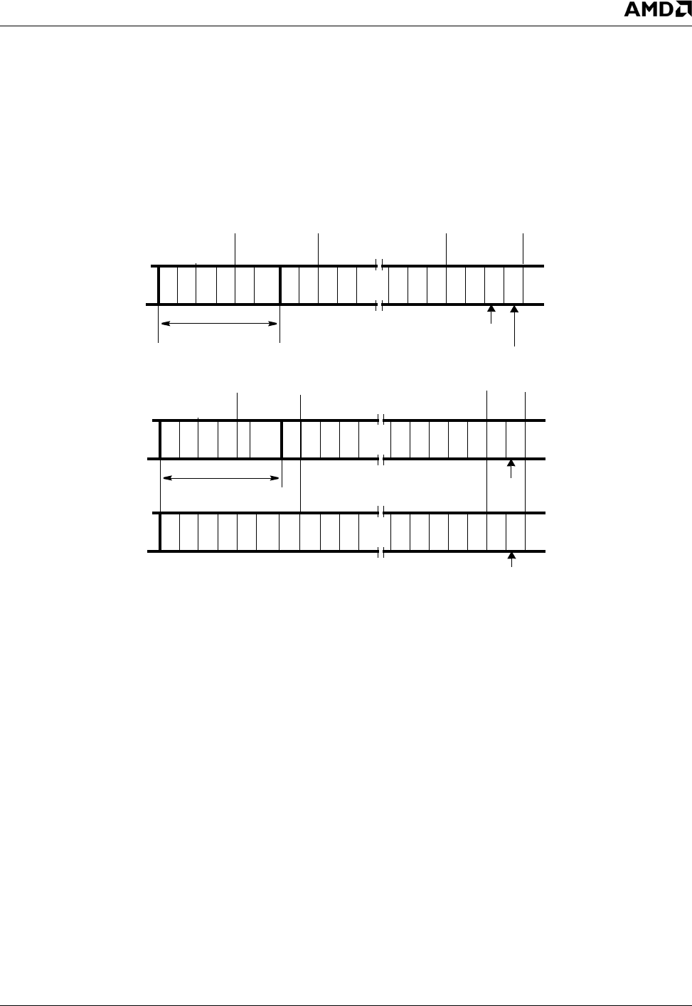
AMD Geode™ LX Processors Data Book 469
Video Input Port 33234H
6.9.5.2 Ancillary Packets
Ancillary packets are received during vertical and/or hori-
zontal blanking. The ancillary packet has a 6-byte header
of 00-FF-FF-DID-SDID-NN. The first three bytes are the
pre-amble. The DID and SDID bytes are the data identifier
and the secondary data identifier bytes. The NN byte is the
data count and specifies the length of the ancillary data
block in DWORDs (4-byte blocks). The entire ancillary data
packet is stored to memory, including all 6 bytes of pream-
ble/header. See Section 6.9.10 on page 475 for further
explanation. There is no restriction on the code in the data
section of the packet (codes 00 and FF are allowed) The
SAV/EAV packet preamble detection circuitry is disabled
during the reception of these NN blocks of data to allow
reception of 00, FF codes. The active data is received on
bits [7:0] in 8-bit mode, [9:0] in 10-bit mode and on [15:0] in
16-bit mode.
A sample ancillary packet is shown in Figure 6-42.
Figure 6-42. Ancillary Data Packets
0
0F
FF
FD
IS
IN
N
6 Byte Ancillary Header
DD
First DWORD Last DWORD
Id0 d1 d2 d d d d d
check sum
fill byte
0
0F
FF
FD
IS
I
DD
First Last
d0 d2 d4 d6 ddddd
check
XXXX XXd1 d3 d5 d7 ddddd
fill byte
d
d
DWORD
6 Byte Ancillary Header
N
N
8/10-BIT ANCILLARY PACKET
16-BIT ANCILLARY PACKET
sum
D
D
I
D
D
DWORD
VID[7:0]
VID[7:0]
VID[15:8]
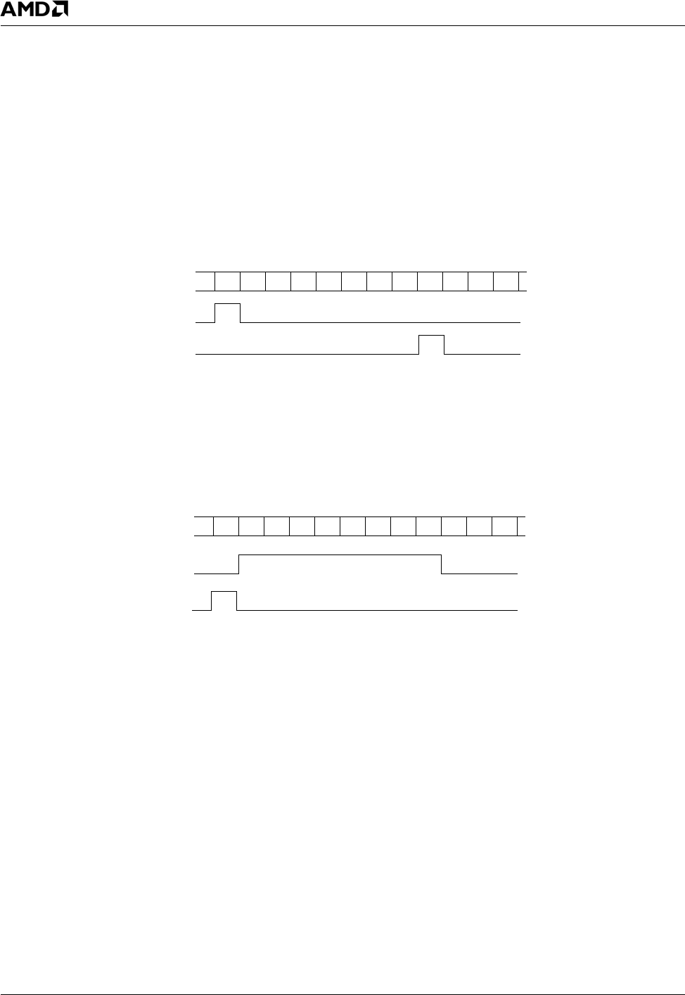
470 AMD Geode™ LX Processors Data Book
Video Input Port
33234H
6.9.6 Message Passing Mode
The Message Passing mode (MSG) allows an external
device to pass raw data packets to the AMD Geode LX pro-
cessor system memory (see Figure 6-43). In Message
Passing mode, VID8 is redefined as a start message indi-
cation and VID9 is redefined as an end message indica-
tion. Video data reception (SAV/EAV packets and ancillary
packets) is disabled while in Message Passing mode.
6.9.7 Data Streaming Mode
The Data Streaming mode (STRM) allows an external
device to pass raw data to the processor system memory
(see Figure 6-44). When in Data Streaming mode, the
VID9 data pin is redefined as a DATA_VALID control input.
VID8 is the START_MSG indicator. The VIP stores all data
during the time that the DATA_VALID input is active. The
data is stored sequentially into system memory. Figure 6-
44 shows the Data Streaming format. Video data reception
(SAV/EAV packets and ancillary packets) is disabled while
in Data Streaming mode.
Figure 6-43. Message Passing Data Packet
Figure 6-44. Data Streaming Data Packet
VIP_DATA[7:0]
START_MSG
END_MSG
(VID[8])
(VID[9])
D0 D1 D2 D3 D4 D5 D6 D7XX XX XX XX XX
VIP_DATA[7:0]
DATA_VALID
(VID[9])
D0 D1 D2 D3 D4 D5 D6 D7XX XX XX XX XX
START_MSG
(VID[8])
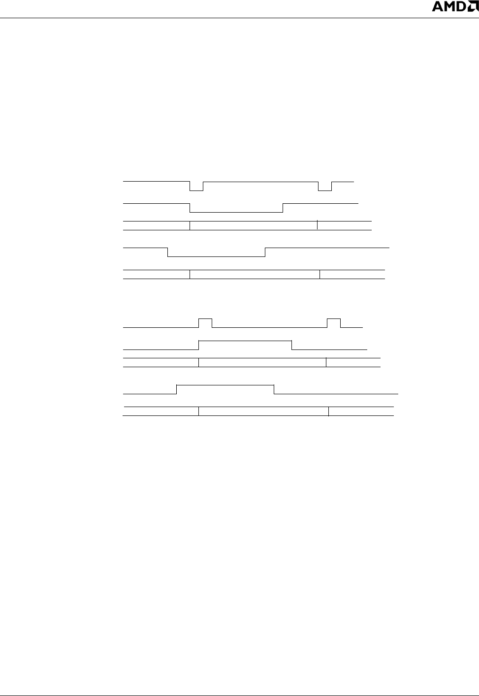
AMD Geode™ LX Processors Data Book 471
Video Input Port 33234H
6.9.8 BT.601 Mode
BT.601 mode allows reception of 8- or 16-bit video input
which consists of HSYNC, VSYNC, and 8/16 bit data. Verti-
cal and horizontal start/stop registers provide the informa-
tion for data capture in each field/frame. The BT.656 SAV/
EAV codes (if present) are ignored. Frame/line timing is
derived from the HSYNC and VSYNC inputs only. Odd/
even field is determined by the leading edges of VSYNC
and HSYNC. Default field detection is shown in Figure 6-
45. A detection window is programmable using the VIP
Memory Offset 50h. If the leading edge of VSYNC occurs
within the window, the field is odd. If the leading edge of
VSYNC occurs outside the window, the field is even. The
VIP Memory Offset 50h default value requires that the
HSYNC and VSYNC leading edges occur simultaneously
for odd field detection (see Figure 6-46 on page 472). The
horizontal and vertical input timings of the input video
frame are also programmable. See Figure 6-47 and Figure
6-48.
Figure 6-45. BT.601 Mode Default Field Detection
HSYNC
VSYNC
ACTIVE LOW HSYNC/VSYNC (HSYNC polarity = 0 / VSYNC polarity = 0)
ACTIVE HIGH HSYNC/VSYNC (HSYNC polarity = 1 / VSYNC polarity = 1)
VSYNC
HSYNC
(for odd field)
(for even field)
even field
odd field
line #1
line #1
even field
odd field (line #1)
(line #1)
even field (line #2)
odd field (line #2)
VSYNC
VSYNC
(for odd field)
(for even field)
even field
odd field
even field
odd field (line #1)
(line #1)
even field (line #2)
odd field (line #2)
Odd field is indicated when leading edge of VSYNC and the leading edge of HSYNC occur simultaneously
(VIP allows for a programmable detection window for odd field).
Even field is indicated when leading edge of VSYNC occurs prior to the leading edge of HSYNC.
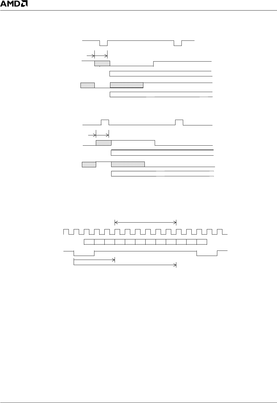
472 AMD Geode™ LX Processors Data Book
Video Input Port
33234H
.
Figure 6-46. BT.601 Mode Programmable Field Detection
Figure 6-47. BT.601 Mode Horizontal Timing
HSYNC
VSYNC
odd_field_detect_start field_detect_duration
ACTIVE LOW HSYNC/VSYNC (HSYNC Polarity = 0 / VSYNC Polarity = 0)
ACTIVE HIGH HSYNC/VSYNC (HSYNC Polarity = 1 / VSYNC Polarity = 1)
VSYNC
(for odd field)
(for even field) even field
odd field
line #1
HSYNC
VSYNC
odd_field_detect_start field_detect_duration
VSYNC
(for odd field)
(for even field) even field
odd field
line #1
A = 3 B = 12
A - horizontal_start for 601 (VIP Memory Offset 3Ch)
CLK
HSYNC
B - horizontal_end for 601 (VIP Memory Offset 38h)
video data
* Clock #1 occurs at leading transition of HSYNC
2
1* 3
D2 D3 D4 D5 D6
4
D1
10 1156789
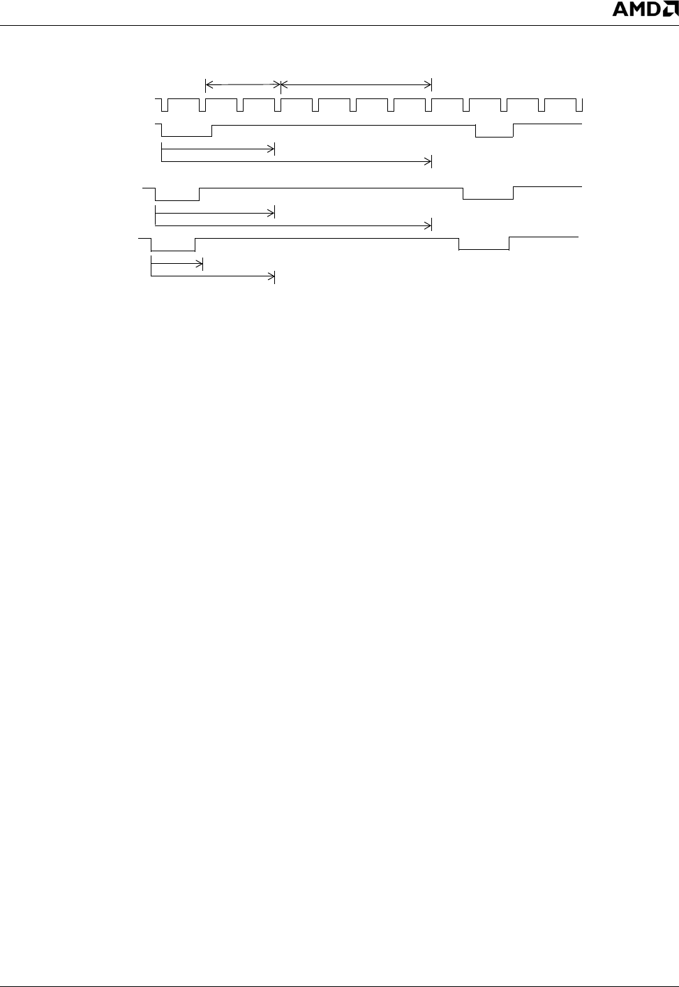
AMD Geode™ LX Processors Data Book 473
Video Input Port 33234H
Figure 6-48. BT.601 Mode Vertical Timing
6.9.9 YUV 4:2:2 to YUV 4:2:0 Translation
The VIP provides the option to translate incoming 4:2:2 co-
sited video to YUV 4:2:0. The U and V values of even lines
are simply discarded. No filtering is performed. VIP stores
the 4:2:0 data to system memory in a planar format. In pla-
nar format, the Y, U, and V data is partitioned into separate
buffers. A single Y, U, V buffer (three buffers) can be used
in the case of progressive scan or with interlaced data
when using Weave. Two sets of buffers (six buffers) are
used to store the odd and even field data separately when
using the Bob method of de-interlacing.
Figure 6-49 on page 474 illustrates the positioning of the
YCbCr samples for the 4:2:2 and 4:2:0 formats when:
1) Receiving a progressive scan frame.
2) Receiving interlaced odd and even fields for use with
the Bob display mode.
3) For receiving odd and even fields with the Weave dis-
play mode.
In addition to the standard 4:2:2 translation, VIP can also
decimate all U/V values in the even field.
C = 4 D = 7
E = 4
F = 7
HSYNC
VSYNC
(even field)
VSYNC
(odd field)
C - vertical_start for 601 odd field (VIP Memory Offset 6Ch[11:0])
D - vertical_end for 601 odd field (VIP Memory Offset 6Ch[27:16])
E - vertical_start for 601 even field (VIP Memory Offset 48h[11:0])
F - vertical_end for 601 even field (VIP Memory Offset 48h[27:16])
Video Data
** Frame timing starts at leading edge of VSYNC
12345678
G = 2 H = 3
VSYNC
G - vbi_start for 601 (VIP Memory Offset 44h[11:0])
H - vbi_end for 601 (VIP Memory Offset 40h[11:0])
VBI Data
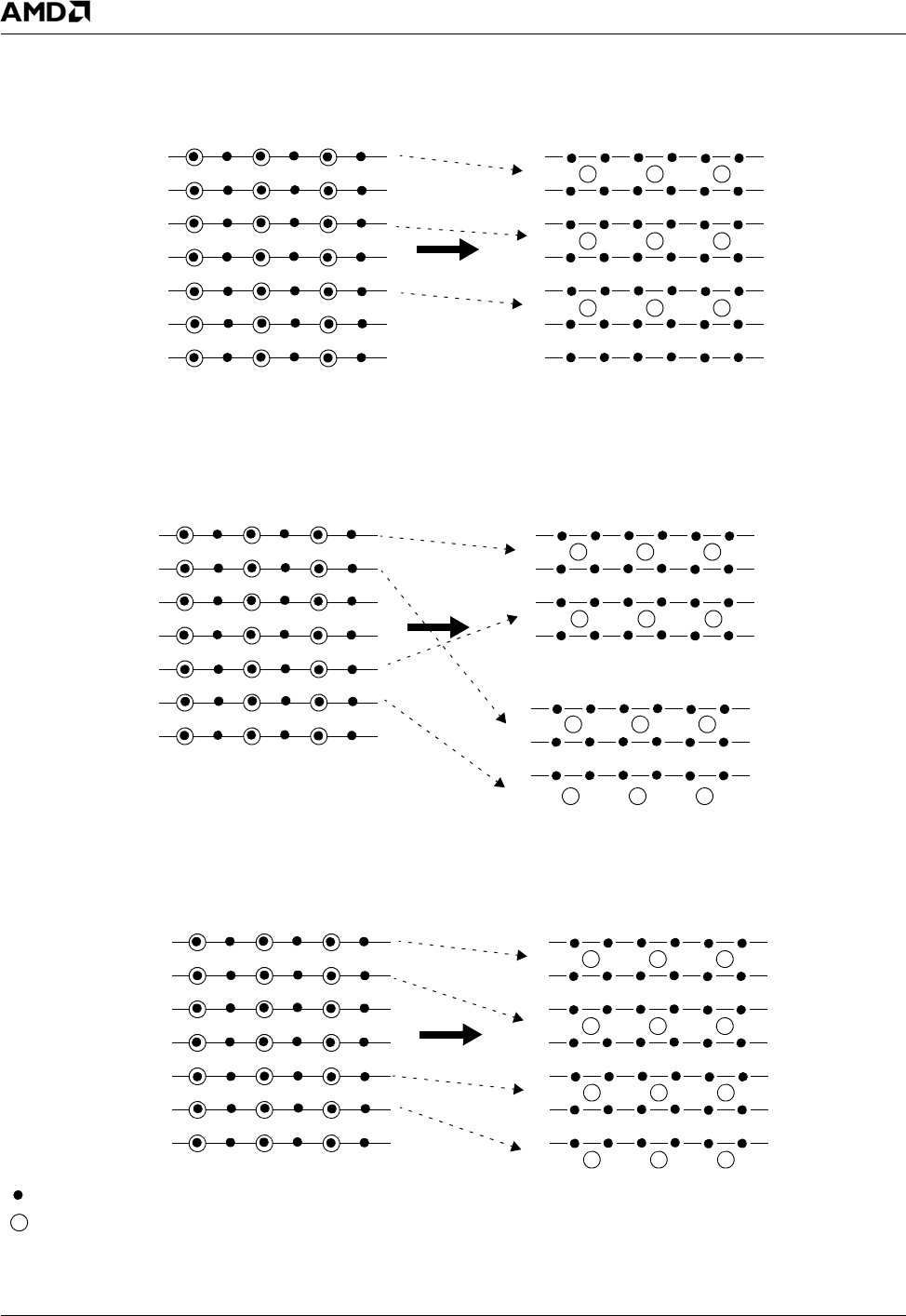
474 AMD Geode™ LX Processors Data Book
Video Input Port
33234H
Figure 6-49. YUV 4:2:2 to YUV 4:2:0 Translation
1
2
4
6
3
5
7
1
2
4
6
3
5
7
YUV 4:2:2 YUV 4:2:0
123 456 123 456
1
2
4
3
1
[1]
[2]
[3]
2
3
4
Y SAMPLE
CB,CR SAMPLE
YUV 4:2:2 YUV 4:2:0
123 456 123 456
[1]
[2]
[3]
123 456
1
2
4
3
1
[1]
[2]
[3]
2
3
4
YUV 4:2:2 YUV 4:2:0
123 456 123 456
5
6
7
Progressive scan - Discard even line UV values
Interlaced (Weave) - Discard even line UV values in both input fields
(single frame buffer in system memory)
(odd and even field buffers in system memory)
Interlaced (Bob) - Discard even line UV values in both input fields
(single frame buffer in system memory)
AMD Geode™ LX Processors Data Book 475
Video Input Port 33234H
6.9.10 Software Model
The VIP receives data and stores it into system memory.
The VIP input modes with associated data types are shown
in Table 6-74. VIP 2.0 is the VESA VIP 2.0 Level I (8-bit)
standard or the VESA VIP 2.0 Level II (16-bit) standard.
VIP 1.1 is the VESA (8-bit) standard in which only a single
video stream is supported and the TASK bit is used to dis-
tinguish between video and VBI data. MSG is the 8-bit
Message Passing mode, and STRM, the Data Streaming
mode, provides support for generic 8-bit data streaming.
MSG and STRM modes are proprietary data transfer for-
mats and are not defined in the VESA VIP specification.
Table 6-74 defines the data types received in each mode.
VIP 2.0 supports nine different data types. This allows
reception of two separate video streams (Task A and B)
plus ancillary data. VIP 1.1 mode supports five data types
(Task A only). One data type is associated with the MSG
and STRM modes.
Table 6-74. VIP Data Types / Memory Registers
Mode Data Type
T F V
(Flags) Base Register Pitch/Size Register Planar Registers
VIP 2.0 Task A, Odd Field,
Active Video
1 0 0 VIP_TASK_A_VID_ODD_BASE VIP_TASK_A_VID_PITCH VIP_TASK_A_U_OFFSET
VIP_TASK_A_V_OFFSET
Task A, Even Field,
Active Video
1 1 0 VIP_TASK_A_VID_EVEN_BASE VIP_TASK_A_U_OFFSET
VIP_TASK_A_V_OFFSET
Task A, Odd Field,
VBI
1 0 1 VIP_TASK_A_VBI_ODD_BASE N/A
Task A, Even Field,
VBI
1 1 1 VIP_TASK_A_VBI_EVEN_BASE N/A
Task B, Odd Field,
Active Video
0 0 0 VIP_TASK_B_VID_ODD_BASE VIP_TASK_B_VID_PITCH VIP_TASK_B_U_OFFSET
VIP_TASK_B_V_OFFSE
Task B, EvenField,
Active Video
0 1 0 VIP_TASK_B_VID_EVEN_BASE VIP_TASK_B_U_OFFSET
VIP_TASK_B_V_OFFSE
Task B, Odd Field,
VBI
0 0 1 VIP_TASK_B_VBI_ODD_BASE N/A
Task B, Even Field,
VBI
0 1 1 VIP_TASK_B_VBI_EVEN_BASE N/A
Ancillary N/A VIP_ANC_MSG_1_BASE VIP_ANC_MSG_SIZE N/A
VIP 1.1 Task A, Odd Field,
Active Video
1 0 0 VIP_TASK_A_VID_ODD_BASE VIP_TASK_A_VID_PITCH VIP_TASK_A_U_OFFSET
VIP_TASK_A_V_OFFSE
Task A, Even Field,
Active Video
1 1 0 VIP_TASK_A_VID_EVEN_BASE VIP_TASK_A_U_OFFSET
VIP_TASK_A_V_OFFSE
Task A, Odd Field,
VBI
0 0 1 VIP_TASK_A_VBI_ODD_BASE N/A
Task A, Even Field,
VBI
0 1 1 VIP_TASK_A_VBI_EVEN_BASE N/A
Ancillary N/A VIP_ANC_MSG_1_BASE VIP_ANC_MSG_SIZE N/A
BT.
601
Task A, Odd Field,
Active Video
1 0 0 VIP_TASK_A_VID_ODD_BASE VIP_TASK_A_VID_PITCH VIP_TASK_A_U_OFFSET
VIP_TASK_A_V_OFFSE
Task A, Even Field,
Active Video
1 1 0 VIP_TASK_A_VID_EVEN_BASE VIP_TASK_A_U_OFFSET
VIP_TASK_A_V_OFFSE
Task A, Odd Field,
VBI
0 0 1 VIP_TASK_A_VBI_ODD_BASE N/A
Task A, Even Field,
VBI
0 1 1 VIP_TASK_A_VBI_EVEN_BASE N/A
MSG Message passing N/A VIP_ANC_MSG_1_BASE,
VIP_ANC_MSG_2_BASE
VIP_ANC_MSG_SIZE N/A
STRM Data Streaming N/A VIP_ANC_MSG_1_BASE,
VIP_ANC_MSG_2_BASE
N/A
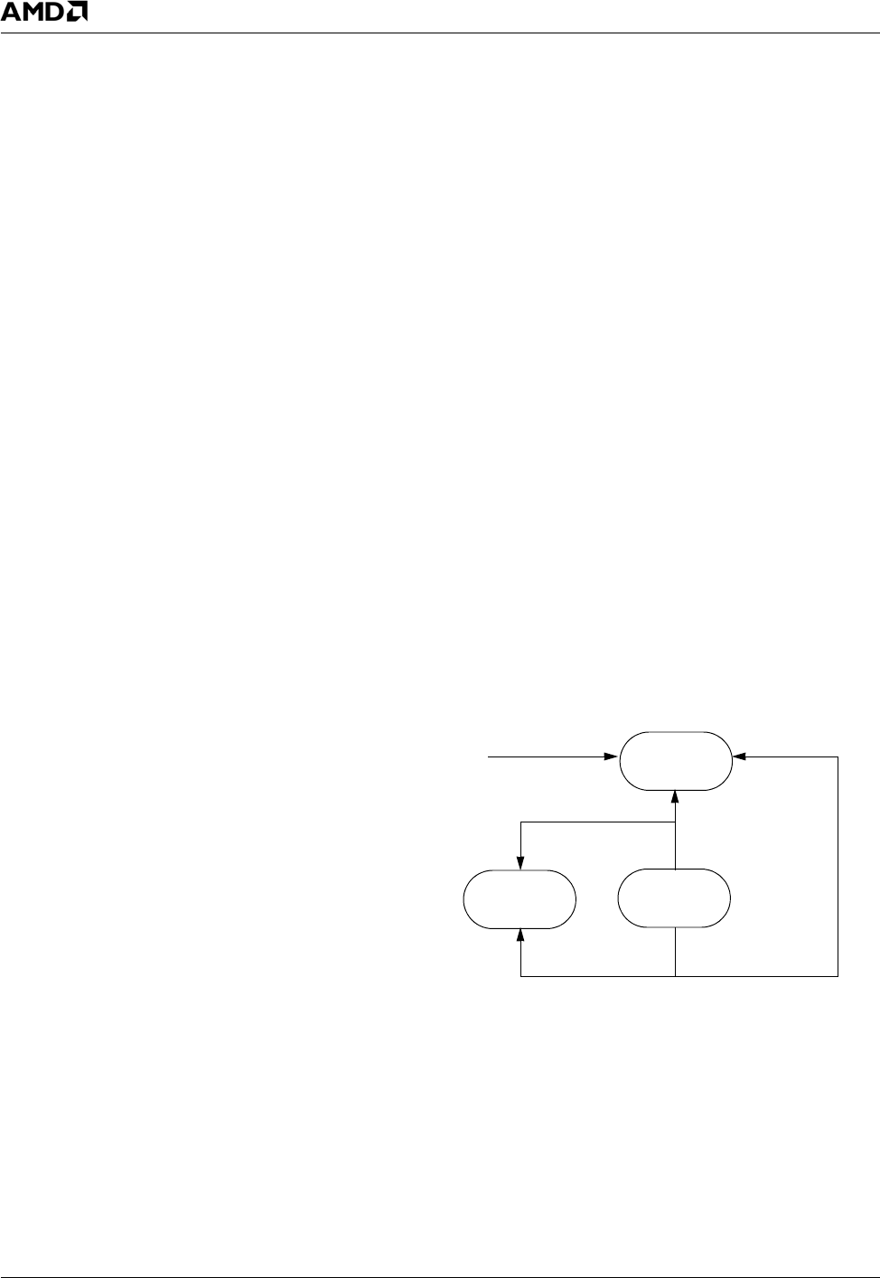
476 AMD Geode™ LX Processors Data Book
Video Input Port
33234H
6.9.10.1 Video Data Buffers
Video data buffers can be organized in linear or planar for-
mats. Linear buffers pack YUV values contiguous in mem-
ory. Planar buffers have separate subbuffers for each set of
YUV values in a field or frame. The VIP Control 1 register
(VIP Memory Offset 00h[4]) determines if the video storage
format is linear or planar.
In linear format, the first video line is stored beginning at
the vid_base address, the second line is stored beginning
at vid_base + pitch, the third line at task_base + (2 x pitch)
and so on until the end of the field/frame. See Figure 6-51
on page 477 for an example of a 4:2:2 SAV/EAV packets
stored in system memory in a linear format.
In planar format, the Y buffer begins at the task_base
address, the U buffer begins at the (vid_base +
U_buffer_offset), and the V values start at the (vid_base +
V_buffer_offset). The pitch value for Y is vid_pitch. The
pitch value for V and U is task_A_UV_pitch (for Task A UV
data) or task_b_pitch/2 (Task b UV data). In 4:2:2 or 4:2:0
video, there are twice as many Y data values per line as
there are U or V values. Additional odd/even offsets and
pitch registers are provided for Task A data. Input U/V val-
ues can be decimated (even lines or even fields). This fur-
ther reduces the U and V data to 1/4 of the Y data.
See Figure 6-51 on page 477 and Figure 6-52 on page 478
for examples of SAV/EAV packets stored in linear buffer
and planar buffer format.
6.9.10.2 VBI Data Buffers
The VBI data packets are stored in linear format. VBI data
is essentially a line of video that occurs during vertical
blanking. The first VBI line is stored beginning at vbi_base,
the second line is stored beginning at vbi_base + vid_pitch,
the third line at vbi_base + (2 x vid_pitch) and on until the
end of the vertical blanking period.
6.9.10.3 Ancillary Data Buffers
Ancillary data packets are stored starting at the buffer
address defined by anc_msg_1. Packet storage continues
to address anc_msg_1 + anc_msg_size at which point the
address is wrapped back around to anc_msg_1. When a
new packet is received, the packet count is incremented.
When software reads a packet from the buffer, it decre-
ments the count by writing a 1 to the Decrement Ancillary
Packet Count bit in the VIP Status register (VIP Memory
Offset 08h[18]).
Ancillary data packets include a checksum. After packet
reception, the internally generated checksum is compared
to the checksum sent with the ancillary packet. If these val-
ues do not compare, the packet is marked bad by writing a
F0 in fill byte immediately following the checksum byte (8/
16 ancillary data) or a 1111 in bits [15:12] of the checksum
DWORD for 10-bit ancillary data. Parity checking is also
performed on the DID, SDID, NN, and checksum WORDs.
Packets with parity errors set the same error bits as when a
checksum error occurs. Parity and checksum errors are
reported in the VIP Status register (VIP Memory Offset
08h). They share a status bit. Parity checking can be dis-
abled via the ANCPEN bit in Control Register 2 (VIP Mem-
ory Offset 04h[26]).
Figure 6-53 on page 479 shows an example of ancillary
packets stored in system memory.
6.9.10.4 Message Passing/Data Streaming Modes
The MSG and STRM modes provide a mechanism for the
AMD Geode CS5536 companion device to send raw data
to the AMD Geode LX processor system memory. MSG
and STRM modes have identical software models. Two
buffers are used (see Figure 6-50). The
VIP_ANC_MSG_1_BASE and VIP_ANC_MSG_2_BASE
registers (VIP Memory Offset 58h and 5Ch) define the two
buffer locations. The VIP_ANC_MSG_SIZE register (VIP
Memory Offset 60h) defines the maximum size of each
buffer. The first packet (data associated with a Start/End
indication) is saved starting at msg_1_base address. The
MB bit in Control Register 1 (VIP Memory Offset 00h[18])
determines when buffer swapping occurs. When MB = 0,
buffers are swapped each packet. When MB = 1, buffers
are only swapped when full. This mode might be used if a
continuous data stream is being delivered. A Message
Buffer Full interrupt occurs when a buffer swap occurs.
Software can read the VIP Status register to determine
which buffer or buffers are full. Software must reset the bit
in order for the buffer to become available. The MSG Buffer
Error status bit (bit 14) is set when a buffer swap occurs
from buffer 1 to buffer 2 with buffer 2 being unavailable or if
a buffer swap occurs from buffer 2 to buffer 1 with buffer 1
being unavailable.
Figure 6-50. Dual Buffer for Message Passing
and Data Streaming Modes
Buffer 1
in use
Buffer 2
in use
buffer1_full/
buffer2_full
Buffer
overrun
buffer2_full
buffer1_full
buffer2_full#
buffer1_full#
mode_2 or mode_3
new PKT
or new PKT
AMD Geode™ LX Processors Data Book 477
Video Input Port 33234H
Figure 6-51. Example VIP YUV 4:2:2 SAV/EAV Packets Stored in System Memory in a Linear Buffer
0
1
2
3
vid_base (buffer start)
CbYCrY
line 1 start
line 2 start
line 3 start
* line is 00 filled if not
QWORD aligned
CbYCrY
CbYCrY
CbYCrY
CbYCrY
00*00*00*00*
CbYCrY
CbYCrY
CbYCrY
CbYCrY
CbYCrY
00*00*00*00*
CbYCrY
vid_base + vid_pitch
vid_base + 2 X vid_pitch
* Similar buffer can exist for Task A odd video, Task A even video, Task B odd video, Task B even video,
Task A odd VBI data, Task A even VBI data, Task B odd VBI data, Task B even VBI data

478 AMD Geode™ LX Processors Data Book
Video Input Port
33234H
Figure 6-52. Example VIP YUV 4:2:0 Planar Buffer
(all base registers are 8-byte aligned)
U Buffer
V Buffer
line #1 Y values
Y pitch = task_A_vid_pitch
Y Buffer
task_A_UV_pitch
+ U_buffer_even_offset
+V_buffer_even_offset
line #1 U values
line #1 V values
vid_base
vid_base
vid_base
** Similar buffers can exist for Task A even video
Note: Line lengths, which are not divisible by 8, will result in an odd number of U and V data for each line.
When this occurs, the fill values used (for QWORD boundaries) may not be 00. This occurs
only if non-standard video formats are used. The non 00 data is not part of the line.
** Odd/even de-interlacing is not supported for Task B (Task B shares pointers between odd/even fields)
U pitch = task_A_U_pitch
V pitch = task_A_V_pitch
AMD Geode™ LX Processors Data Book 479
Video Input Port 33234H
Figure 6-53. Example VIP 8/16- and 10-bit Ancillary Packets Stored in System Memory
0
1
2
3
(8-byte aligned)
00FFFFDID
SDIDNN=4datadata
datadatadatadata
datadatadatadata
data data data data
packet 1 start - buffer start
packet 2 start
00FFFFDID
SDIDNN=6datadata
datadatadatadata
datadatadatadata
data data data data
data data data data
data data data data
00* CS data data
packet 3 start
* packet is 00 filled to QWORD aligned address
anc_message_base
00* CS data data
* packet is 00 filled if not QWORD aligned
SIDNN=7datadata
01
000
3FF
DID
SDIDNN=4
data
data
data data
packet 1 start - buffer start
packet 2 start
SDIDNN=8
data
data
data data
data data
data data
packet 3 start
* packet is 00 filled to QWORD aligned address
00* CS
* packet is 00 filled if not QWORD aligned
3FF
23
CS
0003FF
3FF
DID
00*
0003FF
8/16-BIT ANCILLARY DATA
10-BIT ANCILLARY DATA

480 AMD Geode™ LX Processors Data Book
Video Input Port
33234H
6.9.11 Bob and Weave
Bob and Weave are two methods of outputting interlaced
video, captured by the VIP, in a progressive scan format.
An example of this is when VIP receives 30 Hz interlaced
(NTSC format) and the data is to be displayed on a TFT
panel that requires progressive scan with a 60-85 Hz
refresh rate. In the Bob method, VIP stores the odd and
even fields in separate buffers. This uses less bandwidth
since each field is line doubled by the display controller,
and displayed as a full frame. The disadvantage is that
there are some observable visual effects due to the reduc-
tion in resolution. In the Weave method, VIP assembles a
full frame from the two fields. The Display Controller then
displays a full resolution frame. This requires more band-
width.
6.9.11.1 Bob
In the Bob method, VIP saves the even and odd fields in
separate buffers. The VIP field interrupt is enabled to indi-
cate to software when a field has been completed. A field
status bit is available that indicates whether an odd or even
field was received. Software can manage these field buff-
ers so that the Display Controller always accesses fully
assembled field data.
6.9.11.2 Weave
In the Weave method, VIP assembles the odd field and
even fields together to form the complete frame in system
memory. Since both fields are rendered simultaneously, the
frame must be double buffered. This allows VIP to render a
frame while the Display Controller is outputting a previous
frame. To assemble the odd and even fields into a single
frame, the VIP must be setup such that the video data odd
base address is separated from the video data even base
address by one horizontal line. The video pitch register
must be programmed with the value of two horizontal lines.
The VIP field interrupt is enabled to indicate to software
when each field has been completed. A field status bit is
available that indicates whether an odd or even field was
received. Software can manage these field/frame buffers
so that the Display Controller always accesses fully assem-
bled frame data.
6.9.12 VIP Interrupts
Software applications need synchronization events and
input error indications from the VIP to manage video dis-
play and processing. Interrupts are generated by the VIP in
the form of Interrupts (INT) and/or Asynchronous System
Management Interrupts (ASMI). The following events can
generate an INT or ASMI. These INTs/ASMIs are disabled
at power-up.
FIFO Line Wrap Error - In cases where minimum line
sizes are input with a low GLIU frequency and high GLIU
latency, there is a potential error condition where the VIP
can receive a third line of video before the first line has
been completely output. VIP can not handle more then two
lines of video in its FIFO. If this condition occurs, the input
video line size should be increased by increasing the
blanking time between each line.
FIFO Overflow Error - FIFO overflows can occur if GLIU
latencies become too long. If a FIFO overflow occurs, the
VIP automatically resets the FIFO. Data in the FIFO is dis-
carded. Video reception begins again at the start of the
next line. No software intervention is required. This INT is
generated to indicate that a FIFO overflow occurred. A high
frequency of these interrupts is likely an indication of sys-
tem bandwidth issues.
FIFO Threshold Hit - The FIFO threshold hit is a program-
mable count that gets compared to the number of WORDs
in a FIFO. If the FIFO data level surpasses the FIFO
threshold, then a FIFO threshold hit INT is generated. The
request priority level is also elevated to its high value. Sep-
arate threshold values exist for video and ancillary data.
This INT may be enabled for debug to determine if potential
bandwidth issues are effecting video capture.
Runaway Line (> 3000 clocks) Error - This error occurs
when a SAV code occurs, but a corresponding EAV does
not. VIP Memory Offset 00h[23] (ERR_DETECT) must be
set to 1 to enable the runaway line error. A runaway line
error causes video reception to stop. Video reception starts
again at the beginning of the next line.

AMD Geode™ LX Processors Data Book 481
Video Input Port 33234H
Vertical Timing Error (Frame or Address Error) /Mes-
sage Missed Error - This error indicates a frame error or
an address error. A frame error occurs when the time
between VSYNCs exceeds the window defined by the
VIP_SYNC_ERR_COUNT register (VIP Memory Offset
78h). The VIP_SYNC_ERR_COUNT register must be pro-
grammed. An address error occurs when the GLIU address
equals or exceeds the address programmed in the
VIP_MAX_ADDR register (VIP Memory Offset 14h). The
A_ERR_EN bit must be enabled (VIP Memory Offset
04h[30] = 1). An address error causes data reception to
stop. The A_ERR_EN must be set to a 0 to reset the
Address Error so data reception can restart. Setting the
VRST bit in Control Register 1 also resets the Address
Error (VIP Memory Offset 00h[0].
Active Pixels Per Line Error - This error is only valid when
receiving BT.656 data. This INT indicates that the amount
of active data received between SAV and EAV codes is not
the same from one line to the next. This indicates that there
is a problem in the video input data stream.
VIP Clock Input Error - This error indicates that the VIP
input clock has stopped for 128 GLIU clocks.
Ancillary Checksum or Parity Error - This error indicates
that a checksum value on an ancillary packet was wrong or
the parity on an ancillary packet was wrong. The ancillary
parity check can be disabled by setting the ANCPEN bit to
0 (VIP Memory Offset 04h[26] = 0).
Message Buffer Full or Ancillary Threshold Packet
Count Reached - When in Message Passing mode, this
indicates that a message buffer swap has occurred. The
status register can be read to find out which message
buffer has been filled. When in a video mode, this indicates
that the number of outstanding ancillary packets has
reached the threshold count programmed in VIP Memory
Offset 60h.
End of Vertical Blanking - Indicates that a falling edge of
VBLANK has occurred.
Start of Vertical Blanking - Indicates that a rising edge of
VBLANK has occurred.
Start of Even Field - Indicates that the start of the even
field has occurred (for interlaced video data only).
Start of Odd Field - Indicates that the start of the odd field
has occurred (for interlaced video data only).
Current Line = VIP Line Target - Indicates that the video
line number programmed in the VIP Current/Target register
(VIP Memory Offset 10h) has been reached.
6.9.13 VIP Input Video Status
The VIP checks the input video for conditions that could
indicate an invalid data stream. These indications are pro-
vided to software via interrupts. Another component of the
video detection story is the generation of the video_ok sig-
nal to the DC. When in GenLock mode, the VIP transfers
video data to memory and synchronously to the DC
extracting the video from memory and sending it on to a
display. If the video data is interrupted, the DC needs to
know so that it can switch over to internally generated tim-
ing and data. The video_ok signal provides the indication
that the video data being received by the VIP is OK. The
ERR_DETECT bits (VIP memory Offset 00h[23:20]) are
used to enable/disable the specific checks. When an error
occurs, the video_ok signal remains 0 until the error is
reset by clearing the associated interrupt pending bit in the
VIP Interrupt register (VIP Memory Offset 0Ch). The follow-
ing checks on the video data can be performed.
• Clock Input Error - Enabled when bit 20 = 1
• Line Input Error - Enabled when bit 21 = 1
• Runaway Line Input Error - Enabled when bit 23 = 1
• Vertical Timing Error - Enabled when bit 22 = 1
• Address Error (VIP Memory Offset 04h[30] must = 1) -
Enabled when bit 22 = 1

482 AMD Geode™ LX Processors Data Book
Video Input Port Register Descriptions
33234H
6.10 Video Input Port Register Descriptions
The registers associated with the VIP are the Standard
GeodeLink Device (GLD) MSRs (accessed via the RDMSR
and WRMSR instructions) and VIP Configuration/Control
Registers. Table 6-75 and Table 6-76 are register summary
tables that include reset values and page references where
the bit descriptions are provided.
Note: The MSR address is derived from the perspective
of the CPU Core. See Section 4.1 "MSR Set" on
page 45 for more details on MSR addressing.
Table 6-75. Standard GeodeLink™ Device MSRs Summary
MSR Address Type Register Name Reset Value Reference
54002000h RO GLD Capabilities MSR (GLD_MSR_CAP) 00000000_ 0003C4xxh Page 484
54002001h R/W GLD Configuration MSR
(GLD_MSR_CONFIG)
000000000_ 00000000h Page 484
54002002h R/W GLD SMI MSR (GLD_MSR_SMI) 000000000_ xxxx7FFFh Page 485
54002003h R/W GLD Error MSR (GLD_MSR_ERROR) 000000000_ 00000000h Page 486
54002004h R/W GLD Power Management Register
(GLD_MSR_PM)
000000000_ 00000005h Page 487
54002005h R/W GLD Diagnostic MSR (GLD_MSR_DIAG) 000000000_ 00000000h Page 487
Table 6-76. VIP Configuration/Control Registers Summary
VIP Memory
Offset Type Register Name Reset Value Reference
00h R/W VIP Control Register 1 (VIP_CTL_REG1) 42000001h Page 488
04h R/W VIP Control Register 2 (VIP_CTL_REG2) 00000000h Page 490
08h R/W VIP Status (VIP_STATUS) xxxxxxxxh Page 492
0Ch R/W VIP Interrupt (VIP_INT) xxxxFFFEh Page 494
10h R/W VIP Current/Target (VIP_CUR_TAR) 00000000h Page 495
14h R/W VIP Max Address (VIP_MAX_ADDR) FFFFFFFFh Page 495
18h R/W VIP Task A Video Even Base Address
(VIP_TASK_A_VID_EVEN_BASE)
00000000h Page 496
1Ch R/W VIP Task A Video Odd Base Address
(VIP_TASK_A_VID_ODD_BASE)
00000000h Page 496
20h R/W VIP Task A VBI Even Base Address
(VIP_TASK_A_VBI_EVEN_BASE)
00000000h Page 497
24h R/W VIP Task A VBI Odd Base Address
(VIP_TASK_A_VBI_ODD_BASE)
00000000h Page 497
28h R/W VIP Task A Video Pitch (VIP_TASK_A_VID_PITCH) 00000000h Page 498
2Ch R/W VIP Control Register 3 (VIP_CONTRL_REG3) 00000020h Page 498
30h R/W VIP Task A V Offset (VIP_TASK_A_V_OFFSET) 00000000h Page 499
34h R/W VIP Task A U Offset (VIP_TASK_A_U_OFFSET) 00000000h Page 500
38h R/W VIP Task B Video Even Base/Horizontal End
(VIP_TASK_B_VID_EVEN_BASE_HORIZ_END)
00000000h Page 500
3Ch R/W VIP Task B Video Odd Base/Horizontal Start
(VIP_TASK_B_VID_ODD_BASE_HORIZ_START)
00000000h Page 501
40h R/W VIP Task B VBI Even Base/VBI End
(VIP_TASK_B_VBI_EVEN_BASE_VBI_END)
00000000h Page 501

AMD Geode™ LX Processors Data Book 483
Video Input Port Register Descriptions 33234H
44h R/W VIP Task B VBI Odd Base/VBI Start
(VIP_TASK_B_VBI_ODD_BASE_VBI_START)
00000000h Page 502
48h R/W VIP Task B Data Pitch/Vertical Start Even
(VIP_TASK_B_DATA_PITCH_VERT_START_EVEN)
00000000h Page 502
4Ch -- Reserved -- --
50h R/W VIP Task B V Offset (VIP_TASK_B_V_Offset) 00000000h Page 503
54h R/W VIP Task B U Offset (VIP_TASK_B_U_OFFSET) 00000000h Page 504
58h R/W VIP Ancillary Data/Message Passing/Data Streaming
Buffer1 Base Address (VIP_ANC_MSG_1_BASE)
00000000h Page 504
5Ch R/W VIP Ancillary Data/Message Passing/Data Streaming
Buffer 2 Base Address (VIP_ANC_MSG_2_BASE)
00000000h Page 505
60h R/W VIP Ancillary Data/Message Passing/Data Streaming
Buffer Size (VIP_ANC_MSG_SIZE)
00000000h Page 505
64h -- Reserved -- --
68h R/W VIP Page Offset/ Page Count (VIP_PAGE_OFFSET) 00000000h Page 506
6Ch R/W VIP Vertical Start/Stop (VIP_VERT_START_STOP) 00000000h Page 506
70h R/W VIP FIFO Address (VIP_FIFO_R_W_ADDR) 00000000h Page 507
74h R/W VIP FIFO Data (VIP_FIFO_DATA) xxxxxxxxh Page 507
78h R/W VIP VSYNC Error Count (VIP_SYNC_ERR_COUNT) 00000000h Page 508
7Ch R/W VIP Task A U Even Offset
(VIP_TASK_A_U_EVEN_OFFSET)
00000000h Page 508
80h R/W VIP Task A V Even Offset
(VIP_TASK_A_V_EVEN_OFFSET)
00000000h Page 509
Table 6-76. VIP Configuration/Control Registers Summary
VIP Memory
Offset Type Register Name Reset Value Reference
484 AMD Geode™ LX Processors Data Book
Video Input Port Register Descriptions
33234H
6.10.1 Standard GeodeLink™ Device (GLD) MSRs
6.10.1.1 GLD Capabilities MSR (GLD_MSR_CAP)
6.10.1.2 GLD Configuration MSR (GLD_MSR_CONFIG)
MSR Address 54002000h
Ty p e RO
Reset Value 00000000_ 0003C4xxh
GLD_MSR_CAP Register Map
63 62 61 60 59 58 57 56 55 54 53 52 51 50 49 48 47 46 45 44 43 42 41 40 39 38 37 36 35 34 33 32
RSVD
31 30 29 28 27 26 25 24 23 22 21 20 19 18 17 16 15 14 13 12 11 10 9 8 7 6 5 4 3 2 1 0
NSMI NCLK DEV_ID REV_ID
GLD_MSR_CAP Bit Descriptions
Bit Name Description
63:32 RSVD Reserved.
31:27 NSMI Number of SMI Registers. The VIP generates 15 possible SMI interrupts.
26:24 NCLK Number of Clock Domains. The VIP contains two clock domains; GLIU clock and VIP
video clock.
23:8 DEV_ID Device ID. Identifies device (03C4h).
7:0 REV_ID Revision ID. Identifies device revision. See AMD Geode™ LX Processors Specification
Update document for value.
MSR Address 54002001h
Ty p e R / W
Reset Value 000000000_ 00000000h
GLD_MSR_CONFIG Register Map
63 62 61 60 59 58 57 56 55 54 53 52 51 50 49 48 47 46 45 44 43 42 41 40 39 38 37 36 35 34 33 32
RSVD
313029282726252423222120191817161514131211109876543210
RSVD PRI1
RSVD
PRI0
RSVD
PID
GLD_MSR_CONFIG Bit Descriptions
Bit Name Description
63:11 RSVD Reserved.
10:8 PRI1 Secondary Priority Level. This value is the priority level the VIP uses when performing
high priority GLIU accesses. This is the case when the FIFO is nearly full.
7 RSVD Reserved.
6:4 PRI0 Primary Priority Level. This value is the priority level the VIP uses for most accesses
(i.e., when the VIP FIFO is not in danger of being full).
3 RSVD Reserved.
2:0 PID Priority ID. This value is the priority ID (PID) value used when the VIP initiates GLIU
transactions.
AMD Geode™ LX Processors Data Book 485
Video Input Port Register Descriptions 33234H
6.10.1.3 GLD SMI MSR (GLD_MSR_SMI)
MSR Address 54002002h
Ty p e R / W
Reset Value 000000000_ xxxx7FFFh
GLD_MSR_SMI Register Map
63 62 61 60 59 58 57 56 55 54 53 52 51 50 49 48 47 46 45 44 43 42 41 40 39 38 37 36 35 34 33 32
RSVD
31 30 29 28 27 26 25 24 23 22 21 20 19 18 17 16 15 14 13 12 11 10 9 8 7 6 5 4 3 2 1 0
RSVD
SMI_STATUS
RSVD
SMI_MASK
GLD_MSR_SMI Bit Descriptions
Bit Name Description
63:31 RSVD Reserved.
30:16 SMI_STATUS VIP SMI Interrupt Status.
0: SMI not pending.
1: SMI pending.
Writing a 1 to this bit clears the status:
Bit 30: Reserved.
Bit 29: FIFO overflow error.
Bit 28: FIFO threshold hit.
Bit 27: Long line (> 3000 clocks) error.
Bit 26: Vertical timing error.
Bit 25: Active pixels per line error.
Bit 24: VIP clock input error.
Bit 23: Ancillary packet checksum error.
Bit 22: Message buffer full or ancillary threshold packet count reached.
Bit 21: End of vertical blanking.
Bit 20: Start of vertical blanking.
Bit 19: Start of even field.
Bit 18: Start of odd field.
Bit 17: Current line = VIP Line Target (see Current/Target Line register).
Bit 16: GLIU Address or Type error.
15 RSVD Reserved.
14:0 SMI_MASK VIP SMI Masks.
0: Enable, unmask the SMI.
1: Disabled, mask the SMI.
Bit 14: Reserved.
Bit 13: FIFO overflow error.
Bit 12: FIFO threshold hit.
Bit 11: Long line (> 3000 clocks) error.
Bit 10: Vertical timing error.
Bit 9: Active pixels per line error.
Bit 8: VIP clock input error.
Bit 7: Ancillary packet checksum error.
Bit 6: Message buffer full or ancillary threshold packet count reached.
Bit 5: End of vertical blanking.
Bit 4: Start of vertical blanking.
Bit 3: Start of even field.
Bit 2: Start of odd field.
Bit 1: Current line = VIP Line Target (see Current/Target Line register).
Bit 0: GLIU Address or Type error.
486 AMD Geode™ LX Processors Data Book
Video Input Port Register Descriptions
33234H
6.10.1.4 GLD Error MSR (GLD_MSR_ERROR)
MSR Address 54002003h
Ty p e R / W
Reset Value 000000000_ 00000000h
GLD_MSR_ERROR Register Map
63 62 61 60 59 58 57 56 55 54 53 52 51 50 49 48 47 46 45 44 43 42 41 40 39 38 37 36 35 34 33 32
RSVD
313029282726252423222120191817161514131211109876543210
RSVD E1 E0 RSVD
EM1
EM0
GLD_MSR_ERROR Bit Descriptions
Bit Name Description
63:18 RSVD Reserved.
17 E1 Error Status 1. Writing a 1 to this bit clears the status.
0: VIP error not pending.
1: VIP error pending.
Types of Errors reported:
Bit 17: Unexpected Address.
16 E0 Error Status 0. Writing a 1 to this bit clears the status.
0: VIP error not pending.
1: VIP error pending.
Types of Errors reported:
Bit 16: Unexpected Type.
15:2 RSVD Reserved.
1EM1 Error Mask 1.
0: Unmask the error (Enabled).
1: Mask the error (Disabled).
0EM0 Error Mask 0.
0: Unmask the error (Enabled).
1: Mask the error (Disabled).
AMD Geode™ LX Processors Data Book 487
Video Input Port Register Descriptions 33234H
6.10.1.5 GLD Power Management Register (GLD_MSR_PM)
6.10.1.6 GLD Diagnostic MSR (GLD_MSR_DIAG)
This register is reserved for internal use by AMD and should not be written to.
MSR Address 54002004h
Ty p e R / W
Reset Value 000000000_ 00000005h
GLD_MSR_PM Register Map
63 62 61 60 59 58 57 56 55 54 53 52 51 50 49 48 47 46 45 44 43 42 41 40 39 38 37 36 35 34 33 32
RSVD
313029282726252423222120191817161514131211109876543210
RSVD 0 P1 0 P0
GLD_MSR_PM Bit Descriptions
Bit Name Description
63:4 RSVD Reserved.
3 RSVD Reserved. Always set to 0.
2P1 VIP Clock Power Mode.
0: Disable clock gating. VIP clock is always ON.
1: Enable active hardware clock gating.
The VIP input clock to the video input block is enabled when this bit is 0. When this bit is
1, the VIP input clock is enabled whenever the VIP reset bit (VIP Memory Offset 00h[0])
is 0 or if VIP_MODE (VIP Memory Offset 00h bit [3:1]) is in a non 000 state. This bit
defaults to 1.
1 RSVD Reserved. Always set to 0.
0P0 GLIU Clock Power Mode.
0: Disable clock gating. GLIU clock is always ON.
1: Enable active hardware clock gating.
GLIU clock is always on if the VIP reset bit (VIP Memory Offset 00h[0]) is 0. When the
VIP reset bit is 1 and this bit is 1, the internal VIP GLIU clocks are only turned on in
response to requests (memory mapped read/writes and MSR read/writes) from the GLIU.
This bit defaults to 1.
MSR Address 54002005h
Ty p e R / W
Reset Value 000000000_ 00000000h

488 AMD Geode™ LX Processors Data Book
Video Input Port Register Descriptions
33234H
6.10.2 VIP Control/Configuration Registers
6.10.2.1 VIP Control Register 1 (VIP_CTL_REG1)
VIP Memory Offset 00h
Ty p e R / W
Reset Value 42000001h
VIP_CTL_REG1 Register Map
31302928272625242322212019181716151413121110987 6 543210
ANC_FF VID_FF ERR_DETECT NI MB DZ DD DT_EN RUN_MODE P VIP_MODE
VRST
VIP_CTL_REG1 Bit Descriptions
Bit Name Description
31:29 ANC_FF Ancillary FIFO Flush. Watermark level for flushing the 64-deep ancillary FIFO. This
value determines how full the ancillary FIFO is before VIP starts writing QWORDs to sys-
tem memory. If the FIFO has greater than 4 QWORDs and the address is aligned, VIP
generates a burst (4 QWORDs) transaction.This value is reset to 2 (flush when 17
QWORDs).
0: Flush when there is at least 1 QWORD.
1: Flush when there are at least 9 QWORDs.
2: Flush when there are at least 17 QWORDs. (Default)
n: Flush when there are at least nx8 +1 QWORDs (up to n = 7x8 +1 = 57).
(ANC FIFO size is 64 QWORDs).
28:24 VID_FF Video FIFO Flush. Watermark level for flushing the 64-deep (planar mode) or 192-deep
(linear mode) FIFO(s). This value determines how full the ancillary FIFO is before VIP
starts writing QWORDs to system memory. If the FIFO has greater than 4 QWORDs and
the address is aligned, VIP generates a burst (4 QWORDs) transaction. This value is
reset to 2 (flush when 17 QWORDs).
0: Flush when there is at least 1 QWORD.
1: Flush when there are at least 9 QWORDs.
2: Flush when there are at least 17 QWORDs. (Default)
n: Flush when there are at least nx8+1 QWORDs).
(FIFO size is 192 QWORDs in Linear mode, maximum value is 17H/23d).
(FIFO size is 64 QWORDs in Planar mode, maximum value is 7).
23:20 ERR_DETECT Video Detection Enable. Selects what detection circuitry is used to detect loss of valid
video input. When an error is detected, the video_ok output is set low. The associated
interrupt pending bit must be cleared to allow the video_ok signal to return high.
Bit 23: Runaway Line Error Abort (aborts line if a line is detected longer then 3000
clocks).
Bit 22: Vertical Timing error (Vertical Count Register must be programmed) or address-
ing error (max_addr reg must be programmed).
Bit 21: Number of clocks per active line error (checks that each line has the same # of
data).
Bit 20: Loss of VIP clock (watchdog timer using GLIU clocks --128 GLIU clocks).

AMD Geode™ LX Processors Data Book 489
Video Input Port Register Descriptions 33234H
19 NI Non-Interlaced Video Input. This bit determines if the start/end-of-frame event occurs
each field (for non-interlaced video) or at the end of the odd field (for interlaced video).
The start/end-of-frame indication is used as the start/end-of-frame indication for the Run
Mode Capture. When in 601 input modes, the NI bit determines if separate vertical back-
porch values are used. For interlaced modes, different vertical start/end values can be
programmed.
0: Interlaced video (use FIELD and VBLANK flags for start/end-of-frame indication).
1: Non-Interlaced video (use only VBLANK flag for start/end-of-frame indication).
18 MB Message/Streaming Control.
0: Switch buffers each packet input or at end of buffer.
1: Switch buffers only when buffer is full. Store multiple packets in buffer.
17 DZ Disable Zero Detect. Disables ignoring zero data within SAV/EAV packets. When set,
zero data is received and saved in system memory.
0: Normal operation - Zero data in SAV/EAV packets is ignored and not saved to system
memory.
1: Accept 0 data and save in system memory.
16 DD Disable Decimation. Disables decimation of even lines of Cr,Cb data for 4:2:2->4:2:0
translation.
0: Normal operation - Even lines of Cr,Cb data do NOT get saved in Cr,Cb buffers when
in planar mode.
1: All Cr,Cb data is stored in Cr,Cb main memory buffers.
15:8 DT_EN Data Type Capture Enable. (Only used when VIP_MODE (bits [3:1]) = 001, 010, 011)
0: Disable capture data.
1: Enable capture data.
Bit 8: Task A Video.
Bit 9: Task A VBI.
Bit 10: Task B Video.
Bit 11: Task B VBI.
Bit 12: Ancillary, Rising edge resets the ancillary packet count, the next packet will be
stored starting at the base address.
Bit 13: Reserved (always program to 0).
Bit 14-15: Reserved (always program to 0).
7:5 RUN_MODE Run Mode Capture. Selects capture run mode.
000: Stop capture.
001: Stop capture at end of the current line.
010: Stop capture at end of next field.
011: Stop capture at end of the next frame.
100: Start capture at beginning of next line.
101: Start capture at beginning of the next field.
110: Start capture at beginning of next frame.
111: Start capture (required for msg/data streaming modes).
4P Planar. Determines if video data is stored in a linear format or planar format in system
memory.
0: Store data in linear format.
1: Store video data in planar format.
VIP_CTL_REG1 Bit Descriptions (Continued)
Bit Name Description
490 AMD Geode™ LX Processors Data Book
Video Input Port Register Descriptions
33234H
6.10.2.2 VIP Control Register 2 (VIP_CTL_REG2)
3:1 VIP_MODE VIP Operating Mode.
000: IDLE. This mode forces VID[15:0] to 0 from pads to VIP.
001: VIP 2.0 8-bit mode.
010: VIP 2.0 16-bit.
011: VIP 1.1 8-bit.
100: Message Passing.
101: Data Streaming.
110: 601 type 8-bit mode.
111: 601 type 16-bit mode.
0VRST VIP Reset. When set to 1, this bit causes the VIP input logic to be reset. The control reg-
isters and base registers are not reset. Data is received/stored once this bit is set back to
0 according to Control Register 1 and 2. A 1 should also be written to the FIFO Reset
(Control Register 3 (VIP Memory Offset 2Ch[0])) between writing a 1 and 0 to this regis-
ter. The power-up value of VRST is 1.
VIP Memory Offset 04h
Ty p e R / W
Reset Value 00000000h
VIP_CTL_REG1 Bit Descriptions (Continued)
Bit Name Description
VIP_CTL_REG2 Register Map
31 30 29 28 27 26 25 24 23 22 21 20 19 18 17 16 15 14 13 12 11 10 9 8 7 6 5 4 3 2 1 0
FI
A_ERR_EN
R_EN
SWC
ANC10
ANCPEN
LPB
FF_R/W
PAG E _ CN T
ANC_FF_THRESH
RSVD
VID_FF_THRESH
SYNC_TO_PIN
FIELD_TO_DC
SYNC_TO_DC
VIP_CTL_REG2 Bit Descriptions
Bit Name Description
31 FI Field Invert. When set to 1, the polarity of the input field bit is inverted. This allows for
devices that violate the VIP 2.0 specification.
30 A_ERR_EN Address Error Enable. When set to 1, the GLIU address that VIP is writing to is com-
pared to the Max Address register (VIP Memory Offset 14h). If a comparison is made, the
VIP Run Mode control is forced to 0 causing VIP to stop capturing data. The frame error
interrupt is generated.
29 R_EN Repeat Flag Enable. When set to 1, the repeat flag in the SAV or EAV header is used to
determine if the packet is saved. This allows the VIP to drop repeat fields during 3:2 pull
down.
28 SWC Sub-Window Capture Enable. When set to 1, only a portion of the frame/field is cap-
tured. Capture starts on the line specified in the Vertical Start/Stop register (VIP Memory
Offset 6Ch) and ends after the line specified in the Vertical Start/Stop register.
27 ANC10 10-bit Ancillary Data Input. When set to 1, ancillary data is received as 10-bit data.
(This is only applicable in 16-bit VIP mode).

AMD Geode™ LX Processors Data Book 491
Video Input Port Register Descriptions 33234H
26 ANCPEN Ancillary Parity Check Enable. When set to 1, ancillary DID, SDID, NN, and check sum
bytes are checked for even parity. The error is reported on MSR 4002002h[23]. When
this bit is 0, the Ancillary Checksum or Parity Error bit only indicates ancillary checksum
errors.
25 LPB VOP to VIP Loopback. When set to 1, the VOP clock and data are used as the clock
and data inputs to the VIP. This allows for loopback testing of the VOP and VIP functions.
This bit must be set to 0 for normal VIP operation.
24 FF_R/W FIFO R/W Enable. When set to 1, the FIFO Address (VIP Memory Offset 70h) and FIFO
Data (VIP Memory Offset 74h) registers can be used to write and read the 256x32 bit
FIFO. This bit must be set to 0 for normal VIP operation.
23:21 PAGE_CNT Page Count. Determines how many pages of video data are used. When this value is
000, a single page of video data is stored (Default). Additional pages are saved by add-
ing the value in the Page Offset register (VIP Memory Offset 68h) to each base.
000: 1 Page. (Default)
001: 2 Pages.
“
111: 8 Pages.
20:16 ANC_FF_
THRESH
Ancillary FIFO Threshold. Watermark level for setting the ancillary FIFO threshold. This
value also determines when the secondary priority is used during a write request. If the
FIFO WORD count exceeds this value, the secondary priority ID is used. An INT or SMI
can also be generated if this threshold is exceeded. Threshold value. 0-31.
The Ancillary FIFO depth is always 64 QWORDs.
15 RSVD Reserved.
14:8 VID_FF_
THRESH
Video FIFO Threshold. Watermark level for setting the video FIFO threshold. This value
also determines when the secondary priority is used during a write request. If the FIFO
WORD count exceeds this value, the secondary priority ID is used. An INT or SMI can
also be generated if this threshold is exceeded. Threshold value. 0-127
Linear mode: Y buffer depth is 192 QWORDs.
Planar mode: Y,U,V buffer depths are all 64 QWORDs
7:5 SYNC_TO_PIN Sync Select. Selects signal timing for VIP_VSYNC pin.
000: 0 (output disabled).
001: Select vsync_in from DC.
010: Select vsync_in from DC (inverted).
011: Select bit 17 of Status register (VIP Memory Offset 08h).
100-111: 0.
4:3 FIELD_TO_DC Field to DC Select. Selects signal for field_to_vg.
00: Field input.
01: Inverted field input.
10: LSB of page being written (indicates which page is currently active).
11: Inverted LSB of page being written.
2:0 SYNC_TO_DC VSYNC Select. Selects signal timing for VIP_VSYNC output to the DC.
000: Sync from pin.
001: Inverted sync from pin.
010: VBLANK.
011: Inverted VBLANK.
100: Field.
101: Inverted field.
110: When vip_current_line = target_line.
111: 0.
VIP_CTL_REG2 Bit Descriptions (Continued)
Bit Name Description

492 AMD Geode™ LX Processors Data Book
Video Input Port Register Descriptions
33234H
6.10.2.3 VIP Status (VIP_STATUS)
VIP Memory Offset 08h
Ty p e R / W
Reset Value xxxxxxxxh
VIP_STATUS Register Map
313029282726252423222120191817161514131211109876543210
APC
RSVD
FPE
RSVD
DPC
SO
BRNU
RSVD
MSG_BERR
B2_FULL
B1_FULL
RSVD
GLWC
FE
RSVD F V
RUN_STATUS
VIP_STATUS Bit Descriptions
Bit Name Description
31:24 APC (RO) Ancillary Packet Count (Read Only). Number of ancillary packets available in the ancil-
lary buffer in system memory. This count is incremented each time an ancillary packet is
received. It gets decremented when a 1 is written to the DPC bit (bit 18).
23 RSVD Reserved.
22:20 FPE (RO) FIFO Pointer Error (Read Only). These bits indicate if the FIFO pointers are misaligned
at the point when the base registers are updated. A 1 indicates that the pointers may be
misaligned, which could result in an horizontal image shift. These bits are valid only when
VBI data reception is disabled. INT15 is generated when any of these bits go active.
[22] - B FIFO.
[21] - R FIFO.
[20] - Y FIFO.
19 RSVD Reserved.
18 DPC (WO) Decrement Ancillary Packet Count (Write Only). Writing a 1 to this bit causes the
ancillary packet count to be decremented by 1.
17 SO (WO) Sync Out (Write Only). Writing a 1 to this bit causes a 0-1-0 transition on the
VIP_VSYNC pin (32 GLIU clocks).
16 BRNU (RO) Base Register Not Updated (Read Only).
0: All base registers are updated.
1: One or more of the base registers have been written but have not yet been updated.
Note: The following base registers are updated at a start-of-frame event.
TASK_A_VID_EVEN_BASE, TASK_A_VID_ODD_BASE, TASK_A_VBI_EVEN_BASE,
TASK_A_VID_ODD_BASE, TASK_A_VID_EVEN_BASE, TASK_A_VID_ODD_BASE,
TASK_A_VBI_EVEN_BASE, TASK_A_VID_ODD_BASE
The start-of-frame event occurs when entering a vertical blanking interval during the Odd
field (for interlaced video) or when entering any vertical blanking interval (non-interlaced
video). Since the base pointers are initialized to 0 at reset, a start-of-frame event MUST
occur before enabling VIP to receive data. Otherwise, VIP will save the first video frame
to address 0 in system memory. One way of insuring this is to initialize VIP to receive
video data with the RUN_MODE bits (VIP Memory Offset 00h bits [7:5]) set to 0. This
enables the VIP input interface, but it will not capture video. Poll this bit until the internal
base register updates have occurred. The RUN_MODE control can then be programmed
to start capturing data on the next line/field/frame boundary.
15 RSVD Reserved.

AMD Geode™ LX Processors Data Book 493
Video Input Port Register Descriptions 33234H
14 MSG_BERR Message Buffer Error.
0: No error.
1: Message buffer was overwritten. This occurs when both msg buffers are full and a
msg/dstrm packet is received.
Writing a 1 to the bit resets it to 0.
13 B2_FULL MSG Buffer 2 Full.
0: Buffer 2 empty.
1: Buffer 2 full.
Writing a 1 to the bit resets it to 0.
12 B1_FULL MSG Buffer 1 Full.
0: Buffer 1 empty.
1: Buffer 1 full.
Writing a 1 to the bit resets it to 0.
11:10 RSVD Reserved.
9GLWC GLIU Writes Completed.
0: VIP has outstanding GLIU transactions.
1: VIP has completed all outstanding GLIU transactions.
8FE VIP FIFO Empty.
0: VIP FIFO is NOT empty.
1: VIP FIFO is empty.
7:5 RSVD Reserved.
4 F (RO) Field Indication (Read Only). Indicates current status of field being received.
0: Odd field is being received.
1: Even field is being received.
3V (RO) VBLANK Indication (Read Only). Indicates current status of VBLANK being received.
0: Active video.
1: Vertical blanking.
2:0 Run Status (RO) Run Status (Read Only). Indicates active data types received.
Bit 2: Indicates that an ancillary packet has been received.
Bit 1: Indicates that a VBI packet has been received.
Bit 0: Indicates that a video packet or Msg/Data Streaming packet has been received.
Writing a 1 to a bit resets it to 0. These bits are enabled when the corresponding DT_EN
bits are set in the VIP Control 1 register (VIP Memory Offset 00h) along with the
VIP_MODE bits.
VIP_STATUS Bit Descriptions (Continued)
Bit Name Description

494 AMD Geode™ LX Processors Data Book
Video Input Port Register Descriptions
33234H
6.10.2.4 VIP Interrupt (VIP_INT)
VIP Memory Offset 0Ch
Ty p e R / W
Reset Value xxxxFFFEh
VIP_INT Register Map
313029282726252423222120191817161514131211109876543210
INT_STATUS INT_MASK
VIP_INT Bit Descriptions
Bit Name Description
31:16 INT_STATUS VIP Interrupt Status.
0: INT not pending.
1: INT pending.
Writing a 1 to this bit clears the status.
Bit 30: FIFO line wrap error.
Bit 29: FIFO overflow error.
Bit 28: FIFO threshold hit.
Bit 27: Long line (> 3000 clocks) error.
Bit 26: Vertical timing error (frame error or address error)/Msg missed error.
Bit 25: Active pixels per line error.
Bit 24: VIP clock input error.
Bit 23: Ancillary checksum or parity error.
Bit 22: Msg buffer full or ancillary threshold packet count reached.
Bit 21: End of vertical blanking.
Bit 20: Start of vertical blanking.
Bit 19: Start of even field.
Bit 18: Start of odd field.
Bit 17: Current line = VIP Line Target (see Current/Target Line register).
Bit 16: Not used (0).
15:0 INT_MASK VIP Interrupt Masks.
0: Enable, unmask the INT.
1: Disabled, mask the INT.
Bit 14: When enabled (0), allows FIFO line wrap error INT.
Bit 13: When enabled (0), allows FIFO overflow error INT.
Bit 12: When enabled (0), allows FIFO threshold hit INT.
Bit 11: When enabled (0), allows Long line (> 3000 clocks) error INT.
Bit 10: When enabled (0), allows vertical timing error (frame error or address error) INT.
Bit 9: When enabled (0), allows the active pixel input video error INT.
Bit 8: When enabled (0),allows the VIP clock input error INT.
Bit 7: When enabled (0), allows ancillary checksum or parity error INT.
Bit 6: When enabled (0), allows msg buffer full INT or ancillary threshold packet count
reached INT.
Bit 5: When enabled (0), allows end of vertical blanking INT.
Bit 4: When enabled (0), allows start of vertical blanking INT.
Bit 3: When enabled (0), allows start of even field INT.
Bit 2: When enabled (0), allows start of odd field INT.
Bit 1: When enabled (0), allows current line = VIP Line Target INT (see Current/Target
Line register).
Bit 0: Not used (R/W).

AMD Geode™ LX Processors Data Book 495
Video Input Port Register Descriptions 33234H
6.10.2.5 VIP Current/Target (VIP_CUR_TAR)
6.10.2.6 VIP Max Address (VIP_MAX_ADDR)
VIP Memory Offset 10h
Ty p e R / W
Reset Value 00000000h
VIP_CUR_TAR Register Map
313029282726252423222120191817161514131211109876543210
LINE_TARGET CURRENT_LINE
VIP_CUR_TAR Register Bit Descriptions
Bit Name Description
31:16 LINE_TARGET Line Target. Indicates the video line to generate an interrupt on.
15:0 CURRENT_
LINE (RO)
Current Line (Read Only). Indicates the video line currently being captured. Line count-
ing begins on the first active line.
The count indicated in this field is reset to 0 at the start of each field (interlaced) or frame
(non-interlated).
VIP Memory Offset 14h
Ty p e R / W
Reset Value FFFFFFFFh
VIP_MAX_ADDR Register Map
31 30 29 28 27 26 25 24 23 22 21 20 19 18 17 16 15 14 13 12 11 10 9 8 7 6 5 4 3 2 1 0
MAX_ADDR RSVD
VIP_MAX_ADDR Bit Descriptions
Bit Name Description
31:3 MAX_ADDR Max Address. This value is compared with the GLIU address. If the GLIU address is
equal or greater then this value, a VIP addressing error is detected. This resets the
RUN_MODE bits (VIP Memory Offset 00h[7:5]) to 000, stopping the VIP from capturing
data. A frame error INT is also generated. The A_ERR_EN bit (VIP Memory Offset
04h[30])must be set to enable this function. The VIP must be reset by writing a 1 to the
VRST bit (VIP Memory Offset 00h[0]) to clear the addressing error. Bits [2:0] of this regis-
ter are not used in the comparison. Note that the VIP will only stop capturing data on this
address, it will continue writing data from the FIFO into memory. Up to 192 QWORDs
(1536 bytes) can be written past this address (max # data in FIFO, although it is more
likely that ~10-20 QWORDs are written.
2:0 RSVD Reserved. Set to 0.
496 AMD Geode™ LX Processors Data Book
Video Input Port Register Descriptions
33234H
6.10.2.7 VIP Task A Video Even Base Address (VIP_TASK_A_VID_EVEN_BASE)
6.10.2.8 VIP Task A Video Odd Base Address (VIP_TASK_A_VID_ODD_BASE)
VIP Memory Offset 18h
Ty p e R / W
Reset Value 00000000h
VIP_TASK_A_VID_EVEN_BASE Register Map
313029282726252423222120191817161514131211109876543210
TASK_A_VIDEO_EVEN_BASE_ADDRESS Program to 00000
VIP_TASK_A_VID_EVEN_BASE Bit Descriptions
Bit Name Description
31:0 TASK_A
VIDEO_EVEN
BASE
Task A Video Even Base Address. This register specifies the base address in graphics
memory where Task A even video field data will be stored. Changes to this register take
effect at the beginning of the next field. This value needs to be 32-byte aligned. (Bits [4:0]
are required to be 00000.)
Note: This register is double buffered. When a new value is written to this register, the
new value is placed in a special pending register, and the Base Register Not
Updated bit (VIP Memory Offset 08h[16]) is set to 1. The Task A Video Data
Even Base Address register is not updated at this point. When the first data of
the next field is captured, the pending values of all base registers are written to
the appropriate base registers, and the Base Register Not Updated bit is cleared.
VIP Memory Offset 1Ch
Ty p e R / W
Reset Value 00000000h
VIP_TASK_A_VID_ODD_BASE Register Map
31 30 29 28 27 26 25 24 23 22 21 20 19 18 17 16 15 14 13 12 11 10 9 8 7 6 5 4 3 2 1 0
TASK_A_VIDEO_ODD_BASE Program to 00000
VIP_TASK_A_VID_ODD_BASE Bit Descriptions
Bit Name Description
31:0 TASK_A_VIDE
O_ODD_BASE
Task A Video Odd Base Address. This register specifies the base address in graphics
memory where Task A odd video field data will be stored. Changes to this register take
effect at the beginning of the next field. This value needs to be 32-byte aligned. (Bits [4:0]
are required to be 00000.)
Note: This register is double buffered. When a new value is written to this register, the
new value is placed in a special pending register, and the Base Register Not
Updated bit (VIP Memory Offset 08h[16]) is set to 1. The Task A Video Data Odd
Base Address Register is not updated at this point. When the first data of the
next field is captured, the pending values of all base registers are written to the
appropriate base registers, and the Base Register Not Updated bit is cleared.
AMD Geode™ LX Processors Data Book 497
Video Input Port Register Descriptions 33234H
6.10.2.9 VIP Task A VBI Even Base Address (VIP_TASK_A_VBI_EVEN_BASE)
6.10.2.10 VIP Task A VBI Odd Base Address (VIP_TASK_A_VBI_ODD_BASE)
VIP Memory Offset 20h
Ty p e R / W
Reset Value 00000000h
VIP_TASK_A_VBI_EVEN_BASE Register Map
31 30 29 28 27 26 25 24 23 22 21 20 19 18 17 16 15 14 13 12 11 10 9 8 7 6 5 4 3 2 1 0
TASK_A_VBI_DATA_EVEN_BASE Program to 00000
VIP_TASK_A_VBI_EVEN_BASE Bit Descriptions
Bit Name Description
31:0 TASK_A_VBI_E
VEN_BASE
Task AVBI Even Base Address. This register specifies the base address in graphics
memory where VBI data for even fields is stored. Changes to this register take effect at
the beginning of the next field. The value in this register is 16-byte aligned. This value
needs to be 32-byte aligned. (Bits [4:0] are required to be 00000.)
Note: This register is double buffered. When a new value is written to this register, the
new value is placed in a special pending register, and the Base Register Not
Updated bit (VIP Memory Offset 08h[16]) is set to 1. The Task A VBI Even Base
Address register is not updated at this point. When the first data of the next field
is captured, the pending values of all base registers are written to the appropriate
base registers, and the Base Register Not Updated bit is cleared.
VIP Memory Offset 24h
Ty p e R / W
Reset Value 00000000h
VIP_TASK_A_VBI_ODD_BASE Register Map
313029282726252423222120191817161514131211109876543210
TASK_A_VBI_DATA_ODD_BASE Program to 00000
VIP_TASK_A_VBI_ODD_BASE Bit Description
Bit Name Description
31:0 TASK_A_VBI_O
DD_BASE
Task A VBI Odd Base Address. This register specifies the base address in graphics
memory where Task A VBI data for odd fields are stored. Changes to this register take
effect at the beginning of the next field. The value in this register is 8-byte aligned. This
value needs to be 32-byte aligned. (Bits [4:0] are required to be 00000.)
Note: This register is double buffered. When a new value is written to this register, the
new value is placed in a special pending register, and the Task A Base Register
Not Updated bit (VIP Memory Offset 08h[16]) is set to 1. The Task A VBI Odd
Base Address register is not updated at this point. When the first data of the next
field is captured, the pending values of all base registers are written to the appro-
priate base registers, and the Base Register Not Updated bit is cleared.
498 AMD Geode™ LX Processors Data Book
Video Input Port Register Descriptions
33234H
6.10.2.11 VIP Task A Video Pitch (VIP_TASK_A_VID_PITCH)
6.10.2.12 VIP Control Register 3 (VIP_CONTRL_REG3)
VIP Memory Offset 28h
Ty p e R / W
Reset Value 00000000h
VIP_TASK_A_VID_PITCH Register Map
313029282726252423222120191817161514131211109876543210
TASK_A_UV_PITCH Program to 00000 TASK_A_VIDEO_PITCH Program to 00000
VIP_TASK_A_VID_PITCH Bit Descriptions
Bit Name Description
31:16 TASK_A_UV_
PITCH
Task A UV Pitch. Specifies the logical width of the video data buffer when in linear
mode. Specifies the logical width of the U and V buffers when in planar mode. This value
is added to the start of the line address to get the address of the next line where captured
video data will be stored. This value must be an integral number of QWORDs. This value
needs to be 32-byte aligned. (Bits [20:16] are required to be 00000.)
15:0 TASK_A_
VIDEO_PITCH
Task A Video Pitch. Specifies the logical width of the video data buffer when in linear
mode. Specifies the logical width of the Y buffer when in planar mode. This value is
added to the start of the line address to get the address of the next line where captured
video data will be stored. This value must be an integral number of QWORDs. This value
needs to be 32-byte aligned. (Bits [4:0] are required to be 00000.)
VIP Memory Offset 2Ch
Ty p e R / W
Reset Value 00000020h
VIP_CONTRL_REG3 Register Map
313029282726252423222120191817161514131211109876543210
RSVD
PDM
BRU
DOR
EFD
TP
VP
HP
RSVD
FR
VIP_CONTRL_REG3 Bit Descriptions
Bit Name Description
31:11 RSVD Reserved.
10 PDM Planar De-interlace Mode. When set to 1, the U/V even buffers are referenced to the
Task A Video Odd Base Address (VIP Memory Offset 18h) rather then the Task A Video
Even Base Address (VIP Memory Offset 1Ch). This bit should always be set to 0. (Possi-
bly used in some de-interlacing schemes, but not likely.)
9BRU Base Register Update. When set to 1, base registers are updated at the beginning of
each field when in interlaced mode. When 0, the base registers are updated at the begin-
ning of each frame when in interlaced mode. This bit has no effect in non-interlaced
mode where start of field is the same as start of frame.
8DOR Disable Overflow Recovery. When set to 1, the overflow recovery logic is disabled. An
overflow interrupt is generated. It is then up to the software to do a FIFO reset to recover
from the overflow condition
AMD Geode™ LX Processors Data Book 499
Video Input Port Register Descriptions 33234H
6.10.2.13 VIP Task A V Offset (VIP_TASK_A_V_OFFSET)
7EFD Even Field UV Decimation. When set to 1, the U and V values of the even frame will be
discarded.
Note: The DD bit (VIP Memory Offset 00h[16]) should be set to 1 or even lines will also
be decimated.
6TP Task Polarity. When set to 1, the input TASK bit is inverted.
5VP VSYNC Polarity. This bit is set to 1 when the VSYNC input is active high (high during
VBLANK) or 0 when the VSYNC input is active low (low during VBLANK). This is only
used for 601 type input video where HSYNC and VSYNC signals are used rather then
the SAV/EAV codes.
4HP HSYNC Polarity. This bit is set to 1 when the HSYNC input is active high (high during
HBLANK) or 0 when the HSYNC input is active low (low during HBLANK). This is only
used for 601 type input video where HSYNC and VSYNC signals are used rather then
the SAV/EAV codes.
3:1 RSVD Reserved.
0FR FIFO Reset. Setting this bit forces the VIP FIFO pointers and data counts to their reset
state. This might be used in cases where high GLIU latencies cause continuous FIFO
overflows, when a line overrun error occurs, or if the line offset gets corrupted which
could result in an image shift. This bit remains a 1 during the FIFO reset sequence. When
the FIFO reset sequence has completed, this bit is automatically reset to a 0.
The FIFO reset sequence consists of:
Input reception is halted.
The input and output FIFO addresses and data counts are reset.
Wait for all outstanding GLIU requests to be completed.
The FIFO Reset bit is set to 0.
Input data reception starts after the programmed run control event has occurred (i.e.,
start of line, field, frame).
VIP Memory Offset 30h
Ty p e R / W
Reset Value 00000000h
VIP_CONTRL_REG3 Bit Descriptions (Continued)
Bit Name Description
VIP_TASK_A_V_OFFSET Register Map
313029282726252423222120191817161514131211109876543210
TASK_A_V_ODD_OFFSET Program to 00000
VIP_TASK_A_V_OFFSET Bit Descriptions
Bit Name Description
31:0 TASK_A_V_
ODD_OFFSET
Task A V Odd Offset. This register determines the starting address of the V buffer when
data is stored in planar format. The start of the V buffer is determined by adding the con-
tents of this register to that of the base address. This value must be 32-byte aligned. (Bits
[4:0] are required to be 00000.)
500 AMD Geode™ LX Processors Data Book
Video Input Port Register Descriptions
33234H
6.10.2.14 VIP Task A U Offset (VIP_TASK_A_U_OFFSET)
6.10.2.15 VIP Task B Video Even Base/Horizontal End (VIP_TASK_B_VID_EVEN_BASE_HORIZ_END)
VIP Memory Offset 34h
Ty p e R / W
Reset Value 00000000h
VIP_TASK_A_U_OFFSET Register Map
313029282726252423222120191817161514131211109876543210
Task A U Odd Offset Program to 00000
VIP_TASK_A_U_OFFSET Bit Descriptions
Bit Name Description
31:0 Task A U Odd
Offset
Task A U Odd Offset. This register determines the starting address of the U buffer when
data is stored in planar format. For interlaced input, this register will determine the start-
ing address of the U data for the odd field. The start of the U buffer is determined by add-
ing the contents of this register to that of the base address. This value needs to be 32-
byte aligned. (Bits [4:0] are required to be 00000.)
VIP Memory Offset 38h
Ty p e R / W
Reset Value 00000000h
VIP_TASK_B_VID_EVEN_BASE_HORIZ_END Register Map
313029282726252423222120191817161514131211109876543210
TASK_B_VID_EVEN_BASE_HORIZ_END (601 type modes)
VIP_TASK_B_VID_EVEN_BASE_HORIZ_END Bit Descriptions
Bit Name Description
31:0 TASK_B_VID_
EVEN_BASE
Task B Video Even Base Address. This register specifies the base address in graphics
memory where even video field data are stored. Changes to this register take effect at
the beginning of the next field. The value in this register is 16-byte aligned. Bits [3:0] are
always 0, and define the required address space.
Note: This register is double buffered. When a new value is written to this register, the
new value is placed in a special pending register, and the Base Register Not
Updated bit (VIP Memory Offset 08h[16]) is set to 1. The Task B Video Even
Base Address register is not updated at this point. When the first data of the next
field is captured, the pending values of all base registers are written to the appro-
priate base registers, and the Base Register Not Updated bit is cleared.
15:0 HORIZ_END Horizontal End. This register is redefined in BT.601 mode. In BT. 601 type input modes
timing is derived from the external HSYNC and VSYNC inputs. This value specifies
where video data ends for the line.
AMD Geode™ LX Processors Data Book 501
Video Input Port Register Descriptions 33234H
6.10.2.16 VIP Task B Video Odd Base/Horizontal Start (VIP_TASK_B_VID_ODD_BASE_HORIZ_START)
6.10.2.17 VIP Task B VBI Even Base/VBI End (VIP_TASK_B_VBI_EVEN_BASE_VBI_END)
VIP Memory Offset 3Ch
Ty p e R / W
Reset Value 00000000h
VIP_TASK_B_VID_ODD_BASE_HORIZ_START Register Map
313029282726252423222120191817161514131211109876543210
TASK_B_VID_ODD_BASE_HORIZ_START (601 type modes)
VIP_TASK_B_VID_ODD_BASE_HORIZ_START Bit Descriptions
Bit Name Description
31:0 TASK_B_VID_
ODD_BASE
Task B Video Odd Base Address. This register specifies the base address in graphics
memory where odd video field data is stored. Changes to this register take effect at the
beginning of the next field. This value must be 32-byte aligned. (Bits[4:0] are required to
be 00000.)
Note: This register is double buffered. When a new value is written to this register, the
new value is placed in a special pending register, and the “Base Register Not
Updated” bit (VIP Memory Offset 08h[16]) is set to 1. The Video Data Odd Base
Address register is not updated at this point. When the first data of the next field
is captured, the pending values of all base registers are written to the appropriate
base registers, and the Base Register Not Updated bit is cleared.
11:0 HORIZ_START Horizontal Start. This register is redefined in BT.601 mode. In BT.601 type input modes
timing is derived from the external HSYNC and VSYNC inputs. This value specifies
where video data starts for the line. See Figure 6-47 "BT.601 Mode Horizontal Timing" on
page 472 for programing information.
VIP Memory Offset 40h
Ty p e R / W
Reset Value 00000000h
VIP_TASK_B_VBI_EVEN_BASE_VBI_END Register Map
313029282726252423222120191817161514131211109876543210
TASK_B_VBI_DATA_EVEN_BASE_VBI_END (for 601 type modes)
VIP_TASK_B_VBI_EVEN_BASE_VBI_END Bit Descriptions
Bit Name Description
31:0 TASK_B_VBI_
DATA_EVEN_
BASE_VBI_
END
Task B VBI Even Base Address. This register specifies the base address in graphics
memory where VBI data for even fields is stored. Changes to this register take effect at
the beginning of the next field. This value must be 32-byte aligned. (Bits [4:0] are
required to be 00000.)
Note: This register is double buffered. When a new value is written to this register, the
new value is placed in a special pending register, and the Base Register Not
Updated bit (VIP Memory Offset 08h[16]) is set to 1. The VBI Odd Base Address
register is not updated at this point. When the first data of the next field is cap-
tured, the pending values of all base registers are written to the appropriate base
registers, and the VBI Base Register Not Updated bit is cleared.
502 AMD Geode™ LX Processors Data Book
Video Input Port Register Descriptions
33234H
6.10.2.18 VIP Task B VBI Odd Base/VBI Start (VIP_TASK_B_VBI_ODD_BASE_VBI_START)
6.10.2.19 VIP Task B Data Pitch/Vertical Start Even (VIP_TASK_B_DATA_PITCH_VERT_START_EVEN)
11:0 VBI_END VBI End. This register is redefined in BT.601 mode. In BT.601 type input modes, timing
is derived from the external HSYNC and VSYNC inputs. This value specifies what line
the VBI data ends in each field/frame. The end of VBI data is reached when the number
of lines from the falling edge of VSYNC equals this value. See Figure 6-48 "BT.601 Mode
Vertical Timing" on page 473 for additional detail.
VIP Memory Offset 44h
Ty p e R / W
Reset Value 00000000h
VIP_TASK_B_VBI_EVEN_BASE_VBI_END Bit Descriptions (Continued)
Bit Name Description
VIP_TASK_B_VBI_ODD_BASE_VBI_START Register Map
313029282726252423222120191817161514131211109876543210
TASK_B_VBI_DATA_ODD_BASE_VBI_START (for 601 type modes)
VIP_TASK_B_VBI_ODD_BASE_VBI_START BIt Descriptions
Bit Name Description
31:0 TASK_B_VBI_
DATA_ODD_
BASE
Task B VBI Odd Base Address. This register specifies the base address in graphics
memory where VBI data for odd fields is stored. Changes to this register take effect at
the beginning of the next field. This value must be 32-byte aligned. (Bits [4:0] are
required to be 00000.)
Note: This register is double buffered. When a new value is written to this register, the
new value is placed in a special pending register, and the Base Register Not
Updated bit (VIP Memory Offset 08h[16]) is set to 1. The VBI Odd Base Address
register is not updated at this point. When the first data of the next field is cap-
tured, the pending values of all base registers are written to the appropriate base
registers, and the VBI Base Register Not Updated bit is cleared.
11:0 VBI_START VBI Start. This register is redefined in BT.601 mode. In BT.601 type input modes, timing
is derived from the external HSYNC and VSYNC inputs. This value specifies what line
the VBI data starts in each field/frame. The start of VBI data begins when the number of
lines from the leading edge of VSYNC equals this value. See Figure 6-48 "BT.601 Mode
Vertical Timing" on page 473 for additional detail.
VIP Memory Offset 48h
Ty p e R / W
Reset Value 00000000h
VIP_TASK_B_DATA_PITCH_VERT_START_EVEN Register Map
313029282726252423222120191817161514131211109876543210
RSVD VERTICAL_END_EVEN TASK_B_DATA_PITCH_VERT_START_EVEN
VIP_TASK_B_DATA_PITCH_VERT_START_EVEN BIT Descriptions
Bit Name Description
31:28 RSVD Reserved.
AMD Geode™ LX Processors Data Book 503
Video Input Port Register Descriptions 33234H
6.10.2.20 VIP Task B V Offset (VIP_TASK_B_V_Offset)
27:16 VERTICAL_
END_EVEN
(even/second
field)
Vertical End Even. This register is redefined in BT.601 mode. In BT.601 type input
modes timing is derived from the external HSYNC and VSYNC inputs. This value speci-
fies the last line of the even field captured in interlaced modes. This value is ignored
when the NI bit (VIP Memory Offset 00h[19]) is set (indicating non-interlaced input). The
VERT_END (VIP Memory Offset 6Ch[27:16]) value is used for non-interlaced modes.
See Figure 6-48 "BT.601 Mode Vertical Timing" on page 473 for additional detail.
15:0 TASK_B_DATA
_PITCH
Task B Data Pitch/. Specifies the logical width of the video data buffer. This value is
added to the start of the line address to get the address of the next line where captured
video data will be stored. The value in this register needs to be 32-byte aligned in linear
mode, and 64-byte aligned in planar mode. (In linear mode, bits [4:0] are required to be
00000. In planar mode, bits [5:0] are required to be 000000.)
11:0 VERT_START_
EVEN
(even/second
field)
Vertical Start Even. This register is redefined in BT.601 mode. In BT.601 type input
modes, timing is derived from the external HSYNC and VSYNC inputs. This value speci-
fies the line that the even field video data begins. Even field video data is captured until
Vertical End Even This value is ignored when the NI bit (VIP Memory Offset 00h[19]) is
set (indicating non-interlaced input). The VERT_START (VIP Memory Offset 6Ch) value
is used for non-interlaced modes. See Figure 6-48 "BT.601 Mode Vertical Timing" on
page 473 for additional detail.
VIP Memory Offset 50h
Ty p e R / W
Reset Value 00000000h
VIP_TASK_B_DATA_PITCH_VERT_START_EVEN BIT Descriptions (Continued)
Bit Name Description
VIP_TASK_B_V_OFFSET Register Map
31 30 29 28 27 26 25 24 23 22 21 20 19 18 17 16 15 14 13 12 11 10 9 8 7 6 5 4 3 2 1 0
TASK_B_V_OFFSET_START_ODD
VIP_TAS_B_V_OFFSET Bit Descriptions
Bit Name Description
31:0 TASK_B_V_
OFFSET
Task B V Offset. This register determines the starting address of the V buffer when data
is stored in planar format. The start of the V buffer is determined by adding the contents
of this register to that of the base address. The value in this register needs to be 32-byte
aligned. (Bits [4:0] are required to be 00000.)
Note: This register in NOT double buffered and should be initialized before start of
video capture.
11:0
23:16
START_ODD Start Odd Field Detect/Duration. This register is redefined in BT.601 mode. When in
BT.601 interlaced mode, this register determines the window for field detection. The Start
bits [11:0] are the number of clocks from the leading edge of HSYNC to when the detec-
tion window begins, the duration bits [23:16] are the # of clocks that the detection window
is active. If the leading edge of VSYNC occurs within the window, the field is set to odd,
otherwise it is set to even. At the default state of 0, the leading edge of VBLANK must
transition simultaneously with the leading edge of HSYNC for odd field detection. When
the NI bit in (VIP Memory Offset 00h[19]) is set (non-interlaced mode), all frames are
considered to be odd fields.
504 AMD Geode™ LX Processors Data Book
Video Input Port Register Descriptions
33234H
6.10.2.21 VIP Task B U Offset (VIP_TASK_B_U_OFFSET)
6.10.2.22 VIP Ancillary Data/Message Passing/Data Streaming Buffer1 Base Address (VIP_ANC_MSG_1_BASE)
VIP Memory Offset 54h
Ty p e R / W
Reset Value 00000000h
VIP_TASK_B_U_OFFSET Register Map
313029282726252423222120191817161514131211109876543210
TASK_B_U_OFFSET Program to 00000
VIP_TASK_B_U_OFFSET Bit Descriptions
Bit Name Description
31:0 TASK_B_U_
OFFSET
Task B U Offset. This register determines the starting address of the U buffer when data
is stored in planar format. The start of the U buffer is determined by adding the contents
of this register to that of the base address. The value in this register must be 32-byte
aligned. (Bits [4:0] are required to be 00000.)
Note: This register in NOT double buffered and should be initialized before start of
video capture.
VIP Memory Offset 58h
Ty p e R / W
Reset Value 00000000h
VIP_ANC_MSG_1_BASE Register Map
313029282726252423222120191817161514131211109876543210
ANC_MSG_1_BASE Program to 00000
VIP_ANC_MSG_1_BASE Bit Descriptions
Bit Name Description
31:0 ANC_MSG_1_
BASE
Ancillary Data/Message Passing Data/Data Streaming Base Address. This register
specifies the base address for the ancillary data when in VIP modes or message/stream-
ing data when in Message Passing or Data Streaming modes. Changes to this register
take effect at the beginning of the next field when in VIP mode. It takes place immediately
when in Message Passing or Data Streaming mode. The value in this register must be
32-byte aligned. (Bits [4:0] are required to be 00000.)
Note: This register is NOT double buffered.
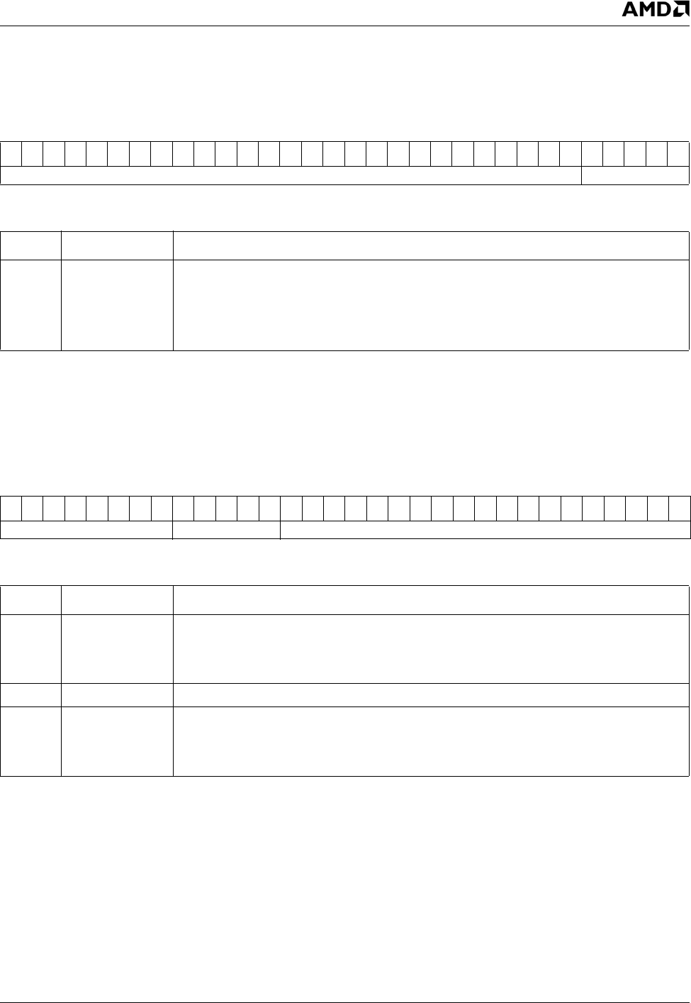
AMD Geode™ LX Processors Data Book 505
Video Input Port Register Descriptions 33234H
6.10.2.23 VIP Ancillary Data/Message Passing/Data Streaming Buffer 2 Base Address (VIP_ANC_MSG_2_BASE)
6.10.2.24 VIP Ancillary Data/Message Passing/Data Streaming Buffer Size (VIP_ANC_MSG_SIZE)
VIP Memory Offset 5Ch
Ty p e R / W
Reset Value 00000000h
VIP_ANC_MSG_2_BASE Register Map
313029282726252423222120191817161514131211109876543210
ANC_MSG_2_BASE Program to 00000
VIP_ANC_MSG_2_BASE Bit Descriptions
Bit Name Description
31:0 ANC_MSG_2_
BASE
Message Passing Data/Data Streaming Base Address. This register specifies the
base address for the second buffer used in Message Passing and Data Streaming
modes. Data written to this register takes place immediately (no double buffer). The
value in this register must be 32-byte aligned. (Bits [4:0] are required to be 00000.)
Note: This register is NOT double buffered.
VIP Memory Offset 60h
Ty p e R / W
Reset Value 00000000h
VIP_ANC_MSG_SIZE Register Map
31 30 29 28 27 26 25 24 23 22 21 20 19 18 17 16 15 14 13 12 11 10 9 8 7 6 5 4 3 2 1 0
ANC_PACK_INT_THRESH RSVD ANC_MSG_STREAM_SIZE
VIP_ANC_MSG_SIZE Bit Descriptions
Bit Name Description
31:24 ANC_PACK_
INT_THRESH
Ancillary Packet Interrupt Threshold Value. This value determines when the ancillary
interrupt occurs. The Ancillary Packet Count (APC) bits (VIP Memory Offset 08h[31:24])
is compared to this value. If the APC is equal to or greater then this value, the ancillary
interrupt is generated.
23:19 RSVD Reserved.
18:0 ANC_MSG_
STREAM_SIZE
Ancillary Data/Message Passing Data/Data Streaming Buffer Size. This register
specifies the size of the ancillary, message passing, and data streaming buffers in bytes.
Changes to this register take effect immediately (not double buffered). The value in this
register is 8-byte aligned. Bits [2:0] are ignored.
506 AMD Geode™ LX Processors Data Book
Video Input Port Register Descriptions
33234H
6.10.2.25 VIP Page Offset/ Page Count (VIP_PAGE_OFFSET)
6.10.2.26 VIP Vertical Start/Stop (VIP_VERT_START_STOP)
VIP Memory Offset 68h
Ty p e R / W
Reset Value 00000000h
VIP_PAGE_OFFSET Register Map
31 30 29 28 27 26 25 24 23 22 21 20 19 18 17 16 15 14 13 12 11 10 9 8 7 6 5 4 3 2 1 0
PAGE_OFFSET Program to 00000
VIP_PAGE_OFFSET Bit Descriptions
Bit Name Description
31:0 PAGE_OFFSET Page Offset. This register specifies the offset to the next page of buffer data. If the page
count is 2 or greater, the next frame of data is started at an address of buffer +
PAGE_OFFSET. Up to eight pages (frames) can be accumulated. The address of the
next frame is located at a “Page Offset” address. Note that ancillary data and MSG/
STRM data is not paged. This only applies to video and VBI data. The value in this regis-
ter needs to be 32-byte aligned. (Bits [4:0] are required to be 00000.)
VIP Memory Offset 6Ch
Ty p e R / W
Reset Value 00000000h
VIP_VERT_START_STOP Register Map
31 30 29 28 27 26 25 24 23 22 21 20 19 18 17 16 15 14 13 12 11 10 9 8 7 6 5 4 3 2 1 0
RSVD VERT_END RSVD VERT_START
VIP_VERT_START_STOP Bit Description
Bit Name Description
31:28 RSVD Reserved. Set to 0.
27:16 VERT_END Vertical End Capture. This register specifies the last line # in a field/frame that is cap-
tured when the subwindow capture function is enabled in non BT.601 modes. In BT.601
interlaced modes, this register determines when the odd field line capture completes. In
601 non-interlaced modes, this register determines when the video capture completes.
See Figure 6-48 "BT.601 Mode Vertical Timing" on page 473 for additional detail.
15:12 RSVD Reserved. Set to 0.
11:0 VERT_START Vertical Start Capture. This register specifies the first line # in a field/frame that is cap-
tured when the subwindow capture function is enabled in non 601 modes. In BT.601
interlaced modes, this register determines when the odd field video capture starts. In
BT.601 non-interlaced modes, this register determines when the video capture starts.
See Figure 6-48 "BT.601 Mode Vertical Timing" on page 473 for additional detail.
AMD Geode™ LX Processors Data Book 507
Video Input Port Register Descriptions 33234H
6.10.2.27 VIP FIFO Address (VIP_FIFO_R_W_ADDR)
6.10.2.28 VIP FIFO Data (VIP_FIFO_DATA)
VIP Memory Offset 70h
Ty p e R / W
Reset Value 00000000h
VIP_FIFO_R_W_ADDR Register Map
31 30 29 28 27 26 25 24 23 22 21 20 19 18 17 16 15 14 13 12 11 10 9 8 7 6 5 4 3 2 1 0
RSVD FIFO_ADDRESS
VIP_FIFO_R_W_ADDR Bit Descriptions
Bit Name Description
31:9 RSVD Reserved. Set to 0.
8:0 FIFO_ADDRESS FIFO ADDRESS. FIFO address for which a FIFO read or write occurs. The data is writ-
ten/read via the FIFO Data register (VIP Memory Offset 74h). Note that the 256x64 bit
FIFO is mapped as a 512x32 bit memory.
VIP Memory Offset 74h
Ty p e R / W
Reset Value xxxxxxxxh
VIP_FIFO_DATA Register Map
31 30 29 28 27 26 25 24 23 22 21 20 19 18 17 16 15 14 13 12 11 10 9 8 7 6 5 4 3 2 1 0
FIFO_DATA
VIP_FIFO_DATA Bit Descriptions
Bit Name Description
31:0 FIFO_DATA FIFO Data. When the FF_R/W bit is set (VIP Memory Offset 04h[24] = 1), data written to
this register is stored in FIFO_ADDR (VIP Memory Offset 70h[7:0]). When the FF_R/W
bit is reset, data from the FIFO corresponding to the address in the FIFO_ADDR is
returned
508 AMD Geode™ LX Processors Data Book
Video Input Port Register Descriptions
33234H
6.10.2.29 VIP VSYNC Error Count (VIP_SYNC_ERR_COUNT)
6.10.2.30 VIP Task A U Even Offset (VIP_TASK_A_U_EVEN_OFFSET)
VIP Memory Offset 78h
Ty p e R / W
Reset Value 00000000h
VIP_SYNC_ERR_COUNT Register Map
313029282726252423222120191817161514131211109876543210
VERTICAL_WINDOW VERTICAL_COUNT
VIP_SYNC_ERR_COUNT Bit Descriptions
Bit Name Description
31:24 VERTICAL_
WINDOW
Vertical Window. This field defines the number of VIP clocks the input VBLANK can
vary before it is considered invalid. (16-4095 clocks)
23:0 VERTICAL_
COUNT
Vertical Count. This field provides the check point for verifying that the input data stream
is maintaining consistent VSYNC timing. This count is the minimum number of VIP clocks
expected in an input field (interlaced video) or frame (non-interlaced video). If the number
of video clocks between rising edges of VBLANK is less then this number (or greater
then VERTICAL_COUNT + VERTICAL_WINDOW), a VSYNC error interrupt is gener-
ated and the video_ok output signal is forced low indicating invalid input video. (0-
16,777,215 clocks)
Note: A 60 Hz VBLANK rate @75 MHz input clock = 1,250,000 clocks.
VIP Memory Offset 7Ch
Ty p e R / W
Reset Value 00000000h
VIP_TASK_A_U_EVEN_OFFSET Register Map
313029282726252423222120191817161514131211109876543210
TASK_A_U_EVEN_OFFSET Program to 00000
VIP_TASK_A_U_EVEN_OFFSET Bit Descriptions
Bit Name Description
31:0 TASK_A_U_
EVEN_OFFSET
Task A U Even Offset. This register determines the starting address of the U buffer for
the even field when in interlaced input mode and data is stored in planar format. This reg-
ister is not used when in non-interlaced input mode. The value in this register needs to be
32-byte aligned. (Bits [4:0] are required to be 00000.)
AMD Geode™ LX Processors Data Book 509
Video Input Port Register Descriptions 33234H
6.10.2.31 VIP Task A V Even Offset (VIP_TASK_A_V_EVEN_OFFSET)
VIP Memory Offset 80h
Ty p e R / W
Reset Value 00000000h
VIP_TASK_A_V_EVEN_OFFSET Register Map
31 30 29 28 27 26 25 24 23 22 21 20 19 18 17 16 15 14 13 12 11 10 9 8 7 6 5 4 3 2 1 0
TASK_A_V_EVEN_OFFSET Program to 00000
VIP_TASK_A_V_EVEN_OFFSET Bit Descriptions
Bit Name Description
31:0 TASK_A_V_
EVEN_OFFSET
Task A V Even Offset. This register determines the starting address of the V buffer for
the even field when in interlaced input mode and data is stored in planar format. This reg-
ister is not used when in non-interlaced input mode. The value in this register needs to be
32-byte aligned. (Bits [4:0] are required to be 00000.)

510 AMD Geode™ LX Processors Data Book
Security Block
33234H
6.11 Security Block
The Security Block provides a hardware Advanced Encryp-
tion Standard (AES) encryption/decryption engine and
interface for accessing EEPROM memory for storing
unique IDs and/or security keys. The AES and EEPROM
sections have separate control registers but share a single
set of interrupt registers.
6.11.1 Security Block Features
•AES
— Electronic Code Book (ECB) or Cipher Block
Chaining (CBC) 128-bit hardware encryption and
decryption
— CBC 128-bit hardware encryption and decryption
— DMA read and write (two contexts)
— Hidden key, (stored on EEPROM)
— Writable key can be written by the x86 processor
— Can use interrupts, SMIs, or be polled for completion
status
— Memory mapped register interface
•EEPROM I/F
— Provides 2K bit of EEPROM storage
— Programmable lock bits
— Programmable “Hidden” AES key
— Can use interrupts, SMIs, or be polled for completion
status
— Memory mapped register interface
•True Random Number Generator (TRNG)
— Read via MSR
Note: For security purposes, the EEPROM interface
resets to the “debug disabled” state. It takes
approximately 490 us to read the EEPROM and
unlock the debug interface. Therefore, the “CPU
stall” feature must be available even when the
debug interface is disabled. Since the EEPROM
may not respond for up to 10 ms after a write oper-
ation, the time out for accessing the EEPROM is
set to approximately 17 ms. Therefore it takes
approximately 17 ms for a part without an
EEPROM to unlock after the release from reset.
6.11.1.1 Performance Metrics
•System goals:
— 400 MHz GLIU interface
— > 40 MB/Sec. encrypt or decrypt
Figure 6-54. Security Block Diagram
SCL
SDA
Security Block
GLIU
AES Engine
EEPROM ID Interface
DMA
Top
I/O
master
slave
rqout
daout
dain
rqin
.
.
.
.
.
.
True Random Number Generator
Clock
Control
Unit Clock
Control
Unit
Clock
Control
Unit
SB Specific
Registers
EEPROM

AMD Geode™ LX Processors Data Book 511
Security Block 33234H
6.11.2 Functional Description
The AES engine provides ECB and CBC 128-bit hardware
encryption and decryption for the AMD Geode LX proces-
sor using the Advanced Encryption Standard algorithm.
The Security Block has two key sources. One is a hidden
128-bit key stored in non-volatile memory. It is expected
that this key is loaded into the non-volatile memory once at
the factory and the memory is locked to prevent future
writes. This key is loaded automatically by hardware after
reset and is not visible to the x86 processor, (also, these
locations in non-volatile memory cannot be read using the
non-volatile memory interface). The second key is writable,
(but not readable) by the x86 processor. It appears as a
series of four writable 32-bit QWORDs in the Security
Block memory address space. Reads to these registers
always return zeros. Note that these bits are accessible via
the debug interface unless the debug interface has been
locked.
For any single operation, the Security Block can work in
either encryption or decryption mode. The same two key
registers (hidden and writable) are used for both modes.
The Security Block provides a mastering DMA interface to
system memory. It contains two sets of pointer registers
(contexts A and B) for controlling the DMA operations. For
each set, there is a 32-bit DMA Source register that points
to the start of the source data in memory. The lower four
LSBs are zero, forcing the address to align to a 16-byte
boundary. There is a 32-bit DMA Destination register that
points to the region in memory where the AES block writes
its results. This pointer also forces alignment to a 16-byte
boundary. For consistency with other block architecture
specifications, these registers are described as QWORDs
in the Security Block memory space. In addition to the 32-
bit DMA Source register, there is a 32-bit Length register
that holds a count of the number of bytes to be encrypted/
decrypted. Again the lower four bits are zero forcing the
length to be an integer multiple of 16-byte blocks. If the
source data does not end on a 16-byte boundary, software
must pad the data out to the next 16-byte boundary. Having
two separate contexts allows the software to queue a sec-
ond encryption/decryption request while the first operation
is completing. The Security Block only contains a single
AES hardware block so the second request is not pro-
cessed until the first request completes.
The Control registers (SB Memory Offset 00h and 04h) are
used to configure the Security Block. There are two sets of
control bits to select the key source (hidden vs. writable)
and the operational mode (encryption/decryption), and the
data coherency flags for memory accesses. There are also
two start bits (A and B) to initiate an operation once the
appropriate pointers have been configured. The Security
Block can be configured to generate an interrupt on com-
pletion of an encryption/decryption operation. Alternatively,
the interrupt can be masked and the completion bit can be
polled.
For each start command, the Security Block processes the
data starting at the DMA source address and continues for
the number of bytes specified in the Length register. The
results are written starting at the address in the Destination
register. For each start command, the Security Block pro-
cesses the data starting at the DMA source address and
continues for the number of bytes specified in the Length
register. The results are written starting at the address in
the Destination register. For each start command, the AES
can be configured for key source, encryption/decryption
mode, and memory coherence flags. No changes to the A
registers should be made during an encryption or decryp-
tion operation for A, and no changes to the B registers
should be made during an encryption or decryption opera-
tion for B. In CBC mode, the CBC Initialization Vector regis-
ter value is used by both A and B channels.
The AMD Geode LX processor supports AES CBC mode
and a True Random Number Generator. CBC encryption/
decryption is similar to ECB. When doing CBC mode
encryption/decryption, the 128-bit initialization vector is
written to the CBC Initialization Vector registers (SB Mem-
ory Offset 40h-4Ch) prior to the start of the encryption/
decryption. The random number generator function pro-
vides true random numbers required for the initialization
values for AES CBC encryption. Software must read the
32-bit random number register four times to build the 128-
bit initialization vector (IV). This can then be used to pro-
gram the CBC Initialization Vector registers prior to the
CBC encryption.
512 AMD Geode™ LX Processors Data Book
Security Block
33234H
6.11.2.1 EEPROM ID Interface
The EEPROM ID interface provides an interface to an
EEPROM non-volatile memory available for storing ID
numbers, keys, or other security related information. The
EEPROM ID interface consists of a 2K (256-byte) array
with 2 bytes reserved for EEPROM control state, 238 bytes
are available as general purpose non-volatile storage, and
16 bytes reserved for use as a hidden key for the AES
engine. (Note that locations 18-33 are reserved for a
Unique ID, but can be used for general purpose storage.)
After reset, the EEPROM ID interface state machine reads
the two access control bytes from the EEPROM. These
define the access policies for the EEPROM. It also auto-
matically copies the 128-bit hidden key from the array to
the AES engine’s hidden key register. When an
AMD Geode LX processor device is initially manufactured,
the EEPROM is programmed to all ones and the control
bytes are set to the unlocked state allowing writing of the
entire EEPROM array and reading of all location except the
hidden key. Information can be stored in the EEPROM and
then optionally the EEPROM can be locked to prevent fur-
ther writes and/or disable certain debug features of the
AMD Geode LX processor.
The EEPROM controller defaults to the unlocked state if it
cannot access an EEPROM after reset. This allows parts
built without EEPROMs to have functional debug inter-
faces.
The EEPROM ID interface works on a byte-wide basis. The
EEPROM Address register (SB Memory Offset 804h) is
first programmed by software, and then the EEPROM
Command register (SB Memory Offset 804h) is written to
initiate a write from the EEPROM Data register (SB Mem-
ory Offset 808h) to the array or a read from the array to the
Data register. The START bit in the Command register (SB
Memory Offset 800h) resets automatically once the
EEPROM access has completed. The user may also
enable an interrupt to be generated when the access has
completed. Since the EEPROM access is slow, this simple
command interface allows the processor to continue with
other tasks while waiting for the access to complete. Table
6-77 shows common usage of the EEPROM.
Note: The EEPROM interface is designed to work with a
GLIU frequency up to 400 MHz. For operation
above 400 MHz, several internal design parame-
ters must be changed.
6.11.2.2 Security Block Interrupts
The Security Block has three possible sources for an inter-
rupt: completion of an AES task on context A, completion
of an AES task on context B, and completion of an
EEPROM read or write operation. The interrupt event and
interrupt mask registers are memory mapped. These three
sources can also generate an SMI. The SMI event and SMI
mask registers are accessible via MSRs. Any one of these
events will simultaneously set the SMI and interrupt event
bits. The mask bits may be used to enable either an inter-
rupt or an SMI if desired.
6.11.2.3 GLIU Interface
The GLIU provides a standard interface to the AMD Geode
LX processor. The Security Block is both a master and a
slave on this bus.
Table 6-77. EEPROM Address Map
Byte Address Range Description
0 Lower Access control byte 0 (WPU and WPL)
1 Access control byte 1 (WPE and DBL)
2-17 Hidden key storage (128 bits)
18-33 Unique ID (128 bits)
34-127 User data
128-255 Upper User data

AMD Geode™ LX Processors Data Book 513
Security Block Register Descriptions 33234H
6.12 Security Block Register Descriptions
This section provides information on the registers associ-
ated with the Security Block (SB), including the Standard
GeodeLink Device (GLD) MSRs, the Security Block Spe-
cific MSRs (accessed via the RDMSR and WRMSR
instructions), and the Security Block Configuration/Control reg-
isters. Table 6-78 through Table 6-80 are register summary
tables that include reset values and page references where
the bit descriptions are provided.
The MSR address is derived from the perspective of the
CPU Core. See Section 4.1 "MSR Set" on page 45 for
more detail on MSR addressing.
Table 6-78. Standard GeodeLink™ Device MSRs Summary
MSR Address Type Register Name Reset Value Reference
58002000h RO GLD Capabilities MSR (GLD_MSR_CAP) 00000000_001304xxh Page 515
58002001h R/W GLD Master Configuration MSR
(GLD_MSR_CONFIG)
00000000_00000000h Page 515
58002002h R/W GLD SMI MSR (GLD_MSR_SMI) 00000000_00000007h Page 516
58002003h R/W GLD Error MSR (GLD_MSR_ERROR) 00000000_00000019h Page 516
58002004h R/W GLD Power Management MSR
(GLD_MSR_PM)
00000000_00000015h Page 518
58002005h R/W GLD Diagnostic MSR (GLD_MSR_DIAG) 00000000_00000000h Page 518
Table 6-79. Security Block Specific MSRs
MSR Address Type Register Name Reset Value Reference
58002006h R/W GLD Control MSR (GLD_MSR_CTRL) 00000000_00000003h Page 519
Table 6-80. Security Block Configuration/Control Registers Summary
SB Memory
Offset Type Register Name Reset Value Reference
000h R/W SB Control A (SB_CTL_A) 00000000h Page 520
004h R/W SB Control B (SB_CTL_B) 00000000h Page 521
008h R/W SB AES Interrupt (SB_AES_INT) 00000007h Page 522
010h R/W SB Source A (SB_SOURCE_A) 00000000h Page 522
014h R/W SB Destination A (SB_DEST_A) 00000000h Page 523
018h R/W SB Length A (SB_LENGTH_A) 00000000h Page 523
020h R/W SB Source B (SB_SOURCE_B) 00000000h Page 524
024h R/W SB Destination B (SB_DEST_B) 00000000h Page 524
028h R/W SB Length B (SB_LENGTH_B) 00000000h Page 525
030h WO SB Writable Key 0 (SB_WKEY_0) 00000000h Page 525
034h WO SB Writable Key 1 (SB_WKEY_1) 00000000h Page 526
038h WO SB Writable Key 2 (SB_WKEY_2) 00000000h Page 526
03Ch WO SB Writable Key 3 (SB_WKEY_3) 00000000h Page 527
040h R/W SB CBC Initialization Vector 0
(SB_CBC_IV_0)
00000000h Page 527
044h R/W SB CBC Initialization Vector 1
(SB_CBC_IV_1)
00000000h Page 528

514 AMD Geode™ LX Processors Data Book
Security Block Register Descriptions
33234H
048h R/W SB CBC Initialization Vector 2
(SB_CBC_IV_2)
00000000h Page 528
04Ch R/W SB CBC Initialization Vector 3
(SB_CBC_IV_3)
00000000h Page 528
050h RO SB Random Number
(SB_RANDOM_NUM)
00000000h Page 529
054h RO SB Random Number Status
(SB_RANDOM_NUM_STATUS)
00000001h Page 529
800h R/W SB EEPROM Command
(SB_EEPROM_COMM)
00000000h Page 530
804h R/W SB EEPROM Address
(SB_EEPROM_ADDR)
000000FFh Page 531
808h R/W SB EEPROM Data (SB_EEPROM_DATA) 00000000h Page 531
80Ch RO SB EEPROM Security State
(SB_EEPROM_SEC_STATE)
00000000h Page 532
Table 6-80. Security Block Configuration/Control Registers Summary (Continued)
SB Memory
Offset Type Register Name Reset Value Reference
AMD Geode™ LX Processors Data Book 515
Security Block Register Descriptions 33234H
6.12.1 Standard GeodeLink™ (GLD) Device MSRs
6.12.1.1 GLD Capabilities MSR (GLD_MSR_CAP)
6.12.1.2 GLD Master Configuration MSR (GLD_MSR_CONFIG)
MSR Address 58002000h
Ty p e RO
Reset Value 00000000_001304xxh
GLD_MSR_CAP Register Map
63 62 61 60 59 58 57 56 55 54 53 52 51 50 49 48 47 46 45 44 43 42 41 40 39 38 37 36 35 34 33 32
RSVD
313029282726252423222120191817161514131211109876543210
RSVD DEV_ID REV_ID
GLD_MSR_CAP Bit Descriptions
Bit Name Description
63:24 RSVD Reserved.
23:8 DEV_ID Device ID. Identifies device (1304h).
7:0 REV_ID Revision ID. Identifies device revision. See AMD Geode™ LX Processors Specification
Update document for value.
MSR Address 58002001h
Ty p e R / W
Reset Value 00000000_00000000h
GLD_MSR_CONFIG Register Map
63 62 61 60 59 58 57 56 55 54 53 52 51 50 49 48 47 46 45 44 43 42 41 40 39 38 37 36 35 34 33 32
RSVD
31 30 29 28 27 26 25 24 23 22 21 20 19 18 17 16 15 14 13 12 11 10 9 8 7 6 5 4 3 2 1 0
RSVD PRI
RSVD
PID
GLD_MSR_CONFIG Bit Descriptions
Bit Name Description
63:7 RSVD Reserved.
6:4 PRI AES Priority Level. This is the Priority level used by the AES interface.
3 RSVD Reserved.
2:0 PID AES Priority Domain. Assigned priority domain identifier.

516 AMD Geode™ LX Processors Data Book
Security Block Register Descriptions
33234H
6.12.1.3 GLD SMI MSR (GLD_MSR_SMI)
6.12.1.4 GLD Error MSR (GLD_MSR_ERROR)
MSR Address 58002002h
Ty p e R / W
Reset Value 00000000_00000007h
GLD_MSR_SMI Register Map
63 62 61 60 59 58 57 56 55 54 53 52 51 50 49 48 47 46 45 44 43 42 41 40 39 38 37 36 35 34 33 32
RSVD SMI_STAT
US
31 30 29 28 27 26 25 24 23 22 21 20 19 18 17 16 15 14 13 12 11 10 9 8 7 6 5 4 3 2 1 0
RSVD SMI_MASK
GLD_MSR_SMI Bit Descriptions
Bit Name Description
63:35 RSVD Reserved.
34:32 SMI_STATUS SMI Status. There are three SMI status sources. For each source, the individual bit has
the following meaning:
0: SMI not pending.
1: SMI pending.
Writing a 1 to the bit clears the status.
Bit 34: EEPROM Operation Complete SMI.
Bit 33: AES Context B Complete SMI.
Bit 32: AES Context A Complete SMI.
31:3 RSVD Reserved.
2:0 SMI_MASK SMI Masks. There are three SMI status masks. For each source, the individual bit has
the following meaning:
0: Enable. Unmask the SMI.
1: Disable. Mask the SMI.
Bit 2: When enabled (0), allows EEPROM Operation Complete SMI.
Bit 1: When enabled (0), allows AES Context B Complete SMI.
Bit 0: When enabled (0), allows AES Context A Complete SMI.
MSR Address 58002003h
Ty p e R / W
Reset Value 00000000_00000019h
AMD Geode™ LX Processors Data Book 517
Security Block Register Descriptions 33234H
GLD_MSR_ERROR Register Map
63 62 61 60 59 58 57 56 55 54 53 52 51 50 49 48 47 46 45 44 43 42 41 40 39 38 37 36 35 34 33 32
RSVD
RB_ERR_STATUS
RA_ERR_STATUS
RSVD
AES_ERR_STATUS
313029282726252423222120191817161514131211109876543210
RSVD
RB_ERR_MASK
RA_ERR_MASK
RSVD
AES_ERR_MASK
GLD_MSR_Error Bit Descriptions
Bit Name Description
63:37 RSVD Reserved.
36 RB_ERR_
STATUS
Response B Error Status. When set, this bit indicates that context B received a
response with either the SSMI or Exception flag set. This can occur on any of the read
responses or on the last write of an encrypt or decrypt operation that also requires a
response. If the error occurs on a read response, the operation is terminated and the
state machine returns to idle and signals completion. Write a one to this bit to clear the
status.
35 RA_ERR_
STATUS
Response A Error Status. When set, this bit indicates that context A received a
response with either the SSMI or Exception flag set. This can occur on any of the read
responses or on the last write of an encrypt or decrypt operation that also requires a
response. If the error occurs on a read response, the operation is terminated and the
state machine returns to idle and signals completion. Write a one to this bit to clear the
status.
34-33 RSVD Reserved.
32 AES_ERR_
STATUS
AES Error Status. Reserved Type. This bit is set if the module receives a transaction
identified with a reserved transaction type. This implies a hardware error.
0: AES Error not pending.
1: AES Error pending.
Writing a 1 to this bit clears the status.
31:3 RSVD Reserved.
4 RB_ERR_
MASK
Response B Error Mask. When set, this bit masks the Response B Error (bit 36) and
prevents generation of the error output. When cleared, the error is enabled and asser-
tion of Response B Error will generate an error.
3 RA_ERR_
MASK
Response A Error Mask. When set, this bit masks the Response A Error (bit 35) and
prevents generation of the error output. When cleared, the error is enabled and asser-
tion of Response A Error will generate an error.
2:1 RSVD Reserved.
0 AES_ERR_
MASK
AES Error Mask. Reserved Type.
0: Unmask the Error (enabled).
1: Mask the Error (disabled).
518 AMD Geode™ LX Processors Data Book
Security Block Register Descriptions
33234H
6.12.1.5 GLD Power Management MSR (GLD_MSR_PM)
6.12.1.6 GLD Diagnostic MSR (GLD_MSR_DIAG)
This register is reserved for internal use by AMD and should not be written to.
MSR Address 58002004h
Ty p e R / W
Reset Value 00000000_00000015h
GLD_MSR_PM Register Map
63 62 61 60 59 58 57 56 55 54 53 52 51 50 49 48 47 46 45 44 43 42 41 40 39 38 37 36 35 34 33 32
RSVD
313029282726252423222120191817161514131211109876543210
RSVD
PMD2
RSVD
PMD1
RSVD
PMD0
GLD_MSR_PM Bit Descriptions
Bit Name Description
63:5 RSVD Reserved.
4PMD2 Power Mode 2 (EEPROM).
0: Disable clock gating. Clocks are always ON.
1: Enable active hardware clock gating.
3 RSVD Reserved.
2PMD1 Power Mode 1 (AES core, GLIU clock/2).
0: Disable clock gating. Clocks are always ON.
1: Enable active hardware clock gating.
1 RSVD Reserved.
0PMD0 Power Mode 0 (GLIU clock).
0: Disable clock gating. Clocks are always ON.
1: Enable active hardware clock gating.
MSR Address 58002005h
Ty p e R / W
Reset Value 00000000_00000000h
AMD Geode™ LX Processors Data Book 519
Security Block Register Descriptions 33234H
6.12.2 Security Block Specific MSRs
6.12.2.1 GLD Control MSR (GLD_MSR_CTRL)
MSR Address 58002006h
Ty p e R / W
Reset Value 00000000_00000003h
GLD_MSR_CTRL Register Map
63 62 61 60 59 58 57 56 55 54 53 52 51 50 49 48 47 46 45 44 43 42 41 40 39 38 37 36 35 34 33 32
RSVD
313029282726252423222120191817161514131211109876543210
RSVD
T_TM
T_NE
T_SEL
RSVD
TW
SBY
SBI
DIV
GLD_MSR_CTRL Bit Descriptions
Bit Name Description
63:12 RSVD Reserved. These bits are implemented but reserved for future use. When writing to this
MSR, software should set these bits to 0 and ignore them on read.
11 T_TM TRNG Test Mode. This bits enables the TRNG test mode. Deterministic TRNG values
are generated when this bit is 1.
10 T_NE TRNG Noise Enable. This bit enables the noise generator for the TRNG.
0: Disable.
1: Enable.
9:8 T_SEL TRNG SEL. These bits select post processing of the TRNG output.
00: Raw output.
01: LFSR output.
10: Whitener output.
11: LFSR + Whitener output.
7:5 RSVD Reserved. These bits are implemented but reserved for future use. When writing to this
MSR, software should set these bits to 0 and ignore them on read.
4TW Time Write. This bit controls the EEPROM write timing within the EEPROM interface
module. Normally the EEPROM interface signals completion immediately after it finishes
shifting out the last bit of a write operation. The start of any other EEPROM access
begins a polling process. Once, the EEPROM has completed its internally timed write
operation, it responds to the polling and the next operation can begin. Setting this bit
causes the EEPROM interface to delay for slightly more than 10 ms after writing to the
EEPROM, before indicating write completion. That is, the start bit will be held high, and
the interrupt and SMI generation will be delayed for 10 ms. This ensures that the
EEPROM has completed its internal write and should be ready to respond to the next
access immediately. This is a “chicken” bit to avoid using the acknowledge polling (as
described in the Atmel datasheet), after a write.
3 SBY Swap Bytes. This bit controls a byte-swapping feature within the AES module. When
set, the bytes within the 16-byte block are swapped on both AES DMA reads and writes.
Byte 15 is swapped with byte 0, byte 14 is swapped with byte 1, etc. Asserting this bit
does not affect the slave operations to AES registers, (including the writable key), nor
does it affect EEPROM operations. When this bit is cleared, the DMA operations read
and write bytes with the same byte order as they appear in memory.
520 AMD Geode™ LX Processors Data Book
Security Block Register Descriptions
33234H
6.12.3 Security Block Configuration/Control Registers
6.12.3.1 SB Control A (SB_CTL_A)
2 SBI Swap Bits. This bit controls a bit-swapping feature within the AES module. When set,
the bits within each byte are swapped on both AES DMA reads and writes. Bit 7 is
swapped with bit 0, bit 6 is swapped with 1, etc. Asserting this bit does not affect the
slave operations to AES registers, (including the writable key), nor does it affect
EEPROM operations. When this bit is cleared, the DMA operations read and write bytes
with the same bit order as they appear in memory.
1:0 DIV AES Enable Divider. These two bits control the ratio between the GLIU clock frequency
and the updating of the AES encryption engine registers. The AES module is clocked at
the GLIU frequency, however, the state registers only update on an enable pulse that
occurs each n cycles, where n is determined by the DIV value. This register should not
be changed during an AES operation.
00: Divide by 1 (use for 100 MHz GLIU or less).
01: Divide by 2 (use for 100 MHz to 200 MHz GLIU).
10: Divide by 3 (use for 200 MHz to 300 MHz GLIU).
11: Divide by 4 (use for 300 MHz to 400 MHz GLIU).
SB Memory Offset 000h
Ty p e R / W
Reset Value 00000000h
GLD_MSR_CTRL Bit Descriptions (Continued)
Bit Name Description
SB_CTL_A Register Map
313029282726252423222120191817161514131211109876543210
RSVD RSVD
CBCA
SCA
DCA
WKA
ECA
STA
SB_CTL_A Register Bit Descriptions
Bit Name Description
31:8 RSVD Reserved.
7:6 RSVD Reserved. These bits are implemented but reserved for future use. When writing to this
register, software should set these bits to 0 and ignore them on read.
5CBCA Cipher Block Chaining (CBC) Mode for A Pointer. When set, the AES engine
encrypts/decrypts using the Cipher Block Chaining Mode for the A pointer. When reset,
the AES engine encrypts/decrypts using the Electronic Codebook (ECB) Mode. No ini-
tialization vector is used when in ECB mode.
4SCA Source Coherency for A Pointer Set. When set, the source memory fetches using the
GLIU interface are flagged as coherent operations. When reset, the operations are non-
coherent.
3 DCA Destination Coherency for A Pointer Set. When set, the destination memory writes
using the GLIU interface are flagged as coherent operations. When reset, the opera-
tions are non-coherent.
2WKA Writable Key for A Pointer Set. When set, the AES engine uses the key from the writ-
able key register (SB Memory Offset 030h-03Ch) for its next operation. When reset, it
uses the hidden key value.
1ECA Encrypt for A Pointer. When set, the AES operates in encryption mode. When reset, it
operates in decryption mode.
AMD Geode™ LX Processors Data Book 521
Security Block Register Descriptions 33234H
6.12.3.2 SB Control B (SB_CTL_B)
0STA Start for A Pointer. When set, this bit commands the AES to start a new operation
based on the current control register setting and the settings in SB Memory Offset 010h
and 014h. This bit is reset automatically when the operation completes. Setting this bit
also clears the “Complete” flag in the AES Interrupt register (SB Memory Offset
008h[16]) and in SB GLD_MSR_SMI (MSR 58002002h[32]). If an operation using the B
pointer set is already underway, the new operation for pointer set A will not start until the
previous B operation completes. If both A and B start bits are asserted in the same write
operation, the A operation take precedence.
SB Memory Offset 004h
Ty p e R / W
Reset Value 00000000h
SB_CTL_A Register Bit Descriptions (Continued)
Bit Name Description
SB_CTL_B Register Map
313029282726252423222120191817161514131211109876543210
RSVD RSVD
CBCB
SCB
DCB
WKB
ECB
STB
SB_CTL_B Register Bit Descriptions
Bit Name Description
31:8 RSVD Reserved.
7:6 RSVD Reserved. These bits are implemented but reserved for future use. When writing to this
register, software should set these bits to 0 and ignore them on read.
5CBCB Cipher Block Chaining (CBC) Mode for B Pointer. When set, the AES engine
encrypts/decrypts using the Cipher Block Chaining Mode for the B pointer. When reset,
the AES engine encrypts/decrypts using the Electronic Codebook (ECB) Mode. No ini-
tialization vector is used when in ECB mode.
4SCB Source Coherency for B Pointer Set. When set, the source memory fetches using the
GLIU interface are flagged as coherent operations. When reset, the operations are non-
coherent.
3 DCB Destination Coherency for B Pointer Set. When set, the destination memory writes
using the GLIU interface are flagged as coherent operations. When reset, the operations
are non-coherent.
2WKB Writable Key for B Pointer Set. When set, the AES engine uses the key from the Writ-
able Key register (SB Memory Offset 030h-03Ch) for its next operation. When reset, it
uses the hidden key value.
1ECB Encrypt for B Pointer. When set, the AES operates in encryption mode. When reset, it
operates in decryption mode.
0STB Start for B Pointer. When set, this bit commands the AES to start a new operation
based on the current control register setting and the settings in SB Memory Offset 020h
and 024h. This bit is reset automatically when the operation completes. Setting this bit
also clears the “Complete” flag in the AES Interrupt register (SB Memory Offset
008h[17]) and in the SB GLD_MSR_SMI (MSR 58002002h[33]). If an operation using
the A pointer set is already underway, the new operation for pointer set B will not start
until the previous A operation completes. If both A and B start bits are asserted in the
same write operation, the A operation take precedence.
522 AMD Geode™ LX Processors Data Book
Security Block Register Descriptions
33234H
6.12.3.3 SB AES Interrupt (SB_AES_INT)
6.12.3.4 SB Source A (SB_SOURCE_A)
SB Memory Offset 008h
Ty p e R / W
Reset Value 00000007h
SB_AES_INT Register Map
31 30 29 28 27 26 25 24 23 22 21 20 19 18 17 16 15 14 13 12 11 10 9 8 7 6 5 4 3 2 1 0
RSVD INT_STATUS RSVD INT_MASK
SB_AES_INT Register Bit Descriptions
Bit Name Description
31:19 RSVD Reserved.
18:16 INT_STATUS AES Interrupt Status.
0: INT not pending.
1: INT pending.
Writing a 1 to this bit clears the status.
18: EEPROM operation complete.
17: AES context B complete.
16: AES context A complete.
15:3 RSVD Reserved.
2:0 INT_MASK AES Interrupt Mask.
0: Enable, unmask the INT.
1: Disabled, mask the INT.
2: When enabled (0), allows EEPROM operation complete INT.
1: When enabled (0), allows AES context B complete INT.
0: When enabled (0), allows AES context A complete INT.
SB Memory Offset 010h
Ty p e R / W
Reset Value 00000000h
SB_SOURCE_A Register Map
313029282726252423222120191817161514131211109876543210
SOURCE_A RSVD
SB_SOURCE_A Register Bit Descriptions
Bit Name Description
31:4 SOURCE_A Source A. The Source field is a 32-bit pointer to system memory. It points to the start of
data to be encrypted or decrypted. The lower four bits must be written as zero and
always read zero. This forces the data fetching to begin on a 16-byte boundary. This
register should not be changed during an AES encryption or decryption operation using
the A pointer (i.e., while STA is asserted, SB Memory Offset 000h[0] = 1). This register
can be modified during an operation using the B pointer set (while STB is asserted, SB
Memory Offset 004h[0] = 1).
3:0 RSVD Reserved. Set to 0.
AMD Geode™ LX Processors Data Book 523
Security Block Register Descriptions 33234H
6.12.3.5 SB Destination A (SB_DEST_A)
6.12.3.6 SB Length A (SB_LENGTH_A)
SB Memory Offset 014h
Ty p e R / W
Reset Value 00000000h
SB_DEST_A Register Map
31 30 29 28 27 26 25 24 23 22 21 20 19 18 17 16 15 14 13 12 11 10 9 8 7 6 5 4 3 2 1 0
Destination A RSVD
SB_DEST_A Register Bit Descriptions
Bit Name Description
31:4 DEST_A Destination A. The Destination field is a 32-bit pointer to system memory. It points to
the start of memory where the results of encryption or decryption operation are to be
written. The lower four bits must be written as zero and always read zero. This forces
the data writing to begin on a 16-byte boundary. This register should not be changed
during an AES encryption or decryption operation using the A pointer set (i.e., while
STA is asserted, SB Memory Offset 000h[0] = 1). This register can be modified during
an operation using the B pointer set (while STB is asserted, SB Memory Offset 004h[0]
= 1).
3:0 RSVD Reserved. Set to 0.
SB Memory Offset 018h
Ty p e R / W
Reset Value 00000000h
SB_LENGTH_A Register Map
31 30 29 28 27 26 25 24 23 22 21 20 19 18 17 16 15 14 13 12 11 10 9 8 7 6 5 4 3 2 1 0
LENGTH_A RSVD
SB_LENGTH_A Register Bit Descriptions
Bit Name Description
31:4 LENGTH_A Length A. The Length field is a 32-bit value that describes the number of bytes to be
encrypted or decrypted in the next operation using pointer set A. The lower four bits
must be written as zero and always read zero. This forces the data length to be an inte-
ger number of 16-byte blocks. This register should not be changed during an AES
encryption or decryption operation using the A pointer set (i.e., while STA is asserted,
SB Memory Offset 000h[0] = 1). This register can be modified during an operation using
the B pointer set (while STB is asserted, SB Memory Offset 004h[0] = 1).
3:0 RSVD Reserved.
524 AMD Geode™ LX Processors Data Book
Security Block Register Descriptions
33234H
6.12.3.7 SB Source B (SB_SOURCE_B)
6.12.3.8 SB Destination B (SB_DEST_B)
SB Memory Offset 020h
Ty p e R / W
Reset Value 00000000h
SB_SOURCE_B Register Map
31 30 29 28 27 26 25 24 23 22 21 20 19 18 17 16 15 14 13 12 11 10 9 8 7 6 5 4 3 2 1 0
SOURCE_B RSVD
SB_SOURCE_B Register Bit Descriptions
Bit Name Description
31:4 SOURCE_B Source B. The Source field is a 32-bit pointer to system memory. It points to the start of
data to be encrypted or decrypted. The lower four bits must be written as zero and
always read zero. This forces the data fetching to begin on a 16-byte boundary. This
register should not be changed during an AES encryption or decryption operation using
the A pointer set (i.e., while STA is asserted, SB Memory Offset 000h[0] = 1). This regis-
ter can be modified during an operation using the B pointer set (while STB is asserted,
SB Memory Offset 004h[0] = 1).
3:0 RSVD Reserved. Set to 0.
SB Memory Offset 024h
Ty p e R / W
Reset Value 00000000h
SB_DEST_B Register Map
313029282726252423222120191817161514131211109876543210
DEST_B RSVD
SB_DEST_B Register Bit Descriptions
Bit Name Description
31:4 DEST_B Destination B. The Destination field is a 32-bit pointer to system memory. It points to
the start of memory where the results of encryption or decryption operation are to be
written. The lower four bits must be written as zero and always read zero. This forces the
data writing to begin on a 16-byte boundary. This register should not be changed during
an AES encryption or decryption operation using the A pointer set (i.e., while STA is
asserted, SB Memory Offset 000h[0] = 1). This register can be modified during an oper-
ation using the B pointer set (while STB is asserted, SB Memory Offset 004h[0] = 1).
3:0 RSVD Reserved. Set to 0.
AMD Geode™ LX Processors Data Book 525
Security Block Register Descriptions 33234H
6.12.3.9 SB Length B (SB_LENGTH_B)
6.12.3.10 SB Writable Key 0 (SB_WKEY_0)
SB Memory Offset 028h
Ty p e R / W
Reset Value 00000000h
SB_LENGTH_B Register Map
31 30 29 28 27 26 25 24 23 22 21 20 19 18 17 16 15 14 13 12 11 10 9 8 7 6 5 4 3 2 1 0
LENGTH_B RSVD
SB_LENGTH_B Register Bit Descriptions
Bit Name Description
31:4 LENGTH_B Length B. The Length field is a 32-bit value that describes the number of bytes to be
encrypted or decrypted in the next operation using pointer set B. The lower four bits
must be written as zero and always read zero. This forces the data length to be an inte-
ger number of 16-byte blocks. This register should not be changed during an AES
encryption or decryption operation using the A pointer set (i.e., while STA is asserted,
SB Memory Offset 000h[0] = 1). This register can be modified during an operation using
the B pointer set (while STB is asserted, SB Memory Offset 004h[0] = 1).
3:0 RSVD Reserved. Set to 0.
SB Memory Offset 030h
Ty p e WO
Reset Value 00000000h
SB_W_KEY0 Register Map
31 30 29 28 27 26 25 24 23 22 21 20 19 18 17 16 15 14 13 12 11 10 9 8 7 6 5 4 3 2 1 0
W_EY_0[31:0]
SB_WKEY_0 Bit Descriptions
Bit Name Description
31:0 WKEY_ 0 Writable Key 0. Bits [31:0] of the Writable Key for the Security Block. This register
should not be changed during an AES encryption or decryption operation. To prevent
one process from reading the key written by another process, this register is not read-
able.
526 AMD Geode™ LX Processors Data Book
Security Block Register Descriptions
33234H
6.12.3.11 SB Writable Key 1 (SB_WKEY_1)
6.12.3.12 SB Writable Key 2 (SB_WKEY_2)
SB Memory Offset 034h
Ty p e WO
Reset Value 00000000h
SB_WKEY_1 Register Map
31 30 29 28 27 26 25 24 23 22 21 20 19 18 17 16 15 14 13 12 11 10 9 8 7 6 5 4 3 2 1 0
WKEY_1[63:32]
SB_WKEY_1 Bit Descriptions
Bit Name Description
31:0 WKEY_1 Writable Key 1. Bits [63:32] of the Writable Key for the Security Block. This register
should not be changed during an AES encryption or decryption operation. To prevent
one process from reading the key written by another process, this register is not read-
able.
SB Memory Offset 038h
Ty p e WO
Reset Value 00000000h
SB_WKEY_2 Register Map
31 30 29 28 27 26 25 24 23 22 21 20 19 18 17 16 15 14 13 12 11 10 9 8 7 6 5 4 3 2 1 0
WKEY_2[95:64]
SB_WKEY_2 Bit Descriptions
Bit Name Description
31:0 WKEY_2 Writable Key 2. Bits [95:64] of the Writable Key for the Security Block. This register
should not be changed during an AES encryption or decryption operation. To prevent
one process from reading the key written by another process, this register is not read-
able.

AMD Geode™ LX Processors Data Book 527
Security Block Register Descriptions 33234H
6.12.3.13 SB Writable Key 3 (SB_WKEY_3)
6.12.3.14 SB CBC Initialization Vector 0 (SB_CBC_IV_0)
SB Memory Offset 03Ch
Ty p e WO
Reset Value 00000000h
SB_WKEY_3 Register Map
313029282726252423222120191817161514131211109876543210
WKEY_3[127:96]
SB_WKEY_3 Bit Descriptions
Bit Name Description
31:0 Writable Key 3 Writable Key 3. Bits [127:96] of the Writable Key for the Security Block. This register
should not be changed during an AES encryption or decryption operation. To prevent
one process from reading the key written by another process, this register is not read-
able.
SB Memory Offset 040h
Ty p e R / W
Reset Value 00000000h
SB_CBC_IV_0 Register Map
31 30 29 28 27 26 25 24 23 22 21 20 19 18 17 16 15 14 13 12 11 10 9 8 7 6 5 4 3 2 1 0
CBC_IV_0[31:0]
SB_CBC_IV_0 Bit Descriptions
Bit Name Description
31:0 CBC_IV_0
[31:0]
CBC Initialization Vector 0 [31:0]. Bits [31:0] of the initialization vector (IV) for the CBC
AES mode (Cipher Block Chaining). Change this register only when both A and B chan-
nels are IDLE. (A and B start bits, SB Memory Offset 000h and 004h, bit 0 = 0). This reg-
ister must be programmed with the IV vector prior to starting an AES CBC mode
encryption or decryption.
528 AMD Geode™ LX Processors Data Book
Security Block Register Descriptions
33234H
6.12.3.15 SB CBC Initialization Vector 1 (SB_CBC_IV_1)
6.12.3.16 SB CBC Initialization Vector 2 (SB_CBC_IV_2)
6.12.3.17 SB CBC Initialization Vector 3 (SB_CBC_IV_3)
SB Memory Offset 044h
Ty p e R / W
Reset Value 00000000h
SB_CBC_IV_1 Register Map
31 30 29 28 27 26 25 24 23 22 21 20 19 18 17 16 15 14 13 12 11 10 9 8 7 6 5 4 3 2 1 0
CBC_IV_1[63:32]
SB_CBC_IV_1 Bit Descriptions
Bit Name Description
31:0 IV[63:32] CBC Initialization Vector 1 [63:32]. Bits [63:32] of the IV for the CBC AES mode.
Change this register only when both A and B channels are IDLE. (A and B start bits, SB
Memory Offset 000h and 004h, bit 0 = 0). This register must be programmed with the IV
prior to starting an AES CBC mode encryption or decryption.
SB Memory Offset 048h
Ty p e R / W
Reset Value 00000000h
SB_CBC_IV_2 Register Map
31 30 29 28 27 26 25 24 23 22 21 20 19 18 17 16 15 14 13 12 11 10 9 8 7 6 5 4 3 2 1 0
CBC_IV_2[95:64]
SB_CBC_IV_2 Bit Descriptions
Bit Name Description
31:0 CBC_IV_2 [95:64] CBC Initialization Vector 2 [95:64]. Bits [95:64] of the IV for the CBC AES mode.
Change this register only when both A and B channels are IDLE. (A and B start
bits, SB Memory Offset 000h and 004h, bit 0 = 0). This register must be pro-
grammed with the IV prior to starting an AES CBC mode encryption or decryption.
SB Memory Offset 04Ch
Ty p e R / W
Reset Value 00000000h
SB_CBC_IV_3 Register Map
31 30 29 28 27 26 25 24 23 22 21 20 19 18 17 16 15 14 13 12 11 10 9 8 7 6 5 4 3 2 1 0
CBC_IV_3[127:96] (rev2.0)
SB_CBC_IV_3 Bit Descriptions
Bit Name Description
31:0 CBC_IV_3
[127:96]
CBC Initialization Vector 3 [127:96]. Bits [127:96] of the IV for the CBC AES Mode.
Change this register only when both A and B channels are IDLE. (A and B start bits, SB
Memory Offset 000h and 004h, bit 0 = 0). This register must be programmed with the IV
prior to starting an AES CBC mode encryption or decryption.
AMD Geode™ LX Processors Data Book 529
Security Block Register Descriptions 33234H
6.12.3.18 SB Random Number (SB_RANDOM_NUM)
6.12.3.19 SB Random Number Status (SB_RANDOM_NUM_STATUS)
SB Memory Offset 050h
Ty p e RO
Reset Value 00000000h
SB_RANDOM_NUM Register Map
313029282726252423222120191817161514131211109876543210
RANDOM_NUM
SB Random Number Bit Descriptions
Bit Name Description
31:0 RANDOM_
NUM
Random Number. Returns a 32-bit random number. Check the TRNG_VALID bit (SB
Memory Offset 054h[0]) before reading this register. If the status bit (TRNG_VALID) is
1, the value in this register is ready for use. A 0 in the status bit indicates that the ran-
dom number is in the process of being generated.
SB Memory Offset 054h
Ty p e RO
Reset Value 00000001h
SB_RANDOM_NUM_STATUS Register Map
313029282726252423222120191817161514131211109876543210
RSVD
TRNG_VALID
SB_RANDOM_NUM_STATUS Bit Descriptions
Bit Name Description
31:1 RSVD Reserved. Returns 0.
0 TRNG_VALID Random Number Valid. When 1, the random number is valid. When 0, the random
number is in the process of being generated.

530 AMD Geode™ LX Processors Data Book
Security Block Register Descriptions
33234H
6.12.3.20 SB EEPROM Command (SB_EEPROM_COMM)
SB Memory Offset 800h
Ty p e R / W
Reset Value 00000000h
SB_EEPROM_COMM Register Map
31 30 29 28 27 26 25 24 23 22 21 20 19 18 17 16 15 14 13 12 11 10 9 8 7 6 5 4 3 2 1 0
RSVD RSVD
HKD
SL
KV
EX
WR
ST
SB_EEPROM_COMM Bit Descriptions
Bit Name Description
31:8 RSVD Reserved.
7:6 RSVD Reserved. These bits are implemented but reserved for future use. When writing to this
register, software should set these bits to 0 and ignore them on read.
5HKD Hidden Key Disable. Reset to 0. When set, this bit disables the hidden key by forcing
all of the bits to zero. This bit can be written to a 1 by software, but once set, it can only
be cleared by reset. Setting this bit also forces the Key Valid bit (bit 3) to 0.
4SD Soft Lock. Reset to 0. When set, this bit locks the same debug functions locked by the
DBL bit (SB Memory Offset 80Ch[10:8]), and is displayed in the Access Control register.
This bit can be written to a 1 by software, but once set, it can only be cleared by reset.
3KV Key Valid. Reset to 0. After reset, this bit is set automatically by the state machine to
indicate that the automatic load of the hidden key into the AES key register has com-
pleted and the key is now ready for use. No AES operations using the hidden key regis-
ter should be initiated before this bit is set. This bit is cleared by reset or by asserting the
Hidden Key Disable bit (bit 5).
2EX Exception. The current access operation did not complete successfully. Note that this
bit may also be set after a reset if the initial read of the EEPROM control bytes or hidden
key did not complete successfully. This bit should only be set on a fatal hardware access
error. Write 1 to clear. If the exception occurs on the initial EEPROM read after reset, it
is assumed that no EEPROM is preset and the EEPROM interface is disabled. When
the interface is disabled, this bit is not clearable.
1WR Write. When set, the EEPROM interface initiates a write operation to the EEPROM
when the START bit (bit 0) is set. When reset, the EEPROM interface initiates a read
operation when the START bit is set.
0ST START. When set, this bit commands the EEPROM interface to start a new operation
based on the current Control register setting and the settings in the Address and Data
registers. This bit is reset automatically when the operation completes. Setting this bit
also clears the EEPROM Complete flag in the AES Interrupt register (SB Memory Offset
008h[18]) and in the SMI MSR register (MSR 58002002h[34]).

AMD Geode™ LX Processors Data Book 531
Security Block Register Descriptions 33234H
6.12.3.21 SB EEPROM Address (SB_EEPROM_ADDR)
6.12.3.22 SB EEPROM Data (SB_EEPROM_DATA)
This register contains the Data bits for writing to or reading from the EEPROM.
SB Memory Offset 804h
Ty p e R / W
Reset Value 000000FFh
SB_EEPROM_ADDR Register Map
31 30 29 28 27 26 25 24 23 22 21 20 19 18 17 16 15 14 13 12 11 10 9 8 7 6 5 4 3 2 1 0
RSVD RSVD EE_ADDR
SB_EEPROM_ADDR Bit Descriptions
Bit Name Description
31:11 RSVD Reserved.
10:8 RSVD Reserved. These bits are reserved for future expansion of the EEPROM size and must
be written to 0.
7:0 EE_ADDR EEPROM Address. This is the 8-bit address for accessing one of the 256 bytes within
the EEPROM array.
SB Memory Offset 808h
Ty p e R / W
Reset Value 00000000h
SB_EEPROM_DATA Register Map
313029282726252423222120191817161514131211109876543210
RSVD EE_DATA
SB_EEPROM_DATA Bit Descriptions
Bit Name Description
31:8 RSVD Reserved.
7:0 EE_DATA EEPROM Data. This register holds the 8-bit data value to be written the EEPROM array
or the data most recently read from the array. Note that when reading a hidden location,
this register will return the previous read or write data with no indication of an error.
Writes to locked locations are ignored with no indication of an error.

532 AMD Geode™ LX Processors Data Book
Security Block Register Descriptions
33234H
6.12.3.23 SB EEPROM Security State (SB_EEPROM_SEC_STATE)
This read only register contains the current state of the access control bits for controlling reads and writes from/to the
EEPROM. It is reloaded from the EEPROM array after every reset. The initial state of the EEPROM is all ones. Therefore
the unlocked state of the control bits must be one. The user locks the part by programming zeroes into the protect bits of the
Access Control bytes. Each lock control is a 3-bit field. The user normally programs all three bits to a zero. The multi-bit
fields are used to prevent a single bit disturb of the EEPROM array from unlocking the part.
SB Memory Offset 80Ch
Ty p e RO
Reset Value 00000000h
SB_EEPROM_SEC_STATE Register Map
31 30 29 28 27 26 25 24 23 22 21 20 19 18 17 16 15 14 13 12 11 10 9 8 7 6 5 4 3 2 1 0
EEPROM byte 1 EEPROM byte 0
RSVD WPE DBL RSVD WPU WPL
SB_EEPROM_SEC_STATE Bit Descriptions
Bit Name Description
31:14 RSVD Reserved.
13:11 WPE Write Protect Extended. Reserved for future use. This register holds the 3-bit value of
the access control bits used to block write access to any address above the 2 Kbit range
(byte address greater than 255). This is included for possible future support of larger
EEPROM memories. With the currently specified 2 Kbit memory, these bits have no
effect. If any of these bits are reset, write operations are blocked to addresses above
255. These bits correspond to the state of bits [5:3] of byte 1of the EEPROM array as
read after the last reset. To change these bits, the user must program the Access Con-
trol byte 1 (address 1 of the EEPROM), and the part must be reset.
10:8 DBL Debug Lock. This register holds the 3-bit value of the access control bits used to dis-
able certain debug features of the AMD Geode LX processor. If any of these bits are
reset, debug operations are blocked. These bits correspond to the state of bits [2:0] of
byte 1 of the EEPROM array as read after the last reset. To change these bits, the User
must program the Access Control byte 1 (address 1 of the EEPROM), and the part must
be reset. Although reset to the locked state (000), these bits will revert to the unlocked
state (111), if no EEPROM is detected after reset. This unlocking will occur approxi-
mately 17 ms after the release from reset with no EEPROM present.
7:6 RSVD Reserved.
5:3 WPU Write Protect Upper. This register holds the 3-bit value of the access control bits used
to block write access to the upper half of the EEPROM array, (address 120 through
255). If any of these bits are reset, write operations are blocked. These bits correspond
to the state of bits [5:3] of byte 0 of the EEPROM array as read after the last reset. To
change these bits, the user must program the Access Control byte 0 (address 0 of the
EEPROM), and the part must be reset.
2:0 WPL Write Protect Lower. This register holds the 3-bit value of the access control bits used
to block write access to the lower half of the EEPROM array, (address 0 through 127).
(Note, these addresses include these access control bits as well as the hidden key bits.)
If any of these bits are reset, write operations are blocked forever. These bits correspond
to the state of bits [2:0] of byte 0 of the EEPROM array as read after the last reset. To
change these bits, the user must program the Access Control byte 0 (address 0 of the
EEPROM), and the part must be reset.
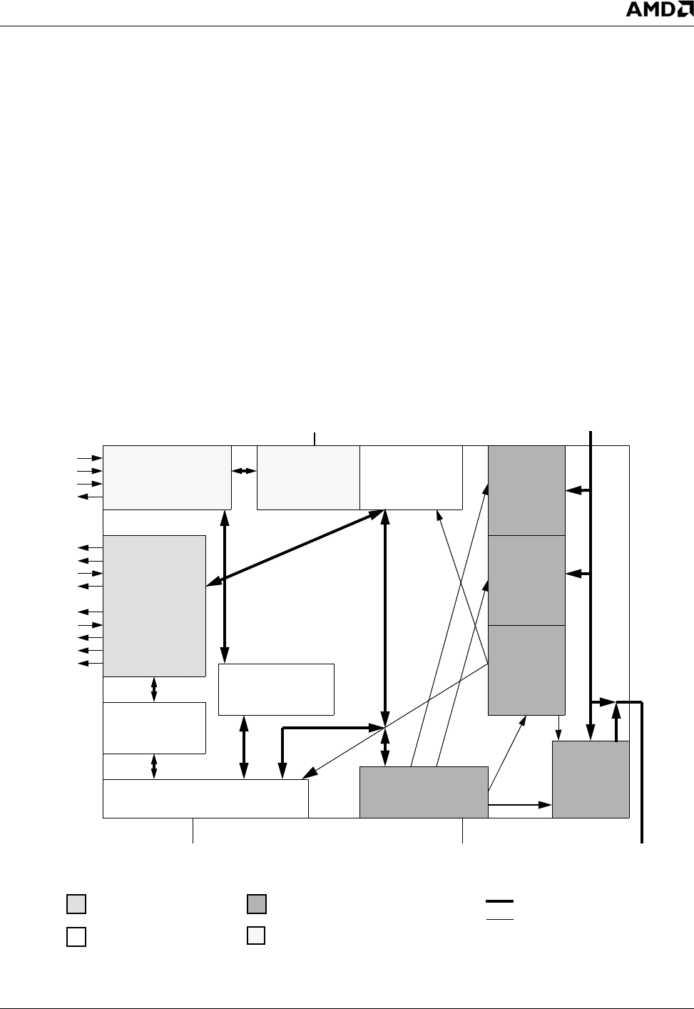
AMD Geode™ LX Processors Data Book 533
GeodeLink™ Control Processor 33234H
6.13 GeodeLink™ Control Processor
The GeodeLink Control Processor (GLCP) functionality
covers these areas (see Figure 6-55):
•Scan chain control
•JTAG interface to boundary scan, BIST, GLIU1, and
debug logic
•Power (clock) control
•Reset logic
•PLL control
•Internal logic analyzer/debugger
•1KB FIFO/SRAM
•Compliant with GLIU System Architecture Specification
v1.07
•Supports AMD Geode™ CS5536 companion device
interface
•Supports physical pins for SUSPA# and IRQ13
•Supports muxed pin for SUSP#
6.13.1 TAP Controller
The TAP controller is IEEE 1149.1 compliant. TMS, TDI,
TCLK, and TDO are directly supported (TRST is available
as a bootstrap pin during reset, but is always inactive if the
system reset is inactive). The Instruction register (IR) is 25
bits wide. The meanings of the various instructions are
shown in Table 6-81 on page 534 along with the length of
the Data register that can be accessed once the instruction
is entered. All Data registers shift in and out data, LSB first.
The Instruction and all Data registers are shift registers, so
if more bits are shifted in than the register can hold, only
the last bits shifted in (the MSBs) are used.
The TAP controller has specific pre-assigned meanings to
the bits in the 25-bit IR. The meanings are summarized in
Table 6-82 on page 534. Note that the bits only affect the
chip once the “Update-IR” JTAG state occurs in the JTAG
controller. Shifting through these bits does not change the
state of internal signals (for example TEST_MODE). For
details on JTAG controller states, refer to the IEEE Stan-
dard 1149.1-1990.
Figure 6-55. GLCP Block Diagram
Debug
Debug
Action
Decode
GLIU Interface
Debug
Control
Diagnostic Bus
Scan, BIST, Clock, Reset, Suspend Signals
TCLK
TMS
TDI
TDO
rqin, rqout, dain, daout Off-Chip
Diagnostic Pins
GLIU Clock Frequency
Debug Clock Frequency (varies)
TCLK Clock Frequency
Data and Control Buses
Control Only
Event
Generator
IEEE 1149.1
Interface Comparators
Clock, Reset,
ACPI Control
Scan and BIST
Control
Serial-to-GLIU
Conversion
128 WORD
64-Bit
FIFO
TDBGI, TDBGO
IRQ13
INTA#
SUSP#
SUSPA#
GIO_IGNNE
VA_FERR
GIO_NMI
GIO_INIT
GIO_INTR
PCI Clock Frequency
GIO
Synchronizing
AMD Geode™
Companion
Device
Interface
(GIO)

534 AMD Geode™ LX Processors Data Book
GeodeLink™ Control Processor
33234H
Table 6-81. TAP Control Instructions (25-Bit IR)
Instruction
DR
Length IR Name Description
123FFFAh 8 BYPASS_MODES This register is read/write.
127FFFAh 8 REVID Should be 10h for initial AMD Geode™ LX processor (upper
nibble is major rev, lower nibble is minor) changes for each
metal spin
1FFFEB0h 441 MULTISCAN Parallel scan (muxes scan outputs onto many chip pins)
1FFFFDFh 1 TRISTATE Put chip into TRI-STATE and comparison mode
1FFFFFDh 29 BISTDR Parallel RAM BIST - internal data register (for chip test)
1FFFFFEh 32 IDCODE ID Code = 0D5A1003h
1FFFFFFh 1 BYPASS Bypass; IEEE 1149.1 spec requires all 1s to be bypass
Table 6-82. TAP Instruction Bits
Bit Name Description
24 TAPSCAN# Also USER[6] in the design. This is a user bit added by AMD; low indicates that an inter-
nal scan chain is accessed by the TAP.
23:18 USER[5:0] User bits used to identify an internal scan chain or, if bit 24 is high, to access a special
internal DR, as shown in Table 6-81.
17:16 bistEnable[4:3] Bits 4 and 3 of the BIST enable for individual BIST chain access.
15:13 clkRatio[2:0]# Not used in the AMD Geode™ LX processor (bits should always be high); clock ratio
controls for LogicBist.
12 freezeMode Not used in the AMD Geode LX processor (should always be high); another clock con-
trol signal.
11:10 setupMode[1:0]# Not used in the AMD Geode LX processor (should always be high); these are special
BIST controller bits.
9:7 bistEnable[2:0] BIST[2:0] of BIST enable. Works in conjunction with bits [17:16].
6 testMode# Active low TEST_MODE for entire chip. Puts internal logic into scan test mode.
5 forceDis# Active low bit TRI-STATEs all output pins.
4 selectJtagOut# Active low bit that allows boundary scan cells to control pads.
3 selectJtagIn# Active low bit that allows boundary scan cells to drive data into core logic of chip.
2:0 OP[2:0] Opcode that selects how the JTAG chains are wired together.

AMD Geode™ LX Processors Data Book 535
GeodeLink™ Control Processor 33234H
EXTEST JTAG Instruction
The EXTEST instruction accesses the boundary scan
chain around the chip and controls the pin logic such that
the boundary scan data controls the data and enable sig-
nals for the pins. IEEE 1149.1 requires that an all-zero
instruction access the boundary scan chain; the controller
actually catches the all-zero condition during the “Update-
IR” state and loads 1FFFFE8h into the internal instruction
register. As seen by Table 6-82, this select OP = 000
(access boundary scan chain) and selectJtagOut# is set
active so that the boundary cells control the pads.
DELAY_CONTROLS
This chain controls the delay timing for the inputs and out-
puts. This register can be overridden with an MSR write to
GLCP_DELAY_CONTROLS (GLCP MSR 4C00000Fh) if
bit 63 of the MSR is set high. Bits [62:0] of this register
have the same meaning as in the MSR description for
GLCP_DELAY_CONTROLS (see Section 6.14.2.8 on page
549).
REVID
This 8-bit JTAG register can be reprogrammed with any
metal layer change to identify silicon changes. This register
has the same value as the GLCP REV_ID bits (MSR
4C002000h[7:0]).
MULTISCAN
During manufacturing test, multiple scan chains are avail-
able on the signal pins. Table 6-81 on page 534 identifies
the specific scan behaviors of various pins when in this
mode. The Data register associated with this TAP instruc-
tion is the boundary scan chain and the instruction bits
configure the pads such that the boundary scan ring is pro-
viding data into the core and the captured data on the
boundary scan chain is the data coming from the core.
TRI-STATE
This instruction TRI-STATEs all of the signals. The Data
register accessed is the Bypass register.
BYPASS
According to IEEE 1149.1, shifting all 1s into the IR must
connect the 1-bit Bypass register. The register has no func-
tion except as a storage flip-flop.
6.13.2 Reset Logic
One of the major functions of the GLCP is to control the
resetting of the AMD Geode LX processor. There are two
methods to reset the processor: either by a hard reset
using the input signal RESET#, or by a soft reset by writing
to an internal MSR in the GLCP.
RESET# is used for power-on reset. During power-on
reset, all internal blocks are reset until the release of the
RESET# signal.
Soft reset is activated by writing to GLCP_SYS_RSTPLL
(MSR 4C000014h). Soft reset resets all the internal blocks
to their initial status except the TAP controller. TAP reset is
achieved by holding IRQ13 low during power-on reset.
6.13.3 Clock Control
The clock control function controls the generation of the
AMD Geode LX processor internal clocks. For this pur-
pose, there are two MSRs: GLCP_SYS_RSTPLL and
GLCP_DOTPLL (MSR 4C000014h and 4C000015h).
As shown in Figure 6-56 on page 536, the internal clocks
are generated by SYSPLL and DOTPLL. In normal opera-
tion mode MSR 4C000014h[12, 11] = 0 and MSR
4C000015h[15] = 0. The SYSPLL output clock drives the
internal clocks of the CPU Core, the GeodeLink modules,
and SDRAM. The output of DOTPLL drives the DOTCLK,
that in turn, drives the Video Processor and Display Con-
troller modules.
In Bypass mode, when MSR 4C000014h[12] = 1, the DOT-
REF input clock drives the clocks of the GLIU and SDRAM,
and when MSR 4C000014h[11] = 1 the DOTREF input
clock drives the clocks of the CPU Core. Also, when
GLCP_DOTPLL[15] = 1, the DOTREF input drives the
DOTCLK.
6.13.3.1 Power Management
The GLCP controls the chip-wide power management by
controlling when to activate and deactivate the PLL clocks
of the AMD Geode LX processor.
Selection of module-level hardware clock gating is done by
programming the GLD_MSR_PM (MSR 4C002004h) of
each module. When hardware clock gating is activated,
each module enters into power save mode when it is not
busy, and leaves power save mode if a new GeodeLink
request or external event is received.
Each module has a power management module called
clock control.
GLIU1 Power Management Support
The GLCP MSRs directly involved in power management
are:
•GLCP Clock Disable Delay Value
(GLCP_CLK_DIS_DELAY)
•GLCP Global Power Management Controls
(GLCP_GLB_PM)
•GLCP Clock Mask for Sleep Request
(GLCP_PMCLKDISABLE)
•GLCP Clock Active Mask for Suspend Acknowledge
(GLCP_CLK4ACK)
•GLCP Control (GLCP_CNT)
•GLCP Level 2 (GLCP_LVL2)
•GLCP Throttle or C2 Start Delay (GLCP_TH_SD)
•GLCP Scale Factor (GLCP_TH_SF)
•GLCP Processor Throttle Off Delay (GLCP_TH_OD)
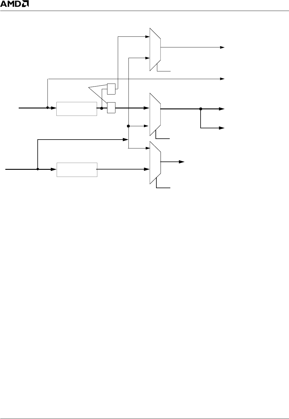
536 AMD Geode™ LX Processors Data Book
GeodeLink™ Control Processor
33234H
Figure 6-56. Processor Clock Generation
6.13.4 Companion Device Interface
The AMD Geode companion device interface for I/O con-
nections (GIO) provides the system interface between the
AMD Geode CS5536 companion device and the
AMD Geode LX processor. The GIO supports companion
device modes for current and future companion device
needs. The major blocks (shown in Figure 6-57 on page
537) of the GIO are:
•GIO_GLIU
•GIO_SYNC
•GIO_PCI
Features
•CS5536 companion device support:
— Supports CPU Interface Serial (CIS) that mux'es
signals: INPUT_DISABLE, OUTPUT_DISABLE and
Legacy (LGCY) signals: A20M, INIT, SUSP, NMI,
INTR, SMI.
— System interface signals clocked on raw PCI input
clock.
• No master capabilities.
6.13.4.1 GIO_GLIU
The GIO_GLIU interface module is responsible for all the
GLIU slave functionality. The GIO_GLIU slave implements
a large MSR space consisting of the required standard
GLIU device MSRs and the MSR controls for the I/O com-
panion modes and the Legacy signals. The GIO_GLIU
must properly decode all possible GLIU transaction types
including the unexpected addresses, request types and
sizes, and must return the proper number of responses. In
addition, it provides error logic to detect unexpected
addresses and types and implements the processor float-
ing point exception handling logic.
6.13.4.2 GIO_SYNC
The GIO synchronization module, GIO_SYNC, handles
synchronization of all signals that cross from the GLIU to
PCI domain or PCI to GLIU domain.
6.13.4.3 GIO_PCI
The GIO_PCI module drives the values of the system inter-
face signals. Table 6-83 on page 537 shows the source of
each output signal in each of the AMD Geode companion
device modes.
SYSPLL
DOTPLL
DOTREF
SYSREF
GLCP_DOTPLL[15]
GLCP_SYS_RSTPLL[12]
SDRAM Clocks
GL Clocks
DOTCLK
PCI
CPU Core
GLCP_SYS_RSTPLL[11]
Dividers
AMD Geode™ LX Processors Data Book 537
GeodeLink™ Control Processor 33234H
Figure 6-57. GIO Interface Block Diagram
GIO_GLIU GIO_SYNC
GIO_PCI
GIO_A20M
GIO_NMI
GIO_SUSP
GIO_INIT
GIO_INPUT_DIS
GIO_OUTPUT_DIS
GIO_INTR
GLCP_SUSPA
RQ13
SUSPA#
GLIU Slave I/F
IGNNE#
FERR
IRQ13_GL
SMI_GL
LGCY_GL
GL Clock
PCI_RAW_CLK
CLK
Control
SUSP# / CIS
Table 6-83. GIO_PCI Outputs
GIO Output Mode A Mode B
GIO_SUSP SUSP# pin in serial mode SUSP# pin in serial mode
GIO_SUSPA SUSPA# pin SUSPA# pin
GIO_IRQ13 IRQ13 pin IRQ13 pin
538 AMD Geode™ LX Processors Data Book
GeodeLink™ Control Processor
33234H
GIO_PCI Serial Protocol
The GIO can override the functionality of its SUSP# pin to
create a serial bus called CPU Interface Serial (CIS). The
reset mode for this pin is the SUSP# function. To properly
operate as the CIS interface, the CISM bit in MSR
51000010h[4:3] in the companion device must be pro-
grammed for Mode C. Notice that all the input signals are
active low. They are all inverted inside the GIO and con-
verted to active high signals. The protocol is shown in Table
6-84. The SUSP# pin must always be parked as inactive or
1.
Serial packets are expected whenever the companion
device signals transitions. Back to back serial packets can
occur once the entire serial packet has completed. The
AMD Geode LX processor decoded signals are guaran-
teed to transition only after the entire completion of the
packet, although they may transition during the transmis-
sion of the packet.
SUSP#/CIS Pin Initialization
The SUSP# function must NOT be active until the initializa-
tion code can set the CISM bits in the companion device to
set the correct companion device mode.
GIO_SMI Synchronization
If the companion device generates a synchronous SMI in
response to a specific CPU initiated instruction (I/O), the
SMI# signal is transmitted to the processor before the com-
pletion of the PCI cycle. Therefore, the companion device
must not complete read or write cycles until it has transmit-
ted the SMI. The design guarantees that if the PCI cycle
completes on the PCICLK after the SMI transmission, the
SMI will reach the processor before the I/O completion
response. Therefore, the processor can handle the SMI
before completing the instruction.
GIO_A20M
GIO_A20M is emulated with an SMI. The processor
receives an SMI from the companion device on I/Os that
modify the state of A20M. The SMI handler must then write
to MSR_A20M (MSR 4C000031h) in the GIO to trigger a
real A20M signal back to the processor. When the instruc-
tion completes, A20M is asserted.
GIO_NMI
The GIO_NMI signal is the real NMI from the companion
device.
GIO_INPUT_DIS, GIO_OUTPUT_DIS
GIO_INPUT_DIS and GIO_OUTPUT_DIS are part of the
GLIU power management. See the AMD Geode™ CS5536
Companion Device Data Book (publication ID 33238) for
details.
GIO_INIT
GIO_INIT is triggered via MSR 4C000033h in the GLCP for
all companion device modes. INIT is used to reset the
CPU. It is NOT a CPU soft reset.
Table 6-84. CIS Signaling Protocol
Phase
Bit Definition
(GIO CIS Mode C)
0 (START) 0
1 (START) 0
2 RSVD
3 RSVD
4 SUSP#
5NMI#
6 INPUT_DIS#
7 OUTPUT_DIS#
8SMI#
9 INTR#
10 1
11 1
12 1
13 1
14 1
15 1
16 1
17 1
18 (END) 1
19 (END) 1
AMD Geode™ LX Processors Data Book 539
GeodeLink™ Control Processor Register Descriptions 33234H
6.14 GeodeLink™ Control Processor Register Descriptions
All GeodeLink Control Processor registers are Model Spe-
cific Registers (MSRs) and are accessed via the RDMSR
and WRMSR instructions.
The registers associated with the GLCP are the Standard
GeodeLink™ Device (GLD) MSRs and GLCP Specific
MSRs. Table 6-85 and Table 6-86 are register summary
tables that include reset values and page references where
the bit descriptions are provided.
Note: The MSR address is derived from the perspective
of the CPU Core. See Section 4.1 "MSR Set" on
page 45 for more details on MSR addressing.
Table 6-85. Standard GeodeLink™ Device MSRs Summary
MSR
Address Type Register Name Reset Value Reference
4C002000h RO GLD Capabilities MSR (GLD_MSR_CAP) 00000000_00002400h Page 541
4C002001h R/W GLD Master Configuration MSR
(GLD_MSR_CONFIG)
00000000_00000000h Page 541
4C002002h R/W GLD SMI MSR (GLD_MSR_SMI) 00000000_0000001Fh Page 542
4C002003h R/W GLD Error MSR (GLD_MSR_ERROR) 00000000_00000000h Page 543
4C002004h R/W GLD Power Management MSR
(GLD_MSR_PM)
00000000_00000015h Page 544
4C002005h R/W GLD Diagnostic MSR (GLD_MSR_DIAG) 00000000_00000000h Page 544
Table 6-86. GLCP Specific MSRs Summary
MSR
Address Type Register Name Reset Value Reference
GLCP Control MSRs
4C000008h R/W GLCP Clock Disable Delay Value
(GLCP_CLK_DIS_DELAY)
00000000_00000000h Page 545
4C000009h R/W GLCP Clock Mask for Sleep Request
(GLCP_PMCLKDISABLE)
00000000_00000000h Page 545
4C00000Ah RO Chip Fabrication Information (GLCP_FAB) 00000000_00000001h Page 547
4C00000Bh R/W GLCP Global Power Management Controls
(GLCP_GLB_PM)
00000000_00000000h Page 547
4C00000Ch R/W GLCP Debug Output from Chip
(GLCP_DBGOUT)
00000000 00000000h Page 548
4C00000Dh R/W GLCP Processor Status (GLCP_PROCSTAT) Bootstrap Dependant Page 548
4C00000Eh R/W GLCP DOWSER (GLCP_DOWSER) 00000000_00000000h Page 549
4C00000Fh R/W GLCP I/O Delay Controls
(GLCP_DELAY_CONTROLS)
00000000_00000000h Page 549
4C000010h R/W GLCP Clock Control (GLCP_CLKOFF) 00000000_00000000h Page 551
4C000011h RO GLCP Clock Active (GLCP_CLKACTIVE) Input Determined Page 552
4C000012h R/W GLCP Clock Mask for Debug Clock Stop
Action (GLCP_CLKDISABLE)
00000000_00000000h Page 553
4C000013h R/W GLCP Clock Active Mask for Suspend
Acknowledge (GLCP_CLK4ACK)
00000000_00000000h Page 553
4C000014h R/W GLCP System Reset and PLL Control
(GLCP_SYS_RSTPLL)
Bootstrap specific Page 554

540 AMD Geode™ LX Processors Data Book
GeodeLink™ Control Processor Register Descriptions
33234H
4C000015h R/W GLCP Dot Clock PLL Control
(GLCP_DOTPLL)
000000D7_02000000h Page 557
4C000016h R/W GLCP Debug Clock Control
(GLCP_DBGCLKCTL)
00000000_00000002h Page 559
4C000017h RO Chip Revision ID (GLCP_CHIP_REVID) 00000000_000000xxh Page 559
GLCP I/O Address MSRs
4C000018h R/W - I/O
Offset 00h
GLCP Control (GLCP_CNT) 00000000_000000Fh Page 560
4C000019h R/W - I/O
Offset 04h
GLCP Level 2 (GLCP_LVL2) 00000000_00000000h Page 560
4C00001Ah -- Reserved -- --
4C00001Bh -- Reserved -- --
4C00001Ch R/W - I/O
Offset 10h
GLCP Throttle or C2 Start Delay
(GLCP_TH_SD)
00000000_00000000h Page 561
4C00001Dh R/W - I/O
Offset 14h
GLCP Scale Factor (GLCP_TH_SF) 00000000_00000000h Page 561
4C00001Eh R/W - I/O
Offset 18h
GLCP Processor Throttle Off Delay
(GLCP_TH_OD)
00000000_00000000h Page 562
4C00001Eh R/W - I/O
Offset 18h
GLCP Processor Throttle Off Delay
(GLCP_TH_OD)
00000000_00000000h Page 562
4C00001Fh -- Reserved -- --
GLCP Debug Interface MSRs
4C000023h R/W GLCP DAC (GLCP_DAC) 00000000_00000000h Page 563
GLCP IGNNE I/Os
F0h, F1h W GLCP IGNNE I/Os NA Page 562
GLCP I/O Companion Interface MSRs
4C000031h R/W CPU A20M Signal (MSR_A20M) 00000000_00000000h Page 564
4C000033h R/W CPU INIT Signal (MSR_INIT) 00000000_00000000h Page 564
4C000036h RO GLIU Device Interrupt Status (MSR_INTAX) 00000000_00000000h Page 565
Table 6-86. GLCP Specific MSRs Summary (Continued)
MSR
Address Type Register Name Reset Value Reference

AMD Geode™ LX Processors Data Book 541
GeodeLink™ Control Processor Register Descriptions 33234H
6.14.1 Standard GeodeLink™ Device MSRs
6.14.1.1 GLD Capabilities MSR (GLD_MSR_CAP)
6.14.1.2 GLD Master Configuration MSR (GLD_MSR_CONFIG)
MSR Address 4C002000h
Ty p e RO
Reset Value 00000000_00002400h
GLD_MSR_CAP Register Map
63 62 61 60 59 58 57 56 55 54 53 52 51 50 49 48 47 46 45 44 43 42 41 40 39 38 37 36 35 34 33 32
RSVD
313029282726252423222120191817161514131211109876543210
RSVD DEV_ID REV_ID
GLD_MSR_CAP Bit Descriptions
Bit Name Description
63:24 RSVD Reserved. Reads as 0.
23:8 DEV_ID Device ID. Identifies device (0024h).
7:0 REV_ID Revision ID. Identifies device revision. See AMD Geode™ LX Processors Specification
Update document for value.
MSR Address 4C002001h
Ty p e R / W
Reset Value 00000000_00000000h
GLD_MSR_CONFIG Register Map
63 62 61 60 59 58 57 56 55 54 53 52 51 50 49 48 47 46 45 44 43 42 41 40 39 38 37 36 35 34 33 32
RSVD
313029282726252423222120191817161514131211109876543210
RSVD PID
GLD_MSR_CONFIG Bit Descriptions
Bit Name Description
63:3 RSVD Reserved. Write as read.
2:0 PID Assigned Priority Domain. Unused by the GLCP.

542 AMD Geode™ LX Processors Data Book
GeodeLink™ Control Processor Register Descriptions
33234H
6.14.1.3 GLD SMI MSR (GLD_MSR_SMI)
MSR Address 4C002002h
Ty p e R / W
Reset Value 00000000_0000001Fh
GLD_MSR_SMI Register Map
63 62 61 60 59 58 57 56 55 54 53 52 51 50 49 48 47 46 45 44 43 42 41 40 39 38 37 36 35 34 33 32
RSVD
313029282726252423222120191817161514131211109876543210
RSVD
SMI_EXT
SMI_PML2
SMI_PMCNT
SMI_DBG
SMI_ERR
RSVD
SMI_EXT_MASK
SMI_PML2_MASK
SMI_PMCNT_MASK
SMI_DBG_MASK
SMI_ERR_MASK
GLD_MSR_SMI Bit Descriptions
Bit Name Description
63:21 RSVD Reserved.
20 SMI_EXT SMI from I/O Companion. ASMI generated when most recent serial packet had
SMI bit set. This bit ALWAYS represents the state of the SMI bit in the last serial
packet received. It cannot be written. To clear external SMI sources, proper external
controls must be sent (i.e., via the PCI bus).
19 SMI_PML2 SMI Power Management GLCP_LVL2. SSMI generated when GLCP_LVL2 (MSR
4C000019h) I/O register was read. Write 1 to clear, 0 has no effect.
18 SMI_PMCNT SMI Power Management GLCP_CNT Mask. SSMI generated when GLCP_CNT
(MSR 4C000018h) I/O register was written. Write 1 to clear, 0 has no effect.
17 SMI_DBG SMI Debug. ASMI generated due to debug event or PROCSTAT access. Write 1 to
clear, 0 has no effect.
16 SMI_ERR SMI Error. ASMI generated due to error signal. Write 1 to clear, 0 has no effect.
15:5 RSVD Reserved.
4 SMI_EXT_MASK SMI from I/O Companion Mask. If clear, enables serial packets from external
device to generate an ASMI.
3 SMI_PML2_MASK SMI Power Management GLCP_LVL2 Mask. If clear, enables power management
logic to generate an SSMI when GLCP_LVL2 I/O register (MSR 4C000019h) is read.
2 SMI_PMCNT_MASK SMI Power Management GLCP_CNT Mask. If clear, enables power management
logic to generate an SSMI when GLCP_CNT (MSR 4C000018h) I/O register is writ-
ten.
1 SMI_DBG_MASK SMI Debug Mask. If clear, enables debug logic to generate an ASMI.
0 SMI_ERR_MASK SMI Error Mask. If clear, then any GLIU device error signal (including GLCP)
causes an ASMI.
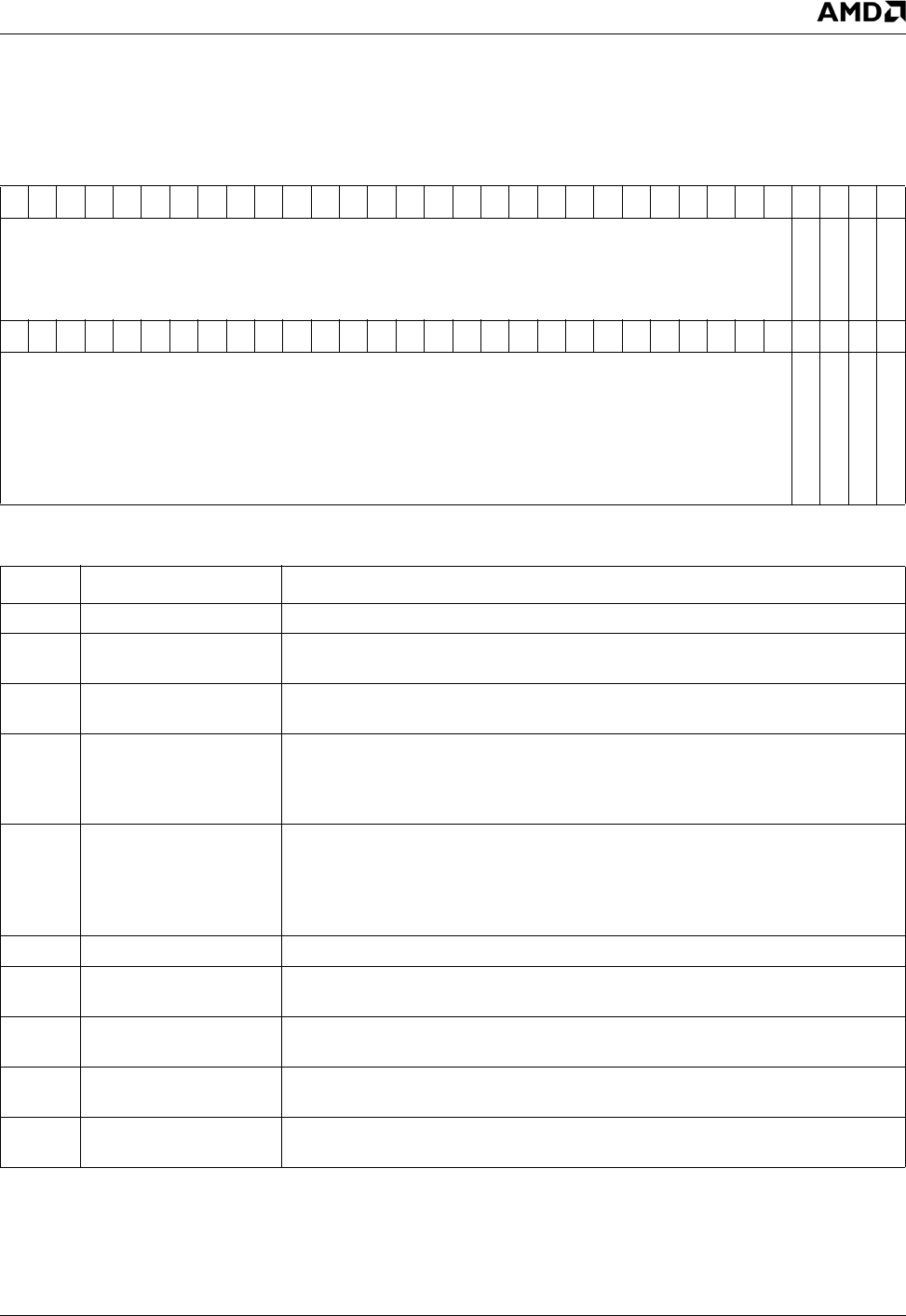
AMD Geode™ LX Processors Data Book 543
GeodeLink™ Control Processor Register Descriptions 33234H
6.14.1.4 GLD Error MSR (GLD_MSR_ERROR)
MSR Address 4C002003h
Ty p e R / W
Reset Value 00000000_00000000h
GLD_MSR_ERROR Register Map
63 62 61 60 59 58 57 56 55 54 53 52 51 50 49 48 47 46 45 44 43 42 41 40 39 38 37 36 35 34 33 32
RSVD
ERR_SYSPLL
ERR_DOTPLL
ERR_SIZE
ERR_TYPE
313029282726252423222120191817161514131211109876543210
RSVD
ERR_SYSPLL_MASK
ERR_DOTPLL_MASK
ERR_SIZE_MASK
ERR_TYPE_MASK
GLD_MSR_ERROR Bit Descriptions
Bit Name Description
63:36 RSVD Reserved.
35 ERR_SYSPLL Error System PLL. System PLL lock signal was active when POR was inactive.
Writing 1 clears error; 0 leaves unchanged.
34 ERR_DOTPLL Error Dot Clock PLL. Dot clock PLL lock signal was active when POR was inac-
tive. Writing 1 clears error; 0 leaves unchanged.
33 ERR_SIZE Error Size. The GLIU interface detected a read or write of more than 1 data
packet (size = 16 bytes or 32 bytes). If a response packet is expected, the excep-
tion bit will be set, in all cases the asynchronous error signal will be set. Writing 1
clears error; 0 leaves unchanged.
32 ERR_TYPE Error Type. An unexpected type was sent to the GLCP GLIU interface (start
request with BEX type, snoop, peek_write, debug_req, or NULL type). If a
response packet is expected, the exception bit will be set, in all cases the asyn-
chronous error signal will be set. Writing a 1 clears the error, writing a 0 leaves
unchanged.
31:4 RSVD Reserved.
3 ERR_SYSPLL_MASK Error System PLL Mask. When set to 1, disables error signaling based on the
state of the ERR_SYSPLL flag (bit 35).
2 ERR_DOTPLL_MASK Error Dot Clock PLL Mask. When set to 1, disables error signaling based on the
state of the ERR_DOTPLL flag (bit 34).
1 ERR_SIZE_MASK Error Size Mask. When set to 1, disables error signaling based on the state of
the ERR_SIZE flag (bit 33).
0 ERR_TYPE_MASK Error Type Mask. Wh.en set to 1, disables error signaling based on the state of
the ERR_TYPE flag (bit 32).
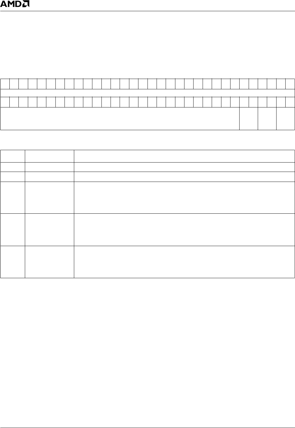
544 AMD Geode™ LX Processors Data Book
GeodeLink™ Control Processor Register Descriptions
33234H
6.14.1.5 GLD Power Management MSR (GLD_MSR_PM)
The debug logic powers up selecting GLIU1 for its clock. Debug clock select is in GLCP_DBGCLKCTL (MSR
4C000016h[2:0]).
6.14.1.6 GLD Diagnostic MSR (GLD_MSR_DIAG)
This register is reserved for internal use by AMD and should not be written to.
MSR Address 4C002004h
Ty p e R / W
Reset Value 00000000_00000015h
GLD_MSR_PM Register Map
63 62 61 60 59 58 57 56 55 54 53 52 51 50 49 48 47 46 45 44 43 42 41 40 39 38 37 36 35 34 33 32
RSVD
313029282726252423222120191817161514131211109876543210
RSVD
PM_PCI
PM_DBG
PM_GLIU
GLD_MSR_PM Bit Descriptions
Bit Name Description
63:32 RSVD Reserved. Write as read.
31:6 RSVD Reserved. Write as 0.
5:4 PM_PCI GLCP PCI Clock Power Mode.
00: Clock always on.
01: Hardware clock gating (GIO interface will wake instantly when SUSP goes low).
1x: Reserved.
3:2 PM_DBG GLCP Debug Clock Power Mode.
00: Clock always on.
01: Hardware clock gating if debug inactive (if GLCP_DBGCLKCTL = 0).
1x: Reserved.
1:0 PM_GLIU GLCP GLIU Clock Power Mode.
00: Clock always on.
01: Hardware clock gating if GLCP inactive.
1x: Reserved.
MSR Address 4C002005h
Ty p e R / W
Reset Value 00000000_00000000h
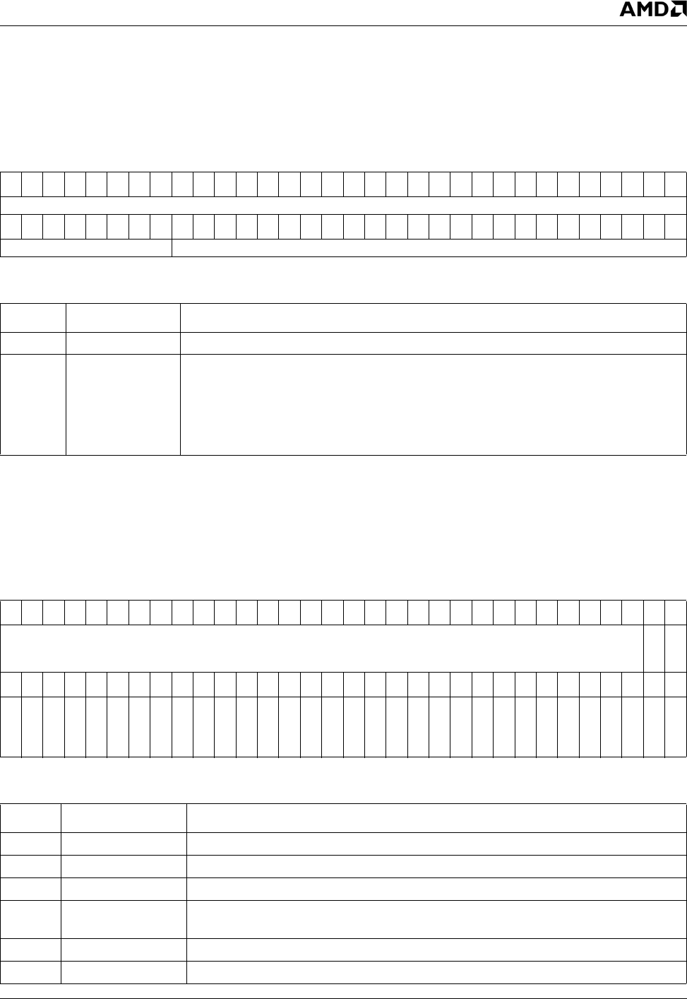
AMD Geode™ LX Processors Data Book 545
GeodeLink™ Control Processor Register Descriptions 33234H
6.14.2 GLCP Specific MSRs - GLCP Control MSRs
6.14.2.1 GLCP Clock Disable Delay Value (GLCP_CLK_DIS_DELAY)
6.14.2.2 GLCP Clock Mask for Sleep Request (GLCP_PMCLKDISABLE)
MSR Address 4C000008h
Ty p e R / W
Reset Value 00000000_00000000h
GLCP_CLK_DIS_DELAY Register Map
63 62 61 60 59 58 57 56 55 54 53 52 51 50 49 48 47 46 45 44 43 42 41 40 39 38 37 36 35 34 33 32
RSVD
313029282726252423222120191817161514131211109876543210
RSVD CLK_DELAY
GLCP_CLK_DIS_DELAY Bit Descriptions
Bit Name Description
63:24 RSVD Reserved. Write as read.
23:0 CLK_DELAY Clock Disable Delay. If enabled in GLCP_GLB_PM (CLK_DLY_EN bit, MSR
4C00000Bh[4] = 1), indicates the period to wait from SLEEP_REQ before gating off
clocks specified in GLCP_PMCLKDISABLE (MSR 4C000009h). If this delay is enabled,
it overrides or disables the function of GLCP_CLK4ACK (MSR 4C000013h). If the
CLK_DLY_EN bit is not set, but this register is non-zero, then this register serves as a
timeout for the CLK4ACK behavior.
MSR Address 4C000009h
Ty p e R / W
Reset Value 00000000_00000000h
GLCP_PMCLKDISABLE Register Map
63 62 61 60 59 58 57 56 55 54 53 52 51 50 49 48 47 46 45 44 43 42 41 40 39 38 37 36 35 34 33 32
RSVD
VIPVIP
VIPGLIU
313029282726252423222120191817161514131211109876543210
AES
AESGLIU
AESEE
GLCPDBG
GLCPGLIU
GLCPPCI
VPVOP
VPDOT_2
VPDOT_1
VPDOT_0
VPGLIU_1
VPGLIU_0
PCIPCIF
PCIPCI
PCIGLIU
GLIU1_1
GLIU1_0
DCGLIU_1
DCGLIU_0
RSVD
DCDOT_0
GLIU0_1
GLIU0_0
GP
GLMC
DRAM
BC_GLIU
BC_VA
MSS
IPIPE
FPUFAST
FPUSLOW
GLCP_PMCLKDISABLE Bit Descriptions
Bit Name Description
63:34 RSVD Reserved.
33 VIPVIP VIP VIPCLK Off. When set, disables VIP VIPCLK.
32 VIPGLIU VIP GLIU Clock Off. When set, disables VIP GLIU clock.
31 AES AES Core Functional Clock Off. When set, disables AES encryption/decryption
clock.
30 AESGLIU AES GLIU Clock Off. When set, disables AES GLIU interface clock.
29 AESEE AES EEPROM Clock Off. When set, disables AES EEPROM clock.

546 AMD Geode™ LX Processors Data Book
GeodeLink™ Control Processor Register Descriptions
33234H
28 GLCPDBG GLCP Debug Clock Off. When set, disables GLCP DBG logic clock.
27 GLCPGLIU GLCP GLIU Clock Off. When set, disables GLCP GLIU clock.
26 GLCPPCI GLCP GIO PCI Clock Off. When set, disables GLCP’s GIO PCI clock.
25 VPVOP VP VOP Clock Off. When set, disables VOP logic clock.
24 VPDOT_2 VP Dot Clock 2 Off. When set, disables VP Dot Clock 2 (vp_vid).
23 VPDOT_1 VP DOT Clock 1 Off. When set, disables VP Dot Clock 1 (lcd_pix).
22 VPDOT_0 VP DOT Clock 0 Off. When set, disables VP Dot Clock 0 (vp_pix).
21 VPGLIU_1 VP GLIU Clock 1 Off. When set, disables VP GLIU Clock 1 (lcd).
20 VPGLIU_0 VP GLIU Clock 0 Off. When set, disables VP GLIU Clock 0 (vp).
19 PCIPCIF Fast PCI Clock Off. When set, disables fast PCI clock inside GLPCI block.
18 PCIPCI PCI Clock Off. When set, disables normal PCI clock inside GLPCI block.
17 PCIGLIU GLPCI Clock Off. When set, disables clock entering GLPCI block.
16 GLIU1_1 GLIU1 Clock Off. When set, disables main clock to secondary GLIU.
15 GLIU1_0 GLIU1 Timer Logic Clock Off. When set, disables clock to timer logic of secondary
GLIU.
14 DCGLIU_1 DC GLIU clock 1 Off. When set, disables DC GLIU Clock 1 (vga).
13 DCGLIU_0 DC GLIU clock 0 Off. When set, disables DC GLIU Clock 0 (DC).
12 RSVD Reserved. Unused bit, reads what was written, value written has no effect.
11 DCDOT_0 DC Dot Clock Off. When set, disables DC Dot Clock 0 (DC).
10 GLIU0_1 GLIU0 Clock Off. When set, disables main clock to primary GLIU.
9GLIU0_0 GLIU0 Timer Logic Clock Off. When set, disables clock to timer logic of primary
GLIU.
8GP GP Clock Off. When set, disables GP clock (GLIU).
7GLMC GLMC Clock Off. When set, disables GLIU clock to GLMC.
6 DRAM DRAM Clocks Off. When set, disables external DRAM clocks (and, hence, feedback
clocks).
5 BC_GLIU Bus Controller Clock Off. When set, disables clock to CPU bus controller block.
4BC_VA CPU to Bus Controller Clock Off. When set, disables CPU clock to bus controller
block.
3MSS CPU to MSS Clock Off. When set, disables CPU clock to memory subsystem block.
2 IPIPE CPU to IPIPE Clock Off. When set, disable CPU clock to IPIPE block.
1 FPUFAST FPU Fast Clock Off. When set, disables the fast FPU clock.
0 FPUSLOW FPU Clock Off. When set, disables the slow CPU clock to FPU.
GLCP_PMCLKDISABLE Bit Descriptions (Continued)
Bit Name Description
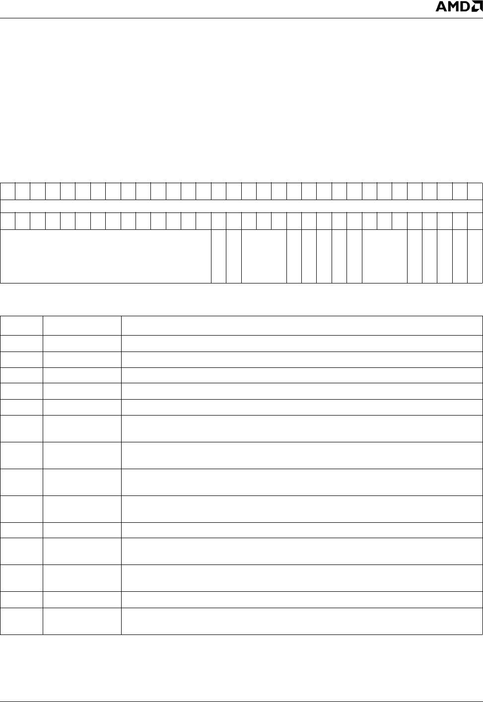
AMD Geode™ LX Processors Data Book 547
GeodeLink™ Control Processor Register Descriptions 33234H
6.14.2.3 Chip Fabrication Information (GLCP_FAB)
This read only register is used to track various fab, process, and product family parameters. It is meant for AMD internal use
only. Reads return reset value.
6.14.2.4 GLCP Global Power Management Controls (GLCP_GLB_PM)
MSR Address 4C00000Ah
Ty p e RO
Reset Value 00000000_00000001h
MSR Address 4C00000Bh
Ty p e R / W
Reset Value 00000000_00000000h
GLCP_GLB_PM Register Map
63 62 61 60 59 58 57 56 55 54 53 52 51 50 49 48 47 46 45 44 43 42 41 40 39 38 37 36 35 34 33 32
RSVD
313029282726252423222120191817161514131211109876543210
RSVD
DOTPLL_EN
SYSPLL_EN
RSVD
OUT_VP
OUT_GIO
OUT_GLMC
OUT_PCI
OUT_OTHER
RSVD
CLK_DLY_EN
CLK_DIS_EN
RSVD
RSVD
THT_EN
GLCP_GLB_PM Bit Descriptions
Bit Name Description
63:18 RSVD Reserved.
17 DOTPLL_EN DOTPLL Enable. Enables turning off the Dot clock PLL during sleep when high.
16 SYSPLL_EN SYSPLL Enable. Enables turning off the system PLLs during sleep when high.
15:13 RSVD Reserved.
12 OUT_VP VP Outputs. When set, enables VP outputs to TRI_STATE during a sleep sequence.
11 OUT_GIO GIO Outputs. When set, enables AMD Geode™ I/O companion (GIO) to TRI_STATE
device outputs during a sleep sequence.
10 OUT_GLMC GLMC Outputs. When set, enables GLMC to TRI_STATE outputs during a sleep
sequence.
9OUT_PCI GLPCI Outputs. When set, enables GLPCI to TRI_STATE outputs during a sleep
sequence.
8OUT_OTHEROther Outputs. When set, enables TDBGO and SUSPA# to TRI_STATE during a sleep
sequence.
7:5 RSVD Reserved.
4 CLK_DLY_EN Clock Delay Enable. Enables gating off clock enables from a delay rather than
GLCP_CLK4ACK (MSR 4C000013h) when high.
3 CLK_DIS_EN Clock Display Enable. Enables the assertion of internal signal, mb_clk_dis_req, during
a sleep sequence when high.
2:1 RSVD Reserved.
0THT_EN Throttle Enable. Enables processor throttling functions. If this bit is low, all the functions
related to throttling are disabled (GLCP_TH_OD, GLCP_CNT, etc.).
548 AMD Geode™ LX Processors Data Book
GeodeLink™ Control Processor Register Descriptions
33234H
6.14.2.5 GLCP Debug Output from Chip (GLCP_DBGOUT)
This register is reserved for internal use by AMD and should not be written to.
6.14.2.6 GLCP Processor Status (GLCP_PROCSTAT)
Note that the names of these bits have the read status data before the "_" and the write behavior after it.
MSR Address 4C00000Ch
Ty p e R / W
Reset Value 00000000 00000000h
MSR Address 4C00000Dh
Ty p e R / W
Reset Value Bootstrap Dependant
GLCP_PROCSTAT Register Map
63 62 61 60 59 58 57 56 55 54 53 52 51 50 49 48 47 46 45 44 43 42 41 40 39 38 37 36 35 34 33 32
RSVD
313029282726252423222120191817161514131211109876543210
RSVD
RESET_NONE
STOPCLK_NONE
GLACT_UNSTALL
GLCPSTALL_DMI
STALL_SMI
SUSP_STOPCLK
DMI_STALL
GLCP_PROCSTAT Bit Descriptions
Bit Name Description
63:7 RSVD Reserved. Writing these bits has no effect.
6 RESET_NONE Reset Status. When read, this bit is high if a hard or soft reset to the
AMD Geode™ LX processor has occurred since this register was last read. Writing
this bit has no effect.
5 STOPCLK_ NONE Stop Clock Status. When read, this bit is high if a GLCP stop clock action has
occurred since this register was last read. Writing this bit has no effect.
4 GLACT_UNSTALL GLIU1 Debug Action Status. When read, this bit is high if the GLCP has triggered
a GLIU1 debug action since this register was last read. Writing this bit high unstalls
the processor.
3 GLCPSTALL_ DMI GLCP Stall Status. When read, this bit is high if the GLCP is stalling the CPU.
Writing this bit high causes a GLCP DMI to the processor.
2 STALL_ SMI CPU Stall Status. When read, this bit is high if the CPU is stalled for any reason.
Writing this bit high causes a GLCP SMI to the processor. Bit 1 of GLD_MSR_SMI
(MSR 4C000002h) gets set by this SMI and an SMI is triggered, assuming appro-
priate SMI enable settings.
1 SUSP_ STOPCLK CPU Suspended Stop Clock Status. When read, this bit is high if the CPU has
suspended execution for any reason since this register was last read. Writing this
bit high causes the GLCP to stop all clocks identified in GLCP_CLKDISABLE
(MSR 4C000012h).
0DMI_STALL CPU DMI Stall Status. When read, this bit is high if the CPU is in DMI mode. Writ-
ing this bit high causes the GLCP to “DEBUG_STALL” the processor.

AMD Geode™ LX Processors Data Book 549
GeodeLink™ Control Processor Register Descriptions 33234H
6.14.2.7 GLCP DOWSER (GLCP_DOWSER)
6.14.2.8 GLCP I/O Delay Controls (GLCP_DELAY_CONTROLS)
MSR Address 4C00000Eh
Ty p e R / W
Reset Value 00000000_00000000h
GLCP_DOWSER Register Map
63 62 61 60 59 58 57 56 55 54 53 52 51 50 49 48 47 46 45 44 43 42 41 40 39 38 37 36 35 34 33 32
SW Defined
313029282726252423222120191817161514131211109876543210
SW Defined
GLCP_DOWSER Bit Descriptions
Bit Name Description
63:0 --- Software Defined. This 64-bit scratchpad register was specifically added for SW
debugger use (DOWSER). The register resets to zero with both hard and soft resets.
MSR Address 4C00000Fh
Ty p e R / W
Reset Value 00000000_00000000h
GLCP_DELAY_CONTROLS Register Map
63 62 61 60 59 58 57 56 55 54 53 52 51 50 49 48 47 46 45 44 43 42 41 40 39 38 37 36 35 34 33 32
EN
B_DQ
B_CMD
B_MA
SDCLK_SET
DDR_RLE
SDCLK_DIS
TLA1_OA
D_TLA1
D_TLA0
D_DQ_E
D_DQ_O
RSVD
D_SDCLK
D_CMD_O
D_CMD_E
D_MA_O
D_MA_E
313029282726252423222120191817161514131211109876543210
D_PCI_O
D_PCI_E
D_DOTCLK
D_DRGB_O
D_DRGB_E
D_PCI_IN
D_TDBGI
D_VIP
D_VIPCLK
H_SDCLK
PLL_FD_DEL
RSVD
DLL_OV
DLL_OVS/RSDA
GLCP_DELAY_CONTROLS Bit Definition
Bit Name Description
63 EN 0: Use default values.
1: Use value in bits [62:0].
62 B_DQ Buffer Control for DQ[63:0], DQS[7:0], DQM[7:0], TLA[1:0] drive select.
1: Half power.
0: Quarter power.
61 B_CMD Buffer Control for RAS[1:0]#, CAS[1:0]#, CKE[1:0], CS[3:0]#, WE[1:0]# drive select.
1: Half power.
0: Quarter power.
60 B_MA Buffer Control for MA[13:0] and BA[1:0].
0: Half power.
1: Full power.

550 AMD Geode™ LX Processors Data Book
GeodeLink™ Control Processor Register Descriptions
33234H
59 SDCLK_SET SDCLK Setup.
0: Full SDCLK setup.
1: Half SDCLK setup for control signals.
58:56 DDR_RLE DDR read latch enable position.
55 SDCLK_DIS SDCLK disable [1,3,5].
0: All SDCLK output.
1: SDCLK[4,2,0] output only.
54:52 TLA1_OA TLA hint pin output adjust.
51:50 D_TLA1 Output delay for TLA1.
49:48 D_TLA0 Output delay for TLA0.
47:46 D_DQ_E Output delay for DQ, DQM - even byte lanes.
45:44 D_DQ_O Output delay for DQ, DQM - odd byte lanes.
43:42 RSVD Reserved.
41:40 D_SDCLK Output delay for SDCLK.
39:38 D_CMD_O Output delay for CKE, CS, RAS, CAS, WE - odd bits.
37:36 D_CMS_E Output delay for CKE, CS, RAS, CAS, WE - even bits.
35:34 D_MA_O Output delay for BA and MA - odd bits.
33:32 D_MA_E Output delay for BA and MA - even bits.
31:30 D_PCI_O Output delay for pci_ad, IRQ13, SUSPA#, INTA# - odd bits.
29:28 D_PCI_E Output delay for pci_ad, CBE#, PAR, STOP#, FRAME#, IRDY#, TRDY#, DEVSEL#,
REQ#, GNT# - even bits.
27:26 D_DOTCLK Output delay for DOTCLK.
25:24 D_DRBG_O Output delay for DRGB[31:0] - odd bits.
23:22 D_DRGB_E Output delay for DRGB[31:0], HSYNC, VSYNC, DISPEN, VDDEN, LDE_MOD - even
bits.
21:20 D_PCI_IN Input delay for AD[31:0], CBE#, PAR, STOP#, FRAME#, IRDY#, TRDY#, DEVSEL#,
REQ#, GNT#, CIS.
19:18 D_TDBGI Input delay for TDBGI.
17:16 D_VIP Input delay for VID[15:0], VIP_HSYNC, VIP_VSYNC.
15:14 D_VIPCLK Input delay for VIPCLK.
13 H_SDCLK Half SDCLK hold select (for cmd addr).
1: Half SDCLK setup for MA and BA signals.
0: Full SDCLK setup.
12:11 PLL_FD_DEL PLL Feedback Delay.
00: No feedback delay.
11: Max feedback delay.
(01: ~350 ps, 10: ~700 ps, 11: ~1100 ps).
10:6 RSVD Reserved.
5 DLL_OV DLL Override (to DLL).
4:0 DLL_OVS/RSDA DLL Override Setting or Read Strobe Delay Adjust.
When DLL Override is 1 this is the DQS overide delay.
When DLL Override is 0 this is the offset adjust value.
GLCP_DELAY_CONTROLS Bit Definition (Continued)
Bit Name Description
AMD Geode™ LX Processors Data Book 551
GeodeLink™ Control Processor Register Descriptions 33234H
6.14.2.9 GLCP Clock Control (GLCP_CLKOFF)
This register has bits that, when set, force clocks off using GeodeLink™ Clock Control (GLCC) logic in the system. This is
for debugging only, and should not be used for power management.
MSR Address 4C000010h
Ty p e R / W
Reset Value 00000000_00000000h
GLCP_CLKOFF Register Map
63 62 61 60 59 58 57 56 55 54 53 52 51 50 49 48 47 46 45 44 43 42 41 40 39 38 37 36 35 34 33 32
RSVD
VIPVIP
VIPGLIU
313029282726252423222120191817161514131211109876543210
AES
AESGLIU
AESEE
GLCPDBG
GLCPGLIU
GLCPPCI
VPVOP
VPDOT_2
VPDOT_1
VPDOT_0
VPGLIU_1
VPGLIU_0
PCIPCIF
PCIPCI
PCIGLIU
GLIU1_1
GLIU1_0
DCGLIU_1
DCGLIU_0
RSVD
DCDOT_0
GLIU0_1
GLIU0_0
GP
GLMC
DRAM
BC_GLIUS
BC_VA
MSS
IPIPE
FPUFAST
FPUSLOW
GLCP_CLKOFF Bit Descriptions
Bit Name Description
63:34 RSVD Reserved.
33 VIPVIP VIP VIPCLK Off. When set, disables VIP VIPCLK.
32 VIPGLIU VIP GLIU Clock Off. When set, disables VIP GLIU clock.
31 AES AES Core Functional Clock Off. When set, disables AES encryption/decryption
clock.
30 AESGLIU AES GLIU Clock Off. When set, disables AES GLIU interface clock.
29 AESEE AES EEPROM Clock Off. When set, disables AES EEPROM clock.
28 GLCPDBG GLCP Debug Clock Off. When set, disables GLCP DBG logic clock.
27 GLCPGLIU GLCP GLIU Clock Off. When set, disables GLCP GLIU clock.
26 GLCPPCI GLCP GIO PCI Clock Off. When set, disables GLCP’s GIO PCI clock.
25 VPVOP VP VOP Clock Off. When set, disables VOP logic clock.
24 VPDOT_2 VP DOT Clock 2 Off. When set, disables VP Dot Clock 2 (vp_vid).
23 VPDOT_1 VP Dot Clock 1 Off. When set, disables VP Dot Clock 1 (lcd_pix).
22 VPDOT_0 VP Dot Clock 0 Off. When set, disables VP Dot Clock 0 (vp_pix).
21 VPGLIU_1 VP GLIU Clock 1 Off. When set, disables VP GLIU Clock 1 (lcd).
20 VPGLIU_0 VP GLIU Clock 0 Off. When set, disables VP GLIU Clock 0 (vp).
19 PCIPCIF Fast PCI Clock Off. When set, disables fast PCI clock inside GLPCI block.
18 PCIPCI PCI Clock Off. When set, disables normal PCI clock inside GLPCI block.
17 PCIGLIU GLPCI Clock Off. When set, disables clock entering GLPCI block.
16 GLIU1_1 GLIU1 Clock Off. When set, disables main clock to secondary GLIU.
15 GLIU1_0 GLIU1 Timer Logic Clock Off. When set, disables clock to timer logic of secondary
GLIU.
14 DCGLIU_1 DC GLIU Clock 1 Off. When set, disables DC GLIU Clock 1 (VGA).
13 DCGLIU_0 DC GLIU Clock 0 Off. When set, disables DC GLIU Clock 0 (DC).
12 RSVD Reserved. Unused bit, reads what was written, value written has no effect.
552 AMD Geode™ LX Processors Data Book
GeodeLink™ Control Processor Register Descriptions
33234H
6.14.2.10 GLCP Clock Active (GLCP_CLKACTIVE)
See "GLCP_CLKOFF Bit Descriptions" on page 551 for bit descriptions.
11 DCDOT_0 DC Dot Clock Off. When set, disables DC Dot Clock 0 (DC).
10 GLIU0_1 GLIU0Clock Off. When set, disables main clock to primary GLIU.
9GLIU0_0 GLIU0 Timer Logic Clock Off. When set, disables clock to timer logic of primary
GLIU.
8GP GP Clock Off. When set, disables GP clock (GLIU).
7GLMC GLMC Clock Off. When set, disables GLIU clock to memory controller.
6 DRAM DRAM Clocks Off. When set, disables external DRAM clocks (and, hence, feedback
clocks).
5 BC_GLIU Bus Controller Clock Off. When set, disables clock to CPU bus controller block.
4BC_VA CPU to Bus Controller Clock Off. When set, disables CPU clock to bus controller
block.
3MSS CPU to MSS Clock Off. When set, disables CPU clock to MSS block.
2 IPIPE CPU to IPIPE Clock Off. When set, disable CPU clock to IPIPE block.
1 FPUFAST FPU Fast Clock Off. When set, disables the fast FPU clock.
0 FPUSLOW FPU Clock Off. When set, disables the slow CPU clock to FPU.
MSR Address 4C000011h
Ty p e RO
Reset Value Input Determined
GLCP_CLKOFF Bit Descriptions (Continued)
Bit Name Description
GLCP_CLKACTIVE Register Map
63 62 61 60 59 58 57 56 55 54 53 52 51 50 49 48 47 46 45 44 43 42 41 40 39 38 37 36 35 34 33 32
RSVD
VIPVIP
VIPGLIU
313029282726252423222120191817161514131211109876543210
AES
AESGLIU
AESEE
GLCPDBG
GLCPGLIU
GLCPPCI
VPVOP
VPDOT_2
VPDOT_1
VPDOT_0
VPGLIU_1
VPGLIU_0
PCIPCIF
PCIPCI
PCIGLIU
GLIU1_1
GLIU1_0
DCGLIU_1
DCGLIU_0
RSVD
DCDOT_0
GLIU0_1
GLIU0_0
GP
GLMC
DRAM
BC_GLIU
BC_VA
MSS
IPIPE
FPUFAST
FPUSLOW
AMD Geode™ LX Processors Data Book 553
GeodeLink™ Control Processor Register Descriptions 33234H
6.14.2.11 GLCP Clock Mask for Debug Clock Stop Action (GLCP_CLKDISABLE)
See "GLCP_CLKOFF Bit Descriptions" on page 551 for bit descriptions.
6.14.2.12 GLCP Clock Active Mask for Suspend Acknowledge (GLCP_CLK4ACK)
See "GLCP_CLKOFF Bit Descriptions" on page 551 for bit descriptions.
MSR Address 4C000012h
Ty p e R / W
Reset Value 00000000_00000000h
GLCP_CLKDISABLE Register Map
63 62 61 60 59 58 57 56 55 54 53 52 51 50 49 48 47 46 45 44 43 42 41 40 39 38 37 36 35 34 33 32
RSVD
VIPVIP
VIPGLIU
313029282726252423222120191817161514131211109876543210
AES
AESGLIU
AESEE
GLCPDBG
GLCPGLIU
GLCPPCI
VPVOP
VPDOT_2
VPDOT_1
VPDOT_0
VPGLIU_1
VPGLIU_0
PCIPCIF
PCIPCI
PCIGLIU
GLIU1_1
GLIU1_0
DCGLIU_1
DCGLIU_0
RSVD
DCDOT_0
GLIU0_1
GLIU0_0
GP
GLMC
DRAM
BC_GLIU
BC_VA
MSS
IPIPE
FPUFAST
FPUSLOW
MSR Address 4C000013h
Ty p e R / W
Reset Value 00000000_00000000h
GLCP_CLK4ACK Register Map
63 62 61 60 59 58 57 56 55 54 53 52 51 50 49 48 47 46 45 44 43 42 41 40 39 38 37 36 35 34 33 32
RSVD
VIPVIP
VIPGLIU
313029282726252423222120191817161514131211109876543210
AES
AESGLIU
AESEE
GLCPDBG
GLCPGLIU
GLCPPCI
VPVOP
VPDOT_2
VPDOT_1
VPDOT_0
VPGLIU_1
VPGLIU_0
PCIPCIF
PCIPCI
PCIGLIU
GLIU1_1
GLIU1_0
DCGLIU_1
DCGLIU_0
RSVD
DCDOT_0
GLIU0_1
GLIU0_0
GP
GLMC
DRAM
BC_GLIU
BC_VA
MSS
IPIPE
FPUFAST
FPUSLOW
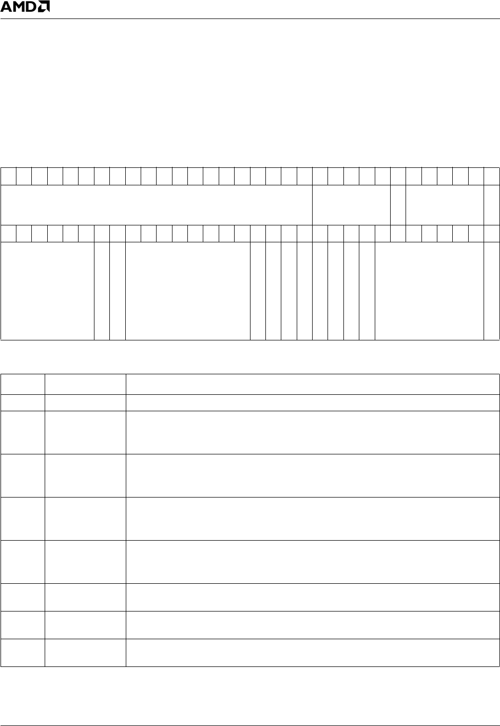
554 AMD Geode™ LX Processors Data Book
GeodeLink™ Control Processor Register Descriptions
33234H
6.14.2.13 GLCP System Reset and PLL Control (GLCP_SYS_RSTPLL)
This register is initialized during POR, but otherwise is not itself reset by any “soft-reset” features. Note that writing this reg-
ister always has immediate effect, so read-modify-writes must be done to avoid corrupting the PLL timing settings. When
using this register functionally to change PLL frequencies, the CHIP_RESET bit (bit 0) should be set. Writing this register
with the CHIP_RESET bit set will never send a write-response over the GLIU (this allows halting bus traffic before the reset
occurs).
MSR Address 4C000014h
Ty p e R / W
Reset Value Bootstrap specific
GLCP_SYS_RSTPLL Register Map
63 62 61 60 59 58 57 56 55 54 53 52 51 50 49 48 47 46 45 44 43 42 41 40 39 38 37 36 35 34 33 32
RSVD GLIUMULT
MBDIV
COREMULT
COREDIV
313029282726252423222120191817161514131211109876543210
SWFLAGS
GLIULOCK
CORELOCK
HOLD_COUNT
RSVD
GLIUPD
COREPD
GLIUBYPASS
COREBYPASS
LPFEN
VA_SEMI_SYNC_MODE
PCI_SEMI_SYNC_MODE
BOOTSTRAPS
CHIP_RESET
GLCP_SYS_RSTPLL Bit Descriptions
Bit Name Description
63:44 RSVD Reserved.
43:39 GLIUMULT GLIU Multiplier (Bootstrap Dependent, see Table 6-87).
00000: Multiply by 1,....
11111: Multiply by 32.
38 GLIUDIV GLIU Divide. When set, predivide the GLIU PLL input frequency by 2.
0: Do not predivide input. (Default)
1: Divide by 2.
37:33 COREMULT CPU Core Multiplier (bootstrap dependent, see Table 6-87 on page 556).
00000: Multiply by 1,....
11111: Multiply by 32.
32 COREDIV CPU Core Divide. When set, predivide the GLIU PLL input frequency by 2.
0: Do not predivide input. (Default)
1: Divide by 2.
31:26 SWFLAGS Flags. Flags that are reset only by the POR# signal, not the CHIP_RESET (bit 0). They
are reset to 0 and can be used as flags in the boot code that survive CHIP_RESET.
25 GLIULOCK (RO) Lock (Read Only). Lock signal from the system PLL. The worst-case lock time for a
AMD Geode™ LX processor PLL is 100 µs.
24 CORELOCK
(RO)
Lock (Read Only). Lock signal from the system PLL. The worst-case lock time for a
AMD Geode LX processor PLL is 100 µs.

AMD Geode™ LX Processors Data Book 555
GeodeLink™ Control Processor Register Descriptions 33234H
23:16 HOLD_COUNT Hold Count. The number of PLL reference clock cycles (divided by 16) that the PLL is
powered down for, and also the number before releasing CHIP_RESET.
0: Wait 0 cycles. (Default)
1: Wait 16 clock cycles, etc.
15 RSVD Reserved. Always write 0.
14 GLIUPD GLIU Power Down. This signal controls the power down mode of the GLIU PLL. It is
active high. This bit is always cleared by a CHIP_RESET (bit 0).
13 COREPD Core Power Down. This signal controls the power down mode of the CPU core PLL. It is
active high. This bit is always cleared by a CHIP_RESET (bit 0).
12 GLIUBYPASS GLIU Bypass. This signal controls the Bypass mode of the GLIU clocking. If this bit is
high, the DOTPLL is configured for bypass and the DOTREF input clock directly drives
the GLIU clock spines. (For SYSREF bypass through the GLIU PLL, the CLKSEL JTAG
register must be used).
11 COREBYPASS Core Bypass. This signal controls the Bypass mode of the Core clock. If this bit is high,
the DOTPLL is configured for bypass and the DOTREFF input clock directly drives the
Core clock. (For SYSREF bypass through the Core PLL, the CLKSEL JTAG register
must be used).
10 LPFEN Loop Filter Enable. This bit is tied to both the GLIU and Core PLL loop filter enables.
This PLL control enables the use of an external resistor. It should be clear for normal
operation.
9 VA_SEMI_
SYNC_MODE
CPU Sync Mode. This bit controls whether the CPU uses a FIFO for interfacing with the
GLIU. If the bit is high, the CPU will not use the FIFO. It behaves as if the CPU and GLIU
domains are synchronous. This bit can be set high as long as the CPU and GLIU fre-
quencies are multiples of each other. The bit is always reset low.
8 PCI_SEMI_
SYNC_MODE
PCI Sync Mode. This bit controls whether the PCI uses the falling edges of mb_func_clk
and pci_func_clk for interfacing with GLIU or not. If the bit is high, PCI does not use fall-
ing clock edges. It behaves as if the PCI and GLIU domains are synchronous. This bit
can be set high as long as the PCI and GLIU frequencies are multiples of each other. The
bit always resets low.
7:1 BOOTSTRAPS
(RO)
Bootstraps (Read Only). These bits are copies of the state of bootstraps when power-
on reset (PCI reset) is released.
Bit 7: PW1 pad - active high when the PCI clock is 66 MHz, low for 33 MHz.
Bit 6: IRQ13 pad - active high for stall-on-reset debug feature, otherwise low.
Bit 5: PW0 pad - part of CPU/GLIU frequency selects.
Bit 4: SUSPA# pad - part of CPU/GLIU frequency selects.
Bit 3: GNT2# pad - part of CPU/GLIU frequency selects.
Bit 2: GNT1# pad - part of CPU/GLIU frequency selects.
Bit 1: GNT0# pad - part of CPU/GLIU frequency selects.
0 CHIP_RESET Chip Reset. When written to a 1, the chip enters reset and does not come out until the
HOLD_COUNT (bits [23:16]) is reached. This register and the JTAG logic are not reset
by CHIP_RESET, but otherwise the entire chip is reset. (Default = 0)
GLCP_SYS_RSTPLL Bit Descriptions (Continued)
Bit Name Description

556 AMD Geode™ LX Processors Data Book
GeodeLink™ Control Processor Register Descriptions
33234H
The PW1 pin (66 MHz PCI) is wired directly to the COREDIV and GLDIV signals during reset. The IRQ13 pin (stall after
reset) has no effect on the PLL controls but is still stored in the BOOTSTRAP bits (MSR 4C000018h[7:1]). Table 6-87
shows examples of reset values when PW1 and/or IRQ13 are high during reset. The hard reset state of this register always
leaves the PLL in bypass mode. The BIOS must clear the bypass bits in order to achieve the desired frequency.
Table 6-87. Bootstrap Bit Settings and Reset State of GLCP_SYS_RSTPLL (PW1 and IRQ13 = 0)
{PW1,IRQ13,PW0,SUSPA#,
GNT#[2:0]}
same as GLCP_SYS_RSTPLL[7:1]
CPU Core
Speed
(MHz)
CPU Core
MULT
GLIU
Speed
(MHz)
GLIU
MULT
GLCP_SYS_RSTPLL
Reset Value
0000000 Bypass 11 Bypass 7 00000396_00001800h
0000001 166 4 166 4 00000208_03001802h
0000010 200 5 200 5 0000028A_03001804h
0000011 266 7 200 5 0000028E_03001806h
0000100 266 7 266 7 0000038E_03001808h
0000101 333 9 200 5 00000292_0300180Ah
0000110 333 9 266 7 00000392_0300180Ch
0000111 333 9 333 9 00000492_0300180Eh
0001000 366 10 200 5 00000294_03001810h
0001001 366 10 266 7 00000394_03001812h
0001010 366 10 333 9 00000494_03001814h
0001011 400 11 200 5 00000296_03001816h
0001100 400 11 266 7 00000396_03001818h
0001101 400 11 333 9 00000496_0300181Ah
0001110 400 11 400 11 00000596_0300181Ch
0001111 433 12 266 7 00000398_0300181Eh
0010000 433 12 333 9 00000498_03001820h
0010001 433 12 400 11 00000598_03001822h
0010010 466 13 266 7 0000039A_03001824h
0010011 466 13 333 9 0000049A_03001826h
0010100 466 13 400 11 0000059A_03001828h
0010101 500 14 266 7 0000039C_0300182Ah
0010110 500 14 333 9 0000049C_0300182Ch
0010111 500 14 400 11 0000059C_0300182Eh
0011000 533 15 266 7 0000039E_03001830h
0011001 533 15 333 9 0000049E_03001832h
0011010 533 15 400 11 0000059E_030001834h
0011011 600 17 200 5 000002A2_03001836h
0011100 566 16 333 9 000004A0_03001838h
0011101 566 16 400 11 000005A0_0300183Ah
0011110 600 17 333 9 000004A2_0300003Ch
0011111 600 17 400 11 000005A2_0300183Eh
AMD Geode™ LX Processors Data Book 557
GeodeLink™ Control Processor Register Descriptions 33234H
6.14.2.14 GLCP Dot Clock PLL Control (GLCP_DOTPLL)
This register does not include hardware handshake controls like the GLCP_SYS_RSTPLL register (MSR 4C000014h), so
care should be taken when changing the settings. For example, to change the DIV settings: write the register with the DOT-
RESET bit (bit 0) set and either in the same write or another write change the DIV settings; read the register until the LOCK
bit (bit 25) goes active (or until a timeout occurs, if desired); write the register with the same DIV settings and with the DOT-
RESET bit clear. The MDIV, NDIV, and PDIV (bits [46:32]) settings work in conjunction to create the internal DOTCLK using
this equation:
For example, with bits [46:32] in the GLCP_DOTPLL register set to 0x00D7 (reset), the Dot clock frequency that the DC and
VP would run with would be:
However, not all MDIV, NDIV, and PDIV settings lock and not all that lock have good long-term jitter characteristics. The PLL
resets to 25.0565 MHz for VGA monitors assuming a 14.31818 MHz input. A 27 MHz input will successfully lock at about 47
MHz, and should then be changed to the desired pixel rate.
Table 6-88. Bootstrap Bit Settings and Reset State of GLCP_SYS_RSTPLL (PW1 and IRQ13 vary)
{PW1,IRQ13,PW0,SUSPA#,GNT#[2:0]}
same as GLCP_SYS_RSTPLL[7:1]
CPU
Speed
CORE
MULT
GLIU
Speed
GLIU
MULT
GLCP_SYS_RSTPLL
Reset Value
0100000 Bypass 11 Bypass 7 00000396_00001840h
1000001 166 4 166 4 00000249_03000082h
1110111 500 14 400 11 000005DD_030000EEh
MSR Address 4C000015h
Ty p e R / W
Reset Value 000000D7_02000000h
Fout Fin NDIV 1+()
MDIV 1+()PDIV 1+()⋅
---------------------------------------------------------------
⋅=
Fout 14.318MHz 13 1+()
01+()71+()
----------------------------------
⋅25.0565MHz==
GLCP_DOTPLL Register Map
63 62 61 60 59 58 57 56 55 54 53 52 51 50 49 48 47 46 45 44 43 42 41 40 39 38 37 36 35 34 33 32
RSVD
DIV4
RSVD
MDIV NDIV PDIV
313029282726252423222120191817161514131211109876543210
SWFLAGS
LOCK
HALFPIX
RSVD
BYPASS
PD
CAPEN
RSVD RSVD
DOTRESET

558 AMD Geode™ LX Processors Data Book
GeodeLink™ Control Processor Register Descriptions
33234H
GLCP_DOTPLL Bit Descriptions
Bit Name Description
63:49 RSVD Reserved. Write as read.
48 DIV4 Divide by 4. When set, the PLL output is divided by 4 before clocking the logic. This bit
is intended for generating frequencies below the PLL spec limit of 15 MHz.
47 RSVD Reserved.
46:44 MDIV Input Clock Divisor. The DOTPLL M setting (resets to VGA timing).
43:36 NDIV Dot Clock PLL Divisor. The DOTPLL N setting (resets to VGA timing).
35:32 PDIV Post Scaler Divisor. The DOTPLL P setting (resets to VGA timing).
31:26 SWFLAGS Software Flags. Unlike in the GLCP_SYS_RSTPLL register (MSR 4C000014h), these
bits are reset to 0 by a soft reset to the chip. These bits are otherwise read/writable by
software. They are not reset by a DOTRESET (bit 0 of this register).
25 LOCK (RO) Lock (Read Only). Lock signal from the DOTCLK PLL.
24 HALFPIX Half Pixel. The DC and VP receive a half-frequency Dot clock while the VOP logic
receives the normal frequency determined by the MDIV, NDIV, PDIV settings. This fea-
ture enables 8-bit VOP of SD data at 27 MHz VOP clock (pixel rate only 13.5 MHz).
23:16 RSVD Reserved. Write as read.
15 BYPASS Dot PLL Bypass. This signal controls the bypass mode of the DOTCLK PLL. If this bit is
high, the DOTREF input clock directly drives the raw DOTCLK, bypassing the MDIV,
NDIV, and PDIV logic.
14 PD Power Down. This bit controls the power down mode of the DOTCLK PLL. It is active
high.
13 CAPEN Capacitor Enable. The CAPEN signal to the DOTPLL enables an external capacitor for
the loop filter.
0: An external capacitor is not used. Internal circuitry is used to stabilize the loop opera-
tion.
1: Enables the use of an external capacitor for the loop filter.
12:10 RSVD Reserved.
9:1 RSVD Reserved. Read/writable bits not currently used.
0 DOTRESET Dot Clock Reset. The reset pin to the Dot clock time blocks. The Dot reset is held active
when CHIP_RESET (MSR 4C000014h[0]) is high, but this bit resets to 0. It is recom-
mended that software set this bit when changing PLL settings and observe LOCK before
releasing this reset. Unlike the SYS_RSTPLL register, this bit is not required to be set
before the other bits in this register affect the PLL.

AMD Geode™ LX Processors Data Book 559
GeodeLink™ Control Processor Register Descriptions 33234H
6.14.2.15 GLCP Debug Clock Control (GLCP_DBGCLKCTL)
Note that after the mux to select the clock, a standard clock control gate exists. This register should never be changed from
one non-zero value to another. Always write this register to 0 when moving to an alternative debug clock.
6.14.2.16 Chip Revision ID (GLCP_CHIP_REVID)
MSR Address 4C000016h
Ty p e R / W
Reset Value 00000000_00000002h
GLCP_DBGCLKCTL Register Map
63 62 61 60 59 58 57 56 55 54 53 52 51 50 49 48 47 46 45 44 43 42 41 40 39 38 37 36 35 34 33 32
RSVD
313029282726252423222120191817161514131211109876543210
RSVD CLKSEL
GLCP_DBGCLKCTL Bit Descriptions
Bit Name Description
63:3 RSVD Reserved. Write as read.
2:0 CLKSEL Clock Select. Selects the clock to drive into the debug logic.
000: None.
001: CPU Core clock.
010: GLIU1 clock.
011: DOTCLK.
100: PCI clock.
101-111: Reserved.
MSR Address 4C000017h
Ty p e RO
Reset Value 00000000_000000xxh
GLCP_CHIP_REVID Register Map
63 62 61 60 59 58 57 56 55 54 53 52 51 50 49 48 47 46 45 44 43 42 41 40 39 38 37 36 35 34 33 32
RSVD
313029282726252423222120191817161514131211109876543210
RSVD MAJ MIN
GLCP_CHIP_REVID Bit Descriptions
Bit Name Description
63:8 RSVD Reserved. Reads as 0.
7:4 MAJ Major Revision. Identifies major silicon revision. See AMD Geode™ LX Processors
Specification Update document for value.
3:0 MIN Minor Revision. Identifies minor silicon revision. See AMD Geode™ LX Processors
Specification Update document for value.
560 AMD Geode™ LX Processors Data Book
GeodeLink™ Control Processor Register Descriptions
33234H
6.14.2.17 GLCP Control (GLCP_CNT)
This register is used in conjunction with GLIU1 Power Management. I/O writes, which include the lowest byte of this regis-
ter, may trigger an SMI if GLD_MSR_SMI (MSR 4C002002h) is configured appropriately. MSR writes do not cause SMIs.
The throttle sequence starts after the delay specified by GLCP_TH_SD (MSR 4C00001Ch), which can allow for SMI han-
dling time or any other preparations. Throttling is temporarily stopped in IRQ, SSMI, ASMI, or DMI. NMI and system sleep
(C2) always clear THT_EN (bit 4).
6.14.2.18 GLCP Level 2 (GLCP_LVL2)
This register has no writable bits. I/O reads to the lower byte of this register (with or without reading the other three bytes)
return 0 and cause the system to enter “C2 processor state” as defined by the GLIU1 power management spec; that is, sus-
pend the processor. I/O reads to the lower byte of this register may trigger an SMI if GLD_MSR_SMI (MSR 4C002002h) is
configured appropriately. Note that the suspend starts after a delay specified by GLCP_TH_SD (MSR 4C00001Ch), which
can allow for SMI handling or any other preparations. P_LVL2_IN (MSR 4C00001Ch[12]) can abort the suspend operation.
MSR reads to this register return 0, but perform no further action.
MSR Address 4C000018h
Type R/W - I/O Offset 00h
Reset Value 00000000_000000Fh
GLCP_CNT Register Map
63 62 61 60 59 58 57 56 55 54 53 52 51 50 49 48 47 46 45 44 43 42 41 40 39 38 37 36 35 34 33 32
RSVD
313029282726252423222120191817161514131211109876543210
RSVD
THT_EN
CLK_VAL
GLCP_CNT Bit Descriptions
Bit Name Description
63:5 RSVD Reserved. Write as read.
4THT_EN Throttle Enable. When high, enables throttling of processor for power management.
This bit is always cleared by an NMI to the processor or when system sleep initiates, it
may clear from an SMI or IRQ depending on GLCP_TH_OD (MSR 4C00001Eh) settings.
3:0 CLK_VAL Clock Throttling Value. The value 0000 is reserved and should not be used. The value
0001 yields the most throttling while the value 1111 has the effect of no throttling (1111 is
the reset value). Reads return value written. THT_EN (bit 4) must be low to change the
value of CLK_VAL. See also GLCP_TH_SF (MSR 4C00001Dh). During processor throt-
tling, processor suspend is applied the amount of time of “(15-CLK_VAL)*GLCP_TH_SF”
and then removed the amount of time of “CLK_VAL*GLCP_TH_SF”.
MSR Address 4C000019h
Type R/W - I/O Offset 04h
Reset Value 00000000_00000000h

AMD Geode™ LX Processors Data Book 561
GeodeLink™ Control Processor Register Descriptions 33234H
6.14.2.19 GLCP Throttle or C2 Start Delay (GLCP_TH_SD)
6.14.2.20 GLCP Scale Factor (GLCP_TH_SF)
MSR Address 4C00001Ch
Type R/W - I/O Offset 10h
Reset Value 00000000_00000000h
GLCP_TH_SD Register Map
63 62 61 60 59 58 57 56 55 54 53 52 51 50 49 48 47 46 45 44 43 42 41 40 39 38 37 36 35 34 33 32
RSVD
313029282726252423222120191817161514131211109876543210
RSVD
P_LVL2_IN
THT_DELAY
GLCP_TH_SD Bit Descriptions
Bit Name Description
63:13 RSVD Reserved. By convention, always write zero.
12 P_LVL2_IN Enable Indicator. If P_LVL2 (in MSR 4C000019h) was read, then this bit reads high. If
this bit is written to a one, the suspend is aborted. This bit is always cleared and Suspend
de-asserted on NMI, IRQ, SSMI, ASMI, DMI, or system Sleep.
11:0 THT_DELAY Throttle Delay. Indicates how long to wait before beginning the processor throttling pro-
cess as defined by MSR 4C000018h. The delay setting is multiplied by 16 to get the
number of PCI clock cycles to wait, thus setting THT_DELAY = 3 causes a wait of 48 PCI
clock cycles.
MSR Address 4C00001Dh
Type R/W - I/O Offset 14h
Reset Value 00000000_00000000h
GLCP_TH_SF Register Map
63 62 61 60 59 58 57 56 55 54 53 52 51 50 49 48 47 46 45 44 43 42 41 40 39 38 37 36 35 34 33 32
RSVD
313029282726252423222120191817161514131211109876543210
RSVD SCALE
GLCP_TH_SF Bit Descriptions
Bit Name Description
63:8 RSVD Reserved. By convention, always write 0.
7:0 SCALE Scale Factor. This value is used in conjunction with CLK_VAL in the GLCP_CNT MSR
(4C000018h[3:0]). This value times CLK_VAL (or 15-CLK_VAL) indicates the number of
PCI clock cycles to wait during processor active (or suspend) periods. The setting is mul-
tiplied by 16 to get the number of PCI clock cycles per period, thus SCALE = 3 and
CLK_VAL = 5 will have the processor active for 240 PCI clocks and suspended for 480
PCI clocks.
562 AMD Geode™ LX Processors Data Book
GeodeLink™ Control Processor Register Descriptions
33234H
6.14.2.21 GLCP Processor Throttle Off Delay (GLCP_TH_OD)
6.14.3 GLCP IGNNE I/Os
The GLCP’s GLIU is responsible for all the GLIU functionality. The GLCP’s GLIU implements a large MSR space consisting
of the required standard GLIU device MSRs, MSR controls for clock and PLL interfacing, the MSR controls for the I/O com-
panion modes and MVPI signals, and MSR controls for the debug logic. The GLCP’s GLIU must properly decode all possi-
ble GLIU transaction types including the unexpected addresses, request types and sizes. It must respond with the proper
number of response packets. In addition, it provides error logic to detect unexpected addresses and types.
The GLCP’s GLIU also implements the processor floating point exception handling logic.
always @(va_ferr or irq13 or write_to_F0F1 or ignee)
if (!va_ferr) nxt_ignne = 0;
else if (irq13 && write_to_F0F1) nxt_ignne = 1;
else nxt_ignne = ignne;
always @(posege ck)
ignee <= nxt_ignne;
irq13 <= va_ferr & !nxt_ignne;
The GLCP’s GLIU maintains MSRs that control the source and value of the companion device system outputs. It also con-
trols the current companion device mode.
Read data returns GLD_MSR_CAP data.
MSR Address 4C00001Eh
Type R/W - I/O Offset 18h
Reset Value 00000000_00000000h
GLCP_TH_OD Register Map
63 62 61 60 59 58 57 56 55 54 53 52 51 50 49 48 47 46 45 44 43 42 41 40 39 38 37 36 35 34 33 32
RSVD
313029282726252423222120191817161514131211109876543210
RSVD
IRQ_EN
SMI_EN
OFF_DELAY
GLCP_TH_OD Bit Descriptions
Bit Name Description
63:16 RSVD Reserved. By convention, always write 0.
15 IRQ_EN Enable Throttling Restart after IRQ. If this bit is set and throttling is not disabled during
the IRQ handling, throttling restarts after the period specified by OFF_DELAY (bits
[13:0]). If this bit is clear, then an IRQ clears THT_EN (MSR 4C000018h[4]).
14 SMI_EN Enable Throttling Restart after SMI. If this bit is set and throttling is not disabled during
the SMI handling, throttling restarts after the period specified by OFF_DELAY (bits
[13:0])If this bit is clear, then an ASMI clears THT_EN (MSR 4C000018h[4]).
13:0 OFF_DELAY Throttle Off Delay. Indicates the period to wait from receipt of IRQ_EN (bit 15) or
SMI_EN (bit 14) before restarting throttle operation. This setting is multiplied by 16 to get
the number of PCI clock cycles to wait. If the OFF_DELAY has not expired and another
IRQ or SMI occurs, the OFF_DELAY timer is cleared again and the wait begins again.
Setting OFF_DELAY to 0 results in only one PCI clock cycle of throttling being disabled
after an IRQ or SMI.
GLCP I/O Offset F0h, F1h
Ty p e W
Reset Value NA
AMD Geode™ LX Processors Data Book 563
GeodeLink™ Control Processor Register Descriptions 33234H
6.14.4 GLCP Specific MSRs - GLCP Debug Interface MSRs
6.14.4.1 GLCP DAC (GLCP_DAC)
This register has DAC diagnostic controls and status. It ties directly to inputs and outputs on the DAC module.
Bits [13:11] of this register are only valid after the DAC is enabled.
MSR Address 4C000023h
Ty p e R / W
Reset Value 00000000_00000000h
GLCP_DAC Register Map
63 62 61 60 59 58 57 56 55 54 53 52 51 50 49 48 47 46 45 44 43 42 41 40 39 38 37 36 35 34 33 32
RSVD
313029282726252423222120191817161514131211109876543210
RSVD
SB
SG
SR
INREFEN
OL
AB AG AR
GLCP_DAC Bit Descriptions
Bit Name Description
64:14 RSVD Reserved.
13 SB (RO) Status Blue (Read only). A logic level 1 means the Blue DAC output is above 0.35V.
12 SG (RO) Status Green (Read only). A logic level 1 means the Green DAC output is above 0.35V.
11 SR (RO) Status Red (Read only). A logic level 1 means the Red DAC output is above 0.35V.
10 INREFEN Internal Reference Enable. Internal reference enable to the DAC.
9OL Output Level.
0: RGB.
1: TV - for testing only, analog TV out is not supported).
8:6 AB Adjust for Blue DAC.
000: 0%.
011: 7.5%.
100: -10%.
111: -2.5%.
5:3 AG Adjust for Green DAC.
000: 0%.
011: 7.5%.
100: -10%.
111: -2.5%.
2:0 AR Adjust for Red DAC.
000: 0%.
011: 7.5%.
100: -10%.
111: -2.5%.
564 AMD Geode™ LX Processors Data Book
GeodeLink™ Control Processor Register Descriptions
33234H
6.14.5 GLCP Specific MSRs - GLCP Companion Device Interface MSRs
6.14.5.1 CPU A20M Signal (MSR_A20M)
6.14.5.2 CPU INIT Signal (MSR_INIT)
MSR Address 4C000031h
Ty p e R / W
Reset Value 00000000_00000000h
MSR_A20M Register Map
63 62 61 60 59 58 57 56 55 54 53 52 51 50 49 48 47 46 45 44 43 42 41 40 39 38 37 36 35 34 33 32
RSVD
313029282726252423222120191817161514131211109876543210
RSVD
MSR_A20M
MSR_A20M Bit Descriptions
Bit Name Description
63:1 RSVD Reserved.
0 MSR_A20M A20M. Value of A20M driven to CPU logic.
MSR Address 4C000033h
Ty p e R / W
Reset Value 00000000_00000000h
MSR_INIT Register Map
63 62 61 60 59 58 57 56 55 54 53 52 51 50 49 48 47 46 45 44 43 42 41 40 39 38 37 36 35 34 33 32
RSVD
313029282726252423222120191817161514131211109876543210
RSVD
MSR_INIT
MSR_INIT Bit Descriptions
Bit Name Description
63:1 RSVD Reserved.
0MSR_INIT MSR_INIT. Value of INIT signal driven to CPU.
AMD Geode™ LX Processors Data Book 565
GeodeLink™ Control Processor Register Descriptions 33234H
6.14.5.3 GLIU Device Interrupt Status (MSR_INTAX)
This is a read only MSR with the status of interrupt signals from the various blocks. This register is intended for debug pur-
poses. For functional interrupt handlers, the block-specific interrupt registers are memory-mapped. For devices that do not
support interrupts, the associated bit is 0.
MSR Address 4C000036h
Ty p e RO
Reset Value 00000000_00000000h
MSR_INTAX Register Map
63 62 61 60 59 58 57 56 55 54 53 52 51 50 49 48 47 46 45 44 43 42 41 40 39 38 37 36 35 34 33 32
RSVD
31 30 29 28 27 26 25 24 23 22 21 20 19 18 17 16 15 14 13 12 11 10 9 8 7 6 5 4 3 2 1 0
RSVD
GLIU1_INT6
GLIU1_INT5
GLIU1_INT4
GLIU1_INT3
GLIU1_INT2
GLIU1_INT1
GLIU1_INT0
RSVD
RSVD
GLIU0_INT5
GLIU0_INT4
GLIU0_INT3
GLIU0_INT2
GLIU0_INT1
GLIU0_INT0
MSR_INTAX Bit Descriptions
Bit Name Description
63:15 RSVD Reserved.
14 GLIU1_INT6 Value of INTR signal from GLIU1, Port 6 (Security Block (AES)).
13 GLIU1_INT5 Value of INTR signal from GLIU1, Port 5 (VIP).
12 GLIU1_INT4 Value of INTR signal from GLIU1, Port 4 (GLPCI).
11 GLIU1_INT3 Value of INTR signal from GLIU1, Port 3 (GLCP).
10 GLIU1_INT2 Value of INTR signal from GLIU1, Port 2 (VP).
9 GLIU1_INT1 Value of INTR signal from GLIU1, Port 1 (GLIU).
8 GLIU1_INT0 Value of INTR signal from GLIU1, Port 0 (GLIU).
7 RSVD Reserved.
6 RSVD Reserved.
5 GLIU0_INT5 Value of INTR signal from GLIU0, Port 5 (GP).
4 GLIU0_INT4 Value of INTR signal from GLIU0, Port 4 (DC).
3 GLIU0_INT3 Value of INTR signal from GLIU0, Port 3 (CPU).
2 GLIU0_INT2 Value of INTR signal from GLIU0, Port 2 (GLIU)
1 GLIU0_INT1 Value of INTR signal from GLIU0, Port 1 (GLMC).
0 GLIU0_INT0 Value of INTR signal from GLIU0, Port 0 (GLIU).
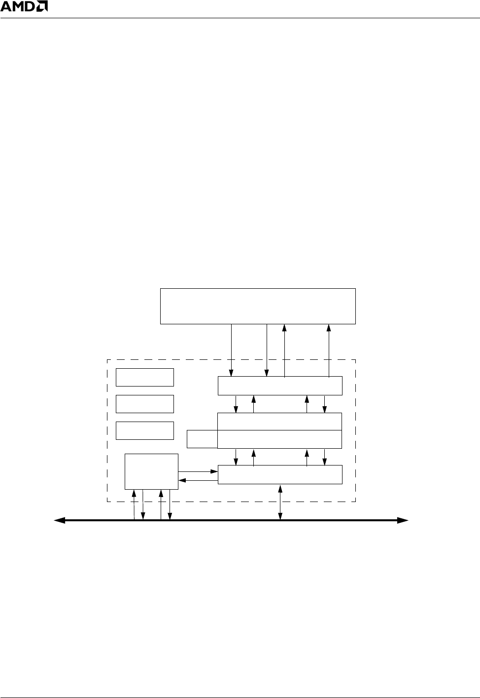
566 AMD Geode™ LX Processors Data Book
GeodeLink™ PCI Bridge
33234H
6.15 GeodeLink™ PCI Bridge
The GeodeLink™ PCI Bridge (GLPCI) module provides a
PCI interface for GeodeLink Interface Unit-based designs.
The GLPCI module is composed of five major blocks:
•GeodeLink Interface
•FIFO/Synchronization
•Transaction Forwarding
•PCI Bus Interface
•PCI Arbiter
The GeodeLink and PCI Bus Interface blocks provide
adaptation to the respective buses. The Transaction For-
warding block provides bridging logic.
Features
•PCI Version 2.2 compliance
•32-bit, 66 MHz PCI bus operation
•Target support for fast back-to-back transactions
•Arbiter support for three external PCI bus masters
•Write gathering and write posting for in-bound write
requests
•Virtual PCI header support
•Delayed transactions for in-bound read requests
•Zero wait state operation within a PCI burst
•Dynamic clock stop/start support for GLIU and PCI clock
domains (this is not CLKRUN support)
•Capable of handling out of bound transactions immedi-
ately after reset
Figure 6-58. GLPCI Block Diagram
PCI Bus Interface
PCI Bus
RequestRequest Data
PCI
Arbiter
REQ#/GNT#
MSR Transaction Forwarding
FIFOs/Synchronization
GeodeLink™ Interface
GeodeLink™ Interface Unit 1 (GLIU1)
Clock Control
Clock Control
Clock Control

AMD Geode™ LX Processors Data Book 567
GeodeLink™ PCI Bridge 33234H
6.15.1 GeodeLink™ Interface Block
The GeodeLink Interface block provides a thin protocol
conversion layer between the Transaction Forwarding block
and GeodeLink Interface Unit 1 (GLIU1). It is responsible
for multiplexing in-bound write request data with out-bound
read response data on the single GLIU1 data out bus.
6.15.2 FIFO/Synchronization Block
The FIFO module consists of a collection of in-bound and
out-bound FIFOs. Each FIFO provides simple, synchro-
nous interfaces to read and write requests.
6.15.3 Transaction Forwarding Block
The Transaction Forwarding block receives, processes, and
forwards transaction requests and responses between the
GeodeLink Interface and PCI Bus Interface blocks. It imple-
ments the transaction ordering rules and performs write
gathering and read prefetching as needed. It also performs
the necessary translation between GLIU1 and PCI com-
mands; except for the creation of PCI configuration cycles
in response to I/O accesses of address 0CFCh. The Trans-
action Forwarding block also handles the conversion
between 64-bit GLIU1 data paths and 32-bit PCI data
paths.
Out-bound transactions are handled in a strongly ordered
fashion. Some out-bound burst writes may be combined
into a larger PCI transaction. This is accomplished by
dynamically concatenating together contiguous bursts as
they are streamed out in a PCI bus transaction. Single 32-
bit WORD accesses are not gathered. It is anticipated that
the processor generates the majority of out-bound
requests. Out-bound memory writes will not be posted.
Thus, any queued out-bound requests need NOT be
flushed prior to handling an in-bound read request.
Dynamic concatenation of contiguous bursts may occur
when reading the penultimate (next to last) data WORD
from the out-bound write data FIFO. On that cycle, if a suit-
able request is available at the head of the out-bound
request FIFO, the PCI burst will be extended.
In-bound requests are handled using slightly relaxed order-
ing. All in-bound writes are gathered as much as possible.
Any partially gathered in-bound writes are flushed when a
cache line boundary is reached. All in-bound writes are
posted. Thus, any queued in-bound write data MUST be
written to system memory prior to the processor receiving
data for an out-bound read request. This is accomplished
by sorting out-bound read response data amongst in-
bound write data. Thus, a pending out-bound read request
need not be deferred while posted in-bound write data is
flushed. The out-bound read request may be performed on
the PCI bus at the same time that the in-bound write data is
flowing through GLIU1.
When handling an in-bound read request, the intended size
of the transfer is unknown. In-bound read requests for non-
prefetchable addresses only fetch the data explicitly indi-
cated in the PCI transaction. Thus, all in-bound read
requests made to non-prefetchable addresses return at
most a single 32-bit WORD. In-bound read requests made
to prefetchable memory may cause more than a 32-bit
WORD to be prefetched. The amount of data prefetched is
configured via the read threshold fields of the CTRL model
specific register of GLPCI_CTRL (MSR 50002010h). Multi-
ple read requests may be generated to satisfy the read
threshold value.
In-bound read requests may pass posted in-bound write
data when there is no address collision between the read
request and the address range of the posted write data (dif-
ferent cache lines) and the read address is marked as
being prefetchable.
6.15.3.1 Atomic External MSR Access
The companion device implements a mailbox scheme simi-
lar to the AMD Geode LX processor. To access internal
model specific registers on the AMD Geode companion
device’s GLIU it is necessary to perform multiple PCI con-
figuration cycles. The GLPCI module provides a mecha-
nism to give software atomic, transparent access to the
companion device’s GLIU resident MSRs. It translates
MSR read/writes received from the AMD Geode LX pro-
cessor’s GLIUs into the multiple PCI configuration needed
to access the companion device’s internal MSR. From soft-
ware’s point of view, the GLPCI module routes MSR read/
write requests like a GLIU. The GLPCI module terminates
MSR accesses where the three most significant bits are
zero. Otherwise it uses the same three MSBs as an index
to look up a PCI device number and a PCI function number
in GLPCI_EXT (MSR 5000201Eh). This device number is
then further mapped onto AD[31:11] pins using the same
mapping as with software generated PCI configuration
cycles. Next the GLPCI module performs three PCI config-
uration bus cycles.
•Write MSR address to offset F4h
•Read/write MSR data to/from offset F8h
•Read/write MSR data to/from offset FCh
Note: The GLPCI module attempts to do a burst PCI con-
figuration read or write. It is expected that the tar-
get PCI device will typically cause this burst to get
broken up into two by performing a slave termina-
tion after each DWORD of data is transferred.
The GLPCI module can address up to seven external PCI
devices in this manner.

568 AMD Geode™ LX Processors Data Book
GeodeLink™ PCI Bridge
33234H
Figure 6-59. Atomic MSR Accesses Across the PCI Bus
GLIU1
Device-A Device-B
Device-C
PCI-device = 1
PCI-device = 15 PCI-device = 25 PCI-device = 30
2
4
3
6
5
1
2
7
3
AMD Geode™ LX Processor
2.4.1.3.6.x 2.4.2.5.1.x
2.4.3.2.7.3
GLPCI_EXT (MSR 5000201Eh) configuration:
GLIU-port1 -> PCI-device-15
GLIU-port2 -> PCI-device-25
GLIU-port3 -> PCI-device-30
GLIU-port4 -> PCI-device-1
GLPCI
GLIU0
GLIU1
GLPCI
GLIU0
GLIU1
GLPCI
GLIU0
GLIU1
GLIU2
GLPCI
GLIU0
CPU Core

AMD Geode™ LX Processors Data Book 569
GeodeLink™ PCI Bridge 33234H
6.15.4 PCI Bus Interface Block
The PCI Bus Interface block is compliant to the PCI 2.2
specification, except in the handling of SERR#/PERR# sig-
nals. These signals are not available.
The PCI Bus Interface block provides a protocol conversion
layer between the Transaction Forwarding block and the
PCI bus. The master and target portions of this block oper-
ate independently. Thus, out-bound write requests and in-
bound read responses are effectively multiplexed onto the
PCI bus. It generates configuration cycles and software
generated special cycles using the standard 0CF8h/0CFCh
I/O address scheme. It includes address decoding logic to
recognize distinct address regions for slave operation.
Each address region is defined by a base address, a size,
and some attached attributes (i.e., prefetchable, coherent).
This block is responsible for retrying out-bound requests
when a slave termination without data is seen on the PCI
bus. It must restart transactions on the PCI bus that are
prematurely ended with a slave termination. This block
always slave terminates in-bound read transactions issued
to non-prefetchable regions after a single DWORD has
been transferred.
The maximum inbound write throughput is only limited by
the PCI latency timer (see register GLPCI_CTRL bits
[39:35]), which will interrupt an inbound transaction after
the specified number of cycles. With this latency timer dis-
abled (GLPCI_CTRL bit 9), the maximum throughput is
achieved
The maximum inbound read throughput is also affected by
the PCI latency timer in a similar fashion to the inbound
write throughput. It is also affected by the inbound read
prefetch threshold setting (GLPCI_CTRL bits [59:56]). With
the latency timer disabled and the read prefetch set to 0Ah
to 0Fh, the maximum throughput is achieved. With the read
prefetch threshold set to the default of 04h, the throughput
is not optimal.
6.15.4.1 PCI Configuration and Virtual PCI Header
Support
The PCI Bus Interface block implements the logic to gener-
ate PCI configuration cycles. The standard mechanism for
generating PCI configuration cycles (as described in the
PCI 2.2 specification) is used.
To access the internal PCI configuration registers of the
AMD Geode LX processor, the Configuration Address reg-
ister (CONFIG_ADDRESS) must be written as a DWORD
using the format shown in Table 6-89. Any other size will be
interpreted as an I/O write to Port 0CF8h. Also, when
entering the Configuration Index, only the six most signifi-
cant bits of the offset are used, and the two least significant
bits must be 00.
BYTE and WORD sized I/O accesses to 0CF8h pass
through the PCI Bus Interface block onto the PCI bus.
Writes to the CONFIG_DATA register are translated into
PCI configuration write bus cycles. Reads to the
CONFIG_DATA register are translated into PCI configura-
tion read bus cycles. Bit 31 of the CONFIG_ADDRESS
register gates the translation of I/O accesses to 0CFCh into
PCI configuration cycles.
IDSEL assertions are realized where device numbers 1
through 21 are mapped to the AD[11] through AD[31] pins.
In addition, support is included for virtualization of PCI
buses and secondary bus devices. When a device or bus is
virtualized, the PCI Bus Interface block generates a syn-
chronous SMI for access to the CONFIG_DATA register
instead of generating a configuration cycle on the PCI bus.
See GLPCI_PBUS (MSR register (MSR 50002012h[31:0])
for details on virtual PCI header support.
The PCI Bus Interface block can be configured to accept
in-bound PCI configuration cycles. This is used as a debug
method for indirectly accessing the internal model specific
register from the PCI bus. When this capability is enabled,
the PCI Bus Interface block responds to in-bound PCI con-
figuration cycles that make the PCI Bus Interface block’s
IDSEL signal become asserted (expected to be device 1).
In this case, the PCI Bus Interface block ignores writes and
returns FFFFFFFFh for accesses to locations 00h through
EFh of the PCI configuration space. This makes the PCI
Bus Interface block invisible to PCI Plug&Play software.
Table 6-89. Format for Accessing the Internal PCI Configuration Registers
313029282726252423222120191817161514131211109876543210
1 Reserved 0000000000000000 Configuration Index 00
570 AMD Geode™ LX Processors Data Book
GeodeLink™ PCI Bridge
33234H
6.15.5 PCI Arbiter
The PCI arbiter implements a fair arbitration scheme with
special support for the companion device. By default it
operates as a simple round-robin arbiter that rotates prior-
ity in circular fashion (see Figure 6-60). There are three
external REQ#/GNT# pairs, numbered 0 through 2, and an
internal REQ#/GNT# pair for the CPU. REQ2#/GNT2# is
reserved for the AMD Geode companion device (i.e.,
southbridge).
Each requestor can be configured to be preemptable/non-
preemptable (Figure 6-61), given a repeat-count attribute
and given a grant-hold timeout attribute. The repeat-count
and grant-hold attributes are present to help balance the
fairness of the PCI bus when mixing bus masters of differ-
ent bursting characteristics. For example, the companion
device drops its REQ# signal after each grant and issues
relatively small bursts, while some other bus masters
present very long bursts on the PCI bus. When both bus
masters are concurrently active, the companion device
gets a very small share of the PCI bus. The repeat-count
allows a bus master to retain control of the PCI bus across
multiple bus tenures and the grant-hold keeps the grant
asserted with an idle bus for a configurable number of clock
cycles, giving the bus master a chance to reassert REQ#
again. Together they allow a small bursting bus master, like
the companion device, to repeatedly issue a sequence of
bursts before being preempted, giving it fair access to PCI
bandwidth even in the presence of a large bursting bus
master (e.g., a modern network adapter). Use of the
repeat-count attribute has an impact on the preemptability
of the bus master. That master can only be preempted
when working on its last repeated access to the bus. For
example, if a bus master has a repeat-count of 2 it may
only be preempted on its third access to the bus. The arbi-
ter can be configured to temporarily override this non-pre-
emptability, particular masters that are requesting access
to the PCI bus.
Figure 6-60. Simple Round-Robin
Figure 6-61. Weighted Round-Robin
Table 6-90. PCI Device to AD Bus Mapping
PCI Device AD Pin PCI Device AD Pin PCI Device AD Pin PCI Device AD Pin
0N/A8 18162624N/A
111919172725N/A
2 121020182826N/A
3 131121192927N/A
4 141222203028N/A
5 151323213129N/A
6 16142422N/A30N/A
7 17152523N/A31N/A
CPU 0
2 1
CPU 0
2 1

AMD Geode™ LX Processors Data Book 571
GeodeLink™ PCI Bridge 33234H
6.15.6 Exception Handling
6.15.6.1 Out-Bound Write Exceptions
When performing an out-bound write on the PCI bus, two
errors may occur: target abort and PERR# assertion.
When a target abort occurs, the PCI Bus Interface block
must flush any stored write data. It must then report the
error. The assertion of PERR# is handled generically. The
failed transaction will not be retried.
6.15.6.2 Out-Bound Read Exceptions
When performing an out-bound read on the PCI bus, two
errors may occur: target abort and parity error. When a tar-
get abort occurs, the PCI Bus Interface block must return
the expected amount of data with sufficient error signals.
6.15.6.3 In-Bound Write Exceptions
When performing an in-bound write from the PCI bus, two
errors may occur: a detected parity error and a GLIU
exception. A GLIU exception cannot be relayed back to the
originating PCI bus master because in-bound PCI writes
are always posted. When a parity error is detected, the
PERR# signal must be asserted by the PCI Bus Interface
block. However, the corrupted write data will be passed
along to the GLIU.
6.15.6.4 In-Bound Read Exceptions
When performing an in-bound read from the GLIU, the
EXCEP flag may be set on any received bus-WORD of
data. This may be due to an address configuration error
caused by software or by an error reported by the source of
data. The asynchronous ERR and/or SMI bit will be set by
the PCI Bus Interface block and the read data, valid or not,
will be passed to the PCI Interface block along with the
associated exceptions. The PCI Bus Interface block should
simply pass the read response data along to the PCI bus.

572 AMD Geode™ LX Processors Data Book
GeodeLink™ PCI Bridge Register Descriptions
33234H
6.16 GeodeLink™ PCI Bridge Register Descriptions
All GeodeLink™ PCI Bridge (GLPCI) registers are Model
Specific Registers (MSRs) and are accessed via the
RDMSR and WRMSR instructions.
The registers associated with the GLPCI are the Standard
GeodeLink Device (GLD) MSRs and GLPCI Specific
MSRs. Table 6-91 and Table 6-92 are register summary
tables that include reset values and page references where
the bit descriptions are provided.
The MSR address is derived from the perspective of the
CPU Core. See Section 4.1 "MSR Set" on page 45 for
more detail on MSR addressing.
Table 6-91. Standard GeodeLink™ Device MSRs Summary
MSR
Address Type Register Name Reset Value Reference
50002000h RO GLD Capabilities MSR (GLD_MSR_CAP) 00000000_001054xxh Page 574
50002001h R/W GLD Master Configuration MSR
(GLD_MSR_CONFIG)
00000000_00000000h Page 574
50002002h R/W GLD SMI MSR (GLD_MSR_SMI) 00000000_0000003Fh Page 575
50002003h R/W GLD Error MSR (GLD_MSR_ERROR) 00000000_0000003Fh Page 576
50002004h R/W GLD Power Management MSR
(GLD_MSR_PM)
00000000_00000015h Page 577
50002005h R/W GLD Diagnostic MSR (GLD_MSR_DIAG) 00000000_00000000h Page 577
Table 6-92. GLPCI Specific Registers Summary
MSR
Address Type Register Name Reset Value Reference
50002010h R/W GLPCI Global Control (GLPCI_CTRL) 44000000_00000000h Page 578
50002011h R/W GLPCI Arbiter Control (GLPCI_ARB) 00000000_00000000h Page 581
50002012h R/W GLPCI VPH / PCI Configuration Cycle Con-
trol (GLPCI_PBUS)
00FF0000_00000000h Page 584
50002013h R/W GLPCI Debug Packet Configuration
(GLPCI_DEBUG)
00000000_00000000h Page 584
50002014h R/W GLPCI Fixed Region Enables
(GLPCI_REN)
00000000_00000000h Page 584
50002015h R/W GLPCI Fixed Region Configuration A0-BF
(GLPCI_A0)
00000000_00000000h Page 585
50002016h R/W GLPCI Fixed Region Configuration C0-DF
(GLPCI_C0)
00000000_00000000h Page 586
50002017h R/W GLPCI Fixed Region Configuration E0-FF
(GLPCI_E0)
00000000_00000000h Page 587
50002018h R/W GLPCI Memory Region 0 Configuration
(GLPCI_R0)
00000000_00000000h Page 588
50002019h R/W GLPCI Memory Region 1 Configuration
(GLPCI_R1)
00000000_00000000h Page 589
5000201Ah R/W GLPCI Memory Region 2 Configuration
(GLPCI_R2)
00000000_00000000h Page 590
5000201Bh R/W GLCPI Memory Region 3 Configuration
(GLPCI_R3)
00000000_00000000h Page 591
5000201Ch R/W GLCPI Memory Region 4 Configuration
(GLPCI_R4)
00000000_00000000h Page 592

AMD Geode™ LX Processors Data Book 573
GeodeLink™ PCI Bridge Register Descriptions 33234H
5000201Dh R/W GLPCI Memory Region 5 Configuration
(GLPCI_R5)
00000000_00000000h Page 593
5000201Eh R/W GLPCI External MSR Access Configuration
(GLPCI EXT_MSR)
00000000_00000000h Page 594
5000201Fh R/W GLPCI Spare 00000000_00000000h Page 595
50002020h R/W GLPCI General Purpose I/O (GLPCI_GPIO) 00000000_00000000h Page 596
Table 6-92. GLPCI Specific Registers Summary
MSR
Address Type Register Name Reset Value Reference
574 AMD Geode™ LX Processors Data Book
GeodeLink™ PCI Bridge Register Descriptions
33234H
6.16.1 Standard GeodeLink™ Device (GLD) MSRs
6.16.1.1 GLD Capabilities MSR (GLD_MSR_CAP)
6.16.1.2 GLD Master Configuration MSR (GLD_MSR_CONFIG)
MSR Address 50002000h
Ty p e RO
Reset Value 00000000_001054xxh
GLD_MSR_CAP Register Map
63 62 61 60 59 58 57 56 55 54 53 52 51 50 49 48 47 46 45 44 43 42 41 40 39 38 37 36 35 34 33 32
RSVD
313029282726252423222120191817161514131211109876543210
RSVD DEV_ID REV_ID
GLD_MSR_CAP Bit Descriptions
Bit Name Description
63:24 RSVD Reserved. Reserved for future use.
23:8 DEV_ID Device ID. Identifies device (1054h).
7:0 REV_ID Revision ID. Identifies device revision. See AMD Geode™ LX Processors Specification
Update document for value.
MSR Address 50002001h
Ty p e R / W
Reset Value 00000000_00000000h
GLD_MSR_CONFIG Register Map
63 62 61 60 59 58 57 56 55 54 53 52 51 50 49 48 47 46 45 44 43 42 41 40 39 38 37 36 35 34 33 32
RSVD
31 30 29 28 27 26 25 24 23 22 21 20 19 18 17 16 15 14 13 12 11 10 9 8 7 6 5 4 3 2 1 0
RSVD PRI
RSVD
PID
GLD_MSR_CONFIG Bit Descriptions
Bit Name Description
63:7 RSVD (RO) Reserved (Read Only). Reserved for future use.
6:4 PRI Priority. Default priority.
3 RSVD (RO) Reserved (Read Only). Reserved for future use.
2:0 PID Priority ID. Assigned priority domain.
AMD Geode™ LX Processors Data Book 575
GeodeLink™ PCI Bridge Register Descriptions 33234H
6.16.1.3 GLD SMI MSR (GLD_MSR_SMI)
MSR Address 50002002h
Ty p e R / W
Reset Value 00000000_0000003Fh
GLD_MSR_SMI Register Map
63 62 61 60 59 58 57 56 55 54 53 52 51 50 49 48 47 46 45 44 43 42 41 40 39 38 37 36 35 34 33 32
RSVD
313029282726252423222120191817161514131211109876543210
RSVD
PA R E
SYSE
VPHE
BME
TAR E
MARE
RSVD
PA R M
SYSM
VPHM
BMM
TAR M
MARM
GLD_MSR_SMI Bit Descriptions
Bit Name Description
63:22 RSVD (RO) Reserved (Read Only). Reserved for future use.
21 PARE Parity Error Event (Read/Write-1-to-Clear). This bit is asserted due to detection of a
PCI bus parity error. Write 1 to clear. PS (MSR 50002010h[27]) must be set to enable this
event. The event causes an ASMI if PARM (bit 5) is cleared.
20 SYSE System Error Event (Read/Write-1-to-Clear). This bit is asserted due to the detection
of a PCI bus system error. Write 1 to clear. PS (MSR 50002010h[27]) must be set to
enable this event. The event causes an ASMI if SYSM (bit 4) is cleared.
19 VPHE Virtual PCI Header Event (Read/Write-1-to-Clear). This bit is set by Virtual PCI Header
support logic, write 1 to clear. The event causes an SSMI if VPHM (bit 3) is cleared.
18 BME Broken Master Event (Read/Write-1-to-Clear). This bit is asserted due to detection of a
broken PCI bus master. Write 1 to clear. BMS (MSR 50002010h[26]) must be set to
enable this event. The event causes an ASMI if BMM (bit 2) is cleared.
17 TARE Target Abort Received Event (Read/Write-1-to-Clear). This bit is asserted due to
reception of target abort on PCI. Write 1 to clear. TARS (MSR50002010h[25]) must be
set to enable this event. The event causes an ASMI if TARM (bit 1) is cleared.
16 MARE Master Abort Received Event (Read/Write-1-to-Clear). This bit is asserted due to
reception of master abort on PCI. Write 1 to clear. MARS (MSR 50002010h[24]) must be
set to enable this event. The event causes an ASMI if MARM (bit 0) is cleared.
15:6 RSVD Reserved. Reserved for future use.
5PARM Parity Error Mask. Clear to allow PARE (bit 21) to generate an ASMI.
4 SYSM System Error Mask. Clear to allow SYSE (bit 20) to generate an ASMI.
3 VPHM Virtual PCI Header Mask. Clear to allow SSMI flag to be set in selected GLIU response
packets. I/O reads and writes to location 0CFCh may cause an SSMI depending upon
the configuration of this bit and the GLPCI_PBUS (MSR 50002012h) model specific reg-
isters.
2BMM Broken Master Mask. Clear to allow BME (bit 18) to generate an ASMI.
1TARM Target Abort Received Mask. Clear to allow TARE (bit 17) to generate an ASMI.
0MARM Master Abort Received Mask. Clear to allow MARE (bit 16) to generate an ASMI.
576 AMD Geode™ LX Processors Data Book
GeodeLink™ PCI Bridge Register Descriptions
33234H
6.16.1.4 GLD Error MSR (GLD_MSR_ERROR)
MSR Address 50002003h
Ty p e R / W
Reset Value 00000000_0000003Fh
GLD_MSR_ERROR Register Map
63 62 61 60 59 58 57 56 55 54 53 52 51 50 49 48 47 46 45 44 43 42 41 40 39 38 37 36 35 34 33 32
RSVD
313029282726252423222120191817161514131211109876543210
RSVD
PA R E
SYSE
RSVD
BME
TAR E
MARE
RSVD
PA R M
SYSM
RSVD
BMM
TAR M
MARM
GLD_MSR_ERROR Bit Descriptions
Bit Name Description
63:22 RSVD (RO) Reserved (Read Only). Reserved for future use.
21 PARE Parity Error Event (Read/Write-1-to-Clear). This bit is asserted due to detection of a
PCI bus parity error. Write 1 to clear. PE (MSR 50002010h[31]) must be set to enable this
event. The event causes an ERR if PARM (bit 5) is cleared.
20 SYSE System Error Event (Read/Write-1-to-Clear). This bit is asserted due to the detection
of a PCI bus system error. Write 1 to clear. PE (MSR 50002010h[31]) must be set to
enable this event. The event causes an ERR if SYSM (bit 4) is cleared.
19 RSVD (RO) Reserved (Read Only). Reserved for future use.
18 BME Broken Master Event (Read/Write-1-to-Clear). This bit is asserted due to detection of a
broken PCI bus master. Write 1 to clear. BME (MSR 50002010h[30]) must be set to
enable this event. The event causes an ERR if BMM (bit 2) is cleared.
17 TARE Target Abort Received Event (Read/Write-1-to-Clear). This bit is asserted due to the
reception of a target abort on PCI. Write 1 to clear. TARE (MSR 50002010h[29]) must be
set to enable this event. The event causes an ERR if TARM (bit 1) is cleared.
16 MARE Master Abort Received Event (Read/Write-1-to-Clear). This bit is asserted due to the
reception of a master abort on PCI. Write 1 to clear. MARE (MSR 50002010h[28]) must
be set to enable this event. The event causes an ERR if MARM (bit 0) is cleared.
15:6 RSVD (RO) Reserved (Read Only). Reserved for future use.
5PARM Parity Error Mask. Clear to allow PARE (bit 21) to generate an ERR.
4 SYSM System Error Mask. Clear to allow SYSE (bit 20) to generate an ERR.
3 RSVD (RO) Reserved (Read Only). Reserved for future use.
2BMM Broken Master Mask. Clear to allow BME (bit 18) to generate an ERR.
1TARM Target Abort Received Mask. Clear to allow TARE (bit 17) to assert ERR.
0MARM Master Abort Received Mask. Clear to allow MARE (bit 16) to assert ERR.
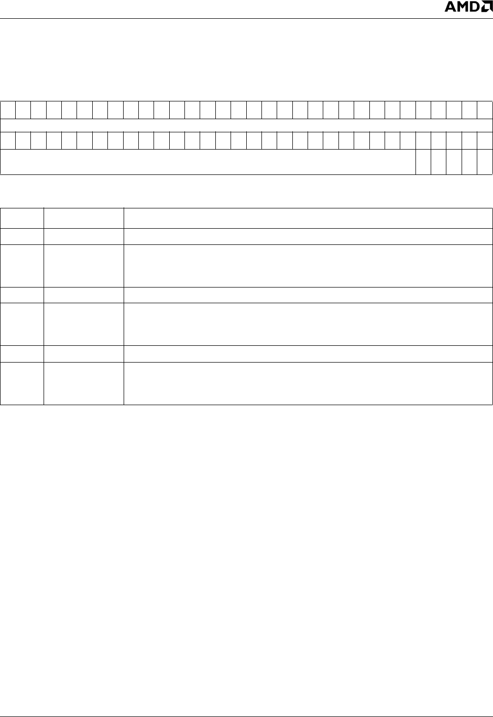
AMD Geode™ LX Processors Data Book 577
GeodeLink™ PCI Bridge Register Descriptions 33234H
6.16.1.5 GLD Power Management MSR (GLD_MSR_PM)
6.16.1.6 GLD Diagnostic MSR (GLD_MSR_DIAG)
This register is for AMD use only and should not be written to.
MSR Address 50002004h
Ty p e R / W
Reset Value 00000000_00000015h
GLD_MSR_PM Register Map
63 62 61 60 59 58 57 56 55 54 53 52 51 50 49 48 47 46 45 44 43 42 41 40 39 38 37 36 35 34 33 32
RSVD
313029282726252423222120191817161514131211109876543210
RSVD
PM2
RSVD
PM1
RSVD
PM0
GLD_MSR_PM Bit Descriptions
Bit Name Description
63:5 RSVD (RO) Reserved (Read Only). Reserved for future use.
4PM2 Power Mode 2. Power mode for PCI-fast clock domain.
0: Disable clock gating. Clocks are always ON.
1: Enable active hardware clock gating.
3 RSVD (RO) Reserved (Read Only). Reserved for future use.
2PM1 Power Mode 1. Power mode for PCI clock domain.
0: Disable clock gating. Clocks are always ON.
1: Enable active hardware clock gating.
1 RSVD (RO) Reserved (Read Only). Reserved for future use.
0PM0 Power Mode 0. Power mode for GLIU clock domain.
0: Disable clock gating. Clocks are always ON.
1: Enable active hardware clock gating.
MSR Address 50002005h
Ty p e R / W
Reset Value 00000000_00000000h

578 AMD Geode™ LX Processors Data Book
GeodeLink™ PCI Bridge Register Descriptions
33234H
6.16.2 GLPCI Specific Registers
6.16.2.1 GLPCI Global Control (GLPCI_CTRL)
MSR Address 50002010h
Ty p e R / W
Reset Value 44000000_00000000h
GLPCI_CTRL Register Map
63 62 61 60 59 58 57 56 55 54 53 52 51 50 49 48 47 46 45 44 43 42 41 40 39 38 37 36 35 34 33 32
FTH RTH SBRTH RTL DTL WTO
SLTO
ILTO LAT 0
313029282726252423222120191817161514131211109876543210
PE
BME
TAR E
MARE
PS
BMS
TAR S
MARS
SUS IRFT IRFC IOD
ST
ER
RHE
LDE
RUPO
BZ
NI
ISO
OWC
IWC
PCD
IE
ME
GLPCI_CTRL Bit Descriptions
Bit Name Description
63:60 FTH In-Bound Flush Threshold. Controls the timing for requesting new read data while con-
currently flushing previously prefetched, stale read data. If the number of prefetched 64-
bit WORDs reaches this level then a pending request will be made.
59:56 RTH In-Bound Read Threshold. Controls the timing for prefetching read data. If the number
of prefetched 32-bit WORDs reaches this threshold, a subsequent GLIU request will be
generated to fetch the next cache line of read data.
55:52 SBRTH Southbridge In-Bound Read Threshold. Controls the timing for prefetching read data
for the AMD Geode™ companion device. If the number of prefetched 32-bit WORDs
reaches this threshold, a subsequent GLIU request will be generated to fetch the next
cache line of read data. The status of the companion device’s GNT# pin (GNT2#) is sam-
pled to determine when the companion device is generating an in-bound request.
51:49 RTL Retry Transaction Limit. Limits the number of out-bound retries. If a target signals retry
indefinitely, the PCI interface may be configured to abort the failing out-bound request.
000: No limit 100: 64 retries
001: 8 retries 101: 128 retries
010: 16 retries 110: 256 retries
011: 32 retries 111: 512 retries
48:46 DTL Delayed Transaction Limit. Limits the duration of delayed transactions. Once a read
transaction is delayed (retried before the first data phase has completed) all other in-
bound transactions are rejected until the original request is satisfied. If the original master
stops retrying, a live-lock condition may occur. If the number of rejected transactions
reaches the limit defined by this field, then the delayed transaction is forgotten.
000: No limit 100: 16 rejections
001: 2 rejections 101: 32 rejections
010: 4 rejections 110: 64 rejections
011: 8 rejections 111: 128 rejections
45:43 WTO In-Bound Write Timeout. Controls the flushing of in-bound posted write data. When an
in-bound write has completed on the PCI bus, an internal counter is loaded with a value
derived from this field. It will then count down on each PCI clock edge. When the counter
reaches 0, the posted write data is flushed to memory.
000: 4 PCI clock edge 100: 64 PCI clock edges
001: 8 PCI clock edge 101: 128 PCI clock edges
010: 16 PCI clock edge 110: 256 PCI clock edges
011: 32 PCI clock edges 111: No timeout

AMD Geode™ LX Processors Data Book 579
GeodeLink™ PCI Bridge Register Descriptions 33234H
42 SLTO Subsequent Latency Timeout Select. Specifies the subsequent target latency timeout
limit. If within a burst, the GLPCI module does not respond with the configured number of
clock ticks, the PCI interface will terminate the PCI bus cycle.
0: 8 PCI clock edges
1: 4 PCI clock edges
41:40 ILTO Initial Latency Timeout Select. Specifies the initial target latency timeout limit for the
PCI interface. If the GLPCI module does not respond with the first data phase within the
configured number of clock edges, the PCI interface will terminate the PCI bus cycle.
If AILTO (MSR 5000201Fh[6]) = 0
00: 32 PCI clock edges 10: 8 PCI clock edges
01: 16 PCI clock edges 11: 4 PCI clock edges
If AILTO = 1
00: 64 PCI clock edges 10: 256 PCI clock edges
01: 128 PCI clock edges 11: No timeout
39:35 LAT PCI Latency Timer. Latency timeout value for limiting bus tenure.
34:32 0 (RO) Constant 0 (Read Only). The three least significant bits of the PCI latency timer field are
fixed as zeros. These bits are not used as part of the PCI latency timer comparison.
31 PE PCI Error. Allow detection of either a parity error or a system error to be reported in the
PARE bit (MSR 50002003h[21]).
0: Disable.
1: Enable.
30 BME Broken Master Error. Allow detection of a broken PCI bus master to be reported in the
BME bit (MSR 50002003h[18]).
0: Disable.
1: Enable.
29 TARE Target Abort Received Error. Allow reception of a PCI bus target abort to be reported in
the TARE bit (MSR 50002003h[17]).
0: Disable.
1: Enable.
28 MARE Master Abort Received Error. Allow reception of a PCI bus master abort to be reported
in the MARE bit (MSR 50002003h[16]).
0: Disable.
1: Enable.
27 PS PCI ASMI. Allow detection of either a parity error or a system error to be reported in the
PARE bit (MSR 50002002h[21]).
0: Disable.
1: Enable.
26 BMS Broken Master ASMI. Allow detection of a broken PCI bus master to be reported in the
BME bit (MSR 50002002h[18]).
0: Disable.
1: Enable.
25 TARS Target Abort Received ASMI. Allow reception of a PCI bus target abort to be reported in
the TARE bit (MSR 50002002h[17]).
0: Disable.
1: Enable.
GLPCI_CTRL Bit Descriptions (Continued)
Bit Name Description

580 AMD Geode™ LX Processors Data Book
GeodeLink™ PCI Bridge Register Descriptions
33234H
24 MARS Master Abort Receive ASMI. Allow reception of a PCI bus master abort to be reported
in the TARE bit (MSR 50002002h[17]).
0: Disable.
1: Enable.
23:21 SUS Busy Sustain. Controls the sustain time for keeping the clocks running after the internal
busy signals indicate that the clocks may be gated.
000: No sustain 100: 32 clock cycles
001: 4 clock cycles 101: 64 clock cycles
010: 8 clock cycles 110: 128 clock cycles
011: 16 clock cycles 111: 256 clock cycles
20:18 IRFT In-Bound Read Flush Timeout. Controls the flushing of in-bound prefetch read data.
When an in-bound read has completed on the PCI bus, an internal counter is loaded with
a value derived from this field. It then counts down on each PCI clock edge. When the
counter reaches 0, any remaining prefetched data is flushed. The counter stops counting
down if a subsequent in-bound read is received. It continues to count down through an
in-bound write and through any out-bound traffic.
000: 4 PCI clock edge 100: 64 PCI clock edges
001: 8 PCI clock edges 101: 128 PCI clock edges
010: 16 PCI clock edges 110: 256 PCI clock edges
011: 32 PCI clock edges 111: No timeout
17:16 IRFC In-Bound Read Flush Control. Controls the policy for discarding stale data from in-
bound read data FIFO.
00: Discard at end of in-bound read PCI transaction.
01: Discard upon timeout.
10: Discard at start of out-bound write or upon timeout.
11: Discard at start of out-bound write, at start of out-bound read or upon timeout.
In addition to these policies, in-bound read data will be discarded whenever a non-contig-
uous in-bound read is accepted, or when an in-bound write is received that will affect the
prefetched memory.
15:13 IOD I/O Delay. Delay completion of out-bound I/O transactions for a configurable number of
PCI clock cycles.
000: 0 PCI clock cycles
001: 1 PCI clock cycles
010: 2 PCI clock cycles
011: 4 PCI clock cycles
100: 8 PCI clock cycles
101: 16 PCI clock cycles
110: 32 PCI clock cycles
111: 64 PCI clock cycles
12 ST Short Timer. When cleared to 0, delayed transactions are discarded after 215 PCI clock
cycles. When set to 1, delayed transactions are discarded after 25 PCI clock cycles. For
normal operation. this bit should be cleared.
11 ER Early Read. When cleared to 0, out-bound reads are stalled until there is enough FIFO
space in the out-bound read FIFO to hold data for the entire transaction. When set to 1,
out-bound reads will start as soon as possible.
10 RHE Read Hints Enable. When cleared to 0, all out-bound reads use PCI CMD = 6. When set
to 1, the PCI CMD provides a hint about the size of the read request.
6: 1, 2 or 4 DWORDs
E: 8 DWORDs
GLPCI_CTRL Bit Descriptions (Continued)
Bit Name Description
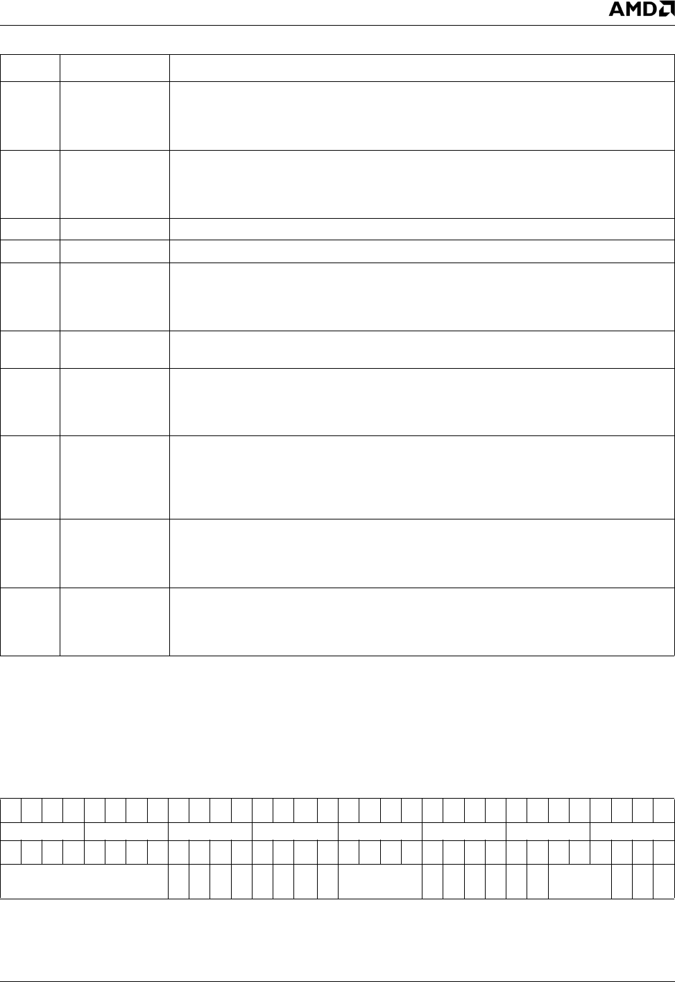
AMD Geode™ LX Processors Data Book 581
GeodeLink™ PCI Bridge Register Descriptions 33234H
6.16.2.2 GLPCI Arbiter Control (GLPCI_ARB)
9LDE Latency Disconnect Enable. Writing 1, causes the PCI interface to disconnect from a
PCI bus master when a latency timer expiration occurs. This enforces the configured min-
imum latency upon PCI bus masters where the GLPCI module is a target on the PCI bus.
The latency timer must be greater than 0 when using this feature.
8RUPO Relax Up-Stream Ordering. Removes ordering restrictions for out-bound read response
data with respect to in-bound write data. Setting this bit also causes the GLPCI to clear
the SEND_RESPONSE flag for in-bound GLIU request packets. This bit should be
cleared for normal operation.
7BZ Bizarro Flag. BIZARRO flag configuration to use on in-bound I/O reads and writes.
6NI No Invalidate Flag. Force the INVALIDATE flag to be cleared for all in-bound writes.
5ISO In-Bound Strong Ordering. Disables the ability of in-bound reads to coherently pass
posted in-bound writes. When set to 1, a PCI read request received by the host bridge
target is not forwarded to GLIU until all posted write data has been flushed to memory.
This bit should be cleared for normal operation.
4OWC Out-Bound Write Combining. Enables concatenation of out-bound write bursts into a
larger PCI burst. Setting this bit does NOT add any additional latency to out-bound writes.
3IWC In-Bound Write Combining. Enables combining of different in-bound PCI write transac-
tions into a single GLIU host write transaction. When cleared to 0, PCI write data
received from the host bridge target is not held in the posted write buffer; a GLIU transac-
tion is generated immediately.
2PCD In-Bound PCI Configuration Disable. Disables the handling of in-bound PCI configura-
tion cycles. When set to 1, PCI configuration cycles are not accepted by this PCI inter-
face. After reset, the GLPCI module accepts in-bound PCI configuration cycles to provide
a means of generating MSR transactions onto the internal GLIU. For normal operation
this capability should be disabled.
1IE I/O Enable. Enable handling of in-bound I/O transactions from PCI. When set to 1, the
PCI interface accepts all in-bound I/O transactions from PCI. This mode is only intended
for design verification purposes. When cleared to 0, no in-bound I/O transactions are
accepted.
0ME Memory Enable. Enable handling of in-bound memory access transaction from PCI.
When cleared to 0 the PCI interface does not accept any in-bound memory transactions
from the PCI bus. When set to 1, the PCI interface accepts in-bound memory transac-
tions for those address ranges defined in the region configuration registers.
MSR Address 50002011h
Ty p e R / W
Reset Value 00000000_00000000h
GLPCI_CTRL Bit Descriptions (Continued)
Bit Name Description
GLPCI_ARB Register Map
63 62 61 60 59 58 57 56 55 54 53 52 51 50 49 48 47 46 45 44 43 42 41 40 39 38 37 36 35 34 33 32
CR R2 R1 R0 CH H2 H1 H0
31 30 29 28 27 26 25 24 23 22 21 20 19 18 17 16 15 14 13 12 11 10 9 8 7 6 5 4 3 2 1 0
RSVD
COV
OV2
OV1
OV0
RSVD
MSK2
MSK1
MSK0
RSVD
CPRE
PRE2
PRE1
PRE0
BM1
BM0
RSVD
EA
BMD
PAR K

582 AMD Geode™ LX Processors Data Book
GeodeLink™ PCI Bridge Register Descriptions
33234H
GLPCI_ARB Bit Definitions
Bit Name Description
63:60 CR CPU Repeat. Controls the number of consecutive grants given to the CPU before rotat-
ing to the next requestor. This is only valid if there is a non-zero value for the CPU Hold-
Grant control (CH, bits [47:44]). This may be overidden by either OV2, OV1 or OV0 (bits
[22:20]). It is also ignored if the CPRE (bit 11) is cleared.
59:56 R2 Request Repeat 2. Controls the number of consecutive grants given to PCI requestor 2
before rotating to the next requestor. This is only valid if there is a non-zero value for the
Request Hold-Grant2 control (H2, bits [43:40]). This may be overidden by either COV,
OV1, or OV0 (bits [23,21,20]. It is also ignored if the ARB.PRE2 bit is cleared.
55:52 R1 Request Repeat 1. Controls the number of consecutive grants given to PCI requestor 1
before rotating to the next requestor. This is only valid if there is a non-zero value for the
Request Hold-Grant1 control (H1, bits [39:36]). This may be overidden by either COV,
OV2, or OV1 (bits [23,22,21]. It is also ignored if the PRE1 (bit 9) is cleared.
51:48 R0 Request Repeat 0. Controls the number of consecutive grants given to PCI requestor 0
before rotating to the next requestor. This is only valid if there is a non-zero value for the
Request Hold-Grant0 control (H0, bits [35:32]). This may be overidden by either the
ARB.COV, ARB.OV2 or ARB.OV1 controls. It is also ignored if PRE0 (bit 8) is cleared.
47:44 CH CPU Hold-Grant Controls. Controls the number of PCI clock edges that the PCI bus
must be idle after a CPU transaction before arbitration continues. This is only valid if
there is a non-zero value for the CPU Repeat field (CR, bits [63:60]). This may be overid-
den by either OV2, OV1, or OV0 (bits [22,21,20]). It is also ignored if CPRE (bit 11) is
cleared.
43:40 H2 Request Hold-Grant 2. Controls the number of PCI clock edges that the PCI bus must
be idle after a requestor 2 transaction before arbitration continues. This is only valid if
there is a non-zero value for the Request Repeat 2 field (R2, bits [59:56]). This may be
overidden by either COV, OV1, or OV0 (bits [23,21,20]). It is also ignored if PRE2 (bit 10)
is cleared.
39:36 H1 Request Hold-Grant 1. Controls the number of PCI clock edges that the PCI bus must
be idle after a requestor 1 transaction before arbitration continues. This is only valid if
there is a non-zero value for the Request Repeat 1 field (R1, bits [55:52]). This may be
overidden by either COV, OV1, or OV0 (bits [23,21,20]). It is also ignored if the if PRE2
(bit 10) is cleared.
35:32 H0 Request Hold-Grant 0. Controls the number of PCI clock ticks that the PCI bus must be
idle after a requestor 0 transaction before arbitration continues. This is only valid if there
is a non-zero value for the Request Repeat 0 field (R0, bits [51:48]). This may be overid-
den by either COV, OV1, or OV0 (bits [23,21,20]). It is also ignored if PRE2 (bit 10) is
cleared.
31:24 RSVD (RO) Reserved (Read Only). Reserved for future use.
23 COV CPU Override. Enables the CPU to override the repeat-count and grant-hold for other
requestors. When COV is set and the CPU is requesting access to PCI, repeat-count and
grant-hold mechanisms for other masters are temporarily disabled. This bit does not
change the round robin arbitration cycle, it only overrides repeat-count and grant-hold for
other requestors.
22 OV2 Override 2. Enables requester2 to override the repeat-count and grant-hold for other
requestors. When OV2 is set and REQ2# is asserted, repeat-count and grant-hold mech-
anisms for other masters are temporarily disabled. This bit does not change the round
robin arbitration cycle, it only overrides repeat-count and grant-hold for other requestors.
21 OV1 Override 1. Enables requester1 to override the repeat-count and grant-hold for other
requestors. When OV1 is set and REQ1# is asserted, repeat-count and grant-hold mech-
anisms for other masters are temporarily disabled. This bit does not change the round
robin arbitration cycle, it only overrides repeat-count and grant-hold for other requestors.

AMD Geode™ LX Processors Data Book 583
GeodeLink™ PCI Bridge Register Descriptions 33234H
20 OV0 Override 0. Enables requester0 to override the repeat-count and grant-hold for other
requestors. When OV0 is set and REQ0# is asserted, repeat-count and grant-hold mech-
anisms for other masters are temporarily disabled. This bit does not change the round
robin arbitration cycle, it only overrides repeat-count and grant-hold for other requestors.
19 RSVD (RO) Reserved (Read Only). Reserved for future use.
18 MSK2 Request Mask 2. Disables REQ2# when set to 1. Resets to 0.
17 MSK1 Request Mask 1. Disables REQ1# when set to 1. Resets to 0.
16 MSK0 Request Mask 0. Disables REQ0# when set to 1. Resets to 0.
15:12 RSVD (RO) Reserved (Read Only). Reserved for future use.
11 CPRE CPU Preemption Enable. When set to 1, the CPU’s PCI grant may be de-asserted
before the CPU’s request is de-asserted. If this bit is cleared, the arbiter ignores CH and
CR, bits [47:44] and [63:60].
10 PRE2 Preemption Enable 2. When set to 1, GNT2# may be de-asserted before REQ2# is de-
asserted. If this bit is cleared, the arbiter ignores R2 and H2, bits [59:56] and [43:40].
9PRE1 Preemption Enable 1. When set to 1, GNT1# may be de-asserted before REQ1# is de-
asserted. If this bit is cleared, the arbiter ignores the R1 and H1, bits [55:52] and [39:36].
8PRE0 Preemption Enable 0. When set to 1, GNT0# may be de-asserted before REQ0# is de-
asserted. If this bit is cleared, the arbiter ignores R0 and H0, bits [51:48] and [35:32].
7 BM1 (RO) Broken Master 1 (Read Only). Indicates when a broken master is attached to REQ1#.
This bit is set when the arbiter detects that the PCI bus master attached to REQ1# has
not asserted FRAME# within 16 PCI clock edges after being granted the PCI bus. This bit
is cleared by setting BMD (bit 1) to 1.
6 BM0 (RO) Broken Master 0 (Read Only). Indicates when a broken master is attached to REQ0#.
This bit is set when the arbiter detects that the PCI bus master attached to REQ[0]# has
not asserted FRAME# within 16 PCI clock edges after being granted the PCI bus. This bit
is cleared by setting the BMD (bit 1) to 1.
5:2 RSVD (RO) Reserved (Read Only). Reserved for future use.
1BMD Broken Master Timer Disable. Controls the operation of the broken master detector in
the PCI arbiter. When set to 1, the arbiter does not recognize a broken master condition
on the PCI bus. When cleared to 0, the arbiter detects a broken master condition when a
granted PCI bus master takes 16 or more clock cycles before asserting FRAME#. The
broken master is NOT allowed to gain access to the PCI bus. Software may restore any
broken master’s permission to use the PCI bus by clearing this bit, and optionally, setting
it again.
0PARK Parking Policy. When cleared to 0, the arbiter always parks the PCI bus on the
AMD Geode™ LX processor. When set to 1, the arbiter parks the PCI bus on the last
granted bus master. If this bit is set, the clock for the PCI-fast clock domain should not be
gated.
GLPCI_ARB Bit Definitions (Continued)
Bit Name Description
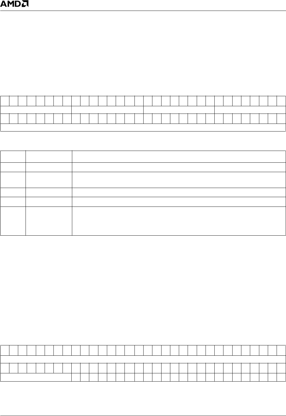
584 AMD Geode™ LX Processors Data Book
GeodeLink™ PCI Bridge Register Descriptions
33234H
6.16.2.3 GLPCI VPH / PCI Configuration Cycle Control (GLPCI_PBUS)
The PBUS model specific register is used to control the way that the GLPCI module generates (or does not generate) PCI
configuration cycles onto the PCI bus. SEC (bits [39:32]) should be configured with the PCI bus number for the locally
attached PCI bus. SUB (bits [55:48]) should be configured with the PCI bus number for the highest numbered PCI bus that
is accessible via the PCI interface. DEV (bits [31:0]) should be configured to indicate which device numbers will NOT gener-
ate PCI configuration cycles on the PCI bus.
6.16.2.4 GLPCI Debug Packet Configuration (GLPCI_DEBUG)
Control relay of debug packets to PCI. The functionality that this register controls has been removed from the GLIU. There-
fore this register is obsolete.
6.16.2.5 GLPCI Fixed Region Enables (GLPCI_REN)
MSR Address 50002012h
Ty p e R / W
Reset Value 00FF0000_00000000h
GLPCI_PBUS Register Map
63 62 61 60 59 58 57 56 55 54 53 52 51 50 49 48 47 46 45 44 43 42 41 40 39 38 37 36 35 34 33 32
RSVD SUB RSVD SEC
31 30 29 28 27 26 25 24 23 22 21 20 19 18 17 16 15 14 13 12 11 10 9 8 7 6 5 4 3 2 1 0
DEV
GLPCI_PBUS Bit Descriptions
Bit Name Description
63:56 RSVD (RO) Reserved (Read Only). Reserved for future use.
55:48 SUB Subordinate Bus Number. Specifies the subordinate PCI bus number for all PCI buses
reachable via the PCI interface.
47:40 RSVD (RO) Reserved (Read Only). Reserved for future use.
39:32 SEC Secondary Bus Number. Specifies the secondary PCI bus number for the PCI interface.
31:0 DEV Device Bitmap. Specifies the virtualized PCI devices. Each bit position corresponds to a
device number. A 0 instructs the GLPCI to allow PCI configuration cycles for the device
to be generated on the PCI bus. A 1 tells the GLPCI to virtualize the device by generating
an SSMI instead of a PCI configuration cycle.
MSR Address 50002013h
Ty p e R / W
Reset Value 00000000_00000000h
MSR Address 50002014h
Ty p e R / W
Reset Value 00000000_00000000h
GLPCI_REN Register Map
63 62 61 60 59 58 57 56 55 54 53 52 51 50 49 48 47 46 45 44 43 42 41 40 39 38 37 36 35 34 33 32
Spare
31 30 29 28 27 26 25 24 23 22 21 20 19 18 17 16 15 14 13 12 11 10 9 8 7 6 5 4 3 2 1 0
RSVD
FC
F8
F4
F0
EC
E8
E4
E0
DC
D8
D4
D0
CC
C8
C4
C0
BC
B8
B4
B0
AC
A8
A4
A0
AMD Geode™ LX Processors Data Book 585
GeodeLink™ PCI Bridge Register Descriptions 33234H
6.16.2.6 GLPCI Fixed Region Configuration A0-BF (GLPCI_A0)
GLPCI_REN Bit Descriptions
Bit Name Description
63:32 Spare Spare Bits. Extra bits available for future use. These bits may be set and cleared, but do
not control anything.
31:24 RSVD (RO) Reserved (Read Only). Reserved for future use
23 FC FC Enable. Enables memory access to FC000 through FFFFF from PCI.
22 F8 F8 Enable. Enables memory access to F8000 through FBFFF from PCI.
21 F4 F4 Enable. Enables memory access to F4000 through F7FFF from PCI.
20 F0 F0 Enable. Enables memory access to F0000 through F3FFF from PCI.
19 EC EC Enable. Enables memory access to EC000 through EFFFF from PCI.
18 E8 E8 Enable. Enables memory access to E8000 through EBFFF from PCI.
17 E4 E4 Enable. Enables memory access to E4000 through E7FFF from PCI.
16 E0 E0 Enable. Enables memory access to E0000 through E3FFF from PCI.
15 DC DC Enable. Enables memory access to DC000 through DFFFF from PCI.
14 D8 D8 Enable. Enables memory access to D8000 through DBFFF from PCI.
13 D4 D4 Enable. Enables memory access to D4000 through D7FFF from PCI.
12 D0 D0 Enable. Enables memory access to D0000 through D3FFF from PCI.
11 CC CC Enable. Enables memory access to CC000 through CFFFF from PCI.
10 C8 C8 Enable. Enables memory access to C8000 through CBFFF from PCI.
9C4 C4 Enable. Enables memory access to C4000 through C7FFF from PCI.
8C0 C0 Enable. Enables memory access to C0000 through C3FFF from PCI.
7BC BC Enable. Enables memory access to BC000 through BFFFF from PCI.
6B8 B8 Enable. Enables memory access to B8000 through BBFFF from PCI.
5B4 B4 Enable. Enables memory access to B4000 through B7FFF from PCI.
4B0 B0 Enable. Enables memory access to B0000 through B3FFF from PCI.
3AC AC Enable. Enables memory access to AC000 through AFFFF from PCI.
2A8 A8 Enable. Enables memory access to A8000 through ABFFF from PCI.
1A4 A4 Enable. Enables memory access to A4000 through A7FFF from PCI.
0A0 A0 Enable. Enables memory access to A0000 through A3FFF from PCI.
MSR Address 50002015h
Ty p e R / W
Reset Value 00000000_00000000h
GLPCI_A0 Register Map
63 62 61 60 59 58 57 56 55 54 53 52 51 50 49 48 47 46 45 44 43 42 41 40 39 38 37 36 35 34 33 32
BC B8 B4 B0
31 30 29 28 27 26 25 24 23 22 21 20 19 18 17 16 15 14 13 12 11 10 9 8 7 6 5 4 3 2 1 0
AC A8 A4 A0
586 AMD Geode™ LX Processors Data Book
GeodeLink™ PCI Bridge Register Descriptions
33234H
6.16.2.7 GLPCI Fixed Region Configuration C0-DF (GLPCI_C0)
GLPCI_A0 Bit Descriptions
Bit Name Description (Note 1)
63:56 BC BC Properties. Region properties for BC000 through BFFFF.
55:48 B8 B8 Properties. Region properties for B8000 through BBFFF.
47:40 B4 B4 Properties. Region Properties for B4000 through B7FFF.
39:32 B0 B0 Properties. Region properties for B0000 through B3FFF.
31:24 AC AC Properties. Region properties for AC000 through AFFFF.
23:16 A8 A8 Properties. Region Properties for A8000 through ABFFF.
15:8 A4 A4 Properties. Region Properties for A4000 through A7FFF.
7:0 A0 A0 Properties. Region properties for A0000 through A3FFF.
Note 1. See Table 6-93 for region properties bit decodes.
Table 6-93. Region Properties
Bit Name Description
7:6 RSVD (RO) Reserved (Read Only). Reserved for future use.
5PF Prefetchable. Reads to this region have no side-effects.
4WC Write Combine. Writes to this region may be combined.
3 RSVD (RO) Reserved (Read Only). Reserved for future use.
2WP Write Protect. When set to 1, only read accesses are allowed. Write accesses are
ignored (master abort).
1DD Discard Data. When set to 1, write access are accepted and discarded. Read accesses
are ignored (master abort).
0CD Cache Disable. When set to 1, accesses are marked as non-coherent. When cleared to
0, accesses are marked as coherent.
MSR Address 50002016h
Ty p e R / W
Reset Value 00000000_00000000h
GLPCI_C0 Register Map
63 62 61 60 59 58 57 56 55 54 53 52 51 50 49 48 47 46 45 44 43 42 41 40 39 38 37 36 35 34 33 32
DC D8 D4 D0
31 30 29 28 27 26 25 24 23 22 21 20 19 18 17 16 15 14 13 12 11 10 9 8 7 6 5 4 3 2 1 0
CC C8 C4 C0
GLPCI_C0 Bit Descriptions
Bit Name Description (Note 1)
63:56 DC DC Properties. Region properties for DC000 through DFFFF.
55:48 D8 D8 Properties. Region properties for D8000 through DBFFF.
47:40 D4 D4 Properties. Region Properties for D4000 through D7FFF.
AMD Geode™ LX Processors Data Book 587
GeodeLink™ PCI Bridge Register Descriptions 33234H
6.16.2.8 GLPCI Fixed Region Configuration E0-FF (GLPCI_E0)
39:32 D0 D0 Properties. Region properties for D0000 through D3FFF.
31:24 CC CC Properties. Region properties for CC000 through CFFFF.
23:16 C8 C4 Properties. Region Properties for C8000 through CBFFF.
15:8 C4 C4 Properties. Region Properties for C4000 through C3FFF.
7:0 C0 C0 Properties. Region properties for C0000 through C3FFF.
Note 1. See Table 6-93 on page 586 for region properties bit decodes.
MSR Address 50002017h
Ty p e R / W
Reset Value 00000000_00000000h
GLPCI_C0 Bit Descriptions (Continued)
Bit Name Description (Note 1)
GLPCI_E0 Register Map
63 62 61 60 59 58 57 56 55 54 53 52 51 50 49 48 47 46 45 44 43 42 41 40 39 38 37 36 35 34 33 32
FC F8 F4 F0
31 30 29 28 27 26 25 24 23 22 21 20 19 18 17 16 15 14 13 12 11 10 9 8 7 6 5 4 3 2 1 0
EC E8 E4 E0
GLPCI_E0 Bit Descriptions
Bit Name Description (Note 1)
63:56 FC FC Properties. Region properties for FC000 through FFFFF.
55:48 F8 F8 Properties. Region properties for F8000 through FBFFF.
47:40 F4 F4 Properties. Region Properties for F4000 through F7FFF.
39:32 F0 F0 Properties. Region properties for F0000 through F3FFF.
31:24 EC EC Properties. Region properties for EC000 through EFFFF.
23:16 E8 E4 Properties. Region Properties for E8000 through EBFFF.
15:8 E4 E4 Properties. Region Properties for E4000 through E3FFF.
7:0 E0 E0 Properties. Region properties for E0000 through E3FFF.
Note 1. See Table 6-93 on page 586 for region properties bit decodes.

588 AMD Geode™ LX Processors Data Book
GeodeLink™ PCI Bridge Register Descriptions
33234H
6.16.2.9 GLPCI Memory Region 0 Configuration (GLPCI_R0)
MSR Address 50002018h
Ty p e R / W
Reset Value 00000000_00000000h
GLPCI_R0 Register Map
63 62 61 60 59 58 57 56 55 54 53 52 51 50 49 48 47 46 45 44 43 42 41 40 39 38 37 36 35 34 33 32
TOP RSVD
31 30 29 28 27 26 25 24 23 22 21 20 19 18 17 16 15 14 13 12 11 10 9 8 7 6 5 4 3 2 1 0
BASE RSVD
EN
RSVD
PF
WC
RSVD
WP
DD
CD
GLPCI_R0 Bit Descriptions
Bit Name Description
63:44 TOP Top of Region. 4 KB granularity, inclusive.
43:32 RSVD (RO) Reserved (Read Only). Reserved for future use.
31:12 BASE Base of Region. 4 KB granularity, inclusive.
11:9 RSVD (RO) Reserved (Read Only). Reserved for future use.
8EN Region Enable. Set to 1 to enable access to this region.
7:6 RSVD (RO) Reserved (Read Only). Reserved for future use.
5PF Prefetchable. Reads to this region have no side-effects.
4WC Write Combine. Writes to this region may be combined.
3 RSVD (RO) Reserved (Read Only). Reserved for future use.
2WP Write Protect. When set to 1, only read accesses are allowed. Write accesses are
ignored (master abort).
1DD Discard Data. When set to 1, write access are accepted and discarded. Read accesses
are ignored (master abort).
0CD Cache Disable. When set to 1, accesses are marked as non-coherent. When cleared to
0 accesses are marked as coherent.

AMD Geode™ LX Processors Data Book 589
GeodeLink™ PCI Bridge Register Descriptions 33234H
6.16.2.10 GLPCI Memory Region 1 Configuration (GLPCI_R1)
MSR Address 50002019h
Ty p e R / W
Reset Value 00000000_00000000h
GLPCI_R1 Register Map
63 62 61 60 59 58 57 56 55 54 53 52 51 50 49 48 47 46 45 44 43 42 41 40 39 38 37 36 35 34 33 32
TOP RSVD
31 30 29 28 27 26 25 24 23 22 21 20 19 18 17 16 15 14 13 12 11 10 9 8 7 6 5 4 3 2 1 0
BASE RSVD
EN
RSVD
PF
WC
RSVD
WP
DD
CD
GLPCI_R1 Bit Descriptions
Bit Name Description
63:44 TOP Top of Region. 4 KB granularity, inclusive.
43:32 RSVD (RO) Reserved (Read Only). Reserved for future use.
31:12 BASE Base of Region. 4 KB granularity, inclusive.
11:9 RSVD (RO) Reserved (Read Only). Reserved for future use.
8EN Region Enable. Set to 1 to enable access to this region.
7:6 RSVD (RO) Reserved (Read Only). Reserved for future use.
5PF Prefetchable. Reads to this region have no side-effects.
4WC Write Combine. Writes to this region may be combined.
3 RSVD (RO) Reserved (Read Only). Reserved for future use.
2WP Write Protect. When set to 1, only read accesses are allowed. Write accesses are
ignored (master abort).
1DD Discard Data. When set to 1, write access are accepted and discarded. Read accesses
are ignored (master abort).
0CD Cache Disable. When set to 1, accesses are marked as non-coherent. When cleared to
0, accesses are marked as coherent.

590 AMD Geode™ LX Processors Data Book
GeodeLink™ PCI Bridge Register Descriptions
33234H
6.16.2.11 GLPCI Memory Region 2 Configuration (GLPCI_R2)
MSR Address 5000201Ah
Ty p e R / W
Reset Value 00000000_00000000h
GLPCI_R2 Register Map
63 62 61 60 59 58 57 56 55 54 53 52 51 50 49 48 47 46 45 44 43 42 41 40 39 38 37 36 35 34 33 32
TOP RSVD
31 30 29 28 27 26 25 24 23 22 21 20 19 18 17 16 15 14 13 12 11 10 9 8 7 6 5 4 3 2 1 0
BASE RSVD
EN
RSVD
PF
WC
RSVD
WP
DD
CD
GLPCI_R2 Bit Descriptions
Bit Name Description
63:44 TOP Top of Region. 4 KB granularity, inclusive.
43:32 RSVD (RO) Reserved (Read Only). Reserved for future use.
31:12 BASE Base of Region. 4 KB granularity, inclusive.
11:9 RSVD (RO) Reserved (Read Only). Reserved for future use.
8EN Region Enable. Set to 1 to enable access to this region.
7:6 RSVD (RO) Reserved (Read Only). Reserved for future use.
5PF Prefetchable. Reads to this region have no side-effects.
4WC Write Combine. Writes to this region may be combined.
3 RSVD (RO) Reserved (Read Only). Reserved for future use.
2WP Write Protect. When set to 1, only read accesses are allowed. Write accesses are
ignored (master abort).
1DD Discard Data. When set to 1, write access are accepted and discarded. Read accesses
are ignored (master abort).
0CD Cache Disable. When set to 1, accesses are marked as non-coherent. When cleared to
0, accesses are marked as coherent.

AMD Geode™ LX Processors Data Book 591
GeodeLink™ PCI Bridge Register Descriptions 33234H
6.16.2.12 GLCPI Memory Region 3 Configuration (GLPCI_R3)
MSR Address 5000201Bh
Ty p e R / W
Reset Value 00000000_00000000h
GLPCI_R3 Register Map
63 62 61 60 59 58 57 56 55 54 53 52 51 50 49 48 47 46 45 44 43 42 41 40 39 38 37 36 35 34 33 32
TOP RSVD
31 30 29 28 27 26 25 24 23 22 21 20 19 18 17 16 15 14 13 12 11 10 9 8 7 6 5 4 3 2 1 0
BASE RSVD
EN
RSVD
PF
WC
RSVD
WP
DD
CD
GLPCI_R3 Bit Descriptions
Bit Name Description
63:44 TOP Top of Region. 4 KB granularity, inclusive.
43:32 RSVD (RO) Reserved (Read Only). Reserved for future use.
31:12 BASE Base of Region. 4 KB granularity, inclusive.
11:9 RSVD (RO) Reserved (Read Only). Reserved for future use.
8EN Region Enable. Set to 1 to enable access to this region.
7:6 RSVD (RO) Reserved (Read Only). Reserved for future use.
5PF Prefetchable. Reads to this region have no side-effects.
4WC Write Combine. Writes to this region may be combined.
3 RSVD (RO) Reserved (Read Only). Reserved for future use.
2WP Write Protect. When set to 1, only read accesses are allowed. Write accesses are
ignored (master abort).
1DD Discard Data. When set to 1, write access are accepted and discarded. Read accesses
are ignored (master abort).
0CD Cache Disable. When set to 1, accesses are marked as non-coherent. When cleared to
0, accesses are marked as coherent.
592 AMD Geode™ LX Processors Data Book
GeodeLink™ PCI Bridge Register Descriptions
33234H
6.16.2.13 GLCPI Memory Region 4 Configuration (GLPCI_R4)
MSR Address 5000201Ch
Ty p e R / W
Reset Value 00000000_00000000h
GLPCI_R4 Register Map
63 62 61 60 59 58 57 56 55 54 53 52 51 50 49 48 47 46 45 44 43 42 41 40 39 38 37 36 35 34 33 32
TOP RSVD
31 30 29 28 27 26 25 24 23 22 21 20 19 18 17 16 15 14 13 12 11 10 9 8 7 6 5 4 3 2 1 0
BASE RSVD
EN
RSVD
PF
WC
RSVD
WP
DD
CD
GLPCI_R4 Bit Descriptions
Bit Name Description
63:44 TOP Top of Region. 4 KB granularity, inclusive.
43:32 RSVD (RO) Reserved (Read Only). Reserved for future use.
31:12 BASE Base of Region. 4 KB granularity, inclusive.
11:9 RSVD (RO) Reserved (Read Only). Reserved for future use.
8EN Region Enable. Set to 1 to enable access to this region.
7:6 RSVD (RO) Reserved (Read Only). Reserved for future use.
5PF Prefetchable. Reads to this region have no side-effects.
4WC Write Combine. Writes to this region may be combined.
3 RSVD (RO) Reserved (Read Only). Reserved for future use.
2WP Write Protect. When set to 1, only read accesses are allowed. Write accesses are
ignored (master abort).
1DD Discard Data. When set to 1, write access are accepted and discarded. Read accesses
are ignored (master abort).
0CD Cache Disable. When set to 1, accesses are marked as non-coherent. When cleared to
0, accesses are marked as coherent.
AMD Geode™ LX Processors Data Book 593
GeodeLink™ PCI Bridge Register Descriptions 33234H
6.16.2.14 GLPCI Memory Region 5 Configuration (GLPCI_R5)
MSR Address 5000201Dh
Ty p e R / W
Reset Value 00000000_00000000h
GLPCI_R5 Register Map
63 62 61 60 59 58 57 56 55 54 53 52 51 50 49 48 47 46 45 44 43 42 41 40 39 38 37 36 35 34 33 32
TOP RSVD
31 30 29 28 27 26 25 24 23 22 21 20 19 18 17 16 15 14 13 12 11 10 9 8 7 6 5 4 3 2 1 0
BASE RSVD
EN
RSVD
PF
WC
RSVD
WP
DD
CD
GLPCI_R5 Bit Descriptions
Bit Name Description
63:44 TOP Top of Region. 4 KB granularity, inclusive.
43:32 RSVD (RO) Reserved (Read Only). Reserved for future use.
31:12 BASE Base of Region. 4 KB granularity, inclusive.
11:9 RSVD (RO) Reserved (Read Only). Reserved for future use.
8EN Region Enable. Set to 1 to enable access to this region.
7:6 RSVD (RO) Reserved (Read Only). Reserved for future use.
5PF Prefetchable. Reads to this region have no side-effects.
4WC Write Combine. Writes to this region may be combined.
3 RSVD (RO) Reserved (Read Only). Reserved for future use.
2WP Write Protect. When set to 1, only read accesses are allowed. Write accesses are
ignored (master abort).
1DD Discard Data. When set to 1, write access are accepted and discarded. Read accesses
are ignored (master abort).
0CD Cache Disable. When set to 1, accesses are marked as non-coherent. When cleared to
0, accesses are marked as coherent.

594 AMD Geode™ LX Processors Data Book
GeodeLink™ PCI Bridge Register Descriptions
33234H
6.16.2.15 GLPCI External MSR Access Configuration (GLPCI EXT_MSR)
Note: MSR accesses addressed to Port 0 are handled directly by the GLPCI module.
MSR Address 5000201Eh
Ty p e R / W
Reset Value 00000000_00000000h
GLPCI_EXT_MSR Register Map
63 62 61 60 59 58 57 56 55 54 53 52 51 50 49 48 47 46 45 44 43 42 41 40 39 38 37 36 35 34 33 32
RSVD FUNC-7 DEVICE-7 FUNC-6 DEVICE-6 FUNC-5 DEVICE-5
31 30 29 28 27 26 25 24 23 22 21 20 19 18 17 16 15 14 13 12 11 10 9 8 7 6 5 4 3 2 1 0
FUNC-4 DEVICE-4 FUNC-3 DEVICE-3 FUNC-2 DEVICE-2 FUNC-1 DEVICE-1
GLPCI_EXT_MSR Bit Descriptions
Bit Name Description
63:56 RSVD (RO) Reserved (Read Only). Reserved for future use.
55:53 FUNC-7 Function Number 7. PCI function number to use for MSR accesses addressed to Port 7.
52:48 DEVICE-7 Device Number 7. PCI device number to use for MSR accesses addressed to Port 7.
47:45 FUNC-6 Function Number 6. PCI function number to use for MSR accesses addressed to Port 6.
44:40 DEVICE-6 Device Number 6. PCI device number to use for MSR accesses addressed to Port 6.
39:37 FUNC-5 Function Number 5. PCI function number to use for MSR accesses addressed to Port 5.
36:32 DEVICE-5 Device Number 5. PCI device number to use for MSR accesses addressed to Port 5.
31:29 FUNC-4 Function Number 4. PCI function number to use for MSR accesses addressed to Port 4.
28:24 DEVICE-4 Device Number 4. PCI device number to use for MSR accesses addressed to Port 4.
23:21 FUNC-3 Function Number 3. PCI function number to use for MSR accesses addressed to Port 3.
20:16 DEVICE-3 Device Number 3. PCI device number to use for MSR accesses addressed to Port 3.
15:13 FUNC-2 Function Number 2. PCI function number to use for MSR accesses addressed to Port 2.
12:8 DEVICE-2 Device Number 2. PCI device number to use for MSR accesses addressed to Port 2.
7:5 FUNC-1 Function Number 1. PCI function number to use for MSR accesses addressed to Port 1.
4:0 DEVICE-1 Device Number 1. PCI device number to use for MSR accesses addressed to Port 1.
AMD Geode™ LX Processors Data Book 595
GeodeLink™ PCI Bridge Register Descriptions 33234H
6.16.2.16 GLPCI Spare
MSR Address 5000201Fh
Ty p e R / W
Reset Value 00000000_00000003h
GLPCI Spare
63 62 61 60 59 58 57 56 55 54 53 52 51 50 49 48 47 46 45 44 43 42 41 40 39 38 37 36 35 34 33 32
Spare
313029282726252423222120191817161514131211109876543210
Spare RSVD
AILTO
PPD
PPC
MPC
MME
NSE
SUPO
GLPCI Spare Bit Descriptions
Bit Name Description
63:10 Spare Spare Bits. Extra bits available for future use. These bits may be set and cleared, but do
not control anything.
9:7 RSVD Reserved. Write as read.
6AILTO Alternate Initial Latency Timeout. Enables alternate initial latency timeout values to be
configured via ILTO (MSR 50002010h[41:40]).
5 PPD Post PIO Data. Enables posting of I/O writes to addresses: 170h and 1F0h.
4 PPC Post PIO Control. Enables posting of I/O writes to addresses: 171h, 172h, 173h, 174h,
175h, 176h, 177h, 1F1h, 1F2h, 1F3h, 1F4h, 1F5h, 1F6h and 1F7h.
3MPC Maximum Posted Count. Controls the maximum number of PIO I/O writes that may be
posted in the GLPCI. When cleared, one I/O write may be posted. When set, two I/O
writes may be posted.
2MME Mask External MSR Exceptions. Set to 1 to force the GLIU synchronous exception flag
to be cleared for all external MSR transactions.
1NSE No Synchronous Exceptions. Controls when out-bound read data is written into the
OBRD FIFO. When this bit is cleared. the GLPCI pipelines the writing of all out-bound
read data into the FIFO. This allows PCI transaction status to be sampled and included
synchronously with the read data. When this bit is cleared, the GLPCI only pipelines read
data for external MSR accesses and I/O read of the configuration data port (0CFCh).
0SUPO Strict Up-Stream Ordering. Controls how out-bound reads get sorted with in-bound
writes. When this bit is set the ordering rules are strictly applied; meaning that all GLIU
write responses associated with a in-bound PCI write transaction must complete before
data from a subsequent out-bound PCI read may be placed onto the GLIU. When this bit
is cleared the out-bound read data may be placed onto the GLIU after the in-bound write
data has been placed onto the GLIU.
596 AMD Geode™ LX Processors Data Book
GeodeLink™ PCI Bridge Register Descriptions
33234H
6.16.2.17 GLPCI General Purpose I/O (GLPCI_GPIO)
MSR Address 50002020h
Ty p e R / W
Reset Value 00000000_00000000h
GLPCI_GPIO Register Map
63 62 61 60 59 58 57 56 55 54 53 52 51 50 49 48 47 46 45 44 43 42 41 40 39 38 37 36 35 34 33 32
MSW
RSVD SAMPDIV
31 30 29 28 27 26 25 24 23 22 21 20 19 18 17 16 15 14 13 12 11 10 9 8 7 6 5 4 3 2 1 0
RSVD
OE2
OE1
OE0
RSVD
OUT2
OUT1
OUT0
RSVD
IN2
IN1
IN0
GLPCI_GPIO Register Bit Descriptions
Bit Name Description
63 MSW Most Significant Word Enable. Must be set on writes to alter SAMPDIV (bits [47:32]).
When cleared, the SAMPDIV field will not be updated. When set, the SAMPDIV field will
be written.
62:48 RSVD (RO) Reserved (Read Only). Reserved for future use.
47:32 SAMPDIV Sample Divider. Controls the frequency of sampling input data fed into each filter. With a
value of zero, each input is sampled on every PCI clock edge. With a value of 1, each
input is sampled every other clock edge. With a value of 2, it is sampled every third clock
edge, and so on.
31:19 RSVD (RO) Reserved (Read Only). Reserved for future use.
18 OE2 Output Enable 2. Output enable for GNT2# pin.
17 OE1 Output Enable 1. Output enable for REQ1# pin.
16 OE0 Output Enable 0. Output enable for GNT1# pin.
15:11 RSVD (RO) Reserved (Read Only). Reserved for future use.
10 OUT2 Output 2. Output for GNT2# pin.
9OUT1 Output 1. Output for REQ1# pin.
8OUT0 Output 0. Output for GNT1# pin.
7:3 RSVD (RO) Reserved (Read Only). Reserved for future use.
2IN2 (RO) Input 2 (Read Only). Filtered input from GNT2# pin.
1IN1 (RO) Input 1 (Read Only). Filtered input from REQ1# pin.
0IN0 (RO) Input 0 (Read Only). Filtered input from GNT1# pin.
AMD Geode™ LX Processors Data Book 597
7
Electrical Specifications 33234H
7.0Electrical Specifications
This section provides information on electrical connections,
absolute maximum ratings, operating conditions, and
DC/AC characteristics for the AMD Geode™ LX processor.
All voltage values in the electrical specifications are with
respect to VSS unless otherwise noted.
7.1 Electrical Connections
7.1.1 PWR/GND Connections and Decoupling
Testing and operating the AMD Geode LX processor
requires the use of standard high frequency techniques to
reduce parasitic effects. When using this device, the effects
can be minimized by filtering the DC power leads with low-
inductance decoupling capacitors, using low-impedance
wiring, and by connecting all VCORE, VIO, VMEM, and ana-
log balls to the appropriate voltage levels.
7.1.2 NC-Designated Balls
Balls designated as NC (No Connection) should be left dis-
connected. Connecting an NC ball to a pull-up/-down resis-
tor, or an active signal could cause unexpected results and
possible circuit malfunctions.
7.1.3 Unused Inputs
All inputs not used by the system designer should be kept
at either ground or VIO. To prevent possible spurious opera-
tion. For active-high inputs to ground through a 20-kΩ
(±10%) pull-down resistor and active-low inputs to VIO
through a 20-kΩ (±10%) pull-up resistor can be used if
desired.
7.2 Absolute Maximum Ratings
Table 7-1 lists absolute maximum ratings for the AMD Geode
LX processor. Stresses beyond the listed ratings may cause
permanent damage to the device. Exposure to conditions
beyond these limits may (1) reduce device reliability and (2)
result in premature failure even when there is no immedi-
ately apparent sign of failure. Prolonged exposure to condi-
tions at or near the absolute maximum ratings may also
result in reduced useful life and reliability. These are stress
ratings only and do not imply that operation under any con-
ditions other than those listed in Table 7-2 "Operating Con-
ditions" on page 598 is possible.
Table 7-1. Absolute Maximum Ratings
Symbol Parameter Min Max Unit Comments
TSTORAGE Storage Temperature -65 150 °C No Bias
VCORE Core Supply Voltage 1.5 V
VIO I/O Supply Voltage 3.0 3.6 V Also applies to VCA, VMA,
VVA, and VDAC
VMEM Memory Voltage 3.6 V
VMAX Voltage On Any Pin -0.5 3.8 V Except HSYNC, VSYNC
Voltage on HSYNC, VSYNC -0.5 5.5 V
ESD - Human Body Model 2000 V
ESD - Machine Model 200 V
598 AMD Geode™ LX Processors Data Book
Electrical Specifications
33234H
7.3 Operating Conditions
Table 7-2 lists the operating conditions for the AMD Geode LX processor.
Table 7-2. Operating Conditions
Symbol Parameter (Note 1)
Note 1. The AMD Geode LX 900@1.5W processor operates at 600 MHz, the AMD Geode LX 800@0.9W processor oper-
ates at 500 MHz, the AMD Geode LX 700@0.8W processor operates at 433 MHz and the AMD Geode
LX 600@.07W processor operates at 366 MHz. Model numbers reflect performance as described here:
http://www.amd.com/connectivitysolutions/geodelxbenchmark.
Min Typ Max Unit Comments
TC Operating Case Temperature
LX 900@1.5W
080°C
Operating Case Temperature
LX 800@0.9W
0 85 °C See Section A.1 "Order Infor-
mation" for applicable OPN.
-40 85 °C
Operating Case Temperature
LX 700@0.8W
LX 600@0.7W
085°C
VCORE Core Supply Voltage
LX 900@1.5W
1.36 1.40 1.44 V Filtered version of this supply
also supplies PLL power.
Note 2
Note 2. This parameter is calculated as nominal ±3%.
Core Supply Voltage
LX 800@0.9W
1.21 1.25 1.29 V
Core Supply Voltage
LX 700@0.8W
LX 600@0.7W
1.16 1.20 1.24 V
VIO I/O Supply Voltage 3.14 3.3 3.46 V Filtered version of this supply
also supplies DAC power.
Note 3
VVA Video PLL Supply Voltage 3.14 3.30 3.46 V Filtered version of VIO.
Note 3
VMA Memory PLL Supply Voltage 3.14 3.30 3.46 V
VCA CPU PLL Supply Voltage 3.14 3.30 3.46 V
VDAC DAC PLL Supply Voltage 3.14 3.30 3.46 V
VMEM DDR (2.6V SSTL)
LX 900@1.5W,
LX 800@0.9W
2.47 2.60 2.73 V Note 3
DDR (2.5V SSTL)
LX 700@0.8W
2.38 2.50 2.63 V
DDR2 (1.9V)
LX 900@1.5W,
LX 800@0.9W
LX 700@0.8W
1.81 1.90 2.00 V
DDR2 (1.8V)
LX 600@0.7W
1.71 1.80 1.89 V
MVREF DDR
LX 900@1.5W,
LX 800@0.9W
1.23 1.30 1.37 V Note 3, Note 4
Note 3. This parameter is calculated as nominal ±5%.
Note 4. MVREF = 1/2 VMEM.
DDR
LX 700@0.8W
1.19 1.25 1.31 V
DDR2
LX 900@1.5W,
LX 800@0.9W
LX 700@0.8W
0.90 0.95 1.0
DDR2 (1.8V)
LX 600@0.7W
0.86 0.90 0.95

AMD Geode™ LX Processors Data Book 599
Electrical Specifications 33234H
7.4 DC Current
DC current is not a simple measurement. Three of the
AMD Geode LX processor’s power states (ON, Active Idle,
and Sleep) were selected for measurement. For the ON
power state measured, two functional characteristics (Typi-
cal Average and Absolute Maximum) are used to deter-
mine how much current the processor requires.
7.4.1 Power State Parameter Definitions
The DC current tables in this section list Core and I/O cur-
rent for three of the power states.
•On (S0/C0): All internal and external clocks with respect
to the AMD Geode LX processor are running and all
functional blocks (CPU Core, Memory Controller,
Display Controller, etc.) are actively generating cycles.
This is equivalent to the ACPI specification’s “S0/C0”
state.
• Active Idle (S0/C1): The CPU Core has been halted
and all other functional blocks (including the Display
Controller for refreshing the display) are actively gener-
ating cycles. This state is entered when a HLT instruc-
tion is executed by the CPU Core. From a user’s
perspective, this state is indistinguishable from the On
state and is equivalent to the ACPI specification’s
“S0/C1” state.
• Sleep (S1): This is the lowest power state the
AMD Geode LX processor can be in with voltage still
applied to the device’s core and I/O supply pins. This is
equivalent to the ACPI specification’s “S1” state.
All measurements were taken at 25°C ambient air.
7.4.2 Definition and Measurement Techniques
of Current Parameters
The following two parameters describe the AMD Geode LX
processor current while in the ON state:
Typical Average
Typical Average (Typ Avg) indicates the average current
used by the AMD Geode LX processor while in the ON
state, with no active power management. This measure-
ment is comprised of two components: WinBench®99
Business Graphics Test and Active Idle power measure-
ments. WinBench 99 represents a maximum typical state
as it simulates a knowledgeable worker’s typical day com-
pressed into the shortest period of time possible. Since it is
not possible for someone to operate as fast as the bench-
mark, the resulting power from the benchmark is averaged
with Active Idle in an 80/20 ratio, with 80% of the time being
in the Windows® XP Idle state and 20% of the time running
applications. This results in a Typical Average power result.
For each voltage, power is measured at one second inter-
vals. The measurements are then averaged together to
produce the final number. The CRT resolution is
1024x768x32 bpp, at 85 Hz refresh and the TFT resolution
is 1024x768 x16 bpp at 60 Hz refresh. This number is pro-
vided for reference only since it can vary depending on the
usage model of the system.
Thermal Design Power
Absolute Maximum and Thermal Design Power (TDP) indi-
cates the maximum average current used by the
AMD Geode LX processor. This is measured with the volt-
ages at maximum. An internally-developed AMD applica-
tion called Pathological Power Measurement Application
causes the AMD Geode LX processor to consume the
maximum amount of power for the Core and I/O rails, while
WinBench 99 Business Graphics Test causes the
AMD Geode LX processor to consume maximum power on
the memory rail. All tests were run at the maximum sup-
ported resolution of 1920x1440x32 bpp at 72 Hz refresh for
the CRT and 1600x1200x16 bpp at 60 Hz refresh for TFT.
This test does not guarantee maximum current. There may
be pathological applications that result in higher measured
currents.
TDP is a function of all power contributors at maximum.
Applications that do not use the CRT or TFT output will
have a somewhat lower TDP. Operating the memory sub-
system at a lower frequency will also lower TDP. Specific
software applications may place lower compute demands
on the CPU, which lowers the TDP as well.
If needed, it is up to the system designer to determine TDP
for systems that operate with conditions that are different
then those specified, however, the TDP specified is the
maximum.
Active Idle
Active Idle power is measured at the Windows XP Idle
state when the monitor is still turned on. During this state
the “Bliss” background is used. The CRT resolution is
1024x768x32 bpp, at 85 Hz refresh and 1024x768 x16 bpp
at 60 Hz refresh is used for TFT. This number is provided
for reference only since it can vary depending on the back-
ground image and processes running on the system.
Sleep
The Sleep power state is achieved by forcing the system
into a “S1” state as defined by the ACPI specification.
7.4.3 DC Current Measurements
Tables 7-3, 7-4, and 7-5 show the DC current measure-
ments of the AMD Geode LX processor family. The proces-
sor supports CRT or TFT displays.
The CRT DACs require current; while the TFT interface,
even though it has no DAC to power, also draws current
while it is active. Therefore, the CRT DACs and the TFT
interface currents are specified in separate tables.
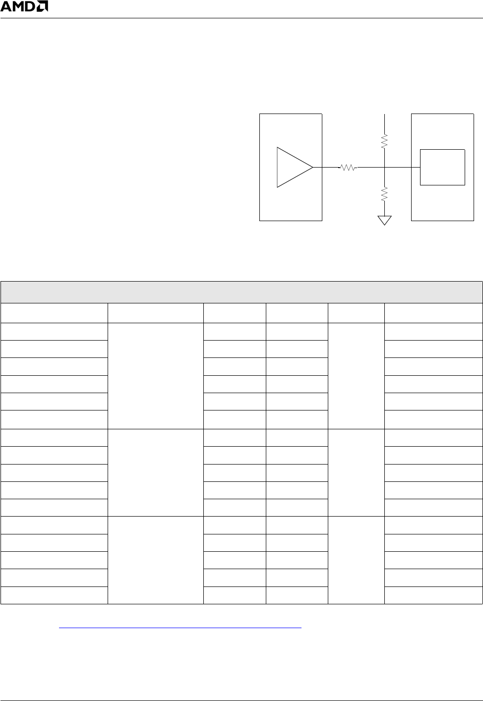
600 AMD Geode™ LX Processors Data Book
Electrical Specifications
33234H
The data bus on the DDR SDRAM has a low voltage swing
when actively terminated (terminated topology). The termi-
nated topology supports higher data transfer rates and is
less constrained, but it consumes more power. Many
designs should be able to operate reliably without active
termination (unterminated topology). The design con-
straints are smaller memory subsystems and tight control
on routing. See the application note, AMD Geode™ LX
Processor and CS5535/CS5536 Companion Device Layout
Recommendations (publication ID #32739), for more infor-
mation.
When series termination resistors are used, as specified in
the AMD Geode™ LX Processor and CS5535/CS5536
Companion Device Layout Recommendations, the actual
power provided by the VMEMLX supply is split between the
processor and the series and parallel termination (see Fig-
ure 7-1). Therefore, it is impossible to specify the power
used by the processor’s memory subsystem with one hun-
dred percent accuracy. A conservative estimate, is that
32.5% of the power is consumed by the processor and
67.5% by the termination resistors. See the AMD Geode™
LX Processor Determining Memory Interface I/O Power
Consumption document (publication ID #40554) for the
detailed analysis. This number is used for the results in DC
Current tables (Tables 7-3, 7-4, and 7-5).
Figure 7-1. VMEMLX Power Split
VMEMLX VMEMDIMM
VTT
Connector
or
Device
MEM
LX
RP1
RP2
RS
Table 7-3. AMD Geode LX 900@1.5W Processor DC Currents
LX 900@1.5W (600 MHz), No EEPROM, VCORE = 1.4V, TDPT = 5.3W, TDPU = 5.1W (Note 1)
Symbol Parameter Typ Avg Max Unit Comments
ICC3ON - CRT Display Power State:
On (S0/C0)
85 100 mA
ICC3ON - TFT Display 37 45
ICOREON 1420 3140
IMEMON - Terminated 150 165 Note 2, Note 3
IMEMON - Unterminated 90 100 Note 3
IMEMDDR2ON 80 95
ICC3IDLE - CRT Display Power State:
Active Idle (S0/C1)
85 mA
ICC3IDLE- TFT Display 37
ICOREIDLE 1250
IMEMIDLE - Terminated 150 Note 2, Note 3
IMEMIDLE - Unterminated 80 Note 3
ICC3SLP - CRT Display Power State:
Sleep (S1)
4mA
ICC3SLP - TFT Display 4
ICORESLP 600
IMEMSLP - Terminated 100 Note 2, Note 3
IMEMSLP - Unterminated 35 Note 3
Note 1. The AMD Geode LX 900@1.5W processor operates at 600 MHz. Model numbers reflect performance as described
here: http://www.amd.com/connectivitysolutions/geodelxbenchmark.
T = Terminated and U = Unterminated.
Note 2. Calculations are based on a 32.5/67.5 split between VMEMLX used by the AMD Geode LX processor and series
termination resistors. See Section 7.4.3 on page 599 for more details.
Note 3. VMEM is 2.6V for the LX 900@1.5W processor.
AMD Geode™ LX Processors Data Book 601
Electrical Specifications 33234H
Table 7-4. AMD Geode LX 800@0.9W Processor DC Currents
LX 800@0.9W (500 MHz), No EEPROM, VCORE = 1.25V, TDPT = 3.8W, TDPU = 3.6W (Note 1)
Symbol Parameter Typ Avg Max Unit Comments
ICC3ON - CRT Display Power State:
On (S0/C0)
85 100 mA
ICC3ON - TFT Display 37 45
ICOREON 1010 2290
IMEMON - Terminated 150 165 Note 2, Note 3
IMEMON - Unterminated 90 100 Note 3
IMEMDDR2ON 80 95
ICC3IDLE - CRT Display Power State:
Active Idle (S0/C1)
85 mA
ICC3IDLE- TFT Display 37
ICOREIDLE 885
IMEMIDLE - Terminated 150 Note 2, Note 3
IMEMIDLE - Unterminated 80 Note 3
ICC3SLP - CRT Display Power State:
Sleep (S1)
4mA
ICC3SLP - TFT Display 4
ICORESLP 225
IMEMSLP - Terminated 100 Note 2, Note 3
IMEMSLP - Unterminated 35 Note 3
Note 1. The AMD Geode LX 800@0.9W processor operates at 500 MHz. Model numbers reflect performance as described
here: http://www.amd.com/connectivitysolutions/geodelxbenchmark.
T = Terminated and U = Unterminated.
Note 2. Calculations are based on a 32.5/67.5 split between VMEMLX used by the AMD Geode LX processor and series
termination resistors. See Section 7.4.3 on page 599 for more details.
Note 3. VMEM is 2.6V for the LX 800@0.9W processor.
602 AMD Geode™ LX Processors Data Book
Electrical Specifications
33234H
Table 7-5. AMD Geode LX 700@0.8W Processor DC Currents
LX 700@0.8W (433 MHz), No EEPROM or EEPROM, VCORE = 1.20V, TDPT = 3.2W, TDPU = 3.1W (Note 1)
Symbol Parameter Typ Avg Max Unit Comments
ICC3ON - CRT Display Power State:
On (S0/C0)
85 100 mA
ICC3ON - TFT Display 37 45
ICOREON 650 1945
IMEMON - Terminated 145 155 Note 2, Note 3
IMEMON - Unterminated 85 95 Note 3
IMEMDDR2ON 75 90
ICC3IDLE - CRT Display Power State:
Active Idle (S0/C1)
85 mA
ICC3IDLE- TFT Display 37
ICOREIDLE 555
IMEMIDLE - Terminated 145 Note 2, Note 3
IMEMIDLE - Unterminated 75 Note 3
ICC3SLP - CRT Display Power State:
Sleep (S1)
4mA
ICC3SLP - TFT Display 4
ICORESLP 195
IMEMSLP - Terminated 95 Note 2, Note 3
IMEMSLP - Unterminated 30 Note 3
Note 1. The AMD Geode LX 700@0.8W processor operates at 433 MHz. Model numbers reflect performance as described
here: http://www.amd.com/connectivitysolutions/geodelxbenchmark.
T = Terminated and U = Unterminated.
Note 2. Calculations are based on a 32.5/67.5 split between VMEMLX used by the AMD Geode LX processor and series
termination resistors. See Section 7.4.3 on page 599 for more details.
Note 3. VMEM is 2.5V for the LX 700@0.8W processor.
AMD Geode™ LX Processors Data Book 603
Electrical Specifications 33234H
Table 7-6. AMD Geode LX 600@0.7W Processor DC Currents
LX 600@0.7W (366 MHz), No EEPROM, VCORE = 1.20V, TDPT = 2.9W, TDPU = 2.8W (Note 1)
Symbol Parameter Typ Avg Max Unit Comments
ICC3ON - CRT Display Power State:
On (S0/C0)
85 100 mA
ICC3ON - TFT Display 37 45
ICOREON 600 1765
IMEMON - Terminated 140 150 Note 2, Note 3
IMEMON - Unterminated 80 90 Note 3
IMEMDDR2ON 70 85
ICC3IDLE - CRT Display Power State:
Active Idle (S0/C1)
85 mA
ICC3IDLE- TFT Display 37
ICOREIDLE 510
IMEMIDLE - Terminated 140 Note 2, Note 3
IMEMIDLE - Unterminated 70 Note 3
ICC3SLP - CRT Display Power State:
Sleep (S1)
4mA
ICC3SLP - TFT Display 4
ICORESLP 185
IMEMSLP - Terminated 90 Note 2, Note 3
IMEMSLP - Unterminated 30 Note 3
Note 1. The AMD Geode LX 600@0.7W processor operates at 366 MHz. Model numbers reflect performance as described
here: http://www.amd.com/connectivitysolutions/geodelxbenchmark.
T = Terminated and U = Unterminated.
Note 2. Calculations are based on a 32.5/67.5 split between VMEMLX used by the AMD Geode LX processor and series
termination resistors. See Section 7.4.3 on page 599 for more details.
Note 3. VMEM is 2.5V for the LX 600@0.7W processor.
604 AMD Geode™ LX Processors Data Book
Electrical Specifications
33234H
7.5 DC Characteristics
All DC parameters and current measurements in this section were measured under the operating conditions listed in Table
7-2 "Operating Conditions", unless otherwise noted. The signals associated with the seven signal buffer types on the
AMD Geode LX processor, are shown Table 3-5 "Ball Assignments - Sorted by Ball Number" on page 26.
Table 7-7. DC Characteristics
Symbol Parameter Min Max Units Comments
VIL Low Level Input Voltage, Note 1
PCI -0.5 0.3*VIO V
24/Q3 -0.5 0.8 V
24/Q5 -0.5 0.8 V
24/Q7 -0.5 0.8 V
5V -0.5 0.8 V
DDR -0.3 MVREF-0.2 V
DDRCLK N/A N/A
VIH High Level Input Voltage, Note 1
PCI 0.5*VIO VIO+0.5 V
24/Q3 2.0 VIO+0.5 V
24/Q5 2.0 VIO+0.5 V
24/Q7 2.0 VIO+0.5 V
5V 2.0 5.5V V Overvoltage tolerant
DDR MVREF+0.2 VMEM+0.3 V
DDRCLK N/A N/A
VOL Low Level Output Voltage, Note 1
PCI 0.1*VIO V
24/Q3 0.4 V
24/Q5 0.4 V
24/Q7 0.4 V
5V 0.4 V
DDR 0.35 V
DDRCLK MVREF-0.4 V
VOH High Level Output Voltage, Note 1
PCI 0.9*VIO V
24/Q3 2.4 V
24/Q5 2.4 V
24/Q7 2.4 V
5V 2.4 V
DDR VMEM-0.43 V
DDRCLK MVREF+0.4 V
AMD Geode™ LX Processors Data Book 605
Electrical Specifications 33234H
ILEAK Input Leakage Current Including Hi-Z Output Leakage, Note 1
PCI -3.0 3.0 µA
24/Q3 -3.0 3.0 µA
24/Q5 -3.0 3.0 µA
24/Q7 -3.0 3.0 µA
5V -3.0 3.0 µA If VIH > VIO,
ILEAK max = 20 µA
DDR -3.0 3.0 µA
DDRCLK -5.0 5.0 µA
IPU/PD Weak Pull-Up/Down Current, Note 1
PCI N/A ---
24/Q3 50 150 µA These pull-downs are only
enabled during reset or
power sequencing system
behaviors. Note 2.
24/Q5 50 150 µA
24/Q7 50 150 µA
5V 50 150 µA
DDR N/A ---
DDRCLK N/A ---
IOH Output High Current, Note 1 VO = VOH (Min)
PCI -500 µA
24/Q3 -24.0 mA
24/Q5 -24.0 mA
24/Q7 -24.0 mA Note 2
5V -16.0 mA
DDR (BA[1:0], MA[13:0]) -15.2 mA IOH min = -11 mA with half-
drive set for pad
DDR (DQ[63:0], CKE[1:0],
CS[3:0]#, RAS[1:0]#, CAS[1:0]#,
WE[1:0]#, DQS[7:0], DQM[7:0],
TLA[1:0]
-11 mA IOH min = -8 mA with quar-
ter-drive set for pad
DDRCLK -10.0 mA
Table 7-7. DC Characteristics (Continued)
Symbol Parameter Min Max Units Comments
606 AMD Geode™ LX Processors Data Book
Electrical Specifications
33234H
IOL Output Low Current, Note 1 VO = VOL (Max)
PCI 1500 µA
24/Q3 24.0 mA
24/Q5 24.0 mA
24/Q7 24.0 mA
5V 16.0 mA
DDR (BA[1:0], MA[13:0]) 15.2 mA IOL min = 11 mA with half-
drive set for pad
DDR (DQ[63:0], CKE[1:0],
CS[3:0]#, RAS[1:0]#, CAS[1:0]#,
WE[1:0]#, DQS[7:0], DQM[7:0],
TLA[1:0]
11 mA IOL min = 8 mA with quarter-
drive set for pad
DDRCLK 10.0 mA
CIO Input and Output Capacitance, Note 1
PCI 8.0 pF
24/Q3 5.0 pF
24/Q5 5.0 pF
24/Q7 5.0 pF
5V 5.0 pF
DDR 8.0 pF
DDRCLK 15.0 pF
Note 1. Refer to the Table 3-5 "Ball Assignments - Sorted by Ball Number" on page 26 for package signal names associated
with each buffer type.
Note 2. The SDA pad is designed to use a pull-up on-chip functionally, hence IOH is not used to drive high, ILEAK is instead
Table 7-7. DC Characteristics (Continued)
Symbol Parameter Min Max Units Comments
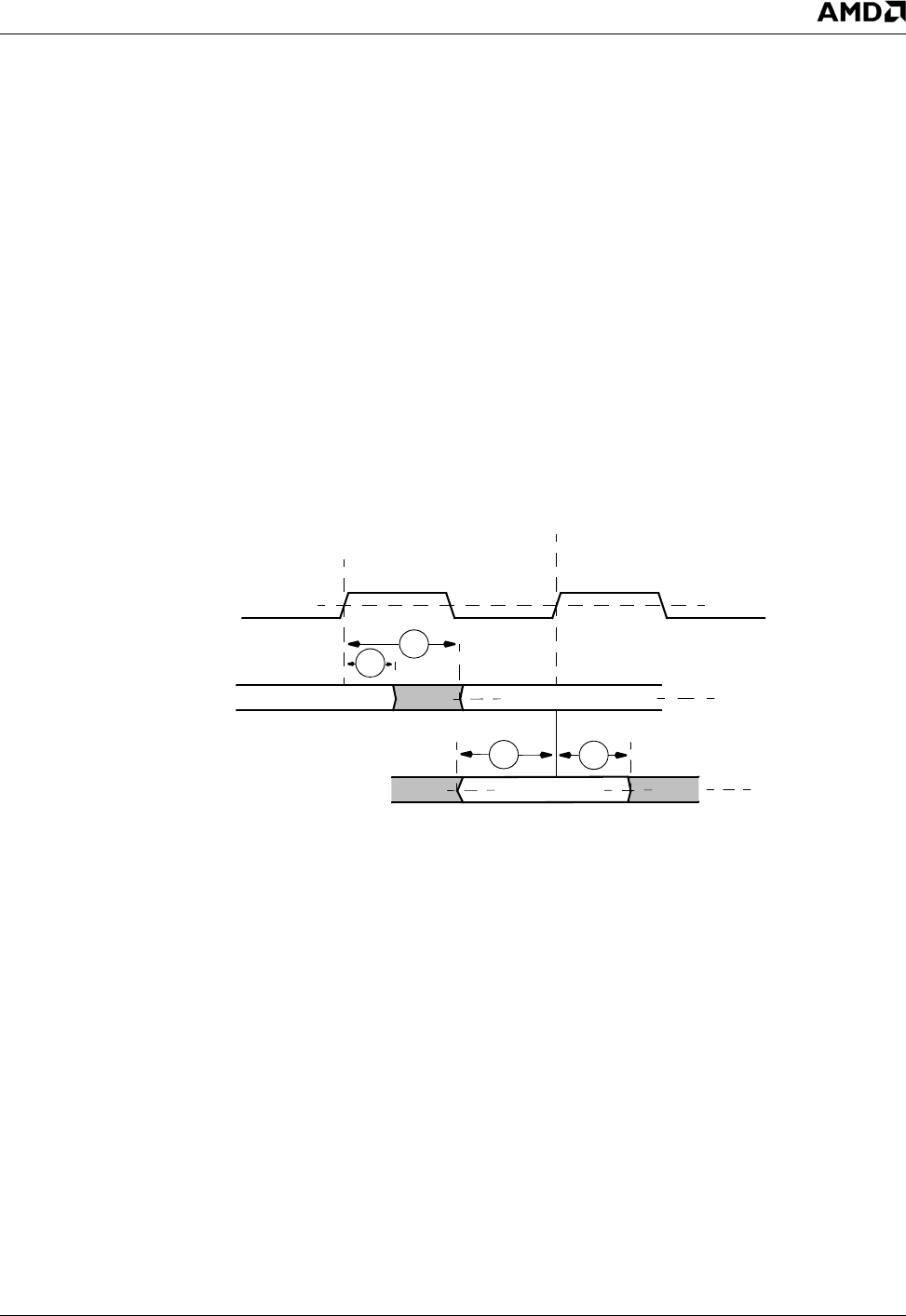
AMD Geode™ LX Processors Data Book 607
Electrical Specifications 33234H
7.6 AC Characteristics
The following tables list the AC characteristics including
output delays, input setup requirements, input hold require-
ments, and output float delays. The rising-clock-edge refer-
ence level VREF
, and other reference levels are shown in
Figure 7-2. Input or output signals must cross these levels dur-
ing testing.
Input setup and hold times are specified minimums that
define the smallest acceptable sampling window for which
a synchronous input signal must be stable for correct opera-
tion.
All AC tests are performed at the following parameters
using the timing diagram shown in Figure 7-2 unless other-
wise specified:
VCORE: 1.14V to 1.26V (1.2V Nominal)
VIO: 3.14V to 3.46V (3.3V Nominal)
VMEM: 2.5V SSTL
MVREF: DDR:1.25V
TC:0
oC to 85oC
RL:50 Ω
CL:50 pF
While most minimum, maximum, and typical AC character-
istics are only shown as a single value, they are tested and
guaranteed across the entire processor core voltage range
of 1.14V to 1.26V. AC characteristics that are affected sig-
nificantly by the core voltage or speed grade are docu-
mented accordingly.
All AC timing measurements are taken at 50% crossing
points for both input times and output times.
Figure 7-2. Drive Level and Measurement Points for Switching Characteristics
CLK
Outputs
Inputs
VIHD
VILD
VREF
Valid Input
Valid Output n+1
Valid Output n
VREF
VREF
VILD
VIHD
Min
Max
Legend: A = Maximum Output or Float Delay Specification
B = Minimum Output or Float Delay Specification
C = Minimum Input Setup Specification
D = Minimum Input Hold Specification
TX
B
A
CD
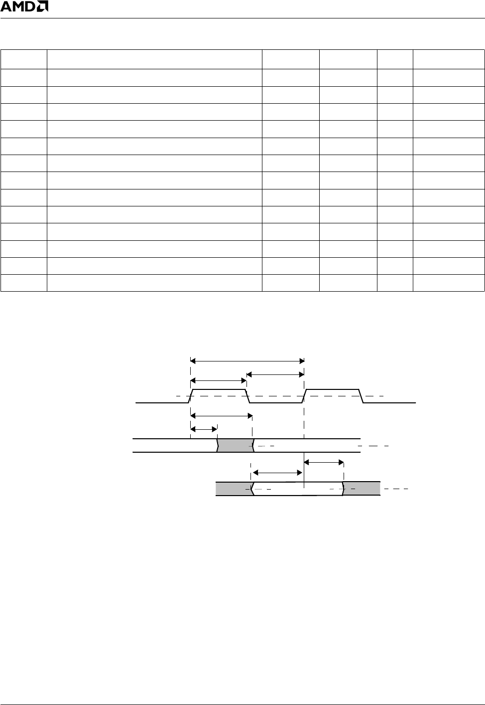
608 AMD Geode™ LX Processors Data Book
Electrical Specifications
33234H
Figure 7-3. Drive Level and Measurement Points for Switching Characteristics
Table 7-8. System Interface Signals
Symbol Parameter Min Max Unit Comments
tCK SYSREF Cycle time 15.0 INF ns 66 MHz
tCH SYSREF High time 6.0 ns 40% tCK
tCL SYSREF Low time 6.0 ns 40% tCK
tSU1 RESET# Setup time to SYSREF 3 ns Note 1
tH1 RESET# Hold time from SYSREF 1 ns Note 1
tSU2 CIS Setup time to SYSREF 3.0 ns
tH2 CIS Hold time from SYSREF 0 ns
tVAL1 IRQ13 Valid Delay time from SYSREF 2.0 6.0 ns
tVAL2 SUSPA# Valid Delay time from SYSREF 2.0 6.0 ns
tON VIO and VMEM power on after VCORE 0100msNote 2
tMVON MVREF power on after VMEM 0100ms
tRSTX Reset Active time after SYSREF clock stable 100 us For PLL lock
tZOutput drive delay after RESET# released 20 ns
Note 1. RESET# is asynchronous. The setup/hold times stated are for testing purposes that require sequential repeatabil-
ity.
Note 2. For proper powerup of DRGB and flat panel controls, VIO must power up after VCORE. Otherwise, VCORE can be
last.
SYSREF
Outputs
Inputs
50%
Valid Input
Valid Output n+1
Valid Output n
50%
50%
tVAL1,2Min
tVAL1,2 Max
tSU1,2
tH1,2
tCK
tCH tCL
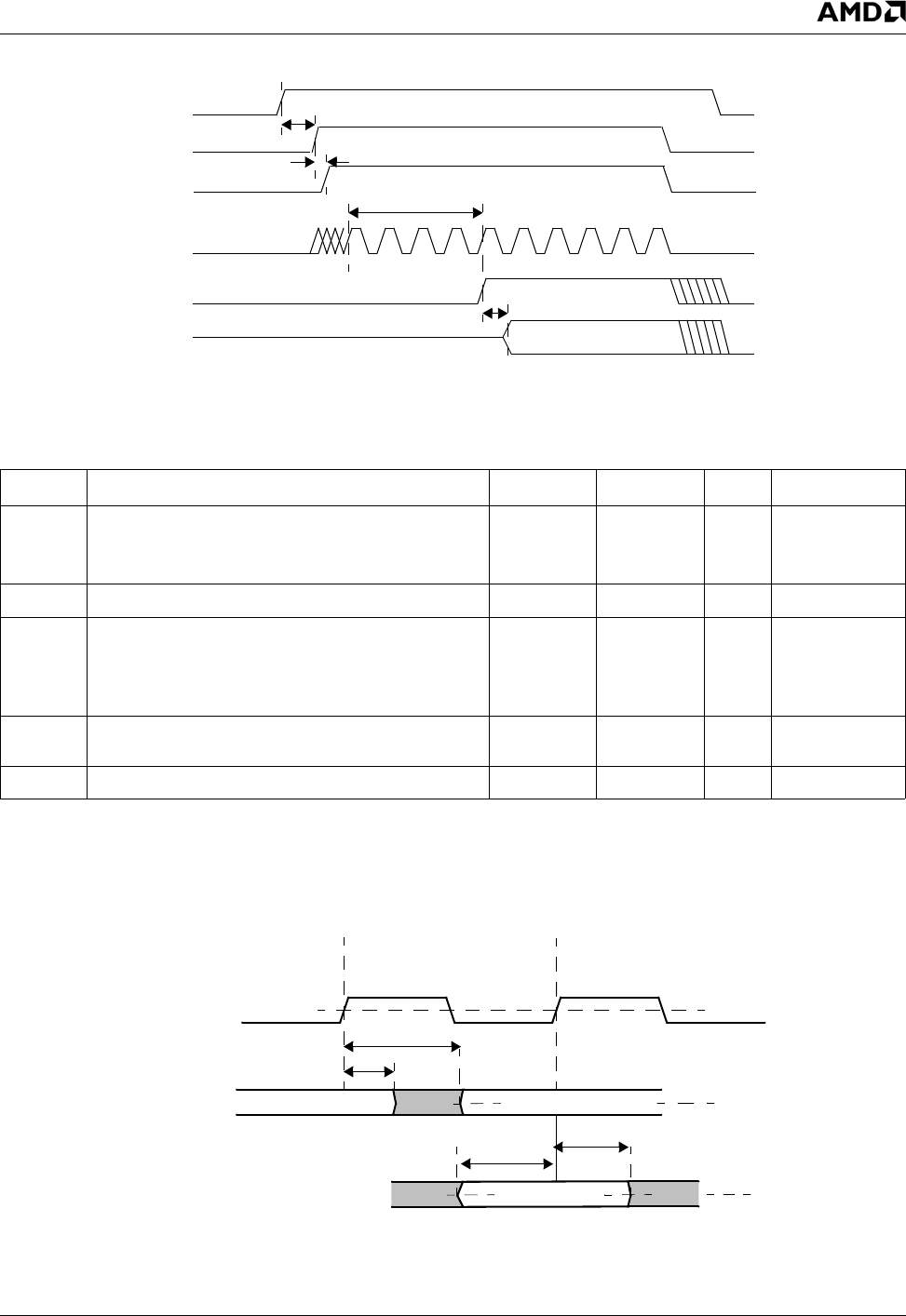
AMD Geode™ LX Processors Data Book 609
Electrical Specifications 33234H
Figure 7-4. Power Up Sequencing
Figure 7-5. Drive Level and Measurement Points for Switching Characteristics
VCORE
VIO,VMEM
RESET#
SYSREF
SYSREF
cycle time not
to scale with
other delays
in this figure.
Outputs
tON
tRSTX
tZ
MVREF
tMVON
Table 7-9. PCI Interface Signals
Symbol Parameter Min Max Unit Comments
tSU1 Input Setup time to SYSREF
(AD[31:0], DEVSEL#,GNT[2:0]#, IRDY#, PAR,
STOP#, TRDY#)
3.0 ns
tSU2 REQ[2:0]# Input Setup time to SYSREF 4.5 ns
tHInput Hold time from SYSREF for all PCI inputs
(STOP#)
(DEVSEL#, FRAME#, GNT[2:0#, IRDY#, PAR,
TRDY#, REQ[2:0]#, STOP#)
0nsNote 1
tVAL1 Bused signals Valid Delay time from SYSREF
(AD[31:0])
2.0 6.0 ns Note 2
tVAL2 GNT[2:0]# Valid Delay time from SYSREF 2.0 5.5 ns Note 2
Note 1. The GNT[2:0]#, IRQ13, SUSPA#, PW0, and PW1 signals are only inputs during RESET# active. They must be sta-
ble between five and two PCI clocks before RESET# inactive.
Note 2. Output delay includes tristate-to-valid transitions and valid-to-tristate timing.
SYSREF
Outputs
Inputs
50%
Valid Input
Valid Output n+1
Valid Output n
50%
50%
tVAL1,2Min
tVAL1,2 Max
tSU1,2
tH1,2
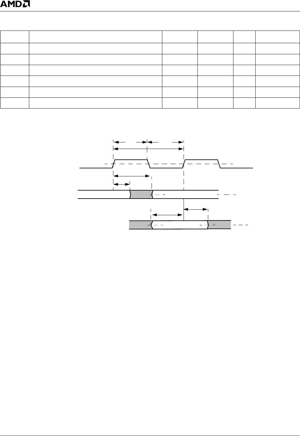
610 AMD Geode™ LX Processors Data Book
Electrical Specifications
33234H
Figure 7-6. Drive Level and Measurement Points for Switching Characteristics
Table 7-10. VIP Interface Signals
Symbol Parameter Min Max Unit Comments
tCK VIPCLK period 12.5 ns 80 MHz
tCH VIPCLK High time 3.0 ns 45% tCK
tCL VIPCLK Low time 3.0 ns 45% tCK
tVAL VIP_SYNC Output Valid Delay time from VIPCLK 1.0 4.0 ns
tSU1 VID[7:0] Input Setup time to VIPCLK 2.0 ns
tH1 VID[7:0] Input Hold time from VIPCLK. 0.2 ns
VIPCLK
Outputs
Inputs
50%
Valid Input
Valid Output n+1
Valid Output n
50%
50%
tVAL1,2Min
tVAL1,2 Max
tSU1,2
tH1,2
tCK
tCH tCL
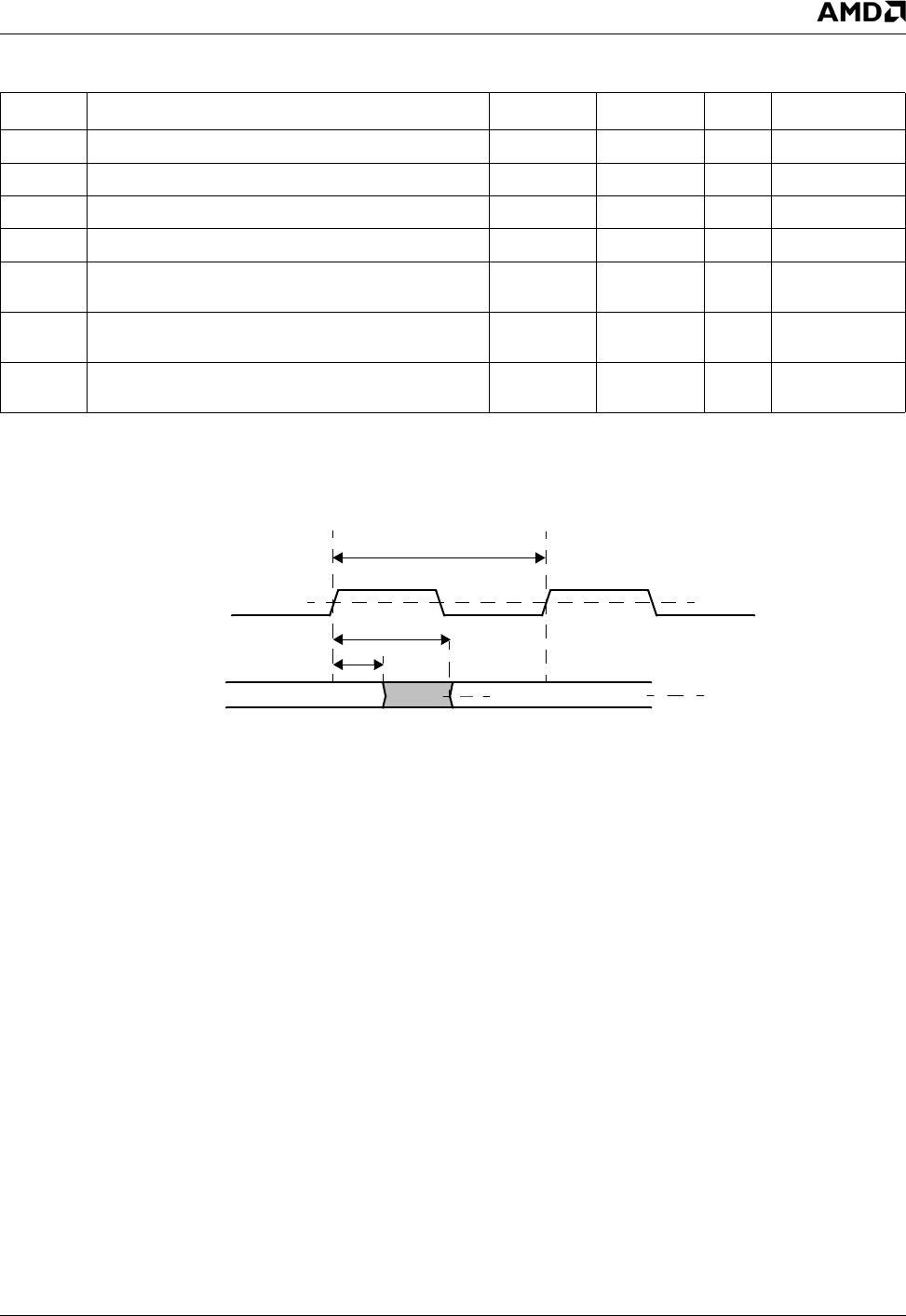
AMD Geode™ LX Processors Data Book 611
Electrical Specifications 33234H
Figure 7-7. Drive Level and Measurement Points for Switching Characteristics
Table 7-11. Flat Panel Interface Signals
Symbol Parameter Min Max Unit Comments
tCK DOTCLK period 6.0 ns 166 MHz
tCH DOTCLK High time 2.7 ns 45% tCK
tCL DOTCLK Low time 2.7 ns 45% tCK
DOTCLK long term output jitter 15% tCK Note 1
tVAL1 DRGB[31:0] Output Valid Delay time from rising
edge of DOTCLK
0.5 3.0 ns
tVAL2 DISPEN, LDEMOD Output Valid Delay time from
rising edge of DOTCLK
0.5 3.0 ns
tVAL3 HSYNC, VSYNC Output Valid Delay time from ris-
ing edge of DOTCLK
0.5 3.0 ns
Note 1. Measured as per VESA requirements. The jitter is observed at its worst case point on a scan line after HSYNC
triggers up to and including the next HSYNC trigger.
DOTCLK
Outputs
50%
Valid Output n+1
Valid Output n50%
tVAL1,2,3 Min
tVAL1,2,3 Max
tCK
612 AMD Geode™ LX Processors Data Book
Electrical Specifications
33234H
Table 7-12. CRT Interface Signals
Symbol Parameter Min Max Unit Comments
tCK DOTCLK Period 2.8 ns 350 MHz
tCH DOTCLK High time 1.2 ns 45% tCK
tCL DOTCLK Low time 1.2 ns 45% tCK
DOTCLK long term output jitter 15% tCK Note 1
tSKEW Skew between RED, GREEN, BLUE Output Valid 0 0.6 ns Between any
two signals
Note 2
Note 1. Measured as per VESA requirements. The jitter is observed at its worst case point on a scan line after HSYNC
triggers up to and including the next HSYNC trigger.
Note 2. HSYNC and VSYNC for CRT timing are generated from the same on-chip clock that is used to generate the RED,
GREEN, and BLUE signals.
Table 7-13. CRT Display Recommended Operating Conditions
Symbol Parameter Min Typ Max Units Comments
VDAC Power Supply connected to
DAVDD
3.14 3.3 3.46 V
RLOutput Load RED, GREEN and
BLUE
37.5
Note 1
ΩOne each signal.
IOUT Output Current RED, GREEN
and BLUE
21 mA One each signal.
RSET Value of the full-scale adjust
resistor connected to DRSET
1.2K ΩThis resistor should have a
1% tolerance.
VEXTREF External voltage reference con-
nected to the DVREF pin
1.235 V
Note 1. There is a 75 Ω resistor on the motherboard and a 75 Ω resistor in the CRT monitor to create the effective 37.5 Ω
typical resistance.

AMD Geode™ LX Processors Data Book 613
Electrical Specifications 33234H
Table 7-14. CRT Display Analog (DAC) Characteristics
Symbol Parameter Min Typ Max Units Comments (Note 1)
VOS Output Voltage Saturation Limit 1.25 V
IOVAR Output Current 18.67 mA Achieves 700 mV on 37.5Ω
INL Integral Linearity Error +/-1 LSB
DNL Differential Linearity Error +/-1 LSB
tFS Full Scale Settling Time 2.5 ns Note 2
-- DAC-to-DAC matching 1 4 %
-- Analog Power Supply Rejection 45 dB @ 1 KHz
tRISE Output Rise Time 0.5 1.25 ns Note 3 and Note 4
tFALL Output Fall Time 0.5 1.25 ns Note 3 and Note 4
Note 1. All tests, unless otherwise specified, are at VIO = 3.14V to 3.46V, TC = 0°C to 85°C (or -40°C to 85°C if
LX 800@0.9w industrial temperature range part), and CL = 50 pF.
Note 2. Full-scale transition time is measured from 50% of full-scale transition until output remaining within 1LSB of target.
Note 3. Timing measurements are made with a 75 Ω doubly-terminated load, with VEXTREF = 1.235V and RSET = 1.2 KΩ.
Note 4. 10% to 90% of full-scale transition.

614 AMD Geode™ LX Processors Data Book
Electrical Specifications
33234H
Table 7-15. Memory (DDR) Interface Signals
Symbol
(Note 1) Parameter Min Max Unit Comments
tCK SDCLK[5:0]P, SDCLK[5:0]N period 5.0 ns Note 2
tCH SDCLK[5:0]P, SDCLK[5:0]N High time 2.4 ns 48% tCK
tCL SDCLK[5:0]P, SDCLK[5:0]N Low time 2.4 ns 48% tCK
tSKEW1 SDCLK[n]P to SDCLK[n]N skew (n=0..5) 0.1 ns Guaranteed by
design
tDEL1 SDCLK[5:1]P, SDCLK[5:0]N edge delay from
SDCLK[0]P
-0.2 0.2 ns Note 2, Note 3
DQS[7:0] Input and output period 5.0 ns Same as tCK
tDQSCK DQS[7:0] Input delay relative to SDCLK[5:0] -0.5 tCK-2 ns Note 4
tDEL2 DQS[7:0] output edge delay from SDCLK[5:0] -0.5 0.5 ns Note 3
tRPRE DQS input preamble before first DQS rising edge 0.25*tCK ns Note 3
tRPST DQS input postamble after last DQS rising edge 0.25*tCK Note 3
tWPRE DQS output write preamble valid time before
SDCLK[5:0] rising edge
0.5*tCK-0.4 0.5*tCK+1 ns
tWPST DQS output write postamble after last DQS falling
edge
0.75*tCK
-0.4
0.75*tCK+1 ns
tDQSQs DQ[63:0] Input setup time from DQS -0.25*tCK
+0.5
ns Note 3,Note 5
tDQSQh DQ[63:0] Input hold time from DQS 0.25*tCK
+0.5
ns Note 3, Note 5
tVAL1 DQ[63:0], DQM[7:0] Output Data Valid Delay time
from DQS rising OR falling edge
0.25*tCK
-0.4
0.25*tCK
+0.4
ns Note 3,
tVAL2 MA[12:0], BA[1:0], CAS[1:0]#, RAS[1:0]#,
CKE[1:0], CS[3:0]#, WE[1:0] Output Valid Delay
time from SDCLK[5:0]
1.1 3.0 ns Note 3, Note 4
Note 1. Refer to Figure 7-8 "DDR Write Timing Measurement Points" on page 615 and Figure 7-9 "DDR Read Timing Mea-
surement Points" on page 616.
Note 2. The SDCLKP and SDCLKN clocks are inversions of each other (differential clocking).
Note 3. These parameters guarantee device timing, but they may be tested to a looser value to allow for tester uncertain-
ties. Devices that meet the loosened tester values meet specs when correlated with lab measurements.
Note 4. tVAL2 and tDQSCK timings are achieved for different DIMM loadings by proper initial settings of the
GLCP_DELAY_CONTROLS MSR. Typical tester results with clock and address loaded equally and no pro-
grammed delay for address are 0 ns for tVAL2.
Note 5. The DQ timing relative to DQS are on a per-byte basis only. DQ[7:0] and DQM[0] should be measured against
DQS[0], DQ[15:8] and DQM[1] should be measured against DQS[1], etc.
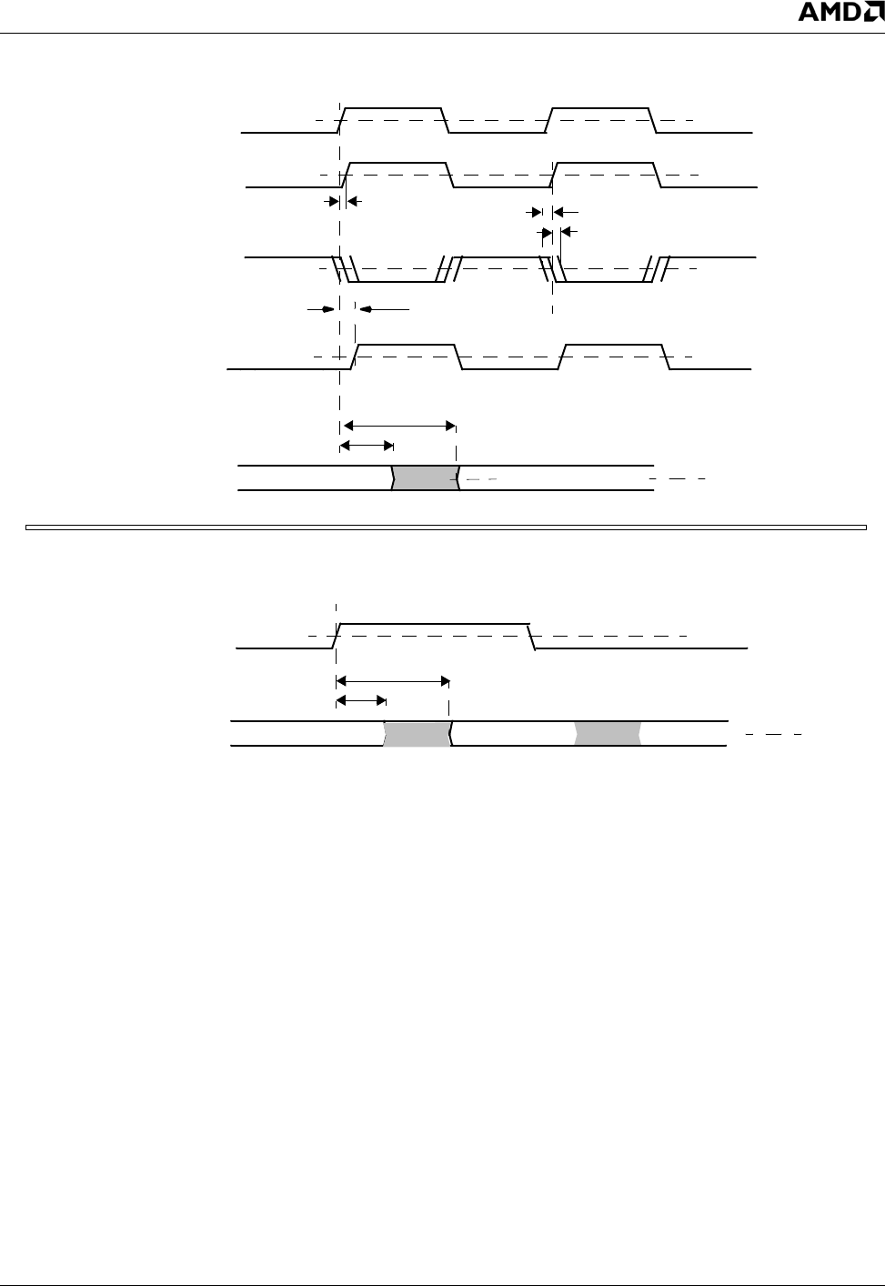
AMD Geode™ LX Processors Data Book 615
Electrical Specifications 33234H
Figure 7-8. DDR Write Timing Measurement Points
SDCLK[5:1]P
Non-DQ Outputs
VREF
Valid Output n+1
Valid Output nVREF
tVAL2Min
tVAL2Max
VIHD
VILD
VREF
DQS Outputs
DQS
VIHD
VILD
VREF
DQ Outputs DQ n+1
DQ nVREF
DQ n+2
SDCLK[5:0]N VREF
tSKEW1
tSKEW1
tDEL2
SDCLK0P VREF
tDEL1
tVAL1Max
tVAL1Min
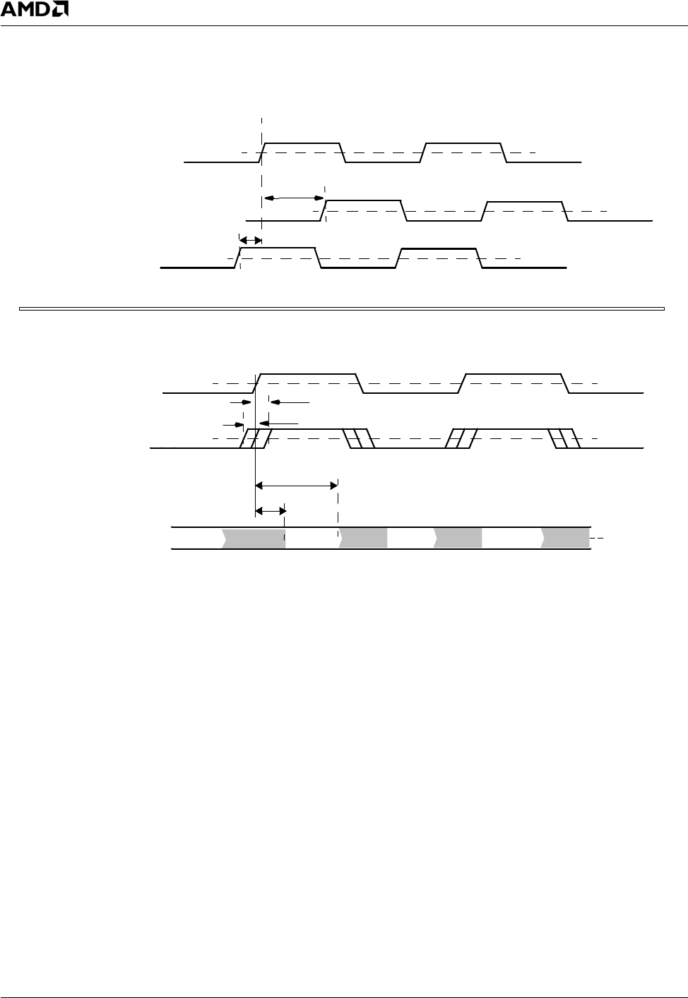
616 AMD Geode™ LX Processors Data Book
Electrical Specifications
33234H
Figure 7-9. DDR Read Timing Measurement Points
DQ Inputs
VREF
DQtVREF
DQt-1
SDCLK0
DQS ‘Late’ Input VREF
other DQS Input VREF
DQt+1 DQt+2
DQS[n] Input VREF
tSKEW2
tDQSCKMax
DQS ‘Early’ Input VREF
tDQSCKMin
tSKEW2
-tDQSQs
tDQSQh
associated with DQS[n]
AMD Geode™ LX Processors Data Book 617
Electrical Specifications 33234H
Table 7-16. JTAG Interface Signals
Symbol Parameter Min Max Unit Comments
TCLK period 15 ns Note 1
TCLK High time 4 ns 40% period
TCLK Low time 4 ns 40% period
TDI, TMS Setup time to TCLK rising edge 1.5 ns
TMS Hold time from TCLK rising edge 3.0 ns
TDI Hold time from TCLK rising edge - Boundary
scan
3.0 ns
TDI Hold time from TCLK rising edge - Functional 2*TGLBus ns Hold for 2
GLBus clocks
TDO Output Valid Delay time from TCLK falling
edge when running boundary scan test
3.0 70.0 ns
TDO Output Valid Delay time from TCLK falling
edge in normal functional mode
3.0 10.0 ns
All chip I/O Setup time to TCLK rise - boundary
scan
1.0 ns
All chip I/O Hold time from TCLK rise - boundary
scan
3ns
All chip I/O Output Valid Delay time from TCLK
falling edge - boundary scan test
2.0 70.0 ns
Note 1. TCLK limited during functional mode to 100 MHz or 1/4 of the memory data frequency.

618 AMD Geode™ LX Processors Data Book
Electrical Specifications
33234H
AMD Geode™ LX Processors Data Book 619
8
Instruction Set 33234H
8.0Instruction Set
This chapter provides the general instruction set format and detailed information on the AMD Geode™ LX processor’s
instructions/instruction encodings. The instruction set is divided into three categories:
•CPUID Instruction Set - listed in Section 8.2 on page 627.
•Processor Core Instruction Set - listed in Section 8.3 on page 633.
•MMX™, FPU, and AMD 3DNow!™ Instruction Sets (including extensions) - listed in Section 8.4 on page 658.
In the above listed sections are tables that provide information on the instruction encoding, and the instruction clock counts
for each instruction. The clock count values for these tables are based on the following assumptions:
1) All clock counts refer to the internal processor core clock frequency.
2) The instruction has been prefetched, decoded, and is ready for execution.
3) Any needed memory operands are in the cache in the last accessed way (i.e., Way0, Way1, Way2, or Way3). Add two
clocks if not in last accessed way.
4) No exceptions are detected during instruction execution.
5) If an effective address is calculated, it does not use two general register components. One register, scaling, and a dis-
placement value can be used within the clock count shown. However, if the effective address calculation uses a base
register, an index register, and a displacement value, a cycle must be added to the count.
6) All clock counts assume an 8-byte span of 32-bit memory/IO operands.
7) If instructions access a 32-bit operand not within an 8-byte block, add one clock for read or write and add two clocks for
read and write.
8) For non-cached memory accesses, add several clocks. Cache miss accesses are approximately an additional 25
clocks, the exact number depends upon the cycle/operation running.
9) Locked cycles are not cacheable. Therefore, using the LOCK prefix with an instruction adds additional clocks as spec-
ified in item 8 above.
8.1 General Instruction Set Format
Depending on the instruction, the AMD Geode LX processor core instructions follow the general instruction format shown in
Table 8-1. These instructions vary in length and can start at any byte address. An instruction consists of one or more bytes
that can include prefix bytes, at least one opcode byte, a mod r/m byte, an s-i-b byte, address displacement, and immedi-
ate data. An instruction can be as short as one byte and as long as 15 bytes. If there are more than 15 bytes in the instruc-
tion, a general protection fault (error code 0) is generated.
The fields in the general instruction format at the byte level are summarized in Table 8-2 on page 620 and detailed in the fol-
lowing subsections.
Table 8-1. General Instruction Set Format
Prefix (Optional) Opcode
Register and Address Mode Specifier
Address
Displacement
Immediate
Data
mod r/m Byte s-i-b Byte
mod reg r/m ss index base
0 or More Bytes 1 or 2 Bytes 7:6 5:3 2:0 7:6 5:3 2:0 0, 8, 16, or 32 Bits 0, 8, 16, or 32 Bits
620 AMD Geode™ LX Processors Data Book
Instruction Set
33234H
8.1.1 Prefix (Optional)
Prefix bytes can be placed in front of any instruction to modify the operation of that instruction. When more than one prefix
is used, the order is not important. There are five types of prefixes that can be used:
1) Segment Override explicitly specifies which segment register the instruction will use for effective address calculation.
2) Address Size switches between 16-bit and 32-bit addressing by selecting the non-default address size.
3) Operand Size switches between 16-bit and 32-bit operand size by selecting the non-default operand size.
4) Repeat is used with a string instruction to cause the instruction to be repeated for each element of the string.
Table 8-3 lists the encoding for different types of prefix bytes.
Table 8-2. Instruction Fields
Field Name Description
Prefix (optional) Prefix Field(s): One or more optional fields that are used to specify segment register over-
ride, address and operand size, repeat elements in string instruction, and LOCK# assertion.
Opcode Opcode Field: Identifies instruction operation.
mod Address Mode Specifier: Used with the r/m field to select addressing mode.
reg General Register Specifier: Uses reg, sreg3, or sreg2 encoding depending on opcode field.
r/m Address Mode Specifier: Used with mod field to select addressing mode.
ss Scale factor: Determines scaled-index address mode.
index Index: Determines general register to be used as index register.
base Base: Determines general register to be used as base register.
Address Displacement Displacement: Determines address displacement.
Immediate Data Immediate Data: Immediate data operand used by instruction.
Table 8-3. Instruction Prefix Summary
Prefix Encoding Description
ES: 26h Override segment default, use ES for memory operand.
CS: 2Eh Override segment default, use CS for memory operand.
SS: 36h Override segment default, use SS for memory operand.
DS: 3Eh Override segment default, use DS for memory operand.
FS: 64h Override segment default, use FS for memory operand.
GS: 65h Override segment default, use GS for memory operand.
Operand Size 66h Make operand size attribute the inverse of the default.
Address Size 67h Make address size attribute the inverse of the default.
LOCK F0h Assert LOCK# internal hardware signal.
REPNE F2h Repeat the following string instruction.
REP/REPE F3h Repeat the following string instruction.
AMD Geode™ LX Processors Data Book 621
Instruction Set 33234H
8.1.2 Opcode
The opcode field specifies the operation to be performed by the instruction. The opcode field is either one or two bytes in
length and may be further defined by additional bits in the mod r/m byte. Some operations have more than one opcode,
each specifying a different form of the operation. Certain opcodes name instruction groups. For example, opcode 80h
names a group of operations that have an immediate operand and a register or memory operand. The reg field may appear
in the second opcode byte or in the mod r/m byte.
The opcode may contain w, d, s, and eee opcode fields, for example, as shown in Table 8-26 on page 634.
8.1.2.1 w Field (Operand Size)
When used, the 1-bit w field selects the operand size during 16-bit and 32-bit data operations. See Table 8-4.
8.1.2.2 d Field (Operand Direction)
When used, the 1-bit d field determines which operand is taken as the source operand and which operand is taken as the
destination. See Table 8-5.
8.1.2.3 s Field (Immediate Data Field Size)
When used, the 1-bit s field determines the size of the immediate data field. If the s bit is set, the immediate field of the
opcode is 8 bits wide and is sign-extended to match the operand size of the opcode. See Table 8-6.
Table 8-4. w Field Encoding
w Field
Operand Size
16-Bit Data Operations 32-Bit Data Operations
0 8 bits 8 bits
1 16 bits 32 bits
Table 8-5. d Field Encoding
d Field Direction of Operation Source Operand Destination Operand
0 Register-to-Register
or
Register-to-Memory
reg mod r/m
or
mod ss-index-base
1 Register-to-Register
or
Memory-to-Register
mod r/m
or
mod ss-index-base
reg
Table 8-6. s Field Encoding
s Field
Immediate Field Size
8-Bit Operand Size 16-Bit Operand Size 32-Bit Operand Size
0 (or not present) 8 bits 16 bits 32 bits
1 8 bits 8 bits (sign-extended) 8 bits (sign-extended)

622 AMD Geode™ LX Processors Data Book
Instruction Set
33234H
8.1.2.4 eee Field (MOV-Instruction Register Selection)
The eee field (bits [5:3]) is used to select the control, debug, and test registers in the MOV instructions. The type of register
and base registers selected by the eee field are listed in Table 8-7. The values shown in Table 8-7 are the only valid encod-
ings for the eee bits.
8.1.3 mod and r/m Byte (Memory Addressing)
The mod and r/m fields within the mod r/m byte select the type of memory addressing to be used. Some instructions use a
fixed addressing mode (e.g., PUSH or POP) and therefore, these fields are not present. Table 8-8 lists the addressing method
when 16-bit addressing is used and a mod r/m byte is present. Some mod r/m field encodings are dependent on the w field
and are shown in Table 8-9.
Table 8-7. eee Field Encoding
eee Field Register Type Base Register
000 Control Register CR0
010 Control Register CR2
011 Control Register CR3
100 Control Register CR4
000 Debug Register DR0
001 Debug Register DR1
010 Debug Register DR2
011 Debug Register DR3
110 Debug Register DR6
111 Debug Register DR7
000 Test Register TR0
001 Test Register TR1
010 Test Register TR2
011 Test Register TR3
100 Test Register TR4
101 Test Register TR5
110 Test Register TR6
111 Test Register TR7
Table 8-8. mod r/m Field Encoding
mod Field r/m Field
16-Bit Address Mode with
mod r/m Byte (Note 1)
32-Bit Address Mode with mod r/m Byte and
No s-i-b Byte Present
(Note 1)
00 000 DS:[BX+SI] DS:[EAX]
00 001 DS:[BX+DI] DS:[ECX]
00 010 SS:[BP+SI] DS:[EDX]
00 011 SS:[BP+DI] DS:[EBX]
00 100 DS:[SI] s-i-b is present (See Table 8-15 on page 626)
00 101 DS:[DI] DS:[d32]
00 110 DS:[d16] DS:[ESI]
00 111 DS:[BX] DS:[EDI]
AMD Geode™ LX Processors Data Book 623
Instruction Set 33234H
01 000 DS:[BX+SI+d8] DS:[EAX+d8]
01 001 DS:[BX+DI+d8] DS:[ECX+d8]
01 010 SS:[BP+SI+d8] DS:[EDX+d8]
01 011 SS:[BP+DI+d8] DS:[EBX+d8]
01 100 DS:[SI+d8] s-i-b is present (See Table 8-15 on page 626)
01 101 DS:[DI+d8] SS:[EBP+d8]
01 110 SS:[BP+d8] DS:[ESI+d8]
01 111 DS:[BX+d8] DS:[EDI+d8]
10 000 DS:[BX+SI+d16] DS:[EAX+d32]
10 001 DS:[BX+DI+d16] DS:[ECX+d32]
10 010 SS:[BP+SI+d16] DS:[EDX+d32]
10 011 SS:[BP+DI+d16] DS:[EBX+d32]
10 100 DS:[SI+d16] s-i-b is present (See Table 8-15 on page 626)
10 101 DS:[DI+d16] SS:[EBP+d32]
10 110 SS:[BP+d16] DS:[ESI+d32]
10 111 DS:[BX+d16] DS:[EDI+d32]
11 xxx See Table 8-9. See Table 8-9
Note 1. d8 refers to 8-bit displacement, d16 refers to 16-bit displacement, and d32 refers to a 32-bit displacement.
Table 8-9. General Registers Selected by mod r/m Fields and w Field
mod r/m
16-Bit Operation 32-Bit Operation
w = 0 w = 1 w = 0 w = 1
11 000 AL AX AL EAX
11 001 CL CX CL ECX
11 010 DL DX DL EDX
11 011 BL BX BL EBX
11 100 AH SP AH ESP
11 101 CH BP CH EBP
11 110 DH SI DH ESI
11 111 BH DI BH EDI
Table 8-8. mod r/m Field Encoding (Continued)
mod Field r/m Field
16-Bit Address Mode with
mod r/m Byte (Note 1)
32-Bit Address Mode with mod r/m Byte and
No s-i-b Byte Present
(Note 1)
624 AMD Geode™ LX Processors Data Book
Instruction Set
33234H
8.1.4 reg Field
The reg field (Table 8-10) determines which general registers are to be used. The selected register is dependent on
whether a 16-bit or 32-bit operation is current and on the status of the w bit.
8.1.4.1 sreg2 Field (ES, CS, SS, DS Register Selection)
The sreg2 field (Table 8-11) is a 2-bit field that allows one of the four 286-type segment registers to be specified.
8.1.4.2 sreg3 Field (FS and GS Segment Register Selection)
The sreg3 field (Table 8-12) is 3-bit field that is similar to the sreg2 field, but allows use of the FS and GS segment registers.
Table 8-10. reg Field
reg
16-Bit Operation 32-Bit Operation
w = 0 w = 1 w = 0 w = 1
000 AL AX AL EAX
001 CL CX CL ECX
010 DL DX DL EDX
011 BL BX BL EBX
100 AH SP AH ESP
101 CH BP CH EBP
110 DH SI DH ESI
111 BH DI BH EDI
Table 8-11. sreg2 Field Encoding
sreg2 Field Segment Register Selected
00 ES
01 CS
10 SS
11 DS
Table 8-12. sreg3 Field (FS and GS Segment Register Selection)
sreg3 Field Segment Register Selected
000 ES
001 CS
010 SS
011 DS
100 FS
101 GS
110 Undefined
111 Undefined
AMD Geode™ LX Processors Data Book 625
Instruction Set 33234H
8.1.5 s-i-b Byte (Scale, Indexing, Base)
The s-i-b fields provide scale factor, indexing, and a base field for address selection. The ss, index, and base fields are
described next.
8.1.5.1 ss Field (Scale Selection)
The ss field (Table 8-13) specifies the scale factor used in the offset mechanism for address calculation. The scale factor
multiplies the index value to provide one of the components used to calculate the offset address.
8.1.5.2 Index Field (Index Selection)
The index field (Table 8-14) specifies the index register used by the offset mechanism for offset address calculation. When
no index register is used (index field = 100), the ss value must be 00 or the effective address is undefined.
Table 8-13. ss Field Encoding
ss Field Scale Factor
00 x1
01 x2
01 x4
11 x8
Table 8-14. index Field Encoding
Index Field Index Register
000 EAX
001 ECX
010 EDX
011 EBX
100 none
101 EBP
110 ESI
111 EDI

626 AMD Geode™ LX Processors Data Book
Instruction Set
33234H
8.1.5.3 Base Field (s-i-b Present)
In Table 8-8 on page 622, the note “s-i-b is present” for certain entries forces the use of the mod and base field as listed in
Table 8-15. The first two digits in the first column of Table 8-15 identify the mod bits in the mod r/m byte. The last three digits
in the second column of this table identify the base fields in the s-i-b byte.
Table 8-15. mod base Field Encoding
mod Field within mod/rm
Byte (bits[7:6])
base Field within s-i-b
Byte (bits [2:0])
32-Bit Address Mode with mod r/m and s-i-b
Bytes Present
00 000 DS:[EAX+(scaled index)]
00 001 DS:[ECX+(scaled index)]
00 010 DS:[EDX+(scaled index)]
00 011 DS:[EBX+(scaled index)]
00 100 SS:[ESP+(scaled index)]
00 101 DS:[d32+(scaled index)]
00 110 DS:[ESI+(scaled index)]
00 111 DS:[EDI+(scaled index)]
01 000 DS:[EAX+(scaled index)+d8]
01 001 DS:[ECX+(scaled index)+d8]
01 010 DS:[EDX+(scaled index)+d8]
01 011 DS:[EBX+(scaled index)+d8]
01 100 SS:[ESP+(scaled index)+d8]
01 101 SS:[EBP+(scaled index)+d8]
01 110 DS:[ESI+(scaled index)+d8]
01 111 DS:[EDI+(scaled index)+d8]
10 000 DS:[EAX+(scaled index)+d32]
10 001 DS:[ECX+(scaled index)+d32]
10 010 DS:[EDX+(scaled index)+d32]
10 011 DS:[EBX+(scaled index)+d32]
10 100 SS:[ESP+(scaled index)+d32]
10 101 SS:[EBP+(scaled index)+d32]
10 110 DS:[ESI+(scaled index)+d32]
10 111 DS:[EDI+(scaled index)+d32]
AMD Geode™ LX Processors Data Book 627
Instruction Set 33234H
8.2 CPUID Instruction Set
The CPUID instruction (opcode 0FA2) allows software to make processor inquiries as to the vendor, family, model, step-
ping, features, and specific cache organization information. The presence of support for the CPUID instruction is indicated
by the ability to change the value of the ID flag, bit 21, in the EFLAGS register.
The CPUID level allows the CPUID instruction to return different information in EAX, EBX, ECX, and EDX registers. The
level is determined by the initialized value of the EAX register prior to execution of the CPUID instruction.
8.2.1 Standard CPUID Levels
The standard CPUID levels are part of the standard x86 instruction set.
8.2.1.1 CPUID Instruction with EAX = 00000000h
Standard function 00000000h (EAX = 00000000h) of the CPUID instruction returns the maximum standard CPUID levels,
as well as the processor vendor string.
After the instruction is executed, the EAX register contains the maximum standard CPUID levels supported. The maximum
standard CPUID level is the highest acceptable value for the EAX register input. This does not include the extended CPUID
levels.
The EBX through EDX registers contain the vendor string of the processor as shown in Table 8-16.
8.2.1.2 CPUID Instruction with EAX = 00000001h
Standard function 00000001h (EAX = 00000001h) of the CPUID instruction returns the processor type, family, model, step-
ping information in the EAX register, and the supported standard feature flags in the EDX register. The EBX and ECX reg-
isters are reserved. Table 8-17 provides a register map.
In the EDX register, each flag refers to a specific feature. Some of these features have protection control in CR4. Before
using any of these features, the software should check the corresponding feature flag. Attempting to execute an unavailable
feature can cause exceptions and unexpected behavior. For example, software must check EDX[4] before attempting to use
the Time Stamp Counter instruction.
Table 8-18 on page 628 shows the EAX and EDX bit field formats when EAX = 00000001h and indicates if a feature is not
supported.
Table 8-16. CPUID Instruction with EAX = 00000000h
Register
(Note 1)
Note 1. The “Register” column is intentionally out of order.
Returned Contents Description Comment
EAX 00000001h Maximum Standard Level
EBX 68747541h {htuA} Vendor ID String 1
EDX 69746E65h {itne} Vendor ID String 2
ECX 444D4163h {DMAc} Vendor ID String 3
Table 8-17. CPUID Instruction with EAX = 00000001h
Register
Returned
Contents Description Comment
EAX 000005Axh Type/Family/Model/Step
EBX 00000400h Reserved
ECX 00000000h Reserved
EDX 0088A93Dh Standard Feature Flags

628 AMD Geode™ LX Processors Data Book
Instruction Set
33234H
Table 8-18. CPUID Instruction Codes with EAX = 00000000
Register
Reset
Value Description Comment
EAX[31:28] 0x0 Reserved
EAX[27:20] 0x00 Extended Family
EAX[19:16] 0x00 Extended Model
EAX[15:12] 0x0 Reserved
EAX[11:8] 0x5 Processor/Instruction Family
EAX[7:4] 0xA Processor Model
EAX[3:0] 0x2 Processor Stepping May change with CPU revision
EBX[31:24] 0x00 Initial local APCI physical ID
EBX[23:16] 0x00 Reserved
EBX[15:08] 0x04 CLFLUSH cache line size in QWORD - 8 byte
increments
EBX[7:0] 0x00 8-bit brand ID
EDX[31:27] 0000 Reserved
EDX[26] 0 XMM2. Streaming SIMD Extensions Not supported
EDX[25] 0 XMM. Streaming SIMD Extensions Not supported
EDX[24] 0 FXSR. Fast FP Save and Restore Not supported
EDX[23] 1 MMX™. MMX Instruction Set and Architecture
EDX[22:20] 000 Reserved
EDX[19} 1 CLFSH. CLFLUSH feature is supported
EDX[18] 0 PN. 96-Bit Serial Number Feature Not supported
EDX[17] 0 PSE36. 36-Bit Page Size Extensions Not supported
EDX[16] 0 PAT. Page Attribute Table Not supported
EDX[15] 1 CMOV. Conditional Move Instruction
EDX[14] 0 MCA. Machine Check Architecture Not supported
EDX[13] 1 PGE. Page Global Enable Feature
EDX[12] 0 MTRR. Memory Type Range Registers Not supported
EDX[11] 1 SEP. Sysenter/Sysexit Instruction
EDX[10] 0 Reserved
EDX[9] 0 APIC. Advanced Programmable Interrupt Not supported
EDX[8] 1 CX8. Compare Exchange (CMPXCHG8B)
Instruction
EDX[7] 0 MCE. Machine Check Exception Not supported
EDX[6] 0 PAE. Page Address Extension Not supported
EDX[5] 1 MSR. Model Specific Registers via
RDMSR/WRMSR Instructions
EDX[4] 1 TSC. Time Stamp Counter and RDTSC
Instruction
EDX[3] 1 PSE. 4 MB Page Size Extension
EDX[2] 1 DE. Debugging Extension
AMD Geode™ LX Processors Data Book 629
Instruction Set 33234H
8.2.2 Extended CPUID Levels
Testing for extended CPUID instruction support can be accomplished by executing a CPUID instruction with the EAX regis-
ter initialized to 80000000h. If a value greater than or equal to 80000000h is returned to the EAX register by the CPUID
instruction, the processor supports extended CPUID levels.
8.2.2.1 CPUID Instruction with EAX = 80000000h
Extended function 80000000h (EAX = 80000000h) of the CPUID instruction returns the maximum extended CPUID sup-
ported levels as well as the processor vendor string.
After the instruction is executed, the EAX register contains the maximum extended CPUID levels supported. The maximum
extended standard CPUID level is the highest acceptable value for the EAX register input.
The EBX through EDX registers contain the vendor string of the processor as shown in Table 8-19.
8.2.2.2 CPUID Instruction with EAX = 80000001h
Extended function 80000001h (EAX = 80000001h) of the CPUID instruction returns the processor type, family, model, step-
ping information in the EAX register, and the supported extended feature flags in the EDX register. The EBX and ECX reg-
isters are reserved. Table 8-20 provides a register map.
In the EDX register, each flag refers to a specific extended feature. Some of these features have protection control in CR4.
Before using any of these extended features, the software should check the corresponding flag. Attempting to execute an
unavailable extended feature can cause exceptions and unexpected behavior.
Table 8-21 on page 630 shows the EAX and EDX bit field formats when EAX = 80000001h and indicates if a feature is not
supported.
EDX[1] 0 VME. Virtual Interrupt Flag in VM86 Not supported
EDX[0] 1 FPU. Floating Point Unit On Chip
Table 8-19. CPUID Instruction with EAX = 80000000h
Register
(Note 1)
Note 1. The “Register” column is intentionally out of order.
Returned Contents Description Comment
EAX 80000006h Maximum Extended CPUID Level
EBX 68747541h {htuA} Vendor ID String 1
EDX 69746E65h {itne} Vendor ID String 2
ECX 444D4163h {DMAc} Vendor ID String 3
Table 8-20. CPUID Instruction with EAX = 80000001h
Register
Returned
Contents Description Comment
EAX 000005Axh Type/Family/Model/Step
EBX 00000000h Reserved
ECX 00000000h Reserved
EDX C0C0A13Dh Feature Flags
Table 8-18. CPUID Instruction Codes with EAX = 00000000
Register
Reset
Value Description Comment

630 AMD Geode™ LX Processors Data Book
Instruction Set
33234H
Table 8-21. CPUID Instruction Codes with EAX = 80000001h
Register Reset Value Description Comment
EAX[31:28] 0x0 Reserved
EAX[27:20] 0x00 Extended Family
EAX[19:16] 0x00 Extended Model
EAX[15:12] 0x0 Reserved
EAX[11:8] 0x5 Processor/Instruction Family
EAX[7:4] 0x5 Processor Model
EAX[3:0] 0x2 Processor Stepping May change with CPU revision
EDX[31] 1 3DN. 3DNow! Instruction Set
EDX[30] 1 3DE. 3DNow! Instruction Set Extension
EDX[29] 0 LM. Long mode Not supported
EDX[28:25] 0000 Reserved Not supported
EDX[24] 0 FXSR/FXRSTOR. Fast FP Save and Restore Not supported
EDX[23] 1 MMX. MMX Instruction Set and Architecture
EDX[22] 1 AMMX. AMD MMX Instruction Extension
EDX[21] 0 Reserved
EDX[20] 0 NX. No-execute page protection Not supported
EDX[19] 0 MP. Multiprocessing capability Not supported
EDX[18] 0 Reserved
EDX[17] 0 PSE36. 36-Bit Page Size Extensions Not supported
EDX[16] 0 PAT. Page Attribute Table Not supported
EDX[15] 1 CMOV. Conditional Move Instruction (CMOV,
FCMOV, FCOMI)
EDX[14] 0 MCA. Machine Check Architecture Not supported
EDX[13] 1 PGE. Page Global Enable Feature
EDX[12] 0 MTRR. Memory Type Range Registers Not supported
EDX[11] 0 ASEP. Syscall/Sysret Instruction
EDX[10] 0 Reserved
EDX[9] 0 APIC. Advanced Programmable Interrupt Control-
ler
Not supported
EDX[8] 1 CX8. Compare Exchange (CMPXCHG8B)
Instruction
EDX[7] 0 MCE. Machine Check Exception Not supported
EDX[6] 0 PAE. Page Address Extension Not supported
EDX[5] 1 MSR. Model Specific Registers via
RDMSR/WRMSR Instructions
EDX[4] 1 TSC. Time Stamp Counter and RDTSC
Instruction
EDX[3] 1 PSE. 4MB Page Size Extension
EDX[2] 1 DE. Debugging Extension
EDX[1] 0 VME. Virtual Interrupt Flag in VM86 Not supported
EDX[0] 1 FPU. Floating Point Unit On Chip
AMD Geode™ LX Processors Data Book 631
Instruction Set 33234H
8.2.2.3 CPUID Instruction with EAX = 80000002h, 80000003h, or 80000004h
Extended functions 80000002h through 80000004h (EAX = 80000002h, EAX = 80000003h, and EAX = 80000004h) of the
CPUID instruction returns an ASCII string containing the CPU marketing name, as shown in Table 8-22. These functions
eliminate the need to look up the processor name in a lookup table. Software can simply call these functions to obtain the
name of the processor. The string may be 48 ASCII characters long, and is returned in little endian format. If the name is
shorter than 48 characters long, the remaining bytes are filled with ASCII NUL characters (00h).
Table 8-22. CPUID Instruction with EAX = 80000002h, 80000003h, or 80000004h
Register Returned Contents Description Comment
EAX = 80000002h
EAX 646F6547h {doeG} CPU Marketing Name 1a
EBX 4D542865h {MT)e} CPU Marketing Name 1b
ECX 6E492029h {nI (} CPU Marketing Name 2a
EDX 72676574h {rget} CPU Marketing Name 2b
EAX = 80000003h
EAX 64657461h {deta} CPU Marketing Name 3a
EBX 6F725020h {orP} CPU Marketing Name 3b
ECX 73736563h {ssec} CPU Marketing Name 4a
EDX 6220726Fh {b ro} CPU Marketing Name 4b
EAX = 80000004h
EAX 4D412079h {MA y} CPU Marketing Name 5a
EBX 43502044h {CP D} CPU Marketing Name 5b
ECX 00000053h {S} CPU Marketing Name 6a
EDX 00000000h CPU Marketing Name 6b
632 AMD Geode™ LX Processors Data Book
Instruction Set
33234H
8.2.2.4 CPUID Instruction with EAX = 80000005h
Extended function 80000005h (EAX = 80000005h) of the CPUID instruction returns information on the internal L1 cache
and TLB structures. They are used for reporting purposes only. See Table 8-23 for returned contents.
8.2.2.5 CPUID Instruction with EAX = 80000006h
Extended function 80000006h (EAX = 80000006h) of the CPUID instruction returns information on the internal L2 cache
and TLB structures. See Table 8-24 on page 632 for returned contents.
.
Table 8-23. CPUID Instruction with EAX = 80000005h
Register
Returned
Contents Description Comment
EAX 00000000h 4 MB L1 TLB Information Indicates no 4 MB L1 TLB.
EBX FF10FF10h 4 KB L1 TLB Information Decodes to eight fully associative code TLB and eight
fully associative data TLB entries.
ECX 40100120h L1 Data Cache Information Indicates 16 KB four-way associative with 32-byte lines
for data cache. These encodings follow the AMD report-
ing method.
EDX 40100120h L1 Code Cache Information Indicates 16 KB four-way associative with 32-byte lines
for code cache. These encodings follow the AMD report-
ing method.
Table 8-24. CPUID Instruction with EAX = 80000006h
Register
Returned
Contents Description Comment
EAX 0000F004h L2 TLB Information Two-way associative 64 entry code and data combined
TLB.
EBX 00002040h L2 TLB Information
ECX 00804120h L2 Code Cache Information Indicates no L2 cache.
EDX 00000000h L2 Data Cache Information
AMD Geode™ LX Processors Data Book 633
Instruction Set 33234H
8.3 Processor Core Instruction Set
The instruction set for the AMD Geode LX processor core is summarized in Table 8-26. The table uses several symbols and
abbreviations that are described next and listed in Table 8-25.
8.3.1 Opcodes
Opcodes are given as hex values except when they appear within brackets as binary values.
8.3.2 Clock Counts
The clock counts listed in the instruction set summary table (Table 8-26) are grouped by operating mode (real and pro-
tected) and whether there is a register/cache hit or a cache miss. In some cases, more than one clock count is shown in a
column for a given instruction, or a variable is used in the clock count.
8.3.3 Flags
There are nine flags that are affected by the execution of instructions. The flag names have been abbreviated and various con-
ventions used to indicate what effect the instruction has on the particular flag.
Table 8-25. Processor Core Instruction Set Table Legend
Symbol or
Abbreviation Description
Opcode
# Immediate 8-bit data.
## Immediate 16-bit data.
### Full immediate 32-bit data (8, 16, or 32 bits).
+ 8-bit signed displacement.
+++ Full signed displacement (16 or 32 bits).
Clock Count
/ Register operand/memory operand.
n Number of times operation is repeated.
L Level of the stack frame.
| Conditional jump taken | Conditional jump not taken. (e.g., “4|1” = four clocks if jump taken, one clock if jump not taken).
\CPL ≤ IOPL \ CPL > IOPL (where CPL = Current Privilege Level, IOPL = I/O Privilege Level).
Flags
OF Overflow Flag.
DF Direction Flag.
IF Interrupt Enable Flag.
TF Trap Flag.
SF Sign Flag.
ZF Zero Flag.
AF Auxiliary Flag.
PF Parity Flag.
CF Carry Flag.
x Flag is modified by the instruction.
- Flag is not changed by the instruction.
0 Flag is reset to “0.”
1 Flag is set to “1.”
u Flag is undefined following execution of the instruction.

634 AMD Geode™ LX Processors Data Book
Instruction Set
33234H
Table 8-26. Processor Core Instruction Set
Instruction Opcode
Clock Count
(Reg/Cache Hit) Flags Notes
Real
Mode
Prot’d
Mode ODI T S Z AP C
FFFFFFFFF
Real
Mode
Prot’d
Mode
AAA ASCII Adjust AL after Addition 37 3 3 u -- -uuxux
AAD ASCII Adjust AX before Divide D5 0A 4 4 u- - - xxuxu
AAM ASCII Adjust AX after Multiply D4 0A u- - - xxuxu
Divide by non-zero 15 15
Divide by zero 18 18
AAS ASCII Adjust AL after Subtract 3F 3 3 u- - - uuxux
ADC Add with Carry x- - - xxxxx b h
Register to Register 1 [00dw] [11 reg r/m] 1 1
Register to Memory 1 [000w] [mod reg r/m] 1 1
Memory to Register 1 [001w] [mod reg r/m] 1 1
Immediate to Register/Memory 8 [00sw] [mod 010 r/m]### 1 1
Immediate to Accumulator 1 [010w] ### 1 1
ADD Integer Add x- - - xxxxx b h
Register to Register 0 [00dw] [11 reg r/m] 1 1
Register to Memory 0 [000w] [mod reg r/m] 1 1
Memory to Register 0 [001w] [mod reg r/m] 1 1
Immediate to Register/Memory 8 [00sw] [mod 000 r/m]### 1 1
Immediate to Accumulator 0 [010w] ### 1 1
AND Boolean AND 0- - - xxux0 b h
Register to Register 2 [00dw] [11 reg r/m] 1 1
Register to Memory 2 [000w] [mod reg r/m] 1 1
Memory to Register 2 [001w] [mod reg r/m] 1 1
Immediate to Register/Memory 8 [00sw] [mod 100 r/m]### 1 1
Immediate to Accumulator 2 [010w] ### 1 1
ARPL Adjust Requested Privilege Level 63 [mod reg r/m] -----x--- ah
To Memory DST[1:0] < SRC[1:0] 6
To Memory DST[1:0] >= SRC[1:0] 4
To Register DST[1:0] < SRC[1:0] 4
To Register DST[1:0] >= SRC[1:0] 4
BOUND Check Array Boundaries 62 [mod reg r/m] --------- b, e g,h,j,k,
r
If Below Range (Interrupt #5) 8+INT 8+INT
If Above Range (Interrupt #5) 8+INT 8+INT
If In Range 66
BSF Scan Bit Forward 0F BC [mod reg r/m] 2 2 -----x--- b h
Register, Register/Memory
BSR Scan Bit Reverse 0F BD [mod reg r/m] 2 2 -----x--- b h
Register, Register/Memory
BSWAP Byte Swap 0F C[1 reg] 1 1 ---------
BT Test Bit --------x b h
Register/Memory, Immediate 0F BA [mod 100 r/m]# 1 1
Register, Register 0F A3 [mod reg r/m] 1 1
Memory, Register 0F A3 [mod reg r/m] 7 7
BTC Test Bit and Complement --------x b h
Register/Memory, Immediate 0F BA [mod 111 r/m]# 2 2
Register, Register 0F BB [mod reg r/m] 2 2
Memory, Register 0F BB [mod reg r/m] 8 8
BTR Test Bit and Reset --------x b h
Register/Memory, Immediate 0F BA [mod 110 r/m]# 2 2
Register, register 0F B3 [mod reg r/m] 2 2
Memory, Register 0F B3 [mod reg r/m 8 8

AMD Geode™ LX Processors Data Book 635
Instruction Set 33234H
BTS Test Bit and Set --------x b h
Register/Memory, Immediate 0F BA [mod 101 r/m] # 2 2
Register, Register 0F AB [mod reg r/m] 2 2
Memory, Register 0F AB [mod reg r/m] 8 8
CALL Subroutine Call --------- b h,j,k,r
Direct Within Segment E8 +++ 2 2
Register/Memory Indirect Within Segment FF [mod 010 r/m] 2/4 2/4
Direct Intersegment
-Call Gate
-Task Switch
711
24+
123+
Indirect Intersegment
-Call Gate
-Task Switch
FF [mod 011 r/m] 9 13
25+
124+
CBW Convert Byte to Word 98 1 1 ---------
CDQ Convert Doubleword to Quadword 99 1 1 ---------
CLC Clear Carry Flag F8 1 1 --------0
CLD Clear Direction Flag FC 2 2 -0-------
CLFLUSH 7+ 7+
CLI Clear Interrupt Flag FA 1 1 --0------ m
CLTS Clear Task Switched Flag 0F 06 3 3 --------- c l
CMC Complement the Carry Flag F5 2 2 --------x
CMOVA/CMOVNBE Move if Above/Not Below or Equal 1 1 --------- r
Register, Register/Memory 0F 47 [mod reg r/m]
CMOVBE/CMOVNA Move if Below or Equal/Not Above 1 1 --------- r
Register, Register/Memory 0F 46 [mod reg r/m]
CMOVAE/CMOVNB/CMOVNC Move if Above or Equal/Not Below/Not Carry 1 1 --------- r
Register, Register/Memory 0F 43 [mod reg r/m]
CMOVB/CMOVC/CMOVNAE Move if Below/Carry/Not Above or Equal 1 1 --------- r
Register, Register/Memory 0F 42 [mod reg r/m]
CMOVE/CMOVZ Move if Equal/Zero 1 1 --------- r
Register, Register/Memory 0F 44 [mod reg r/m]
CMOVNE/CMOVNZ Move if Not Equal/Not Zero 1 1 --------- r
Register, Register/Memory 0F 45 [mod reg r/m]
CMOVG/CMOVNLE Move if Greater/Not Less or Equal 1 1 --------- r
Register, Register/Memory 0F 4F [mod reg r/m]
CMOVLE/CMOVNG Move if Less or Equal/Not Greater 1 1 --------- r
Register, Register/Memory 0F 4E [mod reg r/m]
CMOVL/CMOVNGE Move if Less/Not Greater or Equal 1 1 --------- r
Register, Register/Memory 0F 4C [mod reg r/m]
CMOVGE/CMOVNL Move if Greater or Equal/Not Less 1 1 --------- r
Register, Register/Memory 0F 4D [mod reg r/m]
CMOVO Move if Overflow 1 1 --------- r
Register, Register/Memory 0F 40 [mod reg r/m]
CMOVNO Move if No Overflow 0F 41 [mod reg r/m] 1 1 --------- r
Register, Register/Memory
CMOVP/CMOVPE Move if Parity/Parity Even 0F 4A [mod reg r/m] 1 1 --------- r
Register, Register/Memory
CMOVNP/CMOVPO Move if Not Parity/Parity Odd 0F 4B [mod reg r/m] 1 1 --------- r
Register, Register/Memory
CMOVS Move if Sign 0F 48 [mod reg r/m] 1 1 --------- r
Register, Register/Memory
Table 8-26. Processor Core Instruction Set (Continued)
Instruction Opcode
Clock Count
(Reg/Cache Hit) Flags Notes
Real
Mode
Prot’d
Mode ODI T S Z AP C
FFFFFFFFF
Real
Mode
Prot’d
Mode

636 AMD Geode™ LX Processors Data Book
Instruction Set
33234H
CMOVNS Move if Not Sign 0F 49 [mod reg r/m] 1 1 --------- r
Register, Register/Memory
CMP Compare Integers x- - - xxxxx b h
Register to Register 3 [10dw] [11 reg r/m] 1 1
Register to Memory 3 [101w] [mod reg r/m] 1 1
Memory to Register 3 [100w] [mod reg r/m] 1 1
Immediate to Register/Memory 8 [00sw] [mod 111 r/m] ### 1 1
Immediate to Accumulator 3 [110w] ### 1 1
CMPS Compare String A [011w] 6 6 x- - - xxxxx b h
CMPXCHG Compare and Exchange x- - - xxxxx
Register1, Register2 0F B [000w] [11 reg2 reg1] 4 4
Memory, Register 0F B [000w] [mod reg r/m] 4-5 4-5
CMPXCHG8B Compare and Exchange 8 Bytes 0F C7 [mod 001 r/m] ---------
If {EDX,EAX} == DST 10 10
If {EDX,EAX} != DST 12 12
CPUID CPU Identification 0F A2 ---------
If EAX <= 1 13 13
If 1 < EAX < 231 10 10
If 231 <= EAX <= (231+6) 14 14
If EAX > (231+6) 11 11
CWD Convert Word to Doubleword 99 1 1 ---------
CWDE Convert Word to Doubleword Extended 98 3 3 ---------
DAA Decimal Adjust AL after Addition 27 2 2 ----xxxxx
DAS Decimal Adjust AL after Subtraction 2F 2 2 ----xxxxx
DEC Decrement by 1 x- - - xxxx- b h
Register/Memory Byte FE [mod 001 r/m] 1 1
Register/Memory Word/DWord FF [mod 001 r/m] 1 1
Register (short form) 4 [1 reg] 1 1
DIV Unsigned Divide ----xxuu-
Accumulator by Register/Memory
Divisor: Byte
Word
Doubleword
F [011w] [mod 110 r/m]
15
23
7-39
15
23
7-39
b,e e,h
DMINT Enter Debug Management Mode 0F 39 48-50 50-52 000000000 s, u s, u
ENTER Enter New Stack Frame C8 ##,# ---------
Level = 0 77 bh
Level = 1 13 13
Level (L) > 1 15+21 15+21
HLT Halt F4 13+ 13+ --------- l
ICEBP Call Debug Exception Handler F1 29+ 29+ --x0----- u u
IDIV Integer (Signed) Divide F [011w] [mod 111 r/m] ----xxuu- b,e e,h
Accumulator by Register/Memory
Divisor: Byte
Word
Doubleword
16
24
40
16
24
7-40
Table 8-26. Processor Core Instruction Set (Continued)
Instruction Opcode
Clock Count
(Reg/Cache Hit) Flags Notes
Real
Mode
Prot’d
Mode ODI T S Z AP C
FFFFFFFFF
Real
Mode
Prot’d
Mode
AMD Geode™ LX Processors Data Book 637
Instruction Set 33234H
IMUL Integer (Signed) Multiply x---xxuux b h
Accumulator by Register/Memory
Multiplier: Byte
Word
Doubleword
F [011w] [mod 101 r/m]
3
4
4
3
4
4
Register with Register/Memory
Multiplier: Word
Doubleword
0F AF [mod reg r/m]
4
4
4
4
Register/Memory with Immediate to Register2
Multiplier: Byte
Word
Doubleword
6 [10s1] [mod reg r/m] ###
4-6
4-7
4-7
4-6
4-7
4-7
IN Input from I/O Port --------- m
Fixed Port E [010w] # 7 7/21
Variable Port E [110w] 7 7/21
INC Increment by 1 x- - - xxxx- b h
Register/Memory F [111w] [mod 000 r/m] 1 1
Register (short form) 4 [0 reg] 1 1
INS Input String from I/O Port 6 [110w] 10 10/24 --------- b h,m
INT i Software Interrupt CD # 23 37-245 --x0----- b,e g,j,k,r
INT 3 Breakpoint Software Interrupt CC 21-22 37-245 b,c g,i,k,r
INTO Overflow Software Interrupt
If OF==0
If OF==1 (INT 4)
CE
4
7
4
7
b,c g,i,k,r
INVD Invalidate Cache 0F 08 9+ 9+ --------- t t
INVLPG Invalidate TLB Entry 0F 01 [mod 111 r/m] 7+ 7+ ---------
IRET Interrupt Return CF 6-13 13-239 xxxxxxxxx g,h,j,k,
r
JB/JNAE/JC Jump on Below/Not Above or Equal/Carry --------- r
8-bit Displacement 72 + 1 1
Full Displacement 0F 82 +++ 1 1
JBE/JNA Jump on Below or Equal/Not Above -------- r
8-bit Displacement 76 + 1 1
Full Displacement 0F 86 +++ 1 1
JCXZ/JECXZ Jump on CX/ECX Zero E3 + 2 2 --------- r
JE/JZ Jump on Equal/Zero -------- r
8-bit Displacement 74 + 1 1
Full Displacement 0F 84 +++ 1 1
JL/JNGE Jump on Less/Not Greater or Equal -------- r
8-bit Displacement 7C + 1 1
Full Displacement 0F 8C +++ 1 1
JLE/JNG Jump on Less or Equal/Not Greater -------- r
8-bit Displacement 7E + 1 1
Full Displacement 0F 8E +++ 1 1
JMP Unconditional Jump -------- b h,j,k,r
8-bit Displacement EB + 1 1
Full Displacement E9 +++ 1 1
Register/Memory Indirect Within Segment FF [mod 100 r/m] 1/3 1/3
Direct Intersegment EA [unsigned full offset,
selector]
79-254
Indirect Intersegment FF [mod 101 r/m] 9 11-256
JNB/JAE/JNC Jump on Not Below/Above or Equal/Not Carry -------- r
8-bit Displacement 73 + 1 1
Full Displacement 0F 83 +++ 1 1
Table 8-26. Processor Core Instruction Set (Continued)
Instruction Opcode
Clock Count
(Reg/Cache Hit) Flags Notes
Real
Mode
Prot’d
Mode ODI T S Z AP C
FFFFFFFFF
Real
Mode
Prot’d
Mode

638 AMD Geode™ LX Processors Data Book
Instruction Set
33234H
JNBE/JA Jump on Not Below or Equal/Above -------- r
8-bit Displacement 77 + 1 1
Full Displacement 0F 87 +++ 1 1
JNE/JNZ Jump on Not Equal/Not Zero -------- r
8-bit Displacement 75 + 1 1
Full Displacement 0F 85 +++ 1 1
JNL/JGE Jump on Not Less/Greater or Equal -------- r
8-bit Displacement 7D + 1 1
Full Displacement 0F 8D +++ 1 1
JNLE/JG Jump on Not Less or Equal/Greater -------- r
8-bit Displacement 7F + 1 1
Full Displacement 0F 8F +++ 1 1
JNO Jump on Not Overflow -------- r
8-bit Displacement 71 + 1 1
Full Displacement 0F 81 +++ 1 1
JNP/JPO Jump on Not Parity/Parity Odd -------- r
8-bit Displacement 7B + 1 1
Full Displacement 0F 8B +++ 1 1
JNS Jump on Not Sign -------- r
8-bit Displacement 79 + 1 1
Full Displacement 0F 89 +++ 1 1
JO Jump on Overflow -------- r
8-bit Displacement 70 + 1 1
Full Displacement 0F 80 +++ 1 1
JP/JPE Jump on Parity/Parity Even -------- r
8-bit Displacement 7A + 1 1
Full Displacement 0F 8A +++ 1 1
JS Jump on Sign -------- r
8-bit Displacement 78 + 1 1
Full Displacement 0F 88 +++ 1 1
LAHF Load AH with Flags 9F 2 2 ---------
LAR Load Access Rights 0F 02 [mod reg r/m] -----x--- a g,h,j,p
From Register/Memory 9
LDS Load Pointer to DS C5 [mod reg r/m] 4 9/15 --------- b h,i,j
LEA Load Effective Address ---------
No Index Register 8D [mod reg r/m] 1 1
With Index Register 1 1
LEAVE 22
LES Load Pointer to ES C4 [mod reg r/m] 4 9/15 --------- b h,i,j
LFENCE 11
LFS Load Pointer to FS 0F B4 [mod reg r/m] 4 9/15 --------- b h,i,j
LGDT Load GDT Register 0F 01 [mod 010 r/m] 8-9 8-9 --------- b,c h,l
LGS Load Pointer to GS 0F B5 [mod reg r/m] 4 9/15 --------- b h,i,j
LIDT Load IDT Register 0F 01 [mod 011 r/m] 8-9 8-9 --------- b,c h,l
LLDT Load LDT Register 0F 00 [mod 010 r/m] --------- a g,h,j,l
From Register/Memory 8
LMSW Load Machine Status Word ---------
From Register/Memory 0F 01 [mod 110 r/m] 8 8 b,c h,l
LODS Load String A [110 w] 2 2 --------- b h
LOOP Offset Loop/No Loop E2 + 2 2 --------- r
Table 8-26. Processor Core Instruction Set (Continued)
Instruction Opcode
Clock Count
(Reg/Cache Hit) Flags Notes
Real
Mode
Prot’d
Mode ODI T S Z AP C
FFFFFFFFF
Real
Mode
Prot’d
Mode

AMD Geode™ LX Processors Data Book 639
Instruction Set 33234H
LOOPNZ/LOOPNE Offset E0 + 2 2 --------- r
LOOPZ/LOOPE Offset E1 + 2 2 --------- r
LSL Load Segment Limit -----x---
From Register/Memory 0F 03 [mod reg r/m] 9 a g,h,j,p
LSS Load Pointer to SS 0F B2 [mod reg r/m] 4 9/15 --------- a h,i,j
LTR Load Task Register ---------
From Register/Memory 0F 00 [mod 011 r/m] 9 a g,h,j,l
LEAVE Leave Current Stack Frame C9 2 2 --------- b h
MFENCE 1
MOV Move Data --------- b h
Register to Register 8 [10dw] [11 reg r/m] 1 1
Register to Memory 8 [100w] [mod reg r/m] 1 1
Register/Memory to Register 8 [101w] [mod reg r/m] 1 1
Immediate to Register/Memory C [011w] [mod 000 r/m] ### 1 1
Immediate to Register (short form) B [w reg] ### 1 1
Memory to Accumulator (short form) A [000w] +++ 1 1
Accumulator to Memory (short form) A [001w] +++ 1 1
MOV Move to/from Segment Registers --------- i,j
To Stack Segment 7/13
To all other segments:
Register/Memory to Segment Register 8E [mod sreg3 r/m] 1 6/13
Segment Register to Register/Memory 8C [mod sreg3 r/m] 1 6/13
MOV Move to/from Control Registers --------- l
Register to CR 0F 22 [11 eee reg] 9-13 9-13
CR to Register 0F 20 [11 eee reg] 2-5 2-5
MOV Move To/From Debug Registers --------- l
Register to DR 0F 23 [11 eee reg] 10/18 10/18
DR to Register 0F 21 [11 eee reg] 8/18 8/18
MOV Move To/From Test Registers --------- ul,u
Register to TR 0F 26 [11 eee reg] 2 2
TR to Register 0F 24 [11 eee reg] 1 1
MOVS Move String A [010w] 4 4 --------- b h
MOVSX Move with Sign Extension --------- b h
Register from Register/Memory 0F B[111w] [mod reg r/m] 1 1
MOVZX Move with Zero Extension --------- b h
Register from Register/Memory 0F B[011w] [mod reg r/m] 1 1
MUL Unsigned Multiply x---xxuux b h
Accumulator with Register/Memory
Multiplier: Byte
Word
Doubleword
F [011w] [mod 100 r/m]
3
4
7
3
4
7
NEG Negate Integer F [011w] [mod 011 r/m] 1 1 x- - - xxxxx b h
NOP No Operation 90 1 1 ---------
NOT Boolean Complement F [011w] [mod 010 r/m] 1 1 --------- b h
OIO Official Invalid Opcode 0F FF 1 8-125 --x0-----
OR Boolean OR 0- - - xxux0 b h
Register to Register 0 [10dw] [11 reg r/m] 1 1
Register to Memory 0 [100w] [mod reg r/m] 1 1
Memory to Register 0 [101w] [mod reg r/m] 1 1
Immediate to Register/Memory 8 [00sw] [mod 001 r/m] ### 1 1
Immediate to Accumulator 0 [110w] ### 1 1
Table 8-26. Processor Core Instruction Set (Continued)
Instruction Opcode
Clock Count
(Reg/Cache Hit) Flags Notes
Real
Mode
Prot’d
Mode ODI T S Z AP C
FFFFFFFFF
Real
Mode
Prot’d
Mode

640 AMD Geode™ LX Processors Data Book
Instruction Set
33234H
OUT Output to Port --------- m
Fixed Port E [011w] # 8 8/23
Variable Port E [111w] 8 8/23
OUTS Output String 6 [111w] 12 12/26 --------- b h,m
PAUSE 7
POP Pop Value off Stack --------- b h,i,j
Register 8F [mod 000 r/m] 1 1
Memory 8F [mod 000 r/m] 3 3
Register (short form) 5 [1 reg] 1 1
DS 1F 1 6/13
ES 07 1 6/13
SS 17 1 7/13
FS 0F A1 1 6/13
GS 0F 9A 1 6/13
POPA Pop All General Registers 61 8 8 --------- b h
POPF Pop Stack into FLAGS 9D 2 2 xxxxxxxxx b h,n
PREFIX BYTES --------- m
Assert Hardware LOCK Prefix F0
Address Size Prefix 67
Operand Size Prefix 66
Segment Override Prefix
-CS
-DS
-ES
-FS
-GS
-SS
2E
3E
26
64
65
36
PUSH Push Value onto Stack --------- b h
Register/Memory FF [mod 110 r/m] 1/2 1/2
Register (short form) 5 [0 reg] 1 1
CS 0E 1 1
SS 16 1 1
DS 1E 1 1
ES 06 1 1
FS 0F A0 1 1
GS 0F A8 1 1
Immediate 6 [10s0] ### 1 1
PUSHA Push All General Registers 60 8 8 --------- b h
PUSHF Push FLAGS Register 9C 2 2 --------- b h
RCL Rotate Through Carry Left
Register/Memory by 1 D [000w] [mod 010 r/m] 2 2 x -------x b h
Register/Memory by CL D [001w] [mod 010 r/m] 4-6 4-6 u -------x
Register/Memory by Immediate C [000w] [mod 010 r/m] # 4-6 4-6 u -------x
RCR Rotate Through Carry Right
Register/Memory by 1
Register/Memory by CL
Register/Memory by Immediate
bh
D [000w] [mod 011 r/m] 3-5 3-4 x -------x
D [001w] [mod 011 r/m] 4-7 4-7 u -------x
C [000w] [mod 011 r/m] # 4-7 4-7 u -------x
RDM Leave Debug Management Mode 0F 3A 36+ 36+ xxxxxxxxx s, u s, u
RDMSR Read Tmodel Specific Register (Note 1)0F 32 5 5 ---------
RDPMC (Note 1) 77
RDTSC Read Time Stamp Counter (Note 1) 0F 31 5 5 ---------
Table 8-26. Processor Core Instruction Set (Continued)
Instruction Opcode
Clock Count
(Reg/Cache Hit) Flags Notes
Real
Mode
Prot’d
Mode ODI T S Z AP C
FFFFFFFFF
Real
Mode
Prot’d
Mode
AMD Geode™ LX Processors Data Book 641
Instruction Set 33234H
REP CMPS
CX==0 66
CX==1 13 13
CX>1 10+3C 10+3C
REP INS Input String F3 6[110w] --------- b h,m
CX==0 99/24
CX==1
CX>1 15+6C 15+6C/
30+6C
REP LODS Load String F3 A[110w] --------- b h
CX==0 55
CX==1 10 10
CX>1 8+2C 8+2C
REP MOVS Move String F3 A[010w] --------- b h
CX==0 55
CX==1 13 13
CX>1 11+2C 11+2C
REP OUTS Output String F3 6[111w] 16+10
C
16+10
C\
31+10
C
--------- b h,m
REP STOS Store String F3 A[101w] 8+c 8+c --------- b h
REPE CMPS Compare String
Find non-match F3 A[011w] 11+4n 11+4n x - - - xxxxx b h
REPE SCAS Scan String
Find non-AL/AX/EAX F3 A[111w] 7+2n 7+2n x - - - xxxxx b h
REPNE CMPS Compare String
Find match F2 A[011w] 10+4n 10+4n x- - - xxxxx b h
REPNE SCAS Scan String
Find AL/AX/EAX F2 A[111w] 7+3n 7+3n x- - - xxxxx b h
RET Return from Subroutine ---------
Within Segment C3 3 3 b g,h,j,k,
r
Within Segment Adding Immediate to SP C2 ## 3 3
Intersegment CB 6 10-48
Intersegment Adding Immediate to SP CA ## 7 10-48
Protected Mode: Different Privilege Level
-Intersegment
-Intersegment Adding Immediate to SP
35
35
ROL Rotate Left
Register/Memory by 1 D[000w] [mod 000 r/m] 2 2 x-------x b h
Register/Memory by CL D[001w] [mod 000 r/m] 2 2 u-------x
Register/Memory by Immediate C[000w] [mod 000 r/m] # 2 2 u-------x
ROR Rotate Right
Register/Memory by 1 D[000w] [mod 001 r/m] 2 2 x-------x b h
Register/Memory by CL D[001w] [mod 001 r/m] 2 2 u-------x
Register/Memory by Immediate C[000w] [mod 001 r/m] # 2 2 u-------x
RSDC Restore Segment Register and Descriptor 0F 79 [mod sreg3 r/m] 9 9 --------- s,u s,u
RSLDT Restore LDTR and Descriptor 0F 7B [mod 000 r/m] 9 9 --------- s,u s,u
RSTS Restore TSR and Descriptor 0F 7D [mod 000 r/m] 10 10 --------- s,u s,u
RSM Resume from SMM Mode 0F AA 35 35 xxxxxxxxx s,u s,u
SAHF Store AH in FLAGS 9E 1 1 ----xxxxx
Table 8-26. Processor Core Instruction Set (Continued)
Instruction Opcode
Clock Count
(Reg/Cache Hit) Flags Notes
Real
Mode
Prot’d
Mode ODI T S Z AP C
FFFFFFFFF
Real
Mode
Prot’d
Mode

642 AMD Geode™ LX Processors Data Book
Instruction Set
33234H
SAL Shift Left Arithmetic bh
Register/Memory by 1 D[000w] [mod 100 r/m] 1 1 x - - - x x u x x
Register/Memory by CL D[001w] [mod 100 r/m] 1 1 u - - - x x u x x
Register/Memory by Immediate C[000w] [mod 100 r/m] # 1 1 u - - - x x u x x
SAR Shift Right Arithmetic bh
Register/Memory by 1 D[000w] [mod 111 r/m] 2 2 x - - - x x u x x
Register/Memory by CL D[001w] [mod 111 r/m] 2 2 u - - - x x u x x
Register/Memory by Immediate C[000w] [mod 111 r/m] # 2 2 u - - - x x u x x
SBB Integer Subtract with Borrow bh
Register to Register 1[10dw] [11 reg r/m] 1 1 x- - - xxxx x
Register to Memory 1[100w] [mod reg r/m] 1 1
Memory to Register 1[101w] [mod reg r/m] 1 1
Immediate to Register/Memory 8[00sw] [mod 011 r/m] ### 1 1
Immediate to Accumulator (short form) 1[110w] ### 1 1
SCAS Scan String A [111w] 2 2 x- - - xxxx x b h
SETALC Set AL to CF D6 2 2 u u
SETB/SETNAE/SETC Set Byte on Below/Not Above or Equal/Carry --------- h
To Register/Memory 0F 92 [mod 000 r/m] 1 1
SETBE/SETNA Set Byte on Below or Equal/Not Above --------- h
To Register/Memory 0F 96 [mod 000 r/m] 1 1
SETE/SETZ Set Byte on Equal/Zero --------- h
To Register/Memory 0F 94 [mod 000 r/m] 1 1
SETL/SETNGE Set Byte on Less/Not Greater or Equal --------- h
To Register/Memory 0F 9C [mod 000 r/m] 1 1
SETLE/SETNG Set Byte on Less or Equal/Not Greater --------- h
To Register/Memory 0F 9E [mod 000 r/m] 1 1
SETNB/SETAE/SETNC Set Byte on Not Below/Above or Equal/Not Carry --------- h
To Register/Memory 0F 93 [mod 000 r/m] 1 1
SETNBE/SETA Set Byte on Not Below or Equal/Above --------- h
To Register/Memory 0F 97 [mod 000 r/m] 1 1
SETNE/SETNZ Set Byte on Not Equal/Not Zero --------- h
To Register/Memory 0F 95 [mod 000 r/m] 1 1
SETNL/SETGE Set Byte on Not Less/Greater or Equal --------- h
To Register/Memory 0F 9D [mod 000 r/m] 1 1
SETNLE/SETG Set Byte on Not Less or Equal/Greater --------- h
To Register/Memory 0F 9F [mod 000 r/m] 1 1
SETNO Set Byte on Not Overflow --------- h
To Register/Memory 0F 91 [mod 000 r/m] 1 1
SETNP/SETPO Set Byte on Not Parity/Parity Odd --------- h
To Register/Memory 0F 9B [mod 000 r/m] 1 1
SETNS Set Byte on Not Sign --------- h
To Register/Memory 0F 99 [mod 000 r/m] 1 1
SETO Set Byte on Overflow --------- h
To Register/Memory 0F 90 [mod 000 r/m] 1 1
SETP/SETPE Set Byte on Parity/Parity Even --------- h
To Register/Memory 0F 9A [mod 000 r/m] 1 1
SETS Set Byte on Sign h
To Register/Memory 0F 98 [mod 000 r/m] 1 1 ---------
Table 8-26. Processor Core Instruction Set (Continued)
Instruction Opcode
Clock Count
(Reg/Cache Hit) Flags Notes
Real
Mode
Prot’d
Mode ODI T S Z AP C
FFFFFFFFF
Real
Mode
Prot’d
Mode
AMD Geode™ LX Processors Data Book 643
Instruction Set 33234H
SFENCE 11
SGDT Store GDT Register b,c h
To Register/Memory 0F 01 [mod 000 r/m] 6 6 ---------
SIDT Store IDT Register b,c h
To Register/Memory 0F 01 [mod 001 r/m] 6 6 ---------
SLDT Store LDT Register ah
To Register/Memory 0F 00 [mod 000 r/m] 1 ---------
STR Store Task Register ah
To Register/Memory 0F 00 [mod 001 r/m] 3 ---------
SMSW Store Machine Status Word 0F 01 [mod 100 r/m] 2 2 --------- b,c h
STOS Store String A [101w] 2 2 --------- b h
SHL Shift Left Logical bh
Register/Memory by 1 D [000w] [mod 100 r/m] 1 1 x - - - xxuxx
Register/Memory by CL D [001w] [mod 100 r/m] 2 2 u - - - xxuxx
Register/Memory by Immediate C [000w] [mod 100 r/m] # 1 1 u - - - xxuxx
SHLD Shift Left Double u- - - xxuxx b h
Register/Memory by Immediate 0F A4 [mod reg r/m] # 2 1
Register/Memory by CL 0F A5 [mod reg r/m] 2 1
SHR Shift Right Logical bh
Register/Memory by 1 D [000w] [mod 101 r/m] 2 1 x - - - xxuxx
Register/Memory by CL D [001w] [mod 101 r/m] 2 1 u - - - xxuxx
Register/Memory by Immediate C [000w] [mod 101 r/m] # 2 1 u - - - xxuxx
SHRD Shift Right Double u- - - xxuxx b h
Register/Memory by Immediate 0F AC [mod reg r/m] # 2 1
Register/Memory by CL 0F AD [mod reg r/m] 2 1
SMINT Software SMM Entry 0F 38 56-58 56-58 000000000 s,u s,u
STC Set Carry Flag F9 1 1 --------1
STD Set Direction Flag FD 2 2 -1-------
STI Set Interrupt Flag FB 1 1 --1------ m
SUB Integer Subtract x -- - xxxxx b h
Register to Register 2 [10dw] [11 reg r/m] 1 1
Register to Memory 2 [100w] [mod reg r/m] 1 1
Memory to Register 2 [101w] [mod reg r/m] 1 1
Immediate to Register/Memory 8 [00sw] [mod 101 r/m] ### 1 1
Immediate to Accumulator (short form) 2 [110w] ### 1 1
SVDC Save Segment Register and Descriptor 0F 78 [mod sreg3 r/m] 7 7 --------- s,u s,u
SVLDT Save LDTR and Descriptor 0F 7A [mod 000 r/m] 7 7 --------- s,u s,u
SVTS Save TSR and Descriptor 0F 7C [mod 000 r/m] 8 8 --------- s,u s,u
SYSENTER Fast System Call Entry 0F 34 10 10 ---------
SYSEXIT Fast System Call Exit 0F 35 11 11 ---------
TEST Test B i t s 0 -- - xxux0 b h
Register/Memory and Register 8 [010w] [mod reg r/m] 1 1
Immediate Data and Register/Memory F [011w] [mod 000 r/m] ### 1 1
Immediate Data and Accumulator A [100w] ### 1 1
VERR Verify Read Access -----x--- a g,h,j,p
To Register/Memory 0F 00 [mod 100 r/m] 8
VERW Verify Write Access -----x--- a g,h,j,p
To Register/Memory 0F 00 [mod 101 r/m] 8
WAIT Wait Until FPU Not Busy 9B 1 1 ---------
WBINVD Writeback and Invalidate Cache 0F 09 16+ 16+ --------- t t
Table 8-26. Processor Core Instruction Set (Continued)
Instruction Opcode
Clock Count
(Reg/Cache Hit) Flags Notes
Real
Mode
Prot’d
Mode ODI T S Z AP C
FFFFFFFFF
Real
Mode
Prot’d
Mode

644 AMD Geode™ LX Processors Data Book
Instruction Set
33234H
WRMSR Write to Model Specific Register 0F 30 10 10 ---------
XADD Exchange and Add x- - - xxxxx
Register1, Register2 0F C[000w] [11 reg2 reg1] 2 2
Memory, Register 0F C[000w] [mod reg r/m] 2 2
XCHG Exchange --------- b,f f,h
Register/Memory with Register 8[011w] [mod reg r/m] 2 2
Register with Accumulator 9[0 reg] 2 2
XLAT Translate Byte D7 4 4 --------- h
XOR Boolean Exclusive OR 0- - - xxux0 b h
Register to Register 3 [00dw] [11 reg r/m] 1 1
Register to Memory 3 [000w] [mod reg r/m] 1 1
Memory to Register 3 [001w] [mod reg r/m] 1 1
Immediate to Register/Memory 8 [00sw] [mod 110 r/m] ### 1 1
Immediate to Accumulator (short form) 3 [010w] ### 1 1
Note 1. The instructions, RDTSC, RDPMC, and RDMSR all have the effect of serializing with pending memory requests. For example, a
RDTSC will not complete until any pending line fills or prefetches have completed. This is an artifact of the AMD Geode CPU and
GeodeLink architecture since out-of-order read responses are not supported.
Table 8-26. Processor Core Instruction Set (Continued)
Instruction Opcode
Clock Count
(Reg/Cache Hit) Flags Notes
Real
Mode
Prot’d
Mode ODI T S Z AP C
FFFFFFFFF
Real
Mode
Prot’d
Mode

AMD Geode™ LX Processors Data Book 645
Instruction Set 33234H
Instruction Notes for Instruction Set Summary
Notes a through c apply to real address mode only:
a. This is a protected mode instruction. Attempted execution in real mode results in exception 6 (invalid opcode).
b. Exception 13 fault (general protection) occurs in real mode if an operand reference is made that partially or fully
extends beyond the maximum CS, DS, ES, FS, or GS segment limit. Exception 12 fault (stack segment limit violation or
not present) occurs in real mode if an operand reference is made that partially or fully extends beyond the maximum SS
limit.
c. This instruction may be executed in real mode. In real mode, its purpose is primarily to initialize the CPU for protected
mode.
Notes e through g apply to real address mode and protected virtual address mode:
e. An exception may occur, depending on the value of the operand.
f. LOCK# is automatically asserted, regardless of the presence or absence of the LOCK prefix.
g. LOCK# is asserted during descriptor table accesses.
Notes h through r apply to protected virtual address mode only:
h. Exception 13 fault occurs if the memory operand in CS, DS, ES, FS, or GS cannot be used due to either a segment
limit violation or an access rights violation. If a stack limit is violated, an exception 12 occurs.
i. For segment load operations, the CPL, RPL, and DPL must agree with the privilege rules to avoid an exception 13
fault. The segment’s descriptor must indicate “present” or exception 11 (CS, DS, ES, FS, or GS not present). If the SS
register is loaded, and a stack segment not present is detected, an exception 12 occurs.
j. All segment descriptor accesses in the GDT or LDT made by this instruction automatically assert LOCK# to maintain
descriptor integrity in multiprocessor systems.
k. JMP, CALL, INT, RET, and IRET instructions referring to another code segment cause an exception 13, if an applicable
privilege rule is violated.
l. An exception 13 fault occurs if CPL is greater than 0 (0 is the most privileged level).
m. An exception 13 fault occurs if CPL is greater than IOPL.
n. The IF bit of the Flags register is not updated if CPL is greater than IOPL. The IOPL and VM fields of the Flags register
are updated only if CPL = 0.
o. The PE bit of the MSW (CR0) cannot be reset by this instruction. Use MOV into CR0 if you need to reset the PE bit.
p. Any violation of privilege rules as they apply to the selector operand do not cause a Protection exception; rather, the
zero flag is cleared.
q. If the processor’s memory operand violates a segment limit or segment access rights, an exception 13 fault occurs
before the ESC instruction is executed. An exception 12 fault occurs if the stack limit is violated by the operand’s
starting address.
r. The destination of a JMP, CALL, INT, RET, or IRET must be in the defined limit of a code segment or an exception 13
fault occurs.
Issue s applies to AMD-specific SMM and DMM instructions:
s. An invalid opcode exception 6 occurs unless the current privilege level is zero (most privileged) and either the instruc-
tion is enabled in SMM_CTL, the instruction is enabled in DMM_CTL, the processor is in system management mode,
or the processor is in debug management mode.
Issue t applies to the cache invalidation instruction with the cache operating in writeback mode:
t. The total clock count is the clock count shown plus the number of clocks required to write all “modified” cache lines to
external memory.
u. Non-standard processor core instructions. See Section 8.3.4 "Non-Standard Processor Core Instructions" on page 646
for details.

646 AMD Geode™ LX Processors Data Book
Instruction Set
33234H
8.3.4 Non-Standard Processor Core Instructions
8.3.4.1 DMINT - Enter Debug Management Mode
Operation
Opcode Instruction Clocks Description
0F 39 DMINT 50-52 Enter DMM and call the DMI handler
IF (CPL<>0 OR (DMM_INST_EN=0 AND SMM=0 AND DMM=0))
#UD;
ELSE
DMM_HEADER[AC_TEMP0] <= AC_TEMP0;
DMM_HEADER[TEMP6] <= TEMP6;
DMM_HEADER[DMM_FLAGS] <= DMM_FLAGS;
DMM_HEADER[EFLAGS] <= EFLAGS;
DMM_HEADER[CR0] <= CR0;
DMM_HEADER[NEXT_IP] <= IP oF INSTRUCTION AFTER DMINT;
DMM_HEADER[CURRENT_IP] <= IP OF DMINT instruction;
DMM_HEADER[CS_LIMIT] <= CS.LIMIT;
DMM_HEADER[CS_BASE] <= CS.BASE;
DMM_HEADER[CS_SELECTOR] <= CS.SELECTOR;
DMM_HEADER[CS_FLAGS] <= CS.FLAGS;
DMM_HEADER[SS_SELECTOR] <= SS.SELECTOR;
DMM_HEADER[SS_FLAGS] <= SS.FLAGS;
DMM_HEADER[XDR7] <= XDR7;
DMM_HEADER[XDR6] <= XDR6;
DMM_HEADER[DR7] <= DR7;
DMM_HEADER[DR6] <= DR6;
if (DMM_CACHE_DISABLE)
CR0 <= 32’h00000010;
else
CR0 <= {1’b0, CR0.CD, CR0.NW, 29’h010};
DR7 <= 32’h00000400;
XDR7 <= 32’H00000000;
SS.flags <= {SS.FLAGS[15:7], 2’b0, SS.FLAGS[4:0]};
CS.FLAGS <= 16’h009a;
CS.SELECTOR <= DMM_BASE >> 4;
CS.BASE <= DMM_BASE;
IF (DMM_LIMIT < 32’g100000)
CS.LIMIT <= DMM_LIMIT;
CS.G <= 1’b0;
else
CS.LIMIT <= DMM_LIMIT | 32’hfff;
CS.G <= 1’b1;
EFLAGS <= 32’h00000002;
DMM <= 1;
Jump to CS at offset of 0;
AMD Geode™ LX Processors Data Book 647
Instruction Set 33234H
Description
The DMINT instruction saves portions of the processors state to the Debug Management Mode (DMM) header, alters the
processors state for DMM, enters DMM, and then calls the DMM mode handler. Below is the format of the DMM header.
Flags Affected
All EFlags are returned to their reset values.
Exceptions
#UD If current privilege level is not 0, or the DMM_INST_EN = 0 and if the processor is not in SMM and if the pro-
cessor is not in DMM.
Notes
Data address breakpoints on DMM header addresses that occur when executing the DMINT instruction are ignored.
The DMINT instruction clears the V, X, and H bits of the DMM header. DMINT sets the S bit of the DMM header. The
NEXT_IP failed of the DMM header will point to the instruction after the DMINT.
8.3.4.2 ICEBP - Call Debug Exception Handler
Operation
Same as an INT 1 instruction.
Description
The ICEBP instruction generates a call to the Debug exception handler. It’s advantage over the INT 1 instruction is that it is
a single byte opcode.
Flags Affected
The EFlags are pushed to the stack, and may then be modified before the debug exception handler is called. The EFlags
may be restored by the debug exception handler’s IRET.
Notes
Debuggers should not insert ICEBP instruction immediately after an instruction that alters the stack segment (MOV_SS).
31 30 29 28 27 26 25 24 23 22 21 20 19 18 17 16 15 14 13 12 11 10 9 8 7 6 5 4 3 2 1 0
DR6 -4
DR7 -8
XDR6 -C
XDR7 -10
SS FLAGS SS SELECTOR -14
GB0Av 0 1 DPL 1 0 E W A INDEX TI RPL
CS FLAGS CS SELECTOR -18
GD0Av 01DPL11C
fR A INDEX TI RPL
CS BASE -1C
0 CS LIMIT -20
CURRENT_IP -24
NEXT_IP -28
CR0 -2C
EFLAGS -30
0c
w0c
r0VX0HS0 0 0-34
TEMP6 -38
AC TEMP0 -3C
Opcode Instruction Clocks Description
F1 ICEBP 29+ Call Debug Exception Handler

648 AMD Geode™ LX Processors Data Book
Instruction Set
33234H
8.3.4.3 MOV - Move to/from Test Registers
Operation
IF (CPL <> 0) THEN
#GP(0);
ELSE
DEST <= SRC;
Description
The above forms of the MOV instruction store the contents of a test register (either TR0, TR1, TR2, TR3, TR4, TR5, TR6,
or TR7) to a general purpose register (either EAX, ECX, EDX, EBX, ESP, EBP, ESI, or EDI), or load a test register from a
general purpose register.
Thirty-two bit operands are always used with these instructions, regardless of the operand size attribute.
Flags Affected
None.
Exceptions
#GP(0) If the current privilege level is not 0.
Notes
These are not the Intel or AMD Geode LX processor test registers. Writing to a test register has no side effects. Reading
from a test register has no side effects.
The reg field within the ModR/M byte specifies which of the test registers is involved. Reg values of 0, 1, 2, 3, 4, 5, 6, 7
specify TR0, TR1, TR2, TR3, TR4, TR5, TR6, and TR7 respectively. The two bits in the mod field are always 11. The r/m
field specifies the general register involved.
Moving a value into a test register has no side effects.
Software other than DMI handlers should not use test registers, because DMI handlers might not preserve the contents of
test registers. DMI handlers may use test registers as a place for saving and restoring general registers when the state of
the stack is unknown.
Opcode Instruction Clocks Description
0F 24 /r MOV r32,tr 1 Move test register to general register
0F 26 /r MOV tr, r32 2 Move general register to test register
AMD Geode™ LX Processors Data Book 649
Instruction Set 33234H
8.3.4.4 RDM - Leave Debug Management Mode
Operation
Description
The RDM instruction restores the state of the processor from the DMM header, and then jumps to the address indicated in
the NEXT_IP field of the DMM header. Below is the format of the DMM header.
Flags Affected
All bits of the EFlags register is restored from the DMM header.
Opcode Instruction Clocks Description
0F 3A RDM 36 Return from DMI
31 30 29 28 27 26 25 24 23 22 21 20 19 18 17 16 15 14 13 12 11 10 9 8 7 6 5 4 3 2 1 0
DR6 -4
DR7 -8
XDR6 -C
XDR7 -10
SS FLAGS SS SELECTOR -14
GB0Av 0 1 DPL 1 0 E W A INDEX TI RPL
CS FLAGS CS SELECTOR -18
GD0Av 01DPL11C
fR A INDEX TI RPL
CS BASE -1C
0 CS LIMIT -20
CURRENT_IP -24
NEXT_IP -28
CR0 -2C
EFLAGS -30
0c
w0c
r0VX0HS0 0 0-34
TEMP6 -38
AC TEMP0 -3C
IF (CPL<>0 OR (DMM_INST_EN=0 AND SMM=0 AND DMM=0))
#UD;
ELSE
DR6 <= DMM_HEADR[DR6];
DR7 <= DMM_HEADER[DR7];
XDR6 <= DMM_HEADER[XDR6];
XDR7 <= DMM_HEADER[XDR7];
SS.FLAGS <= DMM_HEADER[SS.FLAGS];
SS.SELECTOR <= DMM_HEADER[SS.SELECTOR];
CPL <= DMM_HEADER[SS.DPL]
CS.FLAGS <= DMM_HEADER[CS.FLAGS];
CS.SELECTOR <= DMM_HEADER[CS.SELECTOR];
CS.BASE <= DMM_HEADER[CS.BASE];
CS.LIMIT <= DMM_HEADER[CS.LIMIT];
CR0 <= DMM_HEADER[CR0];
EFLAGS <= DMM_HEADER[EFLAGS];
DMM <= 0;
IF (DMM_HEADER[H])
HALT PROCESSOR;
ELSE
JUMP to CS at OFFSET of DMM_HEADER[NEXT_IP];
650 AMD Geode™ LX Processors Data Book
Instruction Set
33234H
Exceptions
#UD If current privilege level is not 0, or the DMM_INST_EN = 0 and if the processor is not in SMM and if the processor
is not in DMM.
Notes
Data address breakpoints on DMM header addresses are ignored during the execution of the RSM instruction.
The RDM instruction does not check the values that it reads from the DMM header for validity.
The RDM instruction sets the current privilege level to the SS DPL value read from the DMM header.
If a RDM restores the processor to real mode, the VM bit of the EFlags register is cleared regardless of the state of the VM
bit in the EFlags value of the DMM header.
If RDM restores the processor to a privilege level that is not 3, then the VM bit of the EFlags register is cleared, regardless
of the contents of the VM bit in the EFlags value of the DMM header.
8.3.4.5 RSDC - Restore Segment Register and Descriptor
Operation
Description
Restore the specified segment descriptor (either DS, ES, FS, GS, SS, or CS) from memory. Below is the format of the
descriptor contents in memory.
Flags Affected
None.
Exceptions
#UD If current privilege level is not 0, or the SMM_INST_EN = 0 and if the processor is not in SMM and if the processor
is not in DMM.
Notes
The reg field within the mod r/m byte specifies which segment’s register and descriptor should be restored. Reg fields of 0,
1, 2, 3, 4, and 5 specify the ES, CS, SS, DS, FS, and GS selectors respectively. The RSDC instruction is not recognized if
the reg field is 6 or 7.
The RSDC instruction does not check its memory operand for validity. Care should be taken to always load valid data into
segment registers.
A RSDC CS instruction’s alteration of the CS base does not take affect until the execution of the next non-sequential
instruction or pipeline flush. A pipeline flush could be caused by an external suspend, an external debug stall, or an SMC
snoop hit. A RSDC CS instruction’s alteration of the CS limit takes affect immediately.
A RSDC SS instruction alters the CPL to the DPL value. If the executable bit (X) is set, then the CS becomes unwritable.
External interrupts, single-step traps, and debug exceptions are not taken between a RSDC CS instruction and the RSLDT
instruction (Section 8.3.4.6 on page 651).
Opcode Instruction Clocks Description
0F 79 /r RSDC sr, m80 11 Restore descriptor from memory
31 30 29 28 27 26 25 24 23 22 21 20 19 18 17 16 15 14 13 12 11 10 9 8 7 6 5 4 3 2 1 0
SELECTOR[15:3] TI RPL +8
BASE[31:24] G B 0 V LIMIT[19:16] 1 DPL 1 X E W A BASE[23:16] +4
BASE[15:0] LIMIT[15:0] +0
IF (CPL<>0 OR (SMM_INST_EN=0 AND SMM=0 AND DMM=0))
#UD;
ELSE
SEG.DESCR <= MEM80;
AMD Geode™ LX Processors Data Book 651
Instruction Set 33234H
8.3.4.6 RSLDT - Restore Local Descriptor Table Register and Descriptor
Operation
Description
Restore the Local Descriptor Table register and descriptor from memory. Below is the format of the descriptor contents in
memory.
Flags Affected
None.
Exceptions
#UD If current privilege level is not 0, or the SMM_INST_EN = 0 and if the processor is not in SMM and if the processor
is not in DMM.
Notes
The reg field within the mod r/m byte must be zero for the RSLDT instruction to be recognized.
The RSLDT instruction does not check its memory operand for validity. Care should be taken to always load valid data into
the LDT.
Opcode Instruction Clocks Description
0F 7B RSLDT m80 11 Restore LDTR from memory
31 30 29 28 27 26 25 24 23 22 21 20 19 18 17 16 15 14 13 12 11 10 9 8 7 6 5 4 3 2 1 0
SELECTOR[15:3] TI RPL +8
BASE[31:24] G B 0 V LIMIT[19:16] 1 DPL 1 0 E W A BASE[23:16] +4
BASE[15:0] LIMIT[15:0] +0
IF (CPL<>0 OR (SMM_INST_EN=0 AND SMM=0 AND DMM=0))
#UD;
ELSE
LDT.DESCR <= MEM80;

652 AMD Geode™ LX Processors Data Book
Instruction Set
33234H
8.3.4.7 RSM - Leave System Management Mode
Operation
Description
The RSM instruction restores the state of the processor from the System Management Mode (SMM) header, and then
jumps to the address indicated by the NEXT_IP field of the SMM header. Below is the format of the SMM header.
Flags Affected
All bits of the EFlags register is restored from the SMM header.
Exceptions
#UD If current privilege level is not 0, or the SMM_INST_EN = 0 and if the processor is not in SMM and if the processor
is not in DMM.
Opcode Instruction Clocks Description
0F AA RSM 36 Return from SMI
31 30 29 28 27 26 25 24 23 22 21 20 19 18 17 16 15 14 13 12 11 10 9 8 7 6 5 4 3 2 1 0
DR7 -4
EFlags -8
CR0 -C
CURRENT_IP -10
NEXT_IP -14
CS_FLAGS Code Segment Selector -18
GD0Av 0 1 DPL 1 1 Cf R A INDEX TI RPL
CS_BASE -1C
0 CS_LIMIT[19:0] -20
SS_FLAGS SMM Flags -24
GB0Av 01DPL10EWAcrNVXMHSP Ic
w
0 I/O SIZE I/O ADDRESS[15:0] -28
I/O_DATA -2C
SMM_CTL -30
0-34
IF (CPL<>0 OR (SMM_INST_EN=0 AND SMM=0 AND DMM=0))
#UD;
ELSE
SMM_CTL <= SMM_HEADER[SMM_CTL];
SS.FLAGS <= SMM_HEADER[SS.FLAGS];
CPL <= SMM_HEADER[SS.DPL];
CS.LIMIT <= SMM_HEADER[CS.LIMIT];
CS.BASE <= SMM_HEADER[CS.BASE]
CS.SELECTOR <= SMM_HEADER[CS.SELECTOR];
CS.FLAGS <= SMM_HEADER[CS.FLAGS];
CR0 <= SMM_HEADER[CR0];
EFLAGS <= SMM_HEADER[EFLAGS];
IF (!DMM_CTL.DBG_AS_DMI)
DR7 <= SMM_HEADER[DR7];
IF (SMM_HEADER[N])
SMM <= 1;
else
SMM <= 0;
IF (SMM_HEADER[H])
HALT PROCESSOR;
ELSE
JUMP to CS at OFFSET of SMM_HEADER[NEXT_IP];
AMD Geode™ LX Processors Data Book 653
Instruction Set 33234H
Notes
The RSM instruction does not check the values that it reads from the SMM header for validity.
The RSM instruction set the current privilege level to the SS DPL value read from the SMM header.
If a RSM restores the processor to real mode, the VM bit of the EFlags register is cleared regardless of the state of the VM
bit in the EFlags value of the SMM header.
If RSM restores the processor to a privilege level that is not 3, then the VM bit of the EFlags register is cleared, regardless
of the contents of the VM bit in the EFlags value of the SMM header.
8.3.4.8 RSTS - Restore Task Register and Descriptor
Operation
Description
Restore the Task register and descriptor from memory. Below is the format of the descriptor contents in memory.
Flags Affected
None.
Exceptions
#UD If current privilege level is not 0, or the SMM_INST_EN = 0 and if the processor is not in SMM and if the processor
is not in DMM.
Notes
The reg field within the mod r/m byte must be zero for the RSTS instruction to be recognized.
The RSTS instruction does not check its memory operand for validity. Care should be taken to always load valid data into
the TS.
8.3.4.9 SETALC - Set AL to CF
Operation
AL <= {8{CF}};
Description
IF the EFlags CF is set, then the SETALC instruction sets AL to FFh. Otherwise, SETALC sets AL to FFh.
Flags Affected
None.
Opcode Instruction Clocks Description
0F 7D RSTS m80 12 Restore TS from memory
31 30 29 28 27 26 25 24 23 22 21 20 19 18 17 16 15 14 13 12 11 10 9 8 7 6 5 4 3 2 1 0
SELECTOR[15:3] TI RPL +8
BASE[31:24] G B 0 V LIMIT[19:16] 1 DPL 1 0 E W A BASE[23:16] +4
BASE[15:0] LIMIT[15:0] +0
Opcode Instruction Clocks Description
d6 SETALC 2 Set AL according to CF.
IF (CPL<>0 OR (SMM_INST_EN=0 AND SMM=0 AND DMM=0))
#UD;
ELSE
TS.DESCR <= MEM80;

654 AMD Geode™ LX Processors Data Book
Instruction Set
33234H
Exceptions
None.
Notes
None.
8.3.4.10 SMINT - Enter System Management Mode
Operation
Opcode Instruction Clocks Description
0F 38 SMINT 55 Enter SMM and call the SMI handler
IF (CPL<>0 OR (SMM_INST_EN=0 AND SMM=0 AND DMM=0))
#UD;
ELSE
SMM_HEADER[SMM_CTL] <= SMM_CTL;
SMM_HEADER[I/O_DATA] <= 0;
SMM_HEADER[I/O_ADDRESS] <= 0;
SMM_HEADER[I/O_SIZE] <= 0;
SMM_HEADER[SMM_FLAGS] <= SMM_FLAGS;
SMM_HEADER[SS_FLAGS] <= SS.FLAGS;
SMM_HEADER[CS_LIMIT] <= CS.LIMIT;
SMM_HEADER[CS_BASE] <= CS.BASE;
SMM_HEADER[CS_SELECTOR] <= CS.SELECTOR;
SMM_HEADER[CS_FLAGS] <= CS.FLAGS;
SMM_HEADER[NEXT_IP] <= IP OF INSTRUCTIOn after SMINT;
SMM_HEADER[CURRENT_IP] <= IP of SMINT Instruction;
SMM_HEADER[CR0] <= CR0;
SMM_HEADER[EFLAGS] <= eflags;
SMM_HEADER[DR7] <= DR7;
CR0 <= {1’b0, CR0.CD, CR0.NW, 29’h010};
if (!DMM_CTL.DBG_AS_DMI)
DR7 <= 32’h00000400;
SS.flags <= {SS.FLAGS[15:7], 2’b0, SS.FLAGS[4:0]};
CS.FLAGS <= 16’h009a;
CS.SELECTOR <= SMM_BASE >> 4;
CS.BASE <= SMM_BASE;
IF (SMM_LIMIT < 32’g100000)
CS.LIMIT <= SMM_LIMIT;
CS.G <= 1’b0;
else
CS.LIMIT <= SMM_LIMIT | 32’hfff;
CS.G <= 1’b1;
EFLAGS <= 32’h00000002;
SMM_CTL <= {SMM_CTL[31:3],1’b0, SMM_CTL[1], 1’b0};
SMM <= 1;
Jump to CS at offset of 0;

AMD Geode™ LX Processors Data Book 655
Instruction Set 33234H
Description
The SMINT instruction saves portions of the processors state to the System Management Mode (SMM) header, alters the
processors state for SMM, enters SMM, and then calls the SMM handler. Below is the format of the SMM header.
Flags Affected
All EFlags are returned to their reset values.
8.3.4.11 Exceptions
#UD If current privilege level is not 0, or the SMM_INST_EN = 0 and if the processor is not in SMM and if the processor
is not in DMM.
Notes
The SMINT instruction will clear the V, X, M, H, P, I, I/O ADDRESS, I/O SIZE, and I/O DATA fields of the SMM header. The
CURRENT_IP field of the SMM header will point to the SMINT instruction. The NEXT_IP field of the SMM header will point
to the instruction following the SMINT instruction. The S bit of the SMM header will be set.
31 30 29 28 27 26 25 24 23 22 21 20 19 18 17 16 15 14 13 12 11 10 9 8 7 6 5 4 3 2 1 0
DR7 -4
EFlags -8
CR0 -C
CURRENT_IP -10
NEXT_IP -14
CS_FLAGS Code Segment Selector -18
GD0Av 0 1 DPL 1 1 Cf R A INDEX TI RPL
CS_BASE -1C
0 CS_LIMIT[19:0] -20
SS_FLAGS SMM Flags -24
GB0Av 01DPL10EWAcrNVXMHSP Ic
w
0 I/O SIZE I/O ADDRESS[15:0] -28
I/O_DATA -2C
SMM_CTL -30
656 AMD Geode™ LX Processors Data Book
Instruction Set
33234H
8.3.4.12 SVDC - Save Segment Register and Descriptor
Operation
Description
Write the specified segment descriptor (either DS, ES, FS, GS, SS, or CS) to memory. Below is the format of the descriptor
contents in memory.
Flags Affected
None.
Exceptions
#UD If current privilege level is not 0, or the SMM_INST_EN = 0 and if the processor is not in SMM and if the processor
is not in DMM.
Notes
The reg field within the mod r/m byte specifies which segment’s register and descriptor should be written. Reg fields of 0,
1, 2, 3, 4, and 5 specify the ES, CS, SS, DS, FS, and GS selectors respectively. The RSDC instruction is not recognized if
the reg field is 6 or 7.
8.3.4.13 SVLDT - Save Local Descriptor Table Register and Descriptor
Operation
Description
Write the Local Descriptor Table register and descriptor to memory. Below is the format of the descriptor contents in mem-
ory.
Flags Affected
None.
Opcode Instruction Clocks Description
0F 78 /r SVDC sr, m80 7 Restore descriptor from memory
31 30 29 28 27 26 25 24 23 22 21 20 19 18 17 16 15 14 13 12 11 10 9 8 7 6 5 4 3 2 1 0
SELECTOR[15:3] TI RPL +8
BASE[31:24] G B 0 V LIMIT[19:16] 1 DPL 1 0 E W A BASE[23:16] +4
BASE[15:0] LIMIT[15:0] +0
Opcode Instruction Clocks Description
0F 7A SVLDT m80 7 Save LDT to memory
31 30 29 28 27 26 25 24 23 22 21 20 19 18 17 16 15 14 13 12 11 10 9 8 7 6 5 4 3 2 1 0
SELECTOR[15:3] TI RPL +8
BASE[31:24] G B 0 V LIMIT[19:16] 1 DPL 1 0 E W A BASE[23:16] +4
BASE[15:0] LIMIT[15:0] +0
IF (CPL<>0 OR (SMM_INST_EN=0 AND SMM=0 AND DMM=0))
#UD;
ELSE
MEM80 <= SEG.DESCR;
IF (CPL<>0 OR (SMM_INST_EN=0 AND SMM=0 AND DMM=0))
#UD;
ELSE
MEM80 <= LDT.DESCR;
AMD Geode™ LX Processors Data Book 657
Instruction Set 33234H
Exceptions
#UD If current privilege level is not 0, or the SMM_INST_EN = 0 and if the processor is not in SMM and if the processor
is not in DMM.
Notes
The reg field within the mod r/m byte must be zero for the SVLDT instruction to be recognized.
8.3.4.14 SVTS - Save Task Register and Descriptor
Operation
Description
Write the Task register and descriptor to memory. Below is the format of the descriptor contents in memory..
Flags Affected
None.
Exceptions
#UD If current privilege level is not 0, or the SMM_INST_EN = 0 and if the processor is not in SMM and if the processor
is not in DMM.
Notes
The reg field within the mod r/m byte must be zero for the SVTS instruction to be recognized.
Opcode Instruction Clocks Description
0F 7C SVTS m80 8 Save TS to memory
31 30 29 28 27 26 25 24 23 22 21 20 19 18 17 16 15 14 13 12 11 10 9 8 7 6 5 4 3 2 1 0
SELECTOR[15:3] TI RPL +8
BASE[31:24] G B 0 V LIMIT[19:16] 1 DPL 1 0 E W A BASE[23:16] +4
BASE[15:0] LIMIT[15:0] +0
IF (CPL<>0 OR (SMM_INST_EN=0 AND SMM=0 AND DMM=0))
#UD;
ELSE
MEM80 <= TS.DESCR;

658 AMD Geode™ LX Processors Data Book
Instruction Set
33234H
8.4 MMX™, FPU, and AMD 3DNow!™ Technology Instructions Sets
The CPU is functionally divided into the Floating Point Unit (FPU) unit and the Integer Unit. The FPU has been extended to
process MMX, AMD 3DNow!, and floating point instructions in parallel with the Integer Unit.
When the Integer Unit detects an MMX instruction, the instruction is passed to the FPU or execution. The Integer Unit con-
tinues to execute instructions while the FPU executes the MMX instruction. If another MMX instruction is encountered, the
second MMX instruction is placed in the MMX queue. Up to six MMX instructions can be queued.
When the Integer Unit detects a floating point instruction without memory operands, after two clock cycles the instruction
passes to the FPU for execution. The Integer Unit continues to execute instructions while the FPU executes the floating
point instruction. If another FPU instruction is encountered, the second FPU instruction is placed in the FPU queue. Up to
four FPU instructions can be queued. In the event of an FPU exception, while other FPU instructions are queued, the state
of the CPU is saved to ensure recovery.
The MMX instruction set (including extensions) is summarized in Table 8-28. The FPU instruction set is summarized in
Table 8-29. The AMD 3DNow! instruction set (including extensions) is summarized in Table 8-30. The abbreviations used in
the instruction sets are listed in Table 8-27.
Note: The following opcodes are reserved: D9D7, D9E2, D9E7, DDFC, DED8, DEDA, DEDC, DEDD, DEDE, and DFFC.
If a reserved opcode is executed, unpredictable results may occur (exceptions are not generated).
Table 8-27. MMX™, FPU, and AMD 3DNow!™ Instruction Set Table Legend
Abbreviation Description
<--- Result written.
[11 mm reg] Binary or binary groups of digits.
mm One of eight 64-bit MMX registers.
reg A general purpose register.
<--- sat --- If required, the resultant data is saturated to remain in the associated data range.
<--- move --- Source data is moved to result location.
[byte] Eight 8-bit BYTEs are processed in parallel.
[word] Four 16-bit WORDs are processed in parallel.
[dword] Two 32-bit DWORDs are processed in parallel.
[qword] One 64-bit QWORD is processed.
[sign xxx] The BYTE, WORD, DWORD, or QWORD most significant bit is a sign bit.
mm1, mm2 MMX Register 1, MMX Register 2.
mod r/m Mod and r/m byte encoding (Table 8-8 on page 622).
pack Source data is truncated or saturated to next smaller data size, then concatenated.
packdw Pack two DWORDs from source and two DWORDs from destination into four WORDs in the Desti-
nation register.
packwb Pack four WORDs from source and four WORDs from destination into eight BYTEs in the Destina-
tion register.
imm8 One-byte of immediate value.
memory64 64 bits in memory located in eight consecutive bytes.
memory32 32 bits in memory located in four consecutive bytes.
index 0 (imm8) The value imm8 [1:0] *16.
index 1 (imm8) The value imm8 [3:2] *16.
index 2 (imm8) The value imm8 [5:4] *16.
index 3 (imm8) The value imm8 [7:6] *16.
windex 0 (imm8) The range given by [index0 (imm8) + 15: index0 (imm8)].

AMD Geode™ LX Processors Data Book 659
Instruction Set 33234H
windex 1 (imm8) The range given by [index1 (imm8) + 15: index1 (imm8)].
windex 2 (imm8) The range given by [index2 (imm8) + 15: index2 (imm8)].
windex 3 (imm8) The range given by [index3 (imm8) r15: indes3 (imm8)].
windexall (imm8) The four different index # (imm8) ordered in the same way as word.
msb [bytes] The most significant bits of the different eight bytes in QWORD, ordered from higher to lower
bytes.
msb [words] The most significant bits (sign bit) of the different four WORDs in a QWORD ordered from higher
to lower.
trun If required, the resultant data is truncated to remain within the associated range.
n Stack register number.
TOS (Note 1) Top of stack register pointed to by SSS in the status register.
ST(1) (Note 1) FPU register next to TOS.
ST(n) (Note 1) A specific FPU register, relative to TOS.
M.WI 16-bit integer operand from memory.
M.SI 32-bit integer operand from memory.
M.LI 64-bit integer operand from memory.
M.SR 32-bit real operand from memory.
M.DR 64-bit real operand from memory.
M.XR 80-bit real operand from memory.
M.BCD 18-digit BCD integer operand from memory.
CC FPU condition code.
Env Regs Status, Mode Control and Tag registers, Instruction Pointer and Operand Pointer.
Note 1. All references to TOS and ST(n) refer to stack layout prior to execution. Values popped off the stack are discarded.
A POP from the stack increments the top of the stack pointer. A PUSH to the stack decrements the top of the stack
pointer.
Table 8-27. MMX™, FPU, and AMD 3DNow!™ Instruction Set Table Legend
Abbreviation Description

660 AMD Geode™ LX Processors Data Book
Instruction Set
33234H
Table 8-28. MMX™ Instruction Set
MMX™ Instructions Opcode Operation Clock Ct Notes
EMMS Empty MMX State 0F77 Tag Word <--- FFFFh (empties the floating point tag word) 1 1
MASKMOVQ Streaming (Cache Bypass) Store Using Byte Mask (Using EDI Register) 2
MMX Register1with MMX Register2 0FF7 [11 mm1
mm2]
memory [edi] [byte] <--- MMX reg 2 [Sign byte] ? MMX reg 1
[byte] : memory [edi] [byte]
MOVD Move Doubleword
Register to MMX Register 0F6E [11 mm reg] MMX reg [qword] <--- zero extend --- reg [dword] 1
MMX Register to Register 0F7E [11 mm reg] reg [qword] <--- MMX reg [low dword] 1
Memory to MMX Register 0F6E [mod mm r/m] MMX regr [qword] <--- zero extend --- memory [dword] 1
MMX Register to Memory 0F7E [mod mm r/m] Memory [dword] <--- MMX reg [low dword] 1
MOVNTQ Streaming (Cache Bypass) Store 1
MMX Register to Memory64 0FE7 [mod mm r/m] Memory64 [qword] <--- MMX reg [qword]
MOVQ Move Quardword
MMX Register 2 to MMX Register 1 0F6F [11 mm1
mm2]
MMX reg 1 [qword] <--- MMX reg 2 [qword] 1
MMX Register 1 to MMX Register 2 0F7F [11 mm1
mm2]
MMX reg 2 [qword] <--- MMX reg 1 [qword] 1
Memory to MMX Register 0F6F [mod mm r/m] MMX reg [qword] <--- memory[qword] 1
MMX Register to Memory 0F7F [mod mm r/m] Memory [qword] <--- MMX reg [qword] 1
PACKSSDW Pack Dword with Signed Saturation
MMX Register 2 to MMX Register 1 0F6B [11 mm1
mm2]
MMX reg 1 [qword] <--- packdw, signed sat --- MMX reg 2,
MMX reg 1
2
Memory to MMX Register 0F6B [mod mm r/m] MMX reg [qword] <--- packdw, signed sat --- memory, MMX
reg
2
PACKSSWB Pack Word with Signed Saturation
MMX Register 2 to MMX Register 1 0F63 [11 mm1 mm2] MMX reg 1 [qword] <--- packwb, signed sat --- MMX reg 2,
MMX reg 1
2
Memory to MMX Register 0F63 [mod mm r/m] MMX reg [qword] <--- packwb, signed sat --- memory, MMX
reg
2
PACKUSWB Pack Word with Unsigned Saturation
MMX Register 2 to MMX Register 1 0F67 [11 mm1 mm2] MMX reg 1 [qword] <--- packwb, unsigned sat --- MMX reg 2,
MMX reg 1
2
Memory to MMX Register 0F67 [mod mm r/m] MMX reg [qword] <--- packwb, unsigned sat --- memory, MMX
reg
2
PADDB Packed Add Byte with Wrap-Around
MMX Register 2 to MMX Register 1 0FFC [11 mm1
mm2]
MMX reg 1 [byte] <--- MMX reg 1 [byte] + MMX reg 2 [byte] 2
Memory to MMX Register 0FFC [mod mm r/m] MMX reg[byte] <--- memory [byte] + MMX reg [byte] 2
PADDD Packed Add Dword with Wrap-Around
MMX Register 2 to MMX Register 1 0FFE [11 mm1
mm2]
MMX reg 1 [sign dword] <--- MMX reg 1 [sign dword] + MMX
reg 2 [sign dword]
2
Memory to MMX Register 0FFE [mod mm r/m] MMX reg [sign dword] <--- memory [sign dword] + MMX reg
[sign dword]
2
PADDSB Packed Add Signed Byte with Saturation
MMX Register 2 to MMX Register 1 0FEC [11 mm1
mm2]
MMX reg 1 [sign byte] <--- sat --- (MMX reg 1 [sign byte] +
MMX reg 2 [sign byte])
2
Memory to Register 0FEC [mod mm r/m] MMX reg [sign byte] <--- sat --- (memory [sign byte] + MMX
reg [sign byte])
2
PADDSW Packed Add Signed Word with Saturation
MMX Register 2 to MMX Register 1 0FED [11 mm1
mm2]
MMX reg 1 [sign word] <--- sat --- (MMX reg 1 [sign word] +
MMX reg 2 [sign word])
2
Memory to Register 0FED [mod mm r/m] MMX reg [sign word] <--- sat --- (memory [sign word] + MMX
reg [sign word])
2
PADDUSB Add Unsigned Byte with Saturation
MMX Register 2 to MMX Register 1 0FDC [11 mm1
mm2]
MMX reg 1 [byte] <--- sat --- (MMX reg 1 [byte] + MMX reg 2
[byte])
2
Memory to Register 0FDC [mod mm r/m] MMX reg [byte] <--- sat --- (memory [byte] + MMX reg [byte]) 2
AMD Geode™ LX Processors Data Book 661
Instruction Set 33234H
PADDUSW Add Unsigned Word with Saturation
MMX Register 2 to MMX Register 1 0FDD [11 mm1
mm2]
MMX reg 1 [word] <--- sat --- (MMX reg 1 [word] + MMX reg 2
[word])
2
Memory to Register 0FDD [mod mm r/m] MMX reg [word] <--- sat --- (memory [word] + MMX reg [word]) 2
PADDW Packed Add Word with Wrap-Around
MMX Register 2 to MMX Register 1 0FFD [11 mm1
mm2]
MMX reg 1 [word] <--- MMX reg 1 [word] + MMX reg 2 [word] 2
Memory to MMX Register 0FFD [mod mm r/m] MMX reg [word] <--- memory [word] + MMX reg [word] 2
PAND Bitwise Logical AND
MMX Register 2 to MMX Register 1 0FDB [11 mm1
mm2]
MMX reg 1 [qword] --- MMX reg 1 [qword], <--- logic AND ---
MMX reg 2 [qword]
2
Memory to MMX Register 0FDB [mod mm r/m] MMX reg [qword] memory [qword], <--- logic AND --- MMX reg
[qword]
2
PANDN Bitwise Logical AND NOT
MMX Register 2 to MMX Register 1 0FDF [11 mm1
mm2]
MMX reg 1 [qword] NOT (MMX reg 1 [qword], <--- logic AND
--- MMX reg 2) [qword]
2
Memory to MMX Register 0FDF [mod mm r/m] MMX reg [qword] --- NOT (MMX reg [qword], <--- logic AND
--- Memory [qword])
2
PAVGB Packed Average of Unsigned Byte
MMX Register 1 with MMX Register 2 0FE0 [11 mm1
mm2]
MMX reg 1 [byte] <--- round up --- (MMX reg 1 [byte] + MMX
reg 2 [byte] + 01h)/2
2
MMX Register with Memory64 0FE0 [mod mm r/m] MMX reg 1 [byte] <--- round up --- (MMX reg 1 [byte] +
Memory64 [byte] + 01h)/2
2
PAVGW Packed Average of Unsigned Word
MMX Register 1 with MMX Register 2 0FE3 [11 mm1
mm2]
MMX reg 1 [word] <--- round up --- (MMX reg 1[word] + MMX
reg 2 [word] + 01h)/2
2
MMX Register with Memory 0FE3 [mod mm r/m] MMX reg 1[word] <--- round up --- (MMX reg, [word] +
Memory64 [word] + 01h)/2
2
PCMPEQB Packed Byte Compare for Equality
MMX Register 2 with MMX Register 1 0F74 [11 mm1 mm2] MMX reg 1 [byte] <--- FFh --- if MMX reg 1 [byte] = MMX reg 2
[byte]
MMX reg 1 [byte]<--- 00h --- if MMX reg 1 [byte] NOT = MMX
reg 2 [byte]
2
Memory with MMX Register 0F74 [mod mm r/m] MMX reg [byte] <--- FFh --- if memory[byte] = MMX reg [byte]
MMX reg [byte] <--- 00h --- if memory[byte] NOT = MMX reg
[byte]
2
PCMPEQD Packed Dword Compare for Equality
MMX Register 2 with MMX Register 1 0F76 [11 mm1 mm2] MMX reg 1 [dword] <--- FFFF FFFFh --- if MMX reg 1 [dword]
= MMX reg 2 [dword]
MMX reg 1 [dword]<--- 0000 0000h ---if MMX reg 1[dword]
NOT = MMX reg 2 [dword]
2
Memory with MMX Register 0F76 [mod mm r/m] MMX reg [dword] <--- FFFF FFFFh --- if memory[dword] =
MMX reg [dword]
MMX reg [dword] <--- 0000 0000h --- if memory[dword] NOT
= MMX reg [dword]
2
PCMPEQW Packed Word Compare for Equality
MMX Register 2 with MMX Register 1 0F75 [11 mm1 mm2] MMX reg 1 [word] <--- FFFFh --- if MMX reg 1 [word] = MMX
reg 2 [word]
MMX reg 1 [word]<--- 0000h --- if MMX reg 1 [word] NOT =
MMX reg 2 [word]
2
Memory with MMX Register 0F75 [mod mm r/m] MMX reg [word] <--- FFFFh --- if memory[word] = MMX reg
[word]
MMX reg [word] <--- 0000h --- if memory[word] NOT = MMX
reg [word]
2
PCMPGTB Pack Compare Greater Than Byte
MMX Register 2 to MMX Register 1 0F64 [11 mm1 mm2] MMX reg 1 [byte] <--- FFh --- if MMX reg 1 [byte] > MMX reg 2
[byte]
MMX reg 1 [byte]<--- 00h --- if MMX reg 1 [byte] NOT > MMX
reg 2 [byte]
2
Memory with MMX Register 0F64 [mod mm r/m] MMX reg [byte] <--- FFh --- if memory[byte] > MMX reg [byte]
MMX reg [byte] <--- 00h --- if memory[byte] NOT > MMX reg
[byte]
2
Table 8-28. MMX™ Instruction Set (Continued)
MMX™ Instructions Opcode Operation Clock Ct Notes

662 AMD Geode™ LX Processors Data Book
Instruction Set
33234H
PCMPGTD Pack Compare Greater Than Dword
MMX Register 2 to MMX Register 1 0F66 [11 mm1 mm2] MMX reg 1 [dword] <--- FFFF FFFFh --- if MMX reg 1 [dword]
> MMX reg 2 [dword]
MMX reg 1 [dword]<--- 0000 0000h ---if MMX reg 1
[dword]NOT > MMX reg 2 [dword]
2
Memory with MMX Register 0F66 [mod mm r/m] MMX reg [dword] <--- FFFF FFFFh --- if memory[dword] >
MMX reg [dword]
MMX reg [dword] <--- 0000 0000h --- if memory[dword] NOT
> MMX reg [dword]
2
PCMPGTW Pack Compare Greater Than Word
MMX Register 2 to MMX Register 1 0F65 [11 mm1 mm2] MMX reg 1 [word] <--- FFFFh --- if MMX reg 1 [word] > MMX
reg 2 [word]
MMX reg 1 [word]<--- 0000h --- if MMX reg 1 [word] NOT >
MMX reg 2 [word]
2
Memory with MMX Register 0F65 [mod mm r/m] MMX reg [word] <--- FFFFh --- if memory[word] > MMX reg
[word]
MMX reg [word] <--- 0000h --- if memory[word] NOT > MMX
reg [word]
2
PEXTRW Extract Word into Integer Register 1
Register 32, MMX Register 2 imm8 0FC5 [11 reg mm] # Reg 32 [high word] <--- 0000
reg32 [low word] <--- MMX reg [windex0 (imm8)]
PINSRW Insert Word from Integer Register
MMX Register, Register 32 imm8 0FC4 [11 mm1 reg]
#
tmp1 <--- 0
tmp1 [windex0 (imm8)] <--- reg 32 [low word]
tmp2 <--- MMX reg
tmp2 [windex0 (imm8)] <--- 0
MMX reg <--- tmp 1 Logic OR tmp2
2
MMX Register, Memory 16, imm8 0FC4 [mod mm r/m]
#
temp1 <--- 0
tmp1 [windex0 (imm8)] <--- Memory 16
tmp2 <--- MMX reg
tmp2 [windex0 (imm8)] <--- 0
MMX reg <--- tmp1 Logic OR tmp2 [windex 0 (imm8)]
2
PMADDWD Packed Multiply and Add
MMX Register 2 to MMX Register 1 0FF5 [11 mm1
mm2]
MMX reg 1 [low dword] <--- (MMX reg 1 [low dword] * MMX
reg 2 [low sign word] + (MMX reg 1 [low dword] * MMX reg2
[high sign word]
MMX reg 1 [high dword] <--- (MMX reg 1 [high dword] * MMX
reg 2 [low sign word] + (MMX reg 1 [high dword] * MMX reg2
[high sign word]
2
Memory to MMX Register 0FF5 [mod mm r/m] MMX reg 1 [low dword] <--- (memory [low dword] * MMX reg
[low sign word] + (memory1 [low dword] * MMX reg [high sign
word])
MMX reg 1 [high dword] <--- (memory [higi dword] * MMX reg
[low sign word] + (memory1 [high dword] * MMX reg [high sign
word])
2
PMAXSW Packed Maximum Signed Word
MMX Register 1 with MMX Register 2 0FEE [11 mm1
mm2]
MMX reg 1 [word] <--- MMX reg 1 [word] --- if (MMX reg 1
[sign word] > MMX reg 2 [sign word])
MMX reg 1 [word] <--- MMX reg 2 [word] --- if (MMX reg 1
[sign word] NOT > MMX reg 2 [sign word]
2
MMX Register with Memory64 0FEE [mod mm r/m] MMX reg [word] <--- MMX reg [word] --- if (MMX reg [sign
word] > Memory64 [word]) MMX reg [word] <--- Memory64
[word] --- if (MMX reg [sign word] NOT > Memory64 [sign
word]
2
PMAXUB Packed Maximum Unsigned Byte
MMX Register 1 with MMX Register 2 0FDE [11 mm1
mm2]
MMX reg 1 [byte] <--- MMX reg 1 [byte] --- if (MMX reg 1 [byte]
> MMX reg 2 [byte]0
MMX reg 1 [byte] <--- MMX reg 2 [byte] --- if (MMX reg 1 [byte]
NOT > MMX reg 2 [byte])
2
MMX Register with Memory64 0FDE [mod mm r/m] MMX reg [byte] <--- MMX reg [byte] --- if (MMX reg [byte] >
Memory64 [byte])
MMX reg [byte] <--- Memory64 [byte] --- if (MMX reg [byte]
NOT > Memory64 [byte])
2
Table 8-28. MMX™ Instruction Set (Continued)
MMX™ Instructions Opcode Operation Clock Ct Notes
AMD Geode™ LX Processors Data Book 663
Instruction Set 33234H
PMINSW Packed Minimum Signed Word
MMX Register 1with MMX Register 2 0FEA [11 mm1
mm2]
MMX reg 1 [word] <--- MMX reg 1 [word] --- if (MMX reg 1
[sign word] < MMX reg 2 [sign word])
MMX reg 1 [word] <--- MMX reg 2 [word] --- if (MMX reg 1
[sign word] NOT < MMX reg 2 [sign word])
2
MMX Register 1with Memory64 0FEA [mod mm r/m] MMX reg [word] <--- MMX reg 1 [word] --- if (MMX reg [sign
word] < Memory64 [sign word])
MMX reg [word] <--- Memory64 [word] --- if (MMX reg [sign
word] NOT < Memory64 [sign word])
2
PMINUB Packed Minimum Unsigned Byte
MMX Register 1with MMX Register 2 0FDA [11 mm1
mm2]
MMX reg 1 [byte] <--- MMX reg 1 [byte] --- if (MMX reg 1 [byte]
< MMX reg 2 [byte])
2
MMX reg 1 [byte] <--- MMX reg 2 [byte] --- if (MMX reg 1 [byte]
NOT < MMX reg 2 [byte])
2
MMX Register 1with Memory64 0FDA [mod mm r/m] MMX reg [byte] <--- MMX reg [byte] --- if (MMX reg [byte] <
Memory64 [byte])
2
MMX reg [byte] <--- Memory64 [byte] --- if (MMX reg [byte]
NOT < Memory64 [byte])
2
PMOVMSKB Move Byte Mask to Integer Register 1
Register 32 with MMX Register 0FD7 [11 reg mm] reg32 <--- zero extend, MSB [bytes]
PMULHRW Packed Multiply High with Rounding
MMX Register 2 to MMX Register 1 0FB7 [11 mm1
mm2]
Multiply the signed packed word in the MMX register/memory
with the signed packed word in the MMX register. Round with
1/2 bit 15, and store bits 30 - 15 of result in the MMX register.
2
Memory to MMX Register 0FB7 [mod mm r/m] 2
PMULHUW Packed Multiply High Unsigned Word
MMX Register1 with MMX Register2 0FE4 [11 mm1
mm2]
MMX reg 1 [word] <--- high word --- (MMXreg 1[word] * MMX
reg 2 [word])
2
MMX Register with Memory64 0FE4 [mod mm r/m] MMX reg [word] <--- high word --- (MMX reg [word] *
Memory64 [word])
2
PMULHW Packed Multiply High
MMX Register 2 to MMX Register 1 0FE5 [11 mm1
mm2]
MMX reg 1 [word] <--- high word --- (MMX reg 1 [sign word] *
MMX reg 2 [sign word])
2
Memory to MMX Register 0FE5 [mod mm r/m] MMX reg [word] <--- high word --- MMX reg [sign word] *
Memory64 [sign word]
2
PMULLW Packed Multiply Low
MMX Register 2 to MMX Register 1 0FD5 [11 mm1
mm2]
MMX reg 1 [word] <--- low word --- (MMX reg 1 [sign word] *
MMX reg 2 [sign word])
2
Memory to MMX Register 0FD5 [mod mm r/m] MMX reg 1 [word] <--- low word --- (MMX reg [sign word] *
Memory64 [sign word])
2
POR Bitwise OR
MMX Register 2 to MMX Register 1 0FEB [11 mm1
mm2]
MMX reg 1 [qword] <--- MMX reg 1 [qword] logic OR MMX reg
2 [qword]
2
Memory to MMX Register 0FEB [mod mm r/m] MMX reg [qword] <--- MMX reg [qword] logic OR memory64
[qword]
2
PREFETCH NTA Move Data Closer to the Processor using the NTA Register
Memory8 0F18 [mod 000 r/m]
PREFETCH0 Move Data Closer to the Processor using the T0 Register
Memory8 0F18 [mod 001 r/m]
PREFETCH1 Move Data Closer to the Processor using the T1 Register
Memory8 0F18 [mod 010 r/m]
PREFETCH2 Move Data Closer to the Processor using the T2 Register
Memory8 0F18 [mod 011 r/m]
PSADBW Packed Sum of Absolute Byte Differences
MMX Register1 with MMX Register2 0FF6 [11 mm1
mm2]
MMX reg 1 [low word] <--- Sum --- (abs --- (MMXreg 1[byte] -
MMX reg 2 [byte]))
MMX reg 1 [upper three words] <--- 0
3
MMX Register with Memory64 0FF6 [mod mm r/m] MMX reg [low word] <--- Sum --- (abs --- (MMX reg [byte] -
Memory64 [byte]))
MMX reg [up three word] <--- 0
3
Table 8-28. MMX™ Instruction Set (Continued)
MMX™ Instructions Opcode Operation Clock Ct Notes

664 AMD Geode™ LX Processors Data Book
Instruction Set
33234H
PSHUFW Packed Shuffle Word
MMX Register1, MMX Register2,
imm8
0F70 [11 mm1 mm2]
#
MMX reg 1 [word] <--- MMX reg 2 [windexall (imm8)] 2
MMX Register, Memory64, imm8 0F70 [mod mm r/m]
#
MMX reg [word] <--- Memory64 [windexall (imm8)] 2
PSLLD Packed Shift Left Logical Dword
MMX Register 1 by MMX Register 2 0FF2 [11 mm1
mm2]
MMX reg 1 [dword] <--- MMX reg 1 [dword] shift left by MMX
reg 2 [dword], shifting in zeroes
2
MMX Register by Memory 0FF2 [mod mm r/m] MMX reg [dword] <--- MMX reg [dword] shift left by
memory [dword], shifting in zeroes
2
MMX Register by immediate 0F72 [11 110 mm] # MMX reg [dword] <--- MMX reg [dword] shift left by [im byte],
shifting in zeroes
2
PSLLQ Packed Shift Left Logical Qword
MMX Register 1 by MMX Register 2 0FF3 [11 mm1
mm2]
MMX reg 1 [qword] <--- MMX reg 1 [qword] shift left by MMX
reg 2 [qword], shifting in zeroes
2
MMX Register by Memory 0FF3 [mod mm r/m] MMX reg [qword] <--- MMX reg [qword] shift left by memory
[qword], shifting in zeroes
2
MMX Register by immediate 0F73 [11 110 mm] # MMX reg [qword] <--- MMX reg [qword]shift left by [im byte],
shifting in zeroes
2
PSLLW Packed Shift Left Logical Word
MMX Register 1 by MMX Register 2 0FF1 [11 mm1
mm2]
MMX reg 1 [word] <--- MMX reg 1 [word] shift left by MMX reg
2 [word], shifting in zeroes
2
MMX Register by Memory 0FF1 [mod mm r/m] MMX reg [word] <--- MMX reg [word] shift left by memory
[word], shifting in zeroes
2
MMX Register by immediate 0F71 [11 110mm] # MMX reg [word] <--- MMX reg [word] shift left by [im byte],
shifting in zeroes
2
PSRAD Packed Shift Right Arithmetic Dword
MMX Register 1 by MMX Register 2 0FE2 [11 mm1
mm2]
MMX reg 1 [dword] <--- MMX reg 1 [dword] shift right by MMX
reg 2 [dword], shifting in sign bits
2
MMX Register by Memory 0FE2 [mod mm r/m] MMX reg [dword] <--- MMX reg [dword] shift right by memory
[dword], shifting in sign bits
2
MMX Register by immediate 0F72 [11 100 mm] # MMX reg [dword] <--- MMX reg [dword] shift right by [im byte],
shifting in sign bits
2
PSRAW Packed Shift Right Arithmetic Word
MMX Register 1 by MMX Register 2 0FE1 [11 mm1
mm2]
MMX reg 1 [word] <--- MMX reg 1 [word] shift right by MMX
reg 2 [word], shifting in sign bits
2
MMX Register by Memory 0FE1 [mod mm r/m] MMX reg [word] <--- MMX reg [word] shift right by memory
[word], shifting in sign bits
2
MMX Register by immediate 0F71 [11 100 mm] # MMX reg [word] <--- MMX reg [word] shift right by [im byte],
shifting in sign bits
2
PSRLD Packed Shift Right Logical Dword
MMX Register 1 by MMX Register 2 0FD2 [11 mm1
mm2]
MMX reg 1 [dword] <--- MMX reg 1 [dword] shift right by MMX
reg 2 [dword], shifting in zeroes
2
MMX Register by Memory 0FD2 [mod mm r/m] MMX reg [dword] <--- MMX reg [dword] shift right by mem-
ory[dword], shifting in zeroes
2
MMX Register by immediate 0F72 [11 010 mm] # MMX reg [dword] <--- MMX reg [dword]shift right by [im byte],
shifting in zeroes
2
PSRLQ Packed Shift Right Logical Qword
MMX Register 1 by MMX Register 2 0FD3 [11 mm1
mm2]
MMX reg 1 [qword] <--- MMX reg 1 [qword] shift right by MMX
reg 2 [qword], shifting in zeroes
3
MMX Register by Memory 0FD3 [mod mm r/m] MMX reg [qword] <--- MMX reg [qword] shift right by memory
[qword], shifting in zeroes
3
MMX Register by immediate 0F73 [11 010 mm] # MMX reg [qword] <--- MMX reg [qword] shift right by [im byte],
shifting in zeroes
3
PSRLW Packed Shift Right Logical Word
MMX Register 1 by MMX Register 2 0FD1 [11 mm1
mm2]
MMX reg 1 [word] <--- MMX reg 1 [word] shift right by MMX
reg 2 [word], shifting in zeroes
2
MMX Register by Memory 0FD1 [mod mm r/m] MMX reg [word] <--- MMX reg [word] shift right by memory
[word], shifting in zeroes
2
MMX Register by immediate 0F71 [11 010 mm] # MMX reg [word] <--- MMX reg [word] shift right by imm [word],
shifting in zeroes
2
Table 8-28. MMX™ Instruction Set (Continued)
MMX™ Instructions Opcode Operation Clock Ct Notes
AMD Geode™ LX Processors Data Book 665
Instruction Set 33234H
PSUBB Subtract Byte With Wrap-Around
MMX Register 2 to MMX Register 1 0FF8 [11 mm1
mm2]
MMX reg 1 [byte] <--- MMX reg 1 [byte] - MMX reg 2 [byte] 2
Memory to MMX Register 0FF8 [mod mm r/m] MMX reg [byte] <--- MMX reg [byte] - memory [byte] 2
PSUBD Subtract Dword With Wrap-Around
MMX Register 2 to MMX Register 1 0FFA [11 mm1
mm2]
MMX reg 1 [dword] <--- MMX reg 1 [dword] - MMX reg 2
[dword]
2
Memory to MMX Register 0FFA [mod mm r/m] MMX reg [dword] <--- MMX reg [dword] - memory64 [dword] 2
PSUBSB Subtract Byte Signed With Saturation
MMX Register 2 to MMX Register 1 0FE8 [11 mm1
mm2]
MMX reg 1 [sign byte] <--- sat -- (MMX reg 1 [sign byte] sub-
tract MMX reg 2 [sign byte])
2
Memory to MMX Register 0FE8 [mod mm r/m] MMX reg [sign byte] <--- sat --- (MMX reg [sign byte] subtract
memory64 [sign byte])
2
PSUBSW Subtract Word Signed With Saturation
MMX Register 2 to MMX Register 1 0FE9 [11 mm1
mm2]
MMX reg 1 [sign word] <--- sat --- (MMX reg 1 [sign word] -
MMX reg 2 [sign word])
2
Memory to MMX Register 0FE9 [mod mm r/m] MMX reg [sign word] <--- sat --- (MMX reg [sign word] -
memory64 [sign word])
2
PSUBUSB Subtract Byte Unsigned With Saturation
MMX Register 2 to MMX Register 1 0FD8 [11 mm1
mm2]
MMX reg 1 [byte] <--- sat --- (MMX reg 1 [byte] - MMX reg 2
[byte])
2
Memory to MMX Register 0FD8 [11 mm reg] MMX reg [byte] <--- sat --- (MMX reg [byte] - memory64 [byte]) 2
PSUBUSW Subtract Word Unsigned With Saturation
MMX Register 2 to MMX Register 1 0FD9 [11 mm1
mm2]
MMX reg 1 [word] <--- sat --- (MMX reg 1 [word] - MMX reg 2
[word])
2
Memory to MMX Register 0FD9 [11 mm reg] MMX reg [word] <--- sat --- (MMX reg [word] - memory64
[word])
2
PSUBW Subtract Word With Wrap-Around
MMX Register 2 to MMX Register 1 0FF9 [11 mm1
mm2]
MMX reg 1 [word] <--- (MMX reg 1 [word] - MMX reg 2 [word]) 2
Memory to MMX Register 0FF9 [mod mm r/m] MMX reg [word] <--- (MMX reg [word] - memory64 [word]) 2
PUNPCKHBW Unpack High Packed Byte, Data to Packed Words
MMX Register 2 to MMX Register 1 0F68 [11 mm1 mm2] MMX reg 1 [word] <--- {MMX reg 1 [high byte], MMX reg 2
[high byte]}
2
Memory to MMX Register 0F68 [11 mm reg] MMX reg [word] <--- {memory64 [high byte], MMX reg [high
byte]}
2
PUNPCKHDQ Unpack High Packed Dword, Data to Qword
MMX Register 2 to MMX Register 1 0F6A [11 mm1
mm2]
MMX reg 1 <--- MMX reg 1 [high dword], MMX reg 2 [high
dword]
2
Memory to MMX Register 0F6A [11 mm reg] MMX reg <--- {memory64 [high dword], MMX reg [high
dword]}
2
PUNPCKHWD Unpack High Packed Word, Data to Packed Dwords
MMX Register 2 to MMX Register 1 0F69 [11 mm1 mm2] MMX reg 1 [dword] <--- MMX reg 1 [high word], MMX reg 2
[high word]
2
Memory to MMX Register 0F69 [11 mm reg] MMX reg [dword] <--- memory64 [high word], MMX reg [high
word]
2
PUNPCKLBW Unpack Low Packed Byte, Data to Packed Words
MMX Register 2 to MMX Register 1 0F60 [11 mm1 mm2] MMX reg 1 [word] <--- MMX reg 1 [low byte], MMX reg 2 [low
byte]
2
Memory to MMX Register 0F60 [11 mm reg] MMX reg [word] <--- memory64 [low byte], MMX reg [low byte] 2
PUNPCKLDQ Unpack Low Packed Dword, Data to Qword
MMX Register 2 to MMX Register 1 0F62 [11 mm1 mm2] MMX reg 1 <--- MMX reg 1 [low dword], MMX reg 2 [low
dword]
2
Memory to MMX Register 0F62 [11 mm reg] MMX reg <--- memory64 [low dword], MMX reg [low dword] 2
PUNPCKLWD Unpack Low Packed Word, Data to Packed Dwords
MMX Register 2 to MMX Register 1 0F61 [11 mm1 mm2] MMX reg 1 [dword] <--- MMX reg 1 [low word], MMX reg 2
[low word]
2
Memory to MMX Register 0F61 [11 mm reg] MMX reg [dword] <--- memory64 [low word], MMX reg [low
word]
2
Table 8-28. MMX™ Instruction Set (Continued)
MMX™ Instructions Opcode Operation Clock Ct Notes

666 AMD Geode™ LX Processors Data Book
Instruction Set
33234H
1) This instruction must wait for the FPU pipeline to flush. Cycle count depends on what instructions are in the pipeline.
PXOR Bitwise XOR
MMX Register 2 to MMX Register 1 0FEF [11 mm1
mm2]
MMX reg 1 [qword] --- MMX reg 1 [qword], <--- logic exclusive
OR MMX reg 2 [qword]
2
Memory to MMX Register 0FEF [11 mm reg] MMX reg [qword] --- memory64 [qword], <--- logic exclusive
OR MMX reg [qword]
2
SFENCE Store Fence
0FAE [mod 111 r/m]
Table 8-28. MMX™ Instruction Set (Continued)
MMX™ Instructions Opcode Operation Clock Ct Notes

AMD Geode™ LX Processors Data Book 667
Instruction Set 33234H
Table 8-29. FPU Instruction Set
FPU Instruction Opcode Operation
Clock Ct
Single/Dbl
(or extended) Notes
F2XM1 Function Evaluation 2x-1 D9 F0 TOS <--- 2TOS-1 145 - 166 2
FAB S Floating Absolute Value D9 E1 TOS <--- | TOS | 1 3
FAD D Floating Point Add
Top of Stack DC [1100 0 n] ST(n) <--- ST(n) + TOS 1/6
80-bit Register D8 [1100 0 n] TOS <--- TOS + ST(n) 1/6
64-bit Real DC [mod 000 r/m] TOS <--- TOS + M.DR 1/6
32-bit Real D8 [mod 000 r/m] TOS <--- TOS + M.SR 1/6
FAD DP Floating Point Add, Pop DE [1100 0 n] ST(n) <--- ST(n) + TOS; then pop TOS 1/6
FIADD Floating Point Integer Add
32-bit integer DA [mod 000 r/m] TOS <--- TOS + M.SI 2/7
16-bit integer DE [mod 000 r/m] TOS <--- TOS + M.WI 2/7
FCHS Floating Change Sign D9 E0 TOS <--- - TOS 1
FCLEX Clear Exceptions (9B) DB E2 Wait then Clear Exceptions 1+ 2
FNCLEX Clear Exceptions DB E2 Clear Exceptions 1+ 2
FCMOVB Floating Point Conditional Move if Below DA [1100 0 n] If (CF=1) ST(0) <--- ST(n) 1 3
FCMOVE Floating Point Conditional Move if Equal DA [1100 1 n] If (ZF=1) ST(0) <--- ST(n) 1 3
FCMOVBE Floating Point Conditional Move if
Below or Equal
DA [1101 0 n] If (CF=1 or ZF=1) ST(0) <--- ST(n) 1 3
FCMOVU Floating Point Conditional Move if
Unordered
DA [1101 1 n] If (PF=1) ST(0) <--- ST(n) 1 3
FCMOVNB Floating Point Conditional Move if
Not Below
DB [1100 0 n] If (CF=0) ST(0) <--- ST(n) 1 3
FCMOVNE Floating Point Conditional Move if
Not Equal
DB [1100 1 n] If (ZF=0) ST(0) <--- ST(n) 1 3
FCMOVNBE Floating Point Conditional Move if
Not Below or Equal
DB [1101 0 n] If (CF=0 and ZF=0) ST(0) <--- ST(n) 1 3
FCMOVNU Floating Point Conditional Move if
Not Unordered
DB [1101 1 n] If (PF=0) ST(0) <--- ST(n) 1 3
FCOM Floating Point Compare
80-bit Register D8 [1101 0 n] CC set by TOS - ST(n) 1/6
64-bit Real DC [mod 010 r/m] CC set by TOS - M.DR 1/6
32-bit Real D8 [mod 010 r/m] CC set by TOS - M.SR 1/6
FCOMP Floating Point Compare, Pop
80-bit Register D8 [1101 1 n] CC set by TOS - ST(n); then pop TOS 1/6
64-bit Real DC [mod 011 r/m] CC set by TOS - M.DR; then pop TOS 1/6
32-bit Real D8 [mod 011 r/m] CC set by TOS - M.SR; then pop TOS 1/6
FCOMPP Floating Point Compare, Pop
Two Stack Elements
DE D9 CC set by TOS - ST(1); then pop TOS and ST(1) 1/6
FCOMI Floating Point Compare Real and Set EFLAGS
80-bit Register DB [1111 0 n] EFLAG set by TOS - ST(n) 1/6
FCOMIP Floating Point Compare Real and Set EFLAGS, Pop
80-bit Register DF [1111 0 n] EFLAG set by TOS - ST(n); then pop TOS 1/6
FUCOMI Floating Point Unordered Compare Real and Set EFLAGS
80-bit Integer DB [1110 1 n] EFLAG set by TOS - ST(n) 1/6
FUCOMIP Floating Point Unordered Compare Real and Set EFLAGS, Pop
80-bit Integer DF [1110 1 n] EFLAG set by TOS - ST(n); then pop TOS 1/6
FICOM Floating Point Integer Compare
32-bit integer DA [mod 010 r/m] CC set by TOS - M.WI 2/7
16-bit integer DE [mod 010 r/m] CC set by TOS - M.SI 2/7
FICOMP Floating Point Integer Compare, Pop
32-bit integer DA [mod 011 r/m] CC set by TOS - M.WI; then pop TOS 2/7
16-bit integer DE [mod 011 r/m CC set by TOS - M.SI; then pop TOS 2/7
FCOS Function Evaluation: Cos(x) D9 FF TOS <--- COS(TOS) 146 - 215 1

668 AMD Geode™ LX Processors Data Book
Instruction Set
33234H
FDECSTP Decrement Stack pointer D9 F6 Decrement top of stack pointer 1 3
FDIV Floating Point Divide
Top of Stack DC [1111 1 n] ST(n) <--- ST(n) / TOS 12/47
80-bit Register D8 [1111 0 n] TOS <--- TOS / ST(n) 12/47
64-bit Real DC [mod 110 r/m] TOS <--- TOS / M.DR 12/47
32-bit Real D8 [mod 110 r/m] TOS <--- TOS / M.SR 12/47
FDIVP Floating Point Divide, Pop DE [1111 1 n] ST(n) <--- ST(n) / TOS; then pop TOS 12/47
FDIVR Floating Point Divide Reversed
Top of Stack DC [1111 0 n] TOS <--- ST(n) / TOS 12/47
80-bit Register D8 [1111 1 n] ST(n) <--- TOS / ST(n) 12/47
64-bit Real DC [mod 111 r/m] TOS <--- M.DR / TOS 12/47
32-bit Real D8 [mod 111 r/m] TOS <--- M.SR / TOS 12/47
FDIVRP Floating Point Divide Reversed, Pop DE [1111 0 n] ST(n) <--- TOS / ST(n); then pop TOS 12/47
FIDIV Floating Point Integer Divide
32-bit Integer DA [mod 110 r/m] TOS <--- TOS / M.SI 13/48
16-bit Integer DE [mod 110 r/m] TOS <--- TOS / M.WI 13/48
FIDIVR Floating Point Integer Divide Reversed
32-bit Integer DA [mod 111 r/m] TOS <--- M.SI / TOS 13/48
16-bit Integer DE [mod 111 r/m] TOS <--- M.WI / TOS 13/48
FFREE Free Floating Point Register DD [1100 0 n] TAG(n) <--- Empty 1 3
FINCSTP Increment Stack Pointer D9 F7 Increment top-of-stack pointer 1 3
FINIT Initialize FPU (9B)DB E3 Wait, then initialize 1 2
FNINIT Initialize FPU DB E3 Initialize 1 2
FLD Load Data to FPU Register
Top of Stack D9 [1100 0 n] Push ST(n) onto stack 1 3
80-bit Real DB [mod 101 /m] Push M.XR onto stack 1 3
64-bit Real DD [mod 000 r/m] Push M.DR onto stack 1 3
32-bit Real D9 [mod 000 r/m] Push M.SR onto stack 1 3
FBLD Load Packed BCD Data to FPU Register DF [mod 100 r/m] Push M.BCD onto stack 28
FILD Load Integer Data to FPU Register
64-bit Integer DF [mod 101 r/m] Push M.LI onto stack 4
32-bit Integer DB [mod 000 r/m] Push M.SI onto stack 1
16-bit Integer DF [mod 000 r/m] Push M.WI onto stack 1
FLD1 Load Floating Const.= 1.0 D9 E8 Push 1.0 onto stack 1 3
FLDCW Load FPU Mode Control Register D9 [mod 101 r/m] Ctl Word <--- Memory 1 3
FLDENV Load FPU Environment D9 [mod 100 r/m] Env Regs <--- Memory 1 3
FLDL2E Load Floating Const.= Log2(e) D9 EA Push Log2(e) onto stack 1 3
FLDL2T Load Floating Const.= Log2(10) D9 E9 Push Log2(10) onto stack 1 3
FLDLG2 Load Floating Const.= Log10(2) D9 EC Push Log10(2) onto stack 1 3
FLDLN2 Load Floating Const.= Ln(2) D9 ED Push Loge(2) onto stack 1 3
FLDPI Load Floating Const.= πD9 EB Push π onto stack 1 3
FLDZ Load Floating Const.= 0.0 D9 EE Push 0.0 onto stack 1 3
FMUL Floating Point Multiply
Top of Stack DC [1100 1 n] ST(n) <--- ST(n) × TOS 1/10
80-bit Register D8 [1100 1 n] TOS <--- TOS × ST(n) 1/10
64-bit Real DC [mod 001 r/m] TOS <--- TOS × M.DR 1/10
32-bit Real D8 [mod 001 r/m] TOS <--- TOS × M.SR 1/10
FMULP Floating Point Multiply & Pop DE [1100 1 n] ST(n) <--- ST(n) × TOS; then pop TOS 1/10
FIMUL Floating Point Integer Multiply
32-bit Integer DA [mod 001 r/m] TOS <--- TOS × M.SI 2/11
16-bit Integer DE [mod 001 r/m] TOS <--- TOS × M.WI 2/11
FNOP No Operation D9 D0 No Operation 1 3
Table 8-29. FPU Instruction Set (Continued)
FPU Instruction Opcode Operation
Clock Ct
Single/Dbl
(or extended) Notes
AMD Geode™ LX Processors Data Book 669
Instruction Set 33234H
FPATAN Function Eval: Tan-1(y/x) D9 F3 ST(1) <--- ATAN[ST(1) / TOS]; then pop TOS 269 - 354 3
FPREM Floating Point Remainder D9 F8 TOS <--- Rem[TOS / ST(1)] 53 - 208
FPREM1 Floating Point Remainder IEEE D9 F5 TOS <--- Rem[TOS / ST(1)] 53 - 208
FPTAN Function Eval: Tan(x) D9 F2 TOS <--- TAN(TOS); then push 1.0 onto stack 217 - 232 1, 2
FRNDINT Round to Integer D9 FC TOS <--- Round(TOS) 12
FRSTOR Load FPU Environment and Register DD [mod 100 r/m] Restore state 19 2
FSAVE Save FPU Environment and Register (9B)DD [mod 110 r/m] Wait, then save state 19 2
FNSAVE Save FPU Environment and Register DD [mod 110 r/m] Save state 19 2
FSCALE Floating Multiply by 2n D9 FD TOS <--- TOS × 2(ST(1)) 3
FSIN Function Evaluation: Sin(x) D9 FE TOS <--- SIN(TOS) 130 - 215 1
FSINCOS Function Eval.: Sin(x)& Cos(x) D9 FB temp <--- TOS;
TOS <--- SIN(temp); then
push COS(temp) onto stack
345 - 374 1, 2
FSQRT Floating Point Square Root D9 FA TOS <--- Square Root of TOS 13/54
FST Store FPU Register
FPU Stack DD [1101 0 n] ST(n) <--- TOS 1 3
64-bit Real DD [mod 010 r/m] M.DR <--- TOS 6
32-bit Real D9 [mod 010 r/m] M.SR <--- TOS 1/4
FSTP Store FPU Register, Pop
FPU Stack DB [1101 1 n] ST(n) <--- TOS; then pop TOS 1 3
80-bit Real DB [mod 111 r/m] M.XR <--- TOS; then pop TOS 1 3
64-bit Real DD [mod 011 r/m] M.DR <--- TOS; then pop TOS 6
32-bit Real D9 [mod 011 r/m] M.SR <--- TOS; then pop TOS 1/4
FBSTP Store BCD Data, Pop DF [mod 110 r/m] M.BCD <--- TOS; then pop TOS 82
FIST Store Integer FPU Register
32-bit Integer DB [mod 010 r/m] M.SI <--- TOS 4
16-bit Integer DF [mod 010 r/m] M.WI <--- TOS 3
FISTP Store Integer FPU Register, Pop
64-bit Integer DF [mod 111 r/m] M.LI <--- TOS; then pop TOS 6
32-bit Integer DB [mod 011 r/m] M.SI <--- TOS; then pop TOS 4
16-bit Integer DF [mod 011 r/m] M.WI <--- TOS; then pop TOS 3
FSTCW Store FPU Mode Control Register (9B)D9 [mod 111 r/m] Wait Memory <--- Control Mode Register 1 2
FNSTCW Store FPU Mode Control Register D9 [mod 111 r/m] Memory <--- Control Mode Register 1 2
FSTENV Store FPU Environment (9B)D9 [mod 110 r/m] Wait Memory <--- Env. Registers 1 2
FNSTENV Store FPU Environment D9 [mod 110 r/m] Memory <--- Env. Registers 1 2
FSTSW Store FPU Status Register (9B)DD [mod 111 r/m] Wait Memory <--- Status Register 1 2
FNSTSW Store FPU Status Register DD [mod 111 r/m] Memory <--- Status Register 1 2
FSTSW AX Store FPU Status Register to AX (9B)DF E0 Wait AX <--- Status Register 1 2
FNSTSW AX Store FPU Status Register to AX DF E0 AX <--- Status Register 1 2
FSUB Floating Point Subtract
Top of Stack DC [1110 1 n] ST(n) <--- ST(n) - TOS 1/6
80-bit Register D8 [1110 0 n] TOS <--- TOS - ST(n 1/6
64-bit Real DC [mod 100 r/m] TOS <--- TOS - M.DR 1/6
32-bit Real D8 [mod 100 r/m] TOS <--- TOS - M.SR 1/6
FSUBP Floating Point Subtract, Pop DE [1110 1 n] ST(n) <--- ST(n) - TOS; then pop TOS 1/6
FSUBR Floating Point Subtract Reverse
Top of Stack DC [1110 0 n] TOS <--- ST(n) - TOS 1/6
80-bit Register D8 [1110 1 n] ST(n) <--- TOS - ST(n) 1/6
64-bit Real DC [mod 101 r/m] TOS <--- M.DR - TOS 1/6
32-bit Real D8 [mod 101 r/m] TOS <--- M.SR - TOS 1/6
FSUBRP Floating Point Subtract Reverse, Pop DE [1110 0 n] ST(n) <--- TOS - ST(n); then pop TOS 1/6
Table 8-29. FPU Instruction Set (Continued)
FPU Instruction Opcode Operation
Clock Ct
Single/Dbl
(or extended) Notes
670 AMD Geode™ LX Processors Data Book
Instruction Set
33234H
All references to TOS and ST(n) refer to stack layout prior to execution. Values popped off the stack are discarded. A POP
from the stack increments the top of stack pointer. A PUSH to the stack decrements the top of stack pointer. Issues:
1) For FCOS, FSIN, FSINCOS, and FPTAN, time shown is for the absolute value of TOS < π/4:
— If FSINCOS is outside this range, add two times the FPREM clock counts for argument reduction
— If FCOS, FSIN, or FPTAN is outside this range, add FPREM clock counts for argument reduction
2) These instructions must wait for the FPU pipeline to flush. Cycle count depends on what instructions are in the pipe-
line.
3) These instructions are executed in a separate unit and execute in parallel with other multicycle instructions.
4) The AMD Geode LX processor performs PFRCP and PFRSQRT to 24-bit accuracy in one cycle, so these instructions
are unnecessary. They are treated as a move.
5) 5. The following opcodes are reserved:
D9D7, D9E2, D9E7, DDFC, DED8, DEDA, DEDC, DEDD, DEDE, and DFFC. If a reserved opcode is executed, unpre-
dictable results may occur (exceptions are not generated).
FISUB Floating Point Integer Subtract
32-bit Integer DA [mod 100 r/m] TOS <--- TOS - M.SI 2/7
16-bit Integer DE [mod 100 r/m] TOS <--- TOS - M.WI 2/7
FISUBR Floating Point Integer Subtract Reverse
32-bit Integer Reversed DA [mod 101 r/m] TOS <--- M.SI - TOS 2/7
16-bit Integer Reversed DE [mod 101 r/m] TOS <--- M.WI - TOS 2/7
FTST Test Top of Stack D9 E4 CC set by TOS - 0.0 1
FUCOM Unordered Compare DD [1110 0 n] CC set by TOS - ST(n) 1/6
FUCOMP Unordered Compare, Pop DD [1110 1 n] CC set by TOS - ST(n); then pop TOS 1/6
FUCOMPP Unordered Compare, Pop two
elements
DA E9 CC set by TOS - ST(I); then pop TOS and ST(1) 1/6
FWAIT Wait 9B Wait for FPU not busy 1+ 2
FXAM Report Class of Operand D9 E5 CC <--- Class of TOS 1 3
FXCH Exchange Register with TOS D9 [1100 1 n] TOS <--> ST(n) Exchange 1 3
FXTRACT Extract Exponent D9 F4 temp <--- TOS;
TOS <--- exponent (temp); then
push significant (temp) onto stack
3/6
FLY2X Function Eval. y × Log2(x) D9 F1 ST(1) <--- ST(1) × Log2(TOS); then pop TOS 204 - 222
FLY2XP1 Function Eval. y × Log2(x+1) D9 F9 ST(1) <--- ST(1) × Log2(1+TOS); then pop TOS 220 4
Table 8-29. FPU Instruction Set (Continued)
FPU Instruction Opcode Operation
Clock Ct
Single/Dbl
(or extended) Notes
AMD Geode™ LX Processors Data Book 671
Instruction Set 33234H
Table 8-30. AMD 3DNow!™ Technology Instruction Set
AMD 3DNow!™ Instructions Opcode/imm8 Operation
Clk
Cnt Notes
FEMMS Faster Exit of the MMX or
3DNow! State
0F0E Tag Word <--- FFFFh (empties the floating point tag word)
MMX registers <--- undefined value
11
PAVGUSB Average of Unsigned Packed 8-Bit Values 2
MMX Register 1 with MMX Register2 0F0F [11 mm1
mm2] BF
MMX reg1 [byte] <--- rounded up --- (MMX reg 1 [byte] + MMX reg 2
[byte] + 01h)/2
MMX Register with Memory64 0F0F [mod mm r/m]
BF
MMX reg [byte] <--- rounded up --- (MMX reg 1 [byte] + Memory [byte]
+ 01h)/2
PF2ID Converts Packed Floating-Point Operand to Packed 32-Bit Integer 2
MMX Register 1 by MMX Register2 0F0F [11 mm1
mm2] 1D
MMX reg 1 [dword] <--- Sat integer --- MMX reg 2 [dword]
MMX Register 1 by Memory64 0F0F [mod mm r/m]
1D
MMX reg 1 [dword] <--- Sat integer --- Memory64 [dword]
PF2IW Packed Floating-Point to Integer Word Conversion with Sign Extend 2
MMX Register1 by MMX Register2 0F0F [11 mm1
mm2] 1C
MMX reg 1 [dword] <--- integer sign extended --- sat --- MMX reg 2
[dword]
MMX Register by Memory64 0F0F [mod mm r/m]
1C
MMX reg [dword] <--- integer sign extended --- sat --- Memory64
[dword]
PFACC Floating-Point Accumulate 2
MMX Register 1 with MMX Register2 0F0F [11 mm1
mm2] AE
MMX reg 1 [low dword] <--- MMX reg 1 [low dword] + MMX reg 1 [high
dword]
MMX reg 1 [high dword] <--- MMX reg 2 [low dword] + MMX reg 2 [high
dword]
MMX Register 1 with Memory64 0F0F [mod mm r/m]
AE
MMX reg 1 [low dword] <--- MMX reg 1[low dword] + MMX reg 1 [high
dword]
MMX reg 1 [high dword] <--- Memory64 [low dword] + Memory64 [high
dword]
PFADD Packed Floating-Point Addition 2
MMX Register1 with MMX Register2 0F0F [11 mm1
mm2] 9E
MMX reg 1[dword] <--- MMX reg 1 [dword] + MMX reg 2 [dword]
MMX Register1 with Memory64 0F0F [mod mm r/m]
9E
MMX reg 1 [dword] <--- MMX reg 1 [dword] + Memory64 [dword]
PFCMPEQ Packed Floating-Point Comparison, Equal to 2
MMX Register 1with MMX Register 2 0F0F [11 mm1
mm2] B0
MMX reg 1 [dword] <--- FFFF FFFFh --- if (MMX reg 1 [dword] = MMX
reg 2 [dword])
MMX [dword] <--- 0000 0000 h --- if (MMX reg 1 [dword] NOT + MMX
reg 2 [dword])
MMX Register with Memory64 0F0F [mod mm r/m]
B0
MMX reg [dword] <--- FFFF FFFFh --- if (MMX reg [dword] =
Memory64 [dword])
MMX reg [dword] <---0000 0000h --- if (MMX reg [dword] NOT =
Memory64 [dword])
PFCMPGE Packed Floating-Point Comparison, Greater Than or Equal to 2
MMX Register 1 with MMX Register2 0F0F [11 mm1
mm2] 90
MMX reg 1 [dword] <--- FFFF FFFFh --- if (MMX reg 1 [dword] > MMX
reg 2 [dword])
MMX reg 1 [dword] <---0000 0000h --- if (MMX reg 1 [dword] NOT >
MMX reg 2 [dword])
MMX Register with Memory64 0F0F [mod mm r/m]
90
MMX reg 1 [dword] <--- FFFF FFFFh --- if (MMX reg 1[dword] >
Memory64 [dword])
MMX reg [dword] <--- 0000 0000h --- if (MMX reg [dword] NOT >
Memory64 [dword])
PFCMPGT Packed Floating- Point Comparison, Greater Than 2
MMX Register1 with MMX Register2 0F0F [11 mm1
mm2] A0
MMX reg 1 [dword] <--- FFFF FFFFh --- if (MMX reg 1 [dword] > MMX
reg 2 [dword])
MMX reg 1 [dword] <---0000 0000h --- if (MMX reg 1 [dword] NOT >
MMX reg 2 [dword])
MMX Register with Memory64 0F0F [mod mm r/m]
A0
MMX reg [dword] <---FFFF FFFFh --- if (MMX reg [dword] > Memory64
[dword])
MMX reg [dword] <--- 0000 0000h --- if (MMX reg [dword] NOT >
Memory64 [dword])

672 AMD Geode™ LX Processors Data Book
Instruction Set
33234H
PFMAX Packed Floating-Point MAXimum 2
MMX Register1 with MMX Register2 0F0F [11 mm1
mm2] A4
MMX reg 1[dword] <--- MMX reg 1 [dword] --- if (MMX reg 1 [dword] >
MMX reg 2 [dword])
MMX reg 1 [dword] <--- MMX reg 2 [dword] --- if (MMX reg 1 [dword]
NOT > MMX reg 2 [dword])
MMX Register with Memory64 0F0F [mod mm r/m]
A4
MMX reg [dword] <--- MMX reg [dword] --- if (MMX reg [dword] >
Memory64 [dword])
MMX reg [dword] <--- Memory [dword --- if (MMX reg [dword] NOT >
Memory64 [dword])
PFMIN Packed Floating - Point MINimum 2
MMX Register 1 with MMX Register2 0F0F [11 mm1
mm2] 94
MMX reg 1 [dword] <--- MMX reg 1 [dword] --- if (MMX reg 1 [dword] <
MMX reg 2 [dword])
MMX reg 1 [dword] <--- MMX reg 1 [dword] --- if (MMX reg 1 [dword]
NOT < MMX reg 2 [dword])
MMX register1 with Mwnory64 0F0F [mod mm r/m]
94
MMX reg [dword] <--- MMX reg [dword] --- if (MMX reg [dword] <
Memory64 [dword])
MMX reg [dword] <--- Memory64 [dword] --- if (MMX reg [dword] NOT
< Memory64 [dword])
PFMUL Packed Floating-Point Multiplication 2
MMX Register 1 with MMX Register 2 0F0F [11 mm1
mm2] B4
MMX reg 1 [dword] <--- sat --- MMX reg 1 [dword] * MMX reg 2 [dword]
MMX Register with Memory64 0F0F [mod mm 2]
B4
MMX reg [dword] <--- sat --- MMX reg [dword] * Memory64 [dword]
PFNACC Packed Floating-Point Negative Accumulate 2
MMX Register1 with MMX Register2 0F0F [11 mm1
mm2] 8A
MMX reg 1 [low dword] <--- (MMX reg 1 [low dword] - MMX reg 1 [high
dword])
MMX reg 1 [high dword] <--- (MMX reg 2 [low dword] - MMX reg 2 [high
dword])
MMX Register with Memory64 0F0F [mod mm r/m]
8A
MMX reg [low dword] <--- (MMX reg [low dword] - MMX reg [high
dword])
MMX reg [high dword] <--- (Memory64 [low dword] - Memory64 [high
dword])
PFPNACC Packed Floating-Point Mixed Positive-Negative Accumulate 2
MMX Register1 with MMX Register2 0F0F [11 mm1
mm2] 8E
MMX reg 1 [low dword] <--- (MMX reg 1 [low dword] - MMX reg 1 [high
dword])
MMX reg 1 [high dword] <--- (MMX reg 2 [low dword] + MMX reg 2
[high dword])
MMX Register with Memory64 0F0F [mod mm r/m]
8E
MMX reg [low dword] <--- (MMX reg [low dword] - MMX reg [low
dword])
MMX reg [high dword] <--- (Memory64 [low dword] - Memory64 [high
dword])
PFRCP Floating-Point Reciprocal Approximation 21
MMX Register1 with MMX Register2 0F0F [11 mm1
mm2] 96
MMX reg 1 [low dword] <--- sat --- reciprocal --- MMX reg 2 [low dword]
MMX reg 1 [high dword] <--- sat --- reciprocal --- MMX reg 2 [low
dword]
MMX Register with Memory64 0F0F [mod mm r/m]
96
MMX reg [Low dword] <--- sat --- reciprocal --- Memory64 [low dword]
MMX reg [high dword] <--- sat --- reciprocal --- Memory64 [low dword]
PFRCPV Floating-Point Reciprocal Vector 23
MMX Register1 with MMX Register 0F0F [11 mm1
mm2] 86
MMX reg 1 [low dword] <---sat --- reciprocal --- MMX reg 2 [low dword]
MMX reg 1 [high dword] <--- sat --- reciprocal MMX reg 2 [high dword]
MMX Register with Memory64 0F0F [mod mm r/m]
86
MMX reg [low dword] <---sat --- reciprocal Value - Memory64 [low
dword]
MMX reg [high dword] <--- sat --- reciprocal value - Memory64 [high
dword]
PFRCPIT1 Packed Floating-Point Reciprocal, First Iteration Step 11, 2
MMX Register1 with MMX Register 2 0F0F [11 mm1
mm2] A6
MMX reg 1 [dword] <--- move --- MMX reg 2 [dword]
MMX Register with Memory64 0F0F [mod mm r/m]
A6
MMX reg [dword] <-- move --- Memory64 [dword]
PFRCPIT2 Packed Floating-Point Reciprocal/Reciprocal Square Root, Second Iteration Step 11, 2
MMX Register 1 with MMX Register 2 0FDF [11 mm1
mm2] B6
MMX reg 1 [dword] <--- move --- MMX reg 2 [dword]
MMX Register with Memory64 0FDF [mod mm r/m]
B6
MMX reg [dword] <--- move --- Memory64 [dword]
Table 8-30. AMD 3DNow!™ Technology Instruction Set (Continued)
AMD 3DNow!™ Instructions Opcode/imm8 Operation
Clk
Cnt Notes
AMD Geode™ LX Processors Data Book 673
Instruction Set 33234H
1) These instructions must wait for the FPU pipeline to flush. Cycle count depends on what instructions are in the pipe-
line.
2) The AMD Geode LX processor performs PFRCP and PFRSQRT to 24-bit accuracy in one cycle, so these instructions
are unnecessary. They are treated as a move.
3) Non-standard AMD 3DNow! instruction. See Section 8.4.1 on page 674 for details.
PFSRQIT1 Packed Floating-Point Reciprocal Square Root, First Iteration Step 11, 2
MMX Register1 with MMX Register 2 0F0F [11 mm1
mm2] A7
MMX reg 1 [dword] <--- move --- MMX reg 2 [dword]
MMX Register with Memory64 0F0F [mod mm r/m]
A7
MMX reg [dword] <--- move --- Memory64 [dword]
PFRSQRT Floating-Point Reciprocal Square Root 2
MMX Register 1 by MMX Register 2 0F0F [11 mm1
mm2] 97
MMX reg.1 [low dword] <--- reciprocal --- square root --- MMX reg 2
[low dword]
MMX reg 2 [high dword] <--- reciprocal --- square root --- MMX reg 2
[low dword]
MMX Register by Memory64 0F0F [mod mm r/m]
97
MMX reg [low dword] <--- reciprocal --- square root --- Memory64 [low
dword]
MMX reg [high word] <--- reciprocal --- square root --- Memory64 [low
dword]
PFRSQRTV Floating-Point Reciprocal Square Root Vector 23
MMX Register1 with MMX Register2 0F0F [11 mm1
mm2] 87
MMX reg 1 [low dword] <--- sat --- reciprocal --- square root --- MMX
reg 2 [low dword]
MMX reg 1 [high word] <--- sat --- reciprocal --- square root --- MMX reg
2 [high dword]
MMX Register with Memory64 0F0F [mod mm r/m]
87
MMX reg [low dword] <---sat --- reciprocal --- square root --- Memory64
[low dword]
MMX reg [high dword] <--- sat --- reciprocal --- square root ---
Memory64 [high dword]
PFSUB Packed Floating- Point Subtraction 2
MMX Register1 with MMX Register2 0F0F [11 mm1
mm2] 9A
MMX reg 1 [dword] <--- (MMX reg1 [dword] - MMX reg 2 [dword])
MMX Register with MMX Memory64 0F0F [mod mm r/m
9A
MMX reg [dword] <--- (MMX reg [dword] - Memory64 [dword])
PFSUBR Packed Floating-Point Reverse Subtraction 2
MMX Register1 with MMX Register2 0F0F [11mm1 mm2]
AA
MMX reg 1 [dword] <---(MMX reg 2 [dword] - MMX reg [dword])
MMX Register with Memory64 0F0F [mod mm r/m]
AA
MMX REG [dword] <--- (Memory64 [dword] - MMX reg [dword])
PI2FD Packed 32-Bit Integer to Floating-Point Conversion 2
MMX Register1 by MMX Regester2 0F0F [11 mm1
mm2] 0D
MMX reg 1 [dword] <--- trun --- float --- MMX reg 2 [dword]
MMX Register by Memory64 0F0F [mod mm r/m]
0D
MMX reg [dword] <--- trun --- float --- Memory64 [dword]
PIF2W Packed Integer Word to Floating-Point Conversion 2
MMX Register1 by MMX Register2 0F0F [11 mm1
mm2] 0C
MMX reg 1 [low dword] <--- float --- MMX reg 2 [low word (low dword)]
MMX reg 1 [high dword] <--- float --- MMX reg 2 [low word (high dword)]
MMX Register by Memory64 0F0F [mod mm r/m]
0C
MMX reg [low dword] <--- float --- Memory64 [low word (low dword)]
MMX reg [high dword] <--- float --- Memory64 [low dword (high dword)]
PMULHRW Multiply Signed Packed 16-bit Value with Rounding and Store the High 16 bits 2
MMX Register1 with MMX Register2 0F0F [11 mm1 mm2
B7
MMX reg 1 [word] <--- (MMX reg 1 [word] * MMX reg 2 [word]) + 8000h
MMX Register with Memory64 0F0F [mod mm r/m
B7
MMX reg [word] <--- (MMX reg [word] * Memory64 [word]) + 8000h
PREFETCH/PREFETCHW Prefetch Cache Line into L1 Data Cache (Dcache)
Memory 8 0F0D
PSWAPD Packed Swap Doubleword 1
MMX Register1 by MMX Register2 0F0F [11 mm1
mm2] BB
MMX reg 1 [low dword] <--- MMX reg 2 [high dword]
MMX reg 1 [high dword] <--- MMX reg 2 [low dword]
MMX Register by Memory64 0F0F [mod mm r/m]
BB
MMX reg [low dword] <--- Memory64 [high dword]
MMX reg [high dword] <--- Memory64 [low dword]
Table 8-30. AMD 3DNow!™ Technology Instruction Set (Continued)
AMD 3DNow!™ Instructions Opcode/imm8 Operation
Clk
Cnt Notes
674 AMD Geode™ LX Processors Data Book
Instruction Set
33234H
8.4.1 Non-Standard AMD 3DNow!™ Technology Instructions
8.4.1.1 PFRCPV - Floating-Point Reciprocal Approximation
Operation
DEST[31:0] <= reciprocal(SRC[31:0]);
DEST[63:32] <= RECIPROCAL(SRC[63:32]);
Description
PFRCPV performs the same operation as the PFRCP instruction except that PFRCPV operates on both halves of its oper-
ands, while PFRCP operates on only bits [31:0] of its operand.
Flags Affected
None.
Exceptions
#GP(0) If a memory operand is illegal and not in SS.
#SS(0) If memory operand is illegal and in SS.
#PF(code) Page fault.
#AC Unaligned access.
#UD Illegal opcode.
Notes
This instruction is enabled by the INV_3DNOW_ENABLE bit (bit 1) of the ID_CONFIG MSR (MSR 00001250h).
8.4.1.2 PFRSQRTV - Floating-Point Reciprocal Square Root Approximation
Operation
Description
PFRSQRTV performs the same operation as the PFRSQRT instruction except that PFRSQRTV operates on both halves of
its operands, while PFSQRT operates on only bits [31:0] of its operand.
Flags Affected
None.
Exceptions
#GP(0) If a memory operand is illegal and not in SS.
#SS(0) If memory operand is illegal and in SS.
#PF(code) Page fault.
#AC Unaligned access.
#UD Illegal opcode.
Notes
This instruction is enabled by the INV_3DNOW_ENABLE bit (bit 1) of the ID_CONFIG MSR (MSR 00001250h).
Opcode Instruction Clocks Description
0F 0F / 86 PFRCPV xr,xr/m64 2 Approximate reciprocal
Opcode Instruction Clocks Description
0F 0F / 87 PFRSQRTV xr,xr/m64 2 Approximate reciprocal square root
DEST[31:0] <= reciprocal_SQUARE_ROOT(SRC[31:0]);
DEST[63:32] <= RECIPROCAL_SQUARE_ROOT(SRC[63:32]);
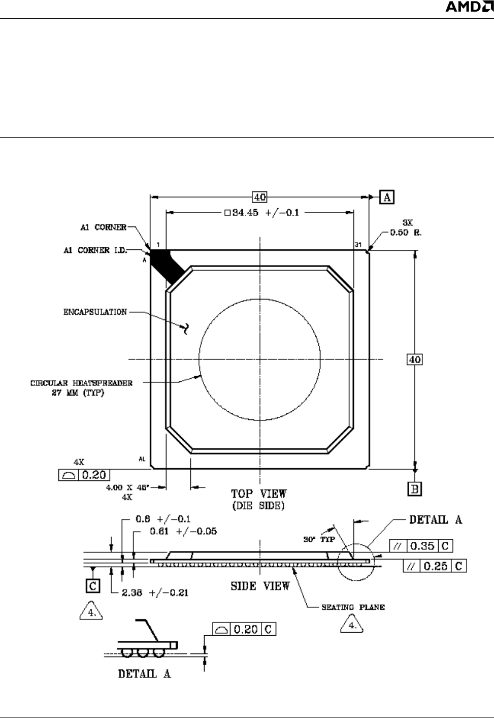
AMD Geode™ LX Processors Data Book 675
9
Package Specifications 33234H
9.0Package Specifications
9.1 Physical Dimensions
The figures in this section provide the mechanical package outline for the BGU481 (481-terminal Ball Grid Array Cavity Up)
Figure 9-1. BGU481 Top/Side View/Dimensions

676 AMD Geode™ LX Processors Data Book
Package Specifications
33234H
Figure 9-2. BGU481 Bottom View/Dimensions
A
AMD Geode™ LX Processors Data Book 677
Appendix A: Support Documentation 33234H
Appendix ASupport Documentation
A.1 Order Information
Ordering information for the AMD Geode™ LX processors is contained in this section. The ordering part number (OPN) is
formed by a combination of elements. An example of the OPN is shown in Figure A-1. Valid OPN combinations are pro-
vided in Table A-1 on page 678.
Figure A-1. AMD Geode™ LX Processors OPN Example
ALX C EE T J C V800
Family/Architecture: ALX = AMD Geode™ LX Processor Family
OPN (Note)
Note: Spaces are added to the ordering number shown above for viewing clarity only.
C
Display Type: V = CRT, TFT, and VOP
Performance Indicator:
Package Type: EE = BGU (TE-PBGA)
C = 0°C to 85°C Commercial
D = 0°C to 85°C Commercial Lead (Pb) Free
H = 0°C to 80°C Commercial Lead (Pb) Free
F = -40°C to 85°C Industrial Lead (Pb) Free
2 = 128K L2 cache, No EEPROM
C = 128K L2 cache, With EEPROM
J = 400 MHz memory, GeodeLink™ Architecture (500/600 MHz CPU)
H = 333 MHz memory, GeodeLink™ Architecture (433 MHz CPU)
K = 266 MHz memory, GeodeLink™ Architecture (366 MHz CPU)
T = 1.20V
X = 1.25V
Y = 1.40V
900 operates at 600 MHz
800 operates at 500 MHz
700 operates at 433 MHz
600 operates at 366 MHz
C ≤ 3W
D ≤ 4W
G ≤ 6W
Case Temperature:
Cache/EEPROM Indicator:
System Bus Speed:
Operating Voltage:
Performance Indicator:
Maximum Thermal Design Power (MTDP):
678 AMD Geode™ LX Processors Data Book
Appendix A: Order Information
33234H
Table A-1. Valid OPN Combinations
Family
Architecture MTDP
Performance
Indicator
Package
Type
Operating
Voltage
System Bus
Speed
EEPROM
Indicator
Display
Type
Case
Temperature/
Solder Type
(Note)
ALX G 900 EE Y J 2 V H
ALX D 800 EE X J 2 V C
D
F
CC
D
ALX C 700 EE T H 2 V C
D
CC
D
ALX C 600 EE T K 2 V D
Note: θJC = 3.7° C/W
Consult your local AMD sales office to confirm availability of specific valid combinations and to check on newly released combinations
possibly not listed.

AMD Geode™ LX Processors Data Book 679
Appendix A: Data Book Revision History 33234H
A.2 Data Book Revision History
This document is a report of the revision/creation process of the data book for the AMD Geode™ LX processors. Any revi-
sion (i.e., additions, deletions, parameter corrections, etc.) are recorded in the table(s) below.
Table A-2. Revision History
Revision #
(PDF Date) Revisions / Comments
0.1 (April 2004) Advance Information.
0.5 (September 2004) Added data registers descriptions, electrical specifications, and package specification
sections. Still preliminary and in the review/proofing process.
0.9 (January 2005) Added functional descriptions and other corrections.
A (May 2005) Engineering edits.
B (October 2005) Majority of edits to Electrical section.
C (April 2006) Engineering edits.
D (June 2006) Engineering edits.
E (November 2006) Added LX 900@1.5W processor values and other clarification edits/corrections.
F (May 2007) Added industrial temperature values and other minor edits/corrections.
G (May 2008) Minor edits/corrections. See Table A-3 for details.
H (February 2009) Added LX 600@0.7W parameters.
Table A-3. Edits to Current Revision
Section Revision
Section 1.0 "Overview" • Section 1.1 "General Description" on page 11:
— Updated link to AMD Embedded Developer Support Web site.
•Section 1.2 "Features" on page 12:
— Added LX 600@0.7W to Power Management bullet and footnote.
Section 6.2 "GeodeLink™
Memory Controller Regis-
ter Descriptions"
•Section 6.2.2.11 "Feature Enables (MC_CF1017_DATA)" on page 231:
— Slightly modified WR2DAT bit description.
Section 7.0 "Electrical
Specifications"
•Table 7-2 "Operating Conditions" on page 598:
— Added LX 600@0.7W and DDR2 values.
•Table 7-3 "AMD Geode LX 900@1.5W Processor DC Currents" on page 600, Table
7-4 "AMD Geode LX 800@0.9W Processor DC Currents" on page 601, and Table 7-5
"AMD Geode LX 700@0.8W Processor DC Currents" on page 602:
— Added IMEMDDR2ON parameter and values.
•Table 7-6 "AMD Geode LX 600@0.7W Processor DC Currents" on page 603:
— New table.
Section A.1 "Order Infor-
mation"
•Figure A-1 "AMD Geode™ LX Processors OPN Example" on page 677:
— Added “K” to System Bus Speed and “600” to Performance Indicator.
•Table A-1 "Valid OPN Combinations" on page 678:
— Added LX 600@0.7W OPN.

One AMD Place • P.O. Box 3453 • Sunnyvale, CA 94088-3453 USA • Tel: 408-749-4000 or 800-538-8450 • TWX: 910-339-9280 • TELEX: 34-6306
www.amd.com
